US9236229B2 - Gas supply member, plasma treatment method, and method of forming yttria-containing film - Google Patents
Gas supply member, plasma treatment method, and method of forming yttria-containing filmDownload PDFInfo
- Publication number
- US9236229B2 US9236229B2US13/193,914US201113193914AUS9236229B2US 9236229 B2US9236229 B2US 9236229B2US 201113193914 AUS201113193914 AUS 201113193914AUS 9236229 B2US9236229 B2US 9236229B2
- Authority
- US
- United States
- Prior art keywords
- gas supply
- exhaust port
- yttria
- downstream side
- electrode constituting
- Prior art date
- Legal status (The legal status is an assumption and is not a legal conclusion. Google has not performed a legal analysis and makes no representation as to the accuracy of the status listed.)
- Expired - Fee Related
Links
Images


Classifications
- H—ELECTRICITY
- H01—ELECTRIC ELEMENTS
- H01J—ELECTRIC DISCHARGE TUBES OR DISCHARGE LAMPS
- H01J37/00—Discharge tubes with provision for introducing objects or material to be exposed to the discharge, e.g. for the purpose of examination or processing thereof
- H01J37/32—Gas-filled discharge tubes
- H01J37/32431—Constructional details of the reactor
- H01J37/3244—Gas supply means
- H01J37/32449—Gas control, e.g. control of the gas flow
- H—ELECTRICITY
- H01—ELECTRIC ELEMENTS
- H01J—ELECTRIC DISCHARGE TUBES OR DISCHARGE LAMPS
- H01J37/00—Discharge tubes with provision for introducing objects or material to be exposed to the discharge, e.g. for the purpose of examination or processing thereof
- H01J37/32—Gas-filled discharge tubes
- H01J37/32431—Constructional details of the reactor
- H01J37/3244—Gas supply means
- H—ELECTRICITY
- H01—ELECTRIC ELEMENTS
- H01J—ELECTRIC DISCHARGE TUBES OR DISCHARGE LAMPS
- H01J37/00—Discharge tubes with provision for introducing objects or material to be exposed to the discharge, e.g. for the purpose of examination or processing thereof
- H01J37/32—Gas-filled discharge tubes
- H01J37/32431—Constructional details of the reactor
- H01J37/32458—Vessel
- H01J37/32477—Vessel characterised by the means for protecting vessels or internal parts, e.g. coatings
- H01J37/32495—Means for protecting the vessel against plasma
- C—CHEMISTRY; METALLURGY
- C23—COATING METALLIC MATERIAL; COATING MATERIAL WITH METALLIC MATERIAL; CHEMICAL SURFACE TREATMENT; DIFFUSION TREATMENT OF METALLIC MATERIAL; COATING BY VACUUM EVAPORATION, BY SPUTTERING, BY ION IMPLANTATION OR BY CHEMICAL VAPOUR DEPOSITION, IN GENERAL; INHIBITING CORROSION OF METALLIC MATERIAL OR INCRUSTATION IN GENERAL
- C23C—COATING METALLIC MATERIAL; COATING MATERIAL WITH METALLIC MATERIAL; SURFACE TREATMENT OF METALLIC MATERIAL BY DIFFUSION INTO THE SURFACE, BY CHEMICAL CONVERSION OR SUBSTITUTION; COATING BY VACUUM EVAPORATION, BY SPUTTERING, BY ION IMPLANTATION OR BY CHEMICAL VAPOUR DEPOSITION, IN GENERAL
- C23C16/00—Chemical coating by decomposition of gaseous compounds, without leaving reaction products of surface material in the coating, i.e. chemical vapour deposition [CVD] processes
- C23C16/44—Chemical coating by decomposition of gaseous compounds, without leaving reaction products of surface material in the coating, i.e. chemical vapour deposition [CVD] processes characterised by the method of coating
- C23C16/455—Chemical coating by decomposition of gaseous compounds, without leaving reaction products of surface material in the coating, i.e. chemical vapour deposition [CVD] processes characterised by the method of coating characterised by the method used for introducing gases into reaction chamber or for modifying gas flows in reaction chamber
- C23C16/45563—Gas nozzles
- C23C16/45565—Shower nozzles
- C—CHEMISTRY; METALLURGY
- C23—COATING METALLIC MATERIAL; COATING MATERIAL WITH METALLIC MATERIAL; CHEMICAL SURFACE TREATMENT; DIFFUSION TREATMENT OF METALLIC MATERIAL; COATING BY VACUUM EVAPORATION, BY SPUTTERING, BY ION IMPLANTATION OR BY CHEMICAL VAPOUR DEPOSITION, IN GENERAL; INHIBITING CORROSION OF METALLIC MATERIAL OR INCRUSTATION IN GENERAL
- C23C—COATING METALLIC MATERIAL; COATING MATERIAL WITH METALLIC MATERIAL; SURFACE TREATMENT OF METALLIC MATERIAL BY DIFFUSION INTO THE SURFACE, BY CHEMICAL CONVERSION OR SUBSTITUTION; COATING BY VACUUM EVAPORATION, BY SPUTTERING, BY ION IMPLANTATION OR BY CHEMICAL VAPOUR DEPOSITION, IN GENERAL
- C23C16/00—Chemical coating by decomposition of gaseous compounds, without leaving reaction products of surface material in the coating, i.e. chemical vapour deposition [CVD] processes
- C23C16/44—Chemical coating by decomposition of gaseous compounds, without leaving reaction products of surface material in the coating, i.e. chemical vapour deposition [CVD] processes characterised by the method of coating
- C23C16/50—Chemical coating by decomposition of gaseous compounds, without leaving reaction products of surface material in the coating, i.e. chemical vapour deposition [CVD] processes characterised by the method of coating using electric discharges
- C23C16/505—Chemical coating by decomposition of gaseous compounds, without leaving reaction products of surface material in the coating, i.e. chemical vapour deposition [CVD] processes characterised by the method of coating using electric discharges using radio frequency discharges
- C23C16/509—Chemical coating by decomposition of gaseous compounds, without leaving reaction products of surface material in the coating, i.e. chemical vapour deposition [CVD] processes characterised by the method of coating using electric discharges using radio frequency discharges using internal electrodes
- C23C16/5096—Flat-bed apparatus
- H—ELECTRICITY
- H01—ELECTRIC ELEMENTS
- H01J—ELECTRIC DISCHARGE TUBES OR DISCHARGE LAMPS
- H01J37/00—Discharge tubes with provision for introducing objects or material to be exposed to the discharge, e.g. for the purpose of examination or processing thereof
- H01J37/32—Gas-filled discharge tubes
- H01J37/32009—Arrangements for generation of plasma specially adapted for examination or treatment of objects, e.g. plasma sources
- Y—GENERAL TAGGING OF NEW TECHNOLOGICAL DEVELOPMENTS; GENERAL TAGGING OF CROSS-SECTIONAL TECHNOLOGIES SPANNING OVER SEVERAL SECTIONS OF THE IPC; TECHNICAL SUBJECTS COVERED BY FORMER USPC CROSS-REFERENCE ART COLLECTIONS [XRACs] AND DIGESTS
- Y10—TECHNICAL SUBJECTS COVERED BY FORMER USPC
- Y10T—TECHNICAL SUBJECTS COVERED BY FORMER US CLASSIFICATION
- Y10T137/00—Fluid handling
- Y10T137/8593—Systems
- Y10T137/87169—Supply and exhaust
Definitions
- Embodiments described hereinrelate generally to a gas supply member, a plasma treatment method, and a method of forming an yttria-containing film.
- a reactive ion etching (RIE) apparatusis used in a microfabrication process for manufacturing a semiconductor device, a liquid crystal display device and the like.
- RIEreactive ion etching
- the inside of a chamberis first adjusted to enter a low pressure state, fluorine-based gas or chlorine-based gas is then introduced into the chamber to generate a plasma phase, and etching is performed.
- a member constituting the inner walls and inner portions of the RIE apparatusis susceptible to plasma and thus is likely to easily corrode when it is exposed to plasma, the member is usually coated with a protective film made of a material having a high plasma resistance such as yttria or alumina.
- the protective filmsuch as yttria is coated onto the member constituting the inner walls and inner portions of the RIE apparatus, the protective film is still likely to degrade due to shedding of particles of the protective film, crack in the protective film and the like.
- FIG. 1is a sectional view schematically illustrating an example of the configuration of a plasma treatment apparatus according to a first embodiment
- FIG. 2is a partial sectional view schematically illustrating the shape in the vicinity of an exhaust port of a shower head according the first embodiment
- FIG. 3A and FIG. 3Bare sectional views schematically illustrating an example of a protective film
- FIG. 4A and FIG. 4Bare sectional views schematically illustrating an example of the procedure of a method for forming a protective film according to the first embodiment
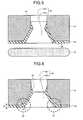
- FIG. 5is a sectional view schematically illustrating the shape in the vicinity of an exhaust port of a conventional shower head
- FIG. 6is a sectional view schematically illustrating the shape in the vicinity of an exhaust port of a shower head according a second embodiment
- FIG. 7is a sectional view schematically illustrating the shape in the vicinity of an exhaust port of a shower head according a third embodiment
- FIG. 8is a sectional view schematically illustrating the shape in the vicinity of an exhaust port of a shower head according a fourth embodiment
- FIG. 9A to FIG. 9Fare sectional views schematically illustrating an example of the procedure of a first method for forming a protective film on a shower head according to the fourth embodiment.
- FIG. 10A to FIG. 10Dare sectional views schematically illustrating an example of the procedure of a second method for forming a protective film on a shower head according to the fourth embodiment.
- a gas supply memberincludes a gas supply passage having a gas flow channel with a first diameter, an exhaust port connected to one end portion of the gas flow channel and installed at the surface of a downstream side of the gas supply member.
- An yttria-containing filmis provided on a surface constituting the exhaust port and the surface of the downstream side of the gas supply member. Furthermore, at least a part of the surface constituting the exhaust port is formed with a curved surface.
- a gas supply member, a plasma treatment method, and a method of forming an yttria-containing film according to the embodimentswill be described in detail below with reference to the accompanying drawings.
- the present inventionis not limited to the following embodiments.
- sectional views of films used in the following embodimentsare schematic, and relationship between the thickness and width of layers and the ratio of thicknesses of the layers differ from the actual relationship or ratio.
- FIG. 1is a sectional view schematically illustrating an example of the configuration of a plasma treatment apparatus according to the first embodiment.
- a RIE apparatusis used as a plasma treatment apparatus 10 .
- the plasma treatment apparatus 10includes a chamber 11 airtightly sealed and made of, for example, aluminum.
- the chamber 11is grounded.
- the chamber 11is provided therein with a substrate holding unit (support table) 21 that horizontally supports a substrate 100 which is a process target such as a wafer and serves as a lower electrode.
- the substrate holding unit 21is provided on the surface thereof with a holding mechanism such as an electrostatic chuck mechanism (not shown) that electrostatically attracts the substrate 100 .
- An insulating ring 22is provided to cover the edges of lateral side and bottom side of the substrate holding unit 21 , and a focus ring 23 is provided on the outer periphery of the upper portion of the substrate holding unit 21 covered by the insulating ring 22 .
- the focus ring 23is a member provided in order to adjust an electric field such that the electric field is not biased with respect to the vertical direction (direction vertical to a substrate surface) at the edges of the substrate 100 when the substrate 100 is etched.
- the substrate holding unit 21is supported on a support section 12 cylindrically protruding upright from the bottom wall near the center of the chamber 11 via the insulating ring 22 such that the substrate holding unit 21 is positioned near the center of the chamber 11 .
- a baffle plate 24is provided between the insulating ring 22 and the sidewall of the chamber 11 .
- the baffle plate 24is formed with a plurality of gas discharge holes 25 passing through the plate in the thickness direction of the plate.
- a power feed line 31 for supplying radio frequency poweris connected to the substrate holding unit 21 , and a blocking condenser 32 , a matching device 33 , and a radio frequency power supply 34 are connected to the power feed line 31 . Radio frequency power with a predetermined frequency is supplied from the radio frequency power supply 34 to the substrate holding unit 21 .
- a shower head 41 serving as an upper electrodeis provided above the substrate holding unit 21 to face the substrate holding unit 21 serving as the lower electrode.
- the shower head 41is fixed to the sidewall near the upper portion of the chamber 11 while being spaced apart from the substrate holding unit 21 by a predetermined distance, thereby facing the substrate holding unit 21 in parallel to the substrate holding unit 21 .
- the shower head 41 and the substrate holding unit 21form a pair of parallel flat plate electrodes.
- the shower head 41is formed with a plurality of gas supply passages 42 passing through the plate in the thickness direction of the plate.
- a gas supply port 13is provided near the upper portion of the chamber 11 to supply treatment gas used in plasma treatment, and a gas supply apparatus (not shown) is connected to the gas supply port 13 through a pipe.
- a gas exhaust port 14is provided at a lower portion of the chamber 11 below the substrate holding unit 21 and the baffle plate 24 , and a vacuum pump (not shown) is connected to the gas exhaust port 14 through a pipe.
- an area of the chamber 11 partitioned by the substrate holding unit 21 , the baffle plate 24 , and the shower head 41is a plasma treatment chamber 61
- an upper area of the chamber 11 partitioned by the shower head 41is a gas supply chamber 62
- a lower area of the chamber 11 partitioned by the substrate holding unit 21 and the baffle plate 24is a gas exhaust chamber 63 .
- a protective film 50is formed on the surface of a member constituting the plasma treatment apparatus 10 with such a configuration, which is in contact with a plasma generation area, that is, on the surface of a member constituting the plasma treatment chamber 61 .
- the protective film 50 including an yttria-containing film(hereinafter, referred to as an yttria film) is formed on the inner wall surface of the chamber 11 which constitutes the plasma treatment chamber 61 , the surface of the shower head 41 facing the plasma treatment chamber 61 , the surface of the baffle plate 24 facing the plasma treatment chamber 61 , the surface of the focus ring 23 , and the surface of the substrate holding unit 21 onto which the substrate 100 is loaded.
- the substrate 100 which is a process targetis loaded onto the substrate holding unit 21 , and the substrate 100 is fixed by the electrostatic chuck mechanism, for example.
- the inside of the chamber 11is vacuum-sucked by the vacuum pump (not shown) connected to the gas exhaust port 14 .
- the vacuum pumpnot shown
- the gas exhaust chamber 63 and the plasma treatment chamber 61are connected to each other through gas discharge holes 25 formed through the baffle plate 24 , and the plasma treatment chamber 61 and the gas supply chamber 62 are connected to each other through the gas supply passages 42 of the shower head 41 , the entire inside space of the chamber 11 is vacuum-sucked through the vacuum pump connected to the gas exhaust port 14 .
- the treatment gasis supplied from the gas supply apparatus (not shown) to the gas supply chamber 62 , and is supplied to the plasma treatment chamber 61 through the gas supply passages 42 of the shower head 41 .
- a radio frequency voltageis applied to the substrate holding unit 21 (the lower electrode) in the state in which the shower head 41 (the upper electrode) is grounded, so that plasma is generated in the plasma treatment chamber 61 .
- the radio frequency voltageis applied to the lower electrode, potential gradient occurs between the plasma and the substrate 100 , so that ions in plasma state are accelerated toward the substrate holding unit 21 and thus an etching process is performed.
- FIG. 2is a partial sectional view schematically illustrating the shape in the vicinity of the exhaust port of the shower head according to the first embodiment.
- the shower head 41 serving as the gas supply memberis provided with the gas supply passages 42 .
- the gas supply passages 42pass through a member constituting the shower head 41 toward the bottom surface (a surface of a downstream side of gas flow) from the top surface of the shower head 41 as illustrated in FIG. 1 .
- the gas supply passage 42includes a gas flow channel 421 with the first diameter, and an exhaust port 422 with an opening diameter increasing in a tilted manner from one end portion of the gas flow channel 421 so as to be the second diameter which is larger than the first diameter.
- the shower head 41is processed to have a tapered shape in which the diameter of the opening of the shower head 41 increases in the vicinity of the exhaust port 422 of the gas supply passage 42 .
- the member constituting the shower head 41for example, aluminum and the like can be used.
- the protective film 50is provided on the formation surface of the exhaust port 422 and in the vicinity of a inflectional section 43 of the surface of the downstream side, which is one main surface of the shower head 41 , such that at least a part of the inflectional section 43 is exposed.
- a film formation targetincludes a plurality of surfaces (planes or curved surfaces) which are not parallel to one another
- the inflectional section 43indicates a protruded section formed by bonding one surface serving as a reference to another surface at an angle of more than 90°.
- a lateral side of the protective film 50 formed in the vicinity of the inflectional section 43 positioned at the boundary between the gas flow channel 421 and the exhaust port 422is approximately level with (is flush with) the inner surface of the gas flow channel 421 . That is, a ring structure formed by the protective film 50 formed in the vicinity of the inflectional section 43 at the upper portion of the exhaust port 422 has a diameter which is approximately the same as the first diameter.
- an yttria film having a thickness of 50 ⁇ m to 100 ⁇may be used.
- FIG. 3A and FIG. 3Bare sectional views schematically illustrating an example of the protective film.
- a general yttria film 51 formed on a constituting member 55 (a film formation target) as illustrated in FIG. 3Amay be used.
- the protective film 50may include a melt-solidified part (a melt-solidified film) 53 obtained by melting the yttria film 51 of FIG. 3A from the surface in the range of the thickness of the yttria film 51 as illustrated in FIG. 3B .
- the yttria film having the total thicknessmay be used as the melt solidified part 53 , or the protective film 50 may have a stacked structure of the melt solidified part 53 obtained by melting the yttria film 51 from the surface in the range of a predetermined thickness and a non-melt solidified part (a non-melt solidified film) 52 .
- the melt solidified part 53has a restricted inter-particle gap as compared with the non-melt solidified part 52 , is high density, and has a planarized surface.
- the melt solidified part 53has a density greater than that of the non-melt solidified part 52 .
- the non-melt solidified part 52has a density range of 2.0 g/cm 3 to 4.0 g/cm 3
- the melt solidified part 53has a density range of 4.0 g/cm 3 to 5.0 g/cm 3 .
- the protective film 50 including the yttria filmis formed on the shower head 41 made of aluminum.
- an alumina filmmay be formed on aluminum, and the protective film 50 may be further formed on the alumina film.
- FIG. 4A and FIG. 4Bare sectional views schematically illustrating an example of the procedure of the method of forming the protective film according to the first embodiment.
- the protective film 50 including the yttria film and having a thickness of 50 ⁇ m to 100 ⁇ mis formed on the surface (the surface of the side of the exhaust port 422 ) of the downstream side of the shower head 41 made of aluminum and formed with the gas supply passage 42 , and on the inner surface over a part of the gas flow channel 421 from the exhaust port 422 .
- the protective film 50is formed to cover the inflectional section 43 at which the diameter of the gas supply passage 42 changes.
- a spraying methoda chemical vapor deposition (CVD) method, an aerosol deposition method, a cold spraying method, a gas deposition method, an electrostatic powder impact deposition method, an impact sintering method and the like can be used.
- the protective film 50 formed on the inner surface of the gas flow channel 421is removed using polishing and the like.
- the lower surfacewhich constitutes the inflectional section 43
- the lateral side of the protective film 50 formed in the vicinity of the inflectional section 43 positioned at the inner surface of the exhaust port 422is approximately level with the inner surface of the gas flow channel 421 . Consequently, the shower head 41 with the structure illustrated in FIG. 2 is achieved.
- the yttria filmmay be subject to surface treatment, melted in the range of the thickness of a film formed from the surface of the yttria film, and then solidified.
- the surface treatmentfor example, it is possible to use a method capable of selectively thermally fusing the surface of the yttria film, such as laser annealing treatment or plasma jet treatment.
- FIG. 5is a sectional view schematically illustrating the shape in the vicinity of an exhaust port of a conventional shower head.
- a shower head 41 serving as a gas supply memberfor example, is provided with a gas supply passage 42 which is configured to pass through a member constituting the shower head 41 toward the surface of a downstream side from the upper surface of the shower head 41 .
- the gas supply passage 42includes a gas flow channel 421 with a first diameter, and an exhaust port 422 with an opening diameter increasing from one end portion of the gas flow channel 421 so as to be a second diameter which is larger than the first diameter.
- a protective film 50is provided on the surface of the downstream side of the shower head 41 , the inner surface of the exhaust port 422 , and in the vicinity of the gas flow channel 421 adjacent to the exhaust port 422 . That is, the protective film 50 is provided to cover a inflectional section 43 of the gas supply passage 42 .
- the protective film 50does not extend over the inflectional section 43 of the shower head 41 .
- an inner surface as a part of the gas supply passage 42 formed by the protective film 50 formed in the vicinity of the inflectional section 43 of the exhaust port 422is approximately level with the inner surface of the gas flow channel 421 . In this way, even if thermal expansion difference occurs between the shower head 41 and the protective film 50 due to heating during the plasma treatment, crack does not easily occur in the protective film 50 in the vicinity of the inflectional section 43 .
- FIG. 6is a sectional view schematically illustrating the shape in the vicinity of an exhaust port of a shower head according to a second embodiment.
- the second embodimentis different from the first embodiment in that an exhaust port 422 of a gas flow channel 421 of a shower head 41 serving as a base material includes a plurality of surfaces with angles different from each other.
- a protective film 50is formed in the vicinity of the exhaust port 422 and on the surface of the downstream side of the shower head 41 serving as the gas supply member. In the protective film 50 with such a structure, stress concentrated on a corner section 44 is attenuated.
- the film thicknesses d 1 and d 2are the thicknesses of the protective film 50 in the normal direction at each position of the shower head 41 .
- the film thickness d 1 at a portion other than the corner section 44is about 10 ⁇ m to about 100 ⁇ m
- the film thickness d 2 in the vicinity of the corner section 44is thicker than the film thickness d 1 by about one to two times, that is, about 10 ⁇ m to about 200 ⁇ m.
- a cross angle of the corner section 44 formed in the exhaust port 422 of the shower head 41may be large as compared with the case of FIG. 2 .
- the protective film 50can be formed on the above-described shower head 41 using a method the same as that of the first embodiment.
- FIG. 7is a sectional view schematically illustrating a third embodiment.
- the surface forming the exhaust port 422 of the shower head 41 serving as a base material and the surface (the lower surface) of the downstream side of gas floware not curved surfaces, and the respective surfaces are connected at a predetermined angle to form the corner section 44 .
- the surface forming a gas flow channel 421 of a shower head 41 serving as a base material and a surface 41 A of a downstream side of the shower head 41are connected to each other by a smooth curved surface.
- the curved surface of an exhaust port 422is formed to have a tapered shape such that the opening diameter of the exhaust port 422 increases as it goes far from a connection part with the gas flow channel 421 , and the opening diameter at the surface 41 A of the downstream side of the shower head 41 is the second diameter which is larger than a first diameter.
- all surfaces constituting the exhaust port 422are formed by curved surfaces.
- a curved surfacemay be formed near (an area corresponding to the corner section 44 of FIG. 6 ) at least a connection part of the surfaces constituting the exhaust port 422 and the surface 41 A of the downstream side of the shower head 41 .
- the surface 41 A of the downstream side of the shower head 41is a surface constituting the shower head 41 facing an area where plasma is generated.
- the curvature radius of the curved surface forming the exhaust port 422 of the shower head 41 illustrated in FIG. 7is about 100 ⁇ m to about 500 ⁇ m.
- the thickness of a protective film 50 formed on the surface forming the exhaust port 422 of the shower head 41is approximately constant. Furthermore, the protective film 50 is also formed on the surfaces forming the exhaust port 422 and in the vicinity of the surfaces forming the gas flow channel 421 , which are adjacent to the exhaust port 422 . Moreover, since the formation surface of the exhaust port 422 of the shower head 41 serving as a base is a curved surface, the protective film 50 is configured to have a curved surface shape according to the formation surface thereof.
- the protective film 50 usedis the same as the protective film 50 used in the first embodiment.
- the protective film 50may be directly formed on the shower head 41 made of aluminum, or an alumina film may be formed on aluminum and the protective film 50 may be formed on the alumina film.
- an yttria film constituting the protective film 50can also be formed using the method described in the first embodiment.
- the exhaust port 422 of the shower head 41 serving as the baseis formed with the curved surface and the protective film 50 is formed on the curved surface, stress concentrating on the corner section 44 is further reduced as compared with the second embodiment, so that crack does not easily occur as compared with the second embodiment.
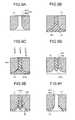
- FIG. 8is a sectional view schematically illustrating the shape in the vicinity of an exhaust port of a shower head according a fourth embodiment.
- the fourth embodimenthas a structure approximately the same as that of the third embodiment. That is, in the third embodiment, the thickness of the protective film 50 on the exhaust port 422 is approximately constant. However, in the fourth embodiment, the thickness of a protective film 50 is gradually reduced toward the vicinity of the center of an exhaust port 422 . Furthermore, the fourth embodiment is different from the third embodiment in that the yttria film is not formed in the side of a gas flow channel 421 . In the protective film 50 with such a structure, since stress concentrated on a corner section 44 is further reduced as compared with the second embodiment, crack does not easily occur as compared with the second embodiment.
- the film thickness of a curved partcontinuously changes from about 10 ⁇ m to about 100 ⁇ m.
- the curvature radius of the curved surface of a shower head 41 illustrated in FIG. 8is about 100 ⁇ m to about 500 ⁇ m similarly to FIG. 7 .
- the curved surface of the exhaust port 422is formed to have a tapered shape such that the opening diameter of the exhaust port 422 increases as it goes far from a connection part with the gas flow channel 421 , and the opening diameter at a surface 41 A of the downstream side of the shower head 41 is a second diameter which is larger than a first diameter.
- all surfaces constituting the exhaust port 422are formed by curved surfaces.
- a curved surfacemay be formed near (an area corresponding to the corner section 44 of FIG. 6 ) at least a connection part of the surfaces constituting the exhaust port 422 and the surface 41 A of the downstream side of the shower head 41 .
- the surface 41 A of the downstream side of the shower head 41is a surface constituting the shower head 41 facing an area where plasma is generated.
- FIG. 9A to FIG. 9Fare a series of sectional views schematically illustrating a first method of forming the protective film in the vicinity of the exhaust port of the shower head illustrated in FIG. 8 according to the fourth embodiment.
- the shower head 41includes the gas flow channel 421 with a first diameter, and the exhaust port 422 with the second diameter at the surface of a downstream side which is a plane while an opening diameter expands from the lower end of the gas flow channel 421 along a smooth surface.
- the protective film 50is formed such that the film thickness thereof gradually increases toward the surface of the downstream side of the shower head 41 from the inflectional section 43 positioned at the boundary between the gas flow channel 421 on the formation surface of the exhaust port 422 , and the exhaust port 422 . Furthermore, the protective film 50 has an approximately uniform thickness on the surface of the downstream side of the shower head 41 . Even in such a structure, the protective film 50 is not formed on the gas flow channel 421 , and a lateral side of the protective film 50 formed in the vicinity of the inflectional section 43 positioned at the boundary between the gas flow channel 421 and the exhaust port 422 is approximately level with the inner surface of the gas flow channel 421 .
- FIG. 9A to FIG. 9Fare sectional views schematically illustrating an example of the procedure of the first method of forming the protective film on the shower head according to the fourth embodiment.
- the descriptionwill be made by illustrating only a part of the gas supply passage 42 of the shower head 41 .
- the gas supply passage 42is formed in a base material made of aluminum.
- the gas supply passage 42includes the gas flow channel 421 with the first diameter, and the exhaust port 422 with the second diameter at the surface of the downstream side which is the plane while the opening diameter expands from the lower end of the gas flow channel 421 along the smooth surface, thereby forming the shower head 41 .
- negative-type photoresist 101is coated from the side of the exhaust port 422 of the shower head 41 .
- the negative-type photoresist 101is exposed from the upper surface (the formation surface of the gas flow channel 421 ) of the shower head 41 using ultraviolet and the like, so that only an exposed part of the negative-type photoresist 101 is cured, resulting in the generation of a sacrificial layer 101 a which is a plug member.
- the protective film 50 including the yttria filmis formed on the formation surface (the surface of the downstream side) of the exhaust port 422 of the shower head 41 provided with the sacrificial layer 101 a .
- the yttria film constituting the protective film 50it is possible to use a spraying method, a CVD method, an aerosol deposition method, a cold spraying method, a gas deposition method, an electrostatic powder impact deposition method, an impact sintering method and the like.
- the protective film 50 having a thickness of 50 ⁇ m to 100 ⁇ mis formed on the surface of the downstream side of the shower head 41 .
- the thickness of the protective film 50is gradually reduced toward the vicinity 105 of the center of the exhaust port 422 because yttria particles do not easily reach the vicinity 105 of the center. Furthermore, the protective film 50 is also formed in the vicinity of the upper surface of the sacrificial layer 101 a.
- the sacrificial layer 101 ais removed using a method such as a resist stripping technique.
- the protective film 50is formed on both the surfaces constituting the exhaust port 422 of the shower head 41 and the surface of the downstream side of the shower head 41 .
- the first formation method described abovecan also be applied to the first to third embodiments.
- a method other than the first formation methodcan also be used.
- a case for processing the vicinity of the exhaust port 422 of the shower head 41 illustrated in FIG. 8 according to the fourth embodiment by using a method different from the first formation methodwill be described.
- FIG. 10A to FIG. 10Dare sectional views schematically illustrating an example of the procedure of a second method of forming the protective film on the shower head illustrated in FIG. 8 according to the fourth embodiment.
- the descriptionwill be made by illustrating only a part of the gas supply passage 42 of the shower head 41 .
- the gas supply passage 42is formed in a base material made of aluminum.
- the gas supply passage 42includes the gas flow channel 421 with the first diameter, and the exhaust port 422 with the second diameter at the surface of the downstream side which is the plane while the opening diameter expands from the lower end of the gas flow channel 421 along the smooth surface, thereby forming the shower head 41 .
- a tool 111 serving as a plug memberis inserted into the gas flow channel 421 .
- the tool 111has a diameter approximately the same as the first diameter of the gas flow channel 421 .
- the tool 111is inserted to slightly protrude toward the exhaust port 422 from the surface (the formation side of the exhaust port 422 ) of the downstream side of the shower head 41 .
- the gas flow channel 421 of the shower head 41is closed by the tool 111 , and the lower end portion of the tool 111 is fixed to slightly protrude further toward the surface (the side where the opening diameter of the exhaust port 422 is expanded) of the downstream side than the boundary between the gas flow channel 421 and the exhaust port 422 .
- the protective film 50 including the yttria filmis formed on the formation surface (the surface of the downstream side) of the exhaust port 422 of the shower head 41 including the tool 111 inserted thereto.
- the yttria film constituting the protective film 50it is possible to use a spraying method, a CVD method, an aerosol deposition method, a cold spraying method, a gas deposition method, an electrostatic powder impact deposition method, an impact sintering method and the like.
- the protective film 50 having a thickness of 50 ⁇ m to 100 ⁇ mis formed on the surface of the downstream side of the shower head 41 .
- the thickness of the protective film 50is gradually reduced toward the vicinity of the center of the exhaust port 422 because yttria particles do not easily reach the vicinity. Furthermore, since the gas flow channel 421 is closed by the tool 111 , the protective film 50 is not formed in the gas flow channel 421 , but formed in the vicinity of the upper surface of the tool 111 .
- the tool 111is removed.
- the tool 111is removed from the surface of the downstream side of the shower head 41 such that the protective film 50 is not damaged.
- the protective film 50is formed on both the surfaces constituting the exhaust port 422 of the shower head 41 and the surface of the downstream side of the shower head 41 .
- the protective film 50is formed on both the surface of the downstream side of the shower head 41 and the formation surface of the exhaust port 422 , and then the tool 111 is pulled out from the gas flow channel 421 , it is possible to easily form the protective film 50 , as compared with the first formation method. Furthermore, since the tool 111 can be repeatedly used a plurality of times, it is possible to form the protective film 50 at a low cost, as compared with the case of using resist in the first formation method.
- the protective film 50may be formed such that at least a part of the inflectional section 43 is exposed.
- the protective film 50 formed on the shower head 41 of the RIE apparatushas been described as an example.
- the embodimentsare not limited thereto.
- the RIE apparatushas been described as an example of the plasma treatment apparatus 10 .
- CDEchemical dry etching
Landscapes
- Physics & Mathematics (AREA)
- Engineering & Computer Science (AREA)
- Plasma & Fusion (AREA)
- Chemical & Material Sciences (AREA)
- Analytical Chemistry (AREA)
- Chemical Vapour Deposition (AREA)
- Drying Of Semiconductors (AREA)
Abstract
Description
Claims (15)
Applications Claiming Priority (4)
| Application Number | Priority Date | Filing Date | Title |
|---|---|---|---|
| JP2010180790 | 2010-08-12 | ||
| JP2010-180790 | 2010-08-12 | ||
| JP2011-060711 | 2011-03-18 | ||
| JP2011060711AJP5198611B2 (en) | 2010-08-12 | 2011-03-18 | Gas supply member, plasma processing apparatus, and method for forming yttria-containing film |
Publications (2)
| Publication Number | Publication Date |
|---|---|
| US20120037596A1 US20120037596A1 (en) | 2012-02-16 |
| US9236229B2true US9236229B2 (en) | 2016-01-12 |
Family
ID=45564042
Family Applications (1)
| Application Number | Title | Priority Date | Filing Date |
|---|---|---|---|
| US13/193,914Expired - Fee RelatedUS9236229B2 (en) | 2010-08-12 | 2011-07-29 | Gas supply member, plasma treatment method, and method of forming yttria-containing film |
Country Status (2)
| Country | Link |
|---|---|
| US (1) | US9236229B2 (en) |
| JP (1) | JP5198611B2 (en) |
Cited By (3)
| Publication number | Priority date | Publication date | Assignee | Title |
|---|---|---|---|---|
| US9884787B2 (en) | 2013-11-12 | 2018-02-06 | Applied Materials, Inc. | Rare-earth oxide based monolithic chamber material |
| US9988702B2 (en) | 2012-05-22 | 2018-06-05 | Kabushiki Kaisha Toshiba | Component for plasma processing apparatus and method for manufacturing component for plasma processing apparatus |
| US20210074505A1 (en)* | 2018-01-24 | 2021-03-11 | Applied Materials, Inc. | Side inject designs for improved radical concentrations |
Families Citing this family (105)
| Publication number | Priority date | Publication date | Assignee | Title |
|---|---|---|---|---|
| US10283321B2 (en) | 2011-01-18 | 2019-05-07 | Applied Materials, Inc. | Semiconductor processing system and methods using capacitively coupled plasma |
| JP2013247150A (en)* | 2012-05-23 | 2013-12-09 | Ulvac Japan Ltd | Plasma processing apparatus |
| US9373517B2 (en) | 2012-08-02 | 2016-06-21 | Applied Materials, Inc. | Semiconductor processing with DC assisted RF power for improved control |
| US9132436B2 (en) | 2012-09-21 | 2015-09-15 | Applied Materials, Inc. | Chemical control features in wafer process equipment |
| US10256079B2 (en) | 2013-02-08 | 2019-04-09 | Applied Materials, Inc. | Semiconductor processing systems having multiple plasma configurations |
| JP2014157944A (en)* | 2013-02-15 | 2014-08-28 | Toshiba Corp | Gas supply member and plasma processing apparatus |
| US9362130B2 (en) | 2013-03-01 | 2016-06-07 | Applied Materials, Inc. | Enhanced etching processes using remote plasma sources |
| US9309598B2 (en) | 2014-05-28 | 2016-04-12 | Applied Materials, Inc. | Oxide and metal removal |
| JP6544902B2 (en)* | 2014-09-18 | 2019-07-17 | 東京エレクトロン株式会社 | Plasma processing system |
| US9355922B2 (en) | 2014-10-14 | 2016-05-31 | Applied Materials, Inc. | Systems and methods for internal surface conditioning in plasma processing equipment |
| US9966240B2 (en) | 2014-10-14 | 2018-05-08 | Applied Materials, Inc. | Systems and methods for internal surface conditioning assessment in plasma processing equipment |
| US11637002B2 (en) | 2014-11-26 | 2023-04-25 | Applied Materials, Inc. | Methods and systems to enhance process uniformity |
| US10224210B2 (en) | 2014-12-09 | 2019-03-05 | Applied Materials, Inc. | Plasma processing system with direct outlet toroidal plasma source |
| US10573496B2 (en) | 2014-12-09 | 2020-02-25 | Applied Materials, Inc. | Direct outlet toroidal plasma source |
| JP6423706B2 (en)* | 2014-12-16 | 2018-11-14 | 東京エレクトロン株式会社 | Plasma processing equipment |
| US11257693B2 (en) | 2015-01-09 | 2022-02-22 | Applied Materials, Inc. | Methods and systems to improve pedestal temperature control |
| US9728437B2 (en) | 2015-02-03 | 2017-08-08 | Applied Materials, Inc. | High temperature chuck for plasma processing systems |
| US20160225652A1 (en) | 2015-02-03 | 2016-08-04 | Applied Materials, Inc. | Low temperature chuck for plasma processing systems |
| TWI677929B (en)* | 2015-05-01 | 2019-11-21 | 美商應用材料股份有限公司 | Dual-channel showerhead for formation of film stacks |
| US12281385B2 (en)* | 2015-06-15 | 2025-04-22 | Taiwan Semiconductor Manufacturing Co., Ltd. | Gas dispenser and deposition apparatus using the same |
| US9691645B2 (en) | 2015-08-06 | 2017-06-27 | Applied Materials, Inc. | Bolted wafer chuck thermal management systems and methods for wafer processing systems |
| US9741593B2 (en) | 2015-08-06 | 2017-08-22 | Applied Materials, Inc. | Thermal management systems and methods for wafer processing systems |
| US9349605B1 (en) | 2015-08-07 | 2016-05-24 | Applied Materials, Inc. | Oxide etch selectivity systems and methods |
| US10504700B2 (en) | 2015-08-27 | 2019-12-10 | Applied Materials, Inc. | Plasma etching systems and methods with secondary plasma injection |
| US10504754B2 (en) | 2016-05-19 | 2019-12-10 | Applied Materials, Inc. | Systems and methods for improved semiconductor etching and component protection |
| US10522371B2 (en) | 2016-05-19 | 2019-12-31 | Applied Materials, Inc. | Systems and methods for improved semiconductor etching and component protection |
| US9865484B1 (en) | 2016-06-29 | 2018-01-09 | Applied Materials, Inc. | Selective etch using material modification and RF pulsing |
| US10629473B2 (en) | 2016-09-09 | 2020-04-21 | Applied Materials, Inc. | Footing removal for nitride spacer |
| US10062575B2 (en) | 2016-09-09 | 2018-08-28 | Applied Materials, Inc. | Poly directional etch by oxidation |
| WO2018051974A1 (en)* | 2016-09-13 | 2018-03-22 | Toto株式会社 | Member for semiconductor manufacturing device |
| US20180090300A1 (en)* | 2016-09-27 | 2018-03-29 | Applied Materials, Inc. | Diffuser With Corner HCG |
| US10062585B2 (en) | 2016-10-04 | 2018-08-28 | Applied Materials, Inc. | Oxygen compatible plasma source |
| US9934942B1 (en) | 2016-10-04 | 2018-04-03 | Applied Materials, Inc. | Chamber with flow-through source |
| US10546729B2 (en) | 2016-10-04 | 2020-01-28 | Applied Materials, Inc. | Dual-channel showerhead with improved profile |
| US10062579B2 (en) | 2016-10-07 | 2018-08-28 | Applied Materials, Inc. | Selective SiN lateral recess |
| US9947549B1 (en) | 2016-10-10 | 2018-04-17 | Applied Materials, Inc. | Cobalt-containing material removal |
| US9768034B1 (en) | 2016-11-11 | 2017-09-19 | Applied Materials, Inc. | Removal methods for high aspect ratio structures |
| US10163696B2 (en) | 2016-11-11 | 2018-12-25 | Applied Materials, Inc. | Selective cobalt removal for bottom up gapfill |
| US10026621B2 (en) | 2016-11-14 | 2018-07-17 | Applied Materials, Inc. | SiN spacer profile patterning |
| US10242908B2 (en) | 2016-11-14 | 2019-03-26 | Applied Materials, Inc. | Airgap formation with damage-free copper |
| JP6984126B2 (en)* | 2016-12-27 | 2021-12-17 | 東京エレクトロン株式会社 | Manufacturing method of gas supply device, plasma processing device and gas supply device |
| US10566206B2 (en) | 2016-12-27 | 2020-02-18 | Applied Materials, Inc. | Systems and methods for anisotropic material breakthrough |
| US10431429B2 (en) | 2017-02-03 | 2019-10-01 | Applied Materials, Inc. | Systems and methods for radial and azimuthal control of plasma uniformity |
| US10403507B2 (en) | 2017-02-03 | 2019-09-03 | Applied Materials, Inc. | Shaped etch profile with oxidation |
| US10043684B1 (en) | 2017-02-06 | 2018-08-07 | Applied Materials, Inc. | Self-limiting atomic thermal etching systems and methods |
| US10319739B2 (en) | 2017-02-08 | 2019-06-11 | Applied Materials, Inc. | Accommodating imperfectly aligned memory holes |
| KR20170024592A (en)* | 2017-02-15 | 2017-03-07 | 주식회사 펨빅스 | Gas Showerhead Having Gas Flow Channel With Non Crack Coating Film |
| US10943834B2 (en) | 2017-03-13 | 2021-03-09 | Applied Materials, Inc. | Replacement contact process |
| US10319649B2 (en) | 2017-04-11 | 2019-06-11 | Applied Materials, Inc. | Optical emission spectroscopy (OES) for remote plasma monitoring |
| US11508556B2 (en)* | 2017-05-16 | 2022-11-22 | Tokyo Electron Limited | Plasma processing apparatus |
| JP7058485B2 (en)* | 2017-05-16 | 2022-04-22 | 東京エレクトロン株式会社 | Plasma processing equipment |
| JP7176860B6 (en) | 2017-05-17 | 2022-12-16 | アプライド マテリアルズ インコーポレイテッド | Semiconductor processing chamber to improve precursor flow |
| US11276590B2 (en) | 2017-05-17 | 2022-03-15 | Applied Materials, Inc. | Multi-zone semiconductor substrate supports |
| US11276559B2 (en) | 2017-05-17 | 2022-03-15 | Applied Materials, Inc. | Semiconductor processing chamber for multiple precursor flow |
| US10497579B2 (en) | 2017-05-31 | 2019-12-03 | Applied Materials, Inc. | Water-free etching methods |
| US10049891B1 (en) | 2017-05-31 | 2018-08-14 | Applied Materials, Inc. | Selective in situ cobalt residue removal |
| US11380557B2 (en)* | 2017-06-05 | 2022-07-05 | Applied Materials, Inc. | Apparatus and method for gas delivery in semiconductor process chambers |
| US10920320B2 (en) | 2017-06-16 | 2021-02-16 | Applied Materials, Inc. | Plasma health determination in semiconductor substrate processing reactors |
| US10541246B2 (en) | 2017-06-26 | 2020-01-21 | Applied Materials, Inc. | 3D flash memory cells which discourage cross-cell electrical tunneling |
| US10727080B2 (en) | 2017-07-07 | 2020-07-28 | Applied Materials, Inc. | Tantalum-containing material removal |
| US10541184B2 (en) | 2017-07-11 | 2020-01-21 | Applied Materials, Inc. | Optical emission spectroscopic techniques for monitoring etching |
| US10354889B2 (en) | 2017-07-17 | 2019-07-16 | Applied Materials, Inc. | Non-halogen etching of silicon-containing materials |
| US10170336B1 (en) | 2017-08-04 | 2019-01-01 | Applied Materials, Inc. | Methods for anisotropic control of selective silicon removal |
| US10043674B1 (en) | 2017-08-04 | 2018-08-07 | Applied Materials, Inc. | Germanium etching systems and methods |
| US10297458B2 (en) | 2017-08-07 | 2019-05-21 | Applied Materials, Inc. | Process window widening using coated parts in plasma etch processes |
| US10283324B1 (en) | 2017-10-24 | 2019-05-07 | Applied Materials, Inc. | Oxygen treatment for nitride etching |
| US10128086B1 (en) | 2017-10-24 | 2018-11-13 | Applied Materials, Inc. | Silicon pretreatment for nitride removal |
| US10256112B1 (en) | 2017-12-08 | 2019-04-09 | Applied Materials, Inc. | Selective tungsten removal |
| US10903054B2 (en) | 2017-12-19 | 2021-01-26 | Applied Materials, Inc. | Multi-zone gas distribution systems and methods |
| US11328909B2 (en) | 2017-12-22 | 2022-05-10 | Applied Materials, Inc. | Chamber conditioning and removal processes |
| US10854426B2 (en) | 2018-01-08 | 2020-12-01 | Applied Materials, Inc. | Metal recess for semiconductor structures |
| US10679870B2 (en) | 2018-02-15 | 2020-06-09 | Applied Materials, Inc. | Semiconductor processing chamber multistage mixing apparatus |
| US10964512B2 (en) | 2018-02-15 | 2021-03-30 | Applied Materials, Inc. | Semiconductor processing chamber multistage mixing apparatus and methods |
| TWI766433B (en) | 2018-02-28 | 2022-06-01 | 美商應用材料股份有限公司 | Systems and methods to form airgaps |
| US10593560B2 (en) | 2018-03-01 | 2020-03-17 | Applied Materials, Inc. | Magnetic induction plasma source for semiconductor processes and equipment |
| US10319600B1 (en) | 2018-03-12 | 2019-06-11 | Applied Materials, Inc. | Thermal silicon etch |
| US10497573B2 (en) | 2018-03-13 | 2019-12-03 | Applied Materials, Inc. | Selective atomic layer etching of semiconductor materials |
| US10573527B2 (en) | 2018-04-06 | 2020-02-25 | Applied Materials, Inc. | Gas-phase selective etching systems and methods |
| US10490406B2 (en) | 2018-04-10 | 2019-11-26 | Appled Materials, Inc. | Systems and methods for material breakthrough |
| US10699879B2 (en) | 2018-04-17 | 2020-06-30 | Applied Materials, Inc. | Two piece electrode assembly with gap for plasma control |
| JP6910319B2 (en)* | 2018-04-23 | 2021-07-28 | 東京エレクトロン株式会社 | How to etch the organic region |
| US10886137B2 (en) | 2018-04-30 | 2021-01-05 | Applied Materials, Inc. | Selective nitride removal |
| US10755941B2 (en) | 2018-07-06 | 2020-08-25 | Applied Materials, Inc. | Self-limiting selective etching systems and methods |
| US10872778B2 (en) | 2018-07-06 | 2020-12-22 | Applied Materials, Inc. | Systems and methods utilizing solid-phase etchants |
| US10672642B2 (en) | 2018-07-24 | 2020-06-02 | Applied Materials, Inc. | Systems and methods for pedestal configuration |
| US11049755B2 (en) | 2018-09-14 | 2021-06-29 | Applied Materials, Inc. | Semiconductor substrate supports with embedded RF shield |
| US10892198B2 (en) | 2018-09-14 | 2021-01-12 | Applied Materials, Inc. | Systems and methods for improved performance in semiconductor processing |
| US11062887B2 (en) | 2018-09-17 | 2021-07-13 | Applied Materials, Inc. | High temperature RF heater pedestals |
| US11417534B2 (en) | 2018-09-21 | 2022-08-16 | Applied Materials, Inc. | Selective material removal |
| US11682560B2 (en) | 2018-10-11 | 2023-06-20 | Applied Materials, Inc. | Systems and methods for hafnium-containing film removal |
| US11121002B2 (en) | 2018-10-24 | 2021-09-14 | Applied Materials, Inc. | Systems and methods for etching metals and metal derivatives |
| US11437242B2 (en) | 2018-11-27 | 2022-09-06 | Applied Materials, Inc. | Selective removal of silicon-containing materials |
| US11721527B2 (en) | 2019-01-07 | 2023-08-08 | Applied Materials, Inc. | Processing chamber mixing systems |
| US10920319B2 (en) | 2019-01-11 | 2021-02-16 | Applied Materials, Inc. | Ceramic showerheads with conductive electrodes |
| JP7159074B2 (en)* | 2019-02-08 | 2022-10-24 | キオクシア株式会社 | GAS SUPPLY MEMBER, PLASMA PROCESSING APPARATUS, AND COATING FILM FORMATION METHOD |
| JP2021064508A (en)* | 2019-10-11 | 2021-04-22 | 東京エレクトロン株式会社 | Plasma processing apparatus |
| US11515195B2 (en)* | 2020-10-26 | 2022-11-29 | Applied Materials, Inc. | Semiconductor chamber components with high-performance coating |
| JP7709681B2 (en)* | 2021-04-21 | 2025-07-17 | Toto株式会社 | Semiconductor manufacturing equipment components and semiconductor manufacturing equipment |
| JP7108983B1 (en)* | 2021-04-21 | 2022-07-29 | Toto株式会社 | Components for semiconductor manufacturing equipment and semiconductor manufacturing equipment |
| JP7709682B2 (en)* | 2021-04-21 | 2025-07-17 | Toto株式会社 | Semiconductor manufacturing equipment components and semiconductor manufacturing equipment |
| JP7197036B2 (en)* | 2021-04-21 | 2022-12-27 | Toto株式会社 | Components for semiconductor manufacturing equipment and semiconductor manufacturing equipment |
| US11749507B2 (en)* | 2021-04-21 | 2023-09-05 | Toto Ltd. | Semiconductor manufacturing apparatus member and semiconductor manufacturing apparatus |
| US12308215B2 (en) | 2021-04-21 | 2025-05-20 | Toto, Ltd. | Semiconductor manufacturing apparatus member and semiconductor manufacturing apparatus |
| US12112922B2 (en)* | 2021-05-27 | 2024-10-08 | Hitachi High-Tech Corporation | Plasma treatment apparatus |
| JP7526349B2 (en)* | 2021-10-12 | 2024-07-31 | 日本碍子株式会社 | Wafer placement table |
Citations (14)
| Publication number | Priority date | Publication date | Assignee | Title |
|---|---|---|---|---|
| US6334983B1 (en)* | 1997-04-11 | 2002-01-01 | Tokyo Electron Limited | Processing system |
| US20020009560A1 (en)* | 2000-05-30 | 2002-01-24 | Kyocera Corporation | Container for treating with corrosive-gas and plasma and method for manufacturing the same |
| US20040060661A1 (en) | 2002-09-30 | 2004-04-01 | Tokyo Electron Limited | Method and apparatus for an improved upper electrode plate with deposition shield in a plasma processing system |
| US20040173313A1 (en)* | 2003-03-03 | 2004-09-09 | Bradley Beach | Fire polished showerhead electrode |
| US20050255257A1 (en)* | 2004-04-20 | 2005-11-17 | Choi Soo Y | Method of controlling the film properties of PECVD-deposited thin films |
| JP2006108178A (en) | 2004-09-30 | 2006-04-20 | Toshiba Corp | Semiconductor manufacturing equipment parts and semiconductor manufacturing equipment |
| US20060228496A1 (en)* | 2004-05-12 | 2006-10-12 | Applied Materials, Inc. | Plasma uniformity control by gas diffuser curvature |
| US20070096658A1 (en)* | 2002-09-30 | 2007-05-03 | Tokyo Electron Limited | Method and apparatus for an improved upper electrode plate in a plasma processing system |
| WO2008044555A1 (en) | 2006-10-06 | 2008-04-17 | Asahi Tech Co., Ltd. | Corrosion-resistant member and method for producing the same |
| US7416635B2 (en)* | 2005-03-02 | 2008-08-26 | Tokyo Electron Limited | Gas supply member and plasma processing apparatus |
| US20090142588A1 (en)* | 2005-06-17 | 2009-06-04 | Tohoku University | Protective Film Structure of Metal Member, Metal Component Employing Protective Film Structure, and Equipment for Producing Semiconductor or Flat-Plate Display Employing Protective Film Structure |
| US20090285998A1 (en)* | 2003-02-03 | 2009-11-19 | Octec Inc. | Plasma processing apparatus, electrode plate for plasma processing apparatus, and electrode plate manufacturing method |
| JP2010087009A (en) | 2008-09-29 | 2010-04-15 | Kyocera Corp | Etching apparatus |
| US7743731B2 (en)* | 2006-03-30 | 2010-06-29 | Tokyo Electron Limited | Reduced contaminant gas injection system and method of using |
Family Cites Families (10)
| Publication number | Priority date | Publication date | Assignee | Title |
|---|---|---|---|---|
| JPH04316325A (en)* | 1991-04-15 | 1992-11-06 | Mitsubishi Electric Corp | plasma processing equipment |
| JPH08134667A (en)* | 1994-11-02 | 1996-05-28 | Mitsubishi Materials Corp | Anode electrode plate for plasma etching |
| JP4124383B2 (en)* | 1998-04-09 | 2008-07-23 | 財団法人国際科学振興財団 | Shower plate for microwave excited plasma device and microwave excited plasma device |
| US7311797B2 (en)* | 2002-06-27 | 2007-12-25 | Lam Research Corporation | Productivity enhancing thermal sprayed yttria-containing coating for plasma reactor |
| JP4260450B2 (en)* | 2002-09-20 | 2009-04-30 | 東京エレクトロン株式会社 | Manufacturing method of electrostatic chuck in vacuum processing apparatus |
| JP2005285845A (en)* | 2004-03-26 | 2005-10-13 | Ibiden Co Ltd | Gas-jetting board for plasma etching apparatus |
| JP2007243020A (en)* | 2006-03-10 | 2007-09-20 | Hitachi High-Technologies Corp | Plasma processing equipment |
| KR101046335B1 (en)* | 2008-07-29 | 2011-07-05 | 피에스케이 주식회사 | Hollow cathode plasma generation method and large area substrate processing method using hollow cathode plasma |
| JP2012036487A (en)* | 2010-08-11 | 2012-02-23 | Toshiba Corp | Yttria-containing film and forming method thereof, and semiconductor manufacturing apparatus and plasma treatment apparatus |
| JP2012057251A (en)* | 2010-08-13 | 2012-03-22 | Toshiba Corp | Protective film, method for forming the same, apparatus for manufacturing semiconductor, and plasma treatment apparatus |
- 2011
- 2011-03-18JPJP2011060711Apatent/JP5198611B2/ennot_activeExpired - Fee Related
- 2011-07-29USUS13/193,914patent/US9236229B2/ennot_activeExpired - Fee Related
Patent Citations (14)
| Publication number | Priority date | Publication date | Assignee | Title |
|---|---|---|---|---|
| US6334983B1 (en)* | 1997-04-11 | 2002-01-01 | Tokyo Electron Limited | Processing system |
| US20020009560A1 (en)* | 2000-05-30 | 2002-01-24 | Kyocera Corporation | Container for treating with corrosive-gas and plasma and method for manufacturing the same |
| US20070096658A1 (en)* | 2002-09-30 | 2007-05-03 | Tokyo Electron Limited | Method and apparatus for an improved upper electrode plate in a plasma processing system |
| US20040060661A1 (en) | 2002-09-30 | 2004-04-01 | Tokyo Electron Limited | Method and apparatus for an improved upper electrode plate with deposition shield in a plasma processing system |
| US20090285998A1 (en)* | 2003-02-03 | 2009-11-19 | Octec Inc. | Plasma processing apparatus, electrode plate for plasma processing apparatus, and electrode plate manufacturing method |
| US20040173313A1 (en)* | 2003-03-03 | 2004-09-09 | Bradley Beach | Fire polished showerhead electrode |
| US20050255257A1 (en)* | 2004-04-20 | 2005-11-17 | Choi Soo Y | Method of controlling the film properties of PECVD-deposited thin films |
| US20060228496A1 (en)* | 2004-05-12 | 2006-10-12 | Applied Materials, Inc. | Plasma uniformity control by gas diffuser curvature |
| JP2006108178A (en) | 2004-09-30 | 2006-04-20 | Toshiba Corp | Semiconductor manufacturing equipment parts and semiconductor manufacturing equipment |
| US7416635B2 (en)* | 2005-03-02 | 2008-08-26 | Tokyo Electron Limited | Gas supply member and plasma processing apparatus |
| US20090142588A1 (en)* | 2005-06-17 | 2009-06-04 | Tohoku University | Protective Film Structure of Metal Member, Metal Component Employing Protective Film Structure, and Equipment for Producing Semiconductor or Flat-Plate Display Employing Protective Film Structure |
| US7743731B2 (en)* | 2006-03-30 | 2010-06-29 | Tokyo Electron Limited | Reduced contaminant gas injection system and method of using |
| WO2008044555A1 (en) | 2006-10-06 | 2008-04-17 | Asahi Tech Co., Ltd. | Corrosion-resistant member and method for producing the same |
| JP2010087009A (en) | 2008-09-29 | 2010-04-15 | Kyocera Corp | Etching apparatus |
Non-Patent Citations (1)
| Title |
|---|
| Office Action mailed Oct. 30, 2012, from the Japanese Patent Office in corresponding Japanese Pat. App. No. JP 2011-060711 and English translation thereof (7 pages total). |
Cited By (8)
| Publication number | Priority date | Publication date | Assignee | Title |
|---|---|---|---|---|
| US9988702B2 (en) | 2012-05-22 | 2018-06-05 | Kabushiki Kaisha Toshiba | Component for plasma processing apparatus and method for manufacturing component for plasma processing apparatus |
| US9884787B2 (en) | 2013-11-12 | 2018-02-06 | Applied Materials, Inc. | Rare-earth oxide based monolithic chamber material |
| US9890086B2 (en) | 2013-11-12 | 2018-02-13 | Applied Materials, Inc. | Rare-earth oxide based monolithic chamber material |
| US10577286B2 (en) | 2013-11-12 | 2020-03-03 | Applied Materials, Inc. | Rare-earth oxide based chamber material |
| US10584068B2 (en) | 2013-11-12 | 2020-03-10 | Applied Materials, Inc. | Rare-earth oxide based chamber material |
| US10934216B2 (en) | 2013-11-12 | 2021-03-02 | Applied Materials, Inc. | Rare-earth oxide based chamber material |
| US20210074505A1 (en)* | 2018-01-24 | 2021-03-11 | Applied Materials, Inc. | Side inject designs for improved radical concentrations |
| US11501945B2 (en)* | 2018-01-24 | 2022-11-15 | Applied Materials, Inc. | Side inject designs for improved radical concentrations |
Also Published As
| Publication number | Publication date |
|---|---|
| US20120037596A1 (en) | 2012-02-16 |
| JP2012060101A (en) | 2012-03-22 |
| JP5198611B2 (en) | 2013-05-15 |
Similar Documents
| Publication | Publication Date | Title |
|---|---|---|
| US9236229B2 (en) | Gas supply member, plasma treatment method, and method of forming yttria-containing film | |
| KR102711219B1 (en) | Semiconductor processing chamber for improved precursor flow | |
| KR102865266B1 (en) | Improved germanium etching systems and methods | |
| JP7551720B2 (en) | Semiconductor processing chamber for multiple precursor flows - Patents.com | |
| KR102789658B1 (en) | Multi-zone gas distribution systems and methods | |
| JP6984126B2 (en) | Manufacturing method of gas supply device, plasma processing device and gas supply device | |
| US20140231251A1 (en) | Gas supply member, plasma processing apparatus and method of fabricating gas supply member | |
| US9208997B2 (en) | Method of etching copper layer and mask | |
| US20120247667A1 (en) | Plasma treatment apparatus | |
| US20070068798A1 (en) | Structure for plasma processing chamber, plasma processing chamber, plasma processing apparatus, and plasma processing chamber component | |
| JP2018082149A (en) | Oxygen compatible plasma source | |
| US20110198034A1 (en) | Gas distribution showerhead with coating material for semiconductor processing | |
| US20110207332A1 (en) | Thin film coated process kits for semiconductor manufacturing tools | |
| US20090159209A1 (en) | Plasma etching method and plasma etching apparatus | |
| JP6552346B2 (en) | Substrate processing equipment | |
| KR102354258B1 (en) | Methods of Forming a Stack of Multiple Deposited Semiconductor Layers | |
| TWI690993B (en) | Deposition apparatus and deposition method | |
| JP2008078515A (en) | Plasma treatment method | |
| US20120111500A1 (en) | Plasma processing apparatus | |
| JP2012036487A (en) | Yttria-containing film and forming method thereof, and semiconductor manufacturing apparatus and plasma treatment apparatus | |
| JP2023529533A (en) | Semiconductor chamber parts with high performance coatings | |
| JP5547366B2 (en) | Plasma processing equipment | |
| TW202105510A (en) | Plasma treatment device | |
| CN117203749A (en) | Uniform in situ cleaning and deposition | |
| JP5389282B2 (en) | Gas supply member, plasma processing apparatus, and method for forming yttria-containing film |
Legal Events
| Date | Code | Title | Description |
|---|---|---|---|
| AS | Assignment | Owner name:KABUSHIKI KAISHA TOSHIBA, JAPAN Free format text:ASSIGNMENT OF ASSIGNORS INTEREST;ASSIGNORS:ETO, HIDEO;IKARIYAMA, RIKYU;SAITO, MAKOTO;AND OTHERS;SIGNING DATES FROM 20110715 TO 20110720;REEL/FRAME:026673/0928 | |
| ZAAA | Notice of allowance and fees due | Free format text:ORIGINAL CODE: NOA | |
| ZAAB | Notice of allowance mailed | Free format text:ORIGINAL CODE: MN/=. | |
| ZAAA | Notice of allowance and fees due | Free format text:ORIGINAL CODE: NOA | |
| ZAAB | Notice of allowance mailed | Free format text:ORIGINAL CODE: MN/=. | |
| STCF | Information on status: patent grant | Free format text:PATENTED CASE | |
| AS | Assignment | Owner name:TOSHIBA MEMORY CORPORATION, JAPAN Free format text:ASSIGNMENT OF ASSIGNORS INTEREST;ASSIGNOR:KABUSHIKI KAISHA TOSHIBA;REEL/FRAME:043709/0035 Effective date:20170706 | |
| MAFP | Maintenance fee payment | Free format text:PAYMENT OF MAINTENANCE FEE, 4TH YEAR, LARGE ENTITY (ORIGINAL EVENT CODE: M1551); ENTITY STATUS OF PATENT OWNER: LARGE ENTITY Year of fee payment:4 | |
| AS | Assignment | Owner name:K.K. PANGEA, JAPAN Free format text:MERGER;ASSIGNOR:TOSHIBA MEMORY CORPORATION;REEL/FRAME:055659/0471 Effective date:20180801 Owner name:KIOXIA CORPORATION, JAPAN Free format text:CHANGE OF NAME AND ADDRESS;ASSIGNOR:TOSHIBA MEMORY CORPORATION;REEL/FRAME:055669/0001 Effective date:20191001 Owner name:TOSHIBA MEMORY CORPORATION, JAPAN Free format text:CHANGE OF NAME AND ADDRESS;ASSIGNOR:K.K. PANGEA;REEL/FRAME:055669/0401 Effective date:20180801 | |
| FEPP | Fee payment procedure | Free format text:MAINTENANCE FEE REMINDER MAILED (ORIGINAL EVENT CODE: REM.); ENTITY STATUS OF PATENT OWNER: LARGE ENTITY | |
| LAPS | Lapse for failure to pay maintenance fees | Free format text:PATENT EXPIRED FOR FAILURE TO PAY MAINTENANCE FEES (ORIGINAL EVENT CODE: EXP.); ENTITY STATUS OF PATENT OWNER: LARGE ENTITY | |
| STCH | Information on status: patent discontinuation | Free format text:PATENT EXPIRED DUE TO NONPAYMENT OF MAINTENANCE FEES UNDER 37 CFR 1.362 | |
| FP | Lapsed due to failure to pay maintenance fee | Effective date:20240112 |