US9231541B2 - Analog circuits having improved transistors, and methods therefor - Google Patents
Analog circuits having improved transistors, and methods thereforDownload PDFInfo
- Publication number
- US9231541B2 US9231541B2US14/500,236US201414500236AUS9231541B2US 9231541 B2US9231541 B2US 9231541B2US 201414500236 AUS201414500236 AUS 201414500236AUS 9231541 B2US9231541 B2US 9231541B2
- Authority
- US
- United States
- Prior art keywords
- transistor
- transistors
- circuit
- coupled
- gate
- Prior art date
- Legal status (The legal status is an assumption and is not a legal conclusion. Google has not performed a legal analysis and makes no representation as to the accuracy of the status listed.)
- Active
Links
- 238000000034methodMethods0.000titledescription6
- 230000004044responseEffects0.000claimsabstractdescription37
- 210000000746body regionAnatomy0.000claimsabstractdescription5
- 238000010586diagramMethods0.000description23
- 238000012216screeningMethods0.000description13
- 238000009792diffusion processMethods0.000description10
- 239000007943implantSubstances0.000description7
- 238000004088simulationMethods0.000description7
- 239000000758substrateSubstances0.000description7
- 125000001475halogen functional groupChemical group0.000description4
- 239000012212insulatorSubstances0.000description4
- 238000004519manufacturing processMethods0.000description4
- 239000002019doping agentSubstances0.000description3
- 230000009467reductionEffects0.000description3
- 239000004065semiconductorSubstances0.000description3
- 230000008901benefitEffects0.000description2
- 230000008569processEffects0.000description2
- 238000012545processingMethods0.000description2
- 230000004075alterationEffects0.000description1
- 238000013459approachMethods0.000description1
- 239000000470constituentSubstances0.000description1
- 238000011109contaminationMethods0.000description1
- 230000008021depositionEffects0.000description1
- 238000013461designMethods0.000description1
- 230000000694effectsEffects0.000description1
- 230000008030eliminationEffects0.000description1
- 238000003379elimination reactionMethods0.000description1
- 230000001747exhibiting effectEffects0.000description1
- 230000003068static effectEffects0.000description1
- 238000006467substitution reactionMethods0.000description1
Images


Classifications
- H—ELECTRICITY
- H03—ELECTRONIC CIRCUITRY
- H03F—AMPLIFIERS
- H03F3/00—Amplifiers with only discharge tubes or only semiconductor devices as amplifying elements
- H03F3/45—Differential amplifiers
- H03F3/45071—Differential amplifiers with semiconductor devices only
- H03F3/45076—Differential amplifiers with semiconductor devices only characterised by the way of implementation of the active amplifying circuit in the differential amplifier
- H03F3/45179—Differential amplifiers with semiconductor devices only characterised by the way of implementation of the active amplifying circuit in the differential amplifier using MOSFET transistors as the active amplifying circuit
- H03F3/45183—Long tailed pairs
- H—ELECTRICITY
- H03—ELECTRONIC CIRCUITRY
- H03F—AMPLIFIERS
- H03F3/00—Amplifiers with only discharge tubes or only semiconductor devices as amplifying elements
- H03F3/45—Differential amplifiers
- H03F3/45071—Differential amplifiers with semiconductor devices only
- H03F3/45076—Differential amplifiers with semiconductor devices only characterised by the way of implementation of the active amplifying circuit in the differential amplifier
- H03F3/45179—Differential amplifiers with semiconductor devices only characterised by the way of implementation of the active amplifying circuit in the differential amplifier using MOSFET transistors as the active amplifying circuit
- H03F3/45273—Mirror types
- H03F2003/45008—
- H—ELECTRICITY
- H03—ELECTRONIC CIRCUITRY
- H03F—AMPLIFIERS
- H03F2200/00—Indexing scheme relating to amplifiers
- H03F2200/375—Circuitry to compensate the offset being present in an amplifier
- H—ELECTRICITY
- H03—ELECTRONIC CIRCUITRY
- H03F—AMPLIFIERS
- H03F2203/00—Indexing scheme relating to amplifiers with only discharge tubes or only semiconductor devices as amplifying elements covered by H03F3/00
- H03F2203/45—Indexing scheme relating to differential amplifiers
- H03F2203/45344—At least one of the AAC sub-circuits being a current mirror
- H—ELECTRICITY
- H03—ELECTRONIC CIRCUITRY
- H03F—AMPLIFIERS
- H03F2203/00—Indexing scheme relating to amplifiers with only discharge tubes or only semiconductor devices as amplifying elements covered by H03F3/00
- H03F2203/45—Indexing scheme relating to differential amplifiers
- H03F2203/45454—Indexing scheme relating to differential amplifiers the CSC comprising biasing means controlled by the input signal
- H—ELECTRICITY
- H03—ELECTRONIC CIRCUITRY
- H03F—AMPLIFIERS
- H03F2203/00—Indexing scheme relating to amplifiers with only discharge tubes or only semiconductor devices as amplifying elements covered by H03F3/00
- H03F2203/45—Indexing scheme relating to differential amplifiers
- H03F2203/45506—Indexing scheme relating to differential amplifiers the CSC comprising only one switch
- H—ELECTRICITY
- H03—ELECTRONIC CIRCUITRY
- H03F—AMPLIFIERS
- H03F2203/00—Indexing scheme relating to amplifiers with only discharge tubes or only semiconductor devices as amplifying elements covered by H03F3/00
- H03F2203/45—Indexing scheme relating to differential amplifiers
- H03F2203/45674—Indexing scheme relating to differential amplifiers the LC comprising one current mirror
- H—ELECTRICITY
- H03—ELECTRONIC CIRCUITRY
- H03F—AMPLIFIERS
- H03F2203/00—Indexing scheme relating to amplifiers with only discharge tubes or only semiconductor devices as amplifying elements covered by H03F3/00
- H03F2203/45—Indexing scheme relating to differential amplifiers
- H03F2203/45676—Indexing scheme relating to differential amplifiers the LC comprising one cascode current mirror
- H—ELECTRICITY
- H03—ELECTRONIC CIRCUITRY
- H03F—AMPLIFIERS
- H03F3/00—Amplifiers with only discharge tubes or only semiconductor devices as amplifying elements
- H03F3/45—Differential amplifiers
- H—ELECTRICITY
- H03—ELECTRONIC CIRCUITRY
- H03F—AMPLIFIERS
- H03F3/00—Amplifiers with only discharge tubes or only semiconductor devices as amplifying elements
- H03F3/45—Differential amplifiers
- H03F3/45071—Differential amplifiers with semiconductor devices only
Definitions
- the present inventionrelates generally to electronic circuits, and more particularly to analog circuits for generating analog values.
- FIG. 1shows an integrated circuit (IC) device according to an embodiment.
- FIG. 2Ashows a deeply depleted channel (DDC) transistor that may be included in embodiments.
- DDCdeeply depleted channel
- FIG. 2Bshows a conventional transistor.
- FIGS. 3A and 3Bshow current mirror circuits according to embodiments.
- FIG. 4is a graph showing simulation results of a current mirror circuit according to one particular embodiment.
- FIG. 5is a block schematic diagram of another IC device according to an embodiment.
- FIG. 6is a graphs showing transistor body biasing variations that can be included in embodiments.
- FIGS. 7A to 7Dshow cascode type current mirror circuits according to embodiments.
- FIGS. 8A and 8Bshow Wilson type current mirror circuits according to embodiments.
- FIG. 9is a block schematic diagram of a further IC device according to an embodiment.
- FIG. 10is a block schematic diagram of an analog circuit having a differential pair of DDC transistors according to an embodiment.
- FIG. 11is a schematic diagram of a differential amplifier circuit according to an embodiment.
- FIGS. 12A to 12Care graphs showing simulation results for a differential amplifier circuit according to one particular embodiment.
- FIGS. 13A to 13Care schematic diagrams of differential amplifier circuits according to further embodiments.
- FIG. 14is a schematic diagram of an analog comparator circuit according to an embodiment.
- FIGS. 15A and 15Bare graphs showing simulation results according to a conventional comparator circuit and according to a particular embodiment.
- FIG. 16is a block schematic diagram of an operational amplifier according to an embodiment.
- FIGS. 17A and 17Bare block diagrams of IC devices according to various embodiments.
- FIG. 18shows a DDC transistor that may be included in embodiments.
- FIG. 19shows another DDC transistor that may be included in embodiments.
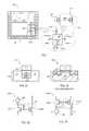
- FIG. 1an integrated circuit (IC) device according to one embodiment is shown in a top plan view, and designated by the general reference character 100 .
- An IC device 100may be formed as a “die” having substrate 101 containing the various circuits therein.
- An IC device 100may include one or more circuit sections, and FIG. 1 identifies four circuit sections as 102 - 0 to 102 - 3 . Any or all of circuit sections ( 102 - 0 to 102 - 3 ) may include analog circuit blocks that perform analog functions for the IC device 100 .
- circuit section 102 - 3can be an analog circuit block that includes one or more analog circuits, one shown as 104 .
- An analog circuit 104may generate an analog voltage and/or current within IC device 100 to enable a circuit function.
- An analog circuit 104may generate an output analog value in response to an input analog value and/or may generate an output analog value based on biasing conditions, as but two examples.
- an analog circuit 104may include one or more output nodes (two shown as 106 - 0 , 106 - 1 ) and may or may not include input nodes (two shown as 108 - 0 , 108 - 1 ). It is noted that in some embodiments, an output node and input node may be the same node.
- an analog circuit 104may include one or more “deeply depleted channel” (DDC) transistors.
- DDC transistorincludes both a highly doped “screening” layer below a gate that defines the extent of the depletion region below the gate in operation, and an undoped channel extending between source and drain of a transistor.
- transistorsare manufactured without halo or “pocket” implants, and anneal conditions are tightly controlled to prevent unwanted diffusion of dopants into the undoped channel.
- Vtthreshold voltage
- a threshold voltage set layercan be grown as a blanket or as selective epitaxial layers and doped by controlled implants, diffusion from the screen layer, or substitutional deposition. This threshold voltage set layer is used to finely adjust or tune the threshold voltage of individual or blocks of transistors. Such a threshold voltage set layer is positioned between the undoped channel and the screen layer and may alternatively contact or be separated from the screen layer. As compared to conventional doped channel transistors, such DDC transistors can be more closely matched in device characteristics, in part because they have reduced channel random dopant fluctuations that can result in variable threshold voltage set points. Further examples of DDC transistor structure and manufacture are disclosed in U.S.
- DDC transistors included within an analog circuitmay include n-channel transistors, p-channel transistors, or both.
- N-channel DDC transistorswill be represented in this disclosure by the symbol shown as 110 - 0 in FIG. 1 .
- P-channel DDC transistorswill be represented in this disclosure by the symbol shown as 110 - 1 in FIG. 1 .
- DDC transistorsmay advantageously include a substantially undoped channel region formed over a relatively highly doped screening layer.
- DDC transistorsmay present analog circuit elements having less variation than conventional counterparts, which can result in improved analog circuit performance as compared to analog circuits constructed with conventional circuit elements of the same size.
- DDC transistor 210may include a gate 212 separated from a substrate 224 by a gate insulator 222 .
- a substantially undoped channel region 214may be formed below gate 212 .
- a doped screening layer 216may be formed below channel region 214 . It is understood that there may be other layers between channel region 214 and screening layer 216 (e.g., a threshold voltage set layer 227 ).
- a substrate 224may be formed of more than one semiconductor layer. As but one example, a substrate may include one or more “epitaxial” layers formed on a bulk semiconductor substrate.
- a screening layer 216may be doped to an opposite conductivity type of the transistor channel type (e.g., an n-channel DDC transistor will have a p-doped screening layer).
- a screening layer 216 doping concentrationmay be greater than a concentration of a body region 218 .
- FIG. 2Aalso shows source and drain regions 220 on opposing lateral sides of channel region 214 .
- Source and drain regions 220may include a source and drain diffusion. More particular types of DDC source and drain structures, relative to substantially undoped channel region will be described in more detail below.
- Threshold voltage set layer 227can be a doped layer formed between screening layer 216 and substantially undoped channel region 214 . Threshold voltage set layer 227 may be doped to achieve a desired threshold voltage in a DDC transistor 210 .
- Conventional transistor 205may include a gate 213 separated from a substrate 225 by a gate insulator 223 .
- a channel region 215may be formed below a gate 213 between source/drain diffusions 221 .
- a channel region 215may be doped to a conductivity type opposite to that of source/drain diffusions 221 , and the same as that of a transistor body region 219 .
- “Pocket” or “halo” implant regions 223may be formed between source/drain diffusions 221 and channel region 215 .
- an integrated circuit devicemay include analog circuits formed with DDC transistors.
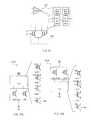
- Analog circuit 304 -Ais a current mirror circuit that provides an output current Iout that tracks an input current Iin.
- Output current Ioutmay be provided by way of a DDC transistor.
- An output current (Iout)may more closely track input current (Iin) as compared to conventional circuits employing doped channel devices, as the DDC device threshold voltage may be subject to less variation than a doped channel counterpart.
- current mirror circuit 304 -Amay include a reference transistor 326 - 1 and a mirror transistor 310 - 00 of a same conductivity type (in this case n-channel devices).
- a reference transistor 326 - 1may have a drain connected to receive input current Iin from a current source 328 , a gate connected to its drain, and a source connected, directly or indirectly, to a low power supply node (e.g., VSS node).
- a reference transistor 326 - 1may preferably be a DDC transistor. However, in alternate embodiments, a reference transistor 326 - 1 may not be a DDC transistor.
- a mirror transistor 310 - 00is a DDC transistor having a gate connected to the gate/drain of reference transistor 326 - 1 , and a source connected, directly or indirectly, to a low power supply node.
- mirror transistor 310 - 00receives a same gate bias as reference transistor 326 - 1 , current (Iout) flowing into mirror transistor 310 - 00 may track input current (Iin).
- both transistors ( 326 - 1 and 310 - 00 )are DDC transistors, such a tracking may be advantageously closer than a conventional current mirror formed with doped channels, which may suffer from random doping fluctuation leading to greater device mismatch.
- a mirror transistor 310 - 00may be identically sized to a reference transistor 326 - 1 , in which Iout ⁇ Iin, or a mirror transistor 310 - 00 may be scaled with respect to reference transistor 326 - 1 by a factor of K, in which case Iout ⁇ K*Iin.
- FIG. 3Banother example of a current mirror circuit according to an embodiment is shown in schematic diagram and designated by the general reference character 304 -B.
- Current mirror circuit 304 -Bshows the same general circuit as FIG. 3A , but using p-channel devices.
- Current mirror circuit 304 -Bmay be subject to the same variations and advantages of that shown in FIG. 3A .
- FIG. 4shows a simulation response of a current mirror like that of FIG. 3A , in which both a reference device 326 and mirror device 310 - 00 are n-channel DDC transistors of the same size.
- a vertical axisshows an output current (Iout) provided by mirror device 310 - 00
- a horizontal axisshows an input current (Iin) sourced to reference device 326 - 1 .
- Responses of the DDC current mirrorare shown by dashed line responses 432 - 0 , - 1 , - 2 .
- Line 432 - 1shows a nominal response, corresponding to a typical transistor response for the DDC transistors.
- Line 432 - 0shows a first extreme case response, in which a mirror device 310 - 00 has a maximum statistical deviation in one direction (+3 ⁇ ) while a reference device 326 deviates in the opposite direction ( ⁇ 3 ⁇ ).
- Line 432 - 2shows a second extreme case response, in which the devices vary in the other opposing direction (i.e., mirror device 310 - 00 is ⁇ 3 ⁇ , while reference device 326 is +3 ⁇ ).
- FIG. 4also includes the same responses noted above, but with a current mirror formed with conventional transistors (shown as solid lines 430 - 0 , - 1 , - 2 ) of the same size.
- a current mirror response according to an embodimenti.e., 432 - 0 , - 1 , - 2
- has a tighter responsei.e., Iout more closely tracks Iin
- the conventional case430 - 0 , - 1 , - 2 ).
- An IC device 500may include a current mirror circuit 504 and one or more standard bias transistors (one shown as 534 ).
- Current mirror circuit 504may have a configuration like that of FIG. 3A .
- FIG. 5differs from FIG. 3A in that reference and mirror transistors ( 526 - 1 and 510 - 00 ) can have bodies that receive a “forward” body bias voltage (V_FBBn).
- a standard bias transistore.g., 534
- V_SBBnstandard body bias voltage
- a forward body bias voltagemay reduce a threshold voltage of transistors as compared to a standard body bias voltage. Accordingly, in FIG. 5 , transistors 526 - 1 and 510 - 00 may be considered forward body biased (FBB) DDC devices. FBB DDC devices can have a lower drain-source saturation voltage (VDSAT) than standard body biased counterparts. A lower VDSAT may enable lower power supply voltages and/or may increase an operating range for signals generated by, or operated on, an IC device.
- VDSATdrain-source saturation voltage
- FIG. 6is a graph showing forward and standard body biasing voltages according to an embodiment.
- a standard body bias voltage for p-channel transistors V_SBBpmay be a relatively high positive voltage, and in some embodiments can be a high power supply voltage VDD.
- a forward body bias voltage for p-channel transistors V_FBBpmay be less than V_SBBp.
- a standard body bias voltage for n-channel transistors V_SBBnmay be a relatively low voltage, and in some embodiments can be a low power supply voltage VSS.
- a forward body bias voltage for n-channel transistors V_FBBnmay be greater than V_SBBn.
- Different body biasing as described hereinmay be static (i.e., transistors body biases are substantially constant during device operation), or may be dynamic, changing in response to circuit inputs and/or conditions.
- current mirror circuitsmay include DDC transistors in various configurations.
- FIGS. 7A to 7Dadditional analog circuits according to embodiments are a shown in schematic diagrams.
- FIGS. 7A to 7Dshow cascode type current mirror circuits according to various embodiments. Cascode type current mirror circuits may provide higher output impedance than single stage arrangements like that of FIGS. 3A to 3B .
- a current mirror circuit 704 -Amay include a first reference transistor 726 - 1 and first mirror transistor 710 - 00 arranged in the same fashion as FIG. 3A .
- second reference transistor 726 - 1 and second mirror transistor 710 - 01may be connected in a cascode type arrangement.
- all transistorsare DDC transistors. However, in alternate embodiments, less than all transistors may be DDC transistors.
- a current mirror circuit 704 -Bmay have the same general arrangement as that shown in FIG. 7A , however all transistors may receive a forward body bias voltage V_FBBn. Accordingly, it is understood that current mirror circuit 704 -B is included in a device having other n-channel transistors that receive a standard body bias voltage (i.e., a body bias voltage lower than V_FBBn). In alternate embodiments, less than all transistors may be DDC transistors.
- a current mirror circuit 704 -Cmay have the same general arrangement as that shown in FIG. 7B , however a body of all transistors may be driven with a bias voltage VBIAS. Further, such a bias voltage may drive the gate-gate connection of the cascode stage formed by transistors 710 - 01 and 726 - 2 .
- a current mirror circuit 704 -Dmay have a similar arrangement as that shown in FIG. 7B .
- a cascode stagemay be formed by low threshold voltage (Vt) transistors 730 and 732 .
- Vtlow threshold voltage
- current mirror circuit 704 -Dis included in a device having other n-channel transistors, and such other n-channel transistors may have a larger Vt than the low Vt devices.
- cascode connected current mirror circuitsmay include DDC transistors in various configurations.
- FIGS. 8A and 8Badditional analog circuits according to embodiments are shown in schematic diagrams.
- FIGS. 8A and 8Bshow Wilson type current mirror circuits according to various embodiments. Wilson type current mirror circuits may also provide higher output impedance than single stage arrangements like that of FIGS. 3A to 3B .
- a current mirror circuit 804 -Amay include a reference transistor 826 , a mirror transistor 810 , and an input stage 834 .
- a reference transistor 826may have a drain connected to receive input current (Iin) from a current source 828 and a source connected, directly or indirectly, to a low power supply node (e.g., VSS node).
- a mirror transistor 810may have its gate connected to its drain and to the gate of reference transistor 826 , and a source connected, directly or indirectly, to a low power supply node.
- Input stage 834may include a first input transistor 836 - 0 having a drain that provides output current Iout, a gate connected to the drain of reference transistor 826 , and a source connected to the drain-gate of mirror transistor 810 .
- a current mirror circuit 804 -Bmay have the same general arrangement as that shown in FIG. 8A , however input stage 834 ′ may further include a second input transistor 836 - 1 having a gate and drain connected to a gate of first input transistor 836 - 0 , and a source connected to the drain of reference transistor 826 .
- all transistorsmay be DDC transistors.
- one or more of the transistorsmay be standard body biased transistors, forward body biased transistors, standard Vt transistors and/or low Vt transistors, as noted above.
- Wilson type current mirror circuitsmay include DDC transistors in various configurations.
- Embodiments of the inventionmay include analog circuits having transistor constituents split over different device sections, with one such section including DDC transistors.
- One very particular embodiment showing such an arrangementis set forth in FIG. 9 .
- An IC deviceis shown in a block diagram and designated by the general reference character 900 .
- An IC device 900may include an input/output (I/O) section 936 and DDC core section 938 .
- I/O section 936may be powered between high power supply voltages VDD and VSS.
- a DDC core section 938may include DDC type transistors, and may be powered between lower power supply voltages VcoreH and VcoreL, where VcoreH ⁇ VDD and VcoreL>VSS.
- Circuits within IC device 900may include transistors in both sections 936 and 938 .
- a current mirror circuit 904is shown that spans sections 936 and 938 . More particularly, a current mirror circuit 904 may include a reference transistor 926 formed in I/O section 936 , and a mirror transistor 910 formed in DDC core section 938 . In particular embodiments, transistors within I/O section 936 may have a thicker gate insulator and/or doping profiles suitable for higher operating voltages than the DDC transistors of section 938 .
- analog circuitsmay span differently powered sections of an IC device.
- Circuit 1004can include a differential pair of DDC transistors 1040 , a bias control circuit 1042 , and a load circuit 1044 .
- Differential pair 1040may include a first DDC transistor 1046 - 0 having a drain connected to load circuit 1044 , a gate coupled to a first input IN 0 , and a source coupled to a bias node 1047 , and a second DDC transistor 1046 - 1 having a drain connected to load circuit 1044 , a gate coupled to a second input IN 1 , and a source coupled to a bias node 1047 .
- first and second transistors 1046 - 0 / 1may be matched in size.
- a bias control circuit 1042may be connected between a bias node 1047 and a low power supply node VSS.
- a load circuit 1044may be connected between the drains of transistors 1046 - 0 / 1 and a high power supply node VDD.
- a differential pair 1040may provide improved compare operations with respect to signals received at inputs IN 0 and IN 1 , as there may be less variation in the Vts of such devices, as their channels do not suffer from random dopant fluctuation.
- an IC devicemay include a differential pair of DDC transistors.
- FIG. 11a particular analog circuit including a differential pair of DDC transistors according to another embodiment is shown in block schematic diagram.
- FIG. 11shows a differential amplifier circuit 1104 that includes items like those shown in FIG. 10 .
- FIG. 11differs from that of FIG. 10 in that a bias control circuit 1142 may include a bias transistor 1150 having a source-drain path connected between bias node 1147 and a low power supply node VSS, and a gate that receives a bias voltage BIAS_CTRL. Further, a load circuit 1044 may be a current mirror formed with p-channel devices 1148 - 0 / 1 . An output of differential amplifier OUT may be at a drain-drain connection of transistors 1148 - 1 / 1146 - 1 .
- the transistors of differential amplifier circuit 1104may all be DDC transistors.
- any of transistors 1148 - 0 / 1 , 1150may be conventional transistors and/or low Vt transistors, such low Vt transistors including conventional and/or DDC transistors (i.e., DDC transistors with lower threshold voltages than other like conductivity DDC transistors in the device).
- all such transistorsmay have body biasing variations described herein, including standard body biasing and forward body biasing.
- an IC devicemay include a differential amplifier that includes DDC transistors.
- FIG. 12Aan advantageous response of a differential amplifier circuit according to an embodiment is shown in a graph.
- FIG. 12Ashows a simulation response of a differential amplifier on a 28 nm generation process, like that of FIG. 11 , in which all transistors are DDC transistors having 100 nanometer (nm) gate lengths.
- a vertical axisshows an output voltage
- a horizontal axisshows an input voltage. Consequently, the response lines are understood to represent an amplifier gain and offset.
- Line 1252 - 1shows a nominal response, corresponding to a typical transistor response for the DDC transistors.
- Line 1252 - 0shows an extreme case response, in which a first load transistor 1148 - 0 has a maximum statistical deviation in one direction ( ⁇ 3 ⁇ ) while the second load transistor 1148 - 1 deviates in the opposite direction (+3 ⁇ ).
- differential pair transistor 1146 - 0has maximum statistical deviation (+3 ⁇ ) opposite to that of the other differential pair transistor 1146 - 1 and first load transistor 1148 - 0 .
- FIG. 12Aalso includes the same responses, but for a differential amplifier having conventional transistors (shown as solid lines 1254 - 0 / 1 ).
- a differential amplifier response according to an embodimenti.e., 1252 - 0 / 2 ) exhibits less voltage offset due to variation, and may provide greater gain.
- FIG. 12Ba large signal simulation response is shown for the differential amplifier circuit of FIG. 12A .
- Responses of the DDC based differential amplifier with an extreme mismatch arrangementare shown by dashed lines.
- An ideal responsee.g., no mismatch is shown by solid lines.
- FIG. 12Cshows a same set of responses as FIG. 12A , but in the large signal range.
- a DDC based differential amplifieraccording to an embodiment may provide greater gain and with less offset.
- FIG. 13Aa portion of a differential amplifier according to a further embodiment is shown in block schematic diagram.
- FIG. 13Ashows a differential amplifier circuit 1304 -A that includes items like those shown in FIG. 11 .
- FIG. 13Adiffers from FIG. 11 in that a bias control circuit 1342 may include a cascode configuration, including a first bias transistor 1350 - 0 and second bias transistor 1350 - 1 having source-drain paths in series between the bias node 1347 and a low power supply node VSS.
- First and second bias transistors ( 1350 - 0 / 1 )may receive a first bias voltage Vbias 1 and second bias voltage Vbias 2 on their respective gates.
- bias transistors ( 1350 - 0 / 1 )may be DDC transistors in some embodiments.
- one or both of the bias transistors ( 1350 - 0 / 1 )may be conventional transistors and/or low Vt transistors. Further, one or both of such transistors may have body biasing variations described herein, including standard body biasing and forward body biasing.
- FIG. 13Bshows a differential amplifier circuit 1304 -B that includes items like those shown in FIG. 13A .
- FIG. 13Bdiffers from FIG. 13A in that first and second bias transistors 1350 - 0 / 1 as well as transistors 1346 - 0 / 1 of the differential pair 1340 may have bodies driven by the bias voltage Vbias 1 received at the gate of first bias transistor 1350 - 0 .
- FIG. 13Cshows a portion of another differential amplifier according to an embodiment is shown in block schematic diagram.
- FIG. 13Cshows a differential amplifier circuit 1304 -C that includes items like those shown in FIG. 13A .
- FIG. 13Cdiffers from FIG. 13A in that bodies of differential pair transistors 1346 - 0 / 1 may be connected to bias node 1347 . Such an arrangement may essentially eliminate the body effect on the operation of differential pair 1340 .
- FIG. 14shows an analog comparator circuit 1404 that can include a differential pair of DDC transistors 1440 , an enable switch 1454 , a latching driver 1458 , and a precharge circuit 1460 .
- Differential pair 1440may take the form of that shown in FIG. 10 , or an equivalent.
- An enable switch 1454may connect common sources (node 1447 ) of the differential pair 1440 to a power supply node VSS in response to an enable signal EN, to thereby enable a sensing operation of differential pair 1440 .
- enable switch 1454may include a switch transistor 1456 having a source-drain path coupled between node 1447 and VSS, and may have a gate coupled to a receive the enable signal EN.
- a latching driver 1458may latch the differential voltage generated at the drains of differential pair transistors 1446 - 0 and 1446 - 1 .
- latching driver 1458may include first conductivity (in this case n-channel) driver transistors 1462 - 0 / 1 and second conductivity (in this case p-channel) driver transistors 1464 - 0 / 1 .
- Driver transistor 1462 - 0may have a source-drain path coupled between a drain of differential pair transistor 1446 - 0 and a first output node VO, and a gate connected to second output node VOB.
- Driver transistor 1462 - 1may have a source-drain path coupled between a drain of differential pair transistor 1446 - 1 and a second output node VOB, and gate connected to first output node VO.
- driver transistor 1464 - 0may have a source-drain path coupled between first output node VO and a high power supply VDD, and a gate connected to second output node VOB
- driver transistor 1464 - 1may have a source-drain path coupled between second output node VOB and a high power supply VDD, and a gate connected to first output node VO.
- Precharge circuit 1460may precharge first and second output nodes VO/VOB to a precharge voltage prior to a compare operation, and then release such nodes (i.e., allow them to float) during a compare operation.
- precharge circuit 1460may precharge output nodes VO/VOB to a high power supply voltage VDD, and includes a first precharge transistor 1466 - 0 having a source-drain path coupled between first output node VO and a high power supply node VDD, and a gate that receives the enable signal EN, and a second precharge transistor 1466 - 1 having a source-drain path coupled between second output node VOB and a high power supply node VDD, and a gate that also receives the enable signal EN.
- transistors of an enable switch 1454 , a latching driver 1458 , and a precharge circuit 1460may all be DDC transistors.
- any transistors of such circuit sectionsmay be conventional transistors and/or low Vt transistors.
- all such transistorsmay have body biasing variations described herein, including standard body biasing and forward body biasing.
- an IC devicemay include an analog comparator that employs DDC transistors.
- FIGS. 15A and 15Ban advantageous response of an analog comparator circuit according to an embodiment is shown in a pair of graphs.
- FIGS. 15A and 15Bare simulation responses of an analog comparator like that of FIG. 14 .
- FIG. 15Ashows a response of such an analog comparator with conventional transistors having a “halo” (e.g., pocket) implant.
- FIG. 15Bshows a response of analog comparator of FIG. 14 that includes all DDC transistors.
- FIGS. 15A and 15Bare Monte Carlo plots generated by placing mismatches on transistors of the analog comparator, and then recording the input difference (VIN ⁇ VINB) that results in the comparator driving its output between high and low values (e.g., VDD to VSS, or VSS to VDD).
- the horizontal axesshow the input offset difference, the vertical axes show the number of units exhibiting the offset response.
- the DDC analog comparatorresults in a smaller offset voltage variation than the conventional case.
- FIG. 16shows an operational amplifier (op amp) circuit 1670 .
- An op amp 1670may include a differential input section 1678 , an input bias section 1672 , an output bias section 1674 , and an output driver circuit 1676 .
- An op amp 1670may amplify values received between a noninverting input (+) and an inverting input ( ⁇ ).
- differential input section 1678may include a differential pair of DDC transistors 1640 , as disclosed herein, or an equivalent.
- input and/or output biasing sections ( 1672 or 1674 )may include one or more current mirrors that employ DDC transistors, as disclosed herein, or equivalents.
- an operational amplifier circuitmay include DDC transistors.
- alternate embodimentsmay include various other analog circuits including but not limited to: high speed I/O circuits, including transceiver circuits; and data converter circuits, including “flash” analog-to-digital converters.
- FIG. 17Ais a block schematic diagram of an analog IC device 1700 -A according to an embodiment.
- An analog IC device 1700 -Amay execute analog signal generating or processing and includes a first section 1780 and one or more other sections (one shown as 1782 ).
- a first section 1780includes DDC transistors, in this embodiment, n-channel DDC transistors.
- the other section 1782may include any of: p-channel DDC transistors, p-channel conventional transistors, including standard Vt and/or standard body bias transistors, low Vt p-channel transistors, or p-channel transistors with a forward body bias.
- FIG. 17Bis a block schematic diagram of an IC device 1700 -B like that of FIG. 17A , but with transistor conductivities reversed.
- an IC device 1700 -Bexecutes analog signal generating or processing functions and includes a first section 1780 ′ with p-channel DDC transistors, and one or more other sections 1782 that include any of numerous other n-channel transistors.
- a DDC transistormay take various forms.
- a DDC transistor according to one very particular embodimentwill now be described with reference to FIG. 18 .
- Such a transistormay be included in any of the embodiments shown above, or equivalents.
- a DDC transistor 1860may include a gate 1812 separated from a substrate 1824 by a gate insulator 1822 .
- a gate 1812may include insulating sidewalls 1868 formed on its sides.
- Source and drain regionsmay include a lightly doped drain (LDD) structures 1876 formed over deep source/drain diffusions 1874 to extend towards each other under a portion of the gate.
- LDDlightly doped drain
- a DDC stacked channel structuremay be formed by a substantially undoped channel layer 1814 , a threshold voltage (Vt) set layer 1870 formed by epitaxial growth and implant, or alternatively, by controlled out-diffusion from a screening layer 1816 positioned below the undoped channel layer 1814 .
- the screening layer 1816acts to define termination of the depletion zone below the gate, while the Vt set layer 1870 adjusts Vt to meet transistor design specifications.
- screening layer 1816may be implanted into body/bulk region 1818 so that it extends between and in contact with the source and drain diffusions 1874 .
- a DDC transistor 1860may be an n-channel transistor manufactured on a 28 nm generation process, and can have a gate length 1878 suitable to the analog circuit role in which it is employed. In very particular embodiments, such gate lengths may be in the range of about 50 to 120 nm.
- the screening layer 1816may have a carrier concentration of greater than about 5 ⁇ 10 18 donors/cm 3
- an overlying Vt set layer 1870may have a carrier concentration of about 5 ⁇ 10 17 to about 5 ⁇ 10 18 donors/cm 3
- a substantially undoped channel region 1814may have a carrier concentration of less than about 5 ⁇ 10 17 donors/cm 3 . It is understood that the above noted carrier concentrations are provided by way of example only and alternate embodiments may include different concentrations according to desired performance in an analog circuit.
- a DDC transistor according to a further embodimentis shown in FIG. 19 , and designated by the general reference character 1960 .
- a DDC transistor 1960may include items like those shown in FIG. 18 , and like items are referred to by the same reference character.
- DDC transistor 1960differs from that of FIG. 18 in that screening layer 1816 may be implanted into body/bulk region 1818 so that it extends below the gate without contacting the source and drain diffusions 1874 .
- the above DDC transistorsare but particular implementations of a DDC transistor, and should not be construed as unduly limiting the circuit elements included within the various analog circuit embodiments shown herein.
- circuits disclosed hereinhave included circuit sections with conductivities of one type, alternate embodiments could reverse such conductivities as would be well understood by those skilled the art.
- the embodiments shown in FIGS. 5 , 7 A to 11 , 13 A to 14 , and 16may be formed with transistor conductivities (and hence power supply nodes) reversed.
- Embodiments of the invention, and their equivalentsmay provide improved performance over conventional circuits by operating with transistors (e.g., DDC transistors) having highly matching characteristics, particularly threshold voltage (Vt). Possible improvements may include faster signal propagation times, as noted above.
- transistorse.g., DDC transistors
- Vtthreshold voltage
- Closer matching of transistor characteristicsmay translate into reductions in transistor size, and hence reductions in device manufacturing cost and/or power consumption. Reduction in size may also result in reduced input capacitance for IC devices receiving input signals on DDC transistor gates. Highly matching transistors at differential inputs may provide greater input range.
- Undoped analog circuit transistor channelsmay allow for shorter channel devices for increased current driving capability and/or driving speed as compared to conventional transistors.
Landscapes
- Engineering & Computer Science (AREA)
- Power Engineering (AREA)
- Amplifiers (AREA)
Abstract
Description
This application is a continuation of U.S. application Ser. No. 13/770,482 and now U.S. Pat. No. 8,847,684, which is a continuation of U.S. application Ser. No. 13/071,399 and now U.S. Pat. No. 8,400,219, each of which are hereby incorporated by reference herein.
The present invention relates generally to electronic circuits, and more particularly to analog circuits for generating analog values.
Various embodiments of the present invention will now be described in detail with reference to a number of drawings. The embodiments show analog circuits and related methods that may be included in integrated circuit devices to provide improved performance over conventional analog circuit approaches.
In the various embodiments below, like items are referred to by the same reference character but the leading digit(s) corresponding to the figure number.
Referring now toFIG. 1 an integrated circuit (IC) device according to one embodiment is shown in a top plan view, and designated by thegeneral reference character 100. AnIC device 100 may be formed as a “die” havingsubstrate 101 containing the various circuits therein. AnIC device 100 may include one or more circuit sections, andFIG. 1 identifies four circuit sections as102-0 to102-3. Any or all of circuit sections (102-0 to102-3) may include analog circuit blocks that perform analog functions for theIC device 100.
In the embodiment shown, circuit section102-3 can be an analog circuit block that includes one or more analog circuits, one shown as104. Ananalog circuit 104 may generate an analog voltage and/or current withinIC device 100 to enable a circuit function. Ananalog circuit 104 may generate an output analog value in response to an input analog value and/or may generate an output analog value based on biasing conditions, as but two examples. Accordingly, ananalog circuit 104 may include one or more output nodes (two shown as106-0,106-1) and may or may not include input nodes (two shown as108-0,108-1). It is noted that in some embodiments, an output node and input node may be the same node.
Referring still toFIG. 1 , ananalog circuit 104 may include one or more “deeply depleted channel” (DDC) transistors. A DDC transistor includes both a highly doped “screening” layer below a gate that defines the extent of the depletion region below the gate in operation, and an undoped channel extending between source and drain of a transistor. Typically, to prevent contamination of the undoped channel, transistors are manufactured without halo or “pocket” implants, and anneal conditions are tightly controlled to prevent unwanted diffusion of dopants into the undoped channel. To improve threshold voltage control and reduce variability in threshold voltage, conventional threshold voltage (Vt) implants and threshold voltage modifying halo implants are also avoided. Instead, a threshold voltage set layer can be grown as a blanket or as selective epitaxial layers and doped by controlled implants, diffusion from the screen layer, or substitutional deposition. This threshold voltage set layer is used to finely adjust or tune the threshold voltage of individual or blocks of transistors. Such a threshold voltage set layer is positioned between the undoped channel and the screen layer and may alternatively contact or be separated from the screen layer. As compared to conventional doped channel transistors, such DDC transistors can be more closely matched in device characteristics, in part because they have reduced channel random dopant fluctuations that can result in variable threshold voltage set points. Further examples of DDC transistor structure and manufacture are disclosed in U.S. patent application Ser. No. 12/708,497, filed on Feb. 18, 2010, titled ELECTRONIC DEVICES AND SYSTEMS, AND METHODS FOR MAKING AND USING THE SAME, by Scott E. Thompson et al., as well as U.S. patent application Ser. No. 12/971,884, filed on Dec. 17, 2010 titled LOW POWER SEMICONDUCTOR TRANSISTOR STRUCTURE AND METHOD OF FABRICATION THEREOF and U.S. patent application Ser. No. 12/971,955 filed on Dec. 17, 2010 titled TRANSISTOR WITH THRESHOLD VOLTAGE SET NOTCH AND METHOD OF FABRICATION THEREOF the respective contents of which are incorporated by reference herein.
DDC transistors included within an analog circuit may include n-channel transistors, p-channel transistors, or both. N-channel DDC transistors will be represented in this disclosure by the symbol shown as110-0 inFIG. 1 . P-channel DDC transistors will be represented in this disclosure by the symbol shown as110-1 inFIG. 1 . As noted above, DDC transistors may advantageously include a substantially undoped channel region formed over a relatively highly doped screening layer. As will be described in more detail below, DDC transistors may present analog circuit elements having less variation than conventional counterparts, which can result in improved analog circuit performance as compared to analog circuits constructed with conventional circuit elements of the same size.
Referring now toFIG. 2A , one exemplary representation of a DDC transistor is shown in a side cross sectional view, and designated by thegeneral reference character 210.DDC transistor 210 may include agate 212 separated from asubstrate 224 by a gate insulator222. A substantiallyundoped channel region 214 may be formed belowgate 212. A doped screening layer216 may be formed belowchannel region 214. It is understood that there may be other layers betweenchannel region 214 and screening layer216 (e.g., a threshold voltage set layer227). Asubstrate 224 may be formed of more than one semiconductor layer. As but one example, a substrate may include one or more “epitaxial” layers formed on a bulk semiconductor substrate.
A screening layer216 may be doped to an opposite conductivity type of the transistor channel type (e.g., an n-channel DDC transistor will have a p-doped screening layer). A screening layer216 doping concentration may be greater than a concentration of abody region 218.FIG. 2A also shows source and drainregions 220 on opposing lateral sides ofchannel region 214. Source anddrain regions 220 may include a source and drain diffusion. More particular types of DDC source and drain structures, relative to substantially undoped channel region will be described in more detail below.
Threshold voltage setlayer 227 can be a doped layer formed between screening layer216 and substantiallyundoped channel region 214. Threshold voltage setlayer 227 may be doped to achieve a desired threshold voltage in aDDC transistor 210.
Referring toFIG. 2B , one representation of a conventional transistor is shown for comparison to that shown inFIG. 2A .Conventional transistor 205 may include agate 213 separated from asubstrate 225 by agate insulator 223. Achannel region 215 may be formed below agate 213 between source/drain diffusions221. Achannel region 215 may be doped to a conductivity type opposite to that of source/drain diffusions221, and the same as that of atransistor body region 219. “Pocket” or “halo”implant regions 223 may be formed between source/drain diffusions221 andchannel region 215.
In this way, an integrated circuit device may include analog circuits formed with DDC transistors.
Referring now toFIG. 3A , one particular example of an analog circuit according to an embodiment is shown in schematic diagram and designated by the general reference character304-A. Analog circuit304-A is a current mirror circuit that provides an output current Iout that tracks an input current Iin. Output current Iout may be provided by way of a DDC transistor. An output current (Iout) may more closely track input current (Iin) as compared to conventional circuits employing doped channel devices, as the DDC device threshold voltage may be subject to less variation than a doped channel counterpart.
In the particular embodiment shown, current mirror circuit304-A may include a reference transistor326-1 and a mirror transistor310-00 of a same conductivity type (in this case n-channel devices). A reference transistor326-1 may have a drain connected to receive input current Iin from acurrent source 328, a gate connected to its drain, and a source connected, directly or indirectly, to a low power supply node (e.g., VSS node). A reference transistor326-1 may preferably be a DDC transistor. However, in alternate embodiments, a reference transistor326-1 may not be a DDC transistor. A mirror transistor310-00 is a DDC transistor having a gate connected to the gate/drain of reference transistor326-1, and a source connected, directly or indirectly, to a low power supply node.
Because mirror transistor310-00 receives a same gate bias as reference transistor326-1, current (Iout) flowing into mirror transistor310-00 may track input current (Iin). In the event both transistors (326-1 and310-00) are DDC transistors, such a tracking may be advantageously closer than a conventional current mirror formed with doped channels, which may suffer from random doping fluctuation leading to greater device mismatch. A mirror transistor310-00 may be identically sized to a reference transistor326-1, in which Iout≅Iin, or a mirror transistor310-00 may be scaled with respect to reference transistor326-1 by a factor of K, in which case Iout≅K*Iin.
Referring now toFIG. 3B , another example of a current mirror circuit according to an embodiment is shown in schematic diagram and designated by the general reference character304-B. Current mirror circuit304-B shows the same general circuit asFIG. 3A , but using p-channel devices. Current mirror circuit304-B may be subject to the same variations and advantages of that shown inFIG. 3A .
Referring now toFIG. 4 , an advantageous response of a current mirror circuit according to an embodiment is shown in a graph.FIG. 4 shows a simulation response of a current mirror like that ofFIG. 3A , in which both a reference device326 and mirror device310-00 are n-channel DDC transistors of the same size. A vertical axis shows an output current (Iout) provided by mirror device310-00, and a horizontal axis shows an input current (Iin) sourced to reference device326-1. Responses of the DDC current mirror are shown by dashed line responses432-0, -1, -2. Line432-1 shows a nominal response, corresponding to a typical transistor response for the DDC transistors. Line432-0 shows a first extreme case response, in which a mirror device310-00 has a maximum statistical deviation in one direction (+3σ) while a reference device326 deviates in the opposite direction (−3σ). Line432-2 shows a second extreme case response, in which the devices vary in the other opposing direction (i.e., mirror device310-00 is −3σ, while reference device326 is +3σ).
For comparison,FIG. 4 also includes the same responses noted above, but with a current mirror formed with conventional transistors (shown as solid lines430-0, -1, -2) of the same size. As shown, a current mirror response according to an embodiment (i.e.,432-0, -1, -2) has a tighter response (i.e., Iout more closely tracks Iin) as compared to the conventional case (430-0, -1, -2).
Referring now toFIG. 5 , an IC device according to another embodiment is shown in a block schematic diagram and designated by thegeneral reference character 500. AnIC device 500 may include acurrent mirror circuit 504 and one or more standard bias transistors (one shown as534).Current mirror circuit 504 may have a configuration like that ofFIG. 3A . However,FIG. 5 differs fromFIG. 3A in that reference and mirror transistors (526-1 and510-00) can have bodies that receive a “forward” body bias voltage (V_FBBn). In contrast, a standard bias transistor (e.g.,534) may have a body that receives a standard body bias voltage (V_SBBn). A forward body bias voltage may reduce a threshold voltage of transistors as compared to a standard body bias voltage. Accordingly, inFIG. 5 , transistors526-1 and510-00 may be considered forward body biased (FBB) DDC devices. FBB DDC devices can have a lower drain-source saturation voltage (VDSAT) than standard body biased counterparts. A lower VDSAT may enable lower power supply voltages and/or may increase an operating range for signals generated by, or operated on, an IC device.
Different body biasing as described herein may be static (i.e., transistors body biases are substantially constant during device operation), or may be dynamic, changing in response to circuit inputs and/or conditions.
In this way, current mirror circuits may include DDC transistors in various configurations.
Referring now toFIGS. 7A to 7D , additional analog circuits according to embodiments are a shown in schematic diagrams.FIGS. 7A to 7D show cascode type current mirror circuits according to various embodiments. Cascode type current mirror circuits may provide higher output impedance than single stage arrangements like that ofFIGS. 3A to 3B .
Referring toFIG. 7A , a current mirror circuit704-A may include a first reference transistor726-1 and first mirror transistor710-00 arranged in the same fashion asFIG. 3A . In addition, second reference transistor726-1 and second mirror transistor710-01 may be connected in a cascode type arrangement. In the embodiment shown, all transistors are DDC transistors. However, in alternate embodiments, less than all transistors may be DDC transistors.
Referring toFIG. 7B , a current mirror circuit704-B may have the same general arrangement as that shown inFIG. 7A , however all transistors may receive a forward body bias voltage V_FBBn. Accordingly, it is understood that current mirror circuit704-B is included in a device having other n-channel transistors that receive a standard body bias voltage (i.e., a body bias voltage lower than V_FBBn). In alternate embodiments, less than all transistors may be DDC transistors.
Referring toFIG. 7C , a current mirror circuit704-C may have the same general arrangement as that shown inFIG. 7B , however a body of all transistors may be driven with a bias voltage VBIAS. Further, such a bias voltage may drive the gate-gate connection of the cascode stage formed by transistors710-01 and726-2.
Referring toFIG. 7D , a current mirror circuit704-D may have a similar arrangement as that shown inFIG. 7B . However, inFIG. 7D a cascode stage may be formed by low threshold voltage (Vt)transistors FIG. 7D , it is understood that current mirror circuit704-D is included in a device having other n-channel transistors, and such other n-channel transistors may have a larger Vt than the low Vt devices.
In this way, cascode connected current mirror circuits may include DDC transistors in various configurations.
Referring now toFIGS. 8A and 8B , additional analog circuits according to embodiments are shown in schematic diagrams.FIGS. 8A and 8B show Wilson type current mirror circuits according to various embodiments. Wilson type current mirror circuits may also provide higher output impedance than single stage arrangements like that ofFIGS. 3A to 3B .
Referring toFIG. 8A , a current mirror circuit804-A may include areference transistor 826, amirror transistor 810, and aninput stage 834. Areference transistor 826 may have a drain connected to receive input current (Iin) from acurrent source 828 and a source connected, directly or indirectly, to a low power supply node (e.g., VSS node). Amirror transistor 810 may have its gate connected to its drain and to the gate ofreference transistor 826, and a source connected, directly or indirectly, to a low power supply node.Input stage 834 may include a first input transistor836-0 having a drain that provides output current Iout, a gate connected to the drain ofreference transistor 826, and a source connected to the drain-gate ofmirror transistor 810.
Referring toFIG. 8B , a current mirror circuit804-B may have the same general arrangement as that shown inFIG. 8A , howeverinput stage 834′ may further include a second input transistor836-1 having a gate and drain connected to a gate of first input transistor836-0, and a source connected to the drain ofreference transistor 826.
It is noted that in the embodiments ofFIGS. 8A and 8B , preferably all transistors may be DDC transistors. However, in alternate embodiments one or more of the transistors may be standard body biased transistors, forward body biased transistors, standard Vt transistors and/or low Vt transistors, as noted above.
In this way, Wilson type current mirror circuits may include DDC transistors in various configurations.
Embodiments of the invention may include analog circuits having transistor constituents split over different device sections, with one such section including DDC transistors. One very particular embodiment showing such an arrangement is set forth inFIG. 9 .
Referring toFIG. 9 , an IC device is shown in a block diagram and designated by thegeneral reference character 900. AnIC device 900 may include an input/output (I/O)section 936 andDDC core section 938. In the embodiment shown, an I/O section 936 may be powered between high power supply voltages VDD and VSS. ADDC core section 938 may include DDC type transistors, and may be powered between lower power supply voltages VcoreH and VcoreL, where VcoreH<VDD and VcoreL>VSS. Circuits withinIC device 900 may include transistors in bothsections
In the particular embodiment ofFIG. 9 , acurrent mirror circuit 904 is shown that spanssections current mirror circuit 904 may include areference transistor 926 formed in I/O section 936, and amirror transistor 910 formed inDDC core section 938. In particular embodiments, transistors within I/O section 936 may have a thicker gate insulator and/or doping profiles suitable for higher operating voltages than the DDC transistors ofsection 938.
In this way, analog circuits may span differently powered sections of an IC device.
Referring now toFIG. 10 , a further analog circuit according to an embodiment is shown in a block schematic diagram.Circuit 1004 can include a differential pair ofDDC transistors 1040, abias control circuit 1042, and aload circuit 1044.Differential pair 1040 may include a first DDC transistor1046-0 having a drain connected to loadcircuit 1044, a gate coupled to a first input IN0, and a source coupled to abias node 1047, and a second DDC transistor1046-1 having a drain connected to loadcircuit 1044, a gate coupled to a second input IN1, and a source coupled to abias node 1047. Preferably, first and second transistors1046-0/1 may be matched in size.
Abias control circuit 1042 may be connected between abias node 1047 and a low power supply node VSS. Aload circuit 1044 may be connected between the drains of transistors1046-0/1 and a high power supply node VDD.
Adifferential pair 1040 may provide improved compare operations with respect to signals received at inputs IN0 and IN1, as there may be less variation in the Vts of such devices, as their channels do not suffer from random dopant fluctuation.
In this way, an IC device may include a differential pair of DDC transistors.
Referring now toFIG. 11 , a particular analog circuit including a differential pair of DDC transistors according to another embodiment is shown in block schematic diagram.FIG. 11 shows adifferential amplifier circuit 1104 that includes items like those shown inFIG. 10 .
Preferably, the transistors ofdifferential amplifier circuit 1104 may all be DDC transistors. However, in alternate embodiments, any of transistors1148-0/1,1150 may be conventional transistors and/or low Vt transistors, such low Vt transistors including conventional and/or DDC transistors (i.e., DDC transistors with lower threshold voltages than other like conductivity DDC transistors in the device). Still further, all such transistors may have body biasing variations described herein, including standard body biasing and forward body biasing.
In this way, an IC device may include a differential amplifier that includes DDC transistors.
Referring toFIG. 12A , an advantageous response of a differential amplifier circuit according to an embodiment is shown in a graph.FIG. 12A shows a simulation response of a differential amplifier on a 28 nm generation process, like that ofFIG. 11 , in which all transistors are DDC transistors having 100 nanometer (nm) gate lengths. A vertical axis shows an output voltage, and a horizontal axis shows an input voltage. Consequently, the response lines are understood to represent an amplifier gain and offset.
Responses of such a DDC based differential amplifier are shown by dashed line responses1252-0/1. Line1252-1 shows a nominal response, corresponding to a typical transistor response for the DDC transistors. Line1252-0 shows an extreme case response, in which a first load transistor1148-0 has a maximum statistical deviation in one direction (−3σ) while the second load transistor1148-1 deviates in the opposite direction (+3σ). At the same time, differential pair transistor1146-0 has maximum statistical deviation (+3σ) opposite to that of the other differential pair transistor1146-1 and first load transistor1148-0.
For comparison,FIG. 12A also includes the same responses, but for a differential amplifier having conventional transistors (shown as solid lines1254-0/1).
As shown, a differential amplifier response according to an embodiment (i.e.,1252-0/2) exhibits less voltage offset due to variation, and may provide greater gain.
Referring toFIG. 12B , a large signal simulation response is shown for the differential amplifier circuit ofFIG. 12A . Responses of the DDC based differential amplifier with an extreme mismatch arrangement are shown by dashed lines. An ideal response (e.g., no mismatch) is shown by solid lines.
Referring now toFIG. 13A , a portion of a differential amplifier according to a further embodiment is shown in block schematic diagram.FIG. 13A shows a differential amplifier circuit1304-A that includes items like those shown inFIG. 11 .
Referring now toFIG. 13B , a portion of another differential amplifier according to an embodiment is shown in block schematic diagram.FIG. 13B shows a differential amplifier circuit1304-B that includes items like those shown inFIG. 13A .FIG. 13B differs fromFIG. 13A in that first and second bias transistors1350-0/1 as well as transistors1346-0/1 of thedifferential pair 1340 may have bodies driven by the bias voltage Vbias1 received at the gate of first bias transistor1350-0.
Referring now toFIG. 13C , a portion of another differential amplifier according to an embodiment is shown in block schematic diagram.FIG. 13C shows a differential amplifier circuit1304-C that includes items like those shown inFIG. 13A .FIG. 13C differs fromFIG. 13A in that bodies of differential pair transistors1346-0/1 may be connected tobias node 1347. Such an arrangement may essentially eliminate the body effect on the operation ofdifferential pair 1340.
Referring now toFIG. 14 , another analog circuit including a differential pair of DDC transistors according to an embodiment is shown in block schematic diagram.FIG. 14 shows ananalog comparator circuit 1404 that can include a differential pair ofDDC transistors 1440, an enableswitch 1454, a latchingdriver 1458, and aprecharge circuit 1460.Differential pair 1440 may take the form of that shown inFIG. 10 , or an equivalent.
An enableswitch 1454 may connect common sources (node1447) of thedifferential pair 1440 to a power supply node VSS in response to an enable signal EN, to thereby enable a sensing operation ofdifferential pair 1440. In the particular embodiment shown, enableswitch 1454 may include aswitch transistor 1456 having a source-drain path coupled betweennode 1447 and VSS, and may have a gate coupled to a receive the enable signal EN.
A latchingdriver 1458 may latch the differential voltage generated at the drains of differential pair transistors1446-0 and1446-1. In the particular embodiment shown, latchingdriver 1458 may include first conductivity (in this case n-channel) driver transistors1462-0/1 and second conductivity (in this case p-channel) driver transistors1464-0/1. Driver transistor1462-0 may have a source-drain path coupled between a drain of differential pair transistor1446-0 and a first output node VO, and a gate connected to second output node VOB. Driver transistor1462-1 may have a source-drain path coupled between a drain of differential pair transistor1446-1 and a second output node VOB, and gate connected to first output node VO. In a cross-coupled fashion, driver transistor1464-0 may have a source-drain path coupled between first output node VO and a high power supply VDD, and a gate connected to second output node VOB, and driver transistor1464-1 may have a source-drain path coupled between second output node VOB and a high power supply VDD, and a gate connected to first output node VO.
In one embodiment, transistors of an enableswitch 1454, a latchingdriver 1458, and aprecharge circuit 1460 may all be DDC transistors. However, in alternate embodiments, any transistors of such circuit sections may be conventional transistors and/or low Vt transistors. Still further, all such transistors may have body biasing variations described herein, including standard body biasing and forward body biasing.
In this way, an IC device may include an analog comparator that employs DDC transistors.
Referring now toFIGS. 15A and 15B , an advantageous response of an analog comparator circuit according to an embodiment is shown in a pair of graphs.FIGS. 15A and 15B are simulation responses of an analog comparator like that ofFIG. 14 .FIG. 15A shows a response of such an analog comparator with conventional transistors having a “halo” (e.g., pocket) implant.FIG. 15B shows a response of analog comparator ofFIG. 14 that includes all DDC transistors.
As shown, the DDC analog comparator results in a smaller offset voltage variation than the conventional case.
Referring now toFIG. 16 , a further analog circuit according to an embodiment is shown in block schematic diagram.FIG. 16 shows an operational amplifier (op amp)circuit 1670. Anop amp 1670 may include adifferential input section 1678, aninput bias section 1672, anoutput bias section 1674, and anoutput driver circuit 1676. Anop amp 1670 may amplify values received between a noninverting input (+) and an inverting input (−).
As shown inFIG. 16 ,differential input section 1678 may include a differential pair ofDDC transistors 1640, as disclosed herein, or an equivalent. In addition or alternatively, input and/or output biasing sections (1672 or1674) may include one or more current mirrors that employ DDC transistors, as disclosed herein, or equivalents.
In this way, an operational amplifier circuit may include DDC transistors.
While the above embodiments have shown very particular analog circuits, alternate embodiments may include various other analog circuits including but not limited to: high speed I/O circuits, including transceiver circuits; and data converter circuits, including “flash” analog-to-digital converters.
While embodiments above have shown the inclusion of DDC transistors in analog circuits and ICs containing such circuits, the invention may also be conceptualized as an analog IC device having various sections, each section including transistors of a particular type. Examples of such embodiments are shown inFIGS. 17A and 17B .
As noted in conjunction withFIG. 2A , a DDC transistor may take various forms. A DDC transistor according to one very particular embodiment will now be described with reference toFIG. 18 . Such a transistor may be included in any of the embodiments shown above, or equivalents.
Referring now toFIG. 18 , a DDC according to a very particular embodiment is shown in a side cross sectional view. ADDC transistor 1860 may include agate 1812 separated from asubstrate 1824 by agate insulator 1822. Agate 1812 may include insulatingsidewalls 1868 formed on its sides. Source and drain regions may include a lightly doped drain (LDD)structures 1876 formed over deep source/drain diffusions 1874 to extend towards each other under a portion of the gate. A DDC stacked channel structure may be formed by a substantiallyundoped channel layer 1814, a threshold voltage (Vt) setlayer 1870 formed by epitaxial growth and implant, or alternatively, by controlled out-diffusion from ascreening layer 1816 positioned below theundoped channel layer 1814. Thescreening layer 1816 acts to define termination of the depletion zone below the gate, while theVt set layer 1870 adjusts Vt to meet transistor design specifications. In the embodiment shown,screening layer 1816 may be implanted into body/bulk region 1818 so that it extends between and in contact with the source and draindiffusions 1874.
In a very particular embodiment, aDDC transistor 1860 may be an n-channel transistor manufactured on a 28 nm generation process, and can have agate length 1878 suitable to the analog circuit role in which it is employed. In very particular embodiments, such gate lengths may be in the range of about 50 to 120 nm. Thescreening layer 1816 may have a carrier concentration of greater than about 5×10¹⁸donors/cm3, while an overlying Vt setlayer 1870 may have a carrier concentration of about 5×10¹⁷to about 5×10¹⁸donors/cm3. A substantiallyundoped channel region 1814 may have a carrier concentration of less than about 5×10¹⁷donors/cm3. It is understood that the above noted carrier concentrations are provided by way of example only and alternate embodiments may include different concentrations according to desired performance in an analog circuit.
A DDC transistor according to a further embodiment is shown inFIG. 19 , and designated by thegeneral reference character 1960. ADDC transistor 1960 may include items like those shown inFIG. 18 , and like items are referred to by the same reference character.DDC transistor 1960 differs from that ofFIG. 18 in thatscreening layer 1816 may be implanted into body/bulk region 1818 so that it extends below the gate without contacting the source and draindiffusions 1874. The above DDC transistors are but particular implementations of a DDC transistor, and should not be construed as unduly limiting the circuit elements included within the various analog circuit embodiments shown herein.
While some analog circuits disclosed herein have included circuit sections with conductivities of one type, alternate embodiments could reverse such conductivities as would be well understood by those skilled the art. As but a few very particular examples, the embodiments shown inFIGS. 5 ,7A to11,13A to14, and16 may be formed with transistor conductivities (and hence power supply nodes) reversed.
Embodiments of the invention, and their equivalents may provide improved performance over conventional circuits by operating with transistors (e.g., DDC transistors) having highly matching characteristics, particularly threshold voltage (Vt). Possible improvements may include faster signal propagation times, as noted above.
Closer matching of transistor characteristics may translate into reductions in transistor size, and hence reductions in device manufacturing cost and/or power consumption. Reduction in size may also result in reduced input capacitance for IC devices receiving input signals on DDC transistor gates. Highly matching transistors at differential inputs may provide greater input range.
Undoped analog circuit transistor channels may allow for shorter channel devices for increased current driving capability and/or driving speed as compared to conventional transistors.
As shown in embodiments above, low transistor variability presented by the inclusion of DDC transistors differential pairs, or the like, can result in amplifier circuits with lower offset voltages. Such an advantage can provide for higher amplifier performance.
It should be appreciated that in the foregoing description of exemplary embodiments of the invention, various features of the invention are sometimes grouped together in a single embodiment, figure, or description thereof for the purpose of streamlining the disclosure and aiding in the understanding of one or more of the various inventive aspects. This method of disclosure, however, is not to be interpreted as reflecting an intention that the claimed invention requires more features than are expressly recited in each claim. Rather, as the following claims reflect, inventive aspects lie in less than all features of a single foregoing disclosed embodiment. Thus, the claims following the detailed description are hereby expressly incorporated into this detailed description, with each claim standing on its own as a separate embodiment of this invention.
It is also understood that the embodiments of the invention may be practiced in the absence of an element and/or step not specifically disclosed. That is, an inventive feature of the invention may be elimination of an element.
Accordingly, while the various aspects of the particular embodiments set forth herein have been described in detail, the present invention could be subject to various changes, substitutions, and alterations without departing from the spirit and scope of the invention.
Claims (20)
1. A circuit, comprising:
a plurality of transistors having controllable current paths coupled between at least a first node and a second node, the transistors configured to generate an analog electrical output signal in response to an analog input value; wherein
at least one of the transistors operates with an applied body bias, and has a deeply depleted channel formed below its gate that includes a substantially undoped channel region formed over a doped screen layer formed over a doped body region, with the doped screen layer extending between and in contact with a source and a drain.
2. The circuit ofclaim 1 , wherein:
the plurality of transistors includes a current mirror circuit comprising a reference transistor with a gate coupled to its drain and configured to pass an input reference current, and
a mirror transistor with a gate coupled to the gate of the reference transistor to generate an output current that tracks the input reference current, wherein at least the mirror transistor includes the deeply depleted channel.
3. The circuit ofclaim 2 , wherein:
the reference transistor is selected from:
a transistor having the deeply depleted channel, and
a transistor having a doped channel formed below its gate.
4. The circuit ofclaim 1 , wherein the plurality of transistors includes at least one first biased transistor and at least one second biased transistor, the first biased transistor having a body coupled to receive a standard bias voltage, the second biased transistor having a body coupled to receive a forward bias voltage that lowers the threshold voltage of the second biased transistor with respect to the first biased transistor.
5. The circuit ofclaim 4 , wherein at least the second biased transistor includes the deeply depleted channel.
6. The circuit ofclaim 1 , wherein the plurality of transistors includes a differential pair of transistors, comprising:
a first transistor having a gate coupled to receive a first input signal and a source coupled to a bias node, and
a second transistor having a gate coupled to receive a second input signal and a source coupled to the bias node, wherein the first and second transistors are matching transistors that both include a deeply depleted channel.
7. The circuit ofclaim 6 , wherein the circuit further comprises:
a differential amplifier circuit comprising the differential pair of transistors; and
a biasing circuit coupled to the bias node that limits a current flow through the differential pair of transistors.
8. The circuit ofclaim 7 , wherein the biasing circuit includes at least one bias transistor having a source-drain path coupled between the bias node and a power supply node, and a gate coupled to receive a bias control signal.
9. The circuit ofclaim 8 , wherein the plurality of transistors includes standard biased transistors of a first conductivity type having bodies coupled to a standard body bias voltage; and
wherein the at least one bias transistor is of the first conductivity type and has a body coupled to a forward bias body voltage different from the standard body bias voltage, the forward body bias voltage lowering the threshold voltage of the bias transistor with respect to the standard biased transistors.
10. The circuit ofclaim 8 , wherein the plurality of transistors includes standard threshold voltage (Vt) transistors of a first conductivity type; and
wherein the at least one bias transistor is a low Vt transistor of the first conductivity type, having a lower threshold voltage than the standard Vt transistors.
11. The circuit ofclaim 7 , wherein the differential amplifier circuit further includes a current mirror load circuit coupled to the drains of the differential pair of transistors, the current mirror circuit comprising:
a first load transistor having a source coupled to a first power supply node, a gate coupled to its drain, and a drain coupled to the drain of the first transistor of the differential pair, and
a second load transistor having a source coupled to the first power supply node and a gate coupled to the gate of the first load transistor, and a drain coupled to the drain of the second transistor of the differential pair;
wherein the first and second load transistors have deeply depleted channels and are of an opposite conductivity type than the differential pair of transistors.
12. The circuit ofclaim 6 , wherein the circuit further comprises:
an analog comparator comprising the differential pair of transistors; and
an enable circuit configured to enable and disable a current path between the bias node and a first power supply node in response to an enable signal.
13. The circuit ofclaim 12 , wherein the plurality of transistors includes standard threshold voltage (Vt) transistors of a first conductivity type; and
wherein the enable circuit includes at least one enable transistor having a source-drain path coupled between the bias node and a power supply node, and a gate coupled to receive the enable signal, the enable transistor being a low Vt transistor of the first conductivity type having a lower threshold voltage than the standard Vt transistors.
14. The circuit ofclaim 12 , wherein the analog comparator circuit further includes:
a first driver transistor having a source coupled to a second power supply node, a gate coupled to a drain of the first transistor of the differential pair, and a drain coupled to the drain of the second transistor of the differential pair; and
a second driver transistor having a source coupled to the second power supply node, a gate coupled to a drain of the second transistor of the differential pair, and a drain coupled to the drain of the first transistor of the differential pair;
wherein the first and second driver transistors each have deeply depleted channel and are of an opposite conductivity type than the differential pair of transistors.
15. The circuit ofclaim 6 , wherein the circuit comprises an operational amplifier comprising:
a noninverting input coupled to a gate of the first transistor of the differential pair; and
an inverting input coupled to a gate of the second transistor of the differential pair.
16. A circuit, comprising:
a plurality of transistors having controllable current paths coupled between at least a first and second node, the transistors configured to generate an analog electrical output signal in response to an analog input value;
wherein at least one of the transistors operates with an applied body bias and has a deeply depleted channel formed below its gate that includes a Vt set layer formed between a substantially undoped channel region and a doped screen layer formed over a doped body region, with both the Vt set layer and the doped screen layer extending between and in contact with a source and a drain.
17. The circuit ofclaim 16 , wherein:
the plurality of transistors includes a current mirror circuit comprising a reference transistor with a gate coupled to its drain and configured to pass an input reference current; and
a mirror transistor with a gate coupled to the gate of the reference transistor to generate an output current that tracks the input reference current;
wherein at least the mirror transistor includes the deeply depleted channel.
18. The circuit ofclaim 16 , wherein the plurality of transistors includes at least one first biased transistor and at least one second biased transistor, the first biased transistor having a body coupled to receive a standard bias voltage, the second biased transistor having a body coupled to receive a forward bias voltage that lowers the threshold voltage of the second biased transistor with respect to the first biased transistor.
19. The circuit ofclaim 16 , wherein the plurality of transistors includes a differential pair of transistors, comprising:
a first transistor having a gate coupled to receive a first input signal and a source coupled to a bias node; and
a second transistor having a gate coupled to receive a second input signal and a source coupled to the bias node, wherein the first and second transistors are matching transistors that both include a deeply depleted channel.
20. The circuit ofclaim 16 , wherein the circuit comprises an operational amplifier comprising:
a noninverting input coupled to a gate of a first transistor of a differential pair, and
an inverting input coupled to a gate of a second transistor of a differential pair.
Priority Applications (1)
| Application Number | Priority Date | Filing Date | Title |
|---|---|---|---|
| US14/500,236US9231541B2 (en) | 2011-03-24 | 2014-09-29 | Analog circuits having improved transistors, and methods therefor |
Applications Claiming Priority (3)
| Application Number | Priority Date | Filing Date | Title |
|---|---|---|---|
| US13/071,399US8400219B2 (en) | 2011-03-24 | 2011-03-24 | Analog circuits having improved transistors, and methods therefor |
| US13/770,482US8847684B2 (en) | 2011-03-24 | 2013-02-19 | Analog circuits having improved transistors, and methods therefor |
| US14/500,236US9231541B2 (en) | 2011-03-24 | 2014-09-29 | Analog circuits having improved transistors, and methods therefor |
Related Parent Applications (1)
| Application Number | Title | Priority Date | Filing Date |
|---|---|---|---|
| US13/770,482ContinuationUS8847684B2 (en) | 2011-03-24 | 2013-02-19 | Analog circuits having improved transistors, and methods therefor |
Publications (2)
| Publication Number | Publication Date |
|---|---|
| US20150015334A1 US20150015334A1 (en) | 2015-01-15 |
| US9231541B2true US9231541B2 (en) | 2016-01-05 |
Family
ID=46876848
Family Applications (3)
| Application Number | Title | Priority Date | Filing Date |
|---|---|---|---|
| US13/071,399Active2031-05-01US8400219B2 (en) | 2011-03-24 | 2011-03-24 | Analog circuits having improved transistors, and methods therefor |
| US13/770,482ActiveUS8847684B2 (en) | 2011-03-24 | 2013-02-19 | Analog circuits having improved transistors, and methods therefor |
| US14/500,236ActiveUS9231541B2 (en) | 2011-03-24 | 2014-09-29 | Analog circuits having improved transistors, and methods therefor |
Family Applications Before (2)
| Application Number | Title | Priority Date | Filing Date |
|---|---|---|---|
| US13/071,399Active2031-05-01US8400219B2 (en) | 2011-03-24 | 2011-03-24 | Analog circuits having improved transistors, and methods therefor |
| US13/770,482ActiveUS8847684B2 (en) | 2011-03-24 | 2013-02-19 | Analog circuits having improved transistors, and methods therefor |
Country Status (1)
| Country | Link |
|---|---|
| US (3) | US8400219B2 (en) |
Families Citing this family (8)
| Publication number | Priority date | Publication date | Assignee | Title |
|---|---|---|---|---|
| US8748270B1 (en)* | 2011-03-30 | 2014-06-10 | Suvolta, Inc. | Process for manufacturing an improved analog transistor |
| JP6100535B2 (en)* | 2013-01-18 | 2017-03-22 | ルネサスエレクトロニクス株式会社 | Semiconductor device and manufacturing method of semiconductor device |
| US10559469B2 (en)* | 2014-04-22 | 2020-02-11 | Texas Instruments Incorporated | Dual pocket approach in PFETs with embedded SI-GE source/drain |
| US9319013B2 (en)* | 2014-08-19 | 2016-04-19 | Mie Fujitsu Semiconductor Limited | Operational amplifier input offset correction with transistor threshold voltage adjustment |
| CN106409678A (en)* | 2015-07-31 | 2017-02-15 | 中芯国际集成电路制造(上海)有限公司 | Transistor and method of forming same |
| CN106160744A (en)* | 2016-07-07 | 2016-11-23 | 合肥工业大学 | A kind of high speed dynamic latch comparator applied in low voltage environment |
| US20210145660A1 (en)* | 2019-11-15 | 2021-05-20 | The Procter & Gamble Company | Tape-type absorbent article with belt structure |
| US11967949B2 (en)* | 2020-03-24 | 2024-04-23 | Mitsubishi Electric Corporation | Bias circuit, sensor device, and wireless sensor device |
Citations (361)
| Publication number | Priority date | Publication date | Assignee | Title |
|---|---|---|---|---|
| US3958266A (en) | 1974-04-19 | 1976-05-18 | Rca Corporation | Deep depletion insulated gate field effect transistors |
| US4000504A (en) | 1975-05-12 | 1976-12-28 | Hewlett-Packard Company | Deep channel MOS transistor |
| US4021835A (en) | 1974-01-25 | 1977-05-03 | Hitachi, Ltd. | Semiconductor device and a method for fabricating the same |
| US4242691A (en) | 1978-09-18 | 1980-12-30 | Mitsubishi Denki Kabushiki Kaisha | MOS Semiconductor device |
| US4276095A (en) | 1977-08-31 | 1981-06-30 | International Business Machines Corporation | Method of making a MOSFET device with reduced sensitivity of threshold voltage to source to substrate voltage variations |
| US4315781A (en) | 1980-04-23 | 1982-02-16 | Hughes Aircraft Company | Method of controlling MOSFET threshold voltage with self-aligned channel stop |
| JPS59193066U (en) | 1983-06-08 | 1984-12-21 | 三菱電機株式会社 | Elevator security TV camera |
| US4518926A (en)* | 1982-12-20 | 1985-05-21 | At&T Bell Laboratories | Gate-coupled field-effect transistor pair amplifier |
| US4578128A (en) | 1984-12-03 | 1986-03-25 | Ncr Corporation | Process for forming retrograde dopant distributions utilizing simultaneous outdiffusion of dopants |
| US4617066A (en) | 1984-11-26 | 1986-10-14 | Hughes Aircraft Company | Process of making semiconductors having shallow, hyperabrupt doped regions by implantation and two step annealing |
| US4761384A (en) | 1986-06-10 | 1988-08-02 | Siemens Aktiengesellschaft | Forming retrograde twin wells by outdiffusion of impurity ions in epitaxial layer followed by CMOS device processing |
| US4780748A (en) | 1986-06-06 | 1988-10-25 | American Telephone & Telegraph Company, At&T Bell Laboratories | Field-effect transistor having a delta-doped ohmic contact |
| US4819043A (en) | 1985-11-29 | 1989-04-04 | Hitachi, Ltd. | MOSFET with reduced short channel effect |
| EP0312237A2 (en) | 1987-10-13 | 1989-04-19 | AT&T Corp. | Interface charge enhancement in delta-doped heterostructure |
| US4885477A (en)* | 1987-06-08 | 1989-12-05 | U.S. Philips Corporation | Differential amplifier and current sensing circuit including such an amplifier |
| US4908681A (en) | 1980-04-30 | 1990-03-13 | Sanyo Electric Co., Ltd. | Insulated gate field effect transistor with buried layer |
| US5034337A (en) | 1989-02-10 | 1991-07-23 | Texas Instruments Incorporated | Method of making an integrated circuit that combines multi-epitaxial power transistors with logic/analog devices |
| US5144378A (en) | 1990-03-06 | 1992-09-01 | Fujitsu Limited | High electron mobility transistor |
| US5156989A (en) | 1988-11-08 | 1992-10-20 | Siliconix, Incorporated | Complementary, isolated DMOS IC technology |
| US5156990A (en) | 1986-07-23 | 1992-10-20 | Texas Instruments Incorporated | Floating-gate memory cell with tailored doping profile |
| US5166765A (en) | 1991-08-26 | 1992-11-24 | At&T Bell Laboratories | Insulated gate field-effect transistor with pulse-shaped doping |
| US5208473A (en) | 1989-11-29 | 1993-05-04 | Mitsubishi Denki Kabushiki Kaisha | Lightly doped MISFET with reduced latchup and punchthrough |
| US5294821A (en) | 1990-10-09 | 1994-03-15 | Seiko Epson Corporation | Thin-film SOI semiconductor device having heavily doped diffusion regions beneath the channels of transistors |
| US5298763A (en) | 1992-11-02 | 1994-03-29 | Motorola, Inc. | Intrinsically doped semiconductor structure and method for making |
| EP0274278B1 (en) | 1987-01-05 | 1994-05-25 | Seiko Instruments Inc. | MOS field effect transistor and method of manufacturing the same |
| US5369288A (en) | 1992-05-08 | 1994-11-29 | Fujitsu Limited | Semiconductor device for switching a ballistic flow of carriers |
| US5373186A (en) | 1984-11-19 | 1994-12-13 | Max-Planck Gesellschaft Zur Foerderung Der Wissenschaften E.V. | Bipolar transistor with monoatomic base layer between emitter and collector layers |
| US5384476A (en) | 1979-08-25 | 1995-01-24 | Zaidan Hojin Handotai Kenkyu Shinkokai | Short channel MOSFET with buried anti-punch through region |
| US5426328A (en) | 1992-09-21 | 1995-06-20 | Siliconix Incorporated | BICDMOS structures |
| US5444008A (en) | 1993-09-24 | 1995-08-22 | Vlsi Technology, Inc. | High-performance punchthrough implant method for MOS/VLSI |
| EP0531621A3 (en) | 1991-09-12 | 1995-08-30 | Po Hang Iron & Steel | Process for formation of delta-doped quantum well field effect transistor |
| US5559368A (en) | 1994-08-30 | 1996-09-24 | The Regents Of The University Of California | Dynamic threshold voltage mosfet having gate to body connection for ultra-low voltage operation |
| US5608253A (en) | 1995-03-22 | 1997-03-04 | Advanced Micro Devices Inc. | Advanced transistor structures with optimum short channel controls for high density/high performance integrated circuits |
| US5622880A (en) | 1994-08-18 | 1997-04-22 | Sun Microsystems, Inc. | Method of making a low power, high performance junction transistor |
| US5625568A (en) | 1993-12-22 | 1997-04-29 | Vlsi Technology, Inc. | Method and apparatus for compacting integrated circuits with standard cell architectures |
| US5641980A (en) | 1995-06-16 | 1997-06-24 | Mitsubishi Denki Kabushiki Kaisha | Device having a high concentration region under the channel |
| US5663583A (en) | 1995-06-06 | 1997-09-02 | Hughes Aircraft Company | Low-noise and power ALGaPSb/GaInAs HEMTs and pseudomorpohic HEMTs on GaAs substrate |
| US5712501A (en) | 1995-10-10 | 1998-01-27 | Motorola, Inc. | Graded-channel semiconductor device |
| US5726488A (en) | 1985-11-29 | 1998-03-10 | Hitachi, Ltd. | Semiconductor device having semiconductor elements formed in a retrograde well structure |
| US5726562A (en) | 1995-09-07 | 1998-03-10 | Nec Corporation | Semiconductor device and power supply controller for same |
| US5754826A (en) | 1995-08-04 | 1998-05-19 | Synopsys, Inc. | CAD and simulation system for targeting IC designs to multiple fabrication processes |
| US5756365A (en) | 1992-10-30 | 1998-05-26 | Kabushiki Kaisha Toshiba | Method of manufacturing MOS-type semiconductor device having electrode structure capable of coping with short-channel effects |
| US5763921A (en) | 1991-10-22 | 1998-06-09 | Mitsubishi Denki Kabushiki Kaisha | Semiconductor device including retrograde well structure with suppressed substrate bias effects |
| US5847419A (en) | 1996-09-17 | 1998-12-08 | Kabushiki Kaisha Toshiba | Si-SiGe semiconductor device and method of fabricating the same |
| US5856003A (en) | 1997-11-17 | 1999-01-05 | Taiwan Semiconductor Manufacturing Company, Ltd. | Method for forming pseudo buried layer for sub-micron bipolar or BiCMOS device |
| US5861334A (en) | 1995-08-07 | 1999-01-19 | Hyundai Electronics Industries Co., | Method for fabricating semiconductor device having a buried channel |
| US5889315A (en) | 1994-08-18 | 1999-03-30 | National Semiconductor Corporation | Semiconductor structure having two levels of buried regions |
| US5895954A (en) | 1997-03-27 | 1999-04-20 | Mitsubishi Denki Kabushiki Kaisha | Field effect transistor with impurity concentration peak under gate electrode |
| US5923987A (en) | 1997-06-30 | 1999-07-13 | Sun Microsystems, Inc. | Method for forming MOS devices with retrograde pocket regions and counter dopant regions at the substrate surface |
| US5923067A (en) | 1997-04-04 | 1999-07-13 | International Business Machines Corporation | 3-D CMOS-on-SOI ESD structure and method |
| US5936868A (en) | 1997-03-06 | 1999-08-10 | Harris Corporation | Method for converting an integrated circuit design for an upgraded process |
| US5946214A (en) | 1997-07-11 | 1999-08-31 | Advanced Micro Devices | Computer implemented method for estimating fabrication yield for semiconductor integrated circuit including memory blocks with redundant rows and/or columns |
| US5985705A (en) | 1998-06-30 | 1999-11-16 | Lsi Logic Corporation | Low threshold voltage MOS transistor and method of manufacture |
| US5989963A (en) | 1997-07-21 | 1999-11-23 | Advanced Micro Devices, Inc. | Method for obtaining a steep retrograde channel profile |
| US6020227A (en) | 1995-09-12 | 2000-02-01 | National Semiconductor Corporation | Fabrication of multiple field-effect transistor structure having local threshold-adjust doping |
| US6066533A (en) | 1998-09-29 | 2000-05-23 | Advanced Micro Devices, Inc. | MOS transistor with dual metal gate structure |
| US6072217A (en) | 1998-06-11 | 2000-06-06 | Sun Microsystems, Inc. | Tunable threshold SOI device using isolated well structure for back gate |
| US6087210A (en) | 1998-06-05 | 2000-07-11 | Hyundai Electronics Industries | Method of manufacturing a CMOS Transistor |
| US6088518A (en) | 1998-01-30 | 2000-07-11 | Aspec Technology, Inc. | Method and system for porting an integrated circuit layout from a reference process to a target process |
| US6087691A (en) | 1997-02-04 | 2000-07-11 | Mitsubishi Denki Kabushiki Kaisha | Semiconductor device having lower minority carrier noise |
| US6091286A (en) | 1994-02-14 | 2000-07-18 | Philips Electronics North America Corporation | Fully integrated reference circuit having controlled temperature dependence |
| US6096611A (en) | 1998-03-13 | 2000-08-01 | Texas Instruments - Acer Incorporated | Method to fabricate dual threshold CMOS circuits |
| US6103562A (en) | 1998-01-14 | 2000-08-15 | Lg Semicon Co., Ltd. | Method of making semiconductor device with decreased channel width and constant threshold voltage |
| US6121153A (en) | 1994-08-29 | 2000-09-19 | Fujitsu Limited | Semiconductor device having a regrowth crystal region |
| US6147383A (en) | 1995-03-10 | 2000-11-14 | Sony Corporation | LDD buried channel field effect semiconductor device and manufacturing method |
| US6157073A (en) | 1997-09-29 | 2000-12-05 | Stmicroelectronics S.A. | Isolation between power supplies of an analog-digital circuit |
| US6175582B1 (en) | 1997-11-26 | 2001-01-16 | Mitsui Chemicals Inc. | Semiconductor laser device |
| US6184112B1 (en) | 1998-12-02 | 2001-02-06 | Advanced Micro Devices, Inc. | Method of forming a MOSFET transistor with a shallow abrupt retrograde dopant profile |
| US6190979B1 (en) | 1999-07-12 | 2001-02-20 | International Business Machines Corporation | Method for fabricating dual workfunction devices on a semiconductor substrate using counter-doping and gapfill |
| US6194259B1 (en) | 1997-06-27 | 2001-02-27 | Advanced Micro Devices, Inc. | Forming retrograde channel profile and shallow LLDD/S-D extensions using nitrogen implants |
| US6218892B1 (en) | 1997-06-20 | 2001-04-17 | Intel Corporation | Differential circuits employing forward body bias |
| US6218895B1 (en) | 1997-06-20 | 2001-04-17 | Intel Corporation | Multiple well transistor circuits having forward body bias |
| US6221724B1 (en) | 1998-11-06 | 2001-04-24 | Advanced Micro Devices, Inc. | Method of fabricating an integrated circuit having punch-through suppression |
| US6232164B1 (en) | 1999-05-24 | 2001-05-15 | Taiwan Semiconductor Manufacturing Company | Process of making CMOS device structure having an anti-SCE block implant |
| US6245618B1 (en) | 1999-02-03 | 2001-06-12 | Advanced Micro Devices, Inc. | Mosfet with localized amorphous region with retrograde implantation |
| US6271551B1 (en) | 1995-12-15 | 2001-08-07 | U.S. Philips Corporation | Si-Ge CMOS semiconductor device |
| US6271070B2 (en) | 1997-12-25 | 2001-08-07 | Matsushita Electronics Corporation | Method of manufacturing semiconductor device |
| EP0683515B1 (en) | 1994-05-17 | 2001-08-16 | Samsung Electronics Co., Ltd. | Method of manufacturing a CMOS device |
| US20010014495A1 (en) | 1999-01-27 | 2001-08-16 | Bin Yu | Method for forming super-steep retrograded channel (SSRC) for cmos transistor using rapid laser annealing to reduce thermal budget |
| US6288429B1 (en) | 1996-12-04 | 2001-09-11 | Sharp Kabushiki Kaisha | Semiconductor device |
| US6297132B1 (en) | 2000-02-07 | 2001-10-02 | Chartered Semiconductor Manufacturing Ltd. | Process to control the lateral doping profile of an implanted channel region |
| US6300177B1 (en) | 2001-01-25 | 2001-10-09 | Chartered Semiconductor Manufacturing Inc. | Method to form transistors with multiple threshold voltages (VT) using a combination of different work function gate materials |
| US6313489B1 (en) | 1999-11-16 | 2001-11-06 | Philips Electronics North America Corporation | Lateral thin-film silicon-on-insulator (SOI) device having a lateral drift region with a retrograde doping profile, and method of making such a device |
| US6320222B1 (en) | 1998-09-01 | 2001-11-20 | Micron Technology, Inc. | Structure and method for reducing threshold voltage variations due to dopant fluctuations |
| US6326666B1 (en) | 2000-03-23 | 2001-12-04 | International Business Machines Corporation | DTCMOS circuit having improved speed |
| US6358806B1 (en) | 2001-06-29 | 2002-03-19 | Lsi Logic Corporation | Silicon carbide CMOS channel |
| US20020042184A1 (en) | 2000-10-10 | 2002-04-11 | Mahalingam Nandakumar | Reduction in well implant channeling and resulting latchup characteristics in shallow trench ilolation by implanting wells through nitride |
| US6380019B1 (en) | 1998-11-06 | 2002-04-30 | Advanced Micro Devices, Inc. | Method of manufacturing a transistor with local insulator structure |
| US6391752B1 (en) | 2000-09-12 | 2002-05-21 | Taiwan Semiconductor Manufacturing, Co., Ltd. | Method of fabricating a silicon-on-insulator semiconductor device with an implanted ground plane |
| US6426279B1 (en) | 1999-08-18 | 2002-07-30 | Advanced Micro Devices, Inc. | Epitaxial delta doping for retrograde channel profile |
| US6432754B1 (en) | 2001-02-20 | 2002-08-13 | International Business Machines Corporation | Double SOI device with recess etch and epitaxy |
| US6444550B1 (en) | 1999-08-18 | 2002-09-03 | Advanced Micro Devices, Inc. | Laser tailoring retrograde channel profile in surfaces |
| US6444551B1 (en) | 2001-07-23 | 2002-09-03 | Taiwan Semiconductor Manufacturing Company | N-type buried layer drive-in recipe to reduce pits over buried antimony layer |
| US6449749B1 (en) | 1999-11-18 | 2002-09-10 | Pdf Solutions, Inc. | System and method for product yield prediction |
| US6461928B2 (en) | 2000-05-23 | 2002-10-08 | Texas Instruments Incorporated | Methodology for high-performance, high reliability input/output devices and analog-compatible input/output and core devices using core device implants |
| US6461920B1 (en) | 1996-04-01 | 2002-10-08 | Mitsubishi Denki Kabushiki Kaisha | Semiconductor device and method of manufacturing the same |
| US6472278B1 (en) | 1998-06-22 | 2002-10-29 | Motorola, Inc. | Method and apparatus for creating a voltage threshold in a FET |
| US6482714B1 (en) | 1999-02-24 | 2002-11-19 | Kabushiki Kaisha Toshiba | Semiconductor device and method of manufacturing the same |
| US6489224B1 (en) | 2001-05-31 | 2002-12-03 | Sun Microsystems, Inc. | Method for engineering the threshold voltage of a device using buried wells |
| US6492232B1 (en) | 1998-06-15 | 2002-12-10 | Motorola, Inc. | Method of manufacturing vertical semiconductor device |
| US6500739B1 (en) | 2001-06-14 | 2002-12-31 | Taiwan Semiconductor Manufacturing Company | Formation of an indium retrograde profile via antimony ion implantation to improve NMOS short channel effect |
| US6503801B1 (en) | 1999-08-18 | 2003-01-07 | Advanced Micro Devices, Inc. | Non-uniform channel profile via enhanced diffusion |
| US6503805B2 (en) | 1999-09-02 | 2003-01-07 | Micron Technology, Inc. | Channel implant through gate polysilicon |
| US20030006415A1 (en) | 2000-06-27 | 2003-01-09 | Toshiya Yokogawa | Semiconductor device |
| US6506640B1 (en) | 1999-09-24 | 2003-01-14 | Advanced Micro Devices, Inc. | Multiple channel implantation to form retrograde channel profile and to engineer threshold voltage and sub-surface punch-through |
| US6518623B1 (en) | 2000-06-09 | 2003-02-11 | Mitsubishi Denki Kabushiki Kaisha | Semiconductor device having a buried-channel MOS structure |
| US6534373B1 (en) | 2001-03-26 | 2003-03-18 | Advanced Micro Devices, Inc. | MOS transistor with reduced floating body effect |
| US6541829B2 (en) | 1999-12-03 | 2003-04-01 | Kabushiki Kaisha Toshiba | Semiconductor device and method of manufacturing the same |
| US6541328B2 (en) | 2001-02-19 | 2003-04-01 | Samsung Electronics Co., Ltd. | Method of fabricating metal oxide semiconductor transistor with lightly doped impurity regions formed after removing spacers used for defining higher density impurity regions |
| US6548842B1 (en) | 2000-03-31 | 2003-04-15 | National Semiconductor Corporation | Field-effect transistor for alleviating short-channel effects |
| US6551885B1 (en) | 2001-02-09 | 2003-04-22 | Advanced Micro Devices, Inc. | Low temperature process for a thin film transistor |
| US6573129B2 (en) | 1999-08-06 | 2003-06-03 | Raytheon Company | Gate electrode formation in double-recessed transistor by two-step etching |
| US6600200B1 (en) | 1999-08-25 | 2003-07-29 | Infineon Technologies Ag | MOS transistor, method for fabricating a MOS transistor and method for fabricating two complementary MOS transistors |
| US6620671B1 (en) | 2001-05-01 | 2003-09-16 | Advanced Micro Devices, Inc. | Method of fabricating transistor having a single crystalline gate conductor |
| US20030173626A1 (en) | 2001-05-18 | 2003-09-18 | Burr James B. | Device including a resistive path to introduce an equivalent RC circuit |
| US6624488B1 (en) | 2000-08-07 | 2003-09-23 | Advanced Micro Devices, Inc. | Epitaxial silicon growth and usage of epitaxial gate insulator for low power, high performance devices |
| US6627473B1 (en) | 1999-11-16 | 2003-09-30 | Nec Compound Semiconductor Devices, Ltd. | Compound semiconductor device with delta doped layer under etching stopper layer for decreasing resistance between active layer and ohmic electrode and process of fabrication thereof |
| US20030183856A1 (en) | 2002-03-28 | 2003-10-02 | Karsten Wieczorek | Semiconductor device having a retrograde dopant profile in a channel region and method for fabricating the same |
| US6630710B1 (en) | 1998-09-29 | 2003-10-07 | Newport Fab, Llc | Elevated channel MOSFET |
| US6662350B2 (en) | 2002-01-28 | 2003-12-09 | International Business Machines Corporation | FinFET layout generation |
| US6660605B1 (en) | 2002-11-12 | 2003-12-09 | Texas Instruments Incorporated | Method to fabricate optimal HDD with dual diffusion process to optimize transistor drive current junction capacitance, tunneling current and channel dopant loss |
| US6667200B2 (en) | 2002-05-20 | 2003-12-23 | Hynix Semiconductor Inc. | Method for forming transistor of semiconductor device |
| US6670260B1 (en) | 1998-11-06 | 2003-12-30 | Advanced Micro Devices, Inc. | Transistor with local insulator structure |
| US6693333B1 (en) | 2001-05-01 | 2004-02-17 | Advanced Micro Devices, Inc. | Semiconductor-on-insulator circuit with multiple work functions |
| JP2004087671A (en) | 2002-08-26 | 2004-03-18 | Sharp Corp | Semiconductor device and method of manufacturing the same |
| US20040075143A1 (en) | 2000-01-07 | 2004-04-22 | Geum-Jong Bae | CMOS integrated circuit devices and substrates having buried silicon germanium layers therein and methods of forming same |
| US20040075118A1 (en) | 2000-12-08 | 2004-04-22 | Bernd Heinemann | Layers in substrate wafers |
| US6730568B2 (en) | 2002-09-17 | 2004-05-04 | Hynix Semiconductor Inc. | Method for fabricating semiconductor device with ultra-shallow super-steep-retrograde epi-channel by boron-fluoride compound doping |
| US20040084731A1 (en) | 2001-03-29 | 2004-05-06 | Kabushiki Kaisha Toshiba | Semiconductor device comprising buried channel region and method for manufacturing the same |
| US6743684B2 (en) | 2002-10-11 | 2004-06-01 | Texas Instruments Incorporated | Method to produce localized halo for MOS transistor |
| US6743291B2 (en) | 2002-07-09 | 2004-06-01 | Chartered Semiconductor Manufacturing Ltd. | Method of fabricating a CMOS device with integrated super-steep retrograde twin wells using double selective epitaxial growth |
| US6751519B1 (en) | 2001-10-25 | 2004-06-15 | Kla-Tencor Technologies Corporation | Methods and systems for predicting IC chip yield |
| US6753230B2 (en) | 2002-05-18 | 2004-06-22 | Hynix Semiconductor Inc. | Method for fabricating semiconductor device with ultra-shallow super-steep-retrograde epi-channel by decaborane doping |
| US6760900B2 (en) | 2001-12-03 | 2004-07-06 | Anadigics Inc. | Integrated circuits with scalable design |
| US6787424B1 (en) | 2001-02-09 | 2004-09-07 | Advanced Micro Devices, Inc. | Fully depleted SOI transistor with elevated source and drain |
| US20040180488A1 (en) | 2003-03-13 | 2004-09-16 | Won-Ho Lee | Method for fabricating complementary metal oxide semiconductor image sensor |
| US6797553B2 (en) | 2000-10-24 | 2004-09-28 | International Business Machines Corporation | Method for making multiple threshold voltage FET using multiple work-function gate materials |
| US6797994B1 (en) | 2000-02-14 | 2004-09-28 | Raytheon Company | Double recessed transistor |
| US6808004B2 (en) | 2002-01-31 | 2004-10-26 | Tht Presses Inc. | Semi-solid molding method |
| US6808994B1 (en) | 2003-06-17 | 2004-10-26 | Micron Technology, Inc. | Transistor structures and processes for forming same |
| US6813750B2 (en) | 2001-04-02 | 2004-11-02 | Kabushiki Kaisha Toshiba | Logic circuit design equipment and method for designing logic circuit for reducing leakage current |
| US6821825B2 (en) | 2001-02-12 | 2004-11-23 | Asm America, Inc. | Process for deposition of semiconductor films |
| US6822297B2 (en) | 2001-06-07 | 2004-11-23 | Texas Instruments Incorporated | Additional n-type LDD/pocket implant for improving short-channel NMOS ESD robustness |
| US6831292B2 (en) | 2001-09-21 | 2004-12-14 | Amberwave Systems Corporation | Semiconductor structures employing strained material layers with defined impurity gradients and methods for fabricating same |
| US6835639B2 (en) | 2001-11-30 | 2004-12-28 | Texas Instruments Incorporated | Multiple work function gates |
| US6881987B2 (en) | 2002-12-30 | 2005-04-19 | Hynix Semiconductor Inc. | pMOS device having ultra shallow super-steep-retrograde epi-channel with dual channel doping and method for fabricating the same |
| US6891439B2 (en) | 2002-11-04 | 2005-05-10 | Advanced Micro Devices, Inc. | Circuit and a method for controlling the bias current in a switched capacitor circuit |
| US6893947B2 (en) | 2002-06-25 | 2005-05-17 | Freescale Semiconductor, Inc. | Advanced RF enhancement-mode FETs with improved gate properties |
| US20050116282A1 (en) | 2003-12-02 | 2005-06-02 | Vishay-Siliconix | Closed cell trench metal-oxide-semiconductor field effect transistor |
| US6917237B1 (en) | 2004-03-02 | 2005-07-12 | Intel Corporation | Temperature dependent regulation of threshold voltage |
| US6916698B2 (en) | 2002-04-19 | 2005-07-12 | International Business Machines Corporation | High performance CMOS device structure with mid-gap metal gate |
| US6928128B1 (en) | 1999-05-03 | 2005-08-09 | Rambus Inc. | Clock alignment circuit having a self regulating voltage supply |
| US6930360B2 (en) | 2002-09-24 | 2005-08-16 | Kabushiki Kaisha Toshiba | Semiconductor device and manufacturing method of the same |
| US6930007B2 (en) | 2003-09-15 | 2005-08-16 | Texas Instruments Incorporated | Integration of pre-S/D anneal selective nitride/oxide composite cap for improving transistor performance |
| US6957163B2 (en) | 2002-04-24 | 2005-10-18 | Yoshiyuki Ando | Integrated circuits having post-silicon adjustment control |
| US6963090B2 (en) | 2003-01-09 | 2005-11-08 | Freescale Semiconductor, Inc. | Enhancement mode metal-oxide-semiconductor field effect transistor |
| US20050250289A1 (en) | 2002-10-30 | 2005-11-10 | Babcock Jeffrey A | Control of dopant diffusion from buried layers in bipolar integrated circuits |
| US20050280075A1 (en) | 2003-06-10 | 2005-12-22 | Fujitsu Limited | Semiconductor integrated circuit device having improved punch-through resistance and production method thereof, semiconductor integrated circuit device including a low-voltage transistor and a high-voltage transistor |
| US20060022270A1 (en) | 2004-07-30 | 2006-02-02 | International Business Machines Corporation | Ultra-thin body super-steep retrograde well (ssrw) fet devices |
| US6995397B2 (en) | 2001-09-14 | 2006-02-07 | Matsushita Electric Industrial Co., Ltd. | Semiconductor device |
| US7008836B2 (en) | 2003-03-28 | 2006-03-07 | Infineon Technologies Wireless Solutions Sweden Ab | Method to provide a triple well in an epitaxially based CMOS or BiCMOS process |
| US20060049464A1 (en) | 2004-09-03 | 2006-03-09 | Rao G R Mohan | Semiconductor devices with graded dopant regions |
| US7013359B1 (en) | 2001-12-21 | 2006-03-14 | Cypress Semiconductor Corporation | High speed memory interface system and method |
| US7015741B2 (en) | 2003-12-23 | 2006-03-21 | Intel Corporation | Adaptive body bias for clock skew compensation |
| US7015546B2 (en) | 2000-02-23 | 2006-03-21 | Semiconductor Research Corporation | Deterministically doped field-effect devices and methods of making same |
| US20060068555A1 (en) | 2004-09-30 | 2006-03-30 | International Business Machines Corporation | Structure and method for manufacturing MOSFET with super-steep retrograded island |
| US20060068586A1 (en) | 2004-09-17 | 2006-03-30 | Bedabrata Pain | Method for implementation of back-illuminated CMOS or CCD imagers |
| US7022559B2 (en) | 1998-09-30 | 2006-04-04 | Intel Corporation | MOSFET gate electrodes having performance tuned work functions and methods of making same |
| US20060071278A1 (en) | 2004-09-27 | 2006-04-06 | Fujitsu Limited | Semiconductor device and method for fabricating the same |
| US7036098B2 (en) | 2003-06-30 | 2006-04-25 | Sun Microsystems, Inc. | On-chip signal state duration measurement and adjustment |
| US7039881B2 (en) | 1999-12-08 | 2006-05-02 | Timothy James Regan | Modification of integrated circuits |
| US7038258B2 (en) | 2003-06-05 | 2006-05-02 | Texas Instruments Incorporated | Semiconductor device having a localized halo implant therein and method of manufacture therefor |
| US7045456B2 (en) | 2003-12-22 | 2006-05-16 | Texas Instruments Incorporated | MOS transistor gates with thin lower metal silicide and methods for making the same |
| US7057216B2 (en) | 2003-10-31 | 2006-06-06 | International Business Machines Corporation | High mobility heterojunction complementary field effect transistors and methods thereof |
| US7061058B2 (en) | 2003-12-01 | 2006-06-13 | Texas Instruments Incorporated | Forming a retrograde well in a transistor to enhance performance of the transistor |
| US7064399B2 (en) | 2000-09-15 | 2006-06-20 | Texas Instruments Incorporated | Advanced CMOS using super steep retrograde wells |
| US7071103B2 (en) | 2004-07-30 | 2006-07-04 | International Business Machines Corporation | Chemical treatment to retard diffusion in a semiconductor overlayer |
| US20060154455A1 (en) | 2002-12-04 | 2006-07-13 | Emcore Corporation | Gallium nitride-based devices and manufacturing process |
| US7078325B2 (en) | 2000-07-12 | 2006-07-18 | Infineon Technologies Ag | Process for producing a doped semiconductor substrate |
| US7089515B2 (en) | 2004-03-09 | 2006-08-08 | International Business Machines Corporation | Threshold voltage roll-off compensation using back-gated MOSFET devices for system high-performance and low standby power |
| US20060203581A1 (en) | 2005-03-10 | 2006-09-14 | Joshi Rajiv V | Efficient method and computer program for modeling and improving static memory performance across process variations and environmental conditions |
| US20060223248A1 (en) | 2005-03-29 | 2006-10-05 | Texas Instruments Incorporated | N+ poly on high-k dielectric for semiconductor devices |
| US7119381B2 (en) | 2004-07-30 | 2006-10-10 | Freescale Semiconductor, Inc. | Complementary metal-oxide-semiconductor field effect transistor structure having ion implant in only one of the complementary devices |
| US7122411B2 (en) | 2000-08-31 | 2006-10-17 | Micron Technology, Inc | SOI device with reduced drain induced barrier lowering |
| US7127687B1 (en) | 2003-10-14 | 2006-10-24 | Sun Microsystems, Inc. | Method and apparatus for determining transistor sizes |
| EP0889502B1 (en) | 1997-06-30 | 2006-12-20 | International Business Machines Corporation | Semiconductor structure with abrupt doping profile |
| US7170120B2 (en) | 2005-03-31 | 2007-01-30 | Intel Corporation | Carbon nanotube energy well (CNEW) field effect transistor |
| US7176137B2 (en) | 2003-05-09 | 2007-02-13 | Taiwan Semiconductor Manufacturing Co., Ltd. | Method for multiple spacer width control |
| US20070040222A1 (en) | 2005-06-15 | 2007-02-22 | Benjamin Van Camp | Method and apparatus for improved ESD performance |
| US7189627B2 (en) | 2004-08-19 | 2007-03-13 | Texas Instruments Incorporated | Method to improve SRAM performance and stability |
| US7202517B2 (en) | 2003-07-18 | 2007-04-10 | Interuniversitair Microelektronica Centrum (Imec Vzw) | Multiple gate semiconductor device and method for forming same |
| US7211871B2 (en) | 2003-12-31 | 2007-05-01 | Dongbu Electronics, Co., Ltd. | Transistors of semiconductor devices and methods of fabricating the same |
| US7221021B2 (en) | 2004-06-25 | 2007-05-22 | Taiwan Semiconductor Manufacturing Co., Ltd. | Method of forming high voltage devices with retrograde well |
| US7223646B2 (en) | 2005-03-30 | 2007-05-29 | Fujitsu Limited | Manufacturing method of semiconductor device suppressing short-channel effect |
| US7226833B2 (en) | 2004-10-29 | 2007-06-05 | Freescale Semiconductor, Inc. | Semiconductor device structure and method therefor |
| US7226843B2 (en) | 2002-09-30 | 2007-06-05 | Intel Corporation | Indium-boron dual halo MOSFET |
| US7235822B2 (en) | 2003-12-30 | 2007-06-26 | Infineon Technologies Ag | Transistor with silicon and carbon layer in the channel region |
| US7256639B1 (en) | 2004-02-02 | 2007-08-14 | Transmeta Corporation | Systems and methods for integrated circuits comprising multiple body bias domains |
| US7260562B2 (en) | 2003-06-30 | 2007-08-21 | Intel Corporation | Solutions for constraint satisfaction problems requiring multiple constraints |
| US7259455B2 (en) | 2004-03-09 | 2007-08-21 | Kabushiki Kaisha Toshiba | Semiconductor device |
| US20070212861A1 (en) | 2006-03-07 | 2007-09-13 | International Business Machines Corporation | Laser surface annealing of antimony doped amorphized semiconductor region |
| US20070238253A1 (en) | 2006-04-10 | 2007-10-11 | Tucker Jesse B | Semiconductor transistors having reduced channel widths and methods of fabricating same |
| US7294877B2 (en) | 2003-03-28 | 2007-11-13 | Nantero, Inc. | Nanotube-on-gate FET structures and applications |
| US7297994B2 (en) | 2002-03-28 | 2007-11-20 | Advanced Micro Devices, Inc. | Semiconductor device having a retrograde dopant profile in a channel region |
| US7301208B2 (en) | 2004-08-04 | 2007-11-27 | Matsushita Electric Industrial Co., Ltd. | Semiconductor device and method for fabricating the same |
| US7304350B2 (en) | 2005-09-05 | 2007-12-04 | Matsushita Electric Industrial Co., Ltd. | Threshold voltage control layer in a semiconductor device |
| US7307471B2 (en) | 2005-08-26 | 2007-12-11 | Texas Instruments Incorporated | Adaptive voltage control and body bias for performance and energy optimization |
| US7323754B2 (en) | 2003-04-10 | 2008-01-29 | Fujitsu Limited | Semiconductor device and its manufacture method |
| US7332439B2 (en) | 2004-09-29 | 2008-02-19 | Intel Corporation | Metal gate transistors with epitaxial source and drain regions |
| US20080067589A1 (en) | 2006-09-20 | 2008-03-20 | Akira Ito | Transistor having reduced channel dopant fluctuation |
| US7348629B2 (en) | 2006-04-20 | 2008-03-25 | International Business Machines Corporation | Metal gated ultra short MOSFET devices |
| US7354833B2 (en) | 2005-06-10 | 2008-04-08 | Taiwan Semiconductor Manufacturing Co., Ltd. | Method for improving threshold voltage stability of a MOS device |
| US20080108208A1 (en) | 2006-11-08 | 2008-05-08 | Varian Semiconductor Equipment Associates, Inc. | Techniques for forming shallow junctions |
| US7380225B2 (en) | 2006-03-14 | 2008-05-27 | International Business Machines Corporation | Method and computer program for efficient cell failure rate estimation in cell arrays |
| US7398497B2 (en) | 2001-07-11 | 2008-07-08 | Fujitsu Limited | Electronic circuit designing method apparatus for designing an electronic circuit, and storage medium for storing an electronic circuit designing method |
| US20080169493A1 (en) | 2007-01-15 | 2008-07-17 | Lee Jin-Woo | Semiconductor devices and dynamic random access memories having a retrograde region and methods of forming the same |
| US20080197439A1 (en) | 2004-11-08 | 2008-08-21 | Alfred Goerlach | Semiconductor Device And Method For Manufacturing Same |
| US7416605B2 (en) | 2007-01-08 | 2008-08-26 | Freescale Semiconductor, Inc. | Anneal of epitaxial layer in a semiconductor device |
| US20080227250A1 (en) | 2007-03-15 | 2008-09-18 | Pushkar Ranade | CMOS device with dual-EPI channels and self-aligned contacts |
| US7427788B2 (en) | 2004-10-28 | 2008-09-23 | Samsung Electronics Co., Ltd. | Multi bridge channel field effect transistors with nano-wire channels and methods of manufacturing the same |
| US20080237661A1 (en) | 2007-03-30 | 2008-10-02 | Pushkar Ranade | Ultra-abrupt semiconductor junction profile |
| US20080258198A1 (en) | 2005-04-29 | 2008-10-23 | International Business Machines Corporation | Stabilization of flatband voltages and threshold voltages in hafnium oxide based silicon transistors for cmos |
| US7442971B2 (en) | 2004-07-30 | 2008-10-28 | Advanced Micro Devices, Inc. | Self-biasing transistor structure and an SRAM cell having less than six transistors |
| US20080272409A1 (en) | 2007-05-03 | 2008-11-06 | Dsm Solutions, Inc.; | JFET Having a Step Channel Doping Profile and Method of Fabrication |
| US7449733B2 (en) | 2005-11-09 | 2008-11-11 | Kabushiki Kaisha Toshiba | Semiconductor device and method of fabricating the same |
| JP4186774B2 (en) | 2003-09-25 | 2008-11-26 | 沖電気工業株式会社 | Information extraction apparatus, information extraction method, and program |
| US7462908B2 (en) | 2004-07-14 | 2008-12-09 | International Rectifier Corporation | Dynamic deep depletion field effect transistor |
| EP1450394B1 (en) | 2002-07-11 | 2009-01-07 | Panasonic Corporation | Semiconductor device and method for manufacturing same |
| US7487474B2 (en) | 2003-01-02 | 2009-02-03 | Pdf Solutions, Inc. | Designing an integrated circuit to improve yield using a variant design element |
| US7485536B2 (en) | 2005-12-30 | 2009-02-03 | Intel Corporation | Abrupt junction formation by atomic layer epitaxy of in situ delta doped dopant diffusion barriers |
| US7491988B2 (en) | 2004-06-28 | 2009-02-17 | Intel Corporation | Transistors with increased mobility in the channel zone and method of fabrication |
| US7496867B2 (en) | 2007-04-02 | 2009-02-24 | Lsi Corporation | Cell library management for power optimization |
| US7496862B2 (en) | 2006-08-29 | 2009-02-24 | Taiwan Semiconductor Manufacturing Co., Ltd. | Method for automatically modifying integrated circuit layout |
| US7498637B2 (en) | 2004-06-15 | 2009-03-03 | Renesas Technology Corp. | Semiconductor memory |
| US20090057746A1 (en) | 2007-09-05 | 2009-03-05 | Renesas Technology Corp. | Semiconductor device |
| US7503020B2 (en) | 2006-06-19 | 2009-03-10 | International Business Machines Corporation | IC layout optimization to improve yield |
| US7514766B2 (en) | 2005-10-07 | 2009-04-07 | Nec Electronics Corporation | Semiconductor device |
| US7521323B2 (en) | 2003-09-03 | 2009-04-21 | Nxp B.V. | Method of fabricating a double gate field effect transistor device, and such a double gate field effect transistor device |
| US20090108350A1 (en) | 2007-10-26 | 2009-04-30 | Jin Cai | Method For Fabricating Super-Steep Retrograde Well Mosfet On SOI or Bulk Silicon Substrate, And Device Fabricated In Accordance With The Method |
| US7531393B2 (en) | 2005-01-18 | 2009-05-12 | Intel Corporation | Non-planar MOS structure with a strained channel region |
| US7531836B2 (en) | 2005-03-31 | 2009-05-12 | Intel Corporation | Body bias compensation for aged transistors |
| US7538412B2 (en) | 2006-06-30 | 2009-05-26 | Infineon Technologies Austria Ag | Semiconductor device with a field stop zone |
| US7538364B2 (en) | 2003-04-28 | 2009-05-26 | Sharp Kabushiki Kaisha | Compound semiconductor FET |
| US20090134468A1 (en) | 2007-11-28 | 2009-05-28 | Renesas Technology Corp. | Semiconductor device and method for controlling semiconductor device |
| US7562233B1 (en) | 2004-06-22 | 2009-07-14 | Transmeta Corporation | Adaptive control of operating and body bias voltages |
| US7564105B2 (en) | 2004-04-24 | 2009-07-21 | Taiwan Semiconductor Manufacturing Co., Ltd. | Quasi-plannar and FinFET-like transistors on bulk silicon |
| US7605060B2 (en) | 2003-03-28 | 2009-10-20 | Nxp B.V. | Method of epitaxial deoposition of an n-doped silicon layer |
| US7605429B2 (en) | 2005-04-15 | 2009-10-20 | International Business Machines Corporation | Hybrid crystal orientation CMOS structure for adaptive well biasing and for power and performance enhancement |
| US7608496B2 (en) | 1999-03-12 | 2009-10-27 | International Business Machines Corporation | High speed GE channel heterostructures for field effect devices |
| US7615802B2 (en) | 2003-03-19 | 2009-11-10 | Siced Electronics Development Gmbh & Co. Kg | Semiconductor structure comprising a highly doped conductive channel region and method for producing a semiconductor structure |
| US7622341B2 (en) | 2008-01-16 | 2009-11-24 | International Business Machines Corporation | Sige channel epitaxial development for high-k PFET manufacturability |
| US20090311837A1 (en) | 2005-10-28 | 2009-12-17 | Dsm Solutions, Inc. | Integrated Circuit Using Complementary Junction Field Effect Transistor and MOS Transistor in Silicon and Silicon Alloys |
| US20090321849A1 (en) | 2006-05-23 | 2009-12-31 | Nec Corporation | Semiconductor device, integrated circuit, and semiconductor manufacturing method |
| US7644377B1 (en) | 2007-01-31 | 2010-01-05 | Hewlett-Packard Development Company, L.P. | Generating a configuration of a system that satisfies constraints contained in models |
| US7645665B2 (en) | 2006-03-30 | 2010-01-12 | Fujitsu Microelectronics Limited | Semiconductor device having shallow b-doped region and its manufacture |
| US20100012988A1 (en) | 2008-07-21 | 2010-01-21 | Advanced Micro Devices, Inc. | Metal oxide semiconductor devices having implanted carbon diffusion retardation layers and methods for fabricating the same |
| US7651920B2 (en) | 2007-06-29 | 2010-01-26 | Infineon Technologies Ag | Noise reduction in semiconductor device using counter-doping |
| US20100038724A1 (en) | 2008-08-12 | 2010-02-18 | Anderson Brent A | Metal-Gate High-K Reference Structure |
| US7673273B2 (en) | 2002-07-08 | 2010-03-02 | Tier Logic, Inc. | MPGA products based on a prototype FPGA |
| US7675317B2 (en) | 2007-09-14 | 2010-03-09 | Altera Corporation | Integrated circuits with adjustable body bias and power supply circuitry |
| US7675126B2 (en) | 2004-12-30 | 2010-03-09 | Dongbu Electronics Co., Ltd. | Metal oxide semiconductor field effect transistor and method of fabricating the same |
| US7682887B2 (en) | 2005-01-27 | 2010-03-23 | International Business Machines Corporation | Transistor having high mobility channel and methods |
| US7683442B1 (en) | 2006-09-29 | 2010-03-23 | Burr James B | Raised source/drain with super steep retrograde channel |
| US7681628B2 (en) | 2006-04-12 | 2010-03-23 | International Business Machines Corporation | Dynamic control of back gate bias in a FinFET SRAM cell |
| US7696000B2 (en) | 2006-12-01 | 2010-04-13 | International Business Machines Corporation | Low defect Si:C layer with retrograde carbon profile |
| US7704844B2 (en) | 2007-10-04 | 2010-04-27 | International Business Machines Corporation | High performance MOSFET |
| US7704822B2 (en) | 2005-12-27 | 2010-04-27 | Dongbu Hitek Co., Ltd. | Semiconductor device |
| US7709828B2 (en) | 2001-09-24 | 2010-05-04 | Taiwan Semiconductor Manufacturing Company, Ltd. | RF circuits including transistors having strained material layers |
| US20100149854A1 (en) | 2007-05-01 | 2010-06-17 | Suvolta, Inc. | Semiconductor device storage cell structure, method of operation, and method of manufacture |
| US20100148153A1 (en) | 2008-12-16 | 2010-06-17 | Hudait Mantu K | Group III-V devices with delta-doped layer under channel region |
| US7741138B2 (en) | 2007-08-29 | 2010-06-22 | Dongbu Hitek Co., Ltd. | Semiconductor device and fabricating method thereof |
| US7745270B2 (en) | 2007-12-28 | 2010-06-29 | Intel Corporation | Tri-gate patterning using dual layer gate stack |
| US7750374B2 (en) | 2006-11-14 | 2010-07-06 | Freescale Semiconductor, Inc | Process for forming an electronic device including a transistor having a metal gate electrode |
| US7750682B2 (en) | 2008-03-10 | 2010-07-06 | International Business Machines Corporation | CMOS back-gated keeper technique |
| US7750381B2 (en) | 2007-03-20 | 2010-07-06 | Kabushiki Kaisha Toshiba | Semiconductor device and method of manufacturing semiconductor device |
| US7750405B2 (en) | 2005-08-08 | 2010-07-06 | International Business Machines Corporation | Low-cost high-performance planar back-gate CMOS |
| US7755144B2 (en) | 2005-11-15 | 2010-07-13 | Infineon Technologies Ag | Multiple-gate MOS transistors |
| US7755146B2 (en) | 2002-07-08 | 2010-07-13 | Round Rock Research, Llc | Formation of standard voltage threshold and low voltage threshold MOSFET devices |
| US7759714B2 (en) | 2007-06-26 | 2010-07-20 | Hitachi, Ltd. | Semiconductor device |
| US7761820B2 (en) | 2005-08-05 | 2010-07-20 | International Business Machines Corporation | Automated migration of analog and mixed-signal VLSI design |
| US7759206B2 (en) | 2005-11-29 | 2010-07-20 | International Business Machines Corporation | Methods of forming semiconductor devices using embedded L-shape spacers |
| US7795677B2 (en) | 2007-09-05 | 2010-09-14 | International Business Machines Corporation | Nanowire field-effect transistors |
| US7808045B2 (en) | 2005-08-01 | 2010-10-05 | Renesas Electronics Corporation | Semiconductor device and semiconductor integrated circuit using the same |
| US7808410B2 (en) | 2008-04-11 | 2010-10-05 | Samsung Electronic Co., Ltd. | Current control circuit |
| US7818702B2 (en) | 2007-02-28 | 2010-10-19 | International Business Machines Corporation | Structure incorporating latch-up resistant semiconductor device structures on hybrid substrates |
| US7831873B1 (en) | 2007-03-07 | 2010-11-09 | Xilinx, Inc. | Method and apparatus for detecting sudden temperature/voltage changes in integrated circuits |
| US7829402B2 (en) | 2009-02-10 | 2010-11-09 | General Electric Company | MOSFET devices and methods of making |
| US7867835B2 (en) | 2008-02-29 | 2011-01-11 | Chartered Semiconductor Manufacturing Ltd. | Integrated circuit system for suppressing short channel effects |
| US7888747B2 (en) | 2008-05-19 | 2011-02-15 | Kabushiki Kaisha Toshiba | Semiconductor device and method of fabricating the same |
| US7895546B2 (en) | 2007-09-04 | 2011-02-22 | Lsi Corporation | Statistical design closure |
| US7897495B2 (en) | 2006-12-12 | 2011-03-01 | Applied Materials, Inc. | Formation of epitaxial layer containing silicon and carbon |
| US20110059588A1 (en) | 2007-04-06 | 2011-03-10 | Shanghai Ic R&D Center | Mos transistor for reducing short-channel effects and its production |
| US7906813B2 (en) | 2006-02-23 | 2011-03-15 | Seiko Epson Corporation | Semiconductor device having a first circuit block isolating a plurality of circuit blocks |
| US7910419B2 (en) | 2008-06-11 | 2011-03-22 | Commissariat A L'energie Atomique | SOI transistor with self-aligned ground plane and gate and buried oxide of variable thickness |
| US20110074498A1 (en) | 2009-09-30 | 2011-03-31 | Suvolta, Inc. | Electronic Devices and Systems, and Methods for Making and Using the Same |
| US20110073961A1 (en) | 2009-09-28 | 2011-03-31 | International Business Machines Corporation | Self-aligned well implant for improving short channel effects control, parasitic capacitance, and junction leakage |
| US7919791B2 (en) | 2002-03-25 | 2011-04-05 | Cree, Inc. | Doped group III-V nitride materials, and microelectronic devices and device precursor structures comprising same |
| US20110079860A1 (en) | 2009-10-06 | 2011-04-07 | Imec | Tunnel field effect transistor with improved subthreshold swing |
| US20110079861A1 (en) | 2009-09-30 | 2011-04-07 | Lucian Shifren | Advanced Transistors with Threshold Voltage Set Dopant Structures |
| US7926018B2 (en) | 2007-09-25 | 2011-04-12 | Synopsys, Inc. | Method and apparatus for generating a layout for a transistor |
| US20110095811A1 (en) | 2009-10-22 | 2011-04-28 | Taiwan Semiconductor Manufacturing Company, Ltd. | Substrate bias control circuit for system on chip |
| US7941776B2 (en) | 2006-05-26 | 2011-05-10 | Open-Silicon Inc. | Method of IC design optimization via creation of design-specific cells from post-layout patterns |
| US7945800B2 (en) | 2003-12-23 | 2011-05-17 | Round Rock Research, Llc | Synchronization devices having input/output delay model tuning elements in signal paths to provide tuning capabilities to offset signal mismatch |
| US7948008B2 (en) | 2007-10-26 | 2011-05-24 | Micron Technology, Inc. | Floating body field-effect transistors, and methods of forming floating body field-effect transistors |
| WO2011062788A1 (en) | 2009-11-17 | 2011-05-26 | Suvolta, Inc. | Electronic devices and systems, and methods for making and using the same |
| US7952147B2 (en) | 2006-05-22 | 2011-05-31 | Samsung Electronics Co., Ltd. | Semiconductor device having analog transistor with improved operating and flicker noise characteristics and method of making same |
| US7960238B2 (en) | 2008-12-29 | 2011-06-14 | Texas Instruments Incorporated | Multiple indium implant methods and devices and integrated circuits therefrom |
| US7960232B2 (en) | 2005-07-01 | 2011-06-14 | Synopsys, Inc. | Methods of designing an integrated circuit on corrugated substrate |
| US7968400B2 (en) | 2007-03-13 | 2011-06-28 | Fairchild Semiconductor Corporation | Short channel LV, MV, and HV CMOS devices |
| US7968411B2 (en) | 2003-10-20 | 2011-06-28 | Micron Technology, Inc. | Threshold voltage adjustment for long-channel transistors |
| US20110169082A1 (en) | 2010-01-14 | 2011-07-14 | International Business Machines Corporation | Method for forming retrograded well for mosfet |
| US20110175170A1 (en) | 2010-01-21 | 2011-07-21 | International Business Machines Corporation | Structure and method for making low leakage and low mismatch nmosfet |
| US20110180880A1 (en) | 2009-04-14 | 2011-07-28 | International Business Machines Corporation | Dual metal and dual dielectric integration for metal high-k fets |
| US7989900B2 (en) | 2007-02-21 | 2011-08-02 | International Business Machines Corporation | Semiconductor structure including gate electrode having laterally variable work function |
| US20110193164A1 (en) | 2009-09-30 | 2011-08-11 | Huilong Zhu | Semiconductor device and method for manufacturing the same |
| US8004024B2 (en) | 2005-04-06 | 2011-08-23 | International Business Machines Corporation | Field effect transistor |
| US8012827B2 (en) | 2008-04-22 | 2011-09-06 | Imec | Method for fabricating a dual workfunction semiconductor device and the device made thereof |
| US20110248352A1 (en) | 2010-04-12 | 2011-10-13 | Lucian Shifren | Low power semiconductor transistor structure and method of fabrication thereof |
| US8039332B2 (en) | 2008-02-27 | 2011-10-18 | Stmicroelectronics (Crolles 2) Sas | Method of manufacturing a buried-gate semiconductor device and corresponding integrated circuit |
| US8046598B2 (en) | 2007-01-22 | 2011-10-25 | Samsung Electronics Co., Ltd. | Device and method for controlling supply voltage/frequency using information of process variation |
| US8051340B2 (en) | 2005-02-15 | 2011-11-01 | International Business Machines Corporation | System and method for balancing delay of signal communication paths through well voltage adjustment |
| US8048810B2 (en) | 2010-01-29 | 2011-11-01 | Taiwan Semiconductor Manufacturing Company, Ltd. | Method for metal gate N/P patterning |
| US8048791B2 (en) | 2009-02-23 | 2011-11-01 | Globalfoundries Inc. | Method of forming a semiconductor device |
| US8049157B2 (en) | 2005-07-27 | 2011-11-01 | Semiconductor Energy Laboratory Co., Ltd. | Semiconductor device |
| US8067279B2 (en) | 2003-10-27 | 2011-11-29 | Texas Instruments Incorporated | Application of different isolation schemes for logic and embedded memory |
| US20110309447A1 (en) | 2010-06-22 | 2011-12-22 | Reza Arghavani | Transistor with threshold voltage set notch and method of fabrication thereof |
| US20120021594A1 (en) | 2008-11-05 | 2012-01-26 | Micron Technology, Inc. | Methods of Forming a Plurality of Transistor Gates, and Methods of Forming a Plurality of Transistor Gates Having at Least Two Different Work Functions |
| US8106481B2 (en) | 2004-09-03 | 2012-01-31 | Rao G R Mohan | Semiconductor devices with graded dopant regions |
| US8105891B2 (en) | 2008-09-12 | 2012-01-31 | Taiwan Semiconductor Manufacturing Company, Ltd. | Method for tuning a work function of high-K metal gate devices |
| US8106424B2 (en) | 2003-12-23 | 2012-01-31 | Infineon Technologies Ag | Field effect transistor with a heterostructure |
| US8120069B2 (en) | 2005-12-29 | 2012-02-21 | Intellectual Ventures Ii Llc | Stratified photodiode for high resolution CMOS image sensor implemented with STI technology |
| US8119482B2 (en) | 2005-06-06 | 2012-02-21 | Alpha And Omega Semiconductor Incorporated | MOSFET using gate work function engineering for switching applications |
| US8129797B2 (en) | 2008-06-18 | 2012-03-06 | International Business Machines Corporation | Work function engineering for eDRAM MOSFETs |
| US20120056275A1 (en) | 2010-09-07 | 2012-03-08 | International Business Machines Corporation | High performance low power bulk fet device and method of manufacture |
| US8134159B2 (en) | 2009-01-22 | 2012-03-13 | Kabushiki Kaisha Toshiba | Semiconductor device including a p-type transistor having extension regions in sours and drain regions and method of fabricating the same |
| US20120065920A1 (en) | 2010-09-10 | 2012-03-15 | Renesas Electronics Corporation | Evaluation method, evaluation apparatus, and simulation method of semiconductor device |
| US8143124B2 (en) | 2003-05-20 | 2012-03-27 | Fairchild Semiconductor Corporation | Methods of making power semiconductor devices with thick bottom oxide layer |
| US8143120B2 (en) | 2004-09-29 | 2012-03-27 | Agere Systems Inc. | Multiple doping level bipolar junctions transistors and method for forming |
| US8143678B2 (en) | 2007-02-09 | 2012-03-27 | Samsung Electronics Co., Ltd | Thin film transistors having multi-layer channel |
| US8148774B2 (en) | 2008-10-28 | 2012-04-03 | Renesas Electronics Corporation | Method of fabricating semiconductor device with a high breakdown voltage between neighboring wells |
| US8163619B2 (en) | 2009-03-27 | 2012-04-24 | National Semiconductor Corporation | Fabrication of semiconductor structure having asymmetric field-effect transistor with tailored pocket portion along source/drain zone |
| US8170857B2 (en) | 2008-11-26 | 2012-05-01 | International Business Machines Corporation | In-situ design method and system for improved memory yield |
| US8169002B2 (en) | 2009-12-31 | 2012-05-01 | National Chiao Tung University | High electron mobility transistor and method for fabricating the same |
| US8173499B2 (en) | 2009-06-12 | 2012-05-08 | Taiwan Semiconductor Manufacturing Co., Ltd. | Method of fabricating a gate stack integration of complementary MOS device |
| US8176461B1 (en) | 2010-05-10 | 2012-05-08 | Xilinx, Inc. | Design-specific performance specification based on a yield for programmable integrated circuits |
| US8173502B2 (en) | 2004-07-15 | 2012-05-08 | Infineon Technologies Ag | Formation of active area using semiconductor growth process without STI integration |
| US8178430B2 (en) | 2009-04-08 | 2012-05-15 | International Business Machines Corporation | N-type carrier enhancement in semiconductors |
| US8185865B2 (en) | 2005-05-06 | 2012-05-22 | Tela Innovations, Inc. | Methods for gate-length biasing using annotation data |
| US8183096B2 (en) | 2008-08-29 | 2012-05-22 | Advanced Micro Devices, Inc. | Static RAM cell design and multi-contact regime for connecting double channel transistors |
| US8183107B2 (en) | 2009-05-27 | 2012-05-22 | Globalfoundries Inc. | Semiconductor devices with improved local matching and end resistance of RX based resistors |
| US8201122B2 (en) | 2010-05-25 | 2012-06-12 | International Business Machines Corporation | Computing resistance sensitivities with respect to geometric parameters of conductors with arbitrary shapes |
| US20120167025A1 (en) | 2010-12-22 | 2012-06-28 | Advanced Micro Devices, Inc. | Method for analyzing sensitivity and failure probability of a circuit |
| US8214190B2 (en) | 2009-04-13 | 2012-07-03 | International Business Machines Corporation | Methodology for correlated memory fail estimations |
| US8225255B2 (en) | 2008-05-21 | 2012-07-17 | International Business Machines Corporation | Placement and optimization of process dummy cells |
| US8227307B2 (en) | 2009-06-24 | 2012-07-24 | International Business Machines Corporation | Method for removing threshold voltage adjusting layer with external acid diffusion process |
| US8239803B2 (en) | 2007-09-07 | 2012-08-07 | Renesas Electronics Corporation | Layout method and layout apparatus for semiconductor integrated circuit |
| US8266567B2 (en) | 2007-06-28 | 2012-09-11 | Sagantec Israel Ltd. | Semiconductor layout modification method based on design rule and user constraints |
| US8404551B2 (en) | 2010-12-03 | 2013-03-26 | Suvolta, Inc. | Source/drain extension control for advanced transistors |
| US8421162B2 (en) | 2009-09-30 | 2013-04-16 | Suvolta, Inc. | Advanced transistors with punch through suppression |
| US8461875B1 (en) | 2011-02-18 | 2013-06-11 | Suvolta, Inc. | Digital circuits having improved transistors, and methods therefor |
| US8569128B2 (en)* | 2010-06-21 | 2013-10-29 | Suvolta, Inc. | Semiconductor structure and method of fabrication thereof with mixed metal types |
Family Cites Families (3)
| Publication number | Priority date | Publication date | Assignee | Title |
|---|---|---|---|---|
| US4855477A (en) | 1986-09-12 | 1989-08-08 | Stauffer Chemical Company | Ester intermediates for 2-benzoyl-4-phenyl-1,3-cyclohexanediones |
| JP4664631B2 (en) | 2004-08-05 | 2011-04-06 | 株式会社東芝 | Semiconductor device and manufacturing method thereof |
| US20060154428A1 (en) | 2005-01-12 | 2006-07-13 | International Business Machines Corporation | Increasing doping of well compensating dopant region according to increasing gate length |
- 2011
- 2011-03-24USUS13/071,399patent/US8400219B2/enactiveActive
- 2013
- 2013-02-19USUS13/770,482patent/US8847684B2/enactiveActive
- 2014
- 2014-09-29USUS14/500,236patent/US9231541B2/enactiveActive
Patent Citations (400)
| Publication number | Priority date | Publication date | Assignee | Title |
|---|---|---|---|---|
| US4021835A (en) | 1974-01-25 | 1977-05-03 | Hitachi, Ltd. | Semiconductor device and a method for fabricating the same |
| US3958266A (en) | 1974-04-19 | 1976-05-18 | Rca Corporation | Deep depletion insulated gate field effect transistors |
| US4000504A (en) | 1975-05-12 | 1976-12-28 | Hewlett-Packard Company | Deep channel MOS transistor |
| US4276095A (en) | 1977-08-31 | 1981-06-30 | International Business Machines Corporation | Method of making a MOSFET device with reduced sensitivity of threshold voltage to source to substrate voltage variations |
| US4242691A (en) | 1978-09-18 | 1980-12-30 | Mitsubishi Denki Kabushiki Kaisha | MOS Semiconductor device |
| US5384476A (en) | 1979-08-25 | 1995-01-24 | Zaidan Hojin Handotai Kenkyu Shinkokai | Short channel MOSFET with buried anti-punch through region |
| US4315781A (en) | 1980-04-23 | 1982-02-16 | Hughes Aircraft Company | Method of controlling MOSFET threshold voltage with self-aligned channel stop |
| US4908681A (en) | 1980-04-30 | 1990-03-13 | Sanyo Electric Co., Ltd. | Insulated gate field effect transistor with buried layer |
| US4518926A (en)* | 1982-12-20 | 1985-05-21 | At&T Bell Laboratories | Gate-coupled field-effect transistor pair amplifier |
| JPS59193066U (en) | 1983-06-08 | 1984-12-21 | 三菱電機株式会社 | Elevator security TV camera |
| US5373186A (en) | 1984-11-19 | 1994-12-13 | Max-Planck Gesellschaft Zur Foerderung Der Wissenschaften E.V. | Bipolar transistor with monoatomic base layer between emitter and collector layers |
| US4617066A (en) | 1984-11-26 | 1986-10-14 | Hughes Aircraft Company | Process of making semiconductors having shallow, hyperabrupt doped regions by implantation and two step annealing |
| US4578128A (en) | 1984-12-03 | 1986-03-25 | Ncr Corporation | Process for forming retrograde dopant distributions utilizing simultaneous outdiffusion of dopants |
| US4819043A (en) | 1985-11-29 | 1989-04-04 | Hitachi, Ltd. | MOSFET with reduced short channel effect |
| US5726488A (en) | 1985-11-29 | 1998-03-10 | Hitachi, Ltd. | Semiconductor device having semiconductor elements formed in a retrograde well structure |
| US4780748A (en) | 1986-06-06 | 1988-10-25 | American Telephone & Telegraph Company, At&T Bell Laboratories | Field-effect transistor having a delta-doped ohmic contact |
| US4761384A (en) | 1986-06-10 | 1988-08-02 | Siemens Aktiengesellschaft | Forming retrograde twin wells by outdiffusion of impurity ions in epitaxial layer followed by CMOS device processing |
| US5156990A (en) | 1986-07-23 | 1992-10-20 | Texas Instruments Incorporated | Floating-gate memory cell with tailored doping profile |
| EP0274278B1 (en) | 1987-01-05 | 1994-05-25 | Seiko Instruments Inc. | MOS field effect transistor and method of manufacturing the same |
| US6229188B1 (en) | 1987-01-05 | 2001-05-08 | Seiko Instruments Inc. | MOS field effect transistor and its manufacturing method |
| US4885477A (en)* | 1987-06-08 | 1989-12-05 | U.S. Philips Corporation | Differential amplifier and current sensing circuit including such an amplifier |
| EP0312237A2 (en) | 1987-10-13 | 1989-04-19 | AT&T Corp. | Interface charge enhancement in delta-doped heterostructure |
| US5156989A (en) | 1988-11-08 | 1992-10-20 | Siliconix, Incorporated | Complementary, isolated DMOS IC technology |
| US5034337A (en) | 1989-02-10 | 1991-07-23 | Texas Instruments Incorporated | Method of making an integrated circuit that combines multi-epitaxial power transistors with logic/analog devices |
| US5208473A (en) | 1989-11-29 | 1993-05-04 | Mitsubishi Denki Kabushiki Kaisha | Lightly doped MISFET with reduced latchup and punchthrough |
| US5144378A (en) | 1990-03-06 | 1992-09-01 | Fujitsu Limited | High electron mobility transistor |
| US5294821A (en) | 1990-10-09 | 1994-03-15 | Seiko Epson Corporation | Thin-film SOI semiconductor device having heavily doped diffusion regions beneath the channels of transistors |
| US5166765A (en) | 1991-08-26 | 1992-11-24 | At&T Bell Laboratories | Insulated gate field-effect transistor with pulse-shaped doping |
| EP0531621A3 (en) | 1991-09-12 | 1995-08-30 | Po Hang Iron & Steel | Process for formation of delta-doped quantum well field effect transistor |
| US5763921A (en) | 1991-10-22 | 1998-06-09 | Mitsubishi Denki Kabushiki Kaisha | Semiconductor device including retrograde well structure with suppressed substrate bias effects |
| US5369288A (en) | 1992-05-08 | 1994-11-29 | Fujitsu Limited | Semiconductor device for switching a ballistic flow of carriers |
| US5426328A (en) | 1992-09-21 | 1995-06-20 | Siliconix Incorporated | BICDMOS structures |
| US5756365A (en) | 1992-10-30 | 1998-05-26 | Kabushiki Kaisha Toshiba | Method of manufacturing MOS-type semiconductor device having electrode structure capable of coping with short-channel effects |
| US5298763A (en) | 1992-11-02 | 1994-03-29 | Motorola, Inc. | Intrinsically doped semiconductor structure and method for making |
| US5444008A (en) | 1993-09-24 | 1995-08-22 | Vlsi Technology, Inc. | High-performance punchthrough implant method for MOS/VLSI |
| US5625568A (en) | 1993-12-22 | 1997-04-29 | Vlsi Technology, Inc. | Method and apparatus for compacting integrated circuits with standard cell architectures |
| US6091286A (en) | 1994-02-14 | 2000-07-18 | Philips Electronics North America Corporation | Fully integrated reference circuit having controlled temperature dependence |
| EP0683515B1 (en) | 1994-05-17 | 2001-08-16 | Samsung Electronics Co., Ltd. | Method of manufacturing a CMOS device |
| US5719422A (en) | 1994-08-18 | 1998-02-17 | Sun Microsystems, Inc. | Low threshold voltage, high performance junction transistor |
| US5889315A (en) | 1994-08-18 | 1999-03-30 | National Semiconductor Corporation | Semiconductor structure having two levels of buried regions |
| US5622880A (en) | 1994-08-18 | 1997-04-22 | Sun Microsystems, Inc. | Method of making a low power, high performance junction transistor |
| US5899714A (en) | 1994-08-18 | 1999-05-04 | National Semiconductor Corporation | Fabrication of semiconductor structure having two levels of buried regions |
| US6121153A (en) | 1994-08-29 | 2000-09-19 | Fujitsu Limited | Semiconductor device having a regrowth crystal region |
| US5559368A (en) | 1994-08-30 | 1996-09-24 | The Regents Of The University Of California | Dynamic threshold voltage mosfet having gate to body connection for ultra-low voltage operation |
| US5780899A (en) | 1994-08-30 | 1998-07-14 | The Regents Of The University Of California | Delta doped and counter doped dynamic threshold voltage MOSFET for ultra-low voltage operation |
| US6147383A (en) | 1995-03-10 | 2000-11-14 | Sony Corporation | LDD buried channel field effect semiconductor device and manufacturing method |
| US5608253A (en) | 1995-03-22 | 1997-03-04 | Advanced Micro Devices Inc. | Advanced transistor structures with optimum short channel controls for high density/high performance integrated circuits |
| US5877049A (en) | 1995-03-22 | 1999-03-02 | Advanced Micro Devices, Inc. | Method for forming advanced transistor structures with optimum short channel controls for high density/high performance integrated circuits |
| US5663583A (en) | 1995-06-06 | 1997-09-02 | Hughes Aircraft Company | Low-noise and power ALGaPSb/GaInAs HEMTs and pseudomorpohic HEMTs on GaAs substrate |
| US5641980A (en) | 1995-06-16 | 1997-06-24 | Mitsubishi Denki Kabushiki Kaisha | Device having a high concentration region under the channel |
| US5754826A (en) | 1995-08-04 | 1998-05-19 | Synopsys, Inc. | CAD and simulation system for targeting IC designs to multiple fabrication processes |
| US5861334A (en) | 1995-08-07 | 1999-01-19 | Hyundai Electronics Industries Co., | Method for fabricating semiconductor device having a buried channel |
| US5726562A (en) | 1995-09-07 | 1998-03-10 | Nec Corporation | Semiconductor device and power supply controller for same |
| US6020227A (en) | 1995-09-12 | 2000-02-01 | National Semiconductor Corporation | Fabrication of multiple field-effect transistor structure having local threshold-adjust doping |
| US5712501A (en) | 1995-10-10 | 1998-01-27 | Motorola, Inc. | Graded-channel semiconductor device |
| US6271551B1 (en) | 1995-12-15 | 2001-08-07 | U.S. Philips Corporation | Si-Ge CMOS semiconductor device |
| US6461920B1 (en) | 1996-04-01 | 2002-10-08 | Mitsubishi Denki Kabushiki Kaisha | Semiconductor device and method of manufacturing the same |
| US5847419A (en) | 1996-09-17 | 1998-12-08 | Kabushiki Kaisha Toshiba | Si-SiGe semiconductor device and method of fabricating the same |
| US6288429B1 (en) | 1996-12-04 | 2001-09-11 | Sharp Kabushiki Kaisha | Semiconductor device |
| US6087691A (en) | 1997-02-04 | 2000-07-11 | Mitsubishi Denki Kabushiki Kaisha | Semiconductor device having lower minority carrier noise |
| US5936868A (en) | 1997-03-06 | 1999-08-10 | Harris Corporation | Method for converting an integrated circuit design for an upgraded process |
| US5895954A (en) | 1997-03-27 | 1999-04-20 | Mitsubishi Denki Kabushiki Kaisha | Field effect transistor with impurity concentration peak under gate electrode |
| US5923067A (en) | 1997-04-04 | 1999-07-13 | International Business Machines Corporation | 3-D CMOS-on-SOI ESD structure and method |
| US6218895B1 (en) | 1997-06-20 | 2001-04-17 | Intel Corporation | Multiple well transistor circuits having forward body bias |
| US6218892B1 (en) | 1997-06-20 | 2001-04-17 | Intel Corporation | Differential circuits employing forward body bias |
| US6194259B1 (en) | 1997-06-27 | 2001-02-27 | Advanced Micro Devices, Inc. | Forming retrograde channel profile and shallow LLDD/S-D extensions using nitrogen implants |
| US7906413B2 (en) | 1997-06-30 | 2011-03-15 | International Business Machines Corporation | Abrupt “delta-like” doping in Si and SiGe films by UHV-CVD |
| US5923987A (en) | 1997-06-30 | 1999-07-13 | Sun Microsystems, Inc. | Method for forming MOS devices with retrograde pocket regions and counter dopant regions at the substrate surface |
| EP0889502B1 (en) | 1997-06-30 | 2006-12-20 | International Business Machines Corporation | Semiconductor structure with abrupt doping profile |
| US5946214A (en) | 1997-07-11 | 1999-08-31 | Advanced Micro Devices | Computer implemented method for estimating fabrication yield for semiconductor integrated circuit including memory blocks with redundant rows and/or columns |
| US5989963A (en) | 1997-07-21 | 1999-11-23 | Advanced Micro Devices, Inc. | Method for obtaining a steep retrograde channel profile |
| US6157073A (en) | 1997-09-29 | 2000-12-05 | Stmicroelectronics S.A. | Isolation between power supplies of an analog-digital circuit |
| US5856003A (en) | 1997-11-17 | 1999-01-05 | Taiwan Semiconductor Manufacturing Company, Ltd. | Method for forming pseudo buried layer for sub-micron bipolar or BiCMOS device |
| US6175582B1 (en) | 1997-11-26 | 2001-01-16 | Mitsui Chemicals Inc. | Semiconductor laser device |
| US6271070B2 (en) | 1997-12-25 | 2001-08-07 | Matsushita Electronics Corporation | Method of manufacturing semiconductor device |
| US6103562A (en) | 1998-01-14 | 2000-08-15 | Lg Semicon Co., Ltd. | Method of making semiconductor device with decreased channel width and constant threshold voltage |
| US6088518A (en) | 1998-01-30 | 2000-07-11 | Aspec Technology, Inc. | Method and system for porting an integrated circuit layout from a reference process to a target process |
| US6096611A (en) | 1998-03-13 | 2000-08-01 | Texas Instruments - Acer Incorporated | Method to fabricate dual threshold CMOS circuits |
| US6087210A (en) | 1998-06-05 | 2000-07-11 | Hyundai Electronics Industries | Method of manufacturing a CMOS Transistor |
| US6072217A (en) | 1998-06-11 | 2000-06-06 | Sun Microsystems, Inc. | Tunable threshold SOI device using isolated well structure for back gate |
| US6492232B1 (en) | 1998-06-15 | 2002-12-10 | Motorola, Inc. | Method of manufacturing vertical semiconductor device |
| US6472278B1 (en) | 1998-06-22 | 2002-10-29 | Motorola, Inc. | Method and apparatus for creating a voltage threshold in a FET |
| US5985705A (en) | 1998-06-30 | 1999-11-16 | Lsi Logic Corporation | Low threshold voltage MOS transistor and method of manufacture |
| US6320222B1 (en) | 1998-09-01 | 2001-11-20 | Micron Technology, Inc. | Structure and method for reducing threshold voltage variations due to dopant fluctuations |
| US6552377B1 (en) | 1998-09-29 | 2003-04-22 | Advanced Micro Devices, Inc. | Mos transistor with dual metal gate structure |
| US6630710B1 (en) | 1998-09-29 | 2003-10-07 | Newport Fab, Llc | Elevated channel MOSFET |
| US6066533A (en) | 1998-09-29 | 2000-05-23 | Advanced Micro Devices, Inc. | MOS transistor with dual metal gate structure |
| US7022559B2 (en) | 1998-09-30 | 2006-04-04 | Intel Corporation | MOSFET gate electrodes having performance tuned work functions and methods of making same |
| US6380019B1 (en) | 1998-11-06 | 2002-04-30 | Advanced Micro Devices, Inc. | Method of manufacturing a transistor with local insulator structure |
| US6221724B1 (en) | 1998-11-06 | 2001-04-24 | Advanced Micro Devices, Inc. | Method of fabricating an integrated circuit having punch-through suppression |
| US6670260B1 (en) | 1998-11-06 | 2003-12-30 | Advanced Micro Devices, Inc. | Transistor with local insulator structure |
| US6184112B1 (en) | 1998-12-02 | 2001-02-06 | Advanced Micro Devices, Inc. | Method of forming a MOSFET transistor with a shallow abrupt retrograde dopant profile |
| US20010014495A1 (en) | 1999-01-27 | 2001-08-16 | Bin Yu | Method for forming super-steep retrograded channel (SSRC) for cmos transistor using rapid laser annealing to reduce thermal budget |
| US6245618B1 (en) | 1999-02-03 | 2001-06-12 | Advanced Micro Devices, Inc. | Mosfet with localized amorphous region with retrograde implantation |
| US20030047763A1 (en) | 1999-02-24 | 2003-03-13 | Kabushiki Kaisha Toshiba | Semiconductor device and method of manufacturing the same |
| US6737724B2 (en) | 1999-02-24 | 2004-05-18 | Kabushiki Kaisha Toshiba | Semiconductor device and method of manufacturing the same |
| US6482714B1 (en) | 1999-02-24 | 2002-11-19 | Kabushiki Kaisha Toshiba | Semiconductor device and method of manufacturing the same |
| US7608496B2 (en) | 1999-03-12 | 2009-10-27 | International Business Machines Corporation | High speed GE channel heterostructures for field effect devices |
| US6928128B1 (en) | 1999-05-03 | 2005-08-09 | Rambus Inc. | Clock alignment circuit having a self regulating voltage supply |
| US6232164B1 (en) | 1999-05-24 | 2001-05-15 | Taiwan Semiconductor Manufacturing Company | Process of making CMOS device structure having an anti-SCE block implant |
| US6190979B1 (en) | 1999-07-12 | 2001-02-20 | International Business Machines Corporation | Method for fabricating dual workfunction devices on a semiconductor substrate using counter-doping and gapfill |
| US6573129B2 (en) | 1999-08-06 | 2003-06-03 | Raytheon Company | Gate electrode formation in double-recessed transistor by two-step etching |
| US6503801B1 (en) | 1999-08-18 | 2003-01-07 | Advanced Micro Devices, Inc. | Non-uniform channel profile via enhanced diffusion |
| US6444550B1 (en) | 1999-08-18 | 2002-09-03 | Advanced Micro Devices, Inc. | Laser tailoring retrograde channel profile in surfaces |
| US6426279B1 (en) | 1999-08-18 | 2002-07-30 | Advanced Micro Devices, Inc. | Epitaxial delta doping for retrograde channel profile |
| US6600200B1 (en) | 1999-08-25 | 2003-07-29 | Infineon Technologies Ag | MOS transistor, method for fabricating a MOS transistor and method for fabricating two complementary MOS transistors |
| US6503805B2 (en) | 1999-09-02 | 2003-01-07 | Micron Technology, Inc. | Channel implant through gate polysilicon |
| US6506640B1 (en) | 1999-09-24 | 2003-01-14 | Advanced Micro Devices, Inc. | Multiple channel implantation to form retrograde channel profile and to engineer threshold voltage and sub-surface punch-through |
| US6627473B1 (en) | 1999-11-16 | 2003-09-30 | Nec Compound Semiconductor Devices, Ltd. | Compound semiconductor device with delta doped layer under etching stopper layer for decreasing resistance between active layer and ohmic electrode and process of fabrication thereof |
| US6313489B1 (en) | 1999-11-16 | 2001-11-06 | Philips Electronics North America Corporation | Lateral thin-film silicon-on-insulator (SOI) device having a lateral drift region with a retrograde doping profile, and method of making such a device |
| US6901564B2 (en) | 1999-11-18 | 2005-05-31 | Pdf Solutions, Inc. | System and method for product yield prediction |
| US6449749B1 (en) | 1999-11-18 | 2002-09-10 | Pdf Solutions, Inc. | System and method for product yield prediction |
| US20030122203A1 (en) | 1999-12-03 | 2003-07-03 | Kabushiki Kaisha Toshiba | Semiconductor device and method of manufacturing the same |
| US6541829B2 (en) | 1999-12-03 | 2003-04-01 | Kabushiki Kaisha Toshiba | Semiconductor device and method of manufacturing the same |
| US6770944B2 (en) | 1999-12-03 | 2004-08-03 | Kabushiki Kaisha Toshiba | Semiconductor device having counter and channel impurity regions |
| US7078776B2 (en) | 1999-12-03 | 2006-07-18 | Kabushiki Kaisha Toshiba | Low threshold voltage semiconductor device |
| US7039881B2 (en) | 1999-12-08 | 2006-05-02 | Timothy James Regan | Modification of integrated circuits |
| US7642140B2 (en) | 2000-01-07 | 2010-01-05 | Samsung Electronics Co., Ltd. | CMOS integrated circuit devices and substrates having buried silicon germanium layers therein and method of forming same |
| US20040075143A1 (en) | 2000-01-07 | 2004-04-22 | Geum-Jong Bae | CMOS integrated circuit devices and substrates having buried silicon germanium layers therein and methods of forming same |
| US6297132B1 (en) | 2000-02-07 | 2001-10-02 | Chartered Semiconductor Manufacturing Ltd. | Process to control the lateral doping profile of an implanted channel region |
| US6797994B1 (en) | 2000-02-14 | 2004-09-28 | Raytheon Company | Double recessed transistor |
| US7015546B2 (en) | 2000-02-23 | 2006-03-21 | Semiconductor Research Corporation | Deterministically doped field-effect devices and methods of making same |
| US6326666B1 (en) | 2000-03-23 | 2001-12-04 | International Business Machines Corporation | DTCMOS circuit having improved speed |
| US6548842B1 (en) | 2000-03-31 | 2003-04-15 | National Semiconductor Corporation | Field-effect transistor for alleviating short-channel effects |
| US6461928B2 (en) | 2000-05-23 | 2002-10-08 | Texas Instruments Incorporated | Methodology for high-performance, high reliability input/output devices and analog-compatible input/output and core devices using core device implants |
| US6518623B1 (en) | 2000-06-09 | 2003-02-11 | Mitsubishi Denki Kabushiki Kaisha | Semiconductor device having a buried-channel MOS structure |
| US20030006415A1 (en) | 2000-06-27 | 2003-01-09 | Toshiya Yokogawa | Semiconductor device |
| US7078325B2 (en) | 2000-07-12 | 2006-07-18 | Infineon Technologies Ag | Process for producing a doped semiconductor substrate |
| US6624488B1 (en) | 2000-08-07 | 2003-09-23 | Advanced Micro Devices, Inc. | Epitaxial silicon growth and usage of epitaxial gate insulator for low power, high performance devices |
| US7566600B2 (en) | 2000-08-31 | 2009-07-28 | Micron Technology, Inc. | SOI device with reduced drain induced barrier lowering |
| US7122411B2 (en) | 2000-08-31 | 2006-10-17 | Micron Technology, Inc | SOI device with reduced drain induced barrier lowering |
| US6391752B1 (en) | 2000-09-12 | 2002-05-21 | Taiwan Semiconductor Manufacturing, Co., Ltd. | Method of fabricating a silicon-on-insulator semiconductor device with an implanted ground plane |
| US7501324B2 (en) | 2000-09-15 | 2009-03-10 | Texas Instruments Incorporated | Advanced CMOS using super steep retrograde wells |
| US7883977B2 (en) | 2000-09-15 | 2011-02-08 | Texas Instruments Incorporated | Advanced CMOS using super steep retrograde wells |
| US7199430B2 (en) | 2000-09-15 | 2007-04-03 | Texas Instruments Incorporated | Advanced CMOS using super steep retrograde wells |
| US8129246B2 (en) | 2000-09-15 | 2012-03-06 | Texas Instruments Incorporated | Advanced CMOS using super steep retrograde wells |
| US7655523B2 (en) | 2000-09-15 | 2010-02-02 | Texas Instruments Incorporated | Advanced CMOS using super steep retrograde wells |
| US7064399B2 (en) | 2000-09-15 | 2006-06-20 | Texas Instruments Incorporated | Advanced CMOS using super steep retrograde wells |
| US20020042184A1 (en) | 2000-10-10 | 2002-04-11 | Mahalingam Nandakumar | Reduction in well implant channeling and resulting latchup characteristics in shallow trench ilolation by implanting wells through nitride |
| US6797553B2 (en) | 2000-10-24 | 2004-09-28 | International Business Machines Corporation | Method for making multiple threshold voltage FET using multiple work-function gate materials |
| US20040075118A1 (en) | 2000-12-08 | 2004-04-22 | Bernd Heinemann | Layers in substrate wafers |
| US6300177B1 (en) | 2001-01-25 | 2001-10-09 | Chartered Semiconductor Manufacturing Inc. | Method to form transistors with multiple threshold voltages (VT) using a combination of different work function gate materials |
| US6551885B1 (en) | 2001-02-09 | 2003-04-22 | Advanced Micro Devices, Inc. | Low temperature process for a thin film transistor |
| US6787424B1 (en) | 2001-02-09 | 2004-09-07 | Advanced Micro Devices, Inc. | Fully depleted SOI transistor with elevated source and drain |
| US6821825B2 (en) | 2001-02-12 | 2004-11-23 | Asm America, Inc. | Process for deposition of semiconductor films |
| US6541328B2 (en) | 2001-02-19 | 2003-04-01 | Samsung Electronics Co., Ltd. | Method of fabricating metal oxide semiconductor transistor with lightly doped impurity regions formed after removing spacers used for defining higher density impurity regions |
| US6432754B1 (en) | 2001-02-20 | 2002-08-13 | International Business Machines Corporation | Double SOI device with recess etch and epitaxy |
| US6534373B1 (en) | 2001-03-26 | 2003-03-18 | Advanced Micro Devices, Inc. | MOS transistor with reduced floating body effect |
| US20040084731A1 (en) | 2001-03-29 | 2004-05-06 | Kabushiki Kaisha Toshiba | Semiconductor device comprising buried channel region and method for manufacturing the same |
| US6813750B2 (en) | 2001-04-02 | 2004-11-02 | Kabushiki Kaisha Toshiba | Logic circuit design equipment and method for designing logic circuit for reducing leakage current |
| US6693333B1 (en) | 2001-05-01 | 2004-02-17 | Advanced Micro Devices, Inc. | Semiconductor-on-insulator circuit with multiple work functions |
| US6620671B1 (en) | 2001-05-01 | 2003-09-16 | Advanced Micro Devices, Inc. | Method of fabricating transistor having a single crystalline gate conductor |
| US20030173626A1 (en) | 2001-05-18 | 2003-09-18 | Burr James B. | Device including a resistive path to introduce an equivalent RC circuit |
| US6489224B1 (en) | 2001-05-31 | 2002-12-03 | Sun Microsystems, Inc. | Method for engineering the threshold voltage of a device using buried wells |
| US6822297B2 (en) | 2001-06-07 | 2004-11-23 | Texas Instruments Incorporated | Additional n-type LDD/pocket implant for improving short-channel NMOS ESD robustness |
| US6500739B1 (en) | 2001-06-14 | 2002-12-31 | Taiwan Semiconductor Manufacturing Company | Formation of an indium retrograde profile via antimony ion implantation to improve NMOS short channel effect |
| US6358806B1 (en) | 2001-06-29 | 2002-03-19 | Lsi Logic Corporation | Silicon carbide CMOS channel |
| US7398497B2 (en) | 2001-07-11 | 2008-07-08 | Fujitsu Limited | Electronic circuit designing method apparatus for designing an electronic circuit, and storage medium for storing an electronic circuit designing method |
| US6444551B1 (en) | 2001-07-23 | 2002-09-03 | Taiwan Semiconductor Manufacturing Company | N-type buried layer drive-in recipe to reduce pits over buried antimony layer |
| US6995397B2 (en) | 2001-09-14 | 2006-02-07 | Matsushita Electric Industrial Co., Ltd. | Semiconductor device |
| US6831292B2 (en) | 2001-09-21 | 2004-12-14 | Amberwave Systems Corporation | Semiconductor structures employing strained material layers with defined impurity gradients and methods for fabricating same |
| US7709828B2 (en) | 2001-09-24 | 2010-05-04 | Taiwan Semiconductor Manufacturing Company, Ltd. | RF circuits including transistors having strained material layers |
| US6751519B1 (en) | 2001-10-25 | 2004-06-15 | Kla-Tencor Technologies Corporation | Methods and systems for predicting IC chip yield |
| US6835639B2 (en) | 2001-11-30 | 2004-12-28 | Texas Instruments Incorporated | Multiple work function gates |
| US6760900B2 (en) | 2001-12-03 | 2004-07-06 | Anadigics Inc. | Integrated circuits with scalable design |
| US7013359B1 (en) | 2001-12-21 | 2006-03-14 | Cypress Semiconductor Corporation | High speed memory interface system and method |
| US6662350B2 (en) | 2002-01-28 | 2003-12-09 | International Business Machines Corporation | FinFET layout generation |
| US6808004B2 (en) | 2002-01-31 | 2004-10-26 | Tht Presses Inc. | Semi-solid molding method |
| US7919791B2 (en) | 2002-03-25 | 2011-04-05 | Cree, Inc. | Doped group III-V nitride materials, and microelectronic devices and device precursor structures comprising same |
| US20030183856A1 (en) | 2002-03-28 | 2003-10-02 | Karsten Wieczorek | Semiconductor device having a retrograde dopant profile in a channel region and method for fabricating the same |
| US7297994B2 (en) | 2002-03-28 | 2007-11-20 | Advanced Micro Devices, Inc. | Semiconductor device having a retrograde dopant profile in a channel region |
| US6881641B2 (en) | 2002-03-28 | 2005-04-19 | Advanced Micro Devices, Inc. | Semiconductor device having a retrograde dopant profile in a channel region and method for fabricating the same |
| US6916698B2 (en) | 2002-04-19 | 2005-07-12 | International Business Machines Corporation | High performance CMOS device structure with mid-gap metal gate |
| US6957163B2 (en) | 2002-04-24 | 2005-10-18 | Yoshiyuki Ando | Integrated circuits having post-silicon adjustment control |
| US6753230B2 (en) | 2002-05-18 | 2004-06-22 | Hynix Semiconductor Inc. | Method for fabricating semiconductor device with ultra-shallow super-steep-retrograde epi-channel by decaborane doping |
| US6667200B2 (en) | 2002-05-20 | 2003-12-23 | Hynix Semiconductor Inc. | Method for forming transistor of semiconductor device |
| US6893947B2 (en) | 2002-06-25 | 2005-05-17 | Freescale Semiconductor, Inc. | Advanced RF enhancement-mode FETs with improved gate properties |
| US7673273B2 (en) | 2002-07-08 | 2010-03-02 | Tier Logic, Inc. | MPGA products based on a prototype FPGA |
| US7755146B2 (en) | 2002-07-08 | 2010-07-13 | Round Rock Research, Llc | Formation of standard voltage threshold and low voltage threshold MOSFET devices |
| US6743291B2 (en) | 2002-07-09 | 2004-06-01 | Chartered Semiconductor Manufacturing Ltd. | Method of fabricating a CMOS device with integrated super-steep retrograde twin wells using double selective epitaxial growth |
| EP1450394B1 (en) | 2002-07-11 | 2009-01-07 | Panasonic Corporation | Semiconductor device and method for manufacturing same |
| US7507999B2 (en) | 2002-07-11 | 2009-03-24 | Panasonic Corporation | Semiconductor device and method for manufacturing same |
| JP2004087671A (en) | 2002-08-26 | 2004-03-18 | Sharp Corp | Semiconductor device and method of manufacturing the same |
| US6730568B2 (en) | 2002-09-17 | 2004-05-04 | Hynix Semiconductor Inc. | Method for fabricating semiconductor device with ultra-shallow super-steep-retrograde epi-channel by boron-fluoride compound doping |
| US7186598B2 (en) | 2002-09-24 | 2007-03-06 | Kabushiki Kaisha Toshiba | Semiconductor device and manufacturing method of the same |
| US6930360B2 (en) | 2002-09-24 | 2005-08-16 | Kabushiki Kaisha Toshiba | Semiconductor device and manufacturing method of the same |
| US7226843B2 (en) | 2002-09-30 | 2007-06-05 | Intel Corporation | Indium-boron dual halo MOSFET |
| US6743684B2 (en) | 2002-10-11 | 2004-06-01 | Texas Instruments Incorporated | Method to produce localized halo for MOS transistor |
| US7064039B2 (en) | 2002-10-11 | 2006-06-20 | Texas Instruments Incorporated | Method to produce localized halo for MOS transistor |
| US20050250289A1 (en) | 2002-10-30 | 2005-11-10 | Babcock Jeffrey A | Control of dopant diffusion from buried layers in bipolar integrated circuits |
| US6891439B2 (en) | 2002-11-04 | 2005-05-10 | Advanced Micro Devices, Inc. | Circuit and a method for controlling the bias current in a switched capacitor circuit |
| US6660605B1 (en) | 2002-11-12 | 2003-12-09 | Texas Instruments Incorporated | Method to fabricate optimal HDD with dual diffusion process to optimize transistor drive current junction capacitance, tunneling current and channel dopant loss |
| US20060154455A1 (en) | 2002-12-04 | 2006-07-13 | Emcore Corporation | Gallium nitride-based devices and manufacturing process |
| US6881987B2 (en) | 2002-12-30 | 2005-04-19 | Hynix Semiconductor Inc. | pMOS device having ultra shallow super-steep-retrograde epi-channel with dual channel doping and method for fabricating the same |
| US7487474B2 (en) | 2003-01-02 | 2009-02-03 | Pdf Solutions, Inc. | Designing an integrated circuit to improve yield using a variant design element |
| US6963090B2 (en) | 2003-01-09 | 2005-11-08 | Freescale Semiconductor, Inc. | Enhancement mode metal-oxide-semiconductor field effect transistor |
| US20040180488A1 (en) | 2003-03-13 | 2004-09-16 | Won-Ho Lee | Method for fabricating complementary metal oxide semiconductor image sensor |
| US7615802B2 (en) | 2003-03-19 | 2009-11-10 | Siced Electronics Development Gmbh & Co. Kg | Semiconductor structure comprising a highly doped conductive channel region and method for producing a semiconductor structure |
| US7605060B2 (en) | 2003-03-28 | 2009-10-20 | Nxp B.V. | Method of epitaxial deoposition of an n-doped silicon layer |
| US7008836B2 (en) | 2003-03-28 | 2006-03-07 | Infineon Technologies Wireless Solutions Sweden Ab | Method to provide a triple well in an epitaxially based CMOS or BiCMOS process |
| US7294877B2 (en) | 2003-03-28 | 2007-11-13 | Nantero, Inc. | Nanotube-on-gate FET structures and applications |
| US7605041B2 (en) | 2003-04-10 | 2009-10-20 | Fujitsu Microelectronics Limited | Semiconductor device and its manufacture method |
| US7323754B2 (en) | 2003-04-10 | 2008-01-29 | Fujitsu Limited | Semiconductor device and its manufacture method |
| US7538364B2 (en) | 2003-04-28 | 2009-05-26 | Sharp Kabushiki Kaisha | Compound semiconductor FET |
| US7176137B2 (en) | 2003-05-09 | 2007-02-13 | Taiwan Semiconductor Manufacturing Co., Ltd. | Method for multiple spacer width control |
| US8143124B2 (en) | 2003-05-20 | 2012-03-27 | Fairchild Semiconductor Corporation | Methods of making power semiconductor devices with thick bottom oxide layer |
| US7038258B2 (en) | 2003-06-05 | 2006-05-02 | Texas Instruments Incorporated | Semiconductor device having a localized halo implant therein and method of manufacture therefor |
| US20050280075A1 (en) | 2003-06-10 | 2005-12-22 | Fujitsu Limited | Semiconductor integrated circuit device having improved punch-through resistance and production method thereof, semiconductor integrated circuit device including a low-voltage transistor and a high-voltage transistor |
| US6808994B1 (en) | 2003-06-17 | 2004-10-26 | Micron Technology, Inc. | Transistor structures and processes for forming same |
| US7260562B2 (en) | 2003-06-30 | 2007-08-21 | Intel Corporation | Solutions for constraint satisfaction problems requiring multiple constraints |
| US7036098B2 (en) | 2003-06-30 | 2006-04-25 | Sun Microsystems, Inc. | On-chip signal state duration measurement and adjustment |
| US7202517B2 (en) | 2003-07-18 | 2007-04-10 | Interuniversitair Microelektronica Centrum (Imec Vzw) | Multiple gate semiconductor device and method for forming same |
| US7521323B2 (en) | 2003-09-03 | 2009-04-21 | Nxp B.V. | Method of fabricating a double gate field effect transistor device, and such a double gate field effect transistor device |
| US6930007B2 (en) | 2003-09-15 | 2005-08-16 | Texas Instruments Incorporated | Integration of pre-S/D anneal selective nitride/oxide composite cap for improving transistor performance |
| JP4186774B2 (en) | 2003-09-25 | 2008-11-26 | 沖電気工業株式会社 | Information extraction apparatus, information extraction method, and program |
| US7127687B1 (en) | 2003-10-14 | 2006-10-24 | Sun Microsystems, Inc. | Method and apparatus for determining transistor sizes |
| US7968411B2 (en) | 2003-10-20 | 2011-06-28 | Micron Technology, Inc. | Threshold voltage adjustment for long-channel transistors |
| US8067279B2 (en) | 2003-10-27 | 2011-11-29 | Texas Instruments Incorporated | Application of different isolation schemes for logic and embedded memory |
| US7057216B2 (en) | 2003-10-31 | 2006-06-06 | International Business Machines Corporation | High mobility heterojunction complementary field effect transistors and methods thereof |
| US7061058B2 (en) | 2003-12-01 | 2006-06-13 | Texas Instruments Incorporated | Forming a retrograde well in a transistor to enhance performance of the transistor |
| US20050116282A1 (en) | 2003-12-02 | 2005-06-02 | Vishay-Siliconix | Closed cell trench metal-oxide-semiconductor field effect transistor |
| US7045456B2 (en) | 2003-12-22 | 2006-05-16 | Texas Instruments Incorporated | MOS transistor gates with thin lower metal silicide and methods for making the same |
| US7015741B2 (en) | 2003-12-23 | 2006-03-21 | Intel Corporation | Adaptive body bias for clock skew compensation |
| US7945800B2 (en) | 2003-12-23 | 2011-05-17 | Round Rock Research, Llc | Synchronization devices having input/output delay model tuning elements in signal paths to provide tuning capabilities to offset signal mismatch |
| US8106424B2 (en) | 2003-12-23 | 2012-01-31 | Infineon Technologies Ag | Field effect transistor with a heterostructure |
| US7235822B2 (en) | 2003-12-30 | 2007-06-26 | Infineon Technologies Ag | Transistor with silicon and carbon layer in the channel region |
| US7211871B2 (en) | 2003-12-31 | 2007-05-01 | Dongbu Electronics, Co., Ltd. | Transistors of semiconductor devices and methods of fabricating the same |
| US7256639B1 (en) | 2004-02-02 | 2007-08-14 | Transmeta Corporation | Systems and methods for integrated circuits comprising multiple body bias domains |
| US6917237B1 (en) | 2004-03-02 | 2005-07-12 | Intel Corporation | Temperature dependent regulation of threshold voltage |
| US7089515B2 (en) | 2004-03-09 | 2006-08-08 | International Business Machines Corporation | Threshold voltage roll-off compensation using back-gated MOSFET devices for system high-performance and low standby power |
| US7259455B2 (en) | 2004-03-09 | 2007-08-21 | Kabushiki Kaisha Toshiba | Semiconductor device |
| US7564105B2 (en) | 2004-04-24 | 2009-07-21 | Taiwan Semiconductor Manufacturing Co., Ltd. | Quasi-plannar and FinFET-like transistors on bulk silicon |
| US7498637B2 (en) | 2004-06-15 | 2009-03-03 | Renesas Technology Corp. | Semiconductor memory |
| US7562233B1 (en) | 2004-06-22 | 2009-07-14 | Transmeta Corporation | Adaptive control of operating and body bias voltages |
| US7221021B2 (en) | 2004-06-25 | 2007-05-22 | Taiwan Semiconductor Manufacturing Co., Ltd. | Method of forming high voltage devices with retrograde well |
| US7491988B2 (en) | 2004-06-28 | 2009-02-17 | Intel Corporation | Transistors with increased mobility in the channel zone and method of fabrication |
| US7462908B2 (en) | 2004-07-14 | 2008-12-09 | International Rectifier Corporation | Dynamic deep depletion field effect transistor |
| US8173502B2 (en) | 2004-07-15 | 2012-05-08 | Infineon Technologies Ag | Formation of active area using semiconductor growth process without STI integration |
| US7071103B2 (en) | 2004-07-30 | 2006-07-04 | International Business Machines Corporation | Chemical treatment to retard diffusion in a semiconductor overlayer |
| US7119381B2 (en) | 2004-07-30 | 2006-10-10 | Freescale Semiconductor, Inc. | Complementary metal-oxide-semiconductor field effect transistor structure having ion implant in only one of the complementary devices |
| US7442971B2 (en) | 2004-07-30 | 2008-10-28 | Advanced Micro Devices, Inc. | Self-biasing transistor structure and an SRAM cell having less than six transistors |
| US7002214B1 (en) | 2004-07-30 | 2006-02-21 | International Business Machines Corporation | Ultra-thin body super-steep retrograde well (SSRW) FET devices |
| US20060022270A1 (en) | 2004-07-30 | 2006-02-02 | International Business Machines Corporation | Ultra-thin body super-steep retrograde well (ssrw) fet devices |
| US7301208B2 (en) | 2004-08-04 | 2007-11-27 | Matsushita Electric Industrial Co., Ltd. | Semiconductor device and method for fabricating the same |
| US7189627B2 (en) | 2004-08-19 | 2007-03-13 | Texas Instruments Incorporated | Method to improve SRAM performance and stability |
| US20060049464A1 (en) | 2004-09-03 | 2006-03-09 | Rao G R Mohan | Semiconductor devices with graded dopant regions |
| US20070158790A1 (en) | 2004-09-03 | 2007-07-12 | Rao G R M | Semiconductor devices with graded dopant regions |
| US8106481B2 (en) | 2004-09-03 | 2012-01-31 | Rao G R Mohan | Semiconductor devices with graded dopant regions |
| US20060068586A1 (en) | 2004-09-17 | 2006-03-30 | Bedabrata Pain | Method for implementation of back-illuminated CMOS or CCD imagers |
| US7592241B2 (en) | 2004-09-27 | 2009-09-22 | Fujitsu Microelectronics Limited | Semiconductor device having well with peak impurity concentrations and method for fabricating the same |
| US20060071278A1 (en) | 2004-09-27 | 2006-04-06 | Fujitsu Limited | Semiconductor device and method for fabricating the same |
| US8143120B2 (en) | 2004-09-29 | 2012-03-27 | Agere Systems Inc. | Multiple doping level bipolar junctions transistors and method for forming |
| US7332439B2 (en) | 2004-09-29 | 2008-02-19 | Intel Corporation | Metal gate transistors with epitaxial source and drain regions |
| US20060068555A1 (en) | 2004-09-30 | 2006-03-30 | International Business Machines Corporation | Structure and method for manufacturing MOSFET with super-steep retrograded island |
| US7723750B2 (en) | 2004-09-30 | 2010-05-25 | International Business Machines Corporation | MOSFET with super-steep retrograded island |
| US7427788B2 (en) | 2004-10-28 | 2008-09-23 | Samsung Electronics Co., Ltd. | Multi bridge channel field effect transistors with nano-wire channels and methods of manufacturing the same |
| US7226833B2 (en) | 2004-10-29 | 2007-06-05 | Freescale Semiconductor, Inc. | Semiconductor device structure and method therefor |
| US20080197439A1 (en) | 2004-11-08 | 2008-08-21 | Alfred Goerlach | Semiconductor Device And Method For Manufacturing Same |
| US7675126B2 (en) | 2004-12-30 | 2010-03-09 | Dongbu Electronics Co., Ltd. | Metal oxide semiconductor field effect transistor and method of fabricating the same |
| US7531393B2 (en) | 2005-01-18 | 2009-05-12 | Intel Corporation | Non-planar MOS structure with a strained channel region |
| US7682887B2 (en) | 2005-01-27 | 2010-03-23 | International Business Machines Corporation | Transistor having high mobility channel and methods |
| US8051340B2 (en) | 2005-02-15 | 2011-11-01 | International Business Machines Corporation | System and method for balancing delay of signal communication paths through well voltage adjustment |
| US20060203581A1 (en) | 2005-03-10 | 2006-09-14 | Joshi Rajiv V | Efficient method and computer program for modeling and improving static memory performance across process variations and environmental conditions |
| US20060223248A1 (en) | 2005-03-29 | 2006-10-05 | Texas Instruments Incorporated | N+ poly on high-k dielectric for semiconductor devices |
| US7223646B2 (en) | 2005-03-30 | 2007-05-29 | Fujitsu Limited | Manufacturing method of semiconductor device suppressing short-channel effect |
| US7312500B2 (en) | 2005-03-30 | 2007-12-25 | Fujitsu Limited | Manufacturing method of semiconductor device suppressing short-channel effect |
| US7170120B2 (en) | 2005-03-31 | 2007-01-30 | Intel Corporation | Carbon nanotube energy well (CNEW) field effect transistor |
| US7531836B2 (en) | 2005-03-31 | 2009-05-12 | Intel Corporation | Body bias compensation for aged transistors |
| US8004024B2 (en) | 2005-04-06 | 2011-08-23 | International Business Machines Corporation | Field effect transistor |
| US7605429B2 (en) | 2005-04-15 | 2009-10-20 | International Business Machines Corporation | Hybrid crystal orientation CMOS structure for adaptive well biasing and for power and performance enhancement |
| US20080258198A1 (en) | 2005-04-29 | 2008-10-23 | International Business Machines Corporation | Stabilization of flatband voltages and threshold voltages in hafnium oxide based silicon transistors for cmos |
| US8185865B2 (en) | 2005-05-06 | 2012-05-22 | Tela Innovations, Inc. | Methods for gate-length biasing using annotation data |
| US8119482B2 (en) | 2005-06-06 | 2012-02-21 | Alpha And Omega Semiconductor Incorporated | MOSFET using gate work function engineering for switching applications |
| US7354833B2 (en) | 2005-06-10 | 2008-04-08 | Taiwan Semiconductor Manufacturing Co., Ltd. | Method for improving threshold voltage stability of a MOS device |
| US20070040222A1 (en) | 2005-06-15 | 2007-02-22 | Benjamin Van Camp | Method and apparatus for improved ESD performance |
| US7960232B2 (en) | 2005-07-01 | 2011-06-14 | Synopsys, Inc. | Methods of designing an integrated circuit on corrugated substrate |
| US8049157B2 (en) | 2005-07-27 | 2011-11-01 | Semiconductor Energy Laboratory Co., Ltd. | Semiconductor device |
| US7808045B2 (en) | 2005-08-01 | 2010-10-05 | Renesas Electronics Corporation | Semiconductor device and semiconductor integrated circuit using the same |
| US7761820B2 (en) | 2005-08-05 | 2010-07-20 | International Business Machines Corporation | Automated migration of analog and mixed-signal VLSI design |
| US7750405B2 (en) | 2005-08-08 | 2010-07-06 | International Business Machines Corporation | Low-cost high-performance planar back-gate CMOS |
| US7307471B2 (en) | 2005-08-26 | 2007-12-11 | Texas Instruments Incorporated | Adaptive voltage control and body bias for performance and energy optimization |
| US7304350B2 (en) | 2005-09-05 | 2007-12-04 | Matsushita Electric Industrial Co., Ltd. | Threshold voltage control layer in a semiconductor device |
| US7514766B2 (en) | 2005-10-07 | 2009-04-07 | Nec Electronics Corporation | Semiconductor device |
| US20090311837A1 (en) | 2005-10-28 | 2009-12-17 | Dsm Solutions, Inc. | Integrated Circuit Using Complementary Junction Field Effect Transistor and MOS Transistor in Silicon and Silicon Alloys |
| US7449733B2 (en) | 2005-11-09 | 2008-11-11 | Kabushiki Kaisha Toshiba | Semiconductor device and method of fabricating the same |
| US7755144B2 (en) | 2005-11-15 | 2010-07-13 | Infineon Technologies Ag | Multiple-gate MOS transistors |
| US7759206B2 (en) | 2005-11-29 | 2010-07-20 | International Business Machines Corporation | Methods of forming semiconductor devices using embedded L-shape spacers |
| US7704822B2 (en) | 2005-12-27 | 2010-04-27 | Dongbu Hitek Co., Ltd. | Semiconductor device |
| US8120069B2 (en) | 2005-12-29 | 2012-02-21 | Intellectual Ventures Ii Llc | Stratified photodiode for high resolution CMOS image sensor implemented with STI technology |
| US7485536B2 (en) | 2005-12-30 | 2009-02-03 | Intel Corporation | Abrupt junction formation by atomic layer epitaxy of in situ delta doped dopant diffusion barriers |
| US7906813B2 (en) | 2006-02-23 | 2011-03-15 | Seiko Epson Corporation | Semiconductor device having a first circuit block isolating a plurality of circuit blocks |
| US20070212861A1 (en) | 2006-03-07 | 2007-09-13 | International Business Machines Corporation | Laser surface annealing of antimony doped amorphized semiconductor region |
| US7380225B2 (en) | 2006-03-14 | 2008-05-27 | International Business Machines Corporation | Method and computer program for efficient cell failure rate estimation in cell arrays |
| US7645665B2 (en) | 2006-03-30 | 2010-01-12 | Fujitsu Microelectronics Limited | Semiconductor device having shallow b-doped region and its manufacture |
| US20070238253A1 (en) | 2006-04-10 | 2007-10-11 | Tucker Jesse B | Semiconductor transistors having reduced channel widths and methods of fabricating same |
| US7681628B2 (en) | 2006-04-12 | 2010-03-23 | International Business Machines Corporation | Dynamic control of back gate bias in a FinFET SRAM cell |
| US7678638B2 (en) | 2006-04-20 | 2010-03-16 | International Business Machines Corporation | Metal gated ultra short MOSFET devices |
| US7494861B2 (en) | 2006-04-20 | 2009-02-24 | International Business Machines Corporation | Method for metal gated ultra short MOSFET devices |
| US7348629B2 (en) | 2006-04-20 | 2008-03-25 | International Business Machines Corporation | Metal gated ultra short MOSFET devices |
| US7952147B2 (en) | 2006-05-22 | 2011-05-31 | Samsung Electronics Co., Ltd. | Semiconductor device having analog transistor with improved operating and flicker noise characteristics and method of making same |
| US20090321849A1 (en) | 2006-05-23 | 2009-12-31 | Nec Corporation | Semiconductor device, integrated circuit, and semiconductor manufacturing method |
| US7941776B2 (en) | 2006-05-26 | 2011-05-10 | Open-Silicon Inc. | Method of IC design optimization via creation of design-specific cells from post-layout patterns |
| US7503020B2 (en) | 2006-06-19 | 2009-03-10 | International Business Machines Corporation | IC layout optimization to improve yield |
| US7538412B2 (en) | 2006-06-30 | 2009-05-26 | Infineon Technologies Austria Ag | Semiconductor device with a field stop zone |
| US7496862B2 (en) | 2006-08-29 | 2009-02-24 | Taiwan Semiconductor Manufacturing Co., Ltd. | Method for automatically modifying integrated circuit layout |
| US20080067589A1 (en) | 2006-09-20 | 2008-03-20 | Akira Ito | Transistor having reduced channel dopant fluctuation |
| US7683442B1 (en) | 2006-09-29 | 2010-03-23 | Burr James B | Raised source/drain with super steep retrograde channel |
| US20080108208A1 (en) | 2006-11-08 | 2008-05-08 | Varian Semiconductor Equipment Associates, Inc. | Techniques for forming shallow junctions |
| US7750374B2 (en) | 2006-11-14 | 2010-07-06 | Freescale Semiconductor, Inc | Process for forming an electronic device including a transistor having a metal gate electrode |
| US7696000B2 (en) | 2006-12-01 | 2010-04-13 | International Business Machines Corporation | Low defect Si:C layer with retrograde carbon profile |
| US7897495B2 (en) | 2006-12-12 | 2011-03-01 | Applied Materials, Inc. | Formation of epitaxial layer containing silicon and carbon |
| US7416605B2 (en) | 2007-01-08 | 2008-08-26 | Freescale Semiconductor, Inc. | Anneal of epitaxial layer in a semiconductor device |
| US20080169493A1 (en) | 2007-01-15 | 2008-07-17 | Lee Jin-Woo | Semiconductor devices and dynamic random access memories having a retrograde region and methods of forming the same |
| US8046598B2 (en) | 2007-01-22 | 2011-10-25 | Samsung Electronics Co., Ltd. | Device and method for controlling supply voltage/frequency using information of process variation |
| US7644377B1 (en) | 2007-01-31 | 2010-01-05 | Hewlett-Packard Development Company, L.P. | Generating a configuration of a system that satisfies constraints contained in models |
| US8143678B2 (en) | 2007-02-09 | 2012-03-27 | Samsung Electronics Co., Ltd | Thin film transistors having multi-layer channel |
| US7989900B2 (en) | 2007-02-21 | 2011-08-02 | International Business Machines Corporation | Semiconductor structure including gate electrode having laterally variable work function |
| US7818702B2 (en) | 2007-02-28 | 2010-10-19 | International Business Machines Corporation | Structure incorporating latch-up resistant semiconductor device structures on hybrid substrates |
| US7831873B1 (en) | 2007-03-07 | 2010-11-09 | Xilinx, Inc. | Method and apparatus for detecting sudden temperature/voltage changes in integrated circuits |
| US7968400B2 (en) | 2007-03-13 | 2011-06-28 | Fairchild Semiconductor Corporation | Short channel LV, MV, and HV CMOS devices |
| US7598142B2 (en) | 2007-03-15 | 2009-10-06 | Pushkar Ranade | CMOS device with dual-epi channels and self-aligned contacts |
| US20080227250A1 (en) | 2007-03-15 | 2008-09-18 | Pushkar Ranade | CMOS device with dual-EPI channels and self-aligned contacts |
| US7750381B2 (en) | 2007-03-20 | 2010-07-06 | Kabushiki Kaisha Toshiba | Semiconductor device and method of manufacturing semiconductor device |
| US20080237661A1 (en) | 2007-03-30 | 2008-10-02 | Pushkar Ranade | Ultra-abrupt semiconductor junction profile |
| US7496867B2 (en) | 2007-04-02 | 2009-02-24 | Lsi Corporation | Cell library management for power optimization |
| US20110059588A1 (en) | 2007-04-06 | 2011-03-10 | Shanghai Ic R&D Center | Mos transistor for reducing short-channel effects and its production |
| US20100149854A1 (en) | 2007-05-01 | 2010-06-17 | Suvolta, Inc. | Semiconductor device storage cell structure, method of operation, and method of manufacture |
| US20080272409A1 (en) | 2007-05-03 | 2008-11-06 | Dsm Solutions, Inc.; | JFET Having a Step Channel Doping Profile and Method of Fabrication |
| US7759714B2 (en) | 2007-06-26 | 2010-07-20 | Hitachi, Ltd. | Semiconductor device |
| US8266567B2 (en) | 2007-06-28 | 2012-09-11 | Sagantec Israel Ltd. | Semiconductor layout modification method based on design rule and user constraints |
| US7651920B2 (en) | 2007-06-29 | 2010-01-26 | Infineon Technologies Ag | Noise reduction in semiconductor device using counter-doping |
| US7741138B2 (en) | 2007-08-29 | 2010-06-22 | Dongbu Hitek Co., Ltd. | Semiconductor device and fabricating method thereof |
| US7895546B2 (en) | 2007-09-04 | 2011-02-22 | Lsi Corporation | Statistical design closure |
| US7795677B2 (en) | 2007-09-05 | 2010-09-14 | International Business Machines Corporation | Nanowire field-effect transistors |
| US20090057746A1 (en) | 2007-09-05 | 2009-03-05 | Renesas Technology Corp. | Semiconductor device |
| US8239803B2 (en) | 2007-09-07 | 2012-08-07 | Renesas Electronics Corporation | Layout method and layout apparatus for semiconductor integrated circuit |
| US7675317B2 (en) | 2007-09-14 | 2010-03-09 | Altera Corporation | Integrated circuits with adjustable body bias and power supply circuitry |
| US7926018B2 (en) | 2007-09-25 | 2011-04-12 | Synopsys, Inc. | Method and apparatus for generating a layout for a transistor |
| US20100187641A1 (en) | 2007-10-04 | 2010-07-29 | International Business Machines Corporation | High performance mosfet |
| US7704844B2 (en) | 2007-10-04 | 2010-04-27 | International Business Machines Corporation | High performance MOSFET |
| US7948008B2 (en) | 2007-10-26 | 2011-05-24 | Micron Technology, Inc. | Floating body field-effect transistors, and methods of forming floating body field-effect transistors |
| US20090302388A1 (en) | 2007-10-26 | 2009-12-10 | International Business Machines Corporation | Method for Fabricating Super-Steep Retrograde Well Mosfet on SOI or Bulk Silicon Substrate, and Device Fabricated in Accordance with the Method |
| US20090108350A1 (en) | 2007-10-26 | 2009-04-30 | Jin Cai | Method For Fabricating Super-Steep Retrograde Well Mosfet On SOI or Bulk Silicon Substrate, And Device Fabricated In Accordance With The Method |
| US20090134468A1 (en) | 2007-11-28 | 2009-05-28 | Renesas Technology Corp. | Semiconductor device and method for controlling semiconductor device |
| US7745270B2 (en) | 2007-12-28 | 2010-06-29 | Intel Corporation | Tri-gate patterning using dual layer gate stack |
| US7622341B2 (en) | 2008-01-16 | 2009-11-24 | International Business Machines Corporation | Sige channel epitaxial development for high-k PFET manufacturability |
| US8039332B2 (en) | 2008-02-27 | 2011-10-18 | Stmicroelectronics (Crolles 2) Sas | Method of manufacturing a buried-gate semiconductor device and corresponding integrated circuit |
| US7867835B2 (en) | 2008-02-29 | 2011-01-11 | Chartered Semiconductor Manufacturing Ltd. | Integrated circuit system for suppressing short channel effects |
| US7750682B2 (en) | 2008-03-10 | 2010-07-06 | International Business Machines Corporation | CMOS back-gated keeper technique |
| US7808410B2 (en) | 2008-04-11 | 2010-10-05 | Samsung Electronic Co., Ltd. | Current control circuit |
| US8012827B2 (en) | 2008-04-22 | 2011-09-06 | Imec | Method for fabricating a dual workfunction semiconductor device and the device made thereof |
| US7888747B2 (en) | 2008-05-19 | 2011-02-15 | Kabushiki Kaisha Toshiba | Semiconductor device and method of fabricating the same |
| US8225255B2 (en) | 2008-05-21 | 2012-07-17 | International Business Machines Corporation | Placement and optimization of process dummy cells |
| US7910419B2 (en) | 2008-06-11 | 2011-03-22 | Commissariat A L'energie Atomique | SOI transistor with self-aligned ground plane and gate and buried oxide of variable thickness |
| US8129797B2 (en) | 2008-06-18 | 2012-03-06 | International Business Machines Corporation | Work function engineering for eDRAM MOSFETs |
| US20120108050A1 (en) | 2008-06-18 | 2012-05-03 | International Business Machines Corporation | Work function engineering for edram mosfets |
| US20100012988A1 (en) | 2008-07-21 | 2010-01-21 | Advanced Micro Devices, Inc. | Metal oxide semiconductor devices having implanted carbon diffusion retardation layers and methods for fabricating the same |
| US20100038724A1 (en) | 2008-08-12 | 2010-02-18 | Anderson Brent A | Metal-Gate High-K Reference Structure |
| US8183096B2 (en) | 2008-08-29 | 2012-05-22 | Advanced Micro Devices, Inc. | Static RAM cell design and multi-contact regime for connecting double channel transistors |
| US8105891B2 (en) | 2008-09-12 | 2012-01-31 | Taiwan Semiconductor Manufacturing Company, Ltd. | Method for tuning a work function of high-K metal gate devices |
| US8148774B2 (en) | 2008-10-28 | 2012-04-03 | Renesas Electronics Corporation | Method of fabricating semiconductor device with a high breakdown voltage between neighboring wells |
| US20120021594A1 (en) | 2008-11-05 | 2012-01-26 | Micron Technology, Inc. | Methods of Forming a Plurality of Transistor Gates, and Methods of Forming a Plurality of Transistor Gates Having at Least Two Different Work Functions |
| US8170857B2 (en) | 2008-11-26 | 2012-05-01 | International Business Machines Corporation | In-situ design method and system for improved memory yield |
| US20100148153A1 (en) | 2008-12-16 | 2010-06-17 | Hudait Mantu K | Group III-V devices with delta-doped layer under channel region |
| US7960238B2 (en) | 2008-12-29 | 2011-06-14 | Texas Instruments Incorporated | Multiple indium implant methods and devices and integrated circuits therefrom |
| US8134159B2 (en) | 2009-01-22 | 2012-03-13 | Kabushiki Kaisha Toshiba | Semiconductor device including a p-type transistor having extension regions in sours and drain regions and method of fabricating the same |
| US7829402B2 (en) | 2009-02-10 | 2010-11-09 | General Electric Company | MOSFET devices and methods of making |
| US8048791B2 (en) | 2009-02-23 | 2011-11-01 | Globalfoundries Inc. | Method of forming a semiconductor device |
| US8163619B2 (en) | 2009-03-27 | 2012-04-24 | National Semiconductor Corporation | Fabrication of semiconductor structure having asymmetric field-effect transistor with tailored pocket portion along source/drain zone |
| US8178430B2 (en) | 2009-04-08 | 2012-05-15 | International Business Machines Corporation | N-type carrier enhancement in semiconductors |
| US20120190177A1 (en) | 2009-04-08 | 2012-07-26 | International Business Machines Corporation | N-type carrier enhancement in semiconductors |
| US8214190B2 (en) | 2009-04-13 | 2012-07-03 | International Business Machines Corporation | Methodology for correlated memory fail estimations |
| US20110180880A1 (en) | 2009-04-14 | 2011-07-28 | International Business Machines Corporation | Dual metal and dual dielectric integration for metal high-k fets |
| US8183107B2 (en) | 2009-05-27 | 2012-05-22 | Globalfoundries Inc. | Semiconductor devices with improved local matching and end resistance of RX based resistors |
| US8173499B2 (en) | 2009-06-12 | 2012-05-08 | Taiwan Semiconductor Manufacturing Co., Ltd. | Method of fabricating a gate stack integration of complementary MOS device |
| US8227307B2 (en) | 2009-06-24 | 2012-07-24 | International Business Machines Corporation | Method for removing threshold voltage adjusting layer with external acid diffusion process |
| US8236661B2 (en) | 2009-09-28 | 2012-08-07 | International Business Machines Corporation | Self-aligned well implant for improving short channel effects control, parasitic capacitance, and junction leakage |
| US20110073961A1 (en) | 2009-09-28 | 2011-03-31 | International Business Machines Corporation | Self-aligned well implant for improving short channel effects control, parasitic capacitance, and junction leakage |
| US20110193164A1 (en) | 2009-09-30 | 2011-08-11 | Huilong Zhu | Semiconductor device and method for manufacturing the same |
| US8421162B2 (en) | 2009-09-30 | 2013-04-16 | Suvolta, Inc. | Advanced transistors with punch through suppression |
| US20110079861A1 (en) | 2009-09-30 | 2011-04-07 | Lucian Shifren | Advanced Transistors with Threshold Voltage Set Dopant Structures |
| US20110074498A1 (en) | 2009-09-30 | 2011-03-31 | Suvolta, Inc. | Electronic Devices and Systems, and Methods for Making and Using the Same |
| US20110079860A1 (en) | 2009-10-06 | 2011-04-07 | Imec | Tunnel field effect transistor with improved subthreshold swing |
| US20110095811A1 (en) | 2009-10-22 | 2011-04-28 | Taiwan Semiconductor Manufacturing Company, Ltd. | Substrate bias control circuit for system on chip |
| WO2011062788A1 (en) | 2009-11-17 | 2011-05-26 | Suvolta, Inc. | Electronic devices and systems, and methods for making and using the same |
| US8169002B2 (en) | 2009-12-31 | 2012-05-01 | National Chiao Tung University | High electron mobility transistor and method for fabricating the same |
| US20120187491A1 (en) | 2010-01-14 | 2012-07-26 | International Business Machines Corporation | Method for forming retrograded well for mosfet |
| US20110169082A1 (en) | 2010-01-14 | 2011-07-14 | International Business Machines Corporation | Method for forming retrograded well for mosfet |
| US20110175170A1 (en) | 2010-01-21 | 2011-07-21 | International Business Machines Corporation | Structure and method for making low leakage and low mismatch nmosfet |
| US8048810B2 (en) | 2010-01-29 | 2011-11-01 | Taiwan Semiconductor Manufacturing Company, Ltd. | Method for metal gate N/P patterning |
| US20110248352A1 (en) | 2010-04-12 | 2011-10-13 | Lucian Shifren | Low power semiconductor transistor structure and method of fabrication thereof |
| US8176461B1 (en) | 2010-05-10 | 2012-05-08 | Xilinx, Inc. | Design-specific performance specification based on a yield for programmable integrated circuits |
| US8201122B2 (en) | 2010-05-25 | 2012-06-12 | International Business Machines Corporation | Computing resistance sensitivities with respect to geometric parameters of conductors with arbitrary shapes |
| US8569128B2 (en)* | 2010-06-21 | 2013-10-29 | Suvolta, Inc. | Semiconductor structure and method of fabrication thereof with mixed metal types |
| US20110309447A1 (en) | 2010-06-22 | 2011-12-22 | Reza Arghavani | Transistor with threshold voltage set notch and method of fabrication thereof |
| US20120056275A1 (en) | 2010-09-07 | 2012-03-08 | International Business Machines Corporation | High performance low power bulk fet device and method of manufacture |
| US20120065920A1 (en) | 2010-09-10 | 2012-03-15 | Renesas Electronics Corporation | Evaluation method, evaluation apparatus, and simulation method of semiconductor device |
| US8404551B2 (en) | 2010-12-03 | 2013-03-26 | Suvolta, Inc. | Source/drain extension control for advanced transistors |
| US20120167025A1 (en) | 2010-12-22 | 2012-06-28 | Advanced Micro Devices, Inc. | Method for analyzing sensitivity and failure probability of a circuit |
| US8461875B1 (en) | 2011-02-18 | 2013-06-11 | Suvolta, Inc. | Digital circuits having improved transistors, and methods therefor |
Non-Patent Citations (28)
| Title |
|---|
| Abiko, H et al., "A Channel Engineering Combined with Channel Epitaxy Optimization and TED Suppression for 0.15 mum n-n Gate CMOS Technology", 1995 Symposium on VLSI Technology Digest of Technical Papers, pp. 23-24. |
| Abiko, H et al., "A Channel Engineering Combined with Channel Epitaxy Optimization and TED Suppression for 0.15 μm n-n Gate CMOS Technology", 1995 Symposium on VLSI Technology Digest of Technical Papers, pp. 23-24. |
| Chau, R et al., "A 50nm Depleted-Substrate CMOS Transistor (DST)", Electron Device Meeting 2001, IEDM Technical Digest, IEEE International, pp. 29.1.1-29.1.4. |
| Ducroquet, F et al. "Fully Depleted Silicon-on-Insulator nMOSFETs with Tensile Strained High Carbon Content Si1-yCy Channel", ECS 210th Meeting, Abstract 1033, 2006. |
| Ernst, T et al., "Nanoscaled MOSFET Transistors on Strained Si, SiGe, Ge Layers: Some Integration and Electrical Properties Features", ECS Trans. 2006, vol. 3, Issue 7, pp. 947-961. |
| Goesele, U et al., Diffusion Engineering by Carbon in Silicon, Mat. Res. Soc. Symp. vol. 610, 2000. |
| Hokazono, A et al., "Steep Channel & Halo Profiles Utilizing Boron-Diffusion-Barrier Layers (Si:C) for 32 nm Node and Beyond", 2008 Symposium on VLSI Technology Digest of Technical Papers, pp. 112-113. |
| Hokazono, A et al., "Steep Channel Profiles in n/pMOS Controlled by Boron-Doped Si:C Layers for Continual Bulk-CMOS Scaling", IEDM09-676 Symposium, pp. 29.1.1-29.1.4, 2009. |
| Holland, OW and Thomas, DK "A Method to Improve Activation of Implanted Dopants in SiC", Oak Ridge National Laboratory, Oak Ridge, TN, 2001. |
| Komaragiri, R. et al., "Depletion-Free Poly Gate Electrode Architecture for Sub 100 Nanometer CMOS Devices with High-K Gate Dielectrics", IEEE IEDM Tech Dig., San Francisco CA, 833-836, Dec 13-15, 2004. |
| Kotaki, H., et al., "Novel Bulk Dynamic Threshold Voltage MOSFET (B-DTMOS) with Advanced Isolation (SITOS) and Gate to Shallow-Well Contact (SSS-C) Processes for Ultra Low Power Dual Gate CMOS", IEDM 96, pp. 459-462. |
| Lavéant, P. "Incorporation, Diffusion and Agglomeration of Carbon in Silicon", Solid State Phenomena, vols. 82-84, pp. 189-194, 2002. |
| Noda, K et al., "A 0.1-mum Delta-Doped MOSFET Fabricated with Post-Low-Energy Implanting Selective Epitaxy" IEEE Transactions on Electron Devices, vol. 45, No. 4, pp. 809-814, Apr. 1998. |
| Noda, K et al., "A 0.1-μm Delta-Doped MOSFET Fabricated with Post-Low-Energy Implanting Selective Epitaxy" IEEE Transactions on Electron Devices, vol. 45, No. 4, pp. 809-814, Apr. 1998. |
| Ohguro, T et al., "An 0.18-mum CMOS for Mixed Digital and Analog Aplications with Zero-Volt-Vth Epitaxial-Channel MOSFET's", IEEE Transactions on Electron Devices, vol. 46, No. 7, pp. 1378-1383, Jul. 1999. |
| Ohguro, T et al., "An 0.18-μm CMOS for Mixed Digital and Analog Aplications with Zero-Volt-Vth Epitaxial-Channel MOSFET's", IEEE Transactions on Electron Devices, vol. 46, No. 7, pp. 1378-1383, Jul. 1999. |
| Pinacho, R et al., "Carbon in Silicon: Modeling of Diffusion and Clustering Mechanisms", Journal of Applied Physics, vol. 92, No. 3, pp. 1582-1588, Aug. 2002. |
| Robertson, LS et al., "The Effect of Impurities on Diffusion and Activation of Ion Implanted Boron in Silicon", Mat. Res. Soc. Symp. vol. 610, 2000. |
| Samsudin, K et al., "Integrating Intrinsic Parameter Fluctuation Description into BSIMSOI to Forecast sub-15nm UTB SOI based 6T SRAM Operation", Solid-State Electronics (50), pp. 86-93, 2006. |
| Scholz, R et al., "Carbon-Induced Undersaturation of Silicon Self-Interstitials", Appl. Phys. Lett. 72(2), pp. 200-202, Jan. 1998. |
| Scholz, RF et al., "The Contribution of Vacancies to Carbon Out-Diffusion in Silicon", Appl. Phys. Lett., vol. 74, No. 3, pp. 392-394, Jan. 1999. |
| Stolk, PA et al., "Physical Mechanisms of Transient Enhanced Dopant Diffusion in Ion-Implanted Silicon", J. Appl. Phys. 81(9), pp. 6031-6050, May 1997. |
| Thompson, S et al., "MOS Scaling: Transistor Challenges for the 21st Century", Intel Technology Journal Q3' 1998, pp. 1-19. |
| Thompson, S et al., "MOS Scaling: Transistor Challenges for the 21st Century", Intel Technology Journal Q3′ 1998, pp. 1-19. |
| Wann, C. et al., "Channel Profile Optimization and Device Design for Low-Power High-Performance Dynamic-Threshold MOSFET", IEDM 96, pp. 113-116, 1996. |
| Werner, P et al., "Carbon Diffusion in Silicon", Applied Physics Letters, vol. 73, No. 17, pp. 2465-2467, Oct. 1998. |
| Wong, H et al., "Nanoscale CMOS", Proceedings of the IEEE, Vo. 87, No. 4, pp. 537-570, Apr. 1999. |
| Yan, Ran-Hong et al., "Scaling the Si MOSFET: From Bulk to SOI to Bulk", IEEE Transactions on Electron Devices, vol. 39, No. 7, Jul. 1992. |
Also Published As
| Publication number | Publication date |
|---|---|
| US8847684B2 (en) | 2014-09-30 |
| US20120242409A1 (en) | 2012-09-27 |
| US20130154739A1 (en) | 2013-06-20 |
| US20150015334A1 (en) | 2015-01-15 |
| US8400219B2 (en) | 2013-03-19 |
Similar Documents
| Publication | Publication Date | Title |
|---|---|---|
| US9231541B2 (en) | Analog circuits having improved transistors, and methods therefor | |
| US7479821B2 (en) | Cascode circuit and semiconductor device | |
| US8212545B2 (en) | Reference voltage circuit and electronic device | |
| US6472939B2 (en) | Low power supply CMOS differential amplifier topology | |
| US8049214B2 (en) | Degradation correction for finFET circuits | |
| US20200027880A1 (en) | Super-saturation current field effect transistor and trans-impedance mos device | |
| US10514716B2 (en) | Reference generator and current source transistor based on complementary current field-effect transistor devices | |
| US7348855B2 (en) | Bias circuitry for cascode transistor circuit | |
| US7636015B2 (en) | Differential amplifier and sampling and holding circuit | |
| JPH03114305A (en) | Current mirror circuit | |
| KR101163457B1 (en) | Low Voltage Regulated Cascade Circuits and CMOS Analog Circuits | |
| US9466986B2 (en) | Current generation circuit | |
| Grasso et al. | Ultra-low power amplifiers for IoT nodes | |
| US7446607B2 (en) | Regulated cascode circuit, an amplifier including the same, and method of regulating a cascode circuit | |
| US20210286394A1 (en) | Current reference circuit with current mirror devices having dynamic body biasing | |
| US7262662B2 (en) | Operational amplifier | |
| US6583669B1 (en) | Apparatus and method for a compact class AB turn-around stage with low noise, low offset, and low power consumption | |
| KR102785028B1 (en) | Integrated circuit and method for manufacturing the same | |
| US20040246760A1 (en) | Amplification circuit | |
| US20050134329A1 (en) | Transconductor circuit for compensating the distortion of output current | |
| US20160164517A1 (en) | High Gain Load Circuit for a Differential Pair Using Depletion Mode Transistors | |
| US6815997B2 (en) | Field effect transistor square multiplier | |
| US20020163386A1 (en) | Amplifying circuit | |
| EP2824534A2 (en) | Bulk-modulated current source | |
| Kasprowicz et al. | VeSFET as an analog-circuit component |
Legal Events
| Date | Code | Title | Description |
|---|---|---|---|
| AS | Assignment | Owner name:SUVOLTA, INC., CALIFORNIA Free format text:ASSIGNMENT OF ASSIGNORS INTEREST;ASSIGNORS:CLARK, LAWRENCE T.;THOMPSON, SCOTT E.;SIGNING DATES FROM 20110329 TO 20110419;REEL/FRAME:033842/0131 | |
| AS | Assignment | Owner name:MIE FUJITSU SEMICONDUCTOR LIMITED, JAPAN Free format text:ASSIGNMENT OF ASSIGNORS INTEREST;ASSIGNOR:SU VOLTA, INC.;REEL/FRAME:035508/0113 Effective date:20150303 | |
| STCF | Information on status: patent grant | Free format text:PATENTED CASE | |
| MAFP | Maintenance fee payment | Free format text:PAYMENT OF MAINTENANCE FEE, 4TH YEAR, LARGE ENTITY (ORIGINAL EVENT CODE: M1551); ENTITY STATUS OF PATENT OWNER: LARGE ENTITY Year of fee payment:4 | |
| MAFP | Maintenance fee payment | Free format text:PAYMENT OF MAINTENANCE FEE, 8TH YEAR, LARGE ENTITY (ORIGINAL EVENT CODE: M1552); ENTITY STATUS OF PATENT OWNER: LARGE ENTITY Year of fee payment:8 |