US9229555B2 - Touch screen panel and method of manufacturing the same - Google Patents
Touch screen panel and method of manufacturing the sameDownload PDFInfo
- Publication number
- US9229555B2 US9229555B2US13/772,124US201313772124AUS9229555B2US 9229555 B2US9229555 B2US 9229555B2US 201313772124 AUS201313772124 AUS 201313772124AUS 9229555 B2US9229555 B2US 9229555B2
- Authority
- US
- United States
- Prior art keywords
- sensing patterns
- insulating layer
- sensing
- connecting unit
- organic insulating
- Prior art date
- Legal status (The legal status is an assumption and is not a legal conclusion. Google has not performed a legal analysis and makes no representation as to the accuracy of the status listed.)
- Expired - Fee Related, expires
Links
Images


Classifications
- G—PHYSICS
- G06—COMPUTING OR CALCULATING; COUNTING
- G06F—ELECTRIC DIGITAL DATA PROCESSING
- G06F3/00—Input arrangements for transferring data to be processed into a form capable of being handled by the computer; Output arrangements for transferring data from processing unit to output unit, e.g. interface arrangements
- G06F3/01—Input arrangements or combined input and output arrangements for interaction between user and computer
- G06F3/03—Arrangements for converting the position or the displacement of a member into a coded form
- G06F3/041—Digitisers, e.g. for touch screens or touch pads, characterised by the transducing means
- G06F3/044—Digitisers, e.g. for touch screens or touch pads, characterised by the transducing means by capacitive means
- G06F3/0443—Digitisers, e.g. for touch screens or touch pads, characterised by the transducing means by capacitive means using a single layer of sensing electrodes
- G—PHYSICS
- G06—COMPUTING OR CALCULATING; COUNTING
- G06F—ELECTRIC DIGITAL DATA PROCESSING
- G06F3/00—Input arrangements for transferring data to be processed into a form capable of being handled by the computer; Output arrangements for transferring data from processing unit to output unit, e.g. interface arrangements
- G06F3/01—Input arrangements or combined input and output arrangements for interaction between user and computer
- G06F3/03—Arrangements for converting the position or the displacement of a member into a coded form
- G06F3/041—Digitisers, e.g. for touch screens or touch pads, characterised by the transducing means
- G06F3/044—Digitisers, e.g. for touch screens or touch pads, characterised by the transducing means by capacitive means
- G06F3/0446—Digitisers, e.g. for touch screens or touch pads, characterised by the transducing means by capacitive means using a grid-like structure of electrodes in at least two directions, e.g. using row and column electrodes
- G—PHYSICS
- G06—COMPUTING OR CALCULATING; COUNTING
- G06F—ELECTRIC DIGITAL DATA PROCESSING
- G06F2203/00—Indexing scheme relating to G06F3/00 - G06F3/048
- G06F2203/041—Indexing scheme relating to G06F3/041 - G06F3/045
- G06F2203/04103—Manufacturing, i.e. details related to manufacturing processes specially suited for touch sensitive devices
- G—PHYSICS
- G06—COMPUTING OR CALCULATING; COUNTING
- G06F—ELECTRIC DIGITAL DATA PROCESSING
- G06F2203/00—Indexing scheme relating to G06F3/00 - G06F3/048
- G06F2203/041—Indexing scheme relating to G06F3/041 - G06F3/045
- G06F2203/04111—Cross over in capacitive digitiser, i.e. details of structures for connecting electrodes of the sensing pattern where the connections cross each other, e.g. bridge structures comprising an insulating layer, or vias through substrate
Definitions
- the described technologygenerally relates to a touch screen panel and a method of manufacturing the same, and more particularly, to a touch screen panel capable of reducing masks and manufacturing processes and a method of manufacturing the same.
- a liquid crystal display (LCD) or an organic light emitting display (OLED)may include a touch screen panel.
- the touch screen panelmay allow an object such as a user's hand or a pen to input a command by sensing capacitance between two electrodes or by detecting a voltage change at a contact position and to provide a command of the position to a display device.
- the flexible substratemay be light and bendable, the flexible substrate may be appropriate to include in a display device of a portable personal terminal or a large display device.
- the touch screen panelmust be flexible when the display device is flexible.
- the sensing electrodes of the touch screen panelare formed of a transparent electrode material such as indium tin oxide (ITO).
- ITOindium tin oxide
- other materialssuch as Ag nanowires, metal mesh, graphene, and conductive polymer are suggested as electrode materials.
- Ag nanowires, metal mesh, graphene, and conductive polymerare suggested as electrode materials.
- Some embodimentsprovide a touch screen panel capable of using Ag having low surface resistance or Ag nanowires having low surface resistance and high flexibility as an electrode material.
- Some embodimentsprovide a method of manufacturing a touch screen panel capable of reducing the number of masks and manufacturing processes.
- Some embodimentsprovide a touch screen panel, including a substrate including a sensing region and a peripheral region around the sensing region, a plurality of first sensing patterns provided in the sensing region of the substrate and connected to each other in a direction by a connecting unit, a plurality of second sensing patterns arranged to be separated from each other in a direction that intersects the first sensing patterns, an insulating layer formed on the first sensing patterns, the connecting unit, and the second sensing patterns, where the insulating layer is patterned so that both sides of the second sensing patterns are exposed, at least one bridge is provided on the insulating layer to intersect the connecting unit, for connecting the exposed parts of the second sensing patterns, and a plurality of wiring lines provided in the peripheral region of the substrate and connected to the first sensing patterns and the second sensing patterns.
- Some embodimentsprovide a method of manufacturing a touch screen panel, including forming a metal layer and an insulating layer on a substrate including a sensing region and a peripheral region, patterning the insulating layer using a first mask, patterning the metal layer by an etching process using the insulating layer as a mask to form a plurality of first sensing patterns connected to each other in a direction by a connecting unit and a plurality of second sensing patterns arranged to be separated from each other in a direction that intersects the first sensing patterns in the sensing region of the substrate, etching parts of the first sensing patterns, the connecting unit, and the second sensing patterns under the insulating layer, etching a partial thickness of the insulating layer to expose both sides of the second sensing patterns, forming a conductive layer on an entire top surface, and patterning the conductive layer by a photolithography process using a second mask to form at least one bridge that intersects the connecting unit and that connects exposed parts of the second sensing patterns on the insulating
- the sensing electrodesmay be formed of Ag having low surface resistance or Ag nanowires having low surface resistance and high flexibility. When Ag is etched at high speed, Ag may be damaged in a process of patterning a layer thereon. In some embodiments, the insulating layer may be formed on the sensing electrodes so that it is possible to prevent Ag from being damaged.
- the sensing electrodesare formed of Ag nanowires, due to the contact area between the sensing electrodes and the bridge or the wiring line being small, contact resistance may be increased.
- a plurality of bridgesmay be formed to increase the contact area so that the contact resistance is not increased.
- the touch screen panelmay be manufactured using two masks.
- the sensing electrodes, the insulating layer, the bridge, and the wiring linesare formed using respective masks.
- the touch screen panelsince the touch screen panel may be manufactured using only two masks, it is possible to effectively reduce the time required for the manufacturing processes and manufacturing cost.
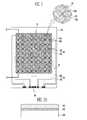
- FIG. 1is a schematic planar view illustrating a touch screen panel according to an embodiment
- FIGS. 2A to 2Eare sectional views illustrating a method of manufacturing a touch screen panel according to an embodiment of the present invention
- FIGS. 3A to 3Dare plan views illustrating a method of manufacturing a touch screen panel according to an embodiment.
- FIGS. 4A and 4Bare sectional views illustrating a method of manufacturing a touch screen panel according to another embodiment.
- FIG. 1is a schematic plan view illustrating a touch screen panel according to an embodiment.
- a substrate 100includes a sensing region 12 and a peripheral region 14 .
- the substrate 100is formed of a transparent insulating material such as thin film shaped glass or plastic and may be a flexible substrate.
- the sensing region 12 for sensing a contact position of a hand or an objectmay be provided, for example, in the center of the substrate 100 .
- a plurality of sensing electrodes 20are formed on the substrate 100 of the sensing region 12 .
- the plurality of sensing electrodes 20include a plurality of first sensing patterns 22 arranged to be connected to each other in one direction (for example, an X direction) and a plurality of second sensing patterns 24 arranged to be connected to each other in the direction (for example, a Y direction) that intersects the first sensing patterns 22 .
- the first sensing patterns 22 and the second sensing patterns 24may be formed of a transparent conductive material.
- the first sensing patterns 22 or the second sensing patterns 24may be formed to be separated from each other in an independent pattern and may be connected to each other by a bridge.
- the second sensing patterns 24are formed to be separated from each other and are connected to each other by a bridge 24 a .
- the bridge 24 ais provided to intersect the connecting unit 22 a of the first sensing patterns 22 and may be electrically insulated from the connecting unit 22 a of the first sensing patterns 22 by an insulating layer (not shown).
- the insulating layermay be formed on the first sensing patterns 22 , the connecting unit 22 a , and the second sensing patterns 24 and may be patterned so that both sides of the second sensing patterns 24 are exposed.
- the bridge 24 amay be provided on the insulating layer to intersect the connecting unit 22 a to connect the exposed parts of adjacent second sensing patterns 24 to each other.
- the insulating layermay be formed to be larger than the first sensing patterns 22 , the connecting unit 22 a , and the second sensing patterns 24 or the insulating layer on the second sensing patterns 24 and the insulating layer on the connecting unit 22 a are connected to each other and a plurality of slots or holes (not shown) may be formed in the insulating layer between the second sensing patterns 24 and the connecting unit 22 a so that the bridge 24 a is not electrically connected to the first sensing patterns 22 and the connecting unit 22 a.
- the peripheral region 14is a peripheral part of the sensing region 12 .
- a plurality of wiring lines 30 connected to a plurality of sensing electrodes 20 and a pad unit 40 connected to the plurality of wiring lines 30are formed on the substrate 100 of the peripheral region 14 .
- a wiring line 32may be formed to be connected to the plurality of first sensing patterns 22 and a wiring line 34 may be formed to be connected to the plurality of sensing patterns 24 .
- the wiring line 30may be formed of a transparent conductive material.
- a driving circuit board(not shown) for driving the touch screen panel may be electrically connected to the pad unit 40 .
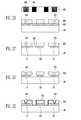
- FIGS. 2A and 2Bare sectional views illustrating a method of manufacturing a touch screen panel according to an embodiment.
- FIGS. 3A to 3Dare planar views illustrating a method of manufacturing a touch screen panel according to an embodiment. A section taken along the line 11 - 12 of the sensing region 12 illustrated in FIG. 1 is illustrated.
- a metal layer 200 and an insulating layer 300are sequentially formed on the substrate 100 including the sensing region 12 and the peripheral region 14 .
- the metal layer 200may be formed of Ag having low surface resistance and Ag nanowires having low surface resistance and high flexibility. Ag nanowires may be formed by spin coating or slit coating.
- the insulating layer 300may be formed of an organic insulating material and is preferably formed of a negative organic insulating material. In some embodiments, acrylate and epoxy based materials may be used as the organic insulating material.
- the insulating layer 300is patterned using a first mask 400 for forming the sensing pattern 20 .
- the insulating layer 300 in the parts where the sensing electrode 20 is not formedis patterned so that the metal layer 200 is completely exposed and the insulating layer 300 in the parts 310 to which the bridge is to be connected is patterned so that a partial thickness remains.
- light blocking patterns 410are formed in the first mask 400 corresponding to the parts where the metal layer 200 is completely exposed and semi-transmissive patterns 420 may be formed in the first mask 400 corresponding to the parts 310 where the partial thickness of the insulating layer 300 remains.
- semi-transmissive patterns 420may be formed of slit patterns or half tone patterns.
- the distance between the slit patterns or the halftone patterns and the amount of exposure of the slit patterns or the halftone patternsare controlled so that the remaining thickness of the insulating layer 300 may be controlled.
- the metal layer 200(shown in FIG. 2B ) is patterned by a wet etching process using the patterned insulating layer 300 as a mask to form the first sensing patterns 22 (shown in FIG. 1 ), the connecting unit 22 a , and the second sensing patterns 24 .
- the sides of the first sensing patterns 22 , the connecting unit 22 a , and the second sensing patterns 24 under the insulating layer 300are excessively etched so that undercuts 210 are generated in both parts under the insulating layer 300 .
- Al (aluminum) etchantsince the etching ratio of Ag is larger than that of the organic insulating layer, the undercuts 210 may be formed.
- the plurality of first sensing patterns 22are connected to each other in one direction (for example, the X direction) by the connecting unit 22 a and the plurality of second sensing patterns 24 are arranged to be separated from each other in the direction (for example, the Y direction) that intersects the first sensing patterns 22 (shown in FIG. 1 ).
- the wiring line 32 connected to the plurality of first sensing patterns 22 and the wiring line 34 connected to the plurality of second sensing patterns 24may be formed in the peripheral region 14 of the substrate 100 when the metal layer 200 is patterned.
- the partial thickness of the insulating layer 300may be entirely etched by a dry etching process to expose the sensing electrode 20 of the parts 310 to which the bridge is to be connected, for example, parts of the second sensing patterns 24 .
- the conductive layermay be patterned by a photolithography process using a second mask for forming the bridge to form, for example, the bridge 24 a for connecting the second sensing patterns 24 to each other. During patterning, the bridge 24 a may be not electrically connected to the connecting unit 22 a thereunder due to the undercuts 210 (shown in FIG. 2C ).
- the conductive layermay be formed of low resistance metal such as Mo, Ag, Ti, Al, and Cu, a lamination structure of the above metals, or a transparent conductive material such as ITO.
- the sensing electrode 20 or the wiring line 30when the conductive layer is formed and patterned in the state where the sensing electrode 20 formed of the metal layer 200 or the wiring line 30 is exposed, the sensing electrode 20 or the wiring line 30 may be damaged where a difference in the etching ratio between the metal layer 200 and the conductive layer is small.
- the insulating layer 300may be formed on the sensing electrode 20 and the wiring line 30 so that the sensing electrode 20 or the wiring line 30 is not damaged when the difference in the etching ratio between the metal layer 200 and the conductive layer is small.
- the wiring line 32 connected to the plurality of first sensing patterns 22 and the wiring line 34 connected to the plurality of second sensing patterns 24may be formed in the peripheral region 14 of the substrate 100 when the conductive layer is patterned.
- the second sensing patterns 24are formed of Ag nanowires, since a contact area between the second sensing patterns 24 and the bridge 24 a is small, contact resistance may be increased. Therefore, in consideration of the entire resistance value of the second sensing patterns 24 , if necessary, a plurality of bridges 24 a may be formed.
- the width of the bridges 24 ais preferably 1 ⁇ m to 6 ⁇ m and the distance between the bridges 24 a is preferably no more than 5 ⁇ m in consideration of visibility.
- FIGS. 4A and 4Bare sectional views illustrating a method of manufacturing a touch screen panel according to another embodiment of the present invention.
- the metal layer 200 and the insulating layer 300are sequentially formed on the substrate 100 including the sensing region 12 and the peripheral region 14 .
- the insulating layer 300is patterned using the first mask 400 for forming the sensing electrode 20 .
- a plurality of slits or holes 320are formed in the insulating layer 300 in the parts where the sensing electrode 20 is not formed.
- slit or hole shaped light blocking patterns 430may be formed in the first mask 400 corresponding to the plurality of slits or holes 320 .
- the metal layer 200is etched as illustrated in FIG. 2C and the insulating layer 300 is etched as illustrated in FIG. 2D .
- the conductive layermay be formed on the entire top surface to a uniform thickness as illustrated in FIG. 2E .
- the conductive layermay be patterned by the photolithography process using the second mask for forming the bridge to form, for example, the bridge 24 a for connecting the second sensing patterns 24 .
- the distance between the plurality of slits or holes 320is small.
- the conductive layermay be formed on only the surface without being filled in the plurality of slits or holes 320 since the distance between the plurality of slits or holes 320 is small.
- the bridge 24 amay be formed on only the surface of the insulating layer 300 . In some embodiments, the bridge 24 a is not electrically connected to the connecting unit 22 a thereunder since the bridge 24 a may be formed on only the surface of the insulating layer 300 .
Landscapes
- Engineering & Computer Science (AREA)
- General Engineering & Computer Science (AREA)
- Theoretical Computer Science (AREA)
- Human Computer Interaction (AREA)
- Physics & Mathematics (AREA)
- General Physics & Mathematics (AREA)
- Position Input By Displaying (AREA)
- Chemical & Material Sciences (AREA)
- General Chemical & Material Sciences (AREA)
- Materials Engineering (AREA)
- Mechanical Engineering (AREA)
- Metallurgy (AREA)
- Organic Chemistry (AREA)
- Chemical Kinetics & Catalysis (AREA)
Abstract
Description
Claims (12)
Applications Claiming Priority (2)
| Application Number | Priority Date | Filing Date | Title |
|---|---|---|---|
| KR10-2012-0122877 | 2012-11-01 | ||
| KR1020120122877AKR102017155B1 (en) | 2012-11-01 | 2012-11-01 | Touch screen panel and method for manufacturing the same |
Publications (2)
| Publication Number | Publication Date |
|---|---|
| US20140118292A1 US20140118292A1 (en) | 2014-05-01 |
| US9229555B2true US9229555B2 (en) | 2016-01-05 |
Family
ID=50546633
Family Applications (1)
| Application Number | Title | Priority Date | Filing Date |
|---|---|---|---|
| US13/772,124Expired - Fee RelatedUS9229555B2 (en) | 2012-11-01 | 2013-02-20 | Touch screen panel and method of manufacturing the same |
Country Status (2)
| Country | Link |
|---|---|
| US (1) | US9229555B2 (en) |
| KR (1) | KR102017155B1 (en) |
Cited By (3)
| Publication number | Priority date | Publication date | Assignee | Title |
|---|---|---|---|---|
| US20150316956A1 (en)* | 2014-05-04 | 2015-11-05 | Tpk Touch Solutions (Xiamen) Inc. | Touch device |
| US20160170515A1 (en)* | 2012-11-30 | 2016-06-16 | Hannstouch Solution Incorporated | Manufacturing method of touch panel |
| US20190227646A1 (en)* | 2018-01-25 | 2019-07-25 | Wuhan China Star Optoelectronics Semiconductor Display Technology Co., Ltd. | Touch panel |
Families Citing this family (17)
| Publication number | Priority date | Publication date | Assignee | Title |
|---|---|---|---|---|
| JP6370883B2 (en)* | 2013-04-30 | 2018-08-08 | アプライド マテリアルズ インコーポレイテッドApplied Materials,Incorporated | Multi-level mask circuit manufacturing and multilayer circuit |
| US20150052747A1 (en)* | 2013-08-22 | 2015-02-26 | Chih-Chung Lin | Manufacturing method of touch substrate |
| KR101653719B1 (en)* | 2014-05-22 | 2016-09-05 | 전자부품연구원 | Touch panel with digitiger electrode and method the same |
| KR102341436B1 (en)* | 2014-08-06 | 2021-12-23 | 삼성디스플레이 주식회사 | Fabrication method of touch screen panel and touch screen panel |
| CN105404407B (en)* | 2014-08-16 | 2019-01-22 | 宸鸿科技(厦门)有限公司 | Touch panel and preparation method thereof with flexible touch control sensor |
| KR102312260B1 (en) | 2015-01-09 | 2021-10-13 | 삼성디스플레이 주식회사 | Flexible touch panel and flexible display device |
| KR102283921B1 (en)* | 2015-01-09 | 2021-07-30 | 삼성디스플레이 주식회사 | Flexible touch panel |
| KR102338748B1 (en) | 2015-04-21 | 2021-12-15 | 삼성디스플레이 주식회사 | Touch screen panel and fabrication method of the same |
| KR102555392B1 (en)* | 2016-03-18 | 2023-07-14 | 삼성디스플레이 주식회사 | Display device and fabricating method thereof |
| CN108628486B (en)* | 2017-03-20 | 2025-04-01 | 宸鸿科技(厦门)有限公司 | Foldable touch display device and touch device thereof |
| CN109426373B (en)* | 2017-08-21 | 2024-08-30 | 京东方科技集团股份有限公司 | Touch panel, manufacturing method thereof and touch display device |
| CN107994057B (en)* | 2017-11-20 | 2021-09-28 | 武汉华星光电半导体显示技术有限公司 | Manufacturing method of touch sensing layer, display screen and display |
| CN108693994A (en) | 2018-03-29 | 2018-10-23 | 武汉华星光电半导体显示技术有限公司 | Touch-control structure, OLED show touch panel and touch control display device |
| CN109471554A (en)* | 2018-09-10 | 2019-03-15 | 芜湖伦丰电子科技有限公司 | A kind of single-layer membrane structure touch function piece, touch screen and touch electronic equipment |
| CN110289292B (en)* | 2019-06-27 | 2022-04-15 | 京东方科技集团股份有限公司 | A display substrate, a display device and a manufacturing method of the display substrate |
| KR102832339B1 (en) | 2019-07-09 | 2025-07-10 | 삼성디스플레이 주식회사 | Display device |
| KR102710487B1 (en)* | 2019-11-01 | 2024-09-25 | 동우 화인켐 주식회사 | Touch Sensor and Method for Manufacturing the Same |
Citations (15)
| Publication number | Priority date | Publication date | Assignee | Title |
|---|---|---|---|---|
| KR20080066658A (en) | 2005-08-12 | 2008-07-16 | 캄브리오스 테크놀로지즈 코포레이션 | Nanowire-based transparent conductor |
| KR20090074925A (en) | 2008-01-03 | 2009-07-08 | 삼성전자주식회사 | Halftone mask, method for manufacturing same and method for manufacturing array substrate using same |
| US20090262096A1 (en)* | 2008-04-22 | 2009-10-22 | Hitachi Displays, Ltd. | Display device with touch panel |
| US20110035938A1 (en)* | 2007-08-17 | 2011-02-17 | Samsung Electro-Mechanics Co., Ltd. | Method of manufacturing a capacitor-embedded printed circuit board |
| US20110205168A1 (en)* | 2010-02-22 | 2011-08-25 | Samsung Mobile Display Co., Ltd. | Touch screen panel and fabricating method thereof |
| US20110207055A1 (en)* | 2010-02-22 | 2011-08-25 | Samsung Mobile Display Co., Ltd. | Fabricating method for touch screen panel |
| US20110279401A1 (en) | 2010-05-14 | 2011-11-17 | Samsung Electro-Mechanics Co., Ltd. | One-layer capacitive touch screen and method of manufacturing the same |
| US20120013554A1 (en)* | 2010-07-14 | 2012-01-19 | Seunghee Nam | Electrostatic capacity type touch screen panel and method of manufacturing the same |
| US20120092292A1 (en)* | 2010-10-14 | 2012-04-19 | Panasonic Liquid Crystal Display Co., Ltd. | Display device having touch panel |
| KR20120059664A (en) | 2010-09-02 | 2012-06-11 | 엘지디스플레이 주식회사 | Touch panel, a flat panel display device comprising the same and method for manufacturing of touch panel |
| US20120229414A1 (en)* | 2011-03-08 | 2012-09-13 | Qrg Limited | Position sensing panel |
| US20130033446A1 (en)* | 2011-08-04 | 2013-02-07 | Chimei Innolux Corporation | Touch panel, touch display apparatus using the same and manufacturing method thereof |
| US20130057497A1 (en)* | 2011-09-06 | 2013-03-07 | Yong-Gu CHO | Touch screen, transparent circuit board for touch screen, and method for fabricating touch screen |
| US20130201116A1 (en)* | 2012-02-07 | 2013-08-08 | Hsueh-Jung Huang | Touch panel |
| US20130293508A1 (en)* | 2012-05-07 | 2013-11-07 | Au Optronics Corporation | Touch panel, touch display panel and touch display apparatus |
Family Cites Families (3)
| Publication number | Priority date | Publication date | Assignee | Title |
|---|---|---|---|---|
| US8023302B2 (en)* | 2005-01-31 | 2011-09-20 | Semiconductor Energy Laboratory Co., Ltd. | Memory device and semiconductor device |
| WO2007012899A1 (en)* | 2005-07-25 | 2007-02-01 | Plastic Logic Limited | Flexible touch screen display |
| KR101634791B1 (en)* | 2008-11-28 | 2016-06-30 | 삼성디스플레이 주식회사 | Touch sensible organic light emitting diode display |
- 2012
- 2012-11-01KRKR1020120122877Apatent/KR102017155B1/ennot_activeExpired - Fee Related
- 2013
- 2013-02-20USUS13/772,124patent/US9229555B2/ennot_activeExpired - Fee Related
Patent Citations (18)
| Publication number | Priority date | Publication date | Assignee | Title |
|---|---|---|---|---|
| KR20080066658A (en) | 2005-08-12 | 2008-07-16 | 캄브리오스 테크놀로지즈 코포레이션 | Nanowire-based transparent conductor |
| US8049333B2 (en) | 2005-08-12 | 2011-11-01 | Cambrios Technologies Corporation | Transparent conductors comprising metal nanowires |
| US20110035938A1 (en)* | 2007-08-17 | 2011-02-17 | Samsung Electro-Mechanics Co., Ltd. | Method of manufacturing a capacitor-embedded printed circuit board |
| KR20090074925A (en) | 2008-01-03 | 2009-07-08 | 삼성전자주식회사 | Halftone mask, method for manufacturing same and method for manufacturing array substrate using same |
| US20090176325A1 (en) | 2008-01-03 | 2009-07-09 | Woo-Seok Jeon | Halftone mask, method of manufacturing the same, and method of manufacturing an array substrate using the same |
| US20090262096A1 (en)* | 2008-04-22 | 2009-10-22 | Hitachi Displays, Ltd. | Display device with touch panel |
| US20110205168A1 (en)* | 2010-02-22 | 2011-08-25 | Samsung Mobile Display Co., Ltd. | Touch screen panel and fabricating method thereof |
| US20110207055A1 (en)* | 2010-02-22 | 2011-08-25 | Samsung Mobile Display Co., Ltd. | Fabricating method for touch screen panel |
| US20110279401A1 (en) | 2010-05-14 | 2011-11-17 | Samsung Electro-Mechanics Co., Ltd. | One-layer capacitive touch screen and method of manufacturing the same |
| KR20110125970A (en) | 2010-05-14 | 2011-11-22 | 삼성전기주식회사 | Single Layer Capacitive Touch Screen and Manufacturing Method Thereof |
| US20120013554A1 (en)* | 2010-07-14 | 2012-01-19 | Seunghee Nam | Electrostatic capacity type touch screen panel and method of manufacturing the same |
| KR20120059664A (en) | 2010-09-02 | 2012-06-11 | 엘지디스플레이 주식회사 | Touch panel, a flat panel display device comprising the same and method for manufacturing of touch panel |
| US20120092292A1 (en)* | 2010-10-14 | 2012-04-19 | Panasonic Liquid Crystal Display Co., Ltd. | Display device having touch panel |
| US20120229414A1 (en)* | 2011-03-08 | 2012-09-13 | Qrg Limited | Position sensing panel |
| US20130033446A1 (en)* | 2011-08-04 | 2013-02-07 | Chimei Innolux Corporation | Touch panel, touch display apparatus using the same and manufacturing method thereof |
| US20130057497A1 (en)* | 2011-09-06 | 2013-03-07 | Yong-Gu CHO | Touch screen, transparent circuit board for touch screen, and method for fabricating touch screen |
| US20130201116A1 (en)* | 2012-02-07 | 2013-08-08 | Hsueh-Jung Huang | Touch panel |
| US20130293508A1 (en)* | 2012-05-07 | 2013-11-07 | Au Optronics Corporation | Touch panel, touch display panel and touch display apparatus |
Cited By (4)
| Publication number | Priority date | Publication date | Assignee | Title |
|---|---|---|---|---|
| US20160170515A1 (en)* | 2012-11-30 | 2016-06-16 | Hannstouch Solution Incorporated | Manufacturing method of touch panel |
| US9983706B2 (en)* | 2012-11-30 | 2018-05-29 | Hannstouch Solution Incorporated | Manufacturing method of touch panel |
| US20150316956A1 (en)* | 2014-05-04 | 2015-11-05 | Tpk Touch Solutions (Xiamen) Inc. | Touch device |
| US20190227646A1 (en)* | 2018-01-25 | 2019-07-25 | Wuhan China Star Optoelectronics Semiconductor Display Technology Co., Ltd. | Touch panel |
Also Published As
| Publication number | Publication date |
|---|---|
| KR102017155B1 (en) | 2019-09-03 |
| KR20140055684A (en) | 2014-05-09 |
| US20140118292A1 (en) | 2014-05-01 |
Similar Documents
| Publication | Publication Date | Title |
|---|---|---|
| US9229555B2 (en) | Touch screen panel and method of manufacturing the same | |
| US11340741B2 (en) | Touch window having a sensing electrode with a variable width of a conductive line | |
| US9217890B2 (en) | Touch screen panel and method for manufacturing the same | |
| CN102375635B (en) | Touch screen panel and method of manufacturing the same | |
| CN102156596B (en) | Electrostatic capacitive type touch screen panel and method of manufacturing the same | |
| US10091872B2 (en) | Touch window and display including the same | |
| KR102052165B1 (en) | Method for manufacturing a touch screen panel | |
| TWI634471B (en) | Touch panel and touch device with the same | |
| CN101553776A (en) | Touch panel apparatus and method for manufacturing the same | |
| CN101751181B (en) | How to make a touch panel | |
| US20140267953A1 (en) | Touch screen panel and method of manufacturing the same | |
| CN102156563A (en) | Touch screen panel | |
| TWI438662B (en) | Touch panel and touch display panel having the same | |
| KR102401556B1 (en) | Touch Screen Panel and Method for Manufacturing the Same | |
| TWI553711B (en) | Touch panel and method for manufacturing the same | |
| CN103677406B (en) | Touch panel and touch display panel | |
| CN109407869A (en) | Touch-control structure and preparation method thereof, display device | |
| JP2014211685A (en) | Display device integrated with touch sensor | |
| US10768764B2 (en) | Touch structure and manufacturing method thereof, and touch device | |
| WO2014015618A1 (en) | Touch control panel and manufacturing method therefor, and touch control device | |
| US20150122624A1 (en) | Touch panel and method of manufacturing thereof | |
| KR102313216B1 (en) | Touch Screen Panel and Method for Manufacturing the Same | |
| KR20140112892A (en) | Touch Screen Panel and Fabricating Method Thereof | |
| KR20140096635A (en) | In-cell Touch Type Liquid Crystal Display and Method of fabricating the same | |
| JP6242710B2 (en) | Manufacturing method of input device |
Legal Events
| Date | Code | Title | Description |
|---|---|---|---|
| AS | Assignment | Owner name:SAMSUNG DISPLAY CO., LTD.,, KOREA, REPUBLIC OF Free format text:ASSIGNMENT OF ASSIGNORS INTEREST;ASSIGNOR:KIM, KYU-YOUNG;REEL/FRAME:029848/0237 Effective date:20130119 | |
| FEPP | Fee payment procedure | Free format text:PAYOR NUMBER ASSIGNED (ORIGINAL EVENT CODE: ASPN); ENTITY STATUS OF PATENT OWNER: LARGE ENTITY | |
| ZAAA | Notice of allowance and fees due | Free format text:ORIGINAL CODE: NOA | |
| ZAAB | Notice of allowance mailed | Free format text:ORIGINAL CODE: MN/=. | |
| STCF | Information on status: patent grant | Free format text:PATENTED CASE | |
| MAFP | Maintenance fee payment | Free format text:PAYMENT OF MAINTENANCE FEE, 4TH YEAR, LARGE ENTITY (ORIGINAL EVENT CODE: M1551); ENTITY STATUS OF PATENT OWNER: LARGE ENTITY Year of fee payment:4 | |
| FEPP | Fee payment procedure | Free format text:MAINTENANCE FEE REMINDER MAILED (ORIGINAL EVENT CODE: REM.); ENTITY STATUS OF PATENT OWNER: LARGE ENTITY | |
| LAPS | Lapse for failure to pay maintenance fees | Free format text:PATENT EXPIRED FOR FAILURE TO PAY MAINTENANCE FEES (ORIGINAL EVENT CODE: EXP.); ENTITY STATUS OF PATENT OWNER: LARGE ENTITY | |
| STCH | Information on status: patent discontinuation | Free format text:PATENT EXPIRED DUE TO NONPAYMENT OF MAINTENANCE FEES UNDER 37 CFR 1.362 | |
| FP | Lapsed due to failure to pay maintenance fee | Effective date:20240105 |