US9226402B2 - Strain isolation structures for stretchable electronics - Google Patents
Strain isolation structures for stretchable electronicsDownload PDFInfo
- Publication number
- US9226402B2 US9226402B2US13/843,873US201313843873AUS9226402B2US 9226402 B2US9226402 B2US 9226402B2US 201313843873 AUS201313843873 AUS 201313843873AUS 9226402 B2US9226402 B2US 9226402B2
- Authority
- US
- United States
- Prior art keywords
- buffer structure
- device component
- junction region
- encapsulant
- buffer
- Prior art date
- Legal status (The legal status is an assumption and is not a legal conclusion. Google has not performed a legal analysis and makes no representation as to the accuracy of the status listed.)
- Active, expires
Links
- 238000002955isolationMethods0.000titledescription12
- 239000008393encapsulating agentSubstances0.000claimsabstractdescription68
- 239000000463materialSubstances0.000claimsdescription63
- 229920000642polymerPolymers0.000claimsdescription25
- 239000004642PolyimideSubstances0.000claimsdescription8
- 229920001721polyimidePolymers0.000claimsdescription8
- 239000000806elastomerSubstances0.000claimsdescription5
- 229920001971elastomerPolymers0.000claimsdescription5
- 239000004065semiconductorSubstances0.000claimsdescription5
- RYGMFSIKBFXOCR-UHFFFAOYSA-NCopperChemical compound[Cu]RYGMFSIKBFXOCR-UHFFFAOYSA-N0.000claimsdescription3
- 229910052782aluminiumInorganic materials0.000claimsdescription3
- XAGFODPZIPBFFR-UHFFFAOYSA-NaluminiumChemical compound[Al]XAGFODPZIPBFFR-UHFFFAOYSA-N0.000claimsdescription3
- 229920001940conductive polymerPolymers0.000claimsdescription3
- 229910052802copperInorganic materials0.000claimsdescription3
- 239000010949copperSubstances0.000claimsdescription3
- PCHJSUWPFVWCPO-UHFFFAOYSA-NgoldChemical compound[Au]PCHJSUWPFVWCPO-UHFFFAOYSA-N0.000claimsdescription3
- 229910052737goldInorganic materials0.000claimsdescription3
- 239000010931goldSubstances0.000claimsdescription3
- 229910052709silverInorganic materials0.000claimsdescription3
- 239000004332silverSubstances0.000claimsdescription3
- 239000010935stainless steelSubstances0.000claimsdescription3
- 229910001220stainless steelInorganic materials0.000claimsdescription3
- 239000012811non-conductive materialSubstances0.000claims3
- 238000004891communicationMethods0.000abstractdescription19
- 238000000034methodMethods0.000description27
- 239000004020conductorSubstances0.000description9
- 239000000758substrateSubstances0.000description8
- XUIMIQQOPSSXEZ-UHFFFAOYSA-NSiliconChemical compound[Si]XUIMIQQOPSSXEZ-UHFFFAOYSA-N0.000description7
- 229910052710siliconInorganic materials0.000description7
- 239000010703siliconSubstances0.000description7
- 230000001788irregularEffects0.000description6
- -1polyethylene terephthalatePolymers0.000description6
- 229920001296polysiloxanePolymers0.000description6
- 230000006378damageEffects0.000description4
- 238000003384imaging methodMethods0.000description4
- 239000004698PolyethyleneSubstances0.000description3
- 238000004458analytical methodMethods0.000description3
- 238000009826distributionMethods0.000description3
- 229910001092metal group alloyInorganic materials0.000description3
- 229920000573polyethylenePolymers0.000description3
- 239000007787solidSubstances0.000description3
- PXHVJJICTQNCMI-UHFFFAOYSA-NNickelChemical compound[Ni]PXHVJJICTQNCMI-UHFFFAOYSA-N0.000description2
- KDLHZDBZIXYQEI-UHFFFAOYSA-NPalladiumChemical compound[Pd]KDLHZDBZIXYQEI-UHFFFAOYSA-N0.000description2
- 230000008901benefitEffects0.000description2
- 230000032798delaminationEffects0.000description2
- 229920005839ecoflex®Polymers0.000description2
- 229910052751metalInorganic materials0.000description2
- 239000002184metalSubstances0.000description2
- BASFCYQUMIYNBI-UHFFFAOYSA-NplatinumChemical compound[Pt]BASFCYQUMIYNBI-UHFFFAOYSA-N0.000description2
- 229920000139polyethylene terephthalatePolymers0.000description2
- 239000005020polyethylene terephthalateSubstances0.000description2
- 229920005989resinPolymers0.000description2
- 239000011347resinSubstances0.000description2
- 238000004528spin coatingMethods0.000description2
- OKTJSMMVPCPJKN-UHFFFAOYSA-NCarbonChemical compound[C]OKTJSMMVPCPJKN-UHFFFAOYSA-N0.000description1
- VYZAMTAEIAYCRO-UHFFFAOYSA-NChromiumChemical compound[Cr]VYZAMTAEIAYCRO-UHFFFAOYSA-N0.000description1
- 229910001218Gallium arsenideInorganic materials0.000description1
- VVQNEPGJFQJSBK-UHFFFAOYSA-NMethyl methacrylateChemical compoundCOC(=O)C(C)=CVVQNEPGJFQJSBK-UHFFFAOYSA-N0.000description1
- 206010028980NeoplasmDiseases0.000description1
- 229920001890NovodurPolymers0.000description1
- 239000004962Polyamide-imideSubstances0.000description1
- 239000004693PolybenzimidazoleSubstances0.000description1
- 239000004697PolyetherimideSubstances0.000description1
- 239000004721Polyphenylene oxideSubstances0.000description1
- 239000004734Polyphenylene sulfideSubstances0.000description1
- 239000004954PolyphthalamideSubstances0.000description1
- 239000004743PolypropyleneSubstances0.000description1
- BQCADISMDOOEFD-UHFFFAOYSA-NSilverChemical compound[Ag]BQCADISMDOOEFD-UHFFFAOYSA-N0.000description1
- RTAQQCXQSZGOHL-UHFFFAOYSA-NTitaniumChemical compound[Ti]RTAQQCXQSZGOHL-UHFFFAOYSA-N0.000description1
- HCHKCACWOHOZIP-UHFFFAOYSA-NZincChemical compound[Zn]HCHKCACWOHOZIP-UHFFFAOYSA-N0.000description1
- 150000001252acrylic acid derivativesChemical class0.000description1
- 229910045601alloyInorganic materials0.000description1
- 239000000956alloySubstances0.000description1
- 238000003491arrayMethods0.000description1
- 230000009286beneficial effectEffects0.000description1
- 229920002988biodegradable polymerPolymers0.000description1
- 239000004621biodegradable polymerSubstances0.000description1
- 230000015572biosynthetic processEffects0.000description1
- 201000011510cancerDiseases0.000description1
- 229910052799carbonInorganic materials0.000description1
- 230000002425cardiocirculatory effectEffects0.000description1
- 229910052804chromiumInorganic materials0.000description1
- 239000011651chromiumSubstances0.000description1
- 239000011248coating agentSubstances0.000description1
- 238000000576coating methodMethods0.000description1
- 230000000295complement effectEffects0.000description1
- 239000000470constituentSubstances0.000description1
- 238000000151depositionMethods0.000description1
- 210000002249digestive systemAnatomy0.000description1
- 238000005516engineering processMethods0.000description1
- 230000008020evaporationEffects0.000description1
- 238000001704evaporationMethods0.000description1
- 229920005570flexible polymerPolymers0.000description1
- 239000004811fluoropolymerSubstances0.000description1
- 229920002313fluoropolymerPolymers0.000description1
- 230000006870functionEffects0.000description1
- AMGQUBHHOARCQH-UHFFFAOYSA-Nindium;oxotinChemical compound[In].[Sn]=OAMGQUBHHOARCQH-UHFFFAOYSA-N0.000description1
- 230000010354integrationEffects0.000description1
- 238000004519manufacturing processMethods0.000description1
- 229910044991metal oxideInorganic materials0.000description1
- 150000004706metal oxidesChemical class0.000description1
- 238000012986modificationMethods0.000description1
- 230000004048modificationEffects0.000description1
- 210000000653nervous systemAnatomy0.000description1
- 229910052759nickelInorganic materials0.000description1
- 229920001778nylonPolymers0.000description1
- 230000005693optoelectronicsEffects0.000description1
- 210000000056organAnatomy0.000description1
- 229910052763palladiumInorganic materials0.000description1
- 229920003023plasticPolymers0.000description1
- 239000004033plasticSubstances0.000description1
- 229910052697platinumInorganic materials0.000description1
- 229920002239polyacrylonitrilePolymers0.000description1
- 229920002312polyamide-imidePolymers0.000description1
- 229920001230polyarylatePolymers0.000description1
- 229920002480polybenzimidazolePolymers0.000description1
- 229920001748polybutylenePolymers0.000description1
- 239000004417polycarbonateSubstances0.000description1
- 229920000515polycarbonatePolymers0.000description1
- 229920000728polyesterPolymers0.000description1
- 229920001601polyetherimidePolymers0.000description1
- 229920001470polyketonePolymers0.000description1
- 229920000306polymethylpentenePolymers0.000description1
- 239000011116polymethylpenteneSubstances0.000description1
- 229920006324polyoxymethylenePolymers0.000description1
- 229920006380polyphenylene oxidePolymers0.000description1
- 229920000069polyphenylene sulfidePolymers0.000description1
- 229920006375polyphtalamidePolymers0.000description1
- 229920001155polypropylenePolymers0.000description1
- 229920002635polyurethanePolymers0.000description1
- 239000004814polyurethaneSubstances0.000description1
- 230000008569processEffects0.000description1
- 230000009467reductionEffects0.000description1
- 230000002787reinforcementEffects0.000description1
- 238000004544sputter depositionMethods0.000description1
- 125000001174sulfone groupChemical group0.000description1
- 238000002560therapeutic procedureMethods0.000description1
- 229920001169thermoplasticPolymers0.000description1
- 229920002725thermoplastic elastomerPolymers0.000description1
- 239000004416thermosoftening plasticSubstances0.000description1
- 239000010409thin filmSubstances0.000description1
- 229910052719titaniumInorganic materials0.000description1
- 239000010936titaniumSubstances0.000description1
- 238000010023transfer printingMethods0.000description1
- 230000007704transitionEffects0.000description1
- 229910052723transition metalInorganic materials0.000description1
- 150000003624transition metalsChemical class0.000description1
- 125000000391vinyl groupChemical group[H]C([*])=C([H])[H]0.000description1
- 229920002554vinyl polymerPolymers0.000description1
- 229910052725zincInorganic materials0.000description1
- 239000011701zincSubstances0.000description1
Images


Classifications
- H—ELECTRICITY
- H05—ELECTRIC TECHNIQUES NOT OTHERWISE PROVIDED FOR
- H05K—PRINTED CIRCUITS; CASINGS OR CONSTRUCTIONAL DETAILS OF ELECTRIC APPARATUS; MANUFACTURE OF ASSEMBLAGES OF ELECTRICAL COMPONENTS
- H05K1/00—Printed circuits
- H05K1/18—Printed circuits structurally associated with non-printed electric components
- H05K1/182—Printed circuits structurally associated with non-printed electric components associated with components mounted in the printed circuit board, e.g. insert mounted components [IMC]
- H05K1/185—Components encapsulated in the insulating substrate of the printed circuit or incorporated in internal layers of a multilayer circuit
- H—ELECTRICITY
- H05—ELECTRIC TECHNIQUES NOT OTHERWISE PROVIDED FOR
- H05K—PRINTED CIRCUITS; CASINGS OR CONSTRUCTIONAL DETAILS OF ELECTRIC APPARATUS; MANUFACTURE OF ASSEMBLAGES OF ELECTRICAL COMPONENTS
- H05K1/00—Printed circuits
- H05K1/02—Details
- H05K1/0271—Arrangements for reducing stress or warp in rigid printed circuit boards, e.g. caused by loads, vibrations or differences in thermal expansion
- H—ELECTRICITY
- H05—ELECTRIC TECHNIQUES NOT OTHERWISE PROVIDED FOR
- H05K—PRINTED CIRCUITS; CASINGS OR CONSTRUCTIONAL DETAILS OF ELECTRIC APPARATUS; MANUFACTURE OF ASSEMBLAGES OF ELECTRICAL COMPONENTS
- H05K1/00—Printed circuits
- H05K1/02—Details
- H05K1/0277—Bendability or stretchability details
- H05K1/028—Bending or folding regions of flexible printed circuits
- H—ELECTRICITY
- H05—ELECTRIC TECHNIQUES NOT OTHERWISE PROVIDED FOR
- H05K—PRINTED CIRCUITS; CASINGS OR CONSTRUCTIONAL DETAILS OF ELECTRIC APPARATUS; MANUFACTURE OF ASSEMBLAGES OF ELECTRICAL COMPONENTS
- H05K1/00—Printed circuits
- H05K1/02—Details
- H05K1/0277—Bendability or stretchability details
- H05K1/0283—Stretchable printed circuits
- H—ELECTRICITY
- H05—ELECTRIC TECHNIQUES NOT OTHERWISE PROVIDED FOR
- H05K—PRINTED CIRCUITS; CASINGS OR CONSTRUCTIONAL DETAILS OF ELECTRIC APPARATUS; MANUFACTURE OF ASSEMBLAGES OF ELECTRICAL COMPONENTS
- H05K1/00—Printed circuits
- H05K1/02—Details
- H05K1/03—Use of materials for the substrate
- H05K1/0313—Organic insulating material
- H05K1/0353—Organic insulating material consisting of two or more materials, e.g. two or more polymers, polymer + filler, + reinforcement
- H05K1/036—Multilayers with layers of different types
- H—ELECTRICITY
- H05—ELECTRIC TECHNIQUES NOT OTHERWISE PROVIDED FOR
- H05K—PRINTED CIRCUITS; CASINGS OR CONSTRUCTIONAL DETAILS OF ELECTRIC APPARATUS; MANUFACTURE OF ASSEMBLAGES OF ELECTRICAL COMPONENTS
- H05K1/00—Printed circuits
- H05K1/02—Details
- H05K1/03—Use of materials for the substrate
- H05K1/0393—Flexible materials
- H—ELECTRICITY
- H05—ELECTRIC TECHNIQUES NOT OTHERWISE PROVIDED FOR
- H05K—PRINTED CIRCUITS; CASINGS OR CONSTRUCTIONAL DETAILS OF ELECTRIC APPARATUS; MANUFACTURE OF ASSEMBLAGES OF ELECTRICAL COMPONENTS
- H05K1/00—Printed circuits
- H05K1/02—Details
- H05K1/09—Use of materials for the conductive, e.g. metallic pattern
- H—ELECTRICITY
- H05—ELECTRIC TECHNIQUES NOT OTHERWISE PROVIDED FOR
- H05K—PRINTED CIRCUITS; CASINGS OR CONSTRUCTIONAL DETAILS OF ELECTRIC APPARATUS; MANUFACTURE OF ASSEMBLAGES OF ELECTRICAL COMPONENTS
- H05K1/00—Printed circuits
- H05K1/02—Details
- H05K1/11—Printed elements for providing electric connections to or between printed circuits
- H05K1/118—Printed elements for providing electric connections to or between printed circuits specially for flexible printed circuits, e.g. using folded portions
- H—ELECTRICITY
- H05—ELECTRIC TECHNIQUES NOT OTHERWISE PROVIDED FOR
- H05K—PRINTED CIRCUITS; CASINGS OR CONSTRUCTIONAL DETAILS OF ELECTRIC APPARATUS; MANUFACTURE OF ASSEMBLAGES OF ELECTRICAL COMPONENTS
- H05K1/00—Printed circuits
- H05K1/18—Printed circuits structurally associated with non-printed electric components
- H05K1/189—Printed circuits structurally associated with non-printed electric components characterised by the use of a flexible or folded printed circuit
- H—ELECTRICITY
- H05—ELECTRIC TECHNIQUES NOT OTHERWISE PROVIDED FOR
- H05K—PRINTED CIRCUITS; CASINGS OR CONSTRUCTIONAL DETAILS OF ELECTRIC APPARATUS; MANUFACTURE OF ASSEMBLAGES OF ELECTRICAL COMPONENTS
- H05K1/00—Printed circuits
- H05K1/02—Details
- H05K1/14—Structural association of two or more printed circuits
- H05K1/147—Structural association of two or more printed circuits at least one of the printed circuits being bent or folded, e.g. by using a flexible printed circuit
- H—ELECTRICITY
- H05—ELECTRIC TECHNIQUES NOT OTHERWISE PROVIDED FOR
- H05K—PRINTED CIRCUITS; CASINGS OR CONSTRUCTIONAL DETAILS OF ELECTRIC APPARATUS; MANUFACTURE OF ASSEMBLAGES OF ELECTRICAL COMPONENTS
- H05K1/00—Printed circuits
- H05K1/02—Details
- H05K1/14—Structural association of two or more printed circuits
- H05K1/148—Arrangements of two or more hingeably connected rigid printed circuit boards, i.e. connected by flexible means
- H—ELECTRICITY
- H05—ELECTRIC TECHNIQUES NOT OTHERWISE PROVIDED FOR
- H05K—PRINTED CIRCUITS; CASINGS OR CONSTRUCTIONAL DETAILS OF ELECTRIC APPARATUS; MANUFACTURE OF ASSEMBLAGES OF ELECTRICAL COMPONENTS
- H05K2201/00—Indexing scheme relating to printed circuits covered by H05K1/00
- H05K2201/01—Dielectrics
- H05K2201/0104—Properties and characteristics in general
- H05K2201/0133—Elastomeric or compliant polymer
- H—ELECTRICITY
- H05—ELECTRIC TECHNIQUES NOT OTHERWISE PROVIDED FOR
- H05K—PRINTED CIRCUITS; CASINGS OR CONSTRUCTIONAL DETAILS OF ELECTRIC APPARATUS; MANUFACTURE OF ASSEMBLAGES OF ELECTRICAL COMPONENTS
- H05K2201/00—Indexing scheme relating to printed circuits covered by H05K1/00
- H05K2201/01—Dielectrics
- H05K2201/0137—Materials
- H05K2201/0154—Polyimide
- H—ELECTRICITY
- H05—ELECTRIC TECHNIQUES NOT OTHERWISE PROVIDED FOR
- H05K—PRINTED CIRCUITS; CASINGS OR CONSTRUCTIONAL DETAILS OF ELECTRIC APPARATUS; MANUFACTURE OF ASSEMBLAGES OF ELECTRICAL COMPONENTS
- H05K2201/00—Indexing scheme relating to printed circuits covered by H05K1/00
- H05K2201/01—Dielectrics
- H05K2201/0183—Dielectric layers
- H05K2201/0187—Dielectric layers with regions of different dielectrics in the same layer, e.g. in a printed capacitor for locally changing the dielectric properties
- H—ELECTRICITY
- H05—ELECTRIC TECHNIQUES NOT OTHERWISE PROVIDED FOR
- H05K—PRINTED CIRCUITS; CASINGS OR CONSTRUCTIONAL DETAILS OF ELECTRIC APPARATUS; MANUFACTURE OF ASSEMBLAGES OF ELECTRICAL COMPONENTS
- H05K2201/00—Indexing scheme relating to printed circuits covered by H05K1/00
- H05K2201/09—Shape and layout
- H05K2201/09209—Shape and layout details of conductors
- H05K2201/09218—Conductive traces
- H05K2201/09245—Crossing layout
- H—ELECTRICITY
- H05—ELECTRIC TECHNIQUES NOT OTHERWISE PROVIDED FOR
- H05K—PRINTED CIRCUITS; CASINGS OR CONSTRUCTIONAL DETAILS OF ELECTRIC APPARATUS; MANUFACTURE OF ASSEMBLAGES OF ELECTRICAL COMPONENTS
- H05K2201/00—Indexing scheme relating to printed circuits covered by H05K1/00
- H05K2201/10—Details of components or other objects attached to or integrated in a printed circuit board
- H05K2201/10227—Other objects, e.g. metallic pieces
- H05K2201/1028—Thin metal strips as connectors or conductors
- H—ELECTRICITY
- H05—ELECTRIC TECHNIQUES NOT OTHERWISE PROVIDED FOR
- H05K—PRINTED CIRCUITS; CASINGS OR CONSTRUCTIONAL DETAILS OF ELECTRIC APPARATUS; MANUFACTURE OF ASSEMBLAGES OF ELECTRICAL COMPONENTS
- H05K2201/00—Indexing scheme relating to printed circuits covered by H05K1/00
- H05K2201/10—Details of components or other objects attached to or integrated in a printed circuit board
- H05K2201/10227—Other objects, e.g. metallic pieces
- H05K2201/10287—Metal wires as connectors or conductors
- H—ELECTRICITY
- H05—ELECTRIC TECHNIQUES NOT OTHERWISE PROVIDED FOR
- H05K—PRINTED CIRCUITS; CASINGS OR CONSTRUCTIONAL DETAILS OF ELECTRIC APPARATUS; MANUFACTURE OF ASSEMBLAGES OF ELECTRICAL COMPONENTS
- H05K2201/00—Indexing scheme relating to printed circuits covered by H05K1/00
- H05K2201/20—Details of printed circuits not provided for in H05K2201/01 - H05K2201/10
- H05K2201/2009—Reinforced areas, e.g. for a specific part of a flexible printed circuit
- H—ELECTRICITY
- H05—ELECTRIC TECHNIQUES NOT OTHERWISE PROVIDED FOR
- H05K—PRINTED CIRCUITS; CASINGS OR CONSTRUCTIONAL DETAILS OF ELECTRIC APPARATUS; MANUFACTURE OF ASSEMBLAGES OF ELECTRICAL COMPONENTS
- H05K3/00—Apparatus or processes for manufacturing printed circuits
- H05K3/46—Manufacturing multilayer circuits
- H05K3/4688—Composite multilayer circuits, i.e. comprising insulating layers having different properties
- H05K3/4691—Rigid-flexible multilayer circuits comprising rigid and flexible layers, e.g. having in the bending regions only flexible layers
- H—ELECTRICITY
- H05—ELECTRIC TECHNIQUES NOT OTHERWISE PROVIDED FOR
- H05K—PRINTED CIRCUITS; CASINGS OR CONSTRUCTIONAL DETAILS OF ELECTRIC APPARATUS; MANUFACTURE OF ASSEMBLAGES OF ELECTRICAL COMPONENTS
- H05K3/00—Apparatus or processes for manufacturing printed circuits
- H05K3/46—Manufacturing multilayer circuits
- H05K3/4688—Composite multilayer circuits, i.e. comprising insulating layers having different properties
- H05K3/4694—Partitioned multilayer circuits having adjacent regions with different properties, e.g. by adding or inserting locally circuit layers having a higher circuit density
Definitions
- High quality medical sensing and imaging datahas become increasingly beneficial in the diagnoses and treatment of a variety of medical conditions.
- the conditionscan be associated with the digestive system, the cardio-circulatory system, and can include injuries to the nervous system, cancer, and the like.
- most electronic systems that could be used to gather such sensing or imaging datahave been rigid and inflexible. These rigid electronics are not ideal for many applications, such as in biomedical devices.
- Most of biological tissueis soft and curved. The skin and organs are delicate and far from two-dimensional.
- various examples described hereinare directed generally to systems, apparatus and methods for providing strain isolation in a conformable electronic system.
- the systems, methods and apparatus described hereinprovide effective, compact, and complex systems that include stretchable and/or flexible interconnects in electrical communication with more rigid deice components.
- buffer structuresare described that effectively redistributes the strain that might normally act at or near an edge of the more rigid device component or on a junction region between the stretchable and/or flexible interconnects and the more rigid device components.
- a system, apparatus and methodis provided that is based on thin device islands, including integrated circuitry (IC) chips and/or stretchable and/or flexible interconnects that are encapsulated in an encapsulant.
- ICintegrated circuitry
- a system, apparatus and methodincludes a device component, at least one conductive stretchable and/or flexible interconnect in electrical communication with the device component, the at least one conductive stretchable and/or flexible interconnect forming the electrical communication with the device component at a junction region, a buffer structure, and an encapsulant encapsulating at least the device component and the junction region.
- the buffer structureoverlaps with at least a portion of the junction region.
- the buffer structurehas a higher value of Young's modulus than the encapsulant.
- a system, apparatus and methodincludes a device component, at least one conductive stretchable and/or flexible interconnect in electrical communication with the device component, the at least one conductive stretchable and/or flexible interconnect forming the electrical communication with the device component at a junction region, a first buffer structure disposed over the device component, a second buffer structure disposed below the device component, and an encapsulant encapsulating at least the device component and the junction region.
- the first buffer structure and the second buffer structureoverlap with at least a portion of the junction region.
- the first buffer structure and the second buffer structurehave a higher value of Young's modulus than the encapsulant.
- a system, apparatus and methodincludes a device component, a flexible base, the device component being disposed on, or at least partially embedded in, the flexible base, at least one conductive stretchable and/or flexible interconnect in electrical communication with the device component, the at least one conductive stretchable and/or flexible interconnect forming the electrical communication with the device component at a junction region, a buffer structure, and an encapsulant encapsulating at least the device component and the junction region.
- the buffer structureoverlaps with at least a portion of the flexible base.
- the flexible basehas a higher value of Young's modulus than the encapsulant.
- the buffer structurehas a higher value of Young's modulus than the encapsulant.
- FIGS. 1A and 1Bshow top and cross-sectional side views of an example conformable electronic system, according to the principles described herein.
- FIGS. 2A and 2Bshow top and cross-sectional side views of an example conformable electronic system, according to the principles described herein.
- FIG. 3Ashows an example apparatus that includes a strain isolation structure, according to the principles described herein.
- FIG. 3Bshows example results of a finite element analysis of the example apparatus of FIG. 3A , according to the principles described herein.
- FIG. 4shows a plot of an example distribution of strain in an example apparatus, according to the principles described herein.
- FIGS. 5A-5Bshow top and cross-sectional side views of an example apparatus, according to the principles described herein.
- FIGS. 6A-6Bshow top and cross-sectional side views of another example apparatus, according to the principles described herein.
- FIG. 7A-7Bshow cross-sectional side views of other example apparatus, according to the principles described herein.
- FIG. 8A-8Bshow cross-sectional side views of other example apparatus, according to the principles described herein.
- FIG. 9Ashow examples of buffer structures that have a substantially polygonal prism conformation, according to the principles described herein
- FIGS. 9B-9Cshow examples of buffer structure having an irregular structure, according to the principles described herein.
- FIG. 10shows a top view of another example apparatus, according to the principles described herein.
- FIG. 11Ashows a cross-sectional side view of another example apparatus, according to the principles described herein.
- FIG. 11Bshows the finite element model approximation for the components in an example computation of an example apparatus, according to the principles described herein.
- FIGS. 12A and 12Bshow example results of the finite element computations of FIG. 11B , according to the principles described herein.
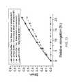
- FIG. 13shows a plot of the von Mises strain and first principal strain versus relative elongation for the example computation of FIGS. 12A and 12B , according to the principles described herein.
- the term “includes”means includes but is not limited to, the term “including” means including but not limited to.
- the term “based on”means based at least in part on.
- the term “disposed on” or “disposed above”is defined to encompass “at least partially embedded in.”
- any references to “top” surface and “bottom” surfaceare used primarily to indicate relative position, alignment and/or orientation of various elements/components with respect to the substrate and each other, and these terms do not necessarily indicate any particular frame of reference (e.g., a gravitational frame of reference).
- reference to a “bottom” of a substrate or a layerdoes not necessarily require that the indicated surface or layer be facing a ground surface.
- a system, apparatus and method described hereinprovides strain isolation in a conformable electronic system.
- buffer structuresare described herein that can be used to reduce a strain that can be exerted near a junction region between a stretchable and/or flexible interconnect or flexible interconnect and a device island when the conformable electronic system is subjected to stretching or torsion.
- the buffer structures according to the principles described hereinare comprised of a material having elastic properties that can effectively redistribute the strain acting on the junction region between stretchable and/or flexible interconnects and rigid device islands in a device structure.
- the stain isolation structurecan be used to create a gradient in local rigidity that effectively redistributes the strain away from the junction region between the stretchable and/or flexible interconnects and the rigid device islands.
- the buffer structurescan be used to facilitate reduction in the concentration of the stress or strain at the junction region, i.e., the transition region from a more rigid component (such as but not limited to a device island) to a more compliant component (such as but not limited to a stretchable and/or flexible interconnect).
- a more rigid componentsuch as but not limited to a device island
- a more compliant componentsuch as but not limited to a stretchable and/or flexible interconnect
- the buffer structurecan have a curved conformation that minimize the stress or strain concentration at or near the sharp edge of integrated circuit (IC) chips.
- the strain relief structurecan be formed in a disk conformation, a torus conformation, or other closed curve conformation.
- the example buffer structurescan be disposed above and/or below the junction region between a more rigid component (such as but not limited to a device island) to a more compliant component (such as but not limited to a stretchable and/or flexible interconnect).
- the dimensions of the buffer structuresare configured such that at least a portion of the buffer structures overlaps the device component and at least a portion of the buffer structure overlaps the junction region between the device component and the compliant component.
- the device componentcan be disposed on or in a flexible base, the flexible base being formed of a material having elastic properties.
- the buffer structuresoverlaps the device component and at least a portion of the buffer structure overlaps the junction region between the device component and the compliant component.
- An example system, apparatus and method according to the principles described hereincan provide a platform of complex device integration and can be applied to many different kinds of stretchable electronic devices.
- An example system, apparatus and method described hereinincludes at least one strain relief structure that is independent of chip geometry, compatible with conventional semiconductor processes, and provides ease of fabrication.
- FIGS. 1A and 1Bshow top and cross-sectional side views of a conformable electronic system 100 to which the example system, apparatus and method described herein can be applied.
- Example conformable electronic system 100includes device components 102 and compliant components 104 encapsulated in an encapsulant 106 .
- the compliant components 104are in electrical communication with the device components 102 at a junction region 108 .
- the compliant component 104can be a stretchable and/or flexible interconnect.
- the encapsulant 106can be any material having elastic properties, including a polymer or other polymeric material.
- the example conformable electronic system 100can be subjected to stretching, torsion or other forces. As shown in FIG.
- the forcescan act to cause a stretching or elongation of the system along a longitudinal direction (e.g., along. the lines of forces shown in the figure).
- the applied forcescan cause an amount of stress or strain to be exerted at junction region 108 .
- the stress or strain at junction region 108can cause an amount of structural damage at junction region 108 , including crack formation in, or rupture of, the compliant component 104 or the junction region 108 .
- FIGS. 2A and 2Bshow top and cross-sectional side views of a conformable electronic system 150 that includes device components 102 and compliant components 104 encapsulated in encapsulant 106 .
- the compliant components 104are in electrical communication with the device components 102 at junction region 108 .
- the device component 102is disposed in, or at least partially embedded in, a flexible base 110 .
- the compliant component 104can be a stretchable and/or flexible interconnect.
- the encapsulant 106can be any material having elastic properties, including a polymer or other polymeric material.
- the example conformable electronic system 100can be subjected to stretching, torsion or other forces.
- the flexible base 110is to cushion the device component 102 . As described in greater detail in connection with FIGS. 3A , 3 B and 4 , the stretching or elongation forces can cause an amount of stress or strain near the junction region.
- FIG. 3Ashow a top views of an example structure that includes device component 102 disposed in a flexible base 110 , encapsulated in an encapsulant 106 .
- FIG. 3Bshows results of a finite element analysis of the example structure as it is subjected to a stretching or other elongation force.
- Table 1shows the materials properties of the components of this example structure of FIG. 3A , including silicon, which can be a constituent of the device component 110 , a polyimide, which can be used to form the flexible base 102 , and a silicone, which can be used as the encapsulant 106 .
- FIG. 4shows a plot of the distribution of strain (computed as Von Mises strain) in the encapsulant and in the flexible base in regions proximate the junction region between the device component and the compliant component.
- FIGS. 5A and 5Bshow top and cross-sectional side views of an example apparatus 500 that includes a buffer structure to provide strain isolation.
- the example apparatus 500includes a device component 502 and a compliant component 504 , encapsulated in encapsulant 506 .
- the compliant component 504is in electrical communication with the device component 502 at junction region 508 .
- the compliant component 504can be a stretchable and/or flexible interconnect.
- the example apparatus of FIGS. 5A and 5Bincludes a buffer structure 509 disposed proximate to the junction region 508 and also encapsulated in the encapsulant 506 . As shown in FIG. 5B , the buffer structure 509 overlaps with at least a portion of the junction region 508 .
- the buffer structure 509is comprised of material that has less elastic flexibility than the material of the encapsulant 506 .
- the buffer structure 509has a higher value of Young's modulus than the encapsulant 506 . While the example of FIGS. 5A and 5B illustrates the buffer structure 509 disposed in the example apparatus 500 proximate to and substantially below the junction region 508 , it is also contemplated that the buffer structure 509 can be disposed in the example apparatus 500 proximate to and substantially above the junction region 508 .
- the buffer structurecan be either disposed on the surface of the flexible base (including an elastomer substrate), including being at least partially embedded in the flexible base (including an elastomer substrate).
- FIGS. 6A and 6Bshow top and cross-sectional side views of another example apparatus 550 that includes a buffer structure to provide strain isolation.
- the example apparatus 550includes the device component 502 and the compliant component 504 , encapsulated in the encapsulant 506 .
- the compliant component 504is in electrical communication with the device component 502 at junction region 508 .
- the compliant component 504can be a stretchable and/or flexible interconnect.
- the example apparatus of FIGS. 5A and 5Bincludes a buffer structure 511 disposed proximate to the junction region 508 and also encapsulated in the encapsulant 506 . Rather than the solid buffer structure 509 shown for the example of FIGS. 5A and 5B , the buffer structure 511 of FIGS.
- the buffer structure 511overlaps with at least a portion of the junction region 508 .
- the buffer structure 509is comprised of material that has less elastic flexibility than the material of the encapsulant 506 .
- the buffer structure 509has a higher value of Young's modulus than the encapsulant 506 .
- the inner dimension of the hollow portion of the buffer structure 511can be positioned to overlap with a portion of the device component proximate the junction region 508 , and the outer dimension of the buffer structure 511 can be positioned to overlap with the junction region 508 .
- the buffer structure 511can be formed as an annular structure.
- the inner diameter of the annular buffer structurecan be positioned to overlap with a portion of the flexible base, and wherein the outer diameter of the annular buffer structure is positioned to overlap with the junction region.
- FIG. 7Ashows a cross-sectional side view of another example apparatus 700 that includes a buffer structure to provide strain isolation.
- the example apparatus 700includes a device component 702 and a compliant component 704 , encapsulated in encapsulant 706 .
- the compliant component 704is in electrical communication with the device component 702 at junction region 708 .
- the compliant component 704can be a stretchable and/or flexible interconnect.
- the device component 702is disposed on, or at least partially embedded in, a flexible base 710 .
- the example apparatus of FIG. 7Aincludes a buffer structure 711 that overlaps with at least a portion of the flexible base 710 and is also encapsulated by the encapsulant 706 .
- the encapsulant 706can be any material having elastic properties, including a polymer or other polymeric material.
- the flexible base 710is formed from a material that has a higher value of Young's modulus than the material of the encapsulant.
- the buffer structure 711is formed from a material that has a higher value of Young's modulus than the material of the encapsulant.
- FIG. 7Bshows a cross-sectional side view of another example apparatus 750 that includes two buffer structures to provide strain isolation.
- the example of FIG. 7Bincludes the same type of materials and components described above in connection with FIG. 7A .
- the description above in connection with the example apparatus 700 of FIG. 7Aapplies to the example apparatus 750 of FIG. 7B .
- the example apparatus 750 of FIG. 7Bincludes two buffer structures 711 - a and 711 - b that are disposed substantially opposite to each other, on either side of the device component 702 and flexible base 710 .
- a central point of buffer structure 711 - aapproximately coincides with a central point of buffer structure 711 - b .
- the two buffer structures 711 - a and 711 - bcan be displaced relative to each other in the encapsulant 706 such that a central point of buffer structure 711 - a does not coincide with a central point of buffer structure 711 - b , with buffer structure 711 - a and/or buffer structure 711 - b overlapping with at least a portion of the flexible base 710 .
- the buffer structure 711can be formed as annular buffer structures.
- the inner diameter of the annular buffer structurecan be positioned to overlap a portion of the flexible base 710 .
- the outer diameter of the annular buffer structurecan be positioned over a portion of the junction region 708 .
- FIG. 8Ashows a cross-sectional side view of another example apparatus 800 that includes a buffer structure to provide strain isolation.
- the example apparatus 800includes a device component 802 and a compliant component 804 , encapsulated in an encapsulant 806 that is formed from any material having elastic properties, including a polymer or other polymeric material.
- the compliant component 804is in electrical communication with the device component 802 at junction region 808 .
- the compliant component 804can be a stretchable and/or flexible interconnect.
- the device component 802is disposed on, or at least partially embedded in, a flexible base 810 .
- FIG. 8Ashows a cross-sectional side view of another example apparatus 800 that includes a buffer structure to provide strain isolation.
- the example apparatus 800includes a device component 802 and a compliant component 804 , encapsulated in an encapsulant 806 that is formed from any material having elastic properties, including a polymer or other polymeric material.
- the compliant component 804is
- the buffer structure 811is formed as a substantially solid structure that overlaps with at least a portion of the flexible base 810 and is also encapsulated by the encapsulant 806 .
- the flexible base 810is formed from a material that has a higher value of Young's modulus than the material of the encapsulant.
- the buffer structure 811is formed from a material that has a higher value of Young's modulus than the material of the encapsulant 806 .
- FIG. 8Bshows a cross-sectional side view of another example apparatus 850 that includes two of the buffer structures 811 - a and 811 - b .
- the example of FIG. 8Bincludes the same type of materials and components described above in connection with FIG. 8A .
- the description above in connection with the example apparatus 800 of FIG. 8Aapplies to the example apparatus 850 of FIG. 8B .
- the two buffer structures 811 - a and 811 - bare disposed substantially opposite to each other, on either side of the device component 802 and flexible base 810 , in the example of FIG. 8B .
- the two buffer structures 811 - a and 811 - bcan be displaced relative to each other in the encapsulant 806 , with buffer structure 811 - a and/or buffer structure 811 - b overlapping with at least a portion of the flexible base 810 .
- the buffer structureincluding any one or more of buffer structures 511 , 711 , 711 - a , 711 - b , 811 , 811 - a , and 811 - b , can be formed to have a substantially cylindrical conformation or to have a substantially polygonal prism conformation.
- FIG. 9Ashows an example of buffer structures that have a substantially polygonal prism conformation, as either a solid buffer structure 900 or as a buffer structure 910 that includes a hollow portion 920 . While the example of FIG.
- the buffer structureincluding any one or more of buffer structures 511 , 711 , 711 - a , 711 - b , 811 , 811 - a , and 811 - b , can be formed to have hexagonal or any other polygonal symmetry or an irregular structure.
- the buffer structureincluding any one or more of buffer structures 511 , 711 , 711 - a , 711 - b , 811 , 811 - a , and 811 - b , can be formed to have an irregular structure.
- the buffer structure having an irregular structurecan include at least one protruding portion that overlaps a portion of the flexible substrate, the junction region, and/or a portion of the compliant according to the principles of any of the examples herein is contemplated.
- FIG. 9Bshows a top view of another example apparatus that includes a buffer structure to provide strain isolation.
- the example apparatusincludes a device component 952 and a compliant component 954 , encapsulated in an encapsulant 956 that is formed from any material having elastic properties, including a polymer or other polymeric material.
- the compliant component 954is in electrical communication with the device component 802 at junction region 958 .
- the compliant component 954can be a stretchable and/or flexible interconnect.
- the device component 952is disposed on, or at least partially embedded in, a flexible base 960 .
- FIG. 9Bshows a top view of another example apparatus that includes a buffer structure to provide strain isolation.
- the example apparatusincludes a device component 952 and a compliant component 954 , encapsulated in an encapsulant 956 that is formed from any material having elastic properties, including a polymer or other polymeric material.
- the compliant component 954is in electrical communication with the device component 802 at junction region
- the buffer structure 961is also encapsulated by the encapsulant 956 and is formed as an irregular structure including a protruding portion 961 - a .
- the buffer structure 961can be disposed in the example apparatus such that the protruding portion 961 - a overlaps with at least a portion of the device component 952 , with the junction region 958 and/or with flexible base 960 .
- the buffer structure 961also can be disposed such that the protruding portion 961 - a overlaps with at least a portion of the compliant component 954 .
- the flexible base 960is formed from a material that has a higher value of Young's modulus than the material of the encapsulant 956 .
- the buffer structure 961including protruding portion 961 - a , is formed from a material that has a higher value of Young's modulus than the material of the encapsulant 956 .
- FIG. 9Cshows a top view of another example apparatus that includes a buffer structure to provide strain isolation.
- the example apparatusincludes a device component 982 and a compliant component 984 , encapsulated in an encapsulant 986 that is formed from any material having elastic properties, including a polymer or other polymeric material.
- the compliant component 984is in electrical communication with the device component 802 at junction region 988 .
- the compliant component 984can be a stretchable and/or flexible interconnect.
- the device component 982is disposed on, or at least partially embedded in, a flexible base 990 .
- FIG. 9Cshows a top view of another example apparatus that includes a buffer structure to provide strain isolation.
- the example apparatusincludes a device component 982 and a compliant component 984 , encapsulated in an encapsulant 986 that is formed from any material having elastic properties, including a polymer or other polymeric material.
- the compliant component 984is in electrical communication with the device component 802 at junction region
- the buffer structure 991is also encapsulated by the encapsulant 986 and is formed as an irregular structure including two protruding portions 991 - a and 991 - b .
- the buffer structure 991can be disposed in the example apparatus such that the protruding portions 991 - a and 991 - b overlap with at least a portion of the device component 982 , with the junction region 988 and/or with flexible base 990 .
- the buffer structure 991also can be disposed such that the protruding portion 991 - a and 991 - b overlap with, and can be disposed along the sides of, at least a portion of the compliant component 984 .
- the flexible base 990is formed from a material that has a higher value of Young's modulus than the material of the encapsulant 986 .
- the buffer structure 991including protruding portions 991 - a and 991 - b , is formed from a material that has a higher value of Young's modulus than the material of the encapsulant 986 .
- any example apparatus described hereincan be formed as a multi-layer apparatus that includes multi-layer arrangement of the device components and the compliant components.
- the multi-layer apparatuscan include at least one buffer structure that is positioned relative to the junction region between at least one device component and at least one compliant structure according to the principles of any of the examples described herein.
- the multi-layer apparatusincludes a device component disposed on or at least partially embedded in a flexible base
- the multi-layer apparatuscan include at least one buffer structure that is positioned relative to the junction region between at least one device component and at least one compliant structure according to the principles of any of the examples described herein.
- the multi-layer apparatuscan include two, three, four or more buffer structures, each of which is positioned in an example multi-layer apparatus relative to a device component, a junction region, a flexible substrate, a stretchable, and/or a flexible interconnect according to the principles of any of the examples described herein.
- at least two of the buffer structurescan be disposed relative to each other such that a central point of the first buffer structure approximately coincides with a central point of the second buffer structure, or at least two of the buffer structures can be disposed relative to each other such that a central point of the first buffer structure is displaced relative to a central point of the second buffer structure.
- FIG. 10shows a top view of an example apparatus 1000 that includes two buffer structures.
- the example apparatus 1000includes two device components (devise component 1002 - a and device component 1002 - b ).
- the example apparatus 1000includes compliant components 1004 - a and 1004 - b and compliant components 1005 - a and 1005 - b , each formed as stretchable and/or flexible interconnect.
- some of the compliant components(such as compliant components 1004 - a and 1004 - b ) can provide electrical communication between device components at a junction region (such as junction region 1008 - a ).
- compliant componentscan provide electrical communication at a junction region (such as junction region 1008 - b ) between device components and an external device, such as device 1018 .
- a junction regionsuch as junction region 1008 - b
- at least one of the devise componentscan be disposed on, or at least partially embedded in, a flexible base (such as flexible base 1010 - a or flexible base 1010 - b ).
- the example apparatus 1000can be encapsulated in an encapsulant 1006 that is formed from any material having elastic properties, including a polymer or other polymeric material.
- buffer structures 1011 - a and 1011 - beach of which is also encapsulated by the encapsulant 1006 .
- the buffer structures 1011 - a and 1011 - bcan be disposed in the example apparatus 1000 such that it overlaps with at least a portion of a device component (devise component 1002 - a and device component 1002 - b ), with a junction region (junction region 1008 - a or junction region 1008 - b ), with at least a portion of a flexible base (flexible base 1010 - a or flexible base 1010 - b ), and/or with at least a portion of a compliant component (compliant components 1004 - a , 1004 - b , 1005 - a , or 1005 - b ).
- the flexible base 1010 - a or 1010 - bcan be formed from a material that has a higher value of Young's modulus than the material of the encapsulant 1006 .
- the buffer structure 1011 - a or 1011 - bcan be formed from a material that has a higher value of Young's modulus than the material of the encapsulant 1006 .
- the stretchable and/or flexible interconnectscan be formed from a conductive material.
- the conductive materialcan be but is not limited to a metal, a metal alloy, a conductive polymer, or other conductive material.
- the metal or metal alloy of the coatingmay include but is not limited to aluminum, stainless steel, or a transition metal (including copper, silver, gold, platinum, zinc, nickel, titanium, chromium, or palladium, or any combination thereof) and any applicable metal alloy, including alloys with carbon.
- suitable conductive materialsmay include a semiconductor-based conductive material, including a silicon-based conductive material, indium tin oxide or other transparent conductive oxide, or Group III-IV conductor (including GaAs).
- the semiconductor-based conductive materialcan be doped.
- intersection structure, the flexible base, and/or the encapsulantcan be formed from any material having elastic properties, subject to the described relationship of elastic properties required for each apparatus.
- intersection structure, the flexible base, and/or the encapsulantcan be formed from a polymer or polymeric material.
- Non-limiting examples of applicable polymers or polymeric materialsinclude, but are not limited to, a polyimide, a polyethylene terephthalate (PET), a silicone, or a polyeurethane.
- a polymer or polymeric material hereincan be a UV curable polymer, or a silicone such as but not limited
- the flexible base and the buffer structurecan be formed from the same polymer or polymeric material, or from different polymers or polymeric materials.
- the encapsulantcan be a silicone such as but not limited to ECOFLEX® (BASF, Florham Park, N.J.).
- the encapsulantshould be biocompatible.
- the stretchable and/or flexible interconnectscan be embedded in a polyimide that also acts as a mechanical reinforcement.
- the stretchable and/or flexible interconnectscan have a thickness of about 0.1 about 0.3 about 0.5 about 0.8 about 1 about 1.5 ⁇ m, about 2 ⁇ m or greater.
- the buffer structure and/or flexible basecan have a thickness of about 5 about 7.5 about 9 ⁇ m, about 12 ⁇ m or greater.
- the encapsulantcan have a thickness of about 100 about 125 about 150 about 175 about 200 about 225 about 250 about 300 ⁇ m or greater.
- FIG. 11Ashows a cross-sectional side view of an example apparatus 1100 that includes two buffer structures, which is used as a model to perform a finite element analysis (described in connection with FIG. 11B ).
- the example of FIG. 11Aincludes a device component 1102 disposed or at least partially embedded in a flexible base 1110 , buffer structures 1111 - a and 1111 - b that are disposed substantially opposite to each other, on either side of the device component 1102 and flexible base 1110 , all encapsulated in encapsulant 1106 .
- the example of FIG. 11Aincludes the same type of materials and components described above in connection with equivalent components of any of the previous example apparatus.
- FIG. 11Bshows the finite element model approximation for the encapsulant 1156 , the flexible base 1160 , the buffer structure 1161 , and the device component 1152 .
- the flexible base and the buffer structuresare approximated as being comprised of a polyimide.
- the encapsulantis approximated as being comprised of a silicone.
- the device componentis approximated as being comprised of a silicon-based device.
- FIGS. 12A and 12Bshow example results of the finite element computations.
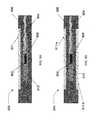
- FIG. 12Ashow example results of the finite element computations of the example apparatus 1100 of FIG. 11A being subjected to a stretching or elongation force.
- FIG. 12Bshow example results of the finite element computations of an example apparatus similar to FIG. 11A which does not include buffer structures 1111 - a and 1111 - b , also being subjected to the stretching or elongation force.
- FIG. 12Bshows that, in the absence of buffer structures, the area 1260 of higher strain concentration in the encapsulant coincides with the edge of the device component 1250 , even though the device component 1250 is disposed in a flexible base.
- a junction region of an electrical communication between a device component and a compliant structurecould be disposed proximate to this edge.
- Such a concentration of strain as shown in FIG. 12Bcould cause damage to the junction region during a stretching or elongation, including possibly resulting in rupture of the junction region.
- such a concentration of strain at the edgecan cause interfacial delamination between the device component and the flexible base near the edge.
- FIG. 12Ashows that the buffer structures 1210 cause the area 1220 of higher strain concentration in the encapsulant to shift from the edge of the device component 1200 or the flexible base, to instead be concentrated in an outer area. As a result, a strain that might develop at the junction region of an apparatus is channeled away from that area.
- Such a distribution of strain as shown in FIG. 12Bcould reduce the risk of or prevent damage to the junction region during a stretching or elongation, thereby maintaining the performance of the apparatus. In addition, there is less risk of interfacial delamination between the device component and the flexible base near the edge.
- the buffer structure in FIG. 12Acan be extended to the edge of the high strain concentration region.
- FIG. 13shows a plot of the von Mises strain and first principal strain versus relative elongation for the computation of FIGS. 12A and 12B .
- FIG. 13shows that the values of von Mises strain and first principal strain in the apparatus without a buffer are higher than for the apparatus that includes a buffer structure.
- the example apparatus described hereincan be fabricated using any technique in the art.
- the conductive materials of the stretchable and/or flexible interconnectscan be fabricated using evaporation, sputtering, or other deposition technique, and then patterned according to the desired conformation.
- the flexible base, the buffer structure, and/or the encapsulantcan be formed using, e.g., spin-coating or casting and using a mask or a mold to define the desired shape of the component.
- the technology described hereinmay be embodied as a method, of which at least one example has been provided.
- the acts performed as part of the methodmay be ordered in any suitable way. Accordingly, embodiments may be constructed in which acts are performed in an order different than illustrated, which may include performing some acts simultaneously, even though shown as sequential acts in illustrative embodiments.
- a reference to “A and/or B”, when used in conjunction with open-ended language such as “comprising”can refer, in one embodiment, to A only (optionally including elements other than B); in another embodiment, to B only (optionally including elements other than A); in yet another embodiment, to both A and B (optionally including other elements); etc.
- the phrase “at least one,” in reference to a list of one or more elements,should be understood to mean at least one element selected from any one or more of the elements in the list of elements, but not necessarily including at least one of each and every element specifically listed within the list of elements and not excluding any combinations of elements in the list of elements.
- This definitionalso allows that elements may optionally be present other than the elements specifically identified within the list of elements to which the phrase “at least one” refers, whether related or unrelated to those elements specifically identified.
- “at least one of A and B”can refer, in one embodiment, to at least one, optionally including more than one, A, with no B present (and optionally including elements other than B); in another embodiment, to at least one, optionally including more than one, B, with no A present (and optionally including elements other than A); in yet another embodiment, to at least one, optionally including more than one, A, and at least one, optionally including more than one, B (and optionally including other elements); etc
Landscapes
- Engineering & Computer Science (AREA)
- Microelectronics & Electronic Packaging (AREA)
- Structures Or Materials For Encapsulating Or Coating Semiconductor Devices Or Solid State Devices (AREA)
- Structure Of Printed Boards (AREA)
- Micromachines (AREA)
- Manufacturing & Machinery (AREA)
- Non-Insulated Conductors (AREA)
- Measuring And Recording Apparatus For Diagnosis (AREA)
- Measurement And Recording Of Electrical Phenomena And Electrical Characteristics Of The Living Body (AREA)
- Non-Metallic Protective Coatings For Printed Circuits (AREA)
- Laminated Bodies (AREA)
- Devices For Indicating Variable Information By Combining Individual Elements (AREA)
- Internal Circuitry In Semiconductor Integrated Circuit Devices (AREA)
- Element Separation (AREA)
Abstract
Description
| TABLE 1 |
| Table 1 |
| Young's modulus (MPa) | Poisson ratio | ||
| Silicon | 1.85 × 10⁵ | 0.3 | ||
| Polyimide | 3.2 × 10³ | 0.3 | ||
| Silicone | 0.06 | 0.485 | ||
Claims (34)
Priority Applications (11)
| Application Number | Priority Date | Filing Date | Title |
|---|---|---|---|
| US13/843,873US9226402B2 (en) | 2012-06-11 | 2013-03-15 | Strain isolation structures for stretchable electronics |
| CA2901789ACA2901789C (en) | 2013-02-25 | 2014-02-24 | Strain isolation structures for stretchable electronics cross-reference to related applications |
| CN201910949060.0ACN110856344A (en) | 2013-02-25 | 2014-02-24 | Strain isolation structures for stretchable electronic devices |
| KR1020157026253AKR20150122721A (en) | 2013-02-25 | 2014-02-24 | Strain isolation structures for stretchable electronics |
| EP14754143.7AEP2959755A4 (en) | 2013-02-25 | 2014-02-24 | Strain isolation structures for stretchable electronics |
| JP2015559039AJP6449789B2 (en) | 2013-02-25 | 2014-02-24 | Device with strain insulation structure for extensible electronic equipment |
| CN201480018842.8ACN105340371B (en) | 2013-02-25 | 2014-02-24 | Strain-isolated structures for stretchable electronics |
| PCT/US2014/017968WO2014130928A2 (en) | 2013-02-25 | 2014-02-24 | Strain isolation structures for stretchable electronics |
| US14/947,558US9408305B2 (en) | 2012-06-11 | 2015-11-20 | Strain isolation structures for stretchable electronics |
| US15/194,995US9844145B2 (en) | 2012-06-11 | 2016-06-28 | Strain isolation structures for stretchable electronics |
| US15/806,162US20180302988A1 (en) | 2012-06-11 | 2017-11-07 | Strain isolation structures for stretchable electronics |
Applications Claiming Priority (3)
| Application Number | Priority Date | Filing Date | Title |
|---|---|---|---|
| US201261658140P | 2012-06-11 | 2012-06-11 | |
| US201361768939P | 2013-02-25 | 2013-02-25 | |
| US13/843,873US9226402B2 (en) | 2012-06-11 | 2013-03-15 | Strain isolation structures for stretchable electronics |
Related Child Applications (1)
| Application Number | Title | Priority Date | Filing Date |
|---|---|---|---|
| US14/947,558ContinuationUS9408305B2 (en) | 2012-06-11 | 2015-11-20 | Strain isolation structures for stretchable electronics |
Publications (2)
| Publication Number | Publication Date |
|---|---|
| US20140240932A1 US20140240932A1 (en) | 2014-08-28 |
| US9226402B2true US9226402B2 (en) | 2015-12-29 |
Family
ID=51387921
Family Applications (4)
| Application Number | Title | Priority Date | Filing Date |
|---|---|---|---|
| US13/843,873Active2034-02-05US9226402B2 (en) | 2012-06-11 | 2013-03-15 | Strain isolation structures for stretchable electronics |
| US14/947,558ActiveUS9408305B2 (en) | 2012-06-11 | 2015-11-20 | Strain isolation structures for stretchable electronics |
| US15/194,995ActiveUS9844145B2 (en) | 2012-06-11 | 2016-06-28 | Strain isolation structures for stretchable electronics |
| US15/806,162AbandonedUS20180302988A1 (en) | 2012-06-11 | 2017-11-07 | Strain isolation structures for stretchable electronics |
Family Applications After (3)
| Application Number | Title | Priority Date | Filing Date |
|---|---|---|---|
| US14/947,558ActiveUS9408305B2 (en) | 2012-06-11 | 2015-11-20 | Strain isolation structures for stretchable electronics |
| US15/194,995ActiveUS9844145B2 (en) | 2012-06-11 | 2016-06-28 | Strain isolation structures for stretchable electronics |
| US15/806,162AbandonedUS20180302988A1 (en) | 2012-06-11 | 2017-11-07 | Strain isolation structures for stretchable electronics |
Country Status (7)
| Country | Link |
|---|---|
| US (4) | US9226402B2 (en) |
| EP (2) | EP2959754A4 (en) |
| JP (3) | JP6396928B2 (en) |
| KR (2) | KR20150122721A (en) |
| CN (4) | CN110856344A (en) |
| CA (2) | CA2900700A1 (en) |
| WO (2) | WO2014130928A2 (en) |
Cited By (57)
| Publication number | Priority date | Publication date | Assignee | Title |
|---|---|---|---|---|
| US9408305B2 (en) | 2012-06-11 | 2016-08-02 | Mc10, Inc. | Strain isolation structures for stretchable electronics |
| US9554850B2 (en) | 2012-07-05 | 2017-01-31 | Mc10, Inc. | Catheter device including flow sensing |
| US9662069B2 (en) | 2008-10-07 | 2017-05-30 | Mc10, Inc. | Systems, methods, and devices having stretchable integrated circuitry for sensing and delivering therapy |
| US9704908B2 (en) | 2008-10-07 | 2017-07-11 | Mc10, Inc. | Methods and applications of non-planar imaging arrays |
| US9750421B2 (en) | 2012-07-05 | 2017-09-05 | Mc10, Inc. | Catheter or guidewire device including flow sensing and use thereof |
| US20170325359A1 (en)* | 2016-05-09 | 2017-11-09 | Nathan S. Lazarus | Self cooling stretchable electrical circuit having a conduit forming an electrical component and containing electrically conductive liquid |
| US20170344055A1 (en)* | 2016-05-25 | 2017-11-30 | Intel Corporation | Structural brace for electronic circuit with stretchable substrate |
| US9833190B2 (en) | 2008-10-07 | 2017-12-05 | Mc10, Inc. | Methods of detecting parameters of a lumen |
| US9894757B2 (en) | 2008-10-07 | 2018-02-13 | Mc10, Inc. | Extremely stretchable electronics |
| US9949691B2 (en) | 2013-11-22 | 2018-04-24 | Mc10, Inc. | Conformal sensor systems for sensing and analysis of cardiac activity |
| US10032709B2 (en) | 2012-10-09 | 2018-07-24 | Mc10, Inc. | Embedding thin chips in polymer |
| USD825537S1 (en) | 2014-10-15 | 2018-08-14 | Mc10, Inc. | Electronic device having antenna |
| US20180376585A1 (en)* | 2015-12-11 | 2018-12-27 | Intel Corporation | Multi-layer flexible/stretchable electronic package for advanced wearable electronics |
| US10277386B2 (en) | 2016-02-22 | 2019-04-30 | Mc10, Inc. | System, devices, and method for on-body data and power transmission |
| US10288590B2 (en) | 2013-10-08 | 2019-05-14 | Smith & Nephew Plc | PH indicator device and formulation |
| US10296819B2 (en) | 2012-10-09 | 2019-05-21 | Mc10, Inc. | Conformal electronics integrated with apparel |
| US10300371B2 (en) | 2015-10-01 | 2019-05-28 | Mc10, Inc. | Method and system for interacting with a virtual environment |
| US10334724B2 (en) | 2013-05-14 | 2019-06-25 | Mc10, Inc. | Conformal electronics including nested serpentine interconnects |
| US10398024B2 (en) | 2016-04-18 | 2019-08-27 | Nippon Mektron, Ltd. | Stretchable circuit board and method for manufacturing stretchable circuit board |
| US10398343B2 (en) | 2015-03-02 | 2019-09-03 | Mc10, Inc. | Perspiration sensor |
| US10410962B2 (en) | 2014-01-06 | 2019-09-10 | Mc10, Inc. | Encapsulated conformal electronic systems and devices, and methods of making and using the same |
| US10447347B2 (en) | 2016-08-12 | 2019-10-15 | Mc10, Inc. | Wireless charger and high speed data off-loader |
| US10467926B2 (en) | 2013-10-07 | 2019-11-05 | Mc10, Inc. | Conformal sensor systems for sensing and analysis |
| US10477354B2 (en) | 2015-02-20 | 2019-11-12 | Mc10, Inc. | Automated detection and configuration of wearable devices based on on-body status, location, and/or orientation |
| US10485118B2 (en) | 2014-03-04 | 2019-11-19 | Mc10, Inc. | Multi-part flexible encapsulation housing for electronic devices and methods of making the same |
| US10482743B2 (en) | 2013-08-05 | 2019-11-19 | Mc10, Inc. | Flexible temperature sensor including conformable electronics |
| US10532211B2 (en) | 2015-10-05 | 2020-01-14 | Mc10, Inc. | Method and system for neuromodulation and stimulation |
| US10653332B2 (en) | 2015-07-17 | 2020-05-19 | Mc10, Inc. | Conductive stiffener, method of making a conductive stiffener, and conductive adhesive and encapsulation layers |
| US10673280B2 (en) | 2016-02-22 | 2020-06-02 | Mc10, Inc. | System, device, and method for coupled hub and sensor node on-body acquisition of sensor information |
| US10709384B2 (en) | 2015-08-19 | 2020-07-14 | Mc10, Inc. | Wearable heat flux devices and methods of use |
| US10820437B2 (en) | 2016-09-28 | 2020-10-27 | Intel Corporation | Flexible packaging for a wearable electronic device |
| US11076997B2 (en) | 2017-07-25 | 2021-08-03 | Smith & Nephew Plc | Restriction of sensor-monitored region for sensor-enabled wound dressings |
| US11154235B2 (en) | 2016-04-19 | 2021-10-26 | Medidata Solutions, Inc. | Method and system for measuring perspiration |
| US11324424B2 (en) | 2017-03-09 | 2022-05-10 | Smith & Nephew Plc | Apparatus and method for imaging blood in a target region of tissue |
| US11516920B2 (en)* | 2013-09-27 | 2022-11-29 | Tactotek Oy | Method for manufacturing an electromechanical structure and an arrangement for carrying out the method |
| US11559438B2 (en) | 2017-11-15 | 2023-01-24 | Smith & Nephew Plc | Integrated sensor enabled wound monitoring and/or therapy dressings and systems |
| US11596553B2 (en) | 2017-09-27 | 2023-03-07 | Smith & Nephew Plc | Ph sensing for sensor enabled negative pressure wound monitoring and therapy apparatuses |
| US11633153B2 (en) | 2017-06-23 | 2023-04-25 | Smith & Nephew Plc | Positioning of sensors for sensor enabled wound monitoring or therapy |
| US11633147B2 (en) | 2017-09-10 | 2023-04-25 | Smith & Nephew Plc | Sensor enabled wound therapy dressings and systems implementing cybersecurity |
| US11638664B2 (en) | 2017-07-25 | 2023-05-02 | Smith & Nephew Plc | Biocompatible encapsulation and component stress relief for sensor enabled negative pressure wound therapy dressings |
| US11690570B2 (en) | 2017-03-09 | 2023-07-04 | Smith & Nephew Plc | Wound dressing, patch member and method of sensing one or more wound parameters |
| US11717447B2 (en) | 2016-05-13 | 2023-08-08 | Smith & Nephew Plc | Sensor enabled wound monitoring and therapy apparatus |
| US11759144B2 (en) | 2017-09-10 | 2023-09-19 | Smith & Nephew Plc | Systems and methods for inspection of encapsulation and components in sensor equipped wound dressings |
| US11791030B2 (en) | 2017-05-15 | 2023-10-17 | Smith & Nephew Plc | Wound analysis device and method |
| US11839464B2 (en) | 2017-09-28 | 2023-12-12 | Smith & Nephew, Plc | Neurostimulation and monitoring using sensor enabled wound monitoring and therapy apparatus |
| US11883262B2 (en) | 2017-04-11 | 2024-01-30 | Smith & Nephew Plc | Component positioning and stress relief for sensor enabled wound dressings |
| US11925735B2 (en) | 2017-08-10 | 2024-03-12 | Smith & Nephew Plc | Positioning of sensors for sensor enabled wound monitoring or therapy |
| US11931165B2 (en) | 2017-09-10 | 2024-03-19 | Smith & Nephew Plc | Electrostatic discharge protection for sensors in wound therapy |
| US11944418B2 (en) | 2018-09-12 | 2024-04-02 | Smith & Nephew Plc | Device, apparatus and method of determining skin perfusion pressure |
| US11957545B2 (en) | 2017-09-26 | 2024-04-16 | Smith & Nephew Plc | Sensor positioning and optical sensing for sensor enabled wound therapy dressings and systems |
| US11969538B2 (en) | 2018-12-21 | 2024-04-30 | T.J.Smith And Nephew, Limited | Wound therapy systems and methods with multiple power sources |
| US12011942B2 (en) | 2019-03-18 | 2024-06-18 | Smith & Nephew Plc | Rules for sensor integrated substrates |
| US12033738B2 (en) | 2017-05-15 | 2024-07-09 | Smith & Nephew Plc | Negative pressure wound therapy system using eulerian video magnification |
| US12178597B2 (en) | 2017-03-09 | 2024-12-31 | Smith & Nephew Plc | Device, apparatus and method of determining skin perfusion pressure |
| US12186165B2 (en) | 2018-09-28 | 2025-01-07 | T.J.Smith And Nephew, Limited | Optical fibers for optically sensing through wound dressings |
| US12186164B2 (en) | 2018-10-16 | 2025-01-07 | Smith & Nephew Plc | Systems and method for applying biocompatible encapsulation to sensor enabled wound monitoring and therapy dressings |
| US12409071B2 (en) | 2018-08-29 | 2025-09-09 | Smith & Nephew Plc | Component positioning and encapsulation for sensor enabled wound dressings |
Families Citing this family (64)
| Publication number | Priority date | Publication date | Assignee | Title |
|---|---|---|---|---|
| US9545216B2 (en) | 2011-08-05 | 2017-01-17 | Mc10, Inc. | Catheter balloon methods and apparatus employing sensing elements |
| US9119533B2 (en) | 2008-10-07 | 2015-09-01 | Mc10, Inc. | Systems, methods, and devices having stretchable integrated circuitry for sensing and delivering therapy |
| US8886334B2 (en) | 2008-10-07 | 2014-11-11 | Mc10, Inc. | Systems, methods, and devices using stretchable or flexible electronics for medical applications |
| WO2011041727A1 (en) | 2009-10-01 | 2011-04-07 | Mc10, Inc. | Protective cases with integrated electronics |
| US9702839B2 (en) | 2011-03-11 | 2017-07-11 | Mc10, Inc. | Integrated devices to facilitate quantitative assays and diagnostics |
| JP2014523633A (en) | 2011-05-27 | 2014-09-11 | エムシー10 インコーポレイテッド | Electronic, optical and / or mechanical devices and systems and methods of manufacturing these devices and systems |
| US9757050B2 (en) | 2011-08-05 | 2017-09-12 | Mc10, Inc. | Catheter balloon employing force sensing elements |
| JP6129838B2 (en) | 2011-09-01 | 2017-05-17 | エムシー10 インコーポレイテッドMc10,Inc. | Electronic device that detects the condition of the tissue |
| JP6277130B2 (en) | 2011-10-05 | 2018-02-14 | エムシーテン、インコーポレイテッド | Medical device and method of manufacturing the same |
| US9247637B2 (en) | 2012-06-11 | 2016-01-26 | Mc10, Inc. | Strain relief structures for stretchable interconnects |
| EP3117206A4 (en) | 2014-03-12 | 2017-11-15 | Mc10, Inc. | Quantification of a change in assay |
| KR102042137B1 (en)* | 2014-05-30 | 2019-11-28 | 한국전자통신연구원 | An electronic device and the method for fabricating the same |
| US9899330B2 (en) | 2014-10-03 | 2018-02-20 | Mc10, Inc. | Flexible electronic circuits with embedded integrated circuit die |
| US10297572B2 (en) | 2014-10-06 | 2019-05-21 | Mc10, Inc. | Discrete flexible interconnects for modules of integrated circuits |
| US9743513B2 (en)* | 2014-12-26 | 2017-08-22 | Industrial Technology Research Institute | Flexible electronic device |
| US10468357B2 (en) | 2015-03-11 | 2019-11-05 | Intel Corporation | Stretchable electronics fabrication method with strain redistribution layer |
| US10182284B2 (en)* | 2015-06-11 | 2019-01-15 | Facebook Technologies, Llc | Connector assembly for detachable audio system |
| CN107949887A (en)* | 2015-09-17 | 2018-04-20 | 积水保力马科技株式会社 | Elastic distribution component |
| WO2017070030A1 (en) | 2015-10-21 | 2017-04-27 | Massachusetts Institute Of Technology | Nanowire fet imaging system and related techniques |
| US10206277B2 (en) | 2015-12-18 | 2019-02-12 | Intel Corporation | Gradient encapsulant protection of devices in stretchable electronics |
| US10477688B2 (en)* | 2015-12-24 | 2019-11-12 | Intel Corporation | Stretchable electronic assembly |
| FI20165054A (en)* | 2016-01-28 | 2017-07-29 | Clothing Plus Mbu Oy | Flexible PCB |
| WO2017156502A1 (en)* | 2016-03-10 | 2017-09-14 | Carnegie Mellon University | Integrated electronic device with flexible and stretchable substrate |
| US10736212B2 (en)* | 2016-05-20 | 2020-08-04 | Ares Materials Inc. | Substrates for stretchable electronics and method of manufacture |
| CN107437534A (en)* | 2016-05-27 | 2017-12-05 | 中国科学院苏州纳米技术与纳米仿生研究所 | Stretchable electronic system |
| WO2018049431A1 (en)* | 2016-09-07 | 2018-03-15 | Ares Materials Inc. | Substrates for stretchable electronics and method of manufacture |
| EP3328166A1 (en)* | 2016-11-29 | 2018-05-30 | IMEC vzw | Method for forming non-flat devices |
| JP6851813B2 (en)* | 2016-12-22 | 2021-03-31 | 東洋アルミニウム株式会社 | Wiring board |
| CN206863338U (en)* | 2017-02-24 | 2018-01-09 | 深圳市大疆创新科技有限公司 | Video eyeglasses headband and video eyeglasses |
| FI20175818A1 (en)* | 2017-09-14 | 2019-03-15 | Clothing Plus Mbu Oy | A system for transmitting electrical signals |
| US11284507B2 (en) | 2017-10-12 | 2022-03-22 | Dai Nippon Printing Co., Ltd. | Wiring board and method for manufacturing wiring board |
| TWI770295B (en)* | 2017-10-12 | 2022-07-11 | 日商大日本印刷股份有限公司 | Wiring board and manufacturing method of wiring board |
| JP6512389B1 (en)* | 2017-11-07 | 2019-05-15 | 大日本印刷株式会社 | Stretchable circuit board and article |
| CN107978578B (en)* | 2017-11-23 | 2020-02-21 | 中国科学院力学研究所 | A flexible and stretchable wire with variable line width and preparation method thereof |
| KR102725064B1 (en)* | 2018-02-16 | 2024-11-01 | 노오쓰웨스턴 유니버시티 | Wireless medical sensors and methods |
| US10955671B2 (en)* | 2018-03-01 | 2021-03-23 | Invensas Corporation | Stretchable film assembly with conductive traces |
| KR102554048B1 (en)* | 2018-07-20 | 2023-07-10 | 엘지디스플레이 주식회사 | Stretchable display device |
| EP3608964B1 (en) | 2018-08-08 | 2022-05-11 | LG Display Co., Ltd. | Stretchable display device |
| CN109216188A (en)* | 2018-09-07 | 2019-01-15 | 清华大学 | Flexible interconnection line and its manufacturing method and measurement method of parameters |
| KR102664207B1 (en) | 2018-10-08 | 2024-05-07 | 엘지디스플레이 주식회사 | Stretchable display device and manufacturing method the same |
| CN111050461B (en)* | 2018-10-12 | 2021-01-22 | 昆山工研院新型平板显示技术中心有限公司 | Electronic device and manufacturing method thereof |
| CN112997587B (en)* | 2018-10-31 | 2024-07-16 | 大日本印刷株式会社 | Wiring board and method for manufacturing wiring board |
| CN112997588B (en)* | 2018-10-31 | 2024-01-30 | 大日本印刷株式会社 | Wiring board and method for manufacturing wiring board |
| JP6870790B2 (en)* | 2019-01-21 | 2021-05-12 | 株式会社村田製作所 | Elastic wiring board |
| JP7251165B2 (en)* | 2019-01-24 | 2023-04-04 | 大日本印刷株式会社 | Wiring board and method for manufacturing wiring board |
| CN111493817B (en)* | 2019-01-31 | 2023-10-10 | 周冠谦 | Stretchable flexible sensing device |
| JP7216911B2 (en)* | 2019-02-14 | 2023-02-02 | 大日本印刷株式会社 | Wiring board and method for manufacturing wiring board |
| JP7216912B2 (en)* | 2019-02-14 | 2023-02-02 | 大日本印刷株式会社 | Wiring board and method for manufacturing wiring board |
| US11768262B2 (en) | 2019-03-14 | 2023-09-26 | Massachusetts Institute Of Technology | Interface responsive to two or more sensor modalities |
| JP7272065B2 (en)* | 2019-04-02 | 2023-05-12 | 大日本印刷株式会社 | Wiring board and method for manufacturing wiring board |
| JP7272074B2 (en)* | 2019-04-08 | 2023-05-12 | 大日本印刷株式会社 | Wiring board and method for manufacturing wiring board |
| GB201914443D0 (en) | 2019-10-07 | 2019-11-20 | Smith & Nephew | Sensor enabled negative pressure wound monitoring apparatus with different impedances inks |
| WO2021114041A1 (en)* | 2019-12-09 | 2021-06-17 | 鹏鼎控股(深圳)股份有限公司 | Stretchable sensing structure and manufacturing method therefor |
| US11123011B1 (en) | 2020-03-23 | 2021-09-21 | Nix, Inc. | Wearable systems, devices, and methods for measurement and analysis of body fluids |
| EP4139904A1 (en) | 2020-04-21 | 2023-03-01 | T.J. Smith and Nephew, Limited | Wound treatment management using augmented reality overlay |
| KR20220013775A (en) | 2020-07-27 | 2022-02-04 | 삼성전자주식회사 | Stretchable device and display panel and sensor and electronic device |
| CN111935900B (en)* | 2020-08-10 | 2024-12-24 | 深圳市特深电气有限公司 | Flexible circuit connection device, connection method and method for protecting flexible circuit board |
| JP7264136B2 (en)* | 2020-08-28 | 2023-04-25 | 横河電機株式会社 | FORCE DETECTION DEVICE, FORCE DETECTION SYSTEM AND METHOD FOR MANUFACTURING FORCE DETECTION DEVICE |
| TWI798811B (en)* | 2020-09-03 | 2023-04-11 | 財團法人工業技術研究院 | Electronic device |
| EP4545056A3 (en) | 2020-09-28 | 2025-07-16 | Coloplast A/S | Medical appliance |
| GB2601325B (en)* | 2020-11-25 | 2023-12-13 | Pragmatic Semiconductor Ltd | Support structures for flexible electronic circuits |
| JP7015952B1 (en) | 2021-04-12 | 2022-02-03 | 大日本印刷株式会社 | Wiring board and manufacturing method of wiring board |
| KR102749617B1 (en)* | 2022-07-08 | 2025-01-02 | 국립공주대학교 산학협력단 | Flexible wavy circuit and its manufacturing method |
| AT526502B1 (en)* | 2023-03-23 | 2024-04-15 | Sendance Gmbh | Deformable object |
Citations (174)
| Publication number | Priority date | Publication date | Assignee | Title |
|---|---|---|---|---|
| US3716861A (en) | 1971-03-22 | 1973-02-13 | J Root | Serpentine antenna mounted on a rotatable capacitive coupler |
| US3805427A (en) | 1972-12-18 | 1974-04-23 | H Epstein | Medical alarm bracelet |
| US4059467A (en) | 1976-09-27 | 1977-11-22 | Bell Telephone Laboratories, Incorporated | Method for removal of elastomeric silicone coatings from integrated circuits |
| US4416288A (en) | 1980-08-14 | 1983-11-22 | The Regents Of The University Of California | Apparatus and method for reconstructing subsurface electrophysiological patterns |
| US4658153A (en) | 1984-06-18 | 1987-04-14 | Amnon Brosh | Planar coil apparatus for providing a frequency output vs. position |
| US5306917A (en) | 1992-08-12 | 1994-04-26 | Reliant Laser Corporation | Electro-optical system for measuring and analyzing accumulated short-wave and long-wave ultraviolet radiation exposure |
| US5331966A (en) | 1991-04-05 | 1994-07-26 | Medtronic, Inc. | Subcutaneous multi-electrode sensing system, method and pacer |
| US5360987A (en) | 1993-11-17 | 1994-11-01 | At&T Bell Laboratories | Semiconductor photodiode device with isolation region |
| US5567975A (en) | 1994-06-30 | 1996-10-22 | Santa Barbara Research Center | Group II-VI radiation detector for simultaneous visible and IR detection |
| US5811790A (en) | 1996-02-22 | 1998-09-22 | Canon Kabushiki Kaisha | Photoelectric conversion device having thermal conductive member |
| US5817008A (en) | 1996-10-31 | 1998-10-06 | Spacelabs Medical, Inc. | Conformal pulse oximetry sensor and monitor |
| US5907477A (en) | 1995-09-19 | 1999-05-25 | Micron Communications, Inc. | Substrate assembly including a compartmental dam for use in the manufacturing of an enclosed electrical circuit using an encapsulant |
| US6063046A (en) | 1997-04-11 | 2000-05-16 | Allum; John H. | Method and apparatus for the diagnosis and rehabilitation of balance disorders |
| US20010012918A1 (en) | 1995-07-28 | 2001-08-09 | Swanson David K. | Systems and methods for conducting electrophysiological testing using high-voltage energy pulses to stun tissue |
| US20010021867A1 (en) | 1993-03-16 | 2001-09-13 | Kordis Thomas F. | Cardiac mapping and ablation systems |
| US20020026127A1 (en) | 2000-03-23 | 2002-02-28 | Balbierz Daniel J. | Tissue biopsy and treatment apparatus and method |
| US20020082515A1 (en) | 1999-07-01 | 2002-06-27 | Campbell Thomas H. | Thermography catheter |
| US6421016B1 (en) | 2000-10-23 | 2002-07-16 | Motorola, Inc. | Antenna system with channeled RF currents |
| US20020094701A1 (en) | 2000-11-29 | 2002-07-18 | Biegelsen David Kalman | Stretchable interconnects using stress gradient films |
| US20020113739A1 (en) | 2000-12-14 | 2002-08-22 | Howard David Amundson | Arrayed-segment loop antenna |
| US20020128700A1 (en) | 2001-03-08 | 2002-09-12 | Cross Thomas E. | Lead with adjustable angular and spatial relationships between electrodes |
| US20020151934A1 (en) | 2001-04-12 | 2002-10-17 | Levine Paul A. | System and method for programmably controlling electrode activation sequence in a multi-site cardiac stimulation device |
| US20030017848A1 (en) | 2001-07-17 | 2003-01-23 | Engstrom G. Eric | Personalizing electronic devices and smart covering |
| US20030045025A1 (en) | 2000-01-26 | 2003-03-06 | Coyle Anthony L. | Method of fabricating a molded package for micromechanical devices |
| US6567158B1 (en) | 1999-01-26 | 2003-05-20 | Consiglio Nazionale Delle Ricerche | Fiber optic sensor with photochromic transducer, and corresponding method |
| US20030097165A1 (en) | 2001-11-16 | 2003-05-22 | The Regents Of The University Of California. | Flexible electrode array for artificial vision |
| US20030162507A1 (en) | 2002-02-20 | 2003-08-28 | Vatt Gregory B. | Semiconductor structure for high speed digital and radio frequency processing |
| US20030214408A1 (en) | 2002-05-14 | 2003-11-20 | Motorola, Inc. | Apparel having multiple alternative sensors and corresponding method |
| US20030236455A1 (en) | 2000-10-05 | 2003-12-25 | Scimed Life Systems, Inc. | Probe assembly for mapping and ablating pulmonary vein tissue and method of using same |
| US20040006264A1 (en) | 2001-11-20 | 2004-01-08 | Mojarradi Mohammad M. | Neural prosthetic micro system |
| US20040092806A1 (en) | 2001-12-11 | 2004-05-13 | Sagon Stephen W | Microelectrode catheter for mapping and ablation |
| US20040106334A1 (en) | 2000-06-14 | 2004-06-03 | Tatsuo Suzuki | Microparticle arrangement film, electrical connection film, electrical connection structure, and microparticle arrangement method |
| US20040135094A1 (en) | 2002-11-25 | 2004-07-15 | Hamamatsu Photonics K.K. | UV sensor |
| US20040138558A1 (en) | 2002-11-14 | 2004-07-15 | Dunki-Jacobs Robert J | Methods and devices for detecting tissue cells |
| US20040149921A1 (en) | 2003-02-05 | 2004-08-05 | Alexander Smyk | Personal solar adviser |
| US6784844B1 (en) | 1999-10-08 | 2004-08-31 | Nokia Mobile Phone Limited | Antenna assembly and method of construction |
| US20040178466A1 (en) | 2003-01-31 | 2004-09-16 | Foveon, Inc. | Vertical color filter sensor group and semiconductor integrated circuit fabrication method for fabricating same |
| US20040203486A1 (en) | 2002-07-31 | 2004-10-14 | Robert Shepherd | Smart pouch cover for mobile device |
| US20040243204A1 (en) | 2003-04-30 | 2004-12-02 | The Regents Of The University Of California | Stretchable polymer-based electronic device |
| US20050021103A1 (en) | 1998-08-05 | 2005-01-27 | Dilorenzo Daniel John | Apparatus and method for closed-loop intracranial stimulation for optimal control of neurological disease |
| US20050067293A1 (en) | 2003-09-29 | 2005-03-31 | Toshiki Naito | Producing method of flexible wired circuit board |
| US20050096513A1 (en) | 1997-11-11 | 2005-05-05 | Irvine Sensors Corporation | Wearable biomonitor with flexible thinned integrated circuit |
| US20050113744A1 (en) | 2003-11-21 | 2005-05-26 | Cyberkinetics, Inc. | Agent delivery systems and related methods under control of biological electrical signals |
| US20050139683A1 (en) | 2003-12-26 | 2005-06-30 | Curitel Communications, Inc. | Communication terminal equipped with a replaceable cover and method of changing themes of communication terminal using the same |
| US20050171524A1 (en) | 2004-01-09 | 2005-08-04 | Barrx, Inc. | Devices and methods for treatment of luminal tissue |
| US20050203366A1 (en) | 2004-03-12 | 2005-09-15 | Donoghue John P. | Neurological event monitoring and therapy systems and related methods |
| US6965160B2 (en) | 2002-08-15 | 2005-11-15 | Micron Technology, Inc. | Semiconductor dice packages employing at least one redistribution layer |
| WO2005122285A2 (en) | 2004-06-04 | 2005-12-22 | The Board Of Trustees Of The University Of Illinois | Methods and devices for fabricating and assembling printable semiconductor elements |
| US20060003709A1 (en) | 2004-06-30 | 2006-01-05 | Nokia Corporation | Protective enclosure for a mobile terminal |
| US6987314B1 (en) | 2004-06-08 | 2006-01-17 | Amkor Technology, Inc. | Stackable semiconductor package with solder on pads on which second semiconductor package is stacked |
| US20060084394A1 (en) | 2001-01-22 | 2006-04-20 | Engstrom G E | Visualization supplemented wireless wireless mobile telephony |
| US20060106321A1 (en) | 2003-01-16 | 2006-05-18 | Galil Medical Ltd. | Device, system, and method for detecting, localizing, and characterizing plaque-induced stenosis of a blood vessel |
| US20060128346A1 (en) | 2004-12-13 | 2006-06-15 | Nec Corporation | Flexible circuit board, electronic circuit device, and mobile communication terminal |
| US20060154398A1 (en) | 2003-06-20 | 2006-07-13 | Acellent Technologies, Inc. | Method of manufacturing a structural health monitoring layer |
| US20060160560A1 (en) | 2003-06-12 | 2006-07-20 | Michael Josenhans | Mobile communication device cover and method for its operation |
| US20060264767A1 (en) | 2005-05-17 | 2006-11-23 | Cardiovu, Inc. | Programmable ECG sensor patch |
| US20060286785A1 (en) | 2004-06-04 | 2006-12-21 | The Board Of Trustees Of The University Of Illinois | A Stretchable Form of Single Crystal Silicon for High Performance Electronics on Rubber Substrates |
| WO2007003019A2 (en) | 2005-07-01 | 2007-01-11 | K.U. Leuven Research & Development | Means for functional restoration of a damaged nervous system |
| US20070027514A1 (en) | 2005-07-29 | 2007-02-01 | Medtronic, Inc. | Electrical stimulation lead with conformable array of electrodes |
| US20070108389A1 (en) | 2005-11-15 | 2007-05-17 | Nokia Corporation | UV radiation meter using visible light sensors |
| US20070123756A1 (en) | 2005-10-14 | 2007-05-31 | Konica Minolta Sensing, Inc. | Vital information measuring device |
| US7265298B2 (en) | 2003-05-30 | 2007-09-04 | The Regents Of The University Of California | Serpentine and corduroy circuits to enhance the stretchability of a stretchable electronic device |
| WO2007136726A2 (en) | 2006-05-18 | 2007-11-29 | Ndi Medical, Llc | Portable assemblies, systems, and methods for providing functional or therapeutic neurostimulation |
| US7302751B2 (en) | 2004-04-30 | 2007-12-04 | Hewlett-Packard Development Company, L.P. | Method of fabricating a rat's nest RFID antenna |
| US20080046080A1 (en) | 2006-07-07 | 2008-02-21 | Interuniversitair Microelektronica Centrum (Imec) | Method for forming packaged microelectronic devices and devices thus obtained |
| WO2008030960A2 (en) | 2006-09-06 | 2008-03-13 | The Board Of Trustees Of The University Of Illinois | Controlled buckling structures in semiconductor interconnects and nanomembranes for stretchable electronics |
| US20080074383A1 (en) | 2006-09-27 | 2008-03-27 | Dean Kenneth A | Portable electronic device having appearance customizable housing |
| US20080096620A1 (en) | 2006-10-20 | 2008-04-24 | Lee Min-Soo | Mobile terminal and case for mobile terminal |
| US20080139894A1 (en) | 2006-12-08 | 2008-06-12 | Joanna Szydlo-Moore | Devices and systems for remote physiological monitoring |
| US20080157235A1 (en) | 2004-06-04 | 2008-07-03 | Rogers John A | Controlled buckling structures in semiconductor interconnects and nanomembranes for stretchable electronics |
| US20080193749A1 (en) | 2007-02-13 | 2008-08-14 | Thompson D Scott | Molded optical articles and methods of making same |
| US20080204021A1 (en) | 2004-06-17 | 2008-08-28 | Koninklijke Philips Electronics N.V. | Flexible and Wearable Radio Frequency Coil Garments for Magnetic Resonance Imaging |
| US20080211087A1 (en) | 2006-12-20 | 2008-09-04 | Infineon Technologies Ag | Chip module and method for producing a chip module |
| US20080237840A1 (en) | 2007-03-26 | 2008-10-02 | Endicott Interconnect Technologies, Inc. | Flexible circuit electronic package with standoffs |
| US20080259576A1 (en) | 2005-10-13 | 2008-10-23 | Nxp B.V. | Electronic Device or Circuit and Method for Fabricating the Same |
| US20080257589A1 (en)* | 2006-11-21 | 2008-10-23 | Andreas Ostmann | Method for the production of expandable circuit carrier and expandable circuit carrier |
| US20080287167A1 (en) | 2007-04-04 | 2008-11-20 | Motorola, Inc. | Method and apparatus for controlling a skin texture surface on a device |
| US20080313552A1 (en) | 2005-05-13 | 2008-12-18 | Imbibo Ncorporated | Method for Customizing Cover for Electronic Device |
| US20090000377A1 (en) | 2007-06-29 | 2009-01-01 | Shipps J Clay | Brain impact measurement system |
| US20090017884A1 (en) | 2006-03-09 | 2009-01-15 | Carmel Rotschild | Method and system for using a cellular phone in water activities |
| US20090015560A1 (en) | 2007-07-13 | 2009-01-15 | Motorola, Inc. | Method and apparatus for controlling a display of a device |
| US7487587B2 (en) | 2005-03-22 | 2009-02-10 | Interuniversitair Microelektronica Centrum Vzw (Imec) | Methods of producing a composite substrate |
| US7491892B2 (en) | 2003-03-28 | 2009-02-17 | Princeton University | Stretchable and elastic interconnects |
| US20090048556A1 (en) | 2007-08-17 | 2009-02-19 | Isis Biopolymer Llc | Iontophoretic drug delivery system |
| US20090088750A1 (en) | 2007-09-28 | 2009-04-02 | Tyco Healthcare Group Lp | Insulating Boot with Silicone Overmold for Electrosurgical Forceps |
| US20090154736A1 (en) | 2007-12-17 | 2009-06-18 | Electronics And Telecommunications Research Institute | Apparatus for generating directional sound and mobile terminal using the same |
| US20090184254A1 (en) | 2008-01-22 | 2009-07-23 | Noriyuki Miura | Ultraviolet sensor and method of manufacturing ultraviolet sensor |
| US20090215385A1 (en) | 2005-02-15 | 2009-08-27 | Vodafone Group Pic | Security for wireless communication |
| US20090225751A1 (en) | 2007-05-22 | 2009-09-10 | Koenck Steven E | Mobile nodal based communication system, method and apparatus |
| WO2009111641A1 (en) | 2008-03-05 | 2009-09-11 | The Board Of Trustees Of The University Of Illinois | Stretchable and foldable electronic devices |
| WO2009114689A1 (en) | 2008-03-12 | 2009-09-17 | The Trustees Of The University Of Pennsylvania | Flexible and scalable sensor arrays for recording and modulating physiologic activity |
| US20090261828A1 (en) | 2008-04-17 | 2009-10-22 | Universitat Zurich | Coil assembly and multiple coil arrangement for magnetic resonance imaging |
| US20090273909A1 (en) | 2004-09-10 | 2009-11-05 | Samsung Electronics Co., Ltd. | Flexible device, flexible pressure sensor, and fabrication method thereof |
| US7618260B2 (en) | 2004-02-27 | 2009-11-17 | Daniel Simon R | Wearable modular interface strap |
| US20090322480A1 (en) | 2008-06-30 | 2009-12-31 | Robert Leon Benedict | Rfid tag and method of vehicle attachment thereof |
| US20100073669A1 (en) | 2008-09-19 | 2010-03-25 | Sensors For Medicine & Science, Inc. | Optical sensor assembly |
| WO2010036807A1 (en) | 2008-09-24 | 2010-04-01 | The Board Of Trustees Of The University Of Illinois | Arrays of ultrathin silicon solar microcells |
| US20100087782A1 (en) | 2008-10-07 | 2010-04-08 | Roozbeh Ghaffari | Catheter balloon having stretchable integrated circuitry and sensor array |
| US20100090824A1 (en) | 2008-10-14 | 2010-04-15 | Hong Kong Applied Science And Technology Research Institute Co., Ltd. | Miniature and Multi-Band RF Coil Design |
| US20100090781A1 (en) | 2005-09-30 | 2010-04-15 | Kenichi Yamamoto | Sheet-like composite electronic component and method for manufacturing same |
| WO2010042957A2 (en) | 2008-10-07 | 2010-04-15 | Mc10, Inc. | Systems, devices, and methods utilizing stretchable electronics to measure tire or road surface conditions |
| WO2010046883A1 (en) | 2008-10-23 | 2010-04-29 | L'oreal | A device for dispensing a preparation, with automatic or semi-automatic adjustment of the properties of the preparation by means of an integrated sensor of the surroundings |
| US20100116526A1 (en) | 2008-10-07 | 2010-05-13 | Arora William J | Extremely stretchable electronics |
| US20100117660A1 (en) | 2007-01-19 | 2010-05-13 | Douglas Malcolm F | Cable for a capacitive proximity sensor |
| WO2010056857A2 (en) | 2008-11-12 | 2010-05-20 | Mc10, Inc. | Extremely stretchable electronics |
| US20100178722A1 (en) | 2008-10-07 | 2010-07-15 | De Graff Bassel | Methods and applications of non-planar imaging arrays |
| WO2010081137A2 (en) | 2009-01-12 | 2010-07-15 | Mc10, Inc. | Methods and applications of non-planar imaging arrays |
| US7759167B2 (en) | 2005-11-23 | 2010-07-20 | Imec | Method for embedding dies |
| WO2010082993A2 (en) | 2008-12-11 | 2010-07-22 | Mc10, Inc. | Systems, methods, and devices using stretchable or flexible electronics for medical applications |
| WO2010102310A2 (en) | 2009-03-03 | 2010-09-10 | Mc10, Inc. | Systems, methods, and devices having stretchable integrated circuitry for sensing and delivering therapy |
| US20100245011A1 (en) | 2009-01-16 | 2010-09-30 | Alkiviades Chatzopoulos | Integrated or printed margarita shaped inductor |
| US20100271191A1 (en) | 2008-10-07 | 2010-10-28 | De Graff Bassel | Systems, devices, and methods utilizing stretchable electronics to measure tire or road surface conditions |
| WO2010132552A1 (en) | 2009-05-12 | 2010-11-18 | The Board Of Trustees Of The University Of Illinois | Printed assemblies of ultrathin, microscale inorganic light emitting diodes for deformable and semitransparent displays |
| US20100298895A1 (en) | 2008-10-07 | 2010-11-25 | Roozbeh Ghaffari | Systems, methods, and devices using stretchable or flexible electronics for medical applications |
| US20100321161A1 (en) | 2009-06-23 | 2010-12-23 | Avery Dennison Corporation | Washable rfid device for apparel tracking |
| US20100327387A1 (en) | 2009-06-26 | 2010-12-30 | Ichiro Kasai | Avalanche Photodiode |
| WO2011003181A1 (en) | 2009-07-06 | 2011-01-13 | Autonomous Identity Management Systems Inc. - Aims | Gait-based authentication system |
| US20110011179A1 (en) | 2009-07-16 | 2011-01-20 | Gustafsson Goeran | Moister sensor |
| US20110034912A1 (en) | 2008-10-07 | 2011-02-10 | Mc10, Inc. | Systems,methods, and devices having stretchable integrated circuitry for sensing and delivering therapy |
| US20110051384A1 (en) | 2006-02-02 | 2011-03-03 | Arno Kriechbaum | Printed circuit board element having at least one component embedded therein and method for embedding at least one component in a printed circuit board element |
| WO2011041727A1 (en) | 2009-10-01 | 2011-04-07 | Mc10, Inc. | Protective cases with integrated electronics |
| US20110101789A1 (en) | 2008-12-01 | 2011-05-05 | Salter Jr Thomas Steven | Rf power harvesting circuit |
| US20110121822A1 (en) | 2009-11-23 | 2011-05-26 | Harris Corporation | Planar communications antenna having an epicyclic structure and isotropic radiation, and associated methods |
| US7960246B2 (en) | 2004-06-04 | 2011-06-14 | Imec | Method for the manufacture of electronic devices on substrates and devices related thereto |
| US20110140897A1 (en) | 2011-02-16 | 2011-06-16 | Connor Kent Purks | Circuits, systems, and methods for monitoring and reporting foot impact, foot placement, shoe life, and other running/walking characteristics |
| WO2011084709A2 (en) | 2009-12-17 | 2011-07-14 | Mc10, Inc. | Methods and apparatus for conformal sensing of force and/or change in motion |
| WO2011084450A1 (en) | 2009-12-16 | 2011-07-14 | The Board Of Trustees Of The University Of Illinois | Electrophysiology in-vivo using conformal electronics |
| US20110184320A1 (en) | 2010-01-26 | 2011-07-28 | Shipps J Clay | Measurement system using body mounted physically decoupled sensor |
| US20110215931A1 (en) | 2009-10-01 | 2011-09-08 | Mc10, Inc. | Methods and apparatus for assessing head trauma based on conformal sensing of force and/or change in motion of a person's head |
| WO2011127331A2 (en) | 2010-04-07 | 2011-10-13 | Mc10, Inc. | Methods and apparatus for measuring technical parameters of equipment, tools and components via conformal electronics |
| US20120016258A1 (en) | 2010-07-14 | 2012-01-19 | Prima-Temp, Inc. | Wireless vaginal sensor probe |
| US20120051005A1 (en) | 2009-01-30 | 2012-03-01 | Universiteit Gent | Stretchable electronic device |
| US20120052268A1 (en) | 2009-01-30 | 2012-03-01 | Universiteit Gent | Stretchable electronic device |
| US20120065937A1 (en) | 2009-10-01 | 2012-03-15 | Mc10, Inc. | Methods and apparatus for measuring technical parameters of equipment, tools and components via conformal electronics |
| US20120074546A1 (en) | 2010-09-24 | 2012-03-29 | Chooi Mei Chong | Multi-chip Semiconductor Packages and Assembly Thereof |
| US20120087216A1 (en) | 2010-10-12 | 2012-04-12 | P.S.L. Limited | Watch |
| US20120091594A1 (en) | 2010-10-18 | 2012-04-19 | Christof Landesberger | Method of Producing a Chip Package, and Chip Package |
| US20120092222A1 (en) | 2009-07-03 | 2012-04-19 | Murata Manufacturing Co., Ltd. | Antenna and antenna module |
| US20120108012A1 (en) | 2009-07-09 | 2012-05-03 | Hiroyuki Yasuda | Film for semiconductor and semiconductor device manufacturing method |
| US8207473B2 (en)* | 2008-06-24 | 2012-06-26 | Imec | Method for manufacturing a stretchable electronic device |
| US20120172697A1 (en) | 2010-12-30 | 2012-07-05 | Roy Urman | Catheter with sheet array of electrodes |
| US8227916B2 (en) | 2009-07-22 | 2012-07-24 | Taiwan Semiconductor Manufacturing Company, Ltd. | Package structure and method for reducing dielectric layer delamination |
| WO2012125494A2 (en) | 2011-03-11 | 2012-09-20 | Mc10, Inc. | Integrated devices to facilitate quantitative assays and diagnostics |
| US20120256308A1 (en) | 2011-04-11 | 2012-10-11 | Imec | Method for Sealing a Micro-Cavity |
| US20120280399A1 (en) | 2011-05-02 | 2012-11-08 | International Business Machines Corporation | Buffer pad in solder bump connections and methods of manufacture |
| WO2012166686A2 (en) | 2011-05-27 | 2012-12-06 | Mc10, Inc. | Electronic, optical and/or mechanical apparatus and systems and methods for fabricating same |
| US20120316455A1 (en) | 2011-06-10 | 2012-12-13 | Aliphcom | Wearable device and platform for sensory input |
| WO2013010171A1 (en) | 2011-07-14 | 2013-01-17 | Mc10, Inc. | Detection of a force on a foot or footwear |
| US20130041235A1 (en) | 2009-12-16 | 2013-02-14 | John A. Rogers | Flexible and Stretchable Electronic Systems for Epidermal Electronics |
| WO2013022853A1 (en) | 2011-08-05 | 2013-02-14 | Mc10, Inc. | Catheter balloon methods and apparatus employing sensing elements |
| WO2013033724A1 (en) | 2011-09-01 | 2013-03-07 | Mc10, Inc. | Electronics for detection of a condition of tissue |
| WO2013049716A1 (en) | 2011-09-28 | 2013-04-04 | Mc10, Inc. | Electronics for detection of a property of a surface |
| WO2013052919A2 (en) | 2011-10-05 | 2013-04-11 | Mc10, Inc. | Cardiac catheter employing conformal electronics for mapping |
| US20130192356A1 (en) | 2009-10-01 | 2013-08-01 | Mc10, Inc. | Methods and apparatus for measuring technical parameters of equipment, tools, and components via conformal electronics |
| US20130211761A1 (en) | 2012-02-10 | 2013-08-15 | Nxp B.V. | Calibration method, calibration device and measurement device |
| WO2013034987A3 (en) | 2011-09-08 | 2013-08-22 | Offshore Incorporations (Cayman) Limited, | Sensor device and system for fitness equipment |
| WO2013170032A2 (en) | 2012-05-09 | 2013-11-14 | Aliphcom | System and method for monitoring the health of a user |
| US20130316487A1 (en) | 2008-10-07 | 2013-11-28 | Bassel de Graff | Methods and applications of non-planar imaging arrays |
| US20130316442A1 (en) | 2011-02-07 | 2013-11-28 | Ecole Polytechnique Federale De Lausanne (Epfl) | Monitoring system for cell culture |
| US20140012242A1 (en) | 2012-07-05 | 2014-01-09 | Mc10, Inc. | Catheter device including flow sensing |
| US20140012160A1 (en) | 2011-08-05 | 2014-01-09 | Mc10, Inc. | Catheter balloon employing force sensing elements |
| US20140022746A1 (en) | 2012-06-11 | 2014-01-23 | MC10 ,Inc. | Strain relief structures for stretachble interconnects |
| US20140097944A1 (en) | 2012-10-09 | 2014-04-10 | Mc10, Inc. | Conformal electronics integrated with apparel |
| WO2014059032A1 (en) | 2012-10-09 | 2014-04-17 | Mc10, Inc. | Embedding thin chips in polymer |
| US20140188426A1 (en) | 2012-12-27 | 2014-07-03 | Steven FASTERT | Monitoring hit count for impact events |
| WO2014110176A1 (en) | 2013-01-08 | 2014-07-17 | Fastert Steven | Application for monitoring a property of a surface |
| WO2014130931A1 (en) | 2013-02-25 | 2014-08-28 | Yung-Yu Hsu | Strain relief structures for stretchable interconnects |
| US20140249520A1 (en) | 2012-07-05 | 2014-09-04 | Mc10, Inc. | Catheter or guidewire device including flow sensing and use thereof |
| US20140303452A1 (en) | 2008-10-07 | 2014-10-09 | Roozbeh Ghaffari | Systems, Methods, and Devices Having Stretchable Integrated Circuitry for Sensing and Delivering Therapy |
| WO2014186467A2 (en) | 2013-05-14 | 2014-11-20 | Yung-Yu Hsu | Conformal electronics including nested serpentine interconnects |
| WO2014197443A1 (en) | 2013-06-03 | 2014-12-11 | Kacyvenski Isaiah | Motion sensor and analysis |
| WO2014205434A2 (en) | 2013-06-21 | 2014-12-24 | Mc10, Inc. | Band with conformable electronics |
| US20150035680A1 (en) | 2013-08-05 | 2015-02-05 | Mc10, Inc. | Flexible temperature sensor including conformable electronics |
| US20150100135A1 (en) | 2013-10-09 | 2015-04-09 | Mc10, Inc. | Utility gear including conformal sensors |
Family Cites Families (115)
| Publication number | Priority date | Publication date | Assignee | Title |
|---|---|---|---|---|
| US3838240A (en) | 1973-04-04 | 1974-09-24 | Rca Corp | Bonding tool and method of bonding therewith |
| CA1105565A (en) | 1978-09-12 | 1981-07-21 | Kaufman (John G.) Hospital Products Ltd. | Electrosurgical electrode |
| US4278474A (en) | 1980-03-25 | 1981-07-14 | The United States Of America As Represented By The United States Department Of Energy | Device for conversion of electromagnetic radiation into electrical current |
| US5018005A (en)* | 1989-12-27 | 1991-05-21 | Motorola Inc. | Thin, molded, surface mount electronic device |
| US6387052B1 (en) | 1991-01-29 | 2002-05-14 | Edwards Lifesciences Corporation | Thermodilution catheter having a safe, flexible heating element |
| JPH0587511A (en) | 1991-07-24 | 1993-04-06 | Yamaha Corp | Bending detection device |
| US5272375A (en) | 1991-12-26 | 1993-12-21 | E. I. Du Pont De Nemours And Company | Electronic assembly with optimum heat dissipation |
| US5491651A (en) | 1992-05-15 | 1996-02-13 | Key, Idea Development | Flexible wearable computer |
| US5471982A (en) | 1992-09-29 | 1995-12-05 | Ep Technologies, Inc. | Cardiac mapping and ablation systems |
| CA2120468A1 (en)* | 1993-04-05 | 1994-10-06 | Kenneth Alan Salisbury | Electronic module containing an internally ribbed, integral heat sink and bonded, flexible printed wiring board with two-sided component population |
| US5617870A (en) | 1993-04-29 | 1997-04-08 | Scimed Life Systems, Inc. | Intravascular flow measurement system |
| US5326521A (en) | 1993-05-26 | 1994-07-05 | East Douglas A | Method for preparing silicone mold tooling |
| WO1995006240A1 (en) | 1993-08-24 | 1995-03-02 | Metrika Laboratories, Inc. | Novel disposable electronic assay device |
| US5473512A (en)* | 1993-12-16 | 1995-12-05 | At&T Corp. | Electronic device package having electronic device boonded, at a localized region thereof, to circuit board |
| US5454270A (en) | 1994-06-06 | 1995-10-03 | Motorola, Inc. | Hermetically sealed pressure sensor and method thereof |
| NL1001890C2 (en) | 1995-12-13 | 1997-06-17 | Cordis Europ | Catheter with plate-shaped electrode array. |
| SE9600334D0 (en) | 1996-01-30 | 1996-01-30 | Radi Medical Systems | Combined flow, pressure and temperature sensor |
| US5880369A (en) | 1996-03-15 | 1999-03-09 | Analog Devices, Inc. | Micromachined device with enhanced dimensional control |
| JP3175673B2 (en)* | 1997-11-27 | 2001-06-11 | 日本電気株式会社 | Method for manufacturing flexible circuit board unit on which semiconductor element is mounted |
| DE59803887D1 (en) | 1998-01-22 | 2002-05-23 | Fraunhofer Ges Forschung | MICROSYSTEM AND METHOD FOR PRODUCING A MICROSYSTEM |
| JP3511895B2 (en) | 1998-06-05 | 2004-03-29 | 株式会社村田製作所 | Manufacturing method of ceramic multilayer substrate |
| US6641860B1 (en) | 2000-01-03 | 2003-11-04 | T-Ink, L.L.C. | Method of manufacturing printed circuit boards |
| US6511478B1 (en) | 2000-06-30 | 2003-01-28 | Scimed Life Systems, Inc. | Medical probe with reduced number of temperature sensor wires |
| US6775906B1 (en) | 2000-10-20 | 2004-08-17 | Silverbrook Research Pty Ltd | Method of manufacturing an integrated circuit carrier |
| US6600363B2 (en) | 2001-04-05 | 2003-07-29 | Cornell Research Foundation, Inc. | Folded floating-gate differential pair amplifier |
| KR100380107B1 (en) | 2001-04-30 | 2003-04-11 | 삼성전자주식회사 | Circuit board having a heating means and multichip package having hermetic sealing part |
| US6455931B1 (en) | 2001-05-15 | 2002-09-24 | Raytheon Company | Monolithic microelectronic array structure having substrate islands and its fabrication |
| US6626940B2 (en) | 2001-06-15 | 2003-09-30 | Scimed Life Systems, Inc. | Medical device activation system |
| US6410971B1 (en) | 2001-07-12 | 2002-06-25 | Ferrotec (Usa) Corporation | Thermoelectric module with thin film substrates |
| US6770966B2 (en) | 2001-07-31 | 2004-08-03 | Intel Corporation | Electronic assembly including a die having an integrated circuit and a layer of diamond to transfer heat |
| JP4638626B2 (en) | 2001-08-01 | 2011-02-23 | 北川工業株式会社 | Magnetic body molding method, magnetic body, and printed circuit board |
| AU2002330718A1 (en) | 2001-09-03 | 2003-03-18 | National Microelectronic Research Centre University College Cork - National University Of Ireland Co | Integrated circuit structure and a method of making an integrated circuit structure |
| DE10202123A1 (en) | 2002-01-21 | 2003-07-31 | Infineon Technologies Ag | Method and device for integrating electronics in textiles |
| US20060134713A1 (en) | 2002-03-21 | 2006-06-22 | Lifescan, Inc. | Biosensor apparatus and methods of use |
| US7227240B2 (en) | 2002-09-10 | 2007-06-05 | Semiconductor Components Industries, L.L.C. | Semiconductor device with wire bond inductor and method |
| JP3931780B2 (en)* | 2002-09-27 | 2007-06-20 | 株式会社デンソー | Multilayer printed circuit board |
| US7698909B2 (en) | 2002-10-01 | 2010-04-20 | Nellcor Puritan Bennett Llc | Headband with tension indicator |
| US20040085469A1 (en) | 2002-10-30 | 2004-05-06 | Eastman Kodak Company | Method to eliminate bus voltage drop effects for pixel source follower amplifiers |
| FI119583B (en)* | 2003-02-26 | 2008-12-31 | Imbera Electronics Oy | Procedure for manufacturing an electronics module |
| JP2005052212A (en) | 2003-08-05 | 2005-03-03 | Axiom Co Ltd | Skin sensor |
| EP2382920A1 (en) | 2003-08-20 | 2011-11-02 | Philometron, Inc. | Hydration monitoring |
| JP2005079472A (en)* | 2003-09-02 | 2005-03-24 | Seiko Epson Corp | Wiring board, electro-optical device and electronic apparatus |
| KR20050061756A (en)* | 2003-12-18 | 2005-06-23 | 한국전자통신연구원 | Electrode-connector protecting cap and electrode-connector including the same for ambulatory physiological signal measurement |
| US7727228B2 (en) | 2004-03-23 | 2010-06-01 | Medtronic Cryocath Lp | Method and apparatus for inflating and deflating balloon catheters |
| US7259030B2 (en) | 2004-03-29 | 2007-08-21 | Articulated Technologies, Llc | Roll-to-roll fabricated light sheet and encapsulated semiconductor circuit devices |
| TWI255572B (en) | 2004-05-05 | 2006-05-21 | Advanced Connectek Inc | A portable electrical power unit with transmission display |
| WO2006026748A1 (en) | 2004-08-31 | 2006-03-09 | Lifescan Scotland Limited | Method of manufacturing an auto-calibrating sensor |
| JP2006108431A (en) | 2004-10-06 | 2006-04-20 | Sharp Corp | Semiconductor device |
| US8118740B2 (en) | 2004-12-20 | 2012-02-21 | Ipventure, Inc. | Moisture sensor for skin |
| JP4137061B2 (en) | 2005-01-11 | 2008-08-20 | 株式会社カイジョー | Wire loop shape, semiconductor device having the wire loop shape, and wire bonding method |
| JP2006201217A (en)* | 2005-01-18 | 2006-08-03 | Seiko Epson Corp | Wiring board, electro-optical device and electronic apparatus |
| US20090291508A1 (en) | 2008-05-20 | 2009-11-26 | Rapid Pathogen Screening Inc. | Nanoparticles in diagnostic tests |
| US7300631B2 (en) | 2005-05-02 | 2007-11-27 | Bioscale, Inc. | Method and apparatus for detection of analyte using a flexural plate wave device and magnetic particles |
| US20060266475A1 (en) | 2005-05-24 | 2006-11-30 | American Standard Circuits, Inc. | Thermally conductive interface |
| WO2007002579A2 (en) | 2005-06-23 | 2007-01-04 | Bioveris Corporation | Assay cartridges and methods for point of care instruments |
| US20070027485A1 (en) | 2005-07-29 | 2007-02-01 | Kallmyer Todd A | Implantable medical device bus system and method |
| US8657814B2 (en) | 2005-08-22 | 2014-02-25 | Medtronic Ablation Frontiers Llc | User interface for tissue ablation system |
| US9629567B2 (en) | 2006-01-12 | 2017-04-25 | Biosense Webster, Inc. | Mapping of complex fractionated atrial electrogram |
| CN101416302A (en)* | 2006-04-07 | 2009-04-22 | 皇家飞利浦电子股份有限公司 | Elastically deformable integrated circuit devices |
| US20080036097A1 (en) | 2006-08-10 | 2008-02-14 | Teppei Ito | Semiconductor package, method of production thereof and encapsulation resin |
| JP5559539B2 (en) | 2006-10-18 | 2014-07-23 | べシックス・バスキュラー・インコーポレイテッド | System that induces desirable temperature effects on body tissue |
| US20080262381A1 (en) | 2007-04-12 | 2008-10-23 | Magneto Inertial Sensing Technology, Inc. | Infant SID Monitor Based On Accelerometer |
| US8140154B2 (en) | 2007-06-13 | 2012-03-20 | Zoll Medical Corporation | Wearable medical treatment device |
| US8877565B2 (en) | 2007-06-28 | 2014-11-04 | Intel Corporation | Method of forming a multilayer substrate core structure using sequential microvia laser drilling and substrate core structure formed according to the method |
| US8484836B2 (en)* | 2007-09-10 | 2013-07-16 | The Board Of Trustees Of The Leland Stanford Junior University | Flexible network |
| JP2009094099A (en)* | 2007-10-03 | 2009-04-30 | Nec Lcd Technologies Ltd | Flexible substrate connection part structure, flexible substrate, flat panel display device |
| US7739791B2 (en)* | 2007-10-26 | 2010-06-22 | Delphi Technologies, Inc. | Method of producing an overmolded electronic module with a flexible circuit pigtail |
| TWI370714B (en)* | 2008-01-09 | 2012-08-11 | Ind Tech Res Inst | Circuit structure and menufacturing method thereof |
| JP2009170173A (en) | 2008-01-11 | 2009-07-30 | Denso Corp | El element, and manufacturing method thereof |
| BRPI0902900A2 (en)* | 2008-02-22 | 2015-06-23 | Sony Corp | Disc cartridge |
| US8251736B2 (en)* | 2008-09-23 | 2012-08-28 | Tyco Electronics Corporation | Connector assembly for connecting an electrical lead to an electrode |
| KR101013557B1 (en) | 2008-11-06 | 2011-02-14 | 주식회사 하이닉스반도체 | Flexible semiconductor package and wire bonding device for manufacturing same |
| PL2392198T3 (en)* | 2009-01-30 | 2019-09-30 | Imec Vzw | Stretchable electronic device and method of manufacturing thereof |
| US8332053B1 (en)* | 2009-04-28 | 2012-12-11 | Hrl Laboratories, Llc | Method for fabrication of a stretchable electronic skin |
| US20110066042A1 (en) | 2009-09-15 | 2011-03-17 | Texas Instruments Incorporated | Estimation of blood flow and hemodynamic parameters from a single chest-worn sensor, and other circuits, devices and processes |
| US20110079908A1 (en)* | 2009-10-06 | 2011-04-07 | Unisem Advanced Technologies Sdn. Bhd. | Stress buffer to protect device features |
| US8872663B2 (en) | 2010-01-19 | 2014-10-28 | Avery Dennison Corporation | Medication regimen compliance monitoring systems and methods |
| GB201005889D0 (en)* | 2010-04-08 | 2010-05-26 | Cambridge Entpr Ltd | Tuning of mechanical properties of polymers |
| JP5284308B2 (en)* | 2010-04-19 | 2013-09-11 | 日本メクトロン株式会社 | Flexible circuit board and manufacturing method thereof |
| JP6192032B2 (en) | 2010-04-22 | 2017-09-06 | リーフ ヘルスケア インコーポレイテッド | A system for monitoring a patient's physiological status |
| CN102907184B (en) | 2010-05-20 | 2016-08-24 | 3M创新有限公司 | Adhesion Enhancement for Flexible Circuit Cover Films |
| EP2597779B1 (en) | 2010-07-23 | 2016-10-12 | Panasonic Intellectual Property Corporation of America | Nfc communication apparatus and method for controlling same |
| US8198109B2 (en) | 2010-08-27 | 2012-06-12 | Quarkstar Llc | Manufacturing methods for solid state light sheet or strip with LEDs connected in series for general illumination |
| JP5570353B2 (en)* | 2010-09-03 | 2014-08-13 | バイエル マテリアルサイエンス株式会社 | Conductive member having elastic wiring |
| CN202478392U (en) | 2010-10-20 | 2012-10-10 | 美敦力阿迪安卢森堡有限责任公司 | Associated system of catheter device |
| TWI513451B (en) | 2010-10-25 | 2015-12-21 | Medtronic Ardian Luxembourg | Devices, systems and methods for evaluation and feedback of neuromodulation treatment |
| US8520399B2 (en)* | 2010-10-29 | 2013-08-27 | Palo Alto Research Center Incorporated | Stretchable electronics modules and circuits |
| US8456021B2 (en) | 2010-11-24 | 2013-06-04 | Texas Instruments Incorporated | Integrated circuit device having die bonded to the polymer side of a polymer substrate |
| JP2013035974A (en)* | 2011-08-10 | 2013-02-21 | Tokai Rubber Ind Ltd | Flexible conductive material |
| US8702619B2 (en) | 2011-08-26 | 2014-04-22 | Symap Holding Limited | Mapping sympathetic nerve distribution for renal ablation and catheters for same |
| US20130116520A1 (en) | 2011-09-01 | 2013-05-09 | Masoud Roham | Single and multi node, semi-disposable wearable medical electronic patches for bio-signal monitoring and robust feature extraction |
| US8836136B2 (en) | 2011-10-17 | 2014-09-16 | Invensas Corporation | Package-on-package assembly with wire bond vias |
| EP2817708B1 (en) | 2012-02-21 | 2020-08-26 | Zebra Technologies Corporation | Method and apparatus for implementing near field communications with a printer |
| US9184798B2 (en) | 2012-03-12 | 2015-11-10 | Broadcom Corporation | Near field communications (NFC) device having adjustable gain |
| US20130316645A1 (en) | 2012-05-23 | 2013-11-28 | Health & Life Co., Ltd. | Near field communication enabled medical device system |
| US20130321373A1 (en) | 2012-05-31 | 2013-12-05 | Semiconductor Energy Laboratory Co., Ltd. | Electronic device, program, and recording medium |
| US8948832B2 (en) | 2012-06-22 | 2015-02-03 | Fitbit, Inc. | Wearable heart rate monitor |
| CN104507655B (en) | 2012-07-31 | 2016-12-14 | 夏普株式会社 | The manufacture method of mould |
| KR20140049314A (en)* | 2012-10-17 | 2014-04-25 | 한국전자통신연구원 | Stretchable electric device and manufacturing method of the same |
| EP3024523B1 (en) | 2013-07-22 | 2018-08-29 | Inhalation Sciences Sweden AB | Apparatus and method for generating an aerosol |
| KR20160065948A (en) | 2013-10-07 | 2016-06-09 | 엠씨10, 인크 | Conformal sensor systems for sensing and analysis |
| EP3071096A4 (en) | 2013-11-22 | 2017-08-09 | Mc10, Inc. | Conformal sensor systems for sensing and analysis of cardiac activity |
| CN105848570B (en) | 2014-01-03 | 2019-09-03 | Mc10股份有限公司 | Integrating device for low-power quantitative measurment |
| KR20160106582A (en) | 2014-01-03 | 2016-09-12 | 엠씨10, 인크 | Catheter or guidewire device including flow sensing and use thereof |
| CN105874606B (en) | 2014-01-06 | 2021-01-12 | Mc10股份有限公司 | Encapsulated conformal electronic systems and devices and methods of making and using the same |
| CN106030798A (en) | 2014-02-24 | 2016-10-12 | Mc10股份有限公司 | Conformal electronics with deformation indicators |
| US10485118B2 (en) | 2014-03-04 | 2019-11-19 | Mc10, Inc. | Multi-part flexible encapsulation housing for electronic devices and methods of making the same |
| EP3117206A4 (en) | 2014-03-12 | 2017-11-15 | Mc10, Inc. | Quantification of a change in assay |
| JP2017528908A (en) | 2014-09-22 | 2017-09-28 | エムシー10 インコーポレイテッドMc10,Inc. | Method and apparatus for shaping and looping bonding wires that function as stretchable and bendable interconnects |
| US9899330B2 (en) | 2014-10-03 | 2018-02-20 | Mc10, Inc. | Flexible electronic circuits with embedded integrated circuit die |
| US10297572B2 (en) | 2014-10-06 | 2019-05-21 | Mc10, Inc. | Discrete flexible interconnects for modules of integrated circuits |
| CN107005282A (en) | 2014-11-18 | 2017-08-01 | Mc10股份有限公司 | The systems, devices and methods activated for electronic installation |
| CN107427230A (en) | 2015-02-05 | 2017-12-01 | Mc10股份有限公司 | For the method and system with environmental interaction |
| WO2016134306A1 (en) | 2015-02-20 | 2016-08-25 | Mc10, Inc. | Automated detection and configuration of wearable devices based on on-body status, location, and/or orientation |
| WO2016140961A1 (en) | 2015-03-02 | 2016-09-09 | Mc10, Inc. | Perspiration sensor |
- 2013
- 2013-03-15USUS13/843,873patent/US9226402B2/enactiveActive
- 2014
- 2014-02-24WOPCT/US2014/017968patent/WO2014130928A2/enactiveApplication Filing
- 2014-02-24CNCN201910949060.0Apatent/CN110856344A/enactivePending
- 2014-02-24CACA2900700Apatent/CA2900700A1/ennot_activeAbandoned
- 2014-02-24KRKR1020157026253Apatent/KR20150122721A/ennot_activeCeased
- 2014-02-24CNCN201811415945.4Apatent/CN109951946B/enactiveActive
- 2014-02-24CNCN201480018842.8Apatent/CN105340371B/enactiveActive
- 2014-02-24JPJP2015559040Apatent/JP6396928B2/enactiveActive
- 2014-02-24EPEP14754166.8Apatent/EP2959754A4/ennot_activeWithdrawn
- 2014-02-24EPEP14754143.7Apatent/EP2959755A4/ennot_activeWithdrawn
- 2014-02-24WOPCT/US2014/017975patent/WO2014130931A1/enactiveApplication Filing
- 2014-02-24KRKR1020157023096Apatent/KR20150125939A/ennot_activeCeased
- 2014-02-24CACA2901789Apatent/CA2901789C/enactiveActive
- 2014-02-24JPJP2015559039Apatent/JP6449789B2/enactiveActive
- 2014-02-24CNCN201480010490.1Apatent/CN105706536B/enactiveActive
- 2015
- 2015-11-20USUS14/947,558patent/US9408305B2/enactiveActive
- 2016
- 2016-06-28USUS15/194,995patent/US9844145B2/enactiveActive
- 2017
- 2017-11-07USUS15/806,162patent/US20180302988A1/ennot_activeAbandoned
- 2018
- 2018-08-30JPJP2018161302Apatent/JP2018207122A/enactivePending
Patent Citations (245)
| Publication number | Priority date | Publication date | Assignee | Title |
|---|---|---|---|---|
| US3716861A (en) | 1971-03-22 | 1973-02-13 | J Root | Serpentine antenna mounted on a rotatable capacitive coupler |
| US3805427A (en) | 1972-12-18 | 1974-04-23 | H Epstein | Medical alarm bracelet |
| US4059467A (en) | 1976-09-27 | 1977-11-22 | Bell Telephone Laboratories, Incorporated | Method for removal of elastomeric silicone coatings from integrated circuits |
| US4416288A (en) | 1980-08-14 | 1983-11-22 | The Regents Of The University Of California | Apparatus and method for reconstructing subsurface electrophysiological patterns |
| US4658153A (en) | 1984-06-18 | 1987-04-14 | Amnon Brosh | Planar coil apparatus for providing a frequency output vs. position |
| US5331966A (en) | 1991-04-05 | 1994-07-26 | Medtronic, Inc. | Subcutaneous multi-electrode sensing system, method and pacer |
| US5306917A (en) | 1992-08-12 | 1994-04-26 | Reliant Laser Corporation | Electro-optical system for measuring and analyzing accumulated short-wave and long-wave ultraviolet radiation exposure |
| US20010021867A1 (en) | 1993-03-16 | 2001-09-13 | Kordis Thomas F. | Cardiac mapping and ablation systems |
| US5360987A (en) | 1993-11-17 | 1994-11-01 | At&T Bell Laboratories | Semiconductor photodiode device with isolation region |
| US5567975A (en) | 1994-06-30 | 1996-10-22 | Santa Barbara Research Center | Group II-VI radiation detector for simultaneous visible and IR detection |
| US20010012918A1 (en) | 1995-07-28 | 2001-08-09 | Swanson David K. | Systems and methods for conducting electrophysiological testing using high-voltage energy pulses to stun tissue |
| US5907477A (en) | 1995-09-19 | 1999-05-25 | Micron Communications, Inc. | Substrate assembly including a compartmental dam for use in the manufacturing of an enclosed electrical circuit using an encapsulant |
| US5811790A (en) | 1996-02-22 | 1998-09-22 | Canon Kabushiki Kaisha | Photoelectric conversion device having thermal conductive member |
| US5817008A (en) | 1996-10-31 | 1998-10-06 | Spacelabs Medical, Inc. | Conformal pulse oximetry sensor and monitor |
| US6063046A (en) | 1997-04-11 | 2000-05-16 | Allum; John H. | Method and apparatus for the diagnosis and rehabilitation of balance disorders |
| US20050096513A1 (en) | 1997-11-11 | 2005-05-05 | Irvine Sensors Corporation | Wearable biomonitor with flexible thinned integrated circuit |
| US20050021103A1 (en) | 1998-08-05 | 2005-01-27 | Dilorenzo Daniel John | Apparatus and method for closed-loop intracranial stimulation for optimal control of neurological disease |
| US6567158B1 (en) | 1999-01-26 | 2003-05-20 | Consiglio Nazionale Delle Ricerche | Fiber optic sensor with photochromic transducer, and corresponding method |
| US20020082515A1 (en) | 1999-07-01 | 2002-06-27 | Campbell Thomas H. | Thermography catheter |
| US6784844B1 (en) | 1999-10-08 | 2004-08-31 | Nokia Mobile Phone Limited | Antenna assembly and method of construction |
| US20030045025A1 (en) | 2000-01-26 | 2003-03-06 | Coyle Anthony L. | Method of fabricating a molded package for micromechanical devices |
| US20020026127A1 (en) | 2000-03-23 | 2002-02-28 | Balbierz Daniel J. | Tissue biopsy and treatment apparatus and method |
| US20040106334A1 (en) | 2000-06-14 | 2004-06-03 | Tatsuo Suzuki | Microparticle arrangement film, electrical connection film, electrical connection structure, and microparticle arrangement method |
| US20030236455A1 (en) | 2000-10-05 | 2003-12-25 | Scimed Life Systems, Inc. | Probe assembly for mapping and ablating pulmonary vein tissue and method of using same |
| US6421016B1 (en) | 2000-10-23 | 2002-07-16 | Motorola, Inc. | Antenna system with channeled RF currents |
| US20020094701A1 (en) | 2000-11-29 | 2002-07-18 | Biegelsen David Kalman | Stretchable interconnects using stress gradient films |
| US20020113739A1 (en) | 2000-12-14 | 2002-08-22 | Howard David Amundson | Arrayed-segment loop antenna |
| US20060084394A1 (en) | 2001-01-22 | 2006-04-20 | Engstrom G E | Visualization supplemented wireless wireless mobile telephony |
| US20020128700A1 (en) | 2001-03-08 | 2002-09-12 | Cross Thomas E. | Lead with adjustable angular and spatial relationships between electrodes |
| US20020151934A1 (en) | 2001-04-12 | 2002-10-17 | Levine Paul A. | System and method for programmably controlling electrode activation sequence in a multi-site cardiac stimulation device |
| US20030017848A1 (en) | 2001-07-17 | 2003-01-23 | Engstrom G. Eric | Personalizing electronic devices and smart covering |
| US20030097165A1 (en) | 2001-11-16 | 2003-05-22 | The Regents Of The University Of California. | Flexible electrode array for artificial vision |
| US20040006264A1 (en) | 2001-11-20 | 2004-01-08 | Mojarradi Mohammad M. | Neural prosthetic micro system |
| US20040092806A1 (en) | 2001-12-11 | 2004-05-13 | Sagon Stephen W | Microelectrode catheter for mapping and ablation |
| US20030162507A1 (en) | 2002-02-20 | 2003-08-28 | Vatt Gregory B. | Semiconductor structure for high speed digital and radio frequency processing |
| US20030214408A1 (en) | 2002-05-14 | 2003-11-20 | Motorola, Inc. | Apparel having multiple alternative sensors and corresponding method |
| US20040203486A1 (en) | 2002-07-31 | 2004-10-14 | Robert Shepherd | Smart pouch cover for mobile device |
| US6965160B2 (en) | 2002-08-15 | 2005-11-15 | Micron Technology, Inc. | Semiconductor dice packages employing at least one redistribution layer |
| US20040138558A1 (en) | 2002-11-14 | 2004-07-15 | Dunki-Jacobs Robert J | Methods and devices for detecting tissue cells |
| US20040135094A1 (en) | 2002-11-25 | 2004-07-15 | Hamamatsu Photonics K.K. | UV sensor |
| US20060106321A1 (en) | 2003-01-16 | 2006-05-18 | Galil Medical Ltd. | Device, system, and method for detecting, localizing, and characterizing plaque-induced stenosis of a blood vessel |
| US20040178466A1 (en) | 2003-01-31 | 2004-09-16 | Foveon, Inc. | Vertical color filter sensor group and semiconductor integrated circuit fabrication method for fabricating same |
| US20040149921A1 (en) | 2003-02-05 | 2004-08-05 | Alexander Smyk | Personal solar adviser |
| US7491892B2 (en) | 2003-03-28 | 2009-02-17 | Princeton University | Stretchable and elastic interconnects |
| US20040243204A1 (en) | 2003-04-30 | 2004-12-02 | The Regents Of The University Of California | Stretchable polymer-based electronic device |
| US7337012B2 (en) | 2003-04-30 | 2008-02-26 | Lawrence Livermore National Security, Llc | Stretchable polymer-based electronic device |
| US7265298B2 (en) | 2003-05-30 | 2007-09-04 | The Regents Of The University Of California | Serpentine and corduroy circuits to enhance the stretchability of a stretchable electronic device |
| US20060160560A1 (en) | 2003-06-12 | 2006-07-20 | Michael Josenhans | Mobile communication device cover and method for its operation |
| US20060154398A1 (en) | 2003-06-20 | 2006-07-13 | Acellent Technologies, Inc. | Method of manufacturing a structural health monitoring layer |
| US20050067293A1 (en) | 2003-09-29 | 2005-03-31 | Toshiki Naito | Producing method of flexible wired circuit board |
| US20050113744A1 (en) | 2003-11-21 | 2005-05-26 | Cyberkinetics, Inc. | Agent delivery systems and related methods under control of biological electrical signals |
| US20050139683A1 (en) | 2003-12-26 | 2005-06-30 | Curitel Communications, Inc. | Communication terminal equipped with a replaceable cover and method of changing themes of communication terminal using the same |
| US20050171524A1 (en) | 2004-01-09 | 2005-08-04 | Barrx, Inc. | Devices and methods for treatment of luminal tissue |
| US7618260B2 (en) | 2004-02-27 | 2009-11-17 | Daniel Simon R | Wearable modular interface strap |
| US20050203366A1 (en) | 2004-03-12 | 2005-09-15 | Donoghue John P. | Neurological event monitoring and therapy systems and related methods |
| US7302751B2 (en) | 2004-04-30 | 2007-12-04 | Hewlett-Packard Development Company, L.P. | Method of fabricating a rat's nest RFID antenna |
| US8440546B2 (en) | 2004-06-04 | 2013-05-14 | The Board Of Trustees Of The University Of Illinois | Methods and devices for fabricating and assembling printable semiconductor elements |
| US8664699B2 (en) | 2004-06-04 | 2014-03-04 | The Board Of Trustees Of The University Of Illinois | Methods and devices for fabricating and assembling printable semiconductor elements |
| WO2005122285A2 (en) | 2004-06-04 | 2005-12-22 | The Board Of Trustees Of The University Of Illinois | Methods and devices for fabricating and assembling printable semiconductor elements |
| US7622367B1 (en) | 2004-06-04 | 2009-11-24 | The Board Of Trustees Of The University Of Illinois | Methods and devices for fabricating and assembling printable semiconductor elements |
| US20150001462A1 (en) | 2004-06-04 | 2015-01-01 | The Board Of Trustees Of The University Of Illinois | Stretchable Form of Single Crystal Silicon for High Performance Electronics on Rubber Substrates |
| US20090294803A1 (en) | 2004-06-04 | 2009-12-03 | The Board Of Trustees Of The University Of Illinois | Methods and devices for fabricating and assembling printable semiconductor elements |
| US20100059863A1 (en) | 2004-06-04 | 2010-03-11 | The Board Of Trustees Of The University Of Illinois | Stretchable Form of Single Crystal Silicon for High Performance Electronics on Rubber Substrates |
| US20140374872A1 (en) | 2004-06-04 | 2014-12-25 | The Board Of Trustees Of The University Of Illinois | Controlled Buckling Structures in Semiconductor Interconnects and Nanomembranes for Stretchable Electronics |
| US20060038182A1 (en) | 2004-06-04 | 2006-02-23 | The Board Of Trustees Of The University | Stretchable semiconductor elements and stretchable electrical circuits |
| US20140191236A1 (en) | 2004-06-04 | 2014-07-10 | The Board Of Trustees Of The University Of Iiiinois | Methods and Devices for Fabricating and Assembling Printable Semiconductor Elements |
| US20060286785A1 (en) | 2004-06-04 | 2006-12-21 | The Board Of Trustees Of The University Of Illinois | A Stretchable Form of Single Crystal Silicon for High Performance Electronics on Rubber Substrates |
| US8754396B2 (en) | 2004-06-04 | 2014-06-17 | The Board Of Trustees Of The University Of Illinois | Stretchable form of single crystal silicon for high performance electronics on rubber substrates |
| US8729524B2 (en) | 2004-06-04 | 2014-05-20 | The Board Of Trustees Of The University Of Illinois | Controlled buckling structures in semiconductor interconnects and nanomembranes for stretchable electronics |
| US20110220890A1 (en) | 2004-06-04 | 2011-09-15 | The Board Of Trustees Of The University Of Illinois | Methods and Devices for Fabricating and Assembling Printable Semiconductor Elements |
| US20130320503A1 (en) | 2004-06-04 | 2013-12-05 | The Board Of Trustees Of The University Of Illinois | Methods and devices for fabricating and assembling printable semiconductor elements |
| US20080157235A1 (en) | 2004-06-04 | 2008-07-03 | Rogers John A | Controlled buckling structures in semiconductor interconnects and nanomembranes for stretchable electronics |
| US7557367B2 (en) | 2004-06-04 | 2009-07-07 | The Board Of Trustees Of The University Of Illinois | Stretchable semiconductor elements and stretchable electrical circuits |
| US20100072577A1 (en) | 2004-06-04 | 2010-03-25 | The Board Of Trustees Of The University Of Illinois | Methods and Devices for Fabricating and Assembling Printable Semiconductor Elements |
| US7521292B2 (en) | 2004-06-04 | 2009-04-21 | The Board Of Trustees Of The University Of Illinois | Stretchable form of single crystal silicon for high performance electronics on rubber substrates |
| US20130100618A1 (en) | 2004-06-04 | 2013-04-25 | The Board Of Trustees Of The University Of Illinoi | Stretchable Form of Single Crystal Silicon for High Performance Electronics on Rubber Substrates |
| US7960246B2 (en) | 2004-06-04 | 2011-06-14 | Imec | Method for the manufacture of electronic devices on substrates and devices related thereto |
| US20120327608A1 (en) | 2004-06-04 | 2012-12-27 | Rogers John A | Controlled Buckling Structures in Semiconductor Interconnects and Nanomembranes for Stretchable Electronics |
| US8217381B2 (en) | 2004-06-04 | 2012-07-10 | The Board Of Trustees Of The University Of Illinois | Controlled buckling structures in semiconductor interconnects and nanomembranes for stretchable electronics |
| US7982296B2 (en) | 2004-06-04 | 2011-07-19 | The Board Of Trustees Of The University Of Illinois | Methods and devices for fabricating and assembling printable semiconductor elements |
| US8198621B2 (en) | 2004-06-04 | 2012-06-12 | The Board Of Trustees Of The University Of Illinois | Stretchable form of single crystal silicon for high performance electronics on rubber substrates |
| US6987314B1 (en) | 2004-06-08 | 2006-01-17 | Amkor Technology, Inc. | Stackable semiconductor package with solder on pads on which second semiconductor package is stacked |
| US20080204021A1 (en) | 2004-06-17 | 2008-08-28 | Koninklijke Philips Electronics N.V. | Flexible and Wearable Radio Frequency Coil Garments for Magnetic Resonance Imaging |
| US20060003709A1 (en) | 2004-06-30 | 2006-01-05 | Nokia Corporation | Protective enclosure for a mobile terminal |
| US20090273909A1 (en) | 2004-09-10 | 2009-11-05 | Samsung Electronics Co., Ltd. | Flexible device, flexible pressure sensor, and fabrication method thereof |
| US20060128346A1 (en) | 2004-12-13 | 2006-06-15 | Nec Corporation | Flexible circuit board, electronic circuit device, and mobile communication terminal |
| US20090215385A1 (en) | 2005-02-15 | 2009-08-27 | Vodafone Group Pic | Security for wireless communication |
| US20090107704A1 (en) | 2005-03-22 | 2009-04-30 | Interuniversitair Microelektronica Centrum Vzw (Imec) | Composite substrate |
| US8431828B2 (en) | 2005-03-22 | 2013-04-30 | Imec | Composite substrate |
| US7487587B2 (en) | 2005-03-22 | 2009-02-10 | Interuniversitair Microelektronica Centrum Vzw (Imec) | Methods of producing a composite substrate |
| US20080313552A1 (en) | 2005-05-13 | 2008-12-18 | Imbibo Ncorporated | Method for Customizing Cover for Electronic Device |
| US20060264767A1 (en) | 2005-05-17 | 2006-11-23 | Cardiovu, Inc. | Programmable ECG sensor patch |
| WO2007003019A2 (en) | 2005-07-01 | 2007-01-11 | K.U. Leuven Research & Development | Means for functional restoration of a damaged nervous system |
| US20070027514A1 (en) | 2005-07-29 | 2007-02-01 | Medtronic, Inc. | Electrical stimulation lead with conformable array of electrodes |
| US20100090781A1 (en) | 2005-09-30 | 2010-04-15 | Kenichi Yamamoto | Sheet-like composite electronic component and method for manufacturing same |
| US20080259576A1 (en) | 2005-10-13 | 2008-10-23 | Nxp B.V. | Electronic Device or Circuit and Method for Fabricating the Same |
| US20070123756A1 (en) | 2005-10-14 | 2007-05-31 | Konica Minolta Sensing, Inc. | Vital information measuring device |
| US20070108389A1 (en) | 2005-11-15 | 2007-05-17 | Nokia Corporation | UV radiation meter using visible light sensors |
| US7759167B2 (en) | 2005-11-23 | 2010-07-20 | Imec | Method for embedding dies |
| US20110051384A1 (en) | 2006-02-02 | 2011-03-03 | Arno Kriechbaum | Printed circuit board element having at least one component embedded therein and method for embedding at least one component in a printed circuit board element |
| US20090017884A1 (en) | 2006-03-09 | 2009-01-15 | Carmel Rotschild | Method and system for using a cellular phone in water activities |
| WO2007136726A2 (en) | 2006-05-18 | 2007-11-29 | Ndi Medical, Llc | Portable assemblies, systems, and methods for providing functional or therapeutic neurostimulation |
| US20080046080A1 (en) | 2006-07-07 | 2008-02-21 | Interuniversitair Microelektronica Centrum (Imec) | Method for forming packaged microelectronic devices and devices thus obtained |
| WO2008030960A2 (en) | 2006-09-06 | 2008-03-13 | The Board Of Trustees Of The University Of Illinois | Controlled buckling structures in semiconductor interconnects and nanomembranes for stretchable electronics |
| US20080074383A1 (en) | 2006-09-27 | 2008-03-27 | Dean Kenneth A | Portable electronic device having appearance customizable housing |
| US20080096620A1 (en) | 2006-10-20 | 2008-04-24 | Lee Min-Soo | Mobile terminal and case for mobile terminal |
| US20080257589A1 (en)* | 2006-11-21 | 2008-10-23 | Andreas Ostmann | Method for the production of expandable circuit carrier and expandable circuit carrier |
| US20080139894A1 (en) | 2006-12-08 | 2008-06-12 | Joanna Szydlo-Moore | Devices and systems for remote physiological monitoring |
| US20080211087A1 (en) | 2006-12-20 | 2008-09-04 | Infineon Technologies Ag | Chip module and method for producing a chip module |
| US20100117660A1 (en) | 2007-01-19 | 2010-05-13 | Douglas Malcolm F | Cable for a capacitive proximity sensor |
| US20080193749A1 (en) | 2007-02-13 | 2008-08-14 | Thompson D Scott | Molded optical articles and methods of making same |
| US20080237840A1 (en) | 2007-03-26 | 2008-10-02 | Endicott Interconnect Technologies, Inc. | Flexible circuit electronic package with standoffs |
| US20080287167A1 (en) | 2007-04-04 | 2008-11-20 | Motorola, Inc. | Method and apparatus for controlling a skin texture surface on a device |
| US20090225751A1 (en) | 2007-05-22 | 2009-09-10 | Koenck Steven E | Mobile nodal based communication system, method and apparatus |
| US20090000377A1 (en) | 2007-06-29 | 2009-01-01 | Shipps J Clay | Brain impact measurement system |
| US20090015560A1 (en) | 2007-07-13 | 2009-01-15 | Motorola, Inc. | Method and apparatus for controlling a display of a device |
| US20090048556A1 (en) | 2007-08-17 | 2009-02-19 | Isis Biopolymer Llc | Iontophoretic drug delivery system |
| US20090088750A1 (en) | 2007-09-28 | 2009-04-02 | Tyco Healthcare Group Lp | Insulating Boot with Silicone Overmold for Electrosurgical Forceps |
| US20090154736A1 (en) | 2007-12-17 | 2009-06-18 | Electronics And Telecommunications Research Institute | Apparatus for generating directional sound and mobile terminal using the same |
| US20090184254A1 (en) | 2008-01-22 | 2009-07-23 | Noriyuki Miura | Ultraviolet sensor and method of manufacturing ultraviolet sensor |
| US8905772B2 (en) | 2008-03-05 | 2014-12-09 | The Board Of Trustees Of The University Of Illinois | Stretchable and foldable electronic devices |
| US8552299B2 (en) | 2008-03-05 | 2013-10-08 | The Board Of Trustees Of The University Of Illinois | Stretchable and foldable electronic devices |
| US20140140020A1 (en) | 2008-03-05 | 2014-05-22 | John A. Rogers | Stretchable and Foldable Electronic Devices |
| US20100002402A1 (en) | 2008-03-05 | 2010-01-07 | Rogers John A | Stretchable and Foldable Electronic Devices |
| WO2009111641A1 (en) | 2008-03-05 | 2009-09-11 | The Board Of Trustees Of The University Of Illinois | Stretchable and foldable electronic devices |
| WO2009114689A1 (en) | 2008-03-12 | 2009-09-17 | The Trustees Of The University Of Pennsylvania | Flexible and scalable sensor arrays for recording and modulating physiologic activity |
| US20110054583A1 (en) | 2008-03-12 | 2011-03-03 | Brian Litt | Flexible and Scalable Sensor Arrays for Recording and Modulating Physiologic Activity |
| US20090261828A1 (en) | 2008-04-17 | 2009-10-22 | Universitat Zurich | Coil assembly and multiple coil arrangement for magnetic resonance imaging |
| US8207473B2 (en)* | 2008-06-24 | 2012-06-26 | Imec | Method for manufacturing a stretchable electronic device |
| US20090322480A1 (en) | 2008-06-30 | 2009-12-31 | Robert Leon Benedict | Rfid tag and method of vehicle attachment thereof |
| US20100073669A1 (en) | 2008-09-19 | 2010-03-25 | Sensors For Medicine & Science, Inc. | Optical sensor assembly |
| WO2010036807A1 (en) | 2008-09-24 | 2010-04-01 | The Board Of Trustees Of The University Of Illinois | Arrays of ultrathin silicon solar microcells |
| US8679888B2 (en) | 2008-09-24 | 2014-03-25 | The Board Of Trustees Of The University Of Illinois | Arrays of ultrathin silicon solar microcells |
| US20110277813A1 (en) | 2008-09-24 | 2011-11-17 | Rogers John A | Arrays of Ultrathin Silicon Solar Microcells |
| US20140216524A1 (en) | 2008-09-24 | 2014-08-07 | John A. Rogers | Arrays of ultrathin silicon solar microcells |
| US20150099976A1 (en) | 2008-10-07 | 2015-04-09 | Mc10 Inc. | Systems, methods, and devices using stretchable or flexible electronics for medical applications |
| US20100116526A1 (en) | 2008-10-07 | 2010-05-13 | Arora William J | Extremely stretchable electronics |
| US8389862B2 (en) | 2008-10-07 | 2013-03-05 | Mc10, Inc. | Extremely stretchable electronics |
| US20150069617A1 (en) | 2008-10-07 | 2015-03-12 | Mc10, Inc. | Extremely stretchable electronics |
| US20100087782A1 (en) | 2008-10-07 | 2010-04-08 | Roozbeh Ghaffari | Catheter balloon having stretchable integrated circuitry and sensor array |
| US20110034912A1 (en) | 2008-10-07 | 2011-02-10 | Mc10, Inc. | Systems,methods, and devices having stretchable integrated circuitry for sensing and delivering therapy |
| US8372726B2 (en) | 2008-10-07 | 2013-02-12 | Mc10, Inc. | Methods and applications of non-planar imaging arrays |
| WO2010042957A2 (en) | 2008-10-07 | 2010-04-15 | Mc10, Inc. | Systems, devices, and methods utilizing stretchable electronics to measure tire or road surface conditions |
| US8886334B2 (en) | 2008-10-07 | 2014-11-11 | Mc10, Inc. | Systems, methods, and devices using stretchable or flexible electronics for medical applications |
| WO2010042653A1 (en) | 2008-10-07 | 2010-04-15 | Mc10, Inc. | Catheter balloon having stretchable integrated circuitry and sensor array |
| US20130225965A1 (en) | 2008-10-07 | 2013-08-29 | MC10, Inc | Catheter balloon having stretchable integrated circuitry and sensor array |
| US20140303452A1 (en) | 2008-10-07 | 2014-10-09 | Roozbeh Ghaffari | Systems, Methods, and Devices Having Stretchable Integrated Circuitry for Sensing and Delivering Therapy |
| US8536667B2 (en) | 2008-10-07 | 2013-09-17 | Mc10, Inc. | Systems, methods, and devices having stretchable integrated circuitry for sensing and delivering therapy |
| US8097926B2 (en) | 2008-10-07 | 2012-01-17 | Mc10, Inc. | Systems, methods, and devices having stretchable integrated circuitry for sensing and delivering therapy |
| US20130316487A1 (en) | 2008-10-07 | 2013-11-28 | Bassel de Graff | Methods and applications of non-planar imaging arrays |
| US20130313713A1 (en) | 2008-10-07 | 2013-11-28 | Mc10, Inc. | Extremely stretchable electronics |
| US9012784B2 (en) | 2008-10-07 | 2015-04-21 | Mc10, Inc. | Extremely stretchable electronics |
| US20100298895A1 (en) | 2008-10-07 | 2010-11-25 | Roozbeh Ghaffari | Systems, methods, and devices using stretchable or flexible electronics for medical applications |
| US20120226130A1 (en) | 2008-10-07 | 2012-09-06 | Mc10, Inc. | Systems, methods, and devices having stretchable integrated circuitry for sensing and delivering therapy |
| US20100271191A1 (en) | 2008-10-07 | 2010-10-28 | De Graff Bassel | Systems, devices, and methods utilizing stretchable electronics to measure tire or road surface conditions |
| US20140039290A1 (en) | 2008-10-07 | 2014-02-06 | Bassel de Graff | Systems, Methods and Devices Having Stretchable Integrated Circuitry for Sensing and Delivering Therapy |
| US20100178722A1 (en) | 2008-10-07 | 2010-07-15 | De Graff Bassel | Methods and applications of non-planar imaging arrays |
| US20100090824A1 (en) | 2008-10-14 | 2010-04-15 | Hong Kong Applied Science And Technology Research Institute Co., Ltd. | Miniature and Multi-Band RF Coil Design |
| WO2010046883A1 (en) | 2008-10-23 | 2010-04-29 | L'oreal | A device for dispensing a preparation, with automatic or semi-automatic adjustment of the properties of the preparation by means of an integrated sensor of the surroundings |
| WO2010056857A2 (en) | 2008-11-12 | 2010-05-20 | Mc10, Inc. | Extremely stretchable electronics |
| US20110101789A1 (en) | 2008-12-01 | 2011-05-05 | Salter Jr Thomas Steven | Rf power harvesting circuit |
| WO2010082993A2 (en) | 2008-12-11 | 2010-07-22 | Mc10, Inc. | Systems, methods, and devices using stretchable or flexible electronics for medical applications |
| WO2010081137A2 (en) | 2009-01-12 | 2010-07-15 | Mc10, Inc. | Methods and applications of non-planar imaging arrays |
| US20100245011A1 (en) | 2009-01-16 | 2010-09-30 | Alkiviades Chatzopoulos | Integrated or printed margarita shaped inductor |
| US20120051005A1 (en) | 2009-01-30 | 2012-03-01 | Universiteit Gent | Stretchable electronic device |
| US20120052268A1 (en) | 2009-01-30 | 2012-03-01 | Universiteit Gent | Stretchable electronic device |
| WO2010102310A2 (en) | 2009-03-03 | 2010-09-10 | Mc10, Inc. | Systems, methods, and devices having stretchable integrated circuitry for sensing and delivering therapy |
| WO2010132552A1 (en) | 2009-05-12 | 2010-11-18 | The Board Of Trustees Of The University Of Illinois | Printed assemblies of ultrathin, microscale inorganic light emitting diodes for deformable and semitransparent displays |
| US20100317132A1 (en) | 2009-05-12 | 2010-12-16 | Rogers John A | Printed Assemblies of Ultrathin, Microscale Inorganic Light Emitting Diodes for Deformable and Semitransparent Displays |
| US8865489B2 (en) | 2009-05-12 | 2014-10-21 | The Board Of Trustees Of The University Of Illinois | Printed assemblies of ultrathin, microscale inorganic light emitting diodes for deformable and semitransparent displays |
| US20100321161A1 (en) | 2009-06-23 | 2010-12-23 | Avery Dennison Corporation | Washable rfid device for apparel tracking |
| US20100327387A1 (en) | 2009-06-26 | 2010-12-30 | Ichiro Kasai | Avalanche Photodiode |
| US20120092222A1 (en) | 2009-07-03 | 2012-04-19 | Murata Manufacturing Co., Ltd. | Antenna and antenna module |
| WO2011003181A1 (en) | 2009-07-06 | 2011-01-13 | Autonomous Identity Management Systems Inc. - Aims | Gait-based authentication system |
| US20120108012A1 (en) | 2009-07-09 | 2012-05-03 | Hiroyuki Yasuda | Film for semiconductor and semiconductor device manufacturing method |
| US20110011179A1 (en) | 2009-07-16 | 2011-01-20 | Gustafsson Goeran | Moister sensor |
| US8227916B2 (en) | 2009-07-22 | 2012-07-24 | Taiwan Semiconductor Manufacturing Company, Ltd. | Package structure and method for reducing dielectric layer delamination |
| WO2011041727A1 (en) | 2009-10-01 | 2011-04-07 | Mc10, Inc. | Protective cases with integrated electronics |
| US20110218756A1 (en) | 2009-10-01 | 2011-09-08 | Mc10, Inc. | Methods and apparatus for conformal sensing of force and/or acceleration at a person's head |
| US20120065937A1 (en) | 2009-10-01 | 2012-03-15 | Mc10, Inc. | Methods and apparatus for measuring technical parameters of equipment, tools and components via conformal electronics |
| US20120092178A1 (en) | 2009-10-01 | 2012-04-19 | Mc10, Inc. | Methods and apparatus for conformal sensing of change in motion at an arbitrarily-shaped surface |
| US20120244848A1 (en) | 2009-10-01 | 2012-09-27 | Mc10, Inc. | Protective cases with integrated electronics |
| US20110215931A1 (en) | 2009-10-01 | 2011-09-08 | Mc10, Inc. | Methods and apparatus for assessing head trauma based on conformal sensing of force and/or change in motion of a person's head |
| US20110218757A1 (en) | 2009-10-01 | 2011-09-08 | Mc10, Inc. | Methods and apparatus having power control features for conformal sensing of change in motion of a body part |
| US20130192356A1 (en) | 2009-10-01 | 2013-08-01 | Mc10, Inc. | Methods and apparatus for measuring technical parameters of equipment, tools, and components via conformal electronics |
| US20110121822A1 (en) | 2009-11-23 | 2011-05-26 | Harris Corporation | Planar communications antenna having an epicyclic structure and isotropic radiation, and associated methods |
| US20120157804A1 (en) | 2009-12-16 | 2012-06-21 | Rogers John A | High-Speed, High-Resolution Electrophysiology In-Vivo Using Conformal Electronics |
| WO2011084450A1 (en) | 2009-12-16 | 2011-07-14 | The Board Of Trustees Of The University Of Illinois | Electrophysiology in-vivo using conformal electronics |
| US20130041235A1 (en) | 2009-12-16 | 2013-02-14 | John A. Rogers | Flexible and Stretchable Electronic Systems for Epidermal Electronics |
| WO2011084709A2 (en) | 2009-12-17 | 2011-07-14 | Mc10, Inc. | Methods and apparatus for conformal sensing of force and/or change in motion |
| US20130118255A1 (en) | 2009-12-17 | 2013-05-16 | Gilman Callsen | Methods and apparatus for conformal sensing of force and/or change in motion |
| US20110184320A1 (en) | 2010-01-26 | 2011-07-28 | Shipps J Clay | Measurement system using body mounted physically decoupled sensor |
| WO2011127331A2 (en) | 2010-04-07 | 2011-10-13 | Mc10, Inc. | Methods and apparatus for measuring technical parameters of equipment, tools and components via conformal electronics |
| US20120016258A1 (en) | 2010-07-14 | 2012-01-19 | Prima-Temp, Inc. | Wireless vaginal sensor probe |
| US20120074546A1 (en) | 2010-09-24 | 2012-03-29 | Chooi Mei Chong | Multi-chip Semiconductor Packages and Assembly Thereof |
| US20120087216A1 (en) | 2010-10-12 | 2012-04-12 | P.S.L. Limited | Watch |
| US20120091594A1 (en) | 2010-10-18 | 2012-04-19 | Christof Landesberger | Method of Producing a Chip Package, and Chip Package |
| US20120172697A1 (en) | 2010-12-30 | 2012-07-05 | Roy Urman | Catheter with sheet array of electrodes |
| US20130316442A1 (en) | 2011-02-07 | 2013-11-28 | Ecole Polytechnique Federale De Lausanne (Epfl) | Monitoring system for cell culture |
| US20110140897A1 (en) | 2011-02-16 | 2011-06-16 | Connor Kent Purks | Circuits, systems, and methods for monitoring and reporting foot impact, foot placement, shoe life, and other running/walking characteristics |
| WO2012125494A2 (en) | 2011-03-11 | 2012-09-20 | Mc10, Inc. | Integrated devices to facilitate quantitative assays and diagnostics |
| US20140001058A1 (en) | 2011-03-11 | 2014-01-02 | Mc10, Inc. | Integrated devices to facilitate quantitative assays and diagnostics |
| US20120256308A1 (en) | 2011-04-11 | 2012-10-11 | Imec | Method for Sealing a Micro-Cavity |
| US20120280399A1 (en) | 2011-05-02 | 2012-11-08 | International Business Machines Corporation | Buffer pad in solder bump connections and methods of manufacture |
| WO2012166686A2 (en) | 2011-05-27 | 2012-12-06 | Mc10, Inc. | Electronic, optical and/or mechanical apparatus and systems and methods for fabricating same |
| US20130099358A1 (en) | 2011-05-27 | 2013-04-25 | Mc10, Inc. | Electronic, optical and/or mechanical apparatus and systems and methods for fabricating same |
| US20120316455A1 (en) | 2011-06-10 | 2012-12-13 | Aliphcom | Wearable device and platform for sensory input |
| US20130185003A1 (en) | 2011-07-14 | 2013-07-18 | Mc10, Inc. | Detection of a force on a foot or footwear |
| WO2013010171A1 (en) | 2011-07-14 | 2013-01-17 | Mc10, Inc. | Detection of a force on a foot or footwear |
| US20130150693A1 (en) | 2011-08-05 | 2013-06-13 | Robert D'Angelo | Catheter balloon methods and apparatus employing sensing elements |
| WO2013022853A1 (en) | 2011-08-05 | 2013-02-14 | Mc10, Inc. | Catheter balloon methods and apparatus employing sensing elements |
| US20140012160A1 (en) | 2011-08-05 | 2014-01-09 | Mc10, Inc. | Catheter balloon employing force sensing elements |
| US20130245388A1 (en) | 2011-09-01 | 2013-09-19 | Mc10, Inc. | Electronics for detection of a condition of tissue |
| WO2013033724A1 (en) | 2011-09-01 | 2013-03-07 | Mc10, Inc. | Electronics for detection of a condition of tissue |
| WO2013034987A3 (en) | 2011-09-08 | 2013-08-22 | Offshore Incorporations (Cayman) Limited, | Sensor device and system for fitness equipment |
| WO2013049716A1 (en) | 2011-09-28 | 2013-04-04 | Mc10, Inc. | Electronics for detection of a property of a surface |
| US20130200268A1 (en) | 2011-09-28 | 2013-08-08 | Mc10, Inc. | Electronics for detection of a property of a surface |
| WO2013052919A2 (en) | 2011-10-05 | 2013-04-11 | Mc10, Inc. | Cardiac catheter employing conformal electronics for mapping |
| US20130274562A1 (en) | 2011-10-05 | 2013-10-17 | Mc10, Inc. | Cardiac catheter employing conformal electronics for mapping |
| US20130211761A1 (en) | 2012-02-10 | 2013-08-15 | Nxp B.V. | Calibration method, calibration device and measurement device |
| WO2013170032A2 (en) | 2012-05-09 | 2013-11-14 | Aliphcom | System and method for monitoring the health of a user |
| US20140240932A1 (en) | 2012-06-11 | 2014-08-28 | Mc10, Inc. | Strain isolation structures for stretchable electronics |
| US20140022746A1 (en) | 2012-06-11 | 2014-01-23 | MC10 ,Inc. | Strain relief structures for stretachble interconnects |
| US20140249520A1 (en) | 2012-07-05 | 2014-09-04 | Mc10, Inc. | Catheter or guidewire device including flow sensing and use thereof |
| WO2014007871A1 (en) | 2012-07-05 | 2014-01-09 | Mc10, Inc. | Catheter device including flow sensing |
| US20140012242A1 (en) | 2012-07-05 | 2014-01-09 | Mc10, Inc. | Catheter device including flow sensing |
| WO2014059032A1 (en) | 2012-10-09 | 2014-04-17 | Mc10, Inc. | Embedding thin chips in polymer |
| US20140110859A1 (en) | 2012-10-09 | 2014-04-24 | Mc10, Inc. | Embedding thin chips in polymer |
| US20140097944A1 (en) | 2012-10-09 | 2014-04-10 | Mc10, Inc. | Conformal electronics integrated with apparel |
| WO2014058473A1 (en) | 2012-10-09 | 2014-04-17 | Mc10, Inc. | Conformal electronics integrated with apparel |
| WO2014106041A1 (en) | 2012-12-27 | 2014-07-03 | Fastert Steven | Monitoring hit count from impact events |
| US20140188426A1 (en) | 2012-12-27 | 2014-07-03 | Steven FASTERT | Monitoring hit count for impact events |
| WO2014110176A1 (en) | 2013-01-08 | 2014-07-17 | Fastert Steven | Application for monitoring a property of a surface |
| WO2014130931A1 (en) | 2013-02-25 | 2014-08-28 | Yung-Yu Hsu | Strain relief structures for stretchable interconnects |
| WO2014130928A2 (en) | 2013-02-25 | 2014-08-28 | Yung-Yu Hsu | Strain isolation structures for stretchable electronics |
| WO2014186467A2 (en) | 2013-05-14 | 2014-11-20 | Yung-Yu Hsu | Conformal electronics including nested serpentine interconnects |
| US20140340857A1 (en) | 2013-05-14 | 2014-11-20 | Mc10, Inc. | Conformal electronics including nested serpentine interconnects |
| US20150019135A1 (en) | 2013-06-03 | 2015-01-15 | Mc10, Inc. | Motion sensor and analysis |
| WO2014197443A1 (en) | 2013-06-03 | 2014-12-11 | Kacyvenski Isaiah | Motion sensor and analysis |
| WO2015054312A1 (en) | 2013-06-03 | 2015-04-16 | Mc10, Inc. | Conformal sensor systems for sensing and analysis |
| US20140375465A1 (en) | 2013-06-21 | 2014-12-25 | Mc10, Inc. | Band with conformable electronics |
| WO2014205434A2 (en) | 2013-06-21 | 2014-12-24 | Mc10, Inc. | Band with conformable electronics |
| US20150035680A1 (en) | 2013-08-05 | 2015-02-05 | Mc10, Inc. | Flexible temperature sensor including conformable electronics |
| WO2015021039A1 (en) | 2013-08-05 | 2015-02-12 | Xia Li | Flexible temperature sensor including conformable electronics |
| US20150100135A1 (en) | 2013-10-09 | 2015-04-09 | Mc10, Inc. | Utility gear including conformal sensors |
Non-Patent Citations (14)
| Title |
|---|
| Demura et al., "Immobilization of Glucose Oxidase with Bombyx Mori Silk Fibroin by Only Stretching Treatment and its Application to Glucose Sensor," Biotechnology and Bioengineering, vol. 33, 598-603 (6 pages) (1989). |
| Halsted, "Ligature and Suture Material," Journal of the American Medical Association, vol. LX, No. 15, 1119-1126, (8 pages) (Apr. 12, 1913). |
| International Search Report, PCT/US2014/017968, 2 pages, date of mailing Mar. 13, 2015. |
| Kim et al., "Complementary Metal Oxide Silicon Integrated Circuits Incorporating Monolithically Integrated Stretchable Wavy Interconnects," Applied Physics Letters, vol. 93, 044102-044102.3 (3 pages) (Jul. 31, 2008). |
| Kim et al., "Dissolvable Films of Silk Fibroin for Ultrathin Conformal Bio-Integrated Electronics," Nature, 1-8 (8 pages) (Apr. 18, 2010). |
| Kim et al., "Materials and Noncoplanar Mesh Designs for Integrated Circuits with Linear Elastic Responses to Extreme Mechanical Deformations," PNAS, vol. 105, No. 48, 18675-18680 (6 pages) (Dec. 2, 2008). |
| Kim et al., "Stretchable and Foldable Silicon Integrated Circuits," Science, vol. 320, 507-511 (5 pages) (Apr. 25, 2008). |
| Ko et al., "A Hemispherical Electronic Eye Camera Based on Compressible Silicon Optoelectronics," Nature, vol. 454, 748-753 (6 pages) (Aug. 7, 2008). |
| Lawrence et al., "Bioactive Silk Protein Biomaterial Systems for Optical Devices," Biomacromolecules, vol. 9, 1214-1220 (7 pages) (Nov. 4, 2008). |
| Meitl et al., "Transfer Printing by Kinetic Control of Adhesion to an Elastomeric Stamp," Nature, vol. 5, 33-38 (6 pages) (Jan. 2006). |
| Omenetto et al., "A New Route for Silk," Nature Photonics, vol. 2, 641-643 (3 pages) (Nov. 2008). |
| Omenetto et al., "New Opportunities for an Ancient Material," Science, vol. 329, 528-531 (5 pages) (Jul. 30, 2010). |
| Tsukada et al., "Structural Changes of Silk Fibroin Membranes Induced by Immersion in Methanol Aqueous Solutions," Journal of Polymer Science, vol. 32, 961-968 (8 pages) (1994). |
| Wang et al., "Controlled Release From Multilayer Silk Biomaterial Coatings to Modulate Vascular Cell Responses" Biomaterials, 29, 894-903 (10 pages) (Nov. 28, 2008). |
Cited By (76)
| Publication number | Priority date | Publication date | Assignee | Title |
|---|---|---|---|---|
| US10325951B2 (en) | 2008-10-07 | 2019-06-18 | Mc10, Inc. | Methods and applications of non-planar imaging arrays |
| US10383219B2 (en) | 2008-10-07 | 2019-08-13 | Mc10, Inc. | Extremely stretchable electronics |
| US9662069B2 (en) | 2008-10-07 | 2017-05-30 | Mc10, Inc. | Systems, methods, and devices having stretchable integrated circuitry for sensing and delivering therapy |
| US9704908B2 (en) | 2008-10-07 | 2017-07-11 | Mc10, Inc. | Methods and applications of non-planar imaging arrays |
| US9894757B2 (en) | 2008-10-07 | 2018-02-13 | Mc10, Inc. | Extremely stretchable electronics |
| US10186546B2 (en) | 2008-10-07 | 2019-01-22 | Mc10, Inc. | Systems, methods, and devices having stretchable integrated circuitry for sensing and delivering therapy |
| US9833190B2 (en) | 2008-10-07 | 2017-12-05 | Mc10, Inc. | Methods of detecting parameters of a lumen |
| US9844145B2 (en) | 2012-06-11 | 2017-12-12 | Mc10, Inc. | Strain isolation structures for stretchable electronics |
| US9408305B2 (en) | 2012-06-11 | 2016-08-02 | Mc10, Inc. | Strain isolation structures for stretchable electronics |
| US9801557B2 (en) | 2012-07-05 | 2017-10-31 | Mc10, Inc. | Catheter or guidewire device including flow sensing and use thereof |
| US9750421B2 (en) | 2012-07-05 | 2017-09-05 | Mc10, Inc. | Catheter or guidewire device including flow sensing and use thereof |
| US9554850B2 (en) | 2012-07-05 | 2017-01-31 | Mc10, Inc. | Catheter device including flow sensing |
| US10296819B2 (en) | 2012-10-09 | 2019-05-21 | Mc10, Inc. | Conformal electronics integrated with apparel |
| US10032709B2 (en) | 2012-10-09 | 2018-07-24 | Mc10, Inc. | Embedding thin chips in polymer |
| US10334724B2 (en) | 2013-05-14 | 2019-06-25 | Mc10, Inc. | Conformal electronics including nested serpentine interconnects |
| US10482743B2 (en) | 2013-08-05 | 2019-11-19 | Mc10, Inc. | Flexible temperature sensor including conformable electronics |
| US11516920B2 (en)* | 2013-09-27 | 2022-11-29 | Tactotek Oy | Method for manufacturing an electromechanical structure and an arrangement for carrying out the method |
| US10467926B2 (en) | 2013-10-07 | 2019-11-05 | Mc10, Inc. | Conformal sensor systems for sensing and analysis |
| US10288590B2 (en) | 2013-10-08 | 2019-05-14 | Smith & Nephew Plc | PH indicator device and formulation |
| US10258282B2 (en) | 2013-11-22 | 2019-04-16 | Mc10, Inc. | Conformal sensor systems for sensing and analysis of cardiac activity |
| US9949691B2 (en) | 2013-11-22 | 2018-04-24 | Mc10, Inc. | Conformal sensor systems for sensing and analysis of cardiac activity |
| US10410962B2 (en) | 2014-01-06 | 2019-09-10 | Mc10, Inc. | Encapsulated conformal electronic systems and devices, and methods of making and using the same |
| US10485118B2 (en) | 2014-03-04 | 2019-11-19 | Mc10, Inc. | Multi-part flexible encapsulation housing for electronic devices and methods of making the same |
| USD825537S1 (en) | 2014-10-15 | 2018-08-14 | Mc10, Inc. | Electronic device having antenna |
| US10986465B2 (en) | 2015-02-20 | 2021-04-20 | Medidata Solutions, Inc. | Automated detection and configuration of wearable devices based on on-body status, location, and/or orientation |
| US10477354B2 (en) | 2015-02-20 | 2019-11-12 | Mc10, Inc. | Automated detection and configuration of wearable devices based on on-body status, location, and/or orientation |
| US10398343B2 (en) | 2015-03-02 | 2019-09-03 | Mc10, Inc. | Perspiration sensor |
| US10653332B2 (en) | 2015-07-17 | 2020-05-19 | Mc10, Inc. | Conductive stiffener, method of making a conductive stiffener, and conductive adhesive and encapsulation layers |
| US10709384B2 (en) | 2015-08-19 | 2020-07-14 | Mc10, Inc. | Wearable heat flux devices and methods of use |
| US10300371B2 (en) | 2015-10-01 | 2019-05-28 | Mc10, Inc. | Method and system for interacting with a virtual environment |
| US10532211B2 (en) | 2015-10-05 | 2020-01-14 | Mc10, Inc. | Method and system for neuromodulation and stimulation |
| US10798817B2 (en)* | 2015-12-11 | 2020-10-06 | Intel Corporation | Method for making a flexible wearable circuit |
| US20180376585A1 (en)* | 2015-12-11 | 2018-12-27 | Intel Corporation | Multi-layer flexible/stretchable electronic package for advanced wearable electronics |
| US10567152B2 (en) | 2016-02-22 | 2020-02-18 | Mc10, Inc. | System, devices, and method for on-body data and power transmission |
| US10277386B2 (en) | 2016-02-22 | 2019-04-30 | Mc10, Inc. | System, devices, and method for on-body data and power transmission |
| US10673280B2 (en) | 2016-02-22 | 2020-06-02 | Mc10, Inc. | System, device, and method for coupled hub and sensor node on-body acquisition of sensor information |
| US10398024B2 (en) | 2016-04-18 | 2019-08-27 | Nippon Mektron, Ltd. | Stretchable circuit board and method for manufacturing stretchable circuit board |
| US11154235B2 (en) | 2016-04-19 | 2021-10-26 | Medidata Solutions, Inc. | Method and system for measuring perspiration |
| US11992326B2 (en) | 2016-04-19 | 2024-05-28 | Medidata Solutions, Inc. | Method and system for measuring perspiration |
| US20170325359A1 (en)* | 2016-05-09 | 2017-11-09 | Nathan S. Lazarus | Self cooling stretchable electrical circuit having a conduit forming an electrical component and containing electrically conductive liquid |
| US10104805B2 (en)* | 2016-05-09 | 2018-10-16 | The United States Of America As Represented By The Secretary Of The Army | Self cooling stretchable electrical circuit having a conduit forming an electrical component and containing electrically conductive liquid |
| US11717447B2 (en) | 2016-05-13 | 2023-08-08 | Smith & Nephew Plc | Sensor enabled wound monitoring and therapy apparatus |
| US20170344055A1 (en)* | 2016-05-25 | 2017-11-30 | Intel Corporation | Structural brace for electronic circuit with stretchable substrate |
| US10447347B2 (en) | 2016-08-12 | 2019-10-15 | Mc10, Inc. | Wireless charger and high speed data off-loader |
| US10820437B2 (en) | 2016-09-28 | 2020-10-27 | Intel Corporation | Flexible packaging for a wearable electronic device |
| US11324424B2 (en) | 2017-03-09 | 2022-05-10 | Smith & Nephew Plc | Apparatus and method for imaging blood in a target region of tissue |
| US12178597B2 (en) | 2017-03-09 | 2024-12-31 | Smith & Nephew Plc | Device, apparatus and method of determining skin perfusion pressure |
| US11690570B2 (en) | 2017-03-09 | 2023-07-04 | Smith & Nephew Plc | Wound dressing, patch member and method of sensing one or more wound parameters |
| US12245920B2 (en) | 2017-04-11 | 2025-03-11 | Smith & Nephew Plc | Component positioning and stress relief for sensor enabled wound dressings |
| US11883262B2 (en) | 2017-04-11 | 2024-01-30 | Smith & Nephew Plc | Component positioning and stress relief for sensor enabled wound dressings |
| US11791030B2 (en) | 2017-05-15 | 2023-10-17 | Smith & Nephew Plc | Wound analysis device and method |
| US12033738B2 (en) | 2017-05-15 | 2024-07-09 | Smith & Nephew Plc | Negative pressure wound therapy system using eulerian video magnification |
| US12424307B2 (en) | 2017-05-15 | 2025-09-23 | Smith & Nephew Plc | Wound analysis device and method |
| US12102447B2 (en) | 2017-06-23 | 2024-10-01 | Smith & Nephew Plc | Positioning of sensors for sensor enabled wound monitoring or therapy |
| US11633153B2 (en) | 2017-06-23 | 2023-04-25 | Smith & Nephew Plc | Positioning of sensors for sensor enabled wound monitoring or therapy |
| US11076997B2 (en) | 2017-07-25 | 2021-08-03 | Smith & Nephew Plc | Restriction of sensor-monitored region for sensor-enabled wound dressings |
| US11638664B2 (en) | 2017-07-25 | 2023-05-02 | Smith & Nephew Plc | Biocompatible encapsulation and component stress relief for sensor enabled negative pressure wound therapy dressings |
| US11925735B2 (en) | 2017-08-10 | 2024-03-12 | Smith & Nephew Plc | Positioning of sensors for sensor enabled wound monitoring or therapy |
| US12214111B2 (en) | 2017-08-10 | 2025-02-04 | Smith & Nephew Plc | Positioning of sensors for sensor enabled wound monitoring or therapy |
| US11759144B2 (en) | 2017-09-10 | 2023-09-19 | Smith & Nephew Plc | Systems and methods for inspection of encapsulation and components in sensor equipped wound dressings |
| US11931165B2 (en) | 2017-09-10 | 2024-03-19 | Smith & Nephew Plc | Electrostatic discharge protection for sensors in wound therapy |
| US12114994B2 (en) | 2017-09-10 | 2024-10-15 | Smith & Nephew Plc | Sensor enabled wound therapy dressings and systems implementing cybersecurity |
| US11633147B2 (en) | 2017-09-10 | 2023-04-25 | Smith & Nephew Plc | Sensor enabled wound therapy dressings and systems implementing cybersecurity |
| US11957545B2 (en) | 2017-09-26 | 2024-04-16 | Smith & Nephew Plc | Sensor positioning and optical sensing for sensor enabled wound therapy dressings and systems |
| US12097092B2 (en) | 2017-09-27 | 2024-09-24 | Smith & Nephew Plc | pH sensing for sensor enabled negative pressure wound monitoring and therapy apparatuses |
| US11596553B2 (en) | 2017-09-27 | 2023-03-07 | Smith & Nephew Plc | Ph sensing for sensor enabled negative pressure wound monitoring and therapy apparatuses |
| US11839464B2 (en) | 2017-09-28 | 2023-12-12 | Smith & Nephew, Plc | Neurostimulation and monitoring using sensor enabled wound monitoring and therapy apparatus |
| US12290352B2 (en) | 2017-09-28 | 2025-05-06 | Smith & Nephew Plc | Neurostimulation and monitoring using sensor enabled wound monitoring and therapy apparatus |
| US11559438B2 (en) | 2017-11-15 | 2023-01-24 | Smith & Nephew Plc | Integrated sensor enabled wound monitoring and/or therapy dressings and systems |
| US12409071B2 (en) | 2018-08-29 | 2025-09-09 | Smith & Nephew Plc | Component positioning and encapsulation for sensor enabled wound dressings |
| US11944418B2 (en) | 2018-09-12 | 2024-04-02 | Smith & Nephew Plc | Device, apparatus and method of determining skin perfusion pressure |
| US12186165B2 (en) | 2018-09-28 | 2025-01-07 | T.J.Smith And Nephew, Limited | Optical fibers for optically sensing through wound dressings |
| US12186164B2 (en) | 2018-10-16 | 2025-01-07 | Smith & Nephew Plc | Systems and method for applying biocompatible encapsulation to sensor enabled wound monitoring and therapy dressings |
| US11969538B2 (en) | 2018-12-21 | 2024-04-30 | T.J.Smith And Nephew, Limited | Wound therapy systems and methods with multiple power sources |
| US12226565B2 (en) | 2018-12-21 | 2025-02-18 | T.J.Smith And Nephew, Limited | Wound therapy systems and methods with multiple power sources |
| US12011942B2 (en) | 2019-03-18 | 2024-06-18 | Smith & Nephew Plc | Rules for sensor integrated substrates |
Also Published As
| Publication number | Publication date |
|---|---|
| CN109951946A (en) | 2019-06-28 |
| CN110856344A (en) | 2020-02-28 |
| KR20150125939A (en) | 2015-11-10 |
| EP2959754A4 (en) | 2016-11-09 |
| JP2018207122A (en) | 2018-12-27 |
| US9844145B2 (en) | 2017-12-12 |
| JP2016524314A (en) | 2016-08-12 |
| US9408305B2 (en) | 2016-08-02 |
| JP6449789B2 (en) | 2019-01-09 |
| US20160309594A1 (en) | 2016-10-20 |
| CN105706536B (en) | 2018-12-21 |
| KR20150122721A (en) | 2015-11-02 |
| JP6396928B2 (en) | 2018-09-26 |
| CA2901789C (en) | 2021-02-16 |
| EP2959755A4 (en) | 2016-11-09 |
| WO2014130931A1 (en) | 2014-08-28 |
| CA2900700A1 (en) | 2014-08-28 |
| WO2014130928A2 (en) | 2014-08-28 |
| EP2959755A2 (en) | 2015-12-30 |
| US20160081192A1 (en) | 2016-03-17 |
| US20180302988A1 (en) | 2018-10-18 |
| CA2901789A1 (en) | 2014-08-28 |
| WO2014130928A3 (en) | 2015-05-07 |
| EP2959754A1 (en) | 2015-12-30 |
| CN109951946B (en) | 2021-10-01 |
| CN105340371B (en) | 2019-11-01 |
| JP2016509375A (en) | 2016-03-24 |
| US20140240932A1 (en) | 2014-08-28 |
| CN105706536A (en) | 2016-06-22 |
| CN105340371A (en) | 2016-02-17 |
Similar Documents
| Publication | Publication Date | Title |
|---|---|---|
| US9844145B2 (en) | Strain isolation structures for stretchable electronics | |
| US9247637B2 (en) | Strain relief structures for stretchable interconnects | |
| US10334724B2 (en) | Conformal electronics including nested serpentine interconnects | |
| US10032709B2 (en) | Embedding thin chips in polymer |
Legal Events
| Date | Code | Title | Description |
|---|---|---|---|
| AS | Assignment | Owner name:MC10, INC., MASSACHUSETTS Free format text:ASSIGNMENT OF ASSIGNORS INTEREST;ASSIGNOR:HSU, YUNG-YU;REEL/FRAME:032736/0716 Effective date:20140423 | |
| FEPP | Fee payment procedure | Free format text:PAYOR NUMBER ASSIGNED (ORIGINAL EVENT CODE: ASPN); ENTITY STATUS OF PATENT OWNER: LARGE ENTITY | |
| STCF | Information on status: patent grant | Free format text:PATENTED CASE | |
| CC | Certificate of correction | ||
| MAFP | Maintenance fee payment | Free format text:PAYMENT OF MAINTENANCE FEE, 4TH YR, SMALL ENTITY (ORIGINAL EVENT CODE: M2551); ENTITY STATUS OF PATENT OWNER: SMALL ENTITY Year of fee payment:4 | |
| AS | Assignment | Owner name:ABERDARE VENTURES IV, LP, CALIFORNIA Free format text:SECURITY INTEREST;ASSIGNOR:MC10, INC.;REEL/FRAME:052296/0969 Effective date:20191112 Owner name:WINDHAM-MC INVESTMENT I, LLC, MARYLAND Free format text:SECURITY INTEREST;ASSIGNOR:MC10, INC.;REEL/FRAME:052296/0969 Effective date:20191112 Owner name:ABERDARE PARTNERS IV, LP, CALIFORNIA Free format text:SECURITY INTEREST;ASSIGNOR:MC10, INC.;REEL/FRAME:052296/0969 Effective date:20191112 Owner name:WINDHAM LIFE SCIENCES PARTNERS, LP, MARYLAND Free format text:SECURITY INTEREST;ASSIGNOR:MC10, INC.;REEL/FRAME:052296/0969 Effective date:20191112 Owner name:LABORATORY CORPORATION OF AMERICA HOLDINGS, NORTH CAROLINA Free format text:SECURITY INTEREST;ASSIGNOR:MC10, INC.;REEL/FRAME:052296/0969 Effective date:20191112 Owner name:BRAEMAR ENERGY VENTURES III, L.P., NEW YORK Free format text:SECURITY INTEREST;ASSIGNOR:MC10, INC.;REEL/FRAME:052296/0969 Effective date:20191112 Owner name:NORTH BRIDGE VENTURE PARTNERS VI, L.P., MASSACHUSETTS Free format text:SECURITY INTEREST;ASSIGNOR:MC10, INC.;REEL/FRAME:052296/0969 Effective date:20191112 Owner name:NORTH BRIDGE VENTURE PARTNERS 7, L.P., MASSACHUSETTS Free format text:SECURITY INTEREST;ASSIGNOR:MC10, INC.;REEL/FRAME:052296/0969 Effective date:20191112 | |
| AS | Assignment | Owner name:MC10, INC., MASSACHUSETTS Free format text:RELEASE BY SECURED PARTY;ASSIGNORS:BRAEMAR ENERGY VENTURES III, L.P.;NORTH BRIDGE VENTURE PARTNERS VI, L.P.;NORTH BRIDGE VENTURE PARTNERS 7, L.P.;AND OTHERS;REEL/FRAME:054456/0903 Effective date:20200930 Owner name:MEDIDATA SOLUTIONS, INC., NEW YORK Free format text:ASSIGNMENT OF ASSIGNORS INTEREST;ASSIGNOR:MC10, INC.;REEL/FRAME:054476/0075 Effective date:20200930 | |
| FEPP | Fee payment procedure | Free format text:ENTITY STATUS SET TO UNDISCOUNTED (ORIGINAL EVENT CODE: BIG.); ENTITY STATUS OF PATENT OWNER: LARGE ENTITY | |
| MAFP | Maintenance fee payment | Free format text:PAYMENT OF MAINTENANCE FEE, 8TH YEAR, LARGE ENTITY (ORIGINAL EVENT CODE: M1552); ENTITY STATUS OF PATENT OWNER: LARGE ENTITY Year of fee payment:8 |