US9225378B2 - Switch circuit and method of switching radio frequency signals - Google Patents
Switch circuit and method of switching radio frequency signalsDownload PDFInfo
- Publication number
- US9225378B2 US9225378B2US14/062,791US201314062791AUS9225378B2US 9225378 B2US9225378 B2US 9225378B2US 201314062791 AUS201314062791 AUS 201314062791AUS 9225378 B2US9225378 B2US 9225378B2
- Authority
- US
- United States
- Prior art keywords
- input
- circuit
- switch
- output
- inverter
- Prior art date
- Legal status (The legal status is an assumption and is not a legal conclusion. Google has not performed a legal analysis and makes no representation as to the accuracy of the status listed.)
- Expired - Fee Related
Links
- 238000000034methodMethods0.000titleabstractdescription54
- 239000000758substrateSubstances0.000claimsabstractdescription47
- 230000006835compressionEffects0.000claimsabstractdescription26
- 238000007906compressionMethods0.000claimsabstractdescription26
- 239000003990capacitorSubstances0.000claimsdescription18
- 239000012212insulatorSubstances0.000claimsdescription15
- 238000010168coupling processMethods0.000claimsdescription12
- 238000005859coupling reactionMethods0.000claimsdescription12
- 230000008878couplingEffects0.000claimsdescription11
- 238000007599dischargingMethods0.000claimsdescription2
- 230000004044responseEffects0.000claimsdescription2
- 239000010409thin filmSubstances0.000claims1
- 229910052710siliconInorganic materials0.000abstractdescription40
- 239000010703siliconSubstances0.000abstractdescription40
- 238000005516engineering processMethods0.000abstractdescription24
- 230000015556catabolic processEffects0.000abstractdescription13
- 239000000463materialSubstances0.000abstractdescription2
- 238000013461designMethods0.000description43
- XUIMIQQOPSSXEZ-UHFFFAOYSA-NSiliconChemical compound[Si]XUIMIQQOPSSXEZ-UHFFFAOYSA-N0.000description36
- 229910052594sapphireInorganic materials0.000description26
- 239000010980sapphireSubstances0.000description26
- 238000002955isolationMethods0.000description23
- 230000006870functionEffects0.000description21
- 238000003780insertionMethods0.000description21
- 230000037431insertionEffects0.000description21
- JBRZTFJDHDCESZ-UHFFFAOYSA-NAsGaChemical compound[As]#[Ga]JBRZTFJDHDCESZ-UHFFFAOYSA-N0.000description13
- 238000004519manufacturing processMethods0.000description13
- 229910001218Gallium arsenideInorganic materials0.000description12
- 238000004891communicationMethods0.000description11
- 238000010586diagramMethods0.000description10
- 230000010354integrationEffects0.000description10
- 235000012431wafersNutrition0.000description9
- 101100328957Caenorhabditis elegans clk-1 geneProteins0.000description8
- 101100113692Caenorhabditis elegans clk-2 geneProteins0.000description8
- 230000006872improvementEffects0.000description7
- 230000008901benefitEffects0.000description6
- 230000003071parasitic effectEffects0.000description5
- 238000000137annealingMethods0.000description4
- 230000003321amplificationEffects0.000description3
- 238000013459approachMethods0.000description3
- 230000008859changeEffects0.000description3
- 239000002131composite materialSubstances0.000description3
- 230000001808coupling effectEffects0.000description3
- 230000007423decreaseEffects0.000description3
- 230000008021depositionEffects0.000description3
- 230000000694effectsEffects0.000description3
- 238000003199nucleic acid amplification methodMethods0.000description3
- 239000004065semiconductorSubstances0.000description3
- 230000007704transitionEffects0.000description3
- 239000011810insulating materialSubstances0.000description2
- 230000008569processEffects0.000description2
- 238000012545processingMethods0.000description2
- 238000010079rubber tappingMethods0.000description2
- 208000032750Device leakageDiseases0.000description1
- 101710178747Phosphatidate cytidylyltransferase 1Proteins0.000description1
- 102100031075Serine/threonine-protein kinase Chk2Human genes0.000description1
- 230000002411adverseEffects0.000description1
- XAGFODPZIPBFFR-UHFFFAOYSA-NaluminiumChemical compound[Al]XAGFODPZIPBFFR-UHFFFAOYSA-N0.000description1
- 229910052782aluminiumInorganic materials0.000description1
- 230000000903blocking effectEffects0.000description1
- 230000001413cellular effectEffects0.000description1
- 230000001143conditioned effectEffects0.000description1
- 239000000356contaminantSubstances0.000description1
- 239000013078crystalSubstances0.000description1
- 230000003247decreasing effectEffects0.000description1
- 230000007547defectEffects0.000description1
- 230000002939deleterious effectEffects0.000description1
- 230000001627detrimental effectEffects0.000description1
- 239000002019doping agentSubstances0.000description1
- 238000007667floatingMethods0.000description1
- 239000007943implantSubstances0.000description1
- 238000005468ion implantationMethods0.000description1
- 238000004377microelectronicMethods0.000description1
- 238000012986modificationMethods0.000description1
- 230000004048modificationEffects0.000description1
- 230000010355oscillationEffects0.000description1
- 230000001590oxidative effectEffects0.000description1
- TWNQGVIAIRXVLR-UHFFFAOYSA-Noxo(oxoalumanyloxy)alumaneChemical compoundO=[Al]O[Al]=OTWNQGVIAIRXVLR-UHFFFAOYSA-N0.000description1
- 238000010248power generationMethods0.000description1
- 230000005855radiationEffects0.000description1
- 230000009467reductionEffects0.000description1
- 238000005070samplingMethods0.000description1
- 229910052596spinelInorganic materials0.000description1
- 239000011029spinelSubstances0.000description1
- 230000001052transient effectEffects0.000description1
Images


Classifications
- H—ELECTRICITY
- H03—ELECTRONIC CIRCUITRY
- H03K—PULSE TECHNIQUE
- H03K17/00—Electronic switching or gating, i.e. not by contact-making and –breaking
- H03K17/51—Electronic switching or gating, i.e. not by contact-making and –breaking characterised by the components used
- H03K17/56—Electronic switching or gating, i.e. not by contact-making and –breaking characterised by the components used by the use, as active elements, of semiconductor devices
- H03K17/687—Electronic switching or gating, i.e. not by contact-making and –breaking characterised by the components used by the use, as active elements, of semiconductor devices the devices being field-effect transistors
- H03K17/6871—Electronic switching or gating, i.e. not by contact-making and –breaking characterised by the components used by the use, as active elements, of semiconductor devices the devices being field-effect transistors the output circuit comprising more than one controlled field-effect transistor
- H—ELECTRICITY
- H01—ELECTRIC ELEMENTS
- H01P—WAVEGUIDES; RESONATORS, LINES, OR OTHER DEVICES OF THE WAVEGUIDE TYPE
- H01P1/00—Auxiliary devices
- H01P1/10—Auxiliary devices for switching or interrupting
- H01P1/15—Auxiliary devices for switching or interrupting by semiconductor devices
- H—ELECTRICITY
- H03—ELECTRONIC CIRCUITRY
- H03K—PULSE TECHNIQUE
- H03K17/00—Electronic switching or gating, i.e. not by contact-making and –breaking
- H03K17/06—Modifications for ensuring a fully conducting state
- H03K17/063—Modifications for ensuring a fully conducting state in field-effect transistor switches
- H—ELECTRICITY
- H03—ELECTRONIC CIRCUITRY
- H03K—PULSE TECHNIQUE
- H03K17/00—Electronic switching or gating, i.e. not by contact-making and –breaking
- H03K17/10—Modifications for increasing the maximum permissible switched voltage
- H03K17/102—Modifications for increasing the maximum permissible switched voltage in field-effect transistor switches
- H—ELECTRICITY
- H03—ELECTRONIC CIRCUITRY
- H03K—PULSE TECHNIQUE
- H03K17/00—Electronic switching or gating, i.e. not by contact-making and –breaking
- H03K17/51—Electronic switching or gating, i.e. not by contact-making and –breaking characterised by the components used
- H03K17/56—Electronic switching or gating, i.e. not by contact-making and –breaking characterised by the components used by the use, as active elements, of semiconductor devices
- H03K17/687—Electronic switching or gating, i.e. not by contact-making and –breaking characterised by the components used by the use, as active elements, of semiconductor devices the devices being field-effect transistors
- H03K17/693—Switching arrangements with several input- or output-terminals, e.g. multiplexers, distributors
- H—ELECTRICITY
- H03—ELECTRONIC CIRCUITRY
- H03K—PULSE TECHNIQUE
- H03K19/00—Logic circuits, i.e. having at least two inputs acting on one output; Inverting circuits
- H03K19/0175—Coupling arrangements; Interface arrangements
- H03K19/0185—Coupling arrangements; Interface arrangements using field effect transistors only
- H03K19/018507—Interface arrangements
- H03K19/018521—Interface arrangements of complementary type, e.g. CMOS
- H—ELECTRICITY
- H03—ELECTRONIC CIRCUITRY
- H03K—PULSE TECHNIQUE
- H03K19/00—Logic circuits, i.e. having at least two inputs acting on one output; Inverting circuits
- H03K19/02—Logic circuits, i.e. having at least two inputs acting on one output; Inverting circuits using specified components
- H03K19/08—Logic circuits, i.e. having at least two inputs acting on one output; Inverting circuits using specified components using semiconductor devices
- H03K19/094—Logic circuits, i.e. having at least two inputs acting on one output; Inverting circuits using specified components using semiconductor devices using field-effect transistors
- H03K19/0944—Logic circuits, i.e. having at least two inputs acting on one output; Inverting circuits using specified components using semiconductor devices using field-effect transistors using MOSFET or insulated gate field-effect transistors, i.e. IGFET
- H—ELECTRICITY
- H04—ELECTRIC COMMUNICATION TECHNIQUE
- H04B—TRANSMISSION
- H04B1/00—Details of transmission systems, not covered by a single one of groups H04B3/00 - H04B13/00; Details of transmission systems not characterised by the medium used for transmission
- H04B1/38—Transceivers, i.e. devices in which transmitter and receiver form a structural unit and in which at least one part is used for functions of transmitting and receiving
- H04B1/40—Circuits
- H—ELECTRICITY
- H03—ELECTRONIC CIRCUITRY
- H03K—PULSE TECHNIQUE
- H03K17/00—Electronic switching or gating, i.e. not by contact-making and –breaking
- H03K17/08—Modifications for protecting switching circuit against overcurrent or overvoltage
- H03K2017/0803—Modifications for protecting switching circuit against overcurrent or overvoltage against radiation hardening
Definitions
- the present disclosurerelates to switches, and particularly to a switch circuit and method of switching radio frequency (RF) signals within an integrated circuit.
- the switch circuitcomprises CMOS devices implemented on a silicon-on-insulator (SOI) substrate, for use in RF applications such as wireless communications, satellites, and cable television.
- SOIsilicon-on-insulator
- radio frequency (RF) switchesare important building blocks in many wireless communication systems.
- RF switchesare found in many different communications devices such as cellular telephones, wireless pagers, wireless infrastructure equipment, satellite communications equipment, and cable television equipment.
- the performance of RF switchesis controlled by three primary operating performance parameters: insertion loss, switch isolation, and the “1 dB compression point.” These three performance parameters are tightly coupled, and any one parameter can be emphasized in the design of RF switch components at the expense of others.
- a fourth performance parameter that is occasionally considered in the design of RF switchesis commonly referred to as the switching time or switching speed (defined as the time required to turn one side of a switch on and turn the other side off).
- Other characteristics that are important in RF switch designinclude case and degree (or level) of integration of the RF switch, complexity, yield, return loss and cost of manufacture.
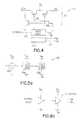
- FIG. 1 ashows a simplified circuit diagram of a prior art single pole, single throw (SPST) RF switch 10 .
- the prior art SPST switch 10includes a switching transistor M 1 5 and a shunting transistor M 2 7 .
- RF signalsare either routed from an RF input node 1 to an RF output node 3 , or shunted to ground through the shunting transistor M 2 7 .
- Actual values of the DC bias voltagesdepend upon the polarity and thresholds of the MOSFET transistors M 1 5 and M 2 7 .
- Resistor R 0 9in series with the RF source signal, isolates the bias from the source signal and is essential for optimal switch performance.
- FIG. 1 bshows the “on” state of the RF switch 10 of FIG. 1 a (i.e., FIG. 1 b shows the equivalent small-signal values of the transistors M 1 and M 2 when the RF switch 10 is “on”, with switching transistor M 1 5 on, and shunting transistor M 2 7 off).
- FIG. 1 cshows the “off” state of the switch 10 of FIG. 1 a (i.e., FIG. 1 c shows the equivalent small-signal values of the transistors M 1 and M 2 when the RF switch 10 is “off”, with switching transistor M 1 5 off, and shunting transistor M 2 7 on).
- the switching transistor M 1 5when the RF switch 10 is on, the switching transistor M 1 5 is primarily resistive while the shunting transistor M 2 7 is primarily capacitive.
- the “insertion loss” of the RF switch 10is determined from the difference between the maximum available power at the input node 1 and the power that is delivered to a load 11 at the output node 3 . At low frequencies, any power lost is due to the finite on resistance “r” 13 of the switching transistor M 1 5 when the switch 10 is on (see FIG. 1 b ).
- the on resistance r 13FIG. 1 b
- insertion lossdepends greatly upon the on resistances of the RF switch transmitters, lowering the transistor on resistances and reducing the parasitic substrate resistances can achieve improvements in insertion loss.
- the input-to-output isolation (or more simply, the switch isolation) of an RF switchis determined by measuring the amount of power that “bleeds” from the input port into the output port when the transistor connecting the two ports is off.
- the isolation characteristicmeasures how well the RF switch turns off (i.e., how well the switch blocks the input signal from the output). More specifically, and referring now to the “off” state of the RF switch 10 of FIG. 1 c , the switching transistor M 1 5 off state acts to block the input 1 from the output 3 .
- the shunting transistor M 2 7also serves to increase the input-to-output isolation of the switch 10 .
- M 1 5When turned off (i.e., when the RF switch 10 and the switching transistor M 1 5 are turned off), M 1 5 is primarily capacitive with “feedthrough” (i.e., passing of the RF input signal from the input node 1 to the output node 3 ) of the input signal determined by the series/parallel values of the capacitors CGD off 15 (Gate-to-Drain Capacitance when the switching transistor M 1 is turned off), CGS off 17 (Gate-to-Source Capacitance when the switching transistor M 1 is turned off), and CDS 1 19 (Drain-to-Source capacitance when the transistor M 1 is turned off). Feedthrough of the input signal is undesirable and is directly related to the input-to-output isolation of the RF switch 10 .
- the shunting transistor M 2 7is used to reduce the magnitude of the feedthrough and thereby increase the isolation characteristic of the RF switch.
- the shunting transistor M 2 7 of FIG. 1 cis turned on when the switching transistor M 1 5 is turned off.
- the shunting transistor M 2 7acts primarily as a resistor having a value of r.
- the value of ris much less than the characteristic impedance of the RF source. Consequently, r greatly reduces the voltage at the input of the switching transistor M 1 5 .
- the value of ris much less than the source resistance R 0 9 and the feedthrough capacitive resistance of the shunting transistor M 2 7 , isolation is easily calculated. Switch isolation for the off state of the RF switch 10 is determined as the difference between the maximum available power at the input to the power at the output.
- RF switch performance characteristicIn addition to RF switch insertion loss and isolation, another important RF switch performance characteristic is the ability to handle large input power when the switch is turned on to ensure that insertion loss is not a function of power at a fixed frequency. Many applications require that the switch does not distort power transmitted through a “switched-on” switch. For example, if two closely spaced tones are concurrently passed through an RF switch, nonlinearities in the switch can produce inter-modulation (IM) and can thereby create a false tone in adjacent channels. If these adjacent channels are reserved, for instance, for information signals, power in these false tones must be maintained as small as possible.
- the switch compression, or “1 dB compression point” (“P1 dB”)is indicative of the switch's ability to handle power.
- the P1 dBis defined as the input power at which the insertion loss has increased by 1 dB from its low-power value.
- the 1 dB compression pointis a measure of the amount of power that can be input to the RF switch at the input port before the output power deviates from a linear relationship with the input power by 1 dB.
- Switch compressionoccurs in one of two ways. To understand how switch compression occurs, operation of the MOSFET transistors shown in the RF switch 10 of FIGS. 1 a - 1 c are described. As is well known in the transistor design arts, MOSFETs require a gate-to-source bias that exceeds a threshold voltage, V i , to turn on. Similarly, the gate-to-source bias must be less than V i for the switch to be off. V i is positive for “type-N” MOSFETs and negative for “type-P” MOSFETs. Type-N MOSFETs were chosen for the RF switch 10 of FIGS. 1 a - 1 c . The source of a type-N MOSFET is the node with the lowest potential.
- the transistor M 2 7begins to turn on and compression begins.
- This first type of compressionis caused by the phenomenon of the turning on of a normally off gate in the shunt leg of the RF switch. Once the shunting transistor M 2 7 turns on, power at the output node 3 no longer follows power at the switch input in a linear manner.
- a second type of RF switch compressionoccurs when the source and drain of the shunting transistor M 2 7 break down at excessive voltages. For submicron silicon-on-insulator (SOI) devices, this voltage may be approximately only +1 VDC above the supply voltage. At breakdown, the shunt device begins to heavily conduct current thereby reducing the power available at the output.
- SOIsilicon-on-insulator
- FIG. 2shows a simplified schematic of a prior art single pole double throw (SPDT) RF switch 20 .
- the prior art RF switch 20minimally includes four MOSFET transistors 23 , 24 , 27 and 28 .
- the transistors 23 and 24act as “pass” or “switching” transistors (similar to the switching MOSFET transistor M 1 5 of FIGS. 1 a - 1 c ), and are configured to alternatively couple their associated and respective RF input nodes to a common RF node 25 .
- the switching transistor 23couples a first RF input signal “RF 1 ”, input to a first RF input node 21 , to the RF common node 25 .
- the switching transistor 24couples a second RF input signal “RF 2 ”, input to a second RF input node 22 , to the RF common node 25 .
- the shunting transistors, 27 and 28when enabled, act to alternatively shunt their associated and respective RF input nodes to ground when their associated RF input nodes are uncoupled from the RF common node 25 (i.e., when the switching transistor ( 23 or 24 ) connected to the associated input node is turned off).
- control voltagesare used to control the operation of the prior art RF switch.
- the control voltageslabeled “SW”, and its inverse “SW_”, control the operation of the transistors 23 , 24 , 27 and 28 .
- the control voltagesare arranged to alternatively enable (turn on) and disable (turn off) selective transistor pairs. For example, as shown in FIG. 2 , when SW is on (in some embodiments this is determined by the control voltage SW being set to a logical “high” voltage level, e.g., “+Vdd”), the switching transistor 23 is enabled, and its associated shunting transistor 28 is also enabled.
- SW_controls the operation of the second switching transistor 24 , and its associated shunting transistor 27 , and the control signal SW_ is off during the time period that SW is on (in some embodiments this is determined by SW_ being set to a ⁇ Vdd value), those two transistors are disabled, or turned off, during this same time period.
- SW “on” and SW_“off”)the RF 1 input signal is coupled to the RF common port 25 (through the enabled switching transistor 23 ). Because the second switching transistor 24 is turned off, the RF 2 input signal is blocked from the RF common port 25 .
- the RF 2 input signalis further isolated from the RF common port 25 because it is shunted to ground through the enabled shunting transistor 28 .
- the RF 2 signalis coupled to the RF common port 25 (and the RF 1 , signal is blocked and shunted to ground) in a similar manner when the SW control signal is “off” (and SW_ is “on”).
- RF switchessuch as the SPDT RF switch 20 of FIG. 2
- CMOScomplementary-metal-oxide-semiconductor
- GaAsgallium-arsenide
- most high performance high-frequency switchesuse GaAs technology.
- the prior art RF switch implementationsattempt to improve the RF switch performance characteristics described above, however, they do so with mixed results and with varying degrees of integrated circuit complexity and yields.
- bulk CMOS RF switchesdisadvantageously exhibit high insertion loss, low compression, and poor linearity performance characteristics.
- parasitic substrate resistancescan be greatly reduced thereby reducing RF switch insertion loss.
- the semi-insulating GaAs substrateimproves switch isolation.
- GaAs RF switch implementationsoffer improved performance characteristics, the technology has several disadvantages.
- GaAs technologyexhibits relatively low yields of properly functioning integrated circuits.
- GaAs RF switchestend to be relatively expensive to design and manufacture.
- GaAs switchesexhibit improved insertion loss characteristics as described above, they may have low frequency limitations due to slow states present in the GaAs substrate.
- the technologyalso does not lend itself to high levels of integration, which requires that digital control circuitry associated with the RF switch be implemented “off chip” from the switch.
- the low power control circuitry associated with the switchhas proven difficult to integrate. This is disadvantageous as it both increases the overall system cost or manufacture, size and complexity, as well as reducing system throughput speeds.
- an RF switch and method for switching RF signalshaving improved performance characteristics. Specifically, it is desirable to provide an RF switch having improved insertion loss, isolation, and compression. It is desirable that such an RF switch be easily designed and manufactured, relatively inexpensive to manufacture, lend itself to high levels of integration, with low-to-high frequency application. Power control circuitry should be easily integrated on-chip together with the switch functions. Such integration has been heretofore difficult to achieve using Si and GaAs substrates. The present teachings provide such an RF switch and method for switching RF signals.
- the RF switch circuitmay be used in wireless applications, and may be fabricated in a silicon-on-insulator technology. In one embodiment the RF switch is fabricated on an Ultra-Thin-Silicon (“UTSi”) substrate.
- UTSiUltra-Thin-Silicon
- the RF switchincludes: an input for receiving an RF signal; a first switching transistor grouping connected to the input to receive the RF signal and connected to an RF common port, wherein the first switching transistor is controlled by a switching voltage (SW); a second switching transistor grouping connected to the first switching transistor grouping and the RF common port, wherein the second switching transistor is controlled by a switching voltage SW_, and wherein SW_ is the inverse of SW so that when the first switching transistor grouping is on, the second switching transistor grouping is off.
- SWswitching voltage
- the RF switchalso includes shunting transistor groupings coupled to the switching transistor groupings and also controlled by the switching voltages SW and SW_.
- the shunting transistor groupingswhen enabled, act to alternatively shunt their associated RF input nodes to ground thereby improving RF switch isolation.
- the switching and shunting transistor groupingscomprise one or more MOSFET transistors connected together in a “stacked” or serial configuration. Within each transistor grouping, the gates of the stacked transistors are commonly controlled by a switching voltage (SW or SW_) that is coupled to each transistor gate through respective gate resistors.
- SW or SW_switching voltage
- the stacking of transistor grouping devices and gate resistorsincreases the compression point of the switch.
- the RC time constant formed by the gate resistors and the gate capacitance of the MOSFETsis designed to be much longer than the period of the RF signal, causing the RF voltage to be shared equally across the series connected devices. This configuration increases the 1 dB compression point of the RF switch.
- a fully integrated RF switchthat includes digital switch control logic and a negative power supply voltage generator circuit integrated together with the inventive RF switch.
- the fully integrated RF switchprovides several functions not present in prior art RF switches.
- the fully integrated RF switchincludes a built-in oscillator that provides clocking input signals to a charge pump circuit, an integrated charge pump circuit that generates the negative power supply voltages required by the other RF switch circuits, CMOS logic circuitry that generates control signals to control the RF switch transistors, level-shifting and low current voltage divider circuits that provide increased reliability of the switch devices, and an RF buffer circuit that isolates RF signal energy from the charge pump and digital control logic circuits.
- the inventive RF switchprovides improvements in insertion loss, switch isolation, and switch compression.
- RF system design and fabrication costsare reduced and reliability is increased using the present method and apparatus.
- FIG. 1 ais a simplified electrical schematic of a prior art single pole, single throw (SPST) RF switch used to demonstrate performance characteristics of the RF switch.
- SPSTsingle pole, single throw
- FIG. 1 bis a simplified electrical schematic of the SPST RF switch of FIG. 1 a showing the dominant characteristics of the switch when the switch is turned “on” allowing the RF signal to pass from an input node to an output node.
- FIG. 1 cshows the equivalent small-signal electrical characteristics of the RF switch of FIGS. 1 a and 1 b when the RF switch is turned “off” thereby blocking the RF signal from the output node.
- FIG. 2is a simplified electrical schematic of a prior art single pole double throw (SPDT) RF switch.
- FIG. 3is an electrical schematic of an RF switch according to one embodiment of the present method and apparatus.
- FIG. 4is a simplified block diagram of an exemplary fully integrated RF switch made in accordance with the present method and apparatus.
- FIG. 5 ais a simplified block diagram of one exemplary embodiment of the negative voltage generator shown in the simplified block diagram of FIG. 4 ;
- FIG. 5 bis an electrical schematic of a first embodiment of a charge pump circuit that is used to generate a negative supply voltage to the RF switch of FIG. 4 .
- FIG. 5 cis a plot of voltage amplitude versus time showing the voltage amplitude of two non-overlapping clock signals used to control the charge pump circuit of FIG. 5 b varying over time.
- FIG. 6 ais an electrical schematic of a first embodiment of an inventive level shifting circuit
- FIG. 6 bis an electrical schematic of one embodiment of the inverters used to implement the level shifter shown in FIG. 6 a.
- FIG. 7 ais a voltage amplitude versus time plot of a digital input signal and corresponding output signal generated by the inventive level shifter of FIG. 6 a ;
- FIG. 7 bis a simplified logic symbol for the inventive level shifter of FIG. 6 a.
- FIG. 8 ais an electrical schematic of one embodiment of a two-stage level shifter and RF buffer circuit including a first stage level shifter and a second stage RF buffer circuit;
- FIG. 8 bis a simplified block diagram of the digital control input and interface to the RF buffer circuit of FIG. 8 a.
- FIG. 9 ais an electrical schematic of one embodiment of a low current voltage divider (LCVD) circuit made in accordance with the present RF switch method and apparatus;
- FIG. 9 bis a simplified logic symbol used to represent the voltage divider of FIG. 9 a.
- LCDlow current voltage divider
- FIG. 10is an electrical schematic of a second embodiment of a level shifting circuit using the low current voltage divider circuit of FIG. 9 a in combination with the level shifting circuit of FIG. 6 a.
- FIGS. 11 a and 11 bare electrical schematics showing an alternative embodiment of the two-stage level shifter and RF buffer circuit of FIG. 8 a.
- FIG. 12is an electrical schematic of a modified charge pump using the level shifting circuit of FIG. 10 .
- the present method and apparatusis a novel RF switch design and method for switching RF circuits.
- a first exemplary embodiment of the present inventive RF switch 30is shown in FIG. 3 .
- the inventive RF switch 30includes four clusters or “groupings” of MOSFET transistors, identified in FIG. 3 as transistor groupings 33 , 34 , 37 and 38 .
- Two transistor groupingscomprise “pass” or “switching” transistor groupings 33 and 34
- two transistor groupingscomprise shunting transistor groupings 37 and 38 .
- Each transistor groupingincludes one or more MOSFET transistors arranged in a serial configuration. For example, in the embodiment shown in FIG.
- the switching grouping 33includes three switching transistors, M 33A , M 33B , and M 33C .
- the switching grouping 34includes three switching transistors, M 34A , M 34B , and M 33C .
- the shunting grouping 37includes three transistors M 37A , M 37B , and M 37C .
- the shunting grouping 38includes three transistors, M 38A , M 38B , and M 38C .
- the transistor groupings 33 , 34 , 37 and 38are shown in FIG. 3 as comprising three MOSFET transistors, those skilled in the RF switch design arts shall recognize that alternative grouping configurations can be used without departing from the scope or spirit of the present method and apparatus. For example, as described below in more detail, any convenient number of transistors can be used to implement the groupings shown in FIG. 3 without departing from the scope of the present method and apparatus.
- the MOSFET transistorsare implemented using a fully insulating substrate silicon-on-insulator (SOI) technology. More specifically, and as described in more detail hereinbelow, the MOSFET transistors of the inventive RF switch are implemented using “Ultra-Thin-Silicon (UTSi)” (also referred to herein as “ultrathin silicon-on-sapphire”) technology. In accordance with UTSi manufacturing methods, the transistors used to implement the inventive RF switch are formed in an extremely thin layer of silicon in an insulating sapphire wafer.
- UTSiUltra-Thin-Silicon
- the fully insulating sapphire substrateenhances the performance characteristics of the inventive RF switch by reducing the deleterious substrate coupling effects associated with non-insulating and partially insulating substrates. For example, improvements in insertion loss are realized by lowering the transistor on resistances and by reducing parasitic substrate resistances.
- switch isolationis improved using the fully insulating substrates provided by UTSi technology. Owing to the fully insulating nature of silicon-on-sapphire technology, the parasitic capacitance between the nodes of the RF switch 30 is greatly reduced as compared with bulk CMOS and other traditional integrated circuit manufacturing technologies. Consequently, the inventive RF switch exhibits improved switch isolation as compared with the prior art RF switch designs.
- the transistor groupingsare controlled by two control signals, SW, and its inverse, SW_.
- the control signalsare coupled to the gates of their respective transistors through associated and respective gate resistors.
- the control signal SWcontrols the operation of the three transistors in the switching transistor grouping 33 (M 33A , M 33B , and M 33C ) through three associated and respective gate resistors (R 33A , R 33B , and R 33C , respectively).
- the control signal SWis input to an input node 33 ′ to control the switching transistor grouping 33 .
- SWis also input to an input node 38 ′ to control the shunting transistor grouping 38 .
- the inverse of SW, SW_controls the switching transistor grouping 34 via an input node 34 ′.
- SW_is also input to an input node 37 ′ to control the shunting transistor grouping 37 .
- the transistor grouping resistorscomprise approximately 30 K ohm resistors, although alternative resistance values can be used without departing from the spirit or scope of the present method and apparatus.
- the gate resistorscomprise any resistive element having a relatively high resistance value.
- reversed-biased diodesmay be used to implement the gate resistors in one embodiment.
- the gate resistorshelp to increase the effective breakdown voltage across the series connected transistors.
- the control signalsfunction to control the enabling and disabling of the transistor groupings 33 , 34 , 37 and 38 , and the RF switch 30 generally functions to pass and block RF signals in a manner that is similar to the control of the analogous transistors of the switch of FIG. 2 .
- the switching transistor groupings 33 and 34act as pass or switching transistors, and are configured to alternatively couple their associated and respective RF input nodes to a common RF node 35 .
- the switching transistor grouping 33couples a first RF input signal “RF 1 ”, input to a first RF input node 31 , to the RF common node 35 .
- the switching transistor grouping 34couples a second RF input signal “RF 2 ”, input to a second RF input node 32 , to the RF common node 35 .
- the shunting transistor groupings, 37 and 38when enabled, act to alternatively shunt their associated and respective RF input nodes to ground when their associated RF input nodes are uncoupled from the RF common node 35 (i.e., when the switching transistor grouping ( 33 or 34 ) that is connected to the associated input node is turned off).
- the control voltagesare connected to alternatively enable and disable selective pairs of transistor groupings. For example, as shown in FIG. 3 , when SW is on (in some embodiments this is determined when the control voltage SW is set to a logical “high” voltage level), the switching transistor grouping 33 is enabled (i.e. all of the transistors in the grouping 33 are turned on), and its associated shunting transistor grouping 38 is also enabled (i.e., all of the transistors in the grouping 38 are turned on). However, similar to the operation of the switch of FIG.
- the RF 1 input signalis coupled to the RF common port 35 .
- the RF 2 input signalis blocked from the RF common port 35 because the switching transistor grouping 34 is off.
- the RF 2 input signalis further isolated from the RF common port 35 because it is shunted to ground through the enabled shunting transistor grouping 38 .
- the RF 2 signalis coupled to the RF common port 35 (and the RF 1 signal is blocked and shunted to ground) in a similar manner when the SW control signal is off (and the SW_ control signal is on).
- One purpose of the stacking of MOSFET transistors and using gate resistors as shown in the inventive RF switch 30 of FIG. 3is to increase the breakdown voltage across the series connected transistors.
- the RC time constant formed by the gate resistor and the gate capacitance of the MOSFETsis designed to be much longer than the period of the RF signal. Thus, very little RF energy is dissipated through the gate resistor.
- This arrangementeffectively causes the RF voltage to be shared equally across the series connected transistors. The net effect is that the breakdown voltage across the series connected devices is increased to n times the breakdown voltage of an individual FET, where n is the number of transistors connected in series. This configuration increases the 1 dB compression point of the inventive RF switch 30 .
- the RC time constantmust be sized so that it is large with respect to the period of the RF signal. This largely places a constraint on the minimum value of R that can be used to implement the gate transistors. As noted above, in one embodiment of the present method and apparatus, a typical value of R is 30 k-ohms, although other resistance values can be used without departing from the scope of the present method and apparatus. Because a MOSFET gate input draws no DC current, there is no change in the biasing of the devices due to IR drops across this resistance.
- the present inventive RF switch 30can accommodate input signals of increased power levels. Owing to the serial arrangement of the MOSFET transistors that comprise the transistor groupings ( 33 , 34 , 37 and 38 ), increased power signals can be presented at the RF input nodes (i.e., at the input nodes 31 and 32 ) without detrimentally affecting switch operation.
- Those skilled in the transistor design arts artshall recognize that greater input power levels can be accommodated by increasing the number of transistors per transistor grouping, or by varying the physical configuration of the transistors. For example, in one embodiment, the transistors are approximately 0.5 ⁇ 2,100 micro-meters in dimension. However, alternative configurations can be used without departing from the scope or spirit of the present method and apparatus.
- SOI technologyis attractive in implementing RF switches due to the fully insulating nature of the insulator substrate.
- SOIhas been used in the implementation of high performance microelectronic devices, primarily in applications requiring radiation hardness and high speed operation.
- SOI technologiesinclude, for example, SIMOX, bonded wafers having a thin silicon layer bonded to an insulating layer, and silicon-on-sapphire.
- the inventive RF switchis fabricated on a sapphire substrate.
- fabricating devices on an insulating substraterequires that an effective method for forming silicon CMOS devices on the insulating substrate be used.
- a composite substratecomprising a monocrystalline semiconductor layer, such as silicon, epitaxially deposited on a supporting insulating substrate, such as sapphire, are well-recognized, and can be realized by employing as the substrate an insulating material, such as sapphire (Al 2 O 3 ), spinel, or other known highly insulating materials, and providing that the conduction path of any inter-device leakage current must pass through the substrate.
- An “ideal” silicon-on-insulator wafercan be defined to include a completely monocrystalline, defect-free silicon layer of sufficient thickness to accommodate the fabrication of active devices therein.
- the silicon layerwould be adjacent to an insulating substrate and would have a minimum of crystal lattice discontinuities at the silicon-insulator interface.
- the high quality silicon films suitable for demanding device applicationscan be fabricated on sapphire substrates by a method that involves epitaxial deposition of a silicon layer on a sapphire substrate, low temperature ion implant to form a buried amorphous region in the silicon layer, and annealing the composite at temperatures below about 950° C.
- electronic devicescan be formed in an extremely thin layer of silicon on an insulating synthetic sapphire wafer.
- the thickness of the silicon layeris typically less than 150 nm.
- Such an “ultrathin” silicon layermaximizes the advantages of the insulating sapphire substrate and allows the integration of multiple functions on a single integrated circuit.
- Traditional transistor isolation wells required for thick siliconare unnecessary, simplifying transistor processing and increasing circuit density.
- theyare herein referred to collectively as “ultrathin silicon-on-sapphire.”
- the MOS transistorsare formed in ultrathin silicon-on-sapphire wafers by the methods disclosed in U.S. Pat. Nos. 5,416,043; 5,492,857; 5,572,040; 5,596,205; 5,600,169; 5,663,570; 5,861,336; 5,863,823; 5,883,396; 5,895,957; 5,920,233; 5,930,638; 5,973,363; 5,973,382; and 6,057,555.
- other known methods of fabricating ultrathin silicon-on-sapphire integrated circuitscan be used without departing from the spirit or scope of the present method and apparatus.
- high quality silicon films suitable for demanding device applicationscan be fabricated on insulating substrates by a method that involves epitaxial deposition of a silicon layer on an insulating substrate, low temperature ion implantation to form a buried amorphous region in the silicon layer, and annealing the composite at temperatures below about 950° C. Any processing of the silicon layer which subjects it to temperatures in excess of approximately 950° C. is performed in an oxidizing ambient environment.
- the thin silicon films in which the transistors are formedtypically have an areal density of electrically active states in regions not intentionally doped which is less than approximately 5 ⁇ 10 11 cm ⁇ 2 .
- UTSi substratesare especially desirable for RF applications because the fully insulating substrate reduces the detrimental effects of substrate coupling associated with traditional substrates (i.e., substrates that are not fully insulating). Consequently, in one embodiment, the RF switch 30 of FIG. 3 is fabricated on an UTSi substrate.
- inventive RF switch 30Several design parameters and tradeoffs should be considered in designing and implementing the inventive RF switch 30 described above with reference to FIG. 3 .
- the inventive RF switchcan be tailored to meet or exceed desired system design requirements and RF switch performance objectives.
- the design tradeoffs and considerations that impact the inventive RF switch designare now described.
- the RF switch 30is implemented using MOSFET transistors, which may be “N-type” or “P-type”.
- MOSFET transistorswhich may be “N-type” or “P-type”.
- N channel transistorsare preferred for RF switches implemented in CMOS technology.
- N channel transistorsare preferred because, for a given transistor size, the “on” resistance of an N channel transistor is much lower than for a P channel transistor due to the higher mobility in silicon of electrons versus holes.
- the control voltagesare selected to insure that the on resistance of the “on” transistor is reduced.
- the control voltagesare also selected to insure that the “off” transistor remains off when disabled.
- the “on” resistanceis inversely proportional to the difference between the voltage applied at the transistor gate and the voltage applied at the transistor source.
- This voltageis commonly referred to as the “Vgs” (gate-to-source voltage).
- Vgsgate-to-source voltage
- the RF input signals(e.g., the RF 1 input signal) generally swing about a zero reference voltage.
- the off transistorse.g., the transistors in the shunting transistor grouping 37 ) must remain disabled or turned off during both the positive and negative voltage excursions of the RF input signal. This argues for making the gate control voltage of the off transistors (e.g., the SW_ control voltage signal) as negative as possible. Again, reliability concerns limit the extent to which this gate control voltage can be made negative.
- MOS transistorshave a fundamental breakdown voltage between their source and drain. When the potential across the device exceeds this breakdown voltage, a high current flows between source and drain even when a gate potential exists that is attempting to keep the transistor in an off state. Improvements in switch compression can be achieved by increasing the breakdown voltage of the transistors.
- One method of fabricating a MOS transistor with a high breakdown voltageis to increase the length of the gate. Unfortunately, an increase in gate length also disadvantageously increases the channel resistance of the device thereby increasing the insertion loss of the device. The channel resistance can be decreased by making the device wider, however, this also decreases the switch isolation. Hence, tradeoffs exist in MOS switch designs.
- the transistorsare stacked in a series configuration to improve the switch 1 dB compression point.
- the relatively high value gate resistorsin combination with the stacking configuration of the transistors in the transistor groupings, increase the effective breakdown voltage across the series connected transistors.
- the switch elementsare designed and fabricated such that the RC time constant (determined by the resistance values of the gate resistors and the gate capacitance of the MOSFETs) is much longer than the period of the RF signal processed by the RF switch 30 .
- the net effect of the stacking configuration and the relatively high resistance gate resistorsis to increase the breakdown voltage across the series connected transistors by a factor of n times the breakdown voltage of an individual transistor (where n equals the number of transistors connected in series in a transistor grouping).
- the body tieused in traditional bulk CMOS transistors.
- the body tieelectrically couples the device either to the well or to the substrate.
- the well-substrate junctionmust remain reversed biased at all times.
- the source-to-body and drain-to-body junctionsmust remain reversed biased at all times.
- the wellfor N-well technology
- the substratefor P-well technology
- the RF input signalswings symmetrically above and below ground
- bulk CMOS switch designsexhibit poor insertion loss, isolation, and 1 dB compression point performance.
- the present RF switch 30is preferably implemented on an insulating substrate.
- the circuitry necessary for the proper operation and functioning of the RF switchcan be integrated together on the same integrated circuit as the switch itself.
- the RF switchcan be integrated in the same integrated circuit with a negative voltage generator and the CMOS control logic circuitry required to control the operation of the RF switch.
- the complexity of the RF switchis also reduced owing to the reduction in control lines required to control the operation of the switch.
- the RF switch control logiccan be implemented using low voltage CMOS transistors.
- a single, relatively low power external power supplycan be used to power the present inventive RF switch.
- This featureis advantageous as compared to the prior art GaAs implementations that require use of a relatively high power external power supply and power generation circuitry necessary to generate both positive and negative power supplies.
- the present inventive RF switchrequires only a single 3 V external power supply.
- the prior art switch designstypically require at least a 6 volt external power supply, and external voltage generation circuitry to generate both positive and negative power supplies.
- FIG. 4shows a simplified block diagram of an exemplary fully integrated RF switch 100 made in accordance with the present method and apparatus.
- the fully integrated RF switch 100includes the inventive RF switch 30 described above in FIG. 3 (shown in a simplified schematic representation in FIG. 4 ), CMOS control logic 110 , and a negative voltage generator circuit 120 (implemented in one embodiment using a “charge pump” circuit).
- a control signal 130is input to the CMOS logic block 110 .
- the control signal 130ranges from 0 volts to +Vdd, however those skilled in the digital logic design arts shall recognize that other logic levels can be used without departing from the scope or spirit of the present method and apparatus.
- the fully integrated RF switch 100is fabricated on UTSi substrates, although other insulating substrate technologies can be used.
- the fully integrated RF switch 100includes several functions and features not present in the prior art RF switch of FIG. 2 .
- the fully integrated RF switch 100integrates the negative voltage generator and RF switch control functions together on the same integrated circuit as the inventive RF switch.
- the fully integrated RF switch 100includes a built-in oscillator that provides clocking input signals to a charge pump circuit, an integrated charge pump circuit that generates the negative power supply voltages required by the other RF switch circuits, CMOS logic circuitry that generates the control signals that control the RF switch transistors, a level-shifting circuit that provides increased reliability by reducing the gate-to-drain, gate-to-source, and drain-to-source voltages of the switch transistors, and an RF buffer circuit that isolates RF signal energy from the charge pump and digital control logic circuits.
- CMOS logic circuitrythat generates the control signals that control the RF switch transistors
- a level-shifting circuitthat provides increased reliability by reducing the gate-to-drain, gate-to-source, and drain-to-source voltages of the switch transistors
- an RF buffer circuitthat isolates RF signal energy from the charge pump and digital control logic circuits.
- one embodiment of the fully integrated RF switch 100includes a negative voltage generator or charge pump 120 .
- the negative voltage generator 120generates the negative power supply voltage (specified hereafter as “ ⁇ Vdd”) required by other circuits of the fully integrated RF switch 100 .
- Two sets of inputsare provided to the negative voltage generator 120 : a positive DC power supply voltage signal (Vdd) 122 ; and a clocking input (shown in the figure as a single input signal, “Clk”) 124 .
- the clocking input 124is shown as a single input signal in FIG. 4 , as described below with reference to FIG. 5 b , in some embodiments of the present inventive RF switch, the clocking input 124 may comprise two or more clock input signals.
- the positive supply voltage that is input to the negative voltage generator circuit 120comprises a 3 VDC power supply.
- other power supply levelsmay be used without departing from the scope or spirit of the present method and apparatus.
- a 3.5 VDC, 5 VDC or any other convenient positive DC power supplycan be input to the negative voltage generator circuit 120 of FIG. 4 .
- the positive power supply signalis typically generated by an external low voltage power supply.
- FIG. 5 ashows a simplified block diagram of one exemplary embodiment 200 of the negative voltage generator 120 of FIG. 4 .
- the negative voltage generatorincludes an oscillator 202 , a clock generator circuit 204 , and an inventive charge pump circuit 206 .
- the oscillator 202 outputis input to the clock generator circuit 204 .
- the output of the clock generator circuit 204is input to the charge pump circuit 206 .
- the negative voltage generator 120provides the negative power supply voltage used by the other circuits of the fully integrated RF switch 100 .
- a first embodiment of the charge pump circuit 206includes two P-channel MOSFET transistors, 208 and 210 , connected in series with two N-channel MOSFET transistors 212 and 214 .
- the left leg of the charge pump circuit 206(comprising the first P-channel transistor 208 connected in series with the first N-channel transistor 212 ) is coupled to the right leg of the charge pump circuit (comprising the second P-channel transistor 210 connected in series with the second N-channel transistor 214 ) using a first capacitor Cp 216 .
- the source of the second P-channel transistor 214is coupled to a second capacitor, an output capacitor, C 218 , as shown.
- Two non-overlapping clock control signals, “Clk 1 ” and “Clk 2 ”,are used to control the operation of the transistors 208 , 210 , 212 and 214 .
- the inverse of “Clk 1 ”, “Clk 1 _”,control the gates of the P-channel transistors 208 , 210 .
- the other non-overlapping clock control signal, “Clk 2 ”controls the gate of the N-channel transistors 212 , 214 , as shown.
- the charge pump 206generates a negative power supply voltage ( ⁇ Vdd) by alternately charging and discharging the two capacitors (Cp 216 and the output capacitor C 218 ) using the non-overlapping clock input signals Clk 1 and Clk 2 to drive the transistor gates.
- the negative power supply voltage, ⁇ Vddis generated from the charge that is stored on the capacitor C 218 .
- a pulse shift circuit(not shown) is used to generate a pulse train that drives the charge pump (i.e., the pulse train is input as the clock input signals Clk 1 and Clk 2 ).
- the capacitor Cp 216is applied the positive power supply Vdd and then discharged across the output capacitor C 218 in an opposite direction to produce the negative power supply voltage ⁇ Vdd.
- No transistor in the charge pumpmust standoff more than Vdd across any source/drain nodes, hence greatly increasing the reliability of the charge pump 206 .
- the output C 218has a capacitance of approximately 200 pF
- Cp 216has a capacitance of approximately 50 pF.
- the two non-overlapping clock signalsare derived from an oscillator signal generated by an internal oscillator 202 .
- the oscillator 202inputs an oscillation signal to a clock generator circuit 204 , which in turn, generates the two non-overlapping clock signals (in any convenient well known manner) that control the charge pump transistor gates.
- the oscillator 202comprises a relatively low frequency (on the order of a few MHz) oscillator.
- the oscillatorcomprises a simple relaxation oscillator.
- other types of oscillatorscan be used to practice the present method and apparatus without departing from its spirit or scope.
- FIG. 5 cshows the voltage amplitude of the two non-overlapping clock signals, Clk 1 and Clk 2 , varying over time.
- the two non-overlapping clock signalsvary in voltage amplitude from ⁇ Vdd to +Vdd.
- the clock signalsvary from ⁇ 3 VDC to ⁇ 3 VDC. This arrangement improves the efficiency of the charge pump 206 .
- the charge pump transistors, 208 , 210 , 212 and 214advantageously comprise single-threshold N-channel ( 212 , 214 ) and P-channel ( 208 , 210 ) devices.
- Previous charge pump circuitsrequire use of multi-threshold level devices. These previous implementations are therefore more complex in design and cost than the inventive charge pump circuit 206 of FIG. 5 b .
- the P-channel transistors 208 , 210have widths of approximately 20 micro-meters, and lengths of approximately 0.8 micro-meters.
- the N-channel transistors 212 , 214have widths of approximately 8 micro-meters, and lengths of approximately 0.8 micro-meters.
- the inventive charge pump circuit 206is very efficient and performs well despite temperature and process variations.
- level shifting circuitryis used to limit the gate-to-source, gate-to-drain, and drain-to-source voltages on the transistors to acceptable levels.
- FIG. 6 aAn inventive level shifting circuit 300 made in accordance with the present method and apparatus is shown in FIG. 6 a .
- the level shifting circuit 300is used to convert or shift typical or “normal” digital input signals (digital signals typically range from ground (GND) to +Vdd) such that they range from ⁇ Vdd to +Vdd. The reliability of the fully integrated RF switch transistors is thereby increased.
- the control signalsare shifted to ⁇ 3 VDC to +3VDC, although those skilled in the RF switch control arts shall recognize that other level shifting voltage ranges can be used without departing from the spirit or scope of the present method and apparatus.
- the inventive level shifting circuit 300comprises a plurality of inverters coupled in a feedback configuration. More specifically, in the embodiment shown in FIG. 6 a , the level shifter 300 includes two groups of inverters used to generate first and second shifted output signals, “out” on a first output node 314 , and its inverse “out_” on a second output node 316 .
- the first group of inverterscomprises inverters 302 , 304 and 306 .
- a second group of inverterscomprises inverters 308 , 310 and 312 .
- a typical or “normal” digital input signal(i.e., a digital input signal that ranges from GND to +Vdd) is input to the level shifter 300 at an input node 318 of a first inverter 320 .
- the first inverter 320generates a first input signal “in” (on an output node 324 ) which is input to a second inverter 322 .
- the second inverter 322generates a second input signal “in_”, the inverse of the first input signal “in”, on an output node 326 . Therefore, the first and second inverters, 320 , 322 , generate the signals that are input to the two groups of inverters described above. For example, the first input signal “in” is coupled to the input 328 of the inverter 302 . Similarly, the second input signal “in_” is coupled to the input 330 of the inverter 308 .
- the output of the first group of inverters, “out”,is generated by a first output inverter 306 , and is provided on a first output node 314 .
- the output of the second group of inverters, “out_”,is generated by a second output inverter 312 , and is provided on a second output node 316 .
- the two level shifter outputs, “out” and “out_”,are input to other circuits of the fully integrated RF switch 100 of FIG. 4 .
- the first output, “out”is coupled to the gates of the devices of the switching transistor grouping 33 and the shunting transistor grouping 38 (i.e., the “out” signal on the first output node 314 of FIG.
- the second level shifter output, “out_”,is coupled to the “SW_” control input signal of FIG. 3 (at the input nodes 34 ′ and 37 ′) and thereby controls the switching transistor grouping 34 and the shunting transistor grouping 37 as described above.
- the level shifter 300 of FIG. 6 ashifts the DC level of an input signal (i.e., the input signal provided on the input node 318 ) while leaving the frequency response of the input signal unchanged.
- the level shifter 300takes full advantage of the floating technology offered by the silicon-on-insulator substrate implementation of the fully integrated RF switch 100 .
- the inverters of the level shifter 300operate on a differential basis, i.e., the level shifter shifts the digital input signals based upon the difference between two voltage signals.
- the level shifter 300reliably functions to shift the input signals to a range between ⁇ Vdd to +Vdd.
- Vddis equal to 3 VDC.
- the transistors comprising the inverters of the level shifter 300e.g., the output inverters 306 and 312 ) never have greater than 3 VDC applied across their source/drain nodes. This increases the reliability of the transistor devices.
- the level shifteruses a feedback approach to shift the digital input signals to voltage levels ranging from ⁇ Vdd to +Vdd.
- the output of the second group of inverters ( 308 , 310 , 312 ) on the second output node 316i.e., the “out_” signal
- the output of the first group of inverters ( 302 , 304 , 306 ) on the first output node 314i.e., the “out” output signal
- the digital input signal on the input node 318reaches a logical “high” state (i.e., in some embodiments, when the input signal transitions from GND to +Vdd), the “in” signal (at the node 324 ) and the “in_” signal (at the node 326 ) go to ground (e.g., 0 VDC) and Vdd (e.g. 3 VDC), respectively.
- the “out” signal at the first output node 314is driven to +Vdd.
- the “out_” signal at the second output node 316is driven towards ⁇ Vdd.
- the feedback (of “out_” fed back to the input of the inverter 304 and “out” fed forward to the input of the inverter 310 ) configurationensures the rapid change in state of the level shifter 300 .
- the level shifter 300works similarly when the input signal transitions from a logic high to a logic low state (i.e., transitions from +Vdd to GND).
- the digital input signal on the input node 318reaches a logic “low” state, the “in” signal (at the node 324 ) and the “in_” signal (at the node 326 ) go to Vdd (e.g., 3 VDC), and ground, respectively.
- Vdde.g., 3 VDC
- the “out_” signal at the second output node 316is driven towards +Vdd.
- the feedbackagain ensures the rapid change in state of the level shifter 300 .
- the grounding contributionensures that the level shifter inverters never see more than a full Vdd voltage drop across the source/drain nodes of the MOSFET transistors of the inverters.
- FIG. 6 bshows one embodiment of the inverters (e.g., the inverters 302 , 304 , and 306 ) used to implement the level shifter 300 of FIG. 6 a .
- the inverter 340includes two MOSFET devices, a P-channel transistor 342 and an N-channel transistor 344 .
- the devicesare connected in series as shown, having their gates coupled together and controlled by an input signal provided at an input node 346 .
- the source of the P-channel transistor 342is coupled to a first power supply voltage signal at node 350
- the source of the N-channel transistor 344is coupled to a second power supply voltage signal at a node 352 .
- the device drainsare coupled together as shown to produce an output of the inverter at an output node 348 .
- the P-channel transistor 342has a width of 5 micro-meters and a length of 0.8 micro-meters.
- the N-channel transistorhas a width of 2 micro-meters and a length of 0.8 micro-meters.
- a logical representation of the inverter 340is also shown as symbol 360 in FIG. 6 b.
- FIG. 7 ashows a voltage amplitude versus time plot of the digital input signal and the corresponding output signal that is generated by the inventive level shifter 300 of FIG. 6 a .
- the digital input signalranges from ground, or 0 VDC to Vdd.
- the output of the inventive level shifter 300ranges from ⁇ Vdd to +Vdd.
- the input signalranges from 0 VDC to +3 VDC
- the output of the level shifter 300ranges from ⁇ 3 VDC to +3 VDC.
- the input signalcan range from 0 to +3.5 VDC, or from 0 to 4 VDC.
- the level shiftershifts the signal to range from ⁇ 3.5 (or ⁇ 4) VDC, to +3.5 (or +4) VDC.
- FIG. 7 bshows a simplified logic symbol for the inventive level shifter 300 of FIG. 6 a .
- This logic symbolis used in subsequent figures.
- the digital input signalis provided on the input node 318 (the same input node 318 described above with reference to FIG. 6 a ).
- the level shifter 300provides two shifted outputs, “out” and its inverse “out_”, and these are provided on output nodes 314 and 316 , respectively (the same output nodes 314 , 316 described above with reference to FIG. 6 a ).
- FIG. 8 ais an electrical schematic of a two-stage level shifter and RF buffer circuit 400 .
- FIG. 8 bis a simplified block diagram of the digital control input and interface to the RF buffer circuit 400 .
- the two-stage level shifter and RF buffer circuit 400 of FIG. 8 acomprises a first stage level shifter 300 and a second stage RF buffer circuit 402 .
- the first stage level shifter 300is identical to that described above with reference to FIGS. 6 a , 6 b , 7 a and 7 b , and is therefore not described in more detail here.
- the level shifter stage 300shifts the logic levels of the digital control signals to range from ⁇ Vdd and +Vdd.
- the second stage of the circuit 400comprises the RF buffer circuit 402 .
- the RF buffer circuit 402acts as a driver stage only (i.e., no level shifting is performed by the RF buffer circuit).
- the RF bufferelectrically isolates the digital control signals (such as those generated by the CMOS logic block 110 of FIG. 4 ) from the RF switch 30 described above with reference to FIG. 3 .
- the RF buffer 402functions to inhibit drooping of the control voltages (SW, SW_, which are also referred to herein and shown in FIG. 8 a as the control signals “out” and “out_, respectively) that control the enabling and disabling of the transistors in the RF switch 30 .
- the RF buffer 402also functions to prevent coupling of large power RF signals to the negative power supply (i.e., ⁇ Vdd) that is generated by the charge pump circuit 206 described above with reference to FIGS.
- the RF buffer 402prevents large power RF signals extent in the RF switch 30 from RF-coupling to, and thereby draining current from, the negative power supply generated by the charge pump 206 ( FIG. 5 b ).
- RF coupling of the RF signals to the digital logic signalscan occur unless an RF buffer circuit is used to isolate the digital logic signals from the RF switch.
- the RF couplingcan and usually will detrimentally affect the RF transistor control signals (SW and SW_).
- SW and SW_RF transistor control signals
- RF input signals on the order of approximately 30 dBmare input to a 1 watt RF switch 30
- RF couplingcan cause voltage swings of several tenths of a volt on the digital control lines. This is due to the feedback of RF signals from the RF switch through to the digital control circuitry.
- This RF coupling effectcan adversely affect the enabling and disabling of the RF transistor groupings and hence the proper operation of the RF switch 30 .
- the buffer circuit 402 of FIG. 8 aprevents the undesirable RF coupling effect.
- the inventive buffer circuit 402is very similar in configuration to the level shifter 300 described above and shown as the first stage of the two-stage circuit 400 .
- the RF buffer 402comprises two groups of inverters, a first group of inverters ( 404 , 406 and 408 ) and a second group of inverters ( 410 , 412 , and 414 ).
- the output of the first group of inverters ( 404 , 406 , and 408 ), generated by the first output inverter 408is labeled “out” in the figure and is provided at a first output node 416 .
- the output signal “out_”is the inverse of the output signal “out”.
- the RF buffer circuit 402does not feedback its output signals to the input. Consequently, the digital input signals input to the first stage (i.e., the control input signals that are input to the level shifter 300 at the nodes 328 and 330 ) are isolated from the output signals that are used to control the RF switch transistors (i.e., the control output signals “out” and its inverse signal “out_” at the output nodes 416 and 418 , respectively, and coupled to the SW and SW_ control signal lines, respectively).
- the level shifter 300inputs the digital control signals “in” and its inverse signal “in_” at the nodes 328 , 330 respectively (as described in more detail above with reference to FIG. 6 a ).
- the first output of the level shifter 300“out1”, at the output node 314 , is fed back to the input of the inverter 310 as shown.
- the second output of the level shifter 300“out1_”, at the output node 316 , is fed back to the input of the inverter 304 .
- the inventive RF buffer circuit 402is used without feedback of the output signals to isolate the input signals (i.e., the digital input signals “in” and “in_) from the RF signals present in the RF switch.
- the first output signal “out1” of the level shifter 300is input to the inverters 404 , 406 of the RF buffer circuit.
- the second output signal “out1_” of the level shifter 300is input to the inverters 410 , 412 of the buffer circuit.
- the two control outputs of the RF buffer circuit 402 (“out” and “out_”)control the enabling and disabling of the transistors of the RF switch and are not provided as feedback to the level shifter. Hence, improved isolation between the RF switch and the digital logic circuitry is achieved.
- the inverters used to implement the two-stage level shifter and RF buffer circuit 400comprise the inverter 340 described above with reference to FIG. 6 b .
- the transistors used to implement the first stage level shifter 300are physically smaller than those used to implement the second stage RF buffer circuit 402 . Larger dimension transistors are used in the RF buffer circuit 402 to achieve an efficient amplification of the control signals.
- the transistors used to implement the RF bufferare three times wider than those used to implement the level shifter 300 , resulting in an amplification of approximately three times the current.
- the transistors used to implement the RF bufferare three times wider than those used to implement the level shifter 300 , resulting in an amplification of approximately three times the current.
- Those skilled in the transistor design artsshall recognize that other convenient transistor dimensions can be used to achieve any desired amplification of the digital control signals.
- FIG. 9 ais an electrical schematic of one embodiment of a low current voltage divider (“LCVD”) circuit 500 that is used in the feedback path of one embodiment of the level shifter 300 described above with reference to FIG. 6 a .
- FIG. 9 bshows a simplified logic symbol that is used to represent the voltage divider 500 of FIG. 9 a .
- the voltage divider 500is used in one embodiment to address potential gate oxide reliability issues related to excessive voltage swings across the gate oxides of the feedback inverter transistors.
- the gate oxides of the feedback inverters 304 and 310can have applied voltages of 2*Vdd. These feedback voltage levels can be applied across the gate oxides of the feedback inverters 304 , 310 , and can result in gate oxide reliability problems.
- the gate oxide reliability issuescan be averted by ensuring that the maximum voltage applied across the gate oxide of the feedback inverters 304 , 310 is lowered to approximately Vdd (as contrasted with gate oxide voltages of 2*Vdd). Therefore, in one embodiment of the present inventive fully integrated RF switch, the voltage divider of FIG. 9 a limits the voltages applied to the gates of the level shifter feedback inverters 304 , 310 . In this embodiment, instead of directly feeding back the level shifter outputs to their respective feedback inverters as shown in the level shifter of FIG.
- the level shifter output signalsare first conditioned by the voltage divider 500 of FIG. 9 a before being fed back to the feedback inverters.
- the voltage divider 500ensures that the voltages applied to the gate oxides of the feedback inverters 304 , 310 do not exceed more than approximately Vdd plus a small voltage drop (the voltage drop being a function of the number of transistors used to implement the voltage divider 500 and a transistor threshold voltage).
- Vddis 3 VDC
- the voltage dropis 0.9 VDC.
- the voltage divider 500ensures that the gate oxides are never applied voltages exceeding approximately 3.9 VDC (i.e., the feedback inverters are applied voltages that range from ⁇ 3 VDC to 0.9 VDC).
- the voltage divider 500includes a plurality of MOSFET devices ( 502 , 504 , 506 and 508 ) coupled together in a serial configuration (i.e., stacked on top of each other in a source to drain arrangement as shown).
- the gate and drain of the MOSFETs 502 , 504 , 506 and 508are coupled together to implement stacked diodes.
- the diode-implementing MOSFETshereafter referred to as “diode devices”, are stacked in series as shown.
- the voltage divider 500also includes a MOSFET M 3 510 and an output MOSFET M 2 512 . The function of these two transistors is described in more detail below.
- the diode devicesare used to divide the voltage of an input signal provided to the voltage divider 500 at an input node 514 .
- the signal that is divided by the voltage divider 500is provided as input to the drain (and connected gate) of the first device 502 .
- the input signalexceeds a positive voltage level of (n*Vthn), where “n” is the number of diode devices used to implement the voltage divider 500 , and Vthn is the threshold voltage of the device (i.e., the “diode-drop” from the drain to the source of the device), the diode devices ( 502 , 504 , 506 , and 508 ) begin to conduct current heavily.
- nis the number of diode devices used to implement the voltage divider 500
- Vthnis the threshold voltage of the device
- the input signal provided to the dividercan be limited to any desired voltage level by varying the number of diode devices used to implement the voltage divider 500 (i.e., by varying the value of “n”). In the embodiment shown in FIG. 9 a , once the input voltage exceeds a voltage level of (4*0.7), or 2.8 volts, the stacked diode devices begin conducting heavily.
- a ballast resistor, R 516is connected to the source of the output diode device 508 as shown. Once the diode devices turn on fully, the ballast resistor R 516 drops any additional input voltage that exceeds the value of n*Vthn. In the embodiment shown in FIG. 9 a , the ballast resistor R 516 drops any additional input voltage exceeding the value of (input voltage ⁇ (4*Vthn)).
- the output of the voltage divider 500is tapped from the connected gate-drain of the output diode device 508 .
- the voltage-divided output signalis provided on an output node 520 .
- the output at the output node 520is guaranteed to never exceed approximately (input voltage ⁇ (3*Vthn)).
- Vthnapproximately 0.7 volts
- a maximum input voltage of approximately 3 voltsthe output node 520 will never exceed (3 VDC ⁇ (3*0.7 VDC)), or 0.9 VDC.
- the voltage divider 500limits the output of the output node 520 to a range of ⁇ 3 VDC to 0.9 VDC.
- the output MOSFET M 2 512is configured as a capacitor and is used to assist in accelerating the switching time of the voltage divider 500 .
- the MOSFET M 3 510assures that the output node 520 swings to the potential of the input signal at the input node 514 when the input goes to a negative potential. This is accomplished by the device M 3 510 turning on when the input signal goes to a negative potential.
- a ⁇ Vdd potentiale.g., ⁇ 3 VDC
- the output signal at the output node 520also goes to ⁇ Vdd.
- the output device 508is reversed biased during negative voltage swings of the input signal assuring that no DC current is drained from the negative power supply during the negative voltage swings of the input signal.
- the voltage divider 500draws no current. This is important because a current at ⁇ 3 VDC discharges the charge pump circuit described above with reference to FIG. 5 b .
- the voltage divider outputis approximately 0.9 volts, the current that is drawn is very small if the ballast resistor R 516 is selected to be relatively large. However, because the current in this case occurs between a positive voltage (0.9 volts) and ground, no additional charge pump current is delivered due to the operation of the voltage divider 500 of FIG. 9 a.
- the ballast resistor R 516has a value of 100 k-ohms.
- all of the devices of the voltage divider 500have the same length.
- all of the deviceshave a length of 0.8 micro-meters.
- all of the diode devices( 502 , 504 , 506 , and 508 ) have identical physical dimensions.
- the diode deviceseach have a width of 2 micro-meters
- the device M 3 510has the same width of 2 micro-meters
- the output MOSFET M 2 512has a width of 14 micro-meters.
- 9 acan be used without departing from the scope or spirit of the present method and apparatus.
- those skilled in the electrical circuit design artsshall recognize that other voltage divider output levels can easily be accommodated by varying the number “n” of diode elements, varying the values of Vthn, or by tapping the output node 520 at a different point in the stack of diode devices (e.g., by tapping the output from the drain of diode device 506 , or 504 , instead of from the drain of device 508 as shown).
- FIG. 10shows a modified level shifter 600 using the voltage divider 500 of FIG. 9 a in combination with the level shifter 300 of FIG. 6 a .
- the output (at output node 314 ) of the inverter 306 of the level shifter 300is applied to an input of a first voltage divider 500 ′.
- the output (at the output node 316 ) of the inverter 312 of the level shifter 300is applied to an input of a second voltage divider 500 ′′.
- the outputs of the voltage dividersare fed back to the input of the feedback inverters 304 , 310 as shown in FIG. 10 .
- the output of the first voltage divider, “out”, on the output node 520 ′is fed back to the input of the feedback inverter 310 .
- the output of the second voltage divider, “out_”, on the output node 520 ′′is fed back to the input of the feedback inverter 304 .
- the level shifters 500 ′ and 500 ′′reduce the feedback voltages to ranges of ⁇ Vdd to approximately +0.9 VDC. This reduced voltage swing on the feedback paths does not alter the function of the level shifter 600 .
- the RF switch control signals, “SW” and “SW_”,can be tapped from the level shifter outputs prior to their input to the voltage dividers 500 ′ and 500 ′′, and provided as input to the inventive RF switch 30 of FIG. 3 .
- the output of inverter 306 at the output node 314can be tapped and used to generate the switch control signal “SW”.
- the output of the inverter 312 at the output node 316can be tapped and used to generate the switch control signal “SW_”.
- the control signals tapped from the nodes 314 , 316are first buffered before being coupled to the RF switch transistors.
- the switch control signals, SW and SW_are allowed to have a full-rail voltage swing which does not create gate oxide reliability problems in the RF switch. More specifically, the switch control signals range from ⁇ Vdd to +Vdd (i.e., the voltage levels of the switch control signals are not limited by the voltage dividers).
- the full voltage swings of the switch control signalsdo not raise gate oxide reliability issues with respect to the RF switch MOSFETs because the sources of the RF switch MOSFETs are grounded.
- the switch input signalsare therefore relative to ground in the RF switch MOSFETs. Consequently, the MOSFETs are applied either a positive Vdd voltage relative to ground across the gate oxides, or a negative Vdd voltage relative to ground across the gate oxides.
- FIG. 10also shows a simplified symbolic representation 601 of a section of the modified level shifter 600 .
- the symbol 601represents the portion indicated by the dashed region 601 ′ of FIG. 10 .
- the symbolic modified level shifter 601includes a first input “in_” 630 corresponding to the input node 326 (“in_”).
- the symbolic level shifter 601also includes a second input “out” 632 corresponding to the input to the feedback inverter 310 . Note that this signal is also derived from the output 520 ′ of the first voltage divider 500 ′.
- a positive power supply voltageis input at a +Vdd input 634 .
- a negative power supply voltageis input at a ⁇ Vdd input 636 .
- the modified level shifter 601has three output signals, “out_pos” (at output 638 ), “out_neg” (at output 640 ), and “out” (at output 642 ). These outputs correspond to the output nodes 606 , 608 , and 520 ′′ described above. For ease of understanding, the symbolic representation of the level shifter 601 is used in the figures described below.
- the potential gate oxide reliability problems associated with the level shifter 300 described above with reference to FIG. 6 aare averted using the voltage dividers 500 ′ and 500 ′′ in the feedback paths of the modified level shifter 600 .
- the voltage dividers 500 ′ and 500 ′′can also function to reduce potential gate oxide reliability problems associated with the charge pump circuit.
- the outputs of the inverters 308 and 310are tapped from the level shifter 300 and provided as input to two output inverters to produce two output signals, “out_pos” and “out_neg.” More specifically, the output of the inverter 308 is provided as input to a first output inverter 602 . Similarly, the output of the feedback inverter 310 is provided as input to a second output inverter 604 .
- the modified level shifter 600output signals never exceed Vdd (or ⁇ Vdd). More specifically, the first output inverter 602 generates an output signal, “out_pos”, at a first output node 606 , that ranges from GND (i.e., 0 VDC) to +Vdd. The second output inverter 604 generates a second output signal, “out_neg”, at a second output node 608 , which ranges from ⁇ Vdd to GND. When the input signal “in_” goes to GND, the output signal “out_pos” also goes to GND. The output signal “out_neg” transfers from GND to ⁇ Vdd.
- the two-stage level shifter and RF buffer 400 described above with reference to FIG. 8 acan experience voltage swings at the RF buffer inverter inputs of approximately 2*Vdd. As already described, this level of voltage swing may present gate oxide reliability problems and detrimentally affect the function of the RF buffer transistors.
- FIGS. 11 a and 11 bshow an alternative embodiment 400 ′ of the two-stage level shifter and RF buffer circuit 400 described above with reference to FIG. 8 a .
- the alternative embodiment of the RF buffer shown in FIG. 11 buses the voltage divider circuit described above to assure that voltages on the gate oxides of the RF buffer never exceed greater than 0.9 volts above Vdd.
- the alternative two-stage level shifter and RF buffer circuit 400 ′includes a first stage level shifter circuit 600 coupled to a second stage RF buffer circuit 402 ′.
- the modified level shifteroutputs, “out_pos” and “out_neg”, described above with reference to FIG.
- the RF buffer invertersare used as input to the RF buffer inverters to generate the RF buffer output signals “out” and “out_”.
- the “out_pos” and “out_neg” output signals generated by a first modified level shifter 700are input to two RF buffer inverters, 702 , 704 , respectively.
- the “out_pos” and “out_neg” output signals generated by a second modified level shifter 706are input to two RF buffer inverters, 708 , 710 , respectively.
- the RF buffer inverters 702 , 704are used to control the power supply voltages of a first RF output inverter 712 .
- the RF buffer inverters 708 , 710are used to control the power supply voltages of a second RF output inverter 714 .
- the RF buffer output signals, “out” and “out_”,are used to control the RF switch (i.e., output signal “out” acts as control voltage “SW”, while “out_” acts as control voltage “SW_”).
- the two output signals “out_pos” and “out_neg” generated by the modified level shifter 600 of FIG. 10can be used in an alternative embodiment of the charge pump circuit to reduce or eliminate potential gate oxide reliability problems associated with excessive voltages applied to the charge pump.
- the clock signals used to control the gates of the charge pump transistorsi.e., the P-channel transistors 208 , 210 , and the N-channel transistors 212 , 214 ) have voltage swings of 2*Vdd. For example, as shown in FIG.
- the charge pump clock signals, “Clk 1 ” and “Clk 2 ”,range from the negative power supply voltage ⁇ Vdd to the positive power supply voltage +Vdd. Similar to the gate oxide reliability issues described above with reference to the RF buffer and level shifter circuits, this full-rail voltage swing may present oxide reliability problems in the charge pump circuit. Therefore, a modified charge pump circuit is shown in FIG. 12 which reduces or eliminates potential gate oxide reliability problems by limiting the voltages applied to gate oxides to range from ⁇ Vdd to 0.9 volts.
- FIG. 12shows a modified charge pump 800 that uses the modified level shifter 600 described above with reference to FIG. 10 .
- the modified charge pump 800comprises a charge pump circuit 206 ′ and an inventive charge pump clock generation circuit 802 .
- the charge pump clock generation circuit 802generates the clock control signals used by the charge pump circuit 206 ′.
- the charge pump circuit 206 ′is very similar in design to the charge pump 206 described above with reference to FIG. 5 b .
- the charge pump 206 ′includes a pair of P-channel transistors 208 , 210 , and a pair of N-channel transistors 212 , 214 , in addition to a pass capacitor Cp 216 and an output capacitor C 218 .
- the output capacitor C 218has a capacitance on the order of a few hundred pF, and the capacitor Cp 216 has a capacitance of approximately 50 pF.
- the capacitor Cp 216has a capacitance of approximately 50 pF.
- the charge pump 206 ′functions very similarly to the charge pump 206 described above with reference to FIG. 5 a , and therefore its operation is not described in detail again here.
- the charge pump 206 ′ shown in FIG. 12differs from the charge pump 206 in that the control signals used to control the charge pump 206 ′ transistor gates (i.e., the gates of the transistors 208 , 210 , 212 , and 214 ) are limited to half-rail voltage swings (i.e., they are limited to range from ⁇ Vdd to ground, or from ground to Vdd). Potential gate oxide reliability problems invoked when the gate control voltages are allowed to swing a full rail (i.e., from ⁇ Vdd to Vdd) are thereby reduced or eliminated.
- the charge pump clock generation circuit 802includes four modified level shifters 804 , 806 , 808 and 810 , coupled together in a feedback configuration.
- the four modified level shiftersare implemented by the modified level shifter 600 described above with reference to FIG. 10 .
- FIG. 12shows the level shifters using the symbolic representation 601 of the level shifter 600 of FIG. 10 .
- the level shifters 804 , 806 , 808 , and 810perform identically to the level shifter 600 of FIG. 10 .
- the two non-overlapping clock signals, “Clk 1 ”, and “Clk 2 ”are input to the “in_” inputs of the level shifters as shown in FIG. 12 .
- the two input clock signals, “Clk 1 ” and “Clk 2 ”,are identical to the non-overlapping clock signals described above with reference to FIGS. 5 a - 5 c .
- the two non-overlapping clock signalsvary in voltage amplitude from ⁇ Vdd to +Vdd. In one embodiment, the clock signals vary from ⁇ 3 VDC to +3 VDC.
- the four modified level shiftersgenerate the half-rail clock control signals that are used to control the charge pump 206 ′. Specifically, as shown in FIG. 12 , the four level shifters generate the “CLK 1 POS_”, “CLK 1 NEG_”, “CLK 2 POS”, and “CLK 2 NEG” control signals that are input to the charge pump transistor gate control nodes 250 , 252 , 254 and 256 , respectively. In the embodiment shown in FIG. 12 , the level shifters 806 and 808 generate the four transistor gate control signals “CLK 1 POS_”, “CLK 1 NEG_”, “CLK 2 POS”, and “CLK 2 NEG”.
- the level shifter 806generates the “CLK 1 POS_” and “CLK 1 NEG_” gate control signals, while the level shifter 808 generates the “CLK 2 POS”, and “CLK 2 NEG” gate control signals. More specifically, as shown in FIG. 12 , the “out_pos” output of the level shifter 806 (“CLK 1 POS_”) is coupled to control the transistor gate input 250 of the transistor 208 . The “out_neg” output of the level shifter 806 (“CLK 1 NEG_”) is coupled to control the transistor gate input 252 of the transistor 210 . Similarly, the “out_pos” output of the level shifter 808 (“CLK 2 POS”) is coupled to control the transistor gate input 254 of the transistor 214 .
- the “out_neg” output of the level shifter 808(“CLK 2 NEG”) is coupled to control the transistor gate input 256 of the transistor 214 .
- the clock generation circuit 802functions to prevent excessive voltages across the gate oxides of the charge pump transistors.
- control configurationscan be used without departing from the spirit or scope of the present method and apparatus.
- the other two level shifters804 , 810
- the other two level shifters804 , 810
- alternative transistor configurationsN-channel and P-channel
- the four level shifters 804 , 806 , 808 and 810are coupled together in level shifter pairs ( 804 with 806 , and 808 with 810 ) in a feedback configuration that is very similar to the feedback topology of the level shifter described above with reference to FIG. 6 a .
- the “out” output node of the level shifter 804is provided as feedback to the “out” node of its associated pair level shifter 806 .
- the “out_” output node of the level shifter 806is provided as feedback to the “out” node of its associated pair level shifter 804 .
- the “out_” output node of the level shifter 808is provided as feedback to the “out” node of its associated pair level shifter 810 .
- the “out_” output node of the level shifter 810is provided as feedback to the “out” node of its associated pair level shifter 808 .
- the feedback configurationis used by the clock generation circuit 802 in the generation of the four transistor gate control signals “CLK 1 POS_”, “CLK 1 NEG_”, “CLK 2 POS”, and “CLK 2 NEG”.
- a novel RF switchis provided wherein the switch is fabricated using an SOI CMOS process. Fabricating the switch on an SOI substrate results in lack of substrate bias and allows the integration of key CMOS circuit building blocks with the RF switch elements. Integration of the CMOS building blocks with RF switch elements provides a fully integrated RF switch solution that requires use of only a single external power supply (i.e., the negative power supply voltage is generated internally by a charge pump circuit integrated with the RF switch). This results in improvements in RF switch isolation, insertion loss and compression.
- the RF switchhas a 1 dB compression point exceeding approximately 1 Watt, an insertion loss of less than approximately 0.5 dB, and switch isolation as high as approximately 40 dB.
- the inventive switchalso provides improvements in switching times.
Landscapes
- Engineering & Computer Science (AREA)
- Computer Hardware Design (AREA)
- Physics & Mathematics (AREA)
- Computing Systems (AREA)
- General Engineering & Computer Science (AREA)
- Mathematical Physics (AREA)
- Power Engineering (AREA)
- Computer Networks & Wireless Communication (AREA)
- Signal Processing (AREA)
- Electronic Switches (AREA)
- Semiconductor Integrated Circuits (AREA)
- Use Of Switch Circuits For Exchanges And Methods Of Control Of Multiplex Exchanges (AREA)
Abstract
Description
This is a continuation of application Ser. No. 12/980,161, filed Dec. 28, 2010, which is a continuation of application Ser. No. 12/315,395, filed Dec. 1, 2008, which issued Dec. 28, 2010 as U.S. Pat. No. 7,860,499, which is a continuation of application Ser. No. 11/582,206, filed Oct. 16, 2006, now U.S. Pat. No. 7,460,852 issued Dec. 2, 2008, which is a continuation of application Ser. No. 10/922,135, filed Aug. 18, 2004, now U.S. Pat. No. 7,123,898 issued Oct. 17, 2006, which is a continuation of application Ser. No. 10/267,531, filed Oct. 8, 2002, now U.S. Pat. No. 6,804,502 issued Oct. 12, 2004, which claims the benefit under 35 USC 119(e) of U.S. Provisional Application No. 60/328,353, filed Oct. 10, 2001, and each of these pending applications and issued patents are hereby incorporated by reference herein in their entirety.
1. Field
The present disclosure relates to switches, and particularly to a switch circuit and method of switching radio frequency (RF) signals within an integrated circuit. In one embodiment, the switch circuit comprises CMOS devices implemented on a silicon-on-insulator (SOI) substrate, for use in RF applications such as wireless communications, satellites, and cable television.
2. Description of Related Art
As is well known, radio frequency (RF) switches are important building blocks in many wireless communication systems. RF switches are found in many different communications devices such as cellular telephones, wireless pagers, wireless infrastructure equipment, satellite communications equipment, and cable television equipment. As is well known, the performance of RF switches is controlled by three primary operating performance parameters: insertion loss, switch isolation, and the “1 dB compression point.” These three performance parameters are tightly coupled, and any one parameter can be emphasized in the design of RF switch components at the expense of others. A fourth performance parameter that is occasionally considered in the design of RF switches is commonly referred to as the switching time or switching speed (defined as the time required to turn one side of a switch on and turn the other side off). Other characteristics that are important in RF switch design include case and degree (or level) of integration of the RF switch, complexity, yield, return loss and cost of manufacture.
These RF switch performance parameters can be more readily described with reference to a prior art RF switch design shown in the simplified circuit schematics ofFIGS. 1 a-1c.FIG. 1 ashows a simplified circuit diagram of a prior art single pole, single throw (SPST)RF switch 10. The priorart SPST switch 10 includes a switching transistor M15 and ashunting transistor M2 7. Referring now toFIG. 1 a, depending upon the state of the control voltages of the two MOSFET transistors M15 and M27 (i.e., depending upon the DC bias applied to the gate inputs of the MOSFET switching and shunting transistors, M1 and M2, respectively), RF signals are either routed from anRF input node 1 to anRF output node 3, or shunted to ground through theshunting transistor M2 7. Actual values of the DC bias voltages depend upon the polarity and thresholds of the MOSFET transistors M15 andM2 7.Resistor R0 9, in series with the RF source signal, isolates the bias from the source signal and is essential for optimal switch performance.FIG. 1 bshows the “on” state of theRF switch 10 ofFIG. 1 a(i.e.,FIG. 1 bshows the equivalent small-signal values of the transistors M1 and M2 when theRF switch 10 is “on”, with switching transistor M15 on, andshunting transistor M2 7 off).FIG. 1 cshows the “off” state of theswitch 10 ofFIG. 1 a(i.e.,FIG. 1 cshows the equivalent small-signal values of the transistors M1 and M2 when theRF switch 10 is “off”, with switching transistor M15 off, andshunting transistor M2 7 on).
As shown inFIG. 1 b, when theRF switch 10 is on, the switching transistor M15 is primarily resistive while theshunting transistor M2 7 is primarily capacitive. The “insertion loss” of theRF switch 10 is determined from the difference between the maximum available power at theinput node 1 and the power that is delivered to aload 11 at theoutput node 3. At low frequencies, any power lost is due to the finite on resistance “r”13 of the switching transistor M15 when theswitch 10 is on (seeFIG. 1 b). The on resistance r13 (FIG. 1 b) typically is much less than thesource resistor R0 9. The insertion loss, “IL”, can therefore be characterized in accordance withEquation 1 shown below:
IL is approximately equal to: 10r/R0 ln(10)=0.087r(in dB). Equation 1:
IL is approximately equal to: 10r/R0 ln(10)=0.087r(in dB). Equation 1:
Thus, at low frequencies, a 3-Ω value for r results in approximately 0.25 dB insertion loss.
Because insertion loss depends greatly upon the on resistances of the RF switch transmitters, lowering the transistor on resistances and reducing the parasitic substrate resistances can achieve improvements in insertion loss.
In general, the input-to-output isolation (or more simply, the switch isolation) of an RF switch is determined by measuring the amount of power that “bleeds” from the input port into the output port when the transistor connecting the two ports is off. The isolation characteristic measures how well the RF switch turns off (i.e., how well the switch blocks the input signal from the output). More specifically, and referring now to the “off” state of theRF switch 10 ofFIG. 1 c, the switching transistor M15 off state acts to block theinput 1 from theoutput 3. The shunting transistor M27 also serves to increase the input-to-output isolation of theswitch 10.
When turned off (i.e., when theRF switch 10 and the switching transistor M15 are turned off), M15 is primarily capacitive with “feedthrough” (i.e., passing of the RF input signal from theinput node 1 to the output node3) of the input signal determined by the series/parallel values of the capacitors CGD off15 (Gate-to-Drain Capacitance when the switching transistor M1 is turned off), CGS off17 (Gate-to-Source Capacitance when the switching transistor M1 is turned off), and CDS119 (Drain-to-Source capacitance when the transistor M1 is turned off). Feedthrough of the input signal is undesirable and is directly related to the input-to-output isolation of theRF switch 10. The shunting transistor M27 is used to reduce the magnitude of the feedthrough and thereby increase the isolation characteristic of the RF switch.
Theshunting transistor M2 7 ofFIG. 1 cis turned on when the switching transistor M15 is turned off. In this condition, theshunting transistor M2 7 acts primarily as a resistor having a value of r. By design, the value of r is much less than the characteristic impedance of the RF source. Consequently, r greatly reduces the voltage at the input of the switching transistor M15. When the value of r is much less than thesource resistance R0 9 and the feedthrough capacitive resistance of theshunting transistor M2 7, isolation is easily calculated. Switch isolation for the off state of theRF switch 10 is determined as the difference between the maximum available power at the input to the power at the output.
In addition to RF switch insertion loss and isolation, another important RF switch performance characteristic is the ability to handle large input power when the switch is turned on to ensure that insertion loss is not a function of power at a fixed frequency. Many applications require that the switch does not distort power transmitted through a “switched-on” switch. For example, if two closely spaced tones are concurrently passed through an RF switch, nonlinearities in the switch can produce inter-modulation (IM) and can thereby create a false tone in adjacent channels. If these adjacent channels are reserved, for instance, for information signals, power in these false tones must be maintained as small as possible. The switch compression, or “1 dB compression point” (“P1 dB”), is indicative of the switch's ability to handle power. The P1 dB is defined as the input power at which the insertion loss has increased by 1 dB from its low-power value. Or stated in another way, the 1 dB compression point is a measure of the amount of power that can be input to the RF switch at the input port before the output power deviates from a linear relationship with the input power by 1 dB.
Switch compression occurs in one of two ways. To understand how switch compression occurs, operation of the MOSFET transistors shown in theRF switch 10 ofFIGS. 1 a-1care described. As is well known in the transistor design arts, MOSFETs require a gate-to-source bias that exceeds a threshold voltage, Vi, to turn on. Similarly, the gate-to-source bias must be less than Vifor the switch to be off. Viis positive for “type-N” MOSFETs and negative for “type-P” MOSFETs. Type-N MOSFETs were chosen for theRF switch 10 ofFIGS. 1 a-1c. The source of a type-N MOSFET is the node with the lowest potential.
Referring again toFIG. 1 c, if a transient voltage on the shuntingtransistor M2 7 results in turning on the shuntingtransistor M2 7 during part of an input signal cycle, input power will be routed to ground and lost to the output. This loss of power increases for increased input power (i.e., input signals of increased power), and thereby causes a first type of compression. The 1 dB compression point in theRF switch 10 is determined by the signal swing on the input at which point the turned-offshunting transistor M2 7 is unable to remain off. Eventually, a negative swing of the input falls below the potential of the M2 gate, as well as below ground (thus becoming the source). When this difference becomes equal to Vi, thetransistor M2 7 begins to turn on and compression begins. This first type of compression is caused by the phenomenon of the turning on of a normally off gate in the shunt leg of the RF switch. Once the shuntingtransistor M2 7 turns on, power at theoutput node 3 no longer follows power at the switch input in a linear manner. A second type of RF switch compression occurs when the source and drain of the shuntingtransistor M2 7 break down at excessive voltages. For submicron silicon-on-insulator (SOI) devices, this voltage may be approximately only +1 VDC above the supply voltage. At breakdown, the shunt device begins to heavily conduct current thereby reducing the power available at the output.
As shown inFIG. 2 , two control voltages are used to control the operation of the prior art RF switch. The control voltages, labeled “SW”, and its inverse “SW_”, control the operation of thetransistors FIG. 2 , when SW is on (in some embodiments this is determined by the control voltage SW being set to a logical “high” voltage level, e.g., “+Vdd”), the switchingtransistor 23 is enabled, and its associated shuntingtransistor 28 is also enabled. However, because the inverse of SW, SW_, controls the operation of thesecond switching transistor 24, and its associated shuntingtransistor 27, and the control signal SW_ is off during the time period that SW is on (in some embodiments this is determined by SW_ being set to a −Vdd value), those two transistors are disabled, or turned off, during this same time period. In this state (SW “on” and SW_“off”), the RF1input signal is coupled to the RF common port25 (through the enabled switching transistor23). Because thesecond switching transistor 24 is turned off, the RF2input signal is blocked from the RFcommon port 25. Moreover, the RF2input signal is further isolated from the RFcommon port 25 because it is shunted to ground through the enabled shuntingtransistor 28. As those skilled in the transistor designs arts shall easily recognize, the RF2signal is coupled to the RF common port25 (and the RF1, signal is blocked and shunted to ground) in a similar manner when the SW control signal is “off” (and SW_ is “on”).
With varying performance results, RF switches, such as the SPDT RF switch20 ofFIG. 2 , have heretofore been implemented in different component technologies, including bulk complementary-metal-oxide-semiconductor (CMOS) and gallium-arsenide (GaAs) technologies. In fact, most high performance high-frequency switches use GaAs technology. The prior art RF switch implementations attempt to improve the RF switch performance characteristics described above, however, they do so with mixed results and with varying degrees of integrated circuit complexity and yields. For example, bulk CMOS RF switches disadvantageously exhibit high insertion loss, low compression, and poor linearity performance characteristics. In contrast, due to the semi-insulating nature of GaAs material, parasitic substrate resistances can be greatly reduced thereby reducing RF switch insertion loss. Similarly, the semi-insulating GaAs substrate improves switch isolation.
Although GaAs RF switch implementations offer improved performance characteristics, the technology has several disadvantages. For example, GaAs technology exhibits relatively low yields of properly functioning integrated circuits. GaAs RF switches tend to be relatively expensive to design and manufacture. In addition, although GaAs switches exhibit improved insertion loss characteristics as described above, they may have low frequency limitations due to slow states present in the GaAs substrate. The technology also does not lend itself to high levels of integration, which requires that digital control circuitry associated with the RF switch be implemented “off chip” from the switch. The low power control circuitry associated with the switch has proven difficult to integrate. This is disadvantageous as it both increases the overall system cost or manufacture, size and complexity, as well as reducing system throughput speeds.
It is therefore desirable to provide an RF switch and method for switching RF signals having improved performance characteristics. Specifically, it is desirable to provide an RF switch having improved insertion loss, isolation, and compression. It is desirable that such an RF switch be easily designed and manufactured, relatively inexpensive to manufacture, lend itself to high levels of integration, with low-to-high frequency application. Power control circuitry should be easily integrated on-chip together with the switch functions. Such integration has been heretofore difficult to achieve using Si and GaAs substrates. The present teachings provide such an RF switch and method for switching RF signals.
A novel RF switch circuit and method for switching RF signals is described. The RF switch circuit may be used in wireless applications, and may be fabricated in a silicon-on-insulator technology. In one embodiment the RF switch is fabricated on an Ultra-Thin-Silicon (“UTSi”) substrate. In one embodiment the RF switch includes: an input for receiving an RF signal; a first switching transistor grouping connected to the input to receive the RF signal and connected to an RF common port, wherein the first switching transistor is controlled by a switching voltage (SW); a second switching transistor grouping connected to the first switching transistor grouping and the RF common port, wherein the second switching transistor is controlled by a switching voltage SW_, and wherein SW_ is the inverse of SW so that when the first switching transistor grouping is on, the second switching transistor grouping is off. The switching transistor groupings, when enabled, alternatively connect their respective RF input signals to the RF common port. In this embodiment the RF switch also includes shunting transistor groupings coupled to the switching transistor groupings and also controlled by the switching voltages SW and SW_. The shunting transistor groupings, when enabled, act to alternatively shunt their associated RF input nodes to ground thereby improving RF switch isolation.
The switching and shunting transistor groupings comprise one or more MOSFET transistors connected together in a “stacked” or serial configuration. Within each transistor grouping, the gates of the stacked transistors are commonly controlled by a switching voltage (SW or SW_) that is coupled to each transistor gate through respective gate resistors. The stacking of transistor grouping devices and gate resistors increases the compression point of the switch. The RC time constant formed by the gate resistors and the gate capacitance of the MOSFETs is designed to be much longer than the period of the RF signal, causing the RF voltage to be shared equally across the series connected devices. This configuration increases the 1 dB compression point of the RF switch.
A fully integrated RF switch is described that includes digital switch control logic and a negative power supply voltage generator circuit integrated together with the inventive RF switch. In one embodiment, the fully integrated RF switch provides several functions not present in prior art RF switches. For example, in one embodiment, the fully integrated RF switch includes a built-in oscillator that provides clocking input signals to a charge pump circuit, an integrated charge pump circuit that generates the negative power supply voltages required by the other RF switch circuits, CMOS logic circuitry that generates control signals to control the RF switch transistors, level-shifting and low current voltage divider circuits that provide increased reliability of the switch devices, and an RF buffer circuit that isolates RF signal energy from the charge pump and digital control logic circuits. Several embodiments of the charge pump, level shifting, voltage divider, and RF buffer circuits are described. The inventive RF switch provides improvements in insertion loss, switch isolation, and switch compression. In addition, owing to the higher levels of integration made available by the present inventive RF switch, RF system design and fabrication costs are reduced and reliability is increased using the present method and apparatus.
Like reference numbers and designations in the various drawings indicate like elements.
Throughout this description, the preferred embodiment and examples shown should be considered as exemplars, rather than as limitations on the present method and apparatus.
The Inventive RF Switch
The present method and apparatus is a novel RF switch design and method for switching RF circuits. A first exemplary embodiment of the presentinventive RF switch 30 is shown inFIG. 3 . As shown inFIG. 3 , in one embodiment, theinventive RF switch 30 includes four clusters or “groupings” of MOSFET transistors, identified inFIG. 3 astransistor groupings transistor groupings transistor groupings FIG. 3 , theswitching grouping 33 includes three switching transistors, M33A, M33B, and M33C. Similarly, theswitching grouping 34 includes three switching transistors, M34A, M34B, and M33C. Theshunting grouping 37 includes three transistors M37A, M37B, and M37C. Similarly, theshunting grouping 38 includes three transistors, M38A, M38B, and M38C. Although thetransistor groupings FIG. 3 as comprising three MOSFET transistors, those skilled in the RF switch design arts shall recognize that alternative grouping configurations can be used without departing from the scope or spirit of the present method and apparatus. For example, as described below in more detail, any convenient number of transistors can be used to implement the groupings shown inFIG. 3 without departing from the scope of the present method and apparatus.
In one embodiment of the present inventive RF switch, the MOSFET transistors (e.g., the transistors M37A, M37B, and M37C) are implemented using a fully insulating substrate silicon-on-insulator (SOI) technology. More specifically, and as described in more detail hereinbelow, the MOSFET transistors of the inventive RF switch are implemented using “Ultra-Thin-Silicon (UTSi)” (also referred to herein as “ultrathin silicon-on-sapphire”) technology. In accordance with UTSi manufacturing methods, the transistors used to implement the inventive RF switch are formed in an extremely thin layer of silicon in an insulating sapphire wafer. The fully insulating sapphire substrate enhances the performance characteristics of the inventive RF switch by reducing the deleterious substrate coupling effects associated with non-insulating and partially insulating substrates. For example, improvements in insertion loss are realized by lowering the transistor on resistances and by reducing parasitic substrate resistances. In addition, switch isolation is improved using the fully insulating substrates provided by UTSi technology. Owing to the fully insulating nature of silicon-on-sapphire technology, the parasitic capacitance between the nodes of theRF switch 30 is greatly reduced as compared with bulk CMOS and other traditional integrated circuit manufacturing technologies. Consequently, the inventive RF switch exhibits improved switch isolation as compared with the prior art RF switch designs.
As shown inFIG. 3 , similar to the switch described above with reference toFIG. 2 , the transistor groupings are controlled by two control signals, SW, and its inverse, SW_. The control signals are coupled to the gates of their respective transistors through associated and respective gate resistors. For example, the control signal SW controls the operation of the three transistors in the switching transistor grouping33 (M33A, M33B, and M33C) through three associated and respective gate resistors (R33A, R33B, and R33C, respectively). The control signal SW is input to aninput node 33′ to control the switchingtransistor grouping 33. SW is also input to aninput node 38′ to control the shuntingtransistor grouping 38. Similarly, the inverse of SW, SW_, controls the switchingtransistor grouping 34 via aninput node 34′. SW_ is also input to aninput node 37′ to control the shuntingtransistor grouping 37.
In one embodiment, the transistor grouping resistors comprise approximately 30 K ohm resistors, although alternative resistance values can be used without departing from the spirit or scope of the present method and apparatus. In addition, in some embodiments of the present method and apparatus, the gate resistors comprise any resistive element having a relatively high resistance value. For example, reversed-biased diodes may be used to implement the gate resistors in one embodiment. As described in more detail below, the gate resistors help to increase the effective breakdown voltage across the series connected transistors.
The control signals function to control the enabling and disabling of thetransistor groupings RF switch 30 generally functions to pass and block RF signals in a manner that is similar to the control of the analogous transistors of the switch ofFIG. 2 . More specifically, the switchingtransistor groupings common RF node 35. For example, when enabled, the switching transistor grouping33 couples a first RF input signal “RF1”, input to a firstRF input node 31, to the RFcommon node 35. Similarly, when enabled, the switching transistor grouping34 couples a second RF input signal “RF2”, input to a secondRF input node 32, to the RFcommon node 35. The shunting transistor groupings,37 and38, when enabled, act to alternatively shunt their associated and respective RF input nodes to ground when their associated RF input nodes are uncoupled from the RF common node35 (i.e., when the switching transistor grouping (33 or34) that is connected to the associated input node is turned off).
The control voltages are connected to alternatively enable and disable selective pairs of transistor groupings. For example, as shown inFIG. 3 , when SW is on (in some embodiments this is determined when the control voltage SW is set to a logical “high” voltage level), the switchingtransistor grouping 33 is enabled (i.e. all of the transistors in thegrouping 33 are turned on), and its associatedshunting transistor grouping 38 is also enabled (i.e., all of the transistors in thegrouping 38 are turned on). However, similar to the operation of the switch ofFIG. 2 , because the inverse of SW, SW, controls the operation of the secondswitching transistor grouping 34, and its associatedshunting transistor grouping 37, these two transistors groupings are disabled (i.e., all of the transistors in thegroupings 34.37 are turned off) during this time period. Therefore, with SW on, the RF1input signal is coupled to the RFcommon port 35. The RF2input signal is blocked from the RFcommon port 35 because the switchingtransistor grouping 34 is off. The RF2input signal is further isolated from the RFcommon port 35 because it is shunted to ground through the enabled shuntingtransistor grouping 38. As those skilled in the RF switch design arts shall recognize, the RF2signal is coupled to the RF common port35 (and the RF1signal is blocked and shunted to ground) in a similar manner when the SW control signal is off (and the SW_ control signal is on).
One purpose of the stacking of MOSFET transistors and using gate resistors as shown in theinventive RF switch 30 ofFIG. 3 is to increase the breakdown voltage across the series connected transistors. The RC time constant formed by the gate resistor and the gate capacitance of the MOSFETs is designed to be much longer than the period of the RF signal. Thus, very little RF energy is dissipated through the gate resistor. This arrangement effectively causes the RF voltage to be shared equally across the series connected transistors. The net effect is that the breakdown voltage across the series connected devices is increased to n times the breakdown voltage of an individual FET, where n is the number of transistors connected in series. This configuration increases the 1 dB compression point of theinventive RF switch 30.
To achieve improved switch performance, the RC time constant must be sized so that it is large with respect to the period of the RF signal. This largely places a constraint on the minimum value of R that can be used to implement the gate transistors. As noted above, in one embodiment of the present method and apparatus, a typical value of R is 30 k-ohms, although other resistance values can be used without departing from the scope of the present method and apparatus. Because a MOSFET gate input draws no DC current, there is no change in the biasing of the devices due to IR drops across this resistance.
Advantageously, the presentinventive RF switch 30 can accommodate input signals of increased power levels. Owing to the serial arrangement of the MOSFET transistors that comprise the transistor groupings (33,34,37 and38), increased power signals can be presented at the RF input nodes (i.e., at theinput nodes 31 and32) without detrimentally affecting switch operation. Those skilled in the transistor design arts art shall recognize that greater input power levels can be accommodated by increasing the number of transistors per transistor grouping, or by varying the physical configuration of the transistors. For example, in one embodiment, the transistors are approximately 0.5×2,100 micro-meters in dimension. However, alternative configurations can be used without departing from the scope or spirit of the present method and apparatus.
Silicon-on-Insulator (SOI) Technologies
As noted above in the description of the RF switch ofFIG. 3 , SOI technology is attractive in implementing RF switches due to the fully insulating nature of the insulator substrate. As is well known, SOI has been used in the implementation of high performance microelectronic devices, primarily in applications requiring radiation hardness and high speed operation. SOI technologies include, for example, SIMOX, bonded wafers having a thin silicon layer bonded to an insulating layer, and silicon-on-sapphire. In order to achieve the desired switch performance characteristics described above, in one embodiment, the inventive RF switch is fabricated on a sapphire substrate.
Fabrication of devices on an insulating substrate requires that an effective method for forming silicon CMOS devices on the insulating substrate be used. The advantages of using a composite substrate comprising a monocrystalline semiconductor layer, such as silicon, epitaxially deposited on a supporting insulating substrate, such as sapphire, are well-recognized, and can be realized by employing as the substrate an insulating material, such as sapphire (Al2O3), spinel, or other known highly insulating materials, and providing that the conduction path of any inter-device leakage current must pass through the substrate.
An “ideal” silicon-on-insulator wafer can be defined to include a completely monocrystalline, defect-free silicon layer of sufficient thickness to accommodate the fabrication of active devices therein. The silicon layer would be adjacent to an insulating substrate and would have a minimum of crystal lattice discontinuities at the silicon-insulator interface. Early attempts to fabricate this “ideal” silicon-on-insulator wafer were frustrated by a number of significant problems, which can be summarized as (1) substantial incursion of contaminants into the epitaxially deposited silicon layer, especially the p-dopant aluminum, as a consequence of the high temperatures used in the initial epitaxial silicon deposition and the subsequent annealing of the silicon layer to reduce defects therein; and (2) poor crystalline quality of the epitaxial silicon layers when the problematic high temperatures were avoided or worked around through various implanting, annealing, and/or re-growth schemes.
It has been found that the high quality silicon films suitable for demanding device applications can be fabricated on sapphire substrates by a method that involves epitaxial deposition of a silicon layer on a sapphire substrate, low temperature ion implant to form a buried amorphous region in the silicon layer, and annealing the composite at temperatures below about 950° C.
Examples of and methods for making such silicon-on-sapphire devices are described in U.S. Pat. No. 5,416,043 (“Minimum charge FET fabricated on an ultrathin silicon on sapphire wafer”); U.S. Pat. No. 5,492,857 (“High-frequency wireless communication system on a single ultrathin silicon on sapphire chip”); U.S. Pat. No. 5,572,040 (“High-frequency wireless communication system on a single ultrathin silicon on sapphire chip”); U.S. Pat. No. 5,596,205 (“High-frequency wireless communication system on a single ultrathin silicon on sapphire chip”); U.S. Pat. No. 5,600,169 (“Minimum charge FET fabricated on an ultrathin silicon on sapphire wafer”); U.S. Pat. No. 5,663,570 (“High-frequency wireless communication system on a single ultrathin silicon on sapphire chip”); U.S. Pat. No. 5,861,336 (“High-frequency wireless communication system on a single ultrathin silicon on sapphire chip”); U.S. Pat. No. 5,863,823 (“Self-aligned edge control in silicon on insulator”); U.S. Pat. No. 5,883,396 (“High-frequency wireless communication system on a single ultrathin silicon on sapphire chip”); U.S. Pat. No. 5,895,957 (“Minimum charge FET fabricated on an ultrathin silicon on sapphire wafer”); U.S. Pat. No. 5,920,233 (“Phase locked loop including a sampling circuit for reducing spurious side bands”); U.S. Pat. No. 5,930,638 (“Method of making a low parasitic resistor on ultrathin silicon on insulator”); U.S. Pat. No. 5,973,363 (“CMOS circuitry with shortened P-channel length on ultrathin silicon on insulator”); U.S. Pat. No. 5,973,382 (“Capacitor on ultrathin semiconductor on insulator”); and U.S. Pat. No. 6,057,555 (“High-frequency wireless communication system on a single ultrathin silicon on sapphire chip”). All of these referenced patents are incorporated herein in their entirety for their teachings on ultrathin silicon-on-sapphire integrated circuit design and fabrication.
Using the methods described in the patents referenced above, electronic devices can be formed in an extremely thin layer of silicon on an insulating synthetic sapphire wafer. The thickness of the silicon layer is typically less than 150 nm. Such an “ultrathin” silicon layer maximizes the advantages of the insulating sapphire substrate and allows the integration of multiple functions on a single integrated circuit. Traditional transistor isolation wells required for thick silicon are unnecessary, simplifying transistor processing and increasing circuit density. To distinguish these above-referenced methods and devices from earlier thick-silicon embodiments, they are herein referred to collectively as “ultrathin silicon-on-sapphire.”
In some preferred embodiments of the method and apparatus, the MOS transistors are formed in ultrathin silicon-on-sapphire wafers by the methods disclosed in U.S. Pat. Nos. 5,416,043; 5,492,857; 5,572,040; 5,596,205; 5,600,169; 5,663,570; 5,861,336; 5,863,823; 5,883,396; 5,895,957; 5,920,233; 5,930,638; 5,973,363; 5,973,382; and 6,057,555. However, other known methods of fabricating ultrathin silicon-on-sapphire integrated circuits can be used without departing from the spirit or scope of the present method and apparatus.
As described and claimed in these patents, high quality silicon films suitable for demanding device applications can be fabricated on insulating substrates by a method that involves epitaxial deposition of a silicon layer on an insulating substrate, low temperature ion implantation to form a buried amorphous region in the silicon layer, and annealing the composite at temperatures below about 950° C. Any processing of the silicon layer which subjects it to temperatures in excess of approximately 950° C. is performed in an oxidizing ambient environment. The thin silicon films in which the transistors are formed typically have an areal density of electrically active states in regions not intentionally doped which is less than approximately 5×1011cm−2.
As noted above, UTSi substrates are especially desirable for RF applications because the fully insulating substrate reduces the detrimental effects of substrate coupling associated with traditional substrates (i.e., substrates that are not fully insulating). Consequently, in one embodiment, theRF switch 30 ofFIG. 3 is fabricated on an UTSi substrate.
RF Switch Design Tradeoffs
Several design parameters and tradeoffs should be considered in designing and implementing theinventive RF switch 30 described above with reference toFIG. 3 . The inventive RF switch can be tailored to meet or exceed desired system design requirements and RF switch performance objectives. The design tradeoffs and considerations that impact the inventive RF switch design are now described.
As described above with reference toFIG. 3 , theRF switch 30 is implemented using MOSFET transistors, which may be “N-type” or “P-type”. However, N channel transistors are preferred for RF switches implemented in CMOS technology. N channel transistors are preferred because, for a given transistor size, the “on” resistance of an N channel transistor is much lower than for a P channel transistor due to the higher mobility in silicon of electrons versus holes. The control voltages are selected to insure that the on resistance of the “on” transistor is reduced. The control voltages are also selected to insure that the “off” transistor remains off when disabled.
As is well known in the transistor design arts, in an N channel MOS transistor, the “on” resistance is inversely proportional to the difference between the voltage applied at the transistor gate and the voltage applied at the transistor source. This voltage is commonly referred to as the “Vgs” (gate-to-source voltage). It is readily observed that as the magnitude of the RF signal (Vs) increases at the input port (e.g., at the firstRF input node 31 ofFIG. 3 ), and hence at the RFcommon port 35, the Vgs of the on transistors decrease (e.g., the Vgs of the transistor M33Ain the switchingtransistor grouping 33 decreases as the magnitude of theRF 1 signal increases). This argues for making the gate control voltage (e.g., SW at theinput node 33′) as positive as possible. Unfortunately, reliability concerns limit the extent to which the gate control voltage can be made positive.
A similar concern exists for the “off” transistors. It is important to note that for typical RF switch applications, the RF input signals (e.g., theRF 1 input signal) generally swing about a zero reference voltage. The off transistors (e.g., the transistors in the shunting transistor grouping37) must remain disabled or turned off during both the positive and negative voltage excursions of the RF input signal. This argues for making the gate control voltage of the off transistors (e.g., the SW_ control voltage signal) as negative as possible. Again, reliability concerns limit the extent to which this gate control voltage can be made negative.
For a CMOS switch, the design of the off transistor also limits the 1 dB compression point of the switch. As is well known in the transistor design arts. MOS transistors have a fundamental breakdown voltage between their source and drain. When the potential across the device exceeds this breakdown voltage, a high current flows between source and drain even when a gate potential exists that is attempting to keep the transistor in an off state. Improvements in switch compression can be achieved by increasing the breakdown voltage of the transistors. One method of fabricating a MOS transistor with a high breakdown voltage is to increase the length of the gate. Unfortunately, an increase in gate length also disadvantageously increases the channel resistance of the device thereby increasing the insertion loss of the device. The channel resistance can be decreased by making the device wider, however, this also decreases the switch isolation. Hence, tradeoffs exist in MOS switch designs.
As described above with reference to theinventive RF switch 30 ofFIG. 3 , the transistors are stacked in a series configuration to improve theswitch 1 dB compression point. The relatively high value gate resistors, in combination with the stacking configuration of the transistors in the transistor groupings, increase the effective breakdown voltage across the series connected transistors. The switch elements are designed and fabricated such that the RC time constant (determined by the resistance values of the gate resistors and the gate capacitance of the MOSFETs) is much longer than the period of the RF signal processed by theRF switch 30. As noted above, the net effect of the stacking configuration and the relatively high resistance gate resistors is to increase the breakdown voltage across the series connected transistors by a factor of n times the breakdown voltage of an individual transistor (where n equals the number of transistors connected in series in a transistor grouping).
An additional design consideration concerns the “body tie” used in traditional bulk CMOS transistors. As is well known in the transistor design arts, the body tie electrically couples the device either to the well or to the substrate. The well-substrate junction must remain reversed biased at all times. The source-to-body and drain-to-body junctions must remain reversed biased at all times. In general, for bulk CMOS designs, the well (for N-well technology) is tied to the most positive potential that will be applied to the circuit. The substrate (for P-well technology) is tied to the most negative potential that will be applied to the circuit. Because the RF input signal swings symmetrically above and below ground, bulk CMOS switch designs exhibit poor insertion loss, isolation, and 1 dB compression point performance. For these reasons, and those described above, thepresent RF switch 30 is preferably implemented on an insulating substrate.
Implementing the inventive RF switch on an insulating substrate provides several advantages such as improved switch isolation and reduced insertion loss. Further advantages are achieved by implementing the inventive RF switch using UTSi technology. For example, as compared with the prior art RF switch implementations in GaAs, improvements in integrated circuit yields, reduced fabrication costs, and increased levels of integration are achieved using UTSi. As is well known in the integrated circuit design arts, GaAs does not lend itself to high levels of integration. Thus, the digital control circuitry and other circuitry associated with the operation and function of the RF switch (such as a negative voltage power supply generator, level shifting, low current voltage divider and RF buffer circuits) must often be implemented off-chip (i.e., these functions are not easily integrated with the RF switch). This leads to increased costs and reduced performance of the prior art RF switch implementations.
In contrast, in accordance with the present RF switch method and apparatus, using UTSi technology, the circuitry necessary for the proper operation and functioning of the RF switch can be integrated together on the same integrated circuit as the switch itself. For example, and as described below in more detail, by implementing the RF switch in UTSi technology, the RF switch can be integrated in the same integrated circuit with a negative voltage generator and the CMOS control logic circuitry required to control the operation of the RF switch. The complexity of the RF switch is also reduced owing to the reduction in control lines required to control the operation of the switch. Advantageously, the RF switch control logic can be implemented using low voltage CMOS transistors. In addition, even for high power RF switch implementations, a single, relatively low power external power supply can be used to power the present inventive RF switch. This feature is advantageous as compared to the prior art GaAs implementations that require use of a relatively high power external power supply and power generation circuitry necessary to generate both positive and negative power supplies. For example, in the exemplary embodiments described below with reference toFIGS. 4-12 , the present inventive RF switch requires only a single 3 V external power supply. The prior art switch designs typically require at least a 6 volt external power supply, and external voltage generation circuitry to generate both positive and negative power supplies.
Fully Integrated RF Switch
As described in more detail below, the fullyintegrated RF switch 100 includes several functions and features not present in the prior art RF switch ofFIG. 2 . For example, in addition to the inventive RF switch30 (which makes use of the novel transistor stacking and gate transistor configuration described above with reference toFIG. 3 ), the fullyintegrated RF switch 100 integrates the negative voltage generator and RF switch control functions together on the same integrated circuit as the inventive RF switch. As described below in more detail, the fullyintegrated RF switch 100 includes a built-in oscillator that provides clocking input signals to a charge pump circuit, an integrated charge pump circuit that generates the negative power supply voltages required by the other RF switch circuits, CMOS logic circuitry that generates the control signals that control the RF switch transistors, a level-shifting circuit that provides increased reliability by reducing the gate-to-drain, gate-to-source, and drain-to-source voltages of the switch transistors, and an RF buffer circuit that isolates RF signal energy from the charge pump and digital control logic circuits. Each of these circuits is described below in more detail with reference to their associated figures.
Negative Voltage Generator—Charge Pump—A First Embodiment
As shown inFIG. 4 , one embodiment of the fullyintegrated RF switch 100 includes a negative voltage generator orcharge pump 120. Thenegative voltage generator 120 generates the negative power supply voltage (specified hereafter as “−Vdd”) required by other circuits of the fullyintegrated RF switch 100. Two sets of inputs are provided to the negative voltage generator120: a positive DC power supply voltage signal (Vdd)122; and a clocking input (shown in the figure as a single input signal, “Clk”)124. Although theclocking input 124 is shown as a single input signal inFIG. 4 , as described below with reference toFIG. 5 b, in some embodiments of the present inventive RF switch, the clockinginput 124 may comprise two or more clock input signals.
In addition, in the embodiment shown inFIG. 4 , the positive supply voltage that is input to the negativevoltage generator circuit 120 comprises a 3 VDC power supply. However, other power supply levels may be used without departing from the scope or spirit of the present method and apparatus. For example, if desired, a 3.5 VDC, 5 VDC or any other convenient positive DC power supply can be input to the negativevoltage generator circuit 120 ofFIG. 4 . The positive power supply signal is typically generated by an external low voltage power supply.
In one embodiment of the present method and apparatus, thenegative voltage generator 120 ofFIG. 4 is implemented using a charge pump circuit.FIG. 5 ashows a simplified block diagram of oneexemplary embodiment 200 of thenegative voltage generator 120 ofFIG. 4 . As shown in the simplified block diagram ofFIG. 5 a, the negative voltage generator includes anoscillator 202, aclock generator circuit 204, and an inventivecharge pump circuit 206. Theoscillator 202 output is input to theclock generator circuit 204. The output of theclock generator circuit 204 is input to thecharge pump circuit 206. Thenegative voltage generator 120 provides the negative power supply voltage used by the other circuits of the fullyintegrated RF switch 100.
Many prior art RF switches disadvantageously require that the negative power supply voltages be generated by circuitry that is external to the RF switch circuitry. Other RF switch implementations use a coupling approach necessary to shift the DC value of the RF input signal to the midpoint of the applied bias voltage. This approach generally requires that relatively high bias voltages be applied because of the effective halving of the FET gate drive due to this level shifting. If the bias voltages are not increased, this produces a negative effect on the switch insertion loss because the gate drive is thereby reduced and the FET channel resistances are increased.
To address these problems, one embodiment of the fullyintegrated RF switch 100 uses the inventivecharge pump circuit 206 shown in detail inFIG. 5 b. As shown inFIG. 5 b, a first embodiment of thecharge pump circuit 206 includes two P-channel MOSFET transistors,208 and210, connected in series with two N-channel MOSFET transistors channel transistor 208 connected in series with the first N-channel transistor212) is coupled to the right leg of the charge pump circuit (comprising the second P-channel transistor 210 connected in series with the second N-channel transistor214) using afirst capacitor Cp 216. The source of the second P-channel transistor 214 is coupled to a second capacitor, an output capacitor,C 218, as shown. Two non-overlapping clock control signals, “Clk1” and “Clk2”, are used to control the operation of thetransistors FIG. 5 b, the inverse of “Clk1”, “Clk1_”, control the gates of the P-channel transistors channel transistors
Thecharge pump 206 generates a negative power supply voltage (−Vdd) by alternately charging and discharging the two capacitors (Cp 216 and the output capacitor C218) using the non-overlapping clock input signals Clk1 and Clk2 to drive the transistor gates. The negative power supply voltage, −Vdd, is generated from the charge that is stored on thecapacitor C 218. In one embodiment, a pulse shift circuit (not shown) is used to generate a pulse train that drives the charge pump (i.e., the pulse train is input as the clock input signals Clk1 and Clk2). As the pulse train is applied to thecharge pump 206, thecapacitor Cp 216 is applied the positive power supply Vdd and then discharged across theoutput capacitor C 218 in an opposite direction to produce the negative power supply voltage −Vdd. No transistor in the charge pump must standoff more than Vdd across any source/drain nodes, hence greatly increasing the reliability of thecharge pump 206.
In one embodiment of the inventivecharge pump circuit 206, theoutput C 218 has a capacitance of approximately 200 pF, andCp 216 has a capacitance of approximately 50 pF. Those skilled in the charge pump design arts shall recognize that other capacitance values can be used without departing from the scope or spirit of the present method and apparatus.
In one embodiment, as shown in the simplified block diagram ofFIG. 5 a, the two non-overlapping clock signals are derived from an oscillator signal generated by aninternal oscillator 202. As shown inFIG. 5 a, theoscillator 202 inputs an oscillation signal to aclock generator circuit 204, which in turn, generates the two non-overlapping clock signals (in any convenient well known manner) that control the charge pump transistor gates. In one embodiment of the present inventive fullyintegrated RF switch 100, theoscillator 202 comprises a relatively low frequency (on the order of a few MHz) oscillator. In this embodiment, the oscillator comprises a simple relaxation oscillator. However, as those skilled in the integrated circuit arts shall recognize, other types of oscillators can be used to practice the present method and apparatus without departing from its spirit or scope.
The charge pump transistors,208,210,212 and214 advantageously comprise single-threshold N-channel (212,214) and P-channel (208,210) devices. Previous charge pump circuits require use of multi-threshold level devices. These previous implementations are therefore more complex in design and cost than the inventivecharge pump circuit 206 ofFIG. 5 b. In one embodiment of thepresent charge pump 206, the P-channel transistors channel transistors charge pump circuit 206 is very efficient and performs well despite temperature and process variations.
Level Shifting Circuitry
Because the charge pump circuitry effectively doubles the power supply voltages that are applied to the circuit, careful attention must be paid to any potential reliability issues associated with these higher voltages. In order to implement the charge pump in a manner that increases the reliability of the transistors, level shifting circuitry is used to limit the gate-to-source, gate-to-drain, and drain-to-source voltages on the transistors to acceptable levels.
An inventivelevel shifting circuit 300 made in accordance with the present method and apparatus is shown inFIG. 6 a. Thelevel shifting circuit 300 is used to convert or shift typical or “normal” digital input signals (digital signals typically range from ground (GND) to +Vdd) such that they range from −Vdd to +Vdd. The reliability of the fully integrated RF switch transistors is thereby increased. In one embodiment of the present method and apparatus, the control signals are shifted to −3 VDC to +3VDC, although those skilled in the RF switch control arts shall recognize that other level shifting voltage ranges can be used without departing from the spirit or scope of the present method and apparatus.
As shown inFIG. 6 a, the inventivelevel shifting circuit 300, hereinafter referred to as thelevel shifter 300, comprises a plurality of inverters coupled in a feedback configuration. More specifically, in the embodiment shown inFIG. 6 a, thelevel shifter 300 includes two groups of inverters used to generate first and second shifted output signals, “out” on afirst output node 314, and its inverse “out_” on asecond output node 316. The first group of inverters comprisesinverters inverters level shifter 300 at aninput node 318 of afirst inverter 320. Thefirst inverter 320 generates a first input signal “in” (on an output node324) which is input to asecond inverter 322. Thesecond inverter 322 generates a second input signal “in_”, the inverse of the first input signal “in”, on anoutput node 326. Therefore, the first and second inverters,320,322, generate the signals that are input to the two groups of inverters described above. For example, the first input signal “in” is coupled to theinput 328 of theinverter 302. Similarly, the second input signal “in_” is coupled to theinput 330 of theinverter 308.
The output of the first group of inverters, “out”, is generated by afirst output inverter 306, and is provided on afirst output node 314. The output of the second group of inverters, “out_”, is generated by asecond output inverter 312, and is provided on asecond output node 316. The two level shifter outputs, “out” and “out_”, are input to other circuits of the fullyintegrated RF switch 100 ofFIG. 4 . For example, in one embodiment, the first output, “out”, is coupled to the gates of the devices of the switchingtransistor grouping 33 and the shunting transistor grouping38 (i.e., the “out” signal on thefirst output node 314 ofFIG. 6 ais coupled to the “SW” control input signal ofFIG. 3 , at theinput nodes 33′ and38′, and thereby controls the operation of the switchingtransistor grouping 33 and the shuntingtransistor grouping 38 as described above with reference toFIG. 3 ). Similarly, in this embodiment, the second level shifter output, “out_”, is coupled to the “SW_” control input signal ofFIG. 3 (at theinput nodes 34′ and37′) and thereby controls the switchingtransistor grouping 34 and the shuntingtransistor grouping 37 as described above.
Thelevel shifter 300 ofFIG. 6 ashifts the DC level of an input signal (i.e., the input signal provided on the input node318) while leaving the frequency response of the input signal unchanged. Thelevel shifter 300 takes full advantage of the floating technology offered by the silicon-on-insulator substrate implementation of the fullyintegrated RF switch 100. The inverters of thelevel shifter 300 operate on a differential basis, i.e., the level shifter shifts the digital input signals based upon the difference between two voltage signals. More specifically, as long as the difference between the power supply signals provided to the inverters (such as, for example, theoutput inverters 306 and312) is on the order of Vdd, thelevel shifter 300 reliably functions to shift the input signals to a range between −Vdd to +Vdd. In one embodiment, Vdd is equal to 3 VDC. In this embodiment, the transistors comprising the inverters of the level shifter300 (e.g., theoutput inverters 306 and312) never have greater than 3 VDC applied across their source/drain nodes. This increases the reliability of the transistor devices.
Referring again toFIG. 6 a, the level shifter uses a feedback approach to shift the digital input signals to voltage levels ranging from −Vdd to +Vdd. Specifically, the output of the second group of inverters (308,310,312) on the second output node316 (i.e., the “out_” signal) is provided as feedback to an input of the first group of inverters at the input of theinverter 304. Similarly, the output of the first group of inverters (302,304,306) on the first output node314 (i.e., the “out” output signal) is provided as input to the second group of inverters, specifically, is provided as input to theinverter 310.
When the digital input signal on theinput node 318 reaches a logical “high” state (i.e., in some embodiments, when the input signal transitions from GND to +Vdd), the “in” signal (at the node324) and the “in_” signal (at the node326) go to ground (e.g., 0 VDC) and Vdd (e.g. 3 VDC), respectively. The “out” signal at thefirst output node 314 is driven to +Vdd. At the same time, the “out_” signal at thesecond output node 316 is driven towards −Vdd. The feedback (of “out_” fed back to the input of theinverter 304 and “out” fed forward to the input of the inverter310) configuration ensures the rapid change in state of thelevel shifter 300. Thelevel shifter 300 works similarly when the input signal transitions from a logic high to a logic low state (i.e., transitions from +Vdd to GND). When the digital input signal on theinput node 318 reaches a logic “low” state, the “in” signal (at the node324) and the “in_” signal (at the node326) go to Vdd (e.g., 3 VDC), and ground, respectively. The “out” signal at thefirst output node 314 is driven to −Vdd. At the same time, the “out_” signal at thesecond output node 316 is driven towards +Vdd. The feedback again ensures the rapid change in state of thelevel shifter 300. The grounding contribution ensures that the level shifter inverters never see more than a full Vdd voltage drop across the source/drain nodes of the MOSFET transistors of the inverters.
Thus, using the presentinventive level shifter 300, digital input signals that initially range from GND to +Vdd are shifted to range from −Vdd to +Vdd.FIG. 7 ashows a voltage amplitude versus time plot of the digital input signal and the corresponding output signal that is generated by theinventive level shifter 300 ofFIG. 6 a. As shown inFIG. 7 a, the digital input signal ranges from ground, or0 VDC to Vdd. The output of theinventive level shifter 300 ranges from −Vdd to +Vdd. In one embodiment of the present inventive RF switch, the input signal ranges from 0 VDC to +3 VDC, and the output of thelevel shifter 300 ranges from −3 VDC to +3 VDC. Other values of power supply voltages can be used without departing from the scope or spirit of the present method and apparatus. For example, in one embodiment, the input signal can range from 0 to +3.5 VDC, or from 0 to 4 VDC. In this embodiment, the level shifter shifts the signal to range from −3.5 (or −4) VDC, to +3.5 (or +4) VDC.
RF Buffer Circuit
The RF buffer electrically isolates the digital control signals (such as those generated by theCMOS logic block 110 ofFIG. 4 ) from theRF switch 30 described above with reference toFIG. 3 . TheRF buffer 402 functions to inhibit drooping of the control voltages (SW, SW_, which are also referred to herein and shown inFIG. 8 aas the control signals “out” and “out_, respectively) that control the enabling and disabling of the transistors in theRF switch 30. As described below in more detail, theRF buffer 402 also functions to prevent coupling of large power RF signals to the negative power supply (i.e., −Vdd) that is generated by thecharge pump circuit 206 described above with reference toFIGS. 5 a-5c. More specifically, theRF buffer 402 prevents large power RF signals extent in theRF switch 30 from RF-coupling to, and thereby draining current from, the negative power supply generated by the charge pump206 (FIG. 5 b).
When very large power RF input signals are input to theinventive RF switch 30, coupling of the RF signals to the digital logic signals can occur unless an RF buffer circuit is used to isolate the digital logic signals from the RF switch. The RF coupling can and usually will detrimentally affect the RF transistor control signals (SW and SW_). For example, when RF input signals on the order of approximately 30 dBm are input to a 1watt RF switch 30, RF coupling can cause voltage swings of several tenths of a volt on the digital control lines. This is due to the feedback of RF signals from the RF switch through to the digital control circuitry. This RF coupling effect can adversely affect the enabling and disabling of the RF transistor groupings and hence the proper operation of theRF switch 30. Thebuffer circuit 402 ofFIG. 8 aprevents the undesirable RF coupling effect.
As shown inFIG. 8 a, theinventive buffer circuit 402 is very similar in configuration to thelevel shifter 300 described above and shown as the first stage of the two-stage circuit 400. Similar to thelevel shifter 300, theRF buffer 402 comprises two groups of inverters, a first group of inverters (404,406 and408) and a second group of inverters (410,412, and414). The output of the first group of inverters (404,406, and408), generated by thefirst output inverter 408, is labeled “out” in the figure and is provided at afirst output node 416. The output of the second group of inverters (410,412, and414), generated by thesecond output inverter 414, is labeled “out_”, and is provided at asecond output node 418. The output signal “out_” is the inverse of the output signal “out”.
Importantly, although the firststage level shifter 300 uses feedback to perform the level shifting function (as described above with reference toFIG. 6 a), theRF buffer circuit 402 does not feedback its output signals to the input. Consequently, the digital input signals input to the first stage (i.e., the control input signals that are input to thelevel shifter 300 at thenodes 328 and330) are isolated from the output signals that are used to control the RF switch transistors (i.e., the control output signals “out” and its inverse signal “out_” at theoutput nodes
More specifically, and referring again toFIG. 8 a, thelevel shifter 300 inputs the digital control signals “in” and its inverse signal “in_” at thenodes FIG. 6 a). The first output of thelevel shifter 300, “out1”, at theoutput node 314, is fed back to the input of theinverter 310 as shown. Similarly, the second output of thelevel shifter 300, “out1_”, at theoutput node 316, is fed back to the input of theinverter 304. As described above, because of this feedback topology, RF coupling occurs (i.e., the level shifter output signals have RF signals superimposed thereon) if the output signals of the level shifter are used to directly control the RF switch transistors (i.e., in the absence of the buffer circuit402). Therefore the inventiveRF buffer circuit 402 is used without feedback of the output signals to isolate the input signals (i.e., the digital input signals “in” and “in_) from the RF signals present in the RF switch. As shown inFIG. 8 a, the first output signal “out1” of thelevel shifter 300 is input to theinverters level shifter 300 is input to theinverters
In one embodiment, the inverters used to implement the two-stage level shifter andRF buffer circuit 400 comprise theinverter 340 described above with reference toFIG. 6 b. However, those skilled in the inverter design arts shall recognize that alternative inverter designs can be used in implementing the two-stage circuit 400 without departing from the scope or spirit of the present method and apparatus. In one embodiment, the transistors used to implement the firststage level shifter 300 are physically smaller than those used to implement the second stageRF buffer circuit 402. Larger dimension transistors are used in theRF buffer circuit 402 to achieve an efficient amplification of the control signals. For example, in one embodiment, the transistors used to implement the RF buffer are three times wider than those used to implement thelevel shifter 300, resulting in an amplification of approximately three times the current. Those skilled in the transistor design arts shall recognize that other convenient transistor dimensions can be used to achieve any desired amplification of the digital control signals.
Voltage Divider for Use in an Alternative Level Shifting Circuit
The gate oxide reliability issues can be averted by ensuring that the maximum voltage applied across the gate oxide of thefeedback inverters FIG. 9 alimits the voltages applied to the gates of the levelshifter feedback inverters FIG. 6 a(i.e., the outputs “out” and “out_”, at theoutput nodes voltage divider 500 ofFIG. 9 abefore being fed back to the feedback inverters. As described below in more detail, thevoltage divider 500 ensures that the voltages applied to the gate oxides of thefeedback inverters voltage divider 500 and a transistor threshold voltage). In one embodiment Vdd is 3 VDC, and the voltage drop is 0.9 VDC. In this embodiment, thevoltage divider 500 ensures that the gate oxides are never applied voltages exceeding approximately 3.9 VDC (i.e., the feedback inverters are applied voltages that range from −3 VDC to 0.9 VDC).
Referring now toFIG. 9 a, thevoltage divider 500 includes a plurality of MOSFET devices (502,504,506 and508) coupled together in a serial configuration (i.e., stacked on top of each other in a source to drain arrangement as shown). In one embodiment, the gate and drain of theMOSFETs voltage divider 500 also includes aMOSFET M3 510 and anoutput MOSFET M2 512. The function of these two transistors is described in more detail below.
The diode devices are used to divide the voltage of an input signal provided to thevoltage divider 500 at aninput node 514. As shown inFIG. 9 a, the signal that is divided by thevoltage divider 500 is provided as input to the drain (and connected gate) of thefirst device 502. Once the input signal exceeds a positive voltage level of (n*Vthn), where “n” is the number of diode devices used to implement thevoltage divider 500, and Vthn is the threshold voltage of the device (i.e., the “diode-drop” from the drain to the source of the device), the diode devices (502,504,506, and508) begin to conduct current heavily. In the embodiment shown inFIG. 9 a, n=4, and Vthn=0.7 volts, although alternative values for “n” and Vthn can be used without departing from the scope or spirit of the present method and apparatus. For example, in other embodiments, the input signal provided to the divider can be limited to any desired voltage level by varying the number of diode devices used to implement the voltage divider500 (i.e., by varying the value of “n”). In the embodiment shown inFIG. 9 a, once the input voltage exceeds a voltage level of (4*0.7), or 2.8 volts, the stacked diode devices begin conducting heavily.
A ballast resistor,R 516, is connected to the source of theoutput diode device 508 as shown. Once the diode devices turn on fully, theballast resistor R 516 drops any additional input voltage that exceeds the value of n*Vthn. In the embodiment shown inFIG. 9 a, theballast resistor R 516 drops any additional input voltage exceeding the value of (input voltage−(4*Vthn)). The output of thevoltage divider 500 is tapped from the connected gate-drain of theoutput diode device 508. The voltage-divided output signal is provided on anoutput node 520. Due to the diode voltage drops of thediode devices ballast resistor R 516, the output at theoutput node 520 is guaranteed to never exceed approximately (input voltage−(3*Vthn)). For Vthn=approximately 0.7 volts, and a maximum input voltage of approximately 3 volts, theoutput node 520 will never exceed (3 VDC−(3*0.7 VDC)), or 0.9 VDC. Thus, in the embodiment shown inFIG. 9 a, for an input voltage ranging between −3 VDC to +3 VDC, thevoltage divider 500 limits the output of theoutput node 520 to a range of −3 VDC to 0.9 VDC.
Theoutput MOSFET M2 512 is configured as a capacitor and is used to assist in accelerating the switching time of thevoltage divider 500. TheMOSFET M3 510 assures that theoutput node 520 swings to the potential of the input signal at theinput node 514 when the input goes to a negative potential. This is accomplished by thedevice M3 510 turning on when the input signal goes to a negative potential. Thus, when the input signal goes to a −Vdd potential (e.g., −3 VDC), the output signal at theoutput node 520 also goes to −Vdd. Theoutput device 508 is reversed biased during negative voltage swings of the input signal assuring that no DC current is drained from the negative power supply during the negative voltage swings of the input signal. When the voltage divider output is approximately −3 VDC, thevoltage divider 500 draws no current. This is important because a current at −3 VDC discharges the charge pump circuit described above with reference toFIG. 5 b. When the voltage divider output is approximately 0.9 volts, the current that is drawn is very small if theballast resistor R 516 is selected to be relatively large. However, because the current in this case occurs between a positive voltage (0.9 volts) and ground, no additional charge pump current is delivered due to the operation of thevoltage divider 500 ofFIG. 9 a.
In one embodiment, theballast resistor R 516 has a value of 100 k-ohms. In one embodiment all of the devices of thevoltage divider 500 have the same length. For example, in one embodiment, all of the devices have a length of 0.8 micro-meters. In one embodiment, all of the diode devices (502,504,506, and508) have identical physical dimensions. In one embodiment, the diode devices each have a width of 2 micro-meters, thedevice M3 510 has the same width of 2 micro-meters, and theoutput MOSFET M2 512 has a width of 14 micro-meters. Those skilled in the integrated circuit design arts shall recognize that other values and alternative configurations for the devices shown inFIG. 9 acan be used without departing from the scope or spirit of the present method and apparatus. For example, those skilled in the electrical circuit design arts shall recognize that other voltage divider output levels can easily be accommodated by varying the number “n” of diode elements, varying the values of Vthn, or by tapping theoutput node 520 at a different point in the stack of diode devices (e.g., by tapping the output from the drain ofdiode device device 508 as shown).
Modified Level Shifter Using the Voltage Divider
By reducing the voltages that are applied to the gate oxides of the RF switch transistors, thevoltage divider 500 ofFIGS. 9 aand9badvantageously can be used to increase the reliability of the transistors in both thelevel shifter 300 and the charge pump circuit described above. For example,FIG. 10 shows a modifiedlevel shifter 600 using thevoltage divider 500 ofFIG. 9 ain combination with thelevel shifter 300 ofFIG. 6 a. As shown inFIG. 10 , the output (at output node314) of theinverter 306 of thelevel shifter 300 is applied to an input of afirst voltage divider 500′. Similarly, the output (at the output node316) of theinverter 312 of thelevel shifter 300 is applied to an input of asecond voltage divider 500″. The outputs of the voltage dividers are fed back to the input of thefeedback inverters FIG. 10 . Specifically, and referring toFIG. 10 , the output of the first voltage divider, “out”, on theoutput node 520′ is fed back to the input of thefeedback inverter 310. Similarly, the output of the second voltage divider, “out_”, on theoutput node 520″ is fed back to the input of thefeedback inverter 304. As described above with reference toFIG. 9 a, thelevel shifters 500′ and500″ reduce the feedback voltages to ranges of −Vdd to approximately +0.9 VDC. This reduced voltage swing on the feedback paths does not alter the function of thelevel shifter 600.
Note that the RF switch control signals, “SW” and “SW_”, can be tapped from the level shifter outputs prior to their input to thevoltage dividers 500′ and500″, and provided as input to theinventive RF switch 30 ofFIG. 3 . For example, as shown inFIG. 10 , the output ofinverter 306 at theoutput node 314 can be tapped and used to generate the switch control signal “SW”. Similarly, the output of theinverter 312 at theoutput node 316 can be tapped and used to generate the switch control signal “SW_”. In one embodiment, as described above with reference to the two-stage level shifter andRF buffer circuit 400 ofFIG. 8 a, the control signals tapped from thenodes
The potential gate oxide reliability problems associated with thelevel shifter 300 described above with reference toFIG. 6 aare averted using thevoltage dividers 500′ and500″ in the feedback paths of the modifiedlevel shifter 600. In addition, thevoltage dividers 500′ and500″ can also function to reduce potential gate oxide reliability problems associated with the charge pump circuit. As shown inFIG. 10 , the outputs of theinverters level shifter 300 and provided as input to two output inverters to produce two output signals, “out_pos” and “out_neg.” More specifically, the output of theinverter 308 is provided as input to afirst output inverter 602. Similarly, the output of thefeedback inverter 310 is provided as input to asecond output inverter 604.
By coupling theoutput inverters level shifter 600 output signals never exceed Vdd (or −Vdd). More specifically, thefirst output inverter 602 generates an output signal, “out_pos”, at afirst output node 606, that ranges from GND (i.e., 0 VDC) to +Vdd. Thesecond output inverter 604 generates a second output signal, “out_neg”, at asecond output node 608, which ranges from −Vdd to GND. When the input signal “in_” goes to GND, the output signal “out_pos” also goes to GND. The output signal “out_neg” transfers from GND to −Vdd. When the input signal “in_” goes positive to +Vdd, “out_pos” also goes to Vdd, and “out_neg” transfers from −Vdd to GND. Thus, using the present modifiedlevel shifter 600, the “out_pos” output signal ranges from GND to +Vdd, while the “out_neg” output signal ranges from −Vdd to GND. As described below in more detail, the two output signals, “out_pos” and “out_neg”, are used to address potential gate oxide reliability problems in a modified charge pump circuit. As described now with reference toFIGS. 11 aand11b, these output signals can also be used to address potential gate oxide reliability problems in the RF buffer circuit.
Modified Level Shifter and RF Buffer Circuit
The two-stage level shifter andRF buffer 400 described above with reference toFIG. 8 acan experience voltage swings at the RF buffer inverter inputs of approximately 2*Vdd. As already described, this level of voltage swing may present gate oxide reliability problems and detrimentally affect the function of the RF buffer transistors.
TheRF buffer inverters RF output inverter 712. Similarly, theRF buffer inverters RF output inverter 714. In this embodiment, the RF buffer output signals, “out” and “out_”, are used to control the RF switch (i.e., output signal “out” acts as control voltage “SW”, while “out_” acts as control voltage “SW_”).
Modified Charge Pump—An Alternative Embodiment
As noted above, the two output signals “out_pos” and “out_neg” generated by the modifiedlevel shifter 600 ofFIG. 10 can be used in an alternative embodiment of the charge pump circuit to reduce or eliminate potential gate oxide reliability problems associated with excessive voltages applied to the charge pump. As described above with reference toFIGS. 5 band5c, the clock signals used to control the gates of the charge pump transistors (i.e., the P-channel transistors channel transistors 212,214) have voltage swings of 2*Vdd. For example, as shown inFIG. 5 c, the charge pump clock signals, “Clk1” and “Clk2”, range from the negative power supply voltage−Vdd to the positive power supply voltage +Vdd. Similar to the gate oxide reliability issues described above with reference to the RF buffer and level shifter circuits, this full-rail voltage swing may present oxide reliability problems in the charge pump circuit. Therefore, a modified charge pump circuit is shown inFIG. 12 which reduces or eliminates potential gate oxide reliability problems by limiting the voltages applied to gate oxides to range from −Vdd to 0.9 volts.
Thecharge pump 206′ functions very similarly to thecharge pump 206 described above with reference toFIG. 5 a, and therefore its operation is not described in detail again here. Thecharge pump 206′ shown inFIG. 12 differs from thecharge pump 206 in that the control signals used to control thecharge pump 206′ transistor gates (i.e., the gates of thetransistors
As shown inFIG. 12 , the charge pumpclock generation circuit 802 includes four modifiedlevel shifters level shifter 600 described above with reference toFIG. 10 .FIG. 12 shows the level shifters using thesymbolic representation 601 of thelevel shifter 600 ofFIG. 10 . In this embodiment, thelevel shifters level shifter 600 ofFIG. 10 . The two non-overlapping clock signals, “Clk1”, and “Clk2” (and their inverse signals, “Clk1_” and “Clk2_”, respectively) are input to the “in_” inputs of the level shifters as shown inFIG. 12 . The two input clock signals, “Clk1” and “Clk2”, are identical to the non-overlapping clock signals described above with reference toFIGS. 5 a-5c. As shown above with reference toFIG. 5 c, the two non-overlapping clock signals vary in voltage amplitude from −Vdd to +Vdd. In one embodiment, the clock signals vary from −3 VDC to +3 VDC.
The four modified level shifters generate the half-rail clock control signals that are used to control thecharge pump 206′. Specifically, as shown inFIG. 12 , the four level shifters generate the “CLK1POS_”, “CLK1NEG_”, “CLK2POS”, and “CLK2NEG” control signals that are input to the charge pump transistorgate control nodes FIG. 12 , thelevel shifters level shifter 806 generates the “CLK1POS_” and “CLK1NEG_” gate control signals, while thelevel shifter 808 generates the “CLK2POS”, and “CLK2NEG” gate control signals. More specifically, as shown inFIG. 12 , the “out_pos” output of the level shifter806 (“CLK1POS_”) is coupled to control thetransistor gate input 250 of thetransistor 208. The “out_neg” output of the level shifter806 (“CLK1NEG_”) is coupled to control thetransistor gate input 252 of thetransistor 210. Similarly, the “out_pos” output of the level shifter808 (“CLK2POS”) is coupled to control thetransistor gate input 254 of thetransistor 214. Finally, the “out_neg” output of the level shifter808 (“CLK2NEG”) is coupled to control thetransistor gate input 256 of thetransistor 214. Theclock generation circuit 802 functions to prevent excessive voltages across the gate oxides of the charge pump transistors.
Those skilled in the transistor design arts shall recognize that other control configurations can be used without departing from the spirit or scope of the present method and apparatus. For example, the other two level shifters (804,810) can be used to generate the control signals in an alternative embodiment of the modified charge pump. Also, as described above with reference to thecharge pump circuit 206, alternative transistor configurations (N-channel and P-channel) can be used to implement the modifiedcharge pump 206′ of the present method and apparatus.
As shown inFIG. 12 , the fourlevel shifters FIG. 6 a. For example, the “out” output node of thelevel shifter 804 is provided as feedback to the “out” node of its associatedpair level shifter 806. Similarly, the “out_” output node of thelevel shifter 806 is provided as feedback to the “out” node of its associatedpair level shifter 804. Similarly, the “out_” output node of thelevel shifter 808 is provided as feedback to the “out” node of its associatedpair level shifter 810. The “out_” output node of thelevel shifter 810 is provided as feedback to the “out” node of its associatedpair level shifter 808. The feedback configuration is used by theclock generation circuit 802 in the generation of the four transistor gate control signals “CLK1POS_”, “CLK1NEG_”, “CLK2POS”, and “CLK2NEG”.
Summary
A novel RF switch is provided wherein the switch is fabricated using an SOI CMOS process. Fabricating the switch on an SOI substrate results in lack of substrate bias and allows the integration of key CMOS circuit building blocks with the RF switch elements. Integration of the CMOS building blocks with RF switch elements provides a fully integrated RF switch solution that requires use of only a single external power supply (i.e., the negative power supply voltage is generated internally by a charge pump circuit integrated with the RF switch). This results in improvements in RF switch isolation, insertion loss and compression. In one embodiment, the RF switch has a 1 dB compression point exceeding approximately 1 Watt, an insertion loss of less than approximately 0.5 dB, and switch isolation as high as approximately 40 dB. The inventive switch also provides improvements in switching times.
A number of embodiments of the present method and apparatus have been described. Nevertheless, it will be understood that various modifications may be made without departing from the spirit and scope of the method and apparatus.
Accordingly, it is to be understood that the present method and apparatus is not to be limited by the specific illustrated embodiments, but only by the scope of the appended claims.
Claims (17)
1. A circuit, comprising:
(a) a first port configured to receive a first RF signal;
(b) a second port configured to receive a second RF signal;
(c) an RF common port;
(d) a first switch transistor grouping having a first node coupled to the first port and a second node coupled to the RF common port, wherein the first switch transistor grouping has a control node configured to receive a switch control signal (SW);
(e) a second switch transistor grouping having a first node coupled to the second port and a second node coupled to the RF common port, wherein the second switch transistor grouping has a control node configured to receive an inverse (SW_) of the switch control signal (SW);
(f) a first shunt transistor grouping having a first node coupled to the second port and a second node coupled to ground, wherein the first shunt transistor grouping has a control node configured to receive the switch control signal (SW); and
(g) a second shunt transistor grouping having a first node coupled to the first port and a second node coupled to ground, wherein the second shunt transistor grouping has a control node configured to receive the inverse (SW_) of the switch control signal (SW),
wherein the first switch transistor, the second switch transistor, the first shunt transistor, and the second shunt transistor are fabricated on a silicon-on-insulator (SOI) substrate, and wherein the SOI substrate comprises a thin-film substrate.
2. The circuit ofclaim 1 , wherein the transistor groupings comprise a plurality of MOSFET transistors arranged in a stacked configuration.
3. The circuit ofclaim 1 , wherein the circuit has an associated 1 dB compression point, and wherein the 1 dB compression point is increased using a stacked MOSFET transistor configuration.
4. A switch circuit, comprising:
(a) the circuit as set forth inclaim 1 ;
(b) a control logic block, coupled to the circuit ofclaim 1 , wherein the control logic block is configured to output the switch control signal (SW) and the inverse switch control signal (SW_); and
(c) a negative voltage generator, coupled to the control logic block, wherein the negative voltage generator is configured to receive a clocking input signal and a positive power supply voltage from an external power supply, and wherein the negative voltage generator is configured to output a negative power supply voltage.
5. The circuit ofclaim 4 , wherein the circuit is integrated in an integrated circuit (IC) with a plurality of digital and analog circuits.
6. The circuit ofclaim 4 , further including:
(a) an oscillator, wherein the oscillator is configured to output clocking input signals;
(b) a charge pump, coupled to the oscillator, wherein the oscillator is configured to input the clocking input signals, and wherein the charge pump is configured to output a negative power supply voltage;
(c) a logic circuit block, coupled to the charge pump, wherein the logic circuit block is configured to output control signals for use in controlling the switch and shunt transistor groupings;
(d) a level-shifting circuit, coupled to the logic circuit block and the circuit, wherein the level-shifting circuit is configured to reduce gate-to-drain, gate-to-source, and drain-to-source voltages of MOSFET transistors used to implement the transistor groupings; and
(e) an RF buffer circuit, coupled to the circuit, wherein the RF buffer circuit is configured to isolate RF signal energy from the charge pump and the logic circuit blocks.
7. The circuit ofclaim 6 , wherein the charge pump comprises:
(a) at least two P-channel MOSFET transistors;
(b) at least two N-channel MOSFET transistors, wherein each N-channel MOSFET transistor is coupled in series with a respective and associated P-channel MOSFET transistor thereby forming a respective leg of the charge pump;
(c) at least one coupling capacitor coupling each leg of the charge pump coupled to a successive leg; and
(d) an output capacitor, coupled to an output leg of the charge pump;
wherein the charge pump is configured to generate the negative power supply voltage by alternately charging and discharging the coupling and output capacitors using non-overlapping input clocking signals to drive the P-channel and N-channel MOSFET transistors.
8. The circuit ofclaim 7 , wherein the non-overlapping input clocking signals comprise two non-overlapping clock control signals, and wherein a first non-overlapping clock control signal controls the P-channel transistors, and wherein a second non-overlapping clock control signal controls the N-channel transistors.
9. The circuit ofclaim 7 , wherein the P-channel and N-channel transistors comprise single-threshold transistors.
10. The circuit ofclaim 7 , wherein a pulse shift circuit is configured to generate the non-overlapping input clocking signals.
11. The circuit ofclaim 7 , wherein the non-overlapping input clocking signals are derived from the oscillator clocking input signals.
12. The circuit ofclaim 7 , wherein the oscillator comprises a relaxation oscillator.
13. The circuit ofclaim 7 , wherein the non-overlapping input clocking signals vary in voltage amplitude from −Vdd to +Vdd.
14. The circuit ofclaim 6 , wherein the level-shifting circuit comprises a plurality of inverters coupled together in a feedback configuration.
15. The circuit ofclaim 14 , wherein the inverters comprise differential inverters having a first differential input, a second differential input, a logic input and a logic output, and wherein the level-shifting circuit comprises:
(a) an input inverter group comprising two input differential inverters, wherein a first input differential inverter is configured to receive a logic input signal (input) and to output a first logic input signal (in), and wherein a second input differential inverter is configured to receive the first logic input signal (in) and to output an inverse (in_) of the first logic input signal;
(b) a first inverter group comprising three differential inverters, wherein the logic output of a first inverter of the first inverter group is coupled to the first logic input signal (in), the logic output of the first inverter is coupled to a first differential input of an output inverter of the first inverter group, the logic output of a second inverter of the first inverter group is coupled to a second differential input of the output inverter of the first inverter group, and wherein the output inverter of the first inverter group is configured to output a first output signal (out); and
(c) a second inverter group comprising three differential inverters, wherein the logic output of a first inverter of the second inverter group is coupled to the inverse (in_) of the first logic input signal, the logic output of the first inverter of the second inverter group is coupled to a first differential input of an output inverter of the second inverter group, the logic output of a second inverter of the second inverter group is coupled to a second differential input of the output inverter of the second inverter group, and wherein the output inverter of the second inverter group is configured to output a second output signal (out_);
wherein the circuit is configured to provide the first output signal (out) as feedback and input to the logic input of the second inverter of the second inverter group, and wherein the circuit is configured to provide the second output signal (out_) as feedback and input to the logic input of the second inverter of the first inverter group.
16. The circuit ofclaim 15 , wherein the switch and shunt transistor groupings are configured to be controlled by the first and second output signals.
17. The circuit ofclaim 14 , wherein the level-shifting circuit is configured to shift the DC level of the logic input signal (input) without affecting the frequency response of the input signal.
Priority Applications (8)
| Application Number | Priority Date | Filing Date | Title |
|---|---|---|---|
| US14/062,791US9225378B2 (en) | 2001-10-10 | 2013-10-24 | Switch circuit and method of switching radio frequency signals |
| US14/883,499US9780778B2 (en) | 2001-10-10 | 2015-10-14 | Switch circuit and method of switching radio frequency signals |
| US15/656,953US10153767B2 (en) | 2001-10-10 | 2017-07-21 | Switch circuit and method of switching radio frequency signals |
| US16/167,389US10622993B2 (en) | 2001-10-10 | 2018-10-22 | Switch circuit and method of switching radio frequency signals |
| US16/676,350US10812068B2 (en) | 2001-10-10 | 2019-11-06 | Switch circuit and method of switching radio frequency signals |
| US16/679,760US10790820B2 (en) | 2001-10-10 | 2019-11-11 | Switch circuit and method of switching radio frequency signals |
| US16/738,343US10797694B2 (en) | 2001-10-10 | 2020-01-09 | Switch circuit and method of switching radio frequency signals |
| US16/930,215US11206017B2 (en) | 2001-10-10 | 2020-07-15 | Switch circuit and method of switching radio frequency signals |
Applications Claiming Priority (7)
| Application Number | Priority Date | Filing Date | Title |
|---|---|---|---|
| US32835301P | 2001-10-10 | 2001-10-10 | |
| US10/267,531US6804502B2 (en) | 2001-10-10 | 2002-10-08 | Switch circuit and method of switching radio frequency signals |
| US10/922,135US7123898B2 (en) | 2001-10-10 | 2004-08-18 | Switch circuit and method of switching radio frequency signals |
| US11/582,206US7460852B2 (en) | 2001-10-10 | 2006-10-16 | Switch circuit and method of switching radio frequency signals |
| US12/315,395US7860499B2 (en) | 2001-10-10 | 2008-12-01 | Switch circuit and method of switching radio frequency signals |
| US12/980,161US8583111B2 (en) | 2001-10-10 | 2010-12-28 | Switch circuit and method of switching radio frequency signals |
| US14/062,791US9225378B2 (en) | 2001-10-10 | 2013-10-24 | Switch circuit and method of switching radio frequency signals |
Related Parent Applications (1)
| Application Number | Title | Priority Date | Filing Date |
|---|---|---|---|
| US12/980,161ContinuationUS8583111B2 (en) | 2001-10-10 | 2010-12-28 | Switch circuit and method of switching radio frequency signals |
Related Child Applications (1)
| Application Number | Title | Priority Date | Filing Date |
|---|---|---|---|
| US14/883,499ContinuationUS9780778B2 (en) | 2001-10-10 | 2015-10-14 | Switch circuit and method of switching radio frequency signals |
Publications (2)
| Publication Number | Publication Date |
|---|---|
| US20140179374A1 US20140179374A1 (en) | 2014-06-26 |
| US9225378B2true US9225378B2 (en) | 2015-12-29 |
Family
ID=23280636
Family Applications (13)
| Application Number | Title | Priority Date | Filing Date |
|---|---|---|---|
| US10/267,531Expired - LifetimeUS6804502B2 (en) | 2001-10-10 | 2002-10-08 | Switch circuit and method of switching radio frequency signals |
| US10/922,135Expired - LifetimeUS7123898B2 (en) | 2001-10-10 | 2004-08-18 | Switch circuit and method of switching radio frequency signals |
| US11/582,206Expired - LifetimeUS7460852B2 (en) | 2001-10-10 | 2006-10-16 | Switch circuit and method of switching radio frequency signals |
| US12/315,395Expired - LifetimeUS7860499B2 (en) | 2001-10-10 | 2008-12-01 | Switch circuit and method of switching radio frequency signals |
| US12/980,161Expired - LifetimeUS8583111B2 (en) | 2001-10-10 | 2010-12-28 | Switch circuit and method of switching radio frequency signals |
| US14/062,791Expired - Fee RelatedUS9225378B2 (en) | 2001-10-10 | 2013-10-24 | Switch circuit and method of switching radio frequency signals |
| US14/883,499Expired - LifetimeUS9780778B2 (en) | 2001-10-10 | 2015-10-14 | Switch circuit and method of switching radio frequency signals |
| US15/656,953Expired - LifetimeUS10153767B2 (en) | 2001-10-10 | 2017-07-21 | Switch circuit and method of switching radio frequency signals |
| US16/167,389Expired - Fee RelatedUS10622993B2 (en) | 2001-10-10 | 2018-10-22 | Switch circuit and method of switching radio frequency signals |
| US16/676,350Expired - Fee RelatedUS10812068B2 (en) | 2001-10-10 | 2019-11-06 | Switch circuit and method of switching radio frequency signals |
| US16/679,760Expired - Fee RelatedUS10790820B2 (en) | 2001-10-10 | 2019-11-11 | Switch circuit and method of switching radio frequency signals |
| US16/738,343Expired - Fee RelatedUS10797694B2 (en) | 2001-10-10 | 2020-01-09 | Switch circuit and method of switching radio frequency signals |
| US16/930,215Expired - LifetimeUS11206017B2 (en) | 2001-10-10 | 2020-07-15 | Switch circuit and method of switching radio frequency signals |
Family Applications Before (5)
| Application Number | Title | Priority Date | Filing Date |
|---|---|---|---|
| US10/267,531Expired - LifetimeUS6804502B2 (en) | 2001-10-10 | 2002-10-08 | Switch circuit and method of switching radio frequency signals |
| US10/922,135Expired - LifetimeUS7123898B2 (en) | 2001-10-10 | 2004-08-18 | Switch circuit and method of switching radio frequency signals |
| US11/582,206Expired - LifetimeUS7460852B2 (en) | 2001-10-10 | 2006-10-16 | Switch circuit and method of switching radio frequency signals |
| US12/315,395Expired - LifetimeUS7860499B2 (en) | 2001-10-10 | 2008-12-01 | Switch circuit and method of switching radio frequency signals |
| US12/980,161Expired - LifetimeUS8583111B2 (en) | 2001-10-10 | 2010-12-28 | Switch circuit and method of switching radio frequency signals |
Family Applications After (7)
| Application Number | Title | Priority Date | Filing Date |
|---|---|---|---|
| US14/883,499Expired - LifetimeUS9780778B2 (en) | 2001-10-10 | 2015-10-14 | Switch circuit and method of switching radio frequency signals |
| US15/656,953Expired - LifetimeUS10153767B2 (en) | 2001-10-10 | 2017-07-21 | Switch circuit and method of switching radio frequency signals |
| US16/167,389Expired - Fee RelatedUS10622993B2 (en) | 2001-10-10 | 2018-10-22 | Switch circuit and method of switching radio frequency signals |
| US16/676,350Expired - Fee RelatedUS10812068B2 (en) | 2001-10-10 | 2019-11-06 | Switch circuit and method of switching radio frequency signals |
| US16/679,760Expired - Fee RelatedUS10790820B2 (en) | 2001-10-10 | 2019-11-11 | Switch circuit and method of switching radio frequency signals |
| US16/738,343Expired - Fee RelatedUS10797694B2 (en) | 2001-10-10 | 2020-01-09 | Switch circuit and method of switching radio frequency signals |
| US16/930,215Expired - LifetimeUS11206017B2 (en) | 2001-10-10 | 2020-07-15 | Switch circuit and method of switching radio frequency signals |
Country Status (6)
| Country | Link |
|---|---|
| US (13) | US6804502B2 (en) |
| EP (3) | EP2387094B1 (en) |
| JP (1) | JP2005515657A (en) |
| AT (1) | ATE497642T1 (en) |
| DE (1) | DE60239105D1 (en) |
| WO (1) | WO2003032431A2 (en) |
Cited By (21)
| Publication number | Priority date | Publication date | Assignee | Title |
|---|---|---|---|---|
| US9397656B2 (en) | 2005-07-11 | 2016-07-19 | Peregrine Semiconductor Corporation | Circuit and method for controlling charge injection in radio frequency switches |
| US9590674B2 (en) | 2012-12-14 | 2017-03-07 | Peregrine Semiconductor Corporation | Semiconductor devices with switchable ground-body connection |
| US9608619B2 (en) | 2005-07-11 | 2017-03-28 | Peregrine Semiconductor Corporation | Method and apparatus improving gate oxide reliability by controlling accumulated charge |
| US20170111013A1 (en)* | 2015-10-20 | 2017-04-20 | Signalchip Innovations Private Limited | Voltage follower circuit to mitigate gain loss caused by finite output impedance of transistors |
| US9653601B2 (en) | 2005-07-11 | 2017-05-16 | Peregrine Semiconductor Corporation | Method and apparatus for use in improving linearity of MOSFETs using an accumulated charge sink-harmonic wrinkle reduction |
| US9780778B2 (en) | 2001-10-10 | 2017-10-03 | Peregrine Semiconductor Corporation | Switch circuit and method of switching radio frequency signals |
| US9780775B2 (en)* | 2005-07-11 | 2017-10-03 | Peregrine Semiconductor Corporation | Method and apparatus for use in improving linearity of MOSFETs using an accumulated charge sink |
| US9831857B2 (en) | 2015-03-11 | 2017-11-28 | Peregrine Semiconductor Corporation | Power splitter with programmable output phase shift |
| US9866212B2 (en) | 2007-04-26 | 2018-01-09 | Peregrine Semiconductor Corporation | Tuning capacitance to enhance FET stack voltage withstand |
| US20180013420A1 (en)* | 2014-08-29 | 2018-01-11 | Skyworks Solutions, Inc. | Forward isolation in radio-frequency switches using internal regulator |
| US10236872B1 (en) | 2018-03-28 | 2019-03-19 | Psemi Corporation | AC coupling modules for bias ladders |
| US10305467B2 (en) | 2016-11-18 | 2019-05-28 | Samsung Electro-Mechanics Co., Ltd. | Radio frequency switch circuit |
| US10374654B2 (en)* | 2004-06-23 | 2019-08-06 | Psemi Corporation | Integrated RF front end with stacked transistor switch |
| US10505530B2 (en) | 2018-03-28 | 2019-12-10 | Psemi Corporation | Positive logic switch with selectable DC blocking circuit |
| US10608617B2 (en) | 2003-09-08 | 2020-03-31 | Psemi Corporation | Low noise charge pump method and apparatus |
| TWI708424B (en)* | 2019-07-04 | 2020-10-21 | 國家中山科學研究院 | Direct attached switch device for active frequency selective surface and manufacturing method thereof |
| US10817644B2 (en)* | 2018-10-19 | 2020-10-27 | Globalfoundries Singapore Pte. Ltd. | Circuit and method for design of RF integrated circuits for process control monitoring |
| US10886911B2 (en) | 2018-03-28 | 2021-01-05 | Psemi Corporation | Stacked FET switch bias ladders |
| US10930325B2 (en)* | 2019-01-25 | 2021-02-23 | International Business Machines Corporation | Two-stage gated-diode sense amplifier |
| USRE48965E1 (en) | 2005-07-11 | 2022-03-08 | Psemi Corporation | Method and apparatus improving gate oxide reliability by controlling accumulated charge |
| US11476849B2 (en) | 2020-01-06 | 2022-10-18 | Psemi Corporation | High power positive logic switch |
Families Citing this family (284)
| Publication number | Priority date | Publication date | Assignee | Title |
|---|---|---|---|---|
| US7796969B2 (en)* | 2001-10-10 | 2010-09-14 | Peregrine Semiconductor Corporation | Symmetrically and asymmetrically stacked transistor group RF switch |
| US8165535B2 (en)* | 2006-06-04 | 2012-04-24 | Samsung Electro-Mechanics | Systems, methods and apparatuses for complementary metal oxide semiconductor (CMOS) antenna switches using switched resonators |
| US20030131127A1 (en)* | 2002-01-05 | 2003-07-10 | King Randy J. | KVM video & OSD switch |
| US7043236B2 (en)* | 2002-05-31 | 2006-05-09 | Pct Technologies, Inc. | RF detection and switching system and method |
| JP2004096441A (en)* | 2002-08-30 | 2004-03-25 | Fujitsu Quantum Devices Ltd | Switching circuit, switching module, and control method therefor |
| US6730953B2 (en)* | 2002-09-13 | 2004-05-04 | Mia-Com, Inc. | Apparatus, methods and articles of manufacture for a low control voltage switch |
| JP3790227B2 (en)* | 2003-04-16 | 2006-06-28 | 松下電器産業株式会社 | High frequency switch circuit |
| US7263337B2 (en)* | 2003-05-16 | 2007-08-28 | Triquint Semiconductor, Inc. | Circuit for boosting DC voltage |
| JP2005006072A (en)* | 2003-06-12 | 2005-01-06 | Matsushita Electric Ind Co Ltd | High frequency switch device and semiconductor device |
| JP2005006143A (en)* | 2003-06-13 | 2005-01-06 | Matsushita Electric Ind Co Ltd | High frequency switch circuit and semiconductor device |
| JP4024762B2 (en)* | 2004-01-16 | 2007-12-19 | ユーディナデバイス株式会社 | High frequency switch |
| JP2005244145A (en)* | 2004-01-28 | 2005-09-08 | Sharp Corp | Semiconductor memory device and manufacturing method thereof |
| US7528728B2 (en)* | 2004-03-29 | 2009-05-05 | Impinj Inc. | Circuits for RFID tags with multiple non-independently driven RF ports |
| US7667589B2 (en)* | 2004-03-29 | 2010-02-23 | Impinj, Inc. | RFID tag uncoupling one of its antenna ports and methods |
| USD578114S1 (en) | 2004-03-29 | 2008-10-07 | Impinj, Inc. | Radio frequency indentification tag antenna assembly |
| USD587691S1 (en) | 2004-03-29 | 2009-03-03 | Impinj, Inc. | Radio frequency identification tag antenna assembly |
| US7423539B2 (en)* | 2004-03-31 | 2008-09-09 | Impinj, Inc. | RFID tags combining signals received from multiple RF ports |
| US7248120B2 (en) | 2004-06-23 | 2007-07-24 | Peregrine Semiconductor Corporation | Stacked transistor method and apparatus |
| US20060022526A1 (en)* | 2004-07-27 | 2006-02-02 | David Cartalade | Asymmetric radio-frequency switch |
| DE102005049247B4 (en)* | 2004-11-05 | 2018-06-07 | Infineon Technologies Ag | High frequency switching transistor and high frequency circuit |
| USD586336S1 (en) | 2004-12-30 | 2009-02-10 | Impinj, Inc. | Radio frequency identification tag antenna assembly |
| CN100388489C (en)* | 2004-12-31 | 2008-05-14 | 络达科技股份有限公司 | Switching circuit |
| US7619462B2 (en)* | 2005-02-09 | 2009-11-17 | Peregrine Semiconductor Corporation | Unpowered switch and bleeder circuit |
| JP2006311507A (en)* | 2005-03-28 | 2006-11-09 | Matsushita Electric Ind Co Ltd | Power switch circuit |
| US7427887B2 (en)* | 2005-05-13 | 2008-09-23 | Analog Devices, Inc. | Open drain driver, and a switch comprising the open drain driver |
| EP1739834A1 (en) | 2005-06-29 | 2007-01-03 | Svenska Grindmatriser AB | An analogue switch, a switch system and a method for use therewith |
| US8742502B2 (en) | 2005-07-11 | 2014-06-03 | Peregrine Semiconductor Corporation | Method and apparatus for use in improving linearity of MOSFETs using an accumulated charge sink-harmonic wrinkle reduction |
| US20070063758A1 (en)* | 2005-09-22 | 2007-03-22 | Honeywell International Inc. | Voltage divider and method for minimizing higher than rated voltages |
| GB2432063B (en)* | 2005-11-01 | 2009-09-09 | Zetex Semiconductors Plc | A multiplexer |
| JP4361536B2 (en) | 2006-01-24 | 2009-11-11 | 三菱電機株式会社 | High frequency switch |
| KR100749071B1 (en)* | 2006-04-11 | 2007-08-13 | 엘아이지넥스원 주식회사 | Prefilter |
| US7492209B2 (en)* | 2006-04-17 | 2009-02-17 | Skyworks Solutions, Inc. | High-frequency switching device with reduced harmonics |
| JP4832965B2 (en) | 2006-06-07 | 2011-12-07 | パナソニック株式会社 | Switch circuit device, radio circuit device using the switch circuit device, and sampling circuit device |
| JP2008071796A (en)* | 2006-09-12 | 2008-03-27 | Toshiba Corp | Semiconductor device and manufacturing method of semiconductor device |
| US7808342B2 (en)* | 2006-10-02 | 2010-10-05 | Skyworks Solutions, Inc. | Harmonic phase tuning filter for RF switches |
| US7839234B2 (en)* | 2006-10-02 | 2010-11-23 | Skyworks Solutions, Inc. | Switching module with harmonic phase tuning filter |
| US7890063B2 (en)* | 2006-10-03 | 2011-02-15 | Samsung Electro-Mechanics | Systems, methods, and apparatuses for complementary metal oxide semiconductor (CMOS) antenna switches using body switching in multistacking structure |
| US7843280B2 (en)* | 2006-12-01 | 2010-11-30 | Samsung Electro-Mechanics Company | Systems, methods, and apparatuses for high power complementary metal oxide semiconductor (CMOS) antenna switches using body switching and substrate junction diode controlling in multistacking structure |
| JP4494423B2 (en)* | 2007-01-23 | 2010-06-30 | 住友電工デバイス・イノベーション株式会社 | Semiconductor device |
| JP5057804B2 (en)* | 2007-03-12 | 2012-10-24 | 株式会社東芝 | Semiconductor device |
| JP2008294726A (en)* | 2007-05-24 | 2008-12-04 | Toshiba Corp | High frequency switch circuit |
| US7817966B2 (en)* | 2007-07-13 | 2010-10-19 | Skyworks Solutions, Inc. | Switching device with reduced intermodulation distortion |
| US7646260B2 (en)* | 2007-07-13 | 2010-01-12 | Skyworks Solutions, Inc. | Switching device with selectable phase shifting modes for reduced intermodulation distortion |
| US8228112B2 (en)* | 2007-07-13 | 2012-07-24 | International Business Machines Corporation | Switch with reduced insertion loss |
| JP4874887B2 (en)* | 2007-07-20 | 2012-02-15 | 株式会社東芝 | High frequency semiconductor switch device |
| US7738841B2 (en)* | 2007-09-14 | 2010-06-15 | Samsung Electro-Mechanics | Systems, methods and apparatuses for high power complementary metal oxide semiconductor (CMOS) antenna switches using body switching and external component in multi-stacking structure |
| US20090072313A1 (en)* | 2007-09-19 | 2009-03-19 | International Business Machines Corporation | Hardened transistors in soi devices |
| US7888959B2 (en)* | 2007-09-19 | 2011-02-15 | International Business Machines Corporation | Apparatus and method for hardening latches in SOI CMOS devices |
| US7880527B2 (en) | 2007-10-19 | 2011-02-01 | Infineon Technologies Ag | Level converter |
| US7804354B2 (en)* | 2007-10-24 | 2010-09-28 | Honeywell International Inc. | Circuit architecture for radiation resilience |
| JP5041154B2 (en)* | 2007-11-19 | 2012-10-03 | ルネサスエレクトロニクス株式会社 | High frequency switch circuit |
| US7863964B2 (en)* | 2007-12-27 | 2011-01-04 | Northrop Grumman Systems Corporation | Level shifting switch driver on GaAs pHEMT |
| US7795968B1 (en) | 2008-01-12 | 2010-09-14 | Peregrine Semiconductor Corporation | Power ranging transmit RF power amplifier |
| US20090181630A1 (en)* | 2008-01-15 | 2009-07-16 | Kabushiki Kaisha Toshiba | Radio frequency switch circuit |
| US9024700B2 (en)* | 2008-02-28 | 2015-05-05 | Peregrine Semiconductor Corporation | Method and apparatus for use in digitally tuning a capacitor in an integrated circuit device |
| DE102008012809B4 (en)* | 2008-03-06 | 2009-11-26 | Infineon Technologies Ag | Potential converter circuit |
| KR100980112B1 (en)* | 2008-03-27 | 2010-09-03 | 광주과학기술원 | Rf switching device and method |
| EP2421132A2 (en) | 2008-07-18 | 2012-02-22 | Peregrine Semiconductor Corporation | Charge pump with a plurality of transfer control switches |
| US9660590B2 (en) | 2008-07-18 | 2017-05-23 | Peregrine Semiconductor Corporation | Low-noise high efficiency bias generation circuits and method |
| US9030248B2 (en)* | 2008-07-18 | 2015-05-12 | Peregrine Semiconductor Corporation | Level shifter with output spike reduction |
| US7868683B2 (en)* | 2008-08-12 | 2011-01-11 | Infineon Technologies Ag | Switch using an accelerating element |
| JP4630922B2 (en) | 2008-09-25 | 2011-02-09 | 株式会社東芝 | High frequency switch circuit |
| US20100161424A1 (en)* | 2008-12-22 | 2010-06-24 | Nortel Networks Limited | Targeted advertising system and method |
| US8131225B2 (en) | 2008-12-23 | 2012-03-06 | International Business Machines Corporation | BIAS voltage generation circuit for an SOI radio frequency switch |
| US8026131B2 (en)* | 2008-12-23 | 2011-09-27 | International Business Machines Corporation | SOI radio frequency switch for reducing high frequency harmonics |
| US7999320B2 (en)* | 2008-12-23 | 2011-08-16 | International Business Machines Corporation | SOI radio frequency switch with enhanced signal fidelity and electrical isolation |
| JP5237842B2 (en)* | 2009-01-29 | 2013-07-17 | ルネサスエレクトロニクス株式会社 | Semiconductor device |
| US7843005B2 (en)* | 2009-02-11 | 2010-11-30 | International Business Machines Corporation | SOI radio frequency switch with reduced signal distortion |
| US8723260B1 (en)* | 2009-03-12 | 2014-05-13 | Rf Micro Devices, Inc. | Semiconductor radio frequency switch with body contact |
| US8890256B2 (en)* | 2009-03-20 | 2014-11-18 | International Business Machines Corporation | Structure for heavy ion tolerant device, method of manufacturing the same and structure thereof |
| US8451044B2 (en) | 2009-06-29 | 2013-05-28 | Sige Semiconductor, Inc. | Switching circuit |
| JP2011015289A (en)* | 2009-07-03 | 2011-01-20 | Renesas Electronics Corp | Semiconductor integrated circuit device |
| US7868657B1 (en)* | 2009-07-22 | 2011-01-11 | Qualcomm, Incorporated | High voltage logic circuits |
| US8395435B2 (en)* | 2009-07-30 | 2013-03-12 | Qualcomm, Incorporated | Switches with bias resistors for even voltage distribution |
| US9094008B2 (en)* | 2009-08-26 | 2015-07-28 | Alfred E. Mann Foundation For Scientific Research | High voltage switch in low voltage process |
| JP4903845B2 (en)* | 2009-08-31 | 2012-03-28 | 株式会社東芝 | Semiconductor switch |
| JP4960414B2 (en)* | 2009-08-31 | 2012-06-27 | 株式会社東芝 | Semiconductor switch |
| JP5378930B2 (en) | 2009-09-28 | 2013-12-25 | ルネサスエレクトロニクス株式会社 | Semiconductor device and wireless communication device |
| WO2011045442A2 (en) | 2009-10-16 | 2011-04-21 | Ferfics Limited | Switching system and method |
| JP5400567B2 (en) | 2009-10-23 | 2014-01-29 | 株式会社東芝 | Semiconductor switch |
| US8306481B2 (en)* | 2009-10-30 | 2012-11-06 | Infineon Technologies Ag | Single pole multi throw switch |
| US8125007B2 (en)* | 2009-11-20 | 2012-02-28 | International Business Machines Corporation | Integrated circuit including FinFET RF switch angled relative to planar MOSFET and related design structure |
| JP5383609B2 (en)* | 2009-12-25 | 2014-01-08 | 株式会社東芝 | Semiconductor switch and wireless device |
| US8487706B2 (en)* | 2010-01-25 | 2013-07-16 | Peregrine Semiconductor Corporation | Stacked linear power amplifier with capacitor feedback and resistor isolation |
| JP2011193191A (en)* | 2010-03-15 | 2011-09-29 | Renesas Electronics Corp | Semiconductor integrated circuit and high frequency module incorporating the same |
| WO2011123640A2 (en)* | 2010-03-31 | 2011-10-06 | Auriga Measurement Systems, LLC | High power radio frequency (rf) switch |
| US8093940B2 (en) | 2010-04-16 | 2012-01-10 | Sige Semiconductor Inc. | System and method of transistor switch biasing in a high power semiconductor switch |
| US8532584B2 (en) | 2010-04-30 | 2013-09-10 | Acco Semiconductor, Inc. | RF switches |
| US8217705B2 (en)* | 2010-05-06 | 2012-07-10 | Micron Technology, Inc. | Voltage switching in a memory device |
| US20110298432A1 (en) | 2010-06-07 | 2011-12-08 | Skyworks Solutions, Inc | Apparatus and method for variable voltage function |
| JP5632663B2 (en)* | 2010-06-29 | 2014-11-26 | ルネサスエレクトロニクス株式会社 | Semiconductor device |
| US8330519B2 (en) | 2010-07-09 | 2012-12-11 | Sige Semiconductor Inc. | System and method of transistor switch biasing in a high power semiconductor switch |
| US8492868B2 (en) | 2010-08-02 | 2013-07-23 | International Business Machines Corporation | Method, apparatus, and design structure for silicon-on-insulator high-bandwidth circuitry with reduced charge layer |
| US9484973B1 (en)* | 2010-08-09 | 2016-11-01 | Qorvo Us, Inc. | Voltage equalization for stacked FETs in RF switches |
| US8350624B2 (en) | 2010-09-01 | 2013-01-08 | Peregrine Semiconductor Corporation | Amplifiers and related biasing methods and devices |
| JP5467979B2 (en)* | 2010-09-14 | 2014-04-09 | ルネサスエレクトロニクス株式会社 | High frequency module |
| WO2012038947A1 (en)* | 2010-09-21 | 2012-03-29 | Dsp Group Ltd. | Rf switch implementation in cmos process |
| US20130252562A1 (en)* | 2010-09-21 | 2013-09-26 | Dsp Group, Ltd. | High power high isolation low current cmos rf switch |
| JP5251953B2 (en) | 2010-09-30 | 2013-07-31 | 株式会社村田製作所 | Switch circuit, semiconductor device, and portable radio |
| WO2012054642A1 (en) | 2010-10-20 | 2012-04-26 | Peregrine Semiconductor Corporation | Method and apparatus for use in improving linearity of mosfets using an accumulated charge sink - harmonic wrinkle reduction |
| US8373490B2 (en)* | 2010-10-27 | 2013-02-12 | Peregrine Semiconductor Corporation | Method, system, and apparatus for RF and DC switching |
| JP5366914B2 (en)* | 2010-11-25 | 2013-12-11 | パナソニック株式会社 | High frequency semiconductor switch circuit |
| JP2012118033A (en)* | 2010-12-03 | 2012-06-21 | Toshiba Corp | Semiconductor device and inspection method thereof |
| JP5814547B2 (en) | 2010-12-20 | 2015-11-17 | サムソン エレクトロ−メカニックス カンパニーリミテッド. | High frequency switch |
| US9264053B2 (en) | 2011-01-18 | 2016-02-16 | Peregrine Semiconductor Corporation | Variable frequency charge pump |
| JP5741479B2 (en)* | 2011-03-29 | 2015-07-01 | 日立金属株式会社 | High frequency switch module |
| US9026063B2 (en) | 2011-05-17 | 2015-05-05 | Triquint Semiconductor, Inc. | Complementary metal-oxide semiconductor direct current to direct current converter |
| JP2013016975A (en)* | 2011-07-01 | 2013-01-24 | Toshiba Corp | Semiconductor switch and wireless device |
| US9124265B2 (en)* | 2011-07-13 | 2015-09-01 | Peregrine Semiconductor Corporation | Method and apparatus for transistor switch isolation |
| US20130029614A1 (en)* | 2011-07-29 | 2013-01-31 | Samsung Electro-Mechanics Company | Systems, Methods, and Apparatuses for Negative-Charge-Pump-Based Antenna Switch Controllers Utilizing Battery Supplies |
| JP5677930B2 (en) | 2011-08-31 | 2015-02-25 | 株式会社東芝 | Semiconductor switch and wireless device |
| KR101204552B1 (en) | 2011-09-19 | 2012-11-23 | 삼성전기주식회사 | Rf transceiver |
| KR101208274B1 (en)* | 2011-09-23 | 2012-12-05 | 삼성전기주식회사 | Multi mode power amplifier |
| US8587361B2 (en) | 2011-09-28 | 2013-11-19 | Infineon Technologies Ag | RF switch circuit including a series connection of a plurality of transistors, RF switch including an RF switch circuit and method for switching RF signals |
| KR101731753B1 (en)* | 2011-11-14 | 2017-04-28 | 인텔 코포레이션 | Macro-transistor devices |
| JP5221739B2 (en)* | 2011-11-16 | 2013-06-26 | 株式会社東芝 | High frequency semiconductor switch device |
| WO2013081551A1 (en)* | 2011-11-28 | 2013-06-06 | Nanyang Technology University | Spst switch, spdt switch, spmt switch and communication device using the same |
| US9543929B2 (en) | 2012-01-06 | 2017-01-10 | Richwave Technology Corp. | Apparatus and method for obtaining power voltage from control signals |
| US9231578B2 (en) | 2012-01-06 | 2016-01-05 | Richwave Technology Corp. | Apparatus and method for obtaining auxiliary voltage from control signals |
| US9373955B2 (en) | 2012-01-09 | 2016-06-21 | Skyworks Solutions, Inc. | Devices and methods related to electrostatic discharge-protected CMOS switches |
| CN103219566B (en)* | 2012-01-19 | 2016-08-03 | 三星电机株式会社 | HF switch |
| US9035716B2 (en) | 2012-01-20 | 2015-05-19 | Samsung Electro-Mechanics Co., Ltd. | High frequency switch |
| US8729948B2 (en) | 2012-01-20 | 2014-05-20 | Samsung Electro-Mechanics Co., Ltd. | High frequency switch |
| DE102012204569B3 (en)* | 2012-03-22 | 2013-08-22 | Continental Automotive Gmbh | Apparatus and method for measuring the value of a resistor |
| KR101408534B1 (en)* | 2013-04-05 | 2014-06-17 | 삼성전기주식회사 | Switching circuit |
| US9008602B2 (en) | 2012-05-04 | 2015-04-14 | Qualcomm Incorporated | Radio frequency switch for diversity receiver |
| US8829967B2 (en) | 2012-06-27 | 2014-09-09 | Triquint Semiconductor, Inc. | Body-contacted partially depleted silicon on insulator transistor |
| US9059702B2 (en) | 2012-07-07 | 2015-06-16 | Skyworks Solutions, Inc. | Switch linearization by non-linear compensation of a field-effect transistor |
| US10147724B2 (en) | 2012-07-07 | 2018-12-04 | Skyworks Solutions, Inc. | Feed-forward circuit to improve intermodulation distortion performance of radio-frequency switch |
| US9276570B2 (en) | 2012-07-07 | 2016-03-01 | Skyworks Solutions, Inc. | Radio-frequency switch having gate node voltage compensation network |
| US9628075B2 (en) | 2012-07-07 | 2017-04-18 | Skyworks Solutions, Inc. | Radio-frequency switch having dynamic body coupling |
| US9543941B2 (en) | 2012-07-07 | 2017-01-10 | Skyworks Solutions, Inc. | Radio-frequency switches having frequency-tuned body bias |
| TWI623142B (en)* | 2012-07-07 | 2018-05-01 | 西凱渥資訊處理科技公司 | Circuit, device, method and combination thereof related to upper insulator based on RF switch |
| US8975950B2 (en) | 2012-07-07 | 2015-03-10 | Skyworks Solutions, Inc. | Switching device having a discharge circuit for improved intermodulation distortion performance |
| US9148194B2 (en) | 2012-07-07 | 2015-09-29 | Skyworks Solutions, Inc. | Radio-frequency switch system having improved intermodulation distortion performance |
| US9160328B2 (en) | 2012-07-07 | 2015-10-13 | Skyworks Solutions, Inc. | Circuits, devices, methods and applications related to silicon-on-insulator based radio-frequency switches |
| US8922268B2 (en) | 2012-07-07 | 2014-12-30 | Skyworks Solutions, Inc. | Adjustable gate and/or body resistance for improved intermodulation distortion performance of radio-frequency switch |
| US8843083B2 (en)* | 2012-07-09 | 2014-09-23 | Rf Micro Devices (Cayman Islands), Ltd. | CMOS switching circuitry of a transmitter module |
| US8729952B2 (en) | 2012-08-16 | 2014-05-20 | Triquint Semiconductor, Inc. | Switching device with non-negative biasing |
| US9106198B2 (en) | 2012-08-23 | 2015-08-11 | Qualcomm Incorporated | High power tunable capacitor |
| US9374086B2 (en) | 2012-11-09 | 2016-06-21 | Taiwan Semiconductor Manufacturing Company, Ltd. | Switch circuit and method of operating the switch circuit |
| US9602720B2 (en) | 2012-12-10 | 2017-03-21 | Samsung Electronics Co., Ltd. | Photographing apparatus |
| KR101452063B1 (en)* | 2012-12-10 | 2014-10-16 | 삼성전기주식회사 | Front end module |
| WO2014094050A1 (en)* | 2012-12-20 | 2014-06-26 | The University Of Melbourne | A receiver circuit |
| KR101452072B1 (en)* | 2012-12-21 | 2014-10-16 | 삼성전기주식회사 | Radio frequency switch circuit |
| KR101730198B1 (en) | 2012-12-26 | 2017-04-25 | 삼성전기주식회사 | Spdt switch circuit |
| US11128261B2 (en) | 2012-12-28 | 2021-09-21 | Psemi Corporation | Constant Vds1 bias control for stacked transistor configuration |
| US9667195B2 (en) | 2012-12-28 | 2017-05-30 | Peregrine Semiconductor Corporation | Amplifiers operating in envelope tracking mode or non-envelope tracking mode |
| US9716477B2 (en) | 2012-12-28 | 2017-07-25 | Peregrine Semiconductor Corporation | Bias control for stacked transistor configuration |
| US8847672B2 (en) | 2013-01-15 | 2014-09-30 | Triquint Semiconductor, Inc. | Switching device with resistive divider |
| JP5997624B2 (en) | 2013-02-01 | 2016-09-28 | 株式会社東芝 | High frequency semiconductor switch and radio equipment |
| US9013225B2 (en) | 2013-02-04 | 2015-04-21 | Skyworks Solutions, Inc. | RF switches having increased voltage swing uniformity |
| US9214932B2 (en) | 2013-02-11 | 2015-12-15 | Triquint Semiconductor, Inc. | Body-biased switching device |
| US8977217B1 (en) | 2013-02-20 | 2015-03-10 | Triquint Semiconductor, Inc. | Switching device with negative bias circuit |
| US8923782B1 (en) | 2013-02-20 | 2014-12-30 | Triquint Semiconductor, Inc. | Switching device with diode-biased field-effect transistor (FET) |
| US9203396B1 (en) | 2013-02-22 | 2015-12-01 | Triquint Semiconductor, Inc. | Radio frequency switch device with source-follower |
| US9294056B2 (en) | 2013-03-12 | 2016-03-22 | Peregrine Semiconductor Corporation | Scalable periphery tunable matching power amplifier |
| US9602063B2 (en) | 2013-03-12 | 2017-03-21 | Peregrine Semiconductor Corporation | Variable impedance match and variable harmonic terminations for different modes and frequency bands |
| US9595923B2 (en) | 2013-03-14 | 2017-03-14 | Peregrine Semiconductor Corporation | Systems and methods for optimizing amplifier operations |
| US8987792B2 (en) | 2013-03-14 | 2015-03-24 | Peregrine Semiconductor Corporation | Merged active devices on a common substrate |
| US20150236748A1 (en) | 2013-03-14 | 2015-08-20 | Peregrine Semiconductor Corporation | Devices and Methods for Duplexer Loss Reduction |
| US9276527B2 (en) | 2013-09-30 | 2016-03-01 | Peregrine Semiconductor Corporation | Methods and devices for impedance matching in power amplifier circuits |
| US9634659B2 (en)* | 2013-03-15 | 2017-04-25 | Taiwan Semiconductor Manufacturing Company Limited | Voltage controller for radio-frequency switch |
| US8975943B2 (en) | 2013-05-29 | 2015-03-10 | Silanna Semiconductor U.S.A., Inc. | Compact level shifter |
| US9128502B2 (en)* | 2013-08-07 | 2015-09-08 | Qualcomm Incorporated | Analog switch for RF front end |
| KR20150035219A (en)* | 2013-09-27 | 2015-04-06 | 삼성전기주식회사 | High frequency switch |
| US9331643B2 (en) | 2013-09-30 | 2016-05-03 | Peregrine Semiconductor Corporation | Methods and devices for thermal control in power amplifier circuits |
| US9864000B2 (en)* | 2013-09-30 | 2018-01-09 | Peregrine Semiconductor Corporation | Mismatch detection using replica circuit |
| KR101952855B1 (en)* | 2013-10-28 | 2019-02-27 | 삼성전기주식회사 | Radio frequency switch circuit with advanced isolation |
| KR101963268B1 (en)* | 2013-11-11 | 2019-03-28 | 삼성전기주식회사 | Frequency switch |
| US20150171860A1 (en)* | 2013-11-13 | 2015-06-18 | Skyworks Solutions, Inc. | Circuits and methods for improved quality factor in a stack of transistors |
| US9406695B2 (en) | 2013-11-20 | 2016-08-02 | Peregrine Semiconductor Corporation | Circuit and method for improving ESD tolerance and switching speed |
| JP2015122628A (en)* | 2013-12-24 | 2015-07-02 | 株式会社村田製作所 | Switching circuit and semiconductor module |
| JP5862653B2 (en)* | 2013-12-24 | 2016-02-16 | 株式会社村田製作所 | Switching circuit and high frequency module |
| KR20150076828A (en) | 2013-12-27 | 2015-07-07 | 삼성전기주식회사 | High frequency switch |
| KR101616608B1 (en)* | 2014-01-28 | 2016-04-28 | 삼성전기주식회사 | Radio frequency switch circuit and electronic device |
| US9379698B2 (en) | 2014-02-04 | 2016-06-28 | Triquint Semiconductor, Inc. | Field effect transistor switching circuit |
| US9438196B2 (en) | 2014-02-14 | 2016-09-06 | Peregrine Semiconductor Corporation | Integrated tunable filter architecture |
| US9673155B2 (en) | 2014-02-14 | 2017-06-06 | Peregrine Semiconductor Corporation | Integrated tunable filter architecture |
| US9143124B2 (en)* | 2014-02-18 | 2015-09-22 | Acco | Switch controls |
| US9768770B2 (en)* | 2014-03-04 | 2017-09-19 | Qorvo Us, Inc. | Bias circuit for a high power radio frequency switching device |
| KR101901694B1 (en)* | 2014-05-09 | 2018-09-27 | 삼성전기 주식회사 | Radio frequency switch |
| US9503075B2 (en) | 2014-05-16 | 2016-11-22 | Peregrine Semiconductor Corporation | Delay line system and switching apparatus with embedded attenuators |
| US9515645B2 (en)* | 2014-06-03 | 2016-12-06 | Infineon Technologies Ag | System and method for a radio frequency switch |
| US9577626B2 (en) | 2014-08-07 | 2017-02-21 | Skyworks Solutions, Inc. | Apparatus and methods for controlling radio frequency switches |
| US9467124B2 (en) | 2014-09-30 | 2016-10-11 | Skyworks Solutions, Inc. | Voltage generator with charge pump and related methods and apparatus |
| KR102451528B1 (en) | 2014-12-24 | 2022-10-06 | 인텔 코포레이션 | Cmos varactor with increased tuning range |
| US10340704B2 (en) | 2015-02-13 | 2019-07-02 | Richwave Technology Corp. | Switch device with a wide bandwidth |
| TWI544678B (en)* | 2015-02-13 | 2016-08-01 | 立積電子股份有限公司 | Single-pole multi-throw switch |
| TWI631820B (en) | 2015-02-15 | 2018-08-01 | 西凱渥資訊處理科技公司 | Unpowered switch module |
| JP6371724B2 (en)* | 2015-03-13 | 2018-08-08 | 株式会社東芝 | Semiconductor switch |
| JP6266554B2 (en) | 2015-03-13 | 2018-01-24 | 株式会社東芝 | Switch control circuit and switch circuit |
| JP2016174240A (en)* | 2015-03-16 | 2016-09-29 | 株式会社東芝 | Semiconductor switch |
| US9831860B2 (en)* | 2015-03-16 | 2017-11-28 | Taiwan Semiconductor Manufacturing Company, Ltd. | Clock generation circuit |
| US9374125B1 (en) | 2015-03-17 | 2016-06-21 | Peregrine Semiconductor Corporation | Methods and devices for overcoming insertion loss in RF systems |
| CN104779782B (en)* | 2015-04-17 | 2017-06-20 | 华为技术有限公司 | A kind of voltage conversion circuit |
| WO2016205553A1 (en) | 2015-06-16 | 2016-12-22 | Tagore Technology, Inc. | High performance radio frequency switch |
| WO2017040223A1 (en) | 2015-08-28 | 2017-03-09 | Skyworks Solutions, Inc. | Tunable notch filter and contour tuning circuit |
| WO2017040221A1 (en) | 2015-08-28 | 2017-03-09 | Skyworks Solutions, Inc | Tunable notch filter |
| GB2546188B (en)* | 2015-09-02 | 2019-07-03 | Skyworks Solutions Inc | Contour tuning circuit |
| US20170093032A1 (en)* | 2015-09-29 | 2017-03-30 | Silicon Laboratories Inc. | Radio-Frequency Apparatus With Integrated Antenna Control and Associated Methods |
| CN106571798A (en) | 2015-10-08 | 2017-04-19 | 微芯片科技公司 | Optimized CMOS analog switch |
| WO2017062142A1 (en)* | 2015-10-08 | 2017-04-13 | Microchip Technology Inc. | An optimized cmos analog switch |
| US9667244B1 (en) | 2015-11-16 | 2017-05-30 | Analog Devices Global | Method of and apparatus for biasing switches |
| US9991889B2 (en)* | 2016-02-09 | 2018-06-05 | Psemi Corporation | High throw-count RF switch |
| JP6466872B2 (en) | 2016-03-01 | 2019-02-06 | 株式会社東芝 | Communication circuit |
| US10468869B2 (en)* | 2016-03-22 | 2019-11-05 | Microchip Technology Incorporated | High voltage transmit / receive switch and voltage detection circuit |
| US9712158B1 (en) | 2016-04-07 | 2017-07-18 | Analog Devices Global | Apparatus and methods for biasing radio frequency switches |
| US10884050B2 (en) | 2016-06-21 | 2021-01-05 | Psemi Corporation | Test of stacked transistors |
| US9973149B2 (en) | 2016-07-15 | 2018-05-15 | Psemi Corporation | Source switched split LNA |
| CN106209048A (en)* | 2016-08-22 | 2016-12-07 | 江苏卓胜微电子有限公司 | A kind of Combinatorial resolution radio-frequency (RF) switch |
| US9948281B2 (en) | 2016-09-02 | 2018-04-17 | Peregrine Semiconductor Corporation | Positive logic digitally tunable capacitor |
| US10786665B2 (en)* | 2016-09-10 | 2020-09-29 | Boston Scientific Neuromodulation Corporation | Biasing of a current generation architecture for an implantable medical device |
| US9837965B1 (en) | 2016-09-16 | 2017-12-05 | Peregrine Semiconductor Corporation | Standby voltage condition for fast RF amplifier bias recovery |
| JP2018050127A (en) | 2016-09-20 | 2018-03-29 | 株式会社東芝 | Semiconductor switch |
| CN109923781B (en) | 2016-11-02 | 2023-05-30 | 派赛公司 | Mismatch detection using replica circuits |
| KR101823269B1 (en)* | 2016-11-18 | 2018-01-29 | 삼성전기주식회사 | Radio-frequency switch apparatus with dynamic bias |
| US10396772B2 (en) | 2016-12-12 | 2019-08-27 | Psemi Corporation | Methods and devices to improve switching time by bypassing gate resistor |
| US10312885B2 (en) | 2017-02-15 | 2019-06-04 | Psemi Corporation | Self-matching phase shifter/attenuator |
| US10439563B2 (en) | 2017-02-28 | 2019-10-08 | Psemi Corporation | Positive temperature coefficient bias compensation circuit |
| US10439562B2 (en) | 2017-02-28 | 2019-10-08 | Psemi Corporation | Current mirror bias compensation circuit |
| US10056874B1 (en) | 2017-02-28 | 2018-08-21 | Psemi Corporation | Power amplifier self-heating compensation circuit |
| US9960737B1 (en) | 2017-03-06 | 2018-05-01 | Psemi Corporation | Stacked PA power control |
| US9921594B1 (en) | 2017-04-13 | 2018-03-20 | Psemi Corporation | Low dropout regulator with thin pass device |
| US10211830B2 (en) | 2017-04-28 | 2019-02-19 | Qualcomm Incorporated | Shunt termination path |
| US10276371B2 (en) | 2017-05-19 | 2019-04-30 | Psemi Corporation | Managed substrate effects for stabilized SOI FETs |
| KR102348686B1 (en) | 2017-08-04 | 2022-01-06 | 삼성전기주식회사 | Radio frequency switch apparatus with integrated shunt and bias |
| US10910714B2 (en) | 2017-09-11 | 2021-02-02 | Qualcomm Incorporated | Configurable power combiner and splitter |
| JP6996934B2 (en)* | 2017-10-20 | 2022-01-17 | 新日本無線株式会社 | High frequency switch device |
| US20190173466A1 (en) | 2017-12-01 | 2019-06-06 | Psemi Corporation | Reconfigurable RF Switch using Single or Multiple-Pole, Single or Multiple-Throw Switches |
| US10686440B2 (en)* | 2017-12-21 | 2020-06-16 | Integrated Device Technology, Inc. | RF switch with digital gate threshold voltage |
| KR102428337B1 (en)* | 2018-01-24 | 2022-08-01 | 삼성전기주식회사 | Radio-frequency switch circuit and apparatus with improved switching response delay |
| EP3518426B1 (en)* | 2018-01-30 | 2023-04-19 | Nxp B.V. | Rf switch |
| KR102482193B1 (en)* | 2018-01-30 | 2022-12-27 | 삼성전기주식회사 | Control buffer circuit and radio frequency switch for dual mode operation |
| US10381991B1 (en) | 2018-02-02 | 2019-08-13 | Psemi Corporation | Drain sharing split LNA |
| KR102054968B1 (en)* | 2018-02-28 | 2020-01-22 | 삼성전기주식회사 | Apparatus and method for determining stack number of rf switch |
| US12316368B2 (en) | 2018-05-04 | 2025-05-27 | Murata Manufacturing Co., Ltd. | Hybrid coupler based T/R switch |
| US10848197B2 (en) | 2018-05-04 | 2020-11-24 | Psemi Corporation | Hybrid coupler based T/R switch |
| US10277205B1 (en) | 2018-06-05 | 2019-04-30 | Samsung Electronics Co., Ltd. | SPDT switch with high linearity |
| TWI704438B (en)* | 2018-07-12 | 2020-09-11 | 立積電子股份有限公司 | Voltage control device |
| US10587225B2 (en) | 2018-07-24 | 2020-03-10 | Psemi Corporation | Transient stabilized cascode biasing |
| TWI676366B (en)* | 2018-08-10 | 2019-11-01 | 立積電子股份有限公司 | Radio frequency device and voltage generating circuit thereof |
| US11575373B2 (en) | 2018-10-18 | 2023-02-07 | Qorvo Us, Inc. | Switch circuitry |
| US10790307B2 (en) | 2018-11-27 | 2020-09-29 | Qorvo Us, Inc. | Switch branch structure |
| US10854596B2 (en)* | 2018-11-29 | 2020-12-01 | Berex, Inc. | CMOS RF power limiter and ESD protection circuits |
| US10700650B1 (en) | 2019-01-08 | 2020-06-30 | Psemi Corporation | Configurable wideband split LNA |
| CN113366759A (en) | 2019-01-08 | 2021-09-07 | 派赛公司 | Configurable wideband split LNA |
| US10673412B1 (en)* | 2019-05-08 | 2020-06-02 | Semiconductor Components Industries, Llc | Radio frequency switch |
| US10972096B2 (en) | 2019-06-28 | 2021-04-06 | Nxp Usa, Inc. | Electronic switch |
| US11264984B2 (en)* | 2019-09-05 | 2022-03-01 | Psemi Corporation | Single supply RF switch driver |
| US11159130B2 (en) | 2019-09-17 | 2021-10-26 | Psemi Corporation | Ruggedness protection circuit |
| US11239803B2 (en) | 2019-09-17 | 2022-02-01 | Psemi Corporation | Ruggedness protection circuit |
| TWI734221B (en)* | 2019-10-16 | 2021-07-21 | 立積電子股份有限公司 | Radio frequency apparatus and voltage generating device thereof |
| CN112688712B (en) | 2019-10-17 | 2022-07-19 | 立积电子股份有限公司 | Radio frequency device and its voltage generating device |
| US11374491B2 (en) | 2020-01-09 | 2022-06-28 | Skyworks Solutions, Inc. | Low noise charge pumps |
| WO2021183446A1 (en) | 2020-03-09 | 2021-09-16 | Psemi Corporation | Compact humidity sensor |
| US11152917B1 (en) | 2020-05-28 | 2021-10-19 | Analog Devices International Unlimited Company | Multi-level buffers for biasing of radio frequency switches |
| JP2021197647A (en)* | 2020-06-16 | 2021-12-27 | 株式会社村田製作所 | Power amplifier module |
| US11133836B1 (en)* | 2020-07-16 | 2021-09-28 | Nxp Usa, Inc. | High isolation radio frequency switch |
| US11509335B2 (en) | 2020-07-29 | 2022-11-22 | Nxp Usa, Inc. | High isolation radio frequency multiplexer |
| US11121713B1 (en) | 2020-08-14 | 2021-09-14 | Analog Devices, Inc. | Boosted switch drivers for high-speed signal switching |
| EP3972127B1 (en) | 2020-09-21 | 2022-09-21 | pSemi Corporation | Impedance control in merged stacked fet amplifiers |
| TWI737529B (en)* | 2020-10-30 | 2021-08-21 | 精拓科技股份有限公司 | Digital isolator |
| US11658177B2 (en) | 2020-12-07 | 2023-05-23 | Globalfoundries U.S. Inc. | Semiconductor device structures with a substrate biasing scheme |
| TWI819264B (en) | 2020-12-25 | 2023-10-21 | 立積電子股份有限公司 | Radio frequency device and voltage generation and harmonic suppressor thereof |
| US11677392B2 (en) | 2021-04-16 | 2023-06-13 | Analog Devices International Unlimited Company | Bias networks for DC or extended low frequency capable fast stacked switches |
| CN115276708A (en) | 2021-04-30 | 2022-11-01 | 恩智浦有限公司 | Antenna switch circuit and method |
| US11405034B1 (en) | 2021-05-14 | 2022-08-02 | Psemi Corporation | Body resistor bypass for RF FET switch stack |
| US11671135B2 (en)* | 2021-10-01 | 2023-06-06 | Psemi Corporation | Methods and apparatus for reducing switching time of RF FET switching devices |
| US11632107B1 (en) | 2021-10-01 | 2023-04-18 | Psemi Corporation | Gate resistive ladder bypass for RF FET switch stack |
| US11539382B1 (en) | 2021-10-19 | 2022-12-27 | Psemi Corporation | Supporting wideband inputs on RF receivers |
| US11863227B2 (en) | 2021-10-25 | 2024-01-02 | Analog Devices International Unlimited Company | Radio frequency switches with fast switching speed |
| US12237327B2 (en) | 2021-11-10 | 2025-02-25 | Psemi Corporation | Variable width for RF neighboring stacks |
| CN114362785B (en) | 2021-12-29 | 2023-11-17 | 贸联电子(昆山)有限公司 | High-frequency signal switching device and tester and test system with same |
| KR102625588B1 (en)* | 2022-03-14 | 2024-01-15 | 전북대학교산학협력단 | Antenna switch for supporting high linearity and electronic communication device including the same |
| US11770322B1 (en)* | 2022-04-29 | 2023-09-26 | Allegro Microsystems, Llc | Electronic circuit to communicate information as an electrical current on two wires such that the electrical current is stabilized by measuring a voltage on a transistor within the electronic circuit |
| US12249965B2 (en)* | 2022-06-21 | 2025-03-11 | Qualcomm Incorporated | Front-end circuitry with amplifier protection |
| US12381474B2 (en) | 2022-07-18 | 2025-08-05 | Skyworks Solutions, Inc. | Voltage generator with low clock feedthrough |
| US12255649B2 (en) | 2022-09-23 | 2025-03-18 | Murata Manufacturing Co., Ltd. | Temperature-controlled driver with built-in self testing of switch status |
| US11936374B1 (en) | 2022-09-23 | 2024-03-19 | Psemi Corporation | Driver with built-in self testing of switch status |
| JP2024135239A (en)* | 2023-03-22 | 2024-10-04 | 株式会社東芝 | High-frequency semiconductor integrated circuit |
| CN116566423B (en)* | 2023-07-03 | 2023-09-08 | 深圳倍易通科技有限公司 | Communication control circuit |
| JP2025026061A (en) | 2023-08-10 | 2025-02-21 | 株式会社東芝 | Semiconductor Device |
| CN119135148B (en)* | 2024-11-14 | 2025-04-29 | 南京创芯慧联技术有限公司 | Chip on-off circuit and chip |
Citations (508)
| Publication number | Priority date | Publication date | Assignee | Title |
|---|---|---|---|---|
| US3470443A (en) | 1967-12-07 | 1969-09-30 | Nasa | Positive dc to negative dc converter |
| US3646361A (en) | 1970-10-16 | 1972-02-29 | Hughes Aircraft Co | High-speed sample and hold signal level comparator |
| US3699359A (en) | 1971-04-20 | 1972-10-17 | Philco Ford Corp | Electronic latching device |
| US3731112A (en) | 1971-12-15 | 1973-05-01 | A Smith | Regulated power supply with diode capacitor matrix |
| US3878450A (en) | 1970-04-29 | 1975-04-15 | Greatbatch W Ltd | Controlled voltage multiplier providing pulse output |
| US3942047A (en) | 1974-06-03 | 1976-03-02 | Motorola, Inc. | MOS DC Voltage booster circuit |
| US3943428A (en) | 1973-11-23 | 1976-03-09 | General Electric Company | DC to DC Voltage converter |
| US3955353A (en) | 1974-07-10 | 1976-05-11 | Optel Corporation | Direct current power converters employing digital techniques used in electronic timekeeping apparatus |
| US3975671A (en) | 1975-02-24 | 1976-08-17 | Intel Corporation | Capacitive voltage converter employing CMOS switches |
| US3988727A (en) | 1974-06-24 | 1976-10-26 | P. R. Mallory & Co., Inc. | Timed switching circuit |
| US4047091A (en) | 1976-07-21 | 1977-09-06 | National Semiconductor Corporation | Capacitive voltage multiplier |
| US4053916A (en) | 1975-09-04 | 1977-10-11 | Westinghouse Electric Corporation | Silicon on sapphire MOS transistor |
| US4061929A (en) | 1975-09-22 | 1977-12-06 | Kabushiki Kaisha Daini Seikosha | Circuit for obtaining DC voltage higher than power source voltage |
| US4068295A (en) | 1975-08-14 | 1978-01-10 | Ebauches S.A. | Voltage multiplier for an electronic time apparatus |
| US4079336A (en) | 1976-12-22 | 1978-03-14 | National Semiconductor Corporation | Stacked transistor output amplifier |
| US4106086A (en) | 1976-12-29 | 1978-08-08 | Rca Corporation | Voltage multiplier circuit |
| US4139826A (en) | 1977-12-27 | 1979-02-13 | Rca Corporation | Crystal overtone oscillator using cascade connected transistors |
| US4145719A (en) | 1977-09-28 | 1979-03-20 | Gte Sylvania Incorporated | Multi-channel video switch using dual-gate MOS-FETS |
| US4186436A (en) | 1977-01-27 | 1980-01-29 | Canon Kabushiki Kaisha | Booster circuit |
| US4241316A (en) | 1979-01-18 | 1980-12-23 | Lawrence Kavanau | Field effect transconductance amplifiers |
| US4244000A (en) | 1978-11-28 | 1981-01-06 | Nippon Telegraph And Telephone Public Corporation | PNPN Semiconductor switches |
| US4256977A (en) | 1978-12-26 | 1981-03-17 | Honeywell Inc. | Alternating polarity power supply control apparatus |
| US4316101A (en) | 1978-11-30 | 1982-02-16 | Licentia-Patent-Verwaltungs-G.M.B.H. | Circuit for switching and transmitting alternating voltages |
| US4317055A (en) | 1978-05-24 | 1982-02-23 | Hitachi, Ltd. | High-voltage circuit for insulated gate field-effect transistor |
| US4321661A (en) | 1980-12-23 | 1982-03-23 | Gte Laboratories Incorporated | Apparatus for charging a capacitor |
| US4367421A (en) | 1980-04-21 | 1983-01-04 | Reliance Electric Company | Biasing methods and circuits for series connected transistor switches |
| US4390798A (en) | 1979-11-22 | 1983-06-28 | Fujitsu Limited | Bias-voltage generator |
| US4460952A (en) | 1982-05-13 | 1984-07-17 | Texas Instruments Incorporated | Electronic rectifier/multiplier/level shifter |
| US4485433A (en) | 1982-12-22 | 1984-11-27 | Ncr Corporation | Integrated circuit dual polarity high voltage multiplier for extended operating temperature range |
| USRE31749E (en) | 1975-09-03 | 1984-11-27 | Hitachi, Ltd. | Class B FET amplifier circuit |
| US4621315A (en) | 1985-09-03 | 1986-11-04 | Motorola, Inc. | Recirculating MOS charge pump |
| US4633106A (en) | 1983-05-27 | 1986-12-30 | Itt Industries, Inc. | MOS bootstrap push-pull stage |
| US4638184A (en) | 1983-09-22 | 1987-01-20 | Oki Electric Industry Co., Ltd. | CMOS bias voltage generating circuit |
| US4679134A (en) | 1985-10-01 | 1987-07-07 | Maxim Integrated Products, Inc. | Integrated dual charge pump power supply and RS-232 transmitter/receiver |
| US4703196A (en) | 1984-08-13 | 1987-10-27 | Fujitsu Limited | High voltage precharging circuit |
| US4736169A (en) | 1986-09-29 | 1988-04-05 | Hughes Aircraft Company | Voltage controlled oscillator with frequency sensitivity control |
| US4739191A (en) | 1981-04-27 | 1988-04-19 | Signetics Corporation | Depletion-mode FET for the regulation of the on-chip generated substrate bias voltage |
| US4746960A (en) | 1987-07-27 | 1988-05-24 | General Motors Corporation | Vertical depletion-mode j-MOSFET |
| US4748485A (en) | 1985-03-21 | 1988-05-31 | Hughes Aircraft Company | Opposed dual-gate hybrid structure for three-dimensional integrated circuits |
| US4752699A (en) | 1986-12-19 | 1988-06-21 | International Business Machines Corp. | On chip multiple voltage generation using a charge pump and plural feedback sense circuits |
| US4769784A (en) | 1986-08-19 | 1988-09-06 | Advanced Micro Devices, Inc. | Capacitor-plate bias generator for CMOS DRAM memories |
| US4777577A (en) | 1985-10-01 | 1988-10-11 | Maxim Integrated Products, Inc. | Integrated dual charge pump power supply and RS-232 transmitter/receiver |
| US4809056A (en) | 1985-10-31 | 1989-02-28 | Fujitsu Limited | Semiconductor device having a silicon on insulator structure |
| US4810911A (en) | 1986-11-14 | 1989-03-07 | Nec Corp | FET switch circuit having small insertion loss and exhibiting stable operation |
| US4825145A (en) | 1987-01-14 | 1989-04-25 | Hitachi, Ltd. | Constant current circuit |
| US4839787A (en) | 1987-05-20 | 1989-06-13 | Matsushita Electric Industrial Co., Ltd. | Integrated high voltage generating system |
| US4847519A (en) | 1987-10-14 | 1989-07-11 | Vtc Incorporated | Integrated, high speed, zero hold current and delay compensated charge pump |
| US4849651A (en) | 1988-02-24 | 1989-07-18 | Hughes Aircraft Company | Two-state, bilateral, single-pole, double-throw, half-bridge power-switching apparatus and power supply means for such electronic power switching apparatus |
| JPH01254014A (en) | 1988-04-04 | 1989-10-11 | Toshiba Corp | power amplifier |
| US4890077A (en) | 1989-03-28 | 1989-12-26 | Teledyne Mec | FET monolithic microwave integrated circuit variable attenuator |
| US4891609A (en) | 1987-12-22 | 1990-01-02 | U.S. Philips Corporation | Ring oscillator |
| US4893070A (en) | 1989-02-28 | 1990-01-09 | The United States Of America As Represented By The Secretary Of The Air Force | Domino effect shunt voltage regulator |
| US4897774A (en) | 1985-10-01 | 1990-01-30 | Maxim Integrated Products | Integrated dual charge pump power supply and RS-232 transmitter/receiver |
| US4906587A (en) | 1988-07-29 | 1990-03-06 | Texas Instruments Incorporated | Making a silicon-on-insulator transistor with selectable body node to source node connection |
| US4929855A (en) | 1988-12-09 | 1990-05-29 | Grumman Corporation | High frequency switching device |
| US4939485A (en) | 1988-12-09 | 1990-07-03 | Varian Associates, Inc. | Microwave field effect switch |
| EP0385641A2 (en) | 1989-02-28 | 1990-09-05 | AT&T Corp. | A high efficiency UHF linear power amplifier |
| US4984040A (en) | 1989-06-15 | 1991-01-08 | Xerox Corporation | High voltage thin film transistor with second gate |
| US4985647A (en) | 1988-06-21 | 1991-01-15 | Nec Corporation | CMOS transfer switch free from malfunction on noise signal |
| US4999585A (en) | 1989-11-06 | 1991-03-12 | Burr-Brown Corporation | Circuit technique for cancelling non-linear capacitor-induced harmonic distortion |
| US5001528A (en) | 1989-01-31 | 1991-03-19 | The United States Of America As Represented By The Secretary Of The Air Force | Radiation hardened CMOS on SOI or SOS devices |
| US5012123A (en) | 1989-03-29 | 1991-04-30 | Hittite Microwave, Inc. | High-power rf switching system |
| US5023494A (en) | 1989-10-20 | 1991-06-11 | Raytheon Company | High isolation passive switch |
| US5029282A (en) | 1989-02-16 | 1991-07-02 | Kabushiki Kaisha Toshiba | Voltage regulator circuit |
| US5032799A (en) | 1989-10-04 | 1991-07-16 | Westinghouse Electric Corp. | Multistage cascode radio frequency amplifier |
| US5038325A (en) | 1990-03-26 | 1991-08-06 | Micron Technology Inc. | High efficiency charge pump circuit |
| US5041797A (en) | 1990-11-19 | 1991-08-20 | Harris Corporation | Micro-power gain lattice |
| US5061907A (en) | 1991-01-17 | 1991-10-29 | National Semiconductor Corporation | High frequency CMOS VCO with gain constant and duty cycle compensation |
| US5061911A (en) | 1990-04-03 | 1991-10-29 | Motorola, Inc. | Single fault/tolerant MMIC switches |
| US5068626A (en) | 1989-06-27 | 1991-11-26 | Sony Corporation | Charge pump circuit |
| US5081706A (en) | 1987-07-30 | 1992-01-14 | Texas Instruments Incorporated | Broadband merged switch |
| US5081371A (en) | 1990-11-07 | 1992-01-14 | U.S. Philips Corp. | Integrated charge pump circuit with back bias voltage reduction |
| US5095348A (en) | 1989-10-02 | 1992-03-10 | Texas Instruments Incorporated | Semiconductor on insulator transistor |
| US5107152A (en) | 1989-09-08 | 1992-04-21 | Mia-Com, Inc. | Control component for a three-electrode device |
| US5111375A (en) | 1990-12-20 | 1992-05-05 | Texas Instruments Incorporated | Charge pump |
| US5125007A (en) | 1988-11-25 | 1992-06-23 | Mitsubishi Denki Kabushiki Kaisha | Thin-film soi-mosfet with a body region |
| US5124762A (en) | 1990-12-31 | 1992-06-23 | Honeywell Inc. | Gaas heterostructure metal-insulator-semiconductor integrated circuit technology |
| US5126590A (en) | 1991-06-17 | 1992-06-30 | Micron Technology, Inc. | High efficiency charge pump |
| JPH04183008A (en) | 1990-11-16 | 1992-06-30 | Nippon Telegr & Teleph Corp <Ntt> | High frequency amplifier |
| US5138190A (en) | 1988-09-13 | 1992-08-11 | Kabushiki Kaisha Toshiba | Charge pump circuit |
| JPH0434980Y2 (en) | 1986-06-30 | 1992-08-19 | ||
| US5148393A (en) | 1988-07-07 | 1992-09-15 | Kabushiki Kaisha Toshiba | Mos dynamic semiconductor memory cell |
| US5157279A (en) | 1991-05-28 | 1992-10-20 | Samsung Electronics Co., Ltd. | Data output driver with substrate biasing producing high output gain |
| US5182529A (en) | 1992-03-06 | 1993-01-26 | Micron Technology, Inc. | Zero crossing-current ring oscillator for substrate charge pump |
| US5193198A (en) | 1990-05-07 | 1993-03-09 | Seiko Epson Corporation | Method and apparatus for reduced power integrated circuit operation |
| US5208557A (en) | 1992-02-18 | 1993-05-04 | Texas Instruments Incorporated | Multiple frequency ring oscillator |
| US5212456A (en) | 1991-09-03 | 1993-05-18 | Allegro Microsystems, Inc. | Wide-dynamic-range amplifier with a charge-pump load and energizing circuit |
| US5272457A (en) | 1992-03-10 | 1993-12-21 | Harris Corporation | High isolation integrated switch circuit |
| US5274343A (en) | 1991-08-06 | 1993-12-28 | Raytheon Company | Plural switch circuits having RF propagation networks and RF terminations |
| US5283457A (en) | 1989-10-02 | 1994-02-01 | Texas Instruments Incorporated | Semiconductor on insulator transistor |
| US5285367A (en) | 1992-02-07 | 1994-02-08 | Power Integrations, Inc. | Linear load circuit to control switching power supplies under minimum load conditions |
| US5306954A (en) | 1992-06-04 | 1994-04-26 | Sipex Corporation | Charge pump with symmetrical +V and -V outputs |
| US5313083A (en) | 1988-12-16 | 1994-05-17 | Raytheon Company | R.F. switching circuits |
| US5317181A (en) | 1992-09-10 | 1994-05-31 | United Technologies Corporation | Alternative body contact for fully-depleted silicon-on-insulator transistors |
| US5319604A (en) | 1990-05-08 | 1994-06-07 | Texas Instruments Incorporated | Circuitry and method for selectively switching negative voltages in CMOS integrated circuits |
| US5345422A (en) | 1990-07-31 | 1994-09-06 | Texas Instruments Incorporated | Power up detection circuit |
| US5349306A (en) | 1993-10-25 | 1994-09-20 | Teledyne Monolithic Microwave | Apparatus and method for high performance wide-band power amplifier monolithic microwave integrated circuits |
| US5350957A (en) | 1989-10-20 | 1994-09-27 | Texas Instrument Incorporated | Electronic switch controlled by plural inputs |
| JPH06314985A (en) | 1993-04-28 | 1994-11-08 | Nec Corp | Portable radio device |
| US5375256A (en) | 1991-09-04 | 1994-12-20 | Nec Corporation | Broadband radio transceiver |
| US5375257A (en) | 1993-12-06 | 1994-12-20 | Raytheon Company | Microwave switch |
| US5392186A (en) | 1992-10-19 | 1995-02-21 | Intel Corporation | Providing various electrical protections to a CMOS integrated circuit |
| US5392205A (en) | 1991-11-07 | 1995-02-21 | Motorola, Inc. | Regulated charge pump and method therefor |
| US5405795A (en) | 1994-06-29 | 1995-04-11 | International Business Machines Corporation | Method of forming a SOI transistor having a self-aligned body contact |
| USH1435H (en) | 1991-10-21 | 1995-05-02 | Cherne Richard D | SOI CMOS device having body extension for providing sidewall channel stop and bodytie |
| US5416043A (en) | 1993-07-12 | 1995-05-16 | Peregrine Semiconductor Corporation | Minimum charge FET fabricated on an ultrathin silicon on sapphire wafer |
| US5422586A (en) | 1993-09-10 | 1995-06-06 | Intel Corporation | Apparatus for a two phase bootstrap charge pump |
| US5422590A (en) | 1993-01-05 | 1995-06-06 | Texas Instruments Incorporated | High voltage negative charge pump with low voltage CMOS transistors |
| JPH0770245B2 (en) | 1991-11-06 | 1995-07-31 | 株式会社大阪サイレン製作所 | Rotation warning light |
| US5442327A (en) | 1994-06-21 | 1995-08-15 | Motorola, Inc. | MMIC tunable biphase modulator |
| US5446418A (en) | 1992-11-06 | 1995-08-29 | Mitsubishi Denki Kabushiki Kaisha | Ring oscillator and constant voltage generation circuit |
| WO1995023460A1 (en) | 1994-02-28 | 1995-08-31 | Qualcomm Incorporated | Method and apparatus for correction and limitation of transmitter power on the reverse link of a mobile radio telephone system |
| US5448207A (en) | 1993-09-30 | 1995-09-05 | Sony Corporation | Attenuator circuit apparatus |
| US5455794A (en) | 1993-09-10 | 1995-10-03 | Intel Corporation | Method and apparatus for controlling the output current provided by a charge pump circuit |
| US5465061A (en) | 1993-03-03 | 1995-11-07 | U.S. Philips Corporation | Low-consumption low-noise charge-pump circuit |
| JPH07106937B2 (en) | 1992-03-16 | 1995-11-15 | 日本碍子株式会社 | β-alumina solid electrolyte |
| US5477184A (en) | 1992-04-15 | 1995-12-19 | Sanyo Electric Co., Ltd. | Fet switching circuit for switching between a high power transmitting signal and a lower power receiving signal |
| US5488243A (en) | 1992-12-04 | 1996-01-30 | Nippondenso Co., Ltd. | SOI MOSFET with floating gate |
| US5493249A (en) | 1993-12-06 | 1996-02-20 | Micron Technology, Inc. | System powered with inter-coupled charge pumps |
| US5492857A (en) | 1993-07-12 | 1996-02-20 | Peregrine Semiconductor Corporation | High-frequency wireless communication system on a single ultrathin silicon on sapphire chip |
| US5519360A (en) | 1995-07-24 | 1996-05-21 | Micron Technology, Inc. | Ring oscillator enable circuit with immediate shutdown |
| JPH08148949A (en) | 1994-11-18 | 1996-06-07 | Fujitsu Ltd | High frequency amplifier |
| US5535160A (en) | 1993-07-05 | 1996-07-09 | Mitsubishi Denki Kabushiki Kaisha | Semiconductor integrated circuit |
| US5548239A (en) | 1993-05-21 | 1996-08-20 | Sony Corporation | Radio receiver-transmitter apparatus and signal changeover switch |
| US5553295A (en) | 1994-03-23 | 1996-09-03 | Intel Corporation | Method and apparatus for regulating the output voltage of negative charge pumps |
| US5553021A (en) | 1993-12-17 | 1996-09-03 | Hitachi, Ltd. | Semiconductor integrated circuit device including a voltage generator for providing desired interval internal voltages |
| US5559368A (en) | 1994-08-30 | 1996-09-24 | The Regents Of The University Of California | Dynamic threshold voltage mosfet having gate to body connection for ultra-low voltage operation |
| US5576647A (en) | 1995-06-22 | 1996-11-19 | Marvell Technology Group, Ltd. | Charge pump for phase lock loop |
| US5578853A (en) | 1992-12-10 | 1996-11-26 | Sony Corporation | Semiconductor memory cell having information storage transistor and switching transistor |
| US5589793A (en) | 1992-10-01 | 1996-12-31 | Sgs-Thomson Microelectronics S.A. | Voltage booster circuit of the charge-pump type with bootstrapped oscillator |
| JPH098621A (en) | 1995-06-16 | 1997-01-10 | Nec Corp | Fet switch circuit |
| US5594371A (en) | 1994-06-28 | 1997-01-14 | Nippon Telegraph And Telephone Corporation | Low voltage SOI (Silicon On Insulator) logic circuit |
| US5597739A (en) | 1994-01-19 | 1997-01-28 | Sony Corporation | MOS transistor and method for making the same |
| US5600588A (en) | 1994-01-24 | 1997-02-04 | Fujitsu Limited | Data retention circuit and semiconductor memory device using the same |
| US5610533A (en) | 1993-11-29 | 1997-03-11 | Mitsubishi Denki Kabushiki Kaisha | Switched substrate bias for logic circuits |
| US5629655A (en) | 1992-10-27 | 1997-05-13 | Ericsson Inc. | Integrated distributed RC low-pass filters |
| JPH09163721A (en) | 1995-12-08 | 1997-06-20 | Mitsubishi Electric Corp | Negative voltage generating circuit |
| EP0782267A2 (en) | 1995-12-27 | 1997-07-02 | Nec Corporation | Semiconductor switch |
| JPH09200021A (en) | 1996-01-22 | 1997-07-31 | Mitsubishi Electric Corp | Integrated circuit |
| US5670907A (en) | 1995-03-14 | 1997-09-23 | Lattice Semiconductor Corporation | VBB reference for pumped substrates |
| US5672992A (en) | 1995-04-11 | 1997-09-30 | International Rectifier Corporation | Charge pump circuit for high side switch |
| US5677649A (en) | 1994-08-17 | 1997-10-14 | Micron Technology, Inc. | Frequency-variable oscillator controlled high efficiency charge pump |
| US5681761A (en) | 1995-12-28 | 1997-10-28 | Philips Electronics North America Corporation | Microwave power SOI-MOSFET with high conductivity metal gate |
| US5689144A (en) | 1996-05-15 | 1997-11-18 | Siliconix Incorporated | Four-terminal power MOSFET switch having reduced threshold voltage and on-resistance |
| US5694308A (en) | 1995-07-03 | 1997-12-02 | Motorola, Inc. | Method and apparatus for regulated low voltage charge pump |
| US5698877A (en) | 1995-10-31 | 1997-12-16 | Gonzalez; Fernando | Charge-pumping to increase electron collection efficiency |
| US5717356A (en) | 1995-01-23 | 1998-02-10 | Sony Corporation | Low insertion loss switch |
| WO1998006174A1 (en) | 1996-08-05 | 1998-02-12 | Mitsubishi Denki Kabushiki Kaisha | High-frequency integrated circuit for high-frequency radio transmitter-receiver suppressed in influence of high-frequency power leakage |
| US5731607A (en) | 1995-04-24 | 1998-03-24 | Sony Corporation | Semiconductor integrated circuit device |
| JPH1079467A (en) | 1996-09-04 | 1998-03-24 | Mitsubishi Electric Corp | Semiconductor device |
| US5734291A (en) | 1996-03-11 | 1998-03-31 | Telcom Semiconductor, Inc. | Power saving technique for battery powered devices |
| JPH1093471A (en) | 1996-09-11 | 1998-04-10 | Murata Mfg Co Ltd | Signal changeover switch |
| US5748016A (en) | 1995-03-22 | 1998-05-05 | Nec Corporation | Driver circuit |
| US5748053A (en) | 1995-09-28 | 1998-05-05 | Kabushiki Kaisha Toshiba | Switching circuit |
| US5753955A (en) | 1996-12-19 | 1998-05-19 | Honeywell Inc. | MOS device having a gate to body connection with a body injection current limiting feature for use on silicon on insulator substrates |
| US5757170A (en) | 1993-05-25 | 1998-05-26 | Micron Technology, Inc. | Method and apparatus for reducing current supplied to an integrated circuit useable in a computer system |
| US5760652A (en) | 1996-06-06 | 1998-06-02 | Mitsubishi Denki Kabushiki Kaisha | Integrated circuit device |
| US5767549A (en) | 1996-07-03 | 1998-06-16 | International Business Machines Corporation | SOI CMOS structure |
| US5774792A (en) | 1994-08-29 | 1998-06-30 | Hitachi, Ltd. | Low distortion switch |
| US5774411A (en) | 1996-09-12 | 1998-06-30 | International Business Machines Corporation | Methods to enhance SOI SRAM cell stability |
| US5777530A (en) | 1996-01-31 | 1998-07-07 | Matsushita Electric Industrial Co., Ltd. | Switch attenuator |
| US5784687A (en) | 1994-08-30 | 1998-07-21 | Matsushita Electric Industrial Co., Ltd. | Transmitting-receiving circuit for radiocommunication apparatus, semiconductor integrated circuit device including the circuit, and radiocommunication apparatus including the same |
| US5784311A (en) | 1997-06-13 | 1998-07-21 | International Business Machines Corporation | Two-device memory cell on SOI for merged logic and memory applications |
| US5786617A (en) | 1994-04-01 | 1998-07-28 | National Semiconductor Corporation | High voltage charge pump using low voltage type transistors |
| US5793246A (en) | 1995-11-08 | 1998-08-11 | Altera Corporation | High voltage pump scheme incorporating an overlapping clock |
| US5801577A (en) | 1995-12-26 | 1998-09-01 | Sgs-Thomson Microelectronics S.A. | High voltage generator |
| US5804858A (en) | 1995-06-08 | 1998-09-08 | Taiwan Semiconductor Manufacturing, Ltd. | Body contacted SOI MOSFET |
| JPH10242826A (en) | 1997-02-26 | 1998-09-11 | Nec Corp | High frequency switch circuit |
| JPH10242477A (en) | 1996-12-26 | 1998-09-11 | Hitachi Ltd | Semiconductor device and manufacturing method thereof |
| US5807772A (en) | 1992-06-09 | 1998-09-15 | Semiconductor Energy Laboratory Co., Ltd. | Method for forming semiconductor device with bottom gate connected to source or drain |
| US5808505A (en) | 1993-05-25 | 1998-09-15 | Nec Corporation | Substrate biasing circuit having controllable ring oscillator |
| US5812939A (en) | 1995-08-10 | 1998-09-22 | Sony Corporation | Switch semiconductor integrated circuit and communication terminal device |
| US5814899A (en) | 1995-01-27 | 1998-09-29 | Nec Corporation | SOI-type semiconductor device with variable threshold voltages |
| US5818099A (en)* | 1996-10-03 | 1998-10-06 | International Business Machines Corporation | MOS high frequency switch circuit using a variable well bias |
| US5818278A (en) | 1996-09-06 | 1998-10-06 | Mitsubishi Denki Kabushiki Kaisha | Level shift circuit |
| US5818283A (en) | 1995-07-13 | 1998-10-06 | Japan Radio Co., Ltd. | High power FET switch |
| US5818766A (en) | 1997-03-05 | 1998-10-06 | Integrated Silicon Solution Inc. | Drain voltage pump circuit for nonvolatile memory device |
| US5818289A (en) | 1996-07-18 | 1998-10-06 | Micron Technology, Inc. | Clocking scheme and charge transfer switch for increasing the efficiency of a charge pump or other circuit |
| US5821800A (en) | 1997-02-11 | 1998-10-13 | Advanced Micro Devices, Inc. | High-voltage CMOS level shifter |
| US5821769A (en) | 1995-04-21 | 1998-10-13 | Nippon Telegraph And Telephone Corporation | Low voltage CMOS logic circuit with threshold voltage control |
| US5825227A (en) | 1995-01-23 | 1998-10-20 | Sony Corporation | Switching circuit at high frequency with low insertion loss |
| JPH10335901A (en) | 1997-06-04 | 1998-12-18 | Nippon Telegr & Teleph Corp <Ntt> | Semiconductor switch |
| US5863823A (en) | 1993-07-12 | 1999-01-26 | Peregrine Semiconductor Corporation | Self-aligned edge control in silicon on insulator |
| US5864328A (en) | 1995-09-01 | 1999-01-26 | Sharp Kabushiki Kaisha | Driving method for a liquid crystal display apparatus |
| JPH1126776A (en) | 1997-07-02 | 1999-01-29 | Mitsubishi Electric Corp | Dual gate FET and high frequency circuit using dual gate FET |
| US5874836A (en) | 1996-09-06 | 1999-02-23 | International Business Machines Corporation | High reliability I/O stacked fets |
| US5874849A (en) | 1996-07-19 | 1999-02-23 | Texas Instruments Incorporated | Low voltage, high current pump for flash memory |
| US5877978A (en) | 1996-03-04 | 1999-03-02 | Mitsubishi Denki Kabushiki Kaisha | Semiconductor memory device |
| US5880620A (en) | 1997-04-22 | 1999-03-09 | Xilinx, Inc. | Pass gate circuit with body bias control |
| US5883541A (en) | 1997-03-05 | 1999-03-16 | Nec Corporation | High frequency switching circuit |
| US5889428A (en) | 1995-06-06 | 1999-03-30 | Ramtron International Corporation | Low loss, regulated charge pump with integrated ferroelectric capacitors |
| US5892400A (en) | 1995-12-15 | 1999-04-06 | Anadigics, Inc. | Amplifier using a single polarity power supply and including depletion mode FET and negative voltage generator |
| US5892382A (en) | 1997-03-25 | 1999-04-06 | Mitsubishi Denki Kabushiki Kaisha | Current mode logic circuit, source follower circuit and flip flop circuit |
| JPH11112316A (en) | 1997-09-18 | 1999-04-23 | Samsung Electron Co Ltd | Switch circuit using MESFET |
| US5903178A (en) | 1994-12-16 | 1999-05-11 | Matsushita Electronics Corporation | Semiconductor integrated circuit |
| US5912560A (en) | 1997-02-25 | 1999-06-15 | Waferscale Integration Inc. | Charge pump circuit for voltage boosting in integrated semiconductor circuits |
| JPH11163642A (en) | 1997-12-01 | 1999-06-18 | Nippon Telegr & Teleph Corp <Ntt> | Semiconductor device and high-frequency circuit using the same |
| JPH11163704A (en) | 1997-11-25 | 1999-06-18 | Sharp Corp | High frequency switch circuit |
| US5917362A (en) | 1996-01-29 | 1999-06-29 | Sony Corporation | Switching circuit |
| US5920233A (en) | 1996-11-18 | 1999-07-06 | Peregrine Semiconductor Corp. | Phase locked loop including a sampling circuit for reducing spurious side bands |
| US5920093A (en) | 1997-04-07 | 1999-07-06 | Motorola, Inc. | SOI FET having gate sub-regions conforming to t-shape |
| WO1999035695A1 (en) | 1998-01-09 | 1999-07-15 | Infineon Technologies Ag | Silicon on insulator high-voltage switch |
| US5926466A (en) | 1995-05-16 | 1999-07-20 | Matsushita Electric Industrial Co., Ltd. | Time division multiple access FDD wireless unit and time division multiple access FDD/TDD dual mode wireless unit |
| US5930638A (en) | 1993-07-12 | 1999-07-27 | Peregrine Semiconductor Corp. | Method of making a low parasitic resistor on ultrathin silicon on insulator |
| US5930605A (en) | 1996-05-20 | 1999-07-27 | Digital Equipment Corporation | Compact self-aligned body contact silicon-on-insulator transistors |
| JPH11205188A (en) | 1998-01-16 | 1999-07-30 | Mitsubishi Electric Corp | Transmission / reception switching circuit |
| US5945867A (en) | 1997-02-24 | 1999-08-31 | Sanyo Electric Co., Ltd. | Switch circuit device |
| US5945879A (en) | 1998-02-05 | 1999-08-31 | The Regents Of The University Of California | Series-connected microwave power amplifiers with voltage feedback and method of operation for the same |
| US5953557A (en) | 1997-11-28 | 1999-09-14 | Nec Corporation | Image forming apparatus with controlled toner charging voltage |
| US5959335A (en) | 1998-09-23 | 1999-09-28 | International Business Machines Corporation | Device design for enhanced avalanche SOI CMOS |
| JPH11274804A (en) | 1998-03-19 | 1999-10-08 | Sharp Corp | High frequency switch |
| US5969571A (en) | 1998-02-17 | 1999-10-19 | Harris Corporation | Pulse duration amplifier system |
| US5973363A (en) | 1993-07-12 | 1999-10-26 | Peregrine Semiconductor Corp. | CMOS circuitry with shortened P-channel length on ultrathin silicon on insulator |
| US5973382A (en) | 1993-07-12 | 1999-10-26 | Peregrine Semiconductor Corporation | Capacitor on ultrathin semiconductor on insulator |
| US5973636A (en) | 1996-03-12 | 1999-10-26 | Fujitsu Ltd. | Radar apparatus with a simplified construction |
| US5986518A (en) | 1998-06-30 | 1999-11-16 | Motorola, Inc. | Distributed MMIC active quadrature hybrid and method for providing in-phase and quadrature-phase signals |
| US5990580A (en) | 1998-03-05 | 1999-11-23 | The Whitaker Corporation | Single pole double throw switch |
| JP2000031167A (en) | 1998-05-01 | 2000-01-28 | Oki Electric Ind Co Ltd | Semiconductor device and method of manufacturing the same |
| US6020781A (en) | 1996-12-27 | 2000-02-01 | Fujitsu Limited | Step-up circuit using two frequencies |
| US6020778A (en) | 1997-04-24 | 2000-02-01 | Kabushiki Kaisha Toshiba | Transmission gate including body effect compensation circuit |
| US6020848A (en) | 1998-01-27 | 2000-02-01 | The Boeing Company | Monolithic microwave integrated circuits for use in low-cost dual polarization phased-array antennas |
| US6049110A (en) | 1996-06-26 | 2000-04-11 | Nec Corporation | Body driven SOI-MOS field effect transistor |
| US6057723A (en) | 1997-01-13 | 2000-05-02 | Kabushiki Kaisha Toshiba | Phase shifter |
| US6061267A (en) | 1998-09-28 | 2000-05-09 | Texas Instruments Incorporated | Memory circuits, systems, and methods with cells using back bias to control the threshold voltage of one or more corresponding cell transistors |
| US6063686A (en) | 1993-11-05 | 2000-05-16 | Masuda; Hiroo | Method of manufacturing an improved SOI (silicon-on-insulator) semiconductor integrated circuit device |
| US6064253A (en) | 1998-04-20 | 2000-05-16 | Endgate Corporation | Multiple stage self-biasing RF transistor circuit |
| US6064872A (en) | 1991-03-12 | 2000-05-16 | Watkins-Johnson Company | Totem pole mixer having grounded serially connected stacked FET pair |
| US6064275A (en) | 1996-04-22 | 2000-05-16 | Mitsubishi Denki Kabushiki Kaisha | Internal voltage generation circuit having ring oscillator whose frequency changes inversely with power supply voltage |
| US6081694A (en) | 1997-10-21 | 2000-06-27 | Matsushita Electric Industrial Co., Ltd. | Mobile telephone transmitter with internal auxiliary matching circuit |
| US6081165A (en) | 1997-07-25 | 2000-06-27 | Texas Instruments Incorporated | Ring oscillator |
| JP2000183353A (en) | 1998-12-14 | 2000-06-30 | Mitsubishi Electric Corp | Semiconductor integrated circuit |
| US6084255A (en) | 1998-01-29 | 2000-07-04 | Mitsubishi Denki Kabushiki Kaisha | Gate array semiconductor device |
| JP2000188501A (en) | 1998-12-22 | 2000-07-04 | Mitsubishi Electric Corp | Semiconductor switch |
| US6087893A (en) | 1996-10-24 | 2000-07-11 | Toshiba Corporation | Semiconductor integrated circuit having suppressed leakage currents |
| US6100564A (en) | 1998-09-30 | 2000-08-08 | International Business Machines Corporation | SOI pass-gate disturb solution |
| JP2000223713A (en) | 1999-02-02 | 2000-08-11 | Oki Electric Ind Co Ltd | Semiconductor element and its manufacture |
| US6104061A (en) | 1997-07-08 | 2000-08-15 | Micron Technology, Inc. | Memory cell with vertical transistor and buried word and body lines |
| US6107885A (en) | 1999-01-25 | 2000-08-22 | General Instrument Corporation | Wideband linear GaAsFET ternate cascode amplifier |
| US6111778A (en) | 1999-05-10 | 2000-08-29 | International Business Machines Corporation | Body contacted dynamic memory |
| US6114923A (en) | 1997-09-01 | 2000-09-05 | Nec Corporation | Switching circuit and semiconductor device |
| JP2000243973A (en) | 1998-12-24 | 2000-09-08 | Mitsubishi Electric Corp | Semiconductor device, method of manufacturing the same, and method of designing semiconductor device |
| US6118343A (en) | 1999-05-10 | 2000-09-12 | Tyco Electronics Logistics Ag | Power Amplifier incorporating single drain switch and single negative voltage generator |
| US6122185A (en) | 1997-07-22 | 2000-09-19 | Seiko Instruments R&D Center Inc. | Electronic apparatus |
| JP2000277703A (en) | 1999-03-25 | 2000-10-06 | Sanyo Electric Co Ltd | Switch circuit device |
| US6130572A (en) | 1997-01-23 | 2000-10-10 | Stmicroelectronics S.R.L. | NMOS negative charge pump |
| US6133752A (en) | 1997-09-25 | 2000-10-17 | Oki Electric Industry Co., Ltd. | Semiconductor integrated circuit having tri-state logic gate circuit |
| JP2000294786A (en) | 1999-04-05 | 2000-10-20 | Nippon Telegr & Teleph Corp <Ntt> | High frequency switch |
| US6137367A (en) | 1998-03-24 | 2000-10-24 | Amcom Communications, Inc. | High power high impedance microwave devices for power applications |
| JP2000311986A (en) | 1999-04-27 | 2000-11-07 | Mitsubishi Electric Corp | Digital / high frequency analog mixed IC chip, IC package and digital / high frequency analog mixed IC |
| US6160292A (en) | 1997-04-23 | 2000-12-12 | International Business Machines Corporation | Circuit and methods to improve the operation of SOI devices |
| US6169444B1 (en) | 1999-07-15 | 2001-01-02 | Maxim Integrated Products, Inc. | Pulse frequency operation of regulated charge pumps |
| US6173235B1 (en) | 1996-04-11 | 2001-01-09 | Mitsubishi Denki Kabushiki Kaisha | Method of estimating lifetime of floating SOI-MOSFET |
| US6172378B1 (en) | 1999-05-03 | 2001-01-09 | Silicon Wave, Inc. | Integrated circuit varactor having a wide capacitance range |
| JP2001007332A (en) | 1999-06-21 | 2001-01-12 | Seiko Epson Corp | SOI structure MOS field effect transistor and method of manufacturing the same |
| US6177826B1 (en) | 1997-12-01 | 2001-01-23 | Mitsubishi Denki Kabushiki Kaisha | Silicon-on-insulator circuit having series connected PMOS transistors each having connected body and gate |
| US6188590B1 (en) | 1996-12-18 | 2001-02-13 | Macronix International Co., Ltd. | Regulator system for charge pump circuits |
| US6188247B1 (en) | 1999-01-29 | 2001-02-13 | International Business Machines Corporation | Method and apparatus for elimination of parasitic bipolar action in logic circuits for history removal under stack contention including complementary oxide semiconductor (CMOS) silicon on insulator (SOI) elements |
| US6191653B1 (en) | 1998-11-18 | 2001-02-20 | Ericsson Inc. | Circuit and method for linearizing amplitude modulation in a power amplifier |
| US6191449B1 (en) | 1996-09-19 | 2001-02-20 | Kabushiki Kaisha Toshiba | SOI based transistor having an independent substrate potential control |
| US6195307B1 (en) | 1997-02-26 | 2001-02-27 | Kabushiki Kaisha Toshiba | Booster circuit and semiconductor memory device having the same |
| US6201761B1 (en) | 2000-01-26 | 2001-03-13 | Advanced Micro Devices, Inc. | Field effect transistor with controlled body bias |
| JP2001089448A (en) | 1999-09-24 | 2001-04-03 | Yamanouchi Pharmaceut Co Ltd | Amide derivative |
| USRE37124E1 (en) | 1993-04-30 | 2001-04-03 | Stmicroelectronics Limited | Ring oscillator using current mirror inverter stages |
| US6215360B1 (en) | 1998-02-23 | 2001-04-10 | Motorola, Inc. | Semiconductor chip for RF transceiver and power output circuit therefor |
| US6218248B1 (en) | 1998-04-02 | 2001-04-17 | Hyundai Electronics Industries Co., Ltd. | Semiconductor device and method for fabricating the same |
| US6218890B1 (en) | 1998-07-14 | 2001-04-17 | Sanyo Electric Co., Ltd. | Switching circuit device and semiconductor device |
| US6218892B1 (en) | 1997-06-20 | 2001-04-17 | Intel Corporation | Differential circuits employing forward body bias |
| US6222394B1 (en) | 2000-02-03 | 2001-04-24 | International Business Machines Corporation | SOI CMOS sense amplifier with enhanced matching characteristics and sense point tolerance |
| JP2001119281A (en) | 1999-10-19 | 2001-04-27 | Nippon Telegr & Teleph Corp <Ntt> | Selection circuit and logic circuit using the same |
| US6225866B1 (en) | 1994-05-31 | 2001-05-01 | Sharp Kabushiki Kaisha | Series connected multi-stage linear FET amplifier circuit |
| US6239657B1 (en) | 1998-03-27 | 2001-05-29 | Rohde & Schwarz Gmbh & Co. Kg | Method and device for measuring the distortion of a high-frequency power amplifier and method and means for automatically equalizing a high-frequency power amplifier |
| US6239649B1 (en) | 1999-04-20 | 2001-05-29 | International Business Machines Corporation | Switched body SOI (silicon on insulator) circuits and fabrication method therefor |
| JP2001156182A (en) | 1999-11-30 | 2001-06-08 | Nec Corp | Semiconductor device and method of manufacturing the same |
| JP2001157487A (en) | 1999-11-26 | 2001-06-08 | Nissan Motor Co Ltd | Control device for rotating electric machine |
| US6249027B1 (en) | 1998-06-08 | 2001-06-19 | Sun Microsystems, Inc. | Partially depleted SOI device having a dedicated single body bias means |
| US6249446B1 (en) | 2000-08-23 | 2001-06-19 | Intersil Americas Inc. | Cascadable, high efficiency charge pump circuit and related methods |
| US20010015461A1 (en) | 1999-12-08 | 2001-08-23 | Akihiko Ebina | SOI-structure MIS field-effect transistor and method of manufacturing the same |
| US6281737B1 (en) | 1998-11-20 | 2001-08-28 | International Business Machines Corporation | Method and apparatus for reducing parasitic bipolar current in a silicon-on-insulator transistor |
| US6288458B1 (en) | 1999-09-30 | 2001-09-11 | Honeywell International Inc. | Power stealing solid state switch |
| US6297696B1 (en) | 2000-06-15 | 2001-10-02 | International Business Machines Corporation | Optimized power amplifier |
| US6297687B1 (en) | 1998-08-11 | 2001-10-02 | Oki Electric Industry Co., Ltd. | Drive control circuit of charged pump circuit |
| US6300796B1 (en) | 1999-02-19 | 2001-10-09 | Zilog, Inc. | High voltage PMOS level shifter |
| US6304110B1 (en) | 1998-06-11 | 2001-10-16 | Mitsubishi Denki Kabushiki Kaisha | Buffer using dynamic threshold-voltage MOS transistor |
| US20010031518A1 (en) | 1999-10-25 | 2001-10-18 | Samsung Electronics,Co. Ltd | Soi semiconductor integrated circuit for eliminating floating body effects in soi mosfets and method of fabricating the same |
| US6310508B1 (en) | 2000-08-24 | 2001-10-30 | Agilent Technologies, Inc. | High frequency switch |
| US6316983B1 (en) | 2000-07-26 | 2001-11-13 | Yrp Advanced Mobile Communication Systems Research Laboratories Co., Ltd. | Predistortion circuit |
| US20010040479A1 (en) | 2000-03-03 | 2001-11-15 | Shuyun Zhang | Electronic switch |
| US6320225B1 (en) | 1999-07-13 | 2001-11-20 | International Business Machines Corporation | SOI CMOS body contact through gate, self-aligned to source- drain diffusions |
| US20010045602A1 (en) | 1998-08-07 | 2001-11-29 | Shigenobu Maeda | A partially depleted soi based tft |
| US6337594B1 (en) | 1998-06-17 | 2002-01-08 | Hynix Semiconductor, Inc. | Charge pump circuit |
| JP2002016441A (en) | 2000-05-17 | 2002-01-18 | Alcatel | Multiplier device, signal modulator and transmitter |
| US6341087B1 (en) | 2000-03-28 | 2002-01-22 | Mitsubishi Denki Kabushiki Kaisha | Semiconductor device |
| EP0851561B1 (en) | 1996-12-23 | 2002-02-27 | Texas Instruments Incorporated | Negative voltage charge pump, particularly for flash EEPROM memories. |
| US6356536B1 (en) | 1998-09-30 | 2002-03-12 | Ericsson Inc. | Protective and decoupling shunt switch at LNA input for TDMA/TDD transceivers |
| US20020029971A1 (en) | 1996-07-09 | 2002-03-14 | Nanogen, Inc. | Multiplexed active biologic array |
| US6365488B1 (en) | 1998-03-05 | 2002-04-02 | Industrial Technology Research Institute | Method of manufacturing SOI wafer with buried layer |
| WO2002027920A1 (en) | 2000-09-28 | 2002-04-04 | Koninklijke Philips Electronics N.V. | Cascode bootstrapped analog power amplifier circuit |
| US6380793B1 (en) | 1999-10-28 | 2002-04-30 | Pixtech S.A. | Very high voltage switch |
| US6380802B1 (en) | 2000-12-29 | 2002-04-30 | Ericsson Inc. | Transmitter using input modulation for envelope restoration scheme for linear high-efficiency power amplification |
| US6387739B1 (en) | 1998-08-07 | 2002-05-14 | International Business Machines Corporation | Method and improved SOI body contact structure for transistors |
| US6392440B2 (en) | 1998-06-04 | 2002-05-21 | Infineon Technologies Ag | 5V compliant transmission gate and the drive logic using 3.3V technology |
| US6396352B1 (en) | 1999-08-27 | 2002-05-28 | Texas Instruments Incorporated | CMOS power amplifier for driving low impedance loads |
| US6396325B2 (en) | 1999-12-03 | 2002-05-28 | Fairchild Semiconductor Corporation | High frequency MOSFET switch |
| JP2002156602A (en) | 2000-08-10 | 2002-05-31 | Lg Electronics Inc | Total reflection prism system for digital micro mirror device and projector utilizing the same |
| US6400211B1 (en) | 2000-09-19 | 2002-06-04 | Rohm Co., Ltd. | DC/DC converter |
| US6407427B1 (en) | 1999-11-05 | 2002-06-18 | Hyundai Electronics Industries Co., Ltd. | SOI wafer device and a method of fabricating the same |
| US6407614B1 (en) | 2000-12-07 | 2002-06-18 | New Japan Radio Co., Ltd. | Semiconductor integrated switching circuit |
| US6411156B1 (en) | 1997-06-20 | 2002-06-25 | Intel Corporation | Employing transistor body bias in controlling chip parameters |
| US6411531B1 (en) | 2000-11-21 | 2002-06-25 | Linear Technology Corporation | Charge pump DC/DC converters with reduced input noise |
| US20020079971A1 (en) | 2000-12-21 | 2002-06-27 | Philips Electronics North America Corp. | Compact cascode radio frequency CMOS power amplifier |
| US6414863B1 (en) | 2001-08-30 | 2002-07-02 | Texas Instruments Incorporated | Frequency control circuit for unregulated inductorless DC/DC converters |
| US6429487B1 (en) | 2000-07-18 | 2002-08-06 | Mitsubishi Denki Kabushiki Kaisha | Semiconductor device having gate to body connection |
| US6429632B1 (en) | 2000-02-11 | 2002-08-06 | Micron Technology, Inc. | Efficient CMOS DC-DC converters based on switched capacitor power supplies with inductive current limiters |
| US6429723B1 (en) | 1999-11-18 | 2002-08-06 | Texas Instruments Incorporated | Integrated circuit with charge pump and method |
| US6433587B1 (en) | 2000-03-17 | 2002-08-13 | International Business Machines Corporation | SOI CMOS dynamic circuits having threshold voltage control |
| US6433589B1 (en) | 2001-04-12 | 2002-08-13 | International Business Machines Corporation | Sense amplifier and method for sensing signals in a silicon-on-insulator integrated circuit |
| US20020115244A1 (en) | 2000-08-11 | 2002-08-22 | Sung-Bae Park | SOI MOSFET having body contact for preventing floating body effect and method of fabricating the same |
| US6449465B1 (en) | 1999-12-20 | 2002-09-10 | Motorola, Inc. | Method and apparatus for linear amplification of a radio frequency signal |
| US20020126767A1 (en) | 2001-01-25 | 2002-09-12 | Regents Of The University Of Minnesota | High linearity circuits and methods regarding same |
| US6452232B1 (en) | 1998-12-03 | 2002-09-17 | Sharp Kabushiki Kaisha | Semiconductor device having SOI structure and manufacturing method thereof |
| US6461902B1 (en) | 2000-07-18 | 2002-10-08 | Institute Of Microelectronics | RF LDMOS on partial SOI substrate |
| US6466082B1 (en) | 2000-05-17 | 2002-10-15 | Advanced Micro Devices, Inc. | Circuit technique to deal with floating body effects |
| US6469568B2 (en) | 1999-12-24 | 2002-10-22 | Sharp Kabushiki Kaisha | Metal oxide semiconductor transistor circuit and semiconductor integrated circuit using the same |
| US6486729B2 (en) | 2000-05-24 | 2002-11-26 | Kabushiki Kaisha Toshiba | Potential detector and semiconductor integrated circuit |
| US6486511B1 (en) | 2001-08-30 | 2002-11-26 | Northrop Grumman Corporation | Solid state RF switch with high cutoff frequency |
| US6498370B1 (en) | 1999-10-25 | 2002-12-24 | Samsung Electronics Co., Ltd. | SOI semiconductor integrated circuit for eliminating floating body effects in SOI MOSFETs and method of fabricating the same |
| US20020195623A1 (en) | 1998-07-06 | 2002-12-26 | Masatada Horiuchi | Semiconductor integrated circuit and method for manufacturing the same |
| US20030002452A1 (en) | 2001-06-26 | 2003-01-02 | Sahota Gurkanwal Singh | System and method for power control calibration and a wireless communication device |
| US6504213B1 (en) | 1999-07-27 | 2003-01-07 | Seiko Epson Corporation | SOI-structure field-effect transistor and method of manufacturing the same |
| US6504212B1 (en) | 2000-02-03 | 2003-01-07 | International Business Machines Corporation | Method and apparatus for enhanced SOI passgate operations |
| US6509799B1 (en) | 2000-11-09 | 2003-01-21 | Intel Corporation | Electrically tuned integrated amplifier for wireless communications |
| US6512269B1 (en) | 2000-09-07 | 2003-01-28 | International Business Machines Corporation | High-voltage high-speed SOI MOSFET |
| US6518645B2 (en) | 2001-03-30 | 2003-02-11 | Samsung Electronics Co., Ltd. | SOI-type semiconductor device and method of forming the same |
| US6518829B2 (en) | 2000-12-04 | 2003-02-11 | United Memories, Inc. | Driver timing and circuit technique for a low noise charge pump circuit |
| US20030032396A1 (en) | 2001-08-07 | 2003-02-13 | Masahiro Tsuchiya | Electronic apparatus and wireless communication system |
| JP2003060451A (en) | 2001-08-17 | 2003-02-28 | Mitsubishi Electric Corp | Complementary push-pull amplifier |
| US6537861B1 (en) | 1998-08-29 | 2003-03-25 | International Business Machines Corporation | SOI transistor with body contact and method of forming same |
| JP2003101407A (en) | 2001-09-21 | 2003-04-04 | Sharp Corp | Semiconductor integrated circuit |
| US6559689B1 (en) | 2000-10-02 | 2003-05-06 | Allegro Microsystems, Inc. | Circuit providing a control voltage to a switch and including a capacitor |
| US6563366B1 (en) | 1997-10-30 | 2003-05-13 | Sony Corporation | High-frequency Circuit |
| JP2003143004A (en) | 2001-11-06 | 2003-05-16 | Matsushita Electric Ind Co Ltd | Level shifter circuit |
| JP2003167615A (en) | 2001-11-30 | 2003-06-13 | Toyota Motor Corp | Production planning apparatus and method |
| JP2003189248A (en) | 2002-10-25 | 2003-07-04 | Toshiba Corp | Digital information management system including video information |
| JP2003198248A (en) | 2001-12-26 | 2003-07-11 | Sharp Corp | Antenna integrated package |
| US20030141543A1 (en) | 2002-01-31 | 2003-07-31 | International Business Machines Corporation | Body contact mosfet |
| US6608789B2 (en) | 2001-12-21 | 2003-08-19 | Motorola, Inc. | Hysteresis reduced sense amplifier and method of operation |
| US6608785B2 (en) | 2002-01-07 | 2003-08-19 | International Business Machines Corporation | Method and apparatus to ensure functionality and timing robustness in SOI circuits |
| US20030160515A1 (en) | 2002-01-15 | 2003-08-28 | Luke Yu | Controllable broad-spectrum harmonic filter (cbf) for electrical power systems |
| US6617933B2 (en) | 2000-09-29 | 2003-09-09 | Mitsubishi Denki Kabushiki Kaisha | VCO circuit with wide output frequency range and PLL circuit with the VCO circuit |
| US20030181167A1 (en) | 2001-02-19 | 2003-09-25 | Sachio Iida | Switch device and portable communication terminal |
| US6631505B2 (en) | 2000-11-29 | 2003-10-07 | Nec Electronics Corporation | Simulation circuit for MOS transistor, simulation testing method, netlist of simulation circuit and storage medium storing same |
| US6632724B2 (en) | 1997-05-12 | 2003-10-14 | Silicon Genesis Corporation | Controlled cleaving process |
| US20030201494A1 (en) | 2002-04-25 | 2003-10-30 | Mitsubishi Denki Kabushiki Kaisha | Semiconductor device and method of manufacturing the same |
| US6642578B1 (en) | 2002-07-22 | 2003-11-04 | Anadigics, Inc. | Linearity radio frequency switch with low control voltage |
| US20030205760A1 (en) | 1997-02-28 | 2003-11-06 | Kabushiki Kaisha Toshiba | Method of manufacturing SOI element having body contact |
| US6646305B2 (en) | 2001-07-25 | 2003-11-11 | International Business Machines Corporation | Grounded body SOI SRAM cell |
| JP2003332583A (en) | 2002-05-15 | 2003-11-21 | Sony Corp | Semiconductor device and its manufacturing method |
| US6653697B2 (en) | 2001-03-27 | 2003-11-25 | Matsushita Electric Industrial Co., Ltd. | High frequency switch circuit and communications terminal using the same |
| US20030224743A1 (en) | 2002-05-31 | 2003-12-04 | Kazuhisa Okada | Apparatus for radio telecommunication system and method of building up output power |
| US20030222313A1 (en) | 2002-05-30 | 2003-12-04 | Honeywell International Inc. | Self-aligned body tie for a partially depleted SOI device structure |
| JP2003347553A (en) | 2002-05-30 | 2003-12-05 | Nec Compound Semiconductor Devices Ltd | High frequency circuit element |
| US20030227056A1 (en) | 2002-06-05 | 2003-12-11 | Hongmei Wang | Fully-depleted (FD) (SOI) MOSFET access transistor and method of fabrication |
| US6670655B2 (en) | 2001-04-18 | 2003-12-30 | International Business Machines Corporation | SOI CMOS device with body to gate connection |
| US6677803B1 (en) | 2002-08-21 | 2004-01-13 | Oki Electric Industry Co., Ltd. | Semiconductor integrated circuit device |
| US6677641B2 (en) | 2001-10-17 | 2004-01-13 | Fairchild Semiconductor Corporation | Semiconductor structure with improved smaller forward voltage loss and higher blocking capability |
| US6684065B2 (en) | 1999-12-20 | 2004-01-27 | Broadcom Corporation | Variable gain amplifier for low voltage applications |
| US6684055B1 (en) | 2000-01-18 | 2004-01-27 | Otis Elevator Company | System for remotely communicating voice and data to and from an elevator controller |
| US20040021137A1 (en) | 2001-06-18 | 2004-02-05 | Pierre Fazan | Semiconductor device |
| US6693326B2 (en) | 2000-04-04 | 2004-02-17 | Sharp Kabushiki Kaisha | Semiconductor device of SOI structure |
| US6693498B1 (en) | 2000-02-22 | 2004-02-17 | Murata Manufacturing Co. Ltd | SPDT switch and communication unit using the same |
| US6698082B2 (en) | 2001-08-28 | 2004-03-02 | Texas Instruments Incorporated | Micro-electromechanical switch fabricated by simultaneous formation of a resistor and bottom electrode |
| US6698498B1 (en) | 1999-04-08 | 2004-03-02 | Castrip, Llc | Casting strip |
| US6703863B2 (en) | 2002-01-15 | 2004-03-09 | Matsushita Electric Industrial Co., Ltd. | Level shift circuit |
| US6704550B1 (en) | 1999-09-14 | 2004-03-09 | Sony Corporation | Antenna switching circuit and communication system using the same |
| US6711397B1 (en) | 2000-11-20 | 2004-03-23 | Ami Semiconductor, Inc. | Structures and methods for direct conversion from radio frequency modulated signals to baseband signals |
| US6714065B2 (en) | 2001-10-26 | 2004-03-30 | Renesas Technology Corp. | Semiconductor device including power supply circuit conducting charge pumping operation |
| US20040061130A1 (en) | 2000-03-30 | 2004-04-01 | Mayumi Morizuka | High electron mobility transistor and method of manufacturing the same |
| US6717458B1 (en) | 2001-12-03 | 2004-04-06 | National Semiconductor Corporation | Method and apparatus for a DC-DC charge pump voltage converter-regulator circuit |
| US20040080364A1 (en) | 2000-08-10 | 2004-04-29 | Sander Wendell B. | High-efficiency modulating RF amplifier |
| JP2004147175A (en) | 2002-10-25 | 2004-05-20 | Renesas Technology Corp | Semiconductor device |
| JP2004166470A (en) | 2002-11-13 | 2004-06-10 | Hitachi Lighting Ltd | Inverter system |
| US20040121745A1 (en) | 2001-08-29 | 2004-06-24 | Meck Ronald A. | Method and apparatus for impedance matching in an amplifier using lumped and distributed inductance |
| US20040129975A1 (en) | 2002-12-06 | 2004-07-08 | Nec Corporation | Semiconductor device and method for manufacturing the same |
| US6762477B2 (en) | 2000-03-24 | 2004-07-13 | Renesas Technology Corp. | Semiconductor device |
| JP2004199950A (en) | 2002-12-17 | 2004-07-15 | Shin Kobe Electric Mach Co Ltd | Method for manufacturing positive electrode plate for lead-acid battery |
| US6774701B1 (en) | 2003-02-19 | 2004-08-10 | Raytheon Company | Method and apparatus for electronic switching with low insertion loss and high isolation |
| US6781805B1 (en) | 1999-09-22 | 2004-08-24 | Kabushiki Kaisha Toshiba | Stacked MOSFET protection circuit |
| US6788130B2 (en) | 2002-09-25 | 2004-09-07 | Texas Instruments Incorporated | Efficient charge pump capable of high voltage operation |
| US6790747B2 (en) | 1997-05-12 | 2004-09-14 | Silicon Genesis Corporation | Method and device for controlled cleaving process |
| US6801076B1 (en) | 2000-04-28 | 2004-10-05 | Micron Technology, Inc. | High output high efficiency low voltage charge pump |
| US6803680B2 (en) | 2002-09-13 | 2004-10-12 | Mia-Com, Inc. | Apparatus, methods, and articles of manufacture for a switch having sharpened control voltage |
| US6804502B2 (en) | 2001-10-10 | 2004-10-12 | Peregrine Semiconductor Corporation | Switch circuit and method of switching radio frequency signals |
| US20040204013A1 (en) | 2002-12-23 | 2004-10-14 | Qing Ma | Communication unit and switch unit |
| JP2004288978A (en) | 2003-03-24 | 2004-10-14 | Seiko Epson Corp | Semiconductor integrated device |
| US6816001B2 (en) | 2001-11-09 | 2004-11-09 | Stmicroelectronics S.R.L. | Low power charge pump circuit |
| US6816000B2 (en) | 2000-08-18 | 2004-11-09 | Texas Instruments Incorporated | Booster circuit |
| US20040227565A1 (en) | 2003-05-13 | 2004-11-18 | Feng Chen | Method and structure for improving the linearity of MOS switches |
| US6825730B1 (en) | 2003-03-31 | 2004-11-30 | Applied Micro Circuits Corporation | High-performance low-noise charge-pump for voltage controlled oscillator applications |
| US20040242182A1 (en) | 2002-05-31 | 2004-12-02 | Kenichi Hidaka | High-frequency switch circuit and mobile telecommunications terminal device using the same |
| US6830963B1 (en) | 2003-10-09 | 2004-12-14 | Micron Technology, Inc. | Fully depleted silicon-on-insulator CMOS logic |
| US6831847B2 (en) | 2000-11-20 | 2004-12-14 | Artesyn Technologies, Inc. | Synchronous rectifier drive circuit and power supply including same |
| US6833745B2 (en) | 2002-04-30 | 2004-12-21 | Infineon Technologies Ag | Signal generator for charge pump in an integrated circuit |
| US6871059B1 (en) | 1999-06-16 | 2005-03-22 | Skyworks Solutions, Inc. | Passive balun FET mixer |
| US6870241B2 (en) | 2000-11-27 | 2005-03-22 | Matsushita Electric Industrial Co., Ltd. | High frequency switch circuit device |
| US6879502B2 (en) | 2002-06-13 | 2005-04-12 | Seiko Instruments Inc. | Power source inverter circuit |
| US20050079829A1 (en) | 2003-10-08 | 2005-04-14 | Takashi Ogawa | Antenna switch |
| US6882210B2 (en) | 2001-04-19 | 2005-04-19 | Sanyo Electric Co. Ltd. | Semiconductor switching device |
| US6891234B1 (en) | 2004-01-07 | 2005-05-10 | Acorn Technologies, Inc. | Transistor with workfunction-induced charge layer |
| US6898778B2 (en) | 2000-07-13 | 2005-05-24 | Kabushiki Kaisha Toshiba | Semiconductor integrated circuit and method of manufacturing the same |
| US6903596B2 (en) | 2003-03-17 | 2005-06-07 | Mitsubishi Electric & Electronics U.S.A., Inc. | Method and system for impedance matched switching |
| US20050122163A1 (en) | 2003-12-08 | 2005-06-09 | Northrop Grumman Corporation | EER modulator with power amplifier having feedback loop providing soft output impedance |
| US20050121699A1 (en) | 2003-12-08 | 2005-06-09 | Xiangdong Chen | Dynamic threshold voltage MOSFET on SOI |
| US20050127442A1 (en) | 2003-12-12 | 2005-06-16 | Surya Veeraraghavan | Method and apparatus for forming an SOI body-contacted transistor |
| US6908832B2 (en) | 1997-08-29 | 2005-06-21 | Silicon Genesis Corporation | In situ plasma wafer bonding method |
| US6917258B2 (en) | 2002-10-24 | 2005-07-12 | Matsushita Electric Industrial Co., Ltd. | High frequency switch |
| US20050167751A1 (en) | 2004-02-02 | 2005-08-04 | Kabushiki Kaisha Toshiba | Semiconductor memory device for storing data as state of majority carriers accumulated in channel body and method of manufacturing the same |
| US6934520B2 (en) | 2002-02-21 | 2005-08-23 | Semiconductor Components Industries, L.L.C. | CMOS current mode RF detector and method |
| US6933744B2 (en) | 2002-06-11 | 2005-08-23 | The Regents Of The University Of Michigan | Low-leakage integrated circuits and dynamic logic circuits |
| JP2005203643A5 (en) | 2004-01-16 | 2005-09-08 | ||
| JP2005251931A (en) | 2004-03-03 | 2005-09-15 | Seiko Epson Corp | Termination circuit |
| US6947720B2 (en) | 2000-10-17 | 2005-09-20 | Rf Micro Devices, Inc. | Low noise mixer circuit with improved gain |
| US20050212595A1 (en) | 2004-02-09 | 2005-09-29 | Sony Ericsson Mobile Communications Japan, Inc. | Distortion compensating device and power amplifying device with distortion compensating function |
| US6954623B2 (en) | 2003-03-18 | 2005-10-11 | Skyworks Solutions, Inc. | Load variation tolerant radio frequency (RF) amplifier |
| US6969668B1 (en) | 1999-04-21 | 2005-11-29 | Silicon Genesis Corporation | Treatment method of film quality for the manufacture of substrates |
| US20050264341A1 (en) | 2004-05-31 | 2005-12-01 | Matsushita Electric Industrial Co., Ltd. | Semiconductor switch |
| US6975271B2 (en) | 2003-02-26 | 2005-12-13 | Matsushita Electric Industrial Co., Ltd. | Antenna switch module, all-in-one communication module, communication apparatus and method for manufacturing antenna switch module |
| US6978437B1 (en) | 2000-10-10 | 2005-12-20 | Toppan Photomasks, Inc. | Photomask for eliminating antenna effects in an integrated circuit and integrated circuit manufacture with same |
| US6978122B2 (en) | 2001-05-25 | 2005-12-20 | Kabushiki Kaisha Toshiba | High-frequency switching device incorporating an inverter circuit |
| US20060009164A1 (en) | 2004-07-07 | 2006-01-12 | Matsushita Electric Industrial Co., Ltd. | Radio frequency switching circuit |
| US20060022526A1 (en) | 2004-07-27 | 2006-02-02 | David Cartalade | Asymmetric radio-frequency switch |
| US7023260B2 (en) | 2003-06-30 | 2006-04-04 | Matrix Semiconductor, Inc. | Charge pump circuit incorporating corresponding parallel charge pump stages and method therefor |
| US20060077082A1 (en) | 2001-02-12 | 2006-04-13 | Symbol Technologies, Inc. | Method, system, and apparatus for remote data calibration of a RFID tag population |
| US7056808B2 (en) | 1999-08-10 | 2006-06-06 | Silicon Genesis Corporation | Cleaving process to fabricate multilayered substrates using low implantation doses |
| US7057472B2 (en) | 2001-08-10 | 2006-06-06 | Hitachi Metals, Ltd. | Bypass filter, multi-band antenna switch circuit, and layered module composite part and communication device using them |
| US20060161520A1 (en) | 2005-01-14 | 2006-07-20 | Microsoft Corporation | System and method for generating alternative search terms |
| US7082293B1 (en) | 1999-10-21 | 2006-07-25 | Broadcom Corporation | Adaptive radio transceiver with CMOS offset PLL |
| US7088971B2 (en) | 2004-06-23 | 2006-08-08 | Peregrine Semiconductor Corporation | Integrated RF front end |
| US7092677B1 (en) | 2002-09-05 | 2006-08-15 | Analog Devices, Inc. | 2V SPDT switch for high power RF wireless applications |
| US20060194558A1 (en) | 2005-02-03 | 2006-08-31 | Kelly Dylan J | Canceling harmonics in semiconductor RF switches |
| US20060194567A1 (en) | 2001-10-10 | 2006-08-31 | Kelly Dylan J | Symmetrically and asymmetrically stacked transistor grouping RF switch |
| US7109532B1 (en) | 2003-12-23 | 2006-09-19 | Lee Zachary K | High Ion/Ioff SOI MOSFET using body voltage control |
| US7129545B2 (en) | 2005-02-24 | 2006-10-31 | International Business Machines Corporation | Charge modulation network for multiple power domains for silicon-on-insulator technology |
| US7132873B2 (en) | 2003-01-08 | 2006-11-07 | Emosyn America, Inc. | Method and apparatus for avoiding gated diode breakdown in transistor circuits |
| US7138846B2 (en) | 2001-12-20 | 2006-11-21 | Matsushita Electric Industrial Co., Ltd. | Field effect transistor switch circuit |
| US20060270367A1 (en) | 2004-06-23 | 2006-11-30 | Burgener Mark L | Integrated RF front end with stacked transistor switch |
| US20060267093A1 (en) | 2004-06-30 | 2006-11-30 | Tang Stephen H | Floating-body dynamic random access memory and method of fabrication in tri-gate technology |
| US20060281418A1 (en) | 2005-06-10 | 2006-12-14 | Huang Chun-Wen P | Device and methods for high isolation and interference suppression switch-filter |
| US7161197B2 (en) | 2004-05-31 | 2007-01-09 | Matsushita Electric Industrial Co., Ltd. | RF switching circuit for use in mobile communication systems |
| WO2007008934A1 (en) | 2005-07-11 | 2007-01-18 | Peregrine Semiconductor Corporation | Method and apparatus for use in improving linearity of mosfets using an accumulated charge sink |
| US20070023833A1 (en) | 2005-07-28 | 2007-02-01 | Serguei Okhonin | Method for reading a memory cell having an electrically floating body transistor, and memory cell and array implementing same |
| US7173471B2 (en) | 2003-06-13 | 2007-02-06 | Matsushita Electric Industrial Co., Ltd. | High frequency switching circuit and semiconductor device |
| US20070045697A1 (en) | 2005-08-31 | 2007-03-01 | International Business Machines Corporation | Body-contacted semiconductor structures and methods of fabricating such body-contacted semiconductor structures |
| WO2007033045A2 (en) | 2005-09-12 | 2007-03-22 | Idaho Research Foundation, Inc. | Stacked mosfets |
| US7199635B2 (en) | 2003-06-12 | 2007-04-03 | Matsushita Electric Industrial Co., Ltd. | High-frequency switching device and semiconductor |
| US7202734B1 (en) | 1999-07-06 | 2007-04-10 | Frederick Herbert Raab | Electronically tuned power amplifier |
| US7202712B2 (en) | 2000-08-10 | 2007-04-10 | University Of Southern California | Multiphase resonant pulse generators |
| US7212788B2 (en) | 2002-08-13 | 2007-05-01 | Atheros Communications, Inc. | Method and apparatus for signal power loss reduction in RF communication systems |
| US7266014B2 (en) | 2005-08-01 | 2007-09-04 | Macronix International Co., Ltd | Method of operating non-volatile memory device |
| US7269392B2 (en) | 2003-08-27 | 2007-09-11 | Renesas Technology Corp. | Electric component for communication device and semiconductor device for switching transmission and reception |
| US20070279120A1 (en) | 2003-12-15 | 2007-12-06 | Infineon Technologies Ag | Noise-Reducing Transistor Arrangement, Integrated Circuit, and Method for Reducing the Noise of Field Effect Transistors |
| US7307490B2 (en) | 2003-10-09 | 2007-12-11 | Mitsubishi Denki Kabushiki Kaisha | High frequency switch device |
| US20070290744A1 (en) | 2006-05-31 | 2007-12-20 | Masakazu Adachi | Radio frequency switching circuit, radio frequency switching device, and transmitter module device |
| US7345342B2 (en) | 2001-01-30 | 2008-03-18 | Fairchild Semiconductor Corporation | Power semiconductor devices and methods of manufacture |
| US7345521B2 (en) | 2002-05-17 | 2008-03-18 | Nec Corporation | High frequency switch circuit |
| US20080076371A1 (en) | 2005-07-11 | 2008-03-27 | Alexander Dribinsky | Circuit and method for controlling charge injection in radio frequency switches |
| US7391282B2 (en) | 2004-11-17 | 2008-06-24 | Matsushita Electric Industrial Co., Ltd. | Radio-frequency switch circuit and semiconductor device |
| US7404157B2 (en) | 2002-12-25 | 2008-07-22 | Nec Corporation | Evaluation device and circuit design method used for the same |
| US20080191788A1 (en) | 2007-02-08 | 2008-08-14 | International Business Machines Corporation | Soi mosfet device with adjustable threshold voltage |
| US7432552B2 (en) | 2005-06-11 | 2008-10-07 | Seoul National University Industry Foundation | Body biasing structure of SOI |
| US7457594B2 (en) | 2004-07-19 | 2008-11-25 | Cisco Technology, Inc. | Isolated sensor for an antenna |
| US20080303080A1 (en) | 2005-06-21 | 2008-12-11 | Micron Technology, Inc. | Back-sided trapped non-volatile memory device |
| US20090029511A1 (en) | 2004-02-18 | 2009-01-29 | Koucheng Wu | NOR-type channel-program channel-erase contactless flash memory on SOI |
| US7515882B2 (en) | 2002-12-17 | 2009-04-07 | Kelcourse Mark F | Apparatus, methods and articles of manufacture for a multi-band switch |
| US7546089B2 (en) | 2004-12-23 | 2009-06-09 | Triquint Semiconductor, Inc. | Switchable directional coupler for use with RF devices |
| US7551036B2 (en) | 2004-11-23 | 2009-06-23 | Universitat Stuttgart | Power amplifier for amplifying high-frequency (H.F.) signals |
| US7561853B2 (en) | 2004-01-16 | 2009-07-14 | Eudyna Devices Inc. | Radio frequency switch |
| US7616482B2 (en) | 2004-02-24 | 2009-11-10 | Micron Technology, Inc. | Multi-state memory cell with asymmetric charge trapping |
| US7659152B2 (en) | 2002-08-29 | 2010-02-09 | Micron Technology, Inc. | Localized biasing for silicon on insulator structures |
| JP2010506156A (en) | 2006-10-06 | 2010-02-25 | テールズ | Hybrid INS / GNSS system with integrity monitoring and integrity monitoring method |
| US7710189B2 (en) | 2005-05-27 | 2010-05-04 | Nec Electronics Corporation | Semiconductor device for RF switching |
| US7719343B2 (en) | 2003-09-08 | 2010-05-18 | Peregrine Semiconductor Corporation | Low noise charge pump method and apparatus |
| US7733156B2 (en) | 2003-09-04 | 2010-06-08 | Infineon Technologies Ag | Transistor arrangement, integrated circuit and method for operating field effect transistors |
| US7756494B2 (en) | 2006-06-19 | 2010-07-13 | Renesas Technology Corp. | RF power amplifier |
| US7786807B1 (en) | 2009-04-23 | 2010-08-31 | Broadcom Corporation | Cascode CMOS RF power amplifier with programmable feedback cascode bias under multiple supply voltages |
| US7808342B2 (en) | 2006-10-02 | 2010-10-05 | Skyworks Solutions, Inc. | Harmonic phase tuning filter for RF switches |
| US7817966B2 (en) | 2007-07-13 | 2010-10-19 | Skyworks Solutions, Inc. | Switching device with reduced intermodulation distortion |
| US20100330938A1 (en) | 2008-03-13 | 2010-12-30 | Freescale Semiconductor, Inc. | Power detector |
| US7868683B2 (en) | 2008-08-12 | 2011-01-11 | Infineon Technologies Ag | Switch using an accelerating element |
| US7890891B2 (en) | 2005-07-11 | 2011-02-15 | Peregrine Semiconductor Corporation | Method and apparatus improving gate oxide reliability by controlling accumulated charge |
| US7936213B2 (en) | 2008-08-28 | 2011-05-03 | Xronet Corporation | Doherty amplifier and signal amplification system having the same, method for amplifying signal |
| US7960772B2 (en) | 2007-04-26 | 2011-06-14 | Peregrine Semiconductor Corporation | Tuning capacitance to enhance FET stack voltage withstand |
| US7982265B2 (en) | 2003-05-20 | 2011-07-19 | Fairchild Semiconductor Corporation | Trenched shield gate power semiconductor devices and methods of manufacture |
| US20110299437A1 (en) | 2010-06-03 | 2011-12-08 | Broadcom Corporation | Front end module with compensating duplexer |
| US8103226B2 (en) | 2008-10-28 | 2012-01-24 | Skyworks Solutions, Inc. | Power amplifier saturation detection |
| US8111104B2 (en) | 2010-01-25 | 2012-02-07 | Peregrine Semiconductor Corporation | Biasing methods and devices for power amplifiers |
| US8131225B2 (en) | 2008-12-23 | 2012-03-06 | International Business Machines Corporation | BIAS voltage generation circuit for an SOI radio frequency switch |
| WO2012054642A1 (en) | 2010-10-20 | 2012-04-26 | Peregrine Semiconductor Corporation | Method and apparatus for use in improving linearity of mosfets using an accumulated charge sink - harmonic wrinkle reduction |
| US8195103B2 (en) | 2006-02-15 | 2012-06-05 | Texas Instruments Incorporated | Linearization of a transmit amplifier |
| US8232627B2 (en) | 2009-09-21 | 2012-07-31 | International Business Machines Corporation | Integrated circuit device with series-connected field effect transistors and integrated voltage equalization and method of forming the device |
| US8253494B2 (en) | 2009-12-15 | 2012-08-28 | Nxp B.V. | Doherty amplifier with composed transfer characteristic having multiple peak amplifiers |
| US20120267719A1 (en) | 2005-07-11 | 2012-10-25 | Brindle Christopher N | Method and Apparatus for use in Improving Linearity of MOSFETS using an Accumulated Charge Sink-Harmonic Wrinkle Reduction |
| US20130015717A1 (en) | 2011-07-13 | 2013-01-17 | Dykstra Jeffrey A | Method and Apparatus for Transistor Switch Isolation |
| US8427241B2 (en) | 2011-05-24 | 2013-04-23 | Amcom Communications, Inc. | High efficiency, high frequency amplifiers |
| US8527949B1 (en) | 2001-11-19 | 2013-09-03 | Cypress Semiconductor Corporation | Graphical user interface for dynamically reconfiguring a programmable device |
| JP5299995B2 (en) | 2008-08-26 | 2013-09-25 | アルパイン株式会社 | Map display device |
| US20140028521A1 (en) | 2012-07-27 | 2014-01-30 | Rf Micro Devices, Inc. | Tuner topology for wide bandwidth |
| US20140085006A1 (en) | 2012-09-23 | 2014-03-27 | Dsp Group, Ltd. | Efficient Linear Integrated Power Amplifier Incorporating Low And High Power Operating Modes |
| US8729948B2 (en) | 2012-01-20 | 2014-05-20 | Samsung Electro-Mechanics Co., Ltd. | High frequency switch |
Family Cites Families (115)
| Publication number | Priority date | Publication date | Assignee | Title |
|---|---|---|---|---|
| US3697860A (en)* | 1971-03-15 | 1972-10-10 | Westinghouse Electric Corp | Dc static switch circuit with a main switch device and a power sharing circuit portion |
| JPS5215850B2 (en) | 1971-08-10 | 1977-05-04 | ||
| US3983414A (en) | 1975-02-10 | 1976-09-28 | Fairchild Camera And Instrument Corporation | Charge cancelling structure and method for integrated circuits |
| US4189651A (en)* | 1975-06-20 | 1980-02-19 | Mitsubishi Denki Kabushiki Kaisha | Transistor switch device |
| JPS606219B2 (en) | 1979-05-15 | 1985-02-16 | 株式会社名機製作所 | Injection molding machine |
| CA1237828A (en) | 1984-08-01 | 1988-06-07 | Simon M. Sze | Semiconductor-on-insulator (soi) device having electrical short to avoid charge accumulation |
| DE3726067A1 (en)* | 1987-08-06 | 1989-02-16 | Hoechst Ag | METHOD FOR PRODUCING 1-OLEFIN POLYMERS |
| US4883976A (en)* | 1987-12-02 | 1989-11-28 | Xicor, Inc. | Low power dual-mode CMOS bias voltage generator |
| JPH02159975A (en)* | 1988-12-09 | 1990-06-20 | Murata Mfg Co Ltd | Self-oscillation type converter |
| JPH07105447B2 (en) | 1988-12-15 | 1995-11-13 | 株式会社東芝 | Transmission gate |
| US5093667A (en)* | 1989-10-16 | 1992-03-03 | Itt Corporation | T/R module with error correction |
| JPH0434980A (en) | 1990-05-30 | 1992-02-05 | Mitsubishi Electric Corp | Semiconductor device |
| JP2848502B2 (en) | 1992-04-24 | 1999-01-20 | 日本電信電話株式会社 | Microwave semiconductor switch |
| JPH06112795A (en) | 1992-07-31 | 1994-04-22 | Hewlett Packard Co <Hp> | Signal changeover circuit and signal generation circuit |
| JP3068985B2 (en) | 1993-07-29 | 2000-07-24 | 株式会社東芝 | Semiconductor relay |
| JPH0770245A (en) | 1993-08-30 | 1995-03-14 | Nippon Synthetic Chem Ind Co Ltd:The | Super absorbent resin manufacturing method |
| JP3263798B2 (en) | 1993-09-30 | 2002-03-11 | ソニー株式会社 | Semiconductor switch |
| JPH0823270A (en) | 1994-07-08 | 1996-01-23 | Nippon Telegr & Teleph Corp <Ntt> | High frequency switch |
| JP2801563B2 (en) | 1994-08-30 | 1998-09-21 | 松下電器産業株式会社 | Transmission / reception circuit of communication radio, semiconductor integrated circuit device, and communication radio |
| US5587604A (en) | 1994-09-22 | 1996-12-24 | International Business Machines Corporation | Contacted body silicon-on-insulator field effect transistor |
| US5553012A (en) | 1995-03-10 | 1996-09-03 | Motorola, Inc. | Exponentiation circuit utilizing shift means and method of using same |
| JP3552068B2 (en) | 1995-03-15 | 2004-08-11 | 株式会社ルネサステクノロジ | CMOS logic circuit |
| JPH098627A (en) | 1995-06-20 | 1997-01-10 | Matsushita Electric Ind Co Ltd | 2 terminal pair multiple common terminal matrix switch |
| JP3810479B2 (en) | 1995-05-25 | 2006-08-16 | セイコー化成株式会社 | Method for producing coated fabric |
| JP3215292B2 (en) | 1995-06-05 | 2001-10-02 | 松下電器産業株式会社 | Semiconductor device |
| JP3647519B2 (en) | 1995-09-27 | 2005-05-11 | 三菱電機株式会社 | GaAs integrated circuit |
| JPH09148587A (en) | 1995-11-28 | 1997-06-06 | Sony Corp | Semiconductor device |
| US5727721A (en) | 1995-11-29 | 1998-03-17 | Guido, Deceased; Joseph Jerome | Flexible web dispenser |
| JPH09181641A (en) | 1995-12-22 | 1997-07-11 | Sharp Corp | High frequency switch |
| JP3439290B2 (en) | 1995-12-28 | 2003-08-25 | 日本電気株式会社 | Semiconductor device |
| JPH09200074A (en) | 1996-01-11 | 1997-07-31 | Hitachi Ltd | Antenna switch |
| JPH09270659A (en) | 1996-01-31 | 1997-10-14 | Matsushita Electric Ind Co Ltd | Switch attenuator |
| JP3485711B2 (en) | 1996-02-29 | 2004-01-13 | 三洋電機株式会社 | Switch circuit device |
| JPH09284170A (en) | 1996-04-12 | 1997-10-31 | Matsushita Electric Ind Co Ltd | Antenna switch and switch / power amplifier integrated semiconductor device |
| JPH09284114A (en) | 1996-04-19 | 1997-10-31 | Toshiba Microelectron Corp | Analog input circuit |
| JP2946406B2 (en) | 1996-04-26 | 1999-09-06 | 東洋通信機株式会社 | Transmission device, reception device, and communication system |
| US5767721A (en) | 1996-06-06 | 1998-06-16 | Itt Industries, Inc. | Switch circuit for FET devices having negative threshold voltages which utilize a positive voltage only |
| JPH1034427A (en) | 1996-07-19 | 1998-02-10 | Sanki Kogyo Kk | Cutter for shape material made of metal |
| US5883823A (en)* | 1997-01-15 | 1999-03-16 | Sun Microsystems, Inc. | System and method of a fast inverse discrete cosine transform and video compression/decompression systems employing the same |
| US6060746A (en)* | 1997-02-11 | 2000-05-09 | International Business Machines Corporation | Power transistor having vertical FETs and method for making same |
| JPH1113611A (en) | 1997-06-27 | 1999-01-19 | Fuji Heavy Ind Ltd | Ignition timing control device for lean buarn engine |
| JP3447927B2 (en) | 1997-09-19 | 2003-09-16 | 株式会社東芝 | Semiconductor device and manufacturing method thereof |
| JP3777768B2 (en) | 1997-12-26 | 2006-05-24 | 株式会社日立製作所 | Semiconductor integrated circuit device, storage medium storing cell library, and method of designing semiconductor integrated circuit |
| DE19812215A1 (en) | 1998-03-19 | 1999-09-23 | Siemens Ag | Controlling link related security functions |
| JP4092782B2 (en) | 1998-07-10 | 2008-05-28 | ヤマハ株式会社 | EFFECT DEVICE, EFFECT PROCESSING METHOD, AND PARAMETER TABLE GENERATION DEVICE |
| JP2000208614A (en) | 1999-01-14 | 2000-07-28 | Mitsubishi Electric Corp | Semiconductor device manufacturing method and semiconductor device |
| US7023030B2 (en) | 1999-02-24 | 2006-04-04 | Quantum Semiconductor, Llc | Misfet |
| US6140805A (en)* | 1999-05-18 | 2000-10-31 | Kabushiki Kaisha Toshiba | Source follower NMOS voltage regulator with PMOS switching element |
| JP3573056B2 (en) | 1999-07-16 | 2004-10-06 | セイコーエプソン株式会社 | Semiconductor device, semiconductor gate array, electro-optical device, and electronic equipment |
| US6683362B1 (en)* | 1999-08-24 | 2004-01-27 | Kenneth K. O | Metal-semiconductor diode clamped complementary field effect transistor integrated circuits |
| JP4627827B2 (en) | 1999-10-28 | 2011-02-09 | ルネサスエレクトロニクス株式会社 | Semiconductor integrated circuit device |
| JP3770008B2 (en) | 1999-11-05 | 2006-04-26 | 株式会社日立製作所 | Semiconductor power converter |
| EP1115158A1 (en) | 2000-01-05 | 2001-07-11 | Mitsubishi Denki Kabushiki Kaisha | Soi-misfet |
| US6968020B1 (en) | 2000-06-06 | 2005-11-22 | Conexant Systems, Inc. | System and method of frequency synthesis to avoid gaps and VCO pulling in direct broadcast satellite systems |
| US6905920B2 (en) | 2000-09-04 | 2005-06-14 | Seiko Epson Corporation | Method for fabrication of field-effect transistor to reduce defects at MOS interfaces formed at low temperature |
| TWI288472B (en) | 2001-01-18 | 2007-10-11 | Toshiba Corp | Semiconductor device and method of fabricating the same |
| JP3736356B2 (en) | 2001-02-01 | 2006-01-18 | 日本電気株式会社 | High frequency switch circuit |
| US6967522B2 (en) | 2001-04-17 | 2005-11-22 | Massachusetts Institute Of Technology | Adaptive power supply and substrate control for ultra low power digital processors using triple well control |
| JP2003008028A (en) | 2001-06-27 | 2003-01-10 | Seiko Epson Corp | Semiconductor device |
| JPWO2004019493A1 (en) | 2002-06-20 | 2005-12-15 | 松下電器産業株式会社 | Switch device |
| US7847344B2 (en) | 2002-07-08 | 2010-12-07 | Micron Technology, Inc. | Memory utilizing oxide-nitride nanolaminates |
| US20040004251A1 (en) | 2002-07-08 | 2004-01-08 | Madurawe Raminda U. | Insulated-gate field-effect thin film transistors |
| US6754131B2 (en)* | 2002-08-29 | 2004-06-22 | Micron Technology, Inc. | Word line driver for negative voltage |
| US6730953B2 (en) | 2002-09-13 | 2004-05-04 | Mia-Com, Inc. | Apparatus, methods and articles of manufacture for a low control voltage switch |
| CN1256521C (en) | 2003-03-26 | 2006-05-17 | 浙江大学 | Frequency conversion volume speed regulation closed hydraulic control system |
| JP3790227B2 (en) | 2003-04-16 | 2006-06-28 | 松下電器産業株式会社 | High frequency switch circuit |
| JP2005051567A (en) | 2003-07-30 | 2005-02-24 | Casio Comput Co Ltd | Electronic camera device, alarm notification method and program in electronic camera device |
| US7304354B2 (en) | 2004-02-17 | 2007-12-04 | Silicon Space Technology Corp. | Buried guard ring and radiation hardened isolation structures and fabrication methods |
| JP2008516511A (en) | 2004-10-08 | 2008-05-15 | コーニンクレッカ フィリップス エレクトロニクス エヌ ヴィ | Array of capacitors switched by MOS transistors |
| DE102005049247B4 (en)* | 2004-11-05 | 2018-06-07 | Infineon Technologies Ag | High frequency switching transistor and high frequency circuit |
| US7619462B2 (en)* | 2005-02-09 | 2009-11-17 | Peregrine Semiconductor Corporation | Unpowered switch and bleeder circuit |
| AU2006224760A1 (en) | 2005-03-17 | 2006-09-21 | Synthon B.V. | Pharmaceutical tablets of crystalline Type II aripiprazole |
| US7427887B2 (en) | 2005-05-13 | 2008-09-23 | Analog Devices, Inc. | Open drain driver, and a switch comprising the open drain driver |
| US9653601B2 (en) | 2005-07-11 | 2017-05-16 | Peregrine Semiconductor Corporation | Method and apparatus for use in improving linearity of MOSFETs using an accumulated charge sink-harmonic wrinkle reduction |
| USRE48965E1 (en) | 2005-07-11 | 2022-03-08 | Psemi Corporation | Method and apparatus improving gate oxide reliability by controlling accumulated charge |
| US7984408B2 (en) | 2006-04-21 | 2011-07-19 | International Business Machines Corporation | Structures incorporating semiconductor device structures with reduced junction capacitance and drain induced barrier lowering |
| JP4183008B2 (en) | 2007-02-28 | 2008-11-19 | 松下電工株式会社 | Micro relay |
| US20090007036A1 (en) | 2007-06-29 | 2009-01-01 | International Business Machines Corporation | Integrated Fin-Local Interconnect Structure |
| US20090181630A1 (en)* | 2008-01-15 | 2009-07-16 | Kabushiki Kaisha Toshiba | Radio frequency switch circuit |
| US8299835B2 (en)* | 2008-02-01 | 2012-10-30 | Sensor Electronic Technology, Inc. | Radio-frequency switch circuit with separately controlled shunt switching device |
| US8008988B1 (en) | 2008-02-20 | 2011-08-30 | Triquint Semiconductor, Inc. | Radio frequency switch with improved intermodulation distortion through use of feed forward capacitor |
| US9024700B2 (en) | 2008-02-28 | 2015-05-05 | Peregrine Semiconductor Corporation | Method and apparatus for use in digitally tuning a capacitor in an integrated circuit device |
| US8451044B2 (en)* | 2009-06-29 | 2013-05-28 | Sige Semiconductor, Inc. | Switching circuit |
| US8461903B1 (en) | 2009-09-11 | 2013-06-11 | Rf Micro Devices, Inc. | SOI switch enhancement |
| WO2011045442A2 (en) | 2009-10-16 | 2011-04-21 | Ferfics Limited | Switching system and method |
| US8461898B2 (en)* | 2009-12-23 | 2013-06-11 | Rf Micro Devices, Inc. | Temperature compensation attenuator |
| US8487706B2 (en) | 2010-01-25 | 2013-07-16 | Peregrine Semiconductor Corporation | Stacked linear power amplifier with capacitor feedback and resistor isolation |
| WO2011123640A2 (en)* | 2010-03-31 | 2011-10-06 | Auriga Measurement Systems, LLC | High power radio frequency (rf) switch |
| US9209784B2 (en) | 2010-04-27 | 2015-12-08 | Rf Micro Devices, Inc. | Switchable capacitive elements for programmable capacitor arrays |
| US10056895B2 (en) | 2010-04-27 | 2018-08-21 | Qorvo Us, Inc. | High power FET switch |
| US8330519B2 (en) | 2010-07-09 | 2012-12-11 | Sige Semiconductor Inc. | System and method of transistor switch biasing in a high power semiconductor switch |
| US8350624B2 (en) | 2010-09-01 | 2013-01-08 | Peregrine Semiconductor Corporation | Amplifiers and related biasing methods and devices |
| JP5467979B2 (en)* | 2010-09-14 | 2014-04-09 | ルネサスエレクトロニクス株式会社 | High frequency module |
| US8368462B2 (en) | 2010-10-06 | 2013-02-05 | Peregrine Semiconductor Corporation | Method, system, and apparatus for RF switching amplifier |
| US8680928B2 (en) | 2012-03-29 | 2014-03-25 | Avago Technologies General Ip (Singapore) Pte. Ltd. | Power amplifier including variable capacitor circuit |
| US9160328B2 (en) | 2012-07-07 | 2015-10-13 | Skyworks Solutions, Inc. | Circuits, devices, methods and applications related to silicon-on-insulator based radio-frequency switches |
| US8779859B2 (en) | 2012-08-08 | 2014-07-15 | Qualcomm Incorporated | Multi-cascode amplifier bias techniques |
| US9667195B2 (en) | 2012-12-28 | 2017-05-30 | Peregrine Semiconductor Corporation | Amplifiers operating in envelope tracking mode or non-envelope tracking mode |
| US9276527B2 (en) | 2013-09-30 | 2016-03-01 | Peregrine Semiconductor Corporation | Methods and devices for impedance matching in power amplifier circuits |
| JP6314985B2 (en) | 2013-07-31 | 2018-04-25 | パナソニック株式会社 | Power transmission device and wireless power transmission system |
| US9276526B2 (en) | 2013-09-27 | 2016-03-01 | Peregrine Semiconductor Corporation | Amplifier with variable feedback impedance |
| US9184709B2 (en) | 2013-10-08 | 2015-11-10 | Peregrine Semiconductor Corporation | Resonant pre-driver for switching amplifier |
| US9160292B2 (en) | 2013-10-08 | 2015-10-13 | Peregrine Semiconductor Corporation | Load compensation in RF amplifiers |
| JP5575348B1 (en) | 2014-01-20 | 2014-08-20 | 株式会社Leap | Connector manufacturing method |
| US9673155B2 (en) | 2014-02-14 | 2017-06-06 | Peregrine Semiconductor Corporation | Integrated tunable filter architecture |
| US9143124B2 (en) | 2014-02-18 | 2015-09-22 | Acco | Switch controls |
| US9438223B2 (en) | 2014-05-20 | 2016-09-06 | Qualcomm Incorporated | Transistor based switch stack having filters for preserving AC equipotential nodes |
| US9419560B2 (en) | 2014-05-23 | 2016-08-16 | Qualcomm Incorporated | Low power multi-stacked power amplifier |
| US9467124B2 (en) | 2014-09-30 | 2016-10-11 | Skyworks Solutions, Inc. | Voltage generator with charge pump and related methods and apparatus |
| CN107534061B (en) | 2015-04-14 | 2020-09-22 | 三菱电机株式会社 | Semiconductor device with a plurality of transistors |
| US9742400B2 (en) | 2015-05-06 | 2017-08-22 | Infineon Technologies Ag | System and method for driving radio frequency switch |
| US9948281B2 (en) | 2016-09-02 | 2018-04-17 | Peregrine Semiconductor Corporation | Positive logic digitally tunable capacitor |
| JP2018050127A (en) | 2016-09-20 | 2018-03-29 | 株式会社東芝 | Semiconductor switch |
| US10749518B2 (en) | 2016-11-18 | 2020-08-18 | Qorvo Us, Inc. | Stacked field-effect transistor switch |
| FR3062642B1 (en) | 2017-08-21 | 2019-04-05 | Sidel Participations | METHOD FOR ADJUSTING A FACILITY TREATMENT FACILITY AND ASSOCIATED INSTALLATION |
- 2002
- 2002-10-08USUS10/267,531patent/US6804502B2/ennot_activeExpired - Lifetime
- 2002-10-10WOPCT/US2002/032266patent/WO2003032431A2/enactiveApplication Filing
- 2002-10-10ATAT02800982Tpatent/ATE497642T1/ennot_activeIP Right Cessation
- 2002-10-10EPEP10011669.8Apatent/EP2387094B1/ennot_activeExpired - Lifetime
- 2002-10-10JPJP2003535287Apatent/JP2005515657A/enactivePending
- 2002-10-10EPEP16020116.6Apatent/EP3113280A1/ennot_activeWithdrawn
- 2002-10-10EPEP02800982.7Apatent/EP1451890B2/ennot_activeExpired - Lifetime
- 2002-10-10DEDE60239105Tpatent/DE60239105D1/ennot_activeExpired - Lifetime
- 2004
- 2004-08-18USUS10/922,135patent/US7123898B2/ennot_activeExpired - Lifetime
- 2006
- 2006-10-16USUS11/582,206patent/US7460852B2/ennot_activeExpired - Lifetime
- 2008
- 2008-12-01USUS12/315,395patent/US7860499B2/ennot_activeExpired - Lifetime
- 2010
- 2010-12-28USUS12/980,161patent/US8583111B2/ennot_activeExpired - Lifetime
- 2013
- 2013-10-24USUS14/062,791patent/US9225378B2/ennot_activeExpired - Fee Related
- 2015
- 2015-10-14USUS14/883,499patent/US9780778B2/ennot_activeExpired - Lifetime
- 2017
- 2017-07-21USUS15/656,953patent/US10153767B2/ennot_activeExpired - Lifetime
- 2018
- 2018-10-22USUS16/167,389patent/US10622993B2/ennot_activeExpired - Fee Related
- 2019
- 2019-11-06USUS16/676,350patent/US10812068B2/ennot_activeExpired - Fee Related
- 2019-11-11USUS16/679,760patent/US10790820B2/ennot_activeExpired - Fee Related
- 2020
- 2020-01-09USUS16/738,343patent/US10797694B2/ennot_activeExpired - Fee Related
- 2020-07-15USUS16/930,215patent/US11206017B2/ennot_activeExpired - Lifetime
Patent Citations (609)
| Publication number | Priority date | Publication date | Assignee | Title |
|---|---|---|---|---|
| US3470443A (en) | 1967-12-07 | 1969-09-30 | Nasa | Positive dc to negative dc converter |
| US3878450A (en) | 1970-04-29 | 1975-04-15 | Greatbatch W Ltd | Controlled voltage multiplier providing pulse output |
| US3646361A (en) | 1970-10-16 | 1972-02-29 | Hughes Aircraft Co | High-speed sample and hold signal level comparator |
| US3699359A (en) | 1971-04-20 | 1972-10-17 | Philco Ford Corp | Electronic latching device |
| US3731112A (en) | 1971-12-15 | 1973-05-01 | A Smith | Regulated power supply with diode capacitor matrix |
| US3943428A (en) | 1973-11-23 | 1976-03-09 | General Electric Company | DC to DC Voltage converter |
| US3942047A (en) | 1974-06-03 | 1976-03-02 | Motorola, Inc. | MOS DC Voltage booster circuit |
| US3988727A (en) | 1974-06-24 | 1976-10-26 | P. R. Mallory & Co., Inc. | Timed switching circuit |
| US3955353A (en) | 1974-07-10 | 1976-05-11 | Optel Corporation | Direct current power converters employing digital techniques used in electronic timekeeping apparatus |
| US3975671A (en) | 1975-02-24 | 1976-08-17 | Intel Corporation | Capacitive voltage converter employing CMOS switches |
| US4068295A (en) | 1975-08-14 | 1978-01-10 | Ebauches S.A. | Voltage multiplier for an electronic time apparatus |
| USRE31749E (en) | 1975-09-03 | 1984-11-27 | Hitachi, Ltd. | Class B FET amplifier circuit |
| US4053916B1 (en) | 1975-09-04 | 1983-03-08 | ||
| US4053916A (en) | 1975-09-04 | 1977-10-11 | Westinghouse Electric Corporation | Silicon on sapphire MOS transistor |
| US4061929A (en) | 1975-09-22 | 1977-12-06 | Kabushiki Kaisha Daini Seikosha | Circuit for obtaining DC voltage higher than power source voltage |
| US4047091A (en) | 1976-07-21 | 1977-09-06 | National Semiconductor Corporation | Capacitive voltage multiplier |
| US4079336A (en) | 1976-12-22 | 1978-03-14 | National Semiconductor Corporation | Stacked transistor output amplifier |
| US4106086A (en) | 1976-12-29 | 1978-08-08 | Rca Corporation | Voltage multiplier circuit |
| US4186436A (en) | 1977-01-27 | 1980-01-29 | Canon Kabushiki Kaisha | Booster circuit |
| US4145719A (en) | 1977-09-28 | 1979-03-20 | Gte Sylvania Incorporated | Multi-channel video switch using dual-gate MOS-FETS |
| US4139826A (en) | 1977-12-27 | 1979-02-13 | Rca Corporation | Crystal overtone oscillator using cascade connected transistors |
| US4317055A (en) | 1978-05-24 | 1982-02-23 | Hitachi, Ltd. | High-voltage circuit for insulated gate field-effect transistor |
| US4244000A (en) | 1978-11-28 | 1981-01-06 | Nippon Telegraph And Telephone Public Corporation | PNPN Semiconductor switches |
| US4316101A (en) | 1978-11-30 | 1982-02-16 | Licentia-Patent-Verwaltungs-G.M.B.H. | Circuit for switching and transmitting alternating voltages |
| US4256977A (en) | 1978-12-26 | 1981-03-17 | Honeywell Inc. | Alternating polarity power supply control apparatus |
| US4241316A (en) | 1979-01-18 | 1980-12-23 | Lawrence Kavanau | Field effect transconductance amplifiers |
| US4390798A (en) | 1979-11-22 | 1983-06-28 | Fujitsu Limited | Bias-voltage generator |
| US4367421A (en) | 1980-04-21 | 1983-01-04 | Reliance Electric Company | Biasing methods and circuits for series connected transistor switches |
| US4321661A (en) | 1980-12-23 | 1982-03-23 | Gte Laboratories Incorporated | Apparatus for charging a capacitor |
| US4739191A (en) | 1981-04-27 | 1988-04-19 | Signetics Corporation | Depletion-mode FET for the regulation of the on-chip generated substrate bias voltage |
| US4460952A (en) | 1982-05-13 | 1984-07-17 | Texas Instruments Incorporated | Electronic rectifier/multiplier/level shifter |
| US4485433A (en) | 1982-12-22 | 1984-11-27 | Ncr Corporation | Integrated circuit dual polarity high voltage multiplier for extended operating temperature range |
| US4633106A (en) | 1983-05-27 | 1986-12-30 | Itt Industries, Inc. | MOS bootstrap push-pull stage |
| US4638184A (en) | 1983-09-22 | 1987-01-20 | Oki Electric Industry Co., Ltd. | CMOS bias voltage generating circuit |
| US4703196A (en) | 1984-08-13 | 1987-10-27 | Fujitsu Limited | High voltage precharging circuit |
| US4748485A (en) | 1985-03-21 | 1988-05-31 | Hughes Aircraft Company | Opposed dual-gate hybrid structure for three-dimensional integrated circuits |
| US4621315A (en) | 1985-09-03 | 1986-11-04 | Motorola, Inc. | Recirculating MOS charge pump |
| US4679134A (en) | 1985-10-01 | 1987-07-07 | Maxim Integrated Products, Inc. | Integrated dual charge pump power supply and RS-232 transmitter/receiver |
| US4897774A (en) | 1985-10-01 | 1990-01-30 | Maxim Integrated Products | Integrated dual charge pump power supply and RS-232 transmitter/receiver |
| US4777577A (en) | 1985-10-01 | 1988-10-11 | Maxim Integrated Products, Inc. | Integrated dual charge pump power supply and RS-232 transmitter/receiver |
| US4809056A (en) | 1985-10-31 | 1989-02-28 | Fujitsu Limited | Semiconductor device having a silicon on insulator structure |
| JPH0434980Y2 (en) | 1986-06-30 | 1992-08-19 | ||
| US4769784A (en) | 1986-08-19 | 1988-09-06 | Advanced Micro Devices, Inc. | Capacitor-plate bias generator for CMOS DRAM memories |
| US4736169A (en) | 1986-09-29 | 1988-04-05 | Hughes Aircraft Company | Voltage controlled oscillator with frequency sensitivity control |
| US4810911A (en) | 1986-11-14 | 1989-03-07 | Nec Corp | FET switch circuit having small insertion loss and exhibiting stable operation |
| US4752699A (en) | 1986-12-19 | 1988-06-21 | International Business Machines Corp. | On chip multiple voltage generation using a charge pump and plural feedback sense circuits |
| US4825145A (en) | 1987-01-14 | 1989-04-25 | Hitachi, Ltd. | Constant current circuit |
| US4839787A (en) | 1987-05-20 | 1989-06-13 | Matsushita Electric Industrial Co., Ltd. | Integrated high voltage generating system |
| US4746960A (en) | 1987-07-27 | 1988-05-24 | General Motors Corporation | Vertical depletion-mode j-MOSFET |
| US5081706A (en) | 1987-07-30 | 1992-01-14 | Texas Instruments Incorporated | Broadband merged switch |
| US4847519A (en) | 1987-10-14 | 1989-07-11 | Vtc Incorporated | Integrated, high speed, zero hold current and delay compensated charge pump |
| US4891609A (en) | 1987-12-22 | 1990-01-02 | U.S. Philips Corporation | Ring oscillator |
| US4849651A (en) | 1988-02-24 | 1989-07-18 | Hughes Aircraft Company | Two-state, bilateral, single-pole, double-throw, half-bridge power-switching apparatus and power supply means for such electronic power switching apparatus |
| JPH01254014A (en) | 1988-04-04 | 1989-10-11 | Toshiba Corp | power amplifier |
| US4985647A (en) | 1988-06-21 | 1991-01-15 | Nec Corporation | CMOS transfer switch free from malfunction on noise signal |
| US5148393A (en) | 1988-07-07 | 1992-09-15 | Kabushiki Kaisha Toshiba | Mos dynamic semiconductor memory cell |
| US4906587A (en) | 1988-07-29 | 1990-03-06 | Texas Instruments Incorporated | Making a silicon-on-insulator transistor with selectable body node to source node connection |
| US5138190A (en) | 1988-09-13 | 1992-08-11 | Kabushiki Kaisha Toshiba | Charge pump circuit |
| US5125007A (en) | 1988-11-25 | 1992-06-23 | Mitsubishi Denki Kabushiki Kaisha | Thin-film soi-mosfet with a body region |
| US4929855A (en) | 1988-12-09 | 1990-05-29 | Grumman Corporation | High frequency switching device |
| US4939485A (en) | 1988-12-09 | 1990-07-03 | Varian Associates, Inc. | Microwave field effect switch |
| US5313083A (en) | 1988-12-16 | 1994-05-17 | Raytheon Company | R.F. switching circuits |
| US5001528A (en) | 1989-01-31 | 1991-03-19 | The United States Of America As Represented By The Secretary Of The Air Force | Radiation hardened CMOS on SOI or SOS devices |
| US5029282A (en) | 1989-02-16 | 1991-07-02 | Kabushiki Kaisha Toshiba | Voltage regulator circuit |
| EP0385641A2 (en) | 1989-02-28 | 1990-09-05 | AT&T Corp. | A high efficiency UHF linear power amplifier |
| US4893070A (en) | 1989-02-28 | 1990-01-09 | The United States Of America As Represented By The Secretary Of The Air Force | Domino effect shunt voltage regulator |
| US4890077A (en) | 1989-03-28 | 1989-12-26 | Teledyne Mec | FET monolithic microwave integrated circuit variable attenuator |
| US5012123A (en) | 1989-03-29 | 1991-04-30 | Hittite Microwave, Inc. | High-power rf switching system |
| US4984040A (en) | 1989-06-15 | 1991-01-08 | Xerox Corporation | High voltage thin film transistor with second gate |
| US5068626A (en) | 1989-06-27 | 1991-11-26 | Sony Corporation | Charge pump circuit |
| US5107152A (en) | 1989-09-08 | 1992-04-21 | Mia-Com, Inc. | Control component for a three-electrode device |
| US5283457A (en) | 1989-10-02 | 1994-02-01 | Texas Instruments Incorporated | Semiconductor on insulator transistor |
| US5095348A (en) | 1989-10-02 | 1992-03-10 | Texas Instruments Incorporated | Semiconductor on insulator transistor |
| US5032799A (en) | 1989-10-04 | 1991-07-16 | Westinghouse Electric Corp. | Multistage cascode radio frequency amplifier |
| US5350957A (en) | 1989-10-20 | 1994-09-27 | Texas Instrument Incorporated | Electronic switch controlled by plural inputs |
| US5023494B1 (en) | 1989-10-20 | 1992-10-27 | Raytheon Co | |
| US5023494A (en) | 1989-10-20 | 1991-06-11 | Raytheon Company | High isolation passive switch |
| US4999585A (en) | 1989-11-06 | 1991-03-12 | Burr-Brown Corporation | Circuit technique for cancelling non-linear capacitor-induced harmonic distortion |
| US5038325A (en) | 1990-03-26 | 1991-08-06 | Micron Technology Inc. | High efficiency charge pump circuit |
| US5061911A (en) | 1990-04-03 | 1991-10-29 | Motorola, Inc. | Single fault/tolerant MMIC switches |
| US5193198A (en) | 1990-05-07 | 1993-03-09 | Seiko Epson Corporation | Method and apparatus for reduced power integrated circuit operation |
| US5319604A (en) | 1990-05-08 | 1994-06-07 | Texas Instruments Incorporated | Circuitry and method for selectively switching negative voltages in CMOS integrated circuits |
| US5345422A (en) | 1990-07-31 | 1994-09-06 | Texas Instruments Incorporated | Power up detection circuit |
| US5081371A (en) | 1990-11-07 | 1992-01-14 | U.S. Philips Corp. | Integrated charge pump circuit with back bias voltage reduction |
| JPH04183008A (en) | 1990-11-16 | 1992-06-30 | Nippon Telegr & Teleph Corp <Ntt> | High frequency amplifier |
| US5146178A (en) | 1990-11-16 | 1992-09-08 | Nippon Telegraph And Telephone Company | Impedance-matched, class F high-frequency amplifier |
| US5041797A (en) | 1990-11-19 | 1991-08-20 | Harris Corporation | Micro-power gain lattice |
| US5111375A (en) | 1990-12-20 | 1992-05-05 | Texas Instruments Incorporated | Charge pump |
| US5124762A (en) | 1990-12-31 | 1992-06-23 | Honeywell Inc. | Gaas heterostructure metal-insulator-semiconductor integrated circuit technology |
| US5061907A (en) | 1991-01-17 | 1991-10-29 | National Semiconductor Corporation | High frequency CMOS VCO with gain constant and duty cycle compensation |
| US6064872A (en) | 1991-03-12 | 2000-05-16 | Watkins-Johnson Company | Totem pole mixer having grounded serially connected stacked FET pair |
| US5157279A (en) | 1991-05-28 | 1992-10-20 | Samsung Electronics Co., Ltd. | Data output driver with substrate biasing producing high output gain |
| US5126590A (en) | 1991-06-17 | 1992-06-30 | Micron Technology, Inc. | High efficiency charge pump |
| US5274343A (en) | 1991-08-06 | 1993-12-28 | Raytheon Company | Plural switch circuits having RF propagation networks and RF terminations |
| US5212456A (en) | 1991-09-03 | 1993-05-18 | Allegro Microsystems, Inc. | Wide-dynamic-range amplifier with a charge-pump load and energizing circuit |
| US5375256A (en) | 1991-09-04 | 1994-12-20 | Nec Corporation | Broadband radio transceiver |
| USH1435H (en) | 1991-10-21 | 1995-05-02 | Cherne Richard D | SOI CMOS device having body extension for providing sidewall channel stop and bodytie |
| JPH0770245B2 (en) | 1991-11-06 | 1995-07-31 | 株式会社大阪サイレン製作所 | Rotation warning light |
| US5392205A (en) | 1991-11-07 | 1995-02-21 | Motorola, Inc. | Regulated charge pump and method therefor |
| US5285367A (en) | 1992-02-07 | 1994-02-08 | Power Integrations, Inc. | Linear load circuit to control switching power supplies under minimum load conditions |
| US5208557A (en) | 1992-02-18 | 1993-05-04 | Texas Instruments Incorporated | Multiple frequency ring oscillator |
| US5182529A (en) | 1992-03-06 | 1993-01-26 | Micron Technology, Inc. | Zero crossing-current ring oscillator for substrate charge pump |
| US5272457A (en) | 1992-03-10 | 1993-12-21 | Harris Corporation | High isolation integrated switch circuit |
| JPH07106937B2 (en) | 1992-03-16 | 1995-11-15 | 日本碍子株式会社 | β-alumina solid electrolyte |
| US5477184A (en) | 1992-04-15 | 1995-12-19 | Sanyo Electric Co., Ltd. | Fet switching circuit for switching between a high power transmitting signal and a lower power receiving signal |
| US5306954A (en) | 1992-06-04 | 1994-04-26 | Sipex Corporation | Charge pump with symmetrical +V and -V outputs |
| US5807772A (en) | 1992-06-09 | 1998-09-15 | Semiconductor Energy Laboratory Co., Ltd. | Method for forming semiconductor device with bottom gate connected to source or drain |
| US5317181A (en) | 1992-09-10 | 1994-05-31 | United Technologies Corporation | Alternative body contact for fully-depleted silicon-on-insulator transistors |
| US5589793A (en) | 1992-10-01 | 1996-12-31 | Sgs-Thomson Microelectronics S.A. | Voltage booster circuit of the charge-pump type with bootstrapped oscillator |
| US5392186A (en) | 1992-10-19 | 1995-02-21 | Intel Corporation | Providing various electrical protections to a CMOS integrated circuit |
| US5629655A (en) | 1992-10-27 | 1997-05-13 | Ericsson Inc. | Integrated distributed RC low-pass filters |
| US5446418A (en) | 1992-11-06 | 1995-08-29 | Mitsubishi Denki Kabushiki Kaisha | Ring oscillator and constant voltage generation circuit |
| US5488243A (en) | 1992-12-04 | 1996-01-30 | Nippondenso Co., Ltd. | SOI MOSFET with floating gate |
| US5578853A (en) | 1992-12-10 | 1996-11-26 | Sony Corporation | Semiconductor memory cell having information storage transistor and switching transistor |
| US5581106A (en) | 1992-12-10 | 1996-12-03 | Sony Corporation | Semiconductor memory cell having information storage transistor and switching transistor |
| US5422590A (en) | 1993-01-05 | 1995-06-06 | Texas Instruments Incorporated | High voltage negative charge pump with low voltage CMOS transistors |
| US5465061A (en) | 1993-03-03 | 1995-11-07 | U.S. Philips Corporation | Low-consumption low-noise charge-pump circuit |
| JPH06314985A (en) | 1993-04-28 | 1994-11-08 | Nec Corp | Portable radio device |
| EP0622901B1 (en) | 1993-04-28 | 1999-02-03 | Nec Corporation | Signal processing circuit and control method with switch capable of reducing insertion loss |
| US5554892A (en) | 1993-04-28 | 1996-09-10 | Nec Corproation | Signal processing circuit for switch capable of reducing insertion loss |
| USRE37124E1 (en) | 1993-04-30 | 2001-04-03 | Stmicroelectronics Limited | Ring oscillator using current mirror inverter stages |
| US5548239A (en) | 1993-05-21 | 1996-08-20 | Sony Corporation | Radio receiver-transmitter apparatus and signal changeover switch |
| EP0625831B1 (en) | 1993-05-21 | 2003-08-06 | Sony Corporation | Switch for radio transceiver |
| US5808505A (en) | 1993-05-25 | 1998-09-15 | Nec Corporation | Substrate biasing circuit having controllable ring oscillator |
| US5757170A (en) | 1993-05-25 | 1998-05-26 | Micron Technology, Inc. | Method and apparatus for reducing current supplied to an integrated circuit useable in a computer system |
| US5535160A (en) | 1993-07-05 | 1996-07-09 | Mitsubishi Denki Kabushiki Kaisha | Semiconductor integrated circuit |
| US5572040A (en) | 1993-07-12 | 1996-11-05 | Peregrine Semiconductor Corporation | High-frequency wireless communication system on a single ultrathin silicon on sapphire chip |
| US5973382A (en) | 1993-07-12 | 1999-10-26 | Peregrine Semiconductor Corporation | Capacitor on ultrathin semiconductor on insulator |
| US5863823A (en) | 1993-07-12 | 1999-01-26 | Peregrine Semiconductor Corporation | Self-aligned edge control in silicon on insulator |
| US5883396A (en) | 1993-07-12 | 1999-03-16 | Peregrine Semiconductor Corporation | High-frequency wireless communication system on a single ultrathin silicon on sapphire chip |
| US5492857A (en) | 1993-07-12 | 1996-02-20 | Peregrine Semiconductor Corporation | High-frequency wireless communication system on a single ultrathin silicon on sapphire chip |
| US5861336A (en) | 1993-07-12 | 1999-01-19 | Peregrine Semiconductor Corporation | High-frequency wireless communication system on a single ultrathin silicon on sapphire chip |
| US5930638A (en) | 1993-07-12 | 1999-07-27 | Peregrine Semiconductor Corp. | Method of making a low parasitic resistor on ultrathin silicon on insulator |
| US5663570A (en) | 1993-07-12 | 1997-09-02 | Peregrine Semiconductor Corporation | High-frequency wireless communication system on a single ultrathin silicon on sapphire chip |
| US6057555A (en) | 1993-07-12 | 2000-05-02 | Peregrine Semiconductor Corporation | High-frequency wireless communication system on a single ultrathin silicon on sapphire chip |
| US5416043A (en) | 1993-07-12 | 1995-05-16 | Peregrine Semiconductor Corporation | Minimum charge FET fabricated on an ultrathin silicon on sapphire wafer |
| US5973363A (en) | 1993-07-12 | 1999-10-26 | Peregrine Semiconductor Corp. | CMOS circuitry with shortened P-channel length on ultrathin silicon on insulator |
| US5895957A (en) | 1993-07-12 | 1999-04-20 | Peregrine Semiconductor Corporation | Minimum charge FET fabricated on an ultrathin silicon on sapphire wafer |
| US5596205A (en) | 1993-07-12 | 1997-01-21 | Peregrine Semiconductor Corporation | High-frequency wireless communication system on a single ultrathin silicon on sapphire chip |
| US5600169A (en) | 1993-07-12 | 1997-02-04 | Peregrine Semiconductor Corporation | Minimum charge FET fabricated on an ultrathin silicon on sapphire wafer |
| US5422586A (en) | 1993-09-10 | 1995-06-06 | Intel Corporation | Apparatus for a two phase bootstrap charge pump |
| US5455794A (en) | 1993-09-10 | 1995-10-03 | Intel Corporation | Method and apparatus for controlling the output current provided by a charge pump circuit |
| US5448207A (en) | 1993-09-30 | 1995-09-05 | Sony Corporation | Attenuator circuit apparatus |
| US5349306A (en) | 1993-10-25 | 1994-09-20 | Teledyne Monolithic Microwave | Apparatus and method for high performance wide-band power amplifier monolithic microwave integrated circuits |
| US6063686A (en) | 1993-11-05 | 2000-05-16 | Masuda; Hiroo | Method of manufacturing an improved SOI (silicon-on-insulator) semiconductor integrated circuit device |
| US5610533A (en) | 1993-11-29 | 1997-03-11 | Mitsubishi Denki Kabushiki Kaisha | Switched substrate bias for logic circuits |
| US5375257A (en) | 1993-12-06 | 1994-12-20 | Raytheon Company | Microwave switch |
| US5493249A (en) | 1993-12-06 | 1996-02-20 | Micron Technology, Inc. | System powered with inter-coupled charge pumps |
| US5553021A (en) | 1993-12-17 | 1996-09-03 | Hitachi, Ltd. | Semiconductor integrated circuit device including a voltage generator for providing desired interval internal voltages |
| US5597739A (en) | 1994-01-19 | 1997-01-28 | Sony Corporation | MOS transistor and method for making the same |
| US5600588A (en) | 1994-01-24 | 1997-02-04 | Fujitsu Limited | Data retention circuit and semiconductor memory device using the same |
| WO1995023460A1 (en) | 1994-02-28 | 1995-08-31 | Qualcomm Incorporated | Method and apparatus for correction and limitation of transmitter power on the reverse link of a mobile radio telephone system |
| US5553295A (en) | 1994-03-23 | 1996-09-03 | Intel Corporation | Method and apparatus for regulating the output voltage of negative charge pumps |
| US5786617A (en) | 1994-04-01 | 1998-07-28 | National Semiconductor Corporation | High voltage charge pump using low voltage type transistors |
| US6225866B1 (en) | 1994-05-31 | 2001-05-01 | Sharp Kabushiki Kaisha | Series connected multi-stage linear FET amplifier circuit |
| US5442327A (en) | 1994-06-21 | 1995-08-15 | Motorola, Inc. | MMIC tunable biphase modulator |
| US5594371A (en) | 1994-06-28 | 1997-01-14 | Nippon Telegraph And Telephone Corporation | Low voltage SOI (Silicon On Insulator) logic circuit |
| US5729039A (en) | 1994-06-29 | 1998-03-17 | International Business Machines Corporation | SOI transistor having a self-aligned body contact |
| US5405795A (en) | 1994-06-29 | 1995-04-11 | International Business Machines Corporation | Method of forming a SOI transistor having a self-aligned body contact |
| US5677649A (en) | 1994-08-17 | 1997-10-14 | Micron Technology, Inc. | Frequency-variable oscillator controlled high efficiency charge pump |
| US5774792A (en) | 1994-08-29 | 1998-06-30 | Hitachi, Ltd. | Low distortion switch |
| US5784687A (en) | 1994-08-30 | 1998-07-21 | Matsushita Electric Industrial Co., Ltd. | Transmitting-receiving circuit for radiocommunication apparatus, semiconductor integrated circuit device including the circuit, and radiocommunication apparatus including the same |
| US5559368A (en) | 1994-08-30 | 1996-09-24 | The Regents Of The University Of California | Dynamic threshold voltage mosfet having gate to body connection for ultra-low voltage operation |
| JPH08148949A (en) | 1994-11-18 | 1996-06-07 | Fujitsu Ltd | High frequency amplifier |
| US5903178A (en) | 1994-12-16 | 1999-05-11 | Matsushita Electronics Corporation | Semiconductor integrated circuit |
| US5717356A (en) | 1995-01-23 | 1998-02-10 | Sony Corporation | Low insertion loss switch |
| US5969560A (en) | 1995-01-23 | 1999-10-19 | Sony Corporation | Switching circuit at high frequency with low insertion loss |
| US5825227A (en) | 1995-01-23 | 1998-10-20 | Sony Corporation | Switching circuit at high frequency with low insertion loss |
| US5814899A (en) | 1995-01-27 | 1998-09-29 | Nec Corporation | SOI-type semiconductor device with variable threshold voltages |
| US5892260A (en) | 1995-01-27 | 1999-04-06 | Nec Corporation | SOI-type semiconductor device with variable threshold voltages |
| US5670907A (en) | 1995-03-14 | 1997-09-23 | Lattice Semiconductor Corporation | VBB reference for pumped substrates |
| US5748016A (en) | 1995-03-22 | 1998-05-05 | Nec Corporation | Driver circuit |
| US5672992A (en) | 1995-04-11 | 1997-09-30 | International Rectifier Corporation | Charge pump circuit for high side switch |
| US5821769A (en) | 1995-04-21 | 1998-10-13 | Nippon Telegraph And Telephone Corporation | Low voltage CMOS logic circuit with threshold voltage control |
| US5731607A (en) | 1995-04-24 | 1998-03-24 | Sony Corporation | Semiconductor integrated circuit device |
| US5926466A (en) | 1995-05-16 | 1999-07-20 | Matsushita Electric Industrial Co., Ltd. | Time division multiple access FDD wireless unit and time division multiple access FDD/TDD dual mode wireless unit |
| US5889428A (en) | 1995-06-06 | 1999-03-30 | Ramtron International Corporation | Low loss, regulated charge pump with integrated ferroelectric capacitors |
| US5804858A (en) | 1995-06-08 | 1998-09-08 | Taiwan Semiconductor Manufacturing, Ltd. | Body contacted SOI MOSFET |
| JPH098621A (en) | 1995-06-16 | 1997-01-10 | Nec Corp | Fet switch circuit |
| US5576647A (en) | 1995-06-22 | 1996-11-19 | Marvell Technology Group, Ltd. | Charge pump for phase lock loop |
| US5694308A (en) | 1995-07-03 | 1997-12-02 | Motorola, Inc. | Method and apparatus for regulated low voltage charge pump |
| US5818283A (en) | 1995-07-13 | 1998-10-06 | Japan Radio Co., Ltd. | High power FET switch |
| US5519360A (en) | 1995-07-24 | 1996-05-21 | Micron Technology, Inc. | Ring oscillator enable circuit with immediate shutdown |
| US5812939A (en) | 1995-08-10 | 1998-09-22 | Sony Corporation | Switch semiconductor integrated circuit and communication terminal device |
| US5864328A (en) | 1995-09-01 | 1999-01-26 | Sharp Kabushiki Kaisha | Driving method for a liquid crystal display apparatus |
| US5748053A (en) | 1995-09-28 | 1998-05-05 | Kabushiki Kaisha Toshiba | Switching circuit |
| US5698877A (en) | 1995-10-31 | 1997-12-16 | Gonzalez; Fernando | Charge-pumping to increase electron collection efficiency |
| US5793246A (en) | 1995-11-08 | 1998-08-11 | Altera Corporation | High voltage pump scheme incorporating an overlapping clock |
| JPH09163721A (en) | 1995-12-08 | 1997-06-20 | Mitsubishi Electric Corp | Negative voltage generating circuit |
| US5699018A (en) | 1995-12-08 | 1997-12-16 | Mitsubishi Denki Kabushiki Kaisha | Negative voltage generator |
| US5892400A (en) | 1995-12-15 | 1999-04-06 | Anadigics, Inc. | Amplifier using a single polarity power supply and including depletion mode FET and negative voltage generator |
| US5801577A (en) | 1995-12-26 | 1998-09-01 | Sgs-Thomson Microelectronics S.A. | High voltage generator |
| EP0782267A2 (en) | 1995-12-27 | 1997-07-02 | Nec Corporation | Semiconductor switch |
| US5681761A (en) | 1995-12-28 | 1997-10-28 | Philips Electronics North America Corporation | Microwave power SOI-MOSFET with high conductivity metal gate |
| US5878331A (en) | 1996-01-22 | 1999-03-02 | Mitsubishi Denki Kabushiki Kaisha | Integrated circuit |
| JPH09200021A (en) | 1996-01-22 | 1997-07-31 | Mitsubishi Electric Corp | Integrated circuit |
| US5917362A (en) | 1996-01-29 | 1999-06-29 | Sony Corporation | Switching circuit |
| US5777530A (en) | 1996-01-31 | 1998-07-07 | Matsushita Electric Industrial Co., Ltd. | Switch attenuator |
| EP0788185B1 (en) | 1996-01-31 | 2002-05-02 | Matsushita Electric Industrial Co., Ltd. | Switch attenuator |
| US6081443A (en) | 1996-03-04 | 2000-06-27 | Mitsubishi Denki Kabushiki Kaisha | Semiconductor memory device |
| US5877978A (en) | 1996-03-04 | 1999-03-02 | Mitsubishi Denki Kabushiki Kaisha | Semiconductor memory device |
| US5734291A (en) | 1996-03-11 | 1998-03-31 | Telcom Semiconductor, Inc. | Power saving technique for battery powered devices |
| US5973636A (en) | 1996-03-12 | 1999-10-26 | Fujitsu Ltd. | Radar apparatus with a simplified construction |
| US6173235B1 (en) | 1996-04-11 | 2001-01-09 | Mitsubishi Denki Kabushiki Kaisha | Method of estimating lifetime of floating SOI-MOSFET |
| US6064275A (en) | 1996-04-22 | 2000-05-16 | Mitsubishi Denki Kabushiki Kaisha | Internal voltage generation circuit having ring oscillator whose frequency changes inversely with power supply voltage |
| US5689144A (en) | 1996-05-15 | 1997-11-18 | Siliconix Incorporated | Four-terminal power MOSFET switch having reduced threshold voltage and on-resistance |
| US5930605A (en) | 1996-05-20 | 1999-07-27 | Digital Equipment Corporation | Compact self-aligned body contact silicon-on-insulator transistors |
| US5760652A (en) | 1996-06-06 | 1998-06-02 | Mitsubishi Denki Kabushiki Kaisha | Integrated circuit device |
| US6049110A (en) | 1996-06-26 | 2000-04-11 | Nec Corporation | Body driven SOI-MOS field effect transistor |
| US5767549A (en) | 1996-07-03 | 1998-06-16 | International Business Machines Corporation | SOI CMOS structure |
| US20020029971A1 (en) | 1996-07-09 | 2002-03-14 | Nanogen, Inc. | Multiplexed active biologic array |
| US5818289A (en) | 1996-07-18 | 1998-10-06 | Micron Technology, Inc. | Clocking scheme and charge transfer switch for increasing the efficiency of a charge pump or other circuit |
| US5874849A (en) | 1996-07-19 | 1999-02-23 | Texas Instruments Incorporated | Low voltage, high current pump for flash memory |
| US6308047B1 (en) | 1996-08-05 | 2001-10-23 | Mitsubishi Denki Kabushiki Kaisha | Radio-frequency integrated circuit for a radio-frequency wireless transmitter-receiver with reduced influence by radio-frequency power leakage |
| WO1998006174A1 (en) | 1996-08-05 | 1998-02-12 | Mitsubishi Denki Kabushiki Kaisha | High-frequency integrated circuit for high-frequency radio transmitter-receiver suppressed in influence of high-frequency power leakage |
| JPH1079467A (en) | 1996-09-04 | 1998-03-24 | Mitsubishi Electric Corp | Semiconductor device |
| US5818278A (en) | 1996-09-06 | 1998-10-06 | Mitsubishi Denki Kabushiki Kaisha | Level shift circuit |
| US5874836A (en) | 1996-09-06 | 1999-02-23 | International Business Machines Corporation | High reliability I/O stacked fets |
| JPH1093471A (en) | 1996-09-11 | 1998-04-10 | Murata Mfg Co Ltd | Signal changeover switch |
| US5774411A (en) | 1996-09-12 | 1998-06-30 | International Business Machines Corporation | Methods to enhance SOI SRAM cell stability |
| US6191449B1 (en) | 1996-09-19 | 2001-02-20 | Kabushiki Kaisha Toshiba | SOI based transistor having an independent substrate potential control |
| US5818099A (en)* | 1996-10-03 | 1998-10-06 | International Business Machines Corporation | MOS high frequency switch circuit using a variable well bias |
| US6392467B1 (en) | 1996-10-24 | 2002-05-21 | Toshiba Corporation | Semiconductor integrated circuit |
| US6087893A (en) | 1996-10-24 | 2000-07-11 | Toshiba Corporation | Semiconductor integrated circuit having suppressed leakage currents |
| US5920233A (en) | 1996-11-18 | 1999-07-06 | Peregrine Semiconductor Corp. | Phase locked loop including a sampling circuit for reducing spurious side bands |
| US6188590B1 (en) | 1996-12-18 | 2001-02-13 | Macronix International Co., Ltd. | Regulator system for charge pump circuits |
| US5753955A (en) | 1996-12-19 | 1998-05-19 | Honeywell Inc. | MOS device having a gate to body connection with a body injection current limiting feature for use on silicon on insulator substrates |
| EP0851561B1 (en) | 1996-12-23 | 2002-02-27 | Texas Instruments Incorporated | Negative voltage charge pump, particularly for flash EEPROM memories. |
| JPH10242477A (en) | 1996-12-26 | 1998-09-11 | Hitachi Ltd | Semiconductor device and manufacturing method thereof |
| US6020781A (en) | 1996-12-27 | 2000-02-01 | Fujitsu Limited | Step-up circuit using two frequencies |
| US6057723A (en) | 1997-01-13 | 2000-05-02 | Kabushiki Kaisha Toshiba | Phase shifter |
| US6130572A (en) | 1997-01-23 | 2000-10-10 | Stmicroelectronics S.R.L. | NMOS negative charge pump |
| US5821800A (en) | 1997-02-11 | 1998-10-13 | Advanced Micro Devices, Inc. | High-voltage CMOS level shifter |
| US5945867A (en) | 1997-02-24 | 1999-08-31 | Sanyo Electric Co., Ltd. | Switch circuit device |
| US5912560A (en) | 1997-02-25 | 1999-06-15 | Waferscale Integration Inc. | Charge pump circuit for voltage boosting in integrated semiconductor circuits |
| JPH10242826A (en) | 1997-02-26 | 1998-09-11 | Nec Corp | High frequency switch circuit |
| US6094088A (en) | 1997-02-26 | 2000-07-25 | Nec Corporation | Radio frequency switch circuit having resistors connected to back gates of transistors |
| US6195307B1 (en) | 1997-02-26 | 2001-02-27 | Kabushiki Kaisha Toshiba | Booster circuit and semiconductor memory device having the same |
| US20030205760A1 (en) | 1997-02-28 | 2003-11-06 | Kabushiki Kaisha Toshiba | Method of manufacturing SOI element having body contact |
| US5818766A (en) | 1997-03-05 | 1998-10-06 | Integrated Silicon Solution Inc. | Drain voltage pump circuit for nonvolatile memory device |
| US5883541A (en) | 1997-03-05 | 1999-03-16 | Nec Corporation | High frequency switching circuit |
| US5892382A (en) | 1997-03-25 | 1999-04-06 | Mitsubishi Denki Kabushiki Kaisha | Current mode logic circuit, source follower circuit and flip flop circuit |
| US5920093A (en) | 1997-04-07 | 1999-07-06 | Motorola, Inc. | SOI FET having gate sub-regions conforming to t-shape |
| US5880620A (en) | 1997-04-22 | 1999-03-09 | Xilinx, Inc. | Pass gate circuit with body bias control |
| US6160292A (en) | 1997-04-23 | 2000-12-12 | International Business Machines Corporation | Circuit and methods to improve the operation of SOI devices |
| US7405982B1 (en) | 1997-04-23 | 2008-07-29 | International Business Machines Corporation | Methods to improve the operation of SOI devices |
| US6020778A (en) | 1997-04-24 | 2000-02-01 | Kabushiki Kaisha Toshiba | Transmission gate including body effect compensation circuit |
| US6632724B2 (en) | 1997-05-12 | 2003-10-14 | Silicon Genesis Corporation | Controlled cleaving process |
| US6790747B2 (en) | 1997-05-12 | 2004-09-14 | Silicon Genesis Corporation | Method and device for controlled cleaving process |
| JPH10335901A (en) | 1997-06-04 | 1998-12-18 | Nippon Telegr & Teleph Corp <Ntt> | Semiconductor switch |
| US5784311A (en) | 1997-06-13 | 1998-07-21 | International Business Machines Corporation | Two-device memory cell on SOI for merged logic and memory applications |
| US6411156B1 (en) | 1997-06-20 | 2002-06-25 | Intel Corporation | Employing transistor body bias in controlling chip parameters |
| US6218892B1 (en) | 1997-06-20 | 2001-04-17 | Intel Corporation | Differential circuits employing forward body bias |
| JPH1126776A (en) | 1997-07-02 | 1999-01-29 | Mitsubishi Electric Corp | Dual gate FET and high frequency circuit using dual gate FET |
| US6104061A (en) | 1997-07-08 | 2000-08-15 | Micron Technology, Inc. | Memory cell with vertical transistor and buried word and body lines |
| US6122185A (en) | 1997-07-22 | 2000-09-19 | Seiko Instruments R&D Center Inc. | Electronic apparatus |
| US6081165A (en) | 1997-07-25 | 2000-06-27 | Texas Instruments Incorporated | Ring oscillator |
| US6908832B2 (en) | 1997-08-29 | 2005-06-21 | Silicon Genesis Corporation | In situ plasma wafer bonding method |
| US6114923A (en) | 1997-09-01 | 2000-09-05 | Nec Corporation | Switching circuit and semiconductor device |
| JPH11112316A (en) | 1997-09-18 | 1999-04-23 | Samsung Electron Co Ltd | Switch circuit using MESFET |
| US6130570A (en) | 1997-09-18 | 2000-10-10 | Samsung Electronics Co., Ltd. | MESFET circuit utilizing only positive power supplies |
| US6133752A (en) | 1997-09-25 | 2000-10-17 | Oki Electric Industry Co., Ltd. | Semiconductor integrated circuit having tri-state logic gate circuit |
| US6081694A (en) | 1997-10-21 | 2000-06-27 | Matsushita Electric Industrial Co., Ltd. | Mobile telephone transmitter with internal auxiliary matching circuit |
| US6563366B1 (en) | 1997-10-30 | 2003-05-13 | Sony Corporation | High-frequency Circuit |
| EP0913939B1 (en) | 1997-10-30 | 2003-12-10 | Sony Corporation | High-frequency circuit |
| JPH11163704A (en) | 1997-11-25 | 1999-06-18 | Sharp Corp | High frequency switch circuit |
| US5953557A (en) | 1997-11-28 | 1999-09-14 | Nec Corporation | Image forming apparatus with controlled toner charging voltage |
| US6177826B1 (en) | 1997-12-01 | 2001-01-23 | Mitsubishi Denki Kabushiki Kaisha | Silicon-on-insulator circuit having series connected PMOS transistors each having connected body and gate |
| JPH11163642A (en) | 1997-12-01 | 1999-06-18 | Nippon Telegr & Teleph Corp <Ntt> | Semiconductor device and high-frequency circuit using the same |
| WO1999035695A1 (en) | 1998-01-09 | 1999-07-15 | Infineon Technologies Ag | Silicon on insulator high-voltage switch |
| DE19832565C2 (en) | 1998-01-16 | 2002-03-07 | Mitsubishi Electric Corp | Duplex circuit equipped with an amplifier and an impedance matching coil |
| JPH11205188A (en) | 1998-01-16 | 1999-07-30 | Mitsubishi Electric Corp | Transmission / reception switching circuit |
| US6066993A (en) | 1998-01-16 | 2000-05-23 | Mitsubishi Denki Kabushiki Kaisha | Duplexer circuit apparatus provided with amplifier and impedance matching inductor |
| US6020848A (en) | 1998-01-27 | 2000-02-01 | The Boeing Company | Monolithic microwave integrated circuits for use in low-cost dual polarization phased-array antennas |
| US6084255A (en) | 1998-01-29 | 2000-07-04 | Mitsubishi Denki Kabushiki Kaisha | Gate array semiconductor device |
| US5945879A (en) | 1998-02-05 | 1999-08-31 | The Regents Of The University Of California | Series-connected microwave power amplifiers with voltage feedback and method of operation for the same |
| US5969571A (en) | 1998-02-17 | 1999-10-19 | Harris Corporation | Pulse duration amplifier system |
| US6215360B1 (en) | 1998-02-23 | 2001-04-10 | Motorola, Inc. | Semiconductor chip for RF transceiver and power output circuit therefor |
| US6365488B1 (en) | 1998-03-05 | 2002-04-02 | Industrial Technology Research Institute | Method of manufacturing SOI wafer with buried layer |
| US5990580A (en) | 1998-03-05 | 1999-11-23 | The Whitaker Corporation | Single pole double throw switch |
| JPH11274804A (en) | 1998-03-19 | 1999-10-08 | Sharp Corp | High frequency switch |
| US6137367A (en) | 1998-03-24 | 2000-10-24 | Amcom Communications, Inc. | High power high impedance microwave devices for power applications |
| US6239657B1 (en) | 1998-03-27 | 2001-05-29 | Rohde & Schwarz Gmbh & Co. Kg | Method and device for measuring the distortion of a high-frequency power amplifier and method and means for automatically equalizing a high-frequency power amplifier |
| US6218248B1 (en) | 1998-04-02 | 2001-04-17 | Hyundai Electronics Industries Co., Ltd. | Semiconductor device and method for fabricating the same |
| US6064253A (en) | 1998-04-20 | 2000-05-16 | Endgate Corporation | Multiple stage self-biasing RF transistor circuit |
| JP2000031167A (en) | 1998-05-01 | 2000-01-28 | Oki Electric Ind Co Ltd | Semiconductor device and method of manufacturing the same |
| US6392440B2 (en) | 1998-06-04 | 2002-05-21 | Infineon Technologies Ag | 5V compliant transmission gate and the drive logic using 3.3V technology |
| US6249027B1 (en) | 1998-06-08 | 2001-06-19 | Sun Microsystems, Inc. | Partially depleted SOI device having a dedicated single body bias means |
| US6304110B1 (en) | 1998-06-11 | 2001-10-16 | Mitsubishi Denki Kabushiki Kaisha | Buffer using dynamic threshold-voltage MOS transistor |
| US6337594B1 (en) | 1998-06-17 | 2002-01-08 | Hynix Semiconductor, Inc. | Charge pump circuit |
| US5986518A (en) | 1998-06-30 | 1999-11-16 | Motorola, Inc. | Distributed MMIC active quadrature hybrid and method for providing in-phase and quadrature-phase signals |
| US20020195623A1 (en) | 1998-07-06 | 2002-12-26 | Masatada Horiuchi | Semiconductor integrated circuit and method for manufacturing the same |
| US6218890B1 (en) | 1998-07-14 | 2001-04-17 | Sanyo Electric Co., Ltd. | Switching circuit device and semiconductor device |
| US6414353B1 (en) | 1998-08-07 | 2002-07-02 | Mitsubishi Denki Kabushiki Kaisha | TFT with partially depleted body |
| US6387739B1 (en) | 1998-08-07 | 2002-05-14 | International Business Machines Corporation | Method and improved SOI body contact structure for transistors |
| US20010045602A1 (en) | 1998-08-07 | 2001-11-29 | Shigenobu Maeda | A partially depleted soi based tft |
| US6297687B1 (en) | 1998-08-11 | 2001-10-02 | Oki Electric Industry Co., Ltd. | Drive control circuit of charged pump circuit |
| US6537861B1 (en) | 1998-08-29 | 2003-03-25 | International Business Machines Corporation | SOI transistor with body contact and method of forming same |
| US5959335A (en) | 1998-09-23 | 1999-09-28 | International Business Machines Corporation | Device design for enhanced avalanche SOI CMOS |
| US6249029B1 (en) | 1998-09-23 | 2001-06-19 | International Business Machines Corporation | Device method for enhanced avalanche SOI CMOS |
| US6061267A (en) | 1998-09-28 | 2000-05-09 | Texas Instruments Incorporated | Memory circuits, systems, and methods with cells using back bias to control the threshold voltage of one or more corresponding cell transistors |
| US6498058B1 (en) | 1998-09-30 | 2002-12-24 | International Business Machines Corporation | SOI pass-gate disturb solution |
| US6356536B1 (en) | 1998-09-30 | 2002-03-12 | Ericsson Inc. | Protective and decoupling shunt switch at LNA input for TDMA/TDD transceivers |
| US6100564A (en) | 1998-09-30 | 2000-08-08 | International Business Machines Corporation | SOI pass-gate disturb solution |
| US6191653B1 (en) | 1998-11-18 | 2001-02-20 | Ericsson Inc. | Circuit and method for linearizing amplitude modulation in a power amplifier |
| US6281737B1 (en) | 1998-11-20 | 2001-08-28 | International Business Machines Corporation | Method and apparatus for reducing parasitic bipolar current in a silicon-on-insulator transistor |
| EP1006584A3 (en) | 1998-12-03 | 2002-09-18 | Sharp Kabushiki Kaisha | Semiconductor device having SOI structure and manufacturing method thereof |
| US6452232B1 (en) | 1998-12-03 | 2002-09-17 | Sharp Kabushiki Kaisha | Semiconductor device having SOI structure and manufacturing method thereof |
| JP2000183353A (en) | 1998-12-14 | 2000-06-30 | Mitsubishi Electric Corp | Semiconductor integrated circuit |
| JP2000188501A (en) | 1998-12-22 | 2000-07-04 | Mitsubishi Electric Corp | Semiconductor switch |
| JP2000243973A (en) | 1998-12-24 | 2000-09-08 | Mitsubishi Electric Corp | Semiconductor device, method of manufacturing the same, and method of designing semiconductor device |
| JP2000208614A5 (en) | 1999-01-14 | 2006-04-06 | ||
| US6107885A (en) | 1999-01-25 | 2000-08-22 | General Instrument Corporation | Wideband linear GaAsFET ternate cascode amplifier |
| US6188247B1 (en) | 1999-01-29 | 2001-02-13 | International Business Machines Corporation | Method and apparatus for elimination of parasitic bipolar action in logic circuits for history removal under stack contention including complementary oxide semiconductor (CMOS) silicon on insulator (SOI) elements |
| JP2000223713A (en) | 1999-02-02 | 2000-08-11 | Oki Electric Ind Co Ltd | Semiconductor element and its manufacture |
| US6300796B1 (en) | 1999-02-19 | 2001-10-09 | Zilog, Inc. | High voltage PMOS level shifter |
| JP2000277703A (en) | 1999-03-25 | 2000-10-06 | Sanyo Electric Co Ltd | Switch circuit device |
| JP2000294786A (en) | 1999-04-05 | 2000-10-20 | Nippon Telegr & Teleph Corp <Ntt> | High frequency switch |
| US6698498B1 (en) | 1999-04-08 | 2004-03-02 | Castrip, Llc | Casting strip |
| US6239649B1 (en) | 1999-04-20 | 2001-05-29 | International Business Machines Corporation | Switched body SOI (silicon on insulator) circuits and fabrication method therefor |
| US6969668B1 (en) | 1999-04-21 | 2005-11-29 | Silicon Genesis Corporation | Treatment method of film quality for the manufacture of substrates |
| JP2000311986A (en) | 1999-04-27 | 2000-11-07 | Mitsubishi Electric Corp | Digital / high frequency analog mixed IC chip, IC package and digital / high frequency analog mixed IC |
| US6172378B1 (en) | 1999-05-03 | 2001-01-09 | Silicon Wave, Inc. | Integrated circuit varactor having a wide capacitance range |
| US6118343A (en) | 1999-05-10 | 2000-09-12 | Tyco Electronics Logistics Ag | Power Amplifier incorporating single drain switch and single negative voltage generator |
| US6111778A (en) | 1999-05-10 | 2000-08-29 | International Business Machines Corporation | Body contacted dynamic memory |
| US6871059B1 (en) | 1999-06-16 | 2005-03-22 | Skyworks Solutions, Inc. | Passive balun FET mixer |
| JP2001007332A (en) | 1999-06-21 | 2001-01-12 | Seiko Epson Corp | SOI structure MOS field effect transistor and method of manufacturing the same |
| US7202734B1 (en) | 1999-07-06 | 2007-04-10 | Frederick Herbert Raab | Electronically tuned power amplifier |
| US6320225B1 (en) | 1999-07-13 | 2001-11-20 | International Business Machines Corporation | SOI CMOS body contact through gate, self-aligned to source- drain diffusions |
| US6169444B1 (en) | 1999-07-15 | 2001-01-02 | Maxim Integrated Products, Inc. | Pulse frequency operation of regulated charge pumps |
| US6504213B1 (en) | 1999-07-27 | 2003-01-07 | Seiko Epson Corporation | SOI-structure field-effect transistor and method of manufacturing the same |
| US7056808B2 (en) | 1999-08-10 | 2006-06-06 | Silicon Genesis Corporation | Cleaving process to fabricate multilayered substrates using low implantation doses |
| US6396352B1 (en) | 1999-08-27 | 2002-05-28 | Texas Instruments Incorporated | CMOS power amplifier for driving low impedance loads |
| US6704550B1 (en) | 1999-09-14 | 2004-03-09 | Sony Corporation | Antenna switching circuit and communication system using the same |
| US6781805B1 (en) | 1999-09-22 | 2004-08-24 | Kabushiki Kaisha Toshiba | Stacked MOSFET protection circuit |
| JP2001089448A (en) | 1999-09-24 | 2001-04-03 | Yamanouchi Pharmaceut Co Ltd | Amide derivative |
| US6288458B1 (en) | 1999-09-30 | 2001-09-11 | Honeywell International Inc. | Power stealing solid state switch |
| JP2001119281A (en) | 1999-10-19 | 2001-04-27 | Nippon Telegr & Teleph Corp <Ntt> | Selection circuit and logic circuit using the same |
| US7082293B1 (en) | 1999-10-21 | 2006-07-25 | Broadcom Corporation | Adaptive radio transceiver with CMOS offset PLL |
| US20010031518A1 (en) | 1999-10-25 | 2001-10-18 | Samsung Electronics,Co. Ltd | Soi semiconductor integrated circuit for eliminating floating body effects in soi mosfets and method of fabricating the same |
| US6498370B1 (en) | 1999-10-25 | 2002-12-24 | Samsung Electronics Co., Ltd. | SOI semiconductor integrated circuit for eliminating floating body effects in SOI MOSFETs and method of fabricating the same |
| US6521959B2 (en) | 1999-10-25 | 2003-02-18 | Samsung Electronics Co., Ltd. | SOI semiconductor integrated circuit for eliminating floating body effects in SOI MOSFETs and method of fabricating the same |
| US6380793B1 (en) | 1999-10-28 | 2002-04-30 | Pixtech S.A. | Very high voltage switch |
| US6407427B1 (en) | 1999-11-05 | 2002-06-18 | Hyundai Electronics Industries Co., Ltd. | SOI wafer device and a method of fabricating the same |
| US6429723B1 (en) | 1999-11-18 | 2002-08-06 | Texas Instruments Incorporated | Integrated circuit with charge pump and method |
| JP2001157487A (en) | 1999-11-26 | 2001-06-08 | Nissan Motor Co Ltd | Control device for rotating electric machine |
| JP2001156182A (en) | 1999-11-30 | 2001-06-08 | Nec Corp | Semiconductor device and method of manufacturing the same |
| US6396325B2 (en) | 1999-12-03 | 2002-05-28 | Fairchild Semiconductor Corporation | High frequency MOSFET switch |
| US20010015461A1 (en) | 1999-12-08 | 2001-08-23 | Akihiko Ebina | SOI-structure MIS field-effect transistor and method of manufacturing the same |
| US6449465B1 (en) | 1999-12-20 | 2002-09-10 | Motorola, Inc. | Method and apparatus for linear amplification of a radio frequency signal |
| US6684065B2 (en) | 1999-12-20 | 2004-01-27 | Broadcom Corporation | Variable gain amplifier for low voltage applications |
| US6469568B2 (en) | 1999-12-24 | 2002-10-22 | Sharp Kabushiki Kaisha | Metal oxide semiconductor transistor circuit and semiconductor integrated circuit using the same |
| US6684055B1 (en) | 2000-01-18 | 2004-01-27 | Otis Elevator Company | System for remotely communicating voice and data to and from an elevator controller |
| US6201761B1 (en) | 2000-01-26 | 2001-03-13 | Advanced Micro Devices, Inc. | Field effect transistor with controlled body bias |
| US6222394B1 (en) | 2000-02-03 | 2001-04-24 | International Business Machines Corporation | SOI CMOS sense amplifier with enhanced matching characteristics and sense point tolerance |
| US6504212B1 (en) | 2000-02-03 | 2003-01-07 | International Business Machines Corporation | Method and apparatus for enhanced SOI passgate operations |
| US6429632B1 (en) | 2000-02-11 | 2002-08-06 | Micron Technology, Inc. | Efficient CMOS DC-DC converters based on switched capacitor power supplies with inductive current limiters |
| US6693498B1 (en) | 2000-02-22 | 2004-02-17 | Murata Manufacturing Co. Ltd | SPDT switch and communication unit using the same |
| US20010040479A1 (en) | 2000-03-03 | 2001-11-15 | Shuyun Zhang | Electronic switch |
| US6433587B1 (en) | 2000-03-17 | 2002-08-13 | International Business Machines Corporation | SOI CMOS dynamic circuits having threshold voltage control |
| US6762477B2 (en) | 2000-03-24 | 2004-07-13 | Renesas Technology Corp. | Semiconductor device |
| US6341087B1 (en) | 2000-03-28 | 2002-01-22 | Mitsubishi Denki Kabushiki Kaisha | Semiconductor device |
| JP2001274265A5 (en) | 2000-03-28 | 2007-03-15 | ||
| US20040061130A1 (en) | 2000-03-30 | 2004-04-01 | Mayumi Morizuka | High electron mobility transistor and method of manufacturing the same |
| US6693326B2 (en) | 2000-04-04 | 2004-02-17 | Sharp Kabushiki Kaisha | Semiconductor device of SOI structure |
| US6801076B1 (en) | 2000-04-28 | 2004-10-05 | Micron Technology, Inc. | High output high efficiency low voltage charge pump |
| US6466082B1 (en) | 2000-05-17 | 2002-10-15 | Advanced Micro Devices, Inc. | Circuit technique to deal with floating body effects |
| JP2002016441A (en) | 2000-05-17 | 2002-01-18 | Alcatel | Multiplier device, signal modulator and transmitter |
| US6486729B2 (en) | 2000-05-24 | 2002-11-26 | Kabushiki Kaisha Toshiba | Potential detector and semiconductor integrated circuit |
| US6297696B1 (en) | 2000-06-15 | 2001-10-02 | International Business Machines Corporation | Optimized power amplifier |
| US7058922B2 (en) | 2000-07-13 | 2006-06-06 | Kabushiki Kaisha Toshiba | Semiconductor integrated circuit and method of manufacturing the same |
| US6898778B2 (en) | 2000-07-13 | 2005-05-24 | Kabushiki Kaisha Toshiba | Semiconductor integrated circuit and method of manufacturing the same |
| US6461902B1 (en) | 2000-07-18 | 2002-10-08 | Institute Of Microelectronics | RF LDMOS on partial SOI substrate |
| US6429487B1 (en) | 2000-07-18 | 2002-08-06 | Mitsubishi Denki Kabushiki Kaisha | Semiconductor device having gate to body connection |
| US6316983B1 (en) | 2000-07-26 | 2001-11-13 | Yrp Advanced Mobile Communication Systems Research Laboratories Co., Ltd. | Predistortion circuit |
| US7202712B2 (en) | 2000-08-10 | 2007-04-10 | University Of Southern California | Multiphase resonant pulse generators |
| US20040080364A1 (en) | 2000-08-10 | 2004-04-29 | Sander Wendell B. | High-efficiency modulating RF amplifier |
| JP2002156602A (en) | 2000-08-10 | 2002-05-31 | Lg Electronics Inc | Total reflection prism system for digital micro mirror device and projector utilizing the same |
| US6816016B2 (en) | 2000-08-10 | 2004-11-09 | Tropian, Inc. | High-efficiency modulating RF amplifier |
| US20020115244A1 (en) | 2000-08-11 | 2002-08-22 | Sung-Bae Park | SOI MOSFET having body contact for preventing floating body effect and method of fabricating the same |
| US6816000B2 (en) | 2000-08-18 | 2004-11-09 | Texas Instruments Incorporated | Booster circuit |
| US6249446B1 (en) | 2000-08-23 | 2001-06-19 | Intersil Americas Inc. | Cascadable, high efficiency charge pump circuit and related methods |
| US6310508B1 (en) | 2000-08-24 | 2001-10-30 | Agilent Technologies, Inc. | High frequency switch |
| US6512269B1 (en) | 2000-09-07 | 2003-01-28 | International Business Machines Corporation | High-voltage high-speed SOI MOSFET |
| US6400211B1 (en) | 2000-09-19 | 2002-06-04 | Rohm Co., Ltd. | DC/DC converter |
| JP2004515937A (en) | 2000-09-28 | 2004-05-27 | コーニンクレッカ フィリップス エレクトロニクス エヌ ヴィ | Cascode bootstrap analog power amplifier circuit |
| US6496074B1 (en) | 2000-09-28 | 2002-12-17 | Koninklijke Philips Electronics N.V. | Cascode bootstrapped analog power amplifier circuit |
| WO2002027920A1 (en) | 2000-09-28 | 2002-04-04 | Koninklijke Philips Electronics N.V. | Cascode bootstrapped analog power amplifier circuit |
| US6617933B2 (en) | 2000-09-29 | 2003-09-09 | Mitsubishi Denki Kabushiki Kaisha | VCO circuit with wide output frequency range and PLL circuit with the VCO circuit |
| US6559689B1 (en) | 2000-10-02 | 2003-05-06 | Allegro Microsystems, Inc. | Circuit providing a control voltage to a switch and including a capacitor |
| US6978437B1 (en) | 2000-10-10 | 2005-12-20 | Toppan Photomasks, Inc. | Photomask for eliminating antenna effects in an integrated circuit and integrated circuit manufacture with same |
| US6947720B2 (en) | 2000-10-17 | 2005-09-20 | Rf Micro Devices, Inc. | Low noise mixer circuit with improved gain |
| US6509799B1 (en) | 2000-11-09 | 2003-01-21 | Intel Corporation | Electrically tuned integrated amplifier for wireless communications |
| US6831847B2 (en) | 2000-11-20 | 2004-12-14 | Artesyn Technologies, Inc. | Synchronous rectifier drive circuit and power supply including same |
| US6711397B1 (en) | 2000-11-20 | 2004-03-23 | Ami Semiconductor, Inc. | Structures and methods for direct conversion from radio frequency modulated signals to baseband signals |
| US6411531B1 (en) | 2000-11-21 | 2002-06-25 | Linear Technology Corporation | Charge pump DC/DC converters with reduced input noise |
| US6870241B2 (en) | 2000-11-27 | 2005-03-22 | Matsushita Electric Industrial Co., Ltd. | High frequency switch circuit device |
| US6631505B2 (en) | 2000-11-29 | 2003-10-07 | Nec Electronics Corporation | Simulation circuit for MOS transistor, simulation testing method, netlist of simulation circuit and storage medium storing same |
| US6518829B2 (en) | 2000-12-04 | 2003-02-11 | United Memories, Inc. | Driver timing and circuit technique for a low noise charge pump circuit |
| US6407614B1 (en) | 2000-12-07 | 2002-06-18 | New Japan Radio Co., Ltd. | Semiconductor integrated switching circuit |
| US20020079971A1 (en) | 2000-12-21 | 2002-06-27 | Philips Electronics North America Corp. | Compact cascode radio frequency CMOS power amplifier |
| US6380802B1 (en) | 2000-12-29 | 2002-04-30 | Ericsson Inc. | Transmitter using input modulation for envelope restoration scheme for linear high-efficiency power amplification |
| US20020126767A1 (en) | 2001-01-25 | 2002-09-12 | Regents Of The University Of Minnesota | High linearity circuits and methods regarding same |
| US7345342B2 (en) | 2001-01-30 | 2008-03-18 | Fairchild Semiconductor Corporation | Power semiconductor devices and methods of manufacture |
| US20060077082A1 (en) | 2001-02-12 | 2006-04-13 | Symbol Technologies, Inc. | Method, system, and apparatus for remote data calibration of a RFID tag population |
| US20030181167A1 (en) | 2001-02-19 | 2003-09-25 | Sachio Iida | Switch device and portable communication terminal |
| US6653697B2 (en) | 2001-03-27 | 2003-11-25 | Matsushita Electric Industrial Co., Ltd. | High frequency switch circuit and communications terminal using the same |
| US6518645B2 (en) | 2001-03-30 | 2003-02-11 | Samsung Electronics Co., Ltd. | SOI-type semiconductor device and method of forming the same |
| US6433589B1 (en) | 2001-04-12 | 2002-08-13 | International Business Machines Corporation | Sense amplifier and method for sensing signals in a silicon-on-insulator integrated circuit |
| US6670655B2 (en) | 2001-04-18 | 2003-12-30 | International Business Machines Corporation | SOI CMOS device with body to gate connection |
| US6882210B2 (en) | 2001-04-19 | 2005-04-19 | Sanyo Electric Co. Ltd. | Semiconductor switching device |
| US6978122B2 (en) | 2001-05-25 | 2005-12-20 | Kabushiki Kaisha Toshiba | High-frequency switching device incorporating an inverter circuit |
| US20040021137A1 (en) | 2001-06-18 | 2004-02-05 | Pierre Fazan | Semiconductor device |
| US20080073719A1 (en) | 2001-06-18 | 2008-03-27 | Pierre Fazan | Semiconductor device |
| US20030002452A1 (en) | 2001-06-26 | 2003-01-02 | Sahota Gurkanwal Singh | System and method for power control calibration and a wireless communication device |
| US6819938B2 (en) | 2001-06-26 | 2004-11-16 | Qualcomm Incorporated | System and method for power control calibration and a wireless communication device |
| US6646305B2 (en) | 2001-07-25 | 2003-11-11 | International Business Machines Corporation | Grounded body SOI SRAM cell |
| US20030032396A1 (en) | 2001-08-07 | 2003-02-13 | Masahiro Tsuchiya | Electronic apparatus and wireless communication system |
| US7057472B2 (en) | 2001-08-10 | 2006-06-06 | Hitachi Metals, Ltd. | Bypass filter, multi-band antenna switch circuit, and layered module composite part and communication device using them |
| JP2003060451A (en) | 2001-08-17 | 2003-02-28 | Mitsubishi Electric Corp | Complementary push-pull amplifier |
| US6698082B2 (en) | 2001-08-28 | 2004-03-02 | Texas Instruments Incorporated | Micro-electromechanical switch fabricated by simultaneous formation of a resistor and bottom electrode |
| US20040121745A1 (en) | 2001-08-29 | 2004-06-24 | Meck Ronald A. | Method and apparatus for impedance matching in an amplifier using lumped and distributed inductance |
| US6414863B1 (en) | 2001-08-30 | 2002-07-02 | Texas Instruments Incorporated | Frequency control circuit for unregulated inductorless DC/DC converters |
| US6486511B1 (en) | 2001-08-30 | 2002-11-26 | Northrop Grumman Corporation | Solid state RF switch with high cutoff frequency |
| JP2003101407A (en) | 2001-09-21 | 2003-04-04 | Sharp Corp | Semiconductor integrated circuit |
| US7860499B2 (en) | 2001-10-10 | 2010-12-28 | Peregrine Semiconductor Corporation | Switch circuit and method of switching radio frequency signals |
| US20110092179A1 (en) | 2001-10-10 | 2011-04-21 | Burgener Mark L | Switch Circuit and Method of Switching Radio Frequency Signals |
| US6804502B2 (en) | 2001-10-10 | 2004-10-12 | Peregrine Semiconductor Corporation | Switch circuit and method of switching radio frequency signals |
| US7123898B2 (en) | 2001-10-10 | 2006-10-17 | Peregrine Semiconductor Corporation | Switch circuit and method of switching radio frequency signals |
| US8583111B2 (en) | 2001-10-10 | 2013-11-12 | Peregrine Semiconductor Corporation | Switch circuit and method of switching radio frequency signals |
| US7460852B2 (en) | 2001-10-10 | 2008-12-02 | Peregrine Semiconductor Corporation | Switch circuit and method of switching radio frequency signals |
| US7796969B2 (en) | 2001-10-10 | 2010-09-14 | Peregrine Semiconductor Corporation | Symmetrically and asymmetrically stacked transistor group RF switch |
| EP1451890B1 (en) | 2001-10-10 | 2011-02-02 | Peregrine Semiconductor Corporation | Switch circuit and method of switching radio frequency signals |
| US20060194567A1 (en) | 2001-10-10 | 2006-08-31 | Kelly Dylan J | Symmetrically and asymmetrically stacked transistor grouping RF switch |
| EP2387094A1 (en) | 2001-10-10 | 2011-11-16 | Peregrine Semiconductor Corporation | Switch circuit and method of switching radio frequency signals |
| US6677641B2 (en) | 2001-10-17 | 2004-01-13 | Fairchild Semiconductor Corporation | Semiconductor structure with improved smaller forward voltage loss and higher blocking capability |
| US6714065B2 (en) | 2001-10-26 | 2004-03-30 | Renesas Technology Corp. | Semiconductor device including power supply circuit conducting charge pumping operation |
| JP2003143004A (en) | 2001-11-06 | 2003-05-16 | Matsushita Electric Ind Co Ltd | Level shifter circuit |
| US6816001B2 (en) | 2001-11-09 | 2004-11-09 | Stmicroelectronics S.R.L. | Low power charge pump circuit |
| US8527949B1 (en) | 2001-11-19 | 2013-09-03 | Cypress Semiconductor Corporation | Graphical user interface for dynamically reconfiguring a programmable device |
| JP2003167615A (en) | 2001-11-30 | 2003-06-13 | Toyota Motor Corp | Production planning apparatus and method |
| US6717458B1 (en) | 2001-12-03 | 2004-04-06 | National Semiconductor Corporation | Method and apparatus for a DC-DC charge pump voltage converter-regulator circuit |
| US7138846B2 (en) | 2001-12-20 | 2006-11-21 | Matsushita Electric Industrial Co., Ltd. | Field effect transistor switch circuit |
| US6608789B2 (en) | 2001-12-21 | 2003-08-19 | Motorola, Inc. | Hysteresis reduced sense amplifier and method of operation |
| JP2003198248A (en) | 2001-12-26 | 2003-07-11 | Sharp Corp | Antenna integrated package |
| US6608785B2 (en) | 2002-01-07 | 2003-08-19 | International Business Machines Corporation | Method and apparatus to ensure functionality and timing robustness in SOI circuits |
| US6703863B2 (en) | 2002-01-15 | 2004-03-09 | Matsushita Electric Industrial Co., Ltd. | Level shift circuit |
| US20030160515A1 (en) | 2002-01-15 | 2003-08-28 | Luke Yu | Controllable broad-spectrum harmonic filter (cbf) for electrical power systems |
| US20030141543A1 (en) | 2002-01-31 | 2003-07-31 | International Business Machines Corporation | Body contact mosfet |
| US6934520B2 (en) | 2002-02-21 | 2005-08-23 | Semiconductor Components Industries, L.L.C. | CMOS current mode RF detector and method |
| US20030201494A1 (en) | 2002-04-25 | 2003-10-30 | Mitsubishi Denki Kabushiki Kaisha | Semiconductor device and method of manufacturing the same |
| US6833745B2 (en) | 2002-04-30 | 2004-12-21 | Infineon Technologies Ag | Signal generator for charge pump in an integrated circuit |
| JP2003332583A (en) | 2002-05-15 | 2003-11-21 | Sony Corp | Semiconductor device and its manufacturing method |
| US7345521B2 (en) | 2002-05-17 | 2008-03-18 | Nec Corporation | High frequency switch circuit |
| JP2003347553A (en) | 2002-05-30 | 2003-12-05 | Nec Compound Semiconductor Devices Ltd | High frequency circuit element |
| US6836172B2 (en) | 2002-05-30 | 2004-12-28 | Nec Compound Semiconductor Devices, Ltd. | Semiconductor switch apparatus including isolated MOS transistors |
| US20030222313A1 (en) | 2002-05-30 | 2003-12-04 | Honeywell International Inc. | Self-aligned body tie for a partially depleted SOI device structure |
| US20040242182A1 (en) | 2002-05-31 | 2004-12-02 | Kenichi Hidaka | High-frequency switch circuit and mobile telecommunications terminal device using the same |
| US20030224743A1 (en) | 2002-05-31 | 2003-12-04 | Kazuhisa Okada | Apparatus for radio telecommunication system and method of building up output power |
| US20030227056A1 (en) | 2002-06-05 | 2003-12-11 | Hongmei Wang | Fully-depleted (FD) (SOI) MOSFET access transistor and method of fabrication |
| US6933744B2 (en) | 2002-06-11 | 2005-08-23 | The Regents Of The University Of Michigan | Low-leakage integrated circuits and dynamic logic circuits |
| US6879502B2 (en) | 2002-06-13 | 2005-04-12 | Seiko Instruments Inc. | Power source inverter circuit |
| US6642578B1 (en) | 2002-07-22 | 2003-11-04 | Anadigics, Inc. | Linearity radio frequency switch with low control voltage |
| US7212788B2 (en) | 2002-08-13 | 2007-05-01 | Atheros Communications, Inc. | Method and apparatus for signal power loss reduction in RF communication systems |
| US6677803B1 (en) | 2002-08-21 | 2004-01-13 | Oki Electric Industry Co., Ltd. | Semiconductor integrated circuit device |
| US7659152B2 (en) | 2002-08-29 | 2010-02-09 | Micron Technology, Inc. | Localized biasing for silicon on insulator structures |
| US7092677B1 (en) | 2002-09-05 | 2006-08-15 | Analog Devices, Inc. | 2V SPDT switch for high power RF wireless applications |
| US6803680B2 (en) | 2002-09-13 | 2004-10-12 | Mia-Com, Inc. | Apparatus, methods, and articles of manufacture for a switch having sharpened control voltage |
| US6788130B2 (en) | 2002-09-25 | 2004-09-07 | Texas Instruments Incorporated | Efficient charge pump capable of high voltage operation |
| US6917258B2 (en) | 2002-10-24 | 2005-07-12 | Matsushita Electric Industrial Co., Ltd. | High frequency switch |
| US7355455B2 (en) | 2002-10-25 | 2008-04-08 | Renesas Technology Corp. | Low power consumption MIS semiconductor device |
| JP2003189248A (en) | 2002-10-25 | 2003-07-04 | Toshiba Corp | Digital information management system including video information |
| JP2004147175A (en) | 2002-10-25 | 2004-05-20 | Renesas Technology Corp | Semiconductor device |
| US7741869B2 (en) | 2002-10-25 | 2010-06-22 | Renesas Technology Corp. | Low power consumption MIS semiconductor device |
| US7928759B2 (en) | 2002-10-25 | 2011-04-19 | Renesas Electronics Corporation | Low power consumption MIS semiconductor device |
| US7042245B2 (en) | 2002-10-25 | 2006-05-09 | Renesas Technology Corp. | Low power consumption MIS semiconductor device |
| US20110163779A1 (en) | 2002-10-25 | 2011-07-07 | Renesas Electronics Corporation | Low power consumption mis semiconductor device |
| JP2004166470A (en) | 2002-11-13 | 2004-06-10 | Hitachi Lighting Ltd | Inverter system |
| US20040129975A1 (en) | 2002-12-06 | 2004-07-08 | Nec Corporation | Semiconductor device and method for manufacturing the same |
| JP2004199950A (en) | 2002-12-17 | 2004-07-15 | Shin Kobe Electric Mach Co Ltd | Method for manufacturing positive electrode plate for lead-acid battery |
| US7515882B2 (en) | 2002-12-17 | 2009-04-07 | Kelcourse Mark F | Apparatus, methods and articles of manufacture for a multi-band switch |
| US20040204013A1 (en) | 2002-12-23 | 2004-10-14 | Qing Ma | Communication unit and switch unit |
| US7404157B2 (en) | 2002-12-25 | 2008-07-22 | Nec Corporation | Evaluation device and circuit design method used for the same |
| US7132873B2 (en) | 2003-01-08 | 2006-11-07 | Emosyn America, Inc. | Method and apparatus for avoiding gated diode breakdown in transistor circuits |
| US6774701B1 (en) | 2003-02-19 | 2004-08-10 | Raytheon Company | Method and apparatus for electronic switching with low insertion loss and high isolation |
| US6975271B2 (en) | 2003-02-26 | 2005-12-13 | Matsushita Electric Industrial Co., Ltd. | Antenna switch module, all-in-one communication module, communication apparatus and method for manufacturing antenna switch module |
| US6903596B2 (en) | 2003-03-17 | 2005-06-07 | Mitsubishi Electric & Electronics U.S.A., Inc. | Method and system for impedance matched switching |
| US6954623B2 (en) | 2003-03-18 | 2005-10-11 | Skyworks Solutions, Inc. | Load variation tolerant radio frequency (RF) amplifier |
| JP2004288978A (en) | 2003-03-24 | 2004-10-14 | Seiko Epson Corp | Semiconductor integrated device |
| US6825730B1 (en) | 2003-03-31 | 2004-11-30 | Applied Micro Circuits Corporation | High-performance low-noise charge-pump for voltage controlled oscillator applications |
| US6897701B2 (en) | 2003-05-13 | 2005-05-24 | Texas Instruments Incorporated | Method and structure for improving the linearity of MOS switches |
| US20040227565A1 (en) | 2003-05-13 | 2004-11-18 | Feng Chen | Method and structure for improving the linearity of MOS switches |
| US7982265B2 (en) | 2003-05-20 | 2011-07-19 | Fairchild Semiconductor Corporation | Trenched shield gate power semiconductor devices and methods of manufacture |
| US7199635B2 (en) | 2003-06-12 | 2007-04-03 | Matsushita Electric Industrial Co., Ltd. | High-frequency switching device and semiconductor |
| US7173471B2 (en) | 2003-06-13 | 2007-02-06 | Matsushita Electric Industrial Co., Ltd. | High frequency switching circuit and semiconductor device |
| US7023260B2 (en) | 2003-06-30 | 2006-04-04 | Matrix Semiconductor, Inc. | Charge pump circuit incorporating corresponding parallel charge pump stages and method therefor |
| US7269392B2 (en) | 2003-08-27 | 2007-09-11 | Renesas Technology Corp. | Electric component for communication device and semiconductor device for switching transmission and reception |
| US7733156B2 (en) | 2003-09-04 | 2010-06-08 | Infineon Technologies Ag | Transistor arrangement, integrated circuit and method for operating field effect transistors |
| US7719343B2 (en) | 2003-09-08 | 2010-05-18 | Peregrine Semiconductor Corporation | Low noise charge pump method and apparatus |
| US20050079829A1 (en) | 2003-10-08 | 2005-04-14 | Takashi Ogawa | Antenna switch |
| US6830963B1 (en) | 2003-10-09 | 2004-12-14 | Micron Technology, Inc. | Fully depleted silicon-on-insulator CMOS logic |
| US20050077564A1 (en) | 2003-10-09 | 2005-04-14 | Micron Technology, Inc. | Fully depleted silicon-on-insulator CMOS logic |
| US7307490B2 (en) | 2003-10-09 | 2007-12-11 | Mitsubishi Denki Kabushiki Kaisha | High frequency switch device |
| US7045873B2 (en) | 2003-12-08 | 2006-05-16 | International Business Machines Corporation | Dynamic threshold voltage MOSFET on SOI |
| US7068096B2 (en) | 2003-12-08 | 2006-06-27 | Northrop Grumman Corporation | EER modulator with power amplifier having feedback loop providing soft output impedance |
| US20050121699A1 (en) | 2003-12-08 | 2005-06-09 | Xiangdong Chen | Dynamic threshold voltage MOSFET on SOI |
| US20050122163A1 (en) | 2003-12-08 | 2005-06-09 | Northrop Grumman Corporation | EER modulator with power amplifier having feedback loop providing soft output impedance |
| US20050127442A1 (en) | 2003-12-12 | 2005-06-16 | Surya Veeraraghavan | Method and apparatus for forming an SOI body-contacted transistor |
| US7733157B2 (en) | 2003-12-15 | 2010-06-08 | Infineon Technologies Ag | Noise-reducing transistor arrangement |
| US20070279120A1 (en) | 2003-12-15 | 2007-12-06 | Infineon Technologies Ag | Noise-Reducing Transistor Arrangement, Integrated Circuit, and Method for Reducing the Noise of Field Effect Transistors |
| US7109532B1 (en) | 2003-12-23 | 2006-09-19 | Lee Zachary K | High Ion/Ioff SOI MOSFET using body voltage control |
| US6891234B1 (en) | 2004-01-07 | 2005-05-10 | Acorn Technologies, Inc. | Transistor with workfunction-induced charge layer |
| JP2005203643A5 (en) | 2004-01-16 | 2005-09-08 | ||
| US7561853B2 (en) | 2004-01-16 | 2009-07-14 | Eudyna Devices Inc. | Radio frequency switch |
| US20050167751A1 (en) | 2004-02-02 | 2005-08-04 | Kabushiki Kaisha Toshiba | Semiconductor memory device for storing data as state of majority carriers accumulated in channel body and method of manufacturing the same |
| US20050212595A1 (en) | 2004-02-09 | 2005-09-29 | Sony Ericsson Mobile Communications Japan, Inc. | Distortion compensating device and power amplifying device with distortion compensating function |
| US20090029511A1 (en) | 2004-02-18 | 2009-01-29 | Koucheng Wu | NOR-type channel-program channel-erase contactless flash memory on SOI |
| US7616482B2 (en) | 2004-02-24 | 2009-11-10 | Micron Technology, Inc. | Multi-state memory cell with asymmetric charge trapping |
| JP2005251931A (en) | 2004-03-03 | 2005-09-15 | Seiko Epson Corp | Termination circuit |
| US7161197B2 (en) | 2004-05-31 | 2007-01-09 | Matsushita Electric Industrial Co., Ltd. | RF switching circuit for use in mobile communication systems |
| US20050264341A1 (en) | 2004-05-31 | 2005-12-01 | Matsushita Electric Industrial Co., Ltd. | Semiconductor switch |
| US8131251B2 (en) | 2004-06-23 | 2012-03-06 | Peregrine Semiconductor Corporation | Integrated RF front end with stacked transistor switch |
| EP2884586A2 (en) | 2004-06-23 | 2015-06-17 | Peregrine Semiconductor Corporation | Intergrated rf front end |
| US7088971B2 (en) | 2004-06-23 | 2006-08-08 | Peregrine Semiconductor Corporation | Integrated RF front end |
| JP4892092B2 (en) | 2004-06-23 | 2012-03-07 | ペレグリン セミコンダクター コーポレーション | RF front-end integrated circuit |
| US20060270367A1 (en) | 2004-06-23 | 2006-11-30 | Burgener Mark L | Integrated RF front end with stacked transistor switch |
| US8649754B2 (en) | 2004-06-23 | 2014-02-11 | Peregrine Semiconductor Corporation | Integrated RF front end with stacked transistor switch |
| EP1774620B1 (en) | 2004-06-23 | 2014-10-01 | Peregrine Semiconductor Corporation | Integrated rf front end |
| US7248120B2 (en) | 2004-06-23 | 2007-07-24 | Peregrine Semiconductor Corporation | Stacked transistor method and apparatus |
| US20140306767A1 (en) | 2004-06-23 | 2014-10-16 | Peregrine Semiconductor Corporation | Integrated RF Front End with Stacked Transistor Switch |
| US20120007679A1 (en) | 2004-06-23 | 2012-01-12 | Burgener Mark L | Integrated RF Front End with Stacked Transistor Switch |
| US20140179249A1 (en) | 2004-06-23 | 2014-06-26 | Peregrine Semiconductor Corporation | Integrated rf front end with stacked transistor switch |
| US8559907B2 (en) | 2004-06-23 | 2013-10-15 | Peregrine Semiconductor Corporation | Integrated RF front end with stacked transistor switch |
| JP4659826B2 (en) | 2004-06-23 | 2011-03-30 | ペレグリン セミコンダクター コーポレーション | RF front-end integrated circuit |
| US20060267093A1 (en) | 2004-06-30 | 2006-11-30 | Tang Stephen H | Floating-body dynamic random access memory and method of fabrication in tri-gate technology |
| US20060009164A1 (en) | 2004-07-07 | 2006-01-12 | Matsushita Electric Industrial Co., Ltd. | Radio frequency switching circuit |
| US7457594B2 (en) | 2004-07-19 | 2008-11-25 | Cisco Technology, Inc. | Isolated sensor for an antenna |
| US20060022526A1 (en) | 2004-07-27 | 2006-02-02 | David Cartalade | Asymmetric radio-frequency switch |
| US7391282B2 (en) | 2004-11-17 | 2008-06-24 | Matsushita Electric Industrial Co., Ltd. | Radio-frequency switch circuit and semiconductor device |
| US7551036B2 (en) | 2004-11-23 | 2009-06-23 | Universitat Stuttgart | Power amplifier for amplifying high-frequency (H.F.) signals |
| US7546089B2 (en) | 2004-12-23 | 2009-06-09 | Triquint Semiconductor, Inc. | Switchable directional coupler for use with RF devices |
| US20060161520A1 (en) | 2005-01-14 | 2006-07-20 | Microsoft Corporation | System and method for generating alternative search terms |
| US8081928B2 (en) | 2005-02-03 | 2011-12-20 | Peregrine Semiconductor Corporation | Canceling harmonics in semiconductor RF switches |
| US20060194558A1 (en) | 2005-02-03 | 2006-08-31 | Kelly Dylan J | Canceling harmonics in semiconductor RF switches |
| US7129545B2 (en) | 2005-02-24 | 2006-10-31 | International Business Machines Corporation | Charge modulation network for multiple power domains for silicon-on-insulator technology |
| US7710189B2 (en) | 2005-05-27 | 2010-05-04 | Nec Electronics Corporation | Semiconductor device for RF switching |
| US20060281418A1 (en) | 2005-06-10 | 2006-12-14 | Huang Chun-Wen P | Device and methods for high isolation and interference suppression switch-filter |
| US7359677B2 (en) | 2005-06-10 | 2008-04-15 | Sige Semiconductor Inc. | Device and methods for high isolation and interference suppression switch-filter |
| US7432552B2 (en) | 2005-06-11 | 2008-10-07 | Seoul National University Industry Foundation | Body biasing structure of SOI |
| US20080303080A1 (en) | 2005-06-21 | 2008-12-11 | Micron Technology, Inc. | Back-sided trapped non-volatile memory device |
| US7890891B2 (en) | 2005-07-11 | 2011-02-15 | Peregrine Semiconductor Corporation | Method and apparatus improving gate oxide reliability by controlling accumulated charge |
| US9130564B2 (en) | 2005-07-11 | 2015-09-08 | Peregrine Semiconductor Corporation | Method and apparatus for use in improving linearity of MOSFETs using an accumulated charge sink |
| US20140167834A1 (en) | 2005-07-11 | 2014-06-19 | Peregrine Semiconductor Corporation | Method and Apparatus Improving Gate Oxide Reliability by Controlling Accumulated Charge |
| US20130293280A1 (en) | 2005-07-11 | 2013-11-07 | Peregrine Semiconductor Corporation | Method and Apparatus for use in Improving Linearity of MOSFETs using an Accumulated Charge Sink |
| US20080076371A1 (en) | 2005-07-11 | 2008-03-27 | Alexander Dribinsky | Circuit and method for controlling charge injection in radio frequency switches |
| JP5215850B2 (en) | 2005-07-11 | 2013-06-19 | ペレグリン セミコンダクター コーポレイション | Method and apparatus used to improve the linearity of a MOSFET using a stored charge sink |
| US20110169550A1 (en) | 2005-07-11 | 2011-07-14 | Brindle Christopher N | Method and Apparatus for Use in Improving Linearity of MOSFETs Using an Accumulated Charge Sink |
| US8742502B2 (en) | 2005-07-11 | 2014-06-03 | Peregrine Semiconductor Corporation | Method and apparatus for use in improving linearity of MOSFETs using an accumulated charge sink-harmonic wrinkle reduction |
| EP2348534A2 (en) | 2005-07-11 | 2011-07-27 | Peregrine Semiconductor Corporation | Apparatus for use in improving linearity of MOSFETs using an accumulated charge sink |
| EP2348533A2 (en) | 2005-07-11 | 2011-07-27 | Peregrine Semiconductor Corporation | Apparatus for use in improving linearity of MOSFETs using an accumulated charge sink |
| EP2348535A2 (en) | 2005-07-11 | 2011-07-27 | Peregrine Semiconductor Corporation | Method and Apparatus for Use in Improving Linearity of MOSFETS Using an Accumulated Charge Sink |
| EP2348532A2 (en) | 2005-07-11 | 2011-07-27 | Peregrine Semiconductor Corporation | Apparatus for use in improving linearity of Mosfets using an accumulated charge sink |
| US8405147B2 (en) | 2005-07-11 | 2013-03-26 | Peregrine Semiconductor Corporation | Method and apparatus for use in improving linearity of MOSFETs using an accumulated charge sink |
| US20120169398A1 (en) | 2005-07-11 | 2012-07-05 | Brindle Christopher N | Method and Apparatus for Use in Improving Linearity of MOSFETs Using an Accumulated Charge Sink |
| US9087899B2 (en) | 2005-07-11 | 2015-07-21 | Peregrine Semiconductor Corporation | Method and apparatus for use in improving linearity of MOSFETs using an accumulated charge sink-harmonic wrinkle reduction |
| US20070018247A1 (en) | 2005-07-11 | 2007-01-25 | Brindle Christopher N | Method and apparatus for use in improving linearity of MOSFET's using an accumulated charge sink |
| US7910993B2 (en) | 2005-07-11 | 2011-03-22 | Peregrine Semiconductor Corporation | Method and apparatus for use in improving linearity of MOSFET's using an accumulated charge sink |
| WO2007008934A1 (en) | 2005-07-11 | 2007-01-18 | Peregrine Semiconductor Corporation | Method and apparatus for use in improving linearity of mosfets using an accumulated charge sink |
| US20120267719A1 (en) | 2005-07-11 | 2012-10-25 | Brindle Christopher N | Method and Apparatus for use in Improving Linearity of MOSFETS using an Accumulated Charge Sink-Harmonic Wrinkle Reduction |
| JP5678106B2 (en) | 2005-07-11 | 2015-02-25 | ペレグリン セミコンダクター コーポレイション | Method and apparatus used to improve the linearity of a MOSFET using a stored charge sink |
| US8129787B2 (en) | 2005-07-11 | 2012-03-06 | Peregrine Semiconductor Corporation | Method and apparatus for use in improving linearity of MOSFETs using an accumulated charge sink |
| US20140312422A1 (en) | 2005-07-11 | 2014-10-23 | Peregrine Semiconductor Corporation | Method and Apparatus for use in Improving Linearity of MOSFETs using an Accumulated Charge Sink-Harmonic Wrinkle Reduction |
| US8954902B2 (en) | 2005-07-11 | 2015-02-10 | Peregrine Semiconductor Corporation | Method and apparatus improving gate oxide reliability by controlling accumulated charge |
| US20150015321A1 (en) | 2005-07-11 | 2015-01-15 | Peregrine Semiconductor Corporation | Circuit and Method for Controlling Charge Injection in Radio Frequency Switches |
| EP2348536A3 (en) | 2005-07-11 | 2012-06-06 | Peregrine Semiconductor Corporation | Method and apparatus for use in approving linearity of MOSFETs using an accumulated charge sink |
| US20070023833A1 (en) | 2005-07-28 | 2007-02-01 | Serguei Okhonin | Method for reading a memory cell having an electrically floating body transistor, and memory cell and array implementing same |
| US7266014B2 (en) | 2005-08-01 | 2007-09-04 | Macronix International Co., Ltd | Method of operating non-volatile memory device |
| US20070045697A1 (en) | 2005-08-31 | 2007-03-01 | International Business Machines Corporation | Body-contacted semiconductor structures and methods of fabricating such body-contacted semiconductor structures |
| WO2007033045A2 (en) | 2005-09-12 | 2007-03-22 | Idaho Research Foundation, Inc. | Stacked mosfets |
| US8195103B2 (en) | 2006-02-15 | 2012-06-05 | Texas Instruments Incorporated | Linearization of a transmit amplifier |
| US20070290744A1 (en) | 2006-05-31 | 2007-12-20 | Masakazu Adachi | Radio frequency switching circuit, radio frequency switching device, and transmitter module device |
| US7756494B2 (en) | 2006-06-19 | 2010-07-13 | Renesas Technology Corp. | RF power amplifier |
| US7808342B2 (en) | 2006-10-02 | 2010-10-05 | Skyworks Solutions, Inc. | Harmonic phase tuning filter for RF switches |
| JP2010506156A (en) | 2006-10-06 | 2010-02-25 | テールズ | Hybrid INS / GNSS system with integrity monitoring and integrity monitoring method |
| US20080191788A1 (en) | 2007-02-08 | 2008-08-14 | International Business Machines Corporation | Soi mosfet device with adjustable threshold voltage |
| JP5591356B2 (en) | 2007-04-26 | 2014-09-17 | ペレグリン セミコンダクター コーポレイション | Capacitance adjustment to increase stack voltage tolerance |
| US8536636B2 (en) | 2007-04-26 | 2013-09-17 | Peregrine Semiconductor Corporation | Tuning capacitance to enhance FET stack voltage withstand |
| US7960772B2 (en) | 2007-04-26 | 2011-06-14 | Peregrine Semiconductor Corporation | Tuning capacitance to enhance FET stack voltage withstand |
| US20140165385A1 (en) | 2007-04-26 | 2014-06-19 | Peregrine Semiconductor Corporation | Tuning Capacitance to Enhance FET Stack Voltage Withstand |
| US7817966B2 (en) | 2007-07-13 | 2010-10-19 | Skyworks Solutions, Inc. | Switching device with reduced intermodulation distortion |
| US20100330938A1 (en) | 2008-03-13 | 2010-12-30 | Freescale Semiconductor, Inc. | Power detector |
| US7868683B2 (en) | 2008-08-12 | 2011-01-11 | Infineon Technologies Ag | Switch using an accelerating element |
| JP5299995B2 (en) | 2008-08-26 | 2013-09-25 | アルパイン株式会社 | Map display device |
| US7936213B2 (en) | 2008-08-28 | 2011-05-03 | Xronet Corporation | Doherty amplifier and signal amplification system having the same, method for amplifying signal |
| US8103226B2 (en) | 2008-10-28 | 2012-01-24 | Skyworks Solutions, Inc. | Power amplifier saturation detection |
| US8131225B2 (en) | 2008-12-23 | 2012-03-06 | International Business Machines Corporation | BIAS voltage generation circuit for an SOI radio frequency switch |
| US7786807B1 (en) | 2009-04-23 | 2010-08-31 | Broadcom Corporation | Cascode CMOS RF power amplifier with programmable feedback cascode bias under multiple supply voltages |
| US8232627B2 (en) | 2009-09-21 | 2012-07-31 | International Business Machines Corporation | Integrated circuit device with series-connected field effect transistors and integrated voltage equalization and method of forming the device |
| US8253494B2 (en) | 2009-12-15 | 2012-08-28 | Nxp B.V. | Doherty amplifier with composed transfer characteristic having multiple peak amplifiers |
| US8111104B2 (en) | 2010-01-25 | 2012-02-07 | Peregrine Semiconductor Corporation | Biasing methods and devices for power amplifiers |
| US20110299437A1 (en) | 2010-06-03 | 2011-12-08 | Broadcom Corporation | Front end module with compensating duplexer |
| WO2012054642A1 (en) | 2010-10-20 | 2012-04-26 | Peregrine Semiconductor Corporation | Method and apparatus for use in improving linearity of mosfets using an accumulated charge sink - harmonic wrinkle reduction |
| DE112011103554T5 (en) | 2010-10-20 | 2013-09-05 | Peregrine Semiconductor Corp. | Method and apparatus for use in improving a linearity of MOSFETs using a charge accumulation sink - reduction of harmonic wrinkles |
| US8427241B2 (en) | 2011-05-24 | 2013-04-23 | Amcom Communications, Inc. | High efficiency, high frequency amplifiers |
| US20130015717A1 (en) | 2011-07-13 | 2013-01-17 | Dykstra Jeffrey A | Method and Apparatus for Transistor Switch Isolation |
| US8729948B2 (en) | 2012-01-20 | 2014-05-20 | Samsung Electro-Mechanics Co., Ltd. | High frequency switch |
| US20140028521A1 (en) | 2012-07-27 | 2014-01-30 | Rf Micro Devices, Inc. | Tuner topology for wide bandwidth |
| US20140085006A1 (en) | 2012-09-23 | 2014-03-27 | Dsp Group, Ltd. | Efficient Linear Integrated Power Amplifier Incorporating Low And High Power Operating Modes |
| US20140087673A1 (en) | 2012-09-23 | 2014-03-27 | Dsp Group, Ltd. | CMOS Based TX/RX Switch |
Non-Patent Citations (625)
| Title |
|---|
| "A Voltage Regulator for GaAs FETs", Microwave Journal, 1995. |
| "An Ultra-Thin Silicon Technology that Provides Integration Solutions on Standard CMOS", Peregrine Semiconductor, 1998. |
| "CMOS Analog Switches", Harris, 1999, pp. 1-9. |
| "CMOS SOI RF Switch Family", Honeywell, 2002, pp. 1-4. |
| "CMOS SOI Technology", Honeywell, 2001, pp. 1-7. |
| "Miniature Dual Control SP4T Switches for Low Cost Multiplexing", Hittite Microwave, 1995. |
| "Positive Bias GaAs Multi-Throw Switches with Integrated TTL Decoders", Hittite Microwave, 2000. |
| "Radiation Hardened CMOS Dual DPST Analog Switch", Intersil, 1999, pp. 1-2. |
| "RF & Microwave Device Overview 2003-Silicon and GaAs Semiconductors", NEC, 2003. |
| "RF Amplifier Design Using HFA3046, HFA3096, HFA3127, HFA3128 Transistor Arrays", Intersil Corporation, 1996, pp. 1-4. |
| "SA630 Single Pole Double Throw (SPDT) Switch", Philips Semiconductors, 1997. |
| "Silicon Wave SiW1502 Radio Modem IC", Silicon Wave, 2000, pp. 1-21. |
| "uPG13xG Series L-Band SPDT Switch GaAs MMIC", NEC, 1996, pp. 1-30. |
| Abidi, "Low Power Radio Frequency IC's for Portable Communications", IEEE, 1995, pp. 544-569. |
| Adan, et al., "Linearity and Low Noise Performance of SOIMOSFETs for RF Applications", IEEE International SOI Conference, 2000, pp. 30-31. |
| Adan, et al., "Linearity and Low-Noise Performance of SOI MOSFETs for RF Applications", IEEE Transactions on Electron Devices, vol. 49, No. 5, May 2002, pp. 881-888. |
| Adan, et al., "Off-State Leakage Current Mechanisms in BulkSi and SOI MOSFETs and Their Impact on CMOS ULSIs Standby Current", IEEE Transactions on Electron Devices, vol. 48, No. 9, Sep. 2001, pp. 2050-2057. |
| Adriaensen, et al., "Analysis and Potential of the Bipolar- and Hybrid-Mode Thin-Film SOI MOSFETs for High-Temperature Applications", Laboratoire de Microelectronique, Universite catholique de Louvain, May 2001, 5 pgs. |
| Ajjkuttira, et al., "A Fully Integrated CMOS RFIC for Bluetooth Applications", IEEE International Solid-State Circuits Conference, 2001, pp. 1-3. |
| Akarvardar, et al., "Multi-Bias Dependence of Threshold Voltage, Subthreshold Swing, and Mobility in G4-FETs", Institute of Microelectronics, Electromagnetism, and Photonics, IEEE 2003, pp. 127-130. |
| Akarvardar, et al., "Threshold Voltage Model of the SOI 4-Gate Transistor", 2004 IEEE International SOI Conference, Oct. 2004, pp. 89-90. |
| Allen, Thomas P., "Characterization and Modeling of Silicon-on-Insulator Field Effect Transistors", Department of Electrical Engineering and Computer Science, MIT, May 20, 1999, 80 pgs. |
| Analog Devices, "CMOS, Low Voltage RF/Video, SPST Switch", Analog Devices, inc., 1999, pp. 1-10. |
| Apel, et al., "A GaAs MMIC Transceiver for 2.45 GHz Wireless Commercial Products", Microwave and Millimeter-Wave Monolithic Circuits Symposium, 1994, pp. 15-18. |
| Aquilani, Dario, Communication and Supplementary European Search Report for related European appln. No. 05763216, dated Nov. 27, 2009, 10 pgs. |
| Aquilani, Dario, Communication and Supplementary European Search Report for related European appln. No. 05763216.8, dated Nov. 27, 2009, 10 pgs. |
| Aquilani, Dario, Communication pursuant to Articl 94(3) EPC dated Jan. 21, 2013 for related appln. No. 05763216.8, 4 pgs. |
| Aquilani, Dario, Communication Pursuant to Article 94(3) EPC received from the EPO for related appln No. 05763216.8, dated Mar. 22, 2010, 7 pages. |
| Aquilani, Dario, Extended Search Report received from the EPO dated Jun. 11, 2015 for appln. No. 14182150.4, 9 pgs. |
| Armijos, "High Speed DMOS FET Analog Switches and Switch Arrays", Temic Semiconductors 1994, pp. 1-10. |
| Assaderaghi, "DTMOS: Its Derivatives and Variations, and Their Potential Applications", The 12th Int'l Conference on Microelectronics, Nov. 2000, pp. 9-10. |
| Assaderaghi, et al., "A Dynamic Threshold Voltage MOSFET (DTMOS) for Ultra-Low Voltage Operation", Int'l Electron Devices Meeting, Dec. 1994, pp. 809-812. |
| Assaderaghi, et al., "History Dependence of Non-Fully Depleted (NFD) Digital SOI Circuits", 1996 Symposium on VLSI Technology Digest of Technical Papers 13.1, 1996, pp. 122-123. |
| Assaderaghi, et al., "Transient Pass-Transistor Leakage Current in SOI MOSFET's", IEEE Electron Device Letters, vol. 18, No. 6, Jun. 1997, pp. 241-243. |
| Ayasli, "Microwave Switching with GaAs FETs", Microwave Journal, 1982, pp. 719-723. |
| Ayasli, et al., "A Monolithic Single-Chip X-Band Four-Bit Phase Shifter", IEEE Transactions on Microwave Theory and Techniques, vol. MTT-30, No. 12, Dec. 1982, pp. 2201-2206. |
| Ayasli, et al., "An X-Band 10 W Monolithic Transmit-Receive GaAs FET Switch", Raytheon Research Division, 1982 IEEE, pp. 42-46. |
| Bahl, "Lumped Elements for RF and Microwave Circuits", Artech House, 2003, pp. 353-394. |
| Baker, et al., "Designing Nanosecond High Voltage Pulse Generators Using Power MOSFET's", Electronics Letters, 1994, pp. 1634-1635. |
| Baker, et al., "Series Operation of Power MOSFETs for High Speed Voltage Switching Applications", American Institute of Physics, 1993, pp. 1655-1656. |
| Baker, et al., "Stacking Power MOSFETs for Use in High Speed Instrumentation", American Institute of Physics, 1992, pp. 5799-5801. |
| Barker, Communications Electronics-Systems, Circuits, and Devices, 1987, Prentice-Hall. |
| Bawedin, et al., "Unusual Floating Body Effect in Fully Depleted MOSFETs", IMEP, Enserg, France and Microelectronics Laboratory, UCL, Belgium, Oct. 2004, 22 pgs. |
| Benker, Guido, Decision to Refulse a European Patent Application (Art. 97(2)EPC) dated Nov. 18, 2011 or related appln. No. 06786943.8, 4 pgs. |
| Bernkopf, et al., "A High Power K/Ka-Band Monolithic T/R Switch", 1991 IEEE, IEEE 1991 Microwave and Millimeter-Wave Monolithic Circuits Symposium, pp. 15-18. |
| Bernstein, et al., "Design and CAD Challenges in sub-90nm CMOS Technologies", IBM Thomas J. Watson Research Center, NY, Nov. 11-13, 2003, pp. 129-136. |
| Bernstein, et al., "SOI Circuit Design Concepts", Springer Science + Business Media, 2000. |
| Bolam, et al., "Reliability Issues for Silicon-on-Insulator", IBM Microelectronics Division, IEEE 2000, pp. 6.4.1-6.4.4. |
| Bonkowski, et al., "Integraton of Triple Band GSM Antenna Switch Module Using SOI CMOS", IEEE Radio Frequency Integrated Circuits Symposium, 2004, pp. 511-514. |
| Botto, et al., "Series Connected Soft Switched IGBTs for High Power, High Voltage Drives Applications: Experimental Results", IEEE, 1997, pp. 3-7. |
| Brindle, Chris, et al, Translation of a Response filed in the Chinese Patent Office dated Nov. 30, 2009 for related appln. No. 200680025128.7, 3 pgs. |
| Brindle, Christopher, Amendment filed in the USPTO dated Jul. 6, 2010 for related U.S. Appl. No. 11/484,370, 32 pgs. |
| Brindle, Christopher, Response filed in the USPTO dated Aug. 24, 2009 for related U.S. Appl. No. 11/484,370, 8 pgs. |
| Brindle, Christopher, Response filed in the USPTO dated Jan. 20, 2009 for related U.S. Appl. No. 11/484,370, 7 pgs. |
| Brindle, et al., Amendment After Final filed in the USPTO dated Dec. 27, 2013 for U.S. Appl. No. 13/277,108, 8 pgs. |
| Brindle, et al., Amendment filed in the USPTO dated Oct. 2, 2014 for U.S. Appl. No. 13/850,251, 13 pgs. |
| Brindle, et al., Response filed in the EPO for related appln. No. 06814836.0-1235 dated Oct. 12, 2010. |
| Brinkman, et al., Respondents' Notice of Prior Art, Investigation No. 337-TA-848, dated Aug. 31, 2012, 59 pgs. |
| Brosa, Anna-Maria, European Search Report received from the EPO dated Feb. 1, 2013 for related appln. No. 12194187.6. 10 pgs. |
| Bullock, "Transceiver and System Design for Digital Communication", Noble, 2000. |
| Burgener, et al, Amendment as filed in the USPTO dated Apr. 29, 2010 for related U.S. Appl. No. 11/501,125, 9 pgs. |
| Burgener, et al., Amendment filed in PTO on Dec. 5, 2005 for U.S. Appl. No. 10/922,135, 7 pgs. |
| Burgener, et al., Amendment filed in the USPTO dated Aug. 19, 2013 for U.S. Appl. No. 12/980,161, 20 pgs. |
| Burgener, et al., Amendment filed in the USPTO dated Jun. 19, 2009 for related U.S. Appl. No. 11/501,125, 5 pgs. |
| Burgener, et al., Amendment filed in the USPTO dated May 20, 2013 for related U.S. Appl. No. 13/412,463, 6 pgs. |
| Burgener, et al., Amendment filed in the USPTO dated Nov. 10, 2014 for U.S. Appl. No. 14/052,680, 13 pgs. |
| Burgener, et al., Amendment filed in USPTO dated Aug. 21, 2006 for related U.S. Appl. No. 10/875,405, 10 pgs. |
| Burgener, et al., Amendment filed in USPTO dated Jan. 25, 2006 for related U.S. Appl. No. 10/875,405, 11 pgs. |
| Burgener, et al., Amendment filed in USPTO dated May 15, 2008 for related U.S. Appl. No. 11/582,206, 11 pages. |
| Burgener, et al., Comments on Examiner's Statement of Reasons for Allowance dated Dec. 26, 2006 for related U.S. Appl. No. 10/875,405, 2 pgs. |
| Burgener, et al., Comments on Examiner's Statement of Reasons for Allowance filed in PTO on Aug. 12, 2004 for U.S. Appl. No. 10/267,531, 2 pgs. |
| Burgener, et al., First Preliminary Amendment filed in the USPTO dated Apr. 27, 2012 for U.S. Appl. No. 12/980,161, 21 pgs. |
| Burgener, et al., Response (in Japanese) as filed in the Japanese Patent Office for related appln. No. 2007-518298 dated Oct. 15, 2010, 45 pages, plus translation of Response as filed dated Oct. 12, 2010, 10 pages. |
| Burgener, et al., Response filed in PTO on May 16, 2006 for U.S. Appl. No. 10/922,135, 4 pgs. |
| Burgener, et al., Response filed in the USPTO dated Nov. 6, 2014 for U.S. Appl. No. 14/177,062, 15 pgs. |
| Burghartz, "Integrated RF and Microwave Components in BiCMOS Technology", IEEE Transactions on Electron Devices, 1996, pp. 1559-1570. |
| C. F. Edwards, et al., The Effect of Body Contact Series Resistance on SOI CMOS Amplifier Stages, IEEE Transactions on Electron Devices, vol. 44, No. 12, Dec. 1997 pp. 2290-2294. |
| C. Tinella et al., "A High-Performance CMOS-SOI Antenna Switch for the 2.55-GHz Band," IEEE Journal of Solid-State Circuits, vol. 38, No. 7, Jul. 2003. |
| Carr, "Secrets of RF Circuit Design", McGraw-Hill, 1997. |
| Casu, et al., "Comparative Analysis of PD-SOI Active Body-Biasing Circuits", IEEE Int'l SOI Conference, Oct. 2000, pp. 94-95. |
| Casu, et al., "Synthesis of Low-Leakage PD-SOI Circuits with Body Biasing", Int'l Symposium on Low Power Electronics and Design, Aug. 2001, pp. 287-290. |
| Casu, Mario Roberto, "High Performance Digital CMOS Circuits in PD-SOI Technology: Modeling and Design", Tesi di Dottorato di Recerca, Gennaio 2002, Politecnico di Torino, Corso di Dottorato di Ricerca in Ingegneria Elettronica e delle Communicazioni, 200 pgs. |
| Cathelin, et al., "Antenna Switch Devices in RF Modules for Mobile Applications", ST Microelectronics, Front-End Technology and Manufacturing, Crolles, France, Mar. 2005, 42 pgs. |
| Caverly, "A Project Oriented Undergraduate CMOS Analog Microelectronic System Design Course", IEEE, 1997, pp. 87-88. |
| Caverly, "Development of a CMOS Cell Library for RF Wireless and Telecommunications Applications", VLSI Symposium, 1998. |
| Caverly, "Distortion in GaAs MESFET Switch Circuits", 1994. |
| Caverly, "Distortion in Microwave Control Devices", 1997. |
| Caverly, "Distortion Properties of Gallium Arsenide and Silicon RF and Microwave Switches", IEEE, 1997, pp. 153-156. |
| Caverly, "High Power Gallium Nitride Devices for Microwave and RF Control Applications", 1999, pp. 1-30. |
| Caverly, "High Power Gallium Nitride Devices for Microwave and RF Control Applications", 2000, pp. 1-33. |
| Caverly, "Nonlinear Properties of Gallium Arsenide and Silicon FET-Based RF and Microwave Switches", IEEE, 1998, pp. 1-4. |
| Caverly, et al., "A Silicon CMOS Monolithic RF and Microwave Switching Element", 27th European Microwave Conference, 1997, pp. 1046-1051. |
| Caverly, et al., "CMOS RF Circuits for Integrated Wireless Systems", IEEE, 1998, pp. 1-4. |
| Caverly, et al., "Gallium Nitride-Based Microwave and RF Control Devices", 2001. |
| Caverly, et al., "On-State Distortion in High Electron Mobility Transistor Microwave and RF Switch Control Circuits", IEEE Transactions on Microwave Theory and Techniques, 2000, pp. 98-103. |
| Caverly, et al., "SPICE Modeling of Microwave and RF Control Diodes", IEEE, 2000, pp. 28-31. |
| Caverly, Robert H., "Linear and Nonlinear Characteristics of the Silicon CMOS Monolithic 50-'Ω Microwave and RF Control Element", IEEE Journal of Solid-State Circuits, vol. 34, No. 1, Jan. 1999, pp. 124-126. |
| Caverly, Robert H., et al., "A Silicon CMOS Monolithic RF and Microwave Switching Element", 1997 European Microwave Conference, Jerusalem, Sep. 1997, 4 pgs. |
| Chan, et al., "A Novel SOI CBiCMOS Compatible Device Structure for Analog and Mixed-Mode Circuits", Dept. of EECS, University of California at Berkeley, IEEE 1995, pp. 40-43. |
| Chan, et al., "Comparative Study of Fully Depleted and Body-Grounded Non Fully Depleted SOI MOSFET's for High Performance Analog and Mixed Signal Circuits", IEEE Transactions on Electron Devices, vol. 42, No. 11, Nov. 1995, pp. 1975-1981. |
| Chang, et al., "Investigations of Bulk Dynamic Threshold-Voltage MOSFET with 65 GHz "Normal-Mode" Ft and 220GHz "Over-Drive Mode" Ft for RF Applications", Institute of Electronics, National Chiao-Tung Universtiy, Taiwan, 2001 Symposium on VLSI Technology Digest of Technical Papers, pp. 89-90. |
| Chen, et al., "Dual-Gate GaAs FET: A Versatile Circuit Component for MMICs", Microwave Journal, Jun. 1989, pp. 125-135. |
| Chen, et al., "Low Power, Multi-Gigabit DRAM Cell Design Issues Using SOI Technologies", http://bwrc.eecs.berkeley.edu/people/grad-students/chenff/reports, May 1999. |
| Chen, Suheng, "G4-FET Based Voltage Reference", Masters Theses, University of Tennessee, Knoxville, Trace: Tennessee Research and Creative Exchange, May 2004, 57 pgs. |
| Cheng, et al., "Gate-Channel Capacitance Characteristics in the Fully-Depleted SOI MOSFET", IEEE Transactions on Electron Devices, vol. 48, No. 2, Feb. 2001, pp. 388-391. |
| Chinese Patent Office, translation of an Office Action received from the Chinese Patent Office dated Jul. 31, 2009 for related appln. No. 200680025128.7, 3 pgs. |
| Chinese Patent Office, Translation of an Office Action received from the Chinese Patent Office dated Nov. 2, 2011 for related appln. No. 2006800251281, 12 pgs. |
| Cho, et al., "Comparative Assessment of Adaptive Body-Bias SOI Pass-Transistor Logic", Fourth Int'l Symposium on Quality Electronic Design, Mar. 2003, pp. 55-60. |
| Choumei, et al., "A High Efficiency, 2V Single Supply Voltage Operation RF Front End MMIC for 1.9GHz Personal Handy Phone Systems", IEEE, 1998, pp. 73-76. |
| Chow, Charles Chang, Office Action received from the USPTO for related U.S. Appl. No. 11/347,671, dated Aug. 20, 2010, 18 pgs. |
| Chow, Charles Chiang, Advisory Action received from the USPTO for related U.S. Appl. No. 11/347,671 dated May 12, 2011, 3 pgs. |
| Chow, Charles Chiang, Notice of Allowance received from the USPTO dated Aug. 16, 2011 for related U.S. Appl. No. 11/347,671, 12 pgs. |
| Chow, Charles Chiang, Office Action received from the USPTO dated Mar. 2, 2011 for related U.S. Appl. No. 11/347,671, 14 pgs. |
| Chow, Charles Chiang, Office Action received from the USPTO for related U.S. Appl. No. 11/347,671 dated Apr. 28, 2010, 20 pgs. |
| Chow, Charles Chiang, Office Action received from the USPTO for related U.S. Appl. No. 11/347,671 dated Jul. 20, 2009, 17 pgs. |
| Chow, Charles Chiang, Office Action received from the USPTO for related U.S. Appl. No. 11/347,671 dated Mar. 2, 2011, 15 pgs. |
| Chow, Charles Chiang, Office Action received from the USPTO for related U.S. Appl. No. 11/347,671, dated Apr. 28, 2010, 20 pages. |
| Chow, Charles Chiang, Office Action received from the USPTO for related U.S. Appl. No. 11/347,671, dated Aug. 20, 2010, 18 pgs. |
| Chow, Charles Chiang, Office Action received from USPTO for related U.S. Appl. No. 11/347,671 dated Apr. 16, 2009, 16 pgs. |
| Chow, Charles Chiang, Office Action received from USPTO for related U.S. Appl. No. 11/347,671 dated Aug. 19, 2008, 14 pgs. |
| Chuang, et al., "SOI for Digital CMOS VLSI Design: Design Consideration and Advances", Proceedings of the IEEE, vol. 86, No. 4, Apr. 1998, pp. 689-720. |
| Chung, et al., "A New SOI Inverter for Low Power Applications", IEEE SOI Conference, Oct. 1996, pp. 20-21. |
| Chung, et al., "A New SOI Inverter Using Dynamic Threshold for Low-Power Applications", IEEE Electron Device Letters, vol. 18, No. 6, Jun. 1997, pp. 248-250. |
| Chung, et al., "A New SOI MOSFET Structure with Junction Type Body Contact", Int'l Electron Device Meeting (IEDM) Technical Digest, 1999, pp. 59-62. |
| Chung, et al., "SOI MOSFET Structure with a Junction-Type Body Contact for Suppression of Pass Gate Leakage", IEEE Transactions on Electron Devices, vol. 48, No. 7, Jul. 2001. |
| Colinge, "Fully Depleted SOI CMOS for Analog Applications", IEEE Transactions on Electron Devices, 1998, pp. 1010-1016. |
| Colinge, et al., "A Low Voltage Low Power Microwave SOI MOSFET", IEEE International SOI Conference, 1996, pp. 128-129. |
| Colinge, Jean-Pierre, "An SOI Voltage-Controlled Bipolar-MOS Device", IEEE Transactions on Electron Devices, vol. ED-34, No. 4, Apr. 1987, pp. 845-849. |
| Couch, "Digital and Analog Communication Systems", 2001, Prentice-Hall. |
| Couch, "Modern Telecommunication System", Prentice-Hall, 1995. |
| Cristoloveanu, et al., "The Four-Gate Transistor", Institute of Microelectronics, Electromagnetism and Photonics, ESSDERC 2001, pp. 323-326. |
| Cristoloveanu, Sorin, "State-of-the-art and Future of Silicon on Insulator Technologies, Materials, and Devices", Microelectronics Reliability 40 (2000), pp. 771-777. |
| Crols, "CMOS Wireless Transceiver Design", Kluwer Academic, 1997. |
| Damiano, et al., "Integrated Dynamic Body Contact for H Gate PD SOI MOSFETs for High Performance/Low Power", IEEE SOI Conference, Oct. 2004, pp. 115-116. |
| Dang, Hung Q., Notice of Allowance received from the USPTO dated Jan. 25, 2013 for related U.S. Appl. No. 12/735,954, 42 pgs. |
| Darabi, et al. "A Dual-Mode 802.11b/Bluetooth Radio in 0.35-•mn CMOS", IEEE Journal of Solid-State Circuits, vol. 40, No. 3, Mar. 2005, pp. 698-706. |
| Darabi, et al., "A 2.4GHz CMOS Transceiver for Bluetooth", IEEE, 2001, pp. 89-92. |
| Das, et al., "A Novel Sub-1 V High Speed Circuit Design Technique in Partially Depleted SOI-CMOS Technology with Ultra Low Leakage Power", Proceedings of the 28th European Solid-State Circuits Conference, Sep. 2002, pp. 24-26. |
| Das, et al., "A Novel Sub-1 V High Speed Circuit Design Technique in Partially Depleted SOI-CMOS Technology with Ultra Low Leakage Power", Proceedings of the 28th European Solid-State Circuits Conference, Sep. 2002, pp. 267-270. |
| Das, et al., "Ultra-Low-Leakage Power Strategies for Sub-1 V VLSI: Novel Circuit Styles and Design Methodologies for Partially Depleted Silicon-on-Insulator (PD-SOI) CMOS Technology", Proceedings of the 16th Int'l Conference on VLSI Design, 2003. |
| De Boer, et al., "Highly Integrated X-Band Multi-Function MMIC with Integrated LNA and Driver Amplifier", TNO Physics and Electronics Laboratory, 2002, pp. 1-4. |
| De La Houssaye, et al., "Microwave Performance of Optically Fabricated T-Gate Thin Film Silicon on Sapphire Based MOSFET's", IEEE Electron Device Letters, 1995, pp. 289-292. |
| Dehan, et al., "Alternative Architectures of SOI MOSFET for Improving DC and Microwave Characteristrics", Microwave Laboratory, Universite catholique de Louvain, Sep. 2001, 4 pgs. |
| Dehan, et al., "Dynamic Threshold Voltage MOS in Partially Depleted SOI Technology: A Wide Frequency Band Analysis", Solid-State Electronics 49 (2005), pp. 67-72. |
| DeRossi, et al., "A Routing Switch Based on a Silicon-on-Insulator Mode Mixer", IEEE Photonics Technology Letters, 1999, pp. 194-196. |
| Devlin, "The Design of Integrated Switches and Phase Shifters", 1999. |
| Devlin, et al., "A 2.4 GHz Single Chip Transceiver", Microwave and Millimeter-Wave Monolithic Circuits Symposium, 1993, pp. 23-26. |
| Dinh, Le T., International Search Report received from USPTO dated Mar. 28, 2003 for related application No. PCT/US02/32266, 2 pgs. |
| Douseki, et al., "A 0.5-V MTCMOS/SIMOX Logic Gate", IEEE Journal of Solid-State Circuits, vol. 32, No. 10, Oct. 1997. |
| Douseki, et al., "A 0.5v SIMOX-MTMCOS Circuit with 200ps Logic Gate", IEEE Int'l Solid-State Circuits Conference, 1996, pp. 84-85, 423. |
| Doyama, "Class E Power Amplifier for Wireless Transceivers", University of Toronto, 1999, pp. 1-9. |
| Drake, et al., "Analysis of the Impact of Gate-Body Signal Phase on DTMOS Inverters in 0.13um PD-SOI", Department of EECS, University of Michican, Ann Arbor, MI, Sep./Oct. 2003, 16 pgs. |
| Drake, et al., "Analysis of the Impact of Gate-Body Signal Phase on DTMOS Inverters in 0.13um PD-SOI", Department of EECS, University of Michigan, Ann Arbor, MI, Sep./Oct. 2003, 4 pgs. |
| Drake, et al., "Dynamic-Threshold Logic for Low Power VLSI Design", www.research.ibm.com/acas, 2001. |
| Drake, et al., "Evaluation of Dynamic-Threshold Logic for Low-Power VLSI Design in 0.13um PD-SOI", IFIP VLSI-SoC 2003, IFIP WG 10.5 International Conference on Very Large Scale Integration of System-on-Chip, Darmstadt, Germany, Dec. 1-3, 2003. |
| Drake, et al., Evaluation of Dynamic-Threshold Logic for Low-Power VLSI Design in 0.13um PD-SOI, University of Michigan, Ann Arbor, MI, Dec. 2003, 29 pgs. |
| Dribinsky, et al., General Letter filed in the USPTO dated Jun. 29, 2011 for related U.S. Appl. No. 11/881,816, 1 pg. |
| Dribinsky, et al., RCE and IDS filed in the USPTO dated Mar. 26, 2012 for related U.S. Appl. No. 11/881,816, 4 pgs. |
| Dribinsky, et al., Response filed in the USPTO dated Aug. 28, 2009 for related U.S. Appl. No. 11/881,816, 7 pgs. |
| Dribinsky, et al., Response filed in the USPTO dated Jan. 14, 2011 for related U.S. Appl. No. 11/881,816, 19 pgs. |
| Dribinsky, et al., Response filed in the USPTO dated Jan. 7, 2009 for related U.S. Appl. No. 11/881,816, 7 pgs. |
| Dribinsky, et al., Response filed in the USPTO dated Jul. 19, 2010 for related U.S. Appl. No. 11/881,816, 22 pgs. |
| Drozdovsky, et al., "Large Signal Modeling of Microwave Gallium Nitride Based HFETs", Asia Pacific Microwave Conference, 2001, pp. 248-251. |
| Dufrene, et al., "Investigation of the Four-Gate Action in G4-FETs", IEEE Transactions on Electron Devices, vol. 51, No. 11, Nov. 2004, pp. 1931-1935. |
| Dufrene, et al., "The G4-FET: Low Voltage to High Voltage Operation and Performance", Dept. of Electrical and Computer Engineering, The University of Tennessee, IEEE 2003, pp. 55-56. |
| Dunga, "Analysis of Floating Body Effects in Thin Film SOI MOSFET's Using the GIDL Current Technique", Proceedings of the 8th Int'l Symposium on Physical and Failure Analysis of Integrated Circuits, 2001, pp. 254-257. |
| Duyet, et al., "Effects of Body Reverse Pulse Bias on Geometric Component of Charge Pumping Current in FD SOI MOSFETs", Proceedings IEEE Int'l SOI Conference, Oct. 1998, pp. 79-80. |
| Duyet, et al., "Suppression of Geometric Component of Charge Pumping Current in Thin Film Silicon on Insulator Metal-Oxide-Semiconductor Field-Effect Transistors", Japanese Journal of Applied Physics, vol. 37, Jul. 1998, pp. L855-858. |
| Eggert, et al., "CMOS/SIMOX-RF-Frontend for 1.7GHz", Solid State Circuits Conference, 1996. |
| Eggert, et al., A SOI-RF-CMOS Technology on High Resistivity SIMOX Substrates for Microwave Applications to 5 GHz, IEEE Transactions on Electron Devices, 1997, pp. 1981-1989. |
| Eisenberg, et al., "High Isolation 1-20GHz MMIC Switches with On-Chip Drivers", IEEE Microwave and Millimeter-Wave Monolithic Circuits Symposium, 1989, pp. 41-45. |
| Englekirk, Robert Mark, Amendment filed in the USPTO dated Mar. 5, 2012 for related U.S. Appl. No. 13/046,560, 4 pgs. |
| Englekirk, Robert Mark, Response After Final Office Action filed in the USPTO dated Jun. 8, 2015 for U.S. Appl. No. 14/028,357, 3 pgs. |
| Englekirk, Robert, Part B-Fee(s) Transmittal and Comments on Examiner's Statement of Reasons for Allowance filed in the USPTO dated Jun. 17, 2013 for related U.S. Appl. No. 13/046,560, 4 pgs. |
| Ernst, et al., "Detailed Analysis of Short-Channel SOI DT-MOSFET", Laboratoire de Physique des Composants a Semiconducteurs, Enserg, France, Sep. 1999, pp. 380-383. |
| Eron, "Small and Large Signal Analysis of MESETs as Switches" Microwave Journal, 1992. |
| Eschenbach, Communication from the EPO dated Feb. 4, 2009 for related appln. No. 06786943.8, 101 pgs. |
| European Patent Office, Brief Communication received from the EPO dated Aug. 14, 2014 for appln. No. 02800982.7, 2 pgs. |
| European Patent Office, Brief Communication received from the EPO dated Jan. 16, 2014 for appln. No. 02800982.7, 7 pgs. |
| European Patent Office, Brief Communication received from the EPO dated May 8, 2014 for appln. No. 02800982.7, 2 pgs. |
| European Patent Office, Brief Communication received from the EPO dated Oct. 24, 2014 for appln. No. 02800982.7, 2 pgs. |
| European Patent Office, Communication received from the EPO dated May 2, 2014 for appln. No. 07794407.2, 1 pg. |
| European Patent Office, Decision to Grant a European patent pursuant to Article 97(1) EPC received from the EPO dated Sep. 4, 2014 for appln. No. 05763216.8, 2 pgs. |
| European Patent Office, Invitation pursuant to Rule 63(1) EPC received from the EPO dated Mar. 3, 2015 for appln. No. 14182150.4, 3 pgs. |
| Ezzeddine, et al., "The High Voltage/High Power FET (HiVP1)", 2003 IEEE Radio Frequency Integrated Circuits Symposium, pp. 215-218. |
| F. Assaderaghi, et al., "Dynamic Threshold-voltage MOSFET (DTMOS) for Ultra-low Voltage VLSI," IEEE Transactions on Electron Devices, vol. 44, No. 3, Mar. 1997, pp. 414-422. |
| F. Hameau and O. Rozeau, "Radio-Frequency Circuits Integration Using CMOS SOI 0.25mum Technology", 2002 RF IC Design Workshop Europe, Mar. 19-22, 2002, Grenoble, France. |
| F. Hameau and O. Rozeau, "Radio-Frequency Circuits Integration Using CMOS SOI 0.25μm Technology", 2002 RF IC Design Workshop Europe, Mar. 19-22, 2002, Grenoble, France. |
| Ferlet-Cavrois, et al., "High Frequency Characterization of SOI Dynamic Threshold Voltage MOS (DTMOS) Transistors", 1999 IEEE International SOI Conference, Oct. 1999, pp. 24-25. |
| Fiorenza, et al., "RF Power Performance of LDMOSFETs on SOI: An Experimental Comparison with Bulk Si MOSFETs", IEEE Radio Frequency Integrated Circuits Symposium, 2001, pp. 43-46. |
| Flandre, et al., "Design of EEPROM Memory Cells in Fully Depleted 'CMOS SOI Technology'", Catholic University of Louvain Faculty of Applied Science, Laboratory of Electronics and Microelectronics, Academic Year 2003-2004, 94 pgs. |
| Flandre, et al., "Fully Depleted SOI CMOS Technology for Low Voltage Low Power Mixed Digital/Analog/Microwave Circuits", Analog Integrated Circuits and Signal Processing, 1999, pp. 213-228. |
| Freeman, "Radio System Design for Telecommunications", Wiley, 1997. |
| Fukuda, et al., "SOI CMOS Device Technology", Special Edition on 21st Century Solutions, 2001, pp. 54-57. |
| Funakoshi, Ryo, Office Action and translation received from the JPO dated Oct. 29, 2013 for appln. No. 2013-006353, 15 pgs. |
| Fung, et al., "Frequency Dispersion in Partially Depleted SOI MOSFET Output Resistance", Proceedings 1996 IEEE International SOI Conference, Oct. 1996, pp. 146-147. |
| Fung, et al., "Present Status and Future Direction of BSIM SOIL Model for High-Performance/Low-Power/RF Application", IBM Microelectronics, Semiconductor Research and Development Center, Apr. 2002, 4 pgs. |
| Fuse, et al., "0.5V SOI CMOS Pass-Gate Logic", 1996 IEEE Int'l Solid-State Circuits Conference, Feb. 1996, pp. 88-89, 424. |
| Fuse, et al., "A 0.5V 200MHz 1-Stage 32b ALU Using a Body Bias Controlled SOI Pass-Gate Logic", IEEE Int'l Solid-State Circuits Conference, Feb. 1997. |
| G. O. Workman and J. G. Fossum, "A Comparative Analysis of the Dynamic Behavior of BTG/SOI MOSFETs and Circuits with Distributed Body Resistance," IEEE Transactions on Electron Devices, vol. 45, No. 10, Oct. 1998 pp. 2138-2145. |
| Gautier, et al., "Body Charge Related Transient Effects in Floating Body SOI NMOSFETs", IEDM Tech. Digest, 1995, pp. 623-626. |
| Gentinne, et al., "Measurement and Two-Dimensional Simulation of Thin-Film SOI MOSETs: Intrinsic Gate Capacitances at Elevated Temperatures", Solid-State Electronics, vol. 39, No. 11, pp. 1613-1619, 1996. |
| Gibson, "The Communication Handbook", CRC Press, 1997. |
| Giffard, et al., "Dynamic Effects in SOI MOSFETs", IEEE SOS/SOI Technology Conference, Oct. 1991, pp. 160-161. |
| Gil, et al., "A High Speed and Low Power SOI Inverter Using Active Body-Bias", Proceedings Int'l Symposium on Low Power Electronics and Design, Aug. 1998, pp. 59-63. |
| Gil, et al., "A High Speed and Low Power SOI Inverter Using Active Body-Bias", Solid-State Electronics, vol. 43, 1999, pp. 791-799. |
| Giugni, "A Novel Multi-Port Microwave/Millimeter-Wave Switching Circuit", Microwave Conference, 2000. |
| Goldman, et al., "0.15um SOI DRAM Technology Incorporating Sub-Volt Dynamic Threshold Devices for Embedded Mixed-Signal & RF Circuits", 2001 IEEE SOI Conference, Oct. 2001, pp. 97-98. |
| Goo, et al., "History-Effect-Conscious SPICE Model Extraction for PD-SOI Technology", 2004 IEEE International SOI Conference, Oct. 2004, pp. 156-158. |
| Gopinath, et al., "GaAs FET RF Switches", IEEE Transactions on Electron Devices, 1985, pp. 1272-1278. |
| Gould, et al., "NMOS SPDT Switch MMIC with >48dB Isolation and 30dBm IIP3 for Applications within GSM and UMTS Bands", Bell Labs, 2001, pp. 1-4. |
| Gritsch, et al., "Influence of Generation/Recombination Effects in Simulations of Partially Depleted SOI MOSFETs", Solid-State Electronics 45 (2001), Received Dec. 22, 2000, accepted Feb. 14, 2001, pp. 621-627. |
| Gu, et al., "A 2.3V PHEMT Power SP3T Antenna Switch IC for GSM Handsets", IEEE GaAs Digest, 2003, pp. 48-51. |
| Gu, et al., "A High Performance GaAs SP3T Switch for Digital Cellular Systems", IEEE MTT-S Digest, 2001, pp. 241-244. |
| Gu, et al., "A High Power DPDT MMIC Switch for Broadband Wireless Applications", IEEE MTT-S Digest, 2003, pp. 173-176. |
| Gu, et al., "Low Insertion Loss and High Linearity PHEMT SPDT and SP3T Switch Ics for WLAN 802.11a/b/g Application", 2004 IEEE Radio Frequency Integrated Circuits Symposium, 2004, pp. 505-508. |
| H. Lee et al., "Analysis of body bias effect with PD-SOI for analog and RF applications," Solid State Electron., vol. 46, pp. 1169-1176, 2002. |
| Hagen, "Radio Frequency Electronics", Cambridge University Press, 1996. |
| Han, et al., "A Simple and Accurate Method for Extracting Substrate Resistance of RF MOSFETs", IEEE Electron Device Letters, vol. 23, No. 7, Jul. 2002, pp. 434-436. |
| Hanzo, "Adaptive Wireless Transceivers", Wiley, 2002. |
| Harjani, et al., "A Prototype Framework for Knowledge Based Analog Circuit Synthesis", IEEE Design Automation Conference, 1987, pp. 42-49. |
| Heller, et al., "Cascode Voltage Switch Logic: A Different CMOS Logic Family", IEEE International Solid-State Circuits Conference, 1984, pp. 16-17. |
| Henshaw, "Design of an RF Transceiver", IEEE Colloquium on Analog Signal Processing, 1998. |
| Hess, et al., "Transformerless Capacitive Coupling of Gate Signals for Series Operation of Power MOS Devices", IEEE, 1999, pp. 673-675. |
| HI-5042 thru HI-5051 Datasheet, Harris Corporation, 1999. |
| Hickman, "Practical RF Handbook", Newnes, 1997. |
| Hieda, et al., Floating-Body Effect Free Concave SOI-MOSFETs (COSMOS), ULSI Research Center, Toshiba Corporation, IEEE 1991, pp. 26.2.1-26.2.4. |
| Hiramoto, Toshiro, et al., "Low Power and Low Voltage MOSFETs with Variable Threshold Voltage Controlled by Back-Bias", IEICE Trans. Electron, vol. E83-C, No. 2, Feb. 2000, pp. 161-169. |
| Hirano, et al., "Impact of Actively Body-bias Controlled (ABC) SOI SRAM by using Direct Body Contact Technology for Low-Voltage Application" IEEE, 2003, pp. 2.4.1-2.4.4. |
| Hirota, et a., "0.5V 320MHz 8b Multiplexer/Demultiplexer Chips Based on a Gate Array with Regular-Structured DTMOS/SOI", ISSCC, Feb. 1998, pp. 12.2-1-12.2-11. |
| Hittite Microwave, "Wireless Symposium 2000 is Stage for New Product Introductions", Hittite Microwave, 2000, pp. 1-8. |
| Hittite Microwave, Floating Ground SPNT MMIC Switch Driver Techniques, 2001. |
| Hoffmann, Niels, International Search Report received from the EPO dated Feb. 27, 2012 for related appln. No. PCT/US2011/056942, 12 pgs. |
| Hoffmann, Niels, Office Action received from the EPO dated Feb. 4, 2009 for related appln. No. 06786943.8, 101 pgs. |
| Hoffmann, Niels, Summons to Attend Oral Proceedings Pursuant to Rule 115(1) EPC dated Jul. 22, 2011 for related appln. No. 06786943.8, 8 pgs. |
| Honeywell, "Honeywell SPDT Absorptive RF Switch", Honeywell, 2002, pp. 1-6. |
| Honeywell, "Honeywell SPDT Reflective RF Switch", Honeywell Advance Information, 2001, pp. 1-3. |
| Horiuchi, Masatada, "A Dynamic-Threshold SOI Device with a J-FET Embedded Source Structure and a Merged Body-Bias-Control Transistor-Part I: A J-FET Embedded Source Structure Properties", IEEE Transactions on Electron Devices, vol. 47, No. 8, Aug. 2000, pp. 1587-1592. |
| Horiuchi, Masatada, "A Dynamic-Threshold SOI Device with a J-FET Embedded Source Structure and a Merged Body-Bias-Control Transistor-Part II: Circuit Simulation", IEEE Transactions on Electron Devices, vol. 47, No. 8, Aug. 2000, pp. 1593-1598. |
| Houng, et al., "60-70 dB Isolation 2-19 GHz Switches", Raytheon Electromagnetic Systems Division, 1989 IEEE, GaAs IC Symposium, pp. 173-176. |
| Hsu, et al., "Comparison of Conventional and Thermall-Stable Cascode (TSC) AlGaAs/GaAs HBTs for Microwave Power Applications", Journal of Solid-State Electronics, V. 43, Sep. 1999, 2 pgs. |
| Hu, et al., "A Unified Gate Oxide Reliability Model", IEEE 37th Annual International Reliability Physics Symposium, San Diego, CA 1999, pp. 47-51. |
| Huang, "A 0.5 um CMOS T/R Switch for 900-MHz Wireless Application", IEEE Journal of Solid-State Circuits, vol. 36, No. 3, Mar. 2001, pp. 486-492. |
| Huang, "Schottky Clamped MOS Transistors for Wireless CMOS Radio Frequency Switch Application", University of Florida, 2001, pp. 1-167. |
| Huang, et al., "A 2.4-GHz Single-Pole Double Throw T/R Switch with 0.8-dB Insertion Loss Implemented in a CMOS Process (slides)", Silicon Microwave Integrated Circuits and Systems Research, 2001, 4 pgs. |
| Huang, et al., "A 2.4-GHz Single-Pole Double Throw T/R Switch with 0.8-dB Insertion Loss Implemented in a CMOS Process", Silicon Microwave Integrated Circuits and Systems Research, 2001, pp. 1-4. |
| Huang, et al., "A 900-MHz T/R Switch with a 0.8-dB Insertion Loss Implemented in a 0.5-um CMOS Process", IEEE Custom Integrated Circuits Conference, 2000, pp. 341-344. |
| Huang, et al., "Device Physics, Performance Simulations and Measured Results of SOI MOS and DTMOS Transistors and Integrated Circuits", Beijing Microelectronics Technology Institute, 1998 IEEE, pp. 712-715. |
| Huang, et al., "Hot Carrier Degradation Behavior in SOI Dynamic-Threshold-Voltage nMOSFET's (n-DTMOSFET) Measured by Gated-Diode Configuration", Microelectronics Reliability 43 (2003), pp. 707-711. |
| Huang, et al., "TFSOI Can It Meet the Challenge of Single Chip Portable Wireless Systems", IEEE International SOI Conference, 1997, pp. 1-3. |
| Iljima, et al., "Boosted Voltage Scheme with Active Body-Biasing Control on PD-SOI for Ultra Low Voltage Operation", IEICE Transactions on Electronics, Institute of Electronics, Tokyo, JP, vol. E90C, No. 4, Apr. 1, 2007, pp. 666-674. |
| Imai, et al., "Novel High Isolation FET Switches", IEEE Transactions on Microwave Theory and Techniques, 1996, pp. 685-691. |
| Imam, et al., "A Simple Method to Determine the Floating-Body Voltage of SOI CMOS Devices", IEEE Electron Device Letters, vol. 21, No. 1, Jan. 2000, pp. 21-23. |
| Ionescu, et al., "A Physical Analysis of Drain Current Transients at Low Drain Voltage in Thin Film SOI MOSFETs", Microelectronic Engineering 28 (1995), pp. 431-434. |
| Iperione, Analia, International Search Report received from the EPO dated Nov. 7, 2006 for related appln. No. PCT/US2006/026965, 19 pgs. |
| Ippoushi, "SOI Structure Avoids Increases in Chip Area and Parasitic Capacitance Enables Operational Control of Transistor Threshold Voltage", Renesas Edge, vol. 2004.5, Jul. 2004, p. 15. |
| Ishida, et al., "A Low Power GaAs Front End IC with Current Reuse Configuration Using 0.15um Gate GaAs MODFETs", IEEE, 1997, pp. 669-672. |
| Itoh, "RF Technologies for Low Power Wireless Communications", Wiley, 2001. |
| Iwata, et al., "Gate Over Driving CMOS Architecture for 0.5V Single Power Supply Operated Devices", IEEE, 1997, pp. 290-291, 473. |
| Iyama, Yoshitada, et al., "L-Bank SPDT Switch Using SI-MOSFET", IEICE Trans. Electronic, vol. E-79-C, No. 5, May 1996, pp. 636-643. |
| J.-H. Lee, et al., "Effect of Body Structure on Analog Performance of SOI NMOSFETs," Proceedings, 1998 IEEE International SOI Conference, Oct. 5-8, 1998, pp. 61-62. |
| Japanese Patent Office, Notice of Allowance received from the JPO dated Jul. 8, 2014 for appln. No. 2013-006353, 3 pgs. |
| Jeon, et al., "A New "Active" Predistorter with High Gain Using Cascode-FET Structures", IEEE Radio Frequency Integrated Circuits Symposium, 2002, pp. 253-256. |
| Johnson, "Advanced High-Frequency Radio Communication", Artech House, 1997. |
| Johnson, "Silicon-on-Sapphire Technology for Microwave Circuit Applications", Dissertation, UCSD, 1997, pp. 1-184. |
| Johnson, et al., "A Model for Leakage Control by MOS Transistor Stacking", ECE Technical Papers, 1997, pp. 1-28. |
| Johnson, et al., "Advanced Thin-Film Silicon-on-Sapphire Technology: Microwave Circtuit Applications", IEEE Transactions on Electron Devices, vol. 45, No. 5, May 1998, pp. 1047-1054. |
| Johnson, et al., "Silicon-On-Sapphire MOSFET Transmit/Receive Switch for L and S Band Transceiver Applications", Electronic Letters, 1997, pp. 1324-1326. |
| Kai, Tetsuo, an English translation of an Office Action received from the Japanese Patent Office for related appln. No. 2007-518298 dated Jul. 20, 2010, 5 pgs. |
| Kai, Tetsuo, Translation of an Office Action received from the Japanese Patent Office dated Mar. 29, 2011 for related Japanese appln. No. 2010-232563, 4 pgs. |
| Kanda, et al., "A Si RF Switch MMIC for the Cellular Frequency Band Using SOI-CMOS Technology", Institute of Electronics, Information and Communication Engineers Technical Report, vol. 100, No. 152, Jun. 2000, pp. 79-83. |
| Kanda, et al., "High Performance 19GHz Band GaAs FET Switches Using LOXI (Layerd Oxide Isolation)-MESFETs", IEEE, 1997, pp. 62-65. |
| Karandikar, et al., "Technology Mapping for SOI Domino Logic Incorporating Solutions for the Parasitic Bipolar Effect", ACM, 2001, pp. 1-14. |
| Katzin, et al., "High Speed 100+ W RF Switches Using GaAs MMICs", IEEE Transactions on Microwave Theory and Techniques, 1992, pp. 1989-1996. |
| Kawakyu, et al., "A 2-V Operation Resonant Type T/R Switch with Low Distortion Characteristics for 1.9GHz PHS", IEICE Trans Electron, vol. E81-C, No. 6, Jun. 1998, pp. 862-867. |
| Kelly, "Integrated Ultra CMIS Designs in GSM Front End", Wireless Design Magazine, 2004, pp. 18-22. |
| Kelly, Dylan, Amendment filed in the USPTO dated May 2, 2011 for related U.S. Appl. No. 11/347,671, 6 pgs. |
| Kelly, Dylan, Amendment filed in the USPTO for related U.S. Appl. No. 11/347,671 dated Dec. 19, 2008, 15 pgs. |
| Kelly, Dylan, Amendment filed in the USPTO for related U.S. Appl. No. 11/347,671 dated Dec. 20, 2010, 12 pgs. |
| Kelly, Dylan, Amendment filed in the USPTO for related U.S. Appl. No. 11/347,671 dated Jan. 20, 2010, 18 pgs. |
| Kelly, Dylan, Amendment filed in the USPTO for related U.S. Appl. No. 11/347,671 dated Jul. 28, 2010, 6 pgs. |
| Kelly, Dylan, et al., Proposed Amendment After Final filed in the USPTO dated Jun. 8, 2009 for related U.S. Appl. No. 11/351,342, 11 pgs. |
| Kelly, Dylan, et al., Response and Terminal Disclaimers filed in the USPTO for related U.S. Appl. No. 11/347,014, dated Mar. 16, 2010, 7 pages. |
| Kelly, Dylan, et al., Response to Office action mailed to the USPTO for related U.S. Appl. No. 11/351,342, dated Jan. 30, 2009, 11 pages. |
| Kelly, Dylan, Notice of Appeal filed in USPTO dated Jun. 2, 2011 for related U.S. Appl. No. 11/347,671, 6 pgs. |
| Kelly, Dylan, Response filed in the USPTO for related U.S. Appl. No. 11/347,671 dated Jun. 16, 2009, 14 pgs. |
| Kelly, et al., Comments on Examiner's Statement of Reasons for Allowance filed in the USPTO for related U.S. Appl. No. 11/347,014, dated Jul. 29, 2010, 2 pgs. |
| Keys, "Low Distortion Mixers or RF Communications", Ph.D. Thesis, University of California-Berkeley, 1995. |
| Kim, et al., "High-Performance V-Band Cascode HEMT Mixer and Downconverter Module", IEEE Transactions on Microwave Theory and Techniques, vol. 51, No. 3, Mar. 2003, pp. 805-810. |
| Koh, et al., "Body-Contacted SOI MOSFET Structure with Fully Bulk CMOS Compatible Layout and Process", IEEE Electron Device Letters, vol. 18, No. 3, Mar. 1997, pp. 102-104. |
| Koh, et al., "Body-Contracted SOI MOSFET Structure and its Application to DRAM", IEEE Transactions on Electron Devices, vol. 45, No. 5, May 1998, pp. 1063-1070. |
| Kohama, et al., "High Power DPDT Antenna Switch MMIC for Digital Cellular Systems", GaAs IC Symposium, 1995, pp. 75-78. |
| Kohama, et al., "High Power DPDT Antenna Switch MMIC for Digital Cellular Systems", IEEE Journal of Solid-State Circuits, 1996, pp. 1406-1411. |
| Koo, Raymond, "RF Switches", Univ. Toronto, Elec. and Computer Engineering Dept. 2001, 12 pgs. |
| Koudymov, et al., "Low Loss High Power RF Switching Using Multifinger AlGaN/GaN MOSHFETs", University of South Carolina Scholar Commons, 2002, pp. 449-451. |
| Krishnan, "Efficacy of Body Ties Under Dynamic Switching Conditions in Partially Depleted SOI CMOS Technology", Proceedings IEEE Int'l SOI Conference, Oct. 1997, pp. 140-141. |
| Kuang, et al., "A Dynamic Body Discharge Technique for SOI Circuit Applications", IEEE Int'l SOI Conference, Oct. 1999, pp. 77-78. |
| Kuang, et al., "A Floating-Body Charge Monitoring Technique for Partially Depleted SOI Technology", Int'l Journal of Electronics, vol. 91, No. 11, Nov. 2004, pp. 625-637. |
| Kuang, et al., "A High-Performance Body-Charge-Modulated SOI Sense Amplifier", IEEE Int'l SOI Conference, Oct. 2000, pp. 100-101. |
| Kuang, et al., "SRAM Bitline Circuits on PD SOI: Advantages and Concerns", IEEE Journal of Solid-State Circuits, vol. 32, No. 6, Jun. 1997. |
| Kuge, et al., "SOI-DRAM Circuit Technologies for Low Power High Speed Multigiga Scale Memories", IEEE Journal of Solid-State Circuits, vol. 31, No. 4, Apr. 1996, pp. 586-591. |
| Kumar, et al., "A Simple High Performance Complementary TFSOI BiCMOS Technology with Excellent Cross-Talk Isolation", 2000 IEEE International SOI Conference, 2000, pp. 142-143. |
| Kuo, et al., "Low-Voltage SOI CMOS VLSI Devices and Circuits", 2001, Wiley Interscience, New York, XP001090589, pp. 57-60 and 349-354. |
| Kuo, et al., "Low-Voltage SOI CMOS VLSI Devices and Circuits", Wiley Interscience, XP001090589, New York, 2001, pp. 57-60, 349-354. |
| Kurisu, Masakazu, Japanese Office Action received from the Japanese Patent Office dated Apr. 17, 2012 for related appln. No. 2010-506156, 4 pgs. |
| Kuroda, et al., "A 0.9-V, 150-MHz, 10-mW, 4 mm2, 2-D Discrete Cosine Transform Core Processor with Variable Threshold-Voltage (VT) Scheme", IEEE Journal of Solid-State Circuits, vol. 31, No. 11, Nov. 1996, pp. 1770-1779. |
| Kuroda, et al., "A 0.9-V, 150-MHz, 10-mW, 4 mm2, 2-D Discrete Cosine Transform Core Processor with Variable-Threshold-Voltage Scheme", Technical Paper, 1996 IEEE International Solid-State Circuits Conference, 1996 Digest of Technical Papers, pp. 166-167. |
| Kusunoki, et al., "SPDT Switch MMIC Using E/D Mode GaAs JFETs for Personal Communications", IEEE GaAs IC Symposium, 1992, pp. 135-138. |
| Kwok, "An X-Band SOS Resistive Gate Insulator Semiconductor (RIS) Switch", IEEE Transactions on Electron Device, 1980, pp. 442-448. |
| La Casta, Munoa, Interlocutory decision in opposition proceedings received from the EPO dated Oct. 31, 2014 for appln. No. 02800982.7, 77 pgs. |
| Larson, "Integrated Circuit Technology Options for RFIC's-Present Status and Future Directions", IEEE Journal of Solid-State Circuits, 1998, pp. 387-399. |
| Larson, "RF and Microwave Circuit Design for Wireless Communications", Artech House, 1996. |
| Lascari, Lance, "Accurate Phase Noise Prediction in PLL Synthesizers" Applied Microwave & Wireless, published May 2000, pp. 90-96. |
| Lauterbach, et al. "Charge Sharing Concept and New Clocking Scheme for Power Efficiency and Electromagnetic Emission Improvement of Boosted Charge Pumps", IEEE Journal of Solid-State Circuits, vol. 35, No. 5, May 2000, pp. 719-723. |
| Le TMOS en technologie SOI, 3.7.2.2 Pompage de charges, pp. 110-111. |
| Le, Lana N., Notice of Allowance received from the USPTO dated Feb. 27, 2006 for related U.S. Appl. No. 11/158,597, 8 pgs. |
| Le, Lana N., Notice of Allowance received from the USPTO dated Sep. 26, 2005 for related U.S. Appl. No. 11/158,597, 10 pgs. |
| Le, Lana, International Search Report received from USPTO dated Nov. 15, 2005 for related PCT appln. No. PCT/US2005/022407, 10 pgs. |
| Lederer, et al., "Frequency degradation of SOI MOS device output conductance", Microwave Laboratory of UCL, Belgium, IEEE 2003, pp. 76-77. |
| Lederer, et al., "Frequency degradation of SOI MOS device output conductance", Microwave Laboratory of Universite catholique de Louvain, Belgium, Sep./Oct. 2003, 1 pg. |
| Lee, "CMOS RF: (Still) No Longer an Oxymoron (Invited)", IEEE Radio Frequency Integrated Circuits Symposium, 1999, pp. 3-6. |
| Lee, et al., "Effects of Gate Structures on the RF Performance in PD SOI MOSFETs", IEEE Microwave and Wireless Components Letters, vol. 15, No. 4, Apr. 2005. |
| Lee, et al., "Harmonic Distortion Due to Narrow Width Effects in Deep sub-micron SOI-CMOS Device for analog-RF applications", 2002 IEEE International SOI Conference, Oct. 2002. |
| Leenaerts, "Circuits Design for RF Transceivers" Kluwer Academic, 2001. |
| Lester F. Eastman, P.I., "High Power, Broadband, Linear, Solid State Amplifier", 16th Quarterly Rep. under MURI Contract No. N00014-96-1-1223 for period Jun. 1, 2000-Aug. 31, 2000, Sep. 2000. |
| Lim, et al., "Partial SOI LDMOSFETs for High-Side Switching", Dept. of Engineering, University of Cambridge, 1999 IEEE, pp. 149-152. |
| Lindert, et al. "Dynamic Threshold Pass-Transistor Logic for Improved Delay at Lower Power Supply Voltages", IEEE Journal of Solid-State Circuits, vol. 34, No. 1, Jan. 1999, pp. 85-89. |
| Linear Technology, "LTC1550L/LTC1551L: Low Noise Charge Pump Inverters in MS8 Shrink Cell Phone Designs", published Dec. 1998, pp. 1-2. |
| Lossee, "RF Systems, Components, and Circuits Handbook", Artech House, 1997. |
| Lovelace, et al., "Silicon MOSFET Technology for RF ICs", IEEE, 1995, pp. 1238-1241. |
| Lu, et al., "Floating Body Effects in Partially Depleted SOI CMOS Circuits", ISPLED, Aug. 1996, pp. 1-6. |
| Luu, An T., Final Office Action received from USPTO, dated Apr. 8, 2009, for related U.S. Appl. No. 11/351,342, 14 pgs. |
| Luu, An T., Notice of Allowance received from USPTO, dated Jul. 2, 2009, for related U.S. Appl. No. 11/351,342, 5 pgs. |
| Luu, An T., Office Action received from USPTO for related U.S. Appl. No. 11/351,342, dated Oct. 30, 2008, 11 pages. |
| Maas, "The RF and Microwave Circuit Design Cookbook", Artech House, 1998. |
| Madihian, et al., "A 2-V, 1-10GHz BiCMOS Transceiver Chip for Multimode Wireless Communications Networks", IEEE, 1997, pp. 521-525. |
| Madihian, et al., "A High Speed Resonance Type FET Transceiver Switch for Millimeter Wave Band Wireless Networks", 26th EuMC, 1996, pp. 941-944. |
| Madihian, et al., "CMOS RF ICs for 900MHz-2.4GHz Band Wireless Communication Networks", IEEE Radio Frequency Integrated Circuits Symposium, 1999, pp. 13-16. |
| Makioka, et al., "Super Self-Aligned GaAs RF Switch IC with 0.25 dB Extremely Low Insertion Loss for Mobile Communication Systems", IEEE Transactions on Electron Devices, vol. 48, No. 8, Aug. 2001, pp. 1510-1514. |
| Marenk, et al., "Layout Optimization of Cascode RF SOI Transistors", IEEE International SOI Conference, 2001, pp. 105-106. |
| Mark L. Burgener, "CMOS SOS Switches Offer Useful Features, High Integration", CMOS SOS Switches, Microwaves & RF, Aug. 2001, pp. 107-118. |
| Marks, Jeffery Earl, "SOI for Frequency Synthesis in RF Integrated Circuits", Thesis submitted to North Carolina State University, 2003, 155 pgs. |
| Marshall, et al., "SOI Design: Analog, Memory, and Digital Techniques", Kluwer Academic Publishers, 2002. |
| Mashiko, et al., "Ultra-Low Power Operation of Partially-Depleted SOI/CMOS Integrated Circuits", IEICE Transactions on Electronic Voltage, No. 11, Nov. 2000, pp. 1697-1704. |
| Masuda, et al., "High Power Heterojunction GaAs Switch IC with P-1dB of more than 38dBm for GSM Application", IEEE, 1998, pp. 229-232. |
| Masuda, et al., "RF Current Evaluation of ICs by MP-10L", NEC Research & Development, vol. 40-41, 1999, pp. 253-258. |
| Matloubian, "Smart Body Contact for SOI MOSFETs", 1989 IEEE SOS/SOI Technology Conference, Oct. 1999, pp. 128-129. |
| Matsumoto, et al., "A Novel High Frequency Quasi-SOI Power MOSFET for Multi-Gigahertz Application", IEEE, 1998, pp. 945-948. |
| Matsumoto, et al., "Fully Depleted 30-V-Class Thin Film SOI Power MOSFET", IEDM 95-979, 1995, pp. 38.6.1-38.6.4. |
| Maxim Integrated Products, "Charge Pumps Shine in Portable Designs", published Mar. 15, 2001, pp. 1-16. |
| McGrath, et al., "A 1.9-GHz GaAs Chip Set for the Personal Handyphone System", IEEE Transaction on Microwave Theory and Techniques, 1995, pp. 1733-1744. |
| McGrath, et al., "Multi Gate FET Power Switches", Applied Microwave, 1991, pp. 77-88. |
| McGrath, et al., "Novel High Performance SPDT Power Switches Using Multi-Gate FET's", IEEE, 1991, pp. 839-842. |
| McRory, et al., "Transformer Coupled Stacked FET Power Amplifier", IEEE Journal of Solid State Circuits, vol. 34, No. 2, Feb. 1999, pp. 157-161. |
| Megahed, et al, "Low Cost UTSI Technology for RF Wireless Applications", Peregrine Semiconductor Corporation, 1998 IEEE MTT-S Digest. |
| Miller, "Modern Electronic Communications", Prentice-Hall, 1999. |
| Ming, et al., "A New Structure of Silicon-on-Insulator Metal-Oxide-Semiconductor Field Effect Transistor to Suppress the Floating Body Effect", Chin. Phys. Lett., vol. 20, No. 5 (2003), pp. 767-769. |
| Minoli, "Telecommunications Technology Handbook", Artech House, 2003. |
| Mishra, et al., "High Power Broadband Amplifiers for 1-18 GHz Naval Radar" University of California, Santa Barbara, pp. 1-9, Jul. 1, 1998. |
| Misra, "Radio Frequency and Microwave Communication Circuits", Wiley, 2001. |
| Miyajima, Ikumi, Notice of Reasons for Refusal from the Japanese Patent Office dated Feb. 13, 2006 for Appln. No. 2003-535287, 3 pgs. |
| Miyajima, Ikumi, translation of Notice of Reasons for Refusal, dated Oct. 5, 2006 for related Japanese application No. 2003-535287, 4 pgs. |
| Miyatsuji, et al., "A GaAs High Power RF Single Pole Double Throw Switch IC for Digital Mobile Communication System", IEEE International Solid-State Circuits Conference, 1994, pp. 34-35. |
| Miyatsuji, et al., "A GaAs High Power RF Single Pole Dual Throw Switch IC for Digital Mobile Communication System", IEEE Journal of Solid-State Circuits, 1995, pp. 979-983. |
| Mizutani, et al., "Compact DC-60-GHz HJFET MMIC Switches using Ohmic Electrode-Sharing Technology", IEEE Transactions on Microwave Theory and Techniques, vol. 46, No. 11, Nov. 1998, pp. 1597-1603. |
| Montoriol, et al., "3.6V and 4.8V GSM/DCS1800 Dual Band PA Application with DECT Capability Using Standard Motorola RFICs", 2000, pp. 1-20. |
| Morena, Enrico, Communication Pursuant to Article 94(3) EPC received from the EPO dated Dec. 18, 2013 for appln. No. 06814836.0, 5 pgs. |
| Morena, Supplementary European Search Report dated Feb. 17, 2010 relating to appln. No. 06814836.0. |
| Morishita, et al., "Leakage Mechanism Due to Floating Body and Countermeasure on Dynamic Retention Mode of SOI-DRAM", 1995 Symposium on VLSI Technology Digest of Technical Papers, Apr. 1995, pp. 141-142. |
| Morreale, "The CRC Handbook of Modern Telecommunication", CRC Press, 2001. |
| Moye, et al., "A Compact Broadband, Six-Bit MMIC Phasor with Integrated Digital Drivers+", IEEE 1990 Microwave and Millimeter-Wave Monolithic Circuits Symposium, 1988 IEEE, pp. 123-126. |
| Nagayama, et al., "Low Insertion Los DP3T MMIC Switch for Dual Band Cellular Phones", IEEE Jounral of Solid State Circuits, 1999, pp. 1051-1055. |
| Nakatani, "A Wide Dynamic Range Switched-LNA in SiGe BICMOS", IEEE Radio Frequency Integrated Circuits Symposium, 2001, pp. 223-226. |
| Nakayama, et al., "A 1.9 GHz Single-Chip RF Front-End GaAs MMIC with Low-Distortion Cascade FET Mixer for Personal Handy-Phone System Terminals", IEEE, 1998, pp. 101-104. |
| Nakayama, et al., "A 1.9GHz Single-Chip RF Front End GaAs MMIC for Personal Communications", Microwave and Millimeter-Wave Monolithic Circuits Symposium, 1996, pp. 69-72. |
| Nakayama, et al., "A 1.9GHz Single-Chip RF Front End GaAs MMIC with Low-Distortion Cascode FET Mixer for Personal Handy-Phone System Terminals", Radio Frequency Integrated Circuits Symposium, 1998, pp. 205-208. |
| Narendra, et al., "Scaling of Stack Effects and its Application for Leakage Reduction", ISLPED 2001, 2001, pp. 195-200. |
| Nelson Pass, Pass Labs, "Cascode Amp Design", Audio Electronics, pp. 1-4, Mar. 1978. |
| Newman, "Radiation Hardened Power Electronics", Intersil Corporation, 1999, pp. 1-4. |
| Nguyen, Niki Hoang, Final Office Action received from the USPTO dated Jan. 22, 2015 for U.S. Appl. No. 13/850,251, 245 pgs. |
| Nguyen, Niki Hoang, Notice of Allowance received from the USPTO dated Apr. 22, 2015 for U.S. Appl. No. 13/850,251, 22 pgs. |
| Nguyen, Niki Hoang, Notice of Allowance received from the USPTO dated Aug. 20, 2014 for U.S. Appl. No. 14/198,315, 11 pgs. |
| Nguyen, Niki Hoang, Notice of Allowance received from the USPTO dated Feb. 3, 2015 for U.S. Appl. No. 14/198,315, 215 pgs. |
| Nguyen, Niki Hoang, Notice of Allowance received from the USPTO dated Jan. 10, 2014 for U.S. Appl. No. 13/277,108, 24 pgs. |
| Nguyen, Niki Hoang, Office Action received from the USPTO dated Apr. 2, 2014 for U.S. Appl. No. 13/850,251, 9 pgs. |
| Nguyen, Patricia T., Office Action received from the USPTO dated Oct. 25, 2005 for related U.S. Appl. No. 10/875,405, 7 pgs. |
| Nguyen, Patricia, Office Action received from USPTO dated Apr. 20, 2006 for related U.S. Appl. No. 10/875,405, 10 pgs. |
| Nguyen, Tram Hoang Notice of Allowance received from the USPTO dated Nov. 17, 2011 for related U.S. Appl. No. 13/053,211, 41 pgs. |
| Nguyen, Tram Hoang, Notice of Allowance received from the USPTO dated Nov. 12, 2010 for related U.S. Appl. No. 11/484,370, 21 pgs. |
| Nguyen, Tram Hoang, Office Action received from the USPTO dated Apr. 11, 2012 for related U.S. Appl. No. 13/412,529, 6 pgs. |
| Nguyen, Tram Hoang, Office Action received from the USPTO dated Apr. 23, 2009 for related U.S. Appl. No. 11/484,370, 11 pgs. |
| Nguyen, Tram Hoang, Office Action received from the USPTO dated Jan. 6, 2010 for related U.S. Appl. No. 11/484,370, 46 pgs. |
| Nguyen, Tram Hoang, Office Action received from the USPTO dated Sep. 19, 2008 for related U.S. Appl. No. 11/484,370, 7 pgs. |
| Ngyuen, Patricia, Notice of Allowance received from USPTO dated Sep. 27, 2006 for related U.S. Appl. No. 10/875,405, 5 pgs. |
| Nishijima, et al., "A High Performance Transceiver Hybrid IC for PHS Hand Set Operating with Single Positive Voltage Supply", Microwave Symposium Digest, 1997, pp. 1155-1158. |
| Nork, Sam, "New Charge Pumps Offer Low Input and Output Noise" Linear Technology Corporation, Design Notes, Design Note 243, published Nov. 2000, pp. 1-2. |
| Notice of Allowance and Fee(s) Due from the USPTO, May 12, 2004, U.S. Appl. No. 10/267,531, 8 pgs. |
| Notice of Allowance from USPTO dated Jul. 15, 2008 for related U.S. Appl. No. 11/582,206, 7 pages. |
| Notice of Allowance from USPTO, Jun. 2, 2006 for U.S. Appl. No. 10/922,135, 5 pgs. |
| Notice of Allowance received from the USPTO dated Dec. 19, 2008 for related U.S. Appl. No. 11/127,520, 7 pgs. |
| Notice of Allowance received from the USPTO dated Sep. 30, 2013 for U.S. Appl. No. 12/980,161, 8 pgs. |
| Notice of Allowance received from the USPTO for related U.S. Appl. No. 11/347,014, dated Apr. 29, 2010, 12 pages. |
| Notice of Allowance received from the USPTO for related U.S. Appl. No. 12/315,395, dated Aug. 11, 2010, 26 pgs. |
| Notice of Allowance received from USPTO dated May 12, 2004 for U.S. Appl. No. 10/267,531, now U.S. Pat. No. 6,804,502, 8 pgs. |
| Numata, et al., "A +2.4/0 V Controlled High Power GaAs SPDT Antenna Switch IC for GSM Application", IEEE Radio Frequency Integrated Circuits Symposium, 2002, pp. 141-144. |
| Numata, et al., "A High Power Handling GSM Switch IC with New Adaptive Control Voltage Generator Circuit Scheme", IEEE Radio Frequency Integrated Circuits Symposium, 2003, pp. 233-236. |
| O, et al., "CMOS Components for 802.11b Wireless LAN Applications", IEEE Radio Frequency Integrated Circuits Symposium, 2002, pp. 103-106. |
| O. Rozeau et al., "SOI Technologies Overview for Low-Power Low-Voltage Radio-Frequency Applications," Analog Integrated Circuits and Signal Processing, 25, pp. 93-114, Boston, MA, Kluwer Academic Publishers, Nov. 2000. |
| Office Action from USPTO dated Nov. 15, 2007 for related U.S. Appl. No. 11/582,206, 9 pages. |
| Office Action from USPTO, Jan. 17, 2006, U.S. Appl. No. 10/922,135, 8 pgs. |
| Office Action from USPTO, Jun. 3, 2005, U.S. Appl. No. 10/922,135, 8 pgs. |
| Office Action received from the USPTO dated Feb. 19, 2013 for U.S. Appl. No. 12/980,161, 97 pgs. |
| Office Action received from the USPTO dated Sep. 16, 2009 for related U.S. Appl. No. 11/347,014, 26 pages. |
| Ohnakado, et al., "A 1.4dB Insertion Loss, 5GHz Transmit/Receive Switch Utilizing Novel Depletion-Layer Extended Transistors (DETs) in 0.18um CMOS Process", Symposium on VLSI Circuits Digest of Technical Papers, 2002, pp. 162-163. |
| Oliveros, Toscano, Communication under Rule 71(3) EPC received from the EPO dated Apr. 25, 2014 for appln. No. 05763216.8, 47 pgs. |
| Orndorff, et al., "CMOS/SOS/LSI Switching Regulator Control Device", Solid-State Circuits Conf., Digest of Technical Papers, Feb. 1978 IEEE International, vol. XXI, pp. 234-235. |
| Ota, et al. "High Isolation and Low Insertion Loss Switch IC Using GaAs MESFETs", IEEE Transactions on Microwave Theory and Techniques, vol. 43, No. 9, Sep. 1995, pp. 2175-2177. |
| Park, "A Regulated, Charge Pump CMOS DC/DC Converter for Low Power Application", 1998, pp. 1-62. |
| Patel, Reema, Final Office Action received from the USPTO dated Apr. 7, 2015 for U.S. Appl. No. 14/028,357, 159 pgs. |
| Patel, Reema, Notice of Allowance received from the USPTO dated Dec. 3, 2012 for related U.S. Appl. No. 13/046,560, 9 pgs. |
| Patel, Reema, Notice of Allowance received from the USPTO dated Jun. 25, 2015 for U.S. Appl. No. 14/028,357, 12 pgs. |
| Patel, Reema, Notice of Allowance received from the USPTO dated Mar. 15, 2013 for related U.S. Appl. No. 13/046,560, 10 pgs. |
| Patel, Reema, Notice of Allowance received from the USPTO dated May 24, 2012 for related U.S. Appl. No. 13/046,560, 15 pgs. |
| Patel, Reema, Office Action received from the USPTO dated Aug. 15, 2014 for U.S. Appl. No. 14/028,357, 8 pgs. |
| Patel, Reema, Office Action received from the USPTO dated Dec. 5, 2011 for related U.S. Appl. No. 13/046,560, 13 pgs. |
| Peczalski, "RF/Analog/Digital SOI Technology GPS Receivers and Other Systems on a Chip", IEEE Aerospace Conference Proceedings, 2002, pp. 2013-2017. |
| Pelella, et al., "Analysis and Control of Hysteresis in PD/SOI CMOS", University of Florida, Gainesville, FL., 1999 IEEE, pp. 34.5.1 through 34.5.4. |
| Pelella, et al., "Control of Off-State Current in Scaled PD/SOI CMOS Digital Circuits", Proceedings IEEE Int'l SOI Conference, Oct. 1998, pp. 147-148. |
| Pelella, et al., "Low-Voltage Transient Bipolar Effect Induced by Dynamic Floating-Body Charging in Scaled PD/SOI MOSFET's", IEEE Electron Device Letters, vol. 17, No. 5, May 1996. |
| Pelloie, et al., "WP 25.2: SOI Technology Performance and Modeling", 1999 IEEE Int'l Solid-State Circuits Conference, Feb. 1999. |
| Peregrine Semiconductor Corporation, Appeal to the Decision for Refusal filed in the EPO dated Mar. 20, 2012 for related appln. No. 06786943.8, 27 pgs. |
| Peregrine Semiconductor Corporation, Reply filed in the EPO dated Jul. 29, 2013 or related appln. No. 05763216.8, 17 pgs. |
| Peregrine Semiconductor Corporation, Reply filed in the EPO dated May 8, 2014 for appln. No. 02800982.7, 79 pgs. |
| Peregrine Semiconductor Corporation, Response (in Japanese), dated Aug. 14, 2006, for related Japanese application No. 2003-535287, 32 pgs. |
| Peregrine Semiconductor Corporation, Response file din the EPO dated Dec. 4, 2014 for U.S. Appl. No. 14/182,150.4, 6 pgs. |
| Peregrine Semiconductor Corporation, Response filed in the EPO dated Apr. 17, 2012 for related appln. No. EP1451890, 42 pgs. |
| Peregrine Semiconductor Corporation, Response filed in the EPO dated Apr. 29, 2015 for appln. No. 14182150.4, 7 pgs. |
| Peregrine Semiconductor Corporation, Response filed in the EPO dated Aug. 12, 2009 for related appln. No. 06786943.8, 31 pgs. |
| Peregrine Semiconductor Corporation, Response filed in the EPO dated Jan. 17, 2012 for related appln. No. 06786943.8, 1 pg. |
| Peregrine Semiconductor Corporation, Response filed in the EPO dated Jan. 9, 2014 for appln. No. 02800982.7, 21 pgs. |
| Peregrine Semiconductor Corporation, Response filed in the EPO dated Jul. 11, 2014 for appln. No. 07794407.2, 32 pgs. |
| Peregrine Semiconductor Corporation, Response filed in the EPO dated May 15, 2012 for related appln. No. 10011669.8, 19 pgs. |
| Peregrine Semiconductor Corporation, Response filed in the EPO dated May 16, 2011 for related appln. No. 11153227.1, 5 pgs. |
| Peregrine Semiconductor Corporation, Response filed in the EPO dated May 16, 2011 for related appln. No. 11153241.2, 5 pgs. |
| Peregrine Semiconductor Corporation, Response filed in the EPO dated May 16, 2011 for related appln. No. 11153247.9, 6 pgs. |
| Peregrine Semiconductor Corporation, Response filed in the EPO dated May 16, 2011 for related appln. No. 11153281.8, 7 pgs. |
| Peregrine Semiconductor Corporation, Response filed in the EPO dated May 16, 2011 for related appln. No. 11153313.9, 8 pgs. |
| Peregrine Semiconductor Corporation, Response filed in the EPO dated May 23, 2013 for related appln. No. 09174085.2, 16 pgs. |
| Peregrine Semiconductor Corporation, Response filed in the EPO dated Oct. 14, 2014 for appln. No. 10011669.8, 30 pgs. |
| Peregrine Semiconductor Corporation, Response filed in the EPO dated Oct. 24, 2011 for related appln. No. 06786943.8, 1 pg. |
| Peregrine Semiconductor Corporation, Response filed in the EPO, dated Dec. 23, 2008 for related application No. 02 800 982.7-2220, 22 pgs. |
| Peregrine Semiconductor Corporation, Response filed in the EPO, dated Oct. 7, 2009 for related application No. 02 800 982.7-2220, 23 pgs. |
| Peregrine Semiconductor Corporation, Response filed in the JPO dated Apr. 28, 2015 for appln. No. 2013-006353, 12 pgs. |
| Peregrine Semiconductor Corporation, Translation of a Response filed in the Chinese Patent Office dated Nov. 30, 2009 for related appln. No. 200680025128.7, 3 pgs. |
| Peregrine Semiconductor Corporation, Translation of Response filed in the JPO dated Jul. 3, 2014 for appln. No. 2013-003388, 14 pgs. |
| Perraud, et al., "A Direct-Conversion CMOS Transceiver for the 802.11a/b/g WLAN Standard Utilizing a Cartesian Feedback Transmitter", IEEE Journal of Solid-State Circuits, vol. 39, No. 12, Dec. 2004, pp. 2226-2238. |
| Philips Semiconductors, Product Specificate, IC17 Data Handbook, Nov. 7, 1997, pp. 1-14. |
| Pozar, "Microwave and RF Design of Wireless Systems", Wiley, 2001. |
| Pucel, et al., "A Multi-Chip GaAs Monolithic Transmit/Receive Module for X-Band", Research Division, Raytheon Company, 1982 IEEE MTT-S Digest, pp. 489-492. |
| Puechberty, et al., "A GaAs Power Chip Set for 3V Cellular Communications", 1994. |
| Pylarinos, "Charge Pumps: An Overview", Proceedings of the IEEE International Symposium on Circuits and Systems, 2003, pp. 1-7. |
| Raab, et al., "Power Amplifiers and Transmitters for RF and Microwave", IEEE Transactions on Microwave Theory and Techniques, vol. 50, No. 3, pp. 814-826, Mar. 2002, USA. |
| Rauly, et al., "Investigation of Single and Double Gate SOI MOSFETs in Accumulation Mode for Enhanced Performances and Reduced Technological Drawbacks", Proceedings 30th European Solid-State Device Research Conference, Sep. 2000, pp. 540-543. |
| Razavi, "Next Generation RF Circuits and Systems", IEEE, 1997, pp. 270-282. |
| Razavi, "RF Microelectronics", Prentice-Hall, 1998. |
| Reedy, et al., "Single Chip Wireless Systems Using SOI", IEEE International SOI Conference, 1999, pp. 8-11. |
| Reedy, et al., "UTSi CMOS: A Complete RF SOI Solution", Peregrine Semiconductor, 2001, pp. 1-6. |
| Rodgers, et al., "Silicon UTSi CMOS RFIC for CDMA Wireless Communications Systems", Peregrine Semiconductor Corporation, 1999 IEEE MTT-S Digest. |
| Rohde, et al., "Optic/Millimeter-Wave Converter for 60 Ghz Radio-Over-Fiber Systems", Fraunhofer-Institut für Angewandte Festkörperphysik Freiburg i. Br., Apr. 1997, pp. 1-5. |
| Rossek, Sacha, "Direct Optical Control of a Microwave Phase Shifter Using GaAs Field-Effect Transistors", Communications Research Group, School of Electronic Engineering, Faculty of Technology, Middlesex University, Sep. 1998, 224 pgs. |
| S. Maeda, et al., Substrate-bias Effect and Source-drain Breakdown Characteristics in Body-tied Short-channel SOI MOSFET's, IEEE Transactions on Electron Devices, vol. 46, No. 1, Jan. 1999 pp. 151-158. |
| Saccamango, et al., "An SOI Floating Body Charge Monitor Technique", IEEE Int'l SOI Conference, Oct. 2000, pp. 88-89. |
| Sanders, "Statistical Modeling of SOI Devices for the Low Power Electronics Program", AET, Inc., 1995, pp. 1-109. |
| Savla, "Design and Simulation of a Low Power Bluetooth Transceiver", The University of Wisconsin, 2001, pp. 1-90. |
| Sayre, "Complete Wireless Design", McGraw-Hill, 2001. |
| Schaper, "Communications, Computations, Control, and Signal Processing", Kluwer Academic, 1997. |
| Scheinberg, et al., "A Computer Simulation Model for Simulating Distortion in FET Resistors", IEEE Transactions on Computer-Aided Design of Integrated Circuits and Systems, vol. 19, No. 9, Sep. 2000, pp. 981-989. |
| Schindler, et al., "A 2-18 GHz Non-Blocking Active 2 X 2 Switch", Raytheon Company, 1989 IEEE, GaAs IC Symposium, pp. 181-183. |
| Schindler, et al., "A High Power 2-18 GHz T/R Switch", IEEE Microwave and Millimeter-Wave Monolithic Circuits Symposium, 1990, pp. 119-122. |
| Schindler, et al., "A Single Chip 2-20 GHz T/R Module" 1988 IEEE, IEEE 1990 Microwave and Millimeter-Wave Monolithic Circuits Symposium, pp. 99-102. |
| Schindler, et al., "DC-20 GHz N X M Passive Switches", IEEE Transactions on Microwave Theory and Techniques, vol. 36, No. 12, Dec. 1988, pp. 1604-1613. |
| Schindler, et al., "DC-20 GHZ N X M Passive Switches", Raytheon Co., 1998 IEEE MTT-S Digest, pp. 1001-1005. |
| Schindler, et al., "DC-40 GHz and 20-40 GHz MMIC SPDT Switches", IEEE Transactions of Electron Devices, vol. ED-34, No. 12, Dec. 1987, pp. 2595-2602. |
| Schlechtweg, et al., "Multifunctional Integration Using HEMT Technology", Fraunhofer Institute for Applied Solid State Physics, (date uncertain, believed Mar. 1997). |
| Schussler, Andrea, Report received from foreign filing associate regarding outcome of opposition conclusion, dated Feb. 25, 2014 for appln. No. 02800982.7, 13 pgs. |
| Sedra, Adel A., et al., "Microelectronic Circuits", Fourth Edition, University of Toronto, Oxford University Press, 1982, 1987, 1991 and 1998, pp. 374-375. |
| Sedra, et al., "Microelectronic Circuits", University of Toronto, Oxford University Press, Fourth Edition, 1982, 1987, 1991, 1998, pp. 374-375. |
| Shafi, "Wireless Communications in the 21st Century", Wiley, 2002. |
| Shahidi, et al., "Partially Depleted SOI Technology for Digital Logic", IEEE Int'l Solid-State Circuits Conference, 1999, pp. 426-427. |
| Shifrin et al., "High Power Control Components Using a New Monolithic FET Structure", IEEE Microwave and Millimeter-Wave Monolithic Circuits Symposium, 1988, pp. 51-56. |
| Shifrin, et al., "A New Power Amplifier Topology with Series Biasing and Power Combining of Transistors", IEEE 1992 Microwave and Millimeter-Wave Monolithic Circuits Symposium, 1992, pp. 39-41. |
| Shifrin, Mitchell, "Monolithic FET Structures for High-Power Control Component Applications", IEEE Transactions on Microwave Theory and Techniques, vol. 37, No. 12, Dec. 1989, pp. 2134-2141. |
| Shimomura, et al., "A 1-V 46-ns 16-mb SOI-DRAM with Body Control Technique", IEEE Journal of Solid-State Circuits, vol. 32, No. 11, Nov. 1997, pp. 1712-1720. |
| Shimomura, et al., "TP 4.3: A 1V 46ns 16Mb SOI-DRAM with Body Control Technique", 1997 IEEE Int'l Solid-State Circuits Conference, Feb. 1997. |
| Shimura, et al., "High Isolation V-Band SPDT Switch MMIC for High Power Use", IEEE MTT-S International Microwave Symposium Digest, 2001, pp. 245-248. |
| Shingleton, Michael, Advisory Action received from the USPTO dated Mar. 18, 2011 for related U.S. Appl. No. 11/811,816, 3 pgs. |
| Shingleton, Michael, Interview Summary received from the USPTO dated Apr. 12, 2011 for related U.S. Appl. No. 11/811,816, 2 pgs. |
| Shingleton, Michael, Interview Summary received from the USPTO dated Apr. 18, 2011 for related U.S. Appl. No. 11/811,816, 3 pgs. |
| Shingleton, Michael, Notice of Allowance received from the USPTO dated Oct. 12, 2011 for related U.S. Appl. No. 11/811,816, 5 pgs. |
| Shingleton, Michael, Office Action received from the USPTO dated Apr. 10, 2015 for U.S. Appl. No. 14/257,808, 8 pgs. |
| Shingleton, Michael, Office Action received from the USPTO dated Jan. 19, 2010 for related U.S. Appl. No. 11/811,816, 16 pgs. |
| Shingleton, Michael, Office Action received from the USPTO dated Oct. 14, 2010 for related U.S. Appl. No. 11/811,816, 15 pgs. |
| Shingleton, Michael, Office Action received from the USPTO dated Oct. 23, 2013 for U.S. Appl. No. 11/881,816, 25 pgs. |
| Shingleton, Michael, Office Action received from the USPTO dated Oct. 7, 2008 for related U.S. Appl. No. 11/811,816, 4 pgs. |
| Shingleton, Michael, Office Communication received from the USPTO dated Apr. 28, 2009 for related U.S. Appl. No. 11/811,816, 3 pgs. |
| Shingleton, Office Action received from USPTO dated Jan. 19, 2010 for related U.S. Appl. No. 11/881,816. |
| Shoucair, "Modeling, Decoupling and Supression of MOSFET Distortion Components", IEEE Proceeding Circuit Devices Systems, vol. 146, No. 1, Feb. 1999. |
| Sivaram, et al., "Silicon Film Thickness Considerations in SOI-DTMOS", IEEE Device Letters, vol. 23, No. 5, May 2002, pp. 276-278. |
| Sleight, et al., "Transient Measurements of SOI Body Contact Effectiveness", IEEE Electron Device Letters, vol. 19, No. 12, Dec. 1998. |
| Slobodnik, et al., "Millimeter Wave GaAs Switch FET Modeling", Microwave Journal, 1989. |
| Smith, "Modern Communication Systems", McGraw-Hill, 1998. |
| Smuk, et al., "Monolithic GaAs Multi-Throw Switches with Integrated Low Power Decoder/Driver Logic", 1997, IEEE Radio Frequency Integrated Circuits. |
| Smuk, et al., "Monolithic GaAs Multi-Throw Switches with Integrated Low-Power Decoder-Driver Logic", Hittite Microwave Corporation, Jun. 1997, 4 pgs. |
| Smuk, et al., "Multi-Throw Plastic MMIC Switches up to 6GHz with Integrated Positive Control Logic", IEEE, 1999, pp. 259-262. |
| Soyuer, et al., "RF and Microwave Building Blocks in a Standard BiCMOS Technology", IBM T.J. Watson Research Center, 1996 IEEE, pp. 89-92. |
| Street, A.M., "RF Switch Design", The Institution of Electrical Engineers, 2000, pp. 4/1-4/7. |
| Streetman, et al., "Solid State Electronic Devices", Microelectronics Research Center, Dept. of Electrical and Computer Engineering, The University of Texas at Austin, Chapter 6, 2004 by Pearson Education Inc., 4 pgs. |
| Stuber, et al., "SOI CMOS with High Performance Passive Components for Analog, RF and Mixed Signal Designs", IEEE International SOI Conference, 1998, pp. 99-100. |
| Stuber, et al., Amendment filed in the USPTO dated Dec. 20, 2013 for U.S. Appl. No. 13/028,144, 25 pgs. |
| Stuber, et al., Amendment filed in the USPTO dated Jun. 10, 2010 for related U.S. Appl. No. 11/520,912, 28 pgs. |
| Stuber, et al., Comments on Examiner's Statement of Reasons for Allowance filed in the USPTO dated Dec. 8, 2014 for U.S. Appl. No. 13/028,144, 4 pgs. |
| Stuber, et al., Photocopy of an amendment that was filed with the USPTO dated Mar. 16, 2009 for related U.S. Appl. No. 11/520,912. |
| Stuber, et al., Photocopy of an amendment that was filed with the USPTO dated Sep. 8, 2009 for related U.S. Appl. No. 11/520,912. |
| Stuber, et al., Response/Amendment and Terminal Disclaimers filed in the USPTO dated Jul. 27, 2015 for U.S. Appl. No. 13/948,094, 26 pgs. |
| Stuber, et al., Response/Amendment filed in the USPTO dated Mar. 2, 2015 for U.S. Appl. No. 13/948,094, 11 pgs. |
| Stuber, et al., Response/Amendment filed in the USPTO dated Oct. 23, 2014 for U.S. Appl. No. 13/948,094, 28 pgs. |
| Stuber, et al., Supplemental Amendment filed in the USPTO dated Nov. 8, 2012 for related U.S. Appl. No. 13/028,144, 17 pgs. |
| Su, et al., "On the Prediction of Geometry-Dependent Floating-Body Effect in SOI MOSFETs", IEEE Transactions on Electron Devices, vol. 52, No. 7, Jul. 2005, pp. 1662-1664. |
| Su, Pin, et al., "On the Body-Source Built-In Potential Lowering of SOI MOSFETs", IEEE Electron Device Letters, vol. 24, No. 2, Feb. 2003, pp. 90-92. |
| Sudhama, et al., "Compact Modeling and Circuit Impact of a Novel Frequency Dependence of Capacitance in RF MOSFETs", Nano Science and Technology Institute, Technical Proceedings of the 2001 Int'l Conference of Modeling and Simulation of Microsystems. 2001. |
| Suehle, et al., "Low Electric Field Breakdown of Thin Si02 Films Under Static and Dynamic Stress", IEEE Transactions on Electron Devices, vol. 44, No. 5, May 1997. |
| Suematsu, "On-Chip Matching SI-MMIC for Mobile Communication Terminal Application", IEEE, 1997, pp. 9-12. |
| Suematsu, et al., "L-Band Internally Matched Si-MMIC Front End", IEEE, 1996, pp. 2375-2378. |
| Suh, et al., "A Physical Charge-Based Model for Non-Fully Depleted SOI MOSFET's and Its Use in Assessing Floating-Body Effects in SOI CMOS Circuits", IEEE Transactions on Electron Devices, vol. 42, No. 4, Apr. 1995, pp. 728-737. |
| Supplemental Notice of Allowance received from the USPTO for related U.S. Appl. No. 12/315,395, dated Oct. 29, 2010, 10 pgs. |
| Szedon, et al., "Advanced Silicon Technology for Microwave Circuits", Naval Research Laboratory, 1994, pp. 1-110. |
| T.-S Chao, et al., "High-voltage and High-temperature Applications of DTMOS with Reverse Schottky Barrier on Substrate Contacts," IEEE Electron Device Letters, vol. 25, No. 2, Feb. 2004, pp. 86-88. |
| Takamiya, et al., "High-Performance Accumulated Back-Interface Dynamic Threshold SOI MOSFET (AB-DTMOS) with Large Body Effect at Low Supply Voltage", Japanese Journal of Applied Physics, vol. 38 (1999), Part 1, No. 4B, Apr. 1999, pp. 2483-2486. |
| Tanada, Kazuya, Translation of an Office Action received from the JPO dated Mar. 11, 2014 for appln. No. 2013-003388, 4 pgs. |
| Tat, Binh C., Notice of Allowance received from the USPTO dated Dec. 5, 2014 for U.S. Appl. No. 13/028,144, 13 pgs. |
| Tat, Binh C., Notice of Allowance received from the USPTO dated Jul. 18, 2014 for U.S. Appl. No. 13/028,144, 29 pgs. |
| Tat, Binh C., Notice of Allowance received from the USPTO dated Oct. 1, 2014 for U.S. Appl. No. 13/028,144, 15 pgs. |
| Tat, Binh C., Office Action received from the USPTO dated Jan. 2, 2015 for U.S. Appl. No. 13/948,094, 187 pgs. |
| Tat, Binh C., Office Action received from the USPTO dated Mar. 27, 2015 for U.S. Appl. No. 13/948,094, 23 pgs. |
| Tat, Binh C., Office Action received from the USPTO dated May 23, 2014 for U.S. Appl. No. 13/948,094, 7 pgs. |
| Tat, International Search Report and Written Opinion received from USRO dated Jul. 3, 2008 for related appln. No. PCT/US06/36240. |
| Tat, Notice of Allowance received from USPTO dated Sep. 16, 2010 for related U.S. Appl. No. 11/520,912. |
| Tat, Office Action received from USPTO dated Dec. 10, 2009 for related U.S. Appl. No. 11/520,912. |
| Tat, Office Action received from USPTO dated Jul. 8, 2009 for related U.S. Appl. No. 11/520,912. |
| Tat, Office Action received from USPTO dated Sep. 15, 2008 for related U.S. Appl. No. 11/520,912. |
| Terauchi, et al., "A Novel 4T SRAM Cell Using "Self-Body-Biased" SOI MOSFET Structure Operating at 0.5 Volt", IEEE Int'l SOI Conference, Oct. 2000, pp. 108-109. |
| Terauchi, et al., "A 'Self-Body-Bias' SOI MOSFET: A Novel Body-Voltage-Controlled SOI MOSFET for Low Voltage Applications", The Japan Sociey of Applied Physics, vol. 42 (2003), pp. 2014-2019, Part 1, No. 4B, Apr. 2003. |
| Texas Instruments, "TPS60204, TPS60205, Regulated 3.3-V, 100-mA Low-Ripple Charge Pump Low Power DC/DC Converters", published Feb. 2001, rev. Sep. 2001, pp. 1-18. |
| Tinella, Carlo, "Study of the potential of CMOS-SOI technologies partially abandoned for radiofrequency applications", Thesis for obtaining the standard of Doctor of INPG, National Polytechnic of Grenoble, Sep. 25, 2003, 187 pgs. |
| Tinella, et al., "A 0.7dB Insertion Loss CMOS-SOI Antenna Switch with More than 50dB Isolation over the 2.5 to 5GHz Band", Proceeding of the 28th European Solid-State Circuits Conference, 2002, pp. 483-486. |
| Titus, et al., "A Silicon BICMOS Transceiver Front-End MMIC Covering 900 and 1900 MHZ Applications", Hittite Microwave Corporation, IEEE 1996 Microwave and Millimeter-Wave Monolithic Circuits Symposium, pp. 73-75. |
| Tokumitsu, et al, "A Low-Voltage, High-Power T/R-Switch MMIC Using LC Resonators", IEEE Transactions on Microwave Theory and Techniques, vol. 43, No. 5, May 1995, pp. 997-1003. |
| Tokumitsu, et al., "A Low Voltage High Power T/R Switch MMIC Using LC Resonators", IEEE Transactions on Microwave Theory and Techniques, 1995, pp. 997-1003. |
| Tran, Pablo N., Notice of Allowance received from the USPTO dated Jun. 6, 2013 for related U.S. Appl. No. 13/412,463, 142 pgs. |
| Tran, Pablo N., Notice of Allowance received from the USPTO dated May 19, 2011 for related U.S. Appl. No. 11/501,125, 11 pgs. |
| Tran, Pablo N., Notice of Allowance received from the USPTO dated Oct. 6, 2011 for related U.S. Appl. No. 11/501,125, 11 pgs. |
| Tran, Pablo N., Notice of Allowance received from the USPTO for related U.S. Appl. No. 11/501,125, dated Jun. 10, 2010, 11 pages. |
| Tran, Pablo N., Office Action received from the USPTO dated Aug. 7, 2014 for U.S. Appl. No. 14/177,062, 7 pgs. |
| Tran, Pablo N., Office Action received from the USPTO dated Feb. 24, 2015 for U.S. Appl. No. 14/177,062, 5 pgs. |
| Tran, Pablo N., Office Action received from the USPTO dated Mar. 19, 2009 for related U.S. Appl. No. 11/501,125, 17 pgs. |
| Tran, Pablo N., Office Action received from the USPTO dated Oct. 29, 2009 for related U.S. Appl. No. 11/501,125, 19 pgs. |
| Tran, Pablo, Notice of Allowance received from the USPTO dated Feb. 15, 2013 for related U.S. Appl. No. 12/903,848, 26 pgs. |
| Tran, Pablo, Notice of Allowance received from the USPTO dated May 16, 2013 for related U.S. Appl. No. 12/903,848, 101 pgs. |
| Tran, Pablo, Notice of Allowance received from the USPTO dated Oct. 26, 2012 for related U.S. Appl. No. 12/903,848, 14 pgs. |
| Tran, Pablo, Office Action received from the USPTO dated Dec. 28, 2012 for related U.S. Appl. No. 13/412,463, 6 pgs. |
| Tran, Pablo, Office Action received from the USPTO dated May 8, 2014 for U.S. Appl. No. 14/052,680, 5 pgs. |
| Trans, Pablo N., Office Action received from the USPTO dated Feb. 3, 2012 for related U.S. Appl. No. 12/903,848, 46 pgs. |
| Tseng, et al. "Comprehensive Study on AC Characteristics in SOI MOSFETs for Analog Applications", 1998 Symposium on VLSI Technology Digest of Technical Papers, Jun. 1998. |
| Tseng, et al., "AC Floating-Body Effects and the Resultant Analog Circuit Issues in Submicron Floating body and Body-Grounded SOI MOSFET's", IEEE Transactions on Electron Devices, vol. 46, No. 8, Aug. 1999, pgs. All. |
| Tseng, et al., "AC Floating-Body Effects in Submicron Fully Depleted (FD) SOI nMOSFET's and the Impact on Analog Applications", IEEE Electron Devices, vol. 19, No. 9, Sep. 1998, pp. 351-353. |
| Tseng, et al., "Characterization of Floating Body and Body-Grounded Thin Film Silicon-on-Insulator MOSFETs for Analog Circuit Applications", Ph.D. Thesis, UCLA, 1999, pgs. All. |
| Tsutsumi, et al., "A Single Chip PHS Front End MMIC with a True Single +3 Voltage Supply", IEEE Radio Frequency Integrated Circuits Symposium, 1998, pp. 105-108. |
| Uda, "Miniturization and High Isolation of a GaAs SPDT Switch IC Mounted in Plastic Package", 1996. |
| Uda, et al., "A High Performance and Miniturized Dual Use (antenna/local) GaAs SPDT Switch IC Operating at +3V/0V", Microwave Symposium Digest, 1996, pp. 141-144. |
| Uda, et al., "High Performance GaAs Switch IC's Fabricated Using MESFETs with Two Kinds of Pinch Off Voltages and a Symmetrical Pattern Configuration", IEEE Journal of Solid-State Circuits, 1994, pp. 1262-1269. |
| Uda, et al., "High Performance GaAs Switch IC's Fabricated Using MESFETs with Two Kinds of Pinch Off Voltages", IEEE GaAs IC Symposium, 1993, pp. 247-250. |
| Uda, et al., "High-Performance GaAs Switch IC's Fabricated Using MESFET's with Two Kinds of Pinch-Off Voltages and a Symmetrical Pattern Configuration", IEEE Journal of Solid-State Circuits, vol. 29, No. 10, Oct. 1994, pp. 1262-1269. |
| Ueda, et al., "A 5GHz-Band On-Chip Matching CMOS MMIC Front-End", 11th GAAS Symposium-Munich 2003, pp. 101-104, Germany. |
| Ueda, et al., "A CAD Compatible SOI/CMOS Gate Array Having Body Fixed Partially Depleted Transistors", IEEE Int'l Solid-State Circuits Conference, Feb. 8, 1997, pp. 288-289. |
| Ueda, et al., "Floating Body Effects on Propagation Delay in SOI/CMOS LSIs", IEEE SOI Conference, Oct. 1996, pp. 142-143. |
| Unterberger, M., Summons to Attend Oral Proceedings pursuant to Rule 115(1) EPC received from the EPO dated Oct. 17, 2013 for appln. No. 02800982.7, 15 pgs. |
| Unterberger, Michael, Communication pursuant to Article 101(1) and Rule 81(2) to (3) EPC received from the EPO dated Mar. 3, 2014 for appln. No. 02800982.7, 3 pgs. |
| Unterberger, Michael, Communication pursuant to Article 94(3) EPC received from the EPO dated Apr. 9, 2014 for appln. No. 10011669.8, 5 pgs. |
| Unterberger, Michael, Extended European Search Report received from the EPO dated Sep. 30, 2011 for related appln. No. 10011669.8-2220, 9 pgs. |
| Valeri, et al., "A Composite High Voltage Device Using Low Voltage SOI MOSFET's", IEEE, 1990, pp. 169-170. |
| Valeri, et al., "A Silicon-on-Insulator Circuit for High Temperature, High-Voltage Applications", IEEE, 1991, pp. 60-61. |
| Van Der Peet, H., Communication pursuant to Article 94(3) EPC for related application No. 02 800 982.7-2220 dated Aug. 6, 2009, 2 pgs. |
| Van Der Peet, H., Communication Pursuant to Article 94(3) EPC received from the EPO in related appln. No. 02 800 982.7-2220 dated Jun. 19, 2008, 3 pgs. |
| Van Der Pujie, "Telecommunication Circuit Design", Wiley, 1992. |
| Van Der Pujie, "Telecommunication Circuit Design", Wiley, 2002. |
| Wada, et al., "Active Body-Bias SOI-CMOS Driver Circuits", Symposium on VLSI Circuits Digest of Technical Papers, 1997, pp. 29-30. |
| Wambacq, et al., "A Single Package Solution for Wireless Transceivers", IEEE, 1999, pp. 1-5. |
| Wang, Chi-Chang, et al., "Efficiency Improvement in Charge Pump Circuits", IEEE Journal of Solid-State Circuits, vol. 32, No. 6, Jun. 1997, pp. 852-860. |
| Wang, et al., "A Robust Large Signal Non-Quasi-Static MOSFET Model for Circuit Simulation", IEEE 2004 Custom Integrated Circuits Conference, pp. 2-1-1 through 2-1-4. |
| Wang, et al., "Threshold Voltage Instability at Low Temperatures in Partially Depleted Thin Film SOI MOSFET's", 1990 IEEE SOS/SOI Technology Conference, Oct. 1990, pp. 91-92. |
| Wang, et all., "A Novel Low-Voltage Silicon-On-Insulator (SOI) CMOS Complementary Pass-Transistor Logic (CPL) Circuit Using Asymmetrical Dynamic Threshold Pass-Transistor (ADTPT) Technique", Proceedings of the 43rd IEEE Midwest Symposium on Circuits and Systems, Aug. 2000, pp. 694-697. |
| Wei, "Measurement and Modeling of Transient Effects in Partially Depleted SOI MOSFETs", M.S. Thesis, MIT, Jul. 1996. |
| Wei, et al., "Effect of Floating-Body Charge on SOI MOSFET Design", IEEE Transaction on Electron Devices, vol. 45, No. 2, Feb. 1998. |
| Wei, et al., "Large-Signal Model of Triple-Gate MESFET/PHEMT for Switch Applications", Alpha Industries, Inc., 1999 IEEE, pp. 745-748. |
| Wei, et al., "Measurement of Transient Effects in SOI DRAM/SRAM Access Transistors", IEEE Electron Device Letters, vol. 17, No. 5, May 1996. |
| Weigand, Christopher, "An ASIC Driver for GaAs FET Control Components", Technical Feature, Applied Microwave & Wireless, 2000, pp. 42-48. |
| Weisman, "The Essential Guide to RF and Wireless", Prentice-Hall, 2000. |
| Weman, Eva, Communication of a notice of opposition received from the EPO dated Nov. 8, 2011 for related appln No. 028000982.7-2220, 33 pgs. |
| Weman, Eva, Communication under Rule 71(3) EPC and Annex Form 2004 received from the European Patent Office for related appln. No. 02800982.7 ated Nov. 27, 2009, 68 pgs. |
| Weman, Eva, Provision of the minutes in accordance with Rule 124(4) EPC received from the EPO dated Apr. 10, 2014 for appln. No. 02800982.7, 9 pgs. |
| Wetzel, "Silicon-on-Sapphire Technology for Microwave Power Application", University of California, San Diego, 2001. |
| Wiatr, et al., "Impact of Floating Silicon Film on Small-Signal Parameters of Fully Depleted SOI-MOSFETs Biased into Accumulation", Solid-State Electronics 49 (2005), Received Sep. 11, 2030, revised on Nov. 9, 2004, pp. 779-789. |
| Willert-Porata, M, Advances in Microwave and Radio Frequency Processing, 8th International Conference on Microwave and High-Frequency Heating, Oct. 2009. |
| Workman, et al., "Dynamic Effects in BTG/SOI MOSFETs and Circuits Due to Distributed Body Resistance", Proceedings 1997 IEEE International SOI Conference, Oct. 1997, pp. 28-29. |
| Yamamoto, et al., "A 2.4GHz Band 1.8V Operation Single Chip SI-CMOS T/R MMIC Front End with a Low Insertion Loss Switch", IEEE Journal of Solid-State Circuits, vol. 36, No. 8, Aug. 2001, pp. 1186-1197. |
| Yamamoto, et al., "A GaAs RF Transceiver IC for 1.9GHz Digital Mobile Communication Systems", ISSCC96, 1996, pp. 340-341, 469. |
| Yamamoto, et al., "A Single-Chip GaAs RF Transceiver for 1.9GHz Digital Mobile Communication Systems", IEEE Journal of Solid-State Circuits, 1996. |
| Yamamoto, et al., "Design and Experimental Results of a 2V-Operation Single-Chip GaAs T/R MMIC Front-End for 1.9GHz Personal Communications", IEEE, 1998, pp. 7-12. |
| Yamamoto, Kazuya, et al., "A 2.2-V Operating, 2.4-GHz Single-Chip GaAs MMIC Transceiver for Wireless Applications", IEEE Journal of Solid-State Circuits, vol. 34, No. 4, Apr. 1999, pp. 502-512. |
| Yamao, "GaAs Broadband Monolithic Switches", 1986, pp. 63-71. |
| Yang, Min, "Sub-100nm Vertical MOSFET's with Si-x-y GexCy Source/Drains", a dissertation presented to the faculty of Princeton University, Jun. 2000, 272 pgs. |
| Yeh, et al., "High Performance 0.1um Partially Depleted SOI CMOSFET", 2000 IEEE International SOI Conference, Oct. 2000, pp. 68-69. |
| Ytterdal, T., et al., "MOSFET Device Physics and Operation", Device Modeling for Analog and RF CMOS Circuit Design, 2003 John Wiley & Sons, Ltd., 46 pgs. |
| Yun, et al., "High Power-GaAs MMIC Switches wtih Planar Semi-Insulated Gate FETs (SIGFETs)", International Symposium on Power Semiconductor Devices & ICs, 1990, pp. 55-58. |
| Zhu, et al., "Simulation of Suppression of Floating-Body Effect in Partially Depleted SOI MOSFET Using a Sil-xGex Dual Source Structure", Materials Science and Engineering B 114-115 (2004), pp. 264-268. |
Cited By (48)
| Publication number | Priority date | Publication date | Assignee | Title |
|---|---|---|---|---|
| US9780778B2 (en) | 2001-10-10 | 2017-10-03 | Peregrine Semiconductor Corporation | Switch circuit and method of switching radio frequency signals |
| US10812068B2 (en)* | 2001-10-10 | 2020-10-20 | Psemi Corporation | Switch circuit and method of switching radio frequency signals |
| US10797694B2 (en)* | 2001-10-10 | 2020-10-06 | Psemi Corporation | Switch circuit and method of switching radio frequency signals |
| US10790820B2 (en)* | 2001-10-10 | 2020-09-29 | Psemi Corporation | Switch circuit and method of switching radio frequency signals |
| US20200153430A1 (en)* | 2001-10-10 | 2020-05-14 | Psemi Corporation | Switch circuit and method of switching radio frequency signals |
| US10965276B2 (en) | 2003-09-08 | 2021-03-30 | Psemi Corporation | Low noise charge pump method and apparatus |
| US10608617B2 (en) | 2003-09-08 | 2020-03-31 | Psemi Corporation | Low noise charge pump method and apparatus |
| US10374654B2 (en)* | 2004-06-23 | 2019-08-06 | Psemi Corporation | Integrated RF front end with stacked transistor switch |
| US11588513B2 (en) | 2004-06-23 | 2023-02-21 | Psemi Corporation | Integrated RF front end with stacked transistor switch |
| US11070244B2 (en) | 2004-06-23 | 2021-07-20 | Psemi Corporation | Integrated RF front end with stacked transistor switch |
| US10715200B2 (en) | 2004-06-23 | 2020-07-14 | Psemi Corporation | Integrated RF front end with stacked transistor switch |
| US9608619B2 (en) | 2005-07-11 | 2017-03-28 | Peregrine Semiconductor Corporation | Method and apparatus improving gate oxide reliability by controlling accumulated charge |
| US9653601B2 (en) | 2005-07-11 | 2017-05-16 | Peregrine Semiconductor Corporation | Method and apparatus for use in improving linearity of MOSFETs using an accumulated charge sink-harmonic wrinkle reduction |
| US9397656B2 (en) | 2005-07-11 | 2016-07-19 | Peregrine Semiconductor Corporation | Circuit and method for controlling charge injection in radio frequency switches |
| US10153763B2 (en) | 2005-07-11 | 2018-12-11 | Psemi Corporation | Method and apparatus for use in improving linearity of MOSFETs using an accumulated charge sink |
| US12074217B2 (en) | 2005-07-11 | 2024-08-27 | Psemi Corporation | Method and apparatus for use in improving linearity of MOSFETs using an accumulated charge sink-harmonic wrinkle reduction |
| US20190089348A1 (en)* | 2005-07-11 | 2019-03-21 | Psemi Corporation | Method and Apparatus for use in Improving Linearity of MOSFETs using an Accumulated Charge Sink |
| US11011633B2 (en) | 2005-07-11 | 2021-05-18 | Psemi Corporation | Method and apparatus for use in improving linearity of MOSFETs using an accumulated charge sink-harmonic wrinkle reduction |
| US9887695B2 (en) | 2005-07-11 | 2018-02-06 | Peregrine Semiconductor Corporation | Circuit and method for controlling charge injection in radio frequency switches |
| US9780775B2 (en)* | 2005-07-11 | 2017-10-03 | Peregrine Semiconductor Corporation | Method and apparatus for use in improving linearity of MOSFETs using an accumulated charge sink |
| US10804892B2 (en) | 2005-07-11 | 2020-10-13 | Psemi Corporation | Circuit and method for controlling charge injection in radio frequency switches |
| US10622990B2 (en)* | 2005-07-11 | 2020-04-14 | Psemi Corporation | Method and apparatus for use in improving linearity of MOSFETs using an accumulated charge sink |
| US10797691B1 (en) | 2005-07-11 | 2020-10-06 | Psemi Corporation | Method and apparatus for use in improving linearity of MOSFETs using an accumulated charge sink |
| US10797172B2 (en)* | 2005-07-11 | 2020-10-06 | Psemi Corporation | Method and apparatus for use in improving linearity of MOSFETs using an accumulated charge sink-harmonic wrinkle reduction |
| USRE48965E1 (en) | 2005-07-11 | 2022-03-08 | Psemi Corporation | Method and apparatus improving gate oxide reliability by controlling accumulated charge |
| USRE48944E1 (en) | 2005-07-11 | 2022-02-22 | Psemi Corporation | Method and apparatus for use in improving linearity of MOSFETS using an accumulated charge sink |
| US9866212B2 (en) | 2007-04-26 | 2018-01-09 | Peregrine Semiconductor Corporation | Tuning capacitance to enhance FET stack voltage withstand |
| US10951210B2 (en) | 2007-04-26 | 2021-03-16 | Psemi Corporation | Tuning capacitance to enhance FET stack voltage withstand |
| US11888468B2 (en) | 2007-04-26 | 2024-01-30 | Psemi Corporation | Tuning capacitance to enhance FET stack voltage withstand |
| US9590674B2 (en) | 2012-12-14 | 2017-03-07 | Peregrine Semiconductor Corporation | Semiconductor devices with switchable ground-body connection |
| US20180013420A1 (en)* | 2014-08-29 | 2018-01-11 | Skyworks Solutions, Inc. | Forward isolation in radio-frequency switches using internal regulator |
| US9871512B2 (en)* | 2014-08-29 | 2018-01-16 | Skyworks Solutions, Inc. | Switch stand-by mode isolation improvement |
| US10069492B2 (en)* | 2014-08-29 | 2018-09-04 | Skyworks Solutions, Inc. | Forward isolation in radio-frequency switches using internal regulator |
| US9831857B2 (en) | 2015-03-11 | 2017-11-28 | Peregrine Semiconductor Corporation | Power splitter with programmable output phase shift |
| US9716472B2 (en)* | 2015-10-20 | 2017-07-25 | Signalchip Innovations Private Limited | Voltage follower circuit to mitigate gain loss caused by finite output impedance of transistors |
| US20170111013A1 (en)* | 2015-10-20 | 2017-04-20 | Signalchip Innovations Private Limited | Voltage follower circuit to mitigate gain loss caused by finite output impedance of transistors |
| US10305467B2 (en) | 2016-11-18 | 2019-05-28 | Samsung Electro-Mechanics Co., Ltd. | Radio frequency switch circuit |
| US10505530B2 (en) | 2018-03-28 | 2019-12-10 | Psemi Corporation | Positive logic switch with selectable DC blocking circuit |
| US11018662B2 (en) | 2018-03-28 | 2021-05-25 | Psemi Corporation | AC coupling modules for bias ladders |
| US10862473B2 (en) | 2018-03-28 | 2020-12-08 | Psemi Corporation | Positive logic switch with selectable DC blocking circuit |
| US11870431B2 (en) | 2018-03-28 | 2024-01-09 | Psemi Corporation | AC coupling modules for bias ladders |
| US10886911B2 (en) | 2018-03-28 | 2021-01-05 | Psemi Corporation | Stacked FET switch bias ladders |
| US10236872B1 (en) | 2018-03-28 | 2019-03-19 | Psemi Corporation | AC coupling modules for bias ladders |
| US10817644B2 (en)* | 2018-10-19 | 2020-10-27 | Globalfoundries Singapore Pte. Ltd. | Circuit and method for design of RF integrated circuits for process control monitoring |
| US10930325B2 (en)* | 2019-01-25 | 2021-02-23 | International Business Machines Corporation | Two-stage gated-diode sense amplifier |
| TWI708424B (en)* | 2019-07-04 | 2020-10-21 | 國家中山科學研究院 | Direct attached switch device for active frequency selective surface and manufacturing method thereof |
| US11476849B2 (en) | 2020-01-06 | 2022-10-18 | Psemi Corporation | High power positive logic switch |
| US12081211B2 (en) | 2020-01-06 | 2024-09-03 | Psemi Corporation | High power positive logic switch |
Also Published As
Similar Documents
| Publication | Publication Date | Title |
|---|---|---|
| US11206017B2 (en) | Switch circuit and method of switching radio frequency signals | |
| US7796969B2 (en) | Symmetrically and asymmetrically stacked transistor group RF switch | |
| US12348221B2 (en) | Circuit and method for controlling charge injection in radio frequency switches | |
| US7613442B1 (en) | Switch circuit and method of switching radio frequency signals |
Legal Events
| Date | Code | Title | Description |
|---|---|---|---|
| STCF | Information on status: patent grant | Free format text:PATENTED CASE | |
| AS | Assignment | Owner name:PSEMI CORPORATION, CALIFORNIA Free format text:CHANGE OF NAME;ASSIGNOR:PEREGRINE SEMICONDUCTOR CORPORATION;REEL/FRAME:045749/0391 Effective date:20171227 | |
| MAFP | Maintenance fee payment | Free format text:PAYMENT OF MAINTENANCE FEE, 4TH YEAR, LARGE ENTITY (ORIGINAL EVENT CODE: M1551); ENTITY STATUS OF PATENT OWNER: LARGE ENTITY Year of fee payment:4 | |
| FEPP | Fee payment procedure | Free format text:MAINTENANCE FEE REMINDER MAILED (ORIGINAL EVENT CODE: REM.); ENTITY STATUS OF PATENT OWNER: LARGE ENTITY | |
| LAPS | Lapse for failure to pay maintenance fees | Free format text:PATENT EXPIRED FOR FAILURE TO PAY MAINTENANCE FEES (ORIGINAL EVENT CODE: EXP.); ENTITY STATUS OF PATENT OWNER: LARGE ENTITY | |
| STCH | Information on status: patent discontinuation | Free format text:PATENT EXPIRED DUE TO NONPAYMENT OF MAINTENANCE FEES UNDER 37 CFR 1.362 | |
| FP | Lapsed due to failure to pay maintenance fee | Effective date:20231229 |