US9225356B2 - Programming a non-volatile memory (NVM) system having error correction code (ECC) - Google Patents
Programming a non-volatile memory (NVM) system having error correction code (ECC)Download PDFInfo
- Publication number
- US9225356B2 US9225356B2US13/674,367US201213674367AUS9225356B2US 9225356 B2US9225356 B2US 9225356B2US 201213674367 AUS201213674367 AUS 201213674367AUS 9225356 B2US9225356 B2US 9225356B2
- Authority
- US
- United States
- Prior art keywords
- program
- program verify
- bit cells
- ecc
- voltage level
- Prior art date
- Legal status (The legal status is an assumption and is not a legal conclusion. Google has not performed a legal analysis and makes no representation as to the accuracy of the status listed.)
- Active, expires
Links
Images

Classifications
- G—PHYSICS
- G11—INFORMATION STORAGE
- G11C—STATIC STORES
- G11C29/00—Checking stores for correct operation ; Subsequent repair; Testing stores during standby or offline operation
- G11C29/04—Detection or location of defective memory elements, e.g. cell constructio details, timing of test signals
- G11C29/08—Functional testing, e.g. testing during refresh, power-on self testing [POST] or distributed testing
- G11C29/12—Built-in arrangements for testing, e.g. built-in self testing [BIST] or interconnection details
- G11C29/38—Response verification devices
- G11C29/42—Response verification devices using error correcting codes [ECC] or parity check
- H—ELECTRICITY
- H03—ELECTRONIC CIRCUITRY
- H03M—CODING; DECODING; CODE CONVERSION IN GENERAL
- H03M13/00—Coding, decoding or code conversion, for error detection or error correction; Coding theory basic assumptions; Coding bounds; Error probability evaluation methods; Channel models; Simulation or testing of codes
- H03M13/03—Error detection or forward error correction by redundancy in data representation, i.e. code words containing more digits than the source words
- H03M13/05—Error detection or forward error correction by redundancy in data representation, i.e. code words containing more digits than the source words using block codes, i.e. a predetermined number of check bits joined to a predetermined number of information bits
- G—PHYSICS
- G06—COMPUTING OR CALCULATING; COUNTING
- G06F—ELECTRIC DIGITAL DATA PROCESSING
- G06F11/00—Error detection; Error correction; Monitoring
- G06F11/07—Responding to the occurrence of a fault, e.g. fault tolerance
- G06F11/08—Error detection or correction by redundancy in data representation, e.g. by using checking codes
- G06F11/10—Adding special bits or symbols to the coded information, e.g. parity check, casting out 9's or 11's
- G06F11/1008—Adding special bits or symbols to the coded information, e.g. parity check, casting out 9's or 11's in individual solid state devices
- G06F11/1068—Adding special bits or symbols to the coded information, e.g. parity check, casting out 9's or 11's in individual solid state devices in sector programmable memories, e.g. flash disk
- G—PHYSICS
- G11—INFORMATION STORAGE
- G11C—STATIC STORES
- G11C13/00—Digital stores characterised by the use of storage elements not covered by groups G11C11/00, G11C23/00, or G11C25/00
- G11C13/0002—Digital stores characterised by the use of storage elements not covered by groups G11C11/00, G11C23/00, or G11C25/00 using resistive RAM [RRAM] elements
- G11C13/0021—Auxiliary circuits
- G11C13/0064—Verifying circuits or methods
- G—PHYSICS
- G11—INFORMATION STORAGE
- G11C—STATIC STORES
- G11C13/00—Digital stores characterised by the use of storage elements not covered by groups G11C11/00, G11C23/00, or G11C25/00
- G11C13/0002—Digital stores characterised by the use of storage elements not covered by groups G11C11/00, G11C23/00, or G11C25/00 using resistive RAM [RRAM] elements
- G11C13/0021—Auxiliary circuits
- G11C13/0069—Writing or programming circuits or methods
- G—PHYSICS
- G11—INFORMATION STORAGE
- G11C—STATIC STORES
- G11C16/00—Erasable programmable read-only memories
- G11C16/02—Erasable programmable read-only memories electrically programmable
- G11C16/06—Auxiliary circuits, e.g. for writing into memory
- G11C16/10—Programming or data input circuits
- G—PHYSICS
- G11—INFORMATION STORAGE
- G11C—STATIC STORES
- G11C16/00—Erasable programmable read-only memories
- G11C16/02—Erasable programmable read-only memories electrically programmable
- G11C16/06—Auxiliary circuits, e.g. for writing into memory
- G11C16/34—Determination of programming status, e.g. threshold voltage, overprogramming or underprogramming, retention
- G—PHYSICS
- G11—INFORMATION STORAGE
- G11C—STATIC STORES
- G11C29/00—Checking stores for correct operation ; Subsequent repair; Testing stores during standby or offline operation
- G11C29/04—Detection or location of defective memory elements, e.g. cell constructio details, timing of test signals
- G11C29/50—Marginal testing, e.g. race, voltage or current testing
- G11C29/50008—Marginal testing, e.g. race, voltage or current testing of impedance
- G—PHYSICS
- G11—INFORMATION STORAGE
- G11C—STATIC STORES
- G11C29/00—Checking stores for correct operation ; Subsequent repair; Testing stores during standby or offline operation
- G11C29/52—Protection of memory contents; Detection of errors in memory contents
- G—PHYSICS
- G11—INFORMATION STORAGE
- G11C—STATIC STORES
- G11C29/00—Checking stores for correct operation ; Subsequent repair; Testing stores during standby or offline operation
- G11C29/04—Detection or location of defective memory elements, e.g. cell constructio details, timing of test signals
- G11C2029/0409—Online test
- G—PHYSICS
- G11—INFORMATION STORAGE
- G11C—STATIC STORES
- G11C29/00—Checking stores for correct operation ; Subsequent repair; Testing stores during standby or offline operation
- G11C29/04—Detection or location of defective memory elements, e.g. cell constructio details, timing of test signals
- G11C2029/0411—Online error correction
Definitions
- NVMsnon-volatile memories
- ECCerror correction code
- Non-volatile memoriesgenerally require special operations for program and erase and there is a limit to how many times these operations can be performed.
- flashthe memory is erased in blocks, it is programmed in segments. Although more than one segment may be programmed at the same time, the portion being programmed is less than a whole block. Nonetheless, there can still be bits that required significantly more programming pulses than the vast majority of other bits. These bits that are slow to program may be referenced as a slow to program bit.
- Another issueis that over time and perhaps tens of thousands of cycles, some memory cells may become weak or slow to program. These latent weak memory cells are very difficult to detect until they actually become weak or slow to program.
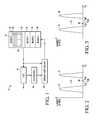
- FIG. 1is an NVM system according to an embodiment
- FIG. 2is a diagram helpful in understanding the NVM system of FIG. 1 ;
- FIG. 3is a diagram helpful in understanding the NVM system of FIG. 1 ;
- FIG. 4is a flow chart helpful in understanding the NVM system of FIG. 1
- ECCerror correction code
- NVMnon-volatile memory
- ECCerror correction code
- NVMnon-volatile memory
- NVMnon-volatile memory
- ECCerror correction code
- ECC record 16a memory controller 18
- NVM array 12includes a plurality of blocks including a block 20 that is shown as block 0 , a block 22 that is shown block 1 , a block 24 that is shown as block 2 , and a block 26 that is shown as block 3 .
- Memory controller 18is coupled to NVM array 12 and ECC record 16 .
- ECC unit 14is coupled to NVM array 12 and ECC record 16 .
- Blocks 20 , 22 , 24 , and 26each have a plurality of memory cells arranged in a plurality of ECC segments.
- Block 20is an exemplary block having a plurality of ECC segments 25 each having data bits and ECC bits.
- Exemplary data bits 27 and exemplary ECC bits 28form a single ECC segment.
- An ECC segmentis the unit, or subset, of a block in which error correction or detection occurs for the data within the ECC segment.
- a typical ECC approachis capable of correcting a single-bit error and detecting a double-bit error in an ECC segment.
- all of the memory cellsare erased at the same time but are programmed in ECC segments, which may be two segments at a time but less than the whole block.
- ECC bits 28correspond to data bits 27 and store information relative to data bits 27 and in this way for set of data bits there is a corresponding set of ECC bits that store information relative to its corresponding data bits. It is typical of NVMs that are flash memories that the erase operation is by block but the program is by segments.
- Memory controller 18controls the operation of NVM array 12 such as controlling the block erase operations, reading, and segment programming.
- ECC unit 14receives the output of NVM array 12 , corrects errors, and provides a corrected output.
- ECC unit 14also provides information to ECC record 16 as to which locations in NVM array needed correcting and information about those corrections.
- ECC record 16is preferably stored in non-volatile memory and may be in a reserved portion of NVM array 12 .
- userstypically during programming operation, users only need to specify the data bits 27 to be programmed, and the corresponding ECC bits 28 will be calculated by the ECC unit and then programmed together with the data bits.
- Memory controller 18has access to the information stored in ECC record 16 .
- FIG. 2Shown in FIG. 2 is a gate voltage distribution 32 of bits before a program operation of one of blocks 20 , 22 , 24 , and 26 and a distribution 30 of bits after a portion of the program operation.
- Distribution 32shows the initial state of the ECC segments to be programmed in which all of the bits of the segment are at an erases state. The distribution is desirably tight.
- the program operationis performed as pluralities of program pulses to raise a threshold voltage of the bits of the ECC segments of the block being programmed to a sufficiently high threshold voltage so that the gate voltage Vg at which they conduct a specified current is above the normal program verify level which is referenced as normal program verify Vgp.
- a first stepis applying a first group of consecutive program pulses to a portion of the block which may be two ECC segments.
- the bit cells in the segmentsare tested to verify that they have been properly programmed by which the gate voltage Vg for conducting the specified current is above normal program verify Vgp. This testing of the bit cells may be referenced as a program verify.
- subsequent steps of applying pulsesare performed.
- the subsequent stepsmay have the same number of pulses for the same duration and at the same voltage.
- the subsequent program stepscan be the same or different as to the number of pulses, the time duration, and the voltage.
- Distribution 30is considered programmed because all of the bits in distribution 30 have a threshold voltage that results, with an applied gate voltage at normal program verify Vgp, in no more than a specified current being conducted.
- the bits of distribution 30may thus be referenced as being above the normal program verify voltage Vgp.
- the gate voltage Vg that is applied to the bit cells during a normal read operation of NVM system 10is between an erase verify voltage Vge and program verify voltage Vgp and is chosen based upon the optimum for performing a read that distinguishes between the programmed and erased states of the bits as well as ensure sufficient margin for data retention.
- the erased bitsshould be in a state in which the current should be above a predetermined current by some margin when the gate voltage Vg is applied as the read voltage during normal read operation and the programmed bits should provide a current below the predetermined current by some margin when the gate voltage Vg is applied as the read voltage for normal read operation.
- bit 34there is also a bit 34 that is not above voltage Vgp arising from the first step in the program operation and thus is not sufficiently programmed for testing based upon applying the normal program verify voltage Vgp as the verify gate voltage Vg.
- Another program verifyis performed with the applied gate voltage of a reduced voltage of Vgr which is lower than program verify voltage Vgp by a predetermined difference which may be 500 millivolts.
- the relaxed program verify voltage Vgrshould be higher than the normal read gate voltage.
- the relaxed program verifyis an easier test than the normal program verify in that bits with a lower threshold voltage can conduct the specified current because of the lowered voltage Vgr being applied as the gate voltage Vg.
- Using lowered voltage Vgr as the verify gate voltage Vgmay be referenced as a relaxed program verify.
- bit 34passes the relaxed program verify.
- FIG. 3Shown in FIG. 3 is for the case where distribution 36 corresponds to the distribution of ECC segments after a program operation starting from an erased distribution 32 that is the same as distribution 32 of FIG. 2 , but with the result that there is a bit 38 that not only does not pass the normal program verify based on normal program voltage Vgp but also does not pass the relaxed program verify based on relaxed program voltage Vgr.
- the difference between FIG. 2 and FIG. 3then is that the single bit 38 that does not pass the normal program verify in FIG. 3 also does not pass the relaxed program verify.
- the only bit, bit 38that does not pass the relaxed verify after the first program steps can be expected to require more further programming than will be required to sufficiently program bit 34 in FIG. 2 . Therefore, for bit 38 in FIG.
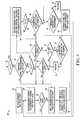
- FIG. 4Shown in FIG. 4 is a flow diagram 50 that shows how to address the single bit slow-to-program situations of FIGS. 2 and 3 .
- Flow diagram 50includes steps 52 , 54 , 56 , 58 , 60 , 62 , 64 , 66 , 68 , 70 , 72 , 74 , 78 , 80 , 82 , 84 , 86 , 88 , and 89 .
- program operationstart which includes initializing the address and the program pulse count. The pulse count would normally be initialized to zero, and the address would be initialized to the first ECC segment to be programmed.
- Step 54is performing a program verify of the current segment at the normal program verify level which is Vgp.
- step 56if the answer is yes, that verification has passed, and the process continues with a determination at step 78 if there is another ECC segment to program. If not at step 78 , then the process ends with program done at step 82 .
- step 78the process continues with a step 80 with the programming progressing to the next ECC segment. If the answer is no at step 56 that verification did not pass, a programming pulse is applied and the pulse count is incremented at step 58 . In effect when step 78 is the next step, then the programming of that segment is considered successful.
- a program verifyis then performed at step 60 with the verification occurring at the normal verify level of Vgp.
- This stepidentifies the number of failing bits (A) for normal verification. If at step 62 , the number of failing bits is zero, which means that current ECC segment has been programmed successfully, the process continues with step 78 and then step 82 if there are no more ECC segments to program and with steps 78 and 80 if there are more ECC segments to program. If there is at least one failed bit from the normal program verify at step 60 , the process continues to step 64 to determine, before starting performing the relaxed program verify, if a predetermined number of pulses have been reached. If not, the process continues to step 58 with the application of another program pulse.
- step 78If not, then the segment is considered as a pass, which is possible because the ECC can be relied upon to correct the single failing bit during normal read operations, and the process continues with step 78 and then either to step 80 or step 82 . If the determination at step 88 is that ECC correction has occurred in the current ECC segment, then the next step is a determination at step 89 if the maximum pulse count has been reached. If not, the process continues by applying another programming pulse at step 58 . This is the case because the ECC circuits have already been used to correct another single-bit issue so that ECC can no longer be relied upon to correct the single slow-to-program failing bit on the current ECC segment. Thus it is necessary to keep applying program pulses to move the single failing bit above the normal program verify level.
- ECC correction capabilitycan be at block level instead of at segment level although for an actual correction it is at the segment level. For example, there may be cases where the total number of ECC corrections occurred in a block can be important. Thus, instead of simply determining that no ECC correction has been done, it may also be beneficial to determine the total number of ECC corrections made on an entire block
- a memory blockhas been through a program operation that takes advantage of knowing the most likely situation of a single failed bit and taking advantage of the available ECC. This is especially true at the segment level. For example, a segment may have 64 bits of data with 8 bits of corresponding ECC. If the ECC is not to be otherwise required and there is a single slow bit during program, then the ECC can be relied upon to handle the situation. If the single slow bit is close to passing, then programming may continue with the expectation that it will ultimately pass. If the single slow bit is far from passing, then there is not likely to be a success in continuing the program process so the subsequent program steps need not be performed if the ECC can be relied upon with a very high degree of confidence to correct the error.
- Another approachis to not perform the ECC check during program verify, but consider the program operation successful if only one bit fails at normal program verify level and only one bit fails at the relaxed program verify level, or only one bit fails at normal program verify level but the number of program pulse count reaches the maximum program pulse count limit. ECC would still be performed during normal read operation to correct the failed bit. Correction may be possible for any programming operation for any segment in which there is only one bit that fails to program and that the ECC bits for that segment are not otherwise needed.
- a semiconductor memory storage devicethat includes an array of non-volatile memory (NVM) bit cells, wherein the array of NVM bit cells is partitioned in one or more blocks.
- the Semiconductor memory storage devicefurther includes a memory controller coupled to the array of NVM bit cells.
- the Semiconductor memory storage devicefurther includes an error correction code (ECC) unit coupled to the array and the memory controller.
- ECCerror correction code
- the memory controlleris configured to, during a program operation of a subset of one of the blocks, consider the program operation to be successful when a first program verify operation detects only one of the NVM bit cells fails to program verify at a normal program verify voltage level and when a second program verify operation detects the one of the NVM bit cells fails to program verify at a relaxed program verify voltage level, wherein the relaxed program verify voltage level is less than the normal program verify voltage level and higher than a normal read voltage level.
- the semiconductor memory storage devicemay have a further characterization by which the program operation is considered to be successful if the ECC unit did not previously perform a correction on the subset that is being programmed.
- the semiconductor memory storage devicemay have a further characterization by which wherein during the program operation which comprises program pulses, the first and second program verify operations are performed after each program pulse or group of program pulses.
- the semiconductor memory storage devicemay have a further characterization by which a predetermined number of program pulses are performed by the memory controller before counting a number of NVM bit cells that failed the first program verify operation.
- the semiconductor memory storage devicemay have a further characterization by which the predetermined number of program pulses is between 2 and 10 program pulses.
- the semiconductor memory storage devicemay have a further characterization by which the second program verify operation is performed when the first program verify operation detects only one of the NVM cells fails to program verify at the normal program verify voltage level.
- the semiconductor memory storage devicemay have a further characterization by which the program operation is considered successful if the ECC unit did not previously perform a correction on the one of the blocks that includes the one of the NVM bit cells that failed to program verify at the relaxed program verify voltage level.
- the semiconductor memory storage devicemay have a further characterization by which the memory controller is configured to, during the program operation on the one of the blocks when the first program verify operation detects only one of the NVM bit cells fails to program verify at the normal program verify voltage level and the second program verify operation detects all of the NVM bit cells successfully programmed at the relaxed program verify voltage level, consider the program operation to be successful if a maximum number of program pulses is reached.
- the semiconductor memory storage devicemay have a further characterization by which the program operation is considered to be successful by the memory controller if the ECC unit did not previously perform a correction on the subset that includes the one of the NVM bit cells that failed to program verify at the normal program verify voltage level.
- the semiconductor memory storage devicemay have a further characterization by which wherein the program operation is considered to not be successful if the ECC unit previously performed a correction on the one of the blocks that includes the one of the NVM bit cells that failed to program verify at the normal program verify voltage level.
- the semiconductor memory storage devicemay further include an ECC record containing one or more ECC indicators stored in non-volatile memory, wherein one of the ECC indicators is allocated to the subset and indicates whether an ECC correction has been performed on the subset.
- the methodfurther includes performing a program operation on a subset of an array of non-volatile bit cells and designating the program operation as successful when a maximum number of program pulses is reached if during the program operation a first program verify operation detects only one of the non-volatile bit cells fails to program verify at a normal program verify voltage level and a second program verify operation detects all of the non-volatile bit cells successfully programmed at a relaxed program verify voltage level, wherein the relaxed program verify voltage level is lower than the normal program verify voltage level.
- the methodmay further include designating the program operation as successful during the program operation when the first program verify operation detects that only one of the non-volatile bit cells fails to program verify at the normal program verify voltage level and when the second program verify operation detects that one of the non-volatile bit cells fails to program verify at the relaxed program verify voltage level.
- the methodmay further include designating the program operation as successful if an Error Correction Code (ECC) correction was not previously performed on the subset of non-volatile bit cells that is being programmed.
- ECCError Correction Code
- the methodmay have a further characterization by which the program operation is considered successful if the ECC unit did not previously perform a correction on the subset that includes the one of the non-volatile bit cells that failed to program verify at the relaxed program verify voltage level, during the program operation, the first and second verify operations are performed after each program pulse or group of program pulses.
- the methodmay have a further characterization by which.
- the methodmay further include designating the program operation as successful if an Error Correction Code (ECC) correction was not previously performed on the subset of the non-volatile bit cells that includes the bit cell that failed to program verify at the normal program verify voltage level and the relaxed program verify voltage level.
- ECCError Correction Code
- the methodmay further include designating the program operation as successful if an Error Correction Code (ECC) unit did not previously perform a correction on the subset that includes the one of the non-volatile bit cells that failed to program verify at the relaxed program verify voltage level and the relaxed program verify voltage level.
- ECCError Correction Code
- the methodincludes determining a number of bit cells that failed to program verify during a program operation, wherein the bit cells are included in a subset of bit cells in an array of bit cells.
- the methodfurther includes determining whether an Error Correction Code (ECC) correction has been previously performed for the subset of bit cells.
- ECCError Correction Code
- the methodfurther includes allowing the program operation to be considered successful if the number of bit cells that failed to program verify after a predetermined number of program pulses is below a threshold number and the ECC correction has not been performed for the subset of bit cells.
- the methodmay further include, during the program operation on the subset of the bit cells, when the first program verify operation detects a predetermined number of the bit cells fails to program verify at the normal program verify voltage level and when the second program verify operation detects another predetermined number of the bit cells fails to program verify at the relaxed program verify voltage level, designating the program operation as successful.
- Coupledis not intended to be limited to a direct coupling or a mechanical coupling.
Landscapes
- Engineering & Computer Science (AREA)
- Theoretical Computer Science (AREA)
- Physics & Mathematics (AREA)
- Quality & Reliability (AREA)
- General Engineering & Computer Science (AREA)
- General Physics & Mathematics (AREA)
- Probability & Statistics with Applications (AREA)
- Read Only Memory (AREA)
- For Increasing The Reliability Of Semiconductor Memories (AREA)
Abstract
Description
Claims (20)
Priority Applications (5)
| Application Number | Priority Date | Filing Date | Title |
|---|---|---|---|
| US13/674,367US9225356B2 (en) | 2012-11-12 | 2012-11-12 | Programming a non-volatile memory (NVM) system having error correction code (ECC) |
| JP2013226683AJP2014096196A (en) | 2012-11-12 | 2013-10-31 | Programming non-volatile memory (nvm) system having error correction code (ecc) |
| TW102140339ATW201432705A (en) | 2012-11-12 | 2013-11-06 | Programming a non-volatile memory (NVM) system having error correction code (ECC) |
| KR1020130136426AKR102143325B1 (en) | 2012-11-12 | 2013-11-11 | Programming a non-volatile memory(nvm) system having error correction code(ecc) |
| CN201310559366.8ACN103810055B (en) | 2012-11-12 | 2013-11-12 | Programming has error-correcting code(ECC)Nonvolatile memory(NVM)System |
Applications Claiming Priority (1)
| Application Number | Priority Date | Filing Date | Title |
|---|---|---|---|
| US13/674,367US9225356B2 (en) | 2012-11-12 | 2012-11-12 | Programming a non-volatile memory (NVM) system having error correction code (ECC) |
Publications (2)
| Publication Number | Publication Date |
|---|---|
| US20140136928A1 US20140136928A1 (en) | 2014-05-15 |
| US9225356B2true US9225356B2 (en) | 2015-12-29 |
Family
ID=50682944
Family Applications (1)
| Application Number | Title | Priority Date | Filing Date |
|---|---|---|---|
| US13/674,367Active2033-06-27US9225356B2 (en) | 2012-11-12 | 2012-11-12 | Programming a non-volatile memory (NVM) system having error correction code (ECC) |
Country Status (5)
| Country | Link |
|---|---|
| US (1) | US9225356B2 (en) |
| JP (1) | JP2014096196A (en) |
| KR (1) | KR102143325B1 (en) |
| CN (1) | CN103810055B (en) |
| TW (1) | TW201432705A (en) |
Cited By (5)
| Publication number | Priority date | Publication date | Assignee | Title |
|---|---|---|---|---|
| US10147495B2 (en) | 2016-11-30 | 2018-12-04 | Samsung Electronics Co., Ltd. | Nonvolatile memory device generating loop status information, storage device including the same, and operating method thereof |
| US10216571B2 (en) | 2016-11-10 | 2019-02-26 | Western Digital Technologies, Inc. | System and methodology for error management within a shared non-volatile memory architecture using bloom filters |
| US10254982B2 (en) | 2016-11-10 | 2019-04-09 | Western Digital Technologies, Inc. | System and methodology for low latency error management within a shared non-volatile memory architecture |
| KR20190115765A (en)* | 2018-04-03 | 2019-10-14 | 에스케이하이닉스 주식회사 | Memory device, memory system including the same and method of operating the same |
| US10514867B2 (en) | 2016-11-10 | 2019-12-24 | Western Digital Technologies, Inc. | System and methodology that facilitates error management within a shared non-volatile memory architecture |
Families Citing this family (13)
| Publication number | Priority date | Publication date | Assignee | Title |
|---|---|---|---|---|
| CN108255633B (en)* | 2016-12-28 | 2021-07-30 | 旺宏电子股份有限公司 | Storage control method and storage device |
| EP3388979B1 (en) | 2017-04-14 | 2020-07-22 | Nxp B.V. | Rfid integrated circuit |
| US10402272B2 (en)* | 2017-05-25 | 2019-09-03 | Micron Technology, Inc. | Memory device with dynamic programming calibration |
| US10140040B1 (en) | 2017-05-25 | 2018-11-27 | Micron Technology, Inc. | Memory device with dynamic program-verify voltage calibration |
| US10452480B2 (en) | 2017-05-25 | 2019-10-22 | Micron Technology, Inc. | Memory device with dynamic processing level calibration |
| US10566063B2 (en) | 2018-05-16 | 2020-02-18 | Micron Technology, Inc. | Memory system with dynamic calibration using a trim management mechanism |
| US10664194B2 (en) | 2018-05-16 | 2020-05-26 | Micron Technology, Inc. | Memory system with dynamic calibration using a variable adjustment mechanism |
| US10990466B2 (en) | 2018-06-20 | 2021-04-27 | Micron Technology, Inc. | Memory sub-system with dynamic calibration using component-based function(s) |
| US11188416B2 (en) | 2018-07-12 | 2021-11-30 | Micron Technology, Inc. | Enhanced block management for a memory sub-system |
| US11113129B2 (en) | 2018-07-13 | 2021-09-07 | Micron Technology, Inc. | Real time block failure analysis for a memory sub-system |
| US10936246B2 (en) | 2018-10-10 | 2021-03-02 | Micron Technology, Inc. | Dynamic background scan optimization in a memory sub-system |
| US11475170B2 (en)* | 2019-05-28 | 2022-10-18 | Nuvoton Technology Corporation | System and method for correction of memory errors |
| CN113764026A (en)* | 2020-04-08 | 2021-12-07 | 长江存储科技有限责任公司 | A kind of programming operation method of three-dimensional memory, memory device |
Citations (21)
| Publication number | Priority date | Publication date | Assignee | Title |
|---|---|---|---|---|
| US5579262A (en) | 1996-02-05 | 1996-11-26 | Integrated Silicon Solution, Inc. | Program verify and erase verify control circuit for EPROM/flash |
| US5995417A (en) | 1998-10-20 | 1999-11-30 | Advanced Micro Devices, Inc. | Scheme for page erase and erase verify in a non-volatile memory array |
| US6967873B2 (en) | 2003-10-02 | 2005-11-22 | Advanced Micro Devices, Inc. | Memory device and method using positive gate stress to recover overerased cell |
| US20060133141A1 (en) | 2004-12-22 | 2006-06-22 | Gorobets Sergey A | Erased sector detection mechanisms |
| US7092290B2 (en) | 2004-11-16 | 2006-08-15 | Sandisk Corporation | High speed programming system with reduced over programming |
| US7158416B2 (en) | 2005-03-15 | 2007-01-02 | Infineon Technologies Flash Gmbh & Co. Kg | Method for operating a flash memory device |
| US7177199B2 (en) | 2003-10-20 | 2007-02-13 | Sandisk Corporation | Behavior based programming of non-volatile memory |
| US20080089135A1 (en) | 2006-10-13 | 2008-04-17 | Fumitoshi Ito | Systems for partitioned erase and erase verification in non-volatile memory |
| US7400537B2 (en) | 2005-03-31 | 2008-07-15 | Sandisk Corporation | Systems for erasing non-volatile memory using individual verification and additional erasing of subsets of memory cells |
| US20080291739A1 (en)* | 2007-05-21 | 2008-11-27 | Samsung Electronics Co., Ltd. | Methods of programming non-volatile semiconductor memory devices using different program verification operations and related devices |
| US20090168544A1 (en) | 2007-12-28 | 2009-07-02 | Hynix Semiconductor Inc. | Erase method and soft programming method of non-volatile memory device |
| US7619930B2 (en) | 2007-02-20 | 2009-11-17 | Sandisk Corporation | Dynamic verify based on threshold voltage distribution |
| US7778084B2 (en)* | 2007-02-27 | 2010-08-17 | Samsung Electronics Co., Ltd. | Non-volatile memory devices and operating methods thereof |
| US7808829B2 (en) | 2007-03-27 | 2010-10-05 | Hynix Semiconductor Inc. | Flash memory device capable of overcoming fast program/slow erase phenomenon and erase method thereof |
| US7859922B2 (en)* | 2006-03-07 | 2010-12-28 | Micron Technology, Inc. | Programming a flash memory device |
| US7889592B2 (en)* | 2007-07-23 | 2011-02-15 | Samsung Electronics Co., Ltd. | Non-volatile memory device and a method of programming the same |
| US8064267B2 (en) | 2008-11-14 | 2011-11-22 | Micron Technology, Inc. | Erase voltage reduction in a non-volatile memory device |
| US8077513B2 (en)* | 2009-09-24 | 2011-12-13 | Macronix International Co., Ltd. | Method and apparatus for programming a multi-level memory |
| US20120140566A1 (en)* | 2010-12-02 | 2012-06-07 | Seiichi Aritome | Programming method of non-volatile memory device |
| US20120201082A1 (en) | 2011-02-09 | 2012-08-09 | Freescale Semiconductor, Inc. | Erase ramp pulse width control for non-volatile memory |
| US8713406B2 (en)* | 2012-04-30 | 2014-04-29 | Freescale Semiconductor, Inc. | Erasing a non-volatile memory (NVM) system having error correction code (ECC) |
Family Cites Families (8)
| Publication number | Priority date | Publication date | Assignee | Title |
|---|---|---|---|---|
| JP4220319B2 (en)* | 2003-07-04 | 2009-02-04 | 株式会社東芝 | Nonvolatile semiconductor memory device and subblock erasing method thereof |
| US6917542B2 (en)* | 2003-07-29 | 2005-07-12 | Sandisk Corporation | Detecting over programmed memory |
| US7954037B2 (en)* | 2005-10-25 | 2011-05-31 | Sandisk Il Ltd | Method for recovering from errors in flash memory |
| US7236402B2 (en)* | 2005-11-30 | 2007-06-26 | Freescale Semiconductor, Inc. | Method and apparatus for programming/erasing a non-volatile memory |
| US7904788B2 (en)* | 2006-11-03 | 2011-03-08 | Sandisk Corporation | Methods of varying read threshold voltage in nonvolatile memory |
| WO2010054410A2 (en)* | 2008-11-10 | 2010-05-14 | Fusion Multisystems, Inc. (Dba Fusion-Io) | Apparatus, system, and method for predicting failures in solid-state storage |
| JP2011258260A (en) | 2010-06-07 | 2011-12-22 | Toshiba Corp | Nonvolatile semiconductor memory device |
| JP2012069180A (en)* | 2010-09-21 | 2012-04-05 | Toshiba Corp | Semiconductor storage device |
- 2012
- 2012-11-12USUS13/674,367patent/US9225356B2/enactiveActive
- 2013
- 2013-10-31JPJP2013226683Apatent/JP2014096196A/enactivePending
- 2013-11-06TWTW102140339Apatent/TW201432705A/enunknown
- 2013-11-11KRKR1020130136426Apatent/KR102143325B1/enactiveActive
- 2013-11-12CNCN201310559366.8Apatent/CN103810055B/enactiveActive
Patent Citations (23)
| Publication number | Priority date | Publication date | Assignee | Title |
|---|---|---|---|---|
| US5579262A (en) | 1996-02-05 | 1996-11-26 | Integrated Silicon Solution, Inc. | Program verify and erase verify control circuit for EPROM/flash |
| US5995417A (en) | 1998-10-20 | 1999-11-30 | Advanced Micro Devices, Inc. | Scheme for page erase and erase verify in a non-volatile memory array |
| US6967873B2 (en) | 2003-10-02 | 2005-11-22 | Advanced Micro Devices, Inc. | Memory device and method using positive gate stress to recover overerased cell |
| US7177199B2 (en) | 2003-10-20 | 2007-02-13 | Sandisk Corporation | Behavior based programming of non-volatile memory |
| US7092290B2 (en) | 2004-11-16 | 2006-08-15 | Sandisk Corporation | High speed programming system with reduced over programming |
| US20060133141A1 (en) | 2004-12-22 | 2006-06-22 | Gorobets Sergey A | Erased sector detection mechanisms |
| US7158416B2 (en) | 2005-03-15 | 2007-01-02 | Infineon Technologies Flash Gmbh & Co. Kg | Method for operating a flash memory device |
| US7400537B2 (en) | 2005-03-31 | 2008-07-15 | Sandisk Corporation | Systems for erasing non-volatile memory using individual verification and additional erasing of subsets of memory cells |
| US7859922B2 (en)* | 2006-03-07 | 2010-12-28 | Micron Technology, Inc. | Programming a flash memory device |
| US20080089135A1 (en) | 2006-10-13 | 2008-04-17 | Fumitoshi Ito | Systems for partitioned erase and erase verification in non-volatile memory |
| US7619930B2 (en) | 2007-02-20 | 2009-11-17 | Sandisk Corporation | Dynamic verify based on threshold voltage distribution |
| US7778084B2 (en)* | 2007-02-27 | 2010-08-17 | Samsung Electronics Co., Ltd. | Non-volatile memory devices and operating methods thereof |
| US7808829B2 (en) | 2007-03-27 | 2010-10-05 | Hynix Semiconductor Inc. | Flash memory device capable of overcoming fast program/slow erase phenomenon and erase method thereof |
| US20080291739A1 (en)* | 2007-05-21 | 2008-11-27 | Samsung Electronics Co., Ltd. | Methods of programming non-volatile semiconductor memory devices using different program verification operations and related devices |
| US7889592B2 (en)* | 2007-07-23 | 2011-02-15 | Samsung Electronics Co., Ltd. | Non-volatile memory device and a method of programming the same |
| US20090168544A1 (en) | 2007-12-28 | 2009-07-02 | Hynix Semiconductor Inc. | Erase method and soft programming method of non-volatile memory device |
| US8064267B2 (en) | 2008-11-14 | 2011-11-22 | Micron Technology, Inc. | Erase voltage reduction in a non-volatile memory device |
| US8391080B2 (en) | 2008-11-14 | 2013-03-05 | Micron Technology, Inc. | Erase voltage reduction in a non-volatile memory device |
| US8077513B2 (en)* | 2009-09-24 | 2011-12-13 | Macronix International Co., Ltd. | Method and apparatus for programming a multi-level memory |
| US20120140566A1 (en)* | 2010-12-02 | 2012-06-07 | Seiichi Aritome | Programming method of non-volatile memory device |
| US8493792B2 (en)* | 2010-12-02 | 2013-07-23 | Hynix Semiconductor Inc. | Programming method of non-volatile memory device |
| US20120201082A1 (en) | 2011-02-09 | 2012-08-09 | Freescale Semiconductor, Inc. | Erase ramp pulse width control for non-volatile memory |
| US8713406B2 (en)* | 2012-04-30 | 2014-04-29 | Freescale Semiconductor, Inc. | Erasing a non-volatile memory (NVM) system having error correction code (ECC) |
Cited By (5)
| Publication number | Priority date | Publication date | Assignee | Title |
|---|---|---|---|---|
| US10216571B2 (en) | 2016-11-10 | 2019-02-26 | Western Digital Technologies, Inc. | System and methodology for error management within a shared non-volatile memory architecture using bloom filters |
| US10254982B2 (en) | 2016-11-10 | 2019-04-09 | Western Digital Technologies, Inc. | System and methodology for low latency error management within a shared non-volatile memory architecture |
| US10514867B2 (en) | 2016-11-10 | 2019-12-24 | Western Digital Technologies, Inc. | System and methodology that facilitates error management within a shared non-volatile memory architecture |
| US10147495B2 (en) | 2016-11-30 | 2018-12-04 | Samsung Electronics Co., Ltd. | Nonvolatile memory device generating loop status information, storage device including the same, and operating method thereof |
| KR20190115765A (en)* | 2018-04-03 | 2019-10-14 | 에스케이하이닉스 주식회사 | Memory device, memory system including the same and method of operating the same |
Also Published As
| Publication number | Publication date |
|---|---|
| JP2014096196A (en) | 2014-05-22 |
| CN103810055B (en) | 2018-06-26 |
| US20140136928A1 (en) | 2014-05-15 |
| KR102143325B1 (en) | 2020-08-12 |
| TW201432705A (en) | 2014-08-16 |
| KR20140061265A (en) | 2014-05-21 |
| CN103810055A (en) | 2014-05-21 |
Similar Documents
| Publication | Publication Date | Title |
|---|---|---|
| US9225356B2 (en) | Programming a non-volatile memory (NVM) system having error correction code (ECC) | |
| TWI574277B (en) | Error correction operations in a memory device | |
| CN105359218B (en) | Programming non-volatile memory data save | |
| JP5236949B2 (en) | Erased sector detection mechanism | |
| US9330783B1 (en) | Identifying word-line-to-substrate and word-line-to-word-line short-circuit events in a memory block | |
| US20080158989A1 (en) | Retention margin program verification | |
| US20140075259A1 (en) | On chip data recovery for non-volatile storage | |
| US8995202B2 (en) | Test flow to detect a latent leaky bit of a non-volatile memory | |
| US10115476B2 (en) | Advanced programming verification schemes for memory cells | |
| US9342401B2 (en) | Selective in-situ retouching of data in nonvolatile memory | |
| US9329921B2 (en) | Imminent read failure detection using high/low read voltage levels | |
| US9490024B1 (en) | Solid state storage device and reading control method thereof | |
| US9343172B2 (en) | Extended protection for embedded erase of non-volatile memory cells | |
| EP2667382B1 (en) | Erasing a non-volatile memory (NVM) system having error correction code (ECC) | |
| US20160012916A1 (en) | Semiconductor memory device and memory system | |
| US9378829B2 (en) | Non-volatile memory device with an EPLI comparator | |
| TWI602055B (en) | Semiconductor memory device and programming method thereof | |
| US9378809B1 (en) | Relaxing verification conditions in memory programming and erasure operations | |
| CN109215716B (en) | Method and device for improving reliability of NAND type floating gate memory | |
| US8923068B2 (en) | Low margin read operation with CRC comparision | |
| TW200841342A (en) | Retention margin program verification | |
| JP2006190488A (en) | Write-in method in semiconductor memory device |
Legal Events
| Date | Code | Title | Description |
|---|---|---|---|
| AS | Assignment | Owner name:FREESCALE SEMICONDUCTOR, INC., TEXAS Free format text:ASSIGNMENT OF ASSIGNORS INTEREST;ASSIGNORS:MU, FUCHEN;HE, CHEN;REEL/FRAME:029280/0838 Effective date:20121108 | |
| AS | Assignment | Owner name:CITIBANK, N.A., AS NOTES COLLATERAL AGENT, NEW YORK Free format text:SUPPLEMENT TO IP SECURITY AGREEMENT;ASSIGNOR:FREESCALE SEMICONDUCTOR, INC.;REEL/FRAME:030258/0558 Effective date:20130214 Owner name:CITIBANK, N.A., AS NOTES COLLATERAL AGENT, NEW YORK Free format text:SUPPLEMENT TO IP SECURITY AGREEMENT;ASSIGNOR:FREESCALE SEMICONDUCTOR, INC.;REEL/FRAME:030258/0523 Effective date:20130214 Owner name:CITIBANK, N.A., AS NOTES COLLATERAL AGENT, NEW YOR Free format text:SUPPLEMENT TO IP SECURITY AGREEMENT;ASSIGNOR:FREESCALE SEMICONDUCTOR, INC.;REEL/FRAME:030258/0523 Effective date:20130214 Owner name:CITIBANK, N.A., AS NOTES COLLATERAL AGENT, NEW YOR Free format text:SUPPLEMENT TO IP SECURITY AGREEMENT;ASSIGNOR:FREESCALE SEMICONDUCTOR, INC.;REEL/FRAME:030258/0558 Effective date:20130214 Owner name:CITIBANK, N.A., AS COLLATERAL AGENT, NEW YORK Free format text:SUPPLEMENT TO IP SECURITY AGREEMENT;ASSIGNOR:FREESCALE SEMICONDUCTOR, INC.;REEL/FRAME:030258/0540 Effective date:20130214 | |
| AS | Assignment | Owner name:CITIBANK, N.A., AS NOTES COLLATERAL AGENT, NEW YORK Free format text:SECURITY AGREEMENT;ASSIGNOR:FREESCALE SEMICONDUCTOR, INC.;REEL/FRAME:030633/0424 Effective date:20130521 Owner name:CITIBANK, N.A., AS NOTES COLLATERAL AGENT, NEW YOR Free format text:SECURITY AGREEMENT;ASSIGNOR:FREESCALE SEMICONDUCTOR, INC.;REEL/FRAME:030633/0424 Effective date:20130521 | |
| AS | Assignment | Owner name:CITIBANK, N.A., AS NOTES COLLATERAL AGENT, NEW YORK Free format text:SECURITY AGREEMENT;ASSIGNOR:FREESCALE SEMICONDUCTOR, INC.;REEL/FRAME:031591/0266 Effective date:20131101 Owner name:CITIBANK, N.A., AS NOTES COLLATERAL AGENT, NEW YOR Free format text:SECURITY AGREEMENT;ASSIGNOR:FREESCALE SEMICONDUCTOR, INC.;REEL/FRAME:031591/0266 Effective date:20131101 | |
| STCF | Information on status: patent grant | Free format text:PATENTED CASE | |
| AS | Assignment | Owner name:FREESCALE SEMICONDUCTOR, INC., TEXAS Free format text:PATENT RELEASE;ASSIGNOR:CITIBANK, N.A., AS COLLATERAL AGENT;REEL/FRAME:037357/0685 Effective date:20151207 Owner name:FREESCALE SEMICONDUCTOR, INC., TEXAS Free format text:PATENT RELEASE;ASSIGNOR:CITIBANK, N.A., AS COLLATERAL AGENT;REEL/FRAME:037357/0671 Effective date:20151207 | |
| AS | Assignment | Owner name:MORGAN STANLEY SENIOR FUNDING, INC., MARYLAND Free format text:ASSIGNMENT AND ASSUMPTION OF SECURITY INTEREST IN PATENTS;ASSIGNOR:CITIBANK, N.A.;REEL/FRAME:037486/0517 Effective date:20151207 | |
| AS | Assignment | Owner name:MORGAN STANLEY SENIOR FUNDING, INC., MARYLAND Free format text:ASSIGNMENT AND ASSUMPTION OF SECURITY INTEREST IN PATENTS;ASSIGNOR:CITIBANK, N.A.;REEL/FRAME:037518/0292 Effective date:20151207 | |
| AS | Assignment | Owner name:FREESCALE SEMICONDUCTOR, INC., TEXAS Free format text:PATENT RELEASE;ASSIGNOR:CITIBANK, N.A., AS COLLATERAL AGENT;REEL/FRAME:037494/0312 Effective date:20151207 | |
| AS | Assignment | Owner name:MORGAN STANLEY SENIOR FUNDING, INC., MARYLAND Free format text:SUPPLEMENT TO THE SECURITY AGREEMENT;ASSIGNOR:FREESCALE SEMICONDUCTOR, INC.;REEL/FRAME:039138/0001 Effective date:20160525 | |
| AS | Assignment | Owner name:NXP, B.V., F/K/A FREESCALE SEMICONDUCTOR, INC., NETHERLANDS Free format text:RELEASE BY SECURED PARTY;ASSIGNOR:MORGAN STANLEY SENIOR FUNDING, INC.;REEL/FRAME:040925/0001 Effective date:20160912 Owner name:NXP, B.V., F/K/A FREESCALE SEMICONDUCTOR, INC., NE Free format text:RELEASE BY SECURED PARTY;ASSIGNOR:MORGAN STANLEY SENIOR FUNDING, INC.;REEL/FRAME:040925/0001 Effective date:20160912 | |
| AS | Assignment | Owner name:NXP B.V., NETHERLANDS Free format text:RELEASE BY SECURED PARTY;ASSIGNOR:MORGAN STANLEY SENIOR FUNDING, INC.;REEL/FRAME:040928/0001 Effective date:20160622 | |
| AS | Assignment | Owner name:NXP USA, INC., TEXAS Free format text:MERGER;ASSIGNOR:FREESCALE SEMICONDUCTOR, INC.;REEL/FRAME:041144/0363 Effective date:20161107 | |
| AS | Assignment | Owner name:MORGAN STANLEY SENIOR FUNDING, INC., MARYLAND Free format text:CORRECTIVE ASSIGNMENT TO CORRECT THE REMOVE PATENTS 8108266 AND 8062324 AND REPLACE THEM WITH 6108266 AND 8060324 PREVIOUSLY RECORDED ON REEL 037518 FRAME 0292. ASSIGNOR(S) HEREBY CONFIRMS THE ASSIGNMENT AND ASSUMPTION OF SECURITY INTEREST IN PATENTS;ASSIGNOR:CITIBANK, N.A.;REEL/FRAME:041703/0536 Effective date:20151207 | |
| AS | Assignment | Owner name:SHENZHEN XINGUODU TECHNOLOGY CO., LTD., CHINA Free format text:CORRECTIVE ASSIGNMENT TO CORRECT THE TO CORRECT THE APPLICATION NO. FROM 13,883,290 TO 13,833,290 PREVIOUSLY RECORDED ON REEL 041703 FRAME 0536. ASSIGNOR(S) HEREBY CONFIRMS THE THE ASSIGNMENT AND ASSUMPTION OF SECURITYINTEREST IN PATENTS.;ASSIGNOR:MORGAN STANLEY SENIOR FUNDING, INC.;REEL/FRAME:048734/0001 Effective date:20190217 | |
| MAFP | Maintenance fee payment | Free format text:PAYMENT OF MAINTENANCE FEE, 4TH YEAR, LARGE ENTITY (ORIGINAL EVENT CODE: M1551); ENTITY STATUS OF PATENT OWNER: LARGE ENTITY Year of fee payment:4 | |
| AS | Assignment | Owner name:NXP B.V., NETHERLANDS Free format text:RELEASE BY SECURED PARTY;ASSIGNOR:MORGAN STANLEY SENIOR FUNDING, INC.;REEL/FRAME:050744/0097 Effective date:20190903 | |
| AS | Assignment | Owner name:MORGAN STANLEY SENIOR FUNDING, INC., MARYLAND Free format text:CORRECTIVE ASSIGNMENT TO CORRECT THE REMOVE APPLICATION11759915 AND REPLACE IT WITH APPLICATION 11759935 PREVIOUSLY RECORDED ON REEL 037486 FRAME 0517. ASSIGNOR(S) HEREBY CONFIRMS THE ASSIGNMENT AND ASSUMPTION OF SECURITYINTEREST IN PATENTS;ASSIGNOR:CITIBANK, N.A.;REEL/FRAME:053547/0421 Effective date:20151207 | |
| AS | Assignment | Owner name:NXP B.V., NETHERLANDS Free format text:CORRECTIVE ASSIGNMENT TO CORRECT THE REMOVEAPPLICATION 11759915 AND REPLACE IT WITH APPLICATION11759935 PREVIOUSLY RECORDED ON REEL 040928 FRAME 0001. ASSIGNOR(S) HEREBY CONFIRMS THE RELEASE OF SECURITYINTEREST;ASSIGNOR:MORGAN STANLEY SENIOR FUNDING, INC.;REEL/FRAME:052915/0001 Effective date:20160622 | |
| AS | Assignment | Owner name:NXP, B.V. F/K/A FREESCALE SEMICONDUCTOR, INC., NETHERLANDS Free format text:CORRECTIVE ASSIGNMENT TO CORRECT THE REMOVEAPPLICATION 11759915 AND REPLACE IT WITH APPLICATION11759935 PREVIOUSLY RECORDED ON REEL 040925 FRAME 0001. ASSIGNOR(S) HEREBY CONFIRMS THE RELEASE OF SECURITYINTEREST;ASSIGNOR:MORGAN STANLEY SENIOR FUNDING, INC.;REEL/FRAME:052917/0001 Effective date:20160912 | |
| MAFP | Maintenance fee payment | Free format text:PAYMENT OF MAINTENANCE FEE, 8TH YEAR, LARGE ENTITY (ORIGINAL EVENT CODE: M1552); ENTITY STATUS OF PATENT OWNER: LARGE ENTITY Year of fee payment:8 |