US9224648B2 - Through-wafer interconnection - Google Patents
Through-wafer interconnectionDownload PDFInfo
- Publication number
- US9224648B2 US9224648B2US13/349,436US201213349436AUS9224648B2US 9224648 B2US9224648 B2US 9224648B2US 201213349436 AUS201213349436 AUS 201213349436AUS 9224648 B2US9224648 B2US 9224648B2
- Authority
- US
- United States
- Prior art keywords
- wafer
- conductive
- conductor
- interconnect
- trench
- Prior art date
- Legal status (The legal status is an assumption and is not a legal conclusion. Google has not performed a legal analysis and makes no representation as to the accuracy of the status listed.)
- Active
Links
- 239000004020conductorSubstances0.000claimsabstractdescription250
- 239000000463materialSubstances0.000claimsabstractdescription138
- 239000003989dielectric materialSubstances0.000claimsabstractdescription13
- 239000012212insulatorSubstances0.000claimsdescription65
- 238000004377microelectronicMethods0.000claimsdescription21
- 239000000945fillerSubstances0.000claimsdescription17
- 230000002093peripheral effectEffects0.000claimsdescription9
- 238000000059patterningMethods0.000claims2
- 238000000034methodMethods0.000abstractdescription143
- 235000012431wafersNutrition0.000description195
- 238000004519manufacturing processMethods0.000description84
- XUIMIQQOPSSXEZ-UHFFFAOYSA-NSiliconChemical compound[Si]XUIMIQQOPSSXEZ-UHFFFAOYSA-N0.000description67
- 229910052710siliconInorganic materials0.000description67
- 239000010703siliconSubstances0.000description67
- 230000008569processEffects0.000description56
- 238000013461designMethods0.000description29
- 230000003647oxidationEffects0.000description19
- 238000007254oxidation reactionMethods0.000description19
- 238000005530etchingMethods0.000description15
- 239000002184metalSubstances0.000description12
- 238000003491arrayMethods0.000description9
- 238000009413insulationMethods0.000description9
- 238000004806packaging method and processMethods0.000description9
- 230000003071parasitic effectEffects0.000description7
- 230000008901benefitEffects0.000description5
- 230000015572biosynthetic processEffects0.000description5
- 238000009713electroplatingMethods0.000description5
- 238000005516engineering processMethods0.000description5
- 238000012986modificationMethods0.000description5
- 230000004048modificationEffects0.000description5
- 239000004065semiconductorSubstances0.000description5
- 239000000758substrateSubstances0.000description5
- 239000004205dimethyl polysiloxaneSubstances0.000description4
- 235000013870dimethyl polysiloxaneNutrition0.000description4
- 230000000694effectsEffects0.000description4
- CXQXSVUQTKDNFP-UHFFFAOYSA-NoctamethyltrisiloxaneChemical compoundC[Si](C)(C)O[Si](C)(C)O[Si](C)(C)CCXQXSVUQTKDNFP-UHFFFAOYSA-N0.000description4
- 230000003287optical effectEffects0.000description4
- 238000004987plasma desorption mass spectroscopyMethods0.000description4
- 229920000435poly(dimethylsiloxane)Polymers0.000description4
- 239000002131composite materialSubstances0.000description3
- 238000010292electrical insulationMethods0.000description3
- 238000011049fillingMethods0.000description3
- 150000004767nitridesChemical class0.000description3
- 238000000427thin-film depositionMethods0.000description3
- 239000004593EpoxySubstances0.000description2
- 239000004642PolyimideSubstances0.000description2
- BOTDANWDWHJENH-UHFFFAOYSA-NTetraethyl orthosilicateChemical compoundCCO[Si](OCC)(OCC)OCCBOTDANWDWHJENH-UHFFFAOYSA-N0.000description2
- 230000001413cellular effectEffects0.000description2
- 238000004891communicationMethods0.000description2
- 238000007796conventional methodMethods0.000description2
- 230000008878couplingEffects0.000description2
- 238000010168coupling processMethods0.000description2
- 238000005859coupling reactionMethods0.000description2
- 229920001971elastomerPolymers0.000description2
- 239000000499gelSubstances0.000description2
- 239000012774insulation materialSubstances0.000description2
- 230000001590oxidative effectEffects0.000description2
- 230000000704physical effectEffects0.000description2
- 229920003229poly(methyl methacrylate)Polymers0.000description2
- 229920001690polydopaminePolymers0.000description2
- 229920001721polyimidePolymers0.000description2
- 229920000642polymerPolymers0.000description2
- 239000004926polymethyl methacrylateSubstances0.000description2
- 238000012545processingMethods0.000description2
- 238000012552reviewMethods0.000description2
- 239000005060rubberSubstances0.000description2
- 230000035882stressEffects0.000description2
- 239000011800void materialSubstances0.000description2
- 229910001218Gallium arsenideInorganic materials0.000description1
- 238000013459approachMethods0.000description1
- 238000005452bendingMethods0.000description1
- 230000007423decreaseEffects0.000description1
- 230000001419dependent effectEffects0.000description1
- 238000000227grindingMethods0.000description1
- 239000011810insulating materialSubstances0.000description1
- 230000010354integrationEffects0.000description1
- 238000002955isolationMethods0.000description1
- 230000005226mechanical processes and functionsEffects0.000description1
- 238000005459micromachiningMethods0.000description1
- 238000005457optimizationMethods0.000description1
- 238000012858packaging processMethods0.000description1
- 238000005498polishingMethods0.000description1
- 230000008092positive effectEffects0.000description1
- 238000002360preparation methodMethods0.000description1
- 230000008646thermal stressEffects0.000description1
- 239000010409thin filmSubstances0.000description1
- 238000012876topographyMethods0.000description1
- 238000002604ultrasonographyMethods0.000description1
Images


Classifications
- H—ELECTRICITY
- H01—ELECTRIC ELEMENTS
- H01L—SEMICONDUCTOR DEVICES NOT COVERED BY CLASS H10
- H01L21/00—Processes or apparatus adapted for the manufacture or treatment of semiconductor or solid state devices or of parts thereof
- H01L21/70—Manufacture or treatment of devices consisting of a plurality of solid state components formed in or on a common substrate or of parts thereof; Manufacture of integrated circuit devices or of parts thereof
- H01L21/71—Manufacture of specific parts of devices defined in group H01L21/70
- H01L21/768—Applying interconnections to be used for carrying current between separate components within a device comprising conductors and dielectrics
- H01L21/76898—Applying interconnections to be used for carrying current between separate components within a device comprising conductors and dielectrics formed through a semiconductor substrate
- H—ELECTRICITY
- H01—ELECTRIC ELEMENTS
- H01L—SEMICONDUCTOR DEVICES NOT COVERED BY CLASS H10
- H01L23/00—Details of semiconductor or other solid state devices
- H01L23/48—Arrangements for conducting electric current to or from the solid state body in operation, e.g. leads, terminal arrangements ; Selection of materials therefor
- H01L23/481—Internal lead connections, e.g. via connections, feedthrough structures
- H—ELECTRICITY
- H01—ELECTRIC ELEMENTS
- H01L—SEMICONDUCTOR DEVICES NOT COVERED BY CLASS H10
- H01L2924/00—Indexing scheme for arrangements or methods for connecting or disconnecting semiconductor or solid-state bodies as covered by H01L24/00
- H—ELECTRICITY
- H01—ELECTRIC ELEMENTS
- H01L—SEMICONDUCTOR DEVICES NOT COVERED BY CLASS H10
- H01L2924/00—Indexing scheme for arrangements or methods for connecting or disconnecting semiconductor or solid-state bodies as covered by H01L24/00
- H01L2924/0001—Technical content checked by a classifier
- H01L2924/00012—Relevant to the scope of the group, the symbol of which is combined with the symbol of this group
- H—ELECTRICITY
- H01—ELECTRIC ELEMENTS
- H01L—SEMICONDUCTOR DEVICES NOT COVERED BY CLASS H10
- H01L2924/00—Indexing scheme for arrangements or methods for connecting or disconnecting semiconductor or solid-state bodies as covered by H01L24/00
- H01L2924/0001—Technical content checked by a classifier
- H01L2924/0002—Not covered by any one of groups H01L24/00, H01L24/00 and H01L2224/00
- H—ELECTRICITY
- H01—ELECTRIC ELEMENTS
- H01L—SEMICONDUCTOR DEVICES NOT COVERED BY CLASS H10
- H01L2924/00—Indexing scheme for arrangements or methods for connecting or disconnecting semiconductor or solid-state bodies as covered by H01L24/00
- H01L2924/30—Technical effects
- H01L2924/301—Electrical effects
- H01L2924/3011—Impedance
Definitions
- the present inventionrelates to microelectronics fabrication, and more particularly to through-wafer interconnection in microelectronics fabrication.
- Through-wafer interconnectionis a structure that electrically connects devices (e.g. integrate circuits and microelectronic devices such as sensors, imagers and transducers) on the front side to the backside of the wafer.
- devicese.g. integrate circuits and microelectronic devices such as sensors, imagers and transducers
- through-wafer interconnectionmakes the electric connection using a conductor that runs directly through the wafer.
- FIG. 1A related art through-wafer interconnect is shown in FIG. 1 .
- the through-wafer interconnectis built in a via through a substrate 10 by first making a hole 12 , then forming a seed layer 14 on surfaces of the hole 12 and subsequently forming a metal layer 16 (e.g., using electroplating methods) on the seed layer 14 .
- the metal layer 16serves as a through-wafer conductor to electrically connect devices or connectors (not shown) on one side of the substrate 10 to devices or connectors on the other side. In a typical application, devices are on the top side of the substrate 10 .
- the through-wafer conductor(metal layer 16 ) connects the devices to a connector (such as a connection pad or connection ball) on the backside.
- the fabrication process of the above-shown through-wafer interconnectionsis usually complex and requires rather sophisticated technologies.
- the fabrication processalso lacks freedom for design optimizations.
- the thickness of the metal layer 16 as shown in FIG. 1is inherently limited by the existing electroplating techniques.
- the resultant through-wafer interconnectsalso lacks physical flexibility. It is therefore desirable to introduce new designs of through-wafer interconnection to improve the fabrication process and the performance of through-wafer interconnects.
- This applicationdiscloses a through-wafer interconnect and a method for fabricating the same.
- the invention methodtakes a reversed approach by starting with a conductive wafer, for example a highly doped silicon wafer, to form a through-wafer conductor from the native material of the conductive wafer.
- One aspect of the present inventionis a method for fabricating through-wafer interconnects in a microelectronic structure.
- the methodcomprises the steps of (1) providing a conductive wafer having a front side and a backside; (2) forming a patterned trench by removing material of the conductive wafer, wherein the patterned trench has an annular circumferential opening generally dividing the conductive wafer along the opening into an inner portion and an outer portion whereby the inner portion of the conductive wafer is insulated from the outer portion and serves as a through-wafer conductor.
- a dielectric materialmay be added into or formed in the patterned trench to mechanically connect the conductors and the surrounding structures together.
- the patterned trenchmay have different cross-sectional sizes (such as a diameter) at two portions at different depths of the wafer.
- the through-wafer conductorhas a bottom portion surrounded and defined by a bottom portion of the patterned trench and a top portion surrounded and defined by a top portion of the patterned trench. The bottom portion of the through-wafer conductor has a smaller cross-sectional size than the top portion of the through-wafer conductor.
- the through-wafer conductormay be formed in a conductive layer that has two contiguous sections or a conductive wafer that has a top layer and a bottom layer which are two separate layers bonded together.
- the conductive waferis a doped silicon wafer that has a top section and a bottom section having different doping levels.
- the bottom portion of the patterned trenchhas trench openings broader than that of the top portion, whereby a bottom portion of the through-wafer conductor surrounded and defined by the bottom portion of the patterned trench has a smaller cross-sectional size than a top portion of the through-wafer conductor surrounded and defined by the top portion of the patterned trench.
- the methodhas additional steps of forming a first portion of the patterned trench from one of the front side or the backside and forming a second portion of the patterned trench from the other side.
- the first portion of the patterned trenchmay be oxidized to form a stop layer thereon to define a stop position for the forming of the second portion of the patterned trench stops.
- a dielectric materialmay be added into or formed in at least one of the first and the second portions of the patterned trench.
- the patterned trenchis further fine-patterned within the trench openings with open passages interlined with lines of unremoved conductive wafer material.
- the lines of unremoved conductive wafer materialmay be oxidized to achieve the effect of adding a dielectric material.
- a filler materialmay be added between the oxidized lines of unremoved conductive wafer material.
- a first dielectric materialis added into a top portion of the patterned trench and a second dielectric material is added into a bottom portion of the patterned trench.
- the lines of unremoved conductive wafer materialmay be patterned to form a framework between the inner portion and the outer portion of the conductive wafer to connect and support the two portions.
- at least part of the lines of unremoved conductive wafer materialis completely oxidized such that the framework is electrically insulative between the inner portion and the outer portion of the conductive wafer.
- a filler materialis added into the trench, and at least part of the lines of unremoved conductive wafer material is then etched away such that the framework is electrically insulative between the inner portion and the outer portion of the conductive wafer.
- the methodmay be used to form a plurality of patterned trenches similarly characterized.
- the plurality of patterned trenchesmay be arranged side-by-side in an array with neighboring patterned trenches sharing a common trench side, or with neighboring patterned trenches separated by an intervening spacing.
- the intervening spacingmay be occupied by a conductive material for decoupling neighboring conductors.
- the conductive material in the intervening spacingmay be an unremoved native conductive material of the conductive wafer.
- the conductive waferis a conductive silicon wafer
- the patterned trenchmay be formed using semiconductor fabrication methods.
- An exemplary fabrication methodincludes the steps of (1) forming a top portion of the patterned trench by etching from the front side of the conductive silicon wafer; (2) forming an oxide layer over surfaces of the top portion of the patterned trench; (3) removing at least part of the oxide layer on a bottom of the top portion of the patterned trench; (4) forming an enlarged cavity at the bottom of the top portion of the patterned trench by isotropic silicon etching; forming a stop layer for backside silicon etching by oxidizing a bottom surface of the enlarged cavity; and (5) forming a bottom portion of the patterned trench by etching from the backside of the conductive silicon wafer to the stop layer.
- Another aspect of the inventionis a method for fabricating through-wafer interconnects in a microelectronic structure by bonding two conductive wafers together.
- the methodcomprising the steps of: (1) bonding a first conductive wafer and a second conductive wafer such that a bottom side of the first conductive wafer contacting a top side of the second conductive wafer; (2) forming a top portion of a patterned trench through a top side of the second conductive wafer by removing material of the first conductive wafer; (3) forming a bottom portion of the patterned trench through the backside of the first conductive wafer to connect with the top portion.
- the first portion and the second portion of the patterned trencheach have an annular circumferential opening generally dividing the respective conductive wafer into an inner portion and an outer portion.
- the inner portion of the respective conductive waferis insulated from the outer portion of the respective conductive wafer, and the inner portion of the first conductive wafer and the inner portion of the second conductive wafer are electrically connected to serves as a through-wafer conductor.
- a cavityis formed on the top side of the first conductive wafer, and at least a bottom surface of the cavity is oxidized to form an etch stop layer thereon.
- a bottom portion of the patterned trenchis then formed by etching through the backside of the first conductive wafer to the etch stop layer.
- the second conductive wafermay be either pre-fabricated to contain at least part of a microelectronic device or allows fabricating a microelectronic device after bonding to the first conductive wafer. For the latter, after bonding the second conductive wafer, at least a part of a microelectronic device may be fabricated on the second conductive wafer. A metal layer may be then deposited on top of the second conductive wafer and patterned.
- the bottom portion of the patterned trenchhas trench openings broader than that of the top portion of the patterned trench, whereby a bottom portion of the through-wafer conductor surrounded and defined by the bottom portion of the patterned trench has a smaller cross-sectional size than a top portion of the through-wafer conductor surrounded and defined by the top portion of the patterned trench.
- the bottom portion of the patterned trenchis further fine-patterned within the trench openings with open passages interlined with lines of unremoved conductive wafer material.
- the lines of unremoved conductive wafer materialmay be patterned to form a framework between the inner portion and the outer portion of the conductive wafer to connect and support the two portions. At least a part of the lines of unmoved conductive wafer material may be totally oxidized or etched away after adding another dielectrical material into the trench.
- the through-wafer interconnectcomprises: (1) a through-wafer conductor passing through the front side of the wafer to the backside of the wafer; (2) an insulator surrounding at least a main body portion of the conductor; and (3) a frame surrounding the through-wafer conductor and the insulator. At least a portion of the through-wafer conductor and a respective surrounding portion of the frame each have a native material of the wafer. In one embodiment, at least a portion of the conductor and a respective surrounding portion of the frame have a common native material of the wafer.
- the waferis preferably a conductive wafer.
- the insulatormay be a dielectric material added to an annular trench formed in the wafer by removing native material of the wafer.
- an oxidemay be formed on lines of unremoved native material of the wafer patterned in the annular trench.
- a filler materialmay be filled between lines of unremoved native material of the wafer patterned in the annular trench.
- the framehas a zigzag shaped wall which is flexible through stretching or compressing.
- a through-wafer interconnect componentthat has: (1) a plurality of conductors arranged in an array, each conductor passing through a front side of a conductive wafer to a backside of the conductive wafer; (2) an insulator surrounding each conductor; and (3) a frame supporting the plurality of conductors and the insulator. At least a portion of each conductor and a portion of the frame each have a native material of the conductive wafer.
- the insulatoris disposed in a plurality of annular trenches each surrounding a respective conductor. The annular trenches are formed by removing native material of the conductive wafer.
- the framehas an outer peripheral wall and a plurality of inter-conductor walls; the outer peripheral wall device defines a general area where the plurality of conductors and the insulator are disposed; and a plurality of inter-conductor walls divide the general area into a plurality of sub-areas each containing a conductor and a respective portion of the insulator surrounding the conductor.
- the inter-conductor walls of the framemay comprise a conductive material to function as a decoupling conductor between the plurality of conductors.
- the unique design of the present inventionallows for a flexible through-wafer interconnect with a frame having a zigzag shaped wall which is flexible through stretching or compressing.
- the present inventionavoids the conventional procedure of introducing a conductor to the wafer to make a through-wafer interconnect. Instead, the present invention allows using the native conductive material of a conductive wafer to form a through-wafer conductor.
- the conductoris insulated from the rest of the wafer using insulators that can be formed using standard semiconductor fabrication processes.
- the methodintroduces greater engineering freedom for designing the shape of the conductor to minimize parasitic capacitance, the shape and properties of the insulator, and the shape and mechanical properties of the overall through-wafer interconnect.
- the methodcan take advantage of semiconductor fabrication and micromachining for creating various shapes and structures.
- the conventional methodsare limited by the dimensions and shapes of via holes and the thickness thin films formed by processes such as thin-film deposition, oxidation, or electroplating.
- the method and the through-wafer interconnects in accordance with the present inventionhave applications in a broader range of technologies. It is particularly useful for assembling and packaging microelectronic devices such as microelectronic imagers used in digital cameras and wireless devices with picture capabilities, micromachined ultrasonic transducers, micromirror arrays for optical communication, optical displays, etc.
- FIG. 1shows a related art through-wafer interconnect.
- FIG. 2shows a schematic cross-sectional view of a through-wafer interconnect in accordance with the present invention.
- FIG. 3shows a schematic cross-sectional view of another through-wafer interconnect in accordance with the present invention.
- FIGS. 4A-4Cshow schematics of a through-wafer interconnection design having multiple conductors.
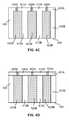
- FIG. 4Dis a variation of FIG. 4C .
- FIGS. 5A-5Cshow schematics of another through-wafer interconnection design having multiple conductors.
- FIG. 5Dshows a cross-sectional view of a variation of the through-wafer interconnection structure in FIGS. 5A-5C .
- FIG. 6shows a bottom review of a flexible through-wafer interconnection structure in accordance with the present invention.
- FIG. 7shows an example of the insulator surrounding the through-wafer interconnection conductor in accordance with the present invention.
- FIG. 8shows an example of a modified conductor in accordance with the present invention.
- FIG. 9shows an example of a modified decoupling conductor in accordance with the present invention.
- FIGS. 10A-10Eshow a process flow of a first exemplary fabrication method.
- FIG. 10Fshows an alternative step in the process of the first exemplary fabrication method.
- FIG. 10Gshows a bottom view of an exemplary trench pattern design in the through-wafer interconnect structure at the step shown in FIG. 10C .
- FIG. 10Hshows a bottom view of another exemplary trench pattern design in the through-wafer interconnect structure at the step shown in FIG. 10C .
- FIGS. 11A-11Bshow an exemplary thin silicon line having segments that are completely oxidized.
- FIGS. 12A-12Gshow a process flow of a second exemplary fabrication method.
- FIGS. 13A-13Hshow a process flow of a third exemplary fabrication method.
- FIGS. 14A-14Fshow a process flow of a fourth exemplary fabrication method.
- FIG. 14Gshows an alternative step in the process of the first exemplary fabrication method.
- FIG. 14Hshows a bottom view of the through-wafer interconnect structure at the step shown in FIG. 14D .
- FIGS. 15A , 15 C, 15 E and 15 G- 15 Kshow a process flow of a fifth exemplary fabrication method.
- FIGS. 15B , 15 D and 15 Fshow top views of the through-wafer interconnection at steps shown in FIG. 15A , FIG. 15C , and FIG. 15E , respectively.
- FIG. 2is a schematic cross-sectional view of a through-wafer interconnect in accordance with the present invention.
- the through-wafer interconnectis built in a wafer 200 .
- the through-wafer interconnectincludes a conductor 210 passing through the front side (top) of the wafer 200 to the backside (bottom) of the wafer.
- the conductor 210is surrounded by an insulator 220 , and both the conductor 210 and the insulator 220 are surrounded by a frame 230 .
- the through-wafer interconnect in accordance with the present inventionis characterized in that at least a portion of the conductor 210 and a respective surrounding portion of the frame 230 each comprise a native material of the wafer 200 .
- this means that the conductor 210may be fabricated directly out of the wafer 200 if the wafer 200 is made of a conductive material.
- a conductive materialis defined as one having a resistivity less than 1 ⁇ 10 4 ⁇ -cm.
- one particularly useful conductive material for fabricating a through-wafer interconnect of the present inventionis doped silicon wafers.
- the through-wafer interconnect in accordance with the present inventionprovides electrically conductive interconnection between electric contacts on the front side and the backside of the wafer 200 .
- Thishas many applications in a broader range of technologies. It is particularly useful for assembling and packaging microelectronic devices such as microelectronic imagers used in digital cameras and wireless devices with picture capabilities, micromachined ultrasonic transducers, micromirror arrays for optical communication, optical displays, etc.
- a microelectronic devicemay be placed or fabricated directly on the front side (top) of the wafer 200 and connected to an integrated circuit (not shown) which is located on the front side of the wafer 200 .
- the integrated circuitis then connected to the conductor 210 through an electric contact (not shown).
- the conductor 210itself may be connected to another electric contact (not shown) on the backside of the wafer 200 .
- any device that requires, or may be benefited by, a through-wafer interconnectmay use the through-wafer interconnect in accordance with the present invention.
- the conductor 210 in the through-wafer interconnect of the present inventionmay be made of a native material of the conductive wafer 200 , instead of being made of an external conductive material introduced to a hole or a via in the wafer.
- the insulator 220may be made of one or more insulating materials (such as a dielectric material) added to a void space formed from the wafer 200 . Because of its unique design, the invention confers a great level of freedom in designing and fabricating the shape, size, electrical and mechanical properties of the conductor 210 , the insulator 220 and the frame 230 .
- the dimensions of the conductor 210are no longer limited by thin-film deposition or electroplating techniques as in the related art through-wafer interconnection designs. If the overall conductivity of the conductor 210 needs to be higher, for instance, the requirement may be satisfied by increasing the cross-sectional size (thickness) of the conductor 210 .
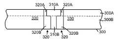
- FIG. 3shows a schematic cross-sectional view of another through-wafer interconnect in accordance with the present invention.
- the conductor 310now has a top portion 310 A and a bottom portion 310 B.
- the bottom portion 310 Bhas a smaller cross-sectional size than the top portion 310 A, resulting in a smaller electric contact area on the backside and thus reducing parasitic capacitance.
- the insulator 320has a first portion 320 A surrounding the top portion 310 A of the conductor 310 and a second portion 320 B surrounding the bottom portion 310 B of the conductor 310 .
- the through-wafer interconnecthas a frame 330 surrounding the conductor 310 ( 310 A and 310 B) and the insulator ( 320 A and 320 B).
- top portion 310 A of the conductor or the bottom portion 310 B of the conductor, or both the top portion 310 A and the bottom portion 310 Bmay have a native conductive material of the wafer 300 .
- a respective surrounding portion of the frame 330may also have the same native conductive material of the wafer 300 .
- the wafer 300may either be a monolithic wafer or include a top section 300 A corresponding in depth to the top portion 310 A of the conductor and a bottom section 300 B corresponding to the bottom portion 310 B of the conductor.
- the top section 300 A and the bottom section 300 Bmay be just two different sections of a single contiguous wafer (wafer 300 ).
- the wafer 300may be a doped conductive silicon wafer, with the top section 300 A and the bottom section 300 B having different doping levels.
- the top section 300 A and the bottom section 300 Bmay be two separate layers bonded together to form a composite wafer 300 .
- the two separate layers ( 300 A and 300 B) of the wafer 300may be either directly bonded together without an intervening layer or indirectly bonded with an intervening layer. In a configuration in which the two separate layers 300 A and 300 B are indirectly bonded together with an intervening layer sandwiched there between, it is essential that the conductivity from the top portion 310 A of the conductor to the bottom portion 300 B is not interrupted.
- the basic design of through-wafer interconnection in accordance with the present inventionmay be used for fabricating through-wafer interconnect structures that are more complicated.
- FIGS. 4A-4Cshow schematics of a through-wafer interconnection design having multiple conductors.
- FIG. 4Ashows a top view of the design
- FIG. 4Bshows a bottom view of the design
- FIG. 4Cshows a cross-section view of the design through the dashed line in FIG. 4A and FIG. 4B .
- the through-wafer interconnection structureis built in a conductive wafer 400 and has an array of four conductors 410 , 412 , 414 and 416 each passing through the front side (top) of a conductive wafer 400 to a backside (bottom) of the conductive wafer 400 .
- the through-wafer interconnection structurefurther has a patterned insulator having a top portion 420 A and the bottom portion 420 B.
- the insulator ( 420 A and 420 B)passes through a front side of the conductive wafer 400 to the backside of the conductive wafer 400 .
- the insulatorsurrounds each conductor 410 , 412 , 414 and 416 .
- a frame 430supports the conductors 410 , 412 , 414 and 416 and the insulator ( 420 A and 420 B). Similar to the through-wafer interconnect shown in FIGS. 2-3 , the through-wafer interconnection structure in FIGS. 4A-4C is characterized in that at least part of each conductor 410 , 412 , 414 and 416 and at least a portion of the frame 430 each comprise a native material of the conductive wafer 400 , allowing the conductors 410 , 412 , 414 and 416 , and at least a part of the frame 430 to be fabricated directly from the conductive wafer 400 .
- the conductors 410 , 412 , 414 and 416are used to access the devices (not shown) on the front surface (top) of the wafer 400 from the backside (bottom) of the wafer 400 .
- conductors 410 , 412 , 414 and 416each have a top portion ( 410 A, 412 A, 414 A and 416 A, respectively) and a bottom portion ( 410 B, 412 B, 414 B and 416 B, respectively).
- the bottom portions 410 B, 412 B, 414 B and 416 Beach have a smaller cross-sectional size than the respective top portion 410 A, 412 A, 414 A and 416 A.
- the top portions ( 410 A, 412 A, 414 A and 416 A) of the conductors 410 , 412 , 414 and 416correspond to the top portion 420 A of the insulator in a top section 400 A of the conductive wafer 400 .
- the bottom portions ( 410 B, 412 B, 414 B and 416 B) of the conductors 410 , 412 , 414 and 416correspond to the bottom portion 420 B of the insulator in a bottom section 400 B of the conductive wafer 400 . Accordingly, the bottom portion 420 B has a greater cross-sectional size than the respective top portion 420 A.
- the two sections 400 A and 400 Bbelong to the same contiguous monolithic single wafer 400 .
- the two sections 400 A and 400 Bmay be of an identical material, but may also be of the same wafer material having different doping levels.
- top portions 410 A, 412 A, 414 A and 416 A and the bottom portions 410 B, 412 B, 414 B and 416 Bbelong to two separate layers, namely a top layer 401 A and a bottom layer 401 B, that are bonded together to form a composite wafer 400 .
- the two separate layers 401 A and 401 Bmay either the bonded together directly as shown in FIG. 4D or bonded indirectly through an intervening material (not shown).
- the top portions of the conductor and the top portion of the insulatormay be formed in the top layer 401 A, while the bottom portions of the conductor and the bottom portion of the insulator may be formed in the bottom layer 401 B.
- the top portion of the conductor and the bottom portion of the conductormay also be made of different materials.
- the top portion of the insulator and the bottom portion of the insulatormay also be made of different materials. It is appreciated that many variations or modifications can be made based on the basic design illustrated herein. The only requirement is that the conductivity path along the conductors 410 , 412 , 414 and 416 between the top side and the bottom side of the wafer 400 is maintained.
- FIGS. 4A-4D and other figures belowan array of four identical conductors is used to demonstrate the interconnection design.
- the through-wafer interconnection designcan be used of for any number of devices, any array of devices, any array of through-wafer conductors, or multiple arrays with different number of devices and conductors, and any other configurations that may require or may benefit from through-wafer interconnection.
- the cross sections of the conductors, the insulator and the framehave a square shape in the examples shown, it is appreciated that these parts can be of any geometric shapes as long as the arrangement thereof provides the desired through-wafer interconnection in accordance with the present invention.
- FIGS. 5A-5Cshow schematics of another through-wafer interconnection design having multiple conductors.
- FIG. 5Ashows a top view of the design
- FIG. 5Bshows a bottom view of the design
- FIG. 5Cshows a cross-section view of the design through the dashed line in FIG. 5A and FIG. 5B .
- the through-wafer interconnection structure in FIGS. 5A-5Cis similar to that in FIGS. 4A-4C .
- the through-wafer interconnection structureis built in a conductive wafer 500 and has an array of four conductors 510 , 512 , 514 and 516 each passing through the front side (top) of a conductive wafer 500 to a backside (bottom) of the conductive wafer 500 .
- the through-wafer interconnection structurefurther has a patterned insulator assembly that has insulators 520 , 522 , 524 and 526 each surrounding a corresponding conductor 510 , 512 , 514 and 516 , and a frame 530 mechanically supporting the conductors 510 , 512 , 514 and 516 and the insulator assembly (insulators 520 , 522 , 524 and 526 ). Similar to the through-wafer interconnect shown in FIGS. 2-3 and FIGS. 4A-4C , the through-wafer interconnection structure in FIGS.
- each conductor 510 , 512 , 514 and 516 and at least a portion of the frame 530each comprise a native material of the conductive wafer 500 , allowing the conductors 510 , 512 , 514 and 516 , and at least a part of the frame 530 to be fabricated directly from the conductive wafer 500 .
- conductors 510 , 512 , 514 and 516each have a top portion ( 510 A, 512 A, 514 A and 516 A, respectively) and a bottom portion ( 510 B, 512 B, 514 B and 516 B, respectively).
- the bottom portions 510 B, 512 B, 514 B and 516 Beach have a smaller cross-sectional size than the respective top portion 510 A, 512 A, 514 A and 516 A.
- top portions 510 A, 512 A, 514 A and 516 A and the bottom portions 510 B, 512 B, 514 B and 516 Bmay either belong to different sections of the same contiguous single wafer 500 or belong to two separate layers that are bonded together to form a composite wafer 500 .
- the two separate layersmay either the bonded together directly or bonded indirectly through an intervening material (not shown).
- the through-wafer interconnect of FIGS. 5A-5Chas a slightly more sophisticated frame 530 .
- the frame 530has an outer peripheral wall 530 a and a plurality of inter-conductor walls 530 b .
- the outer peripheral walls 530 adefine a general area where the conductors 510 , 512 , 514 and 516 and the insulator assembly of insulators 520 , 522 , 524 and 526 are disposed, while the plurality of inter-conductor walls 530 b further divide the general area into a plurality of sub-areas each containing one of the conductors 510 , 512 , 514 and 516 and a respective surrounding portion of the insulator assembly (insulators 520 , 522 , 524 and 526 , respectively, in the example) surrounding the conductor.
- the inter-conductor walls 530 b of the frame 530may also have a conductive material to function as a decoupling conductor between the plurality of conductors 510 , 512 , 514 and 516 .
- the conductive materialmay also be a native material of the conductive wafer 500 , thus allowing the decoupling conductor (the inter-conductor walls 530 b of the frame 530 ) to be fabricated, together with the through-wafer conductors 510 , 512 , 514 and 516 , from the conductive wafer 500 .
- the decoupling conductormay be connected to a certain voltage source (DC or AC).
- the decoupling designis useful in the through-wafer interconnection designs shown herein because electrical AC signals may couple between conductors through insulation material. Placing a conductive layer or wall such as the decoupling conductor 530 b between the conductors 510 , 512 , 514 and 516 helps to shield the electric coupling between these conductors.
- FIG. 5Dshows a cross-sectional view of a variation of the through-wafer interconnection structure in FIGS. 5A-5C .
- the inter-conductor walls 531 bare lower than the outer peripheral wall 530 a and only extend across the lower portion of the wafer 500 .
- the transducersmay need to connect to a flexible through-wafer connection.
- the flexible through-wafer connectioncan be realized by thinning the thickness of the connection.
- the parts along the through-wafer connectionmay be designed as a flexible structure by virtue of its shape instead of its thinness alone.
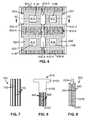
- FIG. 6shows a bottom review of a flexible through-wafer interconnection structure in accordance with the present invention.
- the through-wafer interconnection structure in FIG. 6is similar to that in FIGS. 5A-5C . If the cross-sectional view is taken from the dashed line indicated, it would look like the cross-sectional view showing in FIG. 5C .
- the frame 630has outer peripheral walls 630 - 1 , 630 - 2 , 630 - 3 and 630 - 4 that define a general area where the conductors 610 , 612 , 614 and 616 (shown bottom portions 610 B, 612 B, 614 B and 616 B) and the insulator assembly of insulators 620 , 622 , 624 and 626 are disposed.
- the frame 630also has inter-conductor walls 630 - 5 and 630 - 6 that further divide the general area into sub-areas each containing one of the conductors 610 , 612 , 614 and 616 and a respective portion of the insulator assembly (insulators 620 , 622 , 624 and 626 , respectively, in the example) surrounding the conductor.
- walls 630 - 2 , 630 - 4 and 630 - 6 of the frame 630are made of thin segments and have a zigzag shaped. These thin and zigzag shaped walls provide a degree of flexibility through stretching or compressing. Such flexibility can be particularly helpful when the through-wafer interconnection structure is used for fabricating and packaging microelectronic devices that have a movable part, or have a part that is subject to bending.
- the insulator or insulators in the through-wafer interconnects shown above in FIGS. 4A-4C , FIGS. 5A-5D and FIG. 6are disposed in annular trenches each surrounding a respective conductor.
- the annular trenchesare formed by removing the native material of the conductive wafer.
- the insulatorsmay include a dielectric material added to the annular trench.
- FIG. 7shows an example of the insulator surrounding the through-wafer interconnection conductor in accordance with the present invention.
- the insulator 720is disposed in an annular trench formed on the wafer (not shown) and constitutes lines 740 of unremoved native material of the wafer interlined with spaces 745 .
- the lines 740 of unremoved native materialare formed when the annular trench is formed using a patterned material removal method such as patterned etching method (details shown in the description of fabrication methods herein below).
- the lines 740 of unremoved native materialmay form a supporting framework between conductors (e.g. conductors 410 and 412 in FIGS.
- the lines 740 of unremoved native material of the wafermay be oxidized.
- at least part of the lines 740 of unremoved native materialmay be completely oxidized such that the supporting framework formed by the lines 740 is sufficiently insulative between the conductor and the frame (which may also be a part of a conductive wafer and therefore conductive).
- a dielectric filler materialmay be added to fill the spaces 745 between lines 740 of unremoved native material.
- FIG. 8shows an example of a modified conductor in accordance with the present invention.
- the conductormay be further modified to be partially different from the original native material of the wafer.
- conductor 810has a top portion 810 A and a bottom portion 810 B. Part of the native material of the original wafer in the bottom portion 810 B is removed from a bottom end 810 C to form spaces 845 between lines 840 of unremoved native material. A new material may be then introduced to this partially hallowed structure to modify the physical properties of the conductor 810 .
- the lines 840may be oxidized to form oxidation, or covered by a new material.
- spacings 850may be filled with another material.
- FIG. 9shows an example of a modified decoupling conductor in accordance with the present invention.
- An exemplary decoupling conductor 930has a top portion 930 A and a bottom portion 930 B. Part of the native material of the original wafer in the bottom portion 930 B is removed from a bottom end 930 C to form spaces 945 between lines 940 of unremoved native material. A new material may be then introduced to this partially hallowed structure to modify the physical properties of the decoupling conductor 930 .
- the lines 940may be oxidized to form oxidation, or covered by a new material.
- spaces 945may be filled with another material.
- the conductors described hereincan be made of the any conductive material.
- One good choiceis to form the conductors using semiconductor wafers (e.g., silicon, GaAs, etc). Heavily doped semiconductor wafer may be used to improve the conductivity.
- the through-wafer conductorsmay be made of the two portions.
- a top portionis used to connect the devices on the front surface of the wafer.
- the shape of the top portion of each conductoris usually determined by the dimensions and shapes of the devices which connect to the through-wafer interconnections.
- the top portion of the conductorcan serve as one of the electrodes of capacitance micromachined ultrasonic transducers (cMUTs).
- the bottom portion of the conductoris designed with a trade-off between the capacitance and resistance of the interconnection.
- the capacitanceincreases with the perimeter length of the conductor.
- a through-wafer conductor of a greater cross-sectional sizei.e., thicker
- the resistancedecreases with the cross-sectional size of the conductor. A balance is struck to optimize the performance.
- the top portion of the insulator and the bottom portion of the insulatormay be made of either the same material or different materials, and both can be made of any kind of medium or material, including but not limited to vacuum, air, silicon, oxide, nitride, SOG, TEOS, polyimide, polymer, rubber, PDMS, PMMA, epoxy, gel, and any filling material for ultrasonic transducers, or a combination thereof.
- a useful combinationshould result in an insulator that is non-conductive as a whole.
- a combination of different materialsis used in a portion (top portion or bottom portion) of the insulator, preferably at least one material is an insulation material.
- a configuration of the insulatorshould desirably provide the mechanical strength to the wafer so that the wafer or the devices can survive during the device fabrication process and device assembly and packaging.
- the through-wafer connectioncan be controlled to a desired thickness using grinding and polishing of the processed wafer in a certain fabrication step.
- a thicker through-wafer connectionis preferred for easier and more reliable fabrication process and packaging handling, but a thinner through-wafer connection is usually desired to improve the device performance.
- a balanceoften needs to be struck.
- the conflictmay be at least partially avoided by a carefully designed fabrication process.
- the wafer thinningcan be done before, after or during the fabrications of the through-wafer connection.
- the thin wafer with through-wafer connectionsmay be bonded or stuck to another wafer using a proper wafer bonding technique or a proper stiction layer. Using this technique, the resultant bonded wafer as a whole may be robust enough to be processed.
- the through-wafer interconnectionmay be designed to be insensitive to the vibration coupling from the environment.
- materials selections and the structure configurations of the through-wafer interconnectionshould be used to achieve certain acoustic properties.
- the interconnectionshould provide acoustic decoupling between the cMUT elements and absorb the acoustic energy leaked into the substrate from the transducers.
- the through-wafer interconnection in the present inventionprovides the flexibility to select many different materials and to design the conductors, insulators and decouple conductors with different shapes and configurations to achieve the desired performance.
- a variety of fabrication methodsmay be used to make the through-wafer interconnections in accordance with the present invention.
- the fabrication of the through-wafer interconnectionsmay be done before or after the device fabrication process.
- the fabrication of the through-wafer interconnectionsmay be integrated with the device fabrications.
- the choice of the fabrication methodsis dependent on the material compatibility and process compatibility (e.g., the process thermal budget, the etch selectivity, wafer surface topography and the wafer rigidity, etc.) of both the device fabrication and the through-wafer interconnection fabrication.
- the process method and the materials usedshould be carefully evaluated at each fabrication step, with consideration to factors such as process temperature, to ensure compatibility. This is especially important when the fabrications of the device and the interconnection are integrated.
- the phrase “adding a material”does not mean that the material added must be an external material. It is appreciated that the material may be either alternatively or additionally added by a process of forming a new material, such as oxidation. Furthermore, the thinning process is not shown in the examples of the process flows below. It is appreciated that in the wafer thinning process can be performed before and/or during the fabrication process.
- Some fabrication methods described belowshow a degree of integration of the device fabrication and the through-wafer interconnection fabrication. However, it is appreciated that the interconnection fabrication methods may or may not be integrated with the device fabrications.
- the through-wafer interconnectionmay be fabricated by combining some steps or changing the step orders of different fabrication methods described herein.
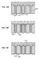
- FIGS. 10A-10Eshow a process flow of a first exemplary fabrication method.
- FIG. 10Fshows an alternative step in the process.
- FIG. 10Gshows a bottom view of the through-wafer interconnect structure after the step shown in FIG. 10C .
- the process flowis outlined in the following steps.
- step onepatterned top trenches 1010 are formed on silicon wafer 1000 by silicon etching to define the top portions 1020 of the through-wafer conductors and the top portion of inter-conductor frame 1025 .
- An example of the inter-conductor frame 1025is illustrated as inter-conductor wall 530 b in FIGS. 5A-5D . It is however appreciated that a similar process may be used to fabricate a through-wafer interconnection without inter-conductor frame 1025 (such as that shown in FIGS. 4A-4D ).
- patterned top trenches 1010would show an annular circumferential opening similar to that illustrated in the top views FIG. 4A and FIG. 5A .
- annularmeans the opening is generally shaped like a ring, but does not suggest any particular shape of the ring, nor does it suggest that the ring is entirely complete or unbroken.
- the annular top trenches 1010generally divide the silicon wafer 1000 along the trench opening into an inner portion and an outer portion whereby the inner portion of the silicon wafer will serve as a through-wafer conductor of the through-wafer interconnect being made.
- a thermal oxidation 1030(or LTO, nitride, etc.) is grown over top trenches 1010 to form an etch stop layer 1040 for backside silicon etch in the next step.
- a filler material(not shown) may be added into trench 1010 if needed.
- the filler materialmay be an external material or formed by oxidation of unremoved native material in the trench 1010 .
- the backside silicon etchwill define the shape of the bottom portions of the conductors.
- bottom trenches 1060backside silicon etch is performed to form bottom trenches 1060 .
- the overall pattern of bottom trenches 1060defines the bottom portions of the through-wafer conductors 1050 .
- bottom trenches 1060are not entirely devoid of the wafer material. Instead, each bottom trench 1060 is fine-patterned within the trench openings with open passages (gaps or spaces) 1045 interlined with thin silicon lines 1065 of unremoved conductive wafer material.
- the shape, size and spacing of the fine pattern within the bottom trenches 1060is not limited to any particular model, as long as it does a meaningful modification of the properties of an empty trench or a proper preparation for the next step.
- step fourthe fine-pattern of the thin silicon lines 1065 are oxidized.
- open passages 1045 between the thing silicon lines 1065may be filled with a filler material 1055 without oxidizing the silicon lines 1065 .
- the filler material 1055may be an oxide, PDMS, SOG or another material for achieving a desired electric or mechanical property.
- step fiveif the thin silicon lines 1065 are oxidized in the above step four, optionally the open passages 1045 between the thin silicon lines 1065 can still be filled with a filler material 1055 , which may be an oxide, PDMS, SOG or another material for achieving a desired electric or mechanical property.
- a filler material 1055which may be an oxide, PDMS, SOG or another material for achieving a desired electric or mechanical property.
- the thin silicon lines 1065are designed so that the thin lines 1065 can be oxidized, the spaces (open passages 1045 ) can be filled, and the stress induced by the oxidation minimized.
- FIG. 10G and 10HTwo exemplary designs of the patterned thin silicon lines 1065 are illustrated in FIG. 10G and 10H which show the bottom view of the silicon wafer 1000 at the end of step 3 ( FIG. 10C ).
- the pattern shown in FIG. 10Gwill continue with the steps shown in FIG. 10D and 10E .
- the pattern shown in FIG. 10Hwill continue with the step shown in FIG. 10F .
- Many other possible patterns and a variety of different thicknesses of the silicon linesmay be used.
- the patternsshould desirably provide enough mechanical strength for the wafer during the fabrication and packaging processes.
- the lines of unremoved conductive wafer materialmay form a framework between the inner portion (conductor 1050 ) and the outer portion (frame 1005 ) of the conductive wafer to connect and support the two portions.
- FIGS. 11A-11Bshow an exemplary thin silicon line having segments that can be completely oxidized.
- FIG. 11Ashows thin silicon line 1100 before oxidation.
- FIG. 11Bshows the thin silicon line 1100 after oxidation where segments 1110 and 1120 are completely oxidized.
- the patternmay be designed to minimize the stress built during the oxidation process and, if needed, to be easily filled by selected material (e.g. LTO, SOG, TEOS, nitride, polyimide, polymer, rubber, PDMS, PMMA, epoxy, gel, etc) with desired properties.
- selected materiale.g. LTO, SOG, TEOS, nitride, polyimide, polymer, rubber, PDMS, PMMA, epoxy, gel, etc
- the patternitself may be designed to have desired properties particularly pertinent to the device supported by the through-wafer interconnection.
- the patternmay be designed to achieve a certain acoustic impedance is the through-wafer interconnection is used for supporting a micromachined ultrasound transducer.
- the patterned structurecan be design to be flexible in the desired direction.
- the device fabrication(e.g., cMUT fabrication) may be started after the oxidation step (the step three).
- the through-wafer connections shown in this examplecan be carried out either before or during the device fabrication.
- a filler material(preferably insulative) may be added into the top trench 1010 .
- the insulative material within the top trench 1010itself can provide enough strength to hold the conductors (or wafers) sturdy enough during the process.
- the shape and the inner pattern of the trench 1060may not need to be designed to form a framework to support and to connect the conductors.
- An exampleis shown in FIG. 10H . Accordingly, electrical insulation between the conductors may be achieved by simply adding an insulative filler material into trenches, instead of using oxidation of the fine patterns in the patterned trenches.
- through-wafer interconnection fabrication method in this examplecan be done with a reversed sequence by forming the bottom trench 1060 first, then ending with the top trench formation 1010 and a dielectric material filling (no shown).
- FIGS. 12A-12Gshow a process flow of a second exemplary fabrication method. The process flow is outlined in the following steps.
- top trenches 1210are etched on silicon wafer 1200 .
- Oxide 1220is grown over the cavities 1210 .
- Oxide 1220is patterned so that only the oxide in top trenches 1210 is kept as etch stop 1225 of the backside silicon etch in a subsequent step.
- a second wafer 1230is bonded to silicon wafer 1200 over the top of top trenches 1210 .
- Wafer 1230is ground to a desired thickness for forming the top portion of a conductor.
- the layer 1230may also be taken from a silicon layer in a SOI wafer.
- a device 1235(e.g., a cMUT) is fabricated on or above the second wafer 1230 to a stage that the fabricated device still allows high temperature process if the oxidation is needed later.
- the device 1235is represented by a simple box without showing details or the exact location. The fabrication of the device 1235 may be finished at this step if there is no more subsequent high temperature process steps.
- Second wafer 1230may serve as an electric contact, such as a bottom electrode, of the device 1235 .
- patterned bottom trenches 1240are formed using backside etch to define the bottom portions 1250 of the conductors.
- Patterned bottom trenches 1240have patterned lines 1265 of the unremoved native material of silicon wafer 1200 interlined or spaced from each other by gaps or spaces 1245 . It is appreciated that any pattern of lines 1265 and spaces 1245 , such as that shown in FIG. 10G or 10 H, may be designed and used, depending on the desired process and properties.
- step fivepatterned bottom trenches 1240 are oxidized to make insulation between the conductors 1250 .
- at least the part of the silicon lines 1265 defined in previous silicon etch step (step four)is completely oxidized. More preferably, all of the silicon lines 1265 are completely oxidized.
- the oxidationalso forms in oxide layer 1270 over the bottom portions 1250 of the through-wafer conductor, as well as bottom portions of the outer frame 1205 and inter-conductor frame 1255 .
- step fourif the layer 1230 and the device 1235 can provide enough strength to hold the conductors (or wafers) to survive the process, the shape and the pattern of the trench 1240 may not need to be designed to serve such a purpose.
- the trench 1240may be designed to cut through the wafer to achieve the electric insulation between the conductors and the frames directly (such as the pattern shown in FIG. 10H ). Therefore, the oxidation step (step five, FIG. 12E ) may not be necessary to form insulation between conductors. Nevertheless, a fill material may still be added into the void within the trench if needed to finish the process.
- step sixgaps or spaces 1245 in the patterned bottom trenches 1240 are filled using a material 1260 with desired properties. Vias are opened on the oxide 1270 on the bottom surface of the bottom portions 1250 of the through-wafer conductors to access the conductors. After that, a metal layer 1280 with desired properties is deposited and patterned. A hard mask may be used to form the metal pattern on the backside of the through-wafer interconnection if the voids between the conductors are not going to be refilled after that.
- step sevenfabrication of the device 1235 on the front surface is completed, and top portions 1252 of the conductors are further defined by silicon etch.
- FIGS. 13A-13Hshow a process flow of a third exemplary fabrication method. This method is similar to the above second method except for using a different technique to define the etch stop for the backside silicon etch which defines the bottom part of the conductors.
- the process flowis outlined in the following steps.
- top trenches 1310are etched on silicon wafer 1300 .
- Oxide 1320is grown over the top trenches 1310 .
- the oxide at the bottom 1322 of the top trenches 1310is then removed.
- step twoisotropic silicon etch is performed to form cavities 1324 .
- the surface of the cavities 1324 created by the isotropic silicon etchis oxidized to form a stop layer 1325 for backside silicon etch.
- the trench 1310may be field with a filler material (not shown) in this step.
- step threethe device 1330 (e.g., a cMUT) is fabricated on or above the wafer 1300 to a stage that the fabricated device still allows high temperature process if the oxidation is needed later.
- the fabrication of device 1330may be finished at this step if there is no more subsequent high temperature process step.
- step four to step eightis similar to the process described from step four ( FIG. 12D ) to step seven ( FIG. 12G ) in the fabrication method II.
- the patterned bottom trenches 1340 , patterned lines 1365 of the unremoved native material of the silicon wafer 1300 , spaces 1345 , bottom portions 1350 of the through-wafer conductor, inter-conductor frame 1355 , filler material 1360 , oxide layer 1370 , metal layer 1380 , and the top portions 1352 of the conductorsare similar to their equivalents in the fabrication method II.
- FIGS. 14A-14Fshow a process flow of a fourth exemplary fabrication method. The process flow is outlined in the following steps.
- step onethe same processes as described in the first three steps of the above fabrication method II shown in FIG. 12A , FIG. 12B and FIG. 12C are first performed on silicon wafer 1400 .
- Top trenches 1420 and backside etch stop layer 1425are formed in these steps.
- the fabrication process of the device 1490may also be completed at this stage.
- patterned bottom trenches 1440are formed using backside etch to define the bottom portions 1450 of the through-wafer conductors.
- Patterned bottom trenches 1440has patterned lines 1465 of the unremoved native material of silicon wafer 1400 interlined or spaced from each other by gaps or spaces 1445 . It is appreciated that any pattern of lines 1465 and spaces 1445 may be designed and used, depending on the desired process and properties.
- inter-conductor frame 1455which may serve as a decoupling conductor, may also be formed if desired.
- step two backside etchingmay also be performed on the frame 1405 , the inter-conductor frame 1455 , and the bottom portions 1450 of the through-wafer conductors to further modify the structure and properties of the conductors.
- This techniquemay be used to achieve some desired effects for the particular type of device that is being fabricated and packaged using the through-wafer interconnection technique. For example, special patterns may be etched, materials may be added, and oxidation performed in the etched patterns in order to achieve special acoustic properties if the device is a micromachined ultrasonic transducer (MUT).
- MUTmicromachined ultrasonic transducer
- FIG. 14Gis an alternative of the cross-sectional view FIG. 14B in step two but with additional etching. It is appreciated that this extra fabrication steps can be incorporated into other fabrication methods in similar ways.
- step three( FIG. 14C ) gaps or spaces 1445 in the patterned bottom trenches 1440 are filled using a material 1460 with desired properties.
- step fourthe whole or part of silicon pattern in the bottom trenches 1440 is etched to make isolation between conductors 1450 and the conductive frame ( 1405 and 1455 ).
- the bottom portions 1450 of the through-wafer conductors and the conductive framescan also be etched into a desired pattern in this step, if such etching has not been performed already in a previous step (e.g., step two).
- FIG. 14His a bottom view after the step four.
- step fiveavoids 1466 created from the silicon etch at step four is filled using a material or materials 1467 with desired properties. This step is optional.
- a metal layer 1480is then deposited and patterned on the bottom surface of the through-wafer conductors and the conductive frames.
- step sixthe device fabrication is completed on the wafer surface, and the top portions 1452 of the through-wafer conductors are further defined by etching from the top side of the wafer.
- the fabrication methods 4does not use high temperature process of thermal oxidation to make insulation between the conductors and the conductive frame. Instead, the whole or part of the silicon pattern between the conductors is etched to achieve the insulation between them (see step four). For this reason, at least one material with desired properties should be used to fill the gaps or spaces within silicon pattern created by the backside silicon etching which also defines the bottom portions of the through-wafer conductors. In contrast, in the fabrication methods 1-3 the step to fill the gaps within the oxide pattern is entirely optional.
- the above fabrication method IVmay also be combined with the fabrication methods I-III such that the resultant method is substantially similar to the fabrication method IV except that top trenches 1420 and backside etch stop layer 1425 are formed differently.
- wafer thinningcan be performed if needed.
- a hard maskmay be used to form the metal pattern on the backside of the through-wafer interconnection if the voids between the conductors are not to be filled.
- FIGS. 15A , 15 C, 15 E and 15 G- 15 Kshow a process flow of a fifth exemplary fabrication method.
- FIGS. 15B , 15 D and 15 Fshow top views of the through-wafer interconnection at a respective step. The process flow is outlined in the following steps.
- step onedeep silicon etching is performed from the front side of the wafer 1500 to a desired thickness to form deep trenches 1511 with silicon patterns 1512 , which can be oxidized to form insulation between the conductors. If desired, etch may go through the entire wafer 1500 . Recesses 1513 on silicon surface can be etched first if needed.
- FIG. 15Ais a cross-sectional view of this formation, while FIG. 15B is the top view of the same.
- the exemplary silicon pattern shown hereis designed to minimize the oxide volume and the thermal stress effects in the structure. Other patterns may be used as long as they can be oxidized and form insulation between the conductors after finishing the fabrication.
- step twothe silicon patterns 1512 formed in the previous step is oxidized to form an oxide formation 1514 .
- FIG. 15Cis a cross-sectional view of this formation, while FIG. 15D is the top view of the same.
- step threepatterned annular deep trenches 1541 are formed.
- FIG. 15Eis a cross-sectional view of this formation, while FIG. 15F is the top view of the same.
- the annular deep trenches 1541have unremoved silicon lines 1543 and empty spaces (voids) 1542 , together forming a framework between the frame 1505 and conductors 1550 .
- the annular deep trenches 1541will insulate the conductors and define the bottom portions of the conductors.
- a thin oxidemay be grown to form a stop layer for late process.
- a prime wafer 1551is bonded to the patterned wafer 1500 over recesses 1513 and is ground and polished to a desired thickness.
- the layer 1551may also obtained by bonding with an SOI wafer.
- step five( FIG. 15H ), the prime wafer 1551 is patterned and etched to form the top portions 1552 of the conductors. Step five is optional.
- step sixdevices 1535 are fabricated.
- a etch processmay be performed to define the top part of the conductors.
- step seventhe wafer 1500 is ground (and polished if needed), or etched, to reach the bottom of the annular deep trenches 1541 from the backside of the wafer. If an etch stop layer was formed at the bottom of the annular deep trenches 1541 in a previous step, the backside etching stops at the etch stop layer.
- step eight( FIG. 15K ) voids 1545 in the silicon pattern are filled with a desired material 1560 if needed.
- a metal layer 1580is then deposited and patterned on the backside of the wafer.
- the top portions 1552 of the through-wafer conductorsmay serve as the substrate, as well as the bottom electrode, of the cMUT.
- a hard maskmay be used to form the metal pattern on the backside of the through-wafer interconnection if the voids between the conductors are not to be refilled.
- the through-wafer interconnection of the present inventioncan be used for miniaturization of electronic components such as ICs, microelectronic devices used in sensor arrays, transducer arrays, and photo imager arrays, and modules that are used in portable devices like cellular phones and PDAs.
- the application of the present inventionhelps to avoid long wires running in or across the wafer surface and thus reduces the undesired parasitic capacitance and high interconnection resistance.
- the inventionthus facilitates the realization of ultimate miniaturization in reaching chip size packaging (CSP) of the components. This could potentially result in a more efficient fabrication process, reduced foot print of the components on the printed board, greater fill factor, and can also improve the device performance.
- CSPchip size packaging
- the design of the present inventioncan be used for devices that have vertical discrete components and stacked planar dies where the conventional rerouting methods are insufficient.
- the fabrication methods of through-wafer interconnection of the present inventionallow wafer-level processing that results in simultaneous fabrication of large number of packages.
- micromechanical smart sensor and actuator systemsincluding but not limited to photo imagers used in digital cameras and cell phones, micromachined ultrasonic transducers (MUTs such as cMUTs, pMUTs and mMUTs), and micromirror array.
- MUTssuch as cMUTs, pMUTs and mMUTs
- micromirror arraySuch systems are often realized as a multi-wafer device in which the mechanical functions are distributed over different wafers and one of the wafers is dedicated to contain the readout circuits.
- the individually processed waferscan be assembled using wafer-to-wafer bonding and can be combined to one single functional electromechanical unit using the through-wafer interconnect of the present invention, provided that the processes involved comply with the constraints imposed by the proper operation of the active electrical and the micromechanical systems.
- the through-wafer interconnection technology according to the present inventionmay be used in fabricating and packaging the novel MUTs (especially cMUTs) disclosed in international patent applications PCT/IB2006/051567 entitled METHODS FOR FABRICATING MICRO-ELECTRO-MECHANICAL DEVICES; PCT/IB2006/051568 entitled MICRO-ELECTRO-MECHANICAL TRANSDUCERS; and PCT/IB2006/051569 entitled MICRO-ELECTRO-MECHANICAL TRANSDUCERS.
- novel MUTsespecially cMUTs
Landscapes
- Engineering & Computer Science (AREA)
- Physics & Mathematics (AREA)
- Condensed Matter Physics & Semiconductors (AREA)
- General Physics & Mathematics (AREA)
- Computer Hardware Design (AREA)
- Microelectronics & Electronic Packaging (AREA)
- Power Engineering (AREA)
- Manufacturing & Machinery (AREA)
- Internal Circuitry In Semiconductor Integrated Circuit Devices (AREA)
- Transducers For Ultrasonic Waves (AREA)
- Micromachines (AREA)
Abstract
Description
Claims (40)
Priority Applications (1)
| Application Number | Priority Date | Filing Date | Title |
|---|---|---|---|
| US13/349,436US9224648B2 (en) | 2005-05-18 | 2012-01-12 | Through-wafer interconnection |
Applications Claiming Priority (4)
| Application Number | Priority Date | Filing Date | Title |
|---|---|---|---|
| US68261905P | 2005-05-18 | 2005-05-18 | |
| PCT/IB2006/051566WO2006123298A2 (en) | 2005-05-18 | 2006-05-18 | Through-wafer interconnection |
| US91458407A | 2007-11-16 | 2007-11-16 | |
| US13/349,436US9224648B2 (en) | 2005-05-18 | 2012-01-12 | Through-wafer interconnection |
Related Parent Applications (3)
| Application Number | Title | Priority Date | Filing Date |
|---|---|---|---|
| PCT/IB2006/051566DivisionWO2006123298A2 (en) | 2005-05-18 | 2006-05-18 | Through-wafer interconnection |
| US11/914,584DivisionUS8105941B2 (en) | 2005-05-18 | 2006-05-18 | Through-wafer interconnection |
| US91458407ADivision | 2005-05-18 | 2007-11-16 |
Publications (2)
| Publication Number | Publication Date |
|---|---|
| US20120112324A1 US20120112324A1 (en) | 2012-05-10 |
| US9224648B2true US9224648B2 (en) | 2015-12-29 |
Family
ID=37431649
Family Applications (2)
| Application Number | Title | Priority Date | Filing Date |
|---|---|---|---|
| US11/914,584Active2028-05-21US8105941B2 (en) | 2005-05-18 | 2006-05-18 | Through-wafer interconnection |
| US13/349,436ActiveUS9224648B2 (en) | 2005-05-18 | 2012-01-12 | Through-wafer interconnection |
Family Applications Before (1)
| Application Number | Title | Priority Date | Filing Date |
|---|---|---|---|
| US11/914,584Active2028-05-21US8105941B2 (en) | 2005-05-18 | 2006-05-18 | Through-wafer interconnection |
Country Status (6)
| Country | Link |
|---|---|
| US (2) | US8105941B2 (en) |
| EP (1) | EP1883956A4 (en) |
| JP (1) | JP2008541473A (en) |
| CN (4) | CN101573861B (en) |
| CA (1) | CA2607885A1 (en) |
| WO (1) | WO2006123298A2 (en) |
Cited By (1)
| Publication number | Priority date | Publication date | Assignee | Title |
|---|---|---|---|---|
| US11173520B2 (en) | 2020-01-20 | 2021-11-16 | The Board Of Trustees Of The Leland Stanford Junior University | Pulse train excitation for capacative micromachined ultrasonic transducer |
Families Citing this family (119)
| Publication number | Priority date | Publication date | Assignee | Title |
|---|---|---|---|---|
| US7888709B2 (en) | 2004-09-15 | 2011-02-15 | Sonetics Ultrasound, Inc. | Capacitive micromachined ultrasonic transducer and manufacturing method |
| US8658453B2 (en) | 2004-09-15 | 2014-02-25 | Sonetics Ultrasound, Inc. | Capacitive micromachined ultrasonic transducer |
| WO2006123299A2 (en) | 2005-05-18 | 2006-11-23 | Kolo Technologies, Inc. | Methods for fabricating micro-electro-mechanical devices |
| EP1883956A4 (en) | 2005-05-18 | 2011-03-23 | Kolo Technologies Inc | Through-wafer interconnection |
| US7786592B2 (en) | 2005-06-14 | 2010-08-31 | John Trezza | Chip capacitive coupling |
| US7781886B2 (en) | 2005-06-14 | 2010-08-24 | John Trezza | Electronic chip contact structure |
| US7851348B2 (en) | 2005-06-14 | 2010-12-14 | Abhay Misra | Routingless chip architecture |
| US7560813B2 (en)* | 2005-06-14 | 2009-07-14 | John Trezza | Chip-based thermo-stack |
| US7687400B2 (en) | 2005-06-14 | 2010-03-30 | John Trezza | Side stacking apparatus and method |
| US7767493B2 (en) | 2005-06-14 | 2010-08-03 | John Trezza | Post & penetration interconnection |
| US7838997B2 (en) | 2005-06-14 | 2010-11-23 | John Trezza | Remote chip attachment |
| US7989958B2 (en) | 2005-06-14 | 2011-08-02 | Cufer Assett Ltd. L.L.C. | Patterned contact |
| US8456015B2 (en) | 2005-06-14 | 2013-06-04 | Cufer Asset Ltd. L.L.C. | Triaxial through-chip connection |
| WO2006134580A2 (en)* | 2005-06-17 | 2006-12-21 | Kolo Technologies, Inc. | Micro-electro-mechanical transducer having an insulation extension |
| US7786014B2 (en)* | 2006-09-22 | 2010-08-31 | Ipdia | Electronic device and method for making the same |
| JP4825778B2 (en)* | 2007-11-16 | 2011-11-30 | 株式会社日立製作所 | Semiconductor device and manufacturing method thereof |
| JP5337813B2 (en)* | 2007-12-03 | 2013-11-06 | コロ テクノロジーズ インコーポレイテッド | Dual-mode operation micromachined ultrasonic transducer |
| US7884015B2 (en)* | 2007-12-06 | 2011-02-08 | Micron Technology, Inc. | Methods for forming interconnects in microelectronic workpieces and microelectronic workpieces formed using such methods |
| JP2009181981A (en)* | 2008-01-29 | 2009-08-13 | Renesas Technology Corp | Manufacturing process of semiconductor device, and the semiconductor device |
| US8072079B2 (en)* | 2008-03-27 | 2011-12-06 | Stats Chippac, Ltd. | Through hole vias at saw streets including protrusions or recesses for interconnection |
| JP5473253B2 (en)* | 2008-06-02 | 2014-04-16 | キヤノン株式会社 | Structure having a plurality of conductive regions and manufacturing method thereof |
| KR101124857B1 (en)* | 2008-09-30 | 2012-03-27 | 주식회사 동부하이텍 | Image Sensor and Method for Manufacturing thereof |
| FR2938970A1 (en) | 2008-11-26 | 2010-05-28 | St Microelectronics Rousset | METHOD FOR STACKING AND INTERCONNECTING INTEGRATED CIRCUITS |
| SE533992C2 (en) | 2008-12-23 | 2011-03-22 | Silex Microsystems Ab | Electrical connection in a structure with insulating and conductive bearings |
| US8630033B2 (en) | 2008-12-23 | 2014-01-14 | Silex Microsystems Ab | Via structure and method thereof |
| US8729713B2 (en) | 2008-12-23 | 2014-05-20 | Silex Microsystems Ab | Via structure and method thereof |
| US8263492B2 (en)* | 2009-04-29 | 2012-09-11 | International Business Machines Corporation | Through substrate vias |
| JP5330115B2 (en) | 2009-06-17 | 2013-10-30 | 浜松ホトニクス株式会社 | Multilayer wiring board |
| US8324006B1 (en)* | 2009-10-28 | 2012-12-04 | National Semiconductor Corporation | Method of forming a capacitive micromachined ultrasonic transducer (CMUT) |
| US8563345B2 (en) | 2009-10-02 | 2013-10-22 | National Semiconductor Corporated | Integration of structurally-stable isolated capacitive micromachined ultrasonic transducer (CMUT) array cells and array elements |
| JP5473579B2 (en) | 2009-12-11 | 2014-04-16 | キヤノン株式会社 | Control device for capacitive electromechanical transducer and control method for capacitive electromechanical transducer |
| JP5414546B2 (en)* | 2010-01-12 | 2014-02-12 | キヤノン株式会社 | Capacitance detection type electromechanical transducer |
| CN101844130A (en)* | 2010-05-14 | 2010-09-29 | 中国科学技术大学 | Array silicon micro-ultrasonic transducer and manufacturing method thereof |
| JP5570311B2 (en)* | 2010-06-07 | 2014-08-13 | キヤノン株式会社 | Electromechanical converter, specimen diagnostic device |
| DE102010029760B4 (en) | 2010-06-07 | 2019-02-21 | Robert Bosch Gmbh | Device with a via and method for its preparation |
| JP5702966B2 (en)* | 2010-08-02 | 2015-04-15 | キヤノン株式会社 | Electromechanical transducer and method for manufacturing the same |
| WO2012049825A1 (en)* | 2010-10-15 | 2012-04-19 | 日立オートモティブシステムズ株式会社 | Physical quantity detector |
| WO2012119333A1 (en)* | 2011-03-04 | 2012-09-13 | 中国科学院微电子研究所 | Through-silicon-via (tsv) structure and its fabricating method |
| US8486805B2 (en) | 2011-03-04 | 2013-07-16 | Institute of Microelectronics, Chinese Academy of Sciences | Through-silicon via and method for forming the same |
| CN102180441B (en)* | 2011-04-01 | 2012-12-19 | 上海丽恒光微电子科技有限公司 | Micro electromechanical device and manufacturing method thereof |
| US8519515B2 (en)* | 2011-04-13 | 2013-08-27 | United Microlectronics Corp. | TSV structure and method for forming the same |
| US8487410B2 (en) | 2011-04-13 | 2013-07-16 | Taiwan Semiconductor Manufacturing Company, Ltd. | Through-silicon vias for semicondcutor substrate and method of manufacture |
| JP5327279B2 (en)* | 2011-06-13 | 2013-10-30 | 株式会社デンソー | Ultrasonic sensor device |
| ITTO20110875A1 (en)* | 2011-09-30 | 2013-03-31 | Stmicroelectronics Malta Ltd | METHOD FOR TESTING IN STRIP OF MEMS DEVICES, TEST STRIP OF MEMS DEVICES AND RELATIVE MEMS DEVICE |
| WO2013057642A1 (en) | 2011-10-17 | 2013-04-25 | Koninklijke Philips Electronics N.V. | Through-wafer via device and method of manufacturing the same |
| EP3689250B1 (en) | 2011-10-17 | 2022-12-07 | BFLY Operations, Inc. | Transmissive imaging and related apparatus and methods |
| DE102011085084B4 (en)* | 2011-10-24 | 2022-01-13 | Robert Bosch Gmbh | Method for producing an electrical via in a substrate and substrate with an electrical via |
| MX2014008852A (en)* | 2012-01-27 | 2014-10-06 | Koninkl Philips Nv | Capacitive micro-machined transducer and method of manufacturing the same. |
| JP2013247139A (en)* | 2012-05-23 | 2013-12-09 | Ps4 Luxco S A R L | Semiconductor device and method of manufacturing the same |
| DE102012210033B4 (en)* | 2012-06-14 | 2023-02-02 | Robert Bosch Gmbh | Component with via and method of manufacture |
| KR101931358B1 (en)* | 2012-06-25 | 2018-12-31 | 삼성전자주식회사 | Jig and manufacturing method thereof and flip chip bonding method for chips composing ultrasound probe using jig |
| EP2922311A4 (en) | 2012-11-15 | 2016-08-03 | Olympus Corp | ULTRASONIC TRANSDUCER ELEMENT AND ULTRASOUND ENDOSCOPE |
| CN104812504B (en)* | 2012-11-20 | 2018-01-26 | 皇家飞利浦有限公司 | Capacitive character micro Process transducer and the method for manufacturing the capacitive character micro Process transducer |
| US9533873B2 (en) | 2013-02-05 | 2017-01-03 | Butterfly Network, Inc. | CMOS ultrasonic transducers and related apparatus and methods |
| US9470710B2 (en)* | 2013-02-27 | 2016-10-18 | Texas Instruments Incorporated | Capacitive MEMS sensor devices |
| US9351081B2 (en) | 2013-02-27 | 2016-05-24 | Texas Instruments Incorporated | Capacitive micromachined ultrasonic transducer (CMUT) with through-substrate via (TSV) substrate plug |
| US9520811B2 (en) | 2013-02-27 | 2016-12-13 | Texas Instruments Incorporated | Capacitive micromachined ultrasonic transducer (CMUT) device with through-substrate via (TSV) |
| US8883535B2 (en)* | 2013-02-28 | 2014-11-11 | Freescale Semiconductor Inc. | Microelectromechanical system devices having through substrate vias and methods for the fabrication thereof |
| US9041213B2 (en) | 2013-03-14 | 2015-05-26 | Freescale Semiconductor Inc. | Microelectromechanical system devices having through substrate vias and methods for the fabrication thereof |
| EP4122609B1 (en) | 2013-03-15 | 2024-11-06 | BFLY Operations, Inc. | Complementary metal oxide semiconductor (cmos) ultrasonic transducers and methods for forming the same |
| KR20220097541A (en) | 2013-03-15 | 2022-07-07 | 버터플라이 네트워크, 인크. | Monolithic ultrasonic imaging devices, systems and methods |
| US9667889B2 (en) | 2013-04-03 | 2017-05-30 | Butterfly Network, Inc. | Portable electronic devices with integrated imaging capabilities |
| US9648425B2 (en)* | 2013-05-28 | 2017-05-09 | Robert Bosch Gmbh | Multi-layer composite backplate for micromechanical microphone |
| EP3024594A2 (en) | 2013-07-23 | 2016-06-01 | Butterfly Network Inc. | Interconnectable ultrasound transducer probes and related methods and apparatus |
| JP2015023994A (en)* | 2013-07-26 | 2015-02-05 | セイコーエプソン株式会社 | Ultrasonic measurement device, ultrasonic head unit, ultrasonic probe, and ultrasonic imaging device |
| JP5490949B1 (en)* | 2013-08-08 | 2014-05-14 | 有限会社 ナプラ | Wiring board and manufacturing method thereof |
| CN103407958A (en)* | 2013-08-27 | 2013-11-27 | 上海先进半导体制造股份有限公司 | Production method of cavity-SOI (Silicon On Insulator) |
| WO2015071387A1 (en)* | 2013-11-18 | 2015-05-21 | Koninklijke Philips N.V. | Ultrasound transducer assembly |
| KR20150065067A (en)* | 2013-12-04 | 2015-06-12 | 삼성전자주식회사 | Capacitive micromachined ultrasonic transducer and method of fabricating the same |
| US9443758B2 (en)* | 2013-12-11 | 2016-09-13 | Taiwan Semiconductor Manufacturing Co., Ltd. | Connecting techniques for stacked CMOS devices |
| CN105828962B (en)* | 2013-12-12 | 2019-07-23 | 皇家飞利浦有限公司 | Single chip integrated three electrodes CMUT equipment |
| US9752943B2 (en)* | 2014-01-24 | 2017-09-05 | Infineon Technologies Dresden Gmbh | Sensor structures, systems and methods with improved integration and optimized footprint |
| CN104934396B (en)* | 2014-03-21 | 2017-12-29 | 中芯国际集成电路制造(北京)有限公司 | A kind of manufacture method of bonding structure |
| EP3126065B1 (en) | 2014-03-31 | 2021-05-19 | Koninklijke Philips N.V. | Ic die, ultrasound probe, ultrasonic diagnostic system and method |
| AU2015247484B2 (en) | 2014-04-18 | 2020-05-14 | Butterfly Network, Inc. | Ultrasonic transducers in complementary metal oxide semiconductor (CMOS) wafers and related apparatus and methods |
| WO2015161157A1 (en) | 2014-04-18 | 2015-10-22 | Butterfly Network, Inc. | Architecture of single substrate ultrasonic imaging devices, related apparatuses, and methods |
| TWI643601B (en) | 2014-04-18 | 2018-12-11 | 美商蝴蝶網路公司 | Ultrasonic imaging compression method and device |
| CN104196650B (en)* | 2014-06-23 | 2016-08-24 | 西北工业大学 | Silica-based MEMS array formula propeller and preparation method thereof |
| US9067779B1 (en) | 2014-07-14 | 2015-06-30 | Butterfly Network, Inc. | Microfabricated ultrasonic transducers and related apparatus and methods |
| KR102363908B1 (en) | 2014-10-08 | 2022-02-17 | 삼성디스플레이 주식회사 | Stretchable films, methods of manufacturing the same and display devices including the same |
| GB2539368A (en) | 2015-02-09 | 2016-12-21 | Univ Erasmus Med Ct Rotterdam | Intravascular photoacoustic imaging |
| US10427188B2 (en) | 2015-07-30 | 2019-10-01 | North Carolina State University | Anodically bonded vacuum-sealed capacitive micromachined ultrasonic transducer (CMUT) |
| WO2017027789A1 (en) | 2015-08-12 | 2017-02-16 | Sonectics Ultrasound, Inc. | Method and system for measuring pressure using ultrasound |
| JP6649044B2 (en)* | 2015-11-10 | 2020-02-19 | 富士フイルム株式会社 | Ultrasonic endoscope and method of manufacturing ultrasonic endoscope |
| US10413938B2 (en) | 2015-11-18 | 2019-09-17 | Kolo Medical, Ltd. | Capacitive micromachined ultrasound transducers having varying properties |
| US9987661B2 (en) | 2015-12-02 | 2018-06-05 | Butterfly Network, Inc. | Biasing of capacitive micromachined ultrasonic transducers (CMUTs) and related apparatus and methods |
| EP3182445B1 (en)* | 2015-12-15 | 2020-11-18 | Nexperia B.V. | Semiconductor device and method of making a semiconductor device |
| US10006888B2 (en)* | 2016-04-21 | 2018-06-26 | The Boeing Company | MEMS transducers in a phased array coupled to a flexible substrate using carbon nanotubes for conformal ultrasound scanning |
| EP3459465A4 (en)* | 2016-05-20 | 2020-01-15 | Olympus Corporation | Ultrasonic transducer module, ultrasonic endoscope, and method for manufacturing ultrasonic transducer module |
| US10618078B2 (en) | 2016-07-18 | 2020-04-14 | Kolo Medical, Ltd. | Bias control for capacitive micromachined ultrasonic transducers |
| US10399121B2 (en) | 2016-09-12 | 2019-09-03 | Kolo Medical, Ltd. | Bias application for capacitive micromachined ultrasonic transducers |
| CN108002339B (en)* | 2016-11-02 | 2019-12-31 | 中芯国际集成电路制造(上海)有限公司 | MEMS device and manufacturing method thereof |
| MY191544A (en)* | 2016-12-27 | 2022-06-30 | Intel Corp | Multi-conductor interconnect structure for a microelectronic device |
| US10011476B1 (en) | 2016-12-29 | 2018-07-03 | Industrial Technology Research Institute | MEMS apparatus having impact absorber |
| CN106744642A (en)* | 2017-01-06 | 2017-05-31 | 中北大学 | The hybrid ultrasonic transducer face battle array probe of broadband and preparation method of receiving-transmitting balance |
| CN106865483A (en)* | 2017-01-06 | 2017-06-20 | 中北大学 | Medical micro- electric capacity ultrasonic transducer face battle array probe and preparation method thereof |
| TWI637639B (en)* | 2017-02-14 | 2018-10-01 | 英屬開曼群島商智動全球股份有限公司 | Electro-acoustic transducer |
| US10196261B2 (en) | 2017-03-08 | 2019-02-05 | Butterfly Network, Inc. | Microfabricated ultrasonic transducers and related apparatus and methods |
| DE102017206766A1 (en)* | 2017-04-21 | 2018-10-25 | Fraunhofer-Gesellschaft zur Förderung der angewandten Forschung e.V. | MEMS CONVERTER FOR INTERACTING WITH A VOLUME FLOW OF A FLUID AND METHOD FOR MANUFACTURING THEREOF |
| WO2018236956A1 (en) | 2017-06-21 | 2018-12-27 | Butterfly Network, Inc. | MICROFABRICATED ULTRASONIC TRANSDUCER HAVING INDIVIDUAL CELLS HAVING ELECTRICALLY ISOLATED ELECTRODE SECTIONS |
| US10613058B2 (en) | 2017-06-27 | 2020-04-07 | Kolo Medical, Ltd. | CMUT signal separation with multi-level bias control |
| JP2019039804A (en)* | 2017-08-25 | 2019-03-14 | セイコーエプソン株式会社 | MEMS device, electronic apparatus, and moving body |
| US11245344B2 (en)* | 2018-06-07 | 2022-02-08 | Encite Llc | Micro electrostatic motor and micro mechanical force transfer devices |
| CN109244232B (en)* | 2018-09-13 | 2023-07-04 | 徐景辉 | Piezoelectric transducer of micro-electromechanical system and manufacturing method |
| MY201172A (en)* | 2018-09-19 | 2024-02-08 | Intel Corp | Stacked through-silicon vias for multi-device packages |
| US11329098B2 (en)* | 2018-11-08 | 2022-05-10 | Vanguard International Semiconductor Singapore Pte. Ltd. | Piezoelectric micromachined ultrasonic transducers and methods for fabricating thereof |
| JP7688911B2 (en)* | 2018-11-16 | 2025-06-05 | ヴァーモン エス.エー. | Capacitive micromachined ultrasonic transducer and method for manufacturing same |
| KR102196437B1 (en)* | 2019-01-29 | 2020-12-30 | 한국과학기술연구원 | Capacitive Micromachined Ultrasonic Transducer |
| DE102019208373A1 (en)* | 2019-06-07 | 2020-12-10 | Infineon Technologies Ag | Production of a MEMS component with a glass cover and MEMS component |
| CN110267172B (en) | 2019-06-28 | 2021-02-05 | Oppo广东移动通信有限公司 | Sound production device, display device and terminal |
| CN110518114B (en)* | 2019-07-31 | 2021-05-28 | 西安交通大学 | Frequency conversion self-focusing hybrid drive transceiver integrated PMUT unit and preparation method thereof |
| CN110508474B (en)* | 2019-07-31 | 2020-10-27 | 西安交通大学 | A hybrid drive MUT unit structure and its parametric excitation method |
| CN111182429B (en)* | 2020-01-03 | 2021-04-02 | 武汉大学 | High Fill Rate MEMS Transducers |
| US11738369B2 (en)* | 2020-02-17 | 2023-08-29 | GE Precision Healthcare LLC | Capactive micromachined transducer having a high contact resistance part |
| CN111918188B (en)* | 2020-07-10 | 2021-12-14 | 瑞声科技(南京)有限公司 | MEMS loudspeaker and manufacturing process thereof |
| CN112718437B (en)* | 2020-12-16 | 2022-01-14 | 武汉大学 | Piezoelectric micromechanical ultrasonic transducer based on multi-diaphragm coupling |
| CN112871613A (en)* | 2020-12-19 | 2021-06-01 | 复旦大学 | Piezoelectric micromachined ultrasonic transducer with support posts |
| CN113048974B (en)* | 2021-03-17 | 2023-09-22 | 吉林大学 | Bionic positioning device and application method thereof |
| CN116891211A (en)* | 2022-04-01 | 2023-10-17 | 昇佳电子股份有限公司 | anchoring construct |
Citations (54)
| Publication number | Priority date | Publication date | Assignee | Title |
|---|---|---|---|---|
| US2975307A (en) | 1958-01-02 | 1961-03-14 | Ibm | Capacitive prime mover |
| US4889832A (en)* | 1987-12-23 | 1989-12-26 | Texas Instruments Incorporated | Method of fabricating an integrated circuit with metal interconnecting layers above and below active circuitry |
| US4996627A (en)* | 1989-01-30 | 1991-02-26 | Dresser Industries, Inc. | High sensitivity miniature pressure transducer |
| US5055731A (en) | 1989-08-02 | 1991-10-08 | Hitachi, Ltd. | High-speed two-dimensional electrostatic actuator |
| US5146435A (en) | 1989-12-04 | 1992-09-08 | The Charles Stark Draper Laboratory, Inc. | Acoustic transducer |
| JPH0547916A (en) | 1991-08-20 | 1993-02-26 | Fujitsu Ltd | Method for manufacturing semiconductor device |
| US5510276A (en) | 1992-12-28 | 1996-04-23 | Commissariat A L'energie Atomique | Process for producing a pressure transducer using silicon-on-insulator technology |
| US5894452A (en) | 1994-10-21 | 1999-04-13 | The Board Of Trustees Of The Leland Stanford Junior University | Microfabricated ultrasonic immersion transducer |
| US5993677A (en)* | 1996-01-25 | 1999-11-30 | Commissariat A L'energie Atomique | Process for transferring a thin film from an initial substrate onto a final substrate |
| US6002117A (en) | 1998-03-10 | 1999-12-14 | Pak; Il Young | Electric heating cord with non-heating core-conducting element and reduced EMF emissions |
| US6004832A (en) | 1994-10-21 | 1999-12-21 | The Board Of Trustees Of The Leland Stanford Junior University | Method of fabricating an electrostatic ultrasonic transducer |
| JP2000508860A (en) | 1996-04-18 | 2000-07-11 | カリフォルニア インスティチュート オブ テクノロジー | Thin film electret microphone |
| US6283601B1 (en) | 2000-04-14 | 2001-09-04 | C Speed Corporation | Optical mirror system with multi-axis rotational control |
| US6314057B1 (en) | 1999-05-11 | 2001-11-06 | Rodney J Solomon | Micro-machined ultrasonic transducer array |
| US20020031294A1 (en) | 1998-01-20 | 2002-03-14 | Takashi Takeda | Optical switching device and image display device |
| JP2002076269A (en) | 2000-04-28 | 2002-03-15 | Stmicroelectronics Srl | Structure for electrically connecting a first body of semiconductor material on which a second body of semiconductor material is superimposed, a composite structure using the electrical connection structure, and methods of manufacturing the same |
| US20020074670A1 (en) | 1999-04-13 | 2002-06-20 | Tadatomo Suga | Method for manufacturing an interconnect structure for stacked semiconductor device |
| JP2002191180A (en) | 2000-10-16 | 2002-07-05 | Xerox Corp | Method and apparatus for preventing deterioration of electrostatic drive element |
| JP2002250665A (en) | 2001-02-23 | 2002-09-06 | Omron Corp | Capacitance-type sensor and its manufacturing method |
| JP2003017503A (en) | 2001-06-29 | 2003-01-17 | Denso Corp | Semiconductor device manufacturing method and semiconductor device |
| US6512625B2 (en) | 2000-11-22 | 2003-01-28 | Ball Semiconductor, Inc. | Light modulation device and system |
| US20030022475A1 (en)* | 2000-02-28 | 2003-01-30 | Line Vieux-Rochaz | Electrical connection between two surfaces of a substrate and method for producing same |
| JP2003078080A (en) | 2001-08-30 | 2003-03-14 | Fujitsu Ltd | Thin-film circuit board and method of manufacturing the same, via-formed substrate and method of manufacturing the same |
| EP1306901A2 (en) | 2001-10-18 | 2003-05-02 | Hewlett-Packard Company | Systems and methods for electrically isolating portions of wafers |
| US6558330B1 (en) | 2000-12-06 | 2003-05-06 | Acuson Corporation | Stacked and filled capacitive microelectromechanical ultrasonic transducer for medical diagnostic ultrasound systems |
| US6585653B2 (en) | 2001-07-31 | 2003-07-01 | Koninklijke Philips Electronics N.V. | Micro-machined ultrasonic transducer (MUT) array |
| US6600587B2 (en) | 2001-04-23 | 2003-07-29 | Memx, Inc. | Surface micromachined optical system with reinforced mirror microstructure |
| US6605518B1 (en)* | 1999-04-30 | 2003-08-12 | Canon Kabushiki Kaisha | Method of separating composite member and process for producing thin film |
| US20030207566A1 (en)* | 2001-02-08 | 2003-11-06 | Leonard Forbes | High performance silicon contact for flip chip |
| US20030222354A1 (en)* | 2002-04-05 | 2003-12-04 | Stmicroelectronics S.R.I. | Process for manufacturing a through insulated interconnection in a body of semiconductor material |
| US6684469B2 (en) | 2000-07-11 | 2004-02-03 | Honeywell International Inc. | Method for forming an actuator array device |
| US20040027671A1 (en) | 2002-08-09 | 2004-02-12 | Xingtao Wu | Tunable optical filter |
| US20040085858A1 (en) | 2002-08-08 | 2004-05-06 | Khuri-Yakub Butrus T. | Micromachined ultrasonic transducers and method of fabrication |
| US20040106221A1 (en) | 2002-05-28 | 2004-06-03 | Hunter James A. | Integrated driver process flow |
| WO2004084300A1 (en) | 2003-03-21 | 2004-09-30 | Silex Microsystems Ab | Electrical connections in substrates |
| JP2004333502A (en) | 1999-04-19 | 2004-11-25 | Murata Mfg Co Ltd | Manufacturing method for external force detection sensor |
| US20050046922A1 (en) | 2003-09-03 | 2005-03-03 | Wen-Jian Lin | Interferometric modulation pixels and manufacturing method thereof |
| US6865140B2 (en) | 2003-03-06 | 2005-03-08 | General Electric Company | Mosaic arrays using micromachined ultrasound transducers |
| US20050075572A1 (en) | 2003-10-01 | 2005-04-07 | Mills David M. | Focusing micromachined ultrasonic transducer arrays and related methods of manufacture |
| US20050168849A1 (en) | 2003-04-21 | 2005-08-04 | Prime View International Co., Ltd. | Method for fabricating an interference display unit |
| US20050237858A1 (en) | 2003-03-06 | 2005-10-27 | Thomenius Kai E | Reconfigurable linear sensor arrays for reduced channel count |
| WO2005120130A1 (en) | 2004-06-03 | 2005-12-15 | Olympus Corporation | Electrostatic capacity type ultrasonic vibrator, manufacturing method thereof, and electrostatic capacity type ultrasonic probe |
| CN1714754A (en) | 2004-06-30 | 2006-01-04 | 通用电气公司 | High sensitivity capacitive micromachined ultrasound transducer |
| US20060075818A1 (en) | 2004-06-04 | 2006-04-13 | Yongli Huang | Capacitive micromachined ultrasonic transducer array with through-substrate electrical connection and method of fabricating same |
| US7030536B2 (en) | 2003-12-29 | 2006-04-18 | General Electric Company | Micromachined ultrasonic transducer cells having compliant support structure |
| US7052464B2 (en) | 2004-01-01 | 2006-05-30 | General Electric Company | Alignment method for fabrication of integrated ultrasonic transducer array |
| US20080194053A1 (en) | 2005-05-18 | 2008-08-14 | Kolo Technologies, Inc. | Methods for Fabricating Micro-Electro-Mechanical Devices |
| US20080203556A1 (en) | 2005-05-18 | 2008-08-28 | Kolo Technologies, Inc. | Through-Wafer Interconnection |
| JP2008541434A (en) | 2005-05-04 | 2008-11-20 | アイスモス テクノロジー コーポレイション | Silicon wafer having vias through the wafer |
| US20080290756A1 (en) | 2005-06-17 | 2008-11-27 | Kolo Technologies, Inc. | Micro-Electro-Mechanical Transducer Having an Insulation Extension |
| US7489593B2 (en) | 2004-11-30 | 2009-02-10 | Vermon | Electrostatic membranes for sensors, ultrasonic transducers incorporating such membranes, and manufacturing methods therefor |
| US7564172B1 (en) | 2005-08-03 | 2009-07-21 | Kolo Technologies, Inc. | Micro-electro-mechanical transducer having embedded springs |
| US8012849B2 (en)* | 2005-11-25 | 2011-09-06 | Fujitsu Semiconductor Limited | Semiconductor device and manufacturing method thereof |
| US8345513B2 (en) | 2007-12-03 | 2013-01-01 | Kolo Technologies, Inc. | Stacked transducing devices |
Family Cites Families (2)
| Publication number | Priority date | Publication date | Assignee | Title |
|---|---|---|---|---|
| US5917272A (en)* | 1998-06-11 | 1999-06-29 | Vectron, Inc. | Oven-heated crystal resonator and oscillator assembly |
| CN1250445C (en)* | 2002-06-25 | 2006-04-12 | 祥群科技股份有限公司 | Wafer level packaging device for MEMS components |
- 2006
- 2006-05-18EPEP06744966Apatent/EP1883956A4/ennot_activeWithdrawn
- 2006-05-18CACA002607885Apatent/CA2607885A1/ennot_activeAbandoned
- 2006-05-18WOPCT/IB2006/051566patent/WO2006123298A2/enactiveApplication Filing
- 2006-05-18JPJP2008511846Apatent/JP2008541473A/enactivePending
- 2006-05-18USUS11/914,584patent/US8105941B2/enactiveActive
- 2006-05-18CNCN2006800171390Apatent/CN101573861B/enactiveActive
- 2006-05-18CNCNA2006800257832Apatent/CN101223633A/enactivePending
- 2006-05-18CNCN2006800226444Apatent/CN101578686B/enactiveActive
- 2006-05-18CNCN2006800171371Apatent/CN101589543B/enactiveActive
- 2012
- 2012-01-12USUS13/349,436patent/US9224648B2/enactiveActive
Patent Citations (64)
| Publication number | Priority date | Publication date | Assignee | Title |
|---|---|---|---|---|
| US2975307A (en) | 1958-01-02 | 1961-03-14 | Ibm | Capacitive prime mover |
| US4889832A (en)* | 1987-12-23 | 1989-12-26 | Texas Instruments Incorporated | Method of fabricating an integrated circuit with metal interconnecting layers above and below active circuitry |
| US4996627A (en)* | 1989-01-30 | 1991-02-26 | Dresser Industries, Inc. | High sensitivity miniature pressure transducer |
| US5055731A (en) | 1989-08-02 | 1991-10-08 | Hitachi, Ltd. | High-speed two-dimensional electrostatic actuator |
| US5146435A (en) | 1989-12-04 | 1992-09-08 | The Charles Stark Draper Laboratory, Inc. | Acoustic transducer |
| JPH0547916A (en) | 1991-08-20 | 1993-02-26 | Fujitsu Ltd | Method for manufacturing semiconductor device |
| US5510276A (en) | 1992-12-28 | 1996-04-23 | Commissariat A L'energie Atomique | Process for producing a pressure transducer using silicon-on-insulator technology |
| US5912499A (en) | 1992-12-28 | 1999-06-15 | Commissariat A L'energie Atomique | Pressure transducer comprising a sealed transducer with a rigid diaphragm |
| US6004832A (en) | 1994-10-21 | 1999-12-21 | The Board Of Trustees Of The Leland Stanford Junior University | Method of fabricating an electrostatic ultrasonic transducer |
| US5894452A (en) | 1994-10-21 | 1999-04-13 | The Board Of Trustees Of The Leland Stanford Junior University | Microfabricated ultrasonic immersion transducer |
| US5993677A (en)* | 1996-01-25 | 1999-11-30 | Commissariat A L'energie Atomique | Process for transferring a thin film from an initial substrate onto a final substrate |
| JP2000508860A (en) | 1996-04-18 | 2000-07-11 | カリフォルニア インスティチュート オブ テクノロジー | Thin film electret microphone |
| US20020031294A1 (en) | 1998-01-20 | 2002-03-14 | Takashi Takeda | Optical switching device and image display device |
| US6002117A (en) | 1998-03-10 | 1999-12-14 | Pak; Il Young | Electric heating cord with non-heating core-conducting element and reduced EMF emissions |
| US20020074670A1 (en) | 1999-04-13 | 2002-06-20 | Tadatomo Suga | Method for manufacturing an interconnect structure for stacked semiconductor device |
| JP2004333502A (en) | 1999-04-19 | 2004-11-25 | Murata Mfg Co Ltd | Manufacturing method for external force detection sensor |
| US6605518B1 (en)* | 1999-04-30 | 2003-08-12 | Canon Kabushiki Kaisha | Method of separating composite member and process for producing thin film |
| US6314057B1 (en) | 1999-05-11 | 2001-11-06 | Rodney J Solomon | Micro-machined ultrasonic transducer array |
| JP2003526207A (en) | 2000-02-28 | 2003-09-02 | コミツサリア タ レネルジー アトミーク | Electrical connection and manufacturing process between two surfaces of a substrate |
| US20030022475A1 (en)* | 2000-02-28 | 2003-01-30 | Line Vieux-Rochaz | Electrical connection between two surfaces of a substrate and method for producing same |
| US6283601B1 (en) | 2000-04-14 | 2001-09-04 | C Speed Corporation | Optical mirror system with multi-axis rotational control |
| JP2002076269A (en) | 2000-04-28 | 2002-03-15 | Stmicroelectronics Srl | Structure for electrically connecting a first body of semiconductor material on which a second body of semiconductor material is superimposed, a composite structure using the electrical connection structure, and methods of manufacturing the same |
| US6684469B2 (en) | 2000-07-11 | 2004-02-03 | Honeywell International Inc. | Method for forming an actuator array device |
| JP2002191180A (en) | 2000-10-16 | 2002-07-05 | Xerox Corp | Method and apparatus for preventing deterioration of electrostatic drive element |
| US6512625B2 (en) | 2000-11-22 | 2003-01-28 | Ball Semiconductor, Inc. | Light modulation device and system |
| US6558330B1 (en) | 2000-12-06 | 2003-05-06 | Acuson Corporation | Stacked and filled capacitive microelectromechanical ultrasonic transducer for medical diagnostic ultrasound systems |
| US20030207566A1 (en)* | 2001-02-08 | 2003-11-06 | Leonard Forbes | High performance silicon contact for flip chip |
| US6828656B2 (en)* | 2001-02-08 | 2004-12-07 | Micron Technology, Inc. | High performance silicon contact for flip chip and a system using same |
| JP2002250665A (en) | 2001-02-23 | 2002-09-06 | Omron Corp | Capacitance-type sensor and its manufacturing method |
| US6600587B2 (en) | 2001-04-23 | 2003-07-29 | Memx, Inc. | Surface micromachined optical system with reinforced mirror microstructure |
| JP2003017503A (en) | 2001-06-29 | 2003-01-17 | Denso Corp | Semiconductor device manufacturing method and semiconductor device |
| US6585653B2 (en) | 2001-07-31 | 2003-07-01 | Koninklijke Philips Electronics N.V. | Micro-machined ultrasonic transducer (MUT) array |
| CN1535243A (en) | 2001-07-31 | 2004-10-06 | �ʼҷ����ֵ�������˾ | Micro-machined ultrasonic transducer (MUT) array |
| JP2003078080A (en) | 2001-08-30 | 2003-03-14 | Fujitsu Ltd | Thin-film circuit board and method of manufacturing the same, via-formed substrate and method of manufacturing the same |
| EP1306901A2 (en) | 2001-10-18 | 2003-05-02 | Hewlett-Packard Company | Systems and methods for electrically isolating portions of wafers |
| JP2003151978A (en) | 2001-10-18 | 2003-05-23 | Hewlett Packard Co <Hp> | System for electrically isolating portions of wafer |
| US20030222354A1 (en)* | 2002-04-05 | 2003-12-04 | Stmicroelectronics S.R.I. | Process for manufacturing a through insulated interconnection in a body of semiconductor material |
| US20040106221A1 (en) | 2002-05-28 | 2004-06-03 | Hunter James A. | Integrated driver process flow |
| US20040085858A1 (en) | 2002-08-08 | 2004-05-06 | Khuri-Yakub Butrus T. | Micromachined ultrasonic transducers and method of fabrication |
| US20040027671A1 (en) | 2002-08-09 | 2004-02-12 | Xingtao Wu | Tunable optical filter |
| US20050237858A1 (en) | 2003-03-06 | 2005-10-27 | Thomenius Kai E | Reconfigurable linear sensor arrays for reduced channel count |
| US6865140B2 (en) | 2003-03-06 | 2005-03-08 | General Electric Company | Mosaic arrays using micromachined ultrasound transducers |
| WO2004084300A1 (en) | 2003-03-21 | 2004-09-30 | Silex Microsystems Ab | Electrical connections in substrates |
| US20050168849A1 (en) | 2003-04-21 | 2005-08-04 | Prime View International Co., Ltd. | Method for fabricating an interference display unit |
| JP2005078068A (en) | 2003-09-03 | 2005-03-24 | Prime View Internatl Co Ltd | Interference modulate pixel and method for manufacturing same |
| US20050046922A1 (en) | 2003-09-03 | 2005-03-03 | Wen-Jian Lin | Interferometric modulation pixels and manufacturing method thereof |
| US20050075572A1 (en) | 2003-10-01 | 2005-04-07 | Mills David M. | Focusing micromachined ultrasonic transducer arrays and related methods of manufacture |
| US7030536B2 (en) | 2003-12-29 | 2006-04-18 | General Electric Company | Micromachined ultrasonic transducer cells having compliant support structure |
| US20060125348A1 (en) | 2003-12-29 | 2006-06-15 | Smith Lowell S | Micromachined ultrasonic transducer cells having compliant support structure |
| US7052464B2 (en) | 2004-01-01 | 2006-05-30 | General Electric Company | Alignment method for fabrication of integrated ultrasonic transducer array |
| WO2005120130A1 (en) | 2004-06-03 | 2005-12-15 | Olympus Corporation | Electrostatic capacity type ultrasonic vibrator, manufacturing method thereof, and electrostatic capacity type ultrasonic probe |
| US20060075818A1 (en) | 2004-06-04 | 2006-04-13 | Yongli Huang | Capacitive micromachined ultrasonic transducer array with through-substrate electrical connection and method of fabricating same |
| CN1714754A (en) | 2004-06-30 | 2006-01-04 | 通用电气公司 | High sensitivity capacitive micromachined ultrasound transducer |
| US20060004289A1 (en) | 2004-06-30 | 2006-01-05 | Wei-Cheng Tian | High sensitivity capacitive micromachined ultrasound transducer |
| US7489593B2 (en) | 2004-11-30 | 2009-02-10 | Vermon | Electrostatic membranes for sensors, ultrasonic transducers incorporating such membranes, and manufacturing methods therefor |
| JP2008541434A (en) | 2005-05-04 | 2008-11-20 | アイスモス テクノロジー コーポレイション | Silicon wafer having vias through the wafer |
| US20080197751A1 (en) | 2005-05-18 | 2008-08-21 | Kolo Technologies, Inc. | Micro-Electro-Mechanical Transducers |
| US20080203556A1 (en) | 2005-05-18 | 2008-08-28 | Kolo Technologies, Inc. | Through-Wafer Interconnection |
| US20080194053A1 (en) | 2005-05-18 | 2008-08-14 | Kolo Technologies, Inc. | Methods for Fabricating Micro-Electro-Mechanical Devices |
| US20090140606A1 (en) | 2005-05-18 | 2009-06-04 | Kolo Technologies, Inc. | Micro-Electro-Mechanical Transducers |
| US20080290756A1 (en) | 2005-06-17 | 2008-11-27 | Kolo Technologies, Inc. | Micro-Electro-Mechanical Transducer Having an Insulation Extension |
| US7564172B1 (en) | 2005-08-03 | 2009-07-21 | Kolo Technologies, Inc. | Micro-electro-mechanical transducer having embedded springs |
| US8012849B2 (en)* | 2005-11-25 | 2011-09-06 | Fujitsu Semiconductor Limited | Semiconductor device and manufacturing method thereof |
| US8345513B2 (en) | 2007-12-03 | 2013-01-01 | Kolo Technologies, Inc. | Stacked transducing devices |
Non-Patent Citations (41)
| Title |
|---|
| Chow et al, "Process Compatible Polysilicon-Based Electrical Through-Wafer Interconnects in Silicon Substrates," Journal of Electromechanical Systems, IEEE, vol. 11, No. 6, Dec. 2002, pp. 631-640. |
| Douglass et al, "Why is the Texas Instruments Digital Micromirror Device(TM) (DMD(TM)) so Reliable?", 1997, 7 pgs. |
| Ergun et al, "Capacitive Micromachined Ultrasonic Transducers: Fabrication Technology," IEEE Transactions on Ultrasonics, Ferroelectrics, and Frequency Control, vol. 52, No. 12, Dec. 2005, pp. 2242-2258. |
| Extended Europoean Search Report mailed on Feb. 18, 2011 for European Patent Application No. 06744966.0, a counterpart foreign application for U.S. Appl. No. 11/914,584, 16 pgs. |
| Final Office Action for U.S. Appl. No. 11/917,666 mailed on Apr. 25, 2011, Yongli Huang, "Micro-Electro-Mechanical Transducer Having an Insulation Extension". |
| Hornbeck et al, "Digital Light Processing and MEMS: Timely Convergence for a Bright Future," DLP-Digital Light Processing, 1995, 25 pgs. |
| Huang et al, "Capacitive Micromachined Ultrasonic Transducers (CMUTS) with Isolation Posts," 2004 IEEE International Ultrasonics, Ferroelectrics, and Frequency Control Joint 50th Anniversary Conference, pp. 2223-2226. |
| Huang et al, "Capacitive Micromachined Ultrasonic Transducers (CMUTS) with Piston-Shaped Membranes," 2005 IEEE Ultrasonics Symposium, 2005, pp. 589-592. |
| Huang et al, "Fabricating Capacitive Micromachined Ultrasonic Transducers with Wafer-Bonding Technology," Journal of Microelectromechanical Systems, IEEE, vol. 12, No. 2, Apr. 2003, pp. 128-137. |
| Huang et al, "New Fabrication Process for Capacitive Micromachined Ultrasonic Transducers," IEEE, 2003, pp. 522-525. |
| Huang et al, "Optimized Membrane Configuration Improves CMUT Performance," 2004 IEEE Ultrasonics Symposium, 2004 IEEE International Ultrasonics, Ferroelectrics, and Frequency Control Joint 50th Anniversary Conference, pp. 505-508. |
| Hwang et al, "Design and Fabrication of the Thin-Film Micromirror Array-actuated for Large Projection Displays," Journal of the Korean Physical Society, vol. 33, Nov. 1998, pp. S467-S470. |
| Jeon et al, "Electrostatic Digital Micromirror Using Interdigitated Cantilevers," IEEE, 2002, pp. 528-531. |
| Jin et al, "Micromachined Capacitive Transducer Arrays for Medical Ultrasound Imaging," 1998 IEEE Ultrasonics Symposium, pp. 1877-1880. |
| Jin et al, "Recent Progress in Capacitive Micromachined Ultrasonic Immersion Transducer Array," The 8th International Symposium on Integrated Circuits, Devices and Systems, Singapore, Sep. 8-10, 1999, pp. 159-162. |
| Khuri-Yakub et al, "Micromachined Ultrasonic Transducers and Their Use for 2D and 3D Imaging," Acoustical Imaging, Kluwer Academic Publishers, Netherlands, 2004, pp. 1-9. |
| Kim et al, "A High Fill-Factor Micro-Mirror Stacked on a Crossbar Torsion Spring for Electrostatically-Actuated Two-Axis Operation in Large-Scale Optical Switch," IEEE, 2003, pp. 259-262. |
| Lemmerhirt et al, "Air-Isolated Through-Wafer Interconnects for Microsystem Applications," The 12th International Conference on Solid State Sensors, Actuators and Microsystems, IEEE, Jun. 6-12, 2003, pp. 1067-1070. |
| Non-Final Office Action for U.S. Appl. No. 11/914,584 mailed on Apr. 25, 2011, Yongli Huang, "Through-Wafer Interconnection". |
| Non-Final Office Action for U.S. Appl. No. 11/914,597, mailed on Nov. 4, 2011, Yongli Huang, "Micro-Electro-Mechanical Transducers", 21 pages. |
| Non-Final Office Action for U.S. Appl. No. 11/917,666, mailed on Apr. 24, 2012, Yongli Huang, "Micro-Electro-Mechanical Transducer Having an Insulation Extension", 12 pages. |
| Office action for U.S. Appl. No. 11/914,608, mailed on Aug. 4, 2011, Huang, "Micro-Electro-Mechanical Transducers", 8 pages. |
| Office action for U.S. Appl. No. 13/568,697, mailed on Aug. 12, 2013, Huang, "Micro-Electro-Mechanical Transducers", 12 pages. |
| The Chinese Office Action mailed Feb. 16, 2012 for Chinese patent application No. 200680017137.1, a counterpart foreign application of U.S. Appl. No. 11/914,597, 7 pages. |
| The Chinese Office Action mailed Jun. 28, 2011 for Chinese patent application No. 200680025783.2, a counterpart foreign application of U.S. Appl. No. 11/914,584. |
| The Extended European Search Report mailed Apr. 10, 2012 for European patent application No. 06756136.5, 7 pages. |
| Translated the Chinese Office Action mailed Dec. 16, 2011 for Chinese patent application No. 200680021083.6, a counterpart foreign application of U.S. Appl. No. 11/917,666, 5 pages. |
| Translated the Chinese Office Action mailed Jun. 19, 2013 for Chinese patent application No. 200680021083.6, a counterpart foreign application of U.S. Appl. No. 11/917,666, 9 pages. |
| Translated the Chinese Office Action mailed Jun. 19, 2014 for Chinese patent application No. 200680025783.2, a counterpart foreign application of U.S. Pat. No. 8,105,941, 4 pages. |
| Translated the Chinese Office Action mailed Mar. 23, 2011 for Chinese Patent Application No. 200680017137.1, a counterpart foreign application of U.S. Appl. No. 11/914,597. |
| Translated the Chinese Office Action mailed Mar. 5, 2012 for Chinese patent application No. 200680025783.2, a counterpart foreign application of U.S. Pat. No. 8,105,941, 10 pages. |
| Translated the Chinese Office Action mailed May 5, 2015 for Chinese patent application No. 200680021083.6, a counterpart foreign application of U.S. Pat. No. 8,796,901, 17 pages. |
| Translated the Chinese Office Action mailed Nov. 14, 2011 for Chinese patent application No. 200680025783.2, a counterpart foreign application of U.S. Appl. No. 11/914,584, 11 pages. |
| Translated the Chinese Office Action mailed Sep. 12, 2013 for Chinese patent application No. 200680025783.2, a counterpart foreign application of U.S. Pat. No. 8,105,941, 14 pages. |
| Translated the Chinese Office Action mailed Sep. 25, 2014 for Chinese patent application No. 200680021083.6, a counterpart foreign application of U.S. Pat. No. 8,796,901, 6 pages. |
| Translated the Japanese Office Action mailed Apr. 27, 2012 for Japanese patent application No. 2008-516496, a counterpart foreign application of U.S. Appl. No. 11/917,666, 4 pages. |
| Translated the Japanese Office Action mailed Jul. 8, 2011 for Japanese patent application No. 2008-511848, a counterpart foreign application of U.S. Appl. No. 11/914,597. |
| Translated the Japanese Office Action mailed May 18, 2012 for Japanese patent application No. 2008-511846, a counterpart foreign application of U.S. Pat. No. 8,105,941, 8 pages. |
| Translated the Japanese Office Action mailed Nov. 16, 2012 for Japanese patent application No. 2008-511846, a counterpart foreign application of U.S. Pat. No. 8,105,941, 5 pages. |
| Translated the Japanese Office Action mailed Oct. 21, 2011 for Japanese patent application No. 2008-516496, a counterpart foreign application of U.S. Appl. No. 11/917,666, 6 pages. |
| Zhou et al, "Two-Axis Scanning Mirror for Free-Space Optical Communication between UAVs," IEEE/LEOS Optical Mems 2003, Hawaii, US, Aug. 2003, pp. 1-2. |
Cited By (4)
| Publication number | Priority date | Publication date | Assignee | Title |
|---|---|---|---|---|
| US11173520B2 (en) | 2020-01-20 | 2021-11-16 | The Board Of Trustees Of The Leland Stanford Junior University | Pulse train excitation for capacative micromachined ultrasonic transducer |
| US11260424B2 (en) | 2020-01-20 | 2022-03-01 | The Board Of Trustees Of The Leland Stanford Junior University | Contoured electrode for capacitive micromachined ultrasonic transducer |
| US11731164B2 (en) | 2020-01-20 | 2023-08-22 | The Board Of Trustees Of The Leland Stanford Junior University | Pulse train excitation for capacitive micromachined ultrasonic transducer |
| US12285780B2 (en) | 2020-01-20 | 2025-04-29 | The Board Of Trustees Of The Leland Stanford Junior University | Capacitive micromachined ultrasonic transducer with contoured electrode |
Also Published As
| Publication number | Publication date |
|---|---|
| WO2006123298A2 (en) | 2006-11-23 |
| CN101573861A (en) | 2009-11-04 |
| EP1883956A4 (en) | 2011-03-23 |
| US20120112324A1 (en) | 2012-05-10 |
| CN101573861B (en) | 2012-05-23 |
| CN101223633A (en) | 2008-07-16 |
| US8105941B2 (en) | 2012-01-31 |
| CN101578686A (en) | 2009-11-11 |
| JP2008541473A (en) | 2008-11-20 |
| CN101589543B (en) | 2012-10-31 |
| CN101578686B (en) | 2012-07-18 |
| EP1883956A2 (en) | 2008-02-06 |
| CA2607885A1 (en) | 2006-11-23 |
| CN101589543A (en) | 2009-11-25 |
| WO2006123298A3 (en) | 2007-07-05 |
| US20080203556A1 (en) | 2008-08-28 |
Similar Documents
| Publication | Publication Date | Title |
|---|---|---|
| US9224648B2 (en) | Through-wafer interconnection | |
| US11426143B2 (en) | Vertical packaging for ultrasound-on-a-chip and related methods | |
| JP5734878B2 (en) | Manufacturing method of monolithic integrated CMUT manufactured by low-temperature wafer bonding | |
| JP4791534B2 (en) | Manufacturing method of micro electromechanical device | |
| US8815653B2 (en) | Packaging and connecting electrostatic transducer arrays | |
| US8324006B1 (en) | Method of forming a capacitive micromachined ultrasonic transducer (CMUT) | |
| US8796901B2 (en) | Micro-electro-mechanical transducer having an insulation extension | |
| US7880565B2 (en) | Micro-electro-mechanical transducer having a surface plate | |
| KR101761818B1 (en) | Electro-acoustic trasnducer and method of manufacturing the same | |
| RU2607720C2 (en) | Ultrasound transducer device and method of manufacturing same | |
| WO2007015219A2 (en) | Micro-electro-mechanical transducer having a surface plate | |
| KR20190022644A (en) | Electrical contact arrangement for a microfabricated ultrasonic transducer | |
| US9230908B2 (en) | Through-wafer via device and method of manufacturing the same | |
| WO2013089648A1 (en) | Capacitive micromachined ultrasonic transducer arrangement and method of fabricating the same | |
| CN119542319A (en) | Semiconductor interconnect structure and manufacturing method thereof, and electronic device |
Legal Events
| Date | Code | Title | Description |
|---|---|---|---|
| STCF | Information on status: patent grant | Free format text:PATENTED CASE | |
| MAFP | Maintenance fee payment | Free format text:PAYMENT OF MAINTENANCE FEE, 4TH YR, SMALL ENTITY (ORIGINAL EVENT CODE: M2551); ENTITY STATUS OF PATENT OWNER: SMALL ENTITY Year of fee payment:4 | |
| AS | Assignment | Owner name:KOLO TECHNOLOGIES, INC., CALIFORNIA Free format text:ASSIGNMENT OF ASSIGNORS INTEREST;ASSIGNOR:HUANG, YONGLI;REEL/FRAME:058497/0540 Effective date:20071116 | |
| AS | Assignment | Owner name:KOLO TECHNOLOGIES, INC., CALIFORNIA Free format text:CORRECTIVE ASSIGNMENT TO CORRECT THE STATE OF INCORPORATION PREVIOUSLY RECORDED AT REEL: 058497 FRAME: 0540. ASSIGNOR(S) HEREBY CONFIRMS THE ASSIGNMENT;ASSIGNOR:HUANG, YONGLI;REEL/FRAME:058723/0691 Effective date:20071116 | |
| AS | Assignment | Owner name:KOLO MEDICAL (SUZHOU) CO., LTD., CHINA Free format text:ASSIGNMENT OF ASSIGNORS INTEREST;ASSIGNOR:KOLO MEDICAL LTD.;REEL/FRAME:058791/0538 Effective date:20220116 Owner name:KOLO MEDICAL LTD., CALIFORNIA Free format text:ASSIGNMENT OF ASSIGNORS INTEREST;ASSIGNOR:KOLO TECHNOLOGIES, INC.;REEL/FRAME:058789/0549 Effective date:20220112 | |
| MAFP | Maintenance fee payment | Free format text:PAYMENT OF MAINTENANCE FEE, 8TH YR, SMALL ENTITY (ORIGINAL EVENT CODE: M2552); ENTITY STATUS OF PATENT OWNER: SMALL ENTITY Year of fee payment:8 |