US9224415B2 - Microprobe, recording apparatus, and method of manufacturing microprobe - Google Patents
Microprobe, recording apparatus, and method of manufacturing microprobeDownload PDFInfo
- Publication number
- US9224415B2 US9224415B2US13/071,555US201113071555AUS9224415B2US 9224415 B2US9224415 B2US 9224415B2US 201113071555 AUS201113071555 AUS 201113071555AUS 9224415 B2US9224415 B2US 9224415B2
- Authority
- US
- United States
- Prior art keywords
- recording medium
- area
- microprobe
- electrode layer
- contact
- Prior art date
- Legal status (The legal status is an assumption and is not a legal conclusion. Google has not performed a legal analysis and makes no representation as to the accuracy of the status listed.)
- Active, expires
Links
Images


Classifications
- G—PHYSICS
- G11—INFORMATION STORAGE
- G11B—INFORMATION STORAGE BASED ON RELATIVE MOVEMENT BETWEEN RECORD CARRIER AND TRANSDUCER
- G11B9/00—Recording or reproducing using a method not covered by one of the main groups G11B3/00 - G11B7/00; Record carriers therefor
- G11B9/12—Recording or reproducing using a method not covered by one of the main groups G11B3/00 - G11B7/00; Record carriers therefor using near-field interactions; Record carriers therefor
- G11B9/14—Recording or reproducing using a method not covered by one of the main groups G11B3/00 - G11B7/00; Record carriers therefor using near-field interactions; Record carriers therefor using microscopic probe means, i.e. recording or reproducing by means directly associated with the tip of a microscopic electrical probe as used in Scanning Tunneling Microscopy [STM] or Atomic Force Microscopy [AFM] for inducing physical or electrical perturbations in a recording medium; Record carriers or media specially adapted for such transducing of information
- G11B9/1418—Disposition or mounting of heads or record carriers
- G—PHYSICS
- G01—MEASURING; TESTING
- G01R—MEASURING ELECTRIC VARIABLES; MEASURING MAGNETIC VARIABLES
- G01R11/00—Electromechanical arrangements for measuring time integral of electric power or current, e.g. of consumption
- G01R11/02—Constructional details
- G01R11/04—Housings; Supporting racks; Arrangements of terminals
- G—PHYSICS
- G01—MEASURING; TESTING
- G01R—MEASURING ELECTRIC VARIABLES; MEASURING MAGNETIC VARIABLES
- G01R1/00—Details of instruments or arrangements of the types included in groups G01R5/00 - G01R13/00 and G01R31/00
- G01R1/02—General constructional details
- G01R1/06—Measuring leads; Measuring probes
- G01R1/067—Measuring probes
- G01R1/06788—Hand-held or hand-manipulated probes, e.g. for oscilloscopes or for portable test instruments
- G—PHYSICS
- G01—MEASURING; TESTING
- G01R—MEASURING ELECTRIC VARIABLES; MEASURING MAGNETIC VARIABLES
- G01R19/00—Arrangements for measuring currents or voltages or for indicating presence or sign thereof
- G01R19/145—Indicating the presence of current or voltage
- G01R19/155—Indicating the presence of voltage
- Y—GENERAL TAGGING OF NEW TECHNOLOGICAL DEVELOPMENTS; GENERAL TAGGING OF CROSS-SECTIONAL TECHNOLOGIES SPANNING OVER SEVERAL SECTIONS OF THE IPC; TECHNICAL SUBJECTS COVERED BY FORMER USPC CROSS-REFERENCE ART COLLECTIONS [XRACs] AND DIGESTS
- Y10—TECHNICAL SUBJECTS COVERED BY FORMER USPC
- Y10T—TECHNICAL SUBJECTS COVERED BY FORMER US CLASSIFICATION
- Y10T29/00—Metal working
- Y10T29/49—Method of mechanical manufacture
- Y10T29/49002—Electrical device making
- Y10T29/49117—Conductor or circuit manufacturing
- Y10T29/49124—On flat or curved insulated base, e.g., printed circuit, etc.
- Y10T29/49155—Manufacturing circuit on or in base
Definitions
- Embodiments described hereinrelate generally to a microprobe used for, for example, a MEMS (Micro Electro Mechanical Systems) memory.
- MEMSMicro Electro Mechanical Systems
- a probe-based MEMS memoryis a recording apparatus which writes, reads out (reproduces), and erases information by using various electrical or physical interactions between the recording/reproducing electrode on the probe tip and a recording medium.
- the state of the probe tip serving to record/reproduce information on/from a recording medium and the contact state or the gap between the probe tip and the recording mediumgreatly influence the recording performance of a probe-based MEMS memory.
- FIGS. 1A and 1Bare perspective views of a microprobe according to the first embodiment
- FIGS. 2A and 2Bare views showing a state in which the microprobe is in contact with a recording medium
- FIG. 3is a view for explaining the relationship between forces acting on the microprobe
- FIG. 4is a block diagram showing a recording apparatus
- FIGS. 5A , 5 B, 5 C, 5 D, 5 E, 5 F, 5 G, 5 H, and 5 Iare views showing an example of a manufacturing process for a microprobe
- FIGS. 6A and 6Bare views showing an example of a manufactured probe
- FIGS. 7A and 7Bare perspective views of a microprobe according to the second embodiment
- FIGS. 8A and 8Bare perspective views of a microprobe according to the third embodiment.
- FIGS. 9A and 9Bare perspective views of a microprobe according to the fourth embodiment.
- FIG. 10is a perspective view of a microprobe according to the fifth embodiment.
- a microprobein general, according to one embodiment, includes a supporting base, an insulating layer, and an electrode layer arrayed in a first direction in this order. A principal surface of the microprobe is formed in a second direction different from the first direction. A step is formed on at least the electrode layer on the principal surface, and the electrode layer is partitioned into a first area and a second area by the step.
- Each embodimentprovides a microprobe having a supporting base, an insulating layer, and an electrode layer arrayed in the first direction in this order.
- a stepis formed on at least the electrode layer. The step partitions the electrode layer into first and second areas.
- This embodimentis directed to a microprobe for, for example, a probe-based MEMS memory.
- the microprobe according to the embodimenthas excellent abrasion resistance characteristics on the probe tip and can be inexpensively and easily manufactured.
- the microprobe according to the embodimentimproves the contact state between the probe tip and a recording medium to increase the effective service life and stabilize recording characteristics.
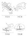
- FIGS. 1A and 1Bare perspective views of the microprobe according to the first embodiment.
- FIG. 1Ais a perspective view of the microprobe when viewed from the bottom direction.
- FIG. 1Bis a perspective view of the microprobe when viewed from the top direction.
- the same reference numerals in the following views of the drawingdenote the same constituent elements.
- a microprobe 10serves to record/reproduce information on/from a recording medium, and has a supporting base 14 , an insulating layer 13 , and an electrode layer 12 arrayed in a first direction D 1 in this order.
- a step 15is formed on a principal surface 11 of the microprobe 10 which is formed in a second direction D 2 different from the first direction D 1 .
- the step 15partitions the electrode layer 12 into the first and second areas 11 a , 11 b .
- the lengths of the step 15 and second area 11 b in the second direction D 2are set to bring a first corner portion X formed on the first area 11 a or the step 15 into contact with a recording medium and inhibit the second area from coming into contact with the recording medium.
- the supporting base 14may have no step.
- a stepis formed on at least the electrode layer 12 .
- This steppartitions the electrode layer 12 into the first and second areas 11 a , 11 b .
- the technical significance of the formation of the step 15is that it is possible to deposit the electrode layer 12 having a large area easily at a low manufacturing cost in a manufacturing process, as shown in FIGS. 1A and 1B .
- the upper surface of a lever portion 16i.e., the surface on the opposite side to the principal surface 11 described above, is coated with a lever electrode 17 .
- the electrode layer 12transfers electrical information to a support electrode 19 formed on the surface of a support base portion 18 via the lever electrode 17 of the lever portion 16 .
- FIG. 2Ashows a state in which the microprobe 10 according to this embodiment is in contact with a recording medium 20 .
- FIG. 2Bis an enlarged view of a portion where the microprobe 10 is in contact with the recording medium 20 .
- the electrode layer 12is preferably made of a material which has good conductivity to transfer electrical information between the microprobe 10 and is harder than the supporting base 14 and the insulating layer 13 and softer than the medium 20 .
- a material for the electrode layer 12it is possible to use a material having high anti-wear resistance which is formed on the sidewall of the insulating layer 13 or the base 14 , such as, W, Ru, Rh, Mo, or Cr.
- a hard material as the electrode layer 12makes the electrode layer wear slower than the supporting base 14 and the insulating layer 13 in accordance with the hardness difference. This makes it easy for the electrode layer 12 to protrude, and hence prevents deterioration in contact with the recording medium 20 even when the base 14 and the insulating layer were worn.
- the supporting base 14As a material for the supporting base 14 , it is possible to use Si, SiO X , SiN X , or the like which allows easy processing or shaping by a MEMS process. It is also possible to use Si, SiO X , or SiN X as an insulating material. Therefore, using such a material as the same material for the supporting base 14 and the insulating layer 13 can integrate the supporting base 14 and the insulating layer 13 .
- the recording medium 20 or the probe 10When recording information on the recording medium 20 or reproducing information from the recording medium 20 , the recording medium 20 or the probe 10 is moved relatively to the microprobe 10 or the recording medium. This relative moving direction is called a “probe scan direction”. As shown in FIGS. 2A and 2B , when a voltage is applied to the microprobe 10 while the corner portion of the microprobe 10 is in contact with the recording medium 20 , a recording bit 21 can be formed.
- the microprobe 10performs position control as follows.
- a first control unit 33controls the position of the microprobe 10 to bring the first corner portion X of the supporting base 14 having the electrode layer 12 formed on a side surface into contact with the recording medium 20 before a second corner portion Y of the second area 11 b (i.e., the tip of the microprobe 10 ) which protrudes in the longitudinal direction of the supporting base 14 . That is, as is obvious from FIG. 2A , the first control unit 33 tilts the microprobe 10 at a proper angle relative to the recording surface of the recording medium 20 so as to bring the two portions into contact with the recording surface. This brings the first corner portion X of the supporting base 14 into contact with the recording medium 20 , and simultaneously brings the electrode layer 12 into contact with the recording medium 20 .
- FIG. 1Ait is possible to form a step on a side wall of the microprobe 10 which is located on the opposite side to the electrode layer 12 .
- This embodimentcan reliably bring the electrode layer 12 into contact with the recording surface of the recording medium 20 . This will be described with reference to FIG. 3 .
- a repulsive force F from the recording medium 20acts on a point p of the microprobe 10 , as shown in FIG. 3 .
- the point ppasses through a shape center axis C 1 of the probe tip.
- This torqueacts in a direction to bring the electrode layer 12 of the microprobe 10 into contact with the recording medium 20 , i.e., the second direction D 2 . It is therefore possible to reliably bring the electrode layer 12 of the microprobe 10 into contact with the recording surface of the recording medium 20 , thus maintaining the stable recording/reproducing characteristics.
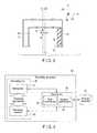
- FIG. 4is a block diagram showing a recording apparatus according to this embodiment.
- a recording apparatus 30includes a control unit 32 connected to an external apparatus 31 and a recording unit 35 .
- the control unit 32includes the first control unit 33 and a second control unit 34 .
- the recording unit 35includes the microprobe 10 and the recording medium 20 .
- the first control unit 33controls the relative positions of the microprobe 10 and recording medium 20 .
- the second control unit 34records information on the recording medium 20 or reproduces information from the recording medium 20 by using the electrical interaction between the electrode layer 12 of the microprobe 10 and the recording medium 20 .
- the external apparatus 31provides information to the control unit 32 .
- the informationis sent to the external apparatus 31 via the control unit 32 .
- FIGS. 5A , 5 B, 5 C, 5 D, 5 E, 5 F, 5 G, 5 H, and 5 Ishow an example of a manufacturing process for the microprobe 10 according to this embodiment.
- an SOI substrate 43was used, which included a device layer 40 having a thickness of 10 ⁇ m, a box layer 41 having a thickness of 0.5 ⁇ m, and a handling layer 42 having a thickness of 380 ⁇ m.
- FIG. 5Aaluminum is deposited and patterned by an Al sputtering process, a lithography process and a wet etching process to form an aluminum mask 44 for the formation of the step 15 on the probe tip. Subsequently, a lithography step is executed again to produce a resist mask 45 for the formation of a probe shape.
- FIG. 5Bthe shape of the microprobe 10 without any step on the distal end portion is obtained by a DRIE (Deep Reactive Ion Etching) process.
- FIG. 5Cthe resist mask 45 is removed to expose the aluminum mask 44 , and lithography process and DRIE process are executed again to form the step 15 on the probe tip.
- FIG. 5Dthe aluminum mask 44 is removed, and a thermal oxidation step is performed to form the insulating layer 13 .
- lithography and DRIE stepsare executed again to form the support base portion 18 on the handling layer 42 of the SOI substrate 43 .
- the SOI substrate 43is turned over, and an aluminum mask for a support base is formed on the handling layer 42 of the SOI substrate 43 by an aluminum deposition process, a lithography process, and an aluminum etching process. Thereafter, as shown in FIG. 5F , the handling layer 42 is etched by DRIE process to form the support base portion 18 . As shown in FIG. 5G , the box layer 41 on the SOI substrate 43 is then removed to release the microprobe 10 .
- FIG. 5Hthe protective resist applied to the device layer 40 of the SOI substrate 43 is removed.
- FIG. 5Hcorresponds to a cross section taken along a line A-A′ in FIG. 1A .
- the electrode layer 12 and the support electrode 19are formed on the surface of the handling layer 42 of the SOI substrate 43 by a sputtering or vacuum deposition step.
- the sputtering or vacuum deposition directioncorresponds to the surface on the opposite side to the principal surface 11 on which the step 15 is formed, i.e., the direction from the lower surface (the surface on the side where the support base portion 18 protrudes) to D 2 .
- FIGS. 6A and 6Bshow an example of the microprobe manufactured in the above manner.
- FIG. 6Ashows the overall microprobe including the support base portion.
- FIG. 6Bis an enlarged view of the probe tip.
- the step 15when sputtering or vacuum deposition is to be performed, since the step 15 is formed on the probe tip, the step 15 serves as an overhang to inhibit deposition on the principal surface 11 of the supporting base 14 and the first corner portion X. As a consequence, the electrode layer 12 is deposited on only a side wall of the probe tip on the outermost side. This makes it possible to easily deposit the electrode layer 12 so as to array the supporting base 14 , the insulating layer 13 , and the electrode layer 12 in the first direction D 1 in this order. This requires no other microfabrication, and hence can suppress the manufacturing cost.
- the supporting base 14 , the insulating layer 13 , and the electrode layer 12are arrayed in the first direction D 1 in this order, and their corner portions come into contact with the recording medium 20 .
- This structurecan prevent the repulsive force from the recording medium 20 at the time of contact of the microprobe 10 with the recording medium 20 from concentrating on only the electrode layer 12 , and can disperse the repulsive force to the supporting base 14 and the insulating layer 13 . It is therefore possible to suppress the abrasion of the electrode layer 12 without increasing the electrical contact area of the electrode layer 12 with the recording medium 20 .
- the material for the electrode layer 12is harder than the material for the supporting base 14 and the insulating layer 13 . In this case, even if abrasion occurs on the distal end of the microprobe 10 , stable recording/reproducing characteristics can be maintained since the electrode layer 12 still protrudes and contacts with the medium 20 . This can prolong the effective service life of the microprobe 10 .
- a microprobe 10 shown in FIG. 1includes an electrode layer 12 on a side surface of a lever portion 16 (supporting base 14 ).
- the second embodimenthas a structure including two electrode layers 50 a and 50 b on the both sidewall surfaces of the lever portion 16 , as shown in FIGS. 7A and 7B .
- the second embodimenthas the same effects as those of the first embodiment, and doubles the amount of information to be recorded/reproduced which can be handled by one microprobe because of the two electrode layers 50 a and 50 b on the distal end of the one microprobe.
- a plurality of slits 61 a , 61 b , 61 c , . . .are formed in the distal end of a microprobe 62 .
- the direction in which the slits 61 a , 61 b , 61 c , . . . are formedis a first direction D 1 , which is the scan direction of the microprobe.
- a plurality of steps 63 a , 63 b , 63 c , . . .are formed.
- a supporting base 64 a , an insulating layer 65 a , and an electrode layer 60 aare formed to be arrayed in the first direction in this order.
- a supporting base 64 b , an insulating layer 65 b , and an electrode layer 60 bare formed to be arrayed in the first direction in this order.
- a supporting base 64 c , an insulating layer 65 c , and an electrode layer 60 care formed to be arrayed in the first direction in this order.
- the plurality of electrode layers 60 a , 60 b , 60 c , . . .may be formed on side surfaces of the slits 61 a , 61 b , 61 c , . . . in this manner.
- the size of recording/reproduction information and recording densitycan be defined by the thickness of electrode layer and the arrangement intervals between the electrode layers 60 a , 60 b , 60 c , . . . , respectively.
- reducing the thickness of the electrode layer and the pitch of the electrodes 60 a , 60 b , 60 c , . . .can increase the recording density and the amount of information which can be written in a recording medium at once. Otherwise, by reducing Relative movement pitch of the probe and the recording media, the recording density can be increased, too.
- the third embodimentgreatly increases the amount of recording/reproduction information which can be handled by one microprobe as compared with the first and second embodiments.
- the distal end of a microprobe 71has a plurality of slits in the shape of a fork unlike in the third embodiment.
- the direction in which slits 73 a , 73 b , 73 c , . . . are formedis the first direction D 1 , which is the scan direction of the microprobe.
- a plurality of steps 72 a , 72 b , 72 c , . . .are formed.
- a supporting base 74 a , an insulating layer 75 a , and an electrode layer 70 aare formed to be arrayed in the first direction in this order.
- a supporting base 74 b , an insulating layer 75 b , and an electrode layer 70 bare formed to be arrayed in the first direction in this order.
- a supporting base 74 c , an insulating layer 75 c , and an electrode layer 70 care formed to be arrayed in the first direction in this order.
- the plurality of electrode layers 70 a , 70 b , 70 c , . . .may be formed on side surfaces of the slits 73 a , 73 b , 73 c, . . . .
- the size of recording/reproduction information and recording densitycan be defined by the thickness of electrode layer and the arrangement intervals between the electrode layers 70 a , 70 b , 70 c , . . . , respectively.
- reducing the thickness of the electrode layer and the pitch of the electrodes 70 a , 70 b , 70 c , . . .can increase the recording density and the amount of information which can be written in a recording medium at once. Otherwise, by reducing Relative movement pitch of the probe and the recording media, the recording density can be increased, too.
- the fourth embodimentgreatly increases the amount of recording/reproduction information which can be handled by one microprobe as compared with the first and second embodiments.
- the fifth embodimentis directed to a modification of the first to fourth embodiments described above.
- the step 15is formed on at least the electrode layer 12 on the principal surface 11 of the microprobe 10 .
- the step 15partitions the electrode layer 12 into the first and second areas 11 a , 11 b , and the second area 11 b forms a distal end portion of the microprobe 10 .
- the second areai.e., the area protruding in a third direction D 3
- an end portion of the step 15forms an end portion of the microprobe 10 . This can prevent the second corner portion Y formed on the second area from coming into contact with the recording medium 20 due to an operation error, impact, or the like. It is therefore possible to improve the stability of recording/reproducing characteristics.
Landscapes
- Physics & Mathematics (AREA)
- General Physics & Mathematics (AREA)
- Micromachines (AREA)
- Semiconductor Memories (AREA)
Abstract
Description
Claims (18)
Applications Claiming Priority (2)
| Application Number | Priority Date | Filing Date | Title |
|---|---|---|---|
| JP2010203659AJP5044685B2 (en) | 2010-09-10 | 2010-09-10 | Microprobe, recording apparatus, and method of manufacturing microprobe |
| JP2010-203659 | 2010-09-10 |
Publications (2)
| Publication Number | Publication Date |
|---|---|
| US20120062213A1 US20120062213A1 (en) | 2012-03-15 |
| US9224415B2true US9224415B2 (en) | 2015-12-29 |
Family
ID=45806042
Family Applications (1)
| Application Number | Title | Priority Date | Filing Date |
|---|---|---|---|
| US13/071,555Active2034-01-10US9224415B2 (en) | 2010-09-10 | 2011-03-25 | Microprobe, recording apparatus, and method of manufacturing microprobe |
Country Status (2)
| Country | Link |
|---|---|
| US (1) | US9224415B2 (en) |
| JP (1) | JP5044685B2 (en) |
Families Citing this family (3)
| Publication number | Priority date | Publication date | Assignee | Title |
|---|---|---|---|---|
| JP5369209B2 (en)* | 2012-03-14 | 2013-12-18 | 株式会社東芝 | Multi-probe, recording apparatus, and multi-probe manufacturing method |
| JP5787923B2 (en)* | 2013-03-15 | 2015-09-30 | 株式会社東芝 | Microprobe and method of manufacturing microprobe |
| US12091313B2 (en) | 2019-08-26 | 2024-09-17 | The Research Foundation For The State University Of New York | Electrodynamically levitated actuator |
Citations (29)
| Publication number | Priority date | Publication date | Assignee | Title |
|---|---|---|---|---|
| US4161437A (en)* | 1975-01-15 | 1979-07-17 | Dragerwerk Aktiengesellschaft | Measuring probe for the polarographic determination of partial gas pressures |
| US5610898A (en)* | 1991-07-17 | 1997-03-11 | Canon Kabushiki Kaisha | Information recording/reproducing method for recording and/or reproducing information on information recording carrier by use of probe electrode |
| US6072764A (en)* | 1997-05-13 | 2000-06-06 | Canon Kabushiki Kaisha | Information processing apparatus having face regulating system |
| US20020137998A1 (en)* | 2001-03-26 | 2002-09-26 | Wilson Smart | Silicon microprobe with integrated biosensor |
| US6473361B1 (en)* | 2000-11-10 | 2002-10-29 | Xerox Corporation | Electromechanical memory cell |
| US20040105380A1 (en)* | 2002-11-28 | 2004-06-03 | Pioneer Corporation | Dielectric recording / reproducing head and dielectric recording / reproducing apparatus |
| US20050082474A1 (en)* | 2003-10-17 | 2005-04-21 | Shih-Yi Wen | MEMS differential actuated nano probe and method for fabrication |
| US20050092709A1 (en)* | 2003-03-24 | 2005-05-05 | Seoul National University Industry Foundation | Microprobe for testing electronic device and manufacturing method thereof |
| US6894272B2 (en)* | 2000-06-09 | 2005-05-17 | Innovationsagentur Gesellschaft Mbh | Device for simultaneously carrying out an electrochemical and a topographical near-field microscopy |
| US20050179458A1 (en)* | 2003-02-04 | 2005-08-18 | Microfabrica Inc. | Cantilever microprobes for contacting electronic components and methods for making such probes |
| US20050189958A1 (en)* | 2003-02-04 | 2005-09-01 | Microfabrica Inc. | Cantilever microprobes for contacting electronic components and methods for making such probes |
| US20050212539A1 (en)* | 2003-02-04 | 2005-09-29 | Microfabrica Inc. | Cantilever microprobes for contacting electronic components and methods for making such probes |
| US20060023606A1 (en)* | 2004-07-30 | 2006-02-02 | Seagate Technology Llc | Ferroelectric probe storage apparatus |
| US7233517B2 (en)* | 2002-10-15 | 2007-06-19 | Nanochip, Inc. | Atomic probes and media for high density data storage |
| US7239544B2 (en)* | 2004-09-14 | 2007-07-03 | Hewlett-Packard Development Company, L.P. | Electrical memory component and a method of construction thereof |
| US20070165512A1 (en)* | 2005-12-27 | 2007-07-19 | Hitachi Ltd. | Information Processing Apparatus |
| US20070274193A1 (en)* | 2006-03-28 | 2007-11-29 | Junichi Akiyama | Information recording and reproducing apparatus |
| US20080009763A1 (en)* | 2006-06-09 | 2008-01-10 | Jin-Chern Chiou | Microprobe array structure and method for manufacturing the same |
| US7349236B2 (en)* | 2005-06-24 | 2008-03-25 | Xerox Corporation | Electromechanical memory cell with torsional movement |
| US20080149832A1 (en)* | 2006-12-20 | 2008-06-26 | Miguel Zorn | Scanning Probe Microscope, Nanomanipulator with Nanospool, Motor, nucleotide cassette and Gaming application |
| US20080229577A1 (en)* | 2007-03-19 | 2008-09-25 | John Heck | Seek-scan probe (SSP) memory with sharp probe tips formed at CMOS-compatible temperatures |
| US20090206953A1 (en)* | 2008-02-15 | 2009-08-20 | Scannanotek Oy | Resonant mems device that detects photons, particles and small forces |
| US20090283867A1 (en)* | 2008-05-13 | 2009-11-19 | Jin-Chem Chiou | Integration structure of semiconductor circuit and microprobe sensing elements and method for fabricating the same |
| US20100331935A1 (en)* | 2009-05-01 | 2010-12-30 | Phillipe Tabada | Rigid Spine Reinforced Polymer Microelectrode Array Probe and Method of Fabrication |
| US20110062594A1 (en)* | 2008-10-16 | 2011-03-17 | Dai Nippon Printing, Co., Ltd. | Through hole electrode substrate, method for manufacturing the through hole electrode substrate, and semiconductor device using the through hole electrode substrate |
| US20110169517A1 (en)* | 2008-09-05 | 2011-07-14 | Kim Sang-Hee | Mems probe card and method of manufacturing same |
| US20110194398A1 (en)* | 2010-01-29 | 2011-08-11 | Yongfang Li | Mems memory microprobe and recording apparatus |
| US8045444B2 (en)* | 2007-09-25 | 2011-10-25 | International Business Machines Corporation | Method of controlling movements of a position of a microscanner |
| US8988065B2 (en)* | 2013-03-15 | 2015-03-24 | Kabushiki Kaisha Toshiba | Microprobe and microprobe manufacturing method |
- 2010
- 2010-09-10JPJP2010203659Apatent/JP5044685B2/enactiveActive
- 2011
- 2011-03-25USUS13/071,555patent/US9224415B2/enactiveActive
Patent Citations (35)
| Publication number | Priority date | Publication date | Assignee | Title |
|---|---|---|---|---|
| US4161437A (en)* | 1975-01-15 | 1979-07-17 | Dragerwerk Aktiengesellschaft | Measuring probe for the polarographic determination of partial gas pressures |
| US5610898A (en)* | 1991-07-17 | 1997-03-11 | Canon Kabushiki Kaisha | Information recording/reproducing method for recording and/or reproducing information on information recording carrier by use of probe electrode |
| US6072764A (en)* | 1997-05-13 | 2000-06-06 | Canon Kabushiki Kaisha | Information processing apparatus having face regulating system |
| US6894272B2 (en)* | 2000-06-09 | 2005-05-17 | Innovationsagentur Gesellschaft Mbh | Device for simultaneously carrying out an electrochemical and a topographical near-field microscopy |
| US6473361B1 (en)* | 2000-11-10 | 2002-10-29 | Xerox Corporation | Electromechanical memory cell |
| US20020137998A1 (en)* | 2001-03-26 | 2002-09-26 | Wilson Smart | Silicon microprobe with integrated biosensor |
| US7233517B2 (en)* | 2002-10-15 | 2007-06-19 | Nanochip, Inc. | Atomic probes and media for high density data storage |
| US20040105380A1 (en)* | 2002-11-28 | 2004-06-03 | Pioneer Corporation | Dielectric recording / reproducing head and dielectric recording / reproducing apparatus |
| US20050179458A1 (en)* | 2003-02-04 | 2005-08-18 | Microfabrica Inc. | Cantilever microprobes for contacting electronic components and methods for making such probes |
| US20050189958A1 (en)* | 2003-02-04 | 2005-09-01 | Microfabrica Inc. | Cantilever microprobes for contacting electronic components and methods for making such probes |
| US20050212539A1 (en)* | 2003-02-04 | 2005-09-29 | Microfabrica Inc. | Cantilever microprobes for contacting electronic components and methods for making such probes |
| US20050092709A1 (en)* | 2003-03-24 | 2005-05-05 | Seoul National University Industry Foundation | Microprobe for testing electronic device and manufacturing method thereof |
| US20050082474A1 (en)* | 2003-10-17 | 2005-04-21 | Shih-Yi Wen | MEMS differential actuated nano probe and method for fabrication |
| US20060016986A1 (en)* | 2003-10-17 | 2006-01-26 | Industrial Technology Research Instutite | MEMS differential actuated nano probe and method for fabrication |
| US6995368B2 (en)* | 2003-10-17 | 2006-02-07 | Industrial Technology Research Institute | MEMS differential actuated nano probe and method for fabrication |
| US7176457B2 (en)* | 2003-10-17 | 2007-02-13 | Industrial Technology Research Institute | MEMS differential actuated nano probe and method for fabrication |
| US20060023606A1 (en)* | 2004-07-30 | 2006-02-02 | Seagate Technology Llc | Ferroelectric probe storage apparatus |
| US7239544B2 (en)* | 2004-09-14 | 2007-07-03 | Hewlett-Packard Development Company, L.P. | Electrical memory component and a method of construction thereof |
| US7349236B2 (en)* | 2005-06-24 | 2008-03-25 | Xerox Corporation | Electromechanical memory cell with torsional movement |
| US20070165512A1 (en)* | 2005-12-27 | 2007-07-19 | Hitachi Ltd. | Information Processing Apparatus |
| US20070274193A1 (en)* | 2006-03-28 | 2007-11-29 | Junichi Akiyama | Information recording and reproducing apparatus |
| US20080009763A1 (en)* | 2006-06-09 | 2008-01-10 | Jin-Chern Chiou | Microprobe array structure and method for manufacturing the same |
| US20080149832A1 (en)* | 2006-12-20 | 2008-06-26 | Miguel Zorn | Scanning Probe Microscope, Nanomanipulator with Nanospool, Motor, nucleotide cassette and Gaming application |
| US20080229577A1 (en)* | 2007-03-19 | 2008-09-25 | John Heck | Seek-scan probe (SSP) memory with sharp probe tips formed at CMOS-compatible temperatures |
| US8045444B2 (en)* | 2007-09-25 | 2011-10-25 | International Business Machines Corporation | Method of controlling movements of a position of a microscanner |
| US20090206953A1 (en)* | 2008-02-15 | 2009-08-20 | Scannanotek Oy | Resonant mems device that detects photons, particles and small forces |
| US7910390B2 (en)* | 2008-02-15 | 2011-03-22 | Scannanotek Oy | Resonant MEMS device that detects photons, particles and small forces |
| US20090283867A1 (en)* | 2008-05-13 | 2009-11-19 | Jin-Chem Chiou | Integration structure of semiconductor circuit and microprobe sensing elements and method for fabricating the same |
| US20110169517A1 (en)* | 2008-09-05 | 2011-07-14 | Kim Sang-Hee | Mems probe card and method of manufacturing same |
| US20110062594A1 (en)* | 2008-10-16 | 2011-03-17 | Dai Nippon Printing, Co., Ltd. | Through hole electrode substrate, method for manufacturing the through hole electrode substrate, and semiconductor device using the through hole electrode substrate |
| US20100331935A1 (en)* | 2009-05-01 | 2010-12-30 | Phillipe Tabada | Rigid Spine Reinforced Polymer Microelectrode Array Probe and Method of Fabrication |
| US20110194398A1 (en)* | 2010-01-29 | 2011-08-11 | Yongfang Li | Mems memory microprobe and recording apparatus |
| JP2011159350A (en)* | 2010-01-29 | 2011-08-18 | Toshiba Corp | Microprobe for mems memory |
| US8331212B2 (en)* | 2010-01-29 | 2012-12-11 | Kabushiki Kaisha Toshiba | MEMS memory microprobe and recording apparatus |
| US8988065B2 (en)* | 2013-03-15 | 2015-03-24 | Kabushiki Kaisha Toshiba | Microprobe and microprobe manufacturing method |
Also Published As
| Publication number | Publication date |
|---|---|
| US20120062213A1 (en) | 2012-03-15 |
| JP2012059332A (en) | 2012-03-22 |
| JP5044685B2 (en) | 2012-10-10 |
Similar Documents
| Publication | Publication Date | Title |
|---|---|---|
| US6748865B2 (en) | Nano-imprinting method, magnetic printing method and recording medium | |
| JP4163729B2 (en) | Magnetic recording medium, method for manufacturing the same, and magnetic recording apparatus | |
| US7309630B2 (en) | Method for forming patterned media for a high density data storage device | |
| CA2069708C (en) | Probe-driving mechanism, production thereof, and apparatus and piezoelectric actuator employing the same | |
| US20070121477A1 (en) | Cantilever with control of vertical and lateral position of contact probe tip | |
| US20080023885A1 (en) | Method for forming a nano-imprint lithography template having very high feature counts | |
| JP2006092632A (en) | Magnetic recording medium, its manufacturing method, and intermediate body for magnetic recording medium | |
| US20060269796A1 (en) | Magnetic recording medium, method of manufacturing the same, and magnetic recording apparatus | |
| US9224415B2 (en) | Microprobe, recording apparatus, and method of manufacturing microprobe | |
| US6943990B1 (en) | Head support mechanism, information recording/reproducing apparatus, and method of manufacturing head support mechanism | |
| US20070041238A1 (en) | High density data storage devices with read/write probes with hollow or reinforced tips | |
| US7367119B2 (en) | Method for forming a reinforced tip for a probe storage device | |
| US20130001719A1 (en) | Interaction structure for a storage medium | |
| US20070008866A1 (en) | Methods for writing and reading in a polarity-dependent memory switch media | |
| US20090285082A1 (en) | Electric field read/write head, method of manufacturing the electric field read/write head, and information storage device including the electric field read/write head | |
| JP5007383B2 (en) | Microprobe for MEMS memory | |
| US20070008867A1 (en) | High density data storage devices with a lubricant layer comprised of a field of polymer chains | |
| US7463573B2 (en) | Patterned media for a high density data storage device | |
| US7593309B2 (en) | Method for recording data and device for carrying out the same comprising a deformable memory support | |
| JP4494337B2 (en) | Data recording apparatus having diaphragm type support | |
| JP2006331540A (en) | Magnetic recording medium and magnetic recording apparatus | |
| US7854016B2 (en) | Process for manufacturing probes intended to interact with a storage medium and probe obtained thereby | |
| US20090175153A1 (en) | Electrical-Effect Data Recording Medium that Includes a Localized Electrical Conduction Layer | |
| JP5369209B2 (en) | Multi-probe, recording apparatus, and multi-probe manufacturing method | |
| JP4966501B2 (en) | Scanning probe memory device |
Legal Events
| Date | Code | Title | Description |
|---|---|---|---|
| AS | Assignment | Owner name:KABUSHIKI KAISHA TOSHIBA, JAPAN Free format text:ASSIGNMENT OF ASSIGNORS INTEREST;ASSIGNORS:LI, YONGFANG;TOMIZAWA, YASUSHI;KOGA, AKIHIRO;AND OTHERS;SIGNING DATES FROM 20110328 TO 20110405;REEL/FRAME:026396/0150 Owner name:THE UNIVERSITY OF TOKYO, A NATIONAL UNIVERSITY COR Free format text:ASSIGNMENT OF ASSIGNORS INTEREST;ASSIGNORS:LI, YONGFANG;TOMIZAWA, YASUSHI;KOGA, AKIHIRO;AND OTHERS;SIGNING DATES FROM 20110328 TO 20110405;REEL/FRAME:026396/0150 | |
| STCF | Information on status: patent grant | Free format text:PATENTED CASE | |
| MAFP | Maintenance fee payment | Free format text:PAYMENT OF MAINTENANCE FEE, 4TH YEAR, LARGE ENTITY (ORIGINAL EVENT CODE: M1551); ENTITY STATUS OF PATENT OWNER: LARGE ENTITY Year of fee payment:4 | |
| AS | Assignment | Owner name:TOSHIBA MEMORY CORPORATION, JAPAN Free format text:CONFIRMATORY ASSIGNMENT;ASSIGNOR:KABUSHIKI KAISHA TOSHIBA;REEL/FRAME:051841/0432 Effective date:20170401 Owner name:KIOXIA CORPORATION, JAPAN Free format text:CHANGE OF NAME;ASSIGNOR:TOSHIBA MEMORY CORPORATION;REEL/FRAME:051842/0789 Effective date:20191001 Owner name:TOSHIBA MEMORY CORPORATION, JAPAN Free format text:MERGER AND CHANGE OF NAME;ASSIGNORS:TOSHIBA MEMORY CORPORATION;K.K. PANGEA;REEL/FRAME:051855/0531 Effective date:20180801 | |
| MAFP | Maintenance fee payment | Free format text:PAYMENT OF MAINTENANCE FEE, 8TH YEAR, LARGE ENTITY (ORIGINAL EVENT CODE: M1552); ENTITY STATUS OF PATENT OWNER: LARGE ENTITY Year of fee payment:8 |