US9223719B2 - Integrating data from symmetric and asymmetric memory - Google Patents
Integrating data from symmetric and asymmetric memoryDownload PDFInfo
- Publication number
- US9223719B2 US9223719B2US14/047,627US201314047627AUS9223719B2US 9223719 B2US9223719 B2US 9223719B2US 201314047627 AUS201314047627 AUS 201314047627AUS 9223719 B2US9223719 B2US 9223719B2
- Authority
- US
- United States
- Prior art keywords
- memory
- data
- asymmetric
- collection
- threshold
- Prior art date
- Legal status (The legal status is an assumption and is not a legal conclusion. Google has not performed a legal analysis and makes no representation as to the accuracy of the status listed.)
- Expired - Fee Related
Links
Images


Classifications
- G—PHYSICS
- G06—COMPUTING OR CALCULATING; COUNTING
- G06F—ELECTRIC DIGITAL DATA PROCESSING
- G06F12/00—Accessing, addressing or allocating within memory systems or architectures
- G06F12/02—Addressing or allocation; Relocation
- G06F12/08—Addressing or allocation; Relocation in hierarchically structured memory systems, e.g. virtual memory systems
- G06F12/10—Address translation
- G—PHYSICS
- G06—COMPUTING OR CALCULATING; COUNTING
- G06F—ELECTRIC DIGITAL DATA PROCESSING
- G06F9/00—Arrangements for program control, e.g. control units
- G06F9/06—Arrangements for program control, e.g. control units using stored programs, i.e. using an internal store of processing equipment to receive or retain programs
- G06F9/46—Multiprogramming arrangements
- G06F9/50—Allocation of resources, e.g. of the central processing unit [CPU]
- G06F9/5005—Allocation of resources, e.g. of the central processing unit [CPU] to service a request
- G06F9/5011—Allocation of resources, e.g. of the central processing unit [CPU] to service a request the resources being hardware resources other than CPUs, Servers and Terminals
- G06F9/5016—Allocation of resources, e.g. of the central processing unit [CPU] to service a request the resources being hardware resources other than CPUs, Servers and Terminals the resource being the memory
- G—PHYSICS
- G06—COMPUTING OR CALCULATING; COUNTING
- G06F—ELECTRIC DIGITAL DATA PROCESSING
- G06F12/00—Accessing, addressing or allocating within memory systems or architectures
- G06F12/02—Addressing or allocation; Relocation
- G06F12/0207—Addressing or allocation; Relocation with multidimensional access, e.g. row/column, matrix
- G—PHYSICS
- G06—COMPUTING OR CALCULATING; COUNTING
- G06F—ELECTRIC DIGITAL DATA PROCESSING
- G06F12/00—Accessing, addressing or allocating within memory systems or architectures
- G06F12/02—Addressing or allocation; Relocation
- G06F12/08—Addressing or allocation; Relocation in hierarchically structured memory systems, e.g. virtual memory systems
- G06F12/12—Replacement control
- G06F12/121—Replacement control using replacement algorithms
- G—PHYSICS
- G06—COMPUTING OR CALCULATING; COUNTING
- G06F—ELECTRIC DIGITAL DATA PROCESSING
- G06F13/00—Interconnection of, or transfer of information or other signals between, memories, input/output devices or central processing units
- G06F13/14—Handling requests for interconnection or transfer
- G06F13/16—Handling requests for interconnection or transfer for access to memory bus
- G06F13/1605—Handling requests for interconnection or transfer for access to memory bus based on arbitration
- G06F13/1652—Handling requests for interconnection or transfer for access to memory bus based on arbitration in a multiprocessor architecture
- G06F13/1657—Access to multiple memories
- G—PHYSICS
- G06—COMPUTING OR CALCULATING; COUNTING
- G06F—ELECTRIC DIGITAL DATA PROCESSING
- G06F3/00—Input arrangements for transferring data to be processed into a form capable of being handled by the computer; Output arrangements for transferring data from processing unit to output unit, e.g. interface arrangements
- G06F3/06—Digital input from, or digital output to, record carriers, e.g. RAID, emulated record carriers or networked record carriers
- G06F3/0601—Interfaces specially adapted for storage systems
- G06F3/0602—Interfaces specially adapted for storage systems specifically adapted to achieve a particular effect
- G06F3/0604—Improving or facilitating administration, e.g. storage management
- G—PHYSICS
- G06—COMPUTING OR CALCULATING; COUNTING
- G06F—ELECTRIC DIGITAL DATA PROCESSING
- G06F3/00—Input arrangements for transferring data to be processed into a form capable of being handled by the computer; Output arrangements for transferring data from processing unit to output unit, e.g. interface arrangements
- G06F3/06—Digital input from, or digital output to, record carriers, e.g. RAID, emulated record carriers or networked record carriers
- G06F3/0601—Interfaces specially adapted for storage systems
- G06F3/0628—Interfaces specially adapted for storage systems making use of a particular technique
- G06F3/0638—Organizing or formatting or addressing of data
- G06F3/064—Management of blocks
- G—PHYSICS
- G06—COMPUTING OR CALCULATING; COUNTING
- G06F—ELECTRIC DIGITAL DATA PROCESSING
- G06F3/00—Input arrangements for transferring data to be processed into a form capable of being handled by the computer; Output arrangements for transferring data from processing unit to output unit, e.g. interface arrangements
- G06F3/06—Digital input from, or digital output to, record carriers, e.g. RAID, emulated record carriers or networked record carriers
- G06F3/0601—Interfaces specially adapted for storage systems
- G06F3/0628—Interfaces specially adapted for storage systems making use of a particular technique
- G06F3/0646—Horizontal data movement in storage systems, i.e. moving data in between storage devices or systems
- G06F3/0647—Migration mechanisms
- G—PHYSICS
- G06—COMPUTING OR CALCULATING; COUNTING
- G06F—ELECTRIC DIGITAL DATA PROCESSING
- G06F3/00—Input arrangements for transferring data to be processed into a form capable of being handled by the computer; Output arrangements for transferring data from processing unit to output unit, e.g. interface arrangements
- G06F3/06—Digital input from, or digital output to, record carriers, e.g. RAID, emulated record carriers or networked record carriers
- G06F3/0601—Interfaces specially adapted for storage systems
- G06F3/0668—Interfaces specially adapted for storage systems adopting a particular infrastructure
- G06F3/0671—In-line storage system
- G06F3/0673—Single storage device
- G06F3/068—Hybrid storage device
- G—PHYSICS
- G06—COMPUTING OR CALCULATING; COUNTING
- G06F—ELECTRIC DIGITAL DATA PROCESSING
- G06F3/00—Input arrangements for transferring data to be processed into a form capable of being handled by the computer; Output arrangements for transferring data from processing unit to output unit, e.g. interface arrangements
- G06F3/06—Digital input from, or digital output to, record carriers, e.g. RAID, emulated record carriers or networked record carriers
- G06F3/0601—Interfaces specially adapted for storage systems
- G06F3/0668—Interfaces specially adapted for storage systems adopting a particular infrastructure
- G06F3/0671—In-line storage system
- G06F3/0683—Plurality of storage devices
- G06F3/0685—Hybrid storage combining heterogeneous device types, e.g. hierarchical storage, hybrid arrays
- G—PHYSICS
- G06—COMPUTING OR CALCULATING; COUNTING
- G06F—ELECTRIC DIGITAL DATA PROCESSING
- G06F12/00—Accessing, addressing or allocating within memory systems or architectures
- G06F12/02—Addressing or allocation; Relocation
- G06F12/0223—User address space allocation, e.g. contiguous or non contiguous base addressing
- G06F12/0292—User address space allocation, e.g. contiguous or non contiguous base addressing using tables or multilevel address translation means
- G—PHYSICS
- G06—COMPUTING OR CALCULATING; COUNTING
- G06F—ELECTRIC DIGITAL DATA PROCESSING
- G06F12/00—Accessing, addressing or allocating within memory systems or architectures
- G06F12/02—Addressing or allocation; Relocation
- G06F12/08—Addressing or allocation; Relocation in hierarchically structured memory systems, e.g. virtual memory systems
- G06F12/10—Address translation
- G06F12/1009—Address translation using page tables, e.g. page table structures
- G—PHYSICS
- G06—COMPUTING OR CALCULATING; COUNTING
- G06F—ELECTRIC DIGITAL DATA PROCESSING
- G06F12/00—Accessing, addressing or allocating within memory systems or architectures
- G06F12/14—Protection against unauthorised use of memory or access to memory
- G06F12/1458—Protection against unauthorised use of memory or access to memory by checking the subject access rights
- G06F12/1466—Key-lock mechanism
- G06F12/1475—Key-lock mechanism in a virtual system, e.g. with translation means
- G—PHYSICS
- G06—COMPUTING OR CALCULATING; COUNTING
- G06F—ELECTRIC DIGITAL DATA PROCESSING
- G06F13/00—Interconnection of, or transfer of information or other signals between, memories, input/output devices or central processing units
- G06F13/14—Handling requests for interconnection or transfer
- G06F13/16—Handling requests for interconnection or transfer for access to memory bus
- G06F13/1668—Details of memory controller
- G06F13/1694—Configuration of memory controller to different memory types
- G—PHYSICS
- G06—COMPUTING OR CALCULATING; COUNTING
- G06F—ELECTRIC DIGITAL DATA PROCESSING
- G06F2212/00—Indexing scheme relating to accessing, addressing or allocation within memory systems or architectures
- G06F2212/20—Employing a main memory using a specific memory technology
- G06F2212/205—Hybrid memory, e.g. using both volatile and non-volatile memory
- G—PHYSICS
- G06—COMPUTING OR CALCULATING; COUNTING
- G06F—ELECTRIC DIGITAL DATA PROCESSING
- G06F2212/00—Indexing scheme relating to accessing, addressing or allocation within memory systems or architectures
- G06F2212/65—Details of virtual memory and virtual address translation
- G06F2212/657—Virtual address space management
- G—PHYSICS
- G06—COMPUTING OR CALCULATING; COUNTING
- G06F—ELECTRIC DIGITAL DATA PROCESSING
- G06F3/00—Input arrangements for transferring data to be processed into a form capable of being handled by the computer; Output arrangements for transferring data from processing unit to output unit, e.g. interface arrangements
- G06F3/06—Digital input from, or digital output to, record carriers, e.g. RAID, emulated record carriers or networked record carriers
- G06F3/0601—Interfaces specially adapted for storage systems
- G06F3/0628—Interfaces specially adapted for storage systems making use of a particular technique
- G06F3/0638—Organizing or formatting or addressing of data
- G—PHYSICS
- G06—COMPUTING OR CALCULATING; COUNTING
- G06F—ELECTRIC DIGITAL DATA PROCESSING
- G06F3/00—Input arrangements for transferring data to be processed into a form capable of being handled by the computer; Output arrangements for transferring data from processing unit to output unit, e.g. interface arrangements
- G06F3/06—Digital input from, or digital output to, record carriers, e.g. RAID, emulated record carriers or networked record carriers
- G06F3/0601—Interfaces specially adapted for storage systems
- G06F3/0628—Interfaces specially adapted for storage systems making use of a particular technique
- G06F3/0646—Horizontal data movement in storage systems, i.e. moving data in between storage devices or systems
- Y02B60/1225—
- Y02B60/142—
- Y—GENERAL TAGGING OF NEW TECHNOLOGICAL DEVELOPMENTS; GENERAL TAGGING OF CROSS-SECTIONAL TECHNOLOGIES SPANNING OVER SEVERAL SECTIONS OF THE IPC; TECHNICAL SUBJECTS COVERED BY FORMER USPC CROSS-REFERENCE ART COLLECTIONS [XRACs] AND DIGESTS
- Y02—TECHNOLOGIES OR APPLICATIONS FOR MITIGATION OR ADAPTATION AGAINST CLIMATE CHANGE
- Y02D—CLIMATE CHANGE MITIGATION TECHNOLOGIES IN INFORMATION AND COMMUNICATION TECHNOLOGIES [ICT], I.E. INFORMATION AND COMMUNICATION TECHNOLOGIES AIMING AT THE REDUCTION OF THEIR OWN ENERGY USE
- Y02D10/00—Energy efficient computing, e.g. low power processors, power management or thermal management
Definitions
- This documentrelates to the configuration and use of main memory, including symmetric and asymmetric memory components, within a computer system.
- Main memoryis memory that is accessible to a central processing unit (“CPU”) of a computer or electronic device. Main memory is used to store data that is deemed likely to be actively used by the CPU.
- CPUcentral processing unit
- data stored within symmetric and asymmetric memory components of main memoryis integrated.
- the resultant integrated datais stored within at least one asymmetric memory component.
- the symmetric memory componentsare each configured to enable random access write operations in which an address within a block of the symmetric memory component is written without affecting the availability of other addresses within the block of the symmetric memory component.
- the asymmetric memory componentsare each configured to enable block write operations in which a write to an address within a block of one of the asymmetric memory components affects the availability of other addresses within the block of the asymmetric memory component.
- a write command to write data to a virtual address associated with a first physical address of an asymmetric memory component of the main memoryis received.
- a page tableis configured to change an association of the virtual address from the association to the first physical address of the asymmetric memory component of the main memory to a second physical address of a symmetric memory component of the main memory.
- An indication that the first physical address is no longer being usedis generated to enable association of the first physical address with another virtual address in a subsequent block write operation.
- a collection of content entries with access characteristics suitable for storage in the asymmetric memory componentis generated. It is determined whether the collection of content entries collectively occupy a threshold amount of storage or whether a threshold period of time has elapsed. In response to determining that the collection of content entries collectively occupy the threshold amount of storage or that the threshold period of time has elapsed, the collection of content entries is loaded to a region of the asymmetric memory component using a block write command.
- Implementationsmay include one or more of the following features.
- loading the collection of content entries to the region of the asymmetric memory componentmay include loading the collection of content entries to a region of the asymmetric memory component that is associated with the first physical address using a block write command.
- the asymmetric memory component of main memoryincludes NOR flash and the symmetric memory component may include dynamic random access memory (DRAM).
- DRAMdynamic random access memory
- a write commandis received to write data to virtual address associated with a first physical address that maps to the NOR flash memory
- a page tableis configured to change an association of the virtual address from the association to the first physical address that maps to the NOR flash memory to a second physical address that maps to DRAM memory.
- Association of the first physical address with another virtual addressis enabled and a collection of content entries of content is generated with access characteristics suitable for storage in the NOR flash memory. It is determined whether the collection of content entries of content includes a threshold amount of storage and the collection of content entries is loaded to the NOR flash using a block write command in response to determining whether the collection of content entries of content requires the threshold amount of storage.
- Loading, in response to determining whether the collection of content entries of content requires the threshold amount of storage, the collection of content entries to the NOR flashmay include loading, in response to determining whether the collection of content entries of content requires the threshold amount of storage, the collection of content entries to the NOR flash that is proximate to the first physical address.
- Generating the collection of content entriesmay include organizing, in symmetric memory, an amount of data to be written corresponding to a size of a sector within a bank of NOR flash.
- Generating the collection of content entriesmay include organizing, in symmetric memory, an amount of data to be written corresponding to a size of multiple blocks within a disruption region of the asymmetric memory component in which a write to an address within a block of one of the asymmetric memory components affects the availability of other addresses within the disruption region of the asymmetric memory component.
- Organizing the amount of datamay include structuring each block to include more than a first threshold of data and less than a second threshold of data.
- Structuring each block to include more than the first threshold of data and less than the second threshold of datamay include structuring each block to include more than the first threshold of data and less than the second threshold of data in response to determining that a system is not constrained for memory resources.
- Each blockmay be structured to support a sequential addition of data within the block.
- Organizing the amount of datamay include structuring a first block within the disruption region to include more than a first threshold of data, in response to determining that a particular write instruction configured to load data to the first block exceeds the first threshold, identifying a second block of data, and organizing additional data to be loaded to the second block of data.
- Structuring the amount of block writesmay include identifying a threshold amount of data for a disruption region, organizing the threshold amount of data into a collection of block organizations, and configuring a memory controller to load the collection of block organizations into the disruption region.
- Organizing the amount of datamay include identifying virtual addresses that were previously mapped to asymmetric memory component and that now map to symmetric memory, tracking the identified virtual addresses, identifying candidates with access characteristics suitable for use in asymmetric memory component, identifying a capacity threshold that indicates approximately a maximum amount of data that can be loaded to a memory structure that includes either a disruption region or a block, organizing the candidates into a memory structure, determining whether the identified candidates include a capacity threshold of data, loading, in response to determining that the identified candidates include a capacity threshold of data, the identified candidates to the memory structure, and accumulating, in response to determining that the identified candidates do not include a capacity threshold of data, additional candidates until a capacity threshold of data is available to load to the memory structure.
- Identifying the capacity thresholdmay include identifying the capacity threshold in response to determining that a system is constrained for memory resources.
- a disruption region in the asymmetric memory componentmay be identified, and one or more blocks within the disruption region may be identified. It may be determined that the one or more blocks within the disruption region do not need to replaced and that the collection of content entries can be added sequentially using a sequential write to the one or more blocks within the asymmetric memory component. The collection of content entries may be added to the disruption region using a sequential write.
- data stored within symmetric and asymmetric memory components of main memorymay be integrated and the resultant integrated data is stored within at least one asymmetric memory component.
- the symmetric memory componentsare each configured to enable random access write operations in which an address within a block of the symmetric memory component is written without affecting the availability of other addresses within the block of the symmetric memory component.
- the asymmetric memory componentsare each configured to enable block write operations in which a write to an address within a block of one of the asymmetric memory components affects the availability of other addresses within the block of the asymmetric memory component.
- First datais identified as having access characteristics suitable for storing in an asymmetric memory component.
- the first datais included among a collection of data to be written to the asymmetric memory component, and an amount of data within the collection of data to be written to the asymmetric memory component is identified.
- the amount of data within the collection of datais compared to a volume threshold to determine whether a block write to the asymmetric memory component is justified by the amount of data, and if justified, loading the collection of data to the asymmetric memory component.
- Implementationsmay include one or more of the following features. For example, identifying the first data as having the access characteristics suitable for storing in the asymmetric memory component may include determining that the first data is an update to second data that was previously stored in the asymmetric memory component. Including the first data among a collection of data to be written to the asymmetric memory component may include loading the first data to an organization location in a symmetric memory component.
- Loading the first data to the organization location in the symmetric memory componentmay include loading the first data from an original location in the asymmetric memory component.
- Loading the first data to the organization location in the symmetric memory componentmay include loading the first data from an original location in the symmetric memory component.
- FIG. 1illustrates an example of a first layer model of a computing system.
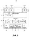
- FIG. 2illustrates an example of a second layer model of a computing system.
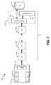
- FIG. 2Ais a block diagram of a system with a CPU that interfaces with a memory system through a memory controller.
- FIGS. 3A-3Bare diagrams illustrating an example of mapping a virtual address space of an application running on a processor into a physical address space of a hybrid main memory using a page table map.
- FIG. 4is a diagram of main memory illustrating an example of migration of information between symmetric memory regions and asymmetric memory regions.
- FIG. 5Ais a diagram illustrating the bits and bit fields in a page table entry in a page table, which is illustrated as having 32 bits.
- FIG. 5Bis a diagram illustrating the bits and bit fields in a sixty-four bit slot or page table entry in a page table.
- FIG. 6illustrates an example of a multilevel mapping of virtual address space of an application running on a processor into a physical address space of a hybrid main memory using a shadow page table.
- FIG. 7illustrates a virtual memory hierarchy for a computer system between a processor core and hard disk storage.
- FIG. 8is a flow of a process by which a memory controller integrates data stored within symmetric and asymmetric memory components of main memory.
- FIG. 9is a block diagram of a configuration for a hybrid memory system within a computer system that includes an asymmetric memory component and a symmetric memory component.
- FIG. 10is a diagram of a page table that indicates how a hybrid memory system for a computer system that includes an asymmetric memory component and a symmetric memory component is being used.
- FIG. 11is a diagram of a configuration for a collection of banks in an asymmetric memory component for a hybrid memory system within a computer system that indicates different levels of utilization.
- FIGS. 12-15are diagrams illustrating four different configurations of data in DRAM, organized to facilitate writing of the data to a block in the asymmetric portion of the hybrid memory system.
- FIG. 16is a flow chart of a process for loading a series of entries to a region of asymmetric memory.
- FIG. 17is a flow chart of a process for loading a series of entries to NOR flash memory by allowing some of the entries being collected for writing to asymmetric memory to come from locations in asymmetric memory.
- FIGS. 18 and 19are diagrams of configurations for a hybrid memory system that illustrate how a memory controller may identify a region of asymmetric memory based on the nature of the write being performed and the state of the region.
- Section Aprovides a brief description of method and mechanisms.
- Section Bprovides a description of the hardware, software, and system context.
- Section Cprovides a description of read movement, write movement, and integration.
- Section Dprovides a discussion of operations performed and additional configurations.
- Computer systemsmay be built using a hybrid memory system that includes symmetric and asymmetric memory components. More precisely, an application on a computer system interfaces with a main memory system that includes symmetric memory components and asymmetric memory components. For example, a search application may load a portion of a search index to asymmetric memory and perform search index analysis using symmetric memory.
- One type of symmetric memory componentincludes Dynamic Random Access Memory (DRAM).
- DRAMDynamic Random Access Memory
- symmetric memoryis volatile memory and includes memory that performs read operations in a time comparable to a time required to perform write operations.
- both read and write operationsmay be performed in a random access manner where a granular amount of data may be requested or written.
- asymmetric memoryis non-volatile memory and includes memory that supports random access read operations, but does not support random access write operations. Rather, write operations to an asymmetric memory component require a block of data to be written. As a result, write operations to some types of asymmetric memory can take an order to magnitude longer than read operations. In addition, writing a block of data to an asymmetric memory component creates a disruption region that is defined by the blocks of the asymmetric memory component that cannot be accessed during a block write operation. Examples of asymmetric memory include NOR flash memory.
- One example of a hybrid memory systemincludes main memory with DRAM as the symmetric memory component and NOR flash as the asymmetric memory component.
- the DRAM componentsare each configured to enable random access write operations in which an address within a block of the DRAM is written without affecting the availability of other addresses within the DRAM.
- the NOR flash componentsare each configured to enable block write operations in which a write to an address within a block of one of the NOR flash affects the availability of other addresses within the block of NOR flash.
- a computer system using a hybrid memory systemmay manage the asymmetric memory component in a special manner to maximize the storage space available for read-intensive data and minimize the impact of adverse performance issues (e.g., disruption regions) associated with block write operations.
- the computer systemmay attempt to load read intensive data to an asymmetric memory component and load write intensive data to a symmetric memory component.
- data that maps to asymmetric memory componentmay be updated or be the subject of a write command.
- the computer systemmay specially process write commands by redirecting writes instructions into symmetric memory, even when the data (or virtual address associated with a previous instance of data) previously mapped to asymmetric memory.
- NOR flashmay be unused because the update to the content has been loaded to DRAM. Over time, these operations may cause the NOR flash to be used in a less efficient manner because data previously identified as having access characteristics desirable for NOR flash is now being stored in DRAM. Significant portions of a bank in NOR flash may go unused as a result.
- a memory controllerthat otherwise desires to load write intensive data to DRAM may use the DRAM resources themselves in a less than desirable manner as read-intensive data is stored in DRAM.
- a memory controllerintegrates data stored within DRAM and NOR flash.
- the resultant integrated datais stored within at least one portion of NOR flash. If a memory controller receives a write command to write data to a virtual address associated with a first physical address of NOR flash, a page table is configured to change an association of the virtual address from the association with the first physical address in NOR flash of the main memory to a second physical address in DRAM.
- the memory controllergenerates an indication that the first physical address is no longer being used to enable association of the first physical address with another virtual address in a subsequent block write operation. Over time, as a number of these operations are performed, the memory controller generates a collection of content entries with access characteristics suitable for storage in NOR flash.
- the memory controllerdetermines whether the collection of content entries collectively occupy a threshold amount of storage or whether a threshold period of time has elapsed since the first data item originally present in NOR flash was associated with a physical address in DRAM. In one example, the memory controller may determine whether the collection of content entries includes enough information to be used in a block write. In another example, the memory controller may write the collection of content entries periodically, even if the collection of content entries includes less than a desired amount of content.
- the memory controllerIn response to determining that the collection of content entries collectively occupy the threshold amount of storage or that the threshold period of time has elapsed, the memory controller loads the collection of content entries to a region of the asymmetric memory component using a block write command.
- the first layer model 100includes an application (AP) layer 101 , an operating system (OS) layer 102 , and a hardware (HW) layer 103 .
- the AP layer 100includes one or more application processes AP1 110 A through APN 110 N.
- Examples of application processesmay include a web browsing or hosting program, a word processing program, a search program, a data mining and analytical program, or other type of application configured to execute on the AP layer.
- Application programsmay be stored on a disk and remain in a passive state until a user chooses to execute an application program where it is loaded into memory as an application process.
- each application process (AP1 110 A to APN 110 N) loaded into memorymay be allocated space in the main memory including a text region 111 , a data region 112 , and a stack region 113 .
- the text region 111may include executable instructions associated with the application program.
- the data region 112may include data associated with the application.
- the datamay be dynamic and/or static.
- the stack region 113may include a state of a function or procedure of the application program and its activation frame.
- the hardware layer 103may include a central processing unit or processor 131 , a main memory 132 , and a hard disk storage 133 .
- the main memory 132may include symmetric memory 135 a (e.g., DRAM) and asymmetric memory 135 b (e.g., NOR flash memory).
- the non-volatile or flash memory 135 bis NOR flash electrically erasable programmable read only memory (EEPROM).
- the operating system layer 102resides between the HW layer 103 and the AP layer 101 .
- the operating system layer 102may be a modified operating system, such as Microsoft Windows, Linux, or another Unix variant, configured to manage hardware included in the HW layer 103 of the computer system.
- the operating systemmay include a flash memory trap handler 125 configured to manage the asymmetric memory 135 b in the main memory 132 .
- the flash memory trap handler 125may be configured to reduce the number of write accesses to the asymmetric memory 135 b.
- the operating systemmay respond to those demands for main memory 132 by managing how physical memory is allocated to a virtual address space of each process executing on the AP layer 101 .
- the operating systemmay use virtual memory management techniques to efficiently manage available physical memory resources and to indicate to the application processes that there is more memory capacity available for use over and beyond the physical memory capacity in main memory 132 .
- the operating system 102maintains a page table 122 to map virtual addresses in application processes to physical addresses in main memory 132 .
- the hard disk storage 133may be used to provide additional memory capacity for an application process.
- Virtual memory management techniquesmay be configured to estimate the immediate memory needs in a specified application and allocate physical memory responsive to the specified application's needs, as opposed to other memory requirements that can be deferred and allocated to hard disk storage 133 .
- a contiguous addressable range of memory, referred to as a page,may be swapped between physical main memory 132 and hard disk storage 133 as its need for immediate use increases or decreases.
- the second layer model 200includes an application (AP) layer 101 , an operating system (OS) layer including one or more host operating systems 102 , a hypervisor layer 104 , and a hardware (HW) layer 103 .
- APapplication
- OSoperating system
- HWhardware
- the second layer model 200differs from the first layer model 100 in that the hypervisor layer 104 is included between the operating system layer 102 and the hardware layer 103 , and, instead of the operating system being modified, the hypervisor in the hypervisor layer 104 includes a write access hypervisor trap handler 225 configured to manage the asymmetric memory 135 b .
- the write access hypervisor trap handler 225may be configured to reduce the number of write accesses to the non-volatile memory 135 b in the main memory 132 .
- a hypervisor in a computer systemmay be a layer of hardware, software, firmware, or combinations thereof operating between the operating system layer and the hardware layer that allows one or more host operating systems (or portions of an operating system) to run, unmodified, on a host computer at the same time.
- Each of the one or more host operating systems 102may maintain one or more page tables 122 to map virtual addresses in application processes to physical addresses in main memory 135 .
- the hypervisor layer 104may maintain one or more respective shadow page tables 222 for each host operating system to map virtual addresses of the application processes to physical addresses in main memory 135 .
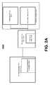
- FIG. 2Ais a block diagram of a system 100 A with a CPU 111 A that interfaces with a memory system 150 A through a memory controller 130 A. More precisely, the memory controller 130 A is positioned, oriented, and configured to enable it to be leveraged in processing read and write requests from the memory management unit 120 A to the memory system 150 A while shielding the CPU 111 A from challenges resulting from particular access characteristics associated with asymmetric memory 170 A.
- the CPU 111 Aincludes logic configured to implement one or more processing operations. Examples of a CPU 111 A may include x86-based processors from Intel Inc. and Advanced Micro Devices Inc. (AMD), and/or ARM (TM) processors. The CPU 111 A may include one or more processor cores.
- each CPU 111 Ainterfaces with an operating system.
- the operating systemmay interface with one or more applications.
- These applicationsmay include a search engine, business analytics, data mining, database operations.
- Each of these applicationsmay be compiled (or interpreted) into different machine-level instructions for execution on the CPU 111 A.
- Each CPU 111 Asupports an instruction set with a variety of instructions. These instructions may include, among other operations, register shifts, arithmetic operations, and memory operations. Examples of the memory operations may include random access read and write operations and I/O read and write instructions that can be used to initiate block read and write operations.
- the CPU 111 Aincludes a memory management unit 120 A.
- the memory management unit 120 Ais configured to manage a physical address space for the CPU 111 A.
- the CPU 111 Amay request to read data from a particular address and write data to a particular address.
- the memory management unit 120 Amay be configured to receive a virtual address from the CPU 111 A and translate the virtual address into a physical address (i.e., a memory management unit-specified physical address).
- the CPU 111 Amay be configured to consult the memory management unit 120 A to obtain the physical address associated with the virtual address specified by the CPU 111 A.
- the memory management unit 120 A(or some other entity) in the CPU 111 A is instructed to retrieve data from the MMU-specified physical address.
- Other systemse.g., the memory controller 130
- the MMUmay be configured to obtain the physical address associated with the virtual address.
- the MMU(or another entity in the CPU) then may be instructed to retrieve data from the MMU-specified physical address.
- the memory controller 130 Ais logically oriented as an intermediary system to enable the CPU 111 A to interface with a memory system 150 A. More precisely, the memory controller 130 A is a system configured to receive read and write instructions with a memory management unit-specified physical address from the memory management unit 120 , lookup a memory controller-specified physical address associated with the memory management unit-specified physical address, and perform the requested read and/or write instruction on the block(s) of physical memory corresponding to the memory controller-specified physical address.
- the memory controller 130 Aincludes logic (hardware and/or software) configured to manage the placement of and movement of data within a memory system 150 A.
- the memory controller 130 Amay be configured to dynamically process instructions based on a determination of whether the data and/or address is associated with symmetric memory or asymmetric memory.
- the memory controller 130 Amay be configured to process read instructions in a first way, and process write instructions in a second way.
- the memory controller 130 Amay be configured to permit read operations from the memory management unit that specify a particular address to leverage or otherwise operate on a first address within asymmetric memory, while concurrently processing write operations from the memory management unit that specify a particular address to leverage or otherwise operate on a second address within symmetric memory.
- the memory controller 130 Aincludes a physical interface to the memory system 150 A.
- the physical interfaceis configured to automatically exchange physical address information as the memory controller 130 A interfaces with the memory system 150 A.
- the memory controller 130 Aincludes a remapping table 140 A that stores an association between a memory management unit-specified physical address and a memory controller-specified physical address.
- the remapping table 140 Amay associate multiple memory controller-specified physical addresses with a memory management unit-specified physical address.
- the remapping table 140 Amay be configured to indicate that writes to the disruption region should be directed to a “new” physical address range for the memory management unit, while reads from the disruption region should be directed to the “old” physical address range.
- the remapping table 140 Amay indicate that a particular memory management unit-specified physical address is associated with a disruption region.
- the memory system 150 Amay include symmetric memory 160 A and asymmetric memory 170 A.
- the memory system 150 Amay be packaged as one or more DIMMs (Dual Inline Memory Modules) and configured to support DIMM protocols, signaling, interconnects, and physical interfaces.
- DIMMsDual Inline Memory Modules
- the symmetric memory 160 Aincludes one or more memory systems where read characteristics have similar properties to the write characteristics. Examples of symmetric memory include DRAM, and other random access memory technologies.
- the asymmetric memory 170 Aincludes one or more memory systems where read characteristics and write characteristics are dissimilar. For example, some types of asymmetric memory have write latencies that are orders of magnitude greater than the read latencies. Examples of asymmetric memory may include NOR flash. With some types of asymmetric memory, an interface is used to (among other things) require an entire region of content to be rendered inaccessible to read requests whenever any constituent block of the region is written, for example, using an I/O block write, instead of a smaller, random access write to the specific update location.
- the DIMMmay be configured to dynamically process read and write instructions. For example, in a read mode, one or more DIMMs may be configured to receive instructions to access content residing at a particular physical address, and provide requested content to the processor through the memory controller. Generally, in a write mode, the DIMM is configured to receive data to be written with a physical address. Depending on whether the physical address represents flash or DRAM, the data may be written in a random access manner (e.g., a word or byte) or in a block (e.g., a 4 Megabyte or a 4 kilobyte block).
- a random access mannere.g., a word or byte
- a blocke.g., a 4 Megabyte or a 4 kilobyte block.
- the DIMMis entirely made up of one type of memory (e.g., DRAM or NOR flash).
- the DIMMincludes a hybrid of both DRAM and flash and relies on an internal or external memory controller to perform the different operations required to implement a hybrid memory system.
- a hybrid and/or dedicated configurationwas used, a different configuration may be used.
- FIGS. 1 , 2 , and 2 Aillustrate different components in a server system that may be configured to interface with and control aspects of a memory system with symmetric and asymmetric components.
- a hybrid (e.g., symmetric/asymmetric volatile/non-volatile, DRAM/Flash, etc.) main memory systemmay be used by modifying application programs to decide which portions of its text (e.g., code) and data areas to map to symmetric regions and asymmetric regions in the main memory.
- the mapping by the application programmay be modified to reflect characteristics of different types of memory.
- a memory controllermay be configured to selectively load data to memory in response to a relatively slow latency seen with a type of flash memory region accesses, as well as other properties of the type of flash memory device, such as the limited write lifetime, limited number of reads between writes, and the relatively longer latency for erase and write operations.
- Modifying application programs to support a hybrid main memory including DRAM memory and flash memorymay pose one or more of the following or other challenges.
- restructuring application programs to be aware of and interface with a hybrid memory systemmay be easier to implement if the modification to the structure of the application is limited.
- application programs that rely on memory-mapped input/output (“I/O”) functionalitysimilar to that provided by a memory map (“mmap”) system call, may reduce the degree of restructuring that is required to support a hybrid main memory.
- I/Omemory-mapped input/output
- mmapmemory map
- Existing parameters and arguments supplied with a mmap callmay be used to make a determination about whether or not a certain I/O object should reside in the asymmetric memory region.
- applications that are associated with a more dynamic use of memory resourcesfor example, to implement an application-specific cache for I/O objects, may require a more extensive revision to the memory commands in order to support a hybrid main memory.
- a program associated with a more dynamic use of memory resourcesmay be specifically configured to operate with certain symmetric (e.g., DRAM) memory characteristics, and thus, may have read/write access behaviors that are not well
- unmodified application programsmay be used with a hybrid DRAM/flash memory subsystem.
- the portion of the application code and data that are accessed in a read-only fashion and/or operations that are relatively tolerant of increased access latencymay be migrated over time in an adaptive fashion from DRAM memory regions into the flash memory regions in the main memory.
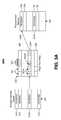
- a virtual address space or processor address space 301may be mapped into a physical hybrid main memory 303 by a page table map 302 . That is, a plurality of pages 310 associated with virtual addresses may be mapped to physical addresses of a plurality of physical pages in the hybrid main memory 303 .
- the page table map 302may include one or more page table entries (PTE) or slots ( 320 A- 320 N) to map the virtual page address to the physical page address.
- PTEpage table entries
- slots320 A- 320 N
- Page table map and page tablemay be referenced interchangeably.
- Each slot 320 in the page table map 302may include a page frame number (PFN) 321 and one or more protection bits 322 , one of which may be a write protection bit 322 W that may be used to provide/signal page protection.
- the write protection bitcontrols whether CPU-initiated writes are allowed against virtual page locations corresponding to the page table entry. When set, writes are disallowed, resulting in an operating system or hypervisor level trap that enables software to exercise control over whether and how the write operation is performed.
- FIG. 5Ashows other bits and bit fields that may be included in each slot 320 of an exemplary thirty-two bit wide PTE of page table map 302 . In a 32-bit wide addressing scheme, bits 31 - 12 identify the page frame number.
- Bit 11is reserved and writable on multiprocessor systems. Bits 10 and 9 are reserved. Bit 8 is a global bit, and bit 7 is used to identify whether the page is a large page. Bit 6 is a dirty bit identifier indicating whether the page has been written to. Bit 5 indicates whether the page has been read. Bit 4 indicates that the cache has been disabled, and bit 3 indicates that write through is supported to disable caching of writes to this page so that changes are immediately flushed to disk. Bit 2 indicates whether the user mode can access the page or whether the page is limited to kernel mode access. Bit 1 indicates whether the page is read/write capable or only readable, controlling whether the page is writable. Bit 0 indicates whether the translation maps to a page in physical memory.
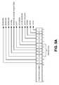
- FIG. 5Bis a diagram illustrating the bits and bit fields in a sixty-four bit slot or page table entry in a page table.
- bits 63 - 53are software representing a working set index.
- Bit 52is used to indicate exceptions, and bits 51 and 50 are reserved.
- Bits 49 - 13represent the page frame number.
- Bit 12is used to indicate a copy on writes, and bit 11 is reserved.
- Bit 10is used to indicate whether writes are allowed, and bit 9 is used to indicate the execute bit.
- Bits 8 and 7indicate owner parameters specifying whether the user mode can access the page or whether the page is limited to kernel mode access.
- Bit 6is a dirty bit indicating whether the page has been written to.
- Bit 5is an access bit indicating whether the page has been read.
- Bits 4 - 2indicate the cache parameters.
- Bit 1is reserved and bit 0 indicates whether the page is valid or not.
- the write protection bitmay be set to logical zero to indicate that the associated page is read-only. In another example, the write protection bit may be set to logical one to indicate that the associated page is read-only. In either example, the write protection bit may be changed to indicate that the associated page is read accessible only. Without the write protection bit being appropriately set to protect a page from write access, the page may be both read and write accessible.
- additional translation hierarchymay be used in addition to the page table map 302 to provide additional addressable memory.
- the hierarchymay include page directories to point to page tables, page directory pointer tables to point to page directories, and a page map level table to point to the page directory pointer tables.
- the page table map 302may be used to support the hybrid main memory at the lowest level of the address translation hierarchy.
- an applicationmay be assigned by the page table map 302 to use DRAM memory pages 330 in the hybrid main memory 303 .
- a virtual page X of addressable memory 310 Xindexes into, relates to, or points to a slot 320 Y in the page table map 302 to translate the virtual address into a physical address that points to a DRAM memory page Y 330 Y in one of the DRAM memory regions of the physical hybrid main memory 303 .
- the write protection bit 322 W of the slot 320 Y in the page table map 302is set to zero to indicate that the DRAM memory page 330 Y in the physical hybrid main memory 303 is both read and write accessible.
- the information in the DRAM memory page Y 330 Yhas been copied into the flash memory page Z 331 Z′, for example.
- the page frame number in slot 320 Y′ in the page table map 302 ′has been updated to page frame number 321 B to translate the virtual page address 310 X to point to the flash memory page Z 331 Z′.
- the write protection bit 322 Whas been changed to the write protection bit 322 W′ to signal that the access through the virtual page address X 310 X to the flash memory page Z 331 Z′ is a read access only with write accesses being trapped. Modification of the write protection bit may disallow random write access to the flash memory page Z 331 Z′.
- the DRAM memory page Y 330 Yis freed-up so that it may be used to store other information.
- write access to the flash memory page Zis disallowed
- a protection handlere.g., the trap handler
- the attempt to write to the protected pagemay be referred to as a general protection fault or a segmentation violation that is trapped by the operating system.
- a page 330 Y of application code and/or data Dmay be stored in the DRAM memory region 401 A of main memory 303 by an application program. Data may be moved into the flash memory regions directly from DRAM or from another source. In response, the application code and/or data D stored in page 330 Y may be copied and written into a page 331 Z′ in the flash memory region 402 A.
- the page 330 Y in the DRAM memory region 401 Amay be thereafter freed and used for other purposes that require write access or that are less tolerant of access latency increases (e.g., the physical address for page 330 Y may be put on a free list maintained by the operating system to indicate that it is unallocated to any process).
- a modified operating systemmay be configured to trap attempted write accesses into the asymmetric memory.
- the trapmay be configured by setting the write protection bit in the page table entry to permit only read accesses.
- An attempt by the processor to write to a location on the corresponding pagemay trigger a protection fault.
- a protection fault handler or trap handler 125can either complete the write (at the slower speed), or decide to copy back the page of data into a DRAM memory page and update it with the write access into the DRAM memory page.
- Such a DRAM memory pagemay also be marked, for example, in the page table, as being non-migratable into a flash memory page for a period of time so as to complete the update of the information by writing into the DRAM memory page.
- the memory controllermay create an access collections table, or modify a memory table to include parameters to track access to data in memory. Reading a virtual address may increment a read counter while writing a virtual address may increment a write counter or set a warning flag indicating that a write to the virtual address has been recently performed.
- the access collections tablemay be modified to include a time parameter indicating that the page should not be migrated for (1) a specified duration or monitoring cycle, or (2) until a threshold degree of reads are performed before another write operation is performed.
- the access collections tablemay track the amount of data written to storage and the elapsed time since the data was migrated to the asymmetric memory component.
- the amount of data writtenmay be used in prioritizing which data is migrated to the asymmetric memory component so that larger amounts of data are favored as being computationally more efficient.
- the elapsed time since the data was migratedmay be used to as an indicator of whether the data is likely to be subject to future write operations. Referring now to FIG. 4 , if the application attempts to write to the protected flash memory page 331 Z′, a new DRAM memory page W 441 W may be allocated in the main memory 303 .
- the information content Dmay be copied into the DRAM memory page W 441 W.
- the PFNis updated to indicate the DRAM memory page W 441 W and the write protection bit 322 W′ is changed back to protection bit 322 W such that the page is writable so that the application may write new information into the DRAM memory page W 441 W.
- the information Dis thereafter updated to information D′ in the DRAM memory page W 441 W.
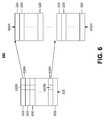
- FIG. 6illustrates a multilevel mapping 600 of virtual address space of an application running on a processor into a physical address space of a hybrid main memory by means of a shadow page table map. More precisely, and also referring back to FIG. 2 , the hypervisor 104 maintains a shadow page table 222 to that of the page table 122 maintained by the operating systems in order to map virtual addresses of applications running under the control of one or more host operating systems to physical addresses in main memory 135 .
- the shadow page table 222 in the hypervisor 104is similar to the page table 122 maintained by the one or more host operating systems 102 . However, in multilevel mapping 600 , the hypervisor 104 alters the bits in the shadow page table 222 .
- the hypervisorsupports executing one or more copies of a host operating system to provide the illusion of enabling multiple virtual machines on one physical machine.
- the hypervisormanages the allocation of raw hardware resources, including main memory, amongst the one or more virtual machines.
- the shadow page table 222 in the hypervisor 104is similarly managed as the page table 303 discussed previously to migrate information in DRAM memory regions into flash memory regions of a main memory. That is, the shadow page table 222 has its page table entries updated as information in DRAM memory pages are copied into flash memory pages and vice-versa.
- the hypervisor 104also changes the write protection bits in the slots of the shadow page table 222 to protect the corresponding mapped flash memory pages from being written.
- the hypervisor trap 225works in conjunction with the kernel page table (KPT) 232 maintained by the hypervisor 104 .
- the kernel page table 232has one or more slots or page table entries 620 that point to the physical address for each process page table 602 of each respective operating system of each respective virtual machine maintained by the hypervisor. For example, entry 620 A points to the process page table 602 A for a first operating system of a first virtual machine. Entry 620 N points to the process page table 602 N of the Nth operating system of the Nth virtual machine.
- Each process page table 602has page table entries 320 to map virtual addresses to physical addresses.
- the hypervisor trap 225traps the instruction that wants to update information located in certain locations of the page table.
- Each slot or entry 620 N in the kernel page table 232includes a protection bit 622 N to protect its associated process page table 602 N from being written.
- the DRAM memory resources freed up because of the migration of information from a page in a DRAM memory region to a page in the flash memory region of the hybrid main memorymay be used by the hypervisor to support the memory requirements of other virtual machines.
- these freed resourcesmay be made available for use by the virtual machine from which they were recovered by dynamically expanding the memory allocation initially configured for that machine.
- a virtual memory hierarchy 701 for a computer system 700is illustrated between a processor core 704 and hard disk storage 133 .
- the processor core 704may be a multiprocessor core including one or more execution engines 714 A- 714 N.
- the memory hierarchy 701may include one or more levels of cache memory 702 A- 702 N and a hybrid main memory 135 with DRAM memory regions 401 and flash memory regions 402 .
- a computer systemmay have more than one processor core, each associated with its own levels of cache memory 702 A- 702 N and possibly its own hybrid main memory 135 .
- the memory closest or nearest to the processor(the fastest memory) has the fastest access times while the memory furthest from the processor (the slower memory) has slower access times.
- a memory management unit 716integrated with or separate from the processor core 704 , working in cooperation with the operating system may bring forward pages of information associated with addresses in an application's virtual address space into main memory 135 to allow the execution engines to actively process this information. That is, the memory management unit 716 may page information by reading pages of information from the hard disk storage 133 into the main memory 135 . Additionally, portions of the information may be brought forward into one or more levels of the cache memory 702 A- 702 N. A valid bit in each slot in the page table corresponding to the page of memory is set to indicate a valid page in memory. If the page of information is no longer needed in main memory, the valid bit is cleared so that page of memory may be reused. If the page of information was updated, indicated by the setting of a dirty bit, the page of information may be written into the hard disk storage 133 by the operating system.
- the computer systemmay be configured so that pages of information in the memory hierarchy 701 are not pushed back down to slower memory in the memory hierarchy.
- pages of informationmay be pushed down the memory hierarchy 701 from DRAM memory regions 401 in the main memory, which may be a faster memory type, into flash memory regions 402 in the main memory, which may be a slower memory type while retaining its direct addressability in memory.
- the hybrid main memory 135has two different types of memory pools that are managed by the operating system or hypervisor, flash type memory regions and DRAM type memory regions.
- the DRAM type memory regionsmay be readily read-writeable.
- the flash type memory regionsmay be readily readable but it is desirous to write infrequently into flash memory due to a slower write access time and the possibility of flash memory wear out.
- FIG. 8is a flow chart 800 of a process by which a memory controller integrates data stored within symmetric and asymmetric memory components of main memory.
- the operationsare described as generally being performed by a memory controller, the operations may be performed on a memory controller that resides in the operating system, a hypervisor layer, or works in association with specialized hardware.
- the memory controllerreceives a write command to write data to a virtual address associated with a first physical address of an asymmetric memory component of the main memory ( 810 ).
- the memory controllermay look up the virtual address in a page table, and based on the lookup, determine that the virtual address maps to the asymmetric memory component.
- the memory controllerconfigures a page to change an association of the virtual address from the association with the first physical address of the asymmetric memory component of the main memory to a second physical address of a symmetric memory component of the main memory ( 820 ).
- the memory controllerloads the data to symmetric memory, and modifies the page table to associate the virtual address with a symmetric memory component physical address.
- the memory controllergenerates an indication that the first physical address is no longer being used to enable association of the first physical address with another virtual address in a subsequent block write operation ( 830 ).
- the memory controllercollects information related to movement of content from asymmetric memory components to symmetric memory components.
- the memory controllermay indicate which pages within the asymmetric memory component are no longer being used and/or the utilization for a region within the asymmetric memory component.
- the informationmay include physical addresses for the locations no longer being used in the asymmetric memory component.
- the memory controllergenerates a collection of content entries with access characteristics suitable for storage in the asymmetric memory component ( 840 ).
- a memory controller that identifies the data that has been moved to the symmetric memory componentmay track how the data in the symmetric memory component continues to be used. Those content entries whose access characteristics are read intensive and feature minimal use of writes are added to a collection of content entries.
- the memory controllerdetermines whether the collection of content entries collectively occupy a threshold amount of storage or whether a threshold period of time has elapsed ( 850 ).
- writing to asymmetric memoryis associated with a certain performance cost.
- a first type of performance costis that a disruption region of asymmetric memory is unavailable for the duration of the write. Thus, reads to the disruption region may be interrupted during the write operation.
- an internal busis occupied as data is transferred from a first component to a second component.
- the performance costmay vary with the amount of data being written and the amount of data being taken offline during the write.
- a sequential write of a pagee.g., 4 k
- to a 2 GB bank that only stores 4 MBis less disruptive than overwriting the entire bank that is nearly full with a new bank's worth of content.
- the memory controllerIn response to determining that the collection of content entries collectively occupy the threshold amount of storage or that the threshold period of time has elapsed, the memory controller loads the collection of content entries to a region of the asymmetric memory component using a block write command ( 860 ).
- the collection of content entriesmay be loaded from DRAM to NOR flash.
- the content entriesmay be loaded from DRAM and first portions of the asymmetric memory component to second portions of the asymmetric memory component.
- FIG. 9is a block diagram 900 of a configuration for a hybrid memory system for a computer system that includes an asymmetric memory component and a symmetric memory component.
- block diagram 900illustrates how a configuration of memory may be organized into a symmetric memory component 910 and an asymmetric memory component 920 .
- the symmetric memory component 910includes a memory system, such as DRAM, where the access characteristics for write operations are similar to access characteristics for read operations. As indicated by the sequence of entries, each entry in symmetric memory component 910 is independently addressable. That is, each entry in symmetric memory component 910 may be read or written using random access commands. And, executing a first write command to a first symmetric memory physical address does not affect the ability to execute a second read command to a second symmetric memory physical address that is proximate to the first symmetric memory physical address.
- the asymmetric memory component 920includes a collection of banks made up of one or more sectors (e.g., sector 930 ).
- writing to an asymmetric memory physical addresscauses a disruption within a bank. That is, executing a first write command to a first asymmetric memory physical address adversely affects the ability to execute a second read command to a second asymmetric memory physical address that is proximate to the first asymmetric memory physical address.
- Each of the entries in sector 930is made up of a collection of entries. Although each entry may be individually accessed by the CPU using a random access read operation, writing to asymmetric memory does not permit random access write operations to be performed. Instead, asymmetric memory requires write operations to be performed as block write operations (e.g., a block input/output (IO) write), where each write includes, for example, 4 k of data.
- the memory controllermay be limited by (1) the granularity at which the page table can translate a virtual address to a physical address in asymmetric memory, and (2) the granularity at which the CPU can access a virtual address.
- the memory controllermay be limited to performing page level translations, that is, between a virtual address specifying a page and a physical address specifying a page.
- greater read granularitymay be specified using an offset within a page to permit entry level access to one or more words while write granularity may be regulated by the internal structure limiting the manner in which content may be retrieved from the asymmetric memory component.
- a memory controller managing access to both componentsmay selectively and intelligently structure the manner in which both components are utilized. For example, where the symmetric memory component 910 includes DRAM and the asymmetric memory component includes NOR flash, a memory controller may manage which content is loaded to DRAM and which content is loaded to NOR flash. And, even though some content may be stored in NOR flash at some point, certain application behaviors may cause an entry within a sector of NOR flash to be moved to DRAM.
- sectorsmay be loaded from NOR flash to DRAM.
- entries within a sector of NOR flashmay be loaded to the DRAM.
- These sectors and entries loaded from NOR flash to DRAMrepresent “holes” in the NOR flash in that the “holes” cannot be used for storing new entries without interrupting access to all content in the bank in which the “holes” appear.
- FIG. 10is a diagram of a page table 1000 that indicates how a hybrid memory system for a computer system that includes an asymmetric memory component and a symmetric memory component is being used.
- page table 1000illustrates how main memory may be organized into three different categories of storage.
- the first category, B 310includes actively used DRAM and NOR flash.
- Category 1010illustrates those portions of the memory system that are being used in a desired manner. A memory controller trying to achieve better system performance may try and increase the size of category 1010 relative to other categories.
- Category 1020includes free DRAM that is not being used.
- category B 320is available to be used for write intensive data and to support special processing operations performed in response to detecting a write command addressed to a virtual address associated with NOR flash.
- Category 1030includes discontinuous NOR flash.
- Memoryis discontinuous if the memory has unused “holes” between used regions. In addition to some of the challenges discussed above with respect to holes, identifying a region as being discontinuous may cause other challenges.
- additional processing operationsmay be required to identify the right storage in the first instance as ineligible storage locations are accessed, and analyzed for suitability.
- the discontinuous naturemay limit the size of write operations that are performed. For example, an application desiring to load 4 Mbytes of a contiguous search index is unable to do so if the “hole” is only 2 Mbytes.
- the memory controllermay support the request to store the 4 Mbytes of content in asymmetric memory, the storage operation may be less than optimal. For example, this requirement may result in a contiguous search index being stored across two different locations. Storing the contiguous search index in two different locations may result in lower application performance as additional interconnect resources may be consumed to access the contiguous search index from two different locations.
- the classification of a memory region as “active”, “free”, or “discontinuous”may be artificial in that in many instances, a memory region is not 100% utilized in order to be considered active, nor must a “free” region be 0% utilized.
- the classification of a region as discontinuousmay vary with the system and/or application, or with system and application performance. For example, where an application works with more granular data (e.g., a page), classification of a region as being discontinuous and thus suitable for a destination of integrated data may be based on whether a region is able to support writing a limited number of pages. In contrast, where an application performs larger writes, classification of a region as discontinuous may be based on the ability of the region to support the larger writes.
- FIG. 11is a diagram of a configuration 1100 for a collection of banks in an asymmetric memory component of a hybrid memory system for a computer system that indicates different levels of utilization.
- Configuration 1100indicates that a first bank with three sectors is being 60% utilized with three sectors that are being utilized at levels 80%, 70%, and 30%, respectively.
- the second bankis being 30% utilized with three sectors being utilized 20%, 70%, and 0%, respectively.
- the third bankis being 10% utilized with three sectors being 30%, 0%, and 0%.
- the memory controllermay decide to write to bank 3 because writing to bank 3 takes the smallest amount of data offline (10%) during a write operation.
- the memory controllermay be configured to use the second sector, which has not yet been used.
- the memory controllermay elect to write to the first sector.
- the memory controllermay be configured to write to bank 1, notwithstanding the impact of writing to the most heavily utilized bank. For example, if an application is building a large data structure that will require a tremendous amount of storage, the memory controller may attempt to keep each bank 100% utilized. Thus, the memory controller may be configured to add incremental amounts of data to each sector in bank 1 to make each sector 100% utilized. While the impact to reads from bank 1 may be disrupted, the memory controller may determine that the impact from loading of data to bank 1 on application performance is less than the impact of operating the memory system at less than a desired level of utilization.
- bank 2may be identified as the candidate if the collection of entries occupies an amount of storage equal to 70% of bank.
- the entriesmay include a sector's worth of content and a marginal amount more that requires 30% of the second sector and 80% of the first sector.
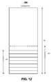
- FIG. 12is a diagram of a configuration 1200 for a collection of data in DRAM that is being organized in order to write the collection of data to a block in the asymmetric portion of the hybrid memory system.
- configuration 1200indicates that the collection of content entries occupies 1.7 Mbytes of content.
- the memory controllerIn order to be written to the asymmetric memory component, the memory controller requires that 2 Mbytes of storage exist. As shown, when a threshold of 2 Mbytes is required, another 300 Kbytes is required before the collection of content entries is loaded to the asymmetric memory component. Of course, if other criteria are used, such as a time threshold, the 1.7 Mbytes of content may be loaded. In contrast, FIG.
- FIG. 13illustrates a configuration for a collection of content entries that does exceed the required threshold amount of content.
- FIG. 13is a diagram of a configuration 1300 for a collection of data in DRAM that is being organized in order to write the collection of data to a block in the asymmetric portion of the hybrid memory system. As shown, configuration 1300 illustrates that the collection of content entries includes 2.2 Mbytes of content, more than the required 2 Mbytes.
- FIGS. 12 and 13illustrate how data is being loaded with respect to a block of contiguous locations in asymmetric memory
- the collection of content entriesmay be organized with a constituent organization designed to support how the asymmetric memory component will be accessed once the collection of content entries has been loaded to the asymmetric memory component.
- FIG. 14is a diagram of a configuration 1400 for a collection of data in DRAM that is being organized in a bank structure in order to write the collection of data to a bank in the asymmetric portion of the hybrid memory system.
- configuration 1400illustrates that a bank includes six blocks, with each blocking being organized so that it uses approximately 50% of the storage in the block. Five of the six constituent blocks have been established with the desired degree of utilization.
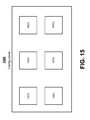
- FIG. 15is a diagram 1500 of a configuration for a collection of data in DRAM that is being organized in order to write the collection of data to a bank in the asymmetric portion of the hybrid memory system.
- configuration 1500illustrates that the collection of content entries can be organized so that each constituent block is more fully utilized (e.g., approaching utilization levels closer to 100%).
- FIG. 16is a flow chart 1600 of a process for loading a series of entries to a region of asymmetric memory.
- flow chart 1600illustrates how generating the collection of content entries includes organizing, in symmetric memory, an amount of data to be written corresponding to multiple blocks within a disruption region of the asymmetric memory component.
- the memory controlleridentifies virtual addresses that were previously mapped to an asymmetric memory component and that now map to symmetric memory ( 1610 ). That is, the memory controller is configured to identify which virtual addresses related to data that was previously stored in the asymmetric memory component. Alternatively, the memory controller identifies physical addresses that were previously mapped to an asymmetric memory component and that are now mapped to the symmetric memory component.
- the memory controllertracks the identified virtual addresses ( 1620 ). Tracking the identified virtual addresses includes determining whether the identified virtual addresses continue to demonstrate access characteristics indicating that the data associated with the virtual address should be stored in the asymmetric memory component.
- the memory controlleridentifies candidates with access characteristics suitable for storage in asymmetric memory component ( 1630 ). For example, the memory controller may determine that some virtual addresses are not good candidates because they are associated with more than a threshold rate or number of write operations (e.g., one or more write operations in a window of time). Alternatively or in addition, the memory controller may track how often a virtual address is read and then identify candidates based on which virtual addresses are the most read.
- the memory controlleridentifies a capacity threshold that indicates approximately a maximum amount of data that can be loaded to a memory structure that includes either a disruption region or a block ( 1640 ). Put differently, the memory controller identifies an amount of content that is required to fully utilize a memory structure in asymmetric memory (e.g., one or more blocks or a bank)
- asymmetric memorye.g., one or more blocks or a bank
- the memory controllerthen organizes the candidates into a memory structure ( 1650 ). For example, the memory controller may create a record that indicates how a memory controller should load a structure within the asymmetric memory component.
- organizing the candidatesincludes loading the candidates to a mirror of the proposed structure in DRAM.
- organizing the candidatesincludes creating a record in DRAM that indicates the address ranges that should be read in order to write the candidates to the asymmetric memory component.
- the memory controllerdetermines whether the identified candidates include a data capacity threshold or whether a time-based threshold ( 1660 ). In one configuration, the memory controller determines whether loading the identified candidates to the asymmetric memory component would result in one of the constituent structures within the asymmetric memory component being used near a desired capacity. Thus, the memory controller may determine whether the identified candidates require one or more block's worth of storage, or even one or more bank's worth of storage.
- the memory controllerthen loads the identified candidates to the memory structure in response to determining that the identified candidates include a capacity threshold of data ( 1670 ).
- a structure within the asymmetric memory componentreceives the identified candidates during a write operation, which in turn becomes a disruption region during the write operation.
- the memory controllermay be configured to automatically migrate data with suitable access characteristics on a periodic basis, even if less than a capacity threshold of data exists.
- timing criteria and thresholdsmay be used to determine the data capacity threshold. For example, a first data capacity threshold may be used if the data has migrated within first window of time. If the data has not been migrated within the first window of time, a second capacity threshold may be used.
- time based criteriamay impose a greater computational burden or lead to operation in a less efficient mode, using time based criteria may result in better performance during subsequent operations or shield the computer system from undesirable faults.
- time based criteriamay increase the likelihood that a search index (or a larger portion of a search index) is immediately available in the asymmetric memory component upon system reboot. This, in turn, may reduce the computation burden imposed by migrating a search index to the asymmetric memory component upon reboot.
- the memory controllermay have additional candidates that require more than the capacity threshold of storage and less than the next threshold required to load another collection of the identified candidates to asymmetric memory.
- the memory controllermay continue identifying virtual addresses for data that is loaded from the asymmetric memory component to the symmetric memory component.
- the memory controllerin response to determining that the identified candidates do not include a capacity threshold of data, the memory controller accumulates additional candidates until a capacity threshold of data is available to load to the asymmetric memory structure ( 1680 ). Once a capacity of threshold data has been accumulated, an additional write operation may be performed to write the additional accumulation of identified candidates to the asymmetric memory component.
- flow chart 1600described performing one or more operations using virtual addresses that were previously mapped to the asymmetric memory component
- the operations described in flow chart H 00also may be performed using data that continues to be stored within the asymmetric memory component.
- the identified candidatesalso may include data in an asymmetric memory component that includes more than a threshold number of “holes” or is being used with less than a threshold degree of utilization.
- FIG. 17is a flow chart 1700 of a process for loading a series of entries to asymmetric memory by allowing some of the entries being collected for writing to asymmetric memory to come from locations in asymmetric memory.
- flow chart 1700illustrates a process by which data stored within symmetric and asymmetric memory components of main memory is integrated and stored within at least one asymmetric memory component.
- the memory controlleridentifies a first data as having access characteristics suitable for storing in an asymmetric memory component ( 1710 ).
- identifying the first dataincludes identifying data that has been moved to a symmetric memory component as a result of a write operation to the asymmetric memory component.
- the first datamay include data that is infrequently updated or represents data that is part of a page with two different portions with each portion having different access characteristics.
- the first datamay be identified as one of the portions with access characteristics suitable for storage in the asymmetric memory component.
- the first dataincludes content in an asymmetric memory component, where the asymmetric memory component is being used in a less than desirable manner (e.g., replete with holes).
- the memory controllerincludes the first data among a collection of data to be written to the asymmetric memory component ( 1720 ).
- including the first data in the collection of dataincludes loading the data to a symmetric memory component organized in the manner in which the collection of data will be loaded to the asymmetric memory component.
- including the first data in the collection of dataincludes creating a structure that indicates the addresses where the memory controller should access the data in order to load data to the asymmetric memory component.
- the memory controlleridentifies an amount of data within the collection of data to be written to the asymmetric memory component ( 1730 ).
- the memory controllermay identify an amount of content required to fully utilize a bank of storage.
- the memory controllercompares the amount of data within the collection of data to a volume threshold to determine whether a block write to the asymmetric memory component is justified by the amount of data ( 1740 ). The memory controller determines whether the collection of data includes enough content to use the asymmetric memory component in the intended manner.
- the memory controllerloads the collection of data to the asymmetric memory component ( 1750 ).
- loading the collection of data to the asymmetric memory componentincludes loading an organized portion from DRAM to NOR flash.
- loading the collection of dataincludes loading a record with addresses that identify where the different portions of the collection of data are stored, and then having the memory controller use the addresses to load the collection of data to the asymmetric memory component so that, for example, data may be loaded from other portions of the asymmetric memory component.
- FIGS. 18 and 19are diagrams of configurations 1800 and 1900 for a hybrid memory system that illustrate how a memory controller may identify a region of asymmetric memory based on the nature of the write being performed and the state of the region.
- Configurations 1800 and 1900illustrate three candidate storage locations within an asymmetric memory component, 1810 , 1820 , and 1830 within configuration 1800 , and 1910 , 1920 , and 1930 within configuration 1900 .
- Each of the candidate locationsrepresents a bank or a “disruption region.”
- the memory controlleris inspecting a single page (PAGE1) to determine which of the candidate locations should be used to store PAGE1.
- the first candidate location, 1810is 50% utilized with two “holes” between two active sectors.
- candidate location 1810means that 50% of the stored content in the bank (representing a disruption region) is unavailable. However, candidate location 1810 is being used in a less than desirable manner with the two holes. Thus, executing a smaller write operation may result in increased system performance as the utilization for candidate location J 10 as memory utilization goes from 50% utilization to 66% utilization, where each of the striped unused regions represents a page.
- Candidate location 1820is 16% utilized, with five portions eligible for a write.
- Candidate location 1820is a strong candidate in that the least amount of data is unavailable during the write operation, and the write operation requires the least amount of time.
- candidate location 1820may be a better candidate for other write operations involving more data.
- candidate location 1820may be preserved for other write operations that are more disruptive (e.g., involve more data).
- Candidate location 1830also is 50% utilized. The overall amount of data becoming unavailable during a write is the same as the amount of data unavailable during a write to the candidate location 1810 . However, candidate location 1830 is structured to support the sequential addition of data. Candidate location 1830 is therefore configured to support the addition of 1-3 pages. As a result, while writing DATA1 to candidate location 1830 may be as burdensome as writing to candidate location 1820 , candidate location 1830 may be used in one configuration in order to save candidate location 1820 for multi-page writes that may be either sequential or non-sequential in nature.
- configuration 1900features a multi-page write being written. If the internal structure of PAGES1-2 spans the boundary between the first page and the second page, the memory controller may elect to avoid candidate location 1910 .
- Candidate location 1920represents the least burdensome candidate location because the smallest amount of data is being taken offline in order to support the write.
- candidate location 1930also is a candidate, candidate location 1930 may be less desirable than candidate location 1920 because writing to candidate location 1930 takes more data offline.
- the memory controllermay be dedicated to a single type of memory (e.g., an asymmetric memory component) in a hybrid memory system that includes symmetric memory components and asymmetric memory components. Multiple memory controllers may be used.
- the asymmetric memory componentsmay be encapsulated in DIMM packaging that includes a memory controller in each module.
- a computer system with three DIMM-encapsulated asymmetric memory componentsmay include three memory controllers.
- the computer systemmay optionally use a separate memory controller for the symmetric memory components, or rely on functionality elsewhere (e.g., in the CPU) to act as a memory controller.
- the memory controllermay be configured to organize a collection of data so that the collection of data includes more than a first threshold of data and less than a second threshold of data.
Landscapes
- Engineering & Computer Science (AREA)
- Theoretical Computer Science (AREA)
- Physics & Mathematics (AREA)
- General Engineering & Computer Science (AREA)
- General Physics & Mathematics (AREA)
- Human Computer Interaction (AREA)
- Software Systems (AREA)
- Mathematical Physics (AREA)
- Memory System (AREA)
- Memory System Of A Hierarchy Structure (AREA)
- Debugging And Monitoring (AREA)
- Techniques For Improving Reliability Of Storages (AREA)
Abstract
Description
Claims (18)
Priority Applications (1)
| Application Number | Priority Date | Filing Date | Title |
|---|---|---|---|
| US14/047,627US9223719B2 (en) | 2006-11-04 | 2013-10-07 | Integrating data from symmetric and asymmetric memory |
Applications Claiming Priority (5)
| Application Number | Priority Date | Filing Date | Title |
|---|---|---|---|
| US86439906P | 2006-11-04 | 2006-11-04 | |
| US11/935,275US7818489B2 (en) | 2006-11-04 | 2007-11-05 | Integrating data from symmetric and asymmetric memory |
| US12/899,709US8156302B2 (en) | 2006-11-04 | 2010-10-07 | Integrating data from symmetric and asymmetric memory |
| US13/443,121US8555024B2 (en) | 2006-11-04 | 2012-04-10 | Integrating data from symmetric and asymmetric memory |
| US14/047,627US9223719B2 (en) | 2006-11-04 | 2013-10-07 | Integrating data from symmetric and asymmetric memory |
Related Parent Applications (1)
| Application Number | Title | Priority Date | Filing Date |
|---|---|---|---|
| US13/443,121ContinuationUS8555024B2 (en) | 2006-11-04 | 2012-04-10 | Integrating data from symmetric and asymmetric memory |
Publications (2)
| Publication Number | Publication Date |
|---|---|
| US20140258653A1 US20140258653A1 (en) | 2014-09-11 |
| US9223719B2true US9223719B2 (en) | 2015-12-29 |
Family
ID=39345108
Family Applications (17)
| Application Number | Title | Priority Date | Filing Date |
|---|---|---|---|
| US11/935,224Active2029-02-02US7774556B2 (en) | 2006-11-04 | 2007-11-05 | Asymmetric memory migration in hybrid main memory |
| US11/935,254Expired - Fee RelatedUS7913055B2 (en) | 2006-11-04 | 2007-11-05 | Seamless application access to hybrid main memory |
| US11/935,275Expired - Fee RelatedUS7818489B2 (en) | 2006-11-04 | 2007-11-05 | Integrating data from symmetric and asymmetric memory |
| US11/935,281Expired - Fee RelatedUS7930513B2 (en) | 2006-11-04 | 2007-11-05 | Writing to asymmetric memory |
| US12/853,135Expired - Fee RelatedUS8156288B2 (en) | 2006-11-04 | 2010-08-09 | Asymmetric memory migration in hybrid main memory |
| US12/899,709Expired - Fee RelatedUS8156302B2 (en) | 2006-11-04 | 2010-10-07 | Integrating data from symmetric and asymmetric memory |
| US13/048,012Expired - Fee RelatedUS8205061B2 (en) | 2006-11-04 | 2011-03-15 | Seamless application access to hybrid main memory |
| US13/053,371Expired - Fee RelatedUS8266407B2 (en) | 2006-11-04 | 2011-03-22 | Writing to asymmetric memory |
| US13/443,086ActiveUS8555002B2 (en) | 2006-11-04 | 2012-04-10 | Asymmetric memory migration in hybrid main memory |
| US13/443,121ActiveUS8555024B2 (en) | 2006-11-04 | 2012-04-10 | Integrating data from symmetric and asymmetric memory |
| US13/525,960Active2028-02-21US8782373B2 (en) | 2006-11-04 | 2012-06-18 | Seamless application access to hybrid main memory |
| US13/608,937ActiveUS8639910B2 (en) | 2006-11-04 | 2012-09-10 | Handling writes to a memory including asymmetric and symmetric components |
| US14/047,627Expired - Fee RelatedUS9223719B2 (en) | 2006-11-04 | 2013-10-07 | Integrating data from symmetric and asymmetric memory |
| US14/047,603ActiveUS9262333B2 (en) | 2006-11-04 | 2013-10-07 | Asymmetric memory migration in hybrid main memory |
| US14/330,930Expired - Fee RelatedUS9262334B2 (en) | 2006-11-04 | 2014-07-14 | Seamless application access to hybrid main memory |
| US14/989,386ActiveUS9836409B2 (en) | 2006-11-04 | 2016-01-06 | Seamless application access to hybrid main memory |
| US14/990,314Expired - Fee RelatedUS9672158B2 (en) | 2006-11-04 | 2016-01-07 | Asymmetric memory migration in hybrid main memory |
Family Applications Before (12)
| Application Number | Title | Priority Date | Filing Date |
|---|---|---|---|
| US11/935,224Active2029-02-02US7774556B2 (en) | 2006-11-04 | 2007-11-05 | Asymmetric memory migration in hybrid main memory |
| US11/935,254Expired - Fee RelatedUS7913055B2 (en) | 2006-11-04 | 2007-11-05 | Seamless application access to hybrid main memory |
| US11/935,275Expired - Fee RelatedUS7818489B2 (en) | 2006-11-04 | 2007-11-05 | Integrating data from symmetric and asymmetric memory |
| US11/935,281Expired - Fee RelatedUS7930513B2 (en) | 2006-11-04 | 2007-11-05 | Writing to asymmetric memory |
| US12/853,135Expired - Fee RelatedUS8156288B2 (en) | 2006-11-04 | 2010-08-09 | Asymmetric memory migration in hybrid main memory |
| US12/899,709Expired - Fee RelatedUS8156302B2 (en) | 2006-11-04 | 2010-10-07 | Integrating data from symmetric and asymmetric memory |
| US13/048,012Expired - Fee RelatedUS8205061B2 (en) | 2006-11-04 | 2011-03-15 | Seamless application access to hybrid main memory |
| US13/053,371Expired - Fee RelatedUS8266407B2 (en) | 2006-11-04 | 2011-03-22 | Writing to asymmetric memory |
| US13/443,086ActiveUS8555002B2 (en) | 2006-11-04 | 2012-04-10 | Asymmetric memory migration in hybrid main memory |
| US13/443,121ActiveUS8555024B2 (en) | 2006-11-04 | 2012-04-10 | Integrating data from symmetric and asymmetric memory |
| US13/525,960Active2028-02-21US8782373B2 (en) | 2006-11-04 | 2012-06-18 | Seamless application access to hybrid main memory |
| US13/608,937ActiveUS8639910B2 (en) | 2006-11-04 | 2012-09-10 | Handling writes to a memory including asymmetric and symmetric components |
Family Applications After (4)
| Application Number | Title | Priority Date | Filing Date |
|---|---|---|---|
| US14/047,603ActiveUS9262333B2 (en) | 2006-11-04 | 2013-10-07 | Asymmetric memory migration in hybrid main memory |
| US14/330,930Expired - Fee RelatedUS9262334B2 (en) | 2006-11-04 | 2014-07-14 | Seamless application access to hybrid main memory |
| US14/989,386ActiveUS9836409B2 (en) | 2006-11-04 | 2016-01-06 | Seamless application access to hybrid main memory |
| US14/990,314Expired - Fee RelatedUS9672158B2 (en) | 2006-11-04 | 2016-01-07 | Asymmetric memory migration in hybrid main memory |
Country Status (2)
| Country | Link |
|---|---|
| US (17) | US7774556B2 (en) |
| WO (4) | WO2008055270A2 (en) |
Cited By (1)
| Publication number | Priority date | Publication date | Assignee | Title |
|---|---|---|---|---|
| US20180293004A1 (en)* | 2017-04-06 | 2018-10-11 | International Business Machines Corporation | Network asset management |
Families Citing this family (249)
| Publication number | Priority date | Publication date | Assignee | Title |
|---|---|---|---|---|
| US8595435B2 (en)* | 2009-07-30 | 2013-11-26 | Cleversafe, Inc. | Dispersed storage write process |
| US7774556B2 (en) | 2006-11-04 | 2010-08-10 | Virident Systems Inc. | Asymmetric memory migration in hybrid main memory |
| CN103473181B (en) | 2007-01-26 | 2017-06-13 | 英特尔公司 | Hierarchical immutable content-addressable memory processor |
| US9601199B2 (en) | 2007-01-26 | 2017-03-21 | Intel Corporation | Iterator register for structured memory |
| JP2008250387A (en)* | 2007-03-29 | 2008-10-16 | Toshiba Corp | Information processing device |
| US8122428B2 (en)* | 2007-06-26 | 2012-02-21 | Analog Devices, Inc. | Methods and apparatus for automation and facilitating design of register maps |
| US8694990B2 (en)* | 2007-08-27 | 2014-04-08 | International Business Machines Corporation | Utilizing system configuration information to determine a data migration order |
| US20090157940A1 (en)* | 2007-12-15 | 2009-06-18 | Hitachi Global Storage Technologies Netherlands, B.V. | Techniques For Storing Data In Multiple Different Data Storage Media |
| CN101903867B (en)* | 2007-12-17 | 2012-12-12 | 大陆-特韦斯贸易合伙股份公司及两合公司 | Memory mapping system, request controller, multi-processing arrangement, central interrupt request controller, apparatus, method for controlling memory access and computer program product |
| US8423739B2 (en)* | 2008-02-06 | 2013-04-16 | International Business Machines Corporation | Apparatus, system, and method for relocating logical array hot spots |
| US8914340B2 (en)* | 2008-02-06 | 2014-12-16 | International Business Machines Corporation | Apparatus, system, and method for relocating storage pool hot spots |
| US8099539B2 (en)* | 2008-03-10 | 2012-01-17 | Lsi Corporation | Method and system of a shared bus architecture |
| US8560761B2 (en)* | 2008-03-31 | 2013-10-15 | Spansion Llc | Memory resource management for a flash aware kernel |
| US8458393B2 (en)* | 2008-03-31 | 2013-06-04 | Spansion Llc | Flash memory and operating system kernel |
| US8738840B2 (en)* | 2008-03-31 | 2014-05-27 | Spansion Llc | Operating system based DRAM/FLASH management scheme |
| US8745311B2 (en)* | 2008-03-31 | 2014-06-03 | Spansion Llc | Flash memory usability enhancements in main memory application |
| US8065304B2 (en)* | 2008-06-11 | 2011-11-22 | International Business Machines Corporation | Using asymmetric memory |
| US9513695B2 (en) | 2008-06-24 | 2016-12-06 | Virident Systems, Inc. | Methods of managing power in network computer systems |
| US8417873B1 (en) | 2008-06-24 | 2013-04-09 | Virident Systems, Inc. | Random read and read/write block accessible memory |
| US20090327535A1 (en)* | 2008-06-30 | 2009-12-31 | Liu Tz-Yi | Adjustable read latency for memory device in page-mode access |
| US8176233B1 (en)* | 2008-07-17 | 2012-05-08 | Virident Systems Inc. | Using non-volatile memory resources to enable a virtual buffer pool for a database application |
| US20100162038A1 (en)* | 2008-12-24 | 2010-06-24 | Jared E Hulbert | Nonvolatile/Volatile Memory Write System and Method |
| KR101612922B1 (en)* | 2009-06-09 | 2016-04-15 | 삼성전자주식회사 | Memory system and method of managing memory system |
| US8880835B2 (en)* | 2009-07-07 | 2014-11-04 | International Business Machines Corporation | Adjusting location of tiered storage residence based on usage patterns |
| US8296496B2 (en)* | 2009-09-17 | 2012-10-23 | Hewlett-Packard Development Company, L.P. | Main memory with non-volatile memory and DRAM |
| US8281181B2 (en)* | 2009-09-30 | 2012-10-02 | Cleversafe, Inc. | Method and apparatus for selectively active dispersed storage memory device utilization |
| CN102110057B (en)* | 2009-12-25 | 2013-05-08 | 澜起科技(上海)有限公司 | Memory module and method for exchanging data in memory module |
| US8850151B2 (en)* | 2010-03-24 | 2014-09-30 | Apple Inc. | Hybrid-device storage based on environmental state |
| US8639879B2 (en)* | 2010-03-25 | 2014-01-28 | International Business Machines Corporation | Sorting movable memory hierarchies in a computer system |
| US8656397B2 (en) | 2010-03-30 | 2014-02-18 | Red Hat Israel, Ltd. | Migrating groups of threads across NUMA nodes based on remote page access frequency |
| US8607200B2 (en)* | 2010-06-01 | 2013-12-10 | Red Hat, Inc. | Executing a web application at different stages in the application life cycle |
| US8364915B2 (en)* | 2010-06-23 | 2013-01-29 | Intel Corporation | Method, apparatus and system for generating access information from an LRU tracking list |
| US8959284B1 (en) | 2010-06-28 | 2015-02-17 | Western Digital Technologies, Inc. | Disk drive steering write data to write cache based on workload |
| US20120017039A1 (en)* | 2010-07-16 | 2012-01-19 | Plx Technology, Inc. | Caching using virtual memory |
| US9268499B1 (en) | 2010-08-13 | 2016-02-23 | Western Digital Technologies, Inc. | Hybrid drive migrating high workload data from disk to non-volatile semiconductor memory |
| US9058280B1 (en)* | 2010-08-13 | 2015-06-16 | Western Digital Technologies, Inc. | Hybrid drive migrating data from disk to non-volatile semiconductor memory based on accumulated access time |
| US20120047313A1 (en)* | 2010-08-19 | 2012-02-23 | Microsoft Corporation | Hierarchical memory management in virtualized systems for non-volatile memory models |
| US8775720B1 (en) | 2010-08-31 | 2014-07-08 | Western Digital Technologies, Inc. | Hybrid drive balancing execution times for non-volatile semiconductor memory and disk |
| US8782334B1 (en) | 2010-09-10 | 2014-07-15 | Western Digital Technologies, Inc. | Hybrid drive copying disk cache to non-volatile semiconductor memory |
| US8595463B2 (en)* | 2010-09-15 | 2013-11-26 | International Business Machines Corporation | Memory architecture with policy based data storage |
| US8533712B2 (en)* | 2010-10-01 | 2013-09-10 | International Business Machines Corporation | Virtual machine stage detection |
| TWI479505B (en)* | 2010-12-16 | 2015-04-01 | Phison Electronics Corp | Data management method, memory controller and memory storage apparatus |
| US8612676B2 (en) | 2010-12-22 | 2013-12-17 | Intel Corporation | Two-level system main memory |
| US8402191B2 (en)* | 2010-12-30 | 2013-03-19 | Stmicroelectronics, Inc. | Computing element virtualization |
| KR101166803B1 (en)* | 2010-12-31 | 2012-07-26 | 세종대학교산학협력단 | System including volatile memory and non-volatile memory and processing mehthod thereof |
| US20120233401A1 (en)* | 2011-03-08 | 2012-09-13 | Skymedi Corporation | Embedded memory system |
| US8930647B1 (en) | 2011-04-06 | 2015-01-06 | P4tents1, LLC | Multiple class memory systems |
| US9158546B1 (en) | 2011-04-06 | 2015-10-13 | P4tents1, LLC | Computer program product for fetching from a first physical memory between an execution of a plurality of threads associated with a second physical memory |
| US9170744B1 (en) | 2011-04-06 | 2015-10-27 | P4tents1, LLC | Computer program product for controlling a flash/DRAM/embedded DRAM-equipped system |
| US9164679B2 (en) | 2011-04-06 | 2015-10-20 | Patents1, Llc | System, method and computer program product for multi-thread operation involving first memory of a first memory class and second memory of a second memory class |
| US9176671B1 (en) | 2011-04-06 | 2015-11-03 | P4tents1, LLC | Fetching data between thread execution in a flash/DRAM/embedded DRAM-equipped system |
| US20120278459A1 (en)* | 2011-04-26 | 2012-11-01 | Cisco Technology, Inc. | Throttling bursty cpu utilization due to bursty tcp flows |
| US8862902B2 (en)* | 2011-04-29 | 2014-10-14 | Seagate Technology Llc | Cascaded data encryption dependent on attributes of physical memory |
| US8848445B2 (en)* | 2011-05-17 | 2014-09-30 | Sandisk Technologies Inc. | System and method for minimizing write amplification while maintaining sequential performance using logical group striping in a multi-bank system |
| US8838895B2 (en)* | 2011-06-09 | 2014-09-16 | 21Vianet Group, Inc. | Solid-state disk caching the top-K hard-disk blocks selected as a function of access frequency and a logarithmic system time |
| US9417754B2 (en) | 2011-08-05 | 2016-08-16 | P4tents1, LLC | User interface system, method, and computer program product |
| WO2013028859A1 (en) | 2011-08-24 | 2013-02-28 | Rambus Inc. | Methods and systems for mapping a peripheral function onto a legacy memory interface |
| US11048410B2 (en)* | 2011-08-24 | 2021-06-29 | Rambus Inc. | Distributed procedure execution and file systems on a memory interface |
| US9098209B2 (en)* | 2011-08-24 | 2015-08-04 | Rambus Inc. | Communication via a memory interface |
| US8656137B2 (en)* | 2011-09-01 | 2014-02-18 | Qualcomm Incorporated | Computer system with processor local coherency for virtualized input/output |
| US9146785B2 (en)* | 2011-09-14 | 2015-09-29 | Microsoft Technology Licensing, Llc | Application acceleration in a virtualized environment |
| US9417803B2 (en)* | 2011-09-20 | 2016-08-16 | Apple Inc. | Adaptive mapping of logical addresses to memory devices in solid state drives |
| US10388103B1 (en)* | 2011-09-22 | 2019-08-20 | Genesis Gaming Solutions, Inc. | Data transport system and method for hospitality industry |
| EP3364304B1 (en) | 2011-09-30 | 2022-06-15 | INTEL Corporation | Memory channel that supports near memory and far memory access |
| WO2013048497A1 (en) | 2011-09-30 | 2013-04-04 | Intel Corporation | Apparatus and method for implementing a multi-level memory hierarchy |
| CN108549609B (en) | 2011-09-30 | 2022-06-21 | 英特尔公司 | Non-volatile random access memory (NVRAM) as a replacement for conventional mass storage devices |
| US9600407B2 (en)* | 2011-09-30 | 2017-03-21 | Intel Corporation | Generation of far memory access signals based on usage statistic tracking |
| US9317429B2 (en) | 2011-09-30 | 2016-04-19 | Intel Corporation | Apparatus and method for implementing a multi-level memory hierarchy over common memory channels |
| EP2761468B1 (en)* | 2011-09-30 | 2019-12-11 | Intel Corporation | Platform storage hierarchy with non-volatile random access memory having configurable partitions |
| CN107608910B (en) | 2011-09-30 | 2021-07-02 | 英特尔公司 | Apparatus and method for implementing a multi-level memory hierarchy with different operating modes |
| US8356050B1 (en)* | 2011-11-21 | 2013-01-15 | Yahoo! Inc. | Method or system for spilling in query environments |
| US9342450B2 (en)* | 2011-11-29 | 2016-05-17 | Red Hat Israel, Ltd. | On-demand hypervisor memory mapping |
| US8842126B2 (en)* | 2011-12-13 | 2014-09-23 | Advanced Micro Devices, Inc. | Methods and systems to facilitate operation in unpinned memory |
| DE112011105984B4 (en)* | 2011-12-20 | 2024-10-17 | Intel Corporation | Dynamic partial shutdown of a memory-side cache in a two-level memory hierarchy |
| KR101572403B1 (en)* | 2011-12-22 | 2015-11-26 | 인텔 코포레이션 | Power conservation by way of memory channel shutdown |
| US8805952B2 (en) | 2012-01-04 | 2014-08-12 | International Business Machines Corporation | Administering globally accessible memory space in a distributed computing system |
| US8554963B1 (en) | 2012-03-23 | 2013-10-08 | DSSD, Inc. | Storage system with multicast DMA and unified address space |
| US20130275699A1 (en)* | 2012-03-23 | 2013-10-17 | Hicamp Systems, Inc. | Special memory access path with segment-offset addressing |
| US9703500B2 (en) | 2012-04-25 | 2017-07-11 | International Business Machines Corporation | Reducing power consumption by migration of data within a tiered storage system |
| US20130290605A1 (en)* | 2012-04-30 | 2013-10-31 | Moon J. Kim | Converged memory and storage system |
| US20130318084A1 (en) | 2012-05-22 | 2013-11-28 | Xockets IP, LLC | Processing structured and unstructured data using offload processors |
| US20130318269A1 (en) | 2012-05-22 | 2013-11-28 | Xockets IP, LLC | Processing structured and unstructured data using offload processors |
| US9524248B2 (en)* | 2012-07-18 | 2016-12-20 | Micron Technology, Inc. | Memory management for a hierarchical memory system |
| US9047090B2 (en)* | 2012-08-07 | 2015-06-02 | Qualcomm Incorporated | Methods, systems and devices for hybrid memory management |
| US9191435B2 (en) | 2012-08-23 | 2015-11-17 | TidalScale, Inc. | Selective data migration or remapping of virtual processors to provide required data accessibility to processor cores |
| US10303618B2 (en)* | 2012-09-25 | 2019-05-28 | International Business Machines Corporation | Power savings via dynamic page type selection |
| CN103729305B (en)* | 2012-10-11 | 2017-09-08 | 财团法人工业技术研究院 | Method and computer system for memory management of virtual machines |
| US9069669B2 (en)* | 2012-10-11 | 2015-06-30 | Industrial Technology Research Institute | Method and computer system for memory management on virtual machine |
| CN104380259B (en) | 2012-10-17 | 2018-09-21 | 华为技术有限公司 | Reduce the method and Memory Controller Hub of memory system power consumption |
| US9110778B2 (en) | 2012-11-08 | 2015-08-18 | International Business Machines Corporation | Address generation in an active memory device |
| US9030482B2 (en)* | 2012-11-09 | 2015-05-12 | Intel Corporation | Hybrid display frame buffer for display subsystem |
| US8959281B1 (en) | 2012-11-09 | 2015-02-17 | Western Digital Technologies, Inc. | Data management for a storage device |
| US9842660B1 (en) | 2012-12-28 | 2017-12-12 | Virident Systems, Llc | System and method to improve enterprise reliability through tracking I/O performance metrics in non-volatile random access memory |
| US9286002B1 (en) | 2012-12-28 | 2016-03-15 | Virident Systems Inc. | Dynamic restriping in nonvolatile memory systems |
| KR102002900B1 (en)* | 2013-01-07 | 2019-07-23 | 삼성전자 주식회사 | System on chip including memory management unit and memory address translation method thereof |
| US9250954B2 (en) | 2013-01-17 | 2016-02-02 | Xockets, Inc. | Offload processor modules for connection to system memory, and corresponding methods and systems |
| US9378161B1 (en) | 2013-01-17 | 2016-06-28 | Xockets, Inc. | Full bandwidth packet handling with server systems including offload processors |
| US9652376B2 (en) | 2013-01-28 | 2017-05-16 | Radian Memory Systems, Inc. | Cooperative flash memory control |
| US9229854B1 (en) | 2013-01-28 | 2016-01-05 | Radian Memory Systems, LLC | Multi-array operation support and related devices, systems and software |
| US11249652B1 (en) | 2013-01-28 | 2022-02-15 | Radian Memory Systems, Inc. | Maintenance of nonvolatile memory on host selected namespaces by a common memory controller |
| US10445229B1 (en) | 2013-01-28 | 2019-10-15 | Radian Memory Systems, Inc. | Memory controller with at least one address segment defined for which data is striped across flash memory dies, with a common address offset being used to obtain physical addresses for the data in each of the dies |
| US10642505B1 (en) | 2013-01-28 | 2020-05-05 | Radian Memory Systems, Inc. | Techniques for data migration based on per-data metrics and memory degradation |
| US10061622B2 (en) | 2013-02-26 | 2018-08-28 | Red Hat Israel, Ltd. | Updating memory topology information for virtual machines |
| US10114662B2 (en) | 2013-02-26 | 2018-10-30 | Red Hat Israel, Ltd. | Updating processor topology information for virtual machines |
| US8996796B1 (en) | 2013-03-15 | 2015-03-31 | Virident Systems Inc. | Small block write operations in non-volatile memory systems |
| US9135164B2 (en)* | 2013-03-15 | 2015-09-15 | Virident Systems Inc. | Synchronous mirroring in non-volatile memory systems |
| US10073626B2 (en) | 2013-03-15 | 2018-09-11 | Virident Systems, Llc | Managing the write performance of an asymmetric memory system |
| US9552176B2 (en)* | 2013-04-12 | 2017-01-24 | Microsoft Technology Licensing, Llc | Block storage using a hybrid memory device |
| GB2514107B (en)* | 2013-05-13 | 2020-07-29 | Advanced Risc Mach Ltd | Page table data management |
| US9817756B1 (en)* | 2013-05-23 | 2017-11-14 | Amazon Technologies, Inc. | Managing memory in virtualized environments |
| US10108539B2 (en)* | 2013-06-13 | 2018-10-23 | International Business Machines Corporation | Allocation of distributed data structures |
| CN104239222B (en)* | 2013-06-20 | 2018-01-23 | 华为技术有限公司 | A kind of memory pool access method, equipment and system |
| US8943449B1 (en)* | 2013-07-15 | 2015-01-27 | Cadence Design Systems, Inc. | Method and apparatus of enabling direct memory access into a target system memory modeled in dual abstractions while ensuring coherency |
| US9141176B1 (en) | 2013-07-29 | 2015-09-22 | Western Digital Technologies, Inc. | Power management for data storage device |
| US9378097B1 (en)* | 2013-08-27 | 2016-06-28 | Sk Hynix Memory Solutions Inc. | Selective copy-back |
| US9070379B2 (en) | 2013-08-28 | 2015-06-30 | Western Digital Technologies, Inc. | Data migration for data storage device |
| CN106062724B (en) | 2013-09-27 | 2020-09-08 | 慧与发展有限责任合伙企业 | Method for managing data on memory module, memory module and storage medium |
| WO2015054291A1 (en)* | 2013-10-09 | 2015-04-16 | Mobile Technology Corporation, LLC | Systems and methods for using spatial and temporal analysis to associate data sources with mobile devices |
| KR102329269B1 (en) | 2013-10-21 | 2021-11-22 | 에프엘씨 글로벌 리미티드 | Final level cache system and corresponding method |
| US10097204B1 (en) | 2014-04-21 | 2018-10-09 | Marvell International Ltd. | Low-density parity-check codes for WiFi networks |
| US9454991B2 (en) | 2013-10-21 | 2016-09-27 | Marvell World Trade Ltd. | Caching systems and methods for hard disk drives and hybrid drives |
| US9559722B1 (en) | 2013-10-21 | 2017-01-31 | Marvell International Ltd. | Network devices and methods of generating low-density parity-check codes and performing corresponding encoding of data |
| US11822474B2 (en) | 2013-10-21 | 2023-11-21 | Flc Global, Ltd | Storage system and method for accessing same |
| US8917471B1 (en) | 2013-10-29 | 2014-12-23 | Western Digital Technologies, Inc. | Power management for data storage device |
| JP6194764B2 (en)* | 2013-11-08 | 2017-09-13 | 富士通株式会社 | Information processing apparatus, control method, and control program |
| US10534686B2 (en)* | 2014-01-30 | 2020-01-14 | Micron Technology, Inc. | Apparatuses and methods for address detection |
| US9916098B2 (en) | 2014-01-31 | 2018-03-13 | Hewlett Packard Enterprise Development Lp | Reducing read latency of memory modules |
| CN110275840B (en)* | 2014-02-23 | 2024-03-15 | 拉姆伯斯公司 | Distributed process execution and file system on memory interface |
| WO2015130314A1 (en)* | 2014-02-28 | 2015-09-03 | Hewlett-Packard Development Company, L.P. | Mapping mode shift |
| US10031933B2 (en) | 2014-03-02 | 2018-07-24 | Netapp, Inc. | Peer to peer ownership negotiation |
| KR102248915B1 (en) | 2014-03-26 | 2021-05-07 | 삼성전자주식회사 | Hybrid memory, memory system including the same and data processing method thereof |
| EP3138099A1 (en) | 2014-05-02 | 2017-03-08 | Marvell World Trade Ltd. | Caching systems and methods for hard disk drives and hybrid drives |
| US9501222B2 (en) | 2014-05-09 | 2016-11-22 | Micron Technology, Inc. | Protection zones in virtualized physical addresses for reconfigurable memory systems using a memory abstraction |
| US10216659B2 (en) | 2014-05-30 | 2019-02-26 | Hewlett Packard Enterprise Development Lp | Memory access signal detection utilizing a tracer DIMM |
| US9733847B2 (en)* | 2014-06-02 | 2017-08-15 | Micron Technology, Inc. | Systems and methods for transmitting packets in a scalable memory system protocol |
| JP5901698B2 (en)* | 2014-06-17 | 2016-04-13 | インターナショナル・ビジネス・マシーンズ・コーポレーションInternational Business Machines Corporation | Memory management method |
| US9996270B2 (en) | 2014-07-08 | 2018-06-12 | International Business Machines Corporation | Storage in tiered environment with cache collaboration |
| US9244858B1 (en)* | 2014-08-25 | 2016-01-26 | Sandisk Technologies Inc. | System and method of separating read intensive addresses from non-read intensive addresses |
| US9542118B1 (en) | 2014-09-09 | 2017-01-10 | Radian Memory Systems, Inc. | Expositive flash memory control |
| US10552085B1 (en) | 2014-09-09 | 2020-02-04 | Radian Memory Systems, Inc. | Techniques for directed data migration |
| KR102500994B1 (en)* | 2014-10-17 | 2023-02-16 | 가부시키가이샤 한도오따이 에네루기 켄큐쇼 | Touch panel |
| WO2016064403A1 (en)* | 2014-10-23 | 2016-04-28 | Hewlett Packard Enterprise Development Lp | Supervisory memory management unit |
| JP6193834B2 (en)* | 2014-10-29 | 2017-09-06 | ファナック株式会社 | Data storage system |
| CN104360825B (en)* | 2014-11-21 | 2018-02-06 | 浪潮(北京)电子信息产业有限公司 | One kind mixing memory system and its management method |
| US9715453B2 (en)* | 2014-12-11 | 2017-07-25 | Intel Corporation | Computing method and apparatus with persistent memory |
| US10114638B2 (en)* | 2014-12-15 | 2018-10-30 | Cisco Technology, Inc. | Command message generation and execution using a machine code-instruction |
| WO2016159930A1 (en) | 2015-03-27 | 2016-10-06 | Hewlett Packard Enterprise Development Lp | File migration to persistent memory |
| US10684954B2 (en) | 2015-04-02 | 2020-06-16 | Hewlett Packard Enterprise Development Lp | Page cache on persistent memory |
| US9841914B2 (en)* | 2015-05-05 | 2017-12-12 | Sap Se | Managed energy-efficient hybrid main memory systems |
| US9703492B2 (en)* | 2015-05-19 | 2017-07-11 | International Business Machines Corporation | Page replacement algorithms for use with solid-state drives |
| US10078448B2 (en) | 2015-07-08 | 2018-09-18 | Samsung Electronics Co., Ltd. | Electronic devices and memory management methods thereof |
| US10552058B1 (en) | 2015-07-17 | 2020-02-04 | Radian Memory Systems, Inc. | Techniques for delegating data processing to a cooperative memory controller |
| KR102274038B1 (en) | 2015-08-03 | 2021-07-09 | 삼성전자주식회사 | Nonvolatile memory module having back-up function |
| US9870248B2 (en) | 2015-08-13 | 2018-01-16 | Red Hat Israel, Ltd. | Page table based dirty page tracking |
| US9804803B2 (en)* | 2015-08-20 | 2017-10-31 | Sap Se | Data access in hybrid main memory systems |
| US9740438B2 (en)* | 2015-08-20 | 2017-08-22 | Sap Se | Allocating memory on multiple types of main memory technologies from software application layer |
| US9686191B2 (en)* | 2015-08-21 | 2017-06-20 | KnuEdge Incorporation | Performing read operations in network on a chip architecture |
| CN105245609A (en)* | 2015-10-23 | 2016-01-13 | 小米科技有限责任公司 | Information pushing method, device, equipment and system |
| US10031801B2 (en) | 2015-12-01 | 2018-07-24 | Microsoft Technology Licensing, Llc | Configurable reliability for memory devices |
| US20170168944A1 (en)* | 2015-12-15 | 2017-06-15 | Facebook, Inc. | Block cache eviction |
| US10185666B2 (en) | 2015-12-15 | 2019-01-22 | Facebook, Inc. | Item-wise simulation in a block cache where data eviction places data into comparable score in comparable section in the block cache |
| CN106933751B (en)* | 2015-12-29 | 2019-12-24 | 澜起科技股份有限公司 | Method and apparatus for protecting dynamic random access memory |
| US10387315B2 (en)* | 2016-01-25 | 2019-08-20 | Advanced Micro Devices, Inc. | Region migration cache |
| US11734430B2 (en) | 2016-04-22 | 2023-08-22 | Hewlett Packard Enterprise Development Lp | Configuration of a memory controller for copy-on-write with a resource controller |
| US10013200B1 (en)* | 2016-06-29 | 2018-07-03 | EMC IP Holding Company LLC | Early compression prediction in a storage system with granular block sizes |
| US10797941B2 (en)* | 2016-07-13 | 2020-10-06 | Cisco Technology, Inc. | Determining network element analytics and networking recommendations based thereon |
| US10783146B2 (en) | 2016-07-19 | 2020-09-22 | Sap Se | Join operations in hybrid main memory systems |
| US10474557B2 (en) | 2016-07-19 | 2019-11-12 | Sap Se | Source code profiling for line-level latency and energy consumption estimation |
| US10437798B2 (en) | 2016-07-19 | 2019-10-08 | Sap Se | Full system simulator and memory-aware splay tree for in-memory databases in hybrid memory systems |
| US10387127B2 (en) | 2016-07-19 | 2019-08-20 | Sap Se | Detecting sequential access data and random access data for placement on hybrid main memory for in-memory databases |
| US10698732B2 (en) | 2016-07-19 | 2020-06-30 | Sap Se | Page ranking in operating system virtual pages in hybrid memory systems |
| US10540098B2 (en) | 2016-07-19 | 2020-01-21 | Sap Se | Workload-aware page management for in-memory databases in hybrid main memory systems |
| US10452539B2 (en)* | 2016-07-19 | 2019-10-22 | Sap Se | Simulator for enterprise-scale simulations on hybrid main memory systems |
| US11977484B2 (en) | 2016-07-19 | 2024-05-07 | Sap Se | Adapting in-memory database in hybrid memory systems and operating system interface |
| US10613991B2 (en)* | 2016-08-01 | 2020-04-07 | Hewlett Packard Enterprise Development Lp | Transparent routers to provide services |
| US10579421B2 (en) | 2016-08-29 | 2020-03-03 | TidalScale, Inc. | Dynamic scheduling of virtual processors in a distributed system |
| FR3055992A1 (en)* | 2016-09-09 | 2018-03-16 | Proton World International N.V. | INDEX MANAGEMENT IN A FLASH MEMORY |
| US10318162B2 (en)* | 2016-09-28 | 2019-06-11 | Amazon Technologies, Inc. | Peripheral device providing virtualized non-volatile storage |
| KR102760497B1 (en)* | 2016-11-07 | 2025-02-03 | 삼성전자주식회사 | Electronic apparatus and method for access memory |
| US10409603B2 (en)* | 2016-12-30 | 2019-09-10 | Intel Corporation | Processors, methods, systems, and instructions to check and store indications of whether memory addresses are in persistent memory |
| US10445261B2 (en) | 2016-12-30 | 2019-10-15 | Intel Corporation | System memory having point-to-point link that transports compressed traffic |
| US11288017B2 (en) | 2017-02-23 | 2022-03-29 | Smart IOPS, Inc. | Devices, systems, and methods for storing data using distributed control |
| US10282127B2 (en) | 2017-04-20 | 2019-05-07 | Western Digital Technologies, Inc. | Managing data in a storage system |
| US11175853B2 (en) | 2017-05-09 | 2021-11-16 | Samsung Electronics Co., Ltd. | Systems and methods for write and flush support in hybrid memory |
| US10147501B1 (en)* | 2017-05-30 | 2018-12-04 | Seagate Technology Llc | Data storage device with rewriteable in-place memory |
| US10809928B2 (en) | 2017-06-02 | 2020-10-20 | Western Digital Technologies, Inc. | Efficient data deduplication leveraging sequential chunks or auxiliary databases |
| US10331578B2 (en)* | 2017-06-09 | 2019-06-25 | Intel Corporation | Fine-grained access host controller for managed flash memory |
| EP3642720A4 (en)* | 2017-06-22 | 2021-01-13 | Telefonaktiebolaget LM Ericsson (publ) | Apparatuses and methods for allocating memory in a data center |
| US11023135B2 (en) | 2017-06-27 | 2021-06-01 | TidalScale, Inc. | Handling frequently accessed pages |
| US10503608B2 (en) | 2017-07-24 | 2019-12-10 | Western Digital Technologies, Inc. | Efficient management of reference blocks used in data deduplication |
| US11010379B2 (en) | 2017-08-15 | 2021-05-18 | Sap Se | Increasing performance of in-memory databases using re-ordered query execution plans |
| US10817347B2 (en) | 2017-08-31 | 2020-10-27 | TidalScale, Inc. | Entanglement of pages and guest threads |
| US11216203B2 (en) | 2017-09-27 | 2022-01-04 | Telefonaktiebolaget Lm Ericsson (Publ) | Method and reallocation component for managing reallocation of information from source to target memory sled |
| US10831565B2 (en)* | 2017-09-28 | 2020-11-10 | Sap Se | Fault tolerant adapter system to consume database as a service |
| US11188467B2 (en) | 2017-09-28 | 2021-11-30 | Intel Corporation | Multi-level system memory with near memory capable of storing compressed cache lines |
| FR3072476A1 (en) | 2017-10-13 | 2019-04-19 | Proton World International N.V. | MEMORY LOGIC UNIT FOR FLASH MEMORY |
| US10769074B2 (en) | 2017-11-09 | 2020-09-08 | Microsoft Technology Licensing, Llc | Computer memory content movement |
| US11354247B2 (en)* | 2017-11-10 | 2022-06-07 | Smart IOPS, Inc. | Devices, systems, and methods for configuring a storage device with cache |
| US10394474B2 (en) | 2017-11-10 | 2019-08-27 | Smart IOPS, Inc. | Devices, systems, and methods for reconfiguring storage devices with applications |
| US10558366B2 (en) | 2017-11-14 | 2020-02-11 | International Business Machines Corporation | Automatic pinning of units of memory |
| US10635602B2 (en)* | 2017-11-14 | 2020-04-28 | International Business Machines Corporation | Address translation prior to receiving a storage reference using the address to be translated |
| US10592164B2 (en) | 2017-11-14 | 2020-03-17 | International Business Machines Corporation | Portions of configuration state registers in-memory |
| US10642757B2 (en) | 2017-11-14 | 2020-05-05 | International Business Machines Corporation | Single call to perform pin and unpin operations |
| US10698686B2 (en)* | 2017-11-14 | 2020-06-30 | International Business Machines Corporation | Configurable architectural placement control |
| US10496437B2 (en) | 2017-11-14 | 2019-12-03 | International Business Machines Corporation | Context switch by changing memory pointers |
| US10761983B2 (en)* | 2017-11-14 | 2020-09-01 | International Business Machines Corporation | Memory based configuration state registers |
| US10901738B2 (en) | 2017-11-14 | 2021-01-26 | International Business Machines Corporation | Bulk store and load operations of configuration state registers |
| US10664181B2 (en) | 2017-11-14 | 2020-05-26 | International Business Machines Corporation | Protecting in-memory configuration state registers |
| US10761751B2 (en) | 2017-11-14 | 2020-09-01 | International Business Machines Corporation | Configuration state registers grouped based on functional affinity |
| US10552070B2 (en)* | 2017-11-14 | 2020-02-04 | International Business Machines Corporation | Separation of memory-based configuration state registers based on groups |
| US10860244B2 (en)* | 2017-12-26 | 2020-12-08 | Intel Corporation | Method and apparatus for multi-level memory early page demotion |
| US10528489B2 (en) | 2018-02-28 | 2020-01-07 | Micron Technology, Inc. | Multiple memory type memory module systems and methods |
| KR20190116641A (en)* | 2018-04-05 | 2019-10-15 | 성균관대학교산학협력단 | Storage apparatuses for virtualized system and operating methods thereof |
| US10714159B2 (en) | 2018-05-09 | 2020-07-14 | Micron Technology, Inc. | Indication in memory system or sub-system of latency associated with performing an access command |
| US11010092B2 (en) | 2018-05-09 | 2021-05-18 | Micron Technology, Inc. | Prefetch signaling in memory system or sub-system |
| US10754578B2 (en)* | 2018-05-09 | 2020-08-25 | Micron Technology, Inc. | Memory buffer management and bypass |
| US10942854B2 (en) | 2018-05-09 | 2021-03-09 | Micron Technology, Inc. | Prefetch management for memory |
| CN112997161B (en) | 2018-06-18 | 2025-02-21 | Flc技术集团股份有限公司 | Method and apparatus for using a storage system as a main memory |
| US11382799B2 (en) | 2018-11-26 | 2022-07-12 | Bluegrass Farmaceuticals, LLC | Tampon with intravaginal cannabinoid delivery device |
| US11055228B2 (en) | 2019-01-31 | 2021-07-06 | Intel Corporation | Caching bypass mechanism for a multi-level memory |
| CN109901800B (en)* | 2019-03-14 | 2020-05-19 | 重庆大学 | A hybrid memory system and method of operation thereof |
| US11061598B2 (en)* | 2019-03-25 | 2021-07-13 | Western Digital Technologies, Inc. | Optimized handling of multiple copies in storage management |
| US11893266B2 (en) | 2019-05-03 | 2024-02-06 | University of Pittsburgh—of the Commonwealth System of Higher Education | Method and apparatus for adaptive page migration and pinning for oversubscribed irregular applications |
| WO2020226878A1 (en)* | 2019-05-03 | 2020-11-12 | University Of Pittsburgh-Of The Commonwealth System Of Higher Education | Method and apparatus for replacing data from near to far memory over a slow interconnect for oversubscribed irregular applications |
| US11163475B2 (en) | 2019-06-04 | 2021-11-02 | International Business Machines Corporation | Block input/output (I/O) accesses in the presence of a storage class memory |
| CN110502452B (en)* | 2019-07-12 | 2022-03-29 | 华为技术有限公司 | Method and device for accessing mixed cache in electronic equipment |
| US11907114B2 (en) | 2019-08-18 | 2024-02-20 | Smart IOPS, Inc. | Devices, systems, and methods for dynamically remapping memory addresses |
| US11580030B2 (en) | 2019-08-18 | 2023-02-14 | Smart IOPS, Inc. | Devices, systems, and methods of logical-to-physical address mapping |
| US20210055882A1 (en)* | 2019-08-22 | 2021-02-25 | Micron Technology, Inc. | Hierarchical memory apparatus |
| US11036434B2 (en)* | 2019-08-22 | 2021-06-15 | Micron Technology, Inc. | Hierarchical memory systems |
| US11016903B2 (en)* | 2019-08-22 | 2021-05-25 | Micron Technology, Inc. | Hierarchical memory systems |
| US11074182B2 (en)* | 2019-08-22 | 2021-07-27 | Micron Technology, Inc. | Three tiered hierarchical memory systems |
| US12093189B1 (en) | 2019-09-30 | 2024-09-17 | Amazon Technologies, Inc. | Memory-side page activity recorder |
| US11237981B1 (en)* | 2019-09-30 | 2022-02-01 | Amazon Technologies, Inc. | Memory scanner to accelerate page classification |
| US11210227B2 (en)* | 2019-11-14 | 2021-12-28 | International Business Machines Corporation | Duplicate-copy cache using heterogeneous memory types |
| US11175984B1 (en) | 2019-12-09 | 2021-11-16 | Radian Memory Systems, Inc. | Erasure coding techniques for flash memory |
| WO2021134414A1 (en)* | 2019-12-31 | 2021-07-08 | Micron Technology, Inc. | Mobile storage random read performance estimation enhancements |
| US12067606B2 (en) | 2020-12-17 | 2024-08-20 | The Toronto-Dominion Bank | Real-time provisioning of targeted, alternative product information based on structured messaging data |
| US12136079B2 (en) | 2020-12-17 | 2024-11-05 | The Toronto-Dominion Bank | Real-time provisioning of targeted recommendations based on decomposed structured messaging data |
| US12333518B2 (en) | 2020-12-19 | 2025-06-17 | The Toronto-Dominion Bank | Real-time reconciliation processing based on structured messaging data |
| US11436142B1 (en)* | 2021-04-23 | 2022-09-06 | EMC IP Holding Company, LLC | System and method for moving metadata without updating references used by the metadata |
| US20230017824A1 (en)* | 2021-07-15 | 2023-01-19 | Samsung Electronics Co., Ltd. | Systems and methods for load balancing in a heterogeneous memory system |
| US11922034B2 (en) | 2021-09-02 | 2024-03-05 | Samsung Electronics Co., Ltd. | Dual mode storage device |
| US20220012195A1 (en)* | 2021-09-24 | 2022-01-13 | Intel Corporation | Enabling logic for flexible configuration of memory module data width |
| US11928511B2 (en)* | 2021-10-28 | 2024-03-12 | Dell Products L.P. | Systems and methods for prioritizing memory allocation for isolated computing workspaces executing on information handling systems |
| JP2023069644A (en)* | 2021-11-08 | 2023-05-18 | 富士通株式会社 | Semiconductor device and method for controlling semiconductor device |
| TWI813455B (en)* | 2022-09-28 | 2023-08-21 | 瑞昱半導體股份有限公司 | Address conversion system and address conversion method |
| CN117056087B (en)* | 2023-10-11 | 2024-01-26 | 深圳云天畅想信息科技有限公司 | Cloud data center hybrid memory optimization method, computer device and storage medium |
| CN117112268B (en)* | 2023-10-23 | 2024-02-13 | 深圳市七彩虹禹贡科技发展有限公司 | Memory sharing management method and system |
Citations (32)
| Publication number | Priority date | Publication date | Assignee | Title |
|---|---|---|---|---|
| US4757533A (en) | 1985-09-11 | 1988-07-12 | Computer Security Corporation | Security system for microcomputers |
| US5012408A (en) | 1990-03-15 | 1991-04-30 | Digital Equipment Corporation | Memory array addressing system for computer systems with multiple memory arrays |
| US5404485A (en) | 1993-03-08 | 1995-04-04 | M-Systems Flash Disk Pioneers Ltd. | Flash file system |
| US6134619A (en)* | 1995-06-15 | 2000-10-17 | Intel Corporation | Method and apparatus for transporting messages between processors in a multiple processor system |
| US6226734B1 (en)* | 1998-06-10 | 2001-05-01 | Compaq Computer Corporation | Method and apparatus for processor migration from different processor states in a multi-processor computer system |
| US20020051350A1 (en) | 2000-10-20 | 2002-05-02 | Mitsubishi Denki Kabushiki Kaisha | Load adjustment board and data processing apparatus |
| US6393545B1 (en) | 1919-04-30 | 2002-05-21 | Canon Kabushiki Kaisha | Method apparatus and system for managing virtual memory with virtual-physical mapping |
| US20020118593A1 (en) | 2001-02-27 | 2002-08-29 | Fujitsu Limited | Memory system |
| US20020133684A1 (en) | 2001-01-17 | 2002-09-19 | Honeywell International, Inc. | Enhanced memory module architecture |
| US20020138600A1 (en) | 2001-03-26 | 2002-09-26 | International Business Machines Corporation | Method, apparatus and program for multi-machine network install using writeable media |
| US6549959B1 (en) | 1999-08-30 | 2003-04-15 | Ati International Srl | Detecting modification to computer memory by a DMA device |
| US6564326B2 (en) | 1999-07-06 | 2003-05-13 | Walter A. Helbig, Sr. | Method and apparatus for enhancing computer system security |
| US20030137862A1 (en) | 2001-07-12 | 2003-07-24 | Brunelle Steven J. | Reversed memory module socket, motherboard and test system including same, and method of modifying motherboard |
| US20030188083A1 (en) | 2002-03-27 | 2003-10-02 | Kumar Mohan J. | Method and apparatus for setting timing parameters |
| US20040117581A1 (en) | 2002-12-13 | 2004-06-17 | Samsung Electronics Co., Ltd. | Computer system and control method thereof |
| US20040160835A1 (en) | 2000-12-14 | 2004-08-19 | Altman Erik R. | Symmetric multi-processing system |
| US20040186948A1 (en) | 1991-07-26 | 2004-09-23 | Lofgren Karl M. J. | Device and method for controlling solid-state memory system |
| US20040193783A1 (en) | 2003-03-26 | 2004-09-30 | Manish Sharma | Computer system with operating system permitting dynamic reallocation of main memory |
| US20050044303A1 (en) | 2000-01-05 | 2005-02-24 | Perego Richard E. | Memory system including an integrated circuit buffer device |
| US20050166026A1 (en) | 2000-01-05 | 2005-07-28 | Fred Ware | Configurable width buffered module having switch elements |
| US20050235131A1 (en) | 2004-04-20 | 2005-10-20 | Ware Frederick A | Memory controller for non-homogeneous memory system |
| US20050240745A1 (en) | 2003-12-18 | 2005-10-27 | Sundar Iyer | High speed memory control and I/O processor system |
| US20050251617A1 (en) | 2004-05-07 | 2005-11-10 | Sinclair Alan W | Hybrid non-volatile memory system |
| US6970968B1 (en) | 1998-02-13 | 2005-11-29 | Intel Corporation | Memory module controller for providing an interface between a system memory controller and a plurality of memory devices on a memory module |
| US20050273570A1 (en) | 2004-06-03 | 2005-12-08 | Desouter Marc A | Virtual space manager for computer having a physical address extension feature |
| US20050289317A1 (en) | 2004-06-24 | 2005-12-29 | Ming-Shi Liou | Method and related apparatus for accessing memory |
| US20060106984A1 (en) | 2004-11-18 | 2006-05-18 | International Business Machines Corporation | Methods and apparatus for efficient memory usage |
| US20060149857A1 (en) | 1997-12-05 | 2006-07-06 | Holman Thomas J | Memory system including a memory module having a memory module controller |
| US20060230250A1 (en) | 2005-04-12 | 2006-10-12 | Nokia Corporation | Memory interface for volatile and non-volatile memory devices |
| US20080109626A1 (en)* | 2006-11-02 | 2008-05-08 | Kai-Li Lee | Method of accessing data in a deinterleaving device |
| US20080177978A1 (en) | 2006-11-04 | 2008-07-24 | Virident Systems Inc. | Integrating data from symmetric and asymmetric memory |
| US8638805B2 (en)* | 2010-05-18 | 2014-01-28 | Lsi Corporation | Packet draining from a scheduling hierarchy in a traffic manager of a network processor |
Family Cites Families (19)
| Publication number | Priority date | Publication date | Assignee | Title |
|---|---|---|---|---|
| DE3605143A1 (en) | 1986-02-18 | 1987-08-20 | Siemens Ag | HOLDING BRACKET FOR FASTENING A FLAT COMPONENT TO A HOUSING PART |
| US5337275A (en)* | 1992-10-30 | 1994-08-09 | Intel Corporation | Method for releasing space in flash EEPROM memory array to allow the storage of compressed data |
| US6883058B2 (en) | 2002-03-29 | 2005-04-19 | D-Link Corp. | Method for implementing PC card bus compatible element on application PCI bus based apparatus and circuits therefor |
| JP3959039B2 (en)* | 2003-02-28 | 2007-08-15 | 株式会社エヌ・ティ・ティ・ドコモ | Image encoding device, image encoding method, image encoding program, image decoding device, image decoding method, and image decoding program |
| US7509644B2 (en)* | 2003-03-04 | 2009-03-24 | Secure 64 Software Corp. | Operating system capable of supporting a customized execution environment |
| US7286296B2 (en) | 2004-04-23 | 2007-10-23 | Light Prescriptions Innovators, Llc | Optical manifold for light-emitting diodes |
| US7395384B2 (en)* | 2004-07-21 | 2008-07-01 | Sandisk Corproation | Method and apparatus for maintaining data on non-volatile memory systems |
| EP1657642A1 (en)* | 2004-11-11 | 2006-05-17 | Siemens AG | Procedure for persistent storage of DHCP subscriber data |
| US20060112219A1 (en)* | 2004-11-19 | 2006-05-25 | Gaurav Chawla | Functional partitioning method for providing modular data storage systems |
| US7529878B2 (en)* | 2005-04-29 | 2009-05-05 | Sigmatel, Inc. | Method and system of memory management |
| US7609564B2 (en)* | 2005-12-31 | 2009-10-27 | Intel Corporation | Systems and techniques for non-volatile memory buffering |
| US7761625B2 (en)* | 2006-09-28 | 2010-07-20 | Virident Systems, Inc. | Methods for main memory with non-volatile type memory modules, and related technologies |
| US7761626B2 (en)* | 2006-09-28 | 2010-07-20 | Virident Systems, Inc. | Methods for main memory in a system with a memory controller configured to control access to non-volatile memory, and related technologies |
| US7761624B2 (en)* | 2006-09-28 | 2010-07-20 | Virident Systems, Inc. | Systems and apparatus for main memory with non-volatile type memory modules, and related technologies |
| US7761623B2 (en)* | 2006-09-28 | 2010-07-20 | Virident Systems, Inc. | Main memory in a system with a memory controller configured to control access to non-volatile memory, and related technologies |
| US20080263348A1 (en)* | 2007-04-17 | 2008-10-23 | Texas Instruments Incorporated | Dynamic asymmetric partitioning of program code memory in network connected devices |
| US8200932B2 (en)* | 2007-10-19 | 2012-06-12 | Virident Systems Inc. | Managing memory systems containing components with asymmetric characteristics |
| US9727452B2 (en)* | 2007-12-14 | 2017-08-08 | Virident Systems, Llc | Distributing metadata across multiple different disruption regions within an asymmetric memory system |
| US8190839B2 (en)* | 2009-03-11 | 2012-05-29 | Applied Micro Circuits Corporation | Using domains for physical address management in a multiprocessor system |
- 2007
- 2007-11-05USUS11/935,224patent/US7774556B2/enactiveActive
- 2007-11-05WOPCT/US2007/083668patent/WO2008055270A2/enactiveApplication Filing
- 2007-11-05USUS11/935,254patent/US7913055B2/ennot_activeExpired - Fee Related
- 2007-11-05WOPCT/US2007/083666patent/WO2008055269A2/enactiveApplication Filing
- 2007-11-05WOPCT/US2007/083671patent/WO2008055272A2/enactiveApplication Filing
- 2007-11-05USUS11/935,275patent/US7818489B2/ennot_activeExpired - Fee Related
- 2007-11-05USUS11/935,281patent/US7930513B2/ennot_activeExpired - Fee Related
- 2007-11-05WOPCT/US2007/083669patent/WO2008055271A2/enactiveApplication Filing
- 2010
- 2010-08-09USUS12/853,135patent/US8156288B2/ennot_activeExpired - Fee Related
- 2010-10-07USUS12/899,709patent/US8156302B2/ennot_activeExpired - Fee Related
- 2011
- 2011-03-15USUS13/048,012patent/US8205061B2/ennot_activeExpired - Fee Related
- 2011-03-22USUS13/053,371patent/US8266407B2/ennot_activeExpired - Fee Related
- 2012
- 2012-04-10USUS13/443,086patent/US8555002B2/enactiveActive
- 2012-04-10USUS13/443,121patent/US8555024B2/enactiveActive
- 2012-06-18USUS13/525,960patent/US8782373B2/enactiveActive
- 2012-09-10USUS13/608,937patent/US8639910B2/enactiveActive
- 2013
- 2013-10-07USUS14/047,627patent/US9223719B2/ennot_activeExpired - Fee Related
- 2013-10-07USUS14/047,603patent/US9262333B2/enactiveActive
- 2014
- 2014-07-14USUS14/330,930patent/US9262334B2/ennot_activeExpired - Fee Related
- 2016
- 2016-01-06USUS14/989,386patent/US9836409B2/enactiveActive
- 2016-01-07USUS14/990,314patent/US9672158B2/ennot_activeExpired - Fee Related
Patent Citations (39)
| Publication number | Priority date | Publication date | Assignee | Title |
|---|---|---|---|---|
| US6393545B1 (en) | 1919-04-30 | 2002-05-21 | Canon Kabushiki Kaisha | Method apparatus and system for managing virtual memory with virtual-physical mapping |
| US4757533A (en) | 1985-09-11 | 1988-07-12 | Computer Security Corporation | Security system for microcomputers |
| US5012408A (en) | 1990-03-15 | 1991-04-30 | Digital Equipment Corporation | Memory array addressing system for computer systems with multiple memory arrays |
| US20040186948A1 (en) | 1991-07-26 | 2004-09-23 | Lofgren Karl M. J. | Device and method for controlling solid-state memory system |
| US5404485A (en) | 1993-03-08 | 1995-04-04 | M-Systems Flash Disk Pioneers Ltd. | Flash file system |
| US6134619A (en)* | 1995-06-15 | 2000-10-17 | Intel Corporation | Method and apparatus for transporting messages between processors in a multiple processor system |
| US20060149857A1 (en) | 1997-12-05 | 2006-07-06 | Holman Thomas J | Memory system including a memory module having a memory module controller |
| US6970968B1 (en) | 1998-02-13 | 2005-11-29 | Intel Corporation | Memory module controller for providing an interface between a system memory controller and a plurality of memory devices on a memory module |
| US6226734B1 (en)* | 1998-06-10 | 2001-05-01 | Compaq Computer Corporation | Method and apparatus for processor migration from different processor states in a multi-processor computer system |
| US6564326B2 (en) | 1999-07-06 | 2003-05-13 | Walter A. Helbig, Sr. | Method and apparatus for enhancing computer system security |
| US6549959B1 (en) | 1999-08-30 | 2003-04-15 | Ati International Srl | Detecting modification to computer memory by a DMA device |
| US20050044303A1 (en) | 2000-01-05 | 2005-02-24 | Perego Richard E. | Memory system including an integrated circuit buffer device |
| US20050166026A1 (en) | 2000-01-05 | 2005-07-28 | Fred Ware | Configurable width buffered module having switch elements |
| US20020051350A1 (en) | 2000-10-20 | 2002-05-02 | Mitsubishi Denki Kabushiki Kaisha | Load adjustment board and data processing apparatus |
| US20040160835A1 (en) | 2000-12-14 | 2004-08-19 | Altman Erik R. | Symmetric multi-processing system |
| US20020133684A1 (en) | 2001-01-17 | 2002-09-19 | Honeywell International, Inc. | Enhanced memory module architecture |
| US20020118593A1 (en) | 2001-02-27 | 2002-08-29 | Fujitsu Limited | Memory system |
| US20020138600A1 (en) | 2001-03-26 | 2002-09-26 | International Business Machines Corporation | Method, apparatus and program for multi-machine network install using writeable media |
| US20030137862A1 (en) | 2001-07-12 | 2003-07-24 | Brunelle Steven J. | Reversed memory module socket, motherboard and test system including same, and method of modifying motherboard |
| US20030188083A1 (en) | 2002-03-27 | 2003-10-02 | Kumar Mohan J. | Method and apparatus for setting timing parameters |
| US20040117581A1 (en) | 2002-12-13 | 2004-06-17 | Samsung Electronics Co., Ltd. | Computer system and control method thereof |
| US20040193783A1 (en) | 2003-03-26 | 2004-09-30 | Manish Sharma | Computer system with operating system permitting dynamic reallocation of main memory |
| US20050240745A1 (en) | 2003-12-18 | 2005-10-27 | Sundar Iyer | High speed memory control and I/O processor system |
| US20050235131A1 (en) | 2004-04-20 | 2005-10-20 | Ware Frederick A | Memory controller for non-homogeneous memory system |
| US20070300038A1 (en) | 2004-04-20 | 2007-12-27 | Ware Frederick A | Memory Controller for Non-Homogeneous Memory System |
| US20050251617A1 (en) | 2004-05-07 | 2005-11-10 | Sinclair Alan W | Hybrid non-volatile memory system |
| US20050273570A1 (en) | 2004-06-03 | 2005-12-08 | Desouter Marc A | Virtual space manager for computer having a physical address extension feature |
| US20050289317A1 (en) | 2004-06-24 | 2005-12-29 | Ming-Shi Liou | Method and related apparatus for accessing memory |
| US20060106984A1 (en) | 2004-11-18 | 2006-05-18 | International Business Machines Corporation | Methods and apparatus for efficient memory usage |
| US20060230250A1 (en) | 2005-04-12 | 2006-10-12 | Nokia Corporation | Memory interface for volatile and non-volatile memory devices |
| US20080109626A1 (en)* | 2006-11-02 | 2008-05-08 | Kai-Li Lee | Method of accessing data in a deinterleaving device |
| US20080177978A1 (en) | 2006-11-04 | 2008-07-24 | Virident Systems Inc. | Integrating data from symmetric and asymmetric memory |
| US7818489B2 (en) | 2006-11-04 | 2010-10-19 | Virident Systems Inc. | Integrating data from symmetric and asymmetric memory |
| US20100325383A1 (en)* | 2006-11-04 | 2010-12-23 | Virident Systems Inc. | Asymmetric memory migration in hybrid main memory |
| US20110022788A1 (en) | 2006-11-04 | 2011-01-27 | Virident Systems Inc. | Integrating data from symmetric and asymmetric memory |
| US8156302B2 (en) | 2006-11-04 | 2012-04-10 | Virident Systems Inc. | Integrating data from symmetric and asymmetric memory |
| US20120198141A1 (en) | 2006-11-04 | 2012-08-02 | Virident Systems Inc. | Integrating data from symmetric and asymmetric memory |
| US8555024B2 (en) | 2006-11-04 | 2013-10-08 | Virident Systems Inc. | Integrating data from symmetric and asymmetric memory |
| US8638805B2 (en)* | 2010-05-18 | 2014-01-28 | Lsi Corporation | Packet draining from a scheduling hierarchy in a traffic manager of a network processor |
Non-Patent Citations (15)
| Title |
|---|
| International Search Report and Written Opinion for International Application No. PCT/US07/79622, dated Apr. 9, 2008, 12 pages. |
| International Search Report and Written Opinion for International Application No. PCT/US07/80015, dated Aug. 13, 2008, 13 pages. |
| International Search Report and Written Opinion for International Application No. PCT/US07/83666, dated Apr. 21, 2008, 9 pages. |
| International Search Report and Written Opinion for International Application No. PCT/US07/83668, dated May 15, 2008, 8 pages. |
| International Search Report and Written Opinion for International Application No. PCT/US07/83669, dated Apr. 30, 2008, 9 pages. |
| International Search Report and Written Opinion for International Application No. PCT/US07/83671, dated May 22, 2008, 14 pages. |
| Lee, H.G., and Chang N., "Energy-Aware Memory Allocation in Heterogeneous Non-Volatile Memory Systems," Low Power Electronics and Design, Aug. 2003, retrieved from http://ieeexplore.ieee.org/iel5/8720/27594/01231941.pdf?tp=&isnumber=&arnumber=12394>on May 1, 2008. |
| Office Action for U.S. Appl. No. 11/864,763, dated Jun. 16, 2008, 11 pages. |
| Tseng, H.W., et al., "An Energy-Efficient Virtual Memory System with Flash Memory as the Secondary Storage," Low Power Electronics and Design, Oct. 4-6, 2006, retrieved from http://ieeexplore.ieee.org/xpls/abs-all.jsp?arnumber=4271879>on May 1, 2008. |
| U.S. Final Office Action for U.S. Appl. No. 12/899,709 dated Aug. 16, 2011, 7 pages. |
| U.S. Non-Final Office Action for U.S. Appl. No. 12/899,709 dated Feb. 17, 2011, 12 pages. |
| U.S. Non-Final Office Action for U.S. Appl. No. 13/443,121 dated Jun. 6, 2013, 12 pages. |
| U.S. Notice of Allowance for U.S. Appl. No. 11/935,275 dated Jun. 14, 2010, 11 pages. |
| U.S. Notice of Allowance for U.S. Appl. No. 12/899,709 dated Dec. 8, 2011, 5 pages. |
| U.S. Notice of Allowance for U.S. Appl. No. 13/443,121 dated Aug. 6, 2013, 6 pages. |
Cited By (2)
| Publication number | Priority date | Publication date | Assignee | Title |
|---|---|---|---|---|
| US20180293004A1 (en)* | 2017-04-06 | 2018-10-11 | International Business Machines Corporation | Network asset management |
| US11074018B2 (en)* | 2017-04-06 | 2021-07-27 | International Business Machines Corporation | Network asset management |
Also Published As
Similar Documents
| Publication | Publication Date | Title |
|---|---|---|
| US9223719B2 (en) | Integrating data from symmetric and asymmetric memory | |
| EP3884392B1 (en) | Faster access of virtual machine memory backed by a host computing device's virtual memory | |
| US9547600B2 (en) | Method and system for restoring consumed memory after memory consolidation | |
| KR102434170B1 (en) | hybrid memory system | |
| KR102443600B1 (en) | hybrid memory system | |
| US20060212654A1 (en) | Method and apparatus for intelligent instruction caching using application characteristics | |
| KR102443593B1 (en) | hybrid memory system | |
| US11074181B2 (en) | Dirty data tracking in persistent memory systems |
Legal Events
| Date | Code | Title | Description |
|---|---|---|---|
| AS | Assignment | Owner name:VIRIDENT SYSTEMS INC., CALIFORNIA Free format text:ASSIGNMENT OF ASSIGNORS INTEREST;ASSIGNORS:KARAMCHETI, VIJAY;OKIN, KENNETH A.;GANAPATHY, KUMAR;AND OTHERS;SIGNING DATES FROM 20140426 TO 20140725;REEL/FRAME:033789/0394 | |
| STCF | Information on status: patent grant | Free format text:PATENTED CASE | |
| AS | Assignment | Owner name:VIRIDENT SYSTEMS, LLC, CALIFORNIA Free format text:CHANGE OF NAME;ASSIGNOR:VIRIDENT SYSTEMS, INC.;REEL/FRAME:042456/0725 Effective date:20160725 | |
| FEPP | Fee payment procedure | Free format text:ENTITY STATUS SET TO UNDISCOUNTED (ORIGINAL EVENT CODE: BIG.) | |
| FEPP | Fee payment procedure | Free format text:PETITION RELATED TO MAINTENANCE FEES GRANTED (ORIGINAL EVENT CODE: PTGR) | |
| MAFP | Maintenance fee payment | Free format text:PAYMENT OF MAINTENANCE FEE, 4TH YEAR, LARGE ENTITY (ORIGINAL EVENT CODE: M1551); ENTITY STATUS OF PATENT OWNER: LARGE ENTITY Year of fee payment:4 | |
| AS | Assignment | Owner name:WESTERN DIGITAL TECHNOLOGIES, INC., CALIFORNIA Free format text:ASSIGNMENT OF ASSIGNORS INTEREST;ASSIGNOR:VIRIDENT SYSTEMS, LLC;REEL/FRAME:053180/0472 Effective date:20200610 | |
| AS | Assignment | Owner name:JPMORGAN CHASE BANK, N.A., AS AGENT, ILLINOIS Free format text:SECURITY INTEREST;ASSIGNOR:WESTERN DIGITAL TECHNOLOGIES, INC.;REEL/FRAME:053926/0446 Effective date:20200828 | |
| AS | Assignment | Owner name:WESTERN DIGITAL TECHNOLOGIES, INC., CALIFORNIA Free format text:RELEASE OF SECURITY INTEREST AT REEL 053926 FRAME 0446;ASSIGNOR:JPMORGAN CHASE BANK, N.A.;REEL/FRAME:058966/0321 Effective date:20220203 | |
| AS | Assignment | Owner name:JPMORGAN CHASE BANK, N.A., ILLINOIS Free format text:PATENT COLLATERAL AGREEMENT - A&R LOAN AGREEMENT;ASSIGNOR:WESTERN DIGITAL TECHNOLOGIES, INC.;REEL/FRAME:064715/0001 Effective date:20230818 Owner name:JPMORGAN CHASE BANK, N.A., ILLINOIS Free format text:PATENT COLLATERAL AGREEMENT - DDTL LOAN AGREEMENT;ASSIGNOR:WESTERN DIGITAL TECHNOLOGIES, INC.;REEL/FRAME:067045/0156 Effective date:20230818 | |
| FEPP | Fee payment procedure | Free format text:MAINTENANCE FEE REMINDER MAILED (ORIGINAL EVENT CODE: REM.); ENTITY STATUS OF PATENT OWNER: LARGE ENTITY | |
| LAPS | Lapse for failure to pay maintenance fees | Free format text:PATENT EXPIRED FOR FAILURE TO PAY MAINTENANCE FEES (ORIGINAL EVENT CODE: EXP.); ENTITY STATUS OF PATENT OWNER: LARGE ENTITY | |
| STCH | Information on status: patent discontinuation | Free format text:PATENT EXPIRED DUE TO NONPAYMENT OF MAINTENANCE FEES UNDER 37 CFR 1.362 | |
| FP | Lapsed due to failure to pay maintenance fee | Effective date:20231229 |