US9223514B2 - Erase suspend/resume for memory - Google Patents
Erase suspend/resume for memoryDownload PDFInfo
- Publication number
- US9223514B2 US9223514B2US13/800,628US201313800628AUS9223514B2US 9223514 B2US9223514 B2US 9223514B2US 201313800628 AUS201313800628 AUS 201313800628AUS 9223514 B2US9223514 B2US 9223514B2
- Authority
- US
- United States
- Prior art keywords
- erase operation
- erase
- memory
- suspend
- memory device
- Prior art date
- Legal status (The legal status is an assumption and is not a legal conclusion. Google has not performed a legal analysis and makes no representation as to the accuracy of the status listed.)
- Active
Links
Images


Classifications
- G—PHYSICS
- G06—COMPUTING OR CALCULATING; COUNTING
- G06F—ELECTRIC DIGITAL DATA PROCESSING
- G06F3/00—Input arrangements for transferring data to be processed into a form capable of being handled by the computer; Output arrangements for transferring data from processing unit to output unit, e.g. interface arrangements
- G06F3/06—Digital input from, or digital output to, record carriers, e.g. RAID, emulated record carriers or networked record carriers
- G06F3/0601—Interfaces specially adapted for storage systems
- G06F3/0628—Interfaces specially adapted for storage systems making use of a particular technique
- G06F3/0646—Horizontal data movement in storage systems, i.e. moving data in between storage devices or systems
- G06F3/0652—Erasing, e.g. deleting, data cleaning, moving of data to a wastebasket
- G—PHYSICS
- G11—INFORMATION STORAGE
- G11C—STATIC STORES
- G11C16/00—Erasable programmable read-only memories
- G11C16/02—Erasable programmable read-only memories electrically programmable
- G11C16/06—Auxiliary circuits, e.g. for writing into memory
- G11C16/10—Programming or data input circuits
- G11C16/14—Circuits for erasing electrically, e.g. erase voltage switching circuits
- G11C16/16—Circuits for erasing electrically, e.g. erase voltage switching circuits for erasing blocks, e.g. arrays, words, groups
- G—PHYSICS
- G11—INFORMATION STORAGE
- G11C—STATIC STORES
- G11C16/00—Erasable programmable read-only memories
- G11C16/02—Erasable programmable read-only memories electrically programmable
- G11C16/06—Auxiliary circuits, e.g. for writing into memory
- G11C16/22—Safety or protection circuits preventing unauthorised or accidental access to memory cells
- G11C16/225—Preventing erasure, programming or reading when power supply voltages are outside the required ranges
- G—PHYSICS
- G06—COMPUTING OR CALCULATING; COUNTING
- G06F—ELECTRIC DIGITAL DATA PROCESSING
- G06F12/00—Accessing, addressing or allocating within memory systems or architectures
- G06F12/02—Addressing or allocation; Relocation
- G06F12/0223—User address space allocation, e.g. contiguous or non contiguous base addressing
- G06F12/023—Free address space management
- G06F12/0238—Memory management in non-volatile memory, e.g. resistive RAM or ferroelectric memory
- G06F12/0246—Memory management in non-volatile memory, e.g. resistive RAM or ferroelectric memory in block erasable memory, e.g. flash memory
Definitions
- Flash memorystores data in arrays of memory elements, or cells, formed from floating-gate transistors. NAND flash memory devices return previously stored data by reading a set of bits from individual cells in an array. The time required to erase data from a cell is typically longer than the time required to write data to a cell and typically much longer than the time required to read data from a cell. As sizes for memory elements continue to decrease, erase times and write times continue to increase at a faster rate than read times.
- Read operationstypically occur at small sets of memory cells, program operations typically occur in the same or larger blocks of multiple memory cells than read operations, and erase operations typically occur at even larger blocks of memory cells.
- Many flash memory devicesare designed to keep read times as low as possible to allow very fast access to the data stored at the memory cells. Write times are typically longer than read times, but shorter than erase times.
- a memory devicemay include one or more chips, and a chip may include one or more memory arrays of memory cells. While an erase operation is being performed for a given cell, other access to the chip on which the cell is located is blocked, including reading data stored at other cells on the same chip or writing data to a block of cells on the same chip.
- an application requesting access to a given cell or group of cells for a read operation, a write operation or other operation associated with a memory access requestmay not be able perform the read/write operation for a significantly long period of time if an erase operation is being performed at the chip on which the given cell is located than if an operation associated with a memory access request is performed automatically upon receipt of the access request.
- FIG. 1depicts a schematic diagram of one embodiment of a network system which includes a computing device having a controller for a memory device.
- FIG. 2depicts a schematic diagram of one embodiment of the memory device of FIG. 1 .
- FIGS. 3A-3Bdepict graph diagrams of embodiments of voltage pulses in an erase operation.
- FIG. 4depicts a block diagram of an embodiment of blocks in the memory device of FIG. 2 .
- FIG. 5depicts a flow chart diagram of one embodiment of a method for suspending an erase operation to the memory device of FIG. 2 .
- Reference to a computer readable mediummay take any physical form capable of storing machine-readable instructions, at least for a time in a non-transient state, on a digital processing apparatus.
- a computer readable mediummay be embodied by a compact disk, digital-video disk, a blu-ray disc, a magnetic tape, a Bernoulli drive, a magnetic disk, flash memory, integrated circuits, or other digital processing apparatus memory device.
- an erase operation that is being processed at non-volatile memorymay be suspended, either temporarily or permanently, in order to allow one or more other memory access operations (e.g., read, write/program, etc.) to be processed at the NVM.
- the term “erase operation”includes any operation to erase a data value represented by a persisted state on the NVM. References herein to an erase operation are inclusive of other equivalent or similar operations.
- the electronic storage devicemay be a NAND flash device that includes a memory array of memory elements. Each memory element is configured to store a charge, voltage, or other electrical parameter to represent the data.
- the electronic storage devicemay include other types of NVM, including other types of flash memory, read-only memory (ROM), magnetic storage devices, optical storage devices, and/or other types of NVM.
- the erase suspend operationmay be performed to suspend an erase (or equivalent) operation to a given block of memory elements in order to read data from one of the memory elements or to write data to a bock of memory elements on the same chip as the block being erase.
- an erase step corresponding to the current erase operationis stored before suspending the erase operation.
- An operation corresponding to a memory access request, such as a read/write access request, queued behind the erase operationmay be performed while the erase operation is suspended, and the erase operation is then resumed at the stored erase step.
- reference to a read/write access request and a read/write operationmay be substituted with other memory access requests and operations associated with the other memory access requests, respectively.
- the term “write operation”is broadly interpreted to include programming, setting, burning, or equivalent operation for persisting a state representing a value on NVM.
- the erase operationis suspended only if the erase operation meets a suspend threshold based on a suspend policy.
- the suspend policymay include any threshold (or condition) that is used to determine whether to suspend an erase operation.
- the suspend policymay determine the suspend threshold based on or including various aspects of the erase operation, the application accessing the memory device, capabilities of the memory device, and/or usage statistics of the memory device.
- the suspend thresholdmay include other conditions. More specific examples are described in detail below.
- program and erase operationsmay block read operations (or other relatively fast operations) from occurring on the same chip that is currently processing a relatively long program or erase operation.
- erase operationsmay block program operations from occurring on the same chip that is currently processing the erase operation.
- read/write access requests that are submitted to the NAND flash device while an erase operation is being performedmay take up to as long as the time needed to perform the full erase operation in addition to the read/write time for the read/write operation associated with the read/write access request.
- the erase operationmay be suspended or canceled to allow the operation(s) associated with the memory access request to be performed. In some embodiments, the erase operation can then be resumed to finish erasing the data from the selected block of memory elements. Resuming the erase operation may require that the memory device store/preserve data corresponding to the erase operation somewhere on the memory device. Resuming the erase operation at the point where the erase operation was suspended may require that the status, or point where the erase operation is suspended, also be stored. The current erase step may be stored at a buffer, register or at some other location on the NAND flash device or at the controller.
- Information related to the erase operationmay include how much of the erase operation has been performed and which erase blocks on the chip were being erased.
- the informationmay be used to resume the operation at the stored erase step.
- the informationmay be used to resume the operation from the beginning of the erase operation.
- the erase operationmay be resumed at a point between the beginning of the erase operation and the stored erase step, such that part, but not all, of the erase operation is repeated.
- FIG. 1depicts a schematic diagram of one embodiment of a network system 100 that includes a computing device having a controller for a memory device.
- the depicted network system 100includes various components, described in more detail below, that are capable of performing the functions and operations described herein.
- at least some of the components of the network system 100are implemented in a computer system.
- the functionality of one or more components of the network system 100may be implemented by computer program instructions stored and executed on another computing device 102 .
- the network system 100may include other components, such as a computing device 104 and one or more remote computing devices 106 .
- the computing device 104may include various components, including a processor 108 (such as a CPU), a storage device 110 , input/output devices 112 , a controller 114 , and a memory device 116 .
- the memory device 116may include non-volatile memory and/or volatile memory.
- Some or all of the components of the network system 100may be stored on a single computing device or on a network of computing devices, including a wireless communication network.
- the network system 100may include more or fewer components or subsystems than those depicted herein. In some embodiments, the network system 100 may be used to implement the methods described herein.
- the controller 114includes a physical input/output (I/O) interface 118 configured to couple the controller 114 to the memory device 116 .
- I/Ophysical input/output
- the controller 114may be implemented by hardware, firmware, a driver, or other implementations capable of controlling operations in a memory device 116 .
- the memory device 116includes one or more memory elements 126 .
- the memory device 116is a NAND flash memory device. Other embodiments may incorporate other types of electronically erasable programmable memory devices.
- the memory device 116includes a single die with an array of memory elements 126 , which is referred to herein as a memory array.
- the memory device 116corresponds to an integrated circuit (IC) package, or chip. Each chip may include one or more die, and each die includes an array of memory elements 126 .
- the memory device 116includes a common circuit board used to mount a plurality of IC packages or chips, which arrangement is referred to herein as a chip array or a NAND array.
- a chip array of 8, 16, 32, etc. chipsmay be mounted to a peripheral memory card that can be connected to a peripheral slot of a computing device.
- the controller 114is also mounted to the same circuit board as the chip array.
- the controller 114may be located remotely (i.e., on a different circuit board) from one or more circuit boards with a chip array with which the controller 114 communicates.
- the memory device 116may be used for storing data associated with the computing device 104 and/or the network system 100 .
- the computing device 104is shown with a single memory device 116 , other embodiments of the computing device 104 may include more than one memory device 116 .
- multiple memory devices 116may be implemented at various locations within the network system 100 .
- Embodiments of the network system 100may provide dedicated or shared memory resources for one or more of the remote computing devices 106 and computing device 104 , though other implementations of storage/memory resources or capacity may be used in conjunction with the network system 100 .
- the memory elements 126may be single level cell (SLC) flash elements, multi-level cell (MLC) flash elements or tri level cell (TLC) flash elements.
- solid-state memory elements 126can be set to different programmable states that correspond to different bits or bit combinations.
- the memory elements 126may be operated in a variety of modes in different embodiments.
- MLC flash elementsmay be operated in an SLC mode to store a single bit of data.
- the MLC flash elementsmay be operated in an MLC mode to store two or more bits of data per state.
- the memory device 116includes other types of memory elements 126 configured to operate in the modes described herein or in other modes.
- the memory device 116may be a non-volatile memory device 116 in the form of a dual-inline memory module (“DIMM”), a daughter card, or a micro-module.
- DIMMdual-inline memory module
- the memory device 116is an element within a rack-mounted blade.
- the memory device 116is contained within a package that is integrated directly onto a higher level assembly (e.g., mother board, laptop, graphics processor, etc.).
- individual components including the memory device 116are integrated directly onto a higher level assembly without intermediate packaging.
- the illustrated controller 114includes an erase suspend module 120 , an erase module 122 , a data read module 124 , and a program module 128 .
- Other embodiments of the controller 114may include fewer or more modular components. Additionally, the components described herein may perform the operations described herein in any manner, either separately or in conjunction with other components of the controller 114 , memory device 116 , and/or computing device 104 .
- the program module 128programs one or more bits of a memory element 126 of the memory device 116 .
- the program module 128programs memory elements 126 by issuing an instruction to the memory device 116 to begin a program operation.
- the memory device 116may then program the memory elements 126 by setting the memory elements 126 to a voltage level or state that represents one or more bits.
- the memory elements 126may be programmed to different states depending on the desired bit configuration for each memory element 126 .
- the data read module 124reads at least one data bit from the memory element 126 .
- the data read module 124reads the bit from the memory element 126 by detecting the current state for the memory element 126 and determining the bit(s) represented by the state.
- the erase module 122erases data stored at a memory element 126 of the memory device 116 in an erase operation.
- the erase module 122may perform erase operations on a block of memory elements 126 .
- the erase module 122erases data by issuing an instruction to the memory device 116 to erase the data at a block of memory elements 126 specified in an erase access request.
- the erase suspend module 122suspends an erase operation at a memory element 126 or group of memory elements 126 .
- the erase suspend module 122suspends an erase operation by issuing an instruction to the memory device 116 to suspend the erase operation. The memory device 116 may then suspend the erase operation.
- the manner in which the erase suspend process is implemented hereinmay affect some aspects of the erase process implemented by the erase module 122 , the program process implemented by the program module 128 , and the read process implemented by the data read module 124 . While the modules are described herein as being a part of the controller 114 , the modules may be at the memory device 116 or at another location in the system 100 .
- the data read module 124may determine or monitor a read time of the memory device 116 .
- the read timerefers to the time it takes for the memory device 116 to read the settings, or charge values, of the memory elements 126 in a word line and make corresponding digital signals available to the controller 114 .
- the overall read processincludes the time it takes for the memory device 116 to perform various processing and development stages, including the time required to build up charge on the memory elements 126 to be read, develop charge at the sense amplifiers 146 , and dissipate remaining charges within the memory array.
- the read time for a read operationmay be approximately 30-40 microseconds for lower page data and approximately 50-60 microseconds for upper page data.
- the program module 128determines, monitors, and/or sets a write time of the memory device 116 .
- the write timerefers to the time it takes to write data to the memory elements 126 by setting charge values for the memory elements 126 to specific levels.
- Program operationsmay be done for a block of memory elements 126 determined by the program module 128 .
- the program module 128may write data to a memory element 126 using an upper page write and a lower page write. In one example, an upper page write may take approximately 2 milliseconds. In another example, an upper page write may take approximately 2.3 milliseconds or longer. As the physical size of memory elements 126 continues to decrease, the upper page write may take even longer. Smaller memory elements 126 store fewer electrons. In order not to over-program the memory elements 126 , smaller pulses are used. Because smaller pulses are used, more pulses may be required, which takes more time. Using different step sizes and starting voltages for programming the upper page write may also affect the write time.
- the erase module 122determines or monitors an erase time of the memory device 116 .
- the erase timerefers to the time it takes to erase data from memory elements 126 by setting charge values for the memory elements 126 to a specific level designated as an erase state. In one example, the erase time may take from approximately 2 milliseconds to 20 milliseconds. In one example, the erase state is associated with a negative charge value, though the erase state may be associated with any charge value according to the specific programming scheme for the memory elements 126 .
- the erase suspend module 120may implement a mechanism to allow flexibility in tuning and improving read, write, and erase performance.
- the mechanismincludes a suspend policy, which may include any threshold or condition that determines when an erase operation should be suspended in order to perform one or more other operations on the same chip and when an erase operation should be completed before performing other operations.
- the suspend policymay include various criteria, including, but not limited to, the completion percentage of the erase operation, the number of read/write operations behind the erase operation, the priority of the read/write operations behind the erase operation, the number of times that the erase operation has been previously suspended, and a comparison of the cost/benefit of suspending the erase operation.
- the suspend policymay determine whether to resume the erase operation from the step at which the erase operation is suspended or to start the erase operation over. In another embodiment, the erase operation may be resumed at a point between the beginning of the erase operation and the stored erase step, such that part, but not all, of the erase operation is repeated.
- application usage of the memory device 116influences how and/or when the erase suspend module 120 suspends erase operations to the memory device 116 . For example, write sensitive applications that submit a high number of write access requests to the memory device 116 may require that the memory device 116 perform erase operations more frequently than applications that have a low number of write access requests to the memory device 116 . If an application is write sensitive, the erase suspend module 120 may be less likely to suspend an erase operation when receiving a memory access request than for applications that are not write sensitive.
- the performance parameters or device characteristics of the memory device 116influence how and/or when the erase suspend module 120 suspends erase operations to the memory device 116 .
- the device characteristicsinclude usage statistics of the memory elements 126 .
- the usage statisticsmay include program/erase (P/E) cycle counts per erase block (EB), bit error rate (BER, as well as the RBER and/or UBER), typical device temperature, and/or other usage statistics. For example, as the P/E cycle counts for the EBs increase, erase operations at the memory device 116 may take longer.
- P/E cycle counts per the EBsincrease, erase operations at the memory device 116 may take longer.
- the probability that erase operations are suspendedincreases as the P/E cycle counts increase because memory access requests queued behind erase operations may have longer wait times if the erase operations are allowed to complete before performing the operations associated with memory access requests.
- the device characteristicsinclude the geometric size of the memory element 126 (e.g. 24 nanometers (nm), 21 nm, 32 nm, etc.), the manufacturer, the number of failed cells or other physical or inherent characteristics of the memory element 126 .
- the erase suspend module 120is configured to store information that defines the erase operation, including an erase step at which the current erase operation is suspended.
- the erase stepincludes information describing the electrical pulses used to set the state of the memory elements 126 to the erase state and the current voltage values stored at the memory elements 126 .
- Such informationmay include, but is not limited to, step count, pulse duration, pulse magnitude, and step magnitude. Additional information, such as the addresses corresponding to the memory elements 126 being erased, may also be stored.
- the information defining the erase operationmay be tracked while the erase operation is running, for example at the controller 114 or at a component on the memory device 116 , so that when the erase operation is suspended, the information may be retained for resuming the erase operation.
- the informationmay be stored in a non-volatile storage so that the information is retained in the event of a power loss.
- the erase operationsare performed using incremental step pulse erase (ISPE), in which a memory element 126 is programmed to a specific state (bit combination) or set to an erase state using small, incremental voltage steps or pulses.
- ISPEincremental step pulse erase
- Suspending the erase operationmay include suspending the erase operation at a specific incremental voltage step.
- the current voltage level and/or number of voltage steps that have been applied to the memory element 126may be stored.
- the memory device 116may use the stored voltage level and/or number of voltage steps to determine where to resume the erase operation to the memory element 126 .
- the erase operationmay be resumed at the stored voltage step, at a step lower or near the stored voltage step, at the beginning of the erase operation, or at any voltage step as determined by the erase suspend module 120 .
- another module or componentmay determine when and where to resume the erase operation.
- the erase operationis described above using ISPE, the erase operation may be performed using any programming/erasing method to a memory element 126 and the erase operation may be resumed in accordance with the programming/erasing method.
- another component of the controller 114 , computing device 104 , or memory device 116may store such information—for example, a buffer or register at the memory device 116 .
- application access to the block being programmedmay be blocked until after the erase operation is resumed and completed.
- the erase suspend module 120suspends an erase operation at a specified block of the memory device 116 in response to receiving a read/write access request or other memory access request.
- another module or component in communication with the program suspend module 120 in the controller 114may receive the memory access request and indicate to the erase suspend module 120 that an access request has been received and that the erase operation should be suspended.
- the erase suspend module 120may issue a suspend command to the memory device 116 , which then suspends the erase operation.
- the requestmay come from an application on the computing device 104 or on a network computer 102 .
- the controller 114receives an access request from an application to read data from the memory device 116 or to write data to the memory device 116 .
- the access requestmay include a read/write signal that includes information about the data to be read from or written to the memory device 116 .
- the controller 114generates additional information for a read/write signal to be sent to the memory device 116 .
- the read/write signalmay then be sent to the memory device 116 to perform the read/write operation after the erase suspend module 120 has suspended the erase operation or after the erase operation is completed.
- the controller 114receives an erase access request with a higher processing priority than a current erase operation occurring at the memory device 116 .
- the priority of the erase access requestmay be determined at an operating system level, at the controller 114 or at the memory device 116 .
- Prioritymay be established at the controller 114 or memory device 116 according to a user-specified priority list, application read/write sensitivity, storage capabilities of the memory device 116 , and/or other criteria.
- the current erase operationmay be suspended to allow the memory device 116 to perform the erase operation associated with the higher priority erase access request.
- the controller 114receives other types of access requests that have a higher priority than the current erase operation.
- the erase suspend module 120sends a suspend command to the memory device 116 automatically upon receiving the access request for the read/write operation. In some embodiments, the erase suspend module 120 sends a suspend command to the memory device 116 at some period of time after receiving the access request. For example, the erase suspend module 120 may first make a determination that the erase operation should be suspended before sending the suspend command. The erase suspend module 120 may determine that the erase operation should not be suspended, and the read/write operation corresponding to the access request is not completed until after the erase operation is completed. For example, the erase suspend module 120 may determine that the erase operation should not be suspended if a certain percentage (or number of voltage steps) of the erase operation has been reached.
- the percentage or number of voltage steps at which the erase operation is suspendedmay be determined based on age of the device, the number of access requests behind the erase operation, the priority of the access requests, and/or other factors related to the memory device 116 , controller 114 or application 128 . In some embodiments, some of the operations for determining whether the erase operation should be suspended are done at the memory device 116 .
- FIG. 2depicts a schematic diagram of one embodiment of the memory device 116 of FIG. 1 .
- the illustrated memory device 116includes the memory elements 126 , a memory control manager 140 , a row decoder 142 , a column decoder 144 , a plurality of sense amplifiers 146 , an input/output (I/O) buffer 148 , and an I/O bus 150 .
- I/Oinput/output
- FIG. 2depicts a schematic diagram of one embodiment of the memory device 116 of FIG. 1 .
- the illustrated memory device 116includes the memory elements 126 , a memory control manager 140 , a row decoder 142 , a column decoder 144 , a plurality of sense amplifiers 146 , an input/output (I/O) buffer 148 , and an I/O bus 150 .
- the memory device 116is shown in FIG. 2 with certain components and described herein with certain functionality, other embodiments of the memory device 116 may include
- the memory control manager 140controls read, write and erase operations at the memory elements 126 .
- the read, write, and erase operationsare collectively referred to as memory access operations.
- the memory control manager 140controls the application of different voltage levels at the row decoder 142 and/or the column decoder 144 to perform the memory access operations at some or all of the memory elements 126 .
- the memory device 116is shown with only a single array of memory elements 126 , other embodiments may include multiple arrays of memory elements 126 , in which case each array may have its own row decoder 142 and column decoder 144 , but may share the same memory control manager 140 .
- control signals from the controller 114are transmitted to the memory device 116 via one or more control signal lines 152 .
- Some examples of possible control signalsinclude, but are not limited to chip select, read, write, erase, address, suspend and resume signals.
- datais transferred between the controller 114 and the memory device 116 via a data bus 150 (e.g., 8-bit).
- the data bus 150may be coupled to the memory control manager 140 and the I/O buffer 148 .
- Other embodimentsmay use a different number or configuration of communication channels for control, address, and data signals between the controller 114 and the memory device 116 .
- the controller 114may send a read/write/erase signal to the memory control manager 140 .
- the write signalmay include a write command and a range of addresses for a block of memory elements 126 to be programmed
- the read signalmay include a read command and an address (or range of addresses) to be read.
- the erase signalmay include an erase command and a range of addresses for a block of memory elements 126 to be erased.
- the memory control manager 140stores the read/write/erase command in a command register 154 .
- the memory control manager 140stores the address(es) in an address register 156 .
- the memory control manager 140may store a status bit value in a status register 158 to indicate that the memory control manager 140 is busy processing the read/write/erase command.
- the memory control manager 140may store a bit value of zero (0) in the status register 158 to indicate that the memory control manager 140 is busy processing the read/write/erase command, although other embodiments may use other bit quantity/value conventions. Storing a bit value in the status register 158 may allow the controller 114 to check the status bit in order to determine if the memory device 116 is busy processing a read/write/erase command.
- digital signalsare transferred via an I/O bus 150 to a main I/O buffer 148 and then to the sense amplifiers 146 .
- the sense amplifiers 146convert the digital values to corresponding analog signals and modify the signals as needed.
- the memory control manager 140uses the addresses provided in the write command to write to column values for a given row (or rows) within the array.
- the memory control manager 140controls the row decoder 142 to activate a particular row and, simultaneously, controls the column decoder 144 to transfer values from the sense amplifiers 146 to the selected row(s) and column(s).
- the memory control manager 140uses the address(es) to read out column values for a given row (or rows) within the array.
- the memory control manager 140controls the row decoder 142 to activate a particular row and, simultaneously, controls the column decoder 144 to transfer column values from the selected row of memory elements 126 to corresponding sense amplifiers 146 .
- the sense amplifiers 146convert the stored analog signals to corresponding digital values, amplify the signals as needed, and transfer the digital signals to the I/O buffer 148 .
- the memory control manager 140may set a status bit within the status register 158 to indicate that data is ready to be written or read.
- the memory control manager 140may control the operations of the decoders and sense amplifiers 146 for writing data to the memory elements 126 or reading data from the memory elements 126 .
- the memory control manager 140may also indicate to the controller 114 that data is at the I/O buffer 148 to be read. For example, the memory control manager 140 may store a bit value of one (1) in the status register 158 to indicate that the data is ready to be read.
- the memory control manager 140uses the addresses corresponding to the erase signal to access column values for a given row (or rows) within the array.
- the memory control manager 140controls the row decoder 142 and column decoder 144 to access the memory elements at the addresses specified by the erase operation.
- the memory control manager 140applies a voltage value to the memory elements 126 to place the memory elements 126 in an erase state, which erases the stored values.
- the memory device 116When the memory device 116 is performing an erase command at a given range of addresses for a block of memory elements 126 , the memory device 116 is not able to perform other command at any of the memory elements 126 on the same chip or chips as the given range of addresses. Thus, any read/write operations to be performed on the chip where an erase operation is occurring are blocked from being performed as long as the erase operation is occurring.
- the memory control manager 140includes an erase suspend register 160 to indicate whether an erase operation is to be suspended or is currently suspended. If the memory control manager 140 receives a read/write signal from the controller 114 to read data from or write data to a chip while an erase operation is being performed on the chip, the memory control manager 140 may determine to suspend the erase operation in order to perform the read/write operation. The memory control manager 140 may then set a bit of the erase suspend register 160 to indicate that the memory control manager 140 is suspending the current erase operation. As an example, the memory control manager 140 may store a bit value of one (1) in the erase suspend register 160 to indicate that the current erase operation is suspended.
- the memory control manager 140suspends the erase operation in response to receiving a suspend command from the controller 114 after the controller 114 makes a determination to suspend the erase operation.
- Other embodimentsmay include other conventions of suspending the erase operation and indicating to the controller 114 that the erase operation is suspended while a read/write operation is performed.
- the I/O buffer 148is used for performing program operations and read operations for the memory elements 126 .
- a cache buffer 162is used to store data corresponding to erase operations.
- the data corresponding to the erase operationmay be stored elsewhere on the memory device 116 or at the controller 114 .
- the memory control manager 140suspends the erase operation, the data corresponding to the erase operation is stored in the cache buffer 162 for temporary storage while the erase operation is suspended. The memory control manager 140 may then perform the read/write operation at the memory elements 126 and retrieve the data stored at the specified address(es) or write the data to the specified address(es).
- the memory control manager 140may set the status bit within the status register 158 to indicate that the controller 114 can request the data retrieved from the memory elements 126 .
- the memory control manager 140may store a bit value of one (1) in the status register 158 to indicate that the memory control manager 140 is done processing the initial data of the read command.
- the data values from the I/O buffer 148then may be transferred to the controller 114 via the data bus 150 and the physical I/O interface 118 .
- the memory control manager 140may set the status bit within the status register 158 to indicate that the data is available for the sense amplifiers 146 .
- the data values from the I/O buffer 148may then be written to the memory elements 126 via the sense amplifiers 146 .
- the erase operationmay be resumed.
- the controller 114receives the data for the read operation
- the controller 114sends a resume command to the memory control manager 140 to resume the erase operation.
- the memory control manager 140resumes the erase operation.
- the data stored in the cache buffer 162may then be used by the memory control manager 140 to resume the erase operation from the stored erase step.
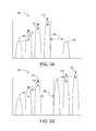
- FIGS. 3A-3Bdepict graph diagrams 300 , 302 of embodiments of voltage pulses in an erase operation.
- the voltage pulses for an erase operationmay be performed using an ISPE approach. While the erase operation is described herein in conjunction with the ISPE approach shown in FIGS. 3A-3B , the erase operation may be implemented using any erasing approach.
- the x-axesrepresent time and the y-axes represent the voltage amplitude/magnitude of pulses applied to the memory element 126 .
- FIG. 3Adepicts a graph diagram 300 of an embodiment of voltage pulses for a erase operation at a memory element 126 that is suspended to perform an operation corresponding to a memory access request queued behind the erase operation.
- the erase operationmay be performed using incremental pulses which incrementally increase or change the voltage level of each pulse, which in turn increases or changes the voltage level stored at the memory element 126 .
- the first pulse 304 applied to the memory element 126has the lowest pulse amplitude of the pulses, and the amplitude for each subsequent pulse in the erase operation increases as the voltage level stored in the memory element 126 gets closer to the voltage level for the desired state.
- the pulse delta 312(or change in voltage level for each pulse) from one pulse to the next decreases as the voltage level stored at the memory element 126 gets closer to the voltage level for the desired state.
- the first voltage pulse 304has the highest delta 312 as compared to the pulse deltas 312 for each subsequent pulse, such that the change in voltage for the first pulse 304 (from zero voltage or other base voltage) is the greatest single change in voltage than for any of the subsequent pulses of the erase operation.
- the erase operationis resumed from the beginning of the erase operation, such that the first pulse 308 applied to the memory element 126 after resuming the erase operation has the same or approximately the same amplitude as the initial pulse 304 .
- the erase operationmay be resumed from the beginning of the erase operation if the erase operation had been suspended for a certain amount of time or if the erase operation had progressed to a certain percentage of completion or to a certain voltage level.
- information that describes a progress of the erase operationmay not need to be stored, or if it has been stored, it may be discarded.
- the erase operationis resumed where the erase operation was suspended to perform the operation 306 corresponding to the memory access request queued behind the erase operation.
- the information that describes the progress of the erase operationmay be stored.
- the informationmay be stored at the memory device 116 , at the controller 114 , or at any location accessible to the memory device 116 .
- the informationmay include a pulse (or step) count, a pulse amplitude, a pulse width or duration, and other information that describes the pulse(s) and progress of the erase operation.
- the informationmay also include information about the current voltage step stored at the memory element 126 .
- the informationmay be retrieved and the erase operation may be resumed using the stored information.
- the erase operationis resumed by continuing the ISPE process from the last stored pulse 310 and applying subsequent pulses to the memory element 126 , such that the first pulse 308 after resuming the erases operation has a greater amplitude than the last stored pulse 310 .
- the erase operationmay be resumed at a point in the ISPE process sometime before the point at which the erase operation was suspended.
- the erase operationmay be resumed by applying a pulse equal to the last stored pulse or a pulse of smaller magnitude than the last stored pulse 310 .
- the erase operationmay be resumed by resuming the ISPE process at any point in the erase operation using the stored information.
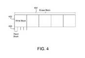
- FIG. 4depicts a block diagram of an embodiment of blocks in the memory device 116 of FIG. 2 . While the blocks of FIG. 3 are described herein in conjunction with the memory device 116 of FIG. 2 , the block may be used in conjunction with any type of memory device 116 . Alternatively, the memory device 116 of FIG. 2 may use any arrangement or size of blocks of memory elements 126 .
- blockis broadly interpreted to include one or more memory elements 126 in the memory device 116 .
- Blocks of memory elements 126may be different sizes for each operation performed at the memory elements 126 .
- read operationsmay be performed for read blocks 400 of individual memory elements 126 or other small group of memory elements 126 .
- Write operationsmay be performed on a write block 402 , which may include a plurality of memory elements 126 , such that data is written to each of the memory elements 126 in the write block 402 in a single operation. Thus, a write operation is performed on a larger block of memory elements 126 than a read operation.
- Erase operationsmay be performed on an erase block 404 , such that data stored at the memory elements 126 in the erase block 404 is erase in a single erase operation.
- the erase blockis larger than the write block 402 , such that the erase block 404 contains several write blocks 402 .
- erase operationstypically take much longer than read operations, and erase operations typically take much longer than both read operations and write operations. Additionally, erase operations performed on a given chip prevent read/write operations from being performed to the memory elements 126 within the erase block 404 , as well as to any memory elements 126 on the same chip as the erase block 404 .
- FIG. 5depicts a flow chart diagram of one embodiment of a method 500 for suspending an erase operation at the memory device 116 of FIG. 2 .
- the method 500is shown and described with operations of the controller 114 and memory device 116 of FIG. 1 , other embodiments of the method 500 may be implemented with other controllers and/or memory devices.
- the method 500includes performing 502 a portion of an erase operation to erase data at the memory array.
- the erase operationincludes erasing data stored in memory elements 126 of the memory device 116 corresponding to a specified block of addresses on the memory device 116 .
- the block of memory elements 126 to be erasedmay be located on more than one memory array or memory chip.
- the method 500may include determining whether the address correspond to the read/write signal is located on the same chip as the erase operation. If the address corresponding to the read/write signal is located on the same chip as the current erase operation, the method 500 includes calculating 506 a suspend threshold based on a suspend policy.
- the method 500determines 508 whether the erase operation meets the erase threshold.
- the suspend thresholdmay be used to determine whether to suspend the current erase operation in response to receiving the read/write signal or to wait until the erase operation is completed before performing the read/write operation for the read/write signal. If the erase operation does not meet the suspend threshold, the erase operation is completed 518 before performing the read/write operation.
- the suspend thresholdmay be used to balance read performance, program performance, and erase performance.
- the suspend policymay include criteria related to the erase operation, the read/write operation, or other operations at the controller 114 or memory device 116 .
- the suspend policyincludes suspending the erase operation automatically in response to receiving the read/write signal.
- the suspend policyincludes suspending the erase operation in response to determining that the erase operation is less than halfway completed.
- the suspend policyincludes a maximum number of times for suspending a single erase operation.
- the suspend policyincludes suspending the erase operation in response to determining that a benefit associated with suspending the erase operation is greater than a predetermined erase penalty value. The benefit is based on a remaining erase time for the erase operation.
- the suspend policyincludes increasing a probability of suspending the erase operation for each read/write signal in a queue of command signals.
- the suspend policyincludes decreasing the probability as the erase operation nears completion.
- the suspend policymay include a read/write/erase sensitivity of an application requesting access to the memory device 116 for read/write/erase operations. If the application performs more erase operations than read/write operations, the threshold may be weighted to give more priority to erase operations. If the application performs more read/write operations than erase operations, the threshold may be weighted to give more priority to read/write operations. In another example, a write sensitive application that performs a high number of write operations may also perform a high number of erase operations before performing write operations if data is already stored at the memory elements 126 . The threshold for such a write sensitive application may be weighted to give more priority to erase operations. Other embodiments may give different weights to erase and read/write operations based on the read/write/erase sensitivity. The suspend threshold may be based on probabilities or other criteria not described herein.
- the erase operationis suspended 510 and any erase operations at the memory elements 126 may be stopped.
- the method 500includes storing 512 an erase step associated with the erase operation in response to suspending the erase operation.
- the addresses for the memory elements 126 associated with the erase operationare also stored with the erase step.
- the data associated with the erase operationmay be stored at any location on the memory device 116 or at the controller, such as in a buffer or register.
- the method 500includes performing 514 the read/write (or other) operation associated with the read/write (or other memory access) signal.
- the read/write signalincludes at least one address corresponding to a row and column for one or more memory elements 126 in the memory array.
- the data from the memory element 126 or memory elements 126is read and copied to the I/O buffer 148 or read buffer 302 .
- the data fetched from the memory arraymay then be sent on the I/O bus 150 to the controller 114 .
- the data from the I/O bus 150may be written to the I/O buffer 148 and then written to the corresponding memory elements 126 on the memory device 116 .
- a status register 158 at the memory device 116is set to indicate that the read/write operation is completed.
- the erase operationis then resumed 516 at the stored step count in response to receiving a resume signal from the controller 114 rather than starting the erase operation at the starting voltage.
- the resume signalindicates that the read/write operation is completed. If data corresponding to the erase step has been stored at a cache buffer 162 or other location in order to perform the read/write operation, the data corresponding to the erase step may be used to resume the erase operation at the stored erase step rather than starting the erase operation from the beginning. In another embodiment, the addresses corresponding to the erase operation may be stored and used to start the erase operation from the beginning. The erase operation may then be completed 518 .
- the suspend policymay include one or more of the policies shown above. Alternatively, the suspend policy may include other criteria not described herein.
- the apparatusincludes an input/output (I/O) interface configured to couple a controller to an I/O buffer of a memory device.
- the apparatusincludes an erase module coupled to the I/O interface.
- the erase moduleis configured to issue an instruction to the memory device to erase data from the memory device.
- the electronic memory device controllerincludes an erase suspend module coupled to the I/O interface.
- the erase suspend moduleis configured to determine that an erase operation executing within the electronic memory device satisfies a suspend policy in response to receiving a memory access request to perform an operation at the memory device on which the erase operation is executing.
- the erase suspend moduleis configured to issue a suspend command to the memory device to suspend the erase operation.
- the methodincludes performing a portion of an erase operation including erasing data from a plurality of memory elements in a memory array of the memory device.
- the methodincludes receiving a memory access request to the memory device.
- the methodincludes calculating a suspend threshold based on a suspend policy.
- the methodincludes determining that the erase operation meets the suspend threshold.
- the methodincludes suspending the erase operation.
- the memory deviceincludes a memory array with a plurality of memory elements. Each memory element is configured to store data.
- the memory deviceincludes a memory control manager coupled to the memory array and to an input/output (I/O) interface of a memory device controller.
- the memory control manageris configured to calculate a suspend threshold associated with a predetermined suspend policy.
- the memory control manageris also configured to determine that an erase operation executing within the memory device meets the suspend threshold in response to receiving a memory access request from the I/O interface.
- the memory control manageris also configured to pause the erase operation.
- the systemincludes means for storing data in a plurality of memory elements in a memory device.
- the systemincludes means for erasing data from the memory elements.
- the systemincludes means for determining that an erase operation executing within the memory device satisfies a suspend policy in response to receiving a memory access request.
- the systemincludes means for suspending the erase operation.
- An embodiment of the electronic memory device controllerincludes at least one processor coupled directly or indirectly to memory elements through a system bus such as a data, address, and/or control bus.
- the memory elementscan include local memory employed during actual execution of the program code, bulk storage, and cache memories which provide temporary storage of at least some program code in order to reduce the number of times code must be retrieved from bulk storage during execution.
- an embodiment of a computer program productincludes a computer useable storage medium to store a computer readable program that, when executed on a computer, causes the computer to perform operations, as described herein.
- Embodiments of the inventioncan take the form of an entirely hardware embodiment, an entirely software embodiment, or an embodiment containing both hardware and software elements.
- the inventionis implemented in software, which includes but is not limited to firmware, resident software, microcode, etc.
- embodiments of the inventioncan take the form of a computer program product accessible from a computer-usable or computer-readable medium providing program code for use by or in connection with a computer or any instruction execution system.
- a computer-usable or computer readable mediumcan be any apparatus that can contain, store, communicate, propagate, or transport the program for use by or in connection with the instruction execution system, apparatus, or device.
- the computer-useable or computer-readable mediumcan be an electronic, magnetic, optical, electromagnetic, infrared, or semiconductor system (or apparatus or device), or a propagation medium.
- Examples of a computer-readable mediuminclude a semiconductor or solid state memory, magnetic tape, a removable computer diskette, a random access memory (RAM), a read-only memory (ROM), a rigid magnetic disk, and an optical disk.
- Current examples of optical disksinclude a compact disk with read only memory (CD-ROM), a compact disk with read/write (CD-R/W), and a digital video disk (DVD).
- I/O devicescan be coupled to the system either directly or through intervening I/O controllers.
- network adaptersalso may be coupled to the system to enable the data processing system to become coupled to other data processing systems or remote printers or memory devices through intervening private or public networks. Modems, cable modems, and Ethernet cards are just a few of the currently available types of network adapters.
Landscapes
- Engineering & Computer Science (AREA)
- Theoretical Computer Science (AREA)
- Computer Security & Cryptography (AREA)
- Human Computer Interaction (AREA)
- Physics & Mathematics (AREA)
- General Engineering & Computer Science (AREA)
- General Physics & Mathematics (AREA)
- Read Only Memory (AREA)
Abstract
Description
| if(bank == erasing && incoming read/write) | |||
| interrupt erase | |||
| issue read/write | |||
| continue erase | |||
| if(bank==erasing && incoming read) | |||
| if(erasing done <= .5 * total erase time) | |||
| interrupt erase | |||
| issue read/write | |||
| continue erase | |||
| already_canceled=0 | |||
| max_cancels=5 | |||
| if(bank == erasing && incoming read/write) | |||
| interrupt erase | |||
| already_canceled++ | |||
| issue read/write | |||
| continue erase | |||
| erase_cancel_penalty=1 | |
| erase_time=5 | |
| if(bank==erasing && incoming read/write) | |
| if(%erase time left * erase_time > erase_cancel_penalty) | |
| interrupt erase | |
| issue read/write | |
| continue erase | |
| magic_number=4 |
| if(bank==erasing && incoming read/write) |
| if(%erase time left / number_of_reads/writes queued > magic_number) |
| interrupt erase |
| issue read/write |
| continue erase |
Claims (29)
Priority Applications (1)
| Application Number | Priority Date | Filing Date | Title |
|---|---|---|---|
| US13/800,628US9223514B2 (en) | 2009-09-09 | 2013-03-13 | Erase suspend/resume for memory |
Applications Claiming Priority (6)
| Application Number | Priority Date | Filing Date | Title |
|---|---|---|---|
| US24099109P | 2009-09-09 | 2009-09-09 | |
| US24562209P | 2009-09-24 | 2009-09-24 | |
| US12/878,987US8429436B2 (en) | 2009-09-09 | 2010-09-09 | Apparatus, system, and method for power reduction in a storage device |
| US201161442173P | 2011-02-11 | 2011-02-11 | |
| US13/372,430US8972627B2 (en) | 2009-09-09 | 2012-02-13 | Apparatus, system, and method for managing operations for data storage media |
| US13/800,628US9223514B2 (en) | 2009-09-09 | 2013-03-13 | Erase suspend/resume for memory |
Related Parent Applications (1)
| Application Number | Title | Priority Date | Filing Date |
|---|---|---|---|
| US13/372,430Continuation-In-PartUS8972627B2 (en) | 2009-09-09 | 2012-02-13 | Apparatus, system, and method for managing operations for data storage media |
Publications (2)
| Publication Number | Publication Date |
|---|---|
| US20130198451A1 US20130198451A1 (en) | 2013-08-01 |
| US9223514B2true US9223514B2 (en) | 2015-12-29 |
Family
ID=48871330
Family Applications (1)
| Application Number | Title | Priority Date | Filing Date |
|---|---|---|---|
| US13/800,628ActiveUS9223514B2 (en) | 2009-09-09 | 2013-03-13 | Erase suspend/resume for memory |
Country Status (1)
| Country | Link |
|---|---|
| US (1) | US9223514B2 (en) |
Cited By (11)
| Publication number | Priority date | Publication date | Assignee | Title |
|---|---|---|---|---|
| US9666244B2 (en) | 2014-03-01 | 2017-05-30 | Fusion-Io, Inc. | Dividing a storage procedure |
| US9933950B2 (en)* | 2015-01-16 | 2018-04-03 | Sandisk Technologies Llc | Storage operation interrupt |
| US10042587B1 (en) | 2016-03-15 | 2018-08-07 | Adesto Technologies Corporation | Automatic resumption of suspended write operation upon completion of higher priority write operation in a memory device |
| US10360045B2 (en) | 2017-04-25 | 2019-07-23 | Sandisk Technologies Llc | Event-driven schemes for determining suspend/resume periods |
| US10521152B2 (en) | 2016-11-07 | 2019-12-31 | Samsung Electronics Co., Ltd. | Storage device storing data in raid manner |
| US20200135284A1 (en)* | 2019-12-26 | 2020-04-30 | Intel Corporation | Solid state drive (ssd) with in-flight erasure iteration suspension |
| US10643711B1 (en) | 2018-12-20 | 2020-05-05 | Western Digital Technologies, Inc. | Workload based dynamic erase suspend adaptation |
| US10692578B2 (en) | 2017-08-17 | 2020-06-23 | Samsung Electronics Co., Ltd | Nonvolatile memory device for performing urgent read operation based on suspend command and method of operating the same |
| US11373708B2 (en)* | 2020-08-14 | 2022-06-28 | SK Hynix Inc. | Memory device and method of operating the same |
| US11456039B2 (en) | 2020-11-24 | 2022-09-27 | Micron Technology, Inc. | Resumption of program or erase operations in memory |
| US11557358B2 (en) | 2021-04-15 | 2023-01-17 | Sandisk Technologies Llc | Memory apparatus and method of operation using adaptive erase time compensation for segmented erase |
Families Citing this family (37)
| Publication number | Priority date | Publication date | Assignee | Title |
|---|---|---|---|---|
| US10230396B1 (en) | 2013-03-05 | 2019-03-12 | Microsemi Solutions (Us), Inc. | Method and apparatus for layer-specific LDPC decoding |
| US9813080B1 (en) | 2013-03-05 | 2017-11-07 | Microsemi Solutions (U.S.), Inc. | Layer specific LDPC decoder |
| KR20150008671A (en)* | 2013-07-15 | 2015-01-23 | 에스케이하이닉스 주식회사 | Semiconductor Apparatus |
| KR102187637B1 (en)* | 2014-02-03 | 2020-12-07 | 삼성전자주식회사 | Memory system including nonvolatile memory device and erase method thereof |
| KR20150116352A (en) | 2014-04-07 | 2015-10-15 | 삼성전자주식회사 | Memory control method and system |
| KR102203298B1 (en)* | 2014-08-01 | 2021-01-15 | 삼성전자주식회사 | Nonvolatile memory device and driving method of the same |
| US10332613B1 (en) | 2015-05-18 | 2019-06-25 | Microsemi Solutions (Us), Inc. | Nonvolatile memory system with retention monitor |
| CN106293623B (en)* | 2015-05-18 | 2020-09-01 | 北京忆芯科技有限公司 | Micro instruction sequence execution method and device |
| US9799405B1 (en) | 2015-07-29 | 2017-10-24 | Ip Gem Group, Llc | Nonvolatile memory system with read circuit for performing reads using threshold voltage shift read instruction |
| US9886214B2 (en) | 2015-12-11 | 2018-02-06 | Ip Gem Group, Llc | Nonvolatile memory system with erase suspend circuit and method for erase suspend management |
| US9892794B2 (en) | 2016-01-04 | 2018-02-13 | Ip Gem Group, Llc | Method and apparatus with program suspend using test mode |
| US9899092B2 (en) | 2016-01-27 | 2018-02-20 | Ip Gem Group, Llc | Nonvolatile memory system with program step manager and method for program step management |
| JP6538597B2 (en)* | 2016-03-14 | 2019-07-03 | 東芝メモリ株式会社 | Storage device |
| US10203884B2 (en)* | 2016-03-30 | 2019-02-12 | Intel Corporation | Methods and apparatus to perform erase-suspend operations in memory devices |
| CN107423227A (en)* | 2016-05-24 | 2017-12-01 | 瑞昱半导体股份有限公司 | Memory device, memory controller and control method thereof |
| US10514862B2 (en) | 2016-07-21 | 2019-12-24 | Micron Technology, Inc. | Memory device including concurrent suspend states for different operations |
| US10291263B2 (en) | 2016-07-28 | 2019-05-14 | Ip Gem Group, Llc | Auto-learning log likelihood ratio |
| US10157677B2 (en) | 2016-07-28 | 2018-12-18 | Ip Gem Group, Llc | Background reference positioning and local reference positioning using threshold voltage shift read |
| US10558398B2 (en)* | 2016-07-29 | 2020-02-11 | Seagate Technology Llc | Reducing read latency |
| US10236915B2 (en) | 2016-07-29 | 2019-03-19 | Microsemi Solutions (U.S.), Inc. | Variable T BCH encoding |
| KR102719399B1 (en)* | 2016-11-07 | 2024-10-21 | 에스케이하이닉스 주식회사 | Memory system and operating method thereof |
| KR102763344B1 (en)* | 2016-11-29 | 2025-02-07 | 삼성전자주식회사 | Operation method of resuming an operation of nonvolatile memory device |
| KR20190088293A (en)* | 2018-01-18 | 2019-07-26 | 에스케이하이닉스 주식회사 | Memory device and operating method thereof |
| US10936199B2 (en)* | 2018-07-17 | 2021-03-02 | Silicon Motion, Inc. | Flash controllers, methods, and corresponding storage devices capable of rapidly/fast generating or updating contents of valid page count table |
| CN110908713A (en)* | 2018-09-17 | 2020-03-24 | 北京兆易创新科技股份有限公司 | Operation interruption method and device, storage equipment and storage medium |
| KR102520540B1 (en)* | 2018-10-23 | 2023-04-12 | 에스케이하이닉스 주식회사 | Memory device and operating method thereof |
| KR102569820B1 (en)* | 2018-10-25 | 2023-08-24 | 에스케이하이닉스 주식회사 | Memory controller and operating method thereof |
| US10976947B2 (en)* | 2018-10-26 | 2021-04-13 | Pure Storage, Inc. | Dynamically selecting segment heights in a heterogeneous RAID group |
| KR102680273B1 (en)* | 2019-02-12 | 2024-07-01 | 삼성전자주식회사 | A method for controlling a suspend mode and a memory controller including the same |
| KR102690405B1 (en)* | 2019-06-03 | 2024-08-01 | 에스케이하이닉스 주식회사 | Memory device and operating method thereof |
| US11237731B2 (en) | 2019-10-24 | 2022-02-01 | Micron Technology, Inc. | Quality of service for memory devices using suspend and resume of program and erase operations |
| US11620053B2 (en) | 2019-10-24 | 2023-04-04 | Micron Technology, Inc. | Quality of service for the multiple functions in memory devices |
| US11687244B2 (en) | 2019-10-24 | 2023-06-27 | Micron Technology, Inc. | Quality of service for memory devices using weighted memory access operation types |
| US11081187B2 (en)* | 2019-12-11 | 2021-08-03 | SanDiskTechnologies LLC | Erase suspend scheme in a storage device |
| KR20240001939A (en)* | 2022-06-28 | 2024-01-04 | 에스케이하이닉스 주식회사 | Memory device and operating method thereof |
| US12230332B2 (en)* | 2022-08-31 | 2025-02-18 | Micron Technology, Inc. | Suspending memory erase operations to perform higher priority memory commands |
| WO2025101488A1 (en)* | 2023-11-07 | 2025-05-15 | Micron Technology, Inc. | Incremental power throttling on memory system |
Citations (308)
| Publication number | Priority date | Publication date | Assignee | Title |
|---|---|---|---|---|
| GB1234160A (en) | 1967-06-09 | 1971-06-03 | ||
| US4980861A (en) | 1987-01-16 | 1990-12-25 | Microchip Technology Incorporated | NAND stack ROM |
| US5193184A (en) | 1990-06-18 | 1993-03-09 | Storage Technology Corporation | Deleted data file space release system for a dynamically mapped virtual data storage subsystem |
| US5261068A (en) | 1990-05-25 | 1993-11-09 | Dell Usa L.P. | Dual path memory retrieval system for an interleaved dynamic RAM memory unit |
| US5325509A (en) | 1991-03-05 | 1994-06-28 | Zitel Corporation | Method of operating a cache memory including determining desirability of cache ahead or cache behind based on a number of available I/O operations |
| US5404485A (en) | 1993-03-08 | 1995-04-04 | M-Systems Flash Disk Pioneers Ltd. | Flash file system |
| US5438671A (en) | 1991-07-19 | 1995-08-01 | Dell U.S.A., L.P. | Method and system for transferring compressed bytes of information between separate hard disk drive units |
| US5504882A (en) | 1994-06-20 | 1996-04-02 | International Business Machines Corporation | Fault tolerant data storage subsystem employing hierarchically arranged controllers |
| US5535399A (en) | 1993-09-30 | 1996-07-09 | Quantum Corporation | Solid state disk drive unit having on-board backup non-volatile memory |
| US5553261A (en) | 1994-04-01 | 1996-09-03 | Intel Corporation | Method of performing clean-up of a solid state disk while executing a read command |
| US5594883A (en) | 1993-04-14 | 1997-01-14 | International Business Machines Corporation | Hierarchical data storage system employing contemporaneous transfer of designated data pages to long write and short read cycle memory |
| US5598370A (en) | 1993-02-24 | 1997-01-28 | International Business Machines Corporation | Nonvolatile memory with cluster-erase flash capability and solid state file apparatus using the same |
| US5638289A (en) | 1994-03-18 | 1997-06-10 | Fujitsu Limited | Method and apparatus allowing hot replacement of circuit boards |
| US5651133A (en) | 1995-02-01 | 1997-07-22 | Hewlett-Packard Company | Methods for avoiding over-commitment of virtual capacity in a redundant hierarchic data storage system |
| US5682499A (en) | 1995-06-06 | 1997-10-28 | International Business Machines Corporation | Directory rebuild method and apparatus for maintaining and rebuilding directory information for compressed data on direct access storage device (DASD) |
| US5682497A (en) | 1993-09-28 | 1997-10-28 | Intel Corporation | Managing file structures for a flash memory file system in a computer |
| US5701434A (en) | 1995-03-16 | 1997-12-23 | Hitachi, Ltd. | Interleave memory controller with a common access queue |
| US5742787A (en) | 1995-04-10 | 1998-04-21 | Intel Corporation | Hardware reset of a write state machine for flash memory |
| US5754563A (en) | 1995-09-11 | 1998-05-19 | Ecc Technologies, Inc. | Byte-parallel system for implementing reed-solomon error-correcting codes |
| US5799140A (en) | 1995-04-21 | 1998-08-25 | International Business Machines Corporation | Disk array system and method for storing data |
| US5799200A (en) | 1995-09-28 | 1998-08-25 | Emc Corporation | Power failure responsive apparatus and method having a shadow dram, a flash ROM, an auxiliary battery, and a controller |
| US5802602A (en) | 1997-01-17 | 1998-09-01 | Intel Corporation | Method and apparatus for performing reads of related data from a set-associative cache memory |
| US5805501A (en) | 1996-05-22 | 1998-09-08 | Macronix International Co., Ltd. | Flash memory device with multiple checkpoint erase suspend logic |
| US5812457A (en) | 1996-09-09 | 1998-09-22 | Sony Corporation | Semiconductor NAND type flash memory with incremental step pulse programming |
| US5845329A (en) | 1993-01-29 | 1998-12-01 | Sanyo Electric Co., Ltd. | Parallel computer |
| US5960462A (en) | 1996-09-26 | 1999-09-28 | Intel Corporation | Method and apparatus for analyzing a main memory configuration to program a memory controller |
| US6000019A (en) | 1995-06-06 | 1999-12-07 | Hewlett-Packard Company | SDRAM data allocation system and method utilizing dual bank storage and retrieval |
| US6014724A (en) | 1995-10-27 | 2000-01-11 | Scm Microsystems (U.S.) Inc. | Flash translation layer block indication map revision system and method |
| KR20000026300A (en) | 1998-10-20 | 2000-05-15 | 윤덕용 | Data storing device using flash memory |
| US6125072A (en) | 1998-07-21 | 2000-09-26 | Seagate Technology, Inc. | Method and apparatus for contiguously addressing a memory system having vertically expanded multiple memory arrays |
| US6170047B1 (en) | 1994-11-16 | 2001-01-02 | Interactive Silicon, Inc. | System and method for managing system memory and/or non-volatile memory using a memory controller with integrated compression and decompression capabilities |
| US6170039B1 (en) | 1997-05-16 | 2001-01-02 | Nec Corporation | Memory controller for interchanging memory against memory error in interleave memory system |
| WO2001001365A2 (en) | 1999-06-30 | 2001-01-04 | Siemens Aktiengesellschaft | System and method for transmitting data, especially between a user programme and a server programme in the field of automation technology with distributed objects |
| US6173381B1 (en) | 1994-11-16 | 2001-01-09 | Interactive Silicon, Inc. | Memory controller including embedded data compression and decompression engines |
| US6185654B1 (en) | 1998-07-17 | 2001-02-06 | Compaq Computer Corporation | Phantom resource memory address mapping system |
| US6205521B1 (en) | 1997-11-03 | 2001-03-20 | Compaq Computer Corporation | Inclusion map for accelerated cache flush |
| US6236593B1 (en) | 1999-04-27 | 2001-05-22 | Samsung Electronics Co., Ltd. | Method for simultaneously programming plural flash memories having invalid blocks |
| US6240040B1 (en) | 2000-03-15 | 2001-05-29 | Advanced Micro Devices, Inc. | Multiple bank simultaneous operation for a flash memory |
| US6256642B1 (en) | 1992-01-29 | 2001-07-03 | Microsoft Corporation | Method and system for file system management using a flash-erasable, programmable, read-only memory |
| US6278633B1 (en) | 1999-11-05 | 2001-08-21 | Multi Level Memory Technology | High bandwidth flash memory that selects programming parameters according to measurements of previous programming operations |
| EP0747822B1 (en) | 1995-06-07 | 2001-10-04 | Hitachi, Ltd. | External storage system with redundant storage controllers |
| US6330688B1 (en) | 1995-10-31 | 2001-12-11 | Intel Corporation | On chip error correction for devices in a solid state drive |
| US6336174B1 (en) | 1999-08-09 | 2002-01-01 | Maxtor Corporation | Hardware assisted memory backup system and method |
| US6385688B1 (en) | 1994-06-03 | 2002-05-07 | Intel Corporation | Asynchronous interface for a nonvolatile memory |
| US6385710B1 (en) | 1996-02-23 | 2002-05-07 | Sun Microsystems, Inc. | Multiple-mode external cache subsystem |
| US20020066047A1 (en) | 2000-11-30 | 2002-05-30 | Olarig Sompong P. | Memory controller with temperature sensors |
| US20020069318A1 (en) | 2000-12-01 | 2002-06-06 | Chow Yan Chiew | Real time application accelerator and method of operating the same |
| US6404647B1 (en) | 2000-08-24 | 2002-06-11 | Hewlett-Packard Co. | Solid-state mass memory storage device |
| US6412080B1 (en) | 1999-02-23 | 2002-06-25 | Microsoft Corporation | Lightweight persistent storage system for flash memory devices |
| US6418478B1 (en) | 1997-10-30 | 2002-07-09 | Commvault Systems, Inc. | Pipelined high speed data transfer mechanism |
| US20020103819A1 (en) | 2000-12-12 | 2002-08-01 | Fresher Information Corporation | Technique for stabilizing data in a non-log based information storage and retrieval system |
| US20020133743A1 (en) | 2001-03-15 | 2002-09-19 | Oldfield Barry J. | Redundant controller data storage system having hot insertion system and method |
| US20020138686A1 (en) | 2001-01-12 | 2002-09-26 | Liuxi Yang | Method for programming memory controller in a high performance microprocessor |
| US6470238B1 (en) | 1997-11-26 | 2002-10-22 | Intel Corporation | Method and apparatus to control device temperature |
| WO2001031512A9 (en) | 1999-10-25 | 2002-11-14 | Infolibria Inc | Fast indexing of web objects |
| US20020181134A1 (en) | 2001-06-04 | 2002-12-05 | Xerox Corporation | Secure data file erasure |
| US20020199056A1 (en) | 2001-06-20 | 2002-12-26 | Hitachi, Ltd. And Hitachi Ulsi Systems Co., Ltd. | Semiconductor device with non-volatile memory and random access memory |
| US6507911B1 (en) | 1998-07-22 | 2003-01-14 | Entrust Technologies Limited | System and method for securely deleting plaintext data |
| US6515909B1 (en) | 2001-10-05 | 2003-02-04 | Micron Technology Inc. | Flash memory device with a variable erase pulse |
| US6515928B2 (en) | 2000-11-30 | 2003-02-04 | Fujitsu Limited | Semiconductor memory device having a plurality of low power consumption modes |
| US20030028726A1 (en) | 2001-08-06 | 2003-02-06 | Gaertner Mark A. | Synchronized mirrored data in a data storage device |
| US20030028704A1 (en) | 2000-12-06 | 2003-02-06 | Naoki Mukaida | Memory controller, flash memory system having memory controller and method for controlling flash memory device |
| US6523102B1 (en) | 2000-04-14 | 2003-02-18 | Interactive Silicon, Inc. | Parallel compression/decompression system and method for implementation of in-memory compressed cache improving storage density and access speed for industry standard memory subsystems and in-line memory modules |
| US20030061296A1 (en) | 2001-09-24 | 2003-03-27 | International Business Machines Corporation | Memory semantic storage I/O |
| US6552955B1 (en) | 2001-10-30 | 2003-04-22 | Mitsubishi Denki Kabushiki Kaisha | Semiconductor memory device with reduced power consumption |
| US20030115405A1 (en) | 1999-06-10 | 2003-06-19 | Fujitsu Limited | Semiconductor memory device and electronic apparatus |
| US6587915B1 (en) | 1999-09-29 | 2003-07-01 | Samsung Electronics Co., Ltd. | Flash memory having data blocks, spare blocks, a map block and a header block and a method for controlling the same |
| US20030126475A1 (en) | 2002-01-02 | 2003-07-03 | Bodas Devadatta V. | Method and apparatus to manage use of system power within a given specification |
| US6601211B1 (en) | 1996-10-15 | 2003-07-29 | Micron Technology, Inc. | Write reduction in flash memory systems through ECC usage |
| US20030145230A1 (en) | 2002-01-31 | 2003-07-31 | Huimin Chiu | System for exchanging data utilizing remote direct memory access |
| US6608793B2 (en) | 2000-05-02 | 2003-08-19 | Korea Advanced Institute Of Science And Technology | Efficient management method of memory cell array |
| US20030163630A1 (en) | 2002-02-27 | 2003-08-28 | Aasheim Jered Donald | Dynamic data structures for tracking data stored in a flash memory device |
| US20030163663A1 (en) | 2002-02-27 | 2003-08-28 | Aasheim Jered Donald | Dynamic data structures for tracking file system free space in a flash memory device |
| US6625685B1 (en) | 2000-09-20 | 2003-09-23 | Broadcom Corporation | Memory controller with programmable configuration |
| US6629112B1 (en) | 1998-12-31 | 2003-09-30 | Nortel Networks Limited | Resource management for CORBA-based applications |
| US6633950B1 (en) | 1996-09-20 | 2003-10-14 | Intel Corporation | Nonvolatile writeable memory with preemption pin |
| US6633956B1 (en) | 2000-04-14 | 2003-10-14 | Mitsubishi Denki Kabushiki Kaisha | Memory card with task registers storing physical addresses |
| US20030198084A1 (en) | 2002-04-18 | 2003-10-23 | Hitachi, Ltd. | Nonvolatile semiconductor memory |
| US6643181B2 (en) | 2001-10-24 | 2003-11-04 | Saifun Semiconductors Ltd. | Method for erasing a memory cell |
| US20030210601A1 (en) | 2002-05-07 | 2003-11-13 | Yu-Chuan Lin | Back up power embodied non-volatile memory device |
| US6655758B2 (en) | 2000-12-29 | 2003-12-02 | Stmicroelectronics S.R.L. | Method for storing data in a nonvolatile memory |
| US6658438B1 (en) | 2000-08-14 | 2003-12-02 | Matrix Semiconductor, Inc. | Method for deleting stored digital data from write-once memory device |
| US6671757B1 (en) | 2000-01-26 | 2003-12-30 | Fusionone, Inc. | Data transfer and synchronization system |
| US20040003167A1 (en) | 2002-06-27 | 2004-01-01 | Hiroyuki Kimura | Microcomputer |
| US20040003002A1 (en) | 2002-06-26 | 2004-01-01 | Adelmann Todd Christopher | Systems and methods for storing information to allow users to manage files |
| US6683810B2 (en) | 2000-09-28 | 2004-01-27 | Renesas Technology Corporation | Non-volatile memory and method of non-volatile memory programming |
| US6694453B1 (en) | 2000-11-14 | 2004-02-17 | Hewlett-Packard Development Company, L.P. | Apparatus and method to handle power supply failures for a peripheral device |
| US6715046B1 (en) | 2001-11-29 | 2004-03-30 | Cisco Technology, Inc. | Method and apparatus for reading from and writing to storage using acknowledged phases of sets of data |
| US6715027B2 (en) | 2000-12-27 | 2004-03-30 | Electronics And Telecommunications Research Institute | Ranked cleaning policy and error recovery method for file systems using flash memory |
| US20040064647A1 (en) | 2002-06-27 | 2004-04-01 | Microsoft Corporation | Method and apparatus to reduce power consumption and improve read/write performance of hard disk drives using non-volatile memory |
| US6735546B2 (en) | 2001-08-31 | 2004-05-11 | Matrix Semiconductor, Inc. | Memory device and method for temperature-based control over write and/or read operations |
| US20040103238A1 (en) | 2002-11-26 | 2004-05-27 | M-Systems Flash Disk Pioneers Ltd. | Appliance, including a flash memory, that is robust under power failure |
| US6751155B2 (en) | 2001-09-28 | 2004-06-15 | Lexar Media, Inc. | Non-volatile memory control |
| US20040114431A1 (en) | 2002-12-17 | 2004-06-17 | Yoshihiro Shona | Data rewriting method for flash memory |
| US6754774B2 (en) | 2001-07-06 | 2004-06-22 | Juniper Networks, Inc. | Streaming output engine facilitating data transfers between application engines and memory |
| US6760806B2 (en) | 2001-09-20 | 2004-07-06 | Hynix Semiconductor Inc. | Low power semiconductor memory device having a normal mode and a partial array self refresh mode |
| US20040148360A1 (en) | 2003-01-24 | 2004-07-29 | Hewlett-Packard Development Company | Communication-link-attached persistent memory device |
| US6779088B1 (en) | 2000-10-24 | 2004-08-17 | International Business Machines Corporation | Virtual uncompressed cache size control in compressed memory systems |
| US6785785B2 (en) | 2000-01-25 | 2004-08-31 | Hewlett-Packard Development Company, L.P. | Method for supporting multi-level stripping of non-homogeneous memory to maximize concurrency |
| US20040177054A1 (en) | 2003-03-03 | 2004-09-09 | M-Systems Flash Disk Pioneers, Ltd. | Efficient flash memory device driver |
| US20040186946A1 (en) | 2003-03-19 | 2004-09-23 | Jinaeon Lee | Flash file system |
| US6807097B2 (en) | 2000-12-11 | 2004-10-19 | Kabushiki Kaisha Toshiba | Non-volatile semiconductor memory device |
| US20040225719A1 (en) | 2003-05-07 | 2004-11-11 | International Business Machines Corporation | Distributed file serving architecture system with metadata storage virtualization and data access at the data server connection speed |
| US20040268359A1 (en) | 2003-06-27 | 2004-12-30 | Hanes David H. | Computer-readable medium, method and computer system for processing input/output requests |
| US20050002263A1 (en) | 2003-05-20 | 2005-01-06 | Yasuaki Iwase | Writing control method and writing control system of semiconductor storage device, and portable electronic apparatus |
| US6845053B2 (en) | 2002-11-15 | 2005-01-18 | Micron Technology, Inc. | Power throughput adjustment in flash memory |
| US20050015539A1 (en) | 2002-01-09 | 2005-01-20 | Takashi Horii | Memory system and memory card |
| US6849480B1 (en) | 1999-05-07 | 2005-02-01 | Seagate Technology Llc | Surface mount IC stacking method and device |
| US6865657B1 (en) | 2000-06-02 | 2005-03-08 | Sun Microsystems, Inc. | Garbage collector for a virtual heap |
| KR20050024278A (en) | 2002-05-21 | 2005-03-10 | 샌디스크 코포레이션 | Efficient, write method for pipeline memory |
| US6871257B2 (en) | 2002-02-22 | 2005-03-22 | Sandisk Corporation | Pipelined parallel programming operation in a non-volatile memory system |
| US6883079B1 (en) | 2000-09-01 | 2005-04-19 | Maxtor Corporation | Method and apparatus for using data compression as a means of increasing buffer bandwidth |
| US6887058B2 (en) | 2003-03-17 | 2005-05-03 | Toshiba Carrier Corporation | Fluid machinery |
| US20050141313A1 (en) | 2003-12-30 | 2005-06-30 | Gorobets Sergey A. | Non-volatile memory and method with memory planes alignment |
| US20050144361A1 (en) | 2003-12-30 | 2005-06-30 | Gonzalez Carlos J. | Adaptive mode switching of flash memory address mapping based on host usage characteristics |
| US6938133B2 (en) | 2001-09-28 | 2005-08-30 | Hewlett-Packard Development Company, L.P. | Memory latency and bandwidth optimizations |
| US20050210323A1 (en) | 2004-03-05 | 2005-09-22 | Batchelor Gary W | Scanning modified data during power loss |
| US20050216653A1 (en) | 2002-02-27 | 2005-09-29 | Microsoft Corporation | Transactional file system for flash memory |
| US6957158B1 (en) | 2002-12-23 | 2005-10-18 | Power Measurement Ltd. | High density random access memory in an intelligent electric device |
| US6959369B1 (en) | 2003-03-06 | 2005-10-25 | International Business Machines Corporation | Method, system, and program for data backup |
| US20050240713A1 (en) | 2004-04-22 | 2005-10-27 | V-Da Technology | Flash memory device with ATA/ATAPI/SCSI or proprietary programming interface on PCI express |
| US20050246510A1 (en) | 2003-11-13 | 2005-11-03 | Retnamma Manoj V | System and method for combining data streams in pipelined storage operations in a storage network |
| US20050246558A1 (en) | 2004-04-29 | 2005-11-03 | Ku Joseph W | Power management using a pre-determined thermal characteristic of a memory module |
| US20050257017A1 (en) | 2004-05-14 | 2005-11-17 | Hideki Yagi | Method and apparatus to erase hidden memory in a memory card |
| US20050262150A1 (en) | 2004-05-21 | 2005-11-24 | Computer Associates Think, Inc. | Object-based storage |
| US20050267882A1 (en) | 2004-06-01 | 2005-12-01 | Eric Aupperlee | Model for communication between manufacturing and enterprise levels |
| US6973551B1 (en) | 2002-12-30 | 2005-12-06 | Emc Corporation | Data storage system having atomic memory operation |
| US20050273476A1 (en) | 2004-05-18 | 2005-12-08 | Oracle International Corporation | Automated disk-oriented backups |
| US20050270927A1 (en) | 2004-06-02 | 2005-12-08 | Katsunori Hayashi | Disk array device and battery output control method for disk array device |
| US6977847B2 (en) | 2001-11-23 | 2005-12-20 | M-Systems Flash Disk Pioneers Ltd. | Detecting partially erased units in flash devices |
| US6981070B1 (en) | 2000-07-12 | 2005-12-27 | Shun Hang Luk | Network storage device having solid-state non-volatile memory |
| US20060004955A1 (en) | 2002-06-20 | 2006-01-05 | Rambus Inc. | Dynamic memory supporting simultaneous refresh and data-access transactions |
| US6990547B2 (en) | 2001-01-29 | 2006-01-24 | Adaptec, Inc. | Replacing file system processors by hot swapping |
| US20060020744A1 (en) | 2004-07-21 | 2006-01-26 | Sandisk Corporation | Method and apparatus for maintaining data on non-volatile memory systems |
| US6996676B2 (en) | 2002-11-14 | 2006-02-07 | International Business Machines Corporation | System and method for implementing an adaptive replacement cache policy |
| US20060053247A1 (en) | 2004-09-08 | 2006-03-09 | Hugo Cheung | Incremental erasing of flash memory to improve system performance |
| US20060059326A1 (en) | 2002-11-21 | 2006-03-16 | Microsoft Corporation | Dynamic data structures for tracking file system free space in a flash memory device |
| US20060069870A1 (en) | 2004-09-24 | 2006-03-30 | Microsoft Corporation | Method and system for improved reliability in storage devices |
| US20060075057A1 (en) | 2004-08-30 | 2006-04-06 | International Business Machines Corporation | Remote direct memory access system and method |
| US20060085471A1 (en) | 2004-10-15 | 2006-04-20 | Vijayan Rajan | System and method for reclaiming unused space from a thinly provisioned data container |
| US20060095659A1 (en) | 2004-10-29 | 2006-05-04 | Hitachi Global Storage Technologies Netherlands, B.V. | Hard disk drive with support for atomic transactions |
| US7042664B2 (en) | 2004-01-26 | 2006-05-09 | Seagate Technology Llc | Method and system for host programmable data storage device self-testing |
| US20060106990A1 (en) | 2004-11-18 | 2006-05-18 | Benhase Michael T | Apparatus, system, and method for flushing cache data |
| US7058769B1 (en) | 2002-08-07 | 2006-06-06 | Nvidia Corporation | Method and system of improving disk access time by compression |
| US7057936B2 (en) | 2002-06-20 | 2006-06-06 | Kabushiki Kaisha Toshiba | Nonvolatile semiconductor memory device |
| WO2006062511A1 (en) | 2004-12-06 | 2006-06-15 | Teac Aerospace Technologies, Inc. | System and method of erasing non-volatile recording media |
| US7064994B1 (en) | 2004-01-30 | 2006-06-20 | Sun Microsystems, Inc. | Dynamic memory throttling for power and thermal limitations |
| US20060136779A1 (en) | 2004-12-20 | 2006-06-22 | Lee Sang-Min | Object-based storage device with low process load and control method thereof |
| WO2006065626A1 (en) | 2004-12-14 | 2006-06-22 | Network Appliance, Inc. | Rendering disk data unrecoverable using encryption |
| US20060149916A1 (en) | 2003-01-03 | 2006-07-06 | Austria Card Plastikkarten Und Ausweissysteme Gmbh | Method and apparatus for block-oriented memory management provided in smart card controllers |
| US20060149893A1 (en) | 2004-12-30 | 2006-07-06 | Barfuss Dale C | Data storage management for flash memory devices |
| US7089391B2 (en) | 2000-04-14 | 2006-08-08 | Quickshift, Inc. | Managing a codec engine for memory compression/decompression operations using a data movement engine |
| US20060179263A1 (en) | 2005-02-04 | 2006-08-10 | Dong-Hyun Song | Flash memory device and associated data merge method |
| US20060184736A1 (en) | 2005-02-17 | 2006-08-17 | Benhase Michael T | Apparatus, system, and method for storing modified data |
| US20060184722A1 (en) | 2005-02-16 | 2006-08-17 | Sinclair Alan W | Direct data file storage implementation techniques in flash memories |
| US7096321B2 (en) | 2003-10-21 | 2006-08-22 | International Business Machines Corporation | Method and system for a cache replacement technique with adaptive skipping |
| US20060190552A1 (en) | 2005-02-24 | 2006-08-24 | Henze Richard H | Data retention system with a plurality of access protocols |
| WO2005103878A3 (en) | 2004-04-26 | 2006-08-24 | Storewiz Inc | Method and system for compression of files for storage and operation on compressed files |
| US7107480B1 (en) | 2000-12-22 | 2006-09-12 | Simpletech, Inc. | System and method for preventing data corruption in solid-state memory devices after a power failure |
| US20060230295A1 (en) | 2005-04-08 | 2006-10-12 | Schumacher Derek S | Memory module with on-board power-consumption monitoring |
| KR20060107728A (en) | 2005-04-11 | 2006-10-16 | 엘지전자 주식회사 | Home network control system and data flow control method in the home network control system |
| US20060248387A1 (en) | 2005-04-15 | 2006-11-02 | Microsoft Corporation | In-line non volatile memory disk read cache and write buffer |
| US20060265636A1 (en) | 2005-05-19 | 2006-11-23 | Klaus Hummler | Optimized testing of on-chip error correction circuit |
| US20060294300A1 (en) | 2005-06-22 | 2006-12-28 | Seagate Technology Llc | Atomic cache transactions in a distributed storage system |
| US20070016699A1 (en) | 2005-07-14 | 2007-01-18 | Canon Kabushiki Kaisha | Memory control apparatus and method |
| US7167944B1 (en) | 2000-07-21 | 2007-01-23 | Lexar Media, Inc. | Block management for mass storage |
| US7173852B2 (en) | 2003-10-03 | 2007-02-06 | Sandisk Corporation | Corrected data storage and handling methods |
| US20070033326A1 (en) | 2005-08-03 | 2007-02-08 | Sinclair Alan W | Enhanced host interfacing methods |
| US20070033362A1 (en) | 2005-02-04 | 2007-02-08 | Sinclair Alan W | Mass data storage system |
| US7177197B2 (en) | 2001-09-17 | 2007-02-13 | Sandisk Corporation | Latched programming of memory and method |
| US7181572B2 (en) | 2002-12-02 | 2007-02-20 | Silverbrook Research Pty Ltd | Cache updating method and apparatus |
| US20070043900A1 (en) | 2005-08-20 | 2007-02-22 | Samsung Electronics Co., Ltd. | Flash memory management method and flash memory system |
| US20070050571A1 (en) | 2005-09-01 | 2007-03-01 | Shuji Nakamura | Storage system, storage device, and control method thereof |
| US20070061508A1 (en) | 2005-09-13 | 2007-03-15 | Quantum Corporation | Data storage cartridge with built-in tamper-resistant clock |
| US7194740B1 (en) | 1999-05-28 | 2007-03-20 | Oracle International Corporation | System for extending an addressable range of memory |
| US20070083530A1 (en) | 2005-10-10 | 2007-04-12 | Oracle International Corporation | Recoverable execution |
| US20070086260A1 (en) | 2005-10-13 | 2007-04-19 | Sinclair Alan W | Method of storing transformed units of data in a memory system having fixed sized storage blocks |
| US20070088666A1 (en) | 2003-11-18 | 2007-04-19 | Hiroshi Saito | File recording apparatus |
| US7219238B2 (en) | 2002-03-20 | 2007-05-15 | Seiko Epson Corporation | Data transfer control device, electronic instrument, and data transfer control method |
| US20070118713A1 (en) | 2005-11-22 | 2007-05-24 | Guterman Daniel C | Memory system for legacy hosts |
| US7227777B2 (en) | 2002-11-21 | 2007-06-05 | Micron Technology, Inc. | Mode selection in a flash memory device |
| US20070143566A1 (en) | 2005-12-21 | 2007-06-21 | Gorobets Sergey A | Non-volatile memories with data alignment in a directly mapped file storage system |
| US20070156998A1 (en) | 2005-12-21 | 2007-07-05 | Gorobets Sergey A | Methods for memory allocation in non-volatile memories with a directly mapped file storage system |
| US7243203B2 (en) | 2003-06-13 | 2007-07-10 | Sandisk 3D Llc | Pipeline circuit for low latency memory |
| US7246179B2 (en) | 2000-10-17 | 2007-07-17 | Microsoft Corporation | System and method for controlling mass storage class digital imaging devices |
| US20070168698A1 (en) | 2005-11-03 | 2007-07-19 | Coulson Richard L | Recovering from a non-volatile memory failure |
| US7257129B2 (en) | 2000-11-22 | 2007-08-14 | Silicon Image | Memory architecture with multiple serial communications ports |
| US7257690B1 (en) | 2004-10-15 | 2007-08-14 | Veritas Operating Corporation | Log-structured temporal shadow store |
| US7263591B2 (en) | 1995-07-31 | 2007-08-28 | Lexar Media, Inc. | Increasing the memory performance of flash memory devices by writing sectors simultaneously to multiple flash memory devices |
| US20070204270A1 (en)* | 2006-02-28 | 2007-08-30 | Samsung Electronics Co., Ltd. | Apparatus and method for processing operations of nonvolatile memory in order of priority |
| US20070208790A1 (en) | 2006-03-06 | 2007-09-06 | Reuter James M | Distributed data-storage system |
| US7275135B2 (en) | 2001-08-31 | 2007-09-25 | Intel Corporation | Hardware updated metadata for non-volatile mass storage cache |
| US20070230253A1 (en) | 2006-03-29 | 2007-10-04 | Jin-Ki Kim | Non-volatile semiconductor memory with page erase |
| US20070233937A1 (en) | 2006-03-31 | 2007-10-04 | Coulson Richard L | Reliability of write operations to a non-volatile memory |
| US20070233938A1 (en) | 2006-03-30 | 2007-10-04 | Silicon Image, Inc. | Shared nonvolatile memory architecture |
| US20070234021A1 (en) | 2006-03-30 | 2007-10-04 | Silicon Image, Inc. | Inter-port communication in a multi-port memory device |
| US20070239926A1 (en)* | 2006-03-28 | 2007-10-11 | Yevgen Gyl | Method and device for reduced read latency of non-volatile memory |
| US20070245076A1 (en) | 2006-04-12 | 2007-10-18 | Giga-Byte Technology Co., Ltd. | Volatile storage device and serial mixed storage system having the same |
| US20070260608A1 (en) | 2006-05-02 | 2007-11-08 | Ben Hertzberg | System and method for allocating and deallocating memory within transactional code |
| US20070266037A1 (en) | 2004-11-05 | 2007-11-15 | Data Robotics Incorporated | Filesystem-Aware Block Storage System, Apparatus, and Method |
| US20070276994A1 (en) | 2006-05-23 | 2007-11-29 | Jason Caulkins | Methods for managing data writes and reads to a hybrid solid-state disk drive |
| US7305520B2 (en) | 2004-01-30 | 2007-12-04 | Hewlett-Packard Development Company, L.P. | Storage system with capability to allocate virtual storage segments among a plurality of controllers |
| US20070300008A1 (en) | 2006-06-23 | 2007-12-27 | Microsoft Corporation | Flash management techniques |
| US20080010395A1 (en) | 2006-07-06 | 2008-01-10 | Nokia Corporation | Performance optimization in solid-state media |
| US7328307B2 (en) | 2004-01-22 | 2008-02-05 | Tquist, Llc | Method and apparatus for improving update performance of non-uniform access time persistent storage media |
| US20080052483A1 (en) | 2006-08-25 | 2008-02-28 | Dell Products L.P. | Thermal control of memory modules using proximity information |
| US20080052477A1 (en) | 2006-08-23 | 2008-02-28 | Lg Electronics, Inc. | Controlling access to non-volatile memory |
| US7340566B2 (en) | 2002-10-21 | 2008-03-04 | Microsoft Corporation | System and method for initializing a memory device from block oriented NAND flash |
| US7340581B2 (en) | 2001-09-28 | 2008-03-04 | Lexar Media, Inc. | Method of writing data to non-volatile memory |
| US20080059820A1 (en) | 2006-08-29 | 2008-03-06 | Vaden Thomas L | Method of reducing power consumption of a computing system by evacuating selective platform memory components thereof |
| US20080080243A1 (en) | 2006-09-29 | 2008-04-03 | Kabushiki Kaisha Toshiba | Semiconductor memory device |
| US20080104344A1 (en) | 2006-10-25 | 2008-05-01 | Norio Shimozono | Storage system comprising volatile cache memory and nonvolatile memory |
| US20080117686A1 (en) | 2006-11-16 | 2008-05-22 | Micron Technology, Inc. | Method and system for selectively limiting peak power consumption during programming or erase of non-volatile memory devices |
| US20080126686A1 (en) | 2006-11-28 | 2008-05-29 | Anobit Technologies Ltd. | Memory power and performance management |
| US20080126507A1 (en) | 2006-08-31 | 2008-05-29 | Keith Iain Wilkinson | Shared memory message switch and cache |
| US20080141043A1 (en) | 2006-12-06 | 2008-06-12 | David Flynn | Apparatus, system, and method for managing data using a data pipeline |
| US20080140737A1 (en) | 2006-12-08 | 2008-06-12 | Apple Computer, Inc. | Dynamic memory management |
| TW200825696A (en) | 2006-12-15 | 2008-06-16 | Inventec Corp | Power management system |
| US7398348B2 (en) | 2004-08-24 | 2008-07-08 | Sandisk 3D Llc | Method and apparatus for using a one-time or few-time programmable memory with a host device designed for erasable/rewritable memory |
| US7400537B2 (en) | 2005-03-31 | 2008-07-15 | Sandisk Corporation | Systems for erasing non-volatile memory using individual verification and additional erasing of subsets of memory cells |
| US20080228992A1 (en) | 2007-03-01 | 2008-09-18 | Douglas Dumitru | System, method and apparatus for accelerating fast block devices |
| US20080243966A1 (en) | 2007-04-02 | 2008-10-02 | Croisettier Ramanakumari M | System and method for managing temporary storage space of a database management system |
| US7441090B2 (en) | 1995-07-31 | 2008-10-21 | Lexar Media, Inc. | System and method for updating data sectors in a non-volatile memory using logical block addressing |
| US20080263305A1 (en) | 2007-04-19 | 2008-10-23 | Microsoft Corporation | Remove-on-delete technologies for solid state drive optimization |
| US20080263259A1 (en) | 2007-04-23 | 2008-10-23 | Microsoft Corporation | Hints model for optimization of storage devices connected to host and write optimization schema for storage devices |
| US20080263569A1 (en) | 2007-04-19 | 2008-10-23 | Microsoft Corporation | Composite solid state drive identification and optimization technologies |
| US20080266973A1 (en) | 2007-04-25 | 2008-10-30 | Deepak Chandra Sekar | Reducing power consumption during read operations in non-volatile storage |
| US7451344B1 (en) | 2005-04-08 | 2008-11-11 | Western Digital Technologies, Inc. | Optimizing order of error recovery steps in a disk drive |
| US20080282031A1 (en) | 2007-03-30 | 2008-11-13 | Nec Corporation | Storage medium control unit, data storage device, data storage system, method, and control program |
| US7457166B2 (en) | 2005-03-31 | 2008-11-25 | Sandisk Corporation | Erase voltage manipulation in non-volatile memory for controlled shifts in threshold voltage |
| US7460432B2 (en) | 2004-08-20 | 2008-12-02 | Micron Technology, Inc. | Sequential access memory with system and method |
| US20080301475A1 (en) | 2005-06-16 | 2008-12-04 | International Business Machines Corporation | Performance conserving method for reducing power consumption in a server system |
| US7464240B2 (en) | 2006-05-23 | 2008-12-09 | Data Ram, Inc. | Hybrid solid state disk drive with controller |
| US7463532B2 (en) | 2004-05-28 | 2008-12-09 | Sandisk Corporation | Comprehensive erase verification for non-volatile memory |
| US7463521B2 (en) | 2005-04-01 | 2008-12-09 | Sandisk Corporation | Method for non-volatile memory with managed execution of cached data |
| US20080320323A1 (en) | 2005-02-09 | 2008-12-25 | International Business Machines Corporation | Power management via dimm read operation limiter |
| US7480766B2 (en) | 2005-08-03 | 2009-01-20 | Sandisk Corporation | Interfacing systems operating through a logical address space and on a direct data file basis |
| US20090031072A1 (en) | 2007-07-25 | 2009-01-29 | Simtek | Hybrid nonvolatile RAM |
| US20090031098A1 (en) | 2007-07-25 | 2009-01-29 | Simtek | Variable partitioning in a hybrid memory subsystem |
| US7487320B2 (en) | 2004-12-15 | 2009-02-03 | International Business Machines Corporation | Apparatus and system for dynamically allocating main memory among a plurality of applications |
| US20090037778A1 (en) | 2007-07-30 | 2009-02-05 | Micron Technology, Inc. | Devices, methods, and apparatuses for detection, sensing, and reporting functionality for semiconductor memory |
| US7495954B2 (en) | 2006-10-13 | 2009-02-24 | Sandisk Corporation | Method for partitioned erase and erase verification to compensate for capacitive coupling effects in non-volatile memory |
| US7499317B2 (en) | 2006-10-13 | 2009-03-03 | Sandisk Corporation | System for partitioned erase and erase verification in a non-volatile memory to compensate for capacitive coupling |
| US7499338B2 (en) | 2006-10-13 | 2009-03-03 | Sandisk Corporation | Partitioned soft programming in non-volatile memory |
| US20090091979A1 (en) | 2007-10-08 | 2009-04-09 | Anobit Technologies | Reliable data storage in analog memory cells in the presence of temperature variations |
| US20090091996A1 (en) | 2007-10-09 | 2009-04-09 | Ming-Dar Chen | Solid state semiconductor storage device with temperature control function, application system thereof and control element thereof |
| US7522457B2 (en) | 2005-03-31 | 2009-04-21 | Sandisk Corporation | Systems for erase voltage manipulation in non-volatile memory for controlled shifts in threshold voltage |
| US20090106479A1 (en) | 2007-10-19 | 2009-04-23 | Virident Systems Inc. | Managing memory systems containing components with asymmetric characteristics |
| US20090125700A1 (en) | 2007-09-11 | 2009-05-14 | Michael Kisel | Processing system having memory partitioning |
| US7535766B2 (en) | 2006-10-13 | 2009-05-19 | Sandisk Corporation | Systems for partitioned soft programming in non-volatile memory |
| US20090150599A1 (en) | 2005-04-21 | 2009-06-11 | Bennett Jon C R | Method and system for storage of data in non-volatile media |
| US20090150605A1 (en) | 2007-12-06 | 2009-06-11 | David Flynn | Apparatus, system, and method for converting a storage request into an append data storage command |
| US20090150621A1 (en) | 2007-12-06 | 2009-06-11 | Silicon Image, Inc. | Bank sharing and refresh in a shared multi-port memory device |
| US7548464B2 (en) | 2006-11-03 | 2009-06-16 | Hynix Semiconductor Inc. | Method for setting programming start bias for flash memory device and programming method using the same |
| US20090157989A1 (en) | 2007-12-14 | 2009-06-18 | Virident Systems Inc. | Distributing Metadata Across Multiple Different Disruption Regions Within an Asymmetric Memory System |
| US7552271B2 (en) | 2005-08-03 | 2009-06-23 | Sandisk Corporation | Nonvolatile memory with block management |
| US20090193183A1 (en) | 2006-07-31 | 2009-07-30 | Kabushiki Kaisha Toshiba | Nonvolatile memory system, and data read/write method for nonvolatile memory system |
| US20090239468A1 (en) | 2008-03-18 | 2009-09-24 | Spansion Llc | Wireless mass storage flash memory |
| US7599967B2 (en) | 2007-03-20 | 2009-10-06 | Oracle International Corporation | No data loss system with reduced commit latency |
| US20090276654A1 (en) | 2008-05-02 | 2009-11-05 | International Business Machines Corporation | Systems and methods for implementing fault tolerant data processing services |
| US20090287887A1 (en) | 2008-05-14 | 2009-11-19 | Hitachi, Ltd. | Storage system and method of managing a storage system using a management apparatus |
| US20090292861A1 (en) | 2008-05-23 | 2009-11-26 | Netapp, Inc. | Use of rdma to access non-volatile solid-state memory in a network storage system |
| US7630255B2 (en) | 2006-12-28 | 2009-12-08 | Hynix Semiconductor Inc. | Method for erasing data of NAND flash memory device |
| US7644239B2 (en) | 2004-05-03 | 2010-01-05 | Microsoft Corporation | Non-volatile memory cache performance improvement |
| US20100005228A1 (en) | 2008-07-07 | 2010-01-07 | Kabushiki Kaisha Toshiba | Data control apparatus, storage system, and computer program product |
| US7652922B2 (en) | 2005-09-30 | 2010-01-26 | Mosaid Technologies Incorporated | Multiple independent serial link memory |
| US20100023682A1 (en) | 2007-10-11 | 2010-01-28 | Super Talent Electronics Inc. | Flash-Memory System with Enhanced Smart-Storage Switch and Packed Meta-Data Cache for Mitigating Write Amplification by Delaying and Merging Writes until a Host Read |
| US20100049913A1 (en) | 2008-08-25 | 2010-02-25 | Sandisk Il Ltd. | Managing multiple concurrent operations with various priority levels in a local storage device |
| US20100082529A1 (en) | 2008-05-08 | 2010-04-01 | Riverbed Technology, Inc. | Log Structured Content Addressable Deduplicating Storage |
| US20100106917A1 (en) | 2008-10-29 | 2010-04-29 | Alan Ruberg | Method and system for improving serial port memory communication latency and reliability |
| US20100102999A1 (en) | 2008-10-29 | 2010-04-29 | Seung-Jong Lee | Coding system for memory systems employing high-speed serial links |
| US20100110748A1 (en) | 2007-04-17 | 2010-05-06 | Best Scott C | Hybrid volatile and non-volatile memory device |
| US20100124123A1 (en) | 2008-11-19 | 2010-05-20 | Seung Won Lee | Nonvolatile Memory Device with Incremental Step Pulse Programming |
| US7725628B1 (en) | 2004-04-20 | 2010-05-25 | Lexar Media, Inc. | Direct secondary device interface by a host |
| US20100131826A1 (en) | 2006-08-27 | 2010-05-27 | Anobit Technologies Ltd. | Estimation of non-linear distortion in memory devices |
| US20100146187A1 (en) | 2008-12-05 | 2010-06-10 | Grimsrud Knut S | Endurance management technique |
| US20100153680A1 (en) | 2008-12-17 | 2010-06-17 | Seagate Technology Llc | Intelligent storage device controller |
| US7743210B1 (en) | 2005-04-29 | 2010-06-22 | Netapp, Inc. | System and method for implementing atomic cross-stripe write operations in a striped volume set |
| US7752360B2 (en) | 2007-05-16 | 2010-07-06 | Nuova Systems, Inc. | Method and system to map virtual PCIe I/O devices and resources to a standard I/O bus |
| US20100211737A1 (en) | 2006-12-06 | 2010-08-19 | David Flynn | Apparatus, system, and method for data block usage information synchronization for a non-volatile storage volume |
| US20100257304A1 (en) | 2006-07-31 | 2010-10-07 | Google Inc. | Apparatus and method for power management of memory circuits by a system or component thereof |
| US20100262762A1 (en) | 2009-04-08 | 2010-10-14 | Google Inc. | Raid configuration in a flash memory data storage device |
| US20100262979A1 (en) | 2009-04-08 | 2010-10-14 | Google Inc. | Circular command queues for communication between a host and a data storage device |
| US20100262767A1 (en) | 2009-04-08 | 2010-10-14 | Google Inc. | Data storage device |
| US7818525B1 (en) | 2009-08-12 | 2010-10-19 | Texas Memory Systems, Inc. | Efficient reduction of read disturb errors in NAND FLASH memory |
| US20100268974A1 (en) | 2009-04-15 | 2010-10-21 | International Business Machines Corporation | Using Power Proxies Combined with On-Chip Actuators to Meet a Defined Power Target |
| US20100287217A1 (en) | 2009-04-08 | 2010-11-11 | Google Inc. | Host control of background garbage collection in a data storage device |
| US7856528B1 (en) | 2009-08-11 | 2010-12-21 | Texas Memory Systems, Inc. | Method and apparatus for protecting data using variable size page stripes in a FLASH-based storage system |
| US20100332897A1 (en) | 2009-06-26 | 2010-12-30 | Dean Clark Wilson | Systems, methods and devices for controlling backup power provided to memory devices and used for storing of sensitive data |
| US20100332871A1 (en) | 2009-06-30 | 2010-12-30 | International Buisness Machines Corporation | Capping power consumption in a data storage system |
| US20110004722A1 (en) | 2009-07-06 | 2011-01-06 | Micron Technology, Inc. | Data transfer management |
| US7898867B2 (en) | 2002-09-30 | 2011-03-01 | Kabushiki Kaisha Toshiba | Nonvolatile semiconductor memory device including plural memory cells and a dummy cell coupled to an end of a memory cell |
| US7903468B2 (en) | 2007-04-23 | 2011-03-08 | Ramot At Telaviv University Ltd. | Adaptive dynamic reading of flash memories |
| US7908501B2 (en) | 2007-03-23 | 2011-03-15 | Silicon Image, Inc. | Progressive power control of a multi-port memory device |
| US7930326B2 (en) | 2000-08-18 | 2011-04-19 | Network Appliance, Inc. | Space allocation in a write anywhere file system |
| US7930589B2 (en) | 2005-06-17 | 2011-04-19 | Analog Devices, Inc. | Interrupt-responsive non-volatile memory system and method |
| US7970770B2 (en) | 2004-04-30 | 2011-06-28 | Netapp, Inc. | Extension of write anywhere file layout write allocation |
| US7978541B2 (en) | 2007-01-02 | 2011-07-12 | Marvell World Trade Ltd. | High speed interface for multi-level memory |
| US20110208911A1 (en) | 2009-08-04 | 2011-08-25 | Hitachi, Ltd. | Storage system, control method thereof, and program |
| US8010738B1 (en) | 2008-06-27 | 2011-08-30 | Emc Corporation | Techniques for obtaining a specified lifetime for a data storage device |
| US8046551B1 (en) | 2008-08-14 | 2011-10-25 | Emc Corporation | Techniques for processing I/O requests |
| US20120030408A1 (en) | 2010-07-28 | 2012-02-02 | Fusion-Io, Inc. | Apparatus, system, and method for atomic storage operations |
| US8130551B2 (en) | 2010-03-31 | 2012-03-06 | Sandisk Technologies Inc. | Extra dummy erase pulses after shallow erase-verify to avoid sensing deep erased threshold voltage |
| US20120239868A1 (en) | 2009-09-23 | 2012-09-20 | National Digital Research Centre Limited | Flash Memory Device and Control Method |
| US20120254515A1 (en)* | 2011-02-03 | 2012-10-04 | Stec, Inc. | Erase-suspend system and method |
| US8289801B2 (en) | 2009-09-09 | 2012-10-16 | Fusion-Io, Inc. | Apparatus, system, and method for power reduction management in a storage device |
| US20140215175A1 (en)* | 2013-01-31 | 2014-07-31 | Apple Inc. | Efficient suspend-resume operation in memory devices |
| US20150248922A1 (en) | 2014-03-01 | 2015-09-03 | Fusion-Io, Inc. | Dividing a storage procedure |
- 2013
- 2013-03-13USUS13/800,628patent/US9223514B2/enactiveActive
Patent Citations (362)
| Publication number | Priority date | Publication date | Assignee | Title |
|---|---|---|---|---|
| GB1234160A (en) | 1967-06-09 | 1971-06-03 | ||
| US4980861A (en) | 1987-01-16 | 1990-12-25 | Microchip Technology Incorporated | NAND stack ROM |
| US5261068A (en) | 1990-05-25 | 1993-11-09 | Dell Usa L.P. | Dual path memory retrieval system for an interleaved dynamic RAM memory unit |
| US5193184A (en) | 1990-06-18 | 1993-03-09 | Storage Technology Corporation | Deleted data file space release system for a dynamically mapped virtual data storage subsystem |
| US5325509A (en) | 1991-03-05 | 1994-06-28 | Zitel Corporation | Method of operating a cache memory including determining desirability of cache ahead or cache behind based on a number of available I/O operations |
| US5438671A (en) | 1991-07-19 | 1995-08-01 | Dell U.S.A., L.P. | Method and system for transferring compressed bytes of information between separate hard disk drive units |
| US6256642B1 (en) | 1992-01-29 | 2001-07-03 | Microsoft Corporation | Method and system for file system management using a flash-erasable, programmable, read-only memory |
| US5845329A (en) | 1993-01-29 | 1998-12-01 | Sanyo Electric Co., Ltd. | Parallel computer |
| US5598370A (en) | 1993-02-24 | 1997-01-28 | International Business Machines Corporation | Nonvolatile memory with cluster-erase flash capability and solid state file apparatus using the same |
| US5404485A (en) | 1993-03-08 | 1995-04-04 | M-Systems Flash Disk Pioneers Ltd. | Flash file system |
| US5594883A (en) | 1993-04-14 | 1997-01-14 | International Business Machines Corporation | Hierarchical data storage system employing contemporaneous transfer of designated data pages to long write and short read cycle memory |
| US5682497A (en) | 1993-09-28 | 1997-10-28 | Intel Corporation | Managing file structures for a flash memory file system in a computer |
| US5535399A (en) | 1993-09-30 | 1996-07-09 | Quantum Corporation | Solid state disk drive unit having on-board backup non-volatile memory |
| US5638289A (en) | 1994-03-18 | 1997-06-10 | Fujitsu Limited | Method and apparatus allowing hot replacement of circuit boards |
| US5553261A (en) | 1994-04-01 | 1996-09-03 | Intel Corporation | Method of performing clean-up of a solid state disk while executing a read command |
| US6385688B1 (en) | 1994-06-03 | 2002-05-07 | Intel Corporation | Asynchronous interface for a nonvolatile memory |
| US6564285B1 (en) | 1994-06-03 | 2003-05-13 | Intel Corporation | Synchronous interface for a nonvolatile memory |
| US5504882A (en) | 1994-06-20 | 1996-04-02 | International Business Machines Corporation | Fault tolerant data storage subsystem employing hierarchically arranged controllers |
| US6173381B1 (en) | 1994-11-16 | 2001-01-09 | Interactive Silicon, Inc. | Memory controller including embedded data compression and decompression engines |
| US6370631B1 (en) | 1994-11-16 | 2002-04-09 | Interactive Silicon, Inc. | Memory controller including compression/decompression capabilities for improved data access |
| US6170047B1 (en) | 1994-11-16 | 2001-01-02 | Interactive Silicon, Inc. | System and method for managing system memory and/or non-volatile memory using a memory controller with integrated compression and decompression capabilities |
| US5651133A (en) | 1995-02-01 | 1997-07-22 | Hewlett-Packard Company | Methods for avoiding over-commitment of virtual capacity in a redundant hierarchic data storage system |
| US5701434A (en) | 1995-03-16 | 1997-12-23 | Hitachi, Ltd. | Interleave memory controller with a common access queue |
| US5742787A (en) | 1995-04-10 | 1998-04-21 | Intel Corporation | Hardware reset of a write state machine for flash memory |
| US5799140A (en) | 1995-04-21 | 1998-08-25 | International Business Machines Corporation | Disk array system and method for storing data |
| US5682499A (en) | 1995-06-06 | 1997-10-28 | International Business Machines Corporation | Directory rebuild method and apparatus for maintaining and rebuilding directory information for compressed data on direct access storage device (DASD) |
| US6000019A (en) | 1995-06-06 | 1999-12-07 | Hewlett-Packard Company | SDRAM data allocation system and method utilizing dual bank storage and retrieval |
| EP0747822B1 (en) | 1995-06-07 | 2001-10-04 | Hitachi, Ltd. | External storage system with redundant storage controllers |
| US7441090B2 (en) | 1995-07-31 | 2008-10-21 | Lexar Media, Inc. | System and method for updating data sectors in a non-volatile memory using logical block addressing |
| US7263591B2 (en) | 1995-07-31 | 2007-08-28 | Lexar Media, Inc. | Increasing the memory performance of flash memory devices by writing sectors simultaneously to multiple flash memory devices |
| US7424593B2 (en) | 1995-07-31 | 2008-09-09 | Micron Technology, Inc. | Increasing the memory performance of flash memory devices by writing sectors simultaneously to multiple flash memory devices |
| US5754563A (en) | 1995-09-11 | 1998-05-19 | Ecc Technologies, Inc. | Byte-parallel system for implementing reed-solomon error-correcting codes |
| US5799200A (en) | 1995-09-28 | 1998-08-25 | Emc Corporation | Power failure responsive apparatus and method having a shadow dram, a flash ROM, an auxiliary battery, and a controller |
| US6014724A (en) | 1995-10-27 | 2000-01-11 | Scm Microsystems (U.S.) Inc. | Flash translation layer block indication map revision system and method |
| US6330688B1 (en) | 1995-10-31 | 2001-12-11 | Intel Corporation | On chip error correction for devices in a solid state drive |
| US6385710B1 (en) | 1996-02-23 | 2002-05-07 | Sun Microsystems, Inc. | Multiple-mode external cache subsystem |
| US5805501A (en) | 1996-05-22 | 1998-09-08 | Macronix International Co., Ltd. | Flash memory device with multiple checkpoint erase suspend logic |
| US5812457A (en) | 1996-09-09 | 1998-09-22 | Sony Corporation | Semiconductor NAND type flash memory with incremental step pulse programming |
| US6633950B1 (en) | 1996-09-20 | 2003-10-14 | Intel Corporation | Nonvolatile writeable memory with preemption pin |
| US5960462A (en) | 1996-09-26 | 1999-09-28 | Intel Corporation | Method and apparatus for analyzing a main memory configuration to program a memory controller |
| US6356986B1 (en) | 1996-09-26 | 2002-03-12 | Intel Corporation | Method and apparatus for analyzing a main memory configuration |
| US6601211B1 (en) | 1996-10-15 | 2003-07-29 | Micron Technology, Inc. | Write reduction in flash memory systems through ECC usage |
| US5802602A (en) | 1997-01-17 | 1998-09-01 | Intel Corporation | Method and apparatus for performing reads of related data from a set-associative cache memory |
| US6170039B1 (en) | 1997-05-16 | 2001-01-02 | Nec Corporation | Memory controller for interchanging memory against memory error in interleave memory system |
| US6418478B1 (en) | 1997-10-30 | 2002-07-09 | Commvault Systems, Inc. | Pipelined high speed data transfer mechanism |
| US6205521B1 (en) | 1997-11-03 | 2001-03-20 | Compaq Computer Corporation | Inclusion map for accelerated cache flush |
| US6470238B1 (en) | 1997-11-26 | 2002-10-22 | Intel Corporation | Method and apparatus to control device temperature |
| US6185654B1 (en) | 1998-07-17 | 2001-02-06 | Compaq Computer Corporation | Phantom resource memory address mapping system |
| US6125072A (en) | 1998-07-21 | 2000-09-26 | Seagate Technology, Inc. | Method and apparatus for contiguously addressing a memory system having vertically expanded multiple memory arrays |
| US6507911B1 (en) | 1998-07-22 | 2003-01-14 | Entrust Technologies Limited | System and method for securely deleting plaintext data |
| KR20000026300A (en) | 1998-10-20 | 2000-05-15 | 윤덕용 | Data storing device using flash memory |
| US6629112B1 (en) | 1998-12-31 | 2003-09-30 | Nortel Networks Limited | Resource management for CORBA-based applications |
| US6412080B1 (en) | 1999-02-23 | 2002-06-25 | Microsoft Corporation | Lightweight persistent storage system for flash memory devices |
| US6236593B1 (en) | 1999-04-27 | 2001-05-22 | Samsung Electronics Co., Ltd. | Method for simultaneously programming plural flash memories having invalid blocks |
| US6849480B1 (en) | 1999-05-07 | 2005-02-01 | Seagate Technology Llc | Surface mount IC stacking method and device |
| US7194740B1 (en) | 1999-05-28 | 2007-03-20 | Oracle International Corporation | System for extending an addressable range of memory |
| US20030115405A1 (en) | 1999-06-10 | 2003-06-19 | Fujitsu Limited | Semiconductor memory device and electronic apparatus |
| WO2001001365A2 (en) | 1999-06-30 | 2001-01-04 | Siemens Aktiengesellschaft | System and method for transmitting data, especially between a user programme and a server programme in the field of automation technology with distributed objects |
| US6336174B1 (en) | 1999-08-09 | 2002-01-01 | Maxtor Corporation | Hardware assisted memory backup system and method |
| US6587915B1 (en) | 1999-09-29 | 2003-07-01 | Samsung Electronics Co., Ltd. | Flash memory having data blocks, spare blocks, a map block and a header block and a method for controlling the same |
| WO2001031512A9 (en) | 1999-10-25 | 2002-11-14 | Infolibria Inc | Fast indexing of web objects |
| US6278633B1 (en) | 1999-11-05 | 2001-08-21 | Multi Level Memory Technology | High bandwidth flash memory that selects programming parameters according to measurements of previous programming operations |
| US20050027951A1 (en) | 2000-01-25 | 2005-02-03 | Piccirillo Gary J. | Method for supporting multi-level striping of non-homogeneous memory to maximize concurrency |
| US6785785B2 (en) | 2000-01-25 | 2004-08-31 | Hewlett-Packard Development Company, L.P. | Method for supporting multi-level stripping of non-homogeneous memory to maximize concurrency |
| US7010652B2 (en) | 2000-01-25 | 2006-03-07 | Hewlett-Packard Development Company, L.P. | Method for supporting multi-level striping of non-homogeneous memory to maximize concurrency |
| US6671757B1 (en) | 2000-01-26 | 2003-12-30 | Fusionone, Inc. | Data transfer and synchronization system |
| US6240040B1 (en) | 2000-03-15 | 2001-05-29 | Advanced Micro Devices, Inc. | Multiple bank simultaneous operation for a flash memory |
| US6523102B1 (en) | 2000-04-14 | 2003-02-18 | Interactive Silicon, Inc. | Parallel compression/decompression system and method for implementation of in-memory compressed cache improving storage density and access speed for industry standard memory subsystems and in-line memory modules |
| US6633956B1 (en) | 2000-04-14 | 2003-10-14 | Mitsubishi Denki Kabushiki Kaisha | Memory card with task registers storing physical addresses |
| US7089391B2 (en) | 2000-04-14 | 2006-08-08 | Quickshift, Inc. | Managing a codec engine for memory compression/decompression operations using a data movement engine |
| US6608793B2 (en) | 2000-05-02 | 2003-08-19 | Korea Advanced Institute Of Science And Technology | Efficient management method of memory cell array |
| US6865657B1 (en) | 2000-06-02 | 2005-03-08 | Sun Microsystems, Inc. | Garbage collector for a virtual heap |
| US6981070B1 (en) | 2000-07-12 | 2005-12-27 | Shun Hang Luk | Network storage device having solid-state non-volatile memory |
| US7167944B1 (en) | 2000-07-21 | 2007-01-23 | Lexar Media, Inc. | Block management for mass storage |
| US6658438B1 (en) | 2000-08-14 | 2003-12-02 | Matrix Semiconductor, Inc. | Method for deleting stored digital data from write-once memory device |
| US7930326B2 (en) | 2000-08-18 | 2011-04-19 | Network Appliance, Inc. | Space allocation in a write anywhere file system |
| US6404647B1 (en) | 2000-08-24 | 2002-06-11 | Hewlett-Packard Co. | Solid-state mass memory storage device |
| US6883079B1 (en) | 2000-09-01 | 2005-04-19 | Maxtor Corporation | Method and apparatus for using data compression as a means of increasing buffer bandwidth |
| US6625685B1 (en) | 2000-09-20 | 2003-09-23 | Broadcom Corporation | Memory controller with programmable configuration |
| US6877076B1 (en) | 2000-09-20 | 2005-04-05 | Broadcom Corporation | Memory controller with programmable configuration |
| US6683810B2 (en) | 2000-09-28 | 2004-01-27 | Renesas Technology Corporation | Non-volatile memory and method of non-volatile memory programming |
| US7246179B2 (en) | 2000-10-17 | 2007-07-17 | Microsoft Corporation | System and method for controlling mass storage class digital imaging devices |
| US6779088B1 (en) | 2000-10-24 | 2004-08-17 | International Business Machines Corporation | Virtual uncompressed cache size control in compressed memory systems |
| US6694453B1 (en) | 2000-11-14 | 2004-02-17 | Hewlett-Packard Development Company, L.P. | Apparatus and method to handle power supply failures for a peripheral device |
| US7340558B2 (en) | 2000-11-22 | 2008-03-04 | Silicon Image, Inc. | Multisection memory bank system |
| US7257129B2 (en) | 2000-11-22 | 2007-08-14 | Silicon Image | Memory architecture with multiple serial communications ports |
| US6515928B2 (en) | 2000-11-30 | 2003-02-04 | Fujitsu Limited | Semiconductor memory device having a plurality of low power consumption modes |
| US20020066047A1 (en) | 2000-11-30 | 2002-05-30 | Olarig Sompong P. | Memory controller with temperature sensors |
| US20020069318A1 (en) | 2000-12-01 | 2002-06-06 | Chow Yan Chiew | Real time application accelerator and method of operating the same |
| US20030028704A1 (en) | 2000-12-06 | 2003-02-06 | Naoki Mukaida | Memory controller, flash memory system having memory controller and method for controlling flash memory device |
| US6807097B2 (en) | 2000-12-11 | 2004-10-19 | Kabushiki Kaisha Toshiba | Non-volatile semiconductor memory device |
| US20020103819A1 (en) | 2000-12-12 | 2002-08-01 | Fresher Information Corporation | Technique for stabilizing data in a non-log based information storage and retrieval system |
| US20060265624A1 (en) | 2000-12-22 | 2006-11-23 | Simple Tech, Inc. | Protection against data corruption due to power failure in solid-state memory device |
| US7107480B1 (en) | 2000-12-22 | 2006-09-12 | Simpletech, Inc. | System and method for preventing data corruption in solid-state memory devices after a power failure |
| US6715027B2 (en) | 2000-12-27 | 2004-03-30 | Electronics And Telecommunications Research Institute | Ranked cleaning policy and error recovery method for file systems using flash memory |
| US6655758B2 (en) | 2000-12-29 | 2003-12-02 | Stmicroelectronics S.R.L. | Method for storing data in a nonvolatile memory |
| US20020138686A1 (en) | 2001-01-12 | 2002-09-26 | Liuxi Yang | Method for programming memory controller in a high performance microprocessor |
| US6990547B2 (en) | 2001-01-29 | 2006-01-24 | Adaptec, Inc. | Replacing file system processors by hot swapping |
| US20020133743A1 (en) | 2001-03-15 | 2002-09-19 | Oldfield Barry J. | Redundant controller data storage system having hot insertion system and method |
| US20020181134A1 (en) | 2001-06-04 | 2002-12-05 | Xerox Corporation | Secure data file erasure |
| US20020199056A1 (en) | 2001-06-20 | 2002-12-26 | Hitachi, Ltd. And Hitachi Ulsi Systems Co., Ltd. | Semiconductor device with non-volatile memory and random access memory |
| US6754774B2 (en) | 2001-07-06 | 2004-06-22 | Juniper Networks, Inc. | Streaming output engine facilitating data transfers between application engines and memory |
| US6880049B2 (en) | 2001-07-06 | 2005-04-12 | Juniper Networks, Inc. | Sharing a second tier cache memory in a multi-processor |
| US20030028726A1 (en) | 2001-08-06 | 2003-02-06 | Gaertner Mark A. | Synchronized mirrored data in a data storage device |
| US7275135B2 (en) | 2001-08-31 | 2007-09-25 | Intel Corporation | Hardware updated metadata for non-volatile mass storage cache |
| US6735546B2 (en) | 2001-08-31 | 2004-05-11 | Matrix Semiconductor, Inc. | Memory device and method for temperature-based control over write and/or read operations |
| US7177197B2 (en) | 2001-09-17 | 2007-02-13 | Sandisk Corporation | Latched programming of memory and method |
| US6760806B2 (en) | 2001-09-20 | 2004-07-06 | Hynix Semiconductor Inc. | Low power semiconductor memory device having a normal mode and a partial array self refresh mode |
| US20030061296A1 (en) | 2001-09-24 | 2003-03-27 | International Business Machines Corporation | Memory semantic storage I/O |
| US7340581B2 (en) | 2001-09-28 | 2008-03-04 | Lexar Media, Inc. | Method of writing data to non-volatile memory |
| US6751155B2 (en) | 2001-09-28 | 2004-06-15 | Lexar Media, Inc. | Non-volatile memory control |
| US20070274150A1 (en) | 2001-09-28 | 2007-11-29 | Lexar Media, Inc. | Non-volatile memory control |
| US7194577B2 (en) | 2001-09-28 | 2007-03-20 | Hewlett-Packard Development Company, L.P. | Memory latency and bandwidth optimizations |
| US7215580B2 (en) | 2001-09-28 | 2007-05-08 | Lexar Media, Inc. | Non-volatile memory control |
| US20050193166A1 (en) | 2001-09-28 | 2005-09-01 | Johnson Jerome J. | Memory latency and bandwidth optimizations |
| US6938133B2 (en) | 2001-09-28 | 2005-08-30 | Hewlett-Packard Development Company, L.P. | Memory latency and bandwidth optimizations |
| US7944762B2 (en) | 2001-09-28 | 2011-05-17 | Micron Technology, Inc. | Non-volatile memory control |
| US6515909B1 (en) | 2001-10-05 | 2003-02-04 | Micron Technology Inc. | Flash memory device with a variable erase pulse |
| US6643181B2 (en) | 2001-10-24 | 2003-11-04 | Saifun Semiconductors Ltd. | Method for erasing a memory cell |
| US6552955B1 (en) | 2001-10-30 | 2003-04-22 | Mitsubishi Denki Kabushiki Kaisha | Semiconductor memory device with reduced power consumption |
| US6977847B2 (en) | 2001-11-23 | 2005-12-20 | M-Systems Flash Disk Pioneers Ltd. | Detecting partially erased units in flash devices |
| US6715046B1 (en) | 2001-11-29 | 2004-03-30 | Cisco Technology, Inc. | Method and apparatus for reading from and writing to storage using acknowledged phases of sets of data |
| US20030126475A1 (en) | 2002-01-02 | 2003-07-03 | Bodas Devadatta V. | Method and apparatus to manage use of system power within a given specification |
| US20070198770A1 (en) | 2002-01-09 | 2007-08-23 | Takashi Horii | Memory system and memory card |
| US20050015539A1 (en) | 2002-01-09 | 2005-01-20 | Takashi Horii | Memory system and memory card |
| US20030145230A1 (en) | 2002-01-31 | 2003-07-31 | Huimin Chiu | System for exchanging data utilizing remote direct memory access |
| US6871257B2 (en) | 2002-02-22 | 2005-03-22 | Sandisk Corporation | Pipelined parallel programming operation in a non-volatile memory system |
| US20030163630A1 (en) | 2002-02-27 | 2003-08-28 | Aasheim Jered Donald | Dynamic data structures for tracking data stored in a flash memory device |
| US20030163663A1 (en) | 2002-02-27 | 2003-08-28 | Aasheim Jered Donald | Dynamic data structures for tracking file system free space in a flash memory device |
| US20050216653A1 (en) | 2002-02-27 | 2005-09-29 | Microsoft Corporation | Transactional file system for flash memory |
| US7219238B2 (en) | 2002-03-20 | 2007-05-15 | Seiko Epson Corporation | Data transfer control device, electronic instrument, and data transfer control method |
| US20030198084A1 (en) | 2002-04-18 | 2003-10-23 | Hitachi, Ltd. | Nonvolatile semiconductor memory |
| US6775185B2 (en) | 2002-04-18 | 2004-08-10 | Renesas Technology Corp. | Nonvolatile semiconductor memory |
| US20030210601A1 (en) | 2002-05-07 | 2003-11-13 | Yu-Chuan Lin | Back up power embodied non-volatile memory device |
| KR20050024278A (en) | 2002-05-21 | 2005-03-10 | 샌디스크 코포레이션 | Efficient, write method for pipeline memory |
| US7057936B2 (en) | 2002-06-20 | 2006-06-06 | Kabushiki Kaisha Toshiba | Nonvolatile semiconductor memory device |
| US20060004955A1 (en) | 2002-06-20 | 2006-01-05 | Rambus Inc. | Dynamic memory supporting simultaneous refresh and data-access transactions |
| US7043599B1 (en) | 2002-06-20 | 2006-05-09 | Rambus Inc. | Dynamic memory supporting simultaneous refresh and data-access transactions |
| US20040003002A1 (en) | 2002-06-26 | 2004-01-01 | Adelmann Todd Christopher | Systems and methods for storing information to allow users to manage files |
| US20040003167A1 (en) | 2002-06-27 | 2004-01-01 | Hiroyuki Kimura | Microcomputer |
| US20040064647A1 (en) | 2002-06-27 | 2004-04-01 | Microsoft Corporation | Method and apparatus to reduce power consumption and improve read/write performance of hard disk drives using non-volatile memory |
| US7058769B1 (en) | 2002-08-07 | 2006-06-06 | Nvidia Corporation | Method and system of improving disk access time by compression |
| US7898867B2 (en) | 2002-09-30 | 2011-03-01 | Kabushiki Kaisha Toshiba | Nonvolatile semiconductor memory device including plural memory cells and a dummy cell coupled to an end of a memory cell |
| US7340566B2 (en) | 2002-10-21 | 2008-03-04 | Microsoft Corporation | System and method for initializing a memory device from block oriented NAND flash |
| US7167953B2 (en) | 2002-11-14 | 2007-01-23 | International Business Machines Corporation | System and method for adaptively managing pages in a memory |
| US6996676B2 (en) | 2002-11-14 | 2006-02-07 | International Business Machines Corporation | System and method for implementing an adaptive replacement cache policy |
| US6845053B2 (en) | 2002-11-15 | 2005-01-18 | Micron Technology, Inc. | Power throughput adjustment in flash memory |
| US20060059326A1 (en) | 2002-11-21 | 2006-03-16 | Microsoft Corporation | Dynamic data structures for tracking file system free space in a flash memory device |
| US20060064556A1 (en) | 2002-11-21 | 2006-03-23 | Microsoft Corporation | Dynamic data structures for tracking file system free space in a flash memory device |
| US7227777B2 (en) | 2002-11-21 | 2007-06-05 | Micron Technology, Inc. | Mode selection in a flash memory device |
| US20040103238A1 (en) | 2002-11-26 | 2004-05-27 | M-Systems Flash Disk Pioneers Ltd. | Appliance, including a flash memory, that is robust under power failure |
| US7181572B2 (en) | 2002-12-02 | 2007-02-20 | Silverbrook Research Pty Ltd | Cache updating method and apparatus |
| US20040114431A1 (en) | 2002-12-17 | 2004-06-17 | Yoshihiro Shona | Data rewriting method for flash memory |
| US6957158B1 (en) | 2002-12-23 | 2005-10-18 | Power Measurement Ltd. | High density random access memory in an intelligent electric device |
| US6973551B1 (en) | 2002-12-30 | 2005-12-06 | Emc Corporation | Data storage system having atomic memory operation |
| US20060149916A1 (en) | 2003-01-03 | 2006-07-06 | Austria Card Plastikkarten Und Ausweissysteme Gmbh | Method and apparatus for block-oriented memory management provided in smart card controllers |
| US20040148360A1 (en) | 2003-01-24 | 2004-07-29 | Hewlett-Packard Development Company | Communication-link-attached persistent memory device |
| US20040177054A1 (en) | 2003-03-03 | 2004-09-09 | M-Systems Flash Disk Pioneers, Ltd. | Efficient flash memory device driver |
| US6959369B1 (en) | 2003-03-06 | 2005-10-25 | International Business Machines Corporation | Method, system, and program for data backup |
| US6887058B2 (en) | 2003-03-17 | 2005-05-03 | Toshiba Carrier Corporation | Fluid machinery |
| US20040186946A1 (en) | 2003-03-19 | 2004-09-23 | Jinaeon Lee | Flash file system |
| WO2004099989A3 (en) | 2003-05-07 | 2005-02-10 | Ibm | Distributed file serving architecture system |
| US20100095059A1 (en) | 2003-05-07 | 2010-04-15 | International Business Machines Corporation | Distributed file serving architecture system with metadata storage virtualization and data access at the data server connection speed |
| CN1771495A (en) | 2003-05-07 | 2006-05-10 | 国际商业机器公司 | Distributed File Service Architecture System |
| US20040225719A1 (en) | 2003-05-07 | 2004-11-11 | International Business Machines Corporation | Distributed file serving architecture system with metadata storage virtualization and data access at the data server connection speed |
| US20050002263A1 (en) | 2003-05-20 | 2005-01-06 | Yasuaki Iwase | Writing control method and writing control system of semiconductor storage device, and portable electronic apparatus |
| US7050337B2 (en) | 2003-05-20 | 2006-05-23 | Sharp Kabushiki Kaisha | Writing control method and writing control system of semiconductor storage device, and portable electronic apparatus |
| US7243203B2 (en) | 2003-06-13 | 2007-07-10 | Sandisk 3D Llc | Pipeline circuit for low latency memory |
| US20040268359A1 (en) | 2003-06-27 | 2004-12-30 | Hanes David H. | Computer-readable medium, method and computer system for processing input/output requests |
| US7173852B2 (en) | 2003-10-03 | 2007-02-06 | Sandisk Corporation | Corrected data storage and handling methods |
| US7096321B2 (en) | 2003-10-21 | 2006-08-22 | International Business Machines Corporation | Method and system for a cache replacement technique with adaptive skipping |
| US20050246510A1 (en) | 2003-11-13 | 2005-11-03 | Retnamma Manoj V | System and method for combining data streams in pipelined storage operations in a storage network |
| US20070088666A1 (en) | 2003-11-18 | 2007-04-19 | Hiroshi Saito | File recording apparatus |
| US20050141313A1 (en) | 2003-12-30 | 2005-06-30 | Gorobets Sergey A. | Non-volatile memory and method with memory planes alignment |
| US20050144361A1 (en) | 2003-12-30 | 2005-06-30 | Gonzalez Carlos J. | Adaptive mode switching of flash memory address mapping based on host usage characteristics |
| US7631138B2 (en) | 2003-12-30 | 2009-12-08 | Sandisk Corporation | Adaptive mode switching of flash memory address mapping based on host usage characteristics |
| US7328307B2 (en) | 2004-01-22 | 2008-02-05 | Tquist, Llc | Method and apparatus for improving update performance of non-uniform access time persistent storage media |
| US7042664B2 (en) | 2004-01-26 | 2006-05-09 | Seagate Technology Llc | Method and system for host programmable data storage device self-testing |
| US7305520B2 (en) | 2004-01-30 | 2007-12-04 | Hewlett-Packard Development Company, L.P. | Storage system with capability to allocate virtual storage segments among a plurality of controllers |
| US7064994B1 (en) | 2004-01-30 | 2006-06-20 | Sun Microsystems, Inc. | Dynamic memory throttling for power and thermal limitations |
| US20050210323A1 (en) | 2004-03-05 | 2005-09-22 | Batchelor Gary W | Scanning modified data during power loss |
| US7725628B1 (en) | 2004-04-20 | 2010-05-25 | Lexar Media, Inc. | Direct secondary device interface by a host |
| US20100205335A1 (en) | 2004-04-20 | 2010-08-12 | Lexar Media Inc. | Direct secondary device interface by a host |
| US20050240713A1 (en) | 2004-04-22 | 2005-10-27 | V-Da Technology | Flash memory device with ATA/ATAPI/SCSI or proprietary programming interface on PCI express |
| WO2005103878A3 (en) | 2004-04-26 | 2006-08-24 | Storewiz Inc | Method and system for compression of files for storage and operation on compressed files |
| US20050246558A1 (en) | 2004-04-29 | 2005-11-03 | Ku Joseph W | Power management using a pre-determined thermal characteristic of a memory module |
| US20110225364A1 (en) | 2004-04-30 | 2011-09-15 | Edwards John K | Extension of write anywhere file layout write allocation |
| US7970770B2 (en) | 2004-04-30 | 2011-06-28 | Netapp, Inc. | Extension of write anywhere file layout write allocation |
| US7644239B2 (en) | 2004-05-03 | 2010-01-05 | Microsoft Corporation | Non-volatile memory cache performance improvement |
| US20050257017A1 (en) | 2004-05-14 | 2005-11-17 | Hideki Yagi | Method and apparatus to erase hidden memory in a memory card |
| US20050273476A1 (en) | 2004-05-18 | 2005-12-08 | Oracle International Corporation | Automated disk-oriented backups |
| US20050262150A1 (en) | 2004-05-21 | 2005-11-24 | Computer Associates Think, Inc. | Object-based storage |
| US7463532B2 (en) | 2004-05-28 | 2008-12-09 | Sandisk Corporation | Comprehensive erase verification for non-volatile memory |
| US20050267882A1 (en) | 2004-06-01 | 2005-12-01 | Eric Aupperlee | Model for communication between manufacturing and enterprise levels |
| US20050270927A1 (en) | 2004-06-02 | 2005-12-08 | Katsunori Hayashi | Disk array device and battery output control method for disk array device |
| US20060020744A1 (en) | 2004-07-21 | 2006-01-26 | Sandisk Corporation | Method and apparatus for maintaining data on non-volatile memory systems |
| US7460432B2 (en) | 2004-08-20 | 2008-12-02 | Micron Technology, Inc. | Sequential access memory with system and method |
| US7398348B2 (en) | 2004-08-24 | 2008-07-08 | Sandisk 3D Llc | Method and apparatus for using a one-time or few-time programmable memory with a host device designed for erasable/rewritable memory |
| US20060075057A1 (en) | 2004-08-30 | 2006-04-06 | International Business Machines Corporation | Remote direct memory access system and method |
| US20060053247A1 (en) | 2004-09-08 | 2006-03-09 | Hugo Cheung | Incremental erasing of flash memory to improve system performance |
| US20060069870A1 (en) | 2004-09-24 | 2006-03-30 | Microsoft Corporation | Method and system for improved reliability in storage devices |
| US20060085471A1 (en) | 2004-10-15 | 2006-04-20 | Vijayan Rajan | System and method for reclaiming unused space from a thinly provisioned data container |
| US20090248763A1 (en) | 2004-10-15 | 2009-10-01 | Vijayan Rajan | System and method for reclaiming unused space from a thinly provisioned data container |
| US7257690B1 (en) | 2004-10-15 | 2007-08-14 | Veritas Operating Corporation | Log-structured temporal shadow store |
| US20060095659A1 (en) | 2004-10-29 | 2006-05-04 | Hitachi Global Storage Technologies Netherlands, B.V. | Hard disk drive with support for atomic transactions |
| US7310711B2 (en) | 2004-10-29 | 2007-12-18 | Hitachi Global Storage Technologies Netherlands B.V. | Hard disk drive with support for atomic transactions |
| US20070266037A1 (en) | 2004-11-05 | 2007-11-15 | Data Robotics Incorporated | Filesystem-Aware Block Storage System, Apparatus, and Method |
| US7873782B2 (en) | 2004-11-05 | 2011-01-18 | Data Robotics, Inc. | Filesystem-aware block storage system, apparatus, and method |
| US20060106990A1 (en) | 2004-11-18 | 2006-05-18 | Benhase Michael T | Apparatus, system, and method for flushing cache data |
| WO2006062511A1 (en) | 2004-12-06 | 2006-06-15 | Teac Aerospace Technologies, Inc. | System and method of erasing non-volatile recording media |
| WO2006065626A1 (en) | 2004-12-14 | 2006-06-22 | Network Appliance, Inc. | Rendering disk data unrecoverable using encryption |
| US7487320B2 (en) | 2004-12-15 | 2009-02-03 | International Business Machines Corporation | Apparatus and system for dynamically allocating main memory among a plurality of applications |
| US20060136779A1 (en) | 2004-12-20 | 2006-06-22 | Lee Sang-Min | Object-based storage device with low process load and control method thereof |
| US20060149893A1 (en) | 2004-12-30 | 2006-07-06 | Barfuss Dale C | Data storage management for flash memory devices |
| US20070033362A1 (en) | 2005-02-04 | 2007-02-08 | Sinclair Alan W | Mass data storage system |
| US20060179263A1 (en) | 2005-02-04 | 2006-08-10 | Dong-Hyun Song | Flash memory device and associated data merge method |
| US8055922B2 (en) | 2005-02-09 | 2011-11-08 | International Business Machines Corporation | Power management via DIMM read operation limiter |
| US20080320323A1 (en) | 2005-02-09 | 2008-12-25 | International Business Machines Corporation | Power management via dimm read operation limiter |
| US20060184722A1 (en) | 2005-02-16 | 2006-08-17 | Sinclair Alan W | Direct data file storage implementation techniques in flash memories |
| US20060184736A1 (en) | 2005-02-17 | 2006-08-17 | Benhase Michael T | Apparatus, system, and method for storing modified data |
| US20060190552A1 (en) | 2005-02-24 | 2006-08-24 | Henze Richard H | Data retention system with a plurality of access protocols |
| US7457166B2 (en) | 2005-03-31 | 2008-11-25 | Sandisk Corporation | Erase voltage manipulation in non-volatile memory for controlled shifts in threshold voltage |
| US7400537B2 (en) | 2005-03-31 | 2008-07-15 | Sandisk Corporation | Systems for erasing non-volatile memory using individual verification and additional erasing of subsets of memory cells |
| US7522457B2 (en) | 2005-03-31 | 2009-04-21 | Sandisk Corporation | Systems for erase voltage manipulation in non-volatile memory for controlled shifts in threshold voltage |
| US7403424B2 (en) | 2005-03-31 | 2008-07-22 | Sandisk Corporation | Erasing non-volatile memory using individual verification and additional erasing of subsets of memory cells |
| US7463521B2 (en) | 2005-04-01 | 2008-12-09 | Sandisk Corporation | Method for non-volatile memory with managed execution of cached data |
| US7451344B1 (en) | 2005-04-08 | 2008-11-11 | Western Digital Technologies, Inc. | Optimizing order of error recovery steps in a disk drive |
| US20060230295A1 (en) | 2005-04-08 | 2006-10-12 | Schumacher Derek S | Memory module with on-board power-consumption monitoring |
| KR20060107728A (en) | 2005-04-11 | 2006-10-16 | 엘지전자 주식회사 | Home network control system and data flow control method in the home network control system |
| US20060248387A1 (en) | 2005-04-15 | 2006-11-02 | Microsoft Corporation | In-line non volatile memory disk read cache and write buffer |
| US20090150599A1 (en) | 2005-04-21 | 2009-06-11 | Bennett Jon C R | Method and system for storage of data in non-volatile media |
| US7743210B1 (en) | 2005-04-29 | 2010-06-22 | Netapp, Inc. | System and method for implementing atomic cross-stripe write operations in a striped volume set |
| US20060265636A1 (en) | 2005-05-19 | 2006-11-23 | Klaus Hummler | Optimized testing of on-chip error correction circuit |
| US20080301475A1 (en) | 2005-06-16 | 2008-12-04 | International Business Machines Corporation | Performance conserving method for reducing power consumption in a server system |
| US7930589B2 (en) | 2005-06-17 | 2011-04-19 | Analog Devices, Inc. | Interrupt-responsive non-volatile memory system and method |
| US20060294300A1 (en) | 2005-06-22 | 2006-12-28 | Seagate Technology Llc | Atomic cache transactions in a distributed storage system |
| US20070016699A1 (en) | 2005-07-14 | 2007-01-18 | Canon Kabushiki Kaisha | Memory control apparatus and method |
| US20070033325A1 (en) | 2005-08-03 | 2007-02-08 | Sinclair Alan W | Non-volatile memory with scheduled reclaim operations |
| US20070033327A1 (en) | 2005-08-03 | 2007-02-08 | Sinclair Alan W | Enhanced host interface |
| US7480766B2 (en) | 2005-08-03 | 2009-01-20 | Sandisk Corporation | Interfacing systems operating through a logical address space and on a direct data file basis |
| US7552271B2 (en) | 2005-08-03 | 2009-06-23 | Sandisk Corporation | Nonvolatile memory with block management |
| US20070033326A1 (en) | 2005-08-03 | 2007-02-08 | Sinclair Alan W | Enhanced host interfacing methods |
| US7450420B2 (en) | 2005-08-03 | 2008-11-11 | Sandisk Corporation | Reclaiming data storage capacity in flash memories |
| US20070043900A1 (en) | 2005-08-20 | 2007-02-22 | Samsung Electronics Co., Ltd. | Flash memory management method and flash memory system |
| US20070050571A1 (en) | 2005-09-01 | 2007-03-01 | Shuji Nakamura | Storage system, storage device, and control method thereof |
| US20070061508A1 (en) | 2005-09-13 | 2007-03-15 | Quantum Corporation | Data storage cartridge with built-in tamper-resistant clock |
| US7652922B2 (en) | 2005-09-30 | 2010-01-26 | Mosaid Technologies Incorporated | Multiple independent serial link memory |
| US20070083530A1 (en) | 2005-10-10 | 2007-04-12 | Oracle International Corporation | Recoverable execution |
| US7529905B2 (en) | 2005-10-13 | 2009-05-05 | Sandisk Corporation | Method of storing transformed units of data in a memory system having fixed sized storage blocks |
| US20070086260A1 (en) | 2005-10-13 | 2007-04-19 | Sinclair Alan W | Method of storing transformed units of data in a memory system having fixed sized storage blocks |
| US20070168698A1 (en) | 2005-11-03 | 2007-07-19 | Coulson Richard L | Recovering from a non-volatile memory failure |
| US20070118713A1 (en) | 2005-11-22 | 2007-05-24 | Guterman Daniel C | Memory system for legacy hosts |
| US20070143566A1 (en) | 2005-12-21 | 2007-06-21 | Gorobets Sergey A | Non-volatile memories with data alignment in a directly mapped file storage system |
| US20070156998A1 (en) | 2005-12-21 | 2007-07-05 | Gorobets Sergey A | Methods for memory allocation in non-volatile memories with a directly mapped file storage system |
| US20070204270A1 (en)* | 2006-02-28 | 2007-08-30 | Samsung Electronics Co., Ltd. | Apparatus and method for processing operations of nonvolatile memory in order of priority |
| US20070208790A1 (en) | 2006-03-06 | 2007-09-06 | Reuter James M | Distributed data-storage system |
| US20070239926A1 (en)* | 2006-03-28 | 2007-10-11 | Yevgen Gyl | Method and device for reduced read latency of non-volatile memory |
| US20070230253A1 (en) | 2006-03-29 | 2007-10-04 | Jin-Ki Kim | Non-volatile semiconductor memory with page erase |
| US20070234021A1 (en) | 2006-03-30 | 2007-10-04 | Silicon Image, Inc. | Inter-port communication in a multi-port memory device |
| US20070245094A1 (en) | 2006-03-30 | 2007-10-18 | Silicon Image, Inc. | Multi-port memory device having variable port speeds |
| US20070233938A1 (en) | 2006-03-30 | 2007-10-04 | Silicon Image, Inc. | Shared nonvolatile memory architecture |
| US20070233937A1 (en) | 2006-03-31 | 2007-10-04 | Coulson Richard L | Reliability of write operations to a non-volatile memory |
| US20070245076A1 (en) | 2006-04-12 | 2007-10-18 | Giga-Byte Technology Co., Ltd. | Volatile storage device and serial mixed storage system having the same |
| US20070260608A1 (en) | 2006-05-02 | 2007-11-08 | Ben Hertzberg | System and method for allocating and deallocating memory within transactional code |
| US20070276994A1 (en) | 2006-05-23 | 2007-11-29 | Jason Caulkins | Methods for managing data writes and reads to a hybrid solid-state disk drive |
| US7464240B2 (en) | 2006-05-23 | 2008-12-09 | Data Ram, Inc. | Hybrid solid state disk drive with controller |
| US20070300008A1 (en) | 2006-06-23 | 2007-12-27 | Microsoft Corporation | Flash management techniques |
| US20080010395A1 (en) | 2006-07-06 | 2008-01-10 | Nokia Corporation | Performance optimization in solid-state media |
| US20090193183A1 (en) | 2006-07-31 | 2009-07-30 | Kabushiki Kaisha Toshiba | Nonvolatile memory system, and data read/write method for nonvolatile memory system |
| US20100257304A1 (en) | 2006-07-31 | 2010-10-07 | Google Inc. | Apparatus and method for power management of memory circuits by a system or component thereof |
| US20080052477A1 (en) | 2006-08-23 | 2008-02-28 | Lg Electronics, Inc. | Controlling access to non-volatile memory |
| US20080052483A1 (en) | 2006-08-25 | 2008-02-28 | Dell Products L.P. | Thermal control of memory modules using proximity information |
| US20100131826A1 (en) | 2006-08-27 | 2010-05-27 | Anobit Technologies Ltd. | Estimation of non-linear distortion in memory devices |
| US20080059820A1 (en) | 2006-08-29 | 2008-03-06 | Vaden Thomas L | Method of reducing power consumption of a computing system by evacuating selective platform memory components thereof |
| US20080126507A1 (en) | 2006-08-31 | 2008-05-29 | Keith Iain Wilkinson | Shared memory message switch and cache |
| US20080080243A1 (en) | 2006-09-29 | 2008-04-03 | Kabushiki Kaisha Toshiba | Semiconductor memory device |
| US7499338B2 (en) | 2006-10-13 | 2009-03-03 | Sandisk Corporation | Partitioned soft programming in non-volatile memory |
| US7499317B2 (en) | 2006-10-13 | 2009-03-03 | Sandisk Corporation | System for partitioned erase and erase verification in a non-volatile memory to compensate for capacitive coupling |
| US7535766B2 (en) | 2006-10-13 | 2009-05-19 | Sandisk Corporation | Systems for partitioned soft programming in non-volatile memory |
| US7495954B2 (en) | 2006-10-13 | 2009-02-24 | Sandisk Corporation | Method for partitioned erase and erase verification to compensate for capacitive coupling effects in non-volatile memory |
| US20080104344A1 (en) | 2006-10-25 | 2008-05-01 | Norio Shimozono | Storage system comprising volatile cache memory and nonvolatile memory |
| US7548464B2 (en) | 2006-11-03 | 2009-06-16 | Hynix Semiconductor Inc. | Method for setting programming start bias for flash memory device and programming method using the same |
| US20080117686A1 (en) | 2006-11-16 | 2008-05-22 | Micron Technology, Inc. | Method and system for selectively limiting peak power consumption during programming or erase of non-volatile memory devices |
| US20080126686A1 (en) | 2006-11-28 | 2008-05-29 | Anobit Technologies Ltd. | Memory power and performance management |
| US20080141043A1 (en) | 2006-12-06 | 2008-06-12 | David Flynn | Apparatus, system, and method for managing data using a data pipeline |
| US20100211737A1 (en) | 2006-12-06 | 2010-08-19 | David Flynn | Apparatus, system, and method for data block usage information synchronization for a non-volatile storage volume |
| US20080140737A1 (en) | 2006-12-08 | 2008-06-12 | Apple Computer, Inc. | Dynamic memory management |
| TW200825696A (en) | 2006-12-15 | 2008-06-16 | Inventec Corp | Power management system |
| US7630255B2 (en) | 2006-12-28 | 2009-12-08 | Hynix Semiconductor Inc. | Method for erasing data of NAND flash memory device |
| US7978541B2 (en) | 2007-01-02 | 2011-07-12 | Marvell World Trade Ltd. | High speed interface for multi-level memory |
| US20080228992A1 (en) | 2007-03-01 | 2008-09-18 | Douglas Dumitru | System, method and apparatus for accelerating fast block devices |
| US7599967B2 (en) | 2007-03-20 | 2009-10-06 | Oracle International Corporation | No data loss system with reduced commit latency |
| US7908501B2 (en) | 2007-03-23 | 2011-03-15 | Silicon Image, Inc. | Progressive power control of a multi-port memory device |
| US20080282031A1 (en) | 2007-03-30 | 2008-11-13 | Nec Corporation | Storage medium control unit, data storage device, data storage system, method, and control program |
| US20080243966A1 (en) | 2007-04-02 | 2008-10-02 | Croisettier Ramanakumari M | System and method for managing temporary storage space of a database management system |
| US20100110748A1 (en) | 2007-04-17 | 2010-05-06 | Best Scott C | Hybrid volatile and non-volatile memory device |
| US20080263569A1 (en) | 2007-04-19 | 2008-10-23 | Microsoft Corporation | Composite solid state drive identification and optimization technologies |
| WO2008130799A1 (en) | 2007-04-19 | 2008-10-30 | Microsoft Corporation | Remove-on-delete technologies for solid state drive optimization |
| US20080263305A1 (en) | 2007-04-19 | 2008-10-23 | Microsoft Corporation | Remove-on-delete technologies for solid state drive optimization |
| US7903468B2 (en) | 2007-04-23 | 2011-03-08 | Ramot At Telaviv University Ltd. | Adaptive dynamic reading of flash memories |
| US20080263259A1 (en) | 2007-04-23 | 2008-10-23 | Microsoft Corporation | Hints model for optimization of storage devices connected to host and write optimization schema for storage devices |
| US20080266973A1 (en) | 2007-04-25 | 2008-10-30 | Deepak Chandra Sekar | Reducing power consumption during read operations in non-volatile storage |
| US7752360B2 (en) | 2007-05-16 | 2010-07-06 | Nuova Systems, Inc. | Method and system to map virtual PCIe I/O devices and resources to a standard I/O bus |
| US20090031098A1 (en) | 2007-07-25 | 2009-01-29 | Simtek | Variable partitioning in a hybrid memory subsystem |
| US20090031072A1 (en) | 2007-07-25 | 2009-01-29 | Simtek | Hybrid nonvolatile RAM |
| US20090037778A1 (en) | 2007-07-30 | 2009-02-05 | Micron Technology, Inc. | Devices, methods, and apparatuses for detection, sensing, and reporting functionality for semiconductor memory |
| US20090125700A1 (en) | 2007-09-11 | 2009-05-14 | Michael Kisel | Processing system having memory partitioning |
| US20090091979A1 (en) | 2007-10-08 | 2009-04-09 | Anobit Technologies | Reliable data storage in analog memory cells in the presence of temperature variations |
| US20090091996A1 (en) | 2007-10-09 | 2009-04-09 | Ming-Dar Chen | Solid state semiconductor storage device with temperature control function, application system thereof and control element thereof |
| US20100023682A1 (en) | 2007-10-11 | 2010-01-28 | Super Talent Electronics Inc. | Flash-Memory System with Enhanced Smart-Storage Switch and Packed Meta-Data Cache for Mitigating Write Amplification by Delaying and Merging Writes until a Host Read |
| US20090106479A1 (en) | 2007-10-19 | 2009-04-23 | Virident Systems Inc. | Managing memory systems containing components with asymmetric characteristics |
| US20090150621A1 (en) | 2007-12-06 | 2009-06-11 | Silicon Image, Inc. | Bank sharing and refresh in a shared multi-port memory device |
| US20090150605A1 (en) | 2007-12-06 | 2009-06-11 | David Flynn | Apparatus, system, and method for converting a storage request into an append data storage command |
| US8001334B2 (en) | 2007-12-06 | 2011-08-16 | Silicon Image, Inc. | Bank sharing and refresh in a shared multi-port memory device |
| US20090157989A1 (en) | 2007-12-14 | 2009-06-18 | Virident Systems Inc. | Distributing Metadata Across Multiple Different Disruption Regions Within an Asymmetric Memory System |
| US20090239468A1 (en) | 2008-03-18 | 2009-09-24 | Spansion Llc | Wireless mass storage flash memory |
| US20090276654A1 (en) | 2008-05-02 | 2009-11-05 | International Business Machines Corporation | Systems and methods for implementing fault tolerant data processing services |
| US20100082529A1 (en) | 2008-05-08 | 2010-04-01 | Riverbed Technology, Inc. | Log Structured Content Addressable Deduplicating Storage |
| US20090287887A1 (en) | 2008-05-14 | 2009-11-19 | Hitachi, Ltd. | Storage system and method of managing a storage system using a management apparatus |
| US20090292861A1 (en) | 2008-05-23 | 2009-11-26 | Netapp, Inc. | Use of rdma to access non-volatile solid-state memory in a network storage system |
| US8010738B1 (en) | 2008-06-27 | 2011-08-30 | Emc Corporation | Techniques for obtaining a specified lifetime for a data storage device |
| US20100005228A1 (en) | 2008-07-07 | 2010-01-07 | Kabushiki Kaisha Toshiba | Data control apparatus, storage system, and computer program product |
| US8046551B1 (en) | 2008-08-14 | 2011-10-25 | Emc Corporation | Techniques for processing I/O requests |
| US20100049913A1 (en) | 2008-08-25 | 2010-02-25 | Sandisk Il Ltd. | Managing multiple concurrent operations with various priority levels in a local storage device |
| US20100106917A1 (en) | 2008-10-29 | 2010-04-29 | Alan Ruberg | Method and system for improving serial port memory communication latency and reliability |
| US7777652B2 (en) | 2008-10-29 | 2010-08-17 | Silicon Image, Inc. | Coding system for memory systems employing high-speed serial links |
| WO2010053756A2 (en) | 2008-10-29 | 2010-05-14 | Silicon Image, Inc. | Method and system for improving serial port memory communication latency and reliability |
| US20100102999A1 (en) | 2008-10-29 | 2010-04-29 | Seung-Jong Lee | Coding system for memory systems employing high-speed serial links |
| US20100124123A1 (en) | 2008-11-19 | 2010-05-20 | Seung Won Lee | Nonvolatile Memory Device with Incremental Step Pulse Programming |
| US20100146187A1 (en) | 2008-12-05 | 2010-06-10 | Grimsrud Knut S | Endurance management technique |
| US20100153680A1 (en) | 2008-12-17 | 2010-06-17 | Seagate Technology Llc | Intelligent storage device controller |
| US20100262762A1 (en) | 2009-04-08 | 2010-10-14 | Google Inc. | Raid configuration in a flash memory data storage device |
| US20100262759A1 (en) | 2009-04-08 | 2010-10-14 | Google Inc. | Data storage device |
| US20100262894A1 (en) | 2009-04-08 | 2010-10-14 | Google Inc. | Error correction for a data storage device |
| US20100262773A1 (en) | 2009-04-08 | 2010-10-14 | Google Inc. | Data striping in a flash memory data storage device |
| US20100262758A1 (en) | 2009-04-08 | 2010-10-14 | Google Inc. | Data storage device |
| US20100262979A1 (en) | 2009-04-08 | 2010-10-14 | Google Inc. | Circular command queues for communication between a host and a data storage device |
| US20100287217A1 (en) | 2009-04-08 | 2010-11-11 | Google Inc. | Host control of background garbage collection in a data storage device |
| US20100262767A1 (en) | 2009-04-08 | 2010-10-14 | Google Inc. | Data storage device |
| US20100262738A1 (en) | 2009-04-08 | 2010-10-14 | Google Inc. | Command and interrupt grouping for a data storage device |
| US20100262740A1 (en) | 2009-04-08 | 2010-10-14 | Google Inc. | Multiple command queues having separate interrupts |
| US20100262766A1 (en) | 2009-04-08 | 2010-10-14 | Google Inc. | Garbage collection for failure prediction and repartitioning |
| US20100262757A1 (en) | 2009-04-08 | 2010-10-14 | Google Inc. | Data storage device |
| US20100262761A1 (en) | 2009-04-08 | 2010-10-14 | Google Inc. | Partitioning a flash memory data storage device |
| US20100262760A1 (en) | 2009-04-08 | 2010-10-14 | Google Inc. | Command processor for a data storage device |
| US20100268974A1 (en) | 2009-04-15 | 2010-10-21 | International Business Machines Corporation | Using Power Proxies Combined with On-Chip Actuators to Meet a Defined Power Target |
| US20100332897A1 (en) | 2009-06-26 | 2010-12-30 | Dean Clark Wilson | Systems, methods and devices for controlling backup power provided to memory devices and used for storing of sensitive data |
| US20100332871A1 (en) | 2009-06-30 | 2010-12-30 | International Buisness Machines Corporation | Capping power consumption in a data storage system |
| US20110004722A1 (en) | 2009-07-06 | 2011-01-06 | Micron Technology, Inc. | Data transfer management |
| US20110208911A1 (en) | 2009-08-04 | 2011-08-25 | Hitachi, Ltd. | Storage system, control method thereof, and program |
| US7856528B1 (en) | 2009-08-11 | 2010-12-21 | Texas Memory Systems, Inc. | Method and apparatus for protecting data using variable size page stripes in a FLASH-based storage system |
| US7818525B1 (en) | 2009-08-12 | 2010-10-19 | Texas Memory Systems, Inc. | Efficient reduction of read disturb errors in NAND FLASH memory |
| US8429436B2 (en) | 2009-09-09 | 2013-04-23 | Fusion-Io, Inc. | Apparatus, system, and method for power reduction in a storage device |
| US8289801B2 (en) | 2009-09-09 | 2012-10-16 | Fusion-Io, Inc. | Apparatus, system, and method for power reduction management in a storage device |
| US20120239868A1 (en) | 2009-09-23 | 2012-09-20 | National Digital Research Centre Limited | Flash Memory Device and Control Method |
| WO2011106394A2 (en) | 2010-02-23 | 2011-09-01 | Fusion-Io, Inc. | Apparatus, system, and method for data block usage information synchronization for a non-volatile storage volume |
| US8130551B2 (en) | 2010-03-31 | 2012-03-06 | Sandisk Technologies Inc. | Extra dummy erase pulses after shallow erase-verify to avoid sensing deep erased threshold voltage |
| US20120030408A1 (en) | 2010-07-28 | 2012-02-02 | Fusion-Io, Inc. | Apparatus, system, and method for atomic storage operations |
| US20120254515A1 (en)* | 2011-02-03 | 2012-10-04 | Stec, Inc. | Erase-suspend system and method |
| US8364888B2 (en) | 2011-02-03 | 2013-01-29 | Stec, Inc. | Erase-suspend system and method |
| US20140215175A1 (en)* | 2013-01-31 | 2014-07-31 | Apple Inc. | Efficient suspend-resume operation in memory devices |
| US20150248922A1 (en) | 2014-03-01 | 2015-09-03 | Fusion-Io, Inc. | Dividing a storage procedure |
Non-Patent Citations (137)
| Title |
|---|
| "(Take 2): Transcendent Memory ("tmem") for Linux", LWN Merchandise, 2009, pp. 3, http://lwn.net/Articles/340409/. |
| "Actel Fusion FPGAs Supporting Intelligent Peripheral Management Interface (IPMI) Applications", Actel, Oct. 2006, pp. 17, Application Note AC286, Mountain View, California, US. |
| "Agiga Tech Introduction", Agigaram, San Diego, California, US. |
| "Am29DL322D/323D/324D", Spansion, Oct. 7, 2004, pp. 57, Publication No. 21534, Revision D, Amendment +7. |
| "ASPMC-660", ASINE, downloaded Nov. 18, 2009, pp. 3, http://www.asinegropu.com/products/aspmc660.html. |
| "Bulletproof Memory for RAID Servers, Part 1", Agiga Tech, 2009, pp. 4, http://agigatech.com/blog/bulletproof-memory-for-raid-servers-part-1/. |
| "Data Management Software (DMS) for AMD Simultaneous Read/Write Flash Memory Devices", Spansion, Jul. 2003, pp. 10, Technology Background, Publication No. 22274, Revision A, Amendment 0. |
| "File Level Caching", ADABAS Caching Facility, May 11, 2004, pp. 9. |
| "File System Primer", CoolSolutionsWiki, downloaded Oct. 18, 2006, pp. 5, http://wiki.novell.com/index.php/File-System-Primer. |
| "Finding the Perfect Memory", Agiga Tech, White Paper, Sep. 3, 2009, pp. 15, Poway, California, US. |
| "Information Technology-SCSI Object-Based Storage Device Commands (OSD)", Seagate Technology, Jul. 30, 2004, pp. 187, Project T10/1355-D, Revision 10. |
| "Intel Turbo Memory with User Pinning", Intel NAND Storage Solutions, 2008, pp. 4. |
| "Intel Turbo Memory with User Pinning", Intel, Jan. 2008, pp. 4. |
| "Introduction to Samsung's Linus Flash File System-RFS", Samsung Electronics Application Noted, Nov. 2006, pp. 6, Version 1.0. |
| "Introduction to Samsung's Linux Flash File System-RFS", Samsung Electronics, Nov. 2006, pp. 6, Application Note, Version 1.0. |
| "Method for Fault Tolerance in Nonvolatile Storage", PriorArtDatabase, Feb. 3, 2005, pp. 6, Technical Disclosure. |
| "NAND Flash 101: An Introduction to NAND Flash and How to Design It in to Your Next Product", Micron Technical Note, 2006, pp. 28, TN-29-19: NAND Flash 101 NAND vs. NOR Comparison. |
| "Nand Flash Memories and Programming NAND Flash Memories Using ELNEC Device Programmers", ELNEC, Aug. 2008, pp. 44, Application Note, Version 2.10/08.2008. |
| "Pivot3 RAIGE Storage Cluster", Pivot3 White Paper, Jun. 2007, pp. 17, Technology Overview. |
| Advanced Micro Devices, Inc., Am29DL322D/323D/324D Data Sheet, Publication No. 21534, Revision D, Amendment +7, Issue Date Oct. 7, 2004. |
| AgigaRAM Company, Technology Review, Feb. 2008, p. 1, reviewed Feb. 17, 2010. |
| Agrawal et al., ECC and Signal Processing Technology for Solid State Drives and Multi-bit per cell NAND Flash Memories, Forward Insights, Report No. Fi-NFL-FSP-0110, (Jan. 2010), 174 pages. |
| Ajanovic, Jasmin, "PCI Express* (PCIe*) 3.0 Accelerator Features", Intel Corporation, pp. 10. |
| Am29DL322D/323D/324D Data Sheet, Spansion, Jul. 2003, pp. 57, Publication No. 21534 Revision D, Amendment +7, Issue Date Oct. 7, 2004. |
| Application No. 07865334.2, Office Action, Jan. 30, 2012. |
| Application No. 07865334.2, Office Action, Nov. 17, 2010. |
| Application No. 07865345.8, Office Action, Jan. 30, 2012. |
| Application No. 07865345.8, Office Action, Nov. 17, 2010. |
| Application No. 10816108.4, Office Action, Sep. 30, 2015. |
| Application No. 12176826.1, Search Report, Dec. 10, 2012. |
| Application No. 200780050970.0, Office Action, Jan. 5, 2012. |
| Application No. 200780050970.0, Office Action, Jun. 29, 2011. |
| Application No. 200780050970.0, Office Action, Oct. 28, 2010. |
| Application No. 200780050983.8, Office Action, May 18, 2011. |
| Application No. 200780051020.X, Nov. 7, 2011. |
| Application No. 200780051020.X, Office Action, Jul. 6, 2011. |
| Application No. 200780051020.X, Office Action, Nov. 11, 2010. |
| Application No. 201080050702.0, FIO-0102*A-CN, 2380.2.34CN1, Second Office Action, Sep. 19, 2014. |
| Application No. 201080050702.0, Office Action, Feb. 20, 2014. |
| Application No. EP11813216, Search Report, Nov. 7, 2013. |
| Application No. PCT/US2007/025048, International Preliminary Report on Patentability, Jun. 18, 2009. |
| Application No. PCT/US2007/025048, International Search Report and Written Opinion, May 27, 2008. |
| Application No. PCT/US2007/086687, International Preliminary Report on Patentability, Mar. 18, 2009. |
| Application No. PCT/US2007/086687, International Search Report and Written Opinion, May 9, 2008. |
| Application No. PCT/US2007/086688, International Preliminary Report on Patentability, Mar. 16, 2009. |
| Application No. PCT/US2007/086688, International Search Report and Written Opinion, Apr. 28, 2008. |
| Application No. PCT/US2007/086691, International Preliminary Report on Patentability, Feb. 16, 2009. |
| Application No. PCT/US2007/086691, International Search Report and Written Opinion, Aug. 5, 2008. |
| Application No. PCT/US2007/086701, International Preliminary Report on Patentability, Mar. 16, 2009. |
| Application No. PCT/US2007/086701, International Search Report and Written Opinion, Jun. 5, 2008. |
| Application No. PCT/US2007/086702, International Preliminary Report on Patentability, Nov. 19, 2009. |
| Application No. PCT/US2007/086702, International Search Report and Written Opinion, Nov. 4, 2009. |
| Application No. PCT/US2009/039626, 2380.2.21PCT, International Search Report and Written Opinion, Aug. 27, 2009. |
| Application No. PCT/US2010/029433, International Preliminary Report on Patentability, Jun. 2, 2010. |
| Application No. PCT/US2011/025885, International Preliminary Report on Patentability, Sep. 7, 2012. |
| Application No. PCT/US2011/025885, International Search Report and Written Opinion, Sep. 28, 2011. |
| Application No. PCT/US2011/036539, International Preliminary Report on Patentability, Nov. 13, 2012. |
| Application No. PCT/US2011/045801, International Search Report, Apr. 6, 2012. |
| Application No. PCT/US2011/053795, International Search Report and Written Opinion, May 4, 2012. |
| Application No. PCT/US2011/064728, International Search Report and Written Opinion, Jul. 31, 2012. |
| Application No. PCT/US2011/065927, International Preliminary Report on Patentability, Aug. 28, 2012. |
| Application No. PCT/US2011/065927, International Search Report, Aug. 28, 2012. |
| Application No. PCT/US2012/024927, 2380.2.62PCT, FIO-0202*3-WO, IPRP, Aug. 13, 2013. |
| Application No. PCT/US2012/024927, International Search Report, Oct. 16, 2012. |
| Application No. PCT/US2012/024927, Written Opinion, Oct. 12, 2012. |
| Application No. PCT/US2015/017804, International Search Report and Written Opinion, May 26, 2015. |
| Arpaci-Dusseau, Andrea C., "Removing the Costs of Indirection in Flash-based SSDs with Nameless Writes", Microsoft Research, pp. 5. |
| Brandon, Daniel, Jr., "Sparse Matrices in CS Education", 2009, pp. 6, Consortium for Computing Sciences in Colleges. |
| Coburn, Joel, "NV-Heaps: Making Persistent Objects Fast and Safe with Next-Generation, Non-Volatile Memories", University of California San Diego, 2011, pp. 13, ACM 978-1-4503-0266.1/11/03, Newport Beach, California, US. |
| Condit, Jeremy, "Better I/O Through Byte-Addressable, Persistent Memory", Microsoft Research, UCLA, Oct. 11-14, 2009, pp. 14, ACM 978-1-60558-752-3/09/10, Big Sky, Montana, US. |
| Dan Raz, "Implementing MLC NAND Flash for Cost-Effective, High-Capacity Memory", M-Systems, Sep. 2003, pp. 13, 91-SR-014-02-8L, REV 1.1. |
| Gal, Eran, "A Transactional Flash File System for Microcontrollers", USENIX Association, 2005, pp. 16, 2005 USENIX Annual Technical Conference. |
| Garfinkel, Simson L., "One Big File Is Not Enough" A Critical Evaluation of the Dominant Free-Space Sanitization Technique, Harvard University, Jun. 28, 2006, pp. 31. |
| Gutmann, Peter, "Secure Deletion of Data from Magnetic and Solid-State Memory", University of Auckland, Jul. 22-25, 1996, pp. 18, Sixth USENIX Security Symposium Proceedings, San Jose, California, US. |
| Hutsell, Woody, "An In-depth Look at the RamSan-500 Cached Flash Solid State Disk", Texas Memory Systems, Mar. 2008, pp. 16. |
| Hutsell, Woody, "An In-depth Look at the RamSan-500 Cached Flash Solid State Disk", Texas Memory Systems, White Paper, Mar. 2008, pp. 16. |
| Ismail, Ari, "Performance Boosting and Workload Isolation in Storage Area Networks with SANCache", Hewlett Packard Laboratories, May 2006, pp. 11, Proceedings of the 23rd IEEE/14th NASA Goddard Conference on Mass Storage Systems and Technologies (MSST 2006), College Park, Maryland, US. |
| Kawaguchi, Atsuo, "A Flash-Memory Based File System", Hitachi, Ltd., pp. 10. |
| Kim, Jin-Ki, "Low Stress Program and Single Wordline Erase Schemes for NAND Flash Memory", MOSAID Technologies Incorporated, 2007, pp. 2, Ottawa, Ontario, Canada. |
| Leventhal, Adam, "Flash Storage Memory", Communications of the ACM, Jul. 2008, pp. 5, vol. 51, No. 7. |
| Leventhal, Adam, Flash Storage Memory Communications of the ACM, vol. 51, No. 7, Jul. 2008. |
| Lottiaux, Renaud, "OpenMosix, OpenSSI and Kerrighed: A Comparative Study", INRIA Institut National De Recherche en Informatique et en Automatique, Nov. 2004, pp. 23, No. 5399. |
| Macko, Peter, "Tracking Back References in Write-Anywhere File System", 8th USENIX Conference on File and Storage Technologies, Feb. 23-26, 2010, pp. 15, San Jose, California, US. |
| Malventano, Allyn, "DDRdrive Hits the Ground Running-PCI-E RAM-based SSD", PC Perspective, May 4, 2009, pp. 2, http://www.pcper.com/article.php?aid=704. |
| Mellor, Chris, "New RAM Shunts Data Into Flash in Power Cuts", The Channel, Oct. 19, 2011, p. 1, http://www.channelregister.co.uk/2011/10/19/viing-hybrid-dram-nand/. |
| Mesnier, Mike, "Object-Based Storage", IEEE Communication Magazine, Aug. 2003, pp. 7, Storage Area Networking, 0163-6804/03. |
| Morgenstern, David, "Is There a Flash Memory Raid in Your Future?", Ziff Davis Enterprise Holdings, Inc., Nov. 8, 2006, pp. 4, http://www.eweek.com. |
| Notice of Allowance, U.S. Appl. No. 12/878,981, Jun. 25, 2012. |
| PCT/US2010/048320 International Search Report, Apr. 28, 2011. |
| PCT/US2010/048320, International Search Report, Apr. 28, 2011. |
| PCT/US2010/048321 International Search Report, Apr. 28, 2011. |
| PCT/US2010/048321, International Search Report, Apr. 28, 2011. |
| Plank, James S., "A Tutorial on Reed-Solomon Coding for Fault-Tolerance in RAID-like Systems", University of Tennessee, pp. 19, Technical Report CS-96-332, http://www.cs.utk.edu/plank/papers/CS-03-504.html. |
| Porter, Donald E., "Operating System Transactions", The University of Texas at Austin, Oct. 11-14, 2009, pp. 20. |
| Rose, Mike, "FPGA PCIe Bandwidth", University of California San Diego, Jun. 9, 2010, pp. 7, Department of Computer Science and Engineering. |
| Rosenblum, Mendel, "The Design and Implementation of a Log-Structured File System", ACM, Feb. 1992, pp. 27, vol. 10, No. 1. |
| Sears, Russell C., "Stasis: Flexible Transactional Storage", University of California at Berkeley, Jan. 8, 2010, pp. 176, Technical Report No. UCB/EECS-2010-2, http://www.eecs.berkeley.edu/Pubs/TechRpts/2010/EECS-2010-2.html. |
| Seltzer, Margo Ilene, "File System Performance and Transaction Support", University of California at Berkeley, 1983, pp. 131. |
| Seltzer, Margo Ilene, "Transaction Support in a Log-Structured File System", Harvard University, pp. 8. |
| Seltzer, Margo, "Transaction Support in Read Optimized and Write Optimized File Systems", University of California Berkeley, pp. 12. |
| Shibata "19nm 112.8mm2 64Gb Multi-Level Flash Memory with 400mb/s/pin 1.8V Toggle Mode Interface" Flash Memory Summit, (2012), 30 pages. |
| Shrout, Ryan, "Gigabyte iRAM Solid State SATA Storage Review", PC Perspective, Apr. 5, 2006, pp. 2, http://www.pcper.com/article.php?aid=224&type=expert. |
| Shrout, Ryan, "Gigabyte iRAM Solid State SATA Storage Review", PC Perspective, Apr. 5, 2006, pp. 6, http://www.pcper.com/article.php?aid+224&type+expert. |
| Spillane, Richard P., "Enabling Transactional File Access via Lightweight Kernel Extensions", Stony Brook University, 2009, pp. 23, Proceedings of the 7th USENIX Conference on File and Storage Technologies. |
| Suh, Kang-Deog, "A 3.3 V 32 Mb NAND Flash Memory with Incremental Step Pulse Programming Scheme", IEEE Journal of Solid-State Circuits, Nov. 30, 1995, pp. 8, vol. 30, No. 11, New York, US. |
| Tal, Arie, "NAND vs. NOR Flash Technology", M-Systems, Feb. 1, 2002, pp. 3, http://www.electronicproducts.com/Digital-ICs/NAND-vs-NOR-flash-t. |
| The International Bureau of WIPO, International Preliminary Report on Patentability for PCT/US2012/024927, dated Aug. 13, 2013. |
| U.S. Appl. No. 10/816,108.4, Search Report, Apr. 2, 2014. |
| U.S. Appl. No. 11/952,101, Office Action, Jan. 6, 2011. |
| U.S. Appl. No. 11/952,109, Office Action, Jul. 1, 2011. |
| U.S. Appl. No. 11/952,109, Office Action, Mar. 17, 2011. |
| U.S. Appl. No. 11/952,109, Office Action, May 1, 2012. |
| U.S. Appl. No. 11/952,109, Office Action, Nov. 29, 2011. |
| U.S. Appl. No. 11/952,113, Office Action, Dec. 15, 2010. |
| U.S. Appl. No. 11/952,113, Office Action, Mar. 6, 2012. |
| U.S. Appl. No. 12/878,981, Notice of Allowance, Aug. 28, 2012. |
| U.S. Appl. No. 12/878,987, Notice of Allowance, Mar. 21, 2013. |
| U.S. Appl. No. 12/878,987, Office Action, Oct. 18, 2012. |
| U.S. Appl. No. 13/015,458, Notice of Allowance, Sep. 19, 2012. |
| U.S. Appl. No. 13/015,458, Office Action, Sep. 7, 2012. |
| U.S. Appl. No. 13/189,402, Notice of Allowance, Nov. 15, 2012. |
| U.S. Appl. No. 13/372,430, Final Office Action, Apr. 21, 2014. |
| U.S. Appl. No. 13/372,430, Notice of Allowance, Nov. 3, 2014. |
| U.S. Appl. No. 13/372,430, Office Action, Aug. 6, 2014. |
| U.S. Appl. No. 13/372,430, Office Action, Nov. 7, 2013. |
| U.S. Appl. No. 13/748,559, Office Action, Jun. 30, 2014. |
| U.S. Appl. No. 13/834,955, Final Office Action, Sep. 8, 2014. |
| U.S. Appl. No. 13/834,955, Notice of Allowance, Jan. 12, 2015. |
| U.S. Appl. No. 13/834,955, Office Action, Apr. 4, 2014. |
| U.S. Appl. No. 60/625,495, Provisional, Nov. 6, 2004. |
| U.S. Appl. No. 60/718,768, Provisional, Aug. 20, 2005. |
| U.S. Appl. No. 60/797,127, Provisional, May 3, 2006. |
| Van Hensbergen, Eric, "Dynamic Policy Disk Caching for Storage Networking", IBM, Nov. 28, 2006, pp. 13, RC24123 (W0611-189). |
| Volos, Haris, "Mnemosyne: Lightweight Persistent Memory", ACM, 2011, pp. 13, 978-1-4503-0266-1/11,03. |
| Volos, Haris, "Mnemosyne: Lightweight Persistent Memory", ASPLOS, Mar. 5-11, 2011, pp. 13, Newport Beach, California, US. |
| Wright, Charles P., "Amino: Extending ACID Semantics to the File System", p. 1. |
| Wu, Michael, "eNVy: A Non-Volatile, Main Memory Storage System", Association of Computing Machinery, 1994, pp. 12, 0-89791-660-3/94/0010, San Jose, California, US. |
Cited By (16)
| Publication number | Priority date | Publication date | Assignee | Title |
|---|---|---|---|---|
| US9666244B2 (en) | 2014-03-01 | 2017-05-30 | Fusion-Io, Inc. | Dividing a storage procedure |
| US9933950B2 (en)* | 2015-01-16 | 2018-04-03 | Sandisk Technologies Llc | Storage operation interrupt |
| US10089021B2 (en)* | 2015-01-16 | 2018-10-02 | Sandisk Technologies Llc | Storage operation interrupt |
| US10042587B1 (en) | 2016-03-15 | 2018-08-07 | Adesto Technologies Corporation | Automatic resumption of suspended write operation upon completion of higher priority write operation in a memory device |
| US10140062B1 (en) | 2016-03-15 | 2018-11-27 | Adesto Technologies Corporation | Automatic resumption of suspended write operation upon completion of higher priority write operation in a memory device |
| US10521152B2 (en) | 2016-11-07 | 2019-12-31 | Samsung Electronics Co., Ltd. | Storage device storing data in raid manner |
| US10360045B2 (en) | 2017-04-25 | 2019-07-23 | Sandisk Technologies Llc | Event-driven schemes for determining suspend/resume periods |
| US10692578B2 (en) | 2017-08-17 | 2020-06-23 | Samsung Electronics Co., Ltd | Nonvolatile memory device for performing urgent read operation based on suspend command and method of operating the same |
| US10643711B1 (en) | 2018-12-20 | 2020-05-05 | Western Digital Technologies, Inc. | Workload based dynamic erase suspend adaptation |
| US20200135284A1 (en)* | 2019-12-26 | 2020-04-30 | Intel Corporation | Solid state drive (ssd) with in-flight erasure iteration suspension |
| US12051472B2 (en)* | 2019-12-26 | 2024-07-30 | Sk Hynix Nand Product Solutions Corp. | Solid state drive (SSD) with in-flight erasure iteration suspension |
| US11373708B2 (en)* | 2020-08-14 | 2022-06-28 | SK Hynix Inc. | Memory device and method of operating the same |
| US11456039B2 (en) | 2020-11-24 | 2022-09-27 | Micron Technology, Inc. | Resumption of program or erase operations in memory |
| US11763900B2 (en) | 2020-11-24 | 2023-09-19 | Micron Technology, Inc. | Resumption of program or erase operations in memory |
| US12300332B2 (en) | 2020-11-24 | 2025-05-13 | Micron Technology, Inc. | Resumption of program or erase operations in memory |
| US11557358B2 (en) | 2021-04-15 | 2023-01-17 | Sandisk Technologies Llc | Memory apparatus and method of operation using adaptive erase time compensation for segmented erase |
Also Published As
| Publication number | Publication date |
|---|---|
| US20130198451A1 (en) | 2013-08-01 |
Similar Documents
| Publication | Publication Date | Title |
|---|---|---|
| US9223514B2 (en) | Erase suspend/resume for memory | |
| US9021158B2 (en) | Program suspend/resume for memory | |
| US11860774B2 (en) | User device including a nonvolatile memory device and a data write method thereof | |
| US10466903B2 (en) | System and method for dynamic and adaptive interrupt coalescing | |
| US8438356B2 (en) | Flash memory controller | |
| KR101423612B1 (en) | NON-VOLATILE MEMORY DEVICE AND METHOD OF OPERATING THE SAME, AND MEMORY SYSTEM CONTAINING THE SAME | |
| CN107767915A (en) | Adaptive temperature and memory parameter suppression | |
| US8982624B2 (en) | Adjustable read time for memory | |
| US20200042238A1 (en) | Data storage device, method of operating the same, and storage system having the same | |
| US10902928B2 (en) | Memory system, operation method thereof, and nonvolatile memory device | |
| KR20150112074A (en) | Method of operating memory system including nonvolatile memory and memory controller | |
| KR102751332B1 (en) | Memory controller, memory system and operationg method of the same | |
| US10838766B2 (en) | Memory system and operating method thereof | |
| US12182407B2 (en) | Monitoring flash memory erase progress using erase credits | |
| KR102365113B1 (en) | Adaptive interrupt processing method and apparatus, and host, I/O device and system adopting the same | |
| US8081517B2 (en) | Solid state storage system for uniformly using memory area and method controlling the same | |
| US20250244914A1 (en) | Memory controller for controlling allocation ratio of buffer memory, memory system including the same, and method of operating memory controller | |
| US11791007B2 (en) | Leakage detection circuit, nonvolatile memory device including leakage detection circuit, and memory system including nonvolatile memory device | |
| US11450397B2 (en) | Memory system | |
| CN118230794A (en) | Memory system | |
| US12299290B2 (en) | Headroom management during parallel plane access in a multi-plane memory device | |
| US12322455B2 (en) | Program verify process having placement aware pre-program verify (PPV) bucket size modulation | |
| KR102668125B1 (en) | Memory system and operating method thereof |
Legal Events
| Date | Code | Title | Description |
|---|---|---|---|
| AS | Assignment | Owner name:FUSION-IO, INC., UTAH Free format text:ASSIGNMENT OF ASSIGNORS INTEREST;ASSIGNORS:HYUN, JEA WOONG;NELLANS, DAVID;SIGNING DATES FROM 20130311 TO 20130312;REEL/FRAME:033980/0316 | |
| AS | Assignment | Owner name:FUSION-IO, LLC, DELAWARE Free format text:CHANGE OF NAME;ASSIGNOR:FUSION-IO, INC;REEL/FRAME:034838/0091 Effective date:20141217 | |
| AS | Assignment | Owner name:SANDISK TECHNOLOGIES, INC., TEXAS Free format text:ASSIGNMENT OF ASSIGNORS INTEREST;ASSIGNOR:FUSION-IO, LLC;REEL/FRAME:035168/0366 Effective date:20150219 | |
| AS | Assignment | Owner name:SANDISK TECHNOLOGIES, INC., TEXAS Free format text:CORRECTIVE ASSIGNMENT TO REMOVE APPL. NO'S 13/925,410 AND 61/663,464 PREVIOUSLY RECORDED AT REEL: 035168 FRAME: 0366. ASSIGNOR(S) HEREBY CONFIRMS THE ASSIGNMENT;ASSIGNOR:FUSION-IO, LLC;REEL/FRAME:035603/0582 Effective date:20150219 Owner name:FUSION-IO, LLC, DELAWARE Free format text:CORRECTIVE ASSIGNMENT TO REMOVE APPL. NO'S 13/925,410 AND 61/663,464 PREVIOUSLY RECORDED AT REEL: 034838 FRAME: 0091. ASSIGNOR(S) HEREBY CONFIRMS THE CHANGE OF NAME;ASSIGNOR:FUSION-IO, INC;REEL/FRAME:035603/0748 Effective date:20141217 | |
| STCF | Information on status: patent grant | Free format text:PATENTED CASE | |
| AS | Assignment | Owner name:SANDISK TECHNOLOGIES LLC, TEXAS Free format text:CHANGE OF NAME;ASSIGNOR:SANDISK TECHNOLOGIES INC;REEL/FRAME:038807/0898 Effective date:20160516 | |
| MAFP | Maintenance fee payment | Free format text:PAYMENT OF MAINTENANCE FEE, 4TH YEAR, LARGE ENTITY (ORIGINAL EVENT CODE: M1551); ENTITY STATUS OF PATENT OWNER: LARGE ENTITY Year of fee payment:4 | |
| MAFP | Maintenance fee payment | Free format text:PAYMENT OF MAINTENANCE FEE, 8TH YEAR, LARGE ENTITY (ORIGINAL EVENT CODE: M1552); ENTITY STATUS OF PATENT OWNER: LARGE ENTITY Year of fee payment:8 | |
| AS | Assignment | Owner name:SANDISK TECHNOLOGIES, INC., CALIFORNIA Free format text:ASSIGNMENT OF ASSIGNORS INTEREST;ASSIGNOR:SANDISK TECHNOLOGIES LLC;REEL/FRAME:069796/0423 Effective date:20241227 | |
| AS | Assignment | Owner name:SANDISK TECHNOLOGIES, INC., CALIFORNIA Free format text:PARTIAL RELEASE OF SECURITY INTERESTS;ASSIGNOR:JPMORGAN CHASE BANK, N.A., AS AGENT;REEL/FRAME:071382/0001 Effective date:20250424 Owner name:JPMORGAN CHASE BANK, N.A., AS COLLATERAL AGENT, ILLINOIS Free format text:SECURITY AGREEMENT;ASSIGNOR:SANDISK TECHNOLOGIES, INC.;REEL/FRAME:071050/0001 Effective date:20250424 |