US9213386B2 - Apparatuses and methods and for providing power responsive to a power loss - Google Patents
Apparatuses and methods and for providing power responsive to a power lossDownload PDFInfo
- Publication number
- US9213386B2 US9213386B2US13/657,444US201213657444AUS9213386B2US 9213386 B2US9213386 B2US 9213386B2US 201213657444 AUS201213657444 AUS 201213657444AUS 9213386 B2US9213386 B2US 9213386B2
- Authority
- US
- United States
- Prior art keywords
- power
- chip
- capacitors
- detecting
- power loss
- Prior art date
- Legal status (The legal status is an assumption and is not a legal conclusion. Google has not performed a legal analysis and makes no representation as to the accuracy of the status listed.)
- Active, expires
Links
Images


Classifications
- G—PHYSICS
- G06—COMPUTING OR CALCULATING; COUNTING
- G06F—ELECTRIC DIGITAL DATA PROCESSING
- G06F1/00—Details not covered by groups G06F3/00 - G06F13/00 and G06F21/00
- G06F1/26—Power supply means, e.g. regulation thereof
- G06F1/30—Means for acting in the event of power-supply failure or interruption, e.g. power-supply fluctuations
- G—PHYSICS
- G06—COMPUTING OR CALCULATING; COUNTING
- G06F—ELECTRIC DIGITAL DATA PROCESSING
- G06F1/00—Details not covered by groups G06F3/00 - G06F13/00 and G06F21/00
- G06F1/26—Power supply means, e.g. regulation thereof
- G06F1/32—Means for saving power
- G06F1/3203—Power management, i.e. event-based initiation of a power-saving mode
- G06F1/3234—Power saving characterised by the action undertaken
- G06F1/325—Power saving in peripheral device
- G06F1/3268—Power saving in hard disk drive
- G—PHYSICS
- G06—COMPUTING OR CALCULATING; COUNTING
- G06F—ELECTRIC DIGITAL DATA PROCESSING
- G06F13/00—Interconnection of, or transfer of information or other signals between, memories, input/output devices or central processing units
- G06F13/14—Handling requests for interconnection or transfer
- G06F13/16—Handling requests for interconnection or transfer for access to memory bus
- G06F13/1668—Details of memory controller
- G06F13/1694—Configuration of memory controller to different memory types
Definitions
- Embodiments of the present invention described hereinrelate generally to memories, and more particularly, in one or more of the illustrated embodiments, providing power in the event of a power loss, for example, to complete an operation in a non-volatile memory.
- Non-volatile memory storage devicessuch as solid state drives (SSDs), use solid state memory to store data. These devices have, in recent years, presented an alternative to conventional hard disk drives (HDDs) that have slower access times. In addition, non-volatile memory storage devices also offer substantially lower power consumption and failure rates than HDDs, making these devices particularly useful for the implementation of modern enterprise storage solutions.
- SSDssolid state drives
- HDDshard disk drives
- non-volatile memory storage devicesalso offer substantially lower power consumption and failure rates than HDDs, making these devices particularly useful for the implementation of modern enterprise storage solutions.
- Non-volatile memory storage devicesare not without their drawbacks, however. That is, in comparison to volatile memories, such as SRAM or DRAM, memory operations, particularly write operations, may impose significant latency. As a result, a queue may be required to store write commands and/or data during operation until non-volatile memory commands can execute each command serially.
- One known implementation for this queueinvolves using a volatile memory buffer cache such that write data are written first to the volatile memory buffer cache and subsequently to solid state memory of the device when the solid state memory is available. In some instances, limited volatile memory cache may exist within the non-volatile memory chip and may be used for this purpose.
- FIG. 1is a block diagram of a power chip according to an embodiment of the invention.
- FIG. 2 ais a block diagram of a chip package that may include the power chip of FIG. 1 according to an embodiment of the invention.
- FIG. 2 bis a block diagram of a chip package that may include the power chip of FIG. 1 according to an embodiment of the invention.
- FIG. 3is a block diagram of an apparatus that may include the power chip of FIG. 1 according to an embodiment of the invention.
- FIG. 4is a perspective view diagram of an array that may be used in the power chip of FIG. 1 according to an embodiment of the invention.
- FIG. 5is a perspective view diagram of a portion of an array that may be used in the array of FIG. 4 according to an embodiment of the invention.
- FIG. 6is a method for preventing data loss during a power failure according to an embodiment of the invention.
- a power chipmay detect a voltage drop and in response may provide power to one or more integrated circuits and/or a write command.
- the term apparatusmay refer to, but is not limited to, for example, a device(s), a system(s), a chip(s), a chip package(s), a drive(s), a die (dice), or any combination or subcombination of the same. Certain details are set forth below to provide a sufficient understanding of embodiments of the invention. However, it will be clear to one having skill in the art that embodiments of the invention may be practiced without these particular details.
- Embodiments of the inventionmay be used with vertically integrated memory, such as three-dimensional non-volatile memory.
- Vertically integrated memoryunlike two-dimensional memory, integrates a plurality of horizontally stacked memory arrays within a single package. That is, memory arrays may be horizontally “tiered” in a package such that the plurality of memory arrays operate as a single memory device.
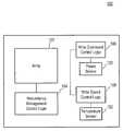
- FIG. 1is a block diagram of a power chip 100 according to an embodiment of the invention.
- the power chip 100may include an array 102 , a redundancy management control logic 104 , a write command control logic 106 , a write speed control logic 108 , a power sensor 120 , and a temperature sensor 122 .
- the array 102may comprise a plurality of capacitors. The capacitors may be configured to store power that may be used in the event of a power loss. In some embodiments, the capacitors of the array 102 may, for instance, be formed from vertically integrated memory.
- each of the capacitors included in the array 102may be formed using any fabrication process known in the art, now or in the future, including fabrication processes similar to those used to create three-dimensional non-volatile memory (e.g., three-dimensional NAND memory). In some embodiments, fabrication processes used to create three-dimensional non-volatile memory may be used. Because the capacitors may be formed in this manner, each of the capacitors may be addressable, for instance, using an address decoder (not shown) coupled to, or included in, the array 102 .
- Each of the capacitors of the array 102may be the same size, or the capacitors may vary in size.
- each of the capacitorsmay be substantially the same size as three-dimensional non-volatile memory cells known in the art, or may be larger than three-dimensional non-volatile memory cells.
- Each of the capacitorsmay be configured to have a same capacitance, for example, one picofarad, or may be configured to have varying capacitances.
- the redundancy management control logic 104may be coupled to the array 102 and may be configured to selectively enable or disable one or more capacitors of the array 102 , for instance, by individually addressing a tier of the array 102 or by individually addressing each capacitor of the array 102 .
- the redundancy management control logic 104may be configured to disable any defective capacitors.
- a capacitormay be defective if, for example, the capacitor fails to be addressed properly or fails to provide capacitance satisfying a particular threshold. Whether a capacitor is defective may be determined by the redundancy management control logic 104 or an external device, such as a tester (not shown).
- the power sensor 120may be configured to detect a power loss of a power supply.
- a power lossmay be represented by, for example, a decrease in voltage and/or current provided by the power supply, a decrease in power, disruption in the provision of power by the power supply, or events that effect the provision of power by the power supply.
- the temperature sensor 122may be configured to measure temperature.
- the power sensor 120may be coupled to the write command control logic 106 and may further be configured to provide a power loss control signal to the write command control logic 106 responsive, at least in part, to detecting a power loss, (e.g., voltage drop, brownout, undervoltage) of a power supply.
- a power losse.g., voltage drop, brownout, undervoltage
- the temperature sensor 122may be coupled to the write speed control logic 108 and configured to measure one or more temperatures inside and/or outside of the power chip 100 .
- the temperature sensor 122may be configured to provide one or more temperature signals to the write speed control logic 108 indicating the one or more measured temperatures, respectively.
- the write command control logic 106may be configured to receive the power loss control signal from the power sensor 120 .
- the write command control logic 106may provide a write command to a controller, for instance, of a storage device (not shown), such as a solid state drive (SSD).
- the write command control logic 106may additionally, or alternatively, be configured to provide the write command to a buffer cache (e.g., DRAM, SRAM) of the storage device.
- a buffer cachee.g., DRAM, SRAM
- providing this signalmay cause the storage device to write data stored in a buffer cache to one or more integrated circuits, such as a memory die, using power stored in the array 102 .
- the write speed control logic 108may be coupled to the write command control logic 106 and may be configured to provide a write speed control signal to at least one of the write command control logic 106 and the controller.
- the write speed control signalmay indicate a speed at which data is to be written from the buffer cache to a memory die in response to the write command provided by the write command control logic 106 , and may be based, at least in part, on the temperature signal provided by the temperature sensor 122 .
- the write speed control signalfurther may be based on other metrics, such as performance characteristics of a storage device. These characteristics may include, for instance, processing speeds of a controller, data write speeds of one or more integrated circuits, and/or various propagation delays between respective devices.
- Each control logic of the power chip 100including the redundancy management control logic 104 , the write command control logic 106 , and the write speed control logic 108 may comprise one or more logic circuits, logic gates, processors, memory, and/or any combination or sub-combination of the same.
- one or more of the control logic of the power chip 100may be combined into a single control logic or may be separated in multiple control logics.
- the write command control logic 106 and the write speed control logic 108may be combined to form, for instance, a write operation control logic.
- one or more of the capacitors of the array 102may be charged.
- the capacitors of the array 102may be charged responsive, at least in part, to a storage device initializing and/or based, at least in part, on the redundancy management control logic 104 selectively enabling capacitors, as described above.
- the power sensor 120may begin to monitor a power supply (e.g., voltage and/or current provided by the power supply), for instance, of the storage device. If a power loss is detected, the power sensor 120 may provide a power loss control signal to the write command control logic 106 indicating the power loss has occurred. In response to the power loss, capacitors of the array 102 may begin to provide power to the storage device.
- a power supplye.g., voltage and/or current provided by the power supply
- powermay be provided redundantly to the power supply. That is, the capacitors of the array 102 may be coupled to the power supply before the power loss and maintain the power level of the power supply when the power loss occurs. In another embodiment, the capacitors may be selectively coupled to the power supply in response to the power loss and maintain the power level of the power supply for a period of time thereafter. The capacitors may be selectively coupled, for example, based on the power loss control signal provided by the power sensor 120 .
- the write command control logic 106may provide a write command instructing the storage device to write data stored in the buffer cache of the storage device to one or more integrated circuits, such as a memory.
- the write commandmay be provided to a controller of the storage device.
- Data stored in the cache buffer of the storage devicemay be written using power provided by the capacitors of the array 102 .
- powermay be provided to all components of the storage device, or may be provided only less than all components of the storage device. For example, in one embodiment, power may be provided to the controller, the buffer cache, and any integrated circuits to which the write data is to be written.
- the write command control logic 106may subsequently send a reset command to the controller of the storage device, thereby resetting various state machines and/or timers of the storage device.
- the reset commandmay be provided by the write command control 106 either after a particular amount of time has elapsed or after receiving a signal indicating that the write has completed.
- FIG. 2 ais a block diagram of a chip package 200 according to an embodiment of the invention.
- the chip package 200may include a power chip 201 and a plurality of integrated circuits 202 .
- the power chip 201may be implemented using the power chip 100 of FIG. 1 .
- Each of the integrated circuits 202may comprise any integrated circuit known in the art, now or in the future, such as a memory or controller, and will not be discussed further in the interest of brevity.
- the power chip 201 and the plurality of integrated circuits 202may be arranged in a stacked configuration and further may be coupled to one another, for example, using through-silicon-vias (TSVs) and/or wire-bonding.
- TSVsthrough-silicon-vias
- the power chip 201may be configured to provide power to one or more components, including one or more integrated circuits, by maintaining the power level of a power supply during a power loss.
- the power chip 201may be configured to provide power to one or more of the integrated circuits 202 of the chip package 200 as well as devices not included in the chip package 200 , such as additional integrated circuits and/or a controller.
- a power chip 201may be configured to selectively provide power to particular components.
- the power chip 201may be configured to provide power only to one or more of the integrated circuits 202 located in the chip package 200 , or may be configured to provide power only to one or more devices located outside of the chip package 200 .
- the power chip 201may be configured to provide power to individual devices using respective sets of capacitors.
- the power chip 201may assign respective sets of capacitors of an array, such as the array 102 , to power corresponding integrated circuits 202 in the chip package 200 .
- the power chip 201may, for instance, be configured to power a first integrated circuit using a first half of a plurality of capacitors and power a second integrated circuit using a second half of the plurality of capacitors.
- the chip package 200may include any number of power chips 201 and any number of integrated circuits 202 .
- the chip package 200may comprise two power chips 201 and two integrated circuits 202 , or may comprise three power chips 201 and five integrated circuits 202 .
- FIG. 2 bis a block diagram of a chip package 250 according to an embodiment of the invention.
- the chip package 250includes a plurality of power chips 201 that have been previously described with respect to the chip package 200 of FIG. 2 a .
- the power chip 201may be arranged in a stacked configuration and further may be coupled to one another, for example, with through-silicon-vias (TSVs) and/or wire-bonding. Operation of each of the plurality of power chips 201 is as previously described with respect to FIG. 2 a . Consequently, a detailed description of the operation will not be repeated in the interest of brevity.
- TSVsthrough-silicon-vias
- Each of the plurality of power chips 201may be configured to provide power to maintain a power level of a power supply during a power loss.
- the powermay be provided, for example, such that data may be written from a buffer cache to an integrated circuit to prevent loss of the data stored in the buffer cache.
- the plurality of power chips 201 of the chip package 250may be configured to provide power directly to the power supply, thereby powering any devices coupled to the power supply.
- each of the plurality of power chips 201may be configured to provide power to one or more devices, respectively. In this manner, all devices may be powered, or only those devices needed to complete a write operation may be powered.
- a power chipsuch as the power chip 100 of FIG. 1
- any number of a plurality of power chipsmay be configured to provide a write command.
- one of a plurality of power chipsmay be configured to provide a write command while each of the plurality of power chips may be configured to provide power in response to a power loss.
- all power chipsmay be configured to provide a write command.
- Power chipsmay also be configured to provide power in various ways. Each of a plurality of power chips may, for instance, be configured to provide power simultaneously. Alternatively, power chips may be configured to sequentially, or in a partially overlapping manner, provide power such that at least one power chip provides power while data is written in turn. The manner in which each power chip provides power may be based, at least in part, on various timing control signals provided by a controller, or may be based on respective delays assigned to each power chip.
- a buffer cache of a memory devicemay be configured to write a page of data during a write operation.
- one or more power chipssuch as the power chip 100 , must be configured to provide a sufficient amount of power as to allow the buffer cache to write up to a page of data.
- a cache buffermay require a capacitor having approximately 28 microfarads of capacitance to be coupled to a supply voltage such that sufficient power may be stored and provided for a page write.
- a power chipmay be configured to have approximately 8 microfarads of capacitance. Accordingly, at least four power chips may be required to provide power during a page write.
- FIG. 3is a block diagram of an apparatus 300 that may include the power chip of FIG. 1 according to an embodiment of the invention.
- the apparatus 300may include a power chip 301 and an integrated circuit 302 .
- the power chip 301may be implemented using the power chip 100 of FIG. 1 and further may be coupled to the integrated circuit 302 by a power bus 315 .
- the integrated circuit 302may be any integrated circuit known in the art, now or in the future and will not be discussed further in the interest of brevity.
- the power bus 315may be coupled to a power supply (not shown) and further may be coupled to any number of devices in a storage device.
- the power supplymay provide, via the power bus 315 , power to any number of devices coupled to the power bus 315 .
- a power sensor of the power chip 301may detect the power loss of the supply voltage on the power bus 315 .
- the power chip 301may begin to provide power to devices coupled to the power bus 315 , such as the integrated circuit 302 .
- powermay be provided redundantly, or may be provided by coupling capacitors of the array of the power chip 301 to the power bus 315 .
- powermay be provided to all devices coupled to the power bus 315 , or may be provided to only those devices performing the write operation of data from the buffer cache to one or more integrated circuits.
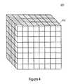
- FIG. 4is a perspective view diagram of an array 400 that may be used in the power chip of FIG. 1 according to an embodiment of the invention.
- the array 400may be used to implement the array 102 of FIG. 1 and may comprise a plurality of capacitors 402 .
- the array 400may be formed using any fabrication process known in the art, including one or more fabrication processes similar (or identical) to those used to create tiers of vertically integrated memory, such as three-dimensional NAND memory.
- a process used to create three-dimensional NAND word line platesmay, in some embodiments, be used to make capacitor electrodes.
- the array 400may comprise up to 32 tiers.
- capacitors 402 of the array 400may be addressable using an address decoder (not shown), and in some embodiments, each capacitor 402 may be individually addressable, or each tier of capacitors 402 may be addressable.
- Each tier of the array 400may comprise a pair of conductive layers, and each conductive layer may, for instance, be similar to a word line plate included in a three-dimensional NAND memory array.
- Each tier of the array 400may further include an insulating layer, with each pair of conductive layers separated by the insulating layer.
- Each of the tiersmay be divided (e.g., physically, logically, etc) into two dimensional arrays of capacitor 402 , thereby allowing each layer and/or capacitor to be individually addressed and/or charged.
- FIG. 5is a perspective view diagram of a portion of an array 500 that may be used in the array 400 of FIG. 4 according to an embodiment of the invention. While certain details are set forth below to provide a sufficient understanding of the array 500 , it will be appreciated by one having skill in the art that particular details of well-known connections, timing protocols, and addressing operations have been omitted to avoid unnecessarily obscuring the described example.
- the array 500may include a plurality of capacitors 502 , each of which may be used to implement a capacitor 402 of FIG. 4 . As illustrated, each of the capacitors 502 may be physically and/or electrically separated, for instance, by an etching process (e.g., three-dimensional NAND memory etching process) such that a charge of a capacitor 502 may be electrically separated from other capacitors 502 .
- an etching processe.g., three-dimensional NAND memory etching process
- Each of the capacitors 502may include capacitive layers 510 , 512 and an insulating layer 515 .
- each capacitive layer 510 , 512may be similar to a WL plate included in a three-dimensional NAND memory, and may comprise any conductor or semiconductor material known in the art, now or in the future.
- Each insulating layer 515may be located between the capacitive layers 510 , 512 such that the capacitive layers 510 , 512 may be properly charged.
- the insulating layer 515may comprise any dielectric material known in the art, now or in the future, or may comprise any other material.
- FIG. 6is a method 600 for preventing data loss during a power loss according to an embodiment of the invention.
- the method 600may be implemented using, for example, any of the power chips described herein, such as the power chip 100 of FIG. 1 .
- a power lossfor instance of a power supply, may be detected.
- the power lossmay be detected by the power sensor 120 of FIG. 1 .
- powermay be provided to one or more components, such as components of a storage device, at a step 610 .
- providing powermay include redundantly maintaining a power supply and/or coupling capacitors of the array 102 to the power supply to maintain the power level.
- a write commandmay be provided at a step 615 , for instance, by the write command control logic 106 of FIG. 1 , thereby instructing the storage device to write data stored in its buffer cache to one or more integrated circuits.
- a reset commandmay be provided to the storage device, thereby resetting any state machines and/or timers included therein.
Landscapes
- Engineering & Computer Science (AREA)
- Theoretical Computer Science (AREA)
- Physics & Mathematics (AREA)
- General Engineering & Computer Science (AREA)
- General Physics & Mathematics (AREA)
- Semiconductor Integrated Circuits (AREA)
Abstract
Description
Claims (26)
Priority Applications (1)
| Application Number | Priority Date | Filing Date | Title |
|---|---|---|---|
| US13/657,444US9213386B2 (en) | 2012-10-22 | 2012-10-22 | Apparatuses and methods and for providing power responsive to a power loss |
Applications Claiming Priority (1)
| Application Number | Priority Date | Filing Date | Title |
|---|---|---|---|
| US13/657,444US9213386B2 (en) | 2012-10-22 | 2012-10-22 | Apparatuses and methods and for providing power responsive to a power loss |
Publications (2)
| Publication Number | Publication Date |
|---|---|
| US20140115373A1 US20140115373A1 (en) | 2014-04-24 |
| US9213386B2true US9213386B2 (en) | 2015-12-15 |
Family
ID=50486478
Family Applications (1)
| Application Number | Title | Priority Date | Filing Date |
|---|---|---|---|
| US13/657,444Active2033-10-22US9213386B2 (en) | 2012-10-22 | 2012-10-22 | Apparatuses and methods and for providing power responsive to a power loss |
Country Status (1)
| Country | Link |
|---|---|
| US (1) | US9213386B2 (en) |
Cited By (2)
| Publication number | Priority date | Publication date | Assignee | Title |
|---|---|---|---|---|
| US20220179472A1 (en)* | 2019-11-11 | 2022-06-09 | Microsoft Technology Licensing, Llc | Managing ephemeral storage on a computing node |
| US11983056B2 (en)* | 2017-01-09 | 2024-05-14 | Inmusic Brands, Inc. | Systems and methods for responding to electrical-power loss in a DJ media player |
Families Citing this family (3)
| Publication number | Priority date | Publication date | Assignee | Title |
|---|---|---|---|---|
| US9767962B2 (en) | 2016-01-22 | 2017-09-19 | Micron Technology, Inc. | Apparatuses, multi-chip modules and capacitive chips |
| US11016890B2 (en)* | 2018-02-05 | 2021-05-25 | Micron Technology, Inc. | CPU cache flushing to persistent memory |
| US10678667B1 (en)* | 2018-12-21 | 2020-06-09 | Micron Technology, Inc. | Holdup self-tests for power loss operations on memory systems |
Citations (31)
| Publication number | Priority date | Publication date | Assignee | Title |
|---|---|---|---|---|
| US5032892A (en) | 1988-05-31 | 1991-07-16 | Micron Technology, Inc. | Depletion mode chip decoupling capacitor |
| US5519831A (en) | 1991-06-12 | 1996-05-21 | Intel Corporation | Non-volatile disk cache |
| US5880925A (en) | 1997-06-27 | 1999-03-09 | Avx Corporation | Surface mount multilayer capacitor |
| US6124625A (en) | 1988-05-31 | 2000-09-26 | Micron Technology, Inc. | Chip decoupling capacitor |
| US6184568B1 (en) | 1988-05-31 | 2001-02-06 | Micron Technology, Inc. | Integrated circuit module having on-chip surge capacitors |
| US6344961B1 (en) | 1999-11-19 | 2002-02-05 | Murata Manufacturing Co., Ltd | Multi-layer capacitator, wiring substrate, decoupling circuit, and high-frequency circuit |
| US20020017700A1 (en) | 2000-07-06 | 2002-02-14 | Nec Corporation | Multilayer capacitor, semiconductor device, and electrical circuit board |
| US20050046991A1 (en)* | 2003-08-29 | 2005-03-03 | Kabushiki Kaisha Toshiba | Information processing apparatus having function to control housing temperature |
| US20050152203A1 (en) | 2004-01-08 | 2005-07-14 | Choi Hyung-Chan | Semiconductor memory device and method of arranging a decoupling capacitor thereof |
| US6990603B2 (en) | 2002-01-02 | 2006-01-24 | Exanet Inc. | Method and apparatus for securing volatile data in power failure in systems having redundancy |
| US20060267412A1 (en)* | 2005-05-23 | 2006-11-30 | Hung-Yi Kuo | Chip with embedded electromagnetic compatibility capacitors and related method |
| US7451348B2 (en) | 2005-08-04 | 2008-11-11 | Dot Hill Systems Corporation | Dynamic write cache size adjustment in raid controller with capacitor backup energy source |
| US7586174B2 (en) | 2005-07-29 | 2009-09-08 | Tdk Corporation | Multilayer capacitor |
| US20090251862A1 (en) | 2008-04-03 | 2009-10-08 | International Business Machines Corporation | Silicon based microchannel cooling and electrical package |
| US7613877B2 (en) | 2006-10-25 | 2009-11-03 | Hitachi, Ltd. | Storage system comprising volatile cache memory and nonvolatile memory |
| US20090290282A1 (en) | 2008-05-21 | 2009-11-26 | International Business Machines Corporation | Modular chip stack and packaging technology with voltage segmentation, regulation, integrated decoupling capacitance and cooling structure and process |
| US20100008175A1 (en) | 2008-07-10 | 2010-01-14 | Sanmina-Sci Corporation | Battery-less cache memory module with integrated backup |
| US20100164084A1 (en) | 2008-12-26 | 2010-07-01 | Jun-Ho Lee | Semiconductor device and semiconductor package including the same |
| US20100244189A1 (en) | 2007-05-10 | 2010-09-30 | Ipdia | Integration substrate with a ultra-high-density capacitor and a through-substrate via |
| US20100311371A1 (en) | 2009-06-03 | 2010-12-09 | Casio Computer Co., Ltd. | Radio wave receiver |
| US20100308435A1 (en) | 2009-06-08 | 2010-12-09 | Qualcomm Incorporated | Through Silicon Via With Embedded Decoupling Capacitor |
| US20110027962A1 (en) | 2009-07-29 | 2011-02-03 | International Business Machines Corporation | Trench decoupling capacitor formed by rie lag of through silicon via (tsv) etch |
| US20110031598A1 (en) | 2009-08-04 | 2011-02-10 | Amkor Technology Korea, Inc. | Semiconductor device and fabricating method thereof |
| US20110108948A1 (en) | 2009-11-09 | 2011-05-12 | International Business Machines Corporation | Integrated decoupling capacitor employing conductive through-substrate vias |
| KR20110119224A (en) | 2010-04-27 | 2011-11-02 | (주)다윈텍 | Memory system accessible in synchronous or asynchronous mode by command |
| US8090988B2 (en) | 2009-11-24 | 2012-01-03 | Virtium Technology, Inc. | Saving information to flash memory during power failure |
| US20120020027A1 (en)* | 2010-07-20 | 2012-01-26 | Avago Technologies Enterprise IP (Singapore) Pte. Ltd. | Tiered Integrated Circuit Assembly and a Method for Manufacturing the Same |
| US20120098343A1 (en)* | 2010-10-26 | 2012-04-26 | Microsoft Corporation | Chassis slots accepting battery modules and other module types |
| US20130039113A1 (en) | 2010-01-21 | 2013-02-14 | Stmicroelectronics (Crolles 2) Sas | Integrated dram memory device |
| US20130194032A1 (en) | 2012-01-27 | 2013-08-01 | Micron Technology, Inc. | Apparatuses and methods for providing capacitance in a multi-chip module |
| US8669828B1 (en)* | 2010-10-21 | 2014-03-11 | Altera Corporation | Decoupling capacitor control circuitry |
- 2012
- 2012-10-22USUS13/657,444patent/US9213386B2/enactiveActive
Patent Citations (34)
| Publication number | Priority date | Publication date | Assignee | Title |
|---|---|---|---|---|
| US6124625A (en) | 1988-05-31 | 2000-09-26 | Micron Technology, Inc. | Chip decoupling capacitor |
| US6184568B1 (en) | 1988-05-31 | 2001-02-06 | Micron Technology, Inc. | Integrated circuit module having on-chip surge capacitors |
| US6448628B2 (en) | 1988-05-31 | 2002-09-10 | Micron Technology, Inc. | Chip decoupling capacitor |
| US5032892A (en) | 1988-05-31 | 1991-07-16 | Micron Technology, Inc. | Depletion mode chip decoupling capacitor |
| US5519831A (en) | 1991-06-12 | 1996-05-21 | Intel Corporation | Non-volatile disk cache |
| US5880925A (en) | 1997-06-27 | 1999-03-09 | Avx Corporation | Surface mount multilayer capacitor |
| US6344961B1 (en) | 1999-11-19 | 2002-02-05 | Murata Manufacturing Co., Ltd | Multi-layer capacitator, wiring substrate, decoupling circuit, and high-frequency circuit |
| US20020017700A1 (en) | 2000-07-06 | 2002-02-14 | Nec Corporation | Multilayer capacitor, semiconductor device, and electrical circuit board |
| US6990603B2 (en) | 2002-01-02 | 2006-01-24 | Exanet Inc. | Method and apparatus for securing volatile data in power failure in systems having redundancy |
| US20050046991A1 (en)* | 2003-08-29 | 2005-03-03 | Kabushiki Kaisha Toshiba | Information processing apparatus having function to control housing temperature |
| US20050152203A1 (en) | 2004-01-08 | 2005-07-14 | Choi Hyung-Chan | Semiconductor memory device and method of arranging a decoupling capacitor thereof |
| US20060267412A1 (en)* | 2005-05-23 | 2006-11-30 | Hung-Yi Kuo | Chip with embedded electromagnetic compatibility capacitors and related method |
| US7586174B2 (en) | 2005-07-29 | 2009-09-08 | Tdk Corporation | Multilayer capacitor |
| US7451348B2 (en) | 2005-08-04 | 2008-11-11 | Dot Hill Systems Corporation | Dynamic write cache size adjustment in raid controller with capacitor backup energy source |
| US7613877B2 (en) | 2006-10-25 | 2009-11-03 | Hitachi, Ltd. | Storage system comprising volatile cache memory and nonvolatile memory |
| US20100244189A1 (en) | 2007-05-10 | 2010-09-30 | Ipdia | Integration substrate with a ultra-high-density capacitor and a through-substrate via |
| US20090251862A1 (en) | 2008-04-03 | 2009-10-08 | International Business Machines Corporation | Silicon based microchannel cooling and electrical package |
| US20090290282A1 (en) | 2008-05-21 | 2009-11-26 | International Business Machines Corporation | Modular chip stack and packaging technology with voltage segmentation, regulation, integrated decoupling capacitance and cooling structure and process |
| US20100008175A1 (en) | 2008-07-10 | 2010-01-14 | Sanmina-Sci Corporation | Battery-less cache memory module with integrated backup |
| US20100164084A1 (en) | 2008-12-26 | 2010-07-01 | Jun-Ho Lee | Semiconductor device and semiconductor package including the same |
| US20100311371A1 (en) | 2009-06-03 | 2010-12-09 | Casio Computer Co., Ltd. | Radio wave receiver |
| US20100308435A1 (en) | 2009-06-08 | 2010-12-09 | Qualcomm Incorporated | Through Silicon Via With Embedded Decoupling Capacitor |
| US20110027962A1 (en) | 2009-07-29 | 2011-02-03 | International Business Machines Corporation | Trench decoupling capacitor formed by rie lag of through silicon via (tsv) etch |
| US20130109135A1 (en) | 2009-08-04 | 2013-05-02 | Amkor Technology Korea, Inc. | Method of fabricating a semiconductor device having an interposer |
| US20110031598A1 (en) | 2009-08-04 | 2011-02-10 | Amkor Technology Korea, Inc. | Semiconductor device and fabricating method thereof |
| US20110108948A1 (en) | 2009-11-09 | 2011-05-12 | International Business Machines Corporation | Integrated decoupling capacitor employing conductive through-substrate vias |
| US8090988B2 (en) | 2009-11-24 | 2012-01-03 | Virtium Technology, Inc. | Saving information to flash memory during power failure |
| US20130039113A1 (en) | 2010-01-21 | 2013-02-14 | Stmicroelectronics (Crolles 2) Sas | Integrated dram memory device |
| KR20110119224A (en) | 2010-04-27 | 2011-11-02 | (주)다윈텍 | Memory system accessible in synchronous or asynchronous mode by command |
| US20120020027A1 (en)* | 2010-07-20 | 2012-01-26 | Avago Technologies Enterprise IP (Singapore) Pte. Ltd. | Tiered Integrated Circuit Assembly and a Method for Manufacturing the Same |
| US8669828B1 (en)* | 2010-10-21 | 2014-03-11 | Altera Corporation | Decoupling capacitor control circuitry |
| US20120098343A1 (en)* | 2010-10-26 | 2012-04-26 | Microsoft Corporation | Chassis slots accepting battery modules and other module types |
| US20130194032A1 (en) | 2012-01-27 | 2013-08-01 | Micron Technology, Inc. | Apparatuses and methods for providing capacitance in a multi-chip module |
| US20140320201A1 (en) | 2012-01-27 | 2014-10-30 | Micron Technology, Inc. | Apparatuses and methods for providing capacitance in a multi-chip module |
Cited By (3)
| Publication number | Priority date | Publication date | Assignee | Title |
|---|---|---|---|---|
| US11983056B2 (en)* | 2017-01-09 | 2024-05-14 | Inmusic Brands, Inc. | Systems and methods for responding to electrical-power loss in a DJ media player |
| US20220179472A1 (en)* | 2019-11-11 | 2022-06-09 | Microsoft Technology Licensing, Llc | Managing ephemeral storage on a computing node |
| US11809253B2 (en)* | 2019-11-11 | 2023-11-07 | Microsoft Technology Licensing, Llc | Managing ephemeral storage on a computing node |
Also Published As
| Publication number | Publication date |
|---|---|
| US20140115373A1 (en) | 2014-04-24 |
Similar Documents
| Publication | Publication Date | Title |
|---|---|---|
| US11581024B2 (en) | Memory module with battery and electronic system having the memory module | |
| US9570201B2 (en) | Repair of memory devices using volatile and non-volatile memory | |
| US9996284B2 (en) | Non-volatile memory storage for multi-channel memory system | |
| KR101891428B1 (en) | Read cache memory | |
| CN106548807B (en) | Repair of circuits, semiconductor devices and semiconductor systems using the same | |
| US20160018998A1 (en) | Methods and Systems for Scalable Reliability Management of Non-Volatile Memory Modules | |
| US9454448B2 (en) | Fault testing in storage devices | |
| US9240248B2 (en) | Method of using non-volatile memories for on-DIMM memory address list storage | |
| US10095412B2 (en) | Memory system and method for improving write performance in a multi-die environment | |
| US20160019160A1 (en) | Methods and Systems for Scalable and Distributed Address Mapping Using Non-Volatile Memory Modules | |
| US9349433B2 (en) | Hidden refresh of weak memory storage cells in semiconductor memory | |
| US9213386B2 (en) | Apparatuses and methods and for providing power responsive to a power loss | |
| US11868252B2 (en) | Memory with post-packaging master die selection | |
| TW201603041A (en) | Memory device having controller with local memory | |
| US9443601B2 (en) | Holdup capacitor energy harvesting | |
| KR20170007458A (en) | Providing power availability information to memory | |
| US11983059B2 (en) | Memory expansion card | |
| US9099165B1 (en) | Single chip mixed memory for dynamic replacement of DRAM bad cell | |
| US20230139599A1 (en) | Stacked memory and storage system | |
| US11282569B2 (en) | Apparatus with latch balancing mechanism and methods for operating the same | |
| KR102388247B1 (en) | Individually Addressing Memory Devices Separated from the Data Bus | |
| CN115148265A (en) | Memory device including calibration operation and transistors with adjustable threshold voltage | |
| CN112927745A (en) | Memory with TSV health monitoring circuit | |
| Lv et al. | Logic-DRAM co-design to exploit the efficient repair technique for stacked DRAM | |
| JP7706028B2 (en) | MEMORY SYSTEM AND METHOD FOR PRE-DIE RETIREMENT WITH CRITICAL WORDLINE LEAKAGE DETECTION - Patent application |
Legal Events
| Date | Code | Title | Description |
|---|---|---|---|
| AS | Assignment | Owner name:MICRON TECHNOLOGY, INC., IDAHO Free format text:ASSIGNMENT OF ASSIGNORS INTEREST;ASSIGNOR:GHODSI, RAMIN;REEL/FRAME:029168/0589 Effective date:20121015 | |
| STCF | Information on status: patent grant | Free format text:PATENTED CASE | |
| AS | Assignment | Owner name:U.S. BANK NATIONAL ASSOCIATION, AS COLLATERAL AGENT, CALIFORNIA Free format text:SECURITY INTEREST;ASSIGNOR:MICRON TECHNOLOGY, INC.;REEL/FRAME:038669/0001 Effective date:20160426 Owner name:U.S. BANK NATIONAL ASSOCIATION, AS COLLATERAL AGEN Free format text:SECURITY INTEREST;ASSIGNOR:MICRON TECHNOLOGY, INC.;REEL/FRAME:038669/0001 Effective date:20160426 | |
| AS | Assignment | Owner name:MORGAN STANLEY SENIOR FUNDING, INC., AS COLLATERAL AGENT, MARYLAND Free format text:PATENT SECURITY AGREEMENT;ASSIGNOR:MICRON TECHNOLOGY, INC.;REEL/FRAME:038954/0001 Effective date:20160426 Owner name:MORGAN STANLEY SENIOR FUNDING, INC., AS COLLATERAL Free format text:PATENT SECURITY AGREEMENT;ASSIGNOR:MICRON TECHNOLOGY, INC.;REEL/FRAME:038954/0001 Effective date:20160426 | |
| AS | Assignment | Owner name:U.S. BANK NATIONAL ASSOCIATION, AS COLLATERAL AGENT, CALIFORNIA Free format text:CORRECTIVE ASSIGNMENT TO CORRECT THE REPLACE ERRONEOUSLY FILED PATENT #7358718 WITH THE CORRECT PATENT #7358178 PREVIOUSLY RECORDED ON REEL 038669 FRAME 0001. ASSIGNOR(S) HEREBY CONFIRMS THE SECURITY INTEREST;ASSIGNOR:MICRON TECHNOLOGY, INC.;REEL/FRAME:043079/0001 Effective date:20160426 Owner name:U.S. BANK NATIONAL ASSOCIATION, AS COLLATERAL AGEN Free format text:CORRECTIVE ASSIGNMENT TO CORRECT THE REPLACE ERRONEOUSLY FILED PATENT #7358718 WITH THE CORRECT PATENT #7358178 PREVIOUSLY RECORDED ON REEL 038669 FRAME 0001. ASSIGNOR(S) HEREBY CONFIRMS THE SECURITY INTEREST;ASSIGNOR:MICRON TECHNOLOGY, INC.;REEL/FRAME:043079/0001 Effective date:20160426 | |
| AS | Assignment | Owner name:JPMORGAN CHASE BANK, N.A., AS COLLATERAL AGENT, ILLINOIS Free format text:SECURITY INTEREST;ASSIGNORS:MICRON TECHNOLOGY, INC.;MICRON SEMICONDUCTOR PRODUCTS, INC.;REEL/FRAME:047540/0001 Effective date:20180703 Owner name:JPMORGAN CHASE BANK, N.A., AS COLLATERAL AGENT, IL Free format text:SECURITY INTEREST;ASSIGNORS:MICRON TECHNOLOGY, INC.;MICRON SEMICONDUCTOR PRODUCTS, INC.;REEL/FRAME:047540/0001 Effective date:20180703 | |
| AS | Assignment | Owner name:MICRON TECHNOLOGY, INC., IDAHO Free format text:RELEASE BY SECURED PARTY;ASSIGNOR:U.S. BANK NATIONAL ASSOCIATION, AS COLLATERAL AGENT;REEL/FRAME:047243/0001 Effective date:20180629 | |
| MAFP | Maintenance fee payment | Free format text:PAYMENT OF MAINTENANCE FEE, 4TH YEAR, LARGE ENTITY (ORIGINAL EVENT CODE: M1551); ENTITY STATUS OF PATENT OWNER: LARGE ENTITY Year of fee payment:4 | |
| AS | Assignment | Owner name:MICRON TECHNOLOGY, INC., IDAHO Free format text:RELEASE BY SECURED PARTY;ASSIGNOR:MORGAN STANLEY SENIOR FUNDING, INC., AS COLLATERAL AGENT;REEL/FRAME:050937/0001 Effective date:20190731 | |
| AS | Assignment | Owner name:MICRON TECHNOLOGY, INC., IDAHO Free format text:RELEASE BY SECURED PARTY;ASSIGNOR:JPMORGAN CHASE BANK, N.A., AS COLLATERAL AGENT;REEL/FRAME:051028/0001 Effective date:20190731 Owner name:MICRON SEMICONDUCTOR PRODUCTS, INC., IDAHO Free format text:RELEASE BY SECURED PARTY;ASSIGNOR:JPMORGAN CHASE BANK, N.A., AS COLLATERAL AGENT;REEL/FRAME:051028/0001 Effective date:20190731 | |
| MAFP | Maintenance fee payment | Free format text:PAYMENT OF MAINTENANCE FEE, 8TH YEAR, LARGE ENTITY (ORIGINAL EVENT CODE: M1552); ENTITY STATUS OF PATENT OWNER: LARGE ENTITY Year of fee payment:8 |