US9212051B1 - Systems and methods for forming MEMS assemblies incorporating getters - Google Patents
Systems and methods for forming MEMS assemblies incorporating gettersDownload PDFInfo
- Publication number
- US9212051B1 US9212051B1US13/198,448US201113198448AUS9212051B1US 9212051 B1US9212051 B1US 9212051B1US 201113198448 AUS201113198448 AUS 201113198448AUS 9212051 B1US9212051 B1US 9212051B1
- Authority
- US
- United States
- Prior art keywords
- mems
- wafer
- assembly
- forming
- hole via
- Prior art date
- Legal status (The legal status is an assumption and is not a legal conclusion. Google has not performed a legal analysis and makes no representation as to the accuracy of the status listed.)
- Active, expires
Links
- 238000000034methodMethods0.000titleabstractdescription106
- 230000000712assemblyEffects0.000titleabstractdescription7
- 238000000429assemblyMethods0.000titleabstractdescription7
- 229910052751metalInorganic materials0.000claimsabstractdescription65
- 239000002184metalSubstances0.000claimsabstractdescription65
- 229910052804chromiumInorganic materials0.000claimsdescription4
- 239000000463materialSubstances0.000claimsdescription3
- 235000012431wafersNutrition0.000description94
- 229920002120photoresistant polymerPolymers0.000description24
- 238000000151depositionMethods0.000description11
- 239000010931goldSubstances0.000description9
- 238000001020plasma etchingMethods0.000description9
- XUIMIQQOPSSXEZ-UHFFFAOYSA-NSiliconChemical compound[Si]XUIMIQQOPSSXEZ-UHFFFAOYSA-N0.000description8
- 229910052737goldInorganic materials0.000description8
- 229910052710siliconInorganic materials0.000description8
- 239000010703siliconSubstances0.000description8
- 238000004519manufacturing processMethods0.000description6
- 238000000992sputter etchingMethods0.000description6
- 230000002730additional effectEffects0.000description5
- 238000000708deep reactive-ion etchingMethods0.000description5
- PCHJSUWPFVWCPO-UHFFFAOYSA-NgoldChemical compound[Au]PCHJSUWPFVWCPO-UHFFFAOYSA-N0.000description5
- 238000004806packaging method and processMethods0.000description5
- 238000000059patterningMethods0.000description5
- 230000005496eutecticsEffects0.000description4
- 238000005476solderingMethods0.000description4
- 239000004593EpoxySubstances0.000description3
- 239000002253acidSubstances0.000description3
- 229910052782aluminiumInorganic materials0.000description3
- 239000010949copperSubstances0.000description3
- 238000005530etchingMethods0.000description3
- 229910052738indiumInorganic materials0.000description3
- 238000000623plasma-assisted chemical vapour depositionMethods0.000description3
- XLYOFNOQVPJJNP-UHFFFAOYSA-NwaterChemical compoundOXLYOFNOQVPJJNP-UHFFFAOYSA-N0.000description3
- RYGMFSIKBFXOCR-UHFFFAOYSA-NCopperChemical compound[Cu]RYGMFSIKBFXOCR-UHFFFAOYSA-N0.000description2
- KRHYYFGTRYWZRS-UHFFFAOYSA-NFluoraneChemical compoundFKRHYYFGTRYWZRS-UHFFFAOYSA-N0.000description2
- 230000001133accelerationEffects0.000description2
- XAGFODPZIPBFFR-UHFFFAOYSA-NaluminiumChemical compound[Al]XAGFODPZIPBFFR-UHFFFAOYSA-N0.000description2
- 229910052802copperInorganic materials0.000description2
- APFVFJFRJDLVQX-UHFFFAOYSA-Nindium atomChemical compound[In]APFVFJFRJDLVQX-UHFFFAOYSA-N0.000description2
- 238000010943off-gassingMethods0.000description2
- 229920000642polymerPolymers0.000description2
- 229910052718tinInorganic materials0.000description2
- 238000001039wet etchingMethods0.000description2
- 229910015365Au—SiInorganic materials0.000description1
- 229910015363Au—SnInorganic materials0.000description1
- ATJFFYVFTNAWJD-UHFFFAOYSA-NTinChemical compound[Sn]ATJFFYVFTNAWJD-UHFFFAOYSA-N0.000description1
- 150000007513acidsChemical class0.000description1
- 239000000853adhesiveSubstances0.000description1
- 238000004026adhesive bondingMethods0.000description1
- 230000001070adhesive effectEffects0.000description1
- 239000011260aqueous acidSubstances0.000description1
- 230000015556catabolic processEffects0.000description1
- 239000000356contaminantSubstances0.000description1
- 238000005260corrosionMethods0.000description1
- 230000007797corrosionEffects0.000description1
- 230000008878couplingEffects0.000description1
- 238000010168coupling processMethods0.000description1
- 238000005859coupling reactionMethods0.000description1
- 238000006731degradation reactionMethods0.000description1
- 238000005137deposition processMethods0.000description1
- 238000005538encapsulationMethods0.000description1
- 125000003700epoxy groupChemical group0.000description1
- 239000003292glueSubstances0.000description1
- 238000010438heat treatmentMethods0.000description1
- 239000012212insulatorSubstances0.000description1
- 238000002955isolationMethods0.000description1
- 150000002739metalsChemical class0.000description1
- 238000004377microelectronicMethods0.000description1
- 239000002245particleSubstances0.000description1
- 238000000206photolithographyMethods0.000description1
- 229920000647polyepoxidePolymers0.000description1
- 229910000679solderInorganic materials0.000description1
- 230000003068static effectEffects0.000description1
- 238000003860storageMethods0.000description1
- 239000000758substrateSubstances0.000description1
Images


Classifications
- B—PERFORMING OPERATIONS; TRANSPORTING
- B81—MICROSTRUCTURAL TECHNOLOGY
- B81C—PROCESSES OR APPARATUS SPECIALLY ADAPTED FOR THE MANUFACTURE OR TREATMENT OF MICROSTRUCTURAL DEVICES OR SYSTEMS
- B81C1/00—Manufacture or treatment of devices or systems in or on a substrate
- B81C1/00015—Manufacture or treatment of devices or systems in or on a substrate for manufacturing microsystems
- B81C1/00261—Processes for packaging MEMS devices
- B81C1/00277—Processes for packaging MEMS devices for maintaining a controlled atmosphere inside of the cavity containing the MEMS
- B—PERFORMING OPERATIONS; TRANSPORTING
- B81—MICROSTRUCTURAL TECHNOLOGY
- B81B—MICROSTRUCTURAL DEVICES OR SYSTEMS, e.g. MICROMECHANICAL DEVICES
- B81B7/00—Microstructural systems; Auxiliary parts of microstructural devices or systems
- B81B7/0032—Packages or encapsulation
- B81B7/007—Interconnections between the MEMS and external electrical signals
- B—PERFORMING OPERATIONS; TRANSPORTING
- B81—MICROSTRUCTURAL TECHNOLOGY
- B81C—PROCESSES OR APPARATUS SPECIALLY ADAPTED FOR THE MANUFACTURE OR TREATMENT OF MICROSTRUCTURAL DEVICES OR SYSTEMS
- B81C1/00—Manufacture or treatment of devices or systems in or on a substrate
- B81C1/00015—Manufacture or treatment of devices or systems in or on a substrate for manufacturing microsystems
- B81C1/00261—Processes for packaging MEMS devices
- B81C1/00277—Processes for packaging MEMS devices for maintaining a controlled atmosphere inside of the cavity containing the MEMS
- B81C1/00285—Processes for packaging MEMS devices for maintaining a controlled atmosphere inside of the cavity containing the MEMS using materials for controlling the level of pressure, contaminants or moisture inside of the package, e.g. getters
- B—PERFORMING OPERATIONS; TRANSPORTING
- B81—MICROSTRUCTURAL TECHNOLOGY
- B81B—MICROSTRUCTURAL DEVICES OR SYSTEMS, e.g. MICROMECHANICAL DEVICES
- B81B7/00—Microstructural systems; Auxiliary parts of microstructural devices or systems
- B81B7/0006—Interconnects
- B—PERFORMING OPERATIONS; TRANSPORTING
- B81—MICROSTRUCTURAL TECHNOLOGY
- B81B—MICROSTRUCTURAL DEVICES OR SYSTEMS, e.g. MICROMECHANICAL DEVICES
- B81B7/00—Microstructural systems; Auxiliary parts of microstructural devices or systems
- B81B7/0032—Packages or encapsulation
- B81B7/0035—Packages or encapsulation for maintaining a controlled atmosphere inside of the chamber containing the MEMS
- B81B7/0038—Packages or encapsulation for maintaining a controlled atmosphere inside of the chamber containing the MEMS using materials for controlling the level of pressure, contaminants or moisture inside of the package, e.g. getters
- B—PERFORMING OPERATIONS; TRANSPORTING
- B81—MICROSTRUCTURAL TECHNOLOGY
- B81B—MICROSTRUCTURAL DEVICES OR SYSTEMS, e.g. MICROMECHANICAL DEVICES
- B81B2201/00—Specific applications of microelectromechanical systems
- B81B2201/02—Sensors
- B81B2201/0228—Inertial sensors
- B81B2201/0235—Accelerometers
- B—PERFORMING OPERATIONS; TRANSPORTING
- B81—MICROSTRUCTURAL TECHNOLOGY
- B81B—MICROSTRUCTURAL DEVICES OR SYSTEMS, e.g. MICROMECHANICAL DEVICES
- B81B2207/00—Microstructural systems or auxiliary parts thereof
- B81B2207/07—Interconnects
- B—PERFORMING OPERATIONS; TRANSPORTING
- B81—MICROSTRUCTURAL TECHNOLOGY
- B81B—MICROSTRUCTURAL DEVICES OR SYSTEMS, e.g. MICROMECHANICAL DEVICES
- B81B2207/00—Microstructural systems or auxiliary parts thereof
- B81B2207/09—Packages
- B81B2207/091—Arrangements for connecting external electrical signals to mechanical structures inside the package
- B81B2207/094—Feed-through, via
- B81B2207/095—Feed-through, via through the lid
- B—PERFORMING OPERATIONS; TRANSPORTING
- B81—MICROSTRUCTURAL TECHNOLOGY
- B81C—PROCESSES OR APPARATUS SPECIALLY ADAPTED FOR THE MANUFACTURE OR TREATMENT OF MICROSTRUCTURAL DEVICES OR SYSTEMS
- B81C2203/00—Forming microstructural systems
- B81C2203/01—Packaging MEMS
- B81C2203/0109—Bonding an individual cap on the substrate
- B—PERFORMING OPERATIONS; TRANSPORTING
- B81—MICROSTRUCTURAL TECHNOLOGY
- B81C—PROCESSES OR APPARATUS SPECIALLY ADAPTED FOR THE MANUFACTURE OR TREATMENT OF MICROSTRUCTURAL DEVICES OR SYSTEMS
- B81C2203/00—Forming microstructural systems
- B81C2203/01—Packaging MEMS
- B81C2203/0118—Bonding a wafer on the substrate, i.e. where the cap consists of another wafer
- B—PERFORMING OPERATIONS; TRANSPORTING
- B81—MICROSTRUCTURAL TECHNOLOGY
- B81C—PROCESSES OR APPARATUS SPECIALLY ADAPTED FOR THE MANUFACTURE OR TREATMENT OF MICROSTRUCTURAL DEVICES OR SYSTEMS
- B81C2203/00—Forming microstructural systems
- B81C2203/01—Packaging MEMS
- B81C2203/0136—Growing or depositing of a covering layer
- B—PERFORMING OPERATIONS; TRANSPORTING
- B81—MICROSTRUCTURAL TECHNOLOGY
- B81C—PROCESSES OR APPARATUS SPECIALLY ADAPTED FOR THE MANUFACTURE OR TREATMENT OF MICROSTRUCTURAL DEVICES OR SYSTEMS
- B81C2203/00—Forming microstructural systems
- B81C2203/01—Packaging MEMS
- B81C2203/0163—Reinforcing a cap, e.g. with ribs
Definitions
- the present inventionrelates to microelectromechanical systems (MEMS), and more specifically to systems and methods for forming MEMS assemblies incorporating getters.
- MEMSmicroelectromechanical systems
- MEMS devicesare fabricated using techniques that leave the mechanical structures exposed after the fabrication process is completed. Open-die MEMS devices can be easily destroyed if their unprotected mechanical elements come in contact with a physical object, so physical protection can be important. MEMS are also very susceptible to degradation by small particles, water vapor, static friction and corrosion. As such, MEMS devices generally need microscopic protection and encapsulation.
- MEMS packagecreates an air or vacuum cavity over the MEMS active area without impeding its motion or function (e.g., deflection, tilt, slide, rotation, or vibration).
- Wafer-level packaging of MEMSrepresents a challenging and often costly task in micro-system manufacturing.
- MEMS packagingdiffers from traditional microelectronics packaging in that the encapsulating cover should generally not touch the micro-machined device.
- the packagingshould protect the sensor while providing suitable electrical access to outside environment.
- Conventional MEMS packaging and fabrication techniquesare often inadequate to meet the above described challenges. As such, a need exists for improved methods for fabricating and interfacing with MEMS devices.
- the inventionrelates to a method for manufacturing a wafer of a microelectromechanical systems (MEMS) assembly, the method including providing the wafer including a buried oxide layer, depositing and patterning a first photo resist layer on the wafer, performing reactive ion etching on a surface of the wafer, the ion etching extending to the buried oxide layer, removing the first photo resist layer, removing portions of the buried oxide layer, thereby forming one or more cavities within the wafer, depositing a first metal layer configured to act as a getter within the one or more cavities, and depositing a second metal layer on the first metal layer.
- MEMSmicroelectromechanical systems
- the inventionin another embodiment, relates to a method for manufacturing a cap for a microelectromechanical systems (MEMS) assembly, the method including providing a cap wafer, depositing a layer of oxide on the cap wafer, depositing and patterning a first photo resist layer on the oxide layer, removing portions of the oxide layer in accordance with the patterned first photo resist layer, removing the first photo resist layer, depositing one or more first metal layers on the cap wafer, depositing and patterning a second photo resist layer on the one or more first metal layers, removing portions of the one or more first metal layers in accordance with the patterned second photo resist layer, removing the second photo resist layer, depositing and patterning a third photo resist layer on the cap wafer, removing portions of the cap wafer in accordance with the oxide layer and the third photo resist layer to form one or more through hole vias, and removing the third photo resist layer.
- MEMSmicroelectromechanical systems
- the inventionin yet another embodiment, relates to a method for forming and bonding to a microelectromechanical systems (MEMS) assembly, the method including providing a first MEMS wafer including a metal layer on an inner surface and one or more cavities for forming a MEMS component, attaching a MEMS capping wafer, having at least one through hole via, to the inner surface of the first MEMS wafer thereby forming at least one encapsulated MEMs component within the first MEMS wafer, and bonding a wire to the metal layer through an open end of the at least one through hole via.
- MEMSmicroelectromechanical systems
- the inventionin another embodiment, relates to a microelectromechanical systems (MEMS) assembly including a first MEMS wafer including a metal layer on an inner surface and one or more cavities for forming a MEMS component, a MEMS capping wafer attached to the first surface of the first MEMS wafer, the MEMS capping wafer having at least one through hole via, thereby forming at least one encapsulated MEMs component within the first MEMS wafer, and a wire bonded to the metal layer through an open end of the at least one through hole via.
- MEMSmicroelectromechanical systems
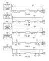
- FIGS. 1 a to 1 fshow a sequence of side views of a base wafer and corresponding processing actions illustrating a process for forming a MEMS assembly wafer in accordance with one embodiment of the invention.
- FIGS. 2 a to 2 jshow a sequence of side views of a cap wafer and corresponding processing actions illustrating a process for forming a MEMS assembly cap wafer in accordance with one embodiment of the invention.
- FIGS. 3 a to 3 bshow a sequence of side views of a base wafer and a cap wafer and corresponding processing actions illustrating a process for attaching a MEMS assembly in accordance with one embodiment of the invention.
- FIG. 4is a flowchart of a process for forming a base wafer of a MEMS assembly in accordance with one embodiment of the invention.
- FIG. 5is a flowchart of a process for forming a cap wafer of a MEMS assembly in accordance with one embodiment of the invention.
- FIG. 6is a flowchart of a process for attaching a base wafer and a cap wafer of a MEMS assembly in accordance with one embodiment of the invention.
- the methodsinclude a process for forming a base wafer for a MEMs assembly, where the process includes forming a two layer conductive pad within a cavity of the base wafer. One of the two layers is configured to act as a getter to absorb water vapor and polymer outgassing within the cavity.
- the methodsalso include a process for forming a cap wafer of the MEMS assembly including use of multiple resist layers to form useful MEMs features for wire bonding such as through vias and cavities for coupling MEMS components.
- a MEMS assemblycan be formed by attaching the base wafer and the cap wafer using a soldering process or another suitable attachment process. Once the MEMS assembly is formed, wire bonding within one of the through vias can be used to couple external electrical leads to internal/isolated electrodes within the MEMS assembly.
- the systems and methods for forming the MEMS assembliesare efficient, and therefore can provide reliable and high yield fabrication for a variety of MEMS sensors and actuators. In one embodiment, these sensors and actuators can include angular acceleration sensors to measure the rotational acceleration of a magnetic media of a storage drive.
- FIGS. 1 a to 1 fshow a sequence of side views of a base wafer 100 and corresponding processing actions illustrating a process for forming a MEMS assembly base wafer in accordance with one embodiment of the invention.
- the processstarts ( 150 ) with a silicon on insulator wafer 100 including a buried oxide layer (BOX) 102 .
- the buried oxide layer 102has a thickness of about 1 to 2 microns.
- the processdeposits and patterns ( 152 ) a layer of photo resist 104 to form a preselected MEMS layout.
- FIG. 1 a to 1 fshow a sequence of side views of a base wafer 100 and corresponding processing actions illustrating a process for forming a MEMS assembly base wafer in accordance with one embodiment of the invention.
- the processstarts ( 150 ) with a silicon on insulator wafer 100 including a buried oxide layer (BOX) 102 .
- the buried oxide layer 102has a thickness of about 1 to 2 micron
- the processthen performs deep reactive ion etching ( 154 ) to form a preselected MEMS structure.
- the ion etchingextends to, and stops on, the buried oxide layer (BOX) 102 , thereby forming several cavities 106 for MEMS components.
- the processcan perform ion milling instead of, or in conjunction with, the reactive ion etching.
- the processperforms resist stripping and hydrofluoric acid etching ( 156 ) to further expand the cavities 106 and thereby release movable MEMS parts.
- other suitable acidscan be used.
- the acid etchinguses either an aqueous acid or a vapor acid.
- the processevaporates or sputters ( 158 ) two metal films 108 , thereby forming conductive pads in the cavities 106 that can act as proof masses in an assembled MEMS device later.
- the first or bottom metal film deposited 108 ais an adhesion metal such as Cr, Ti, or another suitable adhesion metal.
- the second or top metal film deposited 108 bis a conductive contact metal for making electrical contact and for acting as a bonding surface.
- the second or top metal film deposited 108 bcan be a conductive metal such as Au, Al, In or another suitable conductive metal.
- FIG. 1 fillustrates an expanded view of one of the cavities 106 and the deposited metal films ( 108 a , 108 b ).
- portions of the bottom metal film 108 a not covered by the top metal film 108 b in the cavities 106can act as a getter to absorb water vapor and polymer outgassing.
- the bottom metal film 108 ais deposited to have a thickness of about 200 to 500 nanometers.
- the bottom metal film 108 ais deposited to have a thickness of about 300 to 400 nanometers.
- the bottom metal film 108 ais deposited to have a thickness of about 1/10 to 1 times the thickness of the buried oxide layer.
- the process of FIGS. 1 a - 1 fprovides a single mask process for fabricating a MEMS device.
- the processcan perform the sequence of actions in a different order. In another embodiment, the process can skip one or more of the actions. In other embodiments, one or more of the actions are performed simultaneously. In some embodiments, additional actions can be performed.
- FIGS. 2 a to 2 jshow a sequence of side views of a cap wafer 200 and corresponding processing actions illustrating a process for forming a MEMS assembly cap wafer in accordance with one embodiment of the invention.
- the processstarts ( 250 ) with a silicon wafer 200 .
- the top surface of the wafer 200is ground to be relatively smooth while the bottom surface of the wafer 200 is polished.
- the silicon waferhas a thickness of about 400 to 600 microns.
- the processdeposits ( 252 ) an oxide layer 202 using plasma enhanced chemical vapor deposition (PECVD).
- PECVDplasma enhanced chemical vapor deposition
- other suitable deposition methodscan be used instead of PECVD.
- the oxide layer 202is deposited with a thickness of about 3 microns.
- the processthen deposits and patterns ( 254 ) a first resist layer 204 on the oxide layer 202 .
- the first resist layer 204is deposited with a thickness of about 1.8 microns. In other embodiments, the first resist layer 204 is deposited with another suitable thickness.
- the processthen performs reactive ion etching ( 256 ) or RIE to form vias 206 and cavity 208 in the oxide layer 202 .
- the processfirst performs the RIE to remove portions of the oxide layer 202 and then performs deep reactive ion etching (DRIE) to remove portions of the silicon wafer 200 (e.g., remove about 10 microns of the silicon wafer 200 ).
- DRIEdeep reactive ion etching
- the processcan perform ion milling instead of, or in conjunction with, the reactive ion etching.
- the processthen removes ( 258 ) the first resist 204 and deposits metal films 210 for bonding.
- the metal films 210include an adhesion layer made of Cr or Ti, and a top metal layer made of Au, Sn, and/or Cu for soldering/bonding in subsequent assembly steps.
- the metal films 210can include other suitable metals.
- the process of depositing the metal films 210involves use of a full film deposition process that carefully avoids depositing metal on the sidewalls of the vias 206 and cavity 208 .
- the processthen deposits and patterns ( 260 ) a second resist layer 212 for subsequent metal film etching.
- the processperforms wet etching ( 262 ) on the metal film 210 , thereby removing the metal film 210 from areas not protected by the second resist 212 .
- the processcan perform ion milling instead of, or in conjunction with, the wet etching.
- the processremoves ( 264 ) the second resist 212 and deposits and patterns a third resist layer 214 in order to protect the cavity area 208 .
- FIG. 2 hthe process removes ( 264 ) the second resist 212 and deposits and patterns a third resist layer 214 in order to protect the cavity area 208 .
- the processthen performs deep reactive ion etching ( 266 ) or DRIE to etch vias 206 a through the silicon wafer 200 .
- the processcan perform ion milling instead of, or in conjunction with, the reactive ion etching.
- the processthen removes ( 268 ) the third resist 214 and cleans the assembly.
- the final cap assemblyincludes several remaining portions of the metal film layer 210 that can effectively act as conductive pads or electrodes in a final MEMs assembly.
- the various resist layersare patterned using photolithography or other suitable resist patterning techniques.
- aluminumis used in the MEMS base wafer 100 .
- glue type epoxiessuch as Norland 21 or photo resists such as SU8 can be used to adhesively bond the cap wafer 200 to the MEMS base wafer 100 , in which case steps 262 and 264 can be eliminated from the process of FIGS. 2 a - 2 j .
- Using aluminum or indium for the base wafer 100enables low-temperature adhesive or eutectic bonding, however the coefficient of thermal expansion (CTE) can be very large (29 ppm/degree Celsius and 23 ppm/degree Celsius, respectively) and not matched to the silicon substrate ( 200 ).
- Au and Cr metal layerscan provide better match to silicon (14.2 ppm/degree Celsius and 4.9 ppm/degree Celsius, respectively).
- Tiis used as a seed layer in block 258 . In such case, and if only Au is etched in block 262 , then the remaining Ti inside the cap can serve as a getter, without compromising electrical isolation, since it will not get in contact with MEMS during subsequent wafer bonding.
- the processcan form a getter in cavity 208 with the metal films 210 deposited in step 258 .
- the processcan deposit the second resist 212 in the cavity 208 in step 260 to protect the metal films 210 and skip step 264 .
- the processcan perform the sequence of actions in a different order. In another embodiment, the process can skip one or more of the actions. In other embodiments, one or more of the actions are performed simultaneously. In some embodiments, additional actions can be performed.
- FIGS. 3 a to 3 bshow a sequence of side views of a base wafer 100 and a cap wafer 200 and corresponding processing actions illustrating a process for attaching a MEMS assembly in accordance with one embodiment of the invention.
- the processprepares for attachment ( 352 ) of the base wafer 100 and cap wafer 200 by aligning the wafers, baking out contaminants, and bonding the two wafers using either direct bonding or soldering.
- solder on the conductive pads 210 of the cap wafer 200is brought into contact with the metal layers 108 of the base wafer 100 and the assembly heated. As a result, the base wafer 100 and cap wafer 200 become attached at each of the conductive pads 210 .
- the wafersare attached using direct bonding such as gold to gold or copper to copper type bonding. In other embodiments, the wafers are attached using gold to tin or gold to indium soldering.
- the processthen attaches ( 354 ) the assemblies by heating the wafers (as described above) and attaches electrical leads ( 302 a , 302 b ) using conductive epoxy and/or wire bonding.
- a terminal end of the electrical lead 302 ais formed into a conductive metal ball 304 a and secured to conductive metal layer 108 within cavity 306 by wire bonding techniques.
- the electrical lead 302 acan be secured to the conductive metal layer 108 using conductive epoxy or other suitable means of attachment known in the art.
- the electrical lead 302 ais made of gold.
- isolated electrodes 308 a and 308 bare coupled electrical leads 302 a and 302 b , respectively.
- the base wafer 100 and cap wafer 200are aligned and brought in contact by applying a force at a eutectic temperature.
- suitable eutectic temperatures for various material combinationsinclude: 363 degrees Celsius for Au—Si, 283 degrees Celsius for Au—Sn, and 118 degrees Celsius for In—Sn.
- both the base wafer 100 and cap wafer 200have been processed for fine flatness and surface finish.
- FIG. 4is a flowchart of a process 400 for forming a wafer of a MEMS assembly in accordance with one embodiment of the invention.
- the process 400can be used to form the wafer assembly of FIGS. 1 a - 1 f .
- the processfirst provides ( 402 ) a wafer including a buried oxide layer (BOX).
- the processdeposits ( 404 ) and patterns a first photo resist layer on the wafer.
- the processthen performs reactive ion etching ( 406 ) on a surface of the wafer, the reactive ion etching extending to the buried oxide layer.
- the processthen removes ( 408 ) the first photo resist layer.
- the processremoves ( 410 ) portions of the buried oxide layer, thereby forming one or more cavities within the wafer.
- the processthen deposits ( 412 ) a first metal layer configured to act as a getter within the one or more cavities.
- the processthen deposits ( 414 ) a second metal layer on the first metal layer.
- the processcan perform the sequence of actions in a different order. In another embodiment, the process can skip one or more of the actions. In other embodiments, one or more of the actions are performed simultaneously. In some embodiments, additional actions can be performed.
- FIG. 5is a flowchart of a process 500 for forming a cap wafer of a MEMS assembly in accordance with one embodiment of the invention.
- the process 500can be used to form the wafer assembly of FIGS. 2 a - 2 j .
- the processfirst provides ( 502 ) a cap wafer.
- the processdeposits ( 504 ) a layer of oxide on the cap wafer.
- the processdeposits and patterns ( 506 ) a first photo resist layer on the oxide layer.
- the processremoves ( 508 ) portions of the oxide layer in accordance with the patterned first photo resist layer.
- the processremoves ( 510 ) the first photo resist layer.
- the processdeposits ( 512 ) one or more first metal layers on the cap wafer.
- the processdeposits and patterns ( 514 ) a second photo resist layer on the one or more first metal layers.
- the processthen removes ( 516 ) portions of the one or more first metal layers in accordance with the patterned second photo resist layer.
- the processremoves ( 518 ) the second photo resist layer.
- the processthen deposits and patterns ( 520 ) a third photo resist layer on the cap wafer (e.g., to protect a cavity area).
- the processremoves ( 522 ) portions of the cap wafer in accordance with the oxide layer and the third photo resist layer to form one or more through hole vias.
- the processthen removes ( 524 ) the third photo resist layer to form a completed cap wafer assembly.
- the processcan perform the sequence of actions in a different order. In another embodiment, the process can skip one or more of the actions. In other embodiments, one or more of the actions are performed simultaneously. In some embodiments, additional actions can be performed.
- FIG. 6is a flowchart of a process 600 for attaching a wafer and a cap wafer of a MEMS assembly in accordance with one embodiment of the invention.
- the process 600can be used to form the MEMs assembly of FIGS. 3 a - 3 b .
- the processfirst provides ( 602 ) a first MEMS wafer having a metal layer on an inner surface and one or more cavities for forming a MEMS component.
- the processthen attaches ( 604 ) a MEMS capping wafer, having at least one through hole via, to the inner surface of the first MEMS wafer thereby forming at least one encapsulated MEMs component within the first MEMS wafer.
- the processthen bonds ( 606 ) a wire to the metal layer through an open end of the at least one through hole via.
- the processcan perform the sequence of actions in a different order. In another embodiment, the process can skip one or more of the actions. In other embodiments, one or more of the actions are performed simultaneously. In some embodiments, additional actions can be performed.
- the proposed single-mask MEMS flow of FIGS. 1 a - 1 fprovides a clean and simple MEMS structure and helps to avoid drawbacks on MEMS performance caused by process variability, while the more complex cap wafer process of FIGS. 2 a - 2 j bears the burden of completing the three dimensional structures for the final packaged MEMS device.
- these overall processescan provide advantages including: (1) the MEMS wafer process and modular capping process are relatively simple, (2) the wafer capping can be performed via two-layer adhesive bonding (non-hermetic) or three-layer eutectic bonding (hermetic), (3) the small bond area design reduces CTE mismatch issues, (4) both the MEMS wafer and cap wafer can contain getter layers, such as Ti used as seed layer for metal interface, and (5) the cap can be used as independent electrode in some applications.
Landscapes
- Engineering & Computer Science (AREA)
- Microelectronics & Electronic Packaging (AREA)
- Manufacturing & Machinery (AREA)
- Computer Hardware Design (AREA)
- Micromachines (AREA)
Abstract
Description
Claims (9)
Priority Applications (3)
| Application Number | Priority Date | Filing Date | Title |
|---|---|---|---|
| US13/198,448US9212051B1 (en) | 2011-08-04 | 2011-08-04 | Systems and methods for forming MEMS assemblies incorporating getters |
| US14/943,300US20160176706A1 (en) | 2011-08-04 | 2015-11-17 | Systems and methods for forming mems assemblies incorporating getters |
| US14/943,391US20160176705A1 (en) | 2011-08-04 | 2015-11-17 | Systems and methods for forming mems assemblies incorporating getters |
Applications Claiming Priority (1)
| Application Number | Priority Date | Filing Date | Title |
|---|---|---|---|
| US13/198,448US9212051B1 (en) | 2011-08-04 | 2011-08-04 | Systems and methods for forming MEMS assemblies incorporating getters |
Related Child Applications (2)
| Application Number | Title | Priority Date | Filing Date |
|---|---|---|---|
| US14/943,391DivisionUS20160176705A1 (en) | 2011-08-04 | 2015-11-17 | Systems and methods for forming mems assemblies incorporating getters |
| US14/943,300DivisionUS20160176706A1 (en) | 2011-08-04 | 2015-11-17 | Systems and methods for forming mems assemblies incorporating getters |
Publications (1)
| Publication Number | Publication Date |
|---|---|
| US9212051B1true US9212051B1 (en) | 2015-12-15 |
Family
ID=54783082
Family Applications (3)
| Application Number | Title | Priority Date | Filing Date |
|---|---|---|---|
| US13/198,448Active2033-05-14US9212051B1 (en) | 2011-08-04 | 2011-08-04 | Systems and methods for forming MEMS assemblies incorporating getters |
| US14/943,391AbandonedUS20160176705A1 (en) | 2011-08-04 | 2015-11-17 | Systems and methods for forming mems assemblies incorporating getters |
| US14/943,300AbandonedUS20160176706A1 (en) | 2011-08-04 | 2015-11-17 | Systems and methods for forming mems assemblies incorporating getters |
Family Applications After (2)
| Application Number | Title | Priority Date | Filing Date |
|---|---|---|---|
| US14/943,391AbandonedUS20160176705A1 (en) | 2011-08-04 | 2015-11-17 | Systems and methods for forming mems assemblies incorporating getters |
| US14/943,300AbandonedUS20160176706A1 (en) | 2011-08-04 | 2015-11-17 | Systems and methods for forming mems assemblies incorporating getters |
Country Status (1)
| Country | Link |
|---|---|
| US (3) | US9212051B1 (en) |
Cited By (3)
| Publication number | Priority date | Publication date | Assignee | Title |
|---|---|---|---|---|
| US20180237292A1 (en)* | 2017-02-22 | 2018-08-23 | Infineon Technologies Ag | Semiconductor device, microphone and methods for forming a semiconductor device |
| US20190330052A1 (en)* | 2017-04-26 | 2019-10-31 | Invensense, Inc. | Systems and methods for providing getters in microelectromechanical systems |
| US10988372B2 (en)* | 2018-11-29 | 2021-04-27 | Invensense, Inc. | MEMS device with reduced electric charge, cavity volume and stiction |
Families Citing this family (1)
| Publication number | Priority date | Publication date | Assignee | Title |
|---|---|---|---|---|
| US11174157B2 (en)* | 2018-06-27 | 2021-11-16 | Advanced Semiconductor Engineering Inc. | Semiconductor device packages and methods of manufacturing the same |
Citations (24)
| Publication number | Priority date | Publication date | Assignee | Title |
|---|---|---|---|---|
| US6630725B1 (en)* | 2000-10-06 | 2003-10-07 | Motorola, Inc. | Electronic component and method of manufacture |
| US6660564B2 (en) | 2002-01-25 | 2003-12-09 | Sony Corporation | Wafer-level through-wafer packaging process for MEMS and MEMS package produced thereby |
| US6762072B2 (en) | 2002-03-06 | 2004-07-13 | Robert Bosch Gmbh | SI wafer-cap wafer bonding method using local laser energy, device produced by the method, and system used in the method |
| US6952965B2 (en) | 2002-12-24 | 2005-10-11 | Samsung Electronics Co., Ltd. | Vertical MEMS gyroscope by horizontal driving |
| US20060214246A1 (en) | 2005-03-24 | 2006-09-28 | Garcia Jason A | Methods and apparatuses for microelectronic assembly having a material with a variable viscosity around a MEMS device |
| US20060214247A1 (en) | 2004-05-13 | 2006-09-28 | Honeywell International Inc. | Getter deposition for vacuum packaging |
| US20060258039A1 (en) | 2004-02-12 | 2006-11-16 | Markus Lutz | Integrated getter area for wafer level encapsulated microelectromechanical systems |
| US7195945B1 (en) | 2004-09-15 | 2007-03-27 | United States Of America As Represented By The Secretary Of The Army | Minimizing the effect of 1/ƒ noise with a MEMS flux concentrator |
| US7204737B2 (en)* | 2004-09-23 | 2007-04-17 | Temic Automotive Of North America, Inc. | Hermetically sealed microdevice with getter shield |
| US20070220972A1 (en)* | 2004-07-12 | 2007-09-27 | Bae Ststems Plc | Angular Velocity Sensor |
| US7396698B2 (en) | 2003-10-21 | 2008-07-08 | Honeywell International Inc. | Methods and systems for providing MEMS devices with a top cap and upper sense plate |
| US20090139331A1 (en) | 2007-11-15 | 2009-06-04 | Physical Logic Ag | Accelerometer |
| US7595209B1 (en) | 2007-03-09 | 2009-09-29 | Silicon Clocks, Inc. | Low stress thin film microshells |
| US7622324B2 (en) | 2002-09-25 | 2009-11-24 | Ziptronix | Wafer bonding hermetic encapsulation |
| US7659150B1 (en) | 2007-03-09 | 2010-02-09 | Silicon Clocks, Inc. | Microshells for multi-level vacuum cavities |
| US20100117166A1 (en)* | 2007-06-29 | 2010-05-13 | Wolfram Geiger | Method for the production of a component, and component |
| US7736929B1 (en) | 2007-03-09 | 2010-06-15 | Silicon Clocks, Inc. | Thin film microshells incorporating a getter layer |
| US20100267182A1 (en) | 2004-12-15 | 2010-10-21 | Dungan Thomas E | Wafer bonding of micro-electro mechanical systems to active circuitry |
| US7863063B2 (en) | 2008-03-04 | 2011-01-04 | Memsmart Semiconductor Corp. | Method for fabricating a sealed cavity microstructure |
| US20110018075A1 (en)* | 2009-07-23 | 2011-01-27 | Lung-Tai Chen | Structure and fabrication method of a sensing device |
| US20110031565A1 (en) | 2009-08-04 | 2011-02-10 | David Lambe Marx | Micromachined devices and fabricating the same |
| US7923790B1 (en) | 2007-03-09 | 2011-04-12 | Silicon Laboratories Inc. | Planar microshells for vacuum encapsulated devices and damascene method of manufacture |
| US20120142144A1 (en)* | 2010-12-03 | 2012-06-07 | Babak Taheri | Wafer Level Structures and Methods for Fabricating and Packaging MEMS |
| US20140299949A1 (en)* | 2009-05-11 | 2014-10-09 | Stmicroelectronics S.R.I. | Assembly of a capacitive acoustic transducer of the microelectromechanical type and package thereof |
- 2011
- 2011-08-04USUS13/198,448patent/US9212051B1/enactiveActive
- 2015
- 2015-11-17USUS14/943,391patent/US20160176705A1/ennot_activeAbandoned
- 2015-11-17USUS14/943,300patent/US20160176706A1/ennot_activeAbandoned
Patent Citations (25)
| Publication number | Priority date | Publication date | Assignee | Title |
|---|---|---|---|---|
| US6630725B1 (en)* | 2000-10-06 | 2003-10-07 | Motorola, Inc. | Electronic component and method of manufacture |
| US6660564B2 (en) | 2002-01-25 | 2003-12-09 | Sony Corporation | Wafer-level through-wafer packaging process for MEMS and MEMS package produced thereby |
| US6841861B2 (en) | 2002-01-25 | 2005-01-11 | Sony Corporation | MEMS package |
| US6762072B2 (en) | 2002-03-06 | 2004-07-13 | Robert Bosch Gmbh | SI wafer-cap wafer bonding method using local laser energy, device produced by the method, and system used in the method |
| US7622324B2 (en) | 2002-09-25 | 2009-11-24 | Ziptronix | Wafer bonding hermetic encapsulation |
| US6952965B2 (en) | 2002-12-24 | 2005-10-11 | Samsung Electronics Co., Ltd. | Vertical MEMS gyroscope by horizontal driving |
| US7396698B2 (en) | 2003-10-21 | 2008-07-08 | Honeywell International Inc. | Methods and systems for providing MEMS devices with a top cap and upper sense plate |
| US20060258039A1 (en) | 2004-02-12 | 2006-11-16 | Markus Lutz | Integrated getter area for wafer level encapsulated microelectromechanical systems |
| US20060214247A1 (en) | 2004-05-13 | 2006-09-28 | Honeywell International Inc. | Getter deposition for vacuum packaging |
| US20070220972A1 (en)* | 2004-07-12 | 2007-09-27 | Bae Ststems Plc | Angular Velocity Sensor |
| US7195945B1 (en) | 2004-09-15 | 2007-03-27 | United States Of America As Represented By The Secretary Of The Army | Minimizing the effect of 1/ƒ noise with a MEMS flux concentrator |
| US7204737B2 (en)* | 2004-09-23 | 2007-04-17 | Temic Automotive Of North America, Inc. | Hermetically sealed microdevice with getter shield |
| US20100267182A1 (en) | 2004-12-15 | 2010-10-21 | Dungan Thomas E | Wafer bonding of micro-electro mechanical systems to active circuitry |
| US20060214246A1 (en) | 2005-03-24 | 2006-09-28 | Garcia Jason A | Methods and apparatuses for microelectronic assembly having a material with a variable viscosity around a MEMS device |
| US7595209B1 (en) | 2007-03-09 | 2009-09-29 | Silicon Clocks, Inc. | Low stress thin film microshells |
| US7659150B1 (en) | 2007-03-09 | 2010-02-09 | Silicon Clocks, Inc. | Microshells for multi-level vacuum cavities |
| US7736929B1 (en) | 2007-03-09 | 2010-06-15 | Silicon Clocks, Inc. | Thin film microshells incorporating a getter layer |
| US7923790B1 (en) | 2007-03-09 | 2011-04-12 | Silicon Laboratories Inc. | Planar microshells for vacuum encapsulated devices and damascene method of manufacture |
| US20100117166A1 (en)* | 2007-06-29 | 2010-05-13 | Wolfram Geiger | Method for the production of a component, and component |
| US20090139331A1 (en) | 2007-11-15 | 2009-06-04 | Physical Logic Ag | Accelerometer |
| US7863063B2 (en) | 2008-03-04 | 2011-01-04 | Memsmart Semiconductor Corp. | Method for fabricating a sealed cavity microstructure |
| US20140299949A1 (en)* | 2009-05-11 | 2014-10-09 | Stmicroelectronics S.R.I. | Assembly of a capacitive acoustic transducer of the microelectromechanical type and package thereof |
| US20110018075A1 (en)* | 2009-07-23 | 2011-01-27 | Lung-Tai Chen | Structure and fabrication method of a sensing device |
| US20110031565A1 (en) | 2009-08-04 | 2011-02-10 | David Lambe Marx | Micromachined devices and fabricating the same |
| US20120142144A1 (en)* | 2010-12-03 | 2012-06-07 | Babak Taheri | Wafer Level Structures and Methods for Fabricating and Packaging MEMS |
Non-Patent Citations (1)
| Title |
|---|
| Monajemi et al, "Chapter 9-MEMS Packaging" from "Introduction to System on Package: Miniaturization of the Entire System" by Rao Tummala, McGraw Hill, 1st edition, 2008, pp. 503-540. |
Cited By (7)
| Publication number | Priority date | Publication date | Assignee | Title |
|---|---|---|---|---|
| US20180237292A1 (en)* | 2017-02-22 | 2018-08-23 | Infineon Technologies Ag | Semiconductor device, microphone and methods for forming a semiconductor device |
| US10858246B2 (en)* | 2017-02-22 | 2020-12-08 | Infineon Technologies Ag | Semiconductor device, microphone and methods for forming a semiconductor device |
| US11352253B2 (en) | 2017-02-22 | 2022-06-07 | Infineon Technologies Ag | Semiconductor device, microphone and methods for forming a semiconductor device |
| US20190330052A1 (en)* | 2017-04-26 | 2019-10-31 | Invensense, Inc. | Systems and methods for providing getters in microelectromechanical systems |
| US11945713B2 (en)* | 2017-04-26 | 2024-04-02 | Invensense, Inc. | Systems and methods for providing getters in microelectromechanical systems |
| US12319562B2 (en) | 2017-04-26 | 2025-06-03 | Invensense, Inc. | Systems and methods for providing getters in microelectromechanical systems |
| US10988372B2 (en)* | 2018-11-29 | 2021-04-27 | Invensense, Inc. | MEMS device with reduced electric charge, cavity volume and stiction |
Also Published As
| Publication number | Publication date |
|---|---|
| US20160176706A1 (en) | 2016-06-23 |
| US20160176705A1 (en) | 2016-06-23 |
Similar Documents
| Publication | Publication Date | Title |
|---|---|---|
| US9981841B2 (en) | MEMS integrated pressure sensor and microphone devices and methods of forming same | |
| US10155659B2 (en) | Vacuum sealed MEMS and CMOS package | |
| US9862593B2 (en) | MEMS-CMOS device that minimizes outgassing and methods of manufacture | |
| CN107032290B (en) | Semiconductor device and method of forming the same | |
| TWI543280B (en) | Method for forming MEMS components | |
| US9085456B2 (en) | Support structure for TSV in MEMS structure | |
| TWI471259B (en) | Mems device and manufacturing method thereof | |
| US9650237B2 (en) | Electromechanical device including a suspended structure and method of fabricating the same | |
| TWI675444B (en) | Mems device and method for packaging mems | |
| US20100193884A1 (en) | Method of Fabricating High Aspect Ratio Transducer Using Metal Compression Bonding | |
| US11945713B2 (en) | Systems and methods for providing getters in microelectromechanical systems | |
| US8252695B2 (en) | Method for manufacturing a micro-electromechanical structure | |
| TWI523120B (en) | Semiconductor structure and method for forming the same | |
| CN106976838A (en) | Method of manufacturing a MEMS package | |
| US10865103B2 (en) | Packaging method and associated packaging structure | |
| TW201307183A (en) | Metal thin shield on electrical device | |
| US20160176705A1 (en) | Systems and methods for forming mems assemblies incorporating getters | |
| TW201322366A (en) | Sensor process | |
| KR20190003284A (en) | Method of stiction prevention by patterned anti-stiction layer | |
| CN119936434A (en) | Wafer-level packaging structure and packaging method of MEMS capacitive accelerometer based on TSV | |
| JP5139032B2 (en) | Fine structure and manufacturing method thereof | |
| TWI387555B (en) | Mems integrated chip and method for making same |
Legal Events
| Date | Code | Title | Description |
|---|---|---|---|
| AS | Assignment | Owner name:WESTERN DIGITAL (FREMONT), LLC, CALIFORNIA Free format text:ASSIGNMENT OF ASSIGNORS INTEREST;ASSIGNORS:MONADGEMI, PEZHMAN;WANG, LEI;REEL/FRAME:026801/0977 Effective date:20110804 | |
| STCF | Information on status: patent grant | Free format text:PATENTED CASE | |
| AS | Assignment | Owner name:JPMORGAN CHASE BANK, N.A., AS COLLATERAL AGENT, IL Free format text:SECURITY AGREEMENT;ASSIGNOR:WESTERN DIGITAL (FREMONT), LLC;REEL/FRAME:038710/0845 Effective date:20160512 Owner name:JPMORGAN CHASE BANK, N.A., AS COLLATERAL AGENT, IL Free format text:SECURITY AGREEMENT;ASSIGNOR:WESTERN DIGITAL (FREMONT), LLC;REEL/FRAME:038744/0755 Effective date:20160512 Owner name:U.S. BANK NATIONAL ASSOCIATION, AS COLLATERAL AGEN Free format text:SECURITY AGREEMENT;ASSIGNOR:WESTERN DIGITAL (FREMONT), LLC;REEL/FRAME:038744/0675 Effective date:20160512 | |
| AS | Assignment | Owner name:WESTERN DIGITAL (FREMONT), LLC, CALIFORNIA Free format text:RELEASE BY SECURED PARTY;ASSIGNOR:U.S. BANK NATIONAL ASSOCIATION, AS COLLATERAL AGENT;REEL/FRAME:045501/0158 Effective date:20180227 | |
| MAFP | Maintenance fee payment | Free format text:PAYMENT OF MAINTENANCE FEE, 4TH YEAR, LARGE ENTITY (ORIGINAL EVENT CODE: M1551); ENTITY STATUS OF PATENT OWNER: LARGE ENTITY Year of fee payment:4 | |
| AS | Assignment | Owner name:WESTERN DIGITAL TECHNOLOGIES, INC., CALIFORNIA Free format text:ASSIGNMENT OF ASSIGNORS INTEREST;ASSIGNOR:WESTERN DIGITAL (FREMONT), LLC;REEL/FRAME:050450/0582 Effective date:20190508 | |
| AS | Assignment | Owner name:WESTERN DIGITAL TECHNOLOGIES, INC., CALIFORNIA Free format text:RELEASE OF SECURITY INTEREST AT REEL 038710 FRAME 0845;ASSIGNOR:JPMORGAN CHASE BANK, N.A.;REEL/FRAME:058965/0445 Effective date:20220203 Owner name:WESTERN DIGITAL (FREMONT), LLC, CALIFORNIA Free format text:RELEASE OF SECURITY INTEREST AT REEL 038710 FRAME 0845;ASSIGNOR:JPMORGAN CHASE BANK, N.A.;REEL/FRAME:058965/0445 Effective date:20220203 | |
| MAFP | Maintenance fee payment | Free format text:PAYMENT OF MAINTENANCE FEE, 8TH YEAR, LARGE ENTITY (ORIGINAL EVENT CODE: M1552); ENTITY STATUS OF PATENT OWNER: LARGE ENTITY Year of fee payment:8 | |
| AS | Assignment | Owner name:JPMORGAN CHASE BANK, N.A., ILLINOIS Free format text:PATENT COLLATERAL AGREEMENT - A&R LOAN AGREEMENT;ASSIGNOR:WESTERN DIGITAL TECHNOLOGIES, INC.;REEL/FRAME:064715/0001 Effective date:20230818 Owner name:JPMORGAN CHASE BANK, N.A., ILLINOIS Free format text:PATENT COLLATERAL AGREEMENT - DDTL LOAN AGREEMENT;ASSIGNOR:WESTERN DIGITAL TECHNOLOGIES, INC.;REEL/FRAME:067045/0156 Effective date:20230818 |