US9209186B1 - Threshold voltage control for mixed-type non-planar semiconductor devices - Google Patents
Threshold voltage control for mixed-type non-planar semiconductor devicesDownload PDFInfo
- Publication number
- US9209186B1 US9209186B1US14/315,885US201414315885AUS9209186B1US 9209186 B1US9209186 B1US 9209186B1US 201414315885 AUS201414315885 AUS 201414315885AUS 9209186 B1US9209186 B1US 9209186B1
- Authority
- US
- United States
- Prior art keywords
- layer
- work function
- type
- function metal
- creating
- Prior art date
- Legal status (The legal status is an assumption and is not a legal conclusion. Google has not performed a legal analysis and makes no representation as to the accuracy of the status listed.)
- Active
Links
- 239000004065semiconductorSubstances0.000titleclaimsdescription22
- 229910052751metalInorganic materials0.000claimsabstractdescription77
- 239000002184metalSubstances0.000claimsabstractdescription77
- 230000001590oxidative effectEffects0.000claimsabstractdescription12
- XKRFYHLGVUSROY-UHFFFAOYSA-NArgonChemical compound[Ar]XKRFYHLGVUSROY-UHFFFAOYSA-N0.000claimsabstractdescription10
- XUIMIQQOPSSXEZ-UHFFFAOYSA-NSiliconChemical compound[Si]XUIMIQQOPSSXEZ-UHFFFAOYSA-N0.000claimsabstractdescription8
- 229910052710siliconInorganic materials0.000claimsabstractdescription8
- 239000010703siliconSubstances0.000claimsabstractdescription8
- 229910052732germaniumInorganic materials0.000claimsabstractdescription6
- GNPVGFCGXDBREM-UHFFFAOYSA-Ngermanium atomChemical compound[Ge]GNPVGFCGXDBREM-UHFFFAOYSA-N0.000claimsabstractdescription6
- 229910052786argonInorganic materials0.000claimsabstractdescription5
- 229910052785arsenicInorganic materials0.000claimsabstractdescription5
- RQNWIZPPADIBDY-UHFFFAOYSA-Narsenic atomChemical compound[As]RQNWIZPPADIBDY-UHFFFAOYSA-N0.000claimsabstractdescription5
- 238000000034methodMethods0.000claimsdescription47
- 230000004888barrier functionEffects0.000claimsdescription23
- 238000009792diffusion processMethods0.000claimsdescription17
- 239000000463materialSubstances0.000claimsdescription16
- 239000004020conductorSubstances0.000claimsdescription10
- 238000011049fillingMethods0.000claimsdescription9
- 230000008569processEffects0.000claimsdescription9
- 229910021417amorphous siliconInorganic materials0.000claimsdescription7
- 230000007423decreaseEffects0.000claimsdescription7
- 230000000903blocking effectEffects0.000claimsdescription5
- 238000000137annealingMethods0.000claimsdescription3
- 239000000758substrateSubstances0.000abstractdescription11
- MZLGASXMSKOWSE-UHFFFAOYSA-Ntantalum nitrideChemical compound[Ta]#NMZLGASXMSKOWSE-UHFFFAOYSA-N0.000abstractdescription3
- 239000010410layerSubstances0.000description127
- 230000006870functionEffects0.000description60
- NRTOMJZYCJJWKI-UHFFFAOYSA-NTitanium nitrideChemical compound[Ti]#NNRTOMJZYCJJWKI-UHFFFAOYSA-N0.000description7
- 238000000231atomic layer depositionMethods0.000description6
- 238000005229chemical vapour depositionMethods0.000description6
- 238000001312dry etchingMethods0.000description6
- WGTYBPLFGIVFAS-UHFFFAOYSA-Mtetramethylammonium hydroxideChemical compound[OH-].C[N+](C)(C)CWGTYBPLFGIVFAS-UHFFFAOYSA-M0.000description6
- 238000004519manufacturing processMethods0.000description5
- 238000001039wet etchingMethods0.000description4
- KZBUYRJDOAKODT-UHFFFAOYSA-NChlorineChemical compoundClClKZBUYRJDOAKODT-UHFFFAOYSA-N0.000description3
- CPELXLSAUQHCOX-UHFFFAOYSA-NHydrogen bromideChemical compoundBrCPELXLSAUQHCOX-UHFFFAOYSA-N0.000description3
- 229910018503SF6Inorganic materials0.000description3
- 229910052581Si3N4Inorganic materials0.000description3
- 230000000873masking effectEffects0.000description3
- 229910021420polycrystalline siliconInorganic materials0.000description3
- HQVNEWCFYHHQES-UHFFFAOYSA-Nsilicon nitrideChemical compoundN12[Si]34N5[Si]62N3[Si]51N64HQVNEWCFYHHQES-UHFFFAOYSA-N0.000description3
- TXEYQDLBPFQVAA-UHFFFAOYSA-NtetrafluoromethaneChemical compoundFC(F)(F)FTXEYQDLBPFQVAA-UHFFFAOYSA-N0.000description3
- FAQYAMRNWDIXMY-UHFFFAOYSA-NtrichloroboraneChemical compoundClB(Cl)ClFAQYAMRNWDIXMY-UHFFFAOYSA-N0.000description3
- 229910000577Silicon-germaniumInorganic materials0.000description2
- LEVVHYCKPQWKOP-UHFFFAOYSA-N[Si].[Ge]Chemical compound[Si].[Ge]LEVVHYCKPQWKOP-UHFFFAOYSA-N0.000description2
- -1but not limited toSubstances0.000description2
- 239000003989dielectric materialSubstances0.000description2
- WRQGPGZATPOHHX-UHFFFAOYSA-Nethyl 2-oxohexanoateChemical compoundCCCCC(=O)C(=O)OCCWRQGPGZATPOHHX-UHFFFAOYSA-N0.000description2
- 239000012212insulatorSubstances0.000description2
- 239000011229interlayerSubstances0.000description2
- 238000002955isolationMethods0.000description2
- 229920005591polysiliconPolymers0.000description2
- JBRZTFJDHDCESZ-UHFFFAOYSA-NAsGaChemical compound[As]#[Ga]JBRZTFJDHDCESZ-UHFFFAOYSA-N0.000description1
- MYMOFIZGZYHOMD-UHFFFAOYSA-NDioxygenChemical compoundO=OMYMOFIZGZYHOMD-UHFFFAOYSA-N0.000description1
- 229910000530Gallium indium arsenideInorganic materials0.000description1
- GPXJNWSHGFTCBW-UHFFFAOYSA-NIndium phosphideChemical compound[In]#PGPXJNWSHGFTCBW-UHFFFAOYSA-N0.000description1
- 238000007792additionMethods0.000description1
- 229910045601alloyInorganic materials0.000description1
- 239000000956alloySubstances0.000description1
- UQZIWOQVLUASCR-UHFFFAOYSA-Nalumane;titaniumChemical compound[AlH3].[Ti]UQZIWOQVLUASCR-UHFFFAOYSA-N0.000description1
- 230000008859changeEffects0.000description1
- 150000001875compoundsChemical class0.000description1
- 239000013078crystalSubstances0.000description1
- 230000003247decreasing effectEffects0.000description1
- 238000000151depositionMethods0.000description1
- 230000008021depositionEffects0.000description1
- 229910001882dioxygenInorganic materials0.000description1
- 238000005530etchingMethods0.000description1
- HZXMRANICFIONG-UHFFFAOYSA-Ngallium phosphideChemical compound[Ga]#PHZXMRANICFIONG-UHFFFAOYSA-N0.000description1
- 229910000042hydrogen bromideInorganic materials0.000description1
- 239000007943implantSubstances0.000description1
- 239000012535impuritySubstances0.000description1
- WPYVAWXEWQSOGY-UHFFFAOYSA-Nindium antimonideChemical compound[Sb]#[In]WPYVAWXEWQSOGY-UHFFFAOYSA-N0.000description1
- RPQDHPTXJYYUPQ-UHFFFAOYSA-Nindium arsenideChemical compound[In]#[As]RPQDHPTXJYYUPQ-UHFFFAOYSA-N0.000description1
- 238000001459lithographyMethods0.000description1
- 238000012986modificationMethods0.000description1
- 230000004048modificationEffects0.000description1
- 229910021421monocrystalline siliconInorganic materials0.000description1
- 238000005498polishingMethods0.000description1
- 239000011241protective layerSubstances0.000description1
- HBMJWWWQQXIZIP-UHFFFAOYSA-Nsilicon carbideChemical compound[Si+]#[C-]HBMJWWWQQXIZIP-UHFFFAOYSA-N0.000description1
- 125000006850spacer groupChemical group0.000description1
- 238000006467substitution reactionMethods0.000description1
- SFZCNBIFKDRMGX-UHFFFAOYSA-Nsulfur hexafluorideChemical compoundFS(F)(F)(F)(F)FSFZCNBIFKDRMGX-UHFFFAOYSA-N0.000description1
- 229960000909sulfur hexafluorideDrugs0.000description1
- WFKWXMTUELFFGS-UHFFFAOYSA-NtungstenChemical compound[W]WFKWXMTUELFFGS-UHFFFAOYSA-N0.000description1
- 229910052721tungstenInorganic materials0.000description1
- 239000010937tungstenSubstances0.000description1
Images


Classifications
- H01L27/0924—
- H—ELECTRICITY
- H10—SEMICONDUCTOR DEVICES; ELECTRIC SOLID-STATE DEVICES NOT OTHERWISE PROVIDED FOR
- H10D—INORGANIC ELECTRIC SEMICONDUCTOR DEVICES
- H10D84/00—Integrated devices formed in or on semiconductor substrates that comprise only semiconducting layers, e.g. on Si wafers or on GaAs-on-Si wafers
- H10D84/80—Integrated devices formed in or on semiconductor substrates that comprise only semiconducting layers, e.g. on Si wafers or on GaAs-on-Si wafers characterised by the integration of at least one component covered by groups H10D12/00 or H10D30/00, e.g. integration of IGFETs
- H10D84/82—Integrated devices formed in or on semiconductor substrates that comprise only semiconducting layers, e.g. on Si wafers or on GaAs-on-Si wafers characterised by the integration of at least one component covered by groups H10D12/00 or H10D30/00, e.g. integration of IGFETs of only field-effect components
- H10D84/83—Integrated devices formed in or on semiconductor substrates that comprise only semiconducting layers, e.g. on Si wafers or on GaAs-on-Si wafers characterised by the integration of at least one component covered by groups H10D12/00 or H10D30/00, e.g. integration of IGFETs of only field-effect components of only insulated-gate FETs [IGFET]
- H10D84/85—Complementary IGFETs, e.g. CMOS
- H10D84/856—Complementary IGFETs, e.g. CMOS the complementary IGFETs having different architectures than each other, e.g. high-voltage and low-voltage CMOS
- H—ELECTRICITY
- H01—ELECTRIC ELEMENTS
- H01L—SEMICONDUCTOR DEVICES NOT COVERED BY CLASS H10
- H01L21/00—Processes or apparatus adapted for the manufacture or treatment of semiconductor or solid state devices or of parts thereof
- H01L21/02—Manufacture or treatment of semiconductor devices or of parts thereof
- H01L21/04—Manufacture or treatment of semiconductor devices or of parts thereof the devices having potential barriers, e.g. a PN junction, depletion layer or carrier concentration layer
- H01L21/18—Manufacture or treatment of semiconductor devices or of parts thereof the devices having potential barriers, e.g. a PN junction, depletion layer or carrier concentration layer the devices having semiconductor bodies comprising elements of Group IV of the Periodic Table or AIIIBV compounds with or without impurities, e.g. doping materials
- H01L21/26—Bombardment with radiation
- H01L21/263—Bombardment with radiation with high-energy radiation
- H01L21/265—Bombardment with radiation with high-energy radiation producing ion implantation
- H01L21/26506—Bombardment with radiation with high-energy radiation producing ion implantation in group IV semiconductors
- H01L21/26513—Bombardment with radiation with high-energy radiation producing ion implantation in group IV semiconductors of electrically active species
- H—ELECTRICITY
- H01—ELECTRIC ELEMENTS
- H01L—SEMICONDUCTOR DEVICES NOT COVERED BY CLASS H10
- H01L21/00—Processes or apparatus adapted for the manufacture or treatment of semiconductor or solid state devices or of parts thereof
- H01L21/02—Manufacture or treatment of semiconductor devices or of parts thereof
- H01L21/04—Manufacture or treatment of semiconductor devices or of parts thereof the devices having potential barriers, e.g. a PN junction, depletion layer or carrier concentration layer
- H01L21/18—Manufacture or treatment of semiconductor devices or of parts thereof the devices having potential barriers, e.g. a PN junction, depletion layer or carrier concentration layer the devices having semiconductor bodies comprising elements of Group IV of the Periodic Table or AIIIBV compounds with or without impurities, e.g. doping materials
- H01L21/30—Treatment of semiconductor bodies using processes or apparatus not provided for in groups H01L21/20 - H01L21/26
- H01L21/31—Treatment of semiconductor bodies using processes or apparatus not provided for in groups H01L21/20 - H01L21/26 to form insulating layers thereon, e.g. for masking or by using photolithographic techniques; After treatment of these layers; Selection of materials for these layers
- H01L21/3205—Deposition of non-insulating-, e.g. conductive- or resistive-, layers on insulating layers; After-treatment of these layers
- H01L21/321—After treatment
- H01L21/32115—Planarisation
- H—ELECTRICITY
- H01—ELECTRIC ELEMENTS
- H01L—SEMICONDUCTOR DEVICES NOT COVERED BY CLASS H10
- H01L21/00—Processes or apparatus adapted for the manufacture or treatment of semiconductor or solid state devices or of parts thereof
- H01L21/02—Manufacture or treatment of semiconductor devices or of parts thereof
- H01L21/04—Manufacture or treatment of semiconductor devices or of parts thereof the devices having potential barriers, e.g. a PN junction, depletion layer or carrier concentration layer
- H01L21/18—Manufacture or treatment of semiconductor devices or of parts thereof the devices having potential barriers, e.g. a PN junction, depletion layer or carrier concentration layer the devices having semiconductor bodies comprising elements of Group IV of the Periodic Table or AIIIBV compounds with or without impurities, e.g. doping materials
- H01L21/30—Treatment of semiconductor bodies using processes or apparatus not provided for in groups H01L21/20 - H01L21/26
- H01L21/324—Thermal treatment for modifying the properties of semiconductor bodies, e.g. annealing, sintering
- H01L21/823431—
- H01L21/823807—
- H01L21/823821—
- H01L21/823842—
- H01L21/845—
- H01L27/0922—
- H01L29/41791—
- H01L29/66795—
- H—ELECTRICITY
- H10—SEMICONDUCTOR DEVICES; ELECTRIC SOLID-STATE DEVICES NOT OTHERWISE PROVIDED FOR
- H10D—INORGANIC ELECTRIC SEMICONDUCTOR DEVICES
- H10D30/00—Field-effect transistors [FET]
- H10D30/01—Manufacture or treatment
- H10D30/021—Manufacture or treatment of FETs having insulated gates [IGFET]
- H10D30/024—Manufacture or treatment of FETs having insulated gates [IGFET] of fin field-effect transistors [FinFET]
- H—ELECTRICITY
- H10—SEMICONDUCTOR DEVICES; ELECTRIC SOLID-STATE DEVICES NOT OTHERWISE PROVIDED FOR
- H10D—INORGANIC ELECTRIC SEMICONDUCTOR DEVICES
- H10D30/00—Field-effect transistors [FET]
- H10D30/60—Insulated-gate field-effect transistors [IGFET]
- H10D30/62—Fin field-effect transistors [FinFET]
- H10D30/6219—Fin field-effect transistors [FinFET] characterised by the source or drain electrodes
- H—ELECTRICITY
- H10—SEMICONDUCTOR DEVICES; ELECTRIC SOLID-STATE DEVICES NOT OTHERWISE PROVIDED FOR
- H10D—INORGANIC ELECTRIC SEMICONDUCTOR DEVICES
- H10D64/00—Electrodes of devices having potential barriers
- H10D64/01—Manufacture or treatment
- H10D64/017—Manufacture or treatment using dummy gates in processes wherein at least parts of the final gates are self-aligned to the dummy gates, i.e. replacement gate processes
- H—ELECTRICITY
- H10—SEMICONDUCTOR DEVICES; ELECTRIC SOLID-STATE DEVICES NOT OTHERWISE PROVIDED FOR
- H10D—INORGANIC ELECTRIC SEMICONDUCTOR DEVICES
- H10D64/00—Electrodes of devices having potential barriers
- H10D64/60—Electrodes characterised by their materials
- H10D64/66—Electrodes having a conductor capacitively coupled to a semiconductor by an insulator, e.g. MIS electrodes
- H10D64/665—Electrodes having a conductor capacitively coupled to a semiconductor by an insulator, e.g. MIS electrodes the conductor comprising a layer of elemental metal contacting the insulator, e.g. tungsten or molybdenum
- H10D64/666—Electrodes having a conductor capacitively coupled to a semiconductor by an insulator, e.g. MIS electrodes the conductor comprising a layer of elemental metal contacting the insulator, e.g. tungsten or molybdenum the conductor further comprising additional layers
- H—ELECTRICITY
- H10—SEMICONDUCTOR DEVICES; ELECTRIC SOLID-STATE DEVICES NOT OTHERWISE PROVIDED FOR
- H10D—INORGANIC ELECTRIC SEMICONDUCTOR DEVICES
- H10D84/00—Integrated devices formed in or on semiconductor substrates that comprise only semiconducting layers, e.g. on Si wafers or on GaAs-on-Si wafers
- H10D84/01—Manufacture or treatment
- H10D84/0123—Integrating together multiple components covered by H10D12/00 or H10D30/00, e.g. integrating multiple IGBTs
- H10D84/0126—Integrating together multiple components covered by H10D12/00 or H10D30/00, e.g. integrating multiple IGBTs the components including insulated gates, e.g. IGFETs
- H10D84/0158—Integrating together multiple components covered by H10D12/00 or H10D30/00, e.g. integrating multiple IGBTs the components including insulated gates, e.g. IGFETs the components including FinFETs
- H—ELECTRICITY
- H10—SEMICONDUCTOR DEVICES; ELECTRIC SOLID-STATE DEVICES NOT OTHERWISE PROVIDED FOR
- H10D—INORGANIC ELECTRIC SEMICONDUCTOR DEVICES
- H10D84/00—Integrated devices formed in or on semiconductor substrates that comprise only semiconducting layers, e.g. on Si wafers or on GaAs-on-Si wafers
- H10D84/01—Manufacture or treatment
- H10D84/0123—Integrating together multiple components covered by H10D12/00 or H10D30/00, e.g. integrating multiple IGBTs
- H10D84/0126—Integrating together multiple components covered by H10D12/00 or H10D30/00, e.g. integrating multiple IGBTs the components including insulated gates, e.g. IGFETs
- H10D84/0165—Integrating together multiple components covered by H10D12/00 or H10D30/00, e.g. integrating multiple IGBTs the components including insulated gates, e.g. IGFETs the components including complementary IGFETs, e.g. CMOS devices
- H10D84/0167—Manufacturing their channels
- H—ELECTRICITY
- H10—SEMICONDUCTOR DEVICES; ELECTRIC SOLID-STATE DEVICES NOT OTHERWISE PROVIDED FOR
- H10D—INORGANIC ELECTRIC SEMICONDUCTOR DEVICES
- H10D84/00—Integrated devices formed in or on semiconductor substrates that comprise only semiconducting layers, e.g. on Si wafers or on GaAs-on-Si wafers
- H10D84/01—Manufacture or treatment
- H10D84/0123—Integrating together multiple components covered by H10D12/00 or H10D30/00, e.g. integrating multiple IGBTs
- H10D84/0126—Integrating together multiple components covered by H10D12/00 or H10D30/00, e.g. integrating multiple IGBTs the components including insulated gates, e.g. IGFETs
- H10D84/0165—Integrating together multiple components covered by H10D12/00 or H10D30/00, e.g. integrating multiple IGBTs the components including insulated gates, e.g. IGFETs the components including complementary IGFETs, e.g. CMOS devices
- H10D84/0172—Manufacturing their gate conductors
- H10D84/0177—Manufacturing their gate conductors the gate conductors having different materials or different implants
- H—ELECTRICITY
- H10—SEMICONDUCTOR DEVICES; ELECTRIC SOLID-STATE DEVICES NOT OTHERWISE PROVIDED FOR
- H10D—INORGANIC ELECTRIC SEMICONDUCTOR DEVICES
- H10D84/00—Integrated devices formed in or on semiconductor substrates that comprise only semiconducting layers, e.g. on Si wafers or on GaAs-on-Si wafers
- H10D84/01—Manufacture or treatment
- H10D84/0123—Integrating together multiple components covered by H10D12/00 or H10D30/00, e.g. integrating multiple IGBTs
- H10D84/0126—Integrating together multiple components covered by H10D12/00 or H10D30/00, e.g. integrating multiple IGBTs the components including insulated gates, e.g. IGFETs
- H10D84/0165—Integrating together multiple components covered by H10D12/00 or H10D30/00, e.g. integrating multiple IGBTs the components including insulated gates, e.g. IGFETs the components including complementary IGFETs, e.g. CMOS devices
- H10D84/0193—Integrating together multiple components covered by H10D12/00 or H10D30/00, e.g. integrating multiple IGBTs the components including insulated gates, e.g. IGFETs the components including complementary IGFETs, e.g. CMOS devices the components including FinFETs
- H—ELECTRICITY
- H10—SEMICONDUCTOR DEVICES; ELECTRIC SOLID-STATE DEVICES NOT OTHERWISE PROVIDED FOR
- H10D—INORGANIC ELECTRIC SEMICONDUCTOR DEVICES
- H10D84/00—Integrated devices formed in or on semiconductor substrates that comprise only semiconducting layers, e.g. on Si wafers or on GaAs-on-Si wafers
- H10D84/01—Manufacture or treatment
- H10D84/02—Manufacture or treatment characterised by using material-based technologies
- H10D84/03—Manufacture or treatment characterised by using material-based technologies using Group IV technology, e.g. silicon technology or silicon-carbide [SiC] technology
- H10D84/038—Manufacture or treatment characterised by using material-based technologies using Group IV technology, e.g. silicon technology or silicon-carbide [SiC] technology using silicon technology, e.g. SiGe
- H—ELECTRICITY
- H10—SEMICONDUCTOR DEVICES; ELECTRIC SOLID-STATE DEVICES NOT OTHERWISE PROVIDED FOR
- H10D—INORGANIC ELECTRIC SEMICONDUCTOR DEVICES
- H10D84/00—Integrated devices formed in or on semiconductor substrates that comprise only semiconducting layers, e.g. on Si wafers or on GaAs-on-Si wafers
- H10D84/80—Integrated devices formed in or on semiconductor substrates that comprise only semiconducting layers, e.g. on Si wafers or on GaAs-on-Si wafers characterised by the integration of at least one component covered by groups H10D12/00 or H10D30/00, e.g. integration of IGFETs
- H10D84/82—Integrated devices formed in or on semiconductor substrates that comprise only semiconducting layers, e.g. on Si wafers or on GaAs-on-Si wafers characterised by the integration of at least one component covered by groups H10D12/00 or H10D30/00, e.g. integration of IGFETs of only field-effect components
- H10D84/83—Integrated devices formed in or on semiconductor substrates that comprise only semiconducting layers, e.g. on Si wafers or on GaAs-on-Si wafers characterised by the integration of at least one component covered by groups H10D12/00 or H10D30/00, e.g. integration of IGFETs of only field-effect components of only insulated-gate FETs [IGFET]
- H10D84/85—Complementary IGFETs, e.g. CMOS
- H10D84/853—Complementary IGFETs, e.g. CMOS comprising FinFETs
- H—ELECTRICITY
- H10—SEMICONDUCTOR DEVICES; ELECTRIC SOLID-STATE DEVICES NOT OTHERWISE PROVIDED FOR
- H10D—INORGANIC ELECTRIC SEMICONDUCTOR DEVICES
- H10D86/00—Integrated devices formed in or on insulating or conducting substrates, e.g. formed in silicon-on-insulator [SOI] substrates or on stainless steel or glass substrates
- H10D86/01—Manufacture or treatment
- H10D86/011—Manufacture or treatment comprising FinFETs
Definitions
- the present inventiongenerally relates to threshold voltage control for semiconductor devices, and, in particular, to common fabrication of mixed-type non-planar semiconductor devices having different threshold voltages.
- Vtthreshold voltage
- Other current scheme to control Vtis the use of one or more layers of work function metal to achieve a desired Vt.
- this methodis generally unstable for p-type devices, and the use of work function metal with n-type devices may further affect neighboring p-type devices.
- mixed-type devicesi.e., n-type and p-type
- using layers of work function metal aloneis problematic.
- the amount of space in a gate stack remaining for the work function metalalso decreases.
- the use of work function metal alone to adjust Vthas decreasing utility as device size decreases.
- the shortcomings of the prior artare overcome and additional advantages are provided through the provision, in one aspect, of a method of co-fabricating mixed-type non-planar semiconductor devices with different threshold voltages.
- the methodincludes providing a starting non-planar semiconductor structure, the starting structure including at least one non-planar p-type device in process and at least one non-planar n-type device in process, each device including a gate opening.
- the methodfurther includes lining the gate openings with a multi-layer liner, the multi-layer liner including a bottom dielectric layer, a first layer of p-type work function metal over the dielectric layer and an etch stop layer over the first layer of p-type work function metal.
- the methodfurther includes annealing the multi-layer liner, creating a layer of n-type work function metal over the multi-layer liner, and filling a remaining open area of the gate openings with at least one conductive material.
- a gate structurein a second aspect, includes a high-k dielectric layer lining inner surfaces of a gate opening of a non-planar semiconductor device, a first layer of p-type work function metal over the high-k dielectric layer, an etch stop layer over the first layer of p-type work function metal, a layer of n-type work function metal over the layer of barrier material, and a layer of conductive material over the layer of n-type work function metal, the conductive layer filling a remaining open space of the gate opening.
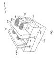
- FIG. 1depicts one example of a starting semiconductor structure including raised structures for both n-type and p-type devices with gate openings thereover, in accordance with one or more aspects of the present invention.
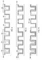
- FIG. 2depicts one example of the gate openings of the structure of FIG. 1 after creation of a multi-layer liner and an anneal thereof, in accordance with one or more aspects of the present invention.
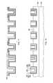
- FIG. 3depicts one example of the gate openings of FIG. 2 repeated three times, i.e., three gate openings for p-type devices (on the left) and three gate openings for n-type devices (on the right), in accordance with one or more aspects of the present invention.
- FIG. 4depicts one example of the gate openings of FIG. 3 after implanting one of the n-type device gate openings with a n-type threshold voltage decrease material, in accordance with one or more aspects of the present invention.
- FIG. 5depicts one example of the gate openings of FIG. 4 after creation of a first layer of p-type work function metal in all gate openings, in accordance with one or more aspects of the present invention.
- FIG. 6depicts one example of the gate openings of FIG. 5 after removal of the first layer of p-type work function metal over all the n-type device gate openings and one of the p-type device gate openings, in accordance with one or more aspects of the present invention.
- FIG. 7depicts one example of the gate openings of FIG. 6 after creation of a blanket layer of additional p-type work function metal, in accordance with one or more aspects of the present invention.
- FIG. 8depicts one example of the gate openings of FIG. 7 after removing the additional layer of p-type work function metal over two of the n-type device gate openings, in accordance with one or more aspects of the present invention.
- FIG. 9depicts one example of the gate openings of FIG. 8 after oxidizing one of the p-type device gate openings while masking the rest of the devices, in accordance with one or more aspects of the present invention.
- FIG. 10depicts one example of the gate openings of FIG. 9 after creating a diffusion barrier layer over all the gate openings, in accordance with one or more aspects of the present invention.
- FIG. 11depicts one example of the gate openings of FIG. 10 after creating a blanket layer of n-type work function metal, in accordance with one or more aspects of the present invention.
- FIG. 12depicts one example of the gate openings of FIG. 11 after filling the remaining space in the gate openings with a conductive material, in accordance with one or more aspects of the present invention.
- Approximating languagemay be applied to modify any quantitative representation that could permissibly vary without resulting in a change in the basic function to which it is related. Accordingly, a value modified by a term or terms, such as “about,” is not limited to the precise value specified. In some instances, the approximating language may correspond to the precision of an instrument for measuring the value.
- a method or device that “comprises,” “has,” “includes” or “contains” one or more steps or elementspossesses those one or more steps or elements, but is not limited to possessing only those one or more steps or elements.
- a step of a method or an element of a device that “comprises,” “has,” “includes” or “contains” one or more featurespossesses those one or more features, but is not limited to possessing only those one or more features.
- a device or structure that is configured in a certain wayis configured in at least that way, but may also be configured in ways that are not listed.
- connectionwhen used to refer to two physical elements, means a direct connection between the two physical elements.
- coupledcan mean a direct connection or a connection through one or more intermediary elements.
- the terms “may” and “may be”indicate a possibility of an occurrence within a set of circumstances; a possession of a specified property, characteristic or function; and/or qualify another verb by expressing one or more of an ability, capability, or possibility associated with the qualified verb. Accordingly, usage of “may” and “may be” indicates that a modified term is apparently appropriate, capable, or suitable for an indicated capacity, function, or usage, while taking into account that in some circumstances the modified term may sometimes not be appropriate, capable or suitable. For example, in some circumstances, an event or capacity can be expected, while in other circumstances the event or capacity cannot occur—this distinction is captured by the terms “may” and “may be.”
- FIG. 1depicts one example of a starting semiconductor structure 100 , the structure including a substrate 102 and raised structures 104 coupled to the substrate, for both n-type 106 and p-type 108 devices, the raised structures surrounded by a layer 109 of an isolation material, and having gate openings 110 and 112 , respectively, thereover, in accordance with one or more aspects of the present invention.
- the starting structuremay be conventionally fabricated, for example, using known processes and techniques. However, it will be understood that the fabrication of the starting structure forms no part of the present invention. Further, although only a portion is shown for simplicity, it will be understood that, in practice, many such structures are typically included on the same bulk substrate.
- substrate 102may include any silicon-containing substrate including, but not limited to, silicon (Si), single crystal silicon, polycrystalline Si, amorphous Si, silicon-on-nothing (SON), silicon-on-insulator (SOI) or silicon-on-replacement insulator (SRI) or silicon germanium substrates and the like.
- substrate 102may in addition or instead include various isolations, dopings and/or device features.
- the substratemay include other suitable elementary semiconductors, such as, for example, germanium (Ge) in crystal, a compound semiconductor, such as silicon carbide (SiC), gallium arsenide (GaAs), gallium phosphide (GaP), indium phosphide (InP), indium arsenide (InAs), and/or indium antimonide (InSb) or combinations thereof; an alloy semiconductor including GaAsP, AlInAs, GaInAs, GaInP, or GaInAsP or combinations thereof.
- germaniumgermanium
- SiCsilicon carbide
- GaAsgallium arsenide
- GaPgallium phosphide
- InPindium phosphide
- InAsindium arsenide
- InSbindium antimonide
- the raised structures 104may take the form of a “fin.”
- the raised structuresmay be etched from a bulk substrate, and may include, for example, any of the materials listed above with respect to the substrate. Further, some or all of the raised structures may include added impurities (e.g., by doping), making them n-type or p-type.
- the raised structuresmay have epitaxial structures 111 and 113 thereon, for example, silicon germanium for p-type devices and phosphorous-doped silicon for n-type devices.
- the gate openings 110 and 112may be defined by spacers 114 and 116 .
- FIG. 2depicts one example of the gate openings 110 and 112 of the structure of FIG. 1 after creation of a multi-layer liner 118 and anneal thereof, in accordance with one or more aspects of the present invention.
- the multi-layer liner 118includes a bottom layer 120 of a dielectric material or interlayer oxide.
- the dielectric materialis preferably a “high-k” dielectric (i.e., dielectric constant of more than 3.9), and may have a thickness of, for example, about 5 Angstroms to about 25 Angstroms, while the interlayer oxide may have a thickness of, for example, about 5 Angstroms to about 10 Angstroms.
- the multi-layer lineralso includes a layer 122 of a p-type work function metal (e.g., titanium nitride (TiN)). Where TiN is used, layer 122 may have a thickness of, for example, about 5 Angstroms to about 15 Angstroms.
- the multi-layer linerfurther includes an etch stop layer 124 , the etch stop function coming into use later in fabrication.
- the etch stop layermay include, for example, tantalum nitride (TaN) and may have a thickness of, for example, about 5 Angstroms to about 25 Angstroms.
- the multi-layer linermay include a layer 128 of amorphous silicon or polysilicon having a thickness of, for example, about 10 Angstroms to about 100 Angstroms.
- the lineris annealed, for example, at a temperature of about 900° C. to about 1000° C. for about 1 millisecond to about 30 seconds.
- FIG. 3depicts one example of the gate openings of FIG. 2 repeated three times, i.e., three gate openings for p-type devices (on the left) 128 , 130 and 132 and three gate openings for n-type devices (on the right) 134 , 136 and 138 , in accordance with one or more aspects of the present invention.
- the multiple gate openingsall include multi-layer liner 118 , and the fabrication process described below will give a range of threshold voltages Vt for each of the p-type device group and the n-type device group. In particular, going from left to right in FIG.
- the p-type devices corresponding to gate openings 128 , 130 and 132will have a lowest Vt (e.g., about 0.05V to about 0.15V), a low Vt (e.g., above about 0.15V to about 0.25V) and a regular Vt (e.g., above about 0.25V to about 0.35V), respectively.
- the n-type devices corresponding to gate openings 134 , 136 and 138will have a lowest Vt (e.g., about 0.05V to about 0.15V), a low Vt (e.g., above about 0.15V to about 0.25V) and a regular Vt (e.g., above about 0.25V to about 0.35V), respectively.
- FIG. 4depicts one example of the gate openings of FIG. 3 after implanting 140 one of the n-type device gate openings 134 with a n-type threshold voltage decrease material, while protecting the remainder of the gate openings, in accordance with one or more aspects of the present invention.
- the n-type threshold voltage decrease materialmay include, for example, arsenic (As), argon (Ar), silicon (Si) or germanium (Ge).
- the implantis implemented with about 1 KeV to about 5 KeV and about 1 e 15 /cm 2 to about 6 e 15 /cm 2 .
- the remaining gate openingsmay be protected with, for example, a layer 142 of lithographic blocking material.
- the protective layermay be blanketly deposited over the gate openings, and etched over gate opening 134 using, for example, a conventional lithography process.
- FIG. 5depicts one example of the gate openings of FIG. 4 after removal of layer 126 and creation of a first layer 144 of p-type work function metal in all gate openings, in accordance with one or more aspects of the present invention.
- Layer 126 of amorphous silicon or polysiliconmay be removed by, for example, wet etching using tetramethylammonium hydroxide (TMAH), dry etching using hydrogen bromide (HBr), or a combination of both wet and dry etching.
- TMAHtetramethylammonium hydroxide
- HBrhydrogen bromide
- the layer 144 of p-type work function metale.g., TiN
- the layer of work function metalmay have a thickness of, for example, about 20 Angstroms to about 70 Angstroms.
- FIG. 6depicts one example of the gate openings of FIG. 5 after removal of the first layer of p-type work function metal over all the n-type device gate openings 134 , 136 and 138 , and one of the p-type device gate openings 132 intended to have the regular threshold voltage of the p-type devices, while protecting the other p-type gate openings, in accordance with one or more aspects of the present invention.
- the p-type work function metal layer 144may be removed over gate openings 132 , 134 , 136 and 138 by, for example, dry etching using one or more of sulfur hexafluoride (SF 6 ), tetrafluoromethane (CF 4 ), boron trichloride (BCl 3 ) and/or chlorine gas (Cl 2 ).
- SF 6sulfur hexafluoride
- CF 4tetrafluoromethane
- BCl 3boron trichloride
- chlorine gasCl 2
- protection of gate openings 128 and 130may be accomplished with a layer 146 of a lithographic blocking material.
- FIG. 7depicts one example of the gate openings of FIG. 6 after creation of a blanket layer 148 of additional p-type work function metal (e.g., TiN), in accordance with one or more aspects of the present invention.
- additional p-type work function metale.g., TiN
- the additional layermay be created using, for example, ALD or CVD, and the additional layer may have a thickness of, for example, about 5 Angstroms to about 30 Angstroms.
- FIG. 8depicts one example of the gate openings of FIG. 7 after removing the additional layer of p-type work function metal over two of the n-type device gate openings 134 and 136 , the corresponding n-type devices intended to have a lowest n-type Vt and a low n-type Vt, respectively, while protecting the remaining gate openings, in accordance with one or more aspects of the present invention.
- the p-type work function metal layer 144may be removed over gate openings 134 and 136 by, for example, dry etching with one or more of SF 6 , CF 4 , BCl 3 , and/or Cl 2 .
- protection of gate openings 128 , 130 , 132 and 138may be accomplished with a layer 150 of a lithographic blocking material.
- FIG. 9depicts one example of the gate openings of FIG. 8 after oxidizing one of the p-type device gate openings 128 , the corresponding p-type device intended to have a lowest p-type Vt, while masking the rest of the devices, in accordance with one or more aspects of the present invention.
- the oxidizingmay be accomplished, for example, with an oxygen gas (O 2 ) flow at a temperature of about 300° C. to about 500° C.
- O 2oxygen gas
- masking of the remaining gate openingsmay be accomplished using a hard mask 152 , e.g., silicon nitride (SiN).
- the maskmay be created, for example, by blanket deposition of SiN, followed by etching the mask above gate opening 128 , for example, wet etching using TMAH, dry etching using HBr, or a combination of both wet and dry etching.
- FIG. 10depicts one example of the gate openings of FIG. 9 after creating a diffusion barrier layer 154 over all the gate openings, in accordance with one or more aspects of the present invention.
- the remaining p-type work function metalis chamfered, and any gate opening that is chamfered for the p-type work function metal is also chamfered for the diffusion barrier layer.
- the diffusion barrier layermay include, for example, TaN, may be created by, for example, ALD or CVD, and may have a thickness of, for example, about 5 Angstroms to about 25 Angstroms.
- the diffusion barrier layeris intended to prevent diffusion of a subsequent n-type work function metal, described with respect to FIG. 11 .
- FIG. 11depicts one example of the gate openings of FIG. 10 after creating a blanket layer 156 of n-type work function metal, in accordance with one or more aspects of the present invention.
- the n-type work function metal layermay include, for example, titanium aluminum (TiAl), may be created by, for example, ALD or CVD, and may have a thickness of, for example, about 20 Angstroms to about 70 Angstroms.
- the n-type work function metal layeris chamfered.
- FIG. 12depicts one example of the gate openings of FIG. 11 after filling the remaining space in the gate openings with a conductive material 158 and planarizing, in accordance with one or more aspects of the present invention.
- the conductive materialmay be, for example, a metal, e.g., tungsten (W), and may be created using, for example, ALD or CVD.
- the planarizingis accomplished using chemical-mechanical polishing (CMP).
- the methodincludes providing a starting non-planar semiconductor structure, the starting structure including at least one non-planar p-type device in process and at least one non-planar n-type device in process, and each device including a gate opening.
- the methodfurther includes lining the gate openings with a multi-layer liner, the multi-layer liner including a bottom dielectric layer, a first layer of p-type work function metal over the dielectric layer and an etch stop layer over the first layer of p-type work function metal.
- the methodfurther includes annealing the multi-layer liner, creating a layer of n-type work function metal over the multi-layer liner, and filling a remaining open area of the gate openings with at least one conductive material.
- the multi-layer liner of the first aspectmay further include a layer of amorphous silicon over the etch stop layer.
- the methodmay include, after the lining and prior to creating the layer of n-type work function metal, implanting the multi-layer liner of the n-type device gate opening(s) with a n-type threshold voltage decrease material, and removing the layer of amorphous silicon. Prior to the implanting, the method may include creating a layer of lithographic blocking material over all the devices except for the n-type device gate opening(s). Implanting is also performed for the p-type device gate opening(s). Creating the second layer of p-type work function metal may include creating the second layer of p-type work function metal over only the p-type device gate opening(s).
- the method of the first aspectmay include creating a third layer of p-type work function metal over all the gate openings, oxidizing the third layer of p-type work function metal, and, prior to creating the second diffusion barrier layer, oxidizing the second and first layers of p-type work function metal over the p-type device(s) and corresponding gate opening(s).
- the method of the first aspectmay include, prior to the oxidizing, creating a hard mask over all the devices except the p-type device gate opening(s).
- the method of the first aspectmay include creating a layer of n-type work function metal over the second diffusion barrier layer.
- the methodmay include filling a remaining open area of the gate openings with a conductive material, and planarizing the filled gate openings.
- lining the gate openings in the method of the first aspectmay include creating a first additional layer of p-type work function metal over the etch stop layer for the p-type device(s), lining the gate openings may include creating a second additional layer of p-type work function metal over the first additional layer for the p-type device(s), and lining the gate openings may include oxidizing the first and second additional p-type work function metal layers for the p-type device(s).
- lining the gate openings in the method of the first aspectmay include implanting the etch stop layer with one of arsenic, argon, silicon and germanium, and creating a diffusion barrier layer over the etch stop layer for one or more of the at least one n-type device.
- lining the gate openings in the method of the first aspectmay include creating an additional layer of p-type work function metal over the etch stop layer for the n-type device(s).
- lining the gate openings in the method of the first aspectmay include creating a diffusion barrier layer over the etch stop layer.
- a gate structure for a non-planar semiconductor deviceincludes a high-k dielectric layer lining inner surfaces of a gate opening of a non-planar semiconductor device, a first layer of p-type work function metal over the high-k dielectric layer, an etch stop layer over the first layer of p-type work function metal, a layer of n-type work function metal over the layer of barrier material, and a layer of conductive material over the layer of n-type work function metal, the conductive layer filling a remaining open space of the gate opening.
- the gate opening of the gate structure of the second aspectmay include a gate opening of a p-type non-planar semiconductor device, the gate structure further including a diffusion barrier layer and at least one second layer of p-type work function metal between the diffusion barrier layer and the second layer of p-type work function metal. Additionally, the second layer of p-type work function metal may be oxidized.
- the gate opening of the gate structure of the second aspectmay further include a gate opening of a n-type non-planar semiconductor device, the gate structure also being present in the n-type device gate opening.
- the gate opening of the gate structure of the second aspectmay include a gate opening of a n-type non-planar semiconductor device, the barrier layer including a first barrier layer and a second barrier layer, and the gate structure further including a second layer of p-type work function metal between the first and second barrier layers.
- the gate opening of the gate structure of the second aspectmay include a gate opening of a n-type non-planar semiconductor device, and a lower portion of the barrier layer may be implanted with a material that lowers n-type threshold voltage, for example, one of arsenic, argon, silicon and germanium.
Landscapes
- Engineering & Computer Science (AREA)
- Physics & Mathematics (AREA)
- Microelectronics & Electronic Packaging (AREA)
- Condensed Matter Physics & Semiconductors (AREA)
- General Physics & Mathematics (AREA)
- Manufacturing & Machinery (AREA)
- Computer Hardware Design (AREA)
- Power Engineering (AREA)
- High Energy & Nuclear Physics (AREA)
- Toxicology (AREA)
- Health & Medical Sciences (AREA)
- Electrodes Of Semiconductors (AREA)
- Insulated Gate Type Field-Effect Transistor (AREA)
Abstract
Description
Claims (13)
Priority Applications (2)
| Application Number | Priority Date | Filing Date | Title |
|---|---|---|---|
| US14/315,885US9209186B1 (en) | 2014-06-26 | 2014-06-26 | Threshold voltage control for mixed-type non-planar semiconductor devices |
| US14/924,486US9362284B2 (en) | 2014-06-26 | 2015-10-27 | Threshold voltage control for mixed-type non-planar semiconductor devices |
Applications Claiming Priority (1)
| Application Number | Priority Date | Filing Date | Title |
|---|---|---|---|
| US14/315,885US9209186B1 (en) | 2014-06-26 | 2014-06-26 | Threshold voltage control for mixed-type non-planar semiconductor devices |
Related Child Applications (1)
| Application Number | Title | Priority Date | Filing Date |
|---|---|---|---|
| US14/924,486DivisionUS9362284B2 (en) | 2014-06-26 | 2015-10-27 | Threshold voltage control for mixed-type non-planar semiconductor devices |
Publications (2)
| Publication Number | Publication Date |
|---|---|
| US9209186B1true US9209186B1 (en) | 2015-12-08 |
| US20150380409A1 US20150380409A1 (en) | 2015-12-31 |
Family
ID=54708386
Family Applications (2)
| Application Number | Title | Priority Date | Filing Date |
|---|---|---|---|
| US14/315,885ActiveUS9209186B1 (en) | 2014-06-26 | 2014-06-26 | Threshold voltage control for mixed-type non-planar semiconductor devices |
| US14/924,486ActiveUS9362284B2 (en) | 2014-06-26 | 2015-10-27 | Threshold voltage control for mixed-type non-planar semiconductor devices |
Family Applications After (1)
| Application Number | Title | Priority Date | Filing Date |
|---|---|---|---|
| US14/924,486ActiveUS9362284B2 (en) | 2014-06-26 | 2015-10-27 | Threshold voltage control for mixed-type non-planar semiconductor devices |
Country Status (1)
| Country | Link |
|---|---|
| US (2) | US9209186B1 (en) |
Cited By (10)
| Publication number | Priority date | Publication date | Assignee | Title |
|---|---|---|---|---|
| US20160049400A1 (en)* | 2014-06-26 | 2016-02-18 | Globalfoundries Inc. | Threshold voltage control for mixed-type non-planar semiconductor devices |
| US20160093535A1 (en)* | 2014-09-26 | 2016-03-31 | Qualcomm Incorporated | Method and apparatus of multi threshold voltage cmos |
| US9443771B1 (en)* | 2015-11-09 | 2016-09-13 | Globalfoundries Inc. | Methods to thin down RMG sidewall layers for scalability of gate-last planar CMOS and FinFET technology |
| US20170221898A1 (en)* | 2015-08-17 | 2017-08-03 | International Business Machines Corporation | High-k gate dielectric and metal gate conductor stack for fin-type field effect transistors formed on type iii-v semiconductor material and silicon germanium semiconductor material |
| US10276575B2 (en)* | 2015-07-31 | 2019-04-30 | Taiwan Semiconductor Manufacturing Company, Ltd. | Multi-threshold voltage field effect transistor and manufacturing method thereof |
| US10431583B2 (en) | 2016-02-11 | 2019-10-01 | Samsung Electronics Co., Ltd. | Semiconductor device including transistors with adjusted threshold voltages |
| US10553693B2 (en) | 2017-10-27 | 2020-02-04 | Samsung Electronics Co., Ltd. | Semiconductor device |
| US20200058753A1 (en)* | 2017-12-04 | 2020-02-20 | International Business Machines Corporation | Vertical transport fets having a gradient threshold voltage |
| US11264288B2 (en)* | 2018-09-28 | 2022-03-01 | Taiwan Semiconductor Manufacturing Co., Ltd. | Gate structure and patterning method |
| US11342445B2 (en)* | 2017-11-30 | 2022-05-24 | Intel Corporation | Differentiated voltage threshold metal gate structures for advanced integrated circuit structure fabrication |
Families Citing this family (13)
| Publication number | Priority date | Publication date | Assignee | Title |
|---|---|---|---|---|
| US9704969B1 (en)* | 2015-12-31 | 2017-07-11 | Taiwan Semiconductor Manufacturing Co., Ltd. | Fin semiconductor device having multiple gate width structures |
| CN107958872B (en)* | 2016-10-17 | 2020-09-08 | 中芯国际集成电路制造(上海)有限公司 | Semiconductor device and method of forming the same |
| US11121131B2 (en) | 2017-06-23 | 2021-09-14 | Samsung Electronics Co., Ltd. | Semiconductor device and method of manufacturing the same |
| KR102293127B1 (en) | 2017-06-23 | 2021-08-26 | 삼성전자주식회사 | Semiconductor device and method for manufacturing the same |
| CN109285810A (en)* | 2017-07-20 | 2019-01-29 | 中芯国际集成电路制造(上海)有限公司 | A semiconductor device and its manufacturing method and electronic device |
| US10367078B2 (en)* | 2017-11-09 | 2019-07-30 | Taiwan Semiconductor Manufacturing Co., Ltd. | Semiconductor devices and FinFET devices having shielding layers |
| KR102481284B1 (en) | 2018-04-10 | 2022-12-27 | 삼성전자주식회사 | A method of manufacturing semiconductor device |
| US10515807B1 (en)* | 2018-06-14 | 2019-12-24 | Taiwan Semiconductor Manufacturing Co., Ltd. | Methods of fabricating semiconductor devices with metal-gate work-function tuning layers |
| JP7195106B2 (en)* | 2018-10-12 | 2022-12-23 | 東京エレクトロン株式会社 | Film forming method and substrate processing system |
| KR102571567B1 (en) | 2018-11-02 | 2023-08-29 | 삼성전자주식회사 | Semiconductor device |
| US11264289B2 (en)* | 2019-07-11 | 2022-03-01 | Tokyo Electron Limited | Method for threshold voltage tuning through selective deposition of high-K metal gate (HKMG) film stacks |
| KR102839927B1 (en) | 2019-09-17 | 2025-07-30 | 삼성전자주식회사 | Semiconductor device |
| US11417653B2 (en)* | 2019-09-30 | 2022-08-16 | Taiwan Semiconductor Manufacturing Company Ltd. | Semiconductor structure and method for forming the same |
Citations (15)
| Publication number | Priority date | Publication date | Assignee | Title |
|---|---|---|---|---|
| US20110284966A1 (en)* | 2010-05-19 | 2011-11-24 | Taiwan Semiconductor Manufacturing Company, Ltd. | Structure and Method for Alignment Marks |
| US20120146159A1 (en)* | 2010-11-30 | 2012-06-14 | Taiwan Semiconductor Manufacturing Company, Ltd. | Structure and method for overlay marks |
| US20130037886A1 (en)* | 2011-08-10 | 2013-02-14 | Teng-Chun Tsai | Semiconductor device and method of making the same |
| US20130200470A1 (en)* | 2012-02-07 | 2013-08-08 | An-Chi Liu | Semiconductor structure and method of fabricating the same |
| US20130249010A1 (en)* | 2012-03-20 | 2013-09-26 | Taiwan Semiconductor Manufacturing Company, Ltd., ("Tsmc") | Metal gate semiconductor device |
| US20140070320A1 (en)* | 2012-09-07 | 2014-03-13 | Srijit Mukherjee | Integrated circuits with selective gate electrode recess |
| US20140183652A1 (en)* | 2012-12-28 | 2014-07-03 | Taiwan Semiconductor Manufacturing Company, Ltd. | Dummy metal gate structures to reduce dishing during chemical-mechanical polishing |
| US20140349452A1 (en)* | 2013-05-22 | 2014-11-27 | United Microelectronics Corp. | Method for manufacturing semiconductor devices |
| US20150021672A1 (en)* | 2011-09-15 | 2015-01-22 | Taiwan Semiconductor Manufacturing Company, Ltd. | Contact for high-k metal gate device |
| US20150041855A1 (en)* | 2013-08-07 | 2015-02-12 | United Microelectronics Corp. | Semiconductor device |
| US20150069473A1 (en)* | 2013-09-06 | 2015-03-12 | Glenn A. Glass | Transistor fabrication technique including sacrificial protective layer for source/drain at contact location |
| US20150076624A1 (en)* | 2013-09-19 | 2015-03-19 | GlobalFoundries, Inc. | Integrated circuits having smooth metal gates and methods for fabricating same |
| US20150214319A1 (en)* | 2014-01-28 | 2015-07-30 | Taiwan Semiconductor Manufacturing Company Ltd. | Metal gate and manufacturing process thereof |
| US20150228647A1 (en)* | 2014-02-07 | 2015-08-13 | Taiwan Semiconductor Manufacturing Company Ltd. | Indented gate end of non-planar transistor |
| US20150228793A1 (en)* | 2014-02-07 | 2015-08-13 | Taiwan Semiconductor Manufacturing Company Ltd. | Semiconductor structure and manufacturing method thereof |
Family Cites Families (6)
| Publication number | Priority date | Publication date | Assignee | Title |
|---|---|---|---|---|
| US9166020B2 (en)* | 2011-03-01 | 2015-10-20 | United Microelectronics Corp. | Metal gate structure and manufacturing method thereof |
| US8580641B2 (en)* | 2011-07-26 | 2013-11-12 | Taiwan Semiconductor Manufacturing Company, Ltd. | Techniques providing high-k dielectric metal gate CMOS |
| US8847333B2 (en)* | 2011-09-01 | 2014-09-30 | Taiwan Semiconductor Manufacturing Company, Ltd. | Techniques providing metal gate devices with multiple barrier layers |
| US20150021681A1 (en)* | 2013-07-16 | 2015-01-22 | United Microelectronics Corp. | Semiconductor device having metal gate and manufacturing method thereof |
| US9698019B2 (en)* | 2014-03-14 | 2017-07-04 | Taiwan Semiconductor Manufacturing Company, Ltd. | N-work function metal with crystal structure |
| US9209186B1 (en)* | 2014-06-26 | 2015-12-08 | Globalfoundries Inc. | Threshold voltage control for mixed-type non-planar semiconductor devices |
- 2014
- 2014-06-26USUS14/315,885patent/US9209186B1/enactiveActive
- 2015
- 2015-10-27USUS14/924,486patent/US9362284B2/enactiveActive
Patent Citations (15)
| Publication number | Priority date | Publication date | Assignee | Title |
|---|---|---|---|---|
| US20110284966A1 (en)* | 2010-05-19 | 2011-11-24 | Taiwan Semiconductor Manufacturing Company, Ltd. | Structure and Method for Alignment Marks |
| US20120146159A1 (en)* | 2010-11-30 | 2012-06-14 | Taiwan Semiconductor Manufacturing Company, Ltd. | Structure and method for overlay marks |
| US20130037886A1 (en)* | 2011-08-10 | 2013-02-14 | Teng-Chun Tsai | Semiconductor device and method of making the same |
| US20150021672A1 (en)* | 2011-09-15 | 2015-01-22 | Taiwan Semiconductor Manufacturing Company, Ltd. | Contact for high-k metal gate device |
| US20130200470A1 (en)* | 2012-02-07 | 2013-08-08 | An-Chi Liu | Semiconductor structure and method of fabricating the same |
| US20130249010A1 (en)* | 2012-03-20 | 2013-09-26 | Taiwan Semiconductor Manufacturing Company, Ltd., ("Tsmc") | Metal gate semiconductor device |
| US20140070320A1 (en)* | 2012-09-07 | 2014-03-13 | Srijit Mukherjee | Integrated circuits with selective gate electrode recess |
| US20140183652A1 (en)* | 2012-12-28 | 2014-07-03 | Taiwan Semiconductor Manufacturing Company, Ltd. | Dummy metal gate structures to reduce dishing during chemical-mechanical polishing |
| US20140349452A1 (en)* | 2013-05-22 | 2014-11-27 | United Microelectronics Corp. | Method for manufacturing semiconductor devices |
| US20150041855A1 (en)* | 2013-08-07 | 2015-02-12 | United Microelectronics Corp. | Semiconductor device |
| US20150069473A1 (en)* | 2013-09-06 | 2015-03-12 | Glenn A. Glass | Transistor fabrication technique including sacrificial protective layer for source/drain at contact location |
| US20150076624A1 (en)* | 2013-09-19 | 2015-03-19 | GlobalFoundries, Inc. | Integrated circuits having smooth metal gates and methods for fabricating same |
| US20150214319A1 (en)* | 2014-01-28 | 2015-07-30 | Taiwan Semiconductor Manufacturing Company Ltd. | Metal gate and manufacturing process thereof |
| US20150228647A1 (en)* | 2014-02-07 | 2015-08-13 | Taiwan Semiconductor Manufacturing Company Ltd. | Indented gate end of non-planar transistor |
| US20150228793A1 (en)* | 2014-02-07 | 2015-08-13 | Taiwan Semiconductor Manufacturing Company Ltd. | Semiconductor structure and manufacturing method thereof |
Cited By (20)
| Publication number | Priority date | Publication date | Assignee | Title |
|---|---|---|---|---|
| US9362284B2 (en)* | 2014-06-26 | 2016-06-07 | Globalfoundries Inc. | Threshold voltage control for mixed-type non-planar semiconductor devices |
| US20160049400A1 (en)* | 2014-06-26 | 2016-02-18 | Globalfoundries Inc. | Threshold voltage control for mixed-type non-planar semiconductor devices |
| US10497625B2 (en) | 2014-09-26 | 2019-12-03 | Qualcomm Incorporated | Method and apparatus of multi threshold voltage CMOS |
| US20160093535A1 (en)* | 2014-09-26 | 2016-03-31 | Qualcomm Incorporated | Method and apparatus of multi threshold voltage cmos |
| US9922880B2 (en)* | 2014-09-26 | 2018-03-20 | Qualcomm Incorporated | Method and apparatus of multi threshold voltage CMOS |
| US10276575B2 (en)* | 2015-07-31 | 2019-04-30 | Taiwan Semiconductor Manufacturing Company, Ltd. | Multi-threshold voltage field effect transistor and manufacturing method thereof |
| US20170221898A1 (en)* | 2015-08-17 | 2017-08-03 | International Business Machines Corporation | High-k gate dielectric and metal gate conductor stack for fin-type field effect transistors formed on type iii-v semiconductor material and silicon germanium semiconductor material |
| US9859279B2 (en) | 2015-08-17 | 2018-01-02 | International Business Machines Corporation | High-k gate dielectric and metal gate conductor stack for fin-type field effect transistors formed on type III-V semiconductor material and silicon germanium semiconductor material |
| US10002871B2 (en)* | 2015-08-17 | 2018-06-19 | International Business Machines Corporation | High-K gate dielectric and metal gate conductor stack for fin-type field effect transistors formed on type III-V semiconductor material and silicon germanium semiconductor material |
| US10262999B2 (en) | 2015-08-17 | 2019-04-16 | International Business Machines Corporation | High-k gate dielectric and metal gate conductor stack for fin-type field effect transistors formed on type III-V semiconductor material and silicon germanium semiconductor material |
| US9443771B1 (en)* | 2015-11-09 | 2016-09-13 | Globalfoundries Inc. | Methods to thin down RMG sidewall layers for scalability of gate-last planar CMOS and FinFET technology |
| US10431583B2 (en) | 2016-02-11 | 2019-10-01 | Samsung Electronics Co., Ltd. | Semiconductor device including transistors with adjusted threshold voltages |
| US10553693B2 (en) | 2017-10-27 | 2020-02-04 | Samsung Electronics Co., Ltd. | Semiconductor device |
| US11342445B2 (en)* | 2017-11-30 | 2022-05-24 | Intel Corporation | Differentiated voltage threshold metal gate structures for advanced integrated circuit structure fabrication |
| US20200058753A1 (en)* | 2017-12-04 | 2020-02-20 | International Business Machines Corporation | Vertical transport fets having a gradient threshold voltage |
| US10937883B2 (en)* | 2017-12-04 | 2021-03-02 | Elpis Technologies Inc. | Vertical transport FETs having a gradient threshold voltage |
| US11264288B2 (en)* | 2018-09-28 | 2022-03-01 | Taiwan Semiconductor Manufacturing Co., Ltd. | Gate structure and patterning method |
| US20220181218A1 (en)* | 2018-09-28 | 2022-06-09 | Taiwan Semiconductor Manufacturing Co., Ltd. | Gate structure and patterning method |
| US11942377B2 (en)* | 2018-09-28 | 2024-03-26 | Taiwan Semiconductor Manufacturing Co., Ltd. | Gate structure and patterning method |
| US20240234214A1 (en)* | 2018-09-28 | 2024-07-11 | Taiwan Semiconductor Manufacturing Co., Ltd. | Gate structure and patterning method |
Also Published As
| Publication number | Publication date |
|---|---|
| US20160049400A1 (en) | 2016-02-18 |
| US9362284B2 (en) | 2016-06-07 |
| US20150380409A1 (en) | 2015-12-31 |
Similar Documents
| Publication | Publication Date | Title |
|---|---|---|
| US9362284B2 (en) | Threshold voltage control for mixed-type non-planar semiconductor devices | |
| US10515859B2 (en) | Extra gate device for nanosheet | |
| US20150179640A1 (en) | Common fabrication of different semiconductor devices with different threshold voltages | |
| US10199480B2 (en) | Controlling self-aligned gate length in vertical transistor replacement gate flow | |
| US8912057B1 (en) | Fabrication of nickel free silicide for semiconductor contact metallization | |
| US9653573B2 (en) | Replacement metal gate including dielectric gate material | |
| US10586709B2 (en) | Methods of fabricating semiconductor devices | |
| US9685537B1 (en) | Gate length control for vertical transistors and integration with replacement gate flow | |
| US10002932B2 (en) | Self-aligned contact protection using reinforced gate cap and spacer portions | |
| US9478625B1 (en) | Metal resistor using FinFET-based replacement gate process | |
| US9666709B2 (en) | Non-planar semiconductor structure with preserved isolation region | |
| US9552992B2 (en) | Co-fabrication of non-planar semiconductor devices having different threshold voltages | |
| US8877580B1 (en) | Reduction of oxide recesses for gate height control | |
| US10290634B2 (en) | Multiple threshold voltages using fin pitch and profile | |
| US20160049488A1 (en) | Semiconductor gate with wide top or bottom | |
| US8889540B2 (en) | Stress memorization in RMG FinFets | |
| US20160049401A1 (en) | Hybrid contacts for commonly fabricated semiconductor devices using same metal | |
| US9634005B2 (en) | Gate planarity for FinFET using dummy polish stop | |
| US20230027413A1 (en) | Recovering Top Spacer Width of Nanosheet Device | |
| US9425100B1 (en) | Methods of facilitating fabricating transistors | |
| US10446399B2 (en) | Hard mask layer to reduce loss of isolation material during dummy gate removal | |
| US9362279B1 (en) | Contact formation for semiconductor device | |
| US20160111514A1 (en) | Ultra-low resistance gate structure for non-planar device via minimized work function material | |
| US20170207118A1 (en) | Self-aligned source/drain contact in replacement metal gate process |
Legal Events
| Date | Code | Title | Description |
|---|---|---|---|
| AS | Assignment | Owner name:GLOBALFOUNDRIES INC., CAYMAN ISLANDS Free format text:ASSIGNMENT OF ASSIGNORS INTEREST;ASSIGNORS:TOGO, MITSUHIRO;XIAO, CHANGYONG;LIU, YIQUN;AND OTHERS;SIGNING DATES FROM 20140620 TO 20140623;REEL/FRAME:033187/0214 | |
| STCF | Information on status: patent grant | Free format text:PATENTED CASE | |
| AS | Assignment | Owner name:WILMINGTON TRUST, NATIONAL ASSOCIATION, DELAWARE Free format text:SECURITY AGREEMENT;ASSIGNOR:GLOBALFOUNDRIES INC.;REEL/FRAME:049490/0001 Effective date:20181127 | |
| MAFP | Maintenance fee payment | Free format text:PAYMENT OF MAINTENANCE FEE, 4TH YEAR, LARGE ENTITY (ORIGINAL EVENT CODE: M1551); ENTITY STATUS OF PATENT OWNER: LARGE ENTITY Year of fee payment:4 | |
| AS | Assignment | Owner name:GLOBALFOUNDRIES U.S. INC., CALIFORNIA Free format text:ASSIGNMENT OF ASSIGNORS INTEREST;ASSIGNOR:GLOBALFOUNDRIES INC.;REEL/FRAME:054633/0001 Effective date:20201022 | |
| AS | Assignment | Owner name:GLOBALFOUNDRIES INC., CAYMAN ISLANDS Free format text:RELEASE BY SECURED PARTY;ASSIGNOR:WILMINGTON TRUST, NATIONAL ASSOCIATION;REEL/FRAME:054636/0001 Effective date:20201117 | |
| AS | Assignment | Owner name:GLOBALFOUNDRIES U.S. INC., NEW YORK Free format text:RELEASE BY SECURED PARTY;ASSIGNOR:WILMINGTON TRUST, NATIONAL ASSOCIATION;REEL/FRAME:056987/0001 Effective date:20201117 | |
| MAFP | Maintenance fee payment | Free format text:PAYMENT OF MAINTENANCE FEE, 8TH YEAR, LARGE ENTITY (ORIGINAL EVENT CODE: M1552); ENTITY STATUS OF PATENT OWNER: LARGE ENTITY Year of fee payment:8 |