US9209074B2 - Cobalt deposition on barrier surfaces - Google Patents
Cobalt deposition on barrier surfacesDownload PDFInfo
- Publication number
- US9209074B2 US9209074B2US14/717,375US201514717375AUS9209074B2US 9209074 B2US9209074 B2US 9209074B2US 201514717375 AUS201514717375 AUS 201514717375AUS 9209074 B2US9209074 B2US 9209074B2
- Authority
- US
- United States
- Prior art keywords
- layer
- cobalt
- substrate
- vapor deposition
- barrier layer
- Prior art date
- Legal status (The legal status is an assumption and is not a legal conclusion. Google has not performed a legal analysis and makes no representation as to the accuracy of the status listed.)
- Expired - Fee Related
Links
- 229910017052cobaltInorganic materials0.000titleclaimsabstractdescription162
- 239000010941cobaltSubstances0.000titleclaimsabstractdescription162
- GUTLYIVDDKVIGB-UHFFFAOYSA-Ncobalt atomChemical compound[Co]GUTLYIVDDKVIGB-UHFFFAOYSA-N0.000titleclaimsabstractdescription152
- 230000004888barrier functionEffects0.000titleclaimsabstractdescription72
- 230000008021depositionEffects0.000titledescription7
- 238000000034methodMethods0.000claimsabstractdescription191
- 230000008569processEffects0.000claimsabstractdescription160
- 239000000758substrateSubstances0.000claimsabstractdescription99
- RYGMFSIKBFXOCR-UHFFFAOYSA-NCopperChemical compound[Cu]RYGMFSIKBFXOCR-UHFFFAOYSA-N0.000claimsabstractdescription49
- 229910052802copperInorganic materials0.000claimsabstractdescription47
- 239000010949copperSubstances0.000claimsabstractdescription47
- 239000000463materialSubstances0.000claimsabstractdescription44
- 239000001257hydrogenSubstances0.000claimsabstractdescription43
- 229910052739hydrogenInorganic materials0.000claimsabstractdescription43
- 239000007789gasSubstances0.000claimsabstractdescription36
- 238000000151depositionMethods0.000claimsabstractdescription32
- UFHFLCQGNIYNRP-UHFFFAOYSA-NHydrogenChemical compound[H][H]UFHFLCQGNIYNRP-UHFFFAOYSA-N0.000claimsabstractdescription26
- 238000011282treatmentMethods0.000claimsabstractdescription19
- 239000004020conductorSubstances0.000claimsabstractdescription11
- 238000005019vapor deposition processMethods0.000claimsabstractdescription10
- CGHIBGNXEGJPQZ-UHFFFAOYSA-N1-hexyneChemical groupCCCCC#CCGHIBGNXEGJPQZ-UHFFFAOYSA-N0.000claimsabstractdescription7
- 229910000881Cu alloyInorganic materials0.000claimsabstractdescription7
- QGZKDVFQNNGYKY-UHFFFAOYSA-NAmmoniaChemical compoundNQGZKDVFQNNGYKY-UHFFFAOYSA-N0.000claimsdescription52
- 238000005229chemical vapour depositionMethods0.000claimsdescription39
- IJGRMHOSHXDMSA-UHFFFAOYSA-NAtomic nitrogenChemical compoundN#NIJGRMHOSHXDMSA-UHFFFAOYSA-N0.000claimsdescription38
- 238000005240physical vapour depositionMethods0.000claimsdescription24
- 229910021529ammoniaInorganic materials0.000claimsdescription21
- 150000002431hydrogenChemical class0.000claimsdescription19
- XKRFYHLGVUSROY-UHFFFAOYSA-NArgonChemical compound[Ar]XKRFYHLGVUSROY-UHFFFAOYSA-N0.000claimsdescription18
- MZLGASXMSKOWSE-UHFFFAOYSA-Ntantalum nitrideChemical group[Ta]#NMZLGASXMSKOWSE-UHFFFAOYSA-N0.000claimsdescription16
- 229910052715tantalumInorganic materials0.000claimsdescription14
- GUVRBAGPIYLISA-UHFFFAOYSA-Ntantalum atomChemical compound[Ta]GUVRBAGPIYLISA-UHFFFAOYSA-N0.000claimsdescription14
- 229910000069nitrogen hydrideInorganic materials0.000claimsdescription10
- 229910052786argonInorganic materials0.000claimsdescription9
- 239000001307heliumSubstances0.000claimsdescription8
- 229910052734heliumInorganic materials0.000claimsdescription8
- SWQJXJOGLNCZEY-UHFFFAOYSA-Nhelium atomChemical compound[He]SWQJXJOGLNCZEY-UHFFFAOYSA-N0.000claimsdescription8
- 238000002230thermal chemical vapour depositionMethods0.000claimsdescription8
- NRTOMJZYCJJWKI-UHFFFAOYSA-NTitanium nitrideChemical compound[Ti]#NNRTOMJZYCJJWKI-UHFFFAOYSA-N0.000claimsdescription7
- 238000007747platingMethods0.000claimsdescription6
- WRSVIZQEENMKOC-UHFFFAOYSA-N[B].[Co].[Co].[Co]Chemical compound[B].[Co].[Co].[Co]WRSVIZQEENMKOC-UHFFFAOYSA-N0.000claimsdescription4
- 238000007669thermal treatmentMethods0.000claims2
- 239000003153chemical reaction reagentSubstances0.000abstractdescription12
- 238000011065in-situ storageMethods0.000abstractdescription9
- 239000010410layerSubstances0.000description221
- 210000002381plasmaAnatomy0.000description54
- 238000000231atomic layer depositionMethods0.000description29
- -1tungsten nitrideChemical class0.000description27
- 229910052721tungstenInorganic materials0.000description21
- 239000010937tungstenSubstances0.000description21
- 239000002243precursorSubstances0.000description20
- 239000000203mixtureSubstances0.000description18
- 238000005137deposition processMethods0.000description17
- 229910052757nitrogenInorganic materials0.000description17
- WFKWXMTUELFFGS-UHFFFAOYSA-NtungstenChemical compound[W]WFKWXMTUELFFGS-UHFFFAOYSA-N0.000description17
- BLRPTPMANUNPDV-UHFFFAOYSA-NSilaneChemical compound[SiH4]BLRPTPMANUNPDV-UHFFFAOYSA-N0.000description11
- 239000003638chemical reducing agentSubstances0.000description11
- 238000000623plasma-assisted chemical vapour depositionMethods0.000description11
- OAKJQQAXSVQMHS-UHFFFAOYSA-NHydrazineChemical compoundNNOAKJQQAXSVQMHS-UHFFFAOYSA-N0.000description9
- PZPGRFITIJYNEJ-UHFFFAOYSA-NdisilaneChemical compound[SiH3][SiH3]PZPGRFITIJYNEJ-UHFFFAOYSA-N0.000description8
- 229910000077silaneInorganic materials0.000description8
- 150000001875compoundsChemical class0.000description7
- XUIMIQQOPSSXEZ-UHFFFAOYSA-NSiliconChemical compound[Si]XUIMIQQOPSSXEZ-UHFFFAOYSA-N0.000description6
- 125000002915carbonyl groupChemical group[*:2]C([*:1])=O0.000description6
- 239000003989dielectric materialSubstances0.000description6
- 238000002203pretreatmentMethods0.000description6
- 229910052710siliconInorganic materials0.000description6
- 239000010703siliconSubstances0.000description6
- 229910045601alloyInorganic materials0.000description5
- 239000000956alloySubstances0.000description5
- 125000003368amide groupChemical group0.000description5
- 238000004519manufacturing processMethods0.000description5
- 238000004151rapid thermal annealingMethods0.000description5
- 229910052814silicon oxideInorganic materials0.000description5
- 239000000126substanceSubstances0.000description5
- 239000010936titaniumSubstances0.000description5
- RTAQQCXQSZGOHL-UHFFFAOYSA-NTitaniumChemical compound[Ti]RTAQQCXQSZGOHL-UHFFFAOYSA-N0.000description4
- 229910052782aluminiumInorganic materials0.000description4
- XAGFODPZIPBFFR-UHFFFAOYSA-NaluminiumChemical compound[Al]XAGFODPZIPBFFR-UHFFFAOYSA-N0.000description4
- 239000003708ampulSubstances0.000description4
- 239000000356contaminantSubstances0.000description4
- 238000009792diffusion processMethods0.000description4
- 239000003446ligandSubstances0.000description4
- 239000004065semiconductorSubstances0.000description4
- 229910052719titaniumInorganic materials0.000description4
- 235000012431wafersNutrition0.000description4
- VYPSYNLAJGMNEJ-UHFFFAOYSA-NSilicium dioxideChemical compoundO=[Si]=OVYPSYNLAJGMNEJ-UHFFFAOYSA-N0.000description3
- 125000002777acetyl groupChemical group[H]C([H])([H])C(*)=O0.000description3
- 238000000137annealingMethods0.000description3
- UORVGPXVDQYIDP-UHFFFAOYSA-NboraneChemical compoundBUORVGPXVDQYIDP-UHFFFAOYSA-N0.000description3
- 239000012159carrier gasSubstances0.000description3
- 238000009997thermal pre-treatmentMethods0.000description3
- 238000007740vapor depositionMethods0.000description3
- XNMQEEKYCVKGBD-UHFFFAOYSA-N2-butyneChemical groupCC#CCXNMQEEKYCVKGBD-UHFFFAOYSA-N0.000description2
- OKTJSMMVPCPJKN-UHFFFAOYSA-NCarbonChemical compound[C]OKTJSMMVPCPJKN-UHFFFAOYSA-N0.000description2
- 229910000531Co alloyInorganic materials0.000description2
- UEXCJVNBTNXOEH-UHFFFAOYSA-NEthynylbenzeneChemical groupC#CC1=CC=CC=C1UEXCJVNBTNXOEH-UHFFFAOYSA-N0.000description2
- KDLHZDBZIXYQEI-UHFFFAOYSA-NPalladiumChemical compound[Pd]KDLHZDBZIXYQEI-UHFFFAOYSA-N0.000description2
- 229910000577Silicon-germaniumInorganic materials0.000description2
- 239000007983Tris bufferSubstances0.000description2
- RBWSUVANMSFNDQ-UHFFFAOYSA-N[Co].[Co].C#CChemical compound[Co].[Co].C#CRBWSUVANMSFNDQ-UHFFFAOYSA-N0.000description2
- DXONNDNQGWPSSU-UHFFFAOYSA-N[Co]C1C=CC=C1Chemical compound[Co]C1C=CC=C1DXONNDNQGWPSSU-UHFFFAOYSA-N0.000description2
- LEVVHYCKPQWKOP-UHFFFAOYSA-N[Si].[Ge]Chemical compound[Si].[Ge]LEVVHYCKPQWKOP-UHFFFAOYSA-N0.000description2
- 230000015572biosynthetic processEffects0.000description2
- 229910000085boraneInorganic materials0.000description2
- 125000000484butyl groupChemical group[H]C([*])([H])C([H])([H])C([H])([H])C([H])([H])[H]0.000description2
- 229910052799carbonInorganic materials0.000description2
- ZSEHKBVRLFIMPB-UHFFFAOYSA-Ncobalt;cyclopenta-1,3-dieneChemical compound[Co].C=1C=C[CH-]C=1ZSEHKBVRLFIMPB-UHFFFAOYSA-N0.000description2
- 125000000058cyclopentadienyl groupChemical groupC1(=CC=CC1)*0.000description2
- 239000010432diamondSubstances0.000description2
- ZSWFCLXCOIISFI-UHFFFAOYSA-Nendo-cyclopentadieneNatural productsC1C=CC=C1ZSWFCLXCOIISFI-UHFFFAOYSA-N0.000description2
- 125000001495ethyl groupChemical group[H]C([H])([H])C([H])([H])*0.000description2
- 238000005755formation reactionMethods0.000description2
- 238000001465metallisationMethods0.000description2
- 125000002496methyl groupChemical group[H]C([H])([H])*0.000description2
- 230000005012migrationEffects0.000description2
- 238000013508migrationMethods0.000description2
- 125000002097pentamethylcyclopentadienyl groupChemical group0.000description2
- BASFCYQUMIYNBI-UHFFFAOYSA-NplatinumChemical compound[Pt]BASFCYQUMIYNBI-UHFFFAOYSA-N0.000description2
- 238000005498polishingMethods0.000description2
- 229910021420polycrystalline siliconInorganic materials0.000description2
- 238000003672processing methodMethods0.000description2
- 125000001436propyl groupChemical group[H]C([*])([H])C([H])([H])C([H])([H])[H]0.000description2
- 229910021332silicideInorganic materials0.000description2
- HBMJWWWQQXIZIP-UHFFFAOYSA-Nsilicon carbideChemical compound[Si+]#[C-]HBMJWWWQQXIZIP-UHFFFAOYSA-N0.000description2
- 229910010271silicon carbideInorganic materials0.000description2
- 229910052718tinInorganic materials0.000description2
- LALRXNPLTWZJIJ-UHFFFAOYSA-NtriethylboraneChemical compoundCCB(CC)CCLALRXNPLTWZJIJ-UHFFFAOYSA-N0.000description2
- 1250000039032-propenyl groupChemical group[H]C([*])([H])C([H])=C([H])[H]0.000description1
- JBRZTFJDHDCESZ-UHFFFAOYSA-NAsGaChemical compound[As]#[Ga]JBRZTFJDHDCESZ-UHFFFAOYSA-N0.000description1
- ZPPDMHPYGZZIID-UHFFFAOYSA-NC(C)[Co]C1C=CC=C1Chemical compoundC(C)[Co]C1C=CC=C1ZPPDMHPYGZZIID-UHFFFAOYSA-N0.000description1
- NVOKNHORTXQFMT-UHFFFAOYSA-NCC1=C(C(=C(C1(C)[Co])C)C)CChemical compoundCC1=C(C(=C(C1(C)[Co])C)C)CNVOKNHORTXQFMT-UHFFFAOYSA-N0.000description1
- KSHBKZVIDAJCJJ-UHFFFAOYSA-NC[Co]C1C=CC=C1Chemical compoundC[Co]C1C=CC=C1KSHBKZVIDAJCJJ-UHFFFAOYSA-N0.000description1
- 229910021012Co2(CO)8Inorganic materials0.000description1
- VGGSQFUCUMXWEO-UHFFFAOYSA-NEtheneChemical compoundC=CVGGSQFUCUMXWEO-UHFFFAOYSA-N0.000description1
- 239000005977EthyleneSubstances0.000description1
- 229910001218Gallium arsenideInorganic materials0.000description1
- FYYHWMGAXLPEAU-UHFFFAOYSA-NMagnesiumChemical compound[Mg]FYYHWMGAXLPEAU-UHFFFAOYSA-N0.000description1
- HAPVSOMXSKSUFV-UHFFFAOYSA-NN(=O)[Co]Chemical compoundN(=O)[Co]HAPVSOMXSKSUFV-UHFFFAOYSA-N0.000description1
- MWUXSHHQAYIFBG-UHFFFAOYSA-NNitric oxideChemical groupO=[N]MWUXSHHQAYIFBG-UHFFFAOYSA-N0.000description1
- XYFCBTPGUUZFHI-UHFFFAOYSA-NPhosphineChemical compoundPXYFCBTPGUUZFHI-UHFFFAOYSA-N0.000description1
- KJTLSVCANCCWHF-UHFFFAOYSA-NRutheniumChemical compound[Ru]KJTLSVCANCCWHF-UHFFFAOYSA-N0.000description1
- 229910052581Si3N4Inorganic materials0.000description1
- BQCADISMDOOEFD-UHFFFAOYSA-NSilverChemical compound[Ag]BQCADISMDOOEFD-UHFFFAOYSA-N0.000description1
- ATJFFYVFTNAWJD-UHFFFAOYSA-NTinChemical compound[Sn]ATJFFYVFTNAWJD-UHFFFAOYSA-N0.000description1
- 229910001080W alloyInorganic materials0.000description1
- FWQBADUOUPOXQK-UHFFFAOYSA-N[Co].C=C.C=CChemical compound[Co].C=C.C=CFWQBADUOUPOXQK-UHFFFAOYSA-N0.000description1
- NZSKIHJMERAYNW-UHFFFAOYSA-N[Co]C1=CC=C1Chemical compound[Co]C1=CC=C1NZSKIHJMERAYNW-UHFFFAOYSA-N0.000description1
- 239000002318adhesion promoterSubstances0.000description1
- 238000005054agglomerationMethods0.000description1
- 230000002776aggregationEffects0.000description1
- 150000001336alkenesChemical class0.000description1
- 150000001345alkine derivativesChemical class0.000description1
- 125000000217alkyl groupChemical group0.000description1
- 125000005103alkyl silyl groupChemical group0.000description1
- RMRFFCXPLWYOOY-UHFFFAOYSA-Nallyl radicalChemical compound[CH2]C=CRMRFFCXPLWYOOY-UHFFFAOYSA-N0.000description1
- HSFWRNGVRCDJHI-UHFFFAOYSA-Nalpha-acetyleneNatural productsC#CHSFWRNGVRCDJHI-UHFFFAOYSA-N0.000description1
- 229910021417amorphous siliconInorganic materials0.000description1
- 125000003118aryl groupChemical group0.000description1
- 230000008901benefitEffects0.000description1
- 125000001797benzyl groupChemical group[H]C1=C([H])C([H])=C(C([H])=C1[H])C([H])([H])*0.000description1
- QKKDAABGGYIZHA-UHFFFAOYSA-Ncarbon monoxide;cobaltChemical compound[Co].[O+]#[C-].[O+]#[C-].[O+]#[C-]QKKDAABGGYIZHA-UHFFFAOYSA-N0.000description1
- AEVRNKXPLOTCBW-UHFFFAOYSA-Ncarbon monoxide;cobalt;cyclopenta-1,3-dieneChemical compound[Co].[O+]#[C-].[O+]#[C-].C=1C=C[CH-]C=1AEVRNKXPLOTCBW-UHFFFAOYSA-N0.000description1
- VEBYIWYCMQPJJV-UHFFFAOYSA-Ncarbonyl dichloride cobalt trimethylphosphaneChemical compound[Co].CP(C)C.CP(C)C.CP(C)C.C(=O)(Cl)ClVEBYIWYCMQPJJV-UHFFFAOYSA-N0.000description1
- UFTVFWCQVIKGSO-UHFFFAOYSA-Ncobalt(2+) 5-methylcyclopenta-1,3-dieneChemical compound[Co++].C[c-]1cccc1.C[c-]1cccc1UFTVFWCQVIKGSO-UHFFFAOYSA-N0.000description1
- ILZSSCVGGYJLOG-UHFFFAOYSA-NcobaltoceneChemical class[Co+2].C=1C=C[CH-]C=1.C=1C=C[CH-]C=1ILZSSCVGGYJLOG-UHFFFAOYSA-N0.000description1
- 229910021419crystalline siliconInorganic materials0.000description1
- 125000003678cyclohexadienyl groupChemical groupC1(=CC=CCC1)*0.000description1
- 230000003247decreasing effectEffects0.000description1
- ZOCHARZZJNPSEU-UHFFFAOYSA-NdiboronChemical compoundB#BZOCHARZZJNPSEU-UHFFFAOYSA-N0.000description1
- UBHZUDXTHNMNLD-UHFFFAOYSA-NdimethylsilaneChemical compoundC[SiH2]CUBHZUDXTHNMNLD-UHFFFAOYSA-N0.000description1
- 239000011532electronic conductorSubstances0.000description1
- 125000002534ethynyl groupChemical group[H]C#C*0.000description1
- 229910052732germaniumInorganic materials0.000description1
- GNPVGFCGXDBREM-UHFFFAOYSA-Ngermanium atomChemical compound[Ge]GNPVGFCGXDBREM-UHFFFAOYSA-N0.000description1
- 239000011521glassSubstances0.000description1
- AMSFEMSYKQQCHL-UHFFFAOYSA-Nhept-2-yneChemical groupCCCCC#CCAMSFEMSYKQQCHL-UHFFFAOYSA-N0.000description1
- XMBWDFGMSWQBCA-UHFFFAOYSA-Nhydrogen iodideChemical compoundIXMBWDFGMSWQBCA-UHFFFAOYSA-N0.000description1
- 239000012212insulatorSubstances0.000description1
- 125000001449isopropyl groupChemical group[H]C([H])([H])C([H])(*)C([H])([H])[H]0.000description1
- 229910052749magnesiumInorganic materials0.000description1
- 239000011777magnesiumSubstances0.000description1
- 229910052751metalInorganic materials0.000description1
- 239000002184metalSubstances0.000description1
- UIUXUFNYAYAMOE-UHFFFAOYSA-NmethylsilaneChemical compound[SiH3]CUIUXUFNYAYAMOE-UHFFFAOYSA-N0.000description1
- 229910021421monocrystalline siliconInorganic materials0.000description1
- 125000001181organosilyl groupChemical group[SiH3]*0.000description1
- 229910052763palladiumInorganic materials0.000description1
- 238000009832plasma treatmentMethods0.000description1
- 229910052697platinumInorganic materials0.000description1
- 229920005591polysiliconPolymers0.000description1
- GHUURDQYRGVEHX-UHFFFAOYSA-Nprop-1-ynylbenzeneChemical groupCC#CC1=CC=CC=C1GHUURDQYRGVEHX-UHFFFAOYSA-N0.000description1
- QQONPFPTGQHPMA-UHFFFAOYSA-NpropyleneNatural productsCC=CQQONPFPTGQHPMA-UHFFFAOYSA-N0.000description1
- 125000004805propylene groupChemical group[H]C([H])([H])C([H])([*:1])C([H])([H])[*:2]0.000description1
- MWWATHDPGQKSAR-UHFFFAOYSA-NpropyneChemical groupCC#CMWWATHDPGQKSAR-UHFFFAOYSA-N0.000description1
- 229910052707rutheniumInorganic materials0.000description1
- 229910052594sapphireInorganic materials0.000description1
- 239000010980sapphireSubstances0.000description1
- FVBUAEGBCNSCDD-UHFFFAOYSA-Nsilicide(4-)Chemical compound[Si-4]FVBUAEGBCNSCDD-UHFFFAOYSA-N0.000description1
- LIVNPJMFVYWSIS-UHFFFAOYSA-Nsilicon monoxideChemical class[Si-]#[O+]LIVNPJMFVYWSIS-UHFFFAOYSA-N0.000description1
- HQVNEWCFYHHQES-UHFFFAOYSA-Nsilicon nitrideChemical compoundN12[Si]34N5[Si]62N3[Si]51N64HQVNEWCFYHHQES-UHFFFAOYSA-N0.000description1
- 229910052709silverInorganic materials0.000description1
- 239000004332silverSubstances0.000description1
- 239000002356single layerSubstances0.000description1
- 125000000999tert-butyl groupChemical group[H]C([H])([H])C(*)(C([H])([H])[H])C([H])([H])[H]0.000description1
- ZDHXKXAHOVTTAH-UHFFFAOYSA-NtrichlorosilaneChemical compoundCl[SiH](Cl)ClZDHXKXAHOVTTAH-UHFFFAOYSA-N0.000description1
- 239000005052trichlorosilaneSubstances0.000description1
- RXJKFRMDXUJTEX-UHFFFAOYSA-NtriethylphosphineChemical compoundCCP(CC)CCRXJKFRMDXUJTEX-UHFFFAOYSA-N0.000description1
- VEDJZFSRVVQBIL-UHFFFAOYSA-NtrisilaneChemical compound[SiH3][SiH2][SiH3]VEDJZFSRVVQBIL-UHFFFAOYSA-N0.000description1
- 238000009736wettingMethods0.000description1
Images

Classifications
- H—ELECTRICITY
- H01—ELECTRIC ELEMENTS
- H01L—SEMICONDUCTOR DEVICES NOT COVERED BY CLASS H10
- H01L21/00—Processes or apparatus adapted for the manufacture or treatment of semiconductor or solid state devices or of parts thereof
- H01L21/02—Manufacture or treatment of semiconductor devices or of parts thereof
- H01L21/04—Manufacture or treatment of semiconductor devices or of parts thereof the devices having potential barriers, e.g. a PN junction, depletion layer or carrier concentration layer
- H01L21/18—Manufacture or treatment of semiconductor devices or of parts thereof the devices having potential barriers, e.g. a PN junction, depletion layer or carrier concentration layer the devices having semiconductor bodies comprising elements of Group IV of the Periodic Table or AIIIBV compounds with or without impurities, e.g. doping materials
- H01L21/28—Manufacture of electrodes on semiconductor bodies using processes or apparatus not provided for in groups H01L21/20 - H01L21/268
- H01L21/283—Deposition of conductive or insulating materials for electrodes conducting electric current
- H01L21/285—Deposition of conductive or insulating materials for electrodes conducting electric current from a gas or vapour, e.g. condensation
- H—ELECTRICITY
- H01—ELECTRIC ELEMENTS
- H01L—SEMICONDUCTOR DEVICES NOT COVERED BY CLASS H10
- H01L21/00—Processes or apparatus adapted for the manufacture or treatment of semiconductor or solid state devices or of parts thereof
- H01L21/70—Manufacture or treatment of devices consisting of a plurality of solid state components formed in or on a common substrate or of parts thereof; Manufacture of integrated circuit devices or of parts thereof
- H01L21/71—Manufacture of specific parts of devices defined in group H01L21/70
- H01L21/768—Applying interconnections to be used for carrying current between separate components within a device comprising conductors and dielectrics
- H01L21/76838—Applying interconnections to be used for carrying current between separate components within a device comprising conductors and dielectrics characterised by the formation and the after-treatment of the conductors
- H01L21/76841—Barrier, adhesion or liner layers
- H01L21/76871—Layers specifically deposited to enhance or enable the nucleation of further layers, i.e. seed layers
- C—CHEMISTRY; METALLURGY
- C23—COATING METALLIC MATERIAL; COATING MATERIAL WITH METALLIC MATERIAL; CHEMICAL SURFACE TREATMENT; DIFFUSION TREATMENT OF METALLIC MATERIAL; COATING BY VACUUM EVAPORATION, BY SPUTTERING, BY ION IMPLANTATION OR BY CHEMICAL VAPOUR DEPOSITION, IN GENERAL; INHIBITING CORROSION OF METALLIC MATERIAL OR INCRUSTATION IN GENERAL
- C23C—COATING METALLIC MATERIAL; COATING MATERIAL WITH METALLIC MATERIAL; SURFACE TREATMENT OF METALLIC MATERIAL BY DIFFUSION INTO THE SURFACE, BY CHEMICAL CONVERSION OR SUBSTITUTION; COATING BY VACUUM EVAPORATION, BY SPUTTERING, BY ION IMPLANTATION OR BY CHEMICAL VAPOUR DEPOSITION, IN GENERAL
- C23C16/00—Chemical coating by decomposition of gaseous compounds, without leaving reaction products of surface material in the coating, i.e. chemical vapour deposition [CVD] processes
- C23C16/06—Chemical coating by decomposition of gaseous compounds, without leaving reaction products of surface material in the coating, i.e. chemical vapour deposition [CVD] processes characterised by the deposition of metallic material
- C23C16/16—Chemical coating by decomposition of gaseous compounds, without leaving reaction products of surface material in the coating, i.e. chemical vapour deposition [CVD] processes characterised by the deposition of metallic material from metal carbonyl compounds
- C—CHEMISTRY; METALLURGY
- C23—COATING METALLIC MATERIAL; COATING MATERIAL WITH METALLIC MATERIAL; CHEMICAL SURFACE TREATMENT; DIFFUSION TREATMENT OF METALLIC MATERIAL; COATING BY VACUUM EVAPORATION, BY SPUTTERING, BY ION IMPLANTATION OR BY CHEMICAL VAPOUR DEPOSITION, IN GENERAL; INHIBITING CORROSION OF METALLIC MATERIAL OR INCRUSTATION IN GENERAL
- C23C—COATING METALLIC MATERIAL; COATING MATERIAL WITH METALLIC MATERIAL; SURFACE TREATMENT OF METALLIC MATERIAL BY DIFFUSION INTO THE SURFACE, BY CHEMICAL CONVERSION OR SUBSTITUTION; COATING BY VACUUM EVAPORATION, BY SPUTTERING, BY ION IMPLANTATION OR BY CHEMICAL VAPOUR DEPOSITION, IN GENERAL
- C23C16/00—Chemical coating by decomposition of gaseous compounds, without leaving reaction products of surface material in the coating, i.e. chemical vapour deposition [CVD] processes
- C23C16/06—Chemical coating by decomposition of gaseous compounds, without leaving reaction products of surface material in the coating, i.e. chemical vapour deposition [CVD] processes characterised by the deposition of metallic material
- C23C16/18—Chemical coating by decomposition of gaseous compounds, without leaving reaction products of surface material in the coating, i.e. chemical vapour deposition [CVD] processes characterised by the deposition of metallic material from metallo-organic compounds
- C—CHEMISTRY; METALLURGY
- C23—COATING METALLIC MATERIAL; COATING MATERIAL WITH METALLIC MATERIAL; CHEMICAL SURFACE TREATMENT; DIFFUSION TREATMENT OF METALLIC MATERIAL; COATING BY VACUUM EVAPORATION, BY SPUTTERING, BY ION IMPLANTATION OR BY CHEMICAL VAPOUR DEPOSITION, IN GENERAL; INHIBITING CORROSION OF METALLIC MATERIAL OR INCRUSTATION IN GENERAL
- C23C—COATING METALLIC MATERIAL; COATING MATERIAL WITH METALLIC MATERIAL; SURFACE TREATMENT OF METALLIC MATERIAL BY DIFFUSION INTO THE SURFACE, BY CHEMICAL CONVERSION OR SUBSTITUTION; COATING BY VACUUM EVAPORATION, BY SPUTTERING, BY ION IMPLANTATION OR BY CHEMICAL VAPOUR DEPOSITION, IN GENERAL
- C23C16/00—Chemical coating by decomposition of gaseous compounds, without leaving reaction products of surface material in the coating, i.e. chemical vapour deposition [CVD] processes
- C23C16/22—Chemical coating by decomposition of gaseous compounds, without leaving reaction products of surface material in the coating, i.e. chemical vapour deposition [CVD] processes characterised by the deposition of inorganic material, other than metallic material
- C23C16/30—Deposition of compounds, mixtures or solid solutions, e.g. borides, carbides, nitrides
- C23C16/42—Silicides
- C—CHEMISTRY; METALLURGY
- C23—COATING METALLIC MATERIAL; COATING MATERIAL WITH METALLIC MATERIAL; CHEMICAL SURFACE TREATMENT; DIFFUSION TREATMENT OF METALLIC MATERIAL; COATING BY VACUUM EVAPORATION, BY SPUTTERING, BY ION IMPLANTATION OR BY CHEMICAL VAPOUR DEPOSITION, IN GENERAL; INHIBITING CORROSION OF METALLIC MATERIAL OR INCRUSTATION IN GENERAL
- C23C—COATING METALLIC MATERIAL; COATING MATERIAL WITH METALLIC MATERIAL; SURFACE TREATMENT OF METALLIC MATERIAL BY DIFFUSION INTO THE SURFACE, BY CHEMICAL CONVERSION OR SUBSTITUTION; COATING BY VACUUM EVAPORATION, BY SPUTTERING, BY ION IMPLANTATION OR BY CHEMICAL VAPOUR DEPOSITION, IN GENERAL
- C23C16/00—Chemical coating by decomposition of gaseous compounds, without leaving reaction products of surface material in the coating, i.e. chemical vapour deposition [CVD] processes
- C23C16/56—After-treatment
- H—ELECTRICITY
- H01—ELECTRIC ELEMENTS
- H01L—SEMICONDUCTOR DEVICES NOT COVERED BY CLASS H10
- H01L21/00—Processes or apparatus adapted for the manufacture or treatment of semiconductor or solid state devices or of parts thereof
- H01L21/02—Manufacture or treatment of semiconductor devices or of parts thereof
- H01L21/02104—Forming layers
- H01L21/02365—Forming inorganic semiconducting materials on a substrate
- H01L21/02612—Formation types
- H01L21/02617—Deposition types
- H01L21/0262—Reduction or decomposition of gaseous compounds, e.g. CVD
- H01L21/205—
- H—ELECTRICITY
- H01—ELECTRIC ELEMENTS
- H01L—SEMICONDUCTOR DEVICES NOT COVERED BY CLASS H10
- H01L21/00—Processes or apparatus adapted for the manufacture or treatment of semiconductor or solid state devices or of parts thereof
- H01L21/02—Manufacture or treatment of semiconductor devices or of parts thereof
- H01L21/04—Manufacture or treatment of semiconductor devices or of parts thereof the devices having potential barriers, e.g. a PN junction, depletion layer or carrier concentration layer
- H01L21/18—Manufacture or treatment of semiconductor devices or of parts thereof the devices having potential barriers, e.g. a PN junction, depletion layer or carrier concentration layer the devices having semiconductor bodies comprising elements of Group IV of the Periodic Table or AIIIBV compounds with or without impurities, e.g. doping materials
- H01L21/28—Manufacture of electrodes on semiconductor bodies using processes or apparatus not provided for in groups H01L21/20 - H01L21/268
- H01L21/283—Deposition of conductive or insulating materials for electrodes conducting electric current
- H01L21/285—Deposition of conductive or insulating materials for electrodes conducting electric current from a gas or vapour, e.g. condensation
- H01L21/28506—Deposition of conductive or insulating materials for electrodes conducting electric current from a gas or vapour, e.g. condensation of conductive layers
- H01L21/28512—Deposition of conductive or insulating materials for electrodes conducting electric current from a gas or vapour, e.g. condensation of conductive layers on semiconductor bodies comprising elements of Group IV of the Periodic Table
- H01L21/28556—Deposition of conductive or insulating materials for electrodes conducting electric current from a gas or vapour, e.g. condensation of conductive layers on semiconductor bodies comprising elements of Group IV of the Periodic Table by chemical means, e.g. CVD, LPCVD, PECVD, laser CVD
- H01L21/28562—Selective deposition
- H—ELECTRICITY
- H01—ELECTRIC ELEMENTS
- H01L—SEMICONDUCTOR DEVICES NOT COVERED BY CLASS H10
- H01L21/00—Processes or apparatus adapted for the manufacture or treatment of semiconductor or solid state devices or of parts thereof
- H01L21/02—Manufacture or treatment of semiconductor devices or of parts thereof
- H01L21/04—Manufacture or treatment of semiconductor devices or of parts thereof the devices having potential barriers, e.g. a PN junction, depletion layer or carrier concentration layer
- H01L21/18—Manufacture or treatment of semiconductor devices or of parts thereof the devices having potential barriers, e.g. a PN junction, depletion layer or carrier concentration layer the devices having semiconductor bodies comprising elements of Group IV of the Periodic Table or AIIIBV compounds with or without impurities, e.g. doping materials
- H01L21/28—Manufacture of electrodes on semiconductor bodies using processes or apparatus not provided for in groups H01L21/20 - H01L21/268
- H01L21/283—Deposition of conductive or insulating materials for electrodes conducting electric current
- H01L21/285—Deposition of conductive or insulating materials for electrodes conducting electric current from a gas or vapour, e.g. condensation
- H01L21/28506—Deposition of conductive or insulating materials for electrodes conducting electric current from a gas or vapour, e.g. condensation of conductive layers
- H01L21/28512—Deposition of conductive or insulating materials for electrodes conducting electric current from a gas or vapour, e.g. condensation of conductive layers on semiconductor bodies comprising elements of Group IV of the Periodic Table
- H01L21/28568—Deposition of conductive or insulating materials for electrodes conducting electric current from a gas or vapour, e.g. condensation of conductive layers on semiconductor bodies comprising elements of Group IV of the Periodic Table the conductive layers comprising transition metals
- H—ELECTRICITY
- H01—ELECTRIC ELEMENTS
- H01L—SEMICONDUCTOR DEVICES NOT COVERED BY CLASS H10
- H01L21/00—Processes or apparatus adapted for the manufacture or treatment of semiconductor or solid state devices or of parts thereof
- H01L21/70—Manufacture or treatment of devices consisting of a plurality of solid state components formed in or on a common substrate or of parts thereof; Manufacture of integrated circuit devices or of parts thereof
- H01L21/71—Manufacture of specific parts of devices defined in group H01L21/70
- H01L21/768—Applying interconnections to be used for carrying current between separate components within a device comprising conductors and dielectrics
- H01L21/76838—Applying interconnections to be used for carrying current between separate components within a device comprising conductors and dielectrics characterised by the formation and the after-treatment of the conductors
- H01L21/76841—Barrier, adhesion or liner layers
- H01L21/76843—Barrier, adhesion or liner layers formed in openings in a dielectric
- H01L21/76846—Layer combinations
- H—ELECTRICITY
- H01—ELECTRIC ELEMENTS
- H01L—SEMICONDUCTOR DEVICES NOT COVERED BY CLASS H10
- H01L21/00—Processes or apparatus adapted for the manufacture or treatment of semiconductor or solid state devices or of parts thereof
- H01L21/70—Manufacture or treatment of devices consisting of a plurality of solid state components formed in or on a common substrate or of parts thereof; Manufacture of integrated circuit devices or of parts thereof
- H01L21/71—Manufacture of specific parts of devices defined in group H01L21/70
- H01L21/768—Applying interconnections to be used for carrying current between separate components within a device comprising conductors and dielectrics
- H01L21/76838—Applying interconnections to be used for carrying current between separate components within a device comprising conductors and dielectrics characterised by the formation and the after-treatment of the conductors
- H01L21/76841—Barrier, adhesion or liner layers
- H01L21/76853—Barrier, adhesion or liner layers characterized by particular after-treatment steps
- H01L21/76861—Post-treatment or after-treatment not introducing additional chemical elements into the layer
- H01L21/76862—Bombardment with particles, e.g. treatment in noble gas plasmas; UV irradiation
- H—ELECTRICITY
- H01—ELECTRIC ELEMENTS
- H01L—SEMICONDUCTOR DEVICES NOT COVERED BY CLASS H10
- H01L21/00—Processes or apparatus adapted for the manufacture or treatment of semiconductor or solid state devices or of parts thereof
- H01L21/70—Manufacture or treatment of devices consisting of a plurality of solid state components formed in or on a common substrate or of parts thereof; Manufacture of integrated circuit devices or of parts thereof
- H01L21/71—Manufacture of specific parts of devices defined in group H01L21/70
- H01L21/768—Applying interconnections to be used for carrying current between separate components within a device comprising conductors and dielectrics
- H01L21/76838—Applying interconnections to be used for carrying current between separate components within a device comprising conductors and dielectrics characterised by the formation and the after-treatment of the conductors
- H01L21/76841—Barrier, adhesion or liner layers
- H01L21/76853—Barrier, adhesion or liner layers characterized by particular after-treatment steps
- H01L21/76861—Post-treatment or after-treatment not introducing additional chemical elements into the layer
- H01L21/76864—Thermal treatment
- H—ELECTRICITY
- H01—ELECTRIC ELEMENTS
- H01L—SEMICONDUCTOR DEVICES NOT COVERED BY CLASS H10
- H01L21/00—Processes or apparatus adapted for the manufacture or treatment of semiconductor or solid state devices or of parts thereof
- H01L21/70—Manufacture or treatment of devices consisting of a plurality of solid state components formed in or on a common substrate or of parts thereof; Manufacture of integrated circuit devices or of parts thereof
- H01L21/71—Manufacture of specific parts of devices defined in group H01L21/70
- H01L21/768—Applying interconnections to be used for carrying current between separate components within a device comprising conductors and dielectrics
- H01L21/76838—Applying interconnections to be used for carrying current between separate components within a device comprising conductors and dielectrics characterised by the formation and the after-treatment of the conductors
- H01L21/76841—Barrier, adhesion or liner layers
- H01L21/76871—Layers specifically deposited to enhance or enable the nucleation of further layers, i.e. seed layers
- H01L21/76873—Layers specifically deposited to enhance or enable the nucleation of further layers, i.e. seed layers for electroplating
Definitions
- Embodiments of the inventiongenerally relate to a metallization process for manufacturing electronic and semiconductor devices, more particularly, embodiments relate to a method for depositing a cobalt layer on a barrier layer before depositing a conductive layer or contact material thereon.
- Copperis the current metal of choice for use in multilevel metallization processes that are crucial to device manufacturing.
- the multilevel interconnects that drive the manufacturing processesrequire planarization of high aspect ratio apertures including contacts, vias, lines, and other features. Filling the features without creating voids or deforming the feature geometry is more difficult when the features have higher aspect ratios. Reliable formation of interconnects is also more difficult as manufacturers strive to increase circuit density and quality.
- Embodiments of the inventionprovide processes for depositing a cobalt layer on a barrier layer prior to depositing a conductive layer thereon.
- a method for depositing materials on a substrate surfaceincludes forming a barrier layer on a substrate, exposing the substrate to dicobalt hexacarbonyl butylacetylene (CCTBA) and hydrogen (H 2 ) to form a cobalt layer on the barrier layer during a vapor deposition process, and depositing a conductive material over the cobalt layer.
- CTBAdicobalt hexacarbonyl butylacetylene
- H 2hydrogen
- the substratemay be exposed to a deposition gas containing CCTBA and hydrogen during a thermal CVD process.
- the substratemay be sequentially exposed to CCTBA and hydrogen during an ALD process.
- the substratemay be heated to a temperature within a range from about 100° C. to about 250° C. during the CVD or ALD process.
- the cobalt layermay be deposited with a thickness of less than about 40 ⁇ .
- the barrier layer and/or the cobalt layermay be exposed to a gas or a reagent during a treatment process.
- the treatmentmay be a thermal process, an in situ plasma process, or a remote plasma process.
- the gas or the reagentmay contain or be nitrogen (N 2 ), ammonia (NH 3 ), hydrogen (H 2 ), an ammonia/hydrogen mixture, silane, disilane, helium, argon, plasmas thereof, derivatives thereof, or combinations thereof.
- the barrier layer or the cobalt layermay be exposed to the gas, reagent, or plasma for a time period within a range from about 1 second to about 30 seconds.
- the substratemay be heated to a temperature within a range from about 50° C. to about 400° C. during the treatment process.
- the conductive materialmay contain copper or a copper alloy.
- the conductive materialmay contain a seed layer and a bulk layer.
- the conductive materialmay be directly deposited on the cobalt layer, such as by an electrochemical plating (ECP) process.
- ECPelectrochemical plating
- a seed layer containing coppermay be deposited by a PVD process or a CVD process.
- the bulk layercontains copper and may be deposited by an ECP process.
- the barrier layermay contain tantalum, tantalum nitride, titanium, titanium nitride, tungsten, tungsten nitride, alloys thereof, derivatives thereof, or combinations thereof.
- the barrier layermay be a tantalum nitride layer disposed on a tantalum layer.
- a method for depositing materials on a substrate surfaceincludes forming a barrier layer on a substrate, exposing the barrier layer to a first plasma during a pre-treatment process, exposing the substrate to CCTBA and hydrogen to form a cobalt layer on the barrier layer during a vapor deposition process, exposing the cobalt layer to a second plasma during a post-treatment process, and depositing a copper layer on the cobalt layer by a vapor deposition process, such as a PVD process or a CVD process.
- a vapor deposition processsuch as a PVD process or a CVD process.
- a method for depositing materials on a substrate surfaceincludes forming a barrier layer on a substrate, exposing the barrier layer to a plasma during a pre-treatment process, exposing the substrate to CCTBA and a reducing gas to form a cobalt layer on the barrier layer during a vapor deposition process, exposing the cobalt layer to a hydrogen plasma during a post-treatment process, and depositing a copper material over the cobalt layer.
- the vapor deposition process to deposit the cobalt layer and the post-treatment processare sequentially repeated to form a cobalt material.
- the cobalt materialcontains multiple cobalt layers which have each been exposed to a hydrogen plasma prior to having another cobalt layer deposited thereon.
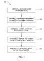
- FIG. 1depicts a flow chart illustrating a process according to an embodiment described herein.
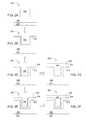
- FIGS. 2A-2Fdepict schematic views of a substrate at different process steps according to an embodiment described herein.
- Embodiments of the inventionprovide a method for depositing a cobalt layer on a barrier layer or layer prior to depositing a conductive layer thereon.
- the cobalt layer and barrier layermay each optionally be exposed to a treatment process, such as a plasma process or a thermal process.
- the conductive layermay contain copper or a copper alloy and be deposited by a physical vapor deposition (PVD) process, an atomic layer deposition (ALD) process, an electrochemical plating (ECP) process, or an electroless deposition process.
- PVDphysical vapor deposition
- ALDatomic layer deposition
- ECPelectrochemical plating
- the cobalt layerimproves copper boundary region properties to promote adhesion, improve gapfill and electromigration performance, decrease diffusion and agglomeration, and encourage uniform roughness and wetting of the substrate surface during processing.
- FIG. 1depicts a flow chart illustrating process 100 according to an embodiment of the invention.
- Process 100may be used to form an interconnect or other device on a substrate.
- steps 110 - 150 of process 100may be performed on substrate 200 , depicted in FIGS. 2A-2F .
- Process 100includes depositing or forming a barrier layer on a substrate (step 110 ), optionally exposing the barrier layer to a pre-treatment process (step 120 ), depositing a cobalt layer on the barrier layer (step 130 ), optionally exposing the cobalt layer to a post-treatment process (step 140 ), and depositing at least one conductive layer on the cobalt layer (step 150 ).
- FIG. 2Adepicts substrate 200 containing dielectric layer 204 disposed over underlayer 202 .
- Aperture 206is formed within dielectric layer 204 and may be a via, damascene, trough, or other passageway formed therein.
- Underlayer 202may be a substrate, substrate surface, contact layer, or another layer depending on device structure.
- Dielectric layer 204may contain a dielectric material, such as a low-k dielectric material.
- dielectric layer 204contains a low-k dielectric material, such as a silicon carbide oxide material, or a carbon doped silicon oxide material, for example, BLACK DIAMOND® II low-k dielectric material, available from Applied Materials, Inc., located in Santa Clara, Calif.
- dielectric layer 204Another example of a suitable material for dielectric layer 204 is a silicon carbide based film formed using chemical vapor deposition (CVD) or plasma enhanced CVD (PE-CVD) processes such as described in commonly assigned U.S. Pat. Nos. 6,537,733, 6,790,788, and 6,890,850, which are incorporated herein by reference.
- CVDchemical vapor deposition
- PE-CVDplasma enhanced CVD
- barrier layer 210may be deposited or formed on a substrate during step 110 of process 100 .
- FIG. 2Bdepicts barrier layer 210 disposed on substrate 200 , over dielectric layer 204 , and conformally within aperture 206 .
- Barrier layer 210may be one layer or multiple layers.
- Barrier layer 210may contain titanium, titanium nitride, tantalum, tantalum nitride, tungsten, tungsten nitride, silicides thereof, derivatives thereof, or combinations thereof.
- barrier layer 210may contain a bilayer of tantalum/tantalum nitride, titanium/titanium nitride, or tungsten/tungsten nitride.
- Barrier layer 210may have a thickness within a range from about 5 ⁇ to about 50 ⁇ , preferably, from about 10 ⁇ to about 30 ⁇ , and may be formed or deposited by PVD, ALD, plasma enhanced ALD (PE-ALD), CVD, PE-CVD, pulsed-CVD, or combinations thereof.
- barrier layer 210contains a lower layer of metallic tantalum deposited by a PVD process and an upper layer disposed over the lower layer of tantalum nitride layer deposited by another PVD process.
- barrier layer 210contains a lower layer of metallic tantalum deposited by an ALD process and an upper layer disposed over the lower layer of tantalum nitride layer deposited by a CVD process.
- barrier layer 210contains a lower layer of metallic tantalum deposited by a PVD process and an upper layer disposed over the lower layer of tantalum nitride layer deposited by a CVD process.
- barrier layer 210may contain tantalum nitride deposited using a CVD process or an ALD process wherein tantalum-containing compound or tantalum precursor (e.g., PDMAT) and nitrogen precursor (e.g., ammonia) are reacted.
- tantalum and/or tantalum nitrideis deposited as barrier layer 210 by an ALD process as described in commonly assigned U.S. Ser. No. 10/281,079, filed Oct. 25, 2002, and published as US 2003-0121608, which is herein incorporated by reference.
- a Ta/TaN bilayermay be deposited as barrier layer 210 , such as a metallic tantalum layer and a tantalum nitride layer that are independently deposited by ALD, CVD, and/or PVD processes, one layer on top of the other layer, in either order.
- a Ti/TiN bilayermay be deposited as barrier layer 210 , such as a metallic titanium layer and a titanium nitride layer that are independently deposited by ALD, CVD, and/or PVD processes, one layer on top of the other layer, in either order.
- a W/WN bilayermay be deposited as barrier layer 210 , such as a metallic tungsten layer and a tungsten nitride layer that are independently deposited by ALD, CVD, and/or PVD processes, one layer on top of the other layer, in either order.
- barrier layer 210may be optionally exposed to a pre-treatment process, such as a plasma process or a thermal process.
- a pre-treatment processsuch as a plasma process or a thermal process.
- Process gases and/or reagents that may be exposed to substrate 200 during plasma or thermal pre-treatment processesinclude hydrogen (e.g., H 2 or atomic-H), nitrogen (e.g., N 2 or atomic-N), ammonia (NH 3 ), a hydrogen and ammonia mixture (H 2 /NH 3 ), hydrazine (N 2 H 4 ), silane (SiH 4 ), disilane (Si 2 H 6 ), helium, argon, derivatives thereof, plasmas thereof, or combinations thereof.
- the process gasmay flow into the processing chamber or be exposed to the substrate having a flow rate within a range from about 500 sccm to about 10 slm, preferably, from about 1 slm to about 6 slm, for example, about 3 slm.
- substrate 200 and barrier layer 210may be exposed to a plasma to remove contaminants from barrier layer 210 during the pre-treatment process at step 120 .
- Substrate 200may be positioned within a processing chamber and exposed to a process gas which is ignited to form the plasma.
- the process gasmay contain one gaseous compound or multiple gaseous compounds.
- Substrate 200may be at room temperature (e.g., 23° C.), but is usually preheated to the desired temperature of the subsequent deposition process.
- Substrate 200may be heated to a temperature within a range from about 100° C. to about 400° C., preferably, from about 125° C. to about 350° C., and more preferably, from about 150° C. to about 300° C., such as about 200° C. or about 250° C.
- the processing chambermay produce an in situ plasma or be equipped with a remote plasma source (RPS).
- substrate 200may be exposed to the plasma (e.g., in situ or remotely) for a time period within a range from about 0.5 seconds to about 90 seconds, preferably, from about 10 seconds to about 60 seconds, and more preferably, from about 20 seconds to about 40 seconds.
- the plasmamay be produced at a power within a range from about 100 watts to about 1,000 watts, preferably, from about 200 watts to about 600 watts, and more preferably, from about 300 watts to about 500 watts.
- the processing chamberusually has an internal pressure of about 100 Torr or less, such as within a range from about 0.1 Torr to about 100 Torr, preferably, from about 0.5 Torr to about 50 Torr, and more preferably, from about 1 Torr to about 10 Torr.
- substrate 200 and barrier layer 210may be exposed to a plasma generated from hydrogen, ammonia, nitrogen, or mixtures thereof. In another example, substrate 200 and barrier layer 210 may be exposed to a plasma generated from hydrogen and ammonia. In another example, substrate 200 and barrier layer 210 may be exposed to a plasma generated from hydrogen, nitrogen, silane, disilane, or mixtures thereof. In another example, substrate 200 and barrier layer 210 may be exposed to a plasma generated from hydrogen, nitrogen, argon, helium, or mixtures thereof.
- substrate 200 and barrier layer 210are exposed to a process gas to remove contaminants from barrier layer 210 during a thermal pre-treatment process at step 120 .
- the thermal pre-treatment processmay be a rapid thermal process (RTP) or a rapid thermal annealing (RTA) process.
- RTPrapid thermal process
- RTArapid thermal annealing
- Substrate 200may be positioned within a processing chamber and exposed to at least one process gas and/or reagent.
- the processing chambermay be a deposition chamber that will be used for a subsequent deposition process, such as a PVD chamber, a CVD chamber, or an ALD chamber.
- the processing chambermay be a thermal annealing chamber, such as the RADIANCE® RTA chamber, commercially available from Applied Materials, Inc., Santa Clara, Calif.
- Substrate 200may be heated to a temperature within a range from about 25° C. to about 800° C., preferably, from about 50° C. to about 400° C., and more preferably, from about 100° C. to about 300° C. Substrate 200 may be heated for a time period within a range from about 2 minutes to about 20 minutes, preferably, from about 5 minutes to about 15 minutes. For example, substrate 200 may be heated to about 400° C. for about 12 minutes within the processing chamber.
- substrate 200 and barrier layer 210may be exposed to hydrogen, ammonia, nitrogen, or mixtures thereof while being heated within the processing chamber. In another example, substrate 200 and barrier layer 210 may be exposed to an ammonia/hydrogen mixture while being heated within the processing chamber. In another example, substrate 200 and barrier layer 210 may be exposed to hydrogen, nitrogen, silane, disilane, or mixtures thereof while being heated within the processing chamber. In another example, substrate 200 and barrier layer 210 may be exposed to hydrogen, nitrogen, argon, helium, or mixtures thereof while being heated within the processing chamber.
- FIG. 2Cdepicts cobalt layer 220 disposed on substrate 200 , over barrier layer 210 , and conformally within aperture 206 .
- Cobalt layer 220is usually a single layer, but may contain multiple layers.
- Cobalt layer 220may be a continuous layer or a discontinuous layer across barrier layer 210 .
- Cobalt layer 220may have a thickness of about 40 ⁇ or less, such as within a range from about 2 ⁇ to about 40 ⁇ , preferably, from about 5 ⁇ to about 30 ⁇ .
- Cobalt layer 220may be formed or deposited by a vapor deposition process, such as CVD, PE-CVD, pulsed-CVD, ALD, PE-ALD, or PVD.
- the plasma enhanced vapor deposition processnamely PE-CVD and PE-ALD, may be an in situ plasma process within the processing chamber or may be a remote plasma process such that a plasma is ignited in by a RPS and directed into the processing chamber.
- cobalt layer 220contains metallic cobalt.
- cobalt layer 220may contain one or more cobalt materials, such as metallic cobalt, cobalt silicide, cobalt boride, cobalt phosphide, alloys thereof, derivatives thereof, or combinations thereof.
- cobalt layer 220may be formed or deposited by simultaneously introducing a cobalt precursor and a reagent into the processing chamber during a thermal CVD process, a pulsed-CVD process, a PE-CVD process, or a pulsed PE-CVD process.
- the cobalt precursormay be introduced into the processing chamber without a reagent during a thermal CVD process, a pulsed-CVD process, a PE-CVD process, or a pulsed PE-CVD process.
- cobalt layer 220may be formed or deposited by sequentially introducing a cobalt precursor and a reagent into the processing chamber during a thermal ALD process or a PE-ALD process.
- Cobalt layer 220may contain metallic cobalt in some examples, but may contain other cobalt materials in other examples.
- Suitable cobalt precursors for forming cobalt materialsinclude cobalt carbonyl complexes, cobalt amidinates compounds, cobaltocene compounds, cobalt dienyl complexes, cobalt nitrosyl complexes, derivatives thereof, complexes thereof, plasmas thereof, or combinations thereof.
- cobalt materialsmay be deposited by CVD and ALD processes further described in commonly assigned U.S. Pat. Nos. 7,264,846 and 7,404,985, which are herein incorporated by reference.
- cobalt carbonyl compounds or complexesmay be utilized as cobalt precursors.
- Cobalt carbonyl compounds or complexeshave the general chemical formula (CO) x Co y L z , where X may be 1, 2, 3, 4, 5, 6, 7, 8, 9, 10, 11, or 12, Y may be 1, 2, 3, 4, or 5, and Z may be 1, 2, 3, 4, 5, 6, 7, or 8.
- the group Lis absent, one ligand or multiple ligands, that may be the same ligand or different ligands, and include cyclopentadienyl, alkylcyclopentadienyl (e.g., methylcyclopentadienyl or pentamethylcyclopentadienyl), pentadienyl, alkylpentadienyl, cyclobutadienyl, butadienyl, ethylene, allyl (or propylene), alkenes, dialkenes, alkynes, acetylene, butylacetylene, nitrosyl, ammonia, derivatives thereof, complexes thereof, plasmas thereof, or combinations thereof.
- alkylcyclopentadienyle.g., methylcyclopentadienyl or pentamethylcyclopentadienyl
- pentadienylalkylpentadienyl
- dicobalt hexacarbonyl acetyl compoundsmay be used to form cobalt materials (e.g., cobalt layer 220 ) during a deposition process.
- Dicobalt hexacarbonyl acetyl compoundsmay have the chemical formula of (CO) 6 Co 2 (RC ⁇ CR′), wherein R and R′ are independently selected from hydrogen, methyl, ethyl, propyl, isopropyl, butyl, tertbutyl, penta, benzyl, aryl, isomers thereof, derivatives thereof, or combinations thereof.
- dicobalt hexacarbonyl butylacetylene(CCTBA, (CO) 6 Co 2 (HC ⁇ C t Bu)) is the cobalt precursor.
- dicobalt hexacarbonyl acetyl compoundsinclude dicobalt hexacarbonyl methyl butylacetylene ((CO) 6 Co 2 (MeC ⁇ C t Bu)), dicobalt hexacarbonyl phenylacetylene ((CO) 6 Co 2 (HC ⁇ CPh)), hexacarbonyl methyl phenylacetylene ((CO) 6 Co 2 (MeC ⁇ CPh)), dicobalt hexacarbonyl methylacetylene ((CO) 6 Co 2 (HC ⁇ CMe)), dicobalt hexacarbonyl dimethylacetylene ((CO) 6 Co 2 (MeC ⁇ CMe)), derivatives thereof, complexes thereof, plasmas thereof, or combinations thereof.
- cobalt carbonyl complexesinclude cyclopentadienyl cobalt bis(carbonyl) (CpCo(CO) 2 ), tricarbonyl allyl cobalt ((CO) 3 Co(CH 2 CH ⁇ CH 2 )), derivatives thereof, complexes thereof, plasmas thereof, or combinations thereof.
- cobalt amidinates or cobalt amido complexesmay be utilized as cobalt precursors.
- Cobalt amido complexeshave the general chemical formula (RR′N) x Co, where X may be 1, 2, or 3, and R and R′ are independently hydrogen, methyl, ethyl, propyl, butyl, alkyl, silyl, alkylsilyl, derivatives thereof, or combinations thereof.
- Some exemplary cobalt amido complexesinclude bis(di(butyldimethylsilyl)amido) cobalt (((BuMe 2 Si) 2 N) 2 Co), bis(di(ethyldimethylsilyl)amido) cobalt (((EtMe 2 Si) 2 N) 2 Co), bis(di(propyldimethylsilyl)amido) cobalt (((PrMe 2 Si) 2 N) 2 Co), bis(di(trimethylsilyl)amido) cobalt (((Me 3 Si) 2 N) 2 Co), tris(di(trimethylsilyl)amido) cobalt (((Me 3 Si) 2 N) 3 Co), derivatives thereof, complexes thereof, plasmas thereof, or combinations thereof.
- Some exemplary cobalt precursorsinclude methylcyclopentadienyl cobalt bis(carbonyl) (MeCpCo(CO) 2 ), ethylcyclopentadienyl cobalt bis(carbonyl) (EtCpCo(CO) 2 ), pentamethylcyclopentadienyl cobalt bis(carbonyl) (Me 5 CpCo(CO) 2 ), dicobalt octa(carbonyl) (Co 2 (CO) 8 ), nitrosyl cobalt tris(carbonyl) ((ON)Co(CO) 3 ), bis(cyclopentadienyl) cobalt, (cyclopentadienyl) cobalt (cyclohexadienyl), cyclopentadienyl cobalt (1,3-hexadienyl), (cyclobutadienyl) cobalt (cyclopentadienyl), bis(methylcyclopentadienyl
- alternative reagentsmay be used to react with cobalt precursors while forming cobalt materials (e.g., metallic cobalt or cobalt alloys) by processes described herein include hydrogen (e.g., H 2 or atomic-H), nitrogen (e.g., N 2 or atomic-N), ammonia (NH 3 ), hydrazine (N 2 H 4 ), a hydrogen and ammonia mixture (H 2 /NH 3 ), borane (BH 3 ), diborane (B 2 H 6 ), triethylborane (Et 3 B), silane (SiH 4 ), disilane (Si 2 H 6 ), trisilane (Si 3 H 8 ), tetrasilane (Si 4 H 10 ), methyl silane (SiCH 6 ), dimethylsilane (SiC 2 H 8 ), phosphine (PH 3 ), derivatives thereof, plasmas thereof, or combinations thereof.
- hydrogene.g., H 2 or atomic-
- cobalt layer 220 containing metallic cobaltis deposited by simultaneously exposing substrate 200 to a cobalt precursor gas and a reducing agent during a thermal CVD process.
- cobalt layer 220 containing metallic cobaltis deposited by simultaneously exposing substrate 200 to a cobalt precursor gas and a reducing agent gas during a plasma enhanced CVD process.
- the plasma sourcemay be an in situ plasma source within the CVD chamber or a RPS positioned outside of the CVD chamber.
- the cobalt precursor gasmay be formed by passing a carrier gas (e.g., nitrogen or argon) through an ampoule of a cobalt precursor (e.g., CCTBA).
- the reducing agent gasmay be a single compound (e.g., H 2 ), and therefore have no carrier gas.
- the reducing agent gasmay be formed by passing a carrier gas through an ampoule of a reducing agent.
- the ampoulemay be heated depending on the cobalt precursor or reducing agent used during the process.
- an ampoule containing a cobalt precursorsuch as a dicobalt hexacarbonyl acetyl compound or other cobalt carbonyl compound (e.g., (CO) x Co y L z ) may be heated to a temperature within a range from about 30° C. to about 500° C.
- the cobalt precursor gasusually has a flow rate within a range from about 100 sccm (standard cubic centimeters per minute) to about 2,000 sccm, preferably, from about 200 sccm to about 1,000 sccm, and more preferably, from about 300 sccm to about 700 sccm, for example, about 500 sccm.
- the reducing agent gasusually has a flow rate within a range from about 0.5 slm (standard liters per minute) to about 10 slm, preferably, from about 1 slm to about 8 slm, and more preferably, from about 2 slm to about 6 slm.
- reducing agent gasis hydrogen and has a flow rate within a range from about 2 slm to about 6 slm, such as about 4 slm.
- the cobalt precursor gas and the reducing agent gasmay be combined to form a deposition gas prior to, while, or subsequent to entering the processing chamber during a deposition process to deposit cobalt layer 220 .
- Substrate 200may be positioned within a processing chamber and heated to a temperature within a range from about 25° C. to about 800° C., preferably, from about 50° C. to about 400° C., and more preferably, from about 100° C. to about 250° C., such as about 150° C.
- substrate 200may be exposed to the deposition gas containing the cobalt precursor gas and the reducing agent gas for a time period within a range from about 0.1 seconds to about 120 seconds, preferably, from about 1 second to about 60 seconds, and more preferably, from about 5 seconds to about 30 seconds.
- substrate 200may be heated to about 150° C. for about 10 minutes within the processing chamber while forming cobalt layer 220 during the CVD process.
- cobalt layer 220may be optionally exposed to a post-treatment process, such as a plasma process or a thermal process.
- a post-treatment processsuch as a plasma process or a thermal process.
- Process gases and/or reagents that may be exposed to substrate 200 and cobalt layer 220 during plasma or thermal post-treatment processesinclude hydrogen (e.g., H 2 or atomic-H), nitrogen (e.g., N 2 or atomic-N), ammonia (NH 3 ), a hydrogen and ammonia mixture (H 2 /NH 3 ), hydrazine (N 2 H 4 ), silane (SiH 4 ), disilane (Si 2 H 6 ), helium, argon, derivatives thereof, plasmas thereof, or combinations thereof.
- the process gasmay flow into the processing chamber or be exposed to the substrate having a flow rate within a range from about 500 sccm to about 10 slm, preferably, from about 1 slm to about 6 slm, for example, about 3 slm.
- substrate 200 and cobalt layer 220are exposed to a plasma to remove contaminants from cobalt layer 220 during the post-treatment process at step 140 .
- Substrate 200may be positioned within a processing chamber and exposed to a process gas which is ignited to form the plasma.
- the process gasmay contain one gaseous compound or multiple gaseous compounds.
- Substrate 200may be at room temperature (e.g., 23° C.), but is usually preheated to the desired temperature of the subsequent deposition process.
- Substrate 200may be heated to a temperature within a range from about 100° C. to about 400° C., preferably, from about 125° C. to about 350° C., and more preferably, from about 150° C. to about 300° C., such as about 200° C. or about 250° C.
- the processing chambermay produce an in situ plasma or be equipped with a RPS.
- substrate 200may be exposed to the plasma (e.g., in situ or remotely) for a time period within a range from about 0.5 seconds to about 90 seconds, preferably, from about 10 seconds to about 60 seconds, and more preferably, from about 20 seconds to about 40 seconds.
- the plasmamay be produced at a power within a range from about 100 watts to about 1,000 watts, preferably, from about 200 watts to about 600 watts, and more preferably, from about 300 watts to about 500 watts.
- the processing chamberusually has an internal pressure of about 100 Torr or less, such as within a range from about 0.1 Torr to about 100 Torr, preferably, from about 0.5 Torr to about 50 Torr, and more preferably, from about 1 Torr to about 10 Torr.
- substrate 200 and cobalt layer 220may be exposed to a plasma generated from hydrogen, ammonia, nitrogen, or mixtures thereof. In another example, substrate 200 and cobalt layer 220 may be exposed to a plasma generated from hydrogen and ammonia. In another example, substrate 200 and cobalt layer 220 may be exposed to a plasma generated from hydrogen, nitrogen, silane, disilane, or mixtures thereof. In another example, substrate 200 and cobalt layer 220 may be exposed to a plasma generated from hydrogen, nitrogen, argon, helium, or mixtures thereof.
- substrate 200 and cobalt layer 220may be exposed to a hydrogen plasma generated from hydrogen gas ignited by a RPS.
- Cobalt layer 220may be exposed to hydrogen gas with a flow rate within a range from about 2 slm to about 4 slm.
- the processing chambermay have an internal pressure within a range from about 1 Torr to about 10 Torr, and the plasma is ignited by a RPS having a power within a range from about 300 watts to about 500 watts.
- the plasmamay be exposed to cobalt layer 220 for a time period within a range from about 20 seconds to about 40 seconds for every deposited layer of cobalt material having a thickness within a range from about 7 ⁇ to about 10 ⁇ . Multiple treatments may be performed sequentially with the multiple layers of deposited cobalt material while forming cobalt layer 220 .
- substrate 200 and cobalt layer 220are exposed to a process gas to remove contaminants from cobalt layer 220 during a thermal post-treatment process at step 140 .
- the thermal post-treatment processmay be a RTP or a RTA process.
- Substrate 200may be positioned within a processing chamber and exposed to at least one process gas and/or reagent.
- the processing chambermay be a deposition chamber that was used in a prior deposition process or will be used for a subsequent deposition process, such as a PVD chamber, a CVD chamber, or an ALD chamber.
- the processing chambermay be a thermal annealing chamber, such as the RADIANCE® RTA chamber, commercially available from Applied Materials, Inc., Santa Clara, Calif.
- Substrate 200may be heated to a temperature within a range from about 25° C. to about 800° C., preferably, from about 50° C. to about 400° C., and more preferably, from about 100° C. to about 300° C. Substrate 200 may be heated for a time period within a range from about 2 minutes to about 20 minutes, preferably, from about 5 minutes to about 15 minutes. For example, substrate 200 may be heated to about 400° C. for about 12 minutes within the processing chamber.
- substrate 200 and cobalt layer 220may be exposed to hydrogen, ammonia, nitrogen, or mixtures thereof while being heated within the processing chamber. In another example, substrate 200 and cobalt layer 220 may be exposed to an ammonia/hydrogen mixture while being heated within the processing chamber. In another example, substrate 200 and cobalt layer 220 may be exposed to hydrogen, nitrogen, silane, disilane, or mixtures thereof while being heated within the processing chamber. In another example, substrate 200 and cobalt layer 220 may be exposed to hydrogen, nitrogen, argon, helium, or mixtures thereof while being heated within the processing chamber.
- FIG. 2Cdepicts aperture 206 formed within dielectric layer 204 on substrate 200 .
- Aperture 206contains barrier layer 210 and cobalt layer 220 conformally disposed therein.
- a conductive layermay be deposited or formed on or over cobalt layer 220 .
- the conductive layeris bulk layer 240 which may be directly deposited over cobalt layer 220 , as depicted in FIG. 2D .
- the conductive layeris seed layer 230 and bulk layer 240 . Seed layer 230 may be deposited over cobalt layer 220 and subsequently, bulk layer 240 may be deposited over seed layer 230 , as depicted in FIGS. 2E-2F .
- Seed layer 230 and bulk layer 240may be deposited or formed during a single deposition process or multiple deposition processes.
- Seed layer 230may contain copper, tungsten, aluminum, ruthenium, cobalt, silver, platinum, palladium, alloys thereof, derivatives thereof or combinations thereof.
- Bulk layer 240may contain copper, tungsten, aluminum, alloys thereof, derivatives thereof or combinations thereof.
- seed layer 230 and bulk layer 240may independently contain copper, tungsten, aluminum, alloys thereof, derivatives thereof or combinations thereof.
- Seed layer 230 and bulk layer 240may independently be deposited by using one or more deposition process, such as a CVD process, an ALD process, a PVD process, an electroless deposition process, an ECP process, derivatives thereof, or combinations thereof.
- each of seed layer 230 and bulk layer 240contains copper or a copper alloy.
- seed layer 230 containing coppermay be formed on cobalt layer 220 by a PVD process and thereafter, bulk layer 240 containing copper may be deposited to fill aperture 206 by an ECP process or an electroless deposition process.
- seed layer 230 containing coppermay be formed on cobalt layer 220 by an ALD process and thereafter, bulk layer 240 containing copper may be deposited to fill aperture 206 by an ECP process or an electroless deposition process.
- seed layer 230 containing coppermay be formed on cobalt layer 220 by a CVD process and thereafter, bulk layer 240 containing copper may be deposited to fill aperture 206 by an ECP process or an electroless deposition process.
- seed layer 230 containing coppermay be formed on cobalt layer 220 by an electroless process and thereafter, bulk layer 240 containing copper may be deposited to fill aperture 206 by an ECP process or an electroless deposition process.
- cobalt layer 220serves as a seed layer to which bulk layer 240 containing copper may be directly deposited to fill aperture 206 by an ECP process or an electroless deposition process.
- each of seed layer 230 and bulk layer 240contains tungsten or a tungsten alloy.
- seed layer 230 containing tungstenmay be formed on cobalt layer 220 by a PVD process and thereafter, bulk layer 240 containing tungsten may be deposited to fill aperture 206 by a CVD process or a pulsed-CVD process.
- seed layer 230 containing tungstenmay be formed on cobalt layer 220 by an ALD process and thereafter, bulk layer 240 containing tungsten may be deposited to fill aperture 206 by a CVD process or a pulsed-CVD process.
- seed layer 230 containing tungstenmay be formed on cobalt layer 220 by a pulsed-CVD process and thereafter, bulk layer 240 containing tungsten may be deposited to fill aperture 206 by a CVD process or a pulsed-CVD process.
- seed layer 230 containing tungstenmay be formed on cobalt layer 220 by an electroless process and thereafter, bulk layer 240 containing tungsten may be deposited to fill aperture 206 by a CVD process or a pulsed-CVD process.
- cobalt layer 220serves as a seed layer to which bulk layer 240 containing tungsten may be directly deposited to fill aperture 206 by a CVD process or a pulsed-CVD process.
- An ALD processing chamber used during embodiments described hereinis available from Applied Materials, Inc., located in Santa Clara, Calif. A detailed description of an ALD processing chamber may be found in commonly assigned U.S. Pat. Nos. 6,916,398 and 6,878,206, commonly assigned U.S. Ser. No. 10/281,079, filed on Oct. 25, 2002, and published as U.S. Pub. No. 2003-0121608, and commonly assigned U.S. Ser. Nos. 11/556,745, 11/556,752, 11/556,756, 11/556,758, 11/556,763, each filed Nov. 6, 2006, and published as U.S. Pub. Nos.
- a chamberconfigured to operate in both an ALD mode as well as a conventional CVD mode may be used to deposit cobalt-containing materials is described in commonly assigned U.S. Pat. No. 7,204,886, which is incorporated herein by reference in its entirety.
- a detailed description of an ALD process for forming cobalt-containing materialsis further disclosed in commonly assigned U.S. Pat. Nos. 7,264,846 and 7,404,985, which are hereby incorporated by reference in their entirety.
- a chamber configured to operate in both an ALD mode as well as a conventional CVD mode that may be used to deposit cobalt-containing materialsis the TXZ® showerhead and CVD chamber available from Applied Materials, Inc., located in Santa Clara, Calif.
- An example of a suitable vapor deposition chamberincludes the WXZTM CVD chamber, commercially available from Applied Materials, Inc., located in Santa Clara, Calif.
- the vapor deposition chambermay be adapted to deposit materials by conventional CVD, pulsed-CVD, or PE-CVD techniques as well as by ALD and PE-ALD techniques.
- the vapor deposition chambermay be used as for treatment processes, such as an in situ plasma process, a remote plasma process, or a thermal annealing process.
- Substrate surfacerefers to any substrate or material surface formed on a substrate upon which film processing is performed during a fabrication process.
- a substrate surface on which processing may be performedinclude materials such as monocrystalline, polycrystalline or amorphous silicon, strained silicon, silicon on insulator (SOI), doped silicon, silicon germanium, germanium, gallium arsenide, glass, sapphire, silicon oxide, silicon nitride, silicon oxynitride, and/or carbon doped silicon oxides, such as SiO x C y , for example, BLACK DIAMOND® low-k dielectric, available from Applied Materials, Inc., located in Santa Clara, Calif.
- SOIsilicon on insulator
- Substratesmay have various dimensions, such as 100 mm, 200 mm, 300 mm, or 450 mm diameter wafers, as well as, rectangular or square panes. Unless otherwise noted, embodiments and examples described herein are usually conducted on substrates with a 200 mm diameter or a 300 mm diameter, more preferably, a 300 mm diameter. Processes of the embodiments described herein may be used to deposit cobalt materials (e.g., metallic cobalt) on many substrates and surfaces, especially, barrier layers and layers.
- cobalt materialse.g., metallic cobalt
- Substrates on which embodiments of the invention may be usefulinclude, but are not limited to semiconductor wafers, such as crystalline silicon (e.g., Si ⁇ 100> or Si ⁇ 111>), silicon oxide, strained silicon, silicon germanium, doped or undoped polysilicon, doped or undoped silicon wafers, and patterned or non-patterned wafers. Substrates may be exposed to a pre-treatment process to polish, etch, reduce, oxidize, hydroxylate, heat, and/or anneal the substrate or substrate surface.
- semiconductor waferssuch as crystalline silicon (e.g., Si ⁇ 100> or Si ⁇ 111>), silicon oxide, strained silicon, silicon germanium, doped or undoped polysilicon, doped or undoped silicon wafers, and patterned or non-patterned wafers.
- Substratesmay be exposed to a pre-treatment process to polish, etch, reduce, oxidize, hydroxylate, heat, and/or anneal the substrate or substrate surface.
Landscapes
- Engineering & Computer Science (AREA)
- Chemical & Material Sciences (AREA)
- Physics & Mathematics (AREA)
- Condensed Matter Physics & Semiconductors (AREA)
- General Physics & Mathematics (AREA)
- Manufacturing & Machinery (AREA)
- Computer Hardware Design (AREA)
- Microelectronics & Electronic Packaging (AREA)
- Power Engineering (AREA)
- General Chemical & Material Sciences (AREA)
- Chemical Kinetics & Catalysis (AREA)
- Materials Engineering (AREA)
- Mechanical Engineering (AREA)
- Metallurgy (AREA)
- Organic Chemistry (AREA)
- Plasma & Fusion (AREA)
- Inorganic Chemistry (AREA)
- Crystallography & Structural Chemistry (AREA)
- Electrodes Of Semiconductors (AREA)
- Chemical Vapour Deposition (AREA)
- Internal Circuitry In Semiconductor Integrated Circuit Devices (AREA)
Abstract
Description
Claims (20)
Priority Applications (1)
| Application Number | Priority Date | Filing Date | Title |
|---|---|---|---|
| US14/717,375US9209074B2 (en) | 2001-07-25 | 2015-05-20 | Cobalt deposition on barrier surfaces |
Applications Claiming Priority (11)
| Application Number | Priority Date | Filing Date | Title |
|---|---|---|---|
| US09/916,234US20030029715A1 (en) | 2001-07-25 | 2001-07-25 | An Apparatus For Annealing Substrates In Physical Vapor Deposition Systems |
| US10/044,412US6740585B2 (en) | 2001-07-25 | 2002-01-09 | Barrier formation using novel sputter deposition method with PVD, CVD, or ALD |
| US10/845,970US20040211665A1 (en) | 2001-07-25 | 2004-05-14 | Barrier formation using novel sputter-deposition method |
| US79136606P | 2006-04-11 | 2006-04-11 | |
| US11/456,073US7416979B2 (en) | 2001-07-25 | 2006-07-06 | Deposition methods for barrier and tungsten materials |
| US86393906P | 2006-11-01 | 2006-11-01 | |
| US11/733,929US8110489B2 (en) | 2001-07-25 | 2007-04-11 | Process for forming cobalt-containing materials |
| US12/111,930US20080268635A1 (en) | 2001-07-25 | 2008-04-29 | Process for forming cobalt and cobalt silicide materials in copper contact applications |
| US12/111,923US20090004850A1 (en) | 2001-07-25 | 2008-04-29 | Process for forming cobalt and cobalt silicide materials in tungsten contact applications |
| US12/201,976US9051641B2 (en) | 2001-07-25 | 2008-08-29 | Cobalt deposition on barrier surfaces |
| US14/717,375US9209074B2 (en) | 2001-07-25 | 2015-05-20 | Cobalt deposition on barrier surfaces |
Related Parent Applications (1)
| Application Number | Title | Priority Date | Filing Date |
|---|---|---|---|
| US12/201,976ContinuationUS9051641B2 (en) | 2001-07-25 | 2008-08-29 | Cobalt deposition on barrier surfaces |
Publications (2)
| Publication Number | Publication Date |
|---|---|
| US20150255333A1 US20150255333A1 (en) | 2015-09-10 |
| US9209074B2true US9209074B2 (en) | 2015-12-08 |
Family
ID=41722231
Family Applications (2)
| Application Number | Title | Priority Date | Filing Date |
|---|---|---|---|
| US12/201,976Expired - LifetimeUS9051641B2 (en) | 2001-07-25 | 2008-08-29 | Cobalt deposition on barrier surfaces |
| US14/717,375Expired - Fee RelatedUS9209074B2 (en) | 2001-07-25 | 2015-05-20 | Cobalt deposition on barrier surfaces |
Family Applications Before (1)
| Application Number | Title | Priority Date | Filing Date |
|---|---|---|---|
| US12/201,976Expired - LifetimeUS9051641B2 (en) | 2001-07-25 | 2008-08-29 | Cobalt deposition on barrier surfaces |
Country Status (6)
| Country | Link |
|---|---|
| US (2) | US9051641B2 (en) |
| JP (2) | JP2012501543A (en) |
| KR (1) | KR101599488B1 (en) |
| CN (2) | CN102132383A (en) |
| TW (2) | TWI654684B (en) |
| WO (1) | WO2010025068A2 (en) |
Cited By (3)
| Publication number | Priority date | Publication date | Assignee | Title |
|---|---|---|---|---|
| US10329663B2 (en) | 2012-09-25 | 2019-06-25 | Entegris, Inc. | Cobalt precursors for low temperature ALD or CVD of cobalt-based thin films |
| US10699946B2 (en) | 2013-09-27 | 2020-06-30 | Applied Materials, Inc. | Method of enabling seamless cobalt gap-fill |
| US11024801B2 (en) | 2018-06-27 | 2021-06-01 | Taiwan Semiconductor Manufacturing Co., Ltd. | Diffusion layer for magnetic tunnel junctions |
Families Citing this family (102)
| Publication number | Priority date | Publication date | Assignee | Title |
|---|---|---|---|---|
| US8110489B2 (en) | 2001-07-25 | 2012-02-07 | Applied Materials, Inc. | Process for forming cobalt-containing materials |
| TW200746268A (en)* | 2006-04-11 | 2007-12-16 | Applied Materials Inc | Process for forming cobalt-containing materials |
| US8791018B2 (en)* | 2006-12-19 | 2014-07-29 | Spansion Llc | Method of depositing copper using physical vapor deposition |
| US8673080B2 (en) | 2007-10-16 | 2014-03-18 | Novellus Systems, Inc. | Temperature controlled showerhead |
| DE102009023381A1 (en)* | 2009-05-29 | 2010-12-02 | Grega, Samuel | Manufacturing tungsten, chromium and molybdenum layers and their carbide, nitride and silicide, multi-layer structure and connection structure on solid substrate, comprises impacting substrate by tungsten, chromium and molybdenum carbonyl |
| US10256142B2 (en) | 2009-08-04 | 2019-04-09 | Novellus Systems, Inc. | Tungsten feature fill with nucleation inhibition |
| KR20120046786A (en) | 2009-09-02 | 2012-05-10 | 가부시키가이샤 알박 | Method for forming co film and method for forming cu wiring film |
| US10128261B2 (en) | 2010-06-30 | 2018-11-13 | Sandisk Technologies Llc | Cobalt-containing conductive layers for control gate electrodes in a memory structure |
| JP5680892B2 (en)* | 2010-07-13 | 2015-03-04 | 株式会社アルバック | Co film forming method |
| US9926639B2 (en) | 2010-07-16 | 2018-03-27 | Applied Materials, Inc. | Methods for forming barrier/seed layers for copper interconnect structures |
| US20120141667A1 (en)* | 2010-07-16 | 2012-06-07 | Applied Materials, Inc. | Methods for forming barrier/seed layers for copper interconnect structures |
| KR101223724B1 (en)* | 2010-10-25 | 2013-01-17 | 삼성디스플레이 주식회사 | Passivation film for electronic device and method of manufacturing the same |
| JP2012174845A (en)* | 2011-02-21 | 2012-09-10 | Tokyo Electron Ltd | Deposition method and semiconductor device manufacturing method |
| JP5659041B2 (en)* | 2011-02-24 | 2015-01-28 | 東京エレクトロン株式会社 | Film formation method and storage medium |
| JP2012175073A (en)* | 2011-02-24 | 2012-09-10 | Tokyo Electron Ltd | Deposition method and storage medium |
| KR101937115B1 (en) | 2011-03-04 | 2019-01-09 | 노벨러스 시스템즈, 인코포레이티드 | Hybrid ceramic showerhead |
| US8524600B2 (en) | 2011-03-31 | 2013-09-03 | Applied Materials, Inc. | Post deposition treatments for CVD cobalt films |
| US10381266B2 (en) | 2012-03-27 | 2019-08-13 | Novellus Systems, Inc. | Tungsten feature fill with nucleation inhibition |
| TWI602283B (en) | 2012-03-27 | 2017-10-11 | 諾發系統有限公司 | Tungsten feature fill |
| US11437269B2 (en) | 2012-03-27 | 2022-09-06 | Novellus Systems, Inc. | Tungsten feature fill with nucleation inhibition |
| US9330939B2 (en)* | 2012-03-28 | 2016-05-03 | Applied Materials, Inc. | Method of enabling seamless cobalt gap-fill |
| US8736056B2 (en)* | 2012-07-31 | 2014-05-27 | Taiwan Semiconductor Manufacturing Company, Ltd. | Device for reducing contact resistance of a metal |
| JP2014101564A (en)* | 2012-11-21 | 2014-06-05 | Ulvac Japan Ltd | Formation method of cobalt film |
| US9865501B2 (en)* | 2013-03-06 | 2018-01-09 | Lam Research Corporation | Method and apparatus for remote plasma treatment for reducing metal oxides on a metal seed layer |
| JP6310653B2 (en)* | 2013-07-08 | 2018-04-11 | 株式会社アルバック | Method for forming Cu wiring structure |
| US9218980B2 (en)* | 2013-09-13 | 2015-12-22 | Applied Materials, Inc. | Surface treatment to improve CCTBA based CVD co nucleation on dielectric substrate |
| US9090964B2 (en)* | 2013-12-19 | 2015-07-28 | Intel Corporation | Additives to improve the performance of a precursor source for cobalt deposition |
| US9425155B2 (en) | 2014-02-25 | 2016-08-23 | Taiwan Semiconductor Manufacturing Company, Ltd. | Wafer bonding process and structure |
| JP6268008B2 (en)* | 2014-03-17 | 2018-01-24 | 東京エレクトロン株式会社 | Manufacturing method of Cu wiring |
| US9496145B2 (en) | 2014-03-19 | 2016-11-15 | Applied Materials, Inc. | Electrochemical plating methods |
| WO2015157004A1 (en)* | 2014-04-07 | 2015-10-15 | Entegris, Inc. | Cobalt cvd |
| US10741365B2 (en) | 2014-05-05 | 2020-08-11 | Lam Research Corporation | Low volume showerhead with porous baffle |
| JP2015224227A (en)* | 2014-05-28 | 2015-12-14 | 宇部興産株式会社 | Method of producing (acetylene)dicobalt hexacarbonyl compound |
| US9847289B2 (en)* | 2014-05-30 | 2017-12-19 | Applied Materials, Inc. | Protective via cap for improved interconnect performance |
| US9899234B2 (en) | 2014-06-30 | 2018-02-20 | Lam Research Corporation | Liner and barrier applications for subtractive metal integration |
| US9349637B2 (en) | 2014-08-21 | 2016-05-24 | Lam Research Corporation | Method for void-free cobalt gap fill |
| US9748137B2 (en) | 2014-08-21 | 2017-08-29 | Lam Research Corporation | Method for void-free cobalt gap fill |
| US9997405B2 (en) | 2014-09-30 | 2018-06-12 | Lam Research Corporation | Feature fill with nucleation inhibition |
| US9487860B2 (en) | 2014-11-10 | 2016-11-08 | L'Air Liquide, Société Anonyme pour l'Etude et l'Exploitation des Procédés Georges Claude | Method for forming cobalt containing films |
| US10741572B2 (en) | 2015-02-04 | 2020-08-11 | Sandisk Technologies Llc | Three-dimensional memory device having multilayer word lines containing selectively grown cobalt or ruthenium and method of making the same |
| US9984963B2 (en)* | 2015-02-04 | 2018-05-29 | Sandisk Technologies Llc | Cobalt-containing conductive layers for control gate electrodes in a memory structure |
| US9758896B2 (en) | 2015-02-12 | 2017-09-12 | Applied Materials, Inc. | Forming cobalt interconnections on a substrate |
| US10563305B2 (en)* | 2015-05-13 | 2020-02-18 | Versum Materials Us, Llc | Container for chemical precursors in a deposition process |
| US10170320B2 (en) | 2015-05-18 | 2019-01-01 | Lam Research Corporation | Feature fill with multi-stage nucleation inhibition |
| US10023959B2 (en) | 2015-05-26 | 2018-07-17 | Lam Research Corporation | Anti-transient showerhead |
| US9972504B2 (en)* | 2015-08-07 | 2018-05-15 | Lam Research Corporation | Atomic layer etching of tungsten for enhanced tungsten deposition fill |
| US9589897B1 (en)* | 2015-08-18 | 2017-03-07 | Taiwan Semiconductor Manufacturing Company, Ltd. | Trench liner for removing impurities in a non-copper trench |
| US9741577B2 (en)* | 2015-12-02 | 2017-08-22 | International Business Machines Corporation | Metal reflow for middle of line contacts |
| US20170186944A1 (en)* | 2015-12-29 | 2017-06-29 | International Business Machines Corporation | Enhancement of spin transfer torque magnetoresistive random access memory device using hydrogen plasma |
| US10011903B2 (en) | 2015-12-31 | 2018-07-03 | L'Air Liquide, Société Anonyme pour l'Etude et l'Exploitation des Procédés Georges Claude | Manganese-containing film forming compositions, their synthesis, and use in film deposition |
| US9719167B2 (en) | 2015-12-31 | 2017-08-01 | L'Air Liquide, Société Anonyme pour l'Etude et l'Exploitation des Procédés Georges Claude | Cobalt-containing film forming compositions, their synthesis, and use in film deposition |
| US9738971B2 (en) | 2015-12-31 | 2017-08-22 | L'Air Liquide, Société Anonyme pour l'Etude et l'Exploitation des Procédés Georges Claude | Vapor deposition methods to form group 8-containing films |
| US10438847B2 (en) | 2016-05-13 | 2019-10-08 | Lam Research Corporation | Manganese barrier and adhesion layers for cobalt |
| WO2018034936A1 (en)* | 2016-08-14 | 2018-02-22 | Entegris, Inc. | ALLOYS OF Co TO REDUCE STRESS |
| US10573522B2 (en) | 2016-08-16 | 2020-02-25 | Lam Research Corporation | Method for preventing line bending during metal fill process |
| JP2018073949A (en)* | 2016-10-27 | 2018-05-10 | 東京エレクトロン株式会社 | Metal wiring layer formation method, metal wiring layer formation device, and storage medium |
| US20180135174A1 (en)* | 2016-11-01 | 2018-05-17 | Versum Materials Us, Llc | Cobalt compounds, method of making and method of use thereof |
| US10600685B2 (en)* | 2016-11-27 | 2020-03-24 | Applied Materials, Inc. | Methods to fill high aspect ratio features on semiconductor substrates with MOCVD cobalt film |
| US10211099B2 (en) | 2016-12-19 | 2019-02-19 | Lam Research Corporation | Chamber conditioning for remote plasma process |
| US10224224B2 (en) | 2017-03-10 | 2019-03-05 | Micromaterials, LLC | High pressure wafer processing systems and related methods |
| US10443146B2 (en) | 2017-03-30 | 2019-10-15 | Lam Research Corporation | Monitoring surface oxide on seed layers during electroplating |
| US10242879B2 (en) | 2017-04-20 | 2019-03-26 | Lam Research Corporation | Methods and apparatus for forming smooth and conformal cobalt film by atomic layer deposition |
| US10622214B2 (en) | 2017-05-25 | 2020-04-14 | Applied Materials, Inc. | Tungsten defluorination by high pressure treatment |
| CN110945157B (en) | 2017-07-18 | 2023-04-04 | 株式会社高纯度化学研究所 | Atomic layer deposition method of metal film |
| US10276411B2 (en) | 2017-08-18 | 2019-04-30 | Applied Materials, Inc. | High pressure and high temperature anneal chamber |
| WO2019036157A1 (en) | 2017-08-18 | 2019-02-21 | Applied Materials, Inc. | High pressure and high temperature anneal chamber |
| US10079177B1 (en) | 2017-09-01 | 2018-09-18 | United Microelectronics Corp. | Method for forming copper material over substrate |
| US10304732B2 (en)* | 2017-09-21 | 2019-05-28 | Applied Materials, Inc. | Methods and apparatus for filling substrate features with cobalt |
| CN117936420A (en) | 2017-11-11 | 2024-04-26 | 微材料有限责任公司 | Gas delivery system for high pressure processing chamber |
| KR20200075892A (en) | 2017-11-17 | 2020-06-26 | 어플라이드 머티어리얼스, 인코포레이티드 | Condenser system for high pressure treatment systems |
| SG11202008256WA (en) | 2018-03-09 | 2020-09-29 | Applied Materials Inc | High pressure annealing process for metal containing materials |
| US10633740B2 (en) | 2018-03-19 | 2020-04-28 | Applied Materials, Inc. | Methods for depositing coatings on aerospace components |
| US20190309422A1 (en)* | 2018-04-06 | 2019-10-10 | Versum Materials Us, Llc | Spin-On Metallization |
| US11015252B2 (en) | 2018-04-27 | 2021-05-25 | Applied Materials, Inc. | Protection of components from corrosion |
| US10950429B2 (en) | 2018-05-08 | 2021-03-16 | Applied Materials, Inc. | Methods of forming amorphous carbon hard mask layers and hard mask layers formed therefrom |
| US10748783B2 (en) | 2018-07-25 | 2020-08-18 | Applied Materials, Inc. | Gas delivery module |
| US20200048760A1 (en)* | 2018-08-13 | 2020-02-13 | Applied Materials, Inc. | High power impulse magnetron sputtering physical vapor deposition of tungsten films having improved bottom coverage |
| US11009339B2 (en) | 2018-08-23 | 2021-05-18 | Applied Materials, Inc. | Measurement of thickness of thermal barrier coatings using 3D imaging and surface subtraction methods for objects with complex geometries |
| US11124874B2 (en) | 2018-10-25 | 2021-09-21 | Applied Materials, Inc. | Methods for depositing metallic iridium and iridium silicide |
| CN113348532A (en)* | 2018-11-13 | 2021-09-03 | 应用材料公司 | Selective deposition and selective oxide removal of metal silicides |
| JP7705347B2 (en) | 2018-12-05 | 2025-07-09 | ラム リサーチ コーポレーション | Void-free, low stress filling |
| WO2020117462A1 (en) | 2018-12-07 | 2020-06-11 | Applied Materials, Inc. | Semiconductor processing system |
| JP7705349B2 (en) | 2019-02-13 | 2025-07-09 | ラム リサーチ コーポレーション | Tungsten feature filling with inhibition control |
| EP3942088A4 (en)* | 2019-03-22 | 2022-12-21 | Applied Materials, Inc. | METHOD AND DEVICE FOR THE DEPOSITION OF METAL NITRIDE |
| CN113614274A (en) | 2019-03-22 | 2021-11-05 | 应用材料公司 | Method and apparatus for depositing multilayer device with superconducting film |
| KR102707825B1 (en) | 2019-04-23 | 2024-09-24 | 삼성전자주식회사 | Cobalt precursor, method for manufacturing cobalt containing layer using the same, and method for manufacturing semiconductor device using the same |
| EP3959356A4 (en) | 2019-04-26 | 2023-01-18 | Applied Materials, Inc. | Methods of protecting aerospace components against corrosion and oxidation |
| US11794382B2 (en) | 2019-05-16 | 2023-10-24 | Applied Materials, Inc. | Methods for depositing anti-coking protective coatings on aerospace components |
| US11697879B2 (en) | 2019-06-14 | 2023-07-11 | Applied Materials, Inc. | Methods for depositing sacrificial coatings on aerospace components |
| CN119980191A (en) | 2019-08-28 | 2025-05-13 | 朗姆研究公司 | Metal Deposition |
| US11466364B2 (en) | 2019-09-06 | 2022-10-11 | Applied Materials, Inc. | Methods for forming protective coatings containing crystallized aluminum oxide |
| TWI753759B (en) | 2020-02-03 | 2022-01-21 | 美商應用材料股份有限公司 | Snspd with integrated aluminum nitride seed or waveguide layer |
| TWI780579B (en) | 2020-02-03 | 2022-10-11 | 美商應用材料股份有限公司 | Snspd with integrated aluminum nitride seed or waveguide layer |
| US11901222B2 (en) | 2020-02-17 | 2024-02-13 | Applied Materials, Inc. | Multi-step process for flowable gap-fill film |
| US11519066B2 (en) | 2020-05-21 | 2022-12-06 | Applied Materials, Inc. | Nitride protective coatings on aerospace components and methods for making the same |
| US12027419B2 (en)* | 2020-06-25 | 2024-07-02 | Taiwan Semiconductor Manufacturing Company Limited | Semiconductor device including liner structure |
| WO2022005696A1 (en) | 2020-07-03 | 2022-01-06 | Applied Materials, Inc. | Methods for refurbishing aerospace components |
| US11742282B2 (en)* | 2020-08-07 | 2023-08-29 | Micron Technology, Inc. | Conductive interconnects |
| CN112201618A (en)* | 2020-09-30 | 2021-01-08 | 上海华力集成电路制造有限公司 | Method for optimizing quality of cushion layer |
| US12065731B2 (en) | 2021-01-21 | 2024-08-20 | Taiwan Semiconductor Manufacturing Company, Ltd. | Tungsten deposition on a cobalt surface |
| US20230134230A1 (en)* | 2021-11-01 | 2023-05-04 | Applied Materials, Inc. | Methods and apparatus for tungsten gap fill |
| TW202431541A (en)* | 2023-01-29 | 2024-08-01 | 美商應用材料股份有限公司 | Plasma treatment of barrier and liner layers |
Citations (420)
| Publication number | Priority date | Publication date | Assignee | Title |
|---|---|---|---|---|
| US4058430A (en) | 1974-11-29 | 1977-11-15 | Tuomo Suntola | Method for producing compound thin films |
| US4389973A (en) | 1980-03-18 | 1983-06-28 | Oy Lohja Ab | Apparatus for performing growth of compound thin films |
| JPS5898917U (en) | 1981-12-26 | 1983-07-05 | 株式会社フジ医療器 | Arm stretcher attached to chair-type pine surgery machine |
| US4413022A (en) | 1979-02-28 | 1983-11-01 | Canon Kabushiki Kaisha | Method for performing growth of compound thin films |
| US4415275A (en) | 1981-12-21 | 1983-11-15 | Dietrich David E | Swirl mixing device |
| US4486487A (en) | 1982-05-10 | 1984-12-04 | Oy Lohja Ab | Combination film, in particular for thin film electroluminescent structures |
| US4500409A (en) | 1983-07-19 | 1985-02-19 | Varian Associates, Inc. | Magnetron sputter coating source for both magnetic and non magnetic target materials |
| JPS61174725U (en) | 1985-04-22 | 1986-10-30 | ||
| US4761269A (en) | 1986-06-12 | 1988-08-02 | Crystal Specialties, Inc. | Apparatus for depositing material on a substrate |
| JPS6428921U (en) | 1987-08-12 | 1989-02-21 | ||
| US4814294A (en) | 1987-07-30 | 1989-03-21 | Allied-Signal Inc. | Method of growing cobalt silicide films by chemical vapor deposition |
| US4824544A (en) | 1987-10-29 | 1989-04-25 | International Business Machines Corporation | Large area cathode lift-off sputter deposition device |
| US4834831A (en) | 1986-09-08 | 1989-05-30 | Research Development Corporation Of Japan | Method for growing single crystal thin films of element semiconductor |
| US4951601A (en) | 1986-12-19 | 1990-08-28 | Applied Materials, Inc. | Multi-chamber integrated process system |
| JPH02246161A (en) | 1989-03-17 | 1990-10-01 | Fujitsu Ltd | Thin-film transistor |
| US4975252A (en) | 1984-07-26 | 1990-12-04 | Junichi Nishizawa | Semiconductor crystal growth apparatus |
| JPH02298263A (en) | 1989-05-12 | 1990-12-10 | Tokyo Electron Ltd | Sputtering device |
| US4993357A (en) | 1987-12-23 | 1991-02-19 | Cs Halbleiter -Und Solartechnologie Gmbh | Apparatus for atomic layer epitaxial growth |
| JPH03140487A (en) | 1989-10-25 | 1991-06-14 | Mitsubishi Electric Corp | Electrochemical reactor |
| US5027746A (en) | 1988-03-22 | 1991-07-02 | U.S. Philips Corporation | Epitaxial reactor having a wall which is protected from deposits |
| JPH03240944A (en) | 1990-02-17 | 1991-10-28 | Masahiko Naoe | Method and device for focusing target sputtering for forming thin aluminum film |
| US5096364A (en) | 1986-04-28 | 1992-03-17 | Varian Associates, Inc. | Wafer arm handler mechanism |
| US5122923A (en) | 1989-08-30 | 1992-06-16 | Nec Corporation | Thin-film capacitors and process for manufacturing the same |
| JPH04291916A (en) | 1991-03-20 | 1992-10-16 | Kokusai Electric Co Ltd | Vapor phase growth method and apparatus |
| US5173327A (en) | 1991-06-18 | 1992-12-22 | Micron Technology, Inc. | LPCVD process for depositing titanium films for semiconductor devices |
| US5178681A (en) | 1991-01-29 | 1993-01-12 | Applied Materials, Inc. | Suspension system for semiconductor reactors |
| US5186718A (en) | 1989-05-19 | 1993-02-16 | Applied Materials, Inc. | Staged-vacuum wafer processing system and method |
| US5225366A (en) | 1990-06-22 | 1993-07-06 | The United States Of America As Represented By The Secretary Of The Navy | Apparatus for and a method of growing thin films of elemental semiconductors |
| JPH05195213A (en) | 1992-01-22 | 1993-08-03 | Hitachi Ltd | Sputtering equipment |
| JPH05206036A (en) | 1992-01-30 | 1993-08-13 | Rikagaku Kenkyusho | Film formation method and film formation apparatus |
| US5242566A (en) | 1990-04-23 | 1993-09-07 | Applied Materials, Inc. | Planar magnetron sputtering source enabling a controlled sputtering profile out to the target perimeter |
| JPH05234899A (en) | 1991-09-17 | 1993-09-10 | Hitachi Ltd | Atomic layer epitaxy system |
| US5252807A (en) | 1990-07-02 | 1993-10-12 | George Chizinsky | Heated plate rapid thermal processor |
| JPH05270997A (en) | 1992-03-19 | 1993-10-19 | Fujitsu Ltd | Atomic layer epitaxy apparatus and atomic layer epitaxy method |
| US5261959A (en) | 1988-05-26 | 1993-11-16 | General Electric Company | Diamond crystal growth apparatus |
| JPH05311419A (en) | 1992-04-01 | 1993-11-22 | Nec Corp | Magnetron type sputtering device |
| JPH0547666Y2 (en) | 1985-03-15 | 1993-12-15 | ||
| US5286296A (en) | 1991-01-10 | 1994-02-15 | Sony Corporation | Multi-chamber wafer process equipment having plural, physically communicating transfer means |
| US5294286A (en) | 1984-07-26 | 1994-03-15 | Research Development Corporation Of Japan | Process for forming a thin film of silicon |
| US5306666A (en) | 1992-07-24 | 1994-04-26 | Nippon Steel Corporation | Process for forming a thin metal film by chemical vapor deposition |
| US5320728A (en) | 1990-03-30 | 1994-06-14 | Applied Materials, Inc. | Planar magnetron sputtering source producing improved coating thickness uniformity, step coverage and step coverage uniformity |
| US5330628A (en) | 1990-01-29 | 1994-07-19 | Varian Associates, Inc. | Collimated deposition apparatus and method |
| US5335138A (en) | 1993-02-12 | 1994-08-02 | Micron Semiconductor, Inc. | High dielectric constant capacitor and method of manufacture |
| JPH06224138A (en) | 1992-07-27 | 1994-08-12 | Texas Instr Inc <Ti> | Atom layer epitaxy device |
| US5338362A (en) | 1992-08-29 | 1994-08-16 | Tokyo Electron Limited | Apparatus for processing semiconductor wafer comprising continuously rotating wafer table and plural chamber compartments |
| JPH07126844A (en) | 1993-11-01 | 1995-05-16 | Tatsuo Asamaki | Sputtering device |
| US5441703A (en) | 1987-06-30 | 1995-08-15 | Aixtron Gmbh | Gas inlet for a plurality of reactant gases into reaction vessel |
| US5443647A (en) | 1993-04-28 | 1995-08-22 | The United States Of America As Represented By The Secretary Of The Army | Method and apparatus for depositing a refractory thin film by chemical vapor deposition |
| JPH07300649A (en) | 1994-04-27 | 1995-11-14 | Kobe Steel Ltd | Hard film excellent in wear resistance and oxidation resistance and high hardness member |
| US5480818A (en) | 1992-02-10 | 1996-01-02 | Fujitsu Limited | Method for forming a film and method for manufacturing a thin film transistor |
| US5483919A (en) | 1990-08-31 | 1996-01-16 | Nippon Telegraph And Telephone Corporation | Atomic layer epitaxy method and apparatus |
| JPH0860355A (en) | 1994-08-23 | 1996-03-05 | Tel Varian Ltd | Treating device |
| EP0703598A1 (en) | 1994-09-26 | 1996-03-27 | Applied Materials, Inc. | Electrode between sputtering target and workpiece |
| US5503875A (en) | 1993-03-18 | 1996-04-02 | Tokyo Electron Limited | Film forming method wherein a partial pressure of a reaction byproduct in a processing container is reduced temporarily |
| US5519373A (en) | 1993-12-28 | 1996-05-21 | Shin-Etsu Chemical Co., Ltd. | Dipole ring magnet for use in magnetron sputtering or magnetron etching |
| WO1996017107A1 (en) | 1994-11-28 | 1996-06-06 | Mikrokemia Oy | Method and apparatus for growing thin films |
| US5526244A (en) | 1993-05-24 | 1996-06-11 | Bishop; Vernon R. | Overhead luminaire |
| US5527438A (en) | 1994-12-16 | 1996-06-18 | Applied Materials, Inc. | Cylindrical sputtering shield |
| US5544771A (en) | 1994-02-23 | 1996-08-13 | Samsung Electronics Co., Ltd. | Method for manufacturing a collimator |
| US5589039A (en) | 1995-07-28 | 1996-12-31 | Sony Corporation | In-plane parallel bias magnetic field generator for sputter coating magnetic materials onto substrates |
| US5593551A (en) | 1993-05-05 | 1997-01-14 | Varian Associates, Inc. | Magnetron sputtering source for low pressure operation |
| US5597462A (en) | 1993-06-24 | 1997-01-28 | Hyundai Electronics Industries Co., Ltd. | Condensing device for sputtering device |
| US5616218A (en) | 1994-09-12 | 1997-04-01 | Matereials Research Corporation | Modification and selection of the magnetic properties of magnetic recording media through selective control of the crystal texture of the recording layer |
| US5632873A (en) | 1995-05-22 | 1997-05-27 | Stevens; Joseph J. | Two piece anti-stick clamp ring |
| US5650052A (en) | 1995-10-04 | 1997-07-22 | Edelstein; Sergio | Variable cell size collimator |
| US5660744A (en) | 1992-03-26 | 1997-08-26 | Kabushiki Kaisha Toshiba | Plasma generating apparatus and surface processing apparatus |
| US5666247A (en) | 1994-02-04 | 1997-09-09 | Seagate Technology, Inc. | No-field, low power FeMn deposition giving high exchange films |
| US5674786A (en) | 1993-01-28 | 1997-10-07 | Applied Materials, Inc. | Method of heating and cooling large area glass substrates |
| EP0799903A2 (en) | 1996-04-05 | 1997-10-08 | Applied Materials, Inc. | Methods of sputtering a metal onto a substrate and semiconductor processing apparatus |
| US5711811A (en) | 1994-11-28 | 1998-01-27 | Mikrokemia Oy | Method and equipment for growing thin films |
| US5730802A (en) | 1994-05-20 | 1998-03-24 | Sharp Kabushiki Kaisha | Vapor growth apparatus and vapor growth method capable of growing good productivity |
| US5736021A (en) | 1996-07-10 | 1998-04-07 | Applied Materials, Inc. | Electrically floating shield in a plasma reactor |
| US5744016A (en) | 1994-10-20 | 1998-04-28 | Nec Corporation | Sputtering apparatus |
| US5780361A (en) | 1995-06-23 | 1998-07-14 | Nec Corporation | Salicide process for selectively forming a monocobalt disilicide film on a silicon region |
| US5785763A (en) | 1994-08-30 | 1998-07-28 | Nec Corporation | Electron-gun evaporation system having evaporation-source stream regulator |
| US5796116A (en) | 1994-07-27 | 1998-08-18 | Sharp Kabushiki Kaisha | Thin-film semiconductor device including a semiconductor film with high field-effect mobility |
| US5804488A (en) | 1995-08-24 | 1998-09-08 | Taiwan Semiconductor Manufacturing Company, Ltd. | Method of forming a tungsten silicide capacitor having a high breakdown voltage |
| US5807792A (en) | 1996-12-18 | 1998-09-15 | Siemens Aktiengesellschaft | Uniform distribution of reactants in a device layer |
| US5814852A (en) | 1995-05-19 | 1998-09-29 | Micron Technology, Inc. | Method of forming a Ta2 O5 dielectric layer, method of forming a capacitor having a Ta2 O5 dielectric layer, and capacitor construction |
| US5835677A (en) | 1996-10-03 | 1998-11-10 | Emcore Corporation | Liquid vaporizer system and method |
| US5834372A (en) | 1995-07-24 | 1998-11-10 | Lg Semicon., Ltd. | Pretreatment of semiconductor substrate |
| JPH10308283A (en) | 1997-03-04 | 1998-11-17 | Denso Corp | El element and its manufacture |
| US5838035A (en) | 1995-06-28 | 1998-11-17 | Bell Communications Research, Inc. | Barrier layer for ferroelectric capacitor integrated on silicon |
| WO1998051838A1 (en) | 1997-05-16 | 1998-11-19 | Applied Materials, Inc. | Low resistivity w using b2h¿6? |
| US5851896A (en) | 1994-08-01 | 1998-12-22 | Texas Instruments Incorporated | Conductive exotic-nitride barrier layer for high-dielectric-constant material electrodes |
| US5855680A (en) | 1994-11-28 | 1999-01-05 | Neste Oy | Apparatus for growing thin films |
| WO1999001595A1 (en) | 1997-07-04 | 1999-01-14 | Asm Microchemistry Ltd | Method and apparatus for growing thin films |
| US5879523A (en) | 1997-09-29 | 1999-03-09 | Applied Materials, Inc. | Ceramic coated metallic insulator particularly useful in a plasma sputter reactor |
| US5879459A (en) | 1997-08-29 | 1999-03-09 | Genus, Inc. | Vertically-stacked process reactor and cluster tool system for atomic layer deposition |
| US5886864A (en) | 1996-12-02 | 1999-03-23 | Applied Materials, Inc. | Substrate support member for uniform heating of a substrate |
| US5899720A (en) | 1994-12-28 | 1999-05-04 | Nec Corporation | Process of fabricating salicide structure from high-purity reproducible cobalt layer without sacrifice of leakage current and breakdown voltage of P-N junction |
| US5902129A (en) | 1997-04-07 | 1999-05-11 | Lsi Logic Corporation | Process for forming improved cobalt silicide layer on integrated circuit structure using two capping layers |
| US5913145A (en) | 1997-08-28 | 1999-06-15 | Texas Instruments Incorporated | Method for fabricating thermally stable contacts with a diffusion barrier formed at high temperatures |
| WO1999029924A1 (en) | 1997-12-09 | 1999-06-17 | Asm Microchemistry Ltd. | Method for coating inner surfaces of equipment |
| US5916365A (en) | 1996-08-16 | 1999-06-29 | Sherman; Arthur | Sequential chemical vapor deposition |
| US5923056A (en) | 1996-10-10 | 1999-07-13 | Lucent Technologies Inc. | Electronic components with doped metal oxide dielectric materials and a process for making electronic components with doped metal oxide dielectric materials |
| JPH11195620A (en) | 1997-10-29 | 1999-07-21 | Nec Corp | Manufacture of semiconductor device and sputtering device |
| US5936831A (en) | 1997-03-06 | 1999-08-10 | Lucent Technologies Inc. | Thin film tantalum oxide capacitors and resulting product |
| US5945008A (en) | 1994-09-29 | 1999-08-31 | Sony Corporation | Method and apparatus for plasma control |
| US5954929A (en) | 1996-02-15 | 1999-09-21 | Mitsubishi Materials Corporation | Deposition-preventing part for physical vapor deposition apparatuses |
| US5972430A (en) | 1997-11-26 | 1999-10-26 | Advanced Technology Materials, Inc. | Digital chemical vapor deposition (CVD) method for forming a multi-component oxide layer |
| WO1999065064A1 (en) | 1998-06-05 | 1999-12-16 | A.S.M. International N.V. | Method and device for transferring wafers |
| US6007403A (en) | 1997-11-17 | 1999-12-28 | Urspringer; Steven E. | Flexible constrictor for inflatable bodies |
| US6008124A (en) | 1996-02-22 | 1999-12-28 | Matsushita Electric Industrial Co., Ltd. | Semiconductor device having improved lamination-structure reliability for buried layers, silicide films and metal films, and a method for forming the same |
| US6015917A (en) | 1998-01-23 | 2000-01-18 | Advanced Technology Materials, Inc. | Tantalum amide precursors for deposition of tantalum nitride on a substrate |
| US6014943A (en) | 1996-09-12 | 2000-01-18 | Tokyo Electron Limited | Plasma process device |
| JP2000031387A (en) | 1998-07-14 | 2000-01-28 | Fuji Electric Co Ltd | Method of manufacturing dielectric thin film capacitor |
| JP2000058777A (en) | 1998-08-12 | 2000-02-25 | Samsung Electronics Co Ltd | Capacitor having alumina / aluminum nitride composite dielectric film formed by atomic layer deposition method and method of manufacturing the same |
| US6033537A (en) | 1996-12-26 | 2000-03-07 | Kabushiki Kaisha Toshiba | Sputtering target and method of manufacturing a semiconductor device |
| WO2000015865A1 (en) | 1998-09-11 | 2000-03-23 | Asm Microchemistry Oy | Method for growing oxide thin films containing barium and strontium |
| US6042652A (en) | 1999-05-01 | 2000-03-28 | P.K. Ltd | Atomic layer deposition apparatus for depositing atomic layer on multiple substrates |
| WO2000030156A1 (en) | 1998-11-17 | 2000-05-25 | Tokyo Electron Limited | Vacuum processing system |
| US6071572A (en) | 1996-10-15 | 2000-06-06 | Applied Materials, Inc. | Forming tin thin films using remote activated specie generation |
| US6071055A (en) | 1997-09-30 | 2000-06-06 | Applied Materials, Inc. | Front end vacuum processing environment |
| WO2000016377A3 (en) | 1998-09-10 | 2000-06-08 | Genitech Co Ltd | Method for forming a three-component nitride film containing metal and silicon |
| JP2000178735A (en) | 1998-12-18 | 2000-06-27 | Tokyo Electron Ltd | Method of forming tungsten film |
| US6084302A (en) | 1995-12-26 | 2000-07-04 | Micron Technologies, Inc. | Barrier layer cladding around copper interconnect lines |
| JP2000212752A (en) | 1999-01-18 | 2000-08-02 | Samsung Electronics Co Ltd | Reaction chamber gas inflow method and shower head used therefor |
| US6099904A (en) | 1997-12-02 | 2000-08-08 | Applied Materials, Inc. | Low resistivity W using B2 H6 nucleation step |
| WO2000054320A1 (en) | 1999-03-11 | 2000-09-14 | Genus, Inc. | Radical-assisted sequential cvd |
| US6124158A (en) | 1999-06-08 | 2000-09-26 | Lucent Technologies Inc. | Method of reducing carbon contamination of a thin dielectric film by using gaseous organic precursors, inert gas, and ozone to react with carbon contaminants |
| US6132575A (en) | 1998-09-28 | 2000-10-17 | Alcatel | Magnetron reactor for providing a high density, inductively coupled plasma source for sputtering metal and dielectric films |
| WO2000063957A1 (en) | 1999-04-06 | 2000-10-26 | Genitech, Inc. | Method of forming a thin film |
| US6139700A (en) | 1997-10-01 | 2000-10-31 | Samsung Electronics Co., Ltd. | Method of and apparatus for forming a metal interconnection in the contact hole of a semiconductor device |
| US6144060A (en) | 1997-07-31 | 2000-11-07 | Samsung Electronics Co., Ltd. | Integrated circuit devices having buffer layers therein which contain metal oxide stabilized by heat treatment under low temperature |
| US6156170A (en) | 1998-08-19 | 2000-12-05 | Kabushiki Kaisha Kobe Seiko Sho (Kobe Steel, Ltd.) | Magnetron sputtering apparatus |
| US6165807A (en) | 1999-01-25 | 2000-12-26 | Taiwan Smiconductor Manufacturing Company | Method for forming junction leakage monitor for mosfets with silicide contacts |
| WO2000079576A1 (en) | 1999-06-19 | 2000-12-28 | Genitech, Inc. | Chemical deposition reactor and method of forming a thin film using the same |
| US6171922B1 (en) | 1993-09-01 | 2001-01-09 | National Semiconductor Corporation | SiCr thin film resistors having improved temperature coefficients of resistance and sheet resistance |
| US6174809B1 (en) | 1997-12-31 | 2001-01-16 | Samsung Electronics, Co., Ltd. | Method for forming metal layer using atomic layer deposition |
| US6174377B1 (en) | 1997-03-03 | 2001-01-16 | Genus, Inc. | Processing chamber for atomic layer deposition processes |
| JP2001020075A (en) | 1999-05-10 | 2001-01-23 | Asm Microchemistry Oy | Thin film manufacturing equipment |
| US6179983B1 (en) | 1997-11-13 | 2001-01-30 | Novellus Systems, Inc. | Method and apparatus for treating surface including virtual anode |
| US6183563B1 (en) | 1998-05-18 | 2001-02-06 | Ips Ltd. | Apparatus for depositing thin films on semiconductor wafers |
| US6190495B1 (en) | 1998-07-29 | 2001-02-20 | Tokyo Electron Limited | Magnetron plasma processing apparatus |
| WO2001015220A1 (en) | 1999-08-24 | 2001-03-01 | Asm America, Inc. | Method for bottomless deposition of barrier layers in integrated circuit metallization schemes |
| US6197683B1 (en) | 1997-09-29 | 2001-03-06 | Samsung Electronics Co., Ltd. | Method of forming metal nitride film by chemical vapor deposition and method of forming metal contact of semiconductor device using the same |
| US6203613B1 (en) | 1999-10-19 | 2001-03-20 | International Business Machines Corporation | Atomic layer deposition with nitrate containing precursors |
| US6207487B1 (en) | 1998-10-13 | 2001-03-27 | Samsung Electronics Co., Ltd. | Method for forming dielectric film of capacitor having different thicknesses partly |
| JP2001095821A (en) | 1999-09-30 | 2001-04-10 | Lion Corp | Cleanser between teeth |
| US6214731B1 (en) | 1998-03-25 | 2001-04-10 | Advanced Micro Devices, Inc. | Copper metalization with improved electromigration resistance |
| US6218716B1 (en) | 1998-03-13 | 2001-04-17 | Taiwan Semiconductor Manufacturing Company | Enhanced structure for salicide MOSFET |
| US6218298B1 (en) | 1999-05-19 | 2001-04-17 | Infineon Technologies North America Corp. | Tungsten-filled deep trenches |
| WO2001027346A1 (en) | 1999-10-15 | 2001-04-19 | Asm Microchemistry Oy | Method of modifying source chemicals in an ald process |
| WO2001027347A1 (en) | 1999-10-15 | 2001-04-19 | Asm Microchemistry Oy | Method of depositing transition metal nitride thin films |
| JP2001111000A (en) | 1999-08-14 | 2001-04-20 | Samsung Electronics Co Ltd | Semiconductor device and manufacturing method thereof |
| US6221766B1 (en) | 1997-01-24 | 2001-04-24 | Steag Rtp Systems, Inc. | Method and apparatus for processing refractory metals on semiconductor substrates |
| WO2001029280A1 (en) | 1999-10-15 | 2001-04-26 | Asm America, Inc. | Deposition of transition metal carbides |
| WO2001029891A1 (en) | 1999-10-15 | 2001-04-26 | Asm America, Inc. | Conformal lining layers for damascene metallization |
| WO2001029893A1 (en) | 1999-10-15 | 2001-04-26 | Asm America, Inc. | Method for depositing nanolaminate thin films on sensitive surfaces |
| US6224312B1 (en) | 1996-11-18 | 2001-05-01 | Applied Materials, Inc. | Optimal trajectory robot motion |
| US6225176B1 (en) | 1999-02-22 | 2001-05-01 | Advanced Micro Devices, Inc. | Step drain and source junction formation |
| US20010000866A1 (en) | 1999-03-11 | 2001-05-10 | Ofer Sneh | Apparatus and concept for minimizing parasitic chemical vapor deposition during atomic layer deposition |
| US6231672B1 (en) | 1998-05-18 | 2001-05-15 | Ips Ltd. | Apparatus for depositing thin films on semiconductor wafer by continuous gas injection |
| US6235634B1 (en) | 1997-10-08 | 2001-05-22 | Applied Komatsu Technology, Inc. | Modular substrate processing system |
| WO2001036702A1 (en) | 1999-11-18 | 2001-05-25 | Genitech Co., Ltd. | Method of vaporizing liquid sources and apparatus therefor |
| JP2001144094A (en) | 1999-11-05 | 2001-05-25 | Hyundai Electronics Ind Co Ltd | Method of forming metal interconnection for semiconductor device |
| US6238533B1 (en) | 1995-08-07 | 2001-05-29 | Applied Materials, Inc. | Integrated PVD system for aluminum hole filling using ionized metal adhesion layer |
| US20010003063A1 (en) | 1999-04-16 | 2001-06-07 | Hu Yongjun Jeff | Electrochemical cobalt silicide liner for metal contact fills and damascene processes |
| EP1091016A3 (en) | 1999-10-08 | 2001-06-13 | Applied Materials, Inc. | Self ionized plasma for sputtering copper |
| JP2001172767A (en) | 1999-10-14 | 2001-06-26 | Asm Microchemistry Oy | Oxide thin film growth method |
| US6251759B1 (en) | 1998-10-03 | 2001-06-26 | Applied Materials, Inc. | Method and apparatus for depositing material upon a semiconductor wafer using a transition chamber of a multiple chamber semiconductor wafer processing system |
| US20010009695A1 (en) | 2000-01-18 | 2001-07-26 | Saanila Ville Antero | Process for growing metalloid thin films |
| US6270572B1 (en) | 1998-08-07 | 2001-08-07 | Samsung Electronics Co., Ltd. | Method for manufacturing thin film using atomic layer deposition |
| US6274484B1 (en) | 2000-03-17 | 2001-08-14 | Taiwan Semiconductor Manufacturing Company | Fabrication process for low resistivity tungsten layer with good adhesion to insulator layers |
| JP2001220294A (en) | 2000-02-04 | 2001-08-14 | Denso Corp | Method for forming film by atomic layer epitaxial growing method |
| US20010014371A1 (en) | 1999-12-28 | 2001-08-16 | Vaino Kilpi | Apparatus for growing thin films |
| US20010013312A1 (en) | 1999-12-28 | 2001-08-16 | Soininen Pekka T. | Apparatus for growing thin films |
| US6284646B1 (en) | 1997-08-19 | 2001-09-04 | Samsung Electronics Co., Ltd | Methods of forming smooth conductive layers for integrated circuit devices |
| US6287965B1 (en) | 1997-07-28 | 2001-09-11 | Samsung Electronics Co, Ltd. | Method of forming metal layer using atomic layer deposition and semiconductor device having the metal layer as barrier metal layer or upper or lower electrode of capacitor |
| JP2001254181A (en) | 2000-01-06 | 2001-09-18 | Tokyo Electron Ltd | Film depositing apparatus and film depositing method |
| US6294836B1 (en) | 1998-12-22 | 2001-09-25 | Cvc Products Inc. | Semiconductor chip interconnect barrier material and fabrication method |
| US20010024387A1 (en) | 1999-12-03 | 2001-09-27 | Ivo Raaijmakers | Conformal thin films over textured capacitor electrodes |
| US20010025979A1 (en) | 1999-12-22 | 2001-10-04 | Min-Soo Kim | Semiconductor device incorporated therein high K capacitor dielectric and method for the manufacture thereof |
| US20010029094A1 (en) | 1998-09-17 | 2001-10-11 | Yoon Mee-Young | Semiconductor device fabrication method using an interface control layer to improve a metal interconnection layer |
| US20010028924A1 (en) | 1996-08-16 | 2001-10-11 | Arthur Sherman | Sequential chemical vapor deposition |
| US6302965B1 (en) | 2000-08-15 | 2001-10-16 | Applied Materials, Inc. | Dispersion plate for flowing vaporizes compounds used in chemical vapor deposition of films onto semiconductor surfaces |
| US6306216B1 (en) | 1999-07-15 | 2001-10-23 | Moohan Co., Ltd. | Apparatus for deposition of thin films on wafers through atomic layer epitaxial process |
| US20010034123A1 (en) | 2000-04-20 | 2001-10-25 | In-Sang Jeon | Method of manufacturing a barrier metal layer using atomic layer deposition |
| US20010041250A1 (en) | 2000-03-07 | 2001-11-15 | Werkhoven Christian J. | Graded thin films |
| US20010042799A1 (en) | 2000-02-16 | 2001-11-22 | Apex Co. Ltd. | Showerhead apparatus for radical-assisted deposition |
| US20010042523A1 (en) | 2000-04-15 | 2001-11-22 | Janne Kesala | Method and apparatus for feeding gas phase reactant into a reaction chamber |
| US20010043453A1 (en) | 1999-12-30 | 2001-11-22 | Narwankar Pravin K. | Method of forming metal electrodes |
| US6326297B1 (en) | 1999-09-30 | 2001-12-04 | Novellus Systems, Inc. | Method of making a tungsten nitride barrier layer with improved adhesion and stability using a silicon layer |
| US6326306B1 (en) | 2001-02-15 | 2001-12-04 | United Microelectronics Corp. | Method of forming copper dual damascene structure |
| US20010050039A1 (en) | 2000-06-07 | 2001-12-13 | Park Chang-Soo | Method of forming a thin film using atomic layer deposition method |
| US6333260B1 (en) | 1998-06-24 | 2001-12-25 | Samsung Electronics Co., Ltd. | Semiconductor device having improved metal line structure and manufacturing method therefor |
| US20010054377A1 (en) | 2000-04-14 | 2001-12-27 | Sven Lindfors | Method of growing a thin film onto a substrate |
| US20010054730A1 (en) | 2000-06-07 | 2001-12-27 | Samsung Electronics Co., Ltd. | Metal-insulator-metal capacitor and manufacturing method thereof |
| US20010054769A1 (en) | 2000-05-15 | 2001-12-27 | Ivo Raaijmakers | Protective layers prior to alternating layer deposition |
| US6335280B1 (en) | 1997-01-13 | 2002-01-01 | Asm America, Inc. | Tungsten silicide deposition process |
| US20020000196A1 (en) | 2000-06-24 | 2002-01-03 | Park Young-Hoon | Reactor for depositing thin film on wafer |
| US20020000598A1 (en) | 1999-12-08 | 2002-01-03 | Sang-Bom Kang | Semiconductor devices having metal layers as barrier layers on upper or lower electrodes of capacitors |
| US20020004293A1 (en) | 2000-05-15 | 2002-01-10 | Soininen Pekka J. | Method of growing electrical conductors |
| US20020007790A1 (en) | 2000-07-22 | 2002-01-24 | Park Young-Hoon | Atomic layer deposition (ALD) thin film deposition equipment having cleaning apparatus and cleaning method |
| US20020009896A1 (en) | 1996-05-31 | 2002-01-24 | Sandhu Gurtej S. | Chemical vapor deposition using organometallic precursors |
| US20020009544A1 (en) | 1999-08-20 | 2002-01-24 | Mcfeely F. Read | Delivery systems for gases for gases via the sublimation of solid precursors |
| WO2002008485A2 (en) | 2000-07-07 | 2002-01-31 | A.S.M. International N.V. | Method for vapour deposition of a film onto a substrate |
| WO2002008488A1 (en) | 2000-07-20 | 2002-01-31 | Asm Microchemistry Oy | Method of growing a thin film onto a substrate |
| US6346477B1 (en) | 2001-01-09 | 2002-02-12 | Research Foundation Of Suny - New York | Method of interlayer mediated epitaxy of cobalt silicide from low temperature chemical vapor deposition of cobalt |
| US20020019121A1 (en) | 2000-06-20 | 2002-02-14 | Pyo Sung Gyu | Method of forming a metal wiring in a semiconductor device |
| US20020017242A1 (en) | 2000-05-25 | 2002-02-14 | Kabushiki Kaisha Kobe Seiko Sho (Kobe Steel, Ltd.) | Inner tube for CVD apparatus |
| US6348376B2 (en) | 1997-09-29 | 2002-02-19 | Samsung Electronics Co., Ltd. | Method of forming metal nitride film by chemical vapor deposition and method of forming metal contact and capacitor of semiconductor device using the same |
| US20020020869A1 (en) | 1999-12-22 | 2002-02-21 | Ki-Seon Park | Semiconductor device incorporated therein high K capacitor dielectric and method for the manufacture thereof |
| US20020021544A1 (en) | 2000-08-11 | 2002-02-21 | Hag-Ju Cho | Integrated circuit devices having dielectric regions protected with multi-layer insulation structures and methods of fabricating same |
| US6355561B1 (en) | 2000-11-21 | 2002-03-12 | Micron Technology, Inc. | ALD method to improve surface coverage |
| US20020037630A1 (en) | 2000-06-08 | 2002-03-28 | Micron Technology, Inc. | Methods for forming and integrated circuit structures containing ruthenium and tungsten containing layers |
| US6368954B1 (en) | 2000-07-28 | 2002-04-09 | Advanced Micro Devices, Inc. | Method of copper interconnect formation using atomic layer copper deposition |
| US6369430B1 (en) | 2001-04-02 | 2002-04-09 | Motorola, Inc. | Method of preventing two neighboring contacts from a short-circuit caused by a void between them and device having the same |
| WO2002001628A3 (en) | 2000-06-27 | 2002-04-11 | Applied Materials Inc | Formation of boride barrier layers using chemisorption techniques |
| US6372598B2 (en) | 1998-06-16 | 2002-04-16 | Samsung Electronics Co., Ltd. | Method of forming selective metal layer and method of forming capacitor and filling contact hole using the same |
| US20020048880A1 (en) | 2000-08-09 | 2002-04-25 | Joo-Won Lee | Method of manufacturing a semiconductor device including metal contact and capacitor |
| US20020048635A1 (en) | 1998-10-16 | 2002-04-25 | Kim Yeong-Kwan | Method for manufacturing thin film |
| US20020052097A1 (en) | 2000-06-24 | 2002-05-02 | Park Young-Hoon | Apparatus and method for depositing thin film on wafer using atomic layer deposition |
| US20020060363A1 (en) | 1997-05-14 | 2002-05-23 | Applied Materials, Inc. | Reliability barrier integration for Cu application |
| US20020068458A1 (en) | 2000-12-06 | 2002-06-06 | Chiang Tony P. | Method for integrated in-situ cleaning and susequent atomic layer deposition within a single processing chamber |
| US20020066411A1 (en) | 2000-12-06 | 2002-06-06 | Chiang Tony P. | Method and apparatus for improved temperature control in atomic layer deposition |
| WO2002046489A1 (en) | 2000-12-06 | 2002-06-13 | Angstron Systems, Inc. | Method for integrated in-situ cleaning and subsequent atomic layer deposition within a single processing chamber |
| US20020076837A1 (en) | 2000-11-30 | 2002-06-20 | Juha Hujanen | Thin films for magnetic device |
| US20020076507A1 (en) | 2000-12-15 | 2002-06-20 | Chiang Tony P. | Process sequence for atomic layer deposition |
| US20020076508A1 (en) | 2000-12-15 | 2002-06-20 | Chiang Tony P. | Varying conductance out of a process region to control gas flux in an ALD reactor |
| US20020076481A1 (en) | 2000-12-15 | 2002-06-20 | Chiang Tony P. | Chamber pressure state-based control for a reactor |
| US20020074588A1 (en) | 2000-12-20 | 2002-06-20 | Kyu-Mann Lee | Ferroelectric capacitors for integrated circuit memory devices and methods of manufacturing same |
| US20020073924A1 (en) | 2000-12-15 | 2002-06-20 | Chiang Tony P. | Gas introduction system for a reactor |
| US20020081381A1 (en) | 2000-10-10 | 2002-06-27 | Rensselaer Polytechnic Institute | Atomic layer deposition of cobalt from cobalt metallorganic compounds |
| US20020086507A1 (en) | 2000-12-29 | 2002-07-04 | Park Dae Gyu | Method of forming a metal gate in a semiconductor device |
| US20020086111A1 (en) | 2001-01-03 | 2002-07-04 | Byun Jeong Soo | Method of forming refractory metal nitride layers using chemisorption techniques |
| US20020086106A1 (en) | 2000-11-07 | 2002-07-04 | Park Chang-Soo | Apparatus and method for thin film deposition |
| US6416822B1 (en) | 2000-12-06 | 2002-07-09 | Angstrom Systems, Inc. | Continuous method for depositing a film by modulated ion-induced atomic layer deposition (MII-ALD) |
| US6420189B1 (en) | 2001-04-27 | 2002-07-16 | Advanced Micro Devices, Inc. | Superconducting damascene interconnected for integrated circuit |
| US20020092471A1 (en) | 2001-01-17 | 2002-07-18 | Samsung Electronics Co., Ltd. | Semiconductor deposition apparatus and shower head |
| US6423619B1 (en) | 2001-11-30 | 2002-07-23 | Motorola, Inc. | Transistor metal gate structure that minimizes non-planarity effects and method of formation |
| US20020098627A1 (en) | 2000-11-24 | 2002-07-25 | Pomarede Christophe F. | Surface preparation prior to deposition |
| US6428859B1 (en) | 2000-12-06 | 2002-08-06 | Angstron Systems, Inc. | Sequential method for depositing a film by modulated ion-induced atomic layer deposition (MII-ALD) |
| US20020105088A1 (en) | 2001-02-08 | 2002-08-08 | Samsung Electronics Co., Ltd. | Semiconductor device having multilayer interconnection structure and manfacturing method thereof |
| US20020104481A1 (en) | 2000-12-06 | 2002-08-08 | Chiang Tony P. | System and method for modulated ion-induced atomic layer deposition (MII-ALD) |
| US20020106846A1 (en) | 2001-02-02 | 2002-08-08 | Applied Materials, Inc. | Formation of a tantalum-nitride layer |
| US20020106536A1 (en) | 2001-02-02 | 2002-08-08 | Jongho Lee | Dielectric layer for semiconductor device and method of manufacturing the same |
| US20020109168A1 (en) | 2001-02-12 | 2002-08-15 | Samsung Electronics Co., Ltd. | Ferroelectric memory device and method of forming the same |
| US20020110991A1 (en) | 2001-02-13 | 2002-08-15 | Micron Technology, Inc. | Sequential pulse deposition |
| US20020108570A1 (en) | 2000-04-14 | 2002-08-15 | Sven Lindfors | Method and apparatus of growing a thin film onto a substrate |
| US20020115886A1 (en) | 2000-12-25 | 2002-08-22 | Sakiko Yasuhara | Tantalum tertiary amylimido tris (dimethylamide), a process for producing the same, a solution of starting material for MOCVD using the same, and a method of forming a tantalum nitride film using the same |
| US20020117399A1 (en) | 2001-02-23 | 2002-08-29 | Applied Materials, Inc. | Atomically thin highly resistive barrier layer in a copper via |
| US6444263B1 (en) | 2000-09-15 | 2002-09-03 | Cvc Products, Inc. | Method of chemical-vapor deposition of a material |
| US20020121342A1 (en) | 2001-03-02 | 2002-09-05 | Nguyen Anh N. | Lid assembly for a processing system to facilitate sequential deposition techniques |
| US20020121241A1 (en) | 2001-03-02 | 2002-09-05 | Nguyen Anh N. | Processing chamber and method of distributing process fluids therein to facilitate sequential deposition of films |
| US20020121697A1 (en) | 2000-08-30 | 2002-09-05 | Marsh Eugene P. | Process for the formation of RuSixOy-containing barrier layers for high-k dielectrics |
| US6447933B1 (en) | 2001-04-30 | 2002-09-10 | Advanced Micro Devices, Inc. | Formation of alloy material using alternating depositions of alloy doping element and bulk material |
| US20020127745A1 (en) | 2001-03-07 | 2002-09-12 | Siqing Lu | Valve control system for atomic layer deposition chamber |
| US6454860B2 (en) | 1998-10-27 | 2002-09-24 | Applied Materials, Inc. | Deposition reactor having vaporizing, mixing and cleaning capabilities |
| US20020134307A1 (en) | 1999-12-17 | 2002-09-26 | Choi Won-Sung | Thin film deposition apparatus for semiconductor |
| US20020135071A1 (en) | 2001-01-17 | 2002-09-26 | Sang-Bom Kang | Integrated circuit device contact plugs having a liner layer that exerts compressive stress thereon and methods of manufacturing same |
| US6458701B1 (en) | 1999-10-20 | 2002-10-01 | Samsung Electronics Co., Ltd. | Method for forming metal layer of semiconductor device using metal halide gas |
| WO2001017692A9 (en) | 1999-09-08 | 2002-10-03 | Asm Inc | Improved apparatus and method for growth of a thin film |
| US20020144655A1 (en) | 2001-04-05 | 2002-10-10 | Chiang Tony P. | Gas valve system for a reactor |
| US20020144657A1 (en) | 2001-04-05 | 2002-10-10 | Chiang Tony P. | ALD reactor employing electrostatic chuck |
| US6468924B2 (en) | 2000-12-06 | 2002-10-22 | Samsung Electronics Co., Ltd. | Methods of forming thin films by atomic layer deposition |
| US6475276B1 (en) | 1999-10-15 | 2002-11-05 | Asm Microchemistry Oy | Production of elemental thin films using a boron-containing reducing agent |
| US20020162506A1 (en) | 2000-11-29 | 2002-11-07 | Ofer Sneh | Apparatus and concept for minimizing parasitic chemical vapor deposition during atomic layer deposition |
| US20020164423A1 (en) | 2001-03-19 | 2002-11-07 | Chiang Tony P. | Continuous method for depositing a film by modulated ion-induced atomic layer deposition (MII-ALD) |
| US20020177282A1 (en) | 2001-05-23 | 2002-11-28 | Samsung Electronics Co., Ltd. | Method of forming semiconductor device having a GAA type transistor |
| US20020182320A1 (en) | 2001-03-16 | 2002-12-05 | Markku Leskela | Method for preparing metal nitride thin films |
| US20020187631A1 (en) | 2000-12-06 | 2002-12-12 | Ki-Bum Kim | Copper interconnect structure having stuffed diffusion barrier |
| US6495854B1 (en) | 1999-12-30 | 2002-12-17 | International Business Machines Corporation | Quantum computing with d-wave superconductors |
| US20020197402A1 (en) | 2000-12-06 | 2002-12-26 | Chiang Tony P. | System for depositing a film by modulated ion-induced atomic layer deposition (MII-ALD) |
| US20020197856A1 (en) | 1997-11-05 | 2002-12-26 | Kimihiro Matsuse | Method of forming a barrier film and method of forming wiring structure and electrodes of semiconductor device having a barrier film |
| US20020197863A1 (en) | 2001-06-20 | 2002-12-26 | Mak Alfred W. | System and method to form a composite film stack utilizing sequential deposition techniques |
| US20030004723A1 (en) | 2001-06-26 | 2003-01-02 | Keiichi Chihara | Method of controlling high-speed reading in a text-to-speech conversion system |
| US20030013300A1 (en) | 2001-07-16 | 2003-01-16 | Applied Materials, Inc. | Method and apparatus for depositing tungsten after surface treatment to improve film characteristics |
| US20030010451A1 (en) | 2001-07-16 | 2003-01-16 | Applied Materials, Inc. | Lid assembly for a processing system to facilitate sequential deposition techniques |
| US20030013320A1 (en) | 2001-05-31 | 2003-01-16 | Samsung Electronics Co., Ltd. | Method of forming a thin film using atomic layer deposition |
| US20030017697A1 (en) | 2001-07-19 | 2003-01-23 | Kyung-In Choi | Methods of forming metal layers using metallic precursors |
| US20030015421A1 (en) | 2001-07-20 | 2003-01-23 | Applied Materials, Inc. | Collimated sputtering of cobalt |
| US20030019745A1 (en) | 2001-07-25 | 2003-01-30 | Data Storage Institute. | Oblique deposition apparatus |
| US20030022487A1 (en) | 2001-07-25 | 2003-01-30 | Applied Materials, Inc. | Barrier formation using novel sputter-deposition method |
| US20030022338A1 (en) | 1999-11-22 | 2003-01-30 | Human Genome Sciences, Inc. | Kunitz-type protease inhibitor polynucleotides, polypeptides, and antibodies |
| US6524952B1 (en) | 1999-06-25 | 2003-02-25 | Applied Materials, Inc. | Method of forming a titanium silicide layer on a substrate |
| US20030038369A1 (en) | 2001-08-22 | 2003-02-27 | Nace Layadi | Method for reducing a metal seam in an interconnect structure and a device manufactured thereby |
| US20030042630A1 (en) | 2001-09-05 | 2003-03-06 | Babcoke Jason E. | Bubbler for gas delivery |
| US20030049931A1 (en) | 2001-09-19 | 2003-03-13 | Applied Materials, Inc. | Formation of refractory metal nitrides using chemisorption techniques |
| US20030049942A1 (en) | 2001-08-31 | 2003-03-13 | Suvi Haukka | Low temperature gate stack |
| US6534404B1 (en) | 1999-11-24 | 2003-03-18 | Novellus Systems, Inc. | Method of depositing diffusion barrier for copper interconnect in integrated circuit |
| US20030053799A1 (en) | 2001-09-14 | 2003-03-20 | Lei Lawrence C. | Apparatus and method for vaporizing solid precursor for CVD or atomic layer deposition |
| WO2003023835A1 (en) | 2001-08-06 | 2003-03-20 | Genitech Co., Ltd. | Plasma enhanced atomic layer deposition (peald) equipment and method of forming a conducting thin film using the same thereof |
| US20030057527A1 (en) | 2001-09-26 | 2003-03-27 | Applied Materials, Inc. | Integration of barrier layer and seed layer |
| US20030057526A1 (en) | 2001-09-26 | 2003-03-27 | Applied Materials, Inc. | Integration of barrier layer and seed layer |
| US20030059538A1 (en) | 2001-09-26 | 2003-03-27 | Applied Materials, Inc. | Integration of barrier layer and seed layer |
| US6548112B1 (en) | 1999-11-18 | 2003-04-15 | Tokyo Electron Limited | Apparatus and method for delivery of precursor vapor from low vapor pressure liquid sources to a CVD chamber |
| US6548424B2 (en) | 2000-04-14 | 2003-04-15 | Asm Microchemistry Oy | Process for producing oxide thin films |
| US20030072884A1 (en) | 2001-10-15 | 2003-04-17 | Applied Materials, Inc. | Method of titanium and titanium nitride layer deposition |
| US20030072913A1 (en) | 2001-10-12 | 2003-04-17 | Kuang-Chun Chou | Substrate strip with sides having flanges and recesses |
| US20030072975A1 (en) | 2001-10-02 | 2003-04-17 | Shero Eric J. | Incorporation of nitrogen into high k dielectric film |
| US6551929B1 (en) | 2000-06-28 | 2003-04-22 | Applied Materials, Inc. | Bifurcated deposition process for depositing refractory metal layers employing atomic layer deposition and chemical vapor deposition techniques |
| US20030075273A1 (en) | 2001-08-15 | 2003-04-24 | Olli Kilpela | Atomic layer deposition reactor |
| US20030075925A1 (en) | 2001-07-03 | 2003-04-24 | Sven Lindfors | Source chemical container assembly |
| US20030082296A1 (en) | 2001-09-14 | 2003-05-01 | Kai Elers | Metal nitride deposition by ALD with reduction pulse |
| US20030082300A1 (en) | 2001-02-12 | 2003-05-01 | Todd Michael A. | Improved Process for Deposition of Semiconductor Films |
| US20030082307A1 (en) | 2001-10-26 | 2003-05-01 | Applied Materials, Inc. | Integration of ALD tantalum nitride and alpha-phase tantalum for copper metallization application |
| US20030101938A1 (en) | 1998-10-27 | 2003-06-05 | Applied Materials, Inc. | Apparatus for the deposition of high dielectric constant films |
| US20030104126A1 (en) | 2001-10-10 | 2003-06-05 | Hongbin Fang | Method for depositing refractory metal layers employing sequential deposition techniques |
| US20030108674A1 (en) | 2001-12-07 | 2003-06-12 | Applied Materials, Inc. | Cyclical deposition of refractory metal silicon nitride |
| US20030106490A1 (en) | 2001-12-06 | 2003-06-12 | Applied Materials, Inc. | Apparatus and method for fast-cycle atomic layer deposition |
| US6578287B2 (en) | 1997-07-11 | 2003-06-17 | Asm America, Inc. | Substrate cooling system and method |
| US20030113187A1 (en) | 2001-12-14 | 2003-06-19 | Applied Materials, Inc. | Dual robot processing system |
| US20030116087A1 (en) | 2001-12-21 | 2003-06-26 | Nguyen Anh N. | Chamber hardware design for titanium nitride atomic layer deposition |
| US6585823B1 (en) | 2000-07-07 | 2003-07-01 | Asm International, N.V. | Atomic layer deposition |
| US20030123216A1 (en) | 2001-12-27 | 2003-07-03 | Yoon Hyungsuk A. | Deposition of tungsten for the formation of conformal tungsten silicide |
| US20030121469A1 (en) | 2000-04-14 | 2003-07-03 | Sven Lindfors | Method and apparatus of growing a thin film |
| US20030121608A1 (en) | 2001-10-26 | 2003-07-03 | Applied Materials, Inc. | Gas delivery apparatus for atomic layer deposition |
| US6592728B1 (en) | 1998-08-04 | 2003-07-15 | Veeco-Cvc, Inc. | Dual collimated deposition apparatus and method of use |
| US6596602B2 (en) | 2001-01-29 | 2003-07-22 | Nec Corporation | Method of fabricating a high dielectric constant metal oxide capacity insulator film using atomic layer CVD |
| US20030143841A1 (en) | 2002-01-26 | 2003-07-31 | Yang Michael X. | Integration of titanium and titanium nitride layers |
| US20030143747A1 (en) | 2002-01-30 | 2003-07-31 | Niklas Bondestam | Active pulse monitoring in a chemical reactor |
| US20030143328A1 (en) | 2002-01-26 | 2003-07-31 | Applied Materials, Inc. | Apparatus and method for plasma assisted deposition |
| US20030143839A1 (en) | 2000-05-15 | 2003-07-31 | Ivo Raaijmakers | Sealing porous structures |
| US20030146084A1 (en) | 2002-02-05 | 2003-08-07 | Jianming Fu | Sputtering of aligned magnetic materials and magnetic dipole ring used therefor |
| US20030153177A1 (en) | 2002-02-11 | 2003-08-14 | Applied Materials, Inc. | Variable flow deposition apparatus and method in semiconductor substrate processing |
| US20030153181A1 (en) | 2002-02-11 | 2003-08-14 | Applied Materials, Inc. | Deposition of tungsten films |
| US6607976B2 (en) | 2001-09-25 | 2003-08-19 | Applied Materials, Inc. | Copper interconnect barrier layer structure and formation method |
| US20030161952A1 (en) | 2002-02-26 | 2003-08-28 | Applied Materials, Inc. | Cyclical deposition of tungsten nitride for metal oxide gate electrode |
| US20030165615A1 (en) | 2002-01-29 | 2003-09-04 | Titta Aaltonen | Process for producing metal thin films by ALD |
| US20030168750A1 (en) | 2002-03-11 | 2003-09-11 | Cem Basceri | MIM capacitor with metal nitride electrode materials and method of formation |
| US20030173586A1 (en) | 2001-04-02 | 2003-09-18 | Masaru Moriwaki | Semiconductor device and method for manufacture thereof |
| US20030172872A1 (en) | 2002-01-25 | 2003-09-18 | Applied Materials, Inc. | Apparatus for cyclical deposition of thin films |
| US6627995B2 (en) | 2000-03-03 | 2003-09-30 | Cvc Products, Inc. | Microelectronic interconnect material with adhesion promotion layer and fabrication method |
| US20030190804A1 (en) | 2002-04-09 | 2003-10-09 | Glenn W. Benjamin | Simultaneous cyclical deposition in different processing regions |
| US20030190497A1 (en) | 2002-04-08 | 2003-10-09 | Applied Materials, Inc. | Cyclical deposition of a variable content titanium silicon nitride layer |
| US20030190423A1 (en) | 2002-04-08 | 2003-10-09 | Applied Materials, Inc. | Multiple precursor cyclical deposition system |
| US20030194825A1 (en) | 2002-04-10 | 2003-10-16 | Kam Law | Deposition of gate metallization for active matrix liquid crystal display (AMLCD) applications |
| US20030194493A1 (en) | 2002-04-16 | 2003-10-16 | Applied Materials, Inc. | Multi-station deposition apparatus and method |
| US6635965B1 (en) | 2001-05-22 | 2003-10-21 | Novellus Systems, Inc. | Method for producing ultra-thin tungsten layers with improved step coverage |
| US20030198754A1 (en) | 2001-07-16 | 2003-10-23 | Ming Xi | Aluminum oxide chamber and process |
| US20030201538A1 (en) | 1999-09-15 | 2003-10-30 | Jong-Won Lee | Method of forming metal interconnection using plating and semiconductor device manufactured by the method |
| US20030203616A1 (en) | 2002-04-24 | 2003-10-30 | Applied Materials, Inc. | Atomic layer deposition of tungsten barrier layers using tungsten carbonyls and boranes for copper metallization |
| US20030213987A1 (en) | 2002-05-16 | 2003-11-20 | Cem Basceri | MIS capacitor and method of formation |
| US20030216981A1 (en) | 2002-03-12 | 2003-11-20 | Michael Tillman | Method and system for hosting centralized online point-of-sale activities for a plurality of distributed customers and vendors |
| US20030213560A1 (en) | 2002-05-16 | 2003-11-20 | Yaxin Wang | Tandem wafer processing system and process |
| US20030219942A1 (en) | 2002-05-25 | 2003-11-27 | Kyung-In Choi | Methods of forming capacitors and integrated circuit devices including tantalum nitride |
| US20030221780A1 (en) | 2002-01-26 | 2003-12-04 | Lei Lawrence C. | Clamshell and small volume chamber with fixed substrate support |
| US20030224217A1 (en) | 2002-05-31 | 2003-12-04 | Applied Materials, Inc. | Metal nitride formation |
| US20030224578A1 (en) | 2001-12-21 | 2003-12-04 | Hua Chung | Selective deposition of a barrier layer on a dielectric material |
| US20030224600A1 (en) | 2002-03-04 | 2003-12-04 | Wei Cao | Sequential deposition of tantalum nitride using a tantalum-containing precursor and a nitrogen-containing precursor |
| US20030228745A1 (en) | 2002-06-10 | 2003-12-11 | Water Lur | Method and system for making cobalt silicide |
| US20030232497A1 (en) | 2002-04-16 | 2003-12-18 | Ming Xi | System and method for forming an integrated barrier layer |
| US20030235961A1 (en) | 2002-04-17 | 2003-12-25 | Applied Materials, Inc. | Cyclical sequential deposition of multicomponent films |
| US20040005749A1 (en) | 2002-07-02 | 2004-01-08 | Choi Gil-Heyun | Methods of forming dual gate semiconductor devices having a metal nitride layer |
| US20040009307A1 (en) | 2000-06-08 | 2004-01-15 | Won-Yong Koh | Thin film forming method |
| US20040013803A1 (en) | 2002-07-16 | 2004-01-22 | Applied Materials, Inc. | Formation of titanium nitride films using a cyclical deposition process |
| US20040011404A1 (en) | 2002-07-19 | 2004-01-22 | Ku Vincent W | Valve design and configuration for fast delivery system |
| US20040014320A1 (en) | 2002-07-17 | 2004-01-22 | Applied Materials, Inc. | Method and apparatus of generating PDMAT precursor |
| US20040015300A1 (en) | 2002-07-22 | 2004-01-22 | Seshadri Ganguli | Method and apparatus for monitoring solid precursor delivery |
| US20040011504A1 (en) | 2002-07-17 | 2004-01-22 | Ku Vincent W. | Method and apparatus for gas temperature control in a semiconductor processing system |
| US20040014315A1 (en) | 2001-07-16 | 2004-01-22 | Applied Materials, Inc. | Formation of composite tungsten films |
| US20040016404A1 (en) | 2002-07-23 | 2004-01-29 | John Gregg | Vaporizer delivery ampoule |
| US20040018747A1 (en) | 2002-07-20 | 2004-01-29 | Lee Jung-Hyun | Deposition method of a dielectric layer |
| US20040018304A1 (en) | 2002-07-10 | 2004-01-29 | Applied Materials, Inc. | Method of film deposition using activated precursor gases |
| US20040021164A1 (en) | 2002-08-02 | 2004-02-05 | Chul-Sung Kim | DRAM semiconductor device and method for fabricating the same |
| US20040025370A1 (en) | 2002-07-29 | 2004-02-12 | Applied Materials, Inc. | Method and apparatus for generating gas to a processing chamber |
| US6692617B1 (en) | 1997-05-08 | 2004-02-17 | Applied Materials, Inc. | Sustained self-sputtering reactor having an increased density plasma |
| US20040033698A1 (en) | 2002-08-17 | 2004-02-19 | Lee Yun-Jung | Method of forming oxide layer using atomic layer deposition method and method of forming capacitor of semiconductor device using the same |
| US20040041320A1 (en) | 2002-08-30 | 2004-03-04 | Honda Giken Kogyo Kabushiki Kaisha | Hydraulic shock absorber mounting structure |
| US20040043630A1 (en) | 2002-08-28 | 2004-03-04 | Micron Technology, Inc. | Systems and methods for forming metal oxides using metal organo-amines and metal organo-oxides |
| US6716287B1 (en) | 2002-10-18 | 2004-04-06 | Applied Materials Inc. | Processing chamber with flow-restricting ring |
| US20040065255A1 (en) | 2002-10-02 | 2004-04-08 | Applied Materials, Inc. | Cyclical layer deposition system |
| GB2355727B (en) | 1999-10-06 | 2004-04-14 | Samsung Electronics Co Ltd | Method of forming thin film using atomic layer deposition |
| US20040069227A1 (en) | 2002-10-09 | 2004-04-15 | Applied Materials, Inc. | Processing chamber configured for uniform gas flow |
| US20040071897A1 (en) | 2002-10-11 | 2004-04-15 | Applied Materials, Inc. | Activated species generator for rapid cycle deposition processes |
| WO2002045871A9 (en) | 2000-12-06 | 2004-04-15 | Angstron Systems Inc | System and method for modulated ion-induced atomic layer deposition (mii-ald) |
| US20040077183A1 (en) | 2002-06-04 | 2004-04-22 | Hua Chung | Titanium tantalum nitride silicide layer |
| US20040077158A1 (en) | 2002-10-17 | 2004-04-22 | Hyeon-Ill Um | Method of manufacturing semiconductor device through salicide process |
| US20040105934A1 (en) | 2002-06-04 | 2004-06-03 | Mei Chang | Ruthenium layer formation for copper film deposition |
| WO2004008491A3 (en) | 2002-07-15 | 2004-06-03 | Aviza Tech Inc | Thermal processing system and configurable vertical chamber |
| US20040144308A1 (en) | 2003-01-29 | 2004-07-29 | Applied Materials, Inc. | Membrane gas valve for pulsing a gas |
| US20040144311A1 (en) | 2002-11-14 | 2004-07-29 | Ling Chen | Apparatus and method for hybrid chemical processing |
| US6778762B1 (en) | 2002-04-17 | 2004-08-17 | Novellus Systems, Inc. | Sloped chamber top for substrate processing |
| US6784096B2 (en) | 2002-09-11 | 2004-08-31 | Applied Materials, Inc. | Methods and apparatus for forming barrier layers in high aspect ratio vias |
| US6790773B1 (en) | 2002-08-28 | 2004-09-14 | Novellus Systems, Inc. | Process for forming barrier/seed structures for integrated circuits |
| US20040187304A1 (en) | 2003-01-07 | 2004-09-30 | Applied Materials, Inc. | Enhancement of Cu line reliability using thin ALD TaN film to cap the Cu line |
| US6803272B1 (en) | 2001-12-31 | 2004-10-12 | Advanced Micro Devices, Inc. | Use of high-K dielectric material in modified ONO structure for semiconductor devices |
| US20040203254A1 (en) | 2003-04-11 | 2004-10-14 | Sharp Laboratories Of America, Inc. | Modulated temperature method of atomic layer deposition (ALD) of high dielectric constant films |
| US20040203233A1 (en) | 2003-04-08 | 2004-10-14 | Sang-Bom Kang | Compositions for depositing a metal layer and methods of forming a metal layer using the same |
| US20040207093A1 (en) | 2003-04-17 | 2004-10-21 | Sey-Shing Sun | Method of fabricating an alloy cap layer over CU wires to improve electromigration performance of CU interconnects |
| US20040211665A1 (en) | 2001-07-25 | 2004-10-28 | Yoon Ki Hwan | Barrier formation using novel sputter-deposition method |
| US20040219784A1 (en) | 2001-07-19 | 2004-11-04 | Sang-Bom Kang | Methods for forming atomic layers and thin films including tantalum nitride and devices including the same |
| US6818094B2 (en) | 2003-01-29 | 2004-11-16 | Applied Materials, Inc. | Reciprocating gas valve for pulsing a gas |
| US6821563B2 (en) | 2002-10-02 | 2004-11-23 | Applied Materials, Inc. | Gas distribution system for cyclical layer deposition |
| US20040235285A1 (en) | 2002-07-17 | 2004-11-25 | Sang-Bom Kang | Methods of producing integrated circuit devices utilizing tantalum amine derivatives |
| US20040241321A1 (en) | 2002-06-04 | 2004-12-02 | Applied Materials, Inc. | Ruthenium layer formation for copper film deposition |
| US20040253375A1 (en) | 2003-06-16 | 2004-12-16 | Ivanov Igor C. | Methods and system for processing a microelectronic topography |
| US20040256351A1 (en) | 2003-01-07 | 2004-12-23 | Hua Chung | Integration of ALD/CVD barriers with porous low k materials |
| US20050006799A1 (en) | 2002-07-23 | 2005-01-13 | Gregg John N. | Method and apparatus to help promote contact of gas with vaporized material |
| US20050009325A1 (en) | 2003-06-18 | 2005-01-13 | Hua Chung | Atomic layer deposition of barrier materials |
| US20050059240A1 (en) | 2001-07-19 | 2005-03-17 | Kyung-In Choi | Method for forming a wiring of a semiconductor device, method for forming a metal layer of a semiconductor device and apparatus for performing the same |
| US6868859B2 (en) | 2003-01-29 | 2005-03-22 | Applied Materials, Inc. | Rotary gas valve for pulsing a gas |
| US20050064207A1 (en) | 2003-04-21 | 2005-03-24 | Yoshihide Senzaki | System and method for forming multi-component dielectric films |
| US20050064706A1 (en) | 2003-09-22 | 2005-03-24 | Hyun-Su Kim | Methods for forming cobalt layers including introducing vaporized cobalt precursors and methods for manufacturing semiconductor devices using the same |
| US20050070126A1 (en) | 2003-04-21 | 2005-03-31 | Yoshihide Senzaki | System and method for forming multi-component dielectric films |
| US20050085031A1 (en) | 2003-10-15 | 2005-04-21 | Applied Materials, Inc. | Heterogeneous activation layers formed by ionic and electroless reactions used for IC interconnect capping layers |
| US20050095859A1 (en) | 2003-11-03 | 2005-05-05 | Applied Materials, Inc. | Precursor delivery system with rate control |
| US6893915B2 (en) | 2001-09-21 | 2005-05-17 | Samsung Electronics, Co., Ltd | Semiconductor device having barrier layer between ruthenium layer and metal layer and method for manufacturing the same |
| US20050104142A1 (en) | 2003-11-13 | 2005-05-19 | Vijav Narayanan | CVD tantalum compounds for FET get electrodes |
| US6902624B2 (en) | 2001-10-29 | 2005-06-07 | Genus, Inc. | Massively parallel atomic layer deposition/chemical vapor deposition system |
| US20050136659A1 (en) | 2003-12-23 | 2005-06-23 | Jong-Ho Yun | Method of forming cobalt disilicide layer and method of manufacturing semiconductor device using the same |
| US20050153571A1 (en) | 2003-11-17 | 2005-07-14 | Yoshihide Senzaki | Nitridation of high-k dielectric films |
| US20050196960A1 (en) | 2002-10-17 | 2005-09-08 | Kyeong-Mo Koo | Method of forming metal silicide film and method of manufacturing semiconductor device having metal silicide film |
| US20050220998A1 (en) | 2002-06-04 | 2005-10-06 | Applied Materials, Inc. | Noble metal layer formation for copper film deposition |
| US6958174B1 (en) | 1999-03-15 | 2005-10-25 | Regents Of The University Of Colorado | Solid material comprising a thin metal film on its surface and methods for producing the same |
| US20060033678A1 (en) | 2004-01-26 | 2006-02-16 | Applied Materials, Inc. | Integrated electroless deposition system |
| US7005697B2 (en) | 2002-06-21 | 2006-02-28 | Micron Technology, Inc. | Method of forming a non-volatile electron storage memory and the resulting device |
| US20060199372A1 (en) | 2005-03-01 | 2006-09-07 | Applied Materials, Inc. | Reduction of copper dewetting by transition metal deposition |
| US7211506B2 (en) | 2003-07-15 | 2007-05-01 | Samsung Electronics Co., Ltd. | Methods of forming cobalt layers for semiconductor devices |
| CN1314225C (en) | 2003-10-24 | 2007-05-02 | 中兴通讯股份有限公司 | System for realizing open telecommunication business based on XML file and thereof |
| JP2007123853A (en) | 2005-09-28 | 2007-05-17 | Ebara Corp | Layer forming method and device, base material processing device, wiring forming method, and wiring structure of substrate |
| US20070119371A1 (en) | 2005-11-04 | 2007-05-31 | Paul Ma | Apparatus and process for plasma-enhanced atomic layer deposition |
| US20070202254A1 (en) | 2001-07-25 | 2007-08-30 | Seshadri Ganguli | Process for forming cobalt-containing materials |
| WO2007121249A2 (en) | 2006-04-11 | 2007-10-25 | Applied Materials, Inc. | Process for forming cobalt-containing materials |
| CN101159253A (en) | 2007-10-31 | 2008-04-09 | 日月光半导体制造股份有限公司 | Under bump metallurgy structure, wafer structure and method for forming the wafer structure |
| US20080135914A1 (en) | 2006-06-30 | 2008-06-12 | Krishna Nety M | Nanocrystal formation |
| US20080268635A1 (en) | 2001-07-25 | 2008-10-30 | Sang-Ho Yu | Process for forming cobalt and cobalt silicide materials in copper contact applications |
| US20090004850A1 (en) | 2001-07-25 | 2009-01-01 | Seshadri Ganguli | Process for forming cobalt and cobalt silicide materials in tungsten contact applications |
Family Cites Families (15)
| Publication number | Priority date | Publication date | Assignee | Title |
|---|---|---|---|---|
| JPS5898917A (en) | 1981-12-09 | 1983-06-13 | Seiko Epson Corp | Atomic layer epitaxial device |
| JPS6119883A (en) | 1984-07-06 | 1986-01-28 | Asahi Chem Ind Co Ltd | composite structure |
| JPS61174725A (en) | 1985-01-30 | 1986-08-06 | Toshiba Corp | Thin film forming equipment |
| JPS6428921A (en) | 1987-07-24 | 1989-01-31 | Tokuda Seisakusho | Plasma treatment device |
| US20020019127A1 (en)* | 1997-02-14 | 2002-02-14 | Micron Technology, Inc. | Interconnect structure and method of making |
| US6365511B1 (en)* | 1999-06-03 | 2002-04-02 | Agere Systems Guardian Corp. | Tungsten silicide nitride as a barrier for high temperature anneals to improve hot carrier reliability |
| CN1314225A (en)* | 2000-02-18 | 2001-09-26 | 德克萨斯仪器股份有限公司 | Structure and method for copper plating layer integrated circuit welding spot |
| JP4342131B2 (en)* | 2001-10-30 | 2009-10-14 | 富士通マイクロエレクトロニクス株式会社 | Capacitance element manufacturing method and semiconductor device manufacturing method |
| JP3992588B2 (en)* | 2002-10-23 | 2007-10-17 | 東京エレクトロン株式会社 | Deposition method |
| JP4401656B2 (en)* | 2003-01-10 | 2010-01-20 | パナソニック株式会社 | Manufacturing method of semiconductor device |
| CN1890401A (en)* | 2003-10-17 | 2007-01-03 | 应用材料公司 | Selective self-initiating electroless capping of copper with cobalt-containing alloys |
| US7064224B1 (en)* | 2005-02-04 | 2006-06-20 | Air Products And Chemicals, Inc. | Organometallic complexes and their use as precursors to deposit metal films |
| US20070108063A1 (en) | 2005-09-28 | 2007-05-17 | Ebara Corporation | Layer forming method, layer forming apparatus, workpiece processing apparatus, interconnect forming method, and substrate interconnect structure |
| JP5060037B2 (en)* | 2005-10-07 | 2012-10-31 | ルネサスエレクトロニクス株式会社 | Manufacturing method of semiconductor device |
| US20070210448A1 (en)* | 2006-03-10 | 2007-09-13 | International Business Machines Corporation | Electroless cobalt-containing liner for middle-of-the-line (mol) applications |
- 2008
- 2008-08-29USUS12/201,976patent/US9051641B2/ennot_activeExpired - Lifetime
- 2009
- 2009-08-19WOPCT/US2009/054307patent/WO2010025068A2/enactiveApplication Filing
- 2009-08-19JPJP2011525098Apatent/JP2012501543A/enactivePending
- 2009-08-19CNCN2009801341725Apatent/CN102132383A/enactivePending
- 2009-08-19CNCN201610339081.7Apatent/CN106024598B/enactiveActive
- 2009-08-19KRKR1020117007281Apatent/KR101599488B1/enactiveActive
- 2009-08-21TWTW101146410Apatent/TWI654684B/enactive
- 2009-08-21TWTW098128269Apatent/TWI528456B/enactive
- 2015
- 2015-05-20USUS14/717,375patent/US9209074B2/ennot_activeExpired - Fee Related
- 2016
- 2016-12-13JPJP2016241204Apatent/JP6449217B2/enactiveActive
Patent Citations (532)
| Publication number | Priority date | Publication date | Assignee | Title |
|---|---|---|---|---|
| US6482262B1 (en) | 1959-10-10 | 2002-11-19 | Asm Microchemistry Oy | Deposition of transition metal carbides |
| US4058430A (en) | 1974-11-29 | 1977-11-15 | Tuomo Suntola | Method for producing compound thin films |
| US4413022A (en) | 1979-02-28 | 1983-11-01 | Canon Kabushiki Kaisha | Method for performing growth of compound thin films |
| US4389973A (en) | 1980-03-18 | 1983-06-28 | Oy Lohja Ab | Apparatus for performing growth of compound thin films |
| US4415275A (en) | 1981-12-21 | 1983-11-15 | Dietrich David E | Swirl mixing device |
| JPS5898917U (en) | 1981-12-26 | 1983-07-05 | 株式会社フジ医療器 | Arm stretcher attached to chair-type pine surgery machine |
| US4486487A (en) | 1982-05-10 | 1984-12-04 | Oy Lohja Ab | Combination film, in particular for thin film electroluminescent structures |
| US4500409A (en) | 1983-07-19 | 1985-02-19 | Varian Associates, Inc. | Magnetron sputter coating source for both magnetic and non magnetic target materials |
| US5294286A (en) | 1984-07-26 | 1994-03-15 | Research Development Corporation Of Japan | Process for forming a thin film of silicon |
| US4975252A (en) | 1984-07-26 | 1990-12-04 | Junichi Nishizawa | Semiconductor crystal growth apparatus |
| JPH0547666Y2 (en) | 1985-03-15 | 1993-12-15 | ||
| JPS61174725U (en) | 1985-04-22 | 1986-10-30 | ||
| US5096364A (en) | 1986-04-28 | 1992-03-17 | Varian Associates, Inc. | Wafer arm handler mechanism |
| US4761269A (en) | 1986-06-12 | 1988-08-02 | Crystal Specialties, Inc. | Apparatus for depositing material on a substrate |
| US4834831A (en) | 1986-09-08 | 1989-05-30 | Research Development Corporation Of Japan | Method for growing single crystal thin films of element semiconductor |
| US4951601A (en) | 1986-12-19 | 1990-08-28 | Applied Materials, Inc. | Multi-chamber integrated process system |
| US5441703A (en) | 1987-06-30 | 1995-08-15 | Aixtron Gmbh | Gas inlet for a plurality of reactant gases into reaction vessel |
| US4814294A (en) | 1987-07-30 | 1989-03-21 | Allied-Signal Inc. | Method of growing cobalt silicide films by chemical vapor deposition |
| JPS6428921U (en) | 1987-08-12 | 1989-02-21 | ||
| US4824544A (en) | 1987-10-29 | 1989-04-25 | International Business Machines Corporation | Large area cathode lift-off sputter deposition device |
| US4993357A (en) | 1987-12-23 | 1991-02-19 | Cs Halbleiter -Und Solartechnologie Gmbh | Apparatus for atomic layer epitaxial growth |
| US5027746A (en) | 1988-03-22 | 1991-07-02 | U.S. Philips Corporation | Epitaxial reactor having a wall which is protected from deposits |
| US5261959A (en) | 1988-05-26 | 1993-11-16 | General Electric Company | Diamond crystal growth apparatus |
| US5374570A (en) | 1989-03-17 | 1994-12-20 | Fujitsu Limited | Method of manufacturing active matrix display device using insulation layer formed by the ale method |
| JPH02246161A (en) | 1989-03-17 | 1990-10-01 | Fujitsu Ltd | Thin-film transistor |
| JPH02298263A (en) | 1989-05-12 | 1990-12-10 | Tokyo Electron Ltd | Sputtering device |
| US5186718A (en) | 1989-05-19 | 1993-02-16 | Applied Materials, Inc. | Staged-vacuum wafer processing system and method |
| US5122923A (en) | 1989-08-30 | 1992-06-16 | Nec Corporation | Thin-film capacitors and process for manufacturing the same |
| JPH03140487A (en) | 1989-10-25 | 1991-06-14 | Mitsubishi Electric Corp | Electrochemical reactor |
| US5330628A (en) | 1990-01-29 | 1994-07-19 | Varian Associates, Inc. | Collimated deposition apparatus and method |
| JPH03240944A (en) | 1990-02-17 | 1991-10-28 | Masahiko Naoe | Method and device for focusing target sputtering for forming thin aluminum film |
| US5320728A (en) | 1990-03-30 | 1994-06-14 | Applied Materials, Inc. | Planar magnetron sputtering source producing improved coating thickness uniformity, step coverage and step coverage uniformity |
| US5242566A (en) | 1990-04-23 | 1993-09-07 | Applied Materials, Inc. | Planar magnetron sputtering source enabling a controlled sputtering profile out to the target perimeter |
| US5225366A (en) | 1990-06-22 | 1993-07-06 | The United States Of America As Represented By The Secretary Of The Navy | Apparatus for and a method of growing thin films of elemental semiconductors |
| US5281274A (en) | 1990-06-22 | 1994-01-25 | The United States Of America As Represented By The Secretary Of The Navy | Atomic layer epitaxy (ALE) apparatus for growing thin films of elemental semiconductors |
| US5252807A (en) | 1990-07-02 | 1993-10-12 | George Chizinsky | Heated plate rapid thermal processor |
| US5483919A (en) | 1990-08-31 | 1996-01-16 | Nippon Telegraph And Telephone Corporation | Atomic layer epitaxy method and apparatus |
| US5286296A (en) | 1991-01-10 | 1994-02-15 | Sony Corporation | Multi-chamber wafer process equipment having plural, physically communicating transfer means |
| US5178681A (en) | 1991-01-29 | 1993-01-12 | Applied Materials, Inc. | Suspension system for semiconductor reactors |
| EP0497267B1 (en) | 1991-01-29 | 1995-05-24 | Applied Materials, Inc. | Semiconductor processing machine and suspension system for use in same |
| JPH04291916A (en) | 1991-03-20 | 1992-10-16 | Kokusai Electric Co Ltd | Vapor phase growth method and apparatus |
| US5173327A (en) | 1991-06-18 | 1992-12-22 | Micron Technology, Inc. | LPCVD process for depositing titanium films for semiconductor devices |
| JPH05234899A (en) | 1991-09-17 | 1993-09-10 | Hitachi Ltd | Atomic layer epitaxy system |
| JPH05195213A (en) | 1992-01-22 | 1993-08-03 | Hitachi Ltd | Sputtering equipment |
| JPH05206036A (en) | 1992-01-30 | 1993-08-13 | Rikagaku Kenkyusho | Film formation method and film formation apparatus |
| US5480818A (en) | 1992-02-10 | 1996-01-02 | Fujitsu Limited | Method for forming a film and method for manufacturing a thin film transistor |
| JPH05270997A (en) | 1992-03-19 | 1993-10-19 | Fujitsu Ltd | Atomic layer epitaxy apparatus and atomic layer epitaxy method |
| US5660744A (en) | 1992-03-26 | 1997-08-26 | Kabushiki Kaisha Toshiba | Plasma generating apparatus and surface processing apparatus |
| JPH05311419A (en) | 1992-04-01 | 1993-11-22 | Nec Corp | Magnetron type sputtering device |
| US5306666A (en) | 1992-07-24 | 1994-04-26 | Nippon Steel Corporation | Process for forming a thin metal film by chemical vapor deposition |
| JPH06224138A (en) | 1992-07-27 | 1994-08-12 | Texas Instr Inc <Ti> | Atom layer epitaxy device |
| US5338362A (en) | 1992-08-29 | 1994-08-16 | Tokyo Electron Limited | Apparatus for processing semiconductor wafer comprising continuously rotating wafer table and plural chamber compartments |
| US5674786A (en) | 1993-01-28 | 1997-10-07 | Applied Materials, Inc. | Method of heating and cooling large area glass substrates |
| US5335138A (en) | 1993-02-12 | 1994-08-02 | Micron Semiconductor, Inc. | High dielectric constant capacitor and method of manufacture |
| US5503875A (en) | 1993-03-18 | 1996-04-02 | Tokyo Electron Limited | Film forming method wherein a partial pressure of a reaction byproduct in a processing container is reduced temporarily |
| US5443647A (en) | 1993-04-28 | 1995-08-22 | The United States Of America As Represented By The Secretary Of The Army | Method and apparatus for depositing a refractory thin film by chemical vapor deposition |
| US5593551A (en) | 1993-05-05 | 1997-01-14 | Varian Associates, Inc. | Magnetron sputtering source for low pressure operation |
| US5526244A (en) | 1993-05-24 | 1996-06-11 | Bishop; Vernon R. | Overhead luminaire |
| US5597462A (en) | 1993-06-24 | 1997-01-28 | Hyundai Electronics Industries Co., Ltd. | Condensing device for sputtering device |
| US6171922B1 (en) | 1993-09-01 | 2001-01-09 | National Semiconductor Corporation | SiCr thin film resistors having improved temperature coefficients of resistance and sheet resistance |
| JPH07126844A (en) | 1993-11-01 | 1995-05-16 | Tatsuo Asamaki | Sputtering device |
| US5519373A (en) | 1993-12-28 | 1996-05-21 | Shin-Etsu Chemical Co., Ltd. | Dipole ring magnet for use in magnetron sputtering or magnetron etching |
| US5666247A (en) | 1994-02-04 | 1997-09-09 | Seagate Technology, Inc. | No-field, low power FeMn deposition giving high exchange films |
| US5544771A (en) | 1994-02-23 | 1996-08-13 | Samsung Electronics Co., Ltd. | Method for manufacturing a collimator |
| JPH07300649A (en) | 1994-04-27 | 1995-11-14 | Kobe Steel Ltd | Hard film excellent in wear resistance and oxidation resistance and high hardness member |
| US5730802A (en) | 1994-05-20 | 1998-03-24 | Sharp Kabushiki Kaisha | Vapor growth apparatus and vapor growth method capable of growing good productivity |
| US5796116A (en) | 1994-07-27 | 1998-08-18 | Sharp Kabushiki Kaisha | Thin-film semiconductor device including a semiconductor film with high field-effect mobility |
| US5851896A (en) | 1994-08-01 | 1998-12-22 | Texas Instruments Incorporated | Conductive exotic-nitride barrier layer for high-dielectric-constant material electrodes |
| JPH0860355A (en) | 1994-08-23 | 1996-03-05 | Tel Varian Ltd | Treating device |
| US5728276A (en) | 1994-08-23 | 1998-03-17 | Tel Varian Limited | Treatment apparatus |
| US5785763A (en) | 1994-08-30 | 1998-07-28 | Nec Corporation | Electron-gun evaporation system having evaporation-source stream regulator |
| US5616218A (en) | 1994-09-12 | 1997-04-01 | Matereials Research Corporation | Modification and selection of the magnetic properties of magnetic recording media through selective control of the crystal texture of the recording layer |
| EP0703598A1 (en) | 1994-09-26 | 1996-03-27 | Applied Materials, Inc. | Electrode between sputtering target and workpiece |
| US5945008A (en) | 1994-09-29 | 1999-08-31 | Sony Corporation | Method and apparatus for plasma control |
| US5744016A (en) | 1994-10-20 | 1998-04-28 | Nec Corporation | Sputtering apparatus |
| US5855680A (en) | 1994-11-28 | 1999-01-05 | Neste Oy | Apparatus for growing thin films |
| US20020041931A1 (en) | 1994-11-28 | 2002-04-11 | Tuomo Suntola | Method for growing thin films |
| US6015590A (en) | 1994-11-28 | 2000-01-18 | Neste Oy | Method for growing thin films |
| US5711811A (en) | 1994-11-28 | 1998-01-27 | Mikrokemia Oy | Method and equipment for growing thin films |
| WO1996017107A1 (en) | 1994-11-28 | 1996-06-06 | Mikrokemia Oy | Method and apparatus for growing thin films |
| US6572705B1 (en) | 1994-11-28 | 2003-06-03 | Asm America, Inc. | Method and apparatus for growing thin films |
| US5527438A (en) | 1994-12-16 | 1996-06-18 | Applied Materials, Inc. | Cylindrical sputtering shield |
| US5899720A (en) | 1994-12-28 | 1999-05-04 | Nec Corporation | Process of fabricating salicide structure from high-purity reproducible cobalt layer without sacrifice of leakage current and breakdown voltage of P-N junction |
| US5814852A (en) | 1995-05-19 | 1998-09-29 | Micron Technology, Inc. | Method of forming a Ta2 O5 dielectric layer, method of forming a capacitor having a Ta2 O5 dielectric layer, and capacitor construction |
| US5632873A (en) | 1995-05-22 | 1997-05-27 | Stevens; Joseph J. | Two piece anti-stick clamp ring |
| US5780361A (en) | 1995-06-23 | 1998-07-14 | Nec Corporation | Salicide process for selectively forming a monocobalt disilicide film on a silicon region |
| US5838035A (en) | 1995-06-28 | 1998-11-17 | Bell Communications Research, Inc. | Barrier layer for ferroelectric capacitor integrated on silicon |
| US5834372A (en) | 1995-07-24 | 1998-11-10 | Lg Semicon., Ltd. | Pretreatment of semiconductor substrate |
| US5589039A (en) | 1995-07-28 | 1996-12-31 | Sony Corporation | In-plane parallel bias magnetic field generator for sputter coating magnetic materials onto substrates |
| US6238533B1 (en) | 1995-08-07 | 2001-05-29 | Applied Materials, Inc. | Integrated PVD system for aluminum hole filling using ionized metal adhesion layer |
| US5804488A (en) | 1995-08-24 | 1998-09-08 | Taiwan Semiconductor Manufacturing Company, Ltd. | Method of forming a tungsten silicide capacitor having a high breakdown voltage |
| US5650052A (en) | 1995-10-04 | 1997-07-22 | Edelstein; Sergio | Variable cell size collimator |
| US6084302A (en) | 1995-12-26 | 2000-07-04 | Micron Technologies, Inc. | Barrier layer cladding around copper interconnect lines |
| US5954929A (en) | 1996-02-15 | 1999-09-21 | Mitsubishi Materials Corporation | Deposition-preventing part for physical vapor deposition apparatuses |
| US6008124A (en) | 1996-02-22 | 1999-12-28 | Matsushita Electric Industrial Co., Ltd. | Semiconductor device having improved lamination-structure reliability for buried layers, silicide films and metal films, and a method for forming the same |
| EP0799903A2 (en) | 1996-04-05 | 1997-10-08 | Applied Materials, Inc. | Methods of sputtering a metal onto a substrate and semiconductor processing apparatus |
| US20020009896A1 (en) | 1996-05-31 | 2002-01-24 | Sandhu Gurtej S. | Chemical vapor deposition using organometallic precursors |
| US5736021A (en) | 1996-07-10 | 1998-04-07 | Applied Materials, Inc. | Electrically floating shield in a plasma reactor |
| US20020031618A1 (en) | 1996-08-16 | 2002-03-14 | Arthur Sherman | Sequential chemical vapor deposition |
| US5916365A (en) | 1996-08-16 | 1999-06-29 | Sherman; Arthur | Sequential chemical vapor deposition |
| US20010028924A1 (en) | 1996-08-16 | 2001-10-11 | Arthur Sherman | Sequential chemical vapor deposition |
| US6342277B1 (en) | 1996-08-16 | 2002-01-29 | Licensee For Microelectronics: Asm America, Inc. | Sequential chemical vapor deposition |
| US6014943A (en) | 1996-09-12 | 2000-01-18 | Tokyo Electron Limited | Plasma process device |
| US5835677A (en) | 1996-10-03 | 1998-11-10 | Emcore Corporation | Liquid vaporizer system and method |
| US5923056A (en) | 1996-10-10 | 1999-07-13 | Lucent Technologies Inc. | Electronic components with doped metal oxide dielectric materials and a process for making electronic components with doped metal oxide dielectric materials |
| US6071572A (en) | 1996-10-15 | 2000-06-06 | Applied Materials, Inc. | Forming tin thin films using remote activated specie generation |
| US6224312B1 (en) | 1996-11-18 | 2001-05-01 | Applied Materials, Inc. | Optimal trajectory robot motion |
| US5886864A (en) | 1996-12-02 | 1999-03-23 | Applied Materials, Inc. | Substrate support member for uniform heating of a substrate |
| US5807792A (en) | 1996-12-18 | 1998-09-15 | Siemens Aktiengesellschaft | Uniform distribution of reactants in a device layer |
| US6033537A (en) | 1996-12-26 | 2000-03-07 | Kabushiki Kaisha Toshiba | Sputtering target and method of manufacturing a semiconductor device |
| US6335280B1 (en) | 1997-01-13 | 2002-01-01 | Asm America, Inc. | Tungsten silicide deposition process |
| US6221766B1 (en) | 1997-01-24 | 2001-04-24 | Steag Rtp Systems, Inc. | Method and apparatus for processing refractory metals on semiconductor substrates |
| US6174377B1 (en) | 1997-03-03 | 2001-01-16 | Genus, Inc. | Processing chamber for atomic layer deposition processes |
| US20010011526A1 (en) | 1997-03-03 | 2001-08-09 | Kenneth Doering | Processing chamber for atomic layer deposition processes |
| JPH10308283A (en) | 1997-03-04 | 1998-11-17 | Denso Corp | El element and its manufacture |
| US6207302B1 (en) | 1997-03-04 | 2001-03-27 | Denso Corporation | Electroluminescent device and method of producing the same |
| US5936831A (en) | 1997-03-06 | 1999-08-10 | Lucent Technologies Inc. | Thin film tantalum oxide capacitors and resulting product |
| US5902129A (en) | 1997-04-07 | 1999-05-11 | Lsi Logic Corporation | Process for forming improved cobalt silicide layer on integrated circuit structure using two capping layers |
| US6960284B2 (en) | 1997-05-08 | 2005-11-01 | Applied Materials, Inc. | Rotational and reciprocal radial movement of a sputtering magnetron |
| US20040140205A1 (en) | 1997-05-08 | 2004-07-22 | Jianming Fu | Rotational and reciprocal radial movement of a sputtering magnetron |
| US6692617B1 (en) | 1997-05-08 | 2004-02-17 | Applied Materials, Inc. | Sustained self-sputtering reactor having an increased density plasma |
| US20020060363A1 (en) | 1997-05-14 | 2002-05-23 | Applied Materials, Inc. | Reliability barrier integration for Cu application |
| US6156382A (en) | 1997-05-16 | 2000-12-05 | Applied Materials, Inc. | Chemical vapor deposition process for depositing tungsten |
| WO1998051838A1 (en) | 1997-05-16 | 1998-11-19 | Applied Materials, Inc. | Low resistivity w using b2h¿6? |
| US6630030B1 (en) | 1997-07-04 | 2003-10-07 | Asm Microchemistry Ltd. | Method and apparatus for growing thin films |
| WO1999001595A1 (en) | 1997-07-04 | 1999-01-14 | Asm Microchemistry Ltd | Method and apparatus for growing thin films |
| US6578287B2 (en) | 1997-07-11 | 2003-06-17 | Asm America, Inc. | Substrate cooling system and method |
| US6287965B1 (en) | 1997-07-28 | 2001-09-11 | Samsung Electronics Co, Ltd. | Method of forming metal layer using atomic layer deposition and semiconductor device having the metal layer as barrier metal layer or upper or lower electrode of capacitor |
| US6144060A (en) | 1997-07-31 | 2000-11-07 | Samsung Electronics Co., Ltd. | Integrated circuit devices having buffer layers therein which contain metal oxide stabilized by heat treatment under low temperature |
| US6284646B1 (en) | 1997-08-19 | 2001-09-04 | Samsung Electronics Co., Ltd | Methods of forming smooth conductive layers for integrated circuit devices |
| US5913145A (en) | 1997-08-28 | 1999-06-15 | Texas Instruments Incorporated | Method for fabricating thermally stable contacts with a diffusion barrier formed at high temperatures |
| US5879459A (en) | 1997-08-29 | 1999-03-09 | Genus, Inc. | Vertically-stacked process reactor and cluster tool system for atomic layer deposition |
| US5879523A (en) | 1997-09-29 | 1999-03-09 | Applied Materials, Inc. | Ceramic coated metallic insulator particularly useful in a plasma sputter reactor |
| US6197683B1 (en) | 1997-09-29 | 2001-03-06 | Samsung Electronics Co., Ltd. | Method of forming metal nitride film by chemical vapor deposition and method of forming metal contact of semiconductor device using the same |
| US6348376B2 (en) | 1997-09-29 | 2002-02-19 | Samsung Electronics Co., Ltd. | Method of forming metal nitride film by chemical vapor deposition and method of forming metal contact and capacitor of semiconductor device using the same |
| US6071055A (en) | 1997-09-30 | 2000-06-06 | Applied Materials, Inc. | Front end vacuum processing environment |
| US6139700A (en) | 1997-10-01 | 2000-10-31 | Samsung Electronics Co., Ltd. | Method of and apparatus for forming a metal interconnection in the contact hole of a semiconductor device |
| US6235634B1 (en) | 1997-10-08 | 2001-05-22 | Applied Komatsu Technology, Inc. | Modular substrate processing system |
| JPH11195620A (en) | 1997-10-29 | 1999-07-21 | Nec Corp | Manufacture of semiconductor device and sputtering device |
| US6861356B2 (en) | 1997-11-05 | 2005-03-01 | Tokyo Electron Limited | Method of forming a barrier film and method of forming wiring structure and electrodes of semiconductor device having a barrier film |
| US20020197856A1 (en) | 1997-11-05 | 2002-12-26 | Kimihiro Matsuse | Method of forming a barrier film and method of forming wiring structure and electrodes of semiconductor device having a barrier film |
| US6179983B1 (en) | 1997-11-13 | 2001-01-30 | Novellus Systems, Inc. | Method and apparatus for treating surface including virtual anode |
| US6007403A (en) | 1997-11-17 | 1999-12-28 | Urspringer; Steven E. | Flexible constrictor for inflatable bodies |
| US5972430A (en) | 1997-11-26 | 1999-10-26 | Advanced Technology Materials, Inc. | Digital chemical vapor deposition (CVD) method for forming a multi-component oxide layer |
| US6099904A (en) | 1997-12-02 | 2000-08-08 | Applied Materials, Inc. | Low resistivity W using B2 H6 nucleation step |
| US6416577B1 (en) | 1997-12-09 | 2002-07-09 | Asm Microchemistry Ltd. | Method for coating inner surfaces of equipment |
| WO1999029924A1 (en) | 1997-12-09 | 1999-06-17 | Asm Microchemistry Ltd. | Method for coating inner surfaces of equipment |
| US6174809B1 (en) | 1997-12-31 | 2001-01-16 | Samsung Electronics, Co., Ltd. | Method for forming metal layer using atomic layer deposition |
| US6379748B1 (en) | 1998-01-23 | 2002-04-30 | Advanced Technology Materials, Inc. | Tantalum amide precursors for deposition of tantalum nitride on a substrate |
| US6015917A (en) | 1998-01-23 | 2000-01-18 | Advanced Technology Materials, Inc. | Tantalum amide precursors for deposition of tantalum nitride on a substrate |
| US6218716B1 (en) | 1998-03-13 | 2001-04-17 | Taiwan Semiconductor Manufacturing Company | Enhanced structure for salicide MOSFET |
| US6214731B1 (en) | 1998-03-25 | 2001-04-10 | Advanced Micro Devices, Inc. | Copper metalization with improved electromigration resistance |
| US6183563B1 (en) | 1998-05-18 | 2001-02-06 | Ips Ltd. | Apparatus for depositing thin films on semiconductor wafers |
| US6231672B1 (en) | 1998-05-18 | 2001-05-15 | Ips Ltd. | Apparatus for depositing thin films on semiconductor wafer by continuous gas injection |
| WO1999065064A1 (en) | 1998-06-05 | 1999-12-16 | A.S.M. International N.V. | Method and device for transferring wafers |
| US6481945B1 (en) | 1998-06-05 | 2002-11-19 | Asm International N.V. | Method and device for transferring wafers |
| US6372598B2 (en) | 1998-06-16 | 2002-04-16 | Samsung Electronics Co., Ltd. | Method of forming selective metal layer and method of forming capacitor and filling contact hole using the same |
| US6333260B1 (en) | 1998-06-24 | 2001-12-25 | Samsung Electronics Co., Ltd. | Semiconductor device having improved metal line structure and manufacturing method therefor |
| JP2000031387A (en) | 1998-07-14 | 2000-01-28 | Fuji Electric Co Ltd | Method of manufacturing dielectric thin film capacitor |
| US6190495B1 (en) | 1998-07-29 | 2001-02-20 | Tokyo Electron Limited | Magnetron plasma processing apparatus |
| US6592728B1 (en) | 1998-08-04 | 2003-07-15 | Veeco-Cvc, Inc. | Dual collimated deposition apparatus and method of use |
| US6270572B1 (en) | 1998-08-07 | 2001-08-07 | Samsung Electronics Co., Ltd. | Method for manufacturing thin film using atomic layer deposition |
| JP2000058777A (en) | 1998-08-12 | 2000-02-25 | Samsung Electronics Co Ltd | Capacitor having alumina / aluminum nitride composite dielectric film formed by atomic layer deposition method and method of manufacturing the same |
| US6156170A (en) | 1998-08-19 | 2000-12-05 | Kabushiki Kaisha Kobe Seiko Sho (Kobe Steel, Ltd.) | Magnetron sputtering apparatus |
| WO2000016377A3 (en) | 1998-09-10 | 2000-06-08 | Genitech Co Ltd | Method for forming a three-component nitride film containing metal and silicon |
| WO2000015865A1 (en) | 1998-09-11 | 2000-03-23 | Asm Microchemistry Oy | Method for growing oxide thin films containing barium and strontium |
| US20010029094A1 (en) | 1998-09-17 | 2001-10-11 | Yoon Mee-Young | Semiconductor device fabrication method using an interface control layer to improve a metal interconnection layer |
| US6358829B2 (en) | 1998-09-17 | 2002-03-19 | Samsung Electronics Company., Ltd. | Semiconductor device fabrication method using an interface control layer to improve a metal interconnection layer |
| US6132575A (en) | 1998-09-28 | 2000-10-17 | Alcatel | Magnetron reactor for providing a high density, inductively coupled plasma source for sputtering metal and dielectric films |
| US6251759B1 (en) | 1998-10-03 | 2001-06-26 | Applied Materials, Inc. | Method and apparatus for depositing material upon a semiconductor wafer using a transition chamber of a multiple chamber semiconductor wafer processing system |
| US6207487B1 (en) | 1998-10-13 | 2001-03-27 | Samsung Electronics Co., Ltd. | Method for forming dielectric film of capacitor having different thicknesses partly |
| US20020048635A1 (en) | 1998-10-16 | 2002-04-25 | Kim Yeong-Kwan | Method for manufacturing thin film |
| US6454860B2 (en) | 1998-10-27 | 2002-09-24 | Applied Materials, Inc. | Deposition reactor having vaporizing, mixing and cleaning capabilities |
| US20030101938A1 (en) | 1998-10-27 | 2003-06-05 | Applied Materials, Inc. | Apparatus for the deposition of high dielectric constant films |
| WO2000030156A1 (en) | 1998-11-17 | 2000-05-25 | Tokyo Electron Limited | Vacuum processing system |
| EP1146548A1 (en) | 1998-11-17 | 2001-10-17 | Tokyo Electron Limited | Vacuum processing system |
| JP2000178735A (en) | 1998-12-18 | 2000-06-27 | Tokyo Electron Ltd | Method of forming tungsten film |
| US6812126B1 (en) | 1998-12-22 | 2004-11-02 | Cvc Products, Inc. | Method for fabricating a semiconductor chip interconnect |
| US6365502B1 (en) | 1998-12-22 | 2002-04-02 | Cvc Products, Inc. | Microelectronic interconnect material with adhesion promotion layer and fabrication method |
| US6294836B1 (en) | 1998-12-22 | 2001-09-25 | Cvc Products Inc. | Semiconductor chip interconnect barrier material and fabrication method |
| US6645847B2 (en) | 1998-12-22 | 2003-11-11 | Cvc Products, Inc. | Microelectronic interconnect material with adhesion promotion layer and fabrication method |
| US6478872B1 (en) | 1999-01-18 | 2002-11-12 | Samsung Electronics Co., Ltd. | Method of delivering gas into reaction chamber and shower head used to deliver gas |
| JP2000212752A (en) | 1999-01-18 | 2000-08-02 | Samsung Electronics Co Ltd | Reaction chamber gas inflow method and shower head used therefor |
| US6165807A (en) | 1999-01-25 | 2000-12-26 | Taiwan Smiconductor Manufacturing Company | Method for forming junction leakage monitor for mosfets with silicide contacts |
| US6225176B1 (en) | 1999-02-22 | 2001-05-01 | Advanced Micro Devices, Inc. | Step drain and source junction formation |
| WO2000054320A1 (en) | 1999-03-11 | 2000-09-14 | Genus, Inc. | Radical-assisted sequential cvd |
| US20010002280A1 (en) | 1999-03-11 | 2001-05-31 | Ofer Sneh | Radical-assisted sequential CVD |
| US6451695B2 (en) | 1999-03-11 | 2002-09-17 | Genus, Inc. | Radical-assisted sequential CVD |
| US6475910B1 (en) | 1999-03-11 | 2002-11-05 | Genus, Inc. | Radical-assisted sequential CVD |
| US20010000866A1 (en) | 1999-03-11 | 2001-05-10 | Ofer Sneh | Apparatus and concept for minimizing parasitic chemical vapor deposition during atomic layer deposition |
| US6305314B1 (en) | 1999-03-11 | 2001-10-23 | Genvs, Inc. | Apparatus and concept for minimizing parasitic chemical vapor deposition during atomic layer deposition |
| US6200893B1 (en) | 1999-03-11 | 2001-03-13 | Genus, Inc | Radical-assisted sequential CVD |
| US6451119B2 (en) | 1999-03-11 | 2002-09-17 | Genus, Inc. | Apparatus and concept for minimizing parasitic chemical vapor deposition during atomic layer deposition |
| US6958174B1 (en) | 1999-03-15 | 2005-10-25 | Regents Of The University Of Colorado | Solid material comprising a thin metal film on its surface and methods for producing the same |
| WO2000063957A1 (en) | 1999-04-06 | 2000-10-26 | Genitech, Inc. | Method of forming a thin film |
| US20010003063A1 (en) | 1999-04-16 | 2001-06-07 | Hu Yongjun Jeff | Electrochemical cobalt silicide liner for metal contact fills and damascene processes |
| US6042652A (en) | 1999-05-01 | 2000-03-28 | P.K. Ltd | Atomic layer deposition apparatus for depositing atomic layer on multiple substrates |
| JP2000319772A (en) | 1999-05-01 | 2000-11-21 | P K Ltd | Atomic layer vapor deposition device capable of vapor- depositing thin film on plural substrate |
| US20010009140A1 (en) | 1999-05-10 | 2001-07-26 | Niklas Bondestam | Apparatus for fabrication of thin films |
| JP2001020075A (en) | 1999-05-10 | 2001-01-23 | Asm Microchemistry Oy | Thin film manufacturing equipment |
| US6218298B1 (en) | 1999-05-19 | 2001-04-17 | Infineon Technologies North America Corp. | Tungsten-filled deep trenches |
| US6124158A (en) | 1999-06-08 | 2000-09-26 | Lucent Technologies Inc. | Method of reducing carbon contamination of a thin dielectric film by using gaseous organic precursors, inert gas, and ozone to react with carbon contaminants |
| WO2000079576A1 (en) | 1999-06-19 | 2000-12-28 | Genitech, Inc. | Chemical deposition reactor and method of forming a thin film using the same |
| US6524952B1 (en) | 1999-06-25 | 2003-02-25 | Applied Materials, Inc. | Method of forming a titanium silicide layer on a substrate |
| US6306216B1 (en) | 1999-07-15 | 2001-10-23 | Moohan Co., Ltd. | Apparatus for deposition of thin films on wafers through atomic layer epitaxial process |
| JP2001111000A (en) | 1999-08-14 | 2001-04-20 | Samsung Electronics Co Ltd | Semiconductor device and manufacturing method thereof |
| US20020009544A1 (en) | 1999-08-20 | 2002-01-24 | Mcfeely F. Read | Delivery systems for gases for gases via the sublimation of solid precursors |
| US6391785B1 (en) | 1999-08-24 | 2002-05-21 | Interuniversitair Microelektronica Centrum (Imec) | Method for bottomless deposition of barrier layers in integrated circuit metallization schemes |
| US20020155722A1 (en) | 1999-08-24 | 2002-10-24 | Alessandra Satta | Method for bottomless deposition of barrier layers in integrated circuit metallization schemes |
| WO2001015220A1 (en) | 1999-08-24 | 2001-03-01 | Asm America, Inc. | Method for bottomless deposition of barrier layers in integrated circuit metallization schemes |
| US20030101927A1 (en) | 1999-09-08 | 2003-06-05 | Ivo Raaijmakers | Apparatus and method for growth of a thin film |
| WO2001017692A9 (en) | 1999-09-08 | 2002-10-03 | Asm Inc | Improved apparatus and method for growth of a thin film |
| US20030089308A1 (en) | 1999-09-08 | 2003-05-15 | Ivo Raaijmakers | Apparatus and method for growth of a thin film |
| US6511539B1 (en) | 1999-09-08 | 2003-01-28 | Asm America, Inc. | Apparatus and method for growth of a thin film |
| US20030201538A1 (en) | 1999-09-15 | 2003-10-30 | Jong-Won Lee | Method of forming metal interconnection using plating and semiconductor device manufactured by the method |
| JP2001095821A (en) | 1999-09-30 | 2001-04-10 | Lion Corp | Cleanser between teeth |
| US6326297B1 (en) | 1999-09-30 | 2001-12-04 | Novellus Systems, Inc. | Method of making a tungsten nitride barrier layer with improved adhesion and stability using a silicon layer |
| GB2355727B (en) | 1999-10-06 | 2004-04-14 | Samsung Electronics Co Ltd | Method of forming thin film using atomic layer deposition |
| EP1091016A3 (en) | 1999-10-08 | 2001-06-13 | Applied Materials, Inc. | Self ionized plasma for sputtering copper |
| JP2001172767A (en) | 1999-10-14 | 2001-06-26 | Asm Microchemistry Oy | Oxide thin film growth method |
| US6632279B1 (en) | 1999-10-14 | 2003-10-14 | Asm Microchemistry, Oy | Method for growing thin oxide films |
| WO2001029893A1 (en) | 1999-10-15 | 2001-04-26 | Asm America, Inc. | Method for depositing nanolaminate thin films on sensitive surfaces |
| WO2001029891A1 (en) | 1999-10-15 | 2001-04-26 | Asm America, Inc. | Conformal lining layers for damascene metallization |
| US6475276B1 (en) | 1999-10-15 | 2002-11-05 | Asm Microchemistry Oy | Production of elemental thin films using a boron-containing reducing agent |
| US20030031807A1 (en) | 1999-10-15 | 2003-02-13 | Kai-Erik Elers | Deposition of transition metal carbides |
| WO2001027346A1 (en) | 1999-10-15 | 2001-04-19 | Asm Microchemistry Oy | Method of modifying source chemicals in an ald process |
| WO2001027347A1 (en) | 1999-10-15 | 2001-04-19 | Asm Microchemistry Oy | Method of depositing transition metal nitride thin films |
| WO2001029280A1 (en) | 1999-10-15 | 2001-04-26 | Asm America, Inc. | Deposition of transition metal carbides |
| US20020187256A1 (en) | 1999-10-15 | 2002-12-12 | Kai-Erik Elers | Method of producing elemental thin films |
| US6203613B1 (en) | 1999-10-19 | 2001-03-20 | International Business Machines Corporation | Atomic layer deposition with nitrate containing precursors |
| US6458701B1 (en) | 1999-10-20 | 2002-10-01 | Samsung Electronics Co., Ltd. | Method for forming metal layer of semiconductor device using metal halide gas |
| JP2001144094A (en) | 1999-11-05 | 2001-05-25 | Hyundai Electronics Ind Co Ltd | Method of forming metal interconnection for semiconductor device |
| WO2001036702A1 (en) | 1999-11-18 | 2001-05-25 | Genitech Co., Ltd. | Method of vaporizing liquid sources and apparatus therefor |
| US6548112B1 (en) | 1999-11-18 | 2003-04-15 | Tokyo Electron Limited | Apparatus and method for delivery of precursor vapor from low vapor pressure liquid sources to a CVD chamber |
| US20030022338A1 (en) | 1999-11-22 | 2003-01-30 | Human Genome Sciences, Inc. | Kunitz-type protease inhibitor polynucleotides, polypeptides, and antibodies |
| US6534404B1 (en) | 1999-11-24 | 2003-03-18 | Novellus Systems, Inc. | Method of depositing diffusion barrier for copper interconnect in integrated circuit |
| US20010024387A1 (en) | 1999-12-03 | 2001-09-27 | Ivo Raaijmakers | Conformal thin films over textured capacitor electrodes |
| US20020000598A1 (en) | 1999-12-08 | 2002-01-03 | Sang-Bom Kang | Semiconductor devices having metal layers as barrier layers on upper or lower electrodes of capacitors |
| US20020134307A1 (en) | 1999-12-17 | 2002-09-26 | Choi Won-Sung | Thin film deposition apparatus for semiconductor |
| US20020020869A1 (en) | 1999-12-22 | 2002-02-21 | Ki-Seon Park | Semiconductor device incorporated therein high K capacitor dielectric and method for the manufacture thereof |
| US20010025979A1 (en) | 1999-12-22 | 2001-10-04 | Min-Soo Kim | Semiconductor device incorporated therein high K capacitor dielectric and method for the manufacture thereof |
| US20030140854A1 (en) | 1999-12-28 | 2003-07-31 | Vaino Kilpi | Apparatus for growing thin films |
| US20010013312A1 (en) | 1999-12-28 | 2001-08-16 | Soininen Pekka T. | Apparatus for growing thin films |
| US6551406B2 (en) | 1999-12-28 | 2003-04-22 | Asm Microchemistry Oy | Apparatus for growing thin films |
| US6447607B2 (en) | 1999-12-28 | 2002-09-10 | Asm Microchemistry Oy | Apparatus for growing thin films |
| US20010014371A1 (en) | 1999-12-28 | 2001-08-16 | Vaino Kilpi | Apparatus for growing thin films |
| US6475854B2 (en) | 1999-12-30 | 2002-11-05 | Applied Materials, Inc. | Method of forming metal electrodes |
| US6495854B1 (en) | 1999-12-30 | 2002-12-17 | International Business Machines Corporation | Quantum computing with d-wave superconductors |
| US20010043453A1 (en) | 1999-12-30 | 2001-11-22 | Narwankar Pravin K. | Method of forming metal electrodes |
| JP2001254181A (en) | 2000-01-06 | 2001-09-18 | Tokyo Electron Ltd | Film depositing apparatus and film depositing method |
| US20030186495A1 (en) | 2000-01-18 | 2003-10-02 | Saanila Ville Antero | Process for growing metal or metal carbide thin films utilizing boron-containing reducing agents |
| US20010009695A1 (en) | 2000-01-18 | 2001-07-26 | Saanila Ville Antero | Process for growing metalloid thin films |
| US6599572B2 (en) | 2000-01-18 | 2003-07-29 | Asm Microchemistry Oy | Process for growing metalloid thin films utilizing boron-containing reducing agents |
| JP2001220294A (en) | 2000-02-04 | 2001-08-14 | Denso Corp | Method for forming film by atomic layer epitaxial growing method |
| US20010042799A1 (en) | 2000-02-16 | 2001-11-22 | Apex Co. Ltd. | Showerhead apparatus for radical-assisted deposition |
| US6627995B2 (en) | 2000-03-03 | 2003-09-30 | Cvc Products, Inc. | Microelectronic interconnect material with adhesion promotion layer and fabrication method |
| US20010041250A1 (en) | 2000-03-07 | 2001-11-15 | Werkhoven Christian J. | Graded thin films |
| WO2001066832A3 (en) | 2000-03-07 | 2002-02-14 | Asm Inc | Graded thin films |
| US20030032281A1 (en) | 2000-03-07 | 2003-02-13 | Werkhoven Christiaan J. | Graded thin films |
| US20030129826A1 (en) | 2000-03-07 | 2003-07-10 | Werkhoven Christiaan J. | Graded thin films |
| US6534395B2 (en) | 2000-03-07 | 2003-03-18 | Asm Microchemistry Oy | Method of forming graded thin films using alternating pulses of vapor phase reactants |
| US6274484B1 (en) | 2000-03-17 | 2001-08-14 | Taiwan Semiconductor Manufacturing Company | Fabrication process for low resistivity tungsten layer with good adhesion to insulator layers |
| US20030121469A1 (en) | 2000-04-14 | 2003-07-03 | Sven Lindfors | Method and apparatus of growing a thin film |
| US6548424B2 (en) | 2000-04-14 | 2003-04-15 | Asm Microchemistry Oy | Process for producing oxide thin films |
| US20010054377A1 (en) | 2000-04-14 | 2001-12-27 | Sven Lindfors | Method of growing a thin film onto a substrate |
| US20020108570A1 (en) | 2000-04-14 | 2002-08-15 | Sven Lindfors | Method and apparatus of growing a thin film onto a substrate |
| US20010042523A1 (en) | 2000-04-15 | 2001-11-22 | Janne Kesala | Method and apparatus for feeding gas phase reactant into a reaction chamber |
| US20010034123A1 (en) | 2000-04-20 | 2001-10-25 | In-Sang Jeon | Method of manufacturing a barrier metal layer using atomic layer deposition |
| US6399491B2 (en) | 2000-04-20 | 2002-06-04 | Samsung Electronics Co., Ltd. | Method of manufacturing a barrier metal layer using atomic layer deposition |
| US20020081844A1 (en) | 2000-04-20 | 2002-06-27 | In-Sang Jeon | Method of manufacturing a barrier metal layer using atomic layer deposition |
| US20020004293A1 (en) | 2000-05-15 | 2002-01-10 | Soininen Pekka J. | Method of growing electrical conductors |
| US20030143839A1 (en) | 2000-05-15 | 2003-07-31 | Ivo Raaijmakers | Sealing porous structures |
| US20030134508A1 (en) | 2000-05-15 | 2003-07-17 | Ivo Raaijmakers | Controlled conformality with alternating layer deposition |
| US20030054631A1 (en) | 2000-05-15 | 2003-03-20 | Ivo Raaijmakers | Protective layers prior to alternating layer deposition |
| US6686271B2 (en) | 2000-05-15 | 2004-02-03 | Asm International N.V. | Protective layers prior to alternating layer deposition |
| US20010054769A1 (en) | 2000-05-15 | 2001-12-27 | Ivo Raaijmakers | Protective layers prior to alternating layer deposition |
| US6482740B2 (en) | 2000-05-15 | 2002-11-19 | Asm Microchemistry Oy | Method of growing electrical conductors by reducing metal oxide film with organic compound containing -OH, -CHO, or -COOH |
| US6482733B2 (en) | 2000-05-15 | 2002-11-19 | Asm Microchemistry Oy | Protective layers prior to alternating layer deposition |
| US20020017242A1 (en) | 2000-05-25 | 2002-02-14 | Kabushiki Kaisha Kobe Seiko Sho (Kobe Steel, Ltd.) | Inner tube for CVD apparatus |
| US20010050039A1 (en) | 2000-06-07 | 2001-12-13 | Park Chang-Soo | Method of forming a thin film using atomic layer deposition method |
| US20010054730A1 (en) | 2000-06-07 | 2001-12-27 | Samsung Electronics Co., Ltd. | Metal-insulator-metal capacitor and manufacturing method thereof |
| US20040009307A1 (en) | 2000-06-08 | 2004-01-15 | Won-Yong Koh | Thin film forming method |
| US20020037630A1 (en) | 2000-06-08 | 2002-03-28 | Micron Technology, Inc. | Methods for forming and integrated circuit structures containing ruthenium and tungsten containing layers |
| US20020055235A1 (en) | 2000-06-08 | 2002-05-09 | Micron Technology, Inc., | Methods for forming and integrated circuit structures containing ruthenium and tungsten containing layers |
| US20020019121A1 (en) | 2000-06-20 | 2002-02-14 | Pyo Sung Gyu | Method of forming a metal wiring in a semiconductor device |
| US6579372B2 (en) | 2000-06-24 | 2003-06-17 | Ips, Ltd. | Apparatus and method for depositing thin film on wafer using atomic layer deposition |
| US20020052097A1 (en) | 2000-06-24 | 2002-05-02 | Park Young-Hoon | Apparatus and method for depositing thin film on wafer using atomic layer deposition |
| EP1167569B1 (en) | 2000-06-24 | 2007-07-18 | IPS Limited | Apparatus and method for depositing thin film on wafer using atomic layer deposition |
| US20020000196A1 (en) | 2000-06-24 | 2002-01-03 | Park Young-Hoon | Reactor for depositing thin film on wafer |
| US20020094689A1 (en) | 2000-06-24 | 2002-07-18 | Park Young-Hoon | Apparatus and method for depositing thin film on wafer using atomic layer deposition |
| US20040018723A1 (en) | 2000-06-27 | 2004-01-29 | Applied Materials, Inc. | Formation of boride barrier layers using chemisorption techniques |
| US6620723B1 (en) | 2000-06-27 | 2003-09-16 | Applied Materials, Inc. | Formation of boride barrier layers using chemisorption techniques |
| WO2002001628A3 (en) | 2000-06-27 | 2002-04-11 | Applied Materials Inc | Formation of boride barrier layers using chemisorption techniques |
| US6551929B1 (en) | 2000-06-28 | 2003-04-22 | Applied Materials, Inc. | Bifurcated deposition process for depositing refractory metal layers employing atomic layer deposition and chemical vapor deposition techniques |
| US6585823B1 (en) | 2000-07-07 | 2003-07-01 | Asm International, N.V. | Atomic layer deposition |
| WO2002008485A2 (en) | 2000-07-07 | 2002-01-31 | A.S.M. International N.V. | Method for vapour deposition of a film onto a substrate |
| US20030224107A1 (en) | 2000-07-20 | 2003-12-04 | Sven Lindfors | Method of growing a thin film onto a substrate |
| WO2002008488A1 (en) | 2000-07-20 | 2002-01-31 | Asm Microchemistry Oy | Method of growing a thin film onto a substrate |
| US20020007790A1 (en) | 2000-07-22 | 2002-01-24 | Park Young-Hoon | Atomic layer deposition (ALD) thin film deposition equipment having cleaning apparatus and cleaning method |
| US6368954B1 (en) | 2000-07-28 | 2002-04-09 | Advanced Micro Devices, Inc. | Method of copper interconnect formation using atomic layer copper deposition |
| US20020048880A1 (en) | 2000-08-09 | 2002-04-25 | Joo-Won Lee | Method of manufacturing a semiconductor device including metal contact and capacitor |
| US20020021544A1 (en) | 2000-08-11 | 2002-02-21 | Hag-Ju Cho | Integrated circuit devices having dielectric regions protected with multi-layer insulation structures and methods of fabricating same |
| US6302965B1 (en) | 2000-08-15 | 2001-10-16 | Applied Materials, Inc. | Dispersion plate for flowing vaporizes compounds used in chemical vapor deposition of films onto semiconductor surfaces |
| US20020121697A1 (en) | 2000-08-30 | 2002-09-05 | Marsh Eugene P. | Process for the formation of RuSixOy-containing barrier layers for high-k dielectrics |
| US6444263B1 (en) | 2000-09-15 | 2002-09-03 | Cvc Products, Inc. | Method of chemical-vapor deposition of a material |
| US6527855B2 (en) | 2000-10-10 | 2003-03-04 | Rensselaer Polytechnic Institute | Atomic layer deposition of cobalt from cobalt metallorganic compounds |
| US20020081381A1 (en) | 2000-10-10 | 2002-06-27 | Rensselaer Polytechnic Institute | Atomic layer deposition of cobalt from cobalt metallorganic compounds |
| US20020086106A1 (en) | 2000-11-07 | 2002-07-04 | Park Chang-Soo | Apparatus and method for thin film deposition |
| US20020061612A1 (en) | 2000-11-21 | 2002-05-23 | Gurtej Sandhu | Novel film composition |
| US20020090829A1 (en) | 2000-11-21 | 2002-07-11 | Gurtej Sandhu | ALD method to improve surface coverage |
| US6355561B1 (en) | 2000-11-21 | 2002-03-12 | Micron Technology, Inc. | ALD method to improve surface coverage |
| WO2002043115A8 (en) | 2000-11-24 | 2003-10-30 | Asm Inc | Surface preparation prior to deposition |
| US20020098627A1 (en) | 2000-11-24 | 2002-07-25 | Pomarede Christophe F. | Surface preparation prior to deposition |
| US20020162506A1 (en) | 2000-11-29 | 2002-11-07 | Ofer Sneh | Apparatus and concept for minimizing parasitic chemical vapor deposition during atomic layer deposition |
| WO2002045167A3 (en) | 2000-11-30 | 2003-05-30 | Asm Microchemistry Oy | Thin films for magnetic devices |
| US20020076837A1 (en) | 2000-11-30 | 2002-06-20 | Juha Hujanen | Thin films for magnetic device |
| US20020187631A1 (en) | 2000-12-06 | 2002-12-12 | Ki-Bum Kim | Copper interconnect structure having stuffed diffusion barrier |
| US20020164421A1 (en) | 2000-12-06 | 2002-11-07 | Chiang Tony P. | Sequential method for depositing a film by modulated ion-induced atomic layer deposition (MII-ALD) |
| WO2002046489A1 (en) | 2000-12-06 | 2002-06-13 | Angstron Systems, Inc. | Method for integrated in-situ cleaning and subsequent atomic layer deposition within a single processing chamber |
| US20020197402A1 (en) | 2000-12-06 | 2002-12-26 | Chiang Tony P. | System for depositing a film by modulated ion-induced atomic layer deposition (MII-ALD) |
| US6468924B2 (en) | 2000-12-06 | 2002-10-22 | Samsung Electronics Co., Ltd. | Methods of forming thin films by atomic layer deposition |
| WO2002045871A9 (en) | 2000-12-06 | 2004-04-15 | Angstron Systems Inc | System and method for modulated ion-induced atomic layer deposition (mii-ald) |
| US6569501B2 (en) | 2000-12-06 | 2003-05-27 | Angstron Systems, Inc. | Sequential method for depositing a film by modulated ion-induced atomic layer deposition (MII-ALD) |
| WO2002067319A8 (en) | 2000-12-06 | 2004-02-26 | Asm Int | Copper interconnect structure having diffusion barrier |
| US6416822B1 (en) | 2000-12-06 | 2002-07-09 | Angstrom Systems, Inc. | Continuous method for depositing a film by modulated ion-induced atomic layer deposition (MII-ALD) |
| US20020066411A1 (en) | 2000-12-06 | 2002-06-06 | Chiang Tony P. | Method and apparatus for improved temperature control in atomic layer deposition |
| US20020104481A1 (en) | 2000-12-06 | 2002-08-08 | Chiang Tony P. | System and method for modulated ion-induced atomic layer deposition (MII-ALD) |
| US6428859B1 (en) | 2000-12-06 | 2002-08-06 | Angstron Systems, Inc. | Sequential method for depositing a film by modulated ion-induced atomic layer deposition (MII-ALD) |
| US20020068458A1 (en) | 2000-12-06 | 2002-06-06 | Chiang Tony P. | Method for integrated in-situ cleaning and susequent atomic layer deposition within a single processing chamber |
| US20020076507A1 (en) | 2000-12-15 | 2002-06-20 | Chiang Tony P. | Process sequence for atomic layer deposition |
| US20020076508A1 (en) | 2000-12-15 | 2002-06-20 | Chiang Tony P. | Varying conductance out of a process region to control gas flux in an ALD reactor |
| US20020073924A1 (en) | 2000-12-15 | 2002-06-20 | Chiang Tony P. | Gas introduction system for a reactor |
| US20020076481A1 (en) | 2000-12-15 | 2002-06-20 | Chiang Tony P. | Chamber pressure state-based control for a reactor |
| US20020074588A1 (en) | 2000-12-20 | 2002-06-20 | Kyu-Mann Lee | Ferroelectric capacitors for integrated circuit memory devices and methods of manufacturing same |
| US20020115886A1 (en) | 2000-12-25 | 2002-08-22 | Sakiko Yasuhara | Tantalum tertiary amylimido tris (dimethylamide), a process for producing the same, a solution of starting material for MOCVD using the same, and a method of forming a tantalum nitride film using the same |
| US6593484B2 (en) | 2000-12-25 | 2003-07-15 | Kabushikikaisha Kojundokagaku Kenkyusho | Tantalum tertiary amylimido tris (dimethylamide), a process for producing the same, a solution of starting material for mocvd using the same, and a method of forming a tantalum nitride film using the same |
| US20020086507A1 (en) | 2000-12-29 | 2002-07-04 | Park Dae Gyu | Method of forming a metal gate in a semiconductor device |
| US20020086111A1 (en) | 2001-01-03 | 2002-07-04 | Byun Jeong Soo | Method of forming refractory metal nitride layers using chemisorption techniques |
| US6346477B1 (en) | 2001-01-09 | 2002-02-12 | Research Foundation Of Suny - New York | Method of interlayer mediated epitaxy of cobalt silicide from low temperature chemical vapor deposition of cobalt |
| US20020092471A1 (en) | 2001-01-17 | 2002-07-18 | Samsung Electronics Co., Ltd. | Semiconductor deposition apparatus and shower head |
| US20020135071A1 (en) | 2001-01-17 | 2002-09-26 | Sang-Bom Kang | Integrated circuit device contact plugs having a liner layer that exerts compressive stress thereon and methods of manufacturing same |
| US6596602B2 (en) | 2001-01-29 | 2003-07-22 | Nec Corporation | Method of fabricating a high dielectric constant metal oxide capacity insulator film using atomic layer CVD |
| US20020106536A1 (en) | 2001-02-02 | 2002-08-08 | Jongho Lee | Dielectric layer for semiconductor device and method of manufacturing the same |
| US20020106846A1 (en) | 2001-02-02 | 2002-08-08 | Applied Materials, Inc. | Formation of a tantalum-nitride layer |
| US20020105088A1 (en) | 2001-02-08 | 2002-08-08 | Samsung Electronics Co., Ltd. | Semiconductor device having multilayer interconnection structure and manfacturing method thereof |
| US20020109168A1 (en) | 2001-02-12 | 2002-08-15 | Samsung Electronics Co., Ltd. | Ferroelectric memory device and method of forming the same |
| US20030082300A1 (en) | 2001-02-12 | 2003-05-01 | Todd Michael A. | Improved Process for Deposition of Semiconductor Films |
| US20020110991A1 (en) | 2001-02-13 | 2002-08-15 | Micron Technology, Inc. | Sequential pulse deposition |
| US6326306B1 (en) | 2001-02-15 | 2001-12-04 | United Microelectronics Corp. | Method of forming copper dual damascene structure |
| US20020117399A1 (en) | 2001-02-23 | 2002-08-29 | Applied Materials, Inc. | Atomically thin highly resistive barrier layer in a copper via |
| US20020121241A1 (en) | 2001-03-02 | 2002-09-05 | Nguyen Anh N. | Processing chamber and method of distributing process fluids therein to facilitate sequential deposition of films |
| US20020121342A1 (en) | 2001-03-02 | 2002-09-05 | Nguyen Anh N. | Lid assembly for a processing system to facilitate sequential deposition techniques |
| US6660126B2 (en) | 2001-03-02 | 2003-12-09 | Applied Materials, Inc. | Lid assembly for a processing system to facilitate sequential deposition techniques |
| US20020127745A1 (en) | 2001-03-07 | 2002-09-12 | Siqing Lu | Valve control system for atomic layer deposition chamber |
| US6734020B2 (en) | 2001-03-07 | 2004-05-11 | Applied Materials, Inc. | Valve control system for atomic layer deposition chamber |
| US20020182320A1 (en) | 2001-03-16 | 2002-12-05 | Markku Leskela | Method for preparing metal nitride thin films |
| US20020164423A1 (en) | 2001-03-19 | 2002-11-07 | Chiang Tony P. | Continuous method for depositing a film by modulated ion-induced atomic layer deposition (MII-ALD) |
| US6369430B1 (en) | 2001-04-02 | 2002-04-09 | Motorola, Inc. | Method of preventing two neighboring contacts from a short-circuit caused by a void between them and device having the same |
| US20030173586A1 (en) | 2001-04-02 | 2003-09-18 | Masaru Moriwaki | Semiconductor device and method for manufacture thereof |
| US6630201B2 (en) | 2001-04-05 | 2003-10-07 | Angstron Systems, Inc. | Adsorption process for atomic layer deposition |
| US20020146511A1 (en) | 2001-04-05 | 2002-10-10 | Chiang Tony P. | Chemisorption technique for atomic layer deposition |
| US20020144655A1 (en) | 2001-04-05 | 2002-10-10 | Chiang Tony P. | Gas valve system for a reactor |
| US20020144657A1 (en) | 2001-04-05 | 2002-10-10 | Chiang Tony P. | ALD reactor employing electrostatic chuck |
| US6420189B1 (en) | 2001-04-27 | 2002-07-16 | Advanced Micro Devices, Inc. | Superconducting damascene interconnected for integrated circuit |
| US6447933B1 (en) | 2001-04-30 | 2002-09-10 | Advanced Micro Devices, Inc. | Formation of alloy material using alternating depositions of alloy doping element and bulk material |
| US6635965B1 (en) | 2001-05-22 | 2003-10-21 | Novellus Systems, Inc. | Method for producing ultra-thin tungsten layers with improved step coverage |
| US20020177282A1 (en) | 2001-05-23 | 2002-11-28 | Samsung Electronics Co., Ltd. | Method of forming semiconductor device having a GAA type transistor |
| US20030013320A1 (en) | 2001-05-31 | 2003-01-16 | Samsung Electronics Co., Ltd. | Method of forming a thin film using atomic layer deposition |
| US20020197863A1 (en) | 2001-06-20 | 2002-12-26 | Mak Alfred W. | System and method to form a composite film stack utilizing sequential deposition techniques |
| US20030004723A1 (en) | 2001-06-26 | 2003-01-02 | Keiichi Chihara | Method of controlling high-speed reading in a text-to-speech conversion system |
| US20030075925A1 (en) | 2001-07-03 | 2003-04-24 | Sven Lindfors | Source chemical container assembly |
| US20030198754A1 (en) | 2001-07-16 | 2003-10-23 | Ming Xi | Aluminum oxide chamber and process |
| US6936538B2 (en) | 2001-07-16 | 2005-08-30 | Applied Materials, Inc. | Method and apparatus for depositing tungsten after surface treatment to improve film characteristics |
| US20040014315A1 (en) | 2001-07-16 | 2004-01-22 | Applied Materials, Inc. | Formation of composite tungsten films |
| US20030013300A1 (en) | 2001-07-16 | 2003-01-16 | Applied Materials, Inc. | Method and apparatus for depositing tungsten after surface treatment to improve film characteristics |
| US20030010451A1 (en) | 2001-07-16 | 2003-01-16 | Applied Materials, Inc. | Lid assembly for a processing system to facilitate sequential deposition techniques |
| US20040219784A1 (en) | 2001-07-19 | 2004-11-04 | Sang-Bom Kang | Methods for forming atomic layers and thin films including tantalum nitride and devices including the same |
| US20030017697A1 (en) | 2001-07-19 | 2003-01-23 | Kyung-In Choi | Methods of forming metal layers using metallic precursors |
| US20050059240A1 (en) | 2001-07-19 | 2005-03-17 | Kyung-In Choi | Method for forming a wiring of a semiconductor device, method for forming a metal layer of a semiconductor device and apparatus for performing the same |
| US20040224506A1 (en) | 2001-07-19 | 2004-11-11 | Kyung-In Choi | Methods of forming metal layers using metallic precursors |
| US20030015421A1 (en) | 2001-07-20 | 2003-01-23 | Applied Materials, Inc. | Collimated sputtering of cobalt |
| US20030029715A1 (en) | 2001-07-25 | 2003-02-13 | Applied Materials, Inc. | An Apparatus For Annealing Substrates In Physical Vapor Deposition Systems |
| US20070202254A1 (en) | 2001-07-25 | 2007-08-30 | Seshadri Ganguli | Process for forming cobalt-containing materials |
| US20090004850A1 (en) | 2001-07-25 | 2009-01-01 | Seshadri Ganguli | Process for forming cobalt and cobalt silicide materials in tungsten contact applications |
| US20060276020A1 (en) | 2001-07-25 | 2006-12-07 | Yoon Ki H | Deposition methods for barrier and tungsten materials |
| US20040211665A1 (en) | 2001-07-25 | 2004-10-28 | Yoon Ki Hwan | Barrier formation using novel sputter-deposition method |
| US20080268635A1 (en) | 2001-07-25 | 2008-10-30 | Sang-Ho Yu | Process for forming cobalt and cobalt silicide materials in copper contact applications |
| US20030022487A1 (en) | 2001-07-25 | 2003-01-30 | Applied Materials, Inc. | Barrier formation using novel sputter-deposition method |
| US20030019745A1 (en) | 2001-07-25 | 2003-01-30 | Data Storage Institute. | Oblique deposition apparatus |
| US6740585B2 (en) | 2001-07-25 | 2004-05-25 | Applied Materials, Inc. | Barrier formation using novel sputter deposition method with PVD, CVD, or ALD |
| US6730197B2 (en) | 2001-07-25 | 2004-05-04 | Data Storage Institute | Oblique deposition apparatus |
| WO2003023835A1 (en) | 2001-08-06 | 2003-03-20 | Genitech Co., Ltd. | Plasma enhanced atomic layer deposition (peald) equipment and method of forming a conducting thin film using the same thereof |
| US20030075273A1 (en) | 2001-08-15 | 2003-04-24 | Olli Kilpela | Atomic layer deposition reactor |
| US20030038369A1 (en) | 2001-08-22 | 2003-02-27 | Nace Layadi | Method for reducing a metal seam in an interconnect structure and a device manufactured thereby |
| US20030049942A1 (en) | 2001-08-31 | 2003-03-13 | Suvi Haukka | Low temperature gate stack |
| US20030042630A1 (en) | 2001-09-05 | 2003-03-06 | Babcoke Jason E. | Bubbler for gas delivery |
| US20030053799A1 (en) | 2001-09-14 | 2003-03-20 | Lei Lawrence C. | Apparatus and method for vaporizing solid precursor for CVD or atomic layer deposition |
| US20030082296A1 (en) | 2001-09-14 | 2003-05-01 | Kai Elers | Metal nitride deposition by ALD with reduction pulse |
| US6718126B2 (en) | 2001-09-14 | 2004-04-06 | Applied Materials, Inc. | Apparatus and method for vaporizing solid precursor for CVD or atomic layer deposition |
| US20030049931A1 (en) | 2001-09-19 | 2003-03-13 | Applied Materials, Inc. | Formation of refractory metal nitrides using chemisorption techniques |
| US6893915B2 (en) | 2001-09-21 | 2005-05-17 | Samsung Electronics, Co., Ltd | Semiconductor device having barrier layer between ruthenium layer and metal layer and method for manufacturing the same |
| US6607976B2 (en) | 2001-09-25 | 2003-08-19 | Applied Materials, Inc. | Copper interconnect barrier layer structure and formation method |
| US20030057527A1 (en) | 2001-09-26 | 2003-03-27 | Applied Materials, Inc. | Integration of barrier layer and seed layer |
| US20030057526A1 (en) | 2001-09-26 | 2003-03-27 | Applied Materials, Inc. | Integration of barrier layer and seed layer |
| US20030059538A1 (en) | 2001-09-26 | 2003-03-27 | Applied Materials, Inc. | Integration of barrier layer and seed layer |
| US20030072975A1 (en) | 2001-10-02 | 2003-04-17 | Shero Eric J. | Incorporation of nitrogen into high k dielectric film |
| US20030104126A1 (en) | 2001-10-10 | 2003-06-05 | Hongbin Fang | Method for depositing refractory metal layers employing sequential deposition techniques |
| US20030072913A1 (en) | 2001-10-12 | 2003-04-17 | Kuang-Chun Chou | Substrate strip with sides having flanges and recesses |
| US20030072884A1 (en) | 2001-10-15 | 2003-04-17 | Applied Materials, Inc. | Method of titanium and titanium nitride layer deposition |
| US20030121608A1 (en) | 2001-10-26 | 2003-07-03 | Applied Materials, Inc. | Gas delivery apparatus for atomic layer deposition |
| US20030082301A1 (en) | 2001-10-26 | 2003-05-01 | Applied Materials, Inc. | Enhanced copper growth with ultrathin barrier layer for high performance interconnects |
| US20030124262A1 (en) | 2001-10-26 | 2003-07-03 | Ling Chen | Integration of ALD tantalum nitride and alpha-phase tantalum for copper metallization application |
| US20030079686A1 (en) | 2001-10-26 | 2003-05-01 | Ling Chen | Gas delivery apparatus and method for atomic layer deposition |
| US20030082307A1 (en) | 2001-10-26 | 2003-05-01 | Applied Materials, Inc. | Integration of ALD tantalum nitride and alpha-phase tantalum for copper metallization application |
| US6902624B2 (en) | 2001-10-29 | 2005-06-07 | Genus, Inc. | Massively parallel atomic layer deposition/chemical vapor deposition system |
| US6423619B1 (en) | 2001-11-30 | 2002-07-23 | Motorola, Inc. | Transistor metal gate structure that minimizes non-planarity effects and method of formation |
| US20030106490A1 (en) | 2001-12-06 | 2003-06-12 | Applied Materials, Inc. | Apparatus and method for fast-cycle atomic layer deposition |
| US6773507B2 (en) | 2001-12-06 | 2004-08-10 | Applied Materials, Inc. | Apparatus and method for fast-cycle atomic layer deposition |
| US20030108674A1 (en) | 2001-12-07 | 2003-06-12 | Applied Materials, Inc. | Cyclical deposition of refractory metal silicon nitride |
| US20030113187A1 (en) | 2001-12-14 | 2003-06-19 | Applied Materials, Inc. | Dual robot processing system |
| US20030224578A1 (en) | 2001-12-21 | 2003-12-04 | Hua Chung | Selective deposition of a barrier layer on a dielectric material |
| US20030116087A1 (en) | 2001-12-21 | 2003-06-26 | Nguyen Anh N. | Chamber hardware design for titanium nitride atomic layer deposition |
| US20030123216A1 (en) | 2001-12-27 | 2003-07-03 | Yoon Hyungsuk A. | Deposition of tungsten for the formation of conformal tungsten silicide |
| US6803272B1 (en) | 2001-12-31 | 2004-10-12 | Advanced Micro Devices, Inc. | Use of high-K dielectric material in modified ONO structure for semiconductor devices |
| US20030172872A1 (en) | 2002-01-25 | 2003-09-18 | Applied Materials, Inc. | Apparatus for cyclical deposition of thin films |
| US20030221780A1 (en) | 2002-01-26 | 2003-12-04 | Lei Lawrence C. | Clamshell and small volume chamber with fixed substrate support |
| US6866746B2 (en) | 2002-01-26 | 2005-03-15 | Applied Materials, Inc. | Clamshell and small volume chamber with fixed substrate support |
| US20030143841A1 (en) | 2002-01-26 | 2003-07-31 | Yang Michael X. | Integration of titanium and titanium nitride layers |
| US20030143328A1 (en) | 2002-01-26 | 2003-07-31 | Applied Materials, Inc. | Apparatus and method for plasma assisted deposition |
| US20030165615A1 (en) | 2002-01-29 | 2003-09-04 | Titta Aaltonen | Process for producing metal thin films by ALD |
| US20030143747A1 (en) | 2002-01-30 | 2003-07-31 | Niklas Bondestam | Active pulse monitoring in a chemical reactor |
| US20040216998A1 (en) | 2002-02-05 | 2004-11-04 | Jianming Fu | Cover ring and shield supporting a wafer ring in a plasma reactor |
| US6743340B2 (en) | 2002-02-05 | 2004-06-01 | Applied Materials, Inc. | Sputtering of aligned magnetic materials and magnetic dipole ring used therefor |
| US20030146084A1 (en) | 2002-02-05 | 2003-08-07 | Jianming Fu | Sputtering of aligned magnetic materials and magnetic dipole ring used therefor |
| US20030153177A1 (en) | 2002-02-11 | 2003-08-14 | Applied Materials, Inc. | Variable flow deposition apparatus and method in semiconductor substrate processing |
| US6777352B2 (en) | 2002-02-11 | 2004-08-17 | Applied Materials, Inc. | Variable flow deposition apparatus and method in semiconductor substrate processing |
| US20030153181A1 (en) | 2002-02-11 | 2003-08-14 | Applied Materials, Inc. | Deposition of tungsten films |
| US20030161952A1 (en) | 2002-02-26 | 2003-08-28 | Applied Materials, Inc. | Cyclical deposition of tungsten nitride for metal oxide gate electrode |
| US20030224600A1 (en) | 2002-03-04 | 2003-12-04 | Wei Cao | Sequential deposition of tantalum nitride using a tantalum-containing precursor and a nitrogen-containing precursor |
| US20030168750A1 (en) | 2002-03-11 | 2003-09-11 | Cem Basceri | MIM capacitor with metal nitride electrode materials and method of formation |
| US20030205729A1 (en) | 2002-03-11 | 2003-11-06 | Cem Basceri | MIM capacitor with metal nitride electrode materials and method of formation |
| US20030216981A1 (en) | 2002-03-12 | 2003-11-20 | Michael Tillman | Method and system for hosting centralized online point-of-sale activities for a plurality of distributed customers and vendors |
| US20030190423A1 (en) | 2002-04-08 | 2003-10-09 | Applied Materials, Inc. | Multiple precursor cyclical deposition system |
| US20030190497A1 (en) | 2002-04-08 | 2003-10-09 | Applied Materials, Inc. | Cyclical deposition of a variable content titanium silicon nitride layer |
| US20030190804A1 (en) | 2002-04-09 | 2003-10-09 | Glenn W. Benjamin | Simultaneous cyclical deposition in different processing regions |
| US20030194825A1 (en) | 2002-04-10 | 2003-10-16 | Kam Law | Deposition of gate metallization for active matrix liquid crystal display (AMLCD) applications |
| US20030194493A1 (en) | 2002-04-16 | 2003-10-16 | Applied Materials, Inc. | Multi-station deposition apparatus and method |
| US20030232497A1 (en) | 2002-04-16 | 2003-12-18 | Ming Xi | System and method for forming an integrated barrier layer |
| US20030235961A1 (en) | 2002-04-17 | 2003-12-25 | Applied Materials, Inc. | Cyclical sequential deposition of multicomponent films |
| US6778762B1 (en) | 2002-04-17 | 2004-08-17 | Novellus Systems, Inc. | Sloped chamber top for substrate processing |
| US20030203616A1 (en) | 2002-04-24 | 2003-10-30 | Applied Materials, Inc. | Atomic layer deposition of tungsten barrier layers using tungsten carbonyls and boranes for copper metallization |
| US20030213560A1 (en) | 2002-05-16 | 2003-11-20 | Yaxin Wang | Tandem wafer processing system and process |
| US20040046197A1 (en) | 2002-05-16 | 2004-03-11 | Cem Basceri | MIS capacitor and method of formation |
| US20030213987A1 (en) | 2002-05-16 | 2003-11-20 | Cem Basceri | MIS capacitor and method of formation |
| US20030219942A1 (en) | 2002-05-25 | 2003-11-27 | Kyung-In Choi | Methods of forming capacitors and integrated circuit devices including tantalum nitride |
| US20030224217A1 (en) | 2002-05-31 | 2003-12-04 | Applied Materials, Inc. | Metal nitride formation |
| US20040077183A1 (en) | 2002-06-04 | 2004-04-22 | Hua Chung | Titanium tantalum nitride silicide layer |
| US20050220998A1 (en) | 2002-06-04 | 2005-10-06 | Applied Materials, Inc. | Noble metal layer formation for copper film deposition |
| US20040241321A1 (en) | 2002-06-04 | 2004-12-02 | Applied Materials, Inc. | Ruthenium layer formation for copper film deposition |
| US20040105934A1 (en) | 2002-06-04 | 2004-06-03 | Mei Chang | Ruthenium layer formation for copper film deposition |
| US7264846B2 (en) | 2002-06-04 | 2007-09-04 | Applied Materials, Inc. | Ruthenium layer formation for copper film deposition |
| US20060153973A1 (en) | 2002-06-04 | 2006-07-13 | Applied Materials, Inc. | Ruthenium layer formation for copper film deposition |
| US20030228745A1 (en) | 2002-06-10 | 2003-12-11 | Water Lur | Method and system for making cobalt silicide |
| US7005697B2 (en) | 2002-06-21 | 2006-02-28 | Micron Technology, Inc. | Method of forming a non-volatile electron storage memory and the resulting device |
| US20040005749A1 (en) | 2002-07-02 | 2004-01-08 | Choi Gil-Heyun | Methods of forming dual gate semiconductor devices having a metal nitride layer |
| US6815285B2 (en) | 2002-07-02 | 2004-11-09 | Samsung Electronics Co., Ltd. | Methods of forming dual gate semiconductor devices having a metal nitride layer |
| US6838125B2 (en) | 2002-07-10 | 2005-01-04 | Applied Materials, Inc. | Method of film deposition using activated precursor gases |
| US20040018304A1 (en) | 2002-07-10 | 2004-01-29 | Applied Materials, Inc. | Method of film deposition using activated precursor gases |
| WO2004008491A3 (en) | 2002-07-15 | 2004-06-03 | Aviza Tech Inc | Thermal processing system and configurable vertical chamber |
| US20040013803A1 (en) | 2002-07-16 | 2004-01-22 | Applied Materials, Inc. | Formation of titanium nitride films using a cyclical deposition process |
| US20040235285A1 (en) | 2002-07-17 | 2004-11-25 | Sang-Bom Kang | Methods of producing integrated circuit devices utilizing tantalum amine derivatives |
| US20040011504A1 (en) | 2002-07-17 | 2004-01-22 | Ku Vincent W. | Method and apparatus for gas temperature control in a semiconductor processing system |
| US20040014320A1 (en) | 2002-07-17 | 2004-01-22 | Applied Materials, Inc. | Method and apparatus of generating PDMAT precursor |
| US20040013577A1 (en) | 2002-07-17 | 2004-01-22 | Seshadri Ganguli | Method and apparatus for providing gas to a processing chamber |
| US20040011404A1 (en) | 2002-07-19 | 2004-01-22 | Ku Vincent W | Valve design and configuration for fast delivery system |
| US20040018747A1 (en) | 2002-07-20 | 2004-01-29 | Lee Jung-Hyun | Deposition method of a dielectric layer |
| US20040015300A1 (en) | 2002-07-22 | 2004-01-22 | Seshadri Ganguli | Method and apparatus for monitoring solid precursor delivery |
| US6772072B2 (en) | 2002-07-22 | 2004-08-03 | Applied Materials, Inc. | Method and apparatus for monitoring solid precursor delivery |
| US6921062B2 (en) | 2002-07-23 | 2005-07-26 | Advanced Technology Materials, Inc. | Vaporizer delivery ampoule |
| US20040016404A1 (en) | 2002-07-23 | 2004-01-29 | John Gregg | Vaporizer delivery ampoule |
| US20050006799A1 (en) | 2002-07-23 | 2005-01-13 | Gregg John N. | Method and apparatus to help promote contact of gas with vaporized material |
| US20040025370A1 (en) | 2002-07-29 | 2004-02-12 | Applied Materials, Inc. | Method and apparatus for generating gas to a processing chamber |
| US20040021164A1 (en) | 2002-08-02 | 2004-02-05 | Chul-Sung Kim | DRAM semiconductor device and method for fabricating the same |
| US20040033698A1 (en) | 2002-08-17 | 2004-02-19 | Lee Yun-Jung | Method of forming oxide layer using atomic layer deposition method and method of forming capacitor of semiconductor device using the same |
| US6790773B1 (en) | 2002-08-28 | 2004-09-14 | Novellus Systems, Inc. | Process for forming barrier/seed structures for integrated circuits |
| US20040043630A1 (en) | 2002-08-28 | 2004-03-04 | Micron Technology, Inc. | Systems and methods for forming metal oxides using metal organo-amines and metal organo-oxides |
| US20040041320A1 (en) | 2002-08-30 | 2004-03-04 | Honda Giken Kogyo Kabushiki Kaisha | Hydraulic shock absorber mounting structure |
| US6784096B2 (en) | 2002-09-11 | 2004-08-31 | Applied Materials, Inc. | Methods and apparatus for forming barrier layers in high aspect ratio vias |
| US6821563B2 (en) | 2002-10-02 | 2004-11-23 | Applied Materials, Inc. | Gas distribution system for cyclical layer deposition |
| US20040065255A1 (en) | 2002-10-02 | 2004-04-08 | Applied Materials, Inc. | Cyclical layer deposition system |
| US20040069227A1 (en) | 2002-10-09 | 2004-04-15 | Applied Materials, Inc. | Processing chamber configured for uniform gas flow |
| US20040071897A1 (en) | 2002-10-11 | 2004-04-15 | Applied Materials, Inc. | Activated species generator for rapid cycle deposition processes |
| US20040077158A1 (en) | 2002-10-17 | 2004-04-22 | Hyeon-Ill Um | Method of manufacturing semiconductor device through salicide process |
| US20050196960A1 (en) | 2002-10-17 | 2005-09-08 | Kyeong-Mo Koo | Method of forming metal silicide film and method of manufacturing semiconductor device having metal silicide film |
| US6716287B1 (en) | 2002-10-18 | 2004-04-06 | Applied Materials Inc. | Processing chamber with flow-restricting ring |
| US20040144311A1 (en) | 2002-11-14 | 2004-07-29 | Ling Chen | Apparatus and method for hybrid chemical processing |
| US20040187304A1 (en) | 2003-01-07 | 2004-09-30 | Applied Materials, Inc. | Enhancement of Cu line reliability using thin ALD TaN film to cap the Cu line |
| US20040256351A1 (en) | 2003-01-07 | 2004-12-23 | Hua Chung | Integration of ALD/CVD barriers with porous low k materials |
| US6818094B2 (en) | 2003-01-29 | 2004-11-16 | Applied Materials, Inc. | Reciprocating gas valve for pulsing a gas |
| US6868859B2 (en) | 2003-01-29 | 2005-03-22 | Applied Materials, Inc. | Rotary gas valve for pulsing a gas |
| US20040144308A1 (en) | 2003-01-29 | 2004-07-29 | Applied Materials, Inc. | Membrane gas valve for pulsing a gas |
| US20040203233A1 (en) | 2003-04-08 | 2004-10-14 | Sang-Bom Kang | Compositions for depositing a metal layer and methods of forming a metal layer using the same |
| US20040203254A1 (en) | 2003-04-11 | 2004-10-14 | Sharp Laboratories Of America, Inc. | Modulated temperature method of atomic layer deposition (ALD) of high dielectric constant films |
| US20040207093A1 (en) | 2003-04-17 | 2004-10-21 | Sey-Shing Sun | Method of fabricating an alloy cap layer over CU wires to improve electromigration performance of CU interconnects |
| US20050064207A1 (en) | 2003-04-21 | 2005-03-24 | Yoshihide Senzaki | System and method for forming multi-component dielectric films |
| US20050233156A1 (en) | 2003-04-21 | 2005-10-20 | Aviza Technology, Inc. | System and method for forming multi-component dielectric films |
| US20050070126A1 (en) | 2003-04-21 | 2005-03-31 | Yoshihide Senzaki | System and method for forming multi-component dielectric films |
| US6881437B2 (en) | 2003-06-16 | 2005-04-19 | Blue29 Llc | Methods and system for processing a microelectronic topography |
| US20040253375A1 (en) | 2003-06-16 | 2004-12-16 | Ivanov Igor C. | Methods and system for processing a microelectronic topography |
| US20050009325A1 (en) | 2003-06-18 | 2005-01-13 | Hua Chung | Atomic layer deposition of barrier materials |
| US7211506B2 (en) | 2003-07-15 | 2007-05-01 | Samsung Electronics Co., Ltd. | Methods of forming cobalt layers for semiconductor devices |
| US20050064706A1 (en) | 2003-09-22 | 2005-03-24 | Hyun-Su Kim | Methods for forming cobalt layers including introducing vaporized cobalt precursors and methods for manufacturing semiconductor devices using the same |
| US7172967B2 (en) | 2003-09-22 | 2007-02-06 | Samsung Electronics Co., Ltd. | Methods for forming cobalt layers including introducing vaporized cobalt precursors and methods for manufacturing semiconductor devices using the same |
| US20050085031A1 (en) | 2003-10-15 | 2005-04-21 | Applied Materials, Inc. | Heterogeneous activation layers formed by ionic and electroless reactions used for IC interconnect capping layers |
| CN1314225C (en) | 2003-10-24 | 2007-05-02 | 中兴通讯股份有限公司 | System for realizing open telecommunication business based on XML file and thereof |
| US20050095859A1 (en) | 2003-11-03 | 2005-05-05 | Applied Materials, Inc. | Precursor delivery system with rate control |
| US20050104142A1 (en) | 2003-11-13 | 2005-05-19 | Vijav Narayanan | CVD tantalum compounds for FET get electrodes |
| US20050153571A1 (en) | 2003-11-17 | 2005-07-14 | Yoshihide Senzaki | Nitridation of high-k dielectric films |
| US20050136659A1 (en) | 2003-12-23 | 2005-06-23 | Jong-Ho Yun | Method of forming cobalt disilicide layer and method of manufacturing semiconductor device using the same |
| US20060033678A1 (en) | 2004-01-26 | 2006-02-16 | Applied Materials, Inc. | Integrated electroless deposition system |
| US20050255243A1 (en) | 2004-04-21 | 2005-11-17 | Aviza Technology, Inc. | System and method for forming multi-component dielectric films |
| US7265048B2 (en) | 2005-03-01 | 2007-09-04 | Applied Materials, Inc. | Reduction of copper dewetting by transition metal deposition |
| US20060199372A1 (en) | 2005-03-01 | 2006-09-07 | Applied Materials, Inc. | Reduction of copper dewetting by transition metal deposition |
| JP2007123853A (en) | 2005-09-28 | 2007-05-17 | Ebara Corp | Layer forming method and device, base material processing device, wiring forming method, and wiring structure of substrate |
| US20070128862A1 (en) | 2005-11-04 | 2007-06-07 | Paul Ma | Apparatus and process for plasma-enhanced atomic layer deposition |
| US20070128863A1 (en) | 2005-11-04 | 2007-06-07 | Paul Ma | Apparatus and process for plasma-enhanced atomic layer deposition |
| US20070128864A1 (en) | 2005-11-04 | 2007-06-07 | Paul Ma | Apparatus and process for plasma-enhanced atomic layer deposition |
| US20070119370A1 (en) | 2005-11-04 | 2007-05-31 | Paul Ma | Apparatus and process for plasma-enhanced atomic layer deposition |
| US20070119371A1 (en) | 2005-11-04 | 2007-05-31 | Paul Ma | Apparatus and process for plasma-enhanced atomic layer deposition |
| WO2007121249A2 (en) | 2006-04-11 | 2007-10-25 | Applied Materials, Inc. | Process for forming cobalt-containing materials |
| US20080135914A1 (en) | 2006-06-30 | 2008-06-12 | Krishna Nety M | Nanocrystal formation |
| CN101159253A (en) | 2007-10-31 | 2008-04-09 | 日月光半导体制造股份有限公司 | Under bump metallurgy structure, wafer structure and method for forming the wafer structure |
Non-Patent Citations (73)
| Title |
|---|
| Asamaki et al. "Copper Self-Sputtering by Planar Magnetron," Japanese Journal of Applied Physics, vol. 33, (1994), Part 1, No. 5A, May 1994, pp. 2500-2503. |
| Asamaki et al. "Filing of Sub-I.Jm Though-holes by Self-sputer Depositon" Japanese Journal of Applied Physics, vol. 33, (1994), Part 1, No. 8, Aug. 1999, pp. 4566-4569. |
| Booyong S. Lim et al, "Atomic Layer Deposition of Transition Metals." Nature Materials, Nov. 2003, vol. 2, pp. 749-754. |
| Byun, et al. "Effect of Deposition Temperature and Sputtering Ambient on in Situ Cobait Silicide Formation," J. Electrochem. Soc., vol. 144, No. 9, (Sep. 1997), pp. 3175-3179. |
| Cameron, et al. "Atomic Layer Deposition of Si02 and Ti02 in Alumina Tubular Membranes: Pore Reduction and Effect of Surface Species on Gas Transport," Langmuir, vol. 16, No. 19, American Chemical Society, 2000, pp. 7435-7444. |
| Clark-Phelps, et al. "Engineered Tantalum Aluminate and Hafnium Aluminate ALD Films for Ultrathin Dieiectric Films with Improved Electrical and Thermal Properties," Mat. Res. Soc. Symp. Proc. vol. 670, (2001), pp. K2.2.1-K2,2.6. |
| Dormans, et al. "OMCVD of cobalt and cobalt silicide," Journal of Crystal Growth 114, (1991 ), Elsevier Publishers B.V., pp. 364-372. |
| Eisenbraun, et al. "Atomic Layer Deposition (ALD) of Tantalum-based materials for zero thickness copper barrier applications," Proceedings of the IEEE 2001 International Interconnect Technology Conference (Cat. No. 01 EX461 ), 2001. |
| Elam, et al. "Nucleation and Growth During Tungsten Atomic Layer Deposition on Si02 Surfaces," Thin Solid Films, 386, (2001), pp. 41-52. |
| Final Office Action for U.S. Appl. No. 12/201,976 dated Jun. 23, 2011. |
| Froment, et al. "Nickel vs. Cobalt silicide integration for sub-50-nm CMOS," European Solid-State Device Research, 2003, ESSDERC '03. 33rdconference on Sep. 16-18, 2003, pp. 215-218. |
| George, et al, "Surface Chemistry for Atomic Layer Growth," J. Phys. Chern. 1996, 100, pp. 13121-13131. |
| Goswami, et al. Transition Metals Show Promise as Copper Barriers, Semiconductor International, ATMI, San Jose-May 1, 2004, Semiconductor International, pp. 1-7. |
| Hong, et al. "Characteristics of PAALD-TaN thin films derived from TAIMATA precursor for copper metallization," Interconnect Technology Conference, 2004, Proceedings of the IEEE 2004 International, Jun. 7-9, 2004, pp. 9-11. |
| Hwang, et al. "Nanometer-Size a-Pb02-type Ti02 in Garnet: A Thermobarometer for Ultrahigh-Pressure Metamorphism," Science Vol, 288, (Apr. 14, 2000), pp. 321-324. |
| Inoue, et al. "A New Cobalt Salicide Technology for 0.15-j.Jm CMOS Devices" IEEE Transactions on Electron Devices, vol. 45, No. 11, (Nov. 1998), pp. 2312-2318. |
| Johnson "Magnetoelectronic memories last and last . . ." IEEE Spectrum, Feb. 2000, pp. 33-40. |
| Kim, et al. "Atomic Layer Deposition of Low Resistivity and High-Density Tungsten Nitride Thin Film Using B2H6, WF6 and NH3," Electrochem. Solid-State Lett., vol. 9, Issue 3, (2006), pp. C54-C57. |
| Kim, et al. "Investigation of Chemical Vapor Deposition (CVD)-Derived Cobalt Silicidation for the Improvement of Contact Resistance," Japanese Journal of Applied Physics, vol. 44, No. 6A, 2005, pp. 3828-3831. |
| Klaus, et al, "Atomically Controlled Growth of Tungsten and Tungsten Nitride Using Sequential Surface Reactions," Applied Surface Science, 162-163 (2000), pp. 479-491. |
| Klaus, et al. "Automatic Layer Deposition Si02 Using Catalyzed and Uncatalyzed Self-Limiting Surface Reactions," Surface Review and Letters, vol. 6, Nos. 3 & 4, (1999), pp. 435-448. |
| Kotaki et al. "Novel Oxygen Free Titanium Silicidation (OFS) Processing for Low Resistance and Termally Stable SALICIDE (Self-Aligned Silicide) in Deep Submicron Dual Gate CMOS, (Complementary Metal-Oxide Semiconductors)", Jpn. J. Appl. Phys. vol. 34 (1995), Part 1, No. 28, Feb. 1995, pp. 776-781. |
| Kukli, et al. "Atomic Layer Epitaxy Growth of Tantalum Oxide Thin Films from Ta(OC2H5)s and H20," Journal of the Electrochemical Society, vol. 142, No. 5, May 1995; pp. 1670-1675. |
| Kukli, et al. "In situ Study of Atomic Layer Epitaxy Growth of Tantalum Oxide Thin Films From Ta(OC2Hs)s and H20," Applied Surface Science, vol. 112, Mar. 1997, pp. 236-242. |
| Kukli, et al. "Properties of {Nb1-xTax}20sSolid Solutions and {Nb1-xTax}20s-Zr02 Nanolaminates Grown by Atomic Layer Epitaxy," NanoStrucutred Materials, vol. 8, No, 7, Elsevier Science Ltd., 1997; pp. 785-793. |
| Kukli, et al. "Properties of Ta20s-Based Dielectric Nanolaminates Deposited by Atomic Layer Epitaxy," Journal of the Electrochemical Society, Vol. 144, No. 1, Jan. 1997; pp. 300-306. |
| Lavoie, et al. "Effects of Alloying Elements on Cobalt Silicide Formation," NSLS Activity Report, Science Highlights, 2001, pp, 2-16-2-20. |
| Lavoie, et al. "Nickel silicide technology," Silicide Technol. Intergr. Circuits, 2004, pp. 95-151. |
| Lee, et al. "Excellent conformal deposition obtained of pure Co Films by MOCVD using Co2(CO)a as a Co precursor," http:/www.samsung.com/AboutSAMSUNG.ELECTRONICSGLOBAUSociaiCommitment!Humantech These/WinningPapers/downloads/11 th/silverproze/LeeJeonGil. pdf. |
| Lee, et al. "Pulsed Nucleation for Ultra-High Aspect Ratio Tungsten Plugfill," Materials Research Society, 2002, pp. 649-653. |
| Lim, et al. "Atomic layer deposition of transition metals," Nature Materials, vol. 2, Nov. 2003, pp. 749-754. |
| Liu et al. "New rare-earth permanent magnets with an intrinsic coercivity of 10 kOe at 500° C.," Journal of Applied Physics, vol. 85, No. 8, Apr. 15, 1999, pp. 5660-5662. |
| Martensson, et al. "Use of Atomic Layer Epitaxy for Fabrication of SifTiN/Cu Structures," J. Vac. Sci. & Tech. B. vol. 17, No. 5, (Sep. 1999), pp. 2122-2128. |
| Min, et al. "Atomic Layer Deposition of TiN Thin Films by Sequential Introduction of Ti Precursor and NH3," Mat. Res. Soc, Symp. Proc, vol. 514 (1998), pp. 337-343. |
| Min, et al. "Chemical Vapor Deposition of Ti-Si-N Films With Alternating Source Supply," Mat. Rec. Soc, Symp. Proc, vol. (1999), pp. 207-210. |
| Min, et al. "Metal-organic Atomic-layer Depositon of Titanium-silicon-nitride films," Applied Physics Letters, vol. 75, No. 11 (Sep. 13, 1999), pp. 1521-1523. |
| Murarka et al., "Copper Metallization for ULSI and Beyond," Critical Reviews in Solid State and Materials Sciences, vol. 20, No. 2, (1995) pp. 87-124. |
| Niinisto, et al. "Synthesis of Oxide Thin Films and Overlayers by Atomic Layer Epitaxy for Advanced Applications," Materials Science and Engineering 841 (1996) pp. 23-29. |
| Notice of Allowance for U.S Appl. No. 12/201,976 dated May 11, 2015. |
| Notice of First Office Action dated Dec. 5, 2013 for Chinese Patent Application No. 200980134172.5. |
| Notice of First Office Action dated Jan. 3, 2011 for Korean Patent Application No. 10-2008-7027610. |
| Notice of First Office Action dated May 10, 2010 for Chinese Patent Application No. 200780021549.7. |
| Office Action dated Dec. 3, 2013 for Japanese Patent Application No. 2011-525098. |
| Office Action for Chinese Application No. 200980134172.5 dated Apr. 15, 2014, 12 pages. |
| Office Action for Chinese Application No. 200980134172.5 dated Aug. 8, 2013, 11 pages. |
| Office Action for Chinese Application No. 200980134172.5 dated Dec. 24, 2014. |
| Office Action for Chinese Application No. 200980134172.5 dated Sep. 8, 2015. |
| Office Action for Japanese Application No. 2011-525098 dated Dec. 2, 2014. |
| Office Action for U.S. Appl. No. 12/201,976 dated Dec. 22, 2010. |
| Park, et al. "Performance improvement of MOSFET with Hf02-A1203 laminate gate dielectric and CVD-TaN metal gate deposited by TAIMATA," Electron Devices Meeting, 2003, IEDM '03 Technical Digest. IEEE International Dec. 8-10, 2003, pp. 13.6.1-13.6.4. |
| Parkin et al. "Exchange-biased magnetic tunnel junctions and application to nonvolatile magnetic random access memory (invited)," Journal of Applied Physics, vol. 85, No. 8, Apr. 15, 1999, pp. 5828-5833 IJGnathan Han/ 07/1612015 L. |
| PCT International Partial Search Report for International Application No. PCT/US02/23578 dated Apr. 15, 2004. |
| PCT International Partial Search Report for International Application No. PCT/US02/23581 dated Sep. 9, 2003. |
| PCT International Search Report and Written Opinion dated Mar. 23, 2010 for International Application No. PCT/US2009/054307. |
| PCT International Search Report and Written Opinion dated Oct. 23, 2007 for International Application No. PCT/US 07/66442. |
| PCT International Search Report for International Application No. PCT/US02/23578 dated Jul. 8, 2004. |
| PCT International Written Opinion for International Application No. PCT/US02/23578 dated Feb. 11, 2005. |
| Posadowski et al. "Sustained self-sputtering using a direct current magnetron source," Journal of Vaccum Science and Technology, A vol. 11, No. 6, Nov./Dec. 1993, pp. 2980-2984. |
| Proceedingsof the ICEEE 1998 international Interconnect Technology Conference-San Francisco, California, Jun. 1-3, 1998. |
| Ritala, et al. "Atomic Force Microscopy Study of Titanium Dioxide Thin Films Grown by Atomic Layer Epitaxy," Thin Solid Films, vol. 228, No. 1-2 (May 15, 1993), pp. 32-35. |
| Ritala, et al. "Atomic Layer Epitaxy Growth of TiN Thin Films from Til4 and NH3," J. Electrochem. Soc., vol. 145, No. 8 (Aug. 1998), pp. 2914-2920. |
| Ritala, et al. "Atomic Layer Epitaxy Growth of TiN Thin Films," J. Electrochem. Soc., vol. 142, No. 8, Aug. 1995, pp. 2731-2737. |
| Ritala, et al. "Effects of Intermediate Zinc Pushes on Properties of TiN and NbN Films by Atomic Layer Epitaxy," Applied Surface Science, vol. 120, No. 3-4, (Dec. 1997), pp. 199-212. |
| Ritala, et al. "Growth of Titanium Dioxide Thin Films by Atomic Layer Epitaxy," Thin Solid Films, vol. 225, No. 1-2 (Mar. 25, 1993), pp. 288-295. |
| Ritala, et al. "Perfectly Conformal TiN and Alz03 Films Deposited by Atomic Layer Deposition," Chemical Vapor Deposition, Jan. 1999, 5, No. 1, pp. 6-9. |
| Ritala, et al. "Surface Roughness Reduction in Atomic Layer Epitaxy Growth of Titanium Dioxide Thin Films," Thin Solid-Films, vol. 249, No. 2 (Sep. 15, 1994), pp. 155-162. |
| Rossnagel, et al. "Plasma-enhanced Atomic Layer Deposition of Ta and Ti for Interconnect Diffusion Barriers," J. Vaccum Sci. & Tech. B., vol. 18, No. 4 (Jul. 2000), pp. 2016-2020. |
| Search Report and Office Action for Taiwan Application No. 98128269 dated Apr. 30, 2015. |
| Shenai, et al. "Correlation of vapor pressure equation and film properties with trimethylindium purity for the MOVPE grown 111-V compounds," Journal of Crystal Growth 248 (2003), pp. 91-98. |
| Tehrani et al., "High density submicron magnetoresistive random access memory (invited)," Journal of Applied Physics, vol. 85, No. 8, Apr. 15, 1999, pp. 5822-5827. |
| Yang, et al. "Atomic Layer Deposition of Tungsten Film from WFs/BzH6: Nucleation Layer for Advanced Semiconductor Devices," Conference Proceedings ULSI XVII (2002), Materials Research Society, pp. 655-660. |
| Yun, et al. "Highly Scalable PVD/CVD-Cobalt Bilayer Salicidation Technology for sub-50nm CMOSFETs," 207th ECS Meeting-Quebec City, Canada, May 15-20, 2005. |
| Zorpette, "The Quest for the SP", IEEE Spectrum, Dec. 2001, pp. 30-35. |
Cited By (5)
| Publication number | Priority date | Publication date | Assignee | Title |
|---|---|---|---|---|
| US10329663B2 (en) | 2012-09-25 | 2019-06-25 | Entegris, Inc. | Cobalt precursors for low temperature ALD or CVD of cobalt-based thin films |
| US10699946B2 (en) | 2013-09-27 | 2020-06-30 | Applied Materials, Inc. | Method of enabling seamless cobalt gap-fill |
| US11024801B2 (en) | 2018-06-27 | 2021-06-01 | Taiwan Semiconductor Manufacturing Co., Ltd. | Diffusion layer for magnetic tunnel junctions |
| US11696510B2 (en) | 2018-06-27 | 2023-07-04 | Taiwan Semiconductor Manufacturing Co., Ltd. | Diffusion layer for magnetic tunnel junctions |
| US12310248B2 (en) | 2018-06-27 | 2025-05-20 | Taiwan Semiconductor Manufacturing Co., Ltd. | Diffusion barrier layer on interconnection vias for magnetic tunnel junctions |
Also Published As
| Publication number | Publication date |
|---|---|
| KR101599488B1 (en) | 2016-03-07 |
| US20090053426A1 (en) | 2009-02-26 |
| CN106024598B (en) | 2020-11-20 |
| JP2012501543A (en) | 2012-01-19 |
| CN102132383A (en) | 2011-07-20 |
| WO2010025068A2 (en) | 2010-03-04 |
| TWI528456B (en) | 2016-04-01 |
| US9051641B2 (en) | 2015-06-09 |
| JP6449217B2 (en) | 2019-01-09 |
| US20150255333A1 (en) | 2015-09-10 |
| TW201017763A (en) | 2010-05-01 |
| TW201312656A (en) | 2013-03-16 |
| TWI654684B (en) | 2019-03-21 |
| CN106024598A (en) | 2016-10-12 |
| JP2017085131A (en) | 2017-05-18 |
| WO2010025068A3 (en) | 2010-05-14 |
| KR20110059741A (en) | 2011-06-03 |
Similar Documents
| Publication | Publication Date | Title |
|---|---|---|
| US11959167B2 (en) | Selective cobalt deposition on copper surfaces | |
| US9209074B2 (en) | Cobalt deposition on barrier surfaces | |
| US8765601B2 (en) | Post deposition treatments for CVD cobalt films | |
| US8815724B2 (en) | Process for forming cobalt-containing materials | |
| US8563424B2 (en) | Process for forming cobalt and cobalt silicide materials in tungsten contact applications | |
| US20070054487A1 (en) | Atomic layer deposition processes for ruthenium materials | |
| US20070077750A1 (en) | Atomic layer deposition processes for ruthenium materials | |
| US20080268635A1 (en) | Process for forming cobalt and cobalt silicide materials in copper contact applications | |
| US20110124192A1 (en) | Process for forming cobalt-containing materials | |
| TWI694501B (en) | Dielectric/metal barrier integration to prevent copper diffusion | |
| WO2013082370A1 (en) | Doped tantalum nitride for copper barrier applications |
Legal Events
| Date | Code | Title | Description |
|---|---|---|---|
| AS | Assignment | Owner name:APPLIED MATERIALS, INC., CALIFORNIA Free format text:ASSIGNMENT OF ASSIGNORS INTEREST;ASSIGNORS:LU, JIANG;HA, HYOUNG-CHAN;MA, PAUL;AND OTHERS;SIGNING DATES FROM 20081003 TO 20081103;REEL/FRAME:036227/0096 | |
| STCF | Information on status: patent grant | Free format text:PATENTED CASE | |
| MAFP | Maintenance fee payment | Free format text:PAYMENT OF MAINTENANCE FEE, 4TH YEAR, LARGE ENTITY (ORIGINAL EVENT CODE: M1551); ENTITY STATUS OF PATENT OWNER: LARGE ENTITY Year of fee payment:4 | |
| FEPP | Fee payment procedure | Free format text:MAINTENANCE FEE REMINDER MAILED (ORIGINAL EVENT CODE: REM.); ENTITY STATUS OF PATENT OWNER: LARGE ENTITY | |
| LAPS | Lapse for failure to pay maintenance fees | Free format text:PATENT EXPIRED FOR FAILURE TO PAY MAINTENANCE FEES (ORIGINAL EVENT CODE: EXP.); ENTITY STATUS OF PATENT OWNER: LARGE ENTITY | |
| STCH | Information on status: patent discontinuation | Free format text:PATENT EXPIRED DUE TO NONPAYMENT OF MAINTENANCE FEES UNDER 37 CFR 1.362 | |
| FP | Lapsed due to failure to pay maintenance fee | Effective date:20231208 |