US9208871B2 - Implementing enhanced data read for multi-level cell (MLC) memory using threshold voltage-drift or resistance drift tolerant moving baseline memory data encoding - Google Patents
Implementing enhanced data read for multi-level cell (MLC) memory using threshold voltage-drift or resistance drift tolerant moving baseline memory data encodingDownload PDFInfo
- Publication number
- US9208871B2 US9208871B2US13/361,918US201213361918AUS9208871B2US 9208871 B2US9208871 B2US 9208871B2US 201213361918 AUS201213361918 AUS 201213361918AUS 9208871 B2US9208871 B2US 9208871B2
- Authority
- US
- United States
- Prior art keywords
- data
- mlc
- read
- controller
- voltage
- Prior art date
- Legal status (The legal status is an assumption and is not a legal conclusion. Google has not performed a legal analysis and makes no representation as to the accuracy of the status listed.)
- Active, expires
Links
Images


Classifications
- G—PHYSICS
- G06—COMPUTING OR CALCULATING; COUNTING
- G06F—ELECTRIC DIGITAL DATA PROCESSING
- G06F12/00—Accessing, addressing or allocating within memory systems or architectures
- G06F12/02—Addressing or allocation; Relocation
- G06F12/0223—User address space allocation, e.g. contiguous or non contiguous base addressing
- G06F12/023—Free address space management
- G06F12/0238—Memory management in non-volatile memory, e.g. resistive RAM or ferroelectric memory
- G—PHYSICS
- G11—INFORMATION STORAGE
- G11C—STATIC STORES
- G11C13/00—Digital stores characterised by the use of storage elements not covered by groups G11C11/00, G11C23/00, or G11C25/00
- G11C13/0002—Digital stores characterised by the use of storage elements not covered by groups G11C11/00, G11C23/00, or G11C25/00 using resistive RAM [RRAM] elements
- G11C13/0021—Auxiliary circuits
- G11C13/0035—Evaluating degradation, retention or wearout, e.g. by counting writing cycles
- G—PHYSICS
- G11—INFORMATION STORAGE
- G11C—STATIC STORES
- G11C13/00—Digital stores characterised by the use of storage elements not covered by groups G11C11/00, G11C23/00, or G11C25/00
- G—PHYSICS
- G11—INFORMATION STORAGE
- G11C—STATIC STORES
- G11C11/00—Digital stores characterised by the use of particular electric or magnetic storage elements; Storage elements therefor
- G11C11/56—Digital stores characterised by the use of particular electric or magnetic storage elements; Storage elements therefor using storage elements with more than two stable states represented by steps, e.g. of voltage, current, phase, frequency
- G11C11/5621—Digital stores characterised by the use of particular electric or magnetic storage elements; Storage elements therefor using storage elements with more than two stable states represented by steps, e.g. of voltage, current, phase, frequency using charge storage in a floating gate
- G11C11/5628—Programming or writing circuits; Data input circuits
- G—PHYSICS
- G11—INFORMATION STORAGE
- G11C—STATIC STORES
- G11C11/00—Digital stores characterised by the use of particular electric or magnetic storage elements; Storage elements therefor
- G11C11/56—Digital stores characterised by the use of particular electric or magnetic storage elements; Storage elements therefor using storage elements with more than two stable states represented by steps, e.g. of voltage, current, phase, frequency
- G11C11/5621—Digital stores characterised by the use of particular electric or magnetic storage elements; Storage elements therefor using storage elements with more than two stable states represented by steps, e.g. of voltage, current, phase, frequency using charge storage in a floating gate
- G11C11/5642—Sensing or reading circuits; Data output circuits
- G—PHYSICS
- G11—INFORMATION STORAGE
- G11C—STATIC STORES
- G11C11/00—Digital stores characterised by the use of particular electric or magnetic storage elements; Storage elements therefor
- G11C11/56—Digital stores characterised by the use of particular electric or magnetic storage elements; Storage elements therefor using storage elements with more than two stable states represented by steps, e.g. of voltage, current, phase, frequency
- G11C11/5678—Digital stores characterised by the use of particular electric or magnetic storage elements; Storage elements therefor using storage elements with more than two stable states represented by steps, e.g. of voltage, current, phase, frequency using amorphous/crystalline phase transition storage elements
- G—PHYSICS
- G11—INFORMATION STORAGE
- G11C—STATIC STORES
- G11C13/00—Digital stores characterised by the use of storage elements not covered by groups G11C11/00, G11C23/00, or G11C25/00
- G11C13/0002—Digital stores characterised by the use of storage elements not covered by groups G11C11/00, G11C23/00, or G11C25/00 using resistive RAM [RRAM] elements
- G11C13/0004—Digital stores characterised by the use of storage elements not covered by groups G11C11/00, G11C23/00, or G11C25/00 using resistive RAM [RRAM] elements comprising amorphous/crystalline phase transition cells
- G—PHYSICS
- G11—INFORMATION STORAGE
- G11C—STATIC STORES
- G11C13/00—Digital stores characterised by the use of storage elements not covered by groups G11C11/00, G11C23/00, or G11C25/00
- G11C13/0002—Digital stores characterised by the use of storage elements not covered by groups G11C11/00, G11C23/00, or G11C25/00 using resistive RAM [RRAM] elements
- G11C13/0021—Auxiliary circuits
- G11C13/0033—Disturbance prevention or evaluation; Refreshing of disturbed memory data
- G—PHYSICS
- G11—INFORMATION STORAGE
- G11C—STATIC STORES
- G11C13/00—Digital stores characterised by the use of storage elements not covered by groups G11C11/00, G11C23/00, or G11C25/00
- G11C13/0002—Digital stores characterised by the use of storage elements not covered by groups G11C11/00, G11C23/00, or G11C25/00 using resistive RAM [RRAM] elements
- G11C13/0021—Auxiliary circuits
- G11C13/004—Reading or sensing circuits or methods
- G—PHYSICS
- G11—INFORMATION STORAGE
- G11C—STATIC STORES
- G11C13/00—Digital stores characterised by the use of storage elements not covered by groups G11C11/00, G11C23/00, or G11C25/00
- G11C13/0002—Digital stores characterised by the use of storage elements not covered by groups G11C11/00, G11C23/00, or G11C25/00 using resistive RAM [RRAM] elements
- G11C13/0021—Auxiliary circuits
- G11C13/0064—Verifying circuits or methods
- G—PHYSICS
- G11—INFORMATION STORAGE
- G11C—STATIC STORES
- G11C16/00—Erasable programmable read-only memories
- G11C16/02—Erasable programmable read-only memories electrically programmable
- G11C16/04—Erasable programmable read-only memories electrically programmable using variable threshold transistors, e.g. FAMOS
- G11C16/0483—Erasable programmable read-only memories electrically programmable using variable threshold transistors, e.g. FAMOS comprising cells having several storage transistors connected in series
- G—PHYSICS
- G11—INFORMATION STORAGE
- G11C—STATIC STORES
- G11C16/00—Erasable programmable read-only memories
- G11C16/02—Erasable programmable read-only memories electrically programmable
- G11C16/06—Auxiliary circuits, e.g. for writing into memory
- G11C16/26—Sensing or reading circuits; Data output circuits
- G—PHYSICS
- G11—INFORMATION STORAGE
- G11C—STATIC STORES
- G11C16/00—Erasable programmable read-only memories
- G11C16/02—Erasable programmable read-only memories electrically programmable
- G11C16/06—Auxiliary circuits, e.g. for writing into memory
- G11C16/34—Determination of programming status, e.g. threshold voltage, overprogramming or underprogramming, retention
- G11C16/349—Arrangements for evaluating degradation, retention or wearout, e.g. by counting erase cycles
- H—ELECTRICITY
- H03—ELECTRONIC CIRCUITRY
- H03M—CODING; DECODING; CODE CONVERSION IN GENERAL
- H03M5/00—Conversion of the form of the representation of individual digits
- H03M5/02—Conversion to or from representation by pulses
- H03M5/04—Conversion to or from representation by pulses the pulses having two levels
- H03M5/14—Code representation, e.g. transition, for a given bit cell depending on the information in one or more adjacent bit cells, e.g. delay modulation code, double density code
- H—ELECTRICITY
- H10—SEMICONDUCTOR DEVICES; ELECTRIC SOLID-STATE DEVICES NOT OTHERWISE PROVIDED FOR
- H10N—ELECTRIC SOLID-STATE DEVICES NOT OTHERWISE PROVIDED FOR
- H10N70/00—Solid-state devices having no potential barriers, and specially adapted for rectifying, amplifying, oscillating or switching
- H10N70/20—Multistable switching devices, e.g. memristors
- H10N70/231—Multistable switching devices, e.g. memristors based on solid-state phase change, e.g. between amorphous and crystalline phases, Ovshinsky effect
- G—PHYSICS
- G11—INFORMATION STORAGE
- G11C—STATIC STORES
- G11C13/00—Digital stores characterised by the use of storage elements not covered by groups G11C11/00, G11C23/00, or G11C25/00
- G11C13/0002—Digital stores characterised by the use of storage elements not covered by groups G11C11/00, G11C23/00, or G11C25/00 using resistive RAM [RRAM] elements
- G11C13/0021—Auxiliary circuits
- G11C13/004—Reading or sensing circuits or methods
- G11C2013/0054—Read is performed on a reference element, e.g. cell, and the reference sensed value is used to compare the sensed value of the selected cell
Definitions
- the present inventionrelates generally to the data storage field, and more particularly, relates to a method and apparatus for implementing enhanced performance including enhanced data write, enhanced data read, and enhanced data partial-erase for multi-level cell (MLC) memory using threshold-voltage-drift or resistance-drift tolerant moving baseline memory data encoding in the interest of extending endurance of non-volatile memories by diminishing damage while performing those enhanced operations.
- MLCmulti-level cell
- Multi-level cell (MLC) memoryshould be broadly understood to include both NAND flash memory and phase-change-memory (PCM).
- Threshold voltage drift in NAND flashresults from loss of charges in floating gate thus affecting a decrease total charge and resistance drift in PCM results from changes to the memory element's resistance where resistance generally increases over time due to structural relaxation of the amorphous phase, hence the drift. It is also possible that the amorphous state changes to the more stable and lower resistance crystalline state but that would be a catastrophic and fast phenomenon, which would fully erase the cell. Voltage or resistance drift should therefore be broadly understood to include a change over time from an original write time not necessarily a drift down or drift upward.
- Threshold-voltage-drift or resistance-drift tolerant moving baseline (MB) memory data encodingshould be broadly understood to include a selected one of various multiple state level data in a self-referenced method that allows content of each memory cell to be determined in relation to the content of other memory cells.
- SSDssolid state drives
- aspects of the present inventionare to provide a method and apparatus for implementing enhanced performance for multi-level cell (MLC) memory, for example, for solid state drives (SSDs).
- MLCmulti-level cell
- SSDssolid state drives
- Other important aspects of the present inventionare to provide such method and apparatus substantially without negative effect and that overcome some of the disadvantages of prior art arrangements.
- a method and apparatusare provided for implementing enhanced performance for multi-level cell (MLC) memory using threshold-voltage-drift or resistance-drift tolerant moving baseline memory data encoding.
- MLCmulti-level cell
- a data read back for data written to the MLC memory using threshold-voltage-drift or resistance-drift tolerant moving baseline memory data encodingis performed, higher voltage and lower voltage levels are compared, and respective data values are identified responsive to the compared higher voltage and lower voltage levels.
- FIG. 1is a block diagram representation illustrating a system for implementing enhanced performance methods for multi-level cell (MLC) memory using threshold-voltage-drift or resistance-drift tolerant moving baseline memory data encoding for solid state drives (SSDs) in accordance with an embodiment of the invention
- MLCmulti-level cell
- SSDssolid state drives
- FIGS. 2A and 2B , 2 C and 2 D, and 2 Eare respective flow charts illustrating example operations of the system of FIG. 1 for implementing enhanced performance including enhanced data write, enhanced data read, and enhanced data partial-erase for multi-level cell (MLC) memory using threshold-voltage-drift or resistance-drift tolerant moving baseline memory data encoding, for example, for solid state drives (SSDs) in accordance with embodiments of the invention;
- MLCmulti-level cell
- SSDssolid state drives
- FIGS. 3A , 3 B, and 3 Crespectively illustrate a start state with all cells fully erased for 2-bit NAND cells, 3-bit NAND cells and 4-bit NAND cells in accordance with embodiments of the invention
- FIG. 4Arespectively illustrates 2-state moving baseline write (MBW) cycles for 2-bit NAND cells, 3-bit NAND cells and 4-bit NAND cells in accordance with embodiments of the invention
- FIGS. 5A , 5 B, 5 C, and 5 Drespectively illustrate example moving baseline coding operations of start with all cells fully erased, first write, second write, and third write for a 2-state, 2-bit MLC cell example in accordance with embodiments of the invention
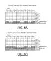
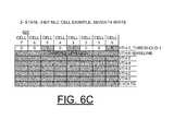
- FIGS. 6A , 6 B, and 6 Crespectively illustrate example moving baseline coding operations of first write, second write and seventh write for a 2-state, 3-bit MLC cell example in accordance with embodiments of the invention
- FIGS. 7A , 7 B, and 7 Crespectively illustrate example moving baseline coding operations of first write, second write and third write for a 3-state, 3-bit MLC cell example in accordance with embodiments of the invention
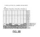
- FIGS. 8A , 8 B, and 8 Crespectively illustrate example moving baseline coding operations of first write, second write and seventh write for a 3-state, 4-bit MLC cell example in accordance with embodiments of the invention
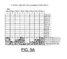
- FIGS. 9A , and 9 Brespectively illustrate an example moving baseline coding operations of first write, and fifth write for a 4-state, 4-bit MLC cell example in accordance with embodiments of the invention
- FIGS. 10A , and 10 Brespectively illustrate an example voltage drift with operations of data written, and data read for a 2-bit MLC NAND cell example in accordance with embodiments of the invention
- FIGS. 11A , 11 B, and 11 Crespectively illustrate an example partial-erase with operations of third data write, fast partial erase, and data re-write for a 2-bit MLC NAND cell example in accordance with embodiments of the invention
- FIGS. 12A , and 12 Brespectively illustrate an example change to threshold resolution with un-degraded cell and degraded cell for a 2-bit MLC NAND cell example in accordance with embodiments of the invention
- FIGS. 13A , and 13 B, 13 C, and 13 Drespectively illustrate example change to threshold resolution with un-degraded cell and degraded cell for a 3-bit MLC NAND cell example in accordance with embodiments of the invention
- FIG. 14is a chart illustrating example parameter data for MLC cell examples in accordance with embodiments of the invention.
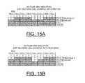
- FIGS. 15A , and 15 Billustrate example voltage leak indication with operations of data written, and data read for a 2-bit MLC NAND cell example in accordance with embodiments of the invention.
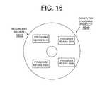
- FIG. 16is a block diagram illustrating a computer program product in accordance with embodiments of the invention.
- a method and apparatusfor implementing enhanced performance including enhanced data write, data read, and data partial-erase for multi-level cell (MLC) memory, for example, for solid state drives (SSDs).
- MLCmulti-level cell
- SSDssolid state drives
- the enhanced data write, data read, and data partial-erase for MLC memoryare implemented using threshold-voltage-drift or resistance-drift tolerant moving baseline (MB) memory data encoding of the invention.
- a moving baseline or flooris used in comparison to which read voltages are compared so that data integrity is less susceptible to threshold-voltage drift or resistance drift.
- Multi-level cell (MLC) phase change memory (PCM) and MLC NAND flash memoryboth have significant resistance drift and threshold-voltage drift respectively over time which is aggravated by typical write and erase cycles.
- Threshold voltage drift for cells of nearly identical charges physically located in proximity in the MLC NAND chipis nearly congruent, while this is not the case for cells of extremely different voltages physically placed away from each other in the chip. The large charge difference occurs when full MLC bit writing capability is employed during data cell writes.
- the resistance value drift for cells of nearly identical degree of amorphous/crystalline state physically placed in close proximity in the MLC PCM chipis nearly congruent, while this is not expected to be the case for cells with extremely different amorphous/crystalline states physically placed far away from each other in the chip.
- the large difference in amorphous/crystalline stateoccurs when the full MLC bit writing capability is employed during data cell writes.
- threshold voltage or resistance drift between similar-state memory cells in close physical proximity in the chipbeing generally congruent data can be more accurately recovered even with an occasional significant drift of a memory cell using voltage-drift or resistance drift tolerant MB data encoding of the invention.
- full-erases of cellsare provided, enabling a longer lifetime for the storage device.
- Full erase of cellscauses significant degradation to cell; about 5 k maximum full erase/write cycles are typical in 25 nm MLC NAND flash memory.
- Conventional higher voltages and longer time duration of voltage event during the full erasecause sustained high electric fields near floating gates of NAND cells with more damage.
- the present inventionuses smaller charge transfers to re-write new data upon old data; minimizing change to charge content of the floating gate.
- the postponed erase operationcomes after several consecutive write operations (and not after each write operation), and when it comes a partial erase instead of a full erase is used.
- PCMphase change memory
- the PCM cellsare placed in their highest resistance (amorphous state) for instance, the resistance of those PCM cells can be decreased by additional current pulse or pulses to the cells, nudging them progressively towards the more stable and low resistance crystalline state.
- MLC PCM cell resistancecan be changed without a full erase by pulsing the cell with voltage/current.
- charge content in the floating gate of MLC NAND cellscan be increased without a full erase.
- Moving Baseline (MB) memory data encoding of the inventionis now described using illustrative MLC NAND Flash cases. It should be understood that one skilled in the art will recognize that MB memory data encoding of the invention advantageously is extended to multi-level PCM memory without departing from the spirit or scope of the invention.
- an overall increase in number of byte-writes to the storage devicesis enabled.
- a 3-bit MLC storage cellcan be written at least seven times before a full-erase using 2-state MB code, increasing lifetime of cell about seven times, the loss of full data capacity for each write to a cell is only one third or one bit rather than three bits, thus there is an overall increase in lifetime of the storage device as measured in a per-written-byte basis.
- the 2-state MB codingproduces a 1-bit number in each cell regardless of the number of write levels, such that 3, 4, 5, 6, 7, 8, 9, or 10 write-levels all produce a 1-bit number.
- a 4-bit MLC storage cellcan be written at least fifteen times before a full-erase using 2-state MB code, increasing lifetime of cell about fifteen times, the loss of full data capacity for each write to a cell is only one fourth or one bit rather than four bits, thus there is an overall increase in lifetime of the storage device as measured in a per-written-byte basis.
- the larger the number of levelsthe larger the benefit in lifetime measured in per-written-byte basis MB can accrue. Note that these calculations are approximate as there is stress during the write cycle; however, this stress is significantly lower than the effects of full-erase stresses.
- some writesmay not need to move the baseline upwards so that a larger number of writes than threshold voltage levels in the MLC cell can be accommodated.
- floating gate charges between adjacent NAND flash cellsare in a similar range for example, as increasingly becomes favored by shrinking memory cell dimensions.
- Continuous shrinking of NAND memory sizesenhances the capacitance coupling between adjacent cells, significantly increasing the lateral fringing field disturbing NAND operations.
- simulationsshow that threshold voltage shift ( ⁇ VT) induced by adjacent cells on the same bitline (BL) and wordline (WL) increases exponentially with technology scaling.
- overhead needed for MB data encodingis minimal. Illegal data combinations for a group of memory cells are unlikely events that can be flagged as they occur in parameter data areas. Since MB is self referenced, if all the cells have the same threshold voltage, it can both be that all cells are 0s or all cells are 1s. This case can be avoided or flagged with the flag stored in a specified bit. Because MB data encoding keeps sets of memory cells self referenced with all these cells being allowed to have only one of two possible threshold values, if a few of the cells drift away from the set, it is possible to correct their contents. This could reduce the number of bytes of ECC protection that is needed to protect data.
- FIG. 1there is shown an example system for implementing enhanced data write, data read, and data partial-erase methods for multi-level cell (MLC) memory, for example, for solid state drives (SSDs) generally designated by the reference character 100 in accordance with an embodiment of the invention.
- System 100includes a solid state drive 102 and a host computer 104 .
- SSD 102includes a controller 106 coupled to a main memory or dynamic random access memory (DRAM) 108 , an MLC memory management information and control 110 and a moving baseline (MB) memory data encoding control 112 .
- DRAMdynamic random access memory
- MBmoving baseline
- SSD 102includes a plurality of multi-level cell (MLC) memory devices 114 coupled to the moving baseline (MB) memory data encoding control block 112 coupled to the controller 106 , such as a NAND flash chips 114 or phase-change-memory (PCM) chips 114 , or a combination of NAND flash chips and PCM chips.
- SSD 102includes a host interface 116 coupled between the host computer 104 , and the controller 106 and the moving baseline (MB) memory data encoding control block 112 .
- system 100is described in the context of the solid state drive 102 , it should be understood that principles of the present invention advantageously are applied to other types of data storage devices.
- Controller 106can be fabricated on one or multiple integrated circuit dies, and is suitably programmed to implement methods in accordance with embodiments of the invention.
- SSD 102implements enhanced data write, data read, and data partial-erase for multi-level cell (MLC) memory using threshold-voltage-drift or resistance-drift tolerant moving baseline memory data encoding for robust MLC memory data write, for robust MLC memory data read, and for robust MLC memory data partial-erase in accordance with embodiments of the invention.
- the controller 106 of SSD 102includes firmware that is given direct access to moving baseline (MB) memory data encoding control block 112 .
- the firmware of controller 106 of SSD 102is given information with respect to the moving baseline (MB) memory data encoding control block 112 , for example, from the MLC memory management information and control block 110 .
- the MLC memory management information and control block 110 and MB memory data encoding control block 112could be implemented by the host computer 104 or within the MLC memory devices 114 , instead of the MB memory data encoding being performed by the SSD 102 .
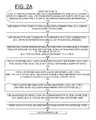
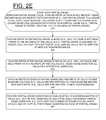
- FIGS. 2A and 2B , 2 C and 2 D, and 2 Ethere are shown respective flow charts illustrating example operations of the system of FIG. 1 for implementing enhanced performance including enhanced data write, enhanced data read, and enhanced data partial-erase for multi-level cell (MLC) memory using threshold-voltage-drift or resistance-drift tolerant moving baseline memory data encoding, for example, for solid state drives (SSDs) in accordance with embodiments of the invention.
- MLCmulti-level cell
- SSDssolid state drives
- voltage-drift tolerant moving baseline memory data encoding for robust MLC memory data writeuses a moving baseline, which is a floor or minimum voltage level for each new write to a memory cell.
- the multi-level cell memoryoptionally includes PCM and NAND flash memory.
- At least two or more write cyclesare enabled before full-erase, with using half or less of the full MLC bit range.
- Illegal data combinations for a group of memory cellsare avoided by coding or separate flags are used, such as all 0s are not permitted, or all 1s are not permitted; or a flag is set to indicate whether a set of cells with the same threshold voltage or same resistance value represents all 0s or all 1s data.
- FIGS. 2A and 2B , 2 C and 2 D, and 2 Eprovide respective flow charts illustrating example operations of the system 100 for implementing enhanced performance including enhanced data write, enhanced data read, and enhanced data partial-erase for multi-level cell (MLC) memory using moving baseline memory data encoding, for example, for solid state drives (SSDs) in accordance with embodiments of the invention.
- MLCmulti-level cell
- SSDssolid state drives
- FIGS. 2A and 2B , 2 C and 2 D, and 2 Eit should be understood that the illustrated example operations or steps include some sequential operations or steps and also include optional operations or steps, alternative operations or steps and combined operations or steps of optional embodiments of the invention.
- example operationsstart for robust MLC memory data write as indicated at a block 200 .
- the moving baselineis a new floor or minimum voltage level for each new write to a memory cell.
- the baseline for the prior writeis obtained prior to the write, for example, by reading cells before the write, or by keeping parameter information of cells with last known baseline level.
- the robust MLC memory data writeoptionally uses substitution code to avoid illegal data combinations.
- a run-length-limited (RLL) codeis used as substitution code as indicated at a block 202 .
- Separate flagsare used to indicate occurrences of illegal combinations, for example, a list of each occurrence of flags are stored in separate data area as indicated at a block 204 .
- Separate flags at block 204optionally are used together with the substitution code at block 202 , or can be used as an alternative to the substitution code.
- Periodically reference cellsoptionally are written at specified voltage levels to keep track of baseline voltage and voltage levels of available data values in the group of cells, for example, for voltage levels equivalent to a 1 or 0 as indicated at a block 206 .
- available data values for each cellare either a 1 or a 0.
- available data values for each cellare either a 1 or a 0.
- FIGS. 5A-5D and FIGS. 6A-6CCells act like single-level cell (SLC) with base-2 binary bit data.
- available data values for each cellinclude, for example, a 2, or a 1 or a 0 in an optional embodiment.
- FIGS. 7A-7C and FIGS. 8A-8CCells data is base-3, with separate data coding to convert block of cells to base 2 binary data.
- available data values for each cellinclude, for example, a 3, or a 2, or a 1 or a 0 in an optional embodiment.
- FIGS. 9A-9BCells data is again binary with 2-bits per cell.
- adjustable bit resolutionoptionally is used, such as via downgrading state-level of MB-code. For example, write data in 3-state MB-code rather than 4-state MB-code, or as indicated at a block 216 write data in 3-state MB-code rather than 3-state or 4-state MB-code.
- using optional adjustment to resolution to refresh data and that adjustmentcan be done at different scope, for example, individual pages, individual lines, individual chips, or individual words.
- using optional adjustable resolutioncan be provided via fewer write cycles before full erase.
- adjustments to resolutioncan be made by storage device itself in response to error correction information in an optional embodiment.
- adjustments to resolutioncan be made by storage device itself in response to voltage drift statistical information collected by storage device during use that measures the degradation of cells due to time-aging, write-cycle-aging, and/or full-erase-cycle aging, for example, warning signs of impending data loss trigger the storage device to downgrade the resolution.
- adjustment or selection of resolutionalso or alternatively can be made by user, such as based upon needs of host computer or other associated device or changing equipments costs or data storage needs, or adjustment or selection of resolution also can be made by manufacturer of the storage device during initial testing or binning. For example, binning of chips or sub-blocks in chips are completed by adjustment and selection of resolution, such as downgrade state-level of MB-code or reduce number of write cycles before full erase.
- the baseline voltageoptionally can be kept as a parameter, for example, to know which new voltage to write to for each write without having to perform a data read prior to write and must update baseline voltage parameter after each write to a cell and after each cell erase.
- the baseline voltageoptionally is not kept as a parameter, for example, with performing a data read of one or more sample cells prior to write to determine latest baseline voltage in an optional embodiment.
- threshold-voltage-drift or resistance-drift tolerant moving baseline memory data encoding for robust MLC memory data readenables read back and error recovery escalation for reading of data written to MLC with moving baseline.
- Initial data readoptionally is blind, for example, using comparison of high voltages with lower voltages. See FIGS. 10A and 10B for voltage drift example. For example, for 2-state MB code, the higher voltage will be a 1 and lower voltage will be a 0, and keeping track of baseline voltage as parameter data is not needed.
- data read backoptionally uses separate data to determine latest baseline, for example, separate data helps to compare voltage levels; and for example, separate data must be updated upon each data write and full-erase.
- optionally separate datais kept as parameter data, for example, a counter can be kept for each write to a page and reset upon each full-erase. For example, flag information or numerical data can be kept for a group of cells.
- alternatively separate datais actual reference cell voltage levels from periodic reference cell writes, such as analog voltage level from actual writes and readback. Reference cells can be some small percentage of a line, page or block.
- the error recovery subroutineoptionally looks at the separate data stored to determine latest baseline level. For example, read first tries a blind readback and if this fails, then looking at separate is providing for help in determining value of written data. Voltage drift of similar reference cells and/or statistical information from prior writes and readbacks can be used for assistance in recovering data.
- the error recovery subroutinealso or alternatively can read other similarly written data cells.
- cells read for baseline determinationare in the same line or page or block as the cell with error and have same baseline value.
- the baseline valueis determined from these other healthy cells.
- read data updateis provided using reference cell voltage reference information and/or similar cells in terms of the number of write/read cycles and number of erase cycles to determine voltage drift.
- write reference cellsfor example, write reference cells and later readback.
- the write event conditionssuch as voltage level, time/date of write, and total write and erase cycles to cell. For example, periodically read back these reference cells and determine voltage level drift; and maintain statistics regarding voltage drift for future adjustment/prediction.
- write data cellskeep track of baseline voltage level, and later readback.
- the write event conditionssuch as voltage level, time/date of write, and total write and erase cycles to cell.
- data read back or data integrity test timeread back these data cells and determine voltage level drift.
- threshold voltage-drift or resistance drift tolerant moving baseline memory data encoding for robust MLC memory data partial eraseis provided prior to re-write of data, whenever an erase is necessary because the baseline can not move further to accommodate the data to be written.
- partial eraseis used, full erase is not used because full erase is both slow and full erase also causes more cell degradation/stress than a partial-erase, with less current during erase for NAND flash, less heating for PCM.
- partial erasehas similar effect as cell voltage drift where all cells in a group change baseline values substantially together.
- optionally data re-write after partial eraseis blind.
- partial-eraseis assumed to reduce cell voltage to a sufficient level and all cells are re-written at new voltage.
- alternatively data re-write after partial eraseis not blind.
- cell voltageis read prior to the re-write of the cells. Read can be done for all cells or a statistical sampling of the cells.
- data re-write after both partial erase and pre-write of cells to a new baseline voltageFor example, in a conceptual description, cells are pre-written to a new baseline before new data write. For example, cells are pre-written to a next even baseline. In actual implementation, the final charge to which each cell will be programmed is reached in a single program command.
- duration and/or voltage for data partial-eraseis adapted to age/degradation of cells. For example, statistical sampling of cells is used for likely necessary partial-erase duration. For example, data kept for number of erase cycles, write cycles, and age of chip can help to determine duration and/or voltage of the partial-erase.
- FIGS. 3A , 3 B, and 3 Crespectively illustrate a start operation, with all cells fully erased for 2-bit NAND cells, 3-bit NAND cells and 4-bit NAND cells respectively generally designated by the reference character 300 , 310 , 320 in accordance with embodiments of the invention.
- the respective start operation 300 , 310 , 320 with all cells fully erasedincludes a V-read less than the illustrated Vth- 1 or V-read ⁇ Vth- 1 for each of 2-bit NAND cells, 3-bit NAND cells and 4-bit NAND cells.
- FIG. 4Arespectively illustrates 2-state moving baseline write (MBW) cycles for 2-bit NAND cells, 3-bit NAND cells and 4-bit NAND cells respectively generally designated by the reference character 400 , 410 , 420 in accordance with embodiments of the invention.
- MW2-state moving baseline write
- Vth- 2shown as THRESHOLD- 1
- Charge levelingis a conceptual description only to clarify the fundamental work of moving baseline.
- Vth- 3shown as THRESHOLD- 1
- FIGS. 7A , 7 B, and 7 Crespectively illustrate example moving baseline coding operations of first write, second write and third write respectively generally designated by the reference character 700 , 710 , 720 for a 3-state, 3-bit MLC cell example in accordance with embodiments of the invention.
- Vth- 1shown as THRESHOLD- 1
- Vth- 2shown as THRESHOLD- 2
- Vth- 3shown as THRESHOLD- 1
- Vth- 4shown as THRESHOLD- 2
- Vth- 1shown as THRESHOLD- 1
- Vth- 2shown as THRESHOLD- 2
- Vth- 3shown as THRESHOLD- 1
- Vth- 4shown as THRESHOLD- 2
- Vth- 12shown as THRESHOLD- 1
- Vth- 13shown as THRESHOLD- 2
- Vth- 14shown as THRESHOLD- 3
- Vth- 2shown as Vth- 2 ′ shown as THRESHOLD
- Vth- 1 ′BASELINE
- V-read0.
- Datais recoverable if voltage drift is substantially the same between the cells, with ability to adjust threshold voltages for read data used as needed.
- Vth- 3shown as THRESHOLD
- the data partial erase operation 1110is shown, where there is potentially uneven erasure between cells.
- the data re-write operation 1120is shown following the partial erase operation 1110 .
- Vth- 3shown as THRESHOLD
- FIGS. 13A , and 13 B, 13 C, and 13 Drespectively illustrate example change to threshold resolution with un-degraded cell and degraded cell respectively generally designated by the reference character 1300 , 1310 , 1320 , and 1330 for a 3-bit MLC NAND cell example in accordance with embodiments of the invention.
- FIG. 13AWith the un-degraded cell example 1300 , there are five threshold levels, Vth- 1 , Vth- 2 , Vth- 3 , Vth- 4 , and Vth- 5 for five moving baseline writes.
- FIG. 13Bwith the degraded cell example 1310 , there are four threshold levels, Vth- 1 ′, Vth- 2 ′, Vth- 3 ′, and Vth- 4 ′ for four moving baseline writes.
- FIG. 13Cwith the degraded cell example 1320 , there are three threshold levels, Vth- 1 ′, Vth- 2 ′, and Vth- 3 ′ for three moving baseline writes.
- FIG. 13Dwith the degraded cell example 1330 , there are two threshold levels, Vth- 1 ′, and Vth- 2 ′ for two moving baseline writes.
- the example parameter data for example MLC cell examples 1400includes respective example levels per cell 1402 , numerical base 1404 , number of threshold levels 1406 , available moving baseline writes is cells are un-degraded after full erase 1408 , and range of available moving baseline writes is cells are degraded after full erase 1410 .
- FIGS. 15A , and 15 Billustrate example voltage leak indication with operations of data written, and data read back respectively generally designated by the reference character 1500 , 1510 for a 2-bit MLC NAND cell example in accordance with embodiments of the invention.
- Vth- 3shown as THRESHOLD- 1
- the moving baseline decodercan either flag the leak as an error or assign to the leaking cell a “0” or “1” with different probabilities and pass this to a soft decoder/error correcting system for final decision on the correct cell content.
- These leak eventscan also be used by a management system to attribute an age for the part according to the frequency these leaky bits occur, which might at a pre-defined threshold recommend for the replacement of the whole memory part.
- Moving Baseline (MB) memory data encoding of the inventionhas been generally described with respect to illustrative MLC NAND Flash cases, one skilled in the art will recognize that MB memory data encoding of the invention also is used advantageously with multi-level PCM memory without departing from the spirit or scope of the invention.
- the computer program product 1600includes a computer readable recording medium 1602 , such as, a floppy disk, a high capacity read only memory in the form of an optically read compact disk or CD-ROM, a tape, or another similar computer program product.
- Computer readable recording medium 1602stores program means or control code 1604 , 1606 , 1608 , 1610 on the medium 1602 for carrying out the methods for implementing enhanced data write, enhanced data read, and enhanced data partial-erase for multi-level cell (MLC) memory using threshold-voltage-drift or resistance-drift tolerant moving baseline memory data encoding of the embodiments of the invention in the system 100 of FIG. 1 .
- MLCmulti-level cell
- MLCmulti-level cell
Landscapes
- Engineering & Computer Science (AREA)
- Computer Hardware Design (AREA)
- Chemical & Material Sciences (AREA)
- Crystallography & Structural Chemistry (AREA)
- Theoretical Computer Science (AREA)
- Microelectronics & Electronic Packaging (AREA)
- Physics & Mathematics (AREA)
- General Engineering & Computer Science (AREA)
- General Physics & Mathematics (AREA)
- Read Only Memory (AREA)
- For Increasing The Reliability Of Semiconductor Memories (AREA)
Abstract
Description
Claims (19)
Priority Applications (4)
| Application Number | Priority Date | Filing Date | Title |
|---|---|---|---|
| US13/361,918US9208871B2 (en) | 2012-01-30 | 2012-01-30 | Implementing enhanced data read for multi-level cell (MLC) memory using threshold voltage-drift or resistance drift tolerant moving baseline memory data encoding |
| KR1020130007448AKR20130088061A (en) | 2012-01-30 | 2013-01-23 | Implementing enhanced data read for multi-level cell (mlc) memory using threshold voltage-drift or resistance drift tolerant moving baseline memory data encoding |
| DE102013001401ADE102013001401A1 (en) | 2012-01-30 | 2013-01-28 | Implementation of extended data reading for multilevel cell (MLC) memory using threshold baseline drift or resistance drift tolerant moving base line memory data encoding |
| GB1301474.1AGB2498875A (en) | 2012-01-30 | 2013-01-28 | Data read of a drift tolerant moving baseline data encoded multi-level memory cell (MLC) |
Applications Claiming Priority (1)
| Application Number | Priority Date | Filing Date | Title |
|---|---|---|---|
| US13/361,918US9208871B2 (en) | 2012-01-30 | 2012-01-30 | Implementing enhanced data read for multi-level cell (MLC) memory using threshold voltage-drift or resistance drift tolerant moving baseline memory data encoding |
Publications (2)
| Publication Number | Publication Date |
|---|---|
| US20130194865A1 US20130194865A1 (en) | 2013-08-01 |
| US9208871B2true US9208871B2 (en) | 2015-12-08 |
Family
ID=47890884
Family Applications (1)
| Application Number | Title | Priority Date | Filing Date |
|---|---|---|---|
| US13/361,918Active2033-04-30US9208871B2 (en) | 2012-01-30 | 2012-01-30 | Implementing enhanced data read for multi-level cell (MLC) memory using threshold voltage-drift or resistance drift tolerant moving baseline memory data encoding |
Country Status (4)
| Country | Link |
|---|---|
| US (1) | US9208871B2 (en) |
| KR (1) | KR20130088061A (en) |
| DE (1) | DE102013001401A1 (en) |
| GB (1) | GB2498875A (en) |
Cited By (2)
| Publication number | Priority date | Publication date | Assignee | Title |
|---|---|---|---|---|
| US20140177322A1 (en)* | 2012-12-26 | 2014-06-26 | Research & Business Foundation Sungkyunkwan University | Semiconductor memory apparatus, verify read method and system |
| US10452312B2 (en) | 2016-12-30 | 2019-10-22 | Intel Corporation | Apparatus, system, and method to determine a demarcation voltage to use to read a non-volatile memory |
Families Citing this family (54)
| Publication number | Priority date | Publication date | Assignee | Title |
|---|---|---|---|---|
| US8762620B2 (en) | 2007-12-27 | 2014-06-24 | Sandisk Enterprise Ip Llc | Multiprocessor storage controller |
| US9699263B1 (en) | 2012-08-17 | 2017-07-04 | Sandisk Technologies Llc. | Automatic read and write acceleration of data accessed by virtual machines |
| US9501398B2 (en) | 2012-12-26 | 2016-11-22 | Sandisk Technologies Llc | Persistent storage device with NVRAM for staging writes |
| US9612948B2 (en) | 2012-12-27 | 2017-04-04 | Sandisk Technologies Llc | Reads and writes between a contiguous data block and noncontiguous sets of logical address blocks in a persistent storage device |
| US9454420B1 (en) | 2012-12-31 | 2016-09-27 | Sandisk Technologies Llc | Method and system of reading threshold voltage equalization |
| US9870830B1 (en) | 2013-03-14 | 2018-01-16 | Sandisk Technologies Llc | Optimal multilevel sensing for reading data from a storage medium |
| US9367246B2 (en) | 2013-03-15 | 2016-06-14 | Sandisk Technologies Inc. | Performance optimization of data transfer for soft information generation |
| US9244763B1 (en) | 2013-03-15 | 2016-01-26 | Sandisk Enterprise Ip Llc | System and method for updating a reading threshold voltage based on symbol transition information |
| US9524235B1 (en) | 2013-07-25 | 2016-12-20 | Sandisk Technologies Llc | Local hash value generation in non-volatile data storage systems |
| US9384126B1 (en) | 2013-07-25 | 2016-07-05 | Sandisk Technologies Inc. | Methods and systems to avoid false negative results in bloom filters implemented in non-volatile data storage systems |
| US9361221B1 (en)* | 2013-08-26 | 2016-06-07 | Sandisk Technologies Inc. | Write amplification reduction through reliable writes during garbage collection |
| US9639463B1 (en) | 2013-08-26 | 2017-05-02 | Sandisk Technologies Llc | Heuristic aware garbage collection scheme in storage systems |
| US9298608B2 (en) | 2013-10-18 | 2016-03-29 | Sandisk Enterprise Ip Llc | Biasing for wear leveling in storage systems |
| US9442662B2 (en) | 2013-10-18 | 2016-09-13 | Sandisk Technologies Llc | Device and method for managing die groups |
| US9436831B2 (en) | 2013-10-30 | 2016-09-06 | Sandisk Technologies Llc | Secure erase in a memory device |
| US9703816B2 (en) | 2013-11-19 | 2017-07-11 | Sandisk Technologies Llc | Method and system for forward reference logging in a persistent datastore |
| US9520197B2 (en) | 2013-11-22 | 2016-12-13 | Sandisk Technologies Llc | Adaptive erase of a storage device |
| US9520162B2 (en) | 2013-11-27 | 2016-12-13 | Sandisk Technologies Llc | DIMM device controller supervisor |
| GB201320983D0 (en)* | 2013-11-28 | 2014-01-15 | Ibm | Data encoding in solid-state storage apparatus |
| US9582058B2 (en) | 2013-11-29 | 2017-02-28 | Sandisk Technologies Llc | Power inrush management of storage devices |
| GB201322075D0 (en) | 2013-12-13 | 2014-01-29 | Ibm | Device for selecting a level for at least one read voltage |
| US9703636B2 (en) | 2014-03-01 | 2017-07-11 | Sandisk Technologies Llc | Firmware reversion trigger and control |
| US9390814B2 (en) | 2014-03-19 | 2016-07-12 | Sandisk Technologies Llc | Fault detection and prediction for data storage elements |
| US9454448B2 (en) | 2014-03-19 | 2016-09-27 | Sandisk Technologies Llc | Fault testing in storage devices |
| US9448876B2 (en) | 2014-03-19 | 2016-09-20 | Sandisk Technologies Llc | Fault detection and prediction in storage devices |
| US9626400B2 (en) | 2014-03-31 | 2017-04-18 | Sandisk Technologies Llc | Compaction of information in tiered data structure |
| US9390021B2 (en) | 2014-03-31 | 2016-07-12 | Sandisk Technologies Llc | Efficient cache utilization in a tiered data structure |
| US9626399B2 (en) | 2014-03-31 | 2017-04-18 | Sandisk Technologies Llc | Conditional updates for reducing frequency of data modification operations |
| US9697267B2 (en) | 2014-04-03 | 2017-07-04 | Sandisk Technologies Llc | Methods and systems for performing efficient snapshots in tiered data structures |
| US10162748B2 (en) | 2014-05-30 | 2018-12-25 | Sandisk Technologies Llc | Prioritizing garbage collection and block allocation based on I/O history for logical address regions |
| US10656842B2 (en) | 2014-05-30 | 2020-05-19 | Sandisk Technologies Llc | Using history of I/O sizes and I/O sequences to trigger coalesced writes in a non-volatile storage device |
| US10656840B2 (en) | 2014-05-30 | 2020-05-19 | Sandisk Technologies Llc | Real-time I/O pattern recognition to enhance performance and endurance of a storage device |
| US10114557B2 (en) | 2014-05-30 | 2018-10-30 | Sandisk Technologies Llc | Identification of hot regions to enhance performance and endurance of a non-volatile storage device |
| US10372613B2 (en) | 2014-05-30 | 2019-08-06 | Sandisk Technologies Llc | Using sub-region I/O history to cache repeatedly accessed sub-regions in a non-volatile storage device |
| US9703491B2 (en) | 2014-05-30 | 2017-07-11 | Sandisk Technologies Llc | Using history of unaligned writes to cache data and avoid read-modify-writes in a non-volatile storage device |
| US10146448B2 (en) | 2014-05-30 | 2018-12-04 | Sandisk Technologies Llc | Using history of I/O sequences to trigger cached read ahead in a non-volatile storage device |
| US9652381B2 (en) | 2014-06-19 | 2017-05-16 | Sandisk Technologies Llc | Sub-block garbage collection |
| US9443601B2 (en) | 2014-09-08 | 2016-09-13 | Sandisk Technologies Llc | Holdup capacitor energy harvesting |
| US9251909B1 (en) | 2014-09-29 | 2016-02-02 | International Business Machines Corporation | Background threshold voltage shifting using base and delta threshold voltage shift values in flash memory |
| US9563373B2 (en) | 2014-10-21 | 2017-02-07 | International Business Machines Corporation | Detecting error count deviations for non-volatile memory blocks for advanced non-volatile memory block management |
| US10365859B2 (en) | 2014-10-21 | 2019-07-30 | International Business Machines Corporation | Storage array management employing a merged background management process |
| KR20160057182A (en) | 2014-11-13 | 2016-05-23 | 에스케이하이닉스 주식회사 | Resistance Variable Memory Apparatus, Read Circuit Unit and Operation Method Therefor |
| KR102245129B1 (en) | 2014-11-24 | 2021-04-28 | 삼성전자 주식회사 | Cross-point Memory Device including multi-level cells and Operating Method thereof |
| US10339048B2 (en) | 2014-12-23 | 2019-07-02 | International Business Machines Corporation | Endurance enhancement scheme using memory re-evaluation |
| US9990279B2 (en) | 2014-12-23 | 2018-06-05 | International Business Machines Corporation | Page-level health equalization |
| US9652350B2 (en) | 2015-01-22 | 2017-05-16 | International Business Machines Corporation | Evaluation of complex SAN environments |
| US9558823B1 (en)* | 2015-09-04 | 2017-01-31 | Macronix International Co., Ltd. | Resistance drift recovery method for MLC PCM |
| US9646721B1 (en)* | 2016-03-31 | 2017-05-09 | EMC IP Holding Company LLC | Solid state drive bad block management |
| TWI623878B (en)* | 2017-07-07 | 2018-05-11 | 大心電子(英屬維京群島)股份有限公司 | Data reading method and storage controller |
| TWI627532B (en)* | 2017-07-25 | 2018-06-21 | 旺宏電子股份有限公司 | Data management method and system for memory device |
| US10170195B1 (en) | 2017-12-06 | 2019-01-01 | International Business Machines Corporation | Threshold voltage shifting at a lower bit error rate by intelligently performing dummy configuration reads |
| US10629247B2 (en) | 2017-12-21 | 2020-04-21 | Western Digital Technologies, Inc. | Read threshold adjustment using reference data |
| CN109884550B (en)* | 2019-04-01 | 2020-01-17 | 北京理工大学 | An online parameter identification and backtracking method for power battery system |
| CN111276176A (en)* | 2020-02-11 | 2020-06-12 | 上海威固信息技术股份有限公司 | Three-dimensional stacked flash memory unit threshold voltage distribution model construction method |
Citations (18)
| Publication number | Priority date | Publication date | Assignee | Title |
|---|---|---|---|---|
| US5867429A (en)* | 1997-11-19 | 1999-02-02 | Sandisk Corporation | High density non-volatile flash memory without adverse effects of electric field coupling between adjacent floating gates |
| US20050213387A1 (en)* | 2004-03-29 | 2005-09-29 | Renesas Technology Corp. | Semiconductor memory device enhancing reliability in data reading |
| EP1746604A1 (en) | 2005-07-22 | 2007-01-24 | STMicroelectronics S.r.l. | Method for accessing a multilevel nonvolatile memory device of the flash NAND type |
| WO2007132452A2 (en) | 2006-05-12 | 2007-11-22 | Anobit Technologies | Reducing programming error in memory devices |
| US7333364B2 (en) | 2000-01-06 | 2008-02-19 | Super Talent Electronics, Inc. | Cell-downgrading and reference-voltage adjustment for a multi-bit-cell flash memory |
| WO2008053472A2 (en) | 2006-10-30 | 2008-05-08 | Anobit Technologies Ltd. | Reading memory cells using multiple thresholds |
| US20090132758A1 (en) | 2007-11-20 | 2009-05-21 | California Institute Of Technology | Rank modulation for flash memories |
| US20090300465A1 (en) | 2008-06-03 | 2009-12-03 | Zining Wu | Statistical tracking for flash memory |
| US20100070799A1 (en) | 2006-05-15 | 2010-03-18 | Apple Inc. | Dynamic cell bit resolution |
| US20100290282A1 (en) | 2009-05-12 | 2010-11-18 | Fujifilm Corporation | Method and system for adaptively finding reference voltages for reading data from a mlc flash memory |
| US20110072191A1 (en) | 2009-09-21 | 2011-03-24 | Skymedi Corporation | Uniform Coding System for a Flash Memory |
| US20110170349A1 (en) | 2004-07-26 | 2011-07-14 | Meir Avraham | Drift compensation in a flash memory |
| US20110307764A1 (en) | 2010-06-10 | 2011-12-15 | Global Unichip Corporation | Data transfer protection apparatus for flash memory controller |
| WO2012023102A1 (en) | 2010-08-17 | 2012-02-23 | Technion R&D Foundation | Mitigating inter-cell coupling effects in non volatile memory (nvm) cells |
| US20120069674A1 (en)* | 2010-09-20 | 2012-03-22 | Samsung Electronics Co., Ltd. | Flash memory device and related program verification method |
| US20120239854A1 (en)* | 2009-05-12 | 2012-09-20 | Stec., Inc. | Flash storage device with read cache |
| US20120254699A1 (en)* | 2011-04-01 | 2012-10-04 | Ruby Paul D | Dynamic read channel calibration for non-volatile memory devices |
| US8792272B2 (en)* | 2012-01-30 | 2014-07-29 | HGST Netherlands B.V. | Implementing enhanced data partial-erase for multi-level cell (MLC) memory using threshold voltage-drift or resistance drift tolerant moving baseline memory data encoding |
Family Cites Families (1)
| Publication number | Priority date | Publication date | Assignee | Title |
|---|---|---|---|---|
| US8898374B2 (en)* | 2010-07-21 | 2014-11-25 | Silicon Motion, Inc. | Flash memory device and method for managing flash memory device |
- 2012
- 2012-01-30USUS13/361,918patent/US9208871B2/enactiveActive
- 2013
- 2013-01-23KRKR1020130007448Apatent/KR20130088061A/ennot_activeCeased
- 2013-01-28DEDE102013001401Apatent/DE102013001401A1/enactivePending
- 2013-01-28GBGB1301474.1Apatent/GB2498875A/ennot_activeWithdrawn
Patent Citations (18)
| Publication number | Priority date | Publication date | Assignee | Title |
|---|---|---|---|---|
| US5867429A (en)* | 1997-11-19 | 1999-02-02 | Sandisk Corporation | High density non-volatile flash memory without adverse effects of electric field coupling between adjacent floating gates |
| US7333364B2 (en) | 2000-01-06 | 2008-02-19 | Super Talent Electronics, Inc. | Cell-downgrading and reference-voltage adjustment for a multi-bit-cell flash memory |
| US20050213387A1 (en)* | 2004-03-29 | 2005-09-29 | Renesas Technology Corp. | Semiconductor memory device enhancing reliability in data reading |
| US20110170349A1 (en) | 2004-07-26 | 2011-07-14 | Meir Avraham | Drift compensation in a flash memory |
| EP1746604A1 (en) | 2005-07-22 | 2007-01-24 | STMicroelectronics S.r.l. | Method for accessing a multilevel nonvolatile memory device of the flash NAND type |
| WO2007132452A2 (en) | 2006-05-12 | 2007-11-22 | Anobit Technologies | Reducing programming error in memory devices |
| US20100070799A1 (en) | 2006-05-15 | 2010-03-18 | Apple Inc. | Dynamic cell bit resolution |
| WO2008053472A2 (en) | 2006-10-30 | 2008-05-08 | Anobit Technologies Ltd. | Reading memory cells using multiple thresholds |
| US20090132758A1 (en) | 2007-11-20 | 2009-05-21 | California Institute Of Technology | Rank modulation for flash memories |
| US20090300465A1 (en) | 2008-06-03 | 2009-12-03 | Zining Wu | Statistical tracking for flash memory |
| US20100290282A1 (en) | 2009-05-12 | 2010-11-18 | Fujifilm Corporation | Method and system for adaptively finding reference voltages for reading data from a mlc flash memory |
| US20120239854A1 (en)* | 2009-05-12 | 2012-09-20 | Stec., Inc. | Flash storage device with read cache |
| US20110072191A1 (en) | 2009-09-21 | 2011-03-24 | Skymedi Corporation | Uniform Coding System for a Flash Memory |
| US20110307764A1 (en) | 2010-06-10 | 2011-12-15 | Global Unichip Corporation | Data transfer protection apparatus for flash memory controller |
| WO2012023102A1 (en) | 2010-08-17 | 2012-02-23 | Technion R&D Foundation | Mitigating inter-cell coupling effects in non volatile memory (nvm) cells |
| US20120069674A1 (en)* | 2010-09-20 | 2012-03-22 | Samsung Electronics Co., Ltd. | Flash memory device and related program verification method |
| US20120254699A1 (en)* | 2011-04-01 | 2012-10-04 | Ruby Paul D | Dynamic read channel calibration for non-volatile memory devices |
| US8792272B2 (en)* | 2012-01-30 | 2014-07-29 | HGST Netherlands B.V. | Implementing enhanced data partial-erase for multi-level cell (MLC) memory using threshold voltage-drift or resistance drift tolerant moving baseline memory data encoding |
Non-Patent Citations (9)
| Title |
|---|
| "Characterizing Flash Memory: Anomalies, Observations, and Applications" by Laura M. Grupp et al., MICRO'09, Dec. 12-16, 2009, New York, NY, USA., Copyright 2009 ACM 978-1-60558-798-01/09/12. |
| "Efficient Coding for a Two-Dimensional Run length-Limited Constraint" by Ron M. Roth, Paul H. Siegelb, and Jack K. WolfComputer Science Department, Technion, Haifa 32000, Israel, ECE, 0407, University of California, San Diego, 9500 Gilman Drive La Jolla, CA 92093-0407 CMRR, 0401, University of California, San Diego, 9500 Gilman Drive La Jolla, CA 92093-0401. |
| "Efficient Two-Write Wom-Codes" by Eitan Yaakobi, et al., University of California, San Diego La Jolla, CA 92093-0401, USA Emails: {eyaakobi, skayser, psiegel, avardy, jwolf}©ucsd.edu. |
| "IBM reports drift-tolerant multilevel cell PCM", by Peter Clarke, Jun. 30, 2011, http://www.eetimes.com/General/DisplayPrintViewContent/4217373. |
| "Multiple-Write WOM-Codes" by Scott Kayse et al., Forty-Eighth Annual Allerton Conference Allerton House, UIUC, Illinois, USA, Sep. 29-Oct. 1, 2010, pp. 1062-1068. |
| "Rank Modulation for Flash Memories" nu Anxiao Jian et al., IEEE Transactions on Information Theory, vol. 55, No. 6, Jun. 2009. |
| "Run-length limited", Wikipedia, the free encyclopedia, http://en.wikipedia.org/wiki/Run-length-limited[Dec. 2, 2011 3:13:18 PM] . |
| Berman et al., "Constrained Flash Memory Programming", Proceedings of 2011 IEEE International Symposium on Information Theory-ISIT, Jul. 31-Aug. 2011, pp. 2128-2132, ISBN 978-1-4577-0596-0 (INSPEC A/N 12300245). |
| Zhang et al., "Helmet: A Resistance Drift Resilient Architecture for Multi-level Cell Phase Change Memory System", 2011 IEEE/IFIP 41st International Conference on Dependable Systems & Networks (DSN), Jun. 27-30, 2011, Hong Kong, China, pp. 197-208, ISBN 978-1-4244-9232-9 (IEE, INSEPC A/N 12122044). |
Cited By (3)
| Publication number | Priority date | Publication date | Assignee | Title |
|---|---|---|---|---|
| US20140177322A1 (en)* | 2012-12-26 | 2014-06-26 | Research & Business Foundation Sungkyunkwan University | Semiconductor memory apparatus, verify read method and system |
| US9424916B2 (en)* | 2012-12-26 | 2016-08-23 | Research & Business Foundation Sungkyunkwan University | Semiconductor memory device and method for reading the same using a memory cell array including resistive memory cells to perform a single read command |
| US10452312B2 (en) | 2016-12-30 | 2019-10-22 | Intel Corporation | Apparatus, system, and method to determine a demarcation voltage to use to read a non-volatile memory |
Also Published As
| Publication number | Publication date |
|---|---|
| KR20130088061A (en) | 2013-08-07 |
| DE102013001401A1 (en) | 2013-09-26 |
| US20130194865A1 (en) | 2013-08-01 |
| GB201301474D0 (en) | 2013-03-13 |
| GB2498875A (en) | 2013-07-31 |
Similar Documents
| Publication | Publication Date | Title |
|---|---|---|
| US9208871B2 (en) | Implementing enhanced data read for multi-level cell (MLC) memory using threshold voltage-drift or resistance drift tolerant moving baseline memory data encoding | |
| US8792272B2 (en) | Implementing enhanced data partial-erase for multi-level cell (MLC) memory using threshold voltage-drift or resistance drift tolerant moving baseline memory data encoding | |
| US8699266B2 (en) | Implementing enhanced data write for multi-level cell (MLC) memory using threshold voltage-drift or resistance drift tolerant moving baseline memory data encoding | |
| KR102042889B1 (en) | Detection of read disturbances on non-volatile memories through counting of read accesses within divisions of the memory | |
| US9229644B2 (en) | Targeted copy of data relocation | |
| CN103853582B (en) | flash memory updating method | |
| JP6027059B2 (en) | Method and apparatus for managing data in memory | |
| KR100963707B1 (en) | Flash memory management method, memory device, system, computer-readable recording medium, non-volatile storage element array management method | |
| US8713380B2 (en) | Non-volatile memory and method having efficient on-chip block-copying with controlled error rate | |
| US9001578B2 (en) | Soft erasure of memory cells | |
| WO2013132532A1 (en) | Semiconductor storage device having nonvolatile semiconductor memory | |
| US9099185B2 (en) | Using different programming modes to store data to a memory cell | |
| JP2019168937A (en) | Memory system, control method and controller | |
| US9501400B2 (en) | Identification and operation of sub-prime blocks in nonvolatile memory | |
| US20140254263A1 (en) | Write Sequence Providing Write Abort Protection | |
| US9342401B2 (en) | Selective in-situ retouching of data in nonvolatile memory | |
| US20160078945A1 (en) | Incremental step pulse programming | |
| US9053011B2 (en) | Selective protection of lower page data during upper page write | |
| US8732391B2 (en) | Obsolete block management for data retention in nonvolatile memory | |
| US9047974B2 (en) | Erased state reading | |
| JP2021026448A (en) | Storage part system, storage part controller, and storage part control method |
Legal Events
| Date | Code | Title | Description |
|---|---|---|---|
| AS | Assignment | Owner name:HITACHI GLOBAL STORAGE TECHNOLOGIES NETHERLANDS B. Free format text:ASSIGNMENT OF ASSIGNORS INTEREST;ASSIGNORS:BANDIC, ZVONIMIR Z.;FRANCA-NETO, LUIZ M.;GUYOT, CYRIL;AND OTHERS;SIGNING DATES FROM 20120126 TO 20120130;REEL/FRAME:027620/0994 | |
| AS | Assignment | Owner name:HGST NETHERLANDS B.V., NETHERLANDS Free format text:CHANGE OF NAME;ASSIGNOR:HITACHI GLOBAL STORAGE TECHNOLOGIES NETHERLANDS B.V.;REEL/FRAME:030891/0256 Effective date:20120723 | |
| STCF | Information on status: patent grant | Free format text:PATENTED CASE | |
| AS | Assignment | Owner name:WESTERN DIGITAL TECHNOLOGIES, INC., CALIFORNIA Free format text:ASSIGNMENT OF ASSIGNORS INTEREST;ASSIGNOR:HGST NETHERLANDS B.V.;REEL/FRAME:040826/0327 Effective date:20160831 | |
| MAFP | Maintenance fee payment | Free format text:PAYMENT OF MAINTENANCE FEE, 4TH YEAR, LARGE ENTITY (ORIGINAL EVENT CODE: M1551); ENTITY STATUS OF PATENT OWNER: LARGE ENTITY Year of fee payment:4 | |
| AS | Assignment | Owner name:JPMORGAN CHASE BANK, N.A., AS AGENT, ILLINOIS Free format text:SECURITY INTEREST;ASSIGNOR:WESTERN DIGITAL TECHNOLOGIES, INC.;REEL/FRAME:052915/0566 Effective date:20200113 | |
| AS | Assignment | Owner name:WESTERN DIGITAL TECHNOLOGIES, INC., CALIFORNIA Free format text:RELEASE OF SECURITY INTEREST AT REEL 052915 FRAME 0566;ASSIGNOR:JPMORGAN CHASE BANK, N.A.;REEL/FRAME:059127/0001 Effective date:20220203 | |
| MAFP | Maintenance fee payment | Free format text:PAYMENT OF MAINTENANCE FEE, 8TH YEAR, LARGE ENTITY (ORIGINAL EVENT CODE: M1552); ENTITY STATUS OF PATENT OWNER: LARGE ENTITY Year of fee payment:8 | |
| AS | Assignment | Owner name:JPMORGAN CHASE BANK, N.A., ILLINOIS Free format text:PATENT COLLATERAL AGREEMENT - A&R LOAN AGREEMENT;ASSIGNOR:WESTERN DIGITAL TECHNOLOGIES, INC.;REEL/FRAME:064715/0001 Effective date:20230818 Owner name:JPMORGAN CHASE BANK, N.A., ILLINOIS Free format text:PATENT COLLATERAL AGREEMENT - DDTL LOAN AGREEMENT;ASSIGNOR:WESTERN DIGITAL TECHNOLOGIES, INC.;REEL/FRAME:067045/0156 Effective date:20230818 | |
| AS | Assignment | Owner name:SANDISK TECHNOLOGIES, INC., CALIFORNIA Free format text:ASSIGNMENT OF ASSIGNORS INTEREST;ASSIGNOR:WESTERN DIGITAL TECHNOLOGIES, INC.;REEL/FRAME:067567/0682 Effective date:20240503 | |
| AS | Assignment | Owner name:SANDISK TECHNOLOGIES, INC., CALIFORNIA Free format text:CHANGE OF NAME;ASSIGNOR:SANDISK TECHNOLOGIES, INC.;REEL/FRAME:067982/0032 Effective date:20240621 | |
| AS | Assignment | Owner name:JPMORGAN CHASE BANK, N.A., AS THE AGENT, ILLINOIS Free format text:PATENT COLLATERAL AGREEMENT;ASSIGNOR:SANDISK TECHNOLOGIES, INC.;REEL/FRAME:068762/0494 Effective date:20240820 | |
| AS | Assignment | Owner name:WESTERN DIGITAL TECHNOLOGIES, INC., CALIFORNIA Free format text:ASSIGNMENT OF ASSIGNORS INTEREST;ASSIGNOR:SANDISK TECHNOLOGIES, INC.;REEL/FRAME:069168/0273 Effective date:20241008 | |
| AS | Assignment | Owner name:JPMORGAN CHASE BANK, N.A., AS COLLATERAL AGENT, ILLINOIS Free format text:SECURITY AGREEMENT (SUPPLEMENTAL);ASSIGNOR:WESTERN DIGITAL TECHNOLOGIES, INC.;REEL/FRAME:069411/0208 Effective date:20241030 |