US9201193B1 - Textured fiber optic coupled image intensified camera - Google Patents
Textured fiber optic coupled image intensified cameraDownload PDFInfo
- Publication number
- US9201193B1 US9201193B1US13/769,518US201313769518AUS9201193B1US 9201193 B1US9201193 B1US 9201193B1US 201313769518 AUS201313769518 AUS 201313769518AUS 9201193 B1US9201193 B1US 9201193B1
- Authority
- US
- United States
- Prior art keywords
- core
- fiber optic
- image sensor
- optic bundle
- bond layer
- Prior art date
- Legal status (The legal status is an assumption and is not a legal conclusion. Google has not performed a legal analysis and makes no representation as to the accuracy of the status listed.)
- Active, expires
Links
- 239000000835fiberSubstances0.000titleclaimsabstractdescription147
- 238000005253claddingMethods0.000claimsdescription17
- 238000010168coupling processMethods0.000claimsdescription7
- 230000008878couplingEffects0.000claimsdescription6
- 238000005859coupling reactionMethods0.000claimsdescription6
- 230000003287optical effectEffects0.000claimsdescription6
- 230000007480spreadingEffects0.000claimsdescription6
- 238000003892spreadingMethods0.000claimsdescription6
- 230000000295complement effectEffects0.000claimsdescription3
- 239000011162core materialSubstances0.000description82
- 239000000463materialSubstances0.000description22
- 239000011521glassSubstances0.000description11
- 230000006870functionEffects0.000description6
- 230000007423decreaseEffects0.000description3
- NCGICGYLBXGBGN-UHFFFAOYSA-N3-morpholin-4-yl-1-oxa-3-azonia-2-azanidacyclopent-3-en-5-imine;hydrochlorideChemical compoundCl.[N-]1OC(=N)C=[N+]1N1CCOCC1NCGICGYLBXGBGN-UHFFFAOYSA-N0.000description2
- OAICVXFJPJFONN-UHFFFAOYSA-NPhosphorusChemical compound[P]OAICVXFJPJFONN-UHFFFAOYSA-N0.000description2
- BJQHLKABXJIVAM-UHFFFAOYSA-Nbis(2-ethylhexyl) phthalateChemical compoundCCCCC(CC)COC(=O)C1=CC=CC=C1C(=O)OCC(CC)CCCCBJQHLKABXJIVAM-UHFFFAOYSA-N0.000description2
- 239000000919ceramicSubstances0.000description2
- 230000000694effectsEffects0.000description2
- 230000006872improvementEffects0.000description2
- 238000000034methodMethods0.000description2
- 239000013307optical fiberSubstances0.000description2
- 230000008569processEffects0.000description2
- 238000007493shaping processMethods0.000description2
- 239000000126substanceSubstances0.000description2
- 239000000758substrateSubstances0.000description2
- XUIMIQQOPSSXEZ-UHFFFAOYSA-NSiliconChemical compound[Si]XUIMIQQOPSSXEZ-UHFFFAOYSA-N0.000description1
- 238000003491arrayMethods0.000description1
- 230000008859changeEffects0.000description1
- 238000006243chemical reactionMethods0.000description1
- 238000005520cutting processMethods0.000description1
- 230000003247decreasing effectEffects0.000description1
- 230000001419dependent effectEffects0.000description1
- 238000004519manufacturing processMethods0.000description1
- 230000007246mechanismEffects0.000description1
- 230000015654memoryEffects0.000description1
- 229910044991metal oxideInorganic materials0.000description1
- 150000004706metal oxidesChemical class0.000description1
- 238000012986modificationMethods0.000description1
- 230000004048modificationEffects0.000description1
- 238000012856packingMethods0.000description1
- 230000002093peripheral effectEffects0.000description1
- 230000000644propagated effectEffects0.000description1
- 230000001902propagating effectEffects0.000description1
- 239000004065semiconductorSubstances0.000description1
- 229910052710siliconInorganic materials0.000description1
- 239000010703siliconSubstances0.000description1
- 239000002002slurrySubstances0.000description1
- 239000007787solidSubstances0.000description1
- 238000003860storageMethods0.000description1
Images


Classifications
- G—PHYSICS
- G02—OPTICS
- G02B—OPTICAL ELEMENTS, SYSTEMS OR APPARATUS
- G02B6/00—Light guides; Structural details of arrangements comprising light guides and other optical elements, e.g. couplings
- G02B6/04—Light guides; Structural details of arrangements comprising light guides and other optical elements, e.g. couplings formed by bundles of fibres
- G—PHYSICS
- G02—OPTICS
- G02B—OPTICAL ELEMENTS, SYSTEMS OR APPARATUS
- G02B6/00—Light guides; Structural details of arrangements comprising light guides and other optical elements, e.g. couplings
- G02B6/24—Coupling light guides
- G02B6/42—Coupling light guides with opto-electronic elements
- G02B6/4201—Packages, e.g. shape, construction, internal or external details
- G02B6/4204—Packages, e.g. shape, construction, internal or external details the coupling comprising intermediate optical elements, e.g. lenses, holograms
- G—PHYSICS
- G02—OPTICS
- G02B—OPTICAL ELEMENTS, SYSTEMS OR APPARATUS
- G02B6/00—Light guides; Structural details of arrangements comprising light guides and other optical elements, e.g. couplings
- G02B6/04—Light guides; Structural details of arrangements comprising light guides and other optical elements, e.g. couplings formed by bundles of fibres
- G02B6/06—Light guides; Structural details of arrangements comprising light guides and other optical elements, e.g. couplings formed by bundles of fibres the relative position of the fibres being the same at both ends, e.g. for transporting images
- G02B6/08—Light guides; Structural details of arrangements comprising light guides and other optical elements, e.g. couplings formed by bundles of fibres the relative position of the fibres being the same at both ends, e.g. for transporting images with fibre bundle in form of plate
- G—PHYSICS
- G02—OPTICS
- G02B—OPTICAL ELEMENTS, SYSTEMS OR APPARATUS
- G02B6/00—Light guides; Structural details of arrangements comprising light guides and other optical elements, e.g. couplings
- G02B6/24—Coupling light guides
- G02B6/26—Optical coupling means
- G02B6/32—Optical coupling means having lens focusing means positioned between opposed fibre ends
- G—PHYSICS
- G02—OPTICS
- G02B—OPTICAL ELEMENTS, SYSTEMS OR APPARATUS
- G02B6/00—Light guides; Structural details of arrangements comprising light guides and other optical elements, e.g. couplings
- G02B6/24—Coupling light guides
- G02B6/42—Coupling light guides with opto-electronic elements
- G02B6/4201—Packages, e.g. shape, construction, internal or external details
- G02B6/4204—Packages, e.g. shape, construction, internal or external details the coupling comprising intermediate optical elements, e.g. lenses, holograms
- G02B6/4212—Packages, e.g. shape, construction, internal or external details the coupling comprising intermediate optical elements, e.g. lenses, holograms the intermediate optical element being a coupling medium interposed therebetween, e.g. epoxy resin, refractive index matching material, index grease, matching liquid or gel
- G—PHYSICS
- G02—OPTICS
- G02B—OPTICAL ELEMENTS, SYSTEMS OR APPARATUS
- G02B6/00—Light guides; Structural details of arrangements comprising light guides and other optical elements, e.g. couplings
- G02B6/04—Light guides; Structural details of arrangements comprising light guides and other optical elements, e.g. couplings formed by bundles of fibres
- G02B6/06—Light guides; Structural details of arrangements comprising light guides and other optical elements, e.g. couplings formed by bundles of fibres the relative position of the fibres being the same at both ends, e.g. for transporting images
Definitions
- the present inventionrelates, in general, to an intensified camera, which includes an image intensifier (I 2 ) and an image sensor. More specifically, the present invention relates to using a textured fiber optic bundle to couple the I 2 and the image sensor.
- I 2image intensifier
- FIG. 1is a cross-sectional view of a conventional image intensifier tube, generally designated as 10 .
- image intensifier tube 10includes a cathode plate, generally designated as 11 , microchannel plate (MCP) 12 , and a fiber optic anode plate, generally designated as 13 .
- MCPmicrochannel plate
- 13fiber optic anode plate
- the electrons exiting from cathode plate 11are amplified by MCP 12 . These electrons are accelerated and caused to impinge on phosphor face 14 of fiber optic anode plate 13 , thereby emitting fluorescent light.
- the emitted lightis guided through fiber optic anode plate 13 , by way of multiple fibers 16 , so as to yield output light.
- the exiting light from fiber optic anode plate 13may be coupled to a charge coupled device (CCD) by way of a tapered fiber optic bundle.
- CCDcharge coupled device
- photocathode 15 , MCP 12 and phosphor face 14are contained within a vacuum formed by housing 17 .
- image intensifier tube 10is not drawn to scale. More specifically, multiple fibers 16 , in the fiber optic anode plate are not drawn to scale. There are typically millions of fibers 16 , in the anode plate.
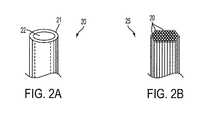
- FIG. 2Ashows an individual fiber 20 , representing each of multiple fibers 16 in fiber optic anode plate 13 , which may or may not be of the same materials or dimensions.
- Fiber 20includes glass rod 22 and glass cladding 21 , which surrounds the glass rod.
- the glass material of cladding 21is different from the glass material of rod 22 .
- Optical fiber 20is formed in the following manner: A glass rod and a cladding tube, coaxially surrounding the glass rod, are suspended vertically in a furnace. The temperature of the furnace is elevated to the softening temperature of the glass. The rod and cladding tube fuse together into single fiber 20 . The fiber 20 is fed into a traction mechanism, where the speed is adjusted until a desired fiber diameter is achieved. The fiber is then cut into shorter lengths.
- the array 25is also known as a multi assembly or a bundle and includes several thousand single fibers 20 , each having a glass rod and a cladding tube.
- the multi assembly 25is suspended vertically in a drawing machine and drawn to decrease the fiber diameter, while still maintaining the configuration of the individual fibers.
- the multi assembly 25is then cut into shorter lengths of bundles.
- the present inventionprovides a camera including an image intensifier (I 2 ), an image sensor, and a fiber optic bundle for coupling the I 2 and the image sensor.
- An output surface of the fiber optic bundleis configured to provide light to the image sensor.
- the output surface of the fiber optic bundleis shaped to reduce spreading of the light provided to the image sensor, and the output surface is shaped for focusing the light.
- the fiber optic bundleincludes multiple fibers, each fiber comprised of a cladding surrounding a core.
- the light provided to the image sensoris configured to exit the core.
- the output surface of the fiber optic bundleis shaped to focus the light exiting the core to form a spot size having a diameter of D t , and D t ⁇ D o ,
- D ois defined as a spot size formed by the output surface of the fiber optic bundle when not shaped to focus the light exiting the core.
- a bond layeris disposed between the output surface of the fiber optic bundle and the image sensor.
- the bond layeris configured into a shape that is complementary to the shape of the output surface of the fiber optic bundle, thereby presenting an index of refraction determined by the bond layer to the light exiting the multiple fibers.
- a bond layeris disposed between the output surface of the fiber optic bundle and the image sensor.
- a boundary lineis formed between the bond layer and the output surface of the fiber optic bundle for providing, in sequence, (a) an index of refraction of the output surface of the fiber optic bundle and (b) an index of refraction of the bond layer to the light exiting the multiple fibers.
- a top portion of the bond layeris shaped into multiple micro-lenses.
- the fiber optic bundleincludes multiple fibers, each fiber having a concave shape at the output surface of the fiber optic bundle, and the concave shape of each fiber is configured to conform to each micro-lens of the bond layer.
- Each fiberincludes a core and a cladding surrounding the core, and the core has a diameter of d; the concave shape of each fiber forms a recessed depth of h; and each micro-lens includes a protrusion corresponding to the recessed depth of h.
- the bond layerhas a thickness of t, and the diameter of d is approximately equal to the thickness of the bond layer of t.
- Each fiberincludes a core and a cladding surrounding the core.
- the coreincludes an index of refraction having a value of ⁇ core and the cladding includes an index of refraction having a value of ⁇ clad .
- the bond layerincludes an index of refraction having a value of ⁇ bond .
- the ⁇ bond valueis selected to be higher than either the ⁇ core value or the ⁇ clad value.
- a bond layeris disposed between the output surface of the fiber optic bundle and the image sensor.
- the bond layerhas a thickness of t.
- the fiber optic bundleincludes multiple cores, each core having a diameter of d, for forming an optical path for the light provided to the image sensor. Each core is shaped to focus the light into a spot size of D t , and D t is a function of the diameter of d, the thickness of t, and the shape of the output surface of the fiber optic bundle.
- the shape of the output surface of the fiber optic bundleincludes multiple concave recesses in the multiple cores, and the bond layer is shaped to conform to the multiple concave recesses of the multiple cores.
- Another embodiment of the present inventionis a fiber optic bundle for coupling light from an image intensifier (I 2 ) to an image sensor.
- the fiber optic bundleincludes multiple cores for directing the light from the I 2 to the image sensor, each core having an output surface, and the output surface shaped into a recessed concave surface for focusing the light toward the image sensor.
- a bond layeris interposed between the output surface of the core and the image sensor, in which the bond layer is shaped into multiple micro-lenses. Each micro-lens is configured to conform to the recessed concave surface of each respective core.
- the image sensorincludes a CMOS imager or a CCD imager.
- an intensified camera systemincluding: an image intensifier (I 2 ), an image sensor, and a fiber optic bundle disposed between the I 2 and the image sensor.
- the fiber optic bundleincludes:
- each corehaving an output surface, and the output surface is shaped into a recessed concave surface for focusing the light toward the image sensor.
- a bond layeris interposed between the output surface of the core and the image sensor, and the bond layer is shaped into multiple micro-lenses, each micro-lens configured to conform to the recessed concave surface of each respective core.
- a surface of the bond layer facing the image sensoris substantially flat.
- Each micro-lenshas an index of refraction that is greater than an index of refraction of each respective core.
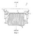
- FIG. 1is a cross-sectional view of a conventional image intensifier tube.
- FIG. 2Ais a perspective view of a conventional fiber optic including a core and a cladding surrounding the core.
- FIG. 2Bis a perspective view of a conventional fiber optic stacked array including multiple fiber optics, one of which is shown in FIG. 2A .
- FIG. 3is a cross-sectional perspective view of a proximity focused image intensifier camera, which includes an embodiment of the present invention.
- FIG. 4is an example of a typical interface between an image sensor and a fiber optic bundle, showing a flat output surface between the fiber optic bundle and a bonding line for bonding the image sensor to the fiber optic bundle.
- FIG. 5is a perspective view of a single core having been shaped at its output surface by cutting the output face at an angle of alpha.
- FIG. 6is a cross-sectional view of a fiber optic coupled camera, showing an exemplary shaping of the output surface of the fiber optic bundle as it interfaces with an image sensor, in accordance with an embodiment of the present invention.
- FIG. 7is a graph of spot sizes of light (in microns) as a function of normalized protrusion depth (depth/core radius of a core in a fiber optic bundle) and as a function of index of refraction of a bonding material, in accordance with an embodiment of the present invention.
- FIG. 8is a top view of the output surface of a fiber optic bundle having been shaped by a chemical mechanical polish (CMP), in accordance with an embodiment of the present invention.
- CMPchemical mechanical polish
- An intensified cameraincludes an image intensifier (I 2 ) and an image sensor (for example, a CCD or CMOS sensor) coupled together. Coupling elements of a complete intensified camera may be accomplished using a relay lens, or a fiber optic bundle. Of the two coupling methods, the fiber optic bundle results in the smallest format and, in general, has a higher modulation transfer function (MTF). As will be explained, the present invention further improves the MTF of the intensified camera by changing the shape of the output surface of the fiber optic bundle.
- MTFmodulation transfer function
- camera 30includes transmissive window 31 , photocathode (or simply cathode) 32 , microchannel plate (MCP) 36 , fluorescent screen (or simply screen) 33 , fiber optic tapered bundle (or simply bundle) 37 , and image sensor (or imager) 34 .
- transmissive window 31photocathode (or simply cathode) 32
- MCPmicrochannel plate
- fluorescent screenor simply screen
- fiber optic tapered bundleor simply bundle
- image sensoror imager
- the photocathode 32 , screen 33 and MCP 36are positioned within an evacuated housing or vacuum envelope, thereby permitting electrons to flow from the photocathode through the MCP and to the screen.
- Poweris provided to the photocathode, MCP and screen by high voltage power supply 35 , as shown.
- the photocathodedetects a light image and changes the light image into an electron image.
- the MCPamplifies the electron image and the screen changes the electron image back to a light image.
- a getter(not shown) absorbs gas which is generated during operation of the image intensifier.
- camera 30includes image intensifier (or image intensifier tube) 38 , fiber optic bundle 37 and image sensor 34 .
- the image intensifierincludes window 31 , photocathode 32 , MCP 36 , screen 33 and power supply 35 .
- the image sensor 34may be any solid state sensor, such as CMOS (complementary metal oxide semiconductor), CCD (charge coupled device) and hybrid EBCCD/CMOS (electronic bombarded CCD or CMOS) sensors. Selection of a sensor depends on the desired application, as CMOS sensors use less power than CCD sensors, but CCD sensors may have a higher fill factor.
- the output of sensor 34produces an intensified image signal that may be sent, by way of a bus, to an image display device (not shown).
- the output of sensor 34may be, alternatively, stored in a memory device (not shown).
- sensor 34is conventionally disposed in a ceramic substrate 39 .
- the sensor 34includes an array of terminal pads for providing input/output (I/O) signals. Hundreds of terminal pads are typically disposed around the peripheral circumference of sensor 34 . Extending from the bottom of ceramic substrate 39 are a plurality of pins (not shown), which are connected through via-holes to the array of terminal pads. In this manner, electrical contacts are made between sensor 34 and other devices, such as displays and storage memories.
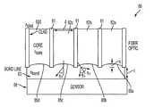
- a typical interfaceis shown between an image sensor (such as image sensor 34 ) and a fiber optic bundle (such as fiber optic bundle 37 ).
- an optical quality materialis used to hold the fiber optic bundle 40 to silicon sensor 44 .
- the optical materialmust be optically transparent, have a thermal expansion compatible with the fiber optic and the sensor. It must also have an index of refraction that limits reflection of light and is compatible with manufacturing assembly and temperature excursions. It must also have good bonding qualities.
- a typical configuration of the interface in FIG. 4shows two characteristic geometry features. First, there is a finite thickness to the bond material (t). Second, the output surface 45 of the fiber optic bundle is flat.
- bond linealso referred to herein as a bond layer
- the bond linehas a flat surface interfacing the flat surface 45 of fiber optic bundle 40 .
- Light passing from each core 42 to bond line 43is spread by the bonding material. This spreading degrades the MTF of the optically coupled fiber optic system.
- the light exits each core in the fiber optic bundlethe light is refracted by any difference in the index of refraction, ⁇ , between the core ( ⁇ core ) and the bonding material ( ⁇ bond ).
- the spot of light (D)which originally is the size of core 42 in the fiber optic bundle, is now larger when it impinges upon image sensor 44 .
- the surface of the image sensoris also flat, a fraction of the light is reflected and propagated in the bond material, i.e. etalon.
- the surfaceis not planar and the change in geometry may break up the etalon effect and reduce the light spread, but the original spread is still present.
- the present inventionreduces the MTF loss due to the optical bonding process in the fiber optic coupled camera by texturing the output surface 45 of fiber optic bundle 40 .
- the texturingreduces the spread of light in bond line 43 between the fiber optic bundle 40 and the image sensor 44 . Since texturing the output surface 45 of the fiber optic bundle 40 causes recesses (or voids) in the output surface, the bond material fills the recesses (or voids). In this manner, the light propagating toward the image sensor passes through only two different materials having, respectively, different indices of refraction, namely, ⁇ core and ⁇ bond .
- the present inventionuses the geometry of each core and cladding in the fiber optic bundle to reduce spreading of the light as it exits each respective core of the fiber optic bundle.
- the angle in which the light leaves a flat surface (such as surface 45 in FIG. 4 ) of a fiber optic bundleis as follows:
- ⁇ osin - 1 ( ⁇ core ⁇ bond ⁇ sin ( 90 - sin - 1 ( ⁇ clad ⁇ core ) ) ) Eq . ⁇ 1
- the thickness of the bond linecannot be made zero, because the bonding material is necessary for bonding the fiber optic bundle to the image sensor.
- the factor of 2 in the above equationis due to the light spreading on both sides of the core.
- FIG. 5there is shown a perspective view of a single core 50 of a fiber optic bundle.
- the coreis cut at an angle of a.
- the light exiting core 50is given by the following equation:
- the surface of the coremay be shaped differently.
- the surface of the coremay be rounded, as shown in FIG. 6 by surface 65 a , 65 b , 65 c , or 65 d .
- the value of achanges continuously along the surface of each core and focusing of the light occurs.
- fiber optic bundle 60is coupled to image sensor 64 by bonding material at bond line (or bond layer) 63 .
- the fiber optic bundleincludes multiple cores 62 , in which each core is surrounded by a cladding material 61 .
- the output surface of fiber optic bundle 60is shaped to form a rounded concave recess in each core 62 .
- Four rounded concave recessesare shown in FIG. 6 , designated as 65 a , 65 b , 65 c and 65 d , corresponding to the four cores, respectively shown as 62 a , 62 b , 62 c and 62 d .
- Each of the rounded concave recessesprovide focusing of the light exiting the respective core.
- each coreexits each core at an angle of ⁇ o which changes along the surface forming the rounded concave recess of the respective core.
- the angle of ⁇ oremains the same with respect to a line drawn perpendicular to the rounded surface, as shown in FIG. 6 .
- the overall angleis about the new exit angle of ⁇ , the latter shown in FIG. 5 .
- the bond linealso has a new geometry that corresponds to the rounded concave surface of each core.
- the bond line 63now has curved bumps (not labeled) that fill the rounded concave surfaces of the cores.
- the bond line 63may be visualized as being like a sheet of micro-lenses formed above a focal planar array in a camera.
- four curved bumps, or micro-lensesare shown (not labeled) that correspond to the four rounded concave surfaces of the cores, namely, 65 a , 65 b , 65 c and 65 d.
- the protrusion height (h) into each coreis a fraction of the diameter (d) of each core, then the protrusion includes a radius (r) which may be expressed as follows:
- FIG. 7a graph of spot size (in microns) as a function of normalized protrusion depth (depth/core radius) and as a function of index of refraction of the bond material ( ⁇ bond ) is shown.
- the graphshows that as the index of refraction of the bond material increases the spot size decreases.
- the graphalso shows that as the protrusion depth into the fiber optic increases the spot size decreases up to a point, then begins to increase again, as the light is scattered further away.
- FIG. 8shows a chemical mechanical polish (CMP) of a fiber optic surface. Controlling the depth and angle is dependent upon the chemistry of the slurry used during the CMP.
- CMPchemical mechanical polish
- the present inventionmay be used in image intensified cameras, optically coupled scintillators for X-rays, micro-lens arrays for multi-aperture systems, and fiber optic field correctors.
Landscapes
- Physics & Mathematics (AREA)
- General Physics & Mathematics (AREA)
- Optics & Photonics (AREA)
- Optical Fibers, Optical Fiber Cores, And Optical Fiber Bundles (AREA)
Abstract
Description
Dt<Do,
- ηcoreis the index of refraction of the core material,
- ηbondis the index of refraction of the bonding material,
- ηcladis the index of refraction of the cladding material, and
- φois the angle in which the light leaves the flat surface of the fiber optic bundle.
Do=d+2*t*tan φo Eq. 2
where:
- Dois the diameter of the spot size formed by the light leaving the flat surface,
- d is the diameter of the core of the fiber optic,
- t is the thickness of the bond line or the bond layer, and
- φois the angle in which the light leaves the flat surface of the fiber optic bundle.
- β is the angle of the light exiting the core,
- α is the angle in which the core is cut,
- ηcoreis the index of refraction of the core material, and
- ηbondis the index of refraction of the bonding material.
Dt=d+2*t*tan(β±φo) Eq. 4
where:
- d is the diameter of the core of the fiber optic,
- t is the thickness of the bond line or the bond layer,
- β is the angle of the light exiting the core,
- φois the angle to a normal, in which the light leaves the surface of the fiber optic bundle, and
- Dtis the diameter of the spot size outputted from each shaped core.
- r is the radius of the protrusion of each core,
- d is the diameter of each core, and
- h is the height of the protrusion of each core.
Claims (17)
Dt<Do,
Priority Applications (1)
| Application Number | Priority Date | Filing Date | Title |
|---|---|---|---|
| US13/769,518US9201193B1 (en) | 2013-02-18 | 2013-02-18 | Textured fiber optic coupled image intensified camera |
Applications Claiming Priority (1)
| Application Number | Priority Date | Filing Date | Title |
|---|---|---|---|
| US13/769,518US9201193B1 (en) | 2013-02-18 | 2013-02-18 | Textured fiber optic coupled image intensified camera |
Publications (1)
| Publication Number | Publication Date |
|---|---|
| US9201193B1true US9201193B1 (en) | 2015-12-01 |
Family
ID=54609186
Family Applications (1)
| Application Number | Title | Priority Date | Filing Date |
|---|---|---|---|
| US13/769,518Active2033-07-14US9201193B1 (en) | 2013-02-18 | 2013-02-18 | Textured fiber optic coupled image intensified camera |
Country Status (1)
| Country | Link |
|---|---|
| US (1) | US9201193B1 (en) |
Cited By (38)
| Publication number | Priority date | Publication date | Assignee | Title |
|---|---|---|---|---|
| US20160097865A1 (en)* | 2014-10-07 | 2016-04-07 | Canon Kabushiki Kaisha | Radiographic imaging apparatus and imaging system |
| US20160307372A1 (en)* | 2015-04-15 | 2016-10-20 | Lytro, Inc. | Capturing light-field volume image and video data using tiled light-field cameras |
| DE102016200287A1 (en)* | 2016-01-13 | 2017-07-13 | Fraunhofer-Gesellschaft zur Förderung der angewandten Forschung e.V. | Multi-aperture imaging devices, methods of making same, and imaging system |
| US10205896B2 (en) | 2015-07-24 | 2019-02-12 | Google Llc | Automatic lens flare detection and correction for light-field images |
| US20190122849A1 (en)* | 2015-02-09 | 2019-04-25 | Arizona Board Of Regents On Behalf Of The University Of Arizona | Small portable night vision system |
| US10275898B1 (en) | 2015-04-15 | 2019-04-30 | Google Llc | Wedge-based light-field video capture |
| US10275892B2 (en) | 2016-06-09 | 2019-04-30 | Google Llc | Multi-view scene segmentation and propagation |
| US10298834B2 (en) | 2006-12-01 | 2019-05-21 | Google Llc | Video refocusing |
| US10334151B2 (en) | 2013-04-22 | 2019-06-25 | Google Llc | Phase detection autofocus using subaperture images |
| US10341632B2 (en) | 2015-04-15 | 2019-07-02 | Google Llc. | Spatial random access enabled video system with a three-dimensional viewing volume |
| US10354399B2 (en) | 2017-05-25 | 2019-07-16 | Google Llc | Multi-view back-projection to a light-field |
| US10412373B2 (en) | 2015-04-15 | 2019-09-10 | Google Llc | Image capture for virtual reality displays |
| US10419737B2 (en) | 2015-04-15 | 2019-09-17 | Google Llc | Data structures and delivery methods for expediting virtual reality playback |
| US10440407B2 (en) | 2017-05-09 | 2019-10-08 | Google Llc | Adaptive control for immersive experience delivery |
| US10444931B2 (en) | 2017-05-09 | 2019-10-15 | Google Llc | Vantage generation and interactive playback |
| US10469873B2 (en) | 2015-04-15 | 2019-11-05 | Google Llc | Encoding and decoding virtual reality video |
| US10474227B2 (en) | 2017-05-09 | 2019-11-12 | Google Llc | Generation of virtual reality with 6 degrees of freedom from limited viewer data |
| US10540818B2 (en) | 2015-04-15 | 2020-01-21 | Google Llc | Stereo image generation and interactive playback |
| US10546424B2 (en) | 2015-04-15 | 2020-01-28 | Google Llc | Layered content delivery for virtual and augmented reality experiences |
| US10545215B2 (en) | 2017-09-13 | 2020-01-28 | Google Llc | 4D camera tracking and optical stabilization |
| US10552947B2 (en) | 2012-06-26 | 2020-02-04 | Google Llc | Depth-based image blurring |
| US10551560B1 (en)* | 2014-10-30 | 2020-02-04 | Tomasz S. Tkaczyk | Arrays of tapered light-guides for snapshot spectral imaging |
| US10565734B2 (en) | 2015-04-15 | 2020-02-18 | Google Llc | Video capture, processing, calibration, computational fiber artifact removal, and light-field pipeline |
| US10567464B2 (en) | 2015-04-15 | 2020-02-18 | Google Llc | Video compression with adaptive view-dependent lighting removal |
| US10594945B2 (en) | 2017-04-03 | 2020-03-17 | Google Llc | Generating dolly zoom effect using light field image data |
| US10598939B2 (en) | 2012-01-24 | 2020-03-24 | Arizona Board Of Regents On Behalf Of The University Of Arizona | Compact eye-tracked head-mounted display |
| US10679361B2 (en) | 2016-12-05 | 2020-06-09 | Google Llc | Multi-view rotoscope contour propagation |
| US10965862B2 (en) | 2018-01-18 | 2021-03-30 | Google Llc | Multi-camera navigation interface |
| US11150449B2 (en) | 2008-01-22 | 2021-10-19 | Arizona Board Of Regents On Behalf Of The University Of Arizona | Head-mounted projection display using reflective microdisplays |
| US11328446B2 (en) | 2015-04-15 | 2022-05-10 | Google Llc | Combining light-field data with active depth data for depth map generation |
| US11350079B2 (en) | 2014-03-05 | 2022-05-31 | Arizona Board Of Regents On Behalf Of The University Of Arizona | Wearable 3D augmented reality display |
| US11546575B2 (en) | 2018-03-22 | 2023-01-03 | Arizona Board Of Regents On Behalf Of The University Of Arizona | Methods of rendering light field images for integral-imaging-based light field display |
| US11609430B2 (en) | 2010-04-30 | 2023-03-21 | The Arizona Board Of Regents On Behalf Of The University Of Arizona | Wide angle and high resolution tiled head-mounted display device |
| US11803059B2 (en) | 2009-09-14 | 2023-10-31 | The Arizona Board Of Regents On Behalf Of The University Of Arizona | 3-dimensional electro-optical see-through displays |
| US12044850B2 (en) | 2017-03-09 | 2024-07-23 | Arizona Board Of Regents On Behalf Of The University Of Arizona | Head-mounted light field display with integral imaging and waveguide prism |
| US12078802B2 (en) | 2017-03-09 | 2024-09-03 | Arizona Board Of Regents On Behalf Of The University Of Arizona | Head-mounted light field display with integral imaging and relay optics |
| CN119065065A (en)* | 2023-05-30 | 2024-12-03 | 中国科学院西安光学精密机械研究所 | A high-precision optical fiber microhole precision coupling device and method |
| CN119666143A (en)* | 2024-11-07 | 2025-03-21 | 南方电网数字电网研究院股份有限公司 | Light cone coupling method of ICMOS chip, ICMOS chip, microprocessor and solar-blind ultraviolet light detection device |
Citations (8)
| Publication number | Priority date | Publication date | Assignee | Title |
|---|---|---|---|---|
| US4380365A (en)* | 1978-05-23 | 1983-04-19 | Battelle Memorial Institute | Optical fiber, having on at least one of its frontal extremities a plano-convex microlens joined with its plane face to said frontal extremity |
| US4980772A (en)* | 1988-05-17 | 1990-12-25 | Hamamatsu Photonics Kabushiki Kaisha | Image pickup device incorporated with image intensifier tube |
| US5268570A (en) | 1991-12-20 | 1993-12-07 | Litton Systems, Inc. | Transmission mode InGaAs photocathode for night vision system |
| US6560029B1 (en)* | 2001-12-21 | 2003-05-06 | Itt Manufacturing Enterprises, Inc. | Video enhanced night vision goggle |
| US6595674B1 (en)* | 1998-07-02 | 2003-07-22 | Ccs Inc. | Lighting device for surface inspection |
| US20030219207A1 (en)* | 2002-05-22 | 2003-11-27 | The Boeing Company | Fiber optic LED illuminator |
| US20080128631A1 (en)* | 2006-06-21 | 2008-06-05 | Avraham Suhami | Radiation cameras |
| US20100103267A1 (en)* | 2008-10-27 | 2010-04-29 | O'rourke Brian | Night vision system |
- 2013
- 2013-02-18USUS13/769,518patent/US9201193B1/enactiveActive
Patent Citations (8)
| Publication number | Priority date | Publication date | Assignee | Title |
|---|---|---|---|---|
| US4380365A (en)* | 1978-05-23 | 1983-04-19 | Battelle Memorial Institute | Optical fiber, having on at least one of its frontal extremities a plano-convex microlens joined with its plane face to said frontal extremity |
| US4980772A (en)* | 1988-05-17 | 1990-12-25 | Hamamatsu Photonics Kabushiki Kaisha | Image pickup device incorporated with image intensifier tube |
| US5268570A (en) | 1991-12-20 | 1993-12-07 | Litton Systems, Inc. | Transmission mode InGaAs photocathode for night vision system |
| US6595674B1 (en)* | 1998-07-02 | 2003-07-22 | Ccs Inc. | Lighting device for surface inspection |
| US6560029B1 (en)* | 2001-12-21 | 2003-05-06 | Itt Manufacturing Enterprises, Inc. | Video enhanced night vision goggle |
| US20030219207A1 (en)* | 2002-05-22 | 2003-11-27 | The Boeing Company | Fiber optic LED illuminator |
| US20080128631A1 (en)* | 2006-06-21 | 2008-06-05 | Avraham Suhami | Radiation cameras |
| US20100103267A1 (en)* | 2008-10-27 | 2010-04-29 | O'rourke Brian | Night vision system |
Cited By (48)
| Publication number | Priority date | Publication date | Assignee | Title |
|---|---|---|---|---|
| US10298834B2 (en) | 2006-12-01 | 2019-05-21 | Google Llc | Video refocusing |
| US11150449B2 (en) | 2008-01-22 | 2021-10-19 | Arizona Board Of Regents On Behalf Of The University Of Arizona | Head-mounted projection display using reflective microdisplays |
| US11592650B2 (en) | 2008-01-22 | 2023-02-28 | Arizona Board Of Regents On Behalf Of The University Of Arizona | Head-mounted projection display using reflective microdisplays |
| US11803059B2 (en) | 2009-09-14 | 2023-10-31 | The Arizona Board Of Regents On Behalf Of The University Of Arizona | 3-dimensional electro-optical see-through displays |
| US11609430B2 (en) | 2010-04-30 | 2023-03-21 | The Arizona Board Of Regents On Behalf Of The University Of Arizona | Wide angle and high resolution tiled head-mounted display device |
| US12204109B2 (en) | 2010-04-30 | 2025-01-21 | The Arizona Board Of Regents On Behalf Of The University Of Arizona | Wide angle and high resolution tiled head-mounted display device |
| US11181746B2 (en) | 2012-01-24 | 2021-11-23 | Arizona Board Of Regents On Behalf Of The University Of Arizona | Compact eye-tracked head-mounted display |
| US12265223B2 (en) | 2012-01-24 | 2025-04-01 | Arizona Board Of Regents On Behalf Of The University Of Arizona | Compact eye-tracked head-mounted display |
| US10969592B2 (en) | 2012-01-24 | 2021-04-06 | Arizona Board Of Regents On Behalf Of The University Of Arizona | Compact eye-tracked head-mounted display |
| US10598939B2 (en) | 2012-01-24 | 2020-03-24 | Arizona Board Of Regents On Behalf Of The University Of Arizona | Compact eye-tracked head-mounted display |
| US10552947B2 (en) | 2012-06-26 | 2020-02-04 | Google Llc | Depth-based image blurring |
| US10334151B2 (en) | 2013-04-22 | 2019-06-25 | Google Llc | Phase detection autofocus using subaperture images |
| US11350079B2 (en) | 2014-03-05 | 2022-05-31 | Arizona Board Of Regents On Behalf Of The University Of Arizona | Wearable 3D augmented reality display |
| US10448908B2 (en)* | 2014-10-07 | 2019-10-22 | Canon Kabushiki Kaisha | Radiographic imaging apparatus and imaging system |
| US20160097865A1 (en)* | 2014-10-07 | 2016-04-07 | Canon Kabushiki Kaisha | Radiographic imaging apparatus and imaging system |
| US10551560B1 (en)* | 2014-10-30 | 2020-02-04 | Tomasz S. Tkaczyk | Arrays of tapered light-guides for snapshot spectral imaging |
| US20190122849A1 (en)* | 2015-02-09 | 2019-04-25 | Arizona Board Of Regents On Behalf Of The University Of Arizona | Small portable night vision system |
| US11205556B2 (en) | 2015-02-09 | 2021-12-21 | Arizona Board Of Regents On Behalf Of The University Of Arizona | Small portable night vision system |
| US10593507B2 (en)* | 2015-02-09 | 2020-03-17 | Arizona Board Of Regents On Behalf Of The University Of Arizona | Small portable night vision system |
| US10565734B2 (en) | 2015-04-15 | 2020-02-18 | Google Llc | Video capture, processing, calibration, computational fiber artifact removal, and light-field pipeline |
| US10419737B2 (en) | 2015-04-15 | 2019-09-17 | Google Llc | Data structures and delivery methods for expediting virtual reality playback |
| US20160307372A1 (en)* | 2015-04-15 | 2016-10-20 | Lytro, Inc. | Capturing light-field volume image and video data using tiled light-field cameras |
| US10540818B2 (en) | 2015-04-15 | 2020-01-21 | Google Llc | Stereo image generation and interactive playback |
| US11328446B2 (en) | 2015-04-15 | 2022-05-10 | Google Llc | Combining light-field data with active depth data for depth map generation |
| US10469873B2 (en) | 2015-04-15 | 2019-11-05 | Google Llc | Encoding and decoding virtual reality video |
| US10567464B2 (en) | 2015-04-15 | 2020-02-18 | Google Llc | Video compression with adaptive view-dependent lighting removal |
| US10341632B2 (en) | 2015-04-15 | 2019-07-02 | Google Llc. | Spatial random access enabled video system with a three-dimensional viewing volume |
| US10546424B2 (en) | 2015-04-15 | 2020-01-28 | Google Llc | Layered content delivery for virtual and augmented reality experiences |
| US10412373B2 (en) | 2015-04-15 | 2019-09-10 | Google Llc | Image capture for virtual reality displays |
| US10275898B1 (en) | 2015-04-15 | 2019-04-30 | Google Llc | Wedge-based light-field video capture |
| US10085005B2 (en)* | 2015-04-15 | 2018-09-25 | Lytro, Inc. | Capturing light-field volume image and video data using tiled light-field cameras |
| US10205896B2 (en) | 2015-07-24 | 2019-02-12 | Google Llc | Automatic lens flare detection and correction for light-field images |
| US10652438B2 (en)* | 2016-01-13 | 2020-05-12 | Fraunhofer-Gesellschaft Zur Foerderung Der Angewandten Forschung E.V. | Multi-aperture imaging devices, methods for producing same and imaging system |
| DE102016200287A1 (en)* | 2016-01-13 | 2017-07-13 | Fraunhofer-Gesellschaft zur Förderung der angewandten Forschung e.V. | Multi-aperture imaging devices, methods of making same, and imaging system |
| US10275892B2 (en) | 2016-06-09 | 2019-04-30 | Google Llc | Multi-view scene segmentation and propagation |
| US10679361B2 (en) | 2016-12-05 | 2020-06-09 | Google Llc | Multi-view rotoscope contour propagation |
| US12044850B2 (en) | 2017-03-09 | 2024-07-23 | Arizona Board Of Regents On Behalf Of The University Of Arizona | Head-mounted light field display with integral imaging and waveguide prism |
| US12078802B2 (en) | 2017-03-09 | 2024-09-03 | Arizona Board Of Regents On Behalf Of The University Of Arizona | Head-mounted light field display with integral imaging and relay optics |
| US10594945B2 (en) | 2017-04-03 | 2020-03-17 | Google Llc | Generating dolly zoom effect using light field image data |
| US10440407B2 (en) | 2017-05-09 | 2019-10-08 | Google Llc | Adaptive control for immersive experience delivery |
| US10444931B2 (en) | 2017-05-09 | 2019-10-15 | Google Llc | Vantage generation and interactive playback |
| US10474227B2 (en) | 2017-05-09 | 2019-11-12 | Google Llc | Generation of virtual reality with 6 degrees of freedom from limited viewer data |
| US10354399B2 (en) | 2017-05-25 | 2019-07-16 | Google Llc | Multi-view back-projection to a light-field |
| US10545215B2 (en) | 2017-09-13 | 2020-01-28 | Google Llc | 4D camera tracking and optical stabilization |
| US10965862B2 (en) | 2018-01-18 | 2021-03-30 | Google Llc | Multi-camera navigation interface |
| US11546575B2 (en) | 2018-03-22 | 2023-01-03 | Arizona Board Of Regents On Behalf Of The University Of Arizona | Methods of rendering light field images for integral-imaging-based light field display |
| CN119065065A (en)* | 2023-05-30 | 2024-12-03 | 中国科学院西安光学精密机械研究所 | A high-precision optical fiber microhole precision coupling device and method |
| CN119666143A (en)* | 2024-11-07 | 2025-03-21 | 南方电网数字电网研究院股份有限公司 | Light cone coupling method of ICMOS chip, ICMOS chip, microprocessor and solar-blind ultraviolet light detection device |
Similar Documents
| Publication | Publication Date | Title |
|---|---|---|
| US9201193B1 (en) | Textured fiber optic coupled image intensified camera | |
| CN103999221B (en) | Solid imaging element and imaging device | |
| US6455860B1 (en) | Resolution enhancement device for an optically-coupled image sensor using high extra-mural absorbent fiber | |
| CN116913934B (en) | Semiconductor near-field active imaging sensor | |
| US9372312B2 (en) | Optical device | |
| KR101816537B1 (en) | Fibre optic phosphor screen comprising an angular filter | |
| CN104584182B (en) | Electron Microscope and Electron Ray Detector | |
| JPH09213206A (en) | Transmission type photoelectric surface, manufacture thereof and photoelectric transfer tube using the transmission type photoelectric surface | |
| US20090134312A1 (en) | Slotted microchannel plate (mcp) | |
| JP2024532837A (en) | Microchannel plate image intensifier and method of producing same | |
| TW202201811A (en) | Micro-led device | |
| US7994693B2 (en) | Curved MCP channels | |
| US10162170B2 (en) | Optical device | |
| JPH10104474A (en) | Optical transmission equipment | |
| JP6303323B2 (en) | Optical device | |
| TWM441217U (en) | Optical sensor device | |
| US7251400B1 (en) | Absorptive clad fiber optic faceplate tube | |
| JP7548833B2 (en) | Light-emitting element, light-detecting module, method for manufacturing light-emitting element, and scanning electron microscope | |
| TWI878193B (en) | Display device | |
| JP5387930B1 (en) | Light emitting element / optical fiber coupling module and its components | |
| JP2020518036A (en) | High brightness light conversion device | |
| JP2000214356A (en) | Light collector and light receiving device | |
| JP3377406B2 (en) | Polarization detector | |
| JP2022138495A (en) | Light guides, electron beam detectors, and charged particle devices | |
| JP2009217996A (en) | Photo-electric cathode, electron tube, and image intensifier |
Legal Events
| Date | Code | Title | Description |
|---|---|---|---|
| AS | Assignment | Owner name:EXELIS, INC., VIRGINIA Free format text:ASSIGNMENT OF ASSIGNORS INTEREST;ASSIGNOR:SMITH, ARLYNN WALTER;REEL/FRAME:029824/0155 Effective date:20130214 | |
| STCF | Information on status: patent grant | Free format text:PATENTED CASE | |
| AS | Assignment | Owner name:HARRIS CORPORATION, FLORIDA Free format text:MERGER;ASSIGNOR:EXELIS INC.;REEL/FRAME:039362/0534 Effective date:20151223 | |
| MAFP | Maintenance fee payment | Free format text:PAYMENT OF MAINTENANCE FEE, 4TH YEAR, LARGE ENTITY (ORIGINAL EVENT CODE: M1551); ENTITY STATUS OF PATENT OWNER: LARGE ENTITY Year of fee payment:4 | |
| AS | Assignment | Owner name:ELBIT SYSTEMS OF AMERICA, LLC, TEXAS Free format text:ASSIGNMENT OF ASSIGNORS INTEREST;ASSIGNORS:L3HARRIS TECHNOLOGIES, INC.;EAGLE TECHNOLOGY, LLC;REEL/FRAME:050375/0008 Effective date:20190913 Owner name:WELLS FARGO BANK, NATIONAL ASSOCIATION, TEXAS Free format text:SECURITY INTEREST;ASSIGNOR:ELBIT SYSTEMS OF AMERICA, LLC;REEL/FRAME:050375/0425 Effective date:20190913 | |
| AS | Assignment | Owner name:L3HARRIS TECHNOLOGIES, INC., DELAWARE Free format text:CHANGE OF NAME;ASSIGNOR:HARRIS CORPORATION;REEL/FRAME:050409/0288 Effective date:20190628 | |
| MAFP | Maintenance fee payment | Free format text:PAYMENT OF MAINTENANCE FEE, 8TH YEAR, LARGE ENTITY (ORIGINAL EVENT CODE: M1552); ENTITY STATUS OF PATENT OWNER: LARGE ENTITY Year of fee payment:8 | |
| AS | Assignment | Owner name:CAPITAL ONE, NATIONAL ASSOCIATION, AS AGENT, ILLINOIS Free format text:SECURITY INTEREST;ASSIGNORS:ELBIT SYSTEMS OF AMERICA, LLC;SPARTON CORPORATION;SPARTON DELEON SPRINGS, LLC;AND OTHERS;REEL/FRAME:066642/0935 Effective date:20240221 Owner name:ELBIT SYSTEMS OF AMERICA, LLC, TEXAS Free format text:RELEASE BY SECURED PARTY;ASSIGNOR:WELLS FARGO BANK, NATIONAL ASSOCIATION;REEL/FRAME:066644/0612 Effective date:20240221 |