US9197292B2 - Non-mating connector - Google Patents
Non-mating connectorDownload PDFInfo
- Publication number
- US9197292B2 US9197292B2US14/064,116US201314064116AUS9197292B2US 9197292 B2US9197292 B2US 9197292B2US 201314064116 AUS201314064116 AUS 201314064116AUS 9197292 B2US9197292 B2US 9197292B2
- Authority
- US
- United States
- Prior art keywords
- female
- male
- connector
- carrier
- coil
- Prior art date
- Legal status (The legal status is an assumption and is not a legal conclusion. Google has not performed a legal analysis and makes no representation as to the accuracy of the status listed.)
- Active - Reinstated, expires
Links
- 230000001939inductive effectEffects0.000claimsabstractdescription9
- 230000008878couplingEffects0.000claimsabstractdescription7
- 238000010168coupling processMethods0.000claimsabstractdescription7
- 238000005859coupling reactionMethods0.000claimsabstractdescription7
- 238000012546transferMethods0.000claimsdescription27
- 239000000463materialSubstances0.000claimsdescription21
- 239000010949copperSubstances0.000claimsdescription16
- RYGMFSIKBFXOCR-UHFFFAOYSA-NCopperChemical compound[Cu]RYGMFSIKBFXOCR-UHFFFAOYSA-N0.000claimsdescription13
- 229910052802copperInorganic materials0.000claimsdescription13
- 239000003990capacitorSubstances0.000claimsdescription7
- 229910052751metalInorganic materials0.000claimsdescription6
- 239000002184metalSubstances0.000claimsdescription6
- 239000003989dielectric materialSubstances0.000claimsdescription3
- 239000000969carrierSubstances0.000claims13
- 229920000379polypropylene carbonatePolymers0.000claims8
- 239000000758substrateSubstances0.000claims7
- 230000000903blocking effectEffects0.000claims5
- 230000035515penetrationEffects0.000claims5
- 229920002120photoresistant polymerPolymers0.000claims5
- 229920000642polymerPolymers0.000claims5
- -1polypropylene carbonatePolymers0.000claims5
- OKKJLVBELUTLKV-UHFFFAOYSA-NMethanolChemical compoundOCOKKJLVBELUTLKV-UHFFFAOYSA-N0.000claims3
- 239000011521glassSubstances0.000claims3
- CSCPPACGZOOCGX-UHFFFAOYSA-NAcetoneChemical compoundCC(C)=OCSCPPACGZOOCGX-UHFFFAOYSA-N0.000claims2
- KFZMGEQAYNKOFK-UHFFFAOYSA-NIsopropanolChemical compoundCC(C)OKFZMGEQAYNKOFK-UHFFFAOYSA-N0.000claims2
- BGTOWKSIORTVQH-UHFFFAOYSA-NcyclopentanoneChemical compoundO=C1CCCC1BGTOWKSIORTVQH-UHFFFAOYSA-N0.000claims2
- XLYOFNOQVPJJNP-UHFFFAOYSA-NwaterChemical compoundOXLYOFNOQVPJJNP-UHFFFAOYSA-N0.000claims2
- 229910052782aluminiumInorganic materials0.000claims1
- XAGFODPZIPBFFR-UHFFFAOYSA-NaluminiumChemical compound[Al]XAGFODPZIPBFFR-UHFFFAOYSA-N0.000claims1
- 238000010292electrical insulationMethods0.000claims1
- PCHJSUWPFVWCPO-UHFFFAOYSA-NgoldChemical compound[Au]PCHJSUWPFVWCPO-UHFFFAOYSA-N0.000claims1
- 229910052737goldInorganic materials0.000claims1
- 239000010931goldSubstances0.000claims1
- 238000000465mouldingMethods0.000claims1
- 229920001343polytetrafluoroethylenePolymers0.000claims1
- 239000004810polytetrafluoroethyleneSubstances0.000claims1
- 238000009987spinningMethods0.000claims1
- 238000005516engineering processMethods0.000abstract1
- BASFCYQUMIYNBI-UHFFFAOYSA-NplatinumChemical compound[Pt]BASFCYQUMIYNBI-UHFFFAOYSA-N0.000description8
- 239000004020conductorSubstances0.000description6
- 230000004907fluxEffects0.000description6
- 238000003780insertionMethods0.000description6
- 230000037431insertionEffects0.000description6
- 230000013011matingEffects0.000description5
- 239000004809TeflonSubstances0.000description4
- 229920006362Teflon®Polymers0.000description4
- 239000012212insulatorSubstances0.000description4
- 229910052697platinumInorganic materials0.000description4
- 229910001220stainless steelInorganic materials0.000description4
- 239000010935stainless steelSubstances0.000description4
- 238000010276constructionMethods0.000description3
- 238000011161developmentMethods0.000description3
- 230000018109developmental processEffects0.000description3
- 230000008859changeEffects0.000description2
- 238000013461designMethods0.000description2
- 230000000694effectsEffects0.000description2
- 230000005684electric fieldEffects0.000description2
- 239000011810insulating materialSubstances0.000description2
- 238000004088simulationMethods0.000description2
- 230000009471actionEffects0.000description1
- 230000005540biological transmissionEffects0.000description1
- 238000005260corrosionMethods0.000description1
- 230000007797corrosionEffects0.000description1
- 230000001808coupling effectEffects0.000description1
- 230000001419dependent effectEffects0.000description1
- 238000009795derivationMethods0.000description1
- 238000006073displacement reactionMethods0.000description1
- 238000010348incorporationMethods0.000description1
- 230000006698inductionEffects0.000description1
- 238000005259measurementMethods0.000description1
- 238000000034methodMethods0.000description1
- 230000035699permeabilityEffects0.000description1
- 239000012466permeateSubstances0.000description1
Images


Classifications
- H—ELECTRICITY
- H04—ELECTRIC COMMUNICATION TECHNIQUE
- H04B—TRANSMISSION
- H04B5/00—Near-field transmission systems, e.g. inductive or capacitive transmission systems
- H04B5/20—Near-field transmission systems, e.g. inductive or capacitive transmission systems characterised by the transmission technique; characterised by the transmission medium
- H04B5/22—Capacitive coupling
- H04B5/0012—
- H04B5/0093—
- H—ELECTRICITY
- H04—ELECTRIC COMMUNICATION TECHNIQUE
- H04B—TRANSMISSION
- H04B5/00—Near-field transmission systems, e.g. inductive or capacitive transmission systems
- H04B5/20—Near-field transmission systems, e.g. inductive or capacitive transmission systems characterised by the transmission technique; characterised by the transmission medium
- H04B5/24—Inductive coupling
- H04B5/26—Inductive coupling using coils
- H04B5/266—One coil at each side, e.g. with primary and secondary coils
Definitions
- an electrical connectoris an electro-mechanical device for joining electrical circuits as an interface using a mechanical assembly [ 1 ]. Every connector, then, must “join” electrical circuits by making electrical contact between two electrical contact points.
- Capacitive couplingcan also be used to join ac circuits and simultaneously block dc offsets. This capacitive coupling effect is done without conduction current that standard connectors use to connect two circuit joints. It is done by displacement current. This work focuses on a new type of connector based entirely on this concept called the non-mating connector (NMC). Capacitive and magnetic coupling are not new concepts.
- NMCsuse no conductive tracks for ohmic contacts. In short, there currently is no connector on the market today that is truly non-mating. This work introduces the concept and development of the NMC.
- NMCsThe primary vision for NMCs is to create connectors that are impervious to ambient moisture giving rise to the idea of waterproof connectors and ultimately to waterproof consumer electronics.
- One such application that an NMC can be used foris the USB 3.0 as shown in FIG. 1 a (traditional) and 1 b (NMC concept).
- the acceptable amount of differential insertion loss in a mated cable assemblyis defined by four vertices which are at: (100 MHz, ⁇ 1.5 dB), (1.25 GHz, ⁇ 5.0 dB), (2.5 GHz, ⁇ 7.5 dB), (7.5 GHz, ⁇ 25 dB). Since the NMC is essentially a parallel plate capacitor the insertion loss for it is directly related to its capacitance value.
- the claim for the NMC USB 3.0is that the capacitance value will be within the range of 0.1 nF to 100 nF in order to meet the industry requirement for insertion loss.
- the simulations for the NMC A-receptacle and B-receptacleare shown in FIGS. 4 a and 4 b respectively which confirm this claim of what is an acceptable capacitance range that yields the acceptable amount of insertion loss with respect to the standard.
- FIG. 1Ashows for USB 3.0 A and B receptacles
- FIG. 1Bshows NMC USB 3.0 A and B receptacles
- FIG. 1Cillustrates the sliding aspect.
- FIG. 2Ashows a high-level NMC example showing side-view and FIG. 2B shows the top-view thereof and sliding action and shows high-level example drawings of a single non-mating connector side view
- FIG. 3insertion loss measurements with Agilent E8361A network analyzer for six different capacitance values
- FIG. 4A and FIG. 4Bshow HFSS simulations for differential insertion loss for the NMC USB 3.0 A-receptacle mated pair and B-receptacle mated pair, respectively
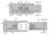
- FIG. 5is a front perspective view of the mated pair for the USB 3.0 A-receptacle, the first embodiment of the invention.
- FIG. 6is an unmated, exploded front perspective view of the first embodiment.
- FIG. 7is an exploded clamshell-style perspective view showing internal construction parts in phantom.
- FIG. 8is a cross-sectional view taken of the A-receptacle mated pair on line 4 - 4 of FIG. 6.1 .
- FIG. 9is a cross-sectional view similar to FIG. 6.4 , showing the components partially separated.
- FIG. 10is a cross-sectional view with parts broken away, taken on line 6 - 6 of FIG. 6.5 , although unlike
- FIG. 11is a front perspective view of the mated pair for the USB 3.0 B-receptacle, the second embodiment of the invention.
- FIG. 12is an unmated, exploded front perspective view of the second embodiment.
- FIG. 13is an exploded clamshell-style perspective view showing internal construction parts in phantom.
- FIG. 14A and FIG. 14Billustrate a demonstration of Ampere's Law (a) showing how a current I(t) traveling through a wire creates a perpendicular magnetic field B and Faraday's Law of induction (b) showing how a current I 1 (t) that travels through one wire, which produces an adjacent magnetic field B 1 , can induce a second current I 2 (t) into a second wire, separated by a distance d, resulting in a second magnetic field B 2 .
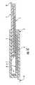
- FIG. 15Physical illustration of what happens in a coil of wire when a current flows
- FIG. 16High-level (simplified) Power NMC schematic setup.
- FIG. 1shows both the female A-receptacle and B-receptacle for the USB 3.0 (a) and its NMC equivalents (b). It should be noted that the NMC USB 3.0 uses the same physical dimensions as the current standard USB connector(s). This was a design requirement in order to maintain continuity with the industry.
- FIGS. 1-13show USB 3.0 A-receptacle 10 overall non-mating connector invention, showing a mated pair, the first embodiment of the invention.
- the Male component housing 12for the A-receptacle.
- the nonconductive housing mold 13 of component 12It is the housing that surrounds the male component of the connector.
- housingis usually called mold and some common mold materials used for connectors are PPC or Teflon. Other materials are possible so long as it is a very good insulator.
- the nonconductive housing mold 15 of component 14It is the housing that surrounds the female component of the connector.
- the female housingcan be made from PPC or Teflon unless the application requires it to be different. For NMCs, this typically will not be the case in order to avoid having to use more than one type of material for housing mold. Other materials are possible so long as it is a very good insulator.
- the ohmic contacts 16 of component 12can be made from materials such as copper, but are no restricted to only copper. The only requirement is the material that makes up the ohmic contact is a good conductor of electric current.
- the ohmic contacts 18 of component 14 , just as in 16can be made from materials such as copper, but are not restricted to only copper. The only requirement is the material that makes up the ohmic contact is a good conductor of electric current.
- the insertable portion 20 of component 12is the male A-receptacle.
- the platesare mounted between the mold of 13 and the high-k dielectric layer of 22 of component 12 .
- This plateis made from a very thin, highly conductive metal. Examples could be, but are not limited to, copper, gold-plated stainless steel, platinum, etc.
- the opening 25 of component 14.
- the high-k dielectric plates 26 of component 14The conductive plates 28 of component 14 .
- the platesare mounted between the mold of 15 and the high-k dielectric layer of 26 of component 14 . This plate is made from a very thin, highly conductive metal.
- the magnet 30 of component 12It is mounted and secured at the end tip of 12 .
- the purpose of 30is for making contact with 32 with the objective of joining, locking and securing 12 and 14 together.
- the magnet 32 of component 14It is mounted and secured at the back of 14 .
- the purpose of 32is for making contact with 30 with the objective of joining, locking and securing 12 and 14 together.
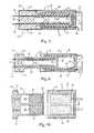
- the USB 3.0 B-receptacle overall non-mating connector invention 40showing a mated pair, the second embodiment of the invention.
- the nonconductive housing mold 43 of component 42It is the housing that surrounds the male component of the connector.
- housingis usually called mold and some common mold materials used for connectors are PPC or Teflon. Other materials are possible so long as it is a very good insulator.
- the female receptacle component housing 44for the B-receptacle.
- the nonconductive housing mold 45 of component 44It is the housing that surrounds the female component of the connector.
- the female housingcan be made from PPC or Teflon unless the application requires it to be different. For NMCs, this typically will not be the case in order to avoid having to use more than one type of material for housing mold.
- the ohmic contacts 46 of component 42can be made from materials such as copper, but are not restricted to only copper. The only requirement is the material that makes up the ohmic contact is a good conductor of electric current.
- the ohmic contacts 48 of component 44Just as in 46 , they can be made from materials such as copper, but are not restricted to only copper. These must also be good conductors.
- the insertable portion 50 of component 42is the male B-receptacle.
- the high-k dielectrics 52 of component 42The conductive plates 54 of component 42 .
- the platesare mounted between the mold of 42 and the high-k dielectric layer of 52 of component 42 .
- This plateis made from a very thin, highly conductive metal. Examples could be, but are not limited to, copper, gold-plated stainless steel, platinum, etc.
- the opening 55 of component 44.
- the high-k dielectric plates 56 of component 44The high-k dielectric plates 56 of component 44 .
- the conductive plates 58 of component 44The plates are mounted between the mold of 44 and the high-k dielectric layer of 56 of component 44 .
- This plateis made from a very thin, highly conductive metal. Examples could be, but are not limited to, copper, gold-plated stainless steel, platinum, etc.
- FIG. 2Adepicts the inductive power connector, in connected configuration.
- Conductors 109 , 110 , 119 , 129supply power and ground to male coil 111 and female coil 112 .
- Permanent magnets 107 and 108hold the connected assembly together, in much the same way discussed previously for the magnetic plates used in the capacitive connector.
- FIG. 2 bdepicts the inductive power connector, in unconnected configuration. Housings 101 and 102 seal the unit from its environment, extending across in front of the coils 111 and 112
- FIG. 16shows the power NMC connected to a time varying source V S , representing the signal being transmitted T X , and the receiving source T R .
- the F-Coilis on the transmitting side, T X , which is L 1 and the M-Coil is on the receiving side, T L , which is L 2 as shown in the figure.
- each power NMChas two inductive, there are two Q-factors, one for each coil called Q L1 and Q L2 .
- the optimal efficiency, ⁇ optfor the entire power NMC can be found after each of the two Q-factors have been found as well as the coupling coefficient, k. This coefficient is the fraction of flux of L 1 from the transmission side that permeates through to the receiving side and into L 2 of FIG. 16 .
- the optimal efficiencybe found by (6).
- ⁇ optk 2 ⁇ ( Q L ⁇ ⁇ 1 ⁇ Q L ⁇ ⁇ 2 ) ( 1 + 1 + k 2 ⁇ Q L ⁇ ⁇ 1 ⁇ Q L ⁇ ⁇ 2 ) 2 ( 6 )
- the distance separating the two coilsmust be as small as possible in order to maintain optimal signal transfer.
- the insulating material, or mold, between the two NMC receptaclesneed to be taken into account since the material will have an effect on how well the magnetic energy transfers from T X to T R . For this reason, each material chosen for a particular NMC power application must have a reasonable tan( ⁇ ) which is the loss coefficient.
Landscapes
- Engineering & Computer Science (AREA)
- Computer Networks & Wireless Communication (AREA)
- Signal Processing (AREA)
- Details Of Connecting Devices For Male And Female Coupling (AREA)
Abstract
Description
ψ=

Using this concept and definition for voltage potential we get:
The relationship between voltage potential, charge and capacitance is:
Substituting the above relationship into this equation, the capacitance between the two plates finally is:
Where H is the magnetic field intensity, J is the density of current and D is the electric flux density. The density of the magnetic field B and its intensity H are interrelated by the permeability of free space μ0. The auxiliary equation relates the two: B=μ0H. Applying Stokes Theorem to equation (1) we can find a relationship between the magnetic field B and the current I.
What equation (4) says is that the magnetic field B circulating the contour is equal to the enclosed current I that is moving through it, which is exactly what
Claims (17)
Priority Applications (1)
| Application Number | Priority Date | Filing Date | Title |
|---|---|---|---|
| US14/064,116US9197292B2 (en) | 2012-10-28 | 2013-10-26 | Non-mating connector |
Applications Claiming Priority (2)
| Application Number | Priority Date | Filing Date | Title |
|---|---|---|---|
| US201261719434P | 2012-10-28 | 2012-10-28 | |
| US14/064,116US9197292B2 (en) | 2012-10-28 | 2013-10-26 | Non-mating connector |
Publications (2)
| Publication Number | Publication Date |
|---|---|
| US20140120747A1 US20140120747A1 (en) | 2014-05-01 |
| US9197292B2true US9197292B2 (en) | 2015-11-24 |
Family
ID=50547651
Family Applications (1)
| Application Number | Title | Priority Date | Filing Date |
|---|---|---|---|
| US14/064,116Active - Reinstated2033-11-27US9197292B2 (en) | 2012-10-28 | 2013-10-26 | Non-mating connector |
Country Status (1)
| Country | Link |
|---|---|
| US (1) | US9197292B2 (en) |
Cited By (6)
| Publication number | Priority date | Publication date | Assignee | Title |
|---|---|---|---|---|
| US20220173548A1 (en)* | 2019-04-03 | 2022-06-02 | James David Wahl | Tethered connector assembly |
| US11626685B1 (en)* | 2021-09-21 | 2023-04-11 | Non-Metallic Connectors, Inc. | Power activation utilizing reed switch technique for non-metallic connector applications |
| US11764610B2 (en) | 2021-08-05 | 2023-09-19 | Non-Metallic Connectors, Inc. | Non-metallic connection light bulb and socket |
| US11801773B1 (en)* | 2022-08-18 | 2023-10-31 | Beta Air, Llc | Methods and systems for ground-based thermal conditioning for an electric aircraft |
| US11993397B1 (en)* | 2023-03-10 | 2024-05-28 | Beta Air, Llc | System and a method for preconditioning a power source of an electric aircraft |
| US20240186826A1 (en)* | 2022-12-02 | 2024-06-06 | Non-Metallic Connectors, Inc. | Non-metallic connection electrical wall outlet |
Families Citing this family (3)
| Publication number | Priority date | Publication date | Assignee | Title |
|---|---|---|---|---|
| US8801460B2 (en)* | 2012-11-09 | 2014-08-12 | Andrew Llc | RF shielded capacitively coupled connector |
| JP7008044B2 (en) | 2016-07-01 | 2022-01-25 | 株式会社ミツトヨ | A power transfer configuration for powering a removable probe for a coordinate measuring machine |
| JP7602885B2 (en)* | 2020-10-07 | 2024-12-19 | キヤノン株式会社 | Wireless communication system and receiving device |
Citations (19)
| Publication number | Priority date | Publication date | Assignee | Title |
|---|---|---|---|---|
| US3995209A (en)* | 1975-01-08 | 1976-11-30 | Pelcon Limited | Inductive connectors |
| US4144485A (en)* | 1974-12-03 | 1979-03-13 | Nippon Soken, Inc. | Contactless connector circuit |
| US4416495A (en) | 1981-06-05 | 1983-11-22 | Hughes Tool Company | Concentric electric connector for subsea well apparatus |
| US4549105A (en)* | 1983-01-07 | 1985-10-22 | Mitsubishi Denki Kabushiki Kaisha | Submergible motor including circuit element encased in molded plug |
| US5684380A (en)* | 1996-07-26 | 1997-11-04 | Delco Electronics Corp. | Oil cooled high power inductive coupler |
| US5909099A (en)* | 1996-08-07 | 1999-06-01 | Sumitomo Wiring Systems, Ltd. | Electric vehicle charging system including refrigerant system |
| US20040067683A1 (en) | 2002-10-08 | 2004-04-08 | Motorola, Inc. | Cable and connector system for optical and electrical signals |
| US7210940B2 (en)* | 2002-11-19 | 2007-05-01 | Huntleigh Technology Plc | Connector with inductive coupling |
| US7277025B2 (en)* | 2003-12-19 | 2007-10-02 | Geolink (Uk) Ltd. | Telescopic data coupler |
| US7598704B2 (en) | 2005-01-19 | 2009-10-06 | Fujifilm Corporation | Print system and print terminal, and image saving system and image saving unit |
| US20110143556A1 (en)* | 2009-12-10 | 2011-06-16 | Delta Eletronics, Inc. | Connecting mechanism for connecting power adapter and electronic device |
| US8102276B2 (en) | 2007-08-31 | 2012-01-24 | Pathfinder Energy Sevices, Inc. | Non-contact capacitive datalink for a downhole assembly |
| US8222827B2 (en) | 1999-06-21 | 2012-07-17 | Access Business Group International Llc | Inductively coupled ballast circuit |
| US20120228529A1 (en)* | 2009-11-16 | 2012-09-13 | Christopher Scott Trewin | Contactless coupling and method for use with an electrical appliance |
| US8350526B2 (en)* | 2011-07-25 | 2013-01-08 | Lightening Energy | Station for rapidly charging an electric vehicle battery |
| US20130052873A1 (en) | 2011-08-23 | 2013-02-28 | Tyco Electronics Nederland Bv | Backward compatible contactless socket connector, and backward compatible contactless socket connector system |
| US8400017B2 (en) | 2008-09-27 | 2013-03-19 | Witricity Corporation | Wireless energy transfer for computer peripheral applications |
| US8633616B2 (en)* | 2007-12-21 | 2014-01-21 | Cynetic Designs Ltd. | Modular pocket with inductive power and data |
| US20140102807A1 (en)* | 2012-06-19 | 2014-04-17 | Schlumberger Technology Corporation | Inductive Coupler |
- 2013
- 2013-10-26USUS14/064,116patent/US9197292B2/enactiveActive - Reinstated
Patent Citations (19)
| Publication number | Priority date | Publication date | Assignee | Title |
|---|---|---|---|---|
| US4144485A (en)* | 1974-12-03 | 1979-03-13 | Nippon Soken, Inc. | Contactless connector circuit |
| US3995209A (en)* | 1975-01-08 | 1976-11-30 | Pelcon Limited | Inductive connectors |
| US4416495A (en) | 1981-06-05 | 1983-11-22 | Hughes Tool Company | Concentric electric connector for subsea well apparatus |
| US4549105A (en)* | 1983-01-07 | 1985-10-22 | Mitsubishi Denki Kabushiki Kaisha | Submergible motor including circuit element encased in molded plug |
| US5684380A (en)* | 1996-07-26 | 1997-11-04 | Delco Electronics Corp. | Oil cooled high power inductive coupler |
| US5909099A (en)* | 1996-08-07 | 1999-06-01 | Sumitomo Wiring Systems, Ltd. | Electric vehicle charging system including refrigerant system |
| US8222827B2 (en) | 1999-06-21 | 2012-07-17 | Access Business Group International Llc | Inductively coupled ballast circuit |
| US20040067683A1 (en) | 2002-10-08 | 2004-04-08 | Motorola, Inc. | Cable and connector system for optical and electrical signals |
| US7210940B2 (en)* | 2002-11-19 | 2007-05-01 | Huntleigh Technology Plc | Connector with inductive coupling |
| US7277025B2 (en)* | 2003-12-19 | 2007-10-02 | Geolink (Uk) Ltd. | Telescopic data coupler |
| US7598704B2 (en) | 2005-01-19 | 2009-10-06 | Fujifilm Corporation | Print system and print terminal, and image saving system and image saving unit |
| US8102276B2 (en) | 2007-08-31 | 2012-01-24 | Pathfinder Energy Sevices, Inc. | Non-contact capacitive datalink for a downhole assembly |
| US8633616B2 (en)* | 2007-12-21 | 2014-01-21 | Cynetic Designs Ltd. | Modular pocket with inductive power and data |
| US8400017B2 (en) | 2008-09-27 | 2013-03-19 | Witricity Corporation | Wireless energy transfer for computer peripheral applications |
| US20120228529A1 (en)* | 2009-11-16 | 2012-09-13 | Christopher Scott Trewin | Contactless coupling and method for use with an electrical appliance |
| US20110143556A1 (en)* | 2009-12-10 | 2011-06-16 | Delta Eletronics, Inc. | Connecting mechanism for connecting power adapter and electronic device |
| US8350526B2 (en)* | 2011-07-25 | 2013-01-08 | Lightening Energy | Station for rapidly charging an electric vehicle battery |
| US20130052873A1 (en) | 2011-08-23 | 2013-02-28 | Tyco Electronics Nederland Bv | Backward compatible contactless socket connector, and backward compatible contactless socket connector system |
| US20140102807A1 (en)* | 2012-06-19 | 2014-04-17 | Schlumberger Technology Corporation | Inductive Coupler |
Non-Patent Citations (1)
| Title |
|---|
| 16th Annual Independent Inventors Conference, Claim Drafting for Beginners, Aug. 15-16, USPTO, Alexandria VA.* |
Cited By (8)
| Publication number | Priority date | Publication date | Assignee | Title |
|---|---|---|---|---|
| US20220173548A1 (en)* | 2019-04-03 | 2022-06-02 | James David Wahl | Tethered connector assembly |
| US12244095B2 (en)* | 2019-04-03 | 2025-03-04 | Microsoft Technology Licensing, Llc | Tethered connector assembly |
| US11764610B2 (en) | 2021-08-05 | 2023-09-19 | Non-Metallic Connectors, Inc. | Non-metallic connection light bulb and socket |
| US12176723B2 (en) | 2021-08-05 | 2024-12-24 | Non-Metallic Connectors, Inc. | Non-metallic connection light bulb and socket |
| US11626685B1 (en)* | 2021-09-21 | 2023-04-11 | Non-Metallic Connectors, Inc. | Power activation utilizing reed switch technique for non-metallic connector applications |
| US11801773B1 (en)* | 2022-08-18 | 2023-10-31 | Beta Air, Llc | Methods and systems for ground-based thermal conditioning for an electric aircraft |
| US20240186826A1 (en)* | 2022-12-02 | 2024-06-06 | Non-Metallic Connectors, Inc. | Non-metallic connection electrical wall outlet |
| US11993397B1 (en)* | 2023-03-10 | 2024-05-28 | Beta Air, Llc | System and a method for preconditioning a power source of an electric aircraft |
Also Published As
| Publication number | Publication date |
|---|---|
| US20140120747A1 (en) | 2014-05-01 |
Similar Documents
| Publication | Publication Date | Title |
|---|---|---|
| US9197292B2 (en) | Non-mating connector | |
| Han et al. | Electromagnetic modeling of through-silicon via (TSV) interconnections using cylindrical modal basis functions | |
| Hsiao et al. | Radiation suppression for cable-attached packages utilizing a compact embedded common-mode filter | |
| CN105070997B (en) | High-frequency signal circuit and electronic equipment | |
| CN102293068B (en) | Multilayer printed circuit board | |
| CN104471832A (en) | Wireless power transmission device, wireless power transmission device, and power receiving device | |
| CN110476306B (en) | Plug system | |
| CA2363529A1 (en) | Press-fit bus bar for distributing power | |
| Martinez et al. | Low loss ferrite Y-junction circulator based on empty substrate integrated coaxial line at Ku-band | |
| EP3876351A1 (en) | Robust, high frequency-suitable electrical terminal | |
| CN100499270C (en) | High frequency edge-mounted connector | |
| CN103733426B (en) | High-frequency signal circuit and electronic equipment | |
| Lin et al. | Development of an ultra-wideband suspended stripline to shielded microstrip transition | |
| CN114600323A (en) | Housing, in particular lead housing, system and method of manufacturing such a system | |
| Wartenberg et al. | A coaxial-to-microstrip transition for multilayer substrates | |
| Krishna et al. | Design of wideband microstrip to SICL transition for millimeter-wave applications | |
| Shi et al. | Parallel plate mode suppression in low-frequency microwave circuit packages using lid of 3-D cross by a 3-D printing technique | |
| Naka et al. | Improvement in efficiency of underwater wireless power transfer with electric coupling | |
| Han et al. | Accurate synthesis of four-line interdigitated coupler | |
| Zhang et al. | Gap waveguide-based PMC packaging for via holes-caused nonsmooth PEC surface | |
| Morales-Hernández et al. | Enhancement of corona discharge thresholds in microstrip bandpass filters by using cover-ended resonators | |
| US11791526B2 (en) | High frequency transmission device and high frequency signal transmission method | |
| CN207303432U (en) | Rectilinear high speed connector and its conductive module | |
| US7295084B2 (en) | Electrical interconnection for coaxial line to slab line structure including a bead ring | |
| US20110014819A1 (en) | Jack side connector and connector set having the jack side connector |
Legal Events
| Date | Code | Title | Description |
|---|---|---|---|
| STCF | Information on status: patent grant | Free format text:PATENTED CASE | |
| FEPP | Fee payment procedure | Free format text:MAINTENANCE FEE REMINDER MAILED (ORIGINAL EVENT CODE: REM.); ENTITY STATUS OF PATENT OWNER: MICROENTITY | |
| PRDP | Patent reinstated due to the acceptance of a late maintenance fee | Effective date:20191206 | |
| FEPP | Fee payment procedure | Free format text:PETITION RELATED TO MAINTENANCE FEES FILED (ORIGINAL EVENT CODE: PMFP); ENTITY STATUS OF PATENT OWNER: MICROENTITY Free format text:ENTITY STATUS SET TO MICRO (ORIGINAL EVENT CODE: MICR); ENTITY STATUS OF PATENT OWNER: MICROENTITY Free format text:SURCHARGE, PETITION TO ACCEPT PYMT AFTER EXP, UNINTENTIONAL (ORIGINAL EVENT CODE: M3558); ENTITY STATUS OF PATENT OWNER: MICROENTITY Free format text:PETITION RELATED TO MAINTENANCE FEES GRANTED (ORIGINAL EVENT CODE: PMFG); ENTITY STATUS OF PATENT OWNER: MICROENTITY | |
| MAFP | Maintenance fee payment | Free format text:PAYMENT OF MAINTENANCE FEE, 4TH YEAR, MICRO ENTITY (ORIGINAL EVENT CODE: M3551); ENTITY STATUS OF PATENT OWNER: MICROENTITY Year of fee payment:4 | |
| FEPP | Fee payment procedure | Free format text:MAINTENANCE FEE REMINDER MAILED (ORIGINAL EVENT CODE: REM.); ENTITY STATUS OF PATENT OWNER: MICROENTITY | |
| FEPP | Fee payment procedure | Free format text:ENTITY STATUS SET TO SMALL (ORIGINAL EVENT CODE: SMAL); ENTITY STATUS OF PATENT OWNER: SMALL ENTITY | |
| FEPP | Fee payment procedure | Free format text:7.5 YR SURCHARGE - LATE PMT W/IN 6 MO, SMALL ENTITY (ORIGINAL EVENT CODE: M2555); ENTITY STATUS OF PATENT OWNER: SMALL ENTITY | |
| MAFP | Maintenance fee payment | Free format text:PAYMENT OF MAINTENANCE FEE, 8TH YR, SMALL ENTITY (ORIGINAL EVENT CODE: M2552); ENTITY STATUS OF PATENT OWNER: SMALL ENTITY Year of fee payment:8 |