US9196716B2 - Enhancement mode III-N HEMTs - Google Patents
Enhancement mode III-N HEMTsDownload PDFInfo
- Publication number
- US9196716B2 US9196716B2US14/464,639US201414464639AUS9196716B2US 9196716 B2US9196716 B2US 9196716B2US 201414464639 AUS201414464639 AUS 201414464639AUS 9196716 B2US9196716 B2US 9196716B2
- Authority
- US
- United States
- Prior art keywords
- layer
- gate
- channel
- iii
- semiconductor device
- Prior art date
- Legal status (The legal status is an assumption and is not a legal conclusion. Google has not performed a legal analysis and makes no representation as to the accuracy of the status listed.)
- Active
Links
Images


Classifications
- H01L29/7783—
- H—ELECTRICITY
- H10—SEMICONDUCTOR DEVICES; ELECTRIC SOLID-STATE DEVICES NOT OTHERWISE PROVIDED FOR
- H10D—INORGANIC ELECTRIC SEMICONDUCTOR DEVICES
- H10D30/00—Field-effect transistors [FET]
- H10D30/40—FETs having zero-dimensional [0D], one-dimensional [1D] or two-dimensional [2D] charge carrier gas channels
- H10D30/47—FETs having zero-dimensional [0D], one-dimensional [1D] or two-dimensional [2D] charge carrier gas channels having 2D charge carrier gas channels, e.g. nanoribbon FETs or high electron mobility transistors [HEMT]
- H10D30/471—High electron mobility transistors [HEMT] or high hole mobility transistors [HHMT]
- H10D30/473—High electron mobility transistors [HEMT] or high hole mobility transistors [HHMT] having confinement of carriers by multiple heterojunctions, e.g. quantum well HEMT
- H10D30/4732—High electron mobility transistors [HEMT] or high hole mobility transistors [HHMT] having confinement of carriers by multiple heterojunctions, e.g. quantum well HEMT using Group III-V semiconductor material
- H10D30/4735—High electron mobility transistors [HEMT] or high hole mobility transistors [HHMT] having confinement of carriers by multiple heterojunctions, e.g. quantum well HEMT using Group III-V semiconductor material having delta-doped or planar-doped donor layers
- H—ELECTRICITY
- H01—ELECTRIC ELEMENTS
- H01L—SEMICONDUCTOR DEVICES NOT COVERED BY CLASS H10
- H01L21/00—Processes or apparatus adapted for the manufacture or treatment of semiconductor or solid state devices or of parts thereof
- H01L21/02—Manufacture or treatment of semiconductor devices or of parts thereof
- H01L21/02104—Forming layers
- H01L21/02107—Forming insulating materials on a substrate
- H01L21/02109—Forming insulating materials on a substrate characterised by the type of layer, e.g. type of material, porous/non-porous, pre-cursors, mixtures or laminates
- H01L21/02112—Forming insulating materials on a substrate characterised by the type of layer, e.g. type of material, porous/non-porous, pre-cursors, mixtures or laminates characterised by the material of the layer
- H01L21/02123—Forming insulating materials on a substrate characterised by the type of layer, e.g. type of material, porous/non-porous, pre-cursors, mixtures or laminates characterised by the material of the layer the material containing silicon
- H01L21/0217—Forming insulating materials on a substrate characterised by the type of layer, e.g. type of material, porous/non-porous, pre-cursors, mixtures or laminates characterised by the material of the layer the material containing silicon the material being a silicon nitride not containing oxygen, e.g. SixNy or SixByNz
- H—ELECTRICITY
- H01—ELECTRIC ELEMENTS
- H01L—SEMICONDUCTOR DEVICES NOT COVERED BY CLASS H10
- H01L21/00—Processes or apparatus adapted for the manufacture or treatment of semiconductor or solid state devices or of parts thereof
- H01L21/02—Manufacture or treatment of semiconductor devices or of parts thereof
- H01L21/02104—Forming layers
- H01L21/02365—Forming inorganic semiconducting materials on a substrate
- H01L21/02518—Deposited layers
- H01L21/02521—Materials
- H01L21/02538—Group 13/15 materials
- H01L21/0254—Nitrides
- H01L29/0847—
- H01L29/1033—
- H01L29/2003—
- H01L29/365—
- H01L29/4236—
- H01L29/66431—
- H01L29/66462—
- H01L29/7787—
- H01L29/7788—
- H—ELECTRICITY
- H10—SEMICONDUCTOR DEVICES; ELECTRIC SOLID-STATE DEVICES NOT OTHERWISE PROVIDED FOR
- H10D—INORGANIC ELECTRIC SEMICONDUCTOR DEVICES
- H10D30/00—Field-effect transistors [FET]
- H10D30/01—Manufacture or treatment
- H10D30/015—Manufacture or treatment of FETs having heterojunction interface channels or heterojunction gate electrodes, e.g. HEMT
- H—ELECTRICITY
- H10—SEMICONDUCTOR DEVICES; ELECTRIC SOLID-STATE DEVICES NOT OTHERWISE PROVIDED FOR
- H10D—INORGANIC ELECTRIC SEMICONDUCTOR DEVICES
- H10D30/00—Field-effect transistors [FET]
- H10D30/40—FETs having zero-dimensional [0D], one-dimensional [1D] or two-dimensional [2D] charge carrier gas channels
- H10D30/47—FETs having zero-dimensional [0D], one-dimensional [1D] or two-dimensional [2D] charge carrier gas channels having 2D charge carrier gas channels, e.g. nanoribbon FETs or high electron mobility transistors [HEMT]
- H10D30/471—High electron mobility transistors [HEMT] or high hole mobility transistors [HHMT]
- H10D30/473—High electron mobility transistors [HEMT] or high hole mobility transistors [HHMT] having confinement of carriers by multiple heterojunctions, e.g. quantum well HEMT
- H10D30/4732—High electron mobility transistors [HEMT] or high hole mobility transistors [HHMT] having confinement of carriers by multiple heterojunctions, e.g. quantum well HEMT using Group III-V semiconductor material
- H—ELECTRICITY
- H10—SEMICONDUCTOR DEVICES; ELECTRIC SOLID-STATE DEVICES NOT OTHERWISE PROVIDED FOR
- H10D—INORGANIC ELECTRIC SEMICONDUCTOR DEVICES
- H10D30/00—Field-effect transistors [FET]
- H10D30/40—FETs having zero-dimensional [0D], one-dimensional [1D] or two-dimensional [2D] charge carrier gas channels
- H10D30/47—FETs having zero-dimensional [0D], one-dimensional [1D] or two-dimensional [2D] charge carrier gas channels having 2D charge carrier gas channels, e.g. nanoribbon FETs or high electron mobility transistors [HEMT]
- H10D30/471—High electron mobility transistors [HEMT] or high hole mobility transistors [HHMT]
- H10D30/475—High electron mobility transistors [HEMT] or high hole mobility transistors [HHMT] having wider bandgap layer formed on top of lower bandgap active layer, e.g. undoped barrier HEMTs such as i-AlGaN/GaN HEMTs
- H10D30/4755—High electron mobility transistors [HEMT] or high hole mobility transistors [HHMT] having wider bandgap layer formed on top of lower bandgap active layer, e.g. undoped barrier HEMTs such as i-AlGaN/GaN HEMTs having wide bandgap charge-carrier supplying layers, e.g. modulation doped HEMTs such as n-AlGaAs/GaAs HEMTs
- H—ELECTRICITY
- H10—SEMICONDUCTOR DEVICES; ELECTRIC SOLID-STATE DEVICES NOT OTHERWISE PROVIDED FOR
- H10D—INORGANIC ELECTRIC SEMICONDUCTOR DEVICES
- H10D30/00—Field-effect transistors [FET]
- H10D30/40—FETs having zero-dimensional [0D], one-dimensional [1D] or two-dimensional [2D] charge carrier gas channels
- H10D30/47—FETs having zero-dimensional [0D], one-dimensional [1D] or two-dimensional [2D] charge carrier gas channels having 2D charge carrier gas channels, e.g. nanoribbon FETs or high electron mobility transistors [HEMT]
- H10D30/471—High electron mobility transistors [HEMT] or high hole mobility transistors [HHMT]
- H10D30/477—Vertical HEMTs or vertical HHMTs
- H—ELECTRICITY
- H10—SEMICONDUCTOR DEVICES; ELECTRIC SOLID-STATE DEVICES NOT OTHERWISE PROVIDED FOR
- H10D—INORGANIC ELECTRIC SEMICONDUCTOR DEVICES
- H10D62/00—Semiconductor bodies, or regions thereof, of devices having potential barriers
- H10D62/10—Shapes, relative sizes or dispositions of the regions of the semiconductor bodies; Shapes of the semiconductor bodies
- H10D62/13—Semiconductor regions connected to electrodes carrying current to be rectified, amplified or switched, e.g. source or drain regions
- H10D62/149—Source or drain regions of field-effect devices
- H10D62/151—Source or drain regions of field-effect devices of IGFETs
- H—ELECTRICITY
- H10—SEMICONDUCTOR DEVICES; ELECTRIC SOLID-STATE DEVICES NOT OTHERWISE PROVIDED FOR
- H10D—INORGANIC ELECTRIC SEMICONDUCTOR DEVICES
- H10D62/00—Semiconductor bodies, or regions thereof, of devices having potential barriers
- H10D62/10—Shapes, relative sizes or dispositions of the regions of the semiconductor bodies; Shapes of the semiconductor bodies
- H10D62/17—Semiconductor regions connected to electrodes not carrying current to be rectified, amplified or switched, e.g. channel regions
- H10D62/213—Channel regions of field-effect devices
- H10D62/221—Channel regions of field-effect devices of FETs
- H10D62/235—Channel regions of field-effect devices of FETs of IGFETs
- H—ELECTRICITY
- H10—SEMICONDUCTOR DEVICES; ELECTRIC SOLID-STATE DEVICES NOT OTHERWISE PROVIDED FOR
- H10D—INORGANIC ELECTRIC SEMICONDUCTOR DEVICES
- H10D62/00—Semiconductor bodies, or regions thereof, of devices having potential barriers
- H10D62/60—Impurity distributions or concentrations
- H10D62/605—Planar doped, e.g. atomic-plane doped or delta-doped
- H—ELECTRICITY
- H10—SEMICONDUCTOR DEVICES; ELECTRIC SOLID-STATE DEVICES NOT OTHERWISE PROVIDED FOR
- H10D—INORGANIC ELECTRIC SEMICONDUCTOR DEVICES
- H10D62/00—Semiconductor bodies, or regions thereof, of devices having potential barriers
- H10D62/80—Semiconductor bodies, or regions thereof, of devices having potential barriers characterised by the materials
- H10D62/82—Heterojunctions
- H10D62/824—Heterojunctions comprising only Group III-V materials heterojunctions, e.g. GaN/AlGaN heterojunctions
- H—ELECTRICITY
- H10—SEMICONDUCTOR DEVICES; ELECTRIC SOLID-STATE DEVICES NOT OTHERWISE PROVIDED FOR
- H10D—INORGANIC ELECTRIC SEMICONDUCTOR DEVICES
- H10D62/00—Semiconductor bodies, or regions thereof, of devices having potential barriers
- H10D62/80—Semiconductor bodies, or regions thereof, of devices having potential barriers characterised by the materials
- H10D62/85—Semiconductor bodies, or regions thereof, of devices having potential barriers characterised by the materials being Group III-V materials, e.g. GaAs
- H10D62/8503—Nitride Group III-V materials, e.g. AlN or GaN
- H—ELECTRICITY
- H10—SEMICONDUCTOR DEVICES; ELECTRIC SOLID-STATE DEVICES NOT OTHERWISE PROVIDED FOR
- H10D—INORGANIC ELECTRIC SEMICONDUCTOR DEVICES
- H10D62/00—Semiconductor bodies, or regions thereof, of devices having potential barriers
- H10D62/80—Semiconductor bodies, or regions thereof, of devices having potential barriers characterised by the materials
- H10D62/85—Semiconductor bodies, or regions thereof, of devices having potential barriers characterised by the materials being Group III-V materials, e.g. GaAs
- H10D62/854—Semiconductor bodies, or regions thereof, of devices having potential barriers characterised by the materials being Group III-V materials, e.g. GaAs further characterised by the dopants
- H—ELECTRICITY
- H10—SEMICONDUCTOR DEVICES; ELECTRIC SOLID-STATE DEVICES NOT OTHERWISE PROVIDED FOR
- H10D—INORGANIC ELECTRIC SEMICONDUCTOR DEVICES
- H10D64/00—Electrodes of devices having potential barriers
- H10D64/20—Electrodes characterised by their shapes, relative sizes or dispositions
- H10D64/27—Electrodes not carrying the current to be rectified, amplified, oscillated or switched, e.g. gates
- H10D64/311—Gate electrodes for field-effect devices
- H10D64/411—Gate electrodes for field-effect devices for FETs
- H10D64/511—Gate electrodes for field-effect devices for FETs for IGFETs
- H10D64/512—Disposition of the gate electrodes, e.g. buried gates
- H10D64/513—Disposition of the gate electrodes, e.g. buried gates within recesses in the substrate, e.g. trench gates, groove gates or buried gates
- H—ELECTRICITY
- H10—SEMICONDUCTOR DEVICES; ELECTRIC SOLID-STATE DEVICES NOT OTHERWISE PROVIDED FOR
- H10D—INORGANIC ELECTRIC SEMICONDUCTOR DEVICES
- H10D64/00—Electrodes of devices having potential barriers
- H10D64/60—Electrodes characterised by their materials
- H10D64/66—Electrodes having a conductor capacitively coupled to a semiconductor by an insulator, e.g. MIS electrodes
- H10D64/68—Electrodes having a conductor capacitively coupled to a semiconductor by an insulator, e.g. MIS electrodes characterised by the insulator, e.g. by the gate insulator
- H10D64/693—Electrodes having a conductor capacitively coupled to a semiconductor by an insulator, e.g. MIS electrodes characterised by the insulator, e.g. by the gate insulator the insulator comprising nitrogen, e.g. nitrides, oxynitrides or nitrogen-doped materials
Definitions
- This inventionrelates to enhancement mode III-nitride devices.
- GaNgallium nitride
- HEMTshigh electron mobility transistors
- D-modedepletion mode
- E-modeenhancement mode
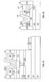
- FIG. 1shows a prior art Ga-face GaN HEMT depletion mode structure.
- Substrate 10may be GaN, SiC, sapphire, Si, or any other suitable substrate upon which a GaN device may be formed.
- GaN buffer layer 14 and Al x GaN layer 18 on top of itare oriented in the [0 0 0 1] (C-plane) direction.
- the conducting channelconsists of a two-dimensional electron gas (2DEG) region, shown by a dotted line in GaN buffer layer 14 in FIG. 1 , is formed in layer 14 near the interface between layer 14 and Al x GaN layer 18 .
- 2DEGtwo-dimensional electron gas
- a thin, 0.6 nm AlN layer(not shown) is optionally included between GaN layer 14 and Al x GaN layer 18 in order to increase the charge density and mobility in the 2DEG region.
- the region of layer 14 between the source 27 and the gate 26is referred to as the source access region.
- the region of layer 14 between the drain 28 and gate 26is referred to as the drain access region.
- the source 27 and drain 28both make contact with buffer layer 14 .
- the 2DEG regionWith no applied gate voltage, the 2DEG region extends all the way from the source 27 to the drain 28 , forming a conducting channel and rendering the device normally on, making it a depletion mode device.
- a negative voltagemust be applied to the gate 26 to deplete the 2DEG region under the gate 26 , and thus to turn the device OFF.
- III-N HEMT deviceAnother related prior art III-N HEMT device is the subject of provisional application Ser. No. 60/972,481, filed Sep. 14, 2007, entitled “III-N Devices with Recessed Gates,” which application is hereby incorporated by reference herein.
- the device of the inventionis an enhancement mode HEMT.
- an enhancement-mode HEMThas two requirements.
- the source and drain access regionsshould contain a 2DEG region that results in a conductivity of those regions at least as large as the conductivity of the channel region beneath the gate when the device is in the ON state.
- the conductivity of these access regionsis as large as possible, as access resistance is thereby reduced, thus reducing the on-resistance R on —a desirable characteristic for a switching device.
- the second requirement of an enhancement mode HEMTis for the channel region underneath the gate to have no 2DEG at zero gate voltage. A positive gate voltage therefore is required to induce a 2DEG charge in this region beneath the gate, and thus to turn the device ON.
- an E-mode HEMThas a 2DEG region across both the access regions.
- Vgs>Vtha large enough voltage is applied to the gate (i.e., Vgs>Vth) a 2DEG region forms underneath the gate and the channel becomes fully conductive between source and drain.
- the disclosed semiconductor deviceincludes a substrate and a nitride channel layer on the substrate, the channel layer including a first channel region beneath a gate region, and two channel access regions on opposite sides of the first channel region.
- the composition of the nitride channel layeris selected from the group consisting of the nitrides of gallium, indium and aluminum, and combinations thereof.
- Adjacent the channel layeris an AlXN layer wherein X is selected from the group consisting of gallium, indium or their combination.
- An n-doped GaN layeris adjacent the AlXN layer in the areas adjacent to the channel access regions, but not in the area adjacent to the first channel region beneath the gate region.
- the concentration of Al in the AlXN layer, the AlXN layer thickness and the n-doping concentration and doping profile in the n-doped GaN layerall are selected to induce a 2DEG charge in channel access regions adjacent the AlXN layer, without inducing any substantial 2DEG charge in the first channel region beneath the gate, so that the channel is not conductive in the absence of a control voltage applied to the gate, but can readily become conductive when a control voltage is applied to the gate.
- a similar disclosed semiconductor deviceincludes a substrate, a nitride channel layer on the substrate including a first channel region beneath a gate region, and two channel access regions on opposite sides of the first channel region, the composition of the nitride channel layer being selected from the group consisting of nitrides of gallium, indium and aluminum, and combinations thereof.
- the devicealso has a first AlXN layer adjacent the channel layer wherein X is selected from the group consisting of gallium, indium or their combination, and a second AlXN layer adjacent the first AlXN layer, the first AlXN layer having a substantially higher concentration of Al than the second AlXN layer.
- the concentration of the Al in each of the first and second AlXN layers, respectively, and their respective thicknessesare selected to induce a 2DEG charge in channel access regions adjacent the first AlXN layer, without inducing any substantial 2DEG charge in the first channel region beneath the gate, so that the channel is not conductive in the absence of a control voltage applied to the gate, but can readily become conductive when a control voltage is applied to the gate.
- Another disclosed deviceincludes a substrate, a nitride channel layer on the substrate, including a first channel region, the material of which is selected from the group consisting of nitrides of gallium, indium, aluminum and combinations thereof.
- the devicefurther comprises an AlXN layer adjacent to the channel and a III-N adjacent to the AlXN layer, the III-N layer also including two channel access region on the opposite sides of the gate, wherein X is selected from the group consisting of gallium, indium or their combination, and the III material is Al, Ga or In.
- the channel access regions in this deviceare in a different layer from the channel region being modulated by the gate.
- a nitride layersuch as AlN, may be interposed between the AlXN layer and the nitride channel layer.
- FIG. 1is a cross-sectional view of a device of the prior art.
- FIG. 2is a cross-sectional view of a device of one embodiment of the invention.
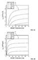
- FIGS. 3 a and 3 bare graphs showing the relationship of the thickness of one layer of the device of FIG. 2 and the sheet charge density.
- FIG. 4is a cross-sectional view of a device of another embodiment of the invention.
- FIG. 5is a cross-sectional view of a device of another embodiment of the invention.
- FIG. 6is a cross-sectional view of a device of another embodiment of the invention.
- FIG. 7is a graph showing the transfer characteristics of the device of FIG. 5 .
- FIGS. 8 a - 8 dshow a method of fabrication for the device of FIG. 9 .
- FIG. 9is a cross-sectional view of a device of another embodiment of the invention.
- FIG. 10is a cross-sectional view of a device of another embodiment of the invention.
- FIG. 11is a cross-sectional view of a device of another embodiment of the invention.
- FIG. 12is a cross-sectional view of a device of another embodiment of the invention.
- FIGS. 13 a and 13 bare cross-sectional views of a device of another embodiment of the invention.
- FIGS. 14 a and 14 bare cross-sectional views of a device of another embodiment of the invention.
- FIG. 15is a cross-sectional view of a device of another embodiment of the invention.
- FIG. 16is a cross-sectional view of a device of another embodiment of the invention.
- FIG. 17is a cross-sectional view of a device of another embodiment of the invention.
- FIGS. 18 a and 18 bare cross-sectional views of a device of two other embodiments of the invention.
- FIGS. 19-23are cross-sectional views of devices of other embodiments of the invention.
- FIGS. 24 a , 24 b and 24 care graphs depicting the operation of the device of FIG. 23 .
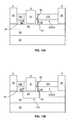
- FIG. 2shows one embodiment of an E-mode GaN HEMT device of this invention.
- Substrate 30may be GaN, SiC, sapphire, Si, or any other suitable substrate for a GaN device as is known in the art.
- Nitride channel layer 34may be placed upon substrate 30 .
- This layermay be a nitride of gallium, indium or aluminum, or combinations of those nitrides.
- a preferred materialis GaN.
- Layer 34may be made semi-insulating, such as by doping with iron.
- Preferably channel layer 34may be C-plane oriented, such that the surfaces furthest from the substrate are [0 0 0 1] surfaces.
- itmay be a semi-polar structure with Ga termination, as is known in the art.
- itmay be grown as a non-polar structure using n-doping, as will be described below.
- a thin layer 38 of Al x XNis placed on top of the GaN layer 34 .
- the “X” materialmay be gallium, indium or a combination of the two.
- a preferable material for this layer 38is Al x GaN.
- layer 38will be referred to as an Al x GaN layer, although it may be these other materials as well.
- layer 38may be AlN.
- Al x GaN layer 38should be sufficiently thin so that no significant 2DEG is established underneath the gate 31 when zero volts is applied to the gate.
- Layer 35is formed over layer 38 , and it may be n-doped, as will be discussed below.
- Gate 31 source 33 and drain 39may be any suitable metal or other electrically conductive material.
- an insulating layer 36is formed between gate 31 and adjacent layers 35 and 38 .
- layers 35 and 38are etched so that the bottoms of these source and drain contacts can make electrical contact with nitride channel layer 34 .
- the graphs of FIGS. 3 a and 3 bshow a plot of the 2DEG sheet charge density n s underneath the gate 31 of the device shown in FIG. 2 with zero volts applied to the gate, versus the Al x GaN layer 38 thickness (t) for a number of different Al compositions.
- the graph of FIG. 3 aillustrates the charge density for a device structure without an intermediate AlN layer; the graph of FIG. 3 b illustrates the charge density for a device structure with an intermediate AlN layer.
- the polarization-induced charge density n ssmall, or to eliminate it completely.
- n sthe polarization-induced charge density
- FIGS. 2 and 3 a and 3 bfor a given Al concentration in the Al x GaN layer 38 , there is a minimum layer thickness required to form a 2DEG under the gate at zero gate bias.
- the Al x GaN thicknessis less than a minimum thickness, no 2DEG region is formed underneath the gate at zero gate voltage, which prevents the device from being normally ON.
- the minimum thickness required to form a 2DEG underneath the gate at zero gate biasis about the same as the maximum thickness for which the device will be normally OFF and therefore operate as an enhancement mode device.
- the maximum thickness of the Al x GaN layer 38 such that no significant 2DEG charge is present in the channel region underneath the gate at zero gate voltagedepends upon how much Al is present in the layer, as illustrated in FIGS. 3 a and 3 b .
- FIGS. 2 and 3 afor a device without an intermediate AlN layer and 20% Al (the top curve 50 ), no charge will be induced if the thickness of the layer 38 is below about 6 nm, whereas for 10% Al, no charge will be induced if the thickness of the layer 38 is below about 12 nm.
- FIG. 1for a device without an intermediate AlN layer and 20% Al
- the leakage current when the device is in the OFF stateincreases with increasing Al composition, as a result of the corresponding decrease in the source-drain barrier when the device is in the OFF state.
- a device with a 5 nm thick Al x GaN layer that contains 20% Alwill exhibit more leakage than a device with a 5 nm thick Al x GaN layer containing 10% Al. Therefore, for a given thickness of layer 38 , a lower Al composition results in a higher threshold voltage and lower leakage when the device is biased OFF, both of which are desirable in an enhancement mode device.
- the maximum 2DEG charge that can be induced in the access regionsincreases with increasing Al concentration in layer 38 .
- Increasing the 2DEG charge in the access regionsreduces the on-resistance R on of the device. Therefore, the Al composition in layer 38 should be at least high enough that a sufficient amount of charge can be induced in the access regions to satisfy the R on requirements of the application for which the device is being used.
- Al x GaN layer 38on top of Al x GaN layer 38 is a second Al y GaN layer 35 .
- ycan be 0, so that the layer is entirely GaN.
- Layer 35is required to provide 2DEG charge in the channel access regions of layer 34 between the source 33 and the gate 31 , and between the drain 39 and the gate 31 .
- layer 35is entirely GaN, there is no net polarization-induced field in layer 35 contributing to the formation of 2DEG charge in the channel access regions. Therefore, for devices in which layer 35 is undoped or unintentionally doped GaN, no significant 2DEG will be present in the access regions, and an enhancement mode device would not be feasible.
- the polarization-induced field in this layercan contribute to the formation of a 2DEG charge in the channel access regions.
- a minimum thickness of layer 35required to induce a 2DEG charge in the channel access regions. This minimum thickness decreases by increasing the Al composition in layer 35 and/or in layer 38 .
- the 2DEG charge concentration in the channel access regionsincreases with increasing thickness of layer 35 , but can never exceed the saturation charge concentration for the structure.
- the saturation charge concentrationwhich is the maximum charge that can be induced in the 2DEG regions, depends upon the Al composition in layers 35 and 38 and upon the thickness of layer 38 . Increasing the Al composition in layer 35 increases the saturation charge concentration for the 2DEG region.
- the thickness and Al content of layer 35are selected so that, by itself, layer 35 doesn't add charge in the structure below, or adds an amount of charge in the access regions which is not large enough to satisfy the R on requirements of the application for which the device is being used.
- One way to achieve thisis to n-dope Al y GaN layer 35 with Si, which acts as an n-type dopant in III-N devices.
- n-dopingThe greater the n-doping, the greater the resultant 2DEG charge in the channel access regions of layer 34 .
- a preferred doping techniqueis called silicon delta doping, well known in the art.
- a uniform doping in layer 35could be used, or other arbitrary doping profile.
- the minimum effective amountis that required to achieve the target 2DEG charge in the channel access regions.
- Increasing the 2DEG chargeincreases the maximum ON current of the device, but also causes it to have a lower breakdown voltage.
- the devicemust block voltage in the OFF condition, it is undesirable to have too low a breakdown voltage. Therefore, in selecting the amount of n-doping, it is necessary to provide a sufficiently high breakdown voltage for the applications for which the device will be used.
- a device of the inventioncan have a switching voltage greater than 2 volts, preferably 2.5 volts, and a current flow through the channel of at least 200 mA per mm of gate width, preferably at least 300 mA per mm, when the channel is conductive.
- the current through the channel when the channel is conductiveshould be at least 10,000 times the current that flows when the channel is not conductive.
- the saturation charge valuethere is a maximum charge, known as the saturation charge value, that is possible in the channel access regions, the magnitude of which depends upon the composition of layer 38 .
- the saturation charge valuethe maximum charge that is possible in the channel access regions, the magnitude of which depends upon the composition of layer 38 .
- layer 38is Al x GaN
- a higher Al composition in layer 38results in a larger saturation charge value in the access regions. Therefore there is no need to dope region 35 beyond the amount required to create the maximum charge in the access regions.
- the amount of required dopingfurther depends upon the doping profile. If the dopant is placed near the bottom of layer 38 , closer to channel layer 34 , a larger 2DEG region is induced than if the dopant is placed farther away from channel layer 34 . But it is undesirable to dope too close to the interface between layers 38 and 34 because that would lessen the mobility of electrons in the 2DEG region, which would increase the resistance of the 2DEG region, and thus the channel resistance.
- One way to determine the aluminum concentration of layer 35is to select the concentration so that, without the n-doping, no 2DEG charge will be formed in the channel access regions in the absence of the application of a gate voltage. Then the n-doping will create the 2DEG charge.
- an additional cap nitride layer(not shown) can be placed atop layer 35 .
- the nitride usedmay be In, Ga, or Al, or a combination of one or more of them. This layer may improve the surface properties of the device.
- a portion of Al y GaN layer 35is removed in region 36 under and around the gate region by a conventional etching step.
- This stepfor example, can be a plasma RIE or ICP etch.
- the resulting structurehas no charge under the gate region at 0 gate voltage, while a desired 2DEG charge still exists in the channel access regions shown within layer 34 by the two dotted lines. Where Si-doping is used, this 2DEG region is at least partially induced by the Si-doped layer 35 .
- a conformal gate insulator 36is deposited by methods well known in the art, such as PECVD, ICP, MOCVD, sputtering or other well know techniques.
- This insulator 36can be silicon dioxide, silicon nitride, or any other insulator or combination of insulators.
- at least one of the insulators of layer 36is a high-K dielectric, such as HfO 2 , Ta 2 O 5 , or ZrO 2 .
- at least one of the insulatorscontains or induces negative charge, thereby acting to deplete the channel region underneath the insulator. Examples of insulators which may act to deplete the underlying channel are AlSiN, HfO 2 , and Ta 2 O 5 .
- the source and drain ohmic contacts 33 and 39 and the gate contact 31are deposited by well known techniques. The order of these process steps may be changed, as is well known in the art. In addition, if desired, one or more field plates externally connected to either the gate 31 or source 33 may be used. SiN or other passivation layers may also be deposited over the entire structure including the contacts, as is known in the art.
- the Al x GaN layer 38 under the gateis thinner than the minimum required to form a 2DEG region beneath the gate at 0 gate voltage.
- the upper limit of this layer 38 thicknessis called the “critical thickness.”
- the minimum gate voltage for which a 2DEG region exists underneath the gate, thus rendering the channel conductive,is called the device threshold voltage V th .
- V thThe minimum gate voltage for which a 2DEG region exists underneath the gate, thus rendering the channel conductive, is called the device threshold voltage V th .
- V th0-3 volts may be used. If, for example, a V th of 3 volts were selected, a positive gate voltage greater than 3 volts is required to turn the device ON, thus inducing a 2DEG region under the gate region and achieving enhancement mode operation where current is conducted between source 33 and drain 39 .
- the gate voltagewere less than 3 volts, the device would remain OFF.
- a higher threshold voltageis preferable to prevent accidental turn on of the device and to decrease leakage
- the maximum positive bias voltage that may be applied to the gateis limited by the schottky barrier forward turn on voltage of the gate junction, thus limiting the maximum full channel current.
- a higher positive biasmay be applied to the gate to accumulate a high channel 2DEG charge under the gate region when the device is ON, thus achieving substantial operating current.
- the gate insulatoris also used to increase the external threshold voltage of an already normally-off device. In the case where the gate insulator acts to deplete charge from the underlying channel, the intrinsic threshold voltage is increased, and OFF state leakage decreases, since the source-drain barrier when the device is in the OFF state is increased.
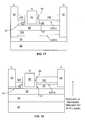
- FIG. 4Another embodiment of the device of the invention is shown in FIG. 4 .
- the layers that are the same as in FIG. 2have the same reference numerals.
- This deviceis similar to the one in FIG. 2 , except that a nitride buffer layer 32 is included in between the nitride channel layer 34 and the substrate 30 .
- Buffer layer 32may be a nitride of gallium, indium or aluminum, or combinations of those nitrides.
- the composition of this buffer layer 32is chosen such that the bandgap of the material is greater than that of the material of the channel layer 34 , and the lattice constant is smaller than that of channel layer 34 . Therefore, these two layers must be different materials.
- buffer layer 32is Al b In c Ga 1-b-c N
- increasing b while keeping c constantincreases the bandgap and decreases the lattice constant of layer 32
- increasing c while keeping b constantdecreases the bandgap and increases the lattice constant. Therefore b and c are chosen in such a way that ensures that the bandgap of the material of buffer layer 32 is greater than that of the material of the channel layer 34 , and the lattice constant of buffer layer 32 is smaller than that of channel layer 34 .
- buffer layer 32is preferably Al z GaN, where z is between a finite value greater than 0, and 1.
- the Al z GaN buffer layer 32acts as a back-barrier, further increasing the source-drain barrier when the device is in the OFF state and increasing the device threshold voltage, as compared to the device of FIG. 2 .
- the GaN layer 34 and AlGaN layer 38which both overlie the Al z GaN buffer layer 32 are conformally strained to the Al z GaN, which modifies the polarization fields in those two layers and thereby reduces the polarization-induced contribution to the 2DEG channel charge.
- the net result of these effectsis that the “critical thickness” of the Al x GaN layer 38 is increased as compared to layer 38 of the device of FIG. 2 . Having a thicker Al x GaN layer 38 in the device of FIG. 4 , with buffer layer 32 , is helpful in enabling manufacturability of these devices.
- Source and drain contacts 33 and 39are formed through the top surface of the device. Prior to the formation of source and drain contacts 33 and 39 , respectively, layers 35 , and 38 are etched so that the bottoms of these source and drain contacts can make electrical contact with nitride channel layer 34 .
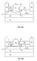
- FIG. 5A preferred embodiment of the device of the invention is shown in FIG. 5 .
- a GaN buffer layer 41is grown on a SiC substrate 40 , followed by the deposition of a 3 nm thick Al 0.2 GaN layer 43 , which is less than the critical thickness and hence does not induce any 2DEG region in area of the underlying GaN layer beneath gate 45 .
- a 20 nm thick GaN layer 44 delta doped with Si between about 6 ⁇ 10 12 atoms/cm 2 and 8 ⁇ 10 12 atoms/cm 2is formed atop Al 0.2 GaN layer 43 .
- the Al 0.2 GaN layer 43 thickness in the area beneath the gate 45needs to be about 5 nm thick or less.
- Source and drain regions 47 and 49are formed on the top surface. Prior to the formation of source and drain contacts 47 and 49 , respectively, layers 46 , 44 and 43 are etched so that the bottoms of these source and drain contacts can make electrical contact with nitride buffer layer 41 .
- FIG. 6An alternative embodiment of the device of FIG. 5 is shown in FIG. 6 .
- the layers that are the same as in FIG. 5have the same reference numerals.
- a thin intermediate AlN layer 48is interposed between layers 41 and 43 .
- the Al 0.2 GaN layer 43 thickness in the area beneath the gate 45needs to be about 1 nm or less.
- a selective gate recess etchwas performed to etch away the Si doped GaN layer 44 under and around the gate region 45 , such that the gate recess etch stops at the Al 0.2 GaN layer 43 .
- Selective etchesare well known in the art that etch GaN (having no Al content) faster than AlGaN.
- the etch rate through the AlGaN layer 43depends upon the percentage of Al in the layer, as these selective etches etch faster through layers with low aluminum content than through layers with higher Al content.
- a selective etchwill etch in the area beneath gate 45 through the GaN layer 44 (that has no aluminum) at a faster rate than through Al 0.2 GaN layer 43 , allowing Al 0.2 GaN layer 43 to act as an etch stop.
- the etch chemistry usedis BCl 3 /SF 6 .
- AlGaNis etched, the AlF 3 that is formed is non-volatile. Therefore the etch rate is reduced.
- ICPinductively coupled plasma ion etching
- BCl 3 /SF 6 etchantBCl 3 /SF 6 etchant
- RIEreactive ion etching
- plasma etching processes known in the artmay be used.
- a SiN layer 46is then deposited to form the gate insulator, for example using a metal-organic CVD (MOCVD) or other suitable deposition process known in the art.
- MOCVDmetal-organic CVD
- the deviceis completed by forming source and drain ohmic contacts and a gate contact in a conventional manner to complete the structure of FIGS. 5 and 6 .
- a further SiN passivation layermay be added to the full structure.
- the transfer characteristics of this devicedemonstrated enhancement mode operation with a +3 volt threshold, as shown in FIG. 7 .
- FIGS. 8 a - 8 dA method of fabrication of a device of one embodiment of the invention is illustrated in FIGS. 8 a - 8 d .
- III-nitride layers 64 , 68 and 65On top of substrate 60 are formed, in order, III-nitride layers 64 , 68 and 65 .
- GaN layer 65On top of GaN layer 65 is formed a passivation layer 67 of SiN.
- layer 67is etched away in the gate region 69 using an etch chemistry which does not substantially etch III-nitride materials, such as CF 4 /O 2 , CHF 3 or SF 6 .
- the etch process usedresults in a slanted sidewall, as shown, and the underlying layer 65 is not etched.
- This sidewall slant of opening 69is achieved by methods well known in the art, for example by choosing a photoresist which has a slanted sidewall as a mask for the etch.
- III-nitride layer 65is etched in the gate region using previously etched layer 67 as an etch mask.
- the etch chemistry usedmust have certain properties. It must selectively etch nitride layer 65 at a higher rate than the underlying nitride layer 68 .
- layer 68serves as an etch stop, and so the etch terminates at the interface between layers 65 and 68 with a high level of precision.
- the etch chemistrymust also etch passivation layer 67 at a rate which is the same or similar to the etch rate of layer 65 . This ensures that the sidewall of opening 69 through layers 65 and 67 are tapered (as opposed to vertical), as shown.
- a gate insulator 62such as SiN, is deposited conformally over the surface of opening 69 and the top of layer 67 .
- source 63 , drain 70 , and gate 61 electrodesare deposited.
- layers 67 , 65 , and 68are etched so that the bottoms of these source and drain contacts can make electrical contact with nitride channel layer 64 .
- the substrate and III-nitride material layersare similar to those of FIG. 2 .
- the embodiment shown in FIG. 9also contains a dielectric passivation layer 67 which covers the surface of the gallium nitride layer 65 furthest from substrate.
- Layer 67is comprised of any material suitable for surface passivation of III-nitride devices as is known in the art, for example, SiN.
- Nitride layer 65 and passivation layer 67are tapered down as shown underneath the sides of the gate metal. Having a tapered sidewall of the gate (as opposed to a perfectly vertical one) allows the gate metal also to act as a slant field plate in region 66 , which increases the device breakdown voltage by decreasing the maximum electric field in the device.
- FIG. 10Another embodiment of the invention is a vertical device shown in FIG. 10 .
- the source and gate contacts 78 and 79are on the top surface of the device while the drain contact 80 is at the bottom, as shown.
- Vertical deviceshave the benefit of using less wafer area for a similar size device as compared to the lateral devices described earlier.
- a lightly doped (n-) GaN drift layer 72is incorporated below the GaN channel layer 74 .
- the thickness of drift layer 72determines the blocking voltage capability of the device, as this layer sets the effective gate-to-drain spacing.
- the doping amount for layer 72is chosen to maximize its conductivity, thereby minimizing its resistance, and to support the required blocking voltage, as discussed earlier. If the doping is too low, the resistance can be too high. If the doping is too high, the blocking voltage can be too low.
- Blocking layer 73blocks direct current flow from source 78 to drain 80 . If such direct current flow were permitted, it would provide an undesirable, parasitic leakage current path in the device.
- Blocking layer 73can be made in various ways. In one method, p-type regions 73 are formed by suitable techniques, for example ion implantation, or by using a 2-step growth process in which a p-type layer 73 is grown completely across n ⁇ GaN layer 72 , and is then removed under the gate region (where the current path is indicated by the arrows), followed by a growth of layers 74 and above. The material of layer 74 merely fills in where layer 73 had been removed.
- an insulating GaN layeris used for the blocking layer 73 .
- Thiscan be formed by suitable techniques such as doping GaN layer 73 with iron, or by an isolation ion implantation of Al or other suitable material that results in the placement of an insulating GaN material in the blocking regions 73 .
- Other methods, such as a regrowth of material in layer 73may also be used.
- FIG. 11Another embodiment of the invention, shown in FIG. 11 , employs a blocking layer, and a highly doped n+ GaN contact layer 81 is placed below the GaN drift layer 72 .
- the entire structureis grown on a semi-insulating substrate 71 .
- via 82Prior to deposition of drain ohmic contact 80 , via 82 is formed by etching through substrate 71 .
- the drain ohmic contact 80makes contact with layer 81 through via 82 .
- the drain contact to layer 81may be made in other ways. As shown in FIG. 11 the device is grown on a conducting substrate 71 , which may, for example, be conducting silicon, GaN or SiC. In this structure, via 82 is not required, since the drain contact 80 is simply made to the bottom of the substrate 71 . In the embodiment of FIG. 11 which uses an insulating substrate, a via is etched through the substrate through which the drain contact with layer 81 is made.
- a lateral mesais etched as shown, and the drain contact 80 is made on the top side of the highly doped GaN contact layer 81 .
- FIGS. 13 a and 13 bAnother embodiment of this invention is show in FIGS. 13 a and 13 b .
- the device of FIG. 13 bincludes a substrate 90 , a nitride channel layer 94 on the substrate, including a first channel region shown as a dotted line 102 in layer 94 beneath the gate 91 .
- the material of the nitride channel layer 94is selected from the group consisting of nitrides of gallium, indium and aluminum, and combinations thereof.
- the devicehas an AlXN layer 98 adjacent the channel layer 94 , where X is selected from the group consisting of gallium, indium or their combination.
- a III-N layer 95is adjacent the AlXN layer, that includes two channel access regions shown by dotted lines on opposite sides of the gate 91 and the first channel regions 102 .
- This III-N layercan be GaN, InN or a combination of the two, preferably GaN. These two channel access regions are respectively connected to the source 93 and the drain 99 .
- mis in the range of 0.1 to 0.3 and the thickness of the layer 100 is in the range of 100-500 Angstroms, the composition and thickness range being selected to achieve an equivalent sheet resistance of under 700 ohms/square in this region.
- the 2DEG channel access regionsare formed in a different layer 95 from the first channel region 102 controlled by the gate 91 .
- the channel access regionsneed to be as conductive as possible at all times, whereas the first channel region 102 beneath the gate needs to be depleted of conducting charge in the absence of a control voltage applied to the gate 91 .
- the device in FIGS. 13 a and 13 bhaving the charge in the channel access regions in a different layer 95 from the layer 94 , that contains the charge 102 beneath the gate that is only present when the device is “ON”, has more flexible design parameters than devices that have their the channel access regions and their first channel region in the same layer or devices that involve substantial trade-offs in access region charge vs. the charge in the nitride channel layer 94 that is modulated by the gate.
- FIG. 13 aillustrates a device where there is no voltage applied to the gate
- FIG. 13 bshows the device when a positive control voltage is applied to gate.
- the material layersare similar to the layers in prior embodiments, except that the thicknesses and compositions of layers 95 and 100 are adjusted so that, in the absence of a control voltage applied to the gate, a substantial 2DEG channel exists in the access regions in layer 95 but not in the first channel region 102 .
- a conducting 2DEG channel shown by the dotted lineis formed in layer 94 adjacent to the interface between layers 94 and 98 in region 102 underneath the gate 91 .
- a vertical conducting regionis formed in layer 95 adjacent the sidewall 97 of insulator 96 , resulting from the accumulation of charge from the positive control voltage on the gate.
- a pathis formed via the mechanisms of tunneling through the barrier or emission over the barrier or both, through layer 98 which connects the 2DEG and conducting regions in layer 95 to the conducting 2DEG channel in region 94 , completing the conduction path from source 93 to drain 99 .
- the conducting channelextends all the way from the source 93 to the drain 99 , and the device is turned ON.
- source 93 and drain 99extend downwardly from the surface of the device at least deep enough so that they are in electrical contact with the 2DEG region in layer 95 (shown by the dotted lines), but not necessarily any deeper. This is different from previous embodiments where the 2DEG access regions are in the same layer as the 2DEG first channel region that is formed under the gate in the presence of a gate voltage above a threshold, where the source and drain contacts must extend downwardly even farther.
- source 93 and drain 99may be formed by depositing a metal layer 100 , such as a Ti/Al/Ni/Au stack, in the source and drain regions 93 and 99 , and then annealing the device at an elevated temperature such that the metal and underlying semiconductor material form a conducting alloy which extends at least beyond the interface of layers 100 and 95 , as shown in FIGS. 13 a and 13 b .
- a metal layer 100such as a Ti/Al/Ni/Au stack
- source 93 and drain 99may be formed by implanting an n-type dopant, such as silicon, into layers 100 and 95 in the places where the source and drain are to be formed and in the source and drain access regions, and then depositing a metal, such as Ti, Al, Ni, Au, or a combination thereof atop the implanted areas to serve as the source and drain contacts.
- a metalsuch as Ti, Al, Ni, Au, or a combination thereof atop the implanted areas to serve as the source and drain contacts.
- source 93 and drain 99are comprised of a combination of the metal and the implanted semiconductor material.
- Source 93 and drain 99may extend deeper than the minimum depth illustrated in FIGS. 13 a and 13 b . As shown in FIGS. 14 a and 14 b , the source and drain 93 and 99 extend downwardly beyond the interface of layers 94 and 98 , as will be discussed below. As shown in FIG. 14 a , the Al compositions of layers 98 , 95 , and 100 are adjusted such that a 2DEG region shown by the dotted line is present in the access regions in layers 95 and 94 , but not underneath the gate 91 , in the absence of an applied gate voltage.
- a 2DEG regionis expected to be present in the access regions in layers 95 and 94 , shown by the dotted lines, and the 2DEG sheet charge density in layer 94 is approximately two times that in layer 95 .
- a conducting 2DEG channel 102is formed beneath gate 91 , shown by the dotted line in layer 94 , adjacent the interface between layers 94 and 98 in region 102 underneath the gate. Further, a vertical conducting region is formed in layer 95 adjacent sidewall 97 of insulator 96 , resulting from the accumulation of charge from the positive control voltage on the gate 91 . In addition, a path via the mechanisms of tunneling through the barrier or emission over the barrier, or both, is formed through layer 98 . This path connects the 2DEG channel access regions in layer 95 to the conducting 2DEG channel in layer 94 , completing the conduction path from source 93 to drain 99 .
- the conducting channel from source 93 to drain 99comprises the 2DEG channel in layer 94 underneath the gate, along with the two in-line 2DEG channel access regions in layer 95 which are connected by the vertical conducting regions in layers 95 and 98 . This is shown in FIG. 14 b.
- This structure of this devicereduces the access resistance and thereby reduces the device ON resistance R on , because the contacts for the source 93 and drain 99 extend downwardly beyond the interface of layers 94 and 98 . That allows the 2DEG regions in the access regions of layers 95 and 2DEG conductive region of layer 94 that is present when the device is ON, to form a conductive path between the source 93 and drain 99 .
- the device of FIG. 14will operate properly as an enhancement-mode device if source 93 and drain 99 extend downwardly just beyond the interface of layers 100 and 95 , as was the case for the device in the embodiment shown in FIG. 13 . However, in that case the source 93 and drain 99 will only contact the 2DEG region in layer 95 and not that in layer 94 , so the access resistance and device on resistance R on remain similar to the device in FIG. 13 .
- layers 95 , 94 , 98 and/or layer 100may be doped with an n-type dopant, such as Si, to further enhance 2DEG charge in the access regions of layer 95 and/or layer 94 .
- an additional III-N layer(not shown), such as AlInGaN, may be included on top of Al m GaN layer 100 in the devices shown in FIGS. 13 and 14 , to help mitigate dispersion in the device.
- FIG. 15Another embodiment of the device of the invention is shown in FIG. 15 .
- the layers that are the same as the devices in FIGS. 13 and 14have the same reference numerals.
- This deviceis similar to the one shown in FIG. 13 , except that a nitride buffer layer 92 is included between the nitride channel layer 94 and the substrate 90 .
- This buffer layerhas the same parameters and is used for the same purpose described above with respect to the embodiment shown in FIG. 4 .
- FIG. 16Another embodiment of the invention is shown in FIG. 16 .
- This deviceis the same as that of FIG. 13 , except that it has no buffer layer between the nitride channel layer 94 and the substrate 90 , but has a thin AlN layer 101 is included in between GaN layer 95 and Al m GaN 100 .
- This AlN layer 101causes an increase in the charge density and electron mobility in the 2DEG charge in the access regions in layer 95 , thereby decreasing the access resistance and thus the device on-resistance R on .
- this layershould be between about 4 ⁇ and 30 ⁇ thick.
- FIG. 17Another embodiment of the invention is shown in FIG. 17 .
- This deviceis the same as that of FIG. 14 , except that a thin AlN layer 103 is included between channel layer 94 and Al x GaN 98 .
- This AlN layer 103causes an increase in the charge density and electron mobility in the 2DEG charge access regions in layer 94 , thereby decreasing the access resistance and thus device on-resistance R on .
- the gate 91is deposited in the gate recess opening, which was formed by first recess etching and then filling the recess with an insulator 96 , as discussed in connection with earlier embodiments, and the gate recess stops precisely at the upper surface of layer 98 , as shown in FIG. 17 .
- FIGS. 18 a and 18 bAnother embodiment of this invention is shown in FIGS. 18 a and 18 b .
- This deviceis the same as that of FIG. 17 , except that the Al x GaN and AlN layers between layers 95 and 94 have been omitted.
- the recess etched gate 91extends below the interface between layers 95 and 94 further down inside the bulk of layer 94 , as shown in FIG. 18 a , and the source 93 and drain 99 extend only into layer 95 so as to contact the 2DEG region shown by the dotted line in layer 95 , but not so far as to contact layer 94 .
- the gate insulator region 96stops precisely at the top of nitride channel layer 94 , but in the device of FIG. 18 a , the gate insulator region 96 extends beyond the interface between layers 94 and 95 .
- the conducting channel produced underneath the gate 91may be a 2DEG region, or alternatively may be an electron accumulation layer.
- the transfer characteristics of the device of FIG. 18 amay be inferior compared to those of the device in FIG. 18 b , this device is more tolerant to variations in processing conditions, since it does not rely upon a precise etch stop at the top of layer 94 to operate properly. It is therefore more easily manufacturable.
- FIG. 19Another embodiment of this invention is shown in FIG. 19 .
- This deviceis similar to that of FIG. 13 , except that all of the III-nitride layers are grown in a nonpolar or semipolar (Ga terminated) orientation (as compared to the [0 0 0 1] orientations of the other embodiments of this invention).
- Using semipolar or nonpolar layersincreases the threshold voltage of the device as well as increasing the barrier between source and drain when the device is in the OFF state, thereby reducing OFF state leakage.
- Al m GaN layer 100 and/or GaN layer 95is doped with an n-type dopant, such as Si, to ensure that a conducting channel exists at all times in the 2DEG access regions in layer 95 .
- an n-type dopantsuch as Si
- FIGS. 20-22More embodiments of this invention are shown in FIGS. 20-22 . These are all vertical devices similar to those shown in FIGS. 10-12 , except that the 2DEG access regions are contained in layer 116 , and when the device is biased ON, a vertical conduction region is induced in region 116 by the gate 119 , and a conducting path is formed through layer 115 , to connect the access regions in layer 116 to the 2DEG region in layer 114 underneath the gate 119 , much like the device in FIG. 13 .
- FIG. 23Another embodiment of this invention is shown in FIG. 23 .
- This deviceis similar to the device in FIG. 14 , but the slanted gate 131 , the SiN passivation layer 137 and the gate insulator layer 132 make this device similar to the device of FIG. 9 .
- a device having the structure shown in FIG. 16was fabricated and had the output characteristics shown in FIGS. 24 a , 24 b and 24 c .
- the threshold voltage V thwas 1.5V
- the ON-resistance R onwas 12 ohm-mm
Landscapes
- Engineering & Computer Science (AREA)
- Physics & Mathematics (AREA)
- Condensed Matter Physics & Semiconductors (AREA)
- General Physics & Mathematics (AREA)
- Manufacturing & Machinery (AREA)
- Computer Hardware Design (AREA)
- Microelectronics & Electronic Packaging (AREA)
- Power Engineering (AREA)
- Junction Field-Effect Transistors (AREA)
- Insulated Gate Type Field-Effect Transistor (AREA)
- Chemical & Material Sciences (AREA)
- Materials Engineering (AREA)
Abstract
Description
Claims (22)
Priority Applications (3)
| Application Number | Priority Date | Filing Date | Title |
|---|---|---|---|
| US14/464,639US9196716B2 (en) | 2008-04-23 | 2014-08-20 | Enhancement mode III-N HEMTs |
| US14/945,341US9437708B2 (en) | 2008-04-23 | 2015-11-18 | Enhancement mode III-N HEMTs |
| US15/242,266US9941399B2 (en) | 2008-04-23 | 2016-08-19 | Enhancement mode III-N HEMTs |
Applications Claiming Priority (3)
| Application Number | Priority Date | Filing Date | Title |
|---|---|---|---|
| US12/108,449US8519438B2 (en) | 2008-04-23 | 2008-04-23 | Enhancement mode III-N HEMTs |
| US13/954,772US8841702B2 (en) | 2008-04-23 | 2013-07-30 | Enhancement mode III-N HEMTs |
| US14/464,639US9196716B2 (en) | 2008-04-23 | 2014-08-20 | Enhancement mode III-N HEMTs |
Related Parent Applications (1)
| Application Number | Title | Priority Date | Filing Date |
|---|---|---|---|
| US13/954,772ContinuationUS8841702B2 (en) | 2008-04-23 | 2013-07-30 | Enhancement mode III-N HEMTs |
Related Child Applications (1)
| Application Number | Title | Priority Date | Filing Date |
|---|---|---|---|
| US14/945,341ContinuationUS9437708B2 (en) | 2008-04-23 | 2015-11-18 | Enhancement mode III-N HEMTs |
Publications (2)
| Publication Number | Publication Date |
|---|---|
| US20140361309A1 US20140361309A1 (en) | 2014-12-11 |
| US9196716B2true US9196716B2 (en) | 2015-11-24 |
Family
ID=41214107
Family Applications (5)
| Application Number | Title | Priority Date | Filing Date |
|---|---|---|---|
| US12/108,449Active2031-08-04US8519438B2 (en) | 2008-04-23 | 2008-04-23 | Enhancement mode III-N HEMTs |
| US13/954,772ActiveUS8841702B2 (en) | 2008-04-23 | 2013-07-30 | Enhancement mode III-N HEMTs |
| US14/464,639ActiveUS9196716B2 (en) | 2008-04-23 | 2014-08-20 | Enhancement mode III-N HEMTs |
| US14/945,341ActiveUS9437708B2 (en) | 2008-04-23 | 2015-11-18 | Enhancement mode III-N HEMTs |
| US15/242,266ActiveUS9941399B2 (en) | 2008-04-23 | 2016-08-19 | Enhancement mode III-N HEMTs |
Family Applications Before (2)
| Application Number | Title | Priority Date | Filing Date |
|---|---|---|---|
| US12/108,449Active2031-08-04US8519438B2 (en) | 2008-04-23 | 2008-04-23 | Enhancement mode III-N HEMTs |
| US13/954,772ActiveUS8841702B2 (en) | 2008-04-23 | 2013-07-30 | Enhancement mode III-N HEMTs |
Family Applications After (2)
| Application Number | Title | Priority Date | Filing Date |
|---|---|---|---|
| US14/945,341ActiveUS9437708B2 (en) | 2008-04-23 | 2015-11-18 | Enhancement mode III-N HEMTs |
| US15/242,266ActiveUS9941399B2 (en) | 2008-04-23 | 2016-08-19 | Enhancement mode III-N HEMTs |
Country Status (4)
| Country | Link |
|---|---|
| US (5) | US8519438B2 (en) |
| CN (1) | CN102017160B (en) |
| TW (1) | TWI509794B (en) |
| WO (1) | WO2009132039A2 (en) |
Cited By (9)
| Publication number | Priority date | Publication date | Assignee | Title |
|---|---|---|---|---|
| US9437708B2 (en)* | 2008-04-23 | 2016-09-06 | Transphorm Inc. | Enhancement mode III-N HEMTs |
| US10630285B1 (en) | 2017-11-21 | 2020-04-21 | Transphorm Technology, Inc. | Switching circuits having drain connected ferrite beads |
| US10756207B2 (en) | 2018-10-12 | 2020-08-25 | Transphorm Technology, Inc. | Lateral III-nitride devices including a vertical gate module |
| US11101378B2 (en) | 2019-04-09 | 2021-08-24 | Raytheon Company | Semiconductor structure having both enhancement mode group III-N high electron mobility transistors and depletion mode group III-N high electron mobility transistors |
| US11362190B2 (en) | 2020-05-22 | 2022-06-14 | Raytheon Company | Depletion mode high electron mobility field effect transistor (HEMT) semiconductor device having beryllium doped Schottky contact layers |
| US11545566B2 (en) | 2019-12-26 | 2023-01-03 | Raytheon Company | Gallium nitride high electron mobility transistors (HEMTs) having reduced current collapse and power added efficiency enhancement |
| US11749656B2 (en) | 2020-06-16 | 2023-09-05 | Transphorm Technology, Inc. | Module configurations for integrated III-Nitride devices |
| US11810971B2 (en) | 2019-03-21 | 2023-11-07 | Transphorm Technology, Inc. | Integrated design for III-Nitride devices |
| US11973138B2 (en) | 2020-08-05 | 2024-04-30 | Transphorm Technology, Inc. | N-polar devices including a depleting layer with improved conductivity |
Families Citing this family (201)
| Publication number | Priority date | Publication date | Assignee | Title |
|---|---|---|---|---|
| US7915643B2 (en) | 2007-09-17 | 2011-03-29 | Transphorm Inc. | Enhancement mode gallium nitride power devices |
| US7965126B2 (en) | 2008-02-12 | 2011-06-21 | Transphorm Inc. | Bridge circuits and their components |
| CN101604704B (en)* | 2008-06-13 | 2012-09-05 | 西安能讯微电子有限公司 | HEMT device and manufacturing method thereof |
| US8289065B2 (en) | 2008-09-23 | 2012-10-16 | Transphorm Inc. | Inductive load power switching circuits |
| JP2010118556A (en)* | 2008-11-13 | 2010-05-27 | Furukawa Electric Co Ltd:The | Semiconductor device and its manufacturing method |
| US7898004B2 (en) | 2008-12-10 | 2011-03-01 | Transphorm Inc. | Semiconductor heterostructure diodes |
| US8742459B2 (en) | 2009-05-14 | 2014-06-03 | Transphorm Inc. | High voltage III-nitride semiconductor devices |
| FR2945671A1 (en)* | 2009-05-18 | 2010-11-19 | St Microelectronics Sa | PHOTODIODE WITH INTERFACE LOAD CONTROL AND ASSOCIATED METHOD. |
| FR2945672A1 (en)* | 2009-05-18 | 2010-11-19 | St Microelectronics Sa | PHOTODIODE WITH INTERFACE LOAD CONTROL BY IMPLANTATION AND ASSOCIATED METHOD. |
| JP2010272728A (en)* | 2009-05-22 | 2010-12-02 | Furukawa Electric Co Ltd:The | GaN-based semiconductor device and manufacturing method thereof |
| US8809949B2 (en)* | 2009-06-17 | 2014-08-19 | Infineon Technologies Austria Ag | Transistor component having an amorphous channel control layer |
| US9306050B2 (en)* | 2009-06-26 | 2016-04-05 | Cornell University | III-V semiconductor structures including aluminum-silicon nitride passivation |
| US8390000B2 (en) | 2009-08-28 | 2013-03-05 | Transphorm Inc. | Semiconductor devices with field plates |
| US8138529B2 (en) | 2009-11-02 | 2012-03-20 | Transphorm Inc. | Package configurations for low EMI circuits |
| EP2502275A1 (en)* | 2009-11-19 | 2012-09-26 | Freescale Semiconductor, Inc. | Lateral power transistor device and method of manufacturing the same |
| US8389977B2 (en) | 2009-12-10 | 2013-03-05 | Transphorm Inc. | Reverse side engineered III-nitride devices |
| US8816497B2 (en)* | 2010-01-08 | 2014-08-26 | Transphorm Inc. | Electronic devices and components for high efficiency power circuits |
| US8624662B2 (en) | 2010-02-05 | 2014-01-07 | Transphorm Inc. | Semiconductor electronic components and circuits |
| US9105703B2 (en)* | 2010-03-22 | 2015-08-11 | International Rectifier Corporation | Programmable III-nitride transistor with aluminum-doped gate |
| US8816395B2 (en) | 2010-05-02 | 2014-08-26 | Visic Technologies Ltd. | Field effect power transistors |
| KR101679054B1 (en) | 2010-05-04 | 2016-11-25 | 삼성전자주식회사 | High Electron Mobility Transistor comprising oxygen processed region and method of manufacturing the same |
| JP5611653B2 (en) | 2010-05-06 | 2014-10-22 | 株式会社東芝 | Nitride semiconductor device |
| US8878246B2 (en) | 2010-06-14 | 2014-11-04 | Samsung Electronics Co., Ltd. | High electron mobility transistors and methods of fabricating the same |
| KR101720589B1 (en)* | 2010-10-11 | 2017-03-30 | 삼성전자주식회사 | E-mode High Electron Mobility Transistor and method of manufacturing the same |
| KR102065115B1 (en)* | 2010-11-05 | 2020-01-13 | 삼성전자주식회사 | High Electron Mobility Transistor having E-mode and method of manufacturing the same |
| JP5724339B2 (en)* | 2010-12-03 | 2015-05-27 | 富士通株式会社 | Compound semiconductor device and manufacturing method thereof |
| US8742460B2 (en)* | 2010-12-15 | 2014-06-03 | Transphorm Inc. | Transistors with isolation regions |
| US8643062B2 (en) | 2011-02-02 | 2014-02-04 | Transphorm Inc. | III-N device structures and methods |
| US8786327B2 (en) | 2011-02-28 | 2014-07-22 | Transphorm Inc. | Electronic components with reactive filters |
| US8772842B2 (en) | 2011-03-04 | 2014-07-08 | Transphorm, Inc. | Semiconductor diodes with low reverse bias currents |
| US8716141B2 (en) | 2011-03-04 | 2014-05-06 | Transphorm Inc. | Electrode configurations for semiconductor devices |
| US20120274366A1 (en)* | 2011-04-28 | 2012-11-01 | International Rectifier Corporation | Integrated Power Stage |
| JP5749580B2 (en)* | 2011-06-16 | 2015-07-15 | ルネサスエレクトロニクス株式会社 | Semiconductor device and manufacturing method of semiconductor device |
| CN102856361B (en) | 2011-06-29 | 2015-07-01 | 财团法人工业技术研究院 | Transistor element with double-sided field plate and manufacturing method thereof |
| GB201112330D0 (en)* | 2011-07-18 | 2011-08-31 | Epigan Nv | Method for growing III-V epitaxial layers and semiconductor structure |
| JP2013048212A (en)* | 2011-07-28 | 2013-03-07 | Sony Corp | Semiconductor device and semiconductor device manufacturing method |
| US8710511B2 (en) | 2011-07-29 | 2014-04-29 | Northrop Grumman Systems Corporation | AIN buffer N-polar GaN HEMT profile |
| KR20130014861A (en)* | 2011-08-01 | 2013-02-12 | 삼성전자주식회사 | High electron mobility transistor and method of manufacturing the same |
| CN102916043B (en)* | 2011-08-03 | 2015-07-22 | 中国科学院微电子研究所 | MOS-HEMT device and manufacturing method thereof |
| US8969912B2 (en) | 2011-08-04 | 2015-03-03 | Avogy, Inc. | Method and system for a GaN vertical JFET utilizing a regrown channel |
| US9136116B2 (en)* | 2011-08-04 | 2015-09-15 | Avogy, Inc. | Method and system for formation of P-N junctions in gallium nitride based electronics |
| US8901604B2 (en) | 2011-09-06 | 2014-12-02 | Transphorm Inc. | Semiconductor devices with guard rings |
| US9257547B2 (en) | 2011-09-13 | 2016-02-09 | Transphorm Inc. | III-N device structures having a non-insulating substrate |
| US9263533B2 (en)* | 2011-09-19 | 2016-02-16 | Sensor Electronic Technology, Inc. | High-voltage normally-off field effect transistor including a channel with a plurality of adjacent sections |
| US9748362B2 (en)* | 2011-09-19 | 2017-08-29 | Sensor Electronic Technology, Inc. | High-voltage normally-off field effect transistor with channel having multiple adjacent sections |
| JP6231730B2 (en)* | 2011-09-28 | 2017-11-15 | 富士通株式会社 | Compound semiconductor device and manufacturing method thereof |
| TWI481025B (en)* | 2011-09-30 | 2015-04-11 | Win Semiconductors Corp | High electron mobility transistor improved structure and process method thereof |
| US8598937B2 (en) | 2011-10-07 | 2013-12-03 | Transphorm Inc. | High power semiconductor electronic components with increased reliability |
| US20130105817A1 (en) | 2011-10-26 | 2013-05-02 | Triquint Semiconductor, Inc. | High electron mobility transistor structure and method |
| US10002957B2 (en)* | 2011-12-21 | 2018-06-19 | Power Integrations, Inc. | Shield wrap for a heterostructure field effect transistor |
| WO2013095643A1 (en)* | 2011-12-23 | 2013-06-27 | Intel Corporation | Iii-n material structure for gate-recessed transistors |
| KR20130076314A (en)* | 2011-12-28 | 2013-07-08 | 삼성전자주식회사 | Power devices and method for manufacturing the same |
| US9165766B2 (en) | 2012-02-03 | 2015-10-20 | Transphorm Inc. | Buffer layer structures suited for III-nitride devices with foreign substrates |
| KR101256466B1 (en)* | 2012-02-06 | 2013-04-19 | 삼성전자주식회사 | Nitride baced heterostructure semiconductor device and manufacturing method thereof |
| JP6054620B2 (en) | 2012-03-29 | 2016-12-27 | トランスフォーム・ジャパン株式会社 | Compound semiconductor device and manufacturing method thereof |
| WO2013155108A1 (en)* | 2012-04-09 | 2013-10-17 | Transphorm Inc. | N-polar iii-nitride transistors |
| US8796097B2 (en)* | 2012-04-26 | 2014-08-05 | University Of South Carolina | Selectively area regrown III-nitride high electron mobility transistor |
| US9035355B2 (en)* | 2012-06-18 | 2015-05-19 | Infineon Technologies Austria Ag | Multi-channel HEMT |
| US9184275B2 (en) | 2012-06-27 | 2015-11-10 | Transphorm Inc. | Semiconductor devices with integrated hole collectors |
| US8803246B2 (en) | 2012-07-16 | 2014-08-12 | Transphorm Inc. | Semiconductor electronic components with integrated current limiters |
| US9076763B2 (en)* | 2012-08-13 | 2015-07-07 | Infineon Technologies Austria Ag | High breakdown voltage III-nitride device |
| US9147632B2 (en) | 2012-08-24 | 2015-09-29 | Rf Micro Devices, Inc. | Semiconductor device having improved heat dissipation |
| US9917080B2 (en)* | 2012-08-24 | 2018-03-13 | Qorvo US. Inc. | Semiconductor device with electrical overstress (EOS) protection |
| US9583574B2 (en)* | 2012-09-28 | 2017-02-28 | Intel Corporation | Epitaxial buffer layers for group III-N transistors on silicon substrates |
| JP2014072377A (en)* | 2012-09-28 | 2014-04-21 | Fujitsu Ltd | Compound semiconductor device and manufacturing method of the same |
| US8884334B2 (en)* | 2012-11-09 | 2014-11-11 | Taiwan Semiconductor Manufacturing Co., Ltd. | Composite layer stacking for enhancement mode transistor |
| JP6486828B2 (en)* | 2012-11-16 | 2019-03-20 | マサチューセッツ インスティテュート オブ テクノロジー | Etching technology for semiconductor structure and recess formation |
| US9029914B2 (en)* | 2012-11-26 | 2015-05-12 | Triquint Semiconductor, Inc. | Group III-nitride-based transistor with gate dielectric including a fluoride -or chloride- based compound |
| TWI488303B (en)* | 2012-12-19 | 2015-06-11 | Ind Tech Res Inst | Enhancement mode gallium nitride based transistor device |
| US8866148B2 (en) | 2012-12-20 | 2014-10-21 | Avogy, Inc. | Vertical GaN power device with breakdown voltage control |
| US8937317B2 (en) | 2012-12-28 | 2015-01-20 | Avogy, Inc. | Method and system for co-packaging gallium nitride electronics |
| US11978792B2 (en)* | 2013-01-15 | 2024-05-07 | Visic Technologies Ltd. | Multichannel transistor |
| CN105164811B (en) | 2013-02-15 | 2018-08-31 | 创世舫电子有限公司 | Electrode of semiconductor devices and forming method thereof |
| US9087718B2 (en) | 2013-03-13 | 2015-07-21 | Transphorm Inc. | Enhancement-mode III-nitride devices |
| US9245992B2 (en) | 2013-03-15 | 2016-01-26 | Transphorm Inc. | Carbon doping semiconductor devices |
| US9018056B2 (en)* | 2013-03-15 | 2015-04-28 | The United States Of America, As Represented By The Secretary Of The Navy | Complementary field effect transistors using gallium polar and nitrogen polar III-nitride material |
| US8907378B2 (en)* | 2013-03-15 | 2014-12-09 | Mitsubishi Electric Research Laboratories, Inc. | High electron mobility transistor with multiple channels |
| US9059076B2 (en) | 2013-04-01 | 2015-06-16 | Transphorm Inc. | Gate drivers for circuits based on semiconductor devices |
| US9443737B2 (en)* | 2013-04-03 | 2016-09-13 | Texas Instruments Incorporated | Method of forming metal contacts in the barrier layer of a group III-N HEMT |
| JP6111821B2 (en)* | 2013-04-25 | 2017-04-12 | 三菱電機株式会社 | Field effect transistor |
| US9324645B2 (en) | 2013-05-23 | 2016-04-26 | Avogy, Inc. | Method and system for co-packaging vertical gallium nitride power devices |
| DE102013211374A1 (en)* | 2013-06-18 | 2014-12-18 | Robert Bosch Gmbh | Transistor and method for manufacturing a transistor |
| US9537425B2 (en) | 2013-07-09 | 2017-01-03 | Transphorm Inc. | Multilevel inverters and their components |
| US9443938B2 (en) | 2013-07-19 | 2016-09-13 | Transphorm Inc. | III-nitride transistor including a p-type depleting layer |
| US9806158B2 (en)* | 2013-08-01 | 2017-10-31 | Taiwan Semiconductor Manufacturing Co., Ltd. | HEMT-compatible lateral rectifier structure |
| JP6143598B2 (en)* | 2013-08-01 | 2017-06-07 | 株式会社東芝 | Semiconductor device |
| US9978844B2 (en) | 2013-08-01 | 2018-05-22 | Taiwan Semiconductor Manufacturing Co., Ltd. | HEMT-compatible lateral rectifier structure |
| JP6220188B2 (en)* | 2013-08-15 | 2017-10-25 | ルネサスエレクトロニクス株式会社 | Semiconductor device |
| JP6193677B2 (en) | 2013-08-28 | 2017-09-06 | ルネサスエレクトロニクス株式会社 | Semiconductor device |
| US8947154B1 (en) | 2013-10-03 | 2015-02-03 | Avogy, Inc. | Method and system for operating gallium nitride electronics |
| KR102061696B1 (en) | 2013-11-05 | 2020-01-03 | 삼성전자주식회사 | Semipolar nitride semiconductor structure and method of fabricating the same |
| US9324809B2 (en) | 2013-11-18 | 2016-04-26 | Avogy, Inc. | Method and system for interleaved boost converter with co-packaged gallium nitride power devices |
| KR102182016B1 (en)* | 2013-12-02 | 2020-11-23 | 엘지이노텍 주식회사 | Semiconductor device and semiconductor circuit including the device |
| JP6135487B2 (en)* | 2013-12-09 | 2017-05-31 | 富士通株式会社 | Semiconductor device and manufacturing method of semiconductor device |
| KR102021887B1 (en)* | 2013-12-09 | 2019-09-17 | 삼성전자주식회사 | Semiconductor device |
| WO2015096581A1 (en)* | 2013-12-23 | 2015-07-02 | 伍震威 | Field plate structure for power semiconductor device, and manufacturing method therefor |
| US9306014B1 (en) | 2013-12-27 | 2016-04-05 | Power Integrations, Inc. | High-electron-mobility transistors |
| KR101758082B1 (en)* | 2013-12-30 | 2017-07-17 | 한국전자통신연구원 | Methods of manufacturing nitride semiconductor devices |
| US9640650B2 (en)* | 2014-01-16 | 2017-05-02 | Qorvo Us, Inc. | Doped gallium nitride high-electron mobility transistor |
| JP6548065B2 (en)* | 2014-01-24 | 2019-07-24 | 国立大学法人 名古屋工業大学 | Normally-off type nitride semiconductor field effect transistor with improved ohmic characteristics |
| JP6007927B2 (en)* | 2014-02-06 | 2016-10-19 | 株式会社豊田中央研究所 | Semiconductor device |
| US9240478B2 (en)* | 2014-04-16 | 2016-01-19 | Taiwan Semiconductor Manufacturing Company, Ltd. | 3D UTB transistor using 2D material channels |
| WO2015179671A1 (en)* | 2014-05-21 | 2015-11-26 | Arizona Board Of Regents On Behalf Of Arizona State University | Iii-nitride based n polar vertical tunnel transistor |
| US9425312B2 (en) | 2014-06-23 | 2016-08-23 | International Business Machines Corporation | Silicon-containing, tunneling field-effect transistor including III-N source |
| US9543940B2 (en) | 2014-07-03 | 2017-01-10 | Transphorm Inc. | Switching circuits having ferrite beads |
| US9590494B1 (en) | 2014-07-17 | 2017-03-07 | Transphorm Inc. | Bridgeless power factor correction circuits |
| US9318593B2 (en) | 2014-07-21 | 2016-04-19 | Transphorm Inc. | Forming enhancement mode III-nitride devices |
| WO2016043748A1 (en) | 2014-09-18 | 2016-03-24 | Intel Corporation | Wurtzite heteroepitaxial structures with inclined sidewall facets for defect propagation control in silicon cmos-compatible semiconductor devices |
| US10229991B2 (en) | 2014-09-25 | 2019-03-12 | Intel Corporation | III-N epitaxial device structures on free standing silicon mesas |
| US9240454B1 (en)* | 2014-10-22 | 2016-01-19 | Stmicroelectronics, Inc. | Integrated circuit including a liner silicide with low contact resistance |
| WO2016068935A1 (en) | 2014-10-30 | 2016-05-06 | Intel Corporation | Source/drain regrowth for low contact resistance to 2d electron gas in gallium nitride transistors |
| US10573647B2 (en) | 2014-11-18 | 2020-02-25 | Intel Corporation | CMOS circuits using n-channel and p-channel gallium nitride transistors |
| US9536967B2 (en) | 2014-12-16 | 2017-01-03 | Transphorm Inc. | Recessed ohmic contacts in a III-N device |
| US9536966B2 (en) | 2014-12-16 | 2017-01-03 | Transphorm Inc. | Gate structures for III-N devices |
| US10056456B2 (en)* | 2014-12-18 | 2018-08-21 | Intel Corporation | N-channel gallium nitride transistors |
| KR101750158B1 (en)* | 2014-12-26 | 2017-06-22 | 타이완 세미콘덕터 매뉴팩쳐링 컴퍼니 리미티드 | Hemt-compatible lateral rectifier structure |
| JP6332021B2 (en)* | 2014-12-26 | 2018-05-30 | 株式会社デンソー | Semiconductor device |
| US10615158B2 (en) | 2015-02-04 | 2020-04-07 | Qorvo Us, Inc. | Transition frequency multiplier semiconductor device |
| US10062684B2 (en) | 2015-02-04 | 2018-08-28 | Qorvo Us, Inc. | Transition frequency multiplier semiconductor device |
| US9679762B2 (en)* | 2015-03-17 | 2017-06-13 | Toshiba Corporation | Access conductivity enhanced high electron mobility transistor |
| TWI572034B (en)* | 2015-03-26 | 2017-02-21 | wen-zhang Jiang | III / nitride semiconductor device and method for producing the same |
| US10756084B2 (en) | 2015-03-26 | 2020-08-25 | Wen-Jang Jiang | Group-III nitride semiconductor device and method for fabricating the same |
| US11335799B2 (en) | 2015-03-26 | 2022-05-17 | Chih-Shu Huang | Group-III nitride semiconductor device and method for fabricating the same |
| US9536984B2 (en) | 2015-04-10 | 2017-01-03 | Cambridge Electronics, Inc. | Semiconductor structure with a spacer layer |
| US9614069B1 (en) | 2015-04-10 | 2017-04-04 | Cambridge Electronics, Inc. | III-Nitride semiconductors with recess regions and methods of manufacture |
| US9502435B2 (en) | 2015-04-27 | 2016-11-22 | International Business Machines Corporation | Hybrid high electron mobility transistor and active matrix structure |
| WO2016186654A1 (en) | 2015-05-19 | 2016-11-24 | Intel Corporation | Semiconductor devices with raised doped crystalline structures |
| US10388777B2 (en) | 2015-06-26 | 2019-08-20 | Intel Corporation | Heteroepitaxial structures with high temperature stable substrate interface material |
| CN107735863A (en)* | 2015-07-01 | 2018-02-23 | 香港科技大学 | Enhanced double-channel high electron mobility transistor |
| JP6597046B2 (en)* | 2015-08-20 | 2019-10-30 | 住友電気工業株式会社 | High electron mobility transistor |
| CN105185827A (en)* | 2015-09-08 | 2015-12-23 | 东南大学 | AlGaN/GaN high-electron-mobility power semiconductor device |
| JP6623691B2 (en)* | 2015-10-30 | 2019-12-25 | 富士通株式会社 | Compound semiconductor device and method of manufacturing the same |
| US9837522B2 (en)* | 2015-11-02 | 2017-12-05 | Infineon Technologies Austria Ag | III-nitride bidirectional device |
| US9871067B2 (en)* | 2015-11-17 | 2018-01-16 | Taiwan Semiconductor Manufacturing Co., Ltd. | Infrared image sensor component |
| ITUB20155862A1 (en) | 2015-11-24 | 2017-05-24 | St Microelectronics Srl | NORMALLY OFF TYPE TRANSISTOR WITH REDUCED RESISTANCE IN THE STATE ON AND RELATIVE MANUFACTURING METHOD |
| US10546927B2 (en)* | 2015-12-07 | 2020-01-28 | Intel Corporation | Self-aligned transistor structures enabling ultra-short channel lengths |
| WO2017111869A1 (en) | 2015-12-24 | 2017-06-29 | Intel Corporation | Transition metal dichalcogenides (tmdcs) over iii-nitride heteroepitaxial layers |
| US11322599B2 (en) | 2016-01-15 | 2022-05-03 | Transphorm Technology, Inc. | Enhancement mode III-nitride devices having an Al1-xSixO gate insulator |
| US10062776B2 (en)* | 2016-02-05 | 2018-08-28 | Taiwan Semiconductor Manufacturing Company Ltd. | Semiconductor structure and manufacturing method thereof |
| US10147813B2 (en)* | 2016-03-04 | 2018-12-04 | United Silicon Carbide, Inc. | Tunneling field effect transistor |
| EP3217433A1 (en)* | 2016-03-08 | 2017-09-13 | IMEC vzw | Group iii nitride based semiconductor device |
| CN107230712A (en)* | 2016-03-25 | 2017-10-03 | 北京大学 | The preparation method of zirconium oxide gate medium transistor |
| CN107230709A (en)* | 2016-03-25 | 2017-10-03 | 北京大学 | AlGaN/GaN MIS-HEMT preparation method |
| US10651317B2 (en) | 2016-04-15 | 2020-05-12 | Macom Technology Solutions Holdings, Inc. | High-voltage lateral GaN-on-silicon Schottky diode |
| US20170301780A1 (en) | 2016-04-15 | 2017-10-19 | Macom Technology Solutions Holdings, Inc. | High-voltage gan high electron mobility transistors with reduced leakage current |
| TWI762486B (en) | 2016-05-31 | 2022-05-01 | 美商創世舫科技有限公司 | Iii-nitride devices including a graded depleting layer |
| US9812562B1 (en)* | 2016-06-03 | 2017-11-07 | Taiwan Semiconductor Manufacturing Company Ltd. | Semiconductor structure, HEMT structure and method of forming the same |
| CN105957890A (en)* | 2016-06-15 | 2016-09-21 | 浙江大学 | Novel enhanced AlGaN/GaN semiconductor device and preparation method thereof |
| US10170611B1 (en)* | 2016-06-24 | 2019-01-01 | Hrl Laboratories, Llc | T-gate field effect transistor with non-linear channel layer and/or gate foot face |
| US10804386B2 (en)* | 2016-07-01 | 2020-10-13 | Intel Corporation | Gate stack design for GaN e-mode transistor performance |
| CN109819678A (en)* | 2016-09-30 | 2019-05-28 | Hrl实验室有限责任公司 | Doped gate dielectric material |
| CN106653837B (en)* | 2016-12-02 | 2019-09-13 | 电子科技大学 | A kind of gallium nitride bidirectional switch device |
| CN106549038B (en)* | 2016-12-09 | 2019-08-02 | 宁波海特创电控有限公司 | A kind of gallium nitride heterojunction HEMT of vertical structure |
| JP6626021B2 (en)* | 2017-02-15 | 2019-12-25 | トヨタ自動車株式会社 | Nitride semiconductor device |
| WO2018182741A1 (en)* | 2017-03-31 | 2018-10-04 | Intel Corporation | Transistors with non-vertical gates |
| WO2019005081A1 (en)* | 2017-06-29 | 2019-01-03 | Intel Corporation | Group iii-nitride transistor structure with embedded diode |
| CN107887433B (en)* | 2017-09-21 | 2021-01-26 | 中国电子科技集团公司第五十五研究所 | Enhanced AlGaN/GaN high-electron-mobility transistor and preparation method thereof |
| US12125888B2 (en) | 2017-09-29 | 2024-10-22 | Intel Corporation | Group III-nitride (III-N) devices with reduced contact resistance and their methods of fabrication |
| WO2019066972A1 (en) | 2017-09-29 | 2019-04-04 | Intel Corporation | Group iii-nitride schottky diode |
| DE112017007912T5 (en) | 2017-09-29 | 2020-07-02 | Intel Corporation | GROUP III NITRIDE ANTENNA DIODE |
| WO2019066953A1 (en) | 2017-09-29 | 2019-04-04 | Intel Corporation | Group iii-nitride (iii-n) devices with reduced contact resistance and their methods of fabrication |
| US11056483B2 (en) | 2018-01-19 | 2021-07-06 | Macom Technology Solutions Holdings, Inc. | Heterolithic microwave integrated circuits including gallium-nitride devices on intrinsic semiconductor |
| US10950598B2 (en) | 2018-01-19 | 2021-03-16 | Macom Technology Solutions Holdings, Inc. | Heterolithic microwave integrated circuits including gallium-nitride devices formed on highly doped semiconductor |
| US11233047B2 (en) | 2018-01-19 | 2022-01-25 | Macom Technology Solutions Holdings, Inc. | Heterolithic microwave integrated circuits including gallium-nitride devices on highly doped regions of intrinsic silicon |
| JP6927112B2 (en)* | 2018-03-27 | 2021-08-25 | 豊田合成株式会社 | Manufacturing method of semiconductor devices |
| FR3081613B1 (en)* | 2018-05-22 | 2022-12-09 | Exagan | TRANSISTOR WITH HIGH ELECTRONIC MOBILITY IN ENRICHMENT MODE |
| CN108807542A (en)* | 2018-05-28 | 2018-11-13 | 捷捷半导体有限公司 | GaN-based vertical power transistor device and manufacturing method thereof |
| US10971615B2 (en) | 2018-08-08 | 2021-04-06 | Qualcomm Incorporated | High power performance gallium nitride high electron mobility transistor with ledges and field plates |
| US10680092B2 (en)* | 2018-10-01 | 2020-06-09 | Semiconductor Components Industries, Llc | Electronic device including a transistor with a non-uniform 2DEG |
| US11316038B2 (en) | 2018-11-20 | 2022-04-26 | Stmicroelectronics S.R.L. | HEMT transistor with adjusted gate-source distance, and manufacturing method thereof |
| US10804387B1 (en)* | 2019-03-21 | 2020-10-13 | Northrop Grumman Systems Corporation | Vertical superlattice transistors |
| CN111755510B (en)* | 2019-03-26 | 2024-04-12 | 苏州捷芯威半导体有限公司 | Semiconductor device and preparation method thereof |
| CN110047910B (en)* | 2019-03-27 | 2020-07-31 | 东南大学 | A heterojunction semiconductor device with high withstand voltage capability |
| US12027613B2 (en)* | 2019-05-22 | 2024-07-02 | Intel Corporation | III-N transistor arrangements for reducing nonlinearity of off-state capacitance |
| CN110676316B (en)* | 2019-09-20 | 2023-04-11 | 中国电子科技集团公司第十三研究所 | Enhancement mode field effect transistor |
| CN110828565B (en)* | 2019-10-30 | 2022-03-15 | 杭州电子科技大学 | A dual-channel high-voltage gallium nitride field effect transistor with a P-type buried layer |
| US11335798B2 (en) | 2020-01-06 | 2022-05-17 | Semiconductor Components Industries, Llc | Enhancement mode MISHEMT with GaN channel regrowth under a gate area |
| JP7280206B2 (en)* | 2020-01-09 | 2023-05-23 | 株式会社東芝 | semiconductor equipment |
| TWI794599B (en)* | 2020-03-24 | 2023-03-01 | 世界先進積體電路股份有限公司 | High electron mobility transistor and fabrication method thereof |
| WO2021195506A1 (en) | 2020-03-26 | 2021-09-30 | Macom Technology Solutions Holdings, Inc. | Microwave integrated circuits including gallium-nitride devices on silicon |
| US11380767B2 (en) | 2020-04-28 | 2022-07-05 | Vanguard International Semiconductor Corporation | High electron mobility transistor and fabrication method thereof |
| US20210399119A1 (en)* | 2020-06-23 | 2021-12-23 | Intel Corporation | Transition metal-iii-nitride alloys for robust high performance hemts |
| US20220005939A1 (en)* | 2020-07-01 | 2022-01-06 | Innoscience (Zhuhai) Technology Co., Ltd. | Semiconductor device and fabrication method thereof |
| TWI768391B (en)* | 2020-07-02 | 2022-06-21 | 聯華電子股份有限公司 | Hemt layout |
| CN114078966B (en)* | 2020-08-13 | 2023-12-01 | 复旦大学 | Radio frequency AlGaN/GaN device with composite channel structure and manufacturing method thereof |
| US20220069114A1 (en)* | 2020-08-28 | 2022-03-03 | Hrl Laboratories, Llc | Self-passivated nitrogen-polar iii-nitride transistor |
| JP7438918B2 (en) | 2020-11-12 | 2024-02-27 | 株式会社東芝 | semiconductor equipment |
| CN114551590B (en) | 2020-11-26 | 2025-09-26 | 联华电子股份有限公司 | High electron mobility transistor and manufacturing method thereof |
| CN112740418B (en)* | 2020-12-14 | 2023-05-02 | 英诺赛科(苏州)科技有限公司 | Semiconductor device and method for manufacturing the same |
| CN113611731A (en)* | 2021-06-17 | 2021-11-05 | 西安电子科技大学广州研究院 | GaN-based enhanced vertical HEMT device and preparation method thereof |
| US11876128B2 (en)* | 2021-09-13 | 2024-01-16 | Walter Tony WOHLMUTH | Field effect transistor |
| CN115810663A (en)* | 2021-09-14 | 2023-03-17 | 联华电子股份有限公司 | High electron mobility transistor and manufacturing method thereof |
| US12218202B2 (en)* | 2021-09-16 | 2025-02-04 | Wolfspeed, Inc. | Semiconductor device incorporating a substrate recess |
| US12289899B2 (en)* | 2021-12-17 | 2025-04-29 | Innoscience (Suzhou) Technology Co., Ltd. | Nitride-based semiconductor device and method for manufacturing the same |
| CN114503282B (en)* | 2021-12-31 | 2024-01-02 | 英诺赛科(苏州)科技有限公司 | Nitride-based semiconductor device and method for manufacturing the same |
| US20230215939A1 (en)* | 2021-12-31 | 2023-07-06 | Innoscience (Suzhou) Technology Co., Ltd. | Semiconductor device and method for manufacturing the same |
| US20240120202A1 (en)* | 2022-10-06 | 2024-04-11 | Wolfspeed, Inc. | Implanted Regions for Semiconductor Structures with Deep Buried Layers |
| US20240243194A1 (en)* | 2023-01-17 | 2024-07-18 | Vanguard International Semiconductor Corporation | High electron mobility transistor structure and fabrication method thereof |
| DE102023202612A1 (en)* | 2023-03-23 | 2024-09-26 | Robert Bosch Gesellschaft mit beschränkter Haftung | GaN MOSFET and method of manufacturing a GaN MOSFET |
| CN117894831B (en)* | 2023-12-26 | 2025-07-08 | 湖北九峰山实验室 | A nitrogen-polarity gallium nitride high electron mobility transistor and a method for preparing the same |
| TWI871161B (en)* | 2024-01-02 | 2025-01-21 | 財團法人工業技術研究院 | Power semiconductor device and method for manufacturing the same |
Citations (179)
| Publication number | Priority date | Publication date | Assignee | Title |
|---|---|---|---|---|
| US4645562A (en) | 1985-04-29 | 1987-02-24 | Hughes Aircraft Company | Double layer photoresist technique for side-wall profile control in plasma etching processes |
| US4728826A (en) | 1986-03-19 | 1988-03-01 | Siemens Aktiengesellschaft | MOSFET switch with inductive load |
| US4821093A (en) | 1986-08-18 | 1989-04-11 | The United States Of America As Represented By The Secretary Of The Army | Dual channel high electron mobility field effect transistor |
| US4914489A (en) | 1986-12-20 | 1990-04-03 | Fujitsu Limited | Constant current semiconductor device |
| US5329147A (en) | 1993-01-04 | 1994-07-12 | Xerox Corporation | High voltage integrated flyback circuit in 2 μm CMOS |
| US5646069A (en) | 1995-06-07 | 1997-07-08 | Hughes Aircraft Company | Fabrication process for Alx In1-x As/Gay In1-y As power HFET ohmic contacts |
| US5705847A (en) | 1996-06-10 | 1998-01-06 | Mitsubishi Denki Kabushiki Kaisha | Semiconductor device |
| US5714393A (en) | 1996-12-09 | 1998-02-03 | Motorola, Inc. | Diode-connected semiconductor device and method of manufacture |
| JPH11224950A (en) | 1997-11-14 | 1999-08-17 | Matsushita Electric Works Ltd | Semiconductor device |
| US5998810A (en) | 1994-12-19 | 1999-12-07 | Kabushiki Kaisha Toshiba | Semiconductor light-emitting diode having a p-type semiconductor layer formed on a light-emitting layer |
| US6008684A (en) | 1996-10-23 | 1999-12-28 | Industrial Technology Research Institute | CMOS output buffer with CMOS-controlled lateral SCR devices |
| JP2000058871A (en) | 1999-07-02 | 2000-02-25 | Citizen Watch Co Ltd | Integrated circuit of electronic apparatus |
| US6097046A (en) | 1993-04-30 | 2000-08-01 | Texas Instruments Incorporated | Vertical field effect transistor and diode |
| US6100571A (en) | 1998-06-16 | 2000-08-08 | Nec Corporation | Fet having non-overlapping field control electrode between gate and drain |
| US20010032999A1 (en) | 2000-04-25 | 2001-10-25 | Seikoh Yoshida | GaN-based compound semiconductor device |
| US6316793B1 (en) | 1998-06-12 | 2001-11-13 | Cree, Inc. | Nitride based transistors on semi-insulating silicon carbide substrates |
| US20010040247A1 (en) | 2000-03-28 | 2001-11-15 | Yuji Ando | Hetero-junction field effect transistor having an intermediate layer |
| US20020036287A1 (en) | 2000-07-28 | 2002-03-28 | The Regents Of The University Of California | Gallium nitride-based HFET and a method for fabricating a gallium nitride-based HFET |
| US6373082B1 (en) | 1997-12-04 | 2002-04-16 | Nec Corporation | Compound semiconductor field effect transistor |
| US20020121648A1 (en) | 2000-12-30 | 2002-09-05 | Wei-Chou Hsu | An in0.34assb0.15/inp hfet utilizing inp channels |
| US6475889B1 (en) | 2000-04-11 | 2002-11-05 | Cree, Inc. | Method of forming vias in silicon carbide and resulting devices and circuits |
| US20020167023A1 (en) | 2001-05-11 | 2002-11-14 | Cree Lighting Company And Regents Of The University Of California | Group-III nitride based high electron mobility transistor (HEMT) with barrier/spacer layer |
| US20030003724A1 (en) | 2001-06-27 | 2003-01-02 | Hitachi, Ltd. | Manufacturing method of the semiconductor device |
| US20030006437A1 (en) | 1998-09-22 | 2003-01-09 | Nec Corporation | Field effect transistor |
| US20030020092A1 (en) | 2001-07-24 | 2003-01-30 | Primit Parikh | Insulating gate AlGaN/GaN HEMT |
| US6548333B2 (en) | 2000-12-01 | 2003-04-15 | Cree, Inc. | Aluminum gallium nitride/gallium nitride high electron mobility transistors having a gate contact on a gallium nitride based cap segment |
| US6586781B2 (en) | 2000-02-04 | 2003-07-01 | Cree Lighting Company | Group III nitride based FETs and HEMTs with reduced trapping and method for producing the same |
| JP2003229566A (en) | 2001-11-27 | 2003-08-15 | Furukawa Electric Co Ltd:The | Power conversion device and GaN-based semiconductor device used therefor |
| JP2003244943A (en) | 2002-02-13 | 2003-08-29 | Honda Motor Co Ltd | Power supply booster |
| US20040041169A1 (en) | 2002-08-26 | 2004-03-04 | Fan Ren | GaN-type enhancement MOSFET using hetero structure |
| US20040061129A1 (en) | 2002-07-16 | 2004-04-01 | Saxler Adam William | Nitride-based transistors and methods of fabrication thereof using non-etched contact recesses |
| US6727531B1 (en) | 2000-08-07 | 2004-04-27 | Advanced Technology Materials, Inc. | Indium gallium nitride channel high electron mobility transistors, and method of making the same |
| US20040164347A1 (en) | 2003-01-15 | 2004-08-26 | Advanced Power Technology, Inc., A Delaware Corporation | Design and fabrication of rugged FRED |
| JP2004260114A (en) | 2003-02-27 | 2004-09-16 | Shin Etsu Handotai Co Ltd | Compound semiconductor element |
| WO2004098060A1 (en) | 2003-04-29 | 2004-11-11 | Kinectrics Inc | High speed bi-directional solid state switch |
| US20050001235A1 (en) | 2003-05-15 | 2005-01-06 | Tomohiro Murata | Semiconductor device |
| US6867078B1 (en) | 2003-11-19 | 2005-03-15 | Freescale Semiconductor, Inc. | Method for forming a microwave field effect transistor with high operating voltage |
| US20050077541A1 (en)* | 2003-10-10 | 2005-04-14 | The Regents Of The University Of California | GaN/AIGaN/GaN dispersion-free high electron mobility transistors |
| US20050133816A1 (en)* | 2003-12-19 | 2005-06-23 | Zhaoyang Fan | III-nitride quantum-well field effect transistors |
| US20050189561A1 (en) | 2004-02-12 | 2005-09-01 | Kinzer Daniel M. | III-Nitride bidirectional switch |
| US20050189562A1 (en) | 2004-02-12 | 2005-09-01 | Kinzer Daniel M. | Integrated III-nitride power devices |
| US20050194612A1 (en) | 2004-01-23 | 2005-09-08 | International Rectifier Corp. | III-Nitride current control device and method of manufacture |
| WO2004070791A3 (en) | 2003-02-04 | 2005-09-22 | Great Wall Semiconductor | Bi-directional power switch |
| US20050253168A1 (en) | 2004-05-11 | 2005-11-17 | Cree, Inc. | Wide bandgap transistors with multiple field plates |
| US20050274977A1 (en) | 2004-06-15 | 2005-12-15 | Kabushiki Kaisha Toshiba | Nitride semiconductor device |
| US6979863B2 (en) | 2003-04-24 | 2005-12-27 | Cree, Inc. | Silicon carbide MOSFETs with integrated antiparallel junction barrier Schottky free wheeling diodes and methods of fabricating the same |
| US20060011915A1 (en) | 2004-07-14 | 2006-01-19 | Kabushiki Kaisha Toshiba | Nitride semiconductor device |
| JP2006033723A (en) | 2004-07-21 | 2006-02-02 | Sharp Corp | Optical coupling device for power control and electronic device using the optical coupling device for power control |
| JP2006032749A (en) | 2004-07-20 | 2006-02-02 | Toyota Motor Corp | Semiconductor device and manufacturing method thereof |
| US20060043499A1 (en) | 2002-10-29 | 2006-03-02 | Koninklijke Philips Electronics, N.V. | Bi-directional double nmos switch |
| CN1748320A (en) | 2002-12-16 | 2006-03-15 | 日本电气株式会社 | field effect transistor |
| US20060060871A1 (en) | 2004-01-23 | 2006-03-23 | International Rectifier Corp. | Enhancement mode III-nitride FET |
| US7030428B2 (en) | 2001-12-03 | 2006-04-18 | Cree, Inc. | Strain balanced nitride heterojunction transistors |
| US7045404B2 (en) | 2004-01-16 | 2006-05-16 | Cree, Inc. | Nitride-based transistors with a protective layer and a low-damage recess and methods of fabrication thereof |
| US20060108605A1 (en) | 2004-11-22 | 2006-05-25 | Matsushita Electric Industrial Co., Ltd. | Schottky barrier diode and integrated circuit using the same |
| US20060108602A1 (en) | 2004-11-19 | 2006-05-25 | Masashi Tanimoto | Field effect transistor and method of manufacturing the same |
| US20060108606A1 (en) | 2004-11-23 | 2006-05-25 | Saxler Adam W | Cap layers and/or passivation layers for nitride-based transistors, transistor structures and methods of fabricating same |
| US7053413B2 (en) | 2000-10-23 | 2006-05-30 | General Electric Company | Homoepitaxial gallium-nitride-based light emitting device and method for producing |
| US20060124962A1 (en) | 2004-12-09 | 2006-06-15 | Matsushita Electric Industrial Co., Ltd. | Field effect transistor and method for fabricating the same |
| US7071498B2 (en) | 2003-12-17 | 2006-07-04 | Nitronex Corporation | Gallium nitride material devices including an electrode-defining layer and methods of forming the same |
| US20060157729A1 (en) | 2005-01-14 | 2006-07-20 | Matsushita Electric Industrial Co., Ltd. | Semiconductor device |
| US7084475B2 (en) | 2004-02-17 | 2006-08-01 | Velox Semiconductor Corporation | Lateral conduction Schottky diode with plural mesas |
| US20060186422A1 (en) | 2005-02-22 | 2006-08-24 | Remigijus Gaska | Etching a nitride-based heterostructure |
| US20060189109A1 (en) | 2001-03-02 | 2006-08-24 | Amberwave Systems | Methods of fabricating contact regions for FET incorporating SiGe |
| US20060202272A1 (en) | 2005-03-11 | 2006-09-14 | Cree, Inc. | Wide bandgap transistors with gate-source field plates |
| US20060220063A1 (en)* | 2005-03-30 | 2006-10-05 | Eudyna Devices Inc. | Semiconductor device having GaN-based semiconductor layer |
| US7125786B2 (en) | 2000-04-11 | 2006-10-24 | Cree, Inc. | Method of forming vias in silicon carbide and resulting devices and circuits |
| US7126212B2 (en) | 1999-10-01 | 2006-10-24 | Ziptronix, Inc. | Three dimensional device integration method and integrated device |
| WO2006114883A1 (en) | 2005-04-22 | 2006-11-02 | Renesas Technology Corp. | Semiconductor device |
| US20060255364A1 (en) | 2004-02-05 | 2006-11-16 | Saxler Adam W | Heterojunction transistors including energy barriers and related methods |
| US20060289901A1 (en) | 2003-03-03 | 2006-12-28 | Cree, Inc. | Integrated nitride and silicon carbide-based devices and methods of fabricating integrated nitride-based devices |
| US7161194B2 (en) | 2004-12-06 | 2007-01-09 | Cree, Inc. | High power density and/or linearity transistors |
| US20070007547A1 (en) | 2005-07-06 | 2007-01-11 | Robert Beach | III-Nitride enhancement mode devices |
| US20070018210A1 (en) | 2005-07-21 | 2007-01-25 | Cree, Inc. | Switch mode power amplifier using MIS-HEMT with field plate extension |
| US20070018199A1 (en) | 2005-07-20 | 2007-01-25 | Cree, Inc. | Nitride-based transistors and fabrication methods with an etch stop layer |
| US20070018187A1 (en) | 2005-07-22 | 2007-01-25 | Samsung Electro-Mechanics Co., Ltd. | Vertical GaN-based LED and method of manfacturing the same |
| US7170111B2 (en) | 2004-02-05 | 2007-01-30 | Cree, Inc. | Nitride heterojunction transistors having charge-transfer induced energy barriers and methods of fabricating the same |
| JP2007036218A (en) | 2005-06-27 | 2007-02-08 | Internatl Rectifier Corp | Active drive of normally-on and normally-off cascode connection configuration device through unsymmetrical cmos |
| US20070045670A1 (en) | 2005-08-31 | 2007-03-01 | Kabushiki Kaisha Toshiba | Nitride-based semiconductor device and method of manufacturing the same |
| US20070080672A1 (en) | 2005-10-12 | 2007-04-12 | System General Corp. | High efficiency buck converter for both full load and light load operations |
| US20070128743A1 (en) | 2005-12-05 | 2007-06-07 | National Chiao Tung University | Process of producing group III nitride based reflectors |
| US20070134834A1 (en) | 2005-12-09 | 2007-06-14 | Samsung Electro-Mechanics Co., Ltd. | Method of manufacturing vertical gallium nitride based light emitting diode |
| US20070132037A1 (en) | 2005-12-12 | 2007-06-14 | Oki Electric Industry Co., Ltd. | Semiconductor device having ohmic recessed electrode |
| US20070131968A1 (en) | 2005-11-25 | 2007-06-14 | Matsushita Electric Industrial Co., Ltd. | Field effect transistor |
| US20070145390A1 (en) | 2005-12-28 | 2007-06-28 | Kabushiki Kaisha Toshiba | Nitride-based semiconductor device |
| US20070145417A1 (en) | 2005-03-29 | 2007-06-28 | Brar Berinder P S | High voltage semiconductor device having a lateral channel and enhanced gate-to-drain separation |
| US7238560B2 (en) | 2004-07-23 | 2007-07-03 | Cree, Inc. | Methods of fabricating nitride-based transistors with a cap layer and a recessed gate |
| WO2007077666A1 (en) | 2005-12-28 | 2007-07-12 | Nec Corporation | Field effect transistor, and multilayered epitaxial film for use in preparation of field effect transistor |
| US20070158692A1 (en) | 2004-06-24 | 2007-07-12 | Nec Corporation | Semiconductor device |
| US20070164315A1 (en) | 2004-11-23 | 2007-07-19 | Cree, Inc. | Cap Layers Including Aluminum Nitride for Nitride-Based Transistors and Methods of Fabricating Same |
| US20070164322A1 (en) | 2006-01-17 | 2007-07-19 | Cree, Inc. | Methods of fabricating transistors including dielectrically-supported gate electrodes and related devices |
| US7253454B2 (en) | 2005-03-03 | 2007-08-07 | Cree, Inc. | High electron mobility transistor |
| US20070194354A1 (en) | 2006-02-23 | 2007-08-23 | Cree, Inc. | Nitride based transistors for millimeter wave operation |
| JP2007215331A (en) | 2006-02-10 | 2007-08-23 | Hitachi Ltd | Booster circuit |
| US7265399B2 (en) | 2004-10-29 | 2007-09-04 | Cree, Inc. | Asymetric layout structures for transistors and methods of fabricating the same |
| US7268375B2 (en) | 2003-10-27 | 2007-09-11 | Sensor Electronic Technology, Inc. | Inverted nitride-based semiconductor structure |
| US20070210329A1 (en) | 2006-03-08 | 2007-09-13 | Sanken Electric Co., Ltd. | Warp-free semiconductor wafer, and devices using the same |
| US20070215899A1 (en) | 2006-03-20 | 2007-09-20 | Thomas Herman | Merged gate cascode transistor |
| US20070224710A1 (en) | 2005-11-15 | 2007-09-27 | The Regents Of The University Of California | Methods to shape the electric field in electron devices, passivate dislocations and point defects, and enhance the luminescence efficiency of optical devices |
| WO2007108404A1 (en) | 2006-03-17 | 2007-09-27 | Sumitomo Chemical Company, Limited | Semiconductor field effect transistor and method for fabricating the same |
| US20070228477A1 (en) | 2006-03-31 | 2007-10-04 | Sanken Electric Co., Ltd. | Monolithic integrated circuit of a field-effect semiconductor device and a diode |
| US20070241368A1 (en) | 2006-04-18 | 2007-10-18 | University Of Massachusetts | Field effect transistor with independently biased gates |
| US20070278518A1 (en) | 2005-11-29 | 2007-12-06 | The Hong Kong University Of Science And Technology | Enhancement-Mode III-N Devices, Circuits, and Methods |
| US20070295985A1 (en) | 2001-02-23 | 2007-12-27 | Nitronex Corporation | Gallium nitride material devices and methods of forming the same |
| US7321132B2 (en) | 2005-03-15 | 2008-01-22 | Lockheed Martin Corporation | Multi-layer structure for use in the fabrication of integrated circuit devices and methods for fabrication of same |
| US7326971B2 (en) | 2005-06-08 | 2008-02-05 | Cree, Inc. | Gallium nitride based high-electron mobility devices |
| US7332795B2 (en) | 2004-05-22 | 2008-02-19 | Cree, Inc. | Dielectric passivation for semiconductor devices |
| US20080073670A1 (en) | 2006-09-22 | 2008-03-27 | Korea Advanced Institute Of Science And Technology | Gallium nitride high electron mobility transistor having inner field-plate for high power applications |
| US20080093626A1 (en) | 2006-10-20 | 2008-04-24 | Kabushiki Kaisha Toshiba | Nitride semiconductor device |
| US7364988B2 (en) | 2005-06-08 | 2008-04-29 | Cree, Inc. | Method of manufacturing gallium nitride based high-electron mobility devices |
| US20080121876A1 (en) | 2005-07-13 | 2008-05-29 | Sanken Electric Co., Ltd. | Surface-stabilized semiconductor device |
| US7388236B2 (en) | 2006-03-29 | 2008-06-17 | Cree, Inc. | High efficiency and/or high power density wide bandgap transistors |
| US20080157121A1 (en)* | 2006-12-28 | 2008-07-03 | Fujitsu Limited | High speed high power nitride semiconductor device |
| US20080203430A1 (en) | 2007-02-23 | 2008-08-28 | Grigory Simin | Enhancement mode insulated gate heterostructure field-effect transistor |
| JP2008199771A (en) | 2007-02-13 | 2008-08-28 | Fujitsu Ten Ltd | Boosting circuit control device and boosting circuit |
| US7419892B2 (en) | 2005-12-13 | 2008-09-02 | Cree, Inc. | Semiconductor devices including implanted regions and protective layers and methods of forming the same |
| US20080230784A1 (en) | 2007-03-20 | 2008-09-25 | Velox Semiconductor | Cascode circuit employing a depletion-mode, GaN-based fet |
| US20080237606A1 (en) | 2007-03-30 | 2008-10-02 | Fujitsu Limited | Compound semiconductor device |
| US20080237640A1 (en) | 2007-03-29 | 2008-10-02 | The Regents Of The University Of California | N-face high electron mobility transistors with low buffer leakage and low parasitic resistance |
| US7432142B2 (en) | 2004-05-20 | 2008-10-07 | Cree, Inc. | Methods of fabricating nitride-based transistors having regrown ohmic contact regions |
| WO2008120094A2 (en) | 2007-03-30 | 2008-10-09 | Picogiga International | Electronic device with improved ohmic contact |
| US20080274574A1 (en) | 2007-03-20 | 2008-11-06 | Luminus Devices, Inc. | Laser liftoff structure and related methods |
| US20080272397A1 (en) | 2007-05-04 | 2008-11-06 | Alexei Koudymov | Semiconductor device with modulated field element |
| US20080283844A1 (en) | 2007-05-16 | 2008-11-20 | Oki Electric Industry Co., Ltd. | Method for manufacturing a field effect transistor having a field plate |
| US20080296618A1 (en) | 2007-06-01 | 2008-12-04 | The Regents Of The University Of California | P-GaN/AlGaN/AlN/GaN ENHANCEMENT-MODE FIELD EFFECT TRANSISTOR |
| US7465967B2 (en) | 2005-03-15 | 2008-12-16 | Cree, Inc. | Group III nitride field effect transistors (FETS) capable of withstanding high temperature reverse bias test conditions |
| US20080308813A1 (en) | 2006-08-18 | 2008-12-18 | Chang Soo Suh | High breakdown enhancement mode gallium nitride based high electron mobility transistors with integrated slant field plate |
| US20090001409A1 (en) | 2005-09-05 | 2009-01-01 | Takayoshi Takano | Semiconductor Light Emitting Device And Illuminating Device Using It |
| US20090032820A1 (en) | 2007-08-03 | 2009-02-05 | The Hong Kong University Of Science & Technology | Reliable Normally-Off III-Nitride Active Device Structures, and Related Methods and Systems |
| US20090050936A1 (en) | 2007-08-24 | 2009-02-26 | Tohru Oka | Nitride semiconductor device and power converter including the same |
| US7501669B2 (en) | 2003-09-09 | 2009-03-10 | Cree, Inc. | Wide bandgap transistor devices with field plates |
| US20090065810A1 (en) | 2007-09-12 | 2009-03-12 | James Honea | Iii-nitride bidirectional switches |
| US20090072269A1 (en) | 2007-09-17 | 2009-03-19 | Chang Soo Suh | Gallium nitride diodes and integrated components |
| US20090075455A1 (en) | 2007-09-14 | 2009-03-19 | Umesh Mishra | Growing N-polar III-nitride Structures |
| US20090072240A1 (en) | 2007-09-14 | 2009-03-19 | Transphorm Inc. | III-Nitride Devices with Recessed Gates |
| US20090085065A1 (en) | 2007-03-29 | 2009-04-02 | The Regents Of The University Of California | Method to fabricate iii-n semiconductor devices on the n-face of layers which are grown in the iii-face direction using wafer bonding and substrate removal |
| WO2009039041A3 (en) | 2007-09-17 | 2009-05-14 | Transphorm Inc | Enhancement mode gallium nitride power devices |
| US20090121775A1 (en) | 2005-07-08 | 2009-05-14 | Daisuke Ueda | Transistor and method for operating the same |
| US7544963B2 (en) | 2005-04-29 | 2009-06-09 | Cree, Inc. | Binary group III-nitride based high electron mobility transistors |
| US20090146185A1 (en) | 2007-12-10 | 2009-06-11 | Transphorm Inc. | Insulated gate e-mode transistors |
| US7547925B2 (en) | 2005-11-14 | 2009-06-16 | Palo Alto Research Center Incorporated | Superlattice strain relief layer for semiconductor devices |
| US7550783B2 (en) | 2004-05-11 | 2009-06-23 | Cree, Inc. | Wide bandgap HEMTs with source connected field plates |
| US20090201072A1 (en) | 2008-02-12 | 2009-08-13 | James Honea | Bridge circuits and their components |
| US7592211B2 (en) | 2006-01-17 | 2009-09-22 | Cree, Inc. | Methods of fabricating transistors including supported gate electrodes |
| US7598108B2 (en) | 2007-07-06 | 2009-10-06 | Sharp Laboratories Of America, Inc. | Gallium nitride-on-silicon interface using multiple aluminum compound buffer layers |
| WO2009132039A2 (en) | 2008-04-23 | 2009-10-29 | Transphorm Inc. | Enhancement mode iii-n hemts |
| US7615774B2 (en) | 2005-04-29 | 2009-11-10 | Cree.Inc. | Aluminum free group III-nitride based high electron mobility transistors |
| US7638818B2 (en) | 2005-09-07 | 2009-12-29 | Cree, Inc. | Robust transistors with fluorine treatment |
| US20100019279A1 (en) | 2008-04-02 | 2010-01-28 | The Hong Kong University Of Science And Technology | Integrated HEMT and Lateral Field-Effect Rectifier Combinations, Methods, and Systems |
| US20100019225A1 (en) | 2002-08-19 | 2010-01-28 | Suk Hun Lee | Nitride semiconductor led and fabrication method thereof |
| US20100067275A1 (en) | 2008-09-12 | 2010-03-18 | Chih-Liang Wang | Unidirectional mosfet and applications thereof |
| US7692263B2 (en) | 2006-11-21 | 2010-04-06 | Cree, Inc. | High voltage GaN transistors |
| WO2010039463A2 (en) | 2008-09-23 | 2010-04-08 | Transphorm Inc. | Inductive load power switching circuits |
| JP2010087076A (en) | 2008-09-30 | 2010-04-15 | Oki Electric Ind Co Ltd | Semiconductor device |
| US7745851B2 (en) | 2006-04-13 | 2010-06-29 | Cree, Inc. | Polytype hetero-interface high electron mobility device and method of making |
| TW201027759A (en) | 2008-12-10 | 2010-07-16 | Transphorm Inc | Semiconductor heterostructure diodes |
| US7759700B2 (en) | 2005-12-01 | 2010-07-20 | Panasonic Corporation | Semiconductor device |
| US20100201439A1 (en) | 2009-02-09 | 2010-08-12 | Transphorm Inc. | III-Nitride Devices and Circuits |
| US7777254B2 (en) | 2007-06-11 | 2010-08-17 | Sanken Electric Co., Ltd. | Normally-off field-effect semiconductor device |
| US7812369B2 (en) | 2003-09-09 | 2010-10-12 | The Regents Of The University Of California | Fabrication of single or multiple gate field plates |
| WO2010132587A2 (en) | 2009-05-14 | 2010-11-18 | Transphorm Inc. | High voltage iii-nitride semiconductor devices |
| US7855401B2 (en) | 2005-06-29 | 2010-12-21 | Cree, Inc. | Passivation of wide band-gap based semiconductor devices with hydrogen-free sputtered nitrides |
| US7859020B2 (en) | 2007-08-31 | 2010-12-28 | Fujitsu Limited | Nitride semiconductor device, Doherty amplifier and drain voltage controlled amplifier |
| CN101312207B (en) | 2007-05-21 | 2011-01-05 | 西安捷威半导体有限公司 | Enhancement type HEMT device structure and its manufacture method |
| US20110006346A1 (en) | 2008-03-12 | 2011-01-13 | Yuji Ando | Semiconductor device |
| US7875537B2 (en) | 2007-08-29 | 2011-01-25 | Cree, Inc. | High temperature ion implantation of nitride based HEMTs |
| US7884395B2 (en) | 2007-06-26 | 2011-02-08 | Kabushiki Kaisha Toshiba | Semiconductor apparatus |
| US7892974B2 (en) | 2000-04-11 | 2011-02-22 | Cree, Inc. | Method of forming vias in silicon carbide and resulting devices and circuits |
| US7901994B2 (en) | 2004-01-16 | 2011-03-08 | Cree, Inc. | Methods of manufacturing group III nitride semiconductor devices with silicon nitride layers |
| WO2011031431A2 (en) | 2009-08-28 | 2011-03-17 | Transphorm Inc. | Semiconductor devices with field plates |
| US7919791B2 (en) | 2002-03-25 | 2011-04-05 | Cree, Inc. | Doped group III-V nitride materials, and microelectronic devices and device precursor structures comprising same |
| US7948011B2 (en) | 2005-09-16 | 2011-05-24 | The Regents Of The University Of California | N-polar aluminum gallium nitride/gallium nitride enhancement-mode field effect transistor |
| US7956383B2 (en)* | 2007-04-20 | 2011-06-07 | Panasonic Corporation | Field effect transistor |
| WO2011072027A2 (en) | 2009-12-10 | 2011-06-16 | Transphorm Inc. | Reverse side engineered iii-nitride devices |
| US7985986B2 (en) | 2008-07-31 | 2011-07-26 | Cree, Inc. | Normally-off semiconductor devices |
| EP1998376B1 (en) | 2006-03-16 | 2011-08-03 | Fujitsu Ltd. | Compound semiconductor device and process for producing the same |
| US8039352B2 (en) | 2007-05-24 | 2011-10-18 | The Regents Of The University Of California | Polarization-induced barriers for N-face nitride-based electronics |
| US20120168822A1 (en) | 2008-01-24 | 2012-07-05 | Kabushiki Kaisha Toshiba | Semiconductor device and fabrication method of the semiconductor device |
| US20120217512A1 (en) | 2009-11-19 | 2012-08-30 | Philippe Renaud | Lateral power transistor device and method of manufacturing the same |
Family Cites Families (7)
| Publication number | Priority date | Publication date | Assignee | Title |
|---|---|---|---|---|
| JPH06244216A (en)* | 1992-12-21 | 1994-09-02 | Mitsubishi Electric Corp | IPG transistor and its manufacturing method, and semiconductor integrated circuit device and its manufacturing method |
| US6546781B1 (en)* | 2000-10-05 | 2003-04-15 | Ford Motor Company | Method of verifying spindle bearing functionality prior to service |
| JP4006634B2 (en)* | 2002-10-10 | 2007-11-14 | ソニー株式会社 | Information processing apparatus and method, and program |
| US7084441B2 (en)* | 2004-05-20 | 2006-08-01 | Cree, Inc. | Semiconductor devices having a hybrid channel layer, current aperture transistors and methods of fabricating same |
| EP1703259B1 (en)* | 2005-03-08 | 2007-07-18 | Bosch Rexroth Mechatronics GmbH | Measuring scale with parallel tape measures |
| US8600095B2 (en) | 2008-12-24 | 2013-12-03 | Innovation Sound Technology Co., Ltd. | Earphone with a movable push rod structure |
| JP5945228B2 (en) | 2010-01-19 | 2016-07-05 | バイオリテック ファーマ マーケティング リミテッド | Enhanced antibacterial PDT |
- 2008
- 2008-04-23USUS12/108,449patent/US8519438B2/enactiveActive
- 2009
- 2009-04-21WOPCT/US2009/041304patent/WO2009132039A2/enactiveApplication Filing
- 2009-04-21CNCN200980114639XApatent/CN102017160B/enactiveActive
- 2009-04-23TWTW098113483Apatent/TWI509794B/enactive
- 2013
- 2013-07-30USUS13/954,772patent/US8841702B2/enactiveActive
- 2014
- 2014-08-20USUS14/464,639patent/US9196716B2/enactiveActive
- 2015
- 2015-11-18USUS14/945,341patent/US9437708B2/enactiveActive
- 2016
- 2016-08-19USUS15/242,266patent/US9941399B2/enactiveActive
Patent Citations (240)
| Publication number | Priority date | Publication date | Assignee | Title |
|---|---|---|---|---|
| US4645562A (en) | 1985-04-29 | 1987-02-24 | Hughes Aircraft Company | Double layer photoresist technique for side-wall profile control in plasma etching processes |
| US4728826A (en) | 1986-03-19 | 1988-03-01 | Siemens Aktiengesellschaft | MOSFET switch with inductive load |
| US4821093A (en) | 1986-08-18 | 1989-04-11 | The United States Of America As Represented By The Secretary Of The Army | Dual channel high electron mobility field effect transistor |
| US4914489A (en) | 1986-12-20 | 1990-04-03 | Fujitsu Limited | Constant current semiconductor device |
| US5329147A (en) | 1993-01-04 | 1994-07-12 | Xerox Corporation | High voltage integrated flyback circuit in 2 μm CMOS |
| US6097046A (en) | 1993-04-30 | 2000-08-01 | Texas Instruments Incorporated | Vertical field effect transistor and diode |
| US5998810A (en) | 1994-12-19 | 1999-12-07 | Kabushiki Kaisha Toshiba | Semiconductor light-emitting diode having a p-type semiconductor layer formed on a light-emitting layer |
| US5646069A (en) | 1995-06-07 | 1997-07-08 | Hughes Aircraft Company | Fabrication process for Alx In1-x As/Gay In1-y As power HFET ohmic contacts |
| US5705847A (en) | 1996-06-10 | 1998-01-06 | Mitsubishi Denki Kabushiki Kaisha | Semiconductor device |
| US6008684A (en) | 1996-10-23 | 1999-12-28 | Industrial Technology Research Institute | CMOS output buffer with CMOS-controlled lateral SCR devices |
| US5714393A (en) | 1996-12-09 | 1998-02-03 | Motorola, Inc. | Diode-connected semiconductor device and method of manufacture |
| JPH11224950A (en) | 1997-11-14 | 1999-08-17 | Matsushita Electric Works Ltd | Semiconductor device |
| US6373082B1 (en) | 1997-12-04 | 2002-04-16 | Nec Corporation | Compound semiconductor field effect transistor |
| US6583454B2 (en) | 1998-06-12 | 2003-06-24 | Cree, Inc. | Nitride based transistors on semi-insulating silicon carbide substrates |
| US6316793B1 (en) | 1998-06-12 | 2001-11-13 | Cree, Inc. | Nitride based transistors on semi-insulating silicon carbide substrates |
| US6486502B1 (en) | 1998-06-12 | 2002-11-26 | Cree, Inc. | Nitride based transistors on semi-insulating silicon carbide substrates |
| US6100571A (en) | 1998-06-16 | 2000-08-08 | Nec Corporation | Fet having non-overlapping field control electrode between gate and drain |
| US20030006437A1 (en) | 1998-09-22 | 2003-01-09 | Nec Corporation | Field effect transistor |
| JP2000058871A (en) | 1999-07-02 | 2000-02-25 | Citizen Watch Co Ltd | Integrated circuit of electronic apparatus |
| US7126212B2 (en) | 1999-10-01 | 2006-10-24 | Ziptronix, Inc. | Three dimensional device integration method and integrated device |
| US6586781B2 (en) | 2000-02-04 | 2003-07-01 | Cree Lighting Company | Group III nitride based FETs and HEMTs with reduced trapping and method for producing the same |
| US20010040247A1 (en) | 2000-03-28 | 2001-11-15 | Yuji Ando | Hetero-junction field effect transistor having an intermediate layer |
| US6649497B2 (en) | 2000-04-11 | 2003-11-18 | Cree, Inc. | Method of forming vias in silicon carbide and resulting devices and circuits |
| US7892974B2 (en) | 2000-04-11 | 2011-02-22 | Cree, Inc. | Method of forming vias in silicon carbide and resulting devices and circuits |
| US6946739B2 (en) | 2000-04-11 | 2005-09-20 | Cree, Inc. | Layered semiconductor devices with conductive vias |
| US7125786B2 (en) | 2000-04-11 | 2006-10-24 | Cree, Inc. | Method of forming vias in silicon carbide and resulting devices and circuits |
| US6515303B2 (en) | 2000-04-11 | 2003-02-04 | Cree, Inc. | Method of forming vias in silicon carbide and resulting devices and circuits |
| US6475889B1 (en) | 2000-04-11 | 2002-11-05 | Cree, Inc. | Method of forming vias in silicon carbide and resulting devices and circuits |
| US20010032999A1 (en) | 2000-04-25 | 2001-10-25 | Seikoh Yoshida | GaN-based compound semiconductor device |
| US20020036287A1 (en) | 2000-07-28 | 2002-03-28 | The Regents Of The University Of California | Gallium nitride-based HFET and a method for fabricating a gallium nitride-based HFET |
| US6727531B1 (en) | 2000-08-07 | 2004-04-27 | Advanced Technology Materials, Inc. | Indium gallium nitride channel high electron mobility transistors, and method of making the same |
| US7053413B2 (en) | 2000-10-23 | 2006-05-30 | General Electric Company | Homoepitaxial gallium-nitride-based light emitting device and method for producing |
| US6548333B2 (en) | 2000-12-01 | 2003-04-15 | Cree, Inc. | Aluminum gallium nitride/gallium nitride high electron mobility transistors having a gate contact on a gallium nitride based cap segment |
| US6777278B2 (en) | 2000-12-01 | 2004-08-17 | Cree, Inc. | Methods of fabricating aluminum gallium nitride/gallium nitride high electron mobility transistors having a gate contact on a gallium nitride based cap segment |
| US20020121648A1 (en) | 2000-12-30 | 2002-09-05 | Wei-Chou Hsu | An in0.34assb0.15/inp hfet utilizing inp channels |
| US20070295985A1 (en) | 2001-02-23 | 2007-12-27 | Nitronex Corporation | Gallium nitride material devices and methods of forming the same |
| US20060189109A1 (en) | 2001-03-02 | 2006-08-24 | Amberwave Systems | Methods of fabricating contact regions for FET incorporating SiGe |
| US20020167023A1 (en) | 2001-05-11 | 2002-11-14 | Cree Lighting Company And Regents Of The University Of California | Group-III nitride based high electron mobility transistor (HEMT) with barrier/spacer layer |
| US6849882B2 (en) | 2001-05-11 | 2005-02-01 | Cree Inc. | Group-III nitride based high electron mobility transistor (HEMT) with barrier/spacer layer |
| US20030003724A1 (en) | 2001-06-27 | 2003-01-02 | Hitachi, Ltd. | Manufacturing method of the semiconductor device |
| US7230284B2 (en) | 2001-07-24 | 2007-06-12 | Cree, Inc. | Insulating gate AlGaN/GaN HEMT |
| US20030020092A1 (en) | 2001-07-24 | 2003-01-30 | Primit Parikh | Insulating gate AlGaN/GaN HEMT |
| US20070205433A1 (en) | 2001-07-24 | 2007-09-06 | Cree, Inc. | Insulating gate AlGaN/GaN HEMTs |
| JP2003229566A (en) | 2001-11-27 | 2003-08-15 | Furukawa Electric Co Ltd:The | Power conversion device and GaN-based semiconductor device used therefor |
| US20060121682A1 (en) | 2001-12-03 | 2006-06-08 | Cree, Inc. | Strain balanced nitride heterojunction transistors and methods of fabricating strain balanced nitride heterojunction transistors |
| US7030428B2 (en) | 2001-12-03 | 2006-04-18 | Cree, Inc. | Strain balanced nitride heterojunction transistors |
| JP2003244943A (en) | 2002-02-13 | 2003-08-29 | Honda Motor Co Ltd | Power supply booster |
| US7919791B2 (en) | 2002-03-25 | 2011-04-05 | Cree, Inc. | Doped group III-V nitride materials, and microelectronic devices and device precursor structures comprising same |
| US20040061129A1 (en) | 2002-07-16 | 2004-04-01 | Saxler Adam William | Nitride-based transistors and methods of fabrication thereof using non-etched contact recesses |
| US7550784B2 (en) | 2002-07-16 | 2009-06-23 | Cree, Inc. | Nitride-based transistors and methods of fabrication thereof using non-etched contact recesses |
| US6982204B2 (en) | 2002-07-16 | 2006-01-03 | Cree, Inc. | Nitride-based transistors and methods of fabrication thereof using non-etched contact recesses |
| US20100019225A1 (en) | 2002-08-19 | 2010-01-28 | Suk Hun Lee | Nitride semiconductor led and fabrication method thereof |
| US20040041169A1 (en) | 2002-08-26 | 2004-03-04 | Fan Ren | GaN-type enhancement MOSFET using hetero structure |
| US20060043499A1 (en) | 2002-10-29 | 2006-03-02 | Koninklijke Philips Electronics, N.V. | Bi-directional double nmos switch |
| CN1748320A (en) | 2002-12-16 | 2006-03-15 | 日本电气株式会社 | field effect transistor |
| US20060102929A1 (en) | 2002-12-16 | 2006-05-18 | Yasuhiro Okamoto | Field-effect transistor |
| US20040164347A1 (en) | 2003-01-15 | 2004-08-26 | Advanced Power Technology, Inc., A Delaware Corporation | Design and fabrication of rugged FRED |
| WO2004070791A3 (en) | 2003-02-04 | 2005-09-22 | Great Wall Semiconductor | Bi-directional power switch |
| JP2004260114A (en) | 2003-02-27 | 2004-09-16 | Shin Etsu Handotai Co Ltd | Compound semiconductor element |
| US20060289901A1 (en) | 2003-03-03 | 2006-12-28 | Cree, Inc. | Integrated nitride and silicon carbide-based devices and methods of fabricating integrated nitride-based devices |
| US6979863B2 (en) | 2003-04-24 | 2005-12-27 | Cree, Inc. | Silicon carbide MOSFETs with integrated antiparallel junction barrier Schottky free wheeling diodes and methods of fabricating the same |
| WO2004098060A1 (en) | 2003-04-29 | 2004-11-11 | Kinectrics Inc | High speed bi-directional solid state switch |
| US20050001235A1 (en) | 2003-05-15 | 2005-01-06 | Tomohiro Murata | Semiconductor device |
| US7812369B2 (en) | 2003-09-09 | 2010-10-12 | The Regents Of The University Of California | Fabrication of single or multiple gate field plates |
| US7501669B2 (en) | 2003-09-09 | 2009-03-10 | Cree, Inc. | Wide bandgap transistor devices with field plates |
| US7928475B2 (en) | 2003-09-09 | 2011-04-19 | Cree, Inc. | Wide bandgap transistor devices with field plates |
| US20050077541A1 (en)* | 2003-10-10 | 2005-04-14 | The Regents Of The University Of California | GaN/AIGaN/GaN dispersion-free high electron mobility transistors |
| US7268375B2 (en) | 2003-10-27 | 2007-09-11 | Sensor Electronic Technology, Inc. | Inverted nitride-based semiconductor structure |
| US6867078B1 (en) | 2003-11-19 | 2005-03-15 | Freescale Semiconductor, Inc. | Method for forming a microwave field effect transistor with high operating voltage |
| US7071498B2 (en) | 2003-12-17 | 2006-07-04 | Nitronex Corporation | Gallium nitride material devices including an electrode-defining layer and methods of forming the same |
| US20050133816A1 (en)* | 2003-12-19 | 2005-06-23 | Zhaoyang Fan | III-nitride quantum-well field effect transistors |
| US7901994B2 (en) | 2004-01-16 | 2011-03-08 | Cree, Inc. | Methods of manufacturing group III nitride semiconductor devices with silicon nitride layers |
| US7045404B2 (en) | 2004-01-16 | 2006-05-16 | Cree, Inc. | Nitride-based transistors with a protective layer and a low-damage recess and methods of fabrication thereof |
| US7906799B2 (en) | 2004-01-16 | 2011-03-15 | Cree, Inc. | Nitride-based transistors with a protective layer and a low-damage recess |
| WO2005070007A3 (en) | 2004-01-23 | 2006-11-23 | Int Rectifier Corp | Iii-nitride current control device and method of manufacture |
| US20060060871A1 (en) | 2004-01-23 | 2006-03-23 | International Rectifier Corp. | Enhancement mode III-nitride FET |
| WO2005070009A3 (en) | 2004-01-23 | 2007-11-22 | Int Rectifier Corp | Enhancement mode iii-nitride fet |
| US20050194612A1 (en) | 2004-01-23 | 2005-09-08 | International Rectifier Corp. | III-Nitride current control device and method of manufacture |
| US20060255364A1 (en) | 2004-02-05 | 2006-11-16 | Saxler Adam W | Heterojunction transistors including energy barriers and related methods |
| US7170111B2 (en) | 2004-02-05 | 2007-01-30 | Cree, Inc. | Nitride heterojunction transistors having charge-transfer induced energy barriers and methods of fabricating the same |
| US7612390B2 (en) | 2004-02-05 | 2009-11-03 | Cree, Inc. | Heterojunction transistors including energy barriers |
| US20050189562A1 (en) | 2004-02-12 | 2005-09-01 | Kinzer Daniel M. | Integrated III-nitride power devices |
| US20050189561A1 (en) | 2004-02-12 | 2005-09-01 | Kinzer Daniel M. | III-Nitride bidirectional switch |
| US7084475B2 (en) | 2004-02-17 | 2006-08-01 | Velox Semiconductor Corporation | Lateral conduction Schottky diode with plural mesas |
| US7573078B2 (en) | 2004-05-11 | 2009-08-11 | Cree, Inc. | Wide bandgap transistors with multiple field plates |
| US7915644B2 (en) | 2004-05-11 | 2011-03-29 | Cree, Inc. | Wide bandgap HEMTs with source connected field plates |
| US20050253168A1 (en) | 2004-05-11 | 2005-11-17 | Cree, Inc. | Wide bandgap transistors with multiple field plates |
| US7550783B2 (en) | 2004-05-11 | 2009-06-23 | Cree, Inc. | Wide bandgap HEMTs with source connected field plates |
| US7432142B2 (en) | 2004-05-20 | 2008-10-07 | Cree, Inc. | Methods of fabricating nitride-based transistors having regrown ohmic contact regions |
| US7332795B2 (en) | 2004-05-22 | 2008-02-19 | Cree, Inc. | Dielectric passivation for semiconductor devices |
| US20050274977A1 (en) | 2004-06-15 | 2005-12-15 | Kabushiki Kaisha Toshiba | Nitride semiconductor device |
| US20070158692A1 (en) | 2004-06-24 | 2007-07-12 | Nec Corporation | Semiconductor device |
| US7304331B2 (en) | 2004-07-14 | 2007-12-04 | Kabushiki Kaisha Toshiba | Nitride semiconductor device such as transverse power FET for high frequency signal amplification or power control |
| US20060011915A1 (en) | 2004-07-14 | 2006-01-19 | Kabushiki Kaisha Toshiba | Nitride semiconductor device |
| JP2006032749A (en) | 2004-07-20 | 2006-02-02 | Toyota Motor Corp | Semiconductor device and manufacturing method thereof |
| US7777252B2 (en) | 2004-07-20 | 2010-08-17 | Toyota Jidosha Kabushiki Kaisha | III-V hemt devices |
| JP2006033723A (en) | 2004-07-21 | 2006-02-02 | Sharp Corp | Optical coupling device for power control and electronic device using the optical coupling device for power control |
| US7678628B2 (en) | 2004-07-23 | 2010-03-16 | Cree, Inc. | Methods of fabricating nitride-based transistors with a cap layer and a recessed gate |
| US7238560B2 (en) | 2004-07-23 | 2007-07-03 | Cree, Inc. | Methods of fabricating nitride-based transistors with a cap layer and a recessed gate |
| US7265399B2 (en) | 2004-10-29 | 2007-09-04 | Cree, Inc. | Asymetric layout structures for transistors and methods of fabricating the same |
| US20060108602A1 (en) | 2004-11-19 | 2006-05-25 | Masashi Tanimoto | Field effect transistor and method of manufacturing the same |
| US20060108605A1 (en) | 2004-11-22 | 2006-05-25 | Matsushita Electric Industrial Co., Ltd. | Schottky barrier diode and integrated circuit using the same |
| US7456443B2 (en) | 2004-11-23 | 2008-11-25 | Cree, Inc. | Transistors having buried n-type and p-type regions beneath the source region |
| US20070164315A1 (en) | 2004-11-23 | 2007-07-19 | Cree, Inc. | Cap Layers Including Aluminum Nitride for Nitride-Based Transistors and Methods of Fabricating Same |
| US7709859B2 (en) | 2004-11-23 | 2010-05-04 | Cree, Inc. | Cap layers including aluminum nitride for nitride-based transistors |
| US20060108606A1 (en) | 2004-11-23 | 2006-05-25 | Saxler Adam W | Cap layers and/or passivation layers for nitride-based transistors, transistor structures and methods of fabricating same |
| CN101107713A (en) | 2004-11-23 | 2008-01-16 | 克里公司 | Capping layer and/or passivation layer of nitride-based transistor, transistor structure and manufacturing method |
| US7161194B2 (en) | 2004-12-06 | 2007-01-09 | Cree, Inc. | High power density and/or linearity transistors |
| US20060124962A1 (en) | 2004-12-09 | 2006-06-15 | Matsushita Electric Industrial Co., Ltd. | Field effect transistor and method for fabricating the same |
| US20060157729A1 (en) | 2005-01-14 | 2006-07-20 | Matsushita Electric Industrial Co., Ltd. | Semiconductor device |
| US20060186422A1 (en) | 2005-02-22 | 2006-08-24 | Remigijus Gaska | Etching a nitride-based heterostructure |
| US7253454B2 (en) | 2005-03-03 | 2007-08-07 | Cree, Inc. | High electron mobility transistor |
| US20060202272A1 (en) | 2005-03-11 | 2006-09-14 | Cree, Inc. | Wide bandgap transistors with gate-source field plates |
| US7321132B2 (en) | 2005-03-15 | 2008-01-22 | Lockheed Martin Corporation | Multi-layer structure for use in the fabrication of integrated circuit devices and methods for fabrication of same |
| US7465967B2 (en) | 2005-03-15 | 2008-12-16 | Cree, Inc. | Group III nitride field effect transistors (FETS) capable of withstanding high temperature reverse bias test conditions |
| US20070145417A1 (en) | 2005-03-29 | 2007-06-28 | Brar Berinder P S | High voltage semiconductor device having a lateral channel and enhanced gate-to-drain separation |
| US20060220063A1 (en)* | 2005-03-30 | 2006-10-05 | Eudyna Devices Inc. | Semiconductor device having GaN-based semiconductor layer |
| WO2006114883A1 (en) | 2005-04-22 | 2006-11-02 | Renesas Technology Corp. | Semiconductor device |
| US7544963B2 (en) | 2005-04-29 | 2009-06-09 | Cree, Inc. | Binary group III-nitride based high electron mobility transistors |
| US7615774B2 (en) | 2005-04-29 | 2009-11-10 | Cree.Inc. | Aluminum free group III-nitride based high electron mobility transistors |
| US7364988B2 (en) | 2005-06-08 | 2008-04-29 | Cree, Inc. | Method of manufacturing gallium nitride based high-electron mobility devices |
| US7326971B2 (en) | 2005-06-08 | 2008-02-05 | Cree, Inc. | Gallium nitride based high-electron mobility devices |
| JP2007036218A (en) | 2005-06-27 | 2007-02-08 | Internatl Rectifier Corp | Active drive of normally-on and normally-off cascode connection configuration device through unsymmetrical cmos |
| US7855401B2 (en) | 2005-06-29 | 2010-12-21 | Cree, Inc. | Passivation of wide band-gap based semiconductor devices with hydrogen-free sputtered nitrides |
| US20070007547A1 (en) | 2005-07-06 | 2007-01-11 | Robert Beach | III-Nitride enhancement mode devices |
| US20090121775A1 (en) | 2005-07-08 | 2009-05-14 | Daisuke Ueda | Transistor and method for operating the same |
| US20080121876A1 (en) | 2005-07-13 | 2008-05-29 | Sanken Electric Co., Ltd. | Surface-stabilized semiconductor device |
| US20070018199A1 (en) | 2005-07-20 | 2007-01-25 | Cree, Inc. | Nitride-based transistors and fabrication methods with an etch stop layer |
| US7875914B2 (en) | 2005-07-21 | 2011-01-25 | Cree, Inc. | Switch mode power amplifier using mis-HEMT with field plate extension |
| US20070018210A1 (en) | 2005-07-21 | 2007-01-25 | Cree, Inc. | Switch mode power amplifier using MIS-HEMT with field plate extension |
| US7548112B2 (en) | 2005-07-21 | 2009-06-16 | Cree, Inc. | Switch mode power amplifier using MIS-HEMT with field plate extension |
| US20070018187A1 (en) | 2005-07-22 | 2007-01-25 | Samsung Electro-Mechanics Co., Ltd. | Vertical GaN-based LED and method of manfacturing the same |
| US20070045670A1 (en) | 2005-08-31 | 2007-03-01 | Kabushiki Kaisha Toshiba | Nitride-based semiconductor device and method of manufacturing the same |
| US20090001409A1 (en) | 2005-09-05 | 2009-01-01 | Takayoshi Takano | Semiconductor Light Emitting Device And Illuminating Device Using It |
| US7638818B2 (en) | 2005-09-07 | 2009-12-29 | Cree, Inc. | Robust transistors with fluorine treatment |
| US7955918B2 (en) | 2005-09-07 | 2011-06-07 | Cree, Inc. | Robust transistors with fluorine treatment |
| US7948011B2 (en) | 2005-09-16 | 2011-05-24 | The Regents Of The University Of California | N-polar aluminum gallium nitride/gallium nitride enhancement-mode field effect transistor |
| US20070080672A1 (en) | 2005-10-12 | 2007-04-12 | System General Corp. | High efficiency buck converter for both full load and light load operations |
| US7547925B2 (en) | 2005-11-14 | 2009-06-16 | Palo Alto Research Center Incorporated | Superlattice strain relief layer for semiconductor devices |
| US20070224710A1 (en) | 2005-11-15 | 2007-09-27 | The Regents Of The University Of California | Methods to shape the electric field in electron devices, passivate dislocations and point defects, and enhance the luminescence efficiency of optical devices |
| US20070131968A1 (en) | 2005-11-25 | 2007-06-14 | Matsushita Electric Industrial Co., Ltd. | Field effect transistor |
| US20070278518A1 (en) | 2005-11-29 | 2007-12-06 | The Hong Kong University Of Science And Technology | Enhancement-Mode III-N Devices, Circuits, and Methods |
| US7759700B2 (en) | 2005-12-01 | 2010-07-20 | Panasonic Corporation | Semiconductor device |
| US20070128743A1 (en) | 2005-12-05 | 2007-06-07 | National Chiao Tung University | Process of producing group III nitride based reflectors |
| US20070134834A1 (en) | 2005-12-09 | 2007-06-14 | Samsung Electro-Mechanics Co., Ltd. | Method of manufacturing vertical gallium nitride based light emitting diode |
| US20070132037A1 (en) | 2005-12-12 | 2007-06-14 | Oki Electric Industry Co., Ltd. | Semiconductor device having ohmic recessed electrode |
| US7419892B2 (en) | 2005-12-13 | 2008-09-02 | Cree, Inc. | Semiconductor devices including implanted regions and protective layers and methods of forming the same |
| US20070145390A1 (en) | 2005-12-28 | 2007-06-28 | Kabushiki Kaisha Toshiba | Nitride-based semiconductor device |
| US20090032879A1 (en) | 2005-12-28 | 2009-02-05 | Kabushiki Kaisha Toshiba | Nitride-based semiconductor device |
| WO2007077666A1 (en) | 2005-12-28 | 2007-07-12 | Nec Corporation | Field effect transistor, and multilayered epitaxial film for use in preparation of field effect transistor |
| US20090045438A1 (en) | 2005-12-28 | 2009-02-19 | Takashi Inoue | Field effect transistor, and multilayered epitaxial film for use in preparation of field effect transistor |
| US7755108B2 (en) | 2005-12-28 | 2010-07-13 | Kabushiki Kaisha Toshiba | Nitride-based semiconductor device |
| US7709269B2 (en) | 2006-01-17 | 2010-05-04 | Cree, Inc. | Methods of fabricating transistors including dielectrically-supported gate electrodes |
| US8049252B2 (en) | 2006-01-17 | 2011-11-01 | Cree, Inc. | Methods of fabricating transistors including dielectrically-supported gate electrodes and related devices |
| US20070164322A1 (en) | 2006-01-17 | 2007-07-19 | Cree, Inc. | Methods of fabricating transistors including dielectrically-supported gate electrodes and related devices |
| US7592211B2 (en) | 2006-01-17 | 2009-09-22 | Cree, Inc. | Methods of fabricating transistors including supported gate electrodes |
| US7960756B2 (en) | 2006-01-17 | 2011-06-14 | Cree, Inc. | Transistors including supported gate electrodes |
| JP2007215331A (en) | 2006-02-10 | 2007-08-23 | Hitachi Ltd | Booster circuit |
| US20070194354A1 (en) | 2006-02-23 | 2007-08-23 | Cree, Inc. | Nitride based transistors for millimeter wave operation |
| US7566918B2 (en) | 2006-02-23 | 2009-07-28 | Cree, Inc. | Nitride based transistors for millimeter wave operation |
| US20070210329A1 (en) | 2006-03-08 | 2007-09-13 | Sanken Electric Co., Ltd. | Warp-free semiconductor wafer, and devices using the same |
| US20090218598A1 (en) | 2006-03-08 | 2009-09-03 | Sanken Electric Co., Ltd. | Warp-free semiconductor wafer, and devices using the same |
| EP1998376B1 (en) | 2006-03-16 | 2011-08-03 | Fujitsu Ltd. | Compound semiconductor device and process for producing the same |
| US20110012110A1 (en) | 2006-03-17 | 2011-01-20 | Sumitomo Chemical Company, Limited | Semiconductor field effect transistor and method for fabricating the same |
| WO2007108404A1 (en) | 2006-03-17 | 2007-09-27 | Sumitomo Chemical Company, Limited | Semiconductor field effect transistor and method for fabricating the same |
| US20070215899A1 (en) | 2006-03-20 | 2007-09-20 | Thomas Herman | Merged gate cascode transistor |
| US7388236B2 (en) | 2006-03-29 | 2008-06-17 | Cree, Inc. | High efficiency and/or high power density wide bandgap transistors |
| US20070228477A1 (en) | 2006-03-31 | 2007-10-04 | Sanken Electric Co., Ltd. | Monolithic integrated circuit of a field-effect semiconductor device and a diode |
| US7745851B2 (en) | 2006-04-13 | 2010-06-29 | Cree, Inc. | Polytype hetero-interface high electron mobility device and method of making |
| US20070241368A1 (en) | 2006-04-18 | 2007-10-18 | University Of Massachusetts | Field effect transistor with independently biased gates |
| US20080308813A1 (en) | 2006-08-18 | 2008-12-18 | Chang Soo Suh | High breakdown enhancement mode gallium nitride based high electron mobility transistors with integrated slant field plate |
| US20080073670A1 (en) | 2006-09-22 | 2008-03-27 | Korea Advanced Institute Of Science And Technology | Gallium nitride high electron mobility transistor having inner field-plate for high power applications |
| US20080093626A1 (en) | 2006-10-20 | 2008-04-24 | Kabushiki Kaisha Toshiba | Nitride semiconductor device |
| US7893500B2 (en) | 2006-11-21 | 2011-02-22 | Cree, Inc. | High voltage GaN transistors |
| US7692263B2 (en) | 2006-11-21 | 2010-04-06 | Cree, Inc. | High voltage GaN transistors |
| US20080157121A1 (en)* | 2006-12-28 | 2008-07-03 | Fujitsu Limited | High speed high power nitride semiconductor device |
| JP2008199771A (en) | 2007-02-13 | 2008-08-28 | Fujitsu Ten Ltd | Boosting circuit control device and boosting circuit |
| US20080203430A1 (en) | 2007-02-23 | 2008-08-28 | Grigory Simin | Enhancement mode insulated gate heterostructure field-effect transistor |
| US20080274574A1 (en) | 2007-03-20 | 2008-11-06 | Luminus Devices, Inc. | Laser liftoff structure and related methods |
| US20080230784A1 (en) | 2007-03-20 | 2008-09-25 | Velox Semiconductor | Cascode circuit employing a depletion-mode, GaN-based fet |
| US20090085065A1 (en) | 2007-03-29 | 2009-04-02 | The Regents Of The University Of California | Method to fabricate iii-n semiconductor devices on the n-face of layers which are grown in the iii-face direction using wafer bonding and substrate removal |
| US20080237640A1 (en) | 2007-03-29 | 2008-10-02 | The Regents Of The University Of California | N-face high electron mobility transistors with low buffer leakage and low parasitic resistance |
| WO2008120094A2 (en) | 2007-03-30 | 2008-10-09 | Picogiga International | Electronic device with improved ohmic contact |
| US20080237606A1 (en) | 2007-03-30 | 2008-10-02 | Fujitsu Limited | Compound semiconductor device |
| US7956383B2 (en)* | 2007-04-20 | 2011-06-07 | Panasonic Corporation | Field effect transistor |
| US20080272397A1 (en) | 2007-05-04 | 2008-11-06 | Alexei Koudymov | Semiconductor device with modulated field element |
| US20080283844A1 (en) | 2007-05-16 | 2008-11-20 | Oki Electric Industry Co., Ltd. | Method for manufacturing a field effect transistor having a field plate |
| CN101312207B (en) | 2007-05-21 | 2011-01-05 | 西安捷威半导体有限公司 | Enhancement type HEMT device structure and its manufacture method |
| US8039352B2 (en) | 2007-05-24 | 2011-10-18 | The Regents Of The University Of California | Polarization-induced barriers for N-face nitride-based electronics |
| US20080296618A1 (en) | 2007-06-01 | 2008-12-04 | The Regents Of The University Of California | P-GaN/AlGaN/AlN/GaN ENHANCEMENT-MODE FIELD EFFECT TRANSISTOR |
| US7777254B2 (en) | 2007-06-11 | 2010-08-17 | Sanken Electric Co., Ltd. | Normally-off field-effect semiconductor device |
| US7884395B2 (en) | 2007-06-26 | 2011-02-08 | Kabushiki Kaisha Toshiba | Semiconductor apparatus |
| US7598108B2 (en) | 2007-07-06 | 2009-10-06 | Sharp Laboratories Of America, Inc. | Gallium nitride-on-silicon interface using multiple aluminum compound buffer layers |
| US20090032820A1 (en) | 2007-08-03 | 2009-02-05 | The Hong Kong University Of Science & Technology | Reliable Normally-Off III-Nitride Active Device Structures, and Related Methods and Systems |
| US20090050936A1 (en) | 2007-08-24 | 2009-02-26 | Tohru Oka | Nitride semiconductor device and power converter including the same |
| US7875537B2 (en) | 2007-08-29 | 2011-01-25 | Cree, Inc. | High temperature ion implantation of nitride based HEMTs |
| US7859020B2 (en) | 2007-08-31 | 2010-12-28 | Fujitsu Limited | Nitride semiconductor device, Doherty amplifier and drain voltage controlled amplifier |
| WO2009036266A3 (en) | 2007-09-12 | 2009-05-07 | Transphorm Inc | Iii-nitride bidirectional switches |
| US20090065810A1 (en) | 2007-09-12 | 2009-03-12 | James Honea | Iii-nitride bidirectional switches |
| JP2010539712A (en) | 2007-09-12 | 2010-12-16 | トランスフォーム インコーポレイテッド | III-nitride bidirectional switch |
| EP2188842B1 (en) | 2007-09-12 | 2015-02-18 | Transphorm Inc. | Iii-nitride bidirectional switches |
| US20090072240A1 (en) | 2007-09-14 | 2009-03-19 | Transphorm Inc. | III-Nitride Devices with Recessed Gates |
| US7795642B2 (en)* | 2007-09-14 | 2010-09-14 | Transphorm, Inc. | III-nitride devices with recessed gates |
| TW200924068A (en) | 2007-09-14 | 2009-06-01 | Transphorm Inc | III-nitride devices with recessed gates |
| WO2009036181A3 (en) | 2007-09-14 | 2009-05-07 | Transphorm Inc | Iii-nitride devices with recessed gates |
| US20090075455A1 (en) | 2007-09-14 | 2009-03-19 | Umesh Mishra | Growing N-polar III-nitride Structures |
| US7915643B2 (en) | 2007-09-17 | 2011-03-29 | Transphorm Inc. | Enhancement mode gallium nitride power devices |
| US20090072269A1 (en) | 2007-09-17 | 2009-03-19 | Chang Soo Suh | Gallium nitride diodes and integrated components |
| WO2009039041A3 (en) | 2007-09-17 | 2009-05-14 | Transphorm Inc | Enhancement mode gallium nitride power devices |
| TW200924201A (en) | 2007-09-17 | 2009-06-01 | Transphorm Inc | Gallium nitride diodes and integrated components |
| WO2009039028A2 (en) | 2007-09-17 | 2009-03-26 | Transphorm Inc. | Gallium nitride diodes and integrated components |
| TW200947703A (en) | 2007-12-10 | 2009-11-16 | Transphorm Inc | Insulated gate e-mode transistors |
| WO2009076076A2 (en) | 2007-12-10 | 2009-06-18 | Transphorm Inc. | Insulated gate e-mode transistors |
| US20090146185A1 (en) | 2007-12-10 | 2009-06-11 | Transphorm Inc. | Insulated gate e-mode transistors |
| CN101897029B (en) | 2007-12-10 | 2015-08-12 | 特兰斯夫公司 | Insulated Gate E-Mode Transistor |
| US20120168822A1 (en) | 2008-01-24 | 2012-07-05 | Kabushiki Kaisha Toshiba | Semiconductor device and fabrication method of the semiconductor device |
| US7965126B2 (en) | 2008-02-12 | 2011-06-21 | Transphorm Inc. | Bridge circuits and their components |
| US20090201072A1 (en) | 2008-02-12 | 2009-08-13 | James Honea | Bridge circuits and their components |
| US20110006346A1 (en) | 2008-03-12 | 2011-01-13 | Yuji Ando | Semiconductor device |
| US20100019279A1 (en) | 2008-04-02 | 2010-01-28 | The Hong Kong University Of Science And Technology | Integrated HEMT and Lateral Field-Effect Rectifier Combinations, Methods, and Systems |
| WO2009132039A2 (en) | 2008-04-23 | 2009-10-29 | Transphorm Inc. | Enhancement mode iii-n hemts |
| TW201010076A (en) | 2008-04-23 | 2010-03-01 | Transphorm Inc | Enhancement mode III-N HEMTs |
| US20130316502A1 (en) | 2008-04-23 | 2013-11-28 | Transphorm Inc. | Enhancement Mode III-N HEMTs |
| US8519438B2 (en)* | 2008-04-23 | 2013-08-27 | Transphorm Inc. | Enhancement mode III-N HEMTs |
| CN102017160B (en) | 2008-04-23 | 2013-05-08 | 特兰斯夫公司 | Enhanced Mode III-N HEMT |
| US20090267078A1 (en) | 2008-04-23 | 2009-10-29 | Transphorm Inc. | Enhancement Mode III-N HEMTs |
| US7985986B2 (en) | 2008-07-31 | 2011-07-26 | Cree, Inc. | Normally-off semiconductor devices |
| US20100067275A1 (en) | 2008-09-12 | 2010-03-18 | Chih-Liang Wang | Unidirectional mosfet and applications thereof |
| TW201027912A (en) | 2008-09-23 | 2010-07-16 | Transphorm Inc | Inductive load power switching circuits |
| WO2010039463A2 (en) | 2008-09-23 | 2010-04-08 | Transphorm Inc. | Inductive load power switching circuits |
| JP2010087076A (en) | 2008-09-30 | 2010-04-15 | Oki Electric Ind Co Ltd | Semiconductor device |
| WO2010068554A3 (en) | 2008-12-10 | 2010-08-26 | Transphorm Inc. | Semiconductor heterostructure diodes |
| TW201027759A (en) | 2008-12-10 | 2010-07-16 | Transphorm Inc | Semiconductor heterostructure diodes |
| WO2010090885A3 (en) | 2009-02-09 | 2010-10-21 | Transphorm Inc. | Iii-nitride devices and circuits |
| US20100201439A1 (en) | 2009-02-09 | 2010-08-12 | Transphorm Inc. | III-Nitride Devices and Circuits |
| TW201036155A (en) | 2009-02-09 | 2010-10-01 | Transphorm Inc | III-nitride devices and circuits |
| WO2010132587A2 (en) | 2009-05-14 | 2010-11-18 | Transphorm Inc. | High voltage iii-nitride semiconductor devices |
| WO2011031431A2 (en) | 2009-08-28 | 2011-03-17 | Transphorm Inc. | Semiconductor devices with field plates |
| US20120217512A1 (en) | 2009-11-19 | 2012-08-30 | Philippe Renaud | Lateral power transistor device and method of manufacturing the same |
| WO2011072027A2 (en) | 2009-12-10 | 2011-06-16 | Transphorm Inc. | Reverse side engineered iii-nitride devices |
Non-Patent Citations (96)
| Title |
|---|
| "Planar, Low Switching Loss, Gallium Nitride Devices for Power Conversion Applications," SBIR N121-090 (Navy), 2012, 3 pages. |
| Ando et al., "10-W/mm AlGaN-GaN HFET with a Field Modulating Plate," IEEE Electron Device Letters, 2003, 24(5):289-291. |
| Arulkumaran et al. "Surface Passivation Effects on AlGaN/GaN High-Electron-Mobility Transistors with SiO2, Si3N4, and Silicon Oxynitride," Applied Physics Letters, 2004, 84(4):613-615. |
| Arulkumaran et al., "Enhancement of Breakdown Voltage by AlN Buffer Layer Thickness in AlGaN/GaN High-electron-mobility Transistors on 4 in. Diameter Silicon," Applied Physics Letters, 2005, 86:123503-1-3. |
| Authorized officer Athina Nickitas-Etienne, International Preliminary Report on Patentability in PCT/US2012/027146, mailed Sep. 19, 2013, 9 pages. |
| Authorized officer Athina Nikitas-Etienne, International Preliminary Report on Patentability in PCT/US2009/066647, mailed Jun. 23, 2011, 12 pages. |
| Authorized officer Beate Giffo-Schmitt, International Preliminary Report on Patentability in PCT/US2010/021824, mailed Aug. 18, 2011, 6 pages. |
| Authorized officer Cheon Whan Cho, International Search Report and Written Opinion in PCT/US2009/066647, mailed Jul. 1, 2010, 16 pages. |
| Authorized officer Chung Keun Lee, International Search Report and Written Opinion in PCT/US2008/076030, mailed Mar. 23, 2009, 10 pages. |
| Authorized officer Chung Keun Lee, International Search Report and Written Opinion in PCT/US2008/076079, mailed Mar. 20, 2009, 11 pages. |
| Authorized officer Chung Keun Lee, International Search Report and Written Opinion in PCT/US2008/076199, mailed Mar. 24, 2009, 11 pages. |
| Authorized officer Dorothée Mülhausen, International Preliminary Report on Patentability in PCT/US2008/076199, mailed Apr. 1, 2010, 6 pages. |
| Authorized officer Dorothée Mülhausen, International Preliminary Report on Patentability, in PCT/US2009/041304, mailed Nov. 4, 2010, 8 pages. |
| Authorized Officer Gijsbertus Beijer, International Preliminary Report on Patentability in PCT/US2009/057554, mailed Mar. 29, 2011, 7 pages. |
| Authorized officer Jeongmin Choi, International Search Report and Written Opinion in PCT/US2010/046193, mailed Apr. 26, 2011, 13 pages. |
| Authorized officer Jeongmin Choi, International Search Report and Written Opinion in PCT/US2012/027146, mailed Sep. 24, 2012, 12 pages. |
| Authorized officer Keon Hyeong Kim, International Search Report and Written Opinion in PCT/US2008/076160 mailed Mar. 18, 2009, 11 pages. |
| Authorized officer Keon Hyeong Kim, International Search Report and Written Opinion in PCT/US2008/085031, mailed Jun. 24, 2009, 11 pages. |
| Authorized officer Kwan Sik Sul, International Search Report and Written Opinion in PCT/US2011/063975, mailed May 18, 2012, 8 pages. |
| Authorized officer Kwan Sik Sul, International Search Report and Written Opinion in PCT/US2012/023160, mailed May 24, 2012, 9 pages. |
| Authorized officer Lingfei Bai, International Preliminary Report on Patentability in PCT/US2011/061407, mailed Jun. 6, 2013, 7 pages. |
| Authorized officer Nora Lindner, International Preliminary Report on Patentability in PCT/US2008/076079, mailed Apr. 1, 2010, 6 pages. |
| Authorized officer Nora Lindner, International Preliminary Report on Patentability in PCT/US2010/034579, mailed Nov. 24, 2011, 7 pages. |
| Authorized officer Nora Lindner, International Preliminary Report on Patentability in PCT/US2010/059486, mailed Jun. 21, 2012, 6 pages. |
| Authorized officer Philippe Bécamel, International Preliminary Report on Patentability in PCT/US2010/046193, mailed Mar. 8, 2012, 10 pages. |
| Authorized officer Sang Ho Lee, International Search Report and Written Opinion in PCT/US2010/034579, mailed Dec. 24, 2010, 9 pages. |
| Authorized officer Sang Ho Lee, International Search Report and Written Opinion in PCT/US2010/059486, mailed Jul. 26, 2011, 9 pages. |
| Authorized officer Sang-Taek Kim, International Search Report and Written Opinion in PCT/US2011/061407, mailed May 22, 2012, 10 pages. |
| Authorized officer Simin Baharlou, International Preliminary Report on Patentability in PCT/US2008/076160, mailed Mar. 25, 2010, 6 pages. |
| Authorized officer Simin Baharlou, International Preliminary Report on Patentability in PCT/US2011/063975, mailed Jun. 27, 2013, 5 pages. |
| Authorized officer Simin Baharlou, International Preliminary Report on Patentability in PCT/US2012/023160, mailed Aug. 15, 2013, 6 pages. |
| Authorized officer Sung Chan Chung, International Search Report and Written Opinion for PCT/US2010/021824, mailed Aug. 23, 2010, 9 pages. |
| Authorized officer Sung Hee Kim, International Search Report and the Written Opinion in PCT/US2009/057554, mailed May 10, 2010, 13 pages. |
| Authorized officer Tae Hoon Kim, International Search Report and Written Opinion in PCT/US2009/041304, mailed Dec. 18, 2009, 13 pages. |
| Authorized officer Tae Hoon Kim, International Search Report and Written Opinion in PCT/US2014/027523, mailed Jul. 30, 2014, 14 pages. |
| Authorized officer Yolaine Cussac, International Preliminary Report on Patentability in PCT/US2008/076030, Mar. 25, 2010, 5 pages. |
| Authorized officer Yolaine Cussac, International Preliminary Report on Patentability in PCT/US2008/085031, mailed Jun. 24, 2010, 6 pages. |
| Barnett and Shinn, "Plastic and Elastic Properties of Compositionally Modulated Thin Films," Annu. Rev. Mater. Sci., 1994, 24:481-511. |
| Chen et al., "High-performance AlGaN/GaN Lateral Field-effect Rectifiers Compatible with High Electron Mobility Transistors," Applied Physics Letters, 2008, 92, 253501-1-3. |
| Cheng et al., "Flat GaN Epitaxial Layers Grown on Si(111) by Metalorganic Vapor Phase Epitaxy Using Step-graded AlGaN Intermediate Layers," Journal of Electronic Materials, 2006, 35(4):592-598. |
| Chinese First Office Action for Application No. 200880120050.6, Aug. 2, 2011, 10 pages. |
| Chinese First Office Action for Application No. 200980114639.X, May 14, 2012, 13 pages. |
| Chu et al., "1200-V Normally Off GaN-on-Si Field-effect Transistors with Low Dynamic On-Resistance," IEEE Electron Device Letters, 2011, 32(5):632-634. |
| Coffie et al., "Unpassivated p-GaN/AlGaN/GaN HEMTs with 7.1, W/mm at 10 GhZ," Electronic Letters, 2003, 39(19):1419-1420. |
| Coffie, "Characterizing and Suppressing DC-to-RF Dispersion in AlGaN/GaN High Electron Mobility Transistors," 2003, PhD Thesis, University of California, Santa Barbara, 169 pages. |
| Dora et al., "High Breakdown Voltage Achieved on AlGaN/GaN HEMTs with Integrated Slant Field Plates," IEEE Electron Device Letters, 2006, 27(9):713-715. |
| Dora et al., "ZrO2 Gate Dielectrics Produced by Ultraviolet Ozone Oxidation for GaN and AlGaN/GaN Transistors," J. Vac. Sci. Technol. B, 2006, 24(2)575-581. |
| Dora, "Understanding Material and Process Limits for High Breakdown Voltage AlGaN/GaN HEMTs," PhD Thesis, University of California, Santa Barbara, Mar. 2006, 157 pages. |
| Fanciulli et al., "Structural and Electrical Properties of HfO2 Films Grown by Atomic Layer Deposition on Si, Ge, GaAs and GaN," Mat. Res. Soc. Symp. Proc., 2004, vol. 786, 6 pages. |
| Green et al., "The Effect of Surface Passivation on the Microwave Characteristics of Undoped AlGaN/GaN HEMT's," IEEE Electron Device Letters, 2000, 21(6):268 270. |
| Gu et al., "AlGaN/GaN MOS Transistors using Crystalline ZrO2 as Gate Dielectric," Proceedings of SPIE, 2007, vol. 6473, 64730S-1-8. |
| Higashiwaki et al. "AlGaN/GaN Heterostructure Field-Effect Transistors on 4H-SiC Substrates with Current-Gain Cutoff Frequency of 190 GHz," Applied Physics Express, 2008, 021103-1-3. |
| Hwang et al., "Effects of a Molecular Beam Epitaxy Grown AlN Passivation Layer on AlGaN/GaN Heterojunction Field Effect Transistors," Solid-State Electronics, 2004, 48:363-366. |
| Im et al., "Normally Off GaN MOSFET Based on AlGaN/GaN Heterostructure with Extremely High 2DEG Density Grown on Silicon Substrate," IEEE Electron Device Letters, 2010, 31(3):192-194. |
| Karmalkar and Mishra, "Enhancement of Breakdown Voltage in AlGaN/GaN High Electron Mobility Transistors Using a Field Plate," IEEE Transactions on Electron Devices, 2001, 48(8):1515-1521. |
| Karmalkar and Mishra, "Very High Voltage AlGaN/GaN High Electron Mobility Transistors Using a Field Plate Deposited on a Stepped Insulator," Solid-State Electronics, 2001, 45:1645-1652. |
| Keller et al., "GaN-GaN Junctions with Ultrathin AlN Interlayers: Expanding Heterojunction Design," Applied Physics Letters, 2002, 80(23):4387-4389. |
| Keller et al., "Method for Heteroepitaxial Growth of High Quality N-Face GaN, InN and AlN and their Alloys by Metal Organic Chemical Vapor Deposition," U.S. Appl. No. 60/866,035, filed Nov. 15, 2006, 31 pages. |
| Khan et al., "AlGaN/GaN Metal Oxide Semiconductor Heterostructure Field Effect Transistor," IEEE Electron Device Letters, 2000, 21(2):63-65. |
| Kim, "Process Development and Device Characteristics of AlGaN/GaN HEMTs for High Frequency Applications," PhD Thesis, University of Illinois at Urbana-Champaign, 2007, 120 pages. |
| Kumar et al., "High Transconductance Enhancement-mode AlGaN/GaN HEMTs on SiC Substrate," Electronics Letters, 2003, 39(24):1758-1760. |
| Kuraguchi et al., "Normally-off GaN-MISFET with Well-controlled Threshold Voltage," Phys. Stats. Sol., 2007, 204(6):2010-2013. |
| Lanford et al., "Recessed-gate Enhancement-mode GaN HEMT with High Threshold Voltage," Electronic Letters, 2005, 41(7):449-450. |
| Lee et al., "Self-aligned Process for Emitter- and Base-regrowth GaN HBTs and BJTs," Solid-State Electronics, 2001, 45:243-247. |
| Marchand et al., "Metalorganic Chemical Vapor Deposition on GaN on Si(111): Stress Control and Application to Filed-effect Transistors," Journal of Applied Physics, 2001, 89(12):7846-7851. |
| Mishra et al., "AlGaN/GaN HEMTs-An Overview of Device Operation and Applications," Proceedings of the IEEE, 2002, 90(6):1022-1031. |
| Mishra et al., "Growing N-polar III-nitride structures," U.S. Appl. No. 60/972,467, filed Sep. 14, 2007, 7 pages. |
| Mishra et al., "N-face High Electron Mobility Transistors with Low Buffer Leakage and Low Parasitic Resistance," U.S. Appl. No. 60/908,914, filed Mar. 29, 2007, 21 pages. |
| Mishra et al., "Polarization-induced Barriers for N-face Nitride-based Electronics," U.S. Appl. No. 60/940,052, filed May 24, 2007, 29 pages. |
| Nanjo et al., "Remarkable Breakdown Voltage Enhancement in AlGaN Channel High Electron Mobility Transistors," Applied Physics Letters 92 (2008), 3 pages. |
| Napierala et al., "Selective GaN Epitaxy on Si(111) Substrates Using Porous Aluminum Oxide Buffer Layers," Journal of the Electrochemical Society, 2006. 153(2):G125-G127, 4 pages. |
| Ota and Nozawa, "AlGaN/GaN Recessed MIS-gate HFET with High-threshold-voltage Normally-off Operation for Power Electronics Applications," IEEE Electron Device Letters, 2008, 29(7):668-670. |
| Palacios et al., "AlGaN/GaN HEMTs with an InGaN-based Back-barrier," Device Research Conference Digest, 2005, DRC '05 63rd, pp. 181-182. |
| Palacios et al., "AlGaN/GaN High Electron Mobility Transistors with InGaN Back-Barriers," IEEE Electron Device Letters, 2006, 27(1):13-15. |
| Palacios et al., "Fluorine Treatment to Shape the Electric Field in Electron Devices, Passivate Dislocations and Point Defects, and Enhance the Luminescence Efficiency of Optical Devices," U.S. Appl. No. 60/736,628, filed Nov. 15, 2005, 21 pages. |
| Palacios et al., "Nitride-based High Electron Mobility Transistors with a GaN Spacer," Applied Physics Letters, 2006, 89:073508-1-3. |
| Pei et al., "Effect of Dielectric Thickness on Power Performance of AlGaN/GaN HEMTs," IEEE Electron Device Letters, 2009, 30(4):313-315. |
| Rajan et al., "Advanced Transistor Structures Based on N-face GaN," 32M International Symposium on Compound Semiconductors (ISCS), Sep. 18-22, 2005, Europa-Park Rust, Germany, 2 pages. |
| Reiher et al., "Efficient Stress Relief in GaN Heteroepitaxy on Si(111) Using Low-temperature AlN Interlayers," Journal of Crystal Growth, 2003, 248:563-567. |
| Saito et al., "Recessed-gate Structure Approach Toward Normally Off High-voltage AlGaN/GaN HEMT for Power Electronics Applications," IEEE Transactions on Electron Device, 2006, 53(2):356-362. |
| Search Report and Action in TW Application No. 098132132, issued Dec. 6, 2012, 8 pages. |
| Shelton et al., "Selective Area Growth and Characterization of AlGaN/GaN Heterojunction Bipolar Transistors by Metalorganic Chemical Vapor Deposition," IEEE Transactions on Electron Devices, 2001, 48(3):490-494. |
| Shen, "Advanced Polarization-based Design of AlGaN/GaN HEMTs," Jun. 2004, PhD Thesis, University of California, Santa Barbara, 192 pages. |
| Sugiura et al., "Enhancement-mode n-channel GaN MOSFETs Fabricated on p-GaN Using HfO2 as Gate Oxide," Electronics Letters, 2007, vol. 43, No. 17, 2 pages. |
| Suh et al. "High-Breakdown Enhancement-mode AlGaN/GaN HEMTs with Integrated Slant Field-Plate," Electron Devices Meeting, 2006, IEDM '06 International, 3 pages. |
| Suh et al., "High Breakdown Enhancement Mode GaN-based HEMTs with Integrated Slant Field Plate," U.S. Appl. No. 60/822,886, filed Aug. 18, 2006, 16 pages. |
| Suh et al., "III-Nitride Devices with Recessed Gates," U.S. Appl. No. 60/972,481, filed Sep. 14, 2007, 18 pages. |
| Tipirneni et al. "Silicon Dioxide-encapsulated High-Voltage AlGaN/GaN HFETs for Power-Switching Applications," IEEE Electron Device Letters, 2007, 28(9):784-786. |
| Vetury et al., "Direct Measurement of Gate Depletion in High Breakdown (405V) Al/GaN/GaN Heterostructure Field Effect Transistors," IEDM 98, 1998, pp. 55-58. |
| Wang et al., "Comparison of the Effect of Gate Dielectric Layer on 2DEG Carrier Concentration in Strained AlGaN/GaN Heterostructure," Mater. Res. Soc. Symp. Proc., 2007, vol. 831, 6 pages. |
| Wang et al., "Enhancement-mode Si3N4/AlGaN/GaN MISHFETs," IEEE Electron Device Letters, 2006, 27(10):793-795. |
| Wu et al., "A 97.8% Efficient GaN HEMT Boost Converter with 300-W Output Power at 1MHz,"Electronic Device Letters, 2008, IEEE, 29(8):824-826. |
| Wu, "AlGaN/GaN Microwave Power High-Mobility Transistors," PhD Thesis, University of California, Santa Barbara, Jul. 1997, 134 pages. |
| Yoshida, "AlGan/GaN Power FET," Furukawa Review, 2002, 21:7-11. |
| Zhang, "High Voltage GaN HEMTs with Low On-resistance for Switching Applications," PhD Thesis, University of California, Santa Barbara, Sep. 2002, 166 pages. |
| Zhanghong Content, Shanghai Institute of Metallurgy, Chinese Academy of Sciences, "Two-Dimensional Electron Gas and High Electron Mobility Transistor (HEMT)," Dec. 31, 1984, 17 pages. |
Cited By (16)
| Publication number | Priority date | Publication date | Assignee | Title |
|---|---|---|---|---|
| US9941399B2 (en) | 2008-04-23 | 2018-04-10 | Transphorm Inc. | Enhancement mode III-N HEMTs |
| US9437708B2 (en)* | 2008-04-23 | 2016-09-06 | Transphorm Inc. | Enhancement mode III-N HEMTs |
| US10630285B1 (en) | 2017-11-21 | 2020-04-21 | Transphorm Technology, Inc. | Switching circuits having drain connected ferrite beads |
| US10897249B1 (en) | 2017-11-21 | 2021-01-19 | Transphorm Technology, Inc. | Switching circuits having drain connected ferrite beads |
| US11309884B1 (en) | 2017-11-21 | 2022-04-19 | Transphorm Technology, Inc. | Switching circuits having drain connected ferrite beads |
| US10756207B2 (en) | 2018-10-12 | 2020-08-25 | Transphorm Technology, Inc. | Lateral III-nitride devices including a vertical gate module |
| US12266725B2 (en) | 2018-10-12 | 2025-04-01 | Transphorm Technology, Inc. | Lateral III-nitride devices including a vertical gate module |
| US11810971B2 (en) | 2019-03-21 | 2023-11-07 | Transphorm Technology, Inc. | Integrated design for III-Nitride devices |
| US12324180B2 (en) | 2019-03-21 | 2025-06-03 | Transphorm Technology, Inc. | Integrated design for III-Nitride devices |
| US11101378B2 (en) | 2019-04-09 | 2021-08-24 | Raytheon Company | Semiconductor structure having both enhancement mode group III-N high electron mobility transistors and depletion mode group III-N high electron mobility transistors |
| US11594627B2 (en) | 2019-04-09 | 2023-02-28 | Raytheon Company | Semiconductor structure having both enhancement mode group III-N high electron mobility transistors and depletion mode group III-N high electron mobility transistors |
| US11545566B2 (en) | 2019-12-26 | 2023-01-03 | Raytheon Company | Gallium nitride high electron mobility transistors (HEMTs) having reduced current collapse and power added efficiency enhancement |
| US11362190B2 (en) | 2020-05-22 | 2022-06-14 | Raytheon Company | Depletion mode high electron mobility field effect transistor (HEMT) semiconductor device having beryllium doped Schottky contact layers |
| US12074150B2 (en) | 2020-06-16 | 2024-08-27 | Transphorm Technology, Inc. | Module configurations for integrated III-nitride devices |
| US11749656B2 (en) | 2020-06-16 | 2023-09-05 | Transphorm Technology, Inc. | Module configurations for integrated III-Nitride devices |
| US11973138B2 (en) | 2020-08-05 | 2024-04-30 | Transphorm Technology, Inc. | N-polar devices including a depleting layer with improved conductivity |
Also Published As
| Publication number | Publication date |
|---|---|
| CN102017160A (en) | 2011-04-13 |
| US9437708B2 (en) | 2016-09-06 |
| TW201010076A (en) | 2010-03-01 |
| US20130316502A1 (en) | 2013-11-28 |
| US20160359030A1 (en) | 2016-12-08 |
| TWI509794B (en) | 2015-11-21 |
| US8841702B2 (en) | 2014-09-23 |
| US20140361309A1 (en) | 2014-12-11 |
| WO2009132039A2 (en) | 2009-10-29 |
| CN102017160B (en) | 2013-05-08 |
| WO2009132039A3 (en) | 2010-02-25 |
| US20090267078A1 (en) | 2009-10-29 |
| US8519438B2 (en) | 2013-08-27 |
| US9941399B2 (en) | 2018-04-10 |
| US20160071951A1 (en) | 2016-03-10 |
Similar Documents
| Publication | Publication Date | Title |
|---|---|---|
| US9941399B2 (en) | Enhancement mode III-N HEMTs | |
| US20250220949A1 (en) | Lateral iii-nitride devices including a vertical gate module | |
| US9520491B2 (en) | Electrodes for semiconductor devices and methods of forming the same | |
| US7851825B2 (en) | Insulated gate e-mode transistors | |
| JP6066933B2 (en) | Electrode structure of semiconductor devices | |
| US9343560B2 (en) | Gallium nitride power devices | |
| JP2023537713A (en) | III-nitride device with depletion layer | |
| US10840353B2 (en) | High electron mobility transistor with dual thickness barrier layer |
Legal Events
| Date | Code | Title | Description |
|---|---|---|---|
| AS | Assignment | Owner name:TRANSPHORM INC., CALIFORNIA Free format text:ASSIGNMENT OF ASSIGNORS INTEREST;ASSIGNORS:MISHRA, UMESH;COFFIE, ROBERT;SHEN, LIKUN;AND OTHERS;REEL/FRAME:033885/0852 Effective date:20080423 | |
| STCF | Information on status: patent grant | Free format text:PATENTED CASE | |
| CC | Certificate of correction | ||
| AS | Assignment | Owner name:NEXPERIA B.V., NETHERLANDS Free format text:SECURITY INTEREST;ASSIGNOR:TRANSPHORM, INC.;REEL/FRAME:045853/0159 Effective date:20180404 | |
| MAFP | Maintenance fee payment | Free format text:PAYMENT OF MAINTENANCE FEE, 4TH YR, SMALL ENTITY (ORIGINAL EVENT CODE: M2551); ENTITY STATUS OF PATENT OWNER: SMALL ENTITY Year of fee payment:4 | |
| AS | Assignment | Owner name:TRANSPHORM TECHNOLOGY, INC., CALIFORNIA Free format text:CHANGE OF NAME;ASSIGNOR:TRANSPHORM, INC.;REEL/FRAME:052091/0697 Effective date:20200212 | |
| FEPP | Fee payment procedure | Free format text:7.5 YR SURCHARGE - LATE PMT W/IN 6 MO, SMALL ENTITY (ORIGINAL EVENT CODE: M2555); ENTITY STATUS OF PATENT OWNER: SMALL ENTITY | |
| MAFP | Maintenance fee payment | Free format text:PAYMENT OF MAINTENANCE FEE, 8TH YR, SMALL ENTITY (ORIGINAL EVENT CODE: M2552); ENTITY STATUS OF PATENT OWNER: SMALL ENTITY Year of fee payment:8 | |
| AS | Assignment | Owner name:RENESAS ELECTRONICS AMERICA INC., JAPAN Free format text:SECURITY INTEREST;ASSIGNORS:TRANSPHORM TECHNOLOGY, INC.;TRANSPHORM, INC.;REEL/FRAME:066713/0531 Effective date:20240301 |