US9196593B2 - Semiconductor device - Google Patents
Semiconductor deviceDownload PDFInfo
- Publication number
- US9196593B2 US9196593B2US12/567,946US56794609AUS9196593B2US 9196593 B2US9196593 B2US 9196593B2US 56794609 AUS56794609 AUS 56794609AUS 9196593 B2US9196593 B2US 9196593B2
- Authority
- US
- United States
- Prior art keywords
- insulating film
- antenna
- chip
- blocking body
- conductive blocking
- Prior art date
- Legal status (The legal status is an assumption and is not a legal conclusion. Google has not performed a legal analysis and makes no representation as to the accuracy of the status listed.)
- Expired - Fee Related, expires
Links
Images


Classifications
- H—ELECTRICITY
- H01—ELECTRIC ELEMENTS
- H01L—SEMICONDUCTOR DEVICES NOT COVERED BY CLASS H10
- H01L23/00—Details of semiconductor or other solid state devices
- H01L23/58—Structural electrical arrangements for semiconductor devices not otherwise provided for, e.g. in combination with batteries
- H01L23/64—Impedance arrangements
- H01L23/645—Inductive arrangements
- G—PHYSICS
- G06—COMPUTING OR CALCULATING; COUNTING
- G06K—GRAPHICAL DATA READING; PRESENTATION OF DATA; RECORD CARRIERS; HANDLING RECORD CARRIERS
- G06K19/00—Record carriers for use with machines and with at least a part designed to carry digital markings
- G06K19/06—Record carriers for use with machines and with at least a part designed to carry digital markings characterised by the kind of the digital marking, e.g. shape, nature, code
- G06K19/067—Record carriers with conductive marks, printed circuits or semiconductor circuit elements, e.g. credit or identity cards also with resonating or responding marks without active components
- G06K19/07—Record carriers with conductive marks, printed circuits or semiconductor circuit elements, e.g. credit or identity cards also with resonating or responding marks without active components with integrated circuit chips
- G06K19/077—Constructional details, e.g. mounting of circuits in the carrier
- G06K19/07749—Constructional details, e.g. mounting of circuits in the carrier the record carrier being capable of non-contact communication, e.g. constructional details of the antenna of a non-contact smart card
- H—ELECTRICITY
- H01—ELECTRIC ELEMENTS
- H01L—SEMICONDUCTOR DEVICES NOT COVERED BY CLASS H10
- H01L23/00—Details of semiconductor or other solid state devices
- H01L23/58—Structural electrical arrangements for semiconductor devices not otherwise provided for, e.g. in combination with batteries
- H01L23/60—Protection against electrostatic charges or discharges, e.g. Faraday shields
- H—ELECTRICITY
- H01—ELECTRIC ELEMENTS
- H01L—SEMICONDUCTOR DEVICES NOT COVERED BY CLASS H10
- H01L23/00—Details of semiconductor or other solid state devices
- H01L23/58—Structural electrical arrangements for semiconductor devices not otherwise provided for, e.g. in combination with batteries
- H01L23/64—Impedance arrangements
- H01L23/642—Capacitive arrangements
- H—ELECTRICITY
- H01—ELECTRIC ELEMENTS
- H01L—SEMICONDUCTOR DEVICES NOT COVERED BY CLASS H10
- H01L2223/00—Details relating to semiconductor or other solid state devices covered by the group H01L23/00
- H01L2223/58—Structural electrical arrangements for semiconductor devices not otherwise provided for
- H01L2223/64—Impedance arrangements
- H01L2223/66—High-frequency adaptations
- H01L2223/6661—High-frequency adaptations for passive devices
- H01L2223/6677—High-frequency adaptations for passive devices for antenna, e.g. antenna included within housing of semiconductor device
- H—ELECTRICITY
- H01—ELECTRIC ELEMENTS
- H01L—SEMICONDUCTOR DEVICES NOT COVERED BY CLASS H10
- H01L2924/00—Indexing scheme for arrangements or methods for connecting or disconnecting semiconductor or solid-state bodies as covered by H01L24/00
- H—ELECTRICITY
- H01—ELECTRIC ELEMENTS
- H01L—SEMICONDUCTOR DEVICES NOT COVERED BY CLASS H10
- H01L2924/00—Indexing scheme for arrangements or methods for connecting or disconnecting semiconductor or solid-state bodies as covered by H01L24/00
- H01L2924/0001—Technical content checked by a classifier
- H01L2924/0002—Not covered by any one of groups H01L24/00, H01L24/00 and H01L2224/00
- H—ELECTRICITY
- H01—ELECTRIC ELEMENTS
- H01L—SEMICONDUCTOR DEVICES NOT COVERED BY CLASS H10
- H01L2924/00—Indexing scheme for arrangements or methods for connecting or disconnecting semiconductor or solid-state bodies as covered by H01L24/00
- H01L2924/10—Details of semiconductor or other solid state devices to be connected
- H01L2924/11—Device type
- H01L2924/12—Passive devices, e.g. 2 terminal devices
- H01L2924/1204—Optical Diode
- H01L2924/12044—OLED
Definitions
- the present inventionrelates to a semiconductor device such as a wireless chip capable of communicating data through wireless communication.
- RFIDsradio frequency identification
- wireless chipsalso called ID tags, IC tags, IC chips, RF (radio frequency) tags, wireless tags, and electronic tags
- semiconductor devicessuch as wireless chips are mounted on cards or the like and the semiconductor devices have recently been suggested to be applied in a variety of fields (for example, Patent Document 1).
- an antenna and an IC chipare disposed so as to be overlapped with each other.
- an integrated circuitmight malfunction due to parasitic capacitance between the antenna and the IC chip.
- an object of the present inventionis to provide a semiconductor device whose reliability is improved by increase in resistance to external stress and electrostatic discharge with reduction in thickness and size achieved.
- An embodiment of the present inventionprovides a wireless chip having the following structure to achieve the above object.
- an IC chipincluding an integrated circuit and a resonant capacitor portion, an antenna provided over the IC chip, and a conductive blocking body provided so as to at least partially overlap the antenna with an insulating film interposed therebetween are included.
- a capacitoris formed with a layered structure of the antenna, the insulating film over the antenna, and the conductive blocking body over the insulating film.
- a conductive blocking body, an insulating film provided over the conductive blocking body, an IC chip provided with an integrated circuit and a resonant capacitor portion and provided over the insulating film, and an antenna provided over the IC chipare included.
- the conductive blocking body and the antennaare provided so as to be at least partially overlapped with each other with the insulating film and the IC chip interposed therebetween.
- a capacitoris formed with a layered structure of the conductive blocking body, the insulating film, and the antenna.
- an IC chipprovided with an integrated circuit and a resonant capacitor portion, an antenna provided over the IC chip, an insulating film provided so as to surround the IC chip and the antenna, and a conductive blocking body provided so as to surround the insulating film.
- a capacitoris formed with a layered structure of the antenna, the insulating film, and the conductive blocking body.
- a resonant capacitor portionincludes a wiring, and a capacitor is formed with a layered structure of the resonant capacitor portion, an insulating film, and a conductive blocking body.
- a first conductive blocking body, a first insulating film provided over the first conductive blocking body, an IC chip provided with an integrated circuit and a resonant capacitor portion and provided over the first insulating film, an antenna provided over the IC chip, a second insulating film provided over the antenna, and a second conductive blocking body provided over the second insulating filmare included.
- the first conductive blocking body and the antennaare provided so as to be partially overlapped with each other with the first insulating film and the IC chip interposed therebetween.
- the second conductive blocking body and the antennaare provided so as to be partially overlapped with each other with the second insulating film interposed therebetween.
- a capacitoris formed with a layered structure of the first conductive blocking body, the first insulating film, and the antenna and another capacitor is formed with a layered structure of the second conductive blocking body, the second insulating film, and the antenna.
- a resonant capacitor portionincludes a wiring, a capacitor is formed with a layered structure of the resonant capacitor portion, a first insulating film, and a first conductive blocking body and another capacitor is formed with a layered structure of a second resonant capacitor portion, a second insulating film, and a second conductive blocking body.
- the insulating film according to an embodiment of the present inventionincludes an impact diffusion layer.
- the first insulating film and the second insulating film according to an embodiment of the present inventioneach include an impact diffusion layer.
- the impact diffusion layer according to an embodiment of the present inventionis a structure body in which a fibrous body is impregnated with an organic resin.
- a capacitoris formed between a conductive blocking body and an antenna and the number of capacitors of a resonant capacitor portion formed in a chip can be reduced as compared to the case where a conductive blocking body is not provided. Accordingly, the size of a wireless chip and the size of an IC chip can be reduced and the limited area in the IC chip and the wireless chip can be utilized efficiently. Further, since the sizes of the IC chip and the wireless chip can be reduced, current consumption can be reduced and thus a communication distance can be prevented from being shortened.
- the conductive blocking bodyresistance to static electricity and physical strength of the wireless chip, which becomes a significant problem when the wireless chip is downsized, can be increased.
- FIGS. 1A and 1Billustrate a structure of a wireless chip of an embodiment of the present invention (Embodiment 1);
- FIGS. 2A and 2Billustrate a structure of a wireless chip of an embodiment of the present invention (Embodiment 2);
- FIGS. 3A and 3Billustrate a structure of a wireless chip of an embodiment of the present invention (Embodiment 3);
- FIGS. 4A and 4Billustrate a structure of a wireless chip of an embodiment of the present invention (Embodiment 4);
- FIGS. 5A and 5Billustrate a structure of a wireless chip of an embodiment of the present invention (Embodiment 5);
- FIGS. 6A to 6Dillustrate manufacturing steps of a wireless chip of an embodiment of the present invention (Embodiment 6);
- FIGS. 7A to 7Cillustrate manufacturing steps of a wireless chip of an embodiment of the present invention (Embodiment 7);
- FIGS. 8A to 8Gillustrate application examples of a wireless chip of an embodiment of the present invention (Embodiment 8);
- FIG. 9shows results of measurement of resonant frequencies with respect to resonant capacitance in IC chips (Example 1).
- FIG. 10shows results of measurement of resonant frequencies with respect to resonant capacitance in IC chips (Example 1).
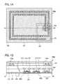
- FIG. 1Bis a cross section taken along line A 1 -A 2 in the wireless chip 200 of FIG. 1A .
- a wireless chip 200 described in this embodimentincludes an antenna 201 and an IC chip 202 that are stacked over the same substrate 203 .
- the antenna 201 and the IC chip 202are disposed so as to be at least partially overlapped with each other with an insulating film interposed therebetween.
- the IC chip 202includes a resonant capacitor portion 204 in the chip, which is provided with a capacitor 220 , and a logic portion 205 including a power supply generating means, a control means, a memory means, and the like. Note that both terminals of the antenna 201 are electrically connected to an integrated circuit 207 of the logic portion 205 .
- a conductive blocking body 206 ais disposed so as to overlap an antenna 201 with insulating films such as a protective film 213 and an impact diffusion layer 214 a interposed therebetween, so that the conductive blocking body 206 a is provided on the uppermost surface of the wireless chip 200 .
- This embodimentwill describe a structure in which a capacitor 215 a includes the antenna 201 and the conductive blocking body 206 a , and the conductive blocking body 206 a is provided above the substrate 203 .
- the integrated circuit 207includes at least semiconductor films 208 a and 208 b each having an impurity region, a gate electrode 210 provided over the semiconductor films 208 a and 208 b with a gate insulating film 209 interposed therebetween, a first interlayer insulating film 211 provided so as to cover the gate electrode 210 , and source and drain electrodes 212 provided over the first interlayer insulating film 211 and electrically connected to the impurity regions of the semiconductor films 208 a and 208 b.
- the antenna 201 connected to the integrated circuit 207is disposed with a second interlayer insulating film 216 interposed therebetween.
- the conductive blocking body 206 ais disposed over the antenna 201 with the protective film 213 and the impact diffusion layer 214 a interposed therebetween. Note that the conductive blocking body 206 a is not connected to the antenna 201 physically.
- the conductive blocking body 206 a and the antenna 201function as electrodes with the protective film 213 and the impact diffusion layer 214 a interposed therebetween, so that the capacitor 215 a is formed.
- the substrate 203is prepared.
- a glass substratesuch as barium borosilicate glass and aluminoborosilicate glass, a quartz substrate, a ceramic substrate, and the like can be used.
- a metal substrate including stainless steel or a semiconductor substrate having a surface provided with an insulating filmmay be employed.
- a substrate formed of a flexible synthetic resin such as plasticgenerally has a lower resistance temperature than the aforementioned substrates, it may be used as long as being resistant to a processing temperature during manufacturing steps.
- the surface of the substrate 203may be planarized by polishing such as a CMP method.
- the integrated circuit 207 included in the logic portion 205is formed over the substrate 203 .
- the integrated circuit 207has at least the semiconductor films 208 a and 208 b , the gate electrode 210 provided over the semiconductor films 208 a and 208 b with the gate insulating film 209 interposed therebetween, the first interlayer insulating film 211 provided so as to cover the gate electrode 210 , and the source and drain electrodes 212 provided over the first interlayer insulating film 211 .
- the capacitor 220may be formed through the same steps as and in a similar manner to the element included in the integrated circuit 207 ; therefore, description thereof is omitted here.
- the semiconductor films 208 a and 208 bmay have any state selected from an amorphous semiconductor, a semiconductor where an amorphous state and a crystalline state are mixed, a microcrystalline semiconductor where a crystal grain with sizes from 0.5 to 20 nm can be observed, and a crystalline semiconductor.
- an amorphous semiconductor filmis formed and crystallized by heat treatment to obtain the semiconductor films 208 a and 208 b .
- the heat treatmentcan be performed by using a furnace, laser irradiation, irradiation of light emitted from a lamp instead of a laser beam (lamp annealing), or a combination of them.
- the gate insulating film 209is formed so as to cover the semiconductor films 208 a and 208 b .
- the gate insulating film 209can be formed to have a single-layer structure or a layered structure using, for example, any of silicon oxide, silicon nitride, silicon nitride oxide, and the like.
- the depositionmay be performed by a plasma CVD method, a sputtering method, or the like.
- the gate electrode 210is formed over each of the semiconductor films 208 a and 208 b with the gate insulating film 209 interposed therebetween.
- the gate electrode 210may be formed to have a single-layer structure or a layered structure of a plurality of metal films.
- the gate electrode 210may be formed by a CVD method or a sputtering method using an element selected from tantalum (Ta), tungsten (W), titanium (Ti), molybdenum (Mo), aluminum (Al), copper (Cu), chromium (Cr), and neodymium (Nd), or an alloy or compound material mainly containing any of these elements.
- a first conductive layer and a second conductive layerare stacked in this order using tantalum nitride and tungsten (W), respectively.
- impurities imparting n-type or p-type conductivityare selectively added to the semiconductor films 208 a and 208 b using the gate electrode 210 or a resist that has been patterned as a mask.
- Each of the semiconductor films 208 a and 208 bhas a channel forming region and impurity regions (including a source region, a drain region, and an LDD region), and an n-channel thin film transistor (hereinafter also referred to as an n-channel TFT) or a p-channel thin film transistor (hereinafter also referred to as a p-channel TFT) can be obtained depending on the conductivity of the added impurity elements.
- an n-channel TFThas side walls at sides of the gate electrode 210 .
- the semiconductor film 208 b of the n-channel TFTis selectively added with impurities imparting n-type conductivity to form a source region, a drain region, and an LDD region.
- the semiconductor film 208 a of a p-channel TFTis selectively added with impurities imparting p-type conductivity, so that a source region and a drain region are formed.
- the side wallsare formed at sides of the gate electrode 210 and the LDD region is selectively formed in the n-channel TFT; however, an embodiment of the present invention is not limited to this structure.
- An LDD regionmay also be formed in the p-channel TFT, and aside wall is not necessarily formed in the p-channel TFT.
- a CMOS structurewhere an n-channel TFT and a p-channel TFT are used in a complementary manner may be employed.
- the first interlayer insulating film 211is formed so as to cover the gate electrode 210 .
- the first interlayer insulating film 211may be formed to have a single-layer structure or a layered structure of an insulating film containing oxygen or nitrogen, such as silicon oxide (SiO x ), silicon nitride (SiN x ), silicon oxynitride (SiO x N y ) (x>y), and silicon nitride oxide (SiN x O y ) (x>y).
- a resin materialsuch as an epoxy resin, an acrylic resin, a phenol resin, a novolac resin, a melamine resin, a urethane resin, or a silicone resin may be used.
- the first interlayer insulating film 211may be formed using an organic material such as benzocyclobutene, parylene, fluorinated arylene ether, or polyimide, a compound material obtained by polymerization such as siloxane-based polymer, a composition material containing water-soluble homopolymer and water-soluble copolymer, or the like.
- organic materialsuch as benzocyclobutene, parylene, fluorinated arylene ether, or polyimide
- a compound material obtained by polymerizationsuch as siloxane-based polymer, a composition material containing water-soluble homopolymer and water-soluble copolymer, or the like.
- the source and drain electrodes 212are formed over the first interlayer insulating film 211 .
- the source and drain electrodes 212are electrically connected to the impurity regions of the semiconductor films 208 a and 208 b .
- a wiringis formed using the same material as the source and drain electrodes 212 .
- the source and drain electrodes 212 and the wiringmay be formed to have a single-layer structure or a layered structure using an element selected from aluminum (Al), tungsten (W), titanium (Ti), tantalum (Ta), molybdenum (Mo), nickel (Ni), platinum (Pt), copper (Cu), gold (Au), silver (Ag), manganese (Mn), neodymium (Nd), carbon (C), and silicon (Si), or an alloy or compound material mainly containing any of these elements by a CVD method, a sputtering method, or the like.
- the alloy material mainly containing aluminumis, for example, a material that contains aluminum as a main component and contains nickel, or an alloy material that contains aluminum as a main component and contains nickel and one or both of carbon and silicon.
- the source and drain electrodes 212 and the wiringmay be formed to have, for example, a layered structure of a barrier film, an aluminum silicon (Al—Si) film and a barrier film, or a layered structure of a barrier film, an aluminum silicon (Al—Si) film, a titanium nitride film, and a barrier film.
- the barrier filmis a thin film containing titanium, nitride of titanium, molybdenum, or nitride of molybdenum.
- Aluminum and aluminum siliconhave a low resistance value and are inexpensive; therefore, they are suitable for the source and drain electrodes 212 and the wiring.
- the barrier filmsare formed for the top layer and the bottom layer, hillock formation in aluminum and aluminum silicon can be prevented. If the barrier film is formed of titanium that is a highly reducing element, even when a thin natural oxide film is formed on the semiconductor films 208 a and 208 b , the natural oxide film can be reduced and contact with the semiconductor films 208 a and 208 b can be improved.
- the second interlayer insulating film 216is formed so as to cover the source and drain electrodes 212 and the wiring.
- the second interlayer insulating film 216may be formed using any of the above materials for the first interlayer insulating film 211 .
- the antenna 201is formed over the second interlayer insulating film 216 , a protective film 213 is formed over the antenna 201 , an impact diffusion layer 214 a is formed over the protective film 213 , and a conductive blocking body 206 a is formed over the impact diffusion layer 214 a , whereby the wireless chip 200 is completed.
- the antenna 201is formed to have a single-layer structure or a layered structure using a conductive material by a CVD method, a sputtering method, a screen printing method, a droplet discharge method, or the like.
- the conductive materialis an element selected from aluminum (Al), titanium (Ti), silver (Ag), copper (Cu), gold (Au), and nickel (Ni), or an alloy or compound material mainly containing any of these elements.
- the protective film 213can be formed using any of the above materials for the first interlayer insulating film 211 . Note that, the coil antenna 201 wound twice is used as one electrode of the capacitor 215 a in FIGS. 1A and 1B ; however, an embodiment of the present invention is not limited to this and an antenna wound once or a plurality of times may be used as one electrode of the capacitor 215 a .
- the impact diffusion layer 214 afor example, a structure body in which a fibrous body is impregnated with an organic resin, or the like can be used. In this case, the impact diffusion layer 214 a may be bonded to the protective film 213 .
- the conductive blocking body 206 acan be formed by a dry process such as a sputtering method, a plasma CVD method, or an evaporation method, or a wet process such as a coating method, a printing method, or a droplet discharge method (inkjet method).
- this embodimentdescribes the case where one of two electrodes of the capacitor 215 a is the antenna 201 and the other is the conductive blocking body 206 a , and the protective film 213 and the impact diffusion layer 214 a are provided between the antenna 201 and the conductive blocking body 206 a , but an embodiment of the present invention is not limited to this.
- a structuremay alternatively be employed in which only the protective film 213 or the impact diffusion layer 214 a is provided between the electrodes.
- an insulating film other than the protective film and the impact diffusion layer described heremay be disposed. That is, any other structure than the structure described in this embodiment can be employed as long as a capacitor can be formed.
- a capacitor 215 ais formed between the conductive blocking body 206 a and the antenna 201 , and the number of capacitors in the capacitor 220 of the resonant capacitor portion 204 formed in the chip can be reduced as compared to the case where the conductive blocking body 206 a is not disposed. Accordingly, the size of the wireless chip 200 and the size of the IC chip 202 can be reduced and the limited area in the IC chip and the wireless chip can be utilized efficiently. Further, since the sizes of the IC chip and the wireless chip can be reduced, current consumption can be reduced and thus a communication distance can be prevented from being shortened. Further, by using the conductive blocking body 206 a , resistance to static electricity and physical strength of the wireless chip, which becomes a significant problem when the wireless chip is downsized, can be increased.
- a wireless chip 200having a structure different from that of the above embodiment is described with reference to drawings.
- the structurewill be described in which the antenna 201 is provided as one of two electrodes of the capacitor 215 b and the conductive blocking body 206 b as the other electrode is disposed below the substrate 203 .
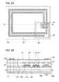
- FIG. 2Bis a cross section taken along line A 1 -A 2 in the wireless chip 200 of FIG. 2A .
- FIGS. 2A and 2Billustrate a structure in which the antenna 201 is provided as one of the two electrodes of the capacitor 215 b and the conductive blocking body 206 b as the other electrode is disposed below the substrate 203 .
- the wireless chip 200 described in this embodimentincludes an antenna 201 and an IC chip 202 that are stacked over the same substrate 203 , and the antenna 201 and the IC chip 202 are disposed so as to be at least partially overlapped with each other with an insulating film interposed therebetween.
- the IC chip 202includes the resonant capacitor portion 204 in the chip, which is provided with the capacitor 220 , and a logic portion 205 including a power supply generating means, a control means, a memory means, and the like.
- the two terminals of the antenna 201are electrically connected to the integrated circuit 207 of the logic portion 205 .
- the antenna 201 and the conductive blocking body 206 bare disposed with the substrate 203 , the first interlayer insulating film 211 , the second interlayer insulating film 216 , the protective film 213 , the impact diffusion layer 214 b , and the like interposed therebetween.
- the conductive blocking body 206 bis provided for the lowermost layer of the wireless chip 200 .
- the antenna 201 connected to the integrated circuit 207is disposed with the second interlayer insulating film 216 interposed therebetween as in the above embodiment.
- the impact diffusion layer 214 bis formed under the substrate 203
- the conductive blocking body 206 bis formed under the impact diffusion layer 214 b .
- the conductive blocking body 206 bis not connected to the antenna 201 physically.
- the conductive blocking body 206 b and the antenna 201function as electrodes with the substrate 203 , the first interlayer insulating film 211 , the second interlayer insulating film 216 , and the impact diffusion layer 214 b interposed therebetween, so that the capacitor 215 b is formed.
- this embodimentdescribes the case where one of two electrodes of the capacitor 215 b is the antenna 201 and the other is the conductive blocking body 206 b , and the substrate 203 , the first interlayer insulating film 211 , the second interlayer insulating film 216 , the protective film 213 , the impact diffusion layer 214 b , and the like are provided between the antenna 201 and the conductive blocking body 206 b , but an embodiment of the present invention is not limited to this. Any other structure than the structure described in this embodiment can be employed as long as a capacitor can be formed.
- a capacitor 215 bis formed between the conductive blocking body 206 b and the antenna 201 and the number of capacitors in the capacitor 220 of the resonant capacitor portion 204 required to be formed in the chip can be reduced as compared to the case where the conductive blocking body 206 b is not disposed. Accordingly, the size of the wireless chip 200 and the size of the IC chip 202 can be reduced and the limited area in the IC chip and the wireless chip can be utilized efficiently. Further, since the sizes of the IC chip and the wireless chip can be reduced, current consumption can be reduced and thus a communication distance can be prevented from being shortened.
- the conductive blocking body 206 bBy using the conductive blocking body 206 b , resistance to static electricity and physical strength of the wireless chip, which becomes a significant problem when the wireless chip is downsized, can be increased. Further, since the conductive blocking body 206 b is not provided over the antenna, favorable communication accuracy can be secured without hindering reception of carrier waves or amplitude modulation waves transmitted from a R/W as compared to the structure described in Embodiment 1.
- the wireless chip 200having a structure different from those of Embodiments 1 and 2 is described with reference to drawings.
- the wireless chip 200includes the capacitor 215 a and a capacitor 215 c .
- the capacitor 215 ahas a structure similar to that in Embodiment 1 and is formed to have a layered structure of the antenna 201 , the protective film 213 , the impact diffusion layer 214 a , and the conductive blocking body 206 a .
- the structurewill be described in which the antenna 201 is provided as one of two electrodes of the capacitor 215 c , and both the conductive blocking body 206 a provided over the substrate 203 and the conductive blocking body 206 b provided under the substrate 203 are disposed as the other electrodes.
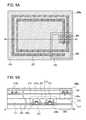
- FIG. 3Bis a cross section taken along line A 1 -A 2 in the wireless chip 200 of FIG. 3A .
- FIGS. 3A and 3Billustrate a structure including the capacitor 215 a and the capacitor 215 c . Since the capacitor 215 a has a structure similar to that in Embodiment 1, description thereof is omitted here.
- the structurewill be described in which the antenna 201 is provided as one of two electrodes of the capacitor 215 c , and both the conductive blocking body 206 a provided over the substrate 203 and the conductive blocking body 206 b provided under the substrate 203 are disposed as the other electrodes.
- the wireless chip 200 described in this embodimentincludes the antenna 201 and the IC chip 202 that are stacked over the same substrate 203 .
- the antenna 201 and the IC chip 202are disposed so as to be at least partially overlapped with each other with an insulating film interposed therebetween.
- the IC chip 202includes the resonant capacitor portion 204 in the chip, which is provided with the capacitor 220 , and the logic portion 205 including a power supply generating means, a control means, a memory means, and the like. Note that both terminals of the antenna 201 are electrically connected to the integrated circuit 207 of the logic portion 205 . Further, the antenna 201 and conductive blocking body 206 a are disposed with insulating films such as the protective film 213 and the impact diffusion layer 214 a and are provided on the uppermost surface of the wireless chip 200 .
- the antenna 201 and the conductive blocking body 206 bare provided with the substrate 203 , the first interlayer insulating film 211 , the second interlayer insulating film 216 , the protective film 213 , the impact diffusion layer 214 b , and the like interposed therebetween.
- the conductive blocking body 206 bis provided for the lowermost layer of the wireless chip 200 .
- the antenna 201 connected to the integrated circuit 207is disposed with the second interlayer insulating film 216 interposed therebetween.
- the conductive blocking body 206 a and the conductive blocking body 206 bare not connected to the antenna 201 physically.
- the conductive blocking body 206 a disposed on a top surface of the substrate and the antenna 201function as electrodes with the protective film 213 and the impact diffusion layer 214 a interposed therebetween, so that a resonant capacitor is formed.
- the conductive blocking body 206 b disposed on a bottom surface of the substrate and the antenna 201function as electrodes with the substrate, the first interlayer insulating film 211 , the second interlayer insulating film 216 , and the impact diffusion layer 214 b interposed therebetween, so that a resonant capacitor is formed. That is, the capacitor 215 c includes the resonant capacitor formed between the conductive blocking body 206 a and the antenna 201 and the resonant capacitor formed between the conductive blocking body 206 b and the antenna 201 .
- the number of capacitors in the capacitor 220 of the resonant capacitor portion 204 in the chipcan be reduced as compared to that in the above embodiment. Further, since the IC chip 202 is sandwiched between the conductive blocking body 206 a and the conductive blocking body 206 b , physical strength of the wireless chip can be further increased as compared to the above embodiment.
- An insulating layer other than the protective film and the impact diffusion layermay be disposed and the protective film and the impact diffusion layer are not necessarily disposed as long as a capacitor can be formed.
- a wireless chip 200having a structure different from those of the above embodiments will be described with reference to drawings.
- the structurewill be described in which the antenna 201 is provided as one of two electrodes of each of capacitors 215 d and 215 f , and a conductive blocking body 206 c provided as the other electrode is disposed so as to surround the other components included in the wireless chip 200 .
- FIG. 4Bis a cross section taken along line A 1 -A 2 in the wireless chip 200 of FIG. 4A .
- FIGS. 4A and 4Billustrate a structure in which the antenna 201 is provided as one of two electrodes of each of the capacitors 215 d and 215 f , and the conductive blocking body 206 c provided as the other electrode is disposed so as to surround the other components included in the wireless chip 200 .
- the wireless chip 200 described in this embodimentincludes the antenna 201 and the IC chip 202 that are stacked over the same substrate 203 .
- the antenna 201 and the IC chip 202are disposed so as to be at least partially overlapped with each other with an insulating film interposed therebetween.
- the IC chip 202includes the resonant capacitor portion 204 in a chip, which is provided with the capacitor 220 , and the logic portion 205 including a power supply generating means, a control means, a memory means, and the like. Note that both terminals of the antenna 201 are electrically connected to the integrated circuit 207 of the logic portion 205 . Further, the antenna 201 and the conductive blocking body 206 c are disposed with insulating films such as the protective film 213 and the impact diffusion layers 214 a and 214 b interposed therebetween. Note that the conductive blocking body 206 c is provided around the outermost perimeter of the wireless chip 200 .
- the antenna 201 connected to the integrated circuit 207is disposed with the second interlayer insulating film 216 interposed therebetween.
- the conductive blocking body 206 cis not connected to the antenna 201 physically.
- the resonant capacitoris formed using the conductive blocking body 206 c surrounding the antenna 201 ; thus, it is very difficult to accurately illustrate the capacitor 215 d formed in this embodiment.
- the capacitor 215 dis illustrated in a portion where the resonant capacitor is formed, for example.
- the structure described in this embodimentis not necessarily employed as long as the conductive blocking body 206 c can be provided around the IC chip and the capacitors 215 d and 215 f can be formed using the antenna 201 and the conductive blocking body 206 c.
- the wireless chip 200having a structure different from those of the above embodiments will be described with reference to drawings.
- the structurewill be described in which a capacitor 215 e in which a wiring 217 of the resonant capacitor portion 204 in the chip, which is formed widely, and the conductive blocking body 206 a are electrodes is provided in addition to the capacitor 215 a in which the antenna 201 and the conductive blocking body 206 a are electrodes.
- FIG. 5Bis a cross section taken along line A 1 -A 2 in the wireless chip 200 of FIG. 5A .
- FIGS. 5A and 5Billustrate the structure in which one of two capacitors of the capacitor 215 e has the antenna 201 and the conductive blocking body 206 a as electrodes and the other has a wiring 217 of the resonant capacitor portion 204 in the chip, which is formed widely, and the conductive blocking body 206 a as electrodes. Note that since the wiring 217 can be formed in the same layer and through the same steps as the source and drain electrodes 212 , a special step is not required.
- the wireless chip 200 described in this embodimentincludes the antenna 201 and the IC chip 202 that are stacked over the same substrate 203 .
- the antenna 201 and the IC chip 202are disposed so as to be at least partially overlapped with each other with an insulating film interposed therebetween.
- the IC chip 202includes the resonant capacitor portion 204 in the chip and the logic portion 205 including a power supply generating means, a control means, a memory means, and the like. Note that both terminals of the antenna 201 are electrically connected to the integrated circuit 207 of the logic portion 205 .
- the wiring 217 and the conductive blocking body 206 aare disposed with insulating films such as the protective film 213 , the impact diffusion layer 214 a , and the second interlayer insulating film 216 interposed therebetween, and the conductive blocking body 206 a is provided on the uppermost surface of the wireless chip 200 .
- the antenna 201 connected to the integrated circuit 207is disposed with the second interlayer insulating film 216 interposed therebetween, and the conductive blocking body 206 a is disposed over the antenna 201 with the protective film 213 and the impact diffusion layer 214 a interposed therebetween.
- the conductive blocking body 206 ais not connected to the antenna 201 physically.
- the capacitor 215 e formed in this embodimentincludes the capacitor including the antenna 201 and the conductive blocking body 206 a as electrodes as in Embodiment 1, and the capacitor including the wiring 217 of the resonant capacitor portion 204 in the chip, in which the wiring 217 is formed widely, and the conductive blocking body 206 a as electrodes.
- the number of capacitors in the chipcan be reduced as compared to the case where the conductive blocking body 206 a is not provided, which results in reduction in the size of the wireless chip 200 and the size of the IC chip 202 , effective utilization of the limited area in the IC chip, reduction in current consumption, and prevention of shortening of a communication distance. Further, by using the conductive blocking body 206 a , resistance to static electricity and physical strength of the wireless chip, which becomes a significant problem when the wireless chip is downsized, can be increased.
- This embodimentwill describe a method for manufacturing a semiconductor device with high reliability and high yield with reference to FIGS. 6A to 6D .
- this embodimentwill describe a method for manufacturing a semiconductor device from which a substrate is separated. Note that any of Embodiments 1 to 5 can be freely combined with this embodiment. Further, this embodiment will describe a CMOS (complementary metal oxide semiconductor) as an example of semiconductor devices.
- CMOScomplementary metal oxide semiconductor
- Transistors 902 and 903 , a capacitor 904 , and an insulating layer 905are provided over a substrate 900 with a separation layer 901 interposed therebetween, so that a semiconductor integrated circuit 910 is formed (see FIG. 6A ). Note that in this embodiment, since a capacitor using a resonant capacitor formed in an IC chip is formed, the capacitor 904 can be smaller than a conventional capacitor.
- the transistors 902 and 903are thin film transistors and each include source and drain regions, a low concentration impurity region, a channel formation region, a gate insulating layer, a gate electrode, wirings serving as source and drain electrodes.
- the source and drain regionsare in contact with and electrically connected with the wirings serving as source and drain electrodes.
- the transistor 902is an n-channel transistor and the source or drain region and the low concentration impurity region include impurity elements imparting n-type conductivity (such as phosphorus (P) or arsenic (As)).
- the transistor 903is a p-channel transistor and the source or drain region and the low concentration impurity region include impurities imparting p-type conductivity (such as boron (B), aluminum (Al), or gallium (Ga)).
- the capacitor 904is formed through the same steps as the transistors 902 and 903 and one electrode is formed of a semiconductor layer and the other electrode is formed of the gate electrode.
- an impurity elementmay be added to the semiconductor layer included in the capacitor 904 before a gate electrode layer is formed. Through this step, an impurity element is added also to the semiconductor layer disposed in a region of a lower layer of the gate electrode layer, and thus the capacitor 904 can function efficiently as a capacitor.
- an antenna 911is formed over the insulating layer 905 by using a conductive film, and a protective film 912 is formed over the antenna 911 .
- the antenna 911is electrically connected to the semiconductor integrated circuit.
- the antenna 911is electrically connected to one electrode of the capacitor 904 .
- an impact diffusion layer 920is formed over the protective film 912 .
- the impact diffusion layer 920for example, a structure body in which a fibrous body 921 is impregnated with an organic resin 922 may be used.
- the semiconductor integrated circuit 910 , the antenna 911 , and the protective film 912are separated from the substrate 900 along the separation layer 901 as an interface. Accordingly, the semiconductor integrated circuit 910 , the antenna 911 , and the protective film 912 are provided on the impact diffusion layer 920 side (see FIG. 6B ).
- bonding of the protective film 912 and the impact diffusion layer 920may be performed using an adhesive, pressure bonding, or thermocompression bonding.
- an impact diffusion layer 930is bonded to an exposed separation surface of the semiconductor integrated circuit 910 with the separation layer 901 interposed therebetween, so that the semiconductor integrated circuit 910 , the antenna 911 , and the protective film 912 are sandwiched between the impact diffusion layer 920 and the impact diffusion layer 930 (see FIG. 6C ).
- the impact diffusion layer 930for example, a structure body in which a fibrous body 931 is impregnated with an organic resin 932 may be used, similarly to the case of the impact diffusion layer 920 .
- the impact diffusion layer 920 and the impact diffusion layer 930sandwich a plurality of structure bodies each including the semiconductor integrated circuit 910 , the antenna 911 , and the protective film 912 so that they are arranged in a planar direction.
- individual semiconductor integrated circuit chipseach having a structure in which the semiconductor integrated circuit 910 , the antenna 911 , and the protective film 912 are sandwiched between the impact diffusion layer 920 and the impact diffusion layer 930 are manufactured.
- a dividing meansas long as physical division is possible, and as a favorable example, division is performed by laser beam irradiation along a dividing line in this embodiment.
- the impact diffusion layer 920 and the impact diffusion layer 930melt and weld together at dividing surfaces 941 and 942 of the semiconductor integrated circuit chip.
- the individual semiconductor integrated circuit chipseach have a structure in which the semiconductor integrated circuit 910 , the antenna 911 , and the protective film 912 are entirely sealed with the impact diffusion layer 920 and the impact diffusion layer 930 (see FIG. 6D ).
- an insulatormay be further provided on outer sides or inner sides than the impact diffusion layer 920 and the impact diffusion layer 930 to cover the entire surfaces of the semiconductor integrated circuit 910 , the antenna 911 , and the protective film 912 more favorably.
- FIG. 7Aillustrates an example in which the conductive blocking body 1101 is formed so as to entirely cover the outside similarly to the structure described in Embodiment 4, the structure described as an example in any of the other embodiments may be employed.
- the conductive blocking body 1101is formed so as to cover a top surface, a bottom surface, and side surfaces of the semiconductor integrated circuit chip.
- the conductive blocking body 1101may be formed so as to cover the entire surfaces by forming the conductive blocking body on the top surface and part of the side surfaces and then turning over the semiconductor integrated circuit and forming the conductive blocking body on the bottom surface and part of the side surfaces.
- the conductive blocking body 1101may be formed to a thickness small enough that reception of carrier waves or amplitude modulation waves transmitted from a R/W is not hindered as much as possible.
- a conductive blocking body 1102may be provided on inner sides than impact diffusion layers so as to cover an entire surface of the semiconductor integrated circuit.
- the conductive blocking body 1102it is required that individual semiconductor integrated circuit chips are formed by division before the semiconductor integrated circuit is sandwiched between the impact diffusion layers and bonding is performed; however, this mode is not necessarily employed.
- a conductive blocking bodyis formed in advance on a top surface and a bottom surface of the semiconductor integrated circuit before the semiconductor integrated circuit chip is sandwiched between impact diffusion layers and bonding is performed, the semiconductor integrated circuit chip is sandwiched between impact diffusion layers and bonding is performed, and then division is performed by laser beam irradiation, so that the conductive blocking bodies melt at dividing surfaces and weld so as to cover side surfaces of the semiconductor integrated circuit from above and below.
- FIG. 7Cis an example in which a conductive blocking body 1103 is provided on an inner side than an impact diffusion layer so that it is formed on one surface of a semiconductor integrated circuit.
- the conductive blocking body 1103is formed on the antenna side as in Embodiment 1; however, the conductive blocking body 1103 may be formed on the separation surface side as in Embodiment 2.
- the conductive blocking bodyBy forming the conductive blocking body on one surface of the semiconductor integrated circuit, the conductive blocking body does not hinder reception of carrier waves or amplitude modulation waves transmitted from a R/W and thus favorable communication accuracy can be secured.
- the semiconductor device manufactured according to this embodimentcan be flexible by using a flexible impact diffusion layer.
- Semiconductor layers included in the transistors 902 and 903 and the capacitor 904can be formed using any of the following materials: an amorphous semiconductor manufactured by a vapor-phase growth method or a sputtering method using a semiconductor material gas typified by silane or germane; a polycrystalline semiconductor formed by crystallizing the amorphous semiconductor with the use of light energy or thermal energy; a microcrystalline (also referred to as semiamorphous) semiconductor; or the like.
- the semiconductor layercan be formed by a sputtering method, an LPCVD method, a plasma CVD method, or the like.
- the microcrystalline semiconductor filmbelongs to a metastable state which is intermediate between an amorphous state and a single crystal state when Gibbs free energy is considered. That is, the microcrystalline semiconductor film is a semiconductor having a third state which is stable in terms of free energy and has a short range order and lattice distortion. Columnar-like or needle-like crystals grow in a normal direction with respect to a substrate surface.
- the Raman spectrum of microcrystalline siliconwhich is a typical example of a microcrystalline semiconductor, is shifted to a lower wavenumber than 520 cm ⁇ 1 which represents a peak of the Raman spectrum of single crystal silicon.
- a peak of the Raman spectrum of microcrystalline siliconlies between 520 cm ⁇ 1 and 480 cm ⁇ 1 which represent that of single crystal silicon and that of amorphous silicon, respectively.
- the microcrystalline semiconductor filmcontains hydrogen or halogen of at least 1 at. % to terminate dangling bonds. Further, a rare gas element such as helium, argon, krypton, or neon may be contained to further promote lattice distortion, so that stability is enhanced and a favorable microcrystalline semiconductor film can be obtained.
- the microcrystalline semiconductor filmcan be formed by a high-frequency plasma CVD method with a frequency of several tens of MHz to several hundred MHz or a microwave plasma CVD apparatus with a frequency of 1 GHz or more.
- the microcrystalline semiconductor filmcan be typically formed using silicon hydride such as SiH 4 , Si 2 H 6 , SiH 2 Cl 2 , SiHCl 3 , SiCl 4 , or SiF 4 which is diluted with hydrogen.
- silicon hydridesuch as SiH 4 , Si 2 H 6 , SiH 2 Cl 2 , SiHCl 3 , SiCl 4 , or SiF 4 which is diluted with hydrogen.
- the microcrystalline semiconductor filmcan be formed.
- the flow ratios of hydrogen to silicon hydrideis set to be from 5:1 to 200:1, preferably, from 50:1 to 150:1, more preferably, the flow ratio of hydrogen to silicon hydride is set to be 100:1.
- Hydrogenated amorphous siliconmay be typically used as an amorphous semiconductor, while polysilicon (polycrystalline silicon) and the like may be typically used as a crystalline semiconductor.
- polysiliconso-called high-temperature polysilicon which contains polysilicon as a main component and is formed at a process temperature of 800° C. or higher, so-called low-temperature polysilicon that contains polysilicon as a main component and is formed at a process temperature of 600° C. or lower, polysilicon obtained by crystallizing amorphous silicon by using an element promoting crystallization or the like, and the like are given. It is needles to say that as mentioned above, a microcrystalline semiconductor or a semiconductor containing a crystal phase in part of a semiconductor layer may be used.
- a compound semiconductorsuch as GaAs, InP, SiC, ZnSe, GaN, or SiGe can be used.
- an oxide semiconductorsuch as zinc oxide (ZnO), tin oxide (SnO 2 ), magnesium zinc oxide, gallium oxide, or indium oxide, an oxide semiconductor formed of any of the above oxide semiconductors, or the like may be used.
- an oxide semiconductor formed of ZnO, indium oxide, and gallium oxidemay be used.
- a gate insulating layeris preferably formed using Y 2 O 3 , Al 2 O 3 , TiO 2 , or a stack of any of the above.
- ITOindium tin oxide
- AuAu
- Tititanium
- ZnO to which In, Ga, or the like is addedmay be used.
- the crystalline semiconductor layermay be formed by any of various methods (such as a laser crystallization method, a thermal crystallization method, and a thermal crystallization method using an element promoting crystallization, such as nickel). Further, a microcrystalline semiconductor may be crystallized by laser irradiation to enhance crystallinity.
- the element promoting crystallizationis not introduced, before irradiating the amorphous silicon film with a laser beam, hydrogen is released until the concentrations of hydrogen contained in the amorphous silicon film become 1 ⁇ 10 20 atoms/cm 3 or less by heating the amorphous silicon film at a temperature of 500° C. for one hour in a nitrogen atmosphere. This is because the amorphous silicon film containing a large amount of hydrogen is destroyed when being irradiated with a laser beam.
- a method for introducing a metal element into the amorphous semiconductor layeris not particularly limited as long as it is capable of introducing the metal element to a surface of or inside the amorphous semiconductor layer.
- a sputtering method, a CVD method, a plasma treatment method (including a plasma CVD method), an adsorption method, or a method for applying a solution of metal saltcan be used.
- a method of using a solutionis simple and advantageous in that the concentration of the metal element can be easily controlled.
- an oxide filmby UV irradiation in an oxygen atmosphere, a thermal oxidation method, treatment with either ozone water containing hydroxyl radicals or hydrogen peroxide, or the like to improve wettability of the surface of the amorphous semiconductor layer so that an aqueous solution is diffused on the entire surface of the amorphous semiconductor layer.
- an element promoting crystallization(also referred to as a catalytic element or a metal element) may be added to the amorphous semiconductor layer and crystallization may be performed by heat treatment (at 550° C. to 750° C. for 3 minutes to 24 hours).
- the element promoting crystallizationcan be one or more of elements such as iron (Fe), nickel (Ni), cobalt (Co), ruthenium (Ru), rhodium (Rh), palladium (Pd), osmium (Os), iridium (Ir), platinum (Pt), copper (Cu), and gold (Au).
- a semiconductor layer containing an impurity elementis formed in contact with the crystalline semiconductor layer and is made to function as a gettering sink.
- an impurity element imparting n-type conductivity, an impurity element imparting p-type conductivity, a rare gas element, or the likecan be used; for example, one or more of phosphorus (P), nitrogen (N), arsenic (As), antimony (Sb), bismuth (Bi), boron (B), helium (He), neon (Ne), argon (Ar), krypton (Kr), and xenon (Xe) can be used.
- a semiconductor layer containing a rare gas elementis formed on the crystalline semiconductor layer containing the element promoting crystallization, and heat treatment (at 550° C. to 750° C. for 3 minutes to 24 hours) is performed.
- the element promoting crystallization, which is contained in the crystalline semiconductor layermoves into the semiconductor layer containing a rare gas element and thus, the element promoting crystallization, which is contained in the crystalline semiconductor layer, is removed or reduced. After that, the semiconductor layer containing a rare gas element, which has served as a gettering sink, is removed.
- An amorphous semiconductor layermay be crystallized by the combination of heat treatment and laser beam irradiation, or one of heat treatment and laser beam irradiation may be performed a plurality of times.
- a crystalline semiconductor layermay be directly formed on a substrate by a plasma method.
- a crystalline semiconductor layermay be selectively formed over a substrate by a plasma method.
- the gate insulating layermay be formed using silicon oxide or may be formed to have a layered structure including silicon oxide and silicon nitride.
- the gate insulating layermay be formed by depositing an insulating film by a plasma CVD method or a low pressure CVD method or may be formed by solid-phase oxidation or solid-phase nitridation by plasma treatment. This is because a gate insulating layer which is formed using a single crystal semiconductor layer which is oxidized or nitrided by plasma treatment is dense, has high withstand voltage, and is excellent in reliability.
- a surface of the semiconductor layeris oxidized or nitrided using nitrous oxide (N 2 O) diluted with Ar by 1 to 3 times (flow ratio) by application of microwave (2.45 GHz) powers of 3 kW to 5 kW at pressures of 10 Pa to 30 Pa.
- nitrous oxideN 2 O
- microwave (2.45 GHz) powers3 kW to 5 kW at pressures of 10 Pa to 30 Pa.
- nitrous oxide (N 2 O) and silane (SiH 4 )are introduced and microwave (2.45 GHz) powers of 3 kW to 5 kW are applied to the insulating film at pressures of 10 Pa to 30 Pa to form a silicon oxynitride film by a vapor-phase growth method, which is to be a gate insulating layer.
- microwave (2.45 GHz) powers of 3 kW to 5 kWare applied to the insulating film at pressures of 10 Pa to 30 Pa to form a silicon oxynitride film by a vapor-phase growth method, which is to be a gate insulating layer.
- a high dielectric constant materialsuch as zirconium dioxide, hafnium oxide, titanium dioxide, or tantalum pentoxide may be used. By using a high dielectric constant material for the gate insulating layer, a gate leakage current can be reduced.
- the gate electrode layercan be formed employing a CVD method, a sputtering method, a droplet discharge method, or the like.
- the gate electrode layermay be formed of an element selected from Ag, Au, Cu, Ni, Pt, Pd, Ir, Rh, W, Al, Ta, Mo, Cd, Zn, Fe, Ti, Si, Ge, Zr, and Ba; or an alloy or compound material containing any of the elements as its main component.
- a semiconductor filmtypified by a polycrystalline silicon film doped with an impurity element such as phosphorus, or an AgPdCu alloy may be used.
- a single-layer structure or a multi-layer structuremay be employed; for example, a two-layer structure of a tungsten nitride film and a molybdenum film may be employed or a three-layer structure in which a tungsten film with a thickness of 50 nm, a film of an aluminum-silicon (Al—Si) alloy with a thickness of 500 nm, and a titanium nitride film with a thickness of 30 nm are stacked in this order may be employed.
- Al—Sialuminum-silicon
- a tungsten nitride filmmay be used instead of the tungsten film as the first conductive film
- an aluminum-titanium (Al—Ti) alloy filmmay be used instead of the aluminum-silicon (Al—Si) alloy film as the second conductive film
- a titanium filmmay be used instead of the titanium nitride film as the third conductive film.
- a light-transmitting material which transmits visible lightmay be used.
- a light-transmitting conductive materialindium tin oxide (ITO), indium tin oxide containing silicon oxide (ITSO), organoindium, organotin, zinc oxide, or the like can be used.
- indium zinc oxide (IZO) containing zinc oxide (ZnO), zinc oxide (ZnO), ZnO doped with gallium (Ga), tin oxide (SnO 2 ), indium oxide containing tungsten oxide, indium zinc oxide containing tungsten oxide, indium oxide containing titanium oxide, indium tin oxide containing titanium oxide, or the likemay be used.
- a maskmay be formed and dry etching or wet etching may be performed.
- the electrode layerscan be etched to have a tapered shape by using an ICP (inductively coupled plasma) etching method and appropriately controlling the etching condition (the amount of power applied to a coiled electrode, the amount of power applied to an electrode on a substrate side, the temperature of the electrode on the substrate side, or the like).
- ICPinductively coupled plasma
- etching gasa chlorine-based gas typified by Cl 2 , BCl 3 , SiCl 4 , CCl 4 , and the like; a fluorine-based gas typified by CF 4 , SF 6 , NF 3 , and the like; or O 2 can be used as appropriate.
- gate electrode layersmay be provided above and below the semiconductor layer or a plurality of gate electrode layers may be provided only on one side of (above or below) the semiconductor layer.
- silicidesmay be provided over the source and drain regions of the transistor.
- the silicidesare formed by forming conductive films over the source and drain regions of the semiconductor layer and reacting silicon in the exposed source and drain regions of the semiconductor layer with the conductive films by heat treatment, a GRTA method, an LRTA method, or the like.
- the silicidesmay be formed by laser irradiation or light irradiation using a lamp.
- any of the followingscan be used: titanium (Ti), nickel (Ni), tungsten (W), molybdenum (Mo), cobalt (Co), zirconium (Zr), hafnium (Hf), tantalum (Ta), vanadium (V), neodymium (Nd), chromium (Cr), platinum (Pt), palladium (Pd), and the like.
- the wiring layers each function as a source electrode layer or a drain electrode layercan be formed by depositing a conductive film by a PVD method, a CVD method, an evaporation method, or the like, and then etching the conductive film such that it has desired shapes.
- the wiring layercan be formed selectively at a predetermined place by a printing method, an electroplating method, or the like.
- a reflow method or a damascene methodmay be used.
- metalsuch as Ag, Au, Cu, Ni, Pt, Pd, Ir, Rh, W, Al, Ta, Mo, Cd, Zn, Fe, Ti, Zr, or Ba
- a semiconductorsuch as Si or Ge, or an alloy or a nitride thereof
- a light-transmitting materialmay be used.
- indium tin oxide (ITO), indium tin oxide containing silicon oxide (ITSO), indium zinc oxide (IZO) containing zinc oxide (ZnO), zinc oxide (ZnO), ZnO doped with gallium (Ga), tin oxide (SnO 2 ), indium oxide containing tungsten oxide, indium zinc oxide containing tungsten oxide, indium oxide containing titanium oxide, indium tin oxide containing titanium oxide, or the likecan be used.
- a material for forming the conductive blocking bodyis preferably a conductor or a semiconductor; for example, a metal film, a metal oxide film, a semiconductor film, a metal nitride film, and the like are given.
- the conductive blocking bodymay be formed using an element selected from titanium, molybdenum, tungsten, aluminum, copper, silver, gold, nickel, platinum, palladium, iridium, rhodium, tantalum, cadmium, zinc, iron, silicon, germanium, zirconium, and barium; or an alloy material, a compound material, a nitride material, or an oxide material each containing any of the above elements as a main component.
- tantalum nitridetitanium nitride, or the like can be used.
- indium tin oxideITO
- indium tin oxide containing silicon oxideITSO
- organoindiumorganotin, zinc oxide, or the like
- indium oxide containing tungsten oxideindium zinc oxide containing tungsten oxide, indium oxide containing titanium oxide, indium tin oxide (ITO) containing titanium oxide, or the like may be used.
- a semiconductor film having conductivitywhich is obtained by adding an impurity element or the like to a semiconductor, or the like can be used.
- a semiconductor film having conductivitywhich is obtained by adding an impurity element or the like to a semiconductor, or the like can be used.
- a polycrystalline silicon film doped with an impurity element such as phosphoruscan be used.
- a conductive macromolecule(also referred to as a conductive polymer) may be used for the conductive blocking body.
- a so-called ⁇ -electron conjugated conductive macromoleculecan be used.
- polyaniline and/or a derivative thereof, polypyrrole and/or a derivative thereof, polythiophene and/or a derivative thereof, and a copolymer of two or more kinds of those materialscan be given.
- conjugated conductive macromoleculeexamples include polypyrrole, poly(3-methylpyrrole), poly(3-butylpyrrole), poly(3-octylpyrrole), poly(3-decylpyrrole), poly(3,4-dimethylpyrrole), poly(3,4-dibutylpyrrole), poly(3-hydroxypyrrole), poly(3-methyl-4-hydroxypyrrole), poly(3-methoxypyrrole), poly(3-ethoxypyrrole), poly(3-octoxypyrrole), poly(3-carboxylpyrrole), poly(3-methyl-4-carboxylpyrrole), polyN-methylpyrrole, polythiophene, poly(3-methylthiophene), poly(3-butylthiophene), poly(3-octylthiophene), poly(3-decylthiophene), poly(3-dodecylthiophene), poly(3-dodecyl
- the conductive blocking body containing a conductive macromoleculemay contain an organic resin or a dopant (a halogen, a Lewis acid, an inorganic acid, an organic acid, a transition metal halide, an organic cyano compound, a nonionic surfactant, or the like).
- a dopanta halogen, a Lewis acid, an inorganic acid, an organic acid, a transition metal halide, an organic cyano compound, a nonionic surfactant, or the like.
- the conductive blocking bodycan be formed by a dry process such as a sputtering method, a plasma CVD method, or an evaporation method, or a wet process such as a coating method, a printing method, or a droplet discharge method (inkjet method).
- a dry processsuch as a sputtering method, a plasma CVD method, or an evaporation method
- a wet processsuch as a coating method, a printing method, or a droplet discharge method (inkjet method).
- a semiconductor device that serves as a wireless tag(hereinafter also referred to as a wireless chip, a wireless processor, or a wireless memory) can be formed.
- the application range of the semiconductor device according to an embodiment of the present inventionis so wide that it may be applied to any object in order that the history thereof or the like is revealed without contact and utilized in production, management, and the like.
- the semiconductor devicemay be incorporated in bills, coins, securities, certificates, bearer bonds, containers for packages, books, recording media, personal belongings, vehicles, groceries, garments, healthcare items, daily commodities, medicals, electronic appliances, or the like. These examples are described with reference to FIGS. 8A to 8G .
- the bills and coinsare money that circulates in the market, and includes one that can be used in the same way as money in a specific area (cash voucher), a commemorative coin, and the like.
- the securitiesinclude checks, certificates, promissory notes, and the like and can each be provided with a chip 1001 including a processor circuit (see FIG. 8A ).
- the certificatesrefer to driver's licenses, certificates of residence, and the like and can each be provided with a chip 1002 including a processor circuit (see FIG. 8B ).
- the personal belongingsinclude bags, pairs of glasses, and the like and can each be provided with a chip 1003 including a processor circuit (see FIG. 8C ).
- the bearer bondsrefer to stamps, rice coupons, various merchandise coupons, and the like.
- the containers for packagesrefer to wrapping paper for food containers, plastic bottles, and the like and can each be provided with a chip 1004 including a processor circuit (see FIG. 8D ).
- the booksrefer to hardbacks, paperbacks, and the like and can each be provided with a chip 1005 including a processor circuit (see FIG. 8E ).
- the recording mediarefer to DVD software, video tapes, and the like and can each be provided with a chip 1006 including a processor circuit (see FIG. 8F ).
- the vehiclesrefer to wheeled vehicles such as bicycles, ships, and the like and can each be provided with a chip 1007 including a processor circuit (see FIG. 8G ).
- the groceriesindicate foods, beverages, and the like.
- the garmentsindicate clothes, shoes, and the like.
- the healthcare itemsindicate a medical apparatus, a health appliance, and the like.
- the daily commoditiesindicate furniture, lighting apparatus, and the like.
- the medicalsindicate a drug, an agricultural chemical, and the like.
- the electronic appliancesindicate a liquid crystal display device, an EL display device, television sets (a television receiver and a thin television receiver), a cellular phone, and the like.
- the semiconductor devicecan be provided by being attached to the surface of an article or being embedded in an article.
- the semiconductor devicemay be embedded in the paper; and in the case of a package made of an organic resin, the semiconductor device may be embedded in the organic resin.
- the efficiency of an inspection system, a system used in a rental shop, or the likecan be improved by providing the containers for packages, the recording media, the personal belongings, the groceries, the garments, the daily commodities, the electronic appliances, or the like with the semiconductor devices.
- the vehiclesby providing the semiconductor devices, forgery or theft can be prevented.
- each creaturewhen the semiconductor devices are implanted into creatures such as animals, each creature can be identified easily. For example, by implanting/attaching the semiconductor device with a sensor in/to a creature such as livestock, its health condition such as a current body temperature as well as its birth year, sex, breed, or the like can be easily managed.
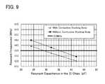
- Example 1will describe results obtained by measuring and comparing resonant capacitance in IC chips of a wireless chip having a structure in which a conductive blocking body is provided on top and bottom surfaces of the IC chip, which is described in Embodiment 3, and a wireless chip provided with no conductive blocking body.
- FIG. 9shows results of measurement of resonant frequencies with respect to resonant capacitance in the IC chips of the wireless chip provided with a conductive blocking body, according to an embodiment of the present invention, and the conventional wireless chip provided with no conductive blocking body.
- Each of the wireless chipshas an antenna with a size (a length from one edge to the other edge of the outermost perimeter of the antenna) of 6 mm Resonant frequencies (MHz) are plotted on the vertical axis with in-chip resonant capacitance (pF) represented on the horizontal axis.
- the line widthis 135 ⁇ m
- the distance between linesis 5 ⁇ m
- the number of coilsis 15.
- the antenna used for measurement in this caseis formed using Al to a thickness of 5 ⁇ m.
- in-chip resonant capacitance required in the wireless chip provided with a conductive blocking bodyis about 29 pF.
- in-chip resonant capacitance required in the wireless chip provided with no conductive blocking bodyis about 35 pF.
- in-chip resonant capacitancecan be reduced by about 6 pF.
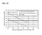
- FIG. 10shows results of measurement of resonant frequencies with respect to resonant capacitance in the IC chips of the wireless chips each having an antenna with a size (a length from one edge to the other edge of the outermost perimeter of the antenna) of 8 mm. Note that resonant frequencies are plotted on the vertical axis with in-chip resonant capacitance represented on the horizontal axis.
- the line widthis 105 ⁇ m
- the distance between linesis 5 ⁇ m
- the number of coilsis 17.
- the antennais formed using Al to a thickness of 5 ⁇ m.
- in-chip resonant capacitance required in the wireless chip provided with a conductive blocking bodyis about 24 pF.
- in-chip resonant capacitance required in the wireless chip provided with no conductive blocking bodyis about 35 pF.
- in-chip resonant capacitancecan be reduced by about 11 pF.
Landscapes
- Engineering & Computer Science (AREA)
- Physics & Mathematics (AREA)
- General Physics & Mathematics (AREA)
- Computer Hardware Design (AREA)
- Microelectronics & Electronic Packaging (AREA)
- Power Engineering (AREA)
- Condensed Matter Physics & Semiconductors (AREA)
- Theoretical Computer Science (AREA)
- Semiconductor Integrated Circuits (AREA)
Abstract
Description
- [Patent Document 1] Japanese Published Patent Application No. 2001-260580
Claims (10)
Applications Claiming Priority (2)
| Application Number | Priority Date | Filing Date | Title |
|---|---|---|---|
| JP2008-256056 | 2008-10-01 | ||
| JP2008256056 | 2008-10-01 |
Publications (2)
| Publication Number | Publication Date |
|---|---|
| US20100078787A1 US20100078787A1 (en) | 2010-04-01 |
| US9196593B2true US9196593B2 (en) | 2015-11-24 |
Family
ID=42056503
Family Applications (1)
| Application Number | Title | Priority Date | Filing Date |
|---|---|---|---|
| US12/567,946Expired - Fee RelatedUS9196593B2 (en) | 2008-10-01 | 2009-09-28 | Semiconductor device |
Country Status (5)
| Country | Link |
|---|---|
| US (1) | US9196593B2 (en) |
| JP (1) | JP5637672B2 (en) |
| KR (1) | KR101611643B1 (en) |
| TW (1) | TWI478311B (en) |
| WO (1) | WO2010038599A1 (en) |
Cited By (1)
| Publication number | Priority date | Publication date | Assignee | Title |
|---|---|---|---|---|
| US20150333112A1 (en)* | 2014-05-13 | 2015-11-19 | Japan Display Inc. | Organic el device and manufacturing method of the same |
Families Citing this family (8)
| Publication number | Priority date | Publication date | Assignee | Title |
|---|---|---|---|---|
| PH12012500375A1 (en)* | 2009-08-26 | 2012-10-22 | Toppan Printing Co Ltd | Contactless communication medium |
| JP5501174B2 (en)* | 2009-09-17 | 2014-05-21 | 株式会社半導体エネルギー研究所 | Semiconductor device |
| JP6283558B2 (en) | 2014-04-22 | 2018-02-21 | 新光電気工業株式会社 | Passive element substrate |
| JP6560610B2 (en)* | 2015-12-18 | 2019-08-14 | 株式会社ジャパンディスプレイ | Display device |
| US11073958B2 (en)* | 2016-01-29 | 2021-07-27 | Sharp Kabushiki Kaisha | Antenna device |
| JP6762004B2 (en)* | 2016-03-11 | 2020-09-30 | 国立大学法人九州工業大学 | Semiconductor integrated circuit equipment and its manufacturing method |
| JP7199174B2 (en)* | 2018-07-26 | 2023-01-05 | 東京エレクトロン株式会社 | Etching method |
| JP6546711B1 (en)* | 2019-04-10 | 2019-07-17 | 株式会社エスケーエレクトロニクス | Non-contact information carrier |
Citations (182)
| Publication number | Priority date | Publication date | Assignee | Title |
|---|---|---|---|---|
| US4373163A (en)* | 1980-07-14 | 1983-02-08 | I.D. Engineering, Inc. | Loop antenna for security systems |
| JPS60198861A (en) | 1984-03-23 | 1985-10-08 | Fujitsu Ltd | Thin film transistor |
| JPS63210023A (en) | 1987-02-24 | 1988-08-31 | Natl Inst For Res In Inorg Mater | Compound having a hexagonal layered structure represented by InGaZn↓4O↓7 and its manufacturing method |
| JPS63210024A (en) | 1987-02-24 | 1988-08-31 | Natl Inst For Res In Inorg Mater | Compound having a hexagonal layered structure represented by InGaZn↓5O↓8 and its manufacturing method |
| JPS63210022A (en) | 1987-02-24 | 1988-08-31 | Natl Inst For Res In Inorg Mater | Compound having hexagonal layered structure represented by InGaZn↓3O↓6 and method for producing the same |
| JPS63215519A (en) | 1987-02-27 | 1988-09-08 | Natl Inst For Res In Inorg Mater | Compound having hexagonal layered structure represented by InGaZn↓6O↓9 and method for producing the same |
| JPS63239117A (en) | 1987-01-28 | 1988-10-05 | Natl Inst For Res In Inorg Mater | Compound having hexagonal layered structure represented by InGaZn↓2O↓5 and method for producing the same |
| JPS63265818A (en) | 1987-04-22 | 1988-11-02 | Natl Inst For Res In Inorg Mater | Compound having a hexagonal layered structure represented by InGaZn↓7O↓1↓0 and its manufacturing method |
| US5075166A (en) | 1989-03-10 | 1991-12-24 | Mtu Motoren- Und Turbinen-Union-Munchen Gmbh | Composite comprising a resin prepreg and a protective sheet containing ferromagnetic material and which is adhered to the resin prepreg by magnetic forces |
| JPH05190582A (en) | 1992-01-08 | 1993-07-30 | Oki Electric Ind Co Ltd | Resin sealed semiconductor device and manufacture thereof |
| JPH05251705A (en) | 1992-03-04 | 1993-09-28 | Fuji Xerox Co Ltd | Thin-film transistor |
| JPH08250745A (en) | 1995-03-10 | 1996-09-27 | Semiconductor Energy Lab Co Ltd | Display device |
| JPH08264794A (en) | 1995-03-27 | 1996-10-11 | Res Dev Corp Of Japan | Metal oxide semiconductor device in which a pn junction is formed with a thin film transistor made of a metal oxide semiconductor such as cuprous oxide, and methods for manufacturing the same |
| JPH08288522A (en) | 1995-02-16 | 1996-11-01 | Semiconductor Energy Lab Co Ltd | Method for manufacturing semiconductor device |
| US5597631A (en) | 1989-01-25 | 1997-01-28 | Asahi Kasei Kogyo Kabushiki Kaisha | Prepreg, composite molding body, and method of manufacture of the composite molded body |
| JPH09156265A (en) | 1995-12-01 | 1997-06-17 | Hitachi Chem Co Ltd | Semiconductor device |
| US5677045A (en) | 1993-09-14 | 1997-10-14 | Hitachi, Ltd. | Laminate and multilayer printed circuit board |
| US5679975A (en) | 1995-12-18 | 1997-10-21 | Integrated Device Technology, Inc. | Conductive encapsulating shield for an integrated circuit |
| US5731856A (en) | 1995-12-30 | 1998-03-24 | Samsung Electronics Co., Ltd. | Methods for forming liquid crystal displays including thin film transistors and gate pads having a particular structure |
| JPH1092980A (en) | 1996-09-13 | 1998-04-10 | Toshiba Corp | Wireless card and method of manufacturing the same |
| US5744864A (en) | 1995-08-03 | 1998-04-28 | U.S. Philips Corporation | Semiconductor device having a transparent switching element |
| JPH10129165A (en) | 1996-03-15 | 1998-05-19 | Hitachi Maxell Ltd | Information carrier and method of manufacturing the same |
| US5757456A (en) | 1995-03-10 | 1998-05-26 | Semiconductor Energy Laboratory Co., Ltd. | Display device and method of fabricating involving peeling circuits from one substrate and mounting on other |
| JPH10181261A (en) | 1996-12-20 | 1998-07-07 | Dainippon Printing Co Ltd | Non-contact IC card |
| JPH10211784A (en) | 1997-01-31 | 1998-08-11 | Denso Corp | Ic card and its manufacture |
| JPH10302027A (en) | 1997-04-28 | 1998-11-13 | Matsushita Electric Ind Co Ltd | Card reader |
| JPH11353440A (en) | 1998-06-09 | 1999-12-24 | Kyodo Printing Co Ltd | Capacitors and contactless IC cards |
| JP2000044236A (en) | 1998-07-24 | 2000-02-15 | Hoya Corp | Article having transparent conductive oxide thin film and method for producing the same |
| JP2000150900A (en) | 1998-11-17 | 2000-05-30 | Japan Science & Technology Corp | Transistor and semiconductor device |
| US6100177A (en) | 1996-06-03 | 2000-08-08 | Nec Corporation | Grooved wiring structure in semiconductor device and method for forming the same |
| JP2000231619A (en) | 1999-02-10 | 2000-08-22 | Nippon Telegr & Teleph Corp <Ntt> | Contact type IC card |
| US6215455B1 (en)* | 1996-10-25 | 2001-04-10 | Gemplus S.C.A. | Armored magnetic field antenna in printed circuit |
| US6224965B1 (en) | 1999-06-25 | 2001-05-01 | Honeywell International Inc. | Microfiber dielectrics which facilitate laser via drilling |
| JP2001260580A (en) | 2000-03-15 | 2001-09-25 | Hitachi Ltd | Bills and securities on which IC chips are mounted and methods for preventing unauthorized use thereof |
| US6294274B1 (en) | 1998-11-16 | 2001-09-25 | Tdk Corporation | Oxide thin film |
| JP2001277726A (en) | 2000-03-31 | 2001-10-10 | Kyodo Printing Co Ltd | Reversible thermosensitive recording transfer sheet, method for producing the same, and method for producing reversible thermosensitive recording medium |
| US6323550B1 (en) | 1995-06-06 | 2001-11-27 | Analog Devices, Inc. | Package for sealing an integrated circuit die |
| US20010046027A1 (en) | 1999-09-03 | 2001-11-29 | Ya-Hsiang Tai | Liquid crystal display having stripe-shaped common electrodes formed above plate-shaped pixel electrodes |
| JP2002043516A (en) | 2000-07-19 | 2002-02-08 | Toshiba Microelectronics Corp | Semiconductor device and memory device |
| JP2002049903A (en) | 2000-08-04 | 2002-02-15 | Hitachi Chem Co Ltd | Non-contact type ic tag |
| JP2002076356A (en) | 2000-09-01 | 2002-03-15 | Japan Science & Technology Corp | Semiconductor device |
| US20020056838A1 (en) | 2000-11-15 | 2002-05-16 | Matsushita Electric Industrial Co., Ltd. | Thin film transistor array, method of producing the same, and display panel using the same |
| US6403221B1 (en) | 1999-10-13 | 2002-06-11 | Ajinomoto Co., Inc. | Epoxy resin composition, and adhesive film and prepreg using the composition, and multilayer printed-wiring board using them, and process for manufacturing the same |
| JP2002246829A (en) | 2001-02-16 | 2002-08-30 | Toppan Forms Co Ltd | Non-contact type data transmitting / receiving antenna and its capacitance adjusting method |
| US20020132454A1 (en) | 2001-03-19 | 2002-09-19 | Fuji Xerox Co., Ltd. | Method of forming crystalline semiconductor thin film on base substrate, lamination formed with crystalline semiconductor thin film and color filter |
| JP2002289859A (en) | 2001-03-23 | 2002-10-04 | Minolta Co Ltd | Thin film transistor |
| US6482495B1 (en) | 1996-09-04 | 2002-11-19 | Hitachi Maxwell, Ltd. | Information carrier and process for production thereof |
| US6491228B1 (en) | 1997-01-14 | 2002-12-10 | Rohm Co., Ltd. | IC card |
| US20030032210A1 (en) | 2001-07-16 | 2003-02-13 | Semiconductor Energy Laboratory Co., Ltd. | Semiconductor device and peeling off method and method of manufacturing semiconductor device |
| JP2003086000A (en) | 2001-09-10 | 2003-03-20 | Sharp Corp | Semiconductor memory device and test method therefor |
| JP2003086808A (en) | 2001-09-10 | 2003-03-20 | Masashi Kawasaki | Thin film transistor and matrix display device |
| JP2003141486A (en) | 2001-11-08 | 2003-05-16 | Oji Paper Co Ltd | Non-contact IC card and method of manufacturing the same |
| JP2003174153A (en) | 2001-07-16 | 2003-06-20 | Semiconductor Energy Lab Co Ltd | Separation method, method for manufacturing semiconductor device, and semiconductor device |
| US20030189401A1 (en) | 2002-03-26 | 2003-10-09 | International Manufacturing And Engineering Services Co., Ltd. | Organic electroluminescent device |
| US6639299B2 (en)* | 2001-04-17 | 2003-10-28 | Casio Computer Co., Ltd. | Semiconductor device having a chip size package including a passive element |
| US20030218222A1 (en) | 2002-05-21 | 2003-11-27 | The State Of Oregon Acting And Through The Oregon State Board Of Higher Education On Behalf Of | Transistor structures and methods for making the same |
| WO2004001848A1 (en) | 2002-06-19 | 2003-12-31 | Sten Bjorsell | Electronics circuit manufacture |
| US20040016939A1 (en) | 2002-07-26 | 2004-01-29 | Masayuki Akiba | Encapsulation of a stack of semiconductor dice |
| US20040038446A1 (en) | 2002-03-15 | 2004-02-26 | Sanyo Electric Co., Ltd.- | Method for forming ZnO film, method for forming ZnO semiconductor layer, method for fabricating semiconductor device, and semiconductor device |
| JP2004094492A (en) | 2002-08-30 | 2004-03-25 | Konica Minolta Holdings Inc | Ic card |
| JP2004103957A (en) | 2002-09-11 | 2004-04-02 | Japan Science & Technology Corp | Transparent thin film field effect transistor using homologous thin film as active layer |
| JP2004118255A (en) | 2002-09-24 | 2004-04-15 | Dainippon Printing Co Ltd | Method for producing film with microstructure and film with microstructure |
| JP2004153717A (en) | 2002-10-31 | 2004-05-27 | Toppan Forms Co Ltd | Non-contact type data transmitter / receiver and capacitance adjusting method thereof |
| US20040127038A1 (en) | 2002-10-11 | 2004-07-01 | Carcia Peter Francis | Transparent oxide semiconductor thin film transistors |
| US6762508B1 (en) | 1998-02-27 | 2004-07-13 | Canon Kabushiki Kaisha | Semiconductor encapsulant resin having an additive with a gradient concentration |
| JP2004273614A (en) | 2003-03-06 | 2004-09-30 | Sharp Corp | Semiconductor device and method of manufacturing the same |
| JP2004273732A (en) | 2003-03-07 | 2004-09-30 | Sharp Corp | Active matrix substrate and manufacturing method thereof |
| JP2004362341A (en) | 2003-06-05 | 2004-12-24 | Toppan Printing Co Ltd | IC tag |
| WO2004114391A1 (en) | 2003-06-20 | 2004-12-29 | Sharp Kabushiki Kaisha | Semiconductor device, its manufacturing method, and electronic device |
| US20050017302A1 (en) | 2003-07-25 | 2005-01-27 | Randy Hoffman | Transistor including a deposited channel region having a doped portion |
| US20050146006A1 (en)* | 2003-12-26 | 2005-07-07 | Semiconductor Energy Laboratory Co., Ltd. | Securities, chip mounting product, and manufacturing method thereof |
| US20050199959A1 (en) | 2004-03-12 | 2005-09-15 | Chiang Hai Q. | Semiconductor device |
| US20050233122A1 (en) | 2004-04-19 | 2005-10-20 | Mikio Nishimura | Manufacturing method of laminated substrate, and manufacturing apparatus of semiconductor device for module and laminated substrate for use therein |
| US20050285231A1 (en) | 2004-06-29 | 2005-12-29 | Tatsuya Arao | Semiconductor device and method for manufacturing the same |
| US20060011288A1 (en) | 2004-07-16 | 2006-01-19 | Semiconductor Energy | Laminating system, IC sheet, roll of IC sheet, and method for manufacturing IC chip |
| US20060043377A1 (en) | 2004-03-12 | 2006-03-02 | Hewlett-Packard Development Company, L.P. | Semiconductor device |
| WO2006038438A2 (en) | 2004-09-14 | 2006-04-13 | Oji Paper Co | Reversible thermal recording material, and communication medium having display layer and recording material |
| JP2006108654A (en) | 2004-09-09 | 2006-04-20 | Semiconductor Energy Lab Co Ltd | Radio chip |
| US20060091793A1 (en) | 2004-11-02 | 2006-05-04 | 3M Innovative Properties Company | Methods and displays utilizing integrated zinc oxide row and column drivers in conjunction with organic light emitting diodes |
| US7049178B2 (en) | 2001-12-18 | 2006-05-23 | Lg Electronics Inc. | Method for fabricating semiconductor package and semiconductor package |
| US20060108636A1 (en) | 2004-11-10 | 2006-05-25 | Canon Kabushiki Kaisha | Amorphous oxide and field effect transistor |
| US20060108529A1 (en) | 2004-11-10 | 2006-05-25 | Canon Kabushiki Kaisha | Sensor and image pickup device |
| US20060110867A1 (en) | 2004-11-10 | 2006-05-25 | Canon Kabushiki Kaisha | Field effect transistor manufacturing method |
| US20060113565A1 (en) | 2004-11-10 | 2006-06-01 | Canon Kabushiki Kaisha | Electric elements and circuits utilizing amorphous oxides |
| US20060113549A1 (en) | 2004-11-10 | 2006-06-01 | Canon Kabushiki Kaisha | Light-emitting device |
| JP2006139802A (en) | 2006-01-23 | 2006-06-01 | Sony Corp | Manufacturing method of semiconductor integrated circuit card |
| US20060113536A1 (en) | 2004-11-10 | 2006-06-01 | Canon Kabushiki Kaisha | Display |
| US20060113539A1 (en) | 2004-11-10 | 2006-06-01 | Canon Kabushiki Kaisha | Field effect transistor |
| US7061083B1 (en) | 1998-12-17 | 2006-06-13 | Hitachi, Ltd. | Semiconductor devices |
| US7061014B2 (en) | 2001-11-05 | 2006-06-13 | Japan Science And Technology Agency | Natural-superlattice homologous single crystal thin film, method for preparation thereof, and device using said single crystal thin film |
| US20060169973A1 (en) | 2005-01-28 | 2006-08-03 | Semiconductor Energy Laboratory Co., Ltd. | Semiconductor device, electronic device, and method of manufacturing semiconductor device |
| US20060170111A1 (en) | 2005-01-28 | 2006-08-03 | Semiconductor Energy Laboratory Co., Ltd. | Semiconductor device, electronic device, and method of manufacturing semiconductor device |
| US20060197092A1 (en) | 2005-03-03 | 2006-09-07 | Randy Hoffman | System and method for forming conductive material on a substrate |
| US7105868B2 (en) | 2002-06-24 | 2006-09-12 | Cermet, Inc. | High-electron mobility transistor with zinc oxide |
| US20060208977A1 (en) | 2005-03-18 | 2006-09-21 | Semiconductor Energy Laboratory Co., Ltd. | Semiconductor device, and display device, driving method and electronic apparatus thereof |
| US20060228974A1 (en) | 2005-03-31 | 2006-10-12 | Theiss Steven D | Methods of making displays |
| US20060231882A1 (en) | 2005-03-28 | 2006-10-19 | Il-Doo Kim | Low voltage flexible organic/transparent transistor for selective gas sensing, photodetecting and CMOS device applications |
| US20060238135A1 (en) | 2005-04-20 | 2006-10-26 | Semiconductor Energy Laboratory Co., Ltd. | Semiconductor device and display device |
| US20060267141A1 (en)* | 2005-05-31 | 2006-11-30 | Semiconductor Energy Laboratory Co., Ltd. | Semiconductor device and manufacturing method thereof |
| US20060267158A1 (en) | 2005-05-11 | 2006-11-30 | Rolf Weis | Semiconductor memory apparatus having improved charge retention as a result of bit line shielding |
| US20060284171A1 (en) | 2005-06-16 | 2006-12-21 | Levy David H | Methods of making thin film transistors comprising zinc-oxide-based semiconductor materials and transistors made thereby |
| US20060284172A1 (en) | 2005-06-10 | 2006-12-21 | Casio Computer Co., Ltd. | Thin film transistor having oxide semiconductor layer and manufacturing method thereof |
| US20060292777A1 (en) | 2005-06-27 | 2006-12-28 | 3M Innovative Properties Company | Method for making electronic devices using metal oxide nanoparticles |
| US20070004125A1 (en) | 2005-06-30 | 2007-01-04 | Semiconductor Energy Laboratory Co., Ltd. | Semiconductor device and manufacturing method thereof |
| JP2007005782A (en) | 2005-05-27 | 2007-01-11 | Semiconductor Energy Lab Co Ltd | Semiconductor device and manufacturing method of semiconductor device |
| JP2007005778A (en) | 2005-05-27 | 2007-01-11 | Semiconductor Energy Lab Co Ltd | Semiconductor device |
| US20070024187A1 (en) | 2005-07-28 | 2007-02-01 | Shin Hyun S | Organic light emitting display (OLED) and its method of fabrication |
| US20070044303A1 (en) | 2005-08-26 | 2007-03-01 | Shinko Electric Industries Co., Ltd. | Method of manufacturing wiring board |
| US20070046191A1 (en) | 2005-08-23 | 2007-03-01 | Canon Kabushiki Kaisha | Organic electroluminescent display device and manufacturing method thereof |
| US20070052025A1 (en) | 2005-09-06 | 2007-03-08 | Canon Kabushiki Kaisha | Oxide semiconductor thin film transistor and method of manufacturing the same |
| US20070054507A1 (en) | 2005-09-06 | 2007-03-08 | Canon Kabushiki Kaisha | Method of fabricating oxide semiconductor device |
| US20070077691A1 (en) | 2005-09-30 | 2007-04-05 | Semiconductor Energy Laboratory Co., Ltd. | Manufacturing method of semiconductor device |
| WO2007043602A1 (en) | 2005-10-14 | 2007-04-19 | Semiconductor Energy Laboratory Co., Ltd. | Semiconductor device and communication system using the semiconductor device |
| US20070090365A1 (en) | 2005-10-20 | 2007-04-26 | Canon Kabushiki Kaisha | Field-effect transistor including transparent oxide and light-shielding member, and display utilizing the transistor |
| US7211825B2 (en) | 2004-06-14 | 2007-05-01 | Yi-Chi Shih | Indium oxide-based thin film transistors and circuits |
| US20070095913A1 (en)* | 2003-06-06 | 2007-05-03 | Isao Takahashi | Antenna module and portable communication terminal equipped with the antenna module |
| US20070108446A1 (en) | 2005-11-15 | 2007-05-17 | Semiconductor Energy Laboratory Co., Ltd. | Semiconductor device and manufacturing method thereof |
| JP2007134694A (en) | 2005-10-14 | 2007-05-31 | Semiconductor Energy Lab Co Ltd | Semiconductor device and communication system using the same |
| US20070152217A1 (en) | 2005-12-29 | 2007-07-05 | Chih-Ming Lai | Pixel structure of active matrix organic light-emitting diode and method for fabricating the same |
| US20070172591A1 (en) | 2006-01-21 | 2007-07-26 | Samsung Electronics Co., Ltd. | METHOD OF FABRICATING ZnO FILM AND THIN FILM TRANSISTOR ADOPTING THE ZnO FILM |
| US20070181875A1 (en)* | 2006-02-08 | 2007-08-09 | Semiconductor Energy Laboratory Co., Ltd. | Semiconductor device |
| US20070187760A1 (en) | 2006-02-02 | 2007-08-16 | Kochi Industrial Promotion Center | Thin film transistor including low resistance conductive thin films and manufacturing method thereof |
| US20070187678A1 (en) | 2006-02-15 | 2007-08-16 | Kochi Industrial Promotion Center | Semiconductor device including active layer made of zinc oxide with controlled orientations and manufacturing method thereof |
| US20070194379A1 (en) | 2004-03-12 | 2007-08-23 | Japan Science And Technology Agency | Amorphous Oxide And Thin Film Transistor |
| JP2007241999A (en) | 2006-02-08 | 2007-09-20 | Semiconductor Energy Lab Co Ltd | Semiconductor device |
| US20070252928A1 (en) | 2006-04-28 | 2007-11-01 | Toppan Printing Co., Ltd. | Structure, transmission type liquid crystal display, reflection type display and manufacturing method thereof |
| US20070252706A1 (en)* | 2005-01-11 | 2007-11-01 | Fujitsu Limited | IC tag housing case |
| US20070257292A1 (en)* | 2004-09-09 | 2007-11-08 | Semiconductor Energy Laboratory Co., Ltd. | Wireless Chip |
| US7297977B2 (en) | 2004-03-12 | 2007-11-20 | Hewlett-Packard Development Company, L.P. | Semiconductor device |
| US20070272922A1 (en) | 2006-04-11 | 2007-11-29 | Samsung Electronics Co. Ltd. | ZnO thin film transistor and method of forming the same |
| US20070278563A1 (en) | 2006-06-01 | 2007-12-06 | Semiconductor Energy Laboratory Co., Ltd. | Nonvolatile semiconductor memory device |
| US20070287296A1 (en) | 2006-06-13 | 2007-12-13 | Canon Kabushiki Kaisha | Dry etching method for oxide semiconductor film |
| US20080006877A1 (en) | 2004-09-17 | 2008-01-10 | Peter Mardilovich | Method of Forming a Solution Processed Device |
| US20080012126A1 (en) | 2006-06-26 | 2008-01-17 | Yoshitaka Dozen | Paper including semiconductor device and manufacturing method thereof |
| US7323356B2 (en) | 2002-02-21 | 2008-01-29 | Japan Science And Technology Agency | LnCuO(S,Se,Te)monocrystalline thin film, its manufacturing method, and optical device or electronic device using the monocrystalline thin film |
| US20080038929A1 (en) | 2006-08-09 | 2008-02-14 | Canon Kabushiki Kaisha | Method of dry etching oxide semiconductor film |
| US20080038882A1 (en) | 2006-08-09 | 2008-02-14 | Kazushige Takechi | Thin-film device and method of fabricating the same |
| US20080036608A1 (en) | 2006-08-08 | 2008-02-14 | Isao Sakama | Rfid tag and method for reading the same |
| US20080044940A1 (en) | 2004-06-02 | 2008-02-21 | Ryosuke Watanabe | Laminating System |
| US20080050595A1 (en) | 2006-01-11 | 2008-02-28 | Murata Manufacturing Co., Ltd. | Transparent conductive film and method for manufacturing the same |
| US20080054976A1 (en) | 2006-08-31 | 2008-03-06 | Semiconductor Energy Laboratory Co., Ltd. | Clock Generation Circuit and Semiconductor Device Including the Same |
| US20080073653A1 (en) | 2006-09-27 | 2008-03-27 | Canon Kabushiki Kaisha | Semiconductor apparatus and method of manufacturing the same |
| JP2008084303A (en) | 2006-08-31 | 2008-04-10 | Semiconductor Energy Lab Co Ltd | Clock generation circuit and semiconductor device including the same |
| US20080083950A1 (en) | 2006-10-10 | 2008-04-10 | Alfred I-Tsung Pan | Fused nanocrystal thin film semiconductor and method |
| US20080093464A1 (en) | 2004-08-23 | 2008-04-24 | C/O Semiconductor Energy Laboratory Co., Ltd. | Wireless Chip And Manufacturing Method Thereof |
| US20080106191A1 (en) | 2006-09-27 | 2008-05-08 | Seiko Epson Corporation | Electronic device, organic electroluminescence device, and organic thin film semiconductor device |
| US20080128689A1 (en) | 2006-11-29 | 2008-06-05 | Je-Hun Lee | Flat panel displays comprising a thin-film transistor having a semiconductive oxide in its channel and methods of fabricating the same for use in flat panel displays |
| US20080129195A1 (en) | 2006-12-04 | 2008-06-05 | Toppan Printing Co., Ltd. | Color el display and method for producing the same |
| US7385224B2 (en) | 2004-09-02 | 2008-06-10 | Casio Computer Co., Ltd. | Thin film transistor having an etching protection film and manufacturing method thereof |
| US20080166834A1 (en) | 2007-01-05 | 2008-07-10 | Samsung Electronics Co., Ltd. | Thin film etching method |
| US7402506B2 (en) | 2005-06-16 | 2008-07-22 | Eastman Kodak Company | Methods of making thin film transistors comprising zinc-oxide-based semiconductor materials and transistors made thereby |
| US20080182358A1 (en) | 2007-01-26 | 2008-07-31 | Cowdery-Corvan Peter J | Process for atomic layer deposition |
| US20080186181A1 (en) | 2007-02-02 | 2008-08-07 | Semiconductor Energy Laboratory Co., Ltd. | Wireless system, semiconductor device, and communication device |
| US7411209B2 (en) | 2006-09-15 | 2008-08-12 | Canon Kabushiki Kaisha | Field-effect transistor and method for manufacturing the same |
| US20080224941A1 (en) | 2007-03-13 | 2008-09-18 | Semiconductor Energy Laboratory Co., Ltd. | Semiconductor device and manufacturing method thereof |
| US20080224133A1 (en) | 2007-03-14 | 2008-09-18 | Jin-Seong Park | Thin film transistor and organic light-emitting display device having the thin film transistor |
| US20080224940A1 (en) | 2007-03-13 | 2008-09-18 | Semiconductor Energy Laboratory Co., Ltd. | Semiconductor device and manufacturing method thereof |
| US20080242005A1 (en) | 2007-03-26 | 2008-10-02 | Semiconductor Energy Laboratory Co., Ltd. | Method for manufacturing semiconductor device |
| US20080258141A1 (en) | 2007-04-19 | 2008-10-23 | Samsung Electronics Co., Ltd. | Thin film transistor, method of manufacturing the same, and flat panel display having the same |
| US20080258140A1 (en) | 2007-04-20 | 2008-10-23 | Samsung Electronics Co., Ltd. | Thin film transistor including selectively crystallized channel layer and method of manufacturing the thin film transistor |
| US20080258139A1 (en) | 2007-04-17 | 2008-10-23 | Toppan Printing Co., Ltd. | Structure with transistor |
| US20080258143A1 (en) | 2007-04-18 | 2008-10-23 | Samsung Electronics Co., Ltd. | Thin film transitor substrate and method of manufacturing the same |
| US7453087B2 (en) | 2005-09-06 | 2008-11-18 | Canon Kabushiki Kaisha | Thin-film transistor and thin-film diode having amorphous-oxide semiconductor layer |
| US20080296568A1 (en) | 2007-05-29 | 2008-12-04 | Samsung Electronics Co., Ltd | Thin film transistors and methods of manufacturing the same |
| US20080303140A1 (en) | 2007-06-07 | 2008-12-11 | Semiconductor Energy Laboratory Co., Ltd. | Semiconductor device |
| US7487373B2 (en) | 2004-01-30 | 2009-02-03 | Semiconductor Energy Laboratory Co., Ltd. | Wireless semiconductor device having low power consumption |
| US7485489B2 (en) | 2002-06-19 | 2009-02-03 | Bjoersell Sten | Electronics circuit manufacture |
| US7501293B2 (en) | 2002-06-13 | 2009-03-10 | Murata Manufacturing Co., Ltd. | Semiconductor device in which zinc oxide is used as a semiconductor material and method for manufacturing the semiconductor device |
| US20090073325A1 (en) | 2005-01-21 | 2009-03-19 | Semiconductor Energy Laboratory Co., Ltd. | Semiconductor device and method for manufacturing the same, and electric device |
| US20090085182A1 (en) | 2007-07-27 | 2009-04-02 | Shunpei Yamazaki | Semiconductor device and method for manufacturing the same |
| US20090114910A1 (en) | 2005-09-06 | 2009-05-07 | Canon Kabushiki Kaisha | Semiconductor device |
| US20090134399A1 (en) | 2005-02-18 | 2009-05-28 | Semiconductor Energy Laboratory Co., Ltd. | Semiconductor Device and Method for Manufacturing the Same |
| US20090152506A1 (en) | 2007-12-17 | 2009-06-18 | Fujifilm Corporation | Process for producing oriented inorganic crystalline film, and semiconductor device using the oriented inorganic crystalline film |
| US20090152541A1 (en) | 2005-02-03 | 2009-06-18 | Semiconductor Energy Laboratory Co., Ltd. | Electronic device, semiconductor device and manufacturing method thereof |
| US7566971B2 (en) | 2005-05-27 | 2009-07-28 | Semiconductor Energy Laboratory Co., Ltd. | Semiconductor device and manufacturing method thereof |
| US20090278252A1 (en) | 2008-05-12 | 2009-11-12 | Semiconductor Energy Laboratory Co., Ltd. | Semiconductor device and method for manufacturing semiconductor device |
| US20090289341A1 (en) | 2008-05-23 | 2009-11-26 | Semiconductor Energy Laboratory Co., Ltd. | Semiconductor device |
| US7674650B2 (en) | 2005-09-29 | 2010-03-09 | Semiconductor Energy Laboratory Co., Ltd. | Semiconductor device and manufacturing method thereof |
| US20100065844A1 (en) | 2008-09-18 | 2010-03-18 | Sony Corporation | Thin film transistor and method of manufacturing thin film transistor |
| US20100092800A1 (en) | 2008-10-09 | 2010-04-15 | Canon Kabushiki Kaisha | Substrate for growing wurtzite type crystal and method for manufacturing the same and semiconductor device |
| US20100109002A1 (en) | 2007-04-25 | 2010-05-06 | Canon Kabushiki Kaisha | Oxynitride semiconductor |
| US7923796B2 (en) | 2005-05-27 | 2011-04-12 | Semiconductor Energy Laboratory Co., Ltd. | Semiconductor device including resonance circuit |
- 2009
- 2009-09-07KRKR1020117009849Apatent/KR101611643B1/ennot_activeExpired - Fee Related
- 2009-09-07WOPCT/JP2009/065970patent/WO2010038599A1/enactiveApplication Filing
- 2009-09-22TWTW098131934Apatent/TWI478311B/ennot_activeIP Right Cessation
- 2009-09-28USUS12/567,946patent/US9196593B2/ennot_activeExpired - Fee Related
- 2009-09-30JPJP2009226638Apatent/JP5637672B2/ennot_activeExpired - Fee Related
Patent Citations (217)
| Publication number | Priority date | Publication date | Assignee | Title |
|---|---|---|---|---|
| US4373163A (en)* | 1980-07-14 | 1983-02-08 | I.D. Engineering, Inc. | Loop antenna for security systems |
| JPS60198861A (en) | 1984-03-23 | 1985-10-08 | Fujitsu Ltd | Thin film transistor |
| JPS63239117A (en) | 1987-01-28 | 1988-10-05 | Natl Inst For Res In Inorg Mater | Compound having hexagonal layered structure represented by InGaZn↓2O↓5 and method for producing the same |
| JPS63210023A (en) | 1987-02-24 | 1988-08-31 | Natl Inst For Res In Inorg Mater | Compound having a hexagonal layered structure represented by InGaZn↓4O↓7 and its manufacturing method |
| JPS63210024A (en) | 1987-02-24 | 1988-08-31 | Natl Inst For Res In Inorg Mater | Compound having a hexagonal layered structure represented by InGaZn↓5O↓8 and its manufacturing method |
| JPS63210022A (en) | 1987-02-24 | 1988-08-31 | Natl Inst For Res In Inorg Mater | Compound having hexagonal layered structure represented by InGaZn↓3O↓6 and method for producing the same |
| JPS63215519A (en) | 1987-02-27 | 1988-09-08 | Natl Inst For Res In Inorg Mater | Compound having hexagonal layered structure represented by InGaZn↓6O↓9 and method for producing the same |
| JPS63265818A (en) | 1987-04-22 | 1988-11-02 | Natl Inst For Res In Inorg Mater | Compound having a hexagonal layered structure represented by InGaZn↓7O↓1↓0 and its manufacturing method |
| US5770313A (en) | 1989-01-25 | 1998-06-23 | Asahi Kasei Kogyo Kabushiki Kaisha | Prepreg, composite molded body and method of manufacture of the composite molded body |
| US5597631A (en) | 1989-01-25 | 1997-01-28 | Asahi Kasei Kogyo Kabushiki Kaisha | Prepreg, composite molding body, and method of manufacture of the composite molded body |
| US5075166A (en) | 1989-03-10 | 1991-12-24 | Mtu Motoren- Und Turbinen-Union-Munchen Gmbh | Composite comprising a resin prepreg and a protective sheet containing ferromagnetic material and which is adhered to the resin prepreg by magnetic forces |
| JPH05190582A (en) | 1992-01-08 | 1993-07-30 | Oki Electric Ind Co Ltd | Resin sealed semiconductor device and manufacture thereof |
| JPH05251705A (en) | 1992-03-04 | 1993-09-28 | Fuji Xerox Co Ltd | Thin-film transistor |
| US5677045A (en) | 1993-09-14 | 1997-10-14 | Hitachi, Ltd. | Laminate and multilayer printed circuit board |
| JPH08288522A (en) | 1995-02-16 | 1996-11-01 | Semiconductor Energy Lab Co Ltd | Method for manufacturing semiconductor device |
| US7361519B2 (en) | 1995-02-16 | 2008-04-22 | Semiconductor Energy Laboratory Co., Ltd. | Method of manufacturing a semiconductor device |
| US20050162578A1 (en) | 1995-02-16 | 2005-07-28 | Shunpei Yamazaki | Method of manufacturing a semiconductor device |
| US6376333B1 (en) | 1995-02-16 | 2002-04-23 | Semiconductor Energy Laboratory Co., Ltd. | Method of manufacturing flexible display with transfer from auxiliary substrate |
| US6998282B1 (en) | 1995-02-16 | 2006-02-14 | Semiconductor Energy Laboratory Co., Ltd. | Method of manufacturing a semiconductor device |
| US5821138A (en) | 1995-02-16 | 1998-10-13 | Semiconductor Energy Laboratory Co., Ltd. | Method of manufacturing a semiconductor device using a metal which promotes crystallization of silicon and substrate bonding |
| US7050138B1 (en) | 1995-03-10 | 2006-05-23 | Semiconductor Energy Laboratory Co., Ltd. | Method of manufacturing a display device having a driver circuit attached to a display substrate |
| US20070259585A1 (en) | 1995-03-10 | 2007-11-08 | Semiconductor Energy Laboratory Co., Ltd. | Display Device and Method of Fabricating the Same |
| US5757456A (en) | 1995-03-10 | 1998-05-26 | Semiconductor Energy Laboratory Co., Ltd. | Display device and method of fabricating involving peeling circuits from one substrate and mounting on other |
| US20050070038A1 (en) | 1995-03-10 | 2005-03-31 | Shunpei Yamazaki | Display device and method of fabricating the same |
| US6118502A (en) | 1995-03-10 | 2000-09-12 | Semiconductor Energy Laboratory Co., Ltd. | Using a temporary substrate to attach components to a display substrate when fabricating a passive type display device |
| US20030071953A1 (en) | 1995-03-10 | 2003-04-17 | Semiconductor Energy Laboratory Co., Ltd., A Japanese Corporation | Display device and method of fabricating the same |
| JPH08250745A (en) | 1995-03-10 | 1996-09-27 | Semiconductor Energy Lab Co Ltd | Display device |
| JPH08264794A (en) | 1995-03-27 | 1996-10-11 | Res Dev Corp Of Japan | Metal oxide semiconductor device in which a pn junction is formed with a thin film transistor made of a metal oxide semiconductor such as cuprous oxide, and methods for manufacturing the same |
| US6323550B1 (en) | 1995-06-06 | 2001-11-27 | Analog Devices, Inc. | Package for sealing an integrated circuit die |
| JPH11505377A (en) | 1995-08-03 | 1999-05-18 | フィリップス エレクトロニクス ネムローゼ フェンノートシャップ | Semiconductor device |
| US5744864A (en) | 1995-08-03 | 1998-04-28 | U.S. Philips Corporation | Semiconductor device having a transparent switching element |
| JPH09156265A (en) | 1995-12-01 | 1997-06-17 | Hitachi Chem Co Ltd | Semiconductor device |
| US5679975A (en) | 1995-12-18 | 1997-10-21 | Integrated Device Technology, Inc. | Conductive encapsulating shield for an integrated circuit |
| US5731856A (en) | 1995-12-30 | 1998-03-24 | Samsung Electronics Co., Ltd. | Methods for forming liquid crystal displays including thin film transistors and gate pads having a particular structure |
| JPH10129165A (en) | 1996-03-15 | 1998-05-19 | Hitachi Maxell Ltd | Information carrier and method of manufacturing the same |
| US6100177A (en) | 1996-06-03 | 2000-08-08 | Nec Corporation | Grooved wiring structure in semiconductor device and method for forming the same |
| US6482495B1 (en) | 1996-09-04 | 2002-11-19 | Hitachi Maxwell, Ltd. | Information carrier and process for production thereof |
| US6926794B2 (en) | 1996-09-04 | 2005-08-09 | Hitachi Maxell, Ltd. | Information carrier and process for production thereof |
| JPH1092980A (en) | 1996-09-13 | 1998-04-10 | Toshiba Corp | Wireless card and method of manufacturing the same |
| US6215455B1 (en)* | 1996-10-25 | 2001-04-10 | Gemplus S.C.A. | Armored magnetic field antenna in printed circuit |
| JPH10181261A (en) | 1996-12-20 | 1998-07-07 | Dainippon Printing Co Ltd | Non-contact IC card |
| US6491228B1 (en) | 1997-01-14 | 2002-12-10 | Rohm Co., Ltd. | IC card |
| JPH10211784A (en) | 1997-01-31 | 1998-08-11 | Denso Corp | Ic card and its manufacture |
| JPH10302027A (en) | 1997-04-28 | 1998-11-13 | Matsushita Electric Ind Co Ltd | Card reader |
| US20040229404A1 (en) | 1998-02-27 | 2004-11-18 | Canon Kabushiki Kaisha | Semiconductor encapsulant resin having an additive with a gradient concentration |
| US6762508B1 (en) | 1998-02-27 | 2004-07-13 | Canon Kabushiki Kaisha | Semiconductor encapsulant resin having an additive with a gradient concentration |
| JPH11353440A (en) | 1998-06-09 | 1999-12-24 | Kyodo Printing Co Ltd | Capacitors and contactless IC cards |
| JP2000044236A (en) | 1998-07-24 | 2000-02-15 | Hoya Corp | Article having transparent conductive oxide thin film and method for producing the same |
| US6294274B1 (en) | 1998-11-16 | 2001-09-25 | Tdk Corporation | Oxide thin film |
| US7064346B2 (en) | 1998-11-17 | 2006-06-20 | Japan Science And Technology Agency | Transistor and semiconductor device |
| US6727522B1 (en) | 1998-11-17 | 2004-04-27 | Japan Science And Technology Corporation | Transistor and semiconductor device |
| JP2000150900A (en) | 1998-11-17 | 2000-05-30 | Japan Science & Technology Corp | Transistor and semiconductor device |
| US7061083B1 (en) | 1998-12-17 | 2006-06-13 | Hitachi, Ltd. | Semiconductor devices |
| JP2000231619A (en) | 1999-02-10 | 2000-08-22 | Nippon Telegr & Teleph Corp <Ntt> | Contact type IC card |
| US6224965B1 (en) | 1999-06-25 | 2001-05-01 | Honeywell International Inc. | Microfiber dielectrics which facilitate laser via drilling |
| US20010046027A1 (en) | 1999-09-03 | 2001-11-29 | Ya-Hsiang Tai | Liquid crystal display having stripe-shaped common electrodes formed above plate-shaped pixel electrodes |
| US6403221B1 (en) | 1999-10-13 | 2002-06-11 | Ajinomoto Co., Inc. | Epoxy resin composition, and adhesive film and prepreg using the composition, and multilayer printed-wiring board using them, and process for manufacturing the same |
| JP2001260580A (en) | 2000-03-15 | 2001-09-25 | Hitachi Ltd | Bills and securities on which IC chips are mounted and methods for preventing unauthorized use thereof |
| JP2001277726A (en) | 2000-03-31 | 2001-10-10 | Kyodo Printing Co Ltd | Reversible thermosensitive recording transfer sheet, method for producing the same, and method for producing reversible thermosensitive recording medium |
| JP2002043516A (en) | 2000-07-19 | 2002-02-08 | Toshiba Microelectronics Corp | Semiconductor device and memory device |
| JP2002049903A (en) | 2000-08-04 | 2002-02-15 | Hitachi Chem Co Ltd | Non-contact type ic tag |
| JP2002076356A (en) | 2000-09-01 | 2002-03-15 | Japan Science & Technology Corp | Semiconductor device |
| US20020056838A1 (en) | 2000-11-15 | 2002-05-16 | Matsushita Electric Industrial Co., Ltd. | Thin film transistor array, method of producing the same, and display panel using the same |
| JP2002246829A (en) | 2001-02-16 | 2002-08-30 | Toppan Forms Co Ltd | Non-contact type data transmitting / receiving antenna and its capacitance adjusting method |
| US20020132454A1 (en) | 2001-03-19 | 2002-09-19 | Fuji Xerox Co., Ltd. | Method of forming crystalline semiconductor thin film on base substrate, lamination formed with crystalline semiconductor thin film and color filter |
| JP2002289859A (en) | 2001-03-23 | 2002-10-04 | Minolta Co Ltd | Thin film transistor |
| US6639299B2 (en)* | 2001-04-17 | 2003-10-28 | Casio Computer Co., Ltd. | Semiconductor device having a chip size package including a passive element |
| JP2003174153A (en) | 2001-07-16 | 2003-06-20 | Semiconductor Energy Lab Co Ltd | Separation method, method for manufacturing semiconductor device, and semiconductor device |
| US20030032210A1 (en) | 2001-07-16 | 2003-02-13 | Semiconductor Energy Laboratory Co., Ltd. | Semiconductor device and peeling off method and method of manufacturing semiconductor device |
| US6563174B2 (en) | 2001-09-10 | 2003-05-13 | Sharp Kabushiki Kaisha | Thin film transistor and matrix display device |
| JP2003086808A (en) | 2001-09-10 | 2003-03-20 | Masashi Kawasaki | Thin film transistor and matrix display device |
| JP2003086000A (en) | 2001-09-10 | 2003-03-20 | Sharp Corp | Semiconductor memory device and test method therefor |
| US7061014B2 (en) | 2001-11-05 | 2006-06-13 | Japan Science And Technology Agency | Natural-superlattice homologous single crystal thin film, method for preparation thereof, and device using said single crystal thin film |
| JP2003141486A (en) | 2001-11-08 | 2003-05-16 | Oji Paper Co Ltd | Non-contact IC card and method of manufacturing the same |
| US7049178B2 (en) | 2001-12-18 | 2006-05-23 | Lg Electronics Inc. | Method for fabricating semiconductor package and semiconductor package |
| US7323356B2 (en) | 2002-02-21 | 2008-01-29 | Japan Science And Technology Agency | LnCuO(S,Se,Te)monocrystalline thin film, its manufacturing method, and optical device or electronic device using the monocrystalline thin film |
| US20040038446A1 (en) | 2002-03-15 | 2004-02-26 | Sanyo Electric Co., Ltd.- | Method for forming ZnO film, method for forming ZnO semiconductor layer, method for fabricating semiconductor device, and semiconductor device |
| US7049190B2 (en) | 2002-03-15 | 2006-05-23 | Sanyo Electric Co., Ltd. | Method for forming ZnO film, method for forming ZnO semiconductor layer, method for fabricating semiconductor device, and semiconductor device |
| US20030189401A1 (en) | 2002-03-26 | 2003-10-09 | International Manufacturing And Engineering Services Co., Ltd. | Organic electroluminescent device |
| US20030218222A1 (en) | 2002-05-21 | 2003-11-27 | The State Of Oregon Acting And Through The Oregon State Board Of Higher Education On Behalf Of | Transistor structures and methods for making the same |
| US7501293B2 (en) | 2002-06-13 | 2009-03-10 | Murata Manufacturing Co., Ltd. | Semiconductor device in which zinc oxide is used as a semiconductor material and method for manufacturing the semiconductor device |
| WO2004001848A1 (en) | 2002-06-19 | 2003-12-31 | Sten Bjorsell | Electronics circuit manufacture |
| US7485489B2 (en) | 2002-06-19 | 2009-02-03 | Bjoersell Sten | Electronics circuit manufacture |
| US7105868B2 (en) | 2002-06-24 | 2006-09-12 | Cermet, Inc. | High-electron mobility transistor with zinc oxide |
| US20050085034A1 (en) | 2002-07-26 | 2005-04-21 | Masayuki Akiba | Encapsulated stack of dice and support therefor |
| US20040016939A1 (en) | 2002-07-26 | 2004-01-29 | Masayuki Akiba | Encapsulation of a stack of semiconductor dice |
| JP2004094492A (en) | 2002-08-30 | 2004-03-25 | Konica Minolta Holdings Inc | Ic card |
| JP2004103957A (en) | 2002-09-11 | 2004-04-02 | Japan Science & Technology Corp | Transparent thin film field effect transistor using homologous thin film as active layer |
| JP2004118255A (en) | 2002-09-24 | 2004-04-15 | Dainippon Printing Co Ltd | Method for producing film with microstructure and film with microstructure |
| US20060035452A1 (en) | 2002-10-11 | 2006-02-16 | Carcia Peter F | Transparent oxide semiconductor thin film transistor |
| US20040127038A1 (en) | 2002-10-11 | 2004-07-01 | Carcia Peter Francis | Transparent oxide semiconductor thin film transistors |
| JP2004153717A (en) | 2002-10-31 | 2004-05-27 | Toppan Forms Co Ltd | Non-contact type data transmitter / receiver and capacitance adjusting method thereof |
| JP2004273614A (en) | 2003-03-06 | 2004-09-30 | Sharp Corp | Semiconductor device and method of manufacturing the same |
| JP2004273732A (en) | 2003-03-07 | 2004-09-30 | Sharp Corp | Active matrix substrate and manufacturing method thereof |
| JP2004362341A (en) | 2003-06-05 | 2004-12-24 | Toppan Printing Co Ltd | IC tag |
| US20070095913A1 (en)* | 2003-06-06 | 2007-05-03 | Isao Takahashi | Antenna module and portable communication terminal equipped with the antenna module |
| US20060244107A1 (en) | 2003-06-20 | 2006-11-02 | Toshinori Sugihara | Semiconductor device, manufacturing method, and electronic device |
| WO2004114391A1 (en) | 2003-06-20 | 2004-12-29 | Sharp Kabushiki Kaisha | Semiconductor device, its manufacturing method, and electronic device |
| US20050017302A1 (en) | 2003-07-25 | 2005-01-27 | Randy Hoffman | Transistor including a deposited channel region having a doped portion |
| US20050146006A1 (en)* | 2003-12-26 | 2005-07-07 | Semiconductor Energy Laboratory Co., Ltd. | Securities, chip mounting product, and manufacturing method thereof |
| US7487373B2 (en) | 2004-01-30 | 2009-02-03 | Semiconductor Energy Laboratory Co., Ltd. | Wireless semiconductor device having low power consumption |
| US20090280600A1 (en) | 2004-03-12 | 2009-11-12 | Japan Science And Technology Agency | Amorphous oxide and thin film transistor |
| US7297977B2 (en) | 2004-03-12 | 2007-11-20 | Hewlett-Packard Development Company, L.P. | Semiconductor device |
| US20050199959A1 (en) | 2004-03-12 | 2005-09-15 | Chiang Hai Q. | Semiconductor device |
| US20060043377A1 (en) | 2004-03-12 | 2006-03-02 | Hewlett-Packard Development Company, L.P. | Semiconductor device |
| US20070194379A1 (en) | 2004-03-12 | 2007-08-23 | Japan Science And Technology Agency | Amorphous Oxide And Thin Film Transistor |
| US7462862B2 (en) | 2004-03-12 | 2008-12-09 | Hewlett-Packard Development Company, L.P. | Transistor using an isovalent semiconductor oxide as the active channel layer |
| US7282782B2 (en) | 2004-03-12 | 2007-10-16 | Hewlett-Packard Development Company, L.P. | Combined binary oxide semiconductor device |
| US20090278122A1 (en) | 2004-03-12 | 2009-11-12 | Japan Science And Technology Agency | Amorphous oxide and thin film transistor |
| US20080254569A1 (en) | 2004-03-12 | 2008-10-16 | Hoffman Randy L | Semiconductor Device |
| US20050233122A1 (en) | 2004-04-19 | 2005-10-20 | Mikio Nishimura | Manufacturing method of laminated substrate, and manufacturing apparatus of semiconductor device for module and laminated substrate for use therein |
| US20080044940A1 (en) | 2004-06-02 | 2008-02-21 | Ryosuke Watanabe | Laminating System |
| US7211825B2 (en) | 2004-06-14 | 2007-05-01 | Yi-Chi Shih | Indium oxide-based thin film transistors and circuits |
| US20050285231A1 (en) | 2004-06-29 | 2005-12-29 | Tatsuya Arao | Semiconductor device and method for manufacturing the same |
| US20060011288A1 (en) | 2004-07-16 | 2006-01-19 | Semiconductor Energy | Laminating system, IC sheet, roll of IC sheet, and method for manufacturing IC chip |
| US20080093464A1 (en) | 2004-08-23 | 2008-04-24 | C/O Semiconductor Energy Laboratory Co., Ltd. | Wireless Chip And Manufacturing Method Thereof |
| US7385224B2 (en) | 2004-09-02 | 2008-06-10 | Casio Computer Co., Ltd. | Thin film transistor having an etching protection film and manufacturing method thereof |
| JP2006108654A (en) | 2004-09-09 | 2006-04-20 | Semiconductor Energy Lab Co Ltd | Radio chip |
| US20070257292A1 (en)* | 2004-09-09 | 2007-11-08 | Semiconductor Energy Laboratory Co., Ltd. | Wireless Chip |
| WO2006038438A2 (en) | 2004-09-14 | 2006-04-13 | Oji Paper Co | Reversible thermal recording material, and communication medium having display layer and recording material |
| US20080006877A1 (en) | 2004-09-17 | 2008-01-10 | Peter Mardilovich | Method of Forming a Solution Processed Device |
| US20060091793A1 (en) | 2004-11-02 | 2006-05-04 | 3M Innovative Properties Company | Methods and displays utilizing integrated zinc oxide row and column drivers in conjunction with organic light emitting diodes |
| US20060113536A1 (en) | 2004-11-10 | 2006-06-01 | Canon Kabushiki Kaisha | Display |
| US20060113565A1 (en) | 2004-11-10 | 2006-06-01 | Canon Kabushiki Kaisha | Electric elements and circuits utilizing amorphous oxides |
| US20060110867A1 (en) | 2004-11-10 | 2006-05-25 | Canon Kabushiki Kaisha | Field effect transistor manufacturing method |
| US20060113549A1 (en) | 2004-11-10 | 2006-06-01 | Canon Kabushiki Kaisha | Light-emitting device |
| US20060108529A1 (en) | 2004-11-10 | 2006-05-25 | Canon Kabushiki Kaisha | Sensor and image pickup device |
| US20060108636A1 (en) | 2004-11-10 | 2006-05-25 | Canon Kabushiki Kaisha | Amorphous oxide and field effect transistor |
| US20060113539A1 (en) | 2004-11-10 | 2006-06-01 | Canon Kabushiki Kaisha | Field effect transistor |
| US7453065B2 (en) | 2004-11-10 | 2008-11-18 | Canon Kabushiki Kaisha | Sensor and image pickup device |
| US20070252706A1 (en)* | 2005-01-11 | 2007-11-01 | Fujitsu Limited | IC tag housing case |
| US20090073325A1 (en) | 2005-01-21 | 2009-03-19 | Semiconductor Energy Laboratory Co., Ltd. | Semiconductor device and method for manufacturing the same, and electric device |
| US7579224B2 (en) | 2005-01-21 | 2009-08-25 | Semiconductor Energy Laboratory Co., Ltd. | Method for manufacturing a thin film semiconductor device |
| US20060169973A1 (en) | 2005-01-28 | 2006-08-03 | Semiconductor Energy Laboratory Co., Ltd. | Semiconductor device, electronic device, and method of manufacturing semiconductor device |
| US20060170111A1 (en) | 2005-01-28 | 2006-08-03 | Semiconductor Energy Laboratory Co., Ltd. | Semiconductor device, electronic device, and method of manufacturing semiconductor device |
| US20090152541A1 (en) | 2005-02-03 | 2009-06-18 | Semiconductor Energy Laboratory Co., Ltd. | Electronic device, semiconductor device and manufacturing method thereof |
| US7858451B2 (en) | 2005-02-03 | 2010-12-28 | Semiconductor Energy Laboratory Co., Ltd. | Electronic device, semiconductor device and manufacturing method thereof |
| US20090134399A1 (en) | 2005-02-18 | 2009-05-28 | Semiconductor Energy Laboratory Co., Ltd. | Semiconductor Device and Method for Manufacturing the Same |
| US20060197092A1 (en) | 2005-03-03 | 2006-09-07 | Randy Hoffman | System and method for forming conductive material on a substrate |
| US20060208977A1 (en) | 2005-03-18 | 2006-09-21 | Semiconductor Energy Laboratory Co., Ltd. | Semiconductor device, and display device, driving method and electronic apparatus thereof |
| US20060231882A1 (en) | 2005-03-28 | 2006-10-19 | Il-Doo Kim | Low voltage flexible organic/transparent transistor for selective gas sensing, photodetecting and CMOS device applications |
| US20060228974A1 (en) | 2005-03-31 | 2006-10-12 | Theiss Steven D | Methods of making displays |
| US20060238135A1 (en) | 2005-04-20 | 2006-10-26 | Semiconductor Energy Laboratory Co., Ltd. | Semiconductor device and display device |
| US20060267158A1 (en) | 2005-05-11 | 2006-11-30 | Rolf Weis | Semiconductor memory apparatus having improved charge retention as a result of bit line shielding |
| US7923796B2 (en) | 2005-05-27 | 2011-04-12 | Semiconductor Energy Laboratory Co., Ltd. | Semiconductor device including resonance circuit |
| US7566971B2 (en) | 2005-05-27 | 2009-07-28 | Semiconductor Energy Laboratory Co., Ltd. | Semiconductor device and manufacturing method thereof |
| JP2007005778A (en) | 2005-05-27 | 2007-01-11 | Semiconductor Energy Lab Co Ltd | Semiconductor device |
| US7919861B2 (en) | 2005-05-27 | 2011-04-05 | Semiconductor Energy Laboratory Co., Ltd. | Semiconductor device and manufacturing method thereof |
| JP2007005782A (en) | 2005-05-27 | 2007-01-11 | Semiconductor Energy Lab Co Ltd | Semiconductor device and manufacturing method of semiconductor device |
| US20060267141A1 (en)* | 2005-05-31 | 2006-11-30 | Semiconductor Energy Laboratory Co., Ltd. | Semiconductor device and manufacturing method thereof |
| US20060284172A1 (en) | 2005-06-10 | 2006-12-21 | Casio Computer Co., Ltd. | Thin film transistor having oxide semiconductor layer and manufacturing method thereof |
| US20060284171A1 (en) | 2005-06-16 | 2006-12-21 | Levy David H | Methods of making thin film transistors comprising zinc-oxide-based semiconductor materials and transistors made thereby |
| US7402506B2 (en) | 2005-06-16 | 2008-07-22 | Eastman Kodak Company | Methods of making thin film transistors comprising zinc-oxide-based semiconductor materials and transistors made thereby |
| US20060292777A1 (en) | 2005-06-27 | 2006-12-28 | 3M Innovative Properties Company | Method for making electronic devices using metal oxide nanoparticles |
| US20070004125A1 (en) | 2005-06-30 | 2007-01-04 | Semiconductor Energy Laboratory Co., Ltd. | Semiconductor device and manufacturing method thereof |
| US20070024187A1 (en) | 2005-07-28 | 2007-02-01 | Shin Hyun S | Organic light emitting display (OLED) and its method of fabrication |
| US20070046191A1 (en) | 2005-08-23 | 2007-03-01 | Canon Kabushiki Kaisha | Organic electroluminescent display device and manufacturing method thereof |
| US20070044303A1 (en) | 2005-08-26 | 2007-03-01 | Shinko Electric Industries Co., Ltd. | Method of manufacturing wiring board |
| US20070052025A1 (en) | 2005-09-06 | 2007-03-08 | Canon Kabushiki Kaisha | Oxide semiconductor thin film transistor and method of manufacturing the same |
| US7453087B2 (en) | 2005-09-06 | 2008-11-18 | Canon Kabushiki Kaisha | Thin-film transistor and thin-film diode having amorphous-oxide semiconductor layer |
| US7468304B2 (en) | 2005-09-06 | 2008-12-23 | Canon Kabushiki Kaisha | Method of fabricating oxide semiconductor device |
| US20090114910A1 (en) | 2005-09-06 | 2009-05-07 | Canon Kabushiki Kaisha | Semiconductor device |
| US20070054507A1 (en) | 2005-09-06 | 2007-03-08 | Canon Kabushiki Kaisha | Method of fabricating oxide semiconductor device |
| US7732819B2 (en) | 2005-09-29 | 2010-06-08 | Semiconductor Energy Laboratory Co., Ltd. | Semiconductor device and manufacturing method thereof |
| US7674650B2 (en) | 2005-09-29 | 2010-03-09 | Semiconductor Energy Laboratory Co., Ltd. | Semiconductor device and manufacturing method thereof |
| US20070077691A1 (en) | 2005-09-30 | 2007-04-05 | Semiconductor Energy Laboratory Co., Ltd. | Manufacturing method of semiconductor device |
| US8222735B2 (en) | 2005-10-14 | 2012-07-17 | Semiconductor Energy Laboratory Co., Ltd. | Semiconductor device and communication system using the semiconductor device |
| JP2007134694A (en) | 2005-10-14 | 2007-05-31 | Semiconductor Energy Lab Co Ltd | Semiconductor device and communication system using the same |
| WO2007043602A1 (en) | 2005-10-14 | 2007-04-19 | Semiconductor Energy Laboratory Co., Ltd. | Semiconductor device and communication system using the semiconductor device |
| US20070090365A1 (en) | 2005-10-20 | 2007-04-26 | Canon Kabushiki Kaisha | Field-effect transistor including transparent oxide and light-shielding member, and display utilizing the transistor |
| US20070108446A1 (en) | 2005-11-15 | 2007-05-17 | Semiconductor Energy Laboratory Co., Ltd. | Semiconductor device and manufacturing method thereof |
| US20070152217A1 (en) | 2005-12-29 | 2007-07-05 | Chih-Ming Lai | Pixel structure of active matrix organic light-emitting diode and method for fabricating the same |
| US20090068773A1 (en) | 2005-12-29 | 2009-03-12 | Industrial Technology Research Institute | Method for fabricating pixel structure of active matrix organic light-emitting diode |
| US20080050595A1 (en) | 2006-01-11 | 2008-02-28 | Murata Manufacturing Co., Ltd. | Transparent conductive film and method for manufacturing the same |
| US20070172591A1 (en) | 2006-01-21 | 2007-07-26 | Samsung Electronics Co., Ltd. | METHOD OF FABRICATING ZnO FILM AND THIN FILM TRANSISTOR ADOPTING THE ZnO FILM |
| JP2006139802A (en) | 2006-01-23 | 2006-06-01 | Sony Corp | Manufacturing method of semiconductor integrated circuit card |
| US20070187760A1 (en) | 2006-02-02 | 2007-08-16 | Kochi Industrial Promotion Center | Thin film transistor including low resistance conductive thin films and manufacturing method thereof |
| JP2007241999A (en) | 2006-02-08 | 2007-09-20 | Semiconductor Energy Lab Co Ltd | Semiconductor device |
| US20070181875A1 (en)* | 2006-02-08 | 2007-08-09 | Semiconductor Energy Laboratory Co., Ltd. | Semiconductor device |
| US20070187678A1 (en) | 2006-02-15 | 2007-08-16 | Kochi Industrial Promotion Center | Semiconductor device including active layer made of zinc oxide with controlled orientations and manufacturing method thereof |
| US20070272922A1 (en) | 2006-04-11 | 2007-11-29 | Samsung Electronics Co. Ltd. | ZnO thin film transistor and method of forming the same |
| US20070252928A1 (en) | 2006-04-28 | 2007-11-01 | Toppan Printing Co., Ltd. | Structure, transmission type liquid crystal display, reflection type display and manufacturing method thereof |
| US20070278563A1 (en) | 2006-06-01 | 2007-12-06 | Semiconductor Energy Laboratory Co., Ltd. | Nonvolatile semiconductor memory device |
| US20070287296A1 (en) | 2006-06-13 | 2007-12-13 | Canon Kabushiki Kaisha | Dry etching method for oxide semiconductor film |
| US20080012126A1 (en) | 2006-06-26 | 2008-01-17 | Yoshitaka Dozen | Paper including semiconductor device and manufacturing method thereof |
| US20080036608A1 (en) | 2006-08-08 | 2008-02-14 | Isao Sakama | Rfid tag and method for reading the same |
| US20080038929A1 (en) | 2006-08-09 | 2008-02-14 | Canon Kabushiki Kaisha | Method of dry etching oxide semiconductor film |
| US20080038882A1 (en) | 2006-08-09 | 2008-02-14 | Kazushige Takechi | Thin-film device and method of fabricating the same |
| JP2008084303A (en) | 2006-08-31 | 2008-04-10 | Semiconductor Energy Lab Co Ltd | Clock generation circuit and semiconductor device including the same |
| US20080054976A1 (en) | 2006-08-31 | 2008-03-06 | Semiconductor Energy Laboratory Co., Ltd. | Clock Generation Circuit and Semiconductor Device Including the Same |
| US7411209B2 (en) | 2006-09-15 | 2008-08-12 | Canon Kabushiki Kaisha | Field-effect transistor and method for manufacturing the same |
| US20080106191A1 (en) | 2006-09-27 | 2008-05-08 | Seiko Epson Corporation | Electronic device, organic electroluminescence device, and organic thin film semiconductor device |
| US20080073653A1 (en) | 2006-09-27 | 2008-03-27 | Canon Kabushiki Kaisha | Semiconductor apparatus and method of manufacturing the same |
| US20080083950A1 (en) | 2006-10-10 | 2008-04-10 | Alfred I-Tsung Pan | Fused nanocrystal thin film semiconductor and method |
| US20080128689A1 (en) | 2006-11-29 | 2008-06-05 | Je-Hun Lee | Flat panel displays comprising a thin-film transistor having a semiconductive oxide in its channel and methods of fabricating the same for use in flat panel displays |
| US20080129195A1 (en) | 2006-12-04 | 2008-06-05 | Toppan Printing Co., Ltd. | Color el display and method for producing the same |
| US20080166834A1 (en) | 2007-01-05 | 2008-07-10 | Samsung Electronics Co., Ltd. | Thin film etching method |
| US20080182358A1 (en) | 2007-01-26 | 2008-07-31 | Cowdery-Corvan Peter J | Process for atomic layer deposition |
| JP2008210380A (en) | 2007-02-02 | 2008-09-11 | Semiconductor Energy Lab Co Ltd | Wireless system, semiconductor device, and communication device |
| US20080186181A1 (en) | 2007-02-02 | 2008-08-07 | Semiconductor Energy Laboratory Co., Ltd. | Wireless system, semiconductor device, and communication device |
| US20080224940A1 (en) | 2007-03-13 | 2008-09-18 | Semiconductor Energy Laboratory Co., Ltd. | Semiconductor device and manufacturing method thereof |
| US20080224941A1 (en) | 2007-03-13 | 2008-09-18 | Semiconductor Energy Laboratory Co., Ltd. | Semiconductor device and manufacturing method thereof |
| US20080224133A1 (en) | 2007-03-14 | 2008-09-18 | Jin-Seong Park | Thin film transistor and organic light-emitting display device having the thin film transistor |
| US20080242005A1 (en) | 2007-03-26 | 2008-10-02 | Semiconductor Energy Laboratory Co., Ltd. | Method for manufacturing semiconductor device |
| US20080258139A1 (en) | 2007-04-17 | 2008-10-23 | Toppan Printing Co., Ltd. | Structure with transistor |
| US20080258143A1 (en) | 2007-04-18 | 2008-10-23 | Samsung Electronics Co., Ltd. | Thin film transitor substrate and method of manufacturing the same |
| US20080258141A1 (en) | 2007-04-19 | 2008-10-23 | Samsung Electronics Co., Ltd. | Thin film transistor, method of manufacturing the same, and flat panel display having the same |
| US20080258140A1 (en) | 2007-04-20 | 2008-10-23 | Samsung Electronics Co., Ltd. | Thin film transistor including selectively crystallized channel layer and method of manufacturing the thin film transistor |
| US20100109002A1 (en) | 2007-04-25 | 2010-05-06 | Canon Kabushiki Kaisha | Oxynitride semiconductor |
| US20080296568A1 (en) | 2007-05-29 | 2008-12-04 | Samsung Electronics Co., Ltd | Thin film transistors and methods of manufacturing the same |
| US20080303140A1 (en) | 2007-06-07 | 2008-12-11 | Semiconductor Energy Laboratory Co., Ltd. | Semiconductor device |
| US20090085182A1 (en) | 2007-07-27 | 2009-04-02 | Shunpei Yamazaki | Semiconductor device and method for manufacturing the same |
| US20090152506A1 (en) | 2007-12-17 | 2009-06-18 | Fujifilm Corporation | Process for producing oriented inorganic crystalline film, and semiconductor device using the oriented inorganic crystalline film |
| US20090278252A1 (en) | 2008-05-12 | 2009-11-12 | Semiconductor Energy Laboratory Co., Ltd. | Semiconductor device and method for manufacturing semiconductor device |
| US20090289341A1 (en) | 2008-05-23 | 2009-11-26 | Semiconductor Energy Laboratory Co., Ltd. | Semiconductor device |
| US20100065844A1 (en) | 2008-09-18 | 2010-03-18 | Sony Corporation | Thin film transistor and method of manufacturing thin film transistor |
| US20100092800A1 (en) | 2008-10-09 | 2010-04-15 | Canon Kabushiki Kaisha | Substrate for growing wurtzite type crystal and method for manufacturing the same and semiconductor device |
Non-Patent Citations (73)
| Title |
|---|
| Asakuma.N. et al., "Crystallization and Reduction of Sol-Gel-Derived Zinc Oxide Films by Irradiation with Ultraviolet Lamp,", Journal of Sol-Gel Science and Technology, 2003, vol. 26, pp. 181-184. |
| Asaoka.Y et al., "29.1:Polarizer-Free Reflective LCD Combined With Ultra Low-Power Driving Technology,", SID Digest '09 : SID International Symposium Digest of Technical Papers, May 31, 2009, pp. 395-398. |
| Chern.H et al., "An Analytical Model for the Above-Threshold Characteristics of Polysilicon Thin-Film Transistors,", IEEE Transactions on Electron Devices, Jul. 1, 1995, vol. 42, No. 7, pp. 1240-1246. |
| Cho.D et al., "21.2:Al and Sn-Doped Zinc Indium Oxide Thin Film Transistors for AMOLED Back-Plane,", SID Digest '09 : SID International Symposium Digest of Technical Papers, May 31, 2009, pp. 280-283. |
| Clark.S et al., "First Principles Methods Using CASTEP,", Zeitschrift fur Kristallographie, 2005, vol. 220, pp. 567-570. |
| Coates.D et al., "Optical Studies of the Amorphous Liquid-Cholesteric Liquid Crystal Transition:The "Blue Phase",", Physics Letters, Sep. 10, 1973, vol. 45A, No. 2, pp. 115-116. |
| Costello.M et al., "Electron Microscopy of a Cholesteric Liquid Crystal and Its Blue Phase,", Phys. Rev. A (Physical Review. A), May 1, 1984, vol. 29, No. 5, pp. 2957-2959. |
| Dembo.H et al., "RFCPUS on Glass and Plastic Substrates Fabricated by TFT Transfer Technology,", IEDM 05: Technical Digest of International Electron Devices Meeting, Dec. 5, 2005, pp. 1067-1069. |
| Fortunato.E et al., "Wide-Bandgap High-Mobility ZnO Thin-Film Transistors Produced at Room Temperature,", Appl. Phys. Lett. (Applied Physics Letters) , Sep. 27, 2004, vol. 85, No. 13, pp. 2541-2543. |
| Fung.T et al., "2-D Numerical Simulation of High Performance Amorphous In-Ga-Zn-O TFTs for Flat Panel Displays,", AM-FPD '08 Digest of Technical Papers, Jul. 2, 2008, pp. 251-252, The Japan Society of Applied Physics. |
| Godo.H et al., "P-9:Numerical Analysis on Temperature Dependence of Characteristics of Amorphous In-Ga-Zn-Oxide TFT,", SID Digest '09 : SID International Symposium Digest of Technical Papers, May 31, 2009, pp. 1110-1112. |
| Godo.H et al., "Temperature Dependence of Characteristics and Electronic Structure for Amorphous In-Ga-Zn-Oxide TFT,", AM-FPD '09 Digest of Technical Papers, Jul. 1, 2009, pp. 41-44. |
| Hayashi.R et al., "42.1: Invited Paper: Improved Amorphous In-Ga-Zn-O TFTs,", SID Digest '08 : SID International Symposium Digest of Technical Papers, May 20, 2008, vol. 39, pp. 621-624. |
| Hirao.T et al., "Novel Top-Gate Zinc Oxide Thin-Film Transistors (ZnO TFTs) for AMLCDs,", Journal of the SID, 2007, vol. 15, No. 1, pp. 17-22. |
| Hosono.H et al., "Working hypothesis to explore novel wide band gap electrically conducting amorphous oxides and examples,", J. Non-Cryst. Solids (Journal of Non-Crystalline Solids), 1996, vol. 198-200, pp. 165-169. |
| Hosono.H, "68.3:Invited Paper:Transparent Amorphous Oxide Semiconductors for High Performance TFT,", SID Digest '07 : SID International Symposium Digest of Technical Papers, 2007, vol. 38, pp. 1830-1833. |
| Hsieh.H et al., "P-29:Modeling of Amorphous Oxide Semiconductor Thin Film Transistors and Subgap Density of States,", SID Digest '08 : SID International Symposium Digest of Technical Papers, 2008, vol. 39, pp. 1277-1280. |
| Ikeda.T et al., "Full-Functional System Liquid Crystal Display Using CG-Silicon Technology,", SID Digest '04 : SID International Symposium Digest of Technical Papers, 2004, vol. 35, pp. 860-863. |
| International Search Report (Application No. PCT/JP2009/065970) Dated Oct. 20, 2009. |
| Janotti.A et al., "Native Point Defects in ZnO,", Phys. Rev. B (Physical Review. B), Oct. 4, 2007, vol. 76, No. 16, pp. 165202-1-165202-22. |
| Janotti.A et al., "Oxygen Vacancies in ZnO,", Appl. Phys. Lett. (Applied Physics Letters) , 2005, vol. 87, pp. 122102-1-122102-3. |
| Jeong.J et al., "3.1: Distinguished Paper: 12.1-Inch WXGA AMOLED Display Driven by Indium-Gallium-Zinc Oxide TFTs Array,", SID Digest '08 : SID International Symposium Digest of Technical Papers, May 20, 2008, vol. 39, No. 1, pp. 1-4. |
| Jin.D et al., "65.2:Distinguished Paper:World-Largest (6.5'') Flexible Full Color Top Emission AMOLED Display on Plastic Film and Its Bending Properties,", SID Digest '09 : SID International Symposium Digest of Technical Papers, May 31, 2009, pp. 983-985. |
| Jin.D et al., "65.2:Distinguished Paper:World-Largest (6.5″) Flexible Full Color Top Emission AMOLED Display on Plastic Film and Its Bending Properties,", SID Digest '09 : SID International Symposium Digest of Technical Papers, May 31, 2009, pp. 983-985. |
| Kanno.H et al., "White Stacked Electrophosphorecent Organic Light-Emitting Devices Employing MoO3 as a Charge-Generation Layer,", Adv. Mater. (Advanced Materials), 2006, vol. 18, No. 3, pp. 339-342. |
| Kikuchi.H et al., "39.1:Invited Paper:Optically Isotropic Nano-Structured Liquid Crystal Composites for Display Applications,", SID Digest '09 : SID International Symposium Digest of Technical Papers, May 31, 2009, pp. 578-581. |
| Kikuchi.H et al., "62.2:Invited Paper:Fast Electro-Optical Switching in Polymer-Stabilized Liquid Crystalline Blue Phases for Display Application,", SID Digest '07 : SID International Symposium Digest of Technical Papers, 2007, vol. 38, pp. 1737-1740. |
| Kikuchi.H et al., "Polymer-Stabilized Liquid Crystal Blue Phases,", Nature Materials, Sep. 2, 2002, vol. 1, pp. 64-68. |
| Kim.S et al., "High-Performance oxide thin film transistors passivated by various gas plasmas,", 214th ECS Meeting, 2008, No. 2317, ECS. |
| Kimizuka.N et al., "Spinel,YbFe2O4, and Yb2Fe3O7 Types of Structures for Compounds in the In2O3 and Sc2O3-A2O3-BO Systems [A; Fe, Ga, or Al; B: Mg, Mn, Fe, Ni, Cu, or Zn] at Temperatures Over 1000° C.,", Journal of Solid State Chemistry, 1985, vol. 60, pp. 382-384. |
| Kimizuka.N et al., "Syntheses and Single-Crystal Data of Homologous Compounds, In2O3(ZnO)m (m = 3, 4, and 5), InGaO3(ZnO)3, and Ga2O3(ZnO)m (m = 7, 8, 9, and 16) in the In2O3-ZnGa2O4-ZnO System,", Journal of Solid State Chemistry, Apr. 1, 1995, vol. 116, No. 1, pp. 170-178. |
| Kitzerow.H et al., "Observation of Blue Phases in Chiral Networks,", Liquid Crystals, 1993, vol. 14, No. 3, pp. 911-916. |
| Korean Office Action (Application No. 2011-7009849) Dated Sep. 2, 2015. |
| Kurokawa.Y et al., "UHF RFCPUS on Flexible and Glass Substrates for Secure RFID System,", Journal of Solid-State Circuits , 2008, vol. 43, No. 1, pp. 292-299. |
| Lany.S et al., "Dopability, Intrinsic Conductivity, and Nonstoichiometry of Transparent Conducting Oxides,", Phys. Rev. Lett. (Physical Review Letters), Jan. 26, 2007, vol. 98, pp. 045501-1-045501-4. |
| Lee.H et al., "Current Status of, Challenges to, and Perspective View of AM-OLED ,", IDW '06 : Proceedings of the 13th International Display Workshops, Dec. 7, 2006, pp. 663-666. |
| Lee.J et al., "World's Largest (15-Inch) XGA AMLCD Panel Using IGZO Oxide TFT,", SID Digest '08 : SID International Symposium Digest of Technical Papers, May 20, 2008, vol. 39, pp. 625-628. |
| Lee.M et al., "15.4:Excellent Performance of Indium-Oxide-Based Thin-Film Transistors by DC Sputtering,", SID Digest '09 : SID International Symposium Digest of Technical Papers, May 31, 2009, pp. 191-193. |
| Li.C et al., "Modulated Structures of Homologous Compounds InMO3(ZnO)m (M=In,Ga; m=Integer) Described by Four-Dimensional Superspace Group,", Journal of Solid State Chemistry, 1998, vol. 139, pp. 347-355. |
| Masuda.S et al., "Transparent thin film transistors using ZnO as an active channel layer and their electrical properties,", J. Appl. Phys. (Journal of Applied Physics) , Feb. 1, 2003, vol. 93, No. 3, pp. 1624-1630. |
| Meiboom.S et al., "Theory of the Blue Phase of Cholesteric Liquid Crystals,", Phys. Rev. Lett. (Physical Review Letters), May 4, 1981, vol. 46, No. 18, pp. 1216-1219. |
| Miyasaka.M, "SUFTLA Flexible Microelectronics on Their Way to Business,", SID Digest '07 : SID International Symposium Digest of Technical Papers, 2007, vol. 38, pp. 1673-1676. |
| Mo.Y et al., "Amorphous Oxide TFT Backplanes for Large Size AMOLED Displays,", IDW '08 : Proceedings of the 6th International Display Workshops, Dec. 3, 2008, pp. 581-584. |
| Nakamura.M et al., "The phase relations in the In2O3-Ga2ZnO4-ZnO system at 1350° C.,", Journal of solid State Chemistry, Aug. 1, 1991, vol. 93, No. 2, pp. 298-315. |
| Nakamura.M, "Synthesis of Homologous Compound with New Long-Period Structure,", NIRIM Newsletter, Mar. 1, 1995, vol. 150, pp. 1-4. |
| Nomura.K et al., "Amorphous Oxide Semiconductors for High-Performance Flexible Thin-Film Transistors,", Jpn. J. Appl. Phys. (Japanese Journal of Applied Physics) , 2006, vol. 45, No. 5B, pp. 4303-4308. |
| Nomura.K et al., "Carrier transport in transparent oxide semiconductor with intrinsic structural randomness probed using single-crystalline InGaO3(ZnO)5 films,", Appl. Phys. Lett. (Applied Physics Letters) , Sep. 13, 2004, vol. 85, No. 11, pp. 1993-1995. |
| Nomura.K et al., "Room-Temperature Fabrication of Transparent Flexible Thin-Film Transistors Using Amorphous Oxide Semiconductors,", Nature, Nov. 25, 2004, vol. 432, pp. 488-492. |
| Nomura.K et al., "Thin-Film Transistor Fabricated in Single-Crystalline Transparent Oxide Semiconductor,", Science, May 23, 2003, vol. 300, No. 5623, pp. 1269-1272. |
| Nowatari.H et al., "60.2: Intermediate Connector With Suppressed Voltage Loss for White Tandem OLEDs,", SID Digest '09 : SID International Symposium Digest of Technical Papers, May 31, 2009, vol. 40, pp. 899-902. |
| Oba.F et al., "Defect energetics in ZnO: A hybrid Hartree-Fock density functional study,", Phys. Rev. B (Physical Review. B), 2008, vol. 77, pp. 245202-1-245202-6. |
| Oh.M et al., "Improving the Gate Stability of ZnO Thin-Film Transistors With Aluminum Oxide Dielectric Layers,", J. Electrochem. Soc. (Journal of the Electrochemical Society), 2008, vol. 155, No. 12, pp. H1009-H1014. |
| Ohara.H et al., "21.3:4.0 In. QVGA AMOLED Display Using In-Ga-Zn-Oxide TFTs With a Novel Passivation Layer,", SID Digest '09 : SID International Symposium Digest of Technical Papers, May 31, 2009, pp. 284-287. |
| Ohara.H et al., "Amorphous In-Ga-Zn-Oxide TFTs with Suppressed Variation for 4.0 inch QVGA AMOLED Display,", AM-FPD '09 Digest of Technical Papers, Jul. 1, 2009, pp. 227-230, The Japan Society of Applied Physics. |
| Orita.M et al., "Amorphous transparent conductive oxide InGaO3(ZnO)m (m<4):a Zn4s conductor,", Philosophical Magazine, 2001, vol. 81, No. 5, pp. 501-515. |
| Orita.M et al., "Mechanism of Electrical Conductivity of Transparent InGaZnO4,", Phys. Rev. B (Physical Review. B), Jan. 15, 2000, vol. 61, No. 3, pp. 1811-1816. |
| Osada.T et al., "15.2: Development of Driver-Integrated Panel using Amorphous In-Ga-Zn-Oxide TFT,", SID Digest '09 : SID International Symposium Digest of Technical Papers, May 31, 2009, pp. 184-187. |
| Osada.T et al., "Development of Driver-Integrated Panel Using Amorphous In-Ga-Zn-Oxide TFT,", AM-FPD '09 Digest of Technical Papers, Jul. 1, 2009, pp. 33-36. |
| Park.J et al., "Amorphous Indium-Gallium-Zinc Oxide TFTs and Their Application for Large Size AMOLED,", AM-FPD '08 Digest of Technical Papers, Jul. 2, 2008, pp. 275-278. |
| Park.J et al., "Dry etching of ZnO films and plasma-induced damage to optical properties,", J. Vac. Sci. Technol. B (Journal of Vacuum Science & Technology B), Mar. 1, 2003, vol. 21, No. 2, pp. 800-803. |
| Park.J et al., "Electronic Transport Properties of Amorphous Indium-Gallium-Zinc Oxide Semiconductor Upon Exposure to Water,", Appl. Phys. Lett. (Applied Physics Letters) , 2008, vol. 92, pp. 072104-1-072104-3. |
| Park.J et al., "High performance amorphous oxide thin film transistors with self-aligned top-gate structure,", IEDM 09: Technical Digest of International Electron Devices Meeting, Dec. 7, 2009, pp. 191-194. |
| Park.J et al., "Improvements in the Device Characteristics of Amorphous Indium Gallium Zinc Oxide Thin-Film Transistors by Ar Plasma Treatment,", Appl. Phys. Lett. (Applied Physics Letters) , Jun. 26, 2007, vol. 90, No. 26, pp. 262106-1-262106-3. |
| Park.S et al., "Challenge to Future Displays: Transparent AM-OLED Driven by PEALD Grown ZnO TFT,", IMID '07 Digest, 2007, pp. 1249-1252. |
| Park.Sang-Hee et al., "42.3: Transparent ZnO Thin Film Transistor for the Application of High Aperture Ratio Bottom Emission AM-OLED Display,", SID Digest '08 : SID International Symposium Digest of Technical Papers, May 20, 2008, vol. 39, pp. 629-632. |
| Prins.M et al., "A Ferroelectric Transparent Thin-Film Transistor,", Appl. Phys. Lett. (Applied Physics Letters) , Jun. 17, 1996, vol. 68, No. 25, pp. 3650-3652. |
| Sakata.J et al., "Development of 4.0-In. AMOLED Display With Driver Circuit Using Amorphous In-Ga-Zn-Oxide TFTs,", IDW '09 : Proceedings of the 16th International Display Workshops, 2009, pp. 689-692. |
| Son.K et al., "42.4L: Late-News Paper: 4 Inch QVGA AMOLED Driven by the Threshold Voltage Controlled Amorphous GIZO (Ga2O3-In2O3-ZnO) TFT,", SID Digest '08 : SID International Symposium Digest of Technical Papers, May 20, 2008, vol. 39, pp. 633-636. |
| Takahashi.M et al., "Theoretical Analysis of IGZO Transparent Amorphous Oxide Semiconductor,", IDW '08 : Proceedings of the 15th International Display Workshops, Dec. 3, 2008, pp. 1637-1640. |
| Tsuda.K et al., "Ultra Low Power Consumption Technologies for Mobile TFT-LCDs ,", IDW '02 : Proceedings of the 9th International Display Workshops, Dec. 4, 2002, pp. 295-298. |
| Ueno.K et al., "Field-Effect Transistor on SrTiO3 With Sputtered Al2O3 Gate Insulator,", Appl. Phys. Lett. (Applied Physics Letters) , Sep. 1, 2003, vol. 83, No. 9, pp. 1755-1757. |
| Van de Walle.C, "Hydrogen as a Cause of Doping in Zinc Oxide,", Phys. Rev. Lett. (Physical Review Letters), Jul. 31, 2000, vol. 85, No. 5, pp. 1012-1015. |
| Written Opinion (Application No. PCT/JP2009/065970) Dated Oct. 20, 2009. |
Cited By (3)
| Publication number | Priority date | Publication date | Assignee | Title |
|---|---|---|---|---|
| US20150333112A1 (en)* | 2014-05-13 | 2015-11-19 | Japan Display Inc. | Organic el device and manufacturing method of the same |
| US9666836B2 (en)* | 2014-05-13 | 2017-05-30 | Japan Display Inc. | Organic EL device |
| US10418423B2 (en) | 2014-05-13 | 2019-09-17 | Japan Display Inc. | Organic EL device |
Also Published As
| Publication number | Publication date |
|---|---|
| TW201030930A (en) | 2010-08-16 |
| JP5637672B2 (en) | 2014-12-10 |
| US20100078787A1 (en) | 2010-04-01 |
| KR101611643B1 (en) | 2016-04-11 |
| WO2010038599A1 (en) | 2010-04-08 |
| KR20110066956A (en) | 2011-06-17 |
| JP2010109351A (en) | 2010-05-13 |
| TWI478311B (en) | 2015-03-21 |
Similar Documents
| Publication | Publication Date | Title |
|---|---|---|
| US9196593B2 (en) | Semiconductor device | |
| US8439270B2 (en) | Semiconductor device and wireless tag using the same | |
| JP5460912B2 (en) | RFID tag | |
| US8698220B2 (en) | Semiconductor device having concentration difference of impurity element in semiconductor films | |
| US8237248B2 (en) | Semiconductor device | |
| US8148818B2 (en) | Semiconductor device and method for manufacturing the same | |
| US9092042B2 (en) | Regulator circuit and RFID tag including the same | |
| US8143708B2 (en) | Semiconductor device and method for manufacturing the same | |
| US8134355B2 (en) | Semiconductor device and RFID tag using the semiconductor device |
Legal Events
| Date | Code | Title | Description |
|---|---|---|---|
| AS | Assignment | Owner name:SEMICONDUCTOR ENERGY LABORATORY CO., LTD.,JAPAN Free format text:ASSIGNMENT OF ASSIGNORS INTEREST;ASSIGNOR:YAKUBO, YUTO;REEL/FRAME:023289/0771 Effective date:20090907 Owner name:SEMICONDUCTOR ENERGY LABORATORY CO., LTD., JAPAN Free format text:ASSIGNMENT OF ASSIGNORS INTEREST;ASSIGNOR:YAKUBO, YUTO;REEL/FRAME:023289/0771 Effective date:20090907 | |
| ZAAA | Notice of allowance and fees due | Free format text:ORIGINAL CODE: NOA | |
| ZAAB | Notice of allowance mailed | Free format text:ORIGINAL CODE: MN/=. | |
| STCF | Information on status: patent grant | Free format text:PATENTED CASE | |
| FEPP | Fee payment procedure | Free format text:PAYOR NUMBER ASSIGNED (ORIGINAL EVENT CODE: ASPN); ENTITY STATUS OF PATENT OWNER: LARGE ENTITY | |
| MAFP | Maintenance fee payment | Free format text:PAYMENT OF MAINTENANCE FEE, 4TH YEAR, LARGE ENTITY (ORIGINAL EVENT CODE: M1551); ENTITY STATUS OF PATENT OWNER: LARGE ENTITY Year of fee payment:4 | |
| FEPP | Fee payment procedure | Free format text:MAINTENANCE FEE REMINDER MAILED (ORIGINAL EVENT CODE: REM.); ENTITY STATUS OF PATENT OWNER: LARGE ENTITY | |
| LAPS | Lapse for failure to pay maintenance fees | Free format text:PATENT EXPIRED FOR FAILURE TO PAY MAINTENANCE FEES (ORIGINAL EVENT CODE: EXP.); ENTITY STATUS OF PATENT OWNER: LARGE ENTITY | |
| STCH | Information on status: patent discontinuation | Free format text:PATENT EXPIRED DUE TO NONPAYMENT OF MAINTENANCE FEES UNDER 37 CFR 1.362 | |
| FP | Lapsed due to failure to pay maintenance fee | Effective date:20231124 |