US9195929B2 - Chip card assembling structure and method thereof - Google Patents
Chip card assembling structure and method thereofDownload PDFInfo
- Publication number
- US9195929B2 US9195929B2US13/958,609US201313958609AUS9195929B2US 9195929 B2US9195929 B2US 9195929B2US 201313958609 AUS201313958609 AUS 201313958609AUS 9195929 B2US9195929 B2US 9195929B2
- Authority
- US
- United States
- Prior art keywords
- fixing
- chip
- base plate
- trough
- thin
- Prior art date
- Legal status (The legal status is an assumption and is not a legal conclusion. Google has not performed a legal analysis and makes no representation as to the accuracy of the status listed.)
- Active, expires
Links
Images


Classifications
- G—PHYSICS
- G06—COMPUTING OR CALCULATING; COUNTING
- G06K—GRAPHICAL DATA READING; PRESENTATION OF DATA; RECORD CARRIERS; HANDLING RECORD CARRIERS
- G06K19/00—Record carriers for use with machines and with at least a part designed to carry digital markings
- G06K19/06—Record carriers for use with machines and with at least a part designed to carry digital markings characterised by the kind of the digital marking, e.g. shape, nature, code
- G06K19/067—Record carriers with conductive marks, printed circuits or semiconductor circuit elements, e.g. credit or identity cards also with resonating or responding marks without active components
- G06K19/07—Record carriers with conductive marks, printed circuits or semiconductor circuit elements, e.g. credit or identity cards also with resonating or responding marks without active components with integrated circuit chips
- G06K19/077—Constructional details, e.g. mounting of circuits in the carrier
- G06K19/07737—Constructional details, e.g. mounting of circuits in the carrier the record carrier consisting of two or more mechanically separable parts
- G06K19/07739—Constructional details, e.g. mounting of circuits in the carrier the record carrier consisting of two or more mechanically separable parts comprising a first part capable of functioning as a record carrier on its own and a second part being only functional as a form factor changing part, e.g. SIM cards type ID 0001, removably attached to a regular smart card form factor
- H—ELECTRICITY
- H04—ELECTRIC COMMUNICATION TECHNIQUE
- H04B—TRANSMISSION
- H04B1/00—Details of transmission systems, not covered by a single one of groups H04B3/00 - H04B13/00; Details of transmission systems not characterised by the medium used for transmission
- H04B1/38—Transceivers, i.e. devices in which transmitter and receiver form a structural unit and in which at least one part is used for functions of transmitting and receiving
- H04B1/3816—Mechanical arrangements for accommodating identification devices, e.g. cards or chips; with connectors for programming identification devices
- Y—GENERAL TAGGING OF NEW TECHNOLOGICAL DEVELOPMENTS; GENERAL TAGGING OF CROSS-SECTIONAL TECHNOLOGIES SPANNING OVER SEVERAL SECTIONS OF THE IPC; TECHNICAL SUBJECTS COVERED BY FORMER USPC CROSS-REFERENCE ART COLLECTIONS [XRACs] AND DIGESTS
- Y10—TECHNICAL SUBJECTS COVERED BY FORMER USPC
- Y10T—TECHNICAL SUBJECTS COVERED BY FORMER US CLASSIFICATION
- Y10T156/00—Adhesive bonding and miscellaneous chemical manufacture
- Y10T156/17—Surface bonding means and/or assemblymeans with work feeding or handling means
Definitions
- the present inventiongenerally relates to a chip card, and more particularly to a chip card assembling structure that allows unconstrained application and reduces manufacture cost and a method thereof.
- a conventional chip cardgenerally comprises a carrier plate and a chip module that are manufactured separately.
- a recessis first formed in one side of the carrier plate and then, the chip module is fit into or embedded in the recess to complete the manufacture. This process is complicated and time-consuming.
- the chip cards that are currently available in the marketare divided into three types, including a regular SIM card, a micro SIM card, and a nano SIM card, of which the sizes and dimensions are different.
- a regular SIM carda regular SIM card
- a micro SIM carda micro SIM card
- a nano SIM cardof which the sizes and dimensions are different.
- manufacturing a conventional chip cardeach time a specific size of the carrier plate and chip module is manufactured and then assembled individually, so that the manufacture cost is high. Further, the application or use of the conventional chip cards is constrained by the size and dimension thereof. In addition, inventory cost is also high.
- the primary object of the present inventionis to use with various sizes and specifications.
- Another object of the present inventionis to reduce the cost required for manufacture.
- the present inventioncomprises at least a base plate and at least a fixing element.
- the fixing elementhas at least a side forming at least a fixing trough corresponding to the base plate.
- At least one adhesive filmis disposed on one side of the fixing element to cover the fixing trough.
- At least one thin-film chipreceived in the fixing trough and bonded to the adhesive film.
- the adhesive filmis lifted to lift up the thin-film chip.
- the base plateis placed into the fixing trough to have the base plate fixed.
- the adhesive filmis set back to have the thin-film chip move toward the fixing trough so that the thin-film chip can be coupled to the base plate.
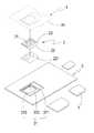
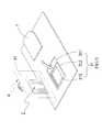
- FIG. 1is a perspective view illustrating a preferred embodiment of the present invention.
- FIG. 2is an exploded view of the preferred embodiment of the present invention.
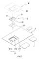
- FIG. 3is a perspective view showing a thin-film chip according to the preferred embodiment of the present invention.
- FIG. 4is a schematic view showing a fixing element according to the preferred embodiment of the present invention.
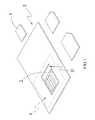
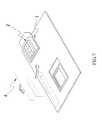
- FIG. 5is a schematic view illustrating assembling of the preferred embodiment of the present invention.
- FIG. 6is another schematic view illustrating assembling of the preferred embodiment of the present invention.
- FIG. 7is a further schematic view illustrating assembling of the preferred embodiment of the present invention.
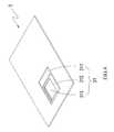
- FIG. 8is a schematic view illustrating disassembling of the preferred embodiment of the present invention.
- FIGS. 1-4are respectively a perspective view and an exploded view of a preferred embodiment of the present invention, a schematic view of a thin-film chip of the preferred embodiment of the present invention, a schematic view of a fixing element of the preferred embodiment of the present invention
- the drawingsclearly show that the present invention comprises at least one base plate 1 , at least one fixing element 3 , at least one adhesive film 4 , and at least one thin-film chip 2 .
- the fixing element 3comprises, formed in at least one side thereof, at least one fixing trough 31 corresponding to the base plate 1 .
- the fixing trough 31is divided into a first fixing trough 311 (of which the size corresponds to that of a regular SIM card), a second fixing trough 312 (of which the size corresponds to that of a micro SIM), and a third fixing trough 313 (of which the size corresponds to that of a nano SIM card). Further, trough bottoms of the first fixing trough 311 , the second fixing trough 312 , and the third fixing trough 313 are arranged to have different distances from a side wall of the base plate 1 .
- the adhesive film 4is set on one side of the fixing element 3 to cover the fixing trough 31 .
- the adhesive film 4has a side that is adjacent to the fixing element 3 and forms at least one sticky portion 41 .
- the sticky portion 41is repeatedly attachable.
- the thin-film chip 2is set in the fixing trough 31 and is bonded to the adhesive film 4 .
- the thin-film chip 2has a side that is adjacent to the adhesive film 4 and comprises a contact interface assembly 21 and an opposite side forming at least one coupling section 22 for coupling to the base plate 1 .
- the coupling section 22comprises at least one separator sheet 221 mounted thereto.
- the thin-film chip 2comprises at least one dividable section 23 that corresponds to the base plate 1 and is detachable.
- the dividable section 23has an outer perimeter having a size corresponding to the micro SIM.
- the dividable section 23has an inner perimeter having a size corresponding to the nano SIM card.
- FIGS. 1-8are respectively a perspective view and an exploded view of a preferred embodiment of the present invention, a schematic view of a thin-film chip of the preferred embodiment of the present invention, a schematic view of a fixing element of the preferred embodiment of the present invention, three schematic view illustrating assembling of the preferred embodiment of the present invention, and a schematic view illustrating disassembling of the preferred embodiment of the present invention, these drawings clearly show that to use the present invention, the adhesive film 4 is first partially peeled off to expose the fixing trough 31 . The adhesive film 4 uses the sticky portion 41 to lift the thin-film chip 2 so as to remove the thin-film chip 2 out of the fixing trough 31 .
- the separator sheet 221is then peeled off to expose the coupling section 22 and the base plate 1 is placed and fixed in one of the first fixing trough 311 , the second fixing trough 312 , and the third fixing trough 313 according to the size thereof.
- the adhesive film 4is bonded back to have the coupling section 22 of the thin-film chip 2 coupled to the base plate 1 .
- the adhesive film 4is partially peeled off again to remove the coupled thin-film chip 2 and base plate 1 .
- the size of the base plate 1is that of a regular SIM card or a micro SIM card, the assembling of the chip card is completed according to the present invention.
- the dividable section 23is detached and removed from the thin-film chip 2 to complete the assembling of the chip card according to the present invention (as shown in FIG. 8 ).
- chip card assembling structure and the method thereof according to the present inventionprovide the following features that improve the known techniques:
Landscapes
- Engineering & Computer Science (AREA)
- Computer Hardware Design (AREA)
- Microelectronics & Electronic Packaging (AREA)
- Physics & Mathematics (AREA)
- General Physics & Mathematics (AREA)
- Theoretical Computer Science (AREA)
- Credit Cards Or The Like (AREA)
Abstract
Description
The present invention generally relates to a chip card, and more particularly to a chip card assembling structure that allows unconstrained application and reduces manufacture cost and a method thereof.
A conventional chip card generally comprises a carrier plate and a chip module that are manufactured separately. In a manufacturing process, a recess is first formed in one side of the carrier plate and then, the chip module is fit into or embedded in the recess to complete the manufacture. This process is complicated and time-consuming.
The chip cards that are currently available in the market are divided into three types, including a regular SIM card, a micro SIM card, and a nano SIM card, of which the sizes and dimensions are different. In manufacturing a conventional chip card, each time a specific size of the carrier plate and chip module is manufactured and then assembled individually, so that the manufacture cost is high. Further, the application or use of the conventional chip cards is constrained by the size and dimension thereof. In addition, inventory cost is also high.
It is thus a challenge for the manufacturers of the field and the present inventor to overcome the above-discussed problems and drawbacks.
In view of the above problems, through intense research and study of related information, as well as repeated trials and improvements, an invention related to a chip card assembling structure that allows unconstrained application and reduces manufacture cost and a method thereof are accomplished.
The primary object of the present invention is to use with various sizes and specifications.
Another object of the present invention is to reduce the cost required for manufacture.
To achieve the above objects, the present invention comprises at least a base plate and at least a fixing element. The fixing element has at least a side forming at least a fixing trough corresponding to the base plate. At least one adhesive film is disposed on one side of the fixing element to cover the fixing trough. At least one thin-film chip received in the fixing trough and bonded to the adhesive film. To use the present invention, the adhesive film is lifted to lift up the thin-film chip. The base plate is placed into the fixing trough to have the base plate fixed. The adhesive film is set back to have the thin-film chip move toward the fixing trough so that the thin-film chip can be coupled to the base plate. The adhesive film is lifted again to remove the coupled thin-film chip and base plate, so that the position where the thin-film chip is set is precise and correct. With the above-described technique, the problems that the application of a conventional film-attached chip card is constrained and the manufacture cost is relatively high can be overcome to achieve a practical advantage of unconstrained application and saving of manufacture cost.
The foregoing objectives and summary provide only a brief introduction to the present invention. To fully appreciate these and other objects of the present invention as well as the invention itself, all of which will become apparent to those skilled in the art, the following detailed description of the invention and the claims should be read in conjunction with the accompanying drawings. Throughout the specification and drawings identical reference numerals refer to identical or similar parts.
Many other advantages and features of the present invention will become manifest to those versed in the art upon making reference to the detailed description and the accompanying sheets of drawings in which a preferred structural embodiment incorporating the principles of the present invention is shown by way of illustrative example.
The following descriptions are exemplary embodiments only, and are not intended to limit the scope, applicability or configuration of the invention in any way. Rather, the following description provides a convenient illustration for implementing exemplary embodiments of the invention. Various changes to the described embodiments may be made in the function and arrangement of the elements described without departing from the scope of the invention as set forth in the appended claims.
Referring toFIGS. 1-4 , which are respectively a perspective view and an exploded view of a preferred embodiment of the present invention, a schematic view of a thin-film chip of the preferred embodiment of the present invention, a schematic view of a fixing element of the preferred embodiment of the present invention, the drawings clearly show that the present invention comprises at least onebase plate 1, at least onefixing element 3, at least oneadhesive film 4, and at least one thin-film chip 2. In the instant embodiment, explanation will be given with reference to three different sizes specified for a regular SIM card, a micro SIM card, and a nano SIM card. Thefixing element 3 comprises, formed in at least one side thereof, at least onefixing trough 31 corresponding to thebase plate 1. Thefixing trough 31 is divided into a first fixing trough311 (of which the size corresponds to that of a regular SIM card), a second fixing trough312 (of which the size corresponds to that of a micro SIM), and a third fixing trough313 (of which the size corresponds to that of a nano SIM card). Further, trough bottoms of thefirst fixing trough 311, thesecond fixing trough 312, and thethird fixing trough 313 are arranged to have different distances from a side wall of thebase plate 1. Theadhesive film 4 is set on one side of thefixing element 3 to cover thefixing trough 31. Theadhesive film 4 has a side that is adjacent to thefixing element 3 and forms at least onesticky portion 41. Thesticky portion 41 is repeatedly attachable. The thin-film chip 2 is set in thefixing trough 31 and is bonded to theadhesive film 4. The thin-film chip 2 has a side that is adjacent to theadhesive film 4 and comprises acontact interface assembly 21 and an opposite side forming at least onecoupling section 22 for coupling to thebase plate 1. Thecoupling section 22 comprises at least oneseparator sheet 221 mounted thereto. The thin-film chip 2 comprises at least onedividable section 23 that corresponds to thebase plate 1 and is detachable. Thedividable section 23 has an outer perimeter having a size corresponding to the micro SIM. Thedividable section 23 has an inner perimeter having a size corresponding to the nano SIM card. Further, the above description is given to only one possible configuration of the present invention, and other configurations are also available.
Referring toFIGS. 1-8 , which are respectively a perspective view and an exploded view of a preferred embodiment of the present invention, a schematic view of a thin-film chip of the preferred embodiment of the present invention, a schematic view of a fixing element of the preferred embodiment of the present invention, three schematic view illustrating assembling of the preferred embodiment of the present invention, and a schematic view illustrating disassembling of the preferred embodiment of the present invention, these drawings clearly show that to use the present invention, theadhesive film 4 is first partially peeled off to expose thefixing trough 31. Theadhesive film 4 uses thesticky portion 41 to lift the thin-film chip 2 so as to remove the thin-film chip 2 out of thefixing trough 31. Theseparator sheet 221 is then peeled off to expose thecoupling section 22 and thebase plate 1 is placed and fixed in one of thefirst fixing trough 311, thesecond fixing trough 312, and thethird fixing trough 313 according to the size thereof. Theadhesive film 4 is bonded back to have thecoupling section 22 of the thin-film chip 2 coupled to thebase plate 1. Theadhesive film 4 is partially peeled off again to remove the coupled thin-film chip 2 andbase plate 1. When the size of thebase plate 1 is that of a regular SIM card or a micro SIM card, the assembling of the chip card is completed according to the present invention.
Further, when thebase plate 1 has a size that is the size of a nano SIM card, thedividable section 23 is detached and removed from the thin-film chip 2 to complete the assembling of the chip card according to the present invention (as shown inFIG. 8 ).
Thus, the chip card assembling structure and the method thereof according to the present invention provide the following features that improve the known techniques:
(1) The collaborative arrangement of thebase plate 1 and theadhesive film 4 and that of the thin-film chip 2 and thebase plate 1 provide the availability for manufacture of different sizes, specifications, and individuals so that the present invention may achieve a practical advantage of unconstrained application and reduction of manufacture cost.
(2) The detachability of thedividable section 23 from the thin-film chip 2 provides the availability for manufacture of different sizes, specifications, and individuals so that the present invention may achieve a practical advantage of unconstrained application and reduction of manufacture cost.
It will be understood that each of the elements described above, or two or more together may also find a useful application in other types of methods differing from the type described above.
While certain novel features of this invention have been shown and described and are pointed out in the annexed claim, it is not intended to be limited to the details above, since it will be understood that various omissions, modifications, substitutions and changes in the forms and details of the device illustrated and in its operation can be made by those skilled in the art without departing in any way from the spirit of the present invention.
Claims (5)
1. A method of forming a chip card assembly including steps of:
providing a fixing element with a fixing trough;
an adhesive film affixed to a surface of the fixing element covering the fixing trough;
wherein said thin film chip is further affixed to the adhesive film;
partially peeling off said adhesive film from the fixing element to expose said fixing trough and lifting said thin film chip;
providing a base plate and disposing said base plate in said fixing trough;
re-bonding the adhesive film onto the fixing element to couple said thin film chip to said base plate to form a chip card assembly; and
re-peeling said adhesive film to remove said chip card assembly from said fixing trough.
2. The method of forming a chip card assembly as claimed inclaim 1 , wherein said thin-film chip has a side that is adjacent to said adhesive film and comprises a contact interface assembly and an opposite side that comprises at least one coupling section for coupling with said base plate, said coupling section comprising at least one separator sheet.
3. The method of forming a chip card assembly as claimed inclaim 1 , wherein said thin-film chip comprises at least one dividable section that corresponds to said base plate and is detachable.
4. The method of forming a chip card assembly as claimed inclaim 1 , wherein said fixing trough is divided into a first fixing trough, a second fixing trough, and a third fixing trough, said first fixing trough, said second fixing trough, and said third fixing trough having trough bottoms that are at different distances from a side of said base plate.
5. The method of forming a chip card assembly as claimed inclaim 1 , wherein said adhesive film has a side that is adjacent to said fixing element and comprises at least one sticky portion, said sticky portion being repeatedly attachable.
Priority Applications (2)
| Application Number | Priority Date | Filing Date | Title |
|---|---|---|---|
| US13/958,609US9195929B2 (en) | 2013-08-05 | 2013-08-05 | Chip card assembling structure and method thereof |
| US14/681,109US9830551B2 (en) | 2013-08-05 | 2015-04-08 | Chip card assembling structure and method thereof |
Applications Claiming Priority (1)
| Application Number | Priority Date | Filing Date | Title |
|---|---|---|---|
| US13/958,609US9195929B2 (en) | 2013-08-05 | 2013-08-05 | Chip card assembling structure and method thereof |
Related Child Applications (1)
| Application Number | Title | Priority Date | Filing Date |
|---|---|---|---|
| US14/681,109DivisionUS9830551B2 (en) | 2013-08-05 | 2015-04-08 | Chip card assembling structure and method thereof |
Publications (2)
| Publication Number | Publication Date |
|---|---|
| US20150034232A1 US20150034232A1 (en) | 2015-02-05 |
| US9195929B2true US9195929B2 (en) | 2015-11-24 |
Family
ID=52426570
Family Applications (2)
| Application Number | Title | Priority Date | Filing Date |
|---|---|---|---|
| US13/958,609Active2033-12-10US9195929B2 (en) | 2013-08-05 | 2013-08-05 | Chip card assembling structure and method thereof |
| US14/681,109Active2034-03-16US9830551B2 (en) | 2013-08-05 | 2015-04-08 | Chip card assembling structure and method thereof |
Family Applications After (1)
| Application Number | Title | Priority Date | Filing Date |
|---|---|---|---|
| US14/681,109Active2034-03-16US9830551B2 (en) | 2013-08-05 | 2015-04-08 | Chip card assembling structure and method thereof |
Country Status (1)
| Country | Link |
|---|---|
| US (2) | US9195929B2 (en) |
Cited By (2)
| Publication number | Priority date | Publication date | Assignee | Title |
|---|---|---|---|---|
| USD930000S1 (en)* | 2018-10-12 | 2021-09-07 | Huawei Technologies Co., Ltd. | Memory card |
| USD930001S1 (en) | 2018-02-01 | 2021-09-07 | Huawei Technologies Co., Ltd. | Card |
Families Citing this family (3)
| Publication number | Priority date | Publication date | Assignee | Title |
|---|---|---|---|---|
| CN102655306B (en)* | 2012-04-20 | 2014-06-04 | 华为终端有限公司 | Fool-proof structure of common card slot space |
| CN109849352B (en)* | 2019-01-04 | 2024-04-30 | 通达(厦门)精密橡塑有限公司 | Spring assembly device for double-card mobile phone card holder |
| US10817868B1 (en)* | 2020-02-27 | 2020-10-27 | Capital One Services, Llc | Payment card with removable cartridge |
Citations (67)
| Publication number | Priority date | Publication date | Assignee | Title |
|---|---|---|---|---|
| US4298120A (en)* | 1978-12-26 | 1981-11-03 | Murata Manufacturing Co., Ltd. | Chip-like electronic component series and method for supplying chip-like electronic components |
| US4394844A (en)* | 1981-05-04 | 1983-07-26 | Wood Laurior A | Chip coater |
| US4472218A (en)* | 1983-12-23 | 1984-09-18 | At&T Technologies, Inc. | Removing articles from an adhesive web |
| US4725924A (en)* | 1985-04-10 | 1988-02-16 | Em Microelectronic-Marin Sa | Electronic unit especially for microcircuit cards and card comprising such a unit |
| US4737395A (en)* | 1983-11-29 | 1988-04-12 | Ibiden Co. Ltd. | Printed wiring board for mounting electronic parts and process for producing the same |
| US4749982A (en)* | 1984-06-19 | 1988-06-07 | Casio Computer Co., Ltd. | Intelligent card |
| US4951119A (en)* | 1988-02-08 | 1990-08-21 | Shinko Electric Industries, Co., Ltd. | Lead frame for semiconductor devices |
| US4996411A (en)* | 1986-07-24 | 1991-02-26 | Schlumberger Industries | Method of manufacturing a card having electronic memory and a card obtained by performing said method |
| US5034083A (en)* | 1989-10-16 | 1991-07-23 | Xerox Corporation | Process and apparatus for assembling smaller scanning or printing arrays together to form an extended array |
| US5048179A (en)* | 1986-05-23 | 1991-09-17 | Ricoh Company, Ltd. | IC chip mounting method |
| US6073334A (en)* | 1997-07-22 | 2000-06-13 | Fuji Machine Mfg. Co., Ltd. | Tape connecting method, member, and tool |
| US6188580B1 (en)* | 1996-08-08 | 2001-02-13 | Infineon Technologies Ag | Smart card and semiconductor chip for use in a smart card |
| US6338980B1 (en)* | 1999-08-13 | 2002-01-15 | Citizen Watch Co., Ltd. | Method for manufacturing chip-scale package and manufacturing IC chip |
| US20020016020A1 (en)* | 2000-03-28 | 2002-02-07 | Mitsuo Usami | Method of manufacturing an electronic device |
| US20020030285A1 (en)* | 1997-09-01 | 2002-03-14 | Kiyoshi Sawada | Bonding method of small parts and module of combined small parts |
| US6413798B2 (en)* | 1998-01-18 | 2002-07-02 | Kabushiki Kaisha Toshiba | Package having very thin semiconductor chip, multichip module assembled by the package, and method for manufacturing the same |
| US6421246B1 (en)* | 1999-10-01 | 2002-07-16 | Itt Manufacturing Enterprises, Inc. | PC card that receives chip card |
| US6478919B1 (en)* | 1999-06-09 | 2002-11-12 | Sony Corporation | Functional film sticking apparatus and functional film sticking method |
| US20030036249A1 (en)* | 2001-08-06 | 2003-02-20 | Bauer Donald G. | Chip alignment and placement apparatus for integrated circuit, MEMS, photonic or other devices |
| US20030218868A1 (en)* | 2002-05-24 | 2003-11-27 | Wen-Wen Chiu | Multi-chip module |
| US20030227075A1 (en)* | 2002-06-10 | 2003-12-11 | Hitachi, Ltd. | Memory card and a method of manufacturing the same |
| US20040048419A1 (en)* | 2001-11-30 | 2004-03-11 | Masahiko Kitamura | Production method for semiconductor chip |
| US20040090829A1 (en)* | 2001-02-28 | 2004-05-13 | Tomomi Miura | Memory card and its manufacturing method |
| US20040104469A1 (en)* | 2000-10-02 | 2004-06-03 | Yoshihiko Yagi | Card type recording medium and production method therefor |
| US20040259331A1 (en)* | 2003-06-20 | 2004-12-23 | Mitsuhiko Ogihara | Method of manufacturing a semiconductor device |
| US20050062135A1 (en)* | 2001-12-25 | 2005-03-24 | Takashi Tase | Semiconductor device and method for fabricating the same |
| US6894373B2 (en)* | 2002-05-23 | 2005-05-17 | Alps Electric Co., Ltd. | Surface-mounting type of electronic circuit unit suitable for miniaturization and a method for fabricating the unit |
| US20050245001A1 (en)* | 2004-04-28 | 2005-11-03 | Nokia Corporation | Shielded laminated structure with embedded chips |
| US20050269717A1 (en)* | 2004-06-02 | 2005-12-08 | Lintec Corporation | Pressure sensitive adhesive sheet for use in semiconductor working and method for producing semiconductor chip |
| US20050287846A1 (en)* | 2004-06-29 | 2005-12-29 | Semiconductor Energy Laboratory Co., Ltd. | Method for manufacturing thin film integrated circuit, and element substrate |
| US20060115989A1 (en)* | 2003-05-29 | 2006-06-01 | The Furukawa Electric Co., Ltd. | Method of manufacturing a thin-film circuit substrate having penetrating structure, and protecting adhesive tape |
| US20060243620A1 (en)* | 2005-02-03 | 2006-11-02 | Shin-Etsu Polymer Co., Ltd. | Fixing carrier, fixing carrier manufacturing method, method of using fixing carriers and substrate storage container |
| US20060266718A1 (en)* | 2005-05-06 | 2006-11-30 | Wolfgang Tischner | Device for stabilizing a workpiece during processing |
| US20060273420A1 (en)* | 2005-06-02 | 2006-12-07 | Michael Bauer | Semiconductor sensor component including a sensor chip and methods for the manufacturing thereof |
| US20070018446A1 (en)* | 2003-08-28 | 2007-01-25 | Toppan Forms Co., Ltd. | Speech-message delivery sheet, its manufacturing method, and power supply circuit |
| US20070026640A1 (en)* | 2005-07-29 | 2007-02-01 | Priewasser Karl H | Method for adhering protecting tape of wafer and adhering apparatus |
| US20070048179A1 (en)* | 2003-09-12 | 2007-03-01 | Machiko Fujita | Chip, device using the chip, and method of using the same |
| US20070181245A1 (en)* | 2006-02-09 | 2007-08-09 | Nitto Denko Corporation | Work bonding and supporting method and work bonding and supporting apparatus using the same |
| US20070285543A1 (en)* | 2006-05-23 | 2007-12-13 | Matsushita Electric Industrial Co., Ltd. | Solid-state imaging device and method of manufacturing the same |
| US20080057253A1 (en)* | 2006-08-29 | 2008-03-06 | Nitto Denko Corporation | Adhesive sheet for water jet laser dicing |
| US20080057270A1 (en)* | 2006-08-29 | 2008-03-06 | Nitto Denko Corporation | Adhesive sheet for water jet laser dicing |
| US20080182095A1 (en)* | 2006-11-06 | 2008-07-31 | Nitto Denko Corporation | Adhesive sheet for water jet laser dicing |
| US20090056981A1 (en)* | 2005-04-18 | 2009-03-05 | Toyo Boseki Kabushiki Kaisha | Thin film-laminated polyimide film and flexible printed wiring board |
| US20090315320A1 (en)* | 2006-09-26 | 2009-12-24 | Advanced Microelectronic And Automation Technology Ltd. | Inlays for security documents |
| US20100029060A1 (en)* | 2008-08-04 | 2010-02-04 | Katsuhiko Kamiya | Dicing die-bonding film |
| US20100029061A1 (en)* | 2008-08-04 | 2010-02-04 | Katsuhiko Kamiya | Dicing die-bonding film |
| US20100029059A1 (en)* | 2008-08-01 | 2010-02-04 | Takeshi Matsumura | Dicing die-bonding film |
| US20100028687A1 (en)* | 2008-08-04 | 2010-02-04 | Katsuhiko Kamiya | Dicing die-bonding film |
| US20100122757A1 (en)* | 2008-11-18 | 2010-05-20 | Robert Edward Lionetti | Tire and electronic device assembly |
| US7811863B1 (en)* | 2006-10-26 | 2010-10-12 | Bridge Semiconductor Corporation | Method of making a semiconductor chip assembly with metal pillar and encapsulant grinding and heat sink attachment |
| US20100289283A1 (en)* | 2006-10-18 | 2010-11-18 | Lintec Corporation | Chip Pickup Method and Chip Pickup Apparatus |
| US20100314894A1 (en)* | 2006-10-18 | 2010-12-16 | Lintec Corporation | Fixed Jig, Chip Pickup Method and Chip Pickup Apparatus |
| US7875501B2 (en)* | 2006-03-15 | 2011-01-25 | Shin-Etsu Polymer Co., Ltd. | Holding jig, semiconductor wafer grinding method, semiconductor wafer protecting structure and semiconductor wafer grinding method and semiconductor chip fabrication method using the structure |
| US20110053346A1 (en)* | 2008-01-18 | 2011-03-03 | Nitto Denko Corporation | Dicing/die bonding film |
| US20110104873A1 (en)* | 2008-01-18 | 2011-05-05 | Nitto Denko Corporation | Dicing/die bonding film |
| US7993983B1 (en)* | 2003-11-17 | 2011-08-09 | Bridge Semiconductor Corporation | Method of making a semiconductor chip assembly with chip and encapsulant grinding |
| US8009047B2 (en)* | 2007-10-11 | 2011-08-30 | Hitachi, Ltd. | RFID tag |
| US20110217501A1 (en)* | 2010-03-05 | 2011-09-08 | Yuichiro Shishido | Dicing die-bonding film |
| US20110256666A1 (en)* | 2010-04-16 | 2011-10-20 | Yuki Sugo | Thermosetting die bond film, dicing die bond film and semiconductor device |
| US20120070960A1 (en)* | 2010-09-21 | 2012-03-22 | Shuhei Murata | Dicing die bond film, method of manufacturing dicing die bond film, and method of manufacturing semiconductor device |
| US20120104102A1 (en)* | 2009-04-10 | 2012-05-03 | Arjowiggins Security | Sectional Documents Comprising a Structure Equipped with a Watermark or Pseudo-Watermark and Associated Process |
| US8181880B2 (en)* | 2004-06-16 | 2012-05-22 | Korea Minting & Security Printing Corporation | Combi-card and method for making the same |
| US20120217606A1 (en)* | 2011-02-28 | 2012-08-30 | Sony Corporation | Method of manufacturing solid-state imaging element, solid-state imaging element and electronic apparatus |
| US20130181037A1 (en)* | 2010-06-30 | 2013-07-18 | Shinkawa Ltd. | Electronic component mounting apparatus and the same method thereof |
| US20130330910A1 (en)* | 2010-10-01 | 2013-12-12 | Shumpei Tanaka | Dicing die bond film and method of manufacturing semiconductor device |
| US20140175070A1 (en)* | 2012-12-25 | 2014-06-26 | Disco Corporation | Laser processing method and fine particle layer forming agent |
| US20140175624A1 (en)* | 2012-12-20 | 2014-06-26 | Infineon Technologies Ag | Method for manufacturing a chip arrangement, and chip arrangement |
Family Cites Families (1)
| Publication number | Priority date | Publication date | Assignee | Title |
|---|---|---|---|---|
| DE102010025774A1 (en)* | 2010-07-01 | 2012-01-05 | Giesecke & Devrient Gmbh | Method of making an inlay for a portable data carrier and inlay |
- 2013
- 2013-08-05USUS13/958,609patent/US9195929B2/enactiveActive
- 2015
- 2015-04-08USUS14/681,109patent/US9830551B2/enactiveActive
Patent Citations (105)
| Publication number | Priority date | Publication date | Assignee | Title |
|---|---|---|---|---|
| US4298120A (en)* | 1978-12-26 | 1981-11-03 | Murata Manufacturing Co., Ltd. | Chip-like electronic component series and method for supplying chip-like electronic components |
| US4394844A (en)* | 1981-05-04 | 1983-07-26 | Wood Laurior A | Chip coater |
| US4737395A (en)* | 1983-11-29 | 1988-04-12 | Ibiden Co. Ltd. | Printed wiring board for mounting electronic parts and process for producing the same |
| US4773955A (en)* | 1983-11-29 | 1988-09-27 | Ibiden Co. Ltd. | Printed wiring board for mounting electronic parts and process for producing the same |
| US4472218A (en)* | 1983-12-23 | 1984-09-18 | At&T Technologies, Inc. | Removing articles from an adhesive web |
| US4749982A (en)* | 1984-06-19 | 1988-06-07 | Casio Computer Co., Ltd. | Intelligent card |
| US4725924A (en)* | 1985-04-10 | 1988-02-16 | Em Microelectronic-Marin Sa | Electronic unit especially for microcircuit cards and card comprising such a unit |
| US5048179A (en)* | 1986-05-23 | 1991-09-17 | Ricoh Company, Ltd. | IC chip mounting method |
| US4996411A (en)* | 1986-07-24 | 1991-02-26 | Schlumberger Industries | Method of manufacturing a card having electronic memory and a card obtained by performing said method |
| US4951119A (en)* | 1988-02-08 | 1990-08-21 | Shinko Electric Industries, Co., Ltd. | Lead frame for semiconductor devices |
| US5034083A (en)* | 1989-10-16 | 1991-07-23 | Xerox Corporation | Process and apparatus for assembling smaller scanning or printing arrays together to form an extended array |
| US6188580B1 (en)* | 1996-08-08 | 2001-02-13 | Infineon Technologies Ag | Smart card and semiconductor chip for use in a smart card |
| US6073334A (en)* | 1997-07-22 | 2000-06-13 | Fuji Machine Mfg. Co., Ltd. | Tape connecting method, member, and tool |
| US6687966B2 (en)* | 1997-07-22 | 2004-02-10 | Fuji Machine Mfg. Co., Ltd. | Tape connecting method, member and tool |
| US6364567B1 (en)* | 1997-07-22 | 2002-04-02 | Fuji Machine Mfg. Co., Ltd. | Tape connecting method, member, and tool |
| US20020038584A1 (en)* | 1997-07-22 | 2002-04-04 | Fuji Machine Mfg. Co., Ltd. | Tape connecting method, member and tool |
| US6683376B2 (en)* | 1997-09-01 | 2004-01-27 | Fanuc Ltd. | Direct bonding of small parts and module of combined small parts without an intermediate layer inbetween |
| US20020030285A1 (en)* | 1997-09-01 | 2002-03-14 | Kiyoshi Sawada | Bonding method of small parts and module of combined small parts |
| US6413798B2 (en)* | 1998-01-18 | 2002-07-02 | Kabushiki Kaisha Toshiba | Package having very thin semiconductor chip, multichip module assembled by the package, and method for manufacturing the same |
| US6478919B1 (en)* | 1999-06-09 | 2002-11-12 | Sony Corporation | Functional film sticking apparatus and functional film sticking method |
| US6338980B1 (en)* | 1999-08-13 | 2002-01-15 | Citizen Watch Co., Ltd. | Method for manufacturing chip-scale package and manufacturing IC chip |
| US6421246B1 (en)* | 1999-10-01 | 2002-07-16 | Itt Manufacturing Enterprises, Inc. | PC card that receives chip card |
| US20040063243A1 (en)* | 2000-03-28 | 2004-04-01 | Mitsuo Usami | Method of manufacturing an electronic device |
| US7056769B2 (en)* | 2000-03-28 | 2006-06-06 | Hitachi, Ltd. | Method of manufacturing an electronic device |
| US20060189040A1 (en)* | 2000-03-28 | 2006-08-24 | Mitsuo Usami | Method of manufacturing an electronic device |
| US6660557B2 (en)* | 2000-03-28 | 2003-12-09 | Hitachi, Ltd. | Method of manufacturing an electronic device |
| US20020016020A1 (en)* | 2000-03-28 | 2002-02-07 | Mitsuo Usami | Method of manufacturing an electronic device |
| US7459341B2 (en)* | 2000-03-28 | 2008-12-02 | Hitachi, Ltd. | Method of manufacturing an electronic device |
| US20040104469A1 (en)* | 2000-10-02 | 2004-06-03 | Yoshihiko Yagi | Card type recording medium and production method therefor |
| US6985363B2 (en)* | 2000-10-02 | 2006-01-10 | Matsushita Electric Industrial Co., Ltd. | Card type recording medium and production method therefor |
| US20040090829A1 (en)* | 2001-02-28 | 2004-05-13 | Tomomi Miura | Memory card and its manufacturing method |
| US20030036249A1 (en)* | 2001-08-06 | 2003-02-20 | Bauer Donald G. | Chip alignment and placement apparatus for integrated circuit, MEMS, photonic or other devices |
| US20040048419A1 (en)* | 2001-11-30 | 2004-03-11 | Masahiko Kitamura | Production method for semiconductor chip |
| US6852608B2 (en)* | 2001-11-30 | 2005-02-08 | Disco Corporation | Production method for semiconductor chip |
| US20050062135A1 (en)* | 2001-12-25 | 2005-03-24 | Takashi Tase | Semiconductor device and method for fabricating the same |
| US6894373B2 (en)* | 2002-05-23 | 2005-05-17 | Alps Electric Co., Ltd. | Surface-mounting type of electronic circuit unit suitable for miniaturization and a method for fabricating the unit |
| US20030218868A1 (en)* | 2002-05-24 | 2003-11-27 | Wen-Wen Chiu | Multi-chip module |
| US6924547B2 (en)* | 2002-06-10 | 2005-08-02 | Renesas Technology Corp. | Memory card |
| US20030227075A1 (en)* | 2002-06-10 | 2003-12-11 | Hitachi, Ltd. | Memory card and a method of manufacturing the same |
| US7413965B2 (en)* | 2003-05-29 | 2008-08-19 | The Furukawa Electric Co., Ltd. | Method of manufacturing a thin-film circuit substrate having penetrating structure, and protecting adhesive tape |
| US20060115989A1 (en)* | 2003-05-29 | 2006-06-01 | The Furukawa Electric Co., Ltd. | Method of manufacturing a thin-film circuit substrate having penetrating structure, and protecting adhesive tape |
| US6913985B2 (en)* | 2003-06-20 | 2005-07-05 | Oki Data Corporation | Method of manufacturing a semiconductor device |
| US20040259331A1 (en)* | 2003-06-20 | 2004-12-23 | Mitsuhiko Ogihara | Method of manufacturing a semiconductor device |
| US20070018446A1 (en)* | 2003-08-28 | 2007-01-25 | Toppan Forms Co., Ltd. | Speech-message delivery sheet, its manufacturing method, and power supply circuit |
| US7840017B2 (en)* | 2003-08-28 | 2010-11-23 | Toppan Forms Co., Ltd. | Audio message transfer sheet and manufacturing method thereof, and power supply circuit |
| US7785533B2 (en)* | 2003-09-12 | 2010-08-31 | Nec Corporation | Chip, device using the chip, and method of using the same |
| US20070048179A1 (en)* | 2003-09-12 | 2007-03-01 | Machiko Fujita | Chip, device using the chip, and method of using the same |
| US7993983B1 (en)* | 2003-11-17 | 2011-08-09 | Bridge Semiconductor Corporation | Method of making a semiconductor chip assembly with chip and encapsulant grinding |
| US20050245001A1 (en)* | 2004-04-28 | 2005-11-03 | Nokia Corporation | Shielded laminated structure with embedded chips |
| US6974724B2 (en)* | 2004-04-28 | 2005-12-13 | Nokia Corporation | Shielded laminated structure with embedded chips |
| US7351645B2 (en)* | 2004-06-02 | 2008-04-01 | Lintec Corporation | Pressure sensitive adhesive sheet for use in semiconductor working and method for producing semiconductor chip |
| US20050269717A1 (en)* | 2004-06-02 | 2005-12-08 | Lintec Corporation | Pressure sensitive adhesive sheet for use in semiconductor working and method for producing semiconductor chip |
| US8181880B2 (en)* | 2004-06-16 | 2012-05-22 | Korea Minting & Security Printing Corporation | Combi-card and method for making the same |
| US7452786B2 (en)* | 2004-06-29 | 2008-11-18 | Semiconductor Energy Laboratory Co., Ltd. | Method for manufacturing thin film integrated circuit, and element substrate |
| US7939385B2 (en)* | 2004-06-29 | 2011-05-10 | Semiconductor Energy Laboratory Co., Ltd. | Method for manufacturing thin film integrated circuit, and element substrate |
| US20050287846A1 (en)* | 2004-06-29 | 2005-12-29 | Semiconductor Energy Laboratory Co., Ltd. | Method for manufacturing thin film integrated circuit, and element substrate |
| US20090050964A1 (en)* | 2004-06-29 | 2009-02-26 | Semiconductor Energy Laboratory Co., Ltd. | Method for manufacturing thin film integrated circuit, and element substrate |
| US20060243620A1 (en)* | 2005-02-03 | 2006-11-02 | Shin-Etsu Polymer Co., Ltd. | Fixing carrier, fixing carrier manufacturing method, method of using fixing carriers and substrate storage container |
| US20090056981A1 (en)* | 2005-04-18 | 2009-03-05 | Toyo Boseki Kabushiki Kaisha | Thin film-laminated polyimide film and flexible printed wiring board |
| US20060266718A1 (en)* | 2005-05-06 | 2006-11-30 | Wolfgang Tischner | Device for stabilizing a workpiece during processing |
| US7460704B2 (en)* | 2005-05-06 | 2008-12-02 | Infineon Technologies Ag | Device for stabilizing a workpiece during processing |
| US7629660B2 (en)* | 2005-06-02 | 2009-12-08 | Infineon Technologies Ag | Semiconductor sensor component including a sensor chip and methods for the manufacturing thereof |
| US20060273420A1 (en)* | 2005-06-02 | 2006-12-07 | Michael Bauer | Semiconductor sensor component including a sensor chip and methods for the manufacturing thereof |
| US20070026640A1 (en)* | 2005-07-29 | 2007-02-01 | Priewasser Karl H | Method for adhering protecting tape of wafer and adhering apparatus |
| US7520309B2 (en)* | 2005-07-29 | 2009-04-21 | Disco Corporation | Method for adhering protecting tape of wafer and adhering apparatus |
| US20120097338A1 (en)* | 2006-02-09 | 2012-04-26 | Nitto Denko Corporation | Work bonding and supporting method and work bonding and supporting apparatus using the same |
| US8110058B2 (en)* | 2006-02-09 | 2012-02-07 | Nitto Denko Corporation | Work bonding and supporting method and work bonding and supporting apparatus using the same |
| US8281838B2 (en)* | 2006-02-09 | 2012-10-09 | Nitto Denko Corporation | Work bonding and supporting method and work bonding and supporting apparatus using the same |
| US20070181245A1 (en)* | 2006-02-09 | 2007-08-09 | Nitto Denko Corporation | Work bonding and supporting method and work bonding and supporting apparatus using the same |
| US20110281509A1 (en)* | 2006-03-15 | 2011-11-17 | Lintec Corporation | Holding jig, semiconductor wafer grinding method, semiconductor wafer protecting structure and semiconductor wafer grinding method and semiconductor chip fabrication method using the structure |
| US8212345B2 (en)* | 2006-03-15 | 2012-07-03 | Shin-Etsu Polymer Co., Ltd. | Holding jig, semiconductor wafer grinding method, semiconductor wafer protecting structure and semiconductor wafer grinding method and semiconductor chip fabrication method using the structure |
| US7875501B2 (en)* | 2006-03-15 | 2011-01-25 | Shin-Etsu Polymer Co., Ltd. | Holding jig, semiconductor wafer grinding method, semiconductor wafer protecting structure and semiconductor wafer grinding method and semiconductor chip fabrication method using the structure |
| US20070285543A1 (en)* | 2006-05-23 | 2007-12-13 | Matsushita Electric Industrial Co., Ltd. | Solid-state imaging device and method of manufacturing the same |
| US20080057253A1 (en)* | 2006-08-29 | 2008-03-06 | Nitto Denko Corporation | Adhesive sheet for water jet laser dicing |
| US20080057270A1 (en)* | 2006-08-29 | 2008-03-06 | Nitto Denko Corporation | Adhesive sheet for water jet laser dicing |
| US20090315320A1 (en)* | 2006-09-26 | 2009-12-24 | Advanced Microelectronic And Automation Technology Ltd. | Inlays for security documents |
| US8608080B2 (en)* | 2006-09-26 | 2013-12-17 | Feinics Amatech Teoranta | Inlays for security documents |
| US20100314894A1 (en)* | 2006-10-18 | 2010-12-16 | Lintec Corporation | Fixed Jig, Chip Pickup Method and Chip Pickup Apparatus |
| US8182649B2 (en)* | 2006-10-18 | 2012-05-22 | Lintec Corporation | Fixed jig, chip pickup method and chip pickup apparatus |
| US20100289283A1 (en)* | 2006-10-18 | 2010-11-18 | Lintec Corporation | Chip Pickup Method and Chip Pickup Apparatus |
| US7811863B1 (en)* | 2006-10-26 | 2010-10-12 | Bridge Semiconductor Corporation | Method of making a semiconductor chip assembly with metal pillar and encapsulant grinding and heat sink attachment |
| US20080182095A1 (en)* | 2006-11-06 | 2008-07-31 | Nitto Denko Corporation | Adhesive sheet for water jet laser dicing |
| US8009047B2 (en)* | 2007-10-11 | 2011-08-30 | Hitachi, Ltd. | RFID tag |
| US20110104873A1 (en)* | 2008-01-18 | 2011-05-05 | Nitto Denko Corporation | Dicing/die bonding film |
| US8617928B2 (en)* | 2008-01-18 | 2013-12-31 | Nitto Denko Corporation | Dicing/die bonding film |
| US20110053346A1 (en)* | 2008-01-18 | 2011-03-03 | Nitto Denko Corporation | Dicing/die bonding film |
| US20100029059A1 (en)* | 2008-08-01 | 2010-02-04 | Takeshi Matsumura | Dicing die-bonding film |
| US20100029061A1 (en)* | 2008-08-04 | 2010-02-04 | Katsuhiko Kamiya | Dicing die-bonding film |
| US20100029060A1 (en)* | 2008-08-04 | 2010-02-04 | Katsuhiko Kamiya | Dicing die-bonding film |
| US8119236B2 (en)* | 2008-08-04 | 2012-02-21 | Nitto Denko Corporation | Dicing die-bonding film |
| US20100028687A1 (en)* | 2008-08-04 | 2010-02-04 | Katsuhiko Kamiya | Dicing die-bonding film |
| US8955759B2 (en)* | 2008-08-29 | 2015-02-17 | Féinics AmaTech Tearanta | Inlays for security documents |
| US20140060722A1 (en)* | 2008-08-29 | 2014-03-06 | David Finn | Inlays for security documents |
| US20100122757A1 (en)* | 2008-11-18 | 2010-05-20 | Robert Edward Lionetti | Tire and electronic device assembly |
| US20120104102A1 (en)* | 2009-04-10 | 2012-05-03 | Arjowiggins Security | Sectional Documents Comprising a Structure Equipped with a Watermark or Pseudo-Watermark and Associated Process |
| US20110217501A1 (en)* | 2010-03-05 | 2011-09-08 | Yuichiro Shishido | Dicing die-bonding film |
| US20110256666A1 (en)* | 2010-04-16 | 2011-10-20 | Yuki Sugo | Thermosetting die bond film, dicing die bond film and semiconductor device |
| US20130181037A1 (en)* | 2010-06-30 | 2013-07-18 | Shinkawa Ltd. | Electronic component mounting apparatus and the same method thereof |
| US20120070960A1 (en)* | 2010-09-21 | 2012-03-22 | Shuhei Murata | Dicing die bond film, method of manufacturing dicing die bond film, and method of manufacturing semiconductor device |
| US20130330910A1 (en)* | 2010-10-01 | 2013-12-12 | Shumpei Tanaka | Dicing die bond film and method of manufacturing semiconductor device |
| US20120217606A1 (en)* | 2011-02-28 | 2012-08-30 | Sony Corporation | Method of manufacturing solid-state imaging element, solid-state imaging element and electronic apparatus |
| US8878116B2 (en)* | 2011-02-28 | 2014-11-04 | Sony Corporation | Method of manufacturing solid-state imaging element, solid-state imaging element and electronic apparatus |
| US20140175624A1 (en)* | 2012-12-20 | 2014-06-26 | Infineon Technologies Ag | Method for manufacturing a chip arrangement, and chip arrangement |
| US8956918B2 (en)* | 2012-12-20 | 2015-02-17 | Infineon Technologies Ag | Method of manufacturing a chip arrangement comprising disposing a metal structure over a carrier |
| US20140175070A1 (en)* | 2012-12-25 | 2014-06-26 | Disco Corporation | Laser processing method and fine particle layer forming agent |
Cited By (3)
| Publication number | Priority date | Publication date | Assignee | Title |
|---|---|---|---|---|
| USD930001S1 (en) | 2018-02-01 | 2021-09-07 | Huawei Technologies Co., Ltd. | Card |
| USD951956S1 (en) | 2018-02-01 | 2022-05-17 | Huawei Technologies Co., Ltd. | Memory card |
| USD930000S1 (en)* | 2018-10-12 | 2021-09-07 | Huawei Technologies Co., Ltd. | Memory card |
Also Published As
| Publication number | Publication date |
|---|---|
| US20150034232A1 (en) | 2015-02-05 |
| US20150213354A1 (en) | 2015-07-30 |
| US9830551B2 (en) | 2017-11-28 |
Similar Documents
| Publication | Publication Date | Title |
|---|---|---|
| US9830551B2 (en) | Chip card assembling structure and method thereof | |
| KR102756631B1 (en) | Metal dual interface card | |
| USD613276S1 (en) | Set of waveguide assisted antenna elements for RFID tags | |
| USD605641S1 (en) | Waveguide assisted strip antenna for RFID tags | |
| USD606057S1 (en) | Set of waveguide assisted antenna elements for RFID tags | |
| USD606056S1 (en) | Waveguide assisted core antenna for RFID tags | |
| US20130201646A1 (en) | Card adaptor apparatus | |
| CN109417218A (en) | Loop antenna module and jig for manufacturing the same | |
| EP2490157A3 (en) | Reversible thermosensitive recording medium and method for producing the same | |
| KR20090079196A (en) | Chip Module for RFID System | |
| WO2009004728A1 (en) | Rifd tag and manufacturing method of the rifd tag | |
| US8360255B2 (en) | Integrally formed shelf | |
| KR20170064850A (en) | Film for protecting front part of portable device and manufacturing method thereof | |
| USD662041S1 (en) | Pin striped thin film solar module for laptop personal computer | |
| EP4189599A1 (en) | Identification card | |
| GB2517683A (en) | Chip card assembling structure and method thereof | |
| TWI494861B (en) | Chip card combination structure and method thereof | |
| KR101321059B1 (en) | Transfer carrier for graphite transfering | |
| TWM479460U (en) | Chip card combination structure | |
| US20140113505A1 (en) | Fixing sheet and electronic apparatus | |
| JP2013089843A (en) | Thermal conductive sheet | |
| US9292781B2 (en) | Installation card for smart overlay and installation method using the same | |
| WO2011118905A3 (en) | Method for manufacturing a smart card | |
| CN202523096U (en) | Metal-resistant electronic tag | |
| KR102119564B1 (en) | Adhesive Agent MAnufacturing Method for Battery case and Adhesive Agent for Battery case using the same |
Legal Events
| Date | Code | Title | Description |
|---|---|---|---|
| AS | Assignment | Owner name:A-MEN TECHNOLOGY CORPORATION, TAIWAN Free format text:ASSIGNMENT OF ASSIGNORS INTEREST;ASSIGNOR:WANG, PEN-LO;REEL/FRAME:030938/0293 Effective date:20130731 | |
| STCF | Information on status: patent grant | Free format text:PATENTED CASE | |
| AS | Assignment | Owner name:ABANCAST LIMITED, VIRGIN ISLANDS, BRITISH Free format text:ASSIGNMENT OF ASSIGNORS INTEREST;ASSIGNOR:A-MEN TECHNOLOGY CORPORATION;REEL/FRAME:038542/0012 Effective date:20160502 | |
| MAFP | Maintenance fee payment | Free format text:PAYMENT OF MAINTENANCE FEE, 4TH YR, SMALL ENTITY (ORIGINAL EVENT CODE: M2551); ENTITY STATUS OF PATENT OWNER: SMALL ENTITY Year of fee payment:4 | |
| MAFP | Maintenance fee payment | Free format text:PAYMENT OF MAINTENANCE FEE, 8TH YR, SMALL ENTITY (ORIGINAL EVENT CODE: M2552); ENTITY STATUS OF PATENT OWNER: SMALL ENTITY Year of fee payment:8 |