US9195329B2 - Touch-sensitive device - Google Patents
Touch-sensitive deviceDownload PDFInfo
- Publication number
- US9195329B2 US9195329B2US11/744,282US74428207AUS9195329B2US 9195329 B2US9195329 B2US 9195329B2US 74428207 AUS74428207 AUS 74428207AUS 9195329 B2US9195329 B2US 9195329B2
- Authority
- US
- United States
- Prior art keywords
- detectors
- touch
- sensitive device
- disposed
- active area
- Prior art date
- Legal status (The legal status is an assumption and is not a legal conclusion. Google has not performed a legal analysis and makes no representation as to the accuracy of the status listed.)
- Active, expires
Links
Images


Classifications
- G—PHYSICS
- G06—COMPUTING OR CALCULATING; COUNTING
- G06F—ELECTRIC DIGITAL DATA PROCESSING
- G06F3/00—Input arrangements for transferring data to be processed into a form capable of being handled by the computer; Output arrangements for transferring data from processing unit to output unit, e.g. interface arrangements
- G06F3/01—Input arrangements or combined input and output arrangements for interaction between user and computer
- G06F3/03—Arrangements for converting the position or the displacement of a member into a coded form
- G06F3/041—Digitisers, e.g. for touch screens or touch pads, characterised by the transducing means
- G06F3/044—Digitisers, e.g. for touch screens or touch pads, characterised by the transducing means by capacitive means
- G06F3/0443—Digitisers, e.g. for touch screens or touch pads, characterised by the transducing means by capacitive means using a single layer of sensing electrodes
- G—PHYSICS
- G06—COMPUTING OR CALCULATING; COUNTING
- G06F—ELECTRIC DIGITAL DATA PROCESSING
- G06F3/00—Input arrangements for transferring data to be processed into a form capable of being handled by the computer; Output arrangements for transferring data from processing unit to output unit, e.g. interface arrangements
- G06F3/01—Input arrangements or combined input and output arrangements for interaction between user and computer
- G06F3/03—Arrangements for converting the position or the displacement of a member into a coded form
- G06F3/041—Digitisers, e.g. for touch screens or touch pads, characterised by the transducing means
- G06F3/0412—Digitisers structurally integrated in a display
- G—PHYSICS
- G06—COMPUTING OR CALCULATING; COUNTING
- G06F—ELECTRIC DIGITAL DATA PROCESSING
- G06F3/00—Input arrangements for transferring data to be processed into a form capable of being handled by the computer; Output arrangements for transferring data from processing unit to output unit, e.g. interface arrangements
- G06F3/01—Input arrangements or combined input and output arrangements for interaction between user and computer
- G06F3/03—Arrangements for converting the position or the displacement of a member into a coded form
- G06F3/041—Digitisers, e.g. for touch screens or touch pads, characterised by the transducing means
- G06F3/045—Digitisers, e.g. for touch screens or touch pads, characterised by the transducing means using resistive elements, e.g. a single continuous surface or two parallel surfaces put in contact
- G—PHYSICS
- G06—COMPUTING OR CALCULATING; COUNTING
- G06F—ELECTRIC DIGITAL DATA PROCESSING
- G06F2203/00—Indexing scheme relating to G06F3/00 - G06F3/048
- G06F2203/041—Indexing scheme relating to G06F3/041 - G06F3/045
- G06F2203/04103—Manufacturing, i.e. details related to manufacturing processes specially suited for touch sensitive devices
- G—PHYSICS
- G06—COMPUTING OR CALCULATING; COUNTING
- G06F—ELECTRIC DIGITAL DATA PROCESSING
- G06F2203/00—Indexing scheme relating to G06F3/00 - G06F3/048
- G06F2203/041—Indexing scheme relating to G06F3/041 - G06F3/045
- G06F2203/04113—Peripheral electrode pattern in resistive digitisers, i.e. electrodes at the periphery of the resistive sheet are shaped in patterns enhancing linearity of induced field
Definitions
- This inventionrelates to electrical devices having a touch sensitive screen and, more specifically, to an electronic device having a touch sensitive screen wherein the touch detectors are disposed in a sparse pattern over the screen active area and in a dense pattern over the viewing area of the screen.
- a display screenAs is well known in the art, users may interact with software or similar constructs through a display screen, or simply “screen.” That is, the screen is structured to display images of various command and control functions which the user selects with an input device.
- the userFor larger electronic devices, such as computers, the user typically utilizes a keyboard and/or mouse.
- controlwas originally limited to a keypad, as a mouse or similar device was not included.
- electronic devices used in public areassuch as, but not limited to, automatic teller machines, also used simple keypads and did not include input devices such as a mouse or a full keyboard.
- touch sensitive screenincluded sensors in a transparent layer above the screen. This type of device, however, increased the thickness of the screen and reduced the screen's optical performance.
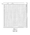
- “In-glass” touch sensitive screenstypically included a plurality of sensors 1 disposed within the screen 2 as shown in FIG. 1 . It is noted that the sensors are shown schematically and are typically not visible to the naked eye. The sensors, which were typically capacitive, mechanical, or optical sensors, provided a signal when actuated. The sensors are actuated when an object, typically a stylus or a finger, is positioned on, or immediately adjacent to, the screen.
- the sensorsare coupled to a sensor output device which is further coupled to a control assembly.
- the sensor output device and/or control assemblyare structured to interpret the sensor signals to determine the position on the screen over which the object is located.
- an electronic devicecould display an image representing commands, such as icons or a menu, and a user could use a stylus or a finger to select the command simply by touching the portion of the screen displaying the icon of menu.
- the sensorscould also, typically, detect a “tap” which indicated when a selection had been made.
- a screen 2such as, but not limited to, a liquid crystal display (LCD) panel 3 , is typically disposed in a frame or housing.
- the LCD panelutilizes a liquid crystal medium to produce an image formed from a number of small, illuminated points, or pixels, located on a grid.
- the pixelsare spaced as closely together as possible so that the image does not include voids or dark areas. Further, the pixels have an “aspect ratio” that represents the size of the pixel.
- the screen or LCD panelhas an active area that is structured to display images. Disposed about the active area is an inactive area. There are no pixels in the inactive area. Because it is desirable to not have the image abut the frame, a portion of the inactive area is visible to the user. This area is also called the “viewing area.” Beneath the frame is a hidden portion of the inactive area that the user cannot see or touch.
- the sensorswere typically disposed in a generally constant pattern over the entire active area and viewing area.
- This patternis, typically, a dense pattern as the higher the number of sensors, the more accurate the touch sensitivity of the screen. That is, if the sensors were disposed in a sparse pattern, the accuracy of the sensor grid would be reduced and, for example, the controlling software may not be able to accurately identify which icon of menu item the user selected.
- the use of a dense patternis a disadvantage as the sensors required space in the active area and, to provide that space, the pixels had to have a reduced aspect ratio.
- the software, or other electronics, used to create the imagecan be structured to limit the locations of the menus or icon to specific portions of the active area, such as an area adjacent to the viewing area.
- the disclosed inventionprovides for a touch sensitive screen for an electronic device wherein there is a sparse pattern of sensors disposed within the active area and a dense pattern of sensors disposed within the viewing area.
- the pixels in the active areamay have a larger aspect ratio and provide a more pleasing image while the dense sensors disposed within the viewing area provide more accurate touch sensitivity.
- the software, or other electronics, used to create the imagemay be structured to position menus or other selectable images adjacent to the viewing area.
- certain images, such as iconscan be programmed to be displayed directly under the sensors in the active area.
- this configurationprovides for the best of both worlds; a bright, clear image with some touch sensitivity in the active area and a sensitive sensor grid in the viewing area where there are no pixels. Further, in use, the user's finger or stylus is disposed generally to the side of the menu as opposed to blocking the menu from view.
- FIG. 1is a schematic view of a prior art touch sensitive screen having sensors disposed in a constant pattern.
- FIG. 2is a schematic, exploded view of an electronic device.
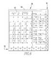
- FIG. 3is a schematic view of a touch sensitive screen having sensors disposed in a sparse pattern in the active area and in a dense pattern in the viewing area.
- FIG. 4is a schematic view of a touch sensitive screen having sensors disposed in a sparse pattern in the active area and in a dense pattern in the viewing area, and further showing how the displayed image corresponds to the placement of the sensors.
- FIG. 5is a schematic view of a touch sensitive screen having sensors generally disposed in a sparse pattern in the active area, in a dense pattern in the viewing area, and having a limited area of dense sensors in the active area.
- FIG. 6is a schematic view of a touch sensitive screen having sensors disposed in a sparse pattern in the active area and in an alternate dense pattern in the viewing area.
- FIG. 7is a schematic view of a touch sensitive screen having sensors disposed in a sparse pattern in the active area and in an alternate dense pattern in the viewing area.
- touch sensitivemeans structured to detect contact or near contact.
- Coupledmeans a link between two or more elements, whether direct or indirect, so long as a link occurs.
- directly coupledmeans that two elements are directly in contact with each other.
- an “aspect ratio”it the ratio of a pixel's height divided by the pixel's width.
- an electronic device 10herein represented by a handheld personal digital assistant, includes a housing 12 , a control assembly 14 , and a display assembly 16 .
- the control assembly 14includes a processor 18 , memory 20 , as well as other components, such as, but not limited to, a circuit board (not shown), structured to link the processor 18 , memory 20 , and display assembly 16 .
- the control assembly 14further includes a set of instructions, such as, but not limited to, software, structured to perform various functions including creating images on the display assembly 16 and receiving input from the user.
- the control assembly 14is structured to provide a video input to the display assembly 16 input/output assembly 30 (described below) and to receive sensor output from a sensor assembly 70 ( FIG. 3 .).
- the display assembly 16includes an input/output assembly 30 and an LCD panel 32 .
- the display assembly input/output assembly 30is structured to receive a video input from the control assembly 14 and to produce an image on the LCD panel 32 .
- the LCD panel 32includes a lower substrate 40 and an upper substrate 42 disposed in a close, but spaced, relationship.
- the LCD panel 32also includes a liquid crystal layer 44 disposed between the lower and upper substrates 40 , 42 . Upon application of an electrical charge, the liquid crystal molecules of the liquid crystal layer 44 are structured to align in a generally perpendicular direction with respect to the substrates 40 , 42 .
- the lower substrate 40has a lower, outer surface 46 and an upper, inner surface 48 .
- the upper substrate 42has a lower, inner surface 50 and an upper, outer surface 52 .
- the lower substrate upper, inner surface 48has a first electrode 54 , also called the pixel electrode, applied thereto.
- the upper substrate lower, inner surface 50has a second electrode 56 , also called the common electrode, applied thereto.
- the first and second electrodes 54 , 56form a grid that defines the aperture size of the pixels.
- the display assembly input/output assembly 30selectively controls the location of the charge applied to the first electrode 54 thereby forming images on the LCD panel 32 .
- the display assembly input/output assembly 30includes a programmable logic circuit, or integrated circuit, structured to apply a charge to the proper pixels.
- the LCD panel 32only creates an image in the area defined by the overlap of the first and second electrodes 54 , 56 .
- the LCD panel 32has a greater area than the first and second electrodes 54 , 56 , however.
- the area wherein an image is createdis the active area 60 of the LCD panel 32 .
- an inactive area 62wherein there are no pixels and no image is created. This area is called the viewing area 64 .
- the perimeter of the inactive area 62is disposed below the electronic device housing 12 and cannot be seen or touched by the user during normal operation.
- the electronic device 10also includes a sensor assembly 70 ( FIG. 3 ) having an output device 72 and a plurality of detectors 74 .
- the detectors 74are shown schematically and are typically too small to be seen by the naked eye.
- Each detector 74is in electrical communication with the output device 72 .
- Each detector 74creates an output signal when actuated.
- the detectors 74are disposed in a pattern, discussed below, and are structured to detect an external object immediately adjacent to, or touching, the LCD panel 32 .
- the external objectis typically a stylus or the user's finger (not shown).
- the output device 72 and/or the control assembly 14are structured to receive the detector signals and convert the signals to data representing the location of the external object relative to the LCD panel 32 .
- the detectors 74are typically capacitive detectors 74 A, optical detectors 74 B, or mechanical detectors 74 C.
- capacitive detectors 74 Aare structured to detect a change in capacitance caused by the electrical field of the external object or a change in capacitance caused by the compression of the capacitive detector 74 A.
- Optical detectors 74 Bare structured to detect a reflection of light, e.g., light created by the LCD panel 32 .
- Mechanical detectors 74 Cinclude a charged grid with columns disposed on one side of the LCD panel 32 and a corresponding grid without columns on the opposing side of the LCD panel 32 . When the LCD panel 32 is compressed, i.e.
- Capacitive detectors 74 Amay be disposed upon the lower substrate upper, inner surface 48 or upon the upper substrate upper, outer surface 52 .
- the detectors 74although small, require space and any pixel adjacent to a detector 74 will have a reduced size, or aperture, to accommodate the adjacent detector 74 .
- the detectors 74are disposed in a pattern, preferably in lines wherein multiple lines form a grid.
- the patternhas at least a first portion 80 and a second portion 82 .
- Detectors 74 in the first portion 80are disposed over the active area 60 .
- the detectors 74 in the first portion 80are disposed in a sparse pattern so that fewer pixels will have a reduced aspect ratio.
- the spacing of detectors 74 in the first portion 80is between about 1.0 mm and 10.0 mm between the detectors 74 , and more preferably about 3.0 mm between the detectors 74 .
- detectors 74 in the second portion 82are disposed over the viewing area 64 .
- the detectors 74 in the second portion 82are disposed in a dense pattern.
- the density of detectors 74 in the second portion 82is between about 0.5 mm and 6.0 mm between the detectors, and more preferably about 1.0 mm between the detectors.
- the control assembly 14is structured to create the image and define the boundaries of selectable portions of the image on the active area 60 of the LCD panel 32 .
- the control assembly 14will, for example, create the image of a pull-down menu 90 or a selectable icon 92 ( FIG. 3 ) on specific portions of the active area 60 of the LCD panel 32 .
- the control assembly 14is further structured to relate specific detectors 74 to the specific portions of the active area 60 of the LCD panel 32 .
- the control assembly 14detects the actuation of a specific detector 74 adjacent to a specific image, e.g. an icon 92 , the control assembly 14 will perform the command related to that icon 92 , e.g. opening the calendar program.
- the detectors 74 in the first portion 80are disposed in a loose grid and detectors 74 in the second portion 82 are disposed in a dense line extending adjacent to the right-hand side and the bottom side of the active area 60 .
- the control assembly 14is, preferably, structured to create interactive images having multiple selections, such as, but not limited to, pull-down menus 90 along the right side of the active area 60 .
- other interactive imagessuch as, but not limited to, icons 92 or, as shown, selectable dates 94 on a calendar ( FIG.
- each interactive imageis located adjacent to a limited number of detectors 74 .
- a usermay, for example, select a date by touching the desired date.
- the output device 72 and/or the control assembly 14will be able to identify which date is being selected.
- the usermay then, for example, open a pull down menu 90 .
- the pull-down menu 90has multiple selections, i.e. menu items, located very close to each other, the user moves the external object along the right side of the active area 60 wherein the detectors 74 in the second portion 82 are disposed in a dense pattern. Because the detectors 74 in the second portion 82 are disposed in a dense pattern, the control assembly 14 will be able to more accurately identify which of the closely disposed menu items is being selected.
- the pattern of detectors 74has a first portion 80 , a second portion 82 , and a third portion 84 .
- the first portion 80 and second portion 82are substantially similar to the embodiment described above.
- the third portion 84is an area of detectors 74 disposed in a dense pattern and located within the active area 60 .
- the third portion 84is structured to support a virtual control device 100 , such as a virtual roller wheel 102 or similar device.
- the image quality in the third portion 84is adversely affected for the reasons set forth above.
- the third portion 84is, preferably, a relatively small area compared to the entire active area 60 .
- the density of detectors 74 in the third portion 84is between about 0.05 mm and 3.0 mm between the detectors, and more preferably about 0.1 mm between the detectors.
- the third portion 84is a dedicated area for the virtual roller wheel 102 , it is acceptable to have a reduced pixel density with larger pixels. Since the pixel size would be very large, the aspect ratio could be significantly higher, e.g., about 65 to 98. These pixels would be special function pixels, such as pixels to light up the roller wheel 102 area and other features to highlight the roller wheel 102 .
- the detectors 74 in the second portion 82are shown as being in a single straight line.
- the inventionis not so limited.
- the detectors 74 in the second portion 82may be disposed in a dense but alternating pattern having two generally parallel lines of detectors 74 .
- the detectors 74 in the second portion 82are disposed in a dense line extending adjacent to the right-hand side and the bottom side of the active area 60 .
- the inventionis not so limited and, as shown in FIG.
- the detectors 74may be disposed on any portion of the viewing area 64 such as, but not limited to, along the left-hand side for use with interactive images that are displayed along the left side of the active area 60 . Further, sensors 74 may be disposed along both the left-hand side and the right-hand side so that the user may use either hand, or both hands, to operate the electronic device 10 .
Landscapes
- Engineering & Computer Science (AREA)
- General Engineering & Computer Science (AREA)
- Theoretical Computer Science (AREA)
- Human Computer Interaction (AREA)
- Physics & Mathematics (AREA)
- General Physics & Mathematics (AREA)
- Position Input By Displaying (AREA)
Abstract
Description
Claims (26)
Priority Applications (1)
| Application Number | Priority Date | Filing Date | Title |
|---|---|---|---|
| US11/744,282US9195329B2 (en) | 2007-05-04 | 2007-05-04 | Touch-sensitive device |
Applications Claiming Priority (1)
| Application Number | Priority Date | Filing Date | Title |
|---|---|---|---|
| US11/744,282US9195329B2 (en) | 2007-05-04 | 2007-05-04 | Touch-sensitive device |
Publications (2)
| Publication Number | Publication Date |
|---|---|
| US20080273014A1 US20080273014A1 (en) | 2008-11-06 |
| US9195329B2true US9195329B2 (en) | 2015-11-24 |
Family
ID=39939210
Family Applications (1)
| Application Number | Title | Priority Date | Filing Date |
|---|---|---|---|
| US11/744,282Active2032-07-31US9195329B2 (en) | 2007-05-04 | 2007-05-04 | Touch-sensitive device |
Country Status (1)
| Country | Link |
|---|---|
| US (1) | US9195329B2 (en) |
Families Citing this family (39)
| Publication number | Priority date | Publication date | Assignee | Title |
|---|---|---|---|---|
| US7663607B2 (en) | 2004-05-06 | 2010-02-16 | Apple Inc. | Multipoint touchscreen |
| CN102981678B (en)* | 2006-06-09 | 2015-07-22 | 苹果公司 | Touch screen liquid crystal display |
| CN104965621B (en) | 2006-06-09 | 2018-06-12 | 苹果公司 | Touch screen LCD and its operating method |
| US9710095B2 (en) | 2007-01-05 | 2017-07-18 | Apple Inc. | Touch screen stack-ups |
| US9195329B2 (en) | 2007-05-04 | 2015-11-24 | Blackberry Limited | Touch-sensitive device |
| CA134390S (en)* | 2009-12-22 | 2010-12-14 | Mitsubishi Electric Corp | Remote controller |
| CA134387S (en)* | 2009-12-22 | 2010-12-14 | Mitsubishi Electric Corp | Remote controller |
| CA134388S (en)* | 2009-12-22 | 2010-12-14 | Mitsubishi Electric Corp | Remote controller |
| CA134389S (en)* | 2009-12-22 | 2010-12-14 | Mitsubishi Electric Corp | Remote controller |
| CA134391S (en)* | 2009-12-22 | 2010-12-14 | Mitsubishi Electric Corp | Remote controller |
| KR101109313B1 (en)* | 2010-04-14 | 2012-01-31 | 삼성전기주식회사 | Display device including touch screen panel |
| EP2453343A3 (en) | 2010-09-24 | 2014-11-12 | BlackBerry Limited | Portable electronic device and method therefor |
| KR20130005296A (en) | 2010-09-24 | 2013-01-15 | 큐엔엑스 소프트웨어 시스템즈 리미티드 | Portable electronic device and method of controlling same |
| EP2434387B1 (en) | 2010-09-24 | 2020-01-08 | 2236008 Ontario Inc. | Portable electronic device and method therefor |
| US8804056B2 (en) | 2010-12-22 | 2014-08-12 | Apple Inc. | Integrated touch screens |
| US9477311B2 (en) | 2011-01-06 | 2016-10-25 | Blackberry Limited | Electronic device and method of displaying information in response to a gesture |
| US9471145B2 (en) | 2011-01-06 | 2016-10-18 | Blackberry Limited | Electronic device and method of displaying information in response to a gesture |
| US9423878B2 (en) | 2011-01-06 | 2016-08-23 | Blackberry Limited | Electronic device and method of displaying information in response to a gesture |
| US9766718B2 (en) | 2011-02-28 | 2017-09-19 | Blackberry Limited | Electronic device and method of displaying information in response to input |
| US9015641B2 (en) | 2011-01-06 | 2015-04-21 | Blackberry Limited | Electronic device and method of providing visual notification of a received communication |
| US9465440B2 (en) | 2011-01-06 | 2016-10-11 | Blackberry Limited | Electronic device and method of displaying information in response to a gesture |
| US9213421B2 (en) | 2011-02-28 | 2015-12-15 | Blackberry Limited | Electronic device and method of displaying information in response to detecting a gesture |
| USD697037S1 (en) | 2011-06-30 | 2014-01-07 | Geberit International Ag | Portion of a display panel for toilet flush tank |
| US8884892B2 (en) | 2011-08-12 | 2014-11-11 | Blackberry Limited | Portable electronic device and method of controlling same |
| USD690275S1 (en)* | 2011-08-23 | 2013-09-24 | Raffel Systems, Llc | Control panel |
| US8947627B2 (en) | 2011-10-14 | 2015-02-03 | Apple Inc. | Electronic devices having displays with openings |
| US9437132B2 (en)* | 2011-11-30 | 2016-09-06 | Apple Inc. | Devices and methods for providing access to internal component |
| US9619038B2 (en) | 2012-01-23 | 2017-04-11 | Blackberry Limited | Electronic device and method of displaying a cover image and an application image from a low power condition |
| US9058168B2 (en) | 2012-01-23 | 2015-06-16 | Blackberry Limited | Electronic device and method of controlling a display |
| USD701235S1 (en)* | 2012-09-20 | 2014-03-18 | Mitsubishi Electric Corporation | User interface for a remote controller |
| USD703225S1 (en)* | 2012-09-20 | 2014-04-22 | Mitsubishi Electric Corporation | Remote controller with graphical user interface |
| USD701236S1 (en)* | 2012-09-20 | 2014-03-18 | Mitsubishi Electric Corporation | Remote controller with graphical user interface |
| USD750648S1 (en)* | 2012-09-20 | 2016-03-01 | Mitsubishi Electric Corporation | Remote controller with graphical user interface |
| US9310843B2 (en) | 2013-01-02 | 2016-04-12 | Apple Inc. | Electronic devices with light sensors and displays |
| US9690476B2 (en) | 2013-03-14 | 2017-06-27 | Blackberry Limited | Electronic device and method of displaying information in response to a gesture |
| US9507495B2 (en) | 2013-04-03 | 2016-11-29 | Blackberry Limited | Electronic device and method of displaying information in response to a gesture |
| USD710315S1 (en)* | 2013-10-30 | 2014-08-05 | Timotion Technology Co, Ltd. | Handheld controller |
| US20160078574A1 (en)* | 2014-09-15 | 2016-03-17 | Mark Sprague | Virtual property management in an interactive geographic information system |
| USD1011301S1 (en)* | 2022-05-06 | 2024-01-16 | Aeki Intellectual Holdings LLC. | Remote for rechargeable RGB LED light |
Citations (25)
| Publication number | Priority date | Publication date | Assignee | Title |
|---|---|---|---|---|
| US4202041A (en) | 1977-07-11 | 1980-05-06 | Massachusetts Institute Of Technology | Dynamically variable keyboard terminal |
| US4731694A (en)* | 1986-05-05 | 1988-03-15 | Siemens Aktiengesellschaft | Touch selection pad and method of manufacture |
| US5412189A (en) | 1992-12-21 | 1995-05-02 | International Business Machines Corporation | Touch screen apparatus with tactile information |
| US6107997A (en) | 1996-06-27 | 2000-08-22 | Ure; Michael J. | Touch-sensitive keyboard/mouse and computing device using the same |
| US6198475B1 (en) | 1997-06-26 | 2001-03-06 | Kabushiki Kaisha Tokai-Rika-Denki-Seisakusho | Touch operation information output device |
| US6236386B1 (en)* | 1997-12-22 | 2001-05-22 | Nec Corporation | Liquid crystal display apparatus with touch panel |
| US6411504B2 (en)* | 1999-08-25 | 2002-06-25 | Dell Usa, L.P. | Portable computer having latching hooks |
| US6459424B1 (en)* | 1999-08-10 | 2002-10-01 | Hewlett-Packard Company | Touch-sensitive input screen having regional sensitivity and resolution properties |
| US20020156807A1 (en) | 2001-04-24 | 2002-10-24 | International Business Machines Corporation | System and method for non-visually presenting multi-part information pages using a combination of sonifications and tactile feedback |
| US6492978B1 (en) | 1998-05-29 | 2002-12-10 | Ncr Corporation | Keyscreen |
| WO2003025886A1 (en) | 2001-09-18 | 2003-03-27 | Research Foundation Of The City University Of New York | Tactile graphic-based interactive overlay assembly and computer system for the visually impaired |
| US20030081016A1 (en) | 2001-10-31 | 2003-05-01 | Genovation Inc. | Personal digital assistant mouse |
| US20030235452A1 (en) | 2002-06-21 | 2003-12-25 | Microsoft Corporation | Method and system for using a keyboard overlay with a touch-sensitive display screen |
| US20040056877A1 (en) | 2002-09-25 | 2004-03-25 | Satoshi Nakajima | Interactive apparatus with tactilely enhanced visual imaging capability apparatuses and methods |
| US20040090428A1 (en) | 2002-11-08 | 2004-05-13 | Xerox Corporation | Overlays with raised portions for touch-sensitive screens |
| US20050057528A1 (en) | 2003-09-01 | 2005-03-17 | Martin Kleen | Screen having a touch-sensitive user interface for command input |
| US20050179668A1 (en)* | 2002-04-16 | 2005-08-18 | Koninklijke Philips Electronics N.V. | Electronic device with a flat panel display and touch buttons/pads outside the display area |
| WO2006065252A1 (en) | 2004-12-17 | 2006-06-22 | Universal Electronics Inc. | Universal remote control or universal remote control/telephone combination with touch operated user interface having tactile feedback |
| EP1717667A1 (en) | 2005-04-25 | 2006-11-02 | Agilent Technologies, Inc. | User interface incorporating emulated hard keys |
| US7199322B2 (en)* | 2004-11-12 | 2007-04-03 | Eastman Kodak Company | Variable spacer dots for touch screen |
| US7203131B2 (en)* | 2003-09-04 | 2007-04-10 | Johnson Outdoors Inc. | Pixel display method and apparatus |
| US20070085838A1 (en)* | 2005-10-17 | 2007-04-19 | Ricks Theodore K | Method for making a display with integrated touchscreen |
| CN1955904A (en) | 2005-10-27 | 2007-05-02 | 阿尔卑斯电气株式会社 | Input device and electric device using the same |
| EP1988447A1 (en) | 2007-05-04 | 2008-11-05 | Research In Motion Limited | In glass touch screen |
| US20080273014A1 (en) | 2007-05-04 | 2008-11-06 | Robert Lowles | Glass Touch Screen |
- 2007
- 2007-05-04USUS11/744,282patent/US9195329B2/enactiveActive
Patent Citations (26)
| Publication number | Priority date | Publication date | Assignee | Title |
|---|---|---|---|---|
| US4202041A (en) | 1977-07-11 | 1980-05-06 | Massachusetts Institute Of Technology | Dynamically variable keyboard terminal |
| US4731694A (en)* | 1986-05-05 | 1988-03-15 | Siemens Aktiengesellschaft | Touch selection pad and method of manufacture |
| US5412189A (en) | 1992-12-21 | 1995-05-02 | International Business Machines Corporation | Touch screen apparatus with tactile information |
| US6107997A (en) | 1996-06-27 | 2000-08-22 | Ure; Michael J. | Touch-sensitive keyboard/mouse and computing device using the same |
| US6198475B1 (en) | 1997-06-26 | 2001-03-06 | Kabushiki Kaisha Tokai-Rika-Denki-Seisakusho | Touch operation information output device |
| US6236386B1 (en)* | 1997-12-22 | 2001-05-22 | Nec Corporation | Liquid crystal display apparatus with touch panel |
| US6492978B1 (en) | 1998-05-29 | 2002-12-10 | Ncr Corporation | Keyscreen |
| US6459424B1 (en)* | 1999-08-10 | 2002-10-01 | Hewlett-Packard Company | Touch-sensitive input screen having regional sensitivity and resolution properties |
| US6411504B2 (en)* | 1999-08-25 | 2002-06-25 | Dell Usa, L.P. | Portable computer having latching hooks |
| US20020156807A1 (en) | 2001-04-24 | 2002-10-24 | International Business Machines Corporation | System and method for non-visually presenting multi-part information pages using a combination of sonifications and tactile feedback |
| WO2003025886A1 (en) | 2001-09-18 | 2003-03-27 | Research Foundation Of The City University Of New York | Tactile graphic-based interactive overlay assembly and computer system for the visually impaired |
| US20030081016A1 (en) | 2001-10-31 | 2003-05-01 | Genovation Inc. | Personal digital assistant mouse |
| US20050179668A1 (en)* | 2002-04-16 | 2005-08-18 | Koninklijke Philips Electronics N.V. | Electronic device with a flat panel display and touch buttons/pads outside the display area |
| US20030235452A1 (en) | 2002-06-21 | 2003-12-25 | Microsoft Corporation | Method and system for using a keyboard overlay with a touch-sensitive display screen |
| US20040056877A1 (en) | 2002-09-25 | 2004-03-25 | Satoshi Nakajima | Interactive apparatus with tactilely enhanced visual imaging capability apparatuses and methods |
| US20040090428A1 (en) | 2002-11-08 | 2004-05-13 | Xerox Corporation | Overlays with raised portions for touch-sensitive screens |
| US20050057528A1 (en) | 2003-09-01 | 2005-03-17 | Martin Kleen | Screen having a touch-sensitive user interface for command input |
| US7203131B2 (en)* | 2003-09-04 | 2007-04-10 | Johnson Outdoors Inc. | Pixel display method and apparatus |
| US7199322B2 (en)* | 2004-11-12 | 2007-04-03 | Eastman Kodak Company | Variable spacer dots for touch screen |
| WO2006065252A1 (en) | 2004-12-17 | 2006-06-22 | Universal Electronics Inc. | Universal remote control or universal remote control/telephone combination with touch operated user interface having tactile feedback |
| EP1717667A1 (en) | 2005-04-25 | 2006-11-02 | Agilent Technologies, Inc. | User interface incorporating emulated hard keys |
| US20070085838A1 (en)* | 2005-10-17 | 2007-04-19 | Ricks Theodore K | Method for making a display with integrated touchscreen |
| CN1955904A (en) | 2005-10-27 | 2007-05-02 | 阿尔卑斯电气株式会社 | Input device and electric device using the same |
| US20070165006A1 (en)* | 2005-10-27 | 2007-07-19 | Alps Electric Co., Ltd | Input device and electronic apparatus |
| EP1988447A1 (en) | 2007-05-04 | 2008-11-05 | Research In Motion Limited | In glass touch screen |
| US20080273014A1 (en) | 2007-05-04 | 2008-11-06 | Robert Lowles | Glass Touch Screen |
Non-Patent Citations (9)
| Title |
|---|
| Canadian Intellectual Property Office, office action issued for CA application No. 2,630,397, dated Jan. 4, 2011, 4 pages. |
| Canadian Intellectual Property Office, office action issued in CA patent application 2,630,397, dated Oct. 14, 2011, 6 pages. |
| Canadian Intellectual Property Office, Office Action issued in connection with Canadian Application No. 2,630,397, dated Dec. 19, 2013, 5 pages. |
| European Patent Office, EP Communication, issued in connection with European Patent Application Serial No. 07 251 889.7, on Feb. 3, 2009, 6 pages. |
| European Patent Office, EP Communication, issued in connection with European Patent Application Serial No. 07 251 889.7, on Sep. 27, 2007, 8 pages. |
| European Patent Office, Summons to attend oral proceedings, issued in connection with European Patent Application Serial No. 07251889.7, on Apr. 8, 2010, 9 pages. |
| State Intellectual Property Office of People'S Republic of China, office action issued in CN application No. 200810210323.8, issued Apr. 20, 2011, 7 pages. |
| State Intellectual Property Office of People'S Republic of China, Third Office Action issued in CN Patent No. 200810210323.8, issued Mar. 7, 2012 6 pages. (English language translation pp. 1-2). |
| The State Intellectual Property Office of People's Republic of China, English language translation of the First Office Action in connection with Chinese Patent Application Serial No. 200810210323.8, issued on Jan. 22, 2010, 6 pages. |
Also Published As
| Publication number | Publication date |
|---|---|
| US20080273014A1 (en) | 2008-11-06 |
Similar Documents
| Publication | Publication Date | Title |
|---|---|---|
| US9195329B2 (en) | Touch-sensitive device | |
| US9703435B2 (en) | Touchpad combined with a display and having proximity and touch sensing capabilities to enable different functions or interfaces to be displayed | |
| US20040012572A1 (en) | Display and touch screen method and apparatus | |
| US9870065B2 (en) | Information display apparatus with proximity detection performance and information display method using the same | |
| EP2090966B1 (en) | Capacitive touch panel | |
| US8363030B2 (en) | Touch panel with mesh-shaped sensor and method for making the same | |
| KR102402349B1 (en) | Electronic devices with sidewall displays | |
| US9191472B2 (en) | Portable terminal, display control program and display control method | |
| JP6045715B2 (en) | Dual configuration computer | |
| JP2008305087A (en) | Display device | |
| KR20050026070A (en) | Single-layer touchpad having touch zones | |
| US20130285966A1 (en) | Display apparatus | |
| KR20060083129A (en) | Single-layer touch pad for use with display screens | |
| CN102129312A (en) | Virtual touchpad for a touch device | |
| US20090322703A1 (en) | Touch panel with touch pads | |
| CA2630397C (en) | Touch-sensitive device | |
| US20100251115A1 (en) | Soft Buttons for an Information Handling System | |
| TWI419041B (en) | Control method for displaying icons of touch screen | |
| TWI425412B (en) | Touch electronic device | |
| JP2009218995A (en) | Mobile terminal device | |
| HK1148839B (en) | Touchpad combined with a display and having proximity and touch sensing capabilities |
Legal Events
| Date | Code | Title | Description |
|---|---|---|---|
| AS | Assignment | Owner name:RESEARCH IN MOTION LIMITED, ONTARIO Free format text:ASSIGNMENT OF ASSIGNORS INTEREST;ASSIGNORS:LOWLES, ROBERT;ROBINSON, JAMES ALEXANDER;REEL/FRAME:019577/0134 Effective date:20070615 | |
| AS | Assignment | Owner name:BLACKBERRY LIMITED, ONTARIO Free format text:CHANGE OF NAME;ASSIGNOR:RESEARCH IN MOTION LIMITED;REEL/FRAME:034012/0111 Effective date:20130709 | |
| STCF | Information on status: patent grant | Free format text:PATENTED CASE | |
| MAFP | Maintenance fee payment | Free format text:PAYMENT OF MAINTENANCE FEE, 4TH YEAR, LARGE ENTITY (ORIGINAL EVENT CODE: M1551); ENTITY STATUS OF PATENT OWNER: LARGE ENTITY Year of fee payment:4 | |
| MAFP | Maintenance fee payment | Free format text:PAYMENT OF MAINTENANCE FEE, 8TH YEAR, LARGE ENTITY (ORIGINAL EVENT CODE: M1552); ENTITY STATUS OF PATENT OWNER: LARGE ENTITY Year of fee payment:8 | |
| AS | Assignment | Owner name:MALIKIE INNOVATIONS LIMITED, IRELAND Free format text:ASSIGNMENT OF ASSIGNORS INTEREST;ASSIGNOR:BLACKBERRY LIMITED;REEL/FRAME:064104/0103 Effective date:20230511 | |
| AS | Assignment | Owner name:MALIKIE INNOVATIONS LIMITED, IRELAND Free format text:NUNC PRO TUNC ASSIGNMENT;ASSIGNOR:BLACKBERRY LIMITED;REEL/FRAME:064269/0001 Effective date:20230511 |