US9190518B2 - Nonplanar device with thinned lower body portion and method of fabrication - Google Patents
Nonplanar device with thinned lower body portion and method of fabricationDownload PDFInfo
- Publication number
- US9190518B2 US9190518B2US14/273,373US201414273373AUS9190518B2US 9190518 B2US9190518 B2US 9190518B2US 201414273373 AUS201414273373 AUS 201414273373AUS 9190518 B2US9190518 B2US 9190518B2
- Authority
- US
- United States
- Prior art keywords
- semiconductor body
- sidewalls
- gate
- top surface
- silicon
- Prior art date
- Legal status (The legal status is an assumption and is not a legal conclusion. Google has not performed a legal analysis and makes no representation as to the accuracy of the status listed.)
- Expired - Fee Related
Links
Images


Classifications
- H—ELECTRICITY
- H10—SEMICONDUCTOR DEVICES; ELECTRIC SOLID-STATE DEVICES NOT OTHERWISE PROVIDED FOR
- H10D—INORGANIC ELECTRIC SEMICONDUCTOR DEVICES
- H10D30/00—Field-effect transistors [FET]
- H10D30/60—Insulated-gate field-effect transistors [IGFET]
- H10D30/62—Fin field-effect transistors [FinFET]
- H10D30/6212—Fin field-effect transistors [FinFET] having fin-shaped semiconductor bodies having non-rectangular cross-sections
- H01L29/785—
- H01L21/823431—
- H01L21/845—
- H01L27/0886—
- H01L27/1211—
- H01L29/42384—
- H01L29/66795—
- H01L29/66818—
- H01L29/7853—
- H01L29/7856—
- H—ELECTRICITY
- H10—SEMICONDUCTOR DEVICES; ELECTRIC SOLID-STATE DEVICES NOT OTHERWISE PROVIDED FOR
- H10D—INORGANIC ELECTRIC SEMICONDUCTOR DEVICES
- H10D30/00—Field-effect transistors [FET]
- H10D30/01—Manufacture or treatment
- H10D30/021—Manufacture or treatment of FETs having insulated gates [IGFET]
- H10D30/024—Manufacture or treatment of FETs having insulated gates [IGFET] of fin field-effect transistors [FinFET]
- H10D30/0245—Manufacture or treatment of FETs having insulated gates [IGFET] of fin field-effect transistors [FinFET] by further thinning the channel after patterning the channel, e.g. using sacrificial oxidation on fins
- H—ELECTRICITY
- H10—SEMICONDUCTOR DEVICES; ELECTRIC SOLID-STATE DEVICES NOT OTHERWISE PROVIDED FOR
- H10D—INORGANIC ELECTRIC SEMICONDUCTOR DEVICES
- H10D30/00—Field-effect transistors [FET]
- H10D30/60—Insulated-gate field-effect transistors [IGFET]
- H10D30/62—Fin field-effect transistors [FinFET]
- H10D30/6212—Fin field-effect transistors [FinFET] having fin-shaped semiconductor bodies having non-rectangular cross-sections
- H10D30/6213—Fin field-effect transistors [FinFET] having fin-shaped semiconductor bodies having non-rectangular cross-sections having rounded corners
- H—ELECTRICITY
- H10—SEMICONDUCTOR DEVICES; ELECTRIC SOLID-STATE DEVICES NOT OTHERWISE PROVIDED FOR
- H10D—INORGANIC ELECTRIC SEMICONDUCTOR DEVICES
- H10D30/00—Field-effect transistors [FET]
- H10D30/60—Insulated-gate field-effect transistors [IGFET]
- H10D30/62—Fin field-effect transistors [FinFET]
- H10D30/6217—Fin field-effect transistors [FinFET] having non-uniform gate electrodes, e.g. gate conductors having varying doping
- H—ELECTRICITY
- H10—SEMICONDUCTOR DEVICES; ELECTRIC SOLID-STATE DEVICES NOT OTHERWISE PROVIDED FOR
- H10D—INORGANIC ELECTRIC SEMICONDUCTOR DEVICES
- H10D30/00—Field-effect transistors [FET]
- H10D30/60—Insulated-gate field-effect transistors [IGFET]
- H10D30/67—Thin-film transistors [TFT]
- H10D30/6729—Thin-film transistors [TFT] characterised by the electrodes
- H10D30/673—Thin-film transistors [TFT] characterised by the electrodes characterised by the shapes, relative sizes or dispositions of the gate electrodes
- H—ELECTRICITY
- H10—SEMICONDUCTOR DEVICES; ELECTRIC SOLID-STATE DEVICES NOT OTHERWISE PROVIDED FOR
- H10D—INORGANIC ELECTRIC SEMICONDUCTOR DEVICES
- H10D84/00—Integrated devices formed in or on semiconductor substrates that comprise only semiconducting layers, e.g. on Si wafers or on GaAs-on-Si wafers
- H10D84/01—Manufacture or treatment
- H10D84/0123—Integrating together multiple components covered by H10D12/00 or H10D30/00, e.g. integrating multiple IGBTs
- H10D84/0126—Integrating together multiple components covered by H10D12/00 or H10D30/00, e.g. integrating multiple IGBTs the components including insulated gates, e.g. IGFETs
- H10D84/0158—Integrating together multiple components covered by H10D12/00 or H10D30/00, e.g. integrating multiple IGBTs the components including insulated gates, e.g. IGFETs the components including FinFETs
- H—ELECTRICITY
- H10—SEMICONDUCTOR DEVICES; ELECTRIC SOLID-STATE DEVICES NOT OTHERWISE PROVIDED FOR
- H10D—INORGANIC ELECTRIC SEMICONDUCTOR DEVICES
- H10D84/00—Integrated devices formed in or on semiconductor substrates that comprise only semiconducting layers, e.g. on Si wafers or on GaAs-on-Si wafers
- H10D84/01—Manufacture or treatment
- H10D84/02—Manufacture or treatment characterised by using material-based technologies
- H10D84/03—Manufacture or treatment characterised by using material-based technologies using Group IV technology, e.g. silicon technology or silicon-carbide [SiC] technology
- H10D84/038—Manufacture or treatment characterised by using material-based technologies using Group IV technology, e.g. silicon technology or silicon-carbide [SiC] technology using silicon technology, e.g. SiGe
- H—ELECTRICITY
- H10—SEMICONDUCTOR DEVICES; ELECTRIC SOLID-STATE DEVICES NOT OTHERWISE PROVIDED FOR
- H10D—INORGANIC ELECTRIC SEMICONDUCTOR DEVICES
- H10D84/00—Integrated devices formed in or on semiconductor substrates that comprise only semiconducting layers, e.g. on Si wafers or on GaAs-on-Si wafers
- H10D84/80—Integrated devices formed in or on semiconductor substrates that comprise only semiconducting layers, e.g. on Si wafers or on GaAs-on-Si wafers characterised by the integration of at least one component covered by groups H10D12/00 or H10D30/00, e.g. integration of IGFETs
- H10D84/82—Integrated devices formed in or on semiconductor substrates that comprise only semiconducting layers, e.g. on Si wafers or on GaAs-on-Si wafers characterised by the integration of at least one component covered by groups H10D12/00 or H10D30/00, e.g. integration of IGFETs of only field-effect components
- H10D84/83—Integrated devices formed in or on semiconductor substrates that comprise only semiconducting layers, e.g. on Si wafers or on GaAs-on-Si wafers characterised by the integration of at least one component covered by groups H10D12/00 or H10D30/00, e.g. integration of IGFETs of only field-effect components of only insulated-gate FETs [IGFET]
- H10D84/834—Integrated devices formed in or on semiconductor substrates that comprise only semiconducting layers, e.g. on Si wafers or on GaAs-on-Si wafers characterised by the integration of at least one component covered by groups H10D12/00 or H10D30/00, e.g. integration of IGFETs of only field-effect components of only insulated-gate FETs [IGFET] comprising FinFETs
- H—ELECTRICITY
- H10—SEMICONDUCTOR DEVICES; ELECTRIC SOLID-STATE DEVICES NOT OTHERWISE PROVIDED FOR
- H10D—INORGANIC ELECTRIC SEMICONDUCTOR DEVICES
- H10D86/00—Integrated devices formed in or on insulating or conducting substrates, e.g. formed in silicon-on-insulator [SOI] substrates or on stainless steel or glass substrates
- H10D86/01—Manufacture or treatment
- H10D86/011—Manufacture or treatment comprising FinFETs
- H—ELECTRICITY
- H10—SEMICONDUCTOR DEVICES; ELECTRIC SOLID-STATE DEVICES NOT OTHERWISE PROVIDED FOR
- H10D—INORGANIC ELECTRIC SEMICONDUCTOR DEVICES
- H10D86/00—Integrated devices formed in or on insulating or conducting substrates, e.g. formed in silicon-on-insulator [SOI] substrates or on stainless steel or glass substrates
- H10D86/201—Integrated devices formed in or on insulating or conducting substrates, e.g. formed in silicon-on-insulator [SOI] substrates or on stainless steel or glass substrates the substrates comprising an insulating layer on a semiconductor body, e.g. SOI
- H10D86/215—Integrated devices formed in or on insulating or conducting substrates, e.g. formed in silicon-on-insulator [SOI] substrates or on stainless steel or glass substrates the substrates comprising an insulating layer on a semiconductor body, e.g. SOI comprising FinFETs
- H—ELECTRICITY
- H01—ELECTRIC ELEMENTS
- H01L—SEMICONDUCTOR DEVICES NOT COVERED BY CLASS H10
- H01L2924/00—Indexing scheme for arrangements or methods for connecting or disconnecting semiconductor or solid-state bodies as covered by H01L24/00
- H01L2924/10—Details of semiconductor or other solid state devices to be connected
- H01L2924/11—Device type
- H01L2924/13—Discrete devices, e.g. 3 terminal devices
- H01L2924/1304—Transistor
- H01L2924/1306—Field-effect transistor [FET]
- H01L2924/13067—FinFET, source/drain region shapes fins on the silicon surface
- Y—GENERAL TAGGING OF NEW TECHNOLOGICAL DEVELOPMENTS; GENERAL TAGGING OF CROSS-SECTIONAL TECHNOLOGIES SPANNING OVER SEVERAL SECTIONS OF THE IPC; TECHNICAL SUBJECTS COVERED BY FORMER USPC CROSS-REFERENCE ART COLLECTIONS [XRACs] AND DIGESTS
- Y10—TECHNICAL SUBJECTS COVERED BY FORMER USPC
- Y10S—TECHNICAL SUBJECTS COVERED BY FORMER USPC CROSS-REFERENCE ART COLLECTIONS [XRACs] AND DIGESTS
- Y10S438/00—Semiconductor device manufacturing: process
- Y10S438/978—Semiconductor device manufacturing: process forming tapered edges on substrate or adjacent layers
Definitions
- the present inventionrelates to the field of semiconductor devices and more particularly to a nonplanar tri-gate transistor having a thinned lower body portion and method of fabrication.
- silicon on insulator (SOI) transistorshave been proposed.
- Silicon on insulator (SOI) transistorshave an advantage in that they can be operated in a fully depleted manner.
- Fully depleted transistorshave an advantage of ideal subthreshold gradients for optimized ON current/OFF current ratios.
- Tri-gate transistor 100includes a silicon body 104 formed on an insulating substrate 102 having a buried oxide layer 103 formed on a monocrystalline silicon substrate 105 .
- a gate dielectric layer 106is formed on the top and sidewalls of the silicon body 104 as shown in FIG. 1 .
- a gate electrode 108is formed on the gate dielectric layer and surrounds the body 104 on three sides, essentially providing a transistor 100 having three gate electrodes (G 1 , G 2 , G 3 ), one on each of the sidewalls of the silicon body 104 and one on the top surface of the silicon body 104 .
- a source region 110 and a drain region 112are formed in the silicon body 104 on opposite sides of the gate electrode 108 as shown in FIG. 1 .
- tri-gate transistor 100exhibits good short channel effects (SCE).
- SCEshort channel effects
- One reason tri-gate transistor 100 achieves good short channel effectsis that the nonplanarity of the device places the gate electrode 108 in such a way as to surround the active channel region. That is, in the tri-gate device, the gate electrode 108 is in contact with three sides of the channel region. Unfortunately, the fourth side, the bottom part of the channel is isolated from the gate electrode by the buried oxide layer 103 and thus is not under close gate control.
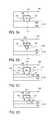
- FIG. 1is an illustration of a nonplanar or tri-gate device.
- FIGS. 2A and 2Billustrate a tri-gate or nonplanar device with a thinned lower body portion in accordance with the present invention.
- FIG. 3Aillustrates a nonplanar device having multiple thinned lower body portions.
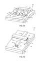
- FIG. 3Bis an illustration of a nonplanar device having a thinned lower body portion and including sidewall spacers, source/drain extensions and silicided source/drain regions.
- FIGS. 4A-4Hillustrate a method of forming a nonplanar device with a thinned lower body portion in accordance with an embodiment of the present invention.
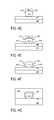
- FIGS. 5A-5Dillustrate other semiconductor body profiles or shapes.
- the present inventionis a novel nonplanar device with a thinned lower body portion and a method of fabrication.
- numerous specific detailsare set forth in order to provide a thorough understanding of the present invention.
- well known semiconductor processes and manufacturing techniqueshave not been described in particular detail in order to not unnecessarily obscure the present invention.
- Embodiments of the present inventioninclude a nonplanar or tri-gate transistor having a semiconductor body which is wrapped around on three sides by a gate dielectric layer and a gate electrode.
- the bottom portion of the semiconductor bodyis made thinner than the top portion of the semiconductor body. Making the bottom portion of the semiconductor body thinner than the top portion increases the gate control over the bottom portion of the body resulting in better short channel effects.
- a semiconductor filmis etched into a semiconductor body utilizing a dry etching process which utilizes a first process gas chemistry and a first RF bias. After forming the semiconductor body, the lower portion of the body is thinned utilizing the same etch chemistry and equipment but utilizing a lower RF bias in order to inwardly taper or facet the lower body portion.
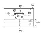
- FIGS. 2A and 2Billustrate a nonplanar or tri-gate device 200 having a semiconductor body with a thinned lower body portion.
- FIG. 2Ais an overhead/side view of transistor 200 while FIG. 2B is an illustration of a cross-sectional view taken through the gate electrode.
- Transistor 200is formed on a substrate 202 and includes a semiconductor body or fin 204 .
- a gate dielectric layer 206is formed on the top surface 234 and sidewalls 230 and 232 of a semiconductor body 204 .
- a gate electrode 208is formed on the gate dielectric layer 206 and surrounds the semiconductor body or fin on three sides.
- a source regions 210 and a drain region 212are formed in the semiconductor body on opposite sides of the gate electrode 208 as shown in FIG. 2A .
- the semiconductor body 204has a bottom portion 222 which is thinner than the top portion 224 . That is, the distance between the sidewalls 230 and 232 is greater at the top surface 234 than at the bottom surface 236 .
- sidewalls 230 and 232 of the top portion 224are substantially vertical and are spaced a uniform distance apart while the sidewalls 230 and 232 of the bottom portion 222 , are faceted or inwardly tapered to reduce the distance between the sidewalls 230 and 232 in the bottom portion.
- the distance between the sidewalls 230 and 232 near the bottom surfaceis between 1 ⁇ 2to 2 ⁇ 3the distance between the sidewalls 230 and 232 near the top surface 234 .
- the sidewalls 230 and 232begin to taper inwardly at approximately the midpoint of the height 238 of the semiconductor body 204 (i.e., sidewalls start tapering inwardly at the midpoint between the top surface 234 and bottom surface 236 ).
- the distance between the sidewalls 230 and 232 at the top surface 234is between 20-30 nanometers while the distance between the sidewalls 230 and 232 near the bottom surface 236 is between 10-15 nanometers.
- the bottom portion 222 of the semiconductor body 204is made sufficiently thin so that the gate control of the bottom portion is made similar to the gate control of the top portion. In an embodiment of the present invention, the bottom portion 222 of the semiconductor body 204 is made sufficiently thin relative to the top portion to improve the short channel effects of transistor 200 .
- FIGS. 5A-5Dother semiconductor body profiles or shapes may be utilized to improve the short channel effects (SCE) of the tri-gate or nonplanar transistor 200 .
- the semiconductor body 204can have a pair of sidewalls 230 and 232 which continually taper inward from the top surface 234 to the bottom surface 236 .
- the semiconductor body 204can have sidewalls 230 and 232 which continually taper inward from the top surface to the bottom surface and reach the bottom surface 236 at a point or substantially at point 502 .
- the semiconductor body 204can have a pair of sidewalls 230 and 232 which include an upper vertical portion 510 separated by uniform distance, a middle inwardly tapered portion 512 and a lower portion 514 of vertical sidewalls separated by a second distance which is less than the distance separating the top portion sidewalls 510 .
- the semiconductor bodycan have an upper portion 224 where the sidewalls 230 and 232 are faceted or tapered inwardly and a bottom portion 222 where the sidewalls 230 and 232 are vertical or substantially vertical.
- the distance between the sidewalls 230 and 232 of semiconductor body 204 on the top surfaceis greater than the distance between the semiconductor body on the bottom surface.
- the gate electrode 208can have better control of the semiconductor body at the bottom surface and thereby improve the short channel effects of the device.
- the tri-gate transistor 200is formed on an insulating substrate 202 which includes a lower monocrystalline silicon substrate 250 upon which is formed an insulating layer 252 , such as a silicon dioxide film.
- insulating layer 252is a buried oxide layer of an SOI substrate.
- the tri-gate transistor 200can be formed on any well known insulating substrate, such as substrates formed from silicon dioxide, nitrides, oxides, and sapphires.
- Semiconductor body 204is formed on insulating layer 252 of insulating substrate 202 .
- Semiconductor body 204can be formed on any well known material, such as but not limited to silicon (Si), germanium (Ge), silicon germanium (Si x Ge y ), gallium arsenide (GaAs), InSb, GaP and GaSb.
- Semiconductor body 204can be formed of any well known material which can be reversely altered from an insulating state to a conductive state by applying external electrical controls.
- Semiconductor body 204is ideally a single crystalline film when best electrical performance of transistor 200 is desired.
- semiconductor body 204is a single crystalline film when transistor 200 is used in higher performance applications, such as high density circuit, such as a microprocessor.
- Semiconductor body 204can be a polycrystalline film when transistor 200 is used in applications requiring less stringent performance, such as liquid crystal displays.
- Insulator 252isolate semiconductor body 204 from the monocrystalline silicon substrate 250 .
- semiconductor body 204is a single crystalline silicon film.
- Gate dielectric layer 206is formed on and around three sides of semiconductor body 204 as shown in FIGS. 2A and 2B . Gate dielectric layer 206 is formed on or adjacent to sidewall 230 , on the top surface 234 of body 204 and on or adjacent to sidewall 232 of body 204 as shown in FIGS. 2A and 2B . Gate dielectric layer 206 can be any well known gate dielectric layer. In an embodiment of the present invention, the gate dielectric layer is a silicon dioxide (SiO 2 ), silicon oxynitride (SiO x N y ) or a silicon nitride (Si 3 N 4 ) dielectric layer.
- the gate dielectric layer 206is a silicon oxynitride film formed to a thickness between 5-20 ⁇ .
- gate dielectric layer 206is a high k gate dielectric layer, such as a metal oxide dielectric, such as but not limited to tantalum pentaoxide (TaO 5 ), titanium oxide (TiO 2 ) and hafnium oxide (HfO).
- Gate dielectric layer 206can be other types of high k dielectric layers, such as but not limited to PZT and BST.
- Gate electrode 208is formed on and around gate dielectric layer 206 as shown in FIGS. 2A and 2B .
- Gate electrode 208is formed on or adjacent to gate dielectric layer 206 formed on sidewall 230 of semiconductor body 204 is formed on gate dielectric layer 206 formed on the top surface 234 of semiconductor body 204 and is formed adjacent to or on gate dielectric layer 206 formed on sidewall 232 of semiconductor body 204 .
- Gate electrode 208has a pair of laterally opposite sidewalls 260 and 262 separated by a distance which defines the gate length (Lg) 264 of transistor 200 .
- laterally opposite sidewalls 260 and 262 of gate electrode 208run in a direction perpendicular to sidewalls 230 and 232 of semiconductor body 204 .
- Gate electrode 208can be formed of any suitable gate electrode material.
- gate electrode 208comprises a polycrystalline silicon film doped to a concentration density between 1 ⁇ 10 19 atoms/cm 3 to 1 ⁇ 10 20 atoms/cm 3 .
- the gate electrodecan be a metal gate electrode, such as but not limited to tungsten, tantalum, titanium and their nitrides.
- the gate electrodeis formed from a material having a midgap workfunction between 4.5 to 4.8 eV. It is to be appreciated that gate electrode 208 need not necessarily be a single material and can be a composite stack of thin films, such as but not limited to polycrystalline silicon/metal electrode or metal/polycrystalline silicon electrode.
- Transistor 200has a source region 210 and a drain region 212 .
- Source region 210 and drain region 212are formed in semiconductor 204 on opposite sides of gate electrode 208 as shown in FIG. 2A .
- Source region 210 and drain region 212are formed to an n type conductivity type when forming a NMOS transistor and are formed to a p type conductivity when forming a PMOS device.
- source region 210 and drain region 212have a doping concentration between 1 ⁇ 10 19 atoms/cm 3 to 1 ⁇ 10 21 atoms/cm 3 .
- Source region 210 and drain region 212can be formed of the uniform concentration or can include subregions of different concentrations or dopant profiles, such as tip regions (e.g., source/drain extensions) and contact regions.
- source region 210 and drain region 212when transistor 200 is a symmetrical transistor, source region 210 and drain region 212 have the same doping concentration and profile.
- the doping concentration profile of the source region 210 and drain region 212when transistor 200 is formed as an asymmetrical transistor, then the doping concentration profile of the source region 210 and drain region 212 may vary in order to any particular electrical characteristics as well known in the art.
- Source region 210 and drain region 212can be collectively referred to as a pair of source/drain regions.
- the portion of semiconductor body 204 located between source region 210 and drain region 212defines the channel region 270 of transistor 200 .
- the channel region 270can also be defined as the area of the semiconductor body 204 surrounded by the gate electrode 208 .
- the source/drain regionmay extend slightly beneath the gate electrode through, for example, diffusion to define a channel region slightly smaller than the gate electrode length (Lg).
- channel region 270is intrinsic or undoped monocrystalline silicon.
- channel region 270is doped monocrystalline silicon. When channel region 270 is doped it is typically doped to a conductivity level of between 1 ⁇ 10 16 to 1 ⁇ 10 19 atoms/cm 3 .
- channel regionwhen the channel region is doped it is typically doped to the opposite conductivity type of the source region 210 and the drain region 212 .
- the channel regionwhen the source and drain regions are n type conductivity the channel region would be doped to p type conductivity.
- the source and drain regionswhen the source and drain regions are p type conductivity the channel region would be n type conductivity.
- Channel region 270can be uniformly doped or can be doped non-uniformly or with differing concentrations to provide particular electrical and performance characteristics.
- channel regions 270can include well-known “halo” regions, if desired.
- the tri-gate transistoris characterized in having three channels and three gates, one gate and channel (G 1 ) which extends between the source and drain regions on side 230 of silicon body 204 , a second gate and channel (G 2 ) which extends between the source and drain regions on the top surface of silicon body 204 , and a third gate and channel (G 3 ) which extends between the source and drain regions on the sidewall of silicon body 204 .
- the gate “width” (Gw) of transistor 200is the sum of the widths of the three channel regions.
- the gate width of transistor 200is equal to the length of sidewall 230 of silicon body 204 , plus the length of top surface 234 of silicon body of 204, plus the length of sidewall 232 of silicon body 204 .
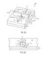
- Larger “width” transistorscan be obtained by using multiple devices coupled together (e.g., multiple silicon bodies 204 surrounded by a single gate electrode 208 ) as illustrated in FIG. 3A .
- transistor 200can be operated in a fully depleted manner wherein when transistor 200 is turned “on” the channel region 270 fully depletes thereby providing the advantageous electrical characteristics and performance of a fully depleted transistor. That is, when transistor 200 is turned “ON” a depletion region is formed in channel region 270 along with an inversion layer at the surfaces of region 270 (i.e., an inversion layer is formed on the side surfaces and top surface of the semiconductor body).
- the inversion layerhas the same conductivity type as the source and drain regions and forms a conductive channel between the source and drain regions to allow current to flow therebetween.
- the depletion regiondepletes free carriers from beneath the inversion layer.
- the depletion regionextends to the bottom of channel region 270 , thus the transistor can be said to be a “fully depleted” transistor.
- the lower portion 222 of the semiconductor body 204has been thinned relative to the upper portion so that the gate electrode can better control the lower portion of the semiconductor body. By thinning the lower portion, the two sidewall gates G 1 and G 3 can more easily deplete free carriers from beneath the inversion layer formed on the sidewalls of the lower portion of the semiconductor body 204 .
- the two gates G 1 and G 3 from the sidewallcan control the channel region in a manner similar to the way the three gates G 1 , G 2 and G 3 control the channel in the upper portion 224 of the semiconductor body 204 .
- Thinning the bottom part of the body or finnot only decreases the thickness of a semiconductor between the two gates, but also decreases the width of that part of the body which is in contact with the buried oxide. These effects combined decrease the short channel effects in the tri-gate device having a thinned lower body portion.
- Transistor 200 of the present inventioncan be said to be an nonplanar transistor because the inversion layer of channel 270 is formed in both the horizontal and vertical directions in semiconductor body 204 .
- the semiconductor device of the present inventioncan also be considered to be a nonplanar device because the electric field from gate electrode 208 is applied from both horizontal (G 2 ) and vertical sides (G 1 and G 3 ).
- transistor 200can include additional or multiple semiconductor bodies or fins 204 as illustrated in FIG. 3A .
- Each semiconductor body or fin 204has a gate dielectric layer 206 formed on its top surface and sidewalls as shown in FIG. 3A .
- Gate electrode 208is formed on and adjacent to each gate dielectric layer 206 on each semiconductor body 204 .
- Each semiconductor body 204includes a source region 210 and drain region 212 formed in the semiconductor body 204 on opposite sides of gate electrode 208 as shown in FIG. 3A .
- each semiconductor body 208is formed with same width and height (thickness) as other semiconductor bodies 204 .
- each source region 210 and drain region 212 of the semiconductor bodies 204are electrically coupled together by semiconductor material used to form semiconductor body 204 to form a source landing pad 310 and a drain landing pad 312 as shown in FIG. 3A .
- the source regions 210 and drain regions 212can be coupled together by higher levels of metallization (e.g., metal 1 , metal 2 , metal 3 ) used to electrically interconnect various transistors 200 together in the functional circuits.
- the gate width of transistor 200 as shown in FIG. 3Awould be equal to the sum of the gate width created by each of the semiconductor bodies 204 . In this way, a nonplanar or tri-gate transistor 200 can be formed with any gate width desired.
- each of the semiconductor bodies 204include a bottom portion 222 which is thinner than the top portion 224 as described above.
- the source 210 and drain 212can include a silicon or other semiconductor film 350 formed on and around semiconductor body 204 as shown in FIG. 3B .
- semiconductor film 350can be a silicon film or silicon alloy, such as silicon germanium (Si x Ge y ).
- the semiconductor film 350is a single crystalline silicon film formed of the same conductivity type as a source region 210 and drain region 212 .
- the semiconductor filmcan be a silicon alloy, such as silicon germanium where silicon comprises approximately 1-99 atomic percent of the alloy.
- the semiconductor film 350need not necessarily be a single crystalline semiconductor film and in embodiment can be a polycrystalline film.
- semiconductor film 350is formed on the source region 210 and the drain region 212 of semiconductor body 204 to form “raised” source and drain regions.
- Semiconductor film 350can be electrically isolated from a gate electrode 208 by a pair of dielectric sidewalls spacers 360 , such as silicon nitride or silicon oxide or composites thereof.
- Sidewall spacers 360run along laterally opposite sidewalls 260 and 262 of gate electrode 208 as shown in FIG. 3B thereby isolating the semiconductor film 350 from the gate electrode 208 .
- sidewall spacer 360have a thickness of between 20-200 ⁇ .
- the thickness of the source and drain regionsis increased thereby reducing the source/drain contact resistance to transistor 200 improving its electrical characteristics and performance.
- a silicide film 370such as but not limited to titanium silicide, nickel silicide, cobalt silicide is formed on the source region 210 and drain region 212 .
- silicide 370is formed on silicon film 350 on semiconductor body 204 as shown in FIG. 3B .
- Silicide film 370can be formed directly onto silicon body 204 , if desired.
- Dielectric spacers 360enables silicide 370 to be formed on semiconductor body 204 or silicon film 250 in a self-aligned process (i.e., a salicide process).
- the silicon film 350 and/or the silicide film 370can also be formed on the top of gate electrode 208 when gate electrode 208 is a silicon or silicon germanium film.
- the formation of silicon film 350 and silicide film 370 on the gate electrode 208reduces the contact resistance of the gate electrode thereby improving the electrical performance of transistor 200 .
- FIGS. 4A-4Hillustrate a method of forming a nonplanar transistor having a thinned lower body portion.
- the fabrication of the transistorbegins with substrate 402 .
- a silicon or semiconductor film 408is formed on substrate 402 as shown in FIG. 4A .
- the substrate 402is an insulating substrate, such as shown in FIG. 4A .
- insulating substrate 402includes a lower monocrystalline silicon substrate 404 and a top insulating layer 406 , such as a silicon dioxide film or silicon nitride film.
- Insulating layer 406isolates semiconductor film 408 from substrate 404 , and in embodiment is formed to a thickness between 200-2000 ⁇ . Insulating layer 406 is sometimes referred to as a “buried oxide” layer.
- SOIsilicon or semiconductor on insulating
- semiconductor film 408is ideally a silicon film, in other embodiments it can be other types of semiconductor films, such as but not limited to germanium (Ge), a silicon germanium alloy (Si x Ge y ), gallium arsenide (GaAs), InSb, GaP and GaSb.
- semiconductor film 408is an intrinsic (i.e., undoped) silicon film.
- semiconductor film 408is doped to a p type or n type conductivity with a concentration level between 1 ⁇ 10 16 -1 ⁇ 10 19 atoms/cm 3 .
- Semiconductor film 408can be insitu doped (i.e., doped while it is deposited) or doped after it is formed on substrate 402 by for example ion-implantation. Doping after formation enables both PMOS and NMOS tri-gate devices to be fabricated easily on the same insulating substrate. The doping level of the semiconductor body at this point can be used to set the doping level of the channel region of the device.
- Semiconductor film 408is formed to a thickness which is approximately equal to the height desired for the subsequently formed semiconductor body or bodies of the fabricated tri-gate transistor. In an embodiment of the present invention, semiconductor film 408 has a thickness or height 409 of less than 30 nanometers and ideally less than 20 nanometers. In an embodiment of the present invention, semiconductor film 408 is formed to the thickness approximately equal to the gate “length” desired of the fabricated tri-gate transistor. In an embodiment of the present invention, semiconductor film 408 is formed thicker than desired gate length of the device. In an embodiment of the present invention, semiconductor film 480 is formed to a thickness which will enable the fabricated tri-gate transistor to be operated in a fully depleted manner for its designed gate length (Lg).
- Lggate length
- Semiconductor film 408can be formed on insulating substrate 402 in any well-known method.
- a silicon on insulator substrateknown as the SIMOX technique
- oxygen atomsare implanted at a high dose into a single crystalline silicon substrate and then anneal to form the buried oxide 406 within the substrate.
- the portion of the single crystalline silicon substrate above the buried oxidebecomes the silicon film 408 .
- Another technique currently used to form SOI substratesis an epitaxial silicon film transfer technique which is generally referred to as bonded SOI.
- bonded SOIIn this technique a first silicon wafer has a thin oxide grown on its surface that will later serve as the buried oxide 406 in the SOI structure.
- a high dose hydrogen implantis made into the first silicon wafer to form a high stress region below the silicon surface of the first wafer.
- This first waferis then flipped over and bonded to the surface of a second silicon wafer.
- the first waferis then cleaved along the high stress plain created by the hydrogen implant. This results in a SOI structure with a thin silicon layer on top, the buried oxide underneath all on top of the single crystalline silicon substrate.
- Well-known smoothing techniquessuch as HCl smoothing or chemical mechanical polishing (CMP) can be used to smooth the top surface of semiconductor film 408 to its desired thickness.
- isolation regionscan be formed into SOI substrate in order to isolate the various transistors to be formed therein from one another. Isolation regions can be formed by etching away portions of the substrate film 408 surrounding a tri-gate transistor, by for example well-known photolithographic and etching techniques, and then back filling the etched regions with an insulating film, such as SiO 2 .
- a hard mask material 410 formed on semiconductor film 408 as shown in FIG. 4Ais a material which can provide a hard mask for the etching of the semiconductor film 408 .
- a hard mask materialis a material which can retain its profile during etching of the semiconductor film 408 .
- a hard mask material 410is a material which will not etch or only slightly etch during the etching of semiconductor film 408 .
- the hard mask materialis formed of a material such that the etchant used to etch the semiconductor film 408 will etch thin film 408 at least five times faster than the hard mask material and ideally at least ten times faster.
- the hard mask material 410when semiconductor film 408 is a silicon film, can be a silicon nitride or silicon oxynitride film. Hard mask material 410 is formed to a thickness sufficient to retain its profile during the entire etch of semiconductor film 408 but not too thick to cause difficulty in its patterning. In an embodiment of the present invention, the hard mask material 410 is formed to a thickness between 3 nanometers to 20 nanometers and ideally to a thickness less than 10 nanometers.
- Photoresist mask 412is formed on hard mask layer 410 .
- Photoresist mask 412contains a feature pattern to be transferred into the semiconductor film 408 .
- the photoresist mask 412can be formed by any well known techniques, such as by blanket depositing a photoresist material by masking, exposing and developing the photoresist film into a photoresist mask 412 having a desired pattern for the semiconductor film 408 to be patterned.
- Photoresist mask 412is typically formed of an organic compound.
- Photoresist mask 412is formed to a thickness sufficient to retain its profile while patterning the hard mask film 410 but yet is not formed to thick to prevent lithographic patterning into the smallest dimensions (i.e., critical dimensions) possible with photolithography system and process used.
- the hard mask material 410is etched in alignment with photoresist mask 412 to form a hard mask 414 as shown in FIG. 4B .
- Photoresist mask 412prevents the underlying portion of hard mask material 410 from becoming etched.
- the hard maskis etched with an etchant which can etch the hard mask material but does not etch the underlying semiconductor film 208 .
- the hard mask materialis etched with an etchant that has almost perfect selectivity to the underlying semiconductor film 208 .
- the hard mask etchantetches the hard mask material at least one hundred times faster than the underlying semiconductor film 208 (i.e., an etchant has a hard mask to semiconductor film selectivity of at least 50:1).
- an etchanthas a hard mask to semiconductor film selectivity of at least 50:1.
- the hard mask material 414is a silicon nitride or silicon oxynitride film
- hard mask material 410can be etched into a hard mask 414 utilizing a dry etch process, such as a reactive ion etching/ecr plasma etching.
- a silicon nitride or silicon oxynitride hard maskis reactive ion etched utilizing chemistry comprising CHF 3 and O 2 and Ar/CH 2 F 2 and C 4 F 8 and Ar and O 2 .
- photoresist mask 412can be removed by well known techniques. For example, photoresist mask 412 can be removed utilizing a “piranha” clean solution which includes sulfuric acid and hydrogen peroxide. Additionally, residue from photoresist mask 412 can be removed with an O 2 ashing.
- photoresist mask 412it is desirable to remove photoresist mask 412 prior to etching semiconductor film 408 so that a polymer film from the photoresist does not form on the sidewalls of the patterned semiconductor film 408 . It is desirable to first remove the photoresist mask 412 prior to etching of the semiconductor film 408 because dry etching processes can erode the photoresist mask and cause a polymer film to develop on the sidewalls of the semiconductor body which can be hard to remove and which can detrimentally device performance. By first removing the photoresist film 412 prior to patterning the semiconductor thin film 408 , the semiconductor thin film 408 can be patterned and pristine sidewalls maintained.
- semiconductor film 408is etched in alignment with hard mask 414 to form a semiconductor body 416 having a pair of laterally opposite sidewalls 418 and 420 .
- Hard mask 414prevents the underlying portion of semiconductor film 208 from becoming etched during the etching process. The etch is continued until the underlying insulating substrate is reached. In an embodiment of the present invention, the etch “end points” on the buried oxide layer 406 .
- Semiconductor film 208etched with an etchant which etches semiconductor 208 without significantly etching hard mask 414 .
- semiconductor film 408is anisotropically etched so that semiconductor body 416 has nearly vertical sidewalls 418 and 420 formed in alignment with the sidewalls of hard mask 414 thereby providing an almost perfect fidelity with hard mask 414 .
- hard mask 414is a silicon nitride or silicon oxynitride hard mask
- semiconductor film 408is a silicon film
- silicon film 408can be etched utilizing a dry etch process comprising HBr/Ar/O 2 .
- semiconductor body 408is etched utilizing an electron cyclotron residence (ECR) plasma etcher.
- ECRelectron cyclotron residence
- an ECR plasma etcher using a chemistry comprising HBr/02 with a pressure between 0.2 to 0.8 pascal and the RF power of approximately 120 wattsis used to etch a silicon thin film 408 into a silicon body 416 .
- Such an etch processproduces a substantially anisotropic etch to provide substantially vertical sidewalls 418 and 420 as shown in FIG. 4D .
- an etchhas a high selectivity (approximately 20:1) to the buried oxide layer 406 so that the buried oxide layer etches very little and can be used as an etch stop and for end point detection.
- the ability to end point detectis important to insure that all of the semiconductor film clears from the buried oxide layer because the thickness 409 of the thin film across the wafer may vary and the etch rate of different width semiconductor bodies may also vary.
- an RF biasof between 100-120 watts is used. The RF bias controls the electron energy in the etch which in turn controls the anisotropic profile of the etch.
- the semiconductor body 416is etched so as the reduce the distance between the sidewalls 418 and 420 in the lower portion of the semiconductor body 416 .
- the etching of a semiconductor body to thin the lower portion of the semiconductor bodycan be referred to as the “profile” etch.
- the profile etchis utilized to inwardly taper or form facets 422 and 424 on the sidewalls 418 and 420 as illustrated in FIG. 4E . It is to be appreciated that in other embodiments of the present invention, the profile etch can thin the lower body portion as illustrated in FIGS. 5A-5D .
- a plasma etch processwhich produces an isotropic etch is utilized to reduce the distance between the sidewalls in lower portion of the semiconductor body as compared to the upper portion of the semiconductor body.
- the same plasma etch equipment and etch chemistryis used during the profile etch as is used during the patterning of the semiconductor film 408 except that the RF bias is decreased so that the vertical directionality of the ions is reduced.
- the profile etchcan be accomplished utilizing an ECR plasma etcher with a chemistry comprising HBr/O2 and a pressure between 0.2 to 0.8 pascal with an RF bias between 50-70 watts.
- the hard mask 414is removed from semiconductor body 416 having a thinned lower body portion.
- a wet chemistrycomprising phosphoric acid and Di water can be used to remove the hard mask.
- the hard mask etchcomprises between 80-90% phosphoric acid (by volume) and Di water heated to a temperature between 150-170° C. and ideally to 160° C. is used.
- Such an etchantwill have an almost perfect selectivity between the silicon nitride hard mask 214 and buried oxide layer 406 .
- semiconductor body 416can be exposed to a wet etchant to clean the body 416 .
- a silicon body 416is exposed to a wet etchant comprising ammonia hydroxide (NH 4 OH) to remove any line edge roughness or pitting which may have developed during the patterning of the silicon body 416 .
- NH 4 OHammonia hydroxide
- a silicon body 416is exposed for a period of time of between 30 seconds to 2 minutes to an etchant comprising between 0.1-1% of ammonia hydroxide by volume at a temperature between 20-30 degrees Celsius in order to provide a semiconductor body 416 with pristine sidewalls 418 and 420 .
- a gate dielectric layer 430is formed on sidewalls 418 and 420 and the top surface of semiconductor body 416 .
- the gate dielectric layercan be a deposited dielectric or a grown dielectric.
- the gate dielectric layer 426is a silicon oxynitride dielectric film grown by a dry/wet oxidation process.
- the silicon oxide filmis grown to a thickness between 5-15 ⁇ .
- the gate dielectric layer 430is a deposited dielectric, such as but not limited to a high dielectric constant film, such as a metal oxide dielectric, such as tantalum pentaoxide (Ta 2 O 5 ), titanium oxide (TiO 2 ), hafnium oxide, zirconium oxide, and aluminum oxide. Additionally, in an embodiment of the present invention, gate dielectric layer 430 can be other high k dielectric films, such as but limited to PZT and BST. Any well known technique can be utilized to deposit a high k dielectric, such as but not limited to chemical vapor deposition, atomic layer deposition and sputtering.
- a high dielectric constant filmsuch as a metal oxide dielectric, such as tantalum pentaoxide (Ta 2 O 5 ), titanium oxide (TiO 2 ), hafnium oxide, zirconium oxide, and aluminum oxide.
- gate dielectric layer 430can be other high k dielectric films, such as but limited to PZT and BST. Any well known
- gate electrode 432is formed on the gate dielectric layer 430 formed on the top surface of semiconductor body 416 and is formed on or adjacent to the gate dielectric layer 430 formed on or adjacent to sidewalls 418 and 420 as shown in FIG. 4G .
- the gate electrode 432has a top surface opposite a bottom surface formed on insulating layer 406 and has a pair of laterally opposite sidewalls 434 and 436 which define the gate length of the device.
- Gate electrode 432can be formed by blanket depositing a suitable gate electrode material over the substrate and then patterning the gate electrode material with well known photolithograph and etching techniques to form a gate electrode 432 from the gate electrode material.
- the gate electrode materialcomprises polycrystalline silicon.
- the gate electrode materialcomprises a polycrystalline silicon germanium alloy.
- the gate electrode materialcan comprise a metal film, such as but not limited to tungsten, tantalum and their nitrides.
- the photolithography process used to find the gate electrode 432utilizes the minimum or smallest dimension lithography process used to fabricate the nonplanar transistor (that is, in an embodiment of the present invention, the gate length (Lg) of the gate electrode 432 has a minimum feature dimension of the transistor defined by photolithography). In an embodiment of the present invention, the gate length is less than or equal to 30 nanometers and ideally less than 20 nanometers.
- the gate dielectric layer and gate electrodeare formed with a “subtractive” process whereby undesired portions are etched away
- the gate electrodecan be formed with a replacement gate process whereby a sacrificial gate electrode is first formed, an interlayer dielectric formed adjacent thereto, the sacrificial gate electrode then removed to form an opening in which the gate electrode is then formed as is well known in the art.
- a source region 440 and a drain region 442are then formed in the semiconductor body 416 on opposite sides of gate electrode 432 .
- the semiconductor bodyare doped to a p type conductivity with a concentration between 1 ⁇ 10 20 to 1 ⁇ 10 21 atoms/cm 3 .
- the semiconductor body 416is doped with n type conductivity to a concentration between 1 ⁇ 10 20 to 1 ⁇ 10 21 atmos/cm 3 to form the source/drain regions.
- the source/drain regionscan be formed by ion implantation.
- the ion implantationoccurs in a vertical direction (i.e., a direction perpendicular to the substrate) as shown in FIG. 4H .
- the gate electrode 432is a polysilicon gate electrode and can be doped during the ion implantation process.
- the gate electrode 432acts as a mask to prevent the ion implantation step from doping the channel region of the nonplanar transistor. Again, the channel region is a portion of the semiconductor body 416 located beneath or surrounded by the gate electrode 432 . If the gate electrode 432 is a metal electrode a dielectric hard mask can be used to block the doping during ion implantation process.
- the source/drain regionsmay also include subregions, such as source/drain extensions and source/drain contact regions.
- the semiconductor body 416would be doped on either side of the gate electrode 432 to form the source/drain extensions and then a pair of sidewall spacers such as illustrated in FIG. 3B would be formed along the sidewalls of the gate electrode and a second doping step utilized to form heavily doped source/drain contact region as is well known in the art.
- additional silicon and/or silicidecan be formed onto the semiconductor bodies 416 to form raised source/drain regions and reduce the contact resistance of the device. This completes the fabrication of a nonplanar device having a semiconductor body with a thinned lower portion to improve device performance.
Landscapes
- Thin Film Transistor (AREA)
- Insulated Gate Type Field-Effect Transistor (AREA)
Abstract
Description
This application is a continuation application of U.S. patent application Ser. No. 13/908,858 filed Jun. 3, 2013, which is a continuation of U.S. patent application Ser. No. 13/243,441 filed Sep. 23, 2011, now issued as U.S. Pat. No. 8,502,351, which is a divisional of U.S. patent application Ser. No. 12/954,241 filed Nov. 24, 2010, now issued as U.S. Pat. No. 8,067,818, which is a divisional of U.S. patent application Ser. No. 10/973,228 filed Oct. 25, 2004, now abandoned.
1. Field of the Invention
The present invention relates to the field of semiconductor devices and more particularly to a nonplanar tri-gate transistor having a thinned lower body portion and method of fabrication.
2. Discussion of Related Art
In order to increase the performance of modern integrated circuits, such as microprocessors, silicon on insulator (SOI) transistors have been proposed. Silicon on insulator (SOI) transistors have an advantage in that they can be operated in a fully depleted manner. Fully depleted transistors have an advantage of ideal subthreshold gradients for optimized ON current/OFF current ratios.
An example of a proposed SOI transistor which can be operated in a fully depleted manner is a tri-gatetransistor 100, such as illustrated inFIG. 1 .Tri-gate transistor 100 includes asilicon body 104 formed on aninsulating substrate 102 having a buriedoxide layer 103 formed on amonocrystalline silicon substrate 105. A gatedielectric layer 106 is formed on the top and sidewalls of thesilicon body 104 as shown inFIG. 1 . Agate electrode 108 is formed on the gate dielectric layer and surrounds thebody 104 on three sides, essentially providing atransistor 100 having three gate electrodes (G1, G2, G3), one on each of the sidewalls of thesilicon body 104 and one on the top surface of thesilicon body 104. Asource region 110 and adrain region 112 are formed in thesilicon body 104 on opposite sides of thegate electrode 108 as shown inFIG. 1 .
An advantage of the tri-gatetransistor 100 is that it exhibits good short channel effects (SCE). One reason tri-gatetransistor 100 achieves good short channel effects is that the nonplanarity of the device places thegate electrode 108 in such a way as to surround the active channel region. That is, in the tri-gate device, thegate electrode 108 is in contact with three sides of the channel region. Unfortunately, the fourth side, the bottom part of the channel is isolated from the gate electrode by the buriedoxide layer 103 and thus is not under close gate control.
The present invention is a novel nonplanar device with a thinned lower body portion and a method of fabrication. In the following description, numerous specific details are set forth in order to provide a thorough understanding of the present invention. In other instances, well known semiconductor processes and manufacturing techniques have not been described in particular detail in order to not unnecessarily obscure the present invention.
Embodiments of the present invention include a nonplanar or tri-gate transistor having a semiconductor body which is wrapped around on three sides by a gate dielectric layer and a gate electrode. In embodiments of the present invention, the bottom portion of the semiconductor body is made thinner than the top portion of the semiconductor body. Making the bottom portion of the semiconductor body thinner than the top portion increases the gate control over the bottom portion of the body resulting in better short channel effects. In an embodiment of the present invention, a semiconductor film is etched into a semiconductor body utilizing a dry etching process which utilizes a first process gas chemistry and a first RF bias. After forming the semiconductor body, the lower portion of the body is thinned utilizing the same etch chemistry and equipment but utilizing a lower RF bias in order to inwardly taper or facet the lower body portion.
As is readily apparent fromFIGS. 2A and 2B , thesemiconductor body 204 has abottom portion 222 which is thinner than thetop portion 224. That is, the distance between thesidewalls top surface 234 than at thebottom surface 236. In an embodiment of the present invention,sidewalls top portion 224 are substantially vertical and are spaced a uniform distance apart while thesidewalls bottom portion 222, are faceted or inwardly tapered to reduce the distance between thesidewalls sidewalls sidewalls top surface 234. In an embodiment of the present invention, thesidewalls height 238 of the semiconductor body204 (i.e., sidewalls start tapering inwardly at the midpoint between thetop surface 234 and bottom surface236). In an embodiment of the present invention, the distance between thesidewalls top surface 234 is between 20-30 nanometers while the distance between thesidewalls bottom surface 236 is between 10-15 nanometers. In an embodiment of the present invention, thebottom portion 222 of thesemiconductor body 204 is made sufficiently thin so that the gate control of the bottom portion is made similar to the gate control of the top portion. In an embodiment of the present invention, thebottom portion 222 of thesemiconductor body 204 is made sufficiently thin relative to the top portion to improve the short channel effects oftransistor 200. Additionally, as illustrated inFIGS. 5A-5D , other semiconductor body profiles or shapes may be utilized to improve the short channel effects (SCE) of the tri-gate ornonplanar transistor 200. For example, as illustrated inFIG. 5A , thesemiconductor body 204 can have a pair ofsidewalls top surface 234 to thebottom surface 236. Additionally, in an embodiment of the present invention, as illustrated inFIG. 5B thesemiconductor body 204 can havesidewalls bottom surface 236 at a point or substantially atpoint 502. In yet another embodiment of the present invention as illustrated inFIG. 5C , thesemiconductor body 204 can have a pair ofsidewalls vertical portion 510 separated by uniform distance, a middle inwardly taperedportion 512 and alower portion 514 of vertical sidewalls separated by a second distance which is less than the distance separating thetop portion sidewalls 510. In yet another embodiment of the present invention, the semiconductor body can have anupper portion 224 where thesidewalls bottom portion 222 where thesidewalls FIGS. 5A-5D , the distance between thesidewalls semiconductor body 204 on the top surface is greater than the distance between the semiconductor body on the bottom surface. In this way, thegate electrode 208 can have better control of the semiconductor body at the bottom surface and thereby improve the short channel effects of the device.
In an embodiment of the present invention, thetri-gate transistor 200 is formed on an insulatingsubstrate 202 which includes a lowermonocrystalline silicon substrate 250 upon which is formed an insulatinglayer 252, such as a silicon dioxide film. In an embodiment of the present invention, insulatinglayer 252 is a buried oxide layer of an SOI substrate. Thetri-gate transistor 200, however, can be formed on any well known insulating substrate, such as substrates formed from silicon dioxide, nitrides, oxides, and sapphires.
The portion ofsemiconductor body 204 located betweensource region 210 and drainregion 212, defines thechannel region 270 oftransistor 200. Thechannel region 270 can also be defined as the area of thesemiconductor body 204 surrounded by thegate electrode 208. At times however, the source/drain region may extend slightly beneath the gate electrode through, for example, diffusion to define a channel region slightly smaller than the gate electrode length (Lg). In an embodiment of the presentinvention channel region 270 is intrinsic or undoped monocrystalline silicon. In an embodiment of the present invention,channel region 270 is doped monocrystalline silicon. Whenchannel region 270 is doped it is typically doped to a conductivity level of between 1×10¹⁶to 1×10¹⁹atoms/cm3. In an embodiment of the present invention, when the channel region is doped it is typically doped to the opposite conductivity type of thesource region 210 and thedrain region 212. For example, when the source and drain regions are n type conductivity the channel region would be doped to p type conductivity. Similarly, when the source and drain regions are p type conductivity the channel region would be n type conductivity. In this manner atri-gate transistor 200 can be formed into either a NMOS transistor or a PMOS transistor respectively.Channel region 270 can be uniformly doped or can be doped non-uniformly or with differing concentrations to provide particular electrical and performance characteristics. For example,channel regions 270 can include well-known “halo” regions, if desired.
By providing a gate dielectric and a gate electrode which surrounds the semiconductor body on three sides, the tri-gate transistor is characterized in having three channels and three gates, one gate and channel (G1) which extends between the source and drain regions onside 230 ofsilicon body 204, a second gate and channel (G2) which extends between the source and drain regions on the top surface ofsilicon body 204, and a third gate and channel (G3) which extends between the source and drain regions on the sidewall ofsilicon body 204. The gate “width” (Gw) oftransistor 200 is the sum of the widths of the three channel regions. That is, the gate width oftransistor 200 is equal to the length ofsidewall 230 ofsilicon body 204, plus the length oftop surface 234 of silicon body of 204, plus the length ofsidewall 232 ofsilicon body 204. Larger “width” transistors can be obtained by using multiple devices coupled together (e.g.,multiple silicon bodies 204 surrounded by a single gate electrode208) as illustrated inFIG. 3A .
Because thechannel region 270 is surrounded on three sides bygate electrode 208 andgate dielectric 206,transistor 200 can be operated in a fully depleted manner wherein whentransistor 200 is turned “on” thechannel region 270 fully depletes thereby providing the advantageous electrical characteristics and performance of a fully depleted transistor. That is, whentransistor 200 is turned “ON” a depletion region is formed inchannel region 270 along with an inversion layer at the surfaces of region270 (i.e., an inversion layer is formed on the side surfaces and top surface of the semiconductor body). The inversion layer has the same conductivity type as the source and drain regions and forms a conductive channel between the source and drain regions to allow current to flow therebetween. The depletion region depletes free carriers from beneath the inversion layer. The depletion region extends to the bottom ofchannel region 270, thus the transistor can be said to be a “fully depleted” transistor. In embodiments of the present invention, thelower portion 222 of thesemiconductor body 204 has been thinned relative to the upper portion so that the gate electrode can better control the lower portion of the semiconductor body. By thinning the lower portion, the two sidewall gates G1and G3can more easily deplete free carriers from beneath the inversion layer formed on the sidewalls of the lower portion of thesemiconductor body 204. By thinning thelower portion 222 ofsemiconductor body 204, the two gates G1and G3from the sidewall can control the channel region in a manner similar to the way the three gates G1, G2and G3control the channel in theupper portion 224 of thesemiconductor body 204. Thinning the bottom part of the body or fin not only decreases the thickness of a semiconductor between the two gates, but also decreases the width of that part of the body which is in contact with the buried oxide. These effects combined decrease the short channel effects in the tri-gate device having a thinned lower body portion.
As stated above the gate width oftransistor 200 is equal to the sum of the three gate widths created fromsemiconductor body 204 oftransistor 200. In order to fabricate transistors with larger gate widths,transistor 200 can include additional or multiple semiconductor bodies orfins 204 as illustrated inFIG. 3A . Each semiconductor body orfin 204 has agate dielectric layer 206 formed on its top surface and sidewalls as shown inFIG. 3A .Gate electrode 208 is formed on and adjacent to eachgate dielectric layer 206 on eachsemiconductor body 204. Eachsemiconductor body 204 includes asource region 210 and drainregion 212 formed in thesemiconductor body 204 on opposite sides ofgate electrode 208 as shown inFIG. 3A . In an embodiment of the present invention, eachsemiconductor body 208 is formed with same width and height (thickness) asother semiconductor bodies 204. In an embodiment of the present invention, eachsource region 210 and drainregion 212 of thesemiconductor bodies 204 are electrically coupled together by semiconductor material used to formsemiconductor body 204 to form asource landing pad 310 and adrain landing pad 312 as shown inFIG. 3A . Alternatively, thesource regions 210 anddrain regions 212 can be coupled together by higher levels of metallization (e.g., metal1,metal 2, metal3) used to electrically interconnectvarious transistors 200 together in the functional circuits. The gate width oftransistor 200 as shown inFIG. 3A would be equal to the sum of the gate width created by each of thesemiconductor bodies 204. In this way, a nonplanar ortri-gate transistor 200 can be formed with any gate width desired. In an embodiment of the present invention, each of thesemiconductor bodies 204 include abottom portion 222 which is thinner than thetop portion 224 as described above.
In an embodiment of the present invention, thesource 210 and drain212 can include a silicon orother semiconductor film 350 formed on and aroundsemiconductor body 204 as shown inFIG. 3B . For example,semiconductor film 350 can be a silicon film or silicon alloy, such as silicon germanium (SixGey). In an embodiment of the present invention, thesemiconductor film 350 is a single crystalline silicon film formed of the same conductivity type as asource region 210 and drainregion 212. In an embodiment of the present invention, the semiconductor film can be a silicon alloy, such as silicon germanium where silicon comprises approximately 1-99 atomic percent of the alloy. Thesemiconductor film 350 need not necessarily be a single crystalline semiconductor film and in embodiment can be a polycrystalline film. In an embodiment of the present invention,semiconductor film 350 is formed on thesource region 210 and thedrain region 212 ofsemiconductor body 204 to form “raised” source and drain regions.Semiconductor film 350 can be electrically isolated from agate electrode 208 by a pair ofdielectric sidewalls spacers 360, such as silicon nitride or silicon oxide or composites thereof.Sidewall spacers 360 run along laterally oppositesidewalls gate electrode 208 as shown inFIG. 3B thereby isolating thesemiconductor film 350 from thegate electrode 208. In an embodiment of the present invention,sidewall spacer 360 have a thickness of between 20-200 Å. By adding a silicon or semiconductor film of the source and drainregions transistor 200 improving its electrical characteristics and performance.
In an embodiment of the present invention, asilicide film 370, such as but not limited to titanium silicide, nickel silicide, cobalt silicide is formed on thesource region 210 and drainregion 212. In an embodiment of the present invention,silicide 370 is formed onsilicon film 350 onsemiconductor body 204 as shown inFIG. 3B .Silicide film 370, however, can be formed directly ontosilicon body 204, if desired.Dielectric spacers 360 enablessilicide 370 to be formed onsemiconductor body 204 orsilicon film 250 in a self-aligned process (i.e., a salicide process).
In an embodiment of the present invention, if desired, thesilicon film 350 and/or thesilicide film 370 can also be formed on the top ofgate electrode 208 whengate electrode 208 is a silicon or silicon germanium film. The formation ofsilicon film 350 andsilicide film 370 on thegate electrode 208 reduces the contact resistance of the gate electrode thereby improving the electrical performance oftransistor 200.
Althoughsemiconductor film 408 is ideally a silicon film, in other embodiments it can be other types of semiconductor films, such as but not limited to germanium (Ge), a silicon germanium alloy (SixGey), gallium arsenide (GaAs), InSb, GaP and GaSb. In an embodiment of the present invention,semiconductor film 408 is an intrinsic (i.e., undoped) silicon film. In other embodiments,semiconductor film 408 is doped to a p type or n type conductivity with a concentration level between 1×10¹⁶-1×10¹⁹atoms/cm3.Semiconductor film 408 can be insitu doped (i.e., doped while it is deposited) or doped after it is formed onsubstrate 402 by for example ion-implantation. Doping after formation enables both PMOS and NMOS tri-gate devices to be fabricated easily on the same insulating substrate. The doping level of the semiconductor body at this point can be used to set the doping level of the channel region of the device.
At this time, if desired, isolation regions (not shown) can be formed into SOI substrate in order to isolate the various transistors to be formed therein from one another. Isolation regions can be formed by etching away portions of thesubstrate film 408 surrounding a tri-gate transistor, by for example well-known photolithographic and etching techniques, and then back filling the etched regions with an insulating film, such as SiO2.
In an embodiment of the present invention, ahard mask material 410 formed onsemiconductor film 408 as shown inFIG. 4A .Hard mask material 410 is a material which can provide a hard mask for the etching of thesemiconductor film 408. A hard mask material is a material which can retain its profile during etching of thesemiconductor film 408. Ahard mask material 410 is a material which will not etch or only slightly etch during the etching ofsemiconductor film 408. In an embodiment of the present invention, the hard mask material is formed of a material such that the etchant used to etch thesemiconductor film 408 will etchthin film 408 at least five times faster than the hard mask material and ideally at least ten times faster. In an embodiment of the present invention, whensemiconductor film 408 is a silicon film, thehard mask material 410 can be a silicon nitride or silicon oxynitride film.Hard mask material 410 is formed to a thickness sufficient to retain its profile during the entire etch ofsemiconductor film 408 but not too thick to cause difficulty in its patterning. In an embodiment of the present invention, thehard mask material 410 is formed to a thickness between 3 nanometers to 20 nanometers and ideally to a thickness less than 10 nanometers.
Next, as also shown inFIG. 4A , aphotoresist mask 412 is formed onhard mask layer 410.Photoresist mask 412 contains a feature pattern to be transferred into thesemiconductor film 408. Thephotoresist mask 412 can be formed by any well known techniques, such as by blanket depositing a photoresist material by masking, exposing and developing the photoresist film into aphotoresist mask 412 having a desired pattern for thesemiconductor film 408 to be patterned.Photoresist mask 412 is typically formed of an organic compound.Photoresist mask 412 is formed to a thickness sufficient to retain its profile while patterning thehard mask film 410 but yet is not formed to thick to prevent lithographic patterning into the smallest dimensions (i.e., critical dimensions) possible with photolithography system and process used.
Next, as shown inFIG. 4B , thehard mask material 410 is etched in alignment withphotoresist mask 412 to form ahard mask 414 as shown inFIG. 4B .Photoresist mask 412 prevents the underlying portion ofhard mask material 410 from becoming etched. In an embodiment of the present invention, the hard mask is etched with an etchant which can etch the hard mask material but does not etch theunderlying semiconductor film 208. The hard mask material is etched with an etchant that has almost perfect selectivity to theunderlying semiconductor film 208. That is, in an embodiment of the present invention, the hard mask etchant etches the hard mask material at least one hundred times faster than the underlying semiconductor film208 (i.e., an etchant has a hard mask to semiconductor film selectivity of at least 50:1). When thehard mask material 414 is a silicon nitride or silicon oxynitride film,hard mask material 410 can be etched into ahard mask 414 utilizing a dry etch process, such as a reactive ion etching/ecr plasma etching. In an embodiment of the present invention, a silicon nitride or silicon oxynitride hard mask is reactive ion etched utilizing chemistry comprising CHF3and O2and Ar/CH2F2and C4F8and Ar and O2.
Next, as shown inFIG. 4C , afterhard mask film 410 has been patterned into ahard mask 414,photoresist mask 412 can be removed by well known techniques. For example,photoresist mask 412 can be removed utilizing a “piranha” clean solution which includes sulfuric acid and hydrogen peroxide. Additionally, residue fromphotoresist mask 412 can be removed with an O2ashing.
Although not required, it is desirable to removephotoresist mask 412 prior toetching semiconductor film 408 so that a polymer film from the photoresist does not form on the sidewalls of the patternedsemiconductor film 408. It is desirable to first remove thephotoresist mask 412 prior to etching of thesemiconductor film 408 because dry etching processes can erode the photoresist mask and cause a polymer film to develop on the sidewalls of the semiconductor body which can be hard to remove and which can detrimentally device performance. By first removing thephotoresist film 412 prior to patterning the semiconductorthin film 408, the semiconductorthin film 408 can be patterned and pristine sidewalls maintained.
Next, as shown inFIG. 4D ,semiconductor film 408 is etched in alignment withhard mask 414 to form asemiconductor body 416 having a pair of laterallyopposite sidewalls Hard mask 414 prevents the underlying portion ofsemiconductor film 208 from becoming etched during the etching process. The etch is continued until the underlying insulating substrate is reached. In an embodiment of the present invention, the etch “end points” on the buriedoxide layer 406.Semiconductor film 208 etched with an etchant which etchessemiconductor 208 without significantly etchinghard mask 414. In an embodiment of the present invention,semiconductor film 408 is anisotropically etched so thatsemiconductor body 416 has nearlyvertical sidewalls hard mask 414 thereby providing an almost perfect fidelity withhard mask 414. Whenhard mask 414 is a silicon nitride or silicon oxynitride hard mask andsemiconductor film 408 is a silicon film,silicon film 408 can be etched utilizing a dry etch process comprising HBr/Ar/O2.
In an embodiment of the present invention,semiconductor body 408 is etched utilizing an electron cyclotron residence (ECR) plasma etcher. In an embodiment of the present invention, an ECR plasma etcher using a chemistry comprising HBr/02 with a pressure between 0.2 to 0.8 pascal and the RF power of approximately 120 watts is used to etch a siliconthin film 408 into asilicon body 416. Such an etch process produces a substantially anisotropic etch to provide substantiallyvertical sidewalls FIG. 4D . Additionally, such an etch has a high selectivity (approximately 20:1) to the buriedoxide layer 406 so that the buried oxide layer etches very little and can be used as an etch stop and for end point detection. The ability to end point detect is important to insure that all of the semiconductor film clears from the buried oxide layer because thethickness 409 of the thin film across the wafer may vary and the etch rate of different width semiconductor bodies may also vary. In an embodiment of the present invention, an RF bias of between 100-120 watts is used. The RF bias controls the electron energy in the etch which in turn controls the anisotropic profile of the etch.
Next, as shown inFIG. 4F , thesemiconductor body 416 is etched so as the reduce the distance between thesidewalls semiconductor body 416. The etching of a semiconductor body to thin the lower portion of the semiconductor body can be referred to as the “profile” etch. In an embodiment of the present invention, the profile etch is utilized to inwardly taper or formfacets sidewalls FIG. 4E . It is to be appreciated that in other embodiments of the present invention, the profile etch can thin the lower body portion as illustrated inFIGS. 5A-5D . In an embodiment of the present invention, a plasma etch process which produces an isotropic etch is utilized to reduce the distance between the sidewalls in lower portion of the semiconductor body as compared to the upper portion of the semiconductor body. In an embodiment of the present invention, the same plasma etch equipment and etch chemistry is used during the profile etch as is used during the patterning of thesemiconductor film 408 except that the RF bias is decreased so that the vertical directionality of the ions is reduced. In an embodiment of the present invention, whensemiconductor body 416 is a silicon body, the profile etch can be accomplished utilizing an ECR plasma etcher with a chemistry comprising HBr/O2 and a pressure between 0.2 to 0.8 pascal with an RF bias between 50-70 watts.
Next, as also shown inFIG. 4F , thehard mask 414 is removed fromsemiconductor body 416 having a thinned lower body portion. In an embodiment of the present invention, whenhard mask 414 is a silicon nitride or silicon oxynitride film, a wet chemistry comprising phosphoric acid and Di water can be used to remove the hard mask. In an embodiment of the present invention, the hard mask etch comprises between 80-90% phosphoric acid (by volume) and Di water heated to a temperature between 150-170° C. and ideally to 160° C. is used. Such an etchant will have an almost perfect selectivity between the silicon nitride hard mask214 and buriedoxide layer 406.
Next, if desired, after removinghard mask 414 as illustrated inFIG. 4F ,semiconductor body 416 can be exposed to a wet etchant to clean thebody 416. In an embodiment of the present invention, asilicon body 416 is exposed to a wet etchant comprising ammonia hydroxide (NH4OH) to remove any line edge roughness or pitting which may have developed during the patterning of thesilicon body 416. In an embodiment of the present invention, asilicon body 416 is exposed for a period of time of between 30 seconds to 2 minutes to an etchant comprising between 0.1-1% of ammonia hydroxide by volume at a temperature between 20-30 degrees Celsius in order to provide asemiconductor body 416 withpristine sidewalls
Next, as illustrated inFIG. 4G , agate dielectric layer 430 is formed onsidewalls semiconductor body 416. The gate dielectric layer can be a deposited dielectric or a grown dielectric. In an embodiment of the present invention, the gate dielectric layer426 is a silicon oxynitride dielectric film grown by a dry/wet oxidation process. In an embodiment of the present invention, the silicon oxide film is grown to a thickness between 5-15 Å. In an embodiment of the present invention, thegate dielectric layer 430 is a deposited dielectric, such as but not limited to a high dielectric constant film, such as a metal oxide dielectric, such as tantalum pentaoxide (Ta2O5), titanium oxide (TiO2), hafnium oxide, zirconium oxide, and aluminum oxide. Additionally, in an embodiment of the present invention,gate dielectric layer 430 can be other high k dielectric films, such as but limited to PZT and BST. Any well known technique can be utilized to deposit a high k dielectric, such as but not limited to chemical vapor deposition, atomic layer deposition and sputtering.
Next,gate electrode 432 is formed on thegate dielectric layer 430 formed on the top surface ofsemiconductor body 416 and is formed on or adjacent to thegate dielectric layer 430 formed on or adjacent to sidewalls418 and420 as shown inFIG. 4G . Thegate electrode 432 has a top surface opposite a bottom surface formed on insulatinglayer 406 and has a pair of laterallyopposite sidewalls 434 and436 which define the gate length of the device.Gate electrode 432 can be formed by blanket depositing a suitable gate electrode material over the substrate and then patterning the gate electrode material with well known photolithograph and etching techniques to form agate electrode 432 from the gate electrode material. In an embodiment of the present invention, the gate electrode material comprises polycrystalline silicon. In another embodiment of the present invention, the gate electrode material comprises a polycrystalline silicon germanium alloy. In yet other embodiments of the present invention, the gate electrode material can comprise a metal film, such as but not limited to tungsten, tantalum and their nitrides. In an embodiment of the present invention, the photolithography process used to find thegate electrode 432 utilizes the minimum or smallest dimension lithography process used to fabricate the nonplanar transistor (that is, in an embodiment of the present invention, the gate length (Lg) of thegate electrode 432 has a minimum feature dimension of the transistor defined by photolithography). In an embodiment of the present invention, the gate length is less than or equal to 30 nanometers and ideally less than 20 nanometers. It is to be appreciated that although the gate dielectric layer and gate electrode, as illustrated inFIGS. 4G and 4H , are formed with a “subtractive” process whereby undesired portions are etched away, the gate electrode can be formed with a replacement gate process whereby a sacrificial gate electrode is first formed, an interlayer dielectric formed adjacent thereto, the sacrificial gate electrode then removed to form an opening in which the gate electrode is then formed as is well known in the art.
Next, as shown inFIG. 4H , asource region 440 and adrain region 442 are then formed in thesemiconductor body 416 on opposite sides ofgate electrode 432. For a PMOS transistor, the semiconductor body are doped to a p type conductivity with a concentration between 1×10²⁰to 1×10²¹atoms/cm3. For an NMOS nonplanar transistor, thesemiconductor body 416 is doped with n type conductivity to a concentration between 1×10²⁰to 1×10²¹atmos/cm3to form the source/drain regions. In an embodiment of the present invention, the source/drain regions can be formed by ion implantation. In an embodiment of the present invention, the ion implantation occurs in a vertical direction (i.e., a direction perpendicular to the substrate) as shown inFIG. 4H . Thegate electrode 432 is a polysilicon gate electrode and can be doped during the ion implantation process. Thegate electrode 432 acts as a mask to prevent the ion implantation step from doping the channel region of the nonplanar transistor. Again, the channel region is a portion of thesemiconductor body 416 located beneath or surrounded by thegate electrode 432. If thegate electrode 432 is a metal electrode a dielectric hard mask can be used to block the doping during ion implantation process. In other embodiments or other methods, such as solid source diffusion may be used to dope the semiconductor body to form the source and drain regions. In embodiments of the present invention, the source/drain regions may also include subregions, such as source/drain extensions and source/drain contact regions. In such a case, thesemiconductor body 416 would be doped on either side of thegate electrode 432 to form the source/drain extensions and then a pair of sidewall spacers such as illustrated inFIG. 3B would be formed along the sidewalls of the gate electrode and a second doping step utilized to form heavily doped source/drain contact region as is well known in the art. Additionally, if desired at this time, additional silicon and/or silicide can be formed onto thesemiconductor bodies 416 to form raised source/drain regions and reduce the contact resistance of the device. This completes the fabrication of a nonplanar device having a semiconductor body with a thinned lower portion to improve device performance.
Claims (10)
1. A nonplanar tri-gate transistor comprising:
a semiconductor body having:
a top surface opposite a bottom surface; and
a pair of laterally opposite sidewalls extending between the top surface and the bottom surface, wherein the laterally opposite sidewalls include a tapered portion that extends from the top surface to the bottom surface of the semiconductor body such that a distance between the laterally opposite sidewalls at the top surface is greater than a distance between the laterally opposite sidewalls at the bottom surface;
a gate dielectric layer formed on and in direct contact with the top surface and the sidewalls of the semiconductor body from the top surface to the bottom surface;
a gate electrode formed on the gate dielectric layer on the top surface and sidewalls of the semiconductor body; and
a pair of source/drain region formed in the semiconductor body on opposite sides of the gate electrode.
2. The nonplanar tri-gate transistor ofclaim 1 wherein the distance between the sidewalls at the bottom surface of the semiconductor body is approximately ½to ⅔of the distance between the sidewalls at the top surface of the semiconductor body.
3. The nonplanar tri-gate transistor ofclaim 1 wherein a distance between the sidewalls at a bottom portion of the semiconductor body is made sufficiently small so as to improve the short channel effects of the transistor.
4. The nonplanar tri-gate transistor ofclaim 1 wherein the distance between the laterally opposite sidewalls at the top surface of the semiconductor body is approximately 20-30 nm.
5. The nonplanar tri-gate transistor ofclaim 1 wherein a distance between the laterally opposite sidewalls near a bottom portion of the semiconductor body is approximately 10-15 nm.
6. The nonplanar tri-gate transistor ofclaim 1 wherein the tapered portion that extends from the top surface to the bottom surface of the semiconductor body is a facet.
7. The nonplanar tri-gate transistor ofclaim 1 wherein the semiconductor body comprises silicon.
8. The nonplanar tri-gate transistor ofclaim 1 wherein the distance between the sidewalls near the bottom surface of the semiconductor body is approximately 50-66% of the distance between the sidewalls at the top of the semiconductor body.
9. The nonplanar tri-gate transistor ofclaim 1 wherein the composition of the gate dielectric layer formed on the top surface is the same composition as the gate dielectric layer formed on the sidewalls.
10. The nonplanar tri-gate transistor ofclaim 1 wherein the gated dielectric layer is a continuous gate dielectric layer formed on and in direct contact with the top surface and the sidewalls of the semiconductor body.
Priority Applications (3)
| Application Number | Priority Date | Filing Date | Title |
|---|---|---|---|
| US14/273,373US9190518B2 (en) | 2004-10-25 | 2014-05-08 | Nonplanar device with thinned lower body portion and method of fabrication |
| US14/856,490US9741809B2 (en) | 2004-10-25 | 2015-09-16 | Nonplanar device with thinned lower body portion and method of fabrication |
| US15/673,219US10236356B2 (en) | 2004-10-25 | 2017-08-09 | Nonplanar device with thinned lower body portion and method of fabrication |
Applications Claiming Priority (5)
| Application Number | Priority Date | Filing Date | Title |
|---|---|---|---|
| US10/973,228US20060086977A1 (en) | 2004-10-25 | 2004-10-25 | Nonplanar device with thinned lower body portion and method of fabrication |
| US12/954,241US8067818B2 (en) | 2004-10-25 | 2010-11-24 | Nonplanar device with thinned lower body portion and method of fabrication |
| US13/243,441US8502351B2 (en) | 2004-10-25 | 2011-09-23 | Nonplanar device with thinned lower body portion and method of fabrication |
| US13/908,858US8749026B2 (en) | 2004-10-25 | 2013-06-03 | Nonplanar device with thinned lower body portion and method of fabrication |
| US14/273,373US9190518B2 (en) | 2004-10-25 | 2014-05-08 | Nonplanar device with thinned lower body portion and method of fabrication |
Related Parent Applications (1)
| Application Number | Title | Priority Date | Filing Date |
|---|---|---|---|
| US13/908,858ContinuationUS8749026B2 (en) | 2004-10-25 | 2013-06-03 | Nonplanar device with thinned lower body portion and method of fabrication |
Related Child Applications (1)
| Application Number | Title | Priority Date | Filing Date |
|---|---|---|---|
| US14/856,490ContinuationUS9741809B2 (en) | 2004-10-25 | 2015-09-16 | Nonplanar device with thinned lower body portion and method of fabrication |
Publications (2)
| Publication Number | Publication Date |
|---|---|
| US20140239358A1 US20140239358A1 (en) | 2014-08-28 |
| US9190518B2true US9190518B2 (en) | 2015-11-17 |
Family
ID=35735429
Family Applications (8)
| Application Number | Title | Priority Date | Filing Date |
|---|---|---|---|
| US10/973,228AbandonedUS20060086977A1 (en) | 2004-10-25 | 2004-10-25 | Nonplanar device with thinned lower body portion and method of fabrication |
| US11/440,313Expired - Fee RelatedUS7550333B2 (en) | 2004-10-25 | 2006-05-23 | Nonplanar device with thinned lower body portion and method of fabrication |
| US12/954,241Expired - Fee RelatedUS8067818B2 (en) | 2004-10-25 | 2010-11-24 | Nonplanar device with thinned lower body portion and method of fabrication |
| US13/243,441Expired - Fee RelatedUS8502351B2 (en) | 2004-10-25 | 2011-09-23 | Nonplanar device with thinned lower body portion and method of fabrication |
| US13/908,858Expired - Fee RelatedUS8749026B2 (en) | 2004-10-25 | 2013-06-03 | Nonplanar device with thinned lower body portion and method of fabrication |
| US14/273,373Expired - Fee RelatedUS9190518B2 (en) | 2004-10-25 | 2014-05-08 | Nonplanar device with thinned lower body portion and method of fabrication |
| US14/856,490Expired - Fee RelatedUS9741809B2 (en) | 2004-10-25 | 2015-09-16 | Nonplanar device with thinned lower body portion and method of fabrication |
| US15/673,219Expired - LifetimeUS10236356B2 (en) | 2004-10-25 | 2017-08-09 | Nonplanar device with thinned lower body portion and method of fabrication |
Family Applications Before (5)
| Application Number | Title | Priority Date | Filing Date |
|---|---|---|---|
| US10/973,228AbandonedUS20060086977A1 (en) | 2004-10-25 | 2004-10-25 | Nonplanar device with thinned lower body portion and method of fabrication |
| US11/440,313Expired - Fee RelatedUS7550333B2 (en) | 2004-10-25 | 2006-05-23 | Nonplanar device with thinned lower body portion and method of fabrication |
| US12/954,241Expired - Fee RelatedUS8067818B2 (en) | 2004-10-25 | 2010-11-24 | Nonplanar device with thinned lower body portion and method of fabrication |
| US13/243,441Expired - Fee RelatedUS8502351B2 (en) | 2004-10-25 | 2011-09-23 | Nonplanar device with thinned lower body portion and method of fabrication |
| US13/908,858Expired - Fee RelatedUS8749026B2 (en) | 2004-10-25 | 2013-06-03 | Nonplanar device with thinned lower body portion and method of fabrication |
Family Applications After (2)
| Application Number | Title | Priority Date | Filing Date |
|---|---|---|---|
| US14/856,490Expired - Fee RelatedUS9741809B2 (en) | 2004-10-25 | 2015-09-16 | Nonplanar device with thinned lower body portion and method of fabrication |
| US15/673,219Expired - LifetimeUS10236356B2 (en) | 2004-10-25 | 2017-08-09 | Nonplanar device with thinned lower body portion and method of fabrication |
Country Status (6)
| Country | Link |
|---|---|
| US (8) | US20060086977A1 (en) |
| KR (1) | KR100879653B1 (en) |
| CN (1) | CN100481514C (en) |
| DE (1) | DE112005002397B4 (en) |
| TW (1) | TWI305053B (en) |
| WO (1) | WO2006047116A1 (en) |
Cited By (2)
| Publication number | Priority date | Publication date | Assignee | Title |
|---|---|---|---|---|
| US9711535B2 (en)* | 2015-03-13 | 2017-07-18 | Taiwan Semiconductor Manufacturing Company, Ltd. | Method of forming FinFET channel |
| US20170358679A1 (en)* | 2016-04-11 | 2017-12-14 | International Business Machines Corporation | Iii-v compound semiconductor channel post replacement gate |
Families Citing this family (99)
| Publication number | Priority date | Publication date | Assignee | Title |
|---|---|---|---|---|
| US6909151B2 (en) | 2003-06-27 | 2005-06-21 | Intel Corporation | Nonplanar device with stress incorporation layer and method of fabrication |
| US7456476B2 (en) | 2003-06-27 | 2008-11-25 | Intel Corporation | Nonplanar semiconductor device with partially or fully wrapped around gate electrode and methods of fabrication |
| US7154118B2 (en) | 2004-03-31 | 2006-12-26 | Intel Corporation | Bulk non-planar transistor having strained enhanced mobility and methods of fabrication |
| US7042009B2 (en) | 2004-06-30 | 2006-05-09 | Intel Corporation | High mobility tri-gate devices and methods of fabrication |
| US7348284B2 (en) | 2004-08-10 | 2008-03-25 | Intel Corporation | Non-planar pMOS structure with a strained channel region and an integrated strained CMOS flow |
| US7332439B2 (en)* | 2004-09-29 | 2008-02-19 | Intel Corporation | Metal gate transistors with epitaxial source and drain regions |
| US7422946B2 (en) | 2004-09-29 | 2008-09-09 | Intel Corporation | Independently accessed double-gate and tri-gate transistors in same process flow |
| US7361958B2 (en)* | 2004-09-30 | 2008-04-22 | Intel Corporation | Nonplanar transistors with metal gate electrodes |
| US20060086977A1 (en) | 2004-10-25 | 2006-04-27 | Uday Shah | Nonplanar device with thinned lower body portion and method of fabrication |
| US7518196B2 (en) | 2005-02-23 | 2009-04-14 | Intel Corporation | Field effect transistor with narrow bandgap source and drain regions and method of fabrication |
| US20060202266A1 (en)* | 2005-03-14 | 2006-09-14 | Marko Radosavljevic | Field effect transistor with metal source/drain regions |
| US7858481B2 (en) | 2005-06-15 | 2010-12-28 | Intel Corporation | Method for fabricating transistor with thinned channel |
| US7547637B2 (en) | 2005-06-21 | 2009-06-16 | Intel Corporation | Methods for patterning a semiconductor film |
| US7279375B2 (en) | 2005-06-30 | 2007-10-09 | Intel Corporation | Block contact architectures for nanoscale channel transistors |
| US7402875B2 (en) | 2005-08-17 | 2008-07-22 | Intel Corporation | Lateral undercut of metal gate in SOI device |
| US7479421B2 (en)* | 2005-09-28 | 2009-01-20 | Intel Corporation | Process for integrating planar and non-planar CMOS transistors on a bulk substrate and article made thereby |
| US20070090416A1 (en) | 2005-09-28 | 2007-04-26 | Doyle Brian S | CMOS devices with a single work function gate electrode and method of fabrication |
| KR20070047624A (en)* | 2005-11-02 | 2007-05-07 | 주성엔지니어링(주) | Method of forming thin film pattern |
| US7485503B2 (en) | 2005-11-30 | 2009-02-03 | Intel Corporation | Dielectric interface for group III-V semiconductor device |
| US7410844B2 (en)* | 2006-01-17 | 2008-08-12 | International Business Machines Corporation | Device fabrication by anisotropic wet etch |
| US7666741B2 (en)* | 2006-01-17 | 2010-02-23 | International Business Machines Corporation | Corner clipping for field effect devices |
| JP2007299951A (en)* | 2006-04-28 | 2007-11-15 | Toshiba Corp | Semiconductor device and manufacturing method thereof |
| US7566949B2 (en)* | 2006-04-28 | 2009-07-28 | International Business Machines Corporation | High performance 3D FET structures, and methods for forming the same using preferential crystallographic etching |
| US8143646B2 (en) | 2006-08-02 | 2012-03-27 | Intel Corporation | Stacking fault and twin blocking barrier for integrating III-V on Si |
| US7704883B2 (en)* | 2006-12-22 | 2010-04-27 | Texas Instruments Incorporated | Annealing to improve edge roughness in semiconductor technology |
| JP2008300384A (en)* | 2007-05-29 | 2008-12-11 | Elpida Memory Inc | Semiconductor device and manufacturing method thereof |
| US20090001470A1 (en)* | 2007-06-26 | 2009-01-01 | Anderson Brent A | Method for forming acute-angle spacer for non-orthogonal finfet and the resulting structure |
| WO2009003056A2 (en)* | 2007-06-27 | 2008-12-31 | New York University | A nanoscale variable resistor/electromechanical transistor |
| JP2009054946A (en)* | 2007-08-29 | 2009-03-12 | Seiko Instruments Inc | Semiconductor device and manufacturing method thereof |
| EP2037492A1 (en)* | 2007-09-11 | 2009-03-18 | S.O.I.Tec Silicon Insulator Technologies | Multiple gate field effect transistor structure and method for fabricating same |
| JP4966153B2 (en)* | 2007-10-05 | 2012-07-04 | 株式会社東芝 | Field effect transistor and manufacturing method thereof |
| ES2489615T3 (en)* | 2007-12-11 | 2014-09-02 | Apoteknos Para La Piel, S.L. | Use of a compound derived from p-hydroxyphenyl propionic acid for the treatment of psoriasis |
| US20090206404A1 (en)* | 2008-02-15 | 2009-08-20 | Ravi Pillarisetty | Reducing external resistance of a multi-gate device by silicidation |
| US8362566B2 (en) | 2008-06-23 | 2013-01-29 | Intel Corporation | Stress in trigate devices using complimentary gate fill materials |
| KR101511933B1 (en)* | 2008-10-31 | 2015-04-16 | 삼성전자주식회사 | Method for manufacturing a fin field effect transistor |
| US7851790B2 (en)* | 2008-12-30 | 2010-12-14 | Intel Corporation | Isolated Germanium nanowire on Silicon fin |
| US8623728B2 (en)* | 2009-07-28 | 2014-01-07 | Taiwan Semiconductor Manufacturing Company, Ltd. | Method for forming high germanium concentration SiGe stressor |
| US8105928B2 (en) | 2009-11-04 | 2012-01-31 | International Business Machines Corporation | Graphene based switching device having a tunable bandgap |
| US8455334B2 (en) | 2009-12-04 | 2013-06-04 | International Business Machines Corporation | Planar and nanowire field effect transistors |
| US8097515B2 (en)* | 2009-12-04 | 2012-01-17 | International Business Machines Corporation | Self-aligned contacts for nanowire field effect transistors |
| US8173993B2 (en)* | 2009-12-04 | 2012-05-08 | International Business Machines Corporation | Gate-all-around nanowire tunnel field effect transistors |
| US8129247B2 (en) | 2009-12-04 | 2012-03-06 | International Business Machines Corporation | Omega shaped nanowire field effect transistors |
| US8384065B2 (en)* | 2009-12-04 | 2013-02-26 | International Business Machines Corporation | Gate-all-around nanowire field effect transistors |
| US8143113B2 (en)* | 2009-12-04 | 2012-03-27 | International Business Machines Corporation | Omega shaped nanowire tunnel field effect transistors fabrication |
| US8344425B2 (en) | 2009-12-30 | 2013-01-01 | Intel Corporation | Multi-gate III-V quantum well structures |
| US8722492B2 (en) | 2010-01-08 | 2014-05-13 | International Business Machines Corporation | Nanowire pin tunnel field effect devices |
| US8324940B2 (en) | 2010-04-13 | 2012-12-04 | International Business Machines Corporation | Nanowire circuits in matched devices |
| US8361907B2 (en) | 2010-05-10 | 2013-01-29 | International Business Machines Corporation | Directionally etched nanowire field effect transistors |
| US8324030B2 (en) | 2010-05-12 | 2012-12-04 | International Business Machines Corporation | Nanowire tunnel field effect transistors |
| US8835231B2 (en) | 2010-08-16 | 2014-09-16 | International Business Machines Corporation | Methods of forming contacts for nanowire field effect transistors |
| US8536563B2 (en) | 2010-09-17 | 2013-09-17 | International Business Machines Corporation | Nanowire field effect transistors |
| US8772860B2 (en)* | 2011-05-26 | 2014-07-08 | United Microelectronics Corp. | FINFET transistor structure and method for making the same |
| US9087741B2 (en) | 2011-07-11 | 2015-07-21 | International Business Machines Corporation | CMOS with dual raised source and drain for NMOS and PMOS |
| US8803233B2 (en) | 2011-09-23 | 2014-08-12 | International Business Machines Corporation | Junctionless transistor |
| KR101805634B1 (en)* | 2011-11-15 | 2017-12-08 | 삼성전자 주식회사 | Semiconductor device comprising III-V group barrier and method of manufacturing the same |
| CN106887453B (en)* | 2011-12-19 | 2020-08-21 | 英特尔公司 | Group III-N Nanowire Transistors |
| WO2013095550A1 (en) | 2011-12-22 | 2013-06-27 | Intel Corporation | Semiconductor device having a necked semiconductor body and method of forming semiconductor bodies of varying width |
| US8872284B2 (en)* | 2012-03-20 | 2014-10-28 | Taiwan Semiconductor Manufacturing Company, Ltd. | FinFET with metal gate stressor |
| US9105654B2 (en) | 2012-03-21 | 2015-08-11 | Taiwan Semiconductor Manufacturing Company, Ltd. | Source/drain profile for FinFET |
| US9559189B2 (en)* | 2012-04-16 | 2017-01-31 | United Microelectronics Corp. | Non-planar FET |
| US9018713B2 (en) | 2012-06-25 | 2015-04-28 | International Business Machines Corporation | Plural differential pair employing FinFET structure |
| US9024387B2 (en)* | 2012-06-25 | 2015-05-05 | International Business Machines Corporation | FinFET with body contact |
| CN103594512B (en)* | 2012-08-16 | 2017-09-05 | 中国科学院微电子研究所 | Semiconductor device and method for manufacturing the same |
| US8716751B2 (en) | 2012-09-28 | 2014-05-06 | Intel Corporation | Methods of containing defects for non-silicon device engineering |
| US9224849B2 (en)* | 2012-12-28 | 2015-12-29 | Taiwan Semiconductor Manufacturing Company, Ltd. | Transistors with wrapped-around gates and methods for forming the same |
| US8927397B2 (en)* | 2013-02-07 | 2015-01-06 | International Business Machines Corporation | Diode structure and method for gate all around silicon nanowire technologies |
| US8859372B2 (en)* | 2013-02-08 | 2014-10-14 | Taiwan Semiconductor Manufacturing Company, Ltd. | Double channel doping in transistor formation |
| US9362386B2 (en) | 2013-02-27 | 2016-06-07 | Taiwan Semiconductor Manufacturing Company, Ltd. | FETs and methods for forming the same |
| US8987791B2 (en) | 2013-02-27 | 2015-03-24 | Taiwan Semiconductor Manufacturing Company, Ltd. | FinFETs and methods for forming the same |
| US20140306286A1 (en)* | 2013-04-10 | 2014-10-16 | International Business Machines Corporation | Tapered fin field effect transistor |
| KR102045212B1 (en)* | 2013-04-23 | 2019-11-15 | 삼성전자 주식회사 | Semiconductor device and fabricated method thereof |
| US9006842B2 (en) | 2013-05-30 | 2015-04-14 | Taiwan Semiconductor Manufacturing Company, Ltd. | Tuning strain in semiconductor devices |
| US9263554B2 (en) | 2013-06-04 | 2016-02-16 | International Business Machines Corporation | Localized fin width scaling using a hydrogen anneal |
| US9401429B2 (en)* | 2013-06-13 | 2016-07-26 | United Microelectronics Corp. | Semiconductor structure and process thereof |
| US9349850B2 (en) | 2013-07-17 | 2016-05-24 | Taiwan Semiconductor Manufacturing Company, Ltd. | Thermally tuning strain in semiconductor devices |
| US9553012B2 (en)* | 2013-09-13 | 2017-01-24 | Taiwan Semiconductor Manufacturing Company Ltd. | Semiconductor structure and the manufacturing method thereof |
| US20150076654A1 (en)* | 2013-09-17 | 2015-03-19 | Global Foundries Inc. | Enlarged fin tip profile for fins of a field effect transistor (finfet) device |
| US9299784B2 (en)* | 2013-10-06 | 2016-03-29 | Taiwan Semiconductor Manufacturing Company Limited | Semiconductor device with non-linear surface |
| US9018711B1 (en)* | 2013-10-17 | 2015-04-28 | Globalfoundries Inc. | Selective growth of a work-function metal in a replacement metal gate of a semiconductor device |
| US9711645B2 (en) | 2013-12-26 | 2017-07-18 | International Business Machines Corporation | Method and structure for multigate FinFET device epi-extension junction control by hydrogen treatment |
| US9627375B2 (en)* | 2014-02-07 | 2017-04-18 | Taiwan Semiconductor Manufacturing Company Ltd. | Indented gate end of non-planar transistor |
| US9553171B2 (en) | 2014-02-14 | 2017-01-24 | Taiwan Semiconductor Manufacturing Co., Ltd. | Fin field effect transistor (FinFET) device and method for forming the same |
| US9252155B2 (en)* | 2014-06-20 | 2016-02-02 | Macronix International Co., Ltd. | Memory device and method for manufacturing the same |
| US9437445B1 (en) | 2015-02-24 | 2016-09-06 | International Business Machines Corporation | Dual fin integration for electron and hole mobility enhancement |
| US9812394B2 (en) | 2015-10-12 | 2017-11-07 | International Business Machines Corporation | Faceted structure formed by self-limiting etch |
| US9564370B1 (en)* | 2015-10-20 | 2017-02-07 | International Business Machines Corporation | Effective device formation for advanced technology nodes with aggressive fin-pitch scaling |
| US9754939B2 (en)* | 2015-11-11 | 2017-09-05 | Globalfoundries Singapore Pte. Ltd. | Integrated circuits having multiple gate devices with dual threshold voltages and methods for fabricating such integrated circuits |
| US9799649B2 (en)* | 2015-12-17 | 2017-10-24 | Taiwan Semiconductor Manufacturing Company Limited | Semiconductor device and manufacturing method thereof |
| US11276755B2 (en)* | 2016-06-17 | 2022-03-15 | Intel Corporation | Field effect transistors with gate electrode self-aligned to semiconductor fin |
| US9966313B2 (en)* | 2016-08-05 | 2018-05-08 | Globalfoundries Inc. | FinFET device and method of manufacturing |
| CN106298936A (en)* | 2016-08-16 | 2017-01-04 | 北京大学 | A kind of inverted trapezoidal top gate structure fin formula field effect transistor and preparation method thereof |
| US9935102B1 (en) | 2016-10-05 | 2018-04-03 | International Business Machines Corporation | Method and structure for improving vertical transistor |
| US10276728B2 (en) | 2017-07-07 | 2019-04-30 | Taiwan Semiconductor Manufacturing Co., Ltd. | Semiconductor device including non-volatile memory cells |
| US10141231B1 (en)* | 2017-08-28 | 2018-11-27 | Taiwan Semiconductor Manufacturing Co., Ltd. | FinFET device with wrapped-around epitaxial structure and manufacturing method thereof |
| KR102466356B1 (en)* | 2017-08-30 | 2022-11-15 | 삼성전자주식회사 | Semiconductor devices and method of fabricating the same |
| WO2019055027A1 (en) | 2017-09-15 | 2019-03-21 | Intel Corporation | Thin film tunnel field effect transistors having relatively increased width |
| WO2019065208A1 (en)* | 2017-09-29 | 2019-04-04 | 国立研究開発法人産業技術総合研究所 | SEMICONDUCTOR DEVICE |
| CN107946354A (en)* | 2017-11-17 | 2018-04-20 | 北京大学 | A kind of SOI FinFETs of anti-integral dose radiation and preparation method thereof |
| US11581334B2 (en)* | 2021-02-05 | 2023-02-14 | Taiwan Semiconductor Manufacturing Company, Ltd. | Cocktail layer over gate dielectric layer of FET FeRAM |
Citations (509)
| Publication number | Priority date | Publication date | Assignee | Title |
|---|---|---|---|---|
| US3387820A (en) | 1965-05-24 | 1968-06-11 | Continental Aviat & Engineerin | Turbine engine construction |
| US4231149A (en) | 1978-10-10 | 1980-11-04 | Texas Instruments Incorporated | Narrow band-gap semiconductor CCD imaging device and method of fabrication |
| JPS5673454A (en) | 1979-11-21 | 1981-06-18 | Sumitomo Metal Mining Co Ltd | Manufacture of stepped semiconductor substrate |
| JPS59145538A (en) | 1983-10-21 | 1984-08-21 | Hitachi Ltd | Semiconductor integrated circuit device |
| US4487652A (en) | 1984-03-30 | 1984-12-11 | Motorola, Inc. | Slope etch of polyimide |
| GB2156149A (en) | 1984-03-14 | 1985-10-02 | Philips Electronic Associated | Dielectrically-isolated integrated circuit manufacture |
| US4711701A (en) | 1986-09-16 | 1987-12-08 | Texas Instruments Incorporated | Self-aligned transistor method |
| EP0265314A1 (en) | 1986-10-06 | 1988-04-27 | France Telecom | Method of forming an insulating layer of a sulphide, sulphur compounds obtained and device to carry out the method |
| US4751201A (en) | 1987-03-04 | 1988-06-14 | Bell Communications Research, Inc. | Passivation of gallium arsenide devices with sodium sulfide |
| US4818715A (en) | 1987-07-09 | 1989-04-04 | Industrial Technology Research Institute | Method of fabricating a LDDFET with self-aligned silicide |
| US4871692A (en) | 1988-09-30 | 1989-10-03 | Lee Hong H | Passivation of group III-V surfaces |
| US4872046A (en) | 1986-01-24 | 1989-10-03 | University Of Illinois | Heterojunction semiconductor device with <001> tilt |
| US4905063A (en) | 1988-06-21 | 1990-02-27 | American Telephone And Telegraph Company, At&T Bell Laboratories | Floating gate memories |
| US4906589A (en) | 1989-02-06 | 1990-03-06 | Industrial Technology Research Institute | Inverse-T LDDFET with self-aligned silicide |
| US4907048A (en) | 1987-11-23 | 1990-03-06 | Xerox Corporation | Double implanted LDD transistor self-aligned with gate |
| US4914059A (en) | 1986-10-27 | 1990-04-03 | Yves Nissim | Process for the heat flash vapour phase deposition of an insulating layer on a III-V material substrate and its application to the production of a MIS structure |
| JPH02303048A (en) | 1989-05-18 | 1990-12-17 | Nissan Motor Co Ltd | Semiconductor device and manufacture thereof |
| US4994873A (en) | 1988-10-17 | 1991-02-19 | Motorola, Inc. | Local interconnect for stacked polysilicon device |
| US4996574A (en) | 1988-07-01 | 1991-02-26 | Fujitsu Limited | MIS transistor structure for increasing conductance between source and drain regions |
| US5023203A (en) | 1988-07-28 | 1991-06-11 | Korea Electronics & Telecommunications Research Institute Et Al. | Method of patterning fine line width semiconductor topology using a spacer |
| WO1991006976A3 (en) | 1989-11-07 | 1991-08-08 | Us Navy | Process for producing an aluminum oxide layer on various substrates |
| EP0469604A2 (en) | 1990-08-01 | 1992-02-05 | Sumitomo Electric Industries, Limited | MIS electrode forming process |
| US5120666A (en) | 1989-05-16 | 1992-06-09 | Fujitsu Limited | Manufacturing method for semiconductor device |
| US5124777A (en) | 1990-07-02 | 1992-06-23 | Samsung Electronics Co., Ltd. | Dielectric medium for capacitor of semiconductor device |
| US5179037A (en) | 1991-12-24 | 1993-01-12 | Texas Instruments Incorporated | Integration of lateral and vertical quantum well transistors in the same epitaxial stack |
| US5216271A (en) | 1990-09-28 | 1993-06-01 | Kabushiki Kaisha Toshiba | BiCMOS device with low bandgap CMOS contact regions and low bandgap bipolar base region |
| US5218213A (en) | 1991-02-22 | 1993-06-08 | Harris Corporation | SOI wafer with sige |
| JPH0590252U (en) | 1992-05-01 | 1993-12-10 | 株式会社長府製作所 | Water heater |
| US5278102A (en) | 1990-08-18 | 1994-01-11 | Fujitsu Limited | SOI device and a fabrication process thereof |
| US5278012A (en) | 1989-03-29 | 1994-01-11 | Hitachi, Ltd. | Method for producing thin film multilayer substrate, and method and apparatus for detecting circuit conductor pattern of the substrate |
| US5308999A (en) | 1992-02-27 | 1994-05-03 | Fujitsu Limited | MOS FET having a thin film SOI structure |
| JPH06151387A (en) | 1992-11-10 | 1994-05-31 | Nippon Telegr & Teleph Corp <Ntt> | Precision processing method of silicon |
| EP0474952B1 (en) | 1990-09-14 | 1994-06-01 | International Business Machines Corporation | A method of passivating etched mirror facets of semiconductor lasers |
| JPH06177089A (en) | 1992-12-04 | 1994-06-24 | Fujitsu Ltd | Method for manufacturing semiconductor device |
| US5328810A (en) | 1990-05-07 | 1994-07-12 | Micron Technology, Inc. | Method for reducing, by a factor or 2-N, the minimum masking pitch of a photolithographic process |
| JPH06224440A (en) | 1993-01-21 | 1994-08-12 | Nippon Steel Corp | MOS field effect transistor and nonvolatile semiconductor memory device |
| US5338959A (en) | 1992-03-30 | 1994-08-16 | Samsung Electronics Co., Ltd. | Thin film transistor with three dimensional multichannel structure |
| US5346836A (en) | 1991-06-06 | 1994-09-13 | Micron Technology, Inc. | Process for forming low resistance contacts between silicide areas and upper level polysilicon interconnects |
| US5346839A (en) | 1991-06-10 | 1994-09-13 | Texas Instruments Incorporated | Sidewall doping technique for SOI transistors |
| US5357119A (en) | 1993-02-19 | 1994-10-18 | Board Of Regents Of The University Of California | Field effect devices having short period superlattice structures using Si and Ge |
| EP0623963A1 (en) | 1993-05-06 | 1994-11-09 | Siemens Aktiengesellschaft | MOSFET on SOI substrate |
| US5371024A (en) | 1988-09-30 | 1994-12-06 | Kabushiki Kaisha Toshiba | Semiconductor device and process for manufacturing the same |
| US5391506A (en) | 1992-01-31 | 1995-02-21 | Kawasaki Steel Corporation | Manufacturing method for semiconductor devices with source/drain formed in substrate projection. |
| US5398641A (en) | 1993-07-27 | 1995-03-21 | Texas Instruments Incorporated | Method for p-type doping of semiconductor structures formed of group II and group VI elements |
| US5428237A (en) | 1991-04-26 | 1995-06-27 | Canon Kabushiki Kaisha | Semiconductor device having an insulated gate transistor |
| US5466621A (en) | 1988-11-21 | 1995-11-14 | Hitachi, Ltd. | Method of manufacturing a semiconductor device having silicon islands |
| US5475869A (en) | 1993-05-28 | 1995-12-12 | Nec Corporation | Radio base station capable of distinguishing between interference due to collisions of outgoing call signals and an external interference noise |
| US5479033A (en) | 1994-05-27 | 1995-12-26 | Sandia Corporation | Complementary junction heterostructure field-effect transistor |
| US5482877A (en) | 1993-02-17 | 1996-01-09 | Samsung Electronics Co., Ltd. | Method for making a semiconductor device having a silicon-on-insulator structure |
| US5495115A (en) | 1993-08-06 | 1996-02-27 | Hitachi, Ltd. | Semiconductor crystalline laminate structure, forming method of the same, and semiconductor device employing the same |
| US5514885A (en) | 1986-10-09 | 1996-05-07 | Myrick; James J. | SOI methods and apparatus |
| US5521859A (en) | 1991-03-20 | 1996-05-28 | Fujitsu Limited | Semiconductor memory device having thin film transistor and method of producing the same |
| US5539229A (en) | 1994-12-28 | 1996-07-23 | International Business Machines Corporation | MOSFET with raised STI isolation self-aligned to the gate stack |
| US5543351A (en) | 1992-03-19 | 1996-08-06 | Matsushita Electric Industrial Co., Ltd. | Method of producing electrically insulated silicon structure |
| US5545586A (en) | 1990-11-27 | 1996-08-13 | Nec Corporation | Method of making a transistor having easily controllable impurity profile |
| US5554870A (en) | 1994-02-04 | 1996-09-10 | Motorola, Inc. | Integrated circuit having both vertical and horizontal devices and process for making the same |
| US5563077A (en) | 1992-04-24 | 1996-10-08 | Hyundai Electronics Industries Co., Ltd. | Method of fabricating a thin film transistor having vertical channel |
| US5576227A (en) | 1994-11-02 | 1996-11-19 | United Microelectronics Corp. | Process for fabricating a recessed gate MOS device |
| US5578513A (en) | 1993-09-17 | 1996-11-26 | Mitsubishi Denki Kabushiki Kaisha | Method of making a semiconductor device having a gate all around type of thin film transistor |
| US5595941A (en) | 1994-06-01 | 1997-01-21 | Mitsubishi Denki Kabushiki Kaisha | Method of forming fine patterns |
| US5595919A (en) | 1996-02-20 | 1997-01-21 | Chartered Semiconductor Manufacturing Pte Ltd. | Method of making self-aligned halo process for reducing junction capacitance |
| JPH09162301A (en) | 1995-12-05 | 1997-06-20 | Nec Corp | Semiconductor device and manufacture thereof |
| US5652454A (en) | 1993-07-05 | 1997-07-29 | Iwamatsu; Toshiaki | Semiconductor device on an SOI substrate |
| US5658806A (en) | 1995-10-26 | 1997-08-19 | National Science Council | Method for fabricating thin-film transistor with bottom-gate or dual-gate configuration |
| US5665203A (en) | 1995-04-28 | 1997-09-09 | International Business Machines Corporation | Silicon etching method |
| US5682048A (en) | 1995-05-19 | 1997-10-28 | Nissan Motor Co., Ltd. | Groove-type semiconductor device |
| US5698869A (en) | 1994-09-13 | 1997-12-16 | Kabushiki Kaisha Toshiba | Insulated-gate transistor having narrow-bandgap-source |
| US5701016A (en) | 1994-11-24 | 1997-12-23 | Kabushiki Kaisha Toshiba | Semiconductor device and method for its manufacture |
| US5716879A (en) | 1994-12-15 | 1998-02-10 | Goldstar Electron Company, Ltd. | Method of making a thin film transistor |
| US5739544A (en) | 1993-05-26 | 1998-04-14 | Matsushita Electric Industrial Co., Ltd. | Quantization functional device utilizing a resonance tunneling effect and method for producing the same |
| US5760442A (en) | 1994-09-29 | 1998-06-02 | Kabushiki Kaisha Toshiba | Semiconductor device of a silicon on insulator metal-insulator type with a concave feature |
| US5770513A (en) | 1993-02-25 | 1998-06-23 | Mitsubishi Denki Kabushiki Kaisha | Method for producing semiconductor device with heat dissipation structure |
| US5773331A (en) | 1996-12-17 | 1998-06-30 | International Business Machines Corporation | Method for making single and double gate field effect transistors with sidewall source-drain contacts |
| US5776821A (en) | 1997-08-22 | 1998-07-07 | Vlsi Technology, Inc. | Method for forming a reduced width gate electrode |
| US5793088A (en) | 1996-06-18 | 1998-08-11 | Integrated Device Technology, Inc. | Structure for controlling threshold voltage of MOSFET |
| US5804848A (en) | 1995-01-20 | 1998-09-08 | Sony Corporation | Field effect transistor having multiple gate electrodes surrounding the channel region |
| US5811324A (en) | 1995-12-26 | 1998-09-22 | Lg Semicon Co., Ltd. | Method for manufacturing thin film transistor |
| US5814545A (en) | 1995-10-02 | 1998-09-29 | Motorola, Inc. | Semiconductor device having a phosphorus doped PECVD film and a method of manufacture |
| US5814895A (en) | 1995-12-22 | 1998-09-29 | Sony Corporation | Static random access memory having transistor elements formed on side walls of a trench in a semiconductor substrate |
| US5821629A (en) | 1994-10-04 | 1998-10-13 | United Microelectronics Corporation | Buried structure SRAM cell and methods for fabrication |
| US5827769A (en) | 1996-11-20 | 1998-10-27 | Intel Corporation | Method for fabricating a transistor with increased hot carrier resistance by nitridizing and annealing the sidewall oxide of the gate electrode |
| US5844278A (en) | 1994-09-14 | 1998-12-01 | Kabushiki Kaisha Toshiba | Semiconductor device having a projecting element region |
| US5856225A (en) | 1997-11-24 | 1999-01-05 | Chartered Semiconductor Manufacturing Ltd | Creation of a self-aligned, ion implanted channel region, after source and drain formation |
| US5859456A (en) | 1994-11-02 | 1999-01-12 | Texas Instruments Incorporated | Multiple transistor integrated circuit with thick copper interconnect |
| US5880015A (en) | 1991-04-30 | 1999-03-09 | Sgs-Thomson Microelectronics, Inc. | Method of producing stepped wall interconnects and gates |
| US5883564A (en) | 1994-04-18 | 1999-03-16 | General Motors Corporation | Magnetic field sensor having high mobility thin indium antimonide active layer on thin aluminum indium antimonide buffer layer |
| US5888309A (en) | 1997-12-29 | 1999-03-30 | Taiwan Semiconductor Manufacturing Company, Ltd. | Lateral etch inhibited multiple for forming a via through a microelectronics layer susceptible to etching within a fluorine containing plasma followed by an oxygen containing plasma |
| US5889304A (en) | 1996-06-28 | 1999-03-30 | Kabushiki Kaisha Toshiba | Nonvolatile semiconductor memory device |
| US5905285A (en) | 1996-09-12 | 1999-05-18 | Advanced Micro Devices, Inc. | Ultra short trench transistors and process for making same |
| US5908313A (en) | 1996-12-31 | 1999-06-01 | Intel Corporation | Method of forming a transistor |
| US5952701A (en) | 1997-08-18 | 1999-09-14 | National Semiconductor Corporation | Design and fabrication of semiconductor structure having complementary channel-junction insulated-gate field-effect transistors whose gate electrodes have work functions close to mid-gap semiconductor value |
| US5965914A (en) | 1997-06-18 | 1999-10-12 | Mitsubishi Denki Kabushiki Kaisha | Thin film transistor having a branched gate and channel |
| US5976767A (en) | 1997-10-09 | 1999-11-02 | Micron Technology, Inc. | Ammonium hydroxide etch of photoresist masked silicon |
| US5981400A (en) | 1997-09-18 | 1999-11-09 | Cornell Research Foundation, Inc. | Compliant universal substrate for epitaxial growth |
| US5985726A (en) | 1998-11-06 | 1999-11-16 | Advanced Micro Devices, Inc. | Damascene process for forming ultra-shallow source/drain extensions and pocket in ULSI MOSFET |
| US6013926A (en) | 1996-11-20 | 2000-01-11 | Mitsubishi Denki Kabushiki Kaisha | Semiconductor device with refractory metal element |
| US6018176A (en) | 1995-05-26 | 2000-01-25 | Samsung Electronics Co., Ltd. | Vertical transistor and memory cell |
| JP2000037842A (en) | 1998-07-27 | 2000-02-08 | Dainippon Printing Co Ltd | Electromagnetic wave absorbing cosmetic material |
| US6031249A (en) | 1996-07-11 | 2000-02-29 | Semiconductor Energy Laboratory Co., Ltd. | CMOS semiconductor device having boron doped channel |
| US6054355A (en) | 1997-06-30 | 2000-04-25 | Kabushiki Kaisha Toshiba | Method of manufacturing a semiconductor device which includes forming a dummy gate |
| US6063675A (en) | 1996-10-28 | 2000-05-16 | Texas Instruments Incorporated | Method of forming a MOSFET using a disposable gate with a sidewall dielectric |
| US6063677A (en) | 1996-10-28 | 2000-05-16 | Texas Instruments Incorporated | Method of forming a MOSFET using a disposable gate and raised source and drain |
| US6066869A (en) | 1997-10-06 | 2000-05-23 | Micron Technology, Inc. | Circuit and method for a folded bit line memory cell with vertical transistor and trench capacitor |
| US6087208A (en) | 1998-03-31 | 2000-07-11 | Advanced Micro Devices, Inc. | Method for increasing gate capacitance by using both high and low dielectric gate material |
| US6093621A (en) | 1999-04-05 | 2000-07-25 | Vanguard International Semiconductor Corp. | Method of forming shallow trench isolation |
| US6114201A (en) | 1998-06-01 | 2000-09-05 | Texas Instruments-Acer Incorporated | Method of manufacturing a multiple fin-shaped capacitor for high density DRAMs |
| US6114206A (en) | 1998-11-06 | 2000-09-05 | Advanced Micro Devices, Inc. | Multiple threshold voltage transistor implemented by a damascene process |
| US6117697A (en) | 1998-07-27 | 2000-09-12 | The United States Of America As Represented By The Secretary Of The Air Force | Solid state magnetic field sensor method |
| US6117741A (en) | 1998-01-09 | 2000-09-12 | Texas Instruments Incorporated | Method of forming a transistor having an improved sidewall gate structure |
| US6120846A (en) | 1997-12-23 | 2000-09-19 | Advanced Technology Materials, Inc. | Method for the selective deposition of bismuth based ferroelectric thin films by chemical vapor deposition |
| US6130123A (en) | 1998-06-30 | 2000-10-10 | Intel Corporation | Method for making a complementary metal gate electrode technology |
| US6133593A (en) | 1999-07-23 | 2000-10-17 | The United States Of America As Represented By The Secretary Of The Navy | Channel design to reduce impact ionization in heterostructure field-effect transistors |
| US6144072A (en) | 1994-11-02 | 2000-11-07 | Mitsubishi Denki Kabushiki Kaisha | Semiconductor device formed on insulating layer and method of manufacturing the same |
| US6150222A (en) | 1999-01-07 | 2000-11-21 | Advanced Micro Devices, Inc. | Method of making a high performance transistor with elevated spacer formation and self-aligned channel regions |
| US6153485A (en) | 1998-11-09 | 2000-11-28 | Chartered Semiconductor Manufacturing Ltd. | Salicide formation on narrow poly lines by pulling back of spacer |
| US6159808A (en) | 1999-11-12 | 2000-12-12 | United Semiconductor Corp. | Method of forming self-aligned DRAM cell |
| US6163053A (en) | 1996-11-06 | 2000-12-19 | Ricoh Company, Ltd. | Semiconductor device having opposite-polarity region under channel |
| US6165880A (en) | 1998-06-15 | 2000-12-26 | Taiwan Semiconductor Manufacturing Company | Double spacer technology for making self-aligned contacts (SAC) on semiconductor integrated circuits |
| US6174820B1 (en) | 1999-02-16 | 2001-01-16 | Sandia Corporation | Use of silicon oxynitride as a sacrificial material for microelectromechanical devices |
| US6190975B1 (en) | 1996-09-17 | 2001-02-20 | Matsushita Electric Industrial Co., Ltd. | Method of forming HCMOS devices with a silicon-germanium-carbon compound semiconductor layer |
| US6200865B1 (en) | 1998-12-04 | 2001-03-13 | Advanced Micro Devices, Inc. | Use of sacrificial dielectric structure to form semiconductor device with a self-aligned threshold adjust and overlying low-resistance gate |
| EP1091413A2 (en) | 1999-10-06 | 2001-04-11 | Lsi Logic Corporation | Fully-depleted, fully-inverted, short-length and vertical channel, dual-gate, cmos fet |
| US6218309B1 (en) | 1999-06-30 | 2001-04-17 | Lam Research Corporation | Method of achieving top rounding and uniform etch depths while etching shallow trench isolation features |
| US6251729B1 (en) | 1998-12-18 | 2001-06-26 | U.S. Philips Corporation | Method of manufacturing a nonvolatile memory |
| US6251763B1 (en) | 1997-06-30 | 2001-06-26 | Kabushiki Kaisha Toshiba | Semiconductor device and method for manufacturing same |
| US6252262B1 (en) | 1998-12-15 | 2001-06-26 | The United States Of America As Represented By The Secretary Of The Navy | Metal passivating layer for III-V semiconductors, and improved gate contact for III-V-based metal-insulator-semiconductor (MIS) devices |
| US6251751B1 (en) | 1997-10-16 | 2001-06-26 | International Business Machines Corporation | Bulk and strained silicon on insulator using local selective oxidation |
| US6252284B1 (en) | 1999-12-09 | 2001-06-26 | International Business Machines Corporation | Planarized silicon fin device |
| US6259135B1 (en) | 1999-09-24 | 2001-07-10 | International Business Machines Corporation | MOS transistors structure for reducing the size of pitch limited circuits |
| US6261921B1 (en) | 1999-07-31 | 2001-07-17 | Taiwan Semiconductor Manufacturing Co., Ltd. | Method of forming shallow trench isolation structure |
| US6262456B1 (en) | 1998-11-06 | 2001-07-17 | Advanced Micro Devices, Inc. | Integrated circuit having transistors with different threshold voltages |
| US6274503B1 (en) | 1998-12-18 | 2001-08-14 | United Microelectronics Corp. | Etching method for doped polysilicon layer |
| US20010019886A1 (en) | 1998-05-12 | 2001-09-06 | International Business Machines Corporation | Borderless contact to diffusion with respect to gate conductor and methods for fabricating |
| US6287924B1 (en) | 1998-09-21 | 2001-09-11 | Texas Instruments Incorporated | Integrated circuit and method |
| US6294416B1 (en) | 1998-01-23 | 2001-09-25 | Texas Instruments-Acer Incorporated | Method of fabricating CMOS transistors with self-aligned planarization twin-well by using fewer mask counts |
| US20010026985A1 (en) | 2000-03-29 | 2001-10-04 | Kim Moon Jung | Fabrication method of submicron gate using anisotropic etching |
| US6307235B1 (en) | 1998-03-30 | 2001-10-23 | Micron Technology, Inc. | Another technique for gated lateral bipolar transistors |
| US6310367B1 (en) | 1999-02-22 | 2001-10-30 | Kabushiki Kaisha Toshiba | MOS transistor having a tensile-strained SI layer and a compressive-strained SI-GE layer |
| US6317444B1 (en) | 1998-06-12 | 2001-11-13 | Agere System Optoelectronics Guardian Corp. | Optical device including carbon-doped contact layers |
| US6319807B1 (en) | 2000-02-07 | 2001-11-20 | United Microelectronics Corp. | Method for forming a semiconductor device by using reverse-offset spacer process |
| US6320212B1 (en) | 1999-09-02 | 2001-11-20 | Hrl Laboratories, Llc. | Superlattice fabrication for InAs/GaSb/AISb semiconductor structures |
| JP2001338987A (en) | 2000-05-26 | 2001-12-07 | Nec Microsystems Ltd | Forming method of shallow trench isolation region of mos transistor |
| US6335251B2 (en) | 1998-05-29 | 2002-01-01 | Kabushiki Kaisha Toshiba | Semiconductor apparatus having elevated source and drain structure and manufacturing method therefor |
| US20020011612A1 (en) | 2000-07-31 | 2002-01-31 | Kabushiki Kaisha Toshiba | Semiconductor device and method for manufacturing the same |
| US6359311B1 (en) | 2001-01-17 | 2002-03-19 | Taiwan Semiconductor Manufacturing Co., Ltd. | Quasi-surrounding gate and a method of fabricating a silicon-on-insulator semiconductor device with the same |
| US6358800B1 (en) | 2000-09-18 | 2002-03-19 | Vanguard International Semiconductor Corporation | Method of forming a MOSFET with a recessed-gate having a channel length beyond photolithography limit |
| US6362111B1 (en) | 1998-12-09 | 2002-03-26 | Texas Instruments Incorporated | Tunable gate linewidth reduction process |
| US20020036290A1 (en) | 2000-09-28 | 2002-03-28 | Kabushiki Kaisha Toshiba | Semiconductor device having MIS field effect transistors or three-dimensional structure |
| US20020037619A1 (en) | 2000-09-22 | 2002-03-28 | Kohei Sugihara | Semiconductor device and method of producing the same |
| US6368923B1 (en) | 2000-04-20 | 2002-04-09 | United Microelectronics Corp. | Method of fabricating a dual metal gate having two different gate dielectric layers |
| JP2002110977A (en) | 2000-06-27 | 2002-04-12 | Samsung Electronics Co Ltd | Nano-sized vertical transistor using carbon nanotube and method of manufacturing the same |
| US6376317B1 (en) | 1998-03-30 | 2002-04-23 | Micron Technology, Inc. | Methods for dual-gated transistors |
| US20020048918A1 (en) | 2000-10-19 | 2002-04-25 | Grider Douglas T. | Multi-layered polysilicon process |
| EP1202335A2 (en) | 2000-10-18 | 2002-05-02 | International Business Machines Corporation | Method of fabricating semiconductor side wall fin |
| US6383882B1 (en) | 2000-08-21 | 2002-05-07 | Samsung Electronics Co., Ltd. | Method for fabricating MOS transistor using selective silicide process |
| US6387820B1 (en) | 2000-09-19 | 2002-05-14 | Advanced Micro Devices, Inc. | BC13/AR chemistry for metal overetching on a high density plasma etcher |
| US20020058374A1 (en) | 2000-11-16 | 2002-05-16 | Tae-Kyun Kim | Method of forming dual-metal gates in semiconductor device |
| US6391782B1 (en) | 2000-06-20 | 2002-05-21 | Advanced Micro Devices, Inc. | Process for forming multiple active lines and gate-all-around MOSFET |
| US6396108B1 (en) | 2000-11-13 | 2002-05-28 | Advanced Micro Devices, Inc. | Self-aligned double gate silicon-on-insulator (SOI) device |
| WO2002043151A1 (en) | 2000-11-22 | 2002-05-30 | Hitachi, Ltd | Semiconductor device and method for fabricating the same |
| US6403981B1 (en) | 2000-08-07 | 2002-06-11 | Advanced Micro Devices, Inc. | Double gate transistor having a silicon/germanium channel region |
| US6403434B1 (en) | 2001-02-09 | 2002-06-11 | Advanced Micro Devices, Inc. | Process for manufacturing MOS transistors having elevated source and drain regions and a high-k gate dielectric |
| US6406795B1 (en) | 1998-11-25 | 2002-06-18 | Applied Optoelectronics, Inc. | Compliant universal substrates for optoelectronic and electronic devices |
| US6407442B2 (en) | 1994-10-28 | 2002-06-18 | Canon Kabushiki Kaisha | Semiconductor device, and operating device, signal converter, and signal processing system using the same semiconductor device |
| US20020074614A1 (en) | 2000-12-15 | 2002-06-20 | Mitsubishi Denki Kabushiki Kaisha | Semiconductor device and manufacturing method therefor |
| US6410371B1 (en) | 2001-02-26 | 2002-06-25 | Advanced Micro Devices, Inc. | Method of fabrication of semiconductor-on-insulator (SOI) wafer having a Si/SiGe/Si active layer |
| US20020081794A1 (en) | 2000-12-26 | 2002-06-27 | Nec Corporation | Enhanced deposition control in fabricating devices in a semiconductor wafer |
| US6413877B1 (en) | 2000-12-22 | 2002-07-02 | Lam Research Corporation | Method of preventing damage to organo-silicate-glass materials during resist stripping |
| US6413802B1 (en) | 2000-10-23 | 2002-07-02 | The Regents Of The University Of California | Finfet transistor structures having a double gate channel extending vertically from a substrate and methods of manufacture |
| US6424015B1 (en) | 1999-06-29 | 2002-07-23 | Hitachi, Ltd. | Semiconductor integrated circuit device |
| US6437550B2 (en) | 1999-12-28 | 2002-08-20 | Ricoh Company, Ltd. | Voltage generating circuit and reference voltage source circuit employing field effect transistors |
| US6457890B1 (en) | 1996-02-26 | 2002-10-01 | Gregor Kohlruss | Device for cleaning flat objects |
| US6458662B1 (en) | 2001-04-04 | 2002-10-01 | Advanced Micro Devices, Inc. | Method of fabricating a semiconductor device having an asymmetrical dual-gate silicon-germanium (SiGe) channel MOSFET and a device thereby formed |
| US6459123B1 (en) | 1999-04-30 | 2002-10-01 | Infineon Technologies Richmond, Lp | Double gated transistor |
| US20020142529A1 (en) | 2001-03-29 | 2002-10-03 | Satoshi Matsuda | Semiconductor device comprising buried channel region and method for manufacturing the same |
| JP2002298051A (en) | 2001-03-30 | 2002-10-11 | Mizuho Bank Ltd | Point exchange service system |
| US6465290B1 (en) | 2000-03-27 | 2002-10-15 | Kabushiki Kaisha Toshiba | Method of manufacturing a semiconductor device using a polymer film pattern |
| US6466621B1 (en) | 1999-03-26 | 2002-10-15 | Koninklijke Philips Electronics N.V. | Video coding method and corresponding video coder |
| US20020149031A1 (en) | 2001-04-12 | 2002-10-17 | Samsung Electronics Co., Ltd. | Semiconductor device having gate all around type transistor and method of forming the same |
| US6472258B1 (en) | 2000-11-13 | 2002-10-29 | International Business Machines Corporation | Double gate trench transistor |
| US20020160553A1 (en) | 2001-02-14 | 2002-10-31 | Hideo Yamanaka | Method and apparatus for forming a thin semiconductor film, method and apparatus for producing a semiconductor device, and electro-opitcal apparatus |
| TW508669B (en) | 1999-11-30 | 2002-11-01 | Infineon Technologies Corp | Process for fabricating a uniform gate oxide of a vertical transistor |
| US6475869B1 (en) | 2001-02-26 | 2002-11-05 | Advanced Micro Devices, Inc. | Method of forming a double gate transistor having an epitaxial silicon/germanium channel region |
| US6475890B1 (en) | 2001-02-12 | 2002-11-05 | Advanced Micro Devices, Inc. | Fabrication of a field effect transistor with an upside down T-shaped semiconductor pillar in SOI technology |
| US6479866B1 (en) | 2000-11-14 | 2002-11-12 | Advanced Micro Devices, Inc. | SOI device with self-aligned selective damage implant, and method |
| US20020166838A1 (en) | 2001-05-10 | 2002-11-14 | Institute Of Microelectronics | Sloped trench etching process |
| US20020167007A1 (en) | 1998-12-29 | 2002-11-14 | Semiconductor Energy Laboratory Co., Ltd. | Semiconductor device and method of fabricating the same |
| US6483156B1 (en) | 2000-03-16 | 2002-11-19 | International Business Machines Corporation | Double planar gated SOI MOSFET structure |
| US6483146B2 (en) | 1999-12-13 | 2002-11-19 | Samsung Electronics Co., Ltd. | Nonvolatile semiconductor memory device and manufacturing method thereof |
| US6483151B2 (en) | 2000-01-21 | 2002-11-19 | Nec Corporation | Semiconductor device and method of manufacturing the same |
| US20020177282A1 (en) | 2001-05-23 | 2002-11-28 | Samsung Electronics Co., Ltd. | Method of forming semiconductor device having a GAA type transistor |
| US20020177263A1 (en) | 2001-05-24 | 2002-11-28 | International Business Machines Corporation | Damascene double-gate MOSFET with vertical channel regions |
| WO2002095814A1 (en) | 2001-05-21 | 2002-11-28 | Motorola, Inc., A Corporation Of The State Of Delaware | Semiconductor device and method therefor________________________ |
| US20020185655A1 (en) | 2000-07-18 | 2002-12-12 | Fahimulla Ayub M. | Ultra-linear multi-channel field effect transistor |
| US6495403B1 (en) | 1999-10-05 | 2002-12-17 | Stmicroelectronics S.A. | Gate-all-around semiconductor device and process for fabricating the same |
| US6500767B2 (en) | 2001-03-20 | 2002-12-31 | Macronix International Co., Ltd. | Method of etching semiconductor metallic layer |
| US6501141B1 (en) | 2001-08-13 | 2002-12-31 | Taiwan Semiconductor Manufacturing Company, Ltd | Self-aligned contact with improved isolation and method for forming |
| TW516232B (en) | 1999-07-22 | 2003-01-01 | Ibm | Structure and process integration for producing transistors having independently adjustable parameters |
| WO2003003442A1 (en) | 2001-06-28 | 2003-01-09 | Infineon Technologies Ag | Field effect transistor and method for production thereof |
| US6506692B2 (en) | 2001-05-30 | 2003-01-14 | Intel Corporation | Method of making a semiconductor device using a silicon carbide hard mask |
| US6515339B2 (en) | 2000-07-18 | 2003-02-04 | Lg Electronics Inc. | Method of horizontally growing carbon nanotubes and field effect transistor using the carbon nanotubes grown by the method |
| US20030036290A1 (en) | 2001-08-17 | 2003-02-20 | United Microelectronics Corp. | Method for improving the coating capability of low-k dielectric layer |
| US6526996B1 (en) | 2000-06-12 | 2003-03-04 | Promos Technologies, Inc. | Dry clean method instead of traditional wet clean after metal etch |
| US20030042542A1 (en) | 1996-04-26 | 2003-03-06 | Shigeto Maegawa | Semiconductor device having a thin film transistor and manufacturing method thereof |
| US6534807B2 (en) | 2001-08-13 | 2003-03-18 | International Business Machines Corporation | Local interconnect junction on insulator (JOI) structure |
| US6537885B1 (en) | 2002-05-09 | 2003-03-25 | Infineon Technologies Ag | Transistor and method of manufacturing a transistor having a shallow junction formation using a two step EPI layer |
| US6537901B2 (en) | 2000-12-29 | 2003-03-25 | Hynix Semiconductor Inc. | Method of manufacturing a transistor in a semiconductor device |
| US20030057486A1 (en) | 2001-09-27 | 2003-03-27 | International Business Machines Corporation | Fin field effect transistor with self-aligned gate |
| US20030057477A1 (en) | 1999-06-18 | 2003-03-27 | Hergenrother John Michael | CMOS integrated circuit having vertical transistors and a process for fabricating same |
| US6541829B2 (en) | 1999-12-03 | 2003-04-01 | Kabushiki Kaisha Toshiba | Semiconductor device and method of manufacturing the same |
| US20030067017A1 (en) | 2001-10-05 | 2003-04-10 | Meikei Ieong | Variable threshold voltage double gated transistors and method of fabrication |
| US6555879B1 (en) | 2002-01-11 | 2003-04-29 | Advanced Micro Devices, Inc. | SOI device with metal source/drain and method of fabrication |
| US20030080332A1 (en) | 2000-05-19 | 2003-05-01 | Phillips Timothy J | Charge carrier extracting transistor |
| US20030080384A1 (en) | 2001-10-25 | 2003-05-01 | Matsushita Electric Industrial Co.., Ltd. | Semiconductor substrate, semiconductor device and method for fabricating the same |
| US20030085194A1 (en) | 2001-11-07 | 2003-05-08 | Hopkins Dean A. | Method for fabricating close spaced mirror arrays |
| US6562687B1 (en) | 1999-01-15 | 2003-05-13 | Commissariat A L'energie Atomique | MIS transistor and method for making same on a semiconductor substrate |
| US6562665B1 (en) | 2000-10-16 | 2003-05-13 | Advanced Micro Devices, Inc. | Fabrication of a field effect transistor with a recess in a semiconductor pillar in SOI technology |
| US20030098479A1 (en) | 1999-12-30 | 2003-05-29 | Anand Murthy | Novel MOS transistor structure and method of fabrication |
| US20030098488A1 (en) | 2001-11-27 | 2003-05-29 | O'keeffe James | Band-structure modulation of nano-structures in an electric field |
| US20030102518A1 (en) | 2001-12-04 | 2003-06-05 | International Business Machines Corporation | Finfet SRAM cell using low mobility plane for cell stability and method for forming |
| US20030102497A1 (en) | 2001-12-04 | 2003-06-05 | International Business Machines Corporation | Multiple-plane finFET CMOS |
| US20030111686A1 (en) | 2001-12-13 | 2003-06-19 | Nowak Edward J. | Method for forming asymmetric dual gate transistor |
| US6583469B1 (en) | 2002-01-28 | 2003-06-24 | International Business Machines Corporation | Self-aligned dog-bone structure for FinFET applications and methods to fabricate the same |
| US20030122186A1 (en) | 2001-03-13 | 2003-07-03 | Nat'l. Inst. Of Advanced Indust'l Sci. And Tech. | Double-gate field-effect transistor, integrated circuit using the transistor and method of manufacturing the same |
| US20030143791A1 (en) | 2002-01-29 | 2003-07-31 | Samsung Electronics Co., Ltd. | Methods for fabricating MOS transistors with notched gate electrodes |
| TW546713B (en) | 2001-06-12 | 2003-08-11 | Ibm | Relaxed SiGe layers on Si or silicon-on-insulator substrates by ion implantation and thermal annealing |
| US6605498B1 (en) | 2002-03-29 | 2003-08-12 | Intel Corporation | Semiconductor transistor having a backfilled channel material |
| US20030151077A1 (en) | 2002-02-13 | 2003-08-14 | Leo Mathew | Method of forming a vertical double gate semiconductor device and structure thereof |
| JP2003229575A (en) | 2002-02-04 | 2003-08-15 | Hitachi Ltd | Integrated semiconductor device and manufacturing method thereof |
| US6607948B1 (en) | 1998-12-24 | 2003-08-19 | Kabushiki Kaisha Toshiba | Method of manufacturing a substrate using an SiGe layer |
| TW548799B (en) | 2001-09-21 | 2003-08-21 | Mitsubishi Electric Corp | Method of manufacturing semiconductor device with offset sidewall structure |
| DE10203998A1 (en) | 2002-02-01 | 2003-08-21 | Infineon Technologies Ag | Production of a toothed structure in crystal structure in/on substrate used in production of floating gate transistor comprises forming trenches using a mask on the substrate and etching process and the unmasked region of substrate |
| US6611029B1 (en) | 2002-11-08 | 2003-08-26 | Advanced Micro Devices, Inc. | Double gate semiconductor device having separate gates |
| US20030174534A1 (en) | 2002-03-12 | 2003-09-18 | Clark Lawrence T. | Low standby power using shadow storage |
| US20030186167A1 (en) | 1999-11-29 | 2003-10-02 | Johnson Jr Alan T. | Fabrication of nanometer size gaps on an electrode |
| US20030190766A1 (en) | 2002-04-08 | 2003-10-09 | Micron Technology, Inc. | Process for making a silicon-on-insulator ledge and structures achieved thereby |
| JP2003298051A (en) | 2002-01-30 | 2003-10-17 | Soko Lee | Double gate FET device and method of manufacturing the same |
| US6635909B2 (en) | 2002-03-19 | 2003-10-21 | International Business Machines Corporation | Strained fin FETs structure and method |
| US20030203636A1 (en) | 2002-04-29 | 2003-10-30 | Anthony Thomas C. | Method of fabricating high density sub-lithographic features on a substrate |
| US6642090B1 (en) | 2002-06-03 | 2003-11-04 | International Business Machines Corporation | Fin FET devices from bulk semiconductor and method for forming |
| US6642114B2 (en) | 1997-01-29 | 2003-11-04 | Fujitsu Limited | Semiconductor device and method for fabricating the same |
| US6645797B1 (en) | 2002-12-06 | 2003-11-11 | Advanced Micro Devices, Inc. | Method for forming fins in a FinFET device using sacrificial carbon layer |
| US6645861B2 (en) | 2001-04-18 | 2003-11-11 | International Business Machines Corporation | Self-aligned silicide process for silicon sidewall source and drain contacts |
| TW561530B (en) | 2001-01-03 | 2003-11-11 | Macronix Int Co Ltd | Process for fabricating CMOS transistor of IC devices employing double spacers for preventing short-channel effect |
| US6660598B2 (en) | 2002-02-26 | 2003-12-09 | International Business Machines Corporation | Method of forming a fully-depleted SOI ( silicon-on-insulator) MOSFET having a thinned channel region |
| US20030227036A1 (en) | 2002-02-22 | 2003-12-11 | Naoharu Sugiyama | Semiconductor device |
| US6664160B2 (en) | 2000-06-28 | 2003-12-16 | Hyundai Electronics Industries Co., Ltd. | Gate structure with high K dielectric |
| US6680240B1 (en) | 2002-06-25 | 2004-01-20 | Advanced Micro Devices, Inc. | Silicon-on-insulator device with strained device film and method for making the same with partial replacement of isolation oxide |
| US20040016968A1 (en) | 2002-04-08 | 2004-01-29 | Stmicroelectronics S.A. | Surround-gate semiconductor device encapsulated in an insulating medium |
| US6686231B1 (en) | 2002-12-06 | 2004-02-03 | Advanced Micro Devices, Inc. | Damascene gate process with sacrificial oxide in semiconductor devices |
| US20040029345A1 (en) | 2000-06-09 | 2004-02-12 | Simon Deleonibus | Damascene architecture electronics storage and method for making same |
| US20040029393A1 (en) | 2002-08-12 | 2004-02-12 | Applied Materials, Inc. | Method for removal of residue from a magneto-resistive random access memory (MRAM) film stack using a sacrificial mask layer |
| TW200402872A (en) | 2002-03-05 | 2004-02-16 | Sharp Kk | Semiconductor memory device |
| US20040033639A1 (en) | 2001-05-07 | 2004-02-19 | Applied Materials, Inc. | Integrated method for release and passivation of MEMS structures |
| US20040031979A1 (en) | 2002-06-07 | 2004-02-19 | Amberwave Systems Corporation | Strained-semiconductor-on-insulator device structures |
| US6696366B1 (en) | 1998-08-17 | 2004-02-24 | Lam Research Corporation | Technique for etching a low capacitance dielectric layer |
| US20040038533A1 (en) | 1999-04-09 | 2004-02-26 | Chunlin Liang | Isolated junction structure and method of manufacture |
| US20040036118A1 (en) | 2002-08-26 | 2004-02-26 | International Business Machines Corporation | Concurrent Fin-FET and thick-body device fabrication |
| US20040036127A1 (en) | 2002-08-23 | 2004-02-26 | Chau Robert S. | Tri-gate devices and methods of fabrication |
| US20040038436A1 (en) | 2002-08-09 | 2004-02-26 | Hitachi, Ltd. | Method of manufacturing a semiconductor integrated circuit device |
| US6706571B1 (en) | 2002-10-22 | 2004-03-16 | Advanced Micro Devices, Inc. | Method for forming multiple structures in a semiconductor device |
| US6709982B1 (en) | 2002-11-26 | 2004-03-23 | Advanced Micro Devices, Inc. | Double spacer FinFET formation |
| US20040063286A1 (en) | 2002-10-01 | 2004-04-01 | Kim Sung-Min | Field effect transistors having multiple stacked channels |
| TW200405408A (en) | 2002-08-30 | 2004-04-01 | Fujitsu Ltd | Semiconductor memory device and method of manufacturing the same |
| US20040061178A1 (en) | 2002-09-30 | 2004-04-01 | Advanced Micro Devices Inc. | Finfet having improved carrier mobility and method of its formation |
| US6716684B1 (en) | 2000-11-13 | 2004-04-06 | Advanced Micro Devices, Inc. | Method of making a self-aligned triple gate silicon-on-insulator device |
| US6716686B1 (en) | 2003-07-08 | 2004-04-06 | Advanced Micro Devices, Inc. | Method for forming channels in a finfet device |
| US6716690B1 (en) | 2003-03-12 | 2004-04-06 | Advanced Micro Devices, Inc. | Uniformly doped source/drain junction in a double-gate MOSFET |
| US20040070020A1 (en) | 1999-12-17 | 2004-04-15 | Ichiro Fujiwara | Nonvolatile semiconductor memory device and method for operating the same |
| US20040075149A1 (en) | 2000-12-04 | 2004-04-22 | Amberwave Systems Corporation | CMOS inverter and integrated circuits utilizing strained silicon surface channel MOSFETs |
| US20040075141A1 (en) | 2002-10-17 | 2004-04-22 | Renesas Technology Corp. | Semiconductor device and method of manufacturing same |
| US20040082125A1 (en) | 2002-10-29 | 2004-04-29 | Taiwan Semiconductor Manufacturing Company | Novel dual gate dielectric scheme: SiON for high performance devices and high k for low power devices |
| US6730964B2 (en) | 1997-07-22 | 2004-05-04 | Hitachi, Ltd. | Semiconductor device and method of producing the same |
| US20040092062A1 (en) | 2002-11-08 | 2004-05-13 | Ahmed Shibly S. | Planarizing gate material to improve gate critical dimension in semiconductor devices |
| US20040099903A1 (en) | 2002-11-26 | 2004-05-27 | Taiwan Semiconductor Manufacturing Co., Ltd. | Strained-channel multiple-gate transistor |
| US20040099966A1 (en) | 2002-11-27 | 2004-05-27 | Chau Robert S. | Novel field effect transistor and method of fabrication |
| US6744103B2 (en) | 1999-12-16 | 2004-06-01 | Spinnaker Semiconductor, Inc. | Short-channel schottky-barrier MOSFET device and manufacturing method |
| US20040110331A1 (en) | 2002-12-06 | 2004-06-10 | Yee-Chia Yeo | CMOS inverters configured using multiple-gate transistors |
| US20040108558A1 (en) | 2002-12-06 | 2004-06-10 | Kwak Byung Il | Transistor of semiconductor device, and method for manufacturing the same |
| US20040108523A1 (en) | 2002-12-06 | 2004-06-10 | Hao-Yu Chen | Multiple-gate transistor structure and method for fabricating |
| US20040113181A1 (en) | 2002-12-13 | 2004-06-17 | Wicker Guy C. | Lateral phase change memory and method therefor |
| TW594990B (en) | 2003-03-26 | 2004-06-21 | Taiwan Semiconductor Mfg | Structure of multiple-gate transistor and method for manufacturing the same |
| US20040119100A1 (en) | 2002-12-19 | 2004-06-24 | International Business Machines Corporation | Dense dual-plane devices |
| US6756657B1 (en) | 1993-06-25 | 2004-06-29 | Semiconductor Energy Laboratory Co., Ltd. | Method of preparing a semiconductor having controlled crystal orientation |
| US20040124492A1 (en) | 2002-09-12 | 2004-07-01 | Kouji Matsuo | Semiconductor device and method of manufacturing the same |
| US20040132567A1 (en) | 2002-07-19 | 2004-07-08 | Piv Drives Gmbh | Tractor hitch transmission |
| US20040132236A1 (en) | 2003-01-08 | 2004-07-08 | International Business Machines Corporation | Mos transistor |
| US6762469B2 (en) | 2002-04-19 | 2004-07-13 | International Business Machines Corporation | High performance CMOS device structure with mid-gap metal gate |
| WO2004059726A1 (en) | 2002-12-20 | 2004-07-15 | International Business Machines Corporation | Integrated antifuse structure for finfet and cmos devices |
| US6764884B1 (en) | 2003-04-03 | 2004-07-20 | Advanced Micro Devices, Inc. | Method for forming a gate in a FinFET device and thinning a fin in a channel region of the FinFET device |
| US6765303B1 (en) | 2003-05-06 | 2004-07-20 | Advanced Micro Devices, Inc. | FinFET-based SRAM cell |
| US20040145019A1 (en) | 2003-01-23 | 2004-07-29 | Srikanteswara Dakshina-Murthy | Strained channel finfet |
| US20040145000A1 (en) | 2003-01-23 | 2004-07-29 | An Judy Xilin | Tri-gate and gate around MOSFET devices and methods for making same |
| TW200414539A (en) | 2002-10-22 | 2004-08-01 | Advanced Micro Devices Inc | Double and triple gate MOSFET devices and method for making same |
| US6770516B2 (en) | 2002-09-05 | 2004-08-03 | Taiwan Semiconductor Manufacturing Company | Method of forming an N channel and P channel FINFET device on the same semiconductor substrate |
| US20040166642A1 (en) | 2003-02-20 | 2004-08-26 | Hao-Yu Chen | Semiconductor nano-rod devices |
| US6784071B2 (en) | 2003-01-31 | 2004-08-31 | Taiwan Semiconductor Manufacturing Company, Ltd. | Bonded SOI wafer with <100> device layer and <110> substrate for performance improvement |
| TW200417034A (en) | 2003-02-27 | 2004-09-01 | Taiwan Semiconductor Mfg | Contacts to semiconductor fin device and method for manufacturing the same |
| US20040169221A1 (en) | 2003-02-28 | 2004-09-02 | Samsung Electronics Co., Ltd. | MOS transistor with elevated source and drain structures and method of fabrication thereof |
| US6787854B1 (en) | 2003-03-12 | 2004-09-07 | Advanced Micro Devices, Inc. | Method for forming a fin in a finFET device |
| US6787402B1 (en) | 2001-04-27 | 2004-09-07 | Advanced Micro Devices, Inc. | Double-gate vertical MOSFET transistor and fabrication method |
| US6787406B1 (en) | 2003-08-12 | 2004-09-07 | Advanced Micro Devices, Inc. | Systems and methods for forming dense n-channel and p-channel fins using shadow implanting |
| US6787845B2 (en) | 2000-03-22 | 2004-09-07 | Commissariat A L'energie Atomique | Metal source and drain mos transistor |
| US20040173846A1 (en) | 2003-03-05 | 2004-09-09 | Hergenrother John Michael | Diffused MOS devices with strained silicon portions and methods for forming same |
| US20040173815A1 (en) | 2003-03-04 | 2004-09-09 | Yee-Chia Yeo | Strained-channel transistor structure with lattice-mismatched zone |
| US6790733B1 (en) | 2003-03-28 | 2004-09-14 | International Business Machines Corporation | Preserving TEOS hard mask using COR for raised source-drain including removable/disposable spacer |
| US20040180491A1 (en) | 2003-03-13 | 2004-09-16 | Nobutoshi Arai | Memory function body, particle forming method therefor and, memory device, semiconductor device, and electronic equipment having the memory function body |
| US6794313B1 (en) | 2002-09-20 | 2004-09-21 | Taiwan Semiconductor Manufacturing Company, Ltd. | Oxidation process to improve polysilicon sidewall roughness |
| US6798000B2 (en) | 2000-07-04 | 2004-09-28 | Infineon Technologies Ag | Field effect transistor |
| US20040191980A1 (en) | 2003-03-27 | 2004-09-30 | Rafael Rios | Multi-corner FET for better immunity from short channel effects |
| US6800885B1 (en) | 2003-03-12 | 2004-10-05 | Advance Micro Devices, Inc. | Asymmetrical double gate or all-around gate MOSFET devices and methods for making same |
| US20040195624A1 (en) | 2003-04-04 | 2004-10-07 | National Taiwan University | Strained silicon fin field effect transistor |
| US20040197975A1 (en) | 2003-01-23 | 2004-10-07 | Zoran Krivokapic | Narrow fin finfet |
| US20040203254A1 (en) | 2003-04-11 | 2004-10-14 | Sharp Laboratories Of America, Inc. | Modulated temperature method of atomic layer deposition (ALD) of high dielectric constant films |
| US20040219722A1 (en) | 2003-05-01 | 2004-11-04 | Pham Daniel T. | Method for forming a double-gated semiconductor device |
| US20040219711A1 (en) | 2003-04-30 | 2004-11-04 | Bi-Chu Wu | Method for manufacturing a polymer chip and an integrated mold for the same |
| US20040219780A1 (en) | 2003-04-30 | 2004-11-04 | Elpida Memory, Inc | Manufacturing method of semiconductor device |
| US20040217420A1 (en) | 2003-04-30 | 2004-11-04 | Yee-Chia Yeo | Semiconductor-on-insulator chip incorporating strained-channel partially-depleted, fully-depleted, and multiple-gate transistors |
| US20040222473A1 (en) | 2003-04-15 | 2004-11-11 | Tomomitsu Risaki | Semiconductor device |
| US20040227187A1 (en) | 2003-02-13 | 2004-11-18 | Zhiyuan Cheng | Integrated semiconductor device and method to make same |
| US6821834B2 (en) | 2002-12-04 | 2004-11-23 | Yoshiyuki Ando | Ion implantation methods and transistor cell layout for fin type transistors |
| US20040238887A1 (en) | 2001-07-05 | 2004-12-02 | Fumiyuki Nihey | Field-effect transistor constituting channel by carbon nano tubes |
| US20040238915A1 (en) | 2001-07-03 | 2004-12-02 | Zhihao Chen | Semiconductor device isolation structure and method of forming |
| US6830998B1 (en) | 2003-06-17 | 2004-12-14 | Advanced Micro Devices, Inc. | Gate dielectric quality for replacement metal gate transistors |
| US6831310B1 (en) | 2003-11-10 | 2004-12-14 | Freescale Semiconductor, Inc. | Integrated circuit having multiple memory types and method of formation |
| US20040253792A1 (en) | 2003-06-13 | 2004-12-16 | International Business Machines Corporation | Strained-silicon-on-insulator single-and double-gate MOSFET and method for forming the same |
| US6833588B2 (en) | 2002-10-22 | 2004-12-21 | Advanced Micro Devices, Inc. | Semiconductor device having a U-shaped gate structure |
| US20040256647A1 (en) | 2003-06-23 | 2004-12-23 | Sharp Laboratories Of America Inc. | Strained silicon finFET device |
| US6835618B1 (en) | 2003-08-05 | 2004-12-28 | Advanced Micro Devices, Inc. | Epitaxially grown fin for FinFET |
| US20040262699A1 (en) | 2003-06-30 | 2004-12-30 | Rafael Rios | N-gate transistor |
| US20040266076A1 (en) | 2003-06-26 | 2004-12-30 | International Business Machines Corporation | HYBRID PLANAR AND FinFET CMOS DEVICES |
| US20040262683A1 (en) | 2003-06-27 | 2004-12-30 | Bohr Mark T. | PMOS transistor strain optimization with raised junction regions |
| US20050017377A1 (en) | 2003-07-21 | 2005-01-27 | International Business Machines Corporation | FET channel having a strained lattice structure along multiple surfaces |
| US20050019993A1 (en) | 2003-07-24 | 2005-01-27 | Deok-Hyung Lee | Methods for fabricating fin field effect transistors using a protective layer to reduce etching damage |
| US20050020020A1 (en) | 2002-07-16 | 2005-01-27 | Nadine Collaert | Integrated semiconductor fin device and a method for manufacturing such device |
| US6849556B2 (en) | 2002-09-27 | 2005-02-01 | Oki Electric Industry Co., Ltd. | Etching method, gate etching method, and method of manufacturing semiconductor devices |
| US20050023633A1 (en) | 2003-08-01 | 2005-02-03 | Yee-Chia Yeo | Semiconductor-on-insulator SRAM configured using partially-depleted and fully-depleted transistors |
| US6855588B1 (en) | 2003-10-07 | 2005-02-15 | United Microelectronics Corp. | Method of fabricating a double gate MOSFET device |
| US20050035391A1 (en) | 2003-08-14 | 2005-02-17 | Lee Deok Hyung | Multi-structured Si-fin and method of manufacture |
| US20050035415A1 (en) | 2003-08-13 | 2005-02-17 | Yee-Chia Yeo | Multiple-gate transistors formed on bulk substrates |
| US6858472B2 (en) | 1998-01-22 | 2005-02-22 | Micron Technology, Inc. | Method for implementing selected functionality on an integrated circuit device |
| US20050040444A1 (en) | 2003-08-22 | 2005-02-24 | International Business Machines Corporation | Strained-channel fin field effect transistor (FET) with a uniform channel thickness and separate gates |
| US20050040429A1 (en) | 2003-04-17 | 2005-02-24 | Uppal Parvez N. | Gaas substrate with sb buffering for high in devices |
| US6864540B1 (en) | 2004-05-21 | 2005-03-08 | International Business Machines Corp. | High performance FET with elevated source/drain region |
| US6864519B2 (en) | 2002-11-26 | 2005-03-08 | Taiwan Semiconductor Manufacturing Co., Ltd. | CMOS SRAM cell configured using multiple-gate transistors |
| US6867460B1 (en) | 2003-11-05 | 2005-03-15 | International Business Machines Corporation | FinFET SRAM cell with chevron FinFET logic |
| US20050059214A1 (en) | 2003-09-16 | 2005-03-17 | International Business Machines Corporation | Method and structure of vertical strained silicon devices |
| US6869898B2 (en) | 2000-07-31 | 2005-03-22 | Heraeus Quarzglas Gmbh & Co. Kg | Quartz glass jig for processing apparatus using plasma |
| US6869868B2 (en) | 2002-12-13 | 2005-03-22 | Taiwan Semiconductor Manufacturing Company, Ltd. | Method of fabricating a MOSFET device with metal containing gate structures |
| US20050062082A1 (en) | 2003-09-22 | 2005-03-24 | Ernst Bucher | Field-effect transistors with weakly coupled layered inorganic semiconductors |
| JP2005085916A (en) | 2003-09-08 | 2005-03-31 | National Institute Of Information & Communication Technology | Method of forming compound semiconductor thin film on si substrate |
| US20050073060A1 (en) | 2003-10-02 | 2005-04-07 | Suman Datta | Method and apparatus for improving stability of a 6T CMOS SRAM cell |
| US6881635B1 (en) | 2004-03-23 | 2005-04-19 | International Business Machines Corporation | Strained silicon NMOS devices with embedded source/drain |
| WO2005036651A1 (en) | 2003-10-09 | 2005-04-21 | Nec Corporation | Semiconductor device and production method therefor |
| US6885055B2 (en) | 2003-02-04 | 2005-04-26 | Lee Jong-Ho | Double-gate FinFET device and fabricating method thereof |
| US6884154B2 (en) | 2000-02-23 | 2005-04-26 | Shin-Etsu Handotai Co., Ltd. | Method for apparatus for polishing outer peripheral chamfered part of wafer |
| US6888199B2 (en) | 2003-10-07 | 2005-05-03 | International Business Machines Corporation | High-density split-gate FinFET |
| US20050093028A1 (en) | 2003-10-29 | 2005-05-05 | Chambers James J. | Multiple-gate MOSFET device with lithography independent silicon body thickness and methods for fabricating the same |
| US20050093154A1 (en) | 2003-07-25 | 2005-05-05 | Interuniversitair Microelektronica Centrum (Imec Vzw) | Multiple gate semiconductor device and method for forming same |
| US20050093075A1 (en) | 2003-10-31 | 2005-05-05 | Bentum Ralf V. | Advanced technique for forming a transistor having raised drain and source regions |
| US6891234B1 (en) | 2004-01-07 | 2005-05-10 | Acorn Technologies, Inc. | Transistor with workfunction-induced charge layer |
| US20050104096A1 (en) | 2003-11-17 | 2005-05-19 | Deok-Hyung Lee | FinFETs having first and second gates of different resistivities, and methods of fabricating the same |
| US20050110082A1 (en) | 2003-11-25 | 2005-05-26 | Taiwan Semiconductor Manufacturing Co., Ltd. | Semiconductor device having high drive current and method of manufacture therefor |
| US20050118790A1 (en) | 2003-12-01 | 2005-06-02 | Taiwan Semiconductor Manufacturing Company, Ltd. | Method for dicing semiconductor wafers |
| US20050116289A1 (en) | 2003-12-02 | 2005-06-02 | International Business Machines Corporation | Ultra-thin Si channel MOSFET using a self-aligned oxygen implant and damascene technique |
| US6902962B2 (en) | 2003-04-04 | 2005-06-07 | Taiwan Semiconductor Manufacturing Company, Ltd. | Silicon-on-insulator chip with multiple crystal orientations |
| US20050127362A1 (en) | 2003-12-10 | 2005-06-16 | Ying Zhang | Sectional field effect devices and method of fabrication |
| US20050127632A1 (en) | 2003-09-04 | 2005-06-16 | Greg Gehret | Vehicle having a suspension assembly with multiple torsion members which cooperatively provide suspension |
| US6909151B2 (en) | 2003-06-27 | 2005-06-21 | Intel Corporation | Nonplanar device with stress incorporation layer and method of fabrication |
| US6909147B2 (en) | 2003-05-05 | 2005-06-21 | International Business Machines Corporation | Multi-height FinFETS |
| US20050133829A1 (en) | 2003-12-22 | 2005-06-23 | Mitsubishi Denki Kabushiki Kaisha | High-frequency semiconductor device |
| US20050136584A1 (en) | 2003-12-23 | 2005-06-23 | Boyan Boyanov | Strained transistor integration for CMOS |
| US20050139860A1 (en) | 2003-10-22 | 2005-06-30 | Snyder John P. | Dynamic schottky barrier MOSFET device and method of manufacture |
| US20050145944A1 (en) | 2003-12-24 | 2005-07-07 | Anand Murthy | Transistor gate electrode having conductor material layer |
| US20050145894A1 (en) | 2003-12-30 | 2005-07-07 | Chau Robert S. | Replacement gate flow facilitating high yield and incorporation of etch stop layers and/or stressed films |
| US20050145941A1 (en) | 2004-01-07 | 2005-07-07 | International Business Machines Corporation | High performance strained silicon FinFETs device and method for forming same |
| US20050148137A1 (en) | 2003-12-30 | 2005-07-07 | Brask Justin K. | Nonplanar transistors with metal gate electrodes |
| US20050148131A1 (en) | 2003-12-30 | 2005-07-07 | Brask Justin K. | Method of varying etch selectivities of a film |
| US20050153494A1 (en) | 2004-01-09 | 2005-07-14 | International Business Machines Corporation | Method of forming fet silicide gate structures incorporating inner spacers |
| US6919238B2 (en) | 2002-07-29 | 2005-07-19 | Intel Corporation | Silicon on insulator (SOI) transistor and methods of fabrication |
| US20050156227A1 (en) | 2003-11-18 | 2005-07-21 | Applied Intellectual Properties Co., Ltd. | Nonvolatile memory with undercut trapping structure |
| US20050156202A1 (en) | 2004-01-17 | 2005-07-21 | Hwa-Sung Rhee | At least penta-sided-channel type of FinFET transistor |
| US6921702B2 (en) | 2002-07-30 | 2005-07-26 | Micron Technology Inc. | Atomic layer deposited nanolaminates of HfO2/ZrO2 films as gate dielectrics |
| US6921691B1 (en) | 2004-03-18 | 2005-07-26 | Infineon Technologies Ag | Transistor with dopant-bearing metal in source and drain |
| US20050161739A1 (en) | 2004-01-28 | 2005-07-28 | International Business Machines Corporation | Method and structure to create multiple device widths in finfet technology in both bulk and soi |
| US20050162928A1 (en) | 2003-12-23 | 2005-07-28 | Maarten Rosmeulen | Non-volatile multibit memory cell and method of manufacturing thereof |
| US6924190B2 (en) | 2000-11-27 | 2005-08-02 | Micron Technology, Inc. | Use of gate electrode workfunction to improve DRAM refresh |
| US20050170593A1 (en) | 2004-02-02 | 2005-08-04 | Hee-Soo Kang | Method for forming a FinFET by a damascene process |
| US20050167766A1 (en) | 2004-01-21 | 2005-08-04 | Atsushi Yagishita | Semiconductor device and manufacturing method thereof |
| TWI238524B (en) | 2002-12-19 | 2005-08-21 | Ibm | FinFET SRAM cell using inverted FinFET thin film transistors |
| EP1566844A2 (en) | 2004-02-20 | 2005-08-24 | Samsung Electronics Co., Ltd. | Multi-gate transistor and method for manufacturing the same |
| US20050184316A1 (en) | 2003-07-23 | 2005-08-25 | Kim Young-Pil | Fin field effect transistors having multi-layer fin patterns and methods of forming the same |
| US20050191795A1 (en) | 2004-03-01 | 2005-09-01 | Dureseti Chidambarrao | Method of manufacture of FinFET devices with T-shaped fins and devices manufactured thereby |
| TWI239102B (en) | 2004-05-12 | 2005-09-01 | Taiwan Semiconductor Mfg | Apparatus and method for multiple-gate semiconductor device with angled sidewalls |
| US20050199919A1 (en) | 2004-03-02 | 2005-09-15 | National Institute Of Advanced Industrial Science And Technology | Semiconductor integrated circuit and method for manufacturing the same |
| US6949433B1 (en) | 2003-02-07 | 2005-09-27 | Fasl Llc | Method of formation of semiconductor resistant to hot carrier injection stress |
| US20050215014A1 (en) | 2004-03-23 | 2005-09-29 | Young-Joon Ahn | Complementary metal oxide semiconductor (CMOS) transistors having three-dimensional channel regions and methods of forming same |
| US20050215022A1 (en) | 2004-03-26 | 2005-09-29 | Texas Instruments Incorporated | Tri-gate low power device and method for manufacturing the same |
| US20050227498A1 (en) | 2004-03-31 | 2005-10-13 | International Business Machines Corporation | Method for fabricating strained silicon-on-insulator structures and strained silicon-on insulator structures formed thereby |
| US20050224797A1 (en) | 2004-04-01 | 2005-10-13 | Taiwan Semiconductor Manufacturing Company, Ltd. | CMOS fabricated on different crystallographic orientation substrates |
| US20050224800A1 (en) | 2004-03-31 | 2005-10-13 | Nick Lindert | Bulk non-planar transistor having strained enhanced mobility and methods of fabrication |
| US20050224798A1 (en) | 2004-04-06 | 2005-10-13 | Texas Instruments, Incorporated | Process to improve transistor drive current through the use of strain |
| US6956281B2 (en) | 2002-08-21 | 2005-10-18 | Freescale Semiconductor, Inc. | Semiconductor device for reducing photovolatic current |
| US6955969B2 (en) | 2003-09-03 | 2005-10-18 | Advanced Micro Devices, Inc. | Method of growing as a channel region to reduce source/drain junction capacitance |
| US6955961B1 (en) | 2004-05-27 | 2005-10-18 | Macronix International Co., Ltd. | Method for defining a minimum pitch in an integrated circuit beyond photolithographic resolution |
| US20050233156A1 (en) | 2003-04-21 | 2005-10-20 | Aviza Technology, Inc. | System and method for forming multi-component dielectric films |
| US20050230763A1 (en) | 2004-04-15 | 2005-10-20 | Taiwan Semiconductor Manufacturing Co., Ltd. | Method of manufacturing a microelectronic device with electrode perturbing sill |
| US20050239252A1 (en) | 2004-04-27 | 2005-10-27 | Young-Joon Ahn | Methods of forming integrated circuit devices having field effect transistors of different types in different device regions |
| US20050255642A1 (en) | 2004-05-11 | 2005-11-17 | Chi-Wen Liu | Method of fabricating inlaid structure |
| US20050266645A1 (en) | 2004-05-25 | 2005-12-01 | Jin-Jun Park | Phosphorous doping methods of manufacturing field effect transistors having multiple stacked channels |
| US20050272192A1 (en) | 2004-06-04 | 2005-12-08 | Chang-Woo Oh | Methods of forming fin field effect transistors using oxidation barrier layers and related devices |
| US6975014B1 (en) | 2001-01-09 | 2005-12-13 | Advanced Micro Devices, Inc. | Method for making an ultra thin FDSOI device with improved short-channel performance |
| US20050277294A1 (en) | 2004-06-10 | 2005-12-15 | Schaeffer James K | Method for treating a semiconductor surface to form a metal-containing layer |
| US20050280121A1 (en) | 2004-06-21 | 2005-12-22 | International Business Machines Corporation | Hybrid substrate technology for high-mobility planar and multiple-gate MOSFETs |
| US20050287752A1 (en) | 2004-06-24 | 2005-12-29 | Applied Materials, Inc. | Methods for forming a transistor |
| US6982433B2 (en) | 2003-06-12 | 2006-01-03 | Intel Corporation | Gate-induced strain for MOS performance improvement |
| WO2006007350A1 (en) | 2004-06-30 | 2006-01-19 | Intel Corporation | High mobility tri-gate devices and methods of fabrication |
| US20060014338A1 (en) | 2004-06-30 | 2006-01-19 | International Business Machines Corporation | Method and structure for strained finfet devices |
| US6998301B1 (en) | 2003-09-03 | 2006-02-14 | Advanced Micro Devices, Inc. | Method for forming a tri-gate MOSFET |
| US6998318B2 (en) | 2002-07-26 | 2006-02-14 | Dongbuanam Semiconductor Inc. | Method for forming short-channel transistors |
| US20060040054A1 (en) | 2004-08-18 | 2006-02-23 | Pearlstein Ronald M | Passivating ALD reactor chamber internal surfaces to prevent residue buildup |
| US20060046521A1 (en) | 2004-09-01 | 2006-03-02 | Vaartstra Brian A | Deposition methods using heteroleptic precursors |
| US20060043500A1 (en) | 2004-08-24 | 2006-03-02 | Jian Chen | Transistor structure with stress modification and capacitive reduction feature in a channel direction and method thereof |
| US7013447B2 (en) | 2003-07-22 | 2006-03-14 | Freescale Semiconductor, Inc. | Method for converting a planar transistor design to a vertical double gate transistor design |
| US20060063469A1 (en) | 2002-01-17 | 2006-03-23 | Homayoun Talieh | Advanced chemical mechanical polishing system with smart endpoint detection |
| US7018551B2 (en) | 2003-12-09 | 2006-03-28 | International Business Machines Corporation | Pull-back method of forming fins in FinFets |
| US20060068590A1 (en) | 2004-09-29 | 2006-03-30 | Nick Lindert | Metal gate transistors with epitaxial source and drain regions |
| US20060071299A1 (en) | 2004-09-29 | 2006-04-06 | Doyle Brian S | Independently accessed double-gate and tri-gate transistors in same process flow |
| US20060071275A1 (en) | 2004-09-30 | 2006-04-06 | Brask Justin K | Nonplanar transistors with metal gate electrodes |
| US20060086977A1 (en) | 2004-10-25 | 2006-04-27 | Uday Shah | Nonplanar device with thinned lower body portion and method of fabrication |
| US20060091432A1 (en) | 2004-11-02 | 2006-05-04 | International Business Machines Corporation | Damascene gate field effect transistor with an internal spacer structure |
| US7045451B2 (en) | 2003-04-05 | 2006-05-16 | Rohm And Haas Electronic Materials Llc | Preparation of group IVA and group VIA compounds |
| US7045441B2 (en) | 2003-03-13 | 2006-05-16 | Industrial Technology Research Institute | Method for forming a single-crystal silicon layer on a transparent substrate |
| US7045407B2 (en) | 2003-12-30 | 2006-05-16 | Intel Corporation | Amorphous etch stop for the anisotropic etching of substrates |
| US7049654B2 (en) | 2004-03-31 | 2006-05-23 | Intel Corporation | Memory with split gate devices and method of fabrication |
| US7056794B2 (en) | 2004-01-09 | 2006-06-06 | International Business Machines Corporation | FET gate structure with metal gate electrode and silicide contact |
| US20060138548A1 (en) | 2004-12-07 | 2006-06-29 | Thunderbird Technologies, Inc. | Strained silicon, gate engineered Fermi-FETs |
| US7071064B2 (en) | 2004-09-23 | 2006-07-04 | Intel Corporation | U-gate transistors and methods of fabrication |
| US20060148182A1 (en) | 2005-01-03 | 2006-07-06 | Suman Datta | Quantum well transistor using high dielectric constant dielectric layer |
| US7074656B2 (en) | 2003-04-29 | 2006-07-11 | Taiwan Semiconductor Manufacturing Company, Ltd. | Doping of semiconductor fin devices |
| US20060154478A1 (en) | 2005-01-12 | 2006-07-13 | Taiwan Semiconductor Manufacturing Co., Ltd. | Contact hole structures and contact structures and fabrication methods thereof |
| WO2006078469A1 (en) | 2005-01-18 | 2006-07-27 | Intel Corporation | Non-planar mos structure with a strained channel region |
| US7084018B1 (en) | 2004-05-05 | 2006-08-01 | Advanced Micro Devices, Inc. | Sacrificial oxide for minimizing box undercut in damascene FinFET |
| US20060172479A1 (en) | 2005-01-28 | 2006-08-03 | International Business Machines Corporation | Method of forming buried isolation regions in semiconductor substrates and semiconductor devices with buried isolation regions |
| US20060172480A1 (en) | 2005-02-03 | 2006-08-03 | Taiwan Semiconductor Manufacturing Company, Ltd. | Single metal gate CMOS device design |
| US20060170066A1 (en) | 2005-01-31 | 2006-08-03 | Freescale Semiconductor Inc. | Hybrid-fet and its application as sram |
| US20060172497A1 (en) | 2003-06-27 | 2006-08-03 | Hareland Scott A | Nonplanar semiconductor device with partially or fully wrapped around gate electrode and methods of fabrication |
| US20060180859A1 (en) | 2005-02-16 | 2006-08-17 | Marko Radosavljevic | Metal gate carbon nanotube transistor |
| US7105891B2 (en) | 2002-07-15 | 2006-09-12 | Texas Instruments Incorporated | Gate structure and method |
| US7105934B2 (en) | 2004-08-30 | 2006-09-12 | International Business Machines Corporation | FinFET with low gate capacitance and low extrinsic resistance |
| US20060204898A1 (en) | 2005-02-24 | 2006-09-14 | Martin Gutsche | Process for producing sublithographic structures |
| US20060202270A1 (en) | 2003-10-31 | 2006-09-14 | Samsung Electronics Co., Ltd. | Fin field effect transistors having capping insulation layers |
| US20060205164A1 (en) | 2005-03-10 | 2006-09-14 | Chih-Hsin Ko | Method of forming a shallow trench isolation structure |
| US7112478B2 (en) | 2002-08-12 | 2006-09-26 | Acorn Technologies, Inc. | Insulated gate field effect transistor having passivated Schottky barriers to the channel |
| US20060220131A1 (en) | 2005-03-28 | 2006-10-05 | Atsuhiro Kinoshita | Fin-type channel transistor and method of manufacturing the same |
| US7119402B2 (en) | 2003-09-05 | 2006-10-10 | Kabushiki Kaisha Toshiba | Field effect transistor and manufacturing method thereof |
| US20060227595A1 (en) | 2005-04-07 | 2006-10-12 | International Business Machines Corporation | Back-gate controlled read SRAM cell |
| US20060240622A1 (en) | 2005-04-21 | 2006-10-26 | Samsung Electronics Co., Ltd. | Multi-channel semiconductor device and method of manufacturing the same |
| US20060263699A1 (en) | 2005-05-23 | 2006-11-23 | Mirzafer Abatchev | Methods for forming arrays of a small, closely spaced features |
| US20060281325A1 (en) | 2005-06-13 | 2006-12-14 | Pei-Yu Chou | Method of defining polysilicon patterns |
| US20060286729A1 (en) | 2005-06-21 | 2006-12-21 | Jack Kavalieros | Complementary metal oxide semiconductor integrated circuit using raised source drain and replacement metal gate |
| US20070004117A1 (en) | 2005-06-14 | 2007-01-04 | Atsushi Yagishita | Semiconductor device and method of manufacturing semiconductor device |
| US20070001219A1 (en) | 2005-06-30 | 2007-01-04 | Marko Radosavljevic | Block contact architectures for nanoscale channel transistors |
| WO2007002426A2 (en) | 2005-06-21 | 2007-01-04 | Intel Corporation | Semiconductor device structures and methods of forming semiconductor structures |
| US7163898B2 (en) | 2002-07-31 | 2007-01-16 | Stmicroelectronics S.R.L. | Method for manufacturing semiconductor integrated circuit structures |
| US20070023795A1 (en) | 2005-07-15 | 2007-02-01 | Kabushiki Kaisha Toshiba | Semiconductor device and method of fabricating the same |
| US20070029624A1 (en) | 2005-08-03 | 2007-02-08 | International Business Machines Corporation | Fin-type field effect transistor |
| US20070048930A1 (en) | 2005-09-01 | 2007-03-01 | Figura Thomas A | Peripheral gate stacks and recessed array gates |
| US20070045748A1 (en) | 2005-08-25 | 2007-03-01 | International Business Machines Corporation | Semiconductor structures integrating damascene-body FinFET's and planar devices on a common substrate and methods for forming such semiconductor structures |
| US20070045735A1 (en) | 2005-08-31 | 2007-03-01 | Orlowski Marius K | FinFET structure with contacts |
| US20070052041A1 (en) | 2003-05-30 | 2007-03-08 | Haruyuki Sorada | Semiconductor device and method of fabricating the same |
| US7196372B1 (en) | 2003-07-08 | 2007-03-27 | Spansion Llc | Flash memory device |
| US20070069302A1 (en) | 2005-09-28 | 2007-03-29 | Been-Yih Jin | Method of fabricating CMOS devices having a single work function gate electrode by band gap engineering and article made thereby |
| US20070069293A1 (en) | 2005-09-28 | 2007-03-29 | Kavalieros Jack T | Process for integrating planar and non-planar CMOS transistors on a bulk substrate and article made thereby |
| WO2007041152A1 (en) | 2005-09-29 | 2007-04-12 | Intel Corporation | Narrow-body multiple-gate fet with dominant body transistor for high performance |
| US20070090416A1 (en) | 2005-09-28 | 2007-04-26 | Doyle Brian S | CMOS devices with a single work function gate electrode and method of fabrication |
| US20070093010A1 (en) | 2005-10-25 | 2007-04-26 | Leo Mathew | Method of making an inverted-T channel transistor |
| US20070108514A1 (en) | 2003-04-28 | 2007-05-17 | Akira Inoue | Semiconductor device and method of fabricating the same |
| US7235822B2 (en) | 2003-12-30 | 2007-06-26 | Infineon Technologies Ag | Transistor with silicon and carbon layer in the channel region |
| US20070148937A1 (en) | 2002-03-29 | 2007-06-28 | Kabushiki Kaisha Toshiba | Semiconductor device and manufacturing method of semiconductor device |
| US20070145487A1 (en) | 2005-12-27 | 2007-06-28 | Intel Corporation | Multigate device with recessed strain regions |
| US7247547B2 (en) | 2005-01-05 | 2007-07-24 | International Business Machines Corporation | Method of fabricating a field effect transistor having improved junctions |
| US7250645B1 (en) | 2004-01-22 | 2007-07-31 | Advanced Micro Devices, Inc. | Reversed T-shaped FinFET |
| US7250655B2 (en) | 2001-11-21 | 2007-07-31 | Samsung Electronics Co., Ltd. | MOS transistor having a T-shaped gate electrode |
| US20070187682A1 (en) | 2003-08-28 | 2007-08-16 | Nec Corporation | Semiconductor device having fin-type effect transistor |
| US7268058B2 (en) | 2004-01-16 | 2007-09-11 | Intel Corporation | Tri-gate transistors and methods to fabricate same |
| US7273785B2 (en) | 2002-09-05 | 2007-09-25 | International Business Machines Corporation | Method to control device threshold of SOI MOSFET's |
| US20070241414A1 (en) | 2004-06-10 | 2007-10-18 | Mitsuru Narihiro | Semiconductor Device and Manufacturing Process Therefor |
| US20070259501A1 (en) | 2006-05-05 | 2007-11-08 | Texas Instruments Incorporated | Integrating high performance and low power multi-gate devices |
| US20080017890A1 (en) | 2006-06-30 | 2008-01-24 | Sandisk 3D Llc | Highly dense monolithic three dimensional memory array and method for forming |
| US20080017934A1 (en) | 2006-05-18 | 2008-01-24 | Samsung Electronic Co., Ltd. | Wire-type semiconductor devices and methods of fabricating the same |
| US7341902B2 (en) | 2006-04-21 | 2008-03-11 | International Business Machines Corporation | Finfet/trigate stress-memorization method |
| US7348284B2 (en) | 2004-08-10 | 2008-03-25 | Intel Corporation | Non-planar pMOS structure with a strained channel region and an integrated strained CMOS flow |
| US7354817B2 (en) | 2002-08-19 | 2008-04-08 | Fujitsu Limited | Semiconductor device, manufacturing method thereof, and CMOS integrated circuit device |
| US20080111163A1 (en) | 2006-11-14 | 2008-05-15 | Infineon Technologies Ag | Field effect transistor with a fin structure |
| US20080116515A1 (en) | 2006-11-17 | 2008-05-22 | Infineon Technologies Agam Campeon | Mugfet with increased thermal mass |
| US20080128796A1 (en) | 2006-11-30 | 2008-06-05 | International Business Machines Corporation | Triple gate and double gate finfets with different vertical dimension fins |
| US20080128797A1 (en) | 2006-11-30 | 2008-06-05 | International Business Machines Corporation | Structure and method for multiple height finfet devices |
| US7388259B2 (en) | 2002-11-25 | 2008-06-17 | International Business Machines Corporation | Strained finFET CMOS device structures |
| US7396730B2 (en) | 2004-02-11 | 2008-07-08 | Samsung Electronics Co., Ltd. | Integrated circuit devices including an L-shaped depletion barrier layer adjacent opposite sides of a gate pattern and methods of forming the same |
| US20080212392A1 (en) | 2007-03-02 | 2008-09-04 | Infineon Technologies | Multiple port mugfet sram |
| US20080237655A1 (en) | 2007-03-29 | 2008-10-02 | Kabushiki Kaisha Toshiba | Semiconductor apparatus and method for manufacturing same |
| US7439120B2 (en) | 2006-08-11 | 2008-10-21 | Advanced Micro Devices, Inc. | Method for fabricating stress enhanced MOS circuits |
| US7452778B2 (en) | 2004-06-10 | 2008-11-18 | Taiwan Semiconductor Manufacturing Company, Ltd. | Semiconductor nano-wire devices and methods of fabrication |
| US7456471B2 (en) | 2006-09-15 | 2008-11-25 | International Business Machines Corporation | Field effect transistor with raised source/drain fin straps |
| US20090099181A1 (en) | 2006-11-16 | 2009-04-16 | Allergan, Inc. | Sulfoximines as kinase inhibitors |
| US7573059B2 (en) | 2006-08-02 | 2009-08-11 | Intel Corporation | Dislocation-free InSb quantum well structure on Si using novel buffer architecture |
| US7585734B2 (en) | 2004-06-29 | 2009-09-08 | Samsung Electronics Co., Ltd. | Method of fabricating multi-gate transistor and multi-gate transistor fabricated thereby |
| US7701018B2 (en) | 2004-03-19 | 2010-04-20 | Nec Corporation | Semiconductor device and method for manufacturing same |
Family Cites Families (8)
| Publication number | Priority date | Publication date | Assignee | Title |
|---|---|---|---|---|
| JPH065856B2 (en) | 1988-07-05 | 1994-01-19 | 株式会社精工舎 | Color separation device |
| JP3038063B2 (en) | 1991-09-25 | 2000-05-08 | 新一郎 植草 | Compound semiconductor surface passivation method |
| JPH065856A (en) | 1992-06-19 | 1994-01-14 | Kawasaki Steel Corp | Semiconductor device |
| JP3257077B2 (en) | 1992-10-20 | 2002-02-18 | ソニー株式会社 | Method of manufacturing MIS type semiconductor device |
| DE10161493C5 (en)* | 2001-12-14 | 2008-09-18 | Micromotion Gmbh | Gearbox according to the voltage wave principle with hollow shafts |
| US6997415B2 (en)* | 2003-12-31 | 2006-02-14 | Gulfstream Aerospace Corporation | Method and arrangement for aircraft fuel dispersion |
| CN102957800B (en) | 2012-11-12 | 2014-05-21 | 北京小米科技有限责任公司 | Method and device for standby state of mobile terminal |
| JP6132521B2 (en) | 2012-11-27 | 2017-05-24 | 三菱重工業株式会社 | Subcriticality measuring method and apparatus |
- 2004
- 2004-10-25USUS10/973,228patent/US20060086977A1/ennot_activeAbandoned
- 2005
- 2005-10-13DEDE112005002397.4Tpatent/DE112005002397B4/ennot_activeExpired - Fee Related
- 2005-10-13KRKR1020077007396Apatent/KR100879653B1/ennot_activeExpired - Fee Related
- 2005-10-13WOPCT/US2005/037169patent/WO2006047116A1/enactiveApplication Filing
- 2005-10-13CNCNB200580033161XApatent/CN100481514C/ennot_activeExpired - Fee Related
- 2005-10-17TWTW094136197Apatent/TWI305053B/ennot_activeIP Right Cessation
- 2006
- 2006-05-23USUS11/440,313patent/US7550333B2/ennot_activeExpired - Fee Related
- 2010
- 2010-11-24USUS12/954,241patent/US8067818B2/ennot_activeExpired - Fee Related
- 2011
- 2011-09-23USUS13/243,441patent/US8502351B2/ennot_activeExpired - Fee Related
- 2013
- 2013-06-03USUS13/908,858patent/US8749026B2/ennot_activeExpired - Fee Related
- 2014
- 2014-05-08USUS14/273,373patent/US9190518B2/ennot_activeExpired - Fee Related
- 2015
- 2015-09-16USUS14/856,490patent/US9741809B2/ennot_activeExpired - Fee Related
- 2017
- 2017-08-09USUS15/673,219patent/US10236356B2/ennot_activeExpired - Lifetime
Patent Citations (637)
| Publication number | Priority date | Publication date | Assignee | Title |
|---|---|---|---|---|
| US3387820A (en) | 1965-05-24 | 1968-06-11 | Continental Aviat & Engineerin | Turbine engine construction |
| US4231149A (en) | 1978-10-10 | 1980-11-04 | Texas Instruments Incorporated | Narrow band-gap semiconductor CCD imaging device and method of fabrication |
| JPS5673454A (en) | 1979-11-21 | 1981-06-18 | Sumitomo Metal Mining Co Ltd | Manufacture of stepped semiconductor substrate |
| JPS59145538A (en) | 1983-10-21 | 1984-08-21 | Hitachi Ltd | Semiconductor integrated circuit device |
| GB2156149A (en) | 1984-03-14 | 1985-10-02 | Philips Electronic Associated | Dielectrically-isolated integrated circuit manufacture |
| US4487652A (en) | 1984-03-30 | 1984-12-11 | Motorola, Inc. | Slope etch of polyimide |
| US4872046A (en) | 1986-01-24 | 1989-10-03 | University Of Illinois | Heterojunction semiconductor device with <001> tilt |
| US4711701A (en) | 1986-09-16 | 1987-12-08 | Texas Instruments Incorporated | Self-aligned transistor method |
| EP0265314A1 (en) | 1986-10-06 | 1988-04-27 | France Telecom | Method of forming an insulating layer of a sulphide, sulphur compounds obtained and device to carry out the method |
| US5514885A (en) | 1986-10-09 | 1996-05-07 | Myrick; James J. | SOI methods and apparatus |
| US4914059A (en) | 1986-10-27 | 1990-04-03 | Yves Nissim | Process for the heat flash vapour phase deposition of an insulating layer on a III-V material substrate and its application to the production of a MIS structure |
| US4751201A (en) | 1987-03-04 | 1988-06-14 | Bell Communications Research, Inc. | Passivation of gallium arsenide devices with sodium sulfide |
| US4818715A (en) | 1987-07-09 | 1989-04-04 | Industrial Technology Research Institute | Method of fabricating a LDDFET with self-aligned silicide |
| US4907048A (en) | 1987-11-23 | 1990-03-06 | Xerox Corporation | Double implanted LDD transistor self-aligned with gate |
| US4905063A (en) | 1988-06-21 | 1990-02-27 | American Telephone And Telegraph Company, At&T Bell Laboratories | Floating gate memories |
| US4996574A (en) | 1988-07-01 | 1991-02-26 | Fujitsu Limited | MIS transistor structure for increasing conductance between source and drain regions |
| US5023203A (en) | 1988-07-28 | 1991-06-11 | Korea Electronics & Telecommunications Research Institute Et Al. | Method of patterning fine line width semiconductor topology using a spacer |
| US4871692A (en) | 1988-09-30 | 1989-10-03 | Lee Hong H | Passivation of group III-V surfaces |
| US5371024A (en) | 1988-09-30 | 1994-12-06 | Kabushiki Kaisha Toshiba | Semiconductor device and process for manufacturing the same |
| US4994873A (en) | 1988-10-17 | 1991-02-19 | Motorola, Inc. | Local interconnect for stacked polysilicon device |
| US5466621A (en) | 1988-11-21 | 1995-11-14 | Hitachi, Ltd. | Method of manufacturing a semiconductor device having silicon islands |
| US4906589A (en) | 1989-02-06 | 1990-03-06 | Industrial Technology Research Institute | Inverse-T LDDFET with self-aligned silicide |
| US5278012A (en) | 1989-03-29 | 1994-01-11 | Hitachi, Ltd. | Method for producing thin film multilayer substrate, and method and apparatus for detecting circuit conductor pattern of the substrate |
| US5120666A (en) | 1989-05-16 | 1992-06-09 | Fujitsu Limited | Manufacturing method for semiconductor device |
| JPH02303048A (en) | 1989-05-18 | 1990-12-17 | Nissan Motor Co Ltd | Semiconductor device and manufacture thereof |
| WO1991006976A3 (en) | 1989-11-07 | 1991-08-08 | Us Navy | Process for producing an aluminum oxide layer on various substrates |
| US5328810A (en) | 1990-05-07 | 1994-07-12 | Micron Technology, Inc. | Method for reducing, by a factor or 2-N, the minimum masking pitch of a photolithographic process |
| US5124777A (en) | 1990-07-02 | 1992-06-23 | Samsung Electronics Co., Ltd. | Dielectric medium for capacitor of semiconductor device |
| EP0469604A2 (en) | 1990-08-01 | 1992-02-05 | Sumitomo Electric Industries, Limited | MIS electrode forming process |
| US5278102A (en) | 1990-08-18 | 1994-01-11 | Fujitsu Limited | SOI device and a fabrication process thereof |
| EP0474952B1 (en) | 1990-09-14 | 1994-06-01 | International Business Machines Corporation | A method of passivating etched mirror facets of semiconductor lasers |
| US5216271A (en) | 1990-09-28 | 1993-06-01 | Kabushiki Kaisha Toshiba | BiCMOS device with low bandgap CMOS contact regions and low bandgap bipolar base region |
| US5545586A (en) | 1990-11-27 | 1996-08-13 | Nec Corporation | Method of making a transistor having easily controllable impurity profile |
| US5218213A (en) | 1991-02-22 | 1993-06-08 | Harris Corporation | SOI wafer with sige |
| US5521859A (en) | 1991-03-20 | 1996-05-28 | Fujitsu Limited | Semiconductor memory device having thin film transistor and method of producing the same |
| EP0510667B1 (en) | 1991-04-26 | 1996-09-11 | Canon Kabushiki Kaisha | Semiconductor device having an improved insulated gate transistor |
| US5428237A (en) | 1991-04-26 | 1995-06-27 | Canon Kabushiki Kaisha | Semiconductor device having an insulated gate transistor |
| US5880015A (en) | 1991-04-30 | 1999-03-09 | Sgs-Thomson Microelectronics, Inc. | Method of producing stepped wall interconnects and gates |
| US5346836A (en) | 1991-06-06 | 1994-09-13 | Micron Technology, Inc. | Process for forming low resistance contacts between silicide areas and upper level polysilicon interconnects |
| US5346839A (en) | 1991-06-10 | 1994-09-13 | Texas Instruments Incorporated | Sidewall doping technique for SOI transistors |
| US5179037A (en) | 1991-12-24 | 1993-01-12 | Texas Instruments Incorporated | Integration of lateral and vertical quantum well transistors in the same epitaxial stack |
| US5391506A (en) | 1992-01-31 | 1995-02-21 | Kawasaki Steel Corporation | Manufacturing method for semiconductor devices with source/drain formed in substrate projection. |
| US5308999A (en) | 1992-02-27 | 1994-05-03 | Fujitsu Limited | MOS FET having a thin film SOI structure |
| US5543351A (en) | 1992-03-19 | 1996-08-06 | Matsushita Electric Industrial Co., Ltd. | Method of producing electrically insulated silicon structure |
| US5338959A (en) | 1992-03-30 | 1994-08-16 | Samsung Electronics Co., Ltd. | Thin film transistor with three dimensional multichannel structure |
| US5563077A (en) | 1992-04-24 | 1996-10-08 | Hyundai Electronics Industries Co., Ltd. | Method of fabricating a thin film transistor having vertical channel |
| JPH0590252U (en) | 1992-05-01 | 1993-12-10 | 株式会社長府製作所 | Water heater |
| JPH06151387A (en) | 1992-11-10 | 1994-05-31 | Nippon Telegr & Teleph Corp <Ntt> | Precision processing method of silicon |
| JPH06177089A (en) | 1992-12-04 | 1994-06-24 | Fujitsu Ltd | Method for manufacturing semiconductor device |
| JPH06224440A (en) | 1993-01-21 | 1994-08-12 | Nippon Steel Corp | MOS field effect transistor and nonvolatile semiconductor memory device |
| US5482877A (en) | 1993-02-17 | 1996-01-09 | Samsung Electronics Co., Ltd. | Method for making a semiconductor device having a silicon-on-insulator structure |
| US5357119A (en) | 1993-02-19 | 1994-10-18 | Board Of Regents Of The University Of California | Field effect devices having short period superlattice structures using Si and Ge |
| US5770513A (en) | 1993-02-25 | 1998-06-23 | Mitsubishi Denki Kabushiki Kaisha | Method for producing semiconductor device with heat dissipation structure |
| EP0623963A1 (en) | 1993-05-06 | 1994-11-09 | Siemens Aktiengesellschaft | MOSFET on SOI substrate |
| JPH0750421A (en) | 1993-05-06 | 1995-02-21 | Siemens Ag | MOS field effect transistor |
| US5739544A (en) | 1993-05-26 | 1998-04-14 | Matsushita Electric Industrial Co., Ltd. | Quantization functional device utilizing a resonance tunneling effect and method for producing the same |
| US5475869A (en) | 1993-05-28 | 1995-12-12 | Nec Corporation | Radio base station capable of distinguishing between interference due to collisions of outgoing call signals and an external interference noise |
| US6756657B1 (en) | 1993-06-25 | 2004-06-29 | Semiconductor Energy Laboratory Co., Ltd. | Method of preparing a semiconductor having controlled crystal orientation |
| US5652454A (en) | 1993-07-05 | 1997-07-29 | Iwamatsu; Toshiaki | Semiconductor device on an SOI substrate |
| US5398641A (en) | 1993-07-27 | 1995-03-21 | Texas Instruments Incorporated | Method for p-type doping of semiconductor structures formed of group II and group VI elements |
| US5495115A (en) | 1993-08-06 | 1996-02-27 | Hitachi, Ltd. | Semiconductor crystalline laminate structure, forming method of the same, and semiconductor device employing the same |
| US5578513A (en) | 1993-09-17 | 1996-11-26 | Mitsubishi Denki Kabushiki Kaisha | Method of making a semiconductor device having a gate all around type of thin film transistor |
| US5554870A (en) | 1994-02-04 | 1996-09-10 | Motorola, Inc. | Integrated circuit having both vertical and horizontal devices and process for making the same |
| US5883564A (en) | 1994-04-18 | 1999-03-16 | General Motors Corporation | Magnetic field sensor having high mobility thin indium antimonide active layer on thin aluminum indium antimonide buffer layer |
| US5479033A (en) | 1994-05-27 | 1995-12-26 | Sandia Corporation | Complementary junction heterostructure field-effect transistor |
| US5595941A (en) | 1994-06-01 | 1997-01-21 | Mitsubishi Denki Kabushiki Kaisha | Method of forming fine patterns |
| US5698869A (en) | 1994-09-13 | 1997-12-16 | Kabushiki Kaisha Toshiba | Insulated-gate transistor having narrow-bandgap-source |
| US5844278A (en) | 1994-09-14 | 1998-12-01 | Kabushiki Kaisha Toshiba | Semiconductor device having a projecting element region |
| US5760442A (en) | 1994-09-29 | 1998-06-02 | Kabushiki Kaisha Toshiba | Semiconductor device of a silicon on insulator metal-insulator type with a concave feature |
| US6051452A (en) | 1994-09-29 | 2000-04-18 | Kabushiki Kaisha Toshiba | Method for manufacturing a semiconductor device with ion implantation |
| US5821629A (en) | 1994-10-04 | 1998-10-13 | United Microelectronics Corporation | Buried structure SRAM cell and methods for fabrication |
| US6407442B2 (en) | 1994-10-28 | 2002-06-18 | Canon Kabushiki Kaisha | Semiconductor device, and operating device, signal converter, and signal processing system using the same semiconductor device |
| US5859456A (en) | 1994-11-02 | 1999-01-12 | Texas Instruments Incorporated | Multiple transistor integrated circuit with thick copper interconnect |
| US6144072A (en) | 1994-11-02 | 2000-11-07 | Mitsubishi Denki Kabushiki Kaisha | Semiconductor device formed on insulating layer and method of manufacturing the same |
| US5576227A (en) | 1994-11-02 | 1996-11-19 | United Microelectronics Corp. | Process for fabricating a recessed gate MOS device |
| US5701016A (en) | 1994-11-24 | 1997-12-23 | Kabushiki Kaisha Toshiba | Semiconductor device and method for its manufacture |
| US5716879A (en) | 1994-12-15 | 1998-02-10 | Goldstar Electron Company, Ltd. | Method of making a thin film transistor |
| KR100222363B1 (en) | 1994-12-28 | 1999-10-01 | 포만 제프리 엘 | Semiconductor device |
| US5539229A (en) | 1994-12-28 | 1996-07-23 | International Business Machines Corporation | MOSFET with raised STI isolation self-aligned to the gate stack |
| US5804848A (en) | 1995-01-20 | 1998-09-08 | Sony Corporation | Field effect transistor having multiple gate electrodes surrounding the channel region |
| US5899710A (en) | 1995-01-20 | 1999-05-04 | Sony Corporation | Method for forming field effect transistor having multiple gate electrodes surrounding the channel region |
| US5665203A (en) | 1995-04-28 | 1997-09-09 | International Business Machines Corporation | Silicon etching method |
| US5682048A (en) | 1995-05-19 | 1997-10-28 | Nissan Motor Co., Ltd. | Groove-type semiconductor device |
| US6018176A (en) | 1995-05-26 | 2000-01-25 | Samsung Electronics Co., Ltd. | Vertical transistor and memory cell |
| US5814545A (en) | 1995-10-02 | 1998-09-29 | Motorola, Inc. | Semiconductor device having a phosphorus doped PECVD film and a method of manufacture |
| US5658806A (en) | 1995-10-26 | 1997-08-19 | National Science Council | Method for fabricating thin-film transistor with bottom-gate or dual-gate configuration |
| JPH09162301A (en) | 1995-12-05 | 1997-06-20 | Nec Corp | Semiconductor device and manufacture thereof |
| US5814895A (en) | 1995-12-22 | 1998-09-29 | Sony Corporation | Static random access memory having transistor elements formed on side walls of a trench in a semiconductor substrate |
| US5811324A (en) | 1995-12-26 | 1998-09-22 | Lg Semicon Co., Ltd. | Method for manufacturing thin film transistor |
| US5595919A (en) | 1996-02-20 | 1997-01-21 | Chartered Semiconductor Manufacturing Pte Ltd. | Method of making self-aligned halo process for reducing junction capacitance |
| US6457890B1 (en) | 1996-02-26 | 2002-10-01 | Gregor Kohlruss | Device for cleaning flat objects |
| US6693324B2 (en) | 1996-04-26 | 2004-02-17 | Mitsubishi Denki Kabushiki Kaisha | Semiconductor device having a thin film transistor and manufacturing method thereof |
| US20030042542A1 (en) | 1996-04-26 | 2003-03-06 | Shigeto Maegawa | Semiconductor device having a thin film transistor and manufacturing method thereof |
| US5793088A (en) | 1996-06-18 | 1998-08-11 | Integrated Device Technology, Inc. | Structure for controlling threshold voltage of MOSFET |
| US5889304A (en) | 1996-06-28 | 1999-03-30 | Kabushiki Kaisha Toshiba | Nonvolatile semiconductor memory device |
| US6031249A (en) | 1996-07-11 | 2000-02-29 | Semiconductor Energy Laboratory Co., Ltd. | CMOS semiconductor device having boron doped channel |
| US5905285A (en) | 1996-09-12 | 1999-05-18 | Advanced Micro Devices, Inc. | Ultra short trench transistors and process for making same |
| US6399970B2 (en) | 1996-09-17 | 2002-06-04 | Matsushita Electric Industrial Co., Ltd. | FET having a Si/SiGeC heterojunction channel |
| US6190975B1 (en) | 1996-09-17 | 2001-02-20 | Matsushita Electric Industrial Co., Ltd. | Method of forming HCMOS devices with a silicon-germanium-carbon compound semiconductor layer |
| US6063677A (en) | 1996-10-28 | 2000-05-16 | Texas Instruments Incorporated | Method of forming a MOSFET using a disposable gate and raised source and drain |
| US6063675A (en) | 1996-10-28 | 2000-05-16 | Texas Instruments Incorporated | Method of forming a MOSFET using a disposable gate with a sidewall dielectric |
| US6163053A (en) | 1996-11-06 | 2000-12-19 | Ricoh Company, Ltd. | Semiconductor device having opposite-polarity region under channel |
| US6013926A (en) | 1996-11-20 | 2000-01-11 | Mitsubishi Denki Kabushiki Kaisha | Semiconductor device with refractory metal element |
| US5827769A (en) | 1996-11-20 | 1998-10-27 | Intel Corporation | Method for fabricating a transistor with increased hot carrier resistance by nitridizing and annealing the sidewall oxide of the gate electrode |
| US5773331A (en) | 1996-12-17 | 1998-06-30 | International Business Machines Corporation | Method for making single and double gate field effect transistors with sidewall source-drain contacts |
| US5908313A (en) | 1996-12-31 | 1999-06-01 | Intel Corporation | Method of forming a transistor |
| US6642114B2 (en) | 1997-01-29 | 2003-11-04 | Fujitsu Limited | Semiconductor device and method for fabricating the same |
| US5965914A (en) | 1997-06-18 | 1999-10-12 | Mitsubishi Denki Kabushiki Kaisha | Thin film transistor having a branched gate and channel |
| US6054355A (en) | 1997-06-30 | 2000-04-25 | Kabushiki Kaisha Toshiba | Method of manufacturing a semiconductor device which includes forming a dummy gate |
| US6251763B1 (en) | 1997-06-30 | 2001-06-26 | Kabushiki Kaisha Toshiba | Semiconductor device and method for manufacturing same |
| US6730964B2 (en) | 1997-07-22 | 2004-05-04 | Hitachi, Ltd. | Semiconductor device and method of producing the same |
| US5952701A (en) | 1997-08-18 | 1999-09-14 | National Semiconductor Corporation | Design and fabrication of semiconductor structure having complementary channel-junction insulated-gate field-effect transistors whose gate electrodes have work functions close to mid-gap semiconductor value |
| US5776821A (en) | 1997-08-22 | 1998-07-07 | Vlsi Technology, Inc. | Method for forming a reduced width gate electrode |
| US5981400A (en) | 1997-09-18 | 1999-11-09 | Cornell Research Foundation, Inc. | Compliant universal substrate for epitaxial growth |
| US6066869A (en) | 1997-10-06 | 2000-05-23 | Micron Technology, Inc. | Circuit and method for a folded bit line memory cell with vertical transistor and trench capacitor |
| US5976767A (en) | 1997-10-09 | 1999-11-02 | Micron Technology, Inc. | Ammonium hydroxide etch of photoresist masked silicon |
| US6251751B1 (en) | 1997-10-16 | 2001-06-26 | International Business Machines Corporation | Bulk and strained silicon on insulator using local selective oxidation |
| US5856225A (en) | 1997-11-24 | 1999-01-05 | Chartered Semiconductor Manufacturing Ltd | Creation of a self-aligned, ion implanted channel region, after source and drain formation |
| US6120846A (en) | 1997-12-23 | 2000-09-19 | Advanced Technology Materials, Inc. | Method for the selective deposition of bismuth based ferroelectric thin films by chemical vapor deposition |
| US5888309A (en) | 1997-12-29 | 1999-03-30 | Taiwan Semiconductor Manufacturing Company, Ltd. | Lateral etch inhibited multiple for forming a via through a microelectronics layer susceptible to etching within a fluorine containing plasma followed by an oxygen containing plasma |
| US6117741A (en) | 1998-01-09 | 2000-09-12 | Texas Instruments Incorporated | Method of forming a transistor having an improved sidewall gate structure |
| US6858472B2 (en) | 1998-01-22 | 2005-02-22 | Micron Technology, Inc. | Method for implementing selected functionality on an integrated circuit device |
| US6294416B1 (en) | 1998-01-23 | 2001-09-25 | Texas Instruments-Acer Incorporated | Method of fabricating CMOS transistors with self-aligned planarization twin-well by using fewer mask counts |
| US6307235B1 (en) | 1998-03-30 | 2001-10-23 | Micron Technology, Inc. | Another technique for gated lateral bipolar transistors |
| US6376317B1 (en) | 1998-03-30 | 2002-04-23 | Micron Technology, Inc. | Methods for dual-gated transistors |
| US6087208A (en) | 1998-03-31 | 2000-07-11 | Advanced Micro Devices, Inc. | Method for increasing gate capacitance by using both high and low dielectric gate material |
| US20010019886A1 (en) | 1998-05-12 | 2001-09-06 | International Business Machines Corporation | Borderless contact to diffusion with respect to gate conductor and methods for fabricating |
| US6498096B2 (en) | 1998-05-12 | 2002-12-24 | International Business Machines Corporation | Borderless contact to diffusion with respect to gate conductor and methods for fabricating |
| US6335251B2 (en) | 1998-05-29 | 2002-01-01 | Kabushiki Kaisha Toshiba | Semiconductor apparatus having elevated source and drain structure and manufacturing method therefor |
| US6114201A (en) | 1998-06-01 | 2000-09-05 | Texas Instruments-Acer Incorporated | Method of manufacturing a multiple fin-shaped capacitor for high density DRAMs |
| US6317444B1 (en) | 1998-06-12 | 2001-11-13 | Agere System Optoelectronics Guardian Corp. | Optical device including carbon-doped contact layers |
| US20010040907A1 (en) | 1998-06-12 | 2001-11-15 | Utpal Kumar Chakrabarti | Optical device including carbon-doped contact layers |
| US6165880A (en) | 1998-06-15 | 2000-12-26 | Taiwan Semiconductor Manufacturing Company | Double spacer technology for making self-aligned contacts (SAC) on semiconductor integrated circuits |
| US6130123A (en) | 1998-06-30 | 2000-10-10 | Intel Corporation | Method for making a complementary metal gate electrode technology |
| US20020096724A1 (en) | 1998-06-30 | 2002-07-25 | Chunlin Liang | Complementary metal gate electrode technology |
| JP2000037842A (en) | 1998-07-27 | 2000-02-08 | Dainippon Printing Co Ltd | Electromagnetic wave absorbing cosmetic material |
| US6117697A (en) | 1998-07-27 | 2000-09-12 | The United States Of America As Represented By The Secretary Of The Air Force | Solid state magnetic field sensor method |
| US6696366B1 (en) | 1998-08-17 | 2004-02-24 | Lam Research Corporation | Technique for etching a low capacitance dielectric layer |
| US6287924B1 (en) | 1998-09-21 | 2001-09-11 | Texas Instruments Incorporated | Integrated circuit and method |
| US5985726A (en) | 1998-11-06 | 1999-11-16 | Advanced Micro Devices, Inc. | Damascene process for forming ultra-shallow source/drain extensions and pocket in ULSI MOSFET |
| US6262456B1 (en) | 1998-11-06 | 2001-07-17 | Advanced Micro Devices, Inc. | Integrated circuit having transistors with different threshold voltages |
| US6114206A (en) | 1998-11-06 | 2000-09-05 | Advanced Micro Devices, Inc. | Multiple threshold voltage transistor implemented by a damascene process |
| US6153485A (en) | 1998-11-09 | 2000-11-28 | Chartered Semiconductor Manufacturing Ltd. | Salicide formation on narrow poly lines by pulling back of spacer |
| US6406795B1 (en) | 1998-11-25 | 2002-06-18 | Applied Optoelectronics, Inc. | Compliant universal substrates for optoelectronic and electronic devices |
| US6200865B1 (en) | 1998-12-04 | 2001-03-13 | Advanced Micro Devices, Inc. | Use of sacrificial dielectric structure to form semiconductor device with a self-aligned threshold adjust and overlying low-resistance gate |
| US6362111B1 (en) | 1998-12-09 | 2002-03-26 | Texas Instruments Incorporated | Tunable gate linewidth reduction process |
| US6252262B1 (en) | 1998-12-15 | 2001-06-26 | The United States Of America As Represented By The Secretary Of The Navy | Metal passivating layer for III-V semiconductors, and improved gate contact for III-V-based metal-insulator-semiconductor (MIS) devices |
| US6274503B1 (en) | 1998-12-18 | 2001-08-14 | United Microelectronics Corp. | Etching method for doped polysilicon layer |
| US6251729B1 (en) | 1998-12-18 | 2001-06-26 | U.S. Philips Corporation | Method of manufacturing a nonvolatile memory |
| US6607948B1 (en) | 1998-12-24 | 2003-08-19 | Kabushiki Kaisha Toshiba | Method of manufacturing a substrate using an SiGe layer |
| US6645826B2 (en) | 1998-12-29 | 2003-11-11 | Semiconductor Energy Laboratory Co., Ltd. | Semiconductor device and method of fabricating the same |
| US20020167007A1 (en) | 1998-12-29 | 2002-11-14 | Semiconductor Energy Laboratory Co., Ltd. | Semiconductor device and method of fabricating the same |
| US6150222A (en) | 1999-01-07 | 2000-11-21 | Advanced Micro Devices, Inc. | Method of making a high performance transistor with elevated spacer formation and self-aligned channel regions |
| US6562687B1 (en) | 1999-01-15 | 2003-05-13 | Commissariat A L'energie Atomique | MIS transistor and method for making same on a semiconductor substrate |
| US6174820B1 (en) | 1999-02-16 | 2001-01-16 | Sandia Corporation | Use of silicon oxynitride as a sacrificial material for microelectromechanical devices |
| US6310367B1 (en) | 1999-02-22 | 2001-10-30 | Kabushiki Kaisha Toshiba | MOS transistor having a tensile-strained SI layer and a compressive-strained SI-GE layer |
| US6466621B1 (en) | 1999-03-26 | 2002-10-15 | Koninklijke Philips Electronics N.V. | Video coding method and corresponding video coder |
| US6093621A (en) | 1999-04-05 | 2000-07-25 | Vanguard International Semiconductor Corp. | Method of forming shallow trench isolation |
| US20040038533A1 (en) | 1999-04-09 | 2004-02-26 | Chunlin Liang | Isolated junction structure and method of manufacture |
| US6459123B1 (en) | 1999-04-30 | 2002-10-01 | Infineon Technologies Richmond, Lp | Double gated transistor |
| US20030057477A1 (en) | 1999-06-18 | 2003-03-27 | Hergenrother John Michael | CMOS integrated circuit having vertical transistors and a process for fabricating same |
| US6424015B1 (en) | 1999-06-29 | 2002-07-23 | Hitachi, Ltd. | Semiconductor integrated circuit device |
| US6218309B1 (en) | 1999-06-30 | 2001-04-17 | Lam Research Corporation | Method of achieving top rounding and uniform etch depths while etching shallow trench isolation features |
| TW516232B (en) | 1999-07-22 | 2003-01-01 | Ibm | Structure and process integration for producing transistors having independently adjustable parameters |
| US6133593A (en) | 1999-07-23 | 2000-10-17 | The United States Of America As Represented By The Secretary Of The Navy | Channel design to reduce impact ionization in heterostructure field-effect transistors |
| US6261921B1 (en) | 1999-07-31 | 2001-07-17 | Taiwan Semiconductor Manufacturing Co., Ltd. | Method of forming shallow trench isolation structure |
| US6320212B1 (en) | 1999-09-02 | 2001-11-20 | Hrl Laboratories, Llc. | Superlattice fabrication for InAs/GaSb/AISb semiconductor structures |
| US6259135B1 (en) | 1999-09-24 | 2001-07-10 | International Business Machines Corporation | MOS transistors structure for reducing the size of pitch limited circuits |
| US6495403B1 (en) | 1999-10-05 | 2002-12-17 | Stmicroelectronics S.A. | Gate-all-around semiconductor device and process for fabricating the same |
| EP1091413A2 (en) | 1999-10-06 | 2001-04-11 | Lsi Logic Corporation | Fully-depleted, fully-inverted, short-length and vertical channel, dual-gate, cmos fet |
| JP2001189453A (en) | 1999-10-06 | 2001-07-10 | Lsi Logic Corp | Fully depleted, fully inverted, vertical channel, short and dual gate CMOS field effect transistors |
| US6159808A (en) | 1999-11-12 | 2000-12-12 | United Semiconductor Corp. | Method of forming self-aligned DRAM cell |
| US20030186167A1 (en) | 1999-11-29 | 2003-10-02 | Johnson Jr Alan T. | Fabrication of nanometer size gaps on an electrode |
| TW508669B (en) | 1999-11-30 | 2002-11-01 | Infineon Technologies Corp | Process for fabricating a uniform gate oxide of a vertical transistor |
| US6541829B2 (en) | 1999-12-03 | 2003-04-01 | Kabushiki Kaisha Toshiba | Semiconductor device and method of manufacturing the same |
| US6252284B1 (en) | 1999-12-09 | 2001-06-26 | International Business Machines Corporation | Planarized silicon fin device |
| US6483146B2 (en) | 1999-12-13 | 2002-11-19 | Samsung Electronics Co., Ltd. | Nonvolatile semiconductor memory device and manufacturing method thereof |
| US6744103B2 (en) | 1999-12-16 | 2004-06-01 | Spinnaker Semiconductor, Inc. | Short-channel schottky-barrier MOSFET device and manufacturing method |
| US20040070020A1 (en) | 1999-12-17 | 2004-04-15 | Ichiro Fujiwara | Nonvolatile semiconductor memory device and method for operating the same |
| US6437550B2 (en) | 1999-12-28 | 2002-08-20 | Ricoh Company, Ltd. | Voltage generating circuit and reference voltage source circuit employing field effect transistors |
| US20030098479A1 (en) | 1999-12-30 | 2003-05-29 | Anand Murthy | Novel MOS transistor structure and method of fabrication |
| US6483151B2 (en) | 2000-01-21 | 2002-11-19 | Nec Corporation | Semiconductor device and method of manufacturing the same |
| US6319807B1 (en) | 2000-02-07 | 2001-11-20 | United Microelectronics Corp. | Method for forming a semiconductor device by using reverse-offset spacer process |
| US6884154B2 (en) | 2000-02-23 | 2005-04-26 | Shin-Etsu Handotai Co., Ltd. | Method for apparatus for polishing outer peripheral chamfered part of wafer |
| US6483156B1 (en) | 2000-03-16 | 2002-11-19 | International Business Machines Corporation | Double planar gated SOI MOSFET structure |
| US6787845B2 (en) | 2000-03-22 | 2004-09-07 | Commissariat A L'energie Atomique | Metal source and drain mos transistor |
| US6465290B1 (en) | 2000-03-27 | 2002-10-15 | Kabushiki Kaisha Toshiba | Method of manufacturing a semiconductor device using a polymer film pattern |
| US20010026985A1 (en) | 2000-03-29 | 2001-10-04 | Kim Moon Jung | Fabrication method of submicron gate using anisotropic etching |
| US6368923B1 (en) | 2000-04-20 | 2002-04-09 | United Microelectronics Corp. | Method of fabricating a dual metal gate having two different gate dielectric layers |
| US20030080332A1 (en) | 2000-05-19 | 2003-05-01 | Phillips Timothy J | Charge carrier extracting transistor |
| JP2001338987A (en) | 2000-05-26 | 2001-12-07 | Nec Microsystems Ltd | Forming method of shallow trench isolation region of mos transistor |
| US20040029345A1 (en) | 2000-06-09 | 2004-02-12 | Simon Deleonibus | Damascene architecture electronics storage and method for making same |
| US6526996B1 (en) | 2000-06-12 | 2003-03-04 | Promos Technologies, Inc. | Dry clean method instead of traditional wet clean after metal etch |
| US6391782B1 (en) | 2000-06-20 | 2002-05-21 | Advanced Micro Devices, Inc. | Process for forming multiple active lines and gate-all-around MOSFET |
| JP2002110977A (en) | 2000-06-27 | 2002-04-12 | Samsung Electronics Co Ltd | Nano-sized vertical transistor using carbon nanotube and method of manufacturing the same |
| US6664160B2 (en) | 2000-06-28 | 2003-12-16 | Hyundai Electronics Industries Co., Ltd. | Gate structure with high K dielectric |
| US6798000B2 (en) | 2000-07-04 | 2004-09-28 | Infineon Technologies Ag | Field effect transistor |
| US6515339B2 (en) | 2000-07-18 | 2003-02-04 | Lg Electronics Inc. | Method of horizontally growing carbon nanotubes and field effect transistor using the carbon nanotubes grown by the method |
| US20020185655A1 (en) | 2000-07-18 | 2002-12-12 | Fahimulla Ayub M. | Ultra-linear multi-channel field effect transistor |
| US6869898B2 (en) | 2000-07-31 | 2005-03-22 | Heraeus Quarzglas Gmbh & Co. Kg | Quartz glass jig for processing apparatus using plasma |
| US20020011612A1 (en) | 2000-07-31 | 2002-01-31 | Kabushiki Kaisha Toshiba | Semiconductor device and method for manufacturing the same |
| US6403981B1 (en) | 2000-08-07 | 2002-06-11 | Advanced Micro Devices, Inc. | Double gate transistor having a silicon/germanium channel region |
| US6383882B1 (en) | 2000-08-21 | 2002-05-07 | Samsung Electronics Co., Ltd. | Method for fabricating MOS transistor using selective silicide process |
| US6358800B1 (en) | 2000-09-18 | 2002-03-19 | Vanguard International Semiconductor Corporation | Method of forming a MOSFET with a recessed-gate having a channel length beyond photolithography limit |
| US6387820B1 (en) | 2000-09-19 | 2002-05-14 | Advanced Micro Devices, Inc. | BC13/AR chemistry for metal overetching on a high density plasma etcher |
| US6566734B2 (en) | 2000-09-22 | 2003-05-20 | Mitsubishi Denki Kabushiki Kaisha | Semiconductor device |
| US20020037619A1 (en) | 2000-09-22 | 2002-03-28 | Kohei Sugihara | Semiconductor device and method of producing the same |
| US6525403B2 (en) | 2000-09-28 | 2003-02-25 | Kabushiki Kaisha Toshiba | Semiconductor device having MIS field effect transistors or three-dimensional structure |
| US20020036290A1 (en) | 2000-09-28 | 2002-03-28 | Kabushiki Kaisha Toshiba | Semiconductor device having MIS field effect transistors or three-dimensional structure |
| US6562665B1 (en) | 2000-10-16 | 2003-05-13 | Advanced Micro Devices, Inc. | Fabrication of a field effect transistor with a recess in a semiconductor pillar in SOI technology |
| EP1202335A2 (en) | 2000-10-18 | 2002-05-02 | International Business Machines Corporation | Method of fabricating semiconductor side wall fin |
| US20020048918A1 (en) | 2000-10-19 | 2002-04-25 | Grider Douglas T. | Multi-layered polysilicon process |
| US6413802B1 (en) | 2000-10-23 | 2002-07-02 | The Regents Of The University Of California | Finfet transistor structures having a double gate channel extending vertically from a substrate and methods of manufacture |
| US6716684B1 (en) | 2000-11-13 | 2004-04-06 | Advanced Micro Devices, Inc. | Method of making a self-aligned triple gate silicon-on-insulator device |
| US6472258B1 (en) | 2000-11-13 | 2002-10-29 | International Business Machines Corporation | Double gate trench transistor |
| US6396108B1 (en) | 2000-11-13 | 2002-05-28 | Advanced Micro Devices, Inc. | Self-aligned double gate silicon-on-insulator (SOI) device |
| US6479866B1 (en) | 2000-11-14 | 2002-11-12 | Advanced Micro Devices, Inc. | SOI device with self-aligned selective damage implant, and method |
| US20020058374A1 (en) | 2000-11-16 | 2002-05-16 | Tae-Kyun Kim | Method of forming dual-metal gates in semiconductor device |
| US20040029323A1 (en) | 2000-11-22 | 2004-02-12 | Akihiro Shimizu | Semiconductor device and method for fabricating the same |
| WO2002043151A1 (en) | 2000-11-22 | 2002-05-30 | Hitachi, Ltd | Semiconductor device and method for fabricating the same |
| US7115954B2 (en) | 2000-11-22 | 2006-10-03 | Renesas Technology Corp. | Semiconductor device including stress inducing films formed over n-channel and p-channel field effect transistors and a method of manufacturing the same |
| US6924190B2 (en) | 2000-11-27 | 2005-08-02 | Micron Technology, Inc. | Use of gate electrode workfunction to improve DRAM refresh |
| US20040075149A1 (en) | 2000-12-04 | 2004-04-22 | Amberwave Systems Corporation | CMOS inverter and integrated circuits utilizing strained silicon surface channel MOSFETs |
| US20020074614A1 (en) | 2000-12-15 | 2002-06-20 | Mitsubishi Denki Kabushiki Kaisha | Semiconductor device and manufacturing method therefor |
| US6413877B1 (en) | 2000-12-22 | 2002-07-02 | Lam Research Corporation | Method of preventing damage to organo-silicate-glass materials during resist stripping |
| US6656853B2 (en) | 2000-12-26 | 2003-12-02 | Nec Electronics Corporation | Enhanced deposition control in fabricating devices in a semiconductor wafer |
| US20020081794A1 (en) | 2000-12-26 | 2002-06-27 | Nec Corporation | Enhanced deposition control in fabricating devices in a semiconductor wafer |
| US6537901B2 (en) | 2000-12-29 | 2003-03-25 | Hynix Semiconductor Inc. | Method of manufacturing a transistor in a semiconductor device |
| TW561530B (en) | 2001-01-03 | 2003-11-11 | Macronix Int Co Ltd | Process for fabricating CMOS transistor of IC devices employing double spacers for preventing short-channel effect |
| US6975014B1 (en) | 2001-01-09 | 2005-12-13 | Advanced Micro Devices, Inc. | Method for making an ultra thin FDSOI device with improved short-channel performance |
| US6359311B1 (en) | 2001-01-17 | 2002-03-19 | Taiwan Semiconductor Manufacturing Co., Ltd. | Quasi-surrounding gate and a method of fabricating a silicon-on-insulator semiconductor device with the same |
| US6403434B1 (en) | 2001-02-09 | 2002-06-11 | Advanced Micro Devices, Inc. | Process for manufacturing MOS transistors having elevated source and drain regions and a high-k gate dielectric |
| US6475890B1 (en) | 2001-02-12 | 2002-11-05 | Advanced Micro Devices, Inc. | Fabrication of a field effect transistor with an upside down T-shaped semiconductor pillar in SOI technology |
| US20020160553A1 (en) | 2001-02-14 | 2002-10-31 | Hideo Yamanaka | Method and apparatus for forming a thin semiconductor film, method and apparatus for producing a semiconductor device, and electro-opitcal apparatus |
| US6410371B1 (en) | 2001-02-26 | 2002-06-25 | Advanced Micro Devices, Inc. | Method of fabrication of semiconductor-on-insulator (SOI) wafer having a Si/SiGe/Si active layer |
| US6475869B1 (en) | 2001-02-26 | 2002-11-05 | Advanced Micro Devices, Inc. | Method of forming a double gate transistor having an epitaxial silicon/germanium channel region |
| US20030122186A1 (en) | 2001-03-13 | 2003-07-03 | Nat'l. Inst. Of Advanced Indust'l Sci. And Tech. | Double-gate field-effect transistor, integrated circuit using the transistor and method of manufacturing the same |
| US7061055B2 (en) | 2001-03-13 | 2006-06-13 | National Institute Of Advanced Industrial Science And Technology | Double-gate field-effect transistor, integrated circuit using the transistor and method of manufacturing the same |
| US6630388B2 (en) | 2001-03-13 | 2003-10-07 | National Institute Of Advanced Industrial Science And Technology | Double-gate field-effect transistor, integrated circuit using the transistor and method of manufacturing the same |
| US6500767B2 (en) | 2001-03-20 | 2002-12-31 | Macronix International Co., Ltd. | Method of etching semiconductor metallic layer |
| US20020142529A1 (en) | 2001-03-29 | 2002-10-03 | Satoshi Matsuda | Semiconductor device comprising buried channel region and method for manufacturing the same |
| JP2002298051A (en) | 2001-03-30 | 2002-10-11 | Mizuho Bank Ltd | Point exchange service system |
| US6458662B1 (en) | 2001-04-04 | 2002-10-01 | Advanced Micro Devices, Inc. | Method of fabricating a semiconductor device having an asymmetrical dual-gate silicon-germanium (SiGe) channel MOSFET and a device thereby formed |
| US20020149031A1 (en) | 2001-04-12 | 2002-10-17 | Samsung Electronics Co., Ltd. | Semiconductor device having gate all around type transistor and method of forming the same |
| US6645861B2 (en) | 2001-04-18 | 2003-11-11 | International Business Machines Corporation | Self-aligned silicide process for silicon sidewall source and drain contacts |
| US6787402B1 (en) | 2001-04-27 | 2004-09-07 | Advanced Micro Devices, Inc. | Double-gate vertical MOSFET transistor and fabrication method |
| US6902947B2 (en) | 2001-05-07 | 2005-06-07 | Applied Materials, Inc. | Integrated method for release and passivation of MEMS structures |
| US20040033639A1 (en) | 2001-05-07 | 2004-02-19 | Applied Materials, Inc. | Integrated method for release and passivation of MEMS structures |
| US20020166838A1 (en) | 2001-05-10 | 2002-11-14 | Institute Of Microelectronics | Sloped trench etching process |
| WO2002095814A1 (en) | 2001-05-21 | 2002-11-28 | Motorola, Inc., A Corporation Of The State Of Delaware | Semiconductor device and method therefor________________________ |
| US6537862B2 (en) | 2001-05-23 | 2003-03-25 | Samsung Electronics Co., Ltd. | Method of forming semiconductor device having a GAA type transistor |
| US20020177282A1 (en) | 2001-05-23 | 2002-11-28 | Samsung Electronics Co., Ltd. | Method of forming semiconductor device having a GAA type transistor |
| US20020177263A1 (en) | 2001-05-24 | 2002-11-28 | International Business Machines Corporation | Damascene double-gate MOSFET with vertical channel regions |
| US6835614B2 (en) | 2001-05-24 | 2004-12-28 | International Business Machines Corporation | Damascene double-gate MOSFET with vertical channel regions |
| US20040092067A1 (en) | 2001-05-24 | 2004-05-13 | International Business Machines Corporation | Damascene double-gate MOSFET with vertical channel regions |
| US6506692B2 (en) | 2001-05-30 | 2003-01-14 | Intel Corporation | Method of making a semiconductor device using a silicon carbide hard mask |
| TW546713B (en) | 2001-06-12 | 2003-08-11 | Ibm | Relaxed SiGe layers on Si or silicon-on-insulator substrates by ion implantation and thermal annealing |
| WO2003003442A1 (en) | 2001-06-28 | 2003-01-09 | Infineon Technologies Ag | Field effect transistor and method for production thereof |
| US20040238915A1 (en) | 2001-07-03 | 2004-12-02 | Zhihao Chen | Semiconductor device isolation structure and method of forming |
| US20040238887A1 (en) | 2001-07-05 | 2004-12-02 | Fumiyuki Nihey | Field-effect transistor constituting channel by carbon nano tubes |
| US6534807B2 (en) | 2001-08-13 | 2003-03-18 | International Business Machines Corporation | Local interconnect junction on insulator (JOI) structure |
| US6501141B1 (en) | 2001-08-13 | 2002-12-31 | Taiwan Semiconductor Manufacturing Company, Ltd | Self-aligned contact with improved isolation and method for forming |
| US20030036290A1 (en) | 2001-08-17 | 2003-02-20 | United Microelectronics Corp. | Method for improving the coating capability of low-k dielectric layer |
| TW548799B (en) | 2001-09-21 | 2003-08-21 | Mitsubishi Electric Corp | Method of manufacturing semiconductor device with offset sidewall structure |
| US20030057486A1 (en) | 2001-09-27 | 2003-03-27 | International Business Machines Corporation | Fin field effect transistor with self-aligned gate |
| US6689650B2 (en) | 2001-09-27 | 2004-02-10 | International Business Machines Corporation | Fin field effect transistor with self-aligned gate |
| US20030067017A1 (en) | 2001-10-05 | 2003-04-10 | Meikei Ieong | Variable threshold voltage double gated transistors and method of fabrication |
| US20030080384A1 (en) | 2001-10-25 | 2003-05-01 | Matsushita Electric Industrial Co.., Ltd. | Semiconductor substrate, semiconductor device and method for fabricating the same |
| US20030085194A1 (en) | 2001-11-07 | 2003-05-08 | Hopkins Dean A. | Method for fabricating close spaced mirror arrays |
| US7250655B2 (en) | 2001-11-21 | 2007-07-31 | Samsung Electronics Co., Ltd. | MOS transistor having a T-shaped gate electrode |
| US7385262B2 (en) | 2001-11-27 | 2008-06-10 | The Board Of Trustees Of The Leland Stanford Junior University | Band-structure modulation of nano-structures in an electric field |
| US20030098488A1 (en) | 2001-11-27 | 2003-05-29 | O'keeffe James | Band-structure modulation of nano-structures in an electric field |
| US6967351B2 (en) | 2001-12-04 | 2005-11-22 | International Business Machines Corporation | Finfet SRAM cell using low mobility plane for cell stability and method for forming |
| US6657259B2 (en) | 2001-12-04 | 2003-12-02 | International Business Machines Corporation | Multiple-plane FinFET CMOS |
| US20030102518A1 (en) | 2001-12-04 | 2003-06-05 | International Business Machines Corporation | Finfet SRAM cell using low mobility plane for cell stability and method for forming |
| US6815277B2 (en) | 2001-12-04 | 2004-11-09 | International Business Machines Corporation | Method for fabricating multiple-plane FinFET CMOS |
| US20030102497A1 (en) | 2001-12-04 | 2003-06-05 | International Business Machines Corporation | Multiple-plane finFET CMOS |
| US6610576B2 (en) | 2001-12-13 | 2003-08-26 | International Business Machines Corporation | Method for forming asymmetric dual gate transistor |
| US20030111686A1 (en) | 2001-12-13 | 2003-06-19 | Nowak Edward J. | Method for forming asymmetric dual gate transistor |
| US6555879B1 (en) | 2002-01-11 | 2003-04-29 | Advanced Micro Devices, Inc. | SOI device with metal source/drain and method of fabrication |
| US20060063469A1 (en) | 2002-01-17 | 2006-03-23 | Homayoun Talieh | Advanced chemical mechanical polishing system with smart endpoint detection |
| US6812075B2 (en) | 2002-01-28 | 2004-11-02 | International Business Machines Corporation | Self-aligned dog-bone structure for FinFET applications and methods to fabricate the same |
| US6583469B1 (en) | 2002-01-28 | 2003-06-24 | International Business Machines Corporation | Self-aligned dog-bone structure for FinFET applications and methods to fabricate the same |
| US20030143791A1 (en) | 2002-01-29 | 2003-07-31 | Samsung Electronics Co., Ltd. | Methods for fabricating MOS transistors with notched gate electrodes |
| US6812111B2 (en) | 2002-01-29 | 2004-11-02 | Samsung Electronics Co., Ltd. | Methods for fabricating MOS transistors with notched gate electrodes |
| JP2003298051A (en) | 2002-01-30 | 2003-10-17 | Soko Lee | Double gate FET device and method of manufacturing the same |
| DE10203998A1 (en) | 2002-02-01 | 2003-08-21 | Infineon Technologies Ag | Production of a toothed structure in crystal structure in/on substrate used in production of floating gate transistor comprises forming trenches using a mask on the substrate and etching process and the unmasked region of substrate |
| JP2003229575A (en) | 2002-02-04 | 2003-08-15 | Hitachi Ltd | Integrated semiconductor device and manufacturing method thereof |
| US20030151077A1 (en) | 2002-02-13 | 2003-08-14 | Leo Mathew | Method of forming a vertical double gate semiconductor device and structure thereof |
| US20030227036A1 (en) | 2002-02-22 | 2003-12-11 | Naoharu Sugiyama | Semiconductor device |
| US6774390B2 (en) | 2002-02-22 | 2004-08-10 | Kabushiki Kaisha Toshiba | Semiconductor device |
| US6660598B2 (en) | 2002-02-26 | 2003-12-09 | International Business Machines Corporation | Method of forming a fully-depleted SOI ( silicon-on-insulator) MOSFET having a thinned channel region |
| TW200402872A (en) | 2002-03-05 | 2004-02-16 | Sharp Kk | Semiconductor memory device |
| US20030174534A1 (en) | 2002-03-12 | 2003-09-18 | Clark Lawrence T. | Low standby power using shadow storage |
| US6849884B2 (en) | 2002-03-19 | 2005-02-01 | International Business Machines Corporation | Strained Fin FETs structure and method |
| US20030201458A1 (en) | 2002-03-19 | 2003-10-30 | Clark William F. | Strained fin fets structure and method |
| US6635909B2 (en) | 2002-03-19 | 2003-10-21 | International Business Machines Corporation | Strained fin FETs structure and method |
| US20070148937A1 (en) | 2002-03-29 | 2007-06-28 | Kabushiki Kaisha Toshiba | Semiconductor device and manufacturing method of semiconductor device |
| US6605498B1 (en) | 2002-03-29 | 2003-08-12 | Intel Corporation | Semiconductor transistor having a backfilled channel material |
| US20040016968A1 (en) | 2002-04-08 | 2004-01-29 | Stmicroelectronics S.A. | Surround-gate semiconductor device encapsulated in an insulating medium |
| US6784076B2 (en) | 2002-04-08 | 2004-08-31 | Micron Technology, Inc. | Process for making a silicon-on-insulator ledge by implanting ions from silicon source |
| US6969878B2 (en) | 2002-04-08 | 2005-11-29 | Stmicroelectronics S.A. | Surround-gate semiconductor device encapsulated in an insulating medium |
| US20030190766A1 (en) | 2002-04-08 | 2003-10-09 | Micron Technology, Inc. | Process for making a silicon-on-insulator ledge and structures achieved thereby |
| US6762469B2 (en) | 2002-04-19 | 2004-07-13 | International Business Machines Corporation | High performance CMOS device structure with mid-gap metal gate |
| US20030203636A1 (en) | 2002-04-29 | 2003-10-30 | Anthony Thomas C. | Method of fabricating high density sub-lithographic features on a substrate |
| US6713396B2 (en) | 2002-04-29 | 2004-03-30 | Hewlett-Packard Development Company, L.P. | Method of fabricating high density sub-lithographic features on a substrate |
| US6537885B1 (en) | 2002-05-09 | 2003-03-25 | Infineon Technologies Ag | Transistor and method of manufacturing a transistor having a shallow junction formation using a two step EPI layer |
| US6642090B1 (en) | 2002-06-03 | 2003-11-04 | International Business Machines Corporation | Fin FET devices from bulk semiconductor and method for forming |
| US7074623B2 (en) | 2002-06-07 | 2006-07-11 | Amberwave Systems Corporation | Methods of forming strained-semiconductor-on-insulator finFET device structures |
| US20040031979A1 (en) | 2002-06-07 | 2004-02-19 | Amberwave Systems Corporation | Strained-semiconductor-on-insulator device structures |
| US6680240B1 (en) | 2002-06-25 | 2004-01-20 | Advanced Micro Devices, Inc. | Silicon-on-insulator device with strained device film and method for making the same with partial replacement of isolation oxide |
| US7105891B2 (en) | 2002-07-15 | 2006-09-12 | Texas Instruments Incorporated | Gate structure and method |
| US20050020020A1 (en) | 2002-07-16 | 2005-01-27 | Nadine Collaert | Integrated semiconductor fin device and a method for manufacturing such device |
| US20040132567A1 (en) | 2002-07-19 | 2004-07-08 | Piv Drives Gmbh | Tractor hitch transmission |
| US6998318B2 (en) | 2002-07-26 | 2006-02-14 | Dongbuanam Semiconductor Inc. | Method for forming short-channel transistors |
| US6919238B2 (en) | 2002-07-29 | 2005-07-19 | Intel Corporation | Silicon on insulator (SOI) transistor and methods of fabrication |
| US6921702B2 (en) | 2002-07-30 | 2005-07-26 | Micron Technology Inc. | Atomic layer deposited nanolaminates of HfO2/ZrO2 films as gate dielectrics |
| US7163898B2 (en) | 2002-07-31 | 2007-01-16 | Stmicroelectronics S.R.L. | Method for manufacturing semiconductor integrated circuit structures |
| US20040038436A1 (en) | 2002-08-09 | 2004-02-26 | Hitachi, Ltd. | Method of manufacturing a semiconductor integrated circuit device |
| US7112478B2 (en) | 2002-08-12 | 2006-09-26 | Acorn Technologies, Inc. | Insulated gate field effect transistor having passivated Schottky barriers to the channel |
| US20040029393A1 (en) | 2002-08-12 | 2004-02-12 | Applied Materials, Inc. | Method for removal of residue from a magneto-resistive random access memory (MRAM) film stack using a sacrificial mask layer |
| US7354817B2 (en) | 2002-08-19 | 2008-04-08 | Fujitsu Limited | Semiconductor device, manufacturing method thereof, and CMOS integrated circuit device |
| US6956281B2 (en) | 2002-08-21 | 2005-10-18 | Freescale Semiconductor, Inc. | Semiconductor device for reducing photovolatic current |
| US20040036127A1 (en) | 2002-08-23 | 2004-02-26 | Chau Robert S. | Tri-gate devices and methods of fabrication |
| US20040094807A1 (en) | 2002-08-23 | 2004-05-20 | Chau Robert S. | Tri-gate devices and methods of fabrication |
| US7358121B2 (en) | 2002-08-23 | 2008-04-15 | Intel Corporation | Tri-gate devices and methods of fabrication |
| TW200414538A (en) | 2002-08-23 | 2004-08-01 | Intel Corp | Tri-gate devices and methods of fabrication |
| US7005366B2 (en) | 2002-08-23 | 2006-02-28 | Intel Corporation | Tri-gate devices and methods of fabrication |
| US20040036126A1 (en) | 2002-08-23 | 2004-02-26 | Chau Robert S. | Tri-gate devices and methods of fabrication |
| US6858478B2 (en) | 2002-08-23 | 2005-02-22 | Intel Corporation | Tri-gate devices and methods of fabrication |
| US20040036118A1 (en) | 2002-08-26 | 2004-02-26 | International Business Machines Corporation | Concurrent Fin-FET and thick-body device fabrication |
| US7163851B2 (en) | 2002-08-26 | 2007-01-16 | International Business Machines Corporation | Concurrent Fin-FET and thick-body device fabrication |
| TW200405408A (en) | 2002-08-30 | 2004-04-01 | Fujitsu Ltd | Semiconductor memory device and method of manufacturing the same |
| US6770516B2 (en) | 2002-09-05 | 2004-08-03 | Taiwan Semiconductor Manufacturing Company | Method of forming an N channel and P channel FINFET device on the same semiconductor substrate |
| US7273785B2 (en) | 2002-09-05 | 2007-09-25 | International Business Machines Corporation | Method to control device threshold of SOI MOSFET's |
| US6977415B2 (en) | 2002-09-12 | 2005-12-20 | Kabushiki Kaisha Toshiba | Semiconductor device including a gate insulating film on a recess and source and drain extension regions |
| US20040124492A1 (en) | 2002-09-12 | 2004-07-01 | Kouji Matsuo | Semiconductor device and method of manufacturing the same |
| US6794313B1 (en) | 2002-09-20 | 2004-09-21 | Taiwan Semiconductor Manufacturing Company, Ltd. | Oxidation process to improve polysilicon sidewall roughness |
| US6849556B2 (en) | 2002-09-27 | 2005-02-01 | Oki Electric Industry Co., Ltd. | Etching method, gate etching method, and method of manufacturing semiconductor devices |
| US20040061178A1 (en) | 2002-09-30 | 2004-04-01 | Advanced Micro Devices Inc. | Finfet having improved carrier mobility and method of its formation |
| US6800910B2 (en) | 2002-09-30 | 2004-10-05 | Advanced Micro Devices, Inc. | FinFET device incorporating strained silicon in the channel region |
| US20040063286A1 (en) | 2002-10-01 | 2004-04-01 | Kim Sung-Min | Field effect transistors having multiple stacked channels |
| US7615429B2 (en) | 2002-10-01 | 2009-11-10 | Samsung Electronics Co., Ltd. | Methods of fabricating field effect transistors having multiple stacked channels |
| US20050189583A1 (en) | 2002-10-01 | 2005-09-01 | Samsung Electronics Co., Ltd. | Field effect transistors having multiple stacked channels |
| US20040209463A1 (en) | 2002-10-01 | 2004-10-21 | Kim Sung-Min | Methods of fabricating field effect transistors having multiple stacked channels |
| US6870226B2 (en) | 2002-10-17 | 2005-03-22 | Renesas Technology Corp. | Semiconductor device and method of manufacturing same |
| US20040075141A1 (en) | 2002-10-17 | 2004-04-22 | Renesas Technology Corp. | Semiconductor device and method of manufacturing same |
| TW200414539A (en) | 2002-10-22 | 2004-08-01 | Advanced Micro Devices Inc | Double and triple gate MOSFET devices and method for making same |
| US6706571B1 (en) | 2002-10-22 | 2004-03-16 | Advanced Micro Devices, Inc. | Method for forming multiple structures in a semiconductor device |
| US6833588B2 (en) | 2002-10-22 | 2004-12-21 | Advanced Micro Devices, Inc. | Semiconductor device having a U-shaped gate structure |
| US20040082125A1 (en) | 2002-10-29 | 2004-04-29 | Taiwan Semiconductor Manufacturing Company | Novel dual gate dielectric scheme: SiON for high performance devices and high k for low power devices |
| US6890811B2 (en) | 2002-10-29 | 2005-05-10 | Taiwan Semiconductor Manufacturing Company, Ltd. | Dual gate dielectric scheme: SiON for high performance devices and high k for low power devices |
| US6611029B1 (en) | 2002-11-08 | 2003-08-26 | Advanced Micro Devices, Inc. | Double gate semiconductor device having separate gates |
| US20040092062A1 (en) | 2002-11-08 | 2004-05-13 | Ahmed Shibly S. | Planarizing gate material to improve gate critical dimension in semiconductor devices |
| US20040126975A1 (en) | 2002-11-08 | 2004-07-01 | Ahmed Shibly S. | Double gate semiconductor device having separate gates |
| US6787439B2 (en) | 2002-11-08 | 2004-09-07 | Advanced Micro Devices, Inc. | Method using planarizing gate material to improve gate critical dimension in semiconductor devices |
| US7388259B2 (en) | 2002-11-25 | 2008-06-17 | International Business Machines Corporation | Strained finFET CMOS device structures |
| US6709982B1 (en) | 2002-11-26 | 2004-03-23 | Advanced Micro Devices, Inc. | Double spacer FinFET formation |
| US20040099903A1 (en) | 2002-11-26 | 2004-05-27 | Taiwan Semiconductor Manufacturing Co., Ltd. | Strained-channel multiple-gate transistor |
| US6864519B2 (en) | 2002-11-26 | 2005-03-08 | Taiwan Semiconductor Manufacturing Co., Ltd. | CMOS SRAM cell configured using multiple-gate transistors |
| TW591798B (en) | 2002-11-26 | 2004-06-11 | Taiwan Semiconductor Mfg | Strained-channel multiple-gate transistor |
| US6855990B2 (en) | 2002-11-26 | 2005-02-15 | Taiwan Semiconductor Manufacturing Co., Ltd | Strained-channel multiple-gate transistor |
| US20040099966A1 (en) | 2002-11-27 | 2004-05-27 | Chau Robert S. | Novel field effect transistor and method of fabrication |
| US20050133866A1 (en) | 2002-11-27 | 2005-06-23 | Chau Robert S. | Novel field effect transistor and method of fabrication |
| US6825506B2 (en) | 2002-11-27 | 2004-11-30 | Intel Corporation | Field effect transistor and method of fabrication |
| US6821834B2 (en) | 2002-12-04 | 2004-11-23 | Yoshiyuki Ando | Ion implantation methods and transistor cell layout for fin type transistors |
| US7214991B2 (en) | 2002-12-06 | 2007-05-08 | Taiwan Semiconductor Manufacturing Co., Ltd. | CMOS inverters configured using multiple-gate transistors |
| US20040110331A1 (en) | 2002-12-06 | 2004-06-10 | Yee-Chia Yeo | CMOS inverters configured using multiple-gate transistors |
| US6645797B1 (en) | 2002-12-06 | 2003-11-11 | Advanced Micro Devices, Inc. | Method for forming fins in a FinFET device using sacrificial carbon layer |
| US20100200923A1 (en) | 2002-12-06 | 2010-08-12 | Taiwan Semiconductor Manufacturing Co., Ltd. | Multiple-gate transistor structure and method for fabricating |
| US20050104055A1 (en) | 2002-12-06 | 2005-05-19 | Hynix Semiconductor Inc. | Transistor of semiconductor device, and method for manufacturing the same |
| US6686231B1 (en) | 2002-12-06 | 2004-02-03 | Advanced Micro Devices, Inc. | Damascene gate process with sacrificial oxide in semiconductor devices |
| US20040108558A1 (en) | 2002-12-06 | 2004-06-10 | Kwak Byung Il | Transistor of semiconductor device, and method for manufacturing the same |
| US20040108523A1 (en) | 2002-12-06 | 2004-06-10 | Hao-Yu Chen | Multiple-gate transistor structure and method for fabricating |
| US20040110097A1 (en) | 2002-12-06 | 2004-06-10 | Ahmed Shibly S. | Double gate semiconductor device having a metal gate |
| US6852559B2 (en) | 2002-12-06 | 2005-02-08 | Hynix Semiconductor Inc. | Transistor of semiconductor device, and method for manufacturing the same |
| US7256455B2 (en) | 2002-12-06 | 2007-08-14 | Advanced Micro Devices, Inc. | Double gate semiconductor device having a metal gate |
| US6869868B2 (en) | 2002-12-13 | 2005-03-22 | Taiwan Semiconductor Manufacturing Company, Ltd. | Method of fabricating a MOSFET device with metal containing gate structures |
| US20040113181A1 (en) | 2002-12-13 | 2004-06-17 | Wicker Guy C. | Lateral phase change memory and method therefor |
| US20040119100A1 (en) | 2002-12-19 | 2004-06-24 | International Business Machines Corporation | Dense dual-plane devices |
| TWI238524B (en) | 2002-12-19 | 2005-08-21 | Ibm | FinFET SRAM cell using inverted FinFET thin film transistors |
| US6794718B2 (en) | 2002-12-19 | 2004-09-21 | International Business Machines Corporation | High mobility crystalline planes in double-gate CMOS technology |
| WO2004059726A1 (en) | 2002-12-20 | 2004-07-15 | International Business Machines Corporation | Integrated antifuse structure for finfet and cmos devices |
| US20040132236A1 (en) | 2003-01-08 | 2004-07-08 | International Business Machines Corporation | Mos transistor |
| US6780694B2 (en) | 2003-01-08 | 2004-08-24 | International Business Machines Corporation | MOS transistor |
| US20040145019A1 (en) | 2003-01-23 | 2004-07-29 | Srikanteswara Dakshina-Murthy | Strained channel finfet |
| US6897527B2 (en) | 2003-01-23 | 2005-05-24 | Advanced Micro Devices, Inc. | Strained channel FinFET |
| US6803631B2 (en) | 2003-01-23 | 2004-10-12 | Advanced Micro Devices, Inc. | Strained channel finfet |
| US20040197975A1 (en) | 2003-01-23 | 2004-10-07 | Zoran Krivokapic | Narrow fin finfet |
| US6921963B2 (en) | 2003-01-23 | 2005-07-26 | Advanced Micro Devices, Inc | Narrow fin FinFET |
| US20040145000A1 (en) | 2003-01-23 | 2004-07-29 | An Judy Xilin | Tri-gate and gate around MOSFET devices and methods for making same |
| US6784071B2 (en) | 2003-01-31 | 2004-08-31 | Taiwan Semiconductor Manufacturing Company, Ltd. | Bonded SOI wafer with <100> device layer and <110> substrate for performance improvement |
| US6885055B2 (en) | 2003-02-04 | 2005-04-26 | Lee Jong-Ho | Double-gate FinFET device and fabricating method thereof |
| US6949433B1 (en) | 2003-02-07 | 2005-09-27 | Fasl Llc | Method of formation of semiconductor resistant to hot carrier injection stress |
| US7304336B2 (en) | 2003-02-13 | 2007-12-04 | Massachusetts Institute Of Technology | FinFET structure and method to make the same |
| US20050202604A1 (en) | 2003-02-13 | 2005-09-15 | Zhiyuan Cheng | Integrated semiconductor device and method to make same |
| US20040227187A1 (en) | 2003-02-13 | 2004-11-18 | Zhiyuan Cheng | Integrated semiconductor device and method to make same |
| US6855606B2 (en) | 2003-02-20 | 2005-02-15 | Taiwan Semiconductor Manufacturing Company, Ltd. | Semiconductor nano-rod devices |
| US20040166642A1 (en) | 2003-02-20 | 2004-08-26 | Hao-Yu Chen | Semiconductor nano-rod devices |
| US20060244066A1 (en) | 2003-02-27 | 2006-11-02 | Taiwan Semiconductor Manufacturing Co., Ltd. | Contacts to semiconductor fin devices |
| US20040169269A1 (en) | 2003-02-27 | 2004-09-02 | Yee-Chia Yeo | Contacts to semiconductor fin devices |
| TW200417034A (en) | 2003-02-27 | 2004-09-01 | Taiwan Semiconductor Mfg | Contacts to semiconductor fin device and method for manufacturing the same |
| US7105894B2 (en) | 2003-02-27 | 2006-09-12 | Taiwan Semiconductor Manufacturing Co., Ltd. | Contacts to semiconductor fin devices |
| US20040169221A1 (en) | 2003-02-28 | 2004-09-02 | Samsung Electronics Co., Ltd. | MOS transistor with elevated source and drain structures and method of fabrication thereof |
| US20040173815A1 (en) | 2003-03-04 | 2004-09-09 | Yee-Chia Yeo | Strained-channel transistor structure with lattice-mismatched zone |
| TWI223449B (en) | 2003-03-04 | 2004-11-01 | Taiwan Semiconductor Mfg | Strained-channel transistor structure with lattice-mismatched zone and fabrication method thereof |
| US20040173846A1 (en) | 2003-03-05 | 2004-09-09 | Hergenrother John Michael | Diffused MOS devices with strained silicon portions and methods for forming same |
| US6716690B1 (en) | 2003-03-12 | 2004-04-06 | Advanced Micro Devices, Inc. | Uniformly doped source/drain junction in a double-gate MOSFET |
| US6800885B1 (en) | 2003-03-12 | 2004-10-05 | Advance Micro Devices, Inc. | Asymmetrical double gate or all-around gate MOSFET devices and methods for making same |
| US6787854B1 (en) | 2003-03-12 | 2004-09-07 | Advanced Micro Devices, Inc. | Method for forming a fin in a finFET device |
| US20040180491A1 (en) | 2003-03-13 | 2004-09-16 | Nobutoshi Arai | Memory function body, particle forming method therefor and, memory device, semiconductor device, and electronic equipment having the memory function body |
| US7187043B2 (en) | 2003-03-13 | 2007-03-06 | Sharp Kabushiki Kaisha | Memory function body, particle forming method therefor and, memory device, semiconductor device, and electronic equipment having the memory function body |
| US7045441B2 (en) | 2003-03-13 | 2006-05-16 | Industrial Technology Research Institute | Method for forming a single-crystal silicon layer on a transparent substrate |
| US6844238B2 (en) | 2003-03-26 | 2005-01-18 | Taiwan Semiconductor Manufacturing Co., Ltd | Multiple-gate transistors with improved gate control |
| TW594990B (en) | 2003-03-26 | 2004-06-21 | Taiwan Semiconductor Mfg | Structure of multiple-gate transistor and method for manufacturing the same |
| US20040198003A1 (en) | 2003-03-26 | 2004-10-07 | Taiwan Semiconductor Manufacturing Co., Ltd. | Multiple-gate transistors with improved gate control |
| US20040191980A1 (en) | 2003-03-27 | 2004-09-30 | Rafael Rios | Multi-corner FET for better immunity from short channel effects |
| US6790733B1 (en) | 2003-03-28 | 2004-09-14 | International Business Machines Corporation | Preserving TEOS hard mask using COR for raised source-drain including removable/disposable spacer |
| US6764884B1 (en) | 2003-04-03 | 2004-07-20 | Advanced Micro Devices, Inc. | Method for forming a gate in a FinFET device and thinning a fin in a channel region of the FinFET device |
| US6902962B2 (en) | 2003-04-04 | 2005-06-07 | Taiwan Semiconductor Manufacturing Company, Ltd. | Silicon-on-insulator chip with multiple crystal orientations |
| TWI231994B (en) | 2003-04-04 | 2005-05-01 | Univ Nat Taiwan | Strained Si FinFET |
| US20040195624A1 (en) | 2003-04-04 | 2004-10-07 | National Taiwan University | Strained silicon fin field effect transistor |
| US7045451B2 (en) | 2003-04-05 | 2006-05-16 | Rohm And Haas Electronic Materials Llc | Preparation of group IVA and group VIA compounds |
| US20040203254A1 (en) | 2003-04-11 | 2004-10-14 | Sharp Laboratories Of America, Inc. | Modulated temperature method of atomic layer deposition (ALD) of high dielectric constant films |
| US20040222473A1 (en) | 2003-04-15 | 2004-11-11 | Tomomitsu Risaki | Semiconductor device |
| US20050040429A1 (en) | 2003-04-17 | 2005-02-24 | Uppal Parvez N. | Gaas substrate with sb buffering for high in devices |
| US20050233156A1 (en) | 2003-04-21 | 2005-10-20 | Aviza Technology, Inc. | System and method for forming multi-component dielectric films |
| US20070108514A1 (en) | 2003-04-28 | 2007-05-17 | Akira Inoue | Semiconductor device and method of fabricating the same |
| US7074656B2 (en) | 2003-04-29 | 2006-07-11 | Taiwan Semiconductor Manufacturing Company, Ltd. | Doping of semiconductor fin devices |
| US7268024B2 (en) | 2003-04-30 | 2007-09-11 | Taiwan Semiconductor Manufacturing Company, Ltd. | Semiconductor-on-insulator chip incorporating strained-channel partially-depleted, fully-depleted, and multiple-gate transistors |
| US20040219711A1 (en) | 2003-04-30 | 2004-11-04 | Bi-Chu Wu | Method for manufacturing a polymer chip and an integrated mold for the same |
| US6867433B2 (en) | 2003-04-30 | 2005-03-15 | Taiwan Semiconductor Manufacturing Company, Ltd. | Semiconductor-on-insulator chip incorporating strained-channel partially-depleted, fully-depleted, and multiple-gate transistors |
| US20040219780A1 (en) | 2003-04-30 | 2004-11-04 | Elpida Memory, Inc | Manufacturing method of semiconductor device |
| US7122463B2 (en) | 2003-04-30 | 2006-10-17 | Elpida Memory, Inc. | Manufacturing method of semiconductor device |
| US20040217420A1 (en) | 2003-04-30 | 2004-11-04 | Yee-Chia Yeo | Semiconductor-on-insulator chip incorporating strained-channel partially-depleted, fully-depleted, and multiple-gate transistors |
| US20050093067A1 (en) | 2003-04-30 | 2005-05-05 | Yee-Chia Yeo | Semiconductor-on-insulator chip incorporating strained-channel partially-depleted, fully-depleted, and multiple-gate transistors |
| US6838322B2 (en) | 2003-05-01 | 2005-01-04 | Freescale Semiconductor, Inc. | Method for forming a double-gated semiconductor device |
| US20040219722A1 (en) | 2003-05-01 | 2004-11-04 | Pham Daniel T. | Method for forming a double-gated semiconductor device |
| US6909147B2 (en) | 2003-05-05 | 2005-06-21 | International Business Machines Corporation | Multi-height FinFETS |
| US6765303B1 (en) | 2003-05-06 | 2004-07-20 | Advanced Micro Devices, Inc. | FinFET-based SRAM cell |
| US20070052041A1 (en) | 2003-05-30 | 2007-03-08 | Haruyuki Sorada | Semiconductor device and method of fabricating the same |
| US6982433B2 (en) | 2003-06-12 | 2006-01-03 | Intel Corporation | Gate-induced strain for MOS performance improvement |
| US20040253792A1 (en) | 2003-06-13 | 2004-12-16 | International Business Machines Corporation | Strained-silicon-on-insulator single-and double-gate MOSFET and method for forming the same |
| US6830998B1 (en) | 2003-06-17 | 2004-12-14 | Advanced Micro Devices, Inc. | Gate dielectric quality for replacement metal gate transistors |
| US20040256647A1 (en) | 2003-06-23 | 2004-12-23 | Sharp Laboratories Of America Inc. | Strained silicon finFET device |
| US7045401B2 (en) | 2003-06-23 | 2006-05-16 | Sharp Laboratories Of America, Inc. | Strained silicon finFET device |
| US7115945B2 (en) | 2003-06-23 | 2006-10-03 | Sharp Laboratories Of America, Inc. | Strained silicon fin structure |
| US20040266076A1 (en) | 2003-06-26 | 2004-12-30 | International Business Machines Corporation | HYBRID PLANAR AND FinFET CMOS DEVICES |
| US20090061572A1 (en) | 2003-06-27 | 2009-03-05 | Intel Corporation | Nonplanar semiconductor device with partially or fully wrapped around gate electrode and methods of fabrication |
| US20040262683A1 (en) | 2003-06-27 | 2004-12-30 | Bohr Mark T. | PMOS transistor strain optimization with raised junction regions |
| US7456476B2 (en) | 2003-06-27 | 2008-11-25 | Intel Corporation | Nonplanar semiconductor device with partially or fully wrapped around gate electrode and methods of fabrication |
| US6974738B2 (en) | 2003-06-27 | 2005-12-13 | Intel Corporation | Nonplanar device with stress incorporation layer and method of fabrication |
| US7241653B2 (en) | 2003-06-27 | 2007-07-10 | Intel Corporation | Nonplanar device with stress incorporation layer and method of fabrication |
| US20060172497A1 (en) | 2003-06-27 | 2006-08-03 | Hareland Scott A | Nonplanar semiconductor device with partially or fully wrapped around gate electrode and methods of fabrication |
| US6909151B2 (en) | 2003-06-27 | 2005-06-21 | Intel Corporation | Nonplanar device with stress incorporation layer and method of fabrication |
| US6960517B2 (en) | 2003-06-30 | 2005-11-01 | Intel Corporation | N-gate transistor |
| US20040262699A1 (en) | 2003-06-30 | 2004-12-30 | Rafael Rios | N-gate transistor |
| US6716686B1 (en) | 2003-07-08 | 2004-04-06 | Advanced Micro Devices, Inc. | Method for forming channels in a finfet device |
| US7196372B1 (en) | 2003-07-08 | 2007-03-27 | Spansion Llc | Flash memory device |
| US20050017377A1 (en) | 2003-07-21 | 2005-01-27 | International Business Machines Corporation | FET channel having a strained lattice structure along multiple surfaces |
| US6921982B2 (en) | 2003-07-21 | 2005-07-26 | International Business Machines Corporation | FET channel having a strained lattice structure along multiple surfaces |
| US7013447B2 (en) | 2003-07-22 | 2006-03-14 | Freescale Semiconductor, Inc. | Method for converting a planar transistor design to a vertical double gate transistor design |
| US7323710B2 (en) | 2003-07-23 | 2008-01-29 | Samsung Electronics Co., Ltd. | Fin field effect transistors having multi-layer fin patterns |
| US20050184316A1 (en) | 2003-07-23 | 2005-08-25 | Kim Young-Pil | Fin field effect transistors having multi-layer fin patterns and methods of forming the same |
| US20050019993A1 (en) | 2003-07-24 | 2005-01-27 | Deok-Hyung Lee | Methods for fabricating fin field effect transistors using a protective layer to reduce etching damage |
| US7074662B2 (en) | 2003-07-24 | 2006-07-11 | Samsung Electronics Co., Ltd. | Methods for fabricating fin field effect transistors using a protective layer to reduce etching damage |
| US20050093154A1 (en) | 2003-07-25 | 2005-05-05 | Interuniversitair Microelektronica Centrum (Imec Vzw) | Multiple gate semiconductor device and method for forming same |
| US20050023633A1 (en) | 2003-08-01 | 2005-02-03 | Yee-Chia Yeo | Semiconductor-on-insulator SRAM configured using partially-depleted and fully-depleted transistors |
| US6835618B1 (en) | 2003-08-05 | 2004-12-28 | Advanced Micro Devices, Inc. | Epitaxially grown fin for FinFET |
| US6787406B1 (en) | 2003-08-12 | 2004-09-07 | Advanced Micro Devices, Inc. | Systems and methods for forming dense n-channel and p-channel fins using shadow implanting |
| US7172943B2 (en) | 2003-08-13 | 2007-02-06 | Taiwan Semiconductor Manufacturing Company, Ltd. | Multiple-gate transistors formed on bulk substrates |
| US20050035415A1 (en) | 2003-08-13 | 2005-02-17 | Yee-Chia Yeo | Multiple-gate transistors formed on bulk substrates |
| US20050035391A1 (en) | 2003-08-14 | 2005-02-17 | Lee Deok Hyung | Multi-structured Si-fin and method of manufacture |
| US7141856B2 (en) | 2003-08-14 | 2006-11-28 | Samsung Electronics Co., Ltd. | Multi-structured Si-fin |
| US20050040444A1 (en) | 2003-08-22 | 2005-02-24 | International Business Machines Corporation | Strained-channel fin field effect transistor (FET) with a uniform channel thickness and separate gates |
| US20070187682A1 (en) | 2003-08-28 | 2007-08-16 | Nec Corporation | Semiconductor device having fin-type effect transistor |
| US6955969B2 (en) | 2003-09-03 | 2005-10-18 | Advanced Micro Devices, Inc. | Method of growing as a channel region to reduce source/drain junction capacitance |
| US6998301B1 (en) | 2003-09-03 | 2006-02-14 | Advanced Micro Devices, Inc. | Method for forming a tri-gate MOSFET |
| US20050127632A1 (en) | 2003-09-04 | 2005-06-16 | Greg Gehret | Vehicle having a suspension assembly with multiple torsion members which cooperatively provide suspension |
| US7119402B2 (en) | 2003-09-05 | 2006-10-10 | Kabushiki Kaisha Toshiba | Field effect transistor and manufacturing method thereof |
| JP2005085916A (en) | 2003-09-08 | 2005-03-31 | National Institute Of Information & Communication Technology | Method of forming compound semiconductor thin film on si substrate |
| US20050059214A1 (en) | 2003-09-16 | 2005-03-17 | International Business Machines Corporation | Method and structure of vertical strained silicon devices |
| US20050062082A1 (en) | 2003-09-22 | 2005-03-24 | Ernst Bucher | Field-effect transistors with weakly coupled layered inorganic semiconductors |
| US20050073060A1 (en) | 2003-10-02 | 2005-04-07 | Suman Datta | Method and apparatus for improving stability of a 6T CMOS SRAM cell |
| US6970373B2 (en) | 2003-10-02 | 2005-11-29 | Intel Corporation | Method and apparatus for improving stability of a 6T CMOS SRAM cell |
| WO2005034212A2 (en) | 2003-10-02 | 2005-04-14 | Intel Corporation | 6t finfet cmos sram cell with an increased cell ratio |
| US6888199B2 (en) | 2003-10-07 | 2005-05-03 | International Business Machines Corporation | High-density split-gate FinFET |
| US6855588B1 (en) | 2003-10-07 | 2005-02-15 | United Microelectronics Corp. | Method of fabricating a double gate MOSFET device |
| WO2005036651A1 (en) | 2003-10-09 | 2005-04-21 | Nec Corporation | Semiconductor device and production method therefor |
| US7612416B2 (en) | 2003-10-09 | 2009-11-03 | Nec Corporation | Semiconductor device having a conductive portion below an interlayer insulating film and method for producing the same |
| US20050139860A1 (en) | 2003-10-22 | 2005-06-30 | Snyder John P. | Dynamic schottky barrier MOSFET device and method of manufacture |
| US20050093028A1 (en) | 2003-10-29 | 2005-05-05 | Chambers James J. | Multiple-gate MOSFET device with lithography independent silicon body thickness and methods for fabricating the same |
| US6946377B2 (en) | 2003-10-29 | 2005-09-20 | Texas Instruments Incorporated | Multiple-gate MOSFET device with lithography independent silicon body thickness and methods for fabricating the same |
| US20060202270A1 (en) | 2003-10-31 | 2006-09-14 | Samsung Electronics Co., Ltd. | Fin field effect transistors having capping insulation layers |
| US7138320B2 (en) | 2003-10-31 | 2006-11-21 | Advanced Micro Devices, Inc. | Advanced technique for forming a transistor having raised drain and source regions |
| US20050093075A1 (en) | 2003-10-31 | 2005-05-05 | Bentum Ralf V. | Advanced technique for forming a transistor having raised drain and source regions |
| US6867460B1 (en) | 2003-11-05 | 2005-03-15 | International Business Machines Corporation | FinFET SRAM cell with chevron FinFET logic |
| US6831310B1 (en) | 2003-11-10 | 2004-12-14 | Freescale Semiconductor, Inc. | Integrated circuit having multiple memory types and method of formation |
| US20050104096A1 (en) | 2003-11-17 | 2005-05-19 | Deok-Hyung Lee | FinFETs having first and second gates of different resistivities, and methods of fabricating the same |
| US20050156227A1 (en) | 2003-11-18 | 2005-07-21 | Applied Intellectual Properties Co., Ltd. | Nonvolatile memory with undercut trapping structure |
| US20050110082A1 (en) | 2003-11-25 | 2005-05-26 | Taiwan Semiconductor Manufacturing Co., Ltd. | Semiconductor device having high drive current and method of manufacture therefor |
| US20050118790A1 (en) | 2003-12-01 | 2005-06-02 | Taiwan Semiconductor Manufacturing Company, Ltd. | Method for dicing semiconductor wafers |
| US7183137B2 (en) | 2003-12-01 | 2007-02-27 | Taiwan Semiconductor Manufacturing Company | Method for dicing semiconductor wafers |
| US20050116289A1 (en) | 2003-12-02 | 2005-06-02 | International Business Machines Corporation | Ultra-thin Si channel MOSFET using a self-aligned oxygen implant and damascene technique |
| US20060211184A1 (en) | 2003-12-02 | 2006-09-21 | Boyd Diane C | Ultra-thin Si channel MOSFET using a self-aligned oxygen implant and damascene technique |
| US7018551B2 (en) | 2003-12-09 | 2006-03-28 | International Business Machines Corporation | Pull-back method of forming fins in FinFets |
| US20050127362A1 (en) | 2003-12-10 | 2005-06-16 | Ying Zhang | Sectional field effect devices and method of fabrication |
| US20050133829A1 (en) | 2003-12-22 | 2005-06-23 | Mitsubishi Denki Kabushiki Kaisha | High-frequency semiconductor device |
| US20050162928A1 (en) | 2003-12-23 | 2005-07-28 | Maarten Rosmeulen | Non-volatile multibit memory cell and method of manufacturing thereof |
| US20050136584A1 (en) | 2003-12-23 | 2005-06-23 | Boyan Boyanov | Strained transistor integration for CMOS |
| US20050145944A1 (en) | 2003-12-24 | 2005-07-07 | Anand Murthy | Transistor gate electrode having conductor material layer |
| US7045407B2 (en) | 2003-12-30 | 2006-05-16 | Intel Corporation | Amorphous etch stop for the anisotropic etching of substrates |
| US20050156171A1 (en) | 2003-12-30 | 2005-07-21 | Brask Justin K. | Nonplanar transistors with metal gate electrodes |
| US20050148137A1 (en) | 2003-12-30 | 2005-07-07 | Brask Justin K. | Nonplanar transistors with metal gate electrodes |
| US7329913B2 (en) | 2003-12-30 | 2008-02-12 | Intel Corporation | Nonplanar transistors with metal gate electrodes |
| US20050148131A1 (en) | 2003-12-30 | 2005-07-07 | Brask Justin K. | Method of varying etch selectivities of a film |
| US7105390B2 (en) | 2003-12-30 | 2006-09-12 | Intel Corporation | Nonplanar transistors with metal gate electrodes |
| US20050145894A1 (en) | 2003-12-30 | 2005-07-07 | Chau Robert S. | Replacement gate flow facilitating high yield and incorporation of etch stop layers and/or stressed films |
| US7247578B2 (en) | 2003-12-30 | 2007-07-24 | Intel Corporation | Method of varying etch selectivities of a film |
| US7235822B2 (en) | 2003-12-30 | 2007-06-26 | Infineon Technologies Ag | Transistor with silicon and carbon layer in the channel region |
| US6891234B1 (en) | 2004-01-07 | 2005-05-10 | Acorn Technologies, Inc. | Transistor with workfunction-induced charge layer |
| US20050145941A1 (en) | 2004-01-07 | 2005-07-07 | International Business Machines Corporation | High performance strained silicon FinFETs device and method for forming same |
| US7056794B2 (en) | 2004-01-09 | 2006-06-06 | International Business Machines Corporation | FET gate structure with metal gate electrode and silicide contact |
| US20050153494A1 (en) | 2004-01-09 | 2005-07-14 | International Business Machines Corporation | Method of forming fet silicide gate structures incorporating inner spacers |
| US20070262389A1 (en) | 2004-01-16 | 2007-11-15 | Robert Chau | Tri-gate transistors and methods to fabricate same |
| US7268058B2 (en) | 2004-01-16 | 2007-09-11 | Intel Corporation | Tri-gate transistors and methods to fabricate same |
| US20050156202A1 (en) | 2004-01-17 | 2005-07-21 | Hwa-Sung Rhee | At least penta-sided-channel type of FinFET transistor |
| US20050167766A1 (en) | 2004-01-21 | 2005-08-04 | Atsushi Yagishita | Semiconductor device and manufacturing method thereof |
| US7250645B1 (en) | 2004-01-22 | 2007-07-31 | Advanced Micro Devices, Inc. | Reversed T-shaped FinFET |
| US20050161739A1 (en) | 2004-01-28 | 2005-07-28 | International Business Machines Corporation | Method and structure to create multiple device widths in finfet technology in both bulk and soi |
| US20050170593A1 (en) | 2004-02-02 | 2005-08-04 | Hee-Soo Kang | Method for forming a FinFET by a damascene process |
| US7396730B2 (en) | 2004-02-11 | 2008-07-08 | Samsung Electronics Co., Ltd. | Integrated circuit devices including an L-shaped depletion barrier layer adjacent opposite sides of a gate pattern and methods of forming the same |
| EP1566844A2 (en) | 2004-02-20 | 2005-08-24 | Samsung Electronics Co., Ltd. | Multi-gate transistor and method for manufacturing the same |
| US7060539B2 (en) | 2004-03-01 | 2006-06-13 | International Business Machines Corporation | Method of manufacture of FinFET devices with T-shaped fins and devices manufactured thereby |
| US20050191795A1 (en) | 2004-03-01 | 2005-09-01 | Dureseti Chidambarrao | Method of manufacture of FinFET devices with T-shaped fins and devices manufactured thereby |
| US20050199919A1 (en) | 2004-03-02 | 2005-09-15 | National Institute Of Advanced Industrial Science And Technology | Semiconductor integrated circuit and method for manufacturing the same |
| US6921691B1 (en) | 2004-03-18 | 2005-07-26 | Infineon Technologies Ag | Transistor with dopant-bearing metal in source and drain |
| US7701018B2 (en) | 2004-03-19 | 2010-04-20 | Nec Corporation | Semiconductor device and method for manufacturing same |
| US20050215014A1 (en) | 2004-03-23 | 2005-09-29 | Young-Joon Ahn | Complementary metal oxide semiconductor (CMOS) transistors having three-dimensional channel regions and methods of forming same |
| US6881635B1 (en) | 2004-03-23 | 2005-04-19 | International Business Machines Corporation | Strained silicon NMOS devices with embedded source/drain |
| US7141480B2 (en) | 2004-03-26 | 2006-11-28 | Texas Instruments Incorporated | Tri-gate low power device and method for manufacturing the same |
| US20050215022A1 (en) | 2004-03-26 | 2005-09-29 | Texas Instruments Incorporated | Tri-gate low power device and method for manufacturing the same |
| US7154118B2 (en) | 2004-03-31 | 2006-12-26 | Intel Corporation | Bulk non-planar transistor having strained enhanced mobility and methods of fabrication |
| US20050224800A1 (en) | 2004-03-31 | 2005-10-13 | Nick Lindert | Bulk non-planar transistor having strained enhanced mobility and methods of fabrication |
| WO2005098963A1 (en) | 2004-03-31 | 2005-10-20 | Intel Corporation | A bulk non-planar transistor having a strained channel with enhanced mobility and methods of fabrication |
| US20050227498A1 (en) | 2004-03-31 | 2005-10-13 | International Business Machines Corporation | Method for fabricating strained silicon-on-insulator structures and strained silicon-on insulator structures formed thereby |
| US7049654B2 (en) | 2004-03-31 | 2006-05-23 | Intel Corporation | Memory with split gate devices and method of fabrication |
| US7326634B2 (en) | 2004-03-31 | 2008-02-05 | Intel Corporation | Bulk non-planar transistor having strained enhanced mobility and methods of fabrication |
| US20050224797A1 (en) | 2004-04-01 | 2005-10-13 | Taiwan Semiconductor Manufacturing Company, Ltd. | CMOS fabricated on different crystallographic orientation substrates |
| US20050224798A1 (en) | 2004-04-06 | 2005-10-13 | Texas Instruments, Incorporated | Process to improve transistor drive current through the use of strain |
| US20050230763A1 (en) | 2004-04-15 | 2005-10-20 | Taiwan Semiconductor Manufacturing Co., Ltd. | Method of manufacturing a microelectronic device with electrode perturbing sill |
| US20050239252A1 (en) | 2004-04-27 | 2005-10-27 | Young-Joon Ahn | Methods of forming integrated circuit devices having field effect transistors of different types in different device regions |
| US7084018B1 (en) | 2004-05-05 | 2006-08-01 | Advanced Micro Devices, Inc. | Sacrificial oxide for minimizing box undercut in damascene FinFET |
| US20050255642A1 (en) | 2004-05-11 | 2005-11-17 | Chi-Wen Liu | Method of fabricating inlaid structure |
| TWI239102B (en) | 2004-05-12 | 2005-09-01 | Taiwan Semiconductor Mfg | Apparatus and method for multiple-gate semiconductor device with angled sidewalls |
| US6864540B1 (en) | 2004-05-21 | 2005-03-08 | International Business Machines Corp. | High performance FET with elevated source/drain region |
| US20050266645A1 (en) | 2004-05-25 | 2005-12-01 | Jin-Jun Park | Phosphorous doping methods of manufacturing field effect transistors having multiple stacked channels |
| US6955961B1 (en) | 2004-05-27 | 2005-10-18 | Macronix International Co., Ltd. | Method for defining a minimum pitch in an integrated circuit beyond photolithographic resolution |
| US7297600B2 (en) | 2004-06-04 | 2007-11-20 | Samsung Electronics Co., Ltd. | Methods of forming fin field effect transistors using oxidation barrier layers |
| US20050272192A1 (en) | 2004-06-04 | 2005-12-08 | Chang-Woo Oh | Methods of forming fin field effect transistors using oxidation barrier layers and related devices |
| US20070241414A1 (en) | 2004-06-10 | 2007-10-18 | Mitsuru Narihiro | Semiconductor Device and Manufacturing Process Therefor |
| US7452778B2 (en) | 2004-06-10 | 2008-11-18 | Taiwan Semiconductor Manufacturing Company, Ltd. | Semiconductor nano-wire devices and methods of fabrication |
| US20050277294A1 (en) | 2004-06-10 | 2005-12-15 | Schaeffer James K | Method for treating a semiconductor surface to form a metal-containing layer |
| US7132360B2 (en) | 2004-06-10 | 2006-11-07 | Freescale Semiconductor, Inc. | Method for treating a semiconductor surface to form a metal-containing layer |
| US7291886B2 (en) | 2004-06-21 | 2007-11-06 | International Business Machines Corporation | Hybrid substrate technology for high-mobility planar and multiple-gate MOSFETs |
| US20050280121A1 (en) | 2004-06-21 | 2005-12-22 | International Business Machines Corporation | Hybrid substrate technology for high-mobility planar and multiple-gate MOSFETs |
| US20050287752A1 (en) | 2004-06-24 | 2005-12-29 | Applied Materials, Inc. | Methods for forming a transistor |
| US7585734B2 (en) | 2004-06-29 | 2009-09-08 | Samsung Electronics Co., Ltd. | Method of fabricating multi-gate transistor and multi-gate transistor fabricated thereby |
| WO2006007350A1 (en) | 2004-06-30 | 2006-01-19 | Intel Corporation | High mobility tri-gate devices and methods of fabrication |
| US20060014338A1 (en) | 2004-06-30 | 2006-01-19 | International Business Machines Corporation | Method and structure for strained finfet devices |
| US7348284B2 (en) | 2004-08-10 | 2008-03-25 | Intel Corporation | Non-planar pMOS structure with a strained channel region and an integrated strained CMOS flow |
| US20060040054A1 (en) | 2004-08-18 | 2006-02-23 | Pearlstein Ronald M | Passivating ALD reactor chamber internal surfaces to prevent residue buildup |
| US20060043500A1 (en) | 2004-08-24 | 2006-03-02 | Jian Chen | Transistor structure with stress modification and capacitive reduction feature in a channel direction and method thereof |
| US7105934B2 (en) | 2004-08-30 | 2006-09-12 | International Business Machines Corporation | FinFET with low gate capacitance and low extrinsic resistance |
| US7250367B2 (en) | 2004-09-01 | 2007-07-31 | Micron Technology, Inc. | Deposition methods using heteroleptic precursors |
| US20060046521A1 (en) | 2004-09-01 | 2006-03-02 | Vaartstra Brian A | Deposition methods using heteroleptic precursors |
| US7071064B2 (en) | 2004-09-23 | 2006-07-04 | Intel Corporation | U-gate transistors and methods of fabrication |
| US20060071299A1 (en) | 2004-09-29 | 2006-04-06 | Doyle Brian S | Independently accessed double-gate and tri-gate transistors in same process flow |
| US20060068591A1 (en) | 2004-09-29 | 2006-03-30 | Marko Radosavljevic | Fabrication of channel wraparound gate structure for field-effect transistor |
| US20060068590A1 (en) | 2004-09-29 | 2006-03-30 | Nick Lindert | Metal gate transistors with epitaxial source and drain regions |
| US20060071275A1 (en) | 2004-09-30 | 2006-04-06 | Brask Justin K | Nonplanar transistors with metal gate electrodes |
| US20060086977A1 (en) | 2004-10-25 | 2006-04-27 | Uday Shah | Nonplanar device with thinned lower body portion and method of fabrication |
| US20060091432A1 (en) | 2004-11-02 | 2006-05-04 | International Business Machines Corporation | Damascene gate field effect transistor with an internal spacer structure |
| US20060138548A1 (en) | 2004-12-07 | 2006-06-29 | Thunderbird Technologies, Inc. | Strained silicon, gate engineered Fermi-FETs |
| US20060148182A1 (en) | 2005-01-03 | 2006-07-06 | Suman Datta | Quantum well transistor using high dielectric constant dielectric layer |
| US7247547B2 (en) | 2005-01-05 | 2007-07-24 | International Business Machines Corporation | Method of fabricating a field effect transistor having improved junctions |
| US20060154478A1 (en) | 2005-01-12 | 2006-07-13 | Taiwan Semiconductor Manufacturing Co., Ltd. | Contact hole structures and contact structures and fabrication methods thereof |
| WO2006078469A1 (en) | 2005-01-18 | 2006-07-27 | Intel Corporation | Non-planar mos structure with a strained channel region |
| US20060172479A1 (en) | 2005-01-28 | 2006-08-03 | International Business Machines Corporation | Method of forming buried isolation regions in semiconductor substrates and semiconductor devices with buried isolation regions |
| US20060170066A1 (en) | 2005-01-31 | 2006-08-03 | Freescale Semiconductor Inc. | Hybrid-fet and its application as sram |
| US20060172480A1 (en) | 2005-02-03 | 2006-08-03 | Taiwan Semiconductor Manufacturing Company, Ltd. | Single metal gate CMOS device design |
| US20060180859A1 (en) | 2005-02-16 | 2006-08-17 | Marko Radosavljevic | Metal gate carbon nanotube transistor |
| US20060204898A1 (en) | 2005-02-24 | 2006-09-14 | Martin Gutsche | Process for producing sublithographic structures |
| US7238564B2 (en) | 2005-03-10 | 2007-07-03 | Taiwan Semiconductor Manufacturing Company | Method of forming a shallow trench isolation structure |
| US20060205164A1 (en) | 2005-03-10 | 2006-09-14 | Chih-Hsin Ko | Method of forming a shallow trench isolation structure |
| US20060220131A1 (en) | 2005-03-28 | 2006-10-05 | Atsuhiro Kinoshita | Fin-type channel transistor and method of manufacturing the same |
| US20060227595A1 (en) | 2005-04-07 | 2006-10-12 | International Business Machines Corporation | Back-gate controlled read SRAM cell |
| US20060240622A1 (en) | 2005-04-21 | 2006-10-26 | Samsung Electronics Co., Ltd. | Multi-channel semiconductor device and method of manufacturing the same |
| US20060263699A1 (en) | 2005-05-23 | 2006-11-23 | Mirzafer Abatchev | Methods for forming arrays of a small, closely spaced features |
| US20060281325A1 (en) | 2005-06-13 | 2006-12-14 | Pei-Yu Chou | Method of defining polysilicon patterns |
| US20070004117A1 (en) | 2005-06-14 | 2007-01-04 | Atsushi Yagishita | Semiconductor device and method of manufacturing semiconductor device |
| US20060286729A1 (en) | 2005-06-21 | 2006-12-21 | Jack Kavalieros | Complementary metal oxide semiconductor integrated circuit using raised source drain and replacement metal gate |
| WO2007002426A2 (en) | 2005-06-21 | 2007-01-04 | Intel Corporation | Semiconductor device structures and methods of forming semiconductor structures |
| US20080258207A1 (en) | 2005-06-30 | 2008-10-23 | Marko Radosavljevic | Block Contact Architectures for Nanoscale Channel Transistors |
| US20070001219A1 (en) | 2005-06-30 | 2007-01-04 | Marko Radosavljevic | Block contact architectures for nanoscale channel transistors |
| US20070023795A1 (en) | 2005-07-15 | 2007-02-01 | Kabushiki Kaisha Toshiba | Semiconductor device and method of fabricating the same |
| US20070029624A1 (en) | 2005-08-03 | 2007-02-08 | International Business Machines Corporation | Fin-type field effect transistor |
| US7348642B2 (en) | 2005-08-03 | 2008-03-25 | International Business Machines Corporation | Fin-type field effect transistor |
| US20070045748A1 (en) | 2005-08-25 | 2007-03-01 | International Business Machines Corporation | Semiconductor structures integrating damascene-body FinFET's and planar devices on a common substrate and methods for forming such semiconductor structures |
| US7339241B2 (en) | 2005-08-31 | 2008-03-04 | Freescale Semiconductor, Inc. | FinFET structure with contacts |
| US20070045735A1 (en) | 2005-08-31 | 2007-03-01 | Orlowski Marius K | FinFET structure with contacts |
| US20070048930A1 (en) | 2005-09-01 | 2007-03-01 | Figura Thomas A | Peripheral gate stacks and recessed array gates |
| US20070069302A1 (en) | 2005-09-28 | 2007-03-29 | Been-Yih Jin | Method of fabricating CMOS devices having a single work function gate electrode by band gap engineering and article made thereby |
| TWI321830B (en) | 2005-09-28 | 2010-03-11 | Intel Corp | Process for integrating planar and non-planar cmos transistors on a bulk substrate and article made thereby |
| WO2007038575A3 (en) | 2005-09-28 | 2007-07-19 | Intel Corp | Process for integrating planar and non-planar cmos transistors on a bulk substrate and article made thereby |
| US7479421B2 (en) | 2005-09-28 | 2009-01-20 | Intel Corporation | Process for integrating planar and non-planar CMOS transistors on a bulk substrate and article made thereby |
| US20070069293A1 (en) | 2005-09-28 | 2007-03-29 | Kavalieros Jack T | Process for integrating planar and non-planar CMOS transistors on a bulk substrate and article made thereby |
| US20090090976A1 (en) | 2005-09-28 | 2009-04-09 | Intel Corporation | Process for integrating planar and non-planar cmos transistors on a bulk substrate and article made thereby |
| US20070090416A1 (en) | 2005-09-28 | 2007-04-26 | Doyle Brian S | CMOS devices with a single work function gate electrode and method of fabrication |
| WO2007041152A1 (en) | 2005-09-29 | 2007-04-12 | Intel Corporation | Narrow-body multiple-gate fet with dominant body transistor for high performance |
| US20070093010A1 (en) | 2005-10-25 | 2007-04-26 | Leo Mathew | Method of making an inverted-T channel transistor |
| US20070145487A1 (en) | 2005-12-27 | 2007-06-28 | Intel Corporation | Multigate device with recessed strain regions |
| US7341902B2 (en) | 2006-04-21 | 2008-03-11 | International Business Machines Corporation | Finfet/trigate stress-memorization method |
| US20070259501A1 (en) | 2006-05-05 | 2007-11-08 | Texas Instruments Incorporated | Integrating high performance and low power multi-gate devices |
| US20080017934A1 (en) | 2006-05-18 | 2008-01-24 | Samsung Electronic Co., Ltd. | Wire-type semiconductor devices and methods of fabricating the same |
| US20080017890A1 (en) | 2006-06-30 | 2008-01-24 | Sandisk 3D Llc | Highly dense monolithic three dimensional memory array and method for forming |
| US7573059B2 (en) | 2006-08-02 | 2009-08-11 | Intel Corporation | Dislocation-free InSb quantum well structure on Si using novel buffer architecture |
| US7439120B2 (en) | 2006-08-11 | 2008-10-21 | Advanced Micro Devices, Inc. | Method for fabricating stress enhanced MOS circuits |
| US7456471B2 (en) | 2006-09-15 | 2008-11-25 | International Business Machines Corporation | Field effect transistor with raised source/drain fin straps |
| US20080111163A1 (en) | 2006-11-14 | 2008-05-15 | Infineon Technologies Ag | Field effect transistor with a fin structure |
| US20090099181A1 (en) | 2006-11-16 | 2009-04-16 | Allergan, Inc. | Sulfoximines as kinase inhibitors |
| US20080116515A1 (en) | 2006-11-17 | 2008-05-22 | Infineon Technologies Agam Campeon | Mugfet with increased thermal mass |
| US20080128797A1 (en) | 2006-11-30 | 2008-06-05 | International Business Machines Corporation | Structure and method for multiple height finfet devices |
| US20080128796A1 (en) | 2006-11-30 | 2008-06-05 | International Business Machines Corporation | Triple gate and double gate finfets with different vertical dimension fins |
| US7655989B2 (en) | 2006-11-30 | 2010-02-02 | International Business Machines Corporation | Triple gate and double gate finFETs with different vertical dimension fins |
| US20080212392A1 (en) | 2007-03-02 | 2008-09-04 | Infineon Technologies | Multiple port mugfet sram |
| US20080237655A1 (en) | 2007-03-29 | 2008-10-02 | Kabushiki Kaisha Toshiba | Semiconductor apparatus and method for manufacturing same |
Non-Patent Citations (105)
| Title |
|---|
| Ashley, et al., "Novel InSb-based Quantum Well Transistors for Ultra-High Speed, Low Power Logic Applications", Solid-State and Integrated Circuits Technology, 7th International Conference on, Beijing 2004, IEEE vol. 3, 4 Pages. |
| Ashley, T , et al., "High-Speed, Low-Power InSb Transistors", IEDM 97, pp. 751-754. |
| Auth et al., "Vertical, Fully-Depleted, Surroundings Gate MOSFETS on sub-0.1um Thick Silicon Pillars", 1996 54th Annual Device Research Conference Digest, pp. 108-109 (1996). |
| Balakrishnan, G. , et al., "Room-Temperature Optically-Pumped InGaSb Quantum Well Lasers Monolithically Grown on Si (100) Substrate", IEE 2005, 2 pages, (Feb. 12, 2005). |
| Bednyi, et al., "Electronic State of the Surface of INP Modified by Treatment in Sulfur Vapor", Bednyi, et al., "Electronic State of the Surface of INP Modified by Treatment in Sulfur Vapor", Soviet Physics Semiconductors, Am. Inst. of Physics, New York, vol. 26, No. 8, Aug. 1, 1992. |
| Bessolov, V N., et al., "Chalcogenide passivation of III-V semiconductor surfaces", Semiconductores, vol. 32, Nov. 1998, pp. 1141-1156. |
| Breed, A., et al., "Dual-gate (FinFET) and tri-gate MOSFETs: simulation and design",Semiconductor Device Research Symposium, 2003 International, Dec. 10-12, 2003, pp. 150-151. |
| Buchanan, D. A., et al., "Fabrication of Midgap Metal Gates Compatible with UltrathinDielectrics," Applied Physics Letters, 73.12, (Sep. 21, 1998), pp. 1676-1678. |
| Burenkov, A. et al., "Corner Effect in Double and Triple Gate FINFETs", European Solid-State Device Research, 2003 33rd Conference on Essderc '03 Sep. 2003 Piscataway, NJ, USA, IEEE, pp. 135-138. |
| Chang, L., et al., "CMOS Circuit Performance Enhancement by Surface Orientation Optimization," IEEE Transactions on Electron Devices, IEEE Service Center, Piscataway NJ, vol. 51, No. 10, Oct. 2004, pp. 1621-1627. |
| Chang, S.T. et al, "3-D Simulation of Strained Si/SiGe Heterojunction FinFETS"Semiconductor Device Research Symposium, 2003 International, Dec. 2003 Piscataway, NJ, USA, IEEE, pp. 176-177. |
| Chau et al., "Advanced Depleted-Substrate Transistors: Single-Gate, Double-Gate and Tri-Gate", 2002 International Conference on Solid State Devices and Materials (SSDM 2002) Nagoya, Japan Sep. 17, 2002. |
| Chau, R., "Advanced Metal Gate/High-K Dielectric Stacks for High-Performance CMOS Transistors", Proceedings of AVS 5th International Conference of Microelectronics and Interfaces, Mar. 2004, (3 pgs.). |
| Choi, Yang-Kyu et al., "A Spacer Patterning Technology for Nanoscale CMOS," IEEE Transactions on Electron Devices, vol. 49, No. 3, Mar. 2002, pp. 436-441. |
| Choi, Yang-Kyu et al., "Sub-20nm CMOS FinFET Technologies", IEEE, IEDM, 2001, pp. 19.1.1-19.1.4. |
| Claflin, B., et al., "Interface Studies of Tungsten Nitride and Titanium Nitride Composite Metal Gate Electrodes with Thin Dielectric Layers," Journal of Vacuum Science and Technology A 16.3, (May/Jun. 1998), pp. 1757-1761. |
| Collaert, N. et al. "A Functional 41-Stage ring oscillator using scaled FinFET devices with 25-nm gate lengths and 10-nm fin widths applicable for the 45-nm CMOS node" IEEE Electron Device Letters, vol. 254, No. 8 (Aug. 2004), pp. 568-570. |
| Datta, et al., "85nm Gate Length Enhancement and Depletion Mode InSb Quantum Well Transistors for Ultra High Speed and Very Low Power Digital Logic Applications", Datta, et al., "85nm Gate Length Enhancement and Depletion Mode InSb Quantum Well Transistors for Ultra High Speed and Very Low Power Digital Logic Applications", IEEE Dec. 5, 2005, pp. 763-766. |
| Frank, et al., "HfO2 and Al2O3 Gate Dielectrics on GaAs Grown by Atomic Layer Deposition", Appl. Phys. Lett. 86, 152904, 2005, 3 pages, online Publication Date: Apr. 4, 2005. |
| Fried, David M. et al., "High-Performance P-Type Independent-Gate FinFETs," IEEE Electron Device Letters, vol. 25, No. 4, Apr. 2004, pp. 199-201. |
| Fried, David M. et al., "Improved Independent Gate N-Type FinFET Fabrication and Characterization", IEEE Electron Device Letters, vol. 24, No. 9, Sep. 2003, pp. 592-594. |
| Gonzalez, C , et al., "Selenium passivation of GaAs(001): a combined experimental and theoretical study", J. Phys. Condens. Matter 16, 2004, pp. 2187-2206. |
| Guo, Jing et al., "Performance Projections for Ballistic Carbon Nanotube Field-Effect Transistors," Applied Physics Letters, vol. 80, No. 17, Apr. 29, 2002, pp. 2192-2194. |
| Hisamoto et al., "A Folded-channel MOSFET for Deep-sub-tenth Micron Era", 1998 IEEE International Electron Device Meeting Technical Digest, pp. 1032-1034 (1998). |
| Hisamoto et al., "A Fully Depleted Lean-Channel Transistor (DELTA)-A Novel Vertical Ultrathin SOI MOSFET", IEEE Electron Device Letters, (1990) V. 11(1), pp. 36-38. |
| Hisamoto, Digh et al. "FinFET-A Self-Aligned Double-Gate MOSFET Scalable to 20 nm", IEEE Transactions on Electron Devices, vol. 47, No. 12, Dec. 2000, pp. 2320-2325. |
| Huang et al., "Sub 50-nm FinFET: PMOS", 1999 IEEE International Electron Device Meeting Technical Digest, (1999) pp. 67-70. |
| Hwang, Jeong-Mo et al., "Novel Polysilicon/Tin Stacked-Gate Structure for Fully-Depleted SOI/CMOS," International Electronic Devices Meeting Technical Digest, (1992), pp. 345-348. |
| Ieong, M. et al., Three Dimensional CMOS Devices and Integrated Circuits, IEEE 2003 CICO, San Jose, CA, Sep. 21-24, 2003, pp. 207-214. |
| Intel Corporation Notice of Allowance for U.S. Appl. No. 12/954,241 mailed Jul. 12, 2011. |
| Intel Corporation Notice of Allowance for U.S. Appl. No. 13/243,441 mailed Apr. 3, 2013. |
| Intel Corporation Notice of Allowance for U.S. Appl. No. 13/908,858 mailed Jan. 30, 2014. |
| Intel Corporation Office Action for U.S. Appl. No. 10/973,228 mailed Aug. 24, 2010. |
| Intel Corporation Office Action for U.S. Appl. No. 10/973,228 mailed Feb. 20, 2010. |
| Intel Corporation Office Action for U.S. Appl. No. 10/973,228 mailed Jan. 25, 2007. |
| Intel Corporation Office Action for U.S. Appl. No. 10/973,228 mailed Jan. 7, 2008. |
| Intel Corporation Office Action for U.S. Appl. No. 10/973,228 mailed Jun. 13, 2007. |
| Intel Corporation Office Action for U.S. Appl. No. 10/973,228 mailed Jun. 26, 2006. |
| Intel Corporation Office Action for U.S. Appl. No. 10/973,228 mailed Mar. 5, 2009. |
| Intel Corporation Office Action for U.S. Appl. No. 10/973,228 mailed May 6, 2008. |
| Intel Corporation Office Action for U.S. Appl. No. 10/973,228 mailed Oct. 3, 2008. |
| Intel Corporation Office Action for U.S. Appl. No. 10/973,228 mailed Sep. 15, 2010. |
| Intel Corporation Office Action for U.S. Appl. No. 12/954,241 mailed Apr. 15, 2011. |
| Intel Corporation Office Action for U.S. Appl. No. 13/243,441 mailed Apr. 2, 2012. |
| Intel Corporation Office Action for U.S. Appl. No. 13/243,441 mailed Nov. 26, 2012. |
| Intel Corporation Office Action for U.S. Appl. No. 13/908,858 mailed Oct. 4, 2013. |
| International Search Report and Written Opinion for PCT/US2004/032442, mailed Jun. 16, 2005, 22 pgs. |
| International Search Report and Written Opinion for PCT/US2005/010505, mailed Aug. 26, 2005, 24 pgs. |
| International Search Report and Written Opinion for PCT/US2005/020339, mailed Oct. 4, 2005, 20 pgs. |
| International Search Report and Written Opinion for PCT/US2005/035380, mailed Feb. 13, 2006, 14 pgs. |
| International Search Report and Written Opinion for PCT/US2005/037169, mailed Feb. 23, 2006, 11 pgs. |
| International Search Report and Written Opinion for PCT/US2006/000378, mailed May 24, 2006, 11 pgs. |
| International Search Report and Written Opinion for PCT/US2006/024516, mailed Jan. 17, 2007, 18 pgs. |
| International Search Report for PCT/US2003/026242, mailed Jan. 26, 2004, 8 pgs. |
| International Search Report for PCT/US2003/039727, mailed Apr. 27, 2004, 6 pgs. |
| International Search Report for PCT/US2003/040320, mailed Jun. 2, 2004, 7 pgs. |
| International Search Report for PCT/US2005/000947, mailed May 3, 2005, 7 pgs. |
| International Search Report for PCT/US2005/033439, mailed Jan. 31, 2006, 7 pgs. |
| International Search Report for PCT/US2006/037643, mailed Jan. 24, 2007, 4 pgs. |
| Jang, H.W. , et al., "Incorporation of Oxygen Donors in AIGaN", Jang, H.W., "Incorporation of Oxygen Donors in AIGaN", J. Electrochem Soc 152, pp. G536-G540, (2004). |
| Javey, Ali et al., "Ballistic Carbon Nanotube Field-Effect Transistors", Nature, vol. 424, Aug. 7, 2003, pp. 654-657. |
| Javey, Ali et al., "High-K Dielectrics for Advanced Carbon-Nanotube Transistors and Logic Gates", Advance Online Publication, Published online, Nov. 17, 2002, pp. 1-6. |
| Jin, B. et al., "Mobility Enhancement in Compressively Strained SIGE Surface Channel PMOS Transistors with HF02/TIN Gate Stack", Proceedings of the First Joint International Symposium, 206th Meeting of Electrochemical Society, Oct. 2004, pp. 111-122. |
| Jones, E. C., "Doping Challenges in Exploratory Devices for High Performance Logic", 14th Int'l Conference, Piscataway, NJ, Sep. 22-27, 2002, pp. 1-6. |
| Kim, Sung Min, et al., A Novel Multi-Channel Field Effect Transistor (McFET) on Bulk Si for High Performance Sub-80nm Application, IEDM 04-639, 2004 IEEE, pp. 27.4.1-27.4.4. |
| Kuo, Charles et al. "A Capacitorless Double Gate DRAM Technology for Sub-100-nm Embedded and Stand-Alone Memory Applications," IEEE Transactions on Electron Devices , vol. 50, No. 12, Dec. 2003, pp. 2408-2416. |
| Kuo, Charles et al., "A Capacitorless Double-Gate DRAM Cell Design for High Density Applications", 2002 IEEE International Electron Devices Meeting Technical Digest, Dec. 2002 pp. 843-846. |
| Lide, David R. "Properties of Semiconductors" CRC Handbook of Chemistry and Physics, internet version 2007, (87th edition), David R. Lide-Editor; Taylor and Francis, pp. 12-77-12-89. |
| Ludwig et al., "FinFET Technology for Future Microprocessors" 2003 IEEE, pp. 33-34. |
| Martel, Richard et al., "Carbon Nanotube Field Effect Transistors for Logic Applications"IBM, T.J. Watson Research Center, 2001 IEEE, IEDM 01, pp. 159-162. |
| Mayer, T.M., et al., "Chemical Vapor Deposition of Fluoroalkylsilane Monolayer Films for Adhesion Control in Microelectromechanical Systems" 2000 American Vacuum Society B 18(5), Sep./Oct. 2000, pp. 2433-2440. |
| Mistele, D , et al., "Incorporation of Dielectric Layers into the Porcessing of III-Nitride-Based Heterosructure Field-Effect Transistors", Journal of Electronic Materials, vol. 32, No. 5, 2003, 9 Pages. |
| Mori, M. , et al., "Heteroepitaxial Growth of InSb on a Si (0 0 1) Substrate Via AlSb Buffer Layer", Applied Surface Science 216 (2003), 6 pages, 569-574. |
| Nackaerts et al., "A 0.314mum2 6T-SRAM Cell build with Tall Triple-Gate Devices for 45nm node applications using 0.75NA 193nm lithography," IDEM, (Dec. 13, 2004), pp. 269-272. |
| Nackaerts et al., "A 0.314μm2 6T-SRAM Cell build with Tall Triple-Gate Devices for 45nm node applications using 0.75NA 193nm lithography," IDEM, (Dec. 13, 2004), pp. 269-272. |
| Nowak, E. J., et al., "A Functional FinFET-DGCMOS SRAM Cell", Int'l Electron Devices Meeting 2002, San Francisco, CA, Dec. 8-11, 2002, pp. 411-414. |
| Nowak, E. J., et al., "Scaling Beyond the 65 nm Node with FinFET-DGCMOS", IEEE 2003 CICC, San Jose, CA, Sep. 21-24, 2003, pp. 339-342. |
| Nowak, Edward J. et al., "Turning Silicon on Its Edge . . . ," IEEE Circuits & Devices Magazine, vol. 1, (Jan./Feb. 2004), pp. 20-31. |
| Ohsawa, Takashi et al., "Memory Design Using a One-Transistor Gain Cell on SOI", IEEE Journal of Solid-State Circuits, vol. 37, No. 11, Nov. 2002, pp. 1510-1522. |
| Park, Donggun et al., "3-Dimensional nano-CMOS Transistors to Overcome Scaling Limits," IEEE 2004, ISBN 0-7803-8511-X, (Oct. 18, 2004), pp. 35-40. |
| Park, Jae-Hyoun et al., "Quantum-wired MOSFET Photodetector Fabricated by Conventional Photolithography on SOI Substrate," Nanotechnology, 2004, 4th IEEE Conference on, Munich, Germany, Aug. 16-19, 2004, Piscataway, NJ, pp. 425-427. |
| Park, Jong-Tae, et al., "Pi-Gate SOI MOSFET". IEEE Electron Device Letters, vol. 22, No. 8, Aug. 2001, pp. 405-406. |
| Park, K.Y. , et al., "Device Characteristics of AlGaN/GaN MIS-HFET Using A/203-HfO3 Laminated High-k Dielectric", Park, K.Y. et al., "Device Characteristics of AIGaN/GaN MIS-HFET Using A/203-HfO3 Laminated High-k Dielectric", Japan Journ of Appl.Phys. vol. 43, 2004, pp. L1433-L1435, (2004). |
| Park, T. et al., "Fabrication of Body-Tied FinFETs (Omega MOSFETs) Using Bulk Si Wafers", 2003 Symposia on VLSI Technology Digest of Technical Papers, Jun. 2003, pp. 135-136. |
| Park, T. et al., "PMOS Body-Tied FinFET (Omega MOSFET) Characteristics", Device Research Conference, Piscataway, NJ, Jun. 23-25, 2003, IEEE Jun. 2003, pp. 33-34. |
| Passlack, Matthias , et al., "Self-Aligned GaAs p-Channel Enhancement Mode Mos Heterostructure Field-Effefct Transistor", IEEE Electron Device Letters, vol. 23, No. 9, Sep. 2002, 3 Pages. |
| Scholz, S. , et al., "MOVPE growth of GaAs on Ge substrates by inserting a thin low temperature buffer layer", Cryst. Res. Technol. 41, No. 2, (2006), 6 pages, (Jan. 15, 2006), 111-116. |
| Seevinck, Evert et al., "Static-Noise Margin Analysis of MOS SRAM Cells" 1987 IEEE, IEEE Journal of Solid-State Circuits, vol. SC-22, No. 5, Oct. 1987. |
| Sieg, R. M., et al., "Toward device-quality GaAs growth by molecular beam epitaxy on offcut Ge/Si-Ge/Si substrates", J. Vac. Sci. Technol. B, vol. 16, No. 3, May/Jun. 1998 4 pages, 1471-1474. |
| Stadele et al., "A Comprehensive Study of Corner Effects in Tri-gate Transistors," IEEE 2004, pp. 165-168. |
| Stolk, Peter A. et al., "Modeling Statistical Dopant Fluctuations in MOS Transistors", 1998 IEEE, IEEE Transactions on Electron Devices, vol. 45, No. 9, Sep. 1998, pp. 1960-1971. |
| Stolk, Peter A., et al., Device Modeling Statistical Dopant Fluctuations in MOS Transistors, IEEE Transactions on Electron Devices, (45)9, 1997, 4 pgs. |
| Subramanian, V., et al., " A Bulk-Si-Compatible Ultrathin-body SOI Technology for sub-100nm MOSFETs" Proceeding of the 57th Annual Device Research Conference, (1999) pp. 28-29. |
| Sugizaki, T. et al., "Novel Multi-bit SONOS Type Flash Memory Using a High-k Charge Trapping Layer," VLSI Technology, 2003, Digest of Technical Papers, Symposium on, Jun. 10-12, 2003, pp. 27-28. |
| Taiwan IPO Search Report for Application No. TW 094136197, mailed May 15, 2008, 4 pgs. |
| Tanaka, T. et al., Scalability Study on a Capacitorless 1T-DRAM: From Single-gate PD-SOI to Double-Gate FinDRAM, 2004 IEEE International Electron Devices Meeting Technical Digest, Dec. 2004, (4 pgs.). |
| Tang, Stephen H. et al., "FinFET-A quasi-planar double-gate Mosfet", 2001 IEEE International Solid-State Circuits Conference (Feb. 6, 2001), pp. 1-3. |
| Tokoro, Kenji et al., "Anisotropic Etching Properties of Silicon in KOH and TMAH Solutions," International Symposium on Micromechatronics and Human Science, IEEE (1998), pp. 65-70. |
| Wan, A. , et al., "Characterization of GaAs grown by molecular beam epitaxy on vicinal Ge(100) substrates", J. Vac. Sci. Technol. B, vol. 22, No. 4, Jul./Aug. 2004, 6 pages, (Jul. 27, 2004), 1893-1898. |
| Wang, X. , et al., "Band alignments in sidewall strained Si/strained SiGe heterostructures", (May 28, 2002), 1-5. |
| Wolf, Stanley et al., "Wet Etching Silicon," Silicon Processing for the VLSI Era, vol. 1: Process Technology, Lattice Press, Sunset Beach, CA, (Sep. 1986), (3 pgs.). |
| Xiong, W., et al., "Corner Effect in Multiple-Gate SOI MOSFETs" 2003 IEEE, pp. 111-113. |
| Xiong, Weize et al., "Improvement of FinFET Electrical Characteristics by Hydrogen Annealing," IEEE Electron Device Letters, vol. 25, No. 8, Aug. 2004, pp. 541-543. |
| Yang, Fu-Liang et al., "25nm CMOS Omega FETs" IEEE 2002, 10.3.1-10-.3.4, pp. 255-258. |
| Yang, Fu-Liang, et al., "5nm-Gate Nanowire FinFET," 2004 Symposium on VLSI Technology Digest of Technical Papers, 2004 IEEE, pp. 196-197. |
Cited By (5)
| Publication number | Priority date | Publication date | Assignee | Title |
|---|---|---|---|---|
| US9711535B2 (en)* | 2015-03-13 | 2017-07-18 | Taiwan Semiconductor Manufacturing Company, Ltd. | Method of forming FinFET channel |
| US20170317109A1 (en)* | 2015-03-13 | 2017-11-02 | Taiwan Semiconductor Manufacturing Company, Ltd. | Method of forming finfet channel and structures thereof |
| US10361220B2 (en)* | 2015-03-13 | 2019-07-23 | Taiwan Semiconductor Manufacturing Company, Ltd. | Method of forming FinFET channel and structures thereof |
| US20170358679A1 (en)* | 2016-04-11 | 2017-12-14 | International Business Machines Corporation | Iii-v compound semiconductor channel post replacement gate |
| US10177254B2 (en)* | 2016-04-11 | 2019-01-08 | International Business Machines Corporation | III-V compound semiconductor channel post replacement gate |
Also Published As
| Publication number | Publication date |
|---|---|
| TWI305053B (en) | 2009-01-01 |
| US20170365677A1 (en) | 2017-12-21 |
| WO2006047116A1 (en) | 2006-05-04 |
| US8502351B2 (en) | 2013-08-06 |
| US20140239358A1 (en) | 2014-08-28 |
| US10236356B2 (en) | 2019-03-19 |
| US9741809B2 (en) | 2017-08-22 |
| US20110062512A1 (en) | 2011-03-17 |
| KR20070052337A (en) | 2007-05-21 |
| CN101032032A (en) | 2007-09-05 |
| US20160005829A1 (en) | 2016-01-07 |
| CN100481514C (en) | 2009-04-22 |
| TW200629548A (en) | 2006-08-16 |
| DE112005002397B4 (en) | 2014-03-27 |
| KR100879653B1 (en) | 2009-01-20 |
| US20120012934A1 (en) | 2012-01-19 |
| DE112005002397T5 (en) | 2007-09-20 |
| US8749026B2 (en) | 2014-06-10 |
| US20130264642A1 (en) | 2013-10-10 |
| US20060214231A1 (en) | 2006-09-28 |
| US20060086977A1 (en) | 2006-04-27 |
| US7550333B2 (en) | 2009-06-23 |
| US8067818B2 (en) | 2011-11-29 |
Similar Documents
| Publication | Publication Date | Title |
|---|---|---|
| US10236356B2 (en) | Nonplanar device with thinned lower body portion and method of fabrication | |
| US7514346B2 (en) | Tri-gate devices and methods of fabrication | |
| US7456476B2 (en) | Nonplanar semiconductor device with partially or fully wrapped around gate electrode and methods of fabrication | |
| US7329913B2 (en) | Nonplanar transistors with metal gate electrodes | |
| US7241653B2 (en) | Nonplanar device with stress incorporation layer and method of fabrication | |
| US7396711B2 (en) | Method of fabricating a multi-cornered film |
Legal Events
| Date | Code | Title | Description |
|---|---|---|---|
| FEPP | Fee payment procedure | Free format text:PAYOR NUMBER ASSIGNED (ORIGINAL EVENT CODE: ASPN); ENTITY STATUS OF PATENT OWNER: LARGE ENTITY | |
| STCF | Information on status: patent grant | Free format text:PATENTED CASE | |
| MAFP | Maintenance fee payment | Free format text:PAYMENT OF MAINTENANCE FEE, 4TH YEAR, LARGE ENTITY (ORIGINAL EVENT CODE: M1551); ENTITY STATUS OF PATENT OWNER: LARGE ENTITY Year of fee payment:4 | |
| FEPP | Fee payment procedure | Free format text:MAINTENANCE FEE REMINDER MAILED (ORIGINAL EVENT CODE: REM.); ENTITY STATUS OF PATENT OWNER: LARGE ENTITY | |
| LAPS | Lapse for failure to pay maintenance fees | Free format text:PATENT EXPIRED FOR FAILURE TO PAY MAINTENANCE FEES (ORIGINAL EVENT CODE: EXP.); ENTITY STATUS OF PATENT OWNER: LARGE ENTITY | |
| STCH | Information on status: patent discontinuation | Free format text:PATENT EXPIRED DUE TO NONPAYMENT OF MAINTENANCE FEES UNDER 37 CFR 1.362 | |
| FP | Lapsed due to failure to pay maintenance fee | Effective date:20231117 |