US9183779B2 - AMOLED light sensing - Google Patents
AMOLED light sensingDownload PDFInfo
- Publication number
- US9183779B2 US9183779B2US13/403,267US201213403267AUS9183779B2US 9183779 B2US9183779 B2US 9183779B2US 201213403267 AUS201213403267 AUS 201213403267AUS 9183779 B2US9183779 B2US 9183779B2
- Authority
- US
- United States
- Prior art keywords
- column
- pixels
- function
- parallel combination
- dual
- Prior art date
- Legal status (The legal status is an assumption and is not a legal conclusion. Google has not performed a legal analysis and makes no representation as to the accuracy of the status listed.)
- Active, expires
Links
Images


Classifications
- H—ELECTRICITY
- H05—ELECTRIC TECHNIQUES NOT OTHERWISE PROVIDED FOR
- H05B—ELECTRIC HEATING; ELECTRIC LIGHT SOURCES NOT OTHERWISE PROVIDED FOR; CIRCUIT ARRANGEMENTS FOR ELECTRIC LIGHT SOURCES, IN GENERAL
- H05B47/00—Circuit arrangements for operating light sources in general, i.e. where the type of light source is not relevant
- H05B47/10—Controlling the light source
- H05B47/105—Controlling the light source in response to determined parameters
- H05B47/11—Controlling the light source in response to determined parameters by determining the brightness or colour temperature of ambient light
- G—PHYSICS
- G09—EDUCATION; CRYPTOGRAPHY; DISPLAY; ADVERTISING; SEALS
- G09G—ARRANGEMENTS OR CIRCUITS FOR CONTROL OF INDICATING DEVICES USING STATIC MEANS TO PRESENT VARIABLE INFORMATION
- G09G3/00—Control arrangements or circuits, of interest only in connection with visual indicators other than cathode-ray tubes
- G09G3/20—Control arrangements or circuits, of interest only in connection with visual indicators other than cathode-ray tubes for presentation of an assembly of a number of characters, e.g. a page, by composing the assembly by combination of individual elements arranged in a matrix no fixed position being assigned to or needed to be assigned to the individual characters or partial characters
- G09G3/22—Control arrangements or circuits, of interest only in connection with visual indicators other than cathode-ray tubes for presentation of an assembly of a number of characters, e.g. a page, by composing the assembly by combination of individual elements arranged in a matrix no fixed position being assigned to or needed to be assigned to the individual characters or partial characters using controlled light sources
- G09G3/30—Control arrangements or circuits, of interest only in connection with visual indicators other than cathode-ray tubes for presentation of an assembly of a number of characters, e.g. a page, by composing the assembly by combination of individual elements arranged in a matrix no fixed position being assigned to or needed to be assigned to the individual characters or partial characters using controlled light sources using electroluminescent panels
- G—PHYSICS
- G06—COMPUTING OR CALCULATING; COUNTING
- G06F—ELECTRIC DIGITAL DATA PROCESSING
- G06F3/00—Input arrangements for transferring data to be processed into a form capable of being handled by the computer; Output arrangements for transferring data from processing unit to output unit, e.g. interface arrangements
- G06F3/01—Input arrangements or combined input and output arrangements for interaction between user and computer
- G06F3/03—Arrangements for converting the position or the displacement of a member into a coded form
- G06F3/033—Pointing devices displaced or positioned by the user, e.g. mice, trackballs, pens or joysticks; Accessories therefor
- G06F3/0354—Pointing devices displaced or positioned by the user, e.g. mice, trackballs, pens or joysticks; Accessories therefor with detection of 2D relative movements between the device, or an operating part thereof, and a plane or surface, e.g. 2D mice, trackballs, pens or pucks
- G06F3/03542—Light pens for emitting or receiving light
- G—PHYSICS
- G06—COMPUTING OR CALCULATING; COUNTING
- G06F—ELECTRIC DIGITAL DATA PROCESSING
- G06F3/00—Input arrangements for transferring data to be processed into a form capable of being handled by the computer; Output arrangements for transferring data from processing unit to output unit, e.g. interface arrangements
- G06F3/01—Input arrangements or combined input and output arrangements for interaction between user and computer
- G06F3/03—Arrangements for converting the position or the displacement of a member into a coded form
- G06F3/041—Digitisers, e.g. for touch screens or touch pads, characterised by the transducing means
- G06F3/0412—Digitisers structurally integrated in a display
- G—PHYSICS
- G06—COMPUTING OR CALCULATING; COUNTING
- G06F—ELECTRIC DIGITAL DATA PROCESSING
- G06F3/00—Input arrangements for transferring data to be processed into a form capable of being handled by the computer; Output arrangements for transferring data from processing unit to output unit, e.g. interface arrangements
- G06F3/01—Input arrangements or combined input and output arrangements for interaction between user and computer
- G06F3/03—Arrangements for converting the position or the displacement of a member into a coded form
- G06F3/041—Digitisers, e.g. for touch screens or touch pads, characterised by the transducing means
- G06F3/042—Digitisers, e.g. for touch screens or touch pads, characterised by the transducing means by opto-electronic means
- G06K9/0004—
- G—PHYSICS
- G06—COMPUTING OR CALCULATING; COUNTING
- G06V—IMAGE OR VIDEO RECOGNITION OR UNDERSTANDING
- G06V40/00—Recognition of biometric, human-related or animal-related patterns in image or video data
- G06V40/10—Human or animal bodies, e.g. vehicle occupants or pedestrians; Body parts, e.g. hands
- G06V40/12—Fingerprints or palmprints
- G06V40/13—Sensors therefor
- G06V40/1318—Sensors therefor using electro-optical elements or layers, e.g. electroluminescent sensing
- G—PHYSICS
- G09—EDUCATION; CRYPTOGRAPHY; DISPLAY; ADVERTISING; SEALS
- G09G—ARRANGEMENTS OR CIRCUITS FOR CONTROL OF INDICATING DEVICES USING STATIC MEANS TO PRESENT VARIABLE INFORMATION
- G09G3/00—Control arrangements or circuits, of interest only in connection with visual indicators other than cathode-ray tubes
- G09G3/20—Control arrangements or circuits, of interest only in connection with visual indicators other than cathode-ray tubes for presentation of an assembly of a number of characters, e.g. a page, by composing the assembly by combination of individual elements arranged in a matrix no fixed position being assigned to or needed to be assigned to the individual characters or partial characters
- G09G3/22—Control arrangements or circuits, of interest only in connection with visual indicators other than cathode-ray tubes for presentation of an assembly of a number of characters, e.g. a page, by composing the assembly by combination of individual elements arranged in a matrix no fixed position being assigned to or needed to be assigned to the individual characters or partial characters using controlled light sources
- G09G3/30—Control arrangements or circuits, of interest only in connection with visual indicators other than cathode-ray tubes for presentation of an assembly of a number of characters, e.g. a page, by composing the assembly by combination of individual elements arranged in a matrix no fixed position being assigned to or needed to be assigned to the individual characters or partial characters using controlled light sources using electroluminescent panels
- G09G3/32—Control arrangements or circuits, of interest only in connection with visual indicators other than cathode-ray tubes for presentation of an assembly of a number of characters, e.g. a page, by composing the assembly by combination of individual elements arranged in a matrix no fixed position being assigned to or needed to be assigned to the individual characters or partial characters using controlled light sources using electroluminescent panels semiconductive, e.g. using light-emitting diodes [LED]
- G09G3/3208—Control arrangements or circuits, of interest only in connection with visual indicators other than cathode-ray tubes for presentation of an assembly of a number of characters, e.g. a page, by composing the assembly by combination of individual elements arranged in a matrix no fixed position being assigned to or needed to be assigned to the individual characters or partial characters using controlled light sources using electroluminescent panels semiconductive, e.g. using light-emitting diodes [LED] organic, e.g. using organic light-emitting diodes [OLED]
- G09G3/3225—Control arrangements or circuits, of interest only in connection with visual indicators other than cathode-ray tubes for presentation of an assembly of a number of characters, e.g. a page, by composing the assembly by combination of individual elements arranged in a matrix no fixed position being assigned to or needed to be assigned to the individual characters or partial characters using controlled light sources using electroluminescent panels semiconductive, e.g. using light-emitting diodes [LED] organic, e.g. using organic light-emitting diodes [OLED] using an active matrix
- G09G3/3233—Control arrangements or circuits, of interest only in connection with visual indicators other than cathode-ray tubes for presentation of an assembly of a number of characters, e.g. a page, by composing the assembly by combination of individual elements arranged in a matrix no fixed position being assigned to or needed to be assigned to the individual characters or partial characters using controlled light sources using electroluminescent panels semiconductive, e.g. using light-emitting diodes [LED] organic, e.g. using organic light-emitting diodes [OLED] using an active matrix with pixel circuitry controlling the current through the light-emitting element
- H—ELECTRICITY
- H05—ELECTRIC TECHNIQUES NOT OTHERWISE PROVIDED FOR
- H05B—ELECTRIC HEATING; ELECTRIC LIGHT SOURCES NOT OTHERWISE PROVIDED FOR; CIRCUIT ARRANGEMENTS FOR ELECTRIC LIGHT SOURCES, IN GENERAL
- H05B45/00—Circuit arrangements for operating light-emitting diodes [LED]
- H05B45/60—Circuit arrangements for operating LEDs comprising organic material, e.g. for operating organic light-emitting diodes [OLED] or polymer light-emitting diodes [PLED]
- G—PHYSICS
- G09—EDUCATION; CRYPTOGRAPHY; DISPLAY; ADVERTISING; SEALS
- G09G—ARRANGEMENTS OR CIRCUITS FOR CONTROL OF INDICATING DEVICES USING STATIC MEANS TO PRESENT VARIABLE INFORMATION
- G09G2300/00—Aspects of the constitution of display devices
- G09G2300/08—Active matrix structure, i.e. with use of active elements, inclusive of non-linear two terminal elements, in the pixels together with light emitting or modulating elements
- G09G2300/0809—Several active elements per pixel in active matrix panels
- G09G2300/0842—Several active elements per pixel in active matrix panels forming a memory circuit, e.g. a dynamic memory with one capacitor
- G09G2300/0861—Several active elements per pixel in active matrix panels forming a memory circuit, e.g. a dynamic memory with one capacitor with additional control of the display period without amending the charge stored in a pixel memory, e.g. by means of additional select electrodes
- G—PHYSICS
- G09—EDUCATION; CRYPTOGRAPHY; DISPLAY; ADVERTISING; SEALS
- G09G—ARRANGEMENTS OR CIRCUITS FOR CONTROL OF INDICATING DEVICES USING STATIC MEANS TO PRESENT VARIABLE INFORMATION
- G09G2310/00—Command of the display device
- G09G2310/02—Addressing, scanning or driving the display screen or processing steps related thereto
- G09G2310/0243—Details of the generation of driving signals
- G09G2310/0254—Control of polarity reversal in general, other than for liquid crystal displays
- G09G2310/0256—Control of polarity reversal in general, other than for liquid crystal displays with the purpose of reversing the voltage across a light emitting or modulating element within a pixel
- G—PHYSICS
- G09—EDUCATION; CRYPTOGRAPHY; DISPLAY; ADVERTISING; SEALS
- G09G—ARRANGEMENTS OR CIRCUITS FOR CONTROL OF INDICATING DEVICES USING STATIC MEANS TO PRESENT VARIABLE INFORMATION
- G09G2320/00—Control of display operating conditions
- G09G2320/06—Adjustment of display parameters
- G09G2320/0626—Adjustment of display parameters for control of overall brightness
- G—PHYSICS
- G09—EDUCATION; CRYPTOGRAPHY; DISPLAY; ADVERTISING; SEALS
- G09G—ARRANGEMENTS OR CIRCUITS FOR CONTROL OF INDICATING DEVICES USING STATIC MEANS TO PRESENT VARIABLE INFORMATION
- G09G2330/00—Aspects of power supply; Aspects of display protection and defect management
- G09G2330/02—Details of power systems and of start or stop of display operation
- G09G2330/021—Power management, e.g. power saving
- G—PHYSICS
- G09—EDUCATION; CRYPTOGRAPHY; DISPLAY; ADVERTISING; SEALS
- G09G—ARRANGEMENTS OR CIRCUITS FOR CONTROL OF INDICATING DEVICES USING STATIC MEANS TO PRESENT VARIABLE INFORMATION
- G09G2360/00—Aspects of the architecture of display systems
- G09G2360/14—Detecting light within display terminals, e.g. using a single or a plurality of photosensors
- G09G2360/144—Detecting light within display terminals, e.g. using a single or a plurality of photosensors the light being ambient light
- G—PHYSICS
- G09—EDUCATION; CRYPTOGRAPHY; DISPLAY; ADVERTISING; SEALS
- G09G—ARRANGEMENTS OR CIRCUITS FOR CONTROL OF INDICATING DEVICES USING STATIC MEANS TO PRESENT VARIABLE INFORMATION
- G09G2360/00—Aspects of the architecture of display systems
- G09G2360/14—Detecting light within display terminals, e.g. using a single or a plurality of photosensors
- G09G2360/145—Detecting light within display terminals, e.g. using a single or a plurality of photosensors the light originating from the display screen
- G09G2360/147—Detecting light within display terminals, e.g. using a single or a plurality of photosensors the light originating from the display screen the originated light output being determined for each pixel
- G09G2360/148—Detecting light within display terminals, e.g. using a single or a plurality of photosensors the light originating from the display screen the originated light output being determined for each pixel the light being detected by light detection means within each pixel
- Y—GENERAL TAGGING OF NEW TECHNOLOGICAL DEVELOPMENTS; GENERAL TAGGING OF CROSS-SECTIONAL TECHNOLOGIES SPANNING OVER SEVERAL SECTIONS OF THE IPC; TECHNICAL SUBJECTS COVERED BY FORMER USPC CROSS-REFERENCE ART COLLECTIONS [XRACs] AND DIGESTS
- Y02—TECHNOLOGIES OR APPLICATIONS FOR MITIGATION OR ADAPTATION AGAINST CLIMATE CHANGE
- Y02B—CLIMATE CHANGE MITIGATION TECHNOLOGIES RELATED TO BUILDINGS, e.g. HOUSING, HOUSE APPLIANCES OR RELATED END-USER APPLICATIONS
- Y02B20/00—Energy efficient lighting technologies, e.g. halogen lamps or gas discharge lamps
- Y02B20/40—Control techniques providing energy savings, e.g. smart controller or presence detection
Definitions
- This applicationrelates generally to light sensing and, more particularly to, light sensing in an organic light emitting diode (OLED) display.
- OLEDorganic light emitting diode
- An OLEDconverts electrical energy into light through a phenomenon called electroluminescence.
- electroluminescencethe OLED is forward biased with an external voltage causing electrons and holes to be injected into an organic (carbon-based) material of the OLED.
- the electrons and holescombine in the organic material into an electron-hole pair and, in the process, emit a photon of light.
- FIG. 1shows an example OLED 100 formed on a substrate 102 , such as glass.
- OLED 100includes an anode 104 , a cathode 106 , and two or more layers of organic material 108 .
- a voltage source 110 with sufficient potentialis applied as shown in FIG. 1 , OLED 100 becomes forward biased and a current flows from cathode 106 to anode 104 .
- Cathode 106provides electrons to organic material 108
- anode 104removes electrons from organic material 108 or, equivalently, gives holes to organic material 108 .
- the electrons and holescombine in organic material 108 and emit photons of light through the phenomenon of electroluminescence.
- OLED 100In general, as the current flowing from cathode 106 to anode 104 is increased, more electrons and holes are injected into organic material 108 and more photons of light are emitted thereby increasing the brightness or luminance of OLED 100 .
- the color of the light emitted by OLED 100depends on the type of organic molecules in organic material 108 .
- An array of OLEDssuch as OLED 100
- OLED 100can be deposited and patterned on a substrate to form a display.
- the brightness or luminance of each OLED in the arraycan be individually controlled to form an image viewable on the display.
- Today, such OLED display technologyis used in a wide range of electronic devices and appliances, from small handheld mobile phones all the way up to large-panel TVs.
- the power consumption associated with OLED displays, although often superior to liquid crystal displays,can be relatively high because they are often driven with sufficient power to provide enough light output to compete with the strongest ambient light environments that they may be operated within, such as outdoor environments where sunlight can be strong.
- the ambient light sensoris used to estimate the ambient light conditions of the environment where the OLED display is currently operating, which is then used to adjust the brightness of the OLEDs in the display to meet, but not greatly exceed, the brightness required for the ambient light conditions.
- this solutioncan improve power consumption, the addition of an ambient light sensor adds cost to the display and increases its overall size.
- the ambient light sensoris prone to being obstructed by a user's hand or finger, or by a portion of the mobile device protective cover, making the ambient light sensor useless.
- FIG. 1illustrates an example OLED formed on, a substrate.
- FIG. 2illustrates an example AMOLED pixel circuit in accordance with embodiments of the present disclosure.
- FIG. 3illustrates a dual-function AMOLED display with pixel circuits that can function to both emit light and sense light in accordance with embodiments of the present disclosure.
- FIG. 4illustrates another dual-function AMOLED display with pixel circuits that can function to both emit light and sense light in accordance with embodiments of the present disclosure.
- FIG. 5illustrates a current sensor in accordance with embodiments of the present disclosure.
- FIG. 6illustrates a flowchart of a method for operating a dual-function AMOLED display in accordance with embodiments of the present disclosure.
- FIG. 7illustrates an example computer system that can be used to implement aspects of the present disclosure.
- references in the specification to “one embodiment,” “an embodiment,” “an example embodiment,” etc.,indicate that the embodiment described may include a particular feature, structure, or characteristic, but every embodiment may not necessarily include the particular feature, structure, or characteristic. Moreover, such phrases are not necessarily referring to the same embodiment. Further, when a particular feature, structure, or characteristic is described in connection with an embodiment, it is submitted that it is within the knowledge of one skilled in the art to affect such feature, structure, or characteristic in connection with other embodiments whether or not explicitly described.
- Embodiments of the method and apparatususe one or more columns of OLEDs in the display to perform two functions: their typical function of emitting light in a display mode, and the additional function of sensing light in a sense mode.
- the one or more columns of OLEDs in the displayare temporarily placed into a photovoltaic and/or photoconductive mode. In the photovoltaic mode, the OLEDs are unbiased, while for the photoconductive mode an external reverse bias is applied across the OLEDs. When an OLED is not biased in the photovoltaic mode or under reverse bias in the photoconductive mode, the OLED operates as a photodiode that is capable of converting light into current.
- the method and apparatus of the present disclosureuses a sensing circuit to measure this current produced by the one or more columns of OLEDs while operating in the sense mode and report it back to a controller.
- the magnitude of the currentis representative of the intensity of the light striking the one or more columns of OLEDs and can be used by the controller to estimate the ambient light conditions of the environment where the OLED display is currently operating.
- the ambient lightcan come from several light sources, including the OLEDs in the display themselves (e.g., via reflections off of objects in the environment where the OLED is currently operating). In fact, reflected light from the OLEDs in the display becomes the dominant, ambient light source in a dark room.
- the controllercan then use the estimated ambient light to adjust the brightness or luminance of the OLEDs in the display to meet, but not greatly exceed, the brightness or luminance required for the ambient light conditions, thereby reducing the power consumed by the display.
- the method and apparatus of the present disclosurecan further use the estimated ambient light conditions to perform a touch and/or proximity sensing function.
- traditional ambient light sensorsthat optionally perform proximity sensing functions and traditional Passive or Capacitive Touch Panels and Touch Controllers can be eliminated as their functions can be replaced with the method and apparatus of the present disclosure.
- stylus pens designed for Passive or Capacitive Touch Panelscan be replaced with stylus pens in the form of a light or LED pen (e.g., a pen that outputs light at its tip), or similar stylus pens designed to influence OLED light sensing circuits.
- the brightness or luminance of an OLEDwhile forward biased, can be controlled through regulation of the current that passes through it. Therefore, pixel circuits are used in OLED displays to control the current flow through the OLEDs making up the displays so that an image can be formatted.
- the pixel circuitsinclude at least two thin film transistors (TFTs) and a storage capacitor to control the current flow through an OLED.
- FIG. 2illustrates one example of such a pixel circuit 200 for an AMOLED display that includes an OLED 202 , a drive TFT 204 , a storage capacitor 206 , and an access TFT 208 .
- a controllerselects pixel circuit 200 in an array of pixel circuits using select line 210 and programs the brightness or luminance of OLED 202 using data line 212 . More specifically, the controller places an appropriate voltage on select line 210 to turn on access TFT 208 and, once access TFT 208 is on, the controller places an appropriate voltage on data line 212 to program a voltage on the gate of drive TFT 204 such that OLED 202 provides a desired brightness or luminance.
- Storage capacitor 206is used to prevent discharge (due to leakage through access TFT 208 ) of the voltage programmed on the gate of drive TFT 204 . By preventing discharge of the voltage programmed on the gate of drive TFT 204 , storage capacitor 206 allows continuous driving of OLED 202 by drive TFT 204 at the desired brightness or luminance while other pixels in the display are selected and programmed.
- Drive TFT 204drives OLED 204 using power supplied by a positive voltage source coupled across first bias voltage line 214 and second bias voltage line 216 . The positive voltage source also forward biases OLED 202 .
- Drive TFT 204is biased in saturation (i.e.,
- changing the voltage programmed on the gate of drive TFT 204 changes the current through OLED 202 and, thereby, controls its brightness or luminance in a predictable manner.
- the brightness or luminance of each OLED in an array of pixelscan be individually programmed using the configuration of pixel circuit 200 to format an image for display.
- the present disclosureis directed to a method and apparatus for controlling pixel 200 to perform, in addition to emitting light in a display mode as described above, the function of sensing light in a sense mode.
- OLED 202 in pixel circuit 200is placed into a photovoltaic and/or photoconductive mode.
- OLED 202In the photovoltaic mode, OLED 202 is unbiased, while in the photoconductive mode an external reverse bias is applied across OLED 202 .
- OLED 202is not biased (in the photovoltaic mode) or under reverse bias (in the photoconductive mode)
- OLED 202operates as a photodiode that is capable of converting light that strikes its surface into current.
- the controller(not shown) is configured to place OLED 202 in a photovoltaic and/or photoconductive mode by controlling the voltage applied across first bias voltage line 214 and second bias voltage line 216 . More specifically, the controller can alternately switch the voltage applied across first bias voltage line 214 and second bias voltage line 216 from a positive voltage (sufficient to forward bias OLED 202 ) while operating in the display mode, to be either zero or a negative voltage (sufficient to reverse bias OLED 202 ) while operating in the sense mode.
- the controlleris further configured to bias drive TFT 204 in its linear region (i.e.,
- the controllercan do this by programming an appropriate voltage on the gate of drive TFT 204 .
- pixel circuit 200provides only one example of a pixel circuit for an AMOLED display.
- Other pixel circuitscan be further used in embodiments of the present disclosure.
- other pixel circuits with additional circuitrye.g., for compensating non-uniformities and stability issues associated with TFTs
- different TFT typese.g., n-type rather than p-type
- different programming methodse.g., current-programming rather than voltage-programming
- each pixel circuit implementationwill generally include a drive TFT having its channel in series with an OLED, similar to drive TFT 204 and OLED 202 in FIG. 2 .
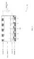
- AMOLED display 300with an array of pixel circuits 200 - 1 through 200 - 9 (each with the same orientation and construction as pixel circuit 200 in FIG. 2 ) that can function to both emit light in a display mode and sense light in a sense mode is illustrated in accordance with embodiments of the present disclosure.
- AMOLED display 300specifically includes, in addition to the array of pixel circuits 200 - 1 through 200 - 9 , a select line driver 302 , a data line driver 304 , and a sensing circuit 306 .
- select line driver 302 and data line driver 304work together under the control of a controller (not shown) to select and program each pixel circuit to provide a particular brightness or luminance. More specifically, select line driver 302 is configured to select a row of pixels circuits for programming by placing an appropriate voltage on one of the select lines 210 . For example, select line driver 302 can select pixel circuits 200 - 2 , 200 - 5 , and 200 - 8 for programming by placing an appropriate voltage on the select line, of select lines 212 , coupled to those pixels.
- select line driver 302selects the row of pixel circuits by turning on their respective access TFTs.
- data line driver 304can program a particular one of the selected pixel circuits by placing an appropriate programming voltage on the data line, of data lines 212 , coupled to that particular pixel circuit. For example, assuming pixel circuits 200 - 2 , 200 - 5 , and 200 - 8 are selected by select line driver 302 , data line driver 304 can program pixel circuit 200 - 5 by placing an appropriate programming voltage on the data line, of data lines 212 , coupled to pixel circuit 200 - 5 .
- the programming voltageis programmed onto the gate of the drive TFT of the particular pixel circuit and, because the drive TFT is biased in its saturation region in the display mode as described above in FIG. 2 , the programming voltage on its gate determines the current through the OLED of the pixel circuit and, thereby, its brightness or luminance.
- Each OLED in the array of pixel circuits 200 - 1 through 200 - 9 operating in the display modecan be individually selected and programmed in the manner described above using select line driver 302 and data line driver 304 to format or create an image for display by AMOLED display 300 .
- the OLED of each pixel circuit 200 - 1 through 200 - 9 operating in the display modeis forward biased by a positive voltage (sufficient to forward bias the OLEDs) applied across first bias voltage lines 214 and second bias voltage lines 216 coupled to those pixel circuits (i.e., the voltage on first bias voltage lines 214 relative to second bias voltage lines 216 is positive).
- select line driver 302 and data line driver 304work together under the control of the controller (not shown) to select and program one or more columns of pixel circuits (or portions of one or more columns of pixel circuits) to be used to sense light for some period of time, rather than emit light.
- the column of pixel circuits 200 - 1 , 200 - 2 , and 200 - 3can be selected by select line driver 302 and programmed by data line driver 304 such that their respective drive TFTs operate in their linear region of operation, as opposed to their saturation region of operation.
- data line driver 304can program the gates of each drive TFT corresponding to pixel circuits 200 - 1 , 200 - 2 , and 200 - 3 with the same or similar voltages such that the drive TFTs operate in their linear region of operation with the same or similar on resistance.
- sensing circuit 306includes a series of switches S 1 , S 2 , and S 3 each coupled to a respective column of the array of pixel circuits 200 - 1 through 200 - 9 .
- Each switchcouples the first bias voltage line, of first bias voltage lines 214 , of its respective column of pixel circuits to one of two different bias voltages, Vb 1 and Vb 3 , depending on the mode in which the column of pixel circuits is to operate.
- the controllercan control switch S 1 to couple the first bias voltage line (of first bias voltage lines 214 corresponding to the column of pixel circuits 200 - 1 , 200 - 2 , and 200 - 3 ) to bias voltage Vb 1 .
- Bias voltage Vb 1is positive relative to bias voltage Vb 2 , which is coupled to the second bias voltage line (of second bias voltage lines 216 corresponding to the column of pixel circuits 200 - 1 , 200 - 2 , and 200 - 3 ).
- pixel circuits 200 - 1 , 200 - 2 , and 200 - 3are forward biased and able to emit light in a display mode.
- the controllercan control switch S 1 to couple the first bias voltage line (of first bias voltage lines 214 corresponding to the column of pixel circuits 200 - 1 , 200 - 2 , and 200 - 3 ) to bias voltage Vb 3 .
- Bias voltage Vb 3is either negative relative to bias voltage Vb 2 , which is coupled to the second bias voltage line (of second bias voltage lines 216 corresponding to the column of pixel circuits 200 - 1 , 200 - 2 , and 200 - 3 ), or is equal to bias voltage Vb 2 .
- pixel circuits 200 - 1 , 200 - 2 , and 200 - 3are either reverse biased and in their photoconductive mode or unbiased and in their photovoltaic mode and, as a result, are able to sense light in a sense mode.
- the column of pixel circuits 200 - 1 , 200 - 2 , and 200 - 3each include an OLED coupled in series with a channel of a drive TFT as shown in FIG. 2 .
- the series coupled OLED and drive TFT of each of these pixel circuits 200 - 1 , 200 - 2 , and 200 - 3 in the columnare further coupled together in a parallel combination.
- a current sensor, included in sensing circuit 306is configured to measure the current produced and flowing through this parallel combination as a result of light striking the surface of the OLEDs of pixel circuits 200 - 1 , 200 - 2 , and 200 - 3 while operating in the sense mode.
- the current sensor, in sensing circuit 306that is specifically configured to measure the current produced by light striking the OLEDs of pixel circuits 200 - 1 , 200 - 2 , and 200 - 3 includes an impedance Z 1 that has some resistive component and a sense amplifier SA 1 .
- the resistive component of impedance Z 1converts the current produced by light striking the OLEDs of pixel circuits 200 - 1 , 200 - 2 , and 200 - 3 into a sense voltage that is then amplified by sense amplifier SA 1 .
- Sense amplifier SA 1outputs a voltage representative of the magnitude of the measured current and provides this voltage to a current reporting circuit 308 for reporting to the controller (not shown).
- FIG. 5illustrates another current sensor 500 that can be used.
- Current sensor 500includes an amplifier 502 and an optional feedback impedance 504 .
- Current reporting circuit 308can communicate the output voltage of each current sensor to the controller (not shown) using any one of a variety of suitable means.
- current reporting circuit 308includes at least one multiplexer configured to select one of the output voltages of the current sensors of sensing circuit 306 for reporting to the controller at a time.
- not current reporting circuit 308is used and the output voltages are sent directly to the controller without any intermediary processing besides, for example, conversion of the current sensor output voltages from an analog value to a digital value.
- the controllercan use the output voltage, which is representative of the intensity of the light striking the column of OLEDs to which the current sensor corresponds, to estimate the ambient light conditions of the environment where AMOLED display 300 is currently operating. For example, and in one embodiment, the controller can low pass filter a number of samples of the output voltage, taken over some period of time and reported to it from one or more current sensors, to estimate the ambient light conditions of the environment where AMOLED display 300 is currently operating. In bright environments, light produced by AMOLED display 300 and reflected back on AMOLED display 300 is typically a non-dominant source of the estimated ambient light. In dark environments, however, light produced by AMOLED display and reflected back on AMOLED display 300 typically becomes a dominant source of the estimated ambient light.
- the controllercan use the estimated ambient light conditions to adjust the brightness or luminance of the OLEDs in AMOLED display 300 to meet, but not greatly exceed, the brightness or luminance required for the ambient light conditions, thereby reducing the power consumed by the display.
- the controllercan increase the brightness or luminance of the OLEDs in AMOLED display 300 , and if the estimated ambient light conditions are comparatively less bright, the controller can reduce the brightness or luminance of the OLEDs in AMO LED display 300 .
- the controllercan further use the estimated ambient light conditions to perform a touch and/or proximity sensing function. For example, and in one embodiment, the controller can determine that one or more pixel circuits of a column of pixel circuits in AMOLED display 300 has been touched by a finger or some other object based on a difference between a light level associated with one or more samples of the output voltage of a current sensor associated with those pixel circuits taken during a period of time and the current estimate of the ambient light level. If the difference is greater than some threshold amount, a touch of one or more of those pixel circuits in the column may be determined to have occurred by the controller.
- the estimated ambient light conditionsare used to “calibrate” the touch sensing function. The proximity of an object to one or more pixel circuits of a column of pixel circuits in AMOLED display 300 can be determined in a similar manner.
- the controllercan further use the estimated ambient light conditions and one or more pixel circuits configured to operate in both the sense and display mode to perform a document scanning function commonly used for facsimile operations, or to perform a fingerprint scanning function commonly used for physical user authentication security operations.
- the array of pixel circuits 200 - 1 through 200 - 9only includes a small number of pixel circuits for the sake of clarity. However, in an actual implementation of AMOLED display 300 , the array generally will include substantially more pixel circuits, although not all pixel circuits necessarily will function to both emit light in a display mode and sense light in a sense mode.
- small groups of pixel circuitscan be configured to operate in both the display mode and the sense mode, while other pixel circuits are configured to operate solely in the display mode.
- the groups of pixel circuits configured to operate in both the display mode and the sense modecan be distributed throughout the array of pixel circuits making up the AMOLED display and can include any number of pixel circuits. For example, 10 ⁇ 10, 20 ⁇ 10, or non-rectangular groupings of pixel circuits configured to operate in both the display mode and the sense mode and can be distributed through the array of pixel circuits making up the AMOLED display, with pixel circuits that only are configured to operate in the display mode placed in between the groups of dual-functioning pixel circuits.
- the groups of dual-functioning pixel circuitscan be placed in the sensing mode at the same or different times and for the same or different durations.
- the groups of dual-functioning pixel circuitsare placed in the sensing mode for only a limited period of time before being placed back into a display mode such that a user of the AMOLED display cannot readily perceive when the groups of dual-functioning pixel circuits are not operating in the display mode or that they are being used for two purposes.
- pixel circuit 200provides only one example of a pixel circuit for implementing pixel circuits 200 - 1 through 200 - 9 illustrated in FIG. 3 .
- Other pixel circuitscan be further used in embodiments of the present disclosure.
- other pixel circuits with additional circuitrye.g., for compensating non-uniformities and stability issues associated with TFTs
- different TFT typese.g., n-type rather than p-type
- programming methodse.g., current-programming rather than voltage-programming
- each pixel circuit implementationwill generally include a drive TFT having its channel in series with an OLED, similar to drive TFT 204 and OLED 202 in FIG. 2 .
- AMOLED display 400with an array of pixel circuits 200 - 1 through 200 - 9 (each with the same orientation and construction as pixel circuit 200 in FIG. 2 ) that can function to both emit light in a display mode and sense light in a sense mode is illustrated in accordance with embodiments of the present disclosure.
- AMOLED display 400is configured and functions in the same manner as AMOLED display 300 described above and illustrated in FIG. 3 .
- AMOLED display 400includes a different sensing circuit 402 .
- sensing circuit 402includes an exemplary current sensor comprised of an impedance Z 1 and a sense amplifier SA 1 that is coupled to more than one column of pixel circuits 200 - 1 through 200 - 9 .
- a current sensorBy coupling the current sensor to more than one column of pixel circuits 200 - 1 through 200 - 9 , the number of components and the complexity of sensing circuit 402 can be reduced.
- a single current sensorcan be used for multiple columns of such pixel circuits.
- such grouping of columnscan reduce sensing resolution and therefore some balance between the number of columns coupled to a single current sensor and the desired sensing resolution may be beneficial.
- FIG. 6a flowchart 600 of a method for operating a dual-function AMOLED display in accordance with embodiments of the present disclosure is illustrated.
- the method of flowchart 600is described with continued reference to the dual-function AMOLED display 300 illustrated in FIG. 3 .
- the methodcan be implemented by other AMOLED displays, such as AMOLED display 400 illustrated in FIG. 4 .
- some of the steps of flowchart 600do not have to occur in the order shown in FIG. 6 .
- the method of flowchart 600begins at step 602 and transitions to step 604 .
- a determinationis made by the controller (not shown) of AMOLED display 300 as to whether a column of pixel circuits (or a portion of a column of pixel circuits) are to operate in a sense mode or in a display mode.
- the column of pixel circuits 200 - 1 , 200 - 2 , and 200 - 3 illustrated in FIG. 3will be used here for discussion purposes.
- step 606the controller of AMOLED display 300 controls switch S 1 to couple the parallel combination of series coupled OLEDs and drive transistors of the column of pixel circuits 200 - 1 , 200 - 2 , and 200 - 3 to bias voltage Vb 1 , which is sufficiently positive relative to bias voltage Vb 2 .
- bias voltage Vb 1When coupled to bias voltage Vb 1 , the column of pixel circuits 200 - 1 , 200 - 2 , and 200 - 3 are forward biased and can be used to emit light in the display mode as described above.
- step 606flowchart 600 transitions to step 608 , where the controller of AMOLED display 300 further controls the drive transistor of each pixel in the column of pixel circuits 200 - 1 , 200 - 2 , and 200 - 3 to be biased in their saturation region of operation.
- step 610the controller of AMOLED display 300 controls switch S 1 to couple the parallel combination of series coupled OLEDs and drive transistors of the column of pixel circuits 200 - 1 , 200 - 2 , and 200 - 3 to bias voltage Vb 3 , which is either equal to or sufficiently negative relative to bias voltage Vb 2 .
- bias voltage Vb 3When coupled to bias voltage Vb 3 , the column of pixel circuits 200 - 1 , 200 - 2 , and 200 - 3 are either unbiased or reverse biased and can be used to sense light in the sense mode as described above.
- step 610flowchart 600 transitions to step 612 , where the controller of AMOLED display 300 further controls the drive transistor of each pixel in the column of pixel circuits 200 - 1 , 200 - 2 , and 200 - 3 to be biased in their linear region of operation.
- step 614the current flowing through the parallel combination of series coupled OLEDs and drive transistors of the column of pixel circuits 200 - 1 , 200 - 2 , and 200 - 3 operating in the sense mode is sensed and reported to the controller of AMOLED display 300 . The controller can then use the value of the reported current to estimate the ambient light conditions of the environment where AMOLED display 300 is currently operating.
- Embodiments of the present inventioncan be implemented in hardware, or as a combination of software and hardware. Consequently, embodiments of the invention may be implemented in the environment of a computer system or other processing system.
- An example of such a computer system 700is shown in FIG. 7 .
- the controller (not shown) of AMOLED display 300 and AMOLED display 400 and each of the steps of the flowchart depicted in FIG. 6can be implemented on one or more distinct computer systems 700 .
- Computer system 700includes one or more processors, such as processor 704 .
- Processor 704can be a special purpose or a general purpose digital signal processor.
- Processor 704is connected to a communication infrastructure 702 (for example, a bus or network).
- a communication infrastructure 702for example, a bus or network.
- Computer system 700also includes a main memory 706 , preferably random access memory (RAM), and may also include a secondary memory 708 .
- Secondary memory 708may include, for example, a hard disk drive 710 and/or a removable storage drive 712 , representing a floppy disk drive, a magnetic tape drive, an optical disk drive, or the like.
- Removable storage drive 712reads from and/or writes to a removable storage unit 716 in a well-known manner.
- Removable storage unit 716represents a floppy disk, magnetic tape, optical disk, or the like, which is read by and written to by removable storage drive 712 .
- removable storage unit 716includes a computer usable storage medium having stored therein computer software and/or data.
- secondary memory 708may include other similar means for allowing computer programs or other instructions to be loaded into computer system 700 .
- Such meansmay include, for example, a removable storage unit 718 and an interface 714 .
- Examples of such meansmay include a program cartridge and cartridge interface (such as that found in video game devices), a removable memory chip (such as an EPROM, or PROM) and associated socket, a thumb drive and USB port, and other removable storage units 718 and interfaces 714 which allow software and data to be transferred from removable storage unit 718 to computer system 700 .
- Computer system 700may also include a communications interface 720 .
- Communications interface 720allows software and data to be transferred between computer system 700 and external devices. Examples of communications interface 720 may include a modem, a network interface (such as an Ethernet card), a communications port, a PCMCIA slot and card, etc.
- Software and data transferred via communications interface 720are in the form of signals which may be electronic, electromagnetic, optical, or other signals capable of being received by communications interface 720 . These signals are provided to communications interface 720 via a communications path 722 .
- Communications path 722carries signals and may be implemented using wire or cable, fiber optics, a phone line, a cellular phone link, an RF link and other communications channels.
- computer program mediumand “computer readable medium” are used to generally refer to tangible storage media such as removable storage units 716 and 718 or a hard disk installed in hard disk drive 710 . These computer program products are means for providing software to computer system 700 .
- Computer programsare stored in main memory 706 and/or secondary memory 708 . Computer programs may also be received via communications interface 720 . Such computer programs, when executed, enable the computer system 700 to implement the present invention as discussed herein. In particular, the computer programs, when executed, enable processor 704 to implement the processes of the present invention, such as any of the methods described herein. Accordingly, such computer programs represent controllers of the computer system 700 . Where the invention is implemented using software, the software may be stored in a computer program product and loaded into computer system 700 using removable storage drive 712 , interface 714 , or communications interface 720 .
- features of the inventionare implemented primarily in hardware using, for example, hardware components such as application-specific integrated circuits (ASICs) and gate arrays.
- ASICsapplication-specific integrated circuits
- gate arraysgate arrays
Landscapes
- Engineering & Computer Science (AREA)
- Theoretical Computer Science (AREA)
- Physics & Mathematics (AREA)
- General Physics & Mathematics (AREA)
- General Engineering & Computer Science (AREA)
- Human Computer Interaction (AREA)
- Computer Hardware Design (AREA)
- Multimedia (AREA)
- Control Of Indicators Other Than Cathode Ray Tubes (AREA)
- Control Of El Displays (AREA)
- Electroluminescent Light Sources (AREA)
Abstract
Description
Claims (22)
Priority Applications (7)
| Application Number | Priority Date | Filing Date | Title |
|---|---|---|---|
| US13/403,267US9183779B2 (en) | 2012-02-23 | 2012-02-23 | AMOLED light sensing |
| EP12005848.2AEP2631898A1 (en) | 2012-02-23 | 2012-08-13 | AMOLED Light Sensing |
| TW101133026ATWI559523B (en) | 2012-02-23 | 2012-09-10 | Amoled light sensing |
| KR1020120106363AKR101425461B1 (en) | 2012-02-23 | 2012-09-25 | Amoled light sensing |
| CN2012103664715ACN103295521A (en) | 2012-02-23 | 2012-09-27 | Amoled light sensing |
| CN201810163726.5ACN108257553B (en) | 2012-02-23 | 2012-09-27 | AMOLED light sensing |
| US14/867,890US9648700B2 (en) | 2012-02-23 | 2015-09-28 | AMOLED light sensing |
Applications Claiming Priority (1)
| Application Number | Priority Date | Filing Date | Title |
|---|---|---|---|
| US13/403,267US9183779B2 (en) | 2012-02-23 | 2012-02-23 | AMOLED light sensing |
Related Child Applications (1)
| Application Number | Title | Priority Date | Filing Date |
|---|---|---|---|
| US14/867,890ContinuationUS9648700B2 (en) | 2012-02-23 | 2015-09-28 | AMOLED light sensing |
Publications (2)
| Publication Number | Publication Date |
|---|---|
| US20130221856A1 US20130221856A1 (en) | 2013-08-29 |
| US9183779B2true US9183779B2 (en) | 2015-11-10 |
Family
ID=46796234
Family Applications (2)
| Application Number | Title | Priority Date | Filing Date |
|---|---|---|---|
| US13/403,267Active2034-08-11US9183779B2 (en) | 2012-02-23 | 2012-02-23 | AMOLED light sensing |
| US14/867,890ActiveUS9648700B2 (en) | 2012-02-23 | 2015-09-28 | AMOLED light sensing |
Family Applications After (1)
| Application Number | Title | Priority Date | Filing Date |
|---|---|---|---|
| US14/867,890ActiveUS9648700B2 (en) | 2012-02-23 | 2015-09-28 | AMOLED light sensing |
Country Status (5)
| Country | Link |
|---|---|
| US (2) | US9183779B2 (en) |
| EP (1) | EP2631898A1 (en) |
| KR (1) | KR101425461B1 (en) |
| CN (2) | CN103295521A (en) |
| TW (1) | TWI559523B (en) |
Cited By (14)
| Publication number | Priority date | Publication date | Assignee | Title |
|---|---|---|---|---|
| US20160021722A1 (en)* | 2012-02-23 | 2016-01-21 | Broadcom Corporation | AMOLED Light Sensing |
| US20180150669A1 (en)* | 2016-11-28 | 2018-05-31 | Nanchang O-Film Bio-Identification Technology Co., Ltd. | Organic light-enitting diode display panel for fingerprint recognition and electronic device |
| US10157590B1 (en) | 2015-12-15 | 2018-12-18 | Apple Inc. | Display with localized brightness adjustment capabilities |
| US10838556B2 (en)* | 2019-04-05 | 2020-11-17 | Apple Inc. | Sensing system for detection of light incident to a light emitting layer of an electronic device display |
| US11067884B2 (en)* | 2018-12-26 | 2021-07-20 | Apple Inc. | Through-display optical transmission, reception, or sensing through micro-optic elements |
| US11295664B2 (en) | 2020-03-11 | 2022-04-05 | Apple Inc. | Display-synchronized optical emitters and transceivers |
| US11327237B2 (en) | 2020-06-18 | 2022-05-10 | Apple Inc. | Display-adjacent optical emission or reception using optical fibers |
| US11487859B2 (en) | 2020-07-31 | 2022-11-01 | Apple Inc. | Behind display polarized optical transceiver |
| US11527582B1 (en) | 2019-09-24 | 2022-12-13 | Apple Inc. | Display stack with integrated photodetectors |
| US11592873B2 (en) | 2020-02-14 | 2023-02-28 | Apple Inc. | Display stack topologies for under-display optical transceivers |
| US11611058B2 (en) | 2019-09-24 | 2023-03-21 | Apple Inc. | Devices and systems for under display image sensor |
| US11733807B2 (en) | 2015-09-25 | 2023-08-22 | Apple Inc. | Light sensing display |
| US11839133B2 (en) | 2021-03-12 | 2023-12-05 | Apple Inc. | Organic photodetectors for in-cell optical sensing |
| US12124002B2 (en) | 2021-09-03 | 2024-10-22 | Apple Inc. | Beam deflector metasurface |
Families Citing this family (50)
| Publication number | Priority date | Publication date | Assignee | Title |
|---|---|---|---|---|
| US8664865B2 (en)* | 2012-03-27 | 2014-03-04 | General Electric Company | Lighting system having an OLED light sensor |
| US20150002554A1 (en)* | 2013-06-26 | 2015-01-01 | Dsp Group Ltd. | Power saving techniques for displays with pixel-addressable intensity |
| TWI480524B (en)* | 2014-05-01 | 2015-04-11 | Univ Chaoyang Technology | Electrical equipment and light sensing method |
| US9741286B2 (en)* | 2014-06-03 | 2017-08-22 | Apple Inc. | Interactive display panel with emitting and sensing diodes |
| US9570002B2 (en) | 2014-06-17 | 2017-02-14 | Apple Inc. | Interactive display panel with IR diodes |
| KR102267600B1 (en)* | 2014-11-19 | 2021-06-23 | 엘지디스플레이 주식회사 | Organic light emitting diode display |
| KR102278607B1 (en)* | 2015-01-12 | 2021-07-19 | 삼성디스플레이 주식회사 | Organic light emitting display |
| US9634048B2 (en)* | 2015-03-24 | 2017-04-25 | Semiconductor Energy Laboratory Co., Ltd. | Imaging device and electronic device |
| CA2898282A1 (en)* | 2015-07-24 | 2017-01-24 | Ignis Innovation Inc. | Hybrid calibration of current sources for current biased voltage progra mmed (cbvp) displays |
| KR102324661B1 (en)* | 2015-07-31 | 2021-11-10 | 엘지디스플레이 주식회사 | Touch sensor integrated type display device and touch sensing method of the same |
| KR102364097B1 (en)* | 2015-08-07 | 2022-02-21 | 엘지디스플레이 주식회사 | Touch sensor integrated type display device and touch sensing method of the same |
| CN105095877B (en)* | 2015-08-12 | 2018-09-04 | 京东方科技集团股份有限公司 | Organic light-emitting diode display substrate and its light reflective surface structural recognition method |
| US9767728B2 (en) | 2015-10-30 | 2017-09-19 | Essential Products, Inc. | Light sensor beneath a dual-mode display |
| US10331260B2 (en) | 2015-10-30 | 2019-06-25 | Essential Products, Inc. | Variable transparency layers for electronic devices |
| US9754526B2 (en) | 2015-10-30 | 2017-09-05 | Essential Products, Inc. | Mobile device with display overlaid with at least a light sensor |
| US10102789B2 (en) | 2015-10-30 | 2018-10-16 | Essential Products, Inc. | Mobile device with display overlaid with at least a light sensor |
| US9823694B2 (en) | 2015-10-30 | 2017-11-21 | Essential Products, Inc. | Camera integrated into a display |
| US9870024B2 (en) | 2015-10-30 | 2018-01-16 | Essential Products, Inc. | Camera integrated into a display |
| US9864400B2 (en) | 2015-10-30 | 2018-01-09 | Essential Products, Inc. | Camera integrated into a display |
| CN105513563B (en)* | 2015-12-05 | 2018-10-16 | 中国航空工业集团公司洛阳电光设备研究所 | A kind of digitlization flat display brightness control device |
| WO2017147614A1 (en) | 2016-02-26 | 2017-08-31 | Essential Products, Inc. | Image capture with a camera integrated display |
| US9961178B2 (en) | 2016-03-24 | 2018-05-01 | Motorola Mobility Llc | Embedded active matrix organic light emitting diode (AMOLED) fingerprint sensor |
| US20170289805A1 (en)* | 2016-03-30 | 2017-10-05 | Motorola Mobility Llc | Embedded active matrix organic light emitting diode (amoled) fingerprint sensor and self-compensating amoled |
| US10541280B1 (en)* | 2016-09-16 | 2020-01-21 | Apple Inc. | OLED based touch sensing and user identification |
| KR102653578B1 (en)* | 2016-11-25 | 2024-04-04 | 엘지디스플레이 주식회사 | Electroluminescent display device integrated with image sensor |
| CN107220592B (en)* | 2017-05-03 | 2020-01-14 | Oppo广东移动通信有限公司 | Optical fingerprint acquisition method and related product |
| WO2019033386A1 (en)* | 2017-08-18 | 2019-02-21 | 深圳市汇顶科技股份有限公司 | Fingerprint image acquisition method and device, and terminal device |
| KR101966820B1 (en)* | 2017-09-29 | 2019-04-08 | 주식회사 센트론 | Method of sensing illuminance using display having passive matrix organic light emitting diode and method of controlling the display |
| US10620750B2 (en)* | 2017-11-07 | 2020-04-14 | Wuhan China Star Optoelectronics Semiconductor Display Technology Co., Ltd. | OLED touch display panel having cathode of OLED circuit also serving as touch electrodes and driving method thereof |
| CN110109562A (en)* | 2018-02-01 | 2019-08-09 | 鸿富锦精密工业(深圳)有限公司 | Miniature LED touch-control display panel |
| CN108154844B (en)* | 2018-03-09 | 2019-07-30 | 京东方科技集团股份有限公司 | A kind of pixel circuit, its driving method and display panel |
| US10768744B2 (en)* | 2018-06-15 | 2020-09-08 | Himax Technologies Limited | Touch panel and controlling method of touch panel |
| CN108877614B (en)* | 2018-07-27 | 2021-03-05 | 维沃移动通信有限公司 | LED circuit, display screen, electronic equipment and detection method |
| WO2020181515A1 (en)* | 2019-03-13 | 2020-09-17 | 京东方科技集团股份有限公司 | Pixel circuit and driving method therefor, and display device |
| WO2020181512A1 (en)* | 2019-03-13 | 2020-09-17 | 京东方科技集团股份有限公司 | Pixel circuit and driving method therefor, and display apparatus |
| TW202036249A (en)* | 2019-03-29 | 2020-10-01 | 光遠科技股份有限公司 | Led circuit and touch sensing method |
| CN111833781A (en)* | 2019-03-29 | 2020-10-27 | 光远科技股份有限公司 | LED circuit and touch detection method |
| KR102173203B1 (en)* | 2019-07-19 | 2020-11-03 | 경희대학교 산학협력단 | Electronic apparatus based on active-matrix and driving method thereof |
| KR102634653B1 (en) | 2019-09-30 | 2024-02-08 | 주식회사 엘엑스세미콘 | Pixel sensing circuit and source driver integrated circuit |
| CN110751113B (en)* | 2019-10-24 | 2023-01-13 | 维沃移动通信有限公司 | Scanning method and electronic equipment |
| CN112420779B (en)* | 2019-12-30 | 2024-08-06 | 义明科技股份有限公司 | Electronic device and ambient light sensing method thereof |
| KR102729889B1 (en)* | 2020-06-10 | 2024-11-13 | 엘지디스플레이 주식회사 | Light emitting display device and method for sensing degradation of the same |
| WO2022027901A1 (en)* | 2020-08-03 | 2022-02-10 | 神盾股份有限公司 | Dual-mode display device having light sensing function |
| CN114092978B (en)* | 2020-08-06 | 2025-03-11 | 北京小米移动软件有限公司 | Signal acquisition circuit, signal acquisition method, and electronic equipment |
| CN114078262A (en)* | 2020-08-21 | 2022-02-22 | 北京小米移动软件有限公司 | Display device, signal acquisition method and electronic device |
| CN114120379A (en)* | 2020-08-27 | 2022-03-01 | 北京小米移动软件有限公司 | Display module, touch method and device, electronic equipment and storage medium |
| CN114512509A (en)* | 2020-11-16 | 2022-05-17 | 华为技术有限公司 | Display device and electronic equipment |
| CN112634818B (en)* | 2020-12-23 | 2022-07-29 | 京东方科技集团股份有限公司 | Pixel driving circuit, driving method and display device |
| CN114531756A (en)* | 2021-12-31 | 2022-05-24 | 成都德鲁伊科技有限公司 | Multifunctional photovoltaic module and intelligent wearable device |
| WO2024101479A1 (en)* | 2022-11-10 | 2024-05-16 | 엘지전자 주식회사 | Display device and image display device including same |
Citations (20)
| Publication number | Priority date | Publication date | Assignee | Title |
|---|---|---|---|---|
| US20020030647A1 (en) | 2000-06-06 | 2002-03-14 | Michael Hack | Uniform active matrix oled displays |
| WO2003054980A2 (en) | 2001-12-20 | 2003-07-03 | Koninklijke Philips Electronics N.V. | Dual-function electroluminescent device and method for driving the same |
| US20030122749A1 (en) | 2001-12-31 | 2003-07-03 | Booth Lawrence A. | Energy sensing light emitting diode display |
| WO2004042413A1 (en) | 2002-11-06 | 2004-05-21 | Koninklijke Philips Electronics N.V. | Inspecting method and apparatus for a led matrix display |
| US20040100463A1 (en)* | 2002-10-31 | 2004-05-27 | Keisuke Miyagawa | Display device and controlling method thereof |
| US20040245438A1 (en) | 2003-06-05 | 2004-12-09 | Payne David M. | Electronic device having a light emitting/detecting display screen |
| DE10359881A1 (en) | 2003-12-12 | 2005-07-14 | Samsung SDI Co., Ltd., Suwon | Organic light emitting diode (OLED) component e.g. for surface display, has current flow through OLED-component measured |
| US20060055631A1 (en)* | 2004-08-31 | 2006-03-16 | Tohoku Pioneer Corporation | Drive device of light emitting display panel |
| US20060114176A1 (en)* | 2004-11-30 | 2006-06-01 | Masamitsu Furuie | Display panel |
| US20070252005A1 (en) | 2006-05-01 | 2007-11-01 | Konicek Jeffrey C | Active matrix emissive display and optical scanner system, methods and applications |
| US20080048951A1 (en)* | 2006-04-13 | 2008-02-28 | Naugler Walter E Jr | Method and apparatus for managing and uniformly maintaining pixel circuitry in a flat panel display |
| US20080094009A1 (en)* | 2004-07-30 | 2008-04-24 | Semiconductor Energy Laboratory Co., Ltd. | Display device, driving method thereof and electronic appliance |
| CN101241688A (en) | 2007-02-07 | 2008-08-13 | 三星电子株式会社 | Low power driving device and method |
| US20100156881A1 (en)* | 2008-12-24 | 2010-06-24 | Hitachi Displays, Ltd. | Image display device |
| US20100214140A1 (en)* | 2009-02-23 | 2010-08-26 | Texas Instruments Deutschland Gmbh | Digital trimming of sar adcs |
| US20100225634A1 (en)* | 2009-03-04 | 2010-09-09 | Levey Charles I | Electroluminescent display compensated drive signal |
| TW201103143A (en) | 2009-07-02 | 2011-01-16 | Au Optronics Corp | Organic light emitting diode touch display |
| TW201131752A (en) | 2010-03-11 | 2011-09-16 | Au Optronics Corp | Amoled display with optical feedback compensation |
| US20140225883A1 (en)* | 2004-12-15 | 2014-08-14 | Ignis Innovation Inc. | System and methods for extraction of threshold and mobility parameters in amoled displays |
| US20140340436A1 (en)* | 2013-05-16 | 2014-11-20 | Samsung Display Co., Ltd. | Electro-optical device and driving method thereof |
Family Cites Families (26)
| Publication number | Priority date | Publication date | Assignee | Title |
|---|---|---|---|---|
| TWI252592B (en)* | 2000-01-17 | 2006-04-01 | Semiconductor Energy Lab | EL display device |
| EP1128662A1 (en)* | 2000-02-22 | 2001-08-29 | Agilent Technologies Inc. a Delaware Corporation | Active pixel sensor with photo diode discharge |
| GB2381644A (en)* | 2001-10-31 | 2003-05-07 | Cambridge Display Tech Ltd | Display drivers |
| US6664744B2 (en)* | 2002-04-03 | 2003-12-16 | Mitsubishi Electric Research Laboratories, Inc. | Automatic backlight for handheld devices |
| JP4706168B2 (en)* | 2003-07-16 | 2011-06-22 | ソニー株式会社 | Display device and display reading device |
| JP4055722B2 (en)* | 2003-11-10 | 2008-03-05 | ソニー株式会社 | Active matrix organic EL display |
| US20060007205A1 (en)* | 2004-06-29 | 2006-01-12 | Damoder Reddy | Active-matrix display and pixel structure for feedback stabilized flat panel display |
| JP4111185B2 (en)* | 2004-10-19 | 2008-07-02 | セイコーエプソン株式会社 | Electro-optical device, driving method thereof, and electronic apparatus |
| CN1609938A (en)* | 2004-11-25 | 2005-04-27 | 友达光电股份有限公司 | Circuit and method for automatically adjusting self-illumination brightness |
| EP1696414A1 (en)* | 2005-02-28 | 2006-08-30 | Research In Motion Limited | Backlight control for a portable computing device |
| JP2007003640A (en)* | 2005-06-22 | 2007-01-11 | Tohoku Pioneer Corp | Self-luminous panel |
| KR100740135B1 (en)* | 2006-08-16 | 2007-07-16 | 삼성에스디아이 주식회사 | Sensor combined organic display and driving method |
| KR20080090662A (en)* | 2007-04-05 | 2008-10-09 | 엘지디스플레이 주식회사 | Electro-luminescence display device |
| CN101514921B (en)* | 2008-02-22 | 2013-05-15 | 凌通科技股份有限公司 | Method for detecting ambient brightness, method for saving power, and display device using same |
| US8154310B1 (en)* | 2008-02-27 | 2012-04-10 | Cypress Semiconductor Corporation | Capacitance sensor with sensor capacitance compensation |
| CN101785043B (en)* | 2008-06-17 | 2013-06-19 | 松下电器产业株式会社 | Display apparatus and control method therefor |
| US8519722B1 (en)* | 2008-10-22 | 2013-08-27 | Cypress Semiconductor Corporation | Method and apparatus for testing projected capacitance matrices and determining the location and types of faults |
| JP2010122936A (en)* | 2008-11-20 | 2010-06-03 | Seiko Epson Corp | Sensing circuit, display and electronic apparatus |
| KR101613327B1 (en)* | 2009-02-27 | 2016-04-18 | 가부시키가이샤 재팬 디스프레이 | Display device, touch panel, and electronic equipment |
| JP5345007B2 (en)* | 2009-06-29 | 2013-11-20 | 株式会社ワコム | Position detecting device, position detecting circuit and position detecting method |
| TWI428906B (en)* | 2009-09-30 | 2014-03-01 | Toshiba Global Commerce Solutions Holdings Corp | Method of automatically adjusting a brightness of an optical touch panel and apparatus thereof |
| US8599155B2 (en)* | 2010-04-30 | 2013-12-03 | Microchip Technology Incorporated | Touch sense using time domain reflectometry |
| JP5839173B2 (en)* | 2010-10-14 | 2016-01-06 | Nltテクノロジー株式会社 | Touch sensor device and electronic device |
| US9183779B2 (en) | 2012-02-23 | 2015-11-10 | Broadcom Corporation | AMOLED light sensing |
| WO2014042248A1 (en)* | 2012-09-14 | 2014-03-20 | シャープ株式会社 | Touch panel and touch panel integrated display device |
| US8987652B2 (en)* | 2012-12-13 | 2015-03-24 | Apple Inc. | Electronic device with display and low-noise ambient light sensor with a control circuitry that periodically disables the display |
- 2012
- 2012-02-23USUS13/403,267patent/US9183779B2/enactiveActive
- 2012-08-13EPEP12005848.2Apatent/EP2631898A1/ennot_activeCeased
- 2012-09-10TWTW101133026Apatent/TWI559523B/enactive
- 2012-09-25KRKR1020120106363Apatent/KR101425461B1/enactiveActive
- 2012-09-27CNCN2012103664715Apatent/CN103295521A/enactivePending
- 2012-09-27CNCN201810163726.5Apatent/CN108257553B/enactiveActive
- 2015
- 2015-09-28USUS14/867,890patent/US9648700B2/enactiveActive
Patent Citations (29)
| Publication number | Priority date | Publication date | Assignee | Title |
|---|---|---|---|---|
| US20020030647A1 (en) | 2000-06-06 | 2002-03-14 | Michael Hack | Uniform active matrix oled displays |
| WO2003054980A2 (en) | 2001-12-20 | 2003-07-03 | Koninklijke Philips Electronics N.V. | Dual-function electroluminescent device and method for driving the same |
| US7348946B2 (en) | 2001-12-31 | 2008-03-25 | Intel Corporation | Energy sensing light emitting diode display |
| US20030122749A1 (en) | 2001-12-31 | 2003-07-03 | Booth Lawrence A. | Energy sensing light emitting diode display |
| CN1608281A (en) | 2001-12-31 | 2005-04-20 | 英特尔公司 | Energy sensing light emitting diode display |
| US20040100463A1 (en)* | 2002-10-31 | 2004-05-27 | Keisuke Miyagawa | Display device and controlling method thereof |
| WO2004042413A1 (en) | 2002-11-06 | 2004-05-21 | Koninklijke Philips Electronics N.V. | Inspecting method and apparatus for a led matrix display |
| CN1711479A (en) | 2002-11-06 | 2005-12-21 | 皇家飞利浦电子股份有限公司 | Inspecting method and apparatus for a LED matrix display |
| US20060015272A1 (en) | 2002-11-06 | 2006-01-19 | Andrea Giraldo | Inspecting method and apparatus for a led matrix display |
| US7423617B2 (en) | 2002-11-06 | 2008-09-09 | Tpo Displays Corp. | Light emissive element having pixel sensing circuit |
| US20040245438A1 (en) | 2003-06-05 | 2004-12-09 | Payne David M. | Electronic device having a light emitting/detecting display screen |
| DE10359881A1 (en) | 2003-12-12 | 2005-07-14 | Samsung SDI Co., Ltd., Suwon | Organic light emitting diode (OLED) component e.g. for surface display, has current flow through OLED-component measured |
| US20080094009A1 (en)* | 2004-07-30 | 2008-04-24 | Semiconductor Energy Laboratory Co., Ltd. | Display device, driving method thereof and electronic appliance |
| US20060055631A1 (en)* | 2004-08-31 | 2006-03-16 | Tohoku Pioneer Corporation | Drive device of light emitting display panel |
| US20060114176A1 (en)* | 2004-11-30 | 2006-06-01 | Masamitsu Furuie | Display panel |
| US20140225883A1 (en)* | 2004-12-15 | 2014-08-14 | Ignis Innovation Inc. | System and methods for extraction of threshold and mobility parameters in amoled displays |
| US20080048951A1 (en)* | 2006-04-13 | 2008-02-28 | Naugler Walter E Jr | Method and apparatus for managing and uniformly maintaining pixel circuitry in a flat panel display |
| US20070252005A1 (en) | 2006-05-01 | 2007-11-01 | Konicek Jeffrey C | Active matrix emissive display and optical scanner system, methods and applications |
| US8063871B2 (en) | 2007-02-07 | 2011-11-22 | Samsung Electronics Co., Ltd. | Low-power driving apparatus and method |
| EP1956584A2 (en) | 2007-02-07 | 2008-08-13 | Samsung Electronics Co., Ltd. | Low-power driving apparatus and method |
| CN101241688A (en) | 2007-02-07 | 2008-08-13 | 三星电子株式会社 | Low power driving device and method |
| US20100156881A1 (en)* | 2008-12-24 | 2010-06-24 | Hitachi Displays, Ltd. | Image display device |
| US20100214140A1 (en)* | 2009-02-23 | 2010-08-26 | Texas Instruments Deutschland Gmbh | Digital trimming of sar adcs |
| US20100225634A1 (en)* | 2009-03-04 | 2010-09-09 | Levey Charles I | Electroluminescent display compensated drive signal |
| TW201103143A (en) | 2009-07-02 | 2011-01-16 | Au Optronics Corp | Organic light emitting diode touch display |
| US8674964B2 (en) | 2009-07-02 | 2014-03-18 | Au Optronics Corp. | Organic light emitting diode touch display |
| TW201131752A (en) | 2010-03-11 | 2011-09-16 | Au Optronics Corp | Amoled display with optical feedback compensation |
| US8669924B2 (en) | 2010-03-11 | 2014-03-11 | Au Optronics Corporation | Amoled display with optical feedback compensation |
| US20140340436A1 (en)* | 2013-05-16 | 2014-11-20 | Samsung Display Co., Ltd. | Electro-optical device and driving method thereof |
Non-Patent Citations (5)
| Title |
|---|
| Chinese Office Action issued in related Chinese Application No. 201210366471.5, dated Oct. 10, 2014, 7 pages. |
| Communication from the Examining Division of the European Patent Office, directed to related European Patent Application No. 12 005 848.2, Munich, Germany, mailed Apr. 9, 2014; 13 pages. |
| European Search Report directed to related European Patent Application No. 12005848.2, mailed on Oct. 21, 2014; 17 pages. |
| European Search Report for European Patent Application No. EP 12 00 5848, Munich, Germany, mailed on Jan. 24, 2013. |
| Office Action directed to related Taiwanese Patent Application No. 101133026, mailed on Jan. 28, 2015; 7 pages. |
Cited By (23)
| Publication number | Priority date | Publication date | Assignee | Title |
|---|---|---|---|---|
| US9648700B2 (en)* | 2012-02-23 | 2017-05-09 | Avago Technologies General Ip (Singapore) Pte. Ltd. | AMOLED light sensing |
| US20160021722A1 (en)* | 2012-02-23 | 2016-01-21 | Broadcom Corporation | AMOLED Light Sensing |
| US11733807B2 (en) | 2015-09-25 | 2023-08-22 | Apple Inc. | Light sensing display |
| US11580934B2 (en) | 2015-12-15 | 2023-02-14 | Apple Inc. | Display with localized brightness adjustment capabilities |
| US10157590B1 (en) | 2015-12-15 | 2018-12-18 | Apple Inc. | Display with localized brightness adjustment capabilities |
| US10984752B2 (en) | 2015-12-15 | 2021-04-20 | Apple Inc. | Display with localized brightness adjustment capabilities |
| US12198656B2 (en) | 2015-12-15 | 2025-01-14 | Apple Inc. | Display with localized brightness adjustment capabilities |
| US11842708B2 (en) | 2015-12-15 | 2023-12-12 | Apple Inc. | Display with localized brightness adjustment capabilities |
| US11348555B2 (en) | 2015-12-15 | 2022-05-31 | Apple Inc. | Display with localized brightness adjustment capabilities |
| US20180150669A1 (en)* | 2016-11-28 | 2018-05-31 | Nanchang O-Film Bio-Identification Technology Co., Ltd. | Organic light-enitting diode display panel for fingerprint recognition and electronic device |
| US10089515B2 (en)* | 2016-11-28 | 2018-10-02 | Nanchang O-Film Bio-Identification Technology Co., Ltd. | Organic light-enitting diode display panel for fingerprint recognition and electronic device |
| US11067884B2 (en)* | 2018-12-26 | 2021-07-20 | Apple Inc. | Through-display optical transmission, reception, or sensing through micro-optic elements |
| US10838556B2 (en)* | 2019-04-05 | 2020-11-17 | Apple Inc. | Sensing system for detection of light incident to a light emitting layer of an electronic device display |
| US11422661B2 (en) | 2019-04-05 | 2022-08-23 | Apple Inc. | Sensing system for detection of light incident to a light emitting layer of an electronic device display |
| US11527582B1 (en) | 2019-09-24 | 2022-12-13 | Apple Inc. | Display stack with integrated photodetectors |
| US11611058B2 (en) | 2019-09-24 | 2023-03-21 | Apple Inc. | Devices and systems for under display image sensor |
| US12016237B2 (en) | 2019-09-24 | 2024-06-18 | Apple Inc. | Display stack with integrated photodetectors |
| US11592873B2 (en) | 2020-02-14 | 2023-02-28 | Apple Inc. | Display stack topologies for under-display optical transceivers |
| US11295664B2 (en) | 2020-03-11 | 2022-04-05 | Apple Inc. | Display-synchronized optical emitters and transceivers |
| US11327237B2 (en) | 2020-06-18 | 2022-05-10 | Apple Inc. | Display-adjacent optical emission or reception using optical fibers |
| US11487859B2 (en) | 2020-07-31 | 2022-11-01 | Apple Inc. | Behind display polarized optical transceiver |
| US11839133B2 (en) | 2021-03-12 | 2023-12-05 | Apple Inc. | Organic photodetectors for in-cell optical sensing |
| US12124002B2 (en) | 2021-09-03 | 2024-10-22 | Apple Inc. | Beam deflector metasurface |
Also Published As
| Publication number | Publication date |
|---|---|
| EP2631898A1 (en) | 2013-08-28 |
| CN108257553B (en) | 2023-08-29 |
| US9648700B2 (en) | 2017-05-09 |
| CN108257553A (en) | 2018-07-06 |
| KR101425461B1 (en) | 2014-07-31 |
| TW201336066A (en) | 2013-09-01 |
| KR20130097051A (en) | 2013-09-02 |
| US20160021722A1 (en) | 2016-01-21 |
| US20130221856A1 (en) | 2013-08-29 |
| TWI559523B (en) | 2016-11-21 |
| CN103295521A (en) | 2013-09-11 |
Similar Documents
| Publication | Publication Date | Title |
|---|---|---|
| US9648700B2 (en) | AMOLED light sensing | |
| US10068950B2 (en) | Pixel circuit, driving method thereof, and display apparatus | |
| CN104091562B (en) | Pixel circuit, display panel and display device | |
| KR101821519B1 (en) | Pixel circuit, driving method therefor and display device | |
| CN104078006B (en) | Image element circuit, display panel and display device | |
| CN103996377B (en) | Image element circuit and display device | |
| EP3316085A1 (en) | In-cell touch display panel, driving method therefor, and display device | |
| WO2016045301A1 (en) | Pixel circuit, driving method therefor, organic light-emitting display panel, and display device | |
| CN104036723B (en) | Image element circuit and display device | |
| US20150268763A1 (en) | Organic light-emitting diode pixel circuit, driving method thereof, and display device | |
| CN104269142B (en) | Touch drive circuit and its driving method | |
| US9778800B2 (en) | Pixel circuit, display panel and display apparatus | |
| CN104102382A (en) | Touch display driving circuit and touch display device | |
| CN203895093U (en) | Pixel circuit and display device | |
| CN203941676U (en) | Image element circuit, display panel and display device | |
| US9697797B2 (en) | Method and apparatus for displaying content | |
| CN203941677U (en) | Image element circuit, display panel and display device | |
| HK1185439A (en) | Amoled light sensing | |
| CN112365812A (en) | Light emitting module, light emitting panel and light emitting panel brightness uniformity processing method |
Legal Events
| Date | Code | Title | Description |
|---|---|---|---|
| AS | Assignment | Owner name:BROADCOM CORPORATION, CALIFORNIA Free format text:ASSIGNMENT OF ASSIGNORS INTEREST;ASSIGNOR:SOTO, WALTER;REEL/FRAME:027751/0411 Effective date:20120221 | |
| AS | Assignment | Owner name:BROADCOM CORPORATION, CALIFORNIA Free format text:ASSIGNMENT OF ASSIGNORS INTEREST;ASSIGNOR:SOTO, WALTER;REEL/FRAME:036672/0982 Effective date:20120221 | |
| STCF | Information on status: patent grant | Free format text:PATENTED CASE | |
| AS | Assignment | Owner name:BANK OF AMERICA, N.A., AS COLLATERAL AGENT, NORTH CAROLINA Free format text:PATENT SECURITY AGREEMENT;ASSIGNOR:BROADCOM CORPORATION;REEL/FRAME:037806/0001 Effective date:20160201 Owner name:BANK OF AMERICA, N.A., AS COLLATERAL AGENT, NORTH Free format text:PATENT SECURITY AGREEMENT;ASSIGNOR:BROADCOM CORPORATION;REEL/FRAME:037806/0001 Effective date:20160201 | |
| AS | Assignment | Owner name:AVAGO TECHNOLOGIES GENERAL IP (SINGAPORE) PTE. LTD., SINGAPORE Free format text:ASSIGNMENT OF ASSIGNORS INTEREST;ASSIGNOR:BROADCOM CORPORATION;REEL/FRAME:041706/0001 Effective date:20170120 Owner name:AVAGO TECHNOLOGIES GENERAL IP (SINGAPORE) PTE. LTD Free format text:ASSIGNMENT OF ASSIGNORS INTEREST;ASSIGNOR:BROADCOM CORPORATION;REEL/FRAME:041706/0001 Effective date:20170120 | |
| AS | Assignment | Owner name:BROADCOM CORPORATION, CALIFORNIA Free format text:TERMINATION AND RELEASE OF SECURITY INTEREST IN PATENTS;ASSIGNOR:BANK OF AMERICA, N.A., AS COLLATERAL AGENT;REEL/FRAME:041712/0001 Effective date:20170119 | |
| AS | Assignment | Owner name:AVAGO TECHNOLOGIES INTERNATIONAL SALES PTE. LIMITE Free format text:MERGER;ASSIGNOR:AVAGO TECHNOLOGIES GENERAL IP (SINGAPORE) PTE. LTD.;REEL/FRAME:047229/0408 Effective date:20180509 | |
| AS | Assignment | Owner name:AVAGO TECHNOLOGIES INTERNATIONAL SALES PTE. LIMITE Free format text:CORRECTIVE ASSIGNMENT TO CORRECT THE EFFECTIVE DATE PREVIOUSLY RECORDED ON REEL 047229 FRAME 0408. ASSIGNOR(S) HEREBY CONFIRMS THE THE EFFECTIVE DATE IS 09/05/2018;ASSIGNOR:AVAGO TECHNOLOGIES GENERAL IP (SINGAPORE) PTE. LTD.;REEL/FRAME:047349/0001 Effective date:20180905 | |
| AS | Assignment | Owner name:AVAGO TECHNOLOGIES INTERNATIONAL SALES PTE. LIMITE Free format text:CORRECTIVE ASSIGNMENT TO CORRECT THE PATENT NUMBER 9,385,856 TO 9,385,756 PREVIOUSLY RECORDED AT REEL: 47349 FRAME: 001. ASSIGNOR(S) HEREBY CONFIRMS THE MERGER;ASSIGNOR:AVAGO TECHNOLOGIES GENERAL IP (SINGAPORE) PTE. LTD.;REEL/FRAME:051144/0648 Effective date:20180905 | |
| MAFP | Maintenance fee payment | Free format text:PAYMENT OF MAINTENANCE FEE, 4TH YEAR, LARGE ENTITY (ORIGINAL EVENT CODE: M1551); ENTITY STATUS OF PATENT OWNER: LARGE ENTITY Year of fee payment:4 | |
| MAFP | Maintenance fee payment | Free format text:PAYMENT OF MAINTENANCE FEE, 8TH YEAR, LARGE ENTITY (ORIGINAL EVENT CODE: M1552); ENTITY STATUS OF PATENT OWNER: LARGE ENTITY Year of fee payment:8 |