US9182587B2 - Manufacturing structure and process for compliant mechanisms - Google Patents
Manufacturing structure and process for compliant mechanismsDownload PDFInfo
- Publication number
- US9182587B2 US9182587B2US13/123,859US200913123859AUS9182587B2US 9182587 B2US9182587 B2US 9182587B2US 200913123859 AUS200913123859 AUS 200913123859AUS 9182587 B2US9182587 B2US 9182587B2
- Authority
- US
- United States
- Prior art keywords
- shutter
- mold
- beams
- substrate
- light
- Prior art date
- Legal status (The legal status is an assumption and is not a legal conclusion. Google has not performed a legal analysis and makes no representation as to the accuracy of the status listed.)
- Active, expires
Links
- 238000000034methodMethods0.000titleclaimsabstractdescription100
- 238000004519manufacturing processMethods0.000titleclaimsdescription22
- 230000008569processEffects0.000titledescription54
- 230000007246mechanismEffects0.000titledescription3
- 239000000463materialSubstances0.000claimsdescription120
- 239000000758substrateSubstances0.000claimsdescription76
- 238000005530etchingMethods0.000claimsdescription22
- 238000000151depositionMethods0.000claimsdescription21
- 230000015572biosynthetic processEffects0.000claimsdescription4
- 239000010410layerSubstances0.000description101
- 230000000712assemblyEffects0.000description36
- 238000000429assemblyMethods0.000description36
- 239000011159matrix materialSubstances0.000description31
- 230000002093peripheral effectEffects0.000description21
- 239000012530fluidSubstances0.000description17
- 230000033001locomotionEffects0.000description17
- 238000000576coating methodMethods0.000description16
- VYPSYNLAJGMNEJ-UHFFFAOYSA-Nsilicon dioxideInorganic materialsO=[Si]=OVYPSYNLAJGMNEJ-UHFFFAOYSA-N0.000description16
- 239000010408filmSubstances0.000description15
- 238000000059patterningMethods0.000description14
- 229920002120photoresistant polymerPolymers0.000description14
- 230000008021depositionEffects0.000description13
- 238000000206photolithographyMethods0.000description13
- 238000005286illuminationMethods0.000description11
- 229910052751metalInorganic materials0.000description11
- 239000002184metalSubstances0.000description11
- 239000010409thin filmSubstances0.000description11
- 239000003086colorantSubstances0.000description10
- 210000002381plasmaAnatomy0.000description10
- 238000000623plasma-assisted chemical vapour depositionMethods0.000description10
- 238000005229chemical vapour depositionMethods0.000description9
- 239000011521glassSubstances0.000description9
- 230000003287optical effectEffects0.000description9
- 239000002131composite materialSubstances0.000description8
- 239000004020conductorSubstances0.000description8
- 229910052710siliconInorganic materials0.000description8
- 229910021417amorphous siliconInorganic materials0.000description7
- 239000011248coating agentSubstances0.000description7
- 229910052681coesiteInorganic materials0.000description7
- 229910052906cristobaliteInorganic materials0.000description7
- 238000010586diagramMethods0.000description7
- 238000010348incorporationMethods0.000description7
- 239000000377silicon dioxideSubstances0.000description7
- 229910052682stishoviteInorganic materials0.000description7
- 229910052905tridymiteInorganic materials0.000description7
- 229910052581Si3N4Inorganic materials0.000description6
- 239000000853adhesiveSubstances0.000description6
- 230000001070adhesive effectEffects0.000description6
- 230000000903blocking effectEffects0.000description6
- 239000003990capacitorSubstances0.000description6
- 230000006870functionEffects0.000description6
- 230000000873masking effectEffects0.000description6
- 239000004033plasticSubstances0.000description6
- 229920003023plasticPolymers0.000description6
- 229920000642polymerPolymers0.000description6
- 230000004044responseEffects0.000description6
- 239000000126substanceSubstances0.000description6
- OKTJSMMVPCPJKN-UHFFFAOYSA-NCarbonChemical compound[C]OKTJSMMVPCPJKN-UHFFFAOYSA-N0.000description5
- 229910045601alloyInorganic materials0.000description5
- 239000000956alloySubstances0.000description5
- 229910052782aluminiumInorganic materials0.000description5
- 229910052804chromiumInorganic materials0.000description5
- 239000011651chromiumSubstances0.000description5
- 229910052759nickelInorganic materials0.000description5
- 238000012545processingMethods0.000description5
- 239000004065semiconductorSubstances0.000description5
- 238000004544sputter depositionMethods0.000description5
- LFQSCWFLJHTTHZ-UHFFFAOYSA-NEthanolChemical compoundCCOLFQSCWFLJHTTHZ-UHFFFAOYSA-N0.000description4
- XUIMIQQOPSSXEZ-UHFFFAOYSA-NSiliconChemical compound[Si]XUIMIQQOPSSXEZ-UHFFFAOYSA-N0.000description4
- 230000008901benefitEffects0.000description4
- 229910052799carbonInorganic materials0.000description4
- 238000010276constructionMethods0.000description4
- 229910052802copperInorganic materials0.000description4
- 239000010949copperSubstances0.000description4
- 238000013461designMethods0.000description4
- 230000009977dual effectEffects0.000description4
- 229910052750molybdenumInorganic materials0.000description4
- 239000010703siliconSubstances0.000description4
- 229910052715tantalumInorganic materials0.000description4
- 229910004613CdTeInorganic materials0.000description3
- 239000004593EpoxySubstances0.000description3
- OKKJLVBELUTLKV-UHFFFAOYSA-NMethanolChemical compoundOCOKKJLVBELUTLKV-UHFFFAOYSA-N0.000description3
- HEMHJVSKTPXQMS-UHFFFAOYSA-MSodium hydroxideChemical compound[OH-].[Na+]HEMHJVSKTPXQMS-UHFFFAOYSA-M0.000description3
- XAGFODPZIPBFFR-UHFFFAOYSA-NaluminiumChemical compound[Al]XAGFODPZIPBFFR-UHFFFAOYSA-N0.000description3
- PNEYBMLMFCGWSK-UHFFFAOYSA-Naluminium oxideInorganic materials[O-2].[O-2].[O-2].[Al+3].[Al+3]PNEYBMLMFCGWSK-UHFFFAOYSA-N0.000description3
- 230000005540biological transmissionEffects0.000description3
- 230000015556catabolic processEffects0.000description3
- 150000001875compoundsChemical class0.000description3
- 229910052593corundumInorganic materials0.000description3
- 238000006073displacement reactionMethods0.000description3
- 238000007772electroless platingMethods0.000description3
- 238000001704evaporationMethods0.000description3
- 230000008020evaporationEffects0.000description3
- 230000002209hydrophobic effectEffects0.000description3
- 150000002500ionsChemical class0.000description3
- 239000004973liquid crystal related substanceSubstances0.000description3
- 239000000314lubricantSubstances0.000description3
- 230000005226mechanical processes and functionsEffects0.000description3
- 150000002739metalsChemical class0.000description3
- 229920003986novolacPolymers0.000description3
- 238000012163sequencing techniqueMethods0.000description3
- 125000006850spacer groupChemical group0.000description3
- 238000009736wettingMethods0.000description3
- 229910001845yogo sapphireInorganic materials0.000description3
- KVNYFPKFSJIPBJ-UHFFFAOYSA-N1,2-diethylbenzeneChemical compoundCCC1=CC=CC=C1CCKVNYFPKFSJIPBJ-UHFFFAOYSA-N0.000description2
- KRHYYFGTRYWZRS-UHFFFAOYSA-NFluoraneChemical compoundFKRHYYFGTRYWZRS-UHFFFAOYSA-N0.000description2
- YCKRFDGAMUMZLT-UHFFFAOYSA-NFluorine atomChemical compound[F]YCKRFDGAMUMZLT-UHFFFAOYSA-N0.000description2
- 229910001218Gallium arsenideInorganic materials0.000description2
- IMNFDUFMRHMDMM-UHFFFAOYSA-NN-HeptaneChemical compoundCCCCCCCIMNFDUFMRHMDMM-UHFFFAOYSA-N0.000description2
- 229910052779NeodymiumInorganic materials0.000description2
- ISWSIDIOOBJBQZ-UHFFFAOYSA-NPhenolChemical compoundOC1=CC=CC=C1ISWSIDIOOBJBQZ-UHFFFAOYSA-N0.000description2
- XYFCBTPGUUZFHI-UHFFFAOYSA-NPhosphineChemical compoundPXYFCBTPGUUZFHI-UHFFFAOYSA-N0.000description2
- 239000004642PolyimideSubstances0.000description2
- QAOWNCQODCNURD-UHFFFAOYSA-NSulfuric acidChemical compoundOS(O)(=O)=OQAOWNCQODCNURD-UHFFFAOYSA-N0.000description2
- GWEVSGVZZGPLCZ-UHFFFAOYSA-NTitan oxideChemical compoundO=[Ti]=OGWEVSGVZZGPLCZ-UHFFFAOYSA-N0.000description2
- 239000011358absorbing materialSubstances0.000description2
- 239000000654additiveSubstances0.000description2
- 238000003491arrayMethods0.000description2
- 238000000231atomic layer depositionMethods0.000description2
- QVGXLLKOCUKJST-UHFFFAOYSA-Natomic oxygenChemical compound[O]QVGXLLKOCUKJST-UHFFFAOYSA-N0.000description2
- 238000005452bendingMethods0.000description2
- 210000004556brainAnatomy0.000description2
- 238000006243chemical reactionMethods0.000description2
- QDOXWKRWXJOMAK-UHFFFAOYSA-Ndichromium trioxideChemical compoundO=[Cr]O[Cr]=OQDOXWKRWXJOMAK-UHFFFAOYSA-N0.000description2
- -1dimethylsiloxaneChemical class0.000description2
- GNTDGMZSJNCJKK-UHFFFAOYSA-Ndivanadium pentaoxideChemical compoundO=[V](=O)O[V](=O)=OGNTDGMZSJNCJKK-UHFFFAOYSA-N0.000description2
- 230000005684electric fieldEffects0.000description2
- 238000009713electroplatingMethods0.000description2
- 238000005516engineering processMethods0.000description2
- 230000007613environmental effectEffects0.000description2
- 229910052731fluorineInorganic materials0.000description2
- 239000011737fluorineSubstances0.000description2
- 229920002313fluoropolymerPolymers0.000description2
- 239000004811fluoropolymerSubstances0.000description2
- 239000007789gasSubstances0.000description2
- 229910052732germaniumInorganic materials0.000description2
- 238000003384imaging methodMethods0.000description2
- 238000007373indentationMethods0.000description2
- 239000007788liquidSubstances0.000description2
- 238000011068loading methodMethods0.000description2
- 238000004518low pressure chemical vapour depositionMethods0.000description2
- 238000005459micromachiningMethods0.000description2
- PXHVJJICTQNCMI-UHFFFAOYSA-NnickelSubstances[Ni]PXHVJJICTQNCMI-UHFFFAOYSA-N0.000description2
- 229910052758niobiumInorganic materials0.000description2
- ZKATWMILCYLAPD-UHFFFAOYSA-Nniobium pentoxideChemical compoundO=[Nb](=O)O[Nb](=O)=OZKATWMILCYLAPD-UHFFFAOYSA-N0.000description2
- 239000001301oxygenSubstances0.000description2
- 229910052760oxygenInorganic materials0.000description2
- 239000002245particleSubstances0.000description2
- 229920001568phenolic resinPolymers0.000description2
- 229920001721polyimidePolymers0.000description2
- 239000002861polymer materialSubstances0.000description2
- 229920005989resinPolymers0.000description2
- 239000011347resinSubstances0.000description2
- 238000005096rolling processMethods0.000description2
- 238000000926separation methodMethods0.000description2
- 229920002545silicone oilPolymers0.000description2
- PBCFLUZVCVVTBY-UHFFFAOYSA-Ntantalum pentoxideInorganic materialsO=[Ta](=O)O[Ta](=O)=OPBCFLUZVCVVTBY-UHFFFAOYSA-N0.000description2
- 229910052719titaniumInorganic materials0.000description2
- 239000012780transparent materialSubstances0.000description2
- 239000012808vapor phaseSubstances0.000description2
- 238000003631wet chemical etchingMethods0.000description2
- 241001270131Agaricus moelleriSpecies0.000description1
- ZOXJGFHDIHLPTG-UHFFFAOYSA-NBoronChemical compound[B]ZOXJGFHDIHLPTG-UHFFFAOYSA-N0.000description1
- ZAMOUSCENKQFHK-UHFFFAOYSA-NChlorine atomChemical compound[Cl]ZAMOUSCENKQFHK-UHFFFAOYSA-N0.000description1
- VYZAMTAEIAYCRO-UHFFFAOYSA-NChromiumChemical compound[Cr]VYZAMTAEIAYCRO-UHFFFAOYSA-N0.000description1
- RYGMFSIKBFXOCR-UHFFFAOYSA-NCopperChemical group[Cu]RYGMFSIKBFXOCR-UHFFFAOYSA-N0.000description1
- VGGSQFUCUMXWEO-UHFFFAOYSA-NEtheneChemical compoundC=CVGGSQFUCUMXWEO-UHFFFAOYSA-N0.000description1
- 239000005977EthyleneSubstances0.000description1
- GRYLNZFGIOXLOG-UHFFFAOYSA-NNitric acidChemical compoundO[N+]([O-])=OGRYLNZFGIOXLOG-UHFFFAOYSA-N0.000description1
- OAICVXFJPJFONN-UHFFFAOYSA-NPhosphorusChemical compound[P]OAICVXFJPJFONN-UHFFFAOYSA-N0.000description1
- 206010034962PhotopsiaDiseases0.000description1
- 239000004952PolyamideSubstances0.000description1
- BLRPTPMANUNPDV-UHFFFAOYSA-NSilaneChemical compound[SiH4]BLRPTPMANUNPDV-UHFFFAOYSA-N0.000description1
- 229910000577Silicon-germaniumInorganic materials0.000description1
- 229910020776SixNyInorganic materials0.000description1
- 238000010521absorption reactionMethods0.000description1
- 230000001133accelerationEffects0.000description1
- 239000002253acidSubstances0.000description1
- 150000001252acrylic acid derivativesChemical class0.000description1
- 238000007792additionMethods0.000description1
- WYTGDNHDOZPMIW-RCBQFDQVSA-NalstonineNatural productsC1=CC2=C3C=CC=CC3=NC2=C2N1C[C@H]1[C@H](C)OC=C(C(=O)OC)[C@H]1C2WYTGDNHDOZPMIW-RCBQFDQVSA-N0.000description1
- 230000004075alterationEffects0.000description1
- 229910052785arsenicInorganic materials0.000description1
- RQNWIZPPADIBDY-UHFFFAOYSA-Narsenic atomChemical compound[As]RQNWIZPPADIBDY-UHFFFAOYSA-N0.000description1
- 230000006399behaviorEffects0.000description1
- UMIVXZPTRXBADB-UHFFFAOYSA-NbenzocyclobuteneChemical compoundC1=CC=C2CCC2=C1UMIVXZPTRXBADB-UHFFFAOYSA-N0.000description1
- 229910052796boronInorganic materials0.000description1
- 239000000460chlorineSubstances0.000description1
- 229910052801chlorineInorganic materials0.000description1
- 239000011247coating layerSubstances0.000description1
- 230000008878couplingEffects0.000description1
- 238000010168coupling processMethods0.000description1
- 238000005859coupling reactionMethods0.000description1
- 238000013500data storageMethods0.000description1
- 238000000354decomposition reactionMethods0.000description1
- 230000007423decreaseEffects0.000description1
- 238000006731degradation reactionMethods0.000description1
- 239000008367deionised waterSubstances0.000description1
- 239000003989dielectric materialSubstances0.000description1
- 239000004205dimethyl polysiloxaneSubstances0.000description1
- 239000002019doping agentSubstances0.000description1
- 230000000694effectsEffects0.000description1
- 230000002708enhancing effectEffects0.000description1
- 125000003700epoxy groupChemical group0.000description1
- 238000001914filtrationMethods0.000description1
- 238000004334fluoridationMethods0.000description1
- 230000004907fluxEffects0.000description1
- 229910002804graphiteInorganic materials0.000description1
- 239000010439graphiteSubstances0.000description1
- CJNBYAVZURUTKZ-UHFFFAOYSA-Nhafnium(IV) oxideInorganic materialsO=[Hf]=OCJNBYAVZURUTKZ-UHFFFAOYSA-N0.000description1
- UQEAIHBTYFGYIE-UHFFFAOYSA-NhexamethyldisiloxaneChemical compoundC[Si](C)(C)O[Si](C)(C)CUQEAIHBTYFGYIE-UHFFFAOYSA-N0.000description1
- 238000010237hybrid techniqueMethods0.000description1
- 238000005984hydrogenation reactionMethods0.000description1
- 239000012535impuritySubstances0.000description1
- 230000000977initiatory effectEffects0.000description1
- 239000012212insulatorSubstances0.000description1
- 238000007733ion platingMethods0.000description1
- 230000001788irregularEffects0.000description1
- 238000000608laser ablationMethods0.000description1
- 238000001182laser chemical vapour depositionMethods0.000description1
- 238000001459lithographyMethods0.000description1
- 238000012423maintenanceMethods0.000description1
- 238000001393microlithographyMethods0.000description1
- 238000012986modificationMethods0.000description1
- 230000004048modificationEffects0.000description1
- 239000002991molded plasticSubstances0.000description1
- TVMXDCGIABBOFY-UHFFFAOYSA-NoctaneChemical compoundCCCCCCCCTVMXDCGIABBOFY-UHFFFAOYSA-N0.000description1
- 230000003647oxidationEffects0.000description1
- 238000007254oxidation reactionMethods0.000description1
- 230000008447perceptionEffects0.000description1
- 230000000737periodic effectEffects0.000description1
- 229910000065phospheneInorganic materials0.000description1
- 229910052698phosphorusInorganic materials0.000description1
- 239000011574phosphorusSubstances0.000description1
- 238000001020plasma etchingMethods0.000description1
- 238000007747platingMethods0.000description1
- 229920000435poly(dimethylsiloxane)Polymers0.000description1
- 229920000636poly(norbornene) polymerPolymers0.000description1
- 229920000052poly(p-xylylene)Polymers0.000description1
- 229920002647polyamidePolymers0.000description1
- 229920000647polyepoxidePolymers0.000description1
- 239000002952polymeric resinSubstances0.000description1
- 229920001296polysiloxanePolymers0.000description1
- 229920002689polyvinyl acetatePolymers0.000description1
- 239000011118polyvinyl acetateSubstances0.000description1
- 238000004382pottingMethods0.000description1
- 239000002243precursorSubstances0.000description1
- 238000000197pyrolysisMethods0.000description1
- 239000010453quartzSubstances0.000description1
- 238000004064recyclingMethods0.000description1
- 238000002310reflectometryMethods0.000description1
- 239000000565sealantSubstances0.000description1
- 239000003566sealing materialSubstances0.000description1
- 229910000077silaneInorganic materials0.000description1
- 238000002444silanisationMethods0.000description1
- HQVNEWCFYHHQES-UHFFFAOYSA-Nsilicon nitrideChemical compoundN12[Si]34N5[Si]62N3[Si]51N64HQVNEWCFYHHQES-UHFFFAOYSA-N0.000description1
- 229910052814silicon oxideInorganic materials0.000description1
- 229910000679solderInorganic materials0.000description1
- 239000002904solventSubstances0.000description1
- 230000003068static effectEffects0.000description1
- 239000000725suspensionSubstances0.000description1
- 230000008961swellingEffects0.000description1
- 230000001360synchronised effectEffects0.000description1
- 229920003002synthetic resinPolymers0.000description1
- 238000005979thermal decomposition reactionMethods0.000description1
- 229920001169thermoplasticPolymers0.000description1
- 239000004416thermosoftening plasticSubstances0.000description1
- 230000001131transforming effectEffects0.000description1
- 230000007704transitionEffects0.000description1
- 238000007740vapor depositionMethods0.000description1
- 229920002554vinyl polymerPolymers0.000description1
- 230000000007visual effectEffects0.000description1
- XLYOFNOQVPJJNP-UHFFFAOYSA-NwaterSubstancesOXLYOFNOQVPJJNP-UHFFFAOYSA-N0.000description1
- IGELFKKMDLGCJO-UHFFFAOYSA-Nxenon difluorideChemical compoundF[Xe]FIGELFKKMDLGCJO-UHFFFAOYSA-N0.000description1
Images


Classifications
- G—PHYSICS
- G02—OPTICS
- G02B—OPTICAL ELEMENTS, SYSTEMS OR APPARATUS
- G02B26/00—Optical devices or arrangements for the control of light using movable or deformable optical elements
- G—PHYSICS
- G02—OPTICS
- G02B—OPTICAL ELEMENTS, SYSTEMS OR APPARATUS
- G02B26/00—Optical devices or arrangements for the control of light using movable or deformable optical elements
- G02B26/02—Optical devices or arrangements for the control of light using movable or deformable optical elements for controlling the intensity of light
- G—PHYSICS
- G02—OPTICS
- G02B—OPTICAL ELEMENTS, SYSTEMS OR APPARATUS
- G02B26/00—Optical devices or arrangements for the control of light using movable or deformable optical elements
- G02B26/08—Optical devices or arrangements for the control of light using movable or deformable optical elements for controlling the direction of light
- G02B26/0816—Optical devices or arrangements for the control of light using movable or deformable optical elements for controlling the direction of light by means of one or more reflecting elements
- G02B26/0833—Optical devices or arrangements for the control of light using movable or deformable optical elements for controlling the direction of light by means of one or more reflecting elements the reflecting element being a micromechanical device, e.g. a MEMS mirror, DMD
- G02B26/0841—Optical devices or arrangements for the control of light using movable or deformable optical elements for controlling the direction of light by means of one or more reflecting elements the reflecting element being a micromechanical device, e.g. a MEMS mirror, DMD the reflecting element being moved or deformed by electrostatic means
- G—PHYSICS
- G09—EDUCATION; CRYPTOGRAPHY; DISPLAY; ADVERTISING; SEALS
- G09G—ARRANGEMENTS OR CIRCUITS FOR CONTROL OF INDICATING DEVICES USING STATIC MEANS TO PRESENT VARIABLE INFORMATION
- G09G3/00—Control arrangements or circuits, of interest only in connection with visual indicators other than cathode-ray tubes
- G09G3/20—Control arrangements or circuits, of interest only in connection with visual indicators other than cathode-ray tubes for presentation of an assembly of a number of characters, e.g. a page, by composing the assembly by combination of individual elements arranged in a matrix no fixed position being assigned to or needed to be assigned to the individual characters or partial characters
- G09G3/34—Control arrangements or circuits, of interest only in connection with visual indicators other than cathode-ray tubes for presentation of an assembly of a number of characters, e.g. a page, by composing the assembly by combination of individual elements arranged in a matrix no fixed position being assigned to or needed to be assigned to the individual characters or partial characters by control of light from an independent source
- G09G3/3433—Control arrangements or circuits, of interest only in connection with visual indicators other than cathode-ray tubes for presentation of an assembly of a number of characters, e.g. a page, by composing the assembly by combination of individual elements arranged in a matrix no fixed position being assigned to or needed to be assigned to the individual characters or partial characters by control of light from an independent source using light modulating elements actuated by an electric field and being other than liquid crystal devices and electrochromic devices
- G—PHYSICS
- G09—EDUCATION; CRYPTOGRAPHY; DISPLAY; ADVERTISING; SEALS
- G09G—ARRANGEMENTS OR CIRCUITS FOR CONTROL OF INDICATING DEVICES USING STATIC MEANS TO PRESENT VARIABLE INFORMATION
- G09G2300/00—Aspects of the constitution of display devices
- G09G2300/08—Active matrix structure, i.e. with use of active elements, inclusive of non-linear two terminal elements, in the pixels together with light emitting or modulating elements
- G—PHYSICS
- G09—EDUCATION; CRYPTOGRAPHY; DISPLAY; ADVERTISING; SEALS
- G09G—ARRANGEMENTS OR CIRCUITS FOR CONTROL OF INDICATING DEVICES USING STATIC MEANS TO PRESENT VARIABLE INFORMATION
- G09G2310/00—Command of the display device
- G09G2310/02—Addressing, scanning or driving the display screen or processing steps related thereto
- G09G2310/0235—Field-sequential colour display
- G—PHYSICS
- G09—EDUCATION; CRYPTOGRAPHY; DISPLAY; ADVERTISING; SEALS
- G09G—ARRANGEMENTS OR CIRCUITS FOR CONTROL OF INDICATING DEVICES USING STATIC MEANS TO PRESENT VARIABLE INFORMATION
- G09G2320/00—Control of display operating conditions
- G09G2320/06—Adjustment of display parameters
- G09G2320/0626—Adjustment of display parameters for control of overall brightness
- G09G2320/0633—Adjustment of display parameters for control of overall brightness by amplitude modulation of the brightness of the illumination source
- G—PHYSICS
- G09—EDUCATION; CRYPTOGRAPHY; DISPLAY; ADVERTISING; SEALS
- G09G—ARRANGEMENTS OR CIRCUITS FOR CONTROL OF INDICATING DEVICES USING STATIC MEANS TO PRESENT VARIABLE INFORMATION
- G09G3/00—Control arrangements or circuits, of interest only in connection with visual indicators other than cathode-ray tubes
- G09G3/20—Control arrangements or circuits, of interest only in connection with visual indicators other than cathode-ray tubes for presentation of an assembly of a number of characters, e.g. a page, by composing the assembly by combination of individual elements arranged in a matrix no fixed position being assigned to or needed to be assigned to the individual characters or partial characters
- G09G3/2007—Display of intermediate tones
- G09G3/2018—Display of intermediate tones by time modulation using two or more time intervals
- G09G3/2022—Display of intermediate tones by time modulation using two or more time intervals using sub-frames
- G—PHYSICS
- G09—EDUCATION; CRYPTOGRAPHY; DISPLAY; ADVERTISING; SEALS
- G09G—ARRANGEMENTS OR CIRCUITS FOR CONTROL OF INDICATING DEVICES USING STATIC MEANS TO PRESENT VARIABLE INFORMATION
- G09G3/00—Control arrangements or circuits, of interest only in connection with visual indicators other than cathode-ray tubes
- G09G3/20—Control arrangements or circuits, of interest only in connection with visual indicators other than cathode-ray tubes for presentation of an assembly of a number of characters, e.g. a page, by composing the assembly by combination of individual elements arranged in a matrix no fixed position being assigned to or needed to be assigned to the individual characters or partial characters
- G09G3/34—Control arrangements or circuits, of interest only in connection with visual indicators other than cathode-ray tubes for presentation of an assembly of a number of characters, e.g. a page, by composing the assembly by combination of individual elements arranged in a matrix no fixed position being assigned to or needed to be assigned to the individual characters or partial characters by control of light from an independent source
- G09G3/3406—Control of illumination source
Definitions
- the inventionrelates to the field of micro-electromechanical systems; in particular, the invention relates to actuation structures for mechanical light modulators.
- Displays built from mechanical light modulatorsare an attractive alternative to displays based on liquid crystal technology.
- Mechanical light modulatorsare fast enough to display video content with good viewing angles and with a wide range of color and grey scale.
- Mechanical light modulatorshave been successful in projection display applications, and have recently been proposed for direct view applications.
- the inventionrelates to a MEMS device comprising a first narrow beam wherein the first narrow beam completely enclose the boundary of a space.
- the first narrow beamforms a loop.
- the MEMS deviceincludes a mechanical light modulator supported over a substrate by the first narrow beam.
- the MEMS deviceincludes a mechanical light modulator in which the first narrow beam forms a portion of an actuator for moving the mechanical light modulator to modulate light.
- the first narrow beamis compliant beams.
- the MEMS deviceincludes an anchor connecting the first narrow beam to the substrate.
- the MEMS deviceincludes a second narrow beam, in which the first and second narrow beam enclose respective, non-intersecting spaces. In certain embodiments the second narrow beam encloses a space that is completely enclosed by the first narrow beam.
- the inventionin another aspect, relates to a method of manufacturing a MEMS device, comprising forming a first narrow beam coupled to a substrate such that the first narrow beam completely encloses the boundary of a space.
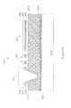
- forming the first narrow beamincludes depositing a mold material onto a sacrificial layer, etching a shape into the mold material to form a mold having at least one sidewall and at least one lower horizontal surface, depositing material onto the etched mold such that the deposited material adheres to at least the side walls and the lower horizontal surface of the etched mold, etching away a portion of the deposited material to remove the deposited material from the lower horizontal surface while leaving substantially all of the material deposited on the sidewalls intact, and removing the mold such that material remaining on the sidewalls forms the first narrow beam.
- the sidewallsinclude walls of a mesa formed in the mold, and the first narrow beam encloses the mesa.
- the sidewallscomprises walls of a recess formed in the mold, and the first narrow beam encloses the recess.
- the mold materialis deposited on top of a layer of sacrificial material, and the method further includes removing the sacrificial material to release the first narrow beam.
- the moldfurther comprises an upper horizontal surface, the material deposited on the mold adheres to the upper horizontal surface, and the method further comprises applying a mask to the upper horizontal surface prior to etching away the deposited material such that a portion of the material deposited on the upper horizontal surface remains on the upper horizontal surface after the etch to form a mechanical light modulator.
- etching anchor holes into the mold materialprior to etching the shape into the mold, etching anchor holes into the mold material, in which the material deposited onto the mold fills the anchor holes to form anchors.
- the formation of the anchors, first narrow beam, and the mechanical light modulatorrequires the utilization of no more than three photolithographic masks.
- the MEMS deviceincludes a mechanical light modulator and an anchor, and the first narrow beam supports the mechanical light modulator over a substrate and connects the mechanical light to the substrate via the anchor, in which the method comprises utilizing no more than three photolithographic masks.
- FIG. 1Ais an isometric view of display apparatus, according to an illustrative embodiment of the invention.
- FIG. 1Bis a block diagram of the display apparatus of FIG. 1A , according to an illustrative embodiment of the invention.
- FIG. 2Ais a perspective view of an illustrative shutter-based light modulator suitable for incorporation into the MEMS-based display of FIG. 1A , according to an illustrative embodiment of the invention
- FIG. 2Bis a cross-sectional view of a roller-shade-based light modulator suitable for incorporation into the MEMS-based display of FIG. 1A , according to an illustrative embodiment of the invention
- FIG. 2Cis a cross sectional view of a light-tap-based light modulator suitable for incorporation into an alternative embodiment of the MEMS-based display of FIG. 1A , according to an illustrative embodiment of the invention
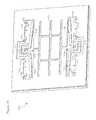
- FIG. 3Ais a schematic diagram of a control matrix suitable for controlling the light modulators incorporated into the MEMS-based display of FIG. 1A , according to an illustrative embodiment of the invention
- FIG. 3Bis a perspective view of an array of shutter-based light modulators connected to the control matrix of FIG. 3A , according to an illustrative embodiment of the invention
- FIGS. 4A and 4Bare plan views of a dual-actuated shutter assembly in the open and closed states respectively, according to an illustrative embodiment of the invention.
- FIG. 5is a cross-sectional view of a display apparatus, according to an illustrative embodiment of the invention.
- FIGS. 6A-6Eare cross sectional views of stages of construction of a composite shutter assembly similar to that shown in FIG. 2A , according to an illustrative embodiment of the invention.
- FIGS. 7A-7Dare isometric views of stages of construction of an alternate shutter assembly with narrow sidewall beams, according to an illustrative embodiment of the invention.
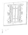
- FIG. 8is a plan view of a shutter assembly incorporating a looped drive beam, according to an illustrative embodiment of the invention.
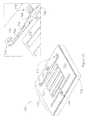
- FIG. 9is an isometric view of a shutter assembly built according to a 3-mask process, according to an illustrative embodiment of the invention.
- FIG. 10is an isometric view of the 2 d sacrificial material patterned into a mold at an interim point in the fabrication process leading to the shutter assembly of FIG. 9 , according to an illustrative embodiment of the invention.
- FIG. 11is an isometric view of a shutter assembly built according to a 3-mask process, according to an illustrative embodiment of the invention.
- FIG. 12is an isometric view of the 2 d sacrificial material patterned into a mold at an interim point in the fabrication process leading to the shutter assembly of FIG. 11 , according to an illustrative embodiment of the invention
- FIG. 13is an isometric view of two connected shutter assemblies built according to a 3-mask process, according to an illustrative embodiment of the invention.
- FIG. 14is an isometric view of a shutter assembly built according to a 3-mask process, according to an illustrative embodiment of the invention.
- FIG. 15is an isometric view of a shutter assembly built according to a 3-mask process, according to an illustrative embodiment of the invention.
- FIG. 16is an isometric view of a shutter assembly built according to a 3-mask process, according to an illustrative embodiment of the invention.
- FIG. 1Ais a schematic diagram of a direct-view MEMS-based display apparatus 100 , according to an illustrative embodiment of the invention.
- the display apparatus 100includes a plurality of light modulators 102 a - 102 d (generally “light modulators 102 ”) arranged in rows and columns.
- light modulators 102 a and 102 dare in the open state, allowing light to pass.
- Light modulators 102 b and 102 care in the closed state, obstructing the passage of light.
- the display apparatus 100can be utilized to form an image 104 for a backlit display, if illuminated by a lamp or lamps 105 .
- the apparatus 100may form an image by modulating reflection of ambient light originating from the front of the apparatus.
- the apparatus 100may form an image by reflection of light from a lamp or lamps positioned in the front of the display, i.e. by use of a front-light.
- the apparatus 100may form an image by modulating both the transmission of light from a source behind the modulating array and simultaneously the reflection of light from a source (lamp or lamps) positioned in the front of the display, called transflective operation.
- the light modulators 102interfere with light in an optical path by, for example, and without limitation, blocking, reflecting, absorbing, filtering, polarizing, diffracting, or otherwise altering a property or path of the light.
- each light modulator 102corresponds to a pixel 106 in the image 104 .
- the display apparatus 100may utilize a plurality of light modulators to form a pixel 106 in the image 104 .
- the display apparatus 100may include three color-specific light modulators 102 . By selectively opening one or more of the color-specific light modulators 102 corresponding to a particular pixel 106 , the display apparatus 100 can generate a color pixel 106 in the image 104 .
- the display apparatus 100includes two or more light modulators 102 per pixel 106 to provide grayscale in an image 104 .
- a “pixel”corresponds to the smallest picture element defined by the resolution of the image.
- the term “pixel”refers to the combined mechanical and electrical components utilized to modulate the light that forms a single pixel of the image.
- Display apparatus 100is a direct-view display in that it does not require imaging optics. The user sees an image by looking directly at the display apparatus 100 .
- the display apparatus 100is incorporated into a projection display.
- the displayforms an image by projecting light onto a screen or onto a wall.
- the display apparatus 100is substantially smaller than the projected image 104 .
- Direct-view displaysmay operate in either a transmissive or reflective mode or both simultaneously (defined as transflective).
- the light modulatorsfilter or selectively block light which originates from a lamp or lamps positioned behind the display. The light from the lamps is optionally injected into a light guide or “backlight”.
- Transmissive direct-view display embodimentsare often built onto transparent or glass substrates to facilitate a sandwich assembly arrangement where one substrate, containing the light modulators, is positioned directly on top of the backlight.
- a color-specific light modulatoris created by associating a color filter material with each modulator 102 .
- colorscan be generated, as described below, using a field sequential color method by alternating illumination of lamps with different primary colors.
- Each light modulator 102includes a shutter 108 and an aperture 109 .
- the shutter 108is positioned such that it allows light to pass through the aperture 109 towards a viewer.
- the shutter 108is positioned such that it obstructs the passage of light through the aperture 109 .
- the aperture 109is defined by an opening patterned through a reflective or light-absorbing material.
- the display apparatusalso includes a control matrix connected to the substrate and to the light modulators for controlling the movement of the shutters.
- the control matrixincludes a series of electrical interconnects (e.g., interconnects 110 , 112 , and 114 ), including at least one write-enable interconnect 110 (also referred to as a “scan-line interconnect”) per row of pixels, one data interconnect 112 for each column of pixels, and one common interconnect 114 providing a common voltage to all pixels, or at least to pixels from both multiple columns and multiples rows in the display apparatus 100 .
- V wethe write-enable interconnect 110 for a given row of pixels prepares the pixels in the row to accept new shutter movement instructions.
- the data interconnects 112communicate the new movement instructions in the form of data voltage pulses.
- the data voltage pulses applied to the data interconnects 112directly contribute to an electrostatic movement of the shutters.
- the data voltage pulsescontrol switches, e.g., transistors or other non-linear circuit elements that control the application of separate actuation voltages, which are typically higher in magnitude than the data voltages, to the light modulators 102 . The application of these actuation voltages then results in the electrostatic driven movement of the shutters 108 .
- FIG. 1Bis a block diagram 150 of the display apparatus 100 .
- the display apparatus 100includes a plurality of scan drivers 152 (also referred to as “write enabling voltage sources”) and a plurality of data drivers 154 (also referred to as “data voltage sources”).
- the scan drivers 152apply write enabling voltages to scan-line interconnects 110 .
- the data drivers 154apply data voltages to the data interconnects 112 .
- the data drivers 154are configured to provide analog data voltages to the light modulators, especially where the gray scale of the image 104 is to be derived in analog fashion.
- the light modulators 102are designed such that when a range of intermediate voltages is applied through the data interconnects 112 there results a range of intermediate open states in the shutters 108 and therefore a range of intermediate illumination states or gray scales in the image 104 .
- the data drivers 154are configured to apply only a reduced set of 2, 3, or 4 digital voltage levels to the control matrix. These voltage levels are designed to set, in digital fashion, either an open state or a closed state to each of the shutters 108 .
- the scan drivers 152 and the data drivers 154are connected to digital controller circuit 156 (also referred to as the “controller 156 ”).
- the controller 156includes an input processing module 158 , which processes an incoming image signal 157 into a digital image format appropriate to the spatial addressing and the gray scale capabilities of the display 100 .
- the pixel location and gray scale data of each imageis stored in a frame buffer 159 so that the data can be fed out as needed to the data drivers 154 .
- the datais sent to the data drivers 154 in mostly serial fashion, organized in predetermined sequences grouped by rows and by image frames.
- the data drivers 154can include series to parallel data converters, level shifting, and for some applications digital to analog voltage converters.
- the display 100 apparatusoptionally includes a set of common drivers 153 , also referred to as common voltage sources.
- the common drivers 153provide a DC common potential to all light modulators within the array of light modulators 103 , for instance by supplying voltage to a series of common interconnects 114 .
- the common drivers 153following commands from the controller 156 , issue voltage pulses or signals to the array of light modulators 103 , for instance global actuation pulses which are capable of driving and/or initiating simultaneous actuation of all or some light modulators in multiple rows and columns of the array 103 .
- All of the driverse.g., scan drivers 152 , data drivers 154 , and common drivers 153 ) for different display functions are time-synchronized by a timing-control module 160 in the controller 156 .
- Timing commands from the module 160coordinate the illumination of red, green and blue and white lamps ( 162 , 164 , 166 , and 167 respectively) via lamp drivers 168 , the write-enabling and sequencing of specific rows within the array of pixels 103 , the output of voltages from the data drivers 154 , and the output of voltages that provide for light modulator actuation.
- the controller 156determines the sequencing or addressing scheme by which each of the shutters 108 in the array 103 can be re-set to the illumination levels appropriate to a new image 104 . Details of suitable addressing, image formation, and gray scale techniques can be found in U.S. patent application Ser. Nos. 11/326,696 and 11/643,042, incorporated herein by reference. New images 104 can be set at periodic intervals. For instance, for video displays, the color images 104 or frames of video are refreshed at frequencies ranging from 10 to 300 Hertz.
- the setting of an image frame to the array 103is synchronized with the illumination of the lamps 162 , 164 , and 166 such that alternate image frames are illuminated with an alternating series of colors, such as red, green, and blue.
- the image frames for each respective coloris referred to as a color sub-frame.
- the field sequential color methodif the color sub-frames are alternated at frequencies in excess of 20 Hz, the human brain will average the alternating frame images into the perception of an image having a broad and continuous range of colors.
- four or more lamps with primary colorscan be employed in display apparatus 100 , employing primaries other than red, green, and blue.
- the controller 156determines the addressing sequence and/or the time intervals between image frames to produce images 104 with appropriate gray scale.
- the process of generating varying levels of grayscale by controlling the amount of time a shutter 108 is open in a particular frameis referred to as time division gray scale.
- the controller 156determines the time period or the fraction of time within each frame that a shutter 108 is allowed to remain in the open state, according to the illumination level or gray scale desired of that pixel.
- the controller 156sets a plurality of sub-frame images in multiple rows and columns of the array 103 , and the controller alters the duration over which each sub-frame image is illuminated in proportion to a gray scale value or significance value employed within a coded word for gray scale.
- the illumination times for a series of sub-frame imagescan be varied in proportion to the binary coding series 1,2,4,8 . . .
- the shutters 108 for each pixel in the array 103are then set to either the open or closed state within a sub-frame image according to the value at a corresponding position within the pixel's binary coded word for gray level. It is also possible to have more than two levels for example a 4 level state for the pixel might involve partially open and partially closed states for additional spatially varied grey levels.
- the controlleralters the intensity of light from the lamps 162 , 164 , and 166 in proportion to the gray scale value desired for a particular sub-frame image.
- a number of hybrid techniquesare also available for forming colors and gray scale from an array of shutters 108 .
- the time division techniques described abovecan be combined with the use of multiple shutters 108 per pixel, or the gray scale value for a particular sub-frame image can be established through a combination of both sub-frame timing and lamp intensity. Details of these and other embodiments can be found in U.S. patent application Ser. No. 11/643,042, referenced above.
- the data for an image state 104is loaded by the controller 156 to the modulator array 103 by a sequential addressing of individual rows, also referred to as scan lines.
- the scan driver 152applies a write-enable voltage to the write enable interconnect 110 for that row of the array 103 , and subsequently the data driver 154 supplies data voltages, corresponding to desired shutter states, for each column in the selected row. This process repeats until data has been loaded for all rows in the array.
- the sequence of selected rows for data loadingis linear, proceeding from top to bottom in the array.
- the sequence of selected rowsis pseudo-randomized, in order to minimize visual artifacts.
- the sequencingis organized by blocks, where, for a block, the data for only a certain fraction of the image state 104 is loaded to the array, for instance by addressing only every 5 th row of the array in sequence.
- the process for loading image data to the array 103is separated in time from the process of actuating the shutters 108 .
- the modulator array 103may include data memory elements for each pixel in the array 103 and the control matrix may include a global actuation interconnect for carrying trigger signals, from common driver 153 , to initiate simultaneous actuation of shutters 108 according to data stored in the memory elements.
- Various addressing sequencesmany of which are described in U.S. patent application Ser. No. 11/643,042, can be coordinated by means of the timing control module 160 .
- the array of pixels 103 and the control matrix that controls the pixelsmay be arranged in configurations other than rectangular rows and columns.
- the pixelscan be arranged in hexagonal arrays or curvilinear rows and columns.
- the term scan-lineshall refer to any plurality of pixels that share a write-enabling interconnect.
- the display 100is comprised of a plurality of functional blocks including the timing control module 160 , the frame buffer 159 , scan drivers 152 , data drivers 154 , and drivers 153 and 168 .
- Each blockcan be understood to represent either a distinguishable hardware circuit and/or a module of executable code.
- the functional blocksare provided as distinct chips or circuits connected together by means of circuit boards and/or cables. Alternately, many of these circuits can be fabricated along with the pixel array 103 on the same substrate of glass or plastic. In other implementations, multiple circuits, drivers, processors, and/or control functions from block diagram 150 may be integrated together within a single silicon chip, which is then bonded directly to the transparent substrate holding pixel array 103 .
- the controller 156includes a programming link 180 by which the addressing, color, and/or gray scale algorithms, which are implemented within controller 156 , can be altered according to the needs of particular applications.
- the programming link 180conveys information from environmental sensors, such as ambient light or temperature sensors, so that the controller 156 can adjust imaging modes or backlight power in correspondence with environmental conditions.
- the controller 156also comprises a power supply input 182 which provides the power needed for lamps as well as light modulator actuation.
- the drivers 152 153 , 154 , and/or 168may include or be associated with DC-DC converters for transforming an input voltage at 182 into various voltages sufficient for the actuation of shutters 108 or illumination of the lamps, such as lamps 162 , 164 , 166 , and 167 .
- FIG. 2Ais a perspective view of an illustrative shutter-based light modulator 200 suitable for incorporation into the MEMS-based display apparatus 100 of FIG. 1A , according to an illustrative embodiment of the invention.
- the shutter-based light modulator 200(also referred to as shutter assembly 200 ) includes a shutter 202 coupled to an actuator 204 .
- the actuator 204is formed from two separate compliant electrode beam actuators 205 (the “actuators 205 ”), as described in U.S. patent application Ser. No. 11/251,035, filed on Oct. 14, 2005.
- the shutter 202couples on one side to the actuators 205 .
- the actuators 205move the shutter 202 transversely over a surface 203 in a plane of motion which is substantially parallel to the surface 203 .
- the opposite side of the shutter 202couples to a spring 207 which provides a restoring force opposing the forces exerted by the actuator 204 . It is possible to replace the spring 207 by another actuator so that an actuation force rather than a elastic spring force can be used to move the shutter 202 transversely over a surface 203 in the opposite direction from that of actuator 204 .
- Each actuator 205includes a compliant load beam 206 connecting the shutter 202 to a load anchor 208 .
- the load anchors 208along with the compliant load beams 206 serve as mechanical supports, keeping the shutter 202 suspended proximate to the surface 203 .
- the load anchors 208physically connect the compliant load beams 206 and the shutter 202 to the surface 203 and electrically connect the load beams 206 to a bias voltage, in some instances, ground.
- Each actuator 205also includes a compliant drive beam 216 positioned adjacent to each load beam 206 .
- the drive beams 216couple at one end to a drive beam anchor 218 shared between the drive beams 216 .
- the other end of each drive beam 216is free to move.
- Each drive beam 216can be curved such that it is closest to the load beam 206 near the free end of the drive beam 216 and the anchored end of the load beam 206 .
- the surface 203includes one or more apertures 211 for admitting the passage of light in the transmissive or transflective embodiments. If the shutter assembly 200 is formed on an opaque substrate, made for example from silicon, then the surface 203 is a surface of the substrate, and the apertures 211 are formed by etching an array of holes through the substrate. If the shutter assembly 200 is formed on a transparent substrate, made for example of glass or plastic, then the surface 203 is a surface of a light blocking layer deposited on the substrate, and the apertures are formed by etching the surface 203 into an array of holes 211 .
- the apertures 211can be generally circular, elliptical, polygonal, serpentine, or irregular in shape. In reflective or some transflective embodiments the regions 211 can represent areas of higher reflection or lower reflection than the surrounding substrate such that movement of the shutter assembly 200 modulates the total reflected light from the shutter based light modulator 200 .
- a display apparatus incorporating the light modulator 200applies an electric potential to the drive beams 216 via the drive beam anchor 218 .
- a second electric potentialmay be applied to the load beams 206 .
- the resulting potential difference between the drive beams 216 and the load beams 206pulls the free ends of the drive beams 216 towards the anchored ends of the load beams 206 , and pulls the shutter ends of the load beams 206 toward the anchored ends of the drive beams 216 , thereby driving the shutter 202 transversely towards the drive anchor 218 .
- the compliant members 206act as springs, such that when the voltage across the beams 206 and 216 is removed, the load beams 206 push the shutter 202 back into its initial position, releasing the stress stored in the load beams 206 .
- the shutter assembly 200also referred to as an elastic shutter assembly, incorporates a passive restoring force, such as a spring, for returning a shutter to its rest or relaxed position after voltages have been removed.
- a passive restoring forcesuch as a spring
- a number of elastic restore mechanisms and various electrostatic couplingscan be designed into or in conjunction with electrostatic actuators, the compliant beams illustrated in shutter assembly 200 being just one example. Other examples are described in U.S. patent application Ser. Nos. 11/251,035 and 11/326,696, incorporated herein by reference. For instance, a highly non-linear voltage-displacement response can be provided which favors an abrupt transition between “open” vs.
- the actuator 205 within the elastic shutter assemblyis said to operate between a closed or actuated position and a relaxed position.
- the designercan choose to place apertures 211 such that shutter assembly 200 is in either the “open” state, i.e. passing light, or in the “closed” state, i.e. blocking light, whenever actuator 205 is in its relaxed position.
- the open statei.e. passing light
- the closed statei.e. blocking light
- Display apparatus 100in alternative embodiments, includes light modulators other than transverse shutter-based light modulators, such as the shutter assembly 200 described above.
- FIG. 2Bis a cross-sectional view of a rolling actuator shutter-based light modulator 220 suitable for incorporation into an alternative embodiment of the MEMS-based display apparatus 100 of FIG. 1A , according to an illustrative embodiment of the invention.
- FIG. 2Bis a cross-sectional view of a rolling actuator shutter-based light modulator 220 suitable for incorporation into an alternative embodiment of the MEMS-based display apparatus 100 of FIG. 1A , according to an illustrative embodiment of the invention.
- U.S. Pat. No. 5,233,459entitled “Electric Display Device,” and U.S. Pat. No.
- a rolling actuator-based light modulatorincludes a moveable electrode disposed opposite a fixed electrode and biased to move in a preferred direction to produce a shutter upon application of an electric field.
- the light modulator 220includes a planar electrode 226 disposed between a substrate 228 and an insulating layer 224 and a moveable electrode 222 having a fixed end 230 attached to the insulating layer 224 . In the absence of any applied voltage, a moveable end 232 of the moveable electrode 222 is free to roll towards the fixed end 230 to produce a rolled state.
- a voltage between the electrodes 222 and 226causes the moveable electrode 222 to unroll and lie flat against the insulating layer 224 , whereby it acts as a shutter that blocks light traveling through the substrate 228 .
- the moveable electrode 222returns to the rolled state by means of an elastic restoring force after the voltage is removed.
- the bias towards a rolled statemay be achieved by manufacturing the moveable electrode 222 to include an nonuniform initial stress or strain state.
- FIG. 2Cis a cross-sectional view of an illustrative non shutter-based MEMS light modulator 250 .
- the light tap modulator 250is suitable for incorporation into an alternative embodiment of the MEMS-based display apparatus 100 of FIG. 1A , according to an illustrative embodiment of the invention.
- a light tapworks according to a principle of frustrated total internal reflection. That is, light 252 is introduced into a light guide 254 , in which, without interference, light 252 is for the most part unable to escape the light guide 254 through its front or rear surfaces due to total internal reflection.
- the light tap 250includes a tap element 256 that has a sufficiently high index of refraction that, in response to the tap element 256 contacting the light guide 254 , light 252 impinging on the surface of the light guide 254 adjacent the tap element 256 escapes the light guide 254 through the tap element 256 towards a viewer, thereby contributing to the formation of an image.
- the tap element 256is formed as part of beam 258 of flexible, transparent material. Electrodes 260 coat portions of one side of the beam 258 . Opposing electrodes 260 are disposed on the light guide 254 . By applying a voltage across the electrodes 260 , the position of the tap element 256 relative to the light guide 254 can be controlled to selectively extract light 252 from the light guide 254 .
- roller-based light modulator 220 and light tap 250are not the only examples of MEMS light modulators suitable for inclusion in various embodiments of the invention. It will be understood that other MEMS light modulators can exist and can be usefully incorporated into the invention.
- FIG. 3Ais a schematic diagram of a control matrix 300 suitable for controlling the light modulators incorporated into the MEMS-based display apparatus 100 of FIG. 1A , according to an illustrative embodiment of the invention.
- FIG. 3Bis a perspective view of an array 320 of shutter-based light modulators connected to the control matrix 300 of FIG. 3A , according to an illustrative embodiment of the invention.
- the control matrix 300may address an array of pixels 320 (the “array 320 ”).
- Each pixel 301includes an elastic shutter assembly 302 , such as the shutter assembly 200 of FIG. 2A , controlled by an actuator 303 .
- Each pixelalso includes an aperture layer 322 that includes apertures 324 .
- shutter assembliessuch as shutter assembly 302 , and variations thereon, can be found in U.S. patent application Ser. Nos. 11/251,035 and 11/326,696. Descriptions of alternate control matrices can also be found in U.S. patent application Ser. No. 11/607,715.
- the control matrix 300is fabricated as a diffused or thin-film-deposited electrical circuit on the surface of a substrate 304 on which the shutter assemblies 302 are formed.
- the control matrix 300includes a scan-line interconnect 306 for each row of pixels 301 in the control matrix 300 and a data-interconnect 308 for each column of pixels 301 in the control matrix 300 .
- Each scan-line interconnect 306electrically connects a write-enabling voltage source 307 to the pixels 301 in a corresponding row of pixels 301 .
- Each data interconnect 308electrically connects a data voltage source, (“V d source”) 309 to the pixels 301 in a corresponding column of pixels 301 .
- V d sourcedata voltage source
- the data voltage V dprovides the majority of the energy necessary for actuation of the shutter assemblies 302 .
- the data voltage source 309also serves as an actuation voltage source.
- the control matrix 300includes a transistor 310 and a capacitor 312 .
- the gate of each transistor 310is electrically connected to the scan-line interconnect 306 of the row in the array 320 in which the pixel 301 is located.
- the source of each transistor 310is electrically connected to its corresponding data interconnect 308 .
- the actuators 303 of each shutter assembly 302include two electrodes.
- the drain of each transistor 310is electrically connected in parallel to one electrode of the corresponding capacitor 312 and to one of the electrodes of the corresponding actuator 303 .
- the other electrode of the capacitor 312 and the other electrode of the actuator 303 in shutter assembly 302are connected to a common or ground potential.
- the transistors 310can be replaced with semiconductor diodes and or metal-insulator-metal sandwich type switching elements.
- the control matrix 300write-enables each row in the array 320 in a sequence by applying V we to each scan-line interconnect 306 in turn.
- V weFor a write-enabled row, the application of V we to the gates of the transistors 310 of the pixels 301 in the row allows the flow of current through the data interconnects 308 through the transistors 310 to apply a potential to the actuator 303 of the shutter assembly 302 . While the row is write-enabled, data voltages V d are selectively applied to the data interconnects 308 .
- the data voltage applied to each data interconnect 308is varied in relation to the desired brightness of the pixel 301 located at the intersection of the write-enabled scan-line interconnect 306 and the data interconnect 308 .
- the data voltageis selected to be either a relatively low magnitude voltage (i.e., a voltage near ground) or to meet or exceed V at (the actuation threshold voltage).
- the actuator 303 in the corresponding shutter assembly 302actuates, opening the shutter in that shutter assembly 302 .
- the voltage applied to the data interconnect 308remains stored in the capacitor 312 of the pixel 301 even after the control matrix 300 ceases to apply V we to a row. It is not necessary, therefore, to wait and hold the voltage V we on a row for times long enough for the shutter assembly 302 to actuate; such actuation can proceed after the write-enabling voltage has been removed from the row.
- the capacitors 312also function as memory elements within the array 320 , storing actuation instructions for periods as long as is necessary for the illumination of an image frame.
- the pixels 301 as well as the control matrix 300 of the array 320are formed on a substrate 304 .
- the arrayincludes an aperture layer 322 , disposed on the substrate 304 , which includes a set of apertures 324 for respective pixels 301 in the array 320 .
- the apertures 324are aligned with the shutter assemblies 302 in each pixel.
- the substrate 304is made of a transparent material, such as glass or plastic.
- the substrate 304is made of an opaque material, but in which holes are etched to form the apertures 324 .
- the regions 324can represent areas of higher or lower reflectivity than the surrounding substrate such that motion of the shutter assembly serves to modulate the reflected component of light from a source in front of the modulating plane.
- Control matrix 300Components of shutter assemblies 302 are processed either at the same time as the control matrix 300 or in subsequent processing steps on the same substrate.
- the electrical components in control matrix 300are fabricated using many thin film techniques in common with the manufacture of thin film transistor arrays for liquid crystal displays. Available techniques are described in Den Boer, Active Matrix Liquid Crystal Displays (Elsevier, Amsterdam, 2005), incorporated herein by reference.
- the shutter assembliesare fabricated using techniques similar to the art of micromachining or from the manufacture of micromechanical (i.e., MEMS) devices. Many applicable thin film MEMS techniques are described in Rai-Choudhury, ed., Handbook of Microlithography, Micromachining & Microfabrication (SPIE Optical Engineering Press, Bellingham, Wash. 1997), incorporated herein by reference.
- the shutter assembly 302can be formed from thin films of amorphous silicon, deposited by a chemical vapor deposition process.
- the shutter assembly 302 together with the actuator 303can be made bi-stable. That is, the shutters can exist in at least two equilibrium positions (e.g. open or closed) with little or no power required to hold them in either position. More particularly, the shutter assembly 302 can be mechanically bi-stable. Once the shutter of the shutter assembly 302 is set in position, no electrical energy or holding voltage is required to maintain that position. The mechanical stresses on the physical elements of the shutter assembly 302 can hold the shutter in place.
- the shutter assembly 302 together with the actuator 303can also be made electrically bi-stable.
- an electrically bi-stable shutter assemblythere exists a range of voltages below the actuation voltage of the shutter assembly, which if applied to a closed actuator (with the shutter being either open or closed), holds the actuator closed and the shutter in position, even if an opposing force is exerted on the shutter.
- the opposing forcemay be exerted by a spring such as spring 207 in shutter-based light modulator 200 , or the opposing force may be exerted by an opposing actuator, such as an “open” or “closed” actuator.
- the light modulator array 320is depicted as having a single MEMS light modulator per pixel. Other embodiments are possible in which multiple MEMS light modulators are provided in each pixel, thereby providing the possibility of more than just binary “on” or “off” optical states in each pixel. Certain forms of coded area division gray scale are possible where multiple MEMS light modulators in the pixel are provided, and where apertures 324 , which are associated with each of the light modulators, have unequal areas.
- roller-based light modulator 220 and the light tap 250can be substituted for the shutter assembly 302 within the light modulator array 320 .
- FIGS. 4A and 4Billustrate an alternative shutter-based light modulator (shutter assembly) 400 suitable for inclusion in various embodiments of the invention.
- the light modulator 400is an example of a dual actuator shutter assembly, and is shown in FIG. 4A in an open state.
- FIG. 4Bis a view of the dual actuator shutter assembly 400 in a closed state.
- Shutter assembly 400is described in further detail in U.S. patent application Ser. No. 11/251,035, referenced above.
- shutter assembly 400includes actuators 402 and 404 on either side of a shutter 406 . Each actuator 402 and 404 is independently controlled.
- a first actuator, a shutter-open actuator 402serves to open the shutter 406 .
- a second opposing actuator, the shutter-close actuator 404serves to close the shutter 406 .
- Both actuators 402 and 404are compliant beam electrode actuators.
- the actuators 402 and 404open and close the shutter 406 by driving the shutter 406 substantially in a plane parallel to an aperture layer 407 over which the shutter is suspended.
- the shutter 406is suspended a short distance over the aperture layer 407 by anchors 408 attached to the actuators 402 and 404 .
- the inclusion of supports attached to both ends of the shutter 406 along its axis of movementreduces out of plane motion of the shutter 406 and confines the motion substantially to a plane parallel to the substrate.
- a control matrix suitable for use with shutter assembly 400might include one transistor and one capacitor for each of the opposing shutter-open and shutter-close actuators 402 and 404 .
- the shutter 406includes two shutter apertures 412 through which light can pass.
- the aperture layer 407includes a set of three apertures 409 .
- FIG. 4Athe shutter assembly 400 is in the open state and, as such, the shutter-open actuator 402 has been actuated, the shutter-close actuator 404 is in its relaxed position, and the centerlines of apertures 412 and 409 coincide.
- FIG. 4Bthe shutter assembly 400 has been moved to the closed state and, as such, the shutter-open actuator 402 is in its relaxed position, the shutter-close actuator 404 has been actuated, and the light blocking portions of shutter 406 are now in position to block transmission of light through the apertures 409 (shown as dotted lines).
- Each aperturehas at least one edge around its periphery.
- the rectangular apertures 409have four edges.
- each aperturemay have only a single edge.
- the aperturesneed not be separated or disjoint in the mathematical sense, but instead can be connected. That is to say, while portions or shaped sections of the aperture may maintain a correspondence to each shutter, several of these sections may be connected such that a single continuous perimeter of the aperture is shared by multiple shutters.
- FIG. 4Bshows a predefined overlap 416 between the edge of light blocking portions in the shutter 406 and one edge of the aperture 409 formed in aperture layer 407 .
- the electrostatic actuators 402 and 404are designed so that their voltage-displacement behavior provides a bi-stable characteristic to the shutter assembly 400 .
- a range of voltages below the actuation voltagewhich if applied while that actuator is in the closed state (with the shutter being either open or closed), will hold the actuator closed and the shutter in position, even after an actuation voltage is applied to the opposing actuator.
- the minimum voltage needed to maintain a shutter's position against such an opposing forceis referred to as a maintenance voltage V m .
- a number of control matriceswhich take advantage of the bi-stable operation characteristic are described in U.S. patent application Ser. No. 11/607,715, referenced above.
- FIG. 5is a cross sectional view of a display apparatus 500 incorporating shutter-based light modulators (shutter assemblies) 502 , according to an illustrative embodiment of the invention.
- Each shutter assemblyincorporates a shutter 503 and an anchor 505 .
- the compliant beam actuatorswhich, when connected between the anchors 505 and the shutters 503 , help to suspend the shutters a short distance above the surface.
- the shutter assemblies 502are disposed on a transparent substrate 504 , preferably made of plastic, quartz, or glass.
- a rear-facing reflective layer, reflective film 506disposed on the substrate 504 defines a plurality of surface apertures 508 located beneath the closed positions of the shutters 503 of the shutter assemblies 502 .
- the reflective film 506reflects light not passing through the surface apertures 508 back towards the rear of the display apparatus 500 .
- the reflective aperture layer 506can be a fine-grained metal film without inclusions formed in thin film fashion by a number of vapor deposition techniques including sputtering, evaporation, ion plating, laser ablation, or chemical vapor deposition.
- the rear-facing reflective layer 506can be formed from a mirror, such as a dielectric mirror.
- a dielectric mirroris fabricated as a stack of dielectric thin films which alternate between materials of high and low refractive index.
- the vertical gap which separates the shutters 503 from the reflective film 506 , within which the shutter is free to move,is in the range of 0.5 to 10 microns.
- the magnitude of the vertical gapis preferably less than the lateral overlap between the edge of shutters 503 and the edge of apertures 508 in the closed state, such as the overlap 416 shown in FIG. 4B .
- the display apparatus 500includes an optional diffuser 512 and/or an optional brightness enhancing film 514 of various potential orientations of which only one is shown here, which separate the substrate 504 from a planar light guide 516 .
- the light guideis comprised of a transparent, i.e. glass or plastic material.
- the light guide 516is illuminated by one or more light sources 518 , forming a backlight.
- the light sources 518can be, for example, and without limitation, incandescent lamps, fluorescent lamps, lasers, or light emitting diodes (LEDs).
- a reflector 519helps direct light from lamp 518 towards the light guide 516 .
- a front-facing reflective film 520is disposed behind the backlight 516 , reflecting light towards the shutter assemblies 502 .
- Light rays such as ray 521 from the backlight that do not pass through one of the shutter assemblies 502will be returned to the backlight and reflected again from the film 520 .
- light that fails to leave the display to form an image on the first passcan be recycled and made available for transmission through other open apertures in the array of shutter assemblies 502 .
- Such light recyclinghas been shown to increase the illumination efficiency of the display.
- the light guide 516includes a set of geometric light redirectors or prisms 517 which re-direct light from the lamps 518 towards the apertures 508 and hence toward the front of the display.
- the light re-directorscan be molded into the plastic body of light guide 516 with shapes that can be alternately triangular, trapezoidal, or curved in cross section.
- the density of the prisms 517generally increases with distance from the lamp 518 .
- the aperture layer 506can be made of a light absorbing material, and in alternate embodiments the surfaces of shutter 503 can be coated with either a light absorbing or a light reflecting material. In alternate embodiments the aperture layer 506 can be deposited directly on the surface of the light guide 516 . In alternate embodiments the aperture layer 506 need not be disposed on the same substrate as the shutters 503 and anchors 505 (see the MEMS-down configuration described below).
- the light sources 518can include lamps of different colors, for instance, the colors red, green, and blue.
- a color imagecan be formed by sequentially illuminating images with lamps of different colors at a rate sufficient for the human brain to average the different colored images into a single multi-color image.
- the various color-specific imagesare formed using the array of shutter assemblies 502 .
- the light source 518includes lamps having more than three different colors.
- the light source 518may have red, green, blue and white lamps or red, green, blue, and yellow lamps.
- a cover plate 522forms the front of the display apparatus 500 .
- the rear side of the cover plate 522can be covered with a black matrix 524 to increase contrast.
- the cover plateincludes color filters, for instance distinct red, green, and blue filters corresponding to different ones of the shutter assemblies 502 .
- the cover plate 522is supported a predetermined distance away from the shutter assemblies 502 forming a gap 526 .
- the gap 526is maintained by mechanical supports or spacers 527 and/or by an adhesive seal 528 attaching the cover plate 522 to the substrate 504 .
- the adhesive seal 528seals in a working fluid 530 .
- the working fluid 530is engineered with viscosities preferably below about 10 centipoise and with relative dielectric constant preferably above about 2.0, and dielectric breakdown strengths above about 10 4 V/cm.
- the working fluid 530can also serve as a lubricant.
- the working fluid 530is a hydrophobic liquid with a high surface wetting capability.
- the working fluid 530has a refractive index that is either greater than or less than that of the substrate 504 .
- the sealing material 528can be formed from polymer adhesives such as epoxies, acrylates, or a silicone materials.
- the adhesive seal 528should have a curing temperature preferably below about 200.degree. C., it should have a coefficient of thermal expansion preferably below about 50 ppm per degree C. and should be moisture resistant.
- An exemplary sealant 528is EPO-TEK B9021-1, sold by Epoxy Technology, Inc.
- the adhesiveis formed from a heat reflowable material such as a solder metal or a glass frit compound.
- the adhesive seal 528seals in a working fluid 530 .
- the working fluid 530is engineered with viscosities preferably below about 10 centipoise and with relative dielectric constant preferably above about 2.0, and dielectric breakdown strengths above about 10.sup.4 V/cm.
- the working fluid 530can also serve as a lubricant.
- the working fluid 530has a refractive index that is either greater than or less than that of the substrate 504 . In one implementation the working fluid has a refractive index greater than 2.0.
- Suitable working fluids 530include, without limitation, de-ionized water, methanol, ethanol, silicone oils, heptane, octane, fluorinated silicone oils, dimethylsiloxane, polydimethylsiloxane, hexamethyldisiloxane, and diethylbenzene.
- the working fluid 530is a hydrophobic liquid with a high surface wetting capability. Preferably, its wetting capabilities are sufficient to wet the front as well as the rear surfaces of the shutter assemblies 502 . Hydrophobic fluids are capable of displacing water from the surfaces of shutter assemblies 502 .
- the working fluid 530contains a suspension of particles with diameters in the range of 0.2 to 20 microns. Such particles scatter light to increase the viewing angle of a display.
- the working fluid 530contains dye molecules in solution for absorbing some or all frequencies of visible light to increase the contrast of the display.
- the fluidcontains additives such as ethanol, ionic fluids, BHT or other additives to slightly conduct or in other ways prevent the buildup of static charge on the surfaces of the assemblies
- a sheet metal or molded plastic assembly bracket 532holds the cover plate 522 , the substrate 504 , the backlight 516 and the other component parts together around the edges.
- the assembly bracket 532is fastened with screws or indent tabs to add rigidity to the combined display apparatus 500 .
- the light source 518is molded in place by an epoxy potting compound.
- Reflectors 536help return light escaping from the edges of light guide 516 back into the light guide.
- electrical interconnectswhich provide control signals as well as power to the shutter assemblies 502 and the lamps 518 .
- Display apparatus 500is referred to as the MEMS-up configuration, wherein the MEMS-based light modulators are formed on a front surface of substrate 504 , i.e. the surface that faces toward the viewer.
- the shutter assemblies 502are built directly on top of the reflective aperture layer 506 .
- the shutter assembliesare disposed on a substrate separate from the substrate on which the reflective aperture layer is formed.
- the substrate on which the reflective aperture layer is formed, defining a plurality of apertures,is referred to herein as the aperture plate.
- the substrate that carries the MEMS-based light modulatorstakes the place of the cover plate 522 in display apparatus 500 and is oriented such that the MEMS-based light modulators are positioned on the rear surface of the top substrate, i.e. the surface that faces away from the viewer and toward the back light 516 .
- the MEMS-based light modulatorsare thereby positioned directly opposite to and across a gap from the reflective aperture layer.
- the gapcan be maintained by a series of spacer posts connecting the aperture plate and the substrate on which the MEMS modulators are formed.
- the spacersare disposed within or between each pixel in the array.
- the gap or distance that separates the MEMS light modulators from their corresponding aperturesis preferably less than 10 microns, or a distance that is less than the overlap between shutters and apertures, such as overlap 416 . Further details and alternate embodiments for the MEMS-down display configuration can be found in the U.S. patent application Ser. Nos. 11/361,785, 11/528,191, and 11/731,628 referenced above.
- roller-based light modulator 220 or the light tap 250can be substituted for the shutter assemblies 502 within the display assembly 500 .
- a shuttermust satisfy mechanical, optical and electrical properties. Mechanically, the shutter film support the load and stress of device under operation. Electrically, the material must be at least minimally conductive to allow electrostatic actuation. Optically, the shutter film must be opaque enough to block light. It is possible to have a single film satisfy all the mechanical, electrical and optical requirements. However, using multiple films in a composite stack offers more design and process latitude.
- FIGS. 6A-6Eare cross-sectional views of stages of construction of an exemplary composite shutter assembly 600 , similar to that shown in FIG. 2A , according to an illustrative embodiment of the invention.
- FIG. 6Ashows a cross sectional detail of a composite shutter assembly 600 , according to an illustrative embodiment of the invention.
- the shutter assembly 600includes shutter 601 , a compliant beam 602 , and anchor structure 604 built-up on substrate 603 and aperture layer 606 .
- the elements of the composite shutter assemblyinclude a first mechanical layer 605 , a conductor layer 607 , a second mechanical layer 609 , and an encapsulating dielectric 611 .
- At least one of the mechanical layers 605 or 609will be deposited to thicknesses in excess of 0.05 microns, as one or both of the mechanical layers will comprise the principle load bearing and mechanical actuation member for the shutter assembly.
- candidate materials for the mechanical layers 605 and 609include, without limitation, metals such as Al, Cu, Ni, Cr, Mo, Ti, Ta, Nb, Nd, or alloys thereof; dielectric materials such as Al 2 O 3 , SiO 2 , Ta 2 O 5 , or Si x N y ; or semiconducting materials such as diamond-like carbon, Si, Ge, GaAs, CdTe or alloys thereof.
- At least one of the layersshould be electrically conducting so as to carry charge on to and off of the actuation elements.
- Candidate materialsinclude, without limitation, Al, Cu, Ni, Cr, Mo, Ti, Ta, Nb, Nd, or alloys thereof or semiconducting materials such as diamond-like carbon, Si, Ge, GaAs, CdTe or alloys thereof, especially when the semiconductors are doped with impurities such as phosphorus, arsenic, boron, or aluminum.
- FIG. 6Ashows a 3 layer sandwich configuration for the composite in which the mechanical layers 605 and 609 with similar thicknesses and mechanical properties are deposited on either side of the conductor layer 607 .
- the sandwich structurehelps to ensure that stresses remaining after deposition and/or stresses that are imposed by temperature variations will not cause bending or warping of the shutter assembly 600 .
- a 2 layer sandwich or 1 layer shutter assemblycould be sufficient to meet required performance specifications.
- the order of the layers in composite shutter assembly 600can be inverted, such that the outside of the sandwich is comprised of a conducting layer while the inside of the sandwich is comprised of a mechanical layer.
- Shutter assembly 600includes a dielectric layer 611 which can encapsulate or partially cover the shutter assembly.
- Dielectric coatingscan be applied in conformal fashion, such that all bottom, tops, and side surfaces of the shutters and beams are uniformly coated or applied such that the surfaces that are to make contact are coated only.
- Such thin filmscan be grown by thermal oxidation and/or by conformal chemical vapor deposition of an insulator such as Al 2 O 3 , Cr 2 O 3 , TiO 2 , HfO 2 , V 2 O 5 , Nb 2 O 5 , Ta 2 O 5 , SiO 2 , or Si 3 N 4 , or by depositing similar materials by means of atomic layer deposition.
- the dielectric coating layercan be applied with thicknesses in the range of 10 nm to 1 micron. Completely conformal dielectric coatings are not always needed. In some cases, sputtering and evaporation can be used to deposit the dielectric coating onto sidewalls, without covering the underside of the devices.
- FIGS. 6B-6Eshow an exemplary process for building shutter assembly 600 , according to an illustrative embodiment of the invention.
- the shutter assemblyis built on top of a pre-existing control matrix, for instance an active matrix array of thin film transistors.
- the processes used for constructing the control matrix on top of or in conjunction with an aperture layer 606is described in U.S. patent application Ser. No. 11/361,785, referred to and incorporated above.
- FIG. 6Bis a cross sectional view of a first step in the process of forming the shutter assembly 600 , according to an illustrative embodiment of the invention.
- a sacrificial layer 613is deposited and patterned.
- Novolac resinor any of the thermoplastic phenol-formaldehyde resins made with an excess of phenol in the reaction, is a preferred sacrificial material.
- Other candidate sacrificial materialsinclude polymer materials such as polyimide, polyamide, fluoropolymer, benzocyclobutene, polyphenylquinoxylene, parylene, or polynorbornene.
- sacrificial layerscan be found among the photoresists: polyvinyl acetate, polyvinyl ethylene, polyimides and phenolic or novolac resins, although their use will typically be limited to temperatures below 350° C.
- An alternate sacrificial layeris SiO 2 , which can be removed preferentially as long as other electronic or structural layers are resistant to the hydrofluoric acid solutions used for its removal (e.g., Si 3 N 4 is so resistant).
- Another alternate sacrificial layeris silicon, which can be removed preferentially as long as other electronic and structural layers are resistant to the fluorine plasmas or XeF 2 used for its removal (e.g., most metals and/or Si 3 N 4 are so resistant).
- Yet another alternate sacrificial layeris aluminum, which can be removed preferentially as long as other electronic or structural layers are resistant to strong base solutions, such as concentrated NaOH (e.g., Cr, Ni, Mo, Ta, and Si are so resistant).
- Still another alternate sacrificial layeris copper, which can be removed preferentially as long as other electronic or structural layers are resistant to nitric or sulfuric acid solutions (e.g., Cr, Ni, and Si are so resistant).
- the sacrificial layer 613is patterned to expose holes or vias at the anchor regions 604 .
- the preferred novolac resin material and other polymer resinscan be formulated to include photoactive agents—enabling regions exposed through a UV photo-mask to be preferentially removed in a developer solution.
- Other sacrificial layers 613can be patterned by coating the sacrificial layer in an additional layer of photoresist, photo-patterning the photoresist, and finally using the photoresist as an etching mask.
- Other sacrificial layerscan be patterned by coating the sacrificial layer with a hard mask, which can be a thin layer of SiO 2 or metal such as chromium.
- a photo-patternis then transferred to the hard mask by means of photoresist and wet chemical etching.
- the pattern developed in the hard maskcan be very resistant to dry chemical, anisotropic, or plasma etching-techniques which can be used to impart very deep and narrow anchor holes into the sacrificial layer.
- the exposed and underlying conducting surface 614can be etched, either chemically or via the sputtering effects of a plasma, to remove any surface oxide layers.
- Such a contact etching stepcan improve the ohmic contact between the underlying conductor and the shutter material.
- any photoresist layers or hard maskscan be removed through use of either solvent cleans or acid etching.
- the shutter assembly 600is composed of multiple thin films 605 , 607 , and 609 .
- the first mechanical layer 605is an amorphous silicon layer, deposited first by PECVD or other low temperature method, followed by a conductor layer 607 comprised of aluminum, followed by a second layer 609 of amorphous silicon.
- the deposition temperature used for the shutter materials 605 , 607 , and 609is below that at which physical degradation occurs for the sacrificial layer. For instance, novalac resin is known to decompose at temperatures above 300° C.
- the shutter materials 605 , 607 and 609can be deposited at temperatures below 300° C., thus allowing usage of novalac resin as a sacrificial material.
- Hydrogenated amorphous siliconis a useful mechanical material for layers 605 and 609 since it can be grown to thicknesses in the range of 0.05 to 3 microns, in a relatively stress-free state, by means of plasma-assisted chemical vapor deposition (PECVD) from silane gas at temperatures in the range of 150 to 350° C.
- PECVDplasma-assisted chemical vapor deposition
- Phosphene gas (PH3)is used as a dopant so that the amorphous silicon can be grown with resistivities below 10 Megohm-cm.
- a similar PECVD techniquecan be used for the deposition of Si 3 N 4 , silicon-rich Si 3 N 4 , or SiO 2 materials as the mechanical layer 605 or for the deposition of diamond-like carbon, Ge, SiGe, CdTe, or other semiconducting materials for mechanical layer 605 .
- An advantage of the PECVD deposition techniqueis that the deposition can be quite conformal, that is, it can coat a variety of inclined surfaces or the inside surfaces of narrow via holes. Even if the anchor or via holes which are cut into the sacrificial material present nearly vertical sidewalls, the PECVD technique can provide a continuous coating between the bottom and top horizontal surfaces of the anchor.
- shutter layers 605 or 609include RF or DC sputtering, metal-organic chemical vapor deposition, evaporation, electroplating or electroless plating.
- a metal thin filmsuch as Al is preferred, although alternates such as Cu, Ni, Mo, Ta, Ti, W Cr, or alloys of the preceding can be chosen.
- the inclusion of such a conducting materialserves two purposes. It reduces the overall sheet resistance of the shutter material and it helps to block the passage of visible light through the shutter material. (Amorphous silicon, if grown to thicknesses of less than 2 microns can transmit visible light to some degree.)
- the conducting materialcan be deposited either by sputtering or, in a more conformal fashion, by chemical vapor deposition techniques, electroplating, or electroless plating.
- the process for building the shutter assembly 600continues in FIG. 6D .
- the shutter layers 605 , 607 , and 609are photomasked and etched while the sacrificial layer 613 is still on the wafer.
- Amorphous silicon, silicon nitride, and silicon oxidecan then be etched in fluorine-based plasma chemistries.
- SiO 2 mechanical layerscan be etched using HF wet chemicals; and any metals in the conductor layers can be etched with either wet chemicals or chlorine-based plasma chemistries.
- the pattern shapes applied through the photomask at FIG. 6Dinfluence the mechanical properties, such as stiffness, compliance, and the voltage response in the actuators and shutters of the shutter assembly 600 .
- the shutter assembly 600includes a compliant beam 602 , shown in cross section. Compliant beam 602 is shaped such that the width is less than the total height or thickness of the shutter material. It is preferable to maintain a beam dimensional ratio of at least >1:1, with the beams 602 being taller or thicker in the out of plane direction than they are wide so that the desired direction of motion is more flexible than the undesired directions.
- the process for building the shutter assembly 600continues as depicted in FIG. 6E .
- the sacrificial layer 613is removed, which frees-up all moving parts from the substrate 603 , except at the anchor points.
- Novalac sacrificial materialsare preferably removed in an oxygen plasma.
- Other polymer materials used for sacrificial layer 613can also be removed in an oxygen plasma, or in some cases by thermal pyrolysis.
- Some sacrificial layers 613(such as SiO 2 ) can be removed by wet chemical etching or by vapor phase etching.
- a dielectric coating 611is deposited on some of the exposed surfaces of the shutter.
- Dielectric coatings 611can be applied in conformal fashion, such that all bottom, tops, and side surfaces of the shutters 601 and beams 602 are uniformly coated using chemical vapor deposition or nonuniformly.
- the required conformality and film thicknessare determined by the application; the dielectric film on the drive beams need only be thick enough to stand off the actuation voltage when the actuation surfaces make contact during operation.
- Al 2 O 3 and SiMxare a preferred dielectric coating for layer 611 , which are deposited by atomic layer deposition or PECVD respectively to thicknesses in the range of 10 to 100 nanometers.
- anti-stiction coatingscan be applied to some of the surfaces of shutters 601 and beams 602 . These coatings prevent the unwanted stickiness or adhesion between two independent beams of an actuator, for instance.
- Applicable coatingsinclude carbon films (both graphite and diamond-like) as well as fluoropolymers, and/or low vapor pressure lubricants. These coatings can be applied by either exposure to a molecular vapor or by decomposition of a precursor compound by means of chemical vapor deposition.
- Anti-stiction coatingscan also be created by the chemical alteration of shutter surfaces, as in the fluoridation, silanization, siloxidation, or hydrogenation of insulating surfaces.
- U.S. patent application Ser. No. 11/251,035describes a number of useful designs for shutter assemblies and actuators.
- One class of suitable actuators for use in MEMS-based shutter displaysincludes compliant actuator beams for controlling shutter motion that is transverse to or in-the-plane of the display substrate.
- the voltage necessary for the actuation of such shutter assembliesdecreases as the actuator beams become more compliant.
- the control of actuated motionalso improves if the beams are shaped such that in-plane motion is preferred or promoted with respect to out-of-plane motion.
- the compliant actuator beamshave a rectangular cross section, such as beam 602 of FIG. 6A , such that the beams are taller or thicker than they are wide.
- the stiffness of a long rectangular beam with respect to bending within a particular planescales with the thinnest dimension of that beam in that plane to the third power. It is of interest, therefore, to reduce the width of the compliant beams as far as possible to reduce the actuation voltages for in-plane motion.
- the minimum width of the beamsis usually limited to the resolution of the optics.
- photolithography equipmenthas been developed for defining patterns in photoresist with features as narrow as 15 nanometers, such equipment is expensive and the areas over which can be patterning can be accomplished in a single exposure are limited.
- the patterning resolution or minimum feature sizeis typically limited to 1 micron or 2 microns or greater.
- FIGS. 7A-7Dare isometric views of stages of construction of an exemplary shutter assembly 700 with narrow sidewall beams, according to an illustrative embodiment of the invention.
- FIGS. 7A-7Ddepict a technique whereby a shutter assembly 700 with compliant actuator beams 718 and 720 can be fabricated at dimensions well below the conventional lithography limits on large substrate panels.
- the technique of FIGS. 7A-7Bis described further in U.S. patent application Ser. No. 11/361,785, referred to above.
- the compliant beams of shutter assembly 700are formed as sidewall features on a mold made from a sacrificial material. The process is referred to as a sidewall beams process.
- the process of forming a shutter assembly 700 with sidewall beamsbegins, as shown in FIG. 7A , with the deposition and patterning of a first sacrificial material 701 on top an aperture layer 725 and substrate 726 .
- the pattern defined in the first sacrificial materialcreates openings or vias 702 within which anchors for the shutter will eventually be formed.
- the deposition and patterning of the first sacrificial material 701is similar in concept, and uses similar materials, as those described for the deposition and patterning described in relation to FIGS. 6A-6E .
- the vias 702can be to the substrate surface or to an element of an electrical circuit so as to control the potential of a portion of the shutter assembly 700 which is in electrical contact to the circuit through the via 702 .
- FIG. 7Bshows the shape of a mold 703 that is created after patterning of the second sacrificial material 705 .
- the mold 703also includes the first sacrificial material 701 with its previously defined vias 702 .
- the mold 703 in FIG. 7Bincludes two distinct horizontal levels: The bottom horizontal level 708 of mold 703 is established by the top surface of the first sacrificial layer 701 and is accessible in those areas where the second sacrificial layer 705 has been etched away.
- the top horizontal level 710 of the mold 703is established by the top surface of the second sacrificial layer 705 .
- the mold 703 illustrated in FIG. 7Balso includes substantially vertical sidewalls 709 .
- the process of forming sidewall beamscontinues with the deposition and patterning of the shutter materials onto all of the exposed surfaces of the sacrificial mold 703 , as depicted in FIG. 7C .
- the preferred materials for use in shutter 712are described above with respect to the shutter materials 605 , 607 , and 609 . Alternate shutter materials and/or shutter coatings are described in U.S. patent application Ser. No. 11/361,785, referred to above.
- the shutter materialsare deposited to a thickness of less than about 2 microns. In some implementations, the shutter materials are deposited to have a thickness of less than about 1.5 microns.
- the shutter materialsare deposited to have a thickness of less than about 1.0 microns, and as thin as about 0.10 microns.
- the shutter material(which may be a composite shutter as described above) is patterned, as shown in FIG. 7C .
- the pattern developed into the photoresistis designed such that shutter material remains in the region of shutter 712 as well as at the anchors 714 and 715 .
- anisotropic etchParticular equipment and chemistries are also chosen for the etching process used at the step shown in FIG. 7C , known in the art as an anisotropic etch.
- the anisotropic etch of the shutter materialis carried out in a plasma atmosphere with a voltage bias applied to the substrate 726 , or to an electrode in proximity to the substrate 726 .
- the biased substrate 726(with electric field perpendicular to the surface of the substrate 726 ) leads to acceleration of ions toward the substrate 726 at an angle nearly perpendicular to the substrate 726 .
- the process of forming sidewall beamsis completed with the removal of the remainder of the second sacrificial layer 705 and the first sacrificial layer 701 , the result being shown in FIG. 7D .
- the process of removing sacrificial materialis similar to that described with respect to FIG. 6E .
- the material deposited on the sidewalls 709 of the mold 703remain as the compliant beams 716 , 718 , and 720 .
- the compliant load beams 716mechanically connect the anchors 714 to the shutter 712 .
- the anchors 714connect to an aperture layer 725 .
- the compliant beams 716 , 718 , and 720are tall and narrow.
- the width of the sidewall beams 716 , 718 , and 720 , as formed from the surface of the mold 703 ,is similar to the thickness of the shutter material as deposited. In some cases, the beam width at 716 will be the same as the thickness of the horizontal shutter material at 712 ; in other cases, the beam width will be only about 1 ⁇ 2 the thickness of the shutter material.
- the height of the sidewall beams 716 , 718 , and 720is determined by the thickness of the second sacrificial material 705 , or in other words, by the depth of the mold 703 as created during the patterning step described in relation to FIG. 7B .
- the method illustrated in FIGS. 7A-7Dis well suited for the production of very narrow beams.
- Conventional photolithographywould limit the patterned features shown in FIGS. 7A , 7 B, and 7 C to much larger dimensions, for instance allowing minimum resolved features no smaller than 2 microns or 5 microns.
- FIG. 7Ddepicts an isometric view of a shutter assembly 700 , formed after the release step in the above-described process, yielding compliant beams with cross sections of high aspect ratio.
- the thickness of the second sacrificial layeris, for example, greater than 4 times larger than the thickness of the shutter material, the resulting ratio of beam height to beam width will be produced to a similar ratio, i.e. to a ratio greater than 4.
- An optional stepinvolves isotropic etching of the sidewall beam material to separate or decouple the compliant load beams 720 from the compliant drive beams 718 .
- the shutter material at point 724has been removed from the sidewall through use of an in isotropic etch.
- An isotropic etchis one whose etch rate is the same in all directions, so that sidewall material in regions such as point 724 is no longer protected.
- the isotropic etchcan be accomplished in the typical plasma etch equipment as long as a bias voltage is not applied to the substrate. Isotropic etch can also be achieved using wet chemical or vapor phase etching techniques.
- the sidewall beam materialexisted essentially continuously around the perimeter of the recessed features in mold 703 .
- the 4 th mask and etch stepis used to separate and divide the sidewall material, forming the distinct beams 718 and 720 .
- the separation of beams at point 724is achieved through a 4th process of photoresist dispense, and exposure through a mask.
- the photoresist patternin this case is designed to protect the sidewall beam material against isotropic etching at all points except at the separation point 724 .
- an encapsulating dielectricsuch as dielectric 611 , FIG. 6A , is deposited around the outside surfaces of the sidewall beams, or, at a minimum, on the surfaces of the beams that might touch during operation.
- the sidewalls 709can be made as vertical as possible. Slopes at the sidewalls 709 and/or exposed surfaces become susceptible to the anisotropic etch. Vertical sidewalls 709 can be produced if the patterning step at FIG. 7B , the patterning of the second sacrificial material 705 , is also carried out in anisotropic fashion.
- the use of an additional photoresist coating or a hard mask in conjunction with patterning of the second sacrificial layer 705see the discussion with respect to FIG.
- Vertical sidewalls 709can also be produced in photo-imageable sacrificial materials, as long as care is taken to control the depth of focus during the UV exposure and excessive shrinkage is avoided during final cure of the resist.
- the surfaces of the mold 703are preferably covered with similar thicknesses of shutter material, regardless or the orientation of those surfaces, either vertical or horizontal.
- Such conformalitycan be achieved when depositing with a chemical vapor deposition technique (CVD).
- CVDchemical vapor deposition technique
- the following conformal techniquescan be employed: plasma enhanced chemical vapor deposition (PECVD), low pressure chemical vapor deposition (LPCVD), and atomic or self-limited layer deposition (ALD).
- PECVDplasma enhanced chemical vapor deposition
- LPCVDlow pressure chemical vapor deposition
- ALDatomic or self-limited layer deposition
- the growth rate of the thin filmcan be limited by reaction rates on a surface as opposed to exposing the surface to a directional flux of source atoms.
- the thickness of material grown on vertical surfacesis preferably at least 50% of the thickness of material grown on horizontal surfaces.
- shutter materialscan be conformally deposited from solution by electroless plating or electroplated, as long as a metal seed layer is provided that coats all surfaces before plating.
- the process leading to the shutter assembly 700 in FIG. 7Dwas a 4-mask process: meaning the process incorporated 4 distinct photolithography steps wherein a photo-sensitive polymer is exposed by illuminating a desired pattern through a photomask.
- the photolithography stepsalso known as masking steps, are amongst the most expensive in the manufacture of MEMS devices, and so it is desirable to create a manufacturing process with a reduced number of masking steps.
- the load beam 720 of shutter assembly 700attaches to the shutter 712 at one end and to the load beam anchor 714 at the other end.
- the drive beam 718attaches to the drive beam anchor 715 at one end while the other end is left unattached or free to move. It can be stated that the purpose of the 4 th mask in the process leading to shutter assembly 700 in FIG. 7C is to terminate or create the freely moving end for the drive beam 718 . It is useful to create this freely moving end for drive beam 718 , since the compliant shape of this beam helps to reduce the voltage needed for shutter actuation.
- the compliant drive beamsneed not have a photo-lithographically terminated freely moving end.
- the drive beams 856 and 857are patterned in the shape of loops.
- FIG. 8is a plan view of exemplary shutter assembly 852 incorporating a looped drive beam, according to an illustrative embodiment of the invention.
- the shutter assembly 852includes dual compliant actuator assembly 854 , which is functionally similar to the actuator 404 designed for the shutter assembly 400 , described above with respect to FIGS. 4A and 4B .
- the actuator assembly 854includes compliant drive beams 856 and 857 along with compliant load beams 858 and 859 .
- the load beams 858 and 859support the shutter 860 on one end and are attached to load beam anchors 862 and 863 , respectively, at the other end.
- the drive beams 856 and 857are each formed into a loop wherein each end of the drive beam is attached to a common anchor 864 .
- each loopthere is a section of outgoing beam which is substantially parallel to a returning section of the same beam.
- the lengths of these two loop sectionsare substantially equal.
- the compliant beams that make up the loops 856 and 857can be completely defined using only the first 3 mask steps described above with respect to shutter assembly 700 .
- the 4 th photo-lithography stepwherein the drive beam is separated from the load beam, is not required to manufacture the looped beams 856 and 857 .
- the loopscompletely enclose or form the periphery around the boundary of a space. Since there is no termination in the loops, as is expected for the boundary around an enclosed space, the 4 th photo-lithography step is not required.
- a methodis sought whereby other compliant beams in the structure are also made to incorporate shapes analogous to loops.
- a termination of a sidewall beamis not necessary as long as the beam forms a boundary which completely encloses a space.
- load beam 858 in shutter assembly 852is terminated at the load beam anchor 862 . So, in this embodiment, a 4 th masking step would be required to terminate the beam 858 at the anchor 862 .
- Designsare therefore sought where the load beam 858 becomes part of a continuous boundary around an enclosed space.
- FIG. 9is an isometric view of exemplary shutter assembly 900 built according to a 3-mask process, according to an illustrative embodiment of the invention.
- the shutter assembly 900can be manufactured with only 3 photo-lithography steps. Those 3 masking steps are referred to as an anchor definition step, a mold definition step, and a shutter definition step, which are used to develop patterns into the first sacrificial layer, the second sacrificial layer, and the shutter material, respectively.
- the compliant beamsare formed at the sidewalls of the mold, also referred to as the second sacrificial layer.
- the shutter assembly 900can be fabricated within a 3-mask process because the beams are designed as closed boundaries that enclose the periphery of features in the mold.
- the shutter assembly 900comprises a shutter 902 , stiffening ribs 903 , load beams 904 , load beam anchors 906 , drive beams 908 , and drive beam anchors 910 .
- the shutter assemblyadditionally includes peripheral beams 912 as well as peripheral anchors 914 .
- the load beams 904 and the drive beams 908together form a set of compliant actuator beams. When a voltage is imposed between these two beams 904 and 908 , the shutter 902 is caused to move towards an open or closed position.
- the drive beams 908are each formed into a loop, which is attached to the substrate at anchor 910 .
- the drive beams 908enclose the space within the loop.
- the load beams 904extend from the shutter 902 to the load beam anchors 906 .
- the peripheral beams 912extend from the load beam anchors 906 to the peripheral anchors 914 .
- the peripheral beamsalso connect together the peripheral anchors 914 .
- the peripheral beams 912play neither an active mechanical function nor an optical function within shutter assembly 900 .
- the peripheral beams 912serve to extend the geometry of the load beams 904 so that these compliant beams 904 and 912 can become connected. Together, the load beams 904 and peripheral beams 912 form a boundary which completely encloses a space.
- FIG. 10is an isometric view of an exemplary mold 1000 , designed to enable the manufacture of shutter assembly 900 of FIG. 9 , according to an illustrative embodiment of the invention.
- the mold 1000is formed from the second sacrificial material, and is patterned as part of the second photo-lithography step in the fabrication of shutter assembly 900 .
- FIG. 10shows the outline of the sacrificial mold before the shutter material has been deposited. The outlines of the shutter 902 are therefore not present in FIG. 10 .
- the mold 1000does, however, comprise rib indentations 1003 that will be used to shape the stiffening ribs 903 of shutter assembly 900 .
- the mold shapeis generally comprised of three kinds of surfaces.
- the moldincludes sidewalls, upon which the compliant beams will be formed, as well as upper and lower surfaces.
- the lower surfaces of the moldare the horizontal surfaces formed by the interface between the first and second sacrificial materials.
- the upper surfaces of the moldare horizontal surfaces in a plane most distant from the substrate.
- a moldgenerally defines two kinds of shapes, both of which are enclosed or bounded by sidewalls upon which the compliant beams can be formed.
- a “mesa,” as used herein,is a space defined by a presence of mold material enclosed by mold sidewalls.
- a “recess,” as used herein,is defined by a space of mold material absence, enclosed by mold sidewalls.
- the mold 1000comprises mesa shapes 1008 .
- the sidewalls which enclose the mesas 1008will be used to form the drive beams 908 .
- the drive beams 908will thereby have the shape of loops without termination.
- the mold 1000also comprises a recess shape 1004 .
- the sidewalls which enclose this recess 1004are used to form the load beams 904 .
- the mold 1000also comprises load beam anchor holes 1006 .
- the anchor holes 1006were formed in a previous step as part of the first sacrificial layer.
- the moldalso comprises drive beam anchor holes 1010 .
- Both the load beams 904 and the drive beams 908 in shutter assembly 900are therefore formed as boundaries that completely enclose a space.
- the spacesare formed from one of either a mesa shape or a recess shape in the mold 1000 .
- load beams 904 and drive beams 908are formed as boundaries enclosing spaces 1004 and 1008 , respectively.
- the boundaries of the shapes that form the load beams 904 and the drive beams 908do not intersect.
- the loop for the drive beam 908is completely enclosed within the loop that forms the load beam 904 (which is a combination of beams 904 and 912 ).
- FIG. 11is an isometric view of exemplary shutter assembly 1100 , built according to a 3-mask process, according to an illustrative embodiment of the invention.
- the shutter assembly 1100can be manufactured with only 3 photo-lithography steps, similar to those described with respect to shutter assemblies 700 and 900 of FIGS. 7 and 9 , respectively.
- compliant beamsare formed at the sidewalls of the mold, also referred to as the second sacrificial layer.
- the shutter assembly 1100can be fabricated within a 3-mask process because the beams are designed as closed boundaries that enclose the periphery of features in the mold.
- the shutter assembly 1100comprises a shutter 1102 , load beams 1104 , load beam anchors 1106 , drive beams 1108 , and drive beam anchors 1110 .
- the load beams 1104 and the drive beams 1108together form a set of compliant actuator beams.
- the shutter assemblyadditionally comprises a set of peripheral beams 1112 .
- the drive beams 1108are formed into a loop, which is attached to the substrate at anchor 1110 .
- the drive beams 1108enclose the space within the loop.
- the load beams 1104extend from the shutter to the load beam anchors 1106 .
- the peripheral beams 1112extend between the load beam anchors 1106 .
- the peripheral beams 1112play neither an active mechanical function nor an optical function within shutter assembly 1100 .
- the peripheral beams 1112serve to extend the geometry of the load beams 1104 so that these compliant beams 1104 and 1112 can become connected. Together, the load beams 1104 and peripheral beams 1112 form a boundary which completely encloses a space.
- FIG. 12is an isometric view of exemplary mold 1200 , designed to enable the manufacture of shutter assembly 1100 of FIG. 11 , according to an illustrative embodiment of the invention.
- the mold 1200is formed from the second sacrificial material, and is patterned as part of the second photo-lithography step in the fabrication of shutter assembly 1100 .
- FIG. 12shows the outline of the sacrificial mold before the shutter material has been deposited. The outlines of the shutter 1102 are therefore not present in FIG. 10 .
- the mold 1200does, however, comprise rib indentations 1203 that will be used to shape the stiffening ribs 1103 shown in shutter assembly 1100 .
- the mold 1200includes recesses 1208 .
- the recess shape 1208is the inverse of the mesa shape 1008 employed for drive beams in mold 1000 .
- the sidewalls which enclose the recesses 1208will be used to form the drive beams 1108 .
- the drive beams 1108will thereby have the shape of loops without termination.
- the mold 1200also includes a recess 1204 .
- the sidewalls of this recessare used to form the load beams 1104 .
- the mold 1200also includes load beam anchor holes 1206 .
- the anchor holeswere formed in a previous step as part of the first sacrificial layer.
- the mold 1200also comprises drive beam anchor holes 1210 .
- the load beam recess 1204 used to form the load beams 1104is connected or merged with the recesses 1203 used to form the ribs 1103 .
- the boundaries of the shapes that form the load beams 1104 and the drive beams 1108do not intersect.
- the loop for the drive beam 1108encloses a shape that lies outside of the shape that forms the load beam 1104 (which is a combination of beams 1104 and 1112 ).
- load beams 904 and drive beams 908Two different types of enclosed areas need to be defined: load beams 904 and drive beams 908 .
- These enclosed boundariescan either define an isolated area of mold polymer (a mesa), or they can define an area where the resist is removed (a recess).
- the drive beams and load beamswill be fabricated either on side of a recess or the side of a mesa.
- FIG. 14shows an embodiment 1400 where the load beams 1404 and drive beams 1408 are formed on the side of a hole.
- FIG. 15shows an embodiment 1500 where the load beams 1504 and drive beams 1508 are formed on the side of a mesa.
- FIG. 16illustrates one possible embodiment 1600 of stress relief features 1616 .
- FIGS. 14 and 15show shutters 1402 and 1502 fabricated on the bottom of as recess; as compared to FIGS. 9 and 11 , where shutters 902 and 1102 are fabricated on the top of a mesa. Again, both options are acceptable, but final device specifications may make one embodiment preferable over the other.
- FIG. 13is an isometric view of two connected exemplary shutter assemblies 1300 built according to a 3-mask process, according to an illustrative embodiment of the invention.
- the shutter assembly 1300can be manufactured with only 3 photo-lithography steps, similar to those described with respect to shutter assemblies 700 and 900 of FIGS. 7 and 9 , respectively.
- compliant beamsare formed at the sidewalls of the mold, also referred to as the second sacrificial layer.
- the shutter assembly 1300can be fabricated within a 3-mask process because the beams are designed as closed boundaries that enclose the periphery of features in the mold.
- the shutter assembly 1300comprises a shutter 1302 , load beams 1304 , load beam anchors 1306 , drive beams 1308 , and drive beam anchors 1310 .
- the load beams 1304 and the drive beams 1308together form a set of compliant actuator beams.
- the shutter assemblyadditionally comprises a set of peripheral beams 1312 .
- the drive beams 1308are each formed into a loop, which is attached to the substrate at anchor 1310 .
- the drive beams 1308enclose the space within the loop.
- the load beams 1304extend from the shutter 1302 to the load beam anchors 1306 .
- the peripheral beamsextend between the load beam anchors 1306 .
- the peripheral beams 1312play neither an active mechanical function nor an optical function within shutter assembly 1300 .
- the peripheral beams 1312serve to extend the geometry of the load beams 1304 so that these compliant beams can become connected. Together, the load beams 1304 and peripheral beams 1312 form a boundary which completely encloses a space.
- the peripheral beams 1312in many cases are used to connect between load beam anchors 1306 that correspond to two different or neighboring shutter assemblies.
- the load beams 1304 along with peripheral beams 1312together form a continuous boundary that encloses a space.
- the space which is enclosed by the beams 1304 and 1312comprises two shutter assemblies.
- a large number of shutter assemblies>100 can be enclosed by a single continuous compliant beam.
- the compliant beamwill be attached to the substrate at multiple points, preferably with at least one attachment point or anchor corresponding to each of the shutter assemblies in the group.
- the load beams 1304 for each of the corresponding shutter assembliescan be formed from the same loop that encloses multiple shutter assemblies.
Landscapes
- Physics & Mathematics (AREA)
- General Physics & Mathematics (AREA)
- Optics & Photonics (AREA)
- Engineering & Computer Science (AREA)
- Computer Hardware Design (AREA)
- Theoretical Computer Science (AREA)
- Mechanical Light Control Or Optical Switches (AREA)
- Micromachines (AREA)
- Control Of Indicators Other Than Cathode Ray Tubes (AREA)
- Devices For Indicating Variable Information By Combining Individual Elements (AREA)
Abstract
Description
This application is a national stage filing under 35 U.S.C. §371 of International Application PCT/US2009/062252, filed on Oct. 27, 2009, which claims the benefit of the filing date under 35 U.S.C. §119(e) of U.S. Provisional Application No. 61/108,783, filed on Oct. 27, 2008, entitled “MEMS Anchors”, which is incorporated by reference herein in its entirety. This application also claims the benefit of U.S. Provisional Patent Application Ser. No. 61/109,045, filed on Oct. 28, 2008, entitled “Manufacturing Structure and Process for Compliant Mechanisms”, which is incorporated by reference herein in its entirety. International Application No. PCT/US2009/062252 was published under PCT Article 21(2) in English.
In general, the invention relates to the field of micro-electromechanical systems; in particular, the invention relates to actuation structures for mechanical light modulators.
Displays built from mechanical light modulators are an attractive alternative to displays based on liquid crystal technology. Mechanical light modulators are fast enough to display video content with good viewing angles and with a wide range of color and grey scale. Mechanical light modulators have been successful in projection display applications, and have recently been proposed for direct view applications. There is a need in the art for fast, bright, low-powered mechanically actuated displays. Specifically there is a need for mechanically actuated displays that can be driven at high speeds and at low voltages for improved image quality and reduced power consumption.
Accordingly, in one aspect, the invention relates to a MEMS device comprising a first narrow beam wherein the first narrow beam completely enclose the boundary of a space. In some embodiments the first narrow beam forms a loop. In one aspect the MEMS device includes a mechanical light modulator supported over a substrate by the first narrow beam. In one aspect the MEMS device includes a mechanical light modulator in which the first narrow beam forms a portion of an actuator for moving the mechanical light modulator to modulate light. In certain embodiments, the first narrow beam is compliant beams. In one aspect the MEMS device includes an anchor connecting the first narrow beam to the substrate. In some embodiments, the MEMS device includes a second narrow beam, in which the first and second narrow beam enclose respective, non-intersecting spaces. In certain embodiments the second narrow beam encloses a space that is completely enclosed by the first narrow beam.
In another aspect, the invention relates to a method of manufacturing a MEMS device, comprising forming a first narrow beam coupled to a substrate such that the first narrow beam completely encloses the boundary of a space. In certain embodiments, forming the first narrow beam includes depositing a mold material onto a sacrificial layer, etching a shape into the mold material to form a mold having at least one sidewall and at least one lower horizontal surface, depositing material onto the etched mold such that the deposited material adheres to at least the side walls and the lower horizontal surface of the etched mold, etching away a portion of the deposited material to remove the deposited material from the lower horizontal surface while leaving substantially all of the material deposited on the sidewalls intact, and removing the mold such that material remaining on the sidewalls forms the first narrow beam. In one aspect, the sidewalls include walls of a mesa formed in the mold, and the first narrow beam encloses the mesa.
In another aspect, the sidewalls comprises walls of a recess formed in the mold, and the first narrow beam encloses the recess. In some embodiments, the mold material is deposited on top of a layer of sacrificial material, and the method further includes removing the sacrificial material to release the first narrow beam.
In one aspect, the mold further comprises an upper horizontal surface, the material deposited on the mold adheres to the upper horizontal surface, and the method further comprises applying a mask to the upper horizontal surface prior to etching away the deposited material such that a portion of the material deposited on the upper horizontal surface remains on the upper horizontal surface after the etch to form a mechanical light modulator. In some embodiments, prior to etching the shape into the mold, etching anchor holes into the mold material, in which the material deposited onto the mold fills the anchor holes to form anchors. In one aspect, the formation of the anchors, first narrow beam, and the mechanical light modulator requires the utilization of no more than three photolithographic masks. In certain embodiments, the MEMS device includes a mechanical light modulator and an anchor, and the first narrow beam supports the mechanical light modulator over a substrate and connects the mechanical light to the substrate via the anchor, in which the method comprises utilizing no more than three photolithographic masks.
The foregoing discussion will be understood more readily from the following detailed description of the invention with reference to the following drawings:
To provide an overall understanding of the invention, certain illustrative embodiments will now be described, including apparatus and methods for displaying images. However, it will be understood by one of ordinary skill in the art that the systems and methods described herein may be adapted and modified as is appropriate for the application being addressed and that the systems and methods described herein may be employed in other suitable applications, and that such other additions and modifications will not depart from the scope hereof.
In thedisplay apparatus 100, eachlight modulator 102 corresponds to apixel 106 in the image104. In other implementations, thedisplay apparatus 100 may utilize a plurality of light modulators to form apixel 106 in the image104. For example, thedisplay apparatus 100 may include three color-specificlight modulators 102. By selectively opening one or more of the color-specificlight modulators 102 corresponding to aparticular pixel 106, thedisplay apparatus 100 can generate acolor pixel 106 in the image104. In another example, thedisplay apparatus 100 includes two or morelight modulators 102 perpixel 106 to provide grayscale in an image104. With respect to an image, a “pixel” corresponds to the smallest picture element defined by the resolution of the image. With respect to structural components of thedisplay apparatus 100, the term “pixel” refers to the combined mechanical and electrical components utilized to modulate the light that forms a single pixel of the image.
Direct-view displays may operate in either a transmissive or reflective mode or both simultaneously (defined as transflective). In a transmissive display, the light modulators filter or selectively block light which originates from a lamp or lamps positioned behind the display. The light from the lamps is optionally injected into a light guide or “backlight”. Transmissive direct-view display embodiments are often built onto transparent or glass substrates to facilitate a sandwich assembly arrangement where one substrate, containing the light modulators, is positioned directly on top of the backlight. In some transmissive display embodiments, a color-specific light modulator is created by associating a color filter material with eachmodulator 102. In other transmissive display embodiments colors can be generated, as described below, using a field sequential color method by alternating illumination of lamps with different primary colors.
Eachlight modulator 102 includes ashutter 108 and an aperture109. To illuminate apixel 106 in the image104, theshutter 108 is positioned such that it allows light to pass through the aperture109 towards a viewer. To keep apixel 106 unlit, theshutter 108 is positioned such that it obstructs the passage of light through the aperture109. The aperture109 is defined by an opening patterned through a reflective or light-absorbing material.
The display apparatus also includes a control matrix connected to the substrate and to the light modulators for controlling the movement of the shutters. The control matrix includes a series of electrical interconnects (e.g., interconnects110,112, and114), including at least one write-enable interconnect110 (also referred to as a “scan-line interconnect”) per row of pixels, onedata interconnect 112 for each column of pixels, and onecommon interconnect 114 providing a common voltage to all pixels, or at least to pixels from both multiple columns and multiples rows in thedisplay apparatus 100. In response to the application of an appropriate voltage (the “write-enabling voltage, Vwe”), the write-enableinterconnect 110 for a given row of pixels prepares the pixels in the row to accept new shutter movement instructions. The data interconnects112 communicate the new movement instructions in the form of data voltage pulses. The data voltage pulses applied to the data interconnects112, in some implementations, directly contribute to an electrostatic movement of the shutters. In other implementations, the data voltage pulses control switches, e.g., transistors or other non-linear circuit elements that control the application of separate actuation voltages, which are typically higher in magnitude than the data voltages, to thelight modulators 102. The application of these actuation voltages then results in the electrostatic driven movement of theshutters 108.
In other cases the data drivers154 are configured to apply only a reduced set of 2, 3, or 4 digital voltage levels to the control matrix. These voltage levels are designed to set, in digital fashion, either an open state or a closed state to each of theshutters 108.
Thescan drivers 152 and the data drivers154 are connected to digital controller circuit156 (also referred to as the “controller 156”). Thecontroller 156 includes aninput processing module 158, which processes anincoming image signal 157 into a digital image format appropriate to the spatial addressing and the gray scale capabilities of thedisplay 100. The pixel location and gray scale data of each image is stored in a frame buffer159 so that the data can be fed out as needed to the data drivers154. The data is sent to the data drivers154 in mostly serial fashion, organized in predetermined sequences grouped by rows and by image frames. The data drivers154 can include series to parallel data converters, level shifting, and for some applications digital to analog voltage converters.
Thedisplay 100 apparatus optionally includes a set of common drivers153, also referred to as common voltage sources. In some embodiments the common drivers153 provide a DC common potential to all light modulators within the array of light modulators103, for instance by supplying voltage to a series ofcommon interconnects 114. In other embodiments the common drivers153, following commands from thecontroller 156, issue voltage pulses or signals to the array of light modulators103, for instance global actuation pulses which are capable of driving and/or initiating simultaneous actuation of all or some light modulators in multiple rows and columns of the array103.
All of the drivers (e.g., scandrivers 152, data drivers154, and common drivers153) for different display functions are time-synchronized by a timing-control module160 in thecontroller 156. Timing commands from the module160 coordinate the illumination of red, green and blue and white lamps (162,164,166, and167 respectively) vialamp drivers 168, the write-enabling and sequencing of specific rows within the array of pixels103, the output of voltages from the data drivers154, and the output of voltages that provide for light modulator actuation.
Thecontroller 156 determines the sequencing or addressing scheme by which each of theshutters 108 in the array103 can be re-set to the illumination levels appropriate to a new image104. Details of suitable addressing, image formation, and gray scale techniques can be found in U.S. patent application Ser. Nos. 11/326,696 and 11/643,042, incorporated herein by reference. New images104 can be set at periodic intervals. For instance, for video displays, the color images104 or frames of video are refreshed at frequencies ranging from 10 to 300 Hertz. In some embodiments the setting of an image frame to the array103 is synchronized with the illumination of thelamps display apparatus 100, employing primaries other than red, green, and blue.
In some implementations, where thedisplay apparatus 100 is designed for the digital switching ofshutters 108 between open and closed states, thecontroller 156 determines the addressing sequence and/or the time intervals between image frames to produce images104 with appropriate gray scale. The process of generating varying levels of grayscale by controlling the amount of time ashutter 108 is open in a particular frame is referred to as time division gray scale. In one embodiment of time division gray scale, thecontroller 156 determines the time period or the fraction of time within each frame that ashutter 108 is allowed to remain in the open state, according to the illumination level or gray scale desired of that pixel. In other implementations, for each image frame, thecontroller 156 sets a plurality of sub-frame images in multiple rows and columns of the array103, and the controller alters the duration over which each sub-frame image is illuminated in proportion to a gray scale value or significance value employed within a coded word for gray scale. For instance, the illumination times for a series of sub-frame images can be varied in proportion to the binary coding series 1,2,4,8 . . . Theshutters 108 for each pixel in the array103 are then set to either the open or closed state within a sub-frame image according to the value at a corresponding position within the pixel's binary coded word for gray level. It is also possible to have more than two levels for example a 4 level state for the pixel might involve partially open and partially closed states for additional spatially varied grey levels.
In other implementations, the controller alters the intensity of light from thelamps shutters 108. For instance, the time division techniques described above can be combined with the use ofmultiple shutters 108 per pixel, or the gray scale value for a particular sub-frame image can be established through a combination of both sub-frame timing and lamp intensity. Details of these and other embodiments can be found in U.S. patent application Ser. No. 11/643,042, referenced above.
In some implementations the data for an image state104 is loaded by thecontroller 156 to the modulator array103 by a sequential addressing of individual rows, also referred to as scan lines. For each row or scan line in the sequence, thescan driver 152 applies a write-enable voltage to the write enableinterconnect 110 for that row of the array103, and subsequently the data driver154 supplies data voltages, corresponding to desired shutter states, for each column in the selected row. This process repeats until data has been loaded for all rows in the array. In some implementations the sequence of selected rows for data loading is linear, proceeding from top to bottom in the array. In other implementations the sequence of selected rows is pseudo-randomized, in order to minimize visual artifacts. And in other implementations the sequencing is organized by blocks, where, for a block, the data for only a certain fraction of the image state104 is loaded to the array, for instance by addressing only every 5throw of the array in sequence.
In some implementations, the process for loading image data to the array103 is separated in time from the process of actuating theshutters 108. In these implementations, the modulator array103 may include data memory elements for each pixel in the array103 and the control matrix may include a global actuation interconnect for carrying trigger signals, from common driver153, to initiate simultaneous actuation ofshutters 108 according to data stored in the memory elements. Various addressing sequences, many of which are described in U.S. patent application Ser. No. 11/643,042, can be coordinated by means of the timing control module160.
In alternative embodiments, the array of pixels103 and the control matrix that controls the pixels may be arranged in configurations other than rectangular rows and columns. For example, the pixels can be arranged in hexagonal arrays or curvilinear rows and columns. In general, as used herein, the term scan-line shall refer to any plurality of pixels that share a write-enabling interconnect.
Thedisplay 100 is comprised of a plurality of functional blocks including the timing control module160, the frame buffer159, scandrivers 152, data drivers154, anddrivers 153 and168. Each block can be understood to represent either a distinguishable hardware circuit and/or a module of executable code. In some implementations the functional blocks are provided as distinct chips or circuits connected together by means of circuit boards and/or cables. Alternately, many of these circuits can be fabricated along with the pixel array103 on the same substrate of glass or plastic. In other implementations, multiple circuits, drivers, processors, and/or control functions from block diagram150 may be integrated together within a single silicon chip, which is then bonded directly to the transparent substrate holding pixel array103.
Thecontroller 156 includes a programming link180 by which the addressing, color, and/or gray scale algorithms, which are implemented withincontroller 156, can be altered according to the needs of particular applications. In some embodiments, the programming link180 conveys information from environmental sensors, such as ambient light or temperature sensors, so that thecontroller 156 can adjust imaging modes or backlight power in correspondence with environmental conditions. Thecontroller 156 also comprises apower supply input 182 which provides the power needed for lamps as well as light modulator actuation. Where necessary, thedrivers 152153,154, and/or168 may include or be associated with DC-DC converters for transforming an input voltage at182 into various voltages sufficient for the actuation ofshutters 108 or illumination of the lamps, such aslamps
MEMS Light Modulators
Each actuator205 includes acompliant load beam 206 connecting theshutter 202 to a load anchor208. The load anchors208 along with the compliant load beams206 serve as mechanical supports, keeping theshutter 202 suspended proximate to the surface203. The load anchors208 physically connect the compliant load beams206 and theshutter 202 to the surface203 and electrically connect the load beams206 to a bias voltage, in some instances, ground.
Each actuator205 also includes a compliant drive beam216 positioned adjacent to eachload beam 206. The drive beams216 couple at one end to a drive beam anchor218 shared between the drive beams216. The other end of each drive beam216 is free to move. However, there are implementations where the other end of the drive beam216 is not completely free to move but partially restrained. Each drive beam216 can be curved such that it is closest to theload beam 206 near the free end of the drive beam216 and the anchored end of theload beam 206.
The surface203 includes one or more apertures211 for admitting the passage of light in the transmissive or transflective embodiments. If the shutter assembly200 is formed on an opaque substrate, made for example from silicon, then the surface203 is a surface of the substrate, and the apertures211 are formed by etching an array of holes through the substrate. If the shutter assembly200 is formed on a transparent substrate, made for example of glass or plastic, then the surface203 is a surface of a light blocking layer deposited on the substrate, and the apertures are formed by etching the surface203 into an array of holes211. The apertures211 can be generally circular, elliptical, polygonal, serpentine, or irregular in shape. In reflective or some transflective embodiments the regions211 can represent areas of higher reflection or lower reflection than the surrounding substrate such that movement of the shutter assembly200 modulates the total reflected light from the shutter based light modulator200.
In operation, a display apparatus incorporating the light modulator200 applies an electric potential to the drive beams216 via the drive beam anchor218. A second electric potential may be applied to the load beams206. The resulting potential difference between the drive beams216 and the load beams206 pulls the free ends of the drive beams216 towards the anchored ends of the load beams206, and pulls the shutter ends of the load beams206 toward the anchored ends of the drive beams216, thereby driving theshutter 202 transversely towards the drive anchor218. Thecompliant members 206 act as springs, such that when the voltage across thebeams 206 and216 is removed, the load beams206 push theshutter 202 back into its initial position, releasing the stress stored in the load beams206.
The shutter assembly200, also referred to as an elastic shutter assembly, incorporates a passive restoring force, such as a spring, for returning a shutter to its rest or relaxed position after voltages have been removed. A number of elastic restore mechanisms and various electrostatic couplings can be designed into or in conjunction with electrostatic actuators, the compliant beams illustrated in shutter assembly200 being just one example. Other examples are described in U.S. patent application Ser. Nos. 11/251,035 and 11/326,696, incorporated herein by reference. For instance, a highly non-linear voltage-displacement response can be provided which favors an abrupt transition between “open” vs. “closed” states of operation, and which, in many cases, provides a bi-stable or hysteretic operating characteristic for the shutter assembly. Other electrostatic actuators can be designed with more incremental voltage-displacement responses and with considerably reduced hysteresis, as may be preferred for analog gray scale operation.
The actuator205 within the elastic shutter assembly is said to operate between a closed or actuated position and a relaxed position. The designer, however, can choose to place apertures211 such that shutter assembly200 is in either the “open” state, i.e. passing light, or in the “closed” state, i.e. blocking light, whenever actuator205 is in its relaxed position. For illustrative purposes, it is assumed below that elastic shutter assemblies described herein are designed to be open in their relaxed state.
In many cases it is preferable to provide a dual set of “open” and “closed” actuators as part of a shutter assembly so that the control electronics are capable of electrostatically driving the shutters into each of the open and closed states.
In one embodiment, thetap element 256 is formed as part ofbeam 258 of flexible, transparent material.Electrodes 260 coat portions of one side of thebeam 258. Opposingelectrodes 260 are disposed on thelight guide 254. By applying a voltage across theelectrodes 260, the position of thetap element 256 relative to thelight guide 254 can be controlled to selectively extract light252 from thelight guide 254.
The roller-basedlight modulator 220 andlight tap 250 are not the only examples of MEMS light modulators suitable for inclusion in various embodiments of the invention. It will be understood that other MEMS light modulators can exist and can be usefully incorporated into the invention.
U.S. patent application Ser. Nos. 11/251,035 and 11/326,696 have described a variety of methods by which an array of shutters can be controlled via a control matrix to produce images, in many cases moving images, with appropriate gray scale. In some cases, control is accomplished by means of a passive matrix array of row and column interconnects connected to driver circuits on the periphery of the display. In other cases it is appropriate to include switching and/or data storage elements within each pixel of the array (the so-called active matrix) to improve either the speed, the gray scale and/or the power dissipation performance of the display.
Thecontrol matrix 300 is fabricated as a diffused or thin-film-deposited electrical circuit on the surface of asubstrate 304 on which theshutter assemblies 302 are formed. Thecontrol matrix 300 includes a scan-line interconnect 306 for each row ofpixels 301 in thecontrol matrix 300 and a data-interconnect 308 for each column ofpixels 301 in thecontrol matrix 300. Each scan-line interconnect 306 electrically connects a write-enablingvoltage source 307 to thepixels 301 in a corresponding row ofpixels 301. Eachdata interconnect 308 electrically connects a data voltage source, (“Vdsource”)309 to thepixels 301 in a corresponding column ofpixels 301. Incontrol matrix 300, the data voltage Vdprovides the majority of the energy necessary for actuation of theshutter assemblies 302. Thus, thedata voltage source 309 also serves as an actuation voltage source.
Referring toFIGS. 3A and 3B , for eachpixel 301 or for eachshutter assembly 302 in the array ofpixels 320, thecontrol matrix 300 includes atransistor 310 and acapacitor 312. The gate of eachtransistor 310 is electrically connected to the scan-line interconnect 306 of the row in thearray 320 in which thepixel 301 is located. The source of eachtransistor 310 is electrically connected to itscorresponding data interconnect 308. Theactuators 303 of eachshutter assembly 302 include two electrodes. The drain of eachtransistor 310 is electrically connected in parallel to one electrode of thecorresponding capacitor 312 and to one of the electrodes of thecorresponding actuator 303. The other electrode of thecapacitor 312 and the other electrode of theactuator 303 inshutter assembly 302 are connected to a common or ground potential. In alternate implementations, thetransistors 310 can be replaced with semiconductor diodes and or metal-insulator-metal sandwich type switching elements.
In operation, to form an image, thecontrol matrix 300 write-enables each row in thearray 320 in a sequence by applying Vweto each scan-line interconnect 306 in turn. For a write-enabled row, the application of Vweto the gates of thetransistors 310 of thepixels 301 in the row allows the flow of current through the data interconnects308 through thetransistors 310 to apply a potential to theactuator 303 of theshutter assembly 302. While the row is write-enabled, data voltages Vdare selectively applied to the data interconnects308. In implementations providing analog gray scale, the data voltage applied to eachdata interconnect 308 is varied in relation to the desired brightness of thepixel 301 located at the intersection of the write-enabled scan-line interconnect 306 and thedata interconnect 308. In implementations providing digital control schemes, the data voltage is selected to be either a relatively low magnitude voltage (i.e., a voltage near ground) or to meet or exceed Vat(the actuation threshold voltage). In response to the application of Vatto adata interconnect 308, theactuator 303 in thecorresponding shutter assembly 302 actuates, opening the shutter in thatshutter assembly 302. The voltage applied to thedata interconnect 308 remains stored in thecapacitor 312 of thepixel 301 even after thecontrol matrix 300 ceases to apply Vweto a row. It is not necessary, therefore, to wait and hold the voltage Vweon a row for times long enough for theshutter assembly 302 to actuate; such actuation can proceed after the write-enabling voltage has been removed from the row. Thecapacitors 312 also function as memory elements within thearray 320, storing actuation instructions for periods as long as is necessary for the illumination of an image frame.
Thepixels 301 as well as thecontrol matrix 300 of thearray 320 are formed on asubstrate 304. The array includes anaperture layer 322, disposed on thesubstrate 304, which includes a set ofapertures 324 forrespective pixels 301 in thearray 320. Theapertures 324 are aligned with theshutter assemblies 302 in each pixel. In one implementation thesubstrate 304 is made of a transparent material, such as glass or plastic. In another implementation thesubstrate 304 is made of an opaque material, but in which holes are etched to form theapertures 324. In yet another implementation for reflective or transflective operation, theregions 324 can represent areas of higher or lower reflectivity than the surrounding substrate such that motion of the shutter assembly serves to modulate the reflected component of light from a source in front of the modulating plane.
Components ofshutter assemblies 302 are processed either at the same time as thecontrol matrix 300 or in subsequent processing steps on the same substrate. The electrical components incontrol matrix 300 are fabricated using many thin film techniques in common with the manufacture of thin film transistor arrays for liquid crystal displays. Available techniques are described in Den Boer,Active Matrix Liquid Crystal Displays(Elsevier, Amsterdam, 2005), incorporated herein by reference. The shutter assemblies are fabricated using techniques similar to the art of micromachining or from the manufacture of micromechanical (i.e., MEMS) devices. Many applicable thin film MEMS techniques are described in Rai-Choudhury, ed., Handbook of Microlithography, Micromachining & Microfabrication (SPIE Optical Engineering Press, Bellingham, Wash. 1997), incorporated herein by reference. Fabrication techniques specific to MEMS light modulators formed on glass substrates can be found in U.S. patent application Ser. Nos. 11/361,785 and 11/731,628, incorporated herein by reference in their entireties. For instance, as described in those applications, theshutter assembly 302 can be formed from thin films of amorphous silicon, deposited by a chemical vapor deposition process.
Theshutter assembly 302 together with theactuator 303 can be made bi-stable. That is, the shutters can exist in at least two equilibrium positions (e.g. open or closed) with little or no power required to hold them in either position. More particularly, theshutter assembly 302 can be mechanically bi-stable. Once the shutter of theshutter assembly 302 is set in position, no electrical energy or holding voltage is required to maintain that position. The mechanical stresses on the physical elements of theshutter assembly 302 can hold the shutter in place.
Theshutter assembly 302 together with theactuator 303 can also be made electrically bi-stable. In an electrically bi-stable shutter assembly, there exists a range of voltages below the actuation voltage of the shutter assembly, which if applied to a closed actuator (with the shutter being either open or closed), holds the actuator closed and the shutter in position, even if an opposing force is exerted on the shutter. The opposing force may be exerted by a spring such as spring207 in shutter-based light modulator200, or the opposing force may be exerted by an opposing actuator, such as an “open” or “closed” actuator.
Thelight modulator array 320 is depicted as having a single MEMS light modulator per pixel. Other embodiments are possible in which multiple MEMS light modulators are provided in each pixel, thereby providing the possibility of more than just binary “on” or “off” optical states in each pixel. Certain forms of coded area division gray scale are possible where multiple MEMS light modulators in the pixel are provided, and whereapertures 324, which are associated with each of the light modulators, have unequal areas.
In other embodiments the roller-basedlight modulator 220 and thelight tap 250, as well as other MEMS-based light modulators, can be substituted for theshutter assembly 302 within thelight modulator array 320.
Theshutter 406 includes twoshutter apertures 412 through which light can pass. Theaperture layer 407 includes a set of three apertures409. InFIG. 4A , theshutter assembly 400 is in the open state and, as such, the shutter-open actuator 402 has been actuated, the shutter-close actuator 404 is in its relaxed position, and the centerlines ofapertures 412 and409 coincide. InFIG. 4B theshutter assembly 400 has been moved to the closed state and, as such, the shutter-open actuator 402 is in its relaxed position, the shutter-close actuator 404 has been actuated, and the light blocking portions ofshutter 406 are now in position to block transmission of light through the apertures409 (shown as dotted lines).
Each aperture has at least one edge around its periphery. For example, the rectangular apertures409 have four edges. In alternative implementations in which circular, elliptical, oval, or other curved apertures are formed in theaperture layer 407, each aperture may have only a single edge. In other implementations the apertures need not be separated or disjoint in the mathematical sense, but instead can be connected. That is to say, while portions or shaped sections of the aperture may maintain a correspondence to each shutter, several of these sections may be connected such that a single continuous perimeter of the aperture is shared by multiple shutters.
In order to allow light with a variety of exit angles to pass throughapertures 412 and409 in the open state, it is advantageous to provide a width or size forshutter apertures 412 which is larger than a corresponding width or size of apertures409 in theaperture layer 407. In order to effectively block light from escaping in the closed state, it is preferable that the light blocking portions of theshutter 406 overlap the apertures409.FIG. 4B shows apredefined overlap 416 between the edge of light blocking portions in theshutter 406 and one edge of the aperture409 formed inaperture layer 407.
Theelectrostatic actuators shutter assembly 400. For each of the shutter-open and shutter-close actuators there exists a range of voltages below the actuation voltage, which if applied while that actuator is in the closed state (with the shutter being either open or closed), will hold the actuator closed and the shutter in position, even after an actuation voltage is applied to the opposing actuator. The minimum voltage needed to maintain a shutter's position against such an opposing force is referred to as a maintenance voltage Vm. A number of control matrices which take advantage of the bi-stable operation characteristic are described in U.S. patent application Ser. No. 11/607,715, referenced above.
Thedisplay apparatus 500 includes an optional diffuser512 and/or an optional brightness enhancing film514 of various potential orientations of which only one is shown here, which separate thesubstrate 504 from a planar light guide516. The light guide is comprised of a transparent, i.e. glass or plastic material. The light guide516 is illuminated by one or morelight sources 518, forming a backlight. Thelight sources 518 can be, for example, and without limitation, incandescent lamps, fluorescent lamps, lasers, or light emitting diodes (LEDs). Areflector 519 helps direct light fromlamp 518 towards the light guide516. A front-facing reflective film520 is disposed behind the backlight516, reflecting light towards theshutter assemblies 502. Light rays such asray 521 from the backlight that do not pass through one of theshutter assemblies 502 will be returned to the backlight and reflected again from the film520. In this fashion light that fails to leave the display to form an image on the first pass can be recycled and made available for transmission through other open apertures in the array ofshutter assemblies 502. Such light recycling has been shown to increase the illumination efficiency of the display.
The light guide516 includes a set of geometric light redirectors orprisms 517 which re-direct light from thelamps 518 towards theapertures 508 and hence toward the front of the display. The light re-directors can be molded into the plastic body of light guide516 with shapes that can be alternately triangular, trapezoidal, or curved in cross section. The density of theprisms 517 generally increases with distance from thelamp 518.
In alternate embodiments theaperture layer 506 can be made of a light absorbing material, and in alternate embodiments the surfaces ofshutter 503 can be coated with either a light absorbing or a light reflecting material. In alternate embodiments theaperture layer 506 can be deposited directly on the surface of the light guide516. In alternate embodiments theaperture layer 506 need not be disposed on the same substrate as theshutters 503 and anchors505 (see the MEMS-down configuration described below). These and other embodiments for a display illumination system are described in detail in the U.S. patent application Ser. Nos. 11/218,690 and 11/528,191, incorporated herein by reference in their entireties.
In one implementation thelight sources 518 can include lamps of different colors, for instance, the colors red, green, and blue. A color image can be formed by sequentially illuminating images with lamps of different colors at a rate sufficient for the human brain to average the different colored images into a single multi-color image. The various color-specific images are formed using the array ofshutter assemblies 502. In another implementation, thelight source 518 includes lamps having more than three different colors. For example, thelight source 518 may have red, green, blue and white lamps or red, green, blue, and yellow lamps.
A cover plate522 forms the front of thedisplay apparatus 500. The rear side of the cover plate522 can be covered with ablack matrix 524 to increase contrast. In alternate implementations the cover plate includes color filters, for instance distinct red, green, and blue filters corresponding to different ones of theshutter assemblies 502. The cover plate522 is supported a predetermined distance away from theshutter assemblies 502 forming agap 526. Thegap 526 is maintained by mechanical supports orspacers 527 and/or by anadhesive seal 528 attaching the cover plate522 to thesubstrate 504.
Theadhesive seal 528 seals in a working fluid530. The working fluid530 is engineered with viscosities preferably below about 10 centipoise and with relative dielectric constant preferably above about 2.0, and dielectric breakdown strengths above about 104V/cm. The working fluid530 can also serve as a lubricant. In one implementation, the working fluid530 is a hydrophobic liquid with a high surface wetting capability. In alternate implementations the working fluid530 has a refractive index that is either greater than or less than that of thesubstrate 504.
The sealingmaterial 528 can be formed from polymer adhesives such as epoxies, acrylates, or a silicone materials. Theadhesive seal 528 should have a curing temperature preferably below about 200.degree. C., it should have a coefficient of thermal expansion preferably below about 50 ppm per degree C. and should be moisture resistant. Anexemplary sealant 528 is EPO-TEK B9021-1, sold by Epoxy Technology, Inc. In an alternate embodiment the adhesive is formed from a heat reflowable material such as a solder metal or a glass frit compound.
Theadhesive seal 528 seals in a working fluid530. The working fluid530 is engineered with viscosities preferably below about 10 centipoise and with relative dielectric constant preferably above about 2.0, and dielectric breakdown strengths above about 10.sup.4 V/cm. The working fluid530 can also serve as a lubricant. In alternate implementations the working fluid530 has a refractive index that is either greater than or less than that of thesubstrate 504. In one implementation the working fluid has a refractive index greater than 2.0. Suitable working fluids530 include, without limitation, de-ionized water, methanol, ethanol, silicone oils, heptane, octane, fluorinated silicone oils, dimethylsiloxane, polydimethylsiloxane, hexamethyldisiloxane, and diethylbenzene.
In another implementation, the working fluid530 is a hydrophobic liquid with a high surface wetting capability. Preferably, its wetting capabilities are sufficient to wet the front as well as the rear surfaces of theshutter assemblies 502. Hydrophobic fluids are capable of displacing water from the surfaces ofshutter assemblies 502. In another implementation, the working fluid530 contains a suspension of particles with diameters in the range of 0.2 to 20 microns. Such particles scatter light to increase the viewing angle of a display. In another implementation the working fluid530 contains dye molecules in solution for absorbing some or all frequencies of visible light to increase the contrast of the display. In another implementation the fluid contains additives such as ethanol, ionic fluids, BHT or other additives to slightly conduct or in other ways prevent the buildup of static charge on the surfaces of the assemblies
A sheet metal or moldedplastic assembly bracket 532 holds the cover plate522, thesubstrate 504, the backlight516 and the other component parts together around the edges. Theassembly bracket 532 is fastened with screws or indent tabs to add rigidity to the combineddisplay apparatus 500. In some implementations, thelight source 518 is molded in place by an epoxy potting compound.Reflectors 536 help return light escaping from the edges of light guide516 back into the light guide. Not shown inFIG. 5 are electrical interconnects which provide control signals as well as power to theshutter assemblies 502 and thelamps 518.
Further details and alternate configurations for thedisplay apparatus 500, including manufacturing methods therefore, can be found in U.S. patent application Ser. Nos. 11/361,785 and 11/731,628, incorporated herein by reference in their entireties.
In other embodiments, the roller-basedlight modulator 220 or thelight tap 250, as well as other MEMS-based light modulators, can be substituted for theshutter assemblies 502 within thedisplay assembly 500.
Shutter Manufacturing
A shutter must satisfy mechanical, optical and electrical properties. Mechanically, the shutter film support the load and stress of device under operation. Electrically, the material must be at least minimally conductive to allow electrostatic actuation. Optically, the shutter film must be opaque enough to block light. It is possible to have a single film satisfy all the mechanical, electrical and optical requirements. However, using multiple films in a composite stack offers more design and process latitude.
In some implementations, the order of the layers incomposite shutter assembly 600 can be inverted, such that the outside of the sandwich is comprised of a conducting layer while the inside of the sandwich is comprised of a mechanical layer.
Further description of materials for use inshutter 601, including the incorporation of materials selected for the absorption or reflection of incident light can be found in U.S. patent application Ser. No. 11/361,785, entitled “Display Apparatus and Methods For Manufacture Thereof,” filed Feb. 23, 2006 incorporated herein by reference in its entirety.
Next thesacrificial layer 613 is patterned to expose holes or vias at theanchor regions 604. The preferred novolac resin material and other polymer resins can be formulated to include photoactive agents—enabling regions exposed through a UV photo-mask to be preferentially removed in a developer solution. Othersacrificial layers 613 can be patterned by coating the sacrificial layer in an additional layer of photoresist, photo-patterning the photoresist, and finally using the photoresist as an etching mask. Other sacrificial layers can be patterned by coating the sacrificial layer with a hard mask, which can be a thin layer of SiO2or metal such as chromium. A photo-pattern is then transferred to the hard mask by means of photoresist and wet chemical etching. The pattern developed in the hard mask can be very resistant to dry chemical, anisotropic, or plasma etching-techniques which can be used to impart very deep and narrow anchor holes into the sacrificial layer.
After theanchor 604 or via regions have been opened in the sacrificial layer, the exposed and underlying conductingsurface 614 can be etched, either chemically or via the sputtering effects of a plasma, to remove any surface oxide layers. Such a contact etching step can improve the ohmic contact between the underlying conductor and the shutter material.
After patterning of the sacrificial layer, any photoresist layers or hard masks can be removed through use of either solvent cleans or acid etching.
Next, in the process for buildingshutter assembly 600, as shown inFIG. 6C , the shutter materials are deposited. Theshutter assembly 600 is composed of multiplethin films mechanical layer 605 is an amorphous silicon layer, deposited first by PECVD or other low temperature method, followed by aconductor layer 607 comprised of aluminum, followed by asecond layer 609 of amorphous silicon. The deposition temperature used for theshutter materials shutter materials layers mechanical layer 605 or for the deposition of diamond-like carbon, Ge, SiGe, CdTe, or other semiconducting materials formechanical layer 605. An advantage of the PECVD deposition technique is that the deposition can be quite conformal, that is, it can coat a variety of inclined surfaces or the inside surfaces of narrow via holes. Even if the anchor or via holes which are cut into the sacrificial material present nearly vertical sidewalls, the PECVD technique can provide a continuous coating between the bottom and top horizontal surfaces of the anchor.
In addition to the PECVD technique, alternate techniques available for the growth of shutter layers605 or609 include RF or DC sputtering, metal-organic chemical vapor deposition, evaporation, electroplating or electroless plating.
For theconducting layer 607, a metal thin film such as Al is preferred, although alternates such as Cu, Ni, Mo, Ta, Ti, W Cr, or alloys of the preceding can be chosen. The inclusion of such a conducting material serves two purposes. It reduces the overall sheet resistance of the shutter material and it helps to block the passage of visible light through the shutter material. (Amorphous silicon, if grown to thicknesses of less than 2 microns can transmit visible light to some degree.) The conducting material can be deposited either by sputtering or, in a more conformal fashion, by chemical vapor deposition techniques, electroplating, or electroless plating.
The process for building theshutter assembly 600 continues inFIG. 6D . The shutter layers605,607, and609 are photomasked and etched while thesacrificial layer 613 is still on the wafer. First a photoresist material is applied, then exposed through a photomask, and then developed to form an etch mask. Amorphous silicon, silicon nitride, and silicon oxide can then be etched in fluorine-based plasma chemistries. SiO2mechanical layers can be etched using HF wet chemicals; and any metals in the conductor layers can be etched with either wet chemicals or chlorine-based plasma chemistries.
The pattern shapes applied through the photomask atFIG. 6D influence the mechanical properties, such as stiffness, compliance, and the voltage response in the actuators and shutters of theshutter assembly 600. Theshutter assembly 600 includes acompliant beam 602, shown in cross section.Compliant beam 602 is shaped such that the width is less than the total height or thickness of the shutter material. It is preferable to maintain a beam dimensional ratio of at least >1:1, with thebeams 602 being taller or thicker in the out of plane direction than they are wide so that the desired direction of motion is more flexible than the undesired directions.
The process for building theshutter assembly 600 continues as depicted inFIG. 6E . Thesacrificial layer 613 is removed, which frees-up all moving parts from thesubstrate 603, except at the anchor points. Novalac sacrificial materials are preferably removed in an oxygen plasma. Other polymer materials used forsacrificial layer 613 can also be removed in an oxygen plasma, or in some cases by thermal pyrolysis. Some sacrificial layers613 (such as SiO2) can be removed by wet chemical etching or by vapor phase etching.
In a final process, not shown inFIG. 6E but shown inFIG. 6A , adielectric coating 611 is deposited on some of the exposed surfaces of the shutter.Dielectric coatings 611 can be applied in conformal fashion, such that all bottom, tops, and side surfaces of theshutters 601 andbeams 602 are uniformly coated using chemical vapor deposition or nonuniformly. The required conformality and film thickness are determined by the application; the dielectric film on the drive beams need only be thick enough to stand off the actuation voltage when the actuation surfaces make contact during operation. Al2O3and SiMx are a preferred dielectric coating forlayer 611, which are deposited by atomic layer deposition or PECVD respectively to thicknesses in the range of 10 to 100 nanometers.
Finally, anti-stiction coatings can be applied to some of the surfaces ofshutters 601 and beams602. These coatings prevent the unwanted stickiness or adhesion between two independent beams of an actuator, for instance. Applicable coatings include carbon films (both graphite and diamond-like) as well as fluoropolymers, and/or low vapor pressure lubricants. These coatings can be applied by either exposure to a molecular vapor or by decomposition of a precursor compound by means of chemical vapor deposition. Anti-stiction coatings can also be created by the chemical alteration of shutter surfaces, as in the fluoridation, silanization, siloxidation, or hydrogenation of insulating surfaces.
The Sidewall Beams Process
U.S. patent application Ser. No. 11/251,035 describes a number of useful designs for shutter assemblies and actuators. One class of suitable actuators for use in MEMS-based shutter displays includes compliant actuator beams for controlling shutter motion that is transverse to or in-the-plane of the display substrate. The voltage necessary for the actuation of such shutter assemblies decreases as the actuator beams become more compliant. The control of actuated motion also improves if the beams are shaped such that in-plane motion is preferred or promoted with respect to out-of-plane motion. In a preferred design, the compliant actuator beams have a rectangular cross section, such asbeam 602 ofFIG. 6A , such that the beams are taller or thicker than they are wide.
The stiffness of a long rectangular beam with respect to bending within a particular plane scales with the thinnest dimension of that beam in that plane to the third power. It is of interest, therefore, to reduce the width of the compliant beams as far as possible to reduce the actuation voltages for in-plane motion. When using conventional photolithography equipment to define and fabricate the shutter and actuator structures, however, the minimum width of the beams is usually limited to the resolution of the optics. And although photolithography equipment has been developed for defining patterns in photoresist with features as narrow as 15 nanometers, such equipment is expensive and the areas over which can be patterning can be accomplished in a single exposure are limited. For economical photolithography over large panels of glass, the patterning resolution or minimum feature size is typically limited to 1 micron or 2 microns or greater.
The process of forming ashutter assembly 700 with sidewall beams begins, as shown inFIG. 7A , with the deposition and patterning of a firstsacrificial material 701 on top anaperture layer 725 andsubstrate 726. The pattern defined in the first sacrificial material creates openings orvias 702 within which anchors for the shutter will eventually be formed. The deposition and patterning of the firstsacrificial material 701 is similar in concept, and uses similar materials, as those described for the deposition and patterning described in relation toFIGS. 6A-6E . It is also possible to form the shutter assembly on top of control circuitry and metal interconnects, In such embodiments, thevias 702 can be to the substrate surface or to an element of an electrical circuit so as to control the potential of a portion of theshutter assembly 700 which is in electrical contact to the circuit through thevia 702.
The process of forming sidewall beams continues with the deposition and patterning of a secondsacrificial material 705.FIG. 7B shows the shape of amold 703 that is created after patterning of the secondsacrificial material 705. Themold 703 also includes the firstsacrificial material 701 with its previously definedvias 702. Themold 703 inFIG. 7B includes two distinct horizontal levels: The bottomhorizontal level 708 ofmold 703 is established by the top surface of the firstsacrificial layer 701 and is accessible in those areas where the secondsacrificial layer 705 has been etched away. The tophorizontal level 710 of themold 703 is established by the top surface of the secondsacrificial layer 705. Themold 703 illustrated inFIG. 7B also includes substantiallyvertical sidewalls 709.
Materials for use assacrificial materials sacrificial material 613.
The process of forming sidewall beams continues with the deposition and patterning of the shutter materials onto all of the exposed surfaces of thesacrificial mold 703, as depicted inFIG. 7C . The preferred materials for use inshutter 712 are described above with respect to theshutter materials FIG. 7C . The pattern developed into the photoresist is designed such that shutter material remains in the region ofshutter 712 as well as at theanchors
Particular equipment and chemistries are also chosen for the etching process used at the step shown inFIG. 7C , known in the art as an anisotropic etch. The anisotropic etch of the shutter material is carried out in a plasma atmosphere with a voltage bias applied to thesubstrate 726, or to an electrode in proximity to thesubstrate 726. The biased substrate726 (with electric field perpendicular to the surface of the substrate726) leads to acceleration of ions toward thesubstrate 726 at an angle nearly perpendicular to thesubstrate 726. Such accelerated ions, coupled with the etching chemicals, lead to etch rates that are much faster in a direction that is normal to the plane of thesubstrate 726 as compared to directions parallel to thesubstrate 726. Undercut-etching of shutter material in the regions protected by photoresist is thereby substantially eliminated. Along sidewall surfaces709 ofmold 703, which are substantially parallel to the track of the accelerated ions, the shutter material is also substantially protected from the anisotropic etch. Such protected sidewall shutter material will later formcompliant beams shutter 712. The anisotropic etch used to form sidewall beams716,718, and720 can be achieved in either RF or DC plasma etching equipment, commonly used in IC or LCD manufacturing. Along other (non-photoresist-protected) horizontal surfaces of the mold, such as tophorizontal surface 710 or bottomhorizontal surface 708, the shutter material has been completely removed by the etch.
The process of forming sidewall beams is completed with the removal of the remainder of the secondsacrificial layer 705 and the firstsacrificial layer 701, the result being shown inFIG. 7D . The process of removing sacrificial material is similar to that described with respect toFIG. 6E . The material deposited on thesidewalls 709 of themold 703 remain as thecompliant beams anchors 714 to theshutter 712. Theanchors 714 connect to anaperture layer 725. Thecompliant beams mold 703, is similar to the thickness of the shutter material as deposited. In some cases, the beam width at716 will be the same as the thickness of the horizontal shutter material at712; in other cases, the beam width will be only about ½ the thickness of the shutter material. The height of the sidewall beams716,718, and720 is determined by the thickness of the secondsacrificial material 705, or in other words, by the depth of themold 703 as created during the patterning step described in relation toFIG. 7B . As long as the thickness of the deposited shutter material is chosen to be less than 2 microns (for many applications the thickness range of 0.1 to 2.0 micron is suitable), the method illustrated inFIGS. 7A-7D is well suited for the production of very narrow beams. Conventional photolithography would limit the patterned features shown inFIGS. 7A ,7B, and7C to much larger dimensions, for instance allowing minimum resolved features no smaller than 2 microns or 5 microns.
An optional step, not illustrated above but included as part of the process leading toFIG. 7C , involves isotropic etching of the sidewall beam material to separate or decouple the compliant load beams720 from the compliant drive beams718. For instance, the shutter material atpoint 724 has been removed from the sidewall through use of an in isotropic etch. An isotropic etch is one whose etch rate is the same in all directions, so that sidewall material in regions such aspoint 724 is no longer protected. The isotropic etch can be accomplished in the typical plasma etch equipment as long as a bias voltage is not applied to the substrate. Isotropic etch can also be achieved using wet chemical or vapor phase etching techniques. Prior to this optional 4thmasking and etch step, the sidewall beam material existed essentially continuously around the perimeter of the recessed features inmold 703. The 4thmask and etch step is used to separate and divide the sidewall material, forming thedistinct beams point 724 is achieved through a 4th process of photoresist dispense, and exposure through a mask. The photoresist pattern in this case is designed to protect the sidewall beam material against isotropic etching at all points except at theseparation point 724.
As a final step in the sidewall process, an encapsulating dielectric, such asdielectric 611,FIG. 6A , is deposited around the outside surfaces of the sidewall beams, or, at a minimum, on the surfaces of the beams that might touch during operation.
In order to protect the shutter material deposited onsidewalls 709 of themold 703 and to produce sidewall beams716 of substantially uniform cross section, some particular process guidelines can be followed. For instance, inFIG. 7B , thesidewalls 709 can be made as vertical as possible. Slopes at thesidewalls 709 and/or exposed surfaces become susceptible to the anisotropic etch.Vertical sidewalls 709 can be produced if the patterning step atFIG. 7B , the patterning of the secondsacrificial material 705, is also carried out in anisotropic fashion. The use of an additional photoresist coating or a hard mask in conjunction with patterning of the second sacrificial layer705 (see the discussion with respect toFIG. 12 ) makes it possible to employ aggressive plasmas and/or high substrate bias in the anisotropic etch of the secondsacrificial material 705, without fear of excessive wear of the photoresist.Vertical sidewalls 709 can also be produced in photo-imageable sacrificial materials, as long as care is taken to control the depth of focus during the UV exposure and excessive shrinkage is avoided during final cure of the resist.
Another process specification that helps during sidewall beam processing regards the conformality of the shutter material deposition. The surfaces of themold 703 are preferably covered with similar thicknesses of shutter material, regardless or the orientation of those surfaces, either vertical or horizontal. Such conformality can be achieved when depositing with a chemical vapor deposition technique (CVD). In particular, the following conformal techniques can be employed: plasma enhanced chemical vapor deposition (PECVD), low pressure chemical vapor deposition (LPCVD), and atomic or self-limited layer deposition (ALD). In the above CVD techniques, the growth rate of the thin film can be limited by reaction rates on a surface as opposed to exposing the surface to a directional flux of source atoms. In such conformal deposition techniques, the thickness of material grown on vertical surfaces is preferably at least 50% of the thickness of material grown on horizontal surfaces. Alternatively, shutter materials can be conformally deposited from solution by electroless plating or electroplated, as long as a metal seed layer is provided that coats all surfaces before plating.
A 3-Mask Process
The process leading to theshutter assembly 700 inFIG. 7D was a 4-mask process: meaning the process incorporated4 distinct photolithography steps wherein a photo-sensitive polymer is exposed by illuminating a desired pattern through a photomask. The photolithography steps, also known as masking steps, are amongst the most expensive in the manufacture of MEMS devices, and so it is desirable to create a manufacturing process with a reduced number of masking steps.
In order to enable a 3-mask shutter assembly process, it is helpful to consider variations to the structure of the shutter assembly. The useful structural changes will be illustrated by 4alternate shutter assemblies FIGS. 9 ,11,14 and15 respectively.
InFIG. 7 , theload beam 720 ofshutter assembly 700 attaches to theshutter 712 at one end and to theload beam anchor 714 at the other end. Thedrive beam 718 attaches to thedrive beam anchor 715 at one end while the other end is left unattached or free to move. It can be stated that the purpose of the 4thmask in the process leading to shutterassembly 700 inFIG. 7C is to terminate or create the freely moving end for thedrive beam 718. It is useful to create this freely moving end fordrive beam 718, since the compliant shape of this beam helps to reduce the voltage needed for shutter actuation.
In various embodiments of this invention, however, the compliant drive beams need not have a photo-lithographically terminated freely moving end. In theshutter assembly 852 illustrated inFIG. 8 , for example, the drive beams856 and857 are patterned in the shape of loops.
The compliant beams that make up the loops856 and857 can be completely defined using only the first 3 mask steps described above with respect to shutterassembly 700. The 4thphoto-lithography step, wherein the drive beam is separated from the load beam, is not required to manufacture the looped beams856 and857. The loops completely enclose or form the periphery around the boundary of a space. Since there is no termination in the loops, as is expected for the boundary around an enclosed space, the 4thphoto-lithography step is not required.
In order to eliminate the 4thmask completely, a method is sought whereby other compliant beams in the structure are also made to incorporate shapes analogous to loops. In particular, a termination of a sidewall beam is not necessary as long as the beam forms a boundary which completely encloses a space. For example,load beam 858 inshutter assembly 852 is terminated at theload beam anchor 862. So, in this embodiment, a 4thmasking step would be required to terminate thebeam 858 at theanchor 862. Designs are therefore sought where theload beam 858 becomes part of a continuous boundary around an enclosed space.
Theshutter assembly 900 comprises a shutter902, stiffening ribs903, load beams904, load beam anchors906, drive beams908, and drive beam anchors910. The shutter assembly additionally includesperipheral beams 912 as well asperipheral anchors 914. The load beams904 and the drive beams908 together form a set of compliant actuator beams. When a voltage is imposed between these twobeams
The drive beams908 are each formed into a loop, which is attached to the substrate at anchor910. The drive beams908 enclose the space within the loop.
The load beams904 extend from the shutter902 to the load beam anchors906. Theperipheral beams 912 extend from the load beam anchors906 to the peripheral anchors914. The peripheral beams also connect together the peripheral anchors914. Theperipheral beams 912 play neither an active mechanical function nor an optical function withinshutter assembly 900. Theperipheral beams 912 serve to extend the geometry of the load beams904 so that thesecompliant beams peripheral beams 912 form a boundary which completely encloses a space.
The mold shape is generally comprised of three kinds of surfaces. The mold includes sidewalls, upon which the compliant beams will be formed, as well as upper and lower surfaces. The lower surfaces of the mold are the horizontal surfaces formed by the interface between the first and second sacrificial materials. The upper surfaces of the mold are horizontal surfaces in a plane most distant from the substrate.
A mold generally defines two kinds of shapes, both of which are enclosed or bounded by sidewalls upon which the compliant beams can be formed. A “mesa,” as used herein, is a space defined by a presence of mold material enclosed by mold sidewalls. A “recess,” as used herein, is defined by a space of mold material absence, enclosed by mold sidewalls.
The mold1000 comprises mesa shapes1008. The sidewalls which enclose themesas 1008 will be used to form the drive beams908. The drive beams908 will thereby have the shape of loops without termination.
The mold1000 also comprises arecess shape 1004. The sidewalls which enclose thisrecess 1004 are used to form the load beams904.
The mold1000 also comprises load beam anchor holes1006. The anchor holes1006 were formed in a previous step as part of the first sacrificial layer. The mold also comprises drive beam anchor holes1010.
Both the load beams904 and the drive beams908 inshutter assembly 900 are therefore formed as boundaries that completely enclose a space. The spaces are formed from one of either a mesa shape or a recess shape in the mold1000. In particular, load beams904 and drivebeams 908 are formed asboundaries enclosing spaces drive beam 908 is completely enclosed within the loop that forms the load beam904 (which is a combination ofbeams 904 and912).
Theshutter assembly 1100 comprises ashutter 1102,load beams 1104, load beam anchors1106,drive beams 1108, and drive beam anchors1110. The load beams1104 and the drive beams1108 together form a set of compliant actuator beams. The shutter assembly additionally comprises a set ofperipheral beams 1112.
The drive beams1108 are formed into a loop, which is attached to the substrate atanchor 1110. The drive beams1108 enclose the space within the loop.
The load beams1104 extend from the shutter to the load beam anchors1106. Theperipheral beams 1112 extend between the load beam anchors1106. Theperipheral beams 1112 play neither an active mechanical function nor an optical function withinshutter assembly 1100. Theperipheral beams 1112 serve to extend the geometry of theload beams 1104 so that thesecompliant beams load beams 1104 andperipheral beams 1112 form a boundary which completely encloses a space.
The mold1200 includesrecesses 1208. Therecess shape 1208 is the inverse of themesa shape 1008 employed for drive beams in mold1000. The sidewalls which enclose therecesses 1208 will be used to form the drive beams1108. The drive beams1108 will thereby have the shape of loops without termination.
The mold1200 also includes arecess 1204. The sidewalls of this recess are used to form the load beams1104.
The mold1200 also includes load beam anchor holes1206. The anchor holes were formed in a previous step as part of the first sacrificial layer. The mold1200 also comprises drive beam anchor holes1210.
In this particular embodiment, theload beam recess 1204 used to form the load beams1104 is connected or merged with therecesses 1203 used to form theribs 1103.
The boundaries of the shapes that form theload beams 1104 and the drive beams1108 do not intersect. The loop for thedrive beam 1108 encloses a shape that lies outside of the shape that forms the load beam1104 (which is a combination ofbeams 1104 and1112).
For a 3-mask process, two different types of enclosed areas need to be defined: load beams904 and drive beams908. These enclosed boundaries can either define an isolated area of mold polymer (a mesa), or they can define an area where the resist is removed (a recess). Depending on the choice, the drive beams and load beams will be fabricated either on side of a recess or the side of a mesa.FIG. 14 shows an embodiment1400 where theload beams 1404 and drivebeams 1408 are formed on the side of a hole.FIG. 15 shows anembodiment 1500 where theload beams 1504 and drivebeams 1508 are formed on the side of a mesa. While either embodiment is effective, the choice of polymer and fab equipment may make it easier to pattern recesses rather than mesa or mesa rather than recesses. Similarly the area outside the display active area can either have resist present or be cleared of resist. Often it is easier to do the third masking step on substrates in which in which the field area is co-planar with the active area of the display, in which case a third closed boundary may be needed around the shutter assembly perimeter. Two possible embodiments of this third closed boundary are illustrated inFIGS. 14 and 15 aselements 1412 and1512, respectively. Certain polymers may have high stress or high shrinkage or swelling upon processing and cause problems if left as large continuous sheets in the perimeter area of the display. In this case, the mold mask can be used to pattern dummy features in perimeter area to break up continuous areas of resist and lower the film stress.FIG. 16 illustrates onepossible embodiment 1600 of stress relief features1616.
An additional consideration when defining the enclosed mold boundaries is whether the shutter should be fabricated on the top of the mold polymer (on a mesa) on in an area where the mold resist is cleared away (in the bottom of a recess).FIGS. 14 and 15 show shutters 1402 and1502 fabricated on the bottom of as recess; as compared toFIGS. 9 and 11 , whereshutters 902 and1102 are fabricated on the top of a mesa. Again, both options are acceptable, but final device specifications may make one embodiment preferable over the other.
Theshutter assembly 1300 comprises ashutter 1302,load beams 1304, load beam anchors1306,drive beams 1308, and drive beam anchors1310. The load beams1304 and the drive beams1308 together form a set of compliant actuator beams. The shutter assembly additionally comprises a set ofperipheral beams 1312.
The drive beams1308 are each formed into a loop, which is attached to the substrate atanchor 1310. The drive beams1308 enclose the space within the loop.
The load beams1304 extend from theshutter 1302 to the load beam anchors1306. The peripheral beams extend between the load beam anchors1306. Theperipheral beams 1312 play neither an active mechanical function nor an optical function withinshutter assembly 1300. Theperipheral beams 1312 serve to extend the geometry of theload beams 1304 so that these compliant beams can become connected. Together, theload beams 1304 andperipheral beams 1312 form a boundary which completely encloses a space.
Inshutter assembly 1300, theperipheral beams 1312 in many cases are used to connect between load beam anchors1306 that correspond to two different or neighboring shutter assemblies. The load beams1304 along withperipheral beams 1312 together form a continuous boundary that encloses a space. The space which is enclosed by thebeams
The invention may be embodied in other specific forms without departing from the spirit or essential characteristics thereof. The foregoing embodiments are therefore to be considered in all respects illustrative, rather than limiting of the invention.
Claims (19)
1. A MEMS device comprising:
a substrate; and
a first beam having a height to width aspect ratio of at least 4:1, wherein the first beam completely encloses the boundary of a space in a plane parallel to the plane of the substrate, and wherein at least a portion of the first beam forms at least a portion of an actuator,
wherein the height of the beam is in a direction orthogonal to the plane of the substrate and the width of the beam is in a direction parallel to the plane of the substrate.
2. The MEMS device ofclaim 1 , wherein the first beam forms a loop.
3. The MEMS device ofclaim 1 , comprising a mechanical light modulator supported over a substrate by the first beam.
4. The MEMS device ofclaim 1 , comprising a mechanical light modulator, wherein the actuator is configured for moving the mechanical light modulator to modulate light.
5. The MEMS device ofclaim 4 , wherein the first beam is a compliant beam.
6. The MEMS device ofclaim 1 , comprising an anchor connecting the first beam to the substrate.
7. The MEMS device ofclaim 1 , comprising a second beam, wherein the first and second beam enclose respective, non-intersecting spaces.
8. The MEMS device ofclaim 1 , comprising a second beam, wherein the second beam encloses a space that is completely enclosed by the first beam.
9. The MEMS device ofclaim 1 , wherein the width of the first beam is no greater than 2 microns.
10. The MEMS device ofclaim 1 further comprising a plurality of beams with height to width aspect ratios of at least 4:1, wherein each of the beams completely encloses the boundary of respective spaces.
11. A method of manufacturing a MEMS device, comprising:
forming a first beam to have a height to width aspect ratio of at least 4:1, coupled to the substrate such that the first beam completely encloses the boundary of a space within a plane parallel to the plane of the substrate, and such that at least a portion of the first beam forms at least a portion of an actuator,
wherein the height of the beam is in a direction orthogonal to the plane of the substrate and the width of the beam is in a direction parallel to the plane of the substrate.
12. The method ofclaim 11 , wherein forming the first beam comprises:
depositing a mold material onto a sacrificial layer;
etching a shape into the mold material to form a mold having at least one sidewall and at least one lower horizontal surface;
depositing material onto the etched mold such that the deposited material adheres to at least the side walls and the lower horizontal surface of the etched mold;
etching away a portion of the deposited material to remove the deposited material from the lower horizontal surface while leaving substantially all of the material deposited on the sidewalls intact; and
removing the mold such that material remaining on the sidewalls forms the first beam.
13. The method ofclaim 12 , wherein the sidewalls comprise walls of a mesa formed in the mold, and the first beam encloses the mesa.
14. The method ofclaim 12 , wherein the sidewalls comprise walls of a recess formed in the mold, and the first beam encloses the recess.
15. The method ofclaim 12 , wherein the mold material is deposited on top of a layer of sacrificial material, the method further comprising removing the sacrificial material to release the first beam.
16. The method ofclaim 12 , wherein the mold further comprises an upper horizontal surface, and the material deposited on the mold adheres to the upper horizontal surface, the method further comprising:
applying a mask to the upper horizontal surface prior to etching away the deposited material such that a portion of the material deposited on the upper horizontal surface remains on the upper horizontal surface after the etch to form a mechanical light modulator.
17. The method ofclaim 16 , further comprising, prior to etching the shape into the mold, etching anchor holes into the mold material, and wherein the material deposited onto the mold fills the anchor holes to form anchors.
18. The method ofclaim 17 , wherein formation of the anchors, first beam, and the mechanical light modulator requires the utilization of no more than three photolithographic masks.
19. The method ofclaim 12 , wherein the MEMS device comprises a mechanical light modulator and an anchor, and the first beam supports the mechanical light modulator over a substrate and connects the mechanical light to the substrate via the anchor, the method comprising utilizing no more than three photolithographic masks.
Priority Applications (1)
| Application Number | Priority Date | Filing Date | Title |
|---|---|---|---|
| US13/123,859US9182587B2 (en) | 2008-10-27 | 2009-10-27 | Manufacturing structure and process for compliant mechanisms |
Applications Claiming Priority (4)
| Application Number | Priority Date | Filing Date | Title |
|---|---|---|---|
| US10878308P | 2008-10-27 | 2008-10-27 | |
| US10904508P | 2008-10-28 | 2008-10-28 | |
| PCT/US2009/062252WO2010062616A2 (en) | 2008-10-27 | 2009-10-27 | Manufacturing structure and process for compliant mechanisms |
| US13/123,859US9182587B2 (en) | 2008-10-27 | 2009-10-27 | Manufacturing structure and process for compliant mechanisms |
Publications (2)
| Publication Number | Publication Date |
|---|---|
| US20110255146A1 US20110255146A1 (en) | 2011-10-20 |
| US9182587B2true US9182587B2 (en) | 2015-11-10 |
Family
ID=42045210
Family Applications (3)
| Application Number | Title | Priority Date | Filing Date |
|---|---|---|---|
| US12/370,471Expired - Fee RelatedUS8526096B2 (en) | 2006-02-23 | 2009-02-12 | Mechanical light modulators with stressed beams |
| US13/123,859Active2031-02-04US9182587B2 (en) | 2008-10-27 | 2009-10-27 | Manufacturing structure and process for compliant mechanisms |
| US14/012,505Expired - Fee RelatedUS9128277B2 (en) | 2006-02-23 | 2013-08-28 | Mechanical light modulators with stressed beams |
Family Applications Before (1)
| Application Number | Title | Priority Date | Filing Date |
|---|---|---|---|
| US12/370,471Expired - Fee RelatedUS8526096B2 (en) | 2006-02-23 | 2009-02-12 | Mechanical light modulators with stressed beams |
Family Applications After (1)
| Application Number | Title | Priority Date | Filing Date |
|---|---|---|---|
| US14/012,505Expired - Fee RelatedUS9128277B2 (en) | 2006-02-23 | 2013-08-28 | Mechanical light modulators with stressed beams |
Country Status (5)
| Country | Link |
|---|---|
| US (3) | US8526096B2 (en) |
| EP (1) | EP2350727A2 (en) |
| JP (1) | JP5689803B2 (en) |
| CN (1) | CN102203658B (en) |
| WO (1) | WO2010062616A2 (en) |
Cited By (5)
| Publication number | Priority date | Publication date | Assignee | Title |
|---|---|---|---|---|
| US20150319915A1 (en)* | 2013-01-29 | 2015-11-12 | Jason James Michael PFITZNER | Seeding apparatus |
| US9857628B2 (en) | 2011-01-07 | 2018-01-02 | Semiconductor Energy Laboratory Co., Ltd. | Display device |
| US9967546B2 (en) | 2013-10-29 | 2018-05-08 | Vefxi Corporation | Method and apparatus for converting 2D-images and videos to 3D for consumer, commercial and professional applications |
| US10158847B2 (en) | 2014-06-19 | 2018-12-18 | Vefxi Corporation | Real—time stereo 3D and autostereoscopic 3D video and image editing |
| US10250864B2 (en) | 2013-10-30 | 2019-04-02 | Vefxi Corporation | Method and apparatus for generating enhanced 3D-effects for real-time and offline applications |
Families Citing this family (55)
| Publication number | Priority date | Publication date | Assignee | Title |
|---|---|---|---|---|
| US9229222B2 (en) | 2005-02-23 | 2016-01-05 | Pixtronix, Inc. | Alignment methods in fluid-filled MEMS displays |
| US8482496B2 (en) | 2006-01-06 | 2013-07-09 | Pixtronix, Inc. | Circuits for controlling MEMS display apparatus on a transparent substrate |
| US8519945B2 (en) | 2006-01-06 | 2013-08-27 | Pixtronix, Inc. | Circuits for controlling display apparatus |
| US8310442B2 (en) | 2005-02-23 | 2012-11-13 | Pixtronix, Inc. | Circuits for controlling display apparatus |
| US9082353B2 (en) | 2010-01-05 | 2015-07-14 | Pixtronix, Inc. | Circuits for controlling display apparatus |
| US9087486B2 (en) | 2005-02-23 | 2015-07-21 | Pixtronix, Inc. | Circuits for controlling display apparatus |
| US7999994B2 (en) | 2005-02-23 | 2011-08-16 | Pixtronix, Inc. | Display apparatus and methods for manufacture thereof |
| US8159428B2 (en) | 2005-02-23 | 2012-04-17 | Pixtronix, Inc. | Display methods and apparatus |
| US9261694B2 (en) | 2005-02-23 | 2016-02-16 | Pixtronix, Inc. | Display apparatus and methods for manufacture thereof |
| US20070205969A1 (en) | 2005-02-23 | 2007-09-06 | Pixtronix, Incorporated | Direct-view MEMS display devices and methods for generating images thereon |
| US9158106B2 (en) | 2005-02-23 | 2015-10-13 | Pixtronix, Inc. | Display methods and apparatus |
| US8526096B2 (en) | 2006-02-23 | 2013-09-03 | Pixtronix, Inc. | Mechanical light modulators with stressed beams |
| US9176318B2 (en) | 2007-05-18 | 2015-11-03 | Pixtronix, Inc. | Methods for manufacturing fluid-filled MEMS displays |
| US8297786B2 (en) | 2008-07-10 | 2012-10-30 | Oree, Inc. | Slim waveguide coupling apparatus and method |
| US8169679B2 (en) | 2008-10-27 | 2012-05-01 | Pixtronix, Inc. | MEMS anchors |
| US9142665B2 (en) | 2010-12-10 | 2015-09-22 | Infineon Technologies Austria Ag | Semiconductor component with a semiconductor via |
| US9396997B2 (en)* | 2010-12-10 | 2016-07-19 | Infineon Technologies Ag | Method for producing a semiconductor component with insulated semiconductor mesas |
| US9213181B2 (en)* | 2011-05-20 | 2015-12-15 | Pixtronix, Inc. | MEMS anchor and spacer structure |
| US9235047B2 (en) | 2011-06-01 | 2016-01-12 | Pixtronix, Inc. | MEMS display pixel control circuits and methods |
| JP5856759B2 (en)* | 2011-06-03 | 2016-02-10 | ピクストロニクス,インコーポレイテッド | Display device |
| JP5727303B2 (en)* | 2011-06-03 | 2015-06-03 | ピクストロニクス,インコーポレイテッド | Display device |
| JP5856760B2 (en) | 2011-06-03 | 2016-02-10 | ピクストロニクス,インコーポレイテッド | Display device and manufacturing method of display device |
| US20120327092A1 (en)* | 2011-06-21 | 2012-12-27 | Qualcomm Mems Technologies, Inc. | Planarized spacer for cover plate over electromechanical systems device array |
| US9809445B2 (en)* | 2011-08-26 | 2017-11-07 | Qualcomm Incorporated | Electromechanical system structures with ribs having gaps |
| WO2013047100A1 (en)* | 2011-09-30 | 2013-04-04 | シャープ株式会社 | Stereoscopic image display apparatus |
| US9323041B2 (en) | 2011-11-30 | 2016-04-26 | Pixtronix, Inc. | Electromechanical systems display apparatus incorporating charge dissipation surfaces |
| US9128289B2 (en)* | 2012-12-28 | 2015-09-08 | Pixtronix, Inc. | Display apparatus incorporating high-aspect ratio electrical interconnects |
| CN103367363B (en)* | 2012-03-27 | 2016-08-10 | 中国科学院微电子研究所 | Semiconductor device and method for manufacturing the same |
| US20130279196A1 (en)* | 2012-04-18 | 2013-10-24 | Skc Haas Display Films Co., Ltd. | Nano-layered light guide plate |
| US9063333B2 (en)* | 2012-06-01 | 2015-06-23 | Pixtronix, Inc. | Microelectromechanical device and method of manufacturing |
| WO2014006501A1 (en) | 2012-07-03 | 2014-01-09 | Yosi Shani | Planar remote phosphor illumination apparatus |
| CN104380367B (en)* | 2012-07-20 | 2017-03-08 | 夏普株式会社 | Display device |
| US9225972B2 (en) | 2012-08-10 | 2015-12-29 | Pixtronix, Inc. | Three dimensional (3D) image generation using electromechanical display elements |
| US20140071142A1 (en)* | 2012-09-13 | 2014-03-13 | Pixtronix, Inc. | Display apparatus incorporating vertically oriented electrical interconnects |
| US9201236B2 (en)* | 2012-11-27 | 2015-12-01 | Pixtronix, Inc. | Display apparatus with stiction reduction features |
| US20140175909A1 (en)* | 2012-12-21 | 2014-06-26 | Pixtronix, Inc. | Systems and Methods for Supporting a Movable Element of an Electromechanical Device |
| US9213182B2 (en)* | 2013-01-18 | 2015-12-15 | Pixtronix, Inc. | Asymmetric overlap and suspended shutter structure |
| KR20140094880A (en)* | 2013-01-23 | 2014-07-31 | 삼성디스플레이 주식회사 | Display device and manufacturing method thereof |
| US9235046B2 (en)* | 2013-01-30 | 2016-01-12 | Pixtronix, Inc. | Low-voltage MEMS shutter assemblies |
| US20140254007A1 (en)* | 2013-03-11 | 2014-09-11 | Qualcomm Mems Technologies, Inc. (Qmt) | Parallax Shutter Barrier For Temporally Interlaced Autostereoscopic Three Dimensional (3D) Display Apparatus |
| US9632307B2 (en)* | 2013-03-13 | 2017-04-25 | Snaptrack, Inc. | MEMS shutter assemblies for high-resolution displays |
| US9134532B2 (en) | 2013-03-13 | 2015-09-15 | Pixtronix, Inc. | MEMS shutter assemblies for high-resolution displays |
| US9176317B2 (en)* | 2013-03-13 | 2015-11-03 | Pixtronix, Inc. | Display apparatus incorporating dual-level shutters |
| US9134552B2 (en) | 2013-03-13 | 2015-09-15 | Pixtronix, Inc. | Display apparatus with narrow gap electrostatic actuators |
| US9135867B2 (en) | 2013-04-01 | 2015-09-15 | Pixtronix, Inc. | Display element pixel circuit with voltage equalization |
| IL313875A (en) | 2013-11-27 | 2024-08-01 | Magic Leap Inc | Virtual and augmented reality systems and methods |
| US9245311B2 (en) | 2014-01-02 | 2016-01-26 | Pixtronix, Inc. | Display apparatus actuators including anchored and suspended shutter electrodes |
| US20150279282A1 (en)* | 2014-03-28 | 2015-10-01 | Pixtronix, Inc. | Distributed electrostatic actuator for mems devices |
| US9446947B2 (en) | 2014-08-25 | 2016-09-20 | Texas Instruments Incorporated | Use of metal native oxide to control stress gradient and bending moment of a released MEMS structure |
| US10685598B2 (en) | 2016-03-25 | 2020-06-16 | Sharp Kabushiki Kaisha | Display panel, display apparatus, and method for manufacturing display panel |
| CN109313871A (en) | 2016-06-28 | 2019-02-05 | 夏普株式会社 | Active matrix substrate, shutter substrate, display device, and manufacturing method of active matrix substrate |
| CN107505701B (en)* | 2017-09-19 | 2020-12-08 | 京东方科技集团股份有限公司 | MEMS light valves, pixel arrays, and display devices |
| US10672803B2 (en)* | 2017-12-29 | 2020-06-02 | Shenzhen China Star Optoelectronics Semiconductor Display Technology Co., Ltd. | Display panel and display device |
| KR20200000006A (en)* | 2018-06-21 | 2020-01-02 | 삼성디스플레이 주식회사 | Display device |
| US10867538B1 (en)* | 2019-03-05 | 2020-12-15 | Facebook Technologies, Llc | Systems and methods for transferring an image to an array of emissive sub pixels |
Citations (779)
| Publication number | Priority date | Publication date | Assignee | Title |
|---|---|---|---|---|
| US3864582A (en) | 1973-01-22 | 1975-02-04 | Timex Corp | Mosfet dynamic circuit |
| US4067043A (en) | 1976-01-21 | 1978-01-03 | The United States Of America As Represented By The Administrator Of The National Aeronautics And Space Administration | Optical conversion method |
| US4074253A (en) | 1975-11-19 | 1978-02-14 | Kenneth E. Macklin | Novel bistable light modulators and display element and arrays therefrom |
| GB2071896A (en) | 1980-03-11 | 1981-09-23 | Centre Electron Horloger | Miniature display device |
| JPS5762028A (en) | 1980-10-01 | 1982-04-14 | Hitachi Ltd | Manufacture of liquid crystal display element |
| JPS5774730A (en) | 1981-08-24 | 1982-05-11 | Copal Co Ltd | Curtain operating device for focal plane shutter |
| JPS57127264U (en) | 1981-02-02 | 1982-08-07 | ||
| US4421381A (en) | 1980-04-04 | 1983-12-20 | Yokogawa Hokushin Electric Corp. | Mechanical vibrating element |
| JPS5933077U (en) | 1982-08-23 | 1984-02-29 | 株式会社小糸製作所 | LCD display |
| US4559535A (en) | 1982-07-12 | 1985-12-17 | Sigmatron Nova, Inc. | System for displaying information with multiple shades of a color on a thin-film EL matrix display panel |
| US4564836A (en) | 1981-07-02 | 1986-01-14 | Centre Electronique Horloger S.A. | Miniature shutter type display device with multiplexing capability |
| US4563836A (en) | 1981-04-06 | 1986-01-14 | American Cyanamid Co. | Insect feeding station |
| US4582396A (en) | 1983-05-09 | 1986-04-15 | Tektronix, Inc. | Field sequential color display system using optical retardation |
| US4673253A (en) | 1983-10-07 | 1987-06-16 | Citizen Watch Co., Ltd. | Method of making a liquid crystal display with color filters |
| JPS62275230A (en) | 1986-05-23 | 1987-11-30 | Nippon Telegr & Teleph Corp <Ntt> | Optical gate matrix switch |
| US4728936A (en) | 1986-04-11 | 1988-03-01 | Adt, Inc. | Control and display system |
| US4744640A (en) | 1985-08-29 | 1988-05-17 | Motorola Inc. | PLZT multi-shutter color electrode pattern |
| US4889603A (en) | 1988-12-09 | 1989-12-26 | Copytele, Inc. | Method of eliminating gas bubbles in an electrophoretic display |
| EP0366847A2 (en) | 1988-11-02 | 1990-05-09 | Sportsoft Systems, Inc. | Graphics display using biomorphs |
| US4958911A (en) | 1988-10-19 | 1990-09-25 | Jonand, Inc. | Liquid crystal display module having housing of C-shaped cross section |
| US4991941A (en) | 1988-06-13 | 1991-02-12 | Kaiser Aerospace & Electronics Corporation | Method and apparatus for multi-color display |
| US5005108A (en) | 1989-02-10 | 1991-04-02 | Lumitex, Inc. | Thin panel illuminator |
| US5025346A (en) | 1989-02-17 | 1991-06-18 | Regents Of The University Of California | Laterally driven resonant microstructures |
| US5025356A (en) | 1988-10-07 | 1991-06-18 | Get Sylvania Canada Ltd | Small profile high wattage horitcultural luminaire |
| EP0438614A1 (en) | 1990-01-23 | 1991-07-31 | Alternative Energy Research Center Inc. | Information display apparatus and method |
| US5042900A (en) | 1988-09-12 | 1991-08-27 | Lumitex, Inc. | Connector assemblies for optical fiber light cables |
| US5044734A (en) | 1988-12-16 | 1991-09-03 | Krone Aktiengesellschaft | Electro-optical flat-design display device, in particular LCD area |
| US5050946A (en) | 1990-09-27 | 1991-09-24 | Compaq Computer Corporation | Faceted light pipe |
| US5061049A (en) | 1984-08-31 | 1991-10-29 | Texas Instruments Incorporated | Spatial light modulator and method |
| US5062689A (en) | 1990-08-21 | 1991-11-05 | Koehler Dale R | Electrostatically actuatable light modulating device |
| US5078479A (en) | 1990-04-20 | 1992-01-07 | Centre Suisse D'electronique Et De Microtechnique Sa | Light modulation device with matrix addressing |
| US5093652A (en) | 1987-12-04 | 1992-03-03 | Thorn Emi Plc | Display device |
| US5096279A (en) | 1984-08-31 | 1992-03-17 | Texas Instruments Incorporated | Spatial light modulator and method |
| US5128787A (en) | 1990-12-07 | 1992-07-07 | At&T Bell Laboratories | Lcd display with multifaceted back reflector |
| US5136751A (en) | 1991-04-30 | 1992-08-11 | Master Manufacturing Co. | Wheel assembly |
| US5142405A (en) | 1990-06-29 | 1992-08-25 | Texas Instruments Incorporated | Bistable dmd addressing circuit and method |
| US5184248A (en) | 1990-07-16 | 1993-02-02 | U.S. Philips Corporation | Image projection apparatus |
| US5184428A (en) | 1991-03-28 | 1993-02-09 | Man Roland Druckmaschinen Ag | Device for adjusting a cnc-controlled grinder |
| US5198730A (en) | 1992-01-29 | 1993-03-30 | Vancil Bernard K | Color display tube |
| US5202950A (en) | 1990-09-27 | 1993-04-13 | Compaq Computer Corporation | Backlighting system with faceted light pipes |
| US5233459A (en) | 1991-03-06 | 1993-08-03 | Massachusetts Institute Of Technology | Electric display device |
| US5233385A (en) | 1991-12-18 | 1993-08-03 | Texas Instruments Incorporated | White light enhanced color field sequential projection |
| US5245454A (en) | 1991-12-31 | 1993-09-14 | At&T Bell Laboratories | Lcd display with microtextured back reflector and method for making same |
| US5266612A (en) | 1992-01-18 | 1993-11-30 | Cheil Industries, Inc. | Imide epoxy resin composition for sealing semiconductor elements |
| US5278652A (en) | 1991-04-01 | 1994-01-11 | Texas Instruments Incorporated | DMD architecture and timing for use in a pulse width modulated display system |
| US5280277A (en) | 1990-06-29 | 1994-01-18 | Texas Instruments Incorporated | Field updated deformable mirror device |
| WO1994001716A1 (en) | 1992-07-10 | 1994-01-20 | Lumitex, Inc. | Fiber optic light emitting panel assemblies and methods of making such panel assemblies |
| US5319061A (en) | 1992-08-07 | 1994-06-07 | The Humphrey Chemical Co., Inc. | Imparting moisture resistance to epoxies |
| US5319491A (en) | 1990-08-10 | 1994-06-07 | Continental Typographics, Inc. | Optical display |
| JPH06174929A (en) | 1992-05-15 | 1994-06-24 | Fujitsu Ltd | Backlight device and light collector |
| JPH06202009A (en) | 1992-11-10 | 1994-07-22 | Korea Electron Telecommun | Optical switchgear and manufacturing method thereof |
| JPH06222290A (en) | 1992-11-10 | 1994-08-12 | Korea Electron Telecommun | Plane display device and its manufacture |
| US5339179A (en) | 1992-10-01 | 1994-08-16 | International Business Machines Corp. | Edge-lit transflective non-emissive display with angled interface means on both sides of light conducting panel |
| JPH06250593A (en) | 1993-02-26 | 1994-09-09 | Nec Corp | Electrostatically driven micro-shutter and shutter array |
| US5359345A (en) | 1992-08-05 | 1994-10-25 | Cree Research, Inc. | Shuttered and cycled light emitting diode display and method of producing the same |
| EP0359450B1 (en) | 1988-09-12 | 1994-11-23 | Lumitex Inc. | Light emitting panel assemblies and method of making same |
| US5379135A (en) | 1992-03-24 | 1995-01-03 | Victor Company Of Japan, Ltd. | Optical system for display apparatus |
| US5396350A (en) | 1993-11-05 | 1995-03-07 | Alliedsignal Inc. | Backlighting apparatus employing an array of microprisms |
| US5416631A (en) | 1992-01-09 | 1995-05-16 | Minolta Camera Kabushiki Kaisha | Light shutter array |
| US5440197A (en) | 1993-10-05 | 1995-08-08 | Tir Technologies, Inc. | Backlighting apparatus for uniformly illuminating a display panel |
| US5452024A (en) | 1993-11-01 | 1995-09-19 | Texas Instruments Incorporated | DMD display system |
| WO1995028035A1 (en) | 1994-04-08 | 1995-10-19 | Vivid Semiconductor, Inc. | High voltage cmos logic using low voltage cmos process |
| US5461411A (en) | 1993-03-29 | 1995-10-24 | Texas Instruments Incorporated | Process and architecture for digital micromirror printer |
| US5465175A (en) | 1992-11-11 | 1995-11-07 | Sharp Kabushiki Kaisha | Autostereoscopic display device |
| US5467104A (en) | 1992-10-22 | 1995-11-14 | Board Of Regents Of The University Of Washington | Virtual retinal display |
| US5477086A (en) | 1993-04-30 | 1995-12-19 | Lsi Logic Corporation | Shaped, self-aligning micro-bump structures |
| US5479279A (en) | 1993-09-07 | 1995-12-26 | Sextant Avionique | Optimized color display device which uses a matrix to control the hue and uses a matrix to control color saturation |
| JPH0836161A (en) | 1994-05-16 | 1996-02-06 | Semiconductor Energy Lab Co Ltd | Liquid crystal electrooptical device and driving method therefor |
| US5491347A (en) | 1994-04-28 | 1996-02-13 | Xerox Corporation | Thin-film structure with dense array of binary control units for presenting images |
| US5493439A (en) | 1992-09-29 | 1996-02-20 | Engle; Craig D. | Enhanced surface deformation light modulator |
| US5497172A (en) | 1994-06-13 | 1996-03-05 | Texas Instruments Incorporated | Pulse width modulation for spatial light modulator with split reset addressing |
| US5497258A (en) | 1994-05-27 | 1996-03-05 | The Regents Of The University Of Colorado | Spatial light modulator including a VLSI chip and using solder for horizontal and vertical component positioning |
| US5499127A (en) | 1992-05-25 | 1996-03-12 | Sharp Kabushiki Kaisha | Liquid crystal display device having a larger gap between the substrates in the display area than in the sealant area |
| US5504389A (en) | 1994-03-08 | 1996-04-02 | Planar Systems, Inc. | Black electrode TFEL display |
| US5504614A (en) | 1995-01-31 | 1996-04-02 | Texas Instruments Incorporated | Method for fabricating a DMD spatial light modulator with a hardened hinge |
| JPH0895526A (en) | 1994-09-22 | 1996-04-12 | Casio Comput Co Ltd | RGB field sequential display type color liquid crystal display device |
| US5510824A (en) | 1993-07-26 | 1996-04-23 | Texas Instruments, Inc. | Spatial light modulator array |
| FR2726135A1 (en) | 1994-10-25 | 1996-04-26 | Suisse Electronique Microtech | SWITCHING DEVICE |
| US5517347A (en) | 1993-12-01 | 1996-05-14 | Texas Instruments Incorporated | Direct view deformable mirror device |
| US5517341A (en) | 1992-06-01 | 1996-05-14 | Samsung Electronics Co., Ltd. | Liquid crystal display with TFT and capacitor electrodes with redundant connection |
| US5519565A (en) | 1992-05-22 | 1996-05-21 | Kalt; Charles G. | Electromagnetic-wave modulating, movable electrode, capacitor elements |
| US5526051A (en) | 1993-10-27 | 1996-06-11 | Texas Instruments Incorporated | Digital television system |
| US5528262A (en) | 1993-01-21 | 1996-06-18 | Fakespace, Inc. | Method for line field-sequential color video display |
| US5548301A (en) | 1993-01-11 | 1996-08-20 | Texas Instruments Incorporated | Pixel control circuitry for spatial light modulator |
| US5548670A (en) | 1992-11-27 | 1996-08-20 | Koike; Yasuhiro | Light-scattering light-guiding device |
| US5552925A (en) | 1993-09-07 | 1996-09-03 | John M. Baker | Electro-micro-mechanical shutters on transparent substrates |
| EP0495273B1 (en) | 1991-01-16 | 1996-09-11 | Lumitex Inc. | Thin panel illuminator |
| US5559389A (en) | 1993-09-08 | 1996-09-24 | Silicon Video Corporation | Electron-emitting devices having variously constituted electron-emissive elements, including cones or pedestals |
| US5578185A (en) | 1993-09-08 | 1996-11-26 | Silicon Video Corporation | Method for creating gated filament structures for field emision displays |
| US5579240A (en) | 1992-05-26 | 1996-11-26 | Dicon A/S | Method and an apparatus for illuminating points on a medium |
| US5579035A (en) | 1991-07-05 | 1996-11-26 | Technomarket, L.P. | Liquid crystal display module |
| US5591049A (en) | 1994-04-21 | 1997-01-07 | Murata Manufacturing Co., Ltd. | High voltage connector |
| US5596369A (en) | 1995-01-24 | 1997-01-21 | Lsi Logic Corporation | Statistically derived method and system for decoding MPEG motion compensation and transform coded video data |
| US5596339A (en) | 1992-10-22 | 1997-01-21 | University Of Washington | Virtual retinal display with fiber optic point source |
| WO1997004436A1 (en) | 1995-07-20 | 1997-02-06 | UNIVERSITY TECHNOLOGY CORPORATION for THE BOARD OF REGENTS OF THE UNIVERSITY OF COLORADO | Apparatus and method for displaying binary images |
| US5613751A (en) | 1995-06-27 | 1997-03-25 | Lumitex, Inc. | Light emitting panel assemblies |
| US5619266A (en) | 1994-01-25 | 1997-04-08 | Sony Corporation | Liquid crystal shutter control circuit for a video camera having a synchronized strobe flash |
| US5622612A (en) | 1993-06-02 | 1997-04-22 | Duracell Inc. | Method of preparing current collectors for electrochemical cells |
| US5629784A (en) | 1994-04-12 | 1997-05-13 | Ois Optical Imaging Systems, Inc. | Liquid crystal display with holographic diffuser and prism sheet on viewer side |
| JPH09189869A (en) | 1995-12-29 | 1997-07-22 | Hewlett Packard Co <Hp> | Optical modulator and display device |
| US5655832A (en) | 1992-04-16 | 1997-08-12 | Tir Technologies, Inc. | Multiple wavelength light processor |
| US5655838A (en) | 1994-06-03 | 1997-08-12 | Land Instruments International Limited | Radiation thermometer with a focusing system |
| JPH09218360A (en) | 1996-02-08 | 1997-08-19 | Ricoh Co Ltd | Mechanical light shutter |
| CA2241823A1 (en) | 1996-01-04 | 1997-08-28 | Ernest Stern | Micromechanical optical switch and flat panel display |
| US5663917A (en) | 1994-11-15 | 1997-09-02 | Fujitsu Limited | Semiconductor circuit having MOS circuit for use in strong electric field |
| US5666226A (en) | 1993-05-25 | 1997-09-09 | Sharp Kabushiki Kaisha | Optical apparatus |
| JPH09292576A (en) | 1996-04-25 | 1997-11-11 | Casio Comput Co Ltd | Light control element and display device using the same |
| US5687465A (en) | 1991-08-01 | 1997-11-18 | Seiko Epson Corporation | Method of removing a bubble from a liquid crystal display element |
| US5691695A (en) | 1996-07-24 | 1997-11-25 | United Technologies Automotive Systems, Inc. | Vehicle information display on steering wheel surface |
| US5694227A (en) | 1994-07-15 | 1997-12-02 | Apple Computer, Inc. | Method and apparatus for calibrating and adjusting a color imaging system |
| WO1998004950A1 (en) | 1996-07-25 | 1998-02-05 | Anvik Corporation | Seamless, maskless lithography system using spatial light modulator |
| JPH1054916A (en) | 1996-05-10 | 1998-02-24 | Commiss Energ Atom | Optical mechanical device and optical mechanical sensor using the device |
| JPH1054947A (en) | 1996-04-18 | 1998-02-24 | Commiss Energ Atom | Opt ical machine microdevice for utilizing to optical machine micro-deflector purpose |
| US5724062A (en) | 1992-08-05 | 1998-03-03 | Cree Research, Inc. | High resolution, high brightness light emitting diode display and method and producing the same |
| US5731802A (en) | 1996-04-22 | 1998-03-24 | Silicon Light Machines | Time-interleaved bit-plane, pulse-width-modulation digital display system |
| US5745203A (en) | 1996-03-28 | 1998-04-28 | Motorola, Inc. | Liquid crystal display device including multiple ambient light illumination modes with switchable holographic optical element |
| US5745284A (en) | 1996-02-23 | 1998-04-28 | President And Fellows Of Harvard College | Solid-state laser source of tunable narrow-bandwidth ultraviolet radiation |
| WO1998019201A1 (en) | 1996-10-29 | 1998-05-07 | Xeotron Corporation | Optical device utilizing optical waveguides and mechanical light-switches |
| US5781331A (en) | 1997-01-24 | 1998-07-14 | Roxburgh Ltd. | Optical microshutter array |
| US5781333A (en) | 1996-08-20 | 1998-07-14 | Lanzillotta; John | Piezoelectric light shutter |
| US5798746A (en) | 1993-12-27 | 1998-08-25 | Semiconductor Energy Laboratory Co., Ltd. | Liquid crystal display device |
| US5801792A (en) | 1995-12-13 | 1998-09-01 | Swz Engineering Ltd. | High resolution, high intensity video projection cathode ray tube provided with a cooled reflective phosphor screen support |
| US5808800A (en) | 1994-12-22 | 1998-09-15 | Displaytech, Inc. | Optics arrangements including light source arrangements for an active matrix liquid crystal image generator |
| US5810469A (en) | 1993-03-26 | 1998-09-22 | Weinreich; Steve | Combination light concentrating and collimating device and light fixture and display screen employing the same |
| US5815134A (en) | 1994-05-16 | 1998-09-29 | Semiconductor Energy Laboratory Co., Ltd. | Liquid crystal electro-optical device and driving method thereof |
| JPH10282521A (en) | 1997-04-04 | 1998-10-23 | Sony Corp | Reflection type liquid crystal display device |
| JPH10282474A (en) | 1997-04-11 | 1998-10-23 | Nec Corp | Reflection type color liquid crystal display device |
| US5835255A (en) | 1986-04-23 | 1998-11-10 | Etalon, Inc. | Visible spectrum modulator arrays |
| US5835256A (en) | 1995-06-19 | 1998-11-10 | Reflectivity, Inc. | Reflective spatial light modulator with encapsulated micro-mechanical elements |
| EP0884525A2 (en) | 1997-06-09 | 1998-12-16 | Lumitex, Inc. | Integrated display panel assembly |
| JPH10333145A (en) | 1997-05-30 | 1998-12-18 | Sanyo Electric Co Ltd | Liquid crystal display device equipped with lighting mechanism |
| US5854872A (en) | 1996-10-08 | 1998-12-29 | Clio Technologies, Inc. | Divergent angle rotator system and method for collimating light beams |
| EP0889458A2 (en) | 1997-07-02 | 1999-01-07 | Sony Corporation | Method and device for driving a spatial light modulator |
| WO1999001696A1 (en) | 1997-07-02 | 1999-01-14 | Lumitex, Inc. | Light delivery system and applications thereof |
| CN1206218A (en) | 1997-05-13 | 1999-01-27 | 新型轻工业有限公司 | Video image viewing device and method |
| US5867302A (en) | 1997-08-07 | 1999-02-02 | Sandia Corporation | Bistable microelectromechanical actuator |
| US5884872A (en) | 1993-05-26 | 1999-03-23 | The United States Of America As Represented By The Secretary Of The Navy | Oscillating flap lift enhancement device |
| JPH1184419A (en) | 1997-09-09 | 1999-03-26 | Hitachi Ltd | Liquid crystal light valve and projection display |
| US5889625A (en) | 1997-05-21 | 1999-03-30 | Raytheon Company | Chromatic aberration correction for display systems |
| JPH1195693A (en) | 1997-07-22 | 1999-04-09 | Toshiba Corp | Display device |
| US5894686A (en) | 1993-11-04 | 1999-04-20 | Lumitex, Inc. | Light distribution/information display systems |
| US5895115A (en) | 1996-01-16 | 1999-04-20 | Lumitex, Inc. | Light emitting panel assemblies for use in automotive applications and the like |
| JPH11126118A (en) | 1997-10-23 | 1999-05-11 | Toshiba Corp | Electronic equipment, back light control method, and recording medium |
| US5917692A (en) | 1995-08-16 | 1999-06-29 | Fev Motorentechnik Gmbh & Co. Kommanditgesellschaft | Method of reducing the impact speed of an armature in an electromagnetic actuator |
| JPH11202325A (en) | 1998-01-08 | 1999-07-30 | Seiko Instruments Inc | Reflection type liquid crystal display device and production therefor |
| US5936596A (en) | 1994-09-02 | 1999-08-10 | Sharp Kabushiki Kaisha | Two-dimensional image display device and driving circuit |
| US5943223A (en) | 1997-10-15 | 1999-08-24 | Reliance Electric Industrial Company | Electric switches for reducing on-state power loss |
| US5963367A (en) | 1997-09-23 | 1999-10-05 | Lucent Technologies, Inc. | Micromechanical xyz stage for use with optical elements |
| US5986828A (en) | 1988-11-01 | 1999-11-16 | The United States Of America As Represented By The Secretary Of The Army | Optical power limiter utilizing nonlinear refraction |
| US5986628A (en) | 1997-05-14 | 1999-11-16 | Planar Systems, Inc. | Field sequential color AMEL display |
| US5990990A (en) | 1990-08-03 | 1999-11-23 | Crabtree; Allen F. | Three-dimensional display techniques, device, systems and method of presenting data in a volumetric format |
| US5995688A (en) | 1998-06-01 | 1999-11-30 | Lucent Technologies, Inc. | Micro-opto-electromechanical devices and method therefor |
| US5994204A (en) | 1994-04-05 | 1999-11-30 | Harris Corporation | Silicon-glass bonded wafers |
| CA2334403A1 (en) | 1998-06-02 | 1999-12-09 | Rainer Glatzer | Flat display screen |
| US6008781A (en) | 1992-10-22 | 1999-12-28 | Board Of Regents Of The University Of Washington | Virtual retinal display |
| JP2000028933A (en) | 1998-05-07 | 2000-01-28 | Fuji Photo Film Co Ltd | Array type optical modulation element, array type exposure element, plane display device, and method for driving array type optical modulation element |
| JP2000028938A (en) | 1998-07-13 | 2000-01-28 | Fuji Photo Film Co Ltd | Array type optical modulation element, array type exposure element, and method for driving plane display device |
| US6028656A (en) | 1996-10-09 | 2000-02-22 | Cambridge Research & Instrumentation Inc. | Optical polarization switch and method of using same |
| JP2000057832A (en) | 1998-07-31 | 2000-02-25 | Hitachi Ltd | Illumination device and liquid crystal display device using the same |
| US6034807A (en) | 1998-10-28 | 2000-03-07 | Memsolutions, Inc. | Bistable paper white direct view display |
| US6040796A (en) | 1997-03-18 | 2000-03-21 | Denso Corporation | Radar system installable in an automotive vehicle for detecting a target object |
| US6040937A (en) | 1994-05-05 | 2000-03-21 | Etalon, Inc. | Interferometric modulation |
| WO2000017695A1 (en) | 1998-09-24 | 2000-03-30 | Reflectivity, Inc. | A double substrate reflective spatial light modulator with self-limiting micro-mechanical elements |
| US6046836A (en) | 1998-03-06 | 2000-04-04 | Electro-Optical Products Corporation | Low frequency optical shutter |
| US6046840A (en) | 1995-06-19 | 2000-04-04 | Reflectivity, Inc. | Double substrate reflective spatial light modulator with self-limiting micro-mechanical elements |
| US6049317A (en) | 1989-02-27 | 2000-04-11 | Texas Instruments Incorporated | System for imaging of light-sensitive media |
| JP2000105547A (en) | 1998-09-29 | 2000-04-11 | Casio Comput Co Ltd | Information processing device |
| JP2000111813A (en) | 1998-10-05 | 2000-04-21 | Fuji Photo Film Co Ltd | Optical modulation element and array type optical modulation element as well as plane display device |
| JP2000121970A (en) | 1998-10-16 | 2000-04-28 | Fuji Photo Film Co Ltd | Array type optical modulation element and method for driving plane display |
| JP2000131627A (en) | 1998-10-27 | 2000-05-12 | Fuji Photo Film Co Ltd | Optical modulation element and array type optical modulation element as well as plane display device |
| GB2343980A (en) | 1998-11-18 | 2000-05-24 | Sharp Kk | Spatial light modulator and display |
| US6069676A (en) | 1996-08-02 | 2000-05-30 | Citizen Electronics Co., Ltd. | Sequential color display device |
| JP2000172219A (en) | 1998-12-08 | 2000-06-23 | Canon Inc | Display control device, display control method, and storage medium |
| EP1022598A2 (en) | 1999-01-20 | 2000-07-26 | Fuji Photo Film Co., Ltd. | Light modulation element, drive method thereof, and flat-panel display unit |
| JP2000214393A (en) | 1999-01-20 | 2000-08-04 | Fuji Photo Film Co Ltd | Optical modulator, array optical modulator and flat- panel display device |
| JP2000214395A (en) | 1999-01-20 | 2000-08-04 | Fuji Photo Film Co Ltd | Optical modulator, array optical modulator and flat- panel display device |
| JP2000214831A (en) | 1999-01-27 | 2000-08-04 | Hitachi Ltd | Display processing device and information processing device |
| JP2000214397A (en) | 1999-01-22 | 2000-08-04 | Canon Inc | Optical deflection device |
| JP2000235152A (en) | 1999-02-12 | 2000-08-29 | Victor Co Of Japan Ltd | Light deflector |
| US6111560A (en) | 1995-04-18 | 2000-08-29 | Cambridge Display Technology Limited | Display with a light modulator and a light source |
| WO2000050807A1 (en) | 1999-02-23 | 2000-08-31 | Solid State Opto Limited | Light emitting panel assemblies |
| WO2000052674A1 (en) | 1999-03-04 | 2000-09-08 | Flixel Ltd. | Micro-mechanical flat panel display with touch sensitive input and vibration source |
| WO2000055916A1 (en) | 1999-03-16 | 2000-09-21 | Alien Technology Corporation | Methods and apparatus for fabricating a multiple modular assembly |
| JP2000259116A (en) | 1999-03-09 | 2000-09-22 | Nec Corp | Driving method and device for multi-level display plasma display |
| US6130735A (en) | 1997-06-16 | 2000-10-10 | Matsushita Electric Industrial Co., Ltd. | Reflective liquid crystal display device having front scattering films |
| US6130527A (en) | 1998-08-31 | 2000-10-10 | Stmicroelectronics S.R.L. | Voltage regulation circuit |
| US6137313A (en) | 1997-06-20 | 2000-10-24 | Altera Corporation | Resistive pull-up device for I/O pin |
| JP2000321566A (en) | 1999-05-11 | 2000-11-24 | Ricoh Microelectronics Co Ltd | Liquid crystal display device |
| US6154586A (en) | 1998-12-24 | 2000-11-28 | Jds Fitel Inc. | Optical switch mechanism |
| US6162657A (en) | 1996-11-12 | 2000-12-19 | Fraunhofer-Gesellschaft Zur Forderung Der Angewandten Forschung E.V. | Method for manufacturing a micromechanical relay |
| US6168395B1 (en) | 1996-02-10 | 2001-01-02 | Fraunhofer-Gesellschaft Zur Foerderung Der Angewandten Forschung E.V. | Bistable microactuator with coupled membranes |
| US6172657B1 (en) | 1996-02-26 | 2001-01-09 | Seiko Epson Corporation | Body mount-type information display apparatus and display method using the same |
| US6174064B1 (en) | 1997-12-29 | 2001-01-16 | Nippon Denyo Company | Light guide panel and plane illuminator apparatus |
| US6195196B1 (en) | 1998-03-13 | 2001-02-27 | Fuji Photo Film Co., Ltd. | Array-type exposing device and flat type display incorporating light modulator and driving method thereof |
| US6201664B1 (en) | 1998-11-16 | 2001-03-13 | International Business Machines Corporation | Polymer bumps for trace and shock protection |
| US6201633B1 (en) | 1999-06-07 | 2001-03-13 | Xerox Corporation | Micro-electromechanical based bistable color display sheets |
| JP2001067010A (en) | 1999-08-26 | 2001-03-16 | Seiko Epson Corp | Image display device |
| JP2001075534A (en) | 1999-09-01 | 2001-03-23 | Victor Co Of Japan Ltd | Liquid crystal display device |
| US6206550B1 (en) | 1994-10-18 | 2001-03-27 | Mitsubishi Rayon Company Ltd. | Active energy ray-curable composition and lens sheet |
| EP1091343A2 (en) | 1999-09-30 | 2001-04-11 | Agilent Technologies Inc | Digital pixel driver with gradation control using pulse width modulation |
| EP1091342A2 (en) | 1999-10-04 | 2001-04-11 | Matsushita Electric Industrial Co., Ltd. | Display technique of high grey scale |
| JP2001100121A (en) | 1999-09-28 | 2001-04-13 | Toshiba Corp | Movable film display |
| US6219119B1 (en) | 1998-03-16 | 2001-04-17 | Kabushiki Kaisha Toshiba | Reflector and liquid-crystal display device |
| EP1093142A2 (en) | 1999-10-15 | 2001-04-18 | Lucent Technologies Inc. | Dual motion electrostatic actuator design for mems micro-relay |
| EP1091842A1 (en) | 1998-02-12 | 2001-04-18 | Moldflow Pty. Ltd. | Automated molding technology for thermoplastic injection molding |
| US6227677B1 (en) | 2000-04-21 | 2001-05-08 | Mary M. Willis | Portable light |
| JP2001125014A (en) | 1999-09-27 | 2001-05-11 | Jds Uniphase Inc | MEMS device for performing optical attenuation, variable optical attenuation system, optical attenuation method, and method of manufacturing MEMS variable optical attenuator |
| US6239777B1 (en) | 1997-07-22 | 2001-05-29 | Kabushiki Kaisha Toshiba | Display device |
| JP2001154642A (en) | 1999-11-30 | 2001-06-08 | Toshiba Corp | Information processing device |
| US6249169B1 (en) | 1998-06-01 | 2001-06-19 | Fujitsu Limited | Transistor output circuit |
| US6249269B1 (en) | 1998-04-30 | 2001-06-19 | Agilent Technologies, Inc. | Analog pixel drive circuit for an electro-optical material-based display device |
| US6249370B1 (en) | 1998-09-18 | 2001-06-19 | Ngk Insulators, Ltd. | Display device |
| JP2001175216A (en) | 1999-10-04 | 2001-06-29 | Matsushita Electric Ind Co Ltd | High gradation display technology |
| US6266240B1 (en) | 1999-02-04 | 2001-07-24 | Palm, Inc. | Encasement for a handheld computer |
| JP2001201698A (en) | 2000-01-19 | 2001-07-27 | Seiko Epson Corp | Image display device and light modulation unit and drive unit suitable for the image display device |
| JP2001201767A (en) | 2000-01-20 | 2001-07-27 | Internatl Business Mach Corp <Ibm> | Liquid crystal display panel and device |
| US6282951B1 (en) | 1998-02-03 | 2001-09-04 | Dresser Industries, Inc. | Fluid flow system having a stress relief casing |
| US6285270B1 (en) | 1997-12-22 | 2001-09-04 | Fki Plc | Electromagnetic actuators |
| JP2001242826A (en) | 2000-03-02 | 2001-09-07 | Fujitsu Hitachi Plasma Display Ltd | Plasma display device and its driving method |
| US6288829B1 (en) | 1998-10-05 | 2001-09-11 | Fuji Photo Film, Co., Ltd. | Light modulation element, array-type light modulation element, and flat-panel display unit |
| US6288824B1 (en) | 1998-11-03 | 2001-09-11 | Alex Kastalsky | Display device based on grating electromechanical shutter |
| WO2001069584A1 (en) | 2000-03-14 | 2001-09-20 | Mitsubishi Denki Kabushiki Kaisha | Image display and image displaying method |
| US6296838B1 (en) | 2000-03-24 | 2001-10-02 | Council Of Scientific And Industrial Research | Anti-fungal herbal formulation for treatment of human nails fungus and process thereof |
| US6296383B1 (en) | 1996-04-17 | 2001-10-02 | Dicon A/S | Method and apparatus for controlling light |
| US6300154B2 (en) | 1997-08-28 | 2001-10-09 | Mems Optical Inc. | Method of manufacturing an apparatus controlling light |
| US6300294B1 (en) | 1998-11-16 | 2001-10-09 | Texas Instruments Incorporated | Lubricant delivery for micromechanical devices |
| JP2001281563A (en) | 2000-03-30 | 2001-10-10 | Toshiba Corp | Movable film display |
| US20010028993A1 (en) | 1999-07-27 | 2001-10-11 | Sanford James E. | Method for selectively exposing a light pattern to a photosensitive work surface |
| US20010030488A1 (en) | 1999-11-29 | 2001-10-18 | Jerman John H. | Balanced microdevice and rotary electrostatic microactuator for use therewith |
| US20010040538A1 (en) | 1999-05-13 | 2001-11-15 | William A. Quanrud | Display system with multiplexed pixels |
| JP2001318377A (en) | 2000-05-10 | 2001-11-16 | Sony Corp | Liquid crystal display device |
| US20010043177A1 (en) | 2000-04-14 | 2001-11-22 | Huston James R. | System and method for color and grayscale drive methods for graphical displays utilizing analog controlled waveforms |
| US6323834B1 (en) | 1998-10-08 | 2001-11-27 | International Business Machines Corporation | Micromechanical displays and fabrication method |
| WO2001089986A1 (en) | 2000-05-26 | 2001-11-29 | Chaker Khalfaoui | A stiction-free electrostatically driven microstructure device |
| JP2001331142A (en) | 2000-05-18 | 2001-11-30 | Canon Inc | Image display device and method |
| JP2001331144A (en) | 2000-05-18 | 2001-11-30 | Canon Inc | Video signal processing device, display device, projector, display method, and information storage medium |
| US20010048265A1 (en) | 2000-04-11 | 2001-12-06 | Miller Samuel Lee | Microelectromechanical apparatus for elevating and tilting a platform |
| US20010048431A1 (en) | 2000-04-25 | 2001-12-06 | Koninklijke Philips Electronics N.V. | Method of reducing errors in displays using double-line sub-field addressing |
| JP2001337649A (en) | 2000-05-29 | 2001-12-07 | Mitsubishi Electric Corp | Plasma display device |
| US6329974B1 (en) | 1998-04-30 | 2001-12-11 | Agilent Technologies, Inc. | Electro-optical material-based display device having analog pixel drivers |
| US6329971B2 (en) | 1996-12-19 | 2001-12-11 | Zight Corporation | Display system having electrode modulation to alter a state of an electro-optic layer |
| US20010050661A1 (en) | 2000-06-12 | 2001-12-13 | Matsushita Electric Industrial Co., Ltd. | Color image display device and projection-type image display apparatus |
| JP2001356281A (en) | 2000-06-14 | 2001-12-26 | Sharp Corp | Display element and display device |
| JP2001356327A (en) | 2000-06-14 | 2001-12-26 | Nitto Denko Corp | Liquid crystal display |
| WO2002007482A2 (en) | 2000-07-18 | 2002-01-24 | General Electric Company | Micro electro mechanical system controlled organic led and pixel arrays and method of using and of manufacturing same |
| US20020012159A1 (en) | 1999-12-30 | 2002-01-31 | Tew Claude E. | Analog pulse width modulation cell for digital micromechanical device |
| JP2002040336A (en) | 2000-07-21 | 2002-02-06 | Fuji Photo Film Co Ltd | Optical modulation element and exposure device and flat display device using the same |
| JP2002040337A (en) | 2000-07-24 | 2002-02-06 | Fuji Photo Film Co Ltd | Optical modulation element and exposure device and flat display device using the same |
| US20020030566A1 (en) | 1997-11-17 | 2002-03-14 | Bozler Carl O. | Microelecto-mechanical system actuator device and reconfigurable circuits utilizing same |
| US6360033B1 (en) | 1999-11-25 | 2002-03-19 | Electronics And Telecommunications Research Institute | Optical switch incorporating therein shallow arch leaf springs |
| US20020047172A1 (en) | 2000-08-23 | 2002-04-25 | Reid Jason S. | Transition metal dielectric alloy materials for MEMS |
| EP1202096A2 (en) | 2000-10-31 | 2002-05-02 | Microsoft Corporation | Microelectrical mechanical structure (MEMS) optical modulator and optical display system |
| US20020051096A1 (en) | 2000-07-11 | 2002-05-02 | Shunpei Yamazaki | Digital micromirror device and method of driving digital micromirror device |
| US6388661B1 (en) | 2000-05-03 | 2002-05-14 | Reflectivity, Inc. | Monochrome and color digital display systems and methods |
| JP2002140038A (en) | 2000-11-02 | 2002-05-17 | Advanced Display Inc | Transmission type image display device |
| JP2002139683A (en) | 2000-07-11 | 2002-05-17 | Semiconductor Energy Lab Co Ltd | Digital micromirror device and method for driving the same |
| US6392736B1 (en) | 1999-08-03 | 2002-05-21 | Minolta Co., Ltd. | Method of manufacturing liquid crystal display element |
| US20020063661A1 (en) | 2000-11-29 | 2002-05-30 | E Ink Corporation | Addressing schemes for electronic displays |
| US20020063218A1 (en) | 2000-11-30 | 2002-05-30 | Ge Medical Systems Global Technology Company, Llc | Protective cover and attachment method for moisture sensitive devices |
| US6404942B1 (en) | 1998-10-23 | 2002-06-11 | Corning Incorporated | Fluid-encapsulated MEMS optical switch |
| US6402335B1 (en) | 1999-09-13 | 2002-06-11 | Nippon Leiz Corporation | Light guide panel and plane illuminator apparatus |
| US6402355B1 (en) | 1999-08-19 | 2002-06-11 | Koito Manufacturing Co., Ltd. | Vehicular headlamp having improved low-beam illumination |
| US6407851B1 (en) | 2000-08-01 | 2002-06-18 | Mohammed N. Islam | Micromechanical optical switch |
| US20020075555A1 (en) | 1994-05-05 | 2002-06-20 | Iridigm Display Corporation | Interferometric modulation of radiation |
| US6411423B2 (en) | 1999-12-10 | 2002-06-25 | Lg.Philips Lcd Co., Ltd. | Transmissive display device using micro light modulator |
| US20020093722A1 (en) | 2000-12-01 | 2002-07-18 | Edward Chan | Driver and method of operating a micro-electromechanical system device |
| US6424388B1 (en) | 1995-04-28 | 2002-07-23 | International Business Machines Corporation | Reflective spatial light modulator array |
| US6424329B1 (en) | 1996-08-06 | 2002-07-23 | Masaya Okita | System for driving a nematic liquid crystal |
| US6428173B1 (en) | 1999-05-03 | 2002-08-06 | Jds Uniphase, Inc. | Moveable microelectromechanical mirror structures and associated methods |
| US6429625B1 (en) | 2001-05-18 | 2002-08-06 | Palm, Inc. | Method and apparatus for indicating battery charge status |
| US6429628B2 (en) | 2000-02-07 | 2002-08-06 | Fidelix Y.K. | Voltage step down type DC-DC converter having a coupled inductor |
| US20020109903A1 (en) | 2000-12-21 | 2002-08-15 | Toshiyuki Kaeriyama | Micro-electromechanical system |
| US20020113281A1 (en) | 2000-12-19 | 2002-08-22 | Cunningham Shawn Jay | MEMS device having an actuator with curved electrodes |
| US20020126387A1 (en) | 2001-01-10 | 2002-09-12 | Hiroichi Ishikawa | Optical multilayer structure material and process for producing the same, light switching device, and image display apparatus |
| JP2002279812A (en) | 2001-03-19 | 2002-09-27 | Casio Comput Co Ltd | Surface light source |
| US6459467B1 (en) | 1998-05-15 | 2002-10-01 | Minolta Co., Ltd. | Liquid crystal light modulating device, and a manufacturing method and a manufacturing apparatus thereof |
| JP2002287718A (en) | 2001-01-18 | 2002-10-04 | Sharp Corp | Display devices, mobile devices, substrates |
| JP2002297085A (en) | 2001-03-30 | 2002-10-09 | Ricoh Co Ltd | Gradation display method and gradation display device |
| US20020150698A1 (en) | 2001-04-13 | 2002-10-17 | Fuji Photo Film Co., Ltd. | Liquid crystal composition, color filter and liquid crystal display device |
| US6471879B2 (en) | 1999-09-01 | 2002-10-29 | Micron Technology, Inc. | Buffer layer in flat panel display |
| US6473220B1 (en) | 1998-01-22 | 2002-10-29 | Trivium Technologies, Inc. | Film having transmissive and reflective properties |
| JP2002318564A (en) | 2001-04-20 | 2002-10-31 | Fujitsu Ltd | Display device |
| US6476886B2 (en) | 1999-02-15 | 2002-11-05 | Rainbow Displays, Inc. | Method for assembling a tiled, flat-panel microdisplay array |
| US20020163709A1 (en) | 2001-05-04 | 2002-11-07 | Mirza Amir Raza | Method and apparatus for detecting and latching the position of a MEMS moving member |
| US20020163482A1 (en) | 1998-04-20 | 2002-11-07 | Alan Sullivan | Multi-planar volumetric display system including optical elements made from liquid crystal having polymer stabilized cholesteric textures |
| US6483613B1 (en) | 1998-08-04 | 2002-11-19 | Sharp Kabushiki Kaisha | Reflective display device and a light source for a display device |
| JP2002333619A (en) | 2001-05-07 | 2002-11-22 | Nec Corp | Liquid crystal display element and manufacturing method therefor |
| US6486997B1 (en) | 1997-10-28 | 2002-11-26 | 3M Innovative Properties Company | Reflective LCD projection system using wide-angle Cartesian polarizing beam splitter |
| JP2002341343A (en) | 2001-05-14 | 2002-11-27 | Nitto Denko Corp | Lighting device and liquid crystal display device |
| US20020181597A1 (en) | 2001-06-01 | 2002-12-05 | Shigeyuki Okada | Image processing apparatus implemented in IC chip |
| JP2002351431A (en) | 2001-05-30 | 2002-12-06 | Sony Corp | Display driving method |
| US20020185699A1 (en) | 2000-08-23 | 2002-12-12 | Reflectivity, Inc., A Delaware Corporation | MEMS with flexible portions made of novel materials |
| JP2002365650A (en) | 2001-06-05 | 2002-12-18 | Fujitsu Ltd | Liquid crystal display panel manufacturing method |
| US6498685B1 (en) | 1999-01-11 | 2002-12-24 | Kenneth C. Johnson | Maskless, microlens EUV lithography system |
| US20020196522A1 (en) | 2000-03-20 | 2002-12-26 | Little Michael J. | Compliant mechanism and method of forming same |
| US20020195423A1 (en) | 1999-10-26 | 2002-12-26 | Reflectivity, Inc. | Method for vapor phase etching of silicon |
| US20030001815A1 (en) | 2001-06-28 | 2003-01-02 | Ying Cui | Method and apparatus for enabling power management of a flat panel display |
| US6504985B2 (en) | 1995-06-27 | 2003-01-07 | Lumitex, Inc. | Illuminated surgical retractor |
| US6507138B1 (en) | 1999-06-24 | 2003-01-14 | Sandia Corporation | Very compact, high-stability electrostatic actuator featuring contact-free self-limiting displacement |
| WO2003004836A1 (en) | 2001-07-02 | 2003-01-16 | Filterwerk Mann+Hummel Gmbh | Recycling circuit for crankcase gases on an internal combustion engine |
| US20030009898A1 (en) | 2001-01-19 | 2003-01-16 | Massachusetts Institute Of Technology | Characterization of compliant structure force-displacement behavior |
| WO2003007049A1 (en) | 1999-10-05 | 2003-01-23 | Iridigm Display Corporation | Photonic mems and structures |
| JP2003029295A (en) | 2001-07-11 | 2003-01-29 | Sony Corp | Liquid crystal display device |
| WO2003008860A1 (en) | 2001-07-19 | 2003-01-30 | Solid State Opto Limited | Light redirecting films and film systems |
| US20030023110A1 (en) | 1999-09-20 | 2003-01-30 | Wilson Tam | Multidentate phosphite ligands, catalytic compositions containing such ligands, and catalytic prosses utilizing such catalytic compositions |
| US6514111B2 (en) | 1998-07-09 | 2003-02-04 | Fujitsu Limited | Plasma display panel having a dielectric layer of a reduced thickness in a sealing portion |
| JP2003036057A (en) | 2001-07-23 | 2003-02-07 | Toshiba Corp | Display device |
| JP2003506755A (en) | 1999-08-11 | 2003-02-18 | エーデーシー・テレコミュニケーションズ・インコーポレーテッド | Microelectromechanical optical switch and method of manufacturing the same |
| US20030036215A1 (en) | 2001-07-20 | 2003-02-20 | Reflectivity, Inc., A Delaware Corporation | MEMS device made of transition metal-dielectric oxide materials |
| US6523961B2 (en) | 2000-08-30 | 2003-02-25 | Reflectivity, Inc. | Projection system and mirror elements for improved contrast ratio in spatial light modulators |
| US6529265B1 (en) | 1997-04-14 | 2003-03-04 | Dicon A/S | Illumination unit and a method for point illumination of a medium |
| US6529250B1 (en) | 1997-05-22 | 2003-03-04 | Seiko Epson Corporation | Projector |
| US20030042157A1 (en) | 2001-08-30 | 2003-03-06 | Mays Joe N. | Baseball bat and accessory bag |
| US20030043337A1 (en) | 2001-09-05 | 2003-03-06 | Hironori Takabayashi | Method of manufacturing liquid crystal display apparatus and manufacturing device therefor |
| US6531329B2 (en) | 2000-06-20 | 2003-03-11 | Nec Corporation | Method of manufacturing liquid crystal display panel |
| US6531947B1 (en) | 2000-09-12 | 2003-03-11 | 3M Innovative Properties Company | Direct acting vertical thermal actuator with controlled bending |
| US6532044B1 (en) | 2000-07-21 | 2003-03-11 | Corning Precision Lens, Incorporated | Electronic projector with equal-length color component paths |
| CN1402033A (en) | 2001-08-17 | 2003-03-12 | 日本电气株式会社 | Functional device, mfg. method thereof and drive circuit |
| US20030048036A1 (en) | 2001-08-31 | 2003-03-13 | Lemkin Mark Alan | MEMS comb-finger actuator |
| US20030048370A1 (en) | 2001-09-07 | 2003-03-13 | Semiconductor Energy Laboratory Co., Ltd. | Electrophoresis display device and electronic equiptments |
| US6535311B1 (en) | 1999-12-09 | 2003-03-18 | Corning Incorporated | Wavelength selective cross-connect switch using a MEMS shutter array |
| US6535256B1 (en) | 1998-03-24 | 2003-03-18 | Minolta Co., Ltd. | Color liquid crystal display device |
| JP2003086233A (en) | 2001-09-07 | 2003-03-20 | Mitsubishi Electric Corp | Flat battery and its manufacturing method |
| US20030058543A1 (en) | 2001-02-21 | 2003-03-27 | Sheedy James B. | Optically corrective lenses for a head-mounted computer display |
| US20030063234A1 (en) | 2001-07-25 | 2003-04-03 | Masaharu Oda | Surface lighting device |
| JP2003098984A (en) | 2001-09-25 | 2003-04-04 | Rohm Co Ltd | Image display device |
| US20030068118A1 (en) | 2001-10-04 | 2003-04-10 | Colibrys S.A. | Switching device, in particular for optical applications |
| US20030067565A1 (en) | 2001-10-05 | 2003-04-10 | Nobuyuki Yamamura | Liquid crystal display |
| US20030071686A1 (en) | 2001-08-31 | 2003-04-17 | Lemkin Mark Alan | High voltage integrated circuit amplifier |
| US20030076649A1 (en) | 1997-10-14 | 2003-04-24 | Stuart Speakman | Method of forming an electronic device |
| US6556261B1 (en) | 1999-02-15 | 2003-04-29 | Rainbow Displays, Inc. | Method for assembling a tiled, flat-panel microdisplay array having reflective microdisplay tiles and attaching thermally-conductive substrate |
| US6556258B1 (en) | 1998-04-30 | 2003-04-29 | Casio Computer Co., Ltd. | Display device using ambient light a lighting panel |
| US20030081402A1 (en) | 2001-10-30 | 2003-05-01 | Seong-Man Jeon | Backlight device for liquid crystal display devices |
| US20030081315A1 (en) | 2001-10-30 | 2003-05-01 | Seiko Epson Corporation | Electro-optical apparatus, manufacturing method thereof, and electronic instrument |
| US6559827B1 (en) | 2000-08-16 | 2003-05-06 | Gateway, Inc. | Display assembly |
| USRE38108E1 (en) | 1995-06-07 | 2003-05-06 | Seiko Epson Corporation | Computer system with video display controller having power saving modes |
| US20030085650A1 (en) | 2000-08-31 | 2003-05-08 | Micron Technology, Inc. | Spacers for field emission displays |
| US20030085867A1 (en) | 2001-11-06 | 2003-05-08 | Michael Grabert | Apparatus for image projection |
| US6567063B1 (en) | 1998-04-10 | 2003-05-20 | Hunet, Inc. | High-speed driving method of a liquid crystal |
| US6574033B1 (en) | 2002-02-27 | 2003-06-03 | Iridigm Display Corporation | Microelectromechanical systems device and method for fabricating same |
| JP2003162904A (en) | 2001-07-18 | 2003-06-06 | Lumitex Inc | Lighting device |
| US6576887B2 (en) | 2001-08-15 | 2003-06-10 | 3M Innovative Properties Company | Light guide for use with backlit display |
| WO2003048836A2 (en) | 2001-12-03 | 2003-06-12 | Flixel Ltd. | Display devices |
| WO2003050448A1 (en) | 2001-12-05 | 2003-06-19 | Solid State Opto Limited | Transreflectors, transreflector systems and displays and methods of making transreflectors |
| US6583915B1 (en) | 1999-10-08 | 2003-06-24 | Lg. Philips Lcd Co., Ltd. | Display device using a micro light modulator and fabricating method thereof |
| US6582095B1 (en) | 1999-07-23 | 2003-06-24 | Minebea Co., Ltd. | Spread illuminating apparatus |
| US6589625B1 (en) | 2001-08-01 | 2003-07-08 | Iridigm Display Corporation | Hermetic seal and method to create the same |
| US20030128218A1 (en) | 2001-08-03 | 2003-07-10 | Struyk David A. | Sequential inverse encoding apparatus and method for providing confidential viewing of a fundamental display image |
| US20030128416A1 (en) | 2001-12-20 | 2003-07-10 | Caracci Lisa A. | Spatial light modulators with improved inter-pixel performance |
| US6593677B2 (en) | 2000-03-24 | 2003-07-15 | Onix Microsystems, Inc. | Biased rotatable combdrive devices and methods |
| US20030133284A1 (en) | 2001-12-21 | 2003-07-17 | Jan Chipchase | Reflectors |
| JP2003202519A (en) | 2001-12-28 | 2003-07-18 | Canon Inc | 3D image display device |
| WO2003061007A1 (en) | 2002-01-15 | 2003-07-24 | Koninklijke Philips Electronics N.V. | Light emitting display device with mechanical pixel switch |
| WO2003061329A2 (en) | 2001-12-28 | 2003-07-24 | Axiowave Networks Inc. | Method and hybrid optical-electronic switching node for optimizing use of optical bandwidth |
| US6600474B1 (en) | 1998-03-06 | 2003-07-29 | Flixel Ltd. | Micro-mechanical flat-panel display |
| WO2003069593A2 (en) | 2002-02-09 | 2003-08-21 | Display Science, Inc. | Flexible video displays and their manufacture |
| US20030156422A1 (en) | 2002-01-25 | 2003-08-21 | Toyoda Gosei Co., Ltd. | Illumination device for vehicle compartment |
| US20030164814A1 (en) | 2002-03-01 | 2003-09-04 | Starkweather Gary K. | Reflective microelectrical mechanical structure (MEMS) optical modulator and optical display system |
| JP2003248463A (en) | 2002-02-25 | 2003-09-05 | Matsushita Electric Ind Co Ltd | Liquid crystal display |
| US20030174931A1 (en) | 2002-03-14 | 2003-09-18 | Rodgers Murray Steven | Compliant push/pull connector microstructure |
| US20030174422A1 (en) | 2002-03-12 | 2003-09-18 | Miller Samuel Lee | Microelectromechanical system with non-collinear force compensation |
| US6626540B2 (en) | 2000-03-17 | 2003-09-30 | Hitachi, Ltd. | Image display device |
| US20030184189A1 (en) | 2002-03-29 | 2003-10-02 | Sinclair Michael J. | Electrostatic bimorph actuator |
| US20030183008A1 (en) | 2001-12-06 | 2003-10-02 | Memgen Corporation | Complex microdevices and apparatus and methods for fabricating such devices |
| WO2003081315A1 (en) | 2002-03-26 | 2003-10-02 | Dicon A/S | Micro light modulator arrangement |
| US20030190536A1 (en) | 2001-06-27 | 2003-10-09 | Fries David P. | Maskless photolithography for etching and deposition |
| US6633301B1 (en) | 1999-05-17 | 2003-10-14 | Displaytech, Inc. | RGB illuminator with calibration via single detector servo |
| US20030196590A1 (en) | 2002-04-23 | 2003-10-23 | Hartzell John W. | Crystal-structure-processed mechanical devices and methods and systems for making |
| US6639572B1 (en) | 1998-10-28 | 2003-10-28 | Intel Corporation | Paper white direct view display |
| US20030210811A1 (en) | 2002-05-10 | 2003-11-13 | Massachusetts Institute Of Technology | Elastomeric actuator devices for magnetic resonance imaging |
| US6650455B2 (en) | 1994-05-05 | 2003-11-18 | Iridigm Display Corporation | Photonic mems and structures |
| US20030218793A1 (en) | 2002-05-24 | 2003-11-27 | Fujitsu Limited | Micro mirror unit including mirror substrate and wiring substrate spaced by conductive spacer |
| US6664779B2 (en) | 2000-11-16 | 2003-12-16 | Texas Instruments Incorporated | Package with environmental control material carrier |
| US20030231160A1 (en) | 2002-06-13 | 2003-12-18 | Fujitsu Limited | Display device |
| WO2003105198A1 (en) | 2002-06-11 | 2003-12-18 | Reflectivity, Inc. | Methods for depositing, releasing and packaging micro-electromechanical devices on wafer substrates |
| US6666561B1 (en) | 2002-10-28 | 2003-12-23 | Hewlett-Packard Development Company, L.P. | Continuously variable analog micro-mirror device |
| US6671078B2 (en) | 2001-05-23 | 2003-12-30 | Axsun Technologies, Inc. | Electrostatic zipper actuator optical beam switching system and method of operation |
| US6674562B1 (en) | 1994-05-05 | 2004-01-06 | Iridigm Display Corporation | Interferometric modulation of radiation |
| JP2004004216A (en) | 2002-05-31 | 2004-01-08 | Victor Co Of Japan Ltd | Liquid crystal display device |
| US6677936B2 (en) | 1996-10-31 | 2004-01-13 | Kopin Corporation | Color display system for a camera |
| US6678029B2 (en) | 2000-07-28 | 2004-01-13 | International Business Machines Corporation | Liquid crystal cell, display device, and method of fabricating liquid crystal cell with special fill ports |
| WO2004008629A1 (en) | 2002-07-16 | 2004-01-22 | Intel Corporation | Method and apparatus to compensate imbalance of demodulator |
| US6687040B2 (en) | 2000-07-21 | 2004-02-03 | Fuji Photo Film Co., Ltd. | Light modulating element array and method of driving the light modulating element array |
| US6687896B1 (en) | 1996-09-20 | 2004-02-03 | Robert Royce | Computer system to compile non incremental computer source code to execute within incremental type computer system |
| US6690422B1 (en) | 1999-11-03 | 2004-02-10 | Sharp Laboratories Of America, Inc. | Method and system for field sequential color image capture using color filter array |
| CN1476664A (en) | 2000-11-22 | 2004-02-18 | 西门子公司 | Method for controlling matrix converter |
| JP2004053839A (en) | 2002-07-18 | 2004-02-19 | Murata Mfg Co Ltd | Light switching device |
| US6697035B2 (en) | 2000-03-30 | 2004-02-24 | Kabushiki Kaisha Toshiba | Display device and moving-film display device |
| US20040036668A1 (en) | 2002-08-21 | 2004-02-26 | Nec Viewtechnology, Ltd. | Video display device |
| US6698348B1 (en) | 2002-12-11 | 2004-03-02 | Edgetec Group Pty. Ltd. | Stencil clip for a curb |
| US6698349B2 (en) | 1999-12-01 | 2004-03-02 | Riso Kagaku Corporation | Screen printing machine |
| US6700554B2 (en) | 1999-12-04 | 2004-03-02 | Lg. Philips Lcd Co., Ltd. | Transmissive display device using micro light modulator |
| JP2004069788A (en) | 2002-08-01 | 2004-03-04 | Victor Co Of Japan Ltd | Method for driving liquid crystal display device |
| WO2004019120A1 (en) | 2002-08-21 | 2004-03-04 | Nokia Corporation | Switchable lens display |
| US6707176B1 (en) | 2002-03-14 | 2004-03-16 | Memx, Inc. | Non-linear actuator suspension for microelectromechanical systems |
| US20040051929A1 (en) | 1994-05-05 | 2004-03-18 | Sampsell Jeffrey Brian | Separable modulator |
| US6710008B2 (en) | 2002-01-17 | 2004-03-23 | Exxonmobil Chemical Patents Inc. | Method of making molecular sieve catalyst |
| US6710538B1 (en) | 1998-08-26 | 2004-03-23 | Micron Technology, Inc. | Field emission display having reduced power requirements and method |
| US6710908B2 (en) | 1994-05-05 | 2004-03-23 | Iridigm Display Corporation | Controlling micro-electro-mechanical cavities |
| US6710920B1 (en) | 1998-03-27 | 2004-03-23 | Sanyo Electric Co., Ltd | Stereoscopic display |
| US20040058532A1 (en) | 2002-09-20 | 2004-03-25 | Miles Mark W. | Controlling electromechanical behavior of structures within a microelectromechanical systems device |
| US6712071B1 (en) | 1997-09-18 | 2004-03-30 | Martin John Parker | Self-contained breathing apparatus |
| JP2004117833A (en) | 2002-09-26 | 2004-04-15 | Seiko Epson Corp | Optical attenuator, electronic device, and optical attenuator driving method |
| CN1491030A (en) | 2003-06-12 | 2004-04-21 | 浙江大学 | Three-Color Convergence Method for Matrix Pixel Device Projection Display |
| WO2004034136A1 (en) | 2002-10-03 | 2004-04-22 | General Electric Company | Bulk diffuser for flat panel display |
| US20040076008A1 (en) | 2001-12-26 | 2004-04-22 | Koichi Ikeda | Electrostatic drive type mems element, manufacturing method thereof, optical mems element, optical modulation element, glv device, and laser display |
| US20040080484A1 (en) | 2000-11-22 | 2004-04-29 | Amichai Heines | Display devices manufactured utilizing mems technology |
| US6731355B2 (en) | 2002-03-08 | 2004-05-04 | Citizen Electronics Co., Ltd. | Lighting panel for a display |
| US6731492B2 (en) | 2001-09-07 | 2004-05-04 | Mcnc Research And Development Institute | Overdrive structures for flexible electrostatic switch |
| US20040085749A1 (en) | 1999-02-23 | 2004-05-06 | Parker Jeffery R. | Transreflectors, transreflector systems and displays and methods of making transreflectors |
| WO2004038496A1 (en) | 2002-10-25 | 2004-05-06 | Hewlett-Packard Development Company, L.P. | Molecular light valve display using colour sequential illumination |
| US20040088629A1 (en) | 2002-07-01 | 2004-05-06 | Ott William E. | Cell buffer with built-in test |
| US20040085608A1 (en) | 2002-10-31 | 2004-05-06 | Theil Jeremy A. | Method and structure for stub tunable resonant cavity for photonic crystals |
| US20040090599A1 (en) | 2002-10-16 | 2004-05-13 | Eastman Kodak Company | Light modulation apparatus using a VCSEL array with an electromechanical grating device |
| JP2004140800A (en) | 2002-08-21 | 2004-05-13 | Nec Viewtechnology Ltd | Image display device |
| US20040090144A1 (en) | 2001-09-27 | 2004-05-13 | Miller Samuel Lee | Large tilt angle MEM platform |
| US6738177B1 (en) | 2000-09-05 | 2004-05-18 | Siwave, Inc. | Soft snap-down optical element using kinematic supports |
| CN1498408A (en) | 2002-01-11 | 2004-05-19 | ���乫˾ | Spatial light modulator with charge-pump pixel cell |
| US6741377B2 (en) | 2002-07-02 | 2004-05-25 | Iridigm Display Corporation | Device having a light-absorbing mask and a method for fabricating same |
| US6746886B2 (en) | 2001-03-19 | 2004-06-08 | Texas Instruments Incorporated | MEMS device with controlled gas space chemistry |
| EP1426190A1 (en) | 2002-12-02 | 2004-06-09 | Fuji Photo Film Co., Ltd. | Correction of unevenness caused by inclination angle deviation of the imaging head |
| JP2004163915A (en) | 2002-10-21 | 2004-06-10 | Canon Inc | Projection display device |
| US6750930B2 (en) | 2000-07-03 | 2004-06-15 | Alps Electric Co., Ltd. | Reflector providing particularly high reflectance in an intended viewing angle and reflection type liquid crystal display device using the same |
| EP1429310A2 (en) | 2002-12-11 | 2004-06-16 | Hitachi, Ltd. | Low-power driven display device |
| US20040122328A1 (en) | 2000-06-19 | 2004-06-24 | University Of Washington | Integrated optical scanning image acquisition and display |
| US6755534B2 (en) | 2001-08-24 | 2004-06-29 | Brookhaven Science Associates | Prismatic optical display |
| US20040125062A1 (en) | 1999-10-25 | 2004-07-01 | Tsunenori Yamamoto | Liquid crystal display apparatus |
| US6760505B1 (en) | 2000-11-08 | 2004-07-06 | Xerox Corporation | Method of aligning mirrors in an optical cross switch |
| US6760081B2 (en) | 1999-05-25 | 2004-07-06 | Nec Lcd Technologies, Ltd. | Liquid crystal display device having uniform feedthrough voltage components |
| JP2004191736A (en) | 2002-12-12 | 2004-07-08 | Ngk Insulators Ltd | Display device |
| US6762868B2 (en) | 2000-11-16 | 2004-07-13 | Texas Instruments Incorporated | Electro-optical package with drop-in aperture |
| US6762743B2 (en) | 2001-07-16 | 2004-07-13 | Fujitsu Limited | Display device employing a field-sequential method |
| US20040135951A1 (en) | 2002-09-30 | 2004-07-15 | Dave Stumbo | Integrated displays using nanowire transistors |
| US20040136680A1 (en) | 2003-01-09 | 2004-07-15 | Teraop Ltd. | Single layer MEMS based variable optical attenuator with transparent shutter |
| US20040135273A1 (en) | 1995-06-27 | 2004-07-15 | Parker Jeffery R. | Methods of making a pattern of optical element shapes on a roll for use in making optical elements on or in substrates |
| US6764796B2 (en) | 2001-06-27 | 2004-07-20 | University Of South Florida | Maskless photolithography using plasma displays |
| US20040141700A1 (en) | 2003-01-14 | 2004-07-22 | Benq Corporation | Low power backlight module |
| JP2004205973A (en) | 2002-12-26 | 2004-07-22 | Fuji Photo Film Co Ltd | Flat plane display element and method of driving the same |
| JP2004212673A (en) | 2002-12-27 | 2004-07-29 | Fuji Photo Film Co Ltd | Planar display device and its driving method |
| US20040145580A1 (en) | 2003-01-29 | 2004-07-29 | Perlman Stephen G. | Apparatus and method for reflective display of images on a card |
| US20040145854A1 (en) | 2003-01-24 | 2004-07-29 | Murata Manufacturing Co., Ltd. | Electrostatic actuator |
| US20040145793A1 (en) | 2003-01-28 | 2004-07-29 | Barbour Michael J. | Multiple-bit storage element for binary optical display element |
| US6774964B2 (en) | 2000-12-28 | 2004-08-10 | Omron Corporation | Reflection type display apparatus, reflection type display apparatus manufacturing method, and electronic appliance using the same |
| US20040156246A1 (en) | 2002-09-18 | 2004-08-12 | Seiko Epson Corporation | Optoelectronic-device substrate, method for driving same, digitally-driven liquid-crystal-display, electronic apparatus, and projector |
| US20040157664A1 (en) | 2000-11-28 | 2004-08-12 | Nintendo Co., Ltd. | Hand-held video game platform emulation |
| US6778248B1 (en) | 1999-05-19 | 2004-08-17 | Kabushiki Kaisha Toshiba | Flat display apparatus and method of manufacturing the same |
| US6778162B2 (en) | 2000-11-30 | 2004-08-17 | Kabushiki Kaisha Toshiba | Display apparatus having digital memory cell in pixel and method of driving the same |
| US6785454B2 (en) | 2000-12-20 | 2004-08-31 | Kyocera Corporation | Optical waveguide and optical circuit base component |
| US20040171206A1 (en) | 2002-08-20 | 2004-09-02 | Rodgers Murray Steven | Electrically isolated support for overlying MEM structure |
| US6787969B2 (en) | 2000-06-06 | 2004-09-07 | Iolon, Inc. | Damped micromechanical device |
| US6788371B2 (en) | 2001-07-27 | 2004-09-07 | Alps Electric Co., Ltd. | Semitransparent reflective liquid crystal display device having decreased number of phase difference and polarizing plates and having reflector with concave portions on outer surface of transparent substrate |
| US20040173872A1 (en) | 2002-11-18 | 2004-09-09 | Samsung Electronics Co., Ltd. | Microelectro mechanical system switch |
| US20040179146A1 (en) | 2003-01-17 | 2004-09-16 | Nilsson Boo Jorgen Lars | Display employing organic material |
| US6794119B2 (en) | 2002-02-12 | 2004-09-21 | Iridigm Display Corporation | Method for fabricating a structure for a microelectromechanical systems (MEMS) device |
| US20040184710A1 (en) | 2003-03-19 | 2004-09-23 | Xerox Corporation | MEMS optical latching switch |
| US6798935B2 (en) | 2000-02-25 | 2004-09-28 | Colibrys S.A. | Switching device, particularly for optical switching |
| US6800996B2 (en) | 2000-07-21 | 2004-10-05 | Nichia Corporation | Light emitting device, display apparatus with an array of light emitting devices, and display apparatus method of manufacture |
| US20040196215A1 (en) | 2002-12-16 | 2004-10-07 | E Ink Corporation | Backplanes for electro-optic displays |
| WO2004086098A2 (en) | 2002-12-03 | 2004-10-07 | Flixel Ltd. | Display devices |
| WO2004088629A1 (en) | 2003-04-02 | 2004-10-14 | Koninklijke Philips Electronics N.V. | Foil display |
| JP2004287431A (en) | 2003-03-19 | 2004-10-14 | Xerox Corp | Optical multistate latching switch for micro-electromechanical system |
| JP2004287215A (en) | 2003-03-24 | 2004-10-14 | Fuji Photo Film Co Ltd | Transmission type optical modulation apparatus and method for packaging the same |
| US20040207815A1 (en) | 2002-08-07 | 2004-10-21 | Will Allen | Image display system and method |
| US20040207768A1 (en) | 2003-04-15 | 2004-10-21 | Yin Liu | Electron-beam controlled micromirror (ECM) projection display system |
| US6809851B1 (en) | 2001-10-24 | 2004-10-26 | Decicon, Inc. | MEMS driver |
| EP1471495A2 (en) | 2003-04-24 | 2004-10-27 | Hewlett-Packard Development Company, L.P. | Dynamic self-refresh display memory |
| CN1541483A (en) | 2001-07-06 | 2004-10-27 | �����͡��Կ��� | Image projecting device and method |
| JP2004302270A (en) | 2003-03-31 | 2004-10-28 | Fujitsu Display Technologies Corp | Image processing method and liquid crystal display device using the same |
| US20040212907A1 (en) | 2003-04-24 | 2004-10-28 | Mohiuddin Mala | Micro-electro-mechanical-system two dimensional mirror with articulated suspension structures for high fill factor arrays |
| US20040212759A1 (en) | 2003-03-27 | 2004-10-28 | Seiko Epson Corporation | Electro-optical device, method of manufacturing the same, and electronic apparatus |
| CN1542499A (en) | 2003-04-30 | 2004-11-03 | ��������˹�����տ����� | Control of MEMS and light modulator arrays |
| US20040218154A1 (en) | 2000-08-30 | 2004-11-04 | Huibers Andrew G. | Packaged micromirror array for a projection display |
| US20040217919A1 (en) | 2003-04-30 | 2004-11-04 | Arthur Piehl | Self-packaged optical interference display device having anti-stiction bumps, integral micro-lens, and reflection-absorbing layers |
| US20040218292A1 (en) | 2001-08-03 | 2004-11-04 | Huibers Andrew G | Micromirror array for projection TV |
| JP2004317785A (en) | 2003-04-16 | 2004-11-11 | Seiko Epson Corp | Driving method of electro-optical device, electro-optical device, and electronic apparatus |
| WO2004097506A2 (en) | 2003-04-24 | 2004-11-11 | Displaytech, Inc. | Microdisplay and interface on a single chip |
| JP2004317557A (en) | 2003-04-11 | 2004-11-11 | Seiko Epson Corp | Display device, projector, and driving method thereof |
| US6819386B2 (en) | 2001-09-28 | 2004-11-16 | Koninklijke Philips Electronics N.V. | Apparatus having a flat display |
| JP2004325909A (en) | 2003-04-25 | 2004-11-18 | Fuji Photo Film Co Ltd | Light shutter and image display using the same |
| US6822734B1 (en) | 1998-11-02 | 2004-11-23 | Orbotech Ltd. | Apparatus and method for fabricating flat workpieces |
| US20040233503A1 (en) | 2003-05-23 | 2004-11-25 | Fuji Photo Film Co., Ltd. | Transmissive spatial light modulator and method of manufacturing the same |
| US6825499B2 (en) | 2001-02-08 | 2004-11-30 | Sony Corporation | Display system and method of producing the same |
| US6825470B1 (en) | 1998-03-13 | 2004-11-30 | Intel Corporation | Infrared correction system |
| US20040240138A1 (en) | 2003-05-14 | 2004-12-02 | Eric Martin | Charge control circuit |
| US20040246275A1 (en) | 2003-01-29 | 2004-12-09 | Fujitsu Limited | Display device and display method |
| US6831678B1 (en) | 1997-06-28 | 2004-12-14 | Holographic Imaging Llc | Autostereoscopic display |
| US6832511B2 (en) | 2002-02-26 | 2004-12-21 | Yamaha Hatsudoki Kabushiki Kaisha | Throttle-opening sensor |
| US20040263944A1 (en) | 2003-06-24 | 2004-12-30 | Miles Mark W. | Thin film precursor stack for MEMS manufacturing |
| WO2005001892A2 (en) | 2003-06-23 | 2005-01-06 | Solid State Opto Limited | Light emitting panel assemblies |
| US20050007671A1 (en) | 2003-06-20 | 2005-01-13 | Asml Netherlands B.V. | Spatial light modulator, method of spatially modulating a radiation beam, lithographic apparatus and device manufacturing method |
| US6844959B2 (en) | 2002-11-26 | 2005-01-18 | Reflectivity, Inc | Spatial light modulators with light absorbing areas |
| US20050012197A1 (en) | 2003-07-15 | 2005-01-20 | Smith Mark A. | Fluidic MEMS device |
| US6847425B2 (en) | 2001-07-12 | 2005-01-25 | Alps Electric Co., Ltd. | Liquid crystal display having reflector outside liquid crystal cell |
| US6846082B2 (en) | 2000-01-21 | 2005-01-25 | Dicon A/S | Rear-projecting device |
| US6846089B2 (en) | 2003-05-16 | 2005-01-25 | 3M Innovative Properties Company | Method for stacking surface structured optical films |
| US6847428B1 (en) | 1999-06-23 | 2005-01-25 | Citizen Watch Co., Ltd. | Camera having a liquid crystal display device |
| US20050018322A1 (en)* | 2003-05-28 | 2005-01-27 | Terraop Ltd. | Magnetically actuated fast MEMS mirrors and microscanners |
| CN1573525A (en) | 2003-05-29 | 2005-02-02 | 精工爱普生株式会社 | Screens, image display devices and rear projection projectors |
| US20050024849A1 (en) | 1999-02-23 | 2005-02-03 | Parker Jeffery R. | Methods of cutting or forming cavities in a substrate for use in making optical films, components or wave guides |
| US6852095B1 (en) | 1997-07-09 | 2005-02-08 | Charles D. Ray | Interbody device and method for treatment of osteoporotic vertebral collapse |
| WO2005015287A1 (en) | 2003-08-11 | 2005-02-17 | Murata Manufacturing Co., Ltd. | Buckling type actuator |
| DE10332647A1 (en) | 2003-07-18 | 2005-02-17 | Monty Knopp | Method for image generation with microelectromechanical system (MEMS) switch filters, with several information of colour, red, green, blue plasma monitors reproducing full information per pixel |
| JP2005043726A (en) | 2003-07-23 | 2005-02-17 | Fuji Photo Film Co Ltd | Display element and portable equipment using it |
| JP2005043674A (en) | 2003-07-22 | 2005-02-17 | Moritex Corp | Comb electrostatic actuator and light control device using comb electrostatic actuator |
| US6859625B2 (en) | 2001-03-29 | 2005-02-22 | Ricoh Company, Ltd. | Image forming device having a regular information dispatch judgment unit configured to determine irregular message transmission |
| US6857751B2 (en) | 2002-12-20 | 2005-02-22 | Texas Instruments Incorporated | Adaptive illumination modulator |
| CN1584731A (en) | 2003-08-18 | 2005-02-23 | 精工爱普生株式会社 | Light control device and control method thereof, spatial light modulation device and projector |
| US6862072B2 (en) | 2002-08-14 | 2005-03-01 | Hannstar Display Corp. | Liquid crystal display and method for manufacturing the same |
| US6863219B1 (en) | 2001-08-17 | 2005-03-08 | Alien Technology Corporation | Apparatuses and methods for forming electronic assemblies |
| US6864618B2 (en) | 2002-03-14 | 2005-03-08 | Memx, Inc. | Method for operating a microelectromechanical system using a stiff coupling |
| US20050052681A1 (en) | 2003-05-29 | 2005-03-10 | Seiko Epson Corporation | Image scanner provided with power saving mode and a system having a power saving mode |
| US6867192B1 (en) | 1998-12-18 | 2005-03-15 | Duncan Robert Armour | Compounds useful in the treatment of inflammatory diseases |
| US20050059184A1 (en) | 2001-04-23 | 2005-03-17 | Sniegowski Jeffry J. | Method for making a microstructure by surface micromachining |
| CN1599522A (en) | 2003-09-17 | 2005-03-23 | 精工爱普生株式会社 | Display panel, method of manufacturing display panel, and display apparatus |
| US20050062708A1 (en) | 2003-09-19 | 2005-03-24 | Fujitsu Limited | Liquid crystal display device |
| US6873311B2 (en) | 1997-10-14 | 2005-03-29 | Fujitsu Limited | Liquid crystal display unit and display control method therefor |
| US20050073471A1 (en) | 2003-10-03 | 2005-04-07 | Uni-Pixel Displays, Inc. | Z-axis redundant display/multilayer display |
| US6879307B1 (en) | 2002-05-15 | 2005-04-12 | Ernest Stern | Method and apparatus for reducing driver count and power consumption in micromechanical flat panel displays |
| EP1522883A1 (en) | 2003-10-10 | 2005-04-13 | Japan Aviation Electronics Industry, Limited | Miniature movable device |
| US6887202B2 (en) | 2000-06-01 | 2005-05-03 | Science Applications International Corporation | Systems and methods for monitoring health and delivering drugs transdermally |
| US6888678B2 (en) | 2000-02-16 | 2005-05-03 | Matsushita Electric Industrial Co., Ltd. | Irregular-shape body, reflection sheet and reflection-type liquid crystal display element, and production method and production device therefor |
| US20050094240A1 (en) | 2003-10-30 | 2005-05-05 | Andrew Huibers | Micromirror and post arrangements on substrates |
| US6889565B2 (en) | 2000-05-16 | 2005-05-10 | Fidelica Microsystems, Inc. | Fingerprint sensors using membrane switch arrays |
| US6893677B2 (en) | 2002-03-22 | 2005-05-17 | Fujitsu Limted | Method for forming coating film on internal surface of elongated tube and unit for forming the same |
| US20050104804A1 (en) | 2002-02-19 | 2005-05-19 | Feenstra Bokke J. | Display device |
| US6897164B2 (en) | 2002-02-14 | 2005-05-24 | 3M Innovative Properties Company | Aperture masks for circuit fabrication |
| US6897843B2 (en) | 2001-07-14 | 2005-05-24 | Koninklijke Philips Electronics N.V. | Active matrix display devices |
| EP1533853A2 (en) | 2003-11-24 | 2005-05-25 | Kabushiki Kaisha Toyota Jidoshokki | Lighting device |
| JP2005134896A (en) | 2003-10-10 | 2005-05-26 | Japan Aviation Electronics Industry Ltd | Micro movable device |
| US6900072B2 (en) | 2001-03-15 | 2005-05-31 | Reflectivity, Inc. | Method for making a micromechanical device by using a sacrificial substrate |
| US20050116798A1 (en) | 2002-11-01 | 2005-06-02 | Bintoro Jemmy S. | Single substrate electromagnetic actuator |
| US20050122591A1 (en) | 1999-02-23 | 2005-06-09 | Parker Jeffery R. | Light redirecting films and film systems |
| US20050122560A1 (en) | 2003-12-09 | 2005-06-09 | Sampsell Jeffrey B. | Area array modulation and lead reduction in interferometric modulators |
| US20050123249A1 (en) | 2003-12-05 | 2005-06-09 | Yun Ho G. | Structure for manufacturing optical module |
| US20050123349A1 (en) | 2000-04-19 | 2005-06-09 | Koch Earl D. | Temporary ramp |
| US6906847B2 (en) | 2000-12-07 | 2005-06-14 | Reflectivity, Inc | Spatial light modulators with light blocking/absorbing areas |
| US20050128370A1 (en) | 2003-12-10 | 2005-06-16 | Lg Electronics Inc. | Optical shutter for plasma display panel and driving method thereof |
| US20050134805A1 (en) | 2003-12-23 | 2005-06-23 | Conner Arlie R. | Pixel-shifting projection lens assembly to provide optical interlacing for increased addressability |
| US20050134768A1 (en) | 2001-01-25 | 2005-06-23 | Fujitsu Display Technologies Corporation | Reflection type liquid crystal display device and manufacturing method thereof |
| US6911964B2 (en) | 2002-11-07 | 2005-06-28 | Duke University | Frame buffer pixel circuit for liquid crystal display |
| US6911891B2 (en) | 2001-01-19 | 2005-06-28 | Massachusetts Institute Of Technology | Bistable actuation techniques, mechanisms, and applications |
| US6912082B1 (en) | 2004-03-11 | 2005-06-28 | Palo Alto Research Center Incorporated | Integrated driver electronics for MEMS device using high voltage thin film transistors |
| US20050140636A1 (en) | 2003-12-29 | 2005-06-30 | Chung In J. | Method and apparatus for driving liquid crystal display |
| US20050139542A1 (en) | 2001-10-22 | 2005-06-30 | Dickensheets David L. | Stiffened surface micromachined structures and process for fabricating the same |
| US20050141076A1 (en) | 2003-12-29 | 2005-06-30 | Bausenwein Bernhard R. | 2-Channel display system comprising micro electro mechanical systems |
| EP1551002A2 (en) | 2004-01-05 | 2005-07-06 | Fujitsu Limited | Control of synchronization of backlight for liquid crystal display apparatus |
| US20050157376A1 (en) | 2002-11-26 | 2005-07-21 | Huibers Andrew G. | Spatial light modulators with light blocking/absorbing areas |
| US20050171408A1 (en) | 1997-07-02 | 2005-08-04 | Parker Jeffery R. | Light delivery systems and applications thereof |
| US20050168431A1 (en) | 2004-02-03 | 2005-08-04 | Clarence Chui | Driver voltage adjuster |
| US20050168789A1 (en) | 2002-04-09 | 2005-08-04 | Henrik Glent-Madsen | Light modulating engine |
| US20050179977A1 (en) | 2004-02-03 | 2005-08-18 | Clarence Chui | Spatial light modulator with integrated optical compensation structure |
| US6934080B2 (en) | 2002-09-20 | 2005-08-23 | Honeywell International, Inc. | High efficiency viewing screen |
| US6936013B2 (en) | 2001-07-31 | 2005-08-30 | Private Concepts, Inc. | Intra-vaginal self-administered cell collecting device and method |
| US6936968B2 (en) | 2001-11-30 | 2005-08-30 | Mule Lighting, Inc. | Retrofit light emitting diode tube |
| US6940631B2 (en) | 2000-07-03 | 2005-09-06 | Sony Corporation | Optical multilayer structure, optical switching device, and image display |
| US20050195468A1 (en) | 2004-03-05 | 2005-09-08 | Sampsell Jeffrey B. | Integrated modulator illumination |
| US20050195467A1 (en) | 2004-03-03 | 2005-09-08 | Manish Kothari | Altering temporal response of microelectromechanical elements |
| WO2005082908A1 (en) | 2004-02-25 | 2005-09-09 | Schering Corporation | Pyrazolotriazines as kinase inhibitors |
| US6947107B2 (en) | 2001-06-28 | 2005-09-20 | Alps Electric Co., Ltd. | Reflector which appears bright when viewed at specific angle and reflective liquid crystal display |
| US6947195B2 (en) | 2001-01-18 | 2005-09-20 | Ricoh Company, Ltd. | Optical modulator, optical modulator manufacturing method, light information processing apparatus including optical modulator, image formation apparatus including optical modulator, and image projection and display apparatus including optical modulator |
| US20050206991A1 (en) | 2003-12-09 | 2005-09-22 | Clarence Chui | System and method for addressing a MEMS display |
| US6950240B2 (en) | 1999-07-14 | 2005-09-27 | Nec Viewtechnology, Ltd. | Imaging optical system |
| US20050212738A1 (en) | 2004-03-06 | 2005-09-29 | Brian Gally | Method and system for color optimization in a display |
| US20050212734A1 (en) | 2004-03-11 | 2005-09-29 | Fuji Photo Film Co., Ltd. | Drive method of spatial light modulator array, light modulating device and image forming apparatus |
| US6952301B2 (en) | 1995-06-19 | 2005-10-04 | Reflectivity, Inc | Spatial light modulators with light blocking and absorbing areas |
| US20050219676A1 (en) | 2004-03-24 | 2005-10-06 | Fuji Photo Film Co., Ltd. | Driving method of spatial light modulator array, spatial light modulator array, and image forming apparatus |
| US20050225501A1 (en) | 2004-03-30 | 2005-10-13 | Balakrishnan Srinivasan | Self-aligned microlens array for transmissive MEMS image arrray |
| US20050225827A1 (en) | 2004-04-12 | 2005-10-13 | Alexander Kastalsky | Display device based on bistable electrostatic shutter |
| US20050225519A1 (en) | 2004-04-12 | 2005-10-13 | The Board Of Trustees Of The Leland Stanford Junior University | Low power circuits for active matrix emissive displays and methods of operating the same |
| US20050237596A1 (en) | 2002-05-06 | 2005-10-27 | Uni-Pixel Displays, Inc. | Field sequential color efficiency |
| US20050236928A1 (en) | 2004-04-26 | 2005-10-27 | Matsushita Electric Industrial Co., Ltd. | Microactuator |
| US6961167B2 (en) | 2001-06-05 | 2005-11-01 | Koninklijke Philips Electronics N.V. | Display device based on frustrated total internal reflection |
| US20050243023A1 (en) | 2004-04-06 | 2005-11-03 | Damoder Reddy | Color filter integrated with sensor array for flat panel display |
| US20050244099A1 (en) | 2004-03-24 | 2005-11-03 | Pasch Nicholas F | Cantilevered micro-electromechanical switch array |
| US20050242710A1 (en) | 2004-04-30 | 2005-11-03 | Seiko Epson Corporation | Display panel and display device |
| US20050245313A1 (en) | 2004-03-31 | 2005-11-03 | Nintendo Co., Ltd. | Game console and memory card |
| JP2005309416A (en) | 2004-03-24 | 2005-11-04 | Fuji Photo Film Co Ltd | Method for driving light modulator array, light modulation array and image forming apparatus |
| US6962419B2 (en) | 1998-09-24 | 2005-11-08 | Reflectivity, Inc | Micromirror elements, package for the micromirror elements, and projection system therefor |
| US6962418B2 (en) | 2001-05-14 | 2005-11-08 | Sony Corporation | Projection apparatus panel assembly |
| US20050249966A1 (en) | 2004-05-04 | 2005-11-10 | Ming-Hau Tung | Method of manufacture for microelectromechanical devices |
| US6965375B1 (en) | 2001-04-27 | 2005-11-15 | Palm, Inc. | Compact integrated touch panel display for a handheld device |
| US20050253779A1 (en) | 2002-02-20 | 2005-11-17 | Koninklijke Philips Electronic N.V. | Display apparatus |
| US6967763B2 (en) | 2003-03-11 | 2005-11-22 | Fuji Photo Film Co., Ltd. | Display device |
| US6967698B2 (en) | 2001-09-21 | 2005-11-22 | Omron Corporation | Plane light source apparatus |
| US20050259198A1 (en) | 2002-03-26 | 2005-11-24 | Trivium Technologies, Inc. | Light collimating device |
| US20050258571A1 (en) | 2004-05-24 | 2005-11-24 | Agency For Science, Technology And Research | Method of imprinting shadow mask nanostructures for display pixel segregation |
| US6970227B2 (en) | 2002-08-30 | 2005-11-29 | Sharp Corporation | Method of manufacturing liquid crystal display device |
| US20050263866A1 (en) | 2004-05-27 | 2005-12-01 | Chang-Fegn Wan | Hermetic pacakging and method of manufacture and use therefore |
| US20050265029A1 (en) | 2004-06-01 | 2005-12-01 | 3M Innovative Properties Company | Led array systems |
| US6972889B2 (en) | 2002-06-27 | 2005-12-06 | Research Triangle Institute | Mems electrostatically actuated optical display device and associated arrays |
| US20050275930A1 (en) | 2004-06-15 | 2005-12-15 | Satyadev Patel | Micromirror array assembly with in-array pillars |
| US20050275072A1 (en) | 2004-05-26 | 2005-12-15 | Haluzak Charles C | Package having bond-sealed underbump |
| US6977710B2 (en) | 2002-03-26 | 2005-12-20 | Kabushiki Kaisha Toshiba | Display device with an adhesion layer and a thin glass layer on adhesion layer and method of manufacturing the same |
| US6980349B1 (en) | 2004-08-25 | 2005-12-27 | Reflectivity, Inc | Micromirrors with novel mirror plates |
| US20050286114A1 (en) | 1996-12-19 | 2005-12-29 | Miles Mark W | Interferometric modulation of radiation |
| US20050285816A1 (en) | 1999-02-26 | 2005-12-29 | Micron Technology, Inc. | Electrowetting display |
| US20060003676A1 (en) | 2002-09-27 | 2006-01-05 | Professional Tool Manufacturing | Drill sharpener |
| US20060004928A1 (en) | 2004-06-30 | 2006-01-05 | Hess Gary M | Configurable feature selection mechanism |
| US20060001942A1 (en) | 2004-07-02 | 2006-01-05 | Clarence Chui | Interferometric modulators with thin film transistors |
| US6985205B2 (en) | 2002-08-12 | 2006-01-10 | Lg.Philips Lcd Co., Ltd. | Method for fabricating a reflective plate of a reflective or transflective LCD with improved angular reflectivity |
| US20060007514A1 (en) | 2004-06-24 | 2006-01-12 | Shahyaan Desai | Fiber based MEMS |
| US20060007701A1 (en) | 2002-07-08 | 2006-01-12 | Koninklijke Philips Electronics N.V. | Foil display with two light guides |
| US20060012781A1 (en) | 2004-07-14 | 2006-01-19 | Negevtech Ltd. | Programmable spatial filter for wafer inspection |
| US6992375B2 (en) | 2000-11-30 | 2006-01-31 | Texas Instruments Incorporated | Anchor for device package |
| US20060023287A1 (en) | 2004-07-30 | 2006-02-02 | Przybyla James R | Light modulator with a light-absorbing layer |
| US6996306B2 (en) | 2003-08-25 | 2006-02-07 | Asia Pacific Microsystems, Inc. | Electrostatically operated micro-optical devices and method for manufacturing thereof |
| US20060028811A1 (en) | 2004-08-05 | 2006-02-09 | Ross Charles A Jr | Digital video recording flashlight |
| WO2006017129A2 (en) | 2004-07-09 | 2006-02-16 | University Of Cincinnati | Display capable electrowetting light valve |
| US20060033676A1 (en) | 2004-08-10 | 2006-02-16 | Kenneth Faase | Display device |
| US20060038768A1 (en) | 2002-07-25 | 2006-02-23 | Masakazu Sagawa | Field emission display |
| US20060038766A1 (en) | 2004-08-23 | 2006-02-23 | Toshiba Matsushita Display Technology Co., Ltd. | Driver circuit of display device |
| US7004610B2 (en) | 2000-09-25 | 2006-02-28 | Mitsubishi Rayon Co., Ltd. | Light source device |
| US20060044298A1 (en) | 2004-08-27 | 2006-03-02 | Marc Mignard | System and method of sensing actuation and release voltages of an interferometric modulator |
| US20060044928A1 (en) | 2004-08-27 | 2006-03-02 | Clarence Chui | Drive method for MEMS devices |
| US20060044246A1 (en) | 2004-08-27 | 2006-03-02 | Marc Mignard | Staggered column drive circuit systems and methods |
| US20060044508A1 (en) | 2004-09-02 | 2006-03-02 | Nano Loa, Inc. | Liquid crystal material filling method and liquid crystal material filling apparatus |
| US7012726B1 (en) | 2003-11-03 | 2006-03-14 | Idc, Llc | MEMS devices with unreleased thin film components |
| US7014349B2 (en) | 2000-02-28 | 2006-03-21 | Omron Corporation | Surface light source, method for manufacturing the same and apparatus using it |
| US20060061559A1 (en) | 2004-09-17 | 2006-03-23 | Uni-Pixel Displays, Inc. | Enhanced bandwidth data encoding method |
| US7019809B2 (en) | 2001-06-29 | 2006-03-28 | Citizen Watch Co., Ltd | Liquid crystal display panel having an insulating member to protect lead electrodes |
| US20060066598A1 (en) | 2004-09-27 | 2006-03-30 | Floyd Philip D | Method and device for electrically programmable display |
| US20060066934A1 (en) | 2002-03-11 | 2006-03-30 | Uni-Pixel Displays, Inc. | Double-electret mems actuator |
| US20060066504A1 (en) | 2004-09-27 | 2006-03-30 | Sampsell Jeffrey B | System with server based control of client device display features |
| US20060066937A1 (en) | 2004-09-27 | 2006-03-30 | Idc, Llc | Mems switch with set and latch electrodes |
| US20060066540A1 (en) | 2004-09-27 | 2006-03-30 | Texas Instruments Incorporated | Spatial light modulation display system |
| US20060066560A1 (en) | 2004-09-27 | 2006-03-30 | Gally Brian J | Systems and methods of actuating MEMS display elements |
| US7026821B2 (en) | 2004-04-17 | 2006-04-11 | Hewlett-Packard Development Company, L.P. | Testing MEM device array |
| US20060077125A1 (en) | 2004-09-27 | 2006-04-13 | Idc, Llc. A Delaware Limited Liability Company | Method and device for generating white in an interferometric modulator display |
| US20060077153A1 (en) | 2004-09-27 | 2006-04-13 | Idc, Llc, A Delaware Limited Liability Company | Reduced capacitance display element |
| JP2006098990A (en) | 2004-09-30 | 2006-04-13 | Fuji Photo Film Co Ltd | Method of manufacturing transmissive type optical modulation element |
| US20060092490A1 (en) | 2004-11-04 | 2006-05-04 | Mccollum Timothy A | Long curved wedges in an optical film |
| US7042618B2 (en) | 2002-02-26 | 2006-05-09 | Uni-Pixel Displays, Inc. | Enhancements to optical flat panel displays |
| US7046905B1 (en) | 1999-10-08 | 2006-05-16 | 3M Innovative Properties Company | Blacklight with structured surfaces |
| US7046221B1 (en) | 2001-10-09 | 2006-05-16 | Displaytech, Inc. | Increasing brightness in field-sequential color displays |
| US20060104061A1 (en) | 2004-11-16 | 2006-05-18 | Scott Lerner | Display with planar light source |
| US7050790B2 (en) | 2000-07-27 | 2006-05-23 | Victor Company Of Japan, Ltd. | Information retrieval system |
| US7050219B2 (en) | 2001-07-19 | 2006-05-23 | Fuji Photo Film Co., Ltd. | Light-modulating element, display element, and exposure element |
| US7050141B2 (en) | 2002-12-27 | 2006-05-23 | International Business Machines Corporation | Manufacturing method and bonding apparatus with vacuum chuck with independent retaining portions for liquid crystal (LCD) device |
| US7050035B2 (en) | 2001-12-11 | 2006-05-23 | Seiko Epson Corporation | Drive method of an electro-optical device, a drive circuit and an electro-optical device and electronic apparatus |
| US7048905B2 (en) | 2000-08-11 | 2006-05-23 | Polimeri Europa S.P.A. | Process for the production of hydrogen peroxide |
| US7060895B2 (en) | 2004-05-04 | 2006-06-13 | Idc, Llc | Modifying the electro-mechanical behavior of devices |
| US20060132383A1 (en) | 2004-09-27 | 2006-06-22 | Idc, Llc | System and method for illuminating interferometric modulator display |
| EP1674893A1 (en) | 2003-09-29 | 2006-06-28 | Sony Corporation | Back light, light guiding plate, method for manufacturing diffusion plate and light guiding plate, and liquid crystal display device |
| US7072096B2 (en) | 2001-12-14 | 2006-07-04 | Digital Optics International, Corporation | Uniform illumination system |
| US20060152476A1 (en) | 2002-03-20 | 2006-07-13 | Gerardus Van Gorkom | Method of driving a foil display screen and device having such a display screen |
| US20060154078A1 (en) | 2003-01-07 | 2006-07-13 | Koji Watanabe | Curing resin composition, adhesive epoxy resin paste, adhesive epoxy resin sheet, conductive connection paste, conductive connection sheet, and electronic component joined body |
| US20060172745A1 (en) | 2005-01-31 | 2006-08-03 | Research In Motion Limited | Mobile electronic device having a geographical position dependent light and method and system for achieving the same |
| US20060187191A1 (en) | 2005-02-23 | 2006-08-24 | Pixtronix, Incorporated | Display methods and apparatus |
| US20060187190A1 (en) | 2005-02-23 | 2006-08-24 | Pixtronix, Incorporated | Display methods and apparatus |
| US20060187290A1 (en) | 2005-02-21 | 2006-08-24 | Brother Kogyo Kabushiki Kaisha | Image forming apparatus |
| WO2006091860A2 (en) | 2005-02-23 | 2006-08-31 | Pixtronix, Inc. | Display apparatus and methods for manufature thereof |
| US20060209012A1 (en) | 2005-02-23 | 2006-09-21 | Pixtronix, Incorporated | Devices having MEMS displays |
| US20060209000A1 (en) | 2001-10-23 | 2006-09-21 | Ken Sumiyoshi | Liquid crystal display device, backlight used for same display device, method for driving same backlight and method for manufacturing same backlight |
| US20060215540A1 (en) | 2005-03-10 | 2006-09-28 | Raghuraman Krishnamoorthi | Efficient employment of digital upsampling using IFFT in OFDM systems for simpler analog filtering |
| US7116464B2 (en) | 2004-01-07 | 2006-10-03 | Fuji Photo Film Co., Ltd. | Reflective color display element, method of manufacture thereof, and information display apparatus employing same |
| US7119944B2 (en) | 2004-08-25 | 2006-10-10 | Reflectivity, Inc. | Micromirror device and method for making the same |
| WO2006091791A9 (en) | 2005-02-23 | 2006-10-12 | Pixtronix Inc | Methods and apparatus for actuating displays |
| US7123796B2 (en) | 2003-12-08 | 2006-10-17 | University Of Cincinnati | Light emissive display based on lightwave coupling |
| US7126738B2 (en) | 1995-05-01 | 2006-10-24 | Idc, Llc | Visible spectrum modulator arrays |
| US20060238443A1 (en) | 2003-11-14 | 2006-10-26 | Uni-Pixel Displays, Inc. | Simple matrix addressing in a display |
| US20060250325A1 (en) | 2005-02-23 | 2006-11-09 | Pixtronix, Incorporated | Display methods and apparatus |
| US20060250676A1 (en) | 2005-02-23 | 2006-11-09 | Pixtronix, Incorporated | Light concentrating reflective display methods and apparatus |
| US20060256039A1 (en) | 2005-02-23 | 2006-11-16 | Pixtronix, Incorporated | Display methods and apparatus |
| US20060262060A1 (en) | 2004-08-13 | 2006-11-23 | E Ink Corporation | Methods for driving electro-optic displays |
| US20060262380A1 (en) | 1998-04-08 | 2006-11-23 | Idc, Llc A Delaware Limited Liability Company | MEMS devices with stiction bumps |
| US7140751B2 (en) | 2004-03-24 | 2006-11-28 | Yuan Lin | Full-color flexible light source device |
| US20060270179A1 (en) | 2005-05-31 | 2006-11-30 | Miradia Inc. | Triple alignment substrate method and structure for packaging devices |
| US20060280319A1 (en) | 2005-06-08 | 2006-12-14 | General Mems Corporation | Micromachined Capacitive Microphone |
| EP1734502A1 (en) | 2005-06-13 | 2006-12-20 | Sony Ericsson Mobile Communications AB | Illumination in a portable communication device |
| US20060291034A1 (en) | 2005-06-23 | 2006-12-28 | E Ink Corporation | Edge seals for, and processes for assembly of, electro-optic displays |
| US20060291771A1 (en) | 2005-06-24 | 2006-12-28 | Henning Braunisch | Methods and apparatus to mount a waveguide to a substrate |
| US7156548B2 (en) | 2004-04-30 | 2007-01-02 | Innolux Display Corp. | Light guide plate with v-shaped grooves and backlight module incorporating same |
| US20070003055A1 (en) | 2005-06-23 | 2007-01-04 | Agere Systems, Inc. | Single-transformer digital isolation barrier |
| US20070002413A1 (en) | 2005-06-14 | 2007-01-04 | California Institute Of Technology | Light conductive controlled shape droplet display device |
| US20070007889A1 (en) | 2003-05-22 | 2007-01-11 | Koninklijke Philips Electronics N.V. | Dynamic foil display having low resistivity electrodes |
| US7164250B2 (en) | 2004-02-06 | 2007-01-16 | Stmicroelectronics S.R.L | Open-loop voltage driving of a DC motor |
| US7164520B2 (en) | 2004-05-12 | 2007-01-16 | Idc, Llc | Packaging for an interferometric modulator |
| US20070024701A1 (en) | 2005-04-07 | 2007-02-01 | Prechtl Eric F | Stereoscopic wide field of view imaging system |
| US20070031097A1 (en) | 2003-12-08 | 2007-02-08 | University Of Cincinnati | Light Emissive Signage Devices Based on Lightwave Coupling |
| US20070035808A1 (en) | 2001-07-09 | 2007-02-15 | E Ink Corporation | Electro-optic display and materials for use therein |
| US7180677B2 (en) | 2003-01-31 | 2007-02-20 | Fuji Photo Film Co., Ltd. | Display device |
| US20070040982A1 (en) | 2005-01-13 | 2007-02-22 | Sharp Kabushiki Kaisha | Display device and electric apparatus using the same |
| WO2006091904B1 (en) | 2005-02-23 | 2007-02-22 | Pixtronix Inc | Methods and apparatus for spatial light modulation |
| US7184202B2 (en) | 2004-09-27 | 2007-02-27 | Idc, Llc | Method and system for packaging a MEMS device |
| EP1757958A1 (en) | 2004-06-14 | 2007-02-28 | Omron Corporation | Diffusing board and surface light source device |
| US20070047887A1 (en) | 2005-08-30 | 2007-03-01 | Uni-Pixel Displays, Inc. | Reducing light leakage and improving contrast ratio performance in FTIR display devices |
| US20070047051A1 (en) | 2005-08-30 | 2007-03-01 | Uni-Pixel Displays, Inc. | Electromechanical dynamic force profile articulating mechanism |
| US20070053652A1 (en) | 2005-09-02 | 2007-03-08 | Marc Mignard | Method and system for driving MEMS display elements |
| US20070052660A1 (en) | 2005-08-23 | 2007-03-08 | Eastman Kodak Company | Forming display color image |
| US7199916B2 (en) | 2004-12-07 | 2007-04-03 | Hewlett-Packard Development Company, L.P. | Light modulator device |
| US20070086078A1 (en) | 2005-02-23 | 2007-04-19 | Pixtronix, Incorporated | Circuits for controlling display apparatus |
| US7215459B2 (en) | 2004-08-25 | 2007-05-08 | Reflectivity, Inc. | Micromirror devices with in-plane deformable hinge |
| US20070103209A1 (en) | 2005-11-09 | 2007-05-10 | Hynix Semiconductor Inc. | Apparatus and method for outputting data of semiconductor memory apparatus |
| US7217588B2 (en) | 2005-01-05 | 2007-05-15 | Sharp Laboratories Of America, Inc. | Integrated MEMS packaging |
| US20070132680A1 (en) | 2005-12-12 | 2007-06-14 | Mitsubishi Electric Corporation | Image display apparatus |
| US7233304B1 (en) | 1999-03-23 | 2007-06-19 | Hitachi, Ltd. | Liquid crystal display apparatus |
| JP2007155983A (en) | 2005-12-02 | 2007-06-21 | Hitachi Displays Ltd | Liquid crystal display |
| JP2007517488A (en) | 2003-12-26 | 2007-06-28 | コミツサリア タ レネルジー アトミーク | Electrostatic drive device |
| US20070172171A1 (en) | 2006-01-24 | 2007-07-26 | Uni-Pixel Displays, Inc. | Optical microstructures for light extraction and control |
| US20070190265A1 (en) | 2002-04-22 | 2007-08-16 | Takashi Aoki | High order silane composition, and method of forming silicon film using the composition |
| US20070205969A1 (en) | 2005-02-23 | 2007-09-06 | Pixtronix, Incorporated | Direct-view MEMS display devices and methods for generating images thereon |
| US7271945B2 (en)* | 2005-02-23 | 2007-09-18 | Pixtronix, Inc. | Methods and apparatus for actuating displays |
| US20070217108A1 (en) | 2006-03-17 | 2007-09-20 | Fujitsu Limited | Control circuit of power supply, power supply and control method thereof |
| US20070216987A1 (en) | 2005-02-23 | 2007-09-20 | Pixtronix, Incorporated | Methods and apparatus for actuating displays |
| US7274416B2 (en) | 2002-02-19 | 2007-09-25 | Koninklijke Philips Electronics, N.V. | Display device |
| US20070247401A1 (en) | 2006-04-19 | 2007-10-25 | Teruo Sasagawa | Microelectromechanical device and method utilizing nanoparticles |
| WO2007123173A1 (en) | 2006-04-19 | 2007-11-01 | Omron Corporation | Diffuser plate and surface light source apparatus |
| US7291363B2 (en) | 2001-06-30 | 2007-11-06 | Texas Instruments Incorporated | Lubricating micro-machined devices using fluorosurfactants |
| US7292235B2 (en) | 2003-06-03 | 2007-11-06 | Nec Electronics Corporation | Controller driver and display apparatus using the same |
| US7298448B2 (en) | 2003-04-10 | 2007-11-20 | Au Optronics Corp. | Liquid crystal display with a uniform common voltage and method thereof |
| WO2007075832A3 (en) | 2005-12-19 | 2007-11-29 | Pixtronix Inc | Direct-view mems display devices and methods for generating images thereon |
| US7304785B2 (en) | 2005-02-23 | 2007-12-04 | Pixtronix, Inc. | Display methods and apparatus |
| US7304786B2 (en) | 2005-02-23 | 2007-12-04 | Pixtronix, Inc. | Methods and apparatus for bi-stable actuation of displays |
| US20070279727A1 (en) | 2006-06-05 | 2007-12-06 | Pixtronix, Inc. | Display apparatus with optical cavities |
| US20070297747A1 (en) | 2006-06-22 | 2007-12-27 | 3M Innovative Properties Company | Birefringent structured film for led color mixing in a backlight |
| US7315294B2 (en) | 2003-08-25 | 2008-01-01 | Texas Instruments Incorporated | Deinterleaving transpose circuits in digital display systems |
| US20080014557A1 (en) | 2006-07-17 | 2008-01-17 | Heraeus Kulzer Gmbh | Dental implant system component having a coating |
| JP2008015081A (en) | 2006-07-04 | 2008-01-24 | Seiko Epson Corp | Display device and display system using the same |
| US20080026066A1 (en) | 2004-04-13 | 2008-01-31 | Cambridge Biostability Limited | Liquids Containing Suspended Glass Particles |
| US20080037104A1 (en) | 2005-02-23 | 2008-02-14 | Pixtronix, Inc. | Alignment methods in fluid-filled MEMS displays |
| US20080043726A1 (en) | 2006-08-21 | 2008-02-21 | Telefonaktiebolaget L M Ericsson (Publ) | Selective Control of User Equipment Capabilities |
| WO2008026066A1 (en) | 2006-08-31 | 2008-03-06 | Ati Technologies Ulc | Adjusting brightness of a display image in a display having an adjustable intensity light source |
| US7345805B2 (en) | 2004-09-27 | 2008-03-18 | Idc, Llc | Interferometric modulator array with integrated MEMS electrical switches |
| US7359108B2 (en) | 2003-01-27 | 2008-04-15 | Liquavista B.V. | Display device |
| JP2008098984A (en) | 2006-10-12 | 2008-04-24 | Fukushin Techno Research Co Ltd | Portable folding antenna |
| US20080094853A1 (en) | 2006-10-20 | 2008-04-24 | Pixtronix, Inc. | Light guides and backlight systems incorporating light redirectors at varying densities |
| US7374328B2 (en) | 2005-01-31 | 2008-05-20 | Toppan Printing Co., Ltd. | Optical sheet, and backlight unit and display using the same |
| US20080129681A1 (en) | 2006-01-06 | 2008-06-05 | Pixtronix, Inc. | Circuits for controlling display apparatus |
| US7391493B2 (en) | 2001-12-14 | 2008-06-24 | Lg Display Lcd Co., Ltd. | Liquid crystal display device having column spacers and method of fabricating the same |
| US20080158635A1 (en)* | 2005-02-23 | 2008-07-03 | Pixtronix, Inc. | Display apparatus and methods for manufacture thereof |
| US20080174532A1 (en) | 2006-01-06 | 2008-07-24 | Pixtronix, Inc. | Circuits for controlling display apparatus |
| US7405852B2 (en) | 2005-02-23 | 2008-07-29 | Pixtronix, Inc. | Display apparatus and methods for manufacture thereof |
| WO2008091339A2 (en) | 2007-01-19 | 2008-07-31 | Pixtronix, Inc. | Mems display apparatus |
| US7417735B2 (en) | 2004-09-27 | 2008-08-26 | Idc, Llc | Systems and methods for measuring color and contrast in specular reflective devices |
| JP2008233898A (en) | 2007-03-21 | 2008-10-02 | Spatial Photonics Inc | Efficient spatial modulator system |
| US20080279727A1 (en) | 2005-03-01 | 2008-11-13 | Haushalter Robert C | Polymeric Fluid Transfer and Printing Devices |
| US20080283175A1 (en) | 2007-05-18 | 2008-11-20 | Pixtronix, Inc. | Methods for manufacturing fluid-filled mems displays |
| US7463227B2 (en) | 1997-11-29 | 2008-12-09 | Uni-Pixel Displays, Inc. | Display device comprising a light guide |
| US20090034052A1 (en) | 2005-02-23 | 2009-02-05 | Pixtronix, Inc. | Methods and apparatus for actuating displays |
| US20090091561A1 (en) | 2007-10-03 | 2009-04-09 | Seiko Epson Corporation | Control method for information display device and an information display device |
| US20090103164A1 (en) | 2007-10-19 | 2009-04-23 | Pixtronix, Inc. | Spacers for maintaining display apparatus alignment |
| US20090103281A1 (en) | 2005-09-05 | 2009-04-23 | Sharp Kabushiki Kaisha | Backlight device and display device |
| US7529012B2 (en) | 2003-05-22 | 2009-05-05 | Liquavista B.V. | Display device |
| JP2009111813A (en) | 2007-10-31 | 2009-05-21 | Seiko Epson Corp | Projector, image data acquisition method and imaging apparatus in projector |
| US7573547B2 (en) | 2004-09-27 | 2009-08-11 | Idc, Llc | System and method for protecting micro-structure of display array using spacers in gap within display device |
| WO2009102471A1 (en) | 2008-02-12 | 2009-08-20 | Pixtronix, Inc. | Mechanical light modulators with stressed beams |
| US7601942B2 (en) | 2000-10-10 | 2009-10-13 | Microemissive Displays Limited | Optoelectronic device having an array of smart pixels |
| US20090284824A1 (en) | 2006-06-06 | 2009-11-19 | Liquavista B.V. | Transflective electrowetting display device |
| US7666049B2 (en) | 2003-03-06 | 2010-02-23 | Sony Corporation | Electrodeposition display panel manufacturing method, electrodeposition display panel, and electrodeposition display device |
| US7715080B2 (en) | 2006-04-13 | 2010-05-11 | Qualcomm Mems Technologies, Inc. | Packaging a MEMS device using a frame |
| US7746529B2 (en) | 2005-02-23 | 2010-06-29 | Pixtronix, Inc. | MEMS display apparatus |
| US7826127B2 (en) | 2006-06-21 | 2010-11-02 | Qualcomm Mems Technologies, Inc. | MEMS device having a recessed cavity and methods therefor |
| US20100328608A1 (en) | 2008-03-03 | 2010-12-30 | Kabushiki Kaisha Topcon | Stereomicroscope |
| US7920317B2 (en) | 2008-08-04 | 2011-04-05 | Pixtronix, Inc. | Display with controlled formation of bubbles |
| US20110122474A1 (en) | 2005-02-23 | 2011-05-26 | Pixtronix, Inc. | Display apparatus and methods for manufacture thereof |
| US20110148948A1 (en) | 2005-02-23 | 2011-06-23 | Pixtronix, Inc. | Circuits for controlling display apparatus |
| US20110164067A1 (en) | 2010-01-05 | 2011-07-07 | Pixtronix, Inc. | Circuits for controlling display apparatus |
| US7975665B2 (en) | 2007-02-23 | 2011-07-12 | Ngk Spark Plug Co., Ltd. | Spark plug and internal combustion engine provided with the same |
| US7999994B2 (en) | 2005-02-23 | 2011-08-16 | Pixtronix, Inc. | Display apparatus and methods for manufacture thereof |
| US20110205259A1 (en) | 2008-10-28 | 2011-08-25 | Pixtronix, Inc. | System and method for selecting display modes |
| EP1640770B1 (en) | 2004-09-27 | 2012-04-18 | QUALCOMM MEMS Technologies, Inc. | Device having a conductive light absorbing mask and method for fabricating same |
| US8169679B2 (en) | 2008-10-27 | 2012-05-01 | Pixtronix, Inc. | MEMS anchors |
| US20120133006A1 (en) | 2010-11-29 | 2012-05-31 | International Business Machines Corporation | Oxide mems beam |
| EP2459777A1 (en) | 2009-07-29 | 2012-06-06 | Rio Tinto Alcan International Limited | Grooved anode for an electrolysis tank |
| JP2012128451A (en) | 2005-02-23 | 2012-07-05 | Pixtronix Inc | Display methods and apparatus |
| US20120229226A1 (en) | 2009-09-28 | 2012-09-13 | Teknologian Tutkimuskeskus Vtt | Micromechanical Resonator |
| JP2012186782A (en) | 2011-02-17 | 2012-09-27 | Ricoh Co Ltd | Transmission management system, transmission management method, program, program providing system, and maintenance system |
| JP2012230079A (en) | 2011-04-27 | 2012-11-22 | Hitachi-Ge Nuclear Energy Ltd | Nuclear power plant, fuel pool water cooling apparatus, and fuel pool water cooling method |
| WO2013032865A1 (en) | 2011-08-26 | 2013-03-07 | Pixtronix, Inc. | Electromechanical system structures with ribs having gaps |
| JP2013061658A (en) | 2007-01-19 | 2013-04-04 | Pixtronix Inc | Mems display apparatus |
| US8526096B2 (en) | 2006-02-23 | 2013-09-03 | Pixtronix, Inc. | Mechanical light modulators with stressed beams |
| US20140078154A1 (en) | 2012-09-14 | 2014-03-20 | Pixtronix, Inc. | Display apparatus with multi-height spacers |
| US8698980B2 (en) | 2011-11-14 | 2014-04-15 | Planck Co., Ltd. | Color regulating device for illumination and apparatus using the same, and method of regulating color |
| US20140145926A1 (en) | 2012-11-27 | 2014-05-29 | Pixtronix, Inc. | Display apparatus with stiction reduction features |
| US20140184573A1 (en) | 2012-12-28 | 2014-07-03 | Pixtronix, Inc. | Electromechanical Systems Color Transflective Display Apparatus |
| US20140184621A1 (en) | 2012-12-28 | 2014-07-03 | Pixtronix, Inc. | Display apparatus including dual actuation axis electromechanical systems light modulators |
| US20140267196A1 (en) | 2013-03-13 | 2014-09-18 | Pixtronix, Inc. | Display apparatus incorporating dual-level shutters |
| US20140268293A1 (en) | 2013-03-13 | 2014-09-18 | Pixtronix, Inc. | Display Apparatus with Narrow Gap Electrostatic Actuators |
| US20140267331A1 (en) | 2013-03-13 | 2014-09-18 | Pixtronix, Inc. | Display apparatus incorporating dual-level shutters |
Family Cites Families (5)
| Publication number | Priority date | Publication date | Assignee | Title |
|---|---|---|---|---|
| US666561A (en)* | 1900-09-01 | 1901-01-22 | Robert Rudkin | Envelop. |
| EP0757958A1 (en) | 1995-08-07 | 1997-02-12 | Societe Des Produits Nestle S.A. | Multi-pack of units held together by means of an adhesive sticker |
| KR100853131B1 (en) | 2001-07-10 | 2008-08-20 | 이리다임 디스플레이 코포레이션 | Method and apparatus for driving an electronic device |
| CN1692181A (en)* | 2002-05-07 | 2005-11-02 | 微制造公司 | Electrochemically fabricated hermetic microstructures and methods and devices for fabricating such structures |
| CN101256279B (en)* | 2005-02-23 | 2014-04-02 | 皮克斯特隆尼斯有限公司 | Display method and apparatus |
- 2009
- 2009-02-12USUS12/370,471patent/US8526096B2/ennot_activeExpired - Fee Related
- 2009-10-27CNCN2009801429280Apatent/CN102203658B/enactiveActive
- 2009-10-27EPEP09813839Apatent/EP2350727A2/ennot_activeWithdrawn
- 2009-10-27JPJP2011533428Apatent/JP5689803B2/enactiveActive
- 2009-10-27USUS13/123,859patent/US9182587B2/enactiveActive
- 2009-10-27WOPCT/US2009/062252patent/WO2010062616A2/enactiveApplication Filing
- 2013
- 2013-08-28USUS14/012,505patent/US9128277B2/ennot_activeExpired - Fee Related
Patent Citations (985)
| Publication number | Priority date | Publication date | Assignee | Title |
|---|---|---|---|---|
| US3864582A (en) | 1973-01-22 | 1975-02-04 | Timex Corp | Mosfet dynamic circuit |
| US4074253A (en) | 1975-11-19 | 1978-02-14 | Kenneth E. Macklin | Novel bistable light modulators and display element and arrays therefrom |
| US4067043A (en) | 1976-01-21 | 1978-01-03 | The United States Of America As Represented By The Administrator Of The National Aeronautics And Space Administration | Optical conversion method |
| GB2071896A (en) | 1980-03-11 | 1981-09-23 | Centre Electron Horloger | Miniature display device |
| JPS56137386A (en) | 1980-03-11 | 1981-10-27 | Centre Electron Horloger | Small display element and method of manufacturing same |
| US4421381A (en) | 1980-04-04 | 1983-12-20 | Yokogawa Hokushin Electric Corp. | Mechanical vibrating element |
| JPS5762028A (en) | 1980-10-01 | 1982-04-14 | Hitachi Ltd | Manufacture of liquid crystal display element |
| JPS57127264U (en) | 1981-02-02 | 1982-08-07 | ||
| US4563836A (en) | 1981-04-06 | 1986-01-14 | American Cyanamid Co. | Insect feeding station |
| US4564836A (en) | 1981-07-02 | 1986-01-14 | Centre Electronique Horloger S.A. | Miniature shutter type display device with multiplexing capability |
| JPS5774730A (en) | 1981-08-24 | 1982-05-11 | Copal Co Ltd | Curtain operating device for focal plane shutter |
| US4559535A (en) | 1982-07-12 | 1985-12-17 | Sigmatron Nova, Inc. | System for displaying information with multiple shades of a color on a thin-film EL matrix display panel |
| JPS5933077U (en) | 1982-08-23 | 1984-02-29 | 株式会社小糸製作所 | LCD display |
| US4582396A (en) | 1983-05-09 | 1986-04-15 | Tektronix, Inc. | Field sequential color display system using optical retardation |
| US4673253A (en) | 1983-10-07 | 1987-06-16 | Citizen Watch Co., Ltd. | Method of making a liquid crystal display with color filters |
| US5061049A (en) | 1984-08-31 | 1991-10-29 | Texas Instruments Incorporated | Spatial light modulator and method |
| US5096279A (en) | 1984-08-31 | 1992-03-17 | Texas Instruments Incorporated | Spatial light modulator and method |
| US4744640A (en) | 1985-08-29 | 1988-05-17 | Motorola Inc. | PLZT multi-shutter color electrode pattern |
| US4728936A (en) | 1986-04-11 | 1988-03-01 | Adt, Inc. | Control and display system |
| US5835255A (en) | 1986-04-23 | 1998-11-10 | Etalon, Inc. | Visible spectrum modulator arrays |
| JPS62275230A (en) | 1986-05-23 | 1987-11-30 | Nippon Telegr & Teleph Corp <Ntt> | Optical gate matrix switch |
| US5093652A (en) | 1987-12-04 | 1992-03-03 | Thorn Emi Plc | Display device |
| US4991941A (en) | 1988-06-13 | 1991-02-12 | Kaiser Aerospace & Electronics Corporation | Method and apparatus for multi-color display |
| EP0359450B1 (en) | 1988-09-12 | 1994-11-23 | Lumitex Inc. | Light emitting panel assemblies and method of making same |
| US5042900A (en) | 1988-09-12 | 1991-08-27 | Lumitex, Inc. | Connector assemblies for optical fiber light cables |
| US5025356A (en) | 1988-10-07 | 1991-06-18 | Get Sylvania Canada Ltd | Small profile high wattage horitcultural luminaire |
| US4958911A (en) | 1988-10-19 | 1990-09-25 | Jonand, Inc. | Liquid crystal display module having housing of C-shaped cross section |
| US5986828A (en) | 1988-11-01 | 1999-11-16 | The United States Of America As Represented By The Secretary Of The Army | Optical power limiter utilizing nonlinear refraction |
| EP0366847A2 (en) | 1988-11-02 | 1990-05-09 | Sportsoft Systems, Inc. | Graphics display using biomorphs |
| US4889603A (en) | 1988-12-09 | 1989-12-26 | Copytele, Inc. | Method of eliminating gas bubbles in an electrophoretic display |
| US5044734A (en) | 1988-12-16 | 1991-09-03 | Krone Aktiengesellschaft | Electro-optical flat-design display device, in particular LCD area |
| US5005108A (en) | 1989-02-10 | 1991-04-02 | Lumitex, Inc. | Thin panel illuminator |
| US5136480A (en) | 1989-02-10 | 1992-08-04 | Lumitex, Inc. | Thin panel illuminator |
| US5025346A (en) | 1989-02-17 | 1991-06-18 | Regents Of The University Of California | Laterally driven resonant microstructures |
| US6049317A (en) | 1989-02-27 | 2000-04-11 | Texas Instruments Incorporated | System for imaging of light-sensitive media |
| EP0415625B1 (en) | 1989-08-28 | 1997-01-08 | Lumitex Inc. | Connector assemblies for optical fiber light cables |
| EP0438614A1 (en) | 1990-01-23 | 1991-07-31 | Alternative Energy Research Center Inc. | Information display apparatus and method |
| US5078479A (en) | 1990-04-20 | 1992-01-07 | Centre Suisse D'electronique Et De Microtechnique Sa | Light modulation device with matrix addressing |
| US5142405A (en) | 1990-06-29 | 1992-08-25 | Texas Instruments Incorporated | Bistable dmd addressing circuit and method |
| US5280277A (en) | 1990-06-29 | 1994-01-18 | Texas Instruments Incorporated | Field updated deformable mirror device |
| US5184248A (en) | 1990-07-16 | 1993-02-02 | U.S. Philips Corporation | Image projection apparatus |
| US5990990A (en) | 1990-08-03 | 1999-11-23 | Crabtree; Allen F. | Three-dimensional display techniques, device, systems and method of presenting data in a volumetric format |
| US5319491A (en) | 1990-08-10 | 1994-06-07 | Continental Typographics, Inc. | Optical display |
| US5062689A (en) | 1990-08-21 | 1991-11-05 | Koehler Dale R | Electrostatically actuatable light modulating device |
| US5202950A (en) | 1990-09-27 | 1993-04-13 | Compaq Computer Corporation | Backlighting system with faceted light pipes |
| US5050946A (en) | 1990-09-27 | 1991-09-24 | Compaq Computer Corporation | Faceted light pipe |
| US5128787A (en) | 1990-12-07 | 1992-07-07 | At&T Bell Laboratories | Lcd display with multifaceted back reflector |
| EP0495273B1 (en) | 1991-01-16 | 1996-09-11 | Lumitex Inc. | Thin panel illuminator |
| US5959763A (en) | 1991-03-06 | 1999-09-28 | Massachusetts Institute Of Technology | Spatial light modulator |
| US5784189A (en) | 1991-03-06 | 1998-07-21 | Massachusetts Institute Of Technology | Spatial light modulator |
| US5233459A (en) | 1991-03-06 | 1993-08-03 | Massachusetts Institute Of Technology | Electric display device |
| US5184428A (en) | 1991-03-28 | 1993-02-09 | Man Roland Druckmaschinen Ag | Device for adjusting a cnc-controlled grinder |
| US5523803A (en) | 1991-04-01 | 1996-06-04 | Texas Instruments Incorporated | DMD architecture and timing for use in a pulse-width modulated display system |
| US5278652A (en) | 1991-04-01 | 1994-01-11 | Texas Instruments Incorporated | DMD architecture and timing for use in a pulse width modulated display system |
| US5339116A (en) | 1991-04-01 | 1994-08-16 | Texas Instruments Incorporated | DMD architecture and timing for use in a pulse-width modulated display system |
| US5745193A (en) | 1991-04-01 | 1998-04-28 | Texas Instruments Incorporated | DMD architecture and timing for use in a pulse-width modulated display system |
| US5136751A (en) | 1991-04-30 | 1992-08-11 | Master Manufacturing Co. | Wheel assembly |
| US5579035A (en) | 1991-07-05 | 1996-11-26 | Technomarket, L.P. | Liquid crystal display module |
| US5687465A (en) | 1991-08-01 | 1997-11-18 | Seiko Epson Corporation | Method of removing a bubble from a liquid crystal display element |
| US5233385A (en) | 1991-12-18 | 1993-08-03 | Texas Instruments Incorporated | White light enhanced color field sequential projection |
| US5245454A (en) | 1991-12-31 | 1993-09-14 | At&T Bell Laboratories | Lcd display with microtextured back reflector and method for making same |
| US5416631A (en) | 1992-01-09 | 1995-05-16 | Minolta Camera Kabushiki Kaisha | Light shutter array |
| US5266612A (en) | 1992-01-18 | 1993-11-30 | Cheil Industries, Inc. | Imide epoxy resin composition for sealing semiconductor elements |
| US5198730A (en) | 1992-01-29 | 1993-03-30 | Vancil Bernard K | Color display tube |
| US5379135A (en) | 1992-03-24 | 1995-01-03 | Victor Company Of Japan, Ltd. | Optical system for display apparatus |
| US5655832A (en) | 1992-04-16 | 1997-08-12 | Tir Technologies, Inc. | Multiple wavelength light processor |
| JPH06174929A (en) | 1992-05-15 | 1994-06-24 | Fujitsu Ltd | Backlight device and light collector |
| US5519565A (en) | 1992-05-22 | 1996-05-21 | Kalt; Charles G. | Electromagnetic-wave modulating, movable electrode, capacitor elements |
| US5499127A (en) | 1992-05-25 | 1996-03-12 | Sharp Kabushiki Kaisha | Liquid crystal display device having a larger gap between the substrates in the display area than in the sealant area |
| US5629787A (en) | 1992-05-25 | 1997-05-13 | Sharp Kabushiki Kaisha | Method for producing an LCD by pressing the substrates |
| US5677749A (en) | 1992-05-25 | 1997-10-14 | Sharp Kabushiki Kaisha | Method for producing an LCD having no spacers in the display area in which heating alleviates cell distortion or greater pressure is applied to the seal region |
| US5579240A (en) | 1992-05-26 | 1996-11-26 | Dicon A/S | Method and an apparatus for illuminating points on a medium |
| US5517341A (en) | 1992-06-01 | 1996-05-14 | Samsung Electronics Co., Ltd. | Liquid crystal display with TFT and capacitor electrodes with redundant connection |
| US5568964A (en) | 1992-07-10 | 1996-10-29 | Lumitex, Inc. | Fiber optic light emitting panel assemblies and methods of making such panel assemblies |
| WO1994001716A1 (en) | 1992-07-10 | 1994-01-20 | Lumitex, Inc. | Fiber optic light emitting panel assemblies and methods of making such panel assemblies |
| US5359345A (en) | 1992-08-05 | 1994-10-25 | Cree Research, Inc. | Shuttered and cycled light emitting diode display and method of producing the same |
| US5724062A (en) | 1992-08-05 | 1998-03-03 | Cree Research, Inc. | High resolution, high brightness light emitting diode display and method and producing the same |
| US5319061A (en) | 1992-08-07 | 1994-06-07 | The Humphrey Chemical Co., Inc. | Imparting moisture resistance to epoxies |
| US5493439A (en) | 1992-09-29 | 1996-02-20 | Engle; Craig D. | Enhanced surface deformation light modulator |
| US5339179A (en) | 1992-10-01 | 1994-08-16 | International Business Machines Corp. | Edge-lit transflective non-emissive display with angled interface means on both sides of light conducting panel |
| US5659327A (en) | 1992-10-22 | 1997-08-19 | Board Of Regents Of The University Of Washington | Virtual retinal display |
| US5596339A (en) | 1992-10-22 | 1997-01-21 | University Of Washington | Virtual retinal display with fiber optic point source |
| US6317103B1 (en) | 1992-10-22 | 2001-11-13 | University Of Washington | Virtual retinal display and method for tracking eye position |
| US5467104A (en) | 1992-10-22 | 1995-11-14 | Board Of Regents Of The University Of Washington | Virtual retinal display |
| US20030095081A1 (en) | 1992-10-22 | 2003-05-22 | University Of Washington | Display with variably transmissive element |
| US20020163484A1 (en) | 1992-10-22 | 2002-11-07 | University Of Washington | Display with variably transmissive element |
| US6639570B2 (en) | 1992-10-22 | 2003-10-28 | University Of Washington | Retinal display scanning of image with plurality of image sectors |
| US6008781A (en) | 1992-10-22 | 1999-12-28 | Board Of Regents Of The University Of Washington | Virtual retinal display |
| US5393710A (en) | 1992-11-10 | 1995-02-28 | Electronics And Telecommunications Research Institute | Method for manufacturing a micro light valve |
| US5405490A (en) | 1992-11-10 | 1995-04-11 | Electronics And Telecommunications Research Institute | Flat display device and method for manufacturing the same |
| JPH06202009A (en) | 1992-11-10 | 1994-07-22 | Korea Electron Telecommun | Optical switchgear and manufacturing method thereof |
| JPH06222290A (en) | 1992-11-10 | 1994-08-12 | Korea Electron Telecommun | Plane display device and its manufacture |
| US5465175A (en) | 1992-11-11 | 1995-11-07 | Sharp Kabushiki Kaisha | Autostereoscopic display device |
| US5548670A (en) | 1992-11-27 | 1996-08-20 | Koike; Yasuhiro | Light-scattering light-guiding device |
| US5548301A (en) | 1993-01-11 | 1996-08-20 | Texas Instruments Incorporated | Pixel control circuitry for spatial light modulator |
| US5528262A (en) | 1993-01-21 | 1996-06-18 | Fakespace, Inc. | Method for line field-sequential color video display |
| US5519240A (en) | 1993-02-26 | 1996-05-21 | Nec Corporation | Microshutter horizontally movable by electrostatic repulsion |
| JPH06250593A (en) | 1993-02-26 | 1994-09-09 | Nec Corp | Electrostatically driven micro-shutter and shutter array |
| US5986796A (en) | 1993-03-17 | 1999-11-16 | Etalon Inc. | Visible spectrum modulator arrays |
| US5810469A (en) | 1993-03-26 | 1998-09-22 | Weinreich; Steve | Combination light concentrating and collimating device and light fixture and display screen employing the same |
| US5461411A (en) | 1993-03-29 | 1995-10-24 | Texas Instruments Incorporated | Process and architecture for digital micromirror printer |
| US5477086A (en) | 1993-04-30 | 1995-12-19 | Lsi Logic Corporation | Shaped, self-aligning micro-bump structures |
| US5666226A (en) | 1993-05-25 | 1997-09-09 | Sharp Kabushiki Kaisha | Optical apparatus |
| US5884872A (en) | 1993-05-26 | 1999-03-23 | The United States Of America As Represented By The Secretary Of The Navy | Oscillating flap lift enhancement device |
| US5622612A (en) | 1993-06-02 | 1997-04-22 | Duracell Inc. | Method of preparing current collectors for electrochemical cells |
| US5510824A (en) | 1993-07-26 | 1996-04-23 | Texas Instruments, Inc. | Spatial light modulator array |
| US5479279A (en) | 1993-09-07 | 1995-12-26 | Sextant Avionique | Optimized color display device which uses a matrix to control the hue and uses a matrix to control color saturation |
| US5552925A (en) | 1993-09-07 | 1996-09-03 | John M. Baker | Electro-micro-mechanical shutters on transparent substrates |
| US5578185A (en) | 1993-09-08 | 1996-11-26 | Silicon Video Corporation | Method for creating gated filament structures for field emision displays |
| US5559389A (en) | 1993-09-08 | 1996-09-24 | Silicon Video Corporation | Electron-emitting devices having variously constituted electron-emissive elements, including cones or pedestals |
| US5440197A (en) | 1993-10-05 | 1995-08-08 | Tir Technologies, Inc. | Backlighting apparatus for uniformly illuminating a display panel |
| US5684354A (en) | 1993-10-05 | 1997-11-04 | Tir Technologies, Inc. | Backlighting apparatus for uniformly illuminating a display panel |
| US5526051A (en) | 1993-10-27 | 1996-06-11 | Texas Instruments Incorporated | Digital television system |
| US5452024A (en) | 1993-11-01 | 1995-09-19 | Texas Instruments Incorporated | DMD display system |
| US5894686A (en) | 1993-11-04 | 1999-04-20 | Lumitex, Inc. | Light distribution/information display systems |
| US6030089A (en) | 1993-11-04 | 2000-02-29 | Lumitex, Inc. | Light distribution system including an area light emitting portion contained in a flexible holder |
| US5396350A (en) | 1993-11-05 | 1995-03-07 | Alliedsignal Inc. | Backlighting apparatus employing an array of microprisms |
| US5517347A (en) | 1993-12-01 | 1996-05-14 | Texas Instruments Incorporated | Direct view deformable mirror device |
| US5798746A (en) | 1993-12-27 | 1998-08-25 | Semiconductor Energy Laboratory Co., Ltd. | Liquid crystal display device |
| US5619266A (en) | 1994-01-25 | 1997-04-08 | Sony Corporation | Liquid crystal shutter control circuit for a video camera having a synchronized strobe flash |
| US5504389A (en) | 1994-03-08 | 1996-04-02 | Planar Systems, Inc. | Black electrode TFEL display |
| US5994204A (en) | 1994-04-05 | 1999-11-30 | Harris Corporation | Silicon-glass bonded wafers |
| WO1995028035A1 (en) | 1994-04-08 | 1995-10-19 | Vivid Semiconductor, Inc. | High voltage cmos logic using low voltage cmos process |
| US5629784A (en) | 1994-04-12 | 1997-05-13 | Ois Optical Imaging Systems, Inc. | Liquid crystal display with holographic diffuser and prism sheet on viewer side |
| US5591049A (en) | 1994-04-21 | 1997-01-07 | Murata Manufacturing Co., Ltd. | High voltage connector |
| US5491347A (en) | 1994-04-28 | 1996-02-13 | Xerox Corporation | Thin-film structure with dense array of binary control units for presenting images |
| US6674562B1 (en) | 1994-05-05 | 2004-01-06 | Iridigm Display Corporation | Interferometric modulation of radiation |
| US6680792B2 (en) | 1994-05-05 | 2004-01-20 | Iridigm Display Corporation | Interferometric modulation of radiation |
| US20040051929A1 (en) | 1994-05-05 | 2004-03-18 | Sampsell Jeffrey Brian | Separable modulator |
| US6710908B2 (en) | 1994-05-05 | 2004-03-23 | Iridigm Display Corporation | Controlling micro-electro-mechanical cavities |
| US7042643B2 (en) | 1994-05-05 | 2006-05-09 | Idc, Llc | Interferometric modulation of radiation |
| US20050244949A1 (en) | 1994-05-05 | 2005-11-03 | Miles Mark W | Method and device for modulating light |
| US20020075555A1 (en) | 1994-05-05 | 2002-06-20 | Iridigm Display Corporation | Interferometric modulation of radiation |
| US6650455B2 (en) | 1994-05-05 | 2003-11-18 | Iridigm Display Corporation | Photonic mems and structures |
| US6040937A (en) | 1994-05-05 | 2000-03-21 | Etalon, Inc. | Interferometric modulation |
| US20050002082A1 (en) | 1994-05-05 | 2005-01-06 | Miles Mark W. | Interferometric modulation of radiation |
| US20060028708A1 (en) | 1994-05-05 | 2006-02-09 | Miles Mark W | Method and device for modulating light |
| US6055090A (en) | 1994-05-05 | 2000-04-25 | Etalon, Inc. | Interferometric modulation |
| US7012732B2 (en) | 1994-05-05 | 2006-03-14 | Idc, Llc | Method and device for modulating light with a time-varying signal |
| US6867896B2 (en) | 1994-05-05 | 2005-03-15 | Idc, Llc | Interferometric modulation of radiation |
| US7123216B1 (en) | 1994-05-05 | 2006-10-17 | Idc, Llc | Photonic MEMS and structures |
| US20040240032A1 (en) | 1994-05-05 | 2004-12-02 | Miles Mark W. | Interferometric modulation of radiation |
| US5815134A (en) | 1994-05-16 | 1998-09-29 | Semiconductor Energy Laboratory Co., Ltd. | Liquid crystal electro-optical device and driving method thereof |
| JPH0836161A (en) | 1994-05-16 | 1996-02-06 | Semiconductor Energy Lab Co Ltd | Liquid crystal electrooptical device and driving method therefor |
| US5497258A (en) | 1994-05-27 | 1996-03-05 | The Regents Of The University Of Colorado | Spatial light modulator including a VLSI chip and using solder for horizontal and vertical component positioning |
| US5655838A (en) | 1994-06-03 | 1997-08-12 | Land Instruments International Limited | Radiation thermometer with a focusing system |
| US5497172A (en) | 1994-06-13 | 1996-03-05 | Texas Instruments Incorporated | Pulse width modulation for spatial light modulator with split reset addressing |
| US5694227A (en) | 1994-07-15 | 1997-12-02 | Apple Computer, Inc. | Method and apparatus for calibrating and adjusting a color imaging system |
| US5936596A (en) | 1994-09-02 | 1999-08-10 | Sharp Kabushiki Kaisha | Two-dimensional image display device and driving circuit |
| JPH0895526A (en) | 1994-09-22 | 1996-04-12 | Casio Comput Co Ltd | RGB field sequential display type color liquid crystal display device |
| US6206550B1 (en) | 1994-10-18 | 2001-03-27 | Mitsubishi Rayon Company Ltd. | Active energy ray-curable composition and lens sheet |
| FR2726135A1 (en) | 1994-10-25 | 1996-04-26 | Suisse Electronique Microtech | SWITCHING DEVICE |
| US5794761A (en) | 1994-10-25 | 1998-08-18 | Csem Centre Suisse D'electronique Et De Microtechnique Sa | Switching device |
| US5663917A (en) | 1994-11-15 | 1997-09-02 | Fujitsu Limited | Semiconductor circuit having MOS circuit for use in strong electric field |
| US5808800A (en) | 1994-12-22 | 1998-09-15 | Displaytech, Inc. | Optics arrangements including light source arrangements for an active matrix liquid crystal image generator |
| US5596369A (en) | 1995-01-24 | 1997-01-21 | Lsi Logic Corporation | Statistically derived method and system for decoding MPEG motion compensation and transform coded video data |
| US5504614A (en) | 1995-01-31 | 1996-04-02 | Texas Instruments Incorporated | Method for fabricating a DMD spatial light modulator with a hardened hinge |
| US6111560A (en) | 1995-04-18 | 2000-08-29 | Cambridge Display Technology Limited | Display with a light modulator and a light source |
| US6424388B1 (en) | 1995-04-28 | 2002-07-23 | International Business Machines Corporation | Reflective spatial light modulator array |
| US20060033975A1 (en) | 1995-05-01 | 2006-02-16 | Miles Mark W | Photonic MEMS and structures |
| US7126738B2 (en) | 1995-05-01 | 2006-10-24 | Idc, Llc | Visible spectrum modulator arrays |
| US20050286113A1 (en) | 1995-05-01 | 2005-12-29 | Miles Mark W | Photonic MEMS and structures |
| USRE38108E1 (en) | 1995-06-07 | 2003-05-06 | Seiko Epson Corporation | Computer system with video display controller having power saving modes |
| US5835256A (en) | 1995-06-19 | 1998-11-10 | Reflectivity, Inc. | Reflective spatial light modulator with encapsulated micro-mechanical elements |
| US6172797B1 (en) | 1995-06-19 | 2001-01-09 | Reflectivity, Inc. | Double substrate reflective spatial light modulator with self-limiting micro-mechanical elements |
| US6046840A (en) | 1995-06-19 | 2000-04-04 | Reflectivity, Inc. | Double substrate reflective spatial light modulator with self-limiting micro-mechanical elements |
| US6952301B2 (en) | 1995-06-19 | 2005-10-04 | Reflectivity, Inc | Spatial light modulators with light blocking and absorbing areas |
| US20060028843A1 (en) | 1995-06-27 | 2006-02-09 | Solid State Opto Limited | Light emitting panel assemblies |
| US7004611B2 (en) | 1995-06-27 | 2006-02-28 | Solid State Opto Limited | Light emitting panel assemblies |
| US6079838A (en) | 1995-06-27 | 2000-06-27 | Lumitex, Inc. | Light emitting panel assemblies |
| US6504985B2 (en) | 1995-06-27 | 2003-01-07 | Lumitex, Inc. | Illuminated surgical retractor |
| US20040012946A1 (en) | 1995-06-27 | 2004-01-22 | Parker Jeffery R. | Light emitting panel assemblies |
| US20060028841A1 (en) | 1995-06-27 | 2006-02-09 | Solid State Opto Limited | Light emitting panel assemblies |
| US5876107A (en) | 1995-06-27 | 1999-03-02 | Lumitex, Inc. | Light emitting panel assemblies |
| US20060028817A1 (en) | 1995-06-27 | 2006-02-09 | Solid State Opto Limited | Light emitting panel assemblies |
| US6712481B2 (en) | 1995-06-27 | 2004-03-30 | Solid State Opto Limited | Light emitting panel assemblies |
| US6749312B2 (en) | 1995-06-27 | 2004-06-15 | Solid State Opto Limited | Light emitting panel assemblies |
| US5975711A (en) | 1995-06-27 | 1999-11-02 | Lumitex, Inc. | Integrated display panel assemblies |
| US20060028840A1 (en) | 1995-06-27 | 2006-02-09 | Solid State Opto Limited | Light emitting panel assemblies |
| US20050111241A1 (en) | 1995-06-27 | 2005-05-26 | Parker Jeffery R. | Light emitting panel assemblies |
| US6755547B2 (en) | 1995-06-27 | 2004-06-29 | Solid State Opto Limited | Light emitting panel assemblies |
| US20030123245A1 (en) | 1995-06-27 | 2003-07-03 | Parker Jeffery R. | Light emitting panel assemblies |
| US20030123246A1 (en) | 1995-06-27 | 2003-07-03 | Parker Jeffery R. | Light emitting panel assemblies |
| US20050111238A1 (en) | 1995-06-27 | 2005-05-26 | Parker Jeffery R. | Light emitting panel assemblies |
| US20040135273A1 (en) | 1995-06-27 | 2004-07-15 | Parker Jeffery R. | Methods of making a pattern of optical element shapes on a roll for use in making optical elements on or in substrates |
| US5613751A (en) | 1995-06-27 | 1997-03-25 | Lumitex, Inc. | Light emitting panel assemblies |
| US20040165372A1 (en) | 1995-06-27 | 2004-08-26 | Parker Jeffery R. | Light emitting panel assemblies |
| US20050213322A1 (en) | 1995-06-27 | 2005-09-29 | Solid State Opto Limited | Light emitting panel assemblies |
| US20050207154A1 (en) | 1995-06-27 | 2005-09-22 | Solid State Opto Limited | Light emitting panel assemblies |
| US20050213349A1 (en) | 1995-06-27 | 2005-09-29 | Solid State Opto Limited | Light emitting panel assemblies |
| US20050213323A1 (en) | 1995-06-27 | 2005-09-29 | Solid State Opto Limited | Light emitting panel assemblies |
| US5618096A (en) | 1995-06-27 | 1997-04-08 | Lumitex, Inc. | Light emitting panel assemblies |
| EP0751340B1 (en) | 1995-06-27 | 2000-05-24 | Lumitex, Inc. | Light emitting panel assemblies |
| US20050207178A1 (en) | 1995-06-27 | 2005-09-22 | Solid State Opto Limited | Light emitting panel assemblies |
| US20050094418A1 (en) | 1995-06-27 | 2005-05-05 | Parker Jeffery R. | Light emitting panel assemblies |
| US20060028844A1 (en) | 1995-06-27 | 2006-02-09 | Solid State Opto Limited | Light emitting panel assemblies |
| US20050007759A1 (en) | 1995-06-27 | 2005-01-13 | Parker Jeffery R. | Light emitting panel assemblies |
| US20050072032A1 (en) | 1995-06-27 | 2005-04-07 | Mccollum Timothy A. | Light emitting panel assemblies |
| US5921652A (en) | 1995-06-27 | 1999-07-13 | Lumitex, Inc. | Light emitting panel assemblies |
| US6225991B1 (en) | 1995-07-20 | 2001-05-01 | The Regents Of The University Of Colorado | Pixel buffer circuits for implementing improved methods of displaying grey-scale or color images |
| US6295054B1 (en) | 1995-07-20 | 2001-09-25 | The Regents Of The University Of Colorado | Pixel buffer circuits for implementing improved methods of displaying grey-scale or color images |
| WO1997004436A1 (en) | 1995-07-20 | 1997-02-06 | UNIVERSITY TECHNOLOGY CORPORATION for THE BOARD OF REGENTS OF THE UNIVERSITY OF COLORADO | Apparatus and method for displaying binary images |
| US5917692A (en) | 1995-08-16 | 1999-06-29 | Fev Motorentechnik Gmbh & Co. Kommanditgesellschaft | Method of reducing the impact speed of an armature in an electromagnetic actuator |
| US5801792A (en) | 1995-12-13 | 1998-09-01 | Swz Engineering Ltd. | High resolution, high intensity video projection cathode ray tube provided with a cooled reflective phosphor screen support |
| JPH09189869A (en) | 1995-12-29 | 1997-07-22 | Hewlett Packard Co <Hp> | Optical modulator and display device |
| US5745281A (en) | 1995-12-29 | 1998-04-28 | Hewlett-Packard Company | Electrostatically-driven light modulator and display |
| EP0786679A2 (en) | 1995-12-29 | 1997-07-30 | Hewlett-Packard Company | Electrostatically-driven light modulator and display |
| CA2241823A1 (en) | 1996-01-04 | 1997-08-28 | Ernest Stern | Micromechanical optical switch and flat panel display |
| US5771321A (en) | 1996-01-04 | 1998-06-23 | Massachusetts Institute Of Technology | Micromechanical optical switch and flat panel display |
| US6886956B2 (en) | 1996-01-16 | 2005-05-03 | Solid State Opto Limited | Light emitting panel assemblies for use in automotive applications and the like |
| US5895115A (en) | 1996-01-16 | 1999-04-20 | Lumitex, Inc. | Light emitting panel assemblies for use in automotive applications and the like |
| US6367940B1 (en) | 1996-01-16 | 2002-04-09 | Solid State Opto Limited | Light emitting panel assemblies for use in automotive applications and the like |
| US6158867A (en) | 1996-01-16 | 2000-12-12 | Lumitex, Inc. | Light emitting panel assemblies for use in automotive applications and the like |
| US6796668B2 (en) | 1996-01-16 | 2004-09-28 | Solid State Opto Limited | Light emitting panel assemblies for use in automotive applications and the like |
| US6508563B2 (en) | 1996-01-16 | 2003-01-21 | Solid State Opto Limited | Light emitting panel assemblies for use in automotive applications and the like |
| JPH09218360A (en) | 1996-02-08 | 1997-08-19 | Ricoh Co Ltd | Mechanical light shutter |
| US6168395B1 (en) | 1996-02-10 | 2001-01-02 | Fraunhofer-Gesellschaft Zur Foerderung Der Angewandten Forschung E.V. | Bistable microactuator with coupled membranes |
| US5745284A (en) | 1996-02-23 | 1998-04-28 | President And Fellows Of Harvard College | Solid-state laser source of tunable narrow-bandwidth ultraviolet radiation |
| US6172657B1 (en) | 1996-02-26 | 2001-01-09 | Seiko Epson Corporation | Body mount-type information display apparatus and display method using the same |
| US5745203A (en) | 1996-03-28 | 1998-04-28 | Motorola, Inc. | Liquid crystal display device including multiple ambient light illumination modes with switchable holographic optical element |
| US6296383B1 (en) | 1996-04-17 | 2001-10-02 | Dicon A/S | Method and apparatus for controlling light |
| JPH1054947A (en) | 1996-04-18 | 1998-02-24 | Commiss Energ Atom | Opt ical machine microdevice for utilizing to optical machine micro-deflector purpose |
| US5923480A (en) | 1996-04-18 | 1999-07-13 | Commissariat A L'energie Atomique | Optomechanical microdevice for use in optomechanical microdeflector applications |
| US5731802A (en) | 1996-04-22 | 1998-03-24 | Silicon Light Machines | Time-interleaved bit-plane, pulse-width-modulation digital display system |
| JPH09292576A (en) | 1996-04-25 | 1997-11-11 | Casio Comput Co Ltd | Light control element and display device using the same |
| JPH1054916A (en) | 1996-05-10 | 1998-02-24 | Commiss Energ Atom | Optical mechanical device and optical mechanical sensor using the device |
| US5926591A (en) | 1996-05-10 | 1999-07-20 | Commissariat A L'energie Atomique | Optomechanical acceleration sensor |
| US5691695A (en) | 1996-07-24 | 1997-11-25 | United Technologies Automotive Systems, Inc. | Vehicle information display on steering wheel surface |
| WO1998004950A1 (en) | 1996-07-25 | 1998-02-05 | Anvik Corporation | Seamless, maskless lithography system using spatial light modulator |
| US6069676A (en) | 1996-08-02 | 2000-05-30 | Citizen Electronics Co., Ltd. | Sequential color display device |
| US6424329B1 (en) | 1996-08-06 | 2002-07-23 | Masaya Okita | System for driving a nematic liquid crystal |
| US5781333A (en) | 1996-08-20 | 1998-07-14 | Lanzillotta; John | Piezoelectric light shutter |
| US6687896B1 (en) | 1996-09-20 | 2004-02-03 | Robert Royce | Computer system to compile non incremental computer source code to execute within incremental type computer system |
| US5854872A (en) | 1996-10-08 | 1998-12-29 | Clio Technologies, Inc. | Divergent angle rotator system and method for collimating light beams |
| US6028656A (en) | 1996-10-09 | 2000-02-22 | Cambridge Research & Instrumentation Inc. | Optical polarization switch and method of using same |
| WO1998019201A1 (en) | 1996-10-29 | 1998-05-07 | Xeotron Corporation | Optical device utilizing optical waveguides and mechanical light-switches |
| US5953469A (en) | 1996-10-29 | 1999-09-14 | Xeotron Corporation | Optical device utilizing optical waveguides and mechanical light-switches |
| US6650822B1 (en) | 1996-10-29 | 2003-11-18 | Xeotion Corp. | Optical device utilizing optical waveguides and mechanical light-switches |
| US6677936B2 (en) | 1996-10-31 | 2004-01-13 | Kopin Corporation | Color display system for a camera |
| US6162657A (en) | 1996-11-12 | 2000-12-19 | Fraunhofer-Gesellschaft Zur Forderung Der Angewandten Forschung E.V. | Method for manufacturing a micromechanical relay |
| US20050286114A1 (en) | 1996-12-19 | 2005-12-29 | Miles Mark W | Interferometric modulation of radiation |
| US6329971B2 (en) | 1996-12-19 | 2001-12-11 | Zight Corporation | Display system having electrode modulation to alter a state of an electro-optic layer |
| US5781331A (en) | 1997-01-24 | 1998-07-14 | Roxburgh Ltd. | Optical microshutter array |
| US6040796A (en) | 1997-03-18 | 2000-03-21 | Denso Corporation | Radar system installable in an automotive vehicle for detecting a target object |
| JPH10282521A (en) | 1997-04-04 | 1998-10-23 | Sony Corp | Reflection type liquid crystal display device |
| JPH10282474A (en) | 1997-04-11 | 1998-10-23 | Nec Corp | Reflection type color liquid crystal display device |
| US6529265B1 (en) | 1997-04-14 | 2003-03-04 | Dicon A/S | Illumination unit and a method for point illumination of a medium |
| CN1206218A (en) | 1997-05-13 | 1999-01-27 | 新型轻工业有限公司 | Video image viewing device and method |
| US5973727A (en) | 1997-05-13 | 1999-10-26 | New Light Industries, Ltd. | Video image viewing device and method |
| US5986628A (en) | 1997-05-14 | 1999-11-16 | Planar Systems, Inc. | Field sequential color AMEL display |
| US5889625A (en) | 1997-05-21 | 1999-03-30 | Raytheon Company | Chromatic aberration correction for display systems |
| US6529250B1 (en) | 1997-05-22 | 2003-03-04 | Seiko Epson Corporation | Projector |
| US6778228B2 (en) | 1997-05-22 | 2004-08-17 | Seiko Epson Corporation | Projection-type display apparatus |
| JPH10333145A (en) | 1997-05-30 | 1998-12-18 | Sanyo Electric Co Ltd | Liquid crystal display device equipped with lighting mechanism |
| EP0884525A2 (en) | 1997-06-09 | 1998-12-16 | Lumitex, Inc. | Integrated display panel assembly |
| JPH1115393A (en) | 1997-06-09 | 1999-01-22 | Lumitex Inc | Display panel assembly |
| US6130735A (en) | 1997-06-16 | 2000-10-10 | Matsushita Electric Industrial Co., Ltd. | Reflective liquid crystal display device having front scattering films |
| US6137313A (en) | 1997-06-20 | 2000-10-24 | Altera Corporation | Resistive pull-up device for I/O pin |
| US6831678B1 (en) | 1997-06-28 | 2004-12-14 | Holographic Imaging Llc | Autostereoscopic display |
| EP0889458A2 (en) | 1997-07-02 | 1999-01-07 | Sony Corporation | Method and device for driving a spatial light modulator |
| WO1999001696A1 (en) | 1997-07-02 | 1999-01-14 | Lumitex, Inc. | Light delivery system and applications thereof |
| US6591049B2 (en) | 1997-07-02 | 2003-07-08 | Lumitex, Inc. | Light delivery systems and applications thereof |
| US6008929A (en) | 1997-07-02 | 1999-12-28 | Sony Corporation | Image displaying apparatus and method |
| JPH1124038A (en) | 1997-07-02 | 1999-01-29 | Sony Corp | Device and method for image display |
| US20050171408A1 (en) | 1997-07-02 | 2005-08-04 | Parker Jeffery R. | Light delivery systems and applications thereof |
| US6852095B1 (en) | 1997-07-09 | 2005-02-08 | Charles D. Ray | Interbody device and method for treatment of osteoporotic vertebral collapse |
| US6239777B1 (en) | 1997-07-22 | 2001-05-29 | Kabushiki Kaisha Toshiba | Display device |
| JPH1195693A (en) | 1997-07-22 | 1999-04-09 | Toshiba Corp | Display device |
| US5867302A (en) | 1997-08-07 | 1999-02-02 | Sandia Corporation | Bistable microelectromechanical actuator |
| US6300154B2 (en) | 1997-08-28 | 2001-10-09 | Mems Optical Inc. | Method of manufacturing an apparatus controlling light |
| JPH1184419A (en) | 1997-09-09 | 1999-03-26 | Hitachi Ltd | Liquid crystal light valve and projection display |
| US6712071B1 (en) | 1997-09-18 | 2004-03-30 | Martin John Parker | Self-contained breathing apparatus |
| US5963367A (en) | 1997-09-23 | 1999-10-05 | Lucent Technologies, Inc. | Micromechanical xyz stage for use with optical elements |
| US6873311B2 (en) | 1997-10-14 | 2005-03-29 | Fujitsu Limited | Liquid crystal display unit and display control method therefor |
| US20030076649A1 (en) | 1997-10-14 | 2003-04-24 | Stuart Speakman | Method of forming an electronic device |
| US5943223A (en) | 1997-10-15 | 1999-08-24 | Reliance Electric Industrial Company | Electric switches for reducing on-state power loss |
| JPH11126118A (en) | 1997-10-23 | 1999-05-11 | Toshiba Corp | Electronic equipment, back light control method, and recording medium |
| US6486997B1 (en) | 1997-10-28 | 2002-11-26 | 3M Innovative Properties Company | Reflective LCD projection system using wide-angle Cartesian polarizing beam splitter |
| US20020030566A1 (en) | 1997-11-17 | 2002-03-14 | Bozler Carl O. | Microelecto-mechanical system actuator device and reconfigurable circuits utilizing same |
| US7463227B2 (en) | 1997-11-29 | 2008-12-09 | Uni-Pixel Displays, Inc. | Display device comprising a light guide |
| US6285270B1 (en) | 1997-12-22 | 2001-09-04 | Fki Plc | Electromagnetic actuators |
| US6174064B1 (en) | 1997-12-29 | 2001-01-16 | Nippon Denyo Company | Light guide panel and plane illuminator apparatus |
| US6215536B1 (en) | 1998-01-08 | 2001-04-10 | Seiko Instruments Inc. | Reflective liquid crystal display device having light scattering liquid crystal display element, and method for manufacturing reflective liquid crystal display device |
| JPH11202325A (en) | 1998-01-08 | 1999-07-30 | Seiko Instruments Inc | Reflection type liquid crystal display device and production therefor |
| US6819465B2 (en) | 1998-01-22 | 2004-11-16 | Trivium Technologies, Inc. | Device having reflective and transmissive properties |
| US6473220B1 (en) | 1998-01-22 | 2002-10-29 | Trivium Technologies, Inc. | Film having transmissive and reflective properties |
| US6919981B2 (en) | 1998-01-22 | 2005-07-19 | Trivium Technologies, Inc. | Device having reflective and transmissive properties |
| US6282951B1 (en) | 1998-02-03 | 2001-09-04 | Dresser Industries, Inc. | Fluid flow system having a stress relief casing |
| EP1091842A1 (en) | 1998-02-12 | 2001-04-18 | Moldflow Pty. Ltd. | Automated molding technology for thermoplastic injection molding |
| US6600474B1 (en) | 1998-03-06 | 2003-07-29 | Flixel Ltd. | Micro-mechanical flat-panel display |
| US6046836A (en) | 1998-03-06 | 2000-04-04 | Electro-Optical Products Corporation | Low frequency optical shutter |
| US6825470B1 (en) | 1998-03-13 | 2004-11-30 | Intel Corporation | Infrared correction system |
| US6195196B1 (en) | 1998-03-13 | 2001-02-27 | Fuji Photo Film Co., Ltd. | Array-type exposing device and flat type display incorporating light modulator and driving method thereof |
| US6219119B1 (en) | 1998-03-16 | 2001-04-17 | Kabushiki Kaisha Toshiba | Reflector and liquid-crystal display device |
| US6535256B1 (en) | 1998-03-24 | 2003-03-18 | Minolta Co., Ltd. | Color liquid crystal display device |
| US6710920B1 (en) | 1998-03-27 | 2004-03-23 | Sanyo Electric Co., Ltd | Stereoscopic display |
| US20060262380A1 (en) | 1998-04-08 | 2006-11-23 | Idc, Llc A Delaware Limited Liability Company | MEMS devices with stiction bumps |
| US6567063B1 (en) | 1998-04-10 | 2003-05-20 | Hunet, Inc. | High-speed driving method of a liquid crystal |
| US20020163482A1 (en) | 1998-04-20 | 2002-11-07 | Alan Sullivan | Multi-planar volumetric display system including optical elements made from liquid crystal having polymer stabilized cholesteric textures |
| US6329974B1 (en) | 1998-04-30 | 2001-12-11 | Agilent Technologies, Inc. | Electro-optical material-based display device having analog pixel drivers |
| US6249269B1 (en) | 1998-04-30 | 2001-06-19 | Agilent Technologies, Inc. | Analog pixel drive circuit for an electro-optical material-based display device |
| US6556258B1 (en) | 1998-04-30 | 2003-04-29 | Casio Computer Co., Ltd. | Display device using ambient light a lighting panel |
| US6795064B2 (en) | 1998-04-30 | 2004-09-21 | Agilent Technologies, Inc. | Electro-optical material-based grey scale generating method |
| JP2000028933A (en) | 1998-05-07 | 2000-01-28 | Fuji Photo Film Co Ltd | Array type optical modulation element, array type exposure element, plane display device, and method for driving array type optical modulation element |
| US6459467B1 (en) | 1998-05-15 | 2002-10-01 | Minolta Co., Ltd. | Liquid crystal light modulating device, and a manufacturing method and a manufacturing apparatus thereof |
| US6249169B1 (en) | 1998-06-01 | 2001-06-19 | Fujitsu Limited | Transistor output circuit |
| US5995688A (en) | 1998-06-01 | 1999-11-30 | Lucent Technologies, Inc. | Micro-opto-electromechanical devices and method therefor |
| CA2334403A1 (en) | 1998-06-02 | 1999-12-09 | Rainer Glatzer | Flat display screen |
| US6514111B2 (en) | 1998-07-09 | 2003-02-04 | Fujitsu Limited | Plasma display panel having a dielectric layer of a reduced thickness in a sealing portion |
| JP2000028938A (en) | 1998-07-13 | 2000-01-28 | Fuji Photo Film Co Ltd | Array type optical modulation element, array type exposure element, and method for driving plane display device |
| JP2000057832A (en) | 1998-07-31 | 2000-02-25 | Hitachi Ltd | Illumination device and liquid crystal display device using the same |
| US6483613B1 (en) | 1998-08-04 | 2002-11-19 | Sharp Kabushiki Kaisha | Reflective display device and a light source for a display device |
| US6710538B1 (en) | 1998-08-26 | 2004-03-23 | Micron Technology, Inc. | Field emission display having reduced power requirements and method |
| US6835111B2 (en) | 1998-08-26 | 2004-12-28 | Micron Technology, Inc. | Field emission display having porous silicon dioxide layer |
| US6953375B2 (en) | 1998-08-26 | 2005-10-11 | Micron Technology, Inc. | Manufacturing method of a field emission display having porous silicon dioxide insulating layer |
| US6130527A (en) | 1998-08-31 | 2000-10-10 | Stmicroelectronics S.R.L. | Voltage regulation circuit |
| US6249370B1 (en) | 1998-09-18 | 2001-06-19 | Ngk Insulators, Ltd. | Display device |
| WO2000017695A1 (en) | 1998-09-24 | 2000-03-30 | Reflectivity, Inc. | A double substrate reflective spatial light modulator with self-limiting micro-mechanical elements |
| US6962419B2 (en) | 1998-09-24 | 2005-11-08 | Reflectivity, Inc | Micromirror elements, package for the micromirror elements, and projection system therefor |
| CN1309782A (en) | 1998-09-24 | 2001-08-22 | 反射公司 | Double-layer dielectric reflective spatial light modulator with self-limiting micromechanical elements |
| JP2000105547A (en) | 1998-09-29 | 2000-04-11 | Casio Comput Co Ltd | Information processing device |
| JP2000111813A (en) | 1998-10-05 | 2000-04-21 | Fuji Photo Film Co Ltd | Optical modulation element and array type optical modulation element as well as plane display device |
| US6288829B1 (en) | 1998-10-05 | 2001-09-11 | Fuji Photo Film, Co., Ltd. | Light modulation element, array-type light modulation element, and flat-panel display unit |
| US20020000959A1 (en) | 1998-10-08 | 2002-01-03 | International Business Machines Corporation | Micromechanical displays and fabrication method |
| US6323834B1 (en) | 1998-10-08 | 2001-11-27 | International Business Machines Corporation | Micromechanical displays and fabrication method |
| JP2000121970A (en) | 1998-10-16 | 2000-04-28 | Fuji Photo Film Co Ltd | Array type optical modulation element and method for driving plane display |
| US6404942B1 (en) | 1998-10-23 | 2002-06-11 | Corning Incorporated | Fluid-encapsulated MEMS optical switch |
| JP2000131627A (en) | 1998-10-27 | 2000-05-12 | Fuji Photo Film Co Ltd | Optical modulation element and array type optical modulation element as well as plane display device |
| US6034807A (en) | 1998-10-28 | 2000-03-07 | Memsolutions, Inc. | Bistable paper white direct view display |
| JP2002528763A (en) | 1998-10-28 | 2002-09-03 | エムイーエムソリューションズ, インコーポレイテッド | Bistable paper white direct display |
| US6639572B1 (en) | 1998-10-28 | 2003-10-28 | Intel Corporation | Paper white direct view display |
| US6329967B1 (en) | 1998-10-28 | 2001-12-11 | Intel Corporation | Bistable paper white direct view display |
| US6822734B1 (en) | 1998-11-02 | 2004-11-23 | Orbotech Ltd. | Apparatus and method for fabricating flat workpieces |
| US6288824B1 (en) | 1998-11-03 | 2001-09-11 | Alex Kastalsky | Display device based on grating electromechanical shutter |
| US6201664B1 (en) | 1998-11-16 | 2001-03-13 | International Business Machines Corporation | Polymer bumps for trace and shock protection |
| US6300294B1 (en) | 1998-11-16 | 2001-10-09 | Texas Instruments Incorporated | Lubricant delivery for micromechanical devices |
| GB2343980A (en) | 1998-11-18 | 2000-05-24 | Sharp Kk | Spatial light modulator and display |
| JP2000172219A (en) | 1998-12-08 | 2000-06-23 | Canon Inc | Display control device, display control method, and storage medium |
| US6867192B1 (en) | 1998-12-18 | 2005-03-15 | Duncan Robert Armour | Compounds useful in the treatment of inflammatory diseases |
| US6154586A (en) | 1998-12-24 | 2000-11-28 | Jds Fitel Inc. | Optical switch mechanism |
| US6498685B1 (en) | 1999-01-11 | 2002-12-24 | Kenneth C. Johnson | Maskless, microlens EUV lithography system |
| EP1022598A2 (en) | 1999-01-20 | 2000-07-26 | Fuji Photo Film Co., Ltd. | Light modulation element, drive method thereof, and flat-panel display unit |
| JP2000214395A (en) | 1999-01-20 | 2000-08-04 | Fuji Photo Film Co Ltd | Optical modulator, array optical modulator and flat- panel display device |
| JP2000214394A (en) | 1999-01-20 | 2000-08-04 | Fuji Photo Film Co Ltd | Optical modulator, array optical modulator, its drive method and flat-panel display device |
| JP2000214393A (en) | 1999-01-20 | 2000-08-04 | Fuji Photo Film Co Ltd | Optical modulator, array optical modulator and flat- panel display device |
| JP2000214397A (en) | 1999-01-22 | 2000-08-04 | Canon Inc | Optical deflection device |
| JP2000214831A (en) | 1999-01-27 | 2000-08-04 | Hitachi Ltd | Display processing device and information processing device |
| US6266240B1 (en) | 1999-02-04 | 2001-07-24 | Palm, Inc. | Encasement for a handheld computer |
| JP2000235152A (en) | 1999-02-12 | 2000-08-29 | Victor Co Of Japan Ltd | Light deflector |
| US6567138B1 (en) | 1999-02-15 | 2003-05-20 | Rainbow Displays, Inc. | Method for assembling a tiled, flat-panel microdisplay array having imperceptible seams |
| US6476886B2 (en) | 1999-02-15 | 2002-11-05 | Rainbow Displays, Inc. | Method for assembling a tiled, flat-panel microdisplay array |
| US6556261B1 (en) | 1999-02-15 | 2003-04-29 | Rainbow Displays, Inc. | Method for assembling a tiled, flat-panel microdisplay array having reflective microdisplay tiles and attaching thermally-conductive substrate |
| US20050024849A1 (en) | 1999-02-23 | 2005-02-03 | Parker Jeffery R. | Methods of cutting or forming cavities in a substrate for use in making optical films, components or wave guides |
| US20030202338A1 (en) | 1999-02-23 | 2003-10-30 | Parker Jeffery R. | Light emitting panel assemblies |
| US20040114346A1 (en) | 1999-02-23 | 2004-06-17 | Parker Jeffery R. | Light redirecting films and film systems |
| US6827456B2 (en) | 1999-02-23 | 2004-12-07 | Solid State Opto Limited | Transreflectors, transreflector systems and displays and methods of making transreflectors |
| WO2000050807A1 (en) | 1999-02-23 | 2000-08-31 | Solid State Opto Limited | Light emitting panel assemblies |
| US6752505B2 (en) | 1999-02-23 | 2004-06-22 | Solid State Opto Limited | Light redirecting films and film systems |
| US20050122591A1 (en) | 1999-02-23 | 2005-06-09 | Parker Jeffery R. | Light redirecting films and film systems |
| US20040085749A1 (en) | 1999-02-23 | 2004-05-06 | Parker Jeffery R. | Transreflectors, transreflector systems and displays and methods of making transreflectors |
| US20050285816A1 (en) | 1999-02-26 | 2005-12-29 | Micron Technology, Inc. | Electrowetting display |
| WO2000052674A1 (en) | 1999-03-04 | 2000-09-08 | Flixel Ltd. | Micro-mechanical flat panel display with touch sensitive input and vibration source |
| JP2000259116A (en) | 1999-03-09 | 2000-09-22 | Nec Corp | Driving method and device for multi-level display plasma display |
| WO2000055916A1 (en) | 1999-03-16 | 2000-09-21 | Alien Technology Corporation | Methods and apparatus for fabricating a multiple modular assembly |
| US7233304B1 (en) | 1999-03-23 | 2007-06-19 | Hitachi, Ltd. | Liquid crystal display apparatus |
| US6428173B1 (en) | 1999-05-03 | 2002-08-06 | Jds Uniphase, Inc. | Moveable microelectromechanical mirror structures and associated methods |
| JP2000321566A (en) | 1999-05-11 | 2000-11-24 | Ricoh Microelectronics Co Ltd | Liquid crystal display device |
| US20010040538A1 (en) | 1999-05-13 | 2001-11-15 | William A. Quanrud | Display system with multiplexed pixels |
| US6633301B1 (en) | 1999-05-17 | 2003-10-14 | Displaytech, Inc. | RGB illuminator with calibration via single detector servo |
| US6778248B1 (en) | 1999-05-19 | 2004-08-17 | Kabushiki Kaisha Toshiba | Flat display apparatus and method of manufacturing the same |
| US6760081B2 (en) | 1999-05-25 | 2004-07-06 | Nec Lcd Technologies, Ltd. | Liquid crystal display device having uniform feedthrough voltage components |
| US6201633B1 (en) | 1999-06-07 | 2001-03-13 | Xerox Corporation | Micro-electromechanical based bistable color display sheets |
| US6847428B1 (en) | 1999-06-23 | 2005-01-25 | Citizen Watch Co., Ltd. | Camera having a liquid crystal display device |
| US6507138B1 (en) | 1999-06-24 | 2003-01-14 | Sandia Corporation | Very compact, high-stability electrostatic actuator featuring contact-free self-limiting displacement |
| US6950240B2 (en) | 1999-07-14 | 2005-09-27 | Nec Viewtechnology, Ltd. | Imaging optical system |
| US6582095B1 (en) | 1999-07-23 | 2003-06-24 | Minebea Co., Ltd. | Spread illuminating apparatus |
| US20010028993A1 (en) | 1999-07-27 | 2001-10-11 | Sanford James E. | Method for selectively exposing a light pattern to a photosensitive work surface |
| US6392736B1 (en) | 1999-08-03 | 2002-05-21 | Minolta Co., Ltd. | Method of manufacturing liquid crystal display element |
| JP2003506755A (en) | 1999-08-11 | 2003-02-18 | エーデーシー・テレコミュニケーションズ・インコーポレーテッド | Microelectromechanical optical switch and method of manufacturing the same |
| US6402355B1 (en) | 1999-08-19 | 2002-06-11 | Koito Manufacturing Co., Ltd. | Vehicular headlamp having improved low-beam illumination |
| US6621488B1 (en) | 1999-08-26 | 2003-09-16 | Seiko Epson Corporation | Image display device and modulation panel therefor |
| JP2001067010A (en) | 1999-08-26 | 2001-03-16 | Seiko Epson Corp | Image display device |
| JP2001075534A (en) | 1999-09-01 | 2001-03-23 | Victor Co Of Japan Ltd | Liquid crystal display device |
| US6471879B2 (en) | 1999-09-01 | 2002-10-29 | Micron Technology, Inc. | Buffer layer in flat panel display |
| US6402335B1 (en) | 1999-09-13 | 2002-06-11 | Nippon Leiz Corporation | Light guide panel and plane illuminator apparatus |
| US20030023110A1 (en) | 1999-09-20 | 2003-01-30 | Wilson Tam | Multidentate phosphite ligands, catalytic compositions containing such ligands, and catalytic prosses utilizing such catalytic compositions |
| JP2001125014A (en) | 1999-09-27 | 2001-05-11 | Jds Uniphase Inc | MEMS device for performing optical attenuation, variable optical attenuation system, optical attenuation method, and method of manufacturing MEMS variable optical attenuator |
| US6275320B1 (en) | 1999-09-27 | 2001-08-14 | Jds Uniphase, Inc. | MEMS variable optical attenuator |
| US6963330B2 (en) | 1999-09-28 | 2005-11-08 | Kabushiki Kaisha Toshiba | Actuated film display device |
| JP2001100121A (en) | 1999-09-28 | 2001-04-13 | Toshiba Corp | Movable film display |
| EP1091343A2 (en) | 1999-09-30 | 2001-04-11 | Agilent Technologies Inc | Digital pixel driver with gradation control using pulse width modulation |
| JP2001175216A (en) | 1999-10-04 | 2001-06-29 | Matsushita Electric Ind Co Ltd | High gradation display technology |
| EP1091342A2 (en) | 1999-10-04 | 2001-04-11 | Matsushita Electric Industrial Co., Ltd. | Display technique of high grey scale |
| US7110158B2 (en) | 1999-10-05 | 2006-09-19 | Idc, Llc | Photonic MEMS and structures |
| WO2003007049A1 (en) | 1999-10-05 | 2003-01-23 | Iridigm Display Corporation | Photonic mems and structures |
| US7046905B1 (en) | 1999-10-08 | 2006-05-16 | 3M Innovative Properties Company | Blacklight with structured surfaces |
| US6583915B1 (en) | 1999-10-08 | 2003-06-24 | Lg. Philips Lcd Co., Ltd. | Display device using a micro light modulator and fabricating method thereof |
| EP1093142A2 (en) | 1999-10-15 | 2001-04-18 | Lucent Technologies Inc. | Dual motion electrostatic actuator design for mems micro-relay |
| US20040125062A1 (en) | 1999-10-25 | 2004-07-01 | Tsunenori Yamamoto | Liquid crystal display apparatus |
| US20020195423A1 (en) | 1999-10-26 | 2002-12-26 | Reflectivity, Inc. | Method for vapor phase etching of silicon |
| US6690422B1 (en) | 1999-11-03 | 2004-02-10 | Sharp Laboratories Of America, Inc. | Method and system for field sequential color image capture using color filter array |
| US6360033B1 (en) | 1999-11-25 | 2002-03-19 | Electronics And Telecommunications Research Institute | Optical switch incorporating therein shallow arch leaf springs |
| US20010030488A1 (en) | 1999-11-29 | 2001-10-18 | Jerman John H. | Balanced microdevice and rotary electrostatic microactuator for use therewith |
| JP2001154642A (en) | 1999-11-30 | 2001-06-08 | Toshiba Corp | Information processing device |
| US6698349B2 (en) | 1999-12-01 | 2004-03-02 | Riso Kagaku Corporation | Screen printing machine |
| US6700554B2 (en) | 1999-12-04 | 2004-03-02 | Lg. Philips Lcd Co., Ltd. | Transmissive display device using micro light modulator |
| US6535311B1 (en) | 1999-12-09 | 2003-03-18 | Corning Incorporated | Wavelength selective cross-connect switch using a MEMS shutter array |
| US6411423B2 (en) | 1999-12-10 | 2002-06-25 | Lg.Philips Lcd Co., Ltd. | Transmissive display device using micro light modulator |
| US20020012159A1 (en) | 1999-12-30 | 2002-01-31 | Tew Claude E. | Analog pulse width modulation cell for digital micromechanical device |
| JP2001201698A (en) | 2000-01-19 | 2001-07-27 | Seiko Epson Corp | Image display device and light modulation unit and drive unit suitable for the image display device |
| JP2001201767A (en) | 2000-01-20 | 2001-07-27 | Internatl Business Mach Corp <Ibm> | Liquid crystal display panel and device |
| US20010028422A1 (en) | 2000-01-20 | 2001-10-11 | Takatoshi Tsujimura | Liquid crystal display panel and device thereof |
| US6846082B2 (en) | 2000-01-21 | 2005-01-25 | Dicon A/S | Rear-projecting device |
| US6429628B2 (en) | 2000-02-07 | 2002-08-06 | Fidelix Y.K. | Voltage step down type DC-DC converter having a coupled inductor |
| US6888678B2 (en) | 2000-02-16 | 2005-05-03 | Matsushita Electric Industrial Co., Ltd. | Irregular-shape body, reflection sheet and reflection-type liquid crystal display element, and production method and production device therefor |
| US6798935B2 (en) | 2000-02-25 | 2004-09-28 | Colibrys S.A. | Switching device, particularly for optical switching |
| US7014349B2 (en) | 2000-02-28 | 2006-03-21 | Omron Corporation | Surface light source, method for manufacturing the same and apparatus using it |
| JP2001242826A (en) | 2000-03-02 | 2001-09-07 | Fujitsu Hitachi Plasma Display Ltd | Plasma display device and its driving method |
| US20020135553A1 (en) | 2000-03-14 | 2002-09-26 | Haruhiko Nagai | Image display and image displaying method |
| WO2001069584A1 (en) | 2000-03-14 | 2001-09-20 | Mitsubishi Denki Kabushiki Kaisha | Image display and image displaying method |
| EP1202244A1 (en) | 2000-03-14 | 2002-05-02 | Mitsubishi Denki Kabushiki Kaisha | Image display and image displaying method |
| US6626540B2 (en) | 2000-03-17 | 2003-09-30 | Hitachi, Ltd. | Image display device |
| US20020196522A1 (en) | 2000-03-20 | 2002-12-26 | Little Michael J. | Compliant mechanism and method of forming same |
| US6296838B1 (en) | 2000-03-24 | 2001-10-02 | Council Of Scientific And Industrial Research | Anti-fungal herbal formulation for treatment of human nails fungus and process thereof |
| US6593677B2 (en) | 2000-03-24 | 2003-07-15 | Onix Microsystems, Inc. | Biased rotatable combdrive devices and methods |
| US6697035B2 (en) | 2000-03-30 | 2004-02-24 | Kabushiki Kaisha Toshiba | Display device and moving-film display device |
| JP2001281563A (en) | 2000-03-30 | 2001-10-10 | Toshiba Corp | Movable film display |
| US20010048265A1 (en) | 2000-04-11 | 2001-12-06 | Miller Samuel Lee | Microelectromechanical apparatus for elevating and tilting a platform |
| US20020171327A1 (en) | 2000-04-11 | 2002-11-21 | Miller Samuel Lee | Microelectromechanical apparatus for elevating and tilting a platform |
| US20010043177A1 (en) | 2000-04-14 | 2001-11-22 | Huston James R. | System and method for color and grayscale drive methods for graphical displays utilizing analog controlled waveforms |
| US20050123349A1 (en) | 2000-04-19 | 2005-06-09 | Koch Earl D. | Temporary ramp |
| US6227677B1 (en) | 2000-04-21 | 2001-05-08 | Mary M. Willis | Portable light |
| US20010048431A1 (en) | 2000-04-25 | 2001-12-06 | Koninklijke Philips Electronics N.V. | Method of reducing errors in displays using double-line sub-field addressing |
| US6388661B1 (en) | 2000-05-03 | 2002-05-14 | Reflectivity, Inc. | Monochrome and color digital display systems and methods |
| JP2001318377A (en) | 2000-05-10 | 2001-11-16 | Sony Corp | Liquid crystal display device |
| US6889565B2 (en) | 2000-05-16 | 2005-05-10 | Fidelica Microsystems, Inc. | Fingerprint sensors using membrane switch arrays |
| JP2001331142A (en) | 2000-05-18 | 2001-11-30 | Canon Inc | Image display device and method |
| JP2001331144A (en) | 2000-05-18 | 2001-11-30 | Canon Inc | Video signal processing device, display device, projector, display method, and information storage medium |
| WO2001089986A1 (en) | 2000-05-26 | 2001-11-29 | Chaker Khalfaoui | A stiction-free electrostatically driven microstructure device |
| JP2001337649A (en) | 2000-05-29 | 2001-12-07 | Mitsubishi Electric Corp | Plasma display device |
| US6887202B2 (en) | 2000-06-01 | 2005-05-03 | Science Applications International Corporation | Systems and methods for monitoring health and delivering drugs transdermally |
| US6787969B2 (en) | 2000-06-06 | 2004-09-07 | Iolon, Inc. | Damped micromechanical device |
| US20010050661A1 (en) | 2000-06-12 | 2001-12-13 | Matsushita Electric Industrial Co., Ltd. | Color image display device and projection-type image display apparatus |
| JP2001356327A (en) | 2000-06-14 | 2001-12-26 | Nitto Denko Corp | Liquid crystal display |
| EP1168051A1 (en) | 2000-06-14 | 2002-01-02 | Nitto Denko Corporation | Back-lighting structure for liquid crystal display device |
| JP2001356281A (en) | 2000-06-14 | 2001-12-26 | Sharp Corp | Display element and display device |
| US20040122328A1 (en) | 2000-06-19 | 2004-06-24 | University Of Washington | Integrated optical scanning image acquisition and display |
| US6531329B2 (en) | 2000-06-20 | 2003-03-11 | Nec Corporation | Method of manufacturing liquid crystal display panel |
| US6940631B2 (en) | 2000-07-03 | 2005-09-06 | Sony Corporation | Optical multilayer structure, optical switching device, and image display |
| US20050219680A1 (en) | 2000-07-03 | 2005-10-06 | Sony Corporation | Optical multilayer structure, optical switching device, and image display |
| US6750930B2 (en) | 2000-07-03 | 2004-06-15 | Alps Electric Co., Ltd. | Reflector providing particularly high reflectance in an intended viewing angle and reflection type liquid crystal display device using the same |
| US20050219679A1 (en) | 2000-07-03 | 2005-10-06 | Sony Corporation | Optical multilayer structure, optical switching device, and image display |
| US20020051096A1 (en) | 2000-07-11 | 2002-05-02 | Shunpei Yamazaki | Digital micromirror device and method of driving digital micromirror device |
| JP2002139683A (en) | 2000-07-11 | 2002-05-17 | Semiconductor Energy Lab Co Ltd | Digital micromirror device and method for driving the same |
| US6677709B1 (en) | 2000-07-18 | 2004-01-13 | General Electric Company | Micro electromechanical system controlled organic led and pixel arrays and method of using and of manufacturing same |
| WO2002007482A2 (en) | 2000-07-18 | 2002-01-24 | General Electric Company | Micro electro mechanical system controlled organic led and pixel arrays and method of using and of manufacturing same |
| US6943495B2 (en) | 2000-07-18 | 2005-09-13 | General Electric Company | Micro electro mechanical system controlled organic LED and pixel arrays and method of using and of manufacturing same |
| US6800996B2 (en) | 2000-07-21 | 2004-10-05 | Nichia Corporation | Light emitting device, display apparatus with an array of light emitting devices, and display apparatus method of manufacture |
| US6687040B2 (en) | 2000-07-21 | 2004-02-03 | Fuji Photo Film Co., Ltd. | Light modulating element array and method of driving the light modulating element array |
| US6532044B1 (en) | 2000-07-21 | 2003-03-11 | Corning Precision Lens, Incorporated | Electronic projector with equal-length color component paths |
| JP2002040336A (en) | 2000-07-21 | 2002-02-06 | Fuji Photo Film Co Ltd | Optical modulation element and exposure device and flat display device using the same |
| JP2002040337A (en) | 2000-07-24 | 2002-02-06 | Fuji Photo Film Co Ltd | Optical modulation element and exposure device and flat display device using the same |
| US7050790B2 (en) | 2000-07-27 | 2006-05-23 | Victor Company Of Japan, Ltd. | Information retrieval system |
| US6678029B2 (en) | 2000-07-28 | 2004-01-13 | International Business Machines Corporation | Liquid crystal cell, display device, and method of fabricating liquid crystal cell with special fill ports |
| US7038758B2 (en) | 2000-07-28 | 2006-05-02 | International Business Machines Corporation | Liquid crystal cell, display device, and particular method of fabricating liquid crystal cell by dropping and capillary action |
| US6407851B1 (en) | 2000-08-01 | 2002-06-18 | Mohammed N. Islam | Micromechanical optical switch |
| US7048905B2 (en) | 2000-08-11 | 2006-05-23 | Polimeri Europa S.P.A. | Process for the production of hydrogen peroxide |
| US6559827B1 (en) | 2000-08-16 | 2003-05-06 | Gateway, Inc. | Display assembly |
| US20020185699A1 (en) | 2000-08-23 | 2002-12-12 | Reflectivity, Inc., A Delaware Corporation | MEMS with flexible portions made of novel materials |
| US20020047172A1 (en) | 2000-08-23 | 2002-04-25 | Reid Jason S. | Transition metal dielectric alloy materials for MEMS |
| US20040223240A1 (en) | 2000-08-30 | 2004-11-11 | Huibers Andrew G. | Micromirror array |
| US20040218293A1 (en) | 2000-08-30 | 2004-11-04 | Huibers Andrew G. | Packaged micromirror array for a projection display |
| US20040218154A1 (en) | 2000-08-30 | 2004-11-04 | Huibers Andrew G. | Packaged micromirror array for a projection display |
| US6523961B2 (en) | 2000-08-30 | 2003-02-25 | Reflectivity, Inc. | Projection system and mirror elements for improved contrast ratio in spatial light modulators |
| US20040233392A1 (en) | 2000-08-30 | 2004-11-25 | Huibers Andrew G. | Projection TV with improved micromirror array |
| US20040218149A1 (en) | 2000-08-30 | 2004-11-04 | Huibers Andrew G. | Projection display |
| US20040223088A1 (en) | 2000-08-30 | 2004-11-11 | Huibers Andrew G. | Projection TV with improved micromirror array |
| US6733354B1 (en) | 2000-08-31 | 2004-05-11 | Micron Technology, Inc. | Spacers for field emission displays |
| US20030085650A1 (en) | 2000-08-31 | 2003-05-08 | Micron Technology, Inc. | Spacers for field emission displays |
| US6738177B1 (en) | 2000-09-05 | 2004-05-18 | Siwave, Inc. | Soft snap-down optical element using kinematic supports |
| US6531947B1 (en) | 2000-09-12 | 2003-03-11 | 3M Innovative Properties Company | Direct acting vertical thermal actuator with controlled bending |
| US7004610B2 (en) | 2000-09-25 | 2006-02-28 | Mitsubishi Rayon Co., Ltd. | Light source device |
| US7601942B2 (en) | 2000-10-10 | 2009-10-13 | Microemissive Displays Limited | Optoelectronic device having an array of smart pixels |
| EP1202096A2 (en) | 2000-10-31 | 2002-05-02 | Microsoft Corporation | Microelectrical mechanical structure (MEMS) optical modulator and optical display system |
| US20050172625A1 (en) | 2000-10-31 | 2005-08-11 | Microsoft Corporation | Microelectrical mechanical structure (MEMS) optical modulator and optical display system |
| US20040233498A1 (en) | 2000-10-31 | 2004-11-25 | Microsoft Corporation | Microelectrical mechanical structure (MEMS) optical modulator and optical display system |
| US6775048B1 (en) | 2000-10-31 | 2004-08-10 | Microsoft Corporation | Microelectrical mechanical structure (MEMS) optical modulator and optical display system |
| JP2002214543A (en) | 2000-10-31 | 2002-07-31 | Microsoft Corp | Microelectrical mechanical system (mems) optical modulator, mems optical module, mems light display system, and mems optical modulation method |
| US20050002086A1 (en) | 2000-10-31 | 2005-01-06 | Microsoft Corporation | Microelectrical mechanical structure (MEMS) optical modulator and optical display system |
| JP2002140038A (en) | 2000-11-02 | 2002-05-17 | Advanced Display Inc | Transmission type image display device |
| US6760505B1 (en) | 2000-11-08 | 2004-07-06 | Xerox Corporation | Method of aligning mirrors in an optical cross switch |
| US6664779B2 (en) | 2000-11-16 | 2003-12-16 | Texas Instruments Incorporated | Package with environmental control material carrier |
| US6762868B2 (en) | 2000-11-16 | 2004-07-13 | Texas Instruments Incorporated | Electro-optical package with drop-in aperture |
| US20040080484A1 (en) | 2000-11-22 | 2004-04-29 | Amichai Heines | Display devices manufactured utilizing mems technology |
| CN1476664A (en) | 2000-11-22 | 2004-02-18 | 西门子公司 | Method for controlling matrix converter |
| US20040157664A1 (en) | 2000-11-28 | 2004-08-12 | Nintendo Co., Ltd. | Hand-held video game platform emulation |
| US20020063661A1 (en) | 2000-11-29 | 2002-05-30 | E Ink Corporation | Addressing schemes for electronic displays |
| US6992375B2 (en) | 2000-11-30 | 2006-01-31 | Texas Instruments Incorporated | Anchor for device package |
| US20020063218A1 (en) | 2000-11-30 | 2002-05-30 | Ge Medical Systems Global Technology Company, Llc | Protective cover and attachment method for moisture sensitive devices |
| US6778162B2 (en) | 2000-11-30 | 2004-08-17 | Kabushiki Kaisha Toshiba | Display apparatus having digital memory cell in pixel and method of driving the same |
| US20020093722A1 (en) | 2000-12-01 | 2002-07-18 | Edward Chan | Driver and method of operating a micro-electromechanical system device |
| US7198982B2 (en) | 2000-12-07 | 2007-04-03 | Texas Instruments Incorporated | Methods for depositing, releasing and packaging micro-electromechanical devices on wafer substrates |
| US6969635B2 (en) | 2000-12-07 | 2005-11-29 | Reflectivity, Inc. | Methods for depositing, releasing and packaging micro-electromechanical devices on wafer substrates |
| US6906847B2 (en) | 2000-12-07 | 2005-06-14 | Reflectivity, Inc | Spatial light modulators with light blocking/absorbing areas |
| US20030021004A1 (en) | 2000-12-19 | 2003-01-30 | Cunningham Shawn Jay | Method for fabricating a through-wafer optical MEMS device having an anti-reflective coating |
| US20020113281A1 (en) | 2000-12-19 | 2002-08-22 | Cunningham Shawn Jay | MEMS device having an actuator with curved electrodes |
| US6785454B2 (en) | 2000-12-20 | 2004-08-31 | Kyocera Corporation | Optical waveguide and optical circuit base component |
| US20020109903A1 (en) | 2000-12-21 | 2002-08-15 | Toshiyuki Kaeriyama | Micro-electromechanical system |
| US6774964B2 (en) | 2000-12-28 | 2004-08-10 | Omron Corporation | Reflection type display apparatus, reflection type display apparatus manufacturing method, and electronic appliance using the same |
| US20020126387A1 (en) | 2001-01-10 | 2002-09-12 | Hiroichi Ishikawa | Optical multilayer structure material and process for producing the same, light switching device, and image display apparatus |
| US6947195B2 (en) | 2001-01-18 | 2005-09-20 | Ricoh Company, Ltd. | Optical modulator, optical modulator manufacturing method, light information processing apparatus including optical modulator, image formation apparatus including optical modulator, and image projection and display apparatus including optical modulator |
| JP2002287718A (en) | 2001-01-18 | 2002-10-04 | Sharp Corp | Display devices, mobile devices, substrates |
| US6911891B2 (en) | 2001-01-19 | 2005-06-28 | Massachusetts Institute Of Technology | Bistable actuation techniques, mechanisms, and applications |
| US20030009898A1 (en) | 2001-01-19 | 2003-01-16 | Massachusetts Institute Of Technology | Characterization of compliant structure force-displacement behavior |
| US20050134768A1 (en) | 2001-01-25 | 2005-06-23 | Fujitsu Display Technologies Corporation | Reflection type liquid crystal display device and manufacturing method thereof |
| US6825499B2 (en) | 2001-02-08 | 2004-11-30 | Sony Corporation | Display system and method of producing the same |
| US20030058543A1 (en) | 2001-02-21 | 2003-03-27 | Sheedy James B. | Optically corrective lenses for a head-mounted computer display |
| US6900072B2 (en) | 2001-03-15 | 2005-05-31 | Reflectivity, Inc. | Method for making a micromechanical device by using a sacrificial substrate |
| US6746886B2 (en) | 2001-03-19 | 2004-06-08 | Texas Instruments Incorporated | MEMS device with controlled gas space chemistry |
| JP2002279812A (en) | 2001-03-19 | 2002-09-27 | Casio Comput Co Ltd | Surface light source |
| US6859625B2 (en) | 2001-03-29 | 2005-02-22 | Ricoh Company, Ltd. | Image forming device having a regular information dispatch judgment unit configured to determine irregular message transmission |
| JP2002297085A (en) | 2001-03-30 | 2002-10-09 | Ricoh Co Ltd | Gradation display method and gradation display device |
| US20020150698A1 (en) | 2001-04-13 | 2002-10-17 | Fuji Photo Film Co., Ltd. | Liquid crystal composition, color filter and liquid crystal display device |
| JP2002318564A (en) | 2001-04-20 | 2002-10-31 | Fujitsu Ltd | Display device |
| US20050059184A1 (en) | 2001-04-23 | 2005-03-17 | Sniegowski Jeffry J. | Method for making a microstructure by surface micromachining |
| US6965375B1 (en) | 2001-04-27 | 2005-11-15 | Palm, Inc. | Compact integrated touch panel display for a handheld device |
| US20020163709A1 (en) | 2001-05-04 | 2002-11-07 | Mirza Amir Raza | Method and apparatus for detecting and latching the position of a MEMS moving member |
| JP2002333619A (en) | 2001-05-07 | 2002-11-22 | Nec Corp | Liquid crystal display element and manufacturing method therefor |
| US20040233354A1 (en) | 2001-05-07 | 2004-11-25 | Uehara Shin-Ichi | Liquid crystal display element and method of producing the same |
| US6962418B2 (en) | 2001-05-14 | 2005-11-08 | Sony Corporation | Projection apparatus panel assembly |
| JP2002341343A (en) | 2001-05-14 | 2002-11-27 | Nitto Denko Corp | Lighting device and liquid crystal display device |
| US6429625B1 (en) | 2001-05-18 | 2002-08-06 | Palm, Inc. | Method and apparatus for indicating battery charge status |
| US6671078B2 (en) | 2001-05-23 | 2003-12-30 | Axsun Technologies, Inc. | Electrostatic zipper actuator optical beam switching system and method of operation |
| JP2002351431A (en) | 2001-05-30 | 2002-12-06 | Sony Corp | Display driving method |
| US20020181597A1 (en) | 2001-06-01 | 2002-12-05 | Shigeyuki Okada | Image processing apparatus implemented in IC chip |
| CN1390045A (en) | 2001-06-01 | 2003-01-08 | 三洋电机株式会社 | Image processing apparatus realized in integrated circuit chip |
| US6961167B2 (en) | 2001-06-05 | 2005-11-01 | Koninklijke Philips Electronics N.V. | Display device based on frustrated total internal reflection |
| JP2002365650A (en) | 2001-06-05 | 2002-12-18 | Fujitsu Ltd | Liquid crystal display panel manufacturing method |
| US6764796B2 (en) | 2001-06-27 | 2004-07-20 | University Of South Florida | Maskless photolithography using plasma displays |
| US20030190536A1 (en) | 2001-06-27 | 2003-10-09 | Fries David P. | Maskless photolithography for etching and deposition |
| US6947107B2 (en) | 2001-06-28 | 2005-09-20 | Alps Electric Co., Ltd. | Reflector which appears bright when viewed at specific angle and reflective liquid crystal display |
| US20030001815A1 (en) | 2001-06-28 | 2003-01-02 | Ying Cui | Method and apparatus for enabling power management of a flat panel display |
| US7019809B2 (en) | 2001-06-29 | 2006-03-28 | Citizen Watch Co., Ltd | Liquid crystal display panel having an insulating member to protect lead electrodes |
| US7291363B2 (en) | 2001-06-30 | 2007-11-06 | Texas Instruments Incorporated | Lubricating micro-machined devices using fluorosurfactants |
| WO2003004836A1 (en) | 2001-07-02 | 2003-01-16 | Filterwerk Mann+Hummel Gmbh | Recycling circuit for crankcase gases on an internal combustion engine |
| CN1541483A (en) | 2001-07-06 | 2004-10-27 | �����͡��Կ��� | Image projecting device and method |
| US20070035808A1 (en) | 2001-07-09 | 2007-02-15 | E Ink Corporation | Electro-optic display and materials for use therein |
| JP2003029295A (en) | 2001-07-11 | 2003-01-29 | Sony Corp | Liquid crystal display device |
| US6847425B2 (en) | 2001-07-12 | 2005-01-25 | Alps Electric Co., Ltd. | Liquid crystal display having reflector outside liquid crystal cell |
| US6897843B2 (en) | 2001-07-14 | 2005-05-24 | Koninklijke Philips Electronics N.V. | Active matrix display devices |
| US6762743B2 (en) | 2001-07-16 | 2004-07-13 | Fujitsu Limited | Display device employing a field-sequential method |
| JP2003162904A (en) | 2001-07-18 | 2003-06-06 | Lumitex Inc | Lighting device |
| US7050219B2 (en) | 2001-07-19 | 2006-05-23 | Fuji Photo Film Co., Ltd. | Light-modulating element, display element, and exposure element |
| WO2003008860A1 (en) | 2001-07-19 | 2003-01-30 | Solid State Opto Limited | Light redirecting films and film systems |
| US20030036215A1 (en) | 2001-07-20 | 2003-02-20 | Reflectivity, Inc., A Delaware Corporation | MEMS device made of transition metal-dielectric oxide materials |
| JP2003036057A (en) | 2001-07-23 | 2003-02-07 | Toshiba Corp | Display device |
| US20030063234A1 (en) | 2001-07-25 | 2003-04-03 | Masaharu Oda | Surface lighting device |
| US6788371B2 (en) | 2001-07-27 | 2004-09-07 | Alps Electric Co., Ltd. | Semitransparent reflective liquid crystal display device having decreased number of phase difference and polarizing plates and having reflector with concave portions on outer surface of transparent substrate |
| US6936013B2 (en) | 2001-07-31 | 2005-08-30 | Private Concepts, Inc. | Intra-vaginal self-administered cell collecting device and method |
| US6589625B1 (en) | 2001-08-01 | 2003-07-08 | Iridigm Display Corporation | Hermetic seal and method to create the same |
| US20030128218A1 (en) | 2001-08-03 | 2003-07-10 | Struyk David A. | Sequential inverse encoding apparatus and method for providing confidential viewing of a fundamental display image |
| US20040218292A1 (en) | 2001-08-03 | 2004-11-04 | Huibers Andrew G | Micromirror array for projection TV |
| CN1555472A (en) | 2001-08-15 | 2004-12-15 | 3M | Light guides for use with backlit displays |
| US6576887B2 (en) | 2001-08-15 | 2003-06-10 | 3M Innovative Properties Company | Light guide for use with backlit display |
| CN1402033A (en) | 2001-08-17 | 2003-03-12 | 日本电气株式会社 | Functional device, mfg. method thereof and drive circuit |
| US6863219B1 (en) | 2001-08-17 | 2005-03-08 | Alien Technology Corporation | Apparatuses and methods for forming electronic assemblies |
| US6755534B2 (en) | 2001-08-24 | 2004-06-29 | Brookhaven Science Associates | Prismatic optical display |
| US20030042157A1 (en) | 2001-08-30 | 2003-03-06 | Mays Joe N. | Baseball bat and accessory bag |
| US20030048036A1 (en) | 2001-08-31 | 2003-03-13 | Lemkin Mark Alan | MEMS comb-finger actuator |
| US20030071686A1 (en) | 2001-08-31 | 2003-04-17 | Lemkin Mark Alan | High voltage integrated circuit amplifier |
| US20030043337A1 (en) | 2001-09-05 | 2003-03-06 | Hironori Takabayashi | Method of manufacturing liquid crystal display apparatus and manufacturing device therefor |
| US20030048370A1 (en) | 2001-09-07 | 2003-03-13 | Semiconductor Energy Laboratory Co., Ltd. | Electrophoresis display device and electronic equiptments |
| JP2003086233A (en) | 2001-09-07 | 2003-03-20 | Mitsubishi Electric Corp | Flat battery and its manufacturing method |
| JP2003084314A (en) | 2001-09-07 | 2003-03-19 | Semiconductor Energy Lab Co Ltd | Display device and electronic equipment using the same |
| US6731492B2 (en) | 2001-09-07 | 2004-05-04 | Mcnc Research And Development Institute | Overdrive structures for flexible electrostatic switch |
| US6967698B2 (en) | 2001-09-21 | 2005-11-22 | Omron Corporation | Plane light source apparatus |
| JP2003098984A (en) | 2001-09-25 | 2003-04-04 | Rohm Co Ltd | Image display device |
| US20040090144A1 (en) | 2001-09-27 | 2004-05-13 | Miller Samuel Lee | Large tilt angle MEM platform |
| US6819386B2 (en) | 2001-09-28 | 2004-11-16 | Koninklijke Philips Electronics N.V. | Apparatus having a flat display |
| JP2005504355A (en) | 2001-10-04 | 2005-02-10 | ディーコン エーエス | Switching device especially for optical applications |
| WO2003029874A2 (en) | 2001-10-04 | 2003-04-10 | Dicon A/S | Switching device, in particular for optical applications |
| US6701039B2 (en) | 2001-10-04 | 2004-03-02 | Colibrys S.A. | Switching device, in particular for optical applications |
| US20030068118A1 (en) | 2001-10-04 | 2003-04-10 | Colibrys S.A. | Switching device, in particular for optical applications |
| US20030067565A1 (en) | 2001-10-05 | 2003-04-10 | Nobuyuki Yamamura | Liquid crystal display |
| JP2003121824A (en) | 2001-10-05 | 2003-04-23 | Samsung Electronics Co Ltd | Liquid crystal display |
| US7046221B1 (en) | 2001-10-09 | 2006-05-16 | Displaytech, Inc. | Increasing brightness in field-sequential color displays |
| US20050139542A1 (en) | 2001-10-22 | 2005-06-30 | Dickensheets David L. | Stiffened surface micromachined structures and process for fabricating the same |
| US20060209000A1 (en) | 2001-10-23 | 2006-09-21 | Ken Sumiyoshi | Liquid crystal display device, backlight used for same display device, method for driving same backlight and method for manufacturing same backlight |
| US6809851B1 (en) | 2001-10-24 | 2004-10-26 | Decicon, Inc. | MEMS driver |
| US20030081402A1 (en) | 2001-10-30 | 2003-05-01 | Seong-Man Jeon | Backlight device for liquid crystal display devices |
| US20030081315A1 (en) | 2001-10-30 | 2003-05-01 | Seiko Epson Corporation | Electro-optical apparatus, manufacturing method thereof, and electronic instrument |
| US20030085867A1 (en) | 2001-11-06 | 2003-05-08 | Michael Grabert | Apparatus for image projection |
| WO2003040802A2 (en) | 2001-11-06 | 2003-05-15 | Keyotee | Apparatus for image projection |
| US6936968B2 (en) | 2001-11-30 | 2005-08-30 | Mule Lighting, Inc. | Retrofit light emitting diode tube |
| WO2003048836A2 (en) | 2001-12-03 | 2003-06-12 | Flixel Ltd. | Display devices |
| US20050088404A1 (en) | 2001-12-03 | 2005-04-28 | Amichai Heines | Display devices |
| JP2005512119A (en) | 2001-12-03 | 2005-04-28 | フリクセル リミテッド | Display device |
| WO2003050448A1 (en) | 2001-12-05 | 2003-06-19 | Solid State Opto Limited | Transreflectors, transreflector systems and displays and methods of making transreflectors |
| US20030183008A1 (en) | 2001-12-06 | 2003-10-02 | Memgen Corporation | Complex microdevices and apparatus and methods for fabricating such devices |
| US7050035B2 (en) | 2001-12-11 | 2006-05-23 | Seiko Epson Corporation | Drive method of an electro-optical device, a drive circuit and an electro-optical device and electronic apparatus |
| US7391493B2 (en) | 2001-12-14 | 2008-06-24 | Lg Display Lcd Co., Ltd. | Liquid crystal display device having column spacers and method of fabricating the same |
| US7072096B2 (en) | 2001-12-14 | 2006-07-04 | Digital Optics International, Corporation | Uniform illumination system |
| US20030128416A1 (en) | 2001-12-20 | 2003-07-10 | Caracci Lisa A. | Spatial light modulators with improved inter-pixel performance |
| US20030133284A1 (en) | 2001-12-21 | 2003-07-17 | Jan Chipchase | Reflectors |
| US20040076008A1 (en) | 2001-12-26 | 2004-04-22 | Koichi Ikeda | Electrostatic drive type mems element, manufacturing method thereof, optical mems element, optical modulation element, glv device, and laser display |
| JP2003202519A (en) | 2001-12-28 | 2003-07-18 | Canon Inc | 3D image display device |
| WO2003061329A2 (en) | 2001-12-28 | 2003-07-24 | Axiowave Networks Inc. | Method and hybrid optical-electronic switching node for optimizing use of optical bandwidth |
| CN1498408A (en) | 2002-01-11 | 2004-05-19 | ���乫˾ | Spatial light modulator with charge-pump pixel cell |
| US20040263076A1 (en) | 2002-01-15 | 2004-12-30 | De Zwart Siebe Tjerk | Light emitting display device with mechanical pixel switch |
| WO2003061007A1 (en) | 2002-01-15 | 2003-07-24 | Koninklijke Philips Electronics N.V. | Light emitting display device with mechanical pixel switch |
| US6710008B2 (en) | 2002-01-17 | 2004-03-23 | Exxonmobil Chemical Patents Inc. | Method of making molecular sieve catalyst |
| US20030156422A1 (en) | 2002-01-25 | 2003-08-21 | Toyoda Gosei Co., Ltd. | Illumination device for vehicle compartment |
| WO2003069593A2 (en) | 2002-02-09 | 2003-08-21 | Display Science, Inc. | Flexible video displays and their manufacture |
| US20070052636A1 (en) | 2002-02-09 | 2007-03-08 | Kalt Charles G | Flexible video displays and their manufacture |
| US6794119B2 (en) | 2002-02-12 | 2004-09-21 | Iridigm Display Corporation | Method for fabricating a structure for a microelectromechanical systems (MEMS) device |
| US6897164B2 (en) | 2002-02-14 | 2005-05-24 | 3M Innovative Properties Company | Aperture masks for circuit fabrication |
| US20090141335A1 (en) | 2002-02-19 | 2009-06-04 | Liquavista Bv | Display device |
| US7274416B2 (en) | 2002-02-19 | 2007-09-25 | Koninklijke Philips Electronics, N.V. | Display device |
| US20050104804A1 (en) | 2002-02-19 | 2005-05-19 | Feenstra Bokke J. | Display device |
| US7463398B2 (en) | 2002-02-19 | 2008-12-09 | Liquivista B.V. | Display device |
| US20050253779A1 (en) | 2002-02-20 | 2005-11-17 | Koninklijke Philips Electronic N.V. | Display apparatus |
| JP2003248463A (en) | 2002-02-25 | 2003-09-05 | Matsushita Electric Ind Co Ltd | Liquid crystal display |
| US7042618B2 (en) | 2002-02-26 | 2006-05-09 | Uni-Pixel Displays, Inc. | Enhancements to optical flat panel displays |
| US20070150813A1 (en) | 2002-02-26 | 2007-06-28 | Uni-Pixel Displays, Inc. | Extending the Gamut Color Generation in an Optical Flat Panel Display |
| US7092142B2 (en) | 2002-02-26 | 2006-08-15 | Uni-Pixel Displays, Inc. | Air gap autogenesis method |
| US6832511B2 (en) | 2002-02-26 | 2004-12-21 | Yamaha Hatsudoki Kabushiki Kaisha | Throttle-opening sensor |
| US20060268386A1 (en) | 2002-02-26 | 2006-11-30 | Uni-Pixel Displays, Inc. | Enhancing a field sequential color palette in an optical display |
| US6574033B1 (en) | 2002-02-27 | 2003-06-03 | Iridigm Display Corporation | Microelectromechanical systems device and method for fabricating same |
| US20030164814A1 (en) | 2002-03-01 | 2003-09-04 | Starkweather Gary K. | Reflective microelectrical mechanical structure (MEMS) optical modulator and optical display system |
| US6731355B2 (en) | 2002-03-08 | 2004-05-04 | Citizen Electronics Co., Ltd. | Lighting panel for a display |
| US20060066934A1 (en) | 2002-03-11 | 2006-03-30 | Uni-Pixel Displays, Inc. | Double-electret mems actuator |
| US20030174422A1 (en) | 2002-03-12 | 2003-09-18 | Miller Samuel Lee | Microelectromechanical system with non-collinear force compensation |
| US6707176B1 (en) | 2002-03-14 | 2004-03-16 | Memx, Inc. | Non-linear actuator suspension for microelectromechanical systems |
| US20030174931A1 (en) | 2002-03-14 | 2003-09-18 | Rodgers Murray Steven | Compliant push/pull connector microstructure |
| US6864618B2 (en) | 2002-03-14 | 2005-03-08 | Memx, Inc. | Method for operating a microelectromechanical system using a stiff coupling |
| US20060152476A1 (en) | 2002-03-20 | 2006-07-13 | Gerardus Van Gorkom | Method of driving a foil display screen and device having such a display screen |
| US6893677B2 (en) | 2002-03-22 | 2005-05-17 | Fujitsu Limted | Method for forming coating film on internal surface of elongated tube and unit for forming the same |
| WO2003081315A1 (en) | 2002-03-26 | 2003-10-02 | Dicon A/S | Micro light modulator arrangement |
| US20050259198A1 (en) | 2002-03-26 | 2005-11-24 | Trivium Technologies, Inc. | Light collimating device |
| CN1623111A (en) | 2002-03-26 | 2005-06-01 | 迪康公司 | Micro light modulator arrangement |
| US7227677B2 (en) | 2002-03-26 | 2007-06-05 | Dtcon A/S | Micro light modulator arrangement |
| US6977710B2 (en) | 2002-03-26 | 2005-12-20 | Kabushiki Kaisha Toshiba | Display device with an adhesion layer and a thin glass layer on adhesion layer and method of manufacturing the same |
| US20030184189A1 (en) | 2002-03-29 | 2003-10-02 | Sinclair Michael J. | Electrostatic bimorph actuator |
| US20040227428A1 (en) | 2002-03-29 | 2004-11-18 | Microsoft Corporation | Electrostatic bimorph actuator |
| US20050168789A1 (en) | 2002-04-09 | 2005-08-04 | Henrik Glent-Madsen | Light modulating engine |
| US20070190265A1 (en) | 2002-04-22 | 2007-08-16 | Takashi Aoki | High order silane composition, and method of forming silicon film using the composition |
| US20030196590A1 (en) | 2002-04-23 | 2003-10-23 | Hartzell John W. | Crystal-structure-processed mechanical devices and methods and systems for making |
| US7218437B2 (en) | 2002-05-06 | 2007-05-15 | Uni-Pixel Displays, Inc. | Field sequential color efficiency |
| US20050237596A1 (en) | 2002-05-06 | 2005-10-27 | Uni-Pixel Displays, Inc. | Field sequential color efficiency |
| US20030210811A1 (en) | 2002-05-10 | 2003-11-13 | Massachusetts Institute Of Technology | Elastomeric actuator devices for magnetic resonance imaging |
| US6879307B1 (en) | 2002-05-15 | 2005-04-12 | Ernest Stern | Method and apparatus for reducing driver count and power consumption in micromechanical flat panel displays |
| JP2003344785A (en) | 2002-05-24 | 2003-12-03 | Fujitsu Ltd | Micro mirror element |
| US20030218793A1 (en) | 2002-05-24 | 2003-11-27 | Fujitsu Limited | Micro mirror unit including mirror substrate and wiring substrate spaced by conductive spacer |
| JP2004004216A (en) | 2002-05-31 | 2004-01-08 | Victor Co Of Japan Ltd | Liquid crystal display device |
| WO2003105198A1 (en) | 2002-06-11 | 2003-12-18 | Reflectivity, Inc. | Methods for depositing, releasing and packaging micro-electromechanical devices on wafer substrates |
| US20030231160A1 (en) | 2002-06-13 | 2003-12-18 | Fujitsu Limited | Display device |
| US6972889B2 (en) | 2002-06-27 | 2005-12-06 | Research Triangle Institute | Mems electrostatically actuated optical display device and associated arrays |
| US20040088629A1 (en) | 2002-07-01 | 2004-05-06 | Ott William E. | Cell buffer with built-in test |
| US6741377B2 (en) | 2002-07-02 | 2004-05-25 | Iridigm Display Corporation | Device having a light-absorbing mask and a method for fabricating same |
| US20060007701A1 (en) | 2002-07-08 | 2006-01-12 | Koninklijke Philips Electronics N.V. | Foil display with two light guides |
| WO2004008629A1 (en) | 2002-07-16 | 2004-01-22 | Intel Corporation | Method and apparatus to compensate imbalance of demodulator |
| JP2004053839A (en) | 2002-07-18 | 2004-02-19 | Murata Mfg Co Ltd | Light switching device |
| US20060038768A1 (en) | 2002-07-25 | 2006-02-23 | Masakazu Sagawa | Field emission display |
| JP2004069788A (en) | 2002-08-01 | 2004-03-04 | Victor Co Of Japan Ltd | Method for driving liquid crystal display device |
| US20040207815A1 (en) | 2002-08-07 | 2004-10-21 | Will Allen | Image display system and method |
| US6985205B2 (en) | 2002-08-12 | 2006-01-10 | Lg.Philips Lcd Co., Ltd. | Method for fabricating a reflective plate of a reflective or transflective LCD with improved angular reflectivity |
| US6862072B2 (en) | 2002-08-14 | 2005-03-01 | Hannstar Display Corp. | Liquid crystal display and method for manufacturing the same |
| US20040171206A1 (en) | 2002-08-20 | 2004-09-02 | Rodgers Murray Steven | Electrically isolated support for overlying MEM structure |
| US20040036668A1 (en) | 2002-08-21 | 2004-02-26 | Nec Viewtechnology, Ltd. | Video display device |
| WO2004019120A1 (en) | 2002-08-21 | 2004-03-04 | Nokia Corporation | Switchable lens display |
| JP2004140800A (en) | 2002-08-21 | 2004-05-13 | Nec Viewtechnology Ltd | Image display device |
| US6970227B2 (en) | 2002-08-30 | 2005-11-29 | Sharp Corporation | Method of manufacturing liquid crystal display device |
| US20040156246A1 (en) | 2002-09-18 | 2004-08-12 | Seiko Epson Corporation | Optoelectronic-device substrate, method for driving same, digitally-driven liquid-crystal-display, electronic apparatus, and projector |
| US20040058532A1 (en) | 2002-09-20 | 2004-03-25 | Miles Mark W. | Controlling electromechanical behavior of structures within a microelectromechanical systems device |
| US6934080B2 (en) | 2002-09-20 | 2005-08-23 | Honeywell International, Inc. | High efficiency viewing screen |
| JP2004117833A (en) | 2002-09-26 | 2004-04-15 | Seiko Epson Corp | Optical attenuator, electronic device, and optical attenuator driving method |
| US20060003676A1 (en) | 2002-09-27 | 2006-01-05 | Professional Tool Manufacturing | Drill sharpener |
| US20040135951A1 (en) | 2002-09-30 | 2004-07-15 | Dave Stumbo | Integrated displays using nanowire transistors |
| WO2004034136A1 (en) | 2002-10-03 | 2004-04-22 | General Electric Company | Bulk diffuser for flat panel display |
| US20040090599A1 (en) | 2002-10-16 | 2004-05-13 | Eastman Kodak Company | Light modulation apparatus using a VCSEL array with an electromechanical grating device |
| US20050151940A1 (en) | 2002-10-21 | 2005-07-14 | Canon Kabushiki Kaisha | Projection type display device |
| JP2004163915A (en) | 2002-10-21 | 2004-06-10 | Canon Inc | Projection display device |
| US6939013B2 (en) | 2002-10-21 | 2005-09-06 | Canon Kabushiki Kaisha | Projection type display device |
| WO2004038496A1 (en) | 2002-10-25 | 2004-05-06 | Hewlett-Packard Development Company, L.P. | Molecular light valve display using colour sequential illumination |
| US6666561B1 (en) | 2002-10-28 | 2003-12-23 | Hewlett-Packard Development Company, L.P. | Continuously variable analog micro-mirror device |
| JP2004151722A (en) | 2002-10-31 | 2004-05-27 | Agilent Technol Inc | Method and structure of tunable resonant cavity of photonic crystal using stub tuner |
| US20040085608A1 (en) | 2002-10-31 | 2004-05-06 | Theil Jeremy A. | Method and structure for stub tunable resonant cavity for photonic crystals |
| US20050116798A1 (en) | 2002-11-01 | 2005-06-02 | Bintoro Jemmy S. | Single substrate electromagnetic actuator |
| US6911964B2 (en) | 2002-11-07 | 2005-06-28 | Duke University | Frame buffer pixel circuit for liquid crystal display |
| US20040173872A1 (en) | 2002-11-18 | 2004-09-09 | Samsung Electronics Co., Ltd. | Microelectro mechanical system switch |
| US6844959B2 (en) | 2002-11-26 | 2005-01-18 | Reflectivity, Inc | Spatial light modulators with light absorbing areas |
| US20050157376A1 (en) | 2002-11-26 | 2005-07-21 | Huibers Andrew G. | Spatial light modulators with light blocking/absorbing areas |
| EP1426190A1 (en) | 2002-12-02 | 2004-06-09 | Fuji Photo Film Co., Ltd. | Correction of unevenness caused by inclination angle deviation of the imaging head |
| WO2004086098A2 (en) | 2002-12-03 | 2004-10-07 | Flixel Ltd. | Display devices |
| US20040113903A1 (en) | 2002-12-11 | 2004-06-17 | Yoshiro Mikami | Low-power driven display device |
| US6698348B1 (en) | 2002-12-11 | 2004-03-02 | Edgetec Group Pty. Ltd. | Stencil clip for a curb |
| EP1429310A2 (en) | 2002-12-11 | 2004-06-16 | Hitachi, Ltd. | Low-power driven display device |
| JP2004191736A (en) | 2002-12-12 | 2004-07-08 | Ngk Insulators Ltd | Display device |
| US20040196215A1 (en) | 2002-12-16 | 2004-10-07 | E Ink Corporation | Backplanes for electro-optic displays |
| US20080165122A1 (en) | 2002-12-16 | 2008-07-10 | E Ink Corporation | Backplanes for electro-optic displays |
| US6857751B2 (en) | 2002-12-20 | 2005-02-22 | Texas Instruments Incorporated | Adaptive illumination modulator |
| JP2004205973A (en) | 2002-12-26 | 2004-07-22 | Fuji Photo Film Co Ltd | Flat plane display element and method of driving the same |
| JP2004212673A (en) | 2002-12-27 | 2004-07-29 | Fuji Photo Film Co Ltd | Planar display device and its driving method |
| US7050141B2 (en) | 2002-12-27 | 2006-05-23 | International Business Machines Corporation | Manufacturing method and bonding apparatus with vacuum chuck with independent retaining portions for liquid crystal (LCD) device |
| US20060154078A1 (en) | 2003-01-07 | 2006-07-13 | Koji Watanabe | Curing resin composition, adhesive epoxy resin paste, adhesive epoxy resin sheet, conductive connection paste, conductive connection sheet, and electronic component joined body |
| US20040136680A1 (en) | 2003-01-09 | 2004-07-15 | Teraop Ltd. | Single layer MEMS based variable optical attenuator with transparent shutter |
| US20040141700A1 (en) | 2003-01-14 | 2004-07-22 | Benq Corporation | Low power backlight module |
| JP2004221051A (en) | 2003-01-14 | 2004-08-05 | Benq Corp | Low power backlight module |
| US20040179146A1 (en) | 2003-01-17 | 2004-09-16 | Nilsson Boo Jorgen Lars | Display employing organic material |
| US20040145854A1 (en) | 2003-01-24 | 2004-07-29 | Murata Manufacturing Co., Ltd. | Electrostatic actuator |
| US7359108B2 (en) | 2003-01-27 | 2008-04-15 | Liquavista B.V. | Display device |
| US20040145793A1 (en) | 2003-01-28 | 2004-07-29 | Barbour Michael J. | Multiple-bit storage element for binary optical display element |
| US20040145580A1 (en) | 2003-01-29 | 2004-07-29 | Perlman Stephen G. | Apparatus and method for reflective display of images on a card |
| US20040246275A1 (en) | 2003-01-29 | 2004-12-09 | Fujitsu Limited | Display device and display method |
| US7180677B2 (en) | 2003-01-31 | 2007-02-20 | Fuji Photo Film Co., Ltd. | Display device |
| US7666049B2 (en) | 2003-03-06 | 2010-02-23 | Sony Corporation | Electrodeposition display panel manufacturing method, electrodeposition display panel, and electrodeposition display device |
| US6967763B2 (en) | 2003-03-11 | 2005-11-22 | Fuji Photo Film Co., Ltd. | Display device |
| US20040184710A1 (en) | 2003-03-19 | 2004-09-23 | Xerox Corporation | MEMS optical latching switch |
| JP2004287431A (en) | 2003-03-19 | 2004-10-14 | Xerox Corp | Optical multistate latching switch for micro-electromechanical system |
| JP2004287215A (en) | 2003-03-24 | 2004-10-14 | Fuji Photo Film Co Ltd | Transmission type optical modulation apparatus and method for packaging the same |
| US20040212759A1 (en) | 2003-03-27 | 2004-10-28 | Seiko Epson Corporation | Electro-optical device, method of manufacturing the same, and electronic apparatus |
| JP2004302270A (en) | 2003-03-31 | 2004-10-28 | Fujitsu Display Technologies Corp | Image processing method and liquid crystal display device using the same |
| US20060291774A1 (en) | 2003-04-02 | 2006-12-28 | Volker Schoellmann | Foil display |
| WO2004088629A1 (en) | 2003-04-02 | 2004-10-14 | Koninklijke Philips Electronics N.V. | Foil display |
| JP2006522360A (en) | 2003-04-02 | 2006-09-28 | コーニンクレッカ フィリップス エレクトロニクス エヌ ヴィ | Foil display |
| US7298448B2 (en) | 2003-04-10 | 2007-11-20 | Au Optronics Corp. | Liquid crystal display with a uniform common voltage and method thereof |
| JP2004317557A (en) | 2003-04-11 | 2004-11-11 | Seiko Epson Corp | Display device, projector, and driving method thereof |
| US20040207768A1 (en) | 2003-04-15 | 2004-10-21 | Yin Liu | Electron-beam controlled micromirror (ECM) projection display system |
| JP2004317785A (en) | 2003-04-16 | 2004-11-11 | Seiko Epson Corp | Driving method of electro-optical device, electro-optical device, and electronic apparatus |
| JP2004327025A (en) | 2003-04-24 | 2004-11-18 | Hewlett-Packard Development Co Lp | Dynamic self-refresh display memory |
| WO2004097506A2 (en) | 2003-04-24 | 2004-11-11 | Displaytech, Inc. | Microdisplay and interface on a single chip |
| US20040263502A1 (en) | 2003-04-24 | 2004-12-30 | Dallas James M. | Microdisplay and interface on single chip |
| US20040212907A1 (en) | 2003-04-24 | 2004-10-28 | Mohiuddin Mala | Micro-electro-mechanical-system two dimensional mirror with articulated suspension structures for high fill factor arrays |
| EP1471495A2 (en) | 2003-04-24 | 2004-10-27 | Hewlett-Packard Development Company, L.P. | Dynamic self-refresh display memory |
| JP2004325909A (en) | 2003-04-25 | 2004-11-18 | Fuji Photo Film Co Ltd | Light shutter and image display using the same |
| US20040217919A1 (en) | 2003-04-30 | 2004-11-04 | Arthur Piehl | Self-packaged optical interference display device having anti-stiction bumps, integral micro-lens, and reflection-absorbing layers |
| CN1542499A (en) | 2003-04-30 | 2004-11-03 | ��������˹�����տ����� | Control of MEMS and light modulator arrays |
| US20040240138A1 (en) | 2003-05-14 | 2004-12-02 | Eric Martin | Charge control circuit |
| US6846089B2 (en) | 2003-05-16 | 2005-01-25 | 3M Innovative Properties Company | Method for stacking surface structured optical films |
| US20070007889A1 (en) | 2003-05-22 | 2007-01-11 | Koninklijke Philips Electronics N.V. | Dynamic foil display having low resistivity electrodes |
| US7529012B2 (en) | 2003-05-22 | 2009-05-05 | Liquavista B.V. | Display device |
| US20040233503A1 (en) | 2003-05-23 | 2004-11-25 | Fuji Photo Film Co., Ltd. | Transmissive spatial light modulator and method of manufacturing the same |
| JP2004347982A (en) | 2003-05-23 | 2004-12-09 | Fuji Photo Film Co Ltd | Transmissive type optical modulator element and method of manufacturing the same |
| US20050018322A1 (en)* | 2003-05-28 | 2005-01-27 | Terraop Ltd. | Magnetically actuated fast MEMS mirrors and microscanners |
| US20050052681A1 (en) | 2003-05-29 | 2005-03-10 | Seiko Epson Corporation | Image scanner provided with power saving mode and a system having a power saving mode |
| CN1573525A (en) | 2003-05-29 | 2005-02-02 | 精工爱普生株式会社 | Screens, image display devices and rear projection projectors |
| US7292235B2 (en) | 2003-06-03 | 2007-11-06 | Nec Electronics Corporation | Controller driver and display apparatus using the same |
| CN1491030A (en) | 2003-06-12 | 2004-04-21 | 浙江大学 | Three-Color Convergence Method for Matrix Pixel Device Projection Display |
| JP2005010786A (en) | 2003-06-20 | 2005-01-13 | Asml Netherlands Bv | Spatial light modulator, method of spatially modulating radiation beam, lithographic apparatus and device manufacturing method |
| US20050007671A1 (en) | 2003-06-20 | 2005-01-13 | Asml Netherlands B.V. | Spatial light modulator, method of spatially modulating a radiation beam, lithographic apparatus and device manufacturing method |
| WO2005001892A2 (en) | 2003-06-23 | 2005-01-06 | Solid State Opto Limited | Light emitting panel assemblies |
| US20040263944A1 (en) | 2003-06-24 | 2004-12-30 | Miles Mark W. | Thin film precursor stack for MEMS manufacturing |
| US20050012197A1 (en) | 2003-07-15 | 2005-01-20 | Smith Mark A. | Fluidic MEMS device |
| DE10332647A1 (en) | 2003-07-18 | 2005-02-17 | Monty Knopp | Method for image generation with microelectromechanical system (MEMS) switch filters, with several information of colour, red, green, blue plasma monitors reproducing full information per pixel |
| JP2005043674A (en) | 2003-07-22 | 2005-02-17 | Moritex Corp | Comb electrostatic actuator and light control device using comb electrostatic actuator |
| US20050052723A1 (en) | 2003-07-22 | 2005-03-10 | Shin-Ichiro Watanabe | Electrostatic comb drive actuator, and optical controller using the electrostatic comb drive actuator |
| JP2005043726A (en) | 2003-07-23 | 2005-02-17 | Fuji Photo Film Co Ltd | Display element and portable equipment using it |
| WO2005015287A1 (en) | 2003-08-11 | 2005-02-17 | Murata Manufacturing Co., Ltd. | Buckling type actuator |
| CN1584731A (en) | 2003-08-18 | 2005-02-23 | 精工爱普生株式会社 | Light control device and control method thereof, spatial light modulation device and projector |
| US6996306B2 (en) | 2003-08-25 | 2006-02-07 | Asia Pacific Microsystems, Inc. | Electrostatically operated micro-optical devices and method for manufacturing thereof |
| US7315294B2 (en) | 2003-08-25 | 2008-01-01 | Texas Instruments Incorporated | Deinterleaving transpose circuits in digital display systems |
| US7071611B2 (en) | 2003-09-17 | 2006-07-04 | Seiko Epson Corporation | Display panel, method of manufacturing display panel, and display apparatus |
| CN1599522A (en) | 2003-09-17 | 2005-03-23 | 精工爱普生株式会社 | Display panel, method of manufacturing display panel, and display apparatus |
| US20050062708A1 (en) | 2003-09-19 | 2005-03-24 | Fujitsu Limited | Liquid crystal display device |
| US20060268568A1 (en) | 2003-09-29 | 2006-11-30 | Takashi Oku | Back light, light guiding plate, method for manufacturing diffusion plate and light guiding plate, and liquid crystal display device |
| EP1674893A1 (en) | 2003-09-29 | 2006-06-28 | Sony Corporation | Back light, light guiding plate, method for manufacturing diffusion plate and light guiding plate, and liquid crystal display device |
| US20050073471A1 (en) | 2003-10-03 | 2005-04-07 | Uni-Pixel Displays, Inc. | Z-axis redundant display/multilayer display |
| US20070091011A1 (en) | 2003-10-03 | 2007-04-26 | Uni-Pixel Displays, Inc. | Z-Axis Redundant Display / Multilayer Display |
| JP2005134896A (en) | 2003-10-10 | 2005-05-26 | Japan Aviation Electronics Industry Ltd | Micro movable device |
| EP1522883A1 (en) | 2003-10-10 | 2005-04-13 | Japan Aviation Electronics Industry, Limited | Miniature movable device |
| US7075702B2 (en) | 2003-10-30 | 2006-07-11 | Reflectivity, Inc | Micromirror and post arrangements on substrates |
| US20050094240A1 (en) | 2003-10-30 | 2005-05-05 | Andrew Huibers | Micromirror and post arrangements on substrates |
| US7012726B1 (en) | 2003-11-03 | 2006-03-14 | Idc, Llc | MEMS devices with unreleased thin film components |
| US20060238443A1 (en) | 2003-11-14 | 2006-10-26 | Uni-Pixel Displays, Inc. | Simple matrix addressing in a display |
| EP1533853A2 (en) | 2003-11-24 | 2005-05-25 | Kabushiki Kaisha Toyota Jidoshokki | Lighting device |
| US20050123249A1 (en) | 2003-12-05 | 2005-06-09 | Yun Ho G. | Structure for manufacturing optical module |
| US7123796B2 (en) | 2003-12-08 | 2006-10-17 | University Of Cincinnati | Light emissive display based on lightwave coupling |
| US20070031097A1 (en) | 2003-12-08 | 2007-02-08 | University Of Cincinnati | Light Emissive Signage Devices Based on Lightwave Coupling |
| US20050122560A1 (en) | 2003-12-09 | 2005-06-09 | Sampsell Jeffrey B. | Area array modulation and lead reduction in interferometric modulators |
| US20050231791A1 (en) | 2003-12-09 | 2005-10-20 | Sampsell Jeffrey B | Area array modulation and lead reduction in interferometric modulators |
| US20050206991A1 (en) | 2003-12-09 | 2005-09-22 | Clarence Chui | System and method for addressing a MEMS display |
| US20050128370A1 (en) | 2003-12-10 | 2005-06-16 | Lg Electronics Inc. | Optical shutter for plasma display panel and driving method thereof |
| WO2005062908A2 (en) | 2003-12-23 | 2005-07-14 | Solid State Opto Limited | Methods of making a pattern of optical element shapes on a roll for use in making optical elements on or in substrates |
| CN1898969A (en) | 2003-12-23 | 2007-01-17 | 3M创新有限公司 | Pixel-shifting projection lens assembly to provide optical interlacing for increased addressability |
| US20050134805A1 (en) | 2003-12-23 | 2005-06-23 | Conner Arlie R. | Pixel-shifting projection lens assembly to provide optical interlacing for increased addressability |
| US20050225732A1 (en) | 2003-12-23 | 2005-10-13 | 3M Innovative Properties Company | Pixel-shifting projection lens assembly to provide optical interlacing for increased addressability |
| JP2007517488A (en) | 2003-12-26 | 2007-06-28 | コミツサリア タ レネルジー アトミーク | Electrostatic drive device |
| US20050141076A1 (en) | 2003-12-29 | 2005-06-30 | Bausenwein Bernhard R. | 2-Channel display system comprising micro electro mechanical systems |
| US20050140636A1 (en) | 2003-12-29 | 2005-06-30 | Chung In J. | Method and apparatus for driving liquid crystal display |
| EP1551002A2 (en) | 2004-01-05 | 2005-07-06 | Fujitsu Limited | Control of synchronization of backlight for liquid crystal display apparatus |
| US7116464B2 (en) | 2004-01-07 | 2006-10-03 | Fuji Photo Film Co., Ltd. | Reflective color display element, method of manufacture thereof, and information display apparatus employing same |
| WO2005073950A1 (en) | 2004-01-22 | 2005-08-11 | Hewlett-Packard Development Company, L.P. | A charge control circuit |
| US20050168431A1 (en) | 2004-02-03 | 2005-08-04 | Clarence Chui | Driver voltage adjuster |
| US20050179977A1 (en) | 2004-02-03 | 2005-08-18 | Clarence Chui | Spatial light modulator with integrated optical compensation structure |
| US7164250B2 (en) | 2004-02-06 | 2007-01-16 | Stmicroelectronics S.R.L | Open-loop voltage driving of a DC motor |
| WO2005082908A1 (en) | 2004-02-25 | 2005-09-09 | Schering Corporation | Pyrazolotriazines as kinase inhibitors |
| US20050195467A1 (en) | 2004-03-03 | 2005-09-08 | Manish Kothari | Altering temporal response of microelectromechanical elements |
| US20050195468A1 (en) | 2004-03-05 | 2005-09-08 | Sampsell Jeffrey B. | Integrated modulator illumination |
| US20050212738A1 (en) | 2004-03-06 | 2005-09-29 | Brian Gally | Method and system for color optimization in a display |
| US6912082B1 (en) | 2004-03-11 | 2005-06-28 | Palo Alto Research Center Incorporated | Integrated driver electronics for MEMS device using high voltage thin film transistors |
| US20050212734A1 (en) | 2004-03-11 | 2005-09-29 | Fuji Photo Film Co., Ltd. | Drive method of spatial light modulator array, light modulating device and image forming apparatus |
| US7140751B2 (en) | 2004-03-24 | 2006-11-28 | Yuan Lin | Full-color flexible light source device |
| US20050219676A1 (en) | 2004-03-24 | 2005-10-06 | Fuji Photo Film Co., Ltd. | Driving method of spatial light modulator array, spatial light modulator array, and image forming apparatus |
| US20050244099A1 (en) | 2004-03-24 | 2005-11-03 | Pasch Nicholas F | Cantilevered micro-electromechanical switch array |
| JP2005309416A (en) | 2004-03-24 | 2005-11-04 | Fuji Photo Film Co Ltd | Method for driving light modulator array, light modulation array and image forming apparatus |
| US20050225501A1 (en) | 2004-03-30 | 2005-10-13 | Balakrishnan Srinivasan | Self-aligned microlens array for transmissive MEMS image arrray |
| US20050245313A1 (en) | 2004-03-31 | 2005-11-03 | Nintendo Co., Ltd. | Game console and memory card |
| US20050243023A1 (en) | 2004-04-06 | 2005-11-03 | Damoder Reddy | Color filter integrated with sensor array for flat panel display |
| US20050225827A1 (en) | 2004-04-12 | 2005-10-13 | Alexander Kastalsky | Display device based on bistable electrostatic shutter |
| US20050225519A1 (en) | 2004-04-12 | 2005-10-13 | The Board Of Trustees Of The Leland Stanford Junior University | Low power circuits for active matrix emissive displays and methods of operating the same |
| US20080026066A1 (en) | 2004-04-13 | 2008-01-31 | Cambridge Biostability Limited | Liquids Containing Suspended Glass Particles |
| US7026821B2 (en) | 2004-04-17 | 2006-04-11 | Hewlett-Packard Development Company, L.P. | Testing MEM device array |
| US20050236928A1 (en) | 2004-04-26 | 2005-10-27 | Matsushita Electric Industrial Co., Ltd. | Microactuator |
| US7156548B2 (en) | 2004-04-30 | 2007-01-02 | Innolux Display Corp. | Light guide plate with v-shaped grooves and backlight module incorporating same |
| US20050242710A1 (en) | 2004-04-30 | 2005-11-03 | Seiko Epson Corporation | Display panel and display device |
| US7161094B2 (en) | 2004-05-04 | 2007-01-09 | Idc, Llc | Modifying the electro-mechanical behavior of devices |
| US20050249966A1 (en) | 2004-05-04 | 2005-11-10 | Ming-Hau Tung | Method of manufacture for microelectromechanical devices |
| US7060895B2 (en) | 2004-05-04 | 2006-06-13 | Idc, Llc | Modifying the electro-mechanical behavior of devices |
| US7164520B2 (en) | 2004-05-12 | 2007-01-16 | Idc, Llc | Packaging for an interferometric modulator |
| US20050258571A1 (en) | 2004-05-24 | 2005-11-24 | Agency For Science, Technology And Research | Method of imprinting shadow mask nanostructures for display pixel segregation |
| US20050275072A1 (en) | 2004-05-26 | 2005-12-15 | Haluzak Charles C | Package having bond-sealed underbump |
| US20050263866A1 (en) | 2004-05-27 | 2005-12-01 | Chang-Fegn Wan | Hermetic pacakging and method of manufacture and use therefore |
| US20050265029A1 (en) | 2004-06-01 | 2005-12-01 | 3M Innovative Properties Company | Led array systems |
| EP1757958A1 (en) | 2004-06-14 | 2007-02-28 | Omron Corporation | Diffusing board and surface light source device |
| US20050275930A1 (en) | 2004-06-15 | 2005-12-15 | Satyadev Patel | Micromirror array assembly with in-array pillars |
| US20060007514A1 (en) | 2004-06-24 | 2006-01-12 | Shahyaan Desai | Fiber based MEMS |
| US20060004928A1 (en) | 2004-06-30 | 2006-01-05 | Hess Gary M | Configurable feature selection mechanism |
| US20060001942A1 (en) | 2004-07-02 | 2006-01-05 | Clarence Chui | Interferometric modulators with thin film transistors |
| WO2006017129A2 (en) | 2004-07-09 | 2006-02-16 | University Of Cincinnati | Display capable electrowetting light valve |
| US20080297880A1 (en) | 2004-07-09 | 2008-12-04 | The University Of Cincinnati | Display Capable Electrowetting Light Valve |
| US20060012781A1 (en) | 2004-07-14 | 2006-01-19 | Negevtech Ltd. | Programmable spatial filter for wafer inspection |
| US20060023287A1 (en) | 2004-07-30 | 2006-02-02 | Przybyla James R | Light modulator with a light-absorbing layer |
| US20060028811A1 (en) | 2004-08-05 | 2006-02-09 | Ross Charles A Jr | Digital video recording flashlight |
| WO2006023077A2 (en) | 2004-08-10 | 2006-03-02 | Solid State Opto Limited | Methods of cutting or forming cavities in a substrate for use in making optical films, components or wave guides |
| US20060033676A1 (en) | 2004-08-10 | 2006-02-16 | Kenneth Faase | Display device |
| US20060262060A1 (en) | 2004-08-13 | 2006-11-23 | E Ink Corporation | Methods for driving electro-optic displays |
| US20060038766A1 (en) | 2004-08-23 | 2006-02-23 | Toshiba Matsushita Display Technology Co., Ltd. | Driver circuit of display device |
| US7215459B2 (en) | 2004-08-25 | 2007-05-08 | Reflectivity, Inc. | Micromirror devices with in-plane deformable hinge |
| US7119944B2 (en) | 2004-08-25 | 2006-10-10 | Reflectivity, Inc. | Micromirror device and method for making the same |
| US6980349B1 (en) | 2004-08-25 | 2005-12-27 | Reflectivity, Inc | Micromirrors with novel mirror plates |
| US20060044298A1 (en) | 2004-08-27 | 2006-03-02 | Marc Mignard | System and method of sensing actuation and release voltages of an interferometric modulator |
| US20060044928A1 (en) | 2004-08-27 | 2006-03-02 | Clarence Chui | Drive method for MEMS devices |
| US20060044246A1 (en) | 2004-08-27 | 2006-03-02 | Marc Mignard | Staggered column drive circuit systems and methods |
| US20060044508A1 (en) | 2004-09-02 | 2006-03-02 | Nano Loa, Inc. | Liquid crystal material filling method and liquid crystal material filling apparatus |
| US20060061559A1 (en) | 2004-09-17 | 2006-03-23 | Uni-Pixel Displays, Inc. | Enhanced bandwidth data encoding method |
| EP1640770B1 (en) | 2004-09-27 | 2012-04-18 | QUALCOMM MEMS Technologies, Inc. | Device having a conductive light absorbing mask and method for fabricating same |
| US20060077125A1 (en) | 2004-09-27 | 2006-04-13 | Idc, Llc. A Delaware Limited Liability Company | Method and device for generating white in an interferometric modulator display |
| US20060132383A1 (en) | 2004-09-27 | 2006-06-22 | Idc, Llc | System and method for illuminating interferometric modulator display |
| US7417735B2 (en) | 2004-09-27 | 2008-08-26 | Idc, Llc | Systems and methods for measuring color and contrast in specular reflective devices |
| US20060066598A1 (en) | 2004-09-27 | 2006-03-30 | Floyd Philip D | Method and device for electrically programmable display |
| US20060077153A1 (en) | 2004-09-27 | 2006-04-13 | Idc, Llc, A Delaware Limited Liability Company | Reduced capacitance display element |
| US7345805B2 (en) | 2004-09-27 | 2008-03-18 | Idc, Llc | Interferometric modulator array with integrated MEMS electrical switches |
| US7184202B2 (en) | 2004-09-27 | 2007-02-27 | Idc, Llc | Method and system for packaging a MEMS device |
| US20060066504A1 (en) | 2004-09-27 | 2006-03-30 | Sampsell Jeffrey B | System with server based control of client device display features |
| US20060066937A1 (en) | 2004-09-27 | 2006-03-30 | Idc, Llc | Mems switch with set and latch electrodes |
| US20060066540A1 (en) | 2004-09-27 | 2006-03-30 | Texas Instruments Incorporated | Spatial light modulation display system |
| US20060066560A1 (en) | 2004-09-27 | 2006-03-30 | Gally Brian J | Systems and methods of actuating MEMS display elements |
| US7573547B2 (en) | 2004-09-27 | 2009-08-11 | Idc, Llc | System and method for protecting micro-structure of display array using spacers in gap within display device |
| WO2006039315A2 (en) | 2004-09-30 | 2006-04-13 | Solid State Opto Limited | Light redirecting films including optical elements |
| JP2006098990A (en) | 2004-09-30 | 2006-04-13 | Fuji Photo Film Co Ltd | Method of manufacturing transmissive type optical modulation element |
| WO2006052755A2 (en) | 2004-11-04 | 2006-05-18 | Solid State Opto Limited | Long curved wedges in an optical film |
| US20060092490A1 (en) | 2004-11-04 | 2006-05-04 | Mccollum Timothy A | Long curved wedges in an optical film |
| US20060104061A1 (en) | 2004-11-16 | 2006-05-18 | Scott Lerner | Display with planar light source |
| US7199916B2 (en) | 2004-12-07 | 2007-04-03 | Hewlett-Packard Development Company, L.P. | Light modulator device |
| US7217588B2 (en) | 2005-01-05 | 2007-05-15 | Sharp Laboratories Of America, Inc. | Integrated MEMS packaging |
| US20070040982A1 (en) | 2005-01-13 | 2007-02-22 | Sharp Kabushiki Kaisha | Display device and electric apparatus using the same |
| US20060172745A1 (en) | 2005-01-31 | 2006-08-03 | Research In Motion Limited | Mobile electronic device having a geographical position dependent light and method and system for achieving the same |
| US7374328B2 (en) | 2005-01-31 | 2008-05-20 | Toppan Printing Co., Ltd. | Optical sheet, and backlight unit and display using the same |
| US20060187290A1 (en) | 2005-02-21 | 2006-08-24 | Brother Kogyo Kabushiki Kaisha | Image forming apparatus |
| US20130010341A1 (en) | 2005-02-23 | 2013-01-10 | Pixtronix, Inc. | Alignment methods in fluid-filled mems displays |
| US7365897B2 (en) | 2005-02-23 | 2008-04-29 | Pixtronix, Inc. | Methods and apparatus for spatial light modulation |
| US20110148948A1 (en) | 2005-02-23 | 2011-06-23 | Pixtronix, Inc. | Circuits for controlling display apparatus |
| US7746529B2 (en) | 2005-02-23 | 2010-06-29 | Pixtronix, Inc. | MEMS display apparatus |
| US20070091038A1 (en) | 2005-02-23 | 2007-04-26 | Pixtronix, Incorporated | Methods and apparatus for spatial light modulation |
| US20060187191A1 (en) | 2005-02-23 | 2006-08-24 | Pixtronix, Incorporated | Display methods and apparatus |
| US20070086078A1 (en) | 2005-02-23 | 2007-04-19 | Pixtronix, Incorporated | Circuits for controlling display apparatus |
| US20070195026A1 (en) | 2005-02-23 | 2007-08-23 | Pixtronix, Incorporated | Display methods and apparatus |
| US20070205969A1 (en) | 2005-02-23 | 2007-09-06 | Pixtronix, Incorporated | Direct-view MEMS display devices and methods for generating images thereon |
| US7271945B2 (en)* | 2005-02-23 | 2007-09-18 | Pixtronix, Inc. | Methods and apparatus for actuating displays |
| US7999994B2 (en) | 2005-02-23 | 2011-08-16 | Pixtronix, Inc. | Display apparatus and methods for manufacture thereof |
| US20070216987A1 (en) | 2005-02-23 | 2007-09-20 | Pixtronix, Incorporated | Methods and apparatus for actuating displays |
| US20060187190A1 (en) | 2005-02-23 | 2006-08-24 | Pixtronix, Incorporated | Display methods and apparatus |
| US20110267668A1 (en) | 2005-02-23 | 2011-11-03 | Pixtronix, Inc. | Display apparatus and methods for manufacture thereof |
| WO2006091860A2 (en) | 2005-02-23 | 2006-08-31 | Pixtronix, Inc. | Display apparatus and methods for manufature thereof |
| US7551344B2 (en) | 2005-02-23 | 2009-06-23 | Pixtronix, Inc. | Methods for manufacturing displays |
| US20060209012A1 (en) | 2005-02-23 | 2006-09-21 | Pixtronix, Incorporated | Devices having MEMS displays |
| WO2006091791A9 (en) | 2005-02-23 | 2006-10-12 | Pixtronix Inc | Methods and apparatus for actuating displays |
| JP2012128451A (en) | 2005-02-23 | 2012-07-05 | Pixtronix Inc | Display methods and apparatus |
| US7304785B2 (en) | 2005-02-23 | 2007-12-04 | Pixtronix, Inc. | Display methods and apparatus |
| US7304786B2 (en) | 2005-02-23 | 2007-12-04 | Pixtronix, Inc. | Methods and apparatus for bi-stable actuation of displays |
| WO2006091904B1 (en) | 2005-02-23 | 2007-02-22 | Pixtronix Inc | Methods and apparatus for spatial light modulation |
| EP2287110B1 (en) | 2005-02-23 | 2014-07-23 | Pixtronix, Inc. | Methods and apparatus for actuating displays |
| US20120280971A1 (en) | 2005-02-23 | 2012-11-08 | Pixtronix, Inc. | Circuits for controlling display apparatus |
| US20130342522A1 (en) | 2005-02-23 | 2013-12-26 | Pixtronix, Inc. | Circuits for controlling display apparatus |
| US7502159B2 (en) | 2005-02-23 | 2009-03-10 | Pixtronix, Inc. | Methods and apparatus for actuating displays |
| US20090034052A1 (en) | 2005-02-23 | 2009-02-05 | Pixtronix, Inc. | Methods and apparatus for actuating displays |
| US20080030827A1 (en) | 2005-02-23 | 2008-02-07 | Pixtronix, Inc. | Display methods and apparatus |
| US20080037104A1 (en) | 2005-02-23 | 2008-02-14 | Pixtronix, Inc. | Alignment methods in fluid-filled MEMS displays |
| US20060250325A1 (en) | 2005-02-23 | 2006-11-09 | Pixtronix, Incorporated | Display methods and apparatus |
| US8519923B2 (en) | 2005-02-23 | 2013-08-27 | Pixtronix, Inc. | Display methods and apparatus |
| US20130010342A1 (en) | 2005-02-23 | 2013-01-10 | Pixtronix, Inc. | Display apparatus and methods for manufacture thereof |
| US20080062500A1 (en) | 2005-02-23 | 2008-03-13 | Pixtronix, Inc. | Methods and apparatus for spatial light modulation |
| US20060250676A1 (en) | 2005-02-23 | 2006-11-09 | Pixtronix, Incorporated | Light concentrating reflective display methods and apparatus |
| US20060256039A1 (en) | 2005-02-23 | 2006-11-16 | Pixtronix, Incorporated | Display methods and apparatus |
| US20130010344A1 (en) | 2005-02-23 | 2013-01-10 | Pixtronix, Inc. | Circuits for controlling display apparatus |
| US20110122474A1 (en) | 2005-02-23 | 2011-05-26 | Pixtronix, Inc. | Display apparatus and methods for manufacture thereof |
| US7460290B2 (en) | 2005-02-23 | 2008-12-02 | Pixtronix, Inc. | Methods and apparatus for spatial light modulation |
| US20120320111A1 (en) | 2005-02-23 | 2012-12-20 | Pixtronix, Inc. | Direct-view mems display devices and methods for generating images thereon |
| US20120320113A1 (en) | 2005-02-23 | 2012-12-20 | Pixtronix, Inc. | Direct-view mems display devices and methods for generating images thereon |
| US20080145527A1 (en) | 2005-02-23 | 2008-06-19 | Pixtronix, Inc. | Methods and apparatus for spatial light modulation |
| US7391552B2 (en) | 2005-02-23 | 2008-06-24 | Pixtronix, Inc. | Methods and apparatus for spatial light modulation |
| US7417782B2 (en) | 2005-02-23 | 2008-08-26 | Pixtronix, Incorporated | Methods and apparatus for spatial light modulation |
| US20080158636A1 (en) | 2005-02-23 | 2008-07-03 | Pixtronix, Inc. | Methods and apparatus for spatial light modulation |
| US20080158635A1 (en)* | 2005-02-23 | 2008-07-03 | Pixtronix, Inc. | Display apparatus and methods for manufacture thereof |
| US20120320112A1 (en) | 2005-02-23 | 2012-12-20 | Pixtronix, Inc. | Direct-view mems display devices and methods for generating images thereon |
| US7405852B2 (en) | 2005-02-23 | 2008-07-29 | Pixtronix, Inc. | Display apparatus and methods for manufacture thereof |
| US20080279727A1 (en) | 2005-03-01 | 2008-11-13 | Haushalter Robert C | Polymeric Fluid Transfer and Printing Devices |
| US20060215540A1 (en) | 2005-03-10 | 2006-09-28 | Raghuraman Krishnamoorthi | Efficient employment of digital upsampling using IFFT in OFDM systems for simpler analog filtering |
| US20070024701A1 (en) | 2005-04-07 | 2007-02-01 | Prechtl Eric F | Stereoscopic wide field of view imaging system |
| US20060270179A1 (en) | 2005-05-31 | 2006-11-30 | Miradia Inc. | Triple alignment substrate method and structure for packaging devices |
| US20060280319A1 (en) | 2005-06-08 | 2006-12-14 | General Mems Corporation | Micromachined Capacitive Microphone |
| EP1734502A1 (en) | 2005-06-13 | 2006-12-20 | Sony Ericsson Mobile Communications AB | Illumination in a portable communication device |
| US20070002413A1 (en) | 2005-06-14 | 2007-01-04 | California Institute Of Technology | Light conductive controlled shape droplet display device |
| US20060291034A1 (en) | 2005-06-23 | 2006-12-28 | E Ink Corporation | Edge seals for, and processes for assembly of, electro-optic displays |
| US20070003055A1 (en) | 2005-06-23 | 2007-01-04 | Agere Systems, Inc. | Single-transformer digital isolation barrier |
| US20060291771A1 (en) | 2005-06-24 | 2006-12-28 | Henning Braunisch | Methods and apparatus to mount a waveguide to a substrate |
| US20070052660A1 (en) | 2005-08-23 | 2007-03-08 | Eastman Kodak Company | Forming display color image |
| US20070047051A1 (en) | 2005-08-30 | 2007-03-01 | Uni-Pixel Displays, Inc. | Electromechanical dynamic force profile articulating mechanism |
| US20070047887A1 (en) | 2005-08-30 | 2007-03-01 | Uni-Pixel Displays, Inc. | Reducing light leakage and improving contrast ratio performance in FTIR display devices |
| US20070053652A1 (en) | 2005-09-02 | 2007-03-08 | Marc Mignard | Method and system for driving MEMS display elements |
| US20090103281A1 (en) | 2005-09-05 | 2009-04-23 | Sharp Kabushiki Kaisha | Backlight device and display device |
| US20070103209A1 (en) | 2005-11-09 | 2007-05-10 | Hynix Semiconductor Inc. | Apparatus and method for outputting data of semiconductor memory apparatus |
| JP2007155983A (en) | 2005-12-02 | 2007-06-21 | Hitachi Displays Ltd | Liquid crystal display |
| US20070132680A1 (en) | 2005-12-12 | 2007-06-14 | Mitsubishi Electric Corporation | Image display apparatus |
| WO2007075832A3 (en) | 2005-12-19 | 2007-11-29 | Pixtronix Inc | Direct-view mems display devices and methods for generating images thereon |
| US20080174532A1 (en) | 2006-01-06 | 2008-07-24 | Pixtronix, Inc. | Circuits for controlling display apparatus |
| US20080129681A1 (en) | 2006-01-06 | 2008-06-05 | Pixtronix, Inc. | Circuits for controlling display apparatus |
| US20070172171A1 (en) | 2006-01-24 | 2007-07-26 | Uni-Pixel Displays, Inc. | Optical microstructures for light extraction and control |
| US20130335806A1 (en) | 2006-02-23 | 2013-12-19 | Pixtronix, Inc. | Mechanical light modulators with stressed beams |
| US8526096B2 (en) | 2006-02-23 | 2013-09-03 | Pixtronix, Inc. | Mechanical light modulators with stressed beams |
| US20070217108A1 (en) | 2006-03-17 | 2007-09-20 | Fujitsu Limited | Control circuit of power supply, power supply and control method thereof |
| US7715080B2 (en) | 2006-04-13 | 2010-05-11 | Qualcomm Mems Technologies, Inc. | Packaging a MEMS device using a frame |
| WO2007123173A1 (en) | 2006-04-19 | 2007-11-01 | Omron Corporation | Diffuser plate and surface light source apparatus |
| US20070247401A1 (en) | 2006-04-19 | 2007-10-25 | Teruo Sasagawa | Microelectromechanical device and method utilizing nanoparticles |
| US20070279727A1 (en) | 2006-06-05 | 2007-12-06 | Pixtronix, Inc. | Display apparatus with optical cavities |
| WO2007145973A3 (en) | 2006-06-05 | 2008-02-28 | Pixtronix Inc | Display apparatus with optical cavities |
| US20090284824A1 (en) | 2006-06-06 | 2009-11-19 | Liquavista B.V. | Transflective electrowetting display device |
| US7826127B2 (en) | 2006-06-21 | 2010-11-02 | Qualcomm Mems Technologies, Inc. | MEMS device having a recessed cavity and methods therefor |
| US20070297747A1 (en) | 2006-06-22 | 2007-12-27 | 3M Innovative Properties Company | Birefringent structured film for led color mixing in a backlight |
| JP2008015081A (en) | 2006-07-04 | 2008-01-24 | Seiko Epson Corp | Display device and display system using the same |
| US20080014557A1 (en) | 2006-07-17 | 2008-01-17 | Heraeus Kulzer Gmbh | Dental implant system component having a coating |
| US20080043726A1 (en) | 2006-08-21 | 2008-02-21 | Telefonaktiebolaget L M Ericsson (Publ) | Selective Control of User Equipment Capabilities |
| WO2008026066A1 (en) | 2006-08-31 | 2008-03-06 | Ati Technologies Ulc | Adjusting brightness of a display image in a display having an adjustable intensity light source |
| JP2008098984A (en) | 2006-10-12 | 2008-04-24 | Fukushin Techno Research Co Ltd | Portable folding antenna |
| US20080094853A1 (en) | 2006-10-20 | 2008-04-24 | Pixtronix, Inc. | Light guides and backlight systems incorporating light redirectors at varying densities |
| JP2013061658A (en) | 2007-01-19 | 2013-04-04 | Pixtronix Inc | Mems display apparatus |
| WO2008091339A2 (en) | 2007-01-19 | 2008-07-31 | Pixtronix, Inc. | Mems display apparatus |
| US7975665B2 (en) | 2007-02-23 | 2011-07-12 | Ngk Spark Plug Co., Ltd. | Spark plug and internal combustion engine provided with the same |
| JP2008233898A (en) | 2007-03-21 | 2008-10-02 | Spatial Photonics Inc | Efficient spatial modulator system |
| US20080283175A1 (en) | 2007-05-18 | 2008-11-20 | Pixtronix, Inc. | Methods for manufacturing fluid-filled mems displays |
| US20090091561A1 (en) | 2007-10-03 | 2009-04-09 | Seiko Epson Corporation | Control method for information display device and an information display device |
| US20090103164A1 (en) | 2007-10-19 | 2009-04-23 | Pixtronix, Inc. | Spacers for maintaining display apparatus alignment |
| JP2009111813A (en) | 2007-10-31 | 2009-05-21 | Seiko Epson Corp | Projector, image data acquisition method and imaging apparatus in projector |
| WO2009102471A1 (en) | 2008-02-12 | 2009-08-20 | Pixtronix, Inc. | Mechanical light modulators with stressed beams |
| US20100328608A1 (en) | 2008-03-03 | 2010-12-30 | Kabushiki Kaisha Topcon | Stereomicroscope |
| US7920317B2 (en) | 2008-08-04 | 2011-04-05 | Pixtronix, Inc. | Display with controlled formation of bubbles |
| US20140085698A1 (en) | 2008-10-27 | 2014-03-27 | Pixtronix, Inc. | Mems anchors |
| US8169679B2 (en) | 2008-10-27 | 2012-05-01 | Pixtronix, Inc. | MEMS anchors |
| US8599463B2 (en) | 2008-10-27 | 2013-12-03 | Pixtronix, Inc. | MEMS anchors |
| US20110205259A1 (en) | 2008-10-28 | 2011-08-25 | Pixtronix, Inc. | System and method for selecting display modes |
| EP2459777A1 (en) | 2009-07-29 | 2012-06-06 | Rio Tinto Alcan International Limited | Grooved anode for an electrolysis tank |
| US20120229226A1 (en) | 2009-09-28 | 2012-09-13 | Teknologian Tutkimuskeskus Vtt | Micromechanical Resonator |
| US20110164067A1 (en) | 2010-01-05 | 2011-07-07 | Pixtronix, Inc. | Circuits for controlling display apparatus |
| US20120133006A1 (en) | 2010-11-29 | 2012-05-31 | International Business Machines Corporation | Oxide mems beam |
| JP2012186782A (en) | 2011-02-17 | 2012-09-27 | Ricoh Co Ltd | Transmission management system, transmission management method, program, program providing system, and maintenance system |
| JP2012230079A (en) | 2011-04-27 | 2012-11-22 | Hitachi-Ge Nuclear Energy Ltd | Nuclear power plant, fuel pool water cooling apparatus, and fuel pool water cooling method |
| WO2013032865A1 (en) | 2011-08-26 | 2013-03-07 | Pixtronix, Inc. | Electromechanical system structures with ribs having gaps |
| US8698980B2 (en) | 2011-11-14 | 2014-04-15 | Planck Co., Ltd. | Color regulating device for illumination and apparatus using the same, and method of regulating color |
| US20140078154A1 (en) | 2012-09-14 | 2014-03-20 | Pixtronix, Inc. | Display apparatus with multi-height spacers |
| US20140145926A1 (en) | 2012-11-27 | 2014-05-29 | Pixtronix, Inc. | Display apparatus with stiction reduction features |
| US20140184573A1 (en) | 2012-12-28 | 2014-07-03 | Pixtronix, Inc. | Electromechanical Systems Color Transflective Display Apparatus |
| US20140184621A1 (en) | 2012-12-28 | 2014-07-03 | Pixtronix, Inc. | Display apparatus including dual actuation axis electromechanical systems light modulators |
| US20140267196A1 (en) | 2013-03-13 | 2014-09-18 | Pixtronix, Inc. | Display apparatus incorporating dual-level shutters |
| US20140268293A1 (en) | 2013-03-13 | 2014-09-18 | Pixtronix, Inc. | Display Apparatus with Narrow Gap Electrostatic Actuators |
| US20140267331A1 (en) | 2013-03-13 | 2014-09-18 | Pixtronix, Inc. | Display apparatus incorporating dual-level shutters |
Non-Patent Citations (120)
| Title |
|---|
| "BLU,"Heesung Precision Ltd., http://www.hspr.co.kr/eng/product/blu.asp Retrieved on Aug. 3, 2006. |
| "Electronic Display Lighting Tutorials," 3M Corporation,file''//D:/Optical/VikuitiTutorial.htm. retrieved on Aug. 10, 2006. |
| "Electronic Display Lighting Tutorials," 3M Corporation,file″//D:/Optical/VikuitiTutorial.htm. retrieved on Aug. 10, 2006. |
| "Low Temperature Polysilicon TFT Reflective Color LCD" by Techno World, Feb. 18, 1999. |
| "Low Temperature Polysilicon TFT Reflective Color LCD" by Techno World. |
| "MicroLensTm-Re-Inventing LCD Backlighting," Global Lighting Technologies Inc., http://www.glthome.com/tech.htm, 1-2; retrieved on Aug. 3, 2006. |
| "Microprism Technology for Liminaires," Reflexite Corporation, Technical Publication RLO•181, Rev. 2 (2003). |
| "Microprism Technology for Luminaires," Reflexite Display Optics; Reflexite Corporation, Technical Publication RLO-181, Rev. 2 (2004). |
| "Nano Tm Su-8 2000 Negative Tone Photoresist Formulations 2002-2025," Micro Che, Rev. 2/02. |
| "Nano TM Su-8 2000 Negative Tone Photoresist Formulations 2002-2025," Micro Che, Rev. 2/02m. |
| "Optical Design Tools for Backlight Displays," Light Tools, Optical Engineering, Publication of ROCOES, 81: 90-101 (Jun. 2003). |
| "Prism Brightness Enhancement Films," 3M Corporation, http://products3.3m.com/catalog/us/en001/electronics-mfg/vikuiti/node-V6G78RBQ5Tbe/root-GST1T4S9TCgv/vroot-S6Q2FD9X0Jge/gvel-GD378DOHGJgl/theme-us-vikuiti-3-0/command-AbcPageHandler/ output-html Retrieved on Aug. 3, 2006. |
| "Prism Sheet," Mitsubishi Rayon America Inc., http://www.mrany.com/data/HTML/29.htm Retrieved on Aug. 4, 2006. |
| "Two Proprietary Technologies Supporting OMRON Backlight," OMRON Electronics Corporation, OMRON Electronics Components Web, www.omron.co.jp/ecb/products/bklight/english/genri/index.html, retrieved on Aug. 3, 2006. |
| Akimoto, et al. "15.1: A 0.9-in UXGA/HDTV FLC Microdisplay," Society for Information Display, pp. 194-197 (2000). |
| Alt et al, "A Gray-Scale Addressing Technique for Thin-Film-Transistor/Liquid Crystal Displays," IBM J. Res. Develop., 36(1):11-22 (Jan. 1992). |
| AZ Displays, Inc., "Complete LCD Solutions," ATM3224C-NC-FTH, pp. 1-15 (Oct. 2, 2003). |
| B.J. Feenstra et. al. "A Reflective Display Based on Electrowetting: Principle and Properties", International Display Research Conference Proceedings 2003, p. 322. |
| Bergquist et. al. "Field Sequential Colour Display with Adaptive Gamut", Society for Information Display, Digest of Technical Papers 2006, pp. 1594-1597. |
| Birch et al, "31.1: SXGA Resolution FLC Microdisplays," SID 02 Digest, 954-957 (2002). |
| Blackstone, "Making MEMS Reliable," SPIE's OEMagazine, 32-34 (Sep. 2002). |
| Boer W.D., "AMLCD Electronics", Active Matrix Liquid Crystal Displays: Fundamentals and Applications, 2005 pp. 87-111, XP055089329, U.S.A, ISBN: 978-0-75-067813-1. |
| Boer W.D., "Improvement of Image Quality in AMLCDs", Active Matrix Liquid Crystal Displays: Fundamentals and Applications, 2005, pp. 139-177, XP055089313, U.S.A, ISBN: 978-0-75-067813-1. |
| Boeuf, J.P., "Plasma display panels: physics,recent deveopments and key issues," J. Phys. D: Appl. Phys. 36 (2003) R53-R79 (received Aug. 29, 2002: published Feb. 26, 2003). |
| Boucinha, M., et al., "Air-gap amorphous silicon thin film transistors," Applied Physics Letters, 73 (4): 502-4 (Jul. 27, 1998). |
| Bozler et al, "Arrays of gated field-emitter cones having 0.32 mm tip-to-tip spacing," J. Vec. Sci. Technol. B, 12 (2): 629-632 (Mar./Apr. 1994). |
| Bryan-Brown, "Ultra Low Power Bistable LCDs," SID 00, 76-79 (2000). |
| Chino, E., et al., "25.1: Invited Paper: Development of Wide-Color-Gamut Mobile Displays with Four-primary-color LCDs," Society for Information Display, 37 (2): 1221-1224 (2006). |
| Clark et al, "FLC Microdisplays," Ferroelectrics, 246:97-110 (2000). |
| Conde, J.P., et al., "Low-temperature Thin-film Silicon MEMS", in Thin Solid Films 427, p. 181 (2003). |
| Conde, J.P., et. al., "Amorphous and microcrystalline silicon deposited by hot-wire chemical vapor deposition at low substrate temperatures: application to devices and thin-film microelectromechanical systems," Thin Solid Films 395: 105-111 (2001). |
| D. Doherty et. al. "Pulse Width Modulation Control of DLP Projectors", TI Technical Journal, No. 3, pp. 115-121 (Jul.-Sep. 1998). |
| Davis, "Light Emitting Diode Source Modeling for Optical Design," Reflexite Display Optics (Oct. 2004). |
| Davis, "Microstructured Optics for LED Applications," Reflexite Display Optics (2002). |
| Den Boer, "Active Matrix Liquid Crystal Displays," Elsevier Science & Technology Books, ISBN #0750678135, Aug. 2005. |
| Doane, et al, "Display Technologies in Russia, Ukraine, and Belarus," World Technology Evaluation Center Panel Report (Dec. 1994) http://www.wtec.org/loyola/displays/toc.htm, retrieved on Nov. 22, 2005. |
| European Patent Office Examination Report dated Sep. 7, 2009 in European Patent Application No. 06847859.3. |
| European Search Opinion for EP Patent Application No. EP08005944, European Patent Office, Munich filed on Dec. 4, 2012. |
| European Search Opinion for EP Patent Application No. EP08005973, European Patent Office, Munich filed on Oct. 4, 2012. |
| European Search Opinion for EP Patent Application No. EP10175901, European Patent Office, Munich filed on Feb. 5, 2012. |
| European Search Opinion for EP Patent Application No. EP10175920, European Patent Office, Munich filed on Sep. 5, 2012. |
| European Search Report-EP10176478-Search Authority-Munich-May 4, 2012. |
| European Search Report-EP10177217-Search Authority-Munich-Mar. 13, 2012. |
| Feenstra et al, "Electrowetting Displays," Liquavista BV, http://www.liquavista.com/documents/electrowetting-displays-whitepaper.pdf, Retrieved on Aug. 17, 2006, pp. 1-16. |
| Feng, "High Quality Light Guide Plates that Can Control the Illumination Angle Based on Microprism Structures," Applied Physics Letters, 85 (24): 6016-6018 (Dec. 2004). |
| Feng, et al, "Novel Integrated Light-Guide Plates for Liquid Crystal Display Backlight," Journal of optics a Pure and applied optics, 2005, 7, 111-117. |
| Final Office Action dated May 18, 2007, U.S. Appl. No. 11/218,690. |
| Final Office Action dated Oct. 3, 2007 in U.S. Appl. No. 11/218,690. |
| Final Office Action dated Sep. 21, 2007, U.S. Appl. No. 11/546,937. |
| Flat Panel Display (FPD) Manufacturing Equipment that Cuts Production Costs by Half, Shibaura Mechatronics Corporation, product brochure for panel processing. |
| Foley, "NE04-21: Microstructured Plastic Optics for Display, Lighting, and Telecommunications Applications," Fresnel Optics (2001). |
| Funamoto et al, "Diffusive-sheetless Backlight System for Mobile Phone," IDW/AD, 1277-1280 (2005). |
| Funamoto et. al. "LED Backlight System with Double-Prism Pattern", Journal of the Society for Information Display v. 14, pp. 1045-1051 (2006). |
| Goddhue et al, "Bright-field analysis of field-emission cones using high-resolution tranmission electron microscopy and the effect of structural properties on current stability," J. Vac. Sci. Technol. B, 12 (2): 693-696 (Mar. Apr. 1994). |
| Hartman, "4.1: Invited paper: Two-Terminal Devices Technologies for AMLCDs," SID 95 Digest, 7-10 (1995). |
| Hewlett et al, "DLP CinemaTM projection: A hybrid frame-rate technique for flicker-free performance," Journ of the SID 9/3, 221-226 (2001). |
| Hornbeck, J., "Digital Light Processing TM: A New MEMS-Based Display Technology," Technical Digest of the IEEJ 14th Sensor Symposium, pp. 297-304 (Jun. 4-5, 1996). |
| International Search Report and Written Opinion dated Jun. 11, 2010 in International Application No. PCT/US2009/06252. |
| International Search Report and Written Opinion-PCT/US2009/062252, International Search Authority-European Patent Office-Jun. 11, 2010. |
| J. Heikenfeld et al, "Contrast Enhancement in Black Dielectric Electroluminescent Devices", IEEE Transactions on Electron Devices, 49:8, 1348-52 (2002). |
| Jepsen et al, "4.11: 0.9'' SXGA Liquid Crystal on Silicon Panel with 450 Hz. Field Rate," SID MicroDisplay Corporation, pp. 106-109 (Sep. 2001). |
| Jepsen et al, "4.11: 0.9″ SXGA Liquid Crystal on Silicon Panel with 450 Hz. Field Rate," SID MicroDisplay Corporation, pp. 106-109 (Sep. 2001). |
| Joaquirn, M., "Polyphenyl Ether Lubricants" Synthetic Lubricants and High-performance Functional Fluids, R. L. Rudnick and R. L. Shubkin, Eds., p. 239, Marcel Dekker, Inc., NY, 1999. |
| Johnstone et al, "Theoretical limits on the freestanding length of cantilevers produced by surface micromachining technology," J. Micromech. Microeng. 12: 855-861 (Published Oct. 3, 2002). |
| Jones et al, "29-1: Addressing TVmin Ferroelectric Liquid Crystal Displays," (1998). |
| Judy, et al, "Self-Adjusting Microstructures(SAMS)," Proceedings of the Workshop on Micro Electro Mechanical Systems, New York, Jan. 30, 1991, vol. Workshop 4, pp. 51-56. |
| Judy, M. W., "Micromechanisms Using Sidewall Beams," Dissertation, University of California at Berkeley, 1994. |
| Kalantar et al, "Optical Micro Deflector Based Functional Light-Guide Plate for Backlight Unit," SID 00 Digest, 1029-1031 (2000). |
| Kalantar, "Modulation of viewing angle on an LCD surface through backlight optics," Journal of the SID, 11 (4): 647-652 (2003). |
| Kalantar, K., et al., "Backlight Unit with Double Surface Light Emission Using a Single Micro-structured Light-guide Plate," p. 1182, Society for Information Display Digest (2004). |
| Kim, C.W., et al., "Manufacturing Technologies for the Next Generation a-Si TFT-LCD," Proceedings of the Intl. Display Mfg. Cnf. Seoul, Korea (2000). |
| Koden et al., "Ferroelectric Liquid Crystal Display," (Sep. 17, 1997). |
| Kuang et al., "Dynamic characteristics of shaped micro-actuators solved using the differential quadrature method," Journal of Micromechanics and Microengineering, 14: 647-655, (2004). |
| Kunzman, A., et al., "10.3 White Enhancement for Color Sequential DLP" Society for Information Display, Digest of Technical Papers 1998. |
| Lee et al, "P-25: A LCOS Microdisplay Driver with Frame Buffering Pixels," SID 02 Digest, 292-295 (2002). |
| Lee et. al. "40.1: Distingusihed Contributed Paper: Integrated Amorphous Silicon Color Sensor on LCD Panel for LED Backlight Feedback Control System", Society for Information Display, Digest of Technical Papers, pp. 1376-1379 (2005). |
| Legtenberg, et al., "Electrostatic Curved Electrode Actuators," Journal of Microelectromechanical Systems, 6 (3): 257-265 (Sep. 1997). |
| Li, J., et al., "DRIE-Fabricated Curved-Electrode Zipping Actuators with Low Pull-In Voltage," 12th International Conference on Solid State Sensors, Actuators and Microsystems, IEE, 480-483 (2003). |
| Liang et al, "Observation of electric field gradients near field-emission cathode arrays," Appl Phys. Lett., 66 (9): 1147-1149 (Feb. 27, 1995). |
| Liu et al, "Scaling Laws of Microactuators and Potential Applications of Electroactive Polymers in MEMS," SPIE, 3669: 345-354 (Mar. 1999). |
| Maboudian et al., "Stiction reduction processes for surface micromachines," Tribology Letters, 3: 215-221 (1997). |
| Markandey, V., et al., "Video Processing for DLP Display Systems," Texas Instruments Corporation, 2666: 21-32 (Mar. 13, 1996). |
| Mastrangelo et al, "Mechanical Stability and Adhesion of Microstructures Under Capillary Forces-Part I: Basic Theory," Journal of Microelectromechanical Systems, 2 (1): 33-43 (Mar. 1993). |
| Mastrangelo et al, "Mechanical Stability and Adhesion of Microstructures Under Capillary Forces-Part II: Experiments," Journal of Microelectromechanical Systems, 2 (1): 44-55 (Mar. 1993). |
| McLaughlin, "Progress in Projection and Large-Area Displays," Proceedings of the IEEE, 90 (4): 521-532 (Apr. 2002). |
| Microchem "Nano SU 8 2000", product brochure for thick polymer, Rev. 2/02. |
| Non Final Office Action Dated Mar. 22, 2007, U.S. Appl. No. 11/546,937. |
| Non Final Office Action dated Nov. 1, 2006, U.S. Appl. No. 11/218,690. |
| Notice of Allowance and Fee(s) Due, mailed Jan. 31, 2008 (U.S. Appl. No. 11/361,785). |
| Office Action dated Jul. 13, 2010 in Japanese Patent Application No. 2007-556428. |
| Office Action dated Oct. 12, 2010 in Japanese Patent Application No. 2008-058190. |
| Okumura et al, "Highly-efficient backlight for liquid crystal display having no optical films," Applied Physics Letters, 83 (13): 2515-2517 (Sep. 29, 2003). |
| Park, Y.I., et al., "Active Matrix OLED Displays Using Simple Poly-Si TFT Process," Society of Information Display, Digest, pp. 487-489 (2003). |
| Pasricha S. et al., "Dynamic Backlight Adaptation for Low Power Handheld Devices" IEEE Design and Test v. 21, 2004, p. 398. |
| Perregaux, G., et al, "Arrays of Addressable High-Speed Optical Microshutters," CSEM Swiss Center for Electronics and Microtechnology Inc., Microsystems Division, pp. 232-235 (2001). |
| Qiu et al, "A Curved-Beam Bistable Mechanism," Journal of Microelectromechanical Systems, 13 (2): 137-145 (Apr. 2004). |
| Qui et al, "A High-Current Electrothermal Bistable MEMS Relay," Micro Electro Mechanical Systems, MEMS-03 Kyoto, pp. 64-67 (Jan. 19-23, 2003). |
| Ravnkilde, J., et al. "Fabrication of Nickel Microshutter Arrays for Spatial Light Modulation," Mesomechanics, pp. 161-165 (2002). Also on their web site: http://www2.mic.dtu.dk/research/mems/publications/Papers/Dicon-Meso2002.pdf. |
| Roosendaal et al, "25.2: A Wide Gamut, High Aperture Mobile Spectrum Sequential Liquid Crystal Display," SID 05 Digest, 1116-1119 (2005). |
| S. Pasricha et. al. "Dynamic Backlight Adaptation for Low Power Handheld Devices" IEEE Design and Test v. 21, p. 398 (2004). |
| Saeedi, et. al. "Molten-Alloy Driven Self-Assembly for Nano and Micro Scale System Integration" Fluid Dynamics and Materials Processing, vol. 2, No. 4, pp. 221-245 (2006). |
| Sato, "Research on Flexible Display Systems," Broadcast Technology, 21: 10-15 (Winter, 2005). |
| Sharp Specification No. LCP-03015 for Mobile Liquid Crystal Display Group, Sharp Corporation, Jun. 13, 2003. |
| Shikida et al, "Fabrication of an S-shaped Microactuator," Journal of Microelectromechanical Systems, 6 (1): 18-24 (Mar. 1997). |
| Sony Corporation, "ACX705AKM, 6.92cm Diagonal Reflective Color LCD Module". |
| Steyn, Lodewyck, "Electroquasistatic Zipper Actuators: A Technology Review", Dec. 2004. |
| Tagaya et al., "Thin Liquid-Crystal Display Backlight System with Highly Scattering Optical Transmission Polymers," Applied Optics, 40 (34): 6274-6280 (Dec. 2001). |
| Takatori et al, "6.3: Field-Sequential Smectic LCD with TFT Pixel Amplifier," SID 01 Digest, 48-51 (2001). |
| Tan et al "Soldering Technology for Optoelectronics Packaging", 1996 Electronic Components and Technology Conference, pp. 26-36 (1996). |
| Teijido, J.M., "Conception and Design of Illumination Light Pipes," Thesis No. 1498 for University of Neuchatel, http://www.unige.ch/cyberdocuments/unine/theses2000/TeijidoJM/these-front.htm 1: 1-99 Retrieved on Aug. 3, 2006. |
| Tien et al, "MEMS Actuators for Silicon Micro-Optical Elements," Proc. of SPIE, 4178: 256-269, (2000). |
| Uchida T. et al., "Encyclopedia of Flat Panel Displays", Japan, Kogyo Chosakai Publishing Co., Ltd./Yukio Shimura, Dec. 25, 2001, pp. 617 to 619. |
| Underwood, "A review of microdisplay technologies," SID© EID, (Nov. 21 to 23, 2000). |
| Underwood, "LCoS through the looking glass," SID (2001). |
| van de Biggelaar, et. al. "Passive and Active Matrix Addressed Polymer Light-emitting Diode Displays", Proc. SPIE vol. 4295, p. 134 (2001). |
| Vangbo et al, "A lateral symmetrically bistable buckled beam," J. Micromech. Microeng., 8: 29-32 (1998). |
| Wang et al., "A highly efficient system for automatic face region detection in MPEG video." IEEE Trans. on Circuits and Systems for Video Technology, vol. 7 Issue 4, Aug. 1997, pp. 615-628. |
| Wang, K., et al, "Highly Space-Efficient Electrostatic Zigzag Transmissive Micro-Optic Switches for an Integrated MEMS Optical Display System", Transducers 03 Conference, 1:575-575 (Jun. 8-12, 2003). |
| Yamada et al, "52.2: Invited Paper: Color Sequential LCD Based on OCB with an LED Backlight," SID 00 Digest, 1180-1183 (2000). |
| Yasumura et al, "Fluid Damping of an Electrostatic Actuator for Optical Switching Applications," Transducers Research Foundation (2002). |
Cited By (6)
| Publication number | Priority date | Publication date | Assignee | Title |
|---|---|---|---|---|
| US9857628B2 (en) | 2011-01-07 | 2018-01-02 | Semiconductor Energy Laboratory Co., Ltd. | Display device |
| US20150319915A1 (en)* | 2013-01-29 | 2015-11-12 | Jason James Michael PFITZNER | Seeding apparatus |
| US10398075B2 (en)* | 2013-01-29 | 2019-09-03 | Jason James Michael PFITZNER | Seeding boot with dry and liquid fertilizer distributors |
| US9967546B2 (en) | 2013-10-29 | 2018-05-08 | Vefxi Corporation | Method and apparatus for converting 2D-images and videos to 3D for consumer, commercial and professional applications |
| US10250864B2 (en) | 2013-10-30 | 2019-04-02 | Vefxi Corporation | Method and apparatus for generating enhanced 3D-effects for real-time and offline applications |
| US10158847B2 (en) | 2014-06-19 | 2018-12-18 | Vefxi Corporation | Real—time stereo 3D and autostereoscopic 3D video and image editing |
Also Published As
| Publication number | Publication date |
|---|---|
| US20110255146A1 (en) | 2011-10-20 |
| JP2012507050A (en) | 2012-03-22 |
| CN103777344A (en) | 2014-05-07 |
| CN102203658B (en) | 2013-12-25 |
| WO2010062616A3 (en) | 2010-08-12 |
| JP5689803B2 (en) | 2015-03-25 |
| US9128277B2 (en) | 2015-09-08 |
| US20090195855A1 (en) | 2009-08-06 |
| US8526096B2 (en) | 2013-09-03 |
| WO2010062616A2 (en) | 2010-06-03 |
| US20130335806A1 (en) | 2013-12-19 |
| EP2350727A2 (en) | 2011-08-03 |
| CN102203658A (en) | 2011-09-28 |
Similar Documents
| Publication | Publication Date | Title |
|---|---|---|
| US9182587B2 (en) | Manufacturing structure and process for compliant mechanisms | |
| US9809445B2 (en) | Electromechanical system structures with ribs having gaps | |
| US9116344B2 (en) | MEMS anchors | |
| WO2009102471A1 (en) | Mechanical light modulators with stressed beams | |
| EP1859311B1 (en) | Light modulator and method for manufature thereof | |
| KR101843948B1 (en) | Mems anchor and spacer structure | |
| US9201236B2 (en) | Display apparatus with stiction reduction features | |
| US9063333B2 (en) | Microelectromechanical device and method of manufacturing | |
| US20130010342A1 (en) | Display apparatus and methods for manufacture thereof | |
| US9134532B2 (en) | MEMS shutter assemblies for high-resolution displays | |
| US9632307B2 (en) | MEMS shutter assemblies for high-resolution displays | |
| US20140218374A1 (en) | Display Apparatus Incorporating Multi-Level Shutters | |
| CN103777344B (en) | Manufacture structures and methods for pliable mechanism |
Legal Events
| Date | Code | Title | Description |
|---|---|---|---|
| AS | Assignment | Owner name:PIXTRONIX, INC., MASSACHUSETTS Free format text:ASSIGNMENT OF ASSIGNORS INTEREST;ASSIGNORS:BROSNIHAN, TIMOTHY J.;ANDERSSON, MARK B.;REEL/FRAME:026514/0493 Effective date:20110621 | |
| STCF | Information on status: patent grant | Free format text:PATENTED CASE | |
| AS | Assignment | Owner name:SNAPTRACK, INC., CALIFORNIA Free format text:ASSIGNMENT OF ASSIGNORS INTEREST;ASSIGNOR:PIXTRONIX, INC.;REEL/FRAME:039905/0188 Effective date:20160901 | |
| MAFP | Maintenance fee payment | Free format text:PAYMENT OF MAINTENANCE FEE, 4TH YEAR, LARGE ENTITY (ORIGINAL EVENT CODE: M1551); ENTITY STATUS OF PATENT OWNER: LARGE ENTITY Year of fee payment:4 | |
| MAFP | Maintenance fee payment | Free format text:PAYMENT OF MAINTENANCE FEE, 8TH YEAR, LARGE ENTITY (ORIGINAL EVENT CODE: M1552); ENTITY STATUS OF PATENT OWNER: LARGE ENTITY Year of fee payment:8 |