US9178419B2 - Power source circuit including transistor with oxide semiconductor - Google Patents
Power source circuit including transistor with oxide semiconductorDownload PDFInfo
- Publication number
- US9178419B2 US9178419B2US13/082,459US201113082459AUS9178419B2US 9178419 B2US9178419 B2US 9178419B2US 201113082459 AUS201113082459 AUS 201113082459AUS 9178419 B2US9178419 B2US 9178419B2
- Authority
- US
- United States
- Prior art keywords
- oxide semiconductor
- semiconductor film
- terminal
- circuit
- electrode
- Prior art date
- Legal status (The legal status is an assumption and is not a legal conclusion. Google has not performed a legal analysis and makes no representation as to the accuracy of the status listed.)
- Expired - Fee Related, expires
Links
Images


Classifications
- H—ELECTRICITY
- H02—GENERATION; CONVERSION OR DISTRIBUTION OF ELECTRIC POWER
- H02M—APPARATUS FOR CONVERSION BETWEEN AC AND AC, BETWEEN AC AND DC, OR BETWEEN DC AND DC, AND FOR USE WITH MAINS OR SIMILAR POWER SUPPLY SYSTEMS; CONVERSION OF DC OR AC INPUT POWER INTO SURGE OUTPUT POWER; CONTROL OR REGULATION THEREOF
- H02M3/00—Conversion of DC power input into DC power output
- H02M3/02—Conversion of DC power input into DC power output without intermediate conversion into AC
- H02M3/04—Conversion of DC power input into DC power output without intermediate conversion into AC by static converters
- H02M3/10—Conversion of DC power input into DC power output without intermediate conversion into AC by static converters using discharge tubes with control electrode or semiconductor devices with control electrode
- H02M3/145—Conversion of DC power input into DC power output without intermediate conversion into AC by static converters using discharge tubes with control electrode or semiconductor devices with control electrode using devices of a triode or transistor type requiring continuous application of a control signal
- H02M3/155—Conversion of DC power input into DC power output without intermediate conversion into AC by static converters using discharge tubes with control electrode or semiconductor devices with control electrode using devices of a triode or transistor type requiring continuous application of a control signal using semiconductor devices only
- H02M3/156—Conversion of DC power input into DC power output without intermediate conversion into AC by static converters using discharge tubes with control electrode or semiconductor devices with control electrode using devices of a triode or transistor type requiring continuous application of a control signal using semiconductor devices only with automatic control of output voltage or current, e.g. switching regulators
- H02M3/157—Conversion of DC power input into DC power output without intermediate conversion into AC by static converters using discharge tubes with control electrode or semiconductor devices with control electrode using devices of a triode or transistor type requiring continuous application of a control signal using semiconductor devices only with automatic control of output voltage or current, e.g. switching regulators with digital control
- G—PHYSICS
- G05—CONTROLLING; REGULATING
- G05F—SYSTEMS FOR REGULATING ELECTRIC OR MAGNETIC VARIABLES
- G05F1/00—Automatic systems in which deviations of an electric quantity from one or more predetermined values are detected at the output of the system and fed back to a device within the system to restore the detected quantity to its predetermined value or values, i.e. retroactive systems
- G—PHYSICS
- G09—EDUCATION; CRYPTOGRAPHY; DISPLAY; ADVERTISING; SEALS
- G09G—ARRANGEMENTS OR CIRCUITS FOR CONTROL OF INDICATING DEVICES USING STATIC MEANS TO PRESENT VARIABLE INFORMATION
- G09G3/00—Control arrangements or circuits, of interest only in connection with visual indicators other than cathode-ray tubes
- G09G3/04—Control arrangements or circuits, of interest only in connection with visual indicators other than cathode-ray tubes for presentation of a single character by selection from a plurality of characters, or by composing the character by combination of individual elements, e.g. segments using a combination of such display devices for composing words, rows or the like, in a frame with fixed character positions
- G09G3/06—Control arrangements or circuits, of interest only in connection with visual indicators other than cathode-ray tubes for presentation of a single character by selection from a plurality of characters, or by composing the character by combination of individual elements, e.g. segments using a combination of such display devices for composing words, rows or the like, in a frame with fixed character positions using controlled light sources
- G09G3/10—Control arrangements or circuits, of interest only in connection with visual indicators other than cathode-ray tubes for presentation of a single character by selection from a plurality of characters, or by composing the character by combination of individual elements, e.g. segments using a combination of such display devices for composing words, rows or the like, in a frame with fixed character positions using controlled light sources using gas tubes
- H—ELECTRICITY
- H02—GENERATION; CONVERSION OR DISTRIBUTION OF ELECTRIC POWER
- H02M—APPARATUS FOR CONVERSION BETWEEN AC AND AC, BETWEEN AC AND DC, OR BETWEEN DC AND DC, AND FOR USE WITH MAINS OR SIMILAR POWER SUPPLY SYSTEMS; CONVERSION OF DC OR AC INPUT POWER INTO SURGE OUTPUT POWER; CONTROL OR REGULATION THEREOF
- H02M3/00—Conversion of DC power input into DC power output
- H02M3/02—Conversion of DC power input into DC power output without intermediate conversion into AC
- H02M3/04—Conversion of DC power input into DC power output without intermediate conversion into AC by static converters
- H02M3/10—Conversion of DC power input into DC power output without intermediate conversion into AC by static converters using discharge tubes with control electrode or semiconductor devices with control electrode
- H02M3/145—Conversion of DC power input into DC power output without intermediate conversion into AC by static converters using discharge tubes with control electrode or semiconductor devices with control electrode using devices of a triode or transistor type requiring continuous application of a control signal
- H—ELECTRICITY
- H03—ELECTRONIC CIRCUITRY
- H03K—PULSE TECHNIQUE
- H03K7/00—Modulating pulses with a continuously-variable modulating signal
- H03K7/08—Duration or width modulation ; Duty cycle modulation
- H—ELECTRICITY
- H10—SEMICONDUCTOR DEVICES; ELECTRIC SOLID-STATE DEVICES NOT OTHERWISE PROVIDED FOR
- H10D—INORGANIC ELECTRIC SEMICONDUCTOR DEVICES
- H10D48/00—Individual devices not covered by groups H10D1/00 - H10D44/00
- H10D48/30—Devices controlled by electric currents or voltages
- H10D48/32—Devices controlled by only the electric current supplied, or only the electric potential applied, to an electrode which does not carry the current to be rectified, amplified or switched
- H10D48/34—Bipolar devices
- H10D48/345—Bipolar transistors having ohmic electrodes on emitter-like, base-like, and collector-like regions
Definitions
- One embodiment of the disclosed inventionrelates to a digital circuit which can be applied to a power source circuit (a switching regulator).
- a power source circuita switching regulator
- an error amplifier circuit(or an error amplifier) is an important circuit to determine the operation of a feedback circuit in the power source circuit.
- the error amplifier circuitis an analog circuit which processes analog signals.
- the error amplifier circuitin general has a structure in which passive elements having a large area, such as a capacitor and a resistor, are connected (see Patent Document 1 and Non-Patent Document 1).
- an output signalmay be disordered, which may result in degradation of the circuit operation of the analog circuit. This may pose a problem of degradation of the power source circuit including the analog circuit.
- the area of a passive element in an analog circuitis large, which may cause an increase in the area of the entire power source circuit including the analog circuit. This increases the cost of the power source circuit.
- an object of one embodiment of the disclosed inventionis to suppress degradation of circuit operation of a power source circuit.
- Another object of one embodiment of the disclosed inventionis to reduce cost of the power source circuit by reducing the area of the power source circuit.
- an error amplifier circuitwhich is an analog circuit is replaced with a digital control circuit.
- voltage difference comparison, integration, and voltage outputwhich are conventionally performed by the error amplifier circuit are performed by a comparator, a digital arithmetic process circuit, a pulse width modulation (PWM) driver, and a low pass filter (LPF) instead.
- PWMpulse width modulation
- LPFlow pass filter
- voltage difference comparisonis performed by a comparator
- integration and phase setting for pulse width modulationare performed by a digital arithmetic process circuit
- power output and frequency responseare performed by a pulse width modulation output driver and a low pass filter.
- One embodiment of the disclosed inventionrelates to a power source circuit including a comparator comparing first voltage and second voltage; a digital arithmetic process circuit averaging, integrating, and digital pulse width modulating a digital signal output from the comparator; a pulse width modulation output driver amplifying the digital signal output from the digital arithmetic process circuit; and a smoothing circuit smoothing the amplified digital signal.
- the comparator, the digital arithmetic process circuit, and the pulse width modulation output drivereach include a transistor including an oxide semiconductor film including a channel formation region, a source electrode, a drain electrode, a gate electrode, and a gate insulating film.
- One embodiment of the disclosed inventionrelates to a power source circuit including a comparator comparing the first voltage and the second voltage, an adder circuit averaging the digital signal output from the comparator; an adder-subtractor circuit integrating the averaged digital signal; a count comparison circuit and a latch circuit digital pulse width modulating the integrated digital signal; a pulse width modulation output driver amplifying the digital signal output from the latch circuit; and a smoothing circuit smoothing the amplified digital signal.
- the power source circuitincludes a DC-DC converter.
- the DC-DC converterincludes a coil, a diode, and a transistor including an oxide semiconductor film including a channel formation region.
- the comparator, the adder circuit, the adder-subtractor circuit, the count comparison circuit, the latch circuit, and the pulse width modulation output drivereach include a transistor including an oxide semiconductor film including a channel formation region, a source electrode, a drain electrode, a gate electrode, and a gate insulating film.
- the transistoris a top-gate transistor and a top surface of the oxide semiconductor film is in contact with the source electrode and the drain electrode.
- the transistoris a top-gate transistor and a bottom surface of the oxide semiconductor film is in contact with the source electrode and the drain electrode.
- the transistoris a bottom-gate transistor and a top surface of the oxide semiconductor film is in contact with the source electrode and the drain electrode.
- the transistoris a bottom-gate transistor and a bottom surface of the oxide semiconductor film is in contact with the source electrode and the drain electrode.
- the smoothing circuitis a low pass filter.
- the area of the power source circuitcan be reduced.
- the cost of the power source circuitcan be reduced.
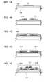
- FIG. 1illustrates a circuit structure of a power source circuit.
- FIGS. 2A to 2Cillustrate a method of a digital pulse width modulation process.
- FIGS. 3A and 3Bare a top view and a cross-sectional view of a transistor in which a channel formation region is provided in an oxide semiconductor film.
- FIGS. 4A to 4Eare cross-sectional views of a manufacturing process of a transistor in which a channel formation region is provided in an oxide semiconductor film.
- FIGS. 5A to 5Care cross-sectional views of transistors in which a channel formation region is provided in an oxide semiconductor film.
- FIG. 6is a circuit diagram illustrating an adder circuit.
- FIG. 7is a circuit diagram illustrating an adder.
- FIG. 8is a circuit diagram illustrating an adder-subtractor circuit, a count comparison circuit, and a latch circuit.
- FIG. 9is a circuit diagram illustrating an adder-subtractor circuit.
- FIG. 10is a circuit diagram illustrating an adder.
- FIG. 11is a circuit diagram illustrating a count comparison circuit.
- FIG. 12is a circuit diagram illustrating a latch circuit.
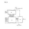
- FIG. 1illustrates an example of a power source circuit 101 .
- the power source circuit 101includes a voltage converter circuit 102 and a control circuit 103 for controlling the voltage converter circuit 102 .
- the voltage converter circuit 102is a DC-DC converter including a transistor 111 , a coil 112 , a diode 113 , and a capacitor 114 .
- the control circuit 103includes a triangle wave generator circuit 121 , a digital control circuit 150 , a pulse width modulation output driver 123 , a resistor 124 , and a resistor 125 .
- a dotted arrow 127indicates a loop of a feedback circuit.
- a feedback voltage Vfbwhich is an output voltage of the resistor 124 , is input to the digital control circuit 150 .
- a DC-DC converteris a circuit which converts a direct current voltage to another direct current voltage.
- Typical conversion modes of a DC-DC converterinclude a linear mode and a switching mode.
- a switching mode DC-DC converterhas excellent conversion efficiency.
- a switching mode DC-DC converterparticularly a chopper-type DC-DC converter including a transistor, a coil, a diode, and a capacitor is used as the voltage converter circuit 102 .
- the digital control circuit 150includes a comparator 151 , a digital arithmetic process circuit 152 , a pulse width modulation output driver 153 , and a low pass filter (LPF) 154 .
- the digital control circuit 150When an error amplifier circuit is replaced with the digital control circuit 150 , variation in characteristics of elements in the circuit 150 does not pose a problem.
- the digital arithmetic process circuit 152 and the pulse width modulation output driver 153are digital circuits. The digital circuit determines whether the signal is 1 or 0 (zero) according to whether the level of a signal in the circuit is higher or lower than a reference, and therefore performs data processing properly even when the elements in the digital circuit vary in characteristics.
- the digital control circuit 150in the digital control circuit 150 , the use of passive elements having a large area (e.g., a capacitor and a resistor) is reduced; therefore, the digital control circuit 150 is preferable in that the area of the circuit can be reduced.
- the comparator 151compares a reference voltage Vref which is input from an inverted input terminal REF and a feedback voltage Vfb, and outputs a digital signal of H (high level) or L (low level), that is, a digital signal 1 or 0 (zero).
- the digital arithmetic process circuit 152includes a digital average-integrator 152 a and a digital pulse width modulator 152 b .
- the digital average-integrator 152 aincludes a digital averaging circuit 152 a _ 1 and a digital integrator 152 a _ 2 .
- an external clock divider 155is connected, and a clock signal is input from the clock divider 155 .
- the digital arithmetic process circuit 152performs an averaging process, an integration process, and a digital pulse width modulation process of the digital signal output from the comparator 151 .
- the digital averaging circuit 152 a _ 1performs an averaging process and the digital integrator 152 a _ 2 performs an integration process.
- the digital pulse width modulator 152 bperforms a digital pulse width modulation process.
- the digital arithmetic process circuit 152holds N bits of data on the digital signal (which is either H (high level) or L (low level)) output from the comparator 151 , compares the frequency of appearance of H signal and L signal, and outputs either one with a higher frequency. Thus, the digital signal is averaged.
- FIGS. 6 and 7illustrate specific circuit structures of the digital averaging circuit 152 a _ 1 which is in the digital average-integrator 152 a in FIG. 1 and which performs an averaging process.
- An adder circuit 201 in FIG. 6is an example of the digital averaging circuit 152 a _ 1 .
- the adder circuit 201detects the value of a signal COMP from the comparator 151 every count and holds H (high level) if the value of the signal COMP is H (high level). For example, the adder circuit 201 outputs an averaged digital signal DIG_AVE every 7 counts. In this embodiment, if the signal COMP of H (high level) is input 4 or more times, the digital signal DIG_AVE of H (high level) is output and if the signal COMP of H (high level) is input 3 or less times, the digital signal DIG_AVE of L (low level) is output. In addition, the stored signal COMP is reset every 8 counts by a reset signal RST.
- the adder circuit 201includes an adder 251 , an adder 252 , and an adder 253 .
- a control reset signal CNT_RSTis input.
- the control reset signal CNT_RSTis a signal which resets data in the adder circuit 201 .
- the signal COMPis input from the comparator 151 .
- a third terminal of the adder 251a third terminal of the adder 252 and a third terminal of the adder 253 are connected, and a clock signal CLK is input.
- a fourth terminal of the adder 251a fourth terminal of the adder 252 and a fourth terminal of the adder 253 are connected, and the reset signal RST is input.
- the reset signal RSTis a signal which resets data in the flip flop 214 described below.
- a fifth terminal of the adder 251a second terminal of the adder 252 is connected.
- the fifth terminal of the adder 251outputs an output signal COUT.
- the first terminal of the adder 252To the first terminal of the adder 252 , the first terminal of the adder 251 and the first terminal of the adder 253 are connected, and the control reset signal CNT_RST is input.
- the fifth terminal of the adder 251To the second terminal of the adder 252 , the fifth terminal of the adder 251 is connected.
- the output signal COUT output from the fifth terminal of the adder 251is input to the second terminal of the adder 252 as an input signal CIN.
- the third terminal of the adder 252To the third terminal of the adder 251 and the third terminal of the adder 253 are connected, and the clock signal CLK is input.
- the fourth terminal of the adder 252To the fourth terminal of the adder 252 , the fourth terminal of the adder 251 and the fourth terminal of the adder 253 are connected, and the reset signal RST is input.
- a second terminal of the adder 253To the fifth terminal of the adder 252 , a second terminal of
- the first terminal of the adder 253To the first terminal of the adder 253 , the first terminal of the adder 251 and the first terminal of the adder 252 are connected, and the control reset signal CNT_RST is input.
- the fifth terminal of the adder 252To the second terminal of the adder 253 , the fifth terminal of the adder 252 is connected. The output signal COUT output from the fifth terminal of the adder 252 is input to the second terminal of the adder 253 as the input signal CIN.
- the third terminal of the adder 251 and the third terminal of the adder 252To the third terminal of the adder 253 , the third terminal of the adder 251 and the third terminal of the adder 252 are connected, and the clock signal CLK is input.
- the fourth terminal of the adder 253To the fourth terminal of the adder 253 , the fourth terminal of the adder 251 and the fourth terminal of the adder 252 are connected, and the reset signal RST is input.
- FIG. 7illustrates a circuit diagram of each of the adders 251 to 253 .
- Each of the adders 251 to 253includes an AND gate 211 , an AND gate 212 , an XOR gate 213 , and a flip flop (FF) 214 .
- FFflip flop
- a first input terminal of the AND gate 211is connected and the input signal CIN is input.
- a second input terminal of the AND gate 211a second input terminal of the XOR gate 213 and a fourth terminal of the flip flop 214 are connected.
- An output terminal of the AND gate 211outputs an output signal COUT.
- the control reset signal CNT_RSTis input.
- an output terminal of the XOR gate 213is connected.
- a first terminal of the flip flop 214is connected.
- the first input terminal of the AND gate 211is connected and the input signal CIN is input.
- the second input terminal of the AND gate 211 and the fourth terminal of the flip flop 214are connected.
- the second input terminal of the AND gate 212is connected.
- the output terminal of the AND gate 212is connected to the first terminal of the flip flop 214 .
- the reset signal RSTis input to a second terminal of the flip flop 214 .
- the clock signal CLKis input to a third terminal of the flip flop 214 .
- the second input terminal of the AND gate 211 and the second input terminal of the XOR gate 213are connected to the fourth terminal of the flip flop 214 .
- the digital integrator 152 a _ 2adds “ ⁇ 1” or “+1” depending on the averaged digital signal DIG_AVE and performs integration. Note that when the averaged digital signal DIG_AVE is an H (high level) signal, “ ⁇ 1” is added, while when the averaged digital signal DIG_AVE is an L (low level) signal, “+1” is added. Thus, the averaged digital signal DIG_AVE is integrated.
- FIG. 8illustrates a circuit structure of the digital integrator 152 a _ 2 (an adder-subtractor circuit 202 ) which is a specific circuit in the digital average-integrator 152 a in FIG. 1 and performs integration.
- FIG. 8also illustrates a circuit structure (a count comparison circuit 203 and a latch circuit 204 ) of the digital pulse width modulator 152 b in FIG. 1 .
- a first terminal of the latch circuit 204is connected and the reset signal RST is input.
- the clock signal CLKis input.
- the averaged digital signal DIG_AVEis input.
- a first terminal of the count comparison circuit 203is connected. The fourth terminal of the adder-subtractor circuit 202 outputs a signal SET-CNT 0 .
- a second terminal of the count comparison circuit 203is connected.
- the fifth terminal of the adder-subtractor circuit 202outputs a signal SET-CNT 1 .
- a third terminal of the count comparison circuit 203is connected to a sixth terminal of the adder-subtractor circuit 202 .
- the sixth terminal of the adder-subtractor circuit 202outputs a signal SET-CNT 2 .
- a fourth terminal of the count comparison circuit 203is connected to a seventh terminal of the adder-subtractor circuit 202 .
- the seventh terminal of the adder-subtractor circuit 202outputs a signal SET-CNT 3 .
- a fifth terminal of the count comparison circuit 203is connected to an eighth terminal of the adder-subtractor circuit 202 .
- the eighth terminal of the adder-subtractor circuit 202outputs a signal SET-CNT 4 .
- a sixth terminal of the count comparison circuit 203is connected to a ninth terminal of the adder-subtractor circuit 202 .
- the ninth terminal of the adder-subtractor circuit 202outputs a signal SET-CNT 5 .
- a seventh terminal of the count comparison circuit 203is connected to a tenth terminal of the adder-subtractor circuit 202 .
- the tenth terminal of the adder-subtractor circuit 202outputs a limit signal LIMIT.
- the signals SET-CNT 0 to SET-CNT 5are needed for generating a pulse signal PULSE having a pulse width W described below.
- a pulse signal PULSEhaving a pulse width W described below.
- 2 6 -phase i.e., 64-phase signal PULSEcan be generated.
- the limit signal LIMITis a signal which limits a phase in a process of generating the pulse signal PULSE having a pulse width W described below.
- the limit signal LIMITfor example, the signals SET-CNT 0 to SET-CNT 5 are limited to 8 to 56.
- the proximity of the maximum value of the pulse width W of the pulse signal PULSE to the period of the pulse signal PULSE and the proximity of the minimum value of the pulse width W to 0 (zero)is prevented.
- the fourth terminal of the adder-subtractor circuit 202is connected and the signal SET-CNT 0 is input.
- the fifth terminal of the adder-subtractor circuit 202is connected and the signal SET-CNT 1 is input.
- the sixth terminal of the adder-subtractor circuit 202is connected and the signal SET-CNT 2 is input.
- the seventh terminal of the adder-subtractor circuit 202is connected and the signal SET-CNT 3 is input.
- the eighth terminal of the adder-subtractor circuit 202is connected and the signal SET-CNT 4 is input.
- the ninth terminal of the adder-subtractor circuit 202is connected and the signal SET-CNT 5 is input.
- the tenth terminal of the adder-subtractor circuit 202is connected.
- the seventh terminal of the count comparison circuit 203outputs the limit signal LIMIT.
- a signal CNT 0is input.
- a ninth terminal of the count comparison circuit 203a signal CNT 1 is input.
- a signal CNT 2is input to a tenth terminal of the count comparison circuit 203 .
- a signal CNT 3is input to an eleventh terminal of the count comparison circuit 203 .
- a signal CNT 4is input to a twelfth terminal of the count comparison circuit 203 .
- a signal CNT 5is input to a thirteenth terminal of the count comparison circuit 203 .
- a fourteenth terminal of the count comparison circuit 203outputs a signal HIGH-SET.
- a fifteenth terminal of the count comparison circuit 203outputs a signal LOW-SET.
- the signals CNT 0 to CNT 5are count signals.
- input of the signals CNT 0 to CNT 5can count from 0 to 63.
- the signal HIGH-SET and the signal LOW-SETdetermine whether the pulse width modulation output signal PWM is an H (high level) signal or an L (low level) signal.
- the pulse width modulation output signal PWMbecomes an H (high level) signal.
- the pulse width modulation output signal PWMbecomes an L (low level) signal.
- the first terminal of the latch circuit 204To the first terminal of the latch circuit 204 , the first terminal of the adder-subtractor circuit 202 is connected and the reset signal RST is input. To a second terminal of the latch circuit 204 , the fourteenth terminal of the count comparison circuit 203 is connected and the signal HIGH-SET is input. To a third terminal of the latch circuit 204 , the fifteenth terminal of the count comparison circuit 203 is connected and the signal LOW-SET is input. From a fourth terminal of the latch circuit 204 , the pulse width modulation output signal PWM is output. To a fifth terminal of the latch circuit 204 , the clock signal CLK is input.
- FIG. 9illustrates a specific circuit structure of the adder-subtractor circuit 202 .
- the adder-subtractor circuit 202 in FIG. 9includes an inverter 261 , an inverter 262 , a NOR gate 263 , an adder 254 , an adder 255 , an adder 256 , an adder 257 , an adder 258 , and an adder 259 .
- the averaged digital signal DIG_AVEis input.
- An output terminal of the inverter 261is connected to a first input terminal of the NOR gate 263 .
- a second input terminal of the NOR gate 263is connected and the limit signal LIMIT is input.
- a first terminal of the adder 254is connected.
- the output terminal of the inverter 261is connected.
- the input terminal of the inverter 262is connected and the limit signal LIMIT is input.
- the output terminal of the inverter 262is connected to the first terminal of the adder 254 .
- a second terminal of the adder 255a second terminal of the adder 256 , a second terminal of the adder 257 , a second terminal of the adder 258 , and a second terminal of the adder 259 are connected, and the clock signal CLK is input.
- a third terminal of the adder 254To a third terminal of the adder 254 , a third terminal of the adder 255 , a third terminal of the adder 256 , a third terminal of the adder 257 , a third terminal of the adder 258 , and a third terminal of the adder 259 are connected, and the reset signal RST is input.
- an output terminal of the NOR gate 263To a fourth terminal of the adder 254 , an output terminal of the NOR gate 263 , a fourth terminal of the adder 255 , a fourth terminal of the adder 256 , a fourth terminal of the adder 257 , a fourth terminal of the adder 258 , and a fourth terminal of the adder 259 are connected.
- a fifth terminal of the adder 254To a fifth terminal of the adder 254 , a first terminal of the adder 255 is connected and the fifth terminal of the adder 254 outputs the signal SET_CNT 0 .
- the fifth terminal of the adder 254is connected and the signal SET_CNT 0 is input.
- the second terminal of the adder 255the second terminal of the adder 254 , the second terminal of the adder 256 , the second terminal of the adder 257 , the second terminal of the adder 258 , and the second terminal of the adder 259 are connected, and the clock signal CLK is input.
- the third terminal of the adder 255the third terminal of the adder 254 , the third terminal of the adder 256 , the third terminal of the adder 257 , the third terminal of the adder 258 , and the third terminal of the adder 259 are connected, and the reset signal RST is input.
- the output terminal of the NOR gate 263 , the fourth terminal of the adder 254 , the fourth terminal of the adder 256 , the fourth terminal of the adder 257 , the fourth terminal of the adder 258 , and the fourth terminal of the adder 259are connected.
- a fifth terminal of the adder 255a first terminal of the adder 256 is connected and the fifth terminal of the adder 255 outputs a signal SET_CNT 1 .
- the fifth terminal of the adder 255is connected and the signal SET_CNT 1 is input.
- the second terminal of the adder 256the second terminal of the adder 254 , the second terminal of the adder 255 , the second terminal of the adder 257 , the second terminal of the adder 258 , and the second terminal of the adder 259 are connected, and the clock signal CLK is input.
- the third terminal of the adder 256the third terminal of the adder 254 , the third terminal of the adder 255 , the third terminal of the adder 257 , the third terminal of the adder 258 , and the third terminal of the adder 259 are connected, and the reset signal RST is input.
- the output terminal of the NOR gate 263To the fourth terminal of the adder 256 , the output terminal of the NOR gate 263 , the fourth terminal of the adder 254 , the fourth terminal of the adder 255 , the fourth terminal of the adder 257 , the fourth terminal of the adder 258 , and the fourth terminal of the adder 259 are connected.
- a fifth terminal of the adder 256a first terminal of the adder 257 is connected and the fifth terminal of the adder 256 outputs a signal SET_CNT 2 .
- the fifth terminal of the adder 256is connected and the signal SET_CNT 2 is input.
- the second terminal of the adder 254To the second terminal of the adder 257 , the second terminal of the adder 254 , the second terminal of the adder 255 , the second terminal of the adder 256 , the second terminal of the adder 258 , and the second terminal of the adder 259 are connected, and the clock signal CLK is input.
- the third terminal of the adder 254 , the third terminal of the adder 255 , the third terminal of the adder 256 , the third terminal of the adder 258 , and the third terminal of the adder 259To the third terminal of the adder 257 , the third terminal of the adder 254 , the third terminal of the adder 255 , the third terminal of the adder 256 , the third terminal of the adder 258 , and the third terminal of the adder 259 are connected, and the reset signal RST is input.
- the output terminal of the NOR gate 263To the fourth terminal of the adder 257 , the output terminal of the NOR gate 263 , the fourth terminal of the adder 254 , the fourth terminal of the adder 255 , the fourth terminal of the adder 256 , the fourth terminal of the adder 258 , and the fourth terminal of the adder 259 are connected.
- a fifth terminal of the adder 257a first terminal of the adder 258 is connected and the fifth terminal of the adder 257 outputs a signal SET_CNT 3 .
- the fifth terminal of the adder 257is connected and the signal SET_CNT 3 is input.
- the second terminal of the adder 258the second terminal of the adder 254 , the second terminal of the adder 255 , the second terminal of the adder 256 , the second terminal of the adder 257 , and the second terminal of the adder 259 are connected, and the clock signal CLK is input.
- the third terminal of the adder 258the third terminal of the adder 254 , the third terminal of the adder 255 , the third terminal of the adder 256 , the third terminal of the adder 257 , and the third terminal of the adder 259 are connected, and the reset signal RST is input.
- the output terminal of the NOR gate 263To the fourth terminal of the adder 258 , the output terminal of the NOR gate 263 , the fourth terminal of the adder 254 , the fourth terminal of the adder 255 , the fourth terminal of the adder 256 , the fourth terminal of the adder 257 , and the fourth terminal of the adder 259 are connected.
- a fifth terminal of the adder 258a first terminal of the adder 259 is connected and the fifth terminal of the adder 258 outputs a signal SET_CNT 4 .
- the fifth terminal of the adder 258is connected and the signal SET_CNT 4 is input.
- the second terminal of the adder 259the second terminal of the adder 254 , the second terminal of the adder 255 , the second terminal of the adder 256 , the second terminal of the adder 257 , and the second terminal of the adder 258 are connected, and the clock signal CLK is input.
- the third terminal of the adder 259the third terminal of the adder 254 , the third terminal of the adder 255 , the third terminal of the adder 256 , the third terminal of the adder 257 , and the third terminal of the adder 258 are connected, and the reset signal RST is input.
- the output terminal of the NOR gate 263To the fourth terminal of the adder 259 , the output terminal of the NOR gate 263 , the fourth terminal of the adder 254 , the fourth terminal of the adder 255 , the fourth terminal of the adder 256 , the fourth terminal of the adder 257 , and the fourth terminal of the adder 258 are connected.
- a fifth terminal of the adder 259outputs a signal SET_CNT 5 .
- FIG. 10illustrates a circuit diagram of each of the adders 254 to 259 .
- Each of the adders 254 to 259includes an AND gate 221 , an AND gate 222 , an OR gate 224 , an XOR gate 225 , an XOR gate 226 , and a flip flop 227 .
- a first input terminal of the AND gate 221To a first input terminal of the AND gate 221 , a first input terminal of the XOR gate 225 is connected and a control signal CONT is input.
- the control signal CONTis a signal which indicates the adder at the subsequent stage that either addition or subtraction is to be performed.
- a second input terminal of the AND gate 221To a second input terminal of the AND gate 221 , a second input terminal of the XOR gate 225 and a fourth terminal of the flip flop 227 are connected.
- a first input terminal of the OR gate 224To an output terminal of the AND gate 221 , a first input terminal of the OR gate 224 is connected.
- a first input terminal of the AND gate 222a first input terminal of the XOR gate 226 is connected and the input signal CIN is input.
- an output terminal of the XOR gate 225 and a second input terminal of the XOR gate 226are connected.
- a second input terminal of the OR gate 224is connected.
- the first input terminal of the XOR gate 225To the first input terminal of the XOR gate 225 , the first input terminal of the AND gate 221 is connected and the control signal CONT is input. To the second input terminal of the XOR gate 225 , the second input terminal of the AND gate 221 and the fourth terminal of the flip flop 227 are connected. To the output terminal of the XOR gate 225 , the second input terminal of the AND gate 222 and the second input terminal of the XOR gate 226 are connected.
- the first input terminal of the AND gate 222is connected and the input signal CIN is input.
- the second input terminal of the AND gate 222 and the output terminal of the XOR gate 225are connected.
- a first terminal the flip flop 227is connected.
- the output terminal of the XOR gate 226is connected.
- the reset signal RSTis input.
- the clock signal CLKis input.
- the second input terminal of the AND gate 221 and the second input terminal of the XOR gate 225is connected.
- the digital pulse width modulator 152 bsets the pulse width of the pulse width modulation in accordance with an integrated digital signal. Thus, a digital pulse width modulation process is performed.
- the pulse width modulation output signal PWM which has been subjected to digital pulse width modulationis input to the pulse width modulation output driver 153 .
- FIG. 11 and FIG. 12illustrate specific circuit structures of the digital pulse width modulator 152 b .
- the count comparison circuit 203 in FIG. 11 and the latch circuit 204 in FIG. 12are specific examples of the digital pulse width modulator 152 b .
- the count comparison circuit 203compares the predetermined value of the duty ratio determined by the signals SET-CNT 0 to SET-CNT 5 and the value of the signals CNT 0 to CNT 5 , and generates the pulse width modulation output signal PWM when they much.
- FIG. 11illustrates a circuit diagram of the count comparison circuit 203 .
- the count comparison circuit 203includes an XOR gate 271 , an XOR gate 272 , an XOR gate 273 , an XOR gate 274 , an XOR gate 275 , an XOR gate 276 , a NAND gate 277 , an AND gate 278 , an OR gate 279 , a NAND gate 281 , and a NAND gate 282 .
- a first input terminal of the NAND gate 281is connected, and the signal CNT 0 is input.
- the signal SET_CNT 0is input.
- a first input terminal of the NAND gate 282is connected.
- a second input terminal of the NAND gate 281is connected, and the signal CNT 1 is input.
- the signal SET_CNT 1is input.
- an output terminal of the XOR gate 272a second input terminal of the NAND gate 282 is connected.
- a third input terminal of the NAND gate 281is connected, and the signal CNT 2 is input.
- the signal SET_CNT 2is input.
- a third input terminal of the NAND gate 282is connected.
- a fourth input terminal of the NAND gate 281is connected, and the signal CNT 3 is input.
- a first input terminal of the NAND gate 277 and a first input terminal of the AND gate 278are connected, and the signal SET_CNT 3 is input.
- a fourth input terminal of the NAND gate 282is connected.
- a fifth input terminal of the NAND gate 281is connected, and the signal CNT 4 is input.
- a second input terminal of the XOR gate 275a second input terminal of the NAND gate 277 and a second input terminal of the AND gate 278 are connected, and the signal SET_CNT 4 is input.
- a fifth input terminal of the NAND gate 282is connected.
- a sixth input terminal of the NAND gate 281is connected, and the signal CNT 5 is input.
- a third input terminal of the NAND gate 277 and a third input terminal of the AND gate 278are connected, and the signal SET_CNT 5 is input.
- a sixth input terminal of the NAND gate 282is connected.
- the second input terminal of the XOR gate 274 and the first input terminal of the AND gate 278are connected, and the signal SET_CNT 3 is input.
- the second input terminal of the XOR gate 275 and the second input terminal of the AND gate 278are connected, and the signal SET_CNT 4 is input.
- the third input terminal of the NAND gate 277the second input terminal of the XOR gate 276 and the third input terminal of the AND gate 278 are connected, and the signal SET_CNT 5 is input.
- a first input terminal of the OR gate 279is connected.
- the second input terminal of the XOR gate 274 and the first input terminal of the NAND gate 277are connected, and the signal SET_CNT 3 is input.
- the second input terminal of the AND gate 278the second input terminal of the XOR gate 275 and the second input terminal of the NAND gate 277 are connected, and the signal SET_CNT 4 is input.
- the third input terminal of the AND gate 278the second input terminal of the XOR gate 276 and the third input terminal of the NAND gate 277 are connected, and the signal SET_CNT 5 is input.
- a second input terminal of the OR gate 279is connected.
- the first input terminal of the XOR gate 271is connected, and the signal CNT 0 is input.
- the first input terminal of the XOR gate 272is connected, and the signal CNT 1 is input.
- the first input terminal of the XOR gate 273is connected, and the signal CNT 2 is input.
- the first input terminal of the XOR gate 274is connected, and the signal CNT 3 is input.
- the first input terminal of the XOR gate 275is connected, and the signal CNT 4 is input.
- the sixth input terminal of the NAND gate 281the first input terminal of the XOR gate 276 is connected, and the signal CNT 5 is input.
- An output terminal of the NAND gate 281outputs the signal LOW-SET.
- the output terminal of the XOR gate 271is connected to the first input terminal of the NAND gate 282 .
- the output terminal of the XOR gate 272is connected.
- the output terminal of the XOR gate 273is connected to the third input terminal of the NAND gate 282 .
- the output terminal of the XOR gate 274is connected to the fourth input terminal of the NAND gate 282 .
- the output terminal of the XOR gate 275is connected.
- the output terminal of the XOR gate 276is connected to the sixth input terminal of the NAND gate 282 . An output terminal of the NAND gate 282 outputs the signal HIGH-SET.
- FIG. 12is a circuit diagram of the latch circuit 204 .
- the latch circuit 204includes a flip flop 241 , a flip flop 242 , a NOR gate 243 , and a NOR gate 244 .
- the signal LOW-SETis input.
- a second terminal of the flip flop 241a second terminal of the flip flop 242 , a second input terminal of the NOR gate 243 , and a second input terminal of the NOR gate 244 are connected, and the reset signal RST is input.
- a third terminal of the flip flop 241a third terminal of the flip flop 242 is connected, and the clock signal CLK is input.
- a fourth terminal of the flip flop 241a first input terminal of the NOR gate 243 is connected.
- the signal HIGH-SETis input.
- the second terminal of the flip flop 242the second terminal of the flip flop 241 , the second input terminal of the NOR gate 243 , and the second input terminal of the NOR gate 244 are connected, and the reset signal RST is input.
- the third terminal of the flip flop 242the third terminal of the flip flop 241 is connected, and the clock signal CLK is input.
- a fourth terminal of the flip flop 242a first input terminal of the NOR gate 244 is connected.
- the fourth terminal of the flip flop 241is connected to the first input terminal of the NOR gate 243 .
- the second terminal of the flip flop 241 , the second terminal of the flip flop 242 , and the second input terminal of the NOR gate 244are connected, and the reset signal RST is input.
- an output terminal of the NOR gate 244is connected to a third input terminal of the NOR gate 243 .
- a third input terminal of the NOR gate 244is connected to an output terminal of the NOR gate 243 .
- the fourth terminal of the flip flop 242is connected to the first input terminal of the NOR gate 244 .
- the second terminal of the flip flop 241 , the second terminal of the flip flop 242 , and the second input terminal of the NOR gate 243are connected, and the reset signal RST is input.
- the output terminal of the NOR gate 243is connected to the third input terminal of the NOR gate 244 .
- the third input terminal of the NOR gate 243is connected.
- the output terminal of the NOR gate 244outputs the pulse width modulation output signal PWM.
- a digital pulse width modulationwill now be described with reference to FIGS. 2A to 2C .
- a pulse width of the digital pulse signal PULSEis referred to as W and a pulse period thereof is referred to as T (see FIG. 2A ).
- the pulse signal PULSEis generated based on a clock from the clock divider 155 and the phase which is controlled by the signals SET_CNT 0 to SET_CNT 5 .
- the pulse signal PULSEcorresponds to the pulse width modulation output signal PWM.
- the duty ratio Diis given by the following FORMULA 1.
- the duty ratio D32is 0.5; when i is 48, the duty ratio D48 is 0.75; and when i is 16, the duty ratio D16 is 0.25.
- a power source voltage Vdd described belowis generated according to the duty ratio.
- a digital signalis thus converted into an analog signal, whereby a process similar to a process by a DA converter is performed.
- 64-phase pulse width modulation output signalcan be output.
- the pulse width modulation output signal which undergoes digital pulse width modulationis input to the pulse width modulation output driver 153 .
- the pulse width modulation output signalis increased in intensity by the pulse width modulation output driver 153 .
- the pulse width modulation output signalis amplified by the pulse width modulation output driver 153 .
- the pulse width modulation output signal with increased signal intensityis input to the low pass filter 154 which is a smoothing circuit.
- the low pass filter 154blocks a high-frequency component of the pulse width modulation output signal and the pulse width modulation output signal is smoothed. Using the pulse width modulation output signal input to the low pass filter 154 , voltage corresponding to the duty ratio is output.
- a digital signalbecomes an analog signal; thus, a process similar to a process by a DA converter is performed.
- frequency responseis performed by the low pass filter 154 .
- the area of the power source circuitcan be reduced.
- control circuit 103Another element in the control circuit 103 will be described below.
- the triangle wave generator circuit 121generates a triangle wave Vosc which is needed for a pulse width modulation signal.
- the output voltage Verr of the digital control circuit 150is input, while to a non-inverted input terminal, the triangle wave Vosc generated by the triangle wave generator circuit 121 is input.
- the pulse width modulation output driver 123compares the output voltage Verr of the digital control circuit 150 with a signal level of the triangle wave Vosc. When the signal level of the triangle wave Vosc is higher than the signal level of the output voltage Ven of the digital control circuit 150 , the pulse width modulation output driver 123 outputs H (high level) as the pulse width modulation signal to the transistor 111 . When the signal level of the triangle wave Vosc is lower than the signal level of the output voltage Verr of the digital control circuit 150 , the pulse width modulation output driver 123 outputs L (low level) as the pulse width modulation signal to the transistor 111 .
- suppression of degradation of circuit operationcan reduce causes of malfunction of electrical elements including the power source circuit and electrical appliances including the electrical element.
- the area of an integrated circuit and the area of an electrical appliance including the integrated circuitcan be reduced. Accordingly, the cost of the integrated circuit and the cost of the electrical appliance including the integrated circuit can be reduced.
- the digital circuitoutputs only either 1 or 0 (zero), all the transistors in the digital circuit can be of the same conductivity type, e.g., n-type. A complicated analog signal processing is very difficult for an analog circuit transistors of which have the same conductivity type. Thus, a digital circuit can be formed using transistors which have the same conductivity type in this embodiment.
- the transistor 111 and a transistor in each of the comparator 151 , the digital arithmetic process circuit 152 , and the pulse width modulation output driver 153 in Embodiment 1will be described.
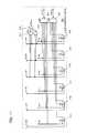
- FIGS. 3A and 3Bshow an example of a top-surface structure and cross-sectional structure of a transistor.
- FIG. 3Ais a top view of a top-gate transistor 410
- FIG. 3Bis a cross-sectional view taken along line A-A′ in FIG. 3A .
- the transistor 410includes an oxide semiconductor film 412 , a first electrode (one of a source electrode and a drain electrode) 415 a , a second electrode (the other of the source electrode and the drain electrode) 415 b , a gate insulating film 402 , and a gate electrode 411 .
- a first wiring 414 a and a second wiring 414 bare in contact with and electrically connected to the first electrode 415 a and the second electrode 415 b , respectively.
- the transistor 410 in FIG. 3Ais a single-gate transistor, one embodiment of the disclosed invention is not limited to this structure.
- the transistormay be a multi-gate transistor including gate electrodes and channel formation regions.
- the transistor in FIGS. 3A and 3Bincludes the first electrode (the one of the source electrode and the drain electrode) 415 a and the second electrode (the other of the source electrode and the drain electrode) 415 b formed over the oxide semiconductor film 412 including the channel formation region, one embodiment of the disclosed invention is not limited thereto.
- the oxide semiconductor film 412 including the channel formation regionmay be formed over the first electrode (the one of the source electrode and the drain electrode) 415 a and the second electrode (the other of the source electrode and the drain electrode) 415 b.
- the transistor 410may be a bottom-gate transistor. Further, when the transistor 410 is a bottom-gate transistor, either the source electrode and the drain electrode or the oxide semiconductor film including the channel formation region may lie over the other. In other words, the source electrode and the drain electrode may be formed over the oxide semiconductor film including a channel formation region; alternatively, the oxide semiconductor film including a channel formation region may be formed over the source electrode and the drain electrode.
- a high-purity oxide semiconductor filmis used as the oxide semiconductor film 412 of the transistor 410 , characteristics of the transistor 410 are improved. Characteristics of such a high-purity oxide semiconductor film and characteristics of a transistor including the high-purity oxide semiconductor film will be described below in detail.
- impurities that adversely affect the electrical characteristics of the transistor including the oxide semiconductor filmare reduced to a very low level.
- a typical example of impurities which adversely affect the electric characteristicsis hydrogen.
- Hydrogenis an impurity which may be a supplier (a donor) of carriers in an oxide semiconductor film.
- the oxide semiconductorincludes a large amount of hydrogen, the oxide semiconductor film might have n-type conductivity.
- a transistor including an oxide semiconductor which includes a large amount of hydrogenmay be a normally-on transistor, and the on/off ratio of the transistor cannot be sufficiently high.
- a “high-purity oxide semiconductor”is an intrinsic or substantially intrinsic oxide semiconductor from which hydrogen is reduced as much as possible.
- off-currentalso referred to as leakage current
- leakage currentrefers to current flowing between a source and a drain of an n-channel transistor having a positive threshold voltage V th , when a given gate voltage in the range of equal to or greater than ⁇ 20 V and equal to or less than ⁇ 5 V is applied at room temperature.
- the room temperatureis equal to or higher than 15° C. and equal to or lower than 25° C.
- the current value per micrometer of channel width (w) of a transistor using an oxide semiconductor disclosed in this specificationis 100 zA or less, and preferably 10 zA or less at room temperature.
- off-state resistance Rthe resistance at the time when the transistor is off
- the off-state resistivityis preferably higher than or equal to 1 ⁇ 10 9 ⁇ m (or higher than or equal to 1 ⁇ 10 10 ⁇ m).
- the energy gap of the oxide semiconductor filmis 2 eV or more, preferably 2.5 eV or more, more preferably 3 eV or more.
- a transistor including a high-purity oxide semiconductorhas favorable temperature characteristics. Specifically, in the temperature range of from ⁇ 25° C. to 150° C., the current-voltage characteristics of the transistor, such as on-state current, off-state current, field-effect mobility, a subthreshold value (an S value), and threshold voltage, hardly change. This means that the current-voltage characteristics are hardly deteriorated by the temperature.
- the hot-carrier degradationrefers to a phenomenon in which electrons that are accelerated to high speed become fixed charges by being injected into a gate insulating film from a channel in the vicinity of drain or form a trap level at the interface between the gate insulating film and the oxide semiconductor film, and thereby causing deterioration such as change in threshold voltage or gate leakage current.
- the causes of the hot-carrier degradationare channel-hot-electron injection (CHE injection) and drain-avalanche-hot-carrier injection (DAHC injection).
- the band gap of siliconis as small as 1.12 eV, electrons are likely to be generated like an avalanche because of avalanche breakdown, and the number of electrons that are accelerated to high speed and go over a barrier to the gate insulating film is increased.
- the oxide semiconductor described in this embodimenthas a wide band gap of 3.15 eV; therefore, the avalanche breakdown is unlikely to occur and resistance to hot-carrier degradation is higher than that of silicon.
- the band gap of silicon carbidewhich is one of the materials having a high breakdown voltage
- the band gap of the oxide semiconductorare approximately the same.
- electronsare less likely to be accelerated in an oxide semiconductor because the mobility of an oxide semiconductor is smaller than that of silicon carbide by approximately two orders of magnitude.
- a barrier between an oxide semiconductor and an oxide film that is a gate insulating filmis larger than a barrier between silicon carbide, gallium nitride, or silicon and the oxide film; therefore, in an oxide semiconductor, the number of electrons injected to the oxide film is extremely small. Because the number of electrons injected to the oxide film is extremely small, an oxide semiconductor has less hot carrier degradation and higher drain breakdown voltage than silicon carbide, gallium nitride, or silicon. Therefore, it is not necessary to intentionally form low-concentration impurity regions between an oxide semiconductor functioning as a channel and a source and drain electrodes; thus, the structure of the transistor can be significantly simplified and the number of manufacturing steps can be reduced.
- a transistor including an oxide semiconductorhas high drain breakdown voltage of, specifically, 100 V or more, preferably 500 V, more preferably 1 kV or more.
- an insulating layer 407 serving as a base filmis formed over a substrate 400 .
- the substrate 400needs to have heat resistance high enough to withstand at least heat treatment to be performed later.
- a substrate having a strain point of 730° C. or higheris preferably used.
- Specific examples of the substrate 400include a glass substrate, a crystalline glass substrate, a ceramic substrate, a quartz substrate, a sapphire substrate, and a plastic substrate.
- specific examples of a material of the glass substrateinclude aluminosilicate glass, aluminoborosilicate glass, and barium borosilicate glass.
- an oxide insulating layersuch as a silicon oxide layer, a silicon oxynitride layer, an aluminum oxide layer, or an aluminum oxynitride layer is preferably used.
- the insulating layer 407can be formed by a plasma CVD method, a sputtering method, or the like.
- the insulating layer 407is preferably formed by a sputtering method.
- a silicon oxide layeris formed as the insulating layer 407 by a sputtering method.
- the substrate 400is transferred to a process chamber and a sputtering gas including high-purity oxygen from which hydrogen and moisture are removed is introduced, and a target of silicon or silicon oxide is used, whereby a silicon oxide layer is formed as the insulating layer 407 over the substrate 400 .
- the substrate 400may be kept at room temperature or may be heated during deposition.
- the thickness of the filmis 100 nm.
- a silicon targetmay be used as the target instead of the quartz (preferably, synthetic quartz) target.
- a sputtering gas for forming the insulating layer 407is a high-purity gas in which impurities such as hydrogen, water, hydroxyl, or hydride are reduced to such a level that the concentration thereof can be expressed in ppm or ppb.
- the insulating layer 407be formed while moisture remaining in the process chamber is removed so that the insulating layer 407 may be prevented from including hydrogen, hydroxyl, moisture, or the like.
- an entrapment vacuum pumpmay be used.
- a cryopump, an ion pump, or a titanium sublimation pumpcan be used.
- a turbo pumpis preferably used in combination with a cold trap.
- a process chamber which is evacuated with a cryopumpis preferable because hydrogen atoms, compounds including a hydrogen atom such as water (H 2 O), or the like are exhausted from the process chamber and thus hydrogen atoms are hardly included in the insulating layer 407 formed in the process chamber.
- Examples of a sputtering methodinclude an RF sputtering method in which a high-frequency power source is used for a sputtering power supply, a DC sputtering method, and a pulsed DC sputtering method in which a bias is applied in a pulsed manner.
- An RF sputtering methodis mainly used in the case where an insulating film is formed, and a DC sputtering method is mainly used in the case where a metal film is formed.
- multi-source sputtering apparatusin which a plurality of targets of different materials can be set.
- films of different materialscan be formed to be stacked in one chamber, or a film can be formed by electric discharge of plural kinds of materials at the same time in one chamber.
- a sputtering apparatusprovided with a magnet system inside the chamber and used for a magnetron sputtering method, or a sputtering apparatus used for an ECR sputtering method in which plasma generated with the use of microwaves is used without using glow discharge can be used.
- a deposition method using a sputtering methodthere are also a reactive sputtering method in which a target substance and a sputtering gas component are chemically reacted with each other during the deposition to form a thin compound film thereof, and a bias sputtering method in which voltage is also applied to a substrate during the deposition.
- the structure of the insulating layer 407is not limited to a single-layer structure and may be a stacked-layer structure.
- the insulating layer 407may have a stacked-layer structure in which a nitride insulating layer such as a silicon nitride layer, a silicon nitride oxide layer, an aluminum nitride layer, or an aluminum nitride oxide layer and the above oxide insulating layer are stacked in this order over the substrate 400 .
- a sputtering gas including high-purity nitrogenis introduced and a silicon nitride layer is formed using a silicon target, and then the sputtering gas is changed to a gas including high-purity oxygen and a silicon oxide layer is formed.
- the silicon nitride layer or a silicon oxide layerbe formed while moisture remaining in the process chamber is removed as in the above case. Further, the substrate may be heated during deposition.
- an oxide semiconductor filmis formed over the insulating layer 407 by a sputtering method.
- the substrate 400 over which the insulating layer 407 is formedbe preheated in a preheating chamber of a sputtering apparatus as pretreatment for the deposition so that impurities such as hydrogen and moisture adsorbed to the substrate 400 may be removed and evacuated.
- an evacuation means in the preheating chamberis preferably a cryopump so as to evacuate hydrogen atoms, compounds containing hydrogen atoms like water (H 2 O), and the like.
- this preheatingis preferably performed on the substrate 400 before the formation of the gate insulating film 402 , which is formed later. Further, this preheating is preferably performed similarly on the substrate 400 over which components up to the first electrode 415 a and the second electrode 415 b are formed. Note that this preheating treatment may be omitted.
- dust attached to a surface of the insulating layer 407is preferably removed by reverse sputtering in which an argon gas is introduced and plasma is generated.
- the reverse sputteringrefers to a method in which an RF power source is used for application of voltage to a substrate in an argon atmosphere and plasma is generated in the vicinity of the substrate to modify the surface.
- nitrogen, helium, oxygen, or the likemay be used instead of an argon atmosphere.
- a metal oxide target including zinc oxide as its main componentcan be used as a target for forming the oxide semiconductor film.
- the filling factor of the target including In, Ga, and Znis 90% or higher and 100% or lower, and preferably 95% or higher and lower than 100%. With the use of a target with high filling factor, the resulting oxide semiconductor film has high density.
- the oxide semiconductor filmmay be formed in a rare gas (typically, argon) atmosphere, an oxygen atmosphere, or a mixed atmosphere of a rare gas and oxygen.
- a sputtering gas for forming the oxide semiconductor filmis a high-purity gas in which impurities such as hydrogen, water, hydroxyl, or hydride are reduced to such a level that the concentration thereof can be expressed in ppm or ppb.
- the oxide semiconductor filmis formed over the substrate 400 in such a manner that the substrate is held in a process chamber under reduced pressure, a sputtering gas from which hydrogen and moisture are removed is introduced while moisture remaining in the process chamber is removed, and metal oxide is used as a target.
- a sputtering gas from which hydrogen and moisture are removedis introduced while moisture remaining in the process chamber is removed, and metal oxide is used as a target.
- an entrapment vacuum pumpis preferably used.
- a cryopump, an ion pump, or a titanium sublimation pumpis preferably used.
- a turbo pumpprovided with a cold trap may be used as an evacuation means.
- a deposition chamberwhich is evacuated with a cryopump, hydrogen atoms, compounds and the like including hydrogen atoms like water (H 2 O) (and preferably, a compound including a carbon atom) are exhausted. Accordingly, the concentration of impurities in the oxide semiconductor film formed in this deposition chamber can be reduced. Further, the substrate temperature may be kept at room temperature or may be increased to a temperature lower than 400° C. during the deposition of the oxide semiconductor film.
- a pulse direct current (DC) power supplyis preferable because dust can be reduced and the film thickness can be uniform.
- the thickness of the oxide semiconductor filmis preferably 2 nm or more and 200 nm or less, preferably 5 nm or more and 30 nm or less. Note that an appropriate thickness of the oxide semiconductor film is different depending on the material; therefore, the thickness may be determined as appropriate depending on the material.
- an In—Ga—Zn—O-based oxide that is a three-component metal oxideis used as the oxide semiconductor in the above example
- the following oxide semiconductorscan also be used: In—Sn—Ga—Zn—O-based oxide that is a four-component metal oxide; In—Sn—Zn—O-based oxide, In—Al—Zn—O-based oxide, Sn—Ga—Zn—O-based oxide, Al—Ga—Zn—O-based oxide, or Sn—Al—Zn—O-based oxide that is a three-component metal oxide; In—Zn—O-based oxide, Sn—Zn—O-based oxide, Al—Zn—O-based oxide, Zn—Mg—O-based oxide, Sn—Mg—O-based oxide, or In—Mg—O-based oxide that is a two-component metal oxide; In—O-based oxide; Sn—O-based oxide; Zn—O-based oxide; and the like.
- a three-component metal oxiderefers to a substance including three kinds of metal elements in addition to oxygen (O).
- a four-component metal oxiderefers to a substance including four kinds of metal elements in addition to oxygen (O)
- a two-component metal oxiderefers to a substance including two kinds of metal elements in addition to oxygen (O).
- Mrepresents one or more metal elements selected from Ga, Al, Mn, and Co.
- Mcan be Ga, Ga and Al, Ga and Mn, or Ga and Co.
- an oxide semiconductor filmis processed into the island-shaped oxide semiconductor film 412 by a first photolithography step (see FIG. 4A ).
- a resist mask for forming the island-shaped oxide semiconductor film 412may be formed using an ink jetting method. Formation of the resist mask by an ink jetting method does not need a photomask; thus, manufacturing cost can be reduced.
- the etching of the oxide semiconductor filmmay be dry etching, wet etching, or both wet etching and dry etching.
- a parallel plate reactive ion etching (RIE) method or an inductively coupled plasma (ICP) etching methodcan be used.
- RIEreactive ion etching
- ICPinductively coupled plasma
- a gas including chlorinea chlorine-based gas such as chlorine (Cl 2 ), boron trichloride (BCl 3 ), silicon tetrachloride (SiCl 4 ), or carbon tetrachloride (CCl 4 )
- a gas including fluorinea fluorine-based gas such as carbon tetrafluoride (CF 4 ), sulfur hexafluoride (SF 6 ), nitrogen trifluoride (NF 3 ), or trifluoromethane (CHF 3 )
- any of these gases to which a rare gas such as helium (He) or argon (Ar) is added, or the likecan be used.
- the etching conditionse.g., an etchant, an etching period, and a temperature
- an etchantis removed together with the material which is etched off by cleaning.
- the waste liquid including the etchant and the material which is etched offmay be purified and the material may be reused.
- a materiale.g., a rare metal such as indium
- the resourcescan be efficiently used.
- the oxide semiconductor filmis processed into the island-shaped oxide semiconductor film 412 by a wet etching method using a mixed solution of phosphoric acid, acetic acid, and nitric acid as an etchant.
- first heat treatmentis performed on the oxide semiconductor film 412 .
- the temperature of the first heat treatmentis 400° C. or higher and 750° C. or lower, preferably 400° C. or higher and lower than the strain point of the substrate.
- the substrateis put in an electric furnace which is one type of heat treatment apparatus and heat treatment is performed on the oxide semiconductor film in a nitrogen atmosphere at 450° C. for one hour. After that, oxide semiconductor film is prevented from being exposed to air and so as not to include water or hydrogen. Thus, an oxide semiconductor film is obtained.
- hydrogen, water, hydroxyl, and the likecan be removed from the oxide semiconductor film 412 .
- the heat treatment apparatusis not limited to an electric furnace, and an apparatus may be provided with a device for heating an object by heat conduction or thermal radiation from a heater such as a resistance heater.
- a rapid thermal annealing (RTA) apparatussuch as a gas rapid thermal annealing (GRTA) apparatus or a lamp rapid thermal annealing (LRTA) apparatus can be used.
- RTArapid thermal annealing
- GRTAgas rapid thermal annealing
- LRTAlamp rapid thermal annealing
- An LRTA apparatusis an apparatus for heating an object by radiation of light (an electromagnetic wave) emitted from a lamp such as a halogen lamp, a metal halide lamp, a xenon arc lamp, a carbon arc lamp, a high-pressure sodium lamp, or a high-pressure mercury lamp.
- a GRTA apparatusis an apparatus which performs heat treatment using a high-temperature gas.
- an inert gastypically, a rare gas such as argon
- the first heat treatmentcan employ GRTA, in which the substrate is transferred into an inert gas heated to a high temperature of 650° C. to 700° C., and heated for several minutes there, and then the substrate is transferred out of the inert gas heated to a high temperature.
- GRTAhigh-temperature heat treatment for a short period of time can be achieved.
- a gas such as nitrogen, helium, neon, or argon which is introduced into a heat treatment apparatuspreferably has a purity of 6N (99.9999%) or higher, more preferably 7N (99.99999%) or higher (that is, the concentration of impurities is 1 ppm or lower, preferably 0.1 ppm or lower).
- the oxide semiconductor film 412may be crystallized to be microcrystal or polycrystal.
- the oxide semiconductor filmmay crystallize to become a microcrystalline oxide semiconductor film having a crystallinity of 80% or more.
- the island-shaped oxide semiconductor film 412may be an amorphous oxide semiconductor film without crystallization after the first heat treatment.
- the oxide semiconductor filmmay become an oxide semiconductor film in which a microcrystalline portion (with a grain diameter of 1 nm or more and 20 nm or less, typically 2 nm or more and 4 nm or less) is mixed into an amorphous oxide semiconductor film.
- the first heat treatment on the oxide semiconductor filmmay be performed on the oxide semiconductor film before being processed into the island-shaped oxide semiconductor film.
- the substrateis taken out of the heat treatment apparatus and subjected to the first photolithography step.
- the first heat treatmentcan be performed either after the source electrode and the drain electrode are stacked over the oxide semiconductor film, or after the gate insulating layer is formed over the source electrode and the drain electrode.
- the first heat treatmentis performed mainly for the purpose of removing impurities such as hydrogen, water, and hydroxyl from the oxide semiconductor film, it may generate oxygen defects in the oxide semiconductor film.
- the first heat treatmentis preferably followed by treatment for supplying oxygen.
- heat treatment in an oxygen atmosphere or an atmosphere including nitrogen and oxygene.g., nitrogen to oxygen is 4 to 1 in volume ratio
- plasma treatment in an oxygen atmospheremay be employed.
- the first heat treatmenthas an effect of dehydration or dehydrogenation on the oxide semiconductor film.
- the conductive filmmay be formed by a sputtering method or a vacuum evaporation method.
- a metal materialsuch as Al, Cu, Cr, Ta, Ti, Mo, W, or Y, an alloy material including any of the metal materials, a conductive metal oxide, and the like can be given.
- an Al material to which an element such as Si, Ti, Ta, W, Mo, Cr, Nd, Sc, or Y, or the like is addedmay be used. In this case, heat resistance can be improved.
- the conductive metal oxidecan be indium oxide (In 2 O 3 ), tin oxide (SnO 2 ), zinc oxide (ZnO), an indium oxide-tin oxide alloy (In 2 O 3 —SnO 2 , abbreviated as ITO), an indium oxide-zinc oxide alloy (In 2 O 3 —ZnO), or any of these metal oxide materials including silicon or silicon oxide.
- the conductive filmmay have a single-layer structure or a stacked-layer structure of two or more layers.
- a single-layer structure of an aluminum film including silicon; a two-layer structure of an aluminum film and a titanium film stacked thereover; and a three-layer structure of a Ti film, an aluminum film stacked thereover, and a Ti film stacked thereovercan be given.
- a stacked-layer structure in which a metal layer of Al, Cu, or the like and a refractory metal layer of Cr, Ta, Ti, Mo, W, or the like are stackedmay be employed.
- a 150-nm-thick titanium filmis formed by sputtering.
- a resist maskis formed over the conductive film by a second photolithography step and selective etching is performed, whereby the first electrode 415 a and the second electrode 415 b are formed, and then, the resist mask is removed (see FIG. 4B ).
- the first electrode 415 aserves as one of a source electrode and a drain electrode while the second electrode 415 b serves as the other of the source electrode and the drain electrode.
- the first electrode 415 a and the second electrode 415 bare preferably etched so as to have tapered ends because coverage with the gate insulating film formed thereon will be improved.
- resist mask for forming the first electrode 415 a and the second electrode 415 bmay be formed by an ink jetting method. Formation of the resist mask by an ink jetting method does not needs a photomask; thus, manufacturing cost can be reduced.
- an In—Ga—Zn—O-based oxide semiconductoris used as the oxide semiconductor film 412
- a titanium filmis used as the conductive film
- an ammonium hydrogen peroxide mixture(a mixture of ammonia, water, and a hydrogen peroxide solution) is used as an etchant so that part of the oxide semiconductor film 412 is not etched.
- the present inventionis not limited thereto. In other words, part of the oxide semiconductor film 412 may be etched by the second photolithography step to form an oxide semiconductor film having a groove (a depression portion).
- Ultraviolet, KrF laser light, or ArF laser lightis used for light exposure for forming the resist mask in the second photolithography step.
- a channel length L of the transistor to be formed laterdepends on the width of an interval between a lower end of the first electrode 415 a and a lower end of the second electrode 415 b which are adjacent to each other over the oxide semiconductor film 412 . Note that when light exposure is performed to provide the channel length L of less than 25 nm, the light exposure for the formation of the resist mask in the second photolithography step is performed using extreme ultraviolet light having an extremely short wavelength of several nanometers to several tens of nanometers. In the light exposure by extreme ultraviolet light, the resolution is high and the focus depth is large.
- the channel length L of the transistor to be formed latercan be 10 nm or more and 1000 nm or less.
- an increase in operation speed of the transistorcan be achieved, and further, a reduction in power consumption of the transistor can be achieved due to extremely small off-state current.
- the gate insulating film 402is formed over the insulating layer 407 , the oxide semiconductor film 412 , the first electrode 415 a , and the second electrode 415 b (see FIG. 4C ).
- the gate insulating film 402can be formed to have a single-layer structure or a stacked-layer structure including any of a silicon oxide layer, a silicon nitride layer, a silicon oxynitride layer, a silicon nitride oxide layer, and an aluminum oxide layer by a plasma CVD method, a sputtering method, or the like.
- the gate insulating film 402is preferably formed in a manner such that hydrogen is not included in the gate insulating film 402 .
- the gate insulating film 402is preferably formed by a sputtering method, in which hydrogen in an atmosphere used for the deposition can be reduced to a very low level.
- a silicon oxide film by a sputtering methoda silicon target or a quartz target is used as a target, and oxygen or a mixed gas of oxygen and argon is used as a sputtering gas.
- a resist maskis formed, and selective etching is performed, whereby part of the gate insulating film 402 is removed; thus, openings 417 a and 417 b reaching the first electrode 415 a and the second electrode 415 b are formed (see FIG. 4D ). Formation of the resist mask by an ink jetting method does not needs a photomask; thus, manufacturing cost can be reduced.
- the gate electrode 411 , the first wiring 414 a and the second wiring 414 bare formed in a fourth photolithography step (see FIG. 4E ).
- a two-layer structure of the gate electrode 411 , the first wiring 414 a , and the second wiring 414 binclude a structure including an aluminum layer and a molybdenum layer thereover, a structure including a copper layer and a molybdenum layer thereover, a structure including a copper layer and a titanium nitride layer or a tantalum nitride layer thereover, and a structure including a titanium nitride layer and a molybdenum layer thereover.
- a three-layer structureexamples include a structure in which a tungsten layer or a tungsten nitride layer, an alloy layer of aluminum and silicon or aluminum and titanium, and a titanium nitride layer or a titanium layer are stacked.
- the gate electrodecan be formed using a light-transmitting conductive film.
- a 150-nm-thick titanium film formed by a sputtering methodis used as the gate electrode 411 , the first wiring 414 a , and the second wiring 414 b .
- second heat treatment(preferably, at 200° C. or higher and 400° C. or lower, for example, at 250° C. or higher and 350° C. or lower) is performed in an inert gas atmosphere or in an oxygen gas atmosphere.
- the second heat treatmentis performed in a nitrogen atmosphere at 250° C. for one hour.
- the second heat treatmentmay be performed after a protective insulating layer or a planarization insulating layer is formed over the transistor 410 .
- Heat treatmentmay be further performed at 100° C. or higher and 200° C. or lower in air for 1 hour or more and 30 hours or less. This heat treatment may be performed at a fixed heating temperature or the temperature may be increased from room temperature to a heating temperature of 100° C. or higher and 200° C. or lower and decreased from the heating temperature to room temperature, plural times repeatedly.
- the transistor 410 including the high-purity oxide semiconductor film 412 in which the concentration of hydrogen, moisture, hydride, and hydroxide is reducedcan be formed.
- the transistor 410 in this embodimentcan be used as the transistor 111 and a transistor in each of the comparator 151 , the digital arithmetic process circuit 152 , and the pulse width modulation output driver 153 in Embodiment 1.
- a protective insulating layer or a planarization insulating layer for planarizationmay be provided over the transistor 410 .
- the protective insulating layercan be formed to have a single-layer structure or a stacked-layer structure including any of a silicon oxide layer, a silicon nitride layer, a silicon oxynitride layer, a silicon nitride oxide layer, and an aluminum oxide layer.
- the planarization insulating layercan be formed of a heat-resistant organic material, such as polyimide, acrylic, benzocyclobutene, polyamide, or epoxy.
- a low-dielectric constant materiala low-k material
- a siloxane-based resinphosphosilicate glass (PSG), borophosphosilicate glass (BPSG), or the like.
- PSGphosphosilicate glass
- BPSGborophosphosilicate glass
- the planarization insulating layermay be formed by stacking a plurality of insulating films formed of any of these materials.
- a siloxane-based resincorresponds to a resin including a Si—O—Si bond which is formed using a siloxane-based material as a starting material.
- the siloxane-based resinmay include an organic group (e.g., an alkyl group or an aryl group) or a fluoro group as a substituent.
- the organic groupmay include a fluoro group.
- the method for forming the planarization insulating layeris not particularly limited.
- the planarization insulating layercan be formed by a method such as sputtering method, an SOG method, a spin coating method, a dipping method, a spray coating method, or a droplet discharge method (e.g., an ink jetting method, screen printing, or offset printing), or by using a tool (an apparatus) such as a doctor knife, a roll coater, a curtain coater, or a knife coater.
- the concentration of hydrogen and hydride in the oxide semiconductor filmcan be reduced.
- FIGS. 5A to 5Cillustrate other examples of a structure of a transistor including high-purity oxide semiconductor which is different from the transistor in FIG. 3B .
- a transistor 420 in FIG. 5Ais a bottom-gate transistor.
- the transistor 420includes a gate electrode 421 over the substrate 400 , a gate insulating film 422 over the gate electrode 421 , an oxide semiconductor film 423 which is over the gate insulating film 422 and overlaps with the gate electrode 421 , a channel protective film 424 which is over the oxide semiconductor film 423 and overlaps with the gate electrode 421 , and a conductive film 425 and a conductive film 426 over the oxide semiconductor film 423 .
- the transistor 420may include the insulating film 427 over the oxide semiconductor film 423 , as its component.
- the transistor 420In the transistor 420 , the conductive film 425 and the conductive film 426 , which are the source electrode and the drain electrode, are in contact with a top surface of the oxide semiconductor film 423 including a channel formation region; therefore, the transistor 420 can be referred to as a top-contact transistor.
- the channel protective film 424is provided to prevent damage (for example, film thickness reduction due to plasma or an etchant in etching) of a portion of the oxide semiconductor film 423 which serves as a channel formation region, in a later step. This can improve the reliability of the transistor.
- the channel protective film 424can be formed using an inorganic material containing oxygen (e.g., silicon oxide, silicon nitride oxide, silicon oxynitride, aluminum oxide, or aluminum oxynitride).
- the channel protective film 424can be formed by a vapor deposition method such as a plasma CVD method or a thermal CVD method, or a sputtering method. After the channel protective film 424 is formed, the shape thereof is processed by etching.
- the channel protective film 424is formed in such a manner that a silicon oxide film is formed by a sputtering method and processed by etching using a mask formed by photolithography.
- the channel protective film 424when the channel protective film 424 is formed in contact with the island-shaped oxide semiconductor film 423 , a region in the island-shaped oxide semiconductor film 423 which is in contact with the channel protective film 424 is increased in resistance and thereby becomes a high-resistance oxide semiconductor region.
- the oxide semiconductor film 423can have the high-resistance oxide semiconductor region in the vicinity of the interface with the channel protective film 424 .
- the transistor 420may further include a back gate electrode over the insulating film 427 .
- the back gate electrodeis formed to overlap with a channel formation region in the oxide semiconductor film 423 .
- the back gate electrodemay be electrically insulated and in a floating state, or may be in a state where the back gate electrode is supplied with a potential. In the latter case, the back gate electrode may be supplied with a potential at the same level as the gate electrode 421 , or may be supplied with a fixed potential such as a ground potential. By controlling the level of the potential supplied to the back gate electrode, it is possible to control the threshold voltage of the transistor 420 .
- a transistor 430 in FIG. 5Bis a bottom-gate transistor.
- the transistor 430includes a gate electrode 431 over the substrate 400 , a gate insulating film 432 over the gate electrode 431 , a conductive film 433 and a conductive film 434 over the gate insulating film 432 , and an oxide semiconductor film 435 over the gate electrode 431 .
- the transistor 430may include an insulating film 437 over the oxide semiconductor film 435 , as its component.
- the conductive film 433 and the conductive film 434which are the source electrode and the drain electrode, are in contact with a bottom surface of the oxide semiconductor film 435 including a channel formation region; therefore, the transistor can be referred to as a bottom-contact transistor.
- the thickness of the conductive film 433 and the conductive film 434is preferably small in order to prevent a break of the oxide semiconductor film 435 formed later.
- the thickness of the conductive film 433 and the conductive film 434are 10 nm to 200 nm, preferably 50 nm to 75 nm.
- the transistor 430may further include a back gate electrode over the insulating film 437 .
- the back gate electrodeis formed to overlap with a channel formation region in the oxide semiconductor film 435 .
- the back gate electrodemay be electrically insulated and in a floating state, or may be in a state where the back gate electrode is supplied with a potential. In the latter case, the back gate electrode may be supplied with a potential at the same level as the gate electrode 431 , or may be supplied with a fixed potential such as a ground potential. By controlling the level of the potential supplied to the back gate electrode, it is possible to control the threshold voltage of the transistor 430 .
- a transistor 440 in FIG. 5Cis a top-gate transistor.
- the transistor 440includes a conductive film 441 and a conductive film 442 over the substrate 400 , an oxide semiconductor film 443 over the conductive film 441 and the conductive film 442 , a gate insulating film 444 over the oxide semiconductor film 443 , and a gate electrode 445 which is over the gate insulating film 444 and overlaps with the oxide semiconductor film 443 .
- the transistor 440may include an insulating film 447 over the gate electrode 445 , as its component.
- the transistor 440the conductive film 441 and the conductive film 442 which are the source electrode and the drain electrode are in contact with a bottom surface of the oxide semiconductor film 443 including a channel formation region; therefore, the transistor can be referred to as a bottom-contact transistor.
- the thickness of the conductive film 441 and the conductive film 442is preferably small in order to prevent a break of the oxide semiconductor film 443 formed later.
- the thickness of the conductive film 441 and the conductive film 442are 10 nm to 200 nm, preferably 50 nm to 75 nm.
- the transistor 410 , the transistor 420 , the transistor 430 , and the transistor 440are n-channel transistors. As described in Embodiment 1 , since a digital circuit outputs only either 1 or 0 (zero), transistors in the digital circuit can all be n-channel transistors which are described in this embodiment.
- a transistor with high breakdown voltageis preferably used as the transistor 111 .
- a transistor which includes a channel formation region in an oxide semiconductor film which has a larger energy gap than a silicon semiconductoris suitable.
- the power source circuit including the transistor in this embodimentby using a digital control circuit in the power source circuit, degradation of circuit operation of the power source circuit can be reduced even when characteristics of transistors vary.
- the area of the power source circuitcan be reduced.
- the cost of the power source circuitcan be reduced.
Landscapes
- Engineering & Computer Science (AREA)
- Physics & Mathematics (AREA)
- General Physics & Mathematics (AREA)
- Power Engineering (AREA)
- Electromagnetism (AREA)
- Radar, Positioning & Navigation (AREA)
- Automation & Control Theory (AREA)
- Computer Hardware Design (AREA)
- Theoretical Computer Science (AREA)
- Thin Film Transistor (AREA)
- Amplifiers (AREA)
- Dc-Dc Converters (AREA)
Abstract
Description
- [Patent Document 1] Japanese Published Patent Application No. 2006-238062
- FUJII Nobuo, “Analog Electronic Circuit —in the integrated circuit era-”, Shokodo, 2004, p. 161
Di=(W/T)=(i/2n) (i=1, 2, . . . , m) (FORMULA 1)
- 101: power source circuit,102: voltage converter circuit,103: control circuit,111: transistor,112: coil,113: diode,114: capacitor,121: triangle wave generator circuit,123: pulse width modulation output driver,124: resistor,125: resistor,127: arrow,150: circuit,151: comparator,152: digital arithmetic process circuit,152a: digital average—integrator152a_1: digital: averaging circuit,152a_2: digital integrator,152b: digital pulse width modulator,153: pulse width modulation output driver,154: low pass filter,155: clock divider,201: adder circuit,202: adder—subtractor circuit,203: count comparison circuit,204: latch circuit,211: AND gate,212: AND gate,213: XOR gate,214: flip flop,221: AND gate,222: AND gate,224: OR gate,225: XOR gate,226: XOR gate,227: flip flop,241: flip flop,242: flip flop,243: NOR gate,244: NOR gate,251: adder,252: adder,253: adder,254: adder,255: adder,256: adder,257: adder,258: adder,259: adder,261: inverter,262: inverter,263: NOR gate,271: XOR gate,272: XOR gate,273: XOR gate,274: XOR gate,275: XOR gate,276: XOR gate,277: NAND gate,278: AND gate,279: OR gate,281: NAND gate,282: NAND gate,400: substrate,402: gate insulating film,407: insulating layer,410: transistor,411: gate electrode,412: oxide semiconductor film,414a: wiring,414b: wiring,415a: electrode,415b: electrode,417a: opening,417b: opening,420: transistor,421: gate electrode,422: gate insulating film,423: oxide semiconductor film,424: channel protective film,425: conductive film,426: conductive film,427: insulating film,430: transistor,431: gate electrode,432: gate insulating film,433: conductive film,434: conductive film,435: oxide semiconductor film,437: insulating film,440: transistor,441: conductive film,442: conductive film,443: oxide semiconductor film,444: gate insulating film,445: gate electrode,447: insulating film, CNT_RST: control reset signal, ONTO: signal, CNT1: signal, CNT2: signal, CNT3: signal, CNT4: signal, CNT5: signal, COMP: signal, RST: reset signal, CLK: clock signal, CIN: input signal, COUT: output signal, LIMIT: limit signal, DIG_AVE: averaged digital signal, CONT: control signal, SET-CNTO: signal, SET-CNT1: signal, SET-CNT2: signal, SET-CNT3: signal, SET-CNT4: signal, SET-CNT5: signal, PWM: pulse width modulation output signal, HIGH-SET: signal, LOW-SET: signal, pulse: signal.
Claims (22)
Applications Claiming Priority (2)
| Application Number | Priority Date | Filing Date | Title |
|---|---|---|---|
| JP2010-095197 | 2010-04-16 | ||
| JP2010095197 | 2010-04-16 |
Publications (2)
| Publication Number | Publication Date |
|---|---|
| US20110254523A1 US20110254523A1 (en) | 2011-10-20 |
| US9178419B2true US9178419B2 (en) | 2015-11-03 |
Family
ID=44787756
Family Applications (1)
| Application Number | Title | Priority Date | Filing Date |
|---|---|---|---|
| US13/082,459Expired - Fee RelatedUS9178419B2 (en) | 2010-04-16 | 2011-04-08 | Power source circuit including transistor with oxide semiconductor |
Country Status (5)
| Country | Link |
|---|---|
| US (1) | US9178419B2 (en) |
| JP (1) | JP2011239664A (en) |
| KR (1) | KR20130061678A (en) |
| TW (1) | TWI544732B (en) |
| WO (1) | WO2011129209A1 (en) |
Cited By (3)
| Publication number | Priority date | Publication date | Assignee | Title |
|---|---|---|---|---|
| US10224906B2 (en) | 2016-02-25 | 2019-03-05 | Semiconductor Energy Laboratory Co., Ltd. | Semiconductor device |
| US11144081B2 (en)* | 2019-10-14 | 2021-10-12 | Himax Technologies Limited | Bandgap voltage generating apparatus and operation method thereof |
| US12126344B2 (en) | 2020-07-24 | 2024-10-22 | Semiconductor Energy Laboratory Co., Ltd. | Semiconductor device |
Families Citing this family (19)
| Publication number | Priority date | Publication date | Assignee | Title |
|---|---|---|---|---|
| US8947062B2 (en) | 2010-08-20 | 2015-02-03 | Semiconductor Energy Laboratory Co., Ltd. | Power supply circuit |
| US8704504B2 (en) | 2010-09-03 | 2014-04-22 | Semiconductor Energy Laboratory Co., Ltd. | Power supply circuit comprising detection circuit including reference voltage circuits as reference voltage generation circuits |
| US9362820B2 (en)* | 2010-10-07 | 2016-06-07 | Semiconductor Energy Laboratory Co., Ltd. | DCDC converter, semiconductor device, and power generation device |
| US9935622B2 (en) | 2011-04-28 | 2018-04-03 | Semiconductor Energy Laboratory Co., Ltd. | Comparator and semiconductor device including comparator |
| KR101991735B1 (en) | 2011-05-19 | 2019-06-21 | 가부시키가이샤 한도오따이 에네루기 켄큐쇼 | Semiconductor integrated circuit |
| TWI559683B (en) | 2011-05-20 | 2016-11-21 | 半導體能源研究所股份有限公司 | Semiconductor integrated circuit |
| US9331689B2 (en)* | 2012-04-27 | 2016-05-03 | Semiconductor Energy Laboratory Co., Ltd. | Power supply circuit and semiconductor device including the same |
| US9343120B2 (en) | 2012-06-01 | 2016-05-17 | Semiconductor Energy Laboratory Co., Ltd. | High speed processing unit with non-volatile register |
| JP6460592B2 (en)* | 2013-07-31 | 2019-01-30 | 株式会社半導体エネルギー研究所 | DC-DC converter and semiconductor device |
| US20150035509A1 (en)* | 2013-07-31 | 2015-02-05 | Semiconductor Energy Laboratory Co., Ltd. | Control circuit and dc-dc converter |
| JP6287266B2 (en)* | 2014-01-28 | 2018-03-07 | 富士電機株式会社 | Switching power supply control device |
| JP6462404B2 (en) | 2014-02-28 | 2019-01-30 | 株式会社半導体エネルギー研究所 | DCDC converter, semiconductor device, and electronic apparatus |
| WO2016197150A1 (en)* | 2015-06-05 | 2016-12-08 | Hassan Ihs | Voltage regulator current load sensing |
| KR101571272B1 (en) | 2015-07-28 | 2015-11-23 | 박웅기 | Pattern for impedance matching between processor unit and memory unit and uhd display board including the same |
| US10453404B2 (en) | 2016-08-17 | 2019-10-22 | Semiconductor Energy Laboratory Co., Ltd. | Display method, display device, display module, and electronic device |
| JP7153791B2 (en)* | 2018-09-21 | 2022-10-14 | 長江存儲科技有限責任公司 | Voltage detection system |
| JP7597581B2 (en) | 2018-12-27 | 2024-12-10 | 株式会社半導体エネルギー研究所 | Semiconductor Device |
| DK202070701A1 (en)* | 2020-10-23 | 2022-05-06 | Gn Hearing As | Shielded hearing device components and related methods |
| CN118944607B (en)* | 2024-10-12 | 2024-12-10 | 南京大学 | Reset type charge sensitive amplifier circuit, data signal amplification and reset method |
Citations (142)
| Publication number | Priority date | Publication date | Assignee | Title |
|---|---|---|---|---|
| JPS60198861A (en) | 1984-03-23 | 1985-10-08 | Fujitsu Ltd | Thin film transistor |
| JPS63210022A (en) | 1987-02-24 | 1988-08-31 | Natl Inst For Res In Inorg Mater | Compound having hexagonal layered structure represented by InGaZn↓3O↓6 and method for producing the same |
| JPS63210023A (en) | 1987-02-24 | 1988-08-31 | Natl Inst For Res In Inorg Mater | Compound having a hexagonal layered structure represented by InGaZn↓4O↓7 and its manufacturing method |
| JPS63210024A (en) | 1987-02-24 | 1988-08-31 | Natl Inst For Res In Inorg Mater | Compound having a hexagonal layered structure represented by InGaZn↓5O↓8 and its manufacturing method |
| US4769753A (en) | 1987-07-02 | 1988-09-06 | Minnesota Mining And Manufacturing Company | Compensated exponential voltage multiplier for electroluminescent displays |
| JPS63215519A (en) | 1987-02-27 | 1988-09-08 | Natl Inst For Res In Inorg Mater | Compound having hexagonal layered structure represented by InGaZn↓6O↓9 and method for producing the same |
| JPS63239117A (en) | 1987-01-28 | 1988-10-05 | Natl Inst For Res In Inorg Mater | Compound having hexagonal layered structure represented by InGaZn↓2O↓5 and method for producing the same |
| JPS63265818A (en) | 1987-04-22 | 1988-11-02 | Natl Inst For Res In Inorg Mater | Compound having a hexagonal layered structure represented by InGaZn↓7O↓1↓0 and its manufacturing method |
| US4914375A (en) | 1988-06-08 | 1990-04-03 | Arex Electronics Corporation | Saturable reactor apparatus for automatic control of power factor of inductive load |
| JPH05251705A (en) | 1992-03-04 | 1993-09-28 | Fuji Xerox Co Ltd | Thin-film transistor |
| JPH06348220A (en) | 1993-06-07 | 1994-12-22 | Fujitsu Ltd | Power circuit of display device |
| JPH08264794A (en) | 1995-03-27 | 1996-10-11 | Res Dev Corp Of Japan | Metal oxide semiconductor device in which a pn junction is formed with a thin film transistor made of a metal oxide semiconductor such as cuprous oxide, and methods for manufacturing the same |
| US5727193A (en) | 1994-05-26 | 1998-03-10 | Seiko Epson Corporation | Clock signal and line voltage control for efficient power consumption |
| US5731856A (en) | 1995-12-30 | 1998-03-24 | Samsung Electronics Co., Ltd. | Methods for forming liquid crystal displays including thin film transistors and gate pads having a particular structure |
| US5744864A (en) | 1995-08-03 | 1998-04-28 | U.S. Philips Corporation | Semiconductor device having a transparent switching element |
| JPH10111028A (en) | 1996-10-04 | 1998-04-28 | Hitachi Ltd | Air conditioner |
| JPH10127047A (en) | 1996-10-17 | 1998-05-15 | Canon Inc | Switching power supply and phase control equipment |
| JPH10283148A (en) | 1997-04-09 | 1998-10-23 | Canon Inc | Power control device and power control method |
| US5929591A (en) | 1996-07-16 | 1999-07-27 | Hitachi, Ltd. | Air conditioner |
| JP2000044236A (en) | 1998-07-24 | 2000-02-15 | Hoya Corp | Article having transparent conductive oxide thin film and method for producing the same |
| JP2000150900A (en) | 1998-11-17 | 2000-05-30 | Japan Science & Technology Corp | Transistor and semiconductor device |
| US20010010638A1 (en) | 2000-01-31 | 2001-08-02 | Sony Corporation | Switching power-supply unit |
| US6294274B1 (en) | 1998-11-16 | 2001-09-25 | Tdk Corporation | Oxide thin film |
| US20010046027A1 (en) | 1999-09-03 | 2001-11-29 | Ya-Hsiang Tai | Liquid crystal display having stripe-shaped common electrodes formed above plate-shaped pixel electrodes |
| JP2002076356A (en) | 2000-09-01 | 2002-03-15 | Japan Science & Technology Corp | Semiconductor device |
| US20020056838A1 (en) | 2000-11-15 | 2002-05-16 | Matsushita Electric Industrial Co., Ltd. | Thin film transistor array, method of producing the same, and display panel using the same |
| US20020060560A1 (en) | 2000-11-21 | 2002-05-23 | Kiyotaka Umemoto | Switching regulator |
| US20020132454A1 (en) | 2001-03-19 | 2002-09-19 | Fuji Xerox Co., Ltd. | Method of forming crystalline semiconductor thin film on base substrate, lamination formed with crystalline semiconductor thin film and color filter |
| JP2002289859A (en) | 2001-03-23 | 2002-10-04 | Minolta Co Ltd | Thin film transistor |
| US20020185994A1 (en) | 2001-06-07 | 2002-12-12 | Hitachi, Ltd. | DC-DC converter and a method of controlling thereof |
| US20030006710A1 (en) | 2001-07-06 | 2003-01-09 | Black Richard L. | Electronic control systems and methods |
| US20030043090A1 (en) | 2001-09-06 | 2003-03-06 | Tohoku Pioneer Corporation | Apparatus and method for driving luminescent display panel |
| JP2003086808A (en) | 2001-09-10 | 2003-03-20 | Masashi Kawasaki | Thin film transistor and matrix display device |
| JP2003086000A (en) | 2001-09-10 | 2003-03-20 | Sharp Corp | Semiconductor memory device and test method therefor |
| US20030160744A1 (en) | 2002-02-27 | 2003-08-28 | Tohoku Pioneer Corporation | Drive method of light-emitting display panel and organic EL display device |
| JP2003284325A (en) | 2002-03-20 | 2003-10-03 | Sanyo Electric Co Ltd | Charge pump circuit and display unit having charge pump circuit |
| US20030189401A1 (en) | 2002-03-26 | 2003-10-09 | International Manufacturing And Engineering Services Co., Ltd. | Organic electroluminescent device |
| US20030218222A1 (en) | 2002-05-21 | 2003-11-27 | The State Of Oregon Acting And Through The Oregon State Board Of Higher Education On Behalf Of | Transistor structures and methods for making the same |
| US20040038446A1 (en) | 2002-03-15 | 2004-02-26 | Sanyo Electric Co., Ltd.- | Method for forming ZnO film, method for forming ZnO semiconductor layer, method for fabricating semiconductor device, and semiconductor device |
| JP2004103957A (en) | 2002-09-11 | 2004-04-02 | Japan Science & Technology Corp | Transparent thin film field effect transistor using homologous thin film as active layer |
| US6724156B2 (en) | 2000-01-14 | 2004-04-20 | Design Rite, Llc | Circuit for driving light-emitting diodes |
| US20040080501A1 (en) | 2002-10-21 | 2004-04-29 | Semiconductor Energy Laboratory Co., Ltd. | Display device |
| US20040127038A1 (en) | 2002-10-11 | 2004-07-01 | Carcia Peter Francis | Transparent oxide semiconductor thin film transistors |
| US20040146101A1 (en) | 2003-01-24 | 2004-07-29 | Intersil Americas Inc. | High resolution digital pulse width modulator for DC-DC voltage converter |
| US6798180B2 (en)* | 2002-06-17 | 2004-09-28 | Hitachi, Ltd. | Power-supply device |
| JP2004273732A (en) | 2003-03-07 | 2004-09-30 | Sharp Corp | Active matrix substrate and manufacturing method thereof |
| JP2004273614A (en) | 2003-03-06 | 2004-09-30 | Sharp Corp | Semiconductor device and method of manufacturing the same |
| WO2004114391A1 (en) | 2003-06-20 | 2004-12-29 | Sharp Kabushiki Kaisha | Semiconductor device, its manufacturing method, and electronic device |
| US20050012698A1 (en) | 2003-07-14 | 2005-01-20 | Tohoku Pioneer Corporation | Drive method and drive device of a light emitting display panel |
| US20050017302A1 (en) | 2003-07-25 | 2005-01-27 | Randy Hoffman | Transistor including a deposited channel region having a doped portion |
| US20050110719A1 (en) | 2003-11-25 | 2005-05-26 | Tohoku Pioneer Corporation | Self-light-emitting display module and method for verifying defect state of the same |
| US20050116655A1 (en) | 2003-11-28 | 2005-06-02 | Tohoku Pioneer Corporation | Self light emitting display device |
| US6940482B2 (en) | 2001-07-13 | 2005-09-06 | Seiko Epson Corporation | Electrooptic device and electronic apparatus |
| US20050199959A1 (en) | 2004-03-12 | 2005-09-15 | Chiang Hai Q. | Semiconductor device |
| US20050264228A1 (en)* | 2004-05-25 | 2005-12-01 | Keum-Nam Kim | Organic electro luminescent display panel and fabricating method thereof |
| US20060044772A1 (en)* | 2004-08-31 | 2006-03-02 | Kabushiki Kaisha Toshiba | Semiconductor module |
| US20060043377A1 (en) | 2004-03-12 | 2006-03-02 | Hewlett-Packard Development Company, L.P. | Semiconductor device |
| US20060091793A1 (en) | 2004-11-02 | 2006-05-04 | 3M Innovative Properties Company | Methods and displays utilizing integrated zinc oxide row and column drivers in conjunction with organic light emitting diodes |
| US20060108529A1 (en) | 2004-11-10 | 2006-05-25 | Canon Kabushiki Kaisha | Sensor and image pickup device |
| US20060110867A1 (en) | 2004-11-10 | 2006-05-25 | Canon Kabushiki Kaisha | Field effect transistor manufacturing method |
| US20060108636A1 (en) | 2004-11-10 | 2006-05-25 | Canon Kabushiki Kaisha | Amorphous oxide and field effect transistor |
| US20060113565A1 (en) | 2004-11-10 | 2006-06-01 | Canon Kabushiki Kaisha | Electric elements and circuits utilizing amorphous oxides |
| US20060113539A1 (en) | 2004-11-10 | 2006-06-01 | Canon Kabushiki Kaisha | Field effect transistor |
| US20060113549A1 (en) | 2004-11-10 | 2006-06-01 | Canon Kabushiki Kaisha | Light-emitting device |
| US20060113536A1 (en) | 2004-11-10 | 2006-06-01 | Canon Kabushiki Kaisha | Display |
| US7061014B2 (en) | 2001-11-05 | 2006-06-13 | Japan Science And Technology Agency | Natural-superlattice homologous single crystal thin film, method for preparation thereof, and device using said single crystal thin film |
| US20060170111A1 (en) | 2005-01-28 | 2006-08-03 | Semiconductor Energy Laboratory Co., Ltd. | Semiconductor device, electronic device, and method of manufacturing semiconductor device |
| US20060169973A1 (en) | 2005-01-28 | 2006-08-03 | Semiconductor Energy Laboratory Co., Ltd. | Semiconductor device, electronic device, and method of manufacturing semiconductor device |
| JP2006238062A (en) | 2005-02-25 | 2006-09-07 | Fuji Electric Holdings Co Ltd | Amplifier circuit |
| US20060197092A1 (en) | 2005-03-03 | 2006-09-07 | Randy Hoffman | System and method for forming conductive material on a substrate |
| US7105868B2 (en) | 2002-06-24 | 2006-09-12 | Cermet, Inc. | High-electron mobility transistor with zinc oxide |
| US20060208977A1 (en) | 2005-03-18 | 2006-09-21 | Semiconductor Energy Laboratory Co., Ltd. | Semiconductor device, and display device, driving method and electronic apparatus thereof |
| US7119525B1 (en) | 2005-08-29 | 2006-10-10 | Fujitsu Limited | Control circuit of DC—DC converter and its control method |
| US20060228974A1 (en) | 2005-03-31 | 2006-10-12 | Theiss Steven D | Methods of making displays |
| US20060231882A1 (en) | 2005-03-28 | 2006-10-19 | Il-Doo Kim | Low voltage flexible organic/transparent transistor for selective gas sensing, photodetecting and CMOS device applications |
| US20060238135A1 (en) | 2005-04-20 | 2006-10-26 | Semiconductor Energy Laboratory Co., Ltd. | Semiconductor device and display device |
| US7138698B2 (en)* | 2003-12-18 | 2006-11-21 | Kabushiki Kaisha Toshiba | Semiconductor device including power MOS field-effect transistor and driver circuit driving thereof |
| US20060284172A1 (en) | 2005-06-10 | 2006-12-21 | Casio Computer Co., Ltd. | Thin film transistor having oxide semiconductor layer and manufacturing method thereof |
| US20060284171A1 (en) | 2005-06-16 | 2006-12-21 | Levy David H | Methods of making thin film transistors comprising zinc-oxide-based semiconductor materials and transistors made thereby |
| US20060292777A1 (en) | 2005-06-27 | 2006-12-28 | 3M Innovative Properties Company | Method for making electronic devices using metal oxide nanoparticles |
| US20070024187A1 (en) | 2005-07-28 | 2007-02-01 | Shin Hyun S | Organic light emitting display (OLED) and its method of fabrication |
| US20070029977A1 (en) | 2005-08-03 | 2007-02-08 | Denso Corporation | Electric generation control apparatus for vehicle alternator |
| US20070046191A1 (en) | 2005-08-23 | 2007-03-01 | Canon Kabushiki Kaisha | Organic electroluminescent display device and manufacturing method thereof |
| US20070052025A1 (en) | 2005-09-06 | 2007-03-08 | Canon Kabushiki Kaisha | Oxide semiconductor thin film transistor and method of manufacturing the same |
| US20070054507A1 (en) | 2005-09-06 | 2007-03-08 | Canon Kabushiki Kaisha | Method of fabricating oxide semiconductor device |
| US20070090365A1 (en) | 2005-10-20 | 2007-04-26 | Canon Kabushiki Kaisha | Field-effect transistor including transparent oxide and light-shielding member, and display utilizing the transistor |
| US7211825B2 (en) | 2004-06-14 | 2007-05-01 | Yi-Chi Shih | Indium oxide-based thin film transistors and circuits |
| US20070108446A1 (en) | 2005-11-15 | 2007-05-17 | Semiconductor Energy Laboratory Co., Ltd. | Semiconductor device and manufacturing method thereof |
| CN1319940C (en) | 2005-01-14 | 2007-06-06 | 中轻物产浙江化工有限公司 | Production of granular dodecyl-sodium sulfate |
| US20070152217A1 (en) | 2005-12-29 | 2007-07-05 | Chih-Ming Lai | Pixel structure of active matrix organic light-emitting diode and method for fabricating the same |
| US20070172591A1 (en) | 2006-01-21 | 2007-07-26 | Samsung Electronics Co., Ltd. | METHOD OF FABRICATING ZnO FILM AND THIN FILM TRANSISTOR ADOPTING THE ZnO FILM |
| US20070182395A1 (en)* | 2004-03-16 | 2007-08-09 | Masaru Sakai | Switching regulator |
| US20070187760A1 (en) | 2006-02-02 | 2007-08-16 | Kochi Industrial Promotion Center | Thin film transistor including low resistance conductive thin films and manufacturing method thereof |
| US20070187678A1 (en) | 2006-02-15 | 2007-08-16 | Kochi Industrial Promotion Center | Semiconductor device including active layer made of zinc oxide with controlled orientations and manufacturing method thereof |
| US20070194379A1 (en) | 2004-03-12 | 2007-08-23 | Japan Science And Technology Agency | Amorphous Oxide And Thin Film Transistor |
| WO2007114068A1 (en) | 2006-03-31 | 2007-10-11 | Densei-Lambda Kabushiki Kaisha | Digital controller |
| US20070252928A1 (en) | 2006-04-28 | 2007-11-01 | Toppan Printing Co., Ltd. | Structure, transmission type liquid crystal display, reflection type display and manufacturing method thereof |
| US7297977B2 (en) | 2004-03-12 | 2007-11-20 | Hewlett-Packard Development Company, L.P. | Semiconductor device |
| US20070272922A1 (en) | 2006-04-11 | 2007-11-29 | Samsung Electronics Co. Ltd. | ZnO thin film transistor and method of forming the same |
| US20070287296A1 (en) | 2006-06-13 | 2007-12-13 | Canon Kabushiki Kaisha | Dry etching method for oxide semiconductor film |
| US20080006877A1 (en) | 2004-09-17 | 2008-01-10 | Peter Mardilovich | Method of Forming a Solution Processed Device |
| US7323356B2 (en) | 2002-02-21 | 2008-01-29 | Japan Science And Technology Agency | LnCuO(S,Se,Te)monocrystalline thin film, its manufacturing method, and optical device or electronic device using the monocrystalline thin film |
| US20080024012A1 (en)* | 2006-07-27 | 2008-01-31 | Jaber Abu Qahouq | Power device configuration with adaptive control |
| US20080038882A1 (en) | 2006-08-09 | 2008-02-14 | Kazushige Takechi | Thin-film device and method of fabricating the same |
| US20080038929A1 (en) | 2006-08-09 | 2008-02-14 | Canon Kabushiki Kaisha | Method of dry etching oxide semiconductor film |
| US20080050595A1 (en) | 2006-01-11 | 2008-02-28 | Murata Manufacturing Co., Ltd. | Transparent conductive film and method for manufacturing the same |
| US20080073653A1 (en) | 2006-09-27 | 2008-03-27 | Canon Kabushiki Kaisha | Semiconductor apparatus and method of manufacturing the same |
| US20080083950A1 (en) | 2006-10-10 | 2008-04-10 | Alfred I-Tsung Pan | Fused nanocrystal thin film semiconductor and method |
| US20080106191A1 (en) | 2006-09-27 | 2008-05-08 | Seiko Epson Corporation | Electronic device, organic electroluminescence device, and organic thin film semiconductor device |
| JP2008113542A (en) | 2006-10-02 | 2008-05-15 | Hitachi Ltd | Digitally controlled switching power supply device and information processing device |
| US20080128689A1 (en) | 2006-11-29 | 2008-06-05 | Je-Hun Lee | Flat panel displays comprising a thin-film transistor having a semiconductive oxide in its channel and methods of fabricating the same for use in flat panel displays |
| US20080129195A1 (en) | 2006-12-04 | 2008-06-05 | Toppan Printing Co., Ltd. | Color el display and method for producing the same |
| US7385224B2 (en) | 2004-09-02 | 2008-06-10 | Casio Computer Co., Ltd. | Thin film transistor having an etching protection film and manufacturing method thereof |
| US20080166834A1 (en) | 2007-01-05 | 2008-07-10 | Samsung Electronics Co., Ltd. | Thin film etching method |
| US7402506B2 (en) | 2005-06-16 | 2008-07-22 | Eastman Kodak Company | Methods of making thin film transistors comprising zinc-oxide-based semiconductor materials and transistors made thereby |
| US20080182358A1 (en) | 2007-01-26 | 2008-07-31 | Cowdery-Corvan Peter J | Process for atomic layer deposition |
| US7411209B2 (en) | 2006-09-15 | 2008-08-12 | Canon Kabushiki Kaisha | Field-effect transistor and method for manufacturing the same |
| US20080224133A1 (en) | 2007-03-14 | 2008-09-18 | Jin-Seong Park | Thin film transistor and organic light-emitting display device having the thin film transistor |
| US20080258140A1 (en) | 2007-04-20 | 2008-10-23 | Samsung Electronics Co., Ltd. | Thin film transistor including selectively crystallized channel layer and method of manufacturing the thin film transistor |
| US20080258141A1 (en) | 2007-04-19 | 2008-10-23 | Samsung Electronics Co., Ltd. | Thin film transistor, method of manufacturing the same, and flat panel display having the same |
| US20080258143A1 (en) | 2007-04-18 | 2008-10-23 | Samsung Electronics Co., Ltd. | Thin film transitor substrate and method of manufacturing the same |
| US20080258139A1 (en) | 2007-04-17 | 2008-10-23 | Toppan Printing Co., Ltd. | Structure with transistor |
| US7453087B2 (en) | 2005-09-06 | 2008-11-18 | Canon Kabushiki Kaisha | Thin-film transistor and thin-film diode having amorphous-oxide semiconductor layer |
| US20080296568A1 (en) | 2007-05-29 | 2008-12-04 | Samsung Electronics Co., Ltd | Thin film transistors and methods of manufacturing the same |
| US20090009704A1 (en) | 2007-07-04 | 2009-01-08 | Seiko Epson Corporation | Liquid crystal device and electronic apparatus |
| US7501293B2 (en) | 2002-06-13 | 2009-03-10 | Murata Manufacturing Co., Ltd. | Semiconductor device in which zinc oxide is used as a semiconductor material and method for manufacturing the semiconductor device |
| US20090073325A1 (en) | 2005-01-21 | 2009-03-19 | Semiconductor Energy Laboratory Co., Ltd. | Semiconductor device and method for manufacturing the same, and electric device |
| US20090114910A1 (en) | 2005-09-06 | 2009-05-07 | Canon Kabushiki Kaisha | Semiconductor device |
| JP2009100609A (en) | 2007-10-19 | 2009-05-07 | Oki Power Tech Co Ltd | Power supply circuit |
| US20090134399A1 (en) | 2005-02-18 | 2009-05-28 | Semiconductor Energy Laboratory Co., Ltd. | Semiconductor Device and Method for Manufacturing the Same |
| US20090152506A1 (en) | 2007-12-17 | 2009-06-18 | Fujifilm Corporation | Process for producing oriented inorganic crystalline film, and semiconductor device using the oriented inorganic crystalline film |
| US20090152541A1 (en) | 2005-02-03 | 2009-06-18 | Semiconductor Energy Laboratory Co., Ltd. | Electronic device, semiconductor device and manufacturing method thereof |
| US20100006826A1 (en) | 2008-07-11 | 2010-01-14 | Weyerhaeuser Company | Increasing yield in ofets by using a high-k dielectric layer in a dual dielectric layer |
| US7656946B2 (en)* | 2004-12-28 | 2010-02-02 | Yamaha Corporation | Pulse width modulation amplifier |
| US20100045110A1 (en)* | 2008-07-17 | 2010-02-25 | Bairen Liu | Power converters and associated methods of control |
| US7674650B2 (en) | 2005-09-29 | 2010-03-09 | Semiconductor Energy Laboratory Co., Ltd. | Semiconductor device and manufacturing method thereof |
| US20100066325A1 (en)* | 2008-09-17 | 2010-03-18 | Semiconductor Energy Laboratory Co., Ltd. | Semiconductor device |
| US20100065844A1 (en) | 2008-09-18 | 2010-03-18 | Sony Corporation | Thin film transistor and method of manufacturing thin film transistor |
| US20100092800A1 (en) | 2008-10-09 | 2010-04-15 | Canon Kabushiki Kaisha | Substrate for growing wurtzite type crystal and method for manufacturing the same and semiconductor device |
| US20100109002A1 (en) | 2007-04-25 | 2010-05-06 | Canon Kabushiki Kaisha | Oxynitride semiconductor |
| US20100123654A1 (en)* | 2008-11-14 | 2010-05-20 | Semiconductor Energy Laboratory Co., Ltd. | Liquid crystal display device |
| US20100140705A1 (en)* | 2008-12-05 | 2010-06-10 | Xerox Corporation | Dielectric structure having lower-k and higher-k materials |
- 2011
- 2011-03-29WOPCT/JP2011/058487patent/WO2011129209A1/enactiveApplication Filing
- 2011-03-29KRKR1020127028567Apatent/KR20130061678A/ennot_activeCeased
- 2011-04-08USUS13/082,459patent/US9178419B2/ennot_activeExpired - Fee Related
- 2011-04-11JPJP2011087075Apatent/JP2011239664A/ennot_activeWithdrawn
- 2011-04-12TWTW100112556Apatent/TWI544732B/ennot_activeIP Right Cessation
Patent Citations (183)
| Publication number | Priority date | Publication date | Assignee | Title |
|---|---|---|---|---|
| JPS60198861A (en) | 1984-03-23 | 1985-10-08 | Fujitsu Ltd | Thin film transistor |
| JPS63239117A (en) | 1987-01-28 | 1988-10-05 | Natl Inst For Res In Inorg Mater | Compound having hexagonal layered structure represented by InGaZn↓2O↓5 and method for producing the same |
| JPS63210024A (en) | 1987-02-24 | 1988-08-31 | Natl Inst For Res In Inorg Mater | Compound having a hexagonal layered structure represented by InGaZn↓5O↓8 and its manufacturing method |
| JPS63210023A (en) | 1987-02-24 | 1988-08-31 | Natl Inst For Res In Inorg Mater | Compound having a hexagonal layered structure represented by InGaZn↓4O↓7 and its manufacturing method |
| JPS63210022A (en) | 1987-02-24 | 1988-08-31 | Natl Inst For Res In Inorg Mater | Compound having hexagonal layered structure represented by InGaZn↓3O↓6 and method for producing the same |
| JPS63215519A (en) | 1987-02-27 | 1988-09-08 | Natl Inst For Res In Inorg Mater | Compound having hexagonal layered structure represented by InGaZn↓6O↓9 and method for producing the same |
| JPS63265818A (en) | 1987-04-22 | 1988-11-02 | Natl Inst For Res In Inorg Mater | Compound having a hexagonal layered structure represented by InGaZn↓7O↓1↓0 and its manufacturing method |
| US4769753A (en) | 1987-07-02 | 1988-09-06 | Minnesota Mining And Manufacturing Company | Compensated exponential voltage multiplier for electroluminescent displays |
| US4914375A (en) | 1988-06-08 | 1990-04-03 | Arex Electronics Corporation | Saturable reactor apparatus for automatic control of power factor of inductive load |
| JPH05251705A (en) | 1992-03-04 | 1993-09-28 | Fuji Xerox Co Ltd | Thin-film transistor |
| JPH06348220A (en) | 1993-06-07 | 1994-12-22 | Fujitsu Ltd | Power circuit of display device |
| US5727193A (en) | 1994-05-26 | 1998-03-10 | Seiko Epson Corporation | Clock signal and line voltage control for efficient power consumption |
| JPH08264794A (en) | 1995-03-27 | 1996-10-11 | Res Dev Corp Of Japan | Metal oxide semiconductor device in which a pn junction is formed with a thin film transistor made of a metal oxide semiconductor such as cuprous oxide, and methods for manufacturing the same |
| JPH11505377A (en) | 1995-08-03 | 1999-05-18 | フィリップス エレクトロニクス ネムローゼ フェンノートシャップ | Semiconductor device |
| US5744864A (en) | 1995-08-03 | 1998-04-28 | U.S. Philips Corporation | Semiconductor device having a transparent switching element |
| US5731856A (en) | 1995-12-30 | 1998-03-24 | Samsung Electronics Co., Ltd. | Methods for forming liquid crystal displays including thin film transistors and gate pads having a particular structure |
| US5929591A (en) | 1996-07-16 | 1999-07-27 | Hitachi, Ltd. | Air conditioner |
| JPH10111028A (en) | 1996-10-04 | 1998-04-28 | Hitachi Ltd | Air conditioner |
| JPH10127047A (en) | 1996-10-17 | 1998-05-15 | Canon Inc | Switching power supply and phase control equipment |
| JPH10283148A (en) | 1997-04-09 | 1998-10-23 | Canon Inc | Power control device and power control method |
| JP2000044236A (en) | 1998-07-24 | 2000-02-15 | Hoya Corp | Article having transparent conductive oxide thin film and method for producing the same |
| US6294274B1 (en) | 1998-11-16 | 2001-09-25 | Tdk Corporation | Oxide thin film |
| US6727522B1 (en) | 1998-11-17 | 2004-04-27 | Japan Science And Technology Corporation | Transistor and semiconductor device |
| JP2000150900A (en) | 1998-11-17 | 2000-05-30 | Japan Science & Technology Corp | Transistor and semiconductor device |
| US7064346B2 (en) | 1998-11-17 | 2006-06-20 | Japan Science And Technology Agency | Transistor and semiconductor device |
| US20010046027A1 (en) | 1999-09-03 | 2001-11-29 | Ya-Hsiang Tai | Liquid crystal display having stripe-shaped common electrodes formed above plate-shaped pixel electrodes |
| US6724156B2 (en) | 2000-01-14 | 2004-04-20 | Design Rite, Llc | Circuit for driving light-emitting diodes |
| KR20010078158A (en) | 2000-01-31 | 2001-08-20 | 이데이 노부유끼 | Switching power-supply unit |
| JP2001218461A (en) | 2000-01-31 | 2001-08-10 | Sony Corp | Switching power supply unit |
| US20010010638A1 (en) | 2000-01-31 | 2001-08-02 | Sony Corporation | Switching power-supply unit |
| US6549429B2 (en) | 2000-01-31 | 2003-04-15 | Sony Corporation | Switching-power supply unit for reducing power consumption in a stand-by-mode |
| JP2002076356A (en) | 2000-09-01 | 2002-03-15 | Japan Science & Technology Corp | Semiconductor device |
| US20020056838A1 (en) | 2000-11-15 | 2002-05-16 | Matsushita Electric Industrial Co., Ltd. | Thin film transistor array, method of producing the same, and display panel using the same |
| US20020060560A1 (en) | 2000-11-21 | 2002-05-23 | Kiyotaka Umemoto | Switching regulator |
| US20020132454A1 (en) | 2001-03-19 | 2002-09-19 | Fuji Xerox Co., Ltd. | Method of forming crystalline semiconductor thin film on base substrate, lamination formed with crystalline semiconductor thin film and color filter |
| JP2002289859A (en) | 2001-03-23 | 2002-10-04 | Minolta Co Ltd | Thin film transistor |
| US20020185994A1 (en) | 2001-06-07 | 2002-12-12 | Hitachi, Ltd. | DC-DC converter and a method of controlling thereof |
| US20030197494A1 (en) | 2001-06-07 | 2003-10-23 | Hitachi, Ltd. | DC-DC converter and a method of controlling thereof |
| WO2003005550A1 (en) | 2001-07-06 | 2003-01-16 | Lutron Electronics Compagny, Inc. | Electronic control systems and methods |
| JP2008312237A (en) | 2001-07-06 | 2008-12-25 | Lutron Electronics Co Inc | Electronic control system and method |
| US20060119292A1 (en) | 2001-07-06 | 2006-06-08 | Lutron Electronics Co., Inc. | Electronic control systems and methods |
| US20060119187A1 (en) | 2001-07-06 | 2006-06-08 | Lutron Electronics Co., Inc. | Electronic control systems and methods |
| US7005762B2 (en) | 2001-07-06 | 2006-02-28 | Lutron Electronics Co., Inc. | Electronic control systems and methods |
| US20060119186A1 (en) | 2001-07-06 | 2006-06-08 | Lutron Electronics Co., Inc. | Electronic control systems and methods |
| US6969959B2 (en) | 2001-07-06 | 2005-11-29 | Lutron Electronics Co., Inc. | Electronic control systems and methods |
| US20030006710A1 (en) | 2001-07-06 | 2003-01-09 | Black Richard L. | Electronic control systems and methods |
| US7859815B2 (en) | 2001-07-06 | 2010-12-28 | Lutron Electronics Co., Inc. | Electronic control systems and methods |
| US20100231055A1 (en) | 2001-07-06 | 2010-09-16 | Lutron Electronics Co., Inc. | Electronic control systems and methods |
| US7719817B2 (en) | 2001-07-06 | 2010-05-18 | Lutron Electronics Co., Inc. | Electronic control systems and methods |
| US7342764B2 (en) | 2001-07-06 | 2008-03-11 | Lutron Electronics Co., Inc. | Electronic control systems and methods |
| US7358627B2 (en) | 2001-07-06 | 2008-04-15 | Lutron Electronics Co., Inc. | Electronic control systems and methods |
| US20080094010A1 (en) | 2001-07-06 | 2008-04-24 | Lutron Electronics Co., Inc. | Electronic control systems and methods |
| US7480128B2 (en) | 2001-07-06 | 2009-01-20 | Lutron Electronics Co., Inc. | Electronic control systems and methods |
| US6940482B2 (en) | 2001-07-13 | 2005-09-06 | Seiko Epson Corporation | Electrooptic device and electronic apparatus |
| US20030043090A1 (en) | 2001-09-06 | 2003-03-06 | Tohoku Pioneer Corporation | Apparatus and method for driving luminescent display panel |
| US6563174B2 (en) | 2001-09-10 | 2003-05-13 | Sharp Kabushiki Kaisha | Thin film transistor and matrix display device |
| JP2003086808A (en) | 2001-09-10 | 2003-03-20 | Masashi Kawasaki | Thin film transistor and matrix display device |
| JP2003086000A (en) | 2001-09-10 | 2003-03-20 | Sharp Corp | Semiconductor memory device and test method therefor |
| US7061014B2 (en) | 2001-11-05 | 2006-06-13 | Japan Science And Technology Agency | Natural-superlattice homologous single crystal thin film, method for preparation thereof, and device using said single crystal thin film |
| US7323356B2 (en) | 2002-02-21 | 2008-01-29 | Japan Science And Technology Agency | LnCuO(S,Se,Te)monocrystalline thin film, its manufacturing method, and optical device or electronic device using the monocrystalline thin film |
| US20030160744A1 (en) | 2002-02-27 | 2003-08-28 | Tohoku Pioneer Corporation | Drive method of light-emitting display panel and organic EL display device |
| US7049190B2 (en) | 2002-03-15 | 2006-05-23 | Sanyo Electric Co., Ltd. | Method for forming ZnO film, method for forming ZnO semiconductor layer, method for fabricating semiconductor device, and semiconductor device |
| US20040038446A1 (en) | 2002-03-15 | 2004-02-26 | Sanyo Electric Co., Ltd.- | Method for forming ZnO film, method for forming ZnO semiconductor layer, method for fabricating semiconductor device, and semiconductor device |
| JP2003284325A (en) | 2002-03-20 | 2003-10-03 | Sanyo Electric Co Ltd | Charge pump circuit and display unit having charge pump circuit |
| US20030189401A1 (en) | 2002-03-26 | 2003-10-09 | International Manufacturing And Engineering Services Co., Ltd. | Organic electroluminescent device |
| US20030218222A1 (en) | 2002-05-21 | 2003-11-27 | The State Of Oregon Acting And Through The Oregon State Board Of Higher Education On Behalf Of | Transistor structures and methods for making the same |
| US7501293B2 (en) | 2002-06-13 | 2009-03-10 | Murata Manufacturing Co., Ltd. | Semiconductor device in which zinc oxide is used as a semiconductor material and method for manufacturing the semiconductor device |
| US6798180B2 (en)* | 2002-06-17 | 2004-09-28 | Hitachi, Ltd. | Power-supply device |
| US7105868B2 (en) | 2002-06-24 | 2006-09-12 | Cermet, Inc. | High-electron mobility transistor with zinc oxide |
| JP2004103957A (en) | 2002-09-11 | 2004-04-02 | Japan Science & Technology Corp | Transparent thin film field effect transistor using homologous thin film as active layer |
| US20060035452A1 (en) | 2002-10-11 | 2006-02-16 | Carcia Peter F | Transparent oxide semiconductor thin film transistor |
| US20040127038A1 (en) | 2002-10-11 | 2004-07-01 | Carcia Peter Francis | Transparent oxide semiconductor thin film transistors |
| US20090009505A1 (en) | 2002-10-21 | 2009-01-08 | Semiconductor Energy Laboratory Co., Ltd. | Display device |
| US20040080501A1 (en) | 2002-10-21 | 2004-04-29 | Semiconductor Energy Laboratory Co., Ltd. | Display device |
| US20040146101A1 (en) | 2003-01-24 | 2004-07-29 | Intersil Americas Inc. | High resolution digital pulse width modulator for DC-DC voltage converter |
| JP2004273614A (en) | 2003-03-06 | 2004-09-30 | Sharp Corp | Semiconductor device and method of manufacturing the same |
| JP2004273732A (en) | 2003-03-07 | 2004-09-30 | Sharp Corp | Active matrix substrate and manufacturing method thereof |
| US20060244107A1 (en) | 2003-06-20 | 2006-11-02 | Toshinori Sugihara | Semiconductor device, manufacturing method, and electronic device |
| WO2004114391A1 (en) | 2003-06-20 | 2004-12-29 | Sharp Kabushiki Kaisha | Semiconductor device, its manufacturing method, and electronic device |
| US20050012698A1 (en) | 2003-07-14 | 2005-01-20 | Tohoku Pioneer Corporation | Drive method and drive device of a light emitting display panel |
| US20050017302A1 (en) | 2003-07-25 | 2005-01-27 | Randy Hoffman | Transistor including a deposited channel region having a doped portion |
| US20050110719A1 (en) | 2003-11-25 | 2005-05-26 | Tohoku Pioneer Corporation | Self-light-emitting display module and method for verifying defect state of the same |
| US20050116655A1 (en) | 2003-11-28 | 2005-06-02 | Tohoku Pioneer Corporation | Self light emitting display device |
| US7138698B2 (en)* | 2003-12-18 | 2006-11-21 | Kabushiki Kaisha Toshiba | Semiconductor device including power MOS field-effect transistor and driver circuit driving thereof |
| US20050199959A1 (en) | 2004-03-12 | 2005-09-15 | Chiang Hai Q. | Semiconductor device |
| US7462862B2 (en) | 2004-03-12 | 2008-12-09 | Hewlett-Packard Development Company, L.P. | Transistor using an isovalent semiconductor oxide as the active channel layer |
| US20090280600A1 (en) | 2004-03-12 | 2009-11-12 | Japan Science And Technology Agency | Amorphous oxide and thin film transistor |
| US20080254569A1 (en) | 2004-03-12 | 2008-10-16 | Hoffman Randy L | Semiconductor Device |
| US20060043377A1 (en) | 2004-03-12 | 2006-03-02 | Hewlett-Packard Development Company, L.P. | Semiconductor device |
| US20090278122A1 (en) | 2004-03-12 | 2009-11-12 | Japan Science And Technology Agency | Amorphous oxide and thin film transistor |
| US20070194379A1 (en) | 2004-03-12 | 2007-08-23 | Japan Science And Technology Agency | Amorphous Oxide And Thin Film Transistor |
| US7282782B2 (en) | 2004-03-12 | 2007-10-16 | Hewlett-Packard Development Company, L.P. | Combined binary oxide semiconductor device |
| US7297977B2 (en) | 2004-03-12 | 2007-11-20 | Hewlett-Packard Development Company, L.P. | Semiconductor device |
| US20070182395A1 (en)* | 2004-03-16 | 2007-08-09 | Masaru Sakai | Switching regulator |
| US20050264228A1 (en)* | 2004-05-25 | 2005-12-01 | Keum-Nam Kim | Organic electro luminescent display panel and fabricating method thereof |
| US7211825B2 (en) | 2004-06-14 | 2007-05-01 | Yi-Chi Shih | Indium oxide-based thin film transistors and circuits |
| US20060044772A1 (en)* | 2004-08-31 | 2006-03-02 | Kabushiki Kaisha Toshiba | Semiconductor module |
| US7385224B2 (en) | 2004-09-02 | 2008-06-10 | Casio Computer Co., Ltd. | Thin film transistor having an etching protection film and manufacturing method thereof |
| US20080006877A1 (en) | 2004-09-17 | 2008-01-10 | Peter Mardilovich | Method of Forming a Solution Processed Device |
| US20060091793A1 (en) | 2004-11-02 | 2006-05-04 | 3M Innovative Properties Company | Methods and displays utilizing integrated zinc oxide row and column drivers in conjunction with organic light emitting diodes |
| US20060113549A1 (en) | 2004-11-10 | 2006-06-01 | Canon Kabushiki Kaisha | Light-emitting device |
| US20060113536A1 (en) | 2004-11-10 | 2006-06-01 | Canon Kabushiki Kaisha | Display |
| US20060108529A1 (en) | 2004-11-10 | 2006-05-25 | Canon Kabushiki Kaisha | Sensor and image pickup device |
| US20060110867A1 (en) | 2004-11-10 | 2006-05-25 | Canon Kabushiki Kaisha | Field effect transistor manufacturing method |
| US20060108636A1 (en) | 2004-11-10 | 2006-05-25 | Canon Kabushiki Kaisha | Amorphous oxide and field effect transistor |
| US20060113565A1 (en) | 2004-11-10 | 2006-06-01 | Canon Kabushiki Kaisha | Electric elements and circuits utilizing amorphous oxides |
| US7453065B2 (en) | 2004-11-10 | 2008-11-18 | Canon Kabushiki Kaisha | Sensor and image pickup device |
| US20060113539A1 (en) | 2004-11-10 | 2006-06-01 | Canon Kabushiki Kaisha | Field effect transistor |
| US7656946B2 (en)* | 2004-12-28 | 2010-02-02 | Yamaha Corporation | Pulse width modulation amplifier |
| CN1319940C (en) | 2005-01-14 | 2007-06-06 | 中轻物产浙江化工有限公司 | Production of granular dodecyl-sodium sulfate |
| US20090073325A1 (en) | 2005-01-21 | 2009-03-19 | Semiconductor Energy Laboratory Co., Ltd. | Semiconductor device and method for manufacturing the same, and electric device |
| US20060169973A1 (en) | 2005-01-28 | 2006-08-03 | Semiconductor Energy Laboratory Co., Ltd. | Semiconductor device, electronic device, and method of manufacturing semiconductor device |
| US20060170111A1 (en) | 2005-01-28 | 2006-08-03 | Semiconductor Energy Laboratory Co., Ltd. | Semiconductor device, electronic device, and method of manufacturing semiconductor device |
| US20090152541A1 (en) | 2005-02-03 | 2009-06-18 | Semiconductor Energy Laboratory Co., Ltd. | Electronic device, semiconductor device and manufacturing method thereof |
| US20090134399A1 (en) | 2005-02-18 | 2009-05-28 | Semiconductor Energy Laboratory Co., Ltd. | Semiconductor Device and Method for Manufacturing the Same |
| JP2006238062A (en) | 2005-02-25 | 2006-09-07 | Fuji Electric Holdings Co Ltd | Amplifier circuit |
| US20060197092A1 (en) | 2005-03-03 | 2006-09-07 | Randy Hoffman | System and method for forming conductive material on a substrate |
| US20060208977A1 (en) | 2005-03-18 | 2006-09-21 | Semiconductor Energy Laboratory Co., Ltd. | Semiconductor device, and display device, driving method and electronic apparatus thereof |
| US20060231882A1 (en) | 2005-03-28 | 2006-10-19 | Il-Doo Kim | Low voltage flexible organic/transparent transistor for selective gas sensing, photodetecting and CMOS device applications |
| US20060228974A1 (en) | 2005-03-31 | 2006-10-12 | Theiss Steven D | Methods of making displays |
| US20060238135A1 (en) | 2005-04-20 | 2006-10-26 | Semiconductor Energy Laboratory Co., Ltd. | Semiconductor device and display device |
| US20060284172A1 (en) | 2005-06-10 | 2006-12-21 | Casio Computer Co., Ltd. | Thin film transistor having oxide semiconductor layer and manufacturing method thereof |
| US7402506B2 (en) | 2005-06-16 | 2008-07-22 | Eastman Kodak Company | Methods of making thin film transistors comprising zinc-oxide-based semiconductor materials and transistors made thereby |
| US20060284171A1 (en) | 2005-06-16 | 2006-12-21 | Levy David H | Methods of making thin film transistors comprising zinc-oxide-based semiconductor materials and transistors made thereby |
| US20060292777A1 (en) | 2005-06-27 | 2006-12-28 | 3M Innovative Properties Company | Method for making electronic devices using metal oxide nanoparticles |
| US20070024187A1 (en) | 2005-07-28 | 2007-02-01 | Shin Hyun S | Organic light emitting display (OLED) and its method of fabrication |
| US20070029977A1 (en) | 2005-08-03 | 2007-02-08 | Denso Corporation | Electric generation control apparatus for vehicle alternator |
| US20070046191A1 (en) | 2005-08-23 | 2007-03-01 | Canon Kabushiki Kaisha | Organic electroluminescent display device and manufacturing method thereof |
| US7119525B1 (en) | 2005-08-29 | 2006-10-10 | Fujitsu Limited | Control circuit of DC—DC converter and its control method |
| TWI303917B (en) | 2005-08-29 | 2008-12-01 | Fujitsu Microelectronics Ltd | Control circuit of dc-dc converter and its control method |
| JP2007068254A (en) | 2005-08-29 | 2007-03-15 | Fujitsu Ltd | DC-DC converter control circuit and control method thereof |
| US20070054507A1 (en) | 2005-09-06 | 2007-03-08 | Canon Kabushiki Kaisha | Method of fabricating oxide semiconductor device |
| US20090114910A1 (en) | 2005-09-06 | 2009-05-07 | Canon Kabushiki Kaisha | Semiconductor device |
| US20070052025A1 (en) | 2005-09-06 | 2007-03-08 | Canon Kabushiki Kaisha | Oxide semiconductor thin film transistor and method of manufacturing the same |
| US7453087B2 (en) | 2005-09-06 | 2008-11-18 | Canon Kabushiki Kaisha | Thin-film transistor and thin-film diode having amorphous-oxide semiconductor layer |
| US7468304B2 (en) | 2005-09-06 | 2008-12-23 | Canon Kabushiki Kaisha | Method of fabricating oxide semiconductor device |
| US7674650B2 (en) | 2005-09-29 | 2010-03-09 | Semiconductor Energy Laboratory Co., Ltd. | Semiconductor device and manufacturing method thereof |
| US7732819B2 (en) | 2005-09-29 | 2010-06-08 | Semiconductor Energy Laboratory Co., Ltd. | Semiconductor device and manufacturing method thereof |
| US20070090365A1 (en) | 2005-10-20 | 2007-04-26 | Canon Kabushiki Kaisha | Field-effect transistor including transparent oxide and light-shielding member, and display utilizing the transistor |
| US20070108446A1 (en) | 2005-11-15 | 2007-05-17 | Semiconductor Energy Laboratory Co., Ltd. | Semiconductor device and manufacturing method thereof |
| US20090068773A1 (en) | 2005-12-29 | 2009-03-12 | Industrial Technology Research Institute | Method for fabricating pixel structure of active matrix organic light-emitting diode |
| US20070152217A1 (en) | 2005-12-29 | 2007-07-05 | Chih-Ming Lai | Pixel structure of active matrix organic light-emitting diode and method for fabricating the same |
| US20080050595A1 (en) | 2006-01-11 | 2008-02-28 | Murata Manufacturing Co., Ltd. | Transparent conductive film and method for manufacturing the same |
| US20070172591A1 (en) | 2006-01-21 | 2007-07-26 | Samsung Electronics Co., Ltd. | METHOD OF FABRICATING ZnO FILM AND THIN FILM TRANSISTOR ADOPTING THE ZnO FILM |
| US20070187760A1 (en) | 2006-02-02 | 2007-08-16 | Kochi Industrial Promotion Center | Thin film transistor including low resistance conductive thin films and manufacturing method thereof |
| US20070187678A1 (en) | 2006-02-15 | 2007-08-16 | Kochi Industrial Promotion Center | Semiconductor device including active layer made of zinc oxide with controlled orientations and manufacturing method thereof |
| KR20080079239A (en) | 2006-03-31 | 2008-08-29 | 덴세이.라무다 가부시기가이샤 | Digital controller |
| CN101356482B (en) | 2006-03-31 | 2011-03-09 | Tdk兰达株式会社 | Digital controller |
| JP2007272641A (en) | 2006-03-31 | 2007-10-18 | Densei Lambda Kk | Digital controller |
| WO2007114068A1 (en) | 2006-03-31 | 2007-10-11 | Densei-Lambda Kabushiki Kaisha | Digital controller |
| US20070272922A1 (en) | 2006-04-11 | 2007-11-29 | Samsung Electronics Co. Ltd. | ZnO thin film transistor and method of forming the same |
| US20070252928A1 (en) | 2006-04-28 | 2007-11-01 | Toppan Printing Co., Ltd. | Structure, transmission type liquid crystal display, reflection type display and manufacturing method thereof |
| US20070287296A1 (en) | 2006-06-13 | 2007-12-13 | Canon Kabushiki Kaisha | Dry etching method for oxide semiconductor film |
| US20080024012A1 (en)* | 2006-07-27 | 2008-01-31 | Jaber Abu Qahouq | Power device configuration with adaptive control |
| US20080038929A1 (en) | 2006-08-09 | 2008-02-14 | Canon Kabushiki Kaisha | Method of dry etching oxide semiconductor film |
| US20080038882A1 (en) | 2006-08-09 | 2008-02-14 | Kazushige Takechi | Thin-film device and method of fabricating the same |
| US7411209B2 (en) | 2006-09-15 | 2008-08-12 | Canon Kabushiki Kaisha | Field-effect transistor and method for manufacturing the same |
| US20080073653A1 (en) | 2006-09-27 | 2008-03-27 | Canon Kabushiki Kaisha | Semiconductor apparatus and method of manufacturing the same |
| US20080106191A1 (en) | 2006-09-27 | 2008-05-08 | Seiko Epson Corporation | Electronic device, organic electroluminescence device, and organic thin film semiconductor device |
| JP2008113542A (en) | 2006-10-02 | 2008-05-15 | Hitachi Ltd | Digitally controlled switching power supply device and information processing device |
| US20080252277A1 (en) | 2006-10-02 | 2008-10-16 | Takashi Sase | Digital control switching power-supply device and information processing equipment |
| US20080083950A1 (en) | 2006-10-10 | 2008-04-10 | Alfred I-Tsung Pan | Fused nanocrystal thin film semiconductor and method |
| US20080128689A1 (en) | 2006-11-29 | 2008-06-05 | Je-Hun Lee | Flat panel displays comprising a thin-film transistor having a semiconductive oxide in its channel and methods of fabricating the same for use in flat panel displays |
| US20080129195A1 (en) | 2006-12-04 | 2008-06-05 | Toppan Printing Co., Ltd. | Color el display and method for producing the same |
| US20080166834A1 (en) | 2007-01-05 | 2008-07-10 | Samsung Electronics Co., Ltd. | Thin film etching method |
| US20080182358A1 (en) | 2007-01-26 | 2008-07-31 | Cowdery-Corvan Peter J | Process for atomic layer deposition |
| US20080224133A1 (en) | 2007-03-14 | 2008-09-18 | Jin-Seong Park | Thin film transistor and organic light-emitting display device having the thin film transistor |
| US20080258139A1 (en) | 2007-04-17 | 2008-10-23 | Toppan Printing Co., Ltd. | Structure with transistor |
| US20080258143A1 (en) | 2007-04-18 | 2008-10-23 | Samsung Electronics Co., Ltd. | Thin film transitor substrate and method of manufacturing the same |
| US20080258141A1 (en) | 2007-04-19 | 2008-10-23 | Samsung Electronics Co., Ltd. | Thin film transistor, method of manufacturing the same, and flat panel display having the same |
| US20080258140A1 (en) | 2007-04-20 | 2008-10-23 | Samsung Electronics Co., Ltd. | Thin film transistor including selectively crystallized channel layer and method of manufacturing the thin film transistor |
| US20100109002A1 (en) | 2007-04-25 | 2010-05-06 | Canon Kabushiki Kaisha | Oxynitride semiconductor |
| US20080296568A1 (en) | 2007-05-29 | 2008-12-04 | Samsung Electronics Co., Ltd | Thin film transistors and methods of manufacturing the same |
| US20090009704A1 (en) | 2007-07-04 | 2009-01-08 | Seiko Epson Corporation | Liquid crystal device and electronic apparatus |
| JP2009100609A (en) | 2007-10-19 | 2009-05-07 | Oki Power Tech Co Ltd | Power supply circuit |
| US20090152506A1 (en) | 2007-12-17 | 2009-06-18 | Fujifilm Corporation | Process for producing oriented inorganic crystalline film, and semiconductor device using the oriented inorganic crystalline film |
| US20100006826A1 (en) | 2008-07-11 | 2010-01-14 | Weyerhaeuser Company | Increasing yield in ofets by using a high-k dielectric layer in a dual dielectric layer |
| US20100045110A1 (en)* | 2008-07-17 | 2010-02-25 | Bairen Liu | Power converters and associated methods of control |
| US20100066325A1 (en)* | 2008-09-17 | 2010-03-18 | Semiconductor Energy Laboratory Co., Ltd. | Semiconductor device |
| US20100065844A1 (en) | 2008-09-18 | 2010-03-18 | Sony Corporation | Thin film transistor and method of manufacturing thin film transistor |
| US20100092800A1 (en) | 2008-10-09 | 2010-04-15 | Canon Kabushiki Kaisha | Substrate for growing wurtzite type crystal and method for manufacturing the same and semiconductor device |
| US20100123654A1 (en)* | 2008-11-14 | 2010-05-20 | Semiconductor Energy Laboratory Co., Ltd. | Liquid crystal display device |
| US20100140705A1 (en)* | 2008-12-05 | 2010-06-10 | Xerox Corporation | Dielectric structure having lower-k and higher-k materials |
Non-Patent Citations (74)
| Title |
|---|
| Asakuma.N. et al., "Crystallization and Reduction of Sol-Gel-Derived Zinc Oxide Films by Irradiation With Ultraviolet Lamp,", Journal of Sol-Gel Science and Technology, 2003, vol. 26, pp. 181-184. |
| Asaoka.Y et al., "29.1: Polarizer-Free Reflective LCD Combined With Ultra Low-Power Driving Technology,", SID Digest '09 : SID International Symposium Digest of Technical Papers, May 31, 2009, pp. 395-398. |
| Chern.H et al., "An Analytical Model for the Above-Threshold Characteristics of Polysilicon Thin-Film Transistors,", IEEE Transactions on Electron Devices, Jul. 1, 1995, vol. 42, No. 7, pp. 1240-1246. |
| Cho.D et al., "21.2:Al and Sn-Doped Zinc Indium Oxide Thin Film Transistors for AMOLED Back-Plane,", SID Digest '09 : SID International Symposium Digest of Technical Papers, May 31, 2009, pp. 280-283. |
| Clark.S et al., "First Principles Methods Using CASTEP,", Zeitschrift fur Kristallographie, 2005, vol. 220, pp. 567-570. |
| Coates.D et al., "Optical Studies of the Amorphous Liquid-Cholesteric Liquid Crystal Transition:The "Blue Phase",", Physics Letters, Sep. 10, 1973, vol. 45A, No. 2, pp. 115-116. |
| Costello.M et al., "Electron Microscopy of a Cholesteric Liquid Crystal and Its Blue Phase,", Phys. Rev. A (Physical Review. A), May 1, 1984, vol. 29, No. 5, pp. 2957-2959. |
| Dembo.H et al., "RFCPUS on Glass and Plastic Substrates Fabricated by TFT Transfer Technology,", IEDM 05: Technical Digest of International Electron Devices Meeting, Dec. 5, 2005, pp. 1067-1069. |
| Fortunato.E et al., "Wide-Bandgap High-Mobility ZnO Thin-Film Transistors Produced At Room Temperature,", Appl. Phys. Lett. (Applied Physics Letters) , Sep. 27, 2004, vol. 85, No. 13, pp. 2541-2543. |
| Fujii Nobuo, "7.2.1 Reverse amplifier circuit,", Analog Electronic Circuit-in the integrated circuit era-, Feb. 25, 2004, p. 161, Shokodo Co., Ltd. |
| Fung.T et al., "2-D Numerical Simulation of High Performance Amorphous In-Ga-Zn-O TFTs for Flat Panel Displays,", AM-FPD '08 Digest of Technical Papers, Jul. 2, 2008, pp. 251-252, The Japan Society of Applied Physics. |
| Godo.H at al., "P-9:Numerical Analysis on Temperature Dependence of Characteristics of Amorphous In-Ga-Zn-Oxide TFT,", SID Digest '09 : SID International Symposium Digest of Technical Papers, May 31, 2009, pp. 1110-1112. |
| Godo.H et al., "Temperature Dependence of Characteristics and Electronic Structure for Amorphous In-Ga-Zn-Oxide TFT,", AM-FPD '09 Digest of Technical Papers, Jul. 1, 2009, pp. 41-44. |
| Hayashi.R et al., "42.1: Invited Paper: Improved Amorphous In-Ga-Zn-O TFTs,", SID Digest '08 : SID International Symposium Digest of Technical Papers, May 20, 2008, vol. 39, pp. 621-624. |
| Hirao.T at al., "Novel Top-Gate Zinc Oxide Thin-Film Transistors (ZnO TFTs) for AMLCDS,", Journal of the SID, 2007, vol. 15, No. 1, pp. 17-22. |
| Hosono.H et al., "Working hypothesis to explore novel wide band gap electrically conducting amorphous oxides and examples,", J. Non-Cryst. Solids (Journal of Non-Crystalline-Solids), 1996, vol. 198-200, pp. 165-169. |
| Hosono.H, "68.3:Invited Paper:Transparent Amorphous Oxide Semiconductors for High Performance TFT,", SID Digest '07 : SID International Symposium Digest of Technical Papers, 2007, vol. 38, pp. 1830-1833. |
| Hsieh.H et al., "P-29:Modeling of Amorphous Oxide Semiconductor Thin Film Transistors and Subgap Density of States,", SID Digest '08 : SID International Symposium Digest of Technical Papers, 2008, vol. 39, pp. 1277-1280. |
| Ikeda.T et al., "Full-Functional System Liquid Crystal Display Using CG-Silicon Technology,", SID Digest '04 : SID International Symposium Digest of Technical Papers, 2004, vol. 35, pp. 860-863. |
| International Search Report (Application No. PCT/JP2011/058487) Dated Jun. 21, 2011. |
| Janotti.A et al., "Native Point Defects in ZnO,", Phys. Rev. B (Physical Review. B), Oct. 4, 2007, vol. 76, No. 16, pp. 165202-1-165202-22. |
| Janotti.A et al., "Oxygen Vacancies in ZnO,", Appl. Phys. Lett. (Applied Physics Letters) , 2005, vol. 87, pp. 122102-1-122102-3. |
| Jeong.J et al., "3.1: Distinguished Paper: 12.1-Inch WXGA AMOLED Display Driven by Indium-Gallium-Zinc Oxide TFTs Array,", SID Digest '08 : SID International Symposium Digest of Technical Papers, May 20, 2008, vol. 39, No. 1, pp. 1-4. |
| Jin.D et al., "65.2:Distinguished Paper:World-Largest (6.5'') Flexible Full Color Top Emission AMOLED Display on Plastic Film and Its Bending Properties,", SID Digest '09 : SID International Symposium Digest of Technical Papers, May 31, 2009, pp. 983-985. |
| Jin.D et al., "65.2:Distinguished Paper:World-Largest (6.5″) Flexible Full Color Top Emission AMOLED Display on Plastic Film and Its Bending Properties,", SID Digest '09 : SID International Symposium Digest of Technical Papers, May 31, 2009, pp. 983-985. |
| Kanno.H et al., "White Stacked Electrophosphorecent Organic Light-Emitting Devices Employing MOO3 As a Charge-Generation Layer,", Adv. Mater. (Advanced Materials), 2006, vol. 18, No. 3, pp. 339-342. |
| Kikuchi.H et al., "39.1:Invited Paper:Optically Isotropic Nano-Structured Liquid Crystal Composites for Display Applications,", SID Digest '09 : SID International Symposium Digest of Technical Papers, May 31, 2009, pp. 578-581. |
| Kikuchi.H et al., "62.2:Invited Paper:Fast Electro-Optical Switching in Polymer-Stabilized Liquid Crystalline Blue Phases for Display Application,", SID Digest '07 : SID International Symposium Digest of Technical Papers, 2007, vol. 38, pp. 1737-1740. |
| Kikuchi.H et al., "Polymer-Stabilized Liquid Crystal Blue Phases,", Nature Materials, Sep. 1, 2002, vol. 1, pp. 64-68. |
| Kim.S et al., "High-Performance oxide thin film transistors passivated by various gas plasmas,", 214th ECS Meeting, 2008, No. 2317. |
| Kimizuka.N. et al., "SPINEL,YBFE2O4, and YB2FE3O7 Types of Structures for Compounds in the IN2O3 and SC2O3-A2O3-BO Systems [A; Fe, Ga, or Al; B: Mg, Mn, Fe, Ni, Cu,or Zn] at Temperatures Over 1000°C.,", Journal of Solid State Chemistry, 1985, vol. 60, pp. 382-384. |
| Kimizuka.N. et al., "Syntheses and Single-Crystal Data of Homologous Compounds, In2O3(ZnO)m (m=3, 4, and 5), InGaO3(ZnO)3, and Ga2O3(ZnO)m (m=7, 8, 9, and 16) in the In2O3-ZnGa2O4-ZnO System,", Journal of Solid State Chemistry, Apr. 1, 1995, vol. 116, No. 1, pp. 170-178. |
| Kitzerow.H et al., "Observation of Blue Phases in Chiral Networks,", Liquid Crystals, 1993, vol. 14, No. 3, pp. 911-916. |
| Kurokawa.Y et al., "UHF RFCPUS on Flexible and Glass Substrates for Secure RFID Systems,", Journal of Solid-State Circuits , 2008, vol. 43, No. 1, pp. 292-299. |
| Lany.S et al., "Dopability, Intrinsic Conductivity, and Nonstoichiometry of Transparent Conducting Oxides,", Phys. Rev. Lett. (Physical Review Letters), Jan. 26, 2007, vol. 98, pp. 045501-1-045501-4. |
| Lee.H et al., "Current Status of, Challenges to, and Perspective View of AM-OLED ,", IDW '06 : Proceedings of the 13th International Display Workshops, Dec. 7, 2006, pp. 663-666. |
| Lee.J et al., "World'S Largest (15-Inch) XGA AMLCD Panel Using IGZO Oxide TFT,", SID Digest '08 : SID International Symposium Digest of Technical Papers, May 20, 2008, vol. 39, pp. 625-628. |
| Lee.M et al., "15.4:Excellent Performance of Indium-Oxide-Based Thin-Film Transistors by DC Sputtering,", SID Digest '09 : SID International Symposium Digest of Technical Papers, May 31, 2009, pp. 191-193. |
| Li.C et al., "Modulated Structures of Homologous Compounds InM03(ZnO)m (M=In,Ga; m=Integer) Described by Four-Dimensional Superspace Group,", Journal of Solid State Chemistry, 1998, vol. 139, pp. 347-355. |
| Masuda.S et al., "Transparent thin film transistors using ZnO as an active channel layer and their electrical properties,", J. Appl. Phys. (Journal of Applied Physics) , Feb. 1, 2003, vol. 93, No. 3, pp. 1624-1630. |
| Meiboom.S et al., "Theory of the Blue Phase of Cholesteric Liquid Crystals,", Phys. Rev. Lett. (Physical Review Letters), May 4, 1981, vol. 46, No. 18, pp. 1216-1219. |
| Miyasaka.M, "Suftla Flexible Microelectronics on Their Way to Business,", SID Digest '07 : SID International Symposium Digest of Technical Papers, 2007, vol. 38, pp. 1673-1676. |
| Mo.Y et al., "Amorphous Oxide TFT Backplanes for Large Size AMOLED Displays,", IDW '08 : Proceedings of the 6th International Display Workshops, Dec. 3, 2008, pp. 581-584. |
| Nakamura.M et al., "The phase relations in the In2O3-Ga2ZnO4-ZnO system at 1350°C.,", Journal of Solid State Chemistry, Aug. 1, 1991, vol. 93, No. 2, pp. 298-315. |
| Nakamura.M, "Synthesis of Homologous Compound with New Long-Period Structure,", Nirim Newsletter, Mar. 1, 1995, vol. 150, pp. 1-4. |
| Nomura.K et al., "Amorphous Oxide Semiconductors for High-Performance Flexible Thin-Film Transistors,", Jpn. J. Appl. Phys. (Japanese Journal of Applied Physics) , 2006, vol. 45, No. 5B, pp. 4303-4308. |
| Nomura.K et al., "Carrier transport in transparent oxide semiconductor with intrinsic structural randomness probed using single-crystalline InGaO3(ZnO)5 films,", Appl. Phys. Lett. (Applied Physics Letters) , Sep. 13, 2004, vol. 85, No. 11, pp. 1993-1995. |
| Nomura.K et al., "Room-Temperature Fabrication of Transparent Flexible Thin-Film Transistors Using Amorphous Oxide Semiconductors,", Nature, Nov. 25, 2004, vol. 432, pp. 488-492. |
| Nomura.K et al., "Thin-Film Transistor Fabricated in Single-Crystalline Transparent Oxide Semiconductor,", Science, May 23, 2003, vol. 300, No. 5623, pp. 1269-1272. |
| Nowatari.H et al., "60.2: Intermediate Connector With Suppressed Voltage Loss for White Tandem OLEDS,", SID Digest '09 : SID International Symposium Digest of Technical Papers, May 31, 2009, vol. 40, pp. 899-902. |
| Oba.F et al., "Defect energetics in ZnO: A hybrid Hartree-Fock density functional study,", Phys. Rev. B (Physical Review. B), 2008, vol. 77, pp. 245202-1-245202-6. |
| Oh.M et al., "Improving the Gate Stability of ZnO Thin-Film Transistors With Aluminum Oxide Dielectric Layers,", J. Electrochem. Soc. (Journal of the Electrochemical Society), 2008, vol. 155, No. 12, pp. H1009-H1014. |
| Ohara.H at al., "21.3:4.0 In. QVGA AMOLED Display Using In-Ga-Zn-Oxide TFTs With a Novel Passivation Layer,", SID Digest '09 : SID International Symposium Digest of Technical Papers, May 31, 2009, pp. 284-287. |
| Ohara.H et al., "Amorphous In-Ga-Zn-Oxide TFTs with Suppressed Variation for 4.0 inch QVGA AMOLED Display,", AM-FPD '09 Digest of Technical Papers, Jul. 1, 2009, pp. 227-230, The Japan Society of Applied Physics. |
| Orita.M et al., "Amorphous transparent conductive oxide InGaO3(ZnO)m (m<4):a Zn4s conductor,", Philosophical Magazine, 2001, vol. 81, No. 5, pp. 501-515. |
| Orita.M et al., "Mechanism of Electrical Conductivity of Transparent InGaZnO4,", Phys. Rev. B (Physical Review. B), Jan. 15, 2000, vol. 61, No. 3, pp. 1811-1816. |
| Osada.T et al., "15.2: Development of Driver-Integrated Panel using Amorphous In-Ga-Zn-Oxide TFT,", SID Digest '09 : SID International Symposium Digest of Technical Papers, May 31, 2009, pp. 184-187. |
| Osada.T et al., "Development of Driver-Integrated Panel Using Amorphous In-Ga-Zn-Oxide TFT,", AM-FPD '09 Digest of Technical Papers, Jul. 1, 2009, pp. 33-36. |
| Park.J at al., "Amorphous Indium-Gallium-Zinc Oxide TFTs and Their Application for Large Size AMOLED,", AM-FPD '08 Digest of Technical Papers, Jul. 2, 2008, pp. 275-278. |
| Park.J et al., "Electronic Transport Properties of Amorphous Indium-Gallium-Zinc Oxide Semiconductor Upon Exposure to Water,", Appl. Phys. Lett. (Applied Physics Letters) , 2008, vol. 92, pp. 072104-1-072104-3. |
| Park.J et al., "High performance amorphous oxide thin film transistors with self-aligned top-gate structure,", IEDM 09: Technical Digest of International Electron Devices Meeting, Dec. 7, 2009, pp. 191-194. |
| Park.J et al., "Improvements in the Device Characteristics of Amorphous Indium Gallium Zinc Oxide Thin-Film Transistors by Ar Plasma Treatment,", Appl. Phys. Lett. (Applied Physics Letters) , Jun. 26, 2007, vol. 90, No. 26, pp. 262106-1-262106-3. |
| Park.J et at "Dry etching of ZnO films and plasma-induced damage to optical properties,", J. Vac. Sci. Technol. B (Journal of Vacuum Science & Technology B), Mar. 1, 2003, vol. 21, No. 2, pp. 800-803. |
| Park.S et al., "Challenge to Future Displays: Transparent AM-OLED Driven by PEALD Grown ZnO TFT,", IMID '07 Digest, 2007, pp. 1249-1252. |
| Park.Sang-Hee et al., "42.3: Transparent ZnO Thin Film Transistor for the Application of High Aperture Ratio Bottom Emission AM-OLED Display,", SID Digest '08 : SID International Symposium Digest of Technical Papers, May 20, 2008, vol. 39, pp. 629-632. |
| Prins.M et al., "A Ferroelectric Transparent Thin-Film Transistor,", Appl. Phys. Lett. (Applied Physics Letters) , Jun. 17, 1996, vol. 68, No. 25, pp. 3650-3652. |
| Sakata.J et al., "Development of 4.0-In. AMOLED Display With Driver Circuit Using Amorphous In-Ga-Zn-Oxide TFTs,", IDW '09 : Proceedings of the 16th International Display Workshops, 2009, pp. 689-692. |
| Son.K et al., "42.4L: Late-News Paper: 4 Inch QVGA AMOLED Driven by the Threshold Voltage Controlled Amorphous GIZO (Ga2O3-In2O3-ZnO) TFT,", SID Digest '08 : SID International Symposium Digest of Technical Papers, May 20, 2008, vol. 39, pp. 633-636. |
| Taiwanese Office Action (Application No. 100112556) Dated Jul. 23, 2015. |
| Takahashi.M et al., "Theoretical Analysis of IGZO Transparent Amorphous Oxide Semiconductor,", IDW '08 : Proceedings of the 15th International Display Workshops, Dec. 3, 2008, pp. 1637-1640. |
| Tsuda.K et al., "Ultra Low Power Consumption Technologies for Mobile TFT-LCDs ,", IDW '02 : Proceedings of the 9th International Display Workshops, Dec. 4, 2002, pp. 295-298. |
| Ueno.K et al., "Field-Effect Transistor on SrTiO3 With Sputtered Al2O3 Gate Insulator,", Appl. Phys. Lett. (Applied Physics Letters) , Sep. 1, 2003, vol. 83, No. 9, pp. 1755-1757. |
| Van de Walle.C, "Hydrogen as a Cause of Doping in Zinc Oxide,", Phys. Rev. Lett. (Physical Review Letters), Jul. 31, 2000, vol. 85, No. 5, pp. 1012-1015. |
| Written Opinion (Application No. PCT/JP2011/058487) Dated Jun. 21, 2011. |
Cited By (3)
| Publication number | Priority date | Publication date | Assignee | Title |
|---|---|---|---|---|
| US10224906B2 (en) | 2016-02-25 | 2019-03-05 | Semiconductor Energy Laboratory Co., Ltd. | Semiconductor device |
| US11144081B2 (en)* | 2019-10-14 | 2021-10-12 | Himax Technologies Limited | Bandgap voltage generating apparatus and operation method thereof |
| US12126344B2 (en) | 2020-07-24 | 2024-10-22 | Semiconductor Energy Laboratory Co., Ltd. | Semiconductor device |
Also Published As
| Publication number | Publication date |
|---|---|
| KR20130061678A (en) | 2013-06-11 |
| TW201223101A (en) | 2012-06-01 |
| US20110254523A1 (en) | 2011-10-20 |
| JP2011239664A (en) | 2011-11-24 |
| WO2011129209A1 (en) | 2011-10-20 |
| TWI544732B (en) | 2016-08-01 |
Similar Documents
| Publication | Publication Date | Title |
|---|---|---|
| US9178419B2 (en) | Power source circuit including transistor with oxide semiconductor | |
| JP7719272B2 (en) | Semiconductor Devices | |
| JP5653193B2 (en) | Semiconductor device and manufacturing method thereof | |
| JP7179901B2 (en) | semiconductor equipment | |
| US8390044B2 (en) | Non-linear element, display device including non-linear element, and electronic device including display device | |
| US9385114B2 (en) | Non-linear element, display device including non-linear element, and electronic device including display device | |
| JP5752308B2 (en) | Photoelectric conversion device | |
| JP5923193B2 (en) | Photoelectric conversion device |
Legal Events
| Date | Code | Title | Description |
|---|---|---|---|
| AS | Assignment | Owner name:SEMICONDUCTOR ENERGY LABORATORY CO., LTD., JAPAN Free format text:ASSIGNMENT OF ASSIGNORS INTEREST;ASSIGNORS:ITO, YOSHIAKI;OHMARU, TAKURO;REEL/FRAME:026094/0822 Effective date:20110328 | |
| FEPP | Fee payment procedure | Free format text:PAYOR NUMBER ASSIGNED (ORIGINAL EVENT CODE: ASPN); ENTITY STATUS OF PATENT OWNER: LARGE ENTITY | |
| ZAAA | Notice of allowance and fees due | Free format text:ORIGINAL CODE: NOA | |
| ZAAB | Notice of allowance mailed | Free format text:ORIGINAL CODE: MN/=. | |
| STCF | Information on status: patent grant | Free format text:PATENTED CASE | |
| MAFP | Maintenance fee payment | Free format text:PAYMENT OF MAINTENANCE FEE, 4TH YEAR, LARGE ENTITY (ORIGINAL EVENT CODE: M1551); ENTITY STATUS OF PATENT OWNER: LARGE ENTITY Year of fee payment:4 | |
| FEPP | Fee payment procedure | Free format text:MAINTENANCE FEE REMINDER MAILED (ORIGINAL EVENT CODE: REM.); ENTITY STATUS OF PATENT OWNER: LARGE ENTITY | |
| LAPS | Lapse for failure to pay maintenance fees | Free format text:PATENT EXPIRED FOR FAILURE TO PAY MAINTENANCE FEES (ORIGINAL EVENT CODE: EXP.); ENTITY STATUS OF PATENT OWNER: LARGE ENTITY | |
| STCH | Information on status: patent discontinuation | Free format text:PATENT EXPIRED DUE TO NONPAYMENT OF MAINTENANCE FEES UNDER 37 CFR 1.362 | |
| FP | Lapsed due to failure to pay maintenance fee | Effective date:20231103 |