US9177963B2 - Forming a low votage antifuse device and resulting device - Google Patents
Forming a low votage antifuse device and resulting deviceDownload PDFInfo
- Publication number
- US9177963B2 US9177963B2US14/082,263US201314082263AUS9177963B2US 9177963 B2US9177963 B2US 9177963B2US 201314082263 AUS201314082263 AUS 201314082263AUS 9177963 B2US9177963 B2US 9177963B2
- Authority
- US
- United States
- Prior art keywords
- area
- forming
- oxide layer
- fin
- gate
- Prior art date
- Legal status (The legal status is an assumption and is not a legal conclusion. Google has not performed a legal analysis and makes no representation as to the accuracy of the status listed.)
- Active, expires
Links
Images


Classifications
- H01L27/11206—
- H01L29/66795—
- H01L29/785—
- H—ELECTRICITY
- H10—SEMICONDUCTOR DEVICES; ELECTRIC SOLID-STATE DEVICES NOT OTHERWISE PROVIDED FOR
- H10B—ELECTRONIC MEMORY DEVICES
- H10B20/00—Read-only memory [ROM] devices
- H10B20/20—Programmable ROM [PROM] devices comprising field-effect components
- H10B20/25—One-time programmable ROM [OTPROM] devices, e.g. using electrically-fusible links
- H—ELECTRICITY
- H10—SEMICONDUCTOR DEVICES; ELECTRIC SOLID-STATE DEVICES NOT OTHERWISE PROVIDED FOR
- H10D—INORGANIC ELECTRIC SEMICONDUCTOR DEVICES
- H10D30/00—Field-effect transistors [FET]
- H10D30/01—Manufacture or treatment
- H10D30/021—Manufacture or treatment of FETs having insulated gates [IGFET]
- H10D30/024—Manufacture or treatment of FETs having insulated gates [IGFET] of fin field-effect transistors [FinFET]
- H—ELECTRICITY
- H10—SEMICONDUCTOR DEVICES; ELECTRIC SOLID-STATE DEVICES NOT OTHERWISE PROVIDED FOR
- H10D—INORGANIC ELECTRIC SEMICONDUCTOR DEVICES
- H10D30/00—Field-effect transistors [FET]
- H10D30/60—Insulated-gate field-effect transistors [IGFET]
- H10D30/62—Fin field-effect transistors [FinFET]
- H—ELECTRICITY
- H10—SEMICONDUCTOR DEVICES; ELECTRIC SOLID-STATE DEVICES NOT OTHERWISE PROVIDED FOR
- H10D—INORGANIC ELECTRIC SEMICONDUCTOR DEVICES
- H10D84/00—Integrated devices formed in or on semiconductor substrates that comprise only semiconducting layers, e.g. on Si wafers or on GaAs-on-Si wafers
- H10D84/01—Manufacture or treatment
- H10D84/0123—Integrating together multiple components covered by H10D12/00 or H10D30/00, e.g. integrating multiple IGBTs
- H10D84/0126—Integrating together multiple components covered by H10D12/00 or H10D30/00, e.g. integrating multiple IGBTs the components including insulated gates, e.g. IGFETs
- H10D84/0158—Integrating together multiple components covered by H10D12/00 or H10D30/00, e.g. integrating multiple IGBTs the components including insulated gates, e.g. IGFETs the components including FinFETs
- H—ELECTRICITY
- H10—SEMICONDUCTOR DEVICES; ELECTRIC SOLID-STATE DEVICES NOT OTHERWISE PROVIDED FOR
- H10D—INORGANIC ELECTRIC SEMICONDUCTOR DEVICES
- H10D84/00—Integrated devices formed in or on semiconductor substrates that comprise only semiconducting layers, e.g. on Si wafers or on GaAs-on-Si wafers
- H10D84/01—Manufacture or treatment
- H10D84/02—Manufacture or treatment characterised by using material-based technologies
- H10D84/03—Manufacture or treatment characterised by using material-based technologies using Group IV technology, e.g. silicon technology or silicon-carbide [SiC] technology
- H10D84/038—Manufacture or treatment characterised by using material-based technologies using Group IV technology, e.g. silicon technology or silicon-carbide [SiC] technology using silicon technology, e.g. SiGe
- H—ELECTRICITY
- H10—SEMICONDUCTOR DEVICES; ELECTRIC SOLID-STATE DEVICES NOT OTHERWISE PROVIDED FOR
- H10D—INORGANIC ELECTRIC SEMICONDUCTOR DEVICES
- H10D84/00—Integrated devices formed in or on semiconductor substrates that comprise only semiconducting layers, e.g. on Si wafers or on GaAs-on-Si wafers
- H10D84/80—Integrated devices formed in or on semiconductor substrates that comprise only semiconducting layers, e.g. on Si wafers or on GaAs-on-Si wafers characterised by the integration of at least one component covered by groups H10D12/00 or H10D30/00, e.g. integration of IGFETs
- H10D84/82—Integrated devices formed in or on semiconductor substrates that comprise only semiconducting layers, e.g. on Si wafers or on GaAs-on-Si wafers characterised by the integration of at least one component covered by groups H10D12/00 or H10D30/00, e.g. integration of IGFETs of only field-effect components
- H10D84/83—Integrated devices formed in or on semiconductor substrates that comprise only semiconducting layers, e.g. on Si wafers or on GaAs-on-Si wafers characterised by the integration of at least one component covered by groups H10D12/00 or H10D30/00, e.g. integration of IGFETs of only field-effect components of only insulated-gate FETs [IGFET]
- H10D84/834—Integrated devices formed in or on semiconductor substrates that comprise only semiconducting layers, e.g. on Si wafers or on GaAs-on-Si wafers characterised by the integration of at least one component covered by groups H10D12/00 or H10D30/00, e.g. integration of IGFETs of only field-effect components of only insulated-gate FETs [IGFET] comprising FinFETs
Definitions
- the present disclosurerelates to one-time programmable (OTP) memory.
- OTPone-time programmable
- the present disclosureis particularly applicable to forming OTP memory requiring a low programming voltage for 20 nanometer (nm) technology nodes and beyond.
- OTP memoryis one approach that enables configurability and programmability. OTP memory that is area efficient, requires low power, and has high performance, while being reliable and secure may afford a particular OTP memory solution. OTP memory that does not require a high voltage from a charge pump or external power supply may prove particularly useful in achieving the goals.
- an antifuse deviceis one type of OTP memory that is programmed by applying an electrical stress that creates a low resistance conductive path, such as a short. Such a short may be achieved by the breakdown of an oxide layer. However, controlling the location of the breakdown in the oxide is critical to reduce electrical variability of the shorted structure.
- An aspect of the present disclosureis a method for forming a low programming voltage antifuse device.
- Another aspect of the present disclosureis a low programming voltage antifuse device.
- some technical effectsmay be achieved in part by a method including forming a plurality of fins above a substrate, removing a portion of a fin, forming a fin tip, forming a first area of a gate oxide layer above at least the fin tip, forming a second area of the gate oxide layer above a remaining portion of the plurality of fins, wherein the first area is thinner than the second area, and forming a gate over at least the fin tip to form an antifuse OTP device.
- An aspect of the present disclosureincludes forming the second area to a thickness of 30 to 70 Angstroms ( ⁇ ). Another aspect includes forming the first area to a thickness of 10 to 15 ⁇ . A further aspect includes removing the portion of the fin using a corner rounding cut mask. Yet another aspect includes a lower breakdown voltage of the gate oxide layer at the fin tip, being closer to the technology node logic nominal voltage as compared to the technology node IO voltage. Still another aspect includes forming the gate to a width of 70 to 150 nm. An additional aspect includes forming the gate over the first area of the gate oxide layer above the fin tip. An aspect also includes forming the second area of the gate oxide layer of a high-k dielectric and a non-high-k dielectric. Yet another aspect includes forming the first area of the gate oxide layer of the high-k dielectric.
- Another aspect of the present disclosureis a device including: a substrate, a plurality of fins above the substrate, at least one fin including a fin tip, a gate oxide layer, the gate oxide layer including a first area above at least the fin tip and a second area above a remaining portion of the plurality of fins, wherein the first area is thinner than the second area, and a gate over the fin tip.
- An aspectincludes the second area having a thickness of 30 to 70 ⁇ . Another aspect includes the first area having a thickness of 10 to 15 ⁇ . Yet another aspect includes the fin tip including an oblique-angled end of the fin. Still another aspect includes the fin tip formed based on a corner rounding cut mask. An additional aspect includes the gate having a width of 70 to 150 nm. Still an additional aspect includes the gate formed over the first area of the gate oxide layer above the fin tip. Yet another aspect includes the second area of the gate oxide layer formed of a high-k dielectric and a non-high-k dielectric. An additional aspect includes the first area of the gate oxide layer formed of the high-k dielectric.
- Another aspect of the present disclosureis a method including: forming a plurality of fins above a substrate, removing a portion of a fin, forming a fin tip, forming a first oxide layer over a first area and a second area, the first area covering at least the fin tip and the second area covering remaining fins of the plurality of fins, forming a mask over the second area, removing the first oxide layer in the first area, forming a second oxide layer over the first area and the second area, and forming a plurality of gates over the substrate and the plurality of fins, at least one gate formed over the fin tip forming an antifuse OTP device.
- Additional aspectsinclude forming the gate to a width of 70 to 150 nm, and removing the portion of the fin using a single corner rounding cut mask, wherein the second oxide layer is formed of a high-k dielectric, and a breakdown voltage of the gate oxide layer at the fin tip being closer to the technology node logic nominal voltage and not needing the transmission or application of a higher voltage such as the technology node IO voltage by design.
- FIGS. 1 through 9schematically illustrate a method for forming a low programming voltage antifuse device, in accordance with an exemplary embodiment.
- fin field-effect transistor (FinFET) technologyis used to create a lower programming voltage OTP memory.
- Methodology in accordance with an embodiment of the present disclosureincludes forming a plurality of fins above a substrate and removing a portion of a fin, forming a fin tip. A first area of a gate oxide is then formed above the fin tip, followed by a second area of the gate oxide layer formed above a remaining portion of the plurality of fins, with the first area being thinner than the second area. A gate is then formed over at least the fin tip to form an antifuse OTP device that requires low programming voltage.
- a method for forming a low programming voltage antifuse devicebegins with a substrate 100 .
- the substratecan be any type of semiconductor substrate, such as silicon (Si), silicon germanium (SiGe), etc.
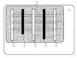
- Fins 101are formed on the substrate 100 for forming FinFETs.
- the fins 101can be formed according to any conventional processing.
- a mask 201is formed over the substrate 100 , partially covering the fins 101 , as illustrated in FIG. 2 .
- the mask 201may be a single cut mask, such as a corner rounding cut mask.
- the mask 201may be formed of any material that acts as a mask.
- the fins 101are removed where exposed by the mask 201 , and the mask 201 is subsequently removed, forming partial fins 301 a - 301 d.
- the mask 201is described as a single mask, more than one mask may be used to form the partial fins 301 a - 301 d. However, as discussed below, the current method allows for use of a single mask.
- partial fins 301may be formed that include oblique-angled ends, or fin tips, such as the fin tip 303 for the partial fin 301 a.
- the fin tip 303can be used as a source of localized higher electrical field when voltage is applied between a gate and silicon, allowing for a lower programming voltage of a resulting OTP memory. Specifically, the localized higher electrical field at the fin tip 303 allows for controlling the location of a breakdown in an oxide layer during programming of the OTP memory.
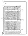
- a gate oxide layer 401is formed over the substrate 100 and the partial fins 301 a - 301 d, as illustrated in FIG. 4 .
- the gate oxide layer 401may be formed to a thickness of 20 to 55 ⁇ and may be formed of one or more conventional oxides, such as one or more non-high k dielectrics.
- a mask 501is formed over the gate oxide layer 401 , as illustrated in FIG. 5 .
- the mask 501is formed to cover the partial fins 301 b - 301 d and to expose the partial fin 301 a and the fin tip 303 .
- the mask 501prevents part of the gate oxide layer 401 from being removed.
- the gate oxide layer 401is removed where left exposed by the mask 501 to form a partial gate oxide layer 601 , as illustrated in FIG. 6 .
- another gate oxide layer 701is formed over the substrate 100 , the partial gate oxide layer 601 , and the partial fin 301 a with the fin tip 303 .
- the gate oxide layer 701may be formed to a thickness of 10 to 15 ⁇ and may be formed of a high-k dielectric.
- gates 801 a - 801 care formed over the gate oxide layer 701 , with gate 801 b formed over the fin tip 303 , as illustrated in FIG. 8 . While conventional logic gates may be formed to a width of 10 to 40 nm, gate 801 b over the fin tip 303 may be formed to a width of 70 to 150 nm so that the gate 801 b covers the entire fin tip 303 .
- the breakdown voltage of the gate oxide layer 701may be the technology node logic nominal voltage, such as 0.9V, so that breakdown of the gate oxide layer 701 does not need the transmission or application of a higher voltage by design, which is typically the IO voltage such as 1.8V or 2.5V.
- the resulting OTP memoryrequires a lower programming voltage, which allows for a smaller area of circuitry to blow the antifuse and for a simple biasing scheme and a large sensing window.
- the embodiments of the present disclosureachieve several technical effects, including an OTP memory with lower voltage requirements for programming with the ability to control the location of the breakdown in a gate oxide layer.
- the present disclosureenjoys industrial applicability associated with the designing and manufacturing of any of various types of highly integrated semiconductor devices used in microprocessors, smart phones, mobile phones, cellular handsets, set-top boxes, DVD recorders and players, automotive navigation, printers and peripherals, networking and telecom equipment, gaming systems, and digital cameras, particularly for 20 nm technologies and beyond.
Landscapes
- Semiconductor Memories (AREA)
- Design And Manufacture Of Integrated Circuits (AREA)
- Read Only Memory (AREA)
Abstract
Description
Claims (20)
Priority Applications (1)
| Application Number | Priority Date | Filing Date | Title |
|---|---|---|---|
| US14/082,263US9177963B2 (en) | 2013-11-18 | 2013-11-18 | Forming a low votage antifuse device and resulting device |
Applications Claiming Priority (1)
| Application Number | Priority Date | Filing Date | Title |
|---|---|---|---|
| US14/082,263US9177963B2 (en) | 2013-11-18 | 2013-11-18 | Forming a low votage antifuse device and resulting device |
Publications (2)
| Publication Number | Publication Date |
|---|---|
| US20150137258A1 US20150137258A1 (en) | 2015-05-21 |
| US9177963B2true US9177963B2 (en) | 2015-11-03 |
Family
ID=53172434
Family Applications (1)
| Application Number | Title | Priority Date | Filing Date |
|---|---|---|---|
| US14/082,263Active2034-04-12US9177963B2 (en) | 2013-11-18 | 2013-11-18 | Forming a low votage antifuse device and resulting device |
Country Status (1)
| Country | Link |
|---|---|
| US (1) | US9177963B2 (en) |
Cited By (3)
| Publication number | Priority date | Publication date | Assignee | Title |
|---|---|---|---|---|
| US9806084B1 (en) | 2016-06-06 | 2017-10-31 | International Business Machines Corporation | Anti-fuse with reduced programming voltage |
| US10475789B2 (en) | 2017-04-03 | 2019-11-12 | Samsung Electroncis Co., Ltd. | Semiconductor device having first and second fin-type patterns and method of fabricating the same |
| US10957701B1 (en)* | 2019-11-11 | 2021-03-23 | Globalfoundries U.S. Inc. | Fin-based anti-fuse device for integrated circuit (IC) products, methods of making such an anti-fuse device and IC products comprising such an anti-fuse device |
Families Citing this family (17)
| Publication number | Priority date | Publication date | Assignee | Title |
|---|---|---|---|---|
| US9818478B2 (en) | 2012-12-07 | 2017-11-14 | Attopsemi Technology Co., Ltd | Programmable resistive device and memory using diode as selector |
| US10229746B2 (en) | 2010-08-20 | 2019-03-12 | Attopsemi Technology Co., Ltd | OTP memory with high data security |
| US10249379B2 (en) | 2010-08-20 | 2019-04-02 | Attopsemi Technology Co., Ltd | One-time programmable devices having program selector for electrical fuses with extended area |
| US9070437B2 (en) | 2010-08-20 | 2015-06-30 | Shine C. Chung | Circuit and system of using junction diode as program selector for one-time programmable devices with heat sink |
| US9824768B2 (en) | 2015-03-22 | 2017-11-21 | Attopsemi Technology Co., Ltd | Integrated OTP memory for providing MTP memory |
| US9711237B2 (en) | 2010-08-20 | 2017-07-18 | Attopsemi Technology Co., Ltd. | Method and structure for reliable electrical fuse programming |
| US9460807B2 (en)* | 2010-08-20 | 2016-10-04 | Shine C. Chung | One-time programmable memory devices using FinFET technology |
| US10923204B2 (en) | 2010-08-20 | 2021-02-16 | Attopsemi Technology Co., Ltd | Fully testible OTP memory |
| US10916317B2 (en) | 2010-08-20 | 2021-02-09 | Attopsemi Technology Co., Ltd | Programmable resistance memory on thin film transistor technology |
| US10586832B2 (en) | 2011-02-14 | 2020-03-10 | Attopsemi Technology Co., Ltd | One-time programmable devices using gate-all-around structures |
| US10192615B2 (en) | 2011-02-14 | 2019-01-29 | Attopsemi Technology Co., Ltd | One-time programmable devices having a semiconductor fin structure with a divided active region |
| US8848423B2 (en) | 2011-02-14 | 2014-09-30 | Shine C. Chung | Circuit and system of using FinFET for building programmable resistive devices |
| US11615859B2 (en) | 2017-04-14 | 2023-03-28 | Attopsemi Technology Co., Ltd | One-time programmable memories with ultra-low power read operation and novel sensing scheme |
| US10535413B2 (en) | 2017-04-14 | 2020-01-14 | Attopsemi Technology Co., Ltd | Low power read operation for programmable resistive memories |
| US10726914B2 (en) | 2017-04-14 | 2020-07-28 | Attopsemi Technology Co. Ltd | Programmable resistive memories with low power read operation and novel sensing scheme |
| US11062786B2 (en) | 2017-04-14 | 2021-07-13 | Attopsemi Technology Co., Ltd | One-time programmable memories with low power read operation and novel sensing scheme |
| US10770160B2 (en) | 2017-11-30 | 2020-09-08 | Attopsemi Technology Co., Ltd | Programmable resistive memory formed by bit slices from a standard cell library |
- 2013
- 2013-11-18USUS14/082,263patent/US9177963B2/enactiveActive
Non-Patent Citations (4)
| Title |
|---|
| Kulkarni et al., "A 32nm High-k and Metal-Gate Anti-Fuse Array Featuring a 1.01um 1T1C Bit Cell," Logic Technology Development, Intel Corporation, Hillsboro, OR, USA, IEEE Symposium on VLSI Technology Digest of Technical Papers, pp. 79-80, 2012. |
| Peng et al., "A Novel Embedded OTP NVM Using Standard Foundry CMOS Logic Technology," IEEE NVSMW, pp. 24-26, 2006. |
| Wee et al., "Antifuse Circuits and Their Applications to Post-Package of DRAMs," Journal of Semiconductor Technology and Science, vol. 1, No. 4, Dec. 2001, pp. 216-231. |
| www.kilopass.com/about/partners/foundry-partners/, Kilopass Technology, retrieved Dec. 17, 2013. |
Cited By (8)
| Publication number | Priority date | Publication date | Assignee | Title |
|---|---|---|---|---|
| US9806084B1 (en) | 2016-06-06 | 2017-10-31 | International Business Machines Corporation | Anti-fuse with reduced programming voltage |
| US10224334B2 (en) | 2016-06-06 | 2019-03-05 | International Business Machines Corporation | Anti-fuse with reduced programming voltage |
| US10586800B2 (en) | 2016-06-06 | 2020-03-10 | International Business Machines Corporation | Anti-fuse with reduced programming voltage |
| US10886284B2 (en) | 2016-06-06 | 2021-01-05 | International Business Machines Corporation | Anti-fuse with reduced programming voltage |
| US10475789B2 (en) | 2017-04-03 | 2019-11-12 | Samsung Electroncis Co., Ltd. | Semiconductor device having first and second fin-type patterns and method of fabricating the same |
| US10643998B2 (en) | 2017-04-03 | 2020-05-05 | Samsung Electronics Co., Ltd. | Semiconductor device having first and second fin-type patterns and method of fabricating the same |
| US10991692B2 (en) | 2017-04-03 | 2021-04-27 | Samsung Electronics Co., Ltd. | Semiconductor device having a plurality of fins and method of fabricating the same |
| US10957701B1 (en)* | 2019-11-11 | 2021-03-23 | Globalfoundries U.S. Inc. | Fin-based anti-fuse device for integrated circuit (IC) products, methods of making such an anti-fuse device and IC products comprising such an anti-fuse device |
Also Published As
| Publication number | Publication date |
|---|---|
| US20150137258A1 (en) | 2015-05-21 |
Similar Documents
| Publication | Publication Date | Title |
|---|---|---|
| US9177963B2 (en) | Forming a low votage antifuse device and resulting device | |
| US8923070B2 (en) | FinFET based one-time programmable device | |
| TWI605547B (en) | Non-volatile memory | |
| US8630117B2 (en) | RFID tag having non-volatile memory device having floating-gate FETs with different source-gate and drain-gate border lengths | |
| US9349842B2 (en) | Methods of forming semiconductor devices comprising ferroelectric elements and fast high-K metal gate transistors | |
| US9263521B2 (en) | Integrated circuit devices including finFETs and methods of forming the same | |
| US8178944B2 (en) | Method for forming a one-time programmable metal fuse and related structure | |
| US20140138777A1 (en) | Integrated circuit device and method for making same | |
| US20110032742A1 (en) | One-time programmable memory cell with shiftable threshold voltage transistor | |
| US20160181440A1 (en) | Field effect transistor with self-adjusting threshold voltage | |
| KR20120134217A (en) | Method for forming mosfet device having different thickness of gate insulating layer | |
| US20140306295A1 (en) | Semiconductor device and method for fabricating the same | |
| EP3170204B1 (en) | Method for programming a non-volatile one-time programmable memory device | |
| CN111433904B (en) | Hybrid high voltage low voltage FINFET devices | |
| US8760917B2 (en) | Non-volatile memory cell with high bit density | |
| US20090059679A1 (en) | Erasing method of non-volatile memory | |
| US9059093B2 (en) | Forming finfet cell with fin tip and resulting device | |
| US20100284210A1 (en) | One-time programmable memory cell | |
| JP5684414B2 (en) | Manufacturing method of semiconductor device | |
| US10784250B2 (en) | Sub-device field-effect transistor architecture for integrated circuits | |
| US8664710B2 (en) | Non-volatile memory and manufacturing method thereof | |
| US20130181276A1 (en) | Non-self aligned non-volatile memory structure |
Legal Events
| Date | Code | Title | Description |
|---|---|---|---|
| AS | Assignment | Owner name:GLOBALFOUNDRIES INC., CAYMAN ISLANDS Free format text:ASSIGNMENT OF ASSIGNORS INTEREST;ASSIGNORS:MITTAL, ANURAG;TARABBIA, MARC;SIGNING DATES FROM 20130926 TO 20131030;REEL/FRAME:031618/0885 | |
| FEPP | Fee payment procedure | Free format text:PAYOR NUMBER ASSIGNED (ORIGINAL EVENT CODE: ASPN); ENTITY STATUS OF PATENT OWNER: LARGE ENTITY | |
| STCF | Information on status: patent grant | Free format text:PATENTED CASE | |
| AS | Assignment | Owner name:WILMINGTON TRUST, NATIONAL ASSOCIATION, DELAWARE Free format text:SECURITY AGREEMENT;ASSIGNOR:GLOBALFOUNDRIES INC.;REEL/FRAME:049490/0001 Effective date:20181127 | |
| MAFP | Maintenance fee payment | Free format text:PAYMENT OF MAINTENANCE FEE, 4TH YEAR, LARGE ENTITY (ORIGINAL EVENT CODE: M1551); ENTITY STATUS OF PATENT OWNER: LARGE ENTITY Year of fee payment:4 | |
| AS | Assignment | Owner name:GLOBALFOUNDRIES U.S. INC., CALIFORNIA Free format text:ASSIGNMENT OF ASSIGNORS INTEREST;ASSIGNOR:GLOBALFOUNDRIES INC.;REEL/FRAME:054633/0001 Effective date:20201022 | |
| AS | Assignment | Owner name:GLOBALFOUNDRIES INC., CAYMAN ISLANDS Free format text:RELEASE BY SECURED PARTY;ASSIGNOR:WILMINGTON TRUST, NATIONAL ASSOCIATION;REEL/FRAME:054636/0001 Effective date:20201117 | |
| AS | Assignment | Owner name:GLOBALFOUNDRIES U.S. INC., NEW YORK Free format text:RELEASE BY SECURED PARTY;ASSIGNOR:WILMINGTON TRUST, NATIONAL ASSOCIATION;REEL/FRAME:056987/0001 Effective date:20201117 | |
| MAFP | Maintenance fee payment | Free format text:PAYMENT OF MAINTENANCE FEE, 8TH YEAR, LARGE ENTITY (ORIGINAL EVENT CODE: M1552); ENTITY STATUS OF PATENT OWNER: LARGE ENTITY Year of fee payment:8 |