US9177828B2 - External gettering method and device - Google Patents
External gettering method and deviceDownload PDFInfo
- Publication number
- US9177828B2 US9177828B2US13/024,806US201113024806AUS9177828B2US 9177828 B2US9177828 B2US 9177828B2US 201113024806 AUS201113024806 AUS 201113024806AUS 9177828 B2US9177828 B2US 9177828B2
- Authority
- US
- United States
- Prior art keywords
- gettering
- substrate
- external
- backside
- front side
- Prior art date
- Legal status (The legal status is an assumption and is not a legal conclusion. Google has not performed a legal analysis and makes no representation as to the accuracy of the status listed.)
- Active, expires
Links
- 238000005247getteringMethods0.000titleclaimsabstractdescription197
- 238000000034methodMethods0.000titleabstractdescription79
- 239000000758substrateSubstances0.000claimsabstractdescription123
- 239000004065semiconductorSubstances0.000claimsabstractdescription90
- 238000005538encapsulationMethods0.000claimsabstractdescription33
- 238000004100electronic packagingMethods0.000claimsabstractdescription7
- 239000000463materialSubstances0.000claimsdescription81
- 239000000853adhesiveSubstances0.000claimsdescription31
- 230000001070adhesive effectEffects0.000claimsdescription31
- 150000002500ionsChemical class0.000claimsdescription30
- 239000000356contaminantSubstances0.000claimsdescription18
- 239000000654additiveSubstances0.000claimsdescription11
- 239000004593EpoxySubstances0.000claimsdescription6
- 230000000996additive effectEffects0.000claimsdescription5
- 229910010293ceramic materialInorganic materials0.000claims1
- 239000002210silicon-based materialSubstances0.000claims1
- 150000001875compoundsChemical class0.000abstractdescription26
- 235000012431wafersNutrition0.000description41
- 229910052710siliconInorganic materials0.000description16
- 239000010703siliconSubstances0.000description16
- XUIMIQQOPSSXEZ-UHFFFAOYSA-NSiliconChemical compound[Si]XUIMIQQOPSSXEZ-UHFFFAOYSA-N0.000description14
- 238000004519manufacturing processMethods0.000description14
- 230000007547defectEffects0.000description11
- 238000005498polishingMethods0.000description9
- 239000013078crystalSubstances0.000description7
- 239000012535impuritySubstances0.000description7
- VYPSYNLAJGMNEJ-UHFFFAOYSA-NSilicium dioxideChemical compoundO=[Si]=OVYPSYNLAJGMNEJ-UHFFFAOYSA-N0.000description6
- 230000008901benefitEffects0.000description6
- 230000015572biosynthetic processEffects0.000description4
- 239000002184metalSubstances0.000description4
- 229910052751metalInorganic materials0.000description4
- 229910000679solderInorganic materials0.000description4
- 239000000919ceramicSubstances0.000description3
- 238000011109contaminationMethods0.000description3
- 239000000377silicon dioxideSubstances0.000description3
- 239000000243solutionSubstances0.000description3
- 238000007796conventional methodMethods0.000description2
- 239000010949copperSubstances0.000description2
- 230000001419dependent effectEffects0.000description2
- 238000002474experimental methodMethods0.000description2
- 229910001410inorganic ionInorganic materials0.000description2
- 150000002739metalsChemical class0.000description2
- 238000004806packaging method and processMethods0.000description2
- 239000004033plasticSubstances0.000description2
- 229920003023plasticPolymers0.000description2
- 238000007517polishing processMethods0.000description2
- 239000011347resinSubstances0.000description2
- 229920005989resinPolymers0.000description2
- -1silicon ionsChemical class0.000description2
- 238000005728strengtheningMethods0.000description2
- 239000000126substanceSubstances0.000description2
- RYGMFSIKBFXOCR-UHFFFAOYSA-NCopperChemical compound[Cu]RYGMFSIKBFXOCR-UHFFFAOYSA-N0.000description1
- 241001050985DiscoSpecies0.000description1
- 230000000712assemblyEffects0.000description1
- 238000000429assemblyMethods0.000description1
- 230000015556catabolic processEffects0.000description1
- 229910052802copperInorganic materials0.000description1
- 238000006731degradation reactionMethods0.000description1
- 230000001627detrimental effectEffects0.000description1
- 229910003460diamondInorganic materials0.000description1
- 239000010432diamondSubstances0.000description1
- 238000005516engineering processMethods0.000description1
- 238000002354inductively-coupled plasma atomic emission spectroscopyMethods0.000description1
- 238000002347injectionMethods0.000description1
- 239000007924injectionSubstances0.000description1
- 239000012212insulatorSubstances0.000description1
- 230000010354integrationEffects0.000description1
- 230000004048modificationEffects0.000description1
- 238000012986modificationMethods0.000description1
- 230000003647oxidationEffects0.000description1
- 238000007254oxidation reactionMethods0.000description1
- 239000002245particleSubstances0.000description1
- 229910052594sapphireInorganic materials0.000description1
- 239000010980sapphireSubstances0.000description1
- 235000012239silicon dioxideNutrition0.000description1
- 238000002791soakingMethods0.000description1
- 238000006467substitution reactionMethods0.000description1
Images


Classifications
- H—ELECTRICITY
- H01—ELECTRIC ELEMENTS
- H01L—SEMICONDUCTOR DEVICES NOT COVERED BY CLASS H10
- H01L23/00—Details of semiconductor or other solid state devices
- H01L23/16—Fillings or auxiliary members in containers or encapsulations, e.g. centering rings
- H01L23/18—Fillings characterised by the material, its physical or chemical properties, or its arrangement within the complete device
- H01L23/26—Fillings characterised by the material, its physical or chemical properties, or its arrangement within the complete device including materials for absorbing or reacting with moisture or other undesired substances, e.g. getters
- H—ELECTRICITY
- H01—ELECTRIC ELEMENTS
- H01L—SEMICONDUCTOR DEVICES NOT COVERED BY CLASS H10
- H01L21/00—Processes or apparatus adapted for the manufacture or treatment of semiconductor or solid state devices or of parts thereof
- H01L21/02—Manufacture or treatment of semiconductor devices or of parts thereof
- H01L21/04—Manufacture or treatment of semiconductor devices or of parts thereof the devices having potential barriers, e.g. a PN junction, depletion layer or carrier concentration layer
- H01L21/18—Manufacture or treatment of semiconductor devices or of parts thereof the devices having potential barriers, e.g. a PN junction, depletion layer or carrier concentration layer the devices having semiconductor bodies comprising elements of Group IV of the Periodic Table or AIIIBV compounds with or without impurities, e.g. doping materials
- H01L21/30—Treatment of semiconductor bodies using processes or apparatus not provided for in groups H01L21/20 - H01L21/26
- H01L21/322—Treatment of semiconductor bodies using processes or apparatus not provided for in groups H01L21/20 - H01L21/26 to modify their internal properties, e.g. to produce internal imperfections
- H01L21/3221—Treatment of semiconductor bodies using processes or apparatus not provided for in groups H01L21/20 - H01L21/26 to modify their internal properties, e.g. to produce internal imperfections of silicon bodies, e.g. for gettering
- H01L21/3225—Thermally inducing defects using oxygen present in the silicon body for intrinsic gettering
- H—ELECTRICITY
- H01—ELECTRIC ELEMENTS
- H01L—SEMICONDUCTOR DEVICES NOT COVERED BY CLASS H10
- H01L21/00—Processes or apparatus adapted for the manufacture or treatment of semiconductor or solid state devices or of parts thereof
- H01L21/02—Manufacture or treatment of semiconductor devices or of parts thereof
- H01L21/04—Manufacture or treatment of semiconductor devices or of parts thereof the devices having potential barriers, e.g. a PN junction, depletion layer or carrier concentration layer
- H01L21/50—Assembly of semiconductor devices using processes or apparatus not provided for in a single one of the groups H01L21/18 - H01L21/326 or H10D48/04 - H10D48/07 e.g. sealing of a cap to a base of a container
- H01L21/56—Encapsulations, e.g. encapsulation layers, coatings
- H01L21/565—Moulds
- H—ELECTRICITY
- H01—ELECTRIC ELEMENTS
- H01L—SEMICONDUCTOR DEVICES NOT COVERED BY CLASS H10
- H01L23/00—Details of semiconductor or other solid state devices
- H01L23/28—Encapsulations, e.g. encapsulating layers, coatings, e.g. for protection
- H01L23/31—Encapsulations, e.g. encapsulating layers, coatings, e.g. for protection characterised by the arrangement or shape
- H01L23/3107—Encapsulations, e.g. encapsulating layers, coatings, e.g. for protection characterised by the arrangement or shape the device being completely enclosed
- H01L23/3121—Encapsulations, e.g. encapsulating layers, coatings, e.g. for protection characterised by the arrangement or shape the device being completely enclosed a substrate forming part of the encapsulation
- H01L23/3128—Encapsulations, e.g. encapsulating layers, coatings, e.g. for protection characterised by the arrangement or shape the device being completely enclosed a substrate forming part of the encapsulation the substrate having spherical bumps for external connection
- H—ELECTRICITY
- H01—ELECTRIC ELEMENTS
- H01L—SEMICONDUCTOR DEVICES NOT COVERED BY CLASS H10
- H01L2224/00—Indexing scheme for arrangements for connecting or disconnecting semiconductor or solid-state bodies and methods related thereto as covered by H01L24/00
- H01L2224/01—Means for bonding being attached to, or being formed on, the surface to be connected, e.g. chip-to-package, die-attach, "first-level" interconnects; Manufacturing methods related thereto
- H01L2224/10—Bump connectors; Manufacturing methods related thereto
- H01L2224/15—Structure, shape, material or disposition of the bump connectors after the connecting process
- H01L2224/16—Structure, shape, material or disposition of the bump connectors after the connecting process of an individual bump connector
- H01L2224/161—Disposition
- H01L2224/16151—Disposition the bump connector connecting between a semiconductor or solid-state body and an item not being a semiconductor or solid-state body, e.g. chip-to-substrate, chip-to-passive
- H01L2224/16221—Disposition the bump connector connecting between a semiconductor or solid-state body and an item not being a semiconductor or solid-state body, e.g. chip-to-substrate, chip-to-passive the body and the item being stacked
- H01L2224/16225—Disposition the bump connector connecting between a semiconductor or solid-state body and an item not being a semiconductor or solid-state body, e.g. chip-to-substrate, chip-to-passive the body and the item being stacked the item being non-metallic, e.g. insulating substrate with or without metallisation
- H—ELECTRICITY
- H01—ELECTRIC ELEMENTS
- H01L—SEMICONDUCTOR DEVICES NOT COVERED BY CLASS H10
- H01L23/00—Details of semiconductor or other solid state devices
- H01L23/564—Details not otherwise provided for, e.g. protection against moisture
- H01L27/14698—
- H—ELECTRICITY
- H01—ELECTRIC ELEMENTS
- H01L—SEMICONDUCTOR DEVICES NOT COVERED BY CLASS H10
- H01L2924/00—Indexing scheme for arrangements or methods for connecting or disconnecting semiconductor or solid-state bodies as covered by H01L24/00
- H01L2924/15—Details of package parts other than the semiconductor or other solid state devices to be connected
- H01L2924/151—Die mounting substrate
- H01L2924/153—Connection portion
- H01L2924/1531—Connection portion the connection portion being formed only on the surface of the substrate opposite to the die mounting surface
- H01L2924/15311—Connection portion the connection portion being formed only on the surface of the substrate opposite to the die mounting surface being a ball array, e.g. BGA
- H01L31/186—
- H01L51/5259—
- H—ELECTRICITY
- H10—SEMICONDUCTOR DEVICES; ELECTRIC SOLID-STATE DEVICES NOT OTHERWISE PROVIDED FOR
- H10F—INORGANIC SEMICONDUCTOR DEVICES SENSITIVE TO INFRARED RADIATION, LIGHT, ELECTROMAGNETIC RADIATION OF SHORTER WAVELENGTH OR CORPUSCULAR RADIATION
- H10F39/00—Integrated devices, or assemblies of multiple devices, comprising at least one element covered by group H10F30/00, e.g. radiation detectors comprising photodiode arrays
- H10F39/011—Manufacture or treatment of image sensors covered by group H10F39/12
- H10F39/028—Manufacture or treatment of image sensors covered by group H10F39/12 performed after manufacture of the image sensors, e.g. annealing, gettering of impurities, short-circuit elimination or recrystallisation
- H—ELECTRICITY
- H10—SEMICONDUCTOR DEVICES; ELECTRIC SOLID-STATE DEVICES NOT OTHERWISE PROVIDED FOR
- H10F—INORGANIC SEMICONDUCTOR DEVICES SENSITIVE TO INFRARED RADIATION, LIGHT, ELECTROMAGNETIC RADIATION OF SHORTER WAVELENGTH OR CORPUSCULAR RADIATION
- H10F71/00—Manufacture or treatment of devices covered by this subclass
- H—ELECTRICITY
- H10—SEMICONDUCTOR DEVICES; ELECTRIC SOLID-STATE DEVICES NOT OTHERWISE PROVIDED FOR
- H10K—ORGANIC ELECTRIC SOLID-STATE DEVICES
- H10K50/00—Organic light-emitting devices
- H10K50/80—Constructional details
- H10K50/84—Passivation; Containers; Encapsulations
- H10K50/846—Passivation; Containers; Encapsulations comprising getter material or desiccants
- Y—GENERAL TAGGING OF NEW TECHNOLOGICAL DEVELOPMENTS; GENERAL TAGGING OF CROSS-SECTIONAL TECHNOLOGIES SPANNING OVER SEVERAL SECTIONS OF THE IPC; TECHNICAL SUBJECTS COVERED BY FORMER USPC CROSS-REFERENCE ART COLLECTIONS [XRACs] AND DIGESTS
- Y10—TECHNICAL SUBJECTS COVERED BY FORMER USPC
- Y10T—TECHNICAL SUBJECTS COVERED BY FORMER US CLASSIFICATION
- Y10T428/00—Stock material or miscellaneous articles
- Y10T428/28—Web or sheet containing structurally defined element or component and having an adhesive outermost layer
Definitions
- the disclosurerelates generally to semiconductors, and more particularly, to semiconductor structures and corresponding methods of fabrication.
- Si wafersare typically fabricated upon a wafer, which may be a silicon (Si)-based wafer, or other suitable materials known in the art.
- a stress relief processOne process conventionally applied to Si wafers of semiconductor devices is known as a “stress relief” process. Stress relief processes are typically applied after the bulk substrate used to form the wafer has been thinned, for example, through a backside grinding process. At least in part due to the thinning process, areas of stress may be formed at the backside of the wafer.
- the thinned backside of the waferis polished, thereby shifting some of the stress at the backside of the wafer away from the stress-relieved backside of the wafer and distributing it more evenly throughout the wafer.
- stress relief processesinclude dry polish (DP) techniques, such as mechano-chemical polishing (MCP) techniques, and chemical-mechanical polishing/planarization (CMP) techniques, as well as other techniques known in the art.
- DPdry polish
- MCPmechano-chemical polishing
- CMPchemical-mechanical polishing/planarization
- the stress relief processincreases the overall strength of the wafer, thereby increasing die strength, particularly for ultra thin dies (i.e., dies in the sub-50 ⁇ m range).
- Gettering processescan be performed during crystal growth or wafer fabrication steps to move contaminants and/or impurities in a semiconductor wafer into its bulk and away from a device region. Gettering creates a zone in the bulk substrate, known as a denude zone, that is substantially clear of contaminants.
- semiconductor devicesfor example, source and drain structures, gate structures, and channel sections
- Intrinsic getteringrefers to the formation of gettering sites within the bulk substrate.
- One process for providing intrinsic getteringincludes the formation of silicon dioxide (SiO 2 ) sites within the silicon bulk. These SiO 2 sites attract and trap ionic impurities within the silicon wafer, thus preventing these impurities from contaminating the device region.
- Extrinsic getteringrefers to the use of an external process, such as backside grinding, to create damage or stress (“defects”) in silicon lattices in the wafer. Extrinsic gettering is typically applied at a backside of the wafer. The defects that are created at the backside of the wafer attract impurities, pulling them away from the device section, which is located at a different side (typically, a topside) of the wafer.
- FIG. 1illustrates a conventional intrinsic gettering technique.
- bulk substrate 101includes crystal defects 103 , such as oxidation-induced stacking faults (OSF), or bulk micro defects (BMD), within substrate 101 .
- Crystal defects 103provide intrinsic gettering to the substrate 101 .
- metal contaminants 102are attracted to the crystal defects 103 , providing a denude zone 105 at a front side of the substrate 101 .
- the bulk substrate 101is then reduced in thickness through grinding and/or other conventional wafer thinning processes.
- substrate 101is thinned and/or grinded to a desired thickness 110 (as shown in FIG. 2 )
- the volume of the backside of bulk substrate 101and thus number of crystal defects 103 outside of the denude zone, is reduced, thereby reducing the amount of intrinsic gettering.
- FIGS. 3A-3Billustrate a conventional extrinsic gettering technique.
- a device section 211may be formed in a denude zone within bulk substrate 101 .
- Substrate 101includes an intrinsic gettering section 212 with contaminants 102 .
- Intrinsic gettering section 212may or may not include intrinsic gettering, as described above with regard to FIG. 1 .
- substrate 101includes an unpolished backside oxidized layer 213 .
- FIG. 3Bwhen bulk substrate 101 is reduced through conventional thinning processes, the thickness of intrinsic gettering section 212 is reduced (as discussed above with regard to FIG. 2 ).
- extrinsic getteringis provided by the backside grind layer 214 formed by the thinning process.
- Backside grind layer 214includes defects in silicon lattices that are formed as a result of the thinning of the backside of substrate 101 . These defects attract and/or trap impurities, pulling them away from the denude zone 211 .
- Grind wheels with super fine finishingfor example, with extra small diamond grits size
- examples of such “fine” polishing techniquesmay use, for example, Gettering Dry Polish (“GDP”) and Poligrind® grinding wheels from Disco Corp., or other appropriate systems and processes that are known in the art.
- GDPGettering Dry Polish
- Poligrind® grinding wheelsfrom Disco Corp.
- FIG. 1is a cross-sectional view of a semiconductor device with conventional intrinsic gettering
- FIG. 2is a cross-sectional view of a semiconductor device with conventional intrinsic gettering subject to grinding and/or thinning processes
- FIGS. 3A-3Bare cross-sectional views of a semiconductor device with conventional extrinsic gettering
- FIG. 4is a cross-sectional view of a semiconductor device with conventional extrinsic gettering subject to stress relief processes
- FIG. 5is a cross-sectional view of a semiconductor device including an external gettering element according to a first embodiment described herein;
- FIG. 6Ais a cross-sectional view of a semiconductor device including an external gettering element according to a second embodiment described herein;
- FIG. 6Bis a cross-sectional view of a semiconductor device including an external gettering element according to a third embodiment described herein;
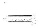
- FIG. 7is a cross-sectional view of a semiconductor device including an external gettering element according to a fourth embodiment described herein;
- FIG. 8Ais a cross-sectional view of a semiconductor device including an external gettering element according to a fifth embodiment described herein;
- FIG. 8Bis a cross-sectional view of a semiconductor device including an external gettering element according to a sixth embodiment described herein;
- FIG. 9is a flowchart illustrating steps of a fabrication process for a semiconductor device including an external gettering element
- FIG. 10is a cross-sectional view of a semiconductor device including an encapsulation mold compound providing external gettering according to a seventh embodiment described herein;
- FIG. 11is a flowchart illustrating steps of a fabrication process for a semiconductor device including an encapsulation mold compound providing external gettering.
- substrateused in the following description may include any supporting structure including, but not limited to, a semiconductor substrate that has an exposed substrate surface.
- a semiconductor substrateshould be understood to include silicon, silicon-on-insulator (SOI), silicon-on-sapphire (SOS), doped and undoped semiconductors, epitaxial layers of silicon supported by a base semiconductor foundation, and other semiconductor structures, including those made of semiconductors other than silicon.
- SOIsilicon-on-insulator
- SOSsilicon-on-sapphire
- doped and undoped semiconductorsepitaxial layers of silicon supported by a base semiconductor foundation, and other semiconductor structures, including those made of semiconductors other than silicon.
- the substrate, as well as devices formed therein,may be formed of any appropriate materials known in the art. When reference is made to a semiconductor substrate or wafer in the following description, previous process steps may have been utilized to form regions or junctions in or over the base semiconductor or foundation.
- external getteringis applied to semiconductor devices using electronic packaging.
- an external gettering elementis applied to a backside of a semiconductor substrate.
- the external gettering elementmay be integrated with or arranged by electronic packaging that is typically used when fabricating a semiconductor device using the semiconductor substrate.
- the external gettering elementmay be integrated with, or adhered by, an adhesive material that is applied to an already-polished backside of a substrate.
- an encapsulation mold compound embedded with one or more additivesmay be formed around the semiconductor substrate.
- FIG. 5is a cross-sectional view of a semiconductor device including external gettering according to a first embodiment.
- FIG. 5illustrates a bulk substrate 101 , including a device section 211 and an internal gettering section 212 .
- bulk substrate 101includes contaminants 102 .
- an internal gettering section 212is shown, embodiments need not include any internal gettering within substrate 101 .
- Bulk substrate 101 in FIG. 5has already been subjected to a thinning process, such as a backside grinding process, and stress relief processes, such as DP, MCP, or CMP processes described above, in order to achieve a desired thickness and to maintain the die strength of substrate 101 . Accordingly, bulk substrate 101 includes a stress relieved backside 215 , as described above with regard to FIG. 4 .
- a thinning processsuch as a backside grinding process
- stress relief processessuch as DP, MCP, or CMP processes described above
- an external gettering element 520is applied to stress relieved backside 215 .
- external gettering element 520includes a gettering material that is integrated into an adhesive material.
- the adhesive materialmay be a type of adhesive material typically employed as part of the electrical packaging used during fabrication of semiconductor devices.
- external gettering element 520may be integrated into a die attach film (“DAF”), which is then applied to stress relieved backside 215 .
- DAFdie attach film
- Examples of DAF products known in the industry that may be appropriate for integration with a gettering materialinclude Nitto Denko's EM-550H-P, Lintec Corp.'s LE4424, and Henkel Corp.'s ATB-130, to name but a few.
- the gettering material of external gettering element 520may be, for example, a substrate or other polymeric, ceramic, silicon, or epoxy-based material, or any material compliant with electronic packaging, which has been imbued with ions of different polarities or quantity.
- the ions used to imbue the gettering material of external gettering element 520may be organic and/or inorganic additives, for example, oxide ions, silicon ions, carbide ions, or other types of ions that can be used to imbue gettering materials.
- the polarity and quantity of ions that may be imbued in the gettering material of external gettering element 520may be highly situational and/or device dependent, and accordingly it should be understood that any appropriately ion-imbued material may be used.
- gettering materials for varying purposesmay have one of multiple different concentration levels, such as a high, medium, or low concentration level.
- a gettering materialmay be soaked in an organic ion solution, such as a Copper (Cu) ion solution, until a high concentration level is reached.
- an organic ion solutionsuch as a Copper (Cu) ion solution
- the ion concentration level of the materialmay then be measured by conventional methods, such as by using the ICP-AES method that is commonly known in the art.
- the external gettering element 520may be adhered directly to stress relieved backside layer 215 .
- External gettering element 520provides external gettering, attracting and/or trapping mobile metals or ions contaminants 102 in the substrate 101 towards the backside 215 of substrate 101 and away from device section 211 . Accordingly, external gettering element 520 provides for the performance benefits of gettering, while maintaining the strengthening benefits of stress relief techniques.
- Stacked semiconductor packagessuch as wafer-on-wafer packages and other forms of three-dimensional semiconductor packaging, can provide increased spatial efficiency for devices utilizing semiconductor technology.
- FIGS. 6A and 6Bshow two such examples of a stacked package including the external gettering concept described above.
- FIG. 6Ais a cross-sectional view of a semiconductor device including external gettering according to a second embodiment.
- FIG. 6Ashows one such example of a stacked package, including a first wafer with a first semiconductor substrate 101 , device layer 211 , and intrinsic gettering layer 212 , and a second wafer with a second semiconductor substrate 301 , device layer 311 , and intrinsic gettering layer 312 .
- internal gettering sections 212 , 312are shown in substrates 101 , 301 , embodiments need not include any internal gettering.
- external gettering element 525that is integrated into a dual-sided adhesive, such as a dual-sided DAF product known in the industry, including, for example, Nitto Denko's EM 550H-P.
- external gettering element 525provides external gettering to both substrates 101 , 301 , pulling contaminants 102 towards the respective backsides and away from the respective device sections 211 , 311 .
- FIG. 6Bis a cross-sectional view of a semiconductor device including external gettering according to a third embodiment.
- FIG. 6Bshows another such example of a stacked package, including similar elements to those described above with regard to FIG. 6A .
- device layer 311 of substrate 301is adhered to the backside of substrate 101 by the external gettering element 525 that is integrated into a dual-sided adhesive.
- Device layer 311 of substrate 301may be provided extrinsic gettering by a separate external gettering element 526 , which may be, for example, a single or dual-sided adhesive with an integrated gettering material.
- the external gettering element at the backside of substrate 301may be a separate external gettering element adhered by an adhesive material.
- FIG. 7is a cross-sectional view of a semiconductor device including external gettering according to a fourth embodiment.
- the external gettering elementincludes a stand-alone layer of gettering material 636 , separate from an adhesive material 630 , which is applied on the stress-relieved backside of substrate 101 .
- Gettering material 636may be, for example, a substrate or other polymeric, ceramic, silicon, or epoxy-based material, or any material compliant with electronic packaging, which has been imbued with ions of different polarities or quantity.
- Adhesive material 630which may be, for example, a conventional DAF or another known adhesive or laminate, holds the gettering material in place on the backside of substrate 101 .
- FIG. 8Ais a cross-sectional view of a semiconductor device including external gettering according to a fifth embodiment.
- FIG. 8Ashows one such example of a stacked package, including a first wafer with a first bulk substrate 101 , device layer 211 , and intrinsic gettering layer 212 , and a second bulk substrate 301 , device layer 311 , and intrinsic gettering layer 312 .
- the respective backsides of substrates 101 and 301are adhered by a dual-sided adhesive 630 , such as a dual-sided DAF product known in the industry.
- Dual-sided adhesive 630also laminates external gettering elements 636 , 646 to the stress-relieved backside of substrate 101 .
- External gettering elements 636 , 646are stand-alone layers of gettering material that are not integrated into the adhesive 630 , similar to the gettering material described above with regard to FIG. 7 .
- External gettering elements 636 , 646have been imbued with ions of different polarities or quantity, in order to provide appropriate external gettering to the respective substrates 101 , 301 by pulling contaminants 102 towards the respective backsides and away from the respective device sections 211 , 311 . It should be understood that, while multiple external gettering elements 636 , 646 are shown in FIG. 8 , in other embodiments, a single external gettering element may be adhered to a backside of one of substrates 101 and 301 .
- FIG. 8Bis a cross-sectional view of a semiconductor device including external gettering according to a sixth embodiment.
- FIG. 8Bshows another such example of a stacked package, including similar elements to those described above with regard to FIG. 8A .
- device layer 311 of substrate 301is adhered to the backside of substrate 101 by the adhesive 630 , and external gettering element 646 is omitted.
- Device layer 311 of substrate 301may be provided extrinsic gettering by a separate external gettering element 637 , which may be, for example, adhered to the backside of substrate 301 by a separate adhesive 631 .
- the external gettering element at the backside of substrate 301may be integrated into an adhesive.
- FIG. 9is a flowchart illustrating steps of a fabrication process 900 for a semiconductor device including an external gettering element.
- Process 900may be used to fabricate one or more of the embodiments described above with regard to FIGS. 5-8 .
- a bulk semiconductor substrateis provided.
- the bulk semiconductor substratemay be, for example, a silicon substrate or other material, and may include an internal gettering section, as discussed above with regard to bulk substrate 101 ( FIG. 5 ).
- the bulk substrateis thinned.
- the backside of the bulk substratemay be subjected to a backside grinding process, as described above, or to any appropriate thinning process known in the art.
- step 903the substrate is subjected to a stress relief process to polish the backside of the wafer and increase overall wafer strength.
- DPdry polish
- MCPmechano-chemical polishing
- CMPchemical-mechanical polishing/planarization
- other techniquessuch as GDP, Poligrind®, or other known polishing techniques may be used.
- an external gettering elementis applied to the stress-relieved backside of the substrate.
- the external gettering elementmay comprise a gettering material, such as a substrate or other polymeric, ceramic, silicon, or epoxy-based material, or any appropriately ion-imbued material.
- the ions used to imbue the gettering material of external gettering elementmay be, for example, organic or inorganic additives, such as oxide ions, silicon ions, carbide ions, or other types of ions that can be used to imbue gettering materials.
- the gettering materialmay be imbued with organic or inorganic ions through known processes, such as by soaking the gettering material in an ion solution.
- the external gettering elementmay be integrated into an adhesive material, as described above with regard to FIGS. 5-6 .
- the external gettering elementmay be a stand-alone layer of gettering material, as described above with regard to FIGS. 7-8 .
- an adhesive or laminatesuch as a conventional single-sided or dual-sided DAF, may be applied to maintain the external gettering element on the backside of the substrate, and/or to provide adhesive for a multiple-die stacked semiconductor structure (see Step 907 , supra) such as the stacked structure shown in FIG. 8 .
- Step 907a multiple-die stacked semiconductor structure
- semiconductor devicesare formed in the denude zone that is provided by the external gettering of the external gettering element.
- Formed semiconductor devicesmay include, for example, source and drain structures, gate structures, channel sections, and other structures known in the art. It should be understood that, if a stack semiconductor structure is formed (see Step 907 , supra), then semiconductor devices may instead be formed in one or both substrates after the formation of the stack semiconductor structure.
- a stack semiconductor structurecan be formed, using the semiconductor substrate with applied external gettering element formed in steps 901 - 906 .
- the external gettering elementis integrated into a dual-sided DAF, as described above with regard to FIG. 6 .
- the dual-sided DAFmay be used to attach a second semiconductor wafer.
- the second semiconductor wafermay receive the benefit of external gettering from the same external gettering element as the first wafer, and/or from a separate external gettering element.
- a conventional dual-sided DAFmay be used to attach the second semiconductor wafer, and may also be used to adhere a second external gettering element to the backside of the second semiconductor wafer, as described above with regard to FIG. 8 .
- FIGS. 5 through 9describe embodiments where an adhesive material is used with an external gettering element
- the concept described hereinis not so limited.
- some configurations of semiconductor devicesmay not require adhesives, such as DAF, in their manufacture, and adding an adhesive to the manufacturing process may be undesirable.
- FIG. 10is a cross-sectional view of a semiconductor device including external gettering according to a fifth embodiment.
- FIG. 10illustrates a bulk substrate 101 including a device section 711 , an internal gettering section 212 , and a backside section 715 .
- semiconductor devices formed in device section 711are connected to external electronic connections 752 (which may be, for example, a ball grid array package that is well known in the art) via solder bumps 751 .
- bulk substrate 101includes contaminants 102 .
- an internal gettering section 212is shown, embodiments need not include any internal gettering within substrate 101 .
- bulk substrate 101 in FIG. 10may have already been subjected to a thinning process, such as a backside grinding process, and stress relief processes, such as DP, MCP, or CMP processes described above, in order to achieve a desired thickness and to maintain the die strength of substrate 101 .
- backside section 715is a stress relieved backside, as described above with regard to FIG. 4 .
- substrate 101may have been subjected to other thinning and/or polishing methods, or may not have been subjected to any thinning and/or polishing methods.
- Substrate 101is surrounded by encapsulation mold compound 750 .
- an encapsulation mold compound 750may be applied through an aperture in an encapsulation mold 753 into a cavity formed by the encapsulation mold 753 .
- the encapsulation mold 753is subsequently removed, leaving the encapsulation mold compound 750 surrounding substrate 101 .
- the encapsulation mold compoundmay be composed of various plastics and/or resins, such as a molded epoxy compound.
- encapsulation mold compound 750may also be embedded with an additive in order to provide gettering to substrate 101 .
- encapsulation mold compound 750may be embedded with organic and/or inorganic ions, such as those described above with regard to imbuing gettering material in FIGS. 5-9 .
- the polarity and quantity of ions for the encapsulation mold compoundmay be highly situational and/or device dependent, and accordingly it should be understood that any appropriately embedded encapsulation mold compound may be used.
- encapsulation mold compound 750provides gettering to substrate 101 , drawing contaminants 102 towards backside 715 and away from device section 711 .
- FIG. 11is a flowchart illustrating steps of a fabrication process 1100 for a semiconductor device including an encapsulation mold compound providing gettering.
- Process 1100may be used to fabricate, for example, the embodiment described above with regard to FIG. 10 .
- a bulk semiconductor substrateis provided.
- the bulk semiconductor substratemay be, for example, a silicon substrate or other material, and may include an internal gettering section, as discussed above with regard to bulk substrate 101 ( FIG. 5 ).
- steps 1102 and 1103the bulk substrate is thinned and polished, respectively.
- the thinning and/or polishing processes used in steps 1102 and 1103may be those described above with regard to steps 902 and 903 of process 900 ( FIG. 9 ).
- process 1100may omit one or both of these steps.
- semiconductor devicesare formed in at least one section of the bulk substrate.
- Formed semiconductor devicesmay include, for example, source and drain structures, gate structures, channel sections, and other structures known in the art.
- solder bumps or other conductive connectionsare formed in order to provide electrical connections between devices formed on the substrate and external electronic connections 752 (see Step 1107 , infra).
- an encapsulation moldis provided surrounding the substrate.
- the encapsulation moldmay include multiple pieces which form a cavity surrounding the substrate, and preferably includes at least one aperture for injecting encapsulation mold compound into the aperture.
- gettering encapsulation mold compoundis applied, for example by injection into the cavity formed by the encapsulation mold compound.
- Gettering encapsulation mold compoundmay be composed of conventional encapsulation mold compound materials, such as a plastic, resin, or other epoxy mold compound, which are embedded with organic and/or inorganic additives, in order to provide gettering to substrate 101 .
- only a portion of the encapsulation mold compoundincludes the organic and/or inorganic additives to provide gettering at a location of the substrate (e.g., backside 715 in FIG. 10 ).
- substantially the entire encapsulation mold compoundis embedded with the organic and/or inorganic additives.
- the gettering encapsulation mold compoundattracts contaminants and forms a denude zone on the at least one section of the bulk substrate where the semiconductor devices are formed (see step 1104 , supra).
- the encapsulation moldmay be removed.
- the encapsulation moldmay be removed before or after completing fabrication of the semiconductor assembly, including step 1108 of process 1100 (infra).
- external electronic connectionsmay optionally formed to provide external connections for the semiconductor devices and solder bumps.
- the external electronic connectionsmay be a ball grid array package as shown in FIG. 10 , or other external electronic connections known in the art that may be used to form integrated circuits or other semiconductor device assemblies.
- the external electronic connectionsmay be formed near the device region, for example connecting via solder bumps to the semiconductor devices in the device region, as shown in FIG. 10 .
- FIGS. 10 and 11show the formation of a semiconductor device without an external gettering element as described above with regard to FIGS. 5 through 9 , this need not be the case.
- a semiconductor device including an external gettering element adhered to a backside of the substratemay be encapsulated by a gettering encapsulation mold compound.
Landscapes
- Engineering & Computer Science (AREA)
- Microelectronics & Electronic Packaging (AREA)
- Physics & Mathematics (AREA)
- Condensed Matter Physics & Semiconductors (AREA)
- General Physics & Mathematics (AREA)
- Computer Hardware Design (AREA)
- Power Engineering (AREA)
- Manufacturing & Machinery (AREA)
- Mechanical Treatment Of Semiconductor (AREA)
- Information Retrieval, Db Structures And Fs Structures Therefor (AREA)
Abstract
Description
Claims (14)
Priority Applications (5)
| Application Number | Priority Date | Filing Date | Title |
|---|---|---|---|
| US13/024,806US9177828B2 (en) | 2011-02-10 | 2011-02-10 | External gettering method and device |
| US13/477,645US9159584B2 (en) | 2000-08-18 | 2012-05-22 | Methods and systems of retrieving documents |
| US14/931,806US9543166B2 (en) | 2011-02-10 | 2015-11-03 | External gettering method and device |
| US15/395,169US10453761B2 (en) | 2011-02-10 | 2016-12-30 | External gettering method and device |
| US16/512,146US10892202B2 (en) | 2011-02-10 | 2019-07-15 | External gettering method and device |
Applications Claiming Priority (1)
| Application Number | Priority Date | Filing Date | Title |
|---|---|---|---|
| US13/024,806US9177828B2 (en) | 2011-02-10 | 2011-02-10 | External gettering method and device |
Related Parent Applications (1)
| Application Number | Title | Priority Date | Filing Date |
|---|---|---|---|
| US12/191,774ContinuationUS7908430B2 (en) | 2000-08-18 | 2008-08-14 | Associative memory |
Related Child Applications (2)
| Application Number | Title | Priority Date | Filing Date |
|---|---|---|---|
| US13/477,645ContinuationUS9159584B2 (en) | 2000-08-18 | 2012-05-22 | Methods and systems of retrieving documents |
| US14/931,806DivisionUS9543166B2 (en) | 2011-02-10 | 2015-11-03 | External gettering method and device |
Publications (2)
| Publication Number | Publication Date |
|---|---|
| US20120205821A1 US20120205821A1 (en) | 2012-08-16 |
| US9177828B2true US9177828B2 (en) | 2015-11-03 |
Family
ID=46636277
Family Applications (5)
| Application Number | Title | Priority Date | Filing Date |
|---|---|---|---|
| US13/024,806Active2034-05-28US9177828B2 (en) | 2000-08-18 | 2011-02-10 | External gettering method and device |
| US13/477,645Expired - Fee RelatedUS9159584B2 (en) | 2000-08-18 | 2012-05-22 | Methods and systems of retrieving documents |
| US14/931,806ActiveUS9543166B2 (en) | 2011-02-10 | 2015-11-03 | External gettering method and device |
| US15/395,169Active2031-11-27US10453761B2 (en) | 2011-02-10 | 2016-12-30 | External gettering method and device |
| US16/512,146ActiveUS10892202B2 (en) | 2011-02-10 | 2019-07-15 | External gettering method and device |
Family Applications After (4)
| Application Number | Title | Priority Date | Filing Date |
|---|---|---|---|
| US13/477,645Expired - Fee RelatedUS9159584B2 (en) | 2000-08-18 | 2012-05-22 | Methods and systems of retrieving documents |
| US14/931,806ActiveUS9543166B2 (en) | 2011-02-10 | 2015-11-03 | External gettering method and device |
| US15/395,169Active2031-11-27US10453761B2 (en) | 2011-02-10 | 2016-12-30 | External gettering method and device |
| US16/512,146ActiveUS10892202B2 (en) | 2011-02-10 | 2019-07-15 | External gettering method and device |
Country Status (1)
| Country | Link |
|---|---|
| US (5) | US9177828B2 (en) |
Families Citing this family (8)
| Publication number | Priority date | Publication date | Assignee | Title |
|---|---|---|---|---|
| TWI473283B (en)* | 2011-09-21 | 2015-02-11 | Nat Univ Tsing Hua | Wafer |
| US20150044783A1 (en)* | 2013-08-12 | 2015-02-12 | Micron Technology, Inc. | Methods of alleviating adverse stress effects on a wafer, and methods of forming a semiconductor device |
| US10329142B2 (en)* | 2015-12-18 | 2019-06-25 | Samsung Electro-Mechanics Co., Ltd. | Wafer level package and method of manufacturing the same |
| US9785833B1 (en)* | 2016-03-17 | 2017-10-10 | Relativity Oda Llc | System and method for textual near-duplicate grouping of documents |
| US10522367B2 (en)* | 2017-03-06 | 2019-12-31 | Qualcomm Incorporated | Gettering layer formation and substrate |
| US10497587B1 (en)* | 2018-06-13 | 2019-12-03 | Infineon Technologies Ag | Ion manipulation methods and related apparatuses and systems for semiconductor encapsulation materials |
| RU2689972C1 (en)* | 2018-09-26 | 2019-05-29 | Акционерное общество "НПО "Орион" | Method of producing a silicon photodiode |
| US11636173B2 (en)* | 2019-03-28 | 2023-04-25 | SK Hynix Inc. | Method for candidate selection and accelerator for performing candidate selection |
Citations (16)
| Publication number | Priority date | Publication date | Assignee | Title |
|---|---|---|---|---|
| US5753560A (en) | 1996-10-31 | 1998-05-19 | Motorola, Inc. | Method for fabricating a semiconductor device using lateral gettering |
| US6165872A (en) | 1997-08-29 | 2000-12-26 | Kabushiki Kaisha Toshiba | Semiconductor device and its manufacturing method |
| US20020181866A1 (en)* | 2001-04-25 | 2002-12-05 | Crook Russell A. | Low cost adhesive bonding of getter |
| US6548382B1 (en)* | 1997-07-18 | 2003-04-15 | Silicon Genesis Corporation | Gettering technique for wafers made using a controlled cleaving process |
| US6639327B2 (en) | 2000-07-10 | 2003-10-28 | Canon Kabushiki Kaisha | Semiconductor member, semiconductor device and manufacturing methods thereof |
| US6696352B1 (en)* | 2001-09-11 | 2004-02-24 | Silicon Wafer Technologies, Inc. | Method of manufacture of a multi-layered substrate with a thin single crystalline layer and a versatile sacrificial layer |
| US20050239267A1 (en)* | 2004-04-23 | 2005-10-27 | Canon Kabushiki Kaisha | Substrate manufacturing method |
| US20050285232A1 (en)* | 2004-06-28 | 2005-12-29 | Tongbi Jiang | Semiconductor constructions |
| US20070187618A1 (en) | 2006-02-13 | 2007-08-16 | Ibis Technology Corporation | Electrostatic particle gettering in an ion implanter |
| US7374818B2 (en) | 2005-05-23 | 2008-05-20 | United Technologies Corporation | Coating system for silicon based substrates |
| US20080197454A1 (en) | 2007-02-16 | 2008-08-21 | Calisolar, Inc. | Method and system for removing impurities from low-grade crystalline silicon wafers |
| US20080224269A1 (en)* | 2007-03-12 | 2008-09-18 | Samsung Electronics Co., Ltd. | Gettering structures and methods and their application |
| US20110025196A1 (en)* | 2009-07-31 | 2011-02-03 | General Electric Company | Hermetic package with getter materials |
| US20110151173A1 (en)* | 2008-04-29 | 2011-06-23 | Agency For Science, Technology And Research | Inorganic graded barrier film and methods for their manufacture |
| FR2967150A1 (en)* | 2010-11-09 | 2012-05-11 | Commissariat Energie Atomique | PROCESS FOR PRODUCING A SUBSTRATE WITH BURNED LAYERS OF GETTER MATERIAL |
| US20120125431A1 (en)* | 2009-06-24 | 2012-05-24 | Mitsubishi Chemical Corporation | Organic electronic device and method for manufacturing the same |
Family Cites Families (124)
| Publication number | Priority date | Publication date | Assignee | Title |
|---|---|---|---|---|
| US4731861A (en) | 1983-08-26 | 1988-03-15 | Texas Instruments Incorporated | Method of optical character recognition |
| JPS61204733A (en) | 1985-03-07 | 1986-09-10 | Oki Electric Ind Co Ltd | Visual field managing system |
| JPS61217863A (en) | 1985-03-23 | 1986-09-27 | Brother Ind Ltd | electronic dictionary |
| EP0321493A4 (en) | 1986-08-22 | 1991-11-21 | Commonwealth Scientific And Industrial Research Organisation | A content-addressable memory system |
| US4864501A (en) | 1987-10-07 | 1989-09-05 | Houghton Mifflin Company | Word annotation system |
| AU632267B2 (en) | 1987-10-09 | 1992-12-24 | Nucleus International Corporation | A relational database representation with relational database operation capability |
| JPH022459A (en) | 1987-12-11 | 1990-01-08 | Hewlett Packard Co <Hp> | Inquiry processing |
| JPH01277977A (en) | 1988-04-28 | 1989-11-08 | Nec Corp | Pattern collating device |
| JPH02186484A (en) | 1989-01-12 | 1990-07-20 | Ricoh Co Ltd | Recognition dictionary learning method |
| US5201047A (en) | 1989-12-21 | 1993-04-06 | International Business Machines Corporation | Attribute-based classification and retrieval system |
| US5344132A (en) | 1990-01-16 | 1994-09-06 | Digital Image Systems | Image based document processing and information management system and apparatus |
| US5191525A (en) | 1990-01-16 | 1993-03-02 | Digital Image Systems, Corporation | System and method for extraction of data from documents for subsequent processing |
| FR2660085A1 (en) | 1990-03-20 | 1991-09-27 | Philips Electronique Lab | DATA PROCESSING DEVICE AND METHOD FOR SELECTING DATA WORDS CONTAINED IN A DICTIONARY. |
| JP3329806B2 (en) | 1990-11-09 | 2002-09-30 | 株式会社日立製作所 | Neural network construction device |
| JPH04123283U (en) | 1991-04-19 | 1992-11-06 | 鐘紡株式会社 | Unused yarn processing device for knitting machines |
| US5278980A (en) | 1991-08-16 | 1994-01-11 | Xerox Corporation | Iterative technique for phrase query formation and an information retrieval system employing same |
| US5245672A (en) | 1992-03-09 | 1993-09-14 | The United States Of America As Represented By The Secretary Of Commerce | Object/anti-object neural network segmentation |
| US5377348A (en) | 1992-06-04 | 1994-12-27 | International Business Machines Corporation | System for searching a data base by creating a marking matrix in which two dimensional patterns control the search and selection |
| US5491758A (en) | 1993-01-27 | 1996-02-13 | International Business Machines Corporation | Automatic handwriting recognition using both static and dynamic parameters |
| US5649068A (en) | 1993-07-27 | 1997-07-15 | Lucent Technologies Inc. | Pattern recognition system using support vectors |
| US5619709A (en) | 1993-09-20 | 1997-04-08 | Hnc, Inc. | System and method of context vector generation and retrieval |
| GB2281997B (en) | 1993-09-20 | 1997-10-15 | Ricoh Kk | Method and apparatus for improving a text image by using character regeneration |
| US5537491A (en) | 1993-11-24 | 1996-07-16 | Xerox Corporation | Analyzing an image or other data to obtain a stable number of groups |
| US5742806A (en) | 1994-01-31 | 1998-04-21 | Sun Microsystems, Inc. | Apparatus and method for decomposing database queries for database management system including multiprocessor digital data processing system |
| NZ248751A (en) | 1994-03-23 | 1997-11-24 | Ryan John Kevin | Text analysis and coding |
| JPH07271916A (en) | 1994-03-31 | 1995-10-20 | Suzuki Motor Corp | Learning pattern generating device and character recognizing device using the same |
| US5671333A (en) | 1994-04-07 | 1997-09-23 | Lucent Technologies Inc. | Training apparatus and method |
| US5689620A (en) | 1995-04-28 | 1997-11-18 | Xerox Corporation | Automatic training of character templates using a transcription and a two-dimensional image source model |
| US5956419A (en) | 1995-04-28 | 1999-09-21 | Xerox Corporation | Unsupervised training of character templates using unsegmented samples |
| US6323550B1 (en)* | 1995-06-06 | 2001-11-27 | Analog Devices, Inc. | Package for sealing an integrated circuit die |
| US5675710A (en) | 1995-06-07 | 1997-10-07 | Lucent Technologies, Inc. | Method and apparatus for training a text classifier |
| JPH096799A (en) | 1995-06-19 | 1997-01-10 | Sharp Corp | Document classification device and document search device |
| EP0856175A4 (en) | 1995-08-16 | 2000-05-24 | Univ Syracuse | MULTILINGUAL DOCUMENT SEARCH SYSTEM AND METHOD USING MATCHING VECTOR MATCHING |
| US5889886A (en) | 1995-11-28 | 1999-03-30 | Xerox Corporation | Method and apparatus for detecting running text in an image |
| US6009196A (en) | 1995-11-28 | 1999-12-28 | Xerox Corporation | Method for classifying non-running text in an image |
| US6076088A (en) | 1996-02-09 | 2000-06-13 | Paik; Woojin | Information extraction system and method using concept relation concept (CRC) triples |
| US5864855A (en) | 1996-02-26 | 1999-01-26 | The United States Of America As Represented By The Secretary Of The Army | Parallel document clustering process |
| JP2987099B2 (en) | 1996-03-27 | 1999-12-06 | 株式会社日立国際ビジネス | Document creation support system and term dictionary |
| US5787201A (en) | 1996-04-09 | 1998-07-28 | The United States Of America As Represented By The Secretary Of The Navy | High order fractal feature extraction for classification of objects in images |
| US5937084A (en) | 1996-05-22 | 1999-08-10 | Ncr Corporation | Knowledge-based document analysis system |
| US6101515A (en) | 1996-05-31 | 2000-08-08 | Oracle Corporation | Learning system for classification of terminology |
| US5778362A (en) | 1996-06-21 | 1998-07-07 | Kdl Technologies Limted | Method and system for revealing information structures in collections of data items |
| DE19627472A1 (en) | 1996-07-08 | 1998-01-15 | Ser Systeme Ag | Database system |
| US5918223A (en) | 1996-07-22 | 1999-06-29 | Muscle Fish | Method and article of manufacture for content-based analysis, storage, retrieval, and segmentation of audio information |
| US5745889A (en) | 1996-08-09 | 1998-04-28 | Digital Equipment Corporation | Method for parsing information of databases records using word-location pairs and metaword-location pairs |
| AU4495597A (en) | 1996-09-23 | 1998-04-14 | Lowrie Mcintosh | Defining a uniform subject classification system incorporating document management/records retention functions |
| US6275610B1 (en) | 1996-10-16 | 2001-08-14 | Convey Corporation | File structure for scanned documents |
| US6327387B1 (en) | 1996-12-27 | 2001-12-04 | Fujitsu Limited | Apparatus and method for extracting management information from image |
| DE19715723A1 (en) | 1997-04-15 | 1998-11-12 | Dci Datenbank Fuer Wirtschafts | Array method |
| US6353840B2 (en) | 1997-08-15 | 2002-03-05 | Ricoh Company, Ltd. | User-defined search template for extracting information from documents |
| JPH11184894A (en) | 1997-10-07 | 1999-07-09 | Ricoh Co Ltd | Logic element extraction method and recording medium |
| US5999664A (en) | 1997-11-14 | 1999-12-07 | Xerox Corporation | System for searching a corpus of document images by user specified document layout components |
| US6665841B1 (en) | 1997-11-14 | 2003-12-16 | Xerox Corporation | Transmission of subsets of layout objects at different resolutions |
| US5987457A (en)* | 1997-11-25 | 1999-11-16 | Acceleration Software International Corporation | Query refinement method for searching documents |
| JP4116688B2 (en) | 1997-12-22 | 2008-07-09 | 株式会社日本デジタル研究所 | Dictionary learning method and character recognition device |
| US6289342B1 (en) | 1998-01-05 | 2001-09-11 | Nec Research Institute, Inc. | Autonomous citation indexing and literature browsing using citation context |
| US6115708A (en) | 1998-03-04 | 2000-09-05 | Microsoft Corporation | Method for refining the initial conditions for clustering with applications to small and large database clustering |
| US6192360B1 (en) | 1998-06-23 | 2001-02-20 | Microsoft Corporation | Methods and apparatus for classifying text and for building a text classifier |
| US6161130A (en) | 1998-06-23 | 2000-12-12 | Microsoft Corporation | Technique which utilizes a probabilistic classifier to detect "junk" e-mail by automatically updating a training and re-training the classifier based on the updated training set |
| US6243713B1 (en) | 1998-08-24 | 2001-06-05 | Excalibur Technologies Corp. | Multimedia document retrieval by application of multimedia queries to a unified index of multimedia data for a plurality of multimedia data types |
| US6324551B1 (en) | 1998-08-31 | 2001-11-27 | Xerox Corporation | Self-contained document management based on document properties |
| US6212532B1 (en) | 1998-10-22 | 2001-04-03 | International Business Machines Corporation | Text categorization toolkit |
| US20030069873A1 (en) | 1998-11-18 | 2003-04-10 | Kevin L. Fox | Multiple engine information retrieval and visualization system |
| JP2000155803A (en) | 1998-11-20 | 2000-06-06 | Nec Corp | Character reading method and optical character reader |
| US6189002B1 (en) | 1998-12-14 | 2001-02-13 | Dolphin Search | Process and system for retrieval of documents using context-relevant semantic profiles |
| US6622134B1 (en) | 1999-01-05 | 2003-09-16 | International Business Machines Corporation | Method of constructing data classifiers and classifiers constructed according to the method |
| IL144174A0 (en) | 1999-01-13 | 2002-05-23 | Computer Ass Think Inc | Signature recognition system and method |
| US6477551B1 (en) | 1999-02-16 | 2002-11-05 | International Business Machines Corporation | Interactive electronic messaging system |
| EP1049030A1 (en) | 1999-04-28 | 2000-11-02 | SER Systeme AG Produkte und Anwendungen der Datenverarbeitung | Classification method and apparatus |
| US6629097B1 (en) | 1999-04-28 | 2003-09-30 | Douglas K. Keith | Displaying implicit associations among items in loosely-structured data sets |
| US6611825B1 (en)* | 1999-06-09 | 2003-08-26 | The Boeing Company | Method and system for text mining using multidimensional subspaces |
| US6501855B1 (en) | 1999-07-20 | 2002-12-31 | Parascript, Llc | Manual-search restriction on documents not having an ASCII index |
| US6785810B1 (en)* | 1999-08-31 | 2004-08-31 | Espoc, Inc. | System and method for providing secure transmission, search, and storage of data |
| US6453315B1 (en) | 1999-09-22 | 2002-09-17 | Applied Semantics, Inc. | Meaning-based information organization and retrieval |
| US6990238B1 (en)* | 1999-09-30 | 2006-01-24 | Battelle Memorial Institute | Data processing, analysis, and visualization system for use with disparate data types |
| US6188010B1 (en) | 1999-10-29 | 2001-02-13 | Sony Corporation | Music search by melody input |
| DE19952769B4 (en) | 1999-11-02 | 2008-07-17 | Sap Ag | Search engine and method for retrieving information using natural language queries |
| EP1128278B1 (en) | 2000-02-23 | 2003-09-17 | SER Solutions, Inc | Method and apparatus for processing electronic documents |
| US7149347B1 (en) | 2000-03-02 | 2006-12-12 | Science Applications International Corporation | Machine learning of document templates for data extraction |
| US7305399B2 (en) | 2000-03-09 | 2007-12-04 | The Web Access, Inc. | Method and apparatus for applying a parametric search methodology to a directory tree database format |
| US6741724B1 (en) | 2000-03-24 | 2004-05-25 | Siemens Dematic Postal Automation, L.P. | Method and system for form processing |
| US20070033252A1 (en) | 2000-03-30 | 2007-02-08 | Combest Ricky F | Dynamic virtual network and method |
| JP2001318948A (en) | 2000-05-09 | 2001-11-16 | Hitachi Ltd | Document search method and apparatus, and medium storing processing program therefor |
| US7028250B2 (en) | 2000-05-25 | 2006-04-11 | Kanisa, Inc. | System and method for automatically classifying text |
| US6895552B1 (en) | 2000-05-31 | 2005-05-17 | Ricoh Co., Ltd. | Method and an apparatus for visual summarization of documents |
| US6944340B1 (en) | 2000-08-07 | 2005-09-13 | Canon Kabushiki Kaisha | Method and apparatus for efficient determination of recognition parameters |
| EP1182577A1 (en) | 2000-08-18 | 2002-02-27 | SER Systeme AG Produkte und Anwendungen der Datenverarbeitung | Associative memory |
| US6766316B2 (en) | 2001-01-18 | 2004-07-20 | Science Applications International Corporation | Method and system of ranking and clustering for document indexing and retrieval |
| US20020156816A1 (en) | 2001-02-13 | 2002-10-24 | Mark Kantrowitz | Method and apparatus for learning from user self-corrections, revisions and modifications |
| US6732090B2 (en) | 2001-08-13 | 2004-05-04 | Xerox Corporation | Meta-document management system with user definable personalities |
| PT1288792E (en) | 2001-08-27 | 2012-02-29 | Bdgb Entpr Software Sarl | A method for automatically indexing documents |
| EP1315096B1 (en) | 2001-11-21 | 2012-07-18 | Werner Voegeli | Method and apparatus for retrieving relevant information |
| JP4006239B2 (en) | 2002-02-21 | 2007-11-14 | 株式会社日立製作所 | Document search method and search system |
| KR20050037561A (en)* | 2002-07-24 | 2005-04-22 | 어드헤시브즈 리서치, 인코포레이티드 | Transformable pressure sensitive adhesive tape and use thereof in display screens |
| GB0308413D0 (en) | 2003-04-11 | 2003-05-21 | Enseal Systems Ltd | Verification of authenticity of check data |
| JP4366108B2 (en) | 2003-04-30 | 2009-11-18 | キヤノン株式会社 | Document search apparatus, document search method, and computer program |
| JP2005038077A (en) | 2003-07-17 | 2005-02-10 | Hitachi Ltd | Written data input device |
| JP2005043977A (en) | 2003-07-23 | 2005-02-17 | Hitachi Ltd | Method and apparatus for calculating similarity between documents |
| US7805446B2 (en) | 2004-10-12 | 2010-09-28 | Ut-Battelle Llc | Agent-based method for distributed clustering of textual information |
| US7482193B2 (en)* | 2004-12-20 | 2009-01-27 | Honeywell International Inc. | Injection-molded package for MEMS inertial sensor |
| US20060142993A1 (en) | 2004-12-28 | 2006-06-29 | Sony Corporation | System and method for utilizing distance measures to perform text classification |
| US8570586B2 (en) | 2005-05-02 | 2013-10-29 | Digimarc Corporation | Active images through digital watermarking |
| US7865018B2 (en) | 2005-06-02 | 2011-01-04 | Microsoft Corporation | Personalized implicit and explicit character shape adaptation and recognition |
| US7949714B1 (en) | 2005-12-05 | 2011-05-24 | Google Inc. | System and method for targeting advertisements or other information using user geographical information |
| US7472121B2 (en) | 2005-12-15 | 2008-12-30 | International Business Machines Corporation | Document comparison using multiple similarity measures |
| US8090743B2 (en) | 2006-04-13 | 2012-01-03 | Lg Electronics Inc. | Document management system and method |
| WO2007149004A1 (en) | 2006-06-13 | 2007-12-27 | Freescale Semiconductor, Inc. | Methods and apparatus for simulating distributed effects |
| US7945627B1 (en) | 2006-09-28 | 2011-05-17 | Bitdefender IPR Management Ltd. | Layout-based electronic communication filtering systems and methods |
| US7610281B2 (en) | 2006-11-29 | 2009-10-27 | Oracle International Corp. | Efficient computation of document similarity |
| US7720721B1 (en) | 2006-12-28 | 2010-05-18 | Amazon Technologies, Inc. | Method and system for analyzing user interaction to identify documents associated with dissimilar items that may contain synonyms |
| US20100325109A1 (en) | 2007-02-09 | 2010-12-23 | Agency For Science, Technology And Rearch | Keyword classification and determination in language modelling |
| US8280877B2 (en) | 2007-02-22 | 2012-10-02 | Microsoft Corporation | Diverse topic phrase extraction |
| US20080212877A1 (en) | 2007-03-04 | 2008-09-04 | John Franco | High speed error detection and correction for character recognition |
| US8049921B2 (en) | 2007-04-16 | 2011-11-01 | Bottomline Technologies (De) Inc. | System and method for transferring invoice data output of a print job source to an automated data processing system |
| US20090228777A1 (en) | 2007-08-17 | 2009-09-10 | Accupatent, Inc. | System and Method for Search |
| US20090125529A1 (en) | 2007-11-12 | 2009-05-14 | Vydiswaran V G Vinod | Extracting information based on document structure and characteristics of attributes |
| US20090198677A1 (en) | 2008-02-05 | 2009-08-06 | Nuix Pty.Ltd. | Document Comparison Method And Apparatus |
| JP5402099B2 (en) | 2008-03-06 | 2014-01-29 | 株式会社リコー | Information processing system, information processing apparatus, information processing method, and program |
| JP4538507B2 (en) | 2008-05-02 | 2010-09-08 | シャープ株式会社 | Image collation method, image collation apparatus, image data output processing apparatus, program, and storage medium |
| JP5001903B2 (en)* | 2008-05-28 | 2012-08-15 | ルネサスエレクトロニクス株式会社 | Semiconductor device and manufacturing method thereof |
| US8350470B2 (en)* | 2008-12-17 | 2013-01-08 | General Electric Company | Encapsulation structures of organic electroluminescence devices |
| JP5095697B2 (en)* | 2009-09-24 | 2012-12-12 | 株式会社東芝 | Semiconductor device and adhesive sheet |
| TWI443784B (en)* | 2010-07-29 | 2014-07-01 | Ind Tech Res Inst | Package of environmental sensitive element and encapsulation method using the same |
| US8541887B2 (en)* | 2010-09-03 | 2013-09-24 | Headway Technologies, Inc. | Layered chip package and method of manufacturing same |
- 2011
- 2011-02-10USUS13/024,806patent/US9177828B2/enactiveActive
- 2012
- 2012-05-22USUS13/477,645patent/US9159584B2/ennot_activeExpired - Fee Related
- 2015
- 2015-11-03USUS14/931,806patent/US9543166B2/enactiveActive
- 2016
- 2016-12-30USUS15/395,169patent/US10453761B2/enactiveActive
- 2019
- 2019-07-15USUS16/512,146patent/US10892202B2/enactiveActive
Patent Citations (17)
| Publication number | Priority date | Publication date | Assignee | Title |
|---|---|---|---|---|
| US5753560A (en) | 1996-10-31 | 1998-05-19 | Motorola, Inc. | Method for fabricating a semiconductor device using lateral gettering |
| US6548382B1 (en)* | 1997-07-18 | 2003-04-15 | Silicon Genesis Corporation | Gettering technique for wafers made using a controlled cleaving process |
| US6165872A (en) | 1997-08-29 | 2000-12-26 | Kabushiki Kaisha Toshiba | Semiconductor device and its manufacturing method |
| US6639327B2 (en) | 2000-07-10 | 2003-10-28 | Canon Kabushiki Kaisha | Semiconductor member, semiconductor device and manufacturing methods thereof |
| US20020181866A1 (en)* | 2001-04-25 | 2002-12-05 | Crook Russell A. | Low cost adhesive bonding of getter |
| US6696352B1 (en)* | 2001-09-11 | 2004-02-24 | Silicon Wafer Technologies, Inc. | Method of manufacture of a multi-layered substrate with a thin single crystalline layer and a versatile sacrificial layer |
| US20050239267A1 (en)* | 2004-04-23 | 2005-10-27 | Canon Kabushiki Kaisha | Substrate manufacturing method |
| US20050285256A1 (en)* | 2004-06-28 | 2005-12-29 | Tongbi Jiang | Methods of forming semiconductor constructions |
| US20050285232A1 (en)* | 2004-06-28 | 2005-12-29 | Tongbi Jiang | Semiconductor constructions |
| US7374818B2 (en) | 2005-05-23 | 2008-05-20 | United Technologies Corporation | Coating system for silicon based substrates |
| US20070187618A1 (en) | 2006-02-13 | 2007-08-16 | Ibis Technology Corporation | Electrostatic particle gettering in an ion implanter |
| US20080197454A1 (en) | 2007-02-16 | 2008-08-21 | Calisolar, Inc. | Method and system for removing impurities from low-grade crystalline silicon wafers |
| US20080224269A1 (en)* | 2007-03-12 | 2008-09-18 | Samsung Electronics Co., Ltd. | Gettering structures and methods and their application |
| US20110151173A1 (en)* | 2008-04-29 | 2011-06-23 | Agency For Science, Technology And Research | Inorganic graded barrier film and methods for their manufacture |
| US20120125431A1 (en)* | 2009-06-24 | 2012-05-24 | Mitsubishi Chemical Corporation | Organic electronic device and method for manufacturing the same |
| US20110025196A1 (en)* | 2009-07-31 | 2011-02-03 | General Electric Company | Hermetic package with getter materials |
| FR2967150A1 (en)* | 2010-11-09 | 2012-05-11 | Commissariat Energie Atomique | PROCESS FOR PRODUCING A SUBSTRATE WITH BURNED LAYERS OF GETTER MATERIAL |
Also Published As
| Publication number | Publication date |
|---|---|
| US20160056051A1 (en) | 2016-02-25 |
| US20170110381A1 (en) | 2017-04-20 |
| US20120205821A1 (en) | 2012-08-16 |
| US10453761B2 (en) | 2019-10-22 |
| US10892202B2 (en) | 2021-01-12 |
| US9543166B2 (en) | 2017-01-10 |
| US9159584B2 (en) | 2015-10-13 |
| US20190341321A1 (en) | 2019-11-07 |
| US20120296933A1 (en) | 2012-11-22 |
Similar Documents
| Publication | Publication Date | Title |
|---|---|---|
| US10892202B2 (en) | External gettering method and device | |
| KR102784018B1 (en) | RF semiconductor device and method for forming the same | |
| US10553562B2 (en) | Methods of forming bonded semiconductor structures, and semiconductor structures formed by such methods | |
| KR102765805B1 (en) | RF semiconductor device and method for forming the same | |
| JP6360194B2 (en) | Junction type semiconductor structure using SiGeC layer as etch stop | |
| US10515837B2 (en) | Method of wafer bonding of dissimilar thickness die | |
| US12131898B2 (en) | Bonded semiconductor structures | |
| TW201901963A (en) | Semiconductor component and method including superlattice as a gettering layer | |
| KR101426362B1 (en) | Methods of forming bonded semiconductor structures, and semiconductor structures formed by such methods | |
| KR20250027591A (en) | Rf semiconductor device and manufacturing method thereof | |
| CN105118788B (en) | The manufacturing method of three dimensional integrated circuits | |
| US10134636B2 (en) | Methods for producing semiconductor devices | |
| CN107681000B (en) | Electronic device and method of forming the same | |
| US9806025B2 (en) | SOI wafers with buried dielectric layers to prevent Cu diffusion | |
| US8633086B2 (en) | Power devices having reduced on-resistance and methods of their manufacture | |
| CN103117250A (en) | Methods for de-bonding carriers | |
| US8274115B2 (en) | Hybrid orientation substrate with stress layer | |
| US8673733B2 (en) | Methods of transferring layers of material in 3D integration processes and related structures and devices | |
| KR20110077485A (en) | Wafer processing method | |
| US20220336366A1 (en) | Semiconductor die edge protection for semiconductor device assemblies and associated systems and methods | |
| US8841742B2 (en) | Low temperature layer transfer process using donor structure with material in recesses in transfer layer, semiconductor structures fabricated using such methods |
Legal Events
| Date | Code | Title | Description |
|---|---|---|---|
| AS | Assignment | Owner name:MICRON TECHNOLOGY, INC., IDAHO Free format text:ASSIGNMENT OF ASSIGNORS INTEREST;ASSIGNORS:TAN, MICHAEL;POUR, CHENG P.;REEL/FRAME:025790/0280 Effective date:20110201 | |
| FEPP | Fee payment procedure | Free format text:PAYOR NUMBER ASSIGNED (ORIGINAL EVENT CODE: ASPN); ENTITY STATUS OF PATENT OWNER: LARGE ENTITY | |
| STCF | Information on status: patent grant | Free format text:PATENTED CASE | |
| AS | Assignment | Owner name:U.S. BANK NATIONAL ASSOCIATION, AS COLLATERAL AGENT, CALIFORNIA Free format text:SECURITY INTEREST;ASSIGNOR:MICRON TECHNOLOGY, INC.;REEL/FRAME:038669/0001 Effective date:20160426 Owner name:U.S. BANK NATIONAL ASSOCIATION, AS COLLATERAL AGEN Free format text:SECURITY INTEREST;ASSIGNOR:MICRON TECHNOLOGY, INC.;REEL/FRAME:038669/0001 Effective date:20160426 | |
| AS | Assignment | Owner name:MORGAN STANLEY SENIOR FUNDING, INC., AS COLLATERAL AGENT, MARYLAND Free format text:PATENT SECURITY AGREEMENT;ASSIGNOR:MICRON TECHNOLOGY, INC.;REEL/FRAME:038954/0001 Effective date:20160426 Owner name:MORGAN STANLEY SENIOR FUNDING, INC., AS COLLATERAL Free format text:PATENT SECURITY AGREEMENT;ASSIGNOR:MICRON TECHNOLOGY, INC.;REEL/FRAME:038954/0001 Effective date:20160426 | |
| AS | Assignment | Owner name:U.S. BANK NATIONAL ASSOCIATION, AS COLLATERAL AGENT, CALIFORNIA Free format text:CORRECTIVE ASSIGNMENT TO CORRECT THE REPLACE ERRONEOUSLY FILED PATENT #7358718 WITH THE CORRECT PATENT #7358178 PREVIOUSLY RECORDED ON REEL 038669 FRAME 0001. ASSIGNOR(S) HEREBY CONFIRMS THE SECURITY INTEREST;ASSIGNOR:MICRON TECHNOLOGY, INC.;REEL/FRAME:043079/0001 Effective date:20160426 Owner name:U.S. BANK NATIONAL ASSOCIATION, AS COLLATERAL AGEN Free format text:CORRECTIVE ASSIGNMENT TO CORRECT THE REPLACE ERRONEOUSLY FILED PATENT #7358718 WITH THE CORRECT PATENT #7358178 PREVIOUSLY RECORDED ON REEL 038669 FRAME 0001. ASSIGNOR(S) HEREBY CONFIRMS THE SECURITY INTEREST;ASSIGNOR:MICRON TECHNOLOGY, INC.;REEL/FRAME:043079/0001 Effective date:20160426 | |
| AS | Assignment | Owner name:JPMORGAN CHASE BANK, N.A., AS COLLATERAL AGENT, ILLINOIS Free format text:SECURITY INTEREST;ASSIGNORS:MICRON TECHNOLOGY, INC.;MICRON SEMICONDUCTOR PRODUCTS, INC.;REEL/FRAME:047540/0001 Effective date:20180703 Owner name:JPMORGAN CHASE BANK, N.A., AS COLLATERAL AGENT, IL Free format text:SECURITY INTEREST;ASSIGNORS:MICRON TECHNOLOGY, INC.;MICRON SEMICONDUCTOR PRODUCTS, INC.;REEL/FRAME:047540/0001 Effective date:20180703 | |
| AS | Assignment | Owner name:MICRON TECHNOLOGY, INC., IDAHO Free format text:RELEASE BY SECURED PARTY;ASSIGNOR:U.S. BANK NATIONAL ASSOCIATION, AS COLLATERAL AGENT;REEL/FRAME:047243/0001 Effective date:20180629 | |
| MAFP | Maintenance fee payment | Free format text:PAYMENT OF MAINTENANCE FEE, 4TH YEAR, LARGE ENTITY (ORIGINAL EVENT CODE: M1551); ENTITY STATUS OF PATENT OWNER: LARGE ENTITY Year of fee payment:4 | |
| AS | Assignment | Owner name:MICRON TECHNOLOGY, INC., IDAHO Free format text:RELEASE BY SECURED PARTY;ASSIGNOR:MORGAN STANLEY SENIOR FUNDING, INC., AS COLLATERAL AGENT;REEL/FRAME:050937/0001 Effective date:20190731 | |
| AS | Assignment | Owner name:MICRON TECHNOLOGY, INC., IDAHO Free format text:RELEASE BY SECURED PARTY;ASSIGNOR:JPMORGAN CHASE BANK, N.A., AS COLLATERAL AGENT;REEL/FRAME:051028/0001 Effective date:20190731 Owner name:MICRON SEMICONDUCTOR PRODUCTS, INC., IDAHO Free format text:RELEASE BY SECURED PARTY;ASSIGNOR:JPMORGAN CHASE BANK, N.A., AS COLLATERAL AGENT;REEL/FRAME:051028/0001 Effective date:20190731 | |
| MAFP | Maintenance fee payment | Free format text:PAYMENT OF MAINTENANCE FEE, 8TH YEAR, LARGE ENTITY (ORIGINAL EVENT CODE: M1552); ENTITY STATUS OF PATENT OWNER: LARGE ENTITY Year of fee payment:8 |