US9177808B2 - Memory device with control gate oxygen diffusion control and method of making thereof - Google Patents
Memory device with control gate oxygen diffusion control and method of making thereofDownload PDFInfo
- Publication number
- US9177808B2 US9177808B2US14/284,917US201414284917AUS9177808B2US 9177808 B2US9177808 B2US 9177808B2US 201414284917 AUS201414284917 AUS 201414284917AUS 9177808 B2US9177808 B2US 9177808B2
- Authority
- US
- United States
- Prior art keywords
- control gate
- blocking dielectric
- barrier layer
- layer
- interface
- Prior art date
- Legal status (The legal status is an assumption and is not a legal conclusion. Google has not performed a legal analysis and makes no representation as to the accuracy of the status listed.)
- Expired - Fee Related
Links
- QVGXLLKOCUKJST-UHFFFAOYSA-Natomic oxygenChemical compound[O]QVGXLLKOCUKJST-UHFFFAOYSA-N0.000titleclaimsabstractdescription18
- 239000001301oxygenSubstances0.000titleclaimsabstractdescription18
- 229910052760oxygenInorganic materials0.000titleclaimsabstractdescription18
- 238000009792diffusion processMethods0.000titleclaimsabstractdescription16
- 238000004519manufacturing processMethods0.000titleclaimsdescription5
- 230000000903blocking effectEffects0.000claimsabstractdescription103
- 238000003860storageMethods0.000claimsabstractdescription92
- 239000004065semiconductorSubstances0.000claimsabstractdescription47
- WIHZLLGSGQNAGK-UHFFFAOYSA-Nhafnium(4+);oxygen(2-)Chemical compound[O-2].[O-2].[Hf+4]WIHZLLGSGQNAGK-UHFFFAOYSA-N0.000claimsdescription107
- 230000004888barrier functionEffects0.000claimsdescription64
- 229910000449hafnium oxideInorganic materials0.000claimsdescription34
- TWNQGVIAIRXVLR-UHFFFAOYSA-Noxo(oxoalumanyloxy)alumaneChemical compoundO=[Al]O[Al]=OTWNQGVIAIRXVLR-UHFFFAOYSA-N0.000claimsdescription33
- IJGRMHOSHXDMSA-UHFFFAOYSA-NAtomic nitrogenChemical compoundN#NIJGRMHOSHXDMSA-UHFFFAOYSA-N0.000claimsdescription27
- 238000000034methodMethods0.000claimsdescription24
- 229910052735hafniumInorganic materials0.000claimsdescription23
- VBJZVLUMGGDVMO-UHFFFAOYSA-Nhafnium atomChemical compound[Hf]VBJZVLUMGGDVMO-UHFFFAOYSA-N0.000claimsdescription23
- 150000004767nitridesChemical class0.000claimsdescription13
- 229910052757nitrogenInorganic materials0.000claimsdescription13
- 229910021341titanium silicideInorganic materials0.000claimsdescription13
- WFKWXMTUELFFGS-UHFFFAOYSA-NtungstenChemical compound[W]WFKWXMTUELFFGS-UHFFFAOYSA-N0.000claimsdescription13
- 229910052721tungstenInorganic materials0.000claimsdescription13
- 239000010937tungstenSubstances0.000claimsdescription13
- NRTOMJZYCJJWKI-UHFFFAOYSA-NTitanium nitrideChemical compound[Ti]#NNRTOMJZYCJJWKI-UHFFFAOYSA-N0.000claimsdescription12
- 229910021417amorphous siliconInorganic materials0.000claimsdescription11
- XUIMIQQOPSSXEZ-UHFFFAOYSA-NSiliconChemical compound[Si]XUIMIQQOPSSXEZ-UHFFFAOYSA-N0.000claimsdescription10
- 229910052710siliconInorganic materials0.000claimsdescription10
- 239000010703siliconSubstances0.000claimsdescription10
- 229910044991metal oxideInorganic materials0.000claimsdescription8
- 150000004706metal oxidesChemical class0.000claimsdescription8
- 238000000151depositionMethods0.000claimsdescription7
- 238000010438heat treatmentMethods0.000claimsdescription3
- 238000005121nitridingMethods0.000claimsdescription3
- 230000015654memoryEffects0.000description29
- 229910000510noble metalInorganic materials0.000description29
- 238000007667floatingMethods0.000description22
- 239000000463materialSubstances0.000description20
- ZOKXTWBITQBERF-UHFFFAOYSA-NMolybdenumChemical compound[Mo]ZOKXTWBITQBERF-UHFFFAOYSA-N0.000description14
- 229910052750molybdenumInorganic materials0.000description14
- 239000011733molybdenumSubstances0.000description14
- 239000000758substrateSubstances0.000description12
- 229910052751metalInorganic materials0.000description11
- 239000002184metalSubstances0.000description11
- 229910021332silicideInorganic materials0.000description11
- 229910001182Mo alloyInorganic materials0.000description10
- 239000000956alloySubstances0.000description10
- VYPSYNLAJGMNEJ-UHFFFAOYSA-NSilicium dioxideChemical compoundO=[Si]=OVYPSYNLAJGMNEJ-UHFFFAOYSA-N0.000description9
- 229910045601alloyInorganic materials0.000description9
- -1SiO2) layerChemical compound0.000description8
- 238000005240physical vapour depositionMethods0.000description6
- 229910052814silicon oxideInorganic materials0.000description6
- 229910052581Si3N4Inorganic materials0.000description5
- 238000005229chemical vapour depositionMethods0.000description5
- FVBUAEGBCNSCDD-UHFFFAOYSA-Nsilicide(4-)Chemical compound[Si-4]FVBUAEGBCNSCDD-UHFFFAOYSA-N0.000description5
- HQVNEWCFYHHQES-UHFFFAOYSA-Nsilicon nitrideChemical compoundN12[Si]34N5[Si]62N3[Si]51N64HQVNEWCFYHHQES-UHFFFAOYSA-N0.000description5
- 238000004544sputter depositionMethods0.000description5
- 239000002800charge carrierSubstances0.000description4
- 239000004020conductorSubstances0.000description4
- 230000000694effectsEffects0.000description4
- 238000000623plasma-assisted chemical vapour depositionMethods0.000description4
- 230000005641tunnelingEffects0.000description4
- RTAQQCXQSZGOHL-UHFFFAOYSA-NTitaniumChemical compound[Ti]RTAQQCXQSZGOHL-UHFFFAOYSA-N0.000description3
- 238000013459approachMethods0.000description3
- 238000010586diagramMethods0.000description3
- 230000005684electric fieldEffects0.000description3
- 238000005530etchingMethods0.000description3
- 239000011810insulating materialSubstances0.000description3
- 229910021420polycrystalline siliconInorganic materials0.000description3
- 238000012545processingMethods0.000description3
- 239000010936titaniumSubstances0.000description3
- 229910052719titaniumInorganic materials0.000description3
- QGZKDVFQNNGYKY-UHFFFAOYSA-NAmmoniaChemical compoundNQGZKDVFQNNGYKY-UHFFFAOYSA-N0.000description2
- 230000005689Fowler Nordheim tunnelingEffects0.000description2
- 229910001080W alloyInorganic materials0.000description2
- PNEYBMLMFCGWSK-UHFFFAOYSA-Naluminium oxideInorganic materials[O-2].[O-2].[O-2].[Al+3].[Al+3]PNEYBMLMFCGWSK-UHFFFAOYSA-N0.000description2
- 238000000137annealingMethods0.000description2
- 230000015556catabolic processEffects0.000description2
- 229910052681coesiteInorganic materials0.000description2
- 229910052593corundumInorganic materials0.000description2
- 229910052906cristobaliteInorganic materials0.000description2
- CJNBYAVZURUTKZ-UHFFFAOYSA-Nhafnium(IV) oxideInorganic materialsO=[Hf]=OCJNBYAVZURUTKZ-UHFFFAOYSA-N0.000description2
- 238000002347injectionMethods0.000description2
- 239000007924injectionSubstances0.000description2
- 229910001092metal group alloyInorganic materials0.000description2
- 238000012986modificationMethods0.000description2
- 230000004048modificationEffects0.000description2
- 239000002105nanoparticleSubstances0.000description2
- 229920002120photoresistant polymerPolymers0.000description2
- 229910052707rutheniumInorganic materials0.000description2
- 239000000377silicon dioxideSubstances0.000description2
- 229910052682stishoviteInorganic materials0.000description2
- 239000011232storage materialSubstances0.000description2
- 239000000126substanceSubstances0.000description2
- 229910052905tridymiteInorganic materials0.000description2
- 229910001845yogo sapphireInorganic materials0.000description2
- KJTLSVCANCCWHF-UHFFFAOYSA-NRutheniumChemical compound[Ru]KJTLSVCANCCWHF-UHFFFAOYSA-N0.000description1
- 229910000577Silicon-germaniumInorganic materials0.000description1
- LEVVHYCKPQWKOP-UHFFFAOYSA-N[Si].[Ge]Chemical compound[Si].[Ge]LEVVHYCKPQWKOP-UHFFFAOYSA-N0.000description1
- 229910021529ammoniaInorganic materials0.000description1
- 238000003491arrayMethods0.000description1
- 238000004380ashingMethods0.000description1
- 238000000231atomic layer depositionMethods0.000description1
- 230000015572biosynthetic processEffects0.000description1
- 239000006227byproductSubstances0.000description1
- 230000001413cellular effectEffects0.000description1
- 150000001875compoundsChemical class0.000description1
- 238000011109contaminationMethods0.000description1
- 230000003247decreasing effectEffects0.000description1
- 238000006731degradation reactionMethods0.000description1
- 239000007772electrode materialSubstances0.000description1
- 238000005516engineering processMethods0.000description1
- 229910052732germaniumInorganic materials0.000description1
- GNPVGFCGXDBREM-UHFFFAOYSA-Ngermanium atomChemical compound[Ge]GNPVGFCGXDBREM-UHFFFAOYSA-N0.000description1
- 239000002082metal nanoparticleSubstances0.000description1
- 230000003647oxidationEffects0.000description1
- 238000007254oxidation reactionMethods0.000description1
- 229910052763palladiumInorganic materials0.000description1
- 238000000206photolithographyMethods0.000description1
- 229910052697platinumInorganic materials0.000description1
- 238000007517polishing processMethods0.000description1
- 229920005591polysiliconPolymers0.000description1
- 230000000717retained effectEffects0.000description1
- 239000010409thin filmSubstances0.000description1
- 238000012795verificationMethods0.000description1
Images


Classifications
- H—ELECTRICITY
- H10—SEMICONDUCTOR DEVICES; ELECTRIC SOLID-STATE DEVICES NOT OTHERWISE PROVIDED FOR
- H10D—INORGANIC ELECTRIC SEMICONDUCTOR DEVICES
- H10D64/00—Electrodes of devices having potential barriers
- H10D64/01—Manufacture or treatment
- H10D64/031—Manufacture or treatment of data-storage electrodes
- H10D64/035—Manufacture or treatment of data-storage electrodes comprising conductor-insulator-conductor-insulator-semiconductor structures
- H01L21/28273—
- H01L21/28282—
- H01L29/42324—
- H01L29/4234—
- H01L29/513—
- H01L29/7881—
- H01L29/792—
- H—ELECTRICITY
- H10—SEMICONDUCTOR DEVICES; ELECTRIC SOLID-STATE DEVICES NOT OTHERWISE PROVIDED FOR
- H10D—INORGANIC ELECTRIC SEMICONDUCTOR DEVICES
- H10D30/00—Field-effect transistors [FET]
- H10D30/60—Insulated-gate field-effect transistors [IGFET]
- H10D30/68—Floating-gate IGFETs
- H10D30/681—Floating-gate IGFETs having only two programming levels
- H—ELECTRICITY
- H10—SEMICONDUCTOR DEVICES; ELECTRIC SOLID-STATE DEVICES NOT OTHERWISE PROVIDED FOR
- H10D—INORGANIC ELECTRIC SEMICONDUCTOR DEVICES
- H10D30/00—Field-effect transistors [FET]
- H10D30/60—Insulated-gate field-effect transistors [IGFET]
- H10D30/68—Floating-gate IGFETs
- H10D30/6891—Floating-gate IGFETs characterised by the shapes, relative sizes or dispositions of the floating gate electrode
- H—ELECTRICITY
- H10—SEMICONDUCTOR DEVICES; ELECTRIC SOLID-STATE DEVICES NOT OTHERWISE PROVIDED FOR
- H10D—INORGANIC ELECTRIC SEMICONDUCTOR DEVICES
- H10D30/00—Field-effect transistors [FET]
- H10D30/60—Insulated-gate field-effect transistors [IGFET]
- H10D30/69—IGFETs having charge trapping gate insulators, e.g. MNOS transistors
- H10D30/694—IGFETs having charge trapping gate insulators, e.g. MNOS transistors characterised by the shapes, relative sizes or dispositions of the gate electrodes
- H—ELECTRICITY
- H10—SEMICONDUCTOR DEVICES; ELECTRIC SOLID-STATE DEVICES NOT OTHERWISE PROVIDED FOR
- H10D—INORGANIC ELECTRIC SEMICONDUCTOR DEVICES
- H10D64/00—Electrodes of devices having potential barriers
- H10D64/01—Manufacture or treatment
- H10D64/031—Manufacture or treatment of data-storage electrodes
- H10D64/037—Manufacture or treatment of data-storage electrodes comprising charge-trapping insulators
- H—ELECTRICITY
- H10—SEMICONDUCTOR DEVICES; ELECTRIC SOLID-STATE DEVICES NOT OTHERWISE PROVIDED FOR
- H10D—INORGANIC ELECTRIC SEMICONDUCTOR DEVICES
- H10D64/00—Electrodes of devices having potential barriers
- H10D64/60—Electrodes characterised by their materials
- H10D64/66—Electrodes having a conductor capacitively coupled to a semiconductor by an insulator, e.g. MIS electrodes
- H10D64/68—Electrodes having a conductor capacitively coupled to a semiconductor by an insulator, e.g. MIS electrodes characterised by the insulator, e.g. by the gate insulator
- H10D64/681—Electrodes having a conductor capacitively coupled to a semiconductor by an insulator, e.g. MIS electrodes characterised by the insulator, e.g. by the gate insulator having a compositional variation, e.g. multilayered
- H10D64/685—Electrodes having a conductor capacitively coupled to a semiconductor by an insulator, e.g. MIS electrodes characterised by the insulator, e.g. by the gate insulator having a compositional variation, e.g. multilayered being perpendicular to the channel plane
- H01L27/11524—
- H01L27/1157—
- H—ELECTRICITY
- H10—SEMICONDUCTOR DEVICES; ELECTRIC SOLID-STATE DEVICES NOT OTHERWISE PROVIDED FOR
- H10B—ELECTRONIC MEMORY DEVICES
- H10B41/00—Electrically erasable-and-programmable ROM [EEPROM] devices comprising floating gates
- H10B41/30—Electrically erasable-and-programmable ROM [EEPROM] devices comprising floating gates characterised by the memory core region
- H10B41/35—Electrically erasable-and-programmable ROM [EEPROM] devices comprising floating gates characterised by the memory core region with a cell select transistor, e.g. NAND
- H—ELECTRICITY
- H10—SEMICONDUCTOR DEVICES; ELECTRIC SOLID-STATE DEVICES NOT OTHERWISE PROVIDED FOR
- H10B—ELECTRONIC MEMORY DEVICES
- H10B43/00—EEPROM devices comprising charge-trapping gate insulators
- H10B43/30—EEPROM devices comprising charge-trapping gate insulators characterised by the memory core region
- H10B43/35—EEPROM devices comprising charge-trapping gate insulators characterised by the memory core region with cell select transistors, e.g. NAND
Definitions
- the present inventionrelates generally to the field of semiconductor devices and specifically to non-volatile memory devices and methods of making thereof.
- Non-volatile semiconductor memoryhas become increasingly popular for use in various electronic devices.
- non-volatile semiconductor memoryis used in cellular telephones, digital cameras, personal digital assistants, mobile computing devices, non-mobile computing devices and other devices.
- Electrically Erasable Programmable Read Only Memory (EEPROM) and flash memoryare among the most popular non-volatile semiconductor memories.
- flash memoryalso a type of EEPROM, the contents of the whole memory array, or of a portion of the memory, can be erased in one step, in contrast to the traditional, full-featured EEPROM.
- Both the traditional EEPROM and the flash memoryutilize a floating gate that is positioned above and insulated from a channel region in a semiconductor substrate.
- the floating gateis positioned between the source and drain regions.
- a control gateis provided over and insulated from the floating gate.
- the threshold voltage (V TH ) of the transistor thus formedis controlled by the amount of charge that is retained on the floating gate. That is, the minimum amount of voltage that must be applied to the control gate before the transistor is turned on to permit conduction between its source and drain is controlled by the level of charge on the floating gate.
- Some EEPROM and flash memory deviceshave a floating gate that is used to store two ranges of charges and, therefore, the memory element can be programmed/erased between two states, e.g., an erased state and a programmed state.
- Such a flash memory deviceis sometimes referred to as a binary flash memory device because each memory element can store one bit of data.
- a multi-state (also called multi-level) flash memory deviceis implemented by identifying multiple distinct allowed/valid programmed threshold voltage ranges.
- Each distinct threshold voltage rangecorresponds to a predetermined value for the set of data bits encoded in the memory device.
- each memory elementcan store two bits of data when the element can be placed in one of four discrete charge bands corresponding to four distinct threshold voltage ranges.
- a program voltage V PGM applied to the control gate during a program operationis applied as a series of pulses that increase in magnitude over time.
- the magnitude of the pulsesis increased with each successive pulse by a predetermined step size, e.g., 0.2-0.4 V V PGM can be applied to the control gates of flash memory elements.
- verify operationsare carried out. That is, the programming level of each element of a group of elements being programmed in parallel is read between successive programming pulses to determine whether it is equal to or greater than a verify level to which the element is being programmed.
- a verification stepmay be performed for each state of an element to determine whether the element has reached its data-associated verify level. For example, a multi-state memory element capable of storing data in four states may need to perform verify operations for three compare points.
- One embodimentrelates to a memory device, the device including: a semiconductor channel; a tunnel dielectric located over the semiconductor channel; a charge storage region located over the tunnel dielectric; a blocking dielectric located over the charge storage region; and a control gate located over the blocking dielectric.
- An interface between the blocking dielectric and the control gatesubstantially prevents oxygen diffusion from the blocking dielectric into the control gate.
- the blocking dielectriccontains at least one metal oxide layer below the interface.
- molybdenum, a molybdenum alloy, a noble metal or a noble metal alloyis located at the interface between the blocking dielectric and the control gate.
- the control gatecomprises a molybdenum control gate; and the molybdenum located at the interface between the blocking dielectric and the control gate comprises a bottom of the control gate.
- Some embodimentsmay include a barrier layer (e.g., an oxynitride layer) located at the interface between the blocking dielectric and the control gate.
- a barrier layere.g., an oxynitride layer located at the interface between the blocking dielectric and the control gate.
- Another embodimentrelates to a method of making a memory device, the method comprising: forming a tunnel dielectric over a semiconductor channel; forming a charge storage region over the tunnel dielectric; forming a blocking dielectric over the charge storage region; and forming a control gate over the blocking dielectric.
- An interface between the blocking dielectric and the control gatesubstantially prevents oxygen diffusion from the blocking dielectric into the control gate.
- the blocking dielectriccontains at least one metal oxide layer below the interface.
- a molybdenum alloy, a noble metal or a noble metal alloyis located at the interface between the blocking dielectric and the control gate.
- the control gatecomprises a molybdenum control gate; and the molybdenum located at the interface between the blocking dielectric and the control gate comprises a bottom of the control gate.
- Some embodimentsmay include a barrier layer (e.g., an oxynitride layer) located at the interface between the blocking dielectric and the control gate.
- a barrier layere.g., an oxynitride layer located at the interface between the blocking dielectric and the control gate.
- a NAND stringthat includes: a semiconductor channel; a tunnel dielectric located over the semiconductor channel; a charge storage region located over the tunnel dielectric; a metal oxide blocking dielectric located over the charge storage region; and a barrier layer comprising titanium silicide nitride or hafnium oxynitride located over the blocking dielectric; and a control gate located over the barrier layer.
- FIGS. 1A-1Eare side cross sectional views of memory devices of alternative embodiments of the invention.
- FIG. 2shows a detailed cross sectional side view of a blocking dielectric for a memory device.
- FIGS. 3A-3Fare side cross sectional views of an in-process memory device during steps in a fabrication process of the memory devices of alternative embodiments of the invention.
- FIG. 4Ashows a schematic of a NAND string.
- FIG. 4Bshows an equivalent circuit diagram from the NAND string of FIG. 4A .
- FIG. 5is a circuit diagram depicting three NAND strings.
- FIG. 6is a side cross sectional view of a NAND string device on a substrate.
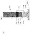
- FIGS. 1A , 1 B, 1 C, 1 D, and 1 Eeach show an exemplary embodiment of a memory device 1100 , such as a single memory cell of a NAND string.
- the memory device 1100includes a semiconductor channel 1102 , a tunnel dielectric 1104 located over the semiconductor channel 1102 , a charge storage region 1106 (e.g., a floating gate or charge trapping dielectric) located over the tunnel dielectric 1104 , a blocking dielectric 1108 located over the charge storage region 1106 , and a control gate 1110 located over the blocking dielectric 1108 .
- An interface 1112is formed between the blocking dielectric 1108 and the control gate 1110 which substantially prevents oxygen diffusion from the oxide blocking dielectric 1108 into the control gate 1110 .
- An interface which substantially prevents oxygen diffusionincludes an interface which prevents all oxygen diffusion into the control gate, such that no oxygen diffuses into the control gate or an interface which prevents at least 90 percent of oxygen diffusion into the control gate from the blocking dielectric.
- the control gate with the interface 1112has at least 90 percent less diffused oxygen from the blocking dielectric than a control gate which lacks such interface.
- the semiconductor channel 1102may include any suitable type of semiconductor material, such as silicon, germanium, silicon-germanium or compound semiconductor material (e.g., III-V semiconductor material).
- the semiconductor channel 1102may include a region of doped semiconductor material of a first conductivity type disposed between source and drain regions (not shown) of semiconductor material having a second conductivity type that differs from the first.
- the semiconductor channel 1102may be n-type doped semiconductor while the source and drain regions are p-type semiconductor material (or vice versa).
- the semiconductor channel 1102may be formed in a substrate, such as a silicon wafer substrate (e.g., as shown in FIG. 6 and as described below).
- the channel 1102may be a semiconductor layer or thin film that is located above a semiconductor or non-semiconductor substrate.
- the tunnel dielectric 1104may be formed from any suitable insulating material, such as an oxide.
- the tunnel dielectric 1104may include a silicon oxide (e.g., SiO 2 ) layer, a nitrided silicon oxide layer or a plurality of insulating layers (e.g., silicon oxide and silicon nitride layers).
- the tunnel dielectric 1104has a thickness selected to allow for quantum tunneling of charge carriers (e.g., Fowler-Nordheim tunneling or hot carrier injection) between the charge storage region 1016 and the semiconductor channel 1102 (e.g., in the presence of an applied electric field) to allow for programming and erasing the memory device 1100 .
- charge carrierse.g., Fowler-Nordheim tunneling or hot carrier injection
- the charge storage region 1106may include any suitable charge storage material.
- the charge storage region 1106includes polycrystalline silicon, metal (e.g., tungsten or ruthenium), metal silicide or insulating material (e.g., silicon nitride).
- the charge storage region 1106may operate as a floating gate for the memory device 1100 .
- the charge storage state of the charge storage region 1106may be programmed by applying an electric field to the region to cause tunneling of charge carriers into or out of the charge storage region 1106 .
- the blocking dielectric 1108may be any suitable material that electrically insulates the charge storage region 1106 from the control gate 1110 .
- the blocking dielectric 1108may include layers of one or more oxide, such as metal oxide layers (e.g., HfO 2 and/or Al 2 O 3 layers).
- the control gate 1110may include an electrically conductive material (e.g., a metal, metal alloy, or metal silicide) in contact with the blocking dielectric 1108 at the interface 1112 .
- the control gate 1110may include for example, tungsten, a tungsten alloy, molybdenum, a molybdenum alloy, a noble metal or a noble metal alloy.
- control gate 1110may include molybdenum, a molybdenum alloy, a noble metal or a noble metal alloy located at the interface 1112 between the blocking dielectric 1108 and the control gate 110 .
- the portion of the control gate 1110 extending away from the interface 1112may be made from a different electrically conductive material than that at the interface (e.g., where a noble metal is used at the interface 1112 , and a less expensive non-noble metal, such as tungsten, may be used to form the remainder of the control gate 110 ).
- the substantially oxygen diffusion free interface 1112prevents or reduces current leakage between the control gate 1110 and the charge storage region 1106 through the blocking dielectric 1108 .
- the interface 1112may also increase the breakdown voltage of the blocking dielectric 1108 in comparison to the case where oxygen diffusion is present.
- the interface 1112may also improve adhesion between the blocking dielectric 1108 into the control gate 1110 .
- one or more of the forgoing advantageous effectsmay result in improved performance of the memory device 1100 .
- one or more of the forgoing advantageous effectsmay result in an increase in program/erase (PE) window of the device 1100 (i.e. the voltage threshold window that separates the programmed state of the device from an erased state of the device).
- PEprogram/erase
- the memory device 1100may experience decreased degradation of the PE over time (e.g., over a number of program/erase cycles).
- one or more of the forgoing advantageous effectsmay result in increased reliability of the memory device 1100 , e.g., a lower chance of device failure over time (e.g., over a number of program/erase cycles).
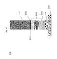
- the blocking dielectric layer 1108may include a stack of multiple layers.
- the blocking dielectric 1108contains a first layer 1108 a (e.g. an aluminum oxide layer) below the interface 1112 and a second layer 1108 b (e.g., a hafnium oxide layer) below the first layer 1108 a .
- the blocking dielectric 1108includes a first hafnium oxide layer 1108 b located over the charge storage region 1106 and a first aluminum oxide layer 1108 a located over the first hafnium oxide layer 1108 b.
- Some embodimentsmay include an optional electrically insulating barrier layer 1114 (e.g., an oxynitride layer such as hafnium oxynitride) located at the interface 1112 between the blocking dielectric 1108 and the control gate 1110 .
- the barrier layer 1114may contact the first aluminum oxide layer 1108 a .
- the barrier layer 1114is an oxynitride (such as hafnium oxynitride) that contains, e.g., between 1 and 10 atomic percent nitrogen or any sub-range thereof, such as between 2 and 5 atomic percent nitrogen.
- the blocking dielectric 1108may include additional layers.
- the blocking dielectric 1108includes a first hafnium oxide layer 108 b located over the charge storage region 1106 , a first aluminum oxide layer 1108 a located over the first hafnium oxide layer 1108 b , and a second hafnium oxide layer 1108 c located between the interface 1112 (e.g., including the oxynitride barrier layer 1114 ) and the first aluminum oxide layer 1108 a.
- the blocking dielectric 1108may include any suitable number of alternating hafnium oxide and aluminum oxide layers.
- FIG. 2shows a detailed view of a blocking dielectric 108 that includes a first hafnium oxide layer 1108 b located over the charge storage region 1106 (not shown) and a first aluminum oxide layer 1108 a located over the first hafnium oxide layer 1108 b , a second aluminum oxide barrier layer 1108 d located at the interface 1112 between the blocking dielectric and the control gate 1110 (not shown), and a second hafnium oxide layer 1108 c located between the second aluminum oxide barrier layer 1108 d and the first aluminum oxide layer 1108 a .
- layer 1108 dacts the insulating barrier layer.
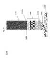
- the barrier layer 1120may be a silicide nitride barrier layer, such as a titanium silicide nitride.
- the silicide nitride barrier layer 1120contains, e.g., between 1 and 20 atomic percent silicon or any subrange thereof, such as 5 and 15 atomic percent silicon.
- the silicide nitride barrier layer 1120contains, e.g., between 25 and 50 atomic percent nitrogen and titanium each, or any sub-range thereof, such as between 35 and 45 atomic percent nitrogen.
- the barrier layer 1120is thinner than the blocking dielectric 1108 , e.g., having a thickness in the range of 1-50 nm or any subrange thereof, such as 1-20 nm, 1-10 nm, or 1-5 nm.
- the memory device 1100may include molybdenum, a molybdenum alloy, a noble metal or a noble metal alloy located at the interface 1112 between the blocking dielectric 1108 and the control gate 1110 .
- the control gate 1110includes molybdenum or a noble metal, and the molybdenum, molybdenum alloy, noble metal or noble metal alloy located at the interface 1112 between the blocking dielectric and the control gate comprises a bottom 1110 a of the control gate 1110 .
- the molybdenum, molybdenum alloy, a noble metal, or noble metal alloy materialsmay be advantageous in that they may exhibit lower electrical resistivity than conventional gate electrode materials, such as tungsten.
- the aforementioned materialsmay also be stable at relatively high temperatures, e.g., reducing or eliminating oxidation at the interface 1112 that might otherwise occur, e.g., during thermal processing such as an annealing step.
- these materialsmay be deposited directly only the blocking dielectric 1108 without the need for a diffusion barrier layer.
- these materialsmay be deposited directly onto a hafnium oxide top layer of the blocking dielectric 1108 .
- these materialsmay have a higher etch selectively to oxides than conventional materials, such as tungsten. The etch byproducts of these materials may be more volatile than those for conventional materials, such as tungsten, reducing or eliminating contamination concerns during processing.
- various embodiments of the memory device 1100may include any suitable combination of the elements and features shown in FIGS. 1A-1E .
- some embodimentsmay include both the electrically conductive barrier layer 1120 as shown in FIG. 1D , and the molybdenum, a molybdenum alloy, a noble metal or a noble metal alloy control gate portion 1110 a located at the interface 1112 , as shown in FIG. 1E .
- FIGS. 3A-3Dillustrate process steps in a method of making a memory device 1100 of the type shown in FIGS. 1A-1E .
- a tunnel dielectric 1104is formed over a semiconductor channel 1102 .
- the semiconductor channel 1102may include any suitable type of semiconductor material, such as silicon.
- the semiconductor channel 1102may include a region of doped semiconductor material of a first conductivity type disposed between source and drain regions (not shown) of semiconductor material having a second conductivity type that differs from the first.
- the semiconductor channel 1102may be n-type doped semiconductor while the source and drain regions are p-type semiconductor material (or vice versa).
- the semiconductor channel 1102may be formed in a substrate, such as a silicon wafer substrate.
- the tunnel dielectric 1104may be formed from any suitable insulating material, such as an oxide (e.g., SiO 2 ).
- the tunnel dielectric 1104may include a silicon oxide, a nitride silicon oxide or silicon oxide/silicon nitride layer stack.
- the tunnel dielectric 104is formed with a thickness selected to allow for quantum tunneling of charge carriers (e.g., Fowler-Nordheim tunneling or hot carrier injection) between the charge storage region 1106 and the semiconductor channel 1104 (e.g., in the presence of an applied voltage) to allow for programming and erasing the memory device 1100 .
- charge carrierse.g., Fowler-Nordheim tunneling or hot carrier injection
- the tunnel dielectric 1104may be formed using may be formed using any suitable technique including sputtering, chemical vapor deposition, physical vapor deposition, plasma enhanced chemical vapor deposition, etc.
- a charge storage region 1106is formed over the tunnel dielectric.
- the charge storage region 1106may include any suitable charge storage material.
- the charge storage region 1106includes polycrystalline silicon, metal, metal silicide or silicon nitride.
- the charge storage region 1106may operate as a floating gate for the memory device 1100 .
- the charge storage state of the charge storage region 1106may be programmed by applying an electric field to the region to cause tunneling of charge carriers into or out of the charge storage region 1106 .
- the charge storage region 1106may be formed using may be formed using any suitable technique including sputtering or chemical vapor deposition, physical vapor deposition, plasma enhanced chemical vapor deposition, etc. .
- a blocking dielectric 1108is formed over the charge storage region 1106 .
- the blocking dielectric 1108may be any suitable materially that electrically insulates the charge storage region 1106 from the control gate 1110 .
- the blocking dielectric 1108may include one or more oxides, such as metal oxides (e.g., HfO 2 and/or Al 2 O 3 ).
- the blocking dielectric 1108may be formed using may be formed using any suitable technique including sputtering or chemical vapor deposition, physical vapor deposition, plasma enhanced chemical vapor deposition, etc.
- a control gate 1110is formed over the blocking dielectric 1108 .
- the control gate 1110may include an electrically conductive material (e.g., a metal, metal alloy, or metal silicide) in contact with the blocking dielectric 1108 at the interface 1112 .
- the control gate 1110may include for example, tungsten, a tungsten alloy, molybdenum, a molybdenum alloy, a noble metal or a noble metal alloy in region 1110 a or in the entire gate.
- the layer structure described abovemay be patterned, e.g., to form an array of pillar or rail structures each comprising a memory device 1100 .
- a patterned mask 1122e.g., a hard mask and/or photoresist
- a patterned mask 1122may be formed using photolithography and etching that exposes only portions of the underlying structure intended for removal.
- An etching processmay then be used to remove exposed portions of the layer stack to define the array of devices.
- the maskmay then be removed, e.g., by using a chemical mechanical polishing process or etching for a hardmask, or ashing for a photoresist to expose a top surface of the array.
- control gate 1110may include molybdenum, a molybdenum alloy, a noble metal or a noble metal alloy located at the interface 1112 between the blocking dielectric 1108 and the control gate 1110 .
- the portion a of the control gate 1110 extending away from the interface 1112may be made from a different electrically conductive material (e.g., where a noble metal is used in region 1110 a at the interface 1112 , a less expensive non-noble metal such as tungsten may be used to form the remainder of the control gate 1110 ).
- This structuremay be formed by depositing a noble metal layer or noble metal nanodots (i.e., nanoparticles) 1110 a (e.g., Pt, Pd, Au, Rh or Ru layer or nanoparticles) over the interface followed by depositing a tungsten control gate 1110 material over the noble metal layer 1110 a .
- a noble metal layer or noble metal nanodotsi.e., nanoparticles
- tungsten control gate 1110 materiale.g., gold, Rh or Ru layer or nanoparticles
- control gate 1110 layer or layersmay be formed using may be formed using any suitable technique including sputtering or chemical vapor deposition, physical vapor deposition, plasma enhanced chemical vapor deposition, etc.
- the structure formed in step 304corresponds to the memory device 1100 shown in FIGS. 1A-1E .
- the memory device 1100includes an interface 1112 between the blocking dielectric and the control gate substantially prevents oxygen diffusion from the blocking dielectric into the control gate.
- the interface 1112provides a variety of advantageous effects in various embodiments.
- step 3303includes forming a blocking dielectric 1108 that contains at least one metal oxide layer 1108 a below the interface, e.g., as shown in FIGS. 1A-1D .
- the step of 3303 of forming the blocking dielectric 108includes forming a first hafnium oxide 1108 b layer located over the charge storage region 106 and forming a first aluminum oxide layer 1108 a located over the first hafnium oxide layer 1108 b , as shown in FIG. 3C .
- the step of 3303 of forming the blocking dielectric 1108includes forming more than two layers.
- forming the blocking dielectric 1108may include forming a first hafnium oxide layer 1108 b over the charge storage region 1106 , forming a first aluminum oxide layer 1108 a over the first hafnium oxide layer 1108 b , forming a second hafnium oxide layer 1108 c over the first aluminum oxide layer 1108 a , followed by forming the insulating barrier layer 1114 or 1108 d described above.
- the insulating barrier layer 1114may be an oxynitride (such as hafnium oxynitride) that contains, e.g., between 1 and 10 atomic percent nitrogen or any sub-range thereof, such as between 2 and 5 atomic percent nitrogen.
- the hafnium oxynitride barrier layer 1114may be formed by nitriding at least an upper surface of the hafnium oxide layer 1108 c in a nitrogen (e.g., molecular nitrogen or ammonia) containing ambient or plasma.
- a hafnium oxynitride barrier layer 1114may be deposited by chemical or physical vapor deposition over the hafnium oxide layer 1108 c.
- the step 3303 of forming the blocking dielectric 1018may include forming any suitable number of alternating hafnium oxide and aluminum oxide layers.
- first hafnium oxide layer 1108 bis formed over the charge storage region 106 (not shown)
- first aluminum oxide layer 108 ais formed over the first hafnium oxide layer 108 b
- a second hafnium oxide layer 108 cis formed over the first aluminum oxide layer 1108 a
- the second aluminum oxide barrier layer 1108 dis formed at the interface 1112 over the second hafnium oxide layer 108 .
- some embodimentsinclude an additional step 3305 of forming the conductive barrier layer 1120 over blocking dielectric 1108 at the interface 1112 .
- the barrier layer 1210may be a silicide nitride barrier layer, such as a titanium silicide nitride layer.
- the silicide nitride barrier layer 1120contains, e.g., between 1 and 20 atomic percent silicon, or any subrange thereof, such as 5 and 15 atomic percent silicon.
- the silicide nitride barrier layer 120contains, e.g., between 25 and 50 atomic percent each of titanium and nitrogen or any sub-range thereof, such as between 35 and 45 atomic percent each of titanium and nitrogen.
- the barrier layer 1120is thinner than the blocking dielectric 108 , e.g., having a thickness in the range of 1-50 nm or any subrange thereof, such as 1-20 nm, 1-10 nm, or 1-5 nm.
- the titanium silicide nitride barrier layer 1120is formed by depositing a titanium nitride layer 1120 a over the blocking dielectric 1108 .
- the titanium nitride layer 1120 ais formed using atomic layer deposition. This is followed by depositing an amorphous silicon layer 1120 b over the titanium nitride layer using physical vapor deposition.
- the titanium nitride layer 1120 ahas a thickness of, e.g., 1 to 20 nm, such as 5 to 10 nm and the amorphous silicon layer 1120 b has a thickness of 1 to 10 nm, such as 1 to 2 nm.
- the barrier layer 1120is formed by reacting the titanium nitride layer 1120 a with the amorphous silicon layer 1120 b to form the titanium silicide nitride barrier layer 1120 as shown.
- the step of reactingmay comprise heating the layers at a suitable temperature, e.g., 350-500 C, such as 400-450 C for 10 to 60 minutes, such as 30-45 minutes.
- the step of reacting the titanium nitride layer 1120 a with the amorphous silicon layer 1120 bincludes heating the titanium nitride layer 1120 a and the amorphous silicon layer 1120 b after forming a tungsten control gate layer 1110 (e.g., by CVD or sputtering) on the amorphous silicon layer 1120 b to keep the tungsten control gate layer resistance to its lowest possible value.
- a tungsten control gate layer 1110e.g., by CVD or sputtering
- Various embodimentsmay include any suitable additional processing steps.
- some embodimentsmay include one or more annealing steps (e.g., to anneal polysilicon, metal, metal silicide or silicon nitride material used form the charge storage region 106 ).
- one or more of the memory devices 1100 of the type described abovemay be used as storage elements in a non-volatile memory device such as an EEPROM or flash memory device.
- FIG. 4Ais a top view showing one NAND string.
- FIG. 4Bis an equivalent circuit thereof.
- the NAND string depicted in FIGS. 4A and 4Bincludes four transistors, 100 , 102 , 104 and 106 , in series and sandwiched between a first select gate 120 and a second select gate 122 .
- Select gate 120gates the NAND string connection to bit line 126 .
- Select gate 122gates the NAND string connection to source line 128 .
- Select gate 120is controlled by applying the appropriate voltages to control gate 120 CG.
- Select gate 122is controlled by applying the appropriate voltages to control gate 122 CG.
- Each of the transistors 100 , 102 , 104 and 106has a control gate and a floating gate.
- Transistor 100has control gate 100 CG and floating gate 100 FG.
- Transistor 102includes control gate 102 CG and floating gate 102 FG.
- Transistor 104includes control gate 104 CG and floating gate 104 FG.
- Transistor 106includes a control gate 106 CG and floating gate 106 FG.
- Control gate 100 CGis connected to (or is) word line WL 3
- control gate 102 CGis connected to word line WL 2
- control gate 104 CGis connected to word line WL 1
- control gate 106 CGis connected to word line WL 0 .
- transistors 100 , 102 , 104 and 106are each storage elements, also referred to as memory cells. In other embodiments, the storage elements may include multiple transistors or may be different than that depicted in FIGS. 4A and 4B .
- Select gate 120is connected to select line SGD.
- Select gate 122is connected to select line SGS.
- One or more of the transistors 100 , 102 , 104 and 106may be implemented as a memory cell 1100 as the type shown in FIGS. 1A-1E above.
- the channel of each transistormay include the semiconductor channel 1102 of the memory device 1100 .
- the floating gate of the transistormay include the charge storage region 1106 of the memory device 1100 .
- the control gate of each transistormay include the control gate 1110 memory device 1100 .
- FIG. 5is a circuit diagram depicting three NAND strings.
- a typical architecture for a flash memory system using a NAND structurewill include several NAND strings.
- three NAND strings 320 , 340 and 360are shown in a memory array having many more NAND strings.
- Each of the NAND stringsincludes two select gates and four storage elements, each of which may include a memory device 1100 of the type described with reference to FIGS. 1A-1E . While four storage elements are illustrated for simplicity, modern NAND strings can have up to thirty-two or sixty-four storage elements, for instance.
- NAND string 320includes select gates 322 and 327 , and storage elements 323 - 326
- NAND string 340includes select gates 342 and 347 , and storage elements 343 - 346
- NAND string 360includes select gates 362 and 367 , and storage elements 363 - 366 .
- Each NAND stringis connected to the source line by its select gates (e.g., select gates 327 , 347 or 367 ).
- a selection line SGSis used to control the source side select gates.
- the various NAND strings 320 , 340 and 360are connected to respective bit lines 321 , 341 and 361 , by select transistors in the select gates 322 , 342 , 362 , etc.
- select transistorsare controlled by a drain select line SGD.
- the select linesdo not necessarily need to be in common among the NAND strings; that is, different select lines can be provided for different NAND strings.
- Word line WL 3is connected to the control gates for storage elements 323 , 343 and 363 .
- Word line WL 2is connected to the control gates for storage elements 324 , 344 and 364 .
- Word line WL 1is connected to the control gates for storage elements 325 , 345 and 365 .
- Word line WL 0is connected to the control gates for storage elements 326 , 346 and 366 .
- each bit line and the respective NAND stringcomprise the columns of the array or set of storage elements.
- the word lines(WL 3 , WL 2 , WL 1 and WL 0 ) comprise the rows of the array or set. Each word line connects the control gates of each storage element in the row. Or, the control gates may be provided by the word lines themselves. For example, word line WL 2 provides the control gates for storage elements 324 , 344 and 364 . In practice, there can be thousands of storage elements on a word line.
- Each storage elementcan store data. For example, when storing one bit of digital data, the range of possible threshold voltages (V TH ) of the storage element is divided into two ranges which are assigned logical data “1” and “0.”
- V THthreshold voltages
- the V THis negative after the storage element is erased, and defined as logic “1.”
- the V TH after a program operationis positive and defined as logic “0.”
- the storage elementwill turn on to indicate logic “1” is being stored.
- the storage elementWhen the VTH is positive and a read operation is attempted, the storage element will not turn on, which indicates that logic “0” is stored.
- a storage elementcan also store multiple levels of information, for example, multiple bits of digital data.
- the range of V TH valueis divided into the number of levels of data. For example, if four levels of information are stored, there will be four V TH ranges assigned to the data values “11”, “10”, “01”, and “00.” In one example of a NAND type memory, the VTH after an erase operation is negative and defined as “11”. Positive V TH values are used for the states of “10”, “01”, and “00.”
- the specific relationship between the data programmed into the storage element and the threshold voltage ranges of the elementdepends upon the data encoding scheme adopted for the storage elements. For example, U.S. Pat. Nos. 6,222,762 and 7,237,074, both of which are incorporated herein by reference in their entirety, describe various data encoding schemes for multi-state flash storage elements.
- a program voltageis applied to the control gate of the storage element, and the bit line associated with the storage element is grounded. Electrons from the channel are injected into the floating gate. When electrons accumulate in the floating gate, the floating gate becomes negatively charged and the V TH of the storage element is raised. To apply the program voltage to the control gate of the storage element being programmed, that program voltage is applied on the appropriate word line. As discussed above, one storage element in each of the NAND strings share the same word line. For example, when programming storage element 324 of FIG. 5 , the program voltage will also be applied to the control gates of storage elements 344 and 364 .
- FIG. 6depicts a cross-sectional view of an exemplary NAND string 400 formed on a substrate.
- the NAND string 400includes a source-side select gate 406 , a drain-side select gate 424 , and eight storage elements 408 , 410 , 412 , 414 , 416 , 418 , 420 and 422 , formed on a substrate 490 .
- Each of the storage elements 408 , 410 , 412 , 414 , 416 , 418 , 420 and 422comprise a memory device 1100 of the type described herein.
- Each of the memory devicesinclude a semiconductor channel, a tunnel dielectric located over the semiconductor channel, a charge storage region (e.g., a floating gate) located over the tunnel dielectric, a blocking dielectric located over the charge storage region, and a control gate located over the blocking dielectric.
- An interfaceis formed between the blocking dielectric and the control gate substantially prevents oxygen diffusion from the blocking dielectric into the control gate.
- these elements of memory device 1100are not explicitly shown in FIG. 6 , but in various embodiments, may be configured as shown in FIGS. 1A-1E .
- a number of source/drain regionsare provided on either side of each storage element and the select gates 406 and 424 .
- the substrate 490employs a triple-well technology that includes a p-well region 492 within an n-well region 494 , which in turn is within a p-type substrate region 496 .
- the NAND string and its non-volatile storage elementscan be formed, at least in part, on the p-well region 492 .
- the semiconductor channel for each storage elementmay comprise a portion of the a p-well region 492 .
- the conductivity types of the regions 492 , 494 , and 496may be reversed.
- each of the storage elements 408 , 410 , 412 , 414 , 416 , 418 , 420 and 422may comprise or be in electrical contact with a respective one of the conductive word lines WL 0 , WL 1 , WL 2 , WL 3 , WL 4 , WL 5 , WL 6 and WL 7 of the NAND device 400 .
- a source supply line 404 with a potential of Vsource (Vsrc)is provided in addition to a bit line 426 with a potential of Vb 1 .
- a voltage Vp-wellcan be applied to the p-well region 492 via a terminal 402 .
- a voltage Vn-wellcan also be applied to the n-well region 494 via a terminal 403 .
- a body biascan be expressed by V-pwell-Vsource or Vn-well-Vsource.
- a control gate voltageis provided on a selected word line which is associated with a selected storage element.
- the control gate of a storage elementmay be provided as a portion of the word line.
- WL 0 , WL 1 , WL 2 , WL 3 , WL 4 , WL 5 , WL 6 and WL 7can extend via the control gates of storage elements 408 , 410 , 412 , 414 , 416 , 418 , 420 and 422 , respectively.
- the operation of the NAND cell 400may operate using the techniques described in, for example, U. S. Pat. No. 8,441,853 granted May 14, 2013 entitled “Sensing for NAND memory based on word line position”; and U.S. Pat. No. 8,638,606 granted Jan. 28, 2014 entitled “Substrate bias during program of non-volatile storage” each of which are incorporated herein by reference in their entirety.
Landscapes
- Semiconductor Memories (AREA)
- Non-Volatile Memory (AREA)
Abstract
Description
Claims (20)
Priority Applications (1)
| Application Number | Priority Date | Filing Date | Title |
|---|---|---|---|
| US14/284,917US9177808B2 (en) | 2013-05-21 | 2014-05-22 | Memory device with control gate oxygen diffusion control and method of making thereof |
Applications Claiming Priority (2)
| Application Number | Priority Date | Filing Date | Title |
|---|---|---|---|
| US201361825866P | 2013-05-21 | 2013-05-21 | |
| US14/284,917US9177808B2 (en) | 2013-05-21 | 2014-05-22 | Memory device with control gate oxygen diffusion control and method of making thereof |
Publications (2)
| Publication Number | Publication Date |
|---|---|
| US20140346584A1 US20140346584A1 (en) | 2014-11-27 |
| US9177808B2true US9177808B2 (en) | 2015-11-03 |
Family
ID=51934824
Family Applications (1)
| Application Number | Title | Priority Date | Filing Date |
|---|---|---|---|
| US14/284,917Expired - Fee RelatedUS9177808B2 (en) | 2013-05-21 | 2014-05-22 | Memory device with control gate oxygen diffusion control and method of making thereof |
Country Status (1)
| Country | Link |
|---|---|
| US (1) | US9177808B2 (en) |
Families Citing this family (2)
| Publication number | Priority date | Publication date | Assignee | Title |
|---|---|---|---|---|
| JP2016129318A (en)* | 2015-01-09 | 2016-07-14 | 株式会社東芝 | Look-up table circuit and nonvolatile memory device |
| US9865703B2 (en) | 2015-12-31 | 2018-01-09 | International Business Machines Corporation | High-K layer chamfering to prevent oxygen ingress in replacement metal gate (RMG) process |
Citations (59)
| Publication number | Priority date | Publication date | Assignee | Title |
|---|---|---|---|---|
| US5570315A (en) | 1993-09-21 | 1996-10-29 | Kabushiki Kaisha Toshiba | Multi-state EEPROM having write-verify control circuit |
| US5714766A (en) | 1995-09-29 | 1998-02-03 | International Business Machines Corporation | Nano-structure memory device |
| US5774397A (en) | 1993-06-29 | 1998-06-30 | Kabushiki Kaisha Toshiba | Non-volatile semiconductor memory device and method of programming a non-volatile memory cell to a predetermined state |
| US6015738A (en) | 1994-05-05 | 2000-01-18 | California Institute Of Technology | Method for fabricating transistorless, multistable current-mode memory cells and memory arrays |
| US6046935A (en) | 1996-03-18 | 2000-04-04 | Kabushiki Kaisha Toshiba | Semiconductor device and memory system |
| US6208000B1 (en) | 1998-05-08 | 2001-03-27 | Kabushiki Kaisha Toshiba | Semiconductor element having charge accumulating layer under gate electrode and using single electron phenomenon |
| US6297095B1 (en) | 2000-06-16 | 2001-10-02 | Motorola, Inc. | Memory device that includes passivated nanoclusters and method for manufacture |
| US6407424B2 (en) | 1997-01-29 | 2002-06-18 | Micron Technology, Inc. | Flash memory with nanocrystalline silicon film floating gate |
| US6646302B2 (en) | 2000-11-21 | 2003-11-11 | Cornell Research Foundation, Inc. | Embedded metal nanocrystals |
| US6656792B2 (en) | 2001-10-19 | 2003-12-02 | Chartered Semiconductor Manufacturing Ltd | Nanocrystal flash memory device and manufacturing method therefor |
| US20040026682A1 (en) | 2002-06-17 | 2004-02-12 | Hai Jiang | Nano-dot memory and fabricating same |
| US20040094794A1 (en) | 2002-11-14 | 2004-05-20 | Ching-Yuan Wu | Stacked-gate cell structure and its nand-type flash memory array |
| US20040130941A1 (en) | 2002-11-26 | 2004-07-08 | Cornell Research Foundation, Inc. | Multibit metal nanocrystal memories and fabrication |
| US20040180491A1 (en) | 2003-03-13 | 2004-09-16 | Nobutoshi Arai | Memory function body, particle forming method therefor and, memory device, semiconductor device, and electronic equipment having the memory function body |
| US20040256662A1 (en) | 2003-06-20 | 2004-12-23 | International Business Machines Corporation | Nonvolatile memory device using semiconductor nanocrystals and method of forming same |
| US6859397B2 (en) | 2003-03-05 | 2005-02-22 | Sandisk Corporation | Source side self boosting technique for non-volatile memory |
| US6881994B2 (en) | 2000-08-14 | 2005-04-19 | Matrix Semiconductor, Inc. | Monolithic three dimensional array of charge storage devices containing a planarized surface |
| US20050112820A1 (en) | 2003-11-25 | 2005-05-26 | Jason Chen | Method for fabricating flash memory device and structure thereof |
| US20050122775A1 (en) | 2002-07-23 | 2005-06-09 | Asahi Glass Company, Limited | Novolatile semiconductor memory device and manufacturing process of the same |
| US6913984B2 (en) | 2002-12-23 | 2005-07-05 | Samsung Electronics Co., Ltd. | Method of manufacturing memory with nano dots |
| US6917542B2 (en) | 2003-07-29 | 2005-07-12 | Sandisk Corporation | Detecting over programmed memory |
| US6927136B2 (en) | 2003-08-25 | 2005-08-09 | Macronix International Co., Ltd. | Non-volatile memory cell having metal nano-particles for trapping charges and fabrication thereof |
| US20050258470A1 (en) | 2004-05-20 | 2005-11-24 | Bohumil Lojek | Gate stack of nanocrystal memory and method for forming same |
| US20050287717A1 (en) | 2004-06-08 | 2005-12-29 | Nanosys, Inc. | Methods and devices for forming nanostructure monolayers and devices including such monolayers |
| US6991984B2 (en) | 2004-01-27 | 2006-01-31 | Freescale Semiconductor, Inc. | Method for forming a memory structure using a modified surface topography and structure thereof |
| US7119395B2 (en) | 2003-08-11 | 2006-10-10 | Infineon Technologies Ag | Memory cell with nanocrystals or nanodots |
| US20060250837A1 (en) | 2005-05-09 | 2006-11-09 | Sandisk 3D, Llc | Nonvolatile memory cell comprising a diode and a resistance-switching material |
| US20060250836A1 (en) | 2005-05-09 | 2006-11-09 | Matrix Semiconductor, Inc. | Rewriteable memory cell comprising a diode and a resistance-switching material |
| US7138680B2 (en) | 2004-09-14 | 2006-11-21 | Infineon Technologies Ag | Memory device with floating gate stack |
| US7173304B2 (en) | 2005-06-06 | 2007-02-06 | Micron Technology, Inc. | Method of manufacturing devices comprising conductive nano-dots, and devices comprising same |
| US20070045604A1 (en) | 2005-08-30 | 2007-03-01 | Micron Technology, Inc. | Resistance variable memory device with nanoparticle electrode and method of fabrication |
| US20070158736A1 (en) | 2005-12-28 | 2007-07-12 | Kabushiki Kaisha Toshiba | Semiconductor memory device and method of fabricating the same |
| US20080026532A1 (en) | 2004-03-10 | 2008-01-31 | Nanosys, Inc. | Nano-Enabled Memory Devices and Anisotropic Charge Carrying Arrays |
| US20080242011A1 (en) | 2007-03-27 | 2008-10-02 | Samsung Electronics Co., Ltd | Method of fabricating non-volatile memory device |
| US20080237692A1 (en) | 2007-03-29 | 2008-10-02 | Lee Jaegab | Method of forming floating gate, non-volatile memory device using the same, and fabricating method thereof |
| DE102008009365A1 (en) | 2007-02-23 | 2008-10-23 | Korea University Industrial & Academic Collaboration Foundation | Nonvolatile memory electronic device using nanowire as a charging cable and nanoparticles as a charge trap, and a method of manufacturing the same |
| US20090001345A1 (en) | 2007-06-29 | 2009-01-01 | April Schricker | Memory cell that employs a selectively deposited reversible resistance-switching element and methods of forming the same |
| US20090014704A1 (en) | 2007-07-11 | 2009-01-15 | International Business Machines Corporation | Current constricting phase change memory element structure |
| US20090027944A1 (en) | 2007-07-24 | 2009-01-29 | Klaus Ufert | Increased Switching Cycle Resistive Memory Element |
| US20090097320A1 (en) | 2007-10-12 | 2009-04-16 | Min Kyu S | Memory Cells, Electronic Systems, Methods Of Forming Memory Cells, And Methods of Programming Memory Cells |
| US20090117697A1 (en) | 2005-10-21 | 2009-05-07 | Sang-Ji Park | Nonvolatile memory device including nano dot and method of fabricating the same |
| US20090134444A1 (en) | 2007-11-26 | 2009-05-28 | Hanafi Hussein I | Memory Cells, And Methods Of Forming Memory Cells |
| US20090146140A1 (en) | 2007-12-05 | 2009-06-11 | Samsung Electronics Co., Ltd. | Nonvolatile organic bistable memory device and method of manufacturing the same |
| US20090155967A1 (en) | 2007-12-18 | 2009-06-18 | Vinod Robert Purayath | Method of forming memory with floating gates including self-aligned metal nanodots using a coupling layer |
| US20090168491A1 (en) | 2007-12-31 | 2009-07-02 | April Schricker | Memory cell that employs a selectively fabricated carbon nano-tube reversible resistance-switching element and methods of forming the same |
| US20100008128A1 (en) | 2008-02-19 | 2010-01-14 | Panasonic Corporation | Resistive nonvolatile memory element, and production method of the same |
| US7649779B2 (en) | 2007-05-15 | 2010-01-19 | Qimonda Ag | Integrated circuits; methods for manufacturing an integrated circuit; memory modules; computing systems |
| US20110020992A1 (en) | 2009-07-21 | 2011-01-27 | Vinod Robert Purayath | Integrated Nanostructure-Based Non-Volatile Memory Fabrication |
| US20110147337A1 (en) | 2009-12-18 | 2011-06-23 | Korea University Research And Business Foundation | Use of block copolymers for preparing conductive nanostructures |
| US20110186799A1 (en) | 2010-02-04 | 2011-08-04 | Sandisk 3D Llc | Non-volatile memory cell containing nanodots and method of making thereof |
| US20110286275A1 (en)* | 2010-05-24 | 2011-11-24 | Samsung Electronics Co., Ltd. | Stacked Memory Devices And Method Of Manufacturing The Same |
| US8193055B1 (en) | 2007-12-18 | 2012-06-05 | Sandisk Technologies Inc. | Method of forming memory with floating gates including self-aligned metal nanodots using a polymer solution |
| US20130105881A1 (en) | 2011-10-28 | 2013-05-02 | James K. Kai | Self-Aligned Planar Flash Memory And Methods Of Fabrication |
| US20130175604A1 (en)* | 2007-12-12 | 2013-07-11 | Cypress Semiconductor Corporation | Nonvolatile charge trap memory device having a high dielectric constant blocking region |
| US20140001535A1 (en) | 2012-07-02 | 2014-01-02 | SanDisk Technologies, Inc. | Non-Volatile Memory Structure Containing Nanodots and Continuous Metal Layer Charge Traps and Method of Making Thereof |
| US20140001553A1 (en) | 2012-06-29 | 2014-01-02 | Kimihiko Imura | Method and system for improved analog performance in sub-100 nanometer cmos transistors |
| US20140160841A1 (en)* | 2012-12-12 | 2014-06-12 | Randy J. Koval | Self-aligned floating gate in a vertical memory structure |
| US8754466B2 (en)* | 2011-10-17 | 2014-06-17 | Samsung Electronics Co., Ltd. | Three-dimensional semiconductor memory devices |
| US8778762B2 (en)* | 2012-12-07 | 2014-07-15 | Micron Technology, Inc. | Methods of forming vertically-stacked structures, and methods of forming vertically-stacked memory cells |
- 2014
- 2014-05-22USUS14/284,917patent/US9177808B2/ennot_activeExpired - Fee Related
Patent Citations (62)
| Publication number | Priority date | Publication date | Assignee | Title |
|---|---|---|---|---|
| US5774397A (en) | 1993-06-29 | 1998-06-30 | Kabushiki Kaisha Toshiba | Non-volatile semiconductor memory device and method of programming a non-volatile memory cell to a predetermined state |
| US5570315A (en) | 1993-09-21 | 1996-10-29 | Kabushiki Kaisha Toshiba | Multi-state EEPROM having write-verify control circuit |
| US6015738A (en) | 1994-05-05 | 2000-01-18 | California Institute Of Technology | Method for fabricating transistorless, multistable current-mode memory cells and memory arrays |
| US5714766A (en) | 1995-09-29 | 1998-02-03 | International Business Machines Corporation | Nano-structure memory device |
| US6046935A (en) | 1996-03-18 | 2000-04-04 | Kabushiki Kaisha Toshiba | Semiconductor device and memory system |
| US6407424B2 (en) | 1997-01-29 | 2002-06-18 | Micron Technology, Inc. | Flash memory with nanocrystalline silicon film floating gate |
| US6208000B1 (en) | 1998-05-08 | 2001-03-27 | Kabushiki Kaisha Toshiba | Semiconductor element having charge accumulating layer under gate electrode and using single electron phenomenon |
| US6297095B1 (en) | 2000-06-16 | 2001-10-02 | Motorola, Inc. | Memory device that includes passivated nanoclusters and method for manufacture |
| US6881994B2 (en) | 2000-08-14 | 2005-04-19 | Matrix Semiconductor, Inc. | Monolithic three dimensional array of charge storage devices containing a planarized surface |
| US6646302B2 (en) | 2000-11-21 | 2003-11-11 | Cornell Research Foundation, Inc. | Embedded metal nanocrystals |
| US6656792B2 (en) | 2001-10-19 | 2003-12-02 | Chartered Semiconductor Manufacturing Ltd | Nanocrystal flash memory device and manufacturing method therefor |
| US20040026682A1 (en) | 2002-06-17 | 2004-02-12 | Hai Jiang | Nano-dot memory and fabricating same |
| US20050122775A1 (en) | 2002-07-23 | 2005-06-09 | Asahi Glass Company, Limited | Novolatile semiconductor memory device and manufacturing process of the same |
| US20040094794A1 (en) | 2002-11-14 | 2004-05-20 | Ching-Yuan Wu | Stacked-gate cell structure and its nand-type flash memory array |
| US20040130941A1 (en) | 2002-11-26 | 2004-07-08 | Cornell Research Foundation, Inc. | Multibit metal nanocrystal memories and fabrication |
| US7259984B2 (en) | 2002-11-26 | 2007-08-21 | Cornell Research Foundation, Inc. | Multibit metal nanocrystal memories and fabrication |
| US6913984B2 (en) | 2002-12-23 | 2005-07-05 | Samsung Electronics Co., Ltd. | Method of manufacturing memory with nano dots |
| US6859397B2 (en) | 2003-03-05 | 2005-02-22 | Sandisk Corporation | Source side self boosting technique for non-volatile memory |
| US20040180491A1 (en) | 2003-03-13 | 2004-09-16 | Nobutoshi Arai | Memory function body, particle forming method therefor and, memory device, semiconductor device, and electronic equipment having the memory function body |
| US7045851B2 (en) | 2003-06-20 | 2006-05-16 | International Business Machines Corporation | Nonvolatile memory device using semiconductor nanocrystals and method of forming same |
| US20040256662A1 (en) | 2003-06-20 | 2004-12-23 | International Business Machines Corporation | Nonvolatile memory device using semiconductor nanocrystals and method of forming same |
| US6917542B2 (en) | 2003-07-29 | 2005-07-12 | Sandisk Corporation | Detecting over programmed memory |
| US7119395B2 (en) | 2003-08-11 | 2006-10-10 | Infineon Technologies Ag | Memory cell with nanocrystals or nanodots |
| US6927136B2 (en) | 2003-08-25 | 2005-08-09 | Macronix International Co., Ltd. | Non-volatile memory cell having metal nano-particles for trapping charges and fabrication thereof |
| US20050112820A1 (en) | 2003-11-25 | 2005-05-26 | Jason Chen | Method for fabricating flash memory device and structure thereof |
| US6991984B2 (en) | 2004-01-27 | 2006-01-31 | Freescale Semiconductor, Inc. | Method for forming a memory structure using a modified surface topography and structure thereof |
| US20080026532A1 (en) | 2004-03-10 | 2008-01-31 | Nanosys, Inc. | Nano-Enabled Memory Devices and Anisotropic Charge Carrying Arrays |
| US20050258470A1 (en) | 2004-05-20 | 2005-11-24 | Bohumil Lojek | Gate stack of nanocrystal memory and method for forming same |
| US20050287717A1 (en) | 2004-06-08 | 2005-12-29 | Nanosys, Inc. | Methods and devices for forming nanostructure monolayers and devices including such monolayers |
| US7138680B2 (en) | 2004-09-14 | 2006-11-21 | Infineon Technologies Ag | Memory device with floating gate stack |
| US20060250837A1 (en) | 2005-05-09 | 2006-11-09 | Sandisk 3D, Llc | Nonvolatile memory cell comprising a diode and a resistance-switching material |
| US20060250836A1 (en) | 2005-05-09 | 2006-11-09 | Matrix Semiconductor, Inc. | Rewriteable memory cell comprising a diode and a resistance-switching material |
| US7173304B2 (en) | 2005-06-06 | 2007-02-06 | Micron Technology, Inc. | Method of manufacturing devices comprising conductive nano-dots, and devices comprising same |
| US20070045604A1 (en) | 2005-08-30 | 2007-03-01 | Micron Technology, Inc. | Resistance variable memory device with nanoparticle electrode and method of fabrication |
| US20090117697A1 (en) | 2005-10-21 | 2009-05-07 | Sang-Ji Park | Nonvolatile memory device including nano dot and method of fabricating the same |
| US20070158736A1 (en) | 2005-12-28 | 2007-07-12 | Kabushiki Kaisha Toshiba | Semiconductor memory device and method of fabricating the same |
| DE102008009365A1 (en) | 2007-02-23 | 2008-10-23 | Korea University Industrial & Academic Collaboration Foundation | Nonvolatile memory electronic device using nanowire as a charging cable and nanoparticles as a charge trap, and a method of manufacturing the same |
| US20080242011A1 (en) | 2007-03-27 | 2008-10-02 | Samsung Electronics Co., Ltd | Method of fabricating non-volatile memory device |
| US20080237692A1 (en) | 2007-03-29 | 2008-10-02 | Lee Jaegab | Method of forming floating gate, non-volatile memory device using the same, and fabricating method thereof |
| US7649779B2 (en) | 2007-05-15 | 2010-01-19 | Qimonda Ag | Integrated circuits; methods for manufacturing an integrated circuit; memory modules; computing systems |
| US20090001345A1 (en) | 2007-06-29 | 2009-01-01 | April Schricker | Memory cell that employs a selectively deposited reversible resistance-switching element and methods of forming the same |
| US20090014704A1 (en) | 2007-07-11 | 2009-01-15 | International Business Machines Corporation | Current constricting phase change memory element structure |
| US20090027944A1 (en) | 2007-07-24 | 2009-01-29 | Klaus Ufert | Increased Switching Cycle Resistive Memory Element |
| US20090097320A1 (en) | 2007-10-12 | 2009-04-16 | Min Kyu S | Memory Cells, Electronic Systems, Methods Of Forming Memory Cells, And Methods of Programming Memory Cells |
| US20090134444A1 (en) | 2007-11-26 | 2009-05-28 | Hanafi Hussein I | Memory Cells, And Methods Of Forming Memory Cells |
| US20090146140A1 (en) | 2007-12-05 | 2009-06-11 | Samsung Electronics Co., Ltd. | Nonvolatile organic bistable memory device and method of manufacturing the same |
| US20130175604A1 (en)* | 2007-12-12 | 2013-07-11 | Cypress Semiconductor Corporation | Nonvolatile charge trap memory device having a high dielectric constant blocking region |
| US8193055B1 (en) | 2007-12-18 | 2012-06-05 | Sandisk Technologies Inc. | Method of forming memory with floating gates including self-aligned metal nanodots using a polymer solution |
| US7723186B2 (en) | 2007-12-18 | 2010-05-25 | Sandisk Corporation | Method of forming memory with floating gates including self-aligned metal nanodots using a coupling layer |
| US20090155967A1 (en) | 2007-12-18 | 2009-06-18 | Vinod Robert Purayath | Method of forming memory with floating gates including self-aligned metal nanodots using a coupling layer |
| US20090168491A1 (en) | 2007-12-31 | 2009-07-02 | April Schricker | Memory cell that employs a selectively fabricated carbon nano-tube reversible resistance-switching element and methods of forming the same |
| US20100008128A1 (en) | 2008-02-19 | 2010-01-14 | Panasonic Corporation | Resistive nonvolatile memory element, and production method of the same |
| US20110020992A1 (en) | 2009-07-21 | 2011-01-27 | Vinod Robert Purayath | Integrated Nanostructure-Based Non-Volatile Memory Fabrication |
| US20110147337A1 (en) | 2009-12-18 | 2011-06-23 | Korea University Research And Business Foundation | Use of block copolymers for preparing conductive nanostructures |
| US20110186799A1 (en) | 2010-02-04 | 2011-08-04 | Sandisk 3D Llc | Non-volatile memory cell containing nanodots and method of making thereof |
| US20110286275A1 (en)* | 2010-05-24 | 2011-11-24 | Samsung Electronics Co., Ltd. | Stacked Memory Devices And Method Of Manufacturing The Same |
| US8754466B2 (en)* | 2011-10-17 | 2014-06-17 | Samsung Electronics Co., Ltd. | Three-dimensional semiconductor memory devices |
| US20130105881A1 (en) | 2011-10-28 | 2013-05-02 | James K. Kai | Self-Aligned Planar Flash Memory And Methods Of Fabrication |
| US20140001553A1 (en) | 2012-06-29 | 2014-01-02 | Kimihiko Imura | Method and system for improved analog performance in sub-100 nanometer cmos transistors |
| US20140001535A1 (en) | 2012-07-02 | 2014-01-02 | SanDisk Technologies, Inc. | Non-Volatile Memory Structure Containing Nanodots and Continuous Metal Layer Charge Traps and Method of Making Thereof |
| US8778762B2 (en)* | 2012-12-07 | 2014-07-15 | Micron Technology, Inc. | Methods of forming vertically-stacked structures, and methods of forming vertically-stacked memory cells |
| US20140160841A1 (en)* | 2012-12-12 | 2014-06-12 | Randy J. Koval | Self-aligned floating gate in a vertical memory structure |
Non-Patent Citations (8)
| Title |
|---|
| Chan et al., "A True Single-Transistor Oxide-Nitride-Oxide EEPROM Device," IEEE Electron Device Letters, vol. EDL-8, No. 3, Mar. 1987, pp. 93-95. |
| Guarini et al., "Low Voltage, Scalable Nanocrystal Flash Memory Fabricated by Templated Self-Assembly," IEEE Int. Electron Devices Meeting Tech. Diges, vol. 22, No. 2, Dec. 2003, pp. 1-4. |
| Haryono et al., "Controlled Arragement of Nanoparticle Arrays in Block-Copolymer Domains," Small.2.5 (2006), pp. 600-611. |
| Komatsu et al., "Applying Nanotechnology to Electronics," Science & Technology Trends, Quarterly Review No. 16, Jul. 2005, pp. 36-45. |
| Nozaki et al., "A 1-Mb EEPROM with MONOS Memory Cell for Semiconductor Disk Application," EEE Journal of Solid-State Circuits, vol. 26, No. 4, Apr. 1991, pp. 497-501. |
| Takeuchi et al., "Molybdenum-Gate HfO2 CMOS FinFET Technology," Electron Device Letters, IEEE 29, No. 6 (2008), pp. 618-620. |
| U.S. Appl. No. 13/690,054, V. Purayath et al., "Select Gate Formation for Nanodot Flat Cell," filed Nov. 30, 2012. |
| U.S. Appl. No. 61/667,007, V. Purayath et al., "NAND Memory Device Containing Nanodots," filed Jul. 2, 2012. |
Also Published As
| Publication number | Publication date |
|---|---|
| US20140346584A1 (en) | 2014-11-27 |
Similar Documents
| Publication | Publication Date | Title |
|---|---|---|
| US8861273B2 (en) | Bandgap engineered charge trapping memory in two-transistor nor architecture | |
| US8803220B2 (en) | P-type control gate in non-volatile storage | |
| JP5466421B2 (en) | Floating gate memory device with interpoly charge trap structure | |
| US7518912B2 (en) | Multi-level non-volatile memory | |
| KR100468745B1 (en) | Non-volatile memory cell having a silicon-oxide-nitride-oxide-silicon gate structure and fabrication method of such cell | |
| US10068912B1 (en) | Method of reducing charge loss in non-volatile memories | |
| US7701769B2 (en) | Method and apparatus for programming nonvolatile memory | |
| JP2002298591A (en) | Semiconductor storage device | |
| US6844588B2 (en) | Non-volatile memory | |
| CN101221956A (en) | Method for operating nonvolatile memory cell with oxidation/nitridation multilayer insulation structure | |
| CN101964209A (en) | Method of operating P-channel non-volatile memory device | |
| US9281314B1 (en) | Non-volatile storage having oxide/nitride sidewall | |
| US20090080250A1 (en) | Nonvolatile semiconductor storage device and operation method thereof | |
| US10950614B2 (en) | Single poly non-volatile memory device, method of manufacturing the same and single poly non-volatile memory device array | |
| US6963107B2 (en) | Nonvolatile semiconductor memory apparatus and the operation method | |
| US7608886B2 (en) | Systems and methods for a high density, compact memory array | |
| US7180123B2 (en) | Method for programming programmable eraseless memory | |
| US5981340A (en) | Method of building an EPROM cell without drain disturb and reduced select gate resistance | |
| JP2009130136A (en) | Nonvolatile semiconductor memory device and manufacturing method thereof | |
| US7098505B1 (en) | Memory device with multiple memory layers of local charge storage | |
| US9177808B2 (en) | Memory device with control gate oxygen diffusion control and method of making thereof | |
| JP2006339599A (en) | Semiconductor device and manufacturing method thereof | |
| US6295229B1 (en) | Semiconductor device and method of operating it | |
| US8906762B2 (en) | Flash memory with P-type floating gate | |
| JP2004158614A (en) | Nonvolatile semiconductor memory device and data writing method thereof |
Legal Events
| Date | Code | Title | Description |
|---|---|---|---|
| AS | Assignment | Owner name:SANDISK TECHNOLOGIES INC., TEXAS Free format text:ASSIGNMENT OF ASSIGNORS INTEREST;ASSIGNORS:PURAYATH, VINOD R.;KAI, JAMES;LEE, DONOVAN;AND OTHERS;SIGNING DATES FROM 20140530 TO 20140602;REEL/FRAME:033180/0733 | |
| STCF | Information on status: patent grant | Free format text:PATENTED CASE | |
| AS | Assignment | Owner name:SANDISK TECHNOLOGIES LLC, TEXAS Free format text:CHANGE OF NAME;ASSIGNOR:SANDISK TECHNOLOGIES INC;REEL/FRAME:038807/0948 Effective date:20160516 | |
| MAFP | Maintenance fee payment | Free format text:PAYMENT OF MAINTENANCE FEE, 4TH YEAR, LARGE ENTITY (ORIGINAL EVENT CODE: M1551); ENTITY STATUS OF PATENT OWNER: LARGE ENTITY Year of fee payment:4 | |
| FEPP | Fee payment procedure | Free format text:MAINTENANCE FEE REMINDER MAILED (ORIGINAL EVENT CODE: REM.); ENTITY STATUS OF PATENT OWNER: LARGE ENTITY | |
| LAPS | Lapse for failure to pay maintenance fees | Free format text:PATENT EXPIRED FOR FAILURE TO PAY MAINTENANCE FEES (ORIGINAL EVENT CODE: EXP.); ENTITY STATUS OF PATENT OWNER: LARGE ENTITY | |
| STCH | Information on status: patent discontinuation | Free format text:PATENT EXPIRED DUE TO NONPAYMENT OF MAINTENANCE FEES UNDER 37 CFR 1.362 | |
| FP | Lapsed due to failure to pay maintenance fee | Effective date:20231103 |