US9172326B2 - Speed of light based oscillator frequency - Google Patents
Speed of light based oscillator frequencyDownload PDFInfo
- Publication number
- US9172326B2 US9172326B2US14/036,205US201314036205AUS9172326B2US 9172326 B2US9172326 B2US 9172326B2US 201314036205 AUS201314036205 AUS 201314036205AUS 9172326 B2US9172326 B2US 9172326B2
- Authority
- US
- United States
- Prior art keywords
- resonator
- length
- oscillator
- transmission lines
- transmission line
- Prior art date
- Legal status (The legal status is an assumption and is not a legal conclusion. Google has not performed a legal analysis and makes no representation as to the accuracy of the status listed.)
- Active, expires
Links
- 230000005540biological transmissionEffects0.000claimsabstractdescription65
- 230000010355oscillationEffects0.000claimsabstractdescription36
- 230000008859changeEffects0.000claimsdescription5
- 238000004519manufacturing processMethods0.000abstractdescription5
- 239000003990capacitorSubstances0.000description36
- 238000010586diagramMethods0.000description10
- 239000002184metalSubstances0.000description10
- 230000035699permeabilityEffects0.000description4
- 239000013078crystalSubstances0.000description3
- 238000000034methodMethods0.000description3
- 239000003989dielectric materialSubstances0.000description2
- 230000004048modificationEffects0.000description2
- 238000012986modificationMethods0.000description2
- 230000008569processEffects0.000description2
- 238000010791quenchingMethods0.000description2
- 239000000872bufferSubstances0.000description1
- 238000006243chemical reactionMethods0.000description1
- 230000000295complement effectEffects0.000description1
- 230000008878couplingEffects0.000description1
- 238000010168coupling processMethods0.000description1
- 238000005859coupling reactionMethods0.000description1
- 238000013016dampingMethods0.000description1
- 230000007423decreaseEffects0.000description1
- 230000002500effect on skinEffects0.000description1
- 239000000463materialSubstances0.000description1
- 239000004065semiconductorSubstances0.000description1
- 238000000926separation methodMethods0.000description1
Images


Classifications
- H—ELECTRICITY
- H03—ELECTRONIC CIRCUITRY
- H03B—GENERATION OF OSCILLATIONS, DIRECTLY OR BY FREQUENCY-CHANGING, BY CIRCUITS EMPLOYING ACTIVE ELEMENTS WHICH OPERATE IN A NON-SWITCHING MANNER; GENERATION OF NOISE BY SUCH CIRCUITS
- H03B5/00—Generation of oscillations using amplifier with regenerative feedback from output to input
- H03B5/18—Generation of oscillations using amplifier with regenerative feedback from output to input with frequency-determining element comprising distributed inductance and capacitance
- H03B5/1841—Generation of oscillations using amplifier with regenerative feedback from output to input with frequency-determining element comprising distributed inductance and capacitance the frequency-determining element being a strip line resonator
- H03B5/1847—Generation of oscillations using amplifier with regenerative feedback from output to input with frequency-determining element comprising distributed inductance and capacitance the frequency-determining element being a strip line resonator the active element in the amplifier being a semiconductor device
- H—ELECTRICITY
- H03—ELECTRONIC CIRCUITRY
- H03B—GENERATION OF OSCILLATIONS, DIRECTLY OR BY FREQUENCY-CHANGING, BY CIRCUITS EMPLOYING ACTIVE ELEMENTS WHICH OPERATE IN A NON-SWITCHING MANNER; GENERATION OF NOISE BY SUCH CIRCUITS
- H03B1/00—Details
- H—ELECTRICITY
- H03—ELECTRONIC CIRCUITRY
- H03B—GENERATION OF OSCILLATIONS, DIRECTLY OR BY FREQUENCY-CHANGING, BY CIRCUITS EMPLOYING ACTIVE ELEMENTS WHICH OPERATE IN A NON-SWITCHING MANNER; GENERATION OF NOISE BY SUCH CIRCUITS
- H03B5/00—Generation of oscillations using amplifier with regenerative feedback from output to input
- H03B5/08—Generation of oscillations using amplifier with regenerative feedback from output to input with frequency-determining element comprising lumped inductance and capacitance
- H03B5/12—Generation of oscillations using amplifier with regenerative feedback from output to input with frequency-determining element comprising lumped inductance and capacitance active element in amplifier being semiconductor device
- H03B5/1206—Generation of oscillations using amplifier with regenerative feedback from output to input with frequency-determining element comprising lumped inductance and capacitance active element in amplifier being semiconductor device using multiple transistors for amplification
- H03B5/1212—Generation of oscillations using amplifier with regenerative feedback from output to input with frequency-determining element comprising lumped inductance and capacitance active element in amplifier being semiconductor device using multiple transistors for amplification the amplifier comprising a pair of transistors, wherein an output terminal of each being connected to an input terminal of the other, e.g. a cross coupled pair
- H03B5/1215—Generation of oscillations using amplifier with regenerative feedback from output to input with frequency-determining element comprising lumped inductance and capacitance active element in amplifier being semiconductor device using multiple transistors for amplification the amplifier comprising a pair of transistors, wherein an output terminal of each being connected to an input terminal of the other, e.g. a cross coupled pair the current source or degeneration circuit being in common to both transistors of the pair, e.g. a cross-coupled long-tailed pair
- H—ELECTRICITY
- H03—ELECTRONIC CIRCUITRY
- H03B—GENERATION OF OSCILLATIONS, DIRECTLY OR BY FREQUENCY-CHANGING, BY CIRCUITS EMPLOYING ACTIVE ELEMENTS WHICH OPERATE IN A NON-SWITCHING MANNER; GENERATION OF NOISE BY SUCH CIRCUITS
- H03B5/00—Generation of oscillations using amplifier with regenerative feedback from output to input
- H03B5/18—Generation of oscillations using amplifier with regenerative feedback from output to input with frequency-determining element comprising distributed inductance and capacitance
- H03B5/1841—Generation of oscillations using amplifier with regenerative feedback from output to input with frequency-determining element comprising distributed inductance and capacitance the frequency-determining element being a strip line resonator
- H03B5/1847—Generation of oscillations using amplifier with regenerative feedback from output to input with frequency-determining element comprising distributed inductance and capacitance the frequency-determining element being a strip line resonator the active element in the amplifier being a semiconductor device
- H03B5/1852—Generation of oscillations using amplifier with regenerative feedback from output to input with frequency-determining element comprising distributed inductance and capacitance the frequency-determining element being a strip line resonator the active element in the amplifier being a semiconductor device the semiconductor device being a field-effect device
- H—ELECTRICITY
- H03—ELECTRONIC CIRCUITRY
- H03L—AUTOMATIC CONTROL, STARTING, SYNCHRONISATION OR STABILISATION OF GENERATORS OF ELECTRONIC OSCILLATIONS OR PULSES
- H03L7/00—Automatic control of frequency or phase; Synchronisation
- H03L7/24—Automatic control of frequency or phase; Synchronisation using a reference signal directly applied to the generator
Definitions
- the present inventionrelates to a transmission line resonator, and more specifically, to a speed of light referenced frequency oscillator.
- CMOScomplementary metal-oxide-semiconductor
- Qsquality factors
- VCOvoltage-controlled oscillator
- an oscillatorincludes a resonator comprising a plurality of transmission lines, an oscillation frequency of the oscillator being independent of at least one dimension of the plurality of transmission lines; and a negative resistance circuit coupled to the resonator and configured to cancel internal loss resistance of the resonator.
- a method of fabricating an oscillatorincludes arranging a plurality of transmission lines to form a resonator whose oscillation frequency is referenced to a speed of light and is independent of at least one dimension of the plurality of transmission lines; and coupling a negative resistance circuit to the resonator, the negative resistance circuit being configured to cancel internal loss resistance of the resonator.
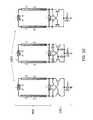
- FIG. 1illustrates a parallel plate transmission line according to an embodiment of the invention
- FIG. 2shows a quarter lambda ( ⁇ /4) transformer and a capacitor, both comprising the parallel plate transmission lines according to an embodiment of the invention
- FIG. 3shows a transmission line resonator according to an embodiment of the invention
- FIG. 4illustrates exemplary arrangements of the transmission lines of the resonator according to embodiments of the invention
- FIG. 5depicts a fixed frequency oscillator according to an embodiment of the invention
- FIG. 6illustrates exemplary oscillators according to different embodiments of the invention
- FIG. 7depicts a variable frequency transmission line resonator including tunable capacitors according to an embodiment of the invention
- FIG. 8illustrates exemplary oscillators including tunable capacitors according to embodiments of the invention
- FIG. 9depicts a variable frequency transmission line resonator including tunable inductors according to an embodiment of the invention.
- FIG. 10illustrates exemplary oscillators including tunable inductors according to embodiments of the invention
- FIG. 11shows quadrature oscillators according to embodiments of the invention.
- FIG. 12is a block diagram of an on-off keying receiver including the oscillator according to embodiments of the invention.
- FIG. 13is a block diagram of radios that include an oscillator according to an embodiment of the invention.
- FIG. 14is a block diagram of a mm-wave digital phase locked loop (PLL) that includes an oscillator according to an embodiment of the invention
- FIG. 15is a block diagram of oscillators according to an embodiment of the invention that may be used in a terahertz (THz) source; and
- FIG. 16is a process flow of a method of fabricating an oscillator according to embodiments described herein.
- a VCOincludes a resonator in which a capacitor and inductor resonate to give the frequency of oscillation when provided with energy.
- Sources of inaccuracycan change the oscillation frequency.
- One source of inaccuracyis an inconsistency in the dimensions of the capacitor and inductor in the manufacturing.
- Embodiments of the resonator described hereinprovide a frequency of oscillation that is referenced to the speed of light and is independent of at least one dimension and up to two dimensions.
- FIG. 1illustrates a parallel plate transmission line 100 according to an embodiment of the invention.
- the transmission line 100 shown in FIG. 1is a building block of the resonator 300 (see e.g., FIG. 3 ) according to embodiments of the invention.
- the transmission line 100includes two metal plates 110 a , 110 b arranged in parallel with a dielectric material 120 separating them.
- the dimensions of the transmission line 100are given by a length (l), width (w), and depth of the dielectric material 120 (d) which is the distance of separation between the two metal plates 110 a , 110 b .
- the resistance of the transmission line 100 (R Line )is given by:
- R Line2 w * ⁇ cond * ⁇ [ EQ . ⁇ 1 ]
- wis the width of the transmission line metal plates 110 a and 110 b as shown in FIG. 1
- ⁇ condis the conductance of the metal plates 110 a , 110 b
- ⁇is the skin effect, which is given by:
- FIG. 2shows a quarter lambda ( ⁇ /4) transformer 200 and a capacitor C 220 , both comprising the parallel plate transmission lines 100 according to an embodiment of the invention.
- the quarter lambda transformer 200forms the inductor of the resonator 300 (see e.g., FIG. 3 ).
- the quarter lambda transformer 200comprises three transmission lines 100 as shown and discussed with reference to FIG. 1 , the metal plate 110 a of each being visible in FIG. 2 .
- the width (w) and depth (d) of each of the transmission lines 100 shown in FIG. 2are assumed to be the same.
- the length (l) of the waveguides 210is a quarter of the wavelength corresponding to the transmission frequency, and the length of capacitor C 220 is given by lcap (capacitor C 220 and the corresponding capacitance C are both references with C).
- the input impedance (230) Z inis given by:
- FIG. 3shows a transmission line resonator 300 according to an embodiment of the invention.
- the resonator 300includes the quarter lambda transformer 200 shown in FIG. 2 , which acts as the inductor of the resonator 300 with inductance indicated by EQ. 10.
- the resonator 300also includes the capacitor C 1 310 , which acts as the capacitor of the resonator 300 with a capacitance given by:
- the frequency of oscillation of the resonator 300is referenced to the speed of light (c) and is independent of the width and depth of the transmission lines 100 that make up the resonator 300 . Instead, the oscillation frequency depends on the lengths (l and l 1 ) corresponding with the capacitors C 220 and C 1 310 and the material properties ( ⁇ r and ⁇ r ) of the metal plates 110 a of the transmission lines 100 .
- the precision with which the oscillation frequency is attaineddepends on the precision of the mask involved in the processing of the integrated circuit.
- the precision of the oscillation frequencyis represented by a variation ( ⁇ f osc ) in the frequency of oscillation and is given by:
- ⁇ ⁇ ⁇ f osc f osc- 1 2 ⁇ ( ⁇ ⁇ ⁇ l l + ⁇ ⁇ ⁇ l 1 l 1 ) [ EQ . ⁇ 14 ]
- FIG. 4illustrates exemplary arrangements of the transmission lines 100 of the resonator 300 according to embodiments of the invention.
- the length of the waveguides 210are always a quarter of the wavelength corresponding with the oscillation frequency. However, that length ( ⁇ /4) may be implemented in a stepped fashion in some embodiments and as a straight line in other embodiments, as shown in FIG. 4 .
- the overall length of the waveguides 210 according to any of the arrangementsis a quarter of the wavelength corresponding with the oscillation frequency (the inductor of the resonator 300 is implemented as a quarter lambda transformer) and the oscillation frequency of the resonator 300 depends only on the lengths (l and l 1 ) of the capacitors C 220 and C 1 310 , respectively.
- FIG. 5depicts a fixed frequency oscillator 500 according to an embodiment of the invention.
- the oscillator 500includes the resonator 300 comprised of the transmission lines 100 and a negative resistance 510 ( ⁇ R N ).
- the negative resistance 510 ( ⁇ R N )essentially creates a resonator 300 with no damping and can be thought of as adding energy to the system. If the oscillation loss of the resonator 300 were modeled as a resistance (R), then the negative resistance 510 ( ⁇ R N ) cancels out the resistance (R).
- FIG. 6illustrates exemplary fixed frequency oscillators 500 according to different embodiments of the invention.
- FIG. 6shows three different exemplary topologies of the oscillator 500 with three different implementations of the negative resistance 510 ( ⁇ R N ).
- Each of the exemplary topologies of the oscillator 500also includes the application of a bias voltage resulting in the bias current 610 .
- the oscillators 500may be used in CMOS or bipolar transistor applications.
- FIG. 7depicts a variable frequency transmission line 100 resonator 700 including tunable capacitors (C 710 and C 1 720 ) according to an embodiment of the invention.
- the resonator 700 of FIG. 7is implemented using transmission lines 100 .
- the resonator 700has a tunable oscillation frequency as discussed below.
- the capacitors (C 710 and C 1 720 ) of the resonator 700may be implemented as variable capacitors with variable lengths (l 7 and l 7-1 , respectively). Because the oscillation frequency depends on the lengths (l 7 and l 7-1 ) of the capacitors (C 710 and C 1 720 ) as shown in EQ.
- the oscillation frequencyvaries as the lengths (l 7 and l 7-1 ) vary.
- exemplary lengths (l 7 ) for the transmission line 100 making up the capacitor C 710 of the quarter lambda transformer (inductor of the resonator 700 )may be within a range d 0 through d 5 with any number of incremental values in between.
- Exemplary lengths (l 7-1 ) for the transmission line 100 making up the capacitor C 1 720 of the resonator 700may be within a range b 0 through b 5 .
- One or both of the lengths (l 7 and l 7-1 )may be changed at one time to adjust the oscillator frequency.
- the capacitors (C 710 and C 1 720 )may be tuned digitally.
- FIG. 8illustrates exemplary oscillators 800 including tunable capacitors according to embodiments of the invention.
- the three different exemplary topologies of the oscillators 800 shown in FIG. 8include tunable capacitors (C 220 and C 1 310 ) such that the oscillators 800 have tunable oscillation frequencies.
- FIG. 8shows three different exemplary implementations of the negative resistance 510 ( ⁇ R N ).
- the three implementations of the negative resistance 510 ( ⁇ R N ) shown in FIG. 8 for the tunable oscillation frequency oscillators 800are the same as those shown in FIG. 6 for the fixed oscillation frequency oscillators 500 .
- FIG. 9depicts a variable frequency transmission line 100 resonator 900 including tunable inductors (L 910 and L 1 920 ) according to an embodiment of the invention.
- the resonator 900includes inductors L 910 and L 1 920 that have respective tunable lengths l 9 and l 9-1 .
- the relationship between inductance of the inductor L 910 and capacitanceis given by EQ. 7 above and depends on the impedance Z 0 of the transmission lines 100 making up the waveguides 210 .
- the length (l 9 and l 9-1 ) of the inductors (L 910 and L 1 920 )may be adjusted individually or collectively to adjust the oscillation frequency of the resonator 900 .
- the resonator 900 of FIG. 9is tunable with two independent inputs (i.e., inductor L 910 and L 1 920 lengths l 9 and l 9-1 ).
- FIG. 10illustrates exemplary oscillators 1000 including tunable inductors (L 910 and L 1 920 ) according to embodiments of the invention.
- the three different exemplary topologies of the oscillators 1000 shown in FIG. 10include tunable inductors (L 910 and L 1 920 ) such that the oscillators 1000 have tunable oscillation frequencies.
- FIG. 10shows three different exemplary implementations of the negative resistance 510 ( ⁇ R N ).
- the three implementations of the negative resistance 510 ( ⁇ R N ) shown in FIG. 10 for the tunable oscillation frequency oscillators 1000are the same as those shown in FIG. 6 (for the fixed oscillation frequency oscillators 500 ) and FIG. 8 (for the tunable oscillation frequency oscillators 700 ).
- FIG. 11shows quadrature oscillators 1110 , 1120 according to embodiments of the invention.
- Each of the quadrature oscillators 1110 , 1120has a symmetric structure with an exemplary implementation of the negative resistance 510 ( ⁇ R N ) on each side of the resonator 1105 , 1115 .
- the resonators 1105 , 1115include the waveguides 210 .
- the other two transmission lines 100may be capacitors ( 220 , 310 ), as discussed with reference to FIG.
- the resonators 1105 , 1115may be fabricated according to any of the embodiments discussed above. As such, the resonators 1105 , 1115 have a quadrature oscillation frequency that is referenced to the speed of light and is independent of with width (w) and depth (d) of the transmission lines 100 that comprise the resonators 1105 , 1115 (see e.g., EQ. 12). Each of the resonators 1105 , 1115 shows biasing, through quarter wavelength lines 1150 , of the transmission lines 1130 , 1140 (in resonator 1106 ) or the waveguides 210 (in resonator 1115 ).
- FIG. 12is a block diagram of an on-off keying (OOK) receiver 1200 including the oscillator ( 500 , 800 , 1000 ) according to embodiments of the invention.
- OOKon-off keying
- the oscillator 500may provide the quench signal.
- the oscillator 500 in this applicationmay be generated with an on-chip reference based on a fixed resonator voltage controlled oscillator without an external crystal oscillator.
- FIG. 13is a block diagram of radios 1300 that include an oscillator 800 according to an embodiment of the invention.
- the oscillator 800may be used as a reference for crystal-less radios 1300 .
- the slave device 1310has no crystal (like the crystal 1320 of the master device 1330 ).
- the OOK receiver 1340is always on.
- the phase locked loop (PLL) 1350switches to the external reference (f REF ) from the OOK receiver 1340 .
- the PLL 1350takes the reference from the on-chip oscillator 800 .
- the slave device 1310locks to the master device 1330 immediately because the PLL 1350 acquires reference frequency (f REF ) information from the beacon and the difference between f REF and f RES (the frequency from the oscillator 800 ) is very small.
- the pull-in time for the PLL 1350to switch from f RES to f REF is very small).
- FIG. 14is a block diagram of a millimeter wave (mm-wave) digital PLL 1400 that includes an oscillator 800 according to an embodiment of the invention.
- the up/down converter 1410detects the sign of the time-to-digital converter (TDC) 1420 .
- the divider 1430works at mm-waves and may be realized with resonant loads.
- FIG. 15is a block diagram of oscillators 1000 according to an embodiment of the invention that may be used in a THz source 1500 .
- FIG. 16is a process flow of a method of fabricating an oscillator ( 500 , 800 , 1000 , 1110 , 1120 ) according to embodiments described herein.
- arranging transmission lines 100 to form a resonatormay be according to the various embodiments described above.
- the transmission lines 100 used as waveguides 210may be combined with a fixed-length capacitor (C 220 ) or variable-length capacitor (C 710 ) or variable-length inductor (L 910 ) and the resonator additionally includes a fixed-length capacitor (C 1 310 ) or variable-length capacitor (C 1 720 ) or variable-length inductor (L 1 920 ).
- adjusting the length to tune the frequency of oscillationincludes adjusting the capacitor (C 220 , 710 ) or inductor (L 710 ), adjusting the capacitor (C 1 310 , 720 ) or inductor (L 1 920 ), or both as discussed with reference to FIGS. 7 and 9 .
- arranging one or more energy sources (negative resistance 510 ) for the resonator ( 300 , 700 , 900 , 1105 , 1115 ) arranged according to blocks 1610 and, optionally, 1620may include providing a single energy source to obtain an oscillator ( 500 , 800 , 1000 ) or two symmetric energy sources to obtain a quadratic oscillator ( 1110 , 1120 ).
Landscapes
- Inductance-Capacitance Distribution Constants And Capacitance-Resistance Oscillators (AREA)
Abstract
Description
where w is the width of the transmission
where ω is the frequency of the
Where d is the distance between the transmission
where ε0*εris the total dielectric constant. As EQ. 4 indicates, the capacitance increases as the width of the transmission
where the impedance of the
L=Z02*C [EQ. 7]
According to EQ. 4, which provides the capacitance per unit length, the capacitance C may also be written as:
In addition, the impedance of the
By substituting the
where l1is the length of the
where the speed of light (c) is given by:
As EQ. 12 illustrates, the frequency of oscillation of the
Claims (9)
Priority Applications (2)
| Application Number | Priority Date | Filing Date | Title |
|---|---|---|---|
| US14/036,205US9172326B2 (en) | 2013-09-25 | 2013-09-25 | Speed of light based oscillator frequency |
| US14/154,247US9190953B2 (en) | 2013-09-25 | 2014-01-14 | Speed of light based oscillator frequency |
Applications Claiming Priority (1)
| Application Number | Priority Date | Filing Date | Title |
|---|---|---|---|
| US14/036,205US9172326B2 (en) | 2013-09-25 | 2013-09-25 | Speed of light based oscillator frequency |
Related Child Applications (1)
| Application Number | Title | Priority Date | Filing Date |
|---|---|---|---|
| US14/154,247ContinuationUS9190953B2 (en) | 2013-09-25 | 2014-01-14 | Speed of light based oscillator frequency |
Publications (2)
| Publication Number | Publication Date |
|---|---|
| US20150084703A1 US20150084703A1 (en) | 2015-03-26 |
| US9172326B2true US9172326B2 (en) | 2015-10-27 |
Family
ID=52690441
Family Applications (2)
| Application Number | Title | Priority Date | Filing Date |
|---|---|---|---|
| US14/036,205Active2033-11-20US9172326B2 (en) | 2013-09-25 | 2013-09-25 | Speed of light based oscillator frequency |
| US14/154,247ActiveUS9190953B2 (en) | 2013-09-25 | 2014-01-14 | Speed of light based oscillator frequency |
Family Applications After (1)
| Application Number | Title | Priority Date | Filing Date |
|---|---|---|---|
| US14/154,247ActiveUS9190953B2 (en) | 2013-09-25 | 2014-01-14 | Speed of light based oscillator frequency |
Country Status (1)
| Country | Link |
|---|---|
| US (2) | US9172326B2 (en) |
Cited By (1)
| Publication number | Priority date | Publication date | Assignee | Title |
|---|---|---|---|---|
| US11303245B2 (en) | 2020-05-08 | 2022-04-12 | International Business Machines Corporation | Phase noise reduction using triple-coil transformer coupling |
Families Citing this family (154)
| Publication number | Priority date | Publication date | Assignee | Title |
|---|---|---|---|---|
| US10009065B2 (en) | 2012-12-05 | 2018-06-26 | At&T Intellectual Property I, L.P. | Backhaul link for distributed antenna system |
| US9113347B2 (en) | 2012-12-05 | 2015-08-18 | At&T Intellectual Property I, Lp | Backhaul link for distributed antenna system |
| US9525524B2 (en) | 2013-05-31 | 2016-12-20 | At&T Intellectual Property I, L.P. | Remote distributed antenna system |
| US9999038B2 (en) | 2013-05-31 | 2018-06-12 | At&T Intellectual Property I, L.P. | Remote distributed antenna system |
| US8897697B1 (en) | 2013-11-06 | 2014-11-25 | At&T Intellectual Property I, Lp | Millimeter-wave surface-wave communications |
| US9209902B2 (en) | 2013-12-10 | 2015-12-08 | At&T Intellectual Property I, L.P. | Quasi-optical coupler |
| US9692101B2 (en) | 2014-08-26 | 2017-06-27 | At&T Intellectual Property I, L.P. | Guided wave couplers for coupling electromagnetic waves between a waveguide surface and a surface of a wire |
| US9768833B2 (en) | 2014-09-15 | 2017-09-19 | At&T Intellectual Property I, L.P. | Method and apparatus for sensing a condition in a transmission medium of electromagnetic waves |
| US10063280B2 (en) | 2014-09-17 | 2018-08-28 | At&T Intellectual Property I, L.P. | Monitoring and mitigating conditions in a communication network |
| US9615269B2 (en) | 2014-10-02 | 2017-04-04 | At&T Intellectual Property I, L.P. | Method and apparatus that provides fault tolerance in a communication network |
| US9685992B2 (en) | 2014-10-03 | 2017-06-20 | At&T Intellectual Property I, L.P. | Circuit panel network and methods thereof |
| US9503189B2 (en) | 2014-10-10 | 2016-11-22 | At&T Intellectual Property I, L.P. | Method and apparatus for arranging communication sessions in a communication system |
| US9973299B2 (en) | 2014-10-14 | 2018-05-15 | At&T Intellectual Property I, L.P. | Method and apparatus for adjusting a mode of communication in a communication network |
| US9762289B2 (en) | 2014-10-14 | 2017-09-12 | At&T Intellectual Property I, L.P. | Method and apparatus for transmitting or receiving signals in a transportation system |
| US9780834B2 (en) | 2014-10-21 | 2017-10-03 | At&T Intellectual Property I, L.P. | Method and apparatus for transmitting electromagnetic waves |
| US9769020B2 (en) | 2014-10-21 | 2017-09-19 | At&T Intellectual Property I, L.P. | Method and apparatus for responding to events affecting communications in a communication network |
| US9577306B2 (en) | 2014-10-21 | 2017-02-21 | At&T Intellectual Property I, L.P. | Guided-wave transmission device and methods for use therewith |
| US9312919B1 (en) | 2014-10-21 | 2016-04-12 | At&T Intellectual Property I, Lp | Transmission device with impairment compensation and methods for use therewith |
| US9520945B2 (en) | 2014-10-21 | 2016-12-13 | At&T Intellectual Property I, L.P. | Apparatus for providing communication services and methods thereof |
| US9653770B2 (en) | 2014-10-21 | 2017-05-16 | At&T Intellectual Property I, L.P. | Guided wave coupler, coupling module and methods for use therewith |
| US9627768B2 (en) | 2014-10-21 | 2017-04-18 | At&T Intellectual Property I, L.P. | Guided-wave transmission device with non-fundamental mode propagation and methods for use therewith |
| US10340573B2 (en) | 2016-10-26 | 2019-07-02 | At&T Intellectual Property I, L.P. | Launcher with cylindrical coupling device and methods for use therewith |
| US9680670B2 (en) | 2014-11-20 | 2017-06-13 | At&T Intellectual Property I, L.P. | Transmission device with channel equalization and control and methods for use therewith |
| US10243784B2 (en) | 2014-11-20 | 2019-03-26 | At&T Intellectual Property I, L.P. | System for generating topology information and methods thereof |
| US9997819B2 (en) | 2015-06-09 | 2018-06-12 | At&T Intellectual Property I, L.P. | Transmission medium and method for facilitating propagation of electromagnetic waves via a core |
| US10009067B2 (en) | 2014-12-04 | 2018-06-26 | At&T Intellectual Property I, L.P. | Method and apparatus for configuring a communication interface |
| US9461706B1 (en) | 2015-07-31 | 2016-10-04 | At&T Intellectual Property I, Lp | Method and apparatus for exchanging communication signals |
| US9654173B2 (en) | 2014-11-20 | 2017-05-16 | At&T Intellectual Property I, L.P. | Apparatus for powering a communication device and methods thereof |
| US9800327B2 (en) | 2014-11-20 | 2017-10-24 | At&T Intellectual Property I, L.P. | Apparatus for controlling operations of a communication device and methods thereof |
| US9954287B2 (en) | 2014-11-20 | 2018-04-24 | At&T Intellectual Property I, L.P. | Apparatus for converting wireless signals and electromagnetic waves and methods thereof |
| US9544006B2 (en) | 2014-11-20 | 2017-01-10 | At&T Intellectual Property I, L.P. | Transmission device with mode division multiplexing and methods for use therewith |
| US9742462B2 (en) | 2014-12-04 | 2017-08-22 | At&T Intellectual Property I, L.P. | Transmission medium and communication interfaces and methods for use therewith |
| US10144036B2 (en) | 2015-01-30 | 2018-12-04 | At&T Intellectual Property I, L.P. | Method and apparatus for mitigating interference affecting a propagation of electromagnetic waves guided by a transmission medium |
| US9876570B2 (en) | 2015-02-20 | 2018-01-23 | At&T Intellectual Property I, Lp | Guided-wave transmission device with non-fundamental mode propagation and methods for use therewith |
| US10587223B2 (en)* | 2015-02-20 | 2020-03-10 | Cornell University | Device for terahertz signal generation and transmitter |
| US9749013B2 (en) | 2015-03-17 | 2017-08-29 | At&T Intellectual Property I, L.P. | Method and apparatus for reducing attenuation of electromagnetic waves guided by a transmission medium |
| US9705561B2 (en) | 2015-04-24 | 2017-07-11 | At&T Intellectual Property I, L.P. | Directional coupling device and methods for use therewith |
| US10224981B2 (en)* | 2015-04-24 | 2019-03-05 | At&T Intellectual Property I, Lp | Passive electrical coupling device and methods for use therewith |
| US9793954B2 (en) | 2015-04-28 | 2017-10-17 | At&T Intellectual Property I, L.P. | Magnetic coupling device and methods for use therewith |
| US9948354B2 (en) | 2015-04-28 | 2018-04-17 | At&T Intellectual Property I, L.P. | Magnetic coupling device with reflective plate and methods for use therewith |
| US9871282B2 (en) | 2015-05-14 | 2018-01-16 | At&T Intellectual Property I, L.P. | At least one transmission medium having a dielectric surface that is covered at least in part by a second dielectric |
| US9748626B2 (en) | 2015-05-14 | 2017-08-29 | At&T Intellectual Property I, L.P. | Plurality of cables having different cross-sectional shapes which are bundled together to form a transmission medium |
| US9490869B1 (en) | 2015-05-14 | 2016-11-08 | At&T Intellectual Property I, L.P. | Transmission medium having multiple cores and methods for use therewith |
| US10650940B2 (en) | 2015-05-15 | 2020-05-12 | At&T Intellectual Property I, L.P. | Transmission medium having a conductive material and methods for use therewith |
| US9917341B2 (en) | 2015-05-27 | 2018-03-13 | At&T Intellectual Property I, L.P. | Apparatus and method for launching electromagnetic waves and for modifying radial dimensions of the propagating electromagnetic waves |
| US9866309B2 (en) | 2015-06-03 | 2018-01-09 | At&T Intellectual Property I, Lp | Host node device and methods for use therewith |
| US10103801B2 (en) | 2015-06-03 | 2018-10-16 | At&T Intellectual Property I, L.P. | Host node device and methods for use therewith |
| US10812174B2 (en) | 2015-06-03 | 2020-10-20 | At&T Intellectual Property I, L.P. | Client node device and methods for use therewith |
| US9912381B2 (en) | 2015-06-03 | 2018-03-06 | At&T Intellectual Property I, Lp | Network termination and methods for use therewith |
| US9913139B2 (en) | 2015-06-09 | 2018-03-06 | At&T Intellectual Property I, L.P. | Signal fingerprinting for authentication of communicating devices |
| US10142086B2 (en) | 2015-06-11 | 2018-11-27 | At&T Intellectual Property I, L.P. | Repeater and methods for use therewith |
| US9608692B2 (en) | 2015-06-11 | 2017-03-28 | At&T Intellectual Property I, L.P. | Repeater and methods for use therewith |
| US9820146B2 (en) | 2015-06-12 | 2017-11-14 | At&T Intellectual Property I, L.P. | Method and apparatus for authentication and identity management of communicating devices |
| US9667317B2 (en) | 2015-06-15 | 2017-05-30 | At&T Intellectual Property I, L.P. | Method and apparatus for providing security using network traffic adjustments |
| US9640850B2 (en) | 2015-06-25 | 2017-05-02 | At&T Intellectual Property I, L.P. | Methods and apparatus for inducing a non-fundamental wave mode on a transmission medium |
| US9509415B1 (en) | 2015-06-25 | 2016-11-29 | At&T Intellectual Property I, L.P. | Methods and apparatus for inducing a fundamental wave mode on a transmission medium |
| US9865911B2 (en) | 2015-06-25 | 2018-01-09 | At&T Intellectual Property I, L.P. | Waveguide system for slot radiating first electromagnetic waves that are combined into a non-fundamental wave mode second electromagnetic wave on a transmission medium |
| US10341142B2 (en) | 2015-07-14 | 2019-07-02 | At&T Intellectual Property I, L.P. | Apparatus and methods for generating non-interfering electromagnetic waves on an uninsulated conductor |
| US10148016B2 (en) | 2015-07-14 | 2018-12-04 | At&T Intellectual Property I, L.P. | Apparatus and methods for communicating utilizing an antenna array |
| US10170840B2 (en) | 2015-07-14 | 2019-01-01 | At&T Intellectual Property I, L.P. | Apparatus and methods for sending or receiving electromagnetic signals |
| US10044409B2 (en) | 2015-07-14 | 2018-08-07 | At&T Intellectual Property I, L.P. | Transmission medium and methods for use therewith |
| US9853342B2 (en) | 2015-07-14 | 2017-12-26 | At&T Intellectual Property I, L.P. | Dielectric transmission medium connector and methods for use therewith |
| US9836957B2 (en) | 2015-07-14 | 2017-12-05 | At&T Intellectual Property I, L.P. | Method and apparatus for communicating with premises equipment |
| US10205655B2 (en) | 2015-07-14 | 2019-02-12 | At&T Intellectual Property I, L.P. | Apparatus and methods for communicating utilizing an antenna array and multiple communication paths |
| US10320586B2 (en) | 2015-07-14 | 2019-06-11 | At&T Intellectual Property I, L.P. | Apparatus and methods for generating non-interfering electromagnetic waves on an insulated transmission medium |
| US9628116B2 (en) | 2015-07-14 | 2017-04-18 | At&T Intellectual Property I, L.P. | Apparatus and methods for transmitting wireless signals |
| US9882257B2 (en) | 2015-07-14 | 2018-01-30 | At&T Intellectual Property I, L.P. | Method and apparatus for launching a wave mode that mitigates interference |
| US9847566B2 (en) | 2015-07-14 | 2017-12-19 | At&T Intellectual Property I, L.P. | Method and apparatus for adjusting a field of a signal to mitigate interference |
| US9722318B2 (en) | 2015-07-14 | 2017-08-01 | At&T Intellectual Property I, L.P. | Method and apparatus for coupling an antenna to a device |
| US10033108B2 (en) | 2015-07-14 | 2018-07-24 | At&T Intellectual Property I, L.P. | Apparatus and methods for generating an electromagnetic wave having a wave mode that mitigates interference |
| US10033107B2 (en) | 2015-07-14 | 2018-07-24 | At&T Intellectual Property I, L.P. | Method and apparatus for coupling an antenna to a device |
| US9793951B2 (en) | 2015-07-15 | 2017-10-17 | At&T Intellectual Property I, L.P. | Method and apparatus for launching a wave mode that mitigates interference |
| US10090606B2 (en) | 2015-07-15 | 2018-10-02 | At&T Intellectual Property I, L.P. | Antenna system with dielectric array and methods for use therewith |
| US9608740B2 (en) | 2015-07-15 | 2017-03-28 | At&T Intellectual Property I, L.P. | Method and apparatus for launching a wave mode that mitigates interference |
| US9948333B2 (en) | 2015-07-23 | 2018-04-17 | At&T Intellectual Property I, L.P. | Method and apparatus for wireless communications to mitigate interference |
| US10784670B2 (en) | 2015-07-23 | 2020-09-22 | At&T Intellectual Property I, L.P. | Antenna support for aligning an antenna |
| US9912027B2 (en) | 2015-07-23 | 2018-03-06 | At&T Intellectual Property I, L.P. | Method and apparatus for exchanging communication signals |
| US9871283B2 (en) | 2015-07-23 | 2018-01-16 | At&T Intellectual Property I, Lp | Transmission medium having a dielectric core comprised of plural members connected by a ball and socket configuration |
| US9749053B2 (en) | 2015-07-23 | 2017-08-29 | At&T Intellectual Property I, L.P. | Node device, repeater and methods for use therewith |
| US9735833B2 (en) | 2015-07-31 | 2017-08-15 | At&T Intellectual Property I, L.P. | Method and apparatus for communications management in a neighborhood network |
| US9967173B2 (en) | 2015-07-31 | 2018-05-08 | At&T Intellectual Property I, L.P. | Method and apparatus for authentication and identity management of communicating devices |
| US10020587B2 (en) | 2015-07-31 | 2018-07-10 | At&T Intellectual Property I, L.P. | Radial antenna and methods for use therewith |
| US9904535B2 (en) | 2015-09-14 | 2018-02-27 | At&T Intellectual Property I, L.P. | Method and apparatus for distributing software |
| US10009901B2 (en) | 2015-09-16 | 2018-06-26 | At&T Intellectual Property I, L.P. | Method, apparatus, and computer-readable storage medium for managing utilization of wireless resources between base stations |
| US10136434B2 (en) | 2015-09-16 | 2018-11-20 | At&T Intellectual Property I, L.P. | Method and apparatus for use with a radio distributed antenna system having an ultra-wideband control channel |
| US10009063B2 (en) | 2015-09-16 | 2018-06-26 | At&T Intellectual Property I, L.P. | Method and apparatus for use with a radio distributed antenna system having an out-of-band reference signal |
| US10079661B2 (en) | 2015-09-16 | 2018-09-18 | At&T Intellectual Property I, L.P. | Method and apparatus for use with a radio distributed antenna system having a clock reference |
| US9769128B2 (en) | 2015-09-28 | 2017-09-19 | At&T Intellectual Property I, L.P. | Method and apparatus for encryption of communications over a network |
| US9729197B2 (en) | 2015-10-01 | 2017-08-08 | At&T Intellectual Property I, L.P. | Method and apparatus for communicating network management traffic over a network |
| US9876264B2 (en) | 2015-10-02 | 2018-01-23 | At&T Intellectual Property I, Lp | Communication system, guided wave switch and methods for use therewith |
| US9882277B2 (en) | 2015-10-02 | 2018-01-30 | At&T Intellectual Property I, Lp | Communication device and antenna assembly with actuated gimbal mount |
| US10665942B2 (en) | 2015-10-16 | 2020-05-26 | At&T Intellectual Property I, L.P. | Method and apparatus for adjusting wireless communications |
| US10355367B2 (en) | 2015-10-16 | 2019-07-16 | At&T Intellectual Property I, L.P. | Antenna structure for exchanging wireless signals |
| US9912419B1 (en) | 2016-08-24 | 2018-03-06 | At&T Intellectual Property I, L.P. | Method and apparatus for managing a fault in a distributed antenna system |
| US9860075B1 (en) | 2016-08-26 | 2018-01-02 | At&T Intellectual Property I, L.P. | Method and communication node for broadband distribution |
| US10291311B2 (en) | 2016-09-09 | 2019-05-14 | At&T Intellectual Property I, L.P. | Method and apparatus for mitigating a fault in a distributed antenna system |
| US11032819B2 (en) | 2016-09-15 | 2021-06-08 | At&T Intellectual Property I, L.P. | Method and apparatus for use with a radio distributed antenna system having a control channel reference signal |
| US10340600B2 (en) | 2016-10-18 | 2019-07-02 | At&T Intellectual Property I, L.P. | Apparatus and methods for launching guided waves via plural waveguide systems |
| US10135147B2 (en) | 2016-10-18 | 2018-11-20 | At&T Intellectual Property I, L.P. | Apparatus and methods for launching guided waves via an antenna |
| US10135146B2 (en) | 2016-10-18 | 2018-11-20 | At&T Intellectual Property I, L.P. | Apparatus and methods for launching guided waves via circuits |
| US10374316B2 (en) | 2016-10-21 | 2019-08-06 | At&T Intellectual Property I, L.P. | System and dielectric antenna with non-uniform dielectric |
| US9991580B2 (en) | 2016-10-21 | 2018-06-05 | At&T Intellectual Property I, L.P. | Launcher and coupling system for guided wave mode cancellation |
| US9876605B1 (en) | 2016-10-21 | 2018-01-23 | At&T Intellectual Property I, L.P. | Launcher and coupling system to support desired guided wave mode |
| US10811767B2 (en) | 2016-10-21 | 2020-10-20 | At&T Intellectual Property I, L.P. | System and dielectric antenna with convex dielectric radome |
| US10312567B2 (en) | 2016-10-26 | 2019-06-04 | At&T Intellectual Property I, L.P. | Launcher with planar strip antenna and methods for use therewith |
| US10498044B2 (en) | 2016-11-03 | 2019-12-03 | At&T Intellectual Property I, L.P. | Apparatus for configuring a surface of an antenna |
| US10224634B2 (en) | 2016-11-03 | 2019-03-05 | At&T Intellectual Property I, L.P. | Methods and apparatus for adjusting an operational characteristic of an antenna |
| US10291334B2 (en) | 2016-11-03 | 2019-05-14 | At&T Intellectual Property I, L.P. | System for detecting a fault in a communication system |
| US10225025B2 (en) | 2016-11-03 | 2019-03-05 | At&T Intellectual Property I, L.P. | Method and apparatus for detecting a fault in a communication system |
| US10340601B2 (en) | 2016-11-23 | 2019-07-02 | At&T Intellectual Property I, L.P. | Multi-antenna system and methods for use therewith |
| US10090594B2 (en) | 2016-11-23 | 2018-10-02 | At&T Intellectual Property I, L.P. | Antenna system having structural configurations for assembly |
| US10178445B2 (en) | 2016-11-23 | 2019-01-08 | At&T Intellectual Property I, L.P. | Methods, devices, and systems for load balancing between a plurality of waveguides |
| US10535928B2 (en) | 2016-11-23 | 2020-01-14 | At&T Intellectual Property I, L.P. | Antenna system and methods for use therewith |
| US10340603B2 (en) | 2016-11-23 | 2019-07-02 | At&T Intellectual Property I, L.P. | Antenna system having shielded structural configurations for assembly |
| US10305190B2 (en) | 2016-12-01 | 2019-05-28 | At&T Intellectual Property I, L.P. | Reflecting dielectric antenna system and methods for use therewith |
| US10361489B2 (en) | 2016-12-01 | 2019-07-23 | At&T Intellectual Property I, L.P. | Dielectric dish antenna system and methods for use therewith |
| US10020844B2 (en) | 2016-12-06 | 2018-07-10 | T&T Intellectual Property I, L.P. | Method and apparatus for broadcast communication via guided waves |
| US9927517B1 (en) | 2016-12-06 | 2018-03-27 | At&T Intellectual Property I, L.P. | Apparatus and methods for sensing rainfall |
| US10439675B2 (en) | 2016-12-06 | 2019-10-08 | At&T Intellectual Property I, L.P. | Method and apparatus for repeating guided wave communication signals |
| US10727599B2 (en) | 2016-12-06 | 2020-07-28 | At&T Intellectual Property I, L.P. | Launcher with slot antenna and methods for use therewith |
| US10755542B2 (en) | 2016-12-06 | 2020-08-25 | At&T Intellectual Property I, L.P. | Method and apparatus for surveillance via guided wave communication |
| US10637149B2 (en) | 2016-12-06 | 2020-04-28 | At&T Intellectual Property I, L.P. | Injection molded dielectric antenna and methods for use therewith |
| US10819035B2 (en) | 2016-12-06 | 2020-10-27 | At&T Intellectual Property I, L.P. | Launcher with helical antenna and methods for use therewith |
| US10326494B2 (en) | 2016-12-06 | 2019-06-18 | At&T Intellectual Property I, L.P. | Apparatus for measurement de-embedding and methods for use therewith |
| US10135145B2 (en) | 2016-12-06 | 2018-11-20 | At&T Intellectual Property I, L.P. | Apparatus and methods for generating an electromagnetic wave along a transmission medium |
| US10382976B2 (en) | 2016-12-06 | 2019-08-13 | At&T Intellectual Property I, L.P. | Method and apparatus for managing wireless communications based on communication paths and network device positions |
| US10694379B2 (en) | 2016-12-06 | 2020-06-23 | At&T Intellectual Property I, L.P. | Waveguide system with device-based authentication and methods for use therewith |
| US10168695B2 (en) | 2016-12-07 | 2019-01-01 | At&T Intellectual Property I, L.P. | Method and apparatus for controlling an unmanned aircraft |
| US10446936B2 (en) | 2016-12-07 | 2019-10-15 | At&T Intellectual Property I, L.P. | Multi-feed dielectric antenna system and methods for use therewith |
| US10359749B2 (en) | 2016-12-07 | 2019-07-23 | At&T Intellectual Property I, L.P. | Method and apparatus for utilities management via guided wave communication |
| US10243270B2 (en) | 2016-12-07 | 2019-03-26 | At&T Intellectual Property I, L.P. | Beam adaptive multi-feed dielectric antenna system and methods for use therewith |
| US10027397B2 (en) | 2016-12-07 | 2018-07-17 | At&T Intellectual Property I, L.P. | Distributed antenna system and methods for use therewith |
| US9893795B1 (en) | 2016-12-07 | 2018-02-13 | At&T Intellectual Property I, Lp | Method and repeater for broadband distribution |
| US10139820B2 (en) | 2016-12-07 | 2018-11-27 | At&T Intellectual Property I, L.P. | Method and apparatus for deploying equipment of a communication system |
| US10389029B2 (en) | 2016-12-07 | 2019-08-20 | At&T Intellectual Property I, L.P. | Multi-feed dielectric antenna system with core selection and methods for use therewith |
| US10547348B2 (en) | 2016-12-07 | 2020-01-28 | At&T Intellectual Property I, L.P. | Method and apparatus for switching transmission mediums in a communication system |
| US10389037B2 (en) | 2016-12-08 | 2019-08-20 | At&T Intellectual Property I, L.P. | Apparatus and methods for selecting sections of an antenna array and use therewith |
| US10326689B2 (en) | 2016-12-08 | 2019-06-18 | At&T Intellectual Property I, L.P. | Method and system for providing alternative communication paths |
| US10103422B2 (en) | 2016-12-08 | 2018-10-16 | At&T Intellectual Property I, L.P. | Method and apparatus for mounting network devices |
| US10530505B2 (en) | 2016-12-08 | 2020-01-07 | At&T Intellectual Property I, L.P. | Apparatus and methods for launching electromagnetic waves along a transmission medium |
| US9998870B1 (en) | 2016-12-08 | 2018-06-12 | At&T Intellectual Property I, L.P. | Method and apparatus for proximity sensing |
| US10777873B2 (en) | 2016-12-08 | 2020-09-15 | At&T Intellectual Property I, L.P. | Method and apparatus for mounting network devices |
| US10601494B2 (en) | 2016-12-08 | 2020-03-24 | At&T Intellectual Property I, L.P. | Dual-band communication device and method for use therewith |
| US10938108B2 (en) | 2016-12-08 | 2021-03-02 | At&T Intellectual Property I, L.P. | Frequency selective multi-feed dielectric antenna system and methods for use therewith |
| US10069535B2 (en) | 2016-12-08 | 2018-09-04 | At&T Intellectual Property I, L.P. | Apparatus and methods for launching electromagnetic waves having a certain electric field structure |
| US10411356B2 (en) | 2016-12-08 | 2019-09-10 | At&T Intellectual Property I, L.P. | Apparatus and methods for selectively targeting communication devices with an antenna array |
| US10916969B2 (en) | 2016-12-08 | 2021-02-09 | At&T Intellectual Property I, L.P. | Method and apparatus for providing power using an inductive coupling |
| US9911020B1 (en) | 2016-12-08 | 2018-03-06 | At&T Intellectual Property I, L.P. | Method and apparatus for tracking via a radio frequency identification device |
| US10264586B2 (en) | 2016-12-09 | 2019-04-16 | At&T Mobility Ii Llc | Cloud-based packet controller and methods for use therewith |
| US9838896B1 (en) | 2016-12-09 | 2017-12-05 | At&T Intellectual Property I, L.P. | Method and apparatus for assessing network coverage |
| US10340983B2 (en) | 2016-12-09 | 2019-07-02 | At&T Intellectual Property I, L.P. | Method and apparatus for surveying remote sites via guided wave communications |
| US9973940B1 (en) | 2017-02-27 | 2018-05-15 | At&T Intellectual Property I, L.P. | Apparatus and methods for dynamic impedance matching of a guided wave launcher |
| US10298293B2 (en) | 2017-03-13 | 2019-05-21 | At&T Intellectual Property I, L.P. | Apparatus of communication utilizing wireless network devices |
| WO2023083483A1 (en)* | 2021-11-15 | 2023-05-19 | Telefonaktiebolaget Lm Ericsson (Publ) | Quadrature oscillator |
Citations (6)
| Publication number | Priority date | Publication date | Assignee | Title |
|---|---|---|---|---|
| US5187450A (en) | 1992-03-13 | 1993-02-16 | Trimble Navigation Limited | Voltage controlled oscillator suitable for complete implementation within a semiconductor integrated circuit |
| US6853260B1 (en) | 1999-09-15 | 2005-02-08 | California Institute Of Technology | Tunable, distributed voltage-controlled oscillator |
| US7119625B2 (en)* | 2004-01-29 | 2006-10-10 | Nihon Dempa Kogyo Co., Ltd. | High frequency oscillator using transmission line resonator |
| US7365612B2 (en) | 2004-08-16 | 2008-04-29 | Synergy Microwave Corporation | Low noise, hybrid tuned wideband voltage controlled oscillator |
| US7852176B2 (en)* | 2005-08-04 | 2010-12-14 | The Regents Of The University Of California | Tunable artificial dielectrics |
| US8035457B2 (en) | 2009-07-23 | 2011-10-11 | Industrial Technology Research Institute | Voltage controlled oscillator |
- 2013
- 2013-09-25USUS14/036,205patent/US9172326B2/enactiveActive
- 2014
- 2014-01-14USUS14/154,247patent/US9190953B2/enactiveActive
Patent Citations (6)
| Publication number | Priority date | Publication date | Assignee | Title |
|---|---|---|---|---|
| US5187450A (en) | 1992-03-13 | 1993-02-16 | Trimble Navigation Limited | Voltage controlled oscillator suitable for complete implementation within a semiconductor integrated circuit |
| US6853260B1 (en) | 1999-09-15 | 2005-02-08 | California Institute Of Technology | Tunable, distributed voltage-controlled oscillator |
| US7119625B2 (en)* | 2004-01-29 | 2006-10-10 | Nihon Dempa Kogyo Co., Ltd. | High frequency oscillator using transmission line resonator |
| US7365612B2 (en) | 2004-08-16 | 2008-04-29 | Synergy Microwave Corporation | Low noise, hybrid tuned wideband voltage controlled oscillator |
| US7852176B2 (en)* | 2005-08-04 | 2010-12-14 | The Regents Of The University Of California | Tunable artificial dielectrics |
| US8035457B2 (en) | 2009-07-23 | 2011-10-11 | Industrial Technology Research Institute | Voltage controlled oscillator |
Non-Patent Citations (15)
| Title |
|---|
| Andress et al., "Surpassing Tradeoffs by Separation: Examples in Frequency Generation Circuits", IEEE, 2008, pp. 130-133. |
| Cai et al., "80 GHz on-chip metamaterial resonator by differential transmission line loaded with split ring resonator", Electronics Letters, vol. 48, No. 18, Aug. 30, 2012, pp. 1-2. |
| Chen et al., "Wideband Varactorless LC VCO Using a Tunable Negative-Inductance Cell", IEEE Transactions on Circuits and Systems-I:Regular Papers, vol. 57, No. 10, Oct. 2010, pp. 2609-2617. |
| Chiang et al., "A 3.7-mW Zero-dB Fully Integrated Active Bandpass Filter at Ka-band in 0.18-um CMOS", IEEE, 2008, pp. 1043-1045. |
| Decanis et al., "A mm-Wave Quadrature VCO Based on Magnetically Coupled Resonators", IEEE International Solid-State Circuits Conference, 2011, pp. 280-282. |
| Freundorfer et al., "Integrated on-chip Ba2Ti9O20 Dielectric Resonator Oscillator in GaAs Technology", IEEE, 2009, pp. 1105-1108. |
| Keller et al., "A Single-Chip Coplanar 0.8-um GaAs MESFET K/Ka-Band DRO", IEEE Microwave and Guided Wave Letters, vol. 9, No. 12, Dec. 1999, pp. 526-528. |
| Laskin et al., "165-GHz Transceiver in SiGe Technology", IEEE Journal of Solid-State Circuits, vol. 43, No. 5, May 2008, pp. 1087-1100. |
| Lin et al., "A 77-GHz CMOS On-Chip Bandpass Filter Using Slow-Wave Stepped-Impedance Resonators", Proceedings of Asia-Pacific Microwave Conference, 2010, pp. 826-828. |
| Liu et al., "A MM-Wave Configurable VCO Using MCPW-Based Tunable Inductor in 65-nm CMOS", IEEE Transactions on Circuits and Systems-II Express Briefs, vol. 58, No. 12, Dec. 2011, pp. 842-846. |
| Pokharel et al., "Design of VCO for 2.4GHz Wireless Applications Using Transmission Line Resonators", Proceedings of Asia-Pacific Microwave Conference, 2007, pp. 1-4. |
| Shi et al., "A Compact 5GHz Standing-Wave Resonator-based VCO in 0.13um CMOS", IEEE Radio Frequency Integrated Circuits Symposium, 2007, pp. 591-594. |
| Tsuchiya et al., "Measurement of On-Chip Transmission-Line with Stacked Split-Ring Resonators", IEEE, 2010, pp. 137-140. |
| Tsuchiya et al., "On-Chip Metamaterial Transmission-Line Based on Stacked Split-Ring Resonator for Millimeter-Wave LSIs", IEEE, 2009, pp. 1458-1461. |
| Yi et al., "A 100 GHz Tranformer-based Varactor-less VCO With 11.2% Tuning Range in 65nm CMOS Technology", 2012, pp. 1-4. |
Cited By (1)
| Publication number | Priority date | Publication date | Assignee | Title |
|---|---|---|---|---|
| US11303245B2 (en) | 2020-05-08 | 2022-04-12 | International Business Machines Corporation | Phase noise reduction using triple-coil transformer coupling |
Also Published As
| Publication number | Publication date |
|---|---|
| US9190953B2 (en) | 2015-11-17 |
| US20150084709A1 (en) | 2015-03-26 |
| US20150084703A1 (en) | 2015-03-26 |
Similar Documents
| Publication | Publication Date | Title |
|---|---|---|
| US9172326B2 (en) | Speed of light based oscillator frequency | |
| US10211779B2 (en) | Boosting varactor capacitance ratio | |
| US9312807B2 (en) | Low phase noise voltage controlled oscillators | |
| US10367514B2 (en) | Passive phased injection locked circuit | |
| EP2575259B1 (en) | Voltage-controlled oscillators and related systems | |
| US20220360219A1 (en) | Radio frequency oscillator | |
| US8792845B2 (en) | Oscillator | |
| CN102412785A (en) | Oscillator with transformer-type noise filter | |
| CN106549636A (en) | A kind of numerical control LC voltage controlled oscillators with amplitude detection | |
| CN103166573A (en) | Voltage-controlled oscillator | |
| Choi et al. | Microstrip square open-loop multiple split-ring resonator for low-phase-noise VCO | |
| Bai et al. | A 28-nm CMOS 40-GHz high-resolution digitally controlled oscillator for automotive radar applications | |
| US20110133849A1 (en) | Low phase noise voltage-controlled oscillator (vco) using high quality factor metamaterial transmission lines | |
| Nick et al. | A very low phase-noise voltage-controlled-oscillator at X-band | |
| Saad et al. | A 5-Mw, 1.2–3.5-Ghz capacitive degeneration in LC-digitally-controlled oscillator for nano-satellite frequency synthesizers in 90-Nm CMOS | |
| US10637487B1 (en) | Tunable voltage controlled oscillators | |
| Harikrishnan et al. | High performance vco design using high q siw resonator | |
| Maxey et al. | K-band differential and quadrature digitally-controlled oscillator designs in SiGe BiCMOS technology | |
| EP1898520B1 (en) | Voltage controlled oscillator with lc resonator circuit | |
| Weng et al. | A Ku-band dual control path frequency synthesizer using varactorless Q-enhanced LC-type VCO | |
| Kourani | Lithium niobate RF-MEMS oscillators for IoT, 5G and beyond | |
| Boughanmi et al. | High Q-VCO with Low phase noise for Communications applications | |
| Taranchuk et al. | Controlled oscillator on the base of MEMS-structures | |
| Tian et al. | Design of a CMOS LC-VCO with low phase noise for UHF RFID reader | |
| GUILLOT et al. | Low noise high resolution silicon-based high frequency reference |
Legal Events
| Date | Code | Title | Description |
|---|---|---|---|
| AS | Assignment | Owner name:INTERNATIONAL BUSINESS MACHINES CORPORATION, NEW Y Free format text:ASSIGNMENT OF ASSIGNORS INTEREST;ASSIGNORS:SANDULEANU, MIHAI A.;SADHU, BODHISATWA;REEL/FRAME:031275/0307 Effective date:20130925 | |
| FEPP | Fee payment procedure | Free format text:PAYOR NUMBER ASSIGNED (ORIGINAL EVENT CODE: ASPN); ENTITY STATUS OF PATENT OWNER: LARGE ENTITY | |
| AS | Assignment | Owner name:GLOBALFOUNDRIES U.S. 2 LLC, NEW YORK Free format text:ASSIGNMENT OF ASSIGNORS INTEREST;ASSIGNOR:INTERNATIONAL BUSINESS MACHINES CORPORATION;REEL/FRAME:036550/0001 Effective date:20150629 | |
| AS | Assignment | Owner name:GLOBALFOUNDRIES INC., CAYMAN ISLANDS Free format text:ASSIGNMENT OF ASSIGNORS INTEREST;ASSIGNORS:GLOBALFOUNDRIES U.S. 2 LLC;GLOBALFOUNDRIES U.S. INC.;REEL/FRAME:036779/0001 Effective date:20150910 | |
| STCF | Information on status: patent grant | Free format text:PATENTED CASE | |
| AS | Assignment | Owner name:WILMINGTON TRUST, NATIONAL ASSOCIATION, DELAWARE Free format text:SECURITY AGREEMENT;ASSIGNOR:GLOBALFOUNDRIES INC.;REEL/FRAME:049490/0001 Effective date:20181127 | |
| MAFP | Maintenance fee payment | Free format text:PAYMENT OF MAINTENANCE FEE, 4TH YEAR, LARGE ENTITY (ORIGINAL EVENT CODE: M1551); ENTITY STATUS OF PATENT OWNER: LARGE ENTITY Year of fee payment:4 | |
| AS | Assignment | Owner name:GLOBALFOUNDRIES U.S. INC., CALIFORNIA Free format text:ASSIGNMENT OF ASSIGNORS INTEREST;ASSIGNOR:GLOBALFOUNDRIES INC.;REEL/FRAME:054633/0001 Effective date:20201022 | |
| AS | Assignment | Owner name:GLOBALFOUNDRIES INC., CAYMAN ISLANDS Free format text:RELEASE BY SECURED PARTY;ASSIGNOR:WILMINGTON TRUST, NATIONAL ASSOCIATION;REEL/FRAME:054636/0001 Effective date:20201117 | |
| AS | Assignment | Owner name:GLOBALFOUNDRIES U.S. INC., NEW YORK Free format text:RELEASE BY SECURED PARTY;ASSIGNOR:WILMINGTON TRUST, NATIONAL ASSOCIATION;REEL/FRAME:056987/0001 Effective date:20201117 | |
| MAFP | Maintenance fee payment | Free format text:PAYMENT OF MAINTENANCE FEE, 8TH YEAR, LARGE ENTITY (ORIGINAL EVENT CODE: M1552); ENTITY STATUS OF PATENT OWNER: LARGE ENTITY Year of fee payment:8 |