US9171715B2 - Atomic layer deposition of GeO2 - Google Patents
Atomic layer deposition of GeO2Download PDFInfo
- Publication number
- US9171715B2 US9171715B2US13/802,393US201313802393AUS9171715B2US 9171715 B2US9171715 B2US 9171715B2US 201313802393 AUS201313802393 AUS 201313802393AUS 9171715 B2US9171715 B2US 9171715B2
- Authority
- US
- United States
- Prior art keywords
- precursor
- alkyl
- substrate
- geo
- independently selected
- Prior art date
- Legal status (The legal status is an assumption and is not a legal conclusion. Google has not performed a legal analysis and makes no representation as to the accuracy of the status listed.)
- Active
Links
Images


Classifications
- C—CHEMISTRY; METALLURGY
- C23—COATING METALLIC MATERIAL; COATING MATERIAL WITH METALLIC MATERIAL; CHEMICAL SURFACE TREATMENT; DIFFUSION TREATMENT OF METALLIC MATERIAL; COATING BY VACUUM EVAPORATION, BY SPUTTERING, BY ION IMPLANTATION OR BY CHEMICAL VAPOUR DEPOSITION, IN GENERAL; INHIBITING CORROSION OF METALLIC MATERIAL OR INCRUSTATION IN GENERAL
- C23C—COATING METALLIC MATERIAL; COATING MATERIAL WITH METALLIC MATERIAL; SURFACE TREATMENT OF METALLIC MATERIAL BY DIFFUSION INTO THE SURFACE, BY CHEMICAL CONVERSION OR SUBSTITUTION; COATING BY VACUUM EVAPORATION, BY SPUTTERING, BY ION IMPLANTATION OR BY CHEMICAL VAPOUR DEPOSITION, IN GENERAL
- C23C16/00—Chemical coating by decomposition of gaseous compounds, without leaving reaction products of surface material in the coating, i.e. chemical vapour deposition [CVD] processes
- C23C16/22—Chemical coating by decomposition of gaseous compounds, without leaving reaction products of surface material in the coating, i.e. chemical vapour deposition [CVD] processes characterised by the deposition of inorganic material, other than metallic material
- C23C16/30—Deposition of compounds, mixtures or solid solutions, e.g. borides, carbides, nitrides
- C23C16/40—Oxides
- C23C16/407—Oxides of zinc, germanium, cadmium, indium, tin, thallium or bismuth
- H—ELECTRICITY
- H01—ELECTRIC ELEMENTS
- H01L—SEMICONDUCTOR DEVICES NOT COVERED BY CLASS H10
- H01L21/00—Processes or apparatus adapted for the manufacture or treatment of semiconductor or solid state devices or of parts thereof
- H01L21/02—Manufacture or treatment of semiconductor devices or of parts thereof
- H01L21/02104—Forming layers
- H01L21/02107—Forming insulating materials on a substrate
- H01L21/02109—Forming insulating materials on a substrate characterised by the type of layer, e.g. type of material, porous/non-porous, pre-cursors, mixtures or laminates
- H01L21/02112—Forming insulating materials on a substrate characterised by the type of layer, e.g. type of material, porous/non-porous, pre-cursors, mixtures or laminates characterised by the material of the layer
- H01L21/02172—Forming insulating materials on a substrate characterised by the type of layer, e.g. type of material, porous/non-porous, pre-cursors, mixtures or laminates characterised by the material of the layer the material containing at least one metal element, e.g. metal oxides, metal nitrides, metal oxynitrides or metal carbides
- C—CHEMISTRY; METALLURGY
- C23—COATING METALLIC MATERIAL; COATING MATERIAL WITH METALLIC MATERIAL; CHEMICAL SURFACE TREATMENT; DIFFUSION TREATMENT OF METALLIC MATERIAL; COATING BY VACUUM EVAPORATION, BY SPUTTERING, BY ION IMPLANTATION OR BY CHEMICAL VAPOUR DEPOSITION, IN GENERAL; INHIBITING CORROSION OF METALLIC MATERIAL OR INCRUSTATION IN GENERAL
- C23C—COATING METALLIC MATERIAL; COATING MATERIAL WITH METALLIC MATERIAL; SURFACE TREATMENT OF METALLIC MATERIAL BY DIFFUSION INTO THE SURFACE, BY CHEMICAL CONVERSION OR SUBSTITUTION; COATING BY VACUUM EVAPORATION, BY SPUTTERING, BY ION IMPLANTATION OR BY CHEMICAL VAPOUR DEPOSITION, IN GENERAL
- C23C16/00—Chemical coating by decomposition of gaseous compounds, without leaving reaction products of surface material in the coating, i.e. chemical vapour deposition [CVD] processes
- C23C16/02—Pretreatment of the material to be coated
- C—CHEMISTRY; METALLURGY
- C23—COATING METALLIC MATERIAL; COATING MATERIAL WITH METALLIC MATERIAL; CHEMICAL SURFACE TREATMENT; DIFFUSION TREATMENT OF METALLIC MATERIAL; COATING BY VACUUM EVAPORATION, BY SPUTTERING, BY ION IMPLANTATION OR BY CHEMICAL VAPOUR DEPOSITION, IN GENERAL; INHIBITING CORROSION OF METALLIC MATERIAL OR INCRUSTATION IN GENERAL
- C23C—COATING METALLIC MATERIAL; COATING MATERIAL WITH METALLIC MATERIAL; SURFACE TREATMENT OF METALLIC MATERIAL BY DIFFUSION INTO THE SURFACE, BY CHEMICAL CONVERSION OR SUBSTITUTION; COATING BY VACUUM EVAPORATION, BY SPUTTERING, BY ION IMPLANTATION OR BY CHEMICAL VAPOUR DEPOSITION, IN GENERAL
- C23C16/00—Chemical coating by decomposition of gaseous compounds, without leaving reaction products of surface material in the coating, i.e. chemical vapour deposition [CVD] processes
- C23C16/22—Chemical coating by decomposition of gaseous compounds, without leaving reaction products of surface material in the coating, i.e. chemical vapour deposition [CVD] processes characterised by the deposition of inorganic material, other than metallic material
- C23C16/30—Deposition of compounds, mixtures or solid solutions, e.g. borides, carbides, nitrides
- C23C16/40—Oxides
- C—CHEMISTRY; METALLURGY
- C23—COATING METALLIC MATERIAL; COATING MATERIAL WITH METALLIC MATERIAL; CHEMICAL SURFACE TREATMENT; DIFFUSION TREATMENT OF METALLIC MATERIAL; COATING BY VACUUM EVAPORATION, BY SPUTTERING, BY ION IMPLANTATION OR BY CHEMICAL VAPOUR DEPOSITION, IN GENERAL; INHIBITING CORROSION OF METALLIC MATERIAL OR INCRUSTATION IN GENERAL
- C23C—COATING METALLIC MATERIAL; COATING MATERIAL WITH METALLIC MATERIAL; SURFACE TREATMENT OF METALLIC MATERIAL BY DIFFUSION INTO THE SURFACE, BY CHEMICAL CONVERSION OR SUBSTITUTION; COATING BY VACUUM EVAPORATION, BY SPUTTERING, BY ION IMPLANTATION OR BY CHEMICAL VAPOUR DEPOSITION, IN GENERAL
- C23C16/00—Chemical coating by decomposition of gaseous compounds, without leaving reaction products of surface material in the coating, i.e. chemical vapour deposition [CVD] processes
- C23C16/44—Chemical coating by decomposition of gaseous compounds, without leaving reaction products of surface material in the coating, i.e. chemical vapour deposition [CVD] processes characterised by the method of coating
- C23C16/455—Chemical coating by decomposition of gaseous compounds, without leaving reaction products of surface material in the coating, i.e. chemical vapour deposition [CVD] processes characterised by the method of coating characterised by the method used for introducing gases into reaction chamber or for modifying gas flows in reaction chamber
- C23C16/45523—Pulsed gas flow or change of composition over time
- C23C16/45525—Atomic layer deposition [ALD]
- C23C16/45527—Atomic layer deposition [ALD] characterized by the ALD cycle, e.g. different flows or temperatures during half-reactions, unusual pulsing sequence, use of precursor mixtures or auxiliary reactants or activations
- C—CHEMISTRY; METALLURGY
- C23—COATING METALLIC MATERIAL; COATING MATERIAL WITH METALLIC MATERIAL; CHEMICAL SURFACE TREATMENT; DIFFUSION TREATMENT OF METALLIC MATERIAL; COATING BY VACUUM EVAPORATION, BY SPUTTERING, BY ION IMPLANTATION OR BY CHEMICAL VAPOUR DEPOSITION, IN GENERAL; INHIBITING CORROSION OF METALLIC MATERIAL OR INCRUSTATION IN GENERAL
- C23C—COATING METALLIC MATERIAL; COATING MATERIAL WITH METALLIC MATERIAL; SURFACE TREATMENT OF METALLIC MATERIAL BY DIFFUSION INTO THE SURFACE, BY CHEMICAL CONVERSION OR SUBSTITUTION; COATING BY VACUUM EVAPORATION, BY SPUTTERING, BY ION IMPLANTATION OR BY CHEMICAL VAPOUR DEPOSITION, IN GENERAL
- C23C16/00—Chemical coating by decomposition of gaseous compounds, without leaving reaction products of surface material in the coating, i.e. chemical vapour deposition [CVD] processes
- C23C16/44—Chemical coating by decomposition of gaseous compounds, without leaving reaction products of surface material in the coating, i.e. chemical vapour deposition [CVD] processes characterised by the method of coating
- C23C16/455—Chemical coating by decomposition of gaseous compounds, without leaving reaction products of surface material in the coating, i.e. chemical vapour deposition [CVD] processes characterised by the method of coating characterised by the method used for introducing gases into reaction chamber or for modifying gas flows in reaction chamber
- C23C16/45523—Pulsed gas flow or change of composition over time
- C23C16/45525—Atomic layer deposition [ALD]
- C23C16/45553—Atomic layer deposition [ALD] characterized by the use of precursors specially adapted for ALD
- H—ELECTRICITY
- H01—ELECTRIC ELEMENTS
- H01L—SEMICONDUCTOR DEVICES NOT COVERED BY CLASS H10
- H01L21/00—Processes or apparatus adapted for the manufacture or treatment of semiconductor or solid state devices or of parts thereof
- H01L21/02—Manufacture or treatment of semiconductor devices or of parts thereof
- H01L21/02104—Forming layers
- H01L21/02107—Forming insulating materials on a substrate
- H01L21/02109—Forming insulating materials on a substrate characterised by the type of layer, e.g. type of material, porous/non-porous, pre-cursors, mixtures or laminates
- H01L21/02112—Forming insulating materials on a substrate characterised by the type of layer, e.g. type of material, porous/non-porous, pre-cursors, mixtures or laminates characterised by the material of the layer
- H—ELECTRICITY
- H01—ELECTRIC ELEMENTS
- H01L—SEMICONDUCTOR DEVICES NOT COVERED BY CLASS H10
- H01L21/00—Processes or apparatus adapted for the manufacture or treatment of semiconductor or solid state devices or of parts thereof
- H01L21/02—Manufacture or treatment of semiconductor devices or of parts thereof
- H01L21/02104—Forming layers
- H01L21/02107—Forming insulating materials on a substrate
- H01L21/02109—Forming insulating materials on a substrate characterised by the type of layer, e.g. type of material, porous/non-porous, pre-cursors, mixtures or laminates
- H01L21/02205—Forming insulating materials on a substrate characterised by the type of layer, e.g. type of material, porous/non-porous, pre-cursors, mixtures or laminates the layer being characterised by the precursor material for deposition
- H—ELECTRICITY
- H01—ELECTRIC ELEMENTS
- H01L—SEMICONDUCTOR DEVICES NOT COVERED BY CLASS H10
- H01L21/00—Processes or apparatus adapted for the manufacture or treatment of semiconductor or solid state devices or of parts thereof
- H01L21/02—Manufacture or treatment of semiconductor devices or of parts thereof
- H01L21/02104—Forming layers
- H01L21/02107—Forming insulating materials on a substrate
- H01L21/02225—Forming insulating materials on a substrate characterised by the process for the formation of the insulating layer
- H01L21/0226—Forming insulating materials on a substrate characterised by the process for the formation of the insulating layer formation by a deposition process
- H01L21/02263—Forming insulating materials on a substrate characterised by the process for the formation of the insulating layer formation by a deposition process deposition from the gas or vapour phase
- H01L21/02271—Forming insulating materials on a substrate characterised by the process for the formation of the insulating layer formation by a deposition process deposition from the gas or vapour phase deposition by decomposition or reaction of gaseous or vapour phase compounds, i.e. chemical vapour deposition
- H01L21/0228—Forming insulating materials on a substrate characterised by the process for the formation of the insulating layer formation by a deposition process deposition from the gas or vapour phase deposition by decomposition or reaction of gaseous or vapour phase compounds, i.e. chemical vapour deposition deposition by cyclic CVD, e.g. ALD, ALE, pulsed CVD
- H—ELECTRICITY
- H01—ELECTRIC ELEMENTS
- H01L—SEMICONDUCTOR DEVICES NOT COVERED BY CLASS H10
- H01L21/00—Processes or apparatus adapted for the manufacture or treatment of semiconductor or solid state devices or of parts thereof
- H01L21/02—Manufacture or treatment of semiconductor devices or of parts thereof
- H01L21/02104—Forming layers
- H01L21/02107—Forming insulating materials on a substrate
- H01L21/02296—Forming insulating materials on a substrate characterised by the treatment performed before or after the formation of the layer
- H01L21/02299—Forming insulating materials on a substrate characterised by the treatment performed before or after the formation of the layer pre-treatment
- H01L21/02301—Forming insulating materials on a substrate characterised by the treatment performed before or after the formation of the layer pre-treatment in-situ cleaning
- H—ELECTRICITY
- H01—ELECTRIC ELEMENTS
- H01L—SEMICONDUCTOR DEVICES NOT COVERED BY CLASS H10
- H01L21/00—Processes or apparatus adapted for the manufacture or treatment of semiconductor or solid state devices or of parts thereof
- H01L21/02—Manufacture or treatment of semiconductor devices or of parts thereof
- H01L21/02104—Forming layers
- H01L21/02107—Forming insulating materials on a substrate
- H01L21/02296—Forming insulating materials on a substrate characterised by the treatment performed before or after the formation of the layer
- H01L21/02299—Forming insulating materials on a substrate characterised by the treatment performed before or after the formation of the layer pre-treatment
- H01L21/02304—Forming insulating materials on a substrate characterised by the treatment performed before or after the formation of the layer pre-treatment formation of intermediate layers, e.g. buffer layers, layers to improve adhesion, lattice match or diffusion barriers
- H01L29/785—
- H—ELECTRICITY
- H10—SEMICONDUCTOR DEVICES; ELECTRIC SOLID-STATE DEVICES NOT OTHERWISE PROVIDED FOR
- H10D—INORGANIC ELECTRIC SEMICONDUCTOR DEVICES
- H10D30/00—Field-effect transistors [FET]
- H10D30/60—Insulated-gate field-effect transistors [IGFET]
- H10D30/62—Fin field-effect transistors [FinFET]
Definitions
- the applicationrelates to atomic layer deposition processes for forming GeO 2 films.
- Ge devicesare of interest because of Ge high hole mobility. Low D it interface formation with HfO 2 HK material will allow for good Ge based FinFETs.
- atomic layer deposition processes for forming germanium oxide thin films on a substrate in a reaction chamberare disclosed.
- the ALD processescan include contacting the substrate with a vapor phase tetravalent Ge precursor, removing excess Ge precursor and any reaction by-products, contacting the substrate with a vapor phase oxygen precursor, removing excess oxygen precursor and any gaseous by-products, and repeating the contacting and removing steps until a germanium oxide thin film of the desired thickness has been formed.
- contacting the substrate with a vapor phase tetravalent Ge precursorresults in the formation of at most a molecular monolayer of the Ge precursor on the substrate surface.
- the oxygen precursorreacts with the Ge precursor on the substrate surface.
- the oxygen precursoris something other than water.
- the oxygen precursoris one of ozone, oxygen atoms, oxygen radicals, or oxygen plasma.
- the Ge-precursoris not a halide.
- the Ge-precursorcomprises at least one alkoxide ligand.
- the Ge-precursorcomprises at least one amine or alkylamine ligand.
- the Ge-precursorcomprises at least one amine or alkylamine ligand, and the oxygen precursor comprises water.
- the surface of the substratecomprises a thin layer of GeO 2 prior to beginning the ALD process.
- the substrateis pretreated with a passivation chemical to prevent oxidation before the germanium oxide film is deposited.
- an interfacial layeris formed on the substrate before the germanium oxide thin film is deposited.
- the deposition temperatureis from about 100° C. to about 400° C.
- the substrateis treated to remove native Ge oxide prior to forming the germanium oxide thin film.
- Some embodiments for forming a germanium oxide thin film by an ALD processinclude depositing a thin layer of a different material over the germanium oxide thin film.
- the thin layer of a different materialis deposited directly on the germanium oxide thin film.
- the thin layercomprises Al 2 O 3 , and in some embodiments, the Al 2 O 3 layer is deposited by a process that does not use water as a reactant.
- the germanium oxide thin filmserves as an interlayer between the substrate and a high-k layer. And in some embodiments, the germanium oxide thin film may be used in a Ge-condensation process.
- an atomic layer deposition processfor forming a pure GeO 2 thin film, in which the process can include alternately and sequentially contacting a substrate with Ge(OCH 2 CH 3 ) 4 and O 3 .
- an atomic layer deposition processfor forming a pure GeO 2 thin film, which can include alternately and sequentially contacting a substrate with an alkylamine Ge precursor and an oxygen source.
- the Ge precursoris TDMAGe
- the oxygen sourceis ozone.
- the Ge precursoris TDMAGe
- the oxygen sourceis water.
- the oxygen sourceis water.
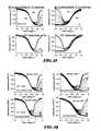
- FIG. 1illustrates the growth rate of GeO 2 films as a function of deposition temperature using vapour pulses of Ge(OEt) 4 and O 3 at 150° C.-300° C.;
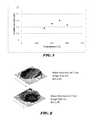
- FIG. 2illustrates two computerized images of the respective thicknesses of two wafers prepared according to some embodiments.
- FIG. 3illustrates GeO 2 film thickness non-uniformity as a function of deposition temperature using vapour pulses of Ge(OEt) 4 and O 3 at 150° C.-300° C.;
- FIG. 4illustrates GeO 2 film thickness as a function of the number of deposition cycles when using vapour pulses of Ge(OEt) 4 and O 3 at 250° C.;
- FIG. 5shows the composition of GeO 2 deposited by ALD at various temperatures.
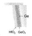
- FIG. 6Ashows GeO 2 films deposited by ALD over Ge at a first magnification. HfO 2 was subsequently deposited over the GeO 2 ;
- FIG. 6Bshows GeO 2 films deposited by ALD over Ge at a second magnification. HfO 2 was subsequently deposited over the GeO 2 ;
- FIG. 7Aillustrates GeO 2 film thickness as a function of the number of deposition cycles when using vapour pulses of Ge(OEt) 4 and O 3 at 300° C. on HF-last Si;
- FIG. 7Billustrates GeO 2 film thickness as a function of the number of deposition cycles when using vapour pulses of Ge(OEt) 4 and O 3 at 300° C. on HF-last Ge;
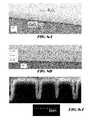
- FIG. 8Ashows a transmission electron microscope (TEM) image of two layers deposited by ALD (GeO 2 and Al 2 O 3 ) where the Al 2 O 3 was deposited using a TMA+O 3 ⁇ process.
- TEMtransmission electron microscope
- FIG. 8Bshows a TEM image of three intermixed layers (Al, Ge, and O) when Al 2 O 3 was deposited using a TMA+H 2 O process.
- FIG. 9Ashows an image from a scanning electron microscope (SEM) at a first magnification illustrating GeO 2 film conformality when deposited using vapour pulses of Ge(OEt) 4 and O 3 .
- FIG. 9Bshows an image from a SEM at a second magnification illustrating GeO 2 film conformality when deposited using vapour pulses of Ge(OEt) 4 and O 3 .
- FIG. 10illustrates ALD GeO 2 /ALD HfO 2 stack film conformality when grown at reaction temperature of 250° C.
- the target thickness of the GeO 2was about 30 nm.
- FIG. 11illustrates the C-V characteristics of ALD GeO 2 interlayers grown on p-doped Ge and n-doped Ge.
- the GeO 2 interlayerswere grown at a reaction temperature 250° C. from vapour pulses of Ge(OEt) 4 and O 3 .
- FIG. 12illustrates the C-V characteristics of GeO 2 interlayer grown by ALD at different temperatures using vapour pulses of Ge(OEt) 4 and O 3 .
- FIG. 13Aillustrates the C-V characteristics of GeO 2 interlayers, grown by ALD at a reaction temperature of 250° C. using vapour pulses of Ge(OEt) 4 and O 3 with an ALD Al 2 O 3 capping layer.
- FIG. 13Billustrates the C-V characteristics of GeO 2 interlayers, grown by ALD at a reaction temperature of 250° C. using vapour pulses of Ge(OEt) 4 and O 3 without an ALD Al 2 O 3 capping layer.
- FIG. 14Aillustrates the C-V characteristics of GeO 2 interlayers grown by ALD on Ge-substrates with HF-cleaning, at a reaction temperature 250° C. using vapour pulses of Ge(OEt) 4 and O 3 .
- FIG. 14Billustrates the C-V characteristics of GeO 2 interlayers grown by ALD on Ge-substrates without HF-cleaning, at a reaction temperature 250° C. using vapour pulses of Ge(OEt) 4 and O 3 .
- a GeO 2 thin filmis formed on a substrate by a vapor deposition process comprising alternately and sequentially contacting a substrate with a vapor phase germanium precursor and an oxygen reactant, such that a layer of the germanium precursor forms on the substrate surface, and the oxygen-containing reactant subsequently reacts with the germanium precursor to form a GeO 2 thin film.
- the Ge precursormay be selected from Germanium ethoxide (GeOEt) 4 and tetrakis(dimethylamino) germanium (TDMAGe). Other possible germanium precursors are provided below.
- the Ge precursoris not a halide.
- the Ge precursorcontains halide in at least one ligand, but not in all ligands.
- the oxygen reactantcomprises one or more of ozone, oxygen atoms, oxygen radicals, and oxygen plasma.
- the oxygen reactantmay be water. However, in other embodiments the oxygen reactant is not water.
- GeO 2 thin filmsare deposited by alternately and sequentially contacting a substrate with Ge(OCH 2 CH 3 ) 4 and O 3 . In some embodiments GeO 2 thin films are deposited by alternately and sequentially contacting a substrate with tetrakis(dimethylamio) germanium (TDMAGe) and O 3 .
- TDMAGetetrakis(dimethylamio) germanium
- GeO 2 filmsmay be used, for example as an interface layer between high-k and new channel materials in semiconductor devices.
- the GeO 2 layermay serve as an interface in a Ge-based FinFET.
- the GeO 2 layeris an interface layer between Ge and a high-k material.
- the GeO 2 interface layermay prevent leakage and decrease trap density.
- Other contexts in which GeO 2 thin films may be utilizedwill be apparent to the skilled artisan.
- GeO 2 thin filmsmay find use in optical applications.
- the GeO 2 films deposited by ALD processesare annealed after the deposition as desired depending on the application.
- the GeO 2 films deposited by ALDcan be used for a process called Ge-condensation.
- a principle of thiscan be seen and understood, for example, from U.S. Patent Publications 2011/0147811 (see FIGS. 3 a and 3 b ) and 2011/0193178 (see para. [0020, which are incorporated by reference herein]).
- U.S. Patent Publications 2011/0147811see FIGS. 3 a and 3 b
- 2011/0193178see para. [0020, which are incorporated by reference herein].
- the ALD-deposited GeO 2 filmwith another film (i.e., a “capping layer”), preferably one deposited by ALD or PEALD, such as ALD-deposited or PEALD-deposited Al 2 O 3 , SiN X , or SiO 2 before an anneal step where Ge will be driven to the fin or channel.
- a “capping layer”preferably one deposited by ALD or PEALD, such as ALD-deposited or PEALD-deposited Al 2 O 3 , SiN X , or SiO 2 before an anneal step where Ge will be driven to the fin or channel.
- a capping layerpreferably one deposited by ALD or PEALD, such as ALD-deposited or PEALD-deposited Al 2 O 3 , SiN X , or SiO 2 before an anneal step where Ge will be driven to the fin or channel.
- watermay be used as an oxygen source in the ALD GeO 2 process.
- the GeO 2is deposited by an ALD process on a silicon fin
- the GeO 2is deposited by an ALD process on a silicon fin and a capping layer is deposited over the GeO 2 layer.
- the GeO 2is deposited by an ALD process on a Si 1-x Ge x fin, and a capping layer is then deposited over the GeO 2 layer.
- the capping layeris SiO 2 .
- the capping layeris SiN X .
- the capping layeris Al 2 O 3 .
- the capping layeris deposited by methods other than an ALD or PEALD process.
- the capping layeris deposited by an ALD process.
- the capping layeris deposited by a PEALD process.
- the GeO 2 films deposited by ALDare pure GeO 2 films.
- deposited GeO 2may be able to produce a better interface layer than GeO 2 formed by thermal oxidation.
- Atomic layer depositionallows for conformal deposition of GeO 2 films.
- the GeO 2 films deposited by ALDhave at least 90%, 95% or higher conformality. In some embodiments the films are about 100% conformal.
- the substratemay be, for example, a semiconductor substrate.
- the surface of the substratecomprises a group III or group IV compound.
- the surface of the substratecomprises Ge.
- the surface of the substratecomprises a thin GeO 2 layer.
- the GeO 2 layermay be formed, for example, through thermal or plasma oxidation.
- the substrate surfaceis H-terminated.
- native Ge oxideis removed, for example with HF, prior to GeO 2 deposition by ALD.
- the substratemay be treated prior to depositing the GeO 2 layer by ALD.
- the substratemay be treated with a passivation chemical to prevent oxidation prior to depositing GeO 2 by ALD.
- the substrateis treated to form an interfacial layer prior to depositing GeO 2 by ALD.
- the substrate treatmentmay comprise exposing the substrate to trimethylaluminum (TMA) to form an interfacial layer or surface termination on the surface prior to GeO 2 deposition.
- TMAtrimethylaluminum
- the substratemay be treated to remove native Ge oxide, for example with HF, prior to depositing GeO 2 by ALD.
- a further filmis deposited.
- the additional filmmay be directly over and contacting the ALD-deposited GeO 2 layer.
- a high-k filmis deposited after the ALD-deposited GeO 2 is deposited.
- the high-k layer or other filmmay be deposited by ALD or by other known deposition methods.
- a HfO 2 layeris deposited over the GeO 2 layer.
- an Al 2 O 3 layeris deposited over the GeO 2 layer.
- a deposition process for depositing a film on top of a GeO 2 filmdoes not utilize water as one of the reactants.
- a deposition process for depositing a film on top of a GeO 2 filmutilizes an oxygen source other than water.
- a deposition process for a film deposited on top of a GeO 2 filmuses ozone as an oxygen source.
- a deposition process for a film deposited on top of a GeO 2 filmuses oxygen atoms, oxygen radicals or oxygen containing plasma as an oxygen source.
- a deposition process for a film deposited on top of a GeO 2 filmuses water, and at least one mixed layer comprising germanium is produced.
- atoms or radicalsmay oxidize the substrate during the first one or more ALD cycles for forming GeO 2 and form a thin layer of GeO 2 on the substrate itself. In that situation, the GeO 2 layer would be a kind of composite of GeO 2 (oxidized from substrate) and ALD-deposited GeO 2 .
- a GeO 2 layeris an interlayer between a substrate and high-k layer.
- a GeO 2 interlayerhas a thickness of less than about 10 nm, more preferably less than about 5 nm and most preferably less than about 3 nm. In some cases the GeO 2 interlayer is less than about 2 nm or even less than about 1 nm thick.
- ALDAtomic Layer Deposition
- ALDatomic layer deposition
- ALD type processesare based on controlled, self-limiting surface reactions of precursor chemicals. Gas phase reactions are avoided by feeding the precursors alternately and sequentially into the reaction chamber. Vapor phase reactants are separated from each other in the reaction chamber, for example, by removing excess reactants and/or reactant by-products from the reaction chamber between reactant pulses.
- a substrateis loaded into a reaction chamber and is heated to a suitable deposition temperature, generally at lowered pressure.
- Deposition temperaturesare maintained below the precursor thermal decomposition temperature but at a high enough level to avoid condensation of reactants and to provide the activation energy for the desired surface reactions.
- the appropriate temperature window for any given ALD reactionwill depend upon the surface termination and reactant species involved.
- the deposition temperatureis from about 20° C. to about 600° C., preferably from about to 100° C. to about 400° C., and more preferably from about 150° C. to about 300° C.
- a first germanium reactantis conducted into the chamber in the form of vapor phase pulse and contacted with the surface of a substrate.
- the substrate surfacecomprises a three dimensional structure.
- Conditionsare preferably selected such that no more than about one monolayer of the germanium precursor is adsorbed on the substrate surface in a self-limiting manner.
- first reactant and reaction byproductsif any, may be removed from the substrate and substrate surface and from proximity to the substrate and substrate surface.
- reactant and reaction byproducts, if anymay be removed by purging. Purging may be accomplished for example, with a pulse of inert gas such as nitrogen or argon.
- Purging the reaction chambermeans that vapor phase precursors and/or vapor phase byproducts are removed from the reaction chamber such as by evacuating the chamber with a vacuum pump and/or by replacing the gas inside the reactor with an inert gas such as argon or nitrogen.
- Typical purging timesare from about 0.05 seconds to about 20 seconds, more preferably between about 1 second and about 10 seconds, and still more preferably between about 1 second and about 2 seconds.
- other purge timescan be utilized if necessary, such as when depositing layers over extremely high aspect ratio structures or other structures with complex surface morphology.
- the appropriate pulsing timescan be readily determined by the skilled artisan based on the particular circumstances.
- Another method for removing excess reactants—metal precursors or oxygen precursors, reaction byproducts, etc.—from the substrate surface or from the area of the substratemay involve physically moving the substrate from a location containing the reactant and/or reaction byproducts.
- a second gaseous oxygen reactantis pulsed into the chamber where it reacts with the first germanium reactant on the surface to form germanium oxide.
- Excess second reactant and gaseous by-products of the surface reactionare removed from the substrate, for example by purging them out of the reaction chamber, preferably with the aid of an inert gas.
- the steps of pulsing and removingare repeated until a thin film of the desired thickness has been formed on the substrate, with each cycle typically leaving no more than about a molecular monolayer.
- each pulse or phase of each cycleis preferably self-limiting.
- An excess of reactant precursorsis supplied in each phase to saturate the susceptible structure surfaces.
- Surface saturationensures reactant occupation of all available reactive sites (subject, for example, to physical size or “steric hindrance” restraints) and thus ensures excellent step coverage.
- the degree of self-limiting behaviorcan be adjusted by, e.g., allowing some overlap of reactant pulses to trade off deposition speed (by allowing some CVD-type reactions) against conformality.
- Ideal ALD conditions with reactants well separated in time and spaceprovide near perfect self-limiting behavior and thus maximum conformality, but steric hindrance results in less than one molecular layer per cycle.
- Limited CVD reactions mixed with the self-limiting ALD reactionscan raise the deposition speed.
- a reaction spacecan be in a single-wafer ALD reactor or a batch ALD reactor where deposition on multiple substrates takes place at the same time.
- the substrate on which deposition is desiredsuch as a semiconductor workpiece, is loaded into a reactor.
- the reactormay be part of a cluster tool in which a variety of different processes in the formation of an integrated circuit are carried out.
- a flow-type reactoris utilized.
- a high-volume manufacturing-capable single wafer ALD reactoris used.
- a batch reactor comprising multiple substratesis used.
- the number of substratesis preferably in the range of 10 to 200, more preferably in the range of 50 to 150, and most preferably in the range of 100 to 130.
- suitable reactorsinclude commercially available ALD equipment such as the F-120® reactor, F-450 reactor, Pulsar® reactors—such as the Pulsar® 2000 and the Pulsar® 3000—EmerALD® reactor and Advance® 400 Series reactors, available from ASM America, Inc of Phoenix, Ariz. and ASM Europe B.V., Almere, Netherlands.
- Other commercially available reactorsinclude those from ASM Japan K.K (Tokyo, Japan) under the tradename Eagle® XP and XP8.
- ALD reactorsmany other kinds of reactors capable of ALD growth of thin films, including CVD reactors equipped with appropriate equipment and means for pulsing the precursors can be employed.
- a flow type ALD reactoris used.
- reactantsare kept separate until reaching the reaction chamber, such that shared lines for the precursors are minimized.
- other arrangementsare possible.
- Suitable batch reactorsinclude, but are not limited to, reactors designed specifically to enhance ALD processes, which are commercially available from and ASM Europe B.V (Almere, Netherlands) under the trade names ALDA400TM and A412TM.
- a vertical batch reactoris utilized in which the boat rotates during processing, such as the A412TM.
- wafersrotate during processing.
- wafer-to-wafer uniformityis less than 3% (1 sigma), less than 2%, less than 1% or even less than 0.5%.
- the germanium oxide ALD processes described hereincan optionally be carried out in a reactor or reaction space connected to a cluster tool.
- a cluster toolbecause each reaction space is dedicated to one type of process, the temperature of the reaction space in each module can be kept constant, which improves the throughput compared to a reactor in which the substrate is heated up to the process temperature before each run.
- a germanium oxide thin filmis formed by an ALD-type process comprising multiple pulsing cycles, each cycle comprising:
- germanium oxidepreferably GeO 2
- germanium oxideis deposited from alternating and sequential pulses of a Ge precursor and an oxygen source, like water, ozone, oxygen plasma, oxygen radicals, or oxygen atoms.
- an oxygen sourcelike water, ozone, oxygen plasma, oxygen radicals, or oxygen atoms.
- the oxygen sourceis not water.
- the Ge precursorpreferably comprises Ge(OEt) 4 or TDMAGe.
- the Ge precursor employed in the ALD type processesmay be solid, liquid, or gaseous material under standard conditions (room temperature and atmospheric pressure), provided that the Ge precursor is in vapor phase before it is conducted into the reaction chamber and contacted with the substrate surface.
- “Pulsing” a vaporized precursor onto the substratemeans that the precursor vapor is conducted into the chamber for a limited period of time. Typically, the pulsing time is from about 0.05 seconds to about 10 seconds. However, depending on the substrate type and its surface area, the pulsing time may be even higher than about 10 seconds.
- the Ge precursoris pulsed for from about 0.05 seconds to about 10 seconds, more preferably for from about 0.1 seconds to about 5 seconds and most preferably for from about 0.3 seconds to about 3.0 seconds.
- the oxygen-containing precursoris preferably pulsed for from about 0.05 seconds to about 10 seconds, more preferably for from about 0.1 seconds to about 5 seconds, most preferably for from about 0.2 seconds to about 3.0 seconds.
- pulsing timescan be on the order of minutes in some cases. The optimum pulsing time can be readily determined by the skilled artisan based on the particular circumstances.
- the Ge precursoris Ge(OEt) 4 or TDMAGe.
- Other possible germanium precursors that can be used in some embodimentsare described below.
- the Ge precursoris Ge(OMe) 4 .
- the Ge-precursoris not a halide.
- the Ge-precursormay comprise a halogen in at least one ligand, but not in all ligands.
- the oxygen sourcemay be an oxygen-containing gas pulse and can be a mixture of oxygen and inactive gas, such as nitrogen or argon.
- the oxygen sourcemay be a molecular oxygen-containing gas pulse.
- the preferred oxygen content of the oxygen-source gasis from about 10% to about 25%.
- one source of oxygenmay be air.
- the oxygen sourceis molecular oxygen.
- the oxygen sourcecomprises an activated or excited oxygen species.
- the oxygen sourcecomprises ozone.
- the oxygen sourcemay be pure ozone or a mixture of ozone, molecular oxygen, and another gas, for example an inactive gas such as nitrogen or argon.
- Ozonecan be produced by an ozone generator and it is most preferably introduced into the reaction space with the aid of an inert gas of some kind, such as nitrogen, or with the aid of oxygen.
- ozoneis provided at a concentration from about 5 vol-% to about 40 vol-%, and preferably from about 15 vol-% to about 25 vol-%.
- the oxygen sourceis oxygen plasma.
- ozone or a mixture of ozone and another gasis pulsed into the reaction chamber.
- ozoneis formed inside the reactor, for example by conducting oxygen containing gas through an arc.
- an oxygen containing plasmais formed in the reactor.
- the plasmamay be formed in situ on top of the substrate or in close proximity to the substrate.
- the plasmais formed upstream of the reaction chamber in a remote plasma generator and plasma products are directed to the reaction chamber to contact the substrate.
- the pathway to the substratecan be optimized to maximize electrically neutral species and minimize ion survival before reaching the substrate.
- the oxygen sourceis an oxygen source other than water.
- wateris not provided in any ALD cycle for depositing GeO 2 .
- the Ge precursorcomprises at least one amine or alkylamine ligand, such as those presented in formulas (2) through (6) and (8) and (9), and the oxygen precursor comprises water.
- the substrateBefore starting the deposition of the film, the substrate is typically heated to a suitable growth temperature, as discussed above.
- the preferred deposition temperaturemay vary depending on a number of factors such as, and without limitation, the reactant precursors, the pressure, flow rate, the arrangement of the reactor, and the composition of the substrate including the nature of the material to be deposited on.
- the processing timedepends on the thickness of the layer to be produced and the growth rate of the film.
- the growth rate of a thin filmis determined as thickness increase per one cycle.
- One cycleconsists of the pulsing and removing steps of the precursors and the duration of one cycle is typically between about 0.2 seconds and about 30 seconds, more preferably between about 1 second and about 10 seconds, but it can be on order of minutes or more in some cases, for example, where large surface areas and volumes are present.
- the GeO 2 film formedis a pure GeO 2 film. Preferably, aside from minor impurities no other metal or semi-metal elements are present in the film. In some embodiments the film comprises less than 1-at % of metal or semi-metal other than Ge. In some embodiments the GeO 2 film is stoichiometric. In some embodiments, a pure GeO 2 film comprises less than about 5-at % of any impurity other than hydrogen, preferably less than about 3-at % of any impurity other than hydrogen, and more preferably less than about 1-at % of any impurity other than hydrogen.
- the GeO 2 film formedhas step coverage of more than about 80%, more preferably more than about 90%, and most preferably more than about 95% in structures which have high aspect ratios.
- high aspect ratio structureshave an aspect ratio that is more than about 3:1 when comparing the depth or height to the width of the feature.
- the structureshave an aspect ratio of more than about 5:1, or even an aspect ratio of 10:1 or greater.
- the Ge precursoris tetravalent (i.e. Ge has an oxidation state of +IV). In some embodiments, the Ge precursor is not divalent (i.e., Ge has an oxidation state of +II). In some embodiments, the Ge precursor may comprise at least one alkoxide ligand. In some embodiments, the Ge precursor may comprise at least one amine or alkylamine ligand. In some embodiments the Ge precursor is a metal-organic or organometallic compound. In some embodiments the Ge precursor comprises at least one halide ligand. In some embodiments the Ge precursor does not comprise a halide ligand.
- the Ge precursoris not solid at room temperature (e.g., about 20° C.).
- Ge precursors from formulas (1) through (9) belowmay be used in some embodiments.
- Preferred options for Rinclude, but are not limited to, methyl, ethyl, propyl, isopropyl, n-butyl, isobutyl, tertbutyl for all formulas, more preferred in ethyl and methyl.
- the preferred options for Rinclude, but are not limited to, C 3 -C 10 alkyls, alkenyls, and alkynyls and substituted versions of those, more preferably C 3 -C 6 alkyls, alkenyls, and alkenyls and substituted versions of those.
- the Ge precursorcomprises one or more halides.
- the precursorcomprises 1, 2, or 3 halide ligands.
- the Ge precursor used in the ALD processdoes not comprise a halide.
- a Ge precursor that comprises an alkoxideis not used in combination with water in an ALD process.
- an amine/alkylyamine or Ge—N bond containing Ge precursormay be used in combination with water.
- Preferred alkylamine Ge precursorsinclude, but are not limited to, tetrakis(dimethylamino) germanium (TDMAGe), tetrakis(diethylamino) germanium (TDEAGe), and tetrakis(ethylmethylamino) germanium (TEMAGe).
- TDMAGetetrakis(dimethylamino) germanium
- TDEAGetetrakis(diethylamino) germanium
- TEMAGetetrakis(ethylmethylamino) germanium
- the Ge precursoris TDMAGe.
- the precursoris TDEAGe.
- the precursoris TEMAGe.
- GeO 2 filmswere deposited in an F-450 ALCVD R&D reactor at temperatures ranging from about 150° C. to about 300° C. using germanium ethoxide (Ge(OEt) 4 ) or tetrakis(dimethylamino) germanium (TDMAGe) as the Ge precursor, and ozone (O 3 ) as the oxygen source.
- Ge(OEt) 4is a liquid with a vapor pressure of about 0.2 Torr at 55° C.
- TDMAGeis a liquid with a vapor pressure of about 3 Torr at 50° C. Pulse/purge times were 3.0 s/6.0 s for all precursors Ge(OEt) 4 , TDMAGe and O 3 .
- GeO 2 filmswere deposited by alternately and sequentially contacting a substrate in a reactor chamber with vapor pulses of Ge(OEt) 4 and O 3 at about 150° C. to about 300° C. In this temperature range growth rate of about 0.18 ⁇ /cycle to about 0.3 ⁇ /cycle was obtained ( FIG. 1 ).
- the thickness non-uniformitywas about 3% to about 13% 1-sigma, and the lowest non-uniformities were obtained at 300° C. ( FIG. 3 ).
- a series of films of various thicknesseswere deposited at 250° C. by varying cycle number. Film growth was linear, i.e. film thickness can be controlled by the number of cycles ( FIG. 4 ). Thinner films were also deposited at 300° C. Between about 150° C. and about 300° C., the GeO 2 film density was about 3.8 g/cm 3 to about 4 g/cm 3 (from XRR; bulk 4.23 g/cm 3 ). In particular, at 250° C.
- the growth ratewas about 0.25 ⁇ /cycle and the film had a non-uniformity of less than about 10%.
- the XRR density at 250° C.was about 4.35 g/cm 3 (bulk 4.23 g/cm3), and the refractive index was modeled to be close to the bulk value from ellipsometer data (bulk 1.650 vs. modeled 1.66).
- the composition of these filmswas about 32-at % Ge and about 68-at % O (RBS analysis of about 50 nm GeO 2 on silicon with native oxide). See FIG. 5 .
- FIGS. 7A and 7Bit can be seen that GeO 2 deposited by ALD grows linearly on HF-last Ge ( FIG. 7B ) and on HF-last Si ( FIG. 7A ) when using vapor pulses of Ge(OEt) 4 and O 3 at 300° C.
- FIGS. 8A and 8Bshow TEM images of an ALD Al 2 O 3 /ALD GeO 2 (37 cycles)/Ge/Si—stack/structure.
- Al 2 O 3was deposited by ALD using vapor pulses or TMA and water or ozone.
- FIG. 8Blayers can mix when using water as an oxygen source in the Al 2 O 3 ALD process, whereas when using ozone as the oxygen source in the Al 2 O 3 ALD process, two clearly separated layers can be seen in FIG. 8A .
- the reason for intermixing of the layersis unsure, and it may be caused by the electron beam in the analysis.
- FIGS. 9A and 9B and in FIG. 10which illustrates ALD GeO 2 /ALD HfO 2 stack film conformality when grown at a reaction temperature of 250° C. and using a target GeO 2 thickness of about 30 nm.
- GeO 2 filmswere deposited by alternately and sequentially contacting a substrate in a reactor chamber with vapor pulses of tetrakis(dimethylamino)germanium (TDMAGe) and O 3 at 150° C. to 300° C.
- growth rateof about 0.4 ⁇ /cycle to about 0.55 ⁇ /cycle was obtained.
- the thickness non-uniformitywas less than about 6%.
- the best nonuniformity of less than about 2%was observed at about 200° C.
- the GeO 2 film densitywas about 3.8 g/cm 3 to about 4 g/cm 3 (from XRR).
- the EDX compositionwas about 30 at. % Ge and about 70 at. % O.
- TDMAGewas also observed to react with water.
- GeO 2was also deposited on a Ge surface and topped with HfO 2 . Briefly, 50 nm of GeO 2 was deposited from TDMAGe and O 3 by ALD, as described herein, on a substrate comprising either 15 nm or 1 ⁇ m Ge on Si. Subsequently, approximately 50 nm of HfO 2 was deposited over the GeO 2 by atomic layer deposition using alternating and sequential pulses of HfCl 4 and H 2 O. The deposition temperature was 300° C. No etching was observed. The results are shown in FIGS. 6A and 6B .
Landscapes
- Chemical & Material Sciences (AREA)
- Engineering & Computer Science (AREA)
- Manufacturing & Machinery (AREA)
- Condensed Matter Physics & Semiconductors (AREA)
- Power Engineering (AREA)
- Microelectronics & Electronic Packaging (AREA)
- Computer Hardware Design (AREA)
- General Physics & Mathematics (AREA)
- Physics & Mathematics (AREA)
- Chemical Kinetics & Catalysis (AREA)
- Mechanical Engineering (AREA)
- Organic Chemistry (AREA)
- Metallurgy (AREA)
- Materials Engineering (AREA)
- General Chemical & Material Sciences (AREA)
- Inorganic Chemistry (AREA)
- Chemical Vapour Deposition (AREA)
- Formation Of Insulating Films (AREA)
Abstract
Description
This application claims the benefit of U.S. Provisional Patent Application Ser. No. 61/697,007, filed Sep. 5, 2012, entitled “ATOMIC LAYER DEPOSITION OF GeO2” and U.S. Provisional Patent Application Ser. No. 61/713,082, filed Oct. 12, 2012, entitled “ATOMIC LAYER DEPOSITION OF GeO2.” The contents of all the above-referenced applications are incorporated herein by reference in their entireties.
1. Field of the Invention
The application relates to atomic layer deposition processes for forming GeO2films.
2. Background
Ge devices are of interest because of Ge high hole mobility. Low Ditinterface formation with HfO2HK material will allow for good Ge based FinFETs.
According to some embodiments of the present disclosure, atomic layer deposition processes for forming germanium oxide thin films on a substrate in a reaction chamber are disclosed. The ALD processes can include contacting the substrate with a vapor phase tetravalent Ge precursor, removing excess Ge precursor and any reaction by-products, contacting the substrate with a vapor phase oxygen precursor, removing excess oxygen precursor and any gaseous by-products, and repeating the contacting and removing steps until a germanium oxide thin film of the desired thickness has been formed. In some embodiments, contacting the substrate with a vapor phase tetravalent Ge precursor results in the formation of at most a molecular monolayer of the Ge precursor on the substrate surface. In some embodiments, the oxygen precursor reacts with the Ge precursor on the substrate surface.
According to some embodiments of the present disclosure, in an ALD process for forming a germanium oxide thin film using a Ge precursor and an oxygen precursor, removing excess Ge precursor comprising removing excess Ge precursor from the substrate surface and in the proximity of the substrate surface. In some embodiments, the oxygen precursor is something other than water. In some embodiments, the oxygen precursor is one of ozone, oxygen atoms, oxygen radicals, or oxygen plasma. In some embodiments, the Ge-precursor is not a halide. In some embodiments, the Ge-precursor comprises at least one alkoxide ligand. In some embodiments, the Ge-precursor comprises at least one amine or alkylamine ligand. In some embodiments, the Ge-precursor comprises at least one amine or alkylamine ligand, and the oxygen precursor comprises water.
According to some embodiments of the present disclosure, in an ALD process for forming a germanium oxide thin film on a substrate, the surface of the substrate comprises a thin layer of GeO2prior to beginning the ALD process. In some embodiments, the substrate is pretreated with a passivation chemical to prevent oxidation before the germanium oxide film is deposited. In some embodiments, an interfacial layer is formed on the substrate before the germanium oxide thin film is deposited. In some embodiments, the deposition temperature is from about 100° C. to about 400° C. In some embodiments, the substrate is treated to remove native Ge oxide prior to forming the germanium oxide thin film.
Some embodiments for forming a germanium oxide thin film by an ALD process include depositing a thin layer of a different material over the germanium oxide thin film. In some embodiments, the thin layer of a different material is deposited directly on the germanium oxide thin film. In some embodiments, the thin layer comprises Al2O3, and in some embodiments, the Al2O3layer is deposited by a process that does not use water as a reactant. In some embodiments, the germanium oxide thin film serves as an interlayer between the substrate and a high-k layer. And in some embodiments, the germanium oxide thin film may be used in a Ge-condensation process.
According to some embodiments, an atomic layer deposition process is disclosed for forming a pure GeO2thin film, in which the process can include alternately and sequentially contacting a substrate with Ge(OCH2CH3)4and O3.
According to some embodiments, an atomic layer deposition process is disclosed for forming a pure GeO2thin film, which can include alternately and sequentially contacting a substrate with an alkylamine Ge precursor and an oxygen source. In some embodiments, the Ge precursor is TDMAGe, and the oxygen source is ozone. And in some embodiments, the Ge precursor is TDMAGe, and the oxygen source is water. In some embodiments, the oxygen source is water.
The invention will be better understood from the Detailed Description and from the appended drawings, which are meant to illustrate and not to limit the invention, and wherein:
In one aspect, methods of depositing GeO2thin films by atomic layer deposition are provided. In some embodiments a GeO2thin film is formed on a substrate by a vapor deposition process comprising alternately and sequentially contacting a substrate with a vapor phase germanium precursor and an oxygen reactant, such that a layer of the germanium precursor forms on the substrate surface, and the oxygen-containing reactant subsequently reacts with the germanium precursor to form a GeO2thin film.
In some embodiments the Ge precursor may be selected from Germanium ethoxide (GeOEt)4and tetrakis(dimethylamino) germanium (TDMAGe). Other possible germanium precursors are provided below. In some embodiments the Ge precursor is not a halide. In some embodiments, the Ge precursor contains halide in at least one ligand, but not in all ligands.
In some embodiments the oxygen reactant comprises one or more of ozone, oxygen atoms, oxygen radicals, and oxygen plasma. In some embodiments the oxygen reactant may be water. However, in other embodiments the oxygen reactant is not water.
In some embodiments, GeO2thin films are deposited by alternately and sequentially contacting a substrate with Ge(OCH2CH3)4and O3. In some embodiments GeO2thin films are deposited by alternately and sequentially contacting a substrate with tetrakis(dimethylamio) germanium (TDMAGe) and O3.
GeO2films may be used, for example as an interface layer between high-k and new channel materials in semiconductor devices. For example, the GeO2layer may serve as an interface in a Ge-based FinFET. In some embodiments the GeO2layer is an interface layer between Ge and a high-k material. The GeO2interface layer may prevent leakage and decrease trap density. Other contexts in which GeO2thin films may be utilized will be apparent to the skilled artisan. For example, GeO2thin films may find use in optical applications. In some embodiments, the GeO2films deposited by ALD processes are annealed after the deposition as desired depending on the application.
In one embodiment, the GeO2films deposited by ALD can be used for a process called Ge-condensation. A principle of this can be seen and understood, for example, from U.S. Patent Publications 2011/0147811 (seeFIGS. 3 aand3b) and 2011/0193178 (see para. [0020, which are incorporated by reference herein]). By adding a GeO2film to the interface of Si1-xGex/SiO2, it may be possible for more Ge to be driven to the fin or channel material. In these cases it is preferable to cap the ALD-deposited GeO2film with another film (i.e., a “capping layer”), preferably one deposited by ALD or PEALD, such as ALD-deposited or PEALD-deposited Al2O3, SiNX, or SiO2before an anneal step where Ge will be driven to the fin or channel. In this application of Ge-condensation, water may be used as an oxygen source in the ALD GeO2process. In some embodiments, the GeO2is deposited by an ALD process on a silicon fin without further depositing a capping layer. In some embodiments, the GeO2is deposited by an ALD process on a Si1-xGexfin without further depositing a capping layer. In some embodiments, the GeO2is deposited by an ALD process on a silicon fin and a capping layer is deposited over the GeO2layer. In some embodiments, the GeO2is deposited by an ALD process on a Si1-xGexfin, and a capping layer is then deposited over the GeO2layer. In some embodiments, the capping layer is SiO2. In some embodiments, the capping layer is SiNX. In some embodiments, the capping layer is Al2O3. In some embodiments, the capping layer is deposited by methods other than an ALD or PEALD process. In some embodiments, the capping layer is deposited by an ALD process. In some embodiments the capping layer is deposited by a PEALD process.
In some embodiments the GeO2films deposited by ALD are pure GeO2films. Thus, deposited GeO2may be able to produce a better interface layer than GeO2formed by thermal oxidation.
Atomic layer deposition allows for conformal deposition of GeO2films. In some embodiments, the GeO2films deposited by ALD have at least 90%, 95% or higher conformality. In some embodiments the films are about 100% conformal.
The substrate may be, for example, a semiconductor substrate. In some embodiments the surface of the substrate comprises a group III or group IV compound. For example, in some embodiments the surface of the substrate comprises Ge. In some embodiments the surface of the substrate comprises a thin GeO2layer. The GeO2layer may be formed, for example, through thermal or plasma oxidation. In some embodiments the substrate surface is H-terminated. In some embodiments native Ge oxide is removed, for example with HF, prior to GeO2deposition by ALD.
The substrate may be treated prior to depositing the GeO2layer by ALD. For example, the substrate may be treated with a passivation chemical to prevent oxidation prior to depositing GeO2by ALD. In other embodiments the substrate is treated to form an interfacial layer prior to depositing GeO2by ALD. For example, the substrate treatment may comprise exposing the substrate to trimethylaluminum (TMA) to form an interfacial layer or surface termination on the surface prior to GeO2deposition. As mentioned above, in some embodiments the substrate may be treated to remove native Ge oxide, for example with HF, prior to depositing GeO2by ALD.
In some embodiments, following GeO2deposition, a further film is deposited. The additional film may be directly over and contacting the ALD-deposited GeO2layer. In some embodiments a high-k film is deposited after the ALD-deposited GeO2is deposited. The high-k layer or other film may be deposited by ALD or by other known deposition methods. In some embodiments a HfO2layer is deposited over the GeO2layer. In some embodiments an Al2O3layer is deposited over the GeO2layer. Without being bound to any particular theory, it is believed that water in the deposition process of the layer deposited on top of a GeO2layer may cause in some situations the intermixing of the already deposited GeO2layer and the layer deposited on top of GeO2layer. In some embodiments this mixing is preferable. In other embodiments, this mixing is to be avoided. Thus, in some embodiments a deposition process for depositing a film on top of a GeO2film does not utilize water as one of the reactants. In some embodiments a deposition process for depositing a film on top of a GeO2film utilizes an oxygen source other than water. In some embodiments, a deposition process for a film deposited on top of a GeO2film uses ozone as an oxygen source. In some embodiments a deposition process for a film deposited on top of a GeO2film uses oxygen atoms, oxygen radicals or oxygen containing plasma as an oxygen source. In some embodiments, a deposition process for a film deposited on top of a GeO2film uses water, and at least one mixed layer comprising germanium is produced. When a Ge substrate is used and ozone or oxygen plasma are provided as an oxygen source, atoms or radicals may oxidize the substrate during the first one or more ALD cycles for forming GeO2and form a thin layer of GeO2on the substrate itself. In that situation, the GeO2layer would be a kind of composite of GeO2(oxidized from substrate) and ALD-deposited GeO2.
In some embodiments a GeO2layer is an interlayer between a substrate and high-k layer. Preferably a GeO2interlayer has a thickness of less than about 10 nm, more preferably less than about 5 nm and most preferably less than about 3 nm. In some cases the GeO2interlayer is less than about 2 nm or even less than about 1 nm thick.
Atomic Layer Deposition (ALD)
As noted above, processes described herein enable use of atomic layer deposition techniques to deposit conformal GeO2layers. Among vapor deposition techniques, ALD has the advantage of providing high conformality at low temperatures.
ALD type processes are based on controlled, self-limiting surface reactions of precursor chemicals. Gas phase reactions are avoided by feeding the precursors alternately and sequentially into the reaction chamber. Vapor phase reactants are separated from each other in the reaction chamber, for example, by removing excess reactants and/or reactant by-products from the reaction chamber between reactant pulses.
Briefly, a substrate is loaded into a reaction chamber and is heated to a suitable deposition temperature, generally at lowered pressure. Deposition temperatures are maintained below the precursor thermal decomposition temperature but at a high enough level to avoid condensation of reactants and to provide the activation energy for the desired surface reactions. Of course, the appropriate temperature window for any given ALD reaction will depend upon the surface termination and reactant species involved. In some embodiments the deposition temperature is from about 20° C. to about 600° C., preferably from about to 100° C. to about 400° C., and more preferably from about 150° C. to about 300° C.
A first germanium reactant is conducted into the chamber in the form of vapor phase pulse and contacted with the surface of a substrate. In some embodiments the substrate surface comprises a three dimensional structure. Conditions are preferably selected such that no more than about one monolayer of the germanium precursor is adsorbed on the substrate surface in a self-limiting manner. Excess first reactant and reaction byproducts, if any, may be removed from the substrate and substrate surface and from proximity to the substrate and substrate surface. In some embodiments reactant and reaction byproducts, if any, may be removed by purging. Purging may be accomplished for example, with a pulse of inert gas such as nitrogen or argon.
Purging the reaction chamber means that vapor phase precursors and/or vapor phase byproducts are removed from the reaction chamber such as by evacuating the chamber with a vacuum pump and/or by replacing the gas inside the reactor with an inert gas such as argon or nitrogen. Typical purging times are from about 0.05 seconds to about 20 seconds, more preferably between about 1 second and about 10 seconds, and still more preferably between about 1 second and about 2 seconds. However, other purge times can be utilized if necessary, such as when depositing layers over extremely high aspect ratio structures or other structures with complex surface morphology. The appropriate pulsing times can be readily determined by the skilled artisan based on the particular circumstances.
Another method for removing excess reactants—metal precursors or oxygen precursors, reaction byproducts, etc.—from the substrate surface or from the area of the substrate may involve physically moving the substrate from a location containing the reactant and/or reaction byproducts.
A second gaseous oxygen reactant is pulsed into the chamber where it reacts with the first germanium reactant on the surface to form germanium oxide. Excess second reactant and gaseous by-products of the surface reaction are removed from the substrate, for example by purging them out of the reaction chamber, preferably with the aid of an inert gas. The steps of pulsing and removing are repeated until a thin film of the desired thickness has been formed on the substrate, with each cycle typically leaving no more than about a molecular monolayer.
As mentioned above, each pulse or phase of each cycle is preferably self-limiting. An excess of reactant precursors is supplied in each phase to saturate the susceptible structure surfaces. Surface saturation ensures reactant occupation of all available reactive sites (subject, for example, to physical size or “steric hindrance” restraints) and thus ensures excellent step coverage. In some arrangements, the degree of self-limiting behavior can be adjusted by, e.g., allowing some overlap of reactant pulses to trade off deposition speed (by allowing some CVD-type reactions) against conformality. Ideal ALD conditions with reactants well separated in time and space provide near perfect self-limiting behavior and thus maximum conformality, but steric hindrance results in less than one molecular layer per cycle. Limited CVD reactions mixed with the self-limiting ALD reactions can raise the deposition speed.
In some embodiments, a reaction space can be in a single-wafer ALD reactor or a batch ALD reactor where deposition on multiple substrates takes place at the same time. In some embodiments the substrate on which deposition is desired, such as a semiconductor workpiece, is loaded into a reactor. The reactor may be part of a cluster tool in which a variety of different processes in the formation of an integrated circuit are carried out. In some embodiments a flow-type reactor is utilized. In some embodiments a high-volume manufacturing-capable single wafer ALD reactor is used. In other embodiments a batch reactor comprising multiple substrates is used. For embodiments in which batch ALD reactors are used, the number of substrates is preferably in the range of 10 to 200, more preferably in the range of 50 to 150, and most preferably in the range of 100 to 130.
Examples of suitable reactors that may be used include commercially available ALD equipment such as the F-120® reactor, F-450 reactor, Pulsar® reactors—such as the Pulsar® 2000 and the Pulsar® 3000—EmerALD® reactor andAdvance® 400 Series reactors, available from ASM America, Inc of Phoenix, Ariz. and ASM Europe B.V., Almere, Netherlands. Other commercially available reactors include those from ASM Japan K.K (Tokyo, Japan) under the tradename Eagle® XP and XP8. In addition to these ALD reactors, many other kinds of reactors capable of ALD growth of thin films, including CVD reactors equipped with appropriate equipment and means for pulsing the precursors can be employed. In some embodiments a flow type ALD reactor is used. Preferably, reactants are kept separate until reaching the reaction chamber, such that shared lines for the precursors are minimized. However, other arrangements are possible.
Suitable batch reactors include, but are not limited to, reactors designed specifically to enhance ALD processes, which are commercially available from and ASM Europe B.V (Almere, Netherlands) under the trade names ALDA400™ and A412™. In some embodiments a vertical batch reactor is utilized in which the boat rotates during processing, such as the A412™. Thus, in some embodiments the wafers rotate during processing. In some embodiments in which a batch reactor is used, wafer-to-wafer uniformity is less than 3% (1 sigma), less than 2%, less than 1% or even less than 0.5%.
The germanium oxide ALD processes described herein can optionally be carried out in a reactor or reaction space connected to a cluster tool. In a cluster tool, because each reaction space is dedicated to one type of process, the temperature of the reaction space in each module can be kept constant, which improves the throughput compared to a reactor in which the substrate is heated up to the process temperature before each run.
According to some embodiments, a germanium oxide thin film is formed by an ALD-type process comprising multiple pulsing cycles, each cycle comprising:
- pulsing a vaporized first Ge precursor into the reaction chamber to form at most a molecular monolayer of the Ge precursor on the substrate,
- removing excess Ge precursor and reaction by products, if any,
- providing a pulse of a second oxygen reactant comprising an oxygen source onto the substrate,
- removing excess second reactant and any gaseous by-products formed in the reaction between the Ge precursor layer on the first surface of the substrate and the second reactant, and
- repeating the pulsing and removing steps until a germanium oxide thin film of the desired thickness has been formed.
In some embodiments germanium oxide, preferably GeO2, is deposited from alternating and sequential pulses of a Ge precursor and an oxygen source, like water, ozone, oxygen plasma, oxygen radicals, or oxygen atoms. In some embodiments the oxygen source is not water. The Ge precursor preferably comprises Ge(OEt)4or TDMAGe.
The Ge precursor employed in the ALD type processes may be solid, liquid, or gaseous material under standard conditions (room temperature and atmospheric pressure), provided that the Ge precursor is in vapor phase before it is conducted into the reaction chamber and contacted with the substrate surface. “Pulsing” a vaporized precursor onto the substrate means that the precursor vapor is conducted into the chamber for a limited period of time. Typically, the pulsing time is from about 0.05 seconds to about 10 seconds. However, depending on the substrate type and its surface area, the pulsing time may be even higher than about 10 seconds.
Preferably, for a 300 mm wafer in a single wafer ALD reactor, the Ge precursor is pulsed for from about 0.05 seconds to about 10 seconds, more preferably for from about 0.1 seconds to about 5 seconds and most preferably for from about 0.3 seconds to about 3.0 seconds. The oxygen-containing precursor is preferably pulsed for from about 0.05 seconds to about 10 seconds, more preferably for from about 0.1 seconds to about 5 seconds, most preferably for from about 0.2 seconds to about 3.0 seconds. However, pulsing times can be on the order of minutes in some cases. The optimum pulsing time can be readily determined by the skilled artisan based on the particular circumstances.
As mentioned above, in some embodiments the Ge precursor is Ge(OEt)4or TDMAGe. Other possible germanium precursors that can be used in some embodiments are described below. In some embodiments, the Ge precursor is Ge(OMe)4. In some embodiments the Ge-precursor is not a halide. In some embodiments the Ge-precursor may comprise a halogen in at least one ligand, but not in all ligands.
The oxygen source may be an oxygen-containing gas pulse and can be a mixture of oxygen and inactive gas, such as nitrogen or argon. In some embodiments the oxygen source may be a molecular oxygen-containing gas pulse. The preferred oxygen content of the oxygen-source gas is from about 10% to about 25%. Thus, one source of oxygen may be air. In some embodiments, the oxygen source is molecular oxygen. In some embodiments, the oxygen source comprises an activated or excited oxygen species. In some embodiments, the oxygen source comprises ozone. The oxygen source may be pure ozone or a mixture of ozone, molecular oxygen, and another gas, for example an inactive gas such as nitrogen or argon. Ozone can be produced by an ozone generator and it is most preferably introduced into the reaction space with the aid of an inert gas of some kind, such as nitrogen, or with the aid of oxygen. In some embodiments, ozone is provided at a concentration from about 5 vol-% to about 40 vol-%, and preferably from about 15 vol-% to about 25 vol-%. In other embodiments, the oxygen source is oxygen plasma.
In some embodiments, ozone or a mixture of ozone and another gas is pulsed into the reaction chamber. In other embodiments, ozone is formed inside the reactor, for example by conducting oxygen containing gas through an arc. In other embodiments, an oxygen containing plasma is formed in the reactor. In some embodiments, the plasma may be formed in situ on top of the substrate or in close proximity to the substrate. In other embodiments, the plasma is formed upstream of the reaction chamber in a remote plasma generator and plasma products are directed to the reaction chamber to contact the substrate. As will be appreciated by the skilled artisan, in the case of a remote plasma, the pathway to the substrate can be optimized to maximize electrically neutral species and minimize ion survival before reaching the substrate.
In some embodiments the oxygen source is an oxygen source other than water. Thus, in some embodiments water is not provided in any ALD cycle for depositing GeO2.
In some embodiments the Ge precursor comprises at least one amine or alkylamine ligand, such as those presented in formulas (2) through (6) and (8) and (9), and the oxygen precursor comprises water.
Before starting the deposition of the film, the substrate is typically heated to a suitable growth temperature, as discussed above. The preferred deposition temperature may vary depending on a number of factors such as, and without limitation, the reactant precursors, the pressure, flow rate, the arrangement of the reactor, and the composition of the substrate including the nature of the material to be deposited on.
The processing time depends on the thickness of the layer to be produced and the growth rate of the film. In ALD, the growth rate of a thin film is determined as thickness increase per one cycle. One cycle consists of the pulsing and removing steps of the precursors and the duration of one cycle is typically between about 0.2 seconds and about 30 seconds, more preferably between about 1 second and about 10 seconds, but it can be on order of minutes or more in some cases, for example, where large surface areas and volumes are present.
In some embodiments the GeO2film formed is a pure GeO2film. Preferably, aside from minor impurities no other metal or semi-metal elements are present in the film. In some embodiments the film comprises less than 1-at % of metal or semi-metal other than Ge. In some embodiments the GeO2film is stoichiometric. In some embodiments, a pure GeO2film comprises less than about 5-at % of any impurity other than hydrogen, preferably less than about 3-at % of any impurity other than hydrogen, and more preferably less than about 1-at % of any impurity other than hydrogen.
In some embodiments, the GeO2film formed has step coverage of more than about 80%, more preferably more than about 90%, and most preferably more than about 95% in structures which have high aspect ratios. In some embodiments high aspect ratio structures have an aspect ratio that is more than about 3:1 when comparing the depth or height to the width of the feature. In some embodiments the structures have an aspect ratio of more than about 5:1, or even an aspect ratio of 10:1 or greater.
Ge Precursors
A number of different Ge precursors can be used in the ALD processes. In some embodiments the Ge precursor is tetravalent (i.e. Ge has an oxidation state of +IV). In some embodiments, the Ge precursor is not divalent (i.e., Ge has an oxidation state of +II). In some embodiments, the Ge precursor may comprise at least one alkoxide ligand. In some embodiments, the Ge precursor may comprise at least one amine or alkylamine ligand. In some embodiments the Ge precursor is a metal-organic or organometallic compound. In some embodiments the Ge precursor comprises at least one halide ligand. In some embodiments the Ge precursor does not comprise a halide ligand.
In some embodiments the Ge precursor is not solid at room temperature (e.g., about 20° C.).
For example, Ge precursors from formulas (1) through (9) below may be used in some embodiments.
GeOR4 (1)
GeOR4 (1)
- Wherein R is can be independently selected from the group consisting of alkyl and substituted alkyl;
GeRxA4-x (2) - Wherein the x is an integer from 1 to 4;
- R is an organic ligand and can be independently selected from the group consisting of alkoxides, alkylsilyls, alkyl, substituted alkyl, alkylamines; and
- A can be independently selected from the group consisting of alkyl, substituted alkyl, alkoxides, alkylsilyls, alkyl, alkylamines, halide, and hydrogen.
Ge(OR)xA4-x (3) - Wherein the x is an integer from 1 to 4;
- R can be independently selected from the group consisting of alkyl and substituted alkyl; and
- A can be independently selected from the group consisting of alkyl, alkoxides, alkylsilyls, alkyl, substituted alkyl, alkylamines, halide, and hydrogen.
Ge(NRIRII)4 (4) - Wherein RIcan be independently selected from the group consisting of hydrogen, alkyl and substituted alkyl; and
- RIIcan be independently selected from the group consisting of alkyl and substituted alkyl;
Ge(NRIRII)xA4-x (5) - Wherein the x is an integer from 1 to 4;
- RIcan be independently selected from the group consisting of hydrogen, alkyl and substituted alkyl; and
- RIIcan be independently selected from the group consisting of alkyl and substituted alkyl;
- A can be independently selected from the group consisting of alkyl, alkoxides, alkylsilyls, alkyl, substituted alkyl, alkylamines, halide, and hydrogen.
Gen(NRIRII)2n+2 (6) - Wherein the n is an integer from 1 to 3;
- RIcan be independently selected from the group consisting of hydrogen, alkyl and substituted alkyl; and
- RIIcan be independently selected from the group consisting of alkyl and substituted alkyl;
Gen(OR)2n+2 (7) - Wherein the n is an integer from 1 to 3; and
- Wherein R can be independently selected from the group consisting of alkyl and substituted alkyl;
GenR2n+2 (8) - Wherein the n is an integer from 1 to 3; and
- R is an organic ligand and can be independently selected from the group consisting of alkoxides, alkylsilyls, alkyl, substituted alkyl, alkylamines.
A3-xRxGe—GeRyA3-y (9) - Wherein the x is an integer from 1 to 3;
- y is an integer from 1 to 3;
- R is an organic ligand and can be independently selected from the group consisting of alkoxides, alkylsilyls, alkyl, substituted alkyl, alkylamines; and
- A can be independently selected from the group consisting of alkyl, alkoxides, alkylsilyls, alkyl, substituted alkyl, alkylamines, halide, and hydrogen.
- Wherein R is can be independently selected from the group consisting of alkyl and substituted alkyl;
Preferred options for R include, but are not limited to, methyl, ethyl, propyl, isopropyl, n-butyl, isobutyl, tertbutyl for all formulas, more preferred in ethyl and methyl. In some embodiments, the preferred options for R include, but are not limited to, C3-C10alkyls, alkenyls, and alkynyls and substituted versions of those, more preferably C3-C6alkyls, alkenyls, and alkenyls and substituted versions of those.
In some embodiments the Ge precursor comprises one or more halides. Preferably the precursor comprises 1, 2, or 3 halide ligands. However, as mentioned above, in some embodiments the Ge precursor used in the ALD process does not comprise a halide.
In some embodiments, a Ge precursor that comprises an alkoxide is not used in combination with water in an ALD process. In other embodiments, an amine/alkylyamine or Ge—N bond containing Ge precursor may be used in combination with water. Preferred alkylamine Ge precursors include, but are not limited to, tetrakis(dimethylamino) germanium (TDMAGe), tetrakis(diethylamino) germanium (TDEAGe), and tetrakis(ethylmethylamino) germanium (TEMAGe). In some embodiments the Ge precursor is TDMAGe. In some embodiments the precursor is TDEAGe. In some embodiments the precursor is TEMAGe.
GeO2films were deposited in an F-450 ALCVD R&D reactor at temperatures ranging from about 150° C. to about 300° C. using germanium ethoxide (Ge(OEt)4) or tetrakis(dimethylamino) germanium (TDMAGe) as the Ge precursor, and ozone (O3) as the oxygen source. Ge(OEt)4is a liquid with a vapor pressure of about 0.2 Torr at 55° C. TDMAGe is a liquid with a vapor pressure of about 3 Torr at 50° C. Pulse/purge times were 3.0 s/6.0 s for all precursors Ge(OEt)4, TDMAGe and O3. In these deposition experiments the Ge precursor was held at room temperature. The O3flow rate was 100 sccm. Film thicknesses were measured using a spectroscopic ellipsometer and x-ray diffraction XRR (Broker AXS D8 Advance). Composition was determined by Rurherford backscattering spectroscopy RBS.
In one set of experiments, GeO2films were deposited by alternately and sequentially contacting a substrate in a reactor chamber with vapor pulses of Ge(OEt)4and O3at about 150° C. to about 300° C. In this temperature range growth rate of about 0.18 Å/cycle to about 0.3 Å/cycle was obtained (FIG. 1 ).
In the same temperature range of 150° C. to 300° C. the thickness non-uniformity was about 3% to about 13% 1-sigma, and the lowest non-uniformities were obtained at 300° C. (FIG. 3 ). A series of films of various thicknesses were deposited at 250° C. by varying cycle number. Film growth was linear, i.e. film thickness can be controlled by the number of cycles (FIG. 4 ). Thinner films were also deposited at 300° C. Between about 150° C. and about 300° C., the GeO2film density was about 3.8 g/cm3to about 4 g/cm3(from XRR; bulk 4.23 g/cm3). In particular, at 250° C. the growth rate was about 0.25 Å/cycle and the film had a non-uniformity of less than about 10%. The XRR density at 250° C. was about 4.35 g/cm3(bulk 4.23 g/cm3), and the refractive index was modeled to be close to the bulk value from ellipsometer data (bulk 1.650 vs. modeled 1.66).
In the temperature range of 150° C. to 250° C., the composition of these films was about 32-at % Ge and about 68-at % O (RBS analysis of about 50 nm GeO2on silicon with native oxide). SeeFIG. 5 .
Electrical results (capacitance-voltage i.e. C-V) of GeO2films deposited by ALD on Ge-substrates (both n- and p-type) using vapor pulses of Ge(OEt)4and O3can be seen inFIG. 11 throughFIG. 14B . In some samples, GeO2ALD deposition was followed by Al2O3ALD film deposition using TMA as aluminum source and ozone or water as oxygen source. It can be concluded from the electrical results that a GeO2interlayer deposited by ALD provides good electrical properties including low Dit (interfacial traps) and Dbt (border traps), as well as small CV hysteresis for capacitors on p-Ge. Promising performance can thus be expected for transistors. No electrical degradation was found when ALD-deposited GeO2interlayer thickness was reduced from about 5 nm to about 2.2 nm. It also can be concluded that the k value of ALD-deposited GeO2is about 5.7. An ALD-deposited Al2O3capping layer is preferable in some situations. Native Ge oxide can also be removed prior to the GeO2ALD deposition. Better performance was also observed for ALD-deposited GeO2interlayers grown at 250° C. compared to 300° C.
InFIGS. 7A and 7B it can be seen that GeO2deposited by ALD grows linearly on HF-last Ge (FIG. 7B ) and on HF-last Si (FIG. 7A ) when using vapor pulses of Ge(OEt)4and O3at 300° C.
Good conformality can be obtained when depositing GeO2by ALD using vapor pulses of Ge(OEt)4and O3as can be seen inFIGS. 9A and 9B and inFIG. 10 , which illustrates ALD GeO2/ALD HfO2stack film conformality when grown at a reaction temperature of 250° C. and using a target GeO2thickness of about 30 nm.
In another set of experiments, GeO2films were deposited by alternately and sequentially contacting a substrate in a reactor chamber with vapor pulses of tetrakis(dimethylamino)germanium (TDMAGe) and O3at 150° C. to 300° C. In this temperature range growth rate of about 0.4 Å/cycle to about 0.55 Å/cycle was obtained. In the same temperature range of 150° C. to 300° C., the thickness non-uniformity was less than about 6%. The best nonuniformity of less than about 2% was observed at about 200° C. In the 150° C. to 300° C. range, the GeO2film density was about 3.8 g/cm3to about 4 g/cm3(from XRR). The EDX composition was about 30 at. % Ge and about 70 at. % O. TDMAGe was also observed to react with water.
GeO2was also deposited on a Ge surface and topped with HfO2. Briefly, 50 nm of GeO2was deposited from TDMAGe and O3by ALD, as described herein, on a substrate comprising either 15 nm or 1 μm Ge on Si. Subsequently, approximately 50 nm of HfO2was deposited over the GeO2by atomic layer deposition using alternating and sequential pulses of HfCl4and H2O. The deposition temperature was 300° C. No etching was observed. The results are shown inFIGS. 6A and 6B .
Although certain embodiments and examples have been discussed, it will be understood by those skilled in the art that the scope of the claims extend beyond the specifically disclosed embodiments to other alternative embodiments and/or uses and obvious modifications and equivalents thereof.
Claims (19)
1. An atomic layer deposition process for forming a germanium oxide thin film on a substrate in a reaction chamber, the ALD process comprising:
contacting the substrate with a vapor phase tetravalent Ge precursor such that at most a molecular monolayer of the Ge precursor is formed on the substrate surface,
removing excess Ge precursor and reaction by products, if any,
contacting the substrate with a vapor phase oxygen precursor, wherein the oxygen precursor reacts with the Ge precursor on the substrate surface;
removing excess oxygen precursor and any gaseous by-products, and
repeating the contacting and removing steps multiple times until a germanium oxide thin film comprising less than about 1-at % of metal or semi-metal other than Ge of the desired thickness has been formed;
wherein the Ge precursor has a formula as in one of the following general formulas:
GeOR4 (1)
GeOR4 (1)
Wherein R can be independently selected from the group consisting of alkyl and substituted alkyl;
GeRxA4-x (2)
GeRxA4-x (2)
Wherein the x is an integer from 1 to 4;
R is an organic ligand and can be independently selected from the group consisting of alkoxides, alkylsilyls, alkyl, substituted alkyl, alkylamines; and
A can be independently selected from the group consisting of alkyl, substituted alkyl, alkoxides, alkylsilyls, alkyl, alkylamines, halide, and hydrogen;
Ge(OR)xA4-x (3)
Ge(OR)xA4-x (3)
Wherein the x is an integer from 1 to 4;
R can be independently selected from the group consisting of alkyl and substituted alkyl; and
A can be independently selected from the group consisting of alkyl, alkoxides, alkylsilyls, alkyl, substituted alkyl, alkylamines, halide, and hydrogen;
Ge(NRIRII)4 (4)
Ge(NRIRII)4 (4)
Wherein RIIcan be independently selected from the group consisting of hydrogen, alkyl and substituted alkyl; and
RIIcan be independently selected from the group consisting of alkyl and substituted alkyl;
Ge(NRIRII)xA4-x (5)
Ge(NRIRII)xA4-x (5)
Wherein the x is an integer from 1 to 4;
RIcan be independently selected from the group consisting of hydrogen, alkyl and substituted alkyl;
RIIcan be independently selected from the group consisting of alkyl and substituted alkyl; and
A can be independently selected from the group consisting of alkyl, alkoxides, alkylsilyls, alkyl, substituted alkyl, alkylamines, halide, and hydrogen;
Gen(NRIRII)2n+2 (6)
Gen(NRIRII)2n+2 (6)
Wherein the n is an integer from 1 to 3;
RIcan be independently selected from the group consisting of hydrogen, alkyl and substituted alkyl; and
RIIcan be independently selected from the group consisting of alkyl and substituted alkyl;
Gen(OR)2n+2 (7)
Gen(OR)2n+2 (7)
Wherein the n is an integer from 1 to 3; and
Wherein R can be independently selected from the group consisting of alkyl and substituted alkyl;
GenR2n+2 (8)
GenR2n+2 (8)
Wherein the n is an integer from 1 to 3; and
R is an organic ligand and can be independently selected from the group consisting of alkoxides, alkylsilyls, alkyl, substituted alkyl, alkylamines;
A3-xRxGe—GeRyA3-y (9)
A3-xRxGe—GeRyA3-y (9)
Wherein the x is an integer from 1 to 3;
y is an integer from 1 to 3;
R is an organic ligand and can be independently selected from the group consisting of alkoxides, alkylsilyls, alkyl, substituted alkyl, alkylamines; and
A can be independently selected from the group consisting of alkyl, alkoxides, alkylsilyls, alkyl, substituted alkyl, alkylamines, halide, and hydrogen.
2. The process ofclaim 1 , wherein removing excess Ge precursor comprises removing excess Ge precursor from the substrate surface and in proximity to the substrate surface.
3. The process ofclaim 1 , wherein the oxygen precursor is other than water.
4. The process ofclaim 1 , wherein the oxygen precursor is ozone, oxygen atoms, oxygen radicals, or oxygen plasma.
5. The process ofclaim 1 , wherein the Ge-precursor is not a halide.
6. The process ofclaim 1 , wherein the Ge-precursor comprises at least one alkoxide ligand.
7. The process ofclaim 1 , wherein the Ge-precursor comprises at least one amine or alkylamine ligand.
8. The process ofclaim 1 , wherein the Ge-precursor comprises at least one amine or alkylamine ligand, and the oxygen precursor comprises water.
9. The process ofclaim 1 , wherein the surface of the substrate comprises a thin layer of GeO2prior to beginning the ALD process.
10. The process ofclaim 1 , wherein the substrate is pretreated with a passivation chemical to prevent oxidation before the germanium oxide thin film is deposited.
11. The process ofclaim 1 , further comprising depositing a thin layer of a different material over the germanium oxide thin film.
12. The process ofclaim 11 , wherein the thin layer comprises Al2O3.
13. The process ofclaim 1 , wherein the germanium oxide layer serves as an interlayer between the substrate and a high-k layer.
14. The process ofclaim 1 , wherein the germanium oxide thin film is used in a Ge-condensation process.
15. An atomic layer deposition process for forming a GeO2thin film comprising less than about 1-at % of metal or semi-metal other than Ge, comprising two or more deposition cycles, wherein at least two sequential deposition cycles form germanium oxide and comprise alternately and sequentially contacting a substrate with Ge(OCH2CH3)4and O3.
16. An atomic layer deposition process for forming a GeO2thin film comprising less than about 1-at % of metal or semi-metal other than Ge, comprising two or more deposition cycles, wherein at least two sequential deposition cycles form germanium oxide and comprise alternately and sequentially contacting a substrate with an alkylamine Ge precursor that does not comprise a halide and an oxygen source.
17. The process ofclaim 16 , wherein the Ge precursor is TDMAGe, and the oxygen source is ozone.
18. The process ofclaim 16 , wherein the Ge precursor is TDMAGe, and the oxygen source is water.
19. The process ofclaim 16 , wherein the oxygen source is water.
Priority Applications (8)
| Application Number | Priority Date | Filing Date | Title |
|---|---|---|---|
| US13/802,393US9171715B2 (en) | 2012-09-05 | 2013-03-13 | Atomic layer deposition of GeO2 |
| TW106119554ATWI638061B (en) | 2012-09-05 | 2013-08-30 | Deposition treatment |
| TW102131162ATWI596227B (en) | 2012-09-05 | 2013-08-30 | Atomic layer deposition of GeO |
| KR1020130106028AKR101994305B1 (en) | 2012-09-05 | 2013-09-04 | Atomic layer deposition of GeO2 |
| US14/867,833US10553423B2 (en) | 2012-09-05 | 2015-09-28 | Atomic layer deposition of GeO2 |
| KR1020190074914AKR102104390B1 (en) | 2012-09-05 | 2019-06-24 | Atomic layer deposition of GeO2 |
| US16/773,026US10811249B2 (en) | 2012-09-05 | 2020-01-27 | Atomic layer deposition of GeO2 |
| KR1020200047259AKR102192161B1 (en) | 2012-09-05 | 2020-04-20 | Atomic layer deposition of GeO2 |
Applications Claiming Priority (3)
| Application Number | Priority Date | Filing Date | Title |
|---|---|---|---|
| US201261697007P | 2012-09-05 | 2012-09-05 | |
| US201261713082P | 2012-10-12 | 2012-10-12 | |
| US13/802,393US9171715B2 (en) | 2012-09-05 | 2013-03-13 | Atomic layer deposition of GeO2 |
Related Child Applications (1)
| Application Number | Title | Priority Date | Filing Date |
|---|---|---|---|
| US14/867,833ContinuationUS10553423B2 (en) | 2012-09-05 | 2015-09-28 | Atomic layer deposition of GeO2 |
Publications (2)
| Publication Number | Publication Date |
|---|---|
| US20140065841A1 US20140065841A1 (en) | 2014-03-06 |
| US9171715B2true US9171715B2 (en) | 2015-10-27 |
Family
ID=50188151
Family Applications (3)
| Application Number | Title | Priority Date | Filing Date |
|---|---|---|---|
| US13/802,393ActiveUS9171715B2 (en) | 2012-09-05 | 2013-03-13 | Atomic layer deposition of GeO2 |
| US14/867,833ActiveUS10553423B2 (en) | 2012-09-05 | 2015-09-28 | Atomic layer deposition of GeO2 |
| US16/773,026ActiveUS10811249B2 (en) | 2012-09-05 | 2020-01-27 | Atomic layer deposition of GeO2 |
Family Applications After (2)
| Application Number | Title | Priority Date | Filing Date |
|---|---|---|---|
| US14/867,833ActiveUS10553423B2 (en) | 2012-09-05 | 2015-09-28 | Atomic layer deposition of GeO2 |
| US16/773,026ActiveUS10811249B2 (en) | 2012-09-05 | 2020-01-27 | Atomic layer deposition of GeO2 |
Country Status (3)
| Country | Link |
|---|---|
| US (3) | US9171715B2 (en) |
| KR (3) | KR101994305B1 (en) |
| TW (2) | TWI596227B (en) |
Cited By (280)
| Publication number | Priority date | Publication date | Assignee | Title |
|---|---|---|---|---|
| US10079233B2 (en) | 2016-09-28 | 2018-09-18 | International Business Machines Corporation | Semiconductor device and method of forming the semiconductor device |
| US10141420B1 (en) | 2017-11-22 | 2018-11-27 | International Business Machines Corporation | Transistors with dielectric-isolated source and drain regions |
| WO2019123164A1 (en)* | 2017-12-20 | 2019-06-27 | International Business Machines Corporation | Formation of self-aligned bottom spacer for vertical transistors |
| US10504794B1 (en) | 2018-06-25 | 2019-12-10 | International Business Machines Corporation | Self-aligned silicide/germanide formation to reduce external resistance in a vertical field-effect transistor |
| US10559675B2 (en) | 2017-12-21 | 2020-02-11 | International Business Machines Corporation | Stacked silicon nanotubes |
| US10665511B2 (en) | 2018-06-07 | 2020-05-26 | International Business Machines Corporation | Self-limiting liners for increasing contact trench volume in N-type and P-type transistors |
| US10971584B2 (en) | 2018-03-07 | 2021-04-06 | International Business Machines Corporation | Low contact resistance nanowire FETs |
| US11001925B2 (en) | 2016-12-19 | 2021-05-11 | Asm Ip Holding B.V. | Substrate processing apparatus |
| US11004977B2 (en) | 2017-07-19 | 2021-05-11 | Asm Ip Holding B.V. | Method for depositing a group IV semiconductor and related semiconductor device structures |
| US11015245B2 (en) | 2014-03-19 | 2021-05-25 | Asm Ip Holding B.V. | Gas-phase reactor and system having exhaust plenum and components thereof |
| US11018002B2 (en) | 2017-07-19 | 2021-05-25 | Asm Ip Holding B.V. | Method for selectively depositing a Group IV semiconductor and related semiconductor device structures |
| US11022879B2 (en) | 2017-11-24 | 2021-06-01 | Asm Ip Holding B.V. | Method of forming an enhanced unexposed photoresist layer |
| US11031242B2 (en) | 2018-11-07 | 2021-06-08 | Asm Ip Holding B.V. | Methods for depositing a boron doped silicon germanium film |
| USD922229S1 (en) | 2019-06-05 | 2021-06-15 | Asm Ip Holding B.V. | Device for controlling a temperature of a gas supply unit |
| US11049751B2 (en) | 2018-09-14 | 2021-06-29 | Asm Ip Holding B.V. | Cassette supply system to store and handle cassettes and processing apparatus equipped therewith |
| US11053591B2 (en) | 2018-08-06 | 2021-07-06 | Asm Ip Holding B.V. | Multi-port gas injection system and reactor system including same |
| US11056344B2 (en) | 2017-08-30 | 2021-07-06 | Asm Ip Holding B.V. | Layer forming method |
| US11069510B2 (en) | 2017-08-30 | 2021-07-20 | Asm Ip Holding B.V. | Substrate processing apparatus |
| US11081345B2 (en) | 2018-02-06 | 2021-08-03 | Asm Ip Holding B.V. | Method of post-deposition treatment for silicon oxide film |
| US11087997B2 (en) | 2018-10-31 | 2021-08-10 | Asm Ip Holding B.V. | Substrate processing apparatus for processing substrates |
| US11088002B2 (en) | 2018-03-29 | 2021-08-10 | Asm Ip Holding B.V. | Substrate rack and a substrate processing system and method |
| US11094582B2 (en) | 2016-07-08 | 2021-08-17 | Asm Ip Holding B.V. | Selective deposition method to form air gaps |
| US11094546B2 (en) | 2017-10-05 | 2021-08-17 | Asm Ip Holding B.V. | Method for selectively depositing a metallic film on a substrate |
| US11101370B2 (en) | 2016-05-02 | 2021-08-24 | Asm Ip Holding B.V. | Method of forming a germanium oxynitride film |
| US11107676B2 (en) | 2016-07-28 | 2021-08-31 | Asm Ip Holding B.V. | Method and apparatus for filling a gap |
| US11114283B2 (en) | 2018-03-16 | 2021-09-07 | Asm Ip Holding B.V. | Reactor, system including the reactor, and methods of manufacturing and using same |
| US11114294B2 (en) | 2019-03-08 | 2021-09-07 | Asm Ip Holding B.V. | Structure including SiOC layer and method of forming same |
| USD930782S1 (en) | 2019-08-22 | 2021-09-14 | Asm Ip Holding B.V. | Gas distributor |
| US11127617B2 (en) | 2017-11-27 | 2021-09-21 | Asm Ip Holding B.V. | Storage device for storing wafer cassettes for use with a batch furnace |
| US11127589B2 (en) | 2019-02-01 | 2021-09-21 | Asm Ip Holding B.V. | Method of topology-selective film formation of silicon oxide |
| USD931978S1 (en) | 2019-06-27 | 2021-09-28 | Asm Ip Holding B.V. | Showerhead vacuum transport |
| US11139191B2 (en) | 2017-08-09 | 2021-10-05 | Asm Ip Holding B.V. | Storage apparatus for storing cassettes for substrates and processing apparatus equipped therewith |
| US11139308B2 (en) | 2015-12-29 | 2021-10-05 | Asm Ip Holding B.V. | Atomic layer deposition of III-V compounds to form V-NAND devices |
| US11158513B2 (en) | 2018-12-13 | 2021-10-26 | Asm Ip Holding B.V. | Methods for forming a rhenium-containing film on a substrate by a cyclical deposition process and related semiconductor device structures |
| US11164955B2 (en) | 2017-07-18 | 2021-11-02 | Asm Ip Holding B.V. | Methods for forming a semiconductor device structure and related semiconductor device structures |
| USD935572S1 (en) | 2019-05-24 | 2021-11-09 | Asm Ip Holding B.V. | Gas channel plate |
| US11171025B2 (en) | 2019-01-22 | 2021-11-09 | Asm Ip Holding B.V. | Substrate processing device |
| US11168395B2 (en) | 2018-06-29 | 2021-11-09 | Asm Ip Holding B.V. | Temperature-controlled flange and reactor system including same |
| US11205585B2 (en) | 2016-07-28 | 2021-12-21 | Asm Ip Holding B.V. | Substrate processing apparatus and method of operating the same |
| US11217444B2 (en) | 2018-11-30 | 2022-01-04 | Asm Ip Holding B.V. | Method for forming an ultraviolet radiation responsive metal oxide-containing film |
| US11222772B2 (en) | 2016-12-14 | 2022-01-11 | Asm Ip Holding B.V. | Substrate processing apparatus |
| USD940837S1 (en) | 2019-08-22 | 2022-01-11 | Asm Ip Holding B.V. | Electrode |
| US11227789B2 (en) | 2019-02-20 | 2022-01-18 | Asm Ip Holding B.V. | Method and apparatus for filling a recess formed within a substrate surface |
| US11227782B2 (en) | 2019-07-31 | 2022-01-18 | Asm Ip Holding B.V. | Vertical batch furnace assembly |
| US11232963B2 (en) | 2018-10-03 | 2022-01-25 | Asm Ip Holding B.V. | Substrate processing apparatus and method |
| US11230766B2 (en) | 2018-03-29 | 2022-01-25 | Asm Ip Holding B.V. | Substrate processing apparatus and method |
| US11233133B2 (en) | 2015-10-21 | 2022-01-25 | Asm Ip Holding B.V. | NbMC layers |
| US11244825B2 (en) | 2018-11-16 | 2022-02-08 | Asm Ip Holding B.V. | Methods for depositing a transition metal chalcogenide film on a substrate by a cyclical deposition process |
| US11242598B2 (en) | 2015-06-26 | 2022-02-08 | Asm Ip Holding B.V. | Structures including metal carbide material, devices including the structures, and methods of forming same |
| US11251040B2 (en) | 2019-02-20 | 2022-02-15 | Asm Ip Holding B.V. | Cyclical deposition method including treatment step and apparatus for same |
| US11251068B2 (en) | 2018-10-19 | 2022-02-15 | Asm Ip Holding B.V. | Substrate processing apparatus and substrate processing method |
| US11251035B2 (en) | 2016-12-22 | 2022-02-15 | Asm Ip Holding B.V. | Method of forming a structure on a substrate |
| USD944946S1 (en) | 2019-06-14 | 2022-03-01 | Asm Ip Holding B.V. | Shower plate |
| US11270899B2 (en) | 2018-06-04 | 2022-03-08 | Asm Ip Holding B.V. | Wafer handling chamber with moisture reduction |
| US11274369B2 (en) | 2018-09-11 | 2022-03-15 | Asm Ip Holding B.V. | Thin film deposition method |
| US11282698B2 (en) | 2019-07-19 | 2022-03-22 | Asm Ip Holding B.V. | Method of forming topology-controlled amorphous carbon polymer film |
| US11286562B2 (en) | 2018-06-08 | 2022-03-29 | Asm Ip Holding B.V. | Gas-phase chemical reactor and method of using same |
| US11289326B2 (en) | 2019-05-07 | 2022-03-29 | Asm Ip Holding B.V. | Method for reforming amorphous carbon polymer film |
| US11286558B2 (en) | 2019-08-23 | 2022-03-29 | Asm Ip Holding B.V. | Methods for depositing a molybdenum nitride film on a surface of a substrate by a cyclical deposition process and related semiconductor device structures including a molybdenum nitride film |
| USD947913S1 (en) | 2019-05-17 | 2022-04-05 | Asm Ip Holding B.V. | Susceptor shaft |
| US11296189B2 (en) | 2018-06-21 | 2022-04-05 | Asm Ip Holding B.V. | Method for depositing a phosphorus doped silicon arsenide film and related semiconductor device structures |
| US11295980B2 (en) | 2017-08-30 | 2022-04-05 | Asm Ip Holding B.V. | Methods for depositing a molybdenum metal film over a dielectric surface of a substrate by a cyclical deposition process and related semiconductor device structures |
| USD948463S1 (en) | 2018-10-24 | 2022-04-12 | Asm Ip Holding B.V. | Susceptor for semiconductor substrate supporting apparatus |
| US11306395B2 (en) | 2017-06-28 | 2022-04-19 | Asm Ip Holding B.V. | Methods for depositing a transition metal nitride film on a substrate by atomic layer deposition and related deposition apparatus |
| USD949319S1 (en) | 2019-08-22 | 2022-04-19 | Asm Ip Holding B.V. | Exhaust duct |
| US11315794B2 (en) | 2019-10-21 | 2022-04-26 | Asm Ip Holding B.V. | Apparatus and methods for selectively etching films |
| US11339476B2 (en) | 2019-10-08 | 2022-05-24 | Asm Ip Holding B.V. | Substrate processing device having connection plates, substrate processing method |
| US11342216B2 (en) | 2019-02-20 | 2022-05-24 | Asm Ip Holding B.V. | Cyclical deposition method and apparatus for filling a recess formed within a substrate surface |
| US11345999B2 (en) | 2019-06-06 | 2022-05-31 | Asm Ip Holding B.V. | Method of using a gas-phase reactor system including analyzing exhausted gas |
| US11355338B2 (en) | 2019-05-10 | 2022-06-07 | Asm Ip Holding B.V. | Method of depositing material onto a surface and structure formed according to the method |
| US11361990B2 (en) | 2018-05-28 | 2022-06-14 | Asm Ip Holding B.V. | Substrate processing method and device manufactured by using the same |
| US11374112B2 (en) | 2017-07-19 | 2022-06-28 | Asm Ip Holding B.V. | Method for depositing a group IV semiconductor and related semiconductor device structures |
| US11378337B2 (en) | 2019-03-28 | 2022-07-05 | Asm Ip Holding B.V. | Door opener and substrate processing apparatus provided therewith |
| US11387106B2 (en) | 2018-02-14 | 2022-07-12 | Asm Ip Holding B.V. | Method for depositing a ruthenium-containing film on a substrate by a cyclical deposition process |
| US11387120B2 (en) | 2017-09-28 | 2022-07-12 | Asm Ip Holding B.V. | Chemical dispensing apparatus and methods for dispensing a chemical to a reaction chamber |
| US11390946B2 (en) | 2019-01-17 | 2022-07-19 | Asm Ip Holding B.V. | Methods of forming a transition metal containing film on a substrate by a cyclical deposition process |
| US11393690B2 (en) | 2018-01-19 | 2022-07-19 | Asm Ip Holding B.V. | Deposition method |
| US11390945B2 (en) | 2019-07-03 | 2022-07-19 | Asm Ip Holding B.V. | Temperature control assembly for substrate processing apparatus and method of using same |
| US11390950B2 (en) | 2017-01-10 | 2022-07-19 | Asm Ip Holding B.V. | Reactor system and method to reduce residue buildup during a film deposition process |
| US11396702B2 (en) | 2016-11-15 | 2022-07-26 | Asm Ip Holding B.V. | Gas supply unit and substrate processing apparatus including the gas supply unit |
| US11398382B2 (en) | 2018-03-27 | 2022-07-26 | Asm Ip Holding B.V. | Method of forming an electrode on a substrate and a semiconductor device structure including an electrode |
| US11401605B2 (en) | 2019-11-26 | 2022-08-02 | Asm Ip Holding B.V. | Substrate processing apparatus |
| US11410851B2 (en) | 2017-02-15 | 2022-08-09 | Asm Ip Holding B.V. | Methods for forming a metallic film on a substrate by cyclical deposition and related semiconductor device structures |
| US11411088B2 (en) | 2018-11-16 | 2022-08-09 | Asm Ip Holding B.V. | Methods for forming a metal silicate film on a substrate in a reaction chamber and related semiconductor device structures |
| US11417545B2 (en) | 2017-08-08 | 2022-08-16 | Asm Ip Holding B.V. | Radiation shield |
| US11414760B2 (en) | 2018-10-08 | 2022-08-16 | Asm Ip Holding B.V. | Substrate support unit, thin film deposition apparatus including the same, and substrate processing apparatus including the same |
| US11424119B2 (en) | 2019-03-08 | 2022-08-23 | Asm Ip Holding B.V. | Method for selective deposition of silicon nitride layer and structure including selectively-deposited silicon nitride layer |
| US11430674B2 (en) | 2018-08-22 | 2022-08-30 | Asm Ip Holding B.V. | Sensor array, apparatus for dispensing a vapor phase reactant to a reaction chamber and related methods |
| US11430640B2 (en) | 2019-07-30 | 2022-08-30 | Asm Ip Holding B.V. | Substrate processing apparatus |
| US11437241B2 (en) | 2020-04-08 | 2022-09-06 | Asm Ip Holding B.V. | Apparatus and methods for selectively etching silicon oxide films |
| US11443926B2 (en) | 2019-07-30 | 2022-09-13 | Asm Ip Holding B.V. | Substrate processing apparatus |
| US11447864B2 (en) | 2019-04-19 | 2022-09-20 | Asm Ip Holding B.V. | Layer forming method and apparatus |
| US11447861B2 (en) | 2016-12-15 | 2022-09-20 | Asm Ip Holding B.V. | Sequential infiltration synthesis apparatus and a method of forming a patterned structure |
| US11453943B2 (en) | 2016-05-25 | 2022-09-27 | Asm Ip Holding B.V. | Method for forming carbon-containing silicon/metal oxide or nitride film by ALD using silicon precursor and hydrocarbon precursor |
| USD965044S1 (en) | 2019-08-19 | 2022-09-27 | Asm Ip Holding B.V. | Susceptor shaft |
| USD965524S1 (en) | 2019-08-19 | 2022-10-04 | Asm Ip Holding B.V. | Susceptor support |
| US11469098B2 (en)* | 2018-05-08 | 2022-10-11 | Asm Ip Holding B.V. | Methods for depositing an oxide film on a substrate by a cyclical deposition process and related device structures |
| US11473195B2 (en) | 2018-03-01 | 2022-10-18 | Asm Ip Holding B.V. | Semiconductor processing apparatus and a method for processing a substrate |
| US11476109B2 (en) | 2019-06-11 | 2022-10-18 | Asm Ip Holding B.V. | Method of forming an electronic structure using reforming gas, system for performing the method, and structure formed using the method |
| US11482533B2 (en) | 2019-02-20 | 2022-10-25 | Asm Ip Holding B.V. | Apparatus and methods for plug fill deposition in 3-D NAND applications |
| US11482418B2 (en) | 2018-02-20 | 2022-10-25 | Asm Ip Holding B.V. | Substrate processing method and apparatus |
| US11482412B2 (en) | 2018-01-19 | 2022-10-25 | Asm Ip Holding B.V. | Method for depositing a gap-fill layer by plasma-assisted deposition |
| US11488819B2 (en) | 2018-12-04 | 2022-11-01 | Asm Ip Holding B.V. | Method of cleaning substrate processing apparatus |
| US11488854B2 (en) | 2020-03-11 | 2022-11-01 | Asm Ip Holding B.V. | Substrate handling device with adjustable joints |
| US11495459B2 (en) | 2019-09-04 | 2022-11-08 | Asm Ip Holding B.V. | Methods for selective deposition using a sacrificial capping layer |
| US11492703B2 (en) | 2018-06-27 | 2022-11-08 | Asm Ip Holding B.V. | Cyclic deposition methods for forming metal-containing material and films and structures including the metal-containing material |
| US11501956B2 (en) | 2012-10-12 | 2022-11-15 | Asm Ip Holding B.V. | Semiconductor reaction chamber showerhead |
| US11499226B2 (en) | 2018-11-02 | 2022-11-15 | Asm Ip Holding B.V. | Substrate supporting unit and a substrate processing device including the same |
| US11499222B2 (en) | 2018-06-27 | 2022-11-15 | Asm Ip Holding B.V. | Cyclic deposition methods for forming metal-containing material and films and structures including the metal-containing material |
| US11501968B2 (en) | 2019-11-15 | 2022-11-15 | Asm Ip Holding B.V. | Method for providing a semiconductor device with silicon filled gaps |
| US11501973B2 (en) | 2018-01-16 | 2022-11-15 | Asm Ip Holding B.V. | Method for depositing a material film on a substrate within a reaction chamber by a cyclical deposition process and related device structures |
| US11515187B2 (en) | 2020-05-01 | 2022-11-29 | Asm Ip Holding B.V. | Fast FOUP swapping with a FOUP handler |
| US11515188B2 (en) | 2019-05-16 | 2022-11-29 | Asm Ip Holding B.V. | Wafer boat handling device, vertical batch furnace and method |
| US11521851B2 (en) | 2020-02-03 | 2022-12-06 | Asm Ip Holding B.V. | Method of forming structures including a vanadium or indium layer |
| US11527403B2 (en) | 2019-12-19 | 2022-12-13 | Asm Ip Holding B.V. | Methods for filling a gap feature on a substrate surface and related semiconductor structures |
| US11527400B2 (en) | 2019-08-23 | 2022-12-13 | Asm Ip Holding B.V. | Method for depositing silicon oxide film having improved quality by peald using bis(diethylamino)silane |
| US11530876B2 (en) | 2020-04-24 | 2022-12-20 | Asm Ip Holding B.V. | Vertical batch furnace assembly comprising a cooling gas supply |
| US11532757B2 (en) | 2016-10-27 | 2022-12-20 | Asm Ip Holding B.V. | Deposition of charge trapping layers |
| US11530483B2 (en) | 2018-06-21 | 2022-12-20 | Asm Ip Holding B.V. | Substrate processing system |
| US11551925B2 (en) | 2019-04-01 | 2023-01-10 | Asm Ip Holding B.V. | Method for manufacturing a semiconductor device |
| US11551912B2 (en) | 2020-01-20 | 2023-01-10 | Asm Ip Holding B.V. | Method of forming thin film and method of modifying surface of thin film |
| USD975665S1 (en) | 2019-05-17 | 2023-01-17 | Asm Ip Holding B.V. | Susceptor shaft |
| US11557474B2 (en) | 2019-07-29 | 2023-01-17 | Asm Ip Holding B.V. | Methods for selective deposition utilizing n-type dopants and/or alternative dopants to achieve high dopant incorporation |
| US11562901B2 (en) | 2019-09-25 | 2023-01-24 | Asm Ip Holding B.V. | Substrate processing method |
| US11572620B2 (en) | 2018-11-06 | 2023-02-07 | Asm Ip Holding B.V. | Methods for selectively depositing an amorphous silicon film on a substrate |
| US11581186B2 (en) | 2016-12-15 | 2023-02-14 | Asm Ip Holding B.V. | Sequential infiltration synthesis apparatus |
| US11587821B2 (en) | 2017-08-08 | 2023-02-21 | Asm Ip Holding B.V. | Substrate lift mechanism and reactor including same |
| US11587815B2 (en) | 2019-07-31 | 2023-02-21 | Asm Ip Holding B.V. | Vertical batch furnace assembly |
| US11587814B2 (en) | 2019-07-31 | 2023-02-21 | Asm Ip Holding B.V. | Vertical batch furnace assembly |
| US11594600B2 (en) | 2019-11-05 | 2023-02-28 | Asm Ip Holding B.V. | Structures with doped semiconductor layers and methods and systems for forming same |
| US11594450B2 (en) | 2019-08-22 | 2023-02-28 | Asm Ip Holding B.V. | Method for forming a structure with a hole |
| USD979506S1 (en) | 2019-08-22 | 2023-02-28 | Asm Ip Holding B.V. | Insulator |
| USD980814S1 (en) | 2021-05-11 | 2023-03-14 | Asm Ip Holding B.V. | Gas distributor for substrate processing apparatus |
| US11605528B2 (en) | 2019-07-09 | 2023-03-14 | Asm Ip Holding B.V. | Plasma device using coaxial waveguide, and substrate treatment method |
| USD980813S1 (en) | 2021-05-11 | 2023-03-14 | Asm Ip Holding B.V. | Gas flow control plate for substrate processing apparatus |
| US11610775B2 (en) | 2016-07-28 | 2023-03-21 | Asm Ip Holding B.V. | Method and apparatus for filling a gap |
| US11610774B2 (en) | 2019-10-02 | 2023-03-21 | Asm Ip Holding B.V. | Methods for forming a topographically selective silicon oxide film by a cyclical plasma-enhanced deposition process |
| US11615970B2 (en) | 2019-07-17 | 2023-03-28 | Asm Ip Holding B.V. | Radical assist ignition plasma system and method |
| USD981973S1 (en) | 2021-05-11 | 2023-03-28 | Asm Ip Holding B.V. | Reactor wall for substrate processing apparatus |
| US11626316B2 (en) | 2019-11-20 | 2023-04-11 | Asm Ip Holding B.V. | Method of depositing carbon-containing material on a surface of a substrate, structure formed using the method, and system for forming the structure |
| US11626308B2 (en) | 2020-05-13 | 2023-04-11 | Asm Ip Holding B.V. | Laser alignment fixture for a reactor system |
| US11629407B2 (en) | 2019-02-22 | 2023-04-18 | Asm Ip Holding B.V. | Substrate processing apparatus and method for processing substrates |
| US11629406B2 (en) | 2018-03-09 | 2023-04-18 | Asm Ip Holding B.V. | Semiconductor processing apparatus comprising one or more pyrometers for measuring a temperature of a substrate during transfer of the substrate |
| US11637014B2 (en) | 2019-10-17 | 2023-04-25 | Asm Ip Holding B.V. | Methods for selective deposition of doped semiconductor material |
| US11637011B2 (en) | 2019-10-16 | 2023-04-25 | Asm Ip Holding B.V. | Method of topology-selective film formation of silicon oxide |
| US11639811B2 (en) | 2017-11-27 | 2023-05-02 | Asm Ip Holding B.V. | Apparatus including a clean mini environment |
| US11639548B2 (en) | 2019-08-21 | 2023-05-02 | Asm Ip Holding B.V. | Film-forming material mixed-gas forming device and film forming device |
| US11643724B2 (en) | 2019-07-18 | 2023-05-09 | Asm Ip Holding B.V. | Method of forming structures using a neutral beam |
| US11646197B2 (en) | 2018-07-03 | 2023-05-09 | Asm Ip Holding B.V. | Method for depositing silicon-free carbon-containing film as gap-fill layer by pulse plasma-assisted deposition |
| US11644758B2 (en) | 2020-07-17 | 2023-05-09 | Asm Ip Holding B.V. | Structures and methods for use in photolithography |
| US11646184B2 (en) | 2019-11-29 | 2023-05-09 | Asm Ip Holding B.V. | Substrate processing apparatus |
| US11646205B2 (en) | 2019-10-29 | 2023-05-09 | Asm Ip Holding B.V. | Methods of selectively forming n-type doped material on a surface, systems for selectively forming n-type doped material, and structures formed using same |
| US11646204B2 (en) | 2020-06-24 | 2023-05-09 | Asm Ip Holding B.V. | Method for forming a layer provided with silicon |
| US11649546B2 (en) | 2016-07-08 | 2023-05-16 | Asm Ip Holding B.V. | Organic reactants for atomic layer deposition |
| US11658030B2 (en) | 2017-03-29 | 2023-05-23 | Asm Ip Holding B.V. | Method for forming doped metal oxide films on a substrate by cyclical deposition and related semiconductor device structures |
| US11658029B2 (en) | 2018-12-14 | 2023-05-23 | Asm Ip Holding B.V. | Method of forming a device structure using selective deposition of gallium nitride and system for same |
| US11658035B2 (en) | 2020-06-30 | 2023-05-23 | Asm Ip Holding B.V. | Substrate processing method |
| US11664245B2 (en) | 2019-07-16 | 2023-05-30 | Asm Ip Holding B.V. | Substrate processing device |
| US11664199B2 (en) | 2018-10-19 | 2023-05-30 | Asm Ip Holding B.V. | Substrate processing apparatus and substrate processing method |
| US11664267B2 (en) | 2019-07-10 | 2023-05-30 | Asm Ip Holding B.V. | Substrate support assembly and substrate processing device including the same |
| US11676812B2 (en) | 2016-02-19 | 2023-06-13 | Asm Ip Holding B.V. | Method for forming silicon nitride film selectively on top/bottom portions |
| US11674220B2 (en) | 2020-07-20 | 2023-06-13 | Asm Ip Holding B.V. | Method for depositing molybdenum layers using an underlayer |
| US11680839B2 (en) | 2019-08-05 | 2023-06-20 | Asm Ip Holding B.V. | Liquid level sensor for a chemical source vessel |
| US11688603B2 (en) | 2019-07-17 | 2023-06-27 | Asm Ip Holding B.V. | Methods of forming silicon germanium structures |
| USD990534S1 (en) | 2020-09-11 | 2023-06-27 | Asm Ip Holding B.V. | Weighted lift pin |
| US11685991B2 (en) | 2018-02-14 | 2023-06-27 | Asm Ip Holding B.V. | Method for depositing a ruthenium-containing film on a substrate by a cyclical deposition process |
| USD990441S1 (en) | 2021-09-07 | 2023-06-27 | Asm Ip Holding B.V. | Gas flow control plate |
| US11705333B2 (en) | 2020-05-21 | 2023-07-18 | Asm Ip Holding B.V. | Structures including multiple carbon layers and methods of forming and using same |
| US11718913B2 (en) | 2018-06-04 | 2023-08-08 | Asm Ip Holding B.V. | Gas distribution system and reactor system including same |
| US11725280B2 (en) | 2020-08-26 | 2023-08-15 | Asm Ip Holding B.V. | Method for forming metal silicon oxide and metal silicon oxynitride layers |
| US11725277B2 (en) | 2011-07-20 | 2023-08-15 | Asm Ip Holding B.V. | Pressure transmitter for a semiconductor processing environment |
| US11735422B2 (en) | 2019-10-10 | 2023-08-22 | Asm Ip Holding B.V. | Method of forming a photoresist underlayer and structure including same |
| US11742198B2 (en) | 2019-03-08 | 2023-08-29 | Asm Ip Holding B.V. | Structure including SiOCN layer and method of forming same |
| US11742189B2 (en) | 2015-03-12 | 2023-08-29 | Asm Ip Holding B.V. | Multi-zone reactor, system including the reactor, and method of using the same |
| US11767589B2 (en) | 2020-05-29 | 2023-09-26 | Asm Ip Holding B.V. | Substrate processing device |
| US11769682B2 (en) | 2017-08-09 | 2023-09-26 | Asm Ip Holding B.V. | Storage apparatus for storing cassettes for substrates and processing apparatus equipped therewith |
| US11776846B2 (en) | 2020-02-07 | 2023-10-03 | Asm Ip Holding B.V. | Methods for depositing gap filling fluids and related systems and devices |
| US11781243B2 (en) | 2020-02-17 | 2023-10-10 | Asm Ip Holding B.V. | Method for depositing low temperature phosphorous-doped silicon |
| US11781221B2 (en) | 2019-05-07 | 2023-10-10 | Asm Ip Holding B.V. | Chemical source vessel with dip tube |
| US11795545B2 (en) | 2014-10-07 | 2023-10-24 | Asm Ip Holding B.V. | Multiple temperature range susceptor, assembly, reactor and system including the susceptor, and methods of using the same |
| US11804388B2 (en) | 2018-09-11 | 2023-10-31 | Asm Ip Holding B.V. | Substrate processing apparatus and method |
| US11804364B2 (en) | 2020-05-19 | 2023-10-31 | Asm Ip Holding B.V. | Substrate processing apparatus |
| US11802338B2 (en) | 2017-07-26 | 2023-10-31 | Asm Ip Holding B.V. | Chemical treatment, deposition and/or infiltration apparatus and method for using the same |
| US11810788B2 (en) | 2016-11-01 | 2023-11-07 | Asm Ip Holding B.V. | Methods for forming a transition metal niobium nitride film on a substrate by atomic layer deposition and related semiconductor device structures |
| US11814747B2 (en) | 2019-04-24 | 2023-11-14 | Asm Ip Holding B.V. | Gas-phase reactor system-with a reaction chamber, a solid precursor source vessel, a gas distribution system, and a flange assembly |
| US11823866B2 (en) | 2020-04-02 | 2023-11-21 | Asm Ip Holding B.V. | Thin film forming method |
| US11821078B2 (en) | 2020-04-15 | 2023-11-21 | Asm Ip Holding B.V. | Method for forming precoat film and method for forming silicon-containing film |
| US11823876B2 (en) | 2019-09-05 | 2023-11-21 | Asm Ip Holding B.V. | Substrate processing apparatus |
| US11827981B2 (en) | 2020-10-14 | 2023-11-28 | Asm Ip Holding B.V. | Method of depositing material on stepped structure |
| US11828707B2 (en) | 2020-02-04 | 2023-11-28 | Asm Ip Holding B.V. | Method and apparatus for transmittance measurements of large articles |
| US11830738B2 (en) | 2020-04-03 | 2023-11-28 | Asm Ip Holding B.V. | Method for forming barrier layer and method for manufacturing semiconductor device |
| US11830730B2 (en) | 2017-08-29 | 2023-11-28 | Asm Ip Holding B.V. | Layer forming method and apparatus |
| US11840761B2 (en) | 2019-12-04 | 2023-12-12 | Asm Ip Holding B.V. | Substrate processing apparatus |
| US11848200B2 (en) | 2017-05-08 | 2023-12-19 | Asm Ip Holding B.V. | Methods for selectively forming a silicon nitride film on a substrate and related semiconductor device structures |
| US11873557B2 (en) | 2020-10-22 | 2024-01-16 | Asm Ip Holding B.V. | Method of depositing vanadium metal |
| US11876356B2 (en) | 2020-03-11 | 2024-01-16 | Asm Ip Holding B.V. | Lockout tagout assembly and system and method of using same |
| US11885013B2 (en) | 2019-12-17 | 2024-01-30 | Asm Ip Holding B.V. | Method of forming vanadium nitride layer and structure including the vanadium nitride layer |
| US11885023B2 (en) | 2018-10-01 | 2024-01-30 | Asm Ip Holding B.V. | Substrate retaining apparatus, system including the apparatus, and method of using same |
| US11885020B2 (en) | 2020-12-22 | 2024-01-30 | Asm Ip Holding B.V. | Transition metal deposition method |
| USD1012873S1 (en) | 2020-09-24 | 2024-01-30 | Asm Ip Holding B.V. | Electrode for semiconductor processing apparatus |
| US11887857B2 (en) | 2020-04-24 | 2024-01-30 | Asm Ip Holding B.V. | Methods and systems for depositing a layer comprising vanadium, nitrogen, and a further element |
| US11891696B2 (en) | 2020-11-30 | 2024-02-06 | Asm Ip Holding B.V. | Injector configured for arrangement within a reaction chamber of a substrate processing apparatus |
| US11898243B2 (en) | 2020-04-24 | 2024-02-13 | Asm Ip Holding B.V. | Method of forming vanadium nitride-containing layer |
| US11901179B2 (en) | 2020-10-28 | 2024-02-13 | Asm Ip Holding B.V. | Method and device for depositing silicon onto substrates |
| US11915929B2 (en) | 2019-11-26 | 2024-02-27 | Asm Ip Holding B.V. | Methods for selectively forming a target film on a substrate comprising a first dielectric surface and a second metallic surface |
| US11923181B2 (en) | 2019-11-29 | 2024-03-05 | Asm Ip Holding B.V. | Substrate processing apparatus for minimizing the effect of a filling gas during substrate processing |
| US11923190B2 (en) | 2018-07-03 | 2024-03-05 | Asm Ip Holding B.V. | Method for depositing silicon-free carbon-containing film as gap-fill layer by pulse plasma-assisted deposition |
| US11929251B2 (en) | 2019-12-02 | 2024-03-12 | Asm Ip Holding B.V. | Substrate processing apparatus having electrostatic chuck and substrate processing method |
| US11939673B2 (en) | 2018-02-23 | 2024-03-26 | Asm Ip Holding B.V. | Apparatus for detecting or monitoring for a chemical precursor in a high temperature environment |
| US11946137B2 (en) | 2020-12-16 | 2024-04-02 | Asm Ip Holding B.V. | Runout and wobble measurement fixtures |
| US11961741B2 (en) | 2020-03-12 | 2024-04-16 | Asm Ip Holding B.V. | Method for fabricating layer structure having target topological profile |
| US11959168B2 (en) | 2020-04-29 | 2024-04-16 | Asm Ip Holding B.V. | Solid source precursor vessel |
| USD1023959S1 (en) | 2021-05-11 | 2024-04-23 | Asm Ip Holding B.V. | Electrode for substrate processing apparatus |
| US11967488B2 (en) | 2013-02-01 | 2024-04-23 | Asm Ip Holding B.V. | Method for treatment of deposition reactor |
| US11976359B2 (en) | 2020-01-06 | 2024-05-07 | Asm Ip Holding B.V. | Gas supply assembly, components thereof, and reactor system including same |
| US11986868B2 (en) | 2020-02-28 | 2024-05-21 | Asm Ip Holding B.V. | System dedicated for parts cleaning |
| US11987881B2 (en) | 2020-05-22 | 2024-05-21 | Asm Ip Holding B.V. | Apparatus for depositing thin films using hydrogen peroxide |
| US11993847B2 (en) | 2020-01-08 | 2024-05-28 | Asm Ip Holding B.V. | Injector |
| US11996289B2 (en) | 2020-04-16 | 2024-05-28 | Asm Ip Holding B.V. | Methods of forming structures including silicon germanium and silicon layers, devices formed using the methods, and systems for performing the methods |
| US11996292B2 (en) | 2019-10-25 | 2024-05-28 | Asm Ip Holding B.V. | Methods for filling a gap feature on a substrate surface and related semiconductor structures |
| US11996309B2 (en) | 2019-05-16 | 2024-05-28 | Asm Ip Holding B.V. | Wafer boat handling device, vertical batch furnace and method |
| US12006572B2 (en) | 2019-10-08 | 2024-06-11 | Asm Ip Holding B.V. | Reactor system including a gas distribution assembly for use with activated species and method of using same |
| US12009241B2 (en) | 2019-10-14 | 2024-06-11 | Asm Ip Holding B.V. | Vertical batch furnace assembly with detector to detect cassette |
| US12009224B2 (en) | 2020-09-29 | 2024-06-11 | Asm Ip Holding B.V. | Apparatus and method for etching metal nitrides |
| US12020934B2 (en) | 2020-07-08 | 2024-06-25 | Asm Ip Holding B.V. | Substrate processing method |
| US12025484B2 (en) | 2018-05-08 | 2024-07-02 | Asm Ip Holding B.V. | Thin film forming method |
| US12027365B2 (en) | 2020-11-24 | 2024-07-02 | Asm Ip Holding B.V. | Methods for filling a gap and related systems and devices |
| US12033885B2 (en) | 2020-01-06 | 2024-07-09 | Asm Ip Holding B.V. | Channeled lift pin |
| US12040200B2 (en) | 2017-06-20 | 2024-07-16 | Asm Ip Holding B.V. | Semiconductor processing apparatus and methods for calibrating a semiconductor processing apparatus |
| US12040184B2 (en) | 2017-10-30 | 2024-07-16 | Asm Ip Holding B.V. | Methods for forming a semiconductor structure and related semiconductor structures |
| US12040199B2 (en) | 2018-11-28 | 2024-07-16 | Asm Ip Holding B.V. | Substrate processing apparatus for processing substrates |
| US12040177B2 (en) | 2020-08-18 | 2024-07-16 | Asm Ip Holding B.V. | Methods for forming a laminate film by cyclical plasma-enhanced deposition processes |
| US12051602B2 (en) | 2020-05-04 | 2024-07-30 | Asm Ip Holding B.V. | Substrate processing system for processing substrates with an electronics module located behind a door in a front wall of the substrate processing system |
| US12051567B2 (en) | 2020-10-07 | 2024-07-30 | Asm Ip Holding B.V. | Gas supply unit and substrate processing apparatus including gas supply unit |
| US12057314B2 (en) | 2020-05-15 | 2024-08-06 | Asm Ip Holding B.V. | Methods for silicon germanium uniformity control using multiple precursors |
| US12074022B2 (en) | 2020-08-27 | 2024-08-27 | Asm Ip Holding B.V. | Method and system for forming patterned structures using multiple patterning process |
| US12087586B2 (en) | 2020-04-15 | 2024-09-10 | Asm Ip Holding B.V. | Method of forming chromium nitride layer and structure including the chromium nitride layer |
| US12107005B2 (en) | 2020-10-06 | 2024-10-01 | Asm Ip Holding B.V. | Deposition method and an apparatus for depositing a silicon-containing material |
| US12106944B2 (en) | 2020-06-02 | 2024-10-01 | Asm Ip Holding B.V. | Rotating substrate support |
| US12112940B2 (en) | 2019-07-19 | 2024-10-08 | Asm Ip Holding B.V. | Method of forming topology-controlled amorphous carbon polymer film |
| US12125700B2 (en) | 2020-01-16 | 2024-10-22 | Asm Ip Holding B.V. | Method of forming high aspect ratio features |
| US12129545B2 (en) | 2020-12-22 | 2024-10-29 | Asm Ip Holding B.V. | Precursor capsule, a vessel and a method |
| US12131885B2 (en) | 2020-12-22 | 2024-10-29 | Asm Ip Holding B.V. | Plasma treatment device having matching box |
| US12148609B2 (en) | 2020-09-16 | 2024-11-19 | Asm Ip Holding B.V. | Silicon oxide deposition method |
| US12154824B2 (en) | 2020-08-14 | 2024-11-26 | Asm Ip Holding B.V. | Substrate processing method |
| US12159788B2 (en) | 2020-12-14 | 2024-12-03 | Asm Ip Holding B.V. | Method of forming structures for threshold voltage control |
| US12169361B2 (en) | 2019-07-30 | 2024-12-17 | Asm Ip Holding B.V. | Substrate processing apparatus and method |
| US12173402B2 (en) | 2018-02-15 | 2024-12-24 | Asm Ip Holding B.V. | Method of forming a transition metal containing film on a substrate by a cyclical deposition process, a method for supplying a transition metal halide compound to a reaction chamber, and related vapor deposition apparatus |
| US12173404B2 (en) | 2020-03-17 | 2024-12-24 | Asm Ip Holding B.V. | Method of depositing epitaxial material, structure formed using the method, and system for performing the method |
| US12195852B2 (en) | 2020-11-23 | 2025-01-14 | Asm Ip Holding B.V. | Substrate processing apparatus with an injector |
| US12211742B2 (en) | 2020-09-10 | 2025-01-28 | Asm Ip Holding B.V. | Methods for depositing gap filling fluid |
| US12209308B2 (en) | 2020-11-12 | 2025-01-28 | Asm Ip Holding B.V. | Reactor and related methods |
| USD1060598S1 (en) | 2021-12-03 | 2025-02-04 | Asm Ip Holding B.V. | Split showerhead cover |
| US12218269B2 (en) | 2020-02-13 | 2025-02-04 | Asm Ip Holding B.V. | Substrate processing apparatus including light receiving device and calibration method of light receiving device |
| US12217954B2 (en) | 2020-08-25 | 2025-02-04 | Asm Ip Holding B.V. | Method of cleaning a surface |
| US12218000B2 (en) | 2020-09-25 | 2025-02-04 | Asm Ip Holding B.V. | Semiconductor processing method |
| US12217946B2 (en) | 2020-10-15 | 2025-02-04 | Asm Ip Holding B.V. | Method of manufacturing semiconductor device, and substrate treatment apparatus using ether-CAT |
| US12221357B2 (en) | 2020-04-24 | 2025-02-11 | Asm Ip Holding B.V. | Methods and apparatus for stabilizing vanadium compounds |
| US12230531B2 (en) | 2018-04-09 | 2025-02-18 | Asm Ip Holding B.V. | Substrate supporting apparatus, substrate processing apparatus including the same, and substrate processing method |
| US12240760B2 (en) | 2016-03-18 | 2025-03-04 | Asm Ip Holding B.V. | Aligned carbon nanotubes |
| US12243747B2 (en) | 2020-04-24 | 2025-03-04 | Asm Ip Holding B.V. | Methods of forming structures including vanadium boride and vanadium phosphide layers |
| US12243742B2 (en) | 2020-04-21 | 2025-03-04 | Asm Ip Holding B.V. | Method for processing a substrate |
| US12243757B2 (en) | 2020-05-21 | 2025-03-04 | Asm Ip Holding B.V. | Flange and apparatus for processing substrates |
| US12241158B2 (en) | 2020-07-20 | 2025-03-04 | Asm Ip Holding B.V. | Method for forming structures including transition metal layers |
| US12247286B2 (en) | 2019-08-09 | 2025-03-11 | Asm Ip Holding B.V. | Heater assembly including cooling apparatus and method of using same |
| US12252785B2 (en) | 2019-06-10 | 2025-03-18 | Asm Ip Holding B.V. | Method for cleaning quartz epitaxial chambers |
| US12255053B2 (en) | 2020-12-10 | 2025-03-18 | Asm Ip Holding B.V. | Methods and systems for depositing a layer |
| US12266524B2 (en) | 2020-06-16 | 2025-04-01 | Asm Ip Holding B.V. | Method for depositing boron containing silicon germanium layers |
| US12272527B2 (en) | 2018-05-09 | 2025-04-08 | Asm Ip Holding B.V. | Apparatus for use with hydrogen radicals and method of using same |
| US12278129B2 (en) | 2020-03-04 | 2025-04-15 | Asm Ip Holding B.V. | Alignment fixture for a reactor system |
| US12276023B2 (en) | 2017-08-04 | 2025-04-15 | Asm Ip Holding B.V. | Showerhead assembly for distributing a gas within a reaction chamber |
| US12288710B2 (en) | 2020-12-18 | 2025-04-29 | Asm Ip Holding B.V. | Wafer processing apparatus with a rotatable table |
| US12322591B2 (en) | 2020-07-27 | 2025-06-03 | Asm Ip Holding B.V. | Thin film deposition process |
| US12378665B2 (en) | 2018-10-26 | 2025-08-05 | Asm Ip Holding B.V. | High temperature coatings for a preclean and etch apparatus and related methods |
| US12406846B2 (en) | 2020-05-26 | 2025-09-02 | Asm Ip Holding B.V. | Method for depositing boron and gallium containing silicon germanium layers |
| US12410515B2 (en) | 2020-01-29 | 2025-09-09 | Asm Ip Holding B.V. | Contaminant trap system for a reactor system |
| US12431334B2 (en) | 2020-02-13 | 2025-09-30 | Asm Ip Holding B.V. | Gas distribution assembly |
| US12431354B2 (en) | 2020-07-01 | 2025-09-30 | Asm Ip Holding B.V. | Silicon nitride and silicon oxide deposition methods using fluorine inhibitor |
| US12428726B2 (en) | 2019-10-08 | 2025-09-30 | Asm Ip Holding B.V. | Gas injection system and reactor system including same |
| US12442082B2 (en) | 2021-05-04 | 2025-10-14 | Asm Ip Holding B.V. | Reactor system comprising a tuning circuit |
Families Citing this family (98)
| Publication number | Priority date | Publication date | Assignee | Title |
|---|---|---|---|---|
| US10378106B2 (en) | 2008-11-14 | 2019-08-13 | Asm Ip Holding B.V. | Method of forming insulation film by modified PEALD |
| US9394608B2 (en) | 2009-04-06 | 2016-07-19 | Asm America, Inc. | Semiconductor processing reactor and components thereof |
| US8802201B2 (en) | 2009-08-14 | 2014-08-12 | Asm America, Inc. | Systems and methods for thin-film deposition of metal oxides using excited nitrogen-oxygen species |
| US9312155B2 (en) | 2011-06-06 | 2016-04-12 | Asm Japan K.K. | High-throughput semiconductor-processing apparatus equipped with multiple dual-chamber modules |
| US10364496B2 (en) | 2011-06-27 | 2019-07-30 | Asm Ip Holding B.V. | Dual section module having shared and unshared mass flow controllers |
| US10854498B2 (en) | 2011-07-15 | 2020-12-01 | Asm Ip Holding B.V. | Wafer-supporting device and method for producing same |
| US9017481B1 (en) | 2011-10-28 | 2015-04-28 | Asm America, Inc. | Process feed management for semiconductor substrate processing |
| JP5780981B2 (en)* | 2012-03-02 | 2015-09-16 | 東京エレクトロン株式会社 | Method for forming germanium thin film |
| US9659799B2 (en) | 2012-08-28 | 2017-05-23 | Asm Ip Holding B.V. | Systems and methods for dynamic semiconductor process scheduling |
| US9171715B2 (en) | 2012-09-05 | 2015-10-27 | Asm Ip Holding B.V. | Atomic layer deposition of GeO2 |
| US9021985B2 (en) | 2012-09-12 | 2015-05-05 | Asm Ip Holdings B.V. | Process gas management for an inductively-coupled plasma deposition reactor |
| US9589770B2 (en) | 2013-03-08 | 2017-03-07 | Asm Ip Holding B.V. | Method and systems for in-situ formation of intermediate reactive species |
| US9484191B2 (en) | 2013-03-08 | 2016-11-01 | Asm Ip Holding B.V. | Pulsed remote plasma method and system |
| US9240412B2 (en) | 2013-09-27 | 2016-01-19 | Asm Ip Holding B.V. | Semiconductor structure and device and methods of forming same using selective epitaxial process |
| US9218963B2 (en) | 2013-12-19 | 2015-12-22 | Asm Ip Holding B.V. | Cyclical deposition of germanium |
| US10683571B2 (en) | 2014-02-25 | 2020-06-16 | Asm Ip Holding B.V. | Gas supply manifold and method of supplying gases to chamber using same |
| RU2016135995A (en)* | 2014-03-04 | 2018-04-04 | Пикосан Ой | ATOMIC-LAYER DEPOSITION OF GERMANY OR GERMANY OXIDE |
| US10167557B2 (en) | 2014-03-18 | 2019-01-01 | Asm Ip Holding B.V. | Gas distribution system, reactor including the system, and methods of using the same |
| US10343907B2 (en) | 2014-03-28 | 2019-07-09 | Asm Ip Holding B.V. | Method and system for delivering hydrogen peroxide to a semiconductor processing chamber |
| US10047435B2 (en)* | 2014-04-16 | 2018-08-14 | Asm Ip Holding B.V. | Dual selective deposition |
| US9431238B2 (en) | 2014-06-05 | 2016-08-30 | Asm Ip Holding B.V. | Reactive curing process for semiconductor substrates |
| US10858737B2 (en) | 2014-07-28 | 2020-12-08 | Asm Ip Holding B.V. | Showerhead assembly and components thereof |
| US9890456B2 (en) | 2014-08-21 | 2018-02-13 | Asm Ip Holding B.V. | Method and system for in situ formation of gas-phase compounds |
| US9657845B2 (en) | 2014-10-07 | 2017-05-23 | Asm Ip Holding B.V. | Variable conductance gas distribution apparatus and method |
| KR102263121B1 (en) | 2014-12-22 | 2021-06-09 | 에이에스엠 아이피 홀딩 비.브이. | Semiconductor device and manufacuring method thereof |
| US9472573B2 (en) | 2014-12-30 | 2016-10-18 | International Business Machines Corporation | Silicon-germanium fin formation |
| US10529542B2 (en) | 2015-03-11 | 2020-01-07 | Asm Ip Holdings B.V. | Cross-flow reactor and method |
| US10600673B2 (en) | 2015-07-07 | 2020-03-24 | Asm Ip Holding B.V. | Magnetic susceptor to baseplate seal |
| US10083836B2 (en) | 2015-07-24 | 2018-09-25 | Asm Ip Holding B.V. | Formation of boron-doped titanium metal films with high work function |
| US9960072B2 (en) | 2015-09-29 | 2018-05-01 | Asm Ip Holding B.V. | Variable adjustment for precise matching of multiple chamber cavity housings |
| US10322384B2 (en) | 2015-11-09 | 2019-06-18 | Asm Ip Holding B.V. | Counter flow mixer for process chamber |
| JP6671166B2 (en)* | 2015-12-15 | 2020-03-25 | 東京エレクトロン株式会社 | Method for manufacturing insulating film laminate |
| US10468251B2 (en) | 2016-02-19 | 2019-11-05 | Asm Ip Holding B.V. | Method for forming spacers using silicon nitride film for spacer-defined multiple patterning |
| US10501866B2 (en) | 2016-03-09 | 2019-12-10 | Asm Ip Holding B.V. | Gas distribution apparatus for improved film uniformity in an epitaxial system |
| US10818933B2 (en) | 2016-03-12 | 2020-10-27 | University Of Wyoming | Methods, catalysts, and supports for electrochemical devices |
| US9892913B2 (en) | 2016-03-24 | 2018-02-13 | Asm Ip Holding B.V. | Radial and thickness control via biased multi-port injection settings |
| US10087522B2 (en) | 2016-04-21 | 2018-10-02 | Asm Ip Holding B.V. | Deposition of metal borides |
| US10865475B2 (en) | 2016-04-21 | 2020-12-15 | Asm Ip Holding B.V. | Deposition of metal borides and silicides |
| US10190213B2 (en) | 2016-04-21 | 2019-01-29 | Asm Ip Holding B.V. | Deposition of metal borides |
| US10032628B2 (en) | 2016-05-02 | 2018-07-24 | Asm Ip Holding B.V. | Source/drain performance through conformal solid state doping |
| KR102592471B1 (en) | 2016-05-17 | 2023-10-20 | 에이에스엠 아이피 홀딩 비.브이. | Method of forming metal interconnection and method of fabricating semiconductor device using the same |
| US10388509B2 (en) | 2016-06-28 | 2019-08-20 | Asm Ip Holding B.V. | Formation of epitaxial layers via dislocation filtering |
| US10714385B2 (en) | 2016-07-19 | 2020-07-14 | Asm Ip Holding B.V. | Selective deposition of tungsten |
| KR102354490B1 (en) | 2016-07-27 | 2022-01-21 | 에이에스엠 아이피 홀딩 비.브이. | Method of processing a substrate |
| US10395919B2 (en) | 2016-07-28 | 2019-08-27 | Asm Ip Holding B.V. | Method and apparatus for filling a gap |
| US10177025B2 (en) | 2016-07-28 | 2019-01-08 | Asm Ip Holding B.V. | Method and apparatus for filling a gap |
| US10410943B2 (en) | 2016-10-13 | 2019-09-10 | Asm Ip Holding B.V. | Method for passivating a surface of a semiconductor and related systems |
| US10643826B2 (en) | 2016-10-26 | 2020-05-05 | Asm Ip Holdings B.V. | Methods for thermally calibrating reaction chambers |
| US10643904B2 (en) | 2016-11-01 | 2020-05-05 | Asm Ip Holdings B.V. | Methods for forming a semiconductor device and related semiconductor device structures |
| US10229833B2 (en) | 2016-11-01 | 2019-03-12 | Asm Ip Holding B.V. | Methods for forming a transition metal nitride film on a substrate by atomic layer deposition and related semiconductor device structures |
| US10435790B2 (en) | 2016-11-01 | 2019-10-08 | Asm Ip Holding B.V. | Method of subatmospheric plasma-enhanced ALD using capacitively coupled electrodes with narrow gap |
| US10134757B2 (en) | 2016-11-07 | 2018-11-20 | Asm Ip Holding B.V. | Method of processing a substrate and a device manufactured by using the method |
| US10340135B2 (en) | 2016-11-28 | 2019-07-02 | Asm Ip Holding B.V. | Method of topologically restricted plasma-enhanced cyclic deposition of silicon or metal nitride |
| US9916980B1 (en) | 2016-12-15 | 2018-03-13 | Asm Ip Holding B.V. | Method of forming a structure on a substrate |
| US10867788B2 (en) | 2016-12-28 | 2020-12-15 | Asm Ip Holding B.V. | Method of forming a structure on a substrate |
| US10655221B2 (en) | 2017-02-09 | 2020-05-19 | Asm Ip Holding B.V. | Method for depositing oxide film by thermal ALD and PEALD |
| US10283353B2 (en) | 2017-03-29 | 2019-05-07 | Asm Ip Holding B.V. | Method of reforming insulating film deposited on substrate with recess pattern |
| EP3382761A1 (en)* | 2017-03-29 | 2018-10-03 | IMEC vzw | Integration of silicon-germanium semiconductor structures |
| US10103040B1 (en) | 2017-03-31 | 2018-10-16 | Asm Ip Holding B.V. | Apparatus and method for manufacturing a semiconductor device |
| KR102457289B1 (en) | 2017-04-25 | 2022-10-21 | 에이에스엠 아이피 홀딩 비.브이. | Method for depositing a thin film and manufacturing a semiconductor device |
| US10446393B2 (en) | 2017-05-08 | 2019-10-15 | Asm Ip Holding B.V. | Methods for forming silicon-containing epitaxial layers and related semiconductor device structures |
| US10892156B2 (en) | 2017-05-08 | 2021-01-12 | Asm Ip Holding B.V. | Methods for forming a silicon nitride film on a substrate and related semiconductor device structures |
| US10504742B2 (en) | 2017-05-31 | 2019-12-10 | Asm Ip Holding B.V. | Method of atomic layer etching using hydrogen plasma |
| US10886123B2 (en) | 2017-06-02 | 2021-01-05 | Asm Ip Holding B.V. | Methods for forming low temperature semiconductor layers and related semiconductor device structures |
| US10685834B2 (en) | 2017-07-05 | 2020-06-16 | Asm Ip Holdings B.V. | Methods for forming a silicon germanium tin layer and related semiconductor device structures |
| US10605530B2 (en) | 2017-07-26 | 2020-03-31 | Asm Ip Holding B.V. | Assembly of a liner and a flange for a vertical furnace as well as the liner and the vertical furnace |
| US10312055B2 (en) | 2017-07-26 | 2019-06-04 | Asm Ip Holding B.V. | Method of depositing film by PEALD using negative bias |
| US10249524B2 (en) | 2017-08-09 | 2019-04-02 | Asm Ip Holding B.V. | Cassette holder assembly for a substrate cassette and holding member for use in such assembly |
| US10236177B1 (en) | 2017-08-22 | 2019-03-19 | ASM IP Holding B.V.. | Methods for depositing a doped germanium tin semiconductor and related semiconductor device structures |
| USD900036S1 (en) | 2017-08-24 | 2020-10-27 | Asm Ip Holding B.V. | Heater electrical connector and adapter |
| KR102401446B1 (en) | 2017-08-31 | 2022-05-24 | 에이에스엠 아이피 홀딩 비.브이. | Substrate processing apparatus |
| US10607895B2 (en) | 2017-09-18 | 2020-03-31 | Asm Ip Holdings B.V. | Method for forming a semiconductor device structure comprising a gate fill metal |
| KR102630301B1 (en) | 2017-09-21 | 2024-01-29 | 에이에스엠 아이피 홀딩 비.브이. | Method of sequential infiltration synthesis treatment of infiltrateable material and structures and devices formed using same |
| US10844484B2 (en) | 2017-09-22 | 2020-11-24 | Asm Ip Holding B.V. | Apparatus for dispensing a vapor phase reactant to a reaction chamber and related methods |
| US10319588B2 (en)* | 2017-10-10 | 2019-06-11 | Asm Ip Holding B.V. | Method for depositing a metal chalcogenide on a substrate by cyclical deposition |
| KR102443047B1 (en) | 2017-11-16 | 2022-09-14 | 에이에스엠 아이피 홀딩 비.브이. | Method of processing a substrate and a device manufactured by the same |
| US10910262B2 (en) | 2017-11-16 | 2021-02-02 | Asm Ip Holding B.V. | Method of selectively depositing a capping layer structure on a semiconductor device structure |
| US10629749B2 (en) | 2017-11-30 | 2020-04-21 | Taiwan Semiconductor Manufacturing Co., Ltd. | Method of treating interfacial layer on silicon germanium |
| US10290508B1 (en) | 2017-12-05 | 2019-05-14 | Asm Ip Holding B.V. | Method for forming vertical spacers for spacer-defined patterning |
| USD903477S1 (en) | 2018-01-24 | 2020-12-01 | Asm Ip Holdings B.V. | Metal clamp |
| US11018047B2 (en) | 2018-01-25 | 2021-05-25 | Asm Ip Holding B.V. | Hybrid lift pin |
| US10535516B2 (en) | 2018-02-01 | 2020-01-14 | Asm Ip Holdings B.V. | Method for depositing a semiconductor structure on a surface of a substrate and related semiconductor structures |
| USD880437S1 (en) | 2018-02-01 | 2020-04-07 | Asm Ip Holding B.V. | Gas supply plate for semiconductor manufacturing apparatus |
| US10658181B2 (en) | 2018-02-20 | 2020-05-19 | Asm Ip Holding B.V. | Method of spacer-defined direct patterning in semiconductor fabrication |
| US10510536B2 (en) | 2018-03-29 | 2019-12-17 | Asm Ip Holding B.V. | Method of depositing a co-doped polysilicon film on a surface of a substrate within a reaction chamber |
| KR102501472B1 (en) | 2018-03-30 | 2023-02-20 | 에이에스엠 아이피 홀딩 비.브이. | Substrate processing method |
| KR20190129718A (en) | 2018-05-11 | 2019-11-20 | 에이에스엠 아이피 홀딩 비.브이. | Methods for forming a doped metal carbide film on a substrate and related semiconductor device structures |
| KR102686758B1 (en) | 2018-06-29 | 2024-07-18 | 에이에스엠 아이피 홀딩 비.브이. | Method for depositing a thin film and manufacturing a semiconductor device |
| US10767789B2 (en) | 2018-07-16 | 2020-09-08 | Asm Ip Holding B.V. | Diaphragm valves, valve components, and methods for forming valve components |
| US10483099B1 (en) | 2018-07-26 | 2019-11-19 | Asm Ip Holding B.V. | Method for forming thermally stable organosilicon polymer film |
| US10883175B2 (en) | 2018-08-09 | 2021-01-05 | Asm Ip Holding B.V. | Vertical furnace for processing substrates and a liner for use therein |
| US10829852B2 (en) | 2018-08-16 | 2020-11-10 | Asm Ip Holding B.V. | Gas distribution device for a wafer processing apparatus |
| US10847365B2 (en) | 2018-10-11 | 2020-11-24 | Asm Ip Holding B.V. | Method of forming conformal silicon carbide film by cyclic CVD |
| US10811256B2 (en) | 2018-10-16 | 2020-10-20 | Asm Ip Holding B.V. | Method for etching a carbon-containing feature |
| US10381219B1 (en) | 2018-10-25 | 2019-08-13 | Asm Ip Holding B.V. | Methods for forming a silicon nitride film |
| US10559458B1 (en) | 2018-11-26 | 2020-02-11 | Asm Ip Holding B.V. | Method of forming oxynitride film |
| KR20210046567A (en)* | 2019-10-17 | 2021-04-28 | 에이에스엠 아이피 홀딩 비.브이. | Atomic layer deposition of indium germanium zinc oxide |
| CN115341276B (en)* | 2022-08-23 | 2024-03-01 | 中国科学院微电子研究所 | r-GeO 2 Thin film single crystal and method for growing the same |
Citations (23)
| Publication number | Priority date | Publication date | Assignee | Title |
|---|---|---|---|---|
| US5766999A (en) | 1995-03-28 | 1998-06-16 | Nec Corporation | Method for making self-aligned bipolar transistor |
| US6235568B1 (en) | 1999-01-22 | 2001-05-22 | Intel Corporation | Semiconductor device having deposited silicon regions and a method of fabrication |
| US6475865B1 (en) | 1997-08-21 | 2002-11-05 | United Microelectronics Corp. | Method of fabricating semiconductor device |
| US20030036268A1 (en) | 2001-05-30 | 2003-02-20 | Brabant Paul D. | Low temperature load and bake |
| US6537370B1 (en) | 1998-09-10 | 2003-03-25 | FRANCE TéLéCOM | Process for obtaining a layer of single-crystal germanium on a substrate of single-crystal silicon, and products obtained |
| US20030080394A1 (en) | 2001-10-31 | 2003-05-01 | Babcock Jeffrey A. | Control of dopant diffusion from polysilicon emitters in bipolar integrated circuits |
| US6620743B2 (en) | 2001-03-26 | 2003-09-16 | Asm America, Inc. | Stable, oxide-free silicon surface preparation |
| US6749687B1 (en) | 1998-01-09 | 2004-06-15 | Asm America, Inc. | In situ growth of oxide and silicon layers |
| US20040137167A1 (en) | 2000-11-22 | 2004-07-15 | Tue Nguyen | Plasma enhanced pulsed layer deposition |
| US20040151845A1 (en) | 2003-02-04 | 2004-08-05 | Tue Nguyen | Nanolayer deposition process |
| US20050192193A1 (en)* | 2004-03-01 | 2005-09-01 | Korzenski Michael B. | Enhancement of silicon-containing particulate material removal using supercritical fluid-based compositions |
| US6960537B2 (en) | 2001-10-02 | 2005-11-01 | Asm America, Inc. | Incorporation of nitrogen into high k dielectric film |
| US20050266700A1 (en)* | 2004-05-05 | 2005-12-01 | Jursich Gregory M | Codeposition of hafnium-germanium oxides on substrates used in or for semiconductor devices |
| US20070117335A1 (en) | 2004-09-02 | 2007-05-24 | Micron Technology, Inc. | Double-sided container capacitors using a sacrificial layer |
| US7238595B2 (en) | 2003-03-13 | 2007-07-03 | Asm America, Inc. | Epitaxial semiconductor deposition methods and structures |
| US20070155138A1 (en) | 2005-05-24 | 2007-07-05 | Pierre Tomasini | Apparatus and method for depositing silicon germanium films |
| US7329593B2 (en) | 2004-02-27 | 2008-02-12 | Asm America, Inc. | Germanium deposition |
| US20090203197A1 (en) | 2008-02-08 | 2009-08-13 | Hiroji Hanawa | Novel method for conformal plasma immersed ion implantation assisted by atomic layer deposition |
| US20110117732A1 (en) | 2009-11-17 | 2011-05-19 | Asm America, Inc. | Cyclical epitaxial deposition and etch |
| US20120009802A1 (en) | 2010-04-15 | 2012-01-12 | Adrien Lavoie | Plasma activated conformal dielectric film deposition |
| US20120028454A1 (en) | 2010-04-15 | 2012-02-02 | Shankar Swaminathan | Plasma activated conformal dielectric film deposition |
| US20120244688A1 (en) | 2006-06-07 | 2012-09-27 | Asm America, Inc. | Selective epitaxial formation of semiconductive films |
| US20130045374A1 (en)* | 2011-08-17 | 2013-02-21 | National Applied Research Laboratories | Nano-laminated film with transparent conductive property and water-vapor resistance function and method thereof |
Family Cites Families (118)
| Publication number | Priority date | Publication date | Assignee | Title |
|---|---|---|---|---|
| US4363828A (en) | 1979-12-12 | 1982-12-14 | International Business Machines Corp. | Method for depositing silicon films and related materials by a glow discharge in a disiland or higher order silane gas |
| US5221556A (en) | 1987-06-24 | 1993-06-22 | Epsilon Technology, Inc. | Gas injectors for reaction chambers in CVD systems |
| US5256550A (en) | 1988-11-29 | 1993-10-26 | Hewlett-Packard Company | Fabricating a semiconductor device with strained Si1-x Gex layer |
| US5445897A (en) | 1989-11-22 | 1995-08-29 | Mitsubishi Kasei Polytec Company | Epitaxial wafer and process for producing the same |
| JP3147338B2 (en) | 1991-01-30 | 2001-03-19 | 住友金属工業株式会社 | Semiconductor substrate manufacturing method |
| US5442205A (en) | 1991-04-24 | 1995-08-15 | At&T Corp. | Semiconductor heterostructure devices with strained semiconductor layers |
| US5221413A (en) | 1991-04-24 | 1993-06-22 | At&T Bell Laboratories | Method for making low defect density semiconductor heterostructure and devices made thereby |
| US5259918A (en) | 1991-06-12 | 1993-11-09 | International Business Machines Corporation | Heteroepitaxial growth of germanium on silicon by UHV/CVD |
| JPH05217921A (en) | 1991-09-13 | 1993-08-27 | Motorola Inc | Temperature-controlled treatment for execution of epitaxial growth of material film |
| JPH0737823A (en) | 1993-07-21 | 1995-02-07 | Oki Electric Ind Co Ltd | Semiconductor film forming method and device |
| JP3116731B2 (en) | 1994-07-25 | 2000-12-11 | 株式会社日立製作所 | Lattice-mismatched stacked crystal structure and semiconductor device using the same |
| JP2685030B2 (en) | 1995-05-26 | 1997-12-03 | 日本電気株式会社 | Semiconductor device and manufacturing method thereof |
| US6093252A (en) | 1995-08-03 | 2000-07-25 | Asm America, Inc. | Process chamber with inner support |
| JP2954039B2 (en) | 1996-09-05 | 1999-09-27 | 日本電気株式会社 | Method for forming SiGe thin film |
| JP2877108B2 (en) | 1996-12-04 | 1999-03-31 | 日本電気株式会社 | Semiconductor device and manufacturing method thereof |
| JP2953567B2 (en) | 1997-02-06 | 1999-09-27 | 日本電気株式会社 | Method for manufacturing semiconductor device |
| JP3024584B2 (en) | 1997-03-10 | 2000-03-21 | 日本電気株式会社 | Method for manufacturing semiconductor device |
| US5891769A (en) | 1997-04-07 | 1999-04-06 | Motorola, Inc. | Method for forming a semiconductor device having a heteroepitaxial layer |
| JP3535527B2 (en) | 1997-06-24 | 2004-06-07 | マサチューセッツ インスティテュート オブ テクノロジー | Controlling threading dislocations in germanium-on-silicon using graded GeSi layer and planarization |
| US6154475A (en) | 1997-12-04 | 2000-11-28 | The United States Of America As Represented By The Secretary Of The Air Force | Silicon-based strain-symmetrized GE-SI quantum lasers |
| FR2773177B1 (en) | 1997-12-29 | 2000-03-17 | France Telecom | PROCESS FOR OBTAINING A SINGLE-CRYSTAL GERMANIUM OR SILICON LAYER ON A SILICON OR SINGLE-CRYSTAL GERMANIUM SUBSTRATE, RESPECTIVELY, AND MULTILAYER PRODUCTS OBTAINED |
| DE19802977A1 (en) | 1998-01-27 | 1999-07-29 | Forschungszentrum Juelich Gmbh | Single crystal layer production on a non-lattice-matched single crystal substrate in microelectronic or optoelectronics component manufacture |
| US6013134A (en) | 1998-02-18 | 2000-01-11 | International Business Machines Corporation | Advance integrated chemical vapor deposition (AICVD) for semiconductor devices |
| JP3403076B2 (en) | 1998-06-30 | 2003-05-06 | 株式会社東芝 | Semiconductor device and manufacturing method thereof |
| WO2000004357A1 (en) | 1998-07-15 | 2000-01-27 | Smithsonian Astrophysical Observatory | Epitaxial germanium temperature sensor |
| US6319782B1 (en) | 1998-09-10 | 2001-11-20 | Matsushita Electric Industrial Co., Ltd. | Semiconductor device and method of fabricating the same |
| KR100441469B1 (en) | 1999-03-12 | 2004-07-23 | 인터내셔널 비지네스 머신즈 코포레이션 | High speed ge channel heterostructures for field effect devices |
| US6350993B1 (en) | 1999-03-12 | 2002-02-26 | International Business Machines Corporation | High speed composite p-channel Si/SiGe heterostructure for field effect devices |
| US6346732B1 (en) | 1999-05-14 | 2002-02-12 | Kabushiki Kaisha Toshiba | Semiconductor device with oxide mediated epitaxial layer |
| DE60039875D1 (en) | 1999-06-25 | 2008-09-25 | Massachusetts Inst Technology | CYCLIC THERMAL HEALING METHOD FOR REDUCING CRYSTAL TRANSLATION |
| US6411548B1 (en) | 1999-07-13 | 2002-06-25 | Kabushiki Kaisha Toshiba | Semiconductor memory having transistors connected in series |
| US7041170B2 (en) | 1999-09-20 | 2006-05-09 | Amberwave Systems Corporation | Method of producing high quality relaxed silicon germanium layers |
| US6373112B1 (en) | 1999-12-02 | 2002-04-16 | Intel Corporation | Polysilicon-germanium MOSFET gate electrodes |
| WO2001041544A2 (en) | 1999-12-11 | 2001-06-14 | Asm America, Inc. | Deposition of gate stacks including silicon germanium layers |
| US6633066B1 (en) | 2000-01-07 | 2003-10-14 | Samsung Electronics Co., Ltd. | CMOS integrated circuit devices and substrates having unstrained silicon active layers |
| JP4406995B2 (en) | 2000-03-27 | 2010-02-03 | パナソニック株式会社 | Semiconductor substrate and method for manufacturing semiconductor substrate |
| AU2001263211A1 (en) | 2000-05-26 | 2001-12-11 | Amberwave Systems Corporation | Buried channel strained silicon fet using an ion implanted doped layer |
| US6461945B1 (en) | 2000-06-22 | 2002-10-08 | Advanced Micro Devices, Inc. | Solid phase epitaxy process for manufacturing transistors having silicon/germanium channel regions |
| US6592942B1 (en) | 2000-07-07 | 2003-07-15 | Asm International N.V. | Method for vapour deposition of a film onto a substrate |
| JP4269541B2 (en) | 2000-08-01 | 2009-05-27 | 株式会社Sumco | Semiconductor substrate, field effect transistor, method of forming SiGe layer, method of forming strained Si layer using the same, and method of manufacturing field effect transistor |
| US6573126B2 (en) | 2000-08-16 | 2003-06-03 | Massachusetts Institute Of Technology | Process for producing semiconductor article using graded epitaxial growth |
| WO2003003431A1 (en) | 2000-09-05 | 2003-01-09 | The Regents Of The University Of California | Relaxed sige films by surfactant mediation |
| JP2002093735A (en) | 2000-09-13 | 2002-03-29 | Sony Corp | Method for manufacturing semiconductor device |
| JP2002184993A (en) | 2000-12-11 | 2002-06-28 | Sony Corp | Semiconductor device |
| KR100385857B1 (en) | 2000-12-27 | 2003-06-02 | 한국전자통신연구원 | Fabrication Method of SiGe MODFET with a Metal-Oxide Gate |
| AU2002306436A1 (en) | 2001-02-12 | 2002-10-15 | Asm America, Inc. | Improved process for deposition of semiconductor films |
| US7026219B2 (en) | 2001-02-12 | 2006-04-11 | Asm America, Inc. | Integration of high k gate dielectric |
| US6482705B1 (en) | 2001-04-03 | 2002-11-19 | Advanced Micro Devices, Inc. | Method of fabricating a semiconductor device having a MOSFET with an amorphous SiGe gate electrode and an elevated crystalline SiGe source/drain structure and a device thereby formed |
| US6541322B2 (en) | 2001-05-17 | 2003-04-01 | Macronix International Co. Ltd. | Method for preventing gate depletion effects of MOS transistor |
| US6770134B2 (en) | 2001-05-24 | 2004-08-03 | Applied Materials, Inc. | Method for fabricating waveguides |
| US6855649B2 (en) | 2001-06-12 | 2005-02-15 | International Business Machines Corporation | Relaxed SiGe layers on Si or silicon-on-insulator substrates by ion implantation and thermal annealing |
| US6844213B2 (en) | 2001-06-14 | 2005-01-18 | Integrated Sensing Systems | Process of forming a microneedle and microneedle formed thereby |
| JP4039013B2 (en) | 2001-07-06 | 2008-01-30 | 株式会社Sumco | Semiconductor substrate, field effect transistor, method of forming SiGe layer, method of forming strained Si layer using the same, and method of manufacturing field effect transistor |
| JP3660897B2 (en) | 2001-09-03 | 2005-06-15 | 株式会社ルネサステクノロジ | Manufacturing method of semiconductor device |
| US6875279B2 (en) | 2001-11-16 | 2005-04-05 | International Business Machines Corporation | Single reactor, multi-pressure chemical vapor deposition for semiconductor devices |
| US6703271B2 (en) | 2001-11-30 | 2004-03-09 | Taiwan Semiconductor Manufacturing Company | Complementary metal oxide semiconductor transistor technology using selective epitaxy of a strained silicon germanium layer |
| US20030124818A1 (en) | 2001-12-28 | 2003-07-03 | Applied Materials, Inc. | Method and apparatus for forming silicon containing films |
| JP4505837B2 (en)* | 2002-01-18 | 2010-07-21 | アークレイ株式会社 | Analyzing device with temperature detector |
| US6805962B2 (en) | 2002-01-23 | 2004-10-19 | International Business Machines Corporation | Method of creating high-quality relaxed SiGe-on-insulator for strained Si CMOS applications |
| US6746902B2 (en) | 2002-01-31 | 2004-06-08 | Sharp Laboratories Of America, Inc. | Method to form relaxed sige layer with high ge content |
| US6649492B2 (en) | 2002-02-11 | 2003-11-18 | International Business Machines Corporation | Strained Si based layer made by UHV-CVD, and devices therein |
| US6723622B2 (en) | 2002-02-21 | 2004-04-20 | Intel Corporation | Method of forming a germanium film on a semiconductor substrate that includes the formation of a graded silicon-germanium buffer layer prior to the formation of a germanium layer |
| US6864520B2 (en) | 2002-04-04 | 2005-03-08 | International Business Machines Corporation | Germanium field effect transistor and method of fabricating the same |
| JP4951202B2 (en) | 2002-05-07 | 2012-06-13 | エーエスエム アメリカ インコーポレイテッド | Method for manufacturing silicon-on-insulator structure |
| KR20050032527A (en) | 2002-06-19 | 2005-04-07 | 메사추세츠 인스티튜트 오브 테크놀로지 | Ge photodetectors |
| US6887773B2 (en) | 2002-06-19 | 2005-05-03 | Luxtera, Inc. | Methods of incorporating germanium within CMOS process |
| US7018910B2 (en) | 2002-07-09 | 2006-03-28 | S.O.I.Tec Silicon On Insulator Technologies S.A. | Transfer of a thin layer from a wafer comprising a buffer layer |
| US6953736B2 (en) | 2002-07-09 | 2005-10-11 | S.O.I.Tec Silicon On Insulator Technologies S.A. | Process for transferring a layer of strained semiconductor material |
| AU2003274922A1 (en) | 2002-08-23 | 2004-03-11 | Amberwave Systems Corporation | Semiconductor heterostructures having reduced dislocation pile-ups and related methods |
| US6878610B1 (en) | 2002-08-27 | 2005-04-12 | Taiwan Semiconductor Manufacturing Company, Ltd. | Relaxed silicon germanium substrate with low defect density |
| JP2004179452A (en) | 2002-11-28 | 2004-06-24 | Shin Etsu Handotai Co Ltd | Hetero epitaxial wafer |
| US7012314B2 (en) | 2002-12-18 | 2006-03-14 | Agere Systems Inc. | Semiconductor devices with reduced active region defects and unique contacting schemes |
| KR100874788B1 (en) | 2003-01-07 | 2008-12-18 | 에스. 오. 이. 떼끄 씰리꽁 오 냉쉴라또흐 떼끄놀로지 | Recycling method by mechanical means of a wafer including a peeling structure after thin layer peeling |
| US7022593B2 (en) | 2003-03-12 | 2006-04-04 | Asm America, Inc. | SiGe rectification process |
| US7682947B2 (en) | 2003-03-13 | 2010-03-23 | Asm America, Inc. | Epitaxial semiconductor deposition methods and structures |
| US6963078B2 (en) | 2003-03-15 | 2005-11-08 | International Business Machines Corporation | Dual strain-state SiGe layers for microelectronics |
| US7517768B2 (en) | 2003-03-31 | 2009-04-14 | Intel Corporation | Method for fabricating a heterojunction bipolar transistor |
| JP4714422B2 (en) | 2003-04-05 | 2011-06-29 | ローム・アンド・ハース・エレクトロニック・マテリアルズ,エル.エル.シー. | Method for depositing germanium-containing film and vapor delivery device |
| US6897472B2 (en) | 2003-06-26 | 2005-05-24 | Rj Mears, Llc | Semiconductor device including MOSFET having band-engineered superlattice |
| US6878576B1 (en) | 2003-06-26 | 2005-04-12 | Rj Mears, Llc | Method for making semiconductor device including band-engineered superlattice |
| US7394911B2 (en)* | 2003-07-08 | 2008-07-01 | Sonian Roskilde A/S | Control panel with activation zone |
| JP2007505477A (en) | 2003-07-23 | 2007-03-08 | エーエスエム アメリカ インコーポレイテッド | Silicon-on-insulator structures and SiGe deposition on bulk substrates |
| KR20060039915A (en) | 2003-07-30 | 2006-05-09 | 에이에스엠 아메리카, 인코포레이티드 | Epitaxial Growth of a Relaxed Silicon Germanium Layer |
| US20050067377A1 (en) | 2003-09-25 | 2005-03-31 | Ryan Lei | Germanium-on-insulator fabrication utilizing wafer bonding |
| US7132338B2 (en) | 2003-10-10 | 2006-11-07 | Applied Materials, Inc. | Methods to fabricate MOSFET devices using selective deposition process |
| KR100589053B1 (en) | 2003-10-15 | 2006-06-12 | 삼성전자주식회사 | Source supply device, source supply method and atomic layer deposition method using the same |
| US6992025B2 (en) | 2004-01-12 | 2006-01-31 | Sharp Laboratories Of America, Inc. | Strained silicon on insulator from film transfer and relaxation by hydrogen implantation |
| US7105393B2 (en) | 2004-01-30 | 2006-09-12 | Taiwan Semiconductor Manufacturing Co., Ltd. | Strained silicon layer fabrication with reduced dislocation defect density |
| US7125785B2 (en) | 2004-06-14 | 2006-10-24 | International Business Machines Corporation | Mixed orientation and mixed material semiconductor-on-insulator wafer |
| US7199021B2 (en) | 2004-06-22 | 2007-04-03 | Texas Instruments Incorporated | Methods and systems to mitigate etch stop clipping for shallow trench isolation fabrication |
| KR100618879B1 (en) | 2004-12-27 | 2006-09-01 | 삼성전자주식회사 | Germanium precursor, UST thin film formed using the same, method for manufacturing the thin film and phase change memory device |
| DE102005000826A1 (en) | 2005-01-05 | 2006-07-20 | Siltronic Ag | Semiconductor wafer with silicon-germanium layer and method for its production |
| US7629267B2 (en) | 2005-03-07 | 2009-12-08 | Asm International N.V. | High stress nitride film and method for formation thereof |
| JP2006253696A (en) | 2005-03-10 | 2006-09-21 | Asm America Inc | Gas injector control system |
| EP1705697A1 (en) | 2005-03-21 | 2006-09-27 | S.O.I. Tec Silicon on Insulator Technologies S.A. | Composition graded layer structure and method for forming the same |
| US7037856B1 (en) | 2005-06-10 | 2006-05-02 | Sharp Laboratories Of America, Inc. | Method of fabricating a low-defect strained epitaxial germanium film on silicon |
| KR100641063B1 (en) | 2005-08-26 | 2006-11-01 | 삼성전자주식회사 | Method of forming single crystal structure and method of manufacturing semiconductor device using same |
| US20070048956A1 (en) | 2005-08-30 | 2007-03-01 | Tokyo Electron Limited | Interrupted deposition process for selective deposition of Si-containing films |
| EP1763069B1 (en) | 2005-09-07 | 2016-04-13 | Soitec | Method for forming a semiconductor heterostructure |
| JP4786495B2 (en) | 2005-11-24 | 2011-10-05 | 東京エレクトロン株式会社 | Thin film forming apparatus cleaning method, thin film forming method, thin film forming apparatus, and program |
| US7901968B2 (en) | 2006-03-23 | 2011-03-08 | Asm America, Inc. | Heteroepitaxial deposition over an oxidized surface |
| US7785995B2 (en) | 2006-05-09 | 2010-08-31 | Asm America, Inc. | Semiconductor buffer structures |
| US7608526B2 (en) | 2006-07-24 | 2009-10-27 | Asm America, Inc. | Strained layers within semiconductor buffer structures |
| CN102352488B (en)* | 2006-11-02 | 2016-04-06 | 诚实公司 | The antimony useful for the CVD/ALD of metallic film and germanium complexes |
| WO2009039187A1 (en) | 2007-09-17 | 2009-03-26 | L'air Liquide - Societe Anonyme Pour L'etude Et L'exploitation Des Procedes Georges Claude | Tellurium precursors for gst film deposition |
| US20090072271A1 (en) | 2007-09-18 | 2009-03-19 | Leonardo Gomez | EPITAXIAL GROWTH OF THIN SMOOTH GERMANIUM (Ge) ON SILICON (Si) UTILIZING AN INTERFACIAL SILICON GERMANIUM (SiGe) PULSE GROWTH METHOD |
| US20130210217A1 (en) | 2008-01-28 | 2013-08-15 | Air Products And Chemicals, Inc. | Precursors for GST Films in ALD/CVD Processes |
| JP2013503849A (en)* | 2009-09-02 | 2013-02-04 | レール・リキード−ソシエテ・アノニム・プール・レテュード・エ・レクスプロワタシオン・デ・プロセデ・ジョルジュ・クロード | Germanium (II) dihalide precursor for deposition of germanium-containing films |
| WO2011091291A1 (en)* | 2010-01-22 | 2011-07-28 | The Arizona Board Of Regents For And On Behalf Of Arizona State University | BACTERIUM COMPRISING A REGULATED rfaH NUCLEIC ACID |
| US20110256734A1 (en) | 2010-04-15 | 2011-10-20 | Hausmann Dennis M | Silicon nitride films and methods |
| US20110262660A1 (en) | 2010-04-22 | 2011-10-27 | L'air Liquide, Societe Anonyme Pour L'etude Et L'exploitation Des Procedes Georges Claude | Chalcogenide-containing precursors, methods of making, and methods of using the same for thin film deposition |
| US8598020B2 (en) | 2010-06-25 | 2013-12-03 | Applied Materials, Inc. | Plasma-enhanced chemical vapor deposition of crystalline germanium |
| US8148197B2 (en) | 2010-07-27 | 2012-04-03 | Micron Technology, Inc. | Methods of forming germanium-antimony-tellurium materials and a method of forming a semiconductor device structure including the same |
| CN103443901B (en) | 2011-03-28 | 2017-09-15 | 应用材料公司 | Method and apparatus for selectively depositing epitaxial germanium alloy stressors |
| US8623734B2 (en) | 2011-06-01 | 2014-01-07 | International Business Machines Corporation | Method to selectively grow phase change material inside a via hole |
| US9127345B2 (en) | 2012-03-06 | 2015-09-08 | Asm America, Inc. | Methods for depositing an epitaxial silicon germanium layer having a germanium to silicon ratio greater than 1:1 using silylgermane and a diluent |
| US9171715B2 (en) | 2012-09-05 | 2015-10-27 | Asm Ip Holding B.V. | Atomic layer deposition of GeO2 |
| US9330899B2 (en) | 2012-11-01 | 2016-05-03 | Asm Ip Holding B.V. | Method of depositing thin film |
- 2013
- 2013-03-13USUS13/802,393patent/US9171715B2/enactiveActive
- 2013-08-30TWTW102131162Apatent/TWI596227B/enactive
- 2013-08-30TWTW106119554Apatent/TWI638061B/enactive
- 2013-09-04KRKR1020130106028Apatent/KR101994305B1/enactiveActive
- 2015
- 2015-09-28USUS14/867,833patent/US10553423B2/enactiveActive
- 2019
- 2019-06-24KRKR1020190074914Apatent/KR102104390B1/enactiveActive
- 2020
- 2020-01-27USUS16/773,026patent/US10811249B2/enactiveActive
- 2020-04-20KRKR1020200047259Apatent/KR102192161B1/enactiveActive
Patent Citations (25)
| Publication number | Priority date | Publication date | Assignee | Title |
|---|---|---|---|---|
| US5766999A (en) | 1995-03-28 | 1998-06-16 | Nec Corporation | Method for making self-aligned bipolar transistor |
| US6475865B1 (en) | 1997-08-21 | 2002-11-05 | United Microelectronics Corp. | Method of fabricating semiconductor device |
| US6749687B1 (en) | 1998-01-09 | 2004-06-15 | Asm America, Inc. | In situ growth of oxide and silicon layers |
| US6537370B1 (en) | 1998-09-10 | 2003-03-25 | FRANCE TéLéCOM | Process for obtaining a layer of single-crystal germanium on a substrate of single-crystal silicon, and products obtained |
| US6235568B1 (en) | 1999-01-22 | 2001-05-22 | Intel Corporation | Semiconductor device having deposited silicon regions and a method of fabrication |
| US20040137167A1 (en) | 2000-11-22 | 2004-07-15 | Tue Nguyen | Plasma enhanced pulsed layer deposition |
| US6620743B2 (en) | 2001-03-26 | 2003-09-16 | Asm America, Inc. | Stable, oxide-free silicon surface preparation |
| US20030036268A1 (en) | 2001-05-30 | 2003-02-20 | Brabant Paul D. | Low temperature load and bake |
| US7108748B2 (en) | 2001-05-30 | 2006-09-19 | Asm America, Inc. | Low temperature load and bake |
| US6960537B2 (en) | 2001-10-02 | 2005-11-01 | Asm America, Inc. | Incorporation of nitrogen into high k dielectric film |
| US20030080394A1 (en) | 2001-10-31 | 2003-05-01 | Babcock Jeffrey A. | Control of dopant diffusion from polysilicon emitters in bipolar integrated circuits |
| US20040151845A1 (en) | 2003-02-04 | 2004-08-05 | Tue Nguyen | Nanolayer deposition process |
| US7238595B2 (en) | 2003-03-13 | 2007-07-03 | Asm America, Inc. | Epitaxial semiconductor deposition methods and structures |
| US7329593B2 (en) | 2004-02-27 | 2008-02-12 | Asm America, Inc. | Germanium deposition |
| US20050192193A1 (en)* | 2004-03-01 | 2005-09-01 | Korzenski Michael B. | Enhancement of silicon-containing particulate material removal using supercritical fluid-based compositions |
| US20050266700A1 (en)* | 2004-05-05 | 2005-12-01 | Jursich Gregory M | Codeposition of hafnium-germanium oxides on substrates used in or for semiconductor devices |
| US7312165B2 (en) | 2004-05-05 | 2007-12-25 | Jursich Gregory M | Codeposition of hafnium-germanium oxides on substrates used in or for semiconductor devices |
| US20070117335A1 (en) | 2004-09-02 | 2007-05-24 | Micron Technology, Inc. | Double-sided container capacitors using a sacrificial layer |
| US20070155138A1 (en) | 2005-05-24 | 2007-07-05 | Pierre Tomasini | Apparatus and method for depositing silicon germanium films |
| US20120244688A1 (en) | 2006-06-07 | 2012-09-27 | Asm America, Inc. | Selective epitaxial formation of semiconductive films |
| US20090203197A1 (en) | 2008-02-08 | 2009-08-13 | Hiroji Hanawa | Novel method for conformal plasma immersed ion implantation assisted by atomic layer deposition |
| US20110117732A1 (en) | 2009-11-17 | 2011-05-19 | Asm America, Inc. | Cyclical epitaxial deposition and etch |
| US20120009802A1 (en) | 2010-04-15 | 2012-01-12 | Adrien Lavoie | Plasma activated conformal dielectric film deposition |
| US20120028454A1 (en) | 2010-04-15 | 2012-02-02 | Shankar Swaminathan | Plasma activated conformal dielectric film deposition |
| US20130045374A1 (en)* | 2011-08-17 | 2013-02-21 | National Applied Research Laboratories | Nano-laminated film with transparent conductive property and water-vapor resistance function and method thereof |
Non-Patent Citations (1)
| Title |
|---|
| Perego et al, "Fabrication of GeO2 layers using a divalent Ge precursor," Applied Physics Letters 90, 2007. |
Cited By (339)
| Publication number | Priority date | Publication date | Assignee | Title |
|---|---|---|---|---|
| US11725277B2 (en) | 2011-07-20 | 2023-08-15 | Asm Ip Holding B.V. | Pressure transmitter for a semiconductor processing environment |
| US11501956B2 (en) | 2012-10-12 | 2022-11-15 | Asm Ip Holding B.V. | Semiconductor reaction chamber showerhead |
| US11967488B2 (en) | 2013-02-01 | 2024-04-23 | Asm Ip Holding B.V. | Method for treatment of deposition reactor |
| US11015245B2 (en) | 2014-03-19 | 2021-05-25 | Asm Ip Holding B.V. | Gas-phase reactor and system having exhaust plenum and components thereof |
| US11795545B2 (en) | 2014-10-07 | 2023-10-24 | Asm Ip Holding B.V. | Multiple temperature range susceptor, assembly, reactor and system including the susceptor, and methods of using the same |
| US11742189B2 (en) | 2015-03-12 | 2023-08-29 | Asm Ip Holding B.V. | Multi-zone reactor, system including the reactor, and method of using the same |
| US11242598B2 (en) | 2015-06-26 | 2022-02-08 | Asm Ip Holding B.V. | Structures including metal carbide material, devices including the structures, and methods of forming same |
| US11233133B2 (en) | 2015-10-21 | 2022-01-25 | Asm Ip Holding B.V. | NbMC layers |
| US11139308B2 (en) | 2015-12-29 | 2021-10-05 | Asm Ip Holding B.V. | Atomic layer deposition of III-V compounds to form V-NAND devices |
| US11956977B2 (en) | 2015-12-29 | 2024-04-09 | Asm Ip Holding B.V. | Atomic layer deposition of III-V compounds to form V-NAND devices |
| US11676812B2 (en) | 2016-02-19 | 2023-06-13 | Asm Ip Holding B.V. | Method for forming silicon nitride film selectively on top/bottom portions |
| US12240760B2 (en) | 2016-03-18 | 2025-03-04 | Asm Ip Holding B.V. | Aligned carbon nanotubes |
| US11101370B2 (en) | 2016-05-02 | 2021-08-24 | Asm Ip Holding B.V. | Method of forming a germanium oxynitride film |
| US11453943B2 (en) | 2016-05-25 | 2022-09-27 | Asm Ip Holding B.V. | Method for forming carbon-containing silicon/metal oxide or nitride film by ALD using silicon precursor and hydrocarbon precursor |
| US11749562B2 (en) | 2016-07-08 | 2023-09-05 | Asm Ip Holding B.V. | Selective deposition method to form air gaps |
| US11649546B2 (en) | 2016-07-08 | 2023-05-16 | Asm Ip Holding B.V. | Organic reactants for atomic layer deposition |
| US11094582B2 (en) | 2016-07-08 | 2021-08-17 | Asm Ip Holding B.V. | Selective deposition method to form air gaps |
| US11694892B2 (en) | 2016-07-28 | 2023-07-04 | Asm Ip Holding B.V. | Method and apparatus for filling a gap |
| US11107676B2 (en) | 2016-07-28 | 2021-08-31 | Asm Ip Holding B.V. | Method and apparatus for filling a gap |
| US11610775B2 (en) | 2016-07-28 | 2023-03-21 | Asm Ip Holding B.V. | Method and apparatus for filling a gap |
| US11205585B2 (en) | 2016-07-28 | 2021-12-21 | Asm Ip Holding B.V. | Substrate processing apparatus and method of operating the same |
| US10541239B2 (en) | 2016-09-28 | 2020-01-21 | International Business Machines Corporation | Semiconductor device and method of forming the semiconductor device |
| US10079233B2 (en) | 2016-09-28 | 2018-09-18 | International Business Machines Corporation | Semiconductor device and method of forming the semiconductor device |
| US11842998B2 (en) | 2016-09-28 | 2023-12-12 | International Business Machines Corporation | Semiconductor device and method of forming the semiconductor device |
| US11532757B2 (en) | 2016-10-27 | 2022-12-20 | Asm Ip Holding B.V. | Deposition of charge trapping layers |
| US11810788B2 (en) | 2016-11-01 | 2023-11-07 | Asm Ip Holding B.V. | Methods for forming a transition metal niobium nitride film on a substrate by atomic layer deposition and related semiconductor device structures |
| US11396702B2 (en) | 2016-11-15 | 2022-07-26 | Asm Ip Holding B.V. | Gas supply unit and substrate processing apparatus including the gas supply unit |
| US11222772B2 (en) | 2016-12-14 | 2022-01-11 | Asm Ip Holding B.V. | Substrate processing apparatus |
| US12000042B2 (en) | 2016-12-15 | 2024-06-04 | Asm Ip Holding B.V. | Sequential infiltration synthesis apparatus and a method of forming a patterned structure |
| US11581186B2 (en) | 2016-12-15 | 2023-02-14 | Asm Ip Holding B.V. | Sequential infiltration synthesis apparatus |
| US11447861B2 (en) | 2016-12-15 | 2022-09-20 | Asm Ip Holding B.V. | Sequential infiltration synthesis apparatus and a method of forming a patterned structure |
| US11851755B2 (en) | 2016-12-15 | 2023-12-26 | Asm Ip Holding B.V. | Sequential infiltration synthesis apparatus and a method of forming a patterned structure |
| US11970766B2 (en) | 2016-12-15 | 2024-04-30 | Asm Ip Holding B.V. | Sequential infiltration synthesis apparatus |
| US11001925B2 (en) | 2016-12-19 | 2021-05-11 | Asm Ip Holding B.V. | Substrate processing apparatus |
| US11251035B2 (en) | 2016-12-22 | 2022-02-15 | Asm Ip Holding B.V. | Method of forming a structure on a substrate |
| US11390950B2 (en) | 2017-01-10 | 2022-07-19 | Asm Ip Holding B.V. | Reactor system and method to reduce residue buildup during a film deposition process |
| US12043899B2 (en) | 2017-01-10 | 2024-07-23 | Asm Ip Holding B.V. | Reactor system and method to reduce residue buildup during a film deposition process |
| US11410851B2 (en) | 2017-02-15 | 2022-08-09 | Asm Ip Holding B.V. | Methods for forming a metallic film on a substrate by cyclical deposition and related semiconductor device structures |
| US12106965B2 (en) | 2017-02-15 | 2024-10-01 | Asm Ip Holding B.V. | Methods for forming a metallic film on a substrate by cyclical deposition and related semiconductor device structures |
| US11658030B2 (en) | 2017-03-29 | 2023-05-23 | Asm Ip Holding B.V. | Method for forming doped metal oxide films on a substrate by cyclical deposition and related semiconductor device structures |
| US11848200B2 (en) | 2017-05-08 | 2023-12-19 | Asm Ip Holding B.V. | Methods for selectively forming a silicon nitride film on a substrate and related semiconductor device structures |
| US12040200B2 (en) | 2017-06-20 | 2024-07-16 | Asm Ip Holding B.V. | Semiconductor processing apparatus and methods for calibrating a semiconductor processing apparatus |
| US11306395B2 (en) | 2017-06-28 | 2022-04-19 | Asm Ip Holding B.V. | Methods for depositing a transition metal nitride film on a substrate by atomic layer deposition and related deposition apparatus |
| US11976361B2 (en) | 2017-06-28 | 2024-05-07 | Asm Ip Holding B.V. | Methods for depositing a transition metal nitride film on a substrate by atomic layer deposition and related deposition apparatus |
| US11164955B2 (en) | 2017-07-18 | 2021-11-02 | Asm Ip Holding B.V. | Methods for forming a semiconductor device structure and related semiconductor device structures |
| US11695054B2 (en) | 2017-07-18 | 2023-07-04 | Asm Ip Holding B.V. | Methods for forming a semiconductor device structure and related semiconductor device structures |
| US11018002B2 (en) | 2017-07-19 | 2021-05-25 | Asm Ip Holding B.V. | Method for selectively depositing a Group IV semiconductor and related semiconductor device structures |
| US11004977B2 (en) | 2017-07-19 | 2021-05-11 | Asm Ip Holding B.V. | Method for depositing a group IV semiconductor and related semiconductor device structures |
| US12363960B2 (en) | 2017-07-19 | 2025-07-15 | Asm Ip Holding B.V. | Method for depositing a Group IV semiconductor and related semiconductor device structures |
| US11374112B2 (en) | 2017-07-19 | 2022-06-28 | Asm Ip Holding B.V. | Method for depositing a group IV semiconductor and related semiconductor device structures |
| US11802338B2 (en) | 2017-07-26 | 2023-10-31 | Asm Ip Holding B.V. | Chemical treatment, deposition and/or infiltration apparatus and method for using the same |
| US12276023B2 (en) | 2017-08-04 | 2025-04-15 | Asm Ip Holding B.V. | Showerhead assembly for distributing a gas within a reaction chamber |
| US11587821B2 (en) | 2017-08-08 | 2023-02-21 | Asm Ip Holding B.V. | Substrate lift mechanism and reactor including same |
| US11417545B2 (en) | 2017-08-08 | 2022-08-16 | Asm Ip Holding B.V. | Radiation shield |
| US11769682B2 (en) | 2017-08-09 | 2023-09-26 | Asm Ip Holding B.V. | Storage apparatus for storing cassettes for substrates and processing apparatus equipped therewith |
| US11139191B2 (en) | 2017-08-09 | 2021-10-05 | Asm Ip Holding B.V. | Storage apparatus for storing cassettes for substrates and processing apparatus equipped therewith |
| US11830730B2 (en) | 2017-08-29 | 2023-11-28 | Asm Ip Holding B.V. | Layer forming method and apparatus |
| US11069510B2 (en) | 2017-08-30 | 2021-07-20 | Asm Ip Holding B.V. | Substrate processing apparatus |
| US11295980B2 (en) | 2017-08-30 | 2022-04-05 | Asm Ip Holding B.V. | Methods for depositing a molybdenum metal film over a dielectric surface of a substrate by a cyclical deposition process and related semiconductor device structures |
| US11056344B2 (en) | 2017-08-30 | 2021-07-06 | Asm Ip Holding B.V. | Layer forming method |
| US11581220B2 (en) | 2017-08-30 | 2023-02-14 | Asm Ip Holding B.V. | Methods for depositing a molybdenum metal film over a dielectric surface of a substrate by a cyclical deposition process and related semiconductor device structures |
| US11387120B2 (en) | 2017-09-28 | 2022-07-12 | Asm Ip Holding B.V. | Chemical dispensing apparatus and methods for dispensing a chemical to a reaction chamber |
| US12033861B2 (en) | 2017-10-05 | 2024-07-09 | Asm Ip Holding B.V. | Method for selectively depositing a metallic film on a substrate |
| US11094546B2 (en) | 2017-10-05 | 2021-08-17 | Asm Ip Holding B.V. | Method for selectively depositing a metallic film on a substrate |
| US12040184B2 (en) | 2017-10-30 | 2024-07-16 | Asm Ip Holding B.V. | Methods for forming a semiconductor structure and related semiconductor structures |
| US10141420B1 (en) | 2017-11-22 | 2018-11-27 | International Business Machines Corporation | Transistors with dielectric-isolated source and drain regions |
| US11022879B2 (en) | 2017-11-24 | 2021-06-01 | Asm Ip Holding B.V. | Method of forming an enhanced unexposed photoresist layer |
| US11682572B2 (en) | 2017-11-27 | 2023-06-20 | Asm Ip Holdings B.V. | Storage device for storing wafer cassettes for use with a batch furnace |
| US11127617B2 (en) | 2017-11-27 | 2021-09-21 | Asm Ip Holding B.V. | Storage device for storing wafer cassettes for use with a batch furnace |
| US11639811B2 (en) | 2017-11-27 | 2023-05-02 | Asm Ip Holding B.V. | Apparatus including a clean mini environment |
| GB2581116B (en)* | 2017-12-20 | 2021-03-03 | Ibm | Formation of self-aligned bottom spacer for vertical transistors |
| GB2581116A (en)* | 2017-12-20 | 2020-08-05 | Ibm | Formation of self-aligned bottom spacer for vertical transistors |
| WO2019123164A1 (en)* | 2017-12-20 | 2019-06-27 | International Business Machines Corporation | Formation of self-aligned bottom spacer for vertical transistors |
| US10741677B2 (en) | 2017-12-21 | 2020-08-11 | International Business Machines Corporation | Stacked silicon nanotubes |
| US10559675B2 (en) | 2017-12-21 | 2020-02-11 | International Business Machines Corporation | Stacked silicon nanotubes |
| US11501973B2 (en) | 2018-01-16 | 2022-11-15 | Asm Ip Holding B.V. | Method for depositing a material film on a substrate within a reaction chamber by a cyclical deposition process and related device structures |
| US11393690B2 (en) | 2018-01-19 | 2022-07-19 | Asm Ip Holding B.V. | Deposition method |
| US12119228B2 (en) | 2018-01-19 | 2024-10-15 | Asm Ip Holding B.V. | Deposition method |
| US11972944B2 (en) | 2018-01-19 | 2024-04-30 | Asm Ip Holding B.V. | Method for depositing a gap-fill layer by plasma-assisted deposition |
| US11482412B2 (en) | 2018-01-19 | 2022-10-25 | Asm Ip Holding B.V. | Method for depositing a gap-fill layer by plasma-assisted deposition |
| US11735414B2 (en) | 2018-02-06 | 2023-08-22 | Asm Ip Holding B.V. | Method of post-deposition treatment for silicon oxide film |
| US11081345B2 (en) | 2018-02-06 | 2021-08-03 | Asm Ip Holding B.V. | Method of post-deposition treatment for silicon oxide film |
| US11387106B2 (en) | 2018-02-14 | 2022-07-12 | Asm Ip Holding B.V. | Method for depositing a ruthenium-containing film on a substrate by a cyclical deposition process |
| US11685991B2 (en) | 2018-02-14 | 2023-06-27 | Asm Ip Holding B.V. | Method for depositing a ruthenium-containing film on a substrate by a cyclical deposition process |
| US12173402B2 (en) | 2018-02-15 | 2024-12-24 | Asm Ip Holding B.V. | Method of forming a transition metal containing film on a substrate by a cyclical deposition process, a method for supplying a transition metal halide compound to a reaction chamber, and related vapor deposition apparatus |
| US11482418B2 (en) | 2018-02-20 | 2022-10-25 | Asm Ip Holding B.V. | Substrate processing method and apparatus |
| US11939673B2 (en) | 2018-02-23 | 2024-03-26 | Asm Ip Holding B.V. | Apparatus for detecting or monitoring for a chemical precursor in a high temperature environment |
| US11473195B2 (en) | 2018-03-01 | 2022-10-18 | Asm Ip Holding B.V. | Semiconductor processing apparatus and a method for processing a substrate |
| US10971584B2 (en) | 2018-03-07 | 2021-04-06 | International Business Machines Corporation | Low contact resistance nanowire FETs |
| US11629406B2 (en) | 2018-03-09 | 2023-04-18 | Asm Ip Holding B.V. | Semiconductor processing apparatus comprising one or more pyrometers for measuring a temperature of a substrate during transfer of the substrate |
| US11114283B2 (en) | 2018-03-16 | 2021-09-07 | Asm Ip Holding B.V. | Reactor, system including the reactor, and methods of manufacturing and using same |
| US11398382B2 (en) | 2018-03-27 | 2022-07-26 | Asm Ip Holding B.V. | Method of forming an electrode on a substrate and a semiconductor device structure including an electrode |
| US12020938B2 (en) | 2018-03-27 | 2024-06-25 | Asm Ip Holding B.V. | Method of forming an electrode on a substrate and a semiconductor device structure including an electrode |
| US11088002B2 (en) | 2018-03-29 | 2021-08-10 | Asm Ip Holding B.V. | Substrate rack and a substrate processing system and method |
| US11230766B2 (en) | 2018-03-29 | 2022-01-25 | Asm Ip Holding B.V. | Substrate processing apparatus and method |
| US12230531B2 (en) | 2018-04-09 | 2025-02-18 | Asm Ip Holding B.V. | Substrate supporting apparatus, substrate processing apparatus including the same, and substrate processing method |
| US11469098B2 (en)* | 2018-05-08 | 2022-10-11 | Asm Ip Holding B.V. | Methods for depositing an oxide film on a substrate by a cyclical deposition process and related device structures |
| US12025484B2 (en) | 2018-05-08 | 2024-07-02 | Asm Ip Holding B.V. | Thin film forming method |
| US12272527B2 (en) | 2018-05-09 | 2025-04-08 | Asm Ip Holding B.V. | Apparatus for use with hydrogen radicals and method of using same |
| US11361990B2 (en) | 2018-05-28 | 2022-06-14 | Asm Ip Holding B.V. | Substrate processing method and device manufactured by using the same |
| US11908733B2 (en) | 2018-05-28 | 2024-02-20 | Asm Ip Holding B.V. | Substrate processing method and device manufactured by using the same |
| US11270899B2 (en) | 2018-06-04 | 2022-03-08 | Asm Ip Holding B.V. | Wafer handling chamber with moisture reduction |
| US11718913B2 (en) | 2018-06-04 | 2023-08-08 | Asm Ip Holding B.V. | Gas distribution system and reactor system including same |
| US11837483B2 (en) | 2018-06-04 | 2023-12-05 | Asm Ip Holding B.V. | Wafer handling chamber with moisture reduction |
| US10665511B2 (en) | 2018-06-07 | 2020-05-26 | International Business Machines Corporation | Self-limiting liners for increasing contact trench volume in N-type and P-type transistors |
| US11183430B2 (en) | 2018-06-07 | 2021-11-23 | International Business Machines Corporation | Self-limiting liners for increasing contact trench volume in n-type and p-type transistors |
| US11286562B2 (en) | 2018-06-08 | 2022-03-29 | Asm Ip Holding B.V. | Gas-phase chemical reactor and method of using same |
| US11296189B2 (en) | 2018-06-21 | 2022-04-05 | Asm Ip Holding B.V. | Method for depositing a phosphorus doped silicon arsenide film and related semiconductor device structures |
| US11530483B2 (en) | 2018-06-21 | 2022-12-20 | Asm Ip Holding B.V. | Substrate processing system |
| US10504794B1 (en) | 2018-06-25 | 2019-12-10 | International Business Machines Corporation | Self-aligned silicide/germanide formation to reduce external resistance in a vertical field-effect transistor |
| US10832970B2 (en) | 2018-06-25 | 2020-11-10 | International Business Machines Corporation | Self-aligned silicide/germanide formation to reduce external resistance in a vertical field-effect transistor |
| US11814715B2 (en) | 2018-06-27 | 2023-11-14 | Asm Ip Holding B.V. | Cyclic deposition methods for forming metal-containing material and films and structures including the metal-containing material |
| US11492703B2 (en) | 2018-06-27 | 2022-11-08 | Asm Ip Holding B.V. | Cyclic deposition methods for forming metal-containing material and films and structures including the metal-containing material |
| US11952658B2 (en) | 2018-06-27 | 2024-04-09 | Asm Ip Holding B.V. | Cyclic deposition methods for forming metal-containing material and films and structures including the metal-containing material |
| US11499222B2 (en) | 2018-06-27 | 2022-11-15 | Asm Ip Holding B.V. | Cyclic deposition methods for forming metal-containing material and films and structures including the metal-containing material |
| US11168395B2 (en) | 2018-06-29 | 2021-11-09 | Asm Ip Holding B.V. | Temperature-controlled flange and reactor system including same |
| US11923190B2 (en) | 2018-07-03 | 2024-03-05 | Asm Ip Holding B.V. | Method for depositing silicon-free carbon-containing film as gap-fill layer by pulse plasma-assisted deposition |
| US11646197B2 (en) | 2018-07-03 | 2023-05-09 | Asm Ip Holding B.V. | Method for depositing silicon-free carbon-containing film as gap-fill layer by pulse plasma-assisted deposition |
| US11053591B2 (en) | 2018-08-06 | 2021-07-06 | Asm Ip Holding B.V. | Multi-port gas injection system and reactor system including same |
| US11430674B2 (en) | 2018-08-22 | 2022-08-30 | Asm Ip Holding B.V. | Sensor array, apparatus for dispensing a vapor phase reactant to a reaction chamber and related methods |
| US11804388B2 (en) | 2018-09-11 | 2023-10-31 | Asm Ip Holding B.V. | Substrate processing apparatus and method |
| US11274369B2 (en) | 2018-09-11 | 2022-03-15 | Asm Ip Holding B.V. | Thin film deposition method |
| US11049751B2 (en) | 2018-09-14 | 2021-06-29 | Asm Ip Holding B.V. | Cassette supply system to store and handle cassettes and processing apparatus equipped therewith |
| US11885023B2 (en) | 2018-10-01 | 2024-01-30 | Asm Ip Holding B.V. | Substrate retaining apparatus, system including the apparatus, and method of using same |
| US11232963B2 (en) | 2018-10-03 | 2022-01-25 | Asm Ip Holding B.V. | Substrate processing apparatus and method |
| US11414760B2 (en) | 2018-10-08 | 2022-08-16 | Asm Ip Holding B.V. | Substrate support unit, thin film deposition apparatus including the same, and substrate processing apparatus including the same |
| US11664199B2 (en) | 2018-10-19 | 2023-05-30 | Asm Ip Holding B.V. | Substrate processing apparatus and substrate processing method |
| US11251068B2 (en) | 2018-10-19 | 2022-02-15 | Asm Ip Holding B.V. | Substrate processing apparatus and substrate processing method |
| USD948463S1 (en) | 2018-10-24 | 2022-04-12 | Asm Ip Holding B.V. | Susceptor for semiconductor substrate supporting apparatus |
| US12378665B2 (en) | 2018-10-26 | 2025-08-05 | Asm Ip Holding B.V. | High temperature coatings for a preclean and etch apparatus and related methods |
| US11735445B2 (en) | 2018-10-31 | 2023-08-22 | Asm Ip Holding B.V. | Substrate processing apparatus for processing substrates |
| US11087997B2 (en) | 2018-10-31 | 2021-08-10 | Asm Ip Holding B.V. | Substrate processing apparatus for processing substrates |
| US11866823B2 (en) | 2018-11-02 | 2024-01-09 | Asm Ip Holding B.V. | Substrate supporting unit and a substrate processing device including the same |
| US11499226B2 (en) | 2018-11-02 | 2022-11-15 | Asm Ip Holding B.V. | Substrate supporting unit and a substrate processing device including the same |
| US11572620B2 (en) | 2018-11-06 | 2023-02-07 | Asm Ip Holding B.V. | Methods for selectively depositing an amorphous silicon film on a substrate |
| US11031242B2 (en) | 2018-11-07 | 2021-06-08 | Asm Ip Holding B.V. | Methods for depositing a boron doped silicon germanium film |
| US11411088B2 (en) | 2018-11-16 | 2022-08-09 | Asm Ip Holding B.V. | Methods for forming a metal silicate film on a substrate in a reaction chamber and related semiconductor device structures |
| US11244825B2 (en) | 2018-11-16 | 2022-02-08 | Asm Ip Holding B.V. | Methods for depositing a transition metal chalcogenide film on a substrate by a cyclical deposition process |
| US11798999B2 (en) | 2018-11-16 | 2023-10-24 | Asm Ip Holding B.V. | Methods for forming a metal silicate film on a substrate in a reaction chamber and related semiconductor device structures |
| US12040199B2 (en) | 2018-11-28 | 2024-07-16 | Asm Ip Holding B.V. | Substrate processing apparatus for processing substrates |
| US11217444B2 (en) | 2018-11-30 | 2022-01-04 | Asm Ip Holding B.V. | Method for forming an ultraviolet radiation responsive metal oxide-containing film |
| US11488819B2 (en) | 2018-12-04 | 2022-11-01 | Asm Ip Holding B.V. | Method of cleaning substrate processing apparatus |
| US11158513B2 (en) | 2018-12-13 | 2021-10-26 | Asm Ip Holding B.V. | Methods for forming a rhenium-containing film on a substrate by a cyclical deposition process and related semiconductor device structures |
| US11769670B2 (en) | 2018-12-13 | 2023-09-26 | Asm Ip Holding B.V. | Methods for forming a rhenium-containing film on a substrate by a cyclical deposition process and related semiconductor device structures |
| US11658029B2 (en) | 2018-12-14 | 2023-05-23 | Asm Ip Holding B.V. | Method of forming a device structure using selective deposition of gallium nitride and system for same |
| US11390946B2 (en) | 2019-01-17 | 2022-07-19 | Asm Ip Holding B.V. | Methods of forming a transition metal containing film on a substrate by a cyclical deposition process |
| US11959171B2 (en) | 2019-01-17 | 2024-04-16 | Asm Ip Holding B.V. | Methods of forming a transition metal containing film on a substrate by a cyclical deposition process |
| US11171025B2 (en) | 2019-01-22 | 2021-11-09 | Asm Ip Holding B.V. | Substrate processing device |
| US11127589B2 (en) | 2019-02-01 | 2021-09-21 | Asm Ip Holding B.V. | Method of topology-selective film formation of silicon oxide |
| US11482533B2 (en) | 2019-02-20 | 2022-10-25 | Asm Ip Holding B.V. | Apparatus and methods for plug fill deposition in 3-D NAND applications |
| US11615980B2 (en) | 2019-02-20 | 2023-03-28 | Asm Ip Holding B.V. | Method and apparatus for filling a recess formed within a substrate surface |
| US11251040B2 (en) | 2019-02-20 | 2022-02-15 | Asm Ip Holding B.V. | Cyclical deposition method including treatment step and apparatus for same |
| US11798834B2 (en) | 2019-02-20 | 2023-10-24 | Asm Ip Holding B.V. | Cyclical deposition method and apparatus for filling a recess formed within a substrate surface |
| US11227789B2 (en) | 2019-02-20 | 2022-01-18 | Asm Ip Holding B.V. | Method and apparatus for filling a recess formed within a substrate surface |
| US11342216B2 (en) | 2019-02-20 | 2022-05-24 | Asm Ip Holding B.V. | Cyclical deposition method and apparatus for filling a recess formed within a substrate surface |
| US12176243B2 (en) | 2019-02-20 | 2024-12-24 | Asm Ip Holding B.V. | Method and apparatus for filling a recess formed within a substrate surface |
| US12410522B2 (en) | 2019-02-22 | 2025-09-09 | Asm Ip Holding B.V. | Substrate processing apparatus and method for processing substrates |
| US11629407B2 (en) | 2019-02-22 | 2023-04-18 | Asm Ip Holding B.V. | Substrate processing apparatus and method for processing substrates |
| US11114294B2 (en) | 2019-03-08 | 2021-09-07 | Asm Ip Holding B.V. | Structure including SiOC layer and method of forming same |
| US11424119B2 (en) | 2019-03-08 | 2022-08-23 | Asm Ip Holding B.V. | Method for selective deposition of silicon nitride layer and structure including selectively-deposited silicon nitride layer |
| US11742198B2 (en) | 2019-03-08 | 2023-08-29 | Asm Ip Holding B.V. | Structure including SiOCN layer and method of forming same |
| US11901175B2 (en) | 2019-03-08 | 2024-02-13 | Asm Ip Holding B.V. | Method for selective deposition of silicon nitride layer and structure including selectively-deposited silicon nitride layer |
| US11378337B2 (en) | 2019-03-28 | 2022-07-05 | Asm Ip Holding B.V. | Door opener and substrate processing apparatus provided therewith |
| US11551925B2 (en) | 2019-04-01 | 2023-01-10 | Asm Ip Holding B.V. | Method for manufacturing a semiconductor device |
| US11447864B2 (en) | 2019-04-19 | 2022-09-20 | Asm Ip Holding B.V. | Layer forming method and apparatus |
| US11814747B2 (en) | 2019-04-24 | 2023-11-14 | Asm Ip Holding B.V. | Gas-phase reactor system-with a reaction chamber, a solid precursor source vessel, a gas distribution system, and a flange assembly |
| US11781221B2 (en) | 2019-05-07 | 2023-10-10 | Asm Ip Holding B.V. | Chemical source vessel with dip tube |
| US11289326B2 (en) | 2019-05-07 | 2022-03-29 | Asm Ip Holding B.V. | Method for reforming amorphous carbon polymer film |
| US11355338B2 (en) | 2019-05-10 | 2022-06-07 | Asm Ip Holding B.V. | Method of depositing material onto a surface and structure formed according to the method |
| US11515188B2 (en) | 2019-05-16 | 2022-11-29 | Asm Ip Holding B.V. | Wafer boat handling device, vertical batch furnace and method |
| US11996309B2 (en) | 2019-05-16 | 2024-05-28 | Asm Ip Holding B.V. | Wafer boat handling device, vertical batch furnace and method |
| USD947913S1 (en) | 2019-05-17 | 2022-04-05 | Asm Ip Holding B.V. | Susceptor shaft |
| USD975665S1 (en) | 2019-05-17 | 2023-01-17 | Asm Ip Holding B.V. | Susceptor shaft |
| USD935572S1 (en) | 2019-05-24 | 2021-11-09 | Asm Ip Holding B.V. | Gas channel plate |
| USD922229S1 (en) | 2019-06-05 | 2021-06-15 | Asm Ip Holding B.V. | Device for controlling a temperature of a gas supply unit |
| US11345999B2 (en) | 2019-06-06 | 2022-05-31 | Asm Ip Holding B.V. | Method of using a gas-phase reactor system including analyzing exhausted gas |
| US12195855B2 (en) | 2019-06-06 | 2025-01-14 | Asm Ip Holding B.V. | Gas-phase reactor system including a gas detector |
| US11453946B2 (en) | 2019-06-06 | 2022-09-27 | Asm Ip Holding B.V. | Gas-phase reactor system including a gas detector |
| US12252785B2 (en) | 2019-06-10 | 2025-03-18 | Asm Ip Holding B.V. | Method for cleaning quartz epitaxial chambers |
| US11476109B2 (en) | 2019-06-11 | 2022-10-18 | Asm Ip Holding B.V. | Method of forming an electronic structure using reforming gas, system for performing the method, and structure formed using the method |
| US11908684B2 (en) | 2019-06-11 | 2024-02-20 | Asm Ip Holding B.V. | Method of forming an electronic structure using reforming gas, system for performing the method, and structure formed using the method |
| USD944946S1 (en) | 2019-06-14 | 2022-03-01 | Asm Ip Holding B.V. | Shower plate |
| USD931978S1 (en) | 2019-06-27 | 2021-09-28 | Asm Ip Holding B.V. | Showerhead vacuum transport |
| US11390945B2 (en) | 2019-07-03 | 2022-07-19 | Asm Ip Holding B.V. | Temperature control assembly for substrate processing apparatus and method of using same |
| US11746414B2 (en) | 2019-07-03 | 2023-09-05 | Asm Ip Holding B.V. | Temperature control assembly for substrate processing apparatus and method of using same |
| US11605528B2 (en) | 2019-07-09 | 2023-03-14 | Asm Ip Holding B.V. | Plasma device using coaxial waveguide, and substrate treatment method |
| US12107000B2 (en) | 2019-07-10 | 2024-10-01 | Asm Ip Holding B.V. | Substrate support assembly and substrate processing device including the same |
| US11664267B2 (en) | 2019-07-10 | 2023-05-30 | Asm Ip Holding B.V. | Substrate support assembly and substrate processing device including the same |
| US11664245B2 (en) | 2019-07-16 | 2023-05-30 | Asm Ip Holding B.V. | Substrate processing device |
| US11996304B2 (en) | 2019-07-16 | 2024-05-28 | Asm Ip Holding B.V. | Substrate processing device |
| US11615970B2 (en) | 2019-07-17 | 2023-03-28 | Asm Ip Holding B.V. | Radical assist ignition plasma system and method |
| US11688603B2 (en) | 2019-07-17 | 2023-06-27 | Asm Ip Holding B.V. | Methods of forming silicon germanium structures |
| US11643724B2 (en) | 2019-07-18 | 2023-05-09 | Asm Ip Holding B.V. | Method of forming structures using a neutral beam |
| US12129548B2 (en) | 2019-07-18 | 2024-10-29 | Asm Ip Holding B.V. | Method of forming structures using a neutral beam |
| US11282698B2 (en) | 2019-07-19 | 2022-03-22 | Asm Ip Holding B.V. | Method of forming topology-controlled amorphous carbon polymer film |
| US12112940B2 (en) | 2019-07-19 | 2024-10-08 | Asm Ip Holding B.V. | Method of forming topology-controlled amorphous carbon polymer film |
| US11557474B2 (en) | 2019-07-29 | 2023-01-17 | Asm Ip Holding B.V. | Methods for selective deposition utilizing n-type dopants and/or alternative dopants to achieve high dopant incorporation |
| US11430640B2 (en) | 2019-07-30 | 2022-08-30 | Asm Ip Holding B.V. | Substrate processing apparatus |
| US11443926B2 (en) | 2019-07-30 | 2022-09-13 | Asm Ip Holding B.V. | Substrate processing apparatus |
| US12169361B2 (en) | 2019-07-30 | 2024-12-17 | Asm Ip Holding B.V. | Substrate processing apparatus and method |
| US11876008B2 (en) | 2019-07-31 | 2024-01-16 | Asm Ip Holding B.V. | Vertical batch furnace assembly |
| US11227782B2 (en) | 2019-07-31 | 2022-01-18 | Asm Ip Holding B.V. | Vertical batch furnace assembly |
| US11587815B2 (en) | 2019-07-31 | 2023-02-21 | Asm Ip Holding B.V. | Vertical batch furnace assembly |
| US11587814B2 (en) | 2019-07-31 | 2023-02-21 | Asm Ip Holding B.V. | Vertical batch furnace assembly |
| US11680839B2 (en) | 2019-08-05 | 2023-06-20 | Asm Ip Holding B.V. | Liquid level sensor for a chemical source vessel |
| US12247286B2 (en) | 2019-08-09 | 2025-03-11 | Asm Ip Holding B.V. | Heater assembly including cooling apparatus and method of using same |
| USD965044S1 (en) | 2019-08-19 | 2022-09-27 | Asm Ip Holding B.V. | Susceptor shaft |
| USD965524S1 (en) | 2019-08-19 | 2022-10-04 | Asm Ip Holding B.V. | Susceptor support |
| US11639548B2 (en) | 2019-08-21 | 2023-05-02 | Asm Ip Holding B.V. | Film-forming material mixed-gas forming device and film forming device |
| USD979506S1 (en) | 2019-08-22 | 2023-02-28 | Asm Ip Holding B.V. | Insulator |
| USD940837S1 (en) | 2019-08-22 | 2022-01-11 | Asm Ip Holding B.V. | Electrode |
| USD930782S1 (en) | 2019-08-22 | 2021-09-14 | Asm Ip Holding B.V. | Gas distributor |
| US11594450B2 (en) | 2019-08-22 | 2023-02-28 | Asm Ip Holding B.V. | Method for forming a structure with a hole |
| USD949319S1 (en) | 2019-08-22 | 2022-04-19 | Asm Ip Holding B.V. | Exhaust duct |
| US12040229B2 (en) | 2019-08-22 | 2024-07-16 | Asm Ip Holding B.V. | Method for forming a structure with a hole |
| US11827978B2 (en) | 2019-08-23 | 2023-11-28 | Asm Ip Holding B.V. | Methods for depositing a molybdenum nitride film on a surface of a substrate by a cyclical deposition process and related semiconductor device structures including a molybdenum nitride film |
| US11286558B2 (en) | 2019-08-23 | 2022-03-29 | Asm Ip Holding B.V. | Methods for depositing a molybdenum nitride film on a surface of a substrate by a cyclical deposition process and related semiconductor device structures including a molybdenum nitride film |
| US12033849B2 (en) | 2019-08-23 | 2024-07-09 | Asm Ip Holding B.V. | Method for depositing silicon oxide film having improved quality by PEALD using bis(diethylamino)silane |
| US11527400B2 (en) | 2019-08-23 | 2022-12-13 | Asm Ip Holding B.V. | Method for depositing silicon oxide film having improved quality by peald using bis(diethylamino)silane |
| US11898242B2 (en) | 2019-08-23 | 2024-02-13 | Asm Ip Holding B.V. | Methods for forming a polycrystalline molybdenum film over a surface of a substrate and related structures including a polycrystalline molybdenum film |
| US11495459B2 (en) | 2019-09-04 | 2022-11-08 | Asm Ip Holding B.V. | Methods for selective deposition using a sacrificial capping layer |
| US11823876B2 (en) | 2019-09-05 | 2023-11-21 | Asm Ip Holding B.V. | Substrate processing apparatus |
| US11562901B2 (en) | 2019-09-25 | 2023-01-24 | Asm Ip Holding B.V. | Substrate processing method |
| US12230497B2 (en) | 2019-10-02 | 2025-02-18 | Asm Ip Holding B.V. | Methods for forming a topographically selective silicon oxide film by a cyclical plasma-enhanced deposition process |
| US11610774B2 (en) | 2019-10-02 | 2023-03-21 | Asm Ip Holding B.V. | Methods for forming a topographically selective silicon oxide film by a cyclical plasma-enhanced deposition process |
| US12006572B2 (en) | 2019-10-08 | 2024-06-11 | Asm Ip Holding B.V. | Reactor system including a gas distribution assembly for use with activated species and method of using same |
| US11339476B2 (en) | 2019-10-08 | 2022-05-24 | Asm Ip Holding B.V. | Substrate processing device having connection plates, substrate processing method |
| US12428726B2 (en) | 2019-10-08 | 2025-09-30 | Asm Ip Holding B.V. | Gas injection system and reactor system including same |
| US11735422B2 (en) | 2019-10-10 | 2023-08-22 | Asm Ip Holding B.V. | Method of forming a photoresist underlayer and structure including same |
| US12009241B2 (en) | 2019-10-14 | 2024-06-11 | Asm Ip Holding B.V. | Vertical batch furnace assembly with detector to detect cassette |
| US11637011B2 (en) | 2019-10-16 | 2023-04-25 | Asm Ip Holding B.V. | Method of topology-selective film formation of silicon oxide |
| US11637014B2 (en) | 2019-10-17 | 2023-04-25 | Asm Ip Holding B.V. | Methods for selective deposition of doped semiconductor material |
| US11315794B2 (en) | 2019-10-21 | 2022-04-26 | Asm Ip Holding B.V. | Apparatus and methods for selectively etching films |
| US11996292B2 (en) | 2019-10-25 | 2024-05-28 | Asm Ip Holding B.V. | Methods for filling a gap feature on a substrate surface and related semiconductor structures |
| US11646205B2 (en) | 2019-10-29 | 2023-05-09 | Asm Ip Holding B.V. | Methods of selectively forming n-type doped material on a surface, systems for selectively forming n-type doped material, and structures formed using same |
| US12266695B2 (en) | 2019-11-05 | 2025-04-01 | Asm Ip Holding B.V. | Structures with doped semiconductor layers and methods and systems for forming same |
| US11594600B2 (en) | 2019-11-05 | 2023-02-28 | Asm Ip Holding B.V. | Structures with doped semiconductor layers and methods and systems for forming same |
| US11501968B2 (en) | 2019-11-15 | 2022-11-15 | Asm Ip Holding B.V. | Method for providing a semiconductor device with silicon filled gaps |
| US11626316B2 (en) | 2019-11-20 | 2023-04-11 | Asm Ip Holding B.V. | Method of depositing carbon-containing material on a surface of a substrate, structure formed using the method, and system for forming the structure |
| US11401605B2 (en) | 2019-11-26 | 2022-08-02 | Asm Ip Holding B.V. | Substrate processing apparatus |
| US11915929B2 (en) | 2019-11-26 | 2024-02-27 | Asm Ip Holding B.V. | Methods for selectively forming a target film on a substrate comprising a first dielectric surface and a second metallic surface |
| US11923181B2 (en) | 2019-11-29 | 2024-03-05 | Asm Ip Holding B.V. | Substrate processing apparatus for minimizing the effect of a filling gas during substrate processing |
| US11646184B2 (en) | 2019-11-29 | 2023-05-09 | Asm Ip Holding B.V. | Substrate processing apparatus |
| US11929251B2 (en) | 2019-12-02 | 2024-03-12 | Asm Ip Holding B.V. | Substrate processing apparatus having electrostatic chuck and substrate processing method |
| US11840761B2 (en) | 2019-12-04 | 2023-12-12 | Asm Ip Holding B.V. | Substrate processing apparatus |
| US11885013B2 (en) | 2019-12-17 | 2024-01-30 | Asm Ip Holding B.V. | Method of forming vanadium nitride layer and structure including the vanadium nitride layer |
| US12119220B2 (en) | 2019-12-19 | 2024-10-15 | Asm Ip Holding B.V. | Methods for filling a gap feature on a substrate surface and related semiconductor structures |
| US11527403B2 (en) | 2019-12-19 | 2022-12-13 | Asm Ip Holding B.V. | Methods for filling a gap feature on a substrate surface and related semiconductor structures |
| US12033885B2 (en) | 2020-01-06 | 2024-07-09 | Asm Ip Holding B.V. | Channeled lift pin |
| US11976359B2 (en) | 2020-01-06 | 2024-05-07 | Asm Ip Holding B.V. | Gas supply assembly, components thereof, and reactor system including same |
| US11993847B2 (en) | 2020-01-08 | 2024-05-28 | Asm Ip Holding B.V. | Injector |
| US12125700B2 (en) | 2020-01-16 | 2024-10-22 | Asm Ip Holding B.V. | Method of forming high aspect ratio features |
| US11551912B2 (en) | 2020-01-20 | 2023-01-10 | Asm Ip Holding B.V. | Method of forming thin film and method of modifying surface of thin film |
| US12410515B2 (en) | 2020-01-29 | 2025-09-09 | Asm Ip Holding B.V. | Contaminant trap system for a reactor system |
| US11521851B2 (en) | 2020-02-03 | 2022-12-06 | Asm Ip Holding B.V. | Method of forming structures including a vanadium or indium layer |
| US11828707B2 (en) | 2020-02-04 | 2023-11-28 | Asm Ip Holding B.V. | Method and apparatus for transmittance measurements of large articles |
| US11776846B2 (en) | 2020-02-07 | 2023-10-03 | Asm Ip Holding B.V. | Methods for depositing gap filling fluids and related systems and devices |
| US12431334B2 (en) | 2020-02-13 | 2025-09-30 | Asm Ip Holding B.V. | Gas distribution assembly |
| US12218269B2 (en) | 2020-02-13 | 2025-02-04 | Asm Ip Holding B.V. | Substrate processing apparatus including light receiving device and calibration method of light receiving device |
| US11781243B2 (en) | 2020-02-17 | 2023-10-10 | Asm Ip Holding B.V. | Method for depositing low temperature phosphorous-doped silicon |
| US11986868B2 (en) | 2020-02-28 | 2024-05-21 | Asm Ip Holding B.V. | System dedicated for parts cleaning |
| US12278129B2 (en) | 2020-03-04 | 2025-04-15 | Asm Ip Holding B.V. | Alignment fixture for a reactor system |
| US11837494B2 (en) | 2020-03-11 | 2023-12-05 | Asm Ip Holding B.V. | Substrate handling device with adjustable joints |
| US11488854B2 (en) | 2020-03-11 | 2022-11-01 | Asm Ip Holding B.V. | Substrate handling device with adjustable joints |
| US11876356B2 (en) | 2020-03-11 | 2024-01-16 | Asm Ip Holding B.V. | Lockout tagout assembly and system and method of using same |
| US11961741B2 (en) | 2020-03-12 | 2024-04-16 | Asm Ip Holding B.V. | Method for fabricating layer structure having target topological profile |
| US12173404B2 (en) | 2020-03-17 | 2024-12-24 | Asm Ip Holding B.V. | Method of depositing epitaxial material, structure formed using the method, and system for performing the method |
| US11823866B2 (en) | 2020-04-02 | 2023-11-21 | Asm Ip Holding B.V. | Thin film forming method |
| US11830738B2 (en) | 2020-04-03 | 2023-11-28 | Asm Ip Holding B.V. | Method for forming barrier layer and method for manufacturing semiconductor device |
| US11437241B2 (en) | 2020-04-08 | 2022-09-06 | Asm Ip Holding B.V. | Apparatus and methods for selectively etching silicon oxide films |
| US11821078B2 (en) | 2020-04-15 | 2023-11-21 | Asm Ip Holding B.V. | Method for forming precoat film and method for forming silicon-containing film |
| US12087586B2 (en) | 2020-04-15 | 2024-09-10 | Asm Ip Holding B.V. | Method of forming chromium nitride layer and structure including the chromium nitride layer |
| US11996289B2 (en) | 2020-04-16 | 2024-05-28 | Asm Ip Holding B.V. | Methods of forming structures including silicon germanium and silicon layers, devices formed using the methods, and systems for performing the methods |
| US12243742B2 (en) | 2020-04-21 | 2025-03-04 | Asm Ip Holding B.V. | Method for processing a substrate |
| US12221357B2 (en) | 2020-04-24 | 2025-02-11 | Asm Ip Holding B.V. | Methods and apparatus for stabilizing vanadium compounds |
| US12243747B2 (en) | 2020-04-24 | 2025-03-04 | Asm Ip Holding B.V. | Methods of forming structures including vanadium boride and vanadium phosphide layers |
| US11887857B2 (en) | 2020-04-24 | 2024-01-30 | Asm Ip Holding B.V. | Methods and systems for depositing a layer comprising vanadium, nitrogen, and a further element |
| US12130084B2 (en) | 2020-04-24 | 2024-10-29 | Asm Ip Holding B.V. | Vertical batch furnace assembly comprising a cooling gas supply |
| US11898243B2 (en) | 2020-04-24 | 2024-02-13 | Asm Ip Holding B.V. | Method of forming vanadium nitride-containing layer |
| US11530876B2 (en) | 2020-04-24 | 2022-12-20 | Asm Ip Holding B.V. | Vertical batch furnace assembly comprising a cooling gas supply |
| US11959168B2 (en) | 2020-04-29 | 2024-04-16 | Asm Ip Holding B.V. | Solid source precursor vessel |
| US11515187B2 (en) | 2020-05-01 | 2022-11-29 | Asm Ip Holding B.V. | Fast FOUP swapping with a FOUP handler |
| US11798830B2 (en) | 2020-05-01 | 2023-10-24 | Asm Ip Holding B.V. | Fast FOUP swapping with a FOUP handler |
| US12051602B2 (en) | 2020-05-04 | 2024-07-30 | Asm Ip Holding B.V. | Substrate processing system for processing substrates with an electronics module located behind a door in a front wall of the substrate processing system |
| US11626308B2 (en) | 2020-05-13 | 2023-04-11 | Asm Ip Holding B.V. | Laser alignment fixture for a reactor system |
| US12057314B2 (en) | 2020-05-15 | 2024-08-06 | Asm Ip Holding B.V. | Methods for silicon germanium uniformity control using multiple precursors |
| US11804364B2 (en) | 2020-05-19 | 2023-10-31 | Asm Ip Holding B.V. | Substrate processing apparatus |
| US11705333B2 (en) | 2020-05-21 | 2023-07-18 | Asm Ip Holding B.V. | Structures including multiple carbon layers and methods of forming and using same |
| US12243757B2 (en) | 2020-05-21 | 2025-03-04 | Asm Ip Holding B.V. | Flange and apparatus for processing substrates |
| US11987881B2 (en) | 2020-05-22 | 2024-05-21 | Asm Ip Holding B.V. | Apparatus for depositing thin films using hydrogen peroxide |
| US12406846B2 (en) | 2020-05-26 | 2025-09-02 | Asm Ip Holding B.V. | Method for depositing boron and gallium containing silicon germanium layers |
| US11767589B2 (en) | 2020-05-29 | 2023-09-26 | Asm Ip Holding B.V. | Substrate processing device |
| US12106944B2 (en) | 2020-06-02 | 2024-10-01 | Asm Ip Holding B.V. | Rotating substrate support |
| US12266524B2 (en) | 2020-06-16 | 2025-04-01 | Asm Ip Holding B.V. | Method for depositing boron containing silicon germanium layers |
| US11646204B2 (en) | 2020-06-24 | 2023-05-09 | Asm Ip Holding B.V. | Method for forming a layer provided with silicon |
| US11658035B2 (en) | 2020-06-30 | 2023-05-23 | Asm Ip Holding B.V. | Substrate processing method |
| US12431354B2 (en) | 2020-07-01 | 2025-09-30 | Asm Ip Holding B.V. | Silicon nitride and silicon oxide deposition methods using fluorine inhibitor |
| US12020934B2 (en) | 2020-07-08 | 2024-06-25 | Asm Ip Holding B.V. | Substrate processing method |
| US12055863B2 (en) | 2020-07-17 | 2024-08-06 | Asm Ip Holding B.V. | Structures and methods for use in photolithography |
| US11644758B2 (en) | 2020-07-17 | 2023-05-09 | Asm Ip Holding B.V. | Structures and methods for use in photolithography |
| US12241158B2 (en) | 2020-07-20 | 2025-03-04 | Asm Ip Holding B.V. | Method for forming structures including transition metal layers |
| US11674220B2 (en) | 2020-07-20 | 2023-06-13 | Asm Ip Holding B.V. | Method for depositing molybdenum layers using an underlayer |
| US12322591B2 (en) | 2020-07-27 | 2025-06-03 | Asm Ip Holding B.V. | Thin film deposition process |
| US12154824B2 (en) | 2020-08-14 | 2024-11-26 | Asm Ip Holding B.V. | Substrate processing method |
| US12040177B2 (en) | 2020-08-18 | 2024-07-16 | Asm Ip Holding B.V. | Methods for forming a laminate film by cyclical plasma-enhanced deposition processes |
| US12217954B2 (en) | 2020-08-25 | 2025-02-04 | Asm Ip Holding B.V. | Method of cleaning a surface |
| US11725280B2 (en) | 2020-08-26 | 2023-08-15 | Asm Ip Holding B.V. | Method for forming metal silicon oxide and metal silicon oxynitride layers |
| US12074022B2 (en) | 2020-08-27 | 2024-08-27 | Asm Ip Holding B.V. | Method and system for forming patterned structures using multiple patterning process |
| US12211742B2 (en) | 2020-09-10 | 2025-01-28 | Asm Ip Holding B.V. | Methods for depositing gap filling fluid |
| USD990534S1 (en) | 2020-09-11 | 2023-06-27 | Asm Ip Holding B.V. | Weighted lift pin |
| US12148609B2 (en) | 2020-09-16 | 2024-11-19 | Asm Ip Holding B.V. | Silicon oxide deposition method |
| USD1012873S1 (en) | 2020-09-24 | 2024-01-30 | Asm Ip Holding B.V. | Electrode for semiconductor processing apparatus |
| US12218000B2 (en) | 2020-09-25 | 2025-02-04 | Asm Ip Holding B.V. | Semiconductor processing method |
| US12009224B2 (en) | 2020-09-29 | 2024-06-11 | Asm Ip Holding B.V. | Apparatus and method for etching metal nitrides |
| US12107005B2 (en) | 2020-10-06 | 2024-10-01 | Asm Ip Holding B.V. | Deposition method and an apparatus for depositing a silicon-containing material |
| US12051567B2 (en) | 2020-10-07 | 2024-07-30 | Asm Ip Holding B.V. | Gas supply unit and substrate processing apparatus including gas supply unit |
| US11827981B2 (en) | 2020-10-14 | 2023-11-28 | Asm Ip Holding B.V. | Method of depositing material on stepped structure |
| US12217946B2 (en) | 2020-10-15 | 2025-02-04 | Asm Ip Holding B.V. | Method of manufacturing semiconductor device, and substrate treatment apparatus using ether-CAT |
| US11873557B2 (en) | 2020-10-22 | 2024-01-16 | Asm Ip Holding B.V. | Method of depositing vanadium metal |
| US11901179B2 (en) | 2020-10-28 | 2024-02-13 | Asm Ip Holding B.V. | Method and device for depositing silicon onto substrates |
| US12209308B2 (en) | 2020-11-12 | 2025-01-28 | Asm Ip Holding B.V. | Reactor and related methods |
| US12195852B2 (en) | 2020-11-23 | 2025-01-14 | Asm Ip Holding B.V. | Substrate processing apparatus with an injector |
| US12027365B2 (en) | 2020-11-24 | 2024-07-02 | Asm Ip Holding B.V. | Methods for filling a gap and related systems and devices |
| US11891696B2 (en) | 2020-11-30 | 2024-02-06 | Asm Ip Holding B.V. | Injector configured for arrangement within a reaction chamber of a substrate processing apparatus |
| US12255053B2 (en) | 2020-12-10 | 2025-03-18 | Asm Ip Holding B.V. | Methods and systems for depositing a layer |
| US12159788B2 (en) | 2020-12-14 | 2024-12-03 | Asm Ip Holding B.V. | Method of forming structures for threshold voltage control |
| US11946137B2 (en) | 2020-12-16 | 2024-04-02 | Asm Ip Holding B.V. | Runout and wobble measurement fixtures |
| US12288710B2 (en) | 2020-12-18 | 2025-04-29 | Asm Ip Holding B.V. | Wafer processing apparatus with a rotatable table |
| US12131885B2 (en) | 2020-12-22 | 2024-10-29 | Asm Ip Holding B.V. | Plasma treatment device having matching box |
| US12129545B2 (en) | 2020-12-22 | 2024-10-29 | Asm Ip Holding B.V. | Precursor capsule, a vessel and a method |
| US11885020B2 (en) | 2020-12-22 | 2024-01-30 | Asm Ip Holding B.V. | Transition metal deposition method |
| US12442082B2 (en) | 2021-05-04 | 2025-10-14 | Asm Ip Holding B.V. | Reactor system comprising a tuning circuit |
| USD1023959S1 (en) | 2021-05-11 | 2024-04-23 | Asm Ip Holding B.V. | Electrode for substrate processing apparatus |
| USD981973S1 (en) | 2021-05-11 | 2023-03-28 | Asm Ip Holding B.V. | Reactor wall for substrate processing apparatus |
| USD980813S1 (en) | 2021-05-11 | 2023-03-14 | Asm Ip Holding B.V. | Gas flow control plate for substrate processing apparatus |
| USD980814S1 (en) | 2021-05-11 | 2023-03-14 | Asm Ip Holding B.V. | Gas distributor for substrate processing apparatus |
| USD990441S1 (en) | 2021-09-07 | 2023-06-27 | Asm Ip Holding B.V. | Gas flow control plate |
| USD1060598S1 (en) | 2021-12-03 | 2025-02-04 | Asm Ip Holding B.V. | Split showerhead cover |
| US12444599B2 (en) | 2021-12-08 | 2025-10-14 | Asm Ip Holding B.V. | Method for forming an ultraviolet radiation responsive metal oxide-containing film |
Also Published As
| Publication number | Publication date |
|---|---|
| KR20140031811A (en) | 2014-03-13 |
| US20140065841A1 (en) | 2014-03-06 |
| US20200266053A1 (en) | 2020-08-20 |
| TWI596227B (en) | 2017-08-21 |
| KR101994305B1 (en) | 2019-06-28 |
| TWI638061B (en) | 2018-10-11 |
| KR102104390B1 (en) | 2020-04-27 |
| US10811249B2 (en) | 2020-10-20 |
| KR102192161B1 (en) | 2020-12-17 |
| TW201734249A (en) | 2017-10-01 |
| KR20200043960A (en) | 2020-04-28 |
| US10553423B2 (en) | 2020-02-04 |
| TW201418506A (en) | 2014-05-16 |
| US20160155635A1 (en) | 2016-06-02 |
| KR20190077274A (en) | 2019-07-03 |
Similar Documents
| Publication | Publication Date | Title |
|---|---|---|
| US10811249B2 (en) | Atomic layer deposition of GeO2 | |
| US11047040B2 (en) | Dual selective deposition | |
| US9368352B2 (en) | Methods for forming doped silicon oxide thin films | |
| US9330899B2 (en) | Method of depositing thin film | |
| US10741388B2 (en) | Cyclical deposition of germanium | |
| US11769664B2 (en) | Methods for depositing a hafnium lanthanum oxide film on a substrate by a cyclical deposition process in a reaction chamber | |
| KR20090068179A (en) | Method for producing a thin film containing silicon dioxide | |
| US20170259298A1 (en) | Selective formation of metal silicides | |
| EP4065746B1 (en) | Method for depositing a film | |
| US7947597B2 (en) | Methods of titanium deposition | |
| US20250140555A1 (en) | Vapor phase deposition proccesses for forming magnesium indium zinc oxide (mizo) layers |
Legal Events
| Date | Code | Title | Description |
|---|---|---|---|
| AS | Assignment | Owner name:ASM IP HOLDING B.V., NETHERLANDS Free format text:ASSIGNMENT OF ASSIGNORS INTEREST;ASSIGNOR:MATERO, RAIJA H.;REEL/FRAME:030044/0693 Effective date:20130313 | |
| STCF | Information on status: patent grant | Free format text:PATENTED CASE | |
| CC | Certificate of correction | ||
| MAFP | Maintenance fee payment | Free format text:PAYMENT OF MAINTENANCE FEE, 4TH YEAR, LARGE ENTITY (ORIGINAL EVENT CODE: M1551); ENTITY STATUS OF PATENT OWNER: LARGE ENTITY Year of fee payment:4 | |
| MAFP | Maintenance fee payment | Free format text:PAYMENT OF MAINTENANCE FEE, 8TH YEAR, LARGE ENTITY (ORIGINAL EVENT CODE: M1552); ENTITY STATUS OF PATENT OWNER: LARGE ENTITY Year of fee payment:8 |