US9167625B2 - Radiation shielding for a substrate holder - Google Patents
Radiation shielding for a substrate holderDownload PDFInfo
- Publication number
- US9167625B2 US9167625B2US13/677,133US201213677133AUS9167625B2US 9167625 B2US9167625 B2US 9167625B2US 201213677133 AUS201213677133 AUS 201213677133AUS 9167625 B2US9167625 B2US 9167625B2
- Authority
- US
- United States
- Prior art keywords
- shield
- substrate
- region
- reaction chamber
- processing
- Prior art date
- Legal status (The legal status is an assumption and is not a legal conclusion. Google has not performed a legal analysis and makes no representation as to the accuracy of the status listed.)
- Active, expires
Links
Images


Classifications
- H—ELECTRICITY
- H05—ELECTRIC TECHNIQUES NOT OTHERWISE PROVIDED FOR
- H05B—ELECTRIC HEATING; ELECTRIC LIGHT SOURCES NOT OTHERWISE PROVIDED FOR; CIRCUIT ARRANGEMENTS FOR ELECTRIC LIGHT SOURCES, IN GENERAL
- H05B1/00—Details of electric heating devices
- H05B1/02—Automatic switching arrangements specially adapted to apparatus ; Control of heating devices
- H05B1/0227—Applications
- H05B1/023—Industrial applications
- H05B1/0233—Industrial applications for semiconductors manufacturing
- H—ELECTRICITY
- H01—ELECTRIC ELEMENTS
- H01L—SEMICONDUCTOR DEVICES NOT COVERED BY CLASS H10
- H01L21/00—Processes or apparatus adapted for the manufacture or treatment of semiconductor or solid state devices or of parts thereof
- H01L21/67—Apparatus specially adapted for handling semiconductor or electric solid state devices during manufacture or treatment thereof; Apparatus specially adapted for handling wafers during manufacture or treatment of semiconductor or electric solid state devices or components ; Apparatus not specifically provided for elsewhere
- H01L21/67005—Apparatus not specifically provided for elsewhere
- H01L21/67011—Apparatus for manufacture or treatment
- H01L21/67098—Apparatus for thermal treatment
- H01L21/67115—Apparatus for thermal treatment mainly by radiation
- H—ELECTRICITY
- H05—ELECTRIC TECHNIQUES NOT OTHERWISE PROVIDED FOR
- H05B—ELECTRIC HEATING; ELECTRIC LIGHT SOURCES NOT OTHERWISE PROVIDED FOR; CIRCUIT ARRANGEMENTS FOR ELECTRIC LIGHT SOURCES, IN GENERAL
- H05B3/00—Ohmic-resistance heating
- H05B3/68—Heating arrangements specially adapted for cooking plates or analogous hot-plates
Definitions
- substrate heatingmay lead to within-substrate temperature variations. Such within-substrate temperature variations may lead to within-substrate processing non-uniformities. In some settings, substrates exhibiting such non-uniformities may produce defective devices. Further, deposition product may be deposited in the lower processing chamber, leading to reduced temperatures in the reaction chamber and therefore increased power consumption to overcome the inadequate heating. Additionally, the build-up of deposition product in the chamber can lead to premature chamber cleaning requirements and increased cost.
- a reaction chamberfor processing substrates.
- a reaction chamberincludes a substrate supporting member positioned within the reaction chamber, the reaction chamber having a first region and a second region, a shield positioned within the second region and movable with the substrate supporting member, and wherein the shield is adjacent at least a bottom surface of the substrate supporting member.
- the shieldmay be adjacent a sidewall of the substrate supporting member.
- the first regionmay be a substrate processing region and the second region may be a substrate loading region.
- the first regionmay be positioned above the second region in the reaction chamber.
- the reaction chambermay further include an isolation device at least partially separating the first and second regions.
- the reaction chambermay further include a gap formed between the shield and the isolation device. The gap may be between 5 and 10 mm.
- the shieldmay be spaced from the substrate supporting member between 5 and 20 mm.
- the shieldmay further include a bottom member and a sidewall member.
- the bottom member and the sidewall membermay connect to one another at an angle of approximately 90 degrees.
- the bottom member and the sidewall membermay connect to one another at an angle between approximately 25 and 65 degrees.
- the shieldmay be secured to a shaft of the substrate supporting member.
- the shieldmay retain heat generated by the substrate support assembly.
- the substrate support assemblymay further include a heater.
- a shield for processing a substratemay include a bottom member having an aperture to surround a substrate support member shaft, a sidewall member extending upward at an angle from the bottom member, wherein the bottom member is positioned below the substrate support member and the sidewall member is positioned around the substrate support member, and wherein the shield moves vertically with the substrate support member.
- the shieldmay be spaced from the substrate supporting member between 5 and 20 mm.
- the shield sidewall membermay avoid contact with a reaction chamber wall.
- the sidewallmay further include a top surface spaced from a reaction chamber surface between approximately 5 and 10 mm.
- a reaction chambermay include a first region, a second region, and a third region, the first region positioned above the second and third regions, and adapted for processing a substrate, the second region positioned below the first region and adapted for loading the substrate in the reaction chamber, the third region positioned between the first region and the second region, and wherein the third region is movable within the second region.
- the reaction chambermay further include a shield defining a barrier between the second region and the third region.
- the shieldmay be movable within the second region.
- a third region volumevaries based on a position of the substrate support member.
- a method of heating a substrate in a processing regionincludes providing a shield within the processing chamber below a substrate support member, loading a substrate in a processing region of the processing chamber, activating a heater, and radiating heat from the shield to the substrate support member.
- the methodmay further include the step of moving the substrate support member from a loading position to a processing position.
- the methodmay further include the step of monitoring the temperature of a cavity between the substrate support member and the shield.
- noun, term, or phraseis intended to be further characterized, specified, or narrowed in some way, then such noun, term, or phrase will expressly include additional adjectives, descriptive terms, or other modifiers in accordance with the normal precepts of English grammar Absent the use of such adjectives, descriptive terms, or modifiers, it is the intent that such nouns, terms, or phrases be given their plain, and ordinary English meaning to those skilled in the applicable arts as set forth above.
- FIG. 1schematically shows a substrate processing chamber including a radiation shield according to an embodiment of the present disclosure in the substrate loading position.
- FIG. 2schematically shows a substrate processing chamber including a radiation shield according to an embodiment of the present disclosure in the substrate processing position.
- FIG. 3schematically shows a bottom perspective view of a portion of the radiation shield illustrated in FIG. 1 .
- FIG. 4schematically shows a perspective exploded view of the radiation shield illustrated in FIG. 1 .
- FIG. 5schematically shows a sectional view of the area labeled FIG. 5 in FIG. 2 .
- FIG. 6schematically shows a sectional view of the area labeled FIG. 6 in FIG. 5 .
- FIG. 7schematically shows a sectional view of the area labeled FIG. 5 in FIG. 2 and the removal of the radiation shield.
- FIG. 8shows example temperature data for a susceptor heater assembly without a radiation shield.
- FIG. 9shows example temperature data for a susceptor heater assembly with a radiation shield of the present disclosure.
- FIG. 10shows example temperature data for a wafer substrate without a radiation shield.
- FIG. 11shows example temperature data for a wafer substrate with a radiation shield.
- FIG. 12schematically shows a sectional view of a second embodiment radiation shield of the present disclosure.
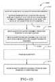
- FIG. 13shows a flow chart for a method of processing a substrate according to an embodiment of the present disclosure.
- Some substrate processing toolsmay include environments that vary in the amount of incident radiation reflected therein. For example, various materials, surface finishes, surface coatings, and/or environmental geometries may affect an amount of thermal radiation reflected within a substrate processing tool, potentially causing a non-uniform temperature field to develop within a substrate being processed in the substrate processing tool.
- a substrate being supported by a susceptor heater assembly that is heated by one or more resistive heatersmay lose heat via thermal radiation to a low pressure environment within a substrate processing tool.
- Such radiative lossesmay increase as the temperature of the susceptor heater assembly increases.
- the radiation capture properties of the substrate processing tool environmentmay affect the radiation loss from the susceptor heater assembly.
- a substrate subjected to an uneven radiation capture environmentmay develop a non-uniform temperature profile within the substrate.
- radiation capturerefers to an object's or an environment's ability to capture thermal radiation.
- non-uniform temperature profilesmay lead to non-uniformities in the processed substrate.
- a semiconductor substrate subjected to a film deposition processmay exhibit a convex, concave, or skewed film thickness profile as a result of the non-uniform temperature that may produce defects and may lead to defective semiconductor devices.
- the disclosed embodimentsrelate to a radiation shield positioned to reflect thermal radiation (including one or more wavelengths of infrared radiation) and/or heat emitted from a susceptor heater assembly used for supporting and heating a substrate within a substrate processing chamber.
- the disclosed embodimentsprovide a radiation shield supported by a structure used to move the susceptor heater assembly within a substrate processing chamber so that the radiation shield moves with the susceptor heater assembly as the susceptor heater assembly is moved from a first position to a second position within the substrate processing chamber.
- the disclosed embodimentsprovide a radiation shield coupled to a susceptor heater assembly where the radiation shield is configured to reflect thermal radiation and/or heat emitted by the susceptor heater assembly to at least two different sides of the susceptor heater assembly.
- a predetermined radiation capture environmentin some embodiments, a uniform radiation capture environment
- such radiation shieldsmay enhance within-substrate temperature uniformity.
- within-substrate processing uniformitye.g., deposition rate, etch rate, and so on
- increasing an amount of thermal radiation and/or heat reflected to the susceptor heater assemblymay reduce power consumed by a heater included in the susceptor heater assembly. Consequently, in some embodiments, enhanced heater control and/or lifetime may be realized. In addition, a reduction in chamber cleaning frequency may also be obtained.
- FIG. 1schematically shows a cross-section of an embodiment of a substrate processing chamber 100 for processing semiconductor substrates in a substrate loading/unloading position.
- substrate processing chamber 100may be included in a suitable substrate processing tool.
- Substrate processing chamber 100may be used for processing semiconductor substrates via any suitable process, e.g., film deposition, film etch, and the like. While the embodiment of substrate processing chamber 100 depicted in FIG. 1 shows a single chamber, it will be appreciated that any suitable number of process chambers may be included in a processing tool so that substrates may be transferred between process chambers without being exposed to ambient conditions.
- some processing toolsmay include just one chamber while other processing tools may include two or more chambers.
- each reaction chambermay include only a single region or a plurality of regions. While not shown in FIG. 1 , various load locks, load ports, and substrate transfer handling robots may be used to transfer substrates between ambient conditions and substrate processing chamber 100 before, during, and after substrate processing.
- substrate processing chamber 100includes an upper reactor 102 within which a reaction zone or processing region 103 is formed where substrate processing occurs.
- Substrate processing chamber 100also includes a lower reactor 104 with a substrate loading region 105 where substrate transfer operations are performed.
- FIG. 1also shows a movable pedestal 106 used to support a substrate within substrate processing chamber 100 .
- the embodiment shown in FIG. 1depicts pedestal 106 in a lowered position within lower reactor 104 . In some settings, pedestal 106 may be placed in a lowered position as a part of transferring a substrate 107 in or out of substrate processing chamber 100 .
- lower reactor 104includes a substrate transfer opening 108 through which substrates are transferred in and out of substrate processing chamber 100 .
- a gate valve(not shown) may be coupled to substrate transfer opening 108 so that substrate processing chamber 100 may be isolated from other portions of a semiconductor processing tool and/or so that substrate processing chamber 100 may be pumped down to a pressure below an ambient pressure (e.g., to a low pressure state).
- pedestal 106comprises a susceptor heater assembly 110 for supporting a substrate within substrate processing chamber 100 .
- Susceptor heater assembly 110includes a heater assembly 112 used to adjust a temperature of the substrate before, during, and/or after substrate processing.
- heater assembly 112may include a resistive platen heater.
- heater assembly 112includes a base 114 and a substrate supporting portion.
- base 114may include one or more channels configured to retain one or more resistive heating elements 116 may be positioned within base 114 .
- heater assembly 112may be a one-piece heater, multiple pieces fused/welded together, or a heater separable from a substrate support.
- Susceptor heater assembly 110is mounted on an elevator 118 so that the substrate may be raised and lowered. In some embodiments, heater assembly 112 may be welded to elevator 118 . Nevertheless, any suitable heating arrangements may be utilized within the reaction chamber.
- Susceptor heater assembly 110is depicted in FIG. 1 as including an optional substrate support surface 111 configured to support substrate 107 .
- substrate support surface 111may be omitted, so that substrate 107 may be supported by a substrate pocket 117 formed into heater assembly 112 .
- substrate pocket 117may be formed into an upper surface of substrate supporting surface of heater assembly 112 or alternatively in an upper surface of a substrate support or susceptor.
- heater assembly 112includes a one-piece heater
- a substrate pocketmay be formed into an upper surface of the one-piece heater, so that substrate 107 rests directly on the one-piece heater.
- FIG. 1also shows a radiation shield 120 coupled to susceptor heater assembly 110 via elevator 118 .
- Radiation shield 120is configured to reflect at least a portion of thermal radiation emitted from susceptor heater assembly 110 back toward susceptor heater assembly 110 .
- radiation shield 120may be configured to reflect thermal radiation and/or heat emitted by susceptor heater assembly 110 to at least two different sides of susceptor heater assembly 110 .
- FIG. 1shows radiation shield 120 adapted to reflect some of the thermal radiation and/or heat emitted from bottom surface 122 and side surface 124 of susceptor heater assembly 110 back to susceptor heater assembly 110 .
- radiation shield 120may be configured so that surfaces of radiation shield 120 reflect thermal radiation and/or heat to at least two different sides of heater assembly 112 .
- radiation shield 120is depicted as extending beyond heater assembly 112 so that thermal radiation and/or heat is reflected to side and/or bottom surfaces of heater assembly 112 . While creating non-uniformity may be a goal, this same arrangement may be used to exaggerate a non-uniformity as may be desired during processing of a substrate.
- radiation shield 120is shaped and sized so that radiation shield 120 is separated from susceptor heater assembly 110 by a gap. Spacing radiation shield 120 and susceptor heater assembly 110 may help maintain an even radiation capture environment around susceptor heater assembly 110 . It will be appreciated that a distance separating radiation shield 120 from susceptor heater assembly 110 may vary according to processing conditions (e.g., susceptor heater assembly temperatures, process pressures, etc.). For example, as pressure increases, thermal convection and/or conduction heat transfer processes may affect temperature fields within the substrate.
- FIG. 2A closer view of example spacing between radiation shield 120 and susceptor heater assembly 110 may be seen in FIG. 2 , which schematically shows an embodiment of radiation shield 120 in a raised position within substrate processing chamber 100 .
- a vertical gap 126 athat defines a space between bottom surface 122 and radiation shield 120 and a horizontal gap 126 b that defines a space between side surface 124 and radiation shield 120 .
- vertical gap 126 ais between 5 and 20 mm, preferably between 10 and 20 mm
- horizontal gap 126 bis between 5 and 15 mm, preferably 7 and 12 mm.
- vertical gap 126 ais approximately 17.25 mm
- horizontal gap 126 bis approximately 9 mm.
- shield 120may be positioned any suitable distance from the bottom surface 122 and the side surface 124 without departing from the spirit and scope of the disclosure.
- such gapsmay define a constant separation between radiation shield 120 and susceptor heater assembly 110 within an acceptable tolerance.
- Such constant separationmay provide a uniform radiation capture and/or reflection environment for susceptor heater assembly 110 , potentially resulting in uniform temperature profile within susceptor heater assembly 110 and/or substrate 107 supported thereon.
- positioning a radiation shield to create a circularly symmetric radiation capture and/or reflection environment around the susceptor heater assemblymay result in a circularly symmetric temperature profile within the substrate.
- a temperature of the substratemeasured at a fixed radial distance from a center of the substrate, may be independent of polar angle.
- such separation between radiation shield 120 and susceptor heater assembly 120may vary.
- separation between susceptor heater assembly 110 and radiation shield 120may vary locally to offset emissivity variations of susceptor heater assembly 110 and/or radiation shield 120 and/or to accommodate various fittings, sensors, and/or other hardware features.
- FIG. 2depicts a chamfered surface 128 formed into radiation shield 120 , which may assist with clearance of various hardware fittings within lower reactor 104 as susceptor heater assembly 110 is raised and lowered.
- a distance between chamfered surface 128 and susceptor heater assembly 110may be less than a distance defining vertical gap 126 a and/or horizontal gap 126 b.
- FIG. 2also shows a space 202 formed between radiation shield 120 and upper reactor 102 .
- space 202may be sized to provide a preselected thermal radiation reflectance from radiation shield 120 while also providing a predetermined gas flow conductance between upper reactor 102 and lower reactor 104 via space 202 when the pedestal is in a raised position, such as during substrate processing shown in FIG. 2 .
- space 202may be sized to provide a desired radiation capture and/or reflection environment for susceptor heater assembly 110 without sealing radiation shield 120 to upper reactor 102 . This may provide differential pumping via space 202 among other portions of substrate processing chamber 100 .
- radiation shield 120may be configured to fit snugly against upper reactor 102 .
- space 202may be approximately 5 mm to 10 mm, and preferably 8.25 mm in one implementation.
- an isolation device 206may be positioned co-planar with an outer surface of shield 120 .
- the outer surface of shield 120may include a sidewall 208 and a bottom wall 210 which may be connected by a chamfered surface 128 .
- the chamfered surface 128may be positioned at an angle between approximately 25 and approximately 65 degrees, or as will described below, at an angle of approximately 90 degrees without a chambered surface.
- susceptor heater assembly 110is shown in a first position with the susceptor heater assembly 110 in a lower position and lift pins extending above a top surface of the susceptor support surface 111 .
- the lift pinsare arranged to receive a substrate 107 on the lift pins.
- the susceptor heater assembly 110is moved upwards in the direction associated with arrows 204 until the susceptor support surface 111 is within the upper chamber 102 and forms at least a portion of a first region.
- a second regionis formed by the inner surface of shield 120
- the third regionis formed by the lower chamber 104 . In this arrangement, the second region may be wholly contained within the third region, or only partially contained within the third region.
- radiation shield 120may be supported by elevator 118 and retained by one or more retaining structures.
- retaining structuresmay include suitable clips.
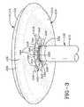
- FIG. 3schematically shows an embodiment of pedestal 106 in a raised position.
- FIGS. 3 and 4illustrate examples of the shield 120 and an attachment apparatus for securing the shield to the susceptor heater assembly 110 .
- shield 120may include a central aperture 212 with a flat surface 214 arranged to assist with securing the shield to the elevator 118 .
- Shield 120may also include a plurality of holes 216 to permit the lift pins to pass there through.
- Susceptor heater assembly 110may also include a raised portion 218 having a flat receiving portion facing shield 120 .
- An alignment tab 220may be located on elevator 118 above a grooved or teeth portion 222 , which is in turn above a concave portion 224 .
- a spacer 226is used to assist with alignment of the shield 120 and susceptor heater assembly 110 .
- the spacer 226may include a top surface 228 with concave surfaces 230 therein.
- the spacer 226may include an opening 232 and an alignment protrusion 234 having a flat surface 236 , both extending from a bottom surface 238 of the spacer.
- a groove 235may be positioned radially inward of alignment protrusion 234 and arranged to receive release pins as will be discussed below.
- the spacermay also include an alignment aperture 240 for cooperation with alignment tab 220 of the elevator 118 .
- the spacer 226is aligned with elevator 118 at alignment aperture 240 and alignment tab 220 , which is in turn aligned with alignment protrusion 234 .
- Shield central aperture 212 and flat surface 214are aligned with alignment protrusion 234 and flat 236 of spacer 226 to thereby orient the susceptor heater assembly 110 , spacer 226 , and shield 120 for proper operation.
- FIGS. 3 and 4illustrate a locking clip 242 having a plurality of engagement protrusions 244 extending generally inward and each having an engagement surface 246 together defining an interior perimeter which is slightly smaller than an outer surface of elevator 118 and specifically grooved portion 222 .
- the locking clip 242may also include a plurality of release tabs 248 extending outward from the outer perimeter of the locking clip.
- Each of the engagement protrusions 244may include a mounting hole 245 for receiving release pins as will be discussed below in greater detail.
- Radiation shield 120may have any suitable shape.
- radiation shield 120may be circularly-shaped so as to provide a uniform thermal radiation reflection and/or absorption environment.
- radiation shield 120may have other suitable shapes, such as polygonal shapes, as the shape of radiation shield 120 may be influenced by heat transfer considerations as well as geometric influences.
- Radiation shield 120may be formed from any suitable material. Non-limiting examples include aluminum, stainless steel, and titanium. Further, it will be appreciated that radiation shield 120 may be formed in any suitable manner. In some embodiments, radiation shield 120 may be formed by metal spinning Other suitable fabrication techniques include casting, stamping, and turning. In some embodiments, radiation shield 120 may include suitable surface treatments and/or surface finishes configured to alter one or more radiation reflectivity characteristics of the material from which it is formed. Such treatments and finishes may be configured to reflect thermal radiation locally (e.g., toward susceptor heater assembly 110 , in some examples) or globally. For example, radiation shield 120 may include a highly polished surface adapted to reflect thermal radiation in some embodiments.
- radiation shield 120may include surface treatments configured to reflect one or more wavelengths of infrared radiation. Further, in some embodiments, radiation shield 120 may be assembled by any suitable technique. For example, in some embodiments, radiation shield sub-assemblies may be welded together or removably connected together.
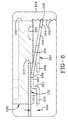
- FIGS. 5 through 7illustrate various operational views of the installation and removal of the shield 120 and specifically the locking clip 242 .
- spacer 226is moved in the direction associated with arrow 204 until the alignment tab 220 and alignment aperture 240 are engaged, such that spacer 226 is arranged to receive shield 120 moved upwards in the direction associated with arrow 204 until the shield central aperture 212 and flat surface 214 are aligned with and in contact with spacer bottom surface 238 .
- locking clip 242is also moved upwards along elevator 118 , with engagement protrusions 244 bent downwards as the locking clip is moved upwards.
- the engagement surfaces 246 of the engagement protrusions 244define an interior perimeter that is smaller in diameter than elevator 118 outer perimeter, there is a frictional engagement between elevator 118 and engagement protrusions 244 , which requires that the engagement protrusions 244 are essentially pulled upwards by the vertical movement of the locking clip 242 .
- the engagement protrusions 244fit within grooved portion 222 and only permit movement upwards in the direction associated with arrow 204 , thereby preventing unlocking or separation of the locking clip, shield, and spacer from the susceptor heater assembly 110 .
- release tabs 248are spaced apart by a gap 250 formed between the release tabs and the shield 120 .
- a mounting surface 252is located on a top side of locking clip 242 and contacts bottom wall 210 of shield 120 to secure the shield to the spacer and ultimately the susceptor heater assembly 110 .
- the locking clip 242may also include a spacing wall 254 which provides the gap 250 between release tabs 248 and the bottom wall 210 of shield 120 .
- the gap 250permits removal of the locking clip 242 , the shield 120 , and the spacer 226 by allowing a user to locate his/her fingers or a tool in gap 250 as will be discussed in greater detail below.
- FIG. 7illustrates the removal of locking clip 242 , the shield 120 , and the spacer 226 being removed with a removal tool 260 generally includes release pins 262 having a first end 262 a and a second end 262 b , with second end 262 b removably positionable within mounting holes 245 to bias engagement protrusions 244 in the direction associated with arrows 306 .
- Second end 262 bincludes a recessed area 264 which is arranged to fit within mounting holes 245 and may extending into groove 235 as may be necessary.
- the removal toolalso includes a clamping member 270 having a flange 272 with threaded holes 274 therein, a plurality of spacing members 276 with gripping arms 278 connected to spacing member 276 and opposite flange 272 . Gripping arms 278 are preferably sized and shaped to fit within gap 250 between shield 120 and release tabs 248 .
- clamping member 270is arranged to be moved upwards in the direction associated with arrows 302 around the release tabs 248 and then rotated to be in contact with the release tabs and positioned in gap 250 .
- the removal tool 260also includes a washer 280 having a plurality of threaded apertures 282 for receiving bolts 290 and an aperture 284 so that the washer can travel around elevator shaft 118 .
- Release pins 262are positioned within mounting holes 245 with recessed area 264 positioned within groove 235 if necessary.
- clamping mechanismis positioned so that gripping arms 278 are within gaps 250 between release tabs 248 and shield 120 .
- the washer 280is then placed in contact with pins 260 and particularly first end 262 a of the release pins.
- Bolts 290are then secured through threaded apertures 272 and 282 steadily around the perimeter of the washer so that washer 280 is pulled upwards in the direction associated with arrows 302 by rotational movement of bolts 290 to displace the bolts in the direction associated with arrows 300 .
- the upward movement of washer 280creates a rotational movement of release pins 262 and imparts rotational movement in the direction associated with arrows 304 .
- the rotational movement in the direction associated with arrows 304imparts a bending force on engagement protrusions 244 in the direction associated with arrows 306 .
- the bending force 306 imparted on the engagement protrusionsincreases the interior perimeter 246 to a point that locking clip 242 can be moved in the direction associated with arrow 308 and removed from elevator 118 .
- shield 120may also then be removed with or without spacer 226 .
- any suitable order of operationsmay be utilized and the directions may be reversed if the removal operation is performed with susceptor assembly 110 on a bench and upside down with elevator 118 pointing upwards. Further, the installation process may require a similar operation and merely be performed in reverse order. It should also be noted and appreciated that a number of other shield attachment means may be utilized without departing from the spirit and scope of the disclosure so long as the shield is connected to the elevator or other suitable reactor components.
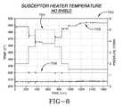
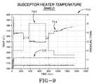
- FIGS. 8 and 9show example temperature data for an unshielded susceptor heater assembly (shown as data 702 ) compared to temperature data for a susceptor heater assembly employing a radiation shield according to an embodiment of the present disclosure (shown as data 704 ).
- the heater poweris adjusted to control the temperature of the susceptor (shown as susceptor temperature setting 706 in FIG. 8 ) to a preselected value of 420° C. for example.
- heat lost from the susceptor heater assemblymay cause the power consumed by the heater, and thus the heater temperature, to necessarily increase.
- the example temperature data shown in FIGS. 8 and 9was collected in a reactor controlled to various pressure setpoints (shown as reactor pressure setting 708 in FIG. 8 ) between 1.5 and 5 Torr.
- heater temperature 710 corresponding to the unshielded susceptor heater assemblywas approximately 15° C. higher at 2 Torr and approximately 22° C. higher at 5 Torr relative to the heater temperature exhibited by the shielded susceptor heater assembly, as shown in heater temperature 712 .
- radiation shieldingmay reduce heater power consumption, which may increase heater service life, or to increase the ultimate substrate temperature for the same heater temperature since more heat from the heater is directed into the susceptor heater assembly and substrate.
- FIGS. 10 and 11show example substrate temperature uniformity data for an unshielded susceptor heater assembly (shown as data 802 ) compared to substrate temperature uniformity data for a susceptor heater assembly employing a radiation shield according to an embodiment of the present disclosure (shown as data 804 ).
- the heater poweris adjusted to control the temperature of the susceptor to a preselected value of 420° C. while the reactor was controlled to various pressure setpoints between 1.5 and 5 Torr.
- FIG. 10shows example substrate temperature uniformity data for an unshielded susceptor heater assembly (shown as data 802 ) compared to substrate temperature uniformity data for a susceptor heater assembly employing a radiation shield according to an embodiment of the present disclosure (shown as data 804 ).
- the heater poweris adjusted to control the temperature of the susceptor to a preselected value of 420° C. while the reactor was controlled to various pressure setpoints between 1.5 and 5 Torr.
- a mean substrate temperature 806 corresponding to the unshielded susceptor heater assemblywas approximately 1° C. higher than a mean temperature 808 corresponding to the shielded susceptor heater assembly.
- a substrate temperature range 810 corresponding to the unshielded susceptor heater assemblywas approximately 1° C. higher than a substrate temperature range 812 corresponding to the shielded susceptor heater assembly. Accordingly, shielding the susceptor heater assembly may, in some examples, decrease within-substrate temperature non-uniformities. This potentially may enhance substrate processing quality, and may enhance downstream substrate processing quality as well.
- Appendix Aalso shows embodiments of radiation shields according to the present disclosure and temperature data related thereto.
- FIG. 12illustrates another embodiment of a substrate support assembly 400 with a pedestal heater 402 and a separable susceptor 404 with a wafer 406 positioned on the susceptor.
- a shield 408functions similar to shield 120 and includes a sidewall 410 and a bottom wall 412 positioned at approximately 90 degrees to one another.
- Shield 408may be secured to a pedestal heater shaft 414 with a clip 416 selectively positioned in a recess 418 of the heater shaft. Accordingly, the arrangement, operation, and installation/removal of shields 120 and 408 are similar to one another and provide similar benefits of increased heater control, wafer heat distribution control, reduced power consumption, and less frequent chamber cleaning requirements.
- FIG. 13shows a flow chart for an embodiment of a method 1300 for processing a substrate in a substrate processing chamber.
- Method 1300may be performed by any suitable hardware and software. It will be appreciated that portions of the processes described in method 1300 may be omitted, reordered, and/or supplemented without departing from the scope of the present disclosure.
- method 1300includes supporting a substrate on a susceptor heater assembly.
- method 1300may include, at 1304 , supporting a substrate on a susceptor heater assembly coupled to a radiation shield configured to reflect thermal radiation to at least two sides of the susceptor heater assembly.
- method 1300includes moving the susceptor heater assembly from a first position to a second position.
- method 1300may include, at 1308 , moving the susceptor heater assembly so that a radiation shield moves with the susceptor heater assembly.
- method 1300includes processing the substrate.
- method 1300includes moving the susceptor heater assembly from the second position to the first position.
- Embodiments of method 1300may be performed by a system process controller comprising a data-holding subsystem comprising instructions executable by a logic subsystem to perform the processes described herein. Any suitable system process controller may be employed without departing from the scope of the present disclosure.
- a system process controller(not specifically shown) may be provided for controlling the example substrate processing chamber 100 .
- the system process controllermay operate process module control subsystems, such as gas control subsystems, pressure control subsystems, temperature control subsystems, electrical control subsystems, and mechanical control subsystems.
- process module control subsystemssuch as gas control subsystems, pressure control subsystems, temperature control subsystems, electrical control subsystems, and mechanical control subsystems.
- Such control subsystemsmay receive various signals provided by sensors, relays, and controllers and make suitable adjustments in response.
- the system process controllercomprises a computing system that includes a data-holding subsystem and a logic subsystem.
- the data-holding subsystemmay include one or more physical, non-transitory, devices configured to hold data and/or instructions executable by the logic subsystem to implement the methods and processes described herein.
- the logic subsystemmay include one or more physical devices configured to execute one or more instructions stored in the data-holding subsystem.
- the logic subsystemmay include one or more processors that are configured to execute software instructions.
- such instructionsmay control the execution of process recipes.
- a process recipeincludes a sequential description of process parameters used to process a substrate, such parameters including time, temperature, pressure, and concentration, etc., as well as various parameters describing electrical, mechanical, and environmental aspects of the tool during substrate processing.
- the instructionsmay also control the execution of various maintenance recipes used during maintenance procedures and the like.
- such instructionsmay be stored on removable computer-readable storage media, which may be used to store and/or transfer data and/or instructions executable to implement the methods and processes described herein. It will be appreciated that any suitable removable computer-readable storage media may be employed without departing from the scope of the present disclosure. Non-limiting examples include DVDs, CD-ROMs, floppy discs, and flash drives.
Landscapes
- Engineering & Computer Science (AREA)
- Manufacturing & Machinery (AREA)
- Physics & Mathematics (AREA)
- Toxicology (AREA)
- Condensed Matter Physics & Semiconductors (AREA)
- General Physics & Mathematics (AREA)
- Health & Medical Sciences (AREA)
- Computer Hardware Design (AREA)
- Microelectronics & Electronic Packaging (AREA)
- Power Engineering (AREA)
- Container, Conveyance, Adherence, Positioning, Of Wafer (AREA)
- Chemical Vapour Deposition (AREA)
- Physical Or Chemical Processes And Apparatus (AREA)
Abstract
Description
This application claims the benefit of U.S. Provisional Application No. 61/563,428, filed on Nov. 23, 2011, the disclosure of which is hereby incorporated herein by reference.
It can be difficult to heat a substrate being processed in a substrate processing tool. Variation in substrate heating may lead to within-substrate temperature variations. Such within-substrate temperature variations may lead to within-substrate processing non-uniformities. In some settings, substrates exhibiting such non-uniformities may produce defective devices. Further, deposition product may be deposited in the lower processing chamber, leading to reduced temperatures in the reaction chamber and therefore increased power consumption to overcome the inadequate heating. Additionally, the build-up of deposition product in the chamber can lead to premature chamber cleaning requirements and increased cost.
Aspects of this document relate to reaction chambers for processing substrates. In one aspect, a reaction chamber includes a substrate supporting member positioned within the reaction chamber, the reaction chamber having a first region and a second region, a shield positioned within the second region and movable with the substrate supporting member, and wherein the shield is adjacent at least a bottom surface of the substrate supporting member.
In an implementation, the shield may be adjacent a sidewall of the substrate supporting member. The first region may be a substrate processing region and the second region may be a substrate loading region. The first region may be positioned above the second region in the reaction chamber. The reaction chamber may further include an isolation device at least partially separating the first and second regions. The reaction chamber may further include a gap formed between the shield and the isolation device. The gap may be between 5 and 10 mm. The shield may be spaced from the substrate supporting member between 5 and 20 mm.
The shield may further include a bottom member and a sidewall member. The bottom member and the sidewall member may connect to one another at an angle of approximately 90 degrees. The bottom member and the sidewall member may connect to one another at an angle between approximately 25 and 65 degrees. The shield may be secured to a shaft of the substrate supporting member. The shield may retain heat generated by the substrate support assembly. The substrate support assembly may further include a heater.
In another aspect, a shield for processing a substrate may include a bottom member having an aperture to surround a substrate support member shaft, a sidewall member extending upward at an angle from the bottom member, wherein the bottom member is positioned below the substrate support member and the sidewall member is positioned around the substrate support member, and wherein the shield moves vertically with the substrate support member.
In an implementation, the shield may be spaced from the substrate supporting member between 5 and 20 mm. The shield sidewall member may avoid contact with a reaction chamber wall. The sidewall may further include a top surface spaced from a reaction chamber surface between approximately 5 and 10 mm.
In another aspect, a reaction chamber may include a first region, a second region, and a third region, the first region positioned above the second and third regions, and adapted for processing a substrate, the second region positioned below the first region and adapted for loading the substrate in the reaction chamber, the third region positioned between the first region and the second region, and wherein the third region is movable within the second region.
In an implementation, the reaction chamber may further include a shield defining a barrier between the second region and the third region. The shield may be movable within the second region. A third region volume varies based on a position of the substrate support member.
In still another aspect, a method of heating a substrate in a processing region includes providing a shield within the processing chamber below a substrate support member, loading a substrate in a processing region of the processing chamber, activating a heater, and radiating heat from the shield to the substrate support member.
In an implementation, the method may further include the step of moving the substrate support member from a loading position to a processing position. The method may further include the step of monitoring the temperature of a cavity between the substrate support member and the shield.
Aspects and implementations of the disclosure presented here are described below in the drawings and detailed description. Unless specifically noted, it is intended that the words and phrases in the specification and the claims be given their plain, ordinary, and accustomed meaning to those of ordinary skill in the applicable arts. The inventors are fully aware that they can be their own lexicographers if desired. The inventors expressly elect, as their own lexicographers, to use only the plain and ordinary meaning of terms in the specification and claims unless they clearly state otherwise and then further, expressly set forth the “special” definition of that term and explain how it differs from the plain and ordinary meaning. Absent such clear statements of intent to apply a “special” definition, it is the inventors' intent and desire that the simple, plain and ordinary meaning of the terms be applied to the interpretation of the specification and claims.
The inventors are also aware of the normal precepts of English grammar Thus, if a noun, term, or phrase is intended to be further characterized, specified, or narrowed in some way, then such noun, term, or phrase will expressly include additional adjectives, descriptive terms, or other modifiers in accordance with the normal precepts of English grammar Absent the use of such adjectives, descriptive terms, or modifiers, it is the intent that such nouns, terms, or phrases be given their plain, and ordinary English meaning to those skilled in the applicable arts as set forth above.
The foregoing and other aspects, features, and advantages will be apparent to those artisans of ordinary skill in the art from the DESCRIPTION and DRAWINGS, and from the CLAIMS.
Embodiments of the present invention will hereinafter be described in conjunction with the appended drawings, where like designations denote like elements, and:
Some substrate processing tools may include environments that vary in the amount of incident radiation reflected therein. For example, various materials, surface finishes, surface coatings, and/or environmental geometries may affect an amount of thermal radiation reflected within a substrate processing tool, potentially causing a non-uniform temperature field to develop within a substrate being processed in the substrate processing tool.
For example, a substrate being supported by a susceptor heater assembly that is heated by one or more resistive heaters may lose heat via thermal radiation to a low pressure environment within a substrate processing tool. Such radiative losses may increase as the temperature of the susceptor heater assembly increases. Further, because the area between a susceptor heater assembly and the surrounding low pressure environment may be non-uniform in some settings, the radiation capture properties of the substrate processing tool environment may affect the radiation loss from the susceptor heater assembly. In turn, a substrate subjected to an uneven radiation capture environment may develop a non-uniform temperature profile within the substrate. As used herein, radiation capture refers to an object's or an environment's ability to capture thermal radiation. Because some substrate processing operations may depend on temperature, such non-uniform temperature profiles may lead to non-uniformities in the processed substrate. For example, a semiconductor substrate subjected to a film deposition process may exhibit a convex, concave, or skewed film thickness profile as a result of the non-uniform temperature that may produce defects and may lead to defective semiconductor devices.
Some previous approaches to reduce the effect of the surrounding radiation capture environment on within-substrate temperature fields have employed fixed radiation shields positioned within portions of processing tools. However, such fixed shields frequently have gaps to allow substrate transfer robots to move substrates within the tool, or that otherwise provide an incomplete and/or inconsistent radiation capture environment. In some other cases, such fixed shields may be irregularly formed so that there may be non-uniform view factors between the susceptor heater assembly and the fixed shield.
Accordingly, the disclosed embodiments relate to a radiation shield positioned to reflect thermal radiation (including one or more wavelengths of infrared radiation) and/or heat emitted from a susceptor heater assembly used for supporting and heating a substrate within a substrate processing chamber. For example, the disclosed embodiments provide a radiation shield supported by a structure used to move the susceptor heater assembly within a substrate processing chamber so that the radiation shield moves with the susceptor heater assembly as the susceptor heater assembly is moved from a first position to a second position within the substrate processing chamber. As another example, the disclosed embodiments provide a radiation shield coupled to a susceptor heater assembly where the radiation shield is configured to reflect thermal radiation and/or heat emitted by the susceptor heater assembly to at least two different sides of the susceptor heater assembly. By maintaining a predetermined radiation capture environment (in some embodiments, a uniform radiation capture environment), such radiation shields may enhance within-substrate temperature uniformity. In turn, within-substrate processing uniformity (e.g., deposition rate, etch rate, and so on) may be enhanced, potentially enhancing substrate deposited film quality provided by the substrate processing chamber and/or at downstream processing operations. Further, in some examples, increasing an amount of thermal radiation and/or heat reflected to the susceptor heater assembly may reduce power consumed by a heater included in the susceptor heater assembly. Consequently, in some embodiments, enhanced heater control and/or lifetime may be realized. In addition, a reduction in chamber cleaning frequency may also be obtained.
As shown inFIGS. 1 and 2 ,substrate processing chamber 100 includes anupper reactor 102 within which a reaction zone orprocessing region 103 is formed where substrate processing occurs.Substrate processing chamber 100 also includes alower reactor 104 with asubstrate loading region 105 where substrate transfer operations are performed.FIG. 1 also shows amovable pedestal 106 used to support a substrate withinsubstrate processing chamber 100. The embodiment shown inFIG. 1 depictspedestal 106 in a lowered position withinlower reactor 104. In some settings,pedestal 106 may be placed in a lowered position as a part of transferring asubstrate 107 in or out ofsubstrate processing chamber 100.
In the embodiment shown inFIG. 1 ,lower reactor 104 includes a substrate transfer opening108 through which substrates are transferred in and out ofsubstrate processing chamber 100. In some embodiments, a gate valve (not shown) may be coupled to substrate transfer opening108 so thatsubstrate processing chamber 100 may be isolated from other portions of a semiconductor processing tool and/or so thatsubstrate processing chamber 100 may be pumped down to a pressure below an ambient pressure (e.g., to a low pressure state).
In the example shown inFIG. 1 ,pedestal 106 comprises asusceptor heater assembly 110 for supporting a substrate withinsubstrate processing chamber 100.Susceptor heater assembly 110 includes aheater assembly 112 used to adjust a temperature of the substrate before, during, and/or after substrate processing. In some embodiments,heater assembly 112 may include a resistive platen heater. In the embodiment shown inFIG. 1 ,heater assembly 112 includes abase 114 and a substrate supporting portion. In some embodiments,base 114 may include one or more channels configured to retain one or moreresistive heating elements 116 may be positioned withinbase 114. In some other embodiments,heater assembly 112 may be a one-piece heater, multiple pieces fused/welded together, or a heater separable from a substrate support.Susceptor heater assembly 110 is mounted on anelevator 118 so that the substrate may be raised and lowered. In some embodiments,heater assembly 112 may be welded toelevator 118. Nevertheless, any suitable heating arrangements may be utilized within the reaction chamber.
In the embodiment shown inFIG. 1 ,radiation shield 120 is shaped and sized so thatradiation shield 120 is separated fromsusceptor heater assembly 110 by a gap. Spacingradiation shield 120 andsusceptor heater assembly 110 may help maintain an even radiation capture environment aroundsusceptor heater assembly 110. It will be appreciated that a distance separatingradiation shield 120 fromsusceptor heater assembly 110 may vary according to processing conditions (e.g., susceptor heater assembly temperatures, process pressures, etc.). For example, as pressure increases, thermal convection and/or conduction heat transfer processes may affect temperature fields within the substrate. A closer view of example spacing betweenradiation shield 120 andsusceptor heater assembly 110 may be seen inFIG. 2 , which schematically shows an embodiment ofradiation shield 120 in a raised position withinsubstrate processing chamber 100.
For example, avertical gap 126athat defines a space betweenbottom surface 122 andradiation shield 120 and a horizontal gap126bthat defines a space betweenside surface 124 andradiation shield 120. In one implementation,vertical gap 126ais between 5 and 20 mm, preferably between 10 and 20 mm, while horizontal gap126bis between 5 and 15 mm, preferably 7 and 12 mm. In one implementation,vertical gap 126ais approximately 17.25 mm, while horizontal gap126bis approximately 9 mm. Nevertheless, shield120 may be positioned any suitable distance from thebottom surface 122 and theside surface 124 without departing from the spirit and scope of the disclosure.
In some embodiments, such gaps may define a constant separation betweenradiation shield 120 andsusceptor heater assembly 110 within an acceptable tolerance. Such constant separation may provide a uniform radiation capture and/or reflection environment forsusceptor heater assembly 110, potentially resulting in uniform temperature profile withinsusceptor heater assembly 110 and/orsubstrate 107 supported thereon. For example, in a scenario where a circularly symmetric substrate is supported on a circularly symmetric substrate heater assembly, positioning a radiation shield to create a circularly symmetric radiation capture and/or reflection environment around the susceptor heater assembly may result in a circularly symmetric temperature profile within the substrate. In turn, a temperature of the substrate, measured at a fixed radial distance from a center of the substrate, may be independent of polar angle.
It will be appreciated that, in some embodiments, such separation betweenradiation shield 120 andsusceptor heater assembly 120 may vary. For example, separation betweensusceptor heater assembly 110 andradiation shield 120 may vary locally to offset emissivity variations ofsusceptor heater assembly 110 and/orradiation shield 120 and/or to accommodate various fittings, sensors, and/or other hardware features. For example,FIG. 2 depicts a chamferedsurface 128 formed intoradiation shield 120, which may assist with clearance of various hardware fittings withinlower reactor 104 assusceptor heater assembly 110 is raised and lowered. In some embodiments, a distance betweenchamfered surface 128 andsusceptor heater assembly 110 may be less than a distance definingvertical gap 126aand/or horizontal gap126b.
Referring toFIG. 1 ,susceptor heater assembly 110 is shown in a first position with thesusceptor heater assembly 110 in a lower position and lift pins extending above a top surface of thesusceptor support surface 111. The lift pins are arranged to receive asubstrate 107 on the lift pins. Moving toFIG. 2 , thesusceptor heater assembly 110 is moved upwards in the direction associated witharrows 204 until thesusceptor support surface 111 is within theupper chamber 102 and forms at least a portion of a first region. A second region is formed by the inner surface ofshield 120, while the third region is formed by thelower chamber 104. In this arrangement, the second region may be wholly contained within the third region, or only partially contained within the third region.
In some embodiments,radiation shield 120 may be supported byelevator 118 and retained by one or more retaining structures. In some embodiments, such retaining structures may include suitable clips.FIG. 3 schematically shows an embodiment ofpedestal 106 in a raised position.
Aspacer 226 is used to assist with alignment of theshield 120 andsusceptor heater assembly 110. Thespacer 226 may include atop surface 228 withconcave surfaces 230 therein. Thespacer 226 may include anopening 232 and analignment protrusion 234 having aflat surface 236, both extending from abottom surface 238 of the spacer. Agroove 235 may be positioned radially inward ofalignment protrusion 234 and arranged to receive release pins as will be discussed below. Finally, the spacer may also include analignment aperture 240 for cooperation withalignment tab 220 of theelevator 118. Accordingly, thespacer 226 is aligned withelevator 118 atalignment aperture 240 andalignment tab 220, which is in turn aligned withalignment protrusion 234. Shieldcentral aperture 212 andflat surface 214 are aligned withalignment protrusion 234 and flat236 ofspacer 226 to thereby orient thesusceptor heater assembly 110,spacer 226, and shield120 for proper operation.
Referring now toFIG. 6 , which is an enlarged sectional view of the section labeled FIG-6 inFIG. 5 . As can be seen in greater detail, releasetabs 248 are spaced apart by agap 250 formed between the release tabs and theshield 120. A mounting surface252 is located on a top side of lockingclip 242 and contactsbottom wall 210 ofshield 120 to secure the shield to the spacer and ultimately thesusceptor heater assembly 110. Thelocking clip 242 may also include aspacing wall 254 which provides thegap 250 betweenrelease tabs 248 and thebottom wall 210 ofshield 120. Advantageously, thegap 250 permits removal of thelocking clip 242, theshield 120, and thespacer 226 by allowing a user to locate his/her fingers or a tool ingap 250 as will be discussed in greater detail below.
Having described all of the removal tool260 components, the operation will now be described. Release pins262 are positioned within mountingholes 245 with recessedarea 264 positioned withingroove 235 if necessary. Next, clamping mechanism is positioned so that grippingarms 278 are withingaps 250 betweenrelease tabs 248 andshield 120. The washer280 is then placed in contact with pins260 and particularly first end262aof the release pins.Bolts 290 are then secured through threadedapertures arrows 302 by rotational movement ofbolts 290 to displace the bolts in the direction associated witharrows 300. The upward movement of washer280 creates a rotational movement of release pins262 and imparts rotational movement in the direction associated witharrows 304. The rotational movement in the direction associated witharrows 304 imparts a bending force onengagement protrusions 244 in the direction associated witharrows 306. Accordingly, the bendingforce 306 imparted on the engagement protrusions increases theinterior perimeter 246 to a point that lockingclip 242 can be moved in the direction associated witharrow 308 and removed fromelevator 118. In the same manner, shield120 may also then be removed with or withoutspacer 226. While the above description uses certain orders of operation and directions (upward or downward), any suitable order of operations may be utilized and the directions may be reversed if the removal operation is performed withsusceptor assembly 110 on a bench and upside down withelevator 118 pointing upwards. Further, the installation process may require a similar operation and merely be performed in reverse order. It should also be noted and appreciated that a number of other shield attachment means may be utilized without departing from the spirit and scope of the disclosure so long as the shield is connected to the elevator or other suitable reactor components.
In some settings, embodiments of radiation shields like those disclosed herein potentially may reduce power consumed by a heater included in a susceptor or even with the susceptor separated from the heater. For example,FIGS. 8 and 9 show example temperature data for an unshielded susceptor heater assembly (shown as data702) compared to temperature data for a susceptor heater assembly employing a radiation shield according to an embodiment of the present disclosure (shown as data704). In the examples shown inFIGS. 8 and 9 , the heater power is adjusted to control the temperature of the susceptor (shown as susceptor temperature setting706 inFIG. 8 ) to a preselected value of 420° C. for example. Accordingly, heat lost from the susceptor heater assembly may cause the power consumed by the heater, and thus the heater temperature, to necessarily increase. The example temperature data shown inFIGS. 8 and 9 was collected in a reactor controlled to various pressure setpoints (shown as reactor pressure setting708 inFIG. 8 ) between 1.5 and 5 Torr. As shown inFIG. 9 ,heater temperature 710 corresponding to the unshielded susceptor heater assembly was approximately 15° C. higher at 2 Torr and approximately 22° C. higher at 5 Torr relative to the heater temperature exhibited by the shielded susceptor heater assembly, as shown inheater temperature 712. Accordingly, it will be appreciated that radiation shielding according to the disclosed embodiments may reduce heater power consumption, which may increase heater service life, or to increase the ultimate substrate temperature for the same heater temperature since more heat from the heater is directed into the susceptor heater assembly and substrate.
Further, in some settings, embodiments of radiation shields like those disclosed herein potentially may enhance within-substrate temperature uniformity. For example,FIGS. 10 and 11 show example substrate temperature uniformity data for an unshielded susceptor heater assembly (shown as data802) compared to substrate temperature uniformity data for a susceptor heater assembly employing a radiation shield according to an embodiment of the present disclosure (shown as data804). In the examples shown inFIG. 10 , the heater power is adjusted to control the temperature of the susceptor to a preselected value of 420° C. while the reactor was controlled to various pressure setpoints between 1.5 and 5 Torr. As shown inFIG. 10 , amean substrate temperature 806 corresponding to the unshielded susceptor heater assembly was approximately 1° C. higher than amean temperature 808 corresponding to the shielded susceptor heater assembly. Further, asubstrate temperature range 810 corresponding to the unshielded susceptor heater assembly was approximately 1° C. higher than asubstrate temperature range 812 corresponding to the shielded susceptor heater assembly. Accordingly, shielding the susceptor heater assembly may, in some examples, decrease within-substrate temperature non-uniformities. This potentially may enhance substrate processing quality, and may enhance downstream substrate processing quality as well. Appendix A also shows embodiments of radiation shields according to the present disclosure and temperature data related thereto.
It will be understood that the hardware described herein may be used when processing substrates in a substrate processing chamber.FIG. 13 shows a flow chart for an embodiment of amethod 1300 for processing a substrate in a substrate processing chamber.Method 1300 may be performed by any suitable hardware and software. It will be appreciated that portions of the processes described inmethod 1300 may be omitted, reordered, and/or supplemented without departing from the scope of the present disclosure.
At1302,method 1300 includes supporting a substrate on a susceptor heater assembly. In some embodiments,method 1300 may include, at1304, supporting a substrate on a susceptor heater assembly coupled to a radiation shield configured to reflect thermal radiation to at least two sides of the susceptor heater assembly. At1306,method 1300 includes moving the susceptor heater assembly from a first position to a second position. In some embodiments,method 1300 may include, at1308, moving the susceptor heater assembly so that a radiation shield moves with the susceptor heater assembly. At1310,method 1300 includes processing the substrate. At1312,method 1300 includes moving the susceptor heater assembly from the second position to the first position.
Embodiments ofmethod 1300 may be performed by a system process controller comprising a data-holding subsystem comprising instructions executable by a logic subsystem to perform the processes described herein. Any suitable system process controller may be employed without departing from the scope of the present disclosure.
For example, a system process controller (not specifically shown) may be provided for controlling the examplesubstrate processing chamber 100. The system process controller may operate process module control subsystems, such as gas control subsystems, pressure control subsystems, temperature control subsystems, electrical control subsystems, and mechanical control subsystems. Such control subsystems may receive various signals provided by sensors, relays, and controllers and make suitable adjustments in response.
The system process controller comprises a computing system that includes a data-holding subsystem and a logic subsystem. The data-holding subsystem may include one or more physical, non-transitory, devices configured to hold data and/or instructions executable by the logic subsystem to implement the methods and processes described herein. The logic subsystem may include one or more physical devices configured to execute one or more instructions stored in the data-holding subsystem. The logic subsystem may include one or more processors that are configured to execute software instructions.
In some embodiments, such instructions may control the execution of process recipes. Generally, a process recipe includes a sequential description of process parameters used to process a substrate, such parameters including time, temperature, pressure, and concentration, etc., as well as various parameters describing electrical, mechanical, and environmental aspects of the tool during substrate processing. The instructions may also control the execution of various maintenance recipes used during maintenance procedures and the like. In some embodiments, such instructions may be stored on removable computer-readable storage media, which may be used to store and/or transfer data and/or instructions executable to implement the methods and processes described herein. It will be appreciated that any suitable removable computer-readable storage media may be employed without departing from the scope of the present disclosure. Non-limiting examples include DVDs, CD-ROMs, floppy discs, and flash drives.
It is to be understood that the configurations and/or approaches described herein are exemplary in nature, and that these specific embodiments or examples are not to be considered in a limiting sense, because numerous variations are possible. The specific routines or methods described herein may represent one or more of any number of processing strategies. Thus, the various acts illustrated may be performed in the sequence illustrated, in other sequences, or omitted in some cases.
The subject matter of the present disclosure includes all novel and nonobvious combinations and subcombinations of the various processes, systems and configurations, and other features, functions, acts, and/or properties disclosed herein, as well as any and all equivalents thereof.
Claims (25)
1. A reaction chamber comprising:
a substrate supporting member comprising a shaft and positioned within the reaction chamber;
the reaction chamber having a first region and a second region;
a shield positioned within the second region and movable with the substrate supporting member; and,
a spacer to space apart the shield and the substrate support member and to space apart the shield and the shaft,
wherein the shield is adjacent at least a bottom surface of the substrate supporting member.
2. The reaction chamber ofclaim 1 wherein the shield is adjacent a sidewall of the substrate supporting member.
3. The reaction chamber ofclaim 1 wherein the first region is a substrate processing region and the second region is a substrate loading region.
4. The reaction chamber ofclaim 3 wherein the first region is positioned above the second region in the reaction chamber.
5. The reaction chamber ofclaim 1 further comprising an isolation device at least partially separating the first and second regions.
6. The reaction chamber ofclaim 5 further comprising a gap formed between the shield and the isolation device.
7. The reaction chamber ofclaim 6 wherein the gap is between 5 and 10 mm.
8. The reaction chamber ofclaim 1 wherein the shield is spaced from the substrate supporting member between 5 and 20 mm.
9. The reaction chamber ofclaim 1 wherein the shield further comprises a bottom member and a sidewall member.
10. The reaction chamber ofclaim 9 wherein the bottom member and the sidewall member connect to one another at an angle of approximately 90 degrees.
11. The reaction chamber ofclaim 9 wherein the bottom member and the sidewall member connect to one another at an angle between approximately 25 and 65 degrees.
12. The reaction chamber ofclaim 1 wherein the shield is secured to the shaft of the substrate supporting member.
13. The reaction chamber ofclaim 1 wherein the shield retains heat generated by the substrate support assembly.
14. The reaction chamber ofclaim 1 wherein the substrate support assembly further comprises a heater.
15. A shield for processing a substrate comprising:
a bottom member having an aperture to surround a substrate support member shaft;
a sidewall member extending upward at an angle from the bottom member;
wherein the bottom member is positioned below the substrate support member and the sidewall member is positioned around the substrate support member;
wherein the bottom member comprises a central aperture comprising a flat surface to assist securing the shield to a shaft of the substrate support member, and,
wherein the shield moves vertically with the substrate support member.
16. The shield for processing a substrate ofclaim 15 wherein the shield is spaced from the substrate supporting member between 5 and 20 mm.
17. The shield for processing a substrate ofclaim 15 wherein the shield sidewall member does not contact a reaction chamber wall.
18. The shield for processing a substrate ofclaim 15 wherein the sidewall further comprises a top surface spaced from a reaction chamber surface between 5 and 10 mm.
19. A reaction chamber comprising:
a first region, a second region, and a third region;
the first region positioned above the second and third regions, and adapted for processing a substrate;
the second region positioned below the first region and adapted for loading the substrate in the reaction chamber;
the third region positioned between the first region and the second region; and
wherein the third region is movable via a shaft within the second region, and
wherein a shield removably attached to the shaft defines a barrier between the second region and the third region.
20. The reaction chamber ofclaim 19 further comprising a spacer further defining the barrier between the second region and the third region.
21. The reaction chamber ofclaim 20 wherein the shield is movable within the second region.
22. The reaction chamber ofclaim 21 wherein a third region volume varies based on a position of the substrate support member.
23. A method of heating a substrate in a processing region comprising:
providing a shield within the processing chamber below a substrate support member attached to a shaft;
providing a spacer to space apart the shield and the substrate sue sort member and to space apart the shield and the shaft;
loading a substrate in a processing region of the processing chamber;
activating a heater; and, radiating heat from the shield to the substrate support member.
24. The method ofclaim 23 further comprising the step of moving the substrate support member from a loading position to a processing position.
25. The method ofclaim 23 further comprising the step of monitoring the temperature of a cavity between the substrate support member and the shield.
Priority Applications (1)
| Application Number | Priority Date | Filing Date | Title |
|---|---|---|---|
| US13/677,133US9167625B2 (en) | 2011-11-23 | 2012-11-14 | Radiation shielding for a substrate holder |
Applications Claiming Priority (2)
| Application Number | Priority Date | Filing Date | Title |
|---|---|---|---|
| US201161563428P | 2011-11-23 | 2011-11-23 | |
| US13/677,133US9167625B2 (en) | 2011-11-23 | 2012-11-14 | Radiation shielding for a substrate holder |
Publications (2)
| Publication Number | Publication Date |
|---|---|
| US20130126515A1 US20130126515A1 (en) | 2013-05-23 |
| US9167625B2true US9167625B2 (en) | 2015-10-20 |
Family
ID=47501409
Family Applications (1)
| Application Number | Title | Priority Date | Filing Date |
|---|---|---|---|
| US13/677,133Active2034-01-21US9167625B2 (en) | 2011-11-23 | 2012-11-14 | Radiation shielding for a substrate holder |
Country Status (6)
| Country | Link |
|---|---|
| US (1) | US9167625B2 (en) |
| KR (1) | KR102021163B1 (en) |
| CN (1) | CN104081513B (en) |
| DE (1) | DE112012004884T5 (en) |
| TW (1) | TWI555109B (en) |
| WO (1) | WO2013078066A1 (en) |
Cited By (4)
| Publication number | Priority date | Publication date | Assignee | Title |
|---|---|---|---|---|
| USD766850S1 (en)* | 2014-03-28 | 2016-09-20 | Tokyo Electron Limited | Wafer holder for manufacturing semiconductor |
| USD795315S1 (en)* | 2014-12-12 | 2017-08-22 | Ebara Corporation | Dresser disk |
| US10494736B2 (en) | 2016-07-02 | 2019-12-03 | Applied Materials, Inc. | Device to increase deposition uniformity in spatial ALD processing chamber |
| US12424464B2 (en) | 2017-08-08 | 2025-09-23 | Asm Ip Holding B.V. | Radiation shield |
Families Citing this family (417)
| Publication number | Priority date | Publication date | Assignee | Title |
|---|---|---|---|---|
| US8986456B2 (en)* | 2006-10-10 | 2015-03-24 | Asm America, Inc. | Precursor delivery system |
| US10378106B2 (en) | 2008-11-14 | 2019-08-13 | Asm Ip Holding B.V. | Method of forming insulation film by modified PEALD |
| US9394608B2 (en) | 2009-04-06 | 2016-07-19 | Asm America, Inc. | Semiconductor processing reactor and components thereof |
| US8802201B2 (en) | 2009-08-14 | 2014-08-12 | Asm America, Inc. | Systems and methods for thin-film deposition of metal oxides using excited nitrogen-oxygen species |
| US8877655B2 (en) | 2010-05-07 | 2014-11-04 | Asm America, Inc. | Systems and methods for thin-film deposition of metal oxides using excited nitrogen-oxygen species |
| US8883270B2 (en)* | 2009-08-14 | 2014-11-11 | Asm America, Inc. | Systems and methods for thin-film deposition of metal oxides using excited nitrogen—oxygen species |
| US9312155B2 (en) | 2011-06-06 | 2016-04-12 | Asm Japan K.K. | High-throughput semiconductor-processing apparatus equipped with multiple dual-chamber modules |
| US9793148B2 (en) | 2011-06-22 | 2017-10-17 | Asm Japan K.K. | Method for positioning wafers in multiple wafer transport |
| US10364496B2 (en) | 2011-06-27 | 2019-07-30 | Asm Ip Holding B.V. | Dual section module having shared and unshared mass flow controllers |
| US10854498B2 (en) | 2011-07-15 | 2020-12-01 | Asm Ip Holding B.V. | Wafer-supporting device and method for producing same |
| US20130023129A1 (en) | 2011-07-20 | 2013-01-24 | Asm America, Inc. | Pressure transmitter for a semiconductor processing environment |
| US9341296B2 (en) | 2011-10-27 | 2016-05-17 | Asm America, Inc. | Heater jacket for a fluid line |
| US9096931B2 (en) | 2011-10-27 | 2015-08-04 | Asm America, Inc | Deposition valve assembly and method of heating the same |
| US9017481B1 (en) | 2011-10-28 | 2015-04-28 | Asm America, Inc. | Process feed management for semiconductor substrate processing |
| US9167625B2 (en) | 2011-11-23 | 2015-10-20 | Asm Ip Holding B.V. | Radiation shielding for a substrate holder |
| US9005539B2 (en) | 2011-11-23 | 2015-04-14 | Asm Ip Holding B.V. | Chamber sealing member |
| US9202727B2 (en) | 2012-03-02 | 2015-12-01 | ASM IP Holding | Susceptor heater shim |
| US8946830B2 (en) | 2012-04-04 | 2015-02-03 | Asm Ip Holdings B.V. | Metal oxide protective layer for a semiconductor device |
| TWI622664B (en) | 2012-05-02 | 2018-05-01 | Asm智慧財產控股公司 | Phase stable film, structure and device comprising the same, and method of forming same |
| US8728832B2 (en) | 2012-05-07 | 2014-05-20 | Asm Ip Holdings B.V. | Semiconductor device dielectric interface layer |
| US8933375B2 (en) | 2012-06-27 | 2015-01-13 | Asm Ip Holding B.V. | Susceptor heater and method of heating a substrate |
| US9558931B2 (en) | 2012-07-27 | 2017-01-31 | Asm Ip Holding B.V. | System and method for gas-phase sulfur passivation of a semiconductor surface |
| US9117866B2 (en) | 2012-07-31 | 2015-08-25 | Asm Ip Holding B.V. | Apparatus and method for calculating a wafer position in a processing chamber under process conditions |
| US9659799B2 (en) | 2012-08-28 | 2017-05-23 | Asm Ip Holding B.V. | Systems and methods for dynamic semiconductor process scheduling |
| US9169975B2 (en) | 2012-08-28 | 2015-10-27 | Asm Ip Holding B.V. | Systems and methods for mass flow controller verification |
| US9021985B2 (en) | 2012-09-12 | 2015-05-05 | Asm Ip Holdings B.V. | Process gas management for an inductively-coupled plasma deposition reactor |
| US9324811B2 (en) | 2012-09-26 | 2016-04-26 | Asm Ip Holding B.V. | Structures and devices including a tensile-stressed silicon arsenic layer and methods of forming same |
| US10714315B2 (en) | 2012-10-12 | 2020-07-14 | Asm Ip Holdings B.V. | Semiconductor reaction chamber showerhead |
| US9640416B2 (en) | 2012-12-26 | 2017-05-02 | Asm Ip Holding B.V. | Single-and dual-chamber module-attachable wafer-handling chamber |
| US8894870B2 (en) | 2013-02-01 | 2014-11-25 | Asm Ip Holding B.V. | Multi-step method and apparatus for etching compounds containing a metal |
| US20160376700A1 (en) | 2013-02-01 | 2016-12-29 | Asm Ip Holding B.V. | System for treatment of deposition reactor |
| US9484191B2 (en) | 2013-03-08 | 2016-11-01 | Asm Ip Holding B.V. | Pulsed remote plasma method and system |
| US9589770B2 (en) | 2013-03-08 | 2017-03-07 | Asm Ip Holding B.V. | Method and systems for in-situ formation of intermediate reactive species |
| DE102013009925A1 (en)* | 2013-06-13 | 2014-12-18 | Centrotherm Photovoltaics Ag | Measuring object, method for producing the same and apparatus for the thermal treatment of substrates |
| US8993054B2 (en) | 2013-07-12 | 2015-03-31 | Asm Ip Holding B.V. | Method and system to reduce outgassing in a reaction chamber |
| US9018111B2 (en) | 2013-07-22 | 2015-04-28 | Asm Ip Holding B.V. | Semiconductor reaction chamber with plasma capabilities |
| US9793115B2 (en) | 2013-08-14 | 2017-10-17 | Asm Ip Holding B.V. | Structures and devices including germanium-tin films and methods of forming same |
| US9396934B2 (en) | 2013-08-14 | 2016-07-19 | Asm Ip Holding B.V. | Methods of forming films including germanium tin and structures and devices including the films |
| US9240412B2 (en) | 2013-09-27 | 2016-01-19 | Asm Ip Holding B.V. | Semiconductor structure and device and methods of forming same using selective epitaxial process |
| US9556516B2 (en) | 2013-10-09 | 2017-01-31 | ASM IP Holding B.V | Method for forming Ti-containing film by PEALD using TDMAT or TDEAT |
| US9605343B2 (en) | 2013-11-13 | 2017-03-28 | Asm Ip Holding B.V. | Method for forming conformal carbon films, structures conformal carbon film, and system of forming same |
| US10179947B2 (en) | 2013-11-26 | 2019-01-15 | Asm Ip Holding B.V. | Method for forming conformal nitrided, oxidized, or carbonized dielectric film by atomic layer deposition |
| USD725168S1 (en)* | 2014-02-04 | 2015-03-24 | Asm Ip Holding B.V. | Heater block |
| USD726884S1 (en)* | 2014-02-04 | 2015-04-14 | Asm Ip Holding B.V. | Heater block |
| US10683571B2 (en) | 2014-02-25 | 2020-06-16 | Asm Ip Holding B.V. | Gas supply manifold and method of supplying gases to chamber using same |
| US10167557B2 (en) | 2014-03-18 | 2019-01-01 | Asm Ip Holding B.V. | Gas distribution system, reactor including the system, and methods of using the same |
| US9447498B2 (en) | 2014-03-18 | 2016-09-20 | Asm Ip Holding B.V. | Method for performing uniform processing in gas system-sharing multiple reaction chambers |
| US11015245B2 (en) | 2014-03-19 | 2021-05-25 | Asm Ip Holding B.V. | Gas-phase reactor and system having exhaust plenum and components thereof |
| US9404587B2 (en) | 2014-04-24 | 2016-08-02 | ASM IP Holding B.V | Lockout tagout for semiconductor vacuum valve |
| US10858737B2 (en) | 2014-07-28 | 2020-12-08 | Asm Ip Holding B.V. | Showerhead assembly and components thereof |
| US9543180B2 (en) | 2014-08-01 | 2017-01-10 | Asm Ip Holding B.V. | Apparatus and method for transporting wafers between wafer carrier and process tool under vacuum |
| US9890456B2 (en) | 2014-08-21 | 2018-02-13 | Asm Ip Holding B.V. | Method and system for in situ formation of gas-phase compounds |
| US10941490B2 (en) | 2014-10-07 | 2021-03-09 | Asm Ip Holding B.V. | Multiple temperature range susceptor, assembly, reactor and system including the susceptor, and methods of using the same |
| US9657845B2 (en) | 2014-10-07 | 2017-05-23 | Asm Ip Holding B.V. | Variable conductance gas distribution apparatus and method |
| KR102300403B1 (en) | 2014-11-19 | 2021-09-09 | 에이에스엠 아이피 홀딩 비.브이. | Method of depositing thin film |
| KR102263121B1 (en) | 2014-12-22 | 2021-06-09 | 에이에스엠 아이피 홀딩 비.브이. | Semiconductor device and manufacuring method thereof |
| US9478415B2 (en) | 2015-02-13 | 2016-10-25 | Asm Ip Holding B.V. | Method for forming film having low resistance and shallow junction depth |
| US10529542B2 (en) | 2015-03-11 | 2020-01-07 | Asm Ip Holdings B.V. | Cross-flow reactor and method |
| US10276355B2 (en) | 2015-03-12 | 2019-04-30 | Asm Ip Holding B.V. | Multi-zone reactor, system including the reactor, and method of using the same |
| US10458018B2 (en) | 2015-06-26 | 2019-10-29 | Asm Ip Holding B.V. | Structures including metal carbide material, devices including the structures, and methods of forming same |
| US10600673B2 (en) | 2015-07-07 | 2020-03-24 | Asm Ip Holding B.V. | Magnetic susceptor to baseplate seal |
| US10043661B2 (en) | 2015-07-13 | 2018-08-07 | Asm Ip Holding B.V. | Method for protecting layer by forming hydrocarbon-based extremely thin film |
| US9899291B2 (en) | 2015-07-13 | 2018-02-20 | Asm Ip Holding B.V. | Method for protecting layer by forming hydrocarbon-based extremely thin film |
| US10083836B2 (en) | 2015-07-24 | 2018-09-25 | Asm Ip Holding B.V. | Formation of boron-doped titanium metal films with high work function |
| US10087525B2 (en) | 2015-08-04 | 2018-10-02 | Asm Ip Holding B.V. | Variable gap hard stop design |
| US9647114B2 (en) | 2015-08-14 | 2017-05-09 | Asm Ip Holding B.V. | Methods of forming highly p-type doped germanium tin films and structures and devices including the films |
| US9711345B2 (en) | 2015-08-25 | 2017-07-18 | Asm Ip Holding B.V. | Method for forming aluminum nitride-based film by PEALD |
| US9960072B2 (en) | 2015-09-29 | 2018-05-01 | Asm Ip Holding B.V. | Variable adjustment for precise matching of multiple chamber cavity housings |
| US9909214B2 (en) | 2015-10-15 | 2018-03-06 | Asm Ip Holding B.V. | Method for depositing dielectric film in trenches by PEALD |
| US10211308B2 (en) | 2015-10-21 | 2019-02-19 | Asm Ip Holding B.V. | NbMC layers |
| US10322384B2 (en) | 2015-11-09 | 2019-06-18 | Asm Ip Holding B.V. | Counter flow mixer for process chamber |
| US9455138B1 (en) | 2015-11-10 | 2016-09-27 | Asm Ip Holding B.V. | Method for forming dielectric film in trenches by PEALD using H-containing gas |
| US9905420B2 (en) | 2015-12-01 | 2018-02-27 | Asm Ip Holding B.V. | Methods of forming silicon germanium tin films and structures and devices including the films |
| US20170178758A1 (en)* | 2015-12-18 | 2017-06-22 | Applied Materials, Inc. | Uniform wafer temperature achievement in unsymmetric chamber environment |
| US9607837B1 (en) | 2015-12-21 | 2017-03-28 | Asm Ip Holding B.V. | Method for forming silicon oxide cap layer for solid state diffusion process |
| US9735024B2 (en) | 2015-12-28 | 2017-08-15 | Asm Ip Holding B.V. | Method of atomic layer etching using functional group-containing fluorocarbon |
| US9627221B1 (en) | 2015-12-28 | 2017-04-18 | Asm Ip Holding B.V. | Continuous process incorporating atomic layer etching |
| US11139308B2 (en) | 2015-12-29 | 2021-10-05 | Asm Ip Holding B.V. | Atomic layer deposition of III-V compounds to form V-NAND devices |
| US9754779B1 (en) | 2016-02-19 | 2017-09-05 | Asm Ip Holding B.V. | Method for forming silicon nitride film selectively on sidewalls or flat surfaces of trenches |
| US10468251B2 (en) | 2016-02-19 | 2019-11-05 | Asm Ip Holding B.V. | Method for forming spacers using silicon nitride film for spacer-defined multiple patterning |
| US10529554B2 (en) | 2016-02-19 | 2020-01-07 | Asm Ip Holding B.V. | Method for forming silicon nitride film selectively on sidewalls or flat surfaces of trenches |
| US10501866B2 (en) | 2016-03-09 | 2019-12-10 | Asm Ip Holding B.V. | Gas distribution apparatus for improved film uniformity in an epitaxial system |
| US10343920B2 (en) | 2016-03-18 | 2019-07-09 | Asm Ip Holding B.V. | Aligned carbon nanotubes |
| US9892913B2 (en) | 2016-03-24 | 2018-02-13 | Asm Ip Holding B.V. | Radial and thickness control via biased multi-port injection settings |
| US10190213B2 (en) | 2016-04-21 | 2019-01-29 | Asm Ip Holding B.V. | Deposition of metal borides |
| US10865475B2 (en) | 2016-04-21 | 2020-12-15 | Asm Ip Holding B.V. | Deposition of metal borides and silicides |
| US10087522B2 (en) | 2016-04-21 | 2018-10-02 | Asm Ip Holding B.V. | Deposition of metal borides |
| US10367080B2 (en) | 2016-05-02 | 2019-07-30 | Asm Ip Holding B.V. | Method of forming a germanium oxynitride film |
| US10032628B2 (en) | 2016-05-02 | 2018-07-24 | Asm Ip Holding B.V. | Source/drain performance through conformal solid state doping |
| KR102592471B1 (en) | 2016-05-17 | 2023-10-20 | 에이에스엠 아이피 홀딩 비.브이. | Method of forming metal interconnection and method of fabricating semiconductor device using the same |
| US11453943B2 (en) | 2016-05-25 | 2022-09-27 | Asm Ip Holding B.V. | Method for forming carbon-containing silicon/metal oxide or nitride film by ALD using silicon precursor and hydrocarbon precursor |
| US10388509B2 (en) | 2016-06-28 | 2019-08-20 | Asm Ip Holding B.V. | Formation of epitaxial layers via dislocation filtering |
| US10612137B2 (en) | 2016-07-08 | 2020-04-07 | Asm Ip Holdings B.V. | Organic reactants for atomic layer deposition |
| US9859151B1 (en) | 2016-07-08 | 2018-01-02 | Asm Ip Holding B.V. | Selective film deposition method to form air gaps |
| US9793135B1 (en) | 2016-07-14 | 2017-10-17 | ASM IP Holding B.V | Method of cyclic dry etching using etchant film |
| US10714385B2 (en) | 2016-07-19 | 2020-07-14 | Asm Ip Holding B.V. | Selective deposition of tungsten |
| KR102354490B1 (en) | 2016-07-27 | 2022-01-21 | 에이에스엠 아이피 홀딩 비.브이. | Method of processing a substrate |
| US9887082B1 (en) | 2016-07-28 | 2018-02-06 | Asm Ip Holding B.V. | Method and apparatus for filling a gap |
| US10177025B2 (en) | 2016-07-28 | 2019-01-08 | Asm Ip Holding B.V. | Method and apparatus for filling a gap |
| US9812320B1 (en) | 2016-07-28 | 2017-11-07 | Asm Ip Holding B.V. | Method and apparatus for filling a gap |
| US10395919B2 (en) | 2016-07-28 | 2019-08-27 | Asm Ip Holding B.V. | Method and apparatus for filling a gap |
| KR102532607B1 (en) | 2016-07-28 | 2023-05-15 | 에이에스엠 아이피 홀딩 비.브이. | Substrate processing apparatus and method of operating the same |
| USD799646S1 (en) | 2016-08-30 | 2017-10-10 | Asm Ip Holding B.V. | Heater block |
| US10090316B2 (en) | 2016-09-01 | 2018-10-02 | Asm Ip Holding B.V. | 3D stacked multilayer semiconductor memory using doped select transistor channel |
| US10410943B2 (en) | 2016-10-13 | 2019-09-10 | Asm Ip Holding B.V. | Method for passivating a surface of a semiconductor and related systems |
| US10643826B2 (en) | 2016-10-26 | 2020-05-05 | Asm Ip Holdings B.V. | Methods for thermally calibrating reaction chambers |
| US11532757B2 (en) | 2016-10-27 | 2022-12-20 | Asm Ip Holding B.V. | Deposition of charge trapping layers |
| US10643904B2 (en) | 2016-11-01 | 2020-05-05 | Asm Ip Holdings B.V. | Methods for forming a semiconductor device and related semiconductor device structures |
| US10714350B2 (en) | 2016-11-01 | 2020-07-14 | ASM IP Holdings, B.V. | Methods for forming a transition metal niobium nitride film on a substrate by atomic layer deposition and related semiconductor device structures |
| US10229833B2 (en) | 2016-11-01 | 2019-03-12 | Asm Ip Holding B.V. | Methods for forming a transition metal nitride film on a substrate by atomic layer deposition and related semiconductor device structures |
| US10435790B2 (en) | 2016-11-01 | 2019-10-08 | Asm Ip Holding B.V. | Method of subatmospheric plasma-enhanced ALD using capacitively coupled electrodes with narrow gap |
| US10134757B2 (en) | 2016-11-07 | 2018-11-20 | Asm Ip Holding B.V. | Method of processing a substrate and a device manufactured by using the method |
| KR102546317B1 (en) | 2016-11-15 | 2023-06-21 | 에이에스엠 아이피 홀딩 비.브이. | Gas supply unit and substrate processing apparatus including the same |
| US10340135B2 (en) | 2016-11-28 | 2019-07-02 | Asm Ip Holding B.V. | Method of topologically restricted plasma-enhanced cyclic deposition of silicon or metal nitride |
| KR102762543B1 (en) | 2016-12-14 | 2025-02-05 | 에이에스엠 아이피 홀딩 비.브이. | Substrate processing apparatus |
| US11581186B2 (en) | 2016-12-15 | 2023-02-14 | Asm Ip Holding B.V. | Sequential infiltration synthesis apparatus |
| US11447861B2 (en) | 2016-12-15 | 2022-09-20 | Asm Ip Holding B.V. | Sequential infiltration synthesis apparatus and a method of forming a patterned structure |
| US9916980B1 (en) | 2016-12-15 | 2018-03-13 | Asm Ip Holding B.V. | Method of forming a structure on a substrate |
| KR102700194B1 (en) | 2016-12-19 | 2024-08-28 | 에이에스엠 아이피 홀딩 비.브이. | Substrate processing apparatus |
| US10269558B2 (en) | 2016-12-22 | 2019-04-23 | Asm Ip Holding B.V. | Method of forming a structure on a substrate |
| US10867788B2 (en) | 2016-12-28 | 2020-12-15 | Asm Ip Holding B.V. | Method of forming a structure on a substrate |
| US11390950B2 (en) | 2017-01-10 | 2022-07-19 | Asm Ip Holding B.V. | Reactor system and method to reduce residue buildup during a film deposition process |
| US10655221B2 (en) | 2017-02-09 | 2020-05-19 | Asm Ip Holding B.V. | Method for depositing oxide film by thermal ALD and PEALD |
| US10468261B2 (en) | 2017-02-15 | 2019-11-05 | Asm Ip Holding B.V. | Methods for forming a metallic film on a substrate by cyclical deposition and related semiconductor device structures |
| US10283353B2 (en) | 2017-03-29 | 2019-05-07 | Asm Ip Holding B.V. | Method of reforming insulating film deposited on substrate with recess pattern |
| US10529563B2 (en) | 2017-03-29 | 2020-01-07 | Asm Ip Holdings B.V. | Method for forming doped metal oxide films on a substrate by cyclical deposition and related semiconductor device structures |
| US10103040B1 (en) | 2017-03-31 | 2018-10-16 | Asm Ip Holding B.V. | Apparatus and method for manufacturing a semiconductor device |
| USD830981S1 (en) | 2017-04-07 | 2018-10-16 | Asm Ip Holding B.V. | Susceptor for semiconductor substrate processing apparatus |
| KR102457289B1 (en) | 2017-04-25 | 2022-10-21 | 에이에스엠 아이피 홀딩 비.브이. | Method for depositing a thin film and manufacturing a semiconductor device |
| US10892156B2 (en) | 2017-05-08 | 2021-01-12 | Asm Ip Holding B.V. | Methods for forming a silicon nitride film on a substrate and related semiconductor device structures |
| US10446393B2 (en) | 2017-05-08 | 2019-10-15 | Asm Ip Holding B.V. | Methods for forming silicon-containing epitaxial layers and related semiconductor device structures |
| US10770286B2 (en) | 2017-05-08 | 2020-09-08 | Asm Ip Holdings B.V. | Methods for selectively forming a silicon nitride film on a substrate and related semiconductor device structures |
| US10504742B2 (en) | 2017-05-31 | 2019-12-10 | Asm Ip Holding B.V. | Method of atomic layer etching using hydrogen plasma |
| US10886123B2 (en) | 2017-06-02 | 2021-01-05 | Asm Ip Holding B.V. | Methods for forming low temperature semiconductor layers and related semiconductor device structures |
| US12040200B2 (en) | 2017-06-20 | 2024-07-16 | Asm Ip Holding B.V. | Semiconductor processing apparatus and methods for calibrating a semiconductor processing apparatus |
| US11306395B2 (en) | 2017-06-28 | 2022-04-19 | Asm Ip Holding B.V. | Methods for depositing a transition metal nitride film on a substrate by atomic layer deposition and related deposition apparatus |
| US10685834B2 (en) | 2017-07-05 | 2020-06-16 | Asm Ip Holdings B.V. | Methods for forming a silicon germanium tin layer and related semiconductor device structures |
| KR20190009245A (en) | 2017-07-18 | 2019-01-28 | 에이에스엠 아이피 홀딩 비.브이. | Methods for forming a semiconductor device structure and related semiconductor device structures |
| US11018002B2 (en) | 2017-07-19 | 2021-05-25 | Asm Ip Holding B.V. | Method for selectively depositing a Group IV semiconductor and related semiconductor device structures |
| US10541333B2 (en) | 2017-07-19 | 2020-01-21 | Asm Ip Holding B.V. | Method for depositing a group IV semiconductor and related semiconductor device structures |
| US11374112B2 (en) | 2017-07-19 | 2022-06-28 | Asm Ip Holding B.V. | Method for depositing a group IV semiconductor and related semiconductor device structures |
| US10590535B2 (en) | 2017-07-26 | 2020-03-17 | Asm Ip Holdings B.V. | Chemical treatment, deposition and/or infiltration apparatus and method for using the same |
| US10312055B2 (en) | 2017-07-26 | 2019-06-04 | Asm Ip Holding B.V. | Method of depositing film by PEALD using negative bias |
| US10605530B2 (en) | 2017-07-26 | 2020-03-31 | Asm Ip Holding B.V. | Assembly of a liner and a flange for a vertical furnace as well as the liner and the vertical furnace |
| TWI815813B (en) | 2017-08-04 | 2023-09-21 | 荷蘭商Asm智慧財產控股公司 | Showerhead assembly for distributing a gas within a reaction chamber |
| US10770336B2 (en) | 2017-08-08 | 2020-09-08 | Asm Ip Holding B.V. | Substrate lift mechanism and reactor including same |
| US10249524B2 (en) | 2017-08-09 | 2019-04-02 | Asm Ip Holding B.V. | Cassette holder assembly for a substrate cassette and holding member for use in such assembly |
| US11769682B2 (en) | 2017-08-09 | 2023-09-26 | Asm Ip Holding B.V. | Storage apparatus for storing cassettes for substrates and processing apparatus equipped therewith |
| US11139191B2 (en) | 2017-08-09 | 2021-10-05 | Asm Ip Holding B.V. | Storage apparatus for storing cassettes for substrates and processing apparatus equipped therewith |
| CN111066133B (en)* | 2017-08-11 | 2023-08-22 | 应用材料公司 | Apparatus and method for improving thermal chemical vapor deposition (CVD) uniformity |
| US10236177B1 (en) | 2017-08-22 | 2019-03-19 | ASM IP Holding B.V.. | Methods for depositing a doped germanium tin semiconductor and related semiconductor device structures |
| USD900036S1 (en) | 2017-08-24 | 2020-10-27 | Asm Ip Holding B.V. | Heater electrical connector and adapter |
| US11830730B2 (en) | 2017-08-29 | 2023-11-28 | Asm Ip Holding B.V. | Layer forming method and apparatus |
| KR102491945B1 (en) | 2017-08-30 | 2023-01-26 | 에이에스엠 아이피 홀딩 비.브이. | Substrate processing apparatus |
| US11295980B2 (en) | 2017-08-30 | 2022-04-05 | Asm Ip Holding B.V. | Methods for depositing a molybdenum metal film over a dielectric surface of a substrate by a cyclical deposition process and related semiconductor device structures |
| US11056344B2 (en) | 2017-08-30 | 2021-07-06 | Asm Ip Holding B.V. | Layer forming method |
| KR102401446B1 (en) | 2017-08-31 | 2022-05-24 | 에이에스엠 아이피 홀딩 비.브이. | Substrate processing apparatus |
| US10607895B2 (en) | 2017-09-18 | 2020-03-31 | Asm Ip Holdings B.V. | Method for forming a semiconductor device structure comprising a gate fill metal |
| KR102630301B1 (en) | 2017-09-21 | 2024-01-29 | 에이에스엠 아이피 홀딩 비.브이. | Method of sequential infiltration synthesis treatment of infiltrateable material and structures and devices formed using same |
| US10844484B2 (en) | 2017-09-22 | 2020-11-24 | Asm Ip Holding B.V. | Apparatus for dispensing a vapor phase reactant to a reaction chamber and related methods |
| US10658205B2 (en) | 2017-09-28 | 2020-05-19 | Asm Ip Holdings B.V. | Chemical dispensing apparatus and methods for dispensing a chemical to a reaction chamber |
| US10403504B2 (en) | 2017-10-05 | 2019-09-03 | Asm Ip Holding B.V. | Method for selectively depositing a metallic film on a substrate |
| US10319588B2 (en) | 2017-10-10 | 2019-06-11 | Asm Ip Holding B.V. | Method for depositing a metal chalcogenide on a substrate by cyclical deposition |
| US10923344B2 (en) | 2017-10-30 | 2021-02-16 | Asm Ip Holding B.V. | Methods for forming a semiconductor structure and related semiconductor structures |
| US10910262B2 (en) | 2017-11-16 | 2021-02-02 | Asm Ip Holding B.V. | Method of selectively depositing a capping layer structure on a semiconductor device structure |
| KR102443047B1 (en) | 2017-11-16 | 2022-09-14 | 에이에스엠 아이피 홀딩 비.브이. | Method of processing a substrate and a device manufactured by the same |
| US11022879B2 (en) | 2017-11-24 | 2021-06-01 | Asm Ip Holding B.V. | Method of forming an enhanced unexposed photoresist layer |
| WO2019103613A1 (en) | 2017-11-27 | 2019-05-31 | Asm Ip Holding B.V. | A storage device for storing wafer cassettes for use with a batch furnace |
| CN111344522B (en) | 2017-11-27 | 2022-04-12 | 阿斯莫Ip控股公司 | Including clean mini-environment device |
| US10290508B1 (en) | 2017-12-05 | 2019-05-14 | Asm Ip Holding B.V. | Method for forming vertical spacers for spacer-defined patterning |
| US10872771B2 (en) | 2018-01-16 | 2020-12-22 | Asm Ip Holding B. V. | Method for depositing a material film on a substrate within a reaction chamber by a cyclical deposition process and related device structures |
| TWI799494B (en) | 2018-01-19 | 2023-04-21 | 荷蘭商Asm 智慧財產控股公司 | Deposition method |
| KR102695659B1 (en) | 2018-01-19 | 2024-08-14 | 에이에스엠 아이피 홀딩 비.브이. | Method for depositing a gap filling layer by plasma assisted deposition |
| USD903477S1 (en) | 2018-01-24 | 2020-12-01 | Asm Ip Holdings B.V. | Metal clamp |
| US11018047B2 (en) | 2018-01-25 | 2021-05-25 | Asm Ip Holding B.V. | Hybrid lift pin |
| USD880437S1 (en) | 2018-02-01 | 2020-04-07 | Asm Ip Holding B.V. | Gas supply plate for semiconductor manufacturing apparatus |
| US10535516B2 (en) | 2018-02-01 | 2020-01-14 | Asm Ip Holdings B.V. | Method for depositing a semiconductor structure on a surface of a substrate and related semiconductor structures |
| US11081345B2 (en) | 2018-02-06 | 2021-08-03 | Asm Ip Holding B.V. | Method of post-deposition treatment for silicon oxide film |
| US10896820B2 (en) | 2018-02-14 | 2021-01-19 | Asm Ip Holding B.V. | Method for depositing a ruthenium-containing film on a substrate by a cyclical deposition process |
| WO2019158960A1 (en) | 2018-02-14 | 2019-08-22 | Asm Ip Holding B.V. | A method for depositing a ruthenium-containing film on a substrate by a cyclical deposition process |
| US10731249B2 (en) | 2018-02-15 | 2020-08-04 | Asm Ip Holding B.V. | Method of forming a transition metal containing film on a substrate by a cyclical deposition process, a method for supplying a transition metal halide compound to a reaction chamber, and related vapor deposition apparatus |
| US10658181B2 (en) | 2018-02-20 | 2020-05-19 | Asm Ip Holding B.V. | Method of spacer-defined direct patterning in semiconductor fabrication |
| KR102636427B1 (en) | 2018-02-20 | 2024-02-13 | 에이에스엠 아이피 홀딩 비.브이. | Substrate processing method and apparatus |
| US10975470B2 (en) | 2018-02-23 | 2021-04-13 | Asm Ip Holding B.V. | Apparatus for detecting or monitoring for a chemical precursor in a high temperature environment |
| US11473195B2 (en) | 2018-03-01 | 2022-10-18 | Asm Ip Holding B.V. | Semiconductor processing apparatus and a method for processing a substrate |
| US11629406B2 (en) | 2018-03-09 | 2023-04-18 | Asm Ip Holding B.V. | Semiconductor processing apparatus comprising one or more pyrometers for measuring a temperature of a substrate during transfer of the substrate |
| US11114283B2 (en) | 2018-03-16 | 2021-09-07 | Asm Ip Holding B.V. | Reactor, system including the reactor, and methods of manufacturing and using same |
| KR102646467B1 (en) | 2018-03-27 | 2024-03-11 | 에이에스엠 아이피 홀딩 비.브이. | Method of forming an electrode on a substrate and a semiconductor device structure including an electrode |
| US10510536B2 (en) | 2018-03-29 | 2019-12-17 | Asm Ip Holding B.V. | Method of depositing a co-doped polysilicon film on a surface of a substrate within a reaction chamber |
| US11230766B2 (en) | 2018-03-29 | 2022-01-25 | Asm Ip Holding B.V. | Substrate processing apparatus and method |
| US11088002B2 (en) | 2018-03-29 | 2021-08-10 | Asm Ip Holding B.V. | Substrate rack and a substrate processing system and method |
| KR102501472B1 (en) | 2018-03-30 | 2023-02-20 | 에이에스엠 아이피 홀딩 비.브이. | Substrate processing method |
| KR102600229B1 (en) | 2018-04-09 | 2023-11-10 | 에이에스엠 아이피 홀딩 비.브이. | Substrate supporting device, substrate processing apparatus including the same and substrate processing method |
| TWI811348B (en) | 2018-05-08 | 2023-08-11 | 荷蘭商Asm 智慧財產控股公司 | Methods for depositing an oxide film on a substrate by a cyclical deposition process and related device structures |
| US12025484B2 (en) | 2018-05-08 | 2024-07-02 | Asm Ip Holding B.V. | Thin film forming method |
| US12272527B2 (en) | 2018-05-09 | 2025-04-08 | Asm Ip Holding B.V. | Apparatus for use with hydrogen radicals and method of using same |
| KR20190129718A (en) | 2018-05-11 | 2019-11-20 | 에이에스엠 아이피 홀딩 비.브이. | Methods for forming a doped metal carbide film on a substrate and related semiconductor device structures |
| KR102596988B1 (en) | 2018-05-28 | 2023-10-31 | 에이에스엠 아이피 홀딩 비.브이. | Method of processing a substrate and a device manufactured by the same |
| US11718913B2 (en) | 2018-06-04 | 2023-08-08 | Asm Ip Holding B.V. | Gas distribution system and reactor system including same |
| TWI840362B (en) | 2018-06-04 | 2024-05-01 | 荷蘭商Asm Ip私人控股有限公司 | Wafer handling chamber with moisture reduction |
| US11286562B2 (en) | 2018-06-08 | 2022-03-29 | Asm Ip Holding B.V. | Gas-phase chemical reactor and method of using same |
| KR102568797B1 (en) | 2018-06-21 | 2023-08-21 | 에이에스엠 아이피 홀딩 비.브이. | Substrate processing system |
| US10797133B2 (en) | 2018-06-21 | 2020-10-06 | Asm Ip Holding B.V. | Method for depositing a phosphorus doped silicon arsenide film and related semiconductor device structures |
| TWI873894B (en) | 2018-06-27 | 2025-02-21 | 荷蘭商Asm Ip私人控股有限公司 | Cyclic deposition methods for forming metal-containing material and films and structures including the metal-containing material |
| KR102854019B1 (en) | 2018-06-27 | 2025-09-02 | 에이에스엠 아이피 홀딩 비.브이. | Periodic deposition method for forming a metal-containing material and films and structures comprising the metal-containing material |
| US10612136B2 (en) | 2018-06-29 | 2020-04-07 | ASM IP Holding, B.V. | Temperature-controlled flange and reactor system including same |
| KR102686758B1 (en) | 2018-06-29 | 2024-07-18 | 에이에스엠 아이피 홀딩 비.브이. | Method for depositing a thin film and manufacturing a semiconductor device |
| US10388513B1 (en) | 2018-07-03 | 2019-08-20 | Asm Ip Holding B.V. | Method for depositing silicon-free carbon-containing film as gap-fill layer by pulse plasma-assisted deposition |
| US10755922B2 (en) | 2018-07-03 | 2020-08-25 | Asm Ip Holding B.V. | Method for depositing silicon-free carbon-containing film as gap-fill layer by pulse plasma-assisted deposition |
| US10767789B2 (en) | 2018-07-16 | 2020-09-08 | Asm Ip Holding B.V. | Diaphragm valves, valve components, and methods for forming valve components |
| US10483099B1 (en) | 2018-07-26 | 2019-11-19 | Asm Ip Holding B.V. | Method for forming thermally stable organosilicon polymer film |
| US11053591B2 (en) | 2018-08-06 | 2021-07-06 | Asm Ip Holding B.V. | Multi-port gas injection system and reactor system including same |
| US10883175B2 (en) | 2018-08-09 | 2021-01-05 | Asm Ip Holding B.V. | Vertical furnace for processing substrates and a liner for use therein |
| US10829852B2 (en) | 2018-08-16 | 2020-11-10 | Asm Ip Holding B.V. | Gas distribution device for a wafer processing apparatus |
| US11430674B2 (en) | 2018-08-22 | 2022-08-30 | Asm Ip Holding B.V. | Sensor array, apparatus for dispensing a vapor phase reactant to a reaction chamber and related methods |
| US11024523B2 (en) | 2018-09-11 | 2021-06-01 | Asm Ip Holding B.V. | Substrate processing apparatus and method |
| KR102707956B1 (en) | 2018-09-11 | 2024-09-19 | 에이에스엠 아이피 홀딩 비.브이. | Method for deposition of a thin film |
| US11049751B2 (en) | 2018-09-14 | 2021-06-29 | Asm Ip Holding B.V. | Cassette supply system to store and handle cassettes and processing apparatus equipped therewith |
| CN110970344B (en) | 2018-10-01 | 2024-10-25 | Asmip控股有限公司 | Substrate holding apparatus, system comprising the same and method of using the same |
| US11232963B2 (en) | 2018-10-03 | 2022-01-25 | Asm Ip Holding B.V. | Substrate processing apparatus and method |
| KR102592699B1 (en) | 2018-10-08 | 2023-10-23 | 에이에스엠 아이피 홀딩 비.브이. | Substrate support unit and apparatuses for depositing thin film and processing the substrate including the same |
| US10847365B2 (en) | 2018-10-11 | 2020-11-24 | Asm Ip Holding B.V. | Method of forming conformal silicon carbide film by cyclic CVD |
| US10811256B2 (en) | 2018-10-16 | 2020-10-20 | Asm Ip Holding B.V. | Method for etching a carbon-containing feature |
| KR102605121B1 (en) | 2018-10-19 | 2023-11-23 | 에이에스엠 아이피 홀딩 비.브이. | Substrate processing apparatus and substrate processing method |
| KR102546322B1 (en) | 2018-10-19 | 2023-06-21 | 에이에스엠 아이피 홀딩 비.브이. | Substrate processing apparatus and substrate processing method |
| USD948463S1 (en) | 2018-10-24 | 2022-04-12 | Asm Ip Holding B.V. | Susceptor for semiconductor substrate supporting apparatus |
| US10381219B1 (en) | 2018-10-25 | 2019-08-13 | Asm Ip Holding B.V. | Methods for forming a silicon nitride film |
| US12378665B2 (en) | 2018-10-26 | 2025-08-05 | Asm Ip Holding B.V. | High temperature coatings for a preclean and etch apparatus and related methods |
| US11087997B2 (en) | 2018-10-31 | 2021-08-10 | Asm Ip Holding B.V. | Substrate processing apparatus for processing substrates |
| KR102748291B1 (en) | 2018-11-02 | 2024-12-31 | 에이에스엠 아이피 홀딩 비.브이. | Substrate support unit and substrate processing apparatus including the same |
| US11572620B2 (en) | 2018-11-06 | 2023-02-07 | Asm Ip Holding B.V. | Methods for selectively depositing an amorphous silicon film on a substrate |
| US11031242B2 (en) | 2018-11-07 | 2021-06-08 | Asm Ip Holding B.V. | Methods for depositing a boron doped silicon germanium film |
| US10818758B2 (en) | 2018-11-16 | 2020-10-27 | Asm Ip Holding B.V. | Methods for forming a metal silicate film on a substrate in a reaction chamber and related semiconductor device structures |
| US10847366B2 (en) | 2018-11-16 | 2020-11-24 | Asm Ip Holding B.V. | Methods for depositing a transition metal chalcogenide film on a substrate by a cyclical deposition process |
| US10559458B1 (en) | 2018-11-26 | 2020-02-11 | Asm Ip Holding B.V. | Method of forming oxynitride film |
| US12040199B2 (en) | 2018-11-28 | 2024-07-16 | Asm Ip Holding B.V. | Substrate processing apparatus for processing substrates |
| US11217444B2 (en) | 2018-11-30 | 2022-01-04 | Asm Ip Holding B.V. | Method for forming an ultraviolet radiation responsive metal oxide-containing film |
| KR102636428B1 (en) | 2018-12-04 | 2024-02-13 | 에이에스엠 아이피 홀딩 비.브이. | A method for cleaning a substrate processing apparatus |
| US11158513B2 (en) | 2018-12-13 | 2021-10-26 | Asm Ip Holding B.V. | Methods for forming a rhenium-containing film on a substrate by a cyclical deposition process and related semiconductor device structures |
| TWI874340B (en) | 2018-12-14 | 2025-03-01 | 荷蘭商Asm Ip私人控股有限公司 | Method of forming device structure, structure formed by the method and system for performing the method |
| TWI866480B (en) | 2019-01-17 | 2024-12-11 | 荷蘭商Asm Ip 私人控股有限公司 | Methods of forming a transition metal containing film on a substrate by a cyclical deposition process |
| KR102727227B1 (en) | 2019-01-22 | 2024-11-07 | 에이에스엠 아이피 홀딩 비.브이. | Semiconductor processing device |
| CN111524788B (en) | 2019-02-01 | 2023-11-24 | Asm Ip私人控股有限公司 | Method for forming topologically selective films of silicon oxide |
| TWI838458B (en) | 2019-02-20 | 2024-04-11 | 荷蘭商Asm Ip私人控股有限公司 | Apparatus and methods for plug fill deposition in 3-d nand applications |
| KR102626263B1 (en) | 2019-02-20 | 2024-01-16 | 에이에스엠 아이피 홀딩 비.브이. | Cyclical deposition method including treatment step and apparatus for same |
| TWI873122B (en) | 2019-02-20 | 2025-02-21 | 荷蘭商Asm Ip私人控股有限公司 | Method of filling a recess formed within a surface of a substrate, semiconductor structure formed according to the method, and semiconductor processing apparatus |
| TWI845607B (en) | 2019-02-20 | 2024-06-21 | 荷蘭商Asm Ip私人控股有限公司 | Cyclical deposition method and apparatus for filling a recess formed within a substrate surface |
| TWI842826B (en) | 2019-02-22 | 2024-05-21 | 荷蘭商Asm Ip私人控股有限公司 | Substrate processing apparatus and method for processing substrate |
| US11742198B2 (en) | 2019-03-08 | 2023-08-29 | Asm Ip Holding B.V. | Structure including SiOCN layer and method of forming same |
| KR102858005B1 (en) | 2019-03-08 | 2025-09-09 | 에이에스엠 아이피 홀딩 비.브이. | Method for Selective Deposition of Silicon Nitride Layer and Structure Including Selectively-Deposited Silicon Nitride Layer |
| KR102782593B1 (en) | 2019-03-08 | 2025-03-14 | 에이에스엠 아이피 홀딩 비.브이. | Structure Including SiOC Layer and Method of Forming Same |
| JP7058239B2 (en)* | 2019-03-14 | 2022-04-21 | 株式会社Kokusai Electric | Semiconductor device manufacturing methods, substrate processing devices and programs |
| JP2020167398A (en) | 2019-03-28 | 2020-10-08 | エーエスエム・アイピー・ホールディング・ベー・フェー | Door openers and substrate processing equipment provided with door openers |
| KR102809999B1 (en) | 2019-04-01 | 2025-05-19 | 에이에스엠 아이피 홀딩 비.브이. | Method of manufacturing semiconductor device |
| KR20200123380A (en) | 2019-04-19 | 2020-10-29 | 에이에스엠 아이피 홀딩 비.브이. | Layer forming method and apparatus |
| KR20200125453A (en) | 2019-04-24 | 2020-11-04 | 에이에스엠 아이피 홀딩 비.브이. | Gas-phase reactor system and method of using same |
| US11289326B2 (en) | 2019-05-07 | 2022-03-29 | Asm Ip Holding B.V. | Method for reforming amorphous carbon polymer film |
| KR20200130121A (en) | 2019-05-07 | 2020-11-18 | 에이에스엠 아이피 홀딩 비.브이. | Chemical source vessel with dip tube |
| KR20200130652A (en) | 2019-05-10 | 2020-11-19 | 에이에스엠 아이피 홀딩 비.브이. | Method of depositing material onto a surface and structure formed according to the method |
| JP7612342B2 (en) | 2019-05-16 | 2025-01-14 | エーエスエム・アイピー・ホールディング・ベー・フェー | Wafer boat handling apparatus, vertical batch furnace and method |
| JP7598201B2 (en) | 2019-05-16 | 2024-12-11 | エーエスエム・アイピー・ホールディング・ベー・フェー | Wafer boat handling apparatus, vertical batch furnace and method |
| USD975665S1 (en) | 2019-05-17 | 2023-01-17 | Asm Ip Holding B.V. | Susceptor shaft |
| USD947913S1 (en) | 2019-05-17 | 2022-04-05 | Asm Ip Holding B.V. | Susceptor shaft |
| USD935572S1 (en) | 2019-05-24 | 2021-11-09 | Asm Ip Holding B.V. | Gas channel plate |
| USD922229S1 (en) | 2019-06-05 | 2021-06-15 | Asm Ip Holding B.V. | Device for controlling a temperature of a gas supply unit |
| KR20200141002A (en) | 2019-06-06 | 2020-12-17 | 에이에스엠 아이피 홀딩 비.브이. | Method of using a gas-phase reactor system including analyzing exhausted gas |
| KR20200141931A (en) | 2019-06-10 | 2020-12-21 | 에이에스엠 아이피 홀딩 비.브이. | Method for cleaning quartz epitaxial chambers |
| KR20200143254A (en) | 2019-06-11 | 2020-12-23 | 에이에스엠 아이피 홀딩 비.브이. | Method of forming an electronic structure using an reforming gas, system for performing the method, and structure formed using the method |
| USD944946S1 (en) | 2019-06-14 | 2022-03-01 | Asm Ip Holding B.V. | Shower plate |
| USD931978S1 (en) | 2019-06-27 | 2021-09-28 | Asm Ip Holding B.V. | Showerhead vacuum transport |
| KR20210005515A (en) | 2019-07-03 | 2021-01-14 | 에이에스엠 아이피 홀딩 비.브이. | Temperature control assembly for substrate processing apparatus and method of using same |
| JP7499079B2 (en) | 2019-07-09 | 2024-06-13 | エーエスエム・アイピー・ホールディング・ベー・フェー | Plasma device using coaxial waveguide and substrate processing method |
| CN112216646A (en) | 2019-07-10 | 2021-01-12 | Asm Ip私人控股有限公司 | Substrate supporting assembly and substrate processing device comprising same |
| KR20210010307A (en) | 2019-07-16 | 2021-01-27 | 에이에스엠 아이피 홀딩 비.브이. | Substrate processing apparatus |
| KR102860110B1 (en) | 2019-07-17 | 2025-09-16 | 에이에스엠 아이피 홀딩 비.브이. | Methods of forming silicon germanium structures |
| KR20210010816A (en) | 2019-07-17 | 2021-01-28 | 에이에스엠 아이피 홀딩 비.브이. | Radical assist ignition plasma system and method |
| US11643724B2 (en) | 2019-07-18 | 2023-05-09 | Asm Ip Holding B.V. | Method of forming structures using a neutral beam |
| TWI839544B (en) | 2019-07-19 | 2024-04-21 | 荷蘭商Asm Ip私人控股有限公司 | Method of forming topology-controlled amorphous carbon polymer film |
| KR20210010817A (en) | 2019-07-19 | 2021-01-28 | 에이에스엠 아이피 홀딩 비.브이. | Method of Forming Topology-Controlled Amorphous Carbon Polymer Film |
| TWI851767B (en) | 2019-07-29 | 2024-08-11 | 荷蘭商Asm Ip私人控股有限公司 | Methods for selective deposition utilizing n-type dopants and/or alternative dopants to achieve high dopant incorporation |
| CN112309899A (en) | 2019-07-30 | 2021-02-02 | Asm Ip私人控股有限公司 | Substrate processing apparatus |
| US12169361B2 (en) | 2019-07-30 | 2024-12-17 | Asm Ip Holding B.V. | Substrate processing apparatus and method |
| CN112309900A (en) | 2019-07-30 | 2021-02-02 | Asm Ip私人控股有限公司 | Substrate processing apparatus |
| US11227782B2 (en) | 2019-07-31 | 2022-01-18 | Asm Ip Holding B.V. | Vertical batch furnace assembly |
| US11587814B2 (en) | 2019-07-31 | 2023-02-21 | Asm Ip Holding B.V. | Vertical batch furnace assembly |
| US11587815B2 (en) | 2019-07-31 | 2023-02-21 | Asm Ip Holding B.V. | Vertical batch furnace assembly |
| CN112323048B (en) | 2019-08-05 | 2024-02-09 | Asm Ip私人控股有限公司 | Liquid level sensor for chemical source container |
| CN112342526A (en) | 2019-08-09 | 2021-02-09 | Asm Ip私人控股有限公司 | Heater assembly including cooling device and method of using same |
| USD965524S1 (en) | 2019-08-19 | 2022-10-04 | Asm Ip Holding B.V. | Susceptor support |
| KR102310036B1 (en)* | 2019-08-19 | 2021-10-07 | 주식회사 유진테크 | Assembly for supporting substrate and apparatus for processing substrate |
| USD965044S1 (en) | 2019-08-19 | 2022-09-27 | Asm Ip Holding B.V. | Susceptor shaft |
| JP2021031769A (en) | 2019-08-21 | 2021-03-01 | エーエスエム アイピー ホールディング ビー.ブイ. | Production apparatus of mixed gas of film deposition raw material and film deposition apparatus |
| KR20210024423A (en) | 2019-08-22 | 2021-03-05 | 에이에스엠 아이피 홀딩 비.브이. | Method for forming a structure with a hole |
| USD930782S1 (en) | 2019-08-22 | 2021-09-14 | Asm Ip Holding B.V. | Gas distributor |
| USD949319S1 (en) | 2019-08-22 | 2022-04-19 | Asm Ip Holding B.V. | Exhaust duct |
| USD940837S1 (en) | 2019-08-22 | 2022-01-11 | Asm Ip Holding B.V. | Electrode |
| USD979506S1 (en) | 2019-08-22 | 2023-02-28 | Asm Ip Holding B.V. | Insulator |
| US11286558B2 (en) | 2019-08-23 | 2022-03-29 | Asm Ip Holding B.V. | Methods for depositing a molybdenum nitride film on a surface of a substrate by a cyclical deposition process and related semiconductor device structures including a molybdenum nitride film |
| KR20210024420A (en) | 2019-08-23 | 2021-03-05 | 에이에스엠 아이피 홀딩 비.브이. | Method for depositing silicon oxide film having improved quality by peald using bis(diethylamino)silane |
| KR102806450B1 (en) | 2019-09-04 | 2025-05-12 | 에이에스엠 아이피 홀딩 비.브이. | Methods for selective deposition using a sacrificial capping layer |
| KR102733104B1 (en) | 2019-09-05 | 2024-11-22 | 에이에스엠 아이피 홀딩 비.브이. | Substrate processing apparatus |
| US11562901B2 (en) | 2019-09-25 | 2023-01-24 | Asm Ip Holding B.V. | Substrate processing method |
| CN112593212B (en) | 2019-10-02 | 2023-12-22 | Asm Ip私人控股有限公司 | Method for forming topologically selective silicon oxide film by cyclic plasma enhanced deposition process |
| TW202128273A (en) | 2019-10-08 | 2021-08-01 | 荷蘭商Asm Ip私人控股有限公司 | Gas injection system, reactor system, and method of depositing material on surface of substratewithin reaction chamber |
| TWI846953B (en) | 2019-10-08 | 2024-07-01 | 荷蘭商Asm Ip私人控股有限公司 | Substrate processing device |
| KR20210042810A (en) | 2019-10-08 | 2021-04-20 | 에이에스엠 아이피 홀딩 비.브이. | Reactor system including a gas distribution assembly for use with activated species and method of using same |
| TWI846966B (en) | 2019-10-10 | 2024-07-01 | 荷蘭商Asm Ip私人控股有限公司 | Method of forming a photoresist underlayer and structure including same |
| US12009241B2 (en) | 2019-10-14 | 2024-06-11 | Asm Ip Holding B.V. | Vertical batch furnace assembly with detector to detect cassette |
| TWI834919B (en) | 2019-10-16 | 2024-03-11 | 荷蘭商Asm Ip私人控股有限公司 | Method of topology-selective film formation of silicon oxide |
| US11637014B2 (en) | 2019-10-17 | 2023-04-25 | Asm Ip Holding B.V. | Methods for selective deposition of doped semiconductor material |
| KR102845724B1 (en) | 2019-10-21 | 2025-08-13 | 에이에스엠 아이피 홀딩 비.브이. | Apparatus and methods for selectively etching films |
| KR20210050453A (en) | 2019-10-25 | 2021-05-07 | 에이에스엠 아이피 홀딩 비.브이. | Methods for filling a gap feature on a substrate surface and related semiconductor structures |
| US11646205B2 (en) | 2019-10-29 | 2023-05-09 | Asm Ip Holding B.V. | Methods of selectively forming n-type doped material on a surface, systems for selectively forming n-type doped material, and structures formed using same |
| KR20210054983A (en) | 2019-11-05 | 2021-05-14 | 에이에스엠 아이피 홀딩 비.브이. | Structures with doped semiconductor layers and methods and systems for forming same |
| US11501968B2 (en) | 2019-11-15 | 2022-11-15 | Asm Ip Holding B.V. | Method for providing a semiconductor device with silicon filled gaps |
| KR102861314B1 (en) | 2019-11-20 | 2025-09-17 | 에이에스엠 아이피 홀딩 비.브이. | Method of depositing carbon-containing material on a surface of a substrate, structure formed using the method, and system for forming the structure |
| CN112951697B (en) | 2019-11-26 | 2025-07-29 | Asmip私人控股有限公司 | Substrate processing apparatus |
| US11450529B2 (en) | 2019-11-26 | 2022-09-20 | Asm Ip Holding B.V. | Methods for selectively forming a target film on a substrate comprising a first dielectric surface and a second metallic surface |
| CN120432376A (en) | 2019-11-29 | 2025-08-05 | Asm Ip私人控股有限公司 | Substrate processing apparatus |
| CN112885692B (en) | 2019-11-29 | 2025-08-15 | Asmip私人控股有限公司 | Substrate processing apparatus |
| JP7527928B2 (en) | 2019-12-02 | 2024-08-05 | エーエスエム・アイピー・ホールディング・ベー・フェー | Substrate processing apparatus and substrate processing method |
| KR20210070898A (en) | 2019-12-04 | 2021-06-15 | 에이에스엠 아이피 홀딩 비.브이. | Substrate processing apparatus |
| KR20210078405A (en) | 2019-12-17 | 2021-06-28 | 에이에스엠 아이피 홀딩 비.브이. | Method of forming vanadium nitride layer and structure including the vanadium nitride layer |
| KR20210080214A (en) | 2019-12-19 | 2021-06-30 | 에이에스엠 아이피 홀딩 비.브이. | Methods for filling a gap feature on a substrate and related semiconductor structures |
| US11600470B2 (en) | 2019-12-27 | 2023-03-07 | Applied Materials, Inc. | Targeted heat control systems |
| JP7636892B2 (en) | 2020-01-06 | 2025-02-27 | エーエスエム・アイピー・ホールディング・ベー・フェー | Channeled Lift Pins |
| JP7730637B2 (en) | 2020-01-06 | 2025-08-28 | エーエスエム・アイピー・ホールディング・ベー・フェー | Gas delivery assembly, components thereof, and reactor system including same |
| US11993847B2 (en) | 2020-01-08 | 2024-05-28 | Asm Ip Holding B.V. | Injector |
| KR20210093163A (en) | 2020-01-16 | 2021-07-27 | 에이에스엠 아이피 홀딩 비.브이. | Method of forming high aspect ratio features |
| KR102675856B1 (en) | 2020-01-20 | 2024-06-17 | 에이에스엠 아이피 홀딩 비.브이. | Method of forming thin film and method of modifying surface of thin film |
| TWI889744B (en) | 2020-01-29 | 2025-07-11 | 荷蘭商Asm Ip私人控股有限公司 | Contaminant trap system, and baffle plate stack |
| TW202513845A (en) | 2020-02-03 | 2025-04-01 | 荷蘭商Asm Ip私人控股有限公司 | Semiconductor structures and methods for forming the same |
| KR20210100010A (en) | 2020-02-04 | 2021-08-13 | 에이에스엠 아이피 홀딩 비.브이. | Method and apparatus for transmittance measurements of large articles |
| US11776846B2 (en) | 2020-02-07 | 2023-10-03 | Asm Ip Holding B.V. | Methods for depositing gap filling fluids and related systems and devices |
| TW202146691A (en) | 2020-02-13 | 2021-12-16 | 荷蘭商Asm Ip私人控股有限公司 | Gas distribution assembly, shower plate assembly, and method of adjusting conductance of gas to reaction chamber |
| KR20210103956A (en) | 2020-02-13 | 2021-08-24 | 에이에스엠 아이피 홀딩 비.브이. | Substrate processing apparatus including light receiving device and calibration method of light receiving device |
| TWI855223B (en) | 2020-02-17 | 2024-09-11 | 荷蘭商Asm Ip私人控股有限公司 | Method for growing phosphorous-doped silicon layer |
| CN113410160A (en) | 2020-02-28 | 2021-09-17 | Asm Ip私人控股有限公司 | System specially used for cleaning parts |
| KR20210113043A (en) | 2020-03-04 | 2021-09-15 | 에이에스엠 아이피 홀딩 비.브이. | Alignment fixture for a reactor system |
| KR20210116240A (en) | 2020-03-11 | 2021-09-27 | 에이에스엠 아이피 홀딩 비.브이. | Substrate handling device with adjustable joints |
| US11876356B2 (en) | 2020-03-11 | 2024-01-16 | Asm Ip Holding B.V. | Lockout tagout assembly and system and method of using same |
| KR102775390B1 (en) | 2020-03-12 | 2025-02-28 | 에이에스엠 아이피 홀딩 비.브이. | Method for Fabricating Layer Structure Having Target Topological Profile |
| US12173404B2 (en) | 2020-03-17 | 2024-12-24 | Asm Ip Holding B.V. | Method of depositing epitaxial material, structure formed using the method, and system for performing the method |
| KR102755229B1 (en) | 2020-04-02 | 2025-01-14 | 에이에스엠 아이피 홀딩 비.브이. | Thin film forming method |
| TWI887376B (en) | 2020-04-03 | 2025-06-21 | 荷蘭商Asm Ip私人控股有限公司 | Method for manufacturing semiconductor device |
| TWI888525B (en) | 2020-04-08 | 2025-07-01 | 荷蘭商Asm Ip私人控股有限公司 | Apparatus and methods for selectively etching silcon oxide films |
| US11821078B2 (en) | 2020-04-15 | 2023-11-21 | Asm Ip Holding B.V. | Method for forming precoat film and method for forming silicon-containing film |
| KR20210128343A (en) | 2020-04-15 | 2021-10-26 | 에이에스엠 아이피 홀딩 비.브이. | Method of forming chromium nitride layer and structure including the chromium nitride layer |
| US11996289B2 (en) | 2020-04-16 | 2024-05-28 | Asm Ip Holding B.V. | Methods of forming structures including silicon germanium and silicon layers, devices formed using the methods, and systems for performing the methods |
| KR20210130646A (en) | 2020-04-21 | 2021-11-01 | 에이에스엠 아이피 홀딩 비.브이. | Method for processing a substrate |
| KR102866804B1 (en) | 2020-04-24 | 2025-09-30 | 에이에스엠 아이피 홀딩 비.브이. | Vertical batch furnace assembly comprising a cooling gas supply |
| CN113555279A (en) | 2020-04-24 | 2021-10-26 | Asm Ip私人控股有限公司 | Methods of forming vanadium nitride-containing layers and structures comprising the same |
| TW202208671A (en) | 2020-04-24 | 2022-03-01 | 荷蘭商Asm Ip私人控股有限公司 | Methods of forming structures including vanadium boride and vanadium phosphide layers |
| KR20210132612A (en) | 2020-04-24 | 2021-11-04 | 에이에스엠 아이피 홀딩 비.브이. | Methods and apparatus for stabilizing vanadium compounds |
| KR20210132600A (en) | 2020-04-24 | 2021-11-04 | 에이에스엠 아이피 홀딩 비.브이. | Methods and systems for depositing a layer comprising vanadium, nitrogen, and a further element |
| KR102783898B1 (en) | 2020-04-29 | 2025-03-18 | 에이에스엠 아이피 홀딩 비.브이. | Solid source precursor vessel |
| KR20210134869A (en) | 2020-05-01 | 2021-11-11 | 에이에스엠 아이피 홀딩 비.브이. | Fast FOUP swapping with a FOUP handler |
| JP7726664B2 (en) | 2020-05-04 | 2025-08-20 | エーエスエム・アイピー・ホールディング・ベー・フェー | Substrate processing system for processing a substrate |
| KR102788543B1 (en) | 2020-05-13 | 2025-03-27 | 에이에스엠 아이피 홀딩 비.브이. | Laser alignment fixture for a reactor system |
| TW202146699A (en) | 2020-05-15 | 2021-12-16 | 荷蘭商Asm Ip私人控股有限公司 | Method of forming a silicon germanium layer, semiconductor structure, semiconductor device, method of forming a deposition layer, and deposition system |
| KR20210143653A (en) | 2020-05-19 | 2021-11-29 | 에이에스엠 아이피 홀딩 비.브이. | Substrate processing apparatus |
| KR102795476B1 (en) | 2020-05-21 | 2025-04-11 | 에이에스엠 아이피 홀딩 비.브이. | Structures including multiple carbon layers and methods of forming and using same |
| KR20210145079A (en) | 2020-05-21 | 2021-12-01 | 에이에스엠 아이피 홀딩 비.브이. | Flange and apparatus for processing substrates |
| TWI873343B (en) | 2020-05-22 | 2025-02-21 | 荷蘭商Asm Ip私人控股有限公司 | Reaction system for forming thin film on substrate |
| KR20210146802A (en) | 2020-05-26 | 2021-12-06 | 에이에스엠 아이피 홀딩 비.브이. | Method for depositing boron and gallium containing silicon germanium layers |
| TWI876048B (en) | 2020-05-29 | 2025-03-11 | 荷蘭商Asm Ip私人控股有限公司 | Substrate processing device |
| TW202212620A (en) | 2020-06-02 | 2022-04-01 | 荷蘭商Asm Ip私人控股有限公司 | Apparatus for processing substrate, method of forming film, and method of controlling apparatus for processing substrate |
| TW202208659A (en) | 2020-06-16 | 2022-03-01 | 荷蘭商Asm Ip私人控股有限公司 | Method for depositing boron containing silicon germanium layers |
| TW202218133A (en) | 2020-06-24 | 2022-05-01 | 荷蘭商Asm Ip私人控股有限公司 | Method for forming a layer provided with silicon |
| TWI873359B (en) | 2020-06-30 | 2025-02-21 | 荷蘭商Asm Ip私人控股有限公司 | Substrate processing method |
| US12431354B2 (en) | 2020-07-01 | 2025-09-30 | Asm Ip Holding B.V. | Silicon nitride and silicon oxide deposition methods using fluorine inhibitor |
| TW202202649A (en) | 2020-07-08 | 2022-01-16 | 荷蘭商Asm Ip私人控股有限公司 | Substrate processing method |
| KR20220010438A (en) | 2020-07-17 | 2022-01-25 | 에이에스엠 아이피 홀딩 비.브이. | Structures and methods for use in photolithography |
| KR20220011092A (en) | 2020-07-20 | 2022-01-27 | 에이에스엠 아이피 홀딩 비.브이. | Method and system for forming structures including transition metal layers |
| TWI878570B (en) | 2020-07-20 | 2025-04-01 | 荷蘭商Asm Ip私人控股有限公司 | Method and system for depositing molybdenum layers |
| US12322591B2 (en) | 2020-07-27 | 2025-06-03 | Asm Ip Holding B.V. | Thin film deposition process |
| KR20220021863A (en) | 2020-08-14 | 2022-02-22 | 에이에스엠 아이피 홀딩 비.브이. | Method for processing a substrate |
| US12040177B2 (en) | 2020-08-18 | 2024-07-16 | Asm Ip Holding B.V. | Methods for forming a laminate film by cyclical plasma-enhanced deposition processes |
| TW202228863A (en) | 2020-08-25 | 2022-08-01 | 荷蘭商Asm Ip私人控股有限公司 | Method for cleaning a substrate, method for selectively depositing, and reaction system |
| US11725280B2 (en) | 2020-08-26 | 2023-08-15 | Asm Ip Holding B.V. | Method for forming metal silicon oxide and metal silicon oxynitride layers |
| TW202229601A (en) | 2020-08-27 | 2022-08-01 | 荷蘭商Asm Ip私人控股有限公司 | Method of forming patterned structures, method of manipulating mechanical property, device structure, and substrate processing system |
| US12020957B2 (en)* | 2020-08-31 | 2024-06-25 | Applied Materials, Inc. | Heater assembly with process gap control for batch processing chambers |
| TW202217045A (en) | 2020-09-10 | 2022-05-01 | 荷蘭商Asm Ip私人控股有限公司 | Methods for depositing gap filing fluids and related systems and devices |
| USD990534S1 (en) | 2020-09-11 | 2023-06-27 | Asm Ip Holding B.V. | Weighted lift pin |
| KR20220036866A (en) | 2020-09-16 | 2022-03-23 | 에이에스엠 아이피 홀딩 비.브이. | Silicon oxide deposition method |
| CN112144044A (en)* | 2020-09-21 | 2020-12-29 | 长江存储科技有限责任公司 | Thin film preparation device, control method and control device of thin film preparation device |
| USD1012873S1 (en) | 2020-09-24 | 2024-01-30 | Asm Ip Holding B.V. | Electrode for semiconductor processing apparatus |
| TWI889903B (en) | 2020-09-25 | 2025-07-11 | 荷蘭商Asm Ip私人控股有限公司 | Semiconductor processing method |
| US12009224B2 (en) | 2020-09-29 | 2024-06-11 | Asm Ip Holding B.V. | Apparatus and method for etching metal nitrides |
| KR20220045900A (en) | 2020-10-06 | 2022-04-13 | 에이에스엠 아이피 홀딩 비.브이. | Deposition method and an apparatus for depositing a silicon-containing material |
| CN114293174A (en) | 2020-10-07 | 2022-04-08 | Asm Ip私人控股有限公司 | Gas supply unit and substrate processing apparatus including the same |
| TW202229613A (en) | 2020-10-14 | 2022-08-01 | 荷蘭商Asm Ip私人控股有限公司 | Method of depositing material on stepped structure |
| TW202232565A (en) | 2020-10-15 | 2022-08-16 | 荷蘭商Asm Ip私人控股有限公司 | Method of manufacturing semiconductor device, and substrate treatment apparatus using ether-cat |
| TW202217037A (en) | 2020-10-22 | 2022-05-01 | 荷蘭商Asm Ip私人控股有限公司 | Method of depositing vanadium metal, structure, device and a deposition assembly |
| TW202223136A (en) | 2020-10-28 | 2022-06-16 | 荷蘭商Asm Ip私人控股有限公司 | Method for forming layer on substrate, and semiconductor processing system |
| KR102807816B1 (en)* | 2020-11-03 | 2025-05-14 | 삼성전자주식회사 | Semiconductor process equipment including temperature control member |
| TW202229620A (en) | 2020-11-12 | 2022-08-01 | 特文特大學 | Deposition system, method for controlling reaction condition, method for depositing |
| TW202229795A (en) | 2020-11-23 | 2022-08-01 | 荷蘭商Asm Ip私人控股有限公司 | A substrate processing apparatus with an injector |
| TW202235649A (en) | 2020-11-24 | 2022-09-16 | 荷蘭商Asm Ip私人控股有限公司 | Methods for filling a gap and related systems and devices |
| TW202235675A (en) | 2020-11-30 | 2022-09-16 | 荷蘭商Asm Ip私人控股有限公司 | Injector, and substrate processing apparatus |
| JP1712715S (en)* | 2020-12-08 | 2022-04-15 | heater | |
| US12255053B2 (en) | 2020-12-10 | 2025-03-18 | Asm Ip Holding B.V. | Methods and systems for depositing a layer |
| TW202233884A (en) | 2020-12-14 | 2022-09-01 | 荷蘭商Asm Ip私人控股有限公司 | Method of forming structures for threshold voltage control |
| US11946137B2 (en) | 2020-12-16 | 2024-04-02 | Asm Ip Holding B.V. | Runout and wobble measurement fixtures |
| TW202232639A (en) | 2020-12-18 | 2022-08-16 | 荷蘭商Asm Ip私人控股有限公司 | Wafer processing apparatus with a rotatable table |
| TW202242184A (en) | 2020-12-22 | 2022-11-01 | 荷蘭商Asm Ip私人控股有限公司 | Precursor capsule, precursor vessel, vapor deposition assembly, and method of loading solid precursor into precursor vessel |
| TW202231903A (en) | 2020-12-22 | 2022-08-16 | 荷蘭商Asm Ip私人控股有限公司 | Transition metal deposition method, transition metal layer, and deposition assembly for depositing transition metal on substrate |
| TW202226899A (en) | 2020-12-22 | 2022-07-01 | 荷蘭商Asm Ip私人控股有限公司 | Plasma treatment device having matching box |
| USD981973S1 (en) | 2021-05-11 | 2023-03-28 | Asm Ip Holding B.V. | Reactor wall for substrate processing apparatus |
| USD980813S1 (en) | 2021-05-11 | 2023-03-14 | Asm Ip Holding B.V. | Gas flow control plate for substrate processing apparatus |
| USD1023959S1 (en) | 2021-05-11 | 2024-04-23 | Asm Ip Holding B.V. | Electrode for substrate processing apparatus |
| USD980814S1 (en) | 2021-05-11 | 2023-03-14 | Asm Ip Holding B.V. | Gas distributor for substrate processing apparatus |
| USD990441S1 (en) | 2021-09-07 | 2023-06-27 | Asm Ip Holding B.V. | Gas flow control plate |
| US12315746B2 (en)* | 2021-10-22 | 2025-05-27 | Applied Materials, Inc. | Bottom cover plate to reduce wafer planar nonuniformity |
| USD1060598S1 (en) | 2021-12-03 | 2025-02-04 | Asm Ip Holding B.V. | Split showerhead cover |
| US12308218B2 (en)* | 2022-03-02 | 2025-05-20 | Applied Materials, Inc. | Thermal shield for processing chamber |
| US20240312807A1 (en)* | 2023-03-17 | 2024-09-19 | Applied Materials, Inc. | Radiation separation system |
Citations (410)
| Publication number | Priority date | Publication date | Assignee | Title |
|---|---|---|---|---|
| US2745640A (en) | 1953-09-24 | 1956-05-15 | American Viscose Corp | Heat exchanging apparatus |
| US2990045A (en) | 1959-09-18 | 1961-06-27 | Lipe Rollway Corp | Thermally responsive transmission for automobile fan |
| US3833492A (en) | 1971-09-22 | 1974-09-03 | Pollution Control Ind Inc | Method of producing ozone |
| US3854443A (en) | 1973-12-19 | 1974-12-17 | Intel Corp | Gas reactor for depositing thin films |
| US3862397A (en) | 1972-03-24 | 1975-01-21 | Applied Materials Tech | Cool wall radiantly heated reactor |
| US3887790A (en) | 1974-10-07 | 1975-06-03 | Vernon H Ferguson | Wrap-around electric resistance heater |
| US4054071A (en) | 1975-06-17 | 1977-10-18 | Aetna-Standard Engineering Company | Flying saw with movable work shifter |
| US4058430A (en) | 1974-11-29 | 1977-11-15 | Tuomo Suntola | Method for producing compound thin films |
| US4145699A (en) | 1977-12-07 | 1979-03-20 | Bell Telephone Laboratories, Incorporated | Superconducting junctions utilizing a binary semiconductor barrier |
| US4176630A (en) | 1977-06-01 | 1979-12-04 | Dynair Limited | Automatic control valves |
| US4181330A (en) | 1977-03-22 | 1980-01-01 | Noriatsu Kojima | Horn shaped multi-inlet pipe fitting |
| US4194536A (en) | 1976-12-09 | 1980-03-25 | Eaton Corporation | Composite tubing product |
| US4322592A (en) | 1980-08-22 | 1982-03-30 | Rca Corporation | Susceptor for heating semiconductor substrates |
| US4389973A (en) | 1980-03-18 | 1983-06-28 | Oy Lohja Ab | Apparatus for performing growth of compound thin films |
| US4393013A (en) | 1970-05-20 | 1983-07-12 | J. C. Schumacher Company | Vapor mass flow control system |
| US4436674A (en) | 1981-07-30 | 1984-03-13 | J.C. Schumacher Co. | Vapor mass flow control system |
| US4499354A (en) | 1982-10-06 | 1985-02-12 | General Instrument Corp. | Susceptor for radiant absorption heater system |
| US4512113A (en) | 1982-09-23 | 1985-04-23 | Budinger William D | Workpiece holder for polishing operation |
| US4570328A (en) | 1983-03-07 | 1986-02-18 | Motorola, Inc. | Method of producing titanium nitride MOS device gate electrode |
| USD288556S (en) | 1984-02-21 | 1987-03-03 | Pace, Incorporated | Ornamental design for a frame of circuit elements utilized to replace damaged elements on printed circuit boards |
| US4653541A (en) | 1985-06-26 | 1987-03-31 | Parker Hannifin Corporation | Dual wall safety tube |
| US4722298A (en) | 1986-05-19 | 1988-02-02 | Machine Technology, Inc. | Modular processing apparatus for processing semiconductor wafers |
| US4735259A (en) | 1984-02-21 | 1988-04-05 | Hewlett-Packard Company | Heated transfer line for capillary tubing |
| US4753192A (en) | 1987-01-08 | 1988-06-28 | Btu Engineering Corporation | Movable core fast cool-down furnace |
| US4789294A (en) | 1985-08-30 | 1988-12-06 | Canon Kabushiki Kaisha | Wafer handling apparatus and method |
| US4821674A (en) | 1987-03-31 | 1989-04-18 | Deboer Wiebe B | Rotatable substrate supporting mechanism with temperature sensing device for use in chemical vapor deposition equipment |
| US4827430A (en) | 1987-05-11 | 1989-05-02 | Baxter International Inc. | Flow measurement system |
| US4882199A (en) | 1986-08-15 | 1989-11-21 | Massachusetts Institute Of Technology | Method of forming a metal coating on a substrate |
| US4986215A (en) | 1988-09-01 | 1991-01-22 | Kyushu Electronic Metal Co., Ltd. | Susceptor for vapor-phase growth system |
| US4991614A (en) | 1987-06-25 | 1991-02-12 | Kvaerner Engineering A/S | Method and a plant for transport of hydrocarbons over a long distance from an offshore source of hydrocarbons |
| US5062386A (en) | 1987-07-27 | 1991-11-05 | Epitaxy Systems, Inc. | Induction heated pancake epitaxial reactor |
| US5074017A (en) | 1989-01-13 | 1991-12-24 | Toshiba Ceramics Co., Ltd. | Susceptor |
| US5119760A (en) | 1988-12-27 | 1992-06-09 | Symetrix Corporation | Methods and apparatus for material deposition |
| US5167716A (en) | 1990-09-28 | 1992-12-01 | Gasonics, Inc. | Method and apparatus for batch processing a semiconductor wafer |
| US5199603A (en) | 1991-11-26 | 1993-04-06 | Prescott Norman F | Delivery system for organometallic compounds |
| US5221556A (en) | 1987-06-24 | 1993-06-22 | Epsilon Technology, Inc. | Gas injectors for reaction chambers in CVD systems |
| US5243195A (en) | 1991-04-25 | 1993-09-07 | Nikon Corporation | Projection exposure apparatus having an off-axis alignment system and method of alignment therefor |
| US5242539A (en) | 1991-04-04 | 1993-09-07 | Hitachi, Ltd. | Plasma treatment method and apparatus |
| US5326427A (en) | 1992-09-11 | 1994-07-05 | Lsi Logic Corporation | Method of selectively etching titanium-containing materials on a semiconductor wafer using remote plasma generation |
| US5380367A (en) | 1992-12-04 | 1995-01-10 | Cselt - Centro Studi E Laboratori Telecomunicazioni S.P.A. | Vapour generator for chemical vapour deposition systems |
| US5422139A (en) | 1990-04-12 | 1995-06-06 | Balzers Aktiengesellschaft | Method for a reactive surface treatment of a workpiece and a treatment chamber for practicing such method |
| US5421893A (en) | 1993-02-26 | 1995-06-06 | Applied Materials, Inc. | Susceptor drive and wafer displacement mechanism |
| JPH07283149A (en) | 1994-04-04 | 1995-10-27 | Nissin Electric Co Ltd | Thin film vapor growth device |
| US5518549A (en) | 1995-04-18 | 1996-05-21 | Memc Electronic Materials, Inc. | Susceptor and baffle therefor |
| JPH08335558A (en) | 1995-06-08 | 1996-12-17 | Nissin Electric Co Ltd | Thin film vapor phase deposition apparatus |
| US5595606A (en) | 1995-04-20 | 1997-01-21 | Tokyo Electron Limited | Shower head and film forming apparatus using the same |
| US5616947A (en) | 1994-02-01 | 1997-04-01 | Matsushita Electric Industrial Co., Ltd. | Semiconductor device having an MIS structure |
| US5632919A (en) | 1996-01-25 | 1997-05-27 | T.G.M., Inc. | Temperature controlled insulation system |
| US5681779A (en) | 1994-02-04 | 1997-10-28 | Lsi Logic Corporation | Method of doping metal layers for electromigration resistance |
| US5695567A (en) | 1996-02-26 | 1997-12-09 | Abb Research Ltd. | Susceptor for a device for epitaxially growing objects and such a device |
| US5730801A (en) | 1994-08-23 | 1998-03-24 | Applied Materials, Inc. | Compartnetalized substrate processing chamber |
| US5732744A (en) | 1996-03-08 | 1998-03-31 | Control Systems, Inc. | Method and apparatus for aligning and supporting semiconductor process gas delivery and regulation components |
| US5736314A (en) | 1995-11-16 | 1998-04-07 | Microfab Technologies, Inc. | Inline thermo-cycler |
| US5796074A (en) | 1995-11-28 | 1998-08-18 | Applied Materials, Inc. | Wafer heater assembly |
| US5837320A (en) | 1996-02-27 | 1998-11-17 | The University Of New Mexico | Chemical vapor deposition of metal sulfide films from metal thiocarboxylate complexes with monodenate or multidentate ligands |
| US5836483A (en) | 1997-02-05 | 1998-11-17 | Aerotech Dental Systems, Inc. | Self-regulating fluid dispensing cap with safety pressure relief valve for dental/medical unit fluid bottles |
| US5855680A (en) | 1994-11-28 | 1999-01-05 | Neste Oy | Apparatus for growing thin films |
| US5920798A (en) | 1996-05-28 | 1999-07-06 | Matsushita Battery Industrial Co., Ltd. | Method of preparing a semiconductor layer for an optical transforming device |
| US5979506A (en) | 1995-08-16 | 1999-11-09 | Aker Engineering As | Arrangement in a pipe bundle |
| US6013553A (en) | 1997-07-24 | 2000-01-11 | Texas Instruments Incorporated | Zirconium and/or hafnium oxynitride gate dielectric |
| US6015465A (en) | 1998-04-08 | 2000-01-18 | Applied Materials, Inc. | Temperature control system for semiconductor process chamber |
| US6035101A (en)* | 1997-02-12 | 2000-03-07 | Applied Materials, Inc. | High temperature multi-layered alloy heater assembly and related methods |
| US6060691A (en) | 1997-04-21 | 2000-05-09 | Fujikin Incorporated | Device for heating fluid controller |
| US6074443A (en) | 1996-10-21 | 2000-06-13 | Applied Materials, Inc. | Method and apparatus for scheduling wafer processing within a multiple chamber semiconductor wafer processing tool having a multiple blade robot |
| US6083321A (en) | 1997-07-11 | 2000-07-04 | Applied Materials, Inc. | Fluid delivery system and method |
| US6086677A (en) | 1998-06-16 | 2000-07-11 | Applied Materials, Inc. | Dual gas faceplate for a showerhead in a semiconductor wafer processing system |
| US6122036A (en) | 1993-10-21 | 2000-09-19 | Nikon Corporation | Projection exposure apparatus and method |
| US6125789A (en) | 1998-01-30 | 2000-10-03 | Applied Materials, Inc. | Increasing the sensitivity of an in-situ particle monitor |
| US6129044A (en) | 1996-07-12 | 2000-10-10 | Applied Materials, Inc. | Apparatus for substrate processing with improved throughput and yield |
| US6148761A (en) | 1998-06-16 | 2000-11-21 | Applied Materials, Inc. | Dual channel gas distribution plate |
| US6160244A (en) | 1998-05-29 | 2000-12-12 | Ngk Insulators, Ltd. | Susceptors |
| US6161500A (en) | 1997-09-30 | 2000-12-19 | Tokyo Electron Limited | Apparatus and method for preventing the premature mixture of reactant gases in CVD and PECVD reactions |
| US6201999B1 (en) | 1997-06-09 | 2001-03-13 | Applied Materials, Inc. | Method and apparatus for automatically generating schedules for wafer processing within a multichamber semiconductor wafer processing tool |
| US6274878B1 (en) | 1997-07-23 | 2001-08-14 | Applied Materials, Inc. | Wafer out-of-pocket detection method |
| US20010017103A1 (en) | 1997-12-15 | 2001-08-30 | Tokyo Electron Limited | Method of coating film, coating unit, aging unit, solvent replacement unit, and apparatus for coating film |
| US6287965B1 (en) | 1997-07-28 | 2001-09-11 | Samsung Electronics Co, Ltd. | Method of forming metal layer using atomic layer deposition and semiconductor device having the metal layer as barrier metal layer or upper or lower electrode of capacitor |
| US6302964B1 (en) | 1998-06-16 | 2001-10-16 | Applied Materials, Inc. | One-piece dual gas faceplate for a showerhead in a semiconductor wafer processing system |
| US6312525B1 (en) | 1997-07-11 | 2001-11-06 | Applied Materials, Inc. | Modular architecture for semiconductor wafer fabrication equipment |
| US20010046765A1 (en) | 2000-05-05 | 2001-11-29 | Annalisa Cappellani | Method for producing a barrier layer in an electronic component and method for producing an electronic component with a barrier layer |
| US6326597B1 (en) | 1999-04-15 | 2001-12-04 | Applied Materials, Inc. | Temperature control system for process chamber |
| USD451893S1 (en) | 1998-10-15 | 2001-12-11 | Meto International Gmbh | Arrangement of aluminum foil coils forming an inductor of a resonant frequency identification element |
| JP2001342570A (en) | 2000-03-30 | 2001-12-14 | Hitachi Kokusai Electric Inc | Semiconductor device manufacturing method and semiconductor manufacturing apparatus |
| US20020001974A1 (en) | 2000-06-30 | 2002-01-03 | Lim Chan | Method for manufacturing zirconium oxide film for use in semiconductor device |
| US6342427B1 (en) | 1999-12-02 | 2002-01-29 | Electronics And Telecommunications Research Institute | Method for forming micro cavity |
| US20020011210A1 (en) | 2000-01-18 | 2002-01-31 | Kiyoshi Satoh | Semiconductor-processing device provided with a remote plasma source for self-cleaning |
| US6367410B1 (en) | 1996-12-16 | 2002-04-09 | Applied Materials, Inc. | Closed-loop dome thermal control apparatus for a semiconductor wafer processing system |
| US6383566B1 (en) | 1999-06-30 | 2002-05-07 | Saint-Gobain Vitrage | Process for depositing a tungsten-based and/or molybdenum-based layer on a rigid substrate, and substrate thus coated |
| US20020064592A1 (en) | 2000-11-29 | 2002-05-30 | Madhav Datta | Electroless method of seed layer depostion, repair, and fabrication of Cu interconnects |
| US6410459B2 (en) | 1999-09-02 | 2002-06-25 | Micron Technology, Inc. | Wafer planarization using a uniform layer of material and method and apparatus for forming uniform layer of material used in semiconductor processing |
| US6420279B1 (en) | 2001-06-28 | 2002-07-16 | Sharp Laboratories Of America, Inc. | Methods of using atomic layer deposition to deposit a high dielectric constant material on a substrate |
| US20020098627A1 (en) | 2000-11-24 | 2002-07-25 | Pomarede Christophe F. | Surface preparation prior to deposition |
| US20020108670A1 (en) | 2001-02-12 | 2002-08-15 | Baker John Eric | High purity chemical container with external level sensor and removable dip tube |
| US20020115252A1 (en) | 2000-10-10 | 2002-08-22 | Haukka Suvi P. | Dielectric interface films and methods therefor |
| US6454860B2 (en) | 1998-10-27 | 2002-09-24 | Applied Materials, Inc. | Deposition reactor having vaporizing, mixing and cleaning capabilities |
| US6478872B1 (en) | 1999-01-18 | 2002-11-12 | Samsung Electronics Co., Ltd. | Method of delivering gas into reaction chamber and shower head used to deliver gas |
| US6483989B1 (en) | 2000-11-21 | 2002-11-19 | Hitachi Kokusai Electric Inc. | Substrate processing apparatus and semiconductor device producing method |
| US6482331B2 (en) | 2001-04-18 | 2002-11-19 | Taiwan Semiconductor Manufacturing Co., Ltd. | Method for preventing contamination in a plasma process chamber |
| US20020172768A1 (en) | 2001-05-21 | 2002-11-21 | Nec Corporation | Method for vapor deposition of a metal compound film |
| US6511539B1 (en) | 1999-09-08 | 2003-01-28 | Asm America, Inc. | Apparatus and method for growth of a thin film |
| US20030019580A1 (en) | 2000-03-30 | 2003-01-30 | Strang Eric J. | Method of and apparatus for tunable gas injection in a plasma processing system |
| US20030025146A1 (en) | 2001-07-23 | 2003-02-06 | Pravin Narwankar | Processes for making a barrier between a dielectric and a conductor and products produced therefrom |
| US6521295B1 (en) | 2001-04-17 | 2003-02-18 | Pilkington North America, Inc. | Chemical vapor deposition of antimony-doped metal oxide and the coated article made thereby |
| US20030040158A1 (en) | 2001-08-21 | 2003-02-27 | Nec Corporation | Semiconductor device and method of fabricating the same |
| US20030042419A1 (en) | 1999-12-21 | 2003-03-06 | Hirohumi Katsumata | Method and apparatus for detecting a wafer's posture on a susceptor |
| US6534395B2 (en) | 2000-03-07 | 2003-03-18 | Asm Microchemistry Oy | Method of forming graded thin films using alternating pulses of vapor phase reactants |
| US20030066826A1 (en) | 2001-10-05 | 2003-04-10 | Samsung Electronics Co., Ltd. | Apparatus for processing a substrate including a heating apparatus |
| US20030075925A1 (en) | 2001-07-03 | 2003-04-24 | Sven Lindfors | Source chemical container assembly |
| US20030094133A1 (en) | 2001-11-21 | 2003-05-22 | Applied Materials, Inc. | Piezoelectric vaporizer |
| US6569239B2 (en) | 1998-07-29 | 2003-05-27 | Shin-Etsu Handotai Co., Ltd. | Silicon epitaxial wafer and production method therefor |
| US6579833B1 (en) | 1999-09-01 | 2003-06-17 | The Board Of Trustees Of The University Of Illinois | Process for converting a metal carbide to carbon by etching in halogens |
| US20030111963A1 (en) | 2001-12-14 | 2003-06-19 | Tolmachev Yuri Nikolaevich | Inductively coupled plasma system |
| US6590251B2 (en) | 1999-12-08 | 2003-07-08 | Samsung Electronics Co., Ltd. | Semiconductor devices having metal layers as barrier layers on upper or lower electrodes of capacitors |
| US6594550B1 (en) | 2002-03-29 | 2003-07-15 | Asm America, Inc. | Method and system for using a buffer to track robotic movement |
| US6598559B1 (en) | 2000-03-24 | 2003-07-29 | Applied Materials, Inc. | Temperature controlled chamber |
| US20030141820A1 (en) | 2002-01-30 | 2003-07-31 | Applied Materials, Inc. | Method and apparatus for substrate processing |
| US20030168001A1 (en) | 2002-03-08 | 2003-09-11 | Sundew Technologies, Llc | ALD method and apparatus |
| US20030180458A1 (en) | 2002-01-17 | 2003-09-25 | Sundew Technologies, Llc | ALD apparatus and method |
| US6627503B2 (en) | 2000-02-11 | 2003-09-30 | Sharp Laboratories Of America, Inc. | Method of forming a multilayer dielectric stack |
| US6633364B2 (en) | 2000-03-31 | 2003-10-14 | Nikon Corporation | Exposure apparatus, exposure method, and device manufacturing method |
| US6645304B2 (en) | 2000-10-23 | 2003-11-11 | Ngk Insulators, Ltd. | Susceptors for semiconductor-producing apparatuses |
| US6648974B1 (en) | 1999-02-12 | 2003-11-18 | Lpe Spa | Device and method for handling substrates by means of a self-leveling vacuum system in epitaxial induction |
| US20030228772A1 (en) | 2002-06-05 | 2003-12-11 | Cowans Kenneth W. | Lateral temperature equalizing system for large area surfaces during processing |
| US20030232138A1 (en) | 2002-06-17 | 2003-12-18 | Marko Tuominen | System for controlling the sublimation of reactants |
| US6673196B1 (en)* | 1999-09-02 | 2004-01-06 | Tokyo Electron Limited | Plasma processing apparatus |
| US20040009679A1 (en) | 2001-01-19 | 2004-01-15 | Yeo Jae-Hyun | Method of forming material using atomic layer deposition and method of forming capacitor of semiconductor device using the same |
| JP2004014952A (en) | 2002-06-10 | 2004-01-15 | Tokyo Electron Ltd | Processing system and processing method |
| US20040013577A1 (en) | 2002-07-17 | 2004-01-22 | Seshadri Ganguli | Method and apparatus for providing gas to a processing chamber |
| US6682973B1 (en) | 2002-05-16 | 2004-01-27 | Advanced Micro Devices, Inc. | Formation of well-controlled thin SiO, SiN, SiON layer for multilayer high-K dielectric applications |
| US20040018307A1 (en) | 2002-07-26 | 2004-01-29 | Park In-Sung | Methods of forming atomic layers of a material on a substrate by sequentially introducing precursors of the material |
| US20040018750A1 (en) | 2002-07-02 | 2004-01-29 | Sophie Auguste J.L. | Method for deposition of nitrogen doped silicon carbide films |
| US20040023516A1 (en) | 2001-10-02 | 2004-02-05 | Londergan Ana R. | Passivation method for improved uniformity and repeatability for atomic layer deposition and chemical vapor deposition |
| US20040036129A1 (en) | 2002-08-22 | 2004-02-26 | Micron Technology, Inc. | Atomic layer deposition of CMOS gates with variable work functions |
| US6709989B2 (en) | 2001-06-21 | 2004-03-23 | Motorola, Inc. | Method for fabricating a semiconductor structure including a metal oxide interface with silicon |
| US6710364B2 (en) | 1999-09-24 | 2004-03-23 | Texas Instruments Incorporated | Semiconductor wafer edge marking |
| JP2004091848A (en) | 2002-08-30 | 2004-03-25 | Tokyo Electron Ltd | Gaseous raw material supply system for thin film forming apparatus and thin film forming apparatus |
| US20040077182A1 (en) | 2002-10-22 | 2004-04-22 | Lim Jung-Wook | Method for forming introgen-containing oxide thin film using plasma enhanced atomic layer deposition |
| US6734090B2 (en) | 2002-02-20 | 2004-05-11 | International Business Machines Corporation | Method of making an edge seal for a semiconductor device |
| US20040101622A1 (en) | 2002-11-20 | 2004-05-27 | Park Young Hoon | Method of depositing thin film using aluminum oxide |
| US20040106249A1 (en) | 2002-12-03 | 2004-06-03 | Hannu Huotari | Method to fabricate dual metal CMOS devices |
| US20040144980A1 (en) | 2003-01-27 | 2004-07-29 | Ahn Kie Y. | Atomic layer deposition of metal oxynitride layers as gate dielectrics and semiconductor device structures utilizing metal oxynitride layers |
| US20040168627A1 (en) | 2003-02-27 | 2004-09-02 | Sharp Laboratories Of America, Inc. | Atomic layer deposition of oxide film |
| US20040169032A1 (en)* | 2003-02-27 | 2004-09-02 | Dainippon Screen Mfg. Co., Ltd. | Heat treatment apparatus by means of light irradiation |
| US20040198069A1 (en) | 2003-04-04 | 2004-10-07 | Applied Materials, Inc. | Method for hafnium nitride deposition |
| US20040200499A1 (en) | 2003-04-11 | 2004-10-14 | Applied Materials, Inc. | Backflush chamber clean |
| US20040219793A1 (en) | 2000-12-05 | 2004-11-04 | Shingo Hishiya | Method and apparatus for treating article to be treated |
| US20040221807A1 (en) | 2003-05-09 | 2004-11-11 | Mohith Verghese | Reactor surface passivation through chemical deactivation |
| US6821910B2 (en) | 2000-07-24 | 2004-11-23 | University Of Maryland, College Park | Spatially programmable microelectronics process equipment using segmented gas injection showerhead with exhaust gas recirculation |
| US6820570B2 (en) | 2001-08-15 | 2004-11-23 | Nobel Biocare Services Ag | Atomic layer deposition reactor |
| US6824665B2 (en) | 2000-10-25 | 2004-11-30 | Shipley Company, L.L.C. | Seed layer deposition |
| US20040266011A1 (en) | 2003-06-26 | 2004-12-30 | Samsung Electronics Co., Ltd. | In-situ analysis method for atomic layer deposition process |
| TWI226380B (en) | 1999-12-03 | 2005-01-11 | Asm Int | Method of growing oxide films |
| CN1563483A (en) | 2004-04-01 | 2005-01-12 | 南昌大学 | Bilayer inlet gas spray nozzle in use for metal-organic chemical vapor deposition device |
| US20050008799A1 (en) | 2003-07-08 | 2005-01-13 | Shizuo Tomiyasu | Solid organometallic compound-filled container and filling method thereof |
| US6847014B1 (en) | 2001-04-30 | 2005-01-25 | Lam Research Corporation | Method and apparatus for controlling the spatial temperature distribution across the surface of a workpiece support |
| US20050020071A1 (en) | 2001-07-31 | 2005-01-27 | Jun Sonobe | Method and apparatus for cleaning and method and apparatus for etching |
| US20050019026A1 (en) | 2003-07-23 | 2005-01-27 | Luping Wang | Delivery systems for efficient vaporization of precursor source material |
| US20050023624A1 (en) | 2002-06-05 | 2005-02-03 | Micron Technology, Inc. | Atomic layer-deposited HfAlO3 films for gate dielectrics |
| US6858524B2 (en) | 2002-12-03 | 2005-02-22 | Asm International, Nv | Method of depositing barrier layer for metal gates |
| US6858547B2 (en) | 2002-06-14 | 2005-02-22 | Applied Materials, Inc. | System and method for forming a gate dielectric |
| US6863019B2 (en) | 2000-06-13 | 2005-03-08 | Applied Materials, Inc. | Semiconductor device fabrication chamber cleaning method and apparatus with recirculation of cleaning gas |
| JP2005507030A (en) | 2001-10-26 | 2005-03-10 | アプライド マテリアルズ インコーポレイテッド | Gas delivery device for atomic layer deposition |
| US20050054228A1 (en) | 2003-05-01 | 2005-03-10 | March David Martin | Mid-line connector and method for pipe-in-pipe electrical heating |
| US20050066893A1 (en) | 2003-09-29 | 2005-03-31 | Soininen Pekka T. | Safe liquid source containers |
| US20050070123A1 (en) | 2003-08-27 | 2005-03-31 | Tomoyuki Hirano | Method for forming a thin film and method for fabricating a semiconductor device |
| US6875677B1 (en) | 2003-09-30 | 2005-04-05 | Sharp Laboratories Of America, Inc. | Method to control the interfacial layer for deposition of high dielectric constant films |
| US6874480B1 (en) | 2000-07-03 | 2005-04-05 | Combustion Dynamics Corp. | Flow meter |
| US20050072357A1 (en) | 2002-07-30 | 2005-04-07 | Shero Eric J. | Sublimation bed employing carrier gas guidance structures |
| US6884066B2 (en) | 2002-09-10 | 2005-04-26 | Fsi International, Inc. | Thermal process station with heated lid |
| US6884319B2 (en) | 2001-11-12 | 2005-04-26 | Jusung Engineering Co., Ltd. | Susceptor of apparatus for manufacturing semiconductor device |
| US20050100669A1 (en) | 2003-11-12 | 2005-05-12 | Veeco Instruments, Inc. | Method and apparatus for fabricating a conformal thin film on a substrate |
| US20050106893A1 (en) | 2003-08-04 | 2005-05-19 | Glen Wilk | Surface preparation prior to deposition on germanium |
| US20050110069A1 (en) | 2003-11-22 | 2005-05-26 | Hynix Semiconductor Inc. | Hafnium oxide and aluminium oxide alloyed dielectric layer and method for fabricating the same |
| US20050123690A1 (en) | 2003-12-09 | 2005-06-09 | Derderian Garo J. | Atomic layer deposition method of depositing an oxide on a substrate |
| US20050173003A1 (en) | 2002-07-19 | 2005-08-11 | Mykrolis Corporation | Liquid flow controller and precision dispense apparatus and system |
| US6930059B2 (en) | 2003-02-27 | 2005-08-16 | Sharp Laboratories Of America, Inc. | Method for depositing a nanolaminate film by atomic layer deposition |
| US20050187647A1 (en) | 2004-02-19 | 2005-08-25 | Kuo-Hua Wang | Intelligent full automation controlled flow for a semiconductor furnace tool |
| US6935269B2 (en) | 2000-05-02 | 2005-08-30 | Sem Technology Co., Ltd. | Apparatus for treating the surface with neutral particle beams |
| US20050212119A1 (en) | 2001-10-02 | 2005-09-29 | Shero Eric J | Incorporation of nitrogen into high k dielectric film |
| US20050214458A1 (en) | 2004-03-01 | 2005-09-29 | Meiere Scott H | Low zirconium hafnium halide compositions |
| US20050214457A1 (en) | 2004-03-29 | 2005-09-29 | Applied Materials, Inc. | Deposition of low dielectric constant films by N2O addition |
| US6955836B2 (en) | 2001-12-25 | 2005-10-18 | Anelva Corporation | Silicon oxide film formation method |
| US20050229848A1 (en) | 2004-04-15 | 2005-10-20 | Asm Japan K.K. | Thin-film deposition apparatus |
| US20050229972A1 (en) | 2001-03-05 | 2005-10-20 | George Hoshi | Fluid controller |
| US20050241176A1 (en) | 2003-10-29 | 2005-11-03 | Shero Eric J | Reaction system for growing a thin film |
| US6972478B1 (en) | 2005-03-07 | 2005-12-06 | Advanced Micro Devices, Inc. | Integrated circuit and method for its manufacture |
| US20050271813A1 (en) | 2004-05-12 | 2005-12-08 | Shreyas Kher | Apparatuses and methods for atomic layer deposition of hafnium-containing high-k dielectric materials |
| US20050282101A1 (en) | 2004-06-21 | 2005-12-22 | Naoshi Adachi | Heat treatment jig for silicon semiconductor substrate |
| US20050287725A1 (en) | 2003-02-06 | 2005-12-29 | Tokyo Electron Limited | Plasma processing method, plasma processing apparatus, and computer recording medium |
| US20060014384A1 (en) | 2002-06-05 | 2006-01-19 | Jong-Cheol Lee | Method of forming a layer and forming a capacitor of a semiconductor device having the same layer |
| US20060013946A1 (en) | 2004-07-15 | 2006-01-19 | Park Hong-Bae | Methods of forming a thin film structure, and a gate structure and a capacitor including the thin film structure |
| US20060019033A1 (en) | 2004-05-21 | 2006-01-26 | Applied Materials, Inc. | Plasma treatment of hafnium-containing materials |
| US20060046518A1 (en) | 2004-08-31 | 2006-03-02 | Micron Technology, Inc. | Method of increasing deposition rate of silicon dioxide on a catalyst |
| US20060060930A1 (en) | 2004-09-17 | 2006-03-23 | Metz Matthew V | Atomic layer deposition of high dielectric constant gate dielectrics |
| US20060063346A1 (en) | 2004-06-10 | 2006-03-23 | Jong-Cheol Lee | Method of forming a layer and method of forming a capacitor of a semiconductor device having the same |
| US20060062910A1 (en) | 2004-03-01 | 2006-03-23 | Meiere Scott H | Low zirconium, hafnium-containing compositions, processes for the preparation thereof and methods of use thereof |
| US20060068125A1 (en) | 2004-09-30 | 2006-03-30 | Gouri Radhakrishnan | Method for producing carbon surface films by plasma exposure of a carbide compound |
| US7045430B2 (en) | 2002-05-02 | 2006-05-16 | Micron Technology Inc. | Atomic layer-deposited LaAlO3 films for gate dielectrics |
| US20060110934A1 (en) | 2004-11-08 | 2006-05-25 | Yusuke Fukuchi | Method and apparatus for forming insulating film |
| US20060113675A1 (en) | 2004-12-01 | 2006-06-01 | Chung-Liang Chang | Barrier material and process for Cu interconnect |
| WO2006056091A1 (en) | 2004-11-24 | 2006-06-01 | Oc Oerlikon Balzers Ag | Vacuum processing chamber for very large area substrates |
| US20060128168A1 (en) | 2004-12-13 | 2006-06-15 | Micron Technology, Inc. | Atomic layer deposited lanthanum hafnium oxide dielectrics |
| US7071051B1 (en) | 2004-01-20 | 2006-07-04 | Advanced Micro Devices, Inc. | Method for forming a thin, high quality buffer layer in a field effect transistor and related structure |
| US20060148180A1 (en) | 2005-01-05 | 2006-07-06 | Micron Technology, Inc. | Atomic layer deposited hafnium tantalum oxide dielectrics |
| JP2006186271A (en) | 2004-12-28 | 2006-07-13 | Sharp Corp | Vapor phase growth apparatus and method of manufacturing film-formed substrate |
| US20060163612A1 (en) | 2003-06-13 | 2006-07-27 | Arizona Board Of Regents | Sixsnyge1-x-y and related alloy heterostructures based on si, ge and sn |
| US20060213439A1 (en) | 2005-03-25 | 2006-09-28 | Tadahiro Ishizaka | Plasma enhanced atomic layer deposition system having reduced contamination |
| US7115838B2 (en) | 2003-07-23 | 2006-10-03 | Espec Corp. | Unit for varying a temperature of a test piece and testing instrument incorporating same |
| US20060223301A1 (en) | 2004-12-17 | 2006-10-05 | Serge Vanhaelemeersch | Formation of deep via airgaps for three dimensional wafer to wafer interconnect |
| WO2006078666A3 (en) | 2005-01-18 | 2006-10-12 | Asm Inc | Reaction system for growing a thin film |
| US20060228888A1 (en) | 2002-08-18 | 2006-10-12 | Lee Sang-In | Atomic layer deposition of high k metal silicates |
| US20060226117A1 (en) | 2005-03-29 | 2006-10-12 | Bertram Ronald T | Phase change based heating element system and method |
| US20060240574A1 (en)* | 2005-04-20 | 2006-10-26 | Toru Yoshie | Method for manufacturing semiconductor device |
| US7129165B2 (en) | 2003-02-04 | 2006-10-31 | Asm Nutool, Inc. | Method and structure to improve reliability of copper interconnects |
| US7132360B2 (en) | 2004-06-10 | 2006-11-07 | Freescale Semiconductor, Inc. | Method for treating a semiconductor surface to form a metal-containing layer |
| US20060257563A1 (en) | 2004-10-13 | 2006-11-16 | Seok-Joo Doh | Method of fabricating silicon-doped metal oxide layer using atomic layer deposition technique |
| US20060258078A1 (en) | 2002-08-18 | 2006-11-16 | Lee Sang-In | Atomic layer deposition of high-k metal oxides |
| US7147766B2 (en) | 1999-09-17 | 2006-12-12 | Asm Nutool, Inc. | Chip interconnect and packaging deposition methods and structures |
| US20070010072A1 (en) | 2005-07-09 | 2007-01-11 | Aviza Technology, Inc. | Uniform batch film deposition process and films so produced |
| US20070020953A1 (en) | 2005-07-21 | 2007-01-25 | Taiwan Semiconductor Manufacturing Co., Ltd. | Method for forming a high density dielectric film by chemical vapor deposition |
| US20070022954A1 (en) | 2003-09-03 | 2007-02-01 | Tokyo Electron Limited | Gas treatment device and heat readiting method |
| US7172497B2 (en) | 2001-01-05 | 2007-02-06 | Asm Nutool, Inc. | Fabrication of semiconductor interconnect structures |
| US20070031598A1 (en) | 2005-07-08 | 2007-02-08 | Yoshikazu Okuyama | Method for depositing silicon-containing films |
| US20070028842A1 (en) | 2005-08-02 | 2007-02-08 | Makoto Inagawa | Vacuum chamber bottom |
| US20070031599A1 (en) | 2004-02-03 | 2007-02-08 | Alexander Gschwandtner | Use of dissolved hafnium alkoxides or zirconium alkoxides as precursors for hafnium oxide and hafnium oxynitride layers or zirconium oxide and zirconium oxynitride layers |
| US20070037412A1 (en) | 2005-08-05 | 2007-02-15 | Tokyo Electron Limited | In-situ atomic layer deposition |
| US20070042117A1 (en) | 2005-08-17 | 2007-02-22 | Applied Materials, Inc. | Method and apparatus to control semiconductor film deposition characteristics |
| US20070049053A1 (en) | 2005-08-26 | 2007-03-01 | Applied Materials, Inc. | Pretreatment processes within a batch ALD reactor |
| US20070059948A1 (en) | 2002-06-14 | 2007-03-15 | Metzner Craig R | Ald metal oxide deposition process using direct oxidation |
| US7192824B2 (en) | 2003-06-24 | 2007-03-20 | Micron Technology, Inc. | Lanthanide oxide / hafnium oxide dielectric layers |
| US7192892B2 (en) | 2003-03-04 | 2007-03-20 | Micron Technology, Inc. | Atomic layer deposited dielectric layers |
| US20070066010A1 (en) | 2005-09-21 | 2007-03-22 | Takashi Ando | Method of manufacturing semiconductor device |
| US20070065578A1 (en) | 2005-09-21 | 2007-03-22 | Applied Materials, Inc. | Treatment processes for a batch ALD reactor |
| US20070077355A1 (en) | 2005-09-30 | 2007-04-05 | Applied Materials, Inc. | Film formation apparatus and methods including temperature and emissivity/pattern compensation |
| US7204887B2 (en) | 2000-10-16 | 2007-04-17 | Nippon Steel Corporation | Wafer holding, wafer support member, wafer boat and heat treatment furnace |
| US7205247B2 (en) | 2003-09-30 | 2007-04-17 | Aviza Technology, Inc. | Atomic layer deposition of hafnium-based high-k dielectric |
| US20070084405A1 (en) | 2003-09-09 | 2007-04-19 | Adaptive Plasama Technology Corporation | Adaptive plasma source for generating uniform plasma |
| US20070096194A1 (en) | 2005-10-31 | 2007-05-03 | Christof Streck | Technique for strain engineering in si-based transistors by using embedded semiconductor layers including atoms with high covalent radius |
| US20070116873A1 (en) | 2005-11-18 | 2007-05-24 | Tokyo Electron Limited | Apparatus for thermal and plasma enhanced vapor deposition and method of operating |
| US20070134942A1 (en) | 2005-12-08 | 2007-06-14 | Micron Technology, Inc. | Hafnium tantalum titanium oxide films |
| US20070146621A1 (en) | 2005-12-28 | 2007-06-28 | Lg.Philips Lcd Co., Ltd. | Apparatus for fabricating flat panel display, and apparatus and method for detecting quantity of static electricity thereof |
| US7238596B2 (en) | 2003-06-13 | 2007-07-03 | Arizona Board of Regenta, a body corporate of the State of Arizona acting for and on behalf of Arizona State University | Method for preparing Ge1-x-ySnxEy (E=P, As, Sb) semiconductors and related Si-Ge-Sn-E and Si-Ge-E analogs |
| US20070155138A1 (en) | 2005-05-24 | 2007-07-05 | Pierre Tomasini | Apparatus and method for depositing silicon germanium films |
| US20070163440A1 (en) | 2006-01-19 | 2007-07-19 | Atto Co., Ltd. | Gas separation type showerhead |
| US20070166457A1 (en) | 2003-03-07 | 2007-07-19 | Hisayoshi Yamoto | Vaporizer, film forming apparatus including the same, method of vaporization and method of forming film |
| US20070175397A1 (en) | 2006-01-27 | 2007-08-02 | Shizuo Tomiyasu | Method for packing solid organometallic compound and packed container |
| US20070209590A1 (en) | 2006-03-08 | 2007-09-13 | Tokyo Electron Limited | Sealing device and method for a processing system |
| US20070232501A1 (en) | 2006-03-29 | 2007-10-04 | Osamu Tonomura | Manufacturing method of semiconductor integrated circuit |
| US20070237697A1 (en) | 2006-03-31 | 2007-10-11 | Tokyo Electron Limited | Method of forming mixed rare earth oxide and aluminate films by atomic layer deposition |
| USD553104S1 (en) | 2004-04-21 | 2007-10-16 | Tokyo Electron Limited | Absorption board for an electric chuck used in semiconductor manufacture |
| US20070249131A1 (en) | 2006-04-21 | 2007-10-25 | International Business Machines Corporation | Opto-thermal annealing methods for forming metal gate and fully silicided gate field effect transistors |
| US20070252244A1 (en) | 2006-04-28 | 2007-11-01 | Micron Technology, Inc. | Methods of forming material over substrates |
| US20070264807A1 (en) | 2004-08-30 | 2007-11-15 | Stefano Leone | Cleaining Process and Operating Process for a Cvd Reactor |
| US7298009B2 (en) | 2005-02-01 | 2007-11-20 | Infineon Technologies Ag | Semiconductor method and device with mixed orientation substrate |
| USD557226S1 (en) | 2005-08-25 | 2007-12-11 | Hitachi High-Technologies Corporation | Electrode cover for a plasma processing apparatus |
| US20080006208A1 (en) | 2006-07-05 | 2008-01-10 | Sumitomo Electric Industries, Ltd. | Metal organic chemical vapor deposition equipment |
| US20080029790A1 (en) | 2006-08-03 | 2008-02-07 | Micron Technology, Inc. | ALD of silicon films on germanium |
| US7329947B2 (en) | 2003-11-07 | 2008-02-12 | Sumitomo Mitsubishi Silicon Corporation | Heat treatment jig for semiconductor substrate |
| US20080054332A1 (en) | 2006-08-30 | 2008-03-06 | Korea Research Institute Of Chemical Technology | Method of depositing nanolaminate film for non-volatile floating gate memory devices by atomic layer deposition |
| US20080057659A1 (en) | 2006-08-31 | 2008-03-06 | Micron Technology, Inc. | Hafnium aluminium oxynitride high-K dielectric and metal gates |
| US20080075881A1 (en) | 2006-07-26 | 2008-03-27 | Won Seok-Jun | Method of Forming A Metallic Oxide Film Using Atomic Layer Deposition |
| US20080085226A1 (en) | 2006-10-10 | 2008-04-10 | Asm America, Inc. | Precursor delivery system |
| US7357138B2 (en) | 2002-07-18 | 2008-04-15 | Air Products And Chemicals, Inc. | Method for etching high dielectric constant materials and for cleaning deposition chambers for high dielectric constant materials |
| US20080113096A1 (en) | 2006-11-14 | 2008-05-15 | Maitreyee Mahajani | Method of depositing catalyst assisted silicates of high-k materials |
| US20080113097A1 (en) | 2006-11-14 | 2008-05-15 | Maitreyee Mahajani | LOW TEMPERATURE ALD SiO2 |
| US20080124908A1 (en) | 2006-08-31 | 2008-05-29 | Micron Technology, Inc. | Hafnium tantalum oxynitride high-k dielectric and metal gates |
| US20080149031A1 (en) | 2006-03-30 | 2008-06-26 | Applied Materials, Inc. | Ampoule with a thermally conductive coating |
| US7393736B2 (en) | 2005-08-29 | 2008-07-01 | Micron Technology, Inc. | Atomic layer deposition of Zrx Hfy Sn1-x-y O2 films as high k gate dielectrics |
| US7393418B2 (en) | 2004-09-29 | 2008-07-01 | Covalent Materials Corporation | Susceptor |
| US20080176375A1 (en) | 2007-01-19 | 2008-07-24 | Qimonda Ag | Method for forming a dielectric layer |
| US7405166B2 (en) | 2006-01-10 | 2008-07-29 | Industrial Technology Research Institute | Method of manufacturing charge storage device |
| US7414281B1 (en) | 2003-09-09 | 2008-08-19 | Spansion Llc | Flash memory with high-K dielectric material between substrate and gate |
| US20080216077A1 (en) | 2007-03-02 | 2008-09-04 | Applied Materials, Inc. | Software sequencer for integrated substrate processing system |
| US20080233288A1 (en) | 2007-03-20 | 2008-09-25 | Tokyo Electron Limited | Method of forming crystallographically stabilized doped hafnium zirconium based films |
| US20080237572A1 (en) | 2007-03-27 | 2008-10-02 | Chi On Chui | Forming a type i heterostructure in a group iv semiconductor |
| US20080248310A1 (en) | 2007-04-04 | 2008-10-09 | Samsung Sdi Co., Ltd. | Carbon nanotube hybrid system using carbide-derived carbon, a method of making the same, an electron emitter comprising the same, and an electron emission device comprising the electron emitter |
| US20080282970A1 (en) | 2005-11-16 | 2008-11-20 | Peter Nicholas Heys | Cyclopentadienyl Type Hafnium and Zirconium Precursors and Use Thereof in Atomic Layer Deposition |
| CN101330015A (en) | 2007-06-22 | 2008-12-24 | 中芯国际集成电路制造(上海)有限公司 | Atomic layer deposition method and formed semiconductor device |
| US20090000550A1 (en) | 2007-06-29 | 2009-01-01 | Applied Materials, Inc. | Manifold assembly |
| US20090011608A1 (en) | 2007-05-15 | 2009-01-08 | Renesas Technology Corp. | Manufacturing method of semiconductor device |
| US20090020072A1 (en) | 2007-07-20 | 2009-01-22 | Tokyo Electron Limited | Chemical solution vaporizing tank and chemical solution treating system |
| US20090029564A1 (en) | 2005-05-31 | 2009-01-29 | Tokyo Electron Limited | Plasma treatment apparatus and plasma treatment method |
| US20090035947A1 (en) | 2005-06-13 | 2009-02-05 | Hitachi Kokusai Electric Inc. | Manufacturing Method of Semiconductor Device, and Substrate Processing Apparatus |
| US7489389B2 (en) | 2003-02-17 | 2009-02-10 | Nikon Corporation | Stage device with frame-shaped member movable in at least three degrees of freedom within a two-dimensional plane |
| US20090061644A1 (en) | 2007-09-05 | 2009-03-05 | Chiang Tony P | Vapor based combinatorial processing |
| EP2036600A1 (en) | 2006-07-04 | 2009-03-18 | Toshiba Mitsubishi-Electric Industrial Systems Corporation | Apparatus and method for the concentration and dilution of specific gas |
| US20090085156A1 (en) | 2007-09-28 | 2009-04-02 | Gilbert Dewey | Metal surface treatments for uniformly growing dielectric layers |
| US20090093094A1 (en) | 2007-10-05 | 2009-04-09 | Zhiyuan Ye | Selective Formation of Silicon Carbon Epitaxial Layer |
| US20090095221A1 (en) | 2007-10-16 | 2009-04-16 | Alexander Tam | Multi-gas concentric injection showerhead |
| US20090107404A1 (en) | 2004-07-30 | 2009-04-30 | Katten Muchin Rosenman Llp | Epitaxial reactor with susceptor controlled positioning |
| US20090136668A1 (en) | 2002-07-23 | 2009-05-28 | Advanced Technology Materials, Inc. | Method and apparatus to help promote contact of gas with vaporized material |
| US20090139657A1 (en) | 2007-12-04 | 2009-06-04 | Applied Materials, Inc. | Etch system |
| USD593969S1 (en) | 2006-10-10 | 2009-06-09 | Tokyo Electron Limited | Processing chamber for manufacturing semiconductors |
| US7575968B2 (en) | 2007-04-30 | 2009-08-18 | Freescale Semiconductor, Inc. | Inverse slope isolation and dual surface orientation integration |
| US20090211525A1 (en) | 2008-02-22 | 2009-08-27 | Demetrius Sarigiannis | Multiple ampoule delivery systems |
| US7589003B2 (en) | 2003-06-13 | 2009-09-15 | Arizona Board Of Regents, Acting For And On Behalf Of Arizona State University, A Corporate Body Organized Under Arizona Law | GeSn alloys and ordered phases with direct tunable bandgaps grown directly on silicon |
| US20090239386A1 (en) | 2003-09-19 | 2009-09-24 | Kenichi Suzaki | Producing method of semiconductor device and substrate processing apparatus |
| US20090242957A1 (en) | 2008-03-31 | 2009-10-01 | Yi Ma | Atomic layer deposition processes for non-volatile memory devices |
| US20090246374A1 (en) | 2008-03-28 | 2009-10-01 | Tokyo Electron Limited | Gas distribution system and method for distributing process gas in a processing system |
| US7601223B2 (en) | 2003-04-29 | 2009-10-13 | Asm International N.V. | Showerhead assembly and ALD methods |
| US20090261331A1 (en) | 2008-04-17 | 2009-10-22 | Applied Materials, Inc. | Low temperature thin film transistor process, device property, and device stability improvement |
| US20090277510A1 (en) | 2005-06-17 | 2009-11-12 | Fujikin Incorporated | Fluid control device |
| US20090289300A1 (en) | 2007-07-27 | 2009-11-26 | Yuichiro Sasaki | Semiconductor device and method for producing the same |
| US7640142B2 (en) | 2005-07-28 | 2009-12-29 | Nuflare Technology, Inc. | Position measurement apparatus and method and pattern forming apparatus and writing method |
| US7651583B2 (en) | 2004-06-04 | 2010-01-26 | Tokyo Electron Limited | Processing system and method for treating a substrate |
| US20100024727A1 (en) | 2008-08-04 | 2010-02-04 | Samsung Electro-Mechanics Co., Ltd | Showerhead and chemical vapor deposition apparatus including the same |
| US20100025796A1 (en) | 2008-08-04 | 2010-02-04 | Amir Massoud Dabiran | Microchannel plate photocathode |
| USD609655S1 (en) | 2008-10-03 | 2010-02-09 | Ngk Insulators, Ltd. | Electrostatic chuck |
| US20100055312A1 (en) | 2008-09-04 | 2010-03-04 | Tokyo Electron Limited | Film deposition apparatus, substrate processing apparatus, film deposition method, and computer-readable storage medium |
| US7678197B2 (en) | 2002-08-09 | 2010-03-16 | Sumitomo Osaka Cement Co., Ltd. | Susceptor device |
| US20100075507A1 (en) | 2008-09-22 | 2010-03-25 | Taiwan Semiconductor Manufacturing Company, Ltd. | Method of Fabricating a Gate Dielectric for High-K Metal Gate Devices |
| US20100102417A1 (en) | 2008-10-27 | 2010-04-29 | Applied Materials, Inc. | Vapor deposition method for ternary compounds |
| US7720560B2 (en) | 2007-07-26 | 2010-05-18 | International Business Machines Corporation | Semiconductor manufacturing process monitoring |
| US20100124610A1 (en) | 2008-11-19 | 2010-05-20 | Tokyo Electron Limited | Substrate position detection apparatus, substrate position detection method, film deposition apparatus, film deposition method, and a computer readable storage medium |
| US7723648B2 (en) | 2006-09-25 | 2010-05-25 | Tokyo Electron Limited | Temperature controlled substrate holder with non-uniform insulation layer for a substrate processing system |
| US20100130017A1 (en) | 2008-11-21 | 2010-05-27 | Axcelis Technologies, Inc. | Front end of line plasma mediated ashing processes and apparatus |
| US7740705B2 (en) | 2006-03-08 | 2010-06-22 | Tokyo Electron Limited | Exhaust apparatus configured to reduce particle contamination in a deposition system |
| US20100170441A1 (en) | 2006-07-10 | 2010-07-08 | Won Seok-Jun | Method of Forming Metal Oxide and Apparatus for Performing the Same |
| US20100193501A1 (en) | 2009-02-04 | 2010-08-05 | Mattson Technology, Inc. | Electrostatic chuck system and process for radially tuning the temperature profile across the surface of a substrate |
| US7780440B2 (en) | 2004-10-19 | 2010-08-24 | Canon Anelva Corporation | Substrate supporting/transferring tray |
| US20100230051A1 (en) | 2009-03-10 | 2010-09-16 | Tokyo Electron Limited | Shower head and plasma processing apparatus having same |
| US20100255198A1 (en) | 2006-08-31 | 2010-10-07 | Advanced Technology Materials, Inc. | Solid precursor-based delivery of fluid utilizing controlled solids morphology |
| US7833353B2 (en) | 2007-01-24 | 2010-11-16 | Asm Japan K.K. | Liquid material vaporization apparatus for semiconductor processing apparatus |
| US20100294199A1 (en) | 2009-04-21 | 2010-11-25 | Applied Materials, Inc. | Cvd apparatus for improved film thickness non-uniformity and particle performance |
| US20100307415A1 (en) | 2009-04-06 | 2010-12-09 | Eric Shero | Semiconductor processing reactor and components thereof |
| US20100322604A1 (en) | 2006-10-10 | 2010-12-23 | Kyle Fondurulia | Precursor delivery system |
| US20110000619A1 (en) | 2008-02-29 | 2011-01-06 | Allied Techfinders Co., Ltd | Rotational antenna and semiconductor device including the same |
| US7884918B2 (en) | 2008-06-09 | 2011-02-08 | Canon Kabushiki Kaisha | Exposure apparatus and method of manufacturing device |
| US20110061810A1 (en) | 2009-09-11 | 2011-03-17 | Applied Materials, Inc. | Apparatus and Methods for Cyclical Oxidation and Etching |
| USD634719S1 (en) | 2009-08-27 | 2011-03-22 | Ebara Corporation | Elastic membrane for semiconductor wafer polishing apparatus |
| US20110070380A1 (en) | 2009-08-14 | 2011-03-24 | Eric Shero | Systems and methods for thin-film deposition of metal oxides using excited nitrogen-oxygen species |
| US20110089469A1 (en) | 2009-10-02 | 2011-04-21 | Imec | Method for Manufacturing a Low Defect Interface Between a Dielectric and a III-V Compound |
| US20110097901A1 (en) | 2009-10-26 | 2011-04-28 | Applied Materials, Inc. | Dual mode inductively coupled plasma reactor with adjustable phase coil assembly |
| US20110108194A1 (en) | 2009-11-10 | 2011-05-12 | Hitachi High-Technologies Corporation | Plasma processing apparatus |
| US20110236600A1 (en) | 2010-03-25 | 2011-09-29 | Keith Fox | Smooth Silicon-Containing Films |
| US8041197B2 (en) | 2005-11-14 | 2011-10-18 | Tokyo Electron Limited | Heating apparatus, heat treatment apparatus, computer program and storage medium |
| US20110254052A1 (en) | 2008-10-15 | 2011-10-20 | Arizona Board of Regents, a body corporate acting for and on behalf of Arizona State University | Hybrid Group IV/III-V Semiconductor Structures |
| US20110256734A1 (en) | 2010-04-15 | 2011-10-20 | Hausmann Dennis M | Silicon nitride films and methods |
| US8055378B2 (en) | 2007-09-18 | 2011-11-08 | Tokyo Electron Limited | Device for controlling processing system, method for controlling processing system and computer-readable storage medium stored processing program |
| US20110275166A1 (en) | 2010-05-07 | 2011-11-10 | Asm America, Inc. | Systems and methods for thin-film deposition of metal oxides using excited nitrogen-oxygen species |
| US8072578B2 (en) | 2004-11-18 | 2011-12-06 | Nikon Corporation | Position measurement method, position control method, measurement method, loading method, exposure method and exposure apparatus, and device manufacturing method |
| US8071452B2 (en) | 2009-04-27 | 2011-12-06 | Asm America, Inc. | Atomic layer deposition of hafnium lanthanum oxides |
| US8076237B2 (en) | 2008-05-09 | 2011-12-13 | Asm America, Inc. | Method and apparatus for 3D interconnect |
| US8076230B2 (en) | 2005-07-01 | 2011-12-13 | Macronix International Co. Ltd. | Method of forming self-aligned contacts and local interconnects |
| US20110308460A1 (en) | 2006-09-20 | 2011-12-22 | Asm Genitech Korea Ltd. | Atomic layer deposition apparatus |
| US20120024479A1 (en) | 2010-07-30 | 2012-02-02 | Applied Materials, Inc. | Apparatus for controlling the flow of a gas in a process chamber |
| US20120070997A1 (en) | 2006-01-11 | 2012-03-22 | Lam Research Corporation | Gas switching section including valves having different flow coefficient's for gas distribution system |
| US20120070136A1 (en)* | 2010-08-09 | 2012-03-22 | Applied Materials, Inc. | Transparent Reflector Plate For Rapid Thermal Processing Chamber |
| US20120098107A1 (en) | 2009-08-14 | 2012-04-26 | Petri Raisanen | Systems and methods for thin-film deposition of metal oxides using excited nitrogen-oxygen species |
| US20120114877A1 (en) | 2010-11-05 | 2012-05-10 | Synos Technology, Inc. | Radical Reactor with Multiple Plasma Chambers |
| US20120160172A1 (en) | 2010-12-28 | 2012-06-28 | Tokyo Electron Limited | Raw material supplying device and film forming apparatus |
| US8216380B2 (en) | 2009-01-08 | 2012-07-10 | Asm America, Inc. | Gap maintenance for opening to process chamber |
| US20120240858A1 (en) | 2011-03-22 | 2012-09-27 | Kitz Sct Corporation | Substrate processing apparatus and solid raw material replenishing method |
| US8278176B2 (en) | 2006-06-07 | 2012-10-02 | Asm America, Inc. | Selective epitaxial formation of semiconductor films |
| US8287648B2 (en) | 2009-02-09 | 2012-10-16 | Asm America, Inc. | Method and apparatus for minimizing contamination in semiconductor processing chamber |
| US8293016B2 (en) | 2008-10-07 | 2012-10-23 | Applied Materials, Inc. | Apparatus for efficient removal of halogen residues from etched substrates |
| US20120270393A1 (en) | 2008-12-19 | 2012-10-25 | Asm International N.V. | Metal silicide, metal germanide, methods for making the same |
| US20120289053A1 (en) | 2011-05-10 | 2012-11-15 | Lam Research Corporation | Semiconductor Processing System Having Multiple Decoupled Plasma Sources |
| US20120295427A1 (en) | 2011-05-19 | 2012-11-22 | Asm America, Inc. | High throughput cyclical epitaxial deposition and etch process |
| US8323413B2 (en) | 2006-03-14 | 2012-12-04 | Lg Innotek Co., Ltd | Susceptor and semiconductor manufacturing apparatus including the same |
| US20120304935A1 (en) | 2011-05-31 | 2012-12-06 | Oosterlaken Theodorus G M | Bubbler assembly and method for vapor flow control |
| US20120318334A1 (en) | 2011-06-14 | 2012-12-20 | International Business Machines Corporation | Spalling methods to form multi-junction photovoltaic structure |
| US20120321786A1 (en) | 2011-06-17 | 2012-12-20 | Intermolecular, Inc. | System for multi-region processing |
| US20130023129A1 (en) | 2011-07-20 | 2013-01-24 | Asm America, Inc. | Pressure transmitter for a semiconductor processing environment |
| US8367528B2 (en) | 2009-11-17 | 2013-02-05 | Asm America, Inc. | Cyclical epitaxial deposition and etch |
| US8372204B2 (en) | 2002-05-13 | 2013-02-12 | Cree, Inc. | Susceptor for MOCVD reactor |
| US20130104988A1 (en) | 2011-10-27 | 2013-05-02 | Asm America, Inc. | Heater jacket for a fluid line |
| US20130104992A1 (en) | 2011-10-27 | 2013-05-02 | Asm America, Inc. | Deposition valve assembly and method of heating the same |
| US20130115383A1 (en) | 2011-11-08 | 2013-05-09 | Xinliang Lu | Deposition of metal films using alane-based precursors |
| US20130129577A1 (en) | 2011-11-23 | 2013-05-23 | ASM Holding B.V. | Chamber sealing member |
| US20130126515A1 (en) | 2011-11-23 | 2013-05-23 | Asm Ip Holding B.V. | Radiation shielding for a substrate holder |
| US8506713B2 (en)* | 2007-09-12 | 2013-08-13 | Tokyo Electron Limited | Film deposition apparatus and film deposition method |
| US20130230814A1 (en) | 2012-03-02 | 2013-09-05 | Asm Ip Holding B.V. | Susceptor heater shim |
| US20130256838A1 (en) | 2012-04-02 | 2013-10-03 | Errol Antonio C. Sanchez | Method of epitaxial doped germanium tin alloy formation |
| US20130264659A1 (en) | 2012-04-04 | 2013-10-10 | Asm Ip Holdings B.V. | Metal Oxide Protective Layer for a Semiconductor Device |
| USD691974S1 (en) | 2011-12-22 | 2013-10-22 | Tokyo Electron Limited | Holding pad for transferring a wafer |
| US20130292676A1 (en) | 2012-05-02 | 2013-11-07 | Asm Ip Holding B.V. | Phase-stabilized thin films, structures and devices including the thin films, and methods of forming same |
| US20130292807A1 (en) | 2012-05-07 | 2013-11-07 | Asm Ip Holdings B.V. | Semiconductor Device Dielectric Interface Layer |
| US20130330911A1 (en) | 2012-06-08 | 2013-12-12 | Yi-Chiau Huang | Method of semiconductor film stabilization |
| US8608885B2 (en) | 2005-12-07 | 2013-12-17 | Dainippon Screen Mfg. Co., Ltd. | Substrate heat treatment apparatus |
| US20140000843A1 (en) | 2012-06-27 | 2014-01-02 | Asm Ip Holding B.V. | Susceptor heater and method of heating a substrate |
| US20140014644A1 (en) | 2011-03-28 | 2014-01-16 | Tokyo Electron Limited | Heating Device |
| US20140020619A1 (en) | 2011-03-31 | 2014-01-23 | Benjamin Vincent | Method for Growing a Monocrystalline Tin-Containing Semiconductor Material |
| US20140027884A1 (en) | 2012-07-27 | 2014-01-30 | Asm Ip Holding B.V. | System and method for gas-phase sulfur passivation of a semiconductor surface |
| US20140036274A1 (en) | 2012-07-31 | 2014-02-06 | Asm Ip Holding B.V. | Apparatus and method for calculating a wafer position in a processing chamber under process conditions |
| US20140060147A1 (en) | 2012-08-28 | 2014-03-06 | Asm Ip Holding B.V. | Systems and methods for mass flow controller verification |
| US20140067110A1 (en) | 2012-08-28 | 2014-03-06 | Asm Ip Holding B.V. | Systems and methods for dynamic semiconductor process scheduling |
| US20140073143A1 (en) | 2012-09-12 | 2014-03-13 | Asm Ip Holdings B.V. | Process Gas Management for an Inductively-Coupled Plasma Deposition Reactor |
| US20140077240A1 (en) | 2012-09-17 | 2014-03-20 | Radek Roucka | Iv material photonic device on dbr |
| US20140087544A1 (en) | 2012-09-24 | 2014-03-27 | Asm America, Inc. | Tin precursors for vapor deposition and deposition processes |
| US20140084341A1 (en) | 2012-09-26 | 2014-03-27 | Asm Ip Holding B.V. | Structures and devices including a tensile-stressed silicon arsenic layer and methods of forming same |
| US8683943B2 (en) | 2009-05-01 | 2014-04-01 | Tokyo Electron Limited | Plasma process apparatus and plasma process method |
| US20140103145A1 (en) | 2012-10-12 | 2014-04-17 | Asm Ip Holding B.V. | Semiconductor reaction chamber showerhead |
| US8711338B2 (en) | 2009-10-16 | 2014-04-29 | Msp Corporation | Apparatus for counting particles in a gas |
| US20140120487A1 (en) | 2012-10-31 | 2014-05-01 | Tokyo Electron Limited | Heat treatment apparatus |
| US8726837B2 (en) | 2008-06-23 | 2014-05-20 | Applied Materials, Inc. | Semiconductor process chamber vision and monitoring system |
| USD705745S1 (en) | 2013-07-08 | 2014-05-27 | Witricity Corporation | Printed resonator coil |
| US20140175054A1 (en) | 2006-11-21 | 2014-06-26 | Applied Materials, Inc. | Independent radiant gas preheating for precursor disassociation control and gas reaction kinetics in low temperature cvd systems |
| US20140217065A1 (en) | 2013-02-01 | 2014-08-07 | Asm Ip Holding B.V. | Multi-step method and apparatus for etching compounds containing a metal |
| US20140225065A1 (en) | 2011-12-23 | 2014-08-14 | Willy Rachmady | Non-planar gate all-around device and method of fabrication thereof |
| US20140251953A1 (en) | 2013-03-08 | 2014-09-11 | Asm Ip Holding B.V. | Method and systems for in-situ formation of intermediate reactive species |
| US20140251954A1 (en) | 2013-03-08 | 2014-09-11 | Asm Ip Holding B.V. | Pulsed remote plasma method and system |
| USD716742S1 (en) | 2013-09-13 | 2014-11-04 | Asm Ip Holding B.V. | Substrate supporter for semiconductor deposition apparatus |
| US20150004316A1 (en) | 2013-06-26 | 2015-01-01 | Applied Materials, Inc. | Methods Of Depositing A Metal Alloy Film |
| US20150014632A1 (en) | 2013-03-15 | 2015-01-15 | Matthew H. Kim | Advanced Heterojunction Devices and Methods of Manufacturing Advanced Heterojunction Devices |
| US20150024609A1 (en) | 2013-07-22 | 2015-01-22 | Asm Ip Holding B.V. | Semiconductor reaction chamber with plasma capabilities |
| US20150048485A1 (en) | 2013-08-14 | 2015-02-19 | Asm Ip Holding B.V. | Methods of forming films including germanium tin and structures and devices including the films |
| US8993054B2 (en) | 2013-07-12 | 2015-03-31 | Asm Ip Holding B.V. | Method and system to reduce outgassing in a reaction chamber |
| US20150091057A1 (en) | 2013-09-27 | 2015-04-02 | Asm Ip Holding B.V. | Semiconductor structure and device and methods of forming same using selective epitaxial process |
| US9017481B1 (en) | 2011-10-28 | 2015-04-28 | Asm America, Inc. | Process feed management for semiconductor substrate processing |
| US20150132212A1 (en) | 2013-11-13 | 2015-05-14 | Asm Ip Holding B.V. | Method for forming conformal carbon films, structures and devices including a conformal carbon film, and system of forming same |
Family Cites Families (4)
| Publication number | Priority date | Publication date | Assignee | Title |
|---|---|---|---|---|
| US7429718B2 (en)* | 2005-08-02 | 2008-09-30 | Applied Materials, Inc. | Heating and cooling of substrate support |
| KR20080046436A (en)* | 2006-11-22 | 2008-05-27 | 삼성전자주식회사 | Baking device |
| JPWO2010073578A1 (en)* | 2008-12-24 | 2012-06-07 | 芝浦メカトロニクス株式会社 | Plasma generator and plasma processing apparatus |
| JP5320171B2 (en)* | 2009-06-05 | 2013-10-23 | 東京エレクトロン株式会社 | Substrate processing equipment |
- 2012
- 2012-11-14USUS13/677,133patent/US9167625B2/enactiveActive
- 2012-11-15TWTW101142582Apatent/TWI555109B/enactive
- 2012-11-15DEDE112012004884.9Tpatent/DE112012004884T5/enactivePending
- 2012-11-15KRKR1020147017110Apatent/KR102021163B1/enactiveActive
- 2012-11-15CNCN201280057542.1Apatent/CN104081513B/enactiveActive
- 2012-11-15WOPCT/US2012/065347patent/WO2013078066A1/enactiveApplication Filing
Patent Citations (481)
| Publication number | Priority date | Publication date | Assignee | Title |
|---|---|---|---|---|
| US2745640A (en) | 1953-09-24 | 1956-05-15 | American Viscose Corp | Heat exchanging apparatus |
| US2990045A (en) | 1959-09-18 | 1961-06-27 | Lipe Rollway Corp | Thermally responsive transmission for automobile fan |
| US4393013A (en) | 1970-05-20 | 1983-07-12 | J. C. Schumacher Company | Vapor mass flow control system |
| US3833492A (en) | 1971-09-22 | 1974-09-03 | Pollution Control Ind Inc | Method of producing ozone |
| US3862397A (en) | 1972-03-24 | 1975-01-21 | Applied Materials Tech | Cool wall radiantly heated reactor |
| US3854443A (en) | 1973-12-19 | 1974-12-17 | Intel Corp | Gas reactor for depositing thin films |
| US3887790A (en) | 1974-10-07 | 1975-06-03 | Vernon H Ferguson | Wrap-around electric resistance heater |
| US4058430A (en) | 1974-11-29 | 1977-11-15 | Tuomo Suntola | Method for producing compound thin films |
| US4054071A (en) | 1975-06-17 | 1977-10-18 | Aetna-Standard Engineering Company | Flying saw with movable work shifter |
| US4194536A (en) | 1976-12-09 | 1980-03-25 | Eaton Corporation | Composite tubing product |
| US4181330A (en) | 1977-03-22 | 1980-01-01 | Noriatsu Kojima | Horn shaped multi-inlet pipe fitting |
| US4176630A (en) | 1977-06-01 | 1979-12-04 | Dynair Limited | Automatic control valves |
| US4145699A (en) | 1977-12-07 | 1979-03-20 | Bell Telephone Laboratories, Incorporated | Superconducting junctions utilizing a binary semiconductor barrier |
| US4389973A (en) | 1980-03-18 | 1983-06-28 | Oy Lohja Ab | Apparatus for performing growth of compound thin films |
| US4322592A (en) | 1980-08-22 | 1982-03-30 | Rca Corporation | Susceptor for heating semiconductor substrates |
| US4436674A (en) | 1981-07-30 | 1984-03-13 | J.C. Schumacher Co. | Vapor mass flow control system |
| US4512113A (en) | 1982-09-23 | 1985-04-23 | Budinger William D | Workpiece holder for polishing operation |
| US4499354A (en) | 1982-10-06 | 1985-02-12 | General Instrument Corp. | Susceptor for radiant absorption heater system |
| US4570328A (en) | 1983-03-07 | 1986-02-18 | Motorola, Inc. | Method of producing titanium nitride MOS device gate electrode |
| USD288556S (en) | 1984-02-21 | 1987-03-03 | Pace, Incorporated | Ornamental design for a frame of circuit elements utilized to replace damaged elements on printed circuit boards |
| US4735259A (en) | 1984-02-21 | 1988-04-05 | Hewlett-Packard Company | Heated transfer line for capillary tubing |
| US4653541A (en) | 1985-06-26 | 1987-03-31 | Parker Hannifin Corporation | Dual wall safety tube |
| US4789294A (en) | 1985-08-30 | 1988-12-06 | Canon Kabushiki Kaisha | Wafer handling apparatus and method |
| US4722298A (en) | 1986-05-19 | 1988-02-02 | Machine Technology, Inc. | Modular processing apparatus for processing semiconductor wafers |
| US4882199A (en) | 1986-08-15 | 1989-11-21 | Massachusetts Institute Of Technology | Method of forming a metal coating on a substrate |
| US4753192A (en) | 1987-01-08 | 1988-06-28 | Btu Engineering Corporation | Movable core fast cool-down furnace |
| US4821674A (en) | 1987-03-31 | 1989-04-18 | Deboer Wiebe B | Rotatable substrate supporting mechanism with temperature sensing device for use in chemical vapor deposition equipment |
| US4827430A (en) | 1987-05-11 | 1989-05-02 | Baxter International Inc. | Flow measurement system |
| US5221556A (en) | 1987-06-24 | 1993-06-22 | Epsilon Technology, Inc. | Gas injectors for reaction chambers in CVD systems |
| US4991614A (en) | 1987-06-25 | 1991-02-12 | Kvaerner Engineering A/S | Method and a plant for transport of hydrocarbons over a long distance from an offshore source of hydrocarbons |
| US5062386A (en) | 1987-07-27 | 1991-11-05 | Epitaxy Systems, Inc. | Induction heated pancake epitaxial reactor |
| US4986215A (en) | 1988-09-01 | 1991-01-22 | Kyushu Electronic Metal Co., Ltd. | Susceptor for vapor-phase growth system |
| US5119760A (en) | 1988-12-27 | 1992-06-09 | Symetrix Corporation | Methods and apparatus for material deposition |
| US5074017A (en) | 1989-01-13 | 1991-12-24 | Toshiba Ceramics Co., Ltd. | Susceptor |
| US5422139A (en) | 1990-04-12 | 1995-06-06 | Balzers Aktiengesellschaft | Method for a reactive surface treatment of a workpiece and a treatment chamber for practicing such method |
| US5167716A (en) | 1990-09-28 | 1992-12-01 | Gasonics, Inc. | Method and apparatus for batch processing a semiconductor wafer |
| US5242539A (en) | 1991-04-04 | 1993-09-07 | Hitachi, Ltd. | Plasma treatment method and apparatus |
| US5243195A (en) | 1991-04-25 | 1993-09-07 | Nikon Corporation | Projection exposure apparatus having an off-axis alignment system and method of alignment therefor |
| US5199603A (en) | 1991-11-26 | 1993-04-06 | Prescott Norman F | Delivery system for organometallic compounds |
| US5326427A (en) | 1992-09-11 | 1994-07-05 | Lsi Logic Corporation | Method of selectively etching titanium-containing materials on a semiconductor wafer using remote plasma generation |
| US5380367A (en) | 1992-12-04 | 1995-01-10 | Cselt - Centro Studi E Laboratori Telecomunicazioni S.P.A. | Vapour generator for chemical vapour deposition systems |
| US5421893A (en) | 1993-02-26 | 1995-06-06 | Applied Materials, Inc. | Susceptor drive and wafer displacement mechanism |
| US6122036A (en) | 1993-10-21 | 2000-09-19 | Nikon Corporation | Projection exposure apparatus and method |
| US5616947A (en) | 1994-02-01 | 1997-04-01 | Matsushita Electric Industrial Co., Ltd. | Semiconductor device having an MIS structure |
| US5681779A (en) | 1994-02-04 | 1997-10-28 | Lsi Logic Corporation | Method of doping metal layers for electromigration resistance |
| JPH07283149A (en) | 1994-04-04 | 1995-10-27 | Nissin Electric Co Ltd | Thin film vapor growth device |
| US5730801A (en) | 1994-08-23 | 1998-03-24 | Applied Materials, Inc. | Compartnetalized substrate processing chamber |
| US5855680A (en) | 1994-11-28 | 1999-01-05 | Neste Oy | Apparatus for growing thin films |
| US5518549A (en) | 1995-04-18 | 1996-05-21 | Memc Electronic Materials, Inc. | Susceptor and baffle therefor |
| US5595606A (en) | 1995-04-20 | 1997-01-21 | Tokyo Electron Limited | Shower head and film forming apparatus using the same |
| JPH08335558A (en) | 1995-06-08 | 1996-12-17 | Nissin Electric Co Ltd | Thin film vapor phase deposition apparatus |
| US5979506A (en) | 1995-08-16 | 1999-11-09 | Aker Engineering As | Arrangement in a pipe bundle |
| US5736314A (en) | 1995-11-16 | 1998-04-07 | Microfab Technologies, Inc. | Inline thermo-cycler |
| US5796074A (en) | 1995-11-28 | 1998-08-18 | Applied Materials, Inc. | Wafer heater assembly |
| US5632919A (en) | 1996-01-25 | 1997-05-27 | T.G.M., Inc. | Temperature controlled insulation system |
| US5695567A (en) | 1996-02-26 | 1997-12-09 | Abb Research Ltd. | Susceptor for a device for epitaxially growing objects and such a device |
| US5837320A (en) | 1996-02-27 | 1998-11-17 | The University Of New Mexico | Chemical vapor deposition of metal sulfide films from metal thiocarboxylate complexes with monodenate or multidentate ligands |
| US5732744A (en) | 1996-03-08 | 1998-03-31 | Control Systems, Inc. | Method and apparatus for aligning and supporting semiconductor process gas delivery and regulation components |
| US5920798A (en) | 1996-05-28 | 1999-07-06 | Matsushita Battery Industrial Co., Ltd. | Method of preparing a semiconductor layer for an optical transforming device |
| US6129044A (en) | 1996-07-12 | 2000-10-10 | Applied Materials, Inc. | Apparatus for substrate processing with improved throughput and yield |
| US6074443A (en) | 1996-10-21 | 2000-06-13 | Applied Materials, Inc. | Method and apparatus for scheduling wafer processing within a multiple chamber semiconductor wafer processing tool having a multiple blade robot |
| US6367410B1 (en) | 1996-12-16 | 2002-04-09 | Applied Materials, Inc. | Closed-loop dome thermal control apparatus for a semiconductor wafer processing system |
| US5836483A (en) | 1997-02-05 | 1998-11-17 | Aerotech Dental Systems, Inc. | Self-regulating fluid dispensing cap with safety pressure relief valve for dental/medical unit fluid bottles |
| US6035101A (en)* | 1997-02-12 | 2000-03-07 | Applied Materials, Inc. | High temperature multi-layered alloy heater assembly and related methods |
| US6060691A (en) | 1997-04-21 | 2000-05-09 | Fujikin Incorporated | Device for heating fluid controller |
| US6201999B1 (en) | 1997-06-09 | 2001-03-13 | Applied Materials, Inc. | Method and apparatus for automatically generating schedules for wafer processing within a multichamber semiconductor wafer processing tool |
| US6083321A (en) | 1997-07-11 | 2000-07-04 | Applied Materials, Inc. | Fluid delivery system and method |
| US6312525B1 (en) | 1997-07-11 | 2001-11-06 | Applied Materials, Inc. | Modular architecture for semiconductor wafer fabrication equipment |
| US6274878B1 (en) | 1997-07-23 | 2001-08-14 | Applied Materials, Inc. | Wafer out-of-pocket detection method |
| US6013553A (en) | 1997-07-24 | 2000-01-11 | Texas Instruments Incorporated | Zirconium and/or hafnium oxynitride gate dielectric |
| US6287965B1 (en) | 1997-07-28 | 2001-09-11 | Samsung Electronics Co, Ltd. | Method of forming metal layer using atomic layer deposition and semiconductor device having the metal layer as barrier metal layer or upper or lower electrode of capacitor |
| US6368987B1 (en) | 1997-09-30 | 2002-04-09 | Tokyo Electron Limited | Apparatus and method for preventing the premature mixture of reactant gases in CVD and PECVD reactions |
| US6161500A (en) | 1997-09-30 | 2000-12-19 | Tokyo Electron Limited | Apparatus and method for preventing the premature mixture of reactant gases in CVD and PECVD reactions |
| US20010017103A1 (en) | 1997-12-15 | 2001-08-30 | Tokyo Electron Limited | Method of coating film, coating unit, aging unit, solvent replacement unit, and apparatus for coating film |
| US6125789A (en) | 1998-01-30 | 2000-10-03 | Applied Materials, Inc. | Increasing the sensitivity of an in-situ particle monitor |
| US6015465A (en) | 1998-04-08 | 2000-01-18 | Applied Materials, Inc. | Temperature control system for semiconductor process chamber |
| US6160244A (en) | 1998-05-29 | 2000-12-12 | Ngk Insulators, Ltd. | Susceptors |
| US6148761A (en) | 1998-06-16 | 2000-11-21 | Applied Materials, Inc. | Dual channel gas distribution plate |
| US6302964B1 (en) | 1998-06-16 | 2001-10-16 | Applied Materials, Inc. | One-piece dual gas faceplate for a showerhead in a semiconductor wafer processing system |
| US6086677A (en) | 1998-06-16 | 2000-07-11 | Applied Materials, Inc. | Dual gas faceplate for a showerhead in a semiconductor wafer processing system |
| US6569239B2 (en) | 1998-07-29 | 2003-05-27 | Shin-Etsu Handotai Co., Ltd. | Silicon epitaxial wafer and production method therefor |
| USD452220S1 (en) | 1998-10-15 | 2001-12-18 | Meto International Gmbh | Arrangement of aluminum foil coils forming an inductor of a resonant frequency identification element |
| USD451893S1 (en) | 1998-10-15 | 2001-12-11 | Meto International Gmbh | Arrangement of aluminum foil coils forming an inductor of a resonant frequency identification element |
| US6454860B2 (en) | 1998-10-27 | 2002-09-24 | Applied Materials, Inc. | Deposition reactor having vaporizing, mixing and cleaning capabilities |
| US6478872B1 (en) | 1999-01-18 | 2002-11-12 | Samsung Electronics Co., Ltd. | Method of delivering gas into reaction chamber and shower head used to deliver gas |
| US6648974B1 (en) | 1999-02-12 | 2003-11-18 | Lpe Spa | Device and method for handling substrates by means of a self-leveling vacuum system in epitaxial induction |
| US6326597B1 (en) | 1999-04-15 | 2001-12-04 | Applied Materials, Inc. | Temperature control system for process chamber |
| US6383566B1 (en) | 1999-06-30 | 2002-05-07 | Saint-Gobain Vitrage | Process for depositing a tungsten-based and/or molybdenum-based layer on a rigid substrate, and substrate thus coated |
| US6579833B1 (en) | 1999-09-01 | 2003-06-17 | The Board Of Trustees Of The University Of Illinois | Process for converting a metal carbide to carbon by etching in halogens |
| US20020187650A1 (en) | 1999-09-02 | 2002-12-12 | Micron Technology, Inc. | Wafer planarization using a uniform layer of material and method and apparatus for forming uniform layer of material used in semiconductor processing |
| US6410459B2 (en) | 1999-09-02 | 2002-06-25 | Micron Technology, Inc. | Wafer planarization using a uniform layer of material and method and apparatus for forming uniform layer of material used in semiconductor processing |
| US6673196B1 (en)* | 1999-09-02 | 2004-01-06 | Tokyo Electron Limited | Plasma processing apparatus |
| US6511539B1 (en) | 1999-09-08 | 2003-01-28 | Asm America, Inc. | Apparatus and method for growth of a thin film |
| US7147766B2 (en) | 1999-09-17 | 2006-12-12 | Asm Nutool, Inc. | Chip interconnect and packaging deposition methods and structures |
| US6710364B2 (en) | 1999-09-24 | 2004-03-23 | Texas Instruments Incorporated | Semiconductor wafer edge marking |
| US6342427B1 (en) | 1999-12-02 | 2002-01-29 | Electronics And Telecommunications Research Institute | Method for forming micro cavity |
| TWI226380B (en) | 1999-12-03 | 2005-01-11 | Asm Int | Method of growing oxide films |
| US6590251B2 (en) | 1999-12-08 | 2003-07-08 | Samsung Electronics Co., Ltd. | Semiconductor devices having metal layers as barrier layers on upper or lower electrodes of capacitors |
| US20030042419A1 (en) | 1999-12-21 | 2003-03-06 | Hirohumi Katsumata | Method and apparatus for detecting a wafer's posture on a susceptor |
| US20020011210A1 (en) | 2000-01-18 | 2002-01-31 | Kiyoshi Satoh | Semiconductor-processing device provided with a remote plasma source for self-cleaning |
| US6627503B2 (en) | 2000-02-11 | 2003-09-30 | Sharp Laboratories Of America, Inc. | Method of forming a multilayer dielectric stack |
| US6534395B2 (en) | 2000-03-07 | 2003-03-18 | Asm Microchemistry Oy | Method of forming graded thin films using alternating pulses of vapor phase reactants |
| US6598559B1 (en) | 2000-03-24 | 2003-07-29 | Applied Materials, Inc. | Temperature controlled chamber |
| US20030019580A1 (en) | 2000-03-30 | 2003-01-30 | Strang Eric J. | Method of and apparatus for tunable gas injection in a plasma processing system |
| JP2001342570A (en) | 2000-03-30 | 2001-12-14 | Hitachi Kokusai Electric Inc | Semiconductor device manufacturing method and semiconductor manufacturing apparatus |
| US6633364B2 (en) | 2000-03-31 | 2003-10-14 | Nikon Corporation | Exposure apparatus, exposure method, and device manufacturing method |
| US6935269B2 (en) | 2000-05-02 | 2005-08-30 | Sem Technology Co., Ltd. | Apparatus for treating the surface with neutral particle beams |
| US20010046765A1 (en) | 2000-05-05 | 2001-11-29 | Annalisa Cappellani | Method for producing a barrier layer in an electronic component and method for producing an electronic component with a barrier layer |
| US6863019B2 (en) | 2000-06-13 | 2005-03-08 | Applied Materials, Inc. | Semiconductor device fabrication chamber cleaning method and apparatus with recirculation of cleaning gas |
| US20020001974A1 (en) | 2000-06-30 | 2002-01-03 | Lim Chan | Method for manufacturing zirconium oxide film for use in semiconductor device |
| US6874480B1 (en) | 2000-07-03 | 2005-04-05 | Combustion Dynamics Corp. | Flow meter |
| US6821910B2 (en) | 2000-07-24 | 2004-11-23 | University Of Maryland, College Park | Spatially programmable microelectronics process equipment using segmented gas injection showerhead with exhaust gas recirculation |
| US20020115252A1 (en) | 2000-10-10 | 2002-08-22 | Haukka Suvi P. | Dielectric interface films and methods therefor |
| US7204887B2 (en) | 2000-10-16 | 2007-04-17 | Nippon Steel Corporation | Wafer holding, wafer support member, wafer boat and heat treatment furnace |
| US6645304B2 (en) | 2000-10-23 | 2003-11-11 | Ngk Insulators, Ltd. | Susceptors for semiconductor-producing apparatuses |
| US6824665B2 (en) | 2000-10-25 | 2004-11-30 | Shipley Company, L.L.C. | Seed layer deposition |
| US6483989B1 (en) | 2000-11-21 | 2002-11-19 | Hitachi Kokusai Electric Inc. | Substrate processing apparatus and semiconductor device producing method |
| US20020098627A1 (en) | 2000-11-24 | 2002-07-25 | Pomarede Christophe F. | Surface preparation prior to deposition |
| US20020064592A1 (en) | 2000-11-29 | 2002-05-30 | Madhav Datta | Electroless method of seed layer depostion, repair, and fabrication of Cu interconnects |
| US20040219793A1 (en) | 2000-12-05 | 2004-11-04 | Shingo Hishiya | Method and apparatus for treating article to be treated |
| US7172497B2 (en) | 2001-01-05 | 2007-02-06 | Asm Nutool, Inc. | Fabrication of semiconductor interconnect structures |
| US20040009679A1 (en) | 2001-01-19 | 2004-01-15 | Yeo Jae-Hyun | Method of forming material using atomic layer deposition and method of forming capacitor of semiconductor device using the same |
| US20020108670A1 (en) | 2001-02-12 | 2002-08-15 | Baker John Eric | High purity chemical container with external level sensor and removable dip tube |
| US20050229972A1 (en) | 2001-03-05 | 2005-10-20 | George Hoshi | Fluid controller |
| US6521295B1 (en) | 2001-04-17 | 2003-02-18 | Pilkington North America, Inc. | Chemical vapor deposition of antimony-doped metal oxide and the coated article made thereby |
| US6482331B2 (en) | 2001-04-18 | 2002-11-19 | Taiwan Semiconductor Manufacturing Co., Ltd. | Method for preventing contamination in a plasma process chamber |
| US6847014B1 (en) | 2001-04-30 | 2005-01-25 | Lam Research Corporation | Method and apparatus for controlling the spatial temperature distribution across the surface of a workpiece support |
| US20020172768A1 (en) | 2001-05-21 | 2002-11-21 | Nec Corporation | Method for vapor deposition of a metal compound film |
| US6709989B2 (en) | 2001-06-21 | 2004-03-23 | Motorola, Inc. | Method for fabricating a semiconductor structure including a metal oxide interface with silicon |
| US6420279B1 (en) | 2001-06-28 | 2002-07-16 | Sharp Laboratories Of America, Inc. | Methods of using atomic layer deposition to deposit a high dielectric constant material on a substrate |
| US20030075925A1 (en) | 2001-07-03 | 2003-04-24 | Sven Lindfors | Source chemical container assembly |
| US6889864B2 (en) | 2001-07-03 | 2005-05-10 | Asm International, Nv | Source chemical container assembly |
| US20030025146A1 (en) | 2001-07-23 | 2003-02-06 | Pravin Narwankar | Processes for making a barrier between a dielectric and a conductor and products produced therefrom |
| US20050020071A1 (en) | 2001-07-31 | 2005-01-27 | Jun Sonobe | Method and apparatus for cleaning and method and apparatus for etching |
| JP2004538374A (en) | 2001-08-15 | 2004-12-24 | エーエスエム インターナショナル エヌ.ヴェー. | Atomic layer deposition reactor |
| US6820570B2 (en) | 2001-08-15 | 2004-11-23 | Nobel Biocare Services Ag | Atomic layer deposition reactor |
| US20050092249A1 (en) | 2001-08-15 | 2005-05-05 | Olli Kilpela | Atomic layer deposition reactor |
| US20030040158A1 (en) | 2001-08-21 | 2003-02-27 | Nec Corporation | Semiconductor device and method of fabricating the same |
| US20040023516A1 (en) | 2001-10-02 | 2004-02-05 | Londergan Ana R. | Passivation method for improved uniformity and repeatability for atomic layer deposition and chemical vapor deposition |
| US20050212119A1 (en) | 2001-10-02 | 2005-09-29 | Shero Eric J | Incorporation of nitrogen into high k dielectric film |
| US20030066826A1 (en) | 2001-10-05 | 2003-04-10 | Samsung Electronics Co., Ltd. | Apparatus for processing a substrate including a heating apparatus |
| JP2005507030A (en) | 2001-10-26 | 2005-03-10 | アプライド マテリアルズ インコーポレイテッド | Gas delivery device for atomic layer deposition |
| US6884319B2 (en) | 2001-11-12 | 2005-04-26 | Jusung Engineering Co., Ltd. | Susceptor of apparatus for manufacturing semiconductor device |
| US20030094133A1 (en) | 2001-11-21 | 2003-05-22 | Applied Materials, Inc. | Piezoelectric vaporizer |
| US20030111963A1 (en) | 2001-12-14 | 2003-06-19 | Tolmachev Yuri Nikolaevich | Inductively coupled plasma system |
| US6955836B2 (en) | 2001-12-25 | 2005-10-18 | Anelva Corporation | Silicon oxide film formation method |
| US20030180458A1 (en) | 2002-01-17 | 2003-09-25 | Sundew Technologies, Llc | ALD apparatus and method |
| US20030141820A1 (en) | 2002-01-30 | 2003-07-31 | Applied Materials, Inc. | Method and apparatus for substrate processing |
| US6734090B2 (en) | 2002-02-20 | 2004-05-11 | International Business Machines Corporation | Method of making an edge seal for a semiconductor device |
| US20030168001A1 (en) | 2002-03-08 | 2003-09-11 | Sundew Technologies, Llc | ALD method and apparatus |
| US6594550B1 (en) | 2002-03-29 | 2003-07-15 | Asm America, Inc. | Method and system for using a buffer to track robotic movement |
| US7045430B2 (en) | 2002-05-02 | 2006-05-16 | Micron Technology Inc. | Atomic layer-deposited LaAlO3 films for gate dielectrics |
| US8372204B2 (en) | 2002-05-13 | 2013-02-12 | Cree, Inc. | Susceptor for MOCVD reactor |
| US6682973B1 (en) | 2002-05-16 | 2004-01-27 | Advanced Micro Devices, Inc. | Formation of well-controlled thin SiO, SiN, SiON layer for multilayer high-K dielectric applications |
| US20050023624A1 (en) | 2002-06-05 | 2005-02-03 | Micron Technology, Inc. | Atomic layer-deposited HfAlO3 films for gate dielectrics |
| US7135421B2 (en) | 2002-06-05 | 2006-11-14 | Micron Technology, Inc. | Atomic layer-deposited hafnium aluminum oxide |
| US20060014384A1 (en) | 2002-06-05 | 2006-01-19 | Jong-Cheol Lee | Method of forming a layer and forming a capacitor of a semiconductor device having the same layer |
| US20030228772A1 (en) | 2002-06-05 | 2003-12-11 | Cowans Kenneth W. | Lateral temperature equalizing system for large area surfaces during processing |
| US7442275B2 (en) | 2002-06-05 | 2008-10-28 | Advanced Thermal Sciences | Lateral temperature equalizing system for large area surfaces during processing |
| US7195693B2 (en) | 2002-06-05 | 2007-03-27 | Advanced Thermal Sciences | Lateral temperature equalizing system for large area surfaces during processing |
| JP2004014952A (en) | 2002-06-10 | 2004-01-15 | Tokyo Electron Ltd | Processing system and processing method |
| US20070059948A1 (en) | 2002-06-14 | 2007-03-15 | Metzner Craig R | Ald metal oxide deposition process using direct oxidation |
| US6858547B2 (en) | 2002-06-14 | 2005-02-22 | Applied Materials, Inc. | System and method for forming a gate dielectric |
| US7601225B2 (en) | 2002-06-17 | 2009-10-13 | Asm International N.V. | System for controlling the sublimation of reactants |
| US20060024439A2 (en) | 2002-06-17 | 2006-02-02 | Asm International N.V. | System for controlling the sublimation of reactants |
| US8309173B2 (en) | 2002-06-17 | 2012-11-13 | Asm International N.V. | System for controlling the sublimation of reactants |
| US20030232138A1 (en) | 2002-06-17 | 2003-12-18 | Marko Tuominen | System for controlling the sublimation of reactants |
| US7851019B2 (en) | 2002-06-17 | 2010-12-14 | Asm International N.V. | Method for controlling the sublimation of reactants |
| US20040018750A1 (en) | 2002-07-02 | 2004-01-29 | Sophie Auguste J.L. | Method for deposition of nitrogen doped silicon carbide films |
| US20040013577A1 (en) | 2002-07-17 | 2004-01-22 | Seshadri Ganguli | Method and apparatus for providing gas to a processing chamber |
| US7357138B2 (en) | 2002-07-18 | 2008-04-15 | Air Products And Chemicals, Inc. | Method for etching high dielectric constant materials and for cleaning deposition chambers for high dielectric constant materials |
| US8082946B2 (en) | 2002-07-19 | 2011-12-27 | Entegris, Inc. | Liquid flow controller and precision dispense apparatus and system |
| US20120090704A1 (en) | 2002-07-19 | 2012-04-19 | Entegris, Inc. | Liquid Flow Controller And Precision Dispense Apparatus And System |
| US20050173003A1 (en) | 2002-07-19 | 2005-08-11 | Mykrolis Corporation | Liquid flow controller and precision dispense apparatus and system |
| US20090136668A1 (en) | 2002-07-23 | 2009-05-28 | Advanced Technology Materials, Inc. | Method and apparatus to help promote contact of gas with vaporized material |
| US8444120B2 (en) | 2002-07-23 | 2013-05-21 | Advanced Technology Materials, Inc. | Method and apparatus to help promote contact of gas with vaporized material |
| US20040018307A1 (en) | 2002-07-26 | 2004-01-29 | Park In-Sung | Methods of forming atomic layers of a material on a substrate by sequentially introducing precursors of the material |
| US7122085B2 (en) | 2002-07-30 | 2006-10-17 | Asm America, Inc. | Sublimation bed employing carrier gas guidance structures |
| US20050072357A1 (en) | 2002-07-30 | 2005-04-07 | Shero Eric J. | Sublimation bed employing carrier gas guidance structures |
| US7678197B2 (en) | 2002-08-09 | 2010-03-16 | Sumitomo Osaka Cement Co., Ltd. | Susceptor device |
| US20060228888A1 (en) | 2002-08-18 | 2006-10-12 | Lee Sang-In | Atomic layer deposition of high k metal silicates |
| US20060258078A1 (en) | 2002-08-18 | 2006-11-16 | Lee Sang-In | Atomic layer deposition of high-k metal oxides |
| US20040036129A1 (en) | 2002-08-22 | 2004-02-26 | Micron Technology, Inc. | Atomic layer deposition of CMOS gates with variable work functions |
| JP2004091848A (en) | 2002-08-30 | 2004-03-25 | Tokyo Electron Ltd | Gaseous raw material supply system for thin film forming apparatus and thin film forming apparatus |
| US6884066B2 (en) | 2002-09-10 | 2005-04-26 | Fsi International, Inc. | Thermal process station with heated lid |
| US20040077182A1 (en) | 2002-10-22 | 2004-04-22 | Lim Jung-Wook | Method for forming introgen-containing oxide thin film using plasma enhanced atomic layer deposition |
| US20040101622A1 (en) | 2002-11-20 | 2004-05-27 | Park Young Hoon | Method of depositing thin film using aluminum oxide |
| US20040106249A1 (en) | 2002-12-03 | 2004-06-03 | Hannu Huotari | Method to fabricate dual metal CMOS devices |
| US6858524B2 (en) | 2002-12-03 | 2005-02-22 | Asm International, Nv | Method of depositing barrier layer for metal gates |
| US20050218462A1 (en) | 2003-01-27 | 2005-10-06 | Ahn Kie Y | Atomic layer deposition of metal oxynitride layers as gate dielectrics |
| US20040144980A1 (en) | 2003-01-27 | 2004-07-29 | Ahn Kie Y. | Atomic layer deposition of metal oxynitride layers as gate dielectrics and semiconductor device structures utilizing metal oxynitride layers |
| US20060051925A1 (en) | 2003-01-27 | 2006-03-09 | Ahn Kie Y | Atomic layer deposition of metal oxynitride layers as gate dielectrics |
| US7129165B2 (en) | 2003-02-04 | 2006-10-31 | Asm Nutool, Inc. | Method and structure to improve reliability of copper interconnects |
| US20050287725A1 (en) | 2003-02-06 | 2005-12-29 | Tokyo Electron Limited | Plasma processing method, plasma processing apparatus, and computer recording medium |
| US20100275846A1 (en) | 2003-02-06 | 2010-11-04 | Tokyo Electron Limited | Plasma processing method, plasma processing apparatus, and computer recording medium |
| US7489389B2 (en) | 2003-02-17 | 2009-02-10 | Nikon Corporation | Stage device with frame-shaped member movable in at least three degrees of freedom within a two-dimensional plane |
| US20040169032A1 (en)* | 2003-02-27 | 2004-09-02 | Dainippon Screen Mfg. Co., Ltd. | Heat treatment apparatus by means of light irradiation |
| US7053009B2 (en) | 2003-02-27 | 2006-05-30 | Sharp Laboratories Of America, Inc. | Nanolaminate film atomic layer deposition method |
| US6930059B2 (en) | 2003-02-27 | 2005-08-16 | Sharp Laboratories Of America, Inc. | Method for depositing a nanolaminate film by atomic layer deposition |
| US20040168627A1 (en) | 2003-02-27 | 2004-09-02 | Sharp Laboratories Of America, Inc. | Atomic layer deposition of oxide film |
| US7405454B2 (en) | 2003-03-04 | 2008-07-29 | Micron Technology, Inc. | Electronic apparatus with deposited dielectric layers |
| US7192892B2 (en) | 2003-03-04 | 2007-03-20 | Micron Technology, Inc. | Atomic layer deposited dielectric layers |
| US20070166457A1 (en) | 2003-03-07 | 2007-07-19 | Hisayoshi Yamoto | Vaporizer, film forming apparatus including the same, method of vaporization and method of forming film |
| US20040198069A1 (en) | 2003-04-04 | 2004-10-07 | Applied Materials, Inc. | Method for hafnium nitride deposition |
| US20060208215A1 (en) | 2003-04-04 | 2006-09-21 | Craig Metzner | Method for hafnium nitride deposition |
| US20040200499A1 (en) | 2003-04-11 | 2004-10-14 | Applied Materials, Inc. | Backflush chamber clean |
| US7601223B2 (en) | 2003-04-29 | 2009-10-13 | Asm International N.V. | Showerhead assembly and ALD methods |
| US20050054228A1 (en) | 2003-05-01 | 2005-03-10 | March David Martin | Mid-line connector and method for pipe-in-pipe electrical heating |
| US20040221807A1 (en) | 2003-05-09 | 2004-11-11 | Mohith Verghese | Reactor surface passivation through chemical deactivation |
| US7589003B2 (en) | 2003-06-13 | 2009-09-15 | Arizona Board Of Regents, Acting For And On Behalf Of Arizona State University, A Corporate Body Organized Under Arizona Law | GeSn alloys and ordered phases with direct tunable bandgaps grown directly on silicon |
| US7238596B2 (en) | 2003-06-13 | 2007-07-03 | Arizona Board of Regenta, a body corporate of the State of Arizona acting for and on behalf of Arizona State University | Method for preparing Ge1-x-ySnxEy (E=P, As, Sb) semiconductors and related Si-Ge-Sn-E and Si-Ge-E analogs |
| US20060163612A1 (en) | 2003-06-13 | 2006-07-27 | Arizona Board Of Regents | Sixsnyge1-x-y and related alloy heterostructures based on si, ge and sn |
| US7312494B2 (en) | 2003-06-24 | 2007-12-25 | Micron Technology, Inc. | Lanthanide oxide / hafnium oxide dielectric layers |
| US7192824B2 (en) | 2003-06-24 | 2007-03-20 | Micron Technology, Inc. | Lanthanide oxide / hafnium oxide dielectric layers |
| US20040266011A1 (en) | 2003-06-26 | 2004-12-30 | Samsung Electronics Co., Ltd. | In-situ analysis method for atomic layer deposition process |
| US8092604B2 (en) | 2003-07-08 | 2012-01-10 | Tosoh Finechem Corporation | Solid organometallic compound-filled container and filling method thereof |
| US20050008799A1 (en) | 2003-07-08 | 2005-01-13 | Shizuo Tomiyasu | Solid organometallic compound-filled container and filling method thereof |
| US20090283041A1 (en) | 2003-07-08 | 2009-11-19 | Shizuo Tomiyasu | Solid organometallic compound-filled container and filling method thereof |
| US7547363B2 (en) | 2003-07-08 | 2009-06-16 | Tosoh Finechem Corporation | Solid organometallic compound-filled container and filling method thereof |
| US20050263075A1 (en) | 2003-07-23 | 2005-12-01 | Luping Wang | Delivery systems for efficient vaporization of precursor source material |
| US7115838B2 (en) | 2003-07-23 | 2006-10-03 | Espec Corp. | Unit for varying a temperature of a test piece and testing instrument incorporating same |
| US6909839B2 (en) | 2003-07-23 | 2005-06-21 | Advanced Technology Materials, Inc. | Delivery systems for efficient vaporization of precursor source material |
| US20050019026A1 (en) | 2003-07-23 | 2005-01-27 | Luping Wang | Delivery systems for efficient vaporization of precursor source material |
| US7437060B2 (en) | 2003-07-23 | 2008-10-14 | Advanced Technology Materials, Inc. | Delivery systems for efficient vaporization of precursor source material |
| US20050106893A1 (en) | 2003-08-04 | 2005-05-19 | Glen Wilk | Surface preparation prior to deposition on germanium |
| US20050070123A1 (en) | 2003-08-27 | 2005-03-31 | Tomoyuki Hirano | Method for forming a thin film and method for fabricating a semiconductor device |
| US20070022954A1 (en) | 2003-09-03 | 2007-02-01 | Tokyo Electron Limited | Gas treatment device and heat readiting method |
| US20070084405A1 (en) | 2003-09-09 | 2007-04-19 | Adaptive Plasama Technology Corporation | Adaptive plasma source for generating uniform plasma |
| US7414281B1 (en) | 2003-09-09 | 2008-08-19 | Spansion Llc | Flash memory with high-K dielectric material between substrate and gate |
| US20110239936A1 (en) | 2003-09-19 | 2011-10-06 | Kenichi Suzaki | Producing method of semiconductor device and substrate processing apparatus |
| US20090239386A1 (en) | 2003-09-19 | 2009-09-24 | Kenichi Suzaki | Producing method of semiconductor device and substrate processing apparatus |
| US20050066893A1 (en) | 2003-09-29 | 2005-03-31 | Soininen Pekka T. | Safe liquid source containers |
| US7205247B2 (en) | 2003-09-30 | 2007-04-17 | Aviza Technology, Inc. | Atomic layer deposition of hafnium-based high-k dielectric |
| US6875677B1 (en) | 2003-09-30 | 2005-04-05 | Sharp Laboratories Of America, Inc. | Method to control the interfacial layer for deposition of high dielectric constant films |
| US20050241176A1 (en) | 2003-10-29 | 2005-11-03 | Shero Eric J | Reaction system for growing a thin film |
| US7329947B2 (en) | 2003-11-07 | 2008-02-12 | Sumitomo Mitsubishi Silicon Corporation | Heat treatment jig for semiconductor substrate |
| US20050100669A1 (en) | 2003-11-12 | 2005-05-12 | Veeco Instruments, Inc. | Method and apparatus for fabricating a conformal thin film on a substrate |
| US20050110069A1 (en) | 2003-11-22 | 2005-05-26 | Hynix Semiconductor Inc. | Hafnium oxide and aluminium oxide alloyed dielectric layer and method for fabricating the same |
| US7431966B2 (en) | 2003-12-09 | 2008-10-07 | Micron Technology, Inc. | Atomic layer deposition method of depositing an oxide on a substrate |
| US7838084B2 (en) | 2003-12-09 | 2010-11-23 | Micron Technology, Inc. | Atomic layer deposition method of depositing an oxide on a substrate |
| US20050123690A1 (en) | 2003-12-09 | 2005-06-09 | Derderian Garo J. | Atomic layer deposition method of depositing an oxide on a substrate |
| US20060257584A1 (en) | 2003-12-09 | 2006-11-16 | Derderian Garo J | Atomic layer deposition method of depositing an oxide on a substrate |
| US7071051B1 (en) | 2004-01-20 | 2006-07-04 | Advanced Micro Devices, Inc. | Method for forming a thin, high quality buffer layer in a field effect transistor and related structure |
| US20070031599A1 (en) | 2004-02-03 | 2007-02-08 | Alexander Gschwandtner | Use of dissolved hafnium alkoxides or zirconium alkoxides as precursors for hafnium oxide and hafnium oxynitride layers or zirconium oxide and zirconium oxynitride layers |
| US20050187647A1 (en) | 2004-02-19 | 2005-08-25 | Kuo-Hua Wang | Intelligent full automation controlled flow for a semiconductor furnace tool |
| US20060062910A1 (en) | 2004-03-01 | 2006-03-23 | Meiere Scott H | Low zirconium, hafnium-containing compositions, processes for the preparation thereof and methods of use thereof |
| US20060193979A1 (en) | 2004-03-01 | 2006-08-31 | Meiere Scott H | Low zirconium, hafnium-containing compositions, processes for the preparation thereof and methods of use thereof |
| US20050214458A1 (en) | 2004-03-01 | 2005-09-29 | Meiere Scott H | Low zirconium hafnium halide compositions |
| US20050214457A1 (en) | 2004-03-29 | 2005-09-29 | Applied Materials, Inc. | Deposition of low dielectric constant films by N2O addition |
| CN1563483A (en) | 2004-04-01 | 2005-01-12 | 南昌大学 | Bilayer inlet gas spray nozzle in use for metal-organic chemical vapor deposition device |
| US20050229848A1 (en) | 2004-04-15 | 2005-10-20 | Asm Japan K.K. | Thin-film deposition apparatus |
| USD553104S1 (en) | 2004-04-21 | 2007-10-16 | Tokyo Electron Limited | Absorption board for an electric chuck used in semiconductor manufacture |
| US20050271813A1 (en) | 2004-05-12 | 2005-12-08 | Shreyas Kher | Apparatuses and methods for atomic layer deposition of hafnium-containing high-k dielectric materials |
| US20060019033A1 (en) | 2004-05-21 | 2006-01-26 | Applied Materials, Inc. | Plasma treatment of hafnium-containing materials |
| US7651583B2 (en) | 2004-06-04 | 2010-01-26 | Tokyo Electron Limited | Processing system and method for treating a substrate |
| US7132360B2 (en) | 2004-06-10 | 2006-11-07 | Freescale Semiconductor, Inc. | Method for treating a semiconductor surface to form a metal-containing layer |
| US20060063346A1 (en) | 2004-06-10 | 2006-03-23 | Jong-Cheol Lee | Method of forming a layer and method of forming a capacitor of a semiconductor device having the same |
| US20050282101A1 (en) | 2004-06-21 | 2005-12-22 | Naoshi Adachi | Heat treatment jig for silicon semiconductor substrate |
| US20060013946A1 (en) | 2004-07-15 | 2006-01-19 | Park Hong-Bae | Methods of forming a thin film structure, and a gate structure and a capacitor including the thin film structure |
| US20090107404A1 (en) | 2004-07-30 | 2009-04-30 | Katten Muchin Rosenman Llp | Epitaxial reactor with susceptor controlled positioning |
| US20070264807A1 (en) | 2004-08-30 | 2007-11-15 | Stefano Leone | Cleaining Process and Operating Process for a Cvd Reactor |
| US20060046518A1 (en) | 2004-08-31 | 2006-03-02 | Micron Technology, Inc. | Method of increasing deposition rate of silicon dioxide on a catalyst |
| US20060060930A1 (en) | 2004-09-17 | 2006-03-23 | Metz Matthew V | Atomic layer deposition of high dielectric constant gate dielectrics |
| US7393418B2 (en) | 2004-09-29 | 2008-07-01 | Covalent Materials Corporation | Susceptor |
| US20060068125A1 (en) | 2004-09-30 | 2006-03-30 | Gouri Radhakrishnan | Method for producing carbon surface films by plasma exposure of a carbide compound |
| US20060257563A1 (en) | 2004-10-13 | 2006-11-16 | Seok-Joo Doh | Method of fabricating silicon-doped metal oxide layer using atomic layer deposition technique |
| US7780440B2 (en) | 2004-10-19 | 2010-08-24 | Canon Anelva Corporation | Substrate supporting/transferring tray |
| US8147242B2 (en) | 2004-10-19 | 2012-04-03 | Canon Anelva Corporation | Substrate supporting/transferring tray |
| US20060110934A1 (en) | 2004-11-08 | 2006-05-25 | Yusuke Fukuchi | Method and apparatus for forming insulating film |
| US8072578B2 (en) | 2004-11-18 | 2011-12-06 | Nikon Corporation | Position measurement method, position control method, measurement method, loading method, exposure method and exposure apparatus, and device manufacturing method |
| WO2006056091A1 (en) | 2004-11-24 | 2006-06-01 | Oc Oerlikon Balzers Ag | Vacuum processing chamber for very large area substrates |
| US20060113675A1 (en) | 2004-12-01 | 2006-06-01 | Chung-Liang Chang | Barrier material and process for Cu interconnect |
| US20060128168A1 (en) | 2004-12-13 | 2006-06-15 | Micron Technology, Inc. | Atomic layer deposited lanthanum hafnium oxide dielectrics |
| US7235501B2 (en) | 2004-12-13 | 2007-06-26 | Micron Technology, Inc. | Lanthanum hafnium oxide dielectrics |
| US20060223301A1 (en) | 2004-12-17 | 2006-10-05 | Serge Vanhaelemeersch | Formation of deep via airgaps for three dimensional wafer to wafer interconnect |
| JP2006186271A (en) | 2004-12-28 | 2006-07-13 | Sharp Corp | Vapor phase growth apparatus and method of manufacturing film-formed substrate |
| US20060148180A1 (en) | 2005-01-05 | 2006-07-06 | Micron Technology, Inc. | Atomic layer deposited hafnium tantalum oxide dielectrics |
| TW200701301A (en) | 2005-01-18 | 2007-01-01 | Asm Inc | Reaction system for growing a thin film |
| WO2006078666A3 (en) | 2005-01-18 | 2006-10-12 | Asm Inc | Reaction system for growing a thin film |
| US20060266289A1 (en) | 2005-01-18 | 2006-11-30 | Mohith Verghese | Reaction system for growing a thin film |
| JP2008527748A (en) | 2005-01-18 | 2008-07-24 | エーエスエム アメリカ インコーポレイテッド | Reactor for thin film growth |
| US7298009B2 (en) | 2005-02-01 | 2007-11-20 | Infineon Technologies Ag | Semiconductor method and device with mixed orientation substrate |
| US6972478B1 (en) | 2005-03-07 | 2005-12-06 | Advanced Micro Devices, Inc. | Integrated circuit and method for its manufacture |
| US20060213439A1 (en) | 2005-03-25 | 2006-09-28 | Tadahiro Ishizaka | Plasma enhanced atomic layer deposition system having reduced contamination |
| US20060226117A1 (en) | 2005-03-29 | 2006-10-12 | Bertram Ronald T | Phase change based heating element system and method |
| US20060240574A1 (en)* | 2005-04-20 | 2006-10-26 | Toru Yoshie | Method for manufacturing semiconductor device |
| US20070155138A1 (en) | 2005-05-24 | 2007-07-05 | Pierre Tomasini | Apparatus and method for depositing silicon germanium films |
| US20090029564A1 (en) | 2005-05-31 | 2009-01-29 | Tokyo Electron Limited | Plasma treatment apparatus and plasma treatment method |
| US20090035947A1 (en) | 2005-06-13 | 2009-02-05 | Hitachi Kokusai Electric Inc. | Manufacturing Method of Semiconductor Device, and Substrate Processing Apparatus |
| US20090277510A1 (en) | 2005-06-17 | 2009-11-12 | Fujikin Incorporated | Fluid control device |
| US8076230B2 (en) | 2005-07-01 | 2011-12-13 | Macronix International Co. Ltd. | Method of forming self-aligned contacts and local interconnects |
| US20070031598A1 (en) | 2005-07-08 | 2007-02-08 | Yoshikazu Okuyama | Method for depositing silicon-containing films |
| US20070010072A1 (en) | 2005-07-09 | 2007-01-11 | Aviza Technology, Inc. | Uniform batch film deposition process and films so produced |
| US20070020953A1 (en) | 2005-07-21 | 2007-01-25 | Taiwan Semiconductor Manufacturing Co., Ltd. | Method for forming a high density dielectric film by chemical vapor deposition |
| US7640142B2 (en) | 2005-07-28 | 2009-12-29 | Nuflare Technology, Inc. | Position measurement apparatus and method and pattern forming apparatus and writing method |
| US20070028842A1 (en) | 2005-08-02 | 2007-02-08 | Makoto Inagawa | Vacuum chamber bottom |
| US20070037412A1 (en) | 2005-08-05 | 2007-02-15 | Tokyo Electron Limited | In-situ atomic layer deposition |
| US20070042117A1 (en) | 2005-08-17 | 2007-02-22 | Applied Materials, Inc. | Method and apparatus to control semiconductor film deposition characteristics |
| US20090211523A1 (en) | 2005-08-17 | 2009-08-27 | Applied Materials, Inc. | Apparatus to Control Semiconductor Film Deposition Characteristics |
| USD557226S1 (en) | 2005-08-25 | 2007-12-11 | Hitachi High-Technologies Corporation | Electrode cover for a plasma processing apparatus |
| US20070049053A1 (en) | 2005-08-26 | 2007-03-01 | Applied Materials, Inc. | Pretreatment processes within a batch ALD reactor |
| US20080261413A1 (en) | 2005-08-26 | 2008-10-23 | Maitreyee Mahajani | Pretreatment processes within a batch ald reactor |
| US7402534B2 (en) | 2005-08-26 | 2008-07-22 | Applied Materials, Inc. | Pretreatment processes within a batch ALD reactor |
| US20080224240A1 (en) | 2005-08-29 | 2008-09-18 | Micron Technology, Inc. | ATOMIC LAYER DEPOSITION OF Zrx Hfy Sn1-x-y O2 FILMS AS HIGH k GATE DIELECTRICS |
| US7393736B2 (en) | 2005-08-29 | 2008-07-01 | Micron Technology, Inc. | Atomic layer deposition of Zrx Hfy Sn1-x-y O2 films as high k gate dielectrics |
| US20070066010A1 (en) | 2005-09-21 | 2007-03-22 | Takashi Ando | Method of manufacturing semiconductor device |
| US20070065578A1 (en) | 2005-09-21 | 2007-03-22 | Applied Materials, Inc. | Treatment processes for a batch ALD reactor |
| US20070077355A1 (en) | 2005-09-30 | 2007-04-05 | Applied Materials, Inc. | Film formation apparatus and methods including temperature and emissivity/pattern compensation |
| US20070096194A1 (en) | 2005-10-31 | 2007-05-03 | Christof Streck | Technique for strain engineering in si-based transistors by using embedded semiconductor layers including atoms with high covalent radius |
| US8041197B2 (en) | 2005-11-14 | 2011-10-18 | Tokyo Electron Limited | Heating apparatus, heat treatment apparatus, computer program and storage medium |
| US20080282970A1 (en) | 2005-11-16 | 2008-11-20 | Peter Nicholas Heys | Cyclopentadienyl Type Hafnium and Zirconium Precursors and Use Thereof in Atomic Layer Deposition |
| US20070116873A1 (en) | 2005-11-18 | 2007-05-24 | Tokyo Electron Limited | Apparatus for thermal and plasma enhanced vapor deposition and method of operating |
| US8608885B2 (en) | 2005-12-07 | 2013-12-17 | Dainippon Screen Mfg. Co., Ltd. | Substrate heat treatment apparatus |
| US20070134942A1 (en) | 2005-12-08 | 2007-06-14 | Micron Technology, Inc. | Hafnium tantalum titanium oxide films |
| US20070146621A1 (en) | 2005-12-28 | 2007-06-28 | Lg.Philips Lcd Co., Ltd. | Apparatus for fabricating flat panel display, and apparatus and method for detecting quantity of static electricity thereof |
| US7405166B2 (en) | 2006-01-10 | 2008-07-29 | Industrial Technology Research Institute | Method of manufacturing charge storage device |
| US20120070997A1 (en) | 2006-01-11 | 2012-03-22 | Lam Research Corporation | Gas switching section including valves having different flow coefficient's for gas distribution system |
| US20070163440A1 (en) | 2006-01-19 | 2007-07-19 | Atto Co., Ltd. | Gas separation type showerhead |
| US20070175397A1 (en) | 2006-01-27 | 2007-08-02 | Shizuo Tomiyasu | Method for packing solid organometallic compound and packed container |
| US7740705B2 (en) | 2006-03-08 | 2010-06-22 | Tokyo Electron Limited | Exhaust apparatus configured to reduce particle contamination in a deposition system |
| US20070209590A1 (en) | 2006-03-08 | 2007-09-13 | Tokyo Electron Limited | Sealing device and method for a processing system |
| US8323413B2 (en) | 2006-03-14 | 2012-12-04 | Lg Innotek Co., Ltd | Susceptor and semiconductor manufacturing apparatus including the same |
| US20070232501A1 (en) | 2006-03-29 | 2007-10-04 | Osamu Tonomura | Manufacturing method of semiconductor integrated circuit |
| US20080149031A1 (en) | 2006-03-30 | 2008-06-26 | Applied Materials, Inc. | Ampoule with a thermally conductive coating |
| US20070237697A1 (en) | 2006-03-31 | 2007-10-11 | Tokyo Electron Limited | Method of forming mixed rare earth oxide and aluminate films by atomic layer deposition |
| US20070249131A1 (en) | 2006-04-21 | 2007-10-25 | International Business Machines Corporation | Opto-thermal annealing methods for forming metal gate and fully silicided gate field effect transistors |
| US20070252244A1 (en) | 2006-04-28 | 2007-11-01 | Micron Technology, Inc. | Methods of forming material over substrates |
| US8278176B2 (en) | 2006-06-07 | 2012-10-02 | Asm America, Inc. | Selective epitaxial formation of semiconductor films |
| US20100162752A1 (en) | 2006-07-04 | 2010-07-01 | Toshiba Mitsubishi Electric Industrial Systems | Apparatus for concentrating and diluting specific gas and method for concentrating and diluting specific gas |
| EP2036600A1 (en) | 2006-07-04 | 2009-03-18 | Toshiba Mitsubishi-Electric Industrial Systems Corporation | Apparatus and method for the concentration and dilution of specific gas |
| US20080006208A1 (en) | 2006-07-05 | 2008-01-10 | Sumitomo Electric Industries, Ltd. | Metal organic chemical vapor deposition equipment |
| US20100170441A1 (en) | 2006-07-10 | 2010-07-08 | Won Seok-Jun | Method of Forming Metal Oxide and Apparatus for Performing the Same |
| US20080075881A1 (en) | 2006-07-26 | 2008-03-27 | Won Seok-Jun | Method of Forming A Metallic Oxide Film Using Atomic Layer Deposition |
| US20080029790A1 (en) | 2006-08-03 | 2008-02-07 | Micron Technology, Inc. | ALD of silicon films on germanium |
| US20080054332A1 (en) | 2006-08-30 | 2008-03-06 | Korea Research Institute Of Chemical Technology | Method of depositing nanolaminate film for non-volatile floating gate memory devices by atomic layer deposition |
| US20080124908A1 (en) | 2006-08-31 | 2008-05-29 | Micron Technology, Inc. | Hafnium tantalum oxynitride high-k dielectric and metal gates |
| US20100255198A1 (en) | 2006-08-31 | 2010-10-07 | Advanced Technology Materials, Inc. | Solid precursor-based delivery of fluid utilizing controlled solids morphology |
| US20080057659A1 (en) | 2006-08-31 | 2008-03-06 | Micron Technology, Inc. | Hafnium aluminium oxynitride high-K dielectric and metal gates |
| US20110308460A1 (en) | 2006-09-20 | 2011-12-22 | Asm Genitech Korea Ltd. | Atomic layer deposition apparatus |
| US7723648B2 (en) | 2006-09-25 | 2010-05-25 | Tokyo Electron Limited | Temperature controlled substrate holder with non-uniform insulation layer for a substrate processing system |
| USD614153S1 (en) | 2006-10-10 | 2010-04-20 | Asm America, Inc. | Reactant source vessel |
| US8986456B2 (en) | 2006-10-10 | 2015-03-24 | Asm America, Inc. | Precursor delivery system |
| USD593969S1 (en) | 2006-10-10 | 2009-06-09 | Tokyo Electron Limited | Processing chamber for manufacturing semiconductors |
| US20100322604A1 (en) | 2006-10-10 | 2010-12-23 | Kyle Fondurulia | Precursor delivery system |
| US20120156108A1 (en) | 2006-10-10 | 2012-06-21 | Asm America, Inc. | Precursor delivery system |
| US8137462B2 (en) | 2006-10-10 | 2012-03-20 | Asm America, Inc. | Precursor delivery system |
| US20080085226A1 (en) | 2006-10-10 | 2008-04-10 | Asm America, Inc. | Precursor delivery system |
| CN101522943B (en) | 2006-10-10 | 2013-04-24 | Asm美国公司 | Precursor delivery system |
| US20080113096A1 (en) | 2006-11-14 | 2008-05-15 | Maitreyee Mahajani | Method of depositing catalyst assisted silicates of high-k materials |
| US20080113097A1 (en) | 2006-11-14 | 2008-05-15 | Maitreyee Mahajani | LOW TEMPERATURE ALD SiO2 |
| US20140175054A1 (en) | 2006-11-21 | 2014-06-26 | Applied Materials, Inc. | Independent radiant gas preheating for precursor disassociation control and gas reaction kinetics in low temperature cvd systems |
| US20080176375A1 (en) | 2007-01-19 | 2008-07-24 | Qimonda Ag | Method for forming a dielectric layer |
| US7833353B2 (en) | 2007-01-24 | 2010-11-16 | Asm Japan K.K. | Liquid material vaporization apparatus for semiconductor processing apparatus |
| US20080216077A1 (en) | 2007-03-02 | 2008-09-04 | Applied Materials, Inc. | Software sequencer for integrated substrate processing system |
| US20080233288A1 (en) | 2007-03-20 | 2008-09-25 | Tokyo Electron Limited | Method of forming crystallographically stabilized doped hafnium zirconium based films |
| US20080237572A1 (en) | 2007-03-27 | 2008-10-02 | Chi On Chui | Forming a type i heterostructure in a group iv semiconductor |
| US20080248310A1 (en) | 2007-04-04 | 2008-10-09 | Samsung Sdi Co., Ltd. | Carbon nanotube hybrid system using carbide-derived carbon, a method of making the same, an electron emitter comprising the same, and an electron emission device comprising the electron emitter |
| US7575968B2 (en) | 2007-04-30 | 2009-08-18 | Freescale Semiconductor, Inc. | Inverse slope isolation and dual surface orientation integration |
| US20090011608A1 (en) | 2007-05-15 | 2009-01-08 | Renesas Technology Corp. | Manufacturing method of semiconductor device |
| CN101330015A (en) | 2007-06-22 | 2008-12-24 | 中芯国际集成电路制造(上海)有限公司 | Atomic layer deposition method and formed semiconductor device |
| US20080315292A1 (en) | 2007-06-22 | 2008-12-25 | Semiconductor Manufacturing International (Shanghai) Corporation | Atomic Layer Deposition Method and Semiconductor Device Formed by the Same |
| US20090000550A1 (en) | 2007-06-29 | 2009-01-01 | Applied Materials, Inc. | Manifold assembly |
| US20090020072A1 (en) | 2007-07-20 | 2009-01-22 | Tokyo Electron Limited | Chemical solution vaporizing tank and chemical solution treating system |
| US7720560B2 (en) | 2007-07-26 | 2010-05-18 | International Business Machines Corporation | Semiconductor manufacturing process monitoring |
| US20090289300A1 (en) | 2007-07-27 | 2009-11-26 | Yuichiro Sasaki | Semiconductor device and method for producing the same |
| US20090061644A1 (en) | 2007-09-05 | 2009-03-05 | Chiang Tony P | Vapor based combinatorial processing |
| US8506713B2 (en)* | 2007-09-12 | 2013-08-13 | Tokyo Electron Limited | Film deposition apparatus and film deposition method |
| US8055378B2 (en) | 2007-09-18 | 2011-11-08 | Tokyo Electron Limited | Device for controlling processing system, method for controlling processing system and computer-readable storage medium stored processing program |
| US20090085156A1 (en) | 2007-09-28 | 2009-04-02 | Gilbert Dewey | Metal surface treatments for uniformly growing dielectric layers |
| US20090093094A1 (en) | 2007-10-05 | 2009-04-09 | Zhiyuan Ye | Selective Formation of Silicon Carbon Epitaxial Layer |
| CN101423937B (en) | 2007-10-16 | 2011-09-28 | 应用材料股份有限公司 | Multi-gas concentric injection showerhead |
| US20090095221A1 (en) | 2007-10-16 | 2009-04-16 | Alexander Tam | Multi-gas concentric injection showerhead |
| US20090139657A1 (en) | 2007-12-04 | 2009-06-04 | Applied Materials, Inc. | Etch system |
| US20090211525A1 (en) | 2008-02-22 | 2009-08-27 | Demetrius Sarigiannis | Multiple ampoule delivery systems |
| US20110000619A1 (en) | 2008-02-29 | 2011-01-06 | Allied Techfinders Co., Ltd | Rotational antenna and semiconductor device including the same |
| US20090246374A1 (en) | 2008-03-28 | 2009-10-01 | Tokyo Electron Limited | Gas distribution system and method for distributing process gas in a processing system |
| US20090242957A1 (en) | 2008-03-31 | 2009-10-01 | Yi Ma | Atomic layer deposition processes for non-volatile memory devices |
| US20090261331A1 (en) | 2008-04-17 | 2009-10-22 | Applied Materials, Inc. | Low temperature thin film transistor process, device property, and device stability improvement |
| US8076237B2 (en) | 2008-05-09 | 2011-12-13 | Asm America, Inc. | Method and apparatus for 3D interconnect |
| US7884918B2 (en) | 2008-06-09 | 2011-02-08 | Canon Kabushiki Kaisha | Exposure apparatus and method of manufacturing device |
| US8726837B2 (en) | 2008-06-23 | 2014-05-20 | Applied Materials, Inc. | Semiconductor process chamber vision and monitoring system |
| US20100024727A1 (en) | 2008-08-04 | 2010-02-04 | Samsung Electro-Mechanics Co., Ltd | Showerhead and chemical vapor deposition apparatus including the same |
| US20100025796A1 (en) | 2008-08-04 | 2010-02-04 | Amir Massoud Dabiran | Microchannel plate photocathode |
| US20100055312A1 (en) | 2008-09-04 | 2010-03-04 | Tokyo Electron Limited | Film deposition apparatus, substrate processing apparatus, film deposition method, and computer-readable storage medium |
| US20100075507A1 (en) | 2008-09-22 | 2010-03-25 | Taiwan Semiconductor Manufacturing Company, Ltd. | Method of Fabricating a Gate Dielectric for High-K Metal Gate Devices |
| USD609655S1 (en) | 2008-10-03 | 2010-02-09 | Ngk Insulators, Ltd. | Electrostatic chuck |
| US8293016B2 (en) | 2008-10-07 | 2012-10-23 | Applied Materials, Inc. | Apparatus for efficient removal of halogen residues from etched substrates |
| US20110254052A1 (en) | 2008-10-15 | 2011-10-20 | Arizona Board of Regents, a body corporate acting for and on behalf of Arizona State University | Hybrid Group IV/III-V Semiconductor Structures |
| US20100102417A1 (en) | 2008-10-27 | 2010-04-29 | Applied Materials, Inc. | Vapor deposition method for ternary compounds |
| US20100124610A1 (en) | 2008-11-19 | 2010-05-20 | Tokyo Electron Limited | Substrate position detection apparatus, substrate position detection method, film deposition apparatus, film deposition method, and a computer readable storage medium |
| US20100130017A1 (en) | 2008-11-21 | 2010-05-27 | Axcelis Technologies, Inc. | Front end of line plasma mediated ashing processes and apparatus |
| US20120270393A1 (en) | 2008-12-19 | 2012-10-25 | Asm International N.V. | Metal silicide, metal germanide, methods for making the same |
| US8216380B2 (en) | 2009-01-08 | 2012-07-10 | Asm America, Inc. | Gap maintenance for opening to process chamber |
| US20100193501A1 (en) | 2009-02-04 | 2010-08-05 | Mattson Technology, Inc. | Electrostatic chuck system and process for radially tuning the temperature profile across the surface of a substrate |
| US8287648B2 (en) | 2009-02-09 | 2012-10-16 | Asm America, Inc. | Method and apparatus for minimizing contamination in semiconductor processing chamber |
| US20100230051A1 (en) | 2009-03-10 | 2010-09-16 | Tokyo Electron Limited | Shower head and plasma processing apparatus having same |
| US8282769B2 (en) | 2009-03-10 | 2012-10-09 | Tokyo Electron Limited | Shower head and plasma processing apparatus having same |
| US20100307415A1 (en) | 2009-04-06 | 2010-12-09 | Eric Shero | Semiconductor processing reactor and components thereof |
| US20100294199A1 (en) | 2009-04-21 | 2010-11-25 | Applied Materials, Inc. | Cvd apparatus for improved film thickness non-uniformity and particle performance |
| US8071452B2 (en) | 2009-04-27 | 2011-12-06 | Asm America, Inc. | Atomic layer deposition of hafnium lanthanum oxides |
| US8683943B2 (en) | 2009-05-01 | 2014-04-01 | Tokyo Electron Limited | Plasma process apparatus and plasma process method |
| US20140346650A1 (en) | 2009-08-14 | 2014-11-27 | Asm Ip Holding B.V. | Systems and methods for thin-film deposition of metal oxides using excited nitrogen-oxygen species |
| US20110070380A1 (en) | 2009-08-14 | 2011-03-24 | Eric Shero | Systems and methods for thin-film deposition of metal oxides using excited nitrogen-oxygen species |
| US8883270B2 (en) | 2009-08-14 | 2014-11-11 | Asm America, Inc. | Systems and methods for thin-film deposition of metal oxides using excited nitrogen—oxygen species |
| US8802201B2 (en) | 2009-08-14 | 2014-08-12 | Asm America, Inc. | Systems and methods for thin-film deposition of metal oxides using excited nitrogen-oxygen species |
| US20120098107A1 (en) | 2009-08-14 | 2012-04-26 | Petri Raisanen | Systems and methods for thin-film deposition of metal oxides using excited nitrogen-oxygen species |
| USD634719S1 (en) | 2009-08-27 | 2011-03-22 | Ebara Corporation | Elastic membrane for semiconductor wafer polishing apparatus |
| US20110061810A1 (en) | 2009-09-11 | 2011-03-17 | Applied Materials, Inc. | Apparatus and Methods for Cyclical Oxidation and Etching |
| US20110089469A1 (en) | 2009-10-02 | 2011-04-21 | Imec | Method for Manufacturing a Low Defect Interface Between a Dielectric and a III-V Compound |
| US8711338B2 (en) | 2009-10-16 | 2014-04-29 | Msp Corporation | Apparatus for counting particles in a gas |
| US20110097901A1 (en) | 2009-10-26 | 2011-04-28 | Applied Materials, Inc. | Dual mode inductively coupled plasma reactor with adjustable phase coil assembly |
| US20110108194A1 (en) | 2009-11-10 | 2011-05-12 | Hitachi High-Technologies Corporation | Plasma processing apparatus |
| US8367528B2 (en) | 2009-11-17 | 2013-02-05 | Asm America, Inc. | Cyclical epitaxial deposition and etch |
| US20110236600A1 (en) | 2010-03-25 | 2011-09-29 | Keith Fox | Smooth Silicon-Containing Films |
| US20110256734A1 (en) | 2010-04-15 | 2011-10-20 | Hausmann Dennis M | Silicon nitride films and methods |
| US20110275166A1 (en) | 2010-05-07 | 2011-11-10 | Asm America, Inc. | Systems and methods for thin-film deposition of metal oxides using excited nitrogen-oxygen species |
| US8877655B2 (en) | 2010-05-07 | 2014-11-04 | Asm America, Inc. | Systems and methods for thin-film deposition of metal oxides using excited nitrogen-oxygen species |
| US20120024479A1 (en) | 2010-07-30 | 2012-02-02 | Applied Materials, Inc. | Apparatus for controlling the flow of a gas in a process chamber |
| US20120070136A1 (en)* | 2010-08-09 | 2012-03-22 | Applied Materials, Inc. | Transparent Reflector Plate For Rapid Thermal Processing Chamber |
| US20120114877A1 (en) | 2010-11-05 | 2012-05-10 | Synos Technology, Inc. | Radical Reactor with Multiple Plasma Chambers |
| US20120160172A1 (en) | 2010-12-28 | 2012-06-28 | Tokyo Electron Limited | Raw material supplying device and film forming apparatus |
| US20120240858A1 (en) | 2011-03-22 | 2012-09-27 | Kitz Sct Corporation | Substrate processing apparatus and solid raw material replenishing method |
| US20140014644A1 (en) | 2011-03-28 | 2014-01-16 | Tokyo Electron Limited | Heating Device |
| US20140020619A1 (en) | 2011-03-31 | 2014-01-23 | Benjamin Vincent | Method for Growing a Monocrystalline Tin-Containing Semiconductor Material |
| US20120289053A1 (en) | 2011-05-10 | 2012-11-15 | Lam Research Corporation | Semiconductor Processing System Having Multiple Decoupled Plasma Sources |
| US20120295427A1 (en) | 2011-05-19 | 2012-11-22 | Asm America, Inc. | High throughput cyclical epitaxial deposition and etch process |
| US20120304935A1 (en) | 2011-05-31 | 2012-12-06 | Oosterlaken Theodorus G M | Bubbler assembly and method for vapor flow control |
| US20120318334A1 (en) | 2011-06-14 | 2012-12-20 | International Business Machines Corporation | Spalling methods to form multi-junction photovoltaic structure |
| US20120321786A1 (en) | 2011-06-17 | 2012-12-20 | Intermolecular, Inc. | System for multi-region processing |
| US20130023129A1 (en) | 2011-07-20 | 2013-01-24 | Asm America, Inc. | Pressure transmitter for a semiconductor processing environment |
| US9096931B2 (en) | 2011-10-27 | 2015-08-04 | Asm America, Inc | Deposition valve assembly and method of heating the same |
| US20130104988A1 (en) | 2011-10-27 | 2013-05-02 | Asm America, Inc. | Heater jacket for a fluid line |
| US20130104992A1 (en) | 2011-10-27 | 2013-05-02 | Asm America, Inc. | Deposition valve assembly and method of heating the same |
| US9017481B1 (en) | 2011-10-28 | 2015-04-28 | Asm America, Inc. | Process feed management for semiconductor substrate processing |
| US20150187568A1 (en) | 2011-10-28 | 2015-07-02 | Asm America, Inc. | Process feed management for semiconductor substrate processing |
| US20130115383A1 (en) | 2011-11-08 | 2013-05-09 | Xinliang Lu | Deposition of metal films using alane-based precursors |
| US20150167159A1 (en) | 2011-11-23 | 2015-06-18 | Asm Ip Holding B.V. | Chamber sealing member |
| US20130129577A1 (en) | 2011-11-23 | 2013-05-23 | ASM Holding B.V. | Chamber sealing member |
| US20130126515A1 (en) | 2011-11-23 | 2013-05-23 | Asm Ip Holding B.V. | Radiation shielding for a substrate holder |
| US9005539B2 (en) | 2011-11-23 | 2015-04-14 | Asm Ip Holding B.V. | Chamber sealing member |
| USD691974S1 (en) | 2011-12-22 | 2013-10-22 | Tokyo Electron Limited | Holding pad for transferring a wafer |
| US20140225065A1 (en) | 2011-12-23 | 2014-08-14 | Willy Rachmady | Non-planar gate all-around device and method of fabrication thereof |
| US20130230814A1 (en) | 2012-03-02 | 2013-09-05 | Asm Ip Holding B.V. | Susceptor heater shim |
| US20130256838A1 (en) | 2012-04-02 | 2013-10-03 | Errol Antonio C. Sanchez | Method of epitaxial doped germanium tin alloy formation |
| US20130264659A1 (en) | 2012-04-04 | 2013-10-10 | Asm Ip Holdings B.V. | Metal Oxide Protective Layer for a Semiconductor Device |
| US20150147877A1 (en) | 2012-04-04 | 2015-05-28 | Asm Ip Holding B.V. | Metal oxide protective layer for a semiconductor device |
| US9029253B2 (en) | 2012-05-02 | 2015-05-12 | Asm Ip Holding B.V. | Phase-stabilized thin films, structures and devices including the thin films, and methods of forming same |
| US20130292676A1 (en) | 2012-05-02 | 2013-11-07 | Asm Ip Holding B.V. | Phase-stabilized thin films, structures and devices including the thin films, and methods of forming same |
| US8728832B2 (en) | 2012-05-07 | 2014-05-20 | Asm Ip Holdings B.V. | Semiconductor device dielectric interface layer |
| US20140159170A1 (en) | 2012-05-07 | 2014-06-12 | Asm Ip Holding B.V. | Semiconductor device dielectric interface layer |
| US20130292807A1 (en) | 2012-05-07 | 2013-11-07 | Asm Ip Holdings B.V. | Semiconductor Device Dielectric Interface Layer |
| US20130330911A1 (en) | 2012-06-08 | 2013-12-12 | Yi-Chiau Huang | Method of semiconductor film stabilization |
| US20140000843A1 (en) | 2012-06-27 | 2014-01-02 | Asm Ip Holding B.V. | Susceptor heater and method of heating a substrate |
| US20150096973A1 (en) | 2012-06-27 | 2015-04-09 | Asm Ip Holding B.V. | Susceptor heater and method of heating a substrate |
| US20140027884A1 (en) | 2012-07-27 | 2014-01-30 | Asm Ip Holding B.V. | System and method for gas-phase sulfur passivation of a semiconductor surface |
| US20140036274A1 (en) | 2012-07-31 | 2014-02-06 | Asm Ip Holding B.V. | Apparatus and method for calculating a wafer position in a processing chamber under process conditions |
| US20140060147A1 (en) | 2012-08-28 | 2014-03-06 | Asm Ip Holding B.V. | Systems and methods for mass flow controller verification |
| US20140067110A1 (en) | 2012-08-28 | 2014-03-06 | Asm Ip Holding B.V. | Systems and methods for dynamic semiconductor process scheduling |
| US20140073143A1 (en) | 2012-09-12 | 2014-03-13 | Asm Ip Holdings B.V. | Process Gas Management for an Inductively-Coupled Plasma Deposition Reactor |
| US20150184291A1 (en) | 2012-09-12 | 2015-07-02 | Asm Ip Holding B.V. | Process gas management for an inductively-coupled plasma deposition reactor |
| US9021985B2 (en) | 2012-09-12 | 2015-05-05 | Asm Ip Holdings B.V. | Process gas management for an inductively-coupled plasma deposition reactor |
| US20140077240A1 (en) | 2012-09-17 | 2014-03-20 | Radek Roucka | Iv material photonic device on dbr |
| US20140087544A1 (en) | 2012-09-24 | 2014-03-27 | Asm America, Inc. | Tin precursors for vapor deposition and deposition processes |
| US20140084341A1 (en) | 2012-09-26 | 2014-03-27 | Asm Ip Holding B.V. | Structures and devices including a tensile-stressed silicon arsenic layer and methods of forming same |
| US20140103145A1 (en) | 2012-10-12 | 2014-04-17 | Asm Ip Holding B.V. | Semiconductor reaction chamber showerhead |
| US20140120487A1 (en) | 2012-10-31 | 2014-05-01 | Tokyo Electron Limited | Heat treatment apparatus |
| US20140217065A1 (en) | 2013-02-01 | 2014-08-07 | Asm Ip Holding B.V. | Multi-step method and apparatus for etching compounds containing a metal |
| US20140220247A1 (en) | 2013-02-01 | 2014-08-07 | Asm Ip Holding B.V. | Method and system for treatment of deposition reactor |
| US20140251954A1 (en) | 2013-03-08 | 2014-09-11 | Asm Ip Holding B.V. | Pulsed remote plasma method and system |
| US20140251953A1 (en) | 2013-03-08 | 2014-09-11 | Asm Ip Holding B.V. | Method and systems for in-situ formation of intermediate reactive species |
| US20150014632A1 (en) | 2013-03-15 | 2015-01-15 | Matthew H. Kim | Advanced Heterojunction Devices and Methods of Manufacturing Advanced Heterojunction Devices |
| US20150004316A1 (en) | 2013-06-26 | 2015-01-01 | Applied Materials, Inc. | Methods Of Depositing A Metal Alloy Film |
| USD705745S1 (en) | 2013-07-08 | 2014-05-27 | Witricity Corporation | Printed resonator coil |
| US8993054B2 (en) | 2013-07-12 | 2015-03-31 | Asm Ip Holding B.V. | Method and system to reduce outgassing in a reaction chamber |
| US20150140210A1 (en) | 2013-07-12 | 2015-05-21 | Asm Ip Holding B.V. | Method and system to reduce outgassing in a reaction chamber |
| US20150024609A1 (en) | 2013-07-22 | 2015-01-22 | Asm Ip Holding B.V. | Semiconductor reaction chamber with plasma capabilities |
| US9018111B2 (en) | 2013-07-22 | 2015-04-28 | Asm Ip Holding B.V. | Semiconductor reaction chamber with plasma capabilities |
| US20150048485A1 (en) | 2013-08-14 | 2015-02-19 | Asm Ip Holding B.V. | Methods of forming films including germanium tin and structures and devices including the films |
| USD716742S1 (en) | 2013-09-13 | 2014-11-04 | Asm Ip Holding B.V. | Substrate supporter for semiconductor deposition apparatus |
| US20150091057A1 (en) | 2013-09-27 | 2015-04-02 | Asm Ip Holding B.V. | Semiconductor structure and device and methods of forming same using selective epitaxial process |
| US20150132212A1 (en) | 2013-11-13 | 2015-05-14 | Asm Ip Holding B.V. | Method for forming conformal carbon films, structures and devices including a conformal carbon film, and system of forming same |
Non-Patent Citations (122)
| Title |
|---|
| Bearzotti, et al., "Fast Humidity Response of a Metal Halide-Doped Novel Polymer," Sensors and Actuators B, 7, pp. 451-454, (1992). |
| Chang et al. Small-Subthreshold-Swing and Low-Voltage Flexible Organic Thin-Film Transistors Which Use HfLaO as the Gate Dielectric; IEEE Electron Device Letters; Feb. 2009; 133-135; vol. 30, No. 2; IEEE Electron Device Society. |
| Chinese Patent Office; Notice on the First Office Action dated May 24, 2013 in Serial No. 201080036764.6. |
| Chinese Patent Office; Notice on the Second Office Action dated Jan. 2, 2014 in Serial No. 201080036764.6. |
| Chinese Patent Office; Notice on the Second Office Action dated Sep. 16, 2014 in Application No. 201110155056. |
| Chinese Patent Office; Notice on the Third Office Action dated Feb. 9, 2015 in Application No. 201110155056. |
| Chinese Patent Office; Notice on the Third Office Action dated Jul. 1, 2014 in Application No. 201080036764.6. |
| Chinese Patent Office; Office Action dated Jan. 10, 2013 is Serial No. 201080015699.9. |
| Chinese Patent Office; Office Action dated Jan. 12, 2015 in Application No. 201080015699.9. |
| Crowell, "Chemical methods of thin film deposition: Chemical vapor deposition, atomic layer deposition, and related technologies," Journal of Vacuum Science & Technology A 21.5, (2003): S88-S95. |
| Japanese Patent Office; Office Action dated Dec. 1, 2014 in Application No. 2012-504786. |
| Japanese Patent Office; Office Action dated Dec. 25, 2014 in Serial No. 2012-504786. |
| Koutsokeras et al. Texture and Microstructure Evolution in Single-Phase TixTal-xN Alloys of Rocksalt Structure. Journal of Applied Physics, 110, pp. 043535-1-043535-6, (2011). |
| Maeng et al. Electrical properties of atomic layer disposition Hf02 and Hf0xNy on Si substrates with various crystal orientations, Journal of the Electrochemical Society, Apr. 2008, p. H267-H271, vol. 155, No. 4, Department of Materials Science and Engineering, Pohang University of Science and Technology, Pohang, Korea. |
| Novaro et al. Theoretical Study on a Reaction Pathway of Ziegler-Natta-Type Catalysis, J. Chem. Phys. 68(5), Mar. 1, 1978 p. 2337-2351. |
| PCT; International Search report and Written Opinion dated Feb. 13, 2013 in Application No. PCT/US2012/065347. |
| PCT; International Search report and Written Opinion dated Feb. 6, 2013 in Application No. PCT/US2012/065343. |
| PCT; International Search report and Written Opinion dated Jan. 12, 2011 in Application No. PCT/US2010/045368. |
| PCT; International Search report and Written Opinion dated Nov. 12, 2010 in Application No. PCT/US2010/030126. |
| Taiwan Patent Office; Office Action dated Dec. 19, 2014 in Application No. 099127063. |
| Taiwan Patent Office; Office Action dated Dec. 30, 2014 in Application No. 099114330. |
| Taiwan Patent Office; Office Action dated Jul. 4, 2014 in Application No. 099110511. |
| UPPTO; Notice of Allowance dated Oct. 21, 2014 in U.S. Appl. No. 13/439,528. |
| USPTO Final Office Action dated Jul. 8, 2014 in U.S. Appl. No. 13/439,528. |
| USPTO; Final Office Action dated Apr. 15, 2015 in U.S. Appl. No. 13/187,300. |
| USPTO; Final Office Action dated Aug. 12, 2015 in U.S. Appl. No. 12/754,223. |
| USPTO; Final Office Action dated Dec. 18, 2013 in U.S. Appl. No. 13/339,609. |
| USPTO; Final Office Action dated Feb. 12, 2015 in U.S. Appl. No. 13/563,066. |
| USPTO; Final Office Action dated Jan. 16, 2015 in U.S. Appl. No. 13/411,271. |
| USPTO; Final Office Action dated Jan. 29, 2015 in U.S. Appl. No. 13/283,408. |
| USPTO; Final Office Action dated Jul. 14, 2014 in U.S. Appl. No. 12/754,223. |
| USPTO; Final Office Action dated Jul. 14, 2015 in U.S. Appl. No. 14/457,058. |
| USPTO; Final Office Action dated Jun. 1, 2015 in U.S. Appl. No. 13/597,108. |
| USPTO; Final Office Action dated Jun. 18, 2014 in U.S. Appl. No. 13/535,214. |
| USPTO; Final Office Action dated Jun. 28, 2013 in U.S. Appl. No. 12/754,223. |
| USPTO; Final Office Action dated Mar. 13, 2013 in U.S. Appl. No. 12/854,818. |
| USPTO; Final Office Action dated Mar. 13, 2015 in U.S. Appl. No. 13/597,043. |
| USPTO; Final Office Action dated Mar. 20, 2015 in U.S. Appl. No. 13/312,591. |
| USPTO; Final Office Action dated Mar. 25, 2014 in U.S. Appl. No. 13/102,980. |
| USPTO; Final Office Action dated Mar. 25, 2015 in U.S. Appl. No. 13/791,246. |
| USPTO; Final Office Action dated Mar. 26, 2014 in U.S. Appl. No. 12/854,818. |
| USPTO; Final Office Action dated May 14, 2014 in U.S. Appl. No. 13/312,591. |
| USPTO; Final Office Action dated May 17, 2013 in U.S. Appl. No. 13/339,609. |
| USPTO; Final Office Action dated Nov. 14, 2014 in U.S. Appl. No. 13/677,151. |
| USPTO; Final Office Action dated Nov. 7, 2014 in U.S. Appl. No. 14/183,187. |
| USPTO; Final Office Action dated Oct. 30, 2013 in U.S. Appl. No. 13/465,340. |
| USPTO; Non-Final Office Action dated Apr. 28, 2015 in U.S. Appl. No. 14/040,196. |
| USPTO; Non-Final Office Action dated Apr. 3, 2015 in U.S. Appl. No. 13/677,133. |
| USPTO; Non-Final Office Action dated Apr. 7, 2015 in U.S. Appl. No. 14/018,345. |
| USPTO; Non-Final Office Action dated Aug. 8, 2014 in U.S. Appl. No. 13/563,066. |
| USPTO; Non-Final Office Action dated Feb. 12, 2015 in U.S. Appl. No. 13/597,108. |
| USPTO; Non-Final Office Action dated Feb. 12, 2015 in U.S. Appl. No. 14/457,058. |
| USPTO; Non-Final Office Action dated Jan. 16, 2015 in U.S. Appl. No. 14/563,044. |
| USPTO; Non-Final Office Action dated Jul. 10, 2014 in U.S. Appl. No. 13/612,538. |
| USPTO; Non-Final Office Action dated Jul. 2, 2014 in U.S. Appl. No. 13/283,408. |
| USPTO; Non-Final Office Action dated Jul. 30, 2014 in U.S. Appl. No. 13/284,642. |
| USPTO; Non-Final Office Action dated Jul. 30, 2015 in U.S. Appl. No. 13/941,216. |
| USPTO; Non-Final Office Action dated Jun. 17, 2015 in U.S. Appl. No. 13/283,408. |
| USPTO; Non-Final Office Action dated Jun. 2, 2014 in U.S. Appl. No. 13/677,151. |
| USPTO; Non-Final Office Action dated Jun. 29, 2015 in U.S. Appl. No. 13/966,782. |
| USPTO; Non-Final Office Action dated Mar. 16, 2015 in U.S. Appl. No. 14/183,187. |
| USPTO; Non-Final Office Action dated Mar. 16, 2015 in U.S. Appl. No. 29/447,298. |
| USPTO; Non-Final Office Action dated Mar. 19, 2015 in U.S. Appl. No. 14/079,302. |
| USPTO; Non-Final Office Action dated Mar. 19, 2015 in U.S. Appl. No. 14/166,462. |
| USPTO; Non-Final Office Action dated May 28, 2015 in U.S. Appl. No. 13/651,144. |
| USPTO; Non-Final Office Action dated May 29, 2014 in U.S. Appl. No. 14/183,187. |
| USPTO; Non-Final Office Action dated Nov. 26, 2014 in U.S. Appl. No. 13/312,591. |
| USPTO; Non-Final Office Action dated Oct. 15, 2014 in U.S. Appl. No. 13/597,043. |
| USPTO; Non-Final Office Action dated Oct. 30, 2014 in U.S. Appl. No. 13/948,055. |
| USPTO; Non-Final Office Action dated Oct. 9, 2014 in U.S. Appl. No. 13/874,708. |
| USPTO; Non-Final Office Action dated Sep. 12, 2014 in U.S. Appl. No. 13/941,134. |
| USPTO; Non-Final Office Action dated Sep. 17, 2014 in U.S. Appl. No. 13/187,300. |
| USPTO; Non-Final Office Action dated Sep. 19, 2014 in U.S. Appl. No. 13/791,246. |
| USPTO; Notice of Allowance dated Apr. 7, 2014 in U.S. Appl. No. 13/339,609. |
| USPTO; Notice of Allowance dated Aug. 13, 2014 in U.S. Appl. No. 13/784,362. |
| USPTO; Notice of Allowance dated Aug. 4, 2011 in U.S. Appl. No. 12/118,596. |
| USPTO; Notice of Allowance dated Aug. 4, 2015 in U.S. Appl. No. 13/677,133. |
| USPTO; Notice of Allowance dated Feb. 11, 2015 in U.S. Appl. No. 13/284,642. |
| USPTO; Notice of Allowance dated Feb. 12, 2014 in U.S. Appl. No. 13/465,340. |
| USPTO; Notice of Allowance dated Feb. 26, 2015 in U.S. Appl. No. 13/677,151. |
| USPTO; Notice of Allowance dated Jan. 20, 2015 in U.S. Appl. No. 13/941,134. |
| USPTO; Notice of Allowance dated Jan. 27, 2015 in U.S. Appl. No. 12/763,037. |
| USPTO; Notice of Allowance dated Jul. 16, 2015 in U.S. Appl. No. 13/563,066. |
| USPTO; Notice of Allowance dated Jul. 27, 2011 in U.S. Appl. No. 12/430,751. |
| USPTO; Notice of Allowance dated Jul. 3, 2014 in U.S. Appl. No. 13/102,980. |
| USPTO; Notice of Allowance dated Jul. 6, 2015 in U.S. Appl. No. 29/447,298. |
| USPTO; Notice of Allowance dated Jun. 12, 2015 in U.S. Appl. No. 13/563,066. |
| USPTO; Notice of Allowance dated Jun. 16, 2011 in U.S. Appl. No. 12/430,751. |
| USPTO; Notice of Allowance dated Mar. 10, 2015 in U.S. Appl. No. 13/874,708. |
| USPTO; Notice of Allowance dated May 14, 2015 in U.S. Appl. No. 13/312,591. |
| USPTO; Notice of Allowance dated Oct. 23, 2014 in U.S. Appl. No. 13/535,214. |
| USPTO; Office Action dated Apr. 23, 2013 in U.S. Appl. No. 12/763,037. |
| USPTO; Office Action dated Apr. 24, 2014 in U.S. Appl. No. 13/784,362. |
| USPTO; Office Action dated Aug. 27, 2010 in U.S. Appl. No. 12/118,596. |
| USPTO; Office Action dated Aug. 29, 2013 in U.S. Appl. No. 13/339,609. |
| USPTO; Office Action dated Aug. 30, 2013 in U.S. Appl. No. 12/854,818. |
| USPTO; Office Action dated Dec. 20, 2013 in U.S. Appl. No. 13/535,214. |
| USPTO; Office Action dated Dec. 6, 2012 in U.S. Appl. No. 12/854,818. |
| USPTO; Office Action dated Feb. 11, 2013 in U.S. Appl. No. 13/339,609. |
| USPTO; Office Action dated Feb. 13, 2014 in U.S. Appl. No. 13/411,271. |
| USPTO; Office Action dated Feb. 15, 2011 in U.S. Appl. No. 12/118,596. |
| USPTO; Office Action dated Feb. 25, 2014 in U.S. Appl. No. 12/754,223. |
| USPTO; Office Action dated Feb. 26, 2013 in U.S. Appl. No. 12/754,223. |
| USPTO; Office Action dated Jan. 10, 2013 in U.S. Appl. No. 13/339,609. |
| USPTO; Office Action dated Jan. 15, 2013 in U.S. Appl. No. 12/754,223. |
| USPTO; Office Action dated Jan. 28, 2014 in U.S. Appl. No. 13/312,591. |
| USPTO; Office Action dated Jul. 31, 2014 in U.S. Appl. No. 13/411,271. |
| USPTO; Office Action dated Jun. 3, 2014 in U.S. Appl. No. 12/854,818. |
| USPTO; Office Action dated Mar. 24, 2014 in U.S. Appl. No. 13/439,258. |
| USPTO; Office Action dated May 23, 2013 in U.S. Appl. No. 13/465,340. |
| USPTO; Office Action dated Nov. 15, 2013 in U.S. Appl. No. 13/612,538. |
| USPTO; Office Action dated Oct. 7, 2013 in U.S. Appl. No. 13/102,980. |
| USPTO; Office Action dated Oct. 8, 2014 in U.S. Appl. No. 12/763,037. |
| USPTO; Restriction Requirement dated Apr. 21, 2014 in U.S. Appl. No. 13/284,642. |
| USPTO; Restriction Requirement dated Apr. 30, 2015 in U.S. Appl. No. 13/941,216. |
| USPTO; Restriction Requirement dated Dec. 16, 2013 in U.S. Appl. No. 13/284,642. |
| USPTO; Restriction Requirement dated Jun. 26, 2014 in U.S. Appl. No. 13/874,708. |
| USPTO; Restriction Requirement dated May 8, 2013 in U.S. Appl. No. 13/102,980. |
| USPTO; Restriction Requirement dated Oct. 29, 2013 in U.S. Appl. No. 13/439,258. |
| USPTO; Restriction Requirement dated Sep. 16, 2014 in U.S. Appl. No. 13/948,055. |
| USPTO; Restriction Requirement dated Sep. 25, 2012 in U.S. Appl. No. 12/854,818. |
| Varma, et al., "Effect of Mtal Halides on Thermal, Mechanical, and Electrical Properties of Polypyromelitimide Films," Journal of Applied Polymer Science, vol. 32, pp. 3987-4000, (1986). |
Cited By (5)
| Publication number | Priority date | Publication date | Assignee | Title |
|---|---|---|---|---|
| USD766850S1 (en)* | 2014-03-28 | 2016-09-20 | Tokyo Electron Limited | Wafer holder for manufacturing semiconductor |
| USD795315S1 (en)* | 2014-12-12 | 2017-08-22 | Ebara Corporation | Dresser disk |
| US10494736B2 (en) | 2016-07-02 | 2019-12-03 | Applied Materials, Inc. | Device to increase deposition uniformity in spatial ALD processing chamber |
| US11085129B2 (en) | 2016-07-02 | 2021-08-10 | Applied Materials, Inc. | Device to increase deposition uniformity in spatial ALD processing chamber |
| US12424464B2 (en) | 2017-08-08 | 2025-09-23 | Asm Ip Holding B.V. | Radiation shield |
Also Published As
| Publication number | Publication date |
|---|---|
| US20130126515A1 (en) | 2013-05-23 |
| CN104081513A (en) | 2014-10-01 |
| KR20140098169A (en) | 2014-08-07 |
| TWI555109B (en) | 2016-10-21 |
| WO2013078066A1 (en) | 2013-05-30 |
| CN104081513B (en) | 2017-04-19 |
| DE112012004884T5 (en) | 2014-08-14 |
| KR102021163B1 (en) | 2019-09-11 |
| TW201338074A (en) | 2013-09-16 |
Similar Documents
| Publication | Publication Date | Title |
|---|---|---|
| US9167625B2 (en) | Radiation shielding for a substrate holder | |
| US11417545B2 (en) | Radiation shield | |
| KR102617521B1 (en) | Methods and wafer edge contact hardware for removing deposition from wafer back edge and notch | |
| KR101681897B1 (en) | Dual temperature heater | |
| CN107112265B (en) | Substrate transfer mechanism | |
| US10793951B2 (en) | Apparatus to improve substrate temperature uniformity | |
| KR102306866B1 (en) | Edge ring for a thermal processing chamber | |
| KR20070091332A (en) | Wafer Support Pin Assembly | |
| KR101549854B1 (en) | Substrate support bushing | |
| US9783889B2 (en) | Apparatus for variable substrate temperature control | |
| JP7418567B2 (en) | Processing kit to improve edge film thickness uniformity of substrates | |
| KR20090036722A (en) | Substrate support and thin film deposition apparatus having the same | |
| US20140174356A1 (en) | Substrate supporting unit and substrate processing apparatus manufacturing method of the substrate supporting unit | |
| KR20100129566A (en) | Substrate support unit and substrate processing apparatus including same | |
| US20160237569A1 (en) | Semiconductor manufacturing apparatus | |
| US9773647B2 (en) | Plasma processing apparatus and upper electrode assembly | |
| KR20130048304A (en) | Substrate processing apparatus | |
| KR20170118180A (en) | Apparatus for adjustable light sources | |
| KR101739014B1 (en) | Substrate Processing Apparatus | |
| KR20150133900A (en) | Substrate processing apparatus |
Legal Events
| Date | Code | Title | Description |
|---|---|---|---|
| AS | Assignment | Owner name:ASM IP HOLDING B.V., NETHERLANDS Free format text:ASSIGNMENT OF ASSIGNORS INTEREST;ASSIGNORS:HALPIN, MICHAEL;SHERO, ERIC;WINKLER, JERRY;SIGNING DATES FROM 20121107 TO 20121108;REEL/FRAME:029299/0350 | |
| STCF | Information on status: patent grant | Free format text:PATENTED CASE | |
| MAFP | Maintenance fee payment | Free format text:PAYMENT OF MAINTENANCE FEE, 4TH YEAR, LARGE ENTITY (ORIGINAL EVENT CODE: M1551); ENTITY STATUS OF PATENT OWNER: LARGE ENTITY Year of fee payment:4 | |
| MAFP | Maintenance fee payment | Free format text:PAYMENT OF MAINTENANCE FEE, 8TH YEAR, LARGE ENTITY (ORIGINAL EVENT CODE: M1552); ENTITY STATUS OF PATENT OWNER: LARGE ENTITY Year of fee payment:8 |