US9166291B2 - Antenna device and communication terminal apparatus - Google Patents
Antenna device and communication terminal apparatusDownload PDFInfo
- Publication number
- US9166291B2 US9166291B2US13/761,195US201313761195AUS9166291B2US 9166291 B2US9166291 B2US 9166291B2US 201313761195 AUS201313761195 AUS 201313761195AUS 9166291 B2US9166291 B2US 9166291B2
- Authority
- US
- United States
- Prior art keywords
- conductive pattern
- antenna device
- magnetic layer
- layers
- major surface
- Prior art date
- Legal status (The legal status is an assumption and is not a legal conclusion. Google has not performed a legal analysis and makes no representation as to the accuracy of the status listed.)
- Active, expires
Links
Images


Classifications
- H—ELECTRICITY
- H01—ELECTRIC ELEMENTS
- H01Q—ANTENNAS, i.e. RADIO AERIALS
- H01Q7/00—Loop antennas with a substantially uniform current distribution around the loop and having a directional radiation pattern in a plane perpendicular to the plane of the loop
- H01Q7/06—Loop antennas with a substantially uniform current distribution around the loop and having a directional radiation pattern in a plane perpendicular to the plane of the loop with core of ferromagnetic material
- H—ELECTRICITY
- H01—ELECTRIC ELEMENTS
- H01Q—ANTENNAS, i.e. RADIO AERIALS
- H01Q1/00—Details of, or arrangements associated with, antennas
- H01Q1/12—Supports; Mounting means
- H01Q1/22—Supports; Mounting means by structural association with other equipment or articles
- H01Q1/24—Supports; Mounting means by structural association with other equipment or articles with receiving set
- H01Q1/241—Supports; Mounting means by structural association with other equipment or articles with receiving set used in mobile communications, e.g. GSM
- H01Q1/242—Supports; Mounting means by structural association with other equipment or articles with receiving set used in mobile communications, e.g. GSM specially adapted for hand-held use
- H01Q1/243—Supports; Mounting means by structural association with other equipment or articles with receiving set used in mobile communications, e.g. GSM specially adapted for hand-held use with built-in antennas
- H—ELECTRICITY
- H01—ELECTRIC ELEMENTS
- H01Q—ANTENNAS, i.e. RADIO AERIALS
- H01Q1/00—Details of, or arrangements associated with, antennas
- H01Q1/36—Structural form of radiating elements, e.g. cone, spiral, umbrella; Particular materials used therewith
- H01Q1/38—Structural form of radiating elements, e.g. cone, spiral, umbrella; Particular materials used therewith formed by a conductive layer on an insulating support
- H—ELECTRICITY
- H01—ELECTRIC ELEMENTS
- H01Q—ANTENNAS, i.e. RADIO AERIALS
- H01Q1/00—Details of, or arrangements associated with, antennas
- H01Q1/40—Radiating elements coated with or embedded in protective material
- H—ELECTRICITY
- H01—ELECTRIC ELEMENTS
- H01Q—ANTENNAS, i.e. RADIO AERIALS
- H01Q9/00—Electrically-short antennas having dimensions not more than twice the operating wavelength and consisting of conductive active radiating elements
- H01Q9/04—Resonant antennas
- H01Q9/16—Resonant antennas with feed intermediate between the extremities of the antenna, e.g. centre-fed dipole
- H01Q9/26—Resonant antennas with feed intermediate between the extremities of the antenna, e.g. centre-fed dipole with folded element or elements, the folded parts being spaced apart a small fraction of operating wavelength
- H01Q9/27—Spiral antennas
- H—ELECTRICITY
- H01—ELECTRIC ELEMENTS
- H01L—SEMICONDUCTOR DEVICES NOT COVERED BY CLASS H10
- H01L2224/00—Indexing scheme for arrangements for connecting or disconnecting semiconductor or solid-state bodies and methods related thereto as covered by H01L24/00
- H01L2224/01—Means for bonding being attached to, or being formed on, the surface to be connected, e.g. chip-to-package, die-attach, "first-level" interconnects; Manufacturing methods related thereto
- H01L2224/10—Bump connectors; Manufacturing methods related thereto
- H01L2224/15—Structure, shape, material or disposition of the bump connectors after the connecting process
- H01L2224/16—Structure, shape, material or disposition of the bump connectors after the connecting process of an individual bump connector
- H01L2224/161—Disposition
- H01L2224/16151—Disposition the bump connector connecting between a semiconductor or solid-state body and an item not being a semiconductor or solid-state body, e.g. chip-to-substrate, chip-to-passive
- H01L2224/16221—Disposition the bump connector connecting between a semiconductor or solid-state body and an item not being a semiconductor or solid-state body, e.g. chip-to-substrate, chip-to-passive the body and the item being stacked
- H01L2224/16225—Disposition the bump connector connecting between a semiconductor or solid-state body and an item not being a semiconductor or solid-state body, e.g. chip-to-substrate, chip-to-passive the body and the item being stacked the item being non-metallic, e.g. insulating substrate with or without metallisation
- H—ELECTRICITY
- H01—ELECTRIC ELEMENTS
- H01L—SEMICONDUCTOR DEVICES NOT COVERED BY CLASS H10
- H01L2924/00—Indexing scheme for arrangements or methods for connecting or disconnecting semiconductor or solid-state bodies as covered by H01L24/00
- H01L2924/19—Details of hybrid assemblies other than the semiconductor or other solid state devices to be connected
- H01L2924/191—Disposition
- H01L2924/19101—Disposition of discrete passive components
- H01L2924/19105—Disposition of discrete passive components in a side-by-side arrangement on a common die mounting substrate
- H—ELECTRICITY
- H01—ELECTRIC ELEMENTS
- H01L—SEMICONDUCTOR DEVICES NOT COVERED BY CLASS H10
- H01L2924/00—Indexing scheme for arrangements or methods for connecting or disconnecting semiconductor or solid-state bodies as covered by H01L24/00
- H01L2924/19—Details of hybrid assemblies other than the semiconductor or other solid state devices to be connected
- H01L2924/191—Disposition
- H01L2924/19101—Disposition of discrete passive components
- H01L2924/19106—Disposition of discrete passive components in a mirrored arrangement on two different side of a common die mounting substrate
Definitions
- the present inventionrelates to an antenna device preferably for use in an RFID system or short-range wireless communication system that communicates with partner equipment through an electromagnetic field signal.
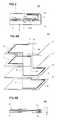
- FIG. 1is a front view that illustrates the structure of the antenna device described in Japanese Unexamined Patent Application Publication No. 2002-325013.
- An antenna coil 30 illustrated in FIG. 1includes an air-core coil 32 including spirally wound conductors 31 ( 31 a , 31 b , 31 e , 31 d ) in a plane on a film 32 a and a flat-shaped magnetic core member 33 disposed in the air-core coil 32 so as to be positioned substantially in parallel with the plane of the air-core coil 32 .
- the air-core coil 32has an opening 32 d in which the magnetic core member 33 is disposed.
- the first terminal 31 a and the coupling conductor 31 eare coupled to each other with a through hole 32 b .
- the second terminal 31 b and the coupling conductor 31 eare coupled to each other with a through hole 32 c .
- This magnetic antennais arranged on a conductive plate 34 .
- the antenna device in which the magnetic body is disposed in the opening of the antenna coil illustrated in FIG. 1can control the directivity of the antenna by controlling the distribution of magnetic fields occurring in the antenna coil.
- the communication distance mainly toward the axial direction of the magnetic bodycan be extended.
- an antenna devicebecause it has a structure in which the antenna coil has an opening in its central portion and a bar-shaped magnetic body (flat-shaped magnetic core member) is disposed in this opening, its manufacturing process is complicated. Thus, the positional accuracy between the magnetic body and the antenna coil is low and the characteristics of an obtained antenna device tend to widely vary.
- an adhesive for use in fixing the antenna coil and the plate-shaped magnetic bodyis needed, and the adhesive may negatively affect the electric characteristics of the antenna device, depending on the type or applied amount of the adhesive.
- each of the conductors 31( 31 a , 31 b , 31 e , 31 d ) is disposed in the plane on the film 32 a , a gap is present between the conductor 31 and the magnetic core member 33 .
- a magnetic fluxis reflected on the interface between the magnetic body and a dielectric body (non-magnetic body) and the magnetic-field coupling decreases.
- Preferred embodiments of the present inventionprovide an antenna device that can be produced by a simple process, has characteristics that do not vary widely, and has satisfactory electric characteristics, and a communication terminal apparatus including the antenna device.
- An antenna deviceincludes a plurality of insulator layers including at least a magnetic layer, at least one first conductive pattern, at least one second conductive pattern, an interlayer conductor, and an antenna coil (e.g., a spiral or helical conductive portion other than the magnetic body) with one turn or a plurality of turns.
- the first conductive patternhas a half-loop shape or a linear shape, includes one or more layers, and is arranged so as to be adjacent to a first major surface of the magnetic layer.
- the second conductive patternhas a half-loop shape or a linear shape, includes one or more layers, and is arranged so as to be adjacent to a second major surface of the magnetic layer.
- the interlayer conductoris disposed in the plurality of layers and connects the first conductive pattern and the second conductive pattern.
- the antenna coilincludes the first conductive pattern, the second conductive pattern, and the interlayer conductor.
- the first conductive patternpreferably is disposed on the first major surface of the magnetic layer
- at least a portion of the second conductive patternis disposed on a first major surface of a non-magnetic layer
- the first major surface of the non-magnetic layeris in contact with the second major surface of the magnetic layer.
- each of the first conductive pattern and the second conductive patternpreferably includes a plurality of half-loop or linear conductive patterns being parallel or substantially parallel with each other, each of the conductive patterns is disposed on a plane, and the antenna coil is spiral when seen from a winding axis direction thereof.
- the plurality of layerspreferably includes one or more non-magnetic layers arranged so as to be adjacent to the first major surface of the magnetic layer and a plurality of non-magnetic layers arranged so as to be adjacent to the second major surface of the magnetic layer, the first conductive pattern is disposed on the magnetic layer and the non-magnetic layer adjacent to the first major surface of the magnetic layer, and the second conductive pattern is disposed on the non-magnetic layer adjacent to the second major surface of the magnetic layer.
- the plurality of layerspreferably includes a plurality of magnetic layers, and at least one of the first conductive pattern and the second conductive pattern preferably is disposed on the plurality of magnetic layers.
- the antenna devicepreferably further includes a coupling conductor disposed within a loop defined by the first conductive pattern and the second conductive pattern when the antenna coil is seen in plan view on any one of the plurality of layers, the coupling conductor being electrically coupled to an external ground terminal and isolated from the antenna coil.
- first conductive pattern and the second conductive patternmay preferably have different line lengths.
- a communication terminal apparatusincludes the antenna device according to one of the preferred embodiments described above, a communication circuit connected to the antenna device, and a casing that houses the antenna device and the communication circuit.
- the casingpreferably includes an end portion to be directed toward a communication partner, and the antenna device preferably is arranged in a vicinity of the end portion of the casing.
- a path length of the first conductive patternmay preferably be longer than a path length of the second conductive pattern, and the antenna device may preferably be arranged such that a side adjacent to the first conductive pattern is directed toward an antenna of a communication partner.
- an antenna devicethat can be manufactured by a simple process, has characteristics that do not vary widely, and has satisfactory characteristics, and a communication terminal apparatus including the antenna device is provided.
- FIG. 1is a front view that illustrates the structure of an antenna device described in Japanese Unexamined Patent Application Publication No. 2002-325013.
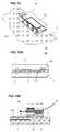
- FIG. 2Ais an exploded perspective view of an antenna device 101 according to a first preferred embodiment of the present invention
- FIG. 2Bis a plan view thereof
- FIG. 2Cis a front view thereof.
- FIG. 3is a schematic cross-sectional view that illustrates the configuration of a communication terminal apparatus 201 in which the antenna device 101 is incorporated.
- FIG. 4Ais an exploded perspective view of an antenna device 102 according to a second preferred embodiment of the present invention
- FIG. 4Bis a front view thereof.
- FIG. 5is a partial cross-sectional view that illustrates the configuration of a communication terminal apparatus 202 in which the antenna device 102 is incorporated.
- FIG. 6Ais an exploded perspective view of an antenna device 103 according to a third preferred embodiment of the present invention
- FIG. 6Bis a front view thereof.
- FIG. 7is an exploded perspective view of an antenna device 104 according to a fourth preferred embodiment of the present invention.
- FIG. 8is a partial perspective view that illustrates the relationship between the antenna device 104 and a ground conductor GND of a substrate.
- FIG. 9Ais a partial cross-sectional view that illustrates the configuration of a communication terminal apparatus 204 in which the antenna device 104 is incorporated
- FIG. 9Bis an enlarged cross-sectional view of a mounting portion in the antenna device 104 .
- FIG. 10is an exploded perspective view of an antenna device 105 according to a fifth preferred embodiment of the present invention.
- FIG. 11is an exploded perspective view of an antenna device 106 according to a sixth preferred embodiment of the present invention.
- FIG. 12is a partial perspective view that illustrates the relationship between the antenna device 106 and the ground conductor GND of the substrate.
- FIG. 13Ais a partial cross-sectional view that illustrates the configuration of a communication terminal apparatus 206 in which the antenna device 106 is incorporated
- FIG. 13Bis an enlarged cross-sectional view of a mounting portion in the antenna device 106 .
- FIG. 14Ais a plan view that illustrates the relationship between the antenna device 106 and the ground conductor GND of the substrate
- FIGS. 14B and 14Care plan views that illustrate a path of a current flowing in the ground conductor GND and that flowing in an antenna coil 456 , respectively.
- FIG. 15Ais a perspective view of an antenna device 107 according to a seventh preferred embodiment of the present invention
- FIG. 15Bis an exploded perspective view thereof
- FIG. 15Cillustrates how a magnetic flux passes through the antenna device 107 .
- FIG. 2Ais an exploded perspective view of an antenna device 101 according to a first preferred embodiment of the present invention.
- FIG. 2Bis a plan view of the antenna device 101 .
- FIG. 2Cis a front view of the antenna device 101 .
- the antenna device 101is configured as an antenna device preferably for use in transmitting and receiving high-frequency signals in a high frequency (HF) range, such as 13.56 MHz, for example. As described below, the antenna device 101 is arranged inside a terminal casing of a communication terminal apparatus, such as a cellular phone, for example.
- a communication terminal apparatussuch as a cellular phone
- the antenna device 101includes an antenna coil.
- the antenna coilincludes a first conductive pattern 40 disposed on a first major surface (upper surface in FIGS. 2A-2C ) of a magnetic sheet 10 , a second conductive pattern 50 disposed on a first major surface (upper surface in FIGS. 2A-2C ) of a non-magnetic sheet 20 , and an interlayer conductor (via electrode) 60 connecting the first conductive pattern 40 and the second conductive pattern 50 .
- the magnetic sheetcorresponds to a “magnetic layer”
- the non-magnetic sheetcorresponds to a “non-magnetic layer”.
- the first conductive pattern 40includes a set of a plurality of half-loop conductive patterns arranged in parallel or substantially in parallel with each other.
- the second conductive pattern 50also includes a set of half-loop conductive patterns arranged in parallel or substantially in parallel with each other.
- the antenna coil including the first conductive pattern 40 and the second conductive patterndefines a spiral or substantially spiral pattern of a plurality of turns (preferably three turns in this example).
- the antenna coilWhen seen in plan view (seen from the winding axis direction of the antenna coil), the antenna coil preferably is a rectangular or substantially rectangular spiral pattern.
- One terminal of the antenna coilis a first input/output terminal 71 , and another terminal thereof is a second input/output terminal 72 . These input/output terminals are connected to a feed circuit.
- the antenna device 101is formed preferably by stacking the magnetic sheet 10 with the first conductive pattern 40 formed thereon and the non-magnetic sheet 20 with the second conductive pattern 50 formed thereon and pressing and bonding them. That is, the antenna device 101 includes a laminate of a magnetic layer and a non-magnetic layer as a base body. That is, the antenna device 101 is a resin multilayer structure in which its base is a laminate of a magnetic layer and a non-magnetic layer and predetermined conductive patterns are disposed inside and outside the base.
- the magnetic sheet 10is a thermoplastic resin sheet in which magnetic powder, such as ferrite, is mixed and dispersed in a thermoplastic resin, such as polyimide or liquid crystal polymer.
- the first conductive pattern 40is formed preferably by patterning copper foil or aluminum foil by, for example, etching.
- the non-magnetic sheet 20includes a thermoplastic resin sheet, such as one made of a polyimide or liquid crystal polymer, that is, a dielectric sheet.
- the second conductive pattern 50is formed preferably by patterning copper foil or aluminum foil by, for example, etching.
- the interlayer conductor 60is formed preferably by filling a through hole formed by radiating the magnetic sheet 10 with laser light with conductive paste including fine metallic particles whose principal component is silver or copper.
- both sheetsare fused together, and simultaneously, the first conductive pattern 40 and the second conductive pattern 50 are electrically connected to each other with conductive paste (metal body after heat treatment) disposed therebetween.
- the interface between the first conductive pattern 40 and the magnetic sheet 10 and the interface between the second conductive pattern 50 and the magnetic sheet 10have neither an air layer nor a dielectric layer.
- a magnetic fluxis not reflected on the interface between the magnetic body and dielectric body, and there are few reductions in the magnetic-field coupling resulting from the reflection.
- Such a resin multilayer antenna deviceis flexible, it can be attached in the casing of, for example, a communication terminal apparatus or attached even to a curved surface of the casing using an adhesive or double-sided adhesive tape, for example.
- the magnetic sheet 10 and the non-magnetic sheet 20are both a sheet mainly including a thermoplastic resin, they can be collectively stacked and pressed and bonded and can be easily integrated using a so-called sheet multilayering process.
- a ceramic multilayer antenna devicecan also be manufactured.
- the first conductive pattern 40 and the interlayer conductor 60may be formed on a magnetic ceramic green sheet using conductive paste
- the second conductive pattern 50may be formed on a dielectric ceramic green sheet or a low permeability ceramic green sheet that has a relative permeability lower than that of a magnetic ceramic green sheet using conductive paste, and both sheets may be stacked and co-fired.
- FIG. 3is a schematic cross-sectional view that illustrates the configuration of a communication terminal apparatus 201 in which the antenna device 101 is incorporated.
- the front side (the surface with an input portion/display portion) D of the communication terminal apparatus 201faces downward.
- the communication terminal apparatus 201is configured such that a substrate (printed wiring board) 2 , a battery pack 3 , the antenna device 101 , and other components are incorporated within a casing 1 .
- the antenna device 101is preferably arranged in the vicinity of an end portion H of the casing 1 .
- the non-magnetic sheet (dielectric sheet) 20 of the antenna device 101is the attaching surface to the casing 1 , and the antenna device 101 is attached to the inner bottom surface of the casing 1 . That is, the first conductive pattern 40 is arranged so as to be adjacent to the end portion H of the casing 1 .
- the substrate 2is provided with a communication circuit.
- the feed circuitpreferably is included in the communication circuit and is connected to the antenna device 101 .
- Contact pinsstand on the substrate 2 .
- Each of the input/output terminals of the antenna device 101 and the feed circuitare electrically connected to each other with the contact pins disposed therebetween.
- the communication terminal apparatus 201has a predetermined directivity centered in the upper right direction in the drawing and can ensure a long maximum communication distance in this direction.
- FIG. 4Ais an exploded perspective view of an antenna device 102 according to a second preferred embodiment of the present invention.
- FIG. 4Bis a front view of the antenna device 102 .
- the antenna device 102is the one in which the antenna device 101 illustrated in the first preferred embodiment further includes a magnetic sheet 11 .
- the added magnetic sheet 11is stacked on the first conductive pattern 40 on the first major surface of the magnetic sheet 10 so as to cover a portion of the first conductive pattern 40 .
- the input/output terminal 71which is one end of the antenna coil, and the input/output terminal 72 , which is another end thereof, are exposed.
- FIG. 5is a partial cross-sectional view that illustrates the configuration of a communication terminal apparatus 202 in which the antenna device 102 is incorporated.
- the front sidethat is, the surface D with an input portion/display portion of the communication terminal apparatus 202 faces downward.
- the communication terminal apparatus 202is configured such that the substrate 2 made of a printed wiring board, the antenna device 102 , and other components are incorporated within the casing 1 .
- the substrate 2is provided with a ground conductor GND.
- a large number of mounting components 5is mounted on the front and back sides of the substrate 2 .
- the antenna device 102preferably is arranged in the vicinity of the end portion H of the casing 1 .
- the non-magnetic sheet (dielectric sheet) 20 of the antenna device 102is the attaching surface to the casing 1 , and the antenna device 102 is attached to the inner bottom surface of the casing 1 . That is, the first conductive pattern 40 is arranged so as to be adjacent to the end portion H of the casing 1 .
- the feed circuit on the substrate 2 and the antenna device 102are connected to each other preferably with contact pins 4 disposed therebetween, for example.
- the magnetic sheets 10 and 11are present between the antenna coil in the antenna device 102 and the substrate 2 (more specifically, between the antenna coil and the mounting components 5 and between the antenna coil and the ground conductor GND).
- a magnetic field occurring in the antenna coilis not easily subjected to the effects of metal elements, such as the ground conductor GND and the mounting components 5 , and the antenna characteristics of the antenna device 102 do not heavily depend on the arrangement situation of peripheral metal elements. Accordingly, stable communication characteristics are obtainable.
- FIG. 6Ais an exploded perspective view of an antenna device 103 according to a third preferred embodiment of the present invention.
- FIG. 6Bis a front view of the antenna device 103 .
- the antenna device 103includes a plurality of non-magnetic sheets.
- the first and second conductive patterns in the antenna device 103are disposed on a plurality of layers.
- the first and second conductive patternsdefine a helical or substantially helical antenna coil.
- a half-loop first conductive pattern 41is disposed on the first major surface of the magnetic sheet 11 .
- a half-loop first conductive pattern 42 and the input/output terminals 71 and 72are disposed on a first major surface of a non-magnetic sheet 21 .
- a half-loop second conductive pattern 51is disposed on a first major surface of a non-magnetic sheet 22 .
- a half-loop second conductive pattern 52is disposed on a first major surface of a non-magnetic sheet 23 .
- Interlayer conductors 61 and 64are disposed in the non-magnetic sheet 21 .
- Interlayer conductors 61 , 62 , 63 , and 64are disposed in the magnetic sheet 11 .
- the interlayer conductors 61 and 63are disposed in the non-magnetic sheet 22 .
- the first conductive patterns 41 and 42 , second conductive patterns 51 and 52 , interlayer conductors 61 to 64define a helical or substantially helical antenna coil between the input/output terminals 71 and 72 .
- an antenna devicehas a structure in which a bar-shaped magnetic body is disposed in an opening of a coil and the antenna coil is a multilayer coil, as in the known example illustrated in FIG. 1 , the conductive pattern may be broken when the antenna coil is bent.
- the structure in the present preferred embodimentit is not necessary to largely bend the antenna coil, and there is little possibility of a break or damage.
- FIG. 7is an exploded perspective view of an antenna device 104 according to a fourth preferred embodiment.
- the antenna device 104includes a plurality of magnetic sheets and a plurality of non-magnetic sheets.
- the first and second conductive patterns in the antenna device 104are disposed on a plurality of layers.
- the first and second conductive patternsdefine a helical or substantially helical antenna coil.
- the half-loop first conductive pattern 41is disposed on the first major surface of the magnetic sheet 11 .
- No conductive patternis disposed on the non-magnetic sheet 21 .
- the half-loop first conductive pattern 42is disposed on the first major surface of the non-magnetic sheet 22 .
- a half-loop first conductive pattern 43is disposed on the first major surface of the non-magnetic sheet 23 .
- Half-loop second conductive patterns 51 , 52 , 53 , and 54are disposed on the first major surfaces of non-magnetic sheets 24 , 25 , 26 , and 27 , respectively.
- the input/output terminals 71 and 72 and NC terminals (not electrically connected vacant terminals) 73 and 74are disposed on the second major surface of the non-magnetic sheet 27 .
- a plurality of magnetic sheets 12are stacked between the magnetic sheet 11 and the non-magnetic sheet 24 .
- Interlayer conductorsare disposed in the magnetic sheets 11 and 12 and the non-magnetic sheets 22 to 27 .
- the first conductive patterns 41 to 43 , second conductive patterns 51 to 54 , and interlayer conductorsdefine a helical or substantially helical antenna coil between the input/output terminals 71 and 72 .
- a plurality of magnetic sheetsmay be stacked and the thickness of the magnetic layers may be increased. That enables the opening of the antenna coil to have a large size, and a high-gain antenna device is obtainable.
- FIG. 8is a partial perspective view that illustrates the relationship between the antenna device 104 and the ground conductor GND of the substrate.
- the above-described helical antenna coil 456is included in the antenna device 104 , and the antenna coil 456 is illustrated in FIG. 8 with a schematic shape.
- the substrateis provided with the ground conductor GND, and the antenna device 104 is mounted in a location remote from the edge of the ground conductor by a predetermined distance in the x-axis direction.
- FIG. 9Ais a partial cross-sectional view that illustrates the configuration of a communication terminal apparatus 204 in which the antenna device 104 is incorporated.
- FIG. 9Bis an enlarged cross-sectional view of a mounting portion in the antenna device 104 .
- the front side (input portion/display portion) of the communication terminal apparatus 204faces downward.
- the communication terminal apparatus 204is configured such that the substrate (printed wiring board) 2 , the antenna device 104 , and other components are incorporated within the casing 1 .
- the substrate 2is provided with the ground conductor GND.
- the large number of mounting components 5is mounted on the front and back sides of the substrate 2 .
- the input/output terminals 71 and 72 and NC terminals 73 and 74 of the antenna device 104are connected to input/output lands and NC lands of the substrate 2 , respectively, with a binder, such as solder.
- a bindersuch as solder.
- FIG. 9Bone input/output land 82 and one NC land 84 are illustrated.
- the antenna device 104is arranged in the vicinity of the end portion H of the casing 1 .
- the antenna device 104is arranged such that the second conductive patterns 51 to 54 face the substrate 2 and are positioned in the vicinity of the end portion H of the casing 1 .
- a magnetic flux ⁇enters between the first conductive patterns 41 to 43 and the second conductive patterns 51 to 54 (into the opening of the antenna coil) and, as in the case of the communication terminal apparatuses illustrated in the first and second preferred embodiments, the directivity characteristic directed from the direction of the end portion of the communication terminal apparatus toward the lower surface (the surface opposite to the surface with the input portion/display portion) is obtainable.
- the antenna device 104can be made of a chip laminate having a length of about 5 mm in the X direction, a length of about 10 mm in the Y direction, and a length of about 0.5 mm in the Z direction and can be configured as a surface-mount device (SMD) that is mountable on the printed wiring board in the casing.
- the antenna coil 456 including the first conductive patterns 41 to 43 and the second conductive patterns 51 to 54is wound such that the opening of the antenna coil 456 faces a side in the Y direction, as illustrated in FIG. 8 .
- the opening of the antenna coilis positioned in the long-side direction, and that can increase the size of the opening of the antenna coil and can increase the area where the magnetic flux can be picked up. Accordingly, a high-gain antenna device can be provided.
- FIG. 10is an exploded perspective view of an antenna device 105 according to a fifth preferred embodiment of the present invention.
- the antenna device 105includes a plurality of magnetic sheets and a plurality of non-magnetic sheets.
- the first and second conductive patterns in the antenna device 105are disposed on a plurality of layers.
- the first and second conductive patternsdefine a helical or substantially helical antenna coil.
- the first conductive pattern 43is disposed on a magnetic sheet 13
- the second conductive pattern 51is disposed on a magnetic sheet 14 .
- the other configurationis preferably the same as that of the antenna device 104 .
- the first conductive pattern 41is located between the magnetic sheet 11 and the magnetic sheet 13 . That is, the first conductive pattern 41 is embedded in the magnetic layers.
- the second conductive pattern 51is located between the stack of magnetic sheets 12 and the magnetic sheet 14 and embedded in the magnetic layers.
- an embedded portion of each of the first conductive patterns and the second conductive patterns in the magnetic layerscan easily enhance the inductance of the antenna coil using the effect of the high permeability of the magnetic layers.
- the antenna coil having predetermined inductancecan be achieved with a small number of turns. That is advantageous for miniaturization.
- the portion embedded in the magnetic layersdoes not substantially contribute to magnetic-field radiation. Accordingly, determining which sheets (how many sheets) in the central section of the plurality of stacked sheets are magnetic sheets and determining that the remaining sheets are non-magnetic sheets may be optimally achieved in consideration of the balance between the size and the gain of the antenna device.
- FIG. 11is an exploded perspective view of an antenna device 106 according to a sixth preferred embodiment of the present invention.
- the antenna device 106includes a plurality of magnetic sheets and a plurality of non-magnetic sheets.
- the first and second conductive patterns in the antenna device 106are disposed on a plurality of layers.
- the first and second conductive patternsdefine a helical or substantially helical antenna coil.
- a non-magnetic sheet 28is arranged in the lowermost position.
- a coupling conductor 90is disposed on a first major surface of the non-magnetic sheet 28 .
- the coupling conductor 90may be disposed on the front side of the non-magnetic sheet 24 , that front side being the interface with the non-magnetic sheet 12 .
- the ground terminals 75 and 76are electrically connected to the coupling conductor 90 with the interlayer conductor.
- the other configurationis the same as that of the antenna device 104 .
- the coupling conductor 90is coupled to the antenna coil including the first conductive patterns 41 to 43 and the second conductive patterns 51 to 54 through electromagnetic fields. As described below, connecting the ground terminals 75 and 76 to ground conductors of a substrate on which the antenna device 106 is mounted enables the coupling conductor 90 to act as part of the ground conductors of the substrate or as an extended ground conductor.
- FIG. 12is a partial perspective view that illustrates the relationship between the antenna device 106 and the ground conductor GND of the substrate.
- the helical antenna coil 456 including the first conductive patterns 41 to 43 and the second conductive patterns 51 to 54is included in the antenna device 106 .
- the antenna coil 456is illustrated in FIG. 12 with a schematic shape.
- the antenna device 106preferably is mounted in a location projecting from the edge of the ground conductor GND of the substrate 2 by a predetermined dimension in the x-axis direction. In the state where the antenna device 106 is mounted on the substrate 2 , the ground conductor GND of the substrate 2 is electrically coupled to the coupling conductor 90 of the antenna device 106 .
- FIG. 13Ais a partial cross-sectional view that illustrates the configuration of a communication terminal apparatus 206 in which the antenna device 106 is incorporated.
- FIG. 13Bis an enlarged cross-sectional view of a mounting portion in the antenna device 106 .
- the front side (input portion/display portion) of the communication terminal apparatus 206faces downward.
- the communication terminal apparatus 206is configured such that the substrate (printed wiring board) 2 , the antenna device 106 , and other components are incorporated in the casing 1 .
- the substrate 2is provided with the ground conductor GND.
- the large number of mounting components 5is mounted on the front and back sides of the substrate 2 .
- the input/output terminals 71 and 72 and ground terminals 75 and 76 of the antenna device 106are connected to the input/output lands and ground conductor GND of the substrate 2 , respectively, with a binder, such as solder.
- a bindersuch as solder.
- FIG. 13Bone input/output land 82 is illustrated.
- FIG. 14includes plan views that illustrate the relationship between the antenna device 106 and the ground conductor GND of the substrate and a path of a current flowing in the ground conductor GND or that in the antenna coil 456 .
- FIG. 14Aillustrates the positional relationship between the antenna coil 456 and the coupling conductor 90 in the antenna device 106 .
- FIG. 14Billustrates a path of a current flowing in the ground conductor GND of the substrate 2 .
- FIG. 14Cillustrates a path of a current flowing in the antenna coil 456 .
- the antenna device 106can also pick up an induced current flowing in the ground conductor GND, as illustrated in FIG. 14B , in addition to operating as in the antenna device 104 illustrated in the fourth preferred embodiment. That is, when an induction field from an antenna device of a communication partner impinges on the ground conductor GND, an induced current flows in the ground conductor GND, as indicated by the arrows illustrated in FIG. 14B , and this induced current converges on the edge of the ground conductor GND because of edge effects. Because the coupling conductor 90 of the antenna device 106 is connected to the edge of the ground conductor GND, the current flowing in the edge of the ground conductor GND is also guided to the coupling conductor 90 . The current having flowed in the coupling conductor 90 flows in the antenna coil 456 over electromagnetic fields (specifically, the coupling conductor 90 and the first conductive patterns 41 to 43 are coupled over magnetic fields), this current is extracted as a signal current.
- the antenna coil 456may be arranged such that all the antenna coil 456 overlaps the ground conductor GND in the range where the antenna coil 456 is not included in the region of the ground conductor GND.
- the coupling conductor 90is optional. However, in the state where the ground terminals 75 and 76 are connected to the ground conductor GND of the substrate on which the antenna device is mounted, the coupling conductor 90 acts as part of the ground conductor of the substrate or as an extended ground conductor. Thus, the substantial edge of the ground conductor GND of the substrate 2 in the x-axis direction depends on the coupling conductor 90 .
- the coupling conductor 90preferably is integrally formed in advance in the antenna device 106 , even if the accuracy of mounting the antenna device 106 on the substrate 2 is low, the positional relationship between the antenna coil in the antenna device 106 and the substantial edge of the ground conductor GND in the x-axis direction is constant. As a result, stable antenna characteristics that are not affected by the accuracy of mounting the antenna device are obtainable.
- FIG. 15Ais a perspective view of an antenna device 107 according to a seventh preferred embodiment of the present invention
- FIG. 15Bis an exploded perspective view thereof.
- FIG. 15Cillustrates how a magnetic flux passes through the antenna device 107 .
- the antenna device 107includes a plurality of magnetic sheets and a plurality of non-magnetic sheets.
- the first and second conductive patterns in the antenna device 107are disposed on a plurality of layers.
- the first and second conductive patternsdefine a helical or substantially helical antenna coil.
- the half-loop first conductive patterns 41 and 42are disposed on the first major surface (upper surface in FIGS. 15A-15C ) of the plurality of magnetic sheets 12 .
- the second conductive patterns 51 and 52each having a linear shape are disposed on the first major surface (upper surface in FIGS. 15A-15C ) of the non-magnetic sheet 20 .
- the input/output terminals 71 and 72are disposed on the second major surface of the non-magnetic sheet 20 .
- the first conductive patterns 41 and 42 and the second conductive patterns 51 and 52are connected to each other with the interlayer conductors in the magnetic sheets 12 disposed therebetween.
- the second conductive patterns 51 and 52 and the input/output terminals 71 and 72are connected to each other with the interlayer conductors in the non-magnetic sheet 20 disposed therebetween.
- first conductive patterns 41 and 42 , the second conductive patterns 51 and 52 , and the interlayer conductorsdefine a spiral or substantially spiral antenna coil with two turns between the input/output terminals 71 and 72 .
- the line length of each of the first conductive patterns 41 and 42 and the line length of each of the second conductive patterns 51 and 52may be different. That is, the magnetic body may substantially pass through the opening of the antenna coil in a location displaced from the center of that opening.
- an antenna of a communication partneris present above or in an upward slanting direction of the antenna device 107 .
- the magnetic flux ⁇enters between the first conductive patterns 41 and 42 and the second conductive patterns 51 and 52 (into the opening of the antenna coil) and exits from the magnetic layers 12 mainly through the end surface.
- the line length of each of the first conductive patterns 41 and 42is longer than that of each of the second conductive patterns 51 and 52 .
- the size of the substantial opening of the antenna coil allowing an entry of the magnetic flux ⁇can be increased as illustrated in FIG. 15C , and the high-gain antenna device is obtainable.
- an antenna devicepreferably for use in an HF range that can be used in NFC or the like is described.
- the antenna devicemay also be configured as the one for use in a UHF range, such as GSM or DCS.
- the antenna device according to the present inventionis not limited to a device including a magnetic sheet and a non-magnetic sheet.
- the antenna devicemay be configured so as to include a magnetic layer and a non-magnetic layer that are formed by thick film printing.
- a flexible resin multilayer structuremay preferably be used as the base body.
- a substrateprinted wiring board
- a rigid ceramic laminatethat can be mounted by substantially the same process as in other mounting components may preferably be used as the base body.
- the present inventionis not limited to that arrangement. That is, the first and second conductive patterns may be arranged on only a non-magnetic sheet that is not in direct contact with a magnetic sheet, and these conductive patterns may be connected together using an interlayer conductor that is contiguously disposed in the magnetic sheet and the non-magnetic sheet.
Landscapes
- Engineering & Computer Science (AREA)
- Computer Networks & Wireless Communication (AREA)
- Details Of Aerials (AREA)
- Support Of Aerials (AREA)
Abstract
Description
1. Field of the Invention
The present invention relates to an antenna device preferably for use in an RFID system or short-range wireless communication system that communicates with partner equipment through an electromagnetic field signal.
2. Description of the Related Art
An antenna device for use in an HF-band communication system, such as Felica (registered trademark) or NFC, is disclosed in Japanese Unexamined Patent Application Publication No. 2002-325013.FIG. 1 is a front view that illustrates the structure of the antenna device described in Japanese Unexamined Patent Application Publication No. 2002-325013.
Anantenna coil 30 illustrated inFIG. 1 includes an air-core coil32 including spirally wound conductors31 (31a,31b,31e,31d) in a plane on afilm 32aand a flat-shapedmagnetic core member 33 disposed in the air-core coil32 so as to be positioned substantially in parallel with the plane of the air-core coil32. The air-core coil32 has an opening32din which themagnetic core member 33 is disposed. Thefirst terminal 31aand thecoupling conductor 31eare coupled to each other with athrough hole 32b. Thesecond terminal 31band thecoupling conductor 31eare coupled to each other with a throughhole 32c. This magnetic antenna is arranged on aconductive plate 34.
The antenna device in which the magnetic body is disposed in the opening of the antenna coil illustrated inFIG. 1 can control the directivity of the antenna by controlling the distribution of magnetic fields occurring in the antenna coil. Although depending on the surrounding environment (e.g., relationship with the ground and the like), the communication distance mainly toward the axial direction of the magnetic body can be extended.
In such an antenna device, however, because it has a structure in which the antenna coil has an opening in its central portion and a bar-shaped magnetic body (flat-shaped magnetic core member) is disposed in this opening, its manufacturing process is complicated. Thus, the positional accuracy between the magnetic body and the antenna coil is low and the characteristics of an obtained antenna device tend to widely vary. In addition, an adhesive for use in fixing the antenna coil and the plate-shaped magnetic body is needed, and the adhesive may negatively affect the electric characteristics of the antenna device, depending on the type or applied amount of the adhesive.
In addition, because each of the conductors31 (31a,31b,31e,31d) is disposed in the plane on thefilm 32a, a gap is present between the conductor31 and themagnetic core member 33. Thus, there is a problem in that a magnetic flux is reflected on the interface between the magnetic body and a dielectric body (non-magnetic body) and the magnetic-field coupling decreases.
Preferred embodiments of the present invention provide an antenna device that can be produced by a simple process, has characteristics that do not vary widely, and has satisfactory electric characteristics, and a communication terminal apparatus including the antenna device.
An antenna device according to a preferred embodiment of the present invention includes a plurality of insulator layers including at least a magnetic layer, at least one first conductive pattern, at least one second conductive pattern, an interlayer conductor, and an antenna coil (e.g., a spiral or helical conductive portion other than the magnetic body) with one turn or a plurality of turns. The first conductive pattern has a half-loop shape or a linear shape, includes one or more layers, and is arranged so as to be adjacent to a first major surface of the magnetic layer. The second conductive pattern has a half-loop shape or a linear shape, includes one or more layers, and is arranged so as to be adjacent to a second major surface of the magnetic layer. The interlayer conductor is disposed in the plurality of layers and connects the first conductive pattern and the second conductive pattern. The antenna coil includes the first conductive pattern, the second conductive pattern, and the interlayer conductor.
For example, at least a portion of the first conductive pattern preferably is disposed on the first major surface of the magnetic layer, at least a portion of the second conductive pattern is disposed on a first major surface of a non-magnetic layer, and the first major surface of the non-magnetic layer is in contact with the second major surface of the magnetic layer.
For example, each of the first conductive pattern and the second conductive pattern preferably includes a plurality of half-loop or linear conductive patterns being parallel or substantially parallel with each other, each of the conductive patterns is disposed on a plane, and the antenna coil is spiral when seen from a winding axis direction thereof.
For example, the plurality of layers preferably includes one or more non-magnetic layers arranged so as to be adjacent to the first major surface of the magnetic layer and a plurality of non-magnetic layers arranged so as to be adjacent to the second major surface of the magnetic layer, the first conductive pattern is disposed on the magnetic layer and the non-magnetic layer adjacent to the first major surface of the magnetic layer, and the second conductive pattern is disposed on the non-magnetic layer adjacent to the second major surface of the magnetic layer.
For example, the plurality of layers preferably includes a plurality of magnetic layers, and at least one of the first conductive pattern and the second conductive pattern preferably is disposed on the plurality of magnetic layers.
For example, the antenna device preferably further includes a coupling conductor disposed within a loop defined by the first conductive pattern and the second conductive pattern when the antenna coil is seen in plan view on any one of the plurality of layers, the coupling conductor being electrically coupled to an external ground terminal and isolated from the antenna coil.
For example, the first conductive pattern and the second conductive pattern may preferably have different line lengths.
A communication terminal apparatus according to a preferred embodiment of the present invention includes the antenna device according to one of the preferred embodiments described above, a communication circuit connected to the antenna device, and a casing that houses the antenna device and the communication circuit.
For example, the casing preferably includes an end portion to be directed toward a communication partner, and the antenna device preferably is arranged in a vicinity of the end portion of the casing.
A path length of the first conductive pattern may preferably be longer than a path length of the second conductive pattern, and the antenna device may preferably be arranged such that a side adjacent to the first conductive pattern is directed toward an antenna of a communication partner.
According to various preferred embodiments of the present invention, an antenna device that can be manufactured by a simple process, has characteristics that do not vary widely, and has satisfactory characteristics, and a communication terminal apparatus including the antenna device is provided.
The above and other elements, features, steps, characteristics and advantages of the present invention will become more apparent from the following detailed description of the preferred embodiments with reference to the attached drawings.
Theantenna device 101 is configured as an antenna device preferably for use in transmitting and receiving high-frequency signals in a high frequency (HF) range, such as 13.56 MHz, for example. As described below, theantenna device 101 is arranged inside a terminal casing of a communication terminal apparatus, such as a cellular phone, for example.
As illustrated inFIGS. 2A-2C , theantenna device 101 includes an antenna coil. The antenna coil includes a firstconductive pattern 40 disposed on a first major surface (upper surface inFIGS. 2A-2C ) of amagnetic sheet 10, a secondconductive pattern 50 disposed on a first major surface (upper surface inFIGS. 2A-2C ) of anon-magnetic sheet 20, and an interlayer conductor (via electrode)60 connecting the firstconductive pattern 40 and the secondconductive pattern 50. The magnetic sheet corresponds to a “magnetic layer”, and the non-magnetic sheet corresponds to a “non-magnetic layer”.
The firstconductive pattern 40 includes a set of a plurality of half-loop conductive patterns arranged in parallel or substantially in parallel with each other. The secondconductive pattern 50 also includes a set of half-loop conductive patterns arranged in parallel or substantially in parallel with each other.
As illustrated inFIG. 2B , the antenna coil including the firstconductive pattern 40 and the second conductive pattern defines a spiral or substantially spiral pattern of a plurality of turns (preferably three turns in this example). When seen in plan view (seen from the winding axis direction of the antenna coil), the antenna coil preferably is a rectangular or substantially rectangular spiral pattern.
One terminal of the antenna coil is a first input/output terminal 71, and another terminal thereof is a second input/output terminal 72. These input/output terminals are connected to a feed circuit.
Theantenna device 101 is formed preferably by stacking themagnetic sheet 10 with the firstconductive pattern 40 formed thereon and thenon-magnetic sheet 20 with the secondconductive pattern 50 formed thereon and pressing and bonding them. That is, theantenna device 101 includes a laminate of a magnetic layer and a non-magnetic layer as a base body. That is, theantenna device 101 is a resin multilayer structure in which its base is a laminate of a magnetic layer and a non-magnetic layer and predetermined conductive patterns are disposed inside and outside the base. The non-magnetic layer may be a low permeability layer having a relative permeability lower than that of the magnetic layer, or alternatively, may be a dielectric layer (relative permeability μr=1), as in this example.
Themagnetic sheet 10 is a thermoplastic resin sheet in which magnetic powder, such as ferrite, is mixed and dispersed in a thermoplastic resin, such as polyimide or liquid crystal polymer. The firstconductive pattern 40 is formed preferably by patterning copper foil or aluminum foil by, for example, etching. Thenon-magnetic sheet 20 includes a thermoplastic resin sheet, such as one made of a polyimide or liquid crystal polymer, that is, a dielectric sheet. The secondconductive pattern 50 is formed preferably by patterning copper foil or aluminum foil by, for example, etching. Theinterlayer conductor 60 is formed preferably by filling a through hole formed by radiating themagnetic sheet 10 with laser light with conductive paste including fine metallic particles whose principal component is silver or copper. When themagnetic sheet 10 and thenon-magnetic sheet 20 are stacked and heated, both sheets are fused together, and simultaneously, the firstconductive pattern 40 and the secondconductive pattern 50 are electrically connected to each other with conductive paste (metal body after heat treatment) disposed therebetween.
As illustrated inFIG. 2C , the interface between the firstconductive pattern 40 and themagnetic sheet 10 and the interface between the secondconductive pattern 50 and themagnetic sheet 10 have neither an air layer nor a dielectric layer. Thus, a magnetic flux is not reflected on the interface between the magnetic body and dielectric body, and there are few reductions in the magnetic-field coupling resulting from the reflection.
Because such a resin multilayer antenna device is flexible, it can be attached in the casing of, for example, a communication terminal apparatus or attached even to a curved surface of the casing using an adhesive or double-sided adhesive tape, for example.
Because themagnetic sheet 10 and thenon-magnetic sheet 20 are both a sheet mainly including a thermoplastic resin, they can be collectively stacked and pressed and bonded and can be easily integrated using a so-called sheet multilayering process.
Aside from the above-described resin multilayer antenna device, a ceramic multilayer antenna device can also be manufactured. In this case, the firstconductive pattern 40 and theinterlayer conductor 60 may be formed on a magnetic ceramic green sheet using conductive paste, the secondconductive pattern 50 may be formed on a dielectric ceramic green sheet or a low permeability ceramic green sheet that has a relative permeability lower than that of a magnetic ceramic green sheet using conductive paste, and both sheets may be stacked and co-fired.
As illustrated inFIG. 3 , theantenna device 101 is preferably arranged in the vicinity of an end portion H of thecasing 1. The non-magnetic sheet (dielectric sheet)20 of theantenna device 101 is the attaching surface to thecasing 1, and theantenna device 101 is attached to the inner bottom surface of thecasing 1. That is, the firstconductive pattern 40 is arranged so as to be adjacent to the end portion H of thecasing 1.
Thesubstrate 2 is provided with a communication circuit. The feed circuit preferably is included in the communication circuit and is connected to theantenna device 101. Contact pins stand on thesubstrate 2. Each of the input/output terminals of theantenna device 101 and the feed circuit are electrically connected to each other with the contact pins disposed therebetween. Thecommunication terminal apparatus 201 has a predetermined directivity centered in the upper right direction in the drawing and can ensure a long maximum communication distance in this direction.
The addedmagnetic sheet 11 is stacked on the firstconductive pattern 40 on the first major surface of themagnetic sheet 10 so as to cover a portion of the firstconductive pattern 40. The input/output terminal 71, which is one end of the antenna coil, and the input/output terminal 72, which is another end thereof, are exposed.
Theantenna device 102 preferably is arranged in the vicinity of the end portion H of thecasing 1. The non-magnetic sheet (dielectric sheet)20 of theantenna device 102 is the attaching surface to thecasing 1, and theantenna device 102 is attached to the inner bottom surface of thecasing 1. That is, the firstconductive pattern 40 is arranged so as to be adjacent to the end portion H of thecasing 1. The feed circuit on thesubstrate 2 and theantenna device 102 are connected to each other preferably withcontact pins 4 disposed therebetween, for example.
With such a configuration, themagnetic sheets antenna device 102 and the substrate2 (more specifically, between the antenna coil and the mountingcomponents 5 and between the antenna coil and the ground conductor GND). Thus, a magnetic field occurring in the antenna coil is not easily subjected to the effects of metal elements, such as the ground conductor GND and the mountingcomponents 5, and the antenna characteristics of theantenna device 102 do not heavily depend on the arrangement situation of peripheral metal elements. Accordingly, stable communication characteristics are obtainable.
A half-loop firstconductive pattern 41 is disposed on the first major surface of themagnetic sheet 11. A half-loop firstconductive pattern 42 and the input/output terminals non-magnetic sheet 21. A half-loop secondconductive pattern 51 is disposed on a first major surface of anon-magnetic sheet 22. A half-loop secondconductive pattern 52 is disposed on a first major surface of anon-magnetic sheet 23.Interlayer conductors non-magnetic sheet 21.Interlayer conductors magnetic sheet 11. Theinterlayer conductors non-magnetic sheet 22.
The firstconductive patterns conductive patterns interlayer conductors 61 to64 define a helical or substantially helical antenna coil between the input/output terminals
If an antenna device has a structure in which a bar-shaped magnetic body is disposed in an opening of a coil and the antenna coil is a multilayer coil, as in the known example illustrated inFIG. 1 , the conductive pattern may be broken when the antenna coil is bent. In contrast, for the structure in the present preferred embodiment, it is not necessary to largely bend the antenna coil, and there is little possibility of a break or damage.
The half-loop firstconductive pattern 41 is disposed on the first major surface of themagnetic sheet 11. No conductive pattern is disposed on thenon-magnetic sheet 21. The half-loop firstconductive pattern 42 is disposed on the first major surface of thenon-magnetic sheet 22. A half-loop firstconductive pattern 43 is disposed on the first major surface of thenon-magnetic sheet 23. Half-loop secondconductive patterns non-magnetic sheets output terminals non-magnetic sheet 27.
A plurality ofmagnetic sheets 12 are stacked between themagnetic sheet 11 and thenon-magnetic sheet 24.
Interlayer conductors are disposed in themagnetic sheets non-magnetic sheets 22 to27.
The firstconductive patterns 41 to43, secondconductive patterns 51 to54, and interlayer conductors define a helical or substantially helical antenna coil between the input/output terminals
In such a manner, a plurality of magnetic sheets may be stacked and the thickness of the magnetic layers may be increased. That enables the opening of the antenna coil to have a large size, and a high-gain antenna device is obtainable.
The input/output terminals NC terminals antenna device 104 are connected to input/output lands and NC lands of thesubstrate 2, respectively, with a binder, such as solder. InFIG. 9B , one input/output land 82 and oneNC land 84 are illustrated.
As illustrated inFIG. 9A , theantenna device 104 is arranged in the vicinity of the end portion H of thecasing 1. Theantenna device 104 is arranged such that the secondconductive patterns 51 to54 face thesubstrate 2 and are positioned in the vicinity of the end portion H of thecasing 1. Thus, a magnetic flux φ enters between the firstconductive patterns 41 to43 and the secondconductive patterns 51 to54 (into the opening of the antenna coil) and, as in the case of the communication terminal apparatuses illustrated in the first and second preferred embodiments, the directivity characteristic directed from the direction of the end portion of the communication terminal apparatus toward the lower surface (the surface opposite to the surface with the input portion/display portion) is obtainable.
For example, theantenna device 104 can be made of a chip laminate having a length of about 5 mm in the X direction, a length of about 10 mm in the Y direction, and a length of about 0.5 mm in the Z direction and can be configured as a surface-mount device (SMD) that is mountable on the printed wiring board in the casing. Theantenna coil 456 including the firstconductive patterns 41 to43 and the secondconductive patterns 51 to54 is wound such that the opening of theantenna coil 456 faces a side in the Y direction, as illustrated inFIG. 8 . That is, of the base body preferably having a rectangular or substantially rectangular parallelepiped shape, the opening of the antenna coil is positioned in the long-side direction, and that can increase the size of the opening of the antenna coil and can increase the area where the magnetic flux can be picked up. Accordingly, a high-gain antenna device can be provided.
In the configuration illustrated inFIG. 10 , the firstconductive pattern 41 is located between themagnetic sheet 11 and themagnetic sheet 13. That is, the firstconductive pattern 41 is embedded in the magnetic layers. Similarly, the secondconductive pattern 51 is located between the stack ofmagnetic sheets 12 and themagnetic sheet 14 and embedded in the magnetic layers.
In this manner, an embedded portion of each of the first conductive patterns and the second conductive patterns in the magnetic layers can easily enhance the inductance of the antenna coil using the effect of the high permeability of the magnetic layers. For example, the antenna coil having predetermined inductance can be achieved with a small number of turns. That is advantageous for miniaturization. Of the first conductive patterns and the second conductive patterns, the portion embedded in the magnetic layers does not substantially contribute to magnetic-field radiation. Accordingly, determining which sheets (how many sheets) in the central section of the plurality of stacked sheets are magnetic sheets and determining that the remaining sheets are non-magnetic sheets may be optimally achieved in consideration of the balance between the size and the gain of the antenna device.
Thecoupling conductor 90 is coupled to the antenna coil including the firstconductive patterns 41 to43 and the secondconductive patterns 51 to54 through electromagnetic fields. As described below, connecting theground terminals antenna device 106 is mounted enables thecoupling conductor 90 to act as part of the ground conductors of the substrate or as an extended ground conductor.
Theantenna device 106 preferably is mounted in a location projecting from the edge of the ground conductor GND of thesubstrate 2 by a predetermined dimension in the x-axis direction. In the state where theantenna device 106 is mounted on thesubstrate 2, the ground conductor GND of thesubstrate 2 is electrically coupled to thecoupling conductor 90 of theantenna device 106.
The input/output terminals ground terminals antenna device 106 are connected to the input/output lands and ground conductor GND of thesubstrate 2, respectively, with a binder, such as solder. InFIG. 13B , one input/output land 82 is illustrated.
Theantenna device 106 can also pick up an induced current flowing in the ground conductor GND, as illustrated inFIG. 14B , in addition to operating as in theantenna device 104 illustrated in the fourth preferred embodiment. That is, when an induction field from an antenna device of a communication partner impinges on the ground conductor GND, an induced current flows in the ground conductor GND, as indicated by the arrows illustrated inFIG. 14B , and this induced current converges on the edge of the ground conductor GND because of edge effects. Because thecoupling conductor 90 of theantenna device 106 is connected to the edge of the ground conductor GND, the current flowing in the edge of the ground conductor GND is also guided to thecoupling conductor 90. The current having flowed in thecoupling conductor 90 flows in theantenna coil 456 over electromagnetic fields (specifically, thecoupling conductor 90 and the firstconductive patterns 41 to43 are coupled over magnetic fields), this current is extracted as a signal current.
Although depending on the distance between the ground conductor GND and theantenna coil 456, when theantenna device 106 is seen in plan view, theantenna coil 456 may be arranged such that all theantenna coil 456 overlaps the ground conductor GND in the range where theantenna coil 456 is not included in the region of the ground conductor GND.
To use an induced current flowing in the ground conductor GND of thesubstrate 2, thecoupling conductor 90 is optional. However, in the state where theground terminals coupling conductor 90 acts as part of the ground conductor of the substrate or as an extended ground conductor. Thus, the substantial edge of the ground conductor GND of thesubstrate 2 in the x-axis direction depends on thecoupling conductor 90. Because thecoupling conductor 90 preferably is integrally formed in advance in theantenna device 106, even if the accuracy of mounting theantenna device 106 on thesubstrate 2 is low, the positional relationship between the antenna coil in theantenna device 106 and the substantial edge of the ground conductor GND in the x-axis direction is constant. As a result, stable antenna characteristics that are not affected by the accuracy of mounting the antenna device are obtainable.
The half-loop firstconductive patterns FIGS. 15A-15C ) of the plurality ofmagnetic sheets 12. The secondconductive patterns FIGS. 15A-15C ) of thenon-magnetic sheet 20. The input/output terminals non-magnetic sheet 20.
The firstconductive patterns conductive patterns magnetic sheets 12 disposed therebetween. The secondconductive patterns output terminals non-magnetic sheet 20 disposed therebetween.
In that way, the firstconductive patterns conductive patterns output terminals
As described above, the line length of each of the firstconductive patterns conductive patterns
In the orientation illustrated inFIG. 15C , an antenna of a communication partner is present above or in an upward slanting direction of theantenna device 107. Thus, the magnetic flux φ enters between the firstconductive patterns conductive patterns 51 and52 (into the opening of the antenna coil) and exits from themagnetic layers 12 mainly through the end surface. In the example illustrated inFIGS. 15A-15C , the line length of each of the firstconductive patterns conductive patterns FIG. 15C , and the high-gain antenna device is obtainable.
In the above-described examples, an antenna device preferably for use in an HF range that can be used in NFC or the like is described. The antenna device may also be configured as the one for use in a UHF range, such as GSM or DCS.
The antenna device according to the present invention is not limited to a device including a magnetic sheet and a non-magnetic sheet. For example, the antenna device may be configured so as to include a magnetic layer and a non-magnetic layer that are formed by thick film printing.
When the antenna device according to various preferred embodiments of the present invention is attached to the inner surface of the casing, as illustrated inFIGS. 3 and 5 , a flexible resin multilayer structure may preferably be used as the base body. When the antenna device according to various preferred embodiments of the present invention is mounted on a substrate (printed wiring board), as illustrated inFIGS. 9A and 9B andFIGS. 13A and 13B , a rigid ceramic laminate that can be mounted by substantially the same process as in other mounting components may preferably be used as the base body.
In the preferred embodiments of the present invention, an example in which a portion of the first and second conductive patterns is preferably in contact with a magnetic sheet is described. However, the present invention is not limited to that arrangement. That is, the first and second conductive patterns may be arranged on only a non-magnetic sheet that is not in direct contact with a magnetic sheet, and these conductive patterns may be connected together using an interlayer conductor that is contiguously disposed in the magnetic sheet and the non-magnetic sheet.
While preferred embodiments of the present invention have been described above, it is to be understood that variations and modifications will be apparent to those skilled in the art without departing from the scope and spirit of the present invention. The scope of the present invention, therefore, is to be determined solely by the following claims.
Claims (21)
1. An antenna device comprising:
a plurality of layers including at least a magnetic layer;
at least one first conductive pattern having a half-loop shape or a linear shape, including one or more layers, and being adjacent to a first major surface of the magnetic layer;
at least one second conductive pattern having a half-loop shape or a linear shape, including one or more layers, and being adjacent to a second major surface of the magnetic layer;
an interlayer conductor included in the plurality of layers and connecting the first conductive pattern and the second conductive pattern; and
an antenna coil including one turn or a plurality of turns, and including the at least one first conductive pattern, the at least one second conductive pattern, and the interlayer conductor, wherein
the plurality of layers includes one or more non-magnetic layers adjacent to the first major surface of the magnetic layer and a plurality of non-magnetic layers adjacent to the second major surface of the magnetic layer, the first conductive pattern is disposed on the magnetic layer and the non-magnetic layer adjacent to the first major surface of the magnetic layer, and the second conductive pattern is disposed on the non-magnetic layer adjacent to the second major surface of the magnetic layer.
2. The antenna device according toclaim 1 , wherein at least a portion of the at least one first conductive pattern is disposed on the first major surface of the magnetic layer, at least a portion of the second conductive pattern is disposed on a first major surface of a non-magnetic layer, and the first major surface of the non-magnetic layer is in contact with the second major surface of the magnetic layer.
3. The antenna device according toclaim 1 , wherein each of the at least one first conductive pattern and the at least one second conductive pattern includes a plurality of half-loop or linear conductive patterns being parallel or substantially parallel with each other, each of the conductive patterns is disposed on a plane, and the antenna coil defines a spiral when seen from a winding axis direction thereof.
4. The antenna device according toclaim 1 , wherein the plurality of layers includes a plurality of magnetic layers, and at least one of the at least one first conductive pattern and the at least one second conductive pattern is disposed on the plurality of magnetic layers.
5. The antenna device according toclaim 1 , further comprising a coupling conductor disposed within a loop defined by the at least one first conductive pattern and the at least one second conductive pattern when seen in plan view on any one of the plurality of layers, the coupling conductor being electrically coupled to an external ground terminal and isolated from the antenna coil.
6. The antenna device according toclaim 1 , wherein the first conductive pattern and the second conductive pattern have different line lengths.
7. The antenna device according toclaim 1 , wherein the antenna coil defines a spiral or substantially spiral pattern including a plurality of turns.
8. The antenna device according toclaim 7 , wherein the spiral or substantially spiral pattern of the antenna coil is a rectangular or substantially rectangular spiral pattern.
9. The antenna device according toclaim 1 , further comprising an additional magnetic layer stacked on the at least one first conductive pattern on the first major surface of the magnetic layer so as to cover a portion of the at least one first conductive pattern.
10. The antenna device according toclaim 9 , further comprising a first input/output terminal located at one end of the antenna coil and a second input/output terminal located at another end of the antenna coil, wherein the first and second input/output terminals are exposed from the antenna device.
11. The antenna device according toclaim 1 , wherein the at least one first and second conductive patterns define a helical or substantially helical antenna coil.
12. The antenna device according toclaim 1 , wherein:
the at least one first conductive pattern and the at least one second conductive pattern define a helical or substantially helical antenna coil, and
each of the at least one first conductive pattern and the at least one second conductive pattern includes a plurality of half-loop conductive patterns disposed on respective ones of the plurality of magnetic layers.
13. The antenna device according toclaim 12 , wherein the at least one first conductive pattern is disposed on one of the plurality of magnetic layers, and the at least one second conductive pattern is disposed on another of the plurality of magnetic layers.
14. The antenna device according toclaim 12 , wherein one of the plurality of non-magnetic layers is arranged at a lowermost position of the plurality of layers, a coupling conductor is disposed on a first major surface of the one of the plurality of non-magnetic layers disposed at the lowermost position, and input/output terminals and ground terminals are disposed on a second major surface of the one of the plurality of non-magnetic layers disposed at the lowermost position.
15. The antenna device according toclaim 12 , wherein at least two first conductive patterns and at least two second conductive patterns are provided and arranged to define a spiral or substantially spiral antenna coil including at least two turns between input/output terminals.
16. A communication terminal apparatus comprising:
an antenna device;
a communication circuit connected to the antenna device; and
a casing that houses the antenna device and the communication circuit;
the antenna device including:
a plurality of layers including at least a magnetic layer;
at least one first conductive pattern having a half-loop shape and being adjacent to a first major surface of the magnetic layer;
at least one second conductive pattern having a half-loop shape and being adjacent to a second major surface of the magnetic layer;
an interlayer conductor disposed in the plurality of layers and connecting the at least one first conductive pattern and the at least one second conductive pattern; and
an antenna coil including one turn or a plurality of turns, the antenna coil including the at least one first conductive pattern, the at least one second conductive pattern, and the interlayer conductor, wherein
the plurality of layers includes one or more non-magnetic layers adjacent to the first major surface of the magnetic layer and a plurality of non-magnetic layers adjacent to the second major surface of the magnetic layer, the first conductive pattern is disposed on the magnetic layer and the non-magnetic layer adjacent to the first major surface of the magnetic layer, and the second conductive pattern is disposed on the non-magnetic layer adjacent to the second major surface of the magnetic layer.
17. The communication terminal apparatus according toclaim 16 , wherein the casing includes an end portion directed toward a communication partner, and the antenna device is located in an area of the end portion of the casing.
18. The communication terminal apparatus according toclaim 16 , wherein a path length of the first conductive pattern is longer than a path length of the second conductive pattern, and the antenna device is arranged such that a side adjacent to the first conductive pattern is directed toward an antenna of a communication partner.
19. The communication terminal apparatus according toclaim 16 , wherein the communication terminal apparatus is a cellular telephone.
20. An antenna device comprising:
a plurality of layers including at least a magnetic layer;
at least one first conductive pattern having a half-loop shape or a linear shape, including one or more layers, and being adjacent to a first major surface of the magnetic layer;
at least one second conductive pattern having a half-loop shape or a linear shape, including one or more layers, and being adjacent to a second major surface of the magnetic layer;
an interlayer conductor included in the plurality of layers and connecting the first conductive pattern and the second conductive pattern;
an antenna coil including one turn or a plurality of turns, and including the at least one first conductive pattern, the at least one second conductive pattern, and the interlayer conductor; and
a coupling conductor disposed within a loop defined by the at least one first conductive pattern and the at least one second conductive pattern when seen in plan view on any one of the plurality of layers, the coupling conductor being electrically coupled to an external ground terminal and isolated from the antenna coil.
21. A communication terminal apparatus comprising:
an antenna device;
a communication circuit connected to the antenna device; and
a casing that houses the antenna device and the communication circuit;
the antenna device including:
a plurality of layers including at least a magnetic layer;
at least one first conductive pattern having a half-loop shape and being adjacent to a first major surface of the magnetic layer;
at least one second conductive pattern having a half-loop shape and being adjacent to a second major surface of the magnetic layer;
an interlayer conductor disposed in the plurality of layers and connecting the at least one first conductive pattern and the at least one second conductive pattern;
an antenna coil including one turn or a plurality of turns, the antenna coil including the at least one first conductive pattern, the at least one second conductive pattern, and the interlayer conductor; and
a coupling conductor disposed within a loop defined by the at least one first conductive pattern and the at least one second conductive pattern when seen in plan view on any one of the plurality of layers, the coupling conductor being electrically coupled to an external ground terminal and isolated from the antenna coil.
Priority Applications (1)
| Application Number | Priority Date | Filing Date | Title |
|---|---|---|---|
| US14/858,000US9705192B2 (en) | 2010-10-12 | 2015-09-18 | Antenna device and communication terminal apparatus |
Applications Claiming Priority (5)
| Application Number | Priority Date | Filing Date | Title |
|---|---|---|---|
| JP2010229756 | 2010-10-12 | ||
| JP2010-229756 | 2010-10-12 | ||
| JP2010-273214 | 2010-12-08 | ||
| JP2010273214 | 2010-12-08 | ||
| PCT/JP2011/073054WO2012050037A1 (en) | 2010-10-12 | 2011-10-06 | Antenna apparatus and communication terminal apparatus |
Related Parent Applications (1)
| Application Number | Title | Priority Date | Filing Date |
|---|---|---|---|
| PCT/JP2011/073054ContinuationWO2012050037A1 (en) | 2010-10-12 | 2011-10-06 | Antenna apparatus and communication terminal apparatus |
Related Child Applications (1)
| Application Number | Title | Priority Date | Filing Date |
|---|---|---|---|
| US14/858,000ContinuationUS9705192B2 (en) | 2010-10-12 | 2015-09-18 | Antenna device and communication terminal apparatus |
Publications (2)
| Publication Number | Publication Date |
|---|---|
| US20130147675A1 US20130147675A1 (en) | 2013-06-13 |
| US9166291B2true US9166291B2 (en) | 2015-10-20 |
Family
ID=45938266
Family Applications (2)
| Application Number | Title | Priority Date | Filing Date |
|---|---|---|---|
| US13/761,195Active2032-08-09US9166291B2 (en) | 2010-10-12 | 2013-02-07 | Antenna device and communication terminal apparatus |
| US14/858,000ActiveUS9705192B2 (en) | 2010-10-12 | 2015-09-18 | Antenna device and communication terminal apparatus |
Family Applications After (1)
| Application Number | Title | Priority Date | Filing Date |
|---|---|---|---|
| US14/858,000ActiveUS9705192B2 (en) | 2010-10-12 | 2015-09-18 | Antenna device and communication terminal apparatus |
Country Status (4)
| Country | Link |
|---|---|
| US (2) | US9166291B2 (en) |
| JP (1) | JP5758909B2 (en) |
| CN (3) | CN103053074B (en) |
| WO (1) | WO2012050037A1 (en) |
Cited By (5)
| Publication number | Priority date | Publication date | Assignee | Title |
|---|---|---|---|---|
| US20160013556A1 (en)* | 2010-10-12 | 2016-01-14 | Murata Manufacturing Co., Ltd. | Antenna device and communication terminal apparatus |
| US20160064822A1 (en)* | 2013-03-19 | 2016-03-03 | Dexerials Corporation | Antenna device and electronic equipment |
| US20180159239A1 (en)* | 2016-12-07 | 2018-06-07 | Wafer Llc | Low loss electrical transmission mechanism and antenna using same |
| US10903557B2 (en)* | 2018-02-13 | 2021-01-26 | Murata Manufacturing Co., Ltd. | Antenna device and electronic device |
| US20220360298A1 (en)* | 2021-05-07 | 2022-11-10 | Wistron Neweb Corp. | Antenna system |
Families Citing this family (36)
| Publication number | Priority date | Publication date | Assignee | Title |
|---|---|---|---|---|
| JP5370581B2 (en)* | 2010-03-24 | 2013-12-18 | 株式会社村田製作所 | RFID system |
| CN204189963U (en)* | 2011-07-19 | 2015-03-04 | 株式会社村田制作所 | Antenna assembly and communication terminal |
| JP6143485B2 (en)* | 2012-10-17 | 2017-06-07 | デクセリアルズ株式会社 | Electronic device and antenna device |
| JP6081783B2 (en)* | 2012-11-26 | 2017-02-15 | Necトーキン株式会社 | Antenna, antenna structure, and electronic device |
| WO2014083990A1 (en)* | 2012-11-28 | 2014-06-05 | 株式会社村田製作所 | Interface and communication device |
| CN204809410U (en)* | 2013-08-13 | 2015-11-25 | 株式会社村田制作所 | Antenna device , card formula device and electronic equipment |
| JP6223067B2 (en)* | 2013-08-28 | 2017-11-01 | デクセリアルズ株式会社 | Electronics |
| US9991590B2 (en)* | 2013-09-19 | 2018-06-05 | Pulse Finland Oy | Short-range antenna structure and methods |
| KR20150041321A (en)* | 2013-10-08 | 2015-04-16 | 엘지이노텍 주식회사 | Magnetic sheet, and magnetic material for wireless charging having the same |
| US9761945B2 (en)* | 2013-10-18 | 2017-09-12 | Taoglas Group Holdings Limited | Ultra-low profile monopole antenna for 2.4GHz band |
| JP6297813B2 (en)* | 2013-10-31 | 2018-03-20 | デクセリアルズ株式会社 | ANTENNA DEVICE AND ELECTRONIC DEVICE |
| WO2015166834A1 (en)* | 2014-04-30 | 2015-11-05 | 株式会社村田製作所 | Antenna device and electronic device |
| WO2016031311A1 (en)* | 2014-08-27 | 2016-03-03 | 株式会社村田製作所 | Coil antenna, wireless ic device, and coil antenna manufacturing method |
| KR20160037652A (en)* | 2014-09-29 | 2016-04-06 | 엘지이노텍 주식회사 | Wireless power transmitting apparatus and wireless power receiving apparatus |
| US9912058B2 (en)* | 2014-10-21 | 2018-03-06 | Infineon Technologies Ag | Hybrid antenna, antenna arrangement and method for manufacturing an antenna arrangement |
| CN110011705B (en)* | 2014-12-19 | 2021-08-06 | 株式会社村田制作所 | Wireless IC device |
| US11264708B2 (en)* | 2015-01-27 | 2022-03-01 | At&S Austria Technologie & Systemtechnik Aktiengesellschaft | Component carrier with integrated antenna structure |
| US20160248149A1 (en)* | 2015-02-20 | 2016-08-25 | Qualcomm Incorporated | Three dimensional (3d) antenna structure |
| USD812598S1 (en)* | 2015-06-17 | 2018-03-13 | Inside Secure | Data communication antenna |
| KR102438680B1 (en)* | 2015-09-23 | 2022-09-01 | 삼성전자주식회사 | Housing including antenna, manufacturing method thereof, and electronic device having it |
| US10320071B2 (en)* | 2016-04-19 | 2019-06-11 | Skyworks Solutions, Inc. | Methods for selectively shielding radio frequency modules |
| WO2017186913A1 (en) | 2016-04-28 | 2017-11-02 | At&S Austria Technologie & Systemtechnik Aktiengesellschaft | Component carrier with integrated antenna arrangement, electronic apparatus, radio communication method |
| US10522912B2 (en)* | 2016-05-12 | 2019-12-31 | Tdk Corporation | Antenna device and mobile wireless device provided with the same |
| CN209045774U (en)* | 2016-08-10 | 2019-06-28 | 株式会社村田制作所 | Antenna assembly and electronic equipment |
| KR102452409B1 (en)* | 2016-10-19 | 2022-10-11 | 삼성전자주식회사 | Electronic device with radiating member |
| US10886598B2 (en) | 2016-11-16 | 2021-01-05 | Wits Co., Ltd. | Antenna module and electronic device having the same |
| KR101983189B1 (en)* | 2016-11-16 | 2019-05-29 | 삼성전기주식회사 | Antenna module and electronic device having the same |
| US10950941B2 (en)* | 2016-11-21 | 2021-03-16 | Microsoft Technology Licensing, Llc | Conductive structural member acting as single-ended NFC antenna |
| US20180206334A1 (en)* | 2017-01-16 | 2018-07-19 | Innolux Corporation | Metal-laminated structure and high-frequency device comprising the same |
| KR102312007B1 (en)* | 2017-03-24 | 2021-10-13 | 주식회사 위츠 | Antenna module |
| US10511095B2 (en) | 2017-03-24 | 2019-12-17 | Wits Co., Ltd. | Antenna module |
| KR102348362B1 (en)* | 2017-11-07 | 2022-01-11 | 주식회사 위츠 | Coil module |
| CN111758183B (en)* | 2017-12-28 | 2024-04-05 | 艾利丹尼森零售信息服务公司 | RFID tag using multilayer structure to improve durability |
| CN111682307A (en)* | 2019-03-11 | 2020-09-18 | 夏普株式会社 | Antenna device and display device having the same |
| JP7282570B2 (en)* | 2019-03-29 | 2023-05-29 | ラピスセミコンダクタ株式会社 | Antennas and semiconductor devices |
| WO2021112086A1 (en)* | 2019-12-03 | 2021-06-10 | 戸田工業株式会社 | Module substrate antenna and module substrate using same |
Citations (515)
| Publication number | Priority date | Publication date | Assignee | Title |
|---|---|---|---|---|
| US3364564A (en) | 1965-06-28 | 1968-01-23 | Gregory Ind Inc | Method of producing welding studs dischargeable in end-to-end relationship |
| JPS50143451A (en) | 1974-05-08 | 1975-11-18 | ||
| JPS61284102A (en) | 1985-06-11 | 1986-12-15 | Oki Electric Ind Co Ltd | Antenna for portable radio equipment |
| JPS62127140U (en) | 1986-02-03 | 1987-08-12 | ||
| US4794397A (en) | 1984-10-13 | 1988-12-27 | Toyota Jidosha Kabushiki Kaisha | Automobile antenna |
| JPH01212035A (en) | 1987-08-13 | 1989-08-25 | Secom Co Ltd | Electromagnetic field diversity reception method |
| JPH02164105A (en) | 1988-12-19 | 1990-06-25 | Mitsubishi Electric Corp | spiral antenna |
| JPH02256208A (en) | 1988-12-16 | 1990-10-17 | Murata Mfg Co Ltd | Laminated chip coil |
| JPH03171385A (en) | 1989-11-30 | 1991-07-24 | Sony Corp | Information card |
| JPH03503467A (en) | 1988-02-04 | 1991-08-01 | ユニスキャン リミティド | magnetic field concentrator |
| JPH03262313A (en) | 1990-03-13 | 1991-11-22 | Murata Mfg Co Ltd | band pass filter |
| NL9100176A (en) | 1991-02-01 | 1992-03-02 | Nedap Nv | Antenna configuration for contactless identification label - forms part of tuned circuit of ID or credit card interrogated via inductive coupling |
| NL9100347A (en) | 1991-02-26 | 1992-03-02 | Nedap Nv | Integrated transformer circuit for ID or credit card - is interrogated via contactless inductive coupling using capacitor to form tuned circuit |
| JPH04150011A (en) | 1990-10-12 | 1992-05-22 | Tdk Corp | Composite electronic component |
| JPH04167500A (en) | 1990-10-30 | 1992-06-15 | Omron Corp | Printed-circuit board management system |
| JPH0496814U (en) | 1991-01-30 | 1992-08-21 | ||
| JPH04101168U (en) | 1991-02-06 | 1992-09-01 | オムロン株式会社 | Electromagnetic coupling type electronic equipment |
| JPH04134807U (en) | 1991-06-07 | 1992-12-15 | 太陽誘電株式会社 | Multilayer ceramic inductance element |
| US5232765A (en) | 1990-07-25 | 1993-08-03 | Ngk Insulators, Ltd. | Distributed constant circuit board using ceramic substrate material |
| JPH05226926A (en) | 1992-02-14 | 1993-09-03 | Mitsubishi Electric Corp | Printed slot antenna |
| US5253969A (en) | 1989-03-10 | 1993-10-19 | Sms Schloemann-Siemag Aktiengesellschaft | Feeding system for strip material, particularly in treatment plants for metal strips |
| JPH05327331A (en) | 1992-05-15 | 1993-12-10 | Matsushita Electric Works Ltd | Printed antenna |
| JPH0653733A (en) | 1992-07-30 | 1994-02-25 | Murata Mfg Co Ltd | Resonator antenna |
| JPH0677729A (en) | 1992-08-25 | 1994-03-18 | Mitsubishi Electric Corp | Antenna integrated microwave circuit |
| JPH0629215U (en) | 1992-09-09 | 1994-04-15 | 神鋼電機株式会社 | Antenna device |
| JPH06177635A (en) | 1992-12-07 | 1994-06-24 | Mitsubishi Electric Corp | Cross dipole antenna system |
| US5337063A (en) | 1991-04-22 | 1994-08-09 | Mitsubishi Denki Kabushiki Kaisha | Antenna circuit for non-contact IC card and method of manufacturing the same |
| JPH06260949A (en) | 1993-03-03 | 1994-09-16 | Seiko Instr Inc | Radio equipment |
| US5374937A (en) | 1991-07-08 | 1994-12-20 | Nippon Telegraph And Telephone Corporation | Retractable antenna system |
| JPH07183836A (en) | 1993-12-22 | 1995-07-21 | San'eisha Mfg Co Ltd | Coupling filter device for distribution line carrier communication |
| EP0694874A2 (en) | 1994-07-25 | 1996-01-31 | Toppan Printing Co., Ltd. | Biodegradable cards |
| US5491483A (en) | 1994-01-05 | 1996-02-13 | Texas Instruments Incorporated | Single loop transponder system and method |
| JPH0856113A (en) | 1994-08-11 | 1996-02-27 | Matsushita Electric Ind Co Ltd | Millimeter wave detector |
| JPH0855725A (en) | 1994-08-10 | 1996-02-27 | Taiyo Yuden Co Ltd | Laminated chip inductor |
| JPH0888586A (en) | 1994-09-09 | 1996-04-02 | Internatl Business Mach Corp <Ibm> | Thin flexible radio frequency tagging circuit |
| JPH0887580A (en) | 1994-09-14 | 1996-04-02 | Omron Corp | Data carrier and ball game |
| JPH08176421A (en) | 1994-12-26 | 1996-07-09 | Toppan Printing Co Ltd | Biodegradable laminate and biodegradable card |
| JPH08180160A (en) | 1994-12-22 | 1996-07-12 | Sony Corp | Ic card |
| JPH08279027A (en) | 1995-04-04 | 1996-10-22 | Toshiba Corp | Wireless communication card |
| JPH08307126A (en) | 1995-05-09 | 1996-11-22 | Kyocera Corp | Antenna storage structure |
| JPH08330372A (en) | 1995-03-31 | 1996-12-13 | Matsushita Electric Ind Co Ltd | Semiconductor device inspection method |
| JPH0914150A (en) | 1995-06-27 | 1997-01-14 | Ebara Densan:Kk | Inverter driven pump control system |
| JPH0935025A (en) | 1995-07-18 | 1997-02-07 | Oki Electric Ind Co Ltd | Tag device and its manufacture |
| GB2305075A (en) | 1995-09-05 | 1997-03-26 | Ibm | Radio Frequency Tag for Electronic Apparatus |
| JPH0993029A (en) | 1995-09-21 | 1997-04-04 | Matsushita Electric Ind Co Ltd | Antenna device |
| JPH09245381A (en) | 1996-03-04 | 1997-09-19 | Sony Corp | optical disk |
| JPH09252217A (en) | 1996-03-18 | 1997-09-22 | Toshiba Corp | Monolithic antenna |
| JPH09270623A (en) | 1996-03-29 | 1997-10-14 | Murata Mfg Co Ltd | Antenna system |
| JPH09284038A (en) | 1996-04-17 | 1997-10-31 | Nhk Spring Co Ltd | Antenna equipment of non-contact data carrier |
| JPH09294374A (en) | 1996-04-26 | 1997-11-11 | Hitachi Ltd | Power supply circuit |
| JPH09512367A (en) | 1994-09-06 | 1997-12-09 | シーメンス アクチエンゲゼルシヤフト | Holder element |
| JPH1069533A (en) | 1996-06-18 | 1998-03-10 | Toppan Printing Co Ltd | Non-contact IC card |
| US5757074A (en) | 1995-07-07 | 1998-05-26 | Hughes Electronics Corporation | Microwave/millimeter wave circuit structure with discrete flip-chip mounted elements |
| EP0848448A2 (en) | 1996-12-10 | 1998-06-17 | Murata Manufacturing Co., Ltd. | Surface mount type antenna and communication apparatus |
| JPH10171954A (en) | 1996-12-05 | 1998-06-26 | Hitachi Maxell Ltd | Non-contact IC card |
| JPH10193851A (en) | 1997-01-08 | 1998-07-28 | Denso Corp | Non-contact card |
| JPH10193849A (en) | 1996-12-27 | 1998-07-28 | Rohm Co Ltd | Circuit chip-mounted card and circuit chip module |
| CA2279176A1 (en) | 1997-01-28 | 1998-07-30 | Amatech Advanced Micromechanic & Automation Technology Gmbh & Co. Kg | Transmission module for a transponder device, and also a transponder device and method of operating a transponder device |
| JPH10242742A (en) | 1997-02-26 | 1998-09-11 | Harada Ind Co Ltd | Transmitting and receiving antenna |
| JPH10293828A (en) | 1997-04-18 | 1998-11-04 | Omron Corp | Data carrier, coil module, reader / writer, and clothing data acquisition method |
| JPH10334203A (en) | 1997-05-27 | 1998-12-18 | Toppan Printing Co Ltd | IC card and IC module |
| JPH1125244A (en) | 1997-06-27 | 1999-01-29 | Toshiba Chem Corp | Non-contact data carrier package |
| JPH1139441A (en) | 1997-07-24 | 1999-02-12 | Mitsubishi Electric Corp | Electromagnetic induction type data carrier system |
| JPH1175329A (en) | 1997-08-29 | 1999-03-16 | Hitachi Ltd | Non-contact IC card system |
| JPH1185937A (en) | 1997-09-02 | 1999-03-30 | Nippon Lsi Card Kk | Non-contact lsi card and method for inspecting the same |
| JPH1188241A (en) | 1997-09-04 | 1999-03-30 | Nippon Steel Corp | Data carrier system |
| JPH11103209A (en) | 1997-09-26 | 1999-04-13 | Fujitsu Ten Ltd | Radio wave reception equipment |
| JPH11102424A (en) | 1997-09-26 | 1999-04-13 | Toshiba Chem Corp | Non-contact type data carrier package |
| JPH11149537A (en) | 1997-11-14 | 1999-06-02 | Toppan Printing Co Ltd | Composite IC card and composite IC module |
| JPH11149536A (en) | 1997-11-14 | 1999-06-02 | Toppan Printing Co Ltd | Composite IC card |
| JPH11149538A (en) | 1997-11-14 | 1999-06-02 | Toppan Printing Co Ltd | Composite IC module and composite IC card |
| JPH11175678A (en) | 1997-12-09 | 1999-07-02 | Toppan Printing Co Ltd | IC module and IC card mounting the module |
| JPH11219420A (en) | 1998-02-03 | 1999-08-10 | Tokin Corp | Ic card module, ic card and their manufacture |
| US5936150A (en) | 1998-04-13 | 1999-08-10 | Rockwell Science Center, Llc | Thin film resonant chemical sensor with resonant acoustic isolator |
| JPH11220319A (en) | 1998-01-30 | 1999-08-10 | Sharp Corp | Antenna device |
| US5955723A (en) | 1995-05-03 | 1999-09-21 | Siemens Aktiengesellschaft | Contactless chip card |
| EP0948083A2 (en) | 1998-03-31 | 1999-10-06 | Kabushiki Kaisha Toshiba | Loop antenna device and its use in a data processing apparatus with a removal data storing medium |
| JPH11331014A (en) | 1998-05-12 | 1999-11-30 | Mitsubishi Electric Corp | Mobile phone |
| JPH11328352A (en) | 1998-05-19 | 1999-11-30 | Tokin Corp | Connection structure between antenna and ic chip, and ic card |
| JPH11346114A (en) | 1997-06-11 | 1999-12-14 | Matsushita Electric Ind Co Ltd | Antenna device |
| WO1999067754A1 (en) | 1998-06-23 | 1999-12-29 | Motorola Inc. | Radio frequency identification tag having a printed antenna and method |
| JP2000021128A (en) | 1998-07-03 | 2000-01-21 | Nippon Steel Corp | Disk-shaped storage medium and its storage case |
| JP2000021639A (en) | 1998-07-02 | 2000-01-21 | Sharp Corp | Inductor, resonance circuit, matching circuit, antenna circuit and oscillation circuit using the same |
| JP2000022421A (en) | 1998-07-03 | 2000-01-21 | Murata Mfg Co Ltd | Chip antenna and radio device mounted with it |
| EP0977145A2 (en) | 1998-07-28 | 2000-02-02 | Kabushiki Kaisha Toshiba | Radio IC card |
| JP2000048152A (en) | 1998-07-31 | 2000-02-18 | Yoshikawa Rf System Kk | Data carrier, and antenna for data carrier |
| WO2000010122A2 (en) | 1998-08-14 | 2000-02-24 | 3M Innovative Properties Company | Radio frequency identification systems applications |
| JP2000059260A (en) | 1998-08-04 | 2000-02-25 | Sony Corp | Storage device |
| JP2000085283A (en) | 1998-09-16 | 2000-03-28 | Dainippon Printing Co Ltd | Non-contact IC card and method of manufacturing the same |
| JP2000090207A (en) | 1998-09-08 | 2000-03-31 | Toppan Printing Co Ltd | Non-contact IC card inspection apparatus and inspection method |
| JP2000132643A (en) | 1998-10-23 | 2000-05-12 | Toppan Printing Co Ltd | Inspection apparatus and inspection method for non-contact IC card |
| JP2000137779A (en) | 1998-10-30 | 2000-05-16 | Hitachi Maxell Ltd | Non-contact information medium and its manufacturing method |
| JP2000137778A (en) | 1998-10-30 | 2000-05-16 | Denso Corp | Id tag for dish type article |
| JP2000137785A (en) | 1998-10-30 | 2000-05-16 | Sony Corp | Manufacture of noncontact type ic card and noncontact type ic card |
| JP2000148948A (en) | 1998-11-05 | 2000-05-30 | Sony Corp | Non-contact ic label and its manufacture |
| JP2000172812A (en) | 1998-12-08 | 2000-06-23 | Hitachi Maxell Ltd | Noncontact information medium |
| JP2000209013A (en) | 1999-01-14 | 2000-07-28 | Nec Saitama Ltd | Mobile radio terminal and built-in antenna |
| JP2000222540A (en) | 1999-02-03 | 2000-08-11 | Hitachi Maxell Ltd | Non-contact type semiconductor tag |
| US6104311A (en) | 1996-08-26 | 2000-08-15 | Addison Technologies | Information storage and identification tag |
| US6107920A (en) | 1998-06-09 | 2000-08-22 | Motorola, Inc. | Radio frequency identification tag having an article integrated antenna |
| JP2000243797A (en) | 1999-02-18 | 2000-09-08 | Sanken Electric Co Ltd | Semiconductor wafer, and cutting method thereof, and semiconductor wafer assembly and cutting method thereof |
| JP2000242754A (en) | 1999-02-23 | 2000-09-08 | Toshiba Corp | IC card |
| JP2000251049A (en) | 1999-03-03 | 2000-09-14 | Konica Corp | Card and production thereof |
| JP2000261230A (en) | 1999-03-05 | 2000-09-22 | Smart Card Technologies:Kk | Coil unit, antenna device and printed circuit board using the same |
| JP2000276569A (en) | 1999-03-26 | 2000-10-06 | Dainippon Printing Co Ltd | IC chip and memory medium incorporating the same |
| JP2000286760A (en) | 1999-03-31 | 2000-10-13 | Toyota Autom Loom Works Ltd | Coupler for mobile communication, mobile object and communication method for mobile object |
| JP2000286634A (en) | 1999-03-30 | 2000-10-13 | Ngk Insulators Ltd | Antenna system and its manufacture |
| JP2000311226A (en) | 1998-07-28 | 2000-11-07 | Toshiba Corp | Wireless IC card, manufacturing method thereof, and wireless IC card read / write system |
| JP2000321984A (en) | 1999-05-12 | 2000-11-24 | Hitachi Ltd | Label with RF-ID tag |
| JP2000349680A (en) | 1999-03-30 | 2000-12-15 | Ngk Insulators Ltd | Transmitter-receiver |
| US6172608B1 (en) | 1996-06-19 | 2001-01-09 | Integrated Silicon Design Pty. Ltd. | Enhanced range transponder system |
| JP2001010264A (en) | 1999-07-02 | 2001-01-16 | Dainippon Printing Co Ltd | Non-contact type IC card and its antenna characteristic adjusting method |
| US6181287B1 (en) | 1997-03-10 | 2001-01-30 | Precision Dynamics Corporation | Reactively coupled elements in circuits on flexible substrates |
| JP2001028036A (en) | 1999-07-14 | 2001-01-30 | Shinko Electric Ind Co Ltd | Semiconductor device and its manufacture |
| JP3075400U (en) | 2000-08-03 | 2001-02-16 | 昌栄印刷株式会社 | Non-contact IC card |
| JP2001043340A (en) | 1999-07-29 | 2001-02-16 | Toppan Printing Co Ltd | Composite IC card |
| US6190942B1 (en) | 1996-10-09 | 2001-02-20 | Pav Card Gmbh | Method and connection arrangement for producing a smart card |
| JP2001066990A (en) | 1999-08-31 | 2001-03-16 | Sumitomo Bakelite Co Ltd | Protective filter and protection method of ic tag |
| EP1085480A1 (en) | 1999-09-14 | 2001-03-21 | Kabushiki Kaisha Miyake | Process for producing resonant tag |
| JP2001076111A (en) | 2000-07-12 | 2001-03-23 | Hitachi Kokusai Electric Inc | Resonance circuit |
| JP2001101369A (en) | 1999-10-01 | 2001-04-13 | Matsushita Electric Ind Co Ltd | RF tag |
| US6249258B1 (en) | 1995-09-15 | 2001-06-19 | Aeg Identifikationssysteme | Transponder arrangement |
| JP2001168628A (en) | 1999-12-06 | 2001-06-22 | Smart Card Technologies:Kk | Auxiliary antenna for IC card |
| JP2001188890A (en) | 2000-01-05 | 2001-07-10 | Omron Corp | Non-contact tag |
| US6259369B1 (en) | 1999-09-30 | 2001-07-10 | Moore North America, Inc. | Low cost long distance RFID reading |
| US20010011012A1 (en) | 2000-01-27 | 2001-08-02 | Yoshiharu Hino | Non-contact IC module |
| JP2001209767A (en) | 2000-01-27 | 2001-08-03 | Hitachi Maxell Ltd | Accessee with non-contact IC module |
| JP2001240046A (en) | 2000-02-25 | 2001-09-04 | Toppan Forms Co Ltd | Container and manufacturing method thereof |
| JP2001240217A (en) | 2000-02-28 | 2001-09-04 | Dainippon Printing Co Ltd | Book delivery, returns and inventory management system, book delivery system, book return system and book inventory management system |
| JP2001256457A (en) | 2000-03-13 | 2001-09-21 | Toshiba Corp | Semiconductor device, manufacturing method thereof, and IC card communication system |
| JP2001257292A (en) | 2000-03-10 | 2001-09-21 | Hitachi Maxell Ltd | Semiconductor device |
| JP2001291181A (en) | 2000-04-07 | 2001-10-19 | Ricoh Elemex Corp | Sensor and sensor system |
| JP2001319380A (en) | 2000-05-11 | 2001-11-16 | Mitsubishi Materials Corp | Optical disk with rfid |
| JP2001332923A (en) | 2000-05-19 | 2001-11-30 | Dx Antenna Co Ltd | Film antenna |
| JP2001331976A (en) | 2000-05-17 | 2001-11-30 | Casio Comput Co Ltd | Optical recording type recording medium |
| EP1160915A2 (en) | 2000-05-30 | 2001-12-05 | Mitsubishi Materials Corporation | Antenna device of interrogator |
| JP2001339226A (en) | 2000-05-26 | 2001-12-07 | Nec Saitama Ltd | Antenna system |
| WO2001095242A2 (en) | 2000-06-06 | 2001-12-13 | Battelle Memorial Institute | Remote communication system |
| JP2001351084A (en) | 2000-04-04 | 2001-12-21 | Dainippon Printing Co Ltd | Non-contact data carrier device and auxiliary antenna |
| JP2001351083A (en) | 2000-04-04 | 2001-12-21 | Dainippon Printing Co Ltd | Non-contact data carrier device and auxiliary antenna |
| JP2001352176A (en) | 2000-06-05 | 2001-12-21 | Fuji Xerox Co Ltd | Multilayer printed wiring board and manufacturing method of multilayer printed wiring board |
| JP2001358527A (en) | 2000-06-12 | 2001-12-26 | Matsushita Electric Ind Co Ltd | Antenna device |
| US6335686B1 (en) | 1998-08-14 | 2002-01-01 | 3M Innovative Properties Company | Application for a radio frequency identification system |
| EP1170795A2 (en) | 2000-07-06 | 2002-01-09 | Murata Manufacturing Co., Ltd. | Electronic component with side contacts and associated method of fabrication |
| JP2002024776A (en) | 2000-07-07 | 2002-01-25 | Nippon Signal Co Ltd:The | Ic card reader/writer |
| JP2002032731A (en) | 2000-07-14 | 2002-01-31 | Sony Corp | Non-contact information exchange card |
| US20020015002A1 (en) | 2000-06-23 | 2002-02-07 | Hidenori Yasukawa | Antenna coil for IC card and manufacturing method thereof |
| JP2002042083A (en) | 2000-07-27 | 2002-02-08 | Hitachi Maxell Ltd | Non-contact communication information carrier |
| JP2002042076A (en) | 2000-07-21 | 2002-02-08 | Dainippon Printing Co Ltd | Non-contact data carrier and booklet having non-contact data carrier |
| JP2002505645A (en) | 1998-04-14 | 2002-02-19 | リバティ・カートン・カンパニー−テキサス | Container for compressors and other goods |
| JP2002063557A (en) | 2000-08-21 | 2002-02-28 | Mitsubishi Materials Corp | Tag for rfid |
| JP2002076750A (en) | 2000-08-24 | 2002-03-15 | Murata Mfg Co Ltd | Antenna device and radio equipment equipped with it |
| US6362784B1 (en) | 1998-03-31 | 2002-03-26 | Matsuda Electric Industrial Co., Ltd. | Antenna unit and digital television receiver |
| EP1193793A2 (en) | 2000-09-28 | 2002-04-03 | Hitachi Kokusai Electric Inc. | Antenna |
| US6367143B1 (en) | 1998-03-10 | 2002-04-09 | Smart Card Technologies Co. Ltd. | Coil element and method for manufacturing thereof |
| US6378774B1 (en) | 1997-11-14 | 2002-04-30 | Toppan Printing Co., Ltd. | IC module and smart card |
| JP2002143826A (en) | 2000-08-30 | 2002-05-21 | Denso Corp | System for recycling waste and system for detecting unlawful dumping |
| JP2002150245A (en) | 2000-10-19 | 2002-05-24 | Samsung Sds Co Ltd | IC module for IC card and IC card using the same |
| JP2002158529A (en) | 2000-11-20 | 2002-05-31 | Murata Mfg Co Ltd | Surface-mounted antenna structure and communications equipment provided with the same |
| JP2002157564A (en) | 2000-11-21 | 2002-05-31 | Toyo Aluminium Kk | Antenna coil for ic card and its manufacturing method |
| US20020067316A1 (en) | 2000-10-27 | 2002-06-06 | Mitsubishi Materials Corporation | Antenna |
| US6406990B1 (en) | 1999-11-24 | 2002-06-18 | Omron Corporation | Method of mounting a semiconductor chip, circuit board for flip-chip connection and method of manufacturing the same, electromagnetic wave readable data carrier and method of manufacturing the same, and electronic component module for an electromagnetic wave readable data carrier |
| WO2002048980A1 (en) | 2000-12-15 | 2002-06-20 | Electrox Corp. | Process for the manufacture of novel, inexpensive radio frequency identification devices |
| JP2002175508A (en) | 2000-12-07 | 2002-06-21 | Dainippon Printing Co Ltd | Non-contact data carrier device and wiring member for booster antenna |
| JP2002175920A (en) | 2000-12-08 | 2002-06-21 | Murata Mfg Co Ltd | High-frequency filter element |
| JP2002183676A (en) | 2000-12-08 | 2002-06-28 | Hitachi Ltd | Information reading device |
| JP2002185358A (en) | 2000-11-24 | 2002-06-28 | Supersensor Pty Ltd | Method for fitting rf transponder to container |
| JP2002183690A (en) | 2000-12-11 | 2002-06-28 | Hitachi Maxell Ltd | Non-contact IC tag device |
| JP2002521757A (en) | 1998-07-20 | 2002-07-16 | インテグレイテッド シリコン デザイン ピーティーワイ.エルティーディ. | Metal shielded electronic labeling system |
| US20020093457A1 (en) | 2001-01-12 | 2002-07-18 | Hiroki Hamada | Antenna device |
| EP1227540A1 (en) | 2001-01-30 | 2002-07-31 | Alps Electric Co., Ltd. | Partial ground connection of a metal housing for realising certain electrical lenghts for the ground connection of a chip antenna |
| WO2002061675A1 (en) | 2001-01-31 | 2002-08-08 | Hitachi, Ltd. | Non-contact identification medium |
| JP2002222398A (en) | 2001-01-25 | 2002-08-09 | Jstm Kk | Non-contact data carrier |
| JP2002230128A (en) | 2001-02-05 | 2002-08-16 | Dainippon Printing Co Ltd | Article with coil-on-chip type semiconductor module and sales system |
| JP2002246828A (en) | 2001-02-15 | 2002-08-30 | Mitsubishi Materials Corp | Antenna for transponder |
| JP2002252117A (en) | 2000-12-19 | 2002-09-06 | Murata Mfg Co Ltd | Laminated coil component and its manufacturing method |
| US6448874B1 (en) | 1999-02-08 | 2002-09-10 | Alps Electric Co., Ltd. | Resonant line constructed by microstrip line which is easy to be trimmed |
| JP2002259934A (en) | 2001-03-06 | 2002-09-13 | Dainippon Printing Co Ltd | Liquid container with RFID tag |
| US6452563B1 (en) | 1998-12-22 | 2002-09-17 | Gemplus | Antenna arrangement in a metallic environment |
| JP2002280821A (en) | 2001-01-12 | 2002-09-27 | Furukawa Electric Co Ltd:The | Antenna device and terminal equipment |
| JP2002290130A (en) | 2001-03-28 | 2002-10-04 | Aiwa Co Ltd | Radio communication unit |
| JP2002298109A (en) | 2001-03-30 | 2002-10-11 | Toppan Forms Co Ltd | Non-contact IC media and method of manufacturing the same |
| JP2002308437A (en) | 2001-04-16 | 2002-10-23 | Dainippon Printing Co Ltd | Inspection system using RFID tag |
| JP2002319009A (en) | 2001-04-23 | 2002-10-31 | Hanex Chuo Kenkyusho:Kk | RFID tag structure and electromagnetic coupler of RFID tag |
| JP2002319008A (en) | 2001-04-23 | 2002-10-31 | Hanex Chuo Kenkyusho:Kk | Rfid tag structure and method of manufacturing it |
| JP2002319812A (en) | 2001-04-20 | 2002-10-31 | Oji Paper Co Ltd | Data carrier attachment method |
| JP2002325013A (en) | 2001-04-26 | 2002-11-08 | Mitsubishi Materials Corp | Antenna coil |
| WO2002097723A1 (en) | 2001-05-31 | 2002-12-05 | Rafsec Oy | A smart label and a smart label web |
| JP2002362613A (en) | 2001-06-07 | 2002-12-18 | Toppan Printing Co Ltd | Laminated packaging material in which non-contact IC is laminated, packaging container using the same, and method for detecting opening of packaging container |
| JP2002366917A (en) | 2001-06-07 | 2002-12-20 | Hitachi Ltd | IC card with built-in antenna |
| JP2002373323A (en) | 2001-06-18 | 2002-12-26 | Dainippon Printing Co Ltd | Card-integrated foam with non-contact IC chip |
| JP2002373029A (en) | 2001-06-18 | 2002-12-26 | Hitachi Ltd | How to prevent unauthorized copying of software using IC tags |
| JP2002374139A (en) | 2001-06-13 | 2002-12-26 | Murata Mfg Co Ltd | Balance type lc filter |
| US20030006901A1 (en) | 2000-07-04 | 2003-01-09 | Ji-Tae Kim | Passive transponder identification and credit-card type transponder |
| JP2003006599A (en) | 2001-06-19 | 2003-01-10 | Teraoka Seiko Co Ltd | Method for mounting ic tag on metal object and marker with built-in ic tag |
| JP2003016412A (en) | 2001-07-03 | 2003-01-17 | Hitachi Chem Co Ltd | Ic module, ic label, and ic card |
| JP2003022912A (en) | 2001-03-30 | 2003-01-24 | Mitsubishi Materials Corp | Antenna coil, identification tag using the same, reader- writer apparatus, reader and writer |
| EP1280350A1 (en) | 2001-07-26 | 2003-01-29 | Irdeto Access B.V. | Time validation system |
| JP2003026177A (en) | 2001-07-12 | 2003-01-29 | Toppan Printing Co Ltd | Non-contact package with IC chip |
| EP1280232A1 (en) | 2001-07-27 | 2003-01-29 | TDK Corporation | Antenna device capable of being commonly used at a plurality of frequencies and electronic equipment having the same |
| JP2003030612A (en) | 2001-07-19 | 2003-01-31 | Oji Paper Co Ltd | Ic chip mounting body |
| JP2003037861A (en) | 2001-07-23 | 2003-02-07 | Hitachi Cable Ltd | Mobile phone housing with non-contact IC card |
| JP2003044789A (en) | 2001-07-31 | 2003-02-14 | Toppan Forms Co Ltd | RF-ID inspection method and inspection system |
| JP2003058840A (en) | 2001-08-14 | 2003-02-28 | Hirano Design Sekkei:Kk | Information protection management program utilizing rfid-loaded computer recording medium |
| US20030045324A1 (en) | 2001-08-30 | 2003-03-06 | Murata Manufacturing Co., Ltd. | Wireless communication apparatus |
| JP2003067711A (en) | 2001-08-29 | 2003-03-07 | Toppan Forms Co Ltd | Articles with IC chip mounting or antenna part |
| JP2003069335A (en) | 2001-08-28 | 2003-03-07 | Hitachi Kokusai Electric Inc | Auxiliary antenna |
| JP2003076963A (en) | 2001-08-31 | 2003-03-14 | Toppan Printing Co Ltd | Fraud prevention label with IC memory chip |
| JP2003078336A (en) | 2001-08-30 | 2003-03-14 | Tokai Univ | Stacked spiral antenna |
| JP2003076947A (en) | 2001-09-05 | 2003-03-14 | Toppan Forms Co Ltd | RF-ID inspection system |
| JP2003085520A (en) | 2001-09-11 | 2003-03-20 | Oji Paper Co Ltd | IC card manufacturing method |
| JP2003085501A (en) | 2001-09-07 | 2003-03-20 | Dainippon Printing Co Ltd | Non-contact IC tag |
| JP2003087008A (en) | 2001-07-02 | 2003-03-20 | Ngk Insulators Ltd | Multilayer dielectric filter |
| JP2003087044A (en) | 2001-09-12 | 2003-03-20 | Mitsubishi Materials Corp | Antenna for rfid and rfid system having the antenna |
| US6542050B1 (en) | 1999-03-30 | 2003-04-01 | Ngk Insulators, Ltd. | Transmitter-receiver |
| JP2003099720A (en) | 2001-09-25 | 2003-04-04 | Toppan Forms Co Ltd | RF-ID inspection system |
| JP2003099184A (en) | 2001-09-25 | 2003-04-04 | Sharp Corp | Information processing system, information processing device and input pen used therein |
| JP2003099721A (en) | 2001-09-25 | 2003-04-04 | Toppan Forms Co Ltd | RF-ID inspection system |
| JP2003110344A (en) | 2001-09-26 | 2003-04-11 | Hitachi Metals Ltd | Surface-mounting type antenna and antenna device mounting the same |
| JP2003132330A (en) | 2001-10-25 | 2003-05-09 | Sato Corp | RFID label printer |
| JP2003134007A (en) | 2001-10-30 | 2003-05-09 | Auto Network Gijutsu Kenkyusho:Kk | Signal transmission / reception system between vehicle-mounted devices and signal transmission / reception method between vehicle-mounted devices |
| JP2003155062A (en) | 2001-11-20 | 2003-05-27 | Dainippon Printing Co Ltd | Package with IC tag and method of manufacturing package with IC tag |
| JP2003158414A (en) | 2001-11-20 | 2003-05-30 | Dainippon Printing Co Ltd | Package with IC tag and method of manufacturing package with IC tag |
| JP2003168760A (en) | 2001-11-30 | 2003-06-13 | Toppan Forms Co Ltd | Interposer with conductive connection |
| JP2003188620A (en) | 2001-12-19 | 2003-07-04 | Murata Mfg Co Ltd | Antenna integral with module |
| JP2003188338A (en) | 2001-12-13 | 2003-07-04 | Sony Corp | Circuit board and its manufacturing method |
| JP2003187211A (en) | 2001-12-20 | 2003-07-04 | Dainippon Printing Co Ltd | Base material for paper IC card with non-contact communication function |
| JP2003187207A (en) | 2001-12-17 | 2003-07-04 | Mitsubishi Materials Corp | Electrode structure of tag for rfid and method for adjusting resonance frequency using the same electrode |
| JP2003198230A (en) | 2001-12-28 | 2003-07-11 | Ntn Corp | Integrated dielectric resin antenna |
| JP2003209421A (en) | 2002-01-17 | 2003-07-25 | Dainippon Printing Co Ltd | RFID tag having transparent antenna and method of manufacturing the same |
| JP2003218624A (en) | 2002-01-21 | 2003-07-31 | Fec Inc | Booster antenna for ic card |
| JP2003216919A (en) | 2002-01-23 | 2003-07-31 | Toppan Forms Co Ltd | RF-ID media |
| JP2003233780A (en) | 2002-02-06 | 2003-08-22 | Mitsubishi Electric Corp | Data communication device |
| JP2003242471A (en) | 2002-02-14 | 2003-08-29 | Dainippon Printing Co Ltd | Method of forming antenna pattern on IC chip mounted on web and package with IC tag |
| JP2003243918A (en) | 2002-02-18 | 2003-08-29 | Dainippon Printing Co Ltd | Non-contact IC tag antenna and non-contact IC tag |
| JP2003249813A (en) | 2002-02-25 | 2003-09-05 | Tecdia Kk | RFID tag with loop antenna |
| EP1343223A1 (en) | 2000-07-20 | 2003-09-10 | Samsung Electronics Co., Ltd. | Antenna |
| US20030169153A1 (en) | 2000-03-28 | 2003-09-11 | Philipp Muller | Rfid-label with an element for regulating the resonance frequency |
| WO2003079305A1 (en) | 2002-03-13 | 2003-09-25 | Celis Semiconductor Corporation | Integrated circuit with enhanced coupling |
| JP2003288560A (en) | 2002-03-27 | 2003-10-10 | Toppan Forms Co Ltd | Interposer and inlet sheet having antistatic function |
| US6634564B2 (en) | 2000-10-24 | 2003-10-21 | Dai Nippon Printing Co., Ltd. | Contact/noncontact type data carrier module |
| EP1357511A2 (en) | 2002-04-24 | 2003-10-29 | Smart Card Co., Ltd. | IC tag system |
| JP2003308363A (en) | 2002-04-18 | 2003-10-31 | Oki Electric Ind Co Ltd | Product and related information management method |
| JP2003309418A (en) | 2002-04-17 | 2003-10-31 | Alps Electric Co Ltd | Dipole antenna |
| JP2003317055A (en) | 2002-04-22 | 2003-11-07 | Symbol Technologies Inc | Power source system for rf location/identification tag |
| JP2003317060A (en) | 2002-04-22 | 2003-11-07 | Dainippon Printing Co Ltd | IC card |
| JP2003331246A (en) | 2002-05-14 | 2003-11-21 | Toppan Printing Co Ltd | Non-contact IC medium module and non-contact IC medium |
| JP2003332820A (en) | 2002-05-10 | 2003-11-21 | Fec Inc | Booster antenna for ic card |
| US20040001027A1 (en) | 2002-06-27 | 2004-01-01 | Killen William D. | Dipole arrangements using dielectric substrates of meta-materials |
| JP2004040597A (en) | 2002-07-05 | 2004-02-05 | Yokowo-Ube Giga Devices Co Ltd | Antenna with built-in filter |
| US20040026519A1 (en) | 2002-08-08 | 2004-02-12 | Mitsuo Usami | Semiconductor devices and manufacturing method therefor and electronic commerce method and transponder reader |
| JP2004088218A (en) | 2002-08-23 | 2004-03-18 | Tokai Univ | Planar antenna |
| JP2004082775A (en) | 2002-08-23 | 2004-03-18 | Yokohama Rubber Co Ltd:The | Pneumatic tire |
| JP2004096566A (en) | 2002-09-02 | 2004-03-25 | Toenec Corp | Inductive communication equipment |
| US20040056823A1 (en) | 2002-09-20 | 2004-03-25 | Zuk Philip C. | RFID tag wide bandwidth logarithmic spiral antenna method and system |
| JP2004093693A (en) | 2002-08-29 | 2004-03-25 | Casio Electronics Co Ltd | Consumables unauthorized use prevention system |
| JP2004096618A (en) | 2002-09-03 | 2004-03-25 | Toyota Central Res & Dev Lab Inc | Antenna and diversity receiver |
| JP2004126750A (en) | 2002-09-30 | 2004-04-22 | Toppan Forms Co Ltd | Information writing / reading device, antenna and RF-ID medium |
| WO2004036772A2 (en) | 2002-10-17 | 2004-04-29 | Ambient Corporation | Arrangement of a data coupler for power line communications |
| JP2004140513A (en) | 2002-10-16 | 2004-05-13 | Hitachi Kokusai Electric Inc | Antenna for reader / writer and article management shelf provided with the same |
| JP2004145449A (en) | 2002-10-22 | 2004-05-20 | Sony Corp | Ic module |
| JP2004163134A (en) | 2002-11-11 | 2004-06-10 | Matsushita Electric Ind Co Ltd | Pressure sensor, pressure measuring device and pressure measuring system using them |
| JP2004166176A (en) | 2002-09-27 | 2004-06-10 | Sony Corp | Antenna assembly |
| JP2004519916A (en) | 2001-03-02 | 2004-07-02 | コーニンクレッカ フィリップス エレクトロニクス エヌ ヴィ | Modules and electronic devices |
| US6763254B2 (en) | 2001-03-30 | 2004-07-13 | Matsushita Electric Industrial Co., Ltd. | Portable information terminal having wireless communication device |
| JP2004213582A (en) | 2003-01-09 | 2004-07-29 | Mitsubishi Materials Corp | Rfid tag, reader/writer and rfid system with tag |
| JP2004234595A (en) | 2003-02-03 | 2004-08-19 | Matsushita Electric Ind Co Ltd | Information recording medium reader |
| WO2004072892A2 (en) | 2003-02-13 | 2004-08-26 | Avery Dennison Corporation | Rfid device tester and method |
| JP2004253858A (en) | 2003-02-18 | 2004-09-09 | Minerva:Kk | Booster antenna device for ic tag |
| JP2004282403A (en) | 2003-03-14 | 2004-10-07 | Fuji Electric Holdings Co Ltd | Antenna and data reader |
| JP2004280390A (en) | 2003-03-14 | 2004-10-07 | Toppan Forms Co Ltd | RF-ID media and method for manufacturing RF-ID media |
| JP2004287767A (en) | 2003-03-20 | 2004-10-14 | Hitachi Maxell Ltd | Non-contact communication information carrier |
| JP2004297249A (en) | 2003-03-26 | 2004-10-21 | Matsushita Electric Ind Co Ltd | Coupler between different phases and its mounting method, and coupling method between different phases |
| JP2004297681A (en) | 2003-03-28 | 2004-10-21 | Toppan Forms Co Ltd | Non-contact information recording medium |
| JP2004295297A (en) | 2003-03-26 | 2004-10-21 | Nec Tokin Corp | Radio tag |
| JP2004304370A (en) | 2003-03-28 | 2004-10-28 | Sony Corp | Antenna coil and communication equipment |
| US6812707B2 (en) | 2001-11-27 | 2004-11-02 | Mitsubishi Materials Corporation | Detection element for objects and detection device using the same |
| US20040219956A1 (en) | 2003-02-06 | 2004-11-04 | Hiroshi Iwai | Portable radio communication apparatus provided with a boom portion and a part of housing operating as an antenna |
| US20040217915A1 (en) | 2003-05-02 | 2004-11-04 | Tatsuya Imaizumi | Antenna matching circuit, mobile communication device including antenna matching circuit, and dielectric antenna including antenna matching circuit |
| JP2004319848A (en) | 2003-04-17 | 2004-11-11 | Nippon Micron Kk | Semiconductor device and its manufacturing process |
| JP2004326380A (en) | 2003-04-24 | 2004-11-18 | Dainippon Printing Co Ltd | RFID tag |
| JP2004334268A (en) | 2003-04-30 | 2004-11-25 | Dainippon Printing Co Ltd | Paper IC tags and books / magazines with paper IC tags, books with paper IC tags |
| JP2004343000A (en) | 2003-05-19 | 2004-12-02 | Fujikura Ltd | Semiconductor module, non-contact IC tag having the same, and method of manufacturing semiconductor module |
| US20040252064A1 (en) | 2003-06-10 | 2004-12-16 | Alps Electric Co., Ltd. | Small-sized and high-gained antenna-integrated module |
| JP2004362341A (en) | 2003-06-05 | 2004-12-24 | Toppan Printing Co Ltd | IC tag |
| JP2004362190A (en) | 2003-06-04 | 2004-12-24 | Hitachi Ltd | Semiconductor device |
| JP2004362602A (en) | 2004-07-26 | 2004-12-24 | Hitachi Ltd | RFID tag |
| US6837438B1 (en) | 1998-10-30 | 2005-01-04 | Hitachi Maxell, Ltd. | Non-contact information medium and communication system utilizing the same |
| JP2005018156A (en) | 2003-06-23 | 2005-01-20 | Dainippon Printing Co Ltd | Sheet with IC tag and manufacturing method thereof |
| JP2005033461A (en) | 2003-07-11 | 2005-02-03 | Mitsubishi Materials Corp | Rfid system and structure of antenna therein |
| JP2005050581A (en) | 2003-07-30 | 2005-02-24 | Seiko Epson Corp | Power cord, power cord inspection device and power cord inspection method |
| JP2005064799A (en) | 2003-08-11 | 2005-03-10 | Toppan Printing Co Ltd | RFID antenna for portable information terminal equipment |
| US20050092836A1 (en) | 2003-10-29 | 2005-05-05 | Kazuhiro Kudo | Loop coilantenna |
| US20050099337A1 (en) | 2003-11-12 | 2005-05-12 | Hitachi, Ltd. | Antenna, method for manufacturing the antenna, and communication apparatus including the antenna |
| JP2005124061A (en) | 2003-10-20 | 2005-05-12 | Toyota Motor Corp | Loop antenna device |
| JP2005129019A (en) | 2004-09-03 | 2005-05-19 | Sony Chem Corp | Ic card |
| JP2005128592A (en) | 2003-10-21 | 2005-05-19 | Mitsubishi Electric Corp | Distributed identification information recording apparatus, distributed identification information storage chip, distributed identification information reading apparatus, and distributed identification information recording / reading system |
| JP2005134942A (en) | 2003-10-28 | 2005-05-26 | Mitsubishi Materials Corp | Rfid reader/writer and structure of antenna |
| JP2005135132A (en) | 2003-10-30 | 2005-05-26 | Dainippon Printing Co Ltd | External factor change detection detection system |
| US20050125093A1 (en) | 2003-10-01 | 2005-06-09 | Sony Corporation | Relaying apparatus and communication system |
| JP2005167327A (en) | 2003-11-28 | 2005-06-23 | Sharp Corp | Small antenna and wireless tag provided with the same |
| US20050134506A1 (en) | 2003-12-23 | 2005-06-23 | 3M Innovative Properties Company | Ultra high frequency radio frequency identification tag |
| JP2005167813A (en) | 2003-12-04 | 2005-06-23 | Hitachi Ltd | Wireless IC tag antenna, wireless IC tag, and container with wireless IC tag |
| JP2005165839A (en) | 2003-12-04 | 2005-06-23 | Nippon Signal Co Ltd:The | Reader/writer, ic tag, article control device, and optical disk device |
| EP1547753A1 (en) | 2003-12-26 | 2005-06-29 | Jamco Corporation | Method and apparatus for molding thermosetting composite material |
| US20050140512A1 (en) | 2003-12-25 | 2005-06-30 | Isao Sakama | Wireless IC tag, and method and apparatus for manufacturing the same |
| US20050138798A1 (en) | 2003-12-25 | 2005-06-30 | Isao Sakama | Radio IC tag, method for manufacturing radio IC tag, and apparatus for manufacturing radio IC tag |
| JP2005191705A (en) | 2003-12-24 | 2005-07-14 | Sharp Corp | Wireless tag and RFID system using the same |
| JP2005190417A (en) | 2003-12-26 | 2005-07-14 | Taketani Shoji:Kk | Fixed object management system and individual identifier for use therein |
| JP2005204038A (en) | 2004-01-15 | 2005-07-28 | Fec Inc | Antenna for reader writer for identification tag |
| JP2005210223A (en) | 2004-01-20 | 2005-08-04 | Tdk Corp | Antenna device |
| JP2005210680A (en) | 2003-12-25 | 2005-08-04 | Mitsubishi Materials Corp | Antenna device |
| US6927738B2 (en) | 2001-01-11 | 2005-08-09 | Hanex Co., Ltd. | Apparatus and method for a communication device |
| JP2005217822A (en) | 2004-01-30 | 2005-08-11 | Soshin Electric Co Ltd | Antenna device |
| JP2005229474A (en) | 2004-02-16 | 2005-08-25 | Olympus Corp | Information terminal device |
| JP2005236339A (en) | 2001-07-19 | 2005-09-02 | Oji Paper Co Ltd | IC chip assembly |
| JP2005244778A (en) | 2004-02-27 | 2005-09-08 | Sharp Corp | Small antenna and wireless tag provided with the same |
| JP2005252853A (en) | 2004-03-05 | 2005-09-15 | Fec Inc | RF-ID antenna |
| WO2005091434A1 (en) | 2004-03-24 | 2005-09-29 | Uchida Yoko Co.,Ltd. | Recording medium ic tag sticking sheet and recording medium |
| JP2005275870A (en) | 2004-03-25 | 2005-10-06 | Matsushita Electric Ind Co Ltd | INSERTION TYPE WIRELESS COMMUNICATION MEDIUM DEVICE AND ELECTRONIC DEVICE |
| JP2005277579A (en) | 2004-03-23 | 2005-10-06 | Kyocera Corp | High frequency module and communication equipment using the same |
| JP2005284352A (en) | 2004-03-26 | 2005-10-13 | Toshiba Corp | Portable electronic device |
| JP2005284455A (en) | 2004-03-29 | 2005-10-13 | Fujita Denki Seisakusho:Kk | RFID system |
| US20050232412A1 (en) | 2004-04-16 | 2005-10-20 | Matsushita Electric Industrial Co., Ltd. | Line state detecting apparatus and transmitting apparatus and receiving apparatus of balanced transmission system |
| JP2005295135A (en) | 2004-03-31 | 2005-10-20 | Sharp Corp | Television receiver |
| JP2005293537A (en) | 2004-04-05 | 2005-10-20 | Fuji Xynetics Kk | Cardboard with ic tag |
| US20050236623A1 (en) | 2004-04-23 | 2005-10-27 | Nec Corporation | Semiconductor device |
| JP2005306696A (en) | 2004-04-26 | 2005-11-04 | Matsushita Electric Ind Co Ltd | Magnetic ferrite, common mode noise filter and chip transformer using the same |
| JP2005321305A (en) | 2004-05-10 | 2005-11-17 | Murata Mfg Co Ltd | Electronic component measurement jig |
| JP2005322119A (en) | 2004-05-11 | 2005-11-17 | Ic Brains Co Ltd | Device for preventing illegal taking of article equipped with ic tag |
| US20050253726A1 (en) | 2004-05-14 | 2005-11-17 | Denso Corporation | Electronic unit having identification information thereof |
| JP2005333244A (en) | 2004-05-18 | 2005-12-02 | Mitsubishi Electric Corp | Mobile phone |
| JP2005335755A (en) | 2004-05-26 | 2005-12-08 | Iwata Label Co Ltd | Method and device for attaching rfid label |
| JP2005340759A (en) | 2004-04-27 | 2005-12-08 | Sony Corp | Magnetic core member for antenna module, antenna module, and personal digital assistant equipped with this |
| JP2005346820A (en) | 2004-06-02 | 2005-12-15 | Funai Electric Co Ltd | Optical disk having radio ic tag and optical disk reproducing device |
| US20050275539A1 (en) | 2004-06-11 | 2005-12-15 | Isao Sakama | Radio frequency IC tag and method for manufacturing the same |
| JP2005345802A (en) | 2004-06-03 | 2005-12-15 | Casio Comput Co Ltd | IMAGING DEVICE, EXCHANGE UNIT USED FOR THIS IMAGING DEVICE, EXCHANGE UNIT USE CONTROL METHOD, AND PROGRAM |
| JP2005352858A (en) | 2004-06-11 | 2005-12-22 | Hitachi Maxell Ltd | Communication record carrier |
| US20060001138A1 (en) | 2004-06-30 | 2006-01-05 | Hitachi, Ltd. | IC-tag-bearing wiring board and method of fabricating the same |
| JP2006013976A (en) | 2004-06-28 | 2006-01-12 | Tdk Corp | Soft magnetic substance and antenna unit using same |
| JP2006033312A (en) | 2004-07-15 | 2006-02-02 | Matsushita Electric Ind Co Ltd | Antenna and antenna mounting method |
| JP2006031766A (en) | 2004-07-13 | 2006-02-02 | Fujitsu Ltd | RFID tag antenna structure for optical recording medium and optical recording medium storage case with RFID tag antenna |
| JP2006042059A (en) | 2004-07-28 | 2006-02-09 | Tdk Corp | Radio communication apparatus and impedance controlling method thereof |
| JP2006039947A (en) | 2004-07-27 | 2006-02-09 | Daido Steel Co Ltd | Composite magnetic sheet |
| JP2006039902A (en) | 2004-07-27 | 2006-02-09 | Ntn Corp | Uhf band radio ic tag |
| JP2006042097A (en) | 2004-07-29 | 2006-02-09 | Kyocera Corp | Antenna wiring board |
| EP1626364A2 (en) | 2004-08-13 | 2006-02-15 | Fujitsu Limited | Radio frequency identification (RFID) tag and manufacturing method thereof |
| JP2006050200A (en) | 2004-08-04 | 2006-02-16 | Matsushita Electric Ind Co Ltd | Reader / writer |
| JP2006067479A (en) | 2004-08-30 | 2006-03-09 | Nhk Spring Co Ltd | Non-contact information medium |
| JP2006072706A (en) | 2004-09-02 | 2006-03-16 | Nippon Telegr & Teleph Corp <Ntt> | Non-contact IC medium and control device |
| JP2006074348A (en) | 2004-09-01 | 2006-03-16 | Denso Wave Inc | Coil antenna for non-contact communication device and manufacturing method thereof |
| US20060055531A1 (en) | 2004-09-14 | 2006-03-16 | Honeywell International, Inc. | Combined RF tag and SAW sensor |
| JP2006080367A (en) | 2004-09-10 | 2006-03-23 | Brother Ind Ltd | Inductance element, RFID tag circuit element, tag tape roll, and method of manufacturing inductance element |
| JP2006092630A (en) | 2004-09-22 | 2006-04-06 | Sony Corp | Optical disk and manufacturing method therefor |
| JP2006102953A (en) | 2004-09-30 | 2006-04-20 | Brother Ind Ltd | Print head and tag label producing apparatus |
| JP2006107296A (en) | 2004-10-08 | 2006-04-20 | Dainippon Printing Co Ltd | Non-contact IC tag and antenna for non-contact IC tag |
| WO2006048663A1 (en) | 2004-11-05 | 2006-05-11 | Qinetiq Limited | Detunable rf tags |
| WO2006049068A1 (en) | 2004-11-08 | 2006-05-11 | Matsushita Electric Industrial Co., Ltd. | Antenna assembly and wireless communication system employing same |
| JP2006148462A (en) | 2004-11-18 | 2006-06-08 | Nec Corp | Rfid tag |
| JP2006148518A (en) | 2004-11-19 | 2006-06-08 | Matsushita Electric Works Ltd | Adjuster and adjusting method of non-contact ic card |
| JP2006151402A (en) | 2004-11-25 | 2006-06-15 | Rengo Co Ltd | Corrugated box with radio tag |
| JP2006174151A (en) | 2004-12-16 | 2006-06-29 | Denso Corp | Ic tag and ic tag attaching structure |
| US20060158380A1 (en) | 2004-12-08 | 2006-07-20 | Hae-Won Son | Antenna using inductively coupled feeding method, RFID tag using the same and antenna impedence matching method thereof |
| JP2006195795A (en) | 2005-01-14 | 2006-07-27 | Hitachi Chem Co Ltd | Ic tag inlet, and manufacturing method for ic tag inlet |
| US20060170606A1 (en) | 2005-02-01 | 2006-08-03 | Fujitsu Limited | Meander line antenna |
| JP2006203187A (en) | 2004-12-24 | 2006-08-03 | Semiconductor Energy Lab Co Ltd | Semiconductor device |
| JP2006203852A (en) | 2004-12-24 | 2006-08-03 | Toppan Forms Co Ltd | Non-contact IC module |
| US7088249B2 (en) | 2000-07-19 | 2006-08-08 | Hanex Co., Ltd. | Housing structure for RFID tag, installation structure for RFID tag, and communication using such RFID tag |
| JP2006238282A (en) | 2005-02-28 | 2006-09-07 | Matsushita Electric Ind Co Ltd | Antenna unit, transmission / reception device, wireless tag reading device, and wireless tag reading system |
| JP2006237674A (en) | 2005-02-22 | 2006-09-07 | Suncall Corp | Patch antenna and rfid inlet |
| JP2006232292A (en) | 2005-02-22 | 2006-09-07 | Nippon Sheet Glass Co Ltd | Container with RFID tag and RFID system |
| EP1701296A1 (en) | 2005-03-07 | 2006-09-13 | Fuji Xerox Co., Ltd. | RFID relay antenna, container comprising the RFID relay antenna, and method of arranging a plurality of these containers |
| EP1703589A1 (en) | 2005-03-17 | 2006-09-20 | Fujitsu Ltd. | Tag antenna |
| US7112952B2 (en) | 2004-01-30 | 2006-09-26 | Semiconductor Energy Laboratory Co., Ltd. | Inspection system, inspection method, and method for manufacturing semiconductor device |
| US20060214801A1 (en) | 2005-03-25 | 2006-09-28 | Nobuo Murofushi | Radio frequency tag and method for regulating the same |
| JP2006270681A (en) | 2005-03-25 | 2006-10-05 | Sony Corp | Portable equipment |
| US20060220871A1 (en) | 2005-04-05 | 2006-10-05 | Fujitsu Limited | RFID tag |
| JP2006270212A (en) | 2005-03-22 | 2006-10-05 | Nec Tokin Corp | Wireless tag |
| JP2006287659A (en) | 2005-03-31 | 2006-10-19 | Tdk Corp | Antenna device |
| US7129834B2 (en) | 2002-03-28 | 2006-10-31 | Kabushiki Kaisha Toshiba | String wireless sensor and its manufacturing method |
| WO2006114821A1 (en) | 2005-04-01 | 2006-11-02 | Fujitsu Limited | Rfid tag applicable to metal and rfid tag section of the same |
| JP2006302219A (en) | 2005-04-25 | 2006-11-02 | Fujita Denki Seisakusho:Kk | RFID tag communication range setting device |
| US20060244568A1 (en) | 2005-04-29 | 2006-11-02 | William Tong | Assembly for monitoring an environment |
| US20060244676A1 (en) | 2005-04-28 | 2006-11-02 | Kouichi Uesaka | Signal processing circuit, and non-contact IC card and tag with the use thereof |
| JP2006311239A (en) | 2005-04-28 | 2006-11-09 | Tomozo Ota | Wireless IC tag device and RFID system |
| JP2006323481A (en) | 2005-05-17 | 2006-11-30 | Fujitsu Ltd | Manufacturing method of semiconductor device |
| US20060267138A1 (en) | 2005-05-30 | 2006-11-30 | Semiconductor Energy Laboratory Co., Ltd. | Semiconductor device |
| JP2006339964A (en) | 2005-06-01 | 2006-12-14 | Nippon Telegr & Teleph Corp <Ntt> | Non-contact IC medium and control device |
| US20070004028A1 (en) | 2005-03-10 | 2007-01-04 | Gen-Probe Incorporated | Signal measuring system for conducting real-time amplification assays |
| EP1742296A1 (en) | 2005-07-08 | 2007-01-10 | Fujitsu Ltd. | Antenna and RFID tag mounting the same |
| JP2007007888A (en) | 2005-06-28 | 2007-01-18 | Oji Paper Co Ltd | Non-contact IC chip mounting body mounted cardboard and manufacturing method thereof |
| JP2007013120A (en) | 2005-05-30 | 2007-01-18 | Semiconductor Energy Lab Co Ltd | Semiconductor device |
| JP2007018067A (en) | 2005-07-05 | 2007-01-25 | Kobayashi Kirokushi Co Ltd | Rfid tag and rfid system |
| JP2007028002A (en) | 2005-07-13 | 2007-02-01 | Matsushita Electric Ind Co Ltd | Reader / writer antenna and communication system |
| JP2007040702A (en) | 2005-07-29 | 2007-02-15 | Oki Electric Ind Co Ltd | Semiconductor ic, wireless ic tag and sensor |
| JP2007043535A (en) | 2005-08-04 | 2007-02-15 | Matsushita Electric Ind Co Ltd | Antenna for RF-ID reader / writer device, RF-ID reader / writer device using the antenna, and RF-ID system |
| US20070040028A1 (en) | 2005-08-18 | 2007-02-22 | Fujitsu Limited | RFID tag |
| JP2007048126A (en) | 2005-08-11 | 2007-02-22 | Brother Ind Ltd | RFID tag IC circuit holder, tag tape roll, RFID tag cartridge |
| US20070052613A1 (en) | 2005-09-06 | 2007-03-08 | Sebastian Gallschuetz | Radio frequency identification transponder antenna |
| US20070057854A1 (en) | 2005-09-13 | 2007-03-15 | Kabushiki Kaisha Toshiba | Mobile transceiver and antenna device |
| JP2007065822A (en) | 2005-08-30 | 2007-03-15 | Sofueru:Kk | Radio ic tag, intermediate ic tag body, intermediate ic tag body set and method for manufacturing radio ic tag |
| US20070069037A1 (en) | 2005-09-29 | 2007-03-29 | Wakahiro Kawai | Antenna unit and noncontact IC tag |
| JP2007079687A (en) | 2005-09-12 | 2007-03-29 | Omron Corp | Inspection method for rfid tag |
| JP2007096655A (en) | 2005-09-28 | 2007-04-12 | Oji Paper Co Ltd | RFID tag antenna and RFID tag |
| JP2007102348A (en) | 2005-09-30 | 2007-04-19 | Dainippon Printing Co Ltd | RFID tag |
| JP2007116347A (en) | 2005-10-19 | 2007-05-10 | Mitsubishi Materials Corp | Tag antenna and mobile radio equipment |
| JP2007122542A (en) | 2005-10-31 | 2007-05-17 | Sato Corp | RFID label and RFID label attaching method |
| US20070132591A1 (en) | 2005-12-08 | 2007-06-14 | Ncr Corporation | RFID device |
| JP2007150642A (en) | 2005-11-28 | 2007-06-14 | Hitachi Ulsi Systems Co Ltd | Interrogator for wireless tag, antenna for wireless tag, wireless tag system, and wireless tag selector |
| JP2007150868A (en) | 2005-11-29 | 2007-06-14 | Renesas Technology Corp | Electronic equipment and method of manufacturing the same |
| JP2007149757A (en) | 2005-11-24 | 2007-06-14 | Tdk Corp | Composite electronic component and manufacturing method thereof |
| JP2007159083A (en) | 2005-11-09 | 2007-06-21 | Alps Electric Co Ltd | Antenna matching circuit |
| JP2007166133A (en) | 2005-12-13 | 2007-06-28 | Nec Tokin Corp | Wireless tag |
| JP2007172369A (en) | 2005-12-22 | 2007-07-05 | Sato Corp | RFID label and RFID label attaching method |
| JP2007172527A (en) | 2005-12-26 | 2007-07-05 | Dainippon Printing Co Ltd | Non-contact data carrier device |
| US20070164414A1 (en) | 2006-01-19 | 2007-07-19 | Murata Manufacturing Co., Ltd. | Wireless ic device and component for wireless ic device |
| WO2007083574A1 (en) | 2006-01-19 | 2007-07-26 | Murata Manufacturing Co., Ltd. | Radio ic device and radio ic device part |
| WO2007083575A1 (en) | 2006-01-19 | 2007-07-26 | Murata Manufacturing Co., Ltd. | Radio ic device |
| US7250910B2 (en) | 2003-02-03 | 2007-07-31 | Matsushita Electric Industrial Co., Ltd. | Antenna apparatus utilizing minute loop antenna and radio communication apparatus using the same antenna apparatus |
| WO2007086130A1 (en) | 2006-01-27 | 2007-08-02 | Totoku Electric Co., Ltd. | Tag device, transceiver device and tag system |
| WO2007094494A1 (en) | 2006-02-19 | 2007-08-23 | Nissha Printing Co., Ltd. | Feeding structure of housing with antenna |
| JP2007524942A (en) | 2004-01-19 | 2007-08-30 | ピグマリヨン | Passive transmitter receiver device given by electromagnetic waves |
| US20070200782A1 (en) | 2006-02-24 | 2007-08-30 | Kosuke Hayama | Antenna and RFID tag |
| WO2007097385A1 (en) | 2006-02-22 | 2007-08-30 | Toyo Seikan Kaisha, Ltd. | Base material for rfid tag adapted to metallic material |
| JP2007228254A (en) | 2006-02-23 | 2007-09-06 | Brother Ind Ltd | Interrogator for RFID tag communication system |
| WO2007100092A1 (en) | 2006-03-02 | 2007-09-07 | Smart Co., Ltd. | Eccentric magnetic body coil system |
| JP2007233597A (en) | 2006-02-28 | 2007-09-13 | Sumitex International Co Ltd | IC tag and article management method |
| WO2007102360A1 (en) | 2006-03-06 | 2007-09-13 | Mitsubishi Electric Corporation | Rfid tag, method for manufacturing rfid tag and method for arranging rfid tag |
| JP2007241789A (en) | 2006-03-10 | 2007-09-20 | Ic Brains Co Ltd | Wireless tag reader / writer, communication apparatus, and communication system |
| WO2007105348A1 (en) | 2006-03-13 | 2007-09-20 | Murata Manufacturing Co., Ltd. | Portable electronic device |
| EP1840802A1 (en) | 2006-03-30 | 2007-10-03 | Fujitsu Limited | RFID tag and manufacturing method thereof |
| EP1841005A1 (en) | 2006-03-28 | 2007-10-03 | Fujitsu Ltd. | Plane antenna |
| WO2007119310A1 (en) | 2006-04-14 | 2007-10-25 | Murata Manufacturing Co., Ltd. | Antenna |
| JP2007287128A (en) | 2006-03-22 | 2007-11-01 | Orient Sokki Computer Kk | Non-contact ic medium |
| US20070252703A1 (en) | 2006-04-26 | 2007-11-01 | Murata Manufacturing Co., Ltd. | Electromagnetic-coupling-module-attached article |
| JP2007295557A (en) | 2006-03-31 | 2007-11-08 | Nitta Ind Corp | Magnetic shield sheet, method for improving non-contact ic card transmission, and non-contact ic card hold container |
| WO2007125683A1 (en) | 2006-04-26 | 2007-11-08 | Murata Manufacturing Co., Ltd. | Article provided with electromagnetically coupled module |
| JP2007295177A (en) | 2006-04-24 | 2007-11-08 | Dainippon Printing Co Ltd | Non-contact data carrier, wiring board for non-contact data carrier |
| WO2007132094A1 (en) | 2006-05-16 | 2007-11-22 | Ask S.A. | Device with no radiofrequency contact comprising several antennas and associated antenna selection circuit |
| JP2007312350A (en) | 2006-05-19 | 2007-11-29 | Ind Technol Res Inst | Broadband antenna |
| WO2007138857A1 (en) | 2006-06-01 | 2007-12-06 | Murata Manufacturing Co., Ltd. | Radio frequency ic device and composite component for radio frequency ic device |
| JP2007324865A (en) | 2006-05-31 | 2007-12-13 | Sony Chemical & Information Device Corp | Antenna circuit, and transponder |
| US20070285335A1 (en) | 2003-12-25 | 2007-12-13 | Mitsubishi Materials Corporation | Antenna Device and Communication Apparatus |
| US7317396B2 (en) | 2004-05-26 | 2008-01-08 | Funai Electric Co., Ltd. | Optical disc having RFID tag, optical disc apparatus, and system for preventing unauthorized copying |
| EP1887652A1 (en) | 2006-08-08 | 2008-02-13 | Samsung Electronics Co., Ltd. | Loop antenna having matching circuit integrally formed |
| JP2008033716A (en) | 2006-07-31 | 2008-02-14 | Sankyo Kk | Coin-type RFID tag |
| US20080070003A1 (en) | 2006-09-05 | 2008-03-20 | Matsushita Electric Industrial Co., Ltd. | Magnetic sheet with stripe-arranged magnetic grains, rfid magnetic sheet, magnetic shielding sheet and method of manufacturing the same |
| JP2008072243A (en) | 2006-09-12 | 2008-03-27 | Murata Mfg Co Ltd | Wireless ic device |
| JP2008083867A (en) | 2006-09-26 | 2008-04-10 | Matsushita Electric Works Ltd | Memory card socket |
| US20080087990A1 (en) | 2004-12-24 | 2008-04-17 | Semiconductor Energy Laboratory Co., Ltd | Semiconductor Device |
| JP2008092131A (en) | 2006-09-29 | 2008-04-17 | Tdk Corp | Antenna element and mobile information terminal |
| JP2008097426A (en) | 2006-10-13 | 2008-04-24 | Toppan Forms Co Ltd | RFID media |
| JP2008098993A (en) | 2006-10-12 | 2008-04-24 | Dx Antenna Co Ltd | Antenna |
| JP2008103691A (en) | 2006-09-05 | 2008-05-01 | Matsushita Electric Ind Co Ltd | Magnetic striped array sheet, RFID magnetic sheet, electromagnetic shielding sheet, and manufacturing method thereof |
| JP2008107947A (en) | 2006-10-24 | 2008-05-08 | Toppan Printing Co Ltd | RFID tag |
| DE102006057369A1 (en) | 2006-12-04 | 2008-06-05 | Airbus Deutschland Gmbh | Radio frequency identification tag for e.g. identifying metal container, has radio frequency identification scanning antenna with conductor loop that is aligned diagonally or perpendicularly to attachment surface |
| US20080129606A1 (en) | 2006-11-30 | 2008-06-05 | Semiconductor Energy Laboratory Co., Ltd. | Antenna and semiconductor device having the same |
| US20080129629A1 (en)* | 2005-07-07 | 2008-06-05 | Toda Kogyo Corporation | Magnetic antenna and board mounted with the same |
| US20080143630A1 (en) | 2006-04-14 | 2008-06-19 | Murata Manufacturing Co., Ltd. | Wireless ic device |
| WO2008081699A1 (en) | 2006-12-28 | 2008-07-10 | Philtech Inc. | Base sheet |
| US20080169905A1 (en) | 2004-10-29 | 2008-07-17 | Hewlett-Packard Development Company, L.P. | Inductive Coupling in Documents |
| JP2008167190A (en) | 2006-12-28 | 2008-07-17 | Philtech Inc | Base body sheet |
| US20080184281A1 (en) | 2007-01-30 | 2008-07-31 | Sony Corporation | Optical disc case, optical disc tray, card member, and manufacturing method |
| JP2008535372A (en) | 2005-04-26 | 2008-08-28 | イー.エム.ダブリュ.アンテナ カンパニー リミテッド | Ultra-wideband antenna with bandstop characteristics |
| JP2008197714A (en) | 2007-02-08 | 2008-08-28 | Dainippon Printing Co Ltd | Non-contact data carrier device and auxiliary antenna for non-contact data carrier |
| JP2008211572A (en) | 2007-02-27 | 2008-09-11 | Dainippon Printing Co Ltd | Non-contact data carrier device, booster antenna board |
| JP2008207875A (en) | 2007-01-30 | 2008-09-11 | Sony Corp | Optical disk case, optical disk tray, card member and manufacturing method |
| JP2008217406A (en) | 2007-03-05 | 2008-09-18 | Dainippon Printing Co Ltd | Non-contact data carrier device |
| JP2008226099A (en) | 2007-03-15 | 2008-09-25 | Dainippon Printing Co Ltd | Non-contact data carrier device |
| JP2008252517A (en) | 2007-03-30 | 2008-10-16 | Tdk Corp | Antenna device and radio communication equipment using the same |
| WO2008126458A1 (en) | 2007-04-06 | 2008-10-23 | Murata Manufacturing Co., Ltd. | Radio ic device |
| WO2008133018A1 (en) | 2007-04-13 | 2008-11-06 | Murata Manufacturing Co., Ltd. | Magnetic field coupling type antenna, magnetic field coupling type antenna module, magnetic field coupling type antenna device, and their manufacturing methods |
| US20080272885A1 (en) | 2004-01-22 | 2008-11-06 | Mikoh Corporation | Modular Radio Frequency Identification Tagging Method |
| WO2008140037A1 (en) | 2007-05-11 | 2008-11-20 | Murata Manufacturing Co., Ltd. | Wireless ic device |
| JP2008288915A (en) | 2007-05-18 | 2008-11-27 | Panasonic Electric Works Co Ltd | Antenna device |
| WO2008142957A1 (en) | 2007-05-10 | 2008-11-27 | Murata Manufacturing Co., Ltd. | Wireless ic device |
| JP2008294491A (en) | 2007-05-22 | 2008-12-04 | Tdk Corp | Antenna system |
| US20090002130A1 (en) | 2006-04-10 | 2009-01-01 | Murata Manufacturing Co., Ltd. | Wireless ic device |
| US20090009007A1 (en) | 2006-04-26 | 2009-01-08 | Murata Manufacturing Co., Ltd. | Product including power supply circuit board |
| WO2009008296A1 (en) | 2007-07-09 | 2009-01-15 | Murata Manufacturing Co., Ltd. | Wireless ic device |
| WO2009011400A1 (en) | 2007-07-17 | 2009-01-22 | Murata Manufacturing Co., Ltd. | Wireless ic device and electronic apparatus |
| WO2009011423A1 (en) | 2007-07-18 | 2009-01-22 | Murata Manufacturing Co., Ltd. | Wireless ic device |
| WO2009011154A1 (en) | 2007-07-18 | 2009-01-22 | Murata Manufacturing Co., Ltd. | Wireless ic device and electronic device |
| WO2009011376A1 (en) | 2007-07-18 | 2009-01-22 | Murata Manufacturing Co., Ltd. | Wireless ic device |
| JP2009017284A (en) | 2007-07-05 | 2009-01-22 | Panasonic Corp | Antenna device |
| US20090021352A1 (en) | 2007-07-18 | 2009-01-22 | Murata Manufacturing Co., Ltd. | Radio frequency ic device and electronic apparatus |
| JP2009021970A (en) | 2007-06-11 | 2009-01-29 | Tamura Seisakusho Co Ltd | Booster antenna coil |
| JP3148168U (en) | 2008-10-21 | 2009-02-05 | 株式会社村田製作所 | Wireless IC device |
| JP2009027291A (en) | 2007-07-18 | 2009-02-05 | Murata Mfg Co Ltd | Wireless ic device |
| JP2009025870A (en) | 2007-07-17 | 2009-02-05 | Murata Mfg Co Ltd | Radio ic device, inspection system thereof, and method for manufacturing radio ic device by using the inspection system |
| JP2009037413A (en) | 2007-08-01 | 2009-02-19 | Murata Mfg Co Ltd | Radio ic device |
| JP2009044647A (en) | 2007-08-10 | 2009-02-26 | Denso Wave Inc | Portable rfid-tag reader |
| JP2009065426A (en) | 2007-09-06 | 2009-03-26 | Tamura Seisakusho Co Ltd | Booster antenna coil |
| WO2009048767A1 (en) | 2007-10-11 | 2009-04-16 | 3M Innovative Properties Company | Rfid tag with a modified dipole antenna |
| US20090109034A1 (en) | 2007-10-29 | 2009-04-30 | China Steel Corporation | Radio frequency identification tag device for metallic products |
| US20090109102A1 (en) | 2006-07-11 | 2009-04-30 | Murata Manufacturing Co., Ltd. | Antenna and radio ic device |
| US20090121955A1 (en) | 2006-08-09 | 2009-05-14 | Murata Manufacturing Co., Ltd. | Antenna coil and antenna device |
| JP2009110144A (en) | 2007-10-29 | 2009-05-21 | Oji Paper Co Ltd | Coin-type RFID tag |
| JP2009135166A (en) | 2007-11-29 | 2009-06-18 | Nikon Corp | Exposure method and apparatus, exposure unit, and device manufacturing method |
| US20090160719A1 (en) | 2007-12-20 | 2009-06-25 | Murata Manufacturing Co., Ltd. | Radio frequency ic device |
| JP2009182630A (en) | 2008-01-30 | 2009-08-13 | Dainippon Printing Co Ltd | Booster antenna substrate, booster antenna substrate sheet and non-contact type data carrier device |
| WO2009110381A1 (en) | 2008-03-03 | 2009-09-11 | 株式会社村田製作所 | Wireless ic device and wireless communication system |
| WO2009119548A1 (en) | 2008-03-26 | 2009-10-01 | 株式会社村田製作所 | Radio ic device |
| WO2009128437A1 (en) | 2008-04-14 | 2009-10-22 | 株式会社村田製作所 | Radio ic device, electronic device, and method for adjusting resonance frequency of radio ic device |
| JP2009260758A (en) | 2008-04-18 | 2009-11-05 | Murata Mfg Co Ltd | Radio ic device |
| US20090284220A1 (en) | 2008-05-13 | 2009-11-19 | Qualcomm Incorporated | Method and apparatus for adaptive tuning of wireless power transfer |
| WO2009142114A1 (en) | 2008-05-21 | 2009-11-26 | 株式会社村田製作所 | Wireless ic device |
| JP2009284182A (en) | 2008-05-22 | 2009-12-03 | Nec Tokin Corp | Radio tag and method of using radio tag |
| US20090321527A1 (en) | 2008-06-25 | 2009-12-31 | Murata Manufacturing Co., Ltd. | Wireless ic device and manufacturing method thereof |
| JP2010050844A (en) | 2008-08-22 | 2010-03-04 | Sony Corp | Loop antenna and communication device |
| WO2010026939A1 (en) | 2008-09-05 | 2010-03-11 | オムロン株式会社 | Rfid tag, rfid tag set and rfid system |
| JP2010081571A (en) | 2008-08-29 | 2010-04-08 | Hoko Denshi Kk | Loop antenna |
| WO2010050361A1 (en) | 2008-10-29 | 2010-05-06 | 株式会社村田製作所 | Wireless ic device |
| WO2010079830A1 (en) | 2009-01-09 | 2010-07-15 | 株式会社村田製作所 | Wireless ic device, wireless ic module and wireless ic module manufacturing method |
| US20100283694A1 (en) | 2008-03-03 | 2010-11-11 | Murata Manufacturing Co., Ltd. | Composite antenna |
Family Cites Families (9)
| Publication number | Priority date | Publication date | Assignee | Title |
|---|---|---|---|---|
| US6222489B1 (en)* | 1995-08-07 | 2001-04-24 | Murata Manufacturing Co., Ltd. | Antenna device |
| JP4196554B2 (en)* | 2001-09-28 | 2008-12-17 | 三菱マテリアル株式会社 | Tag antenna coil and RFID tag using the same |
| JP4232474B2 (en)* | 2002-09-27 | 2009-03-04 | ソニー株式会社 | Electronic equipment with communication function |
| JP4115428B2 (en)* | 2004-06-25 | 2008-07-09 | アルプス電気株式会社 | In-vehicle antenna device |
| JP4466689B2 (en)* | 2006-08-31 | 2010-05-26 | 株式会社カシオ日立モバイルコミュニケーションズ | Antenna and portable electronic device |
| JP5239499B2 (en)* | 2008-05-13 | 2013-07-17 | 戸田工業株式会社 | Composite magnetic antenna and RF tag, metal parts and metal tools provided with the composite magnetic antenna or RF tag |
| KR101148534B1 (en)* | 2008-05-28 | 2012-05-21 | 가부시키가이샤 무라타 세이사쿠쇼 | Wireless ic device and component for a wireless ic device |
| JP4883125B2 (en)* | 2009-04-03 | 2012-02-22 | 株式会社村田製作所 | antenna |
| WO2012050037A1 (en)* | 2010-10-12 | 2012-04-19 | 株式会社村田製作所 | Antenna apparatus and communication terminal apparatus |
- 2011
- 2011-10-06WOPCT/JP2011/073054patent/WO2012050037A1/enactiveApplication Filing
- 2011-10-06CNCN201180038063.0Apatent/CN103053074B/enactiveActive
- 2011-10-06CNCN201510605165.6Apatent/CN105206919B/enactiveActive
- 2011-10-06JPJP2012538654Apatent/JP5758909B2/enactiveActive
- 2011-10-06CNCN201510607144.8Apatent/CN105226382B/enactiveActive
- 2013
- 2013-02-07USUS13/761,195patent/US9166291B2/enactiveActive
- 2015
- 2015-09-18USUS14/858,000patent/US9705192B2/enactiveActive
Patent Citations (658)
| Publication number | Priority date | Publication date | Assignee | Title |
|---|---|---|---|---|
| US3364564A (en) | 1965-06-28 | 1968-01-23 | Gregory Ind Inc | Method of producing welding studs dischargeable in end-to-end relationship |
| JPS50143451A (en) | 1974-05-08 | 1975-11-18 | ||
| US4794397A (en) | 1984-10-13 | 1988-12-27 | Toyota Jidosha Kabushiki Kaisha | Automobile antenna |
| JPS61284102A (en) | 1985-06-11 | 1986-12-15 | Oki Electric Ind Co Ltd | Antenna for portable radio equipment |
| JPS62127140U (en) | 1986-02-03 | 1987-08-12 | ||
| JPH01212035A (en) | 1987-08-13 | 1989-08-25 | Secom Co Ltd | Electromagnetic field diversity reception method |
| JPH03503467A (en) | 1988-02-04 | 1991-08-01 | ユニスキャン リミティド | magnetic field concentrator |
| JPH02256208A (en) | 1988-12-16 | 1990-10-17 | Murata Mfg Co Ltd | Laminated chip coil |
| JPH02164105A (en) | 1988-12-19 | 1990-06-25 | Mitsubishi Electric Corp | spiral antenna |
| US5253969A (en) | 1989-03-10 | 1993-10-19 | Sms Schloemann-Siemag Aktiengesellschaft | Feeding system for strip material, particularly in treatment plants for metal strips |
| US5399060A (en) | 1989-03-10 | 1995-03-21 | Sms Schloemann-Siemag Aktiengesellschaft | Feeding system for strip material, particularly in treatment plants for metal strip |
| JPH03171385A (en) | 1989-11-30 | 1991-07-24 | Sony Corp | Information card |
| JPH03262313A (en) | 1990-03-13 | 1991-11-22 | Murata Mfg Co Ltd | band pass filter |
| US5232765A (en) | 1990-07-25 | 1993-08-03 | Ngk Insulators, Ltd. | Distributed constant circuit board using ceramic substrate material |
| JPH04150011A (en) | 1990-10-12 | 1992-05-22 | Tdk Corp | Composite electronic component |
| JPH04167500A (en) | 1990-10-30 | 1992-06-15 | Omron Corp | Printed-circuit board management system |
| JPH0496814U (en) | 1991-01-30 | 1992-08-21 | ||
| NL9100176A (en) | 1991-02-01 | 1992-03-02 | Nedap Nv | Antenna configuration for contactless identification label - forms part of tuned circuit of ID or credit card interrogated via inductive coupling |
| JPH04101168U (en) | 1991-02-06 | 1992-09-01 | オムロン株式会社 | Electromagnetic coupling type electronic equipment |
| NL9100347A (en) | 1991-02-26 | 1992-03-02 | Nedap Nv | Integrated transformer circuit for ID or credit card - is interrogated via contactless inductive coupling using capacitor to form tuned circuit |
| US5337063A (en) | 1991-04-22 | 1994-08-09 | Mitsubishi Denki Kabushiki Kaisha | Antenna circuit for non-contact IC card and method of manufacturing the same |
| JPH04134807U (en) | 1991-06-07 | 1992-12-15 | 太陽誘電株式会社 | Multilayer ceramic inductance element |
| US5374937A (en) | 1991-07-08 | 1994-12-20 | Nippon Telegraph And Telephone Corporation | Retractable antenna system |
| JPH05226926A (en) | 1992-02-14 | 1993-09-03 | Mitsubishi Electric Corp | Printed slot antenna |
| JPH05327331A (en) | 1992-05-15 | 1993-12-10 | Matsushita Electric Works Ltd | Printed antenna |
| JPH0653733A (en) | 1992-07-30 | 1994-02-25 | Murata Mfg Co Ltd | Resonator antenna |
| JPH0677729A (en) | 1992-08-25 | 1994-03-18 | Mitsubishi Electric Corp | Antenna integrated microwave circuit |
| JPH0629215U (en) | 1992-09-09 | 1994-04-15 | 神鋼電機株式会社 | Antenna device |
| JPH06177635A (en) | 1992-12-07 | 1994-06-24 | Mitsubishi Electric Corp | Cross dipole antenna system |
| JPH06260949A (en) | 1993-03-03 | 1994-09-16 | Seiko Instr Inc | Radio equipment |
| JPH07183836A (en) | 1993-12-22 | 1995-07-21 | San'eisha Mfg Co Ltd | Coupling filter device for distribution line carrier communication |
| US5491483A (en) | 1994-01-05 | 1996-02-13 | Texas Instruments Incorporated | Single loop transponder system and method |
| EP0694874A2 (en) | 1994-07-25 | 1996-01-31 | Toppan Printing Co., Ltd. | Biodegradable cards |
| JPH0855725A (en) | 1994-08-10 | 1996-02-27 | Taiyo Yuden Co Ltd | Laminated chip inductor |
| JPH0856113A (en) | 1994-08-11 | 1996-02-27 | Matsushita Electric Ind Co Ltd | Millimeter wave detector |
| US5903239A (en) | 1994-08-11 | 1999-05-11 | Matsushita Electric Industrial Co., Ltd. | Micro-patch antenna connected to circuits chips |
| JPH09512367A (en) | 1994-09-06 | 1997-12-09 | シーメンス アクチエンゲゼルシヤフト | Holder element |
| JPH0888586A (en) | 1994-09-09 | 1996-04-02 | Internatl Business Mach Corp <Ibm> | Thin flexible radio frequency tagging circuit |
| US5528222A (en) | 1994-09-09 | 1996-06-18 | International Business Machines Corporation | Radio frequency circuit and memory in thin flexible package |
| JPH0887580A (en) | 1994-09-14 | 1996-04-02 | Omron Corp | Data carrier and ball game |
| JPH08180160A (en) | 1994-12-22 | 1996-07-12 | Sony Corp | Ic card |
| JPH08176421A (en) | 1994-12-26 | 1996-07-09 | Toppan Printing Co Ltd | Biodegradable laminate and biodegradable card |
| JPH08330372A (en) | 1995-03-31 | 1996-12-13 | Matsushita Electric Ind Co Ltd | Semiconductor device inspection method |
| JPH08279027A (en) | 1995-04-04 | 1996-10-22 | Toshiba Corp | Wireless communication card |
| US5955723A (en) | 1995-05-03 | 1999-09-21 | Siemens Aktiengesellschaft | Contactless chip card |
| JPH08307126A (en) | 1995-05-09 | 1996-11-22 | Kyocera Corp | Antenna storage structure |
| JPH0914150A (en) | 1995-06-27 | 1997-01-14 | Ebara Densan:Kk | Inverter driven pump control system |
| JPH10505466A (en) | 1995-07-07 | 1998-05-26 | エイチイー・ホールディングス・インコーポレーテッド・ドゥーイング・ビジネス・アズ・ヒューズ・エレクトロニクス | Microwave / millimeter wave circuit structure having discrete elements mounted on flip chip and method of manufacturing the same |
| US5757074A (en) | 1995-07-07 | 1998-05-26 | Hughes Electronics Corporation | Microwave/millimeter wave circuit structure with discrete flip-chip mounted elements |
| JPH0935025A (en) | 1995-07-18 | 1997-02-07 | Oki Electric Ind Co Ltd | Tag device and its manufacture |
| US5854480A (en) | 1995-07-18 | 1998-12-29 | Oki Electric Indusry Co., Ltd. | Tag with IC capacitively coupled to antenna |
| JPH11515094A (en) | 1995-09-05 | 1999-12-21 | インターナショナル・ビジネス・マシーンズ・コーポレーション | High frequency tagging |
| US5995006A (en) | 1995-09-05 | 1999-11-30 | Intermec Ip Corp. | Radio frequency tag |
| JP3653099B2 (en) | 1995-09-05 | 2005-05-25 | インターメック・アイ・ピー・コーポレイション | High frequency tagging |
| GB2305075A (en) | 1995-09-05 | 1997-03-26 | Ibm | Radio Frequency Tag for Electronic Apparatus |
| US6249258B1 (en) | 1995-09-15 | 2001-06-19 | Aeg Identifikationssysteme | Transponder arrangement |
| JPH0993029A (en) | 1995-09-21 | 1997-04-04 | Matsushita Electric Ind Co Ltd | Antenna device |
| JPH09245381A (en) | 1996-03-04 | 1997-09-19 | Sony Corp | optical disk |
| JPH09252217A (en) | 1996-03-18 | 1997-09-22 | Toshiba Corp | Monolithic antenna |
| JPH09270623A (en) | 1996-03-29 | 1997-10-14 | Murata Mfg Co Ltd | Antenna system |
| JPH09284038A (en) | 1996-04-17 | 1997-10-31 | Nhk Spring Co Ltd | Antenna equipment of non-contact data carrier |
| JPH09294374A (en) | 1996-04-26 | 1997-11-11 | Hitachi Ltd | Power supply circuit |
| JPH1069533A (en) | 1996-06-18 | 1998-03-10 | Toppan Printing Co Ltd | Non-contact IC card |
| US6172608B1 (en) | 1996-06-19 | 2001-01-09 | Integrated Silicon Design Pty. Ltd. | Enhanced range transponder system |
| US6104311A (en) | 1996-08-26 | 2000-08-15 | Addison Technologies | Information storage and identification tag |
| JP2001505682A (en) | 1996-10-09 | 2001-04-24 | ペーアーファウ カード ゲームベーハ | Smart card manufacturing method and connection arrangement for manufacturing |
| US6190942B1 (en) | 1996-10-09 | 2001-02-20 | Pav Card Gmbh | Method and connection arrangement for producing a smart card |
| JPH10171954A (en) | 1996-12-05 | 1998-06-26 | Hitachi Maxell Ltd | Non-contact IC card |
| EP0848448A2 (en) | 1996-12-10 | 1998-06-17 | Murata Manufacturing Co., Ltd. | Surface mount type antenna and communication apparatus |
| JPH10173427A (en) | 1996-12-10 | 1998-06-26 | Murata Mfg Co Ltd | Surface mount antenna and communication equipment |
| EP1010543A1 (en) | 1996-12-27 | 2000-06-21 | Rohm Co., Ltd. | Card mounted with circuit chip and circuit chip module |
| JPH10193849A (en) | 1996-12-27 | 1998-07-28 | Rohm Co Ltd | Circuit chip-mounted card and circuit chip module |
| JPH10193851A (en) | 1997-01-08 | 1998-07-28 | Denso Corp | Non-contact card |
| JP2000510271A (en) | 1997-01-28 | 2000-08-08 | アマテック アドヴァンスト マイクロメカニック アンド オートメーション テクノロジー ゲゼルシャフト ミット ベシュレンクテル ハフツング ウント コンパニー.コマンディト ゲゼルシャフト | Transmission module for transponder device, transponder device, and method of operating transponder device |
| CA2279176A1 (en) | 1997-01-28 | 1998-07-30 | Amatech Advanced Micromechanic & Automation Technology Gmbh & Co. Kg | Transmission module for a transponder device, and also a transponder device and method of operating a transponder device |
| WO1998033142A1 (en) | 1997-01-28 | 1998-07-30 | Amatech Advanced Micromechanic & Automation Technology Gmbh & Co. Kg | Transmission module for a transponder device, transponder device and method for operating said device |
| JPH10242742A (en) | 1997-02-26 | 1998-09-11 | Harada Ind Co Ltd | Transmitting and receiving antenna |
| US6181287B1 (en) | 1997-03-10 | 2001-01-30 | Precision Dynamics Corporation | Reactively coupled elements in circuits on flexible substrates |
| JP2001514777A (en) | 1997-03-10 | 2001-09-11 | プレシジョン ダイナミクス コーポレイション | Reactively connected elements of a circuit provided on a flexible substrate |
| JPH10293828A (en) | 1997-04-18 | 1998-11-04 | Omron Corp | Data carrier, coil module, reader / writer, and clothing data acquisition method |
| JPH10334203A (en) | 1997-05-27 | 1998-12-18 | Toppan Printing Co Ltd | IC card and IC module |
| JPH11346114A (en) | 1997-06-11 | 1999-12-14 | Matsushita Electric Ind Co Ltd | Antenna device |
| JPH1125244A (en) | 1997-06-27 | 1999-01-29 | Toshiba Chem Corp | Non-contact data carrier package |
| JPH1139441A (en) | 1997-07-24 | 1999-02-12 | Mitsubishi Electric Corp | Electromagnetic induction type data carrier system |
| JPH1175329A (en) | 1997-08-29 | 1999-03-16 | Hitachi Ltd | Non-contact IC card system |
| JPH1185937A (en) | 1997-09-02 | 1999-03-30 | Nippon Lsi Card Kk | Non-contact lsi card and method for inspecting the same |
| JPH1188241A (en) | 1997-09-04 | 1999-03-30 | Nippon Steel Corp | Data carrier system |
| JPH11102424A (en) | 1997-09-26 | 1999-04-13 | Toshiba Chem Corp | Non-contact type data carrier package |
| JPH11103209A (en) | 1997-09-26 | 1999-04-13 | Fujitsu Ten Ltd | Radio wave reception equipment |
| JPH11149538A (en) | 1997-11-14 | 1999-06-02 | Toppan Printing Co Ltd | Composite IC module and composite IC card |
| JPH11149537A (en) | 1997-11-14 | 1999-06-02 | Toppan Printing Co Ltd | Composite IC card and composite IC module |
| US6378774B1 (en) | 1997-11-14 | 2002-04-30 | Toppan Printing Co., Ltd. | IC module and smart card |
| JPH11149536A (en) | 1997-11-14 | 1999-06-02 | Toppan Printing Co Ltd | Composite IC card |
| JPH11175678A (en) | 1997-12-09 | 1999-07-02 | Toppan Printing Co Ltd | IC module and IC card mounting the module |
| JPH11220319A (en) | 1998-01-30 | 1999-08-10 | Sharp Corp | Antenna device |
| JPH11219420A (en) | 1998-02-03 | 1999-08-10 | Tokin Corp | Ic card module, ic card and their manufacture |
| US6367143B1 (en) | 1998-03-10 | 2002-04-09 | Smart Card Technologies Co. Ltd. | Coil element and method for manufacturing thereof |
| US6243045B1 (en) | 1998-03-31 | 2001-06-05 | Kabushiki Kaisha Toshiba | Removal data storing medium having loop antenna |
| US6362784B1 (en) | 1998-03-31 | 2002-03-26 | Matsuda Electric Industrial Co., Ltd. | Antenna unit and digital television receiver |
| JPH11282993A (en) | 1998-03-31 | 1999-10-15 | Toshiba Corp | Loop antenna |
| EP0948083A2 (en) | 1998-03-31 | 1999-10-06 | Kabushiki Kaisha Toshiba | Loop antenna device and its use in a data processing apparatus with a removal data storing medium |
| US5936150A (en) | 1998-04-13 | 1999-08-10 | Rockwell Science Center, Llc | Thin film resonant chemical sensor with resonant acoustic isolator |
| JP2002505645A (en) | 1998-04-14 | 2002-02-19 | リバティ・カートン・カンパニー−テキサス | Container for compressors and other goods |
| JPH11331014A (en) | 1998-05-12 | 1999-11-30 | Mitsubishi Electric Corp | Mobile phone |
| JPH11328352A (en) | 1998-05-19 | 1999-11-30 | Tokin Corp | Connection structure between antenna and ic chip, and ic card |
| US6107920A (en) | 1998-06-09 | 2000-08-22 | Motorola, Inc. | Radio frequency identification tag having an article integrated antenna |
| WO1999067754A1 (en) | 1998-06-23 | 1999-12-29 | Motorola Inc. | Radio frequency identification tag having a printed antenna and method |
| JP2000021639A (en) | 1998-07-02 | 2000-01-21 | Sharp Corp | Inductor, resonance circuit, matching circuit, antenna circuit and oscillation circuit using the same |
| JP2000022421A (en) | 1998-07-03 | 2000-01-21 | Murata Mfg Co Ltd | Chip antenna and radio device mounted with it |
| JP2000021128A (en) | 1998-07-03 | 2000-01-21 | Nippon Steel Corp | Disk-shaped storage medium and its storage case |
| US6271803B1 (en) | 1998-07-03 | 2001-08-07 | Murata Manufacturing Co., Ltd. | Chip antenna and radio equipment including the same |
| US6956481B1 (en) | 1998-07-20 | 2005-10-18 | Germplus | Metal screened electronic labelling system |
| JP2002521757A (en) | 1998-07-20 | 2002-07-16 | インテグレイテッド シリコン デザイン ピーティーワイ.エルティーディ. | Metal shielded electronic labeling system |
| JP2000311226A (en) | 1998-07-28 | 2000-11-07 | Toshiba Corp | Wireless IC card, manufacturing method thereof, and wireless IC card read / write system |
| EP0977145A2 (en) | 1998-07-28 | 2000-02-02 | Kabushiki Kaisha Toshiba | Radio IC card |
| JP2000048152A (en) | 1998-07-31 | 2000-02-18 | Yoshikawa Rf System Kk | Data carrier, and antenna for data carrier |
| JP2000059260A (en) | 1998-08-04 | 2000-02-25 | Sony Corp | Storage device |
| US6335686B1 (en) | 1998-08-14 | 2002-01-01 | 3M Innovative Properties Company | Application for a radio frequency identification system |
| JP2002522849A (en) | 1998-08-14 | 2002-07-23 | スリーエム イノベイティブ プロパティズ カンパニー | Radio Frequency Identification System Applications |
| WO2000010122A2 (en) | 1998-08-14 | 2000-02-24 | 3M Innovative Properties Company | Radio frequency identification systems applications |
| US20020011967A1 (en) | 1998-08-14 | 2002-01-31 | 3M Innovative Properties Company | Application for a radio frequency identification system |
| JP2000090207A (en) | 1998-09-08 | 2000-03-31 | Toppan Printing Co Ltd | Non-contact IC card inspection apparatus and inspection method |
| JP2000085283A (en) | 1998-09-16 | 2000-03-28 | Dainippon Printing Co Ltd | Non-contact IC card and method of manufacturing the same |
| JP2000132643A (en) | 1998-10-23 | 2000-05-12 | Toppan Printing Co Ltd | Inspection apparatus and inspection method for non-contact IC card |
| JP2000137779A (en) | 1998-10-30 | 2000-05-16 | Hitachi Maxell Ltd | Non-contact information medium and its manufacturing method |
| JP2000137778A (en) | 1998-10-30 | 2000-05-16 | Denso Corp | Id tag for dish type article |
| US6837438B1 (en) | 1998-10-30 | 2005-01-04 | Hitachi Maxell, Ltd. | Non-contact information medium and communication system utilizing the same |
| JP2000137785A (en) | 1998-10-30 | 2000-05-16 | Sony Corp | Manufacture of noncontact type ic card and noncontact type ic card |
| JP2000148948A (en) | 1998-11-05 | 2000-05-30 | Sony Corp | Non-contact ic label and its manufacture |
| JP2000172812A (en) | 1998-12-08 | 2000-06-23 | Hitachi Maxell Ltd | Noncontact information medium |
| US6452563B1 (en) | 1998-12-22 | 2002-09-17 | Gemplus | Antenna arrangement in a metallic environment |
| JP2000209013A (en) | 1999-01-14 | 2000-07-28 | Nec Saitama Ltd | Mobile radio terminal and built-in antenna |
| JP2000222540A (en) | 1999-02-03 | 2000-08-11 | Hitachi Maxell Ltd | Non-contact type semiconductor tag |
| US6448874B1 (en) | 1999-02-08 | 2002-09-10 | Alps Electric Co., Ltd. | Resonant line constructed by microstrip line which is easy to be trimmed |
| JP2000243797A (en) | 1999-02-18 | 2000-09-08 | Sanken Electric Co Ltd | Semiconductor wafer, and cutting method thereof, and semiconductor wafer assembly and cutting method thereof |
| JP2000242754A (en) | 1999-02-23 | 2000-09-08 | Toshiba Corp | IC card |
| JP2000251049A (en) | 1999-03-03 | 2000-09-14 | Konica Corp | Card and production thereof |
| JP2000261230A (en) | 1999-03-05 | 2000-09-22 | Smart Card Technologies:Kk | Coil unit, antenna device and printed circuit board using the same |
| JP2000276569A (en) | 1999-03-26 | 2000-10-06 | Dainippon Printing Co Ltd | IC chip and memory medium incorporating the same |
| JP2000349680A (en) | 1999-03-30 | 2000-12-15 | Ngk Insulators Ltd | Transmitter-receiver |
| JP2000286634A (en) | 1999-03-30 | 2000-10-13 | Ngk Insulators Ltd | Antenna system and its manufacture |
| US6542050B1 (en) | 1999-03-30 | 2003-04-01 | Ngk Insulators, Ltd. | Transmitter-receiver |
| JP2000286760A (en) | 1999-03-31 | 2000-10-13 | Toyota Autom Loom Works Ltd | Coupler for mobile communication, mobile object and communication method for mobile object |
| JP2000321984A (en) | 1999-05-12 | 2000-11-24 | Hitachi Ltd | Label with RF-ID tag |
| JP2001010264A (en) | 1999-07-02 | 2001-01-16 | Dainippon Printing Co Ltd | Non-contact type IC card and its antenna characteristic adjusting method |
| JP2001028036A (en) | 1999-07-14 | 2001-01-30 | Shinko Electric Ind Co Ltd | Semiconductor device and its manufacture |
| JP2001043340A (en) | 1999-07-29 | 2001-02-16 | Toppan Printing Co Ltd | Composite IC card |
| JP2001066990A (en) | 1999-08-31 | 2001-03-16 | Sumitomo Bakelite Co Ltd | Protective filter and protection method of ic tag |
| EP1085480A1 (en) | 1999-09-14 | 2001-03-21 | Kabushiki Kaisha Miyake | Process for producing resonant tag |
| JP2001084463A (en) | 1999-09-14 | 2001-03-30 | Miyake:Kk | Resonance circuit |
| US6259369B1 (en) | 1999-09-30 | 2001-07-10 | Moore North America, Inc. | Low cost long distance RFID reading |
| JP2001101369A (en) | 1999-10-01 | 2001-04-13 | Matsushita Electric Ind Co Ltd | RF tag |
| US6664645B2 (en) | 1999-11-24 | 2003-12-16 | Omron Corporation | Method of mounting a semiconductor chip, circuit board for flip-chip connection and method of manufacturing the same, electromagnetic wave readable data carrier and method of manufacturing the same, and electronic component module for an electromagnetic wave readable data carrier |
| US6406990B1 (en) | 1999-11-24 | 2002-06-18 | Omron Corporation | Method of mounting a semiconductor chip, circuit board for flip-chip connection and method of manufacturing the same, electromagnetic wave readable data carrier and method of manufacturing the same, and electronic component module for an electromagnetic wave readable data carrier |
| JP2001168628A (en) | 1999-12-06 | 2001-06-22 | Smart Card Technologies:Kk | Auxiliary antenna for IC card |
| JP2001188890A (en) | 2000-01-05 | 2001-07-10 | Omron Corp | Non-contact tag |
| US20010011012A1 (en) | 2000-01-27 | 2001-08-02 | Yoshiharu Hino | Non-contact IC module |
| JP2001209767A (en) | 2000-01-27 | 2001-08-03 | Hitachi Maxell Ltd | Accessee with non-contact IC module |
| JP2001240046A (en) | 2000-02-25 | 2001-09-04 | Toppan Forms Co Ltd | Container and manufacturing method thereof |
| JP2001240217A (en) | 2000-02-28 | 2001-09-04 | Dainippon Printing Co Ltd | Book delivery, returns and inventory management system, book delivery system, book return system and book inventory management system |
| JP2001257292A (en) | 2000-03-10 | 2001-09-21 | Hitachi Maxell Ltd | Semiconductor device |
| JP2001256457A (en) | 2000-03-13 | 2001-09-21 | Toshiba Corp | Semiconductor device, manufacturing method thereof, and IC card communication system |
| US20030169153A1 (en) | 2000-03-28 | 2003-09-11 | Philipp Muller | Rfid-label with an element for regulating the resonance frequency |
| JP2003529163A (en) | 2000-03-28 | 2003-09-30 | ルカトロン アーゲー | RFID label having member for adjusting resonance frequency |
| JP2001351083A (en) | 2000-04-04 | 2001-12-21 | Dainippon Printing Co Ltd | Non-contact data carrier device and auxiliary antenna |
| JP2001351084A (en) | 2000-04-04 | 2001-12-21 | Dainippon Printing Co Ltd | Non-contact data carrier device and auxiliary antenna |
| JP2001291181A (en) | 2000-04-07 | 2001-10-19 | Ricoh Elemex Corp | Sensor and sensor system |
| JP2001319380A (en) | 2000-05-11 | 2001-11-16 | Mitsubishi Materials Corp | Optical disk with rfid |
| JP2001331976A (en) | 2000-05-17 | 2001-11-30 | Casio Comput Co Ltd | Optical recording type recording medium |
| JP2001332923A (en) | 2000-05-19 | 2001-11-30 | Dx Antenna Co Ltd | Film antenna |
| JP2001339226A (en) | 2000-05-26 | 2001-12-07 | Nec Saitama Ltd | Antenna system |
| JP2001344574A (en) | 2000-05-30 | 2001-12-14 | Mitsubishi Materials Corp | Antenna device for interrogator |
| EP1160915A2 (en) | 2000-05-30 | 2001-12-05 | Mitsubishi Materials Corporation | Antenna device of interrogator |
| US6963729B2 (en) | 2000-05-30 | 2005-11-08 | Mitsubishi Materials Corporation | Antenna device of interrogator |
| JP2001352176A (en) | 2000-06-05 | 2001-12-21 | Fuji Xerox Co Ltd | Multilayer printed wiring board and manufacturing method of multilayer printed wiring board |
| JP2003536302A (en) | 2000-06-06 | 2003-12-02 | バッテル メモリアル インスティテュート | Telecommunications systems and methods |
| WO2001095242A2 (en) | 2000-06-06 | 2001-12-13 | Battelle Memorial Institute | Remote communication system |
| JP2001358527A (en) | 2000-06-12 | 2001-12-26 | Matsushita Electric Ind Co Ltd | Antenna device |
| US20020015002A1 (en) | 2000-06-23 | 2002-02-07 | Hidenori Yasukawa | Antenna coil for IC card and manufacturing method thereof |
| US20030006901A1 (en) | 2000-07-04 | 2003-01-09 | Ji-Tae Kim | Passive transponder identification and credit-card type transponder |
| EP1170795A2 (en) | 2000-07-06 | 2002-01-09 | Murata Manufacturing Co., Ltd. | Electronic component with side contacts and associated method of fabrication |
| JP2002026513A (en) | 2000-07-06 | 2002-01-25 | Murata Mfg Co Ltd | Electronic parts, its manufacturing method, assembled electronic parts, electronic parts mounting structure, and electronic device |
| JP2002024776A (en) | 2000-07-07 | 2002-01-25 | Nippon Signal Co Ltd:The | Ic card reader/writer |
| JP2001076111A (en) | 2000-07-12 | 2001-03-23 | Hitachi Kokusai Electric Inc | Resonance circuit |
| JP2002032731A (en) | 2000-07-14 | 2002-01-31 | Sony Corp | Non-contact information exchange card |
| US7088249B2 (en) | 2000-07-19 | 2006-08-08 | Hanex Co., Ltd. | Housing structure for RFID tag, installation structure for RFID tag, and communication using such RFID tag |
| JP2005137032A (en) | 2000-07-20 | 2005-05-26 | Samsung Electronics Co Ltd | antenna |
| EP1343223A1 (en) | 2000-07-20 | 2003-09-10 | Samsung Electronics Co., Ltd. | Antenna |
| JP2004505481A (en) | 2000-07-20 | 2004-02-19 | サムスン エレクトロニクス カンパニー リミテッド | antenna |
| JP2002042076A (en) | 2000-07-21 | 2002-02-08 | Dainippon Printing Co Ltd | Non-contact data carrier and booklet having non-contact data carrier |
| JP2002042083A (en) | 2000-07-27 | 2002-02-08 | Hitachi Maxell Ltd | Non-contact communication information carrier |
| JP3075400U (en) | 2000-08-03 | 2001-02-16 | 昌栄印刷株式会社 | Non-contact IC card |
| JP2002063557A (en) | 2000-08-21 | 2002-02-28 | Mitsubishi Materials Corp | Tag for rfid |
| US20020044092A1 (en) | 2000-08-24 | 2002-04-18 | Yuichi Kushihi | Antenna device and radio equipment having the same |
| JP2002076750A (en) | 2000-08-24 | 2002-03-15 | Murata Mfg Co Ltd | Antenna device and radio equipment equipped with it |
| US6462716B1 (en) | 2000-08-24 | 2002-10-08 | Murata Manufacturing Co., Ltd. | Antenna device and radio equipment having the same |
| JP2002143826A (en) | 2000-08-30 | 2002-05-21 | Denso Corp | System for recycling waste and system for detecting unlawful dumping |
| EP1193793A2 (en) | 2000-09-28 | 2002-04-03 | Hitachi Kokusai Electric Inc. | Antenna |
| JP2002111363A (en) | 2000-09-28 | 2002-04-12 | Hiroji Kawakami | antenna |
| JP2002150245A (en) | 2000-10-19 | 2002-05-24 | Samsung Sds Co Ltd | IC module for IC card and IC card using the same |
| US6634564B2 (en) | 2000-10-24 | 2003-10-21 | Dai Nippon Printing Co., Ltd. | Contact/noncontact type data carrier module |
| US20020067316A1 (en) | 2000-10-27 | 2002-06-06 | Mitsubishi Materials Corporation | Antenna |
| US6600459B2 (en) | 2000-10-27 | 2003-07-29 | Mitsubishi Materials Corporation | Antenna |
| JP2002204117A (en) | 2000-10-27 | 2002-07-19 | Mitsubishi Materials Corp | antenna |
| JP2002158529A (en) | 2000-11-20 | 2002-05-31 | Murata Mfg Co Ltd | Surface-mounted antenna structure and communications equipment provided with the same |
| JP2002157564A (en) | 2000-11-21 | 2002-05-31 | Toyo Aluminium Kk | Antenna coil for ic card and its manufacturing method |
| JP2002185358A (en) | 2000-11-24 | 2002-06-28 | Supersensor Pty Ltd | Method for fitting rf transponder to container |
| JP2002175508A (en) | 2000-12-07 | 2002-06-21 | Dainippon Printing Co Ltd | Non-contact data carrier device and wiring member for booster antenna |
| JP2002183676A (en) | 2000-12-08 | 2002-06-28 | Hitachi Ltd | Information reading device |
| JP2002175920A (en) | 2000-12-08 | 2002-06-21 | Murata Mfg Co Ltd | High-frequency filter element |
| JP2002183690A (en) | 2000-12-11 | 2002-06-28 | Hitachi Maxell Ltd | Non-contact IC tag device |
| WO2002048980A1 (en) | 2000-12-15 | 2002-06-20 | Electrox Corp. | Process for the manufacture of novel, inexpensive radio frequency identification devices |
| US20060071084A1 (en) | 2000-12-15 | 2006-04-06 | Electrox Corporation | Process for manufacture of novel, inexpensive radio frequency identification devices |
| JP2002252117A (en) | 2000-12-19 | 2002-09-06 | Murata Mfg Co Ltd | Laminated coil component and its manufacturing method |
| US6927738B2 (en) | 2001-01-11 | 2005-08-09 | Hanex Co., Ltd. | Apparatus and method for a communication device |
| JP2002280821A (en) | 2001-01-12 | 2002-09-27 | Furukawa Electric Co Ltd:The | Antenna device and terminal equipment |
| US20020093457A1 (en) | 2001-01-12 | 2002-07-18 | Hiroki Hamada | Antenna device |
| JP2002222398A (en) | 2001-01-25 | 2002-08-09 | Jstm Kk | Non-contact data carrier |
| EP1227540A1 (en) | 2001-01-30 | 2002-07-31 | Alps Electric Co., Ltd. | Partial ground connection of a metal housing for realising certain electrical lenghts for the ground connection of a chip antenna |
| JP2002232221A (en) | 2001-01-30 | 2002-08-16 | Alps Electric Co Ltd | Transmission and reception unit |
| WO2002061675A1 (en) | 2001-01-31 | 2002-08-08 | Hitachi, Ltd. | Non-contact identification medium |
| JP2002230128A (en) | 2001-02-05 | 2002-08-16 | Dainippon Printing Co Ltd | Article with coil-on-chip type semiconductor module and sales system |
| JP2002246828A (en) | 2001-02-15 | 2002-08-30 | Mitsubishi Materials Corp | Antenna for transponder |
| US6861731B2 (en) | 2001-03-02 | 2005-03-01 | Koninklijke Philips Electronics N.V. | Module and electronic device |
| JP2004519916A (en) | 2001-03-02 | 2004-07-02 | コーニンクレッカ フィリップス エレクトロニクス エヌ ヴィ | Modules and electronic devices |
| JP2002259934A (en) | 2001-03-06 | 2002-09-13 | Dainippon Printing Co Ltd | Liquid container with RFID tag |
| JP2002290130A (en) | 2001-03-28 | 2002-10-04 | Aiwa Co Ltd | Radio communication unit |
| US6763254B2 (en) | 2001-03-30 | 2004-07-13 | Matsushita Electric Industrial Co., Ltd. | Portable information terminal having wireless communication device |
| JP2002298109A (en) | 2001-03-30 | 2002-10-11 | Toppan Forms Co Ltd | Non-contact IC media and method of manufacturing the same |
| JP2003022912A (en) | 2001-03-30 | 2003-01-24 | Mitsubishi Materials Corp | Antenna coil, identification tag using the same, reader- writer apparatus, reader and writer |
| JP2002308437A (en) | 2001-04-16 | 2002-10-23 | Dainippon Printing Co Ltd | Inspection system using RFID tag |
| JP2002319812A (en) | 2001-04-20 | 2002-10-31 | Oji Paper Co Ltd | Data carrier attachment method |
| JP2002319008A (en) | 2001-04-23 | 2002-10-31 | Hanex Chuo Kenkyusho:Kk | Rfid tag structure and method of manufacturing it |
| JP2002319009A (en) | 2001-04-23 | 2002-10-31 | Hanex Chuo Kenkyusho:Kk | RFID tag structure and electromagnetic coupler of RFID tag |
| JP2002325013A (en) | 2001-04-26 | 2002-11-08 | Mitsubishi Materials Corp | Antenna coil |
| WO2002097723A1 (en) | 2001-05-31 | 2002-12-05 | Rafsec Oy | A smart label and a smart label web |
| JP2004527864A (en) | 2001-05-31 | 2004-09-09 | ラフセック オサケ ユキチュア | Smart Label and Smart Label Web |
| JP2002362613A (en) | 2001-06-07 | 2002-12-18 | Toppan Printing Co Ltd | Laminated packaging material in which non-contact IC is laminated, packaging container using the same, and method for detecting opening of packaging container |
| JP2002366917A (en) | 2001-06-07 | 2002-12-20 | Hitachi Ltd | IC card with built-in antenna |
| JP2002374139A (en) | 2001-06-13 | 2002-12-26 | Murata Mfg Co Ltd | Balance type lc filter |
| JP2002373323A (en) | 2001-06-18 | 2002-12-26 | Dainippon Printing Co Ltd | Card-integrated foam with non-contact IC chip |
| JP2002373029A (en) | 2001-06-18 | 2002-12-26 | Hitachi Ltd | How to prevent unauthorized copying of software using IC tags |
| JP2003006599A (en) | 2001-06-19 | 2003-01-10 | Teraoka Seiko Co Ltd | Method for mounting ic tag on metal object and marker with built-in ic tag |
| US6828881B2 (en) | 2001-07-02 | 2004-12-07 | Ngk Insulators, Ltd. | Stacked dielectric filter |
| JP2003087008A (en) | 2001-07-02 | 2003-03-20 | Ngk Insulators Ltd | Multilayer dielectric filter |
| JP2003016412A (en) | 2001-07-03 | 2003-01-17 | Hitachi Chem Co Ltd | Ic module, ic label, and ic card |
| JP2003026177A (en) | 2001-07-12 | 2003-01-29 | Toppan Printing Co Ltd | Non-contact package with IC chip |
| JP2003030612A (en) | 2001-07-19 | 2003-01-31 | Oji Paper Co Ltd | Ic chip mounting body |
| JP2005236339A (en) | 2001-07-19 | 2005-09-02 | Oji Paper Co Ltd | IC chip assembly |
| JP2003037861A (en) | 2001-07-23 | 2003-02-07 | Hitachi Cable Ltd | Mobile phone housing with non-contact IC card |
| JP2003179565A (en) | 2001-07-26 | 2003-06-27 | Irdeto Access Bv | Time verification system |
| EP1280350A1 (en) | 2001-07-26 | 2003-01-29 | Irdeto Access B.V. | Time validation system |
| JP2003046318A (en) | 2001-07-27 | 2003-02-14 | Tdk Corp | Antenna and electronic device with the same |
| EP1280232A1 (en) | 2001-07-27 | 2003-01-29 | TDK Corporation | Antenna device capable of being commonly used at a plurality of frequencies and electronic equipment having the same |
| US20030020661A1 (en) | 2001-07-27 | 2003-01-30 | Tdk Corporation | Antenna device capable of being commonly used at a plurality of frequencies and electronic equipment having the same |
| JP2003044789A (en) | 2001-07-31 | 2003-02-14 | Toppan Forms Co Ltd | RF-ID inspection method and inspection system |
| JP2003058840A (en) | 2001-08-14 | 2003-02-28 | Hirano Design Sekkei:Kk | Information protection management program utilizing rfid-loaded computer recording medium |
| JP2003069335A (en) | 2001-08-28 | 2003-03-07 | Hitachi Kokusai Electric Inc | Auxiliary antenna |
| JP2003067711A (en) | 2001-08-29 | 2003-03-07 | Toppan Forms Co Ltd | Articles with IC chip mounting or antenna part |
| JP2003078336A (en) | 2001-08-30 | 2003-03-14 | Tokai Univ | Stacked spiral antenna |
| US20030045324A1 (en) | 2001-08-30 | 2003-03-06 | Murata Manufacturing Co., Ltd. | Wireless communication apparatus |
| JP2003078333A (en) | 2001-08-30 | 2003-03-14 | Murata Mfg Co Ltd | Radio communication apparatus |
| JP2003076963A (en) | 2001-08-31 | 2003-03-14 | Toppan Printing Co Ltd | Fraud prevention label with IC memory chip |
| JP2003076947A (en) | 2001-09-05 | 2003-03-14 | Toppan Forms Co Ltd | RF-ID inspection system |
| JP2003085501A (en) | 2001-09-07 | 2003-03-20 | Dainippon Printing Co Ltd | Non-contact IC tag |
| JP2003085520A (en) | 2001-09-11 | 2003-03-20 | Oji Paper Co Ltd | IC card manufacturing method |
| JP2003087044A (en) | 2001-09-12 | 2003-03-20 | Mitsubishi Materials Corp | Antenna for rfid and rfid system having the antenna |
| JP2003099721A (en) | 2001-09-25 | 2003-04-04 | Toppan Forms Co Ltd | RF-ID inspection system |
| JP2003099184A (en) | 2001-09-25 | 2003-04-04 | Sharp Corp | Information processing system, information processing device and input pen used therein |
| JP2003099720A (en) | 2001-09-25 | 2003-04-04 | Toppan Forms Co Ltd | RF-ID inspection system |
| JP2003110344A (en) | 2001-09-26 | 2003-04-11 | Hitachi Metals Ltd | Surface-mounting type antenna and antenna device mounting the same |
| JP2003132330A (en) | 2001-10-25 | 2003-05-09 | Sato Corp | RFID label printer |
| JP2003134007A (en) | 2001-10-30 | 2003-05-09 | Auto Network Gijutsu Kenkyusho:Kk | Signal transmission / reception system between vehicle-mounted devices and signal transmission / reception method between vehicle-mounted devices |
| JP2003158414A (en) | 2001-11-20 | 2003-05-30 | Dainippon Printing Co Ltd | Package with IC tag and method of manufacturing package with IC tag |
| JP2003155062A (en) | 2001-11-20 | 2003-05-27 | Dainippon Printing Co Ltd | Package with IC tag and method of manufacturing package with IC tag |
| US6812707B2 (en) | 2001-11-27 | 2004-11-02 | Mitsubishi Materials Corporation | Detection element for objects and detection device using the same |
| JP2003168760A (en) | 2001-11-30 | 2003-06-13 | Toppan Forms Co Ltd | Interposer with conductive connection |
| JP2003188338A (en) | 2001-12-13 | 2003-07-04 | Sony Corp | Circuit board and its manufacturing method |
| US20040066617A1 (en) | 2001-12-13 | 2004-04-08 | Takayuki Hirabayashi | Circuit board device and its manufacturing method |
| JP2003187207A (en) | 2001-12-17 | 2003-07-04 | Mitsubishi Materials Corp | Electrode structure of tag for rfid and method for adjusting resonance frequency using the same electrode |
| JP2003188620A (en) | 2001-12-19 | 2003-07-04 | Murata Mfg Co Ltd | Antenna integral with module |
| JP2003187211A (en) | 2001-12-20 | 2003-07-04 | Dainippon Printing Co Ltd | Base material for paper IC card with non-contact communication function |
| JP2003198230A (en) | 2001-12-28 | 2003-07-11 | Ntn Corp | Integrated dielectric resin antenna |
| JP2003209421A (en) | 2002-01-17 | 2003-07-25 | Dainippon Printing Co Ltd | RFID tag having transparent antenna and method of manufacturing the same |
| JP2003218624A (en) | 2002-01-21 | 2003-07-31 | Fec Inc | Booster antenna for ic card |
| JP2003216919A (en) | 2002-01-23 | 2003-07-31 | Toppan Forms Co Ltd | RF-ID media |
| JP2003233780A (en) | 2002-02-06 | 2003-08-22 | Mitsubishi Electric Corp | Data communication device |
| JP2003242471A (en) | 2002-02-14 | 2003-08-29 | Dainippon Printing Co Ltd | Method of forming antenna pattern on IC chip mounted on web and package with IC tag |
| JP2003243918A (en) | 2002-02-18 | 2003-08-29 | Dainippon Printing Co Ltd | Non-contact IC tag antenna and non-contact IC tag |
| JP2003249813A (en) | 2002-02-25 | 2003-09-05 | Tecdia Kk | RFID tag with loop antenna |
| US7119693B1 (en) | 2002-03-13 | 2006-10-10 | Celis Semiconductor Corp. | Integrated circuit with enhanced coupling |
| WO2003079305A1 (en) | 2002-03-13 | 2003-09-25 | Celis Semiconductor Corporation | Integrated circuit with enhanced coupling |
| JP2003288560A (en) | 2002-03-27 | 2003-10-10 | Toppan Forms Co Ltd | Interposer and inlet sheet having antistatic function |
| US7129834B2 (en) | 2002-03-28 | 2006-10-31 | Kabushiki Kaisha Toshiba | String wireless sensor and its manufacturing method |
| JP2003309418A (en) | 2002-04-17 | 2003-10-31 | Alps Electric Co Ltd | Dipole antenna |
| JP2003308363A (en) | 2002-04-18 | 2003-10-31 | Oki Electric Ind Co Ltd | Product and related information management method |
| JP2003317060A (en) | 2002-04-22 | 2003-11-07 | Dainippon Printing Co Ltd | IC card |
| US20070015549A1 (en) | 2002-04-22 | 2007-01-18 | David Hernandez | Power source system for RF location/identification tags |
| JP2003317055A (en) | 2002-04-22 | 2003-11-07 | Symbol Technologies Inc | Power source system for rf location/identification tag |
| EP1357511A2 (en) | 2002-04-24 | 2003-10-29 | Smart Card Co., Ltd. | IC tag system |
| JP2003332820A (en) | 2002-05-10 | 2003-11-21 | Fec Inc | Booster antenna for ic card |
| JP2003331246A (en) | 2002-05-14 | 2003-11-21 | Toppan Printing Co Ltd | Non-contact IC medium module and non-contact IC medium |
| US20040001027A1 (en) | 2002-06-27 | 2004-01-01 | Killen William D. | Dipole arrangements using dielectric substrates of meta-materials |
| EP1548872A1 (en) | 2002-07-05 | 2005-06-29 | Yokowo Co., Ltd | Antenna with built-in filter |
| US20060055601A1 (en) | 2002-07-05 | 2006-03-16 | Shozaburo Kameda | Antenna with built-in filter |
| JP2004040597A (en) | 2002-07-05 | 2004-02-05 | Yokowo-Ube Giga Devices Co Ltd | Antenna with built-in filter |
| JP2004127230A (en) | 2002-08-08 | 2004-04-22 | Renesas Technology Corp | Semiconductor device, method of manufacturing semiconductor device, method for electronic commerce and transponder reader |
| US20040026519A1 (en) | 2002-08-08 | 2004-02-12 | Mitsuo Usami | Semiconductor devices and manufacturing method therefor and electronic commerce method and transponder reader |
| JP2004082775A (en) | 2002-08-23 | 2004-03-18 | Yokohama Rubber Co Ltd:The | Pneumatic tire |
| JP2004088218A (en) | 2002-08-23 | 2004-03-18 | Tokai Univ | Planar antenna |
| JP2004093693A (en) | 2002-08-29 | 2004-03-25 | Casio Electronics Co Ltd | Consumables unauthorized use prevention system |
| JP2004096566A (en) | 2002-09-02 | 2004-03-25 | Toenec Corp | Inductive communication equipment |
| JP2004096618A (en) | 2002-09-03 | 2004-03-25 | Toyota Central Res & Dev Lab Inc | Antenna and diversity receiver |
| US20040056823A1 (en) | 2002-09-20 | 2004-03-25 | Zuk Philip C. | RFID tag wide bandwidth logarithmic spiral antenna method and system |
| JP2006513594A (en) | 2002-09-20 | 2006-04-20 | フェアチャイルド セミコンダクター コーポレイション | RFID tag wide bandwidth logarithmic spiral antenna method and system |
| US20050001031A1 (en) | 2002-09-27 | 2005-01-06 | Hiraku Akiho | Antenna device and communication device using antenna device |
| JP3975918B2 (en) | 2002-09-27 | 2007-09-12 | ソニー株式会社 | Antenna device |
| JP2004166176A (en) | 2002-09-27 | 2004-06-10 | Sony Corp | Antenna assembly |
| JP2004126750A (en) | 2002-09-30 | 2004-04-22 | Toppan Forms Co Ltd | Information writing / reading device, antenna and RF-ID medium |
| JP2004140513A (en) | 2002-10-16 | 2004-05-13 | Hitachi Kokusai Electric Inc | Antenna for reader / writer and article management shelf provided with the same |
| WO2004036772A2 (en) | 2002-10-17 | 2004-04-29 | Ambient Corporation | Arrangement of a data coupler for power line communications |
| JP2004145449A (en) | 2002-10-22 | 2004-05-20 | Sony Corp | Ic module |
| JP2004163134A (en) | 2002-11-11 | 2004-06-10 | Matsushita Electric Ind Co Ltd | Pressure sensor, pressure measuring device and pressure measuring system using them |
| JP2004213582A (en) | 2003-01-09 | 2004-07-29 | Mitsubishi Materials Corp | Rfid tag, reader/writer and rfid system with tag |
| US7250910B2 (en) | 2003-02-03 | 2007-07-31 | Matsushita Electric Industrial Co., Ltd. | Antenna apparatus utilizing minute loop antenna and radio communication apparatus using the same antenna apparatus |
| JP2004234595A (en) | 2003-02-03 | 2004-08-19 | Matsushita Electric Ind Co Ltd | Information recording medium reader |
| US20060109185A1 (en) | 2003-02-06 | 2006-05-25 | Hiroshi Iwai | Portable radio communication apparatus provided with a part of a housing operating as an antenna |
| US20040219956A1 (en) | 2003-02-06 | 2004-11-04 | Hiroshi Iwai | Portable radio communication apparatus provided with a boom portion and a part of housing operating as an antenna |
| US20040227673A1 (en) | 2003-02-06 | 2004-11-18 | Hiroshi Iwai | Portable radio communication apparatus provided with a part of housing operating as an antenna |
| WO2004072892A2 (en) | 2003-02-13 | 2004-08-26 | Avery Dennison Corporation | Rfid device tester and method |
| JP2004253858A (en) | 2003-02-18 | 2004-09-09 | Minerva:Kk | Booster antenna device for ic tag |
| JP2004282403A (en) | 2003-03-14 | 2004-10-07 | Fuji Electric Holdings Co Ltd | Antenna and data reader |
| JP2004280390A (en) | 2003-03-14 | 2004-10-07 | Toppan Forms Co Ltd | RF-ID media and method for manufacturing RF-ID media |
| JP2004287767A (en) | 2003-03-20 | 2004-10-14 | Hitachi Maxell Ltd | Non-contact communication information carrier |
| JP2004295297A (en) | 2003-03-26 | 2004-10-21 | Nec Tokin Corp | Radio tag |
| JP2004297249A (en) | 2003-03-26 | 2004-10-21 | Matsushita Electric Ind Co Ltd | Coupler between different phases and its mounting method, and coupling method between different phases |
| JP2004304370A (en) | 2003-03-28 | 2004-10-28 | Sony Corp | Antenna coil and communication equipment |
| JP2004297681A (en) | 2003-03-28 | 2004-10-21 | Toppan Forms Co Ltd | Non-contact information recording medium |
| JP2004319848A (en) | 2003-04-17 | 2004-11-11 | Nippon Micron Kk | Semiconductor device and its manufacturing process |
| JP2004326380A (en) | 2003-04-24 | 2004-11-18 | Dainippon Printing Co Ltd | RFID tag |
| JP2004334268A (en) | 2003-04-30 | 2004-11-25 | Dainippon Printing Co Ltd | Paper IC tags and books / magazines with paper IC tags, books with paper IC tags |
| US7088307B2 (en) | 2003-05-02 | 2006-08-08 | Taiyo Yuden Co., Ltd. | Antenna matching circuit, mobile communication device including antenna matching circuit, and dielectric antenna including antenna matching circuit |
| JP2004336250A (en) | 2003-05-02 | 2004-11-25 | Taiyo Yuden Co Ltd | Antenna matching circuit, and mobile communication apparatus and dielectric antenna having the same |
| US20040217915A1 (en) | 2003-05-02 | 2004-11-04 | Tatsuya Imaizumi | Antenna matching circuit, mobile communication device including antenna matching circuit, and dielectric antenna including antenna matching circuit |
| JP2004343000A (en) | 2003-05-19 | 2004-12-02 | Fujikura Ltd | Semiconductor module, non-contact IC tag having the same, and method of manufacturing semiconductor module |
| JP2004362190A (en) | 2003-06-04 | 2004-12-24 | Hitachi Ltd | Semiconductor device |
| JP2004362341A (en) | 2003-06-05 | 2004-12-24 | Toppan Printing Co Ltd | IC tag |
| JP2005005866A (en) | 2003-06-10 | 2005-01-06 | Alps Electric Co Ltd | Antenna-integrated module |
| US20040252064A1 (en) | 2003-06-10 | 2004-12-16 | Alps Electric Co., Ltd. | Small-sized and high-gained antenna-integrated module |
| JP2005018156A (en) | 2003-06-23 | 2005-01-20 | Dainippon Printing Co Ltd | Sheet with IC tag and manufacturing method thereof |
| JP2005033461A (en) | 2003-07-11 | 2005-02-03 | Mitsubishi Materials Corp | Rfid system and structure of antenna therein |
| JP2005050581A (en) | 2003-07-30 | 2005-02-24 | Seiko Epson Corp | Power cord, power cord inspection device and power cord inspection method |
| JP2005064799A (en) | 2003-08-11 | 2005-03-10 | Toppan Printing Co Ltd | RFID antenna for portable information terminal equipment |
| US20050125093A1 (en) | 2003-10-01 | 2005-06-09 | Sony Corporation | Relaying apparatus and communication system |
| JP2005124061A (en) | 2003-10-20 | 2005-05-12 | Toyota Motor Corp | Loop antenna device |
| JP2005128592A (en) | 2003-10-21 | 2005-05-19 | Mitsubishi Electric Corp | Distributed identification information recording apparatus, distributed identification information storage chip, distributed identification information reading apparatus, and distributed identification information recording / reading system |
| JP2005134942A (en) | 2003-10-28 | 2005-05-26 | Mitsubishi Materials Corp | Rfid reader/writer and structure of antenna |
| JP2005136528A (en) | 2003-10-29 | 2005-05-26 | Omron Corp | Loop coil antenna |
| US20050092836A1 (en) | 2003-10-29 | 2005-05-05 | Kazuhiro Kudo | Loop coilantenna |
| JP2005135132A (en) | 2003-10-30 | 2005-05-26 | Dainippon Printing Co Ltd | External factor change detection detection system |
| US20050099337A1 (en) | 2003-11-12 | 2005-05-12 | Hitachi, Ltd. | Antenna, method for manufacturing the antenna, and communication apparatus including the antenna |
| JP2005167327A (en) | 2003-11-28 | 2005-06-23 | Sharp Corp | Small antenna and wireless tag provided with the same |
| JP2005165839A (en) | 2003-12-04 | 2005-06-23 | Nippon Signal Co Ltd:The | Reader/writer, ic tag, article control device, and optical disk device |
| US20050134460A1 (en) | 2003-12-04 | 2005-06-23 | Mitsuo Usami | Antenna for radio frequency identification |
| JP2005167813A (en) | 2003-12-04 | 2005-06-23 | Hitachi Ltd | Wireless IC tag antenna, wireless IC tag, and container with wireless IC tag |
| US20060044192A1 (en) | 2003-12-23 | 2006-03-02 | 3M Innovative Properties Company | Ultra high frequency radio frequency identification tag |
| US20050134506A1 (en) | 2003-12-23 | 2005-06-23 | 3M Innovative Properties Company | Ultra high frequency radio frequency identification tag |
| JP2005191705A (en) | 2003-12-24 | 2005-07-14 | Sharp Corp | Wireless tag and RFID system using the same |
| US20050138798A1 (en) | 2003-12-25 | 2005-06-30 | Isao Sakama | Radio IC tag, method for manufacturing radio IC tag, and apparatus for manufacturing radio IC tag |
| US20050140512A1 (en) | 2003-12-25 | 2005-06-30 | Isao Sakama | Wireless IC tag, and method and apparatus for manufacturing the same |
| US20070285335A1 (en) | 2003-12-25 | 2007-12-13 | Mitsubishi Materials Corporation | Antenna Device and Communication Apparatus |
| JP2005210676A (en) | 2003-12-25 | 2005-08-04 | Hitachi Ltd | Wireless IC tag, wireless IC tag manufacturing method, and wireless IC tag manufacturing apparatus |
| JP2005210680A (en) | 2003-12-25 | 2005-08-04 | Mitsubishi Materials Corp | Antenna device |
| EP1547753A1 (en) | 2003-12-26 | 2005-06-29 | Jamco Corporation | Method and apparatus for molding thermosetting composite material |
| JP2005192124A (en) | 2003-12-26 | 2005-07-14 | Toda Kogyo Corp | Magnetic field antenna, and wireless system and communication system configured by employing the same |
| JP2005190417A (en) | 2003-12-26 | 2005-07-14 | Taketani Shoji:Kk | Fixed object management system and individual identifier for use therein |
| JP2005204038A (en) | 2004-01-15 | 2005-07-28 | Fec Inc | Antenna for reader writer for identification tag |
| US20070252763A1 (en) | 2004-01-19 | 2007-11-01 | Jean-Marc Martin | Passive Transmitter Receiver Device Fed by an Electromagnetic Wave |
| JP2007524942A (en) | 2004-01-19 | 2007-08-30 | ピグマリヨン | Passive transmitter receiver device given by electromagnetic waves |
| JP2005210223A (en) | 2004-01-20 | 2005-08-04 | Tdk Corp | Antenna device |
| US20080272885A1 (en) | 2004-01-22 | 2008-11-06 | Mikoh Corporation | Modular Radio Frequency Identification Tagging Method |
| US20080024156A1 (en) | 2004-01-30 | 2008-01-31 | Semiconductor Energy Laboratory Co., Ltd. | Inspection System, Inspection Method, and Method for Manufacturing Semiconductor Device |
| JP2005217822A (en) | 2004-01-30 | 2005-08-11 | Soshin Electric Co Ltd | Antenna device |
| US7112952B2 (en) | 2004-01-30 | 2006-09-26 | Semiconductor Energy Laboratory Co., Ltd. | Inspection system, inspection method, and method for manufacturing semiconductor device |
| US7276929B2 (en) | 2004-01-30 | 2007-10-02 | Semiconductor Energy Laboratory Co., Ltd. | Inspection system, inspection method, and method for manufacturing semiconductor device |
| JP2005229474A (en) | 2004-02-16 | 2005-08-25 | Olympus Corp | Information terminal device |
| JP2005244778A (en) | 2004-02-27 | 2005-09-08 | Sharp Corp | Small antenna and wireless tag provided with the same |
| JP2005252853A (en) | 2004-03-05 | 2005-09-15 | Fec Inc | RF-ID antenna |
| JP2005277579A (en) | 2004-03-23 | 2005-10-06 | Kyocera Corp | High frequency module and communication equipment using the same |
| WO2005091434A1 (en) | 2004-03-24 | 2005-09-29 | Uchida Yoko Co.,Ltd. | Recording medium ic tag sticking sheet and recording medium |
| JP2005275870A (en) | 2004-03-25 | 2005-10-06 | Matsushita Electric Ind Co Ltd | INSERTION TYPE WIRELESS COMMUNICATION MEDIUM DEVICE AND ELECTRONIC DEVICE |
| JP2005284352A (en) | 2004-03-26 | 2005-10-13 | Toshiba Corp | Portable electronic device |
| JP2005284455A (en) | 2004-03-29 | 2005-10-13 | Fujita Denki Seisakusho:Kk | RFID system |
| JP2005295135A (en) | 2004-03-31 | 2005-10-20 | Sharp Corp | Television receiver |
| JP2005293537A (en) | 2004-04-05 | 2005-10-20 | Fuji Xynetics Kk | Cardboard with ic tag |
| US20050232412A1 (en) | 2004-04-16 | 2005-10-20 | Matsushita Electric Industrial Co., Ltd. | Line state detecting apparatus and transmitting apparatus and receiving apparatus of balanced transmission system |
| US20050236623A1 (en) | 2004-04-23 | 2005-10-27 | Nec Corporation | Semiconductor device |
| JP2005311205A (en) | 2004-04-23 | 2005-11-04 | Nec Corp | Semiconductor device |
| JP2005306696A (en) | 2004-04-26 | 2005-11-04 | Matsushita Electric Ind Co Ltd | Magnetic ferrite, common mode noise filter and chip transformer using the same |
| JP2005340759A (en) | 2004-04-27 | 2005-12-08 | Sony Corp | Magnetic core member for antenna module, antenna module, and personal digital assistant equipped with this |
| EP1744398A1 (en) | 2004-04-27 | 2007-01-17 | Sony Corporation | Antenna module-use magnetic core member, antenna module and portable information terminal provided with it |
| JP2005321305A (en) | 2004-05-10 | 2005-11-17 | Murata Mfg Co Ltd | Electronic component measurement jig |
| JP2005322119A (en) | 2004-05-11 | 2005-11-17 | Ic Brains Co Ltd | Device for preventing illegal taking of article equipped with ic tag |
| US20050253726A1 (en) | 2004-05-14 | 2005-11-17 | Denso Corporation | Electronic unit having identification information thereof |
| JP2005327622A (en) | 2004-05-14 | 2005-11-24 | Denso Corp | Electronic equipment |
| JP2005333244A (en) | 2004-05-18 | 2005-12-02 | Mitsubishi Electric Corp | Mobile phone |
| US7317396B2 (en) | 2004-05-26 | 2008-01-08 | Funai Electric Co., Ltd. | Optical disc having RFID tag, optical disc apparatus, and system for preventing unauthorized copying |
| JP2005335755A (en) | 2004-05-26 | 2005-12-08 | Iwata Label Co Ltd | Method and device for attaching rfid label |
| WO2005115849A1 (en) | 2004-05-26 | 2005-12-08 | Iwata Label Co., Ltd. | Rfid label attachment method and attachment device |
| US20070252700A1 (en) | 2004-05-26 | 2007-11-01 | Iwata Label Co., Ltd. | Affixing Method of Rfid Label and its Affixing Apparatus |
| JP2005346820A (en) | 2004-06-02 | 2005-12-15 | Funai Electric Co Ltd | Optical disk having radio ic tag and optical disk reproducing device |
| JP2005345802A (en) | 2004-06-03 | 2005-12-15 | Casio Comput Co Ltd | IMAGING DEVICE, EXCHANGE UNIT USED FOR THIS IMAGING DEVICE, EXCHANGE UNIT USE CONTROL METHOD, AND PROGRAM |
| US20050275539A1 (en) | 2004-06-11 | 2005-12-15 | Isao Sakama | Radio frequency IC tag and method for manufacturing the same |
| JP2005352858A (en) | 2004-06-11 | 2005-12-22 | Hitachi Maxell Ltd | Communication record carrier |
| JP2006025390A (en) | 2004-06-11 | 2006-01-26 | Hitachi Ltd | Wireless IC tag and method of manufacturing wireless IC tag |
| US7405664B2 (en) | 2004-06-11 | 2008-07-29 | Hitachi, Ltd. | Radio frequency IC tag and method for manufacturing the same |
| JP2006013976A (en) | 2004-06-28 | 2006-01-12 | Tdk Corp | Soft magnetic substance and antenna unit using same |
| US20060001138A1 (en) | 2004-06-30 | 2006-01-05 | Hitachi, Ltd. | IC-tag-bearing wiring board and method of fabricating the same |
| US20070018893A1 (en) | 2004-07-13 | 2007-01-25 | Manabu Kai | Radio tag antenna structure for an optical recording medium and a case for an optical recording medium with a radio tag antenna |
| JP2006031766A (en) | 2004-07-13 | 2006-02-02 | Fujitsu Ltd | RFID tag antenna structure for optical recording medium and optical recording medium storage case with RFID tag antenna |
| US7248221B2 (en) | 2004-07-13 | 2007-07-24 | Fujitsu Limited | Radio tag antenna structure for an optical recording medium and a case for an optical recording medium with a radio tag antenna |
| JP2006033312A (en) | 2004-07-15 | 2006-02-02 | Matsushita Electric Ind Co Ltd | Antenna and antenna mounting method |
| JP2004362602A (en) | 2004-07-26 | 2004-12-24 | Hitachi Ltd | RFID tag |
| JP2006039947A (en) | 2004-07-27 | 2006-02-09 | Daido Steel Co Ltd | Composite magnetic sheet |
| JP2006039902A (en) | 2004-07-27 | 2006-02-09 | Ntn Corp | Uhf band radio ic tag |
| JP2006042059A (en) | 2004-07-28 | 2006-02-09 | Tdk Corp | Radio communication apparatus and impedance controlling method thereof |
| JP2006042097A (en) | 2004-07-29 | 2006-02-09 | Kyocera Corp | Antenna wiring board |
| JP2006050200A (en) | 2004-08-04 | 2006-02-16 | Matsushita Electric Ind Co Ltd | Reader / writer |
| EP1626364A2 (en) | 2004-08-13 | 2006-02-15 | Fujitsu Limited | Radio frequency identification (RFID) tag and manufacturing method thereof |
| US20060032926A1 (en) | 2004-08-13 | 2006-02-16 | Fujitsu Limited | Radio frequency identification (RFID) tag and manufacturing method thereof |
| JP2006053833A (en) | 2004-08-13 | 2006-02-23 | Fujitsu Ltd | RFID tag and manufacturing method thereof |
| JP2006067479A (en) | 2004-08-30 | 2006-03-09 | Nhk Spring Co Ltd | Non-contact information medium |
| JP2006074348A (en) | 2004-09-01 | 2006-03-16 | Denso Wave Inc | Coil antenna for non-contact communication device and manufacturing method thereof |
| JP2006072706A (en) | 2004-09-02 | 2006-03-16 | Nippon Telegr & Teleph Corp <Ntt> | Non-contact IC medium and control device |
| JP2005129019A (en) | 2004-09-03 | 2005-05-19 | Sony Chem Corp | Ic card |
| JP2006080367A (en) | 2004-09-10 | 2006-03-23 | Brother Ind Ltd | Inductance element, RFID tag circuit element, tag tape roll, and method of manufacturing inductance element |
| US20060055531A1 (en) | 2004-09-14 | 2006-03-16 | Honeywell International, Inc. | Combined RF tag and SAW sensor |
| JP2008513888A (en) | 2004-09-14 | 2008-05-01 | ハネウェル・インターナショナル・インコーポレーテッド | Combined RF tag and SAW sensor |
| JP2006092630A (en) | 2004-09-22 | 2006-04-06 | Sony Corp | Optical disk and manufacturing method therefor |
| JP2006102953A (en) | 2004-09-30 | 2006-04-20 | Brother Ind Ltd | Print head and tag label producing apparatus |
| JP2006107296A (en) | 2004-10-08 | 2006-04-20 | Dainippon Printing Co Ltd | Non-contact IC tag and antenna for non-contact IC tag |
| US20080169905A1 (en) | 2004-10-29 | 2008-07-17 | Hewlett-Packard Development Company, L.P. | Inductive Coupling in Documents |
| WO2006048663A1 (en) | 2004-11-05 | 2006-05-11 | Qinetiq Limited | Detunable rf tags |
| JP2008519347A (en) | 2004-11-05 | 2008-06-05 | キネテイツク・リミテツド | Detunable radio frequency tag |
| US20090140947A1 (en) | 2004-11-08 | 2009-06-04 | Misako Sasagawa | Antenna Device and Radio-Communication System Using the Same |
| WO2006049068A1 (en) | 2004-11-08 | 2006-05-11 | Matsushita Electric Industrial Co., Ltd. | Antenna assembly and wireless communication system employing same |
| JP2006148462A (en) | 2004-11-18 | 2006-06-08 | Nec Corp | Rfid tag |
| JP2006148518A (en) | 2004-11-19 | 2006-06-08 | Matsushita Electric Works Ltd | Adjuster and adjusting method of non-contact ic card |
| JP2006151402A (en) | 2004-11-25 | 2006-06-15 | Rengo Co Ltd | Corrugated box with radio tag |
| US20060158380A1 (en) | 2004-12-08 | 2006-07-20 | Hae-Won Son | Antenna using inductively coupled feeding method, RFID tag using the same and antenna impedence matching method thereof |
| JP2006174151A (en) | 2004-12-16 | 2006-06-29 | Denso Corp | Ic tag and ic tag attaching structure |
| US20060145872A1 (en) | 2004-12-16 | 2006-07-06 | Denso Corporation | IC tag and IC tag attachment structure |
| US20080087990A1 (en) | 2004-12-24 | 2008-04-17 | Semiconductor Energy Laboratory Co., Ltd | Semiconductor Device |
| JP2006203187A (en) | 2004-12-24 | 2006-08-03 | Semiconductor Energy Lab Co Ltd | Semiconductor device |
| JP2006203852A (en) | 2004-12-24 | 2006-08-03 | Toppan Forms Co Ltd | Non-contact IC module |
| JP2006195795A (en) | 2005-01-14 | 2006-07-27 | Hitachi Chem Co Ltd | Ic tag inlet, and manufacturing method for ic tag inlet |
| US20060170606A1 (en) | 2005-02-01 | 2006-08-03 | Fujitsu Limited | Meander line antenna |
| JP2006217000A (en) | 2005-02-01 | 2006-08-17 | Fujitsu Ltd | Meander line antenna |
| JP2006232292A (en) | 2005-02-22 | 2006-09-07 | Nippon Sheet Glass Co Ltd | Container with RFID tag and RFID system |
| JP2006237674A (en) | 2005-02-22 | 2006-09-07 | Suncall Corp | Patch antenna and rfid inlet |
| JP2006238282A (en) | 2005-02-28 | 2006-09-07 | Matsushita Electric Ind Co Ltd | Antenna unit, transmission / reception device, wireless tag reading device, and wireless tag reading system |
| EP1701296A1 (en) | 2005-03-07 | 2006-09-13 | Fuji Xerox Co., Ltd. | RFID relay antenna, container comprising the RFID relay antenna, and method of arranging a plurality of these containers |
| JP2006246372A (en) | 2005-03-07 | 2006-09-14 | Fuji Xerox Co Ltd | Relay antenna for rfid and rfid system |
| US20070004028A1 (en) | 2005-03-10 | 2007-01-04 | Gen-Probe Incorporated | Signal measuring system for conducting real-time amplification assays |
| JP2006295879A (en) | 2005-03-17 | 2006-10-26 | Fujitsu Ltd | Tag antenna |
| EP1703589A1 (en) | 2005-03-17 | 2006-09-20 | Fujitsu Ltd. | Tag antenna |
| JP2006270212A (en) | 2005-03-22 | 2006-10-05 | Nec Tokin Corp | Wireless tag |
| US20060214801A1 (en) | 2005-03-25 | 2006-09-28 | Nobuo Murofushi | Radio frequency tag and method for regulating the same |
| JP2006270766A (en) | 2005-03-25 | 2006-10-05 | Toshiba Tec Corp | Radio tag adjustment method and radio tag |
| JP2006270681A (en) | 2005-03-25 | 2006-10-05 | Sony Corp | Portable equipment |
| JP2006287659A (en) | 2005-03-31 | 2006-10-19 | Tdk Corp | Antenna device |
| WO2006114821A1 (en) | 2005-04-01 | 2006-11-02 | Fujitsu Limited | Rfid tag applicable to metal and rfid tag section of the same |
| EP1865574A1 (en) | 2005-04-01 | 2007-12-12 | Fujitsu Ltd. | Rfid tag applicable to metal and rfid tag section of the same |
| US20060220871A1 (en) | 2005-04-05 | 2006-10-05 | Fujitsu Limited | RFID tag |
| JP2006285911A (en) | 2005-04-05 | 2006-10-19 | Fujitsu Ltd | RFID tag |
| JP2006302219A (en) | 2005-04-25 | 2006-11-02 | Fujita Denki Seisakusho:Kk | RFID tag communication range setting device |
| US20100182210A1 (en) | 2005-04-26 | 2010-07-22 | Byung-Hoon Ryou | Ultra-wideband antenna having a band notch characteristic |
| JP2008535372A (en) | 2005-04-26 | 2008-08-28 | イー.エム.ダブリュ.アンテナ カンパニー リミテッド | Ultra-wideband antenna with bandstop characteristics |
| US20060244676A1 (en) | 2005-04-28 | 2006-11-02 | Kouichi Uesaka | Signal processing circuit, and non-contact IC card and tag with the use thereof |
| JP2006311239A (en) | 2005-04-28 | 2006-11-09 | Tomozo Ota | Wireless IC tag device and RFID system |
| US20060244568A1 (en) | 2005-04-29 | 2006-11-02 | William Tong | Assembly for monitoring an environment |
| JP2006323481A (en) | 2005-05-17 | 2006-11-30 | Fujitsu Ltd | Manufacturing method of semiconductor device |
| US20060267138A1 (en) | 2005-05-30 | 2006-11-30 | Semiconductor Energy Laboratory Co., Ltd. | Semiconductor device |
| JP2007013120A (en) | 2005-05-30 | 2007-01-18 | Semiconductor Energy Lab Co Ltd | Semiconductor device |
| JP2006339964A (en) | 2005-06-01 | 2006-12-14 | Nippon Telegr & Teleph Corp <Ntt> | Non-contact IC medium and control device |
| JP2007007888A (en) | 2005-06-28 | 2007-01-18 | Oji Paper Co Ltd | Non-contact IC chip mounting body mounted cardboard and manufacturing method thereof |
| JP2007018067A (en) | 2005-07-05 | 2007-01-25 | Kobayashi Kirokushi Co Ltd | Rfid tag and rfid system |
| US20080129629A1 (en)* | 2005-07-07 | 2008-06-05 | Toda Kogyo Corporation | Magnetic antenna and board mounted with the same |
| EP1742296A1 (en) | 2005-07-08 | 2007-01-10 | Fujitsu Ltd. | Antenna and RFID tag mounting the same |
| JP2007019905A (en) | 2005-07-08 | 2007-01-25 | Fujitsu Ltd | Antenna and RFID tag equipped with the same |
| JP2007028002A (en) | 2005-07-13 | 2007-02-01 | Matsushita Electric Ind Co Ltd | Reader / writer antenna and communication system |
| JP2007040702A (en) | 2005-07-29 | 2007-02-15 | Oki Electric Ind Co Ltd | Semiconductor ic, wireless ic tag and sensor |
| JP2007043535A (en) | 2005-08-04 | 2007-02-15 | Matsushita Electric Ind Co Ltd | Antenna for RF-ID reader / writer device, RF-ID reader / writer device using the antenna, and RF-ID system |
| JP2007048126A (en) | 2005-08-11 | 2007-02-22 | Brother Ind Ltd | RFID tag IC circuit holder, tag tape roll, RFID tag cartridge |
| US20070040028A1 (en) | 2005-08-18 | 2007-02-22 | Fujitsu Limited | RFID tag |
| JP2007065822A (en) | 2005-08-30 | 2007-03-15 | Sofueru:Kk | Radio ic tag, intermediate ic tag body, intermediate ic tag body set and method for manufacturing radio ic tag |
| US20070052613A1 (en) | 2005-09-06 | 2007-03-08 | Sebastian Gallschuetz | Radio frequency identification transponder antenna |
| JP2007079687A (en) | 2005-09-12 | 2007-03-29 | Omron Corp | Inspection method for rfid tag |
| US20070057854A1 (en) | 2005-09-13 | 2007-03-15 | Kabushiki Kaisha Toshiba | Mobile transceiver and antenna device |
| JP2007081712A (en) | 2005-09-13 | 2007-03-29 | Toshiba Corp | Portable radio device and antenna device |
| JP2007096655A (en) | 2005-09-28 | 2007-04-12 | Oji Paper Co Ltd | RFID tag antenna and RFID tag |
| US20070069037A1 (en) | 2005-09-29 | 2007-03-29 | Wakahiro Kawai | Antenna unit and noncontact IC tag |
| JP2007096768A (en) | 2005-09-29 | 2007-04-12 | Omron Corp | Antenna unit and non-contact ic tag |
| JP2007102348A (en) | 2005-09-30 | 2007-04-19 | Dainippon Printing Co Ltd | RFID tag |
| JP2007116347A (en) | 2005-10-19 | 2007-05-10 | Mitsubishi Materials Corp | Tag antenna and mobile radio equipment |
| JP2007122542A (en) | 2005-10-31 | 2007-05-17 | Sato Corp | RFID label and RFID label attaching method |
| JP2007159083A (en) | 2005-11-09 | 2007-06-21 | Alps Electric Co Ltd | Antenna matching circuit |
| JP2007149757A (en) | 2005-11-24 | 2007-06-14 | Tdk Corp | Composite electronic component and manufacturing method thereof |
| JP2007150642A (en) | 2005-11-28 | 2007-06-14 | Hitachi Ulsi Systems Co Ltd | Interrogator for wireless tag, antenna for wireless tag, wireless tag system, and wireless tag selector |
| JP2007150868A (en) | 2005-11-29 | 2007-06-14 | Renesas Technology Corp | Electronic equipment and method of manufacturing the same |
| US20070132591A1 (en) | 2005-12-08 | 2007-06-14 | Ncr Corporation | RFID device |
| JP2007159129A (en) | 2005-12-08 | 2007-06-21 | Ncr Internatl Inc | Rfid device |
| JP2007166133A (en) | 2005-12-13 | 2007-06-28 | Nec Tokin Corp | Wireless tag |
| JP2007172369A (en) | 2005-12-22 | 2007-07-05 | Sato Corp | RFID label and RFID label attaching method |
| JP2007172527A (en) | 2005-12-26 | 2007-07-05 | Dainippon Printing Co Ltd | Non-contact data carrier device |
| JP2009213169A (en) | 2006-01-19 | 2009-09-17 | Murata Mfg Co Ltd | Wireless ic device and component for wireless ic device |
| EP1976056A1 (en) | 2006-01-19 | 2008-10-01 | Murata Manufacturing Co. Ltd. | Radio ic device and radio ic device part |
| WO2007083574A1 (en) | 2006-01-19 | 2007-07-26 | Murata Manufacturing Co., Ltd. | Radio ic device and radio ic device part |
| WO2007083575A1 (en) | 2006-01-19 | 2007-07-26 | Murata Manufacturing Co., Ltd. | Radio ic device |
| JP2008148345A (en) | 2006-01-19 | 2008-06-26 | Murata Mfg Co Ltd | Radio ic device and component for radio ic device |
| JP4069958B2 (en) | 2006-01-19 | 2008-04-02 | 株式会社村田製作所 | Wireless IC device |
| US20070164414A1 (en) | 2006-01-19 | 2007-07-19 | Murata Manufacturing Co., Ltd. | Wireless ic device and component for wireless ic device |
| WO2007086130A1 (en) | 2006-01-27 | 2007-08-02 | Totoku Electric Co., Ltd. | Tag device, transceiver device and tag system |
| US20090231106A1 (en) | 2006-01-27 | 2009-09-17 | Totoku Electric Co., Ltd. | Tag Apparatus,Transceiver Apparatus, and Tag System |
| WO2007094494A1 (en) | 2006-02-19 | 2007-08-23 | Nissha Printing Co., Ltd. | Feeding structure of housing with antenna |
| EP1988601A1 (en) | 2006-02-19 | 2008-11-05 | Nissha Printing Co., Ltd. | Feeding structure of housing with antenna |
| EP1988491A1 (en) | 2006-02-22 | 2008-11-05 | Toyo Seikan Kaisya, Ltd. | Base material for rfid tag adapted to metallic material |
| WO2007097385A1 (en) | 2006-02-22 | 2007-08-30 | Toyo Seikan Kaisha, Ltd. | Base material for rfid tag adapted to metallic material |
| JP2007228254A (en) | 2006-02-23 | 2007-09-06 | Brother Ind Ltd | Interrogator for RFID tag communication system |
| JP2007228325A (en) | 2006-02-24 | 2007-09-06 | Omron Corp | Antenna and rfid tag |
| US20070200782A1 (en) | 2006-02-24 | 2007-08-30 | Kosuke Hayama | Antenna and RFID tag |
| JP2007233597A (en) | 2006-02-28 | 2007-09-13 | Sumitex International Co Ltd | IC tag and article management method |
| US20090066466A1 (en) | 2006-03-02 | 2009-03-12 | Kunitaka Arimura | Coil System Comprising Eccentrically Coiled Magnetic Substance |
| WO2007100092A1 (en) | 2006-03-02 | 2007-09-07 | Smart Co., Ltd. | Eccentric magnetic body coil system |
| EP1993170A1 (en) | 2006-03-06 | 2008-11-19 | Mitsubishi Electric Corporation | Rfid tag, method for manufacturing rfid tag and method for arranging rfid tag |
| WO2007102360A1 (en) | 2006-03-06 | 2007-09-13 | Mitsubishi Electric Corporation | Rfid tag, method for manufacturing rfid tag and method for arranging rfid tag |
| JP2007241789A (en) | 2006-03-10 | 2007-09-20 | Ic Brains Co Ltd | Wireless tag reader / writer, communication apparatus, and communication system |
| US20070247387A1 (en) | 2006-03-13 | 2007-10-25 | Hiroyuki Kubo | Portable Electronic Device |
| WO2007105348A1 (en) | 2006-03-13 | 2007-09-20 | Murata Manufacturing Co., Ltd. | Portable electronic device |
| JP2007287128A (en) | 2006-03-22 | 2007-11-01 | Orient Sokki Computer Kk | Non-contact ic medium |
| JP2007266999A (en) | 2006-03-28 | 2007-10-11 | Fujitsu Ltd | Planar antenna |
| EP1841005A1 (en) | 2006-03-28 | 2007-10-03 | Fujitsu Ltd. | Plane antenna |
| JP2007272264A (en) | 2006-03-30 | 2007-10-18 | Fujitsu Ltd | RFID tag and manufacturing method thereof |
| US20070229276A1 (en) | 2006-03-30 | 2007-10-04 | Fujitsu Limited | RFID tag and manufacturing method thereof |
| EP1840802A1 (en) | 2006-03-30 | 2007-10-03 | Fujitsu Limited | RFID tag and manufacturing method thereof |
| JP2007295557A (en) | 2006-03-31 | 2007-11-08 | Nitta Ind Corp | Magnetic shield sheet, method for improving non-contact ic card transmission, and non-contact ic card hold container |
| US20090002130A1 (en) | 2006-04-10 | 2009-01-01 | Murata Manufacturing Co., Ltd. | Wireless ic device |
| JP2008160874A (en) | 2006-04-14 | 2008-07-10 | Murata Mfg Co Ltd | Wireless ic device |
| WO2007119310A1 (en) | 2006-04-14 | 2007-10-25 | Murata Manufacturing Co., Ltd. | Antenna |
| EP2009738A1 (en) | 2006-04-14 | 2008-12-31 | Murata Manufacturing Co. Ltd. | Antenna |
| US20080143630A1 (en) | 2006-04-14 | 2008-06-19 | Murata Manufacturing Co., Ltd. | Wireless ic device |
| JP2007295177A (en) | 2006-04-24 | 2007-11-08 | Dainippon Printing Co Ltd | Non-contact data carrier, wiring board for non-contact data carrier |
| WO2007125683A1 (en) | 2006-04-26 | 2007-11-08 | Murata Manufacturing Co., Ltd. | Article provided with electromagnetically coupled module |
| US20070252703A1 (en) | 2006-04-26 | 2007-11-01 | Murata Manufacturing Co., Ltd. | Electromagnetic-coupling-module-attached article |
| EP2012258A1 (en) | 2006-04-26 | 2009-01-07 | Murata Manufacturing Co. Ltd. | Article provided with electromagnetically coupled module |
| US20090009007A1 (en) | 2006-04-26 | 2009-01-08 | Murata Manufacturing Co., Ltd. | Product including power supply circuit board |
| WO2007132094A1 (en) | 2006-05-16 | 2007-11-22 | Ask S.A. | Device with no radiofrequency contact comprising several antennas and associated antenna selection circuit |
| US20080068132A1 (en) | 2006-05-16 | 2008-03-20 | Georges Kayanakis | Contactless radiofrequency device featuring several antennas and related antenna selection circuit |
| JP2007312350A (en) | 2006-05-19 | 2007-11-29 | Ind Technol Res Inst | Broadband antenna |
| US20070290928A1 (en) | 2006-05-19 | 2007-12-20 | Industrial Technology Research Institute | Broadband antenna |
| JP2007324865A (en) | 2006-05-31 | 2007-12-13 | Sony Chemical & Information Device Corp | Antenna circuit, and transponder |
| US20090201116A1 (en) | 2006-05-31 | 2009-08-13 | Sony Chemical & Information Device Corporation | Antenna circuit and transponder |
| US20090065594A1 (en)* | 2006-06-01 | 2009-03-12 | Murata Manufacturing Co., Ltd. | Wireless ic device and wireless ic device composite component |
| WO2007138857A1 (en) | 2006-06-01 | 2007-12-06 | Murata Manufacturing Co., Ltd. | Radio frequency ic device and composite component for radio frequency ic device |
| US20090109102A1 (en) | 2006-07-11 | 2009-04-30 | Murata Manufacturing Co., Ltd. | Antenna and radio ic device |
| JP2008033716A (en) | 2006-07-31 | 2008-02-14 | Sankyo Kk | Coin-type RFID tag |
| EP1887652A1 (en) | 2006-08-08 | 2008-02-13 | Samsung Electronics Co., Ltd. | Loop antenna having matching circuit integrally formed |
| JP2008042910A (en) | 2006-08-08 | 2008-02-21 | Samsung Electronics Co Ltd | Loop antenna |
| US20090121955A1 (en) | 2006-08-09 | 2009-05-14 | Murata Manufacturing Co., Ltd. | Antenna coil and antenna device |
| CN101501929A (en) | 2006-08-09 | 2009-08-05 | 株式会社村田制作所 | Antenna coil and antenna device |
| US20080070003A1 (en) | 2006-09-05 | 2008-03-20 | Matsushita Electric Industrial Co., Ltd. | Magnetic sheet with stripe-arranged magnetic grains, rfid magnetic sheet, magnetic shielding sheet and method of manufacturing the same |
| JP2008103691A (en) | 2006-09-05 | 2008-05-01 | Matsushita Electric Ind Co Ltd | Magnetic striped array sheet, RFID magnetic sheet, electromagnetic shielding sheet, and manufacturing method thereof |
| JP2008072243A (en) | 2006-09-12 | 2008-03-27 | Murata Mfg Co Ltd | Wireless ic device |
| JP2008083867A (en) | 2006-09-26 | 2008-04-10 | Matsushita Electric Works Ltd | Memory card socket |
| JP2008092131A (en) | 2006-09-29 | 2008-04-17 | Tdk Corp | Antenna element and mobile information terminal |
| JP2008098993A (en) | 2006-10-12 | 2008-04-24 | Dx Antenna Co Ltd | Antenna |
| JP2008097426A (en) | 2006-10-13 | 2008-04-24 | Toppan Forms Co Ltd | RFID media |
| JP2008107947A (en) | 2006-10-24 | 2008-05-08 | Toppan Printing Co Ltd | RFID tag |
| JP2008160821A (en) | 2006-11-30 | 2008-07-10 | Semiconductor Energy Lab Co Ltd | Antenna and semiconductor device having the same |
| US20080129606A1 (en) | 2006-11-30 | 2008-06-05 | Semiconductor Energy Laboratory Co., Ltd. | Antenna and semiconductor device having the same |
| DE102006057369A1 (en) | 2006-12-04 | 2008-06-05 | Airbus Deutschland Gmbh | Radio frequency identification tag for e.g. identifying metal container, has radio frequency identification scanning antenna with conductor loop that is aligned diagonally or perpendicularly to attachment surface |
| US20110063184A1 (en) | 2006-12-28 | 2011-03-17 | Yuji Furumura | Base sheet |
| JP2008167190A (en) | 2006-12-28 | 2008-07-17 | Philtech Inc | Base body sheet |
| WO2008081699A1 (en) | 2006-12-28 | 2008-07-10 | Philtech Inc. | Base sheet |
| US20080184281A1 (en) | 2007-01-30 | 2008-07-31 | Sony Corporation | Optical disc case, optical disc tray, card member, and manufacturing method |
| JP2008207875A (en) | 2007-01-30 | 2008-09-11 | Sony Corp | Optical disk case, optical disk tray, card member and manufacturing method |
| JP2008197714A (en) | 2007-02-08 | 2008-08-28 | Dainippon Printing Co Ltd | Non-contact data carrier device and auxiliary antenna for non-contact data carrier |
| JP2008211572A (en) | 2007-02-27 | 2008-09-11 | Dainippon Printing Co Ltd | Non-contact data carrier device, booster antenna board |
| JP2008217406A (en) | 2007-03-05 | 2008-09-18 | Dainippon Printing Co Ltd | Non-contact data carrier device |
| JP2008226099A (en) | 2007-03-15 | 2008-09-25 | Dainippon Printing Co Ltd | Non-contact data carrier device |
| JP2008252517A (en) | 2007-03-30 | 2008-10-16 | Tdk Corp | Antenna device and radio communication equipment using the same |
| WO2008126458A1 (en) | 2007-04-06 | 2008-10-23 | Murata Manufacturing Co., Ltd. | Radio ic device |
| US20090278687A1 (en) | 2007-04-06 | 2009-11-12 | Murata Manufacturing Co., Ltd. | Wireless ic device |
| WO2008133018A1 (en) | 2007-04-13 | 2008-11-06 | Murata Manufacturing Co., Ltd. | Magnetic field coupling type antenna, magnetic field coupling type antenna module, magnetic field coupling type antenna device, and their manufacturing methods |
| GB2461443A (en) | 2007-04-13 | 2010-01-06 | Murata Manufacturing Co | Magnetic field coupling type antenna, magnetic field coupling type antenna module, magnetic field coupling type antenna device,and their manufacturing methods |
| US20090224061A1 (en) | 2007-05-10 | 2009-09-10 | Murata Manufacturing Co., Ltd. | Wireless ic device |
| WO2008142957A1 (en) | 2007-05-10 | 2008-11-27 | Murata Manufacturing Co., Ltd. | Wireless ic device |
| EP2148449A1 (en) | 2007-05-11 | 2010-01-27 | Murata Manufacturing Co., Ltd | Wireless ic device |
| WO2008140037A1 (en) | 2007-05-11 | 2008-11-20 | Murata Manufacturing Co., Ltd. | Wireless ic device |
| JP2008288915A (en) | 2007-05-18 | 2008-11-27 | Panasonic Electric Works Co Ltd | Antenna device |
| JP2008294491A (en) | 2007-05-22 | 2008-12-04 | Tdk Corp | Antenna system |
| JP2009021970A (en) | 2007-06-11 | 2009-01-29 | Tamura Seisakusho Co Ltd | Booster antenna coil |
| JP2009017284A (en) | 2007-07-05 | 2009-01-22 | Panasonic Corp | Antenna device |
| EP2166617A1 (en) | 2007-07-09 | 2010-03-24 | Murata Manufacturing Co. Ltd. | Wireless ic device |
| WO2009008296A1 (en) | 2007-07-09 | 2009-01-15 | Murata Manufacturing Co., Ltd. | Wireless ic device |
| US20090266900A1 (en) | 2007-07-17 | 2009-10-29 | Murata Manufacturing Co., Ltd. | Wireless ic device and electronic apparatus |
| JP2009025870A (en) | 2007-07-17 | 2009-02-05 | Murata Mfg Co Ltd | Radio ic device, inspection system thereof, and method for manufacturing radio ic device by using the inspection system |
| WO2009011400A1 (en) | 2007-07-17 | 2009-01-22 | Murata Manufacturing Co., Ltd. | Wireless ic device and electronic apparatus |
| JP2009153166A (en) | 2007-07-18 | 2009-07-09 | Murata Mfg Co Ltd | Wireless ic device and electronic device |
| WO2009011423A1 (en) | 2007-07-18 | 2009-01-22 | Murata Manufacturing Co., Ltd. | Wireless ic device |
| WO2009011376A1 (en) | 2007-07-18 | 2009-01-22 | Murata Manufacturing Co., Ltd. | Wireless ic device |
| WO2009011154A1 (en) | 2007-07-18 | 2009-01-22 | Murata Manufacturing Co., Ltd. | Wireless ic device and electronic device |
| WO2009011144A1 (en) | 2007-07-18 | 2009-01-22 | Murata Manufacturing Co., Ltd. | Wireless ic device and electronic apparatus |
| US20090021352A1 (en) | 2007-07-18 | 2009-01-22 | Murata Manufacturing Co., Ltd. | Radio frequency ic device and electronic apparatus |
| US20100103058A1 (en) | 2007-07-18 | 2010-04-29 | Murata Manufacturing Co., Ltd. | Radio ic device |
| US20090262041A1 (en) | 2007-07-18 | 2009-10-22 | Murata Manufacturing Co., Ltd. | Wireless ic device |
| JP2009044715A (en) | 2007-07-18 | 2009-02-26 | Murata Mfg Co Ltd | Wireless ic device and electronic apparatus |
| JP2009027291A (en) | 2007-07-18 | 2009-02-05 | Murata Mfg Co Ltd | Wireless ic device |
| US20090021446A1 (en) | 2007-07-18 | 2009-01-22 | Murata Manufacturing Co., Ltd. | Wireless ic device and electronic device |
| JP2009037413A (en) | 2007-08-01 | 2009-02-19 | Murata Mfg Co Ltd | Radio ic device |
| JP2009044647A (en) | 2007-08-10 | 2009-02-26 | Denso Wave Inc | Portable rfid-tag reader |
| JP2009065426A (en) | 2007-09-06 | 2009-03-26 | Tamura Seisakusho Co Ltd | Booster antenna coil |
| WO2009048767A1 (en) | 2007-10-11 | 2009-04-16 | 3M Innovative Properties Company | Rfid tag with a modified dipole antenna |
| US20090096696A1 (en) | 2007-10-11 | 2009-04-16 | Joyce Jr Terrence H | Rfid tag with a modified dipole antenna |
| US20090109034A1 (en) | 2007-10-29 | 2009-04-30 | China Steel Corporation | Radio frequency identification tag device for metallic products |
| JP2009110144A (en) | 2007-10-29 | 2009-05-21 | Oji Paper Co Ltd | Coin-type RFID tag |
| JP2009111986A (en) | 2007-10-29 | 2009-05-21 | China Steel Corp | Radio frequency identification tag device |
| JP2009135166A (en) | 2007-11-29 | 2009-06-18 | Nikon Corp | Exposure method and apparatus, exposure unit, and device manufacturing method |
| US20090160719A1 (en) | 2007-12-20 | 2009-06-25 | Murata Manufacturing Co., Ltd. | Radio frequency ic device |
| WO2009081719A1 (en) | 2007-12-20 | 2009-07-02 | Murata Manufacturing Co., Ltd. | Radio ic device |
| CN101595599A (en) | 2007-12-20 | 2009-12-02 | 株式会社村田制作所 | Wireless IC device |
| EP2096709A1 (en) | 2007-12-20 | 2009-09-02 | Murata Manufacturing Co., Ltd. | Radio ic device |
| JP2009182630A (en) | 2008-01-30 | 2009-08-13 | Dainippon Printing Co Ltd | Booster antenna substrate, booster antenna substrate sheet and non-contact type data carrier device |
| EP2251934A1 (en) | 2008-03-03 | 2010-11-17 | Murata Manufacturing Co. Ltd. | Wireless ic device and wireless communication system |
| WO2009110381A1 (en) | 2008-03-03 | 2009-09-11 | 株式会社村田製作所 | Wireless ic device and wireless communication system |
| US20100283694A1 (en) | 2008-03-03 | 2010-11-11 | Murata Manufacturing Co., Ltd. | Composite antenna |
| EP2256861A1 (en) | 2008-03-26 | 2010-12-01 | Murata Manufacturing Co. Ltd. | Radio ic device |
| WO2009119548A1 (en) | 2008-03-26 | 2009-10-01 | 株式会社村田製作所 | Radio ic device |
| US20100308118A1 (en) | 2008-04-14 | 2010-12-09 | Murata Manufacturing Co., Ltd. | Wireless ic device, electronic apparatus, and method for adjusting resonant frequency of wireless ic device |
| WO2009128437A1 (en) | 2008-04-14 | 2009-10-22 | 株式会社村田製作所 | Radio ic device, electronic device, and method for adjusting resonance frequency of radio ic device |
| JP2009260758A (en) | 2008-04-18 | 2009-11-05 | Murata Mfg Co Ltd | Radio ic device |
| WO2009140220A1 (en) | 2008-05-13 | 2009-11-19 | Qualcomm Incorporated | Method and apparatus for adaptive tuning of wireless power transfer |
| US20090284220A1 (en) | 2008-05-13 | 2009-11-19 | Qualcomm Incorporated | Method and apparatus for adaptive tuning of wireless power transfer |
| WO2009142114A1 (en) | 2008-05-21 | 2009-11-26 | 株式会社村田製作所 | Wireless ic device |
| US20110031320A1 (en) | 2008-05-21 | 2011-02-10 | Murata Manufacturing Co., Ltd. | Wireless ic device |
| JP4609604B2 (en) | 2008-05-21 | 2011-01-12 | 株式会社村田製作所 | Wireless IC device |
| JP2009284182A (en) | 2008-05-22 | 2009-12-03 | Nec Tokin Corp | Radio tag and method of using radio tag |
| US20090321527A1 (en) | 2008-06-25 | 2009-12-31 | Murata Manufacturing Co., Ltd. | Wireless ic device and manufacturing method thereof |
| JP2010009196A (en) | 2008-06-25 | 2010-01-14 | Murata Mfg Co Ltd | Radio ic device and its manufacturing method |
| JP2010050844A (en) | 2008-08-22 | 2010-03-04 | Sony Corp | Loop antenna and communication device |
| JP2010081571A (en) | 2008-08-29 | 2010-04-08 | Hoko Denshi Kk | Loop antenna |
| WO2010026939A1 (en) | 2008-09-05 | 2010-03-11 | オムロン株式会社 | Rfid tag, rfid tag set and rfid system |
| EP2330684A1 (en) | 2008-09-05 | 2011-06-08 | Omron Corporation | Rfid tag, rfid tag set and rfid system |
| JP3148168U (en) | 2008-10-21 | 2009-02-05 | 株式会社村田製作所 | Wireless IC device |
| WO2010050361A1 (en) | 2008-10-29 | 2010-05-06 | 株式会社村田製作所 | Wireless ic device |
| US20110186641A1 (en) | 2008-10-29 | 2011-08-04 | Murata Manufacturing Co., Ltd. | Radio ic device |
| WO2010079830A1 (en) | 2009-01-09 | 2010-07-15 | 株式会社村田製作所 | Wireless ic device, wireless ic module and wireless ic module manufacturing method |
| US20110253795A1 (en) | 2009-01-09 | 2011-10-20 | Murata Manufacturing Co., Ltd. | Wireless ic device, wireless ic module and method of manufacturing wireless ic module |
Non-Patent Citations (188)
| Title |
|---|
| "Antenna Engineering Handbook", The Institute of Electronics and Communication Engineers, Mar. 5, 1999, pp. 20-21. |
| Dokai et al.: "Antenna and Radio IC Device"; U.S. Appl. No. 12/350,307, filed Jan. 8, 2009. |
| Dokai et al.: "Antenna and Wireless Communication Device"; U.S. Appl. No. 13/613,021, filed Sep. 13, 2012. |
| Dokai et al.: "Optical Disc"; U.S. Appl. No. 12/326,916, filed Dec. 3, 2008. |
| Dokai et al.: "Optical Disc"; U.S. Appl. No. 13/295,153, filed Nov. 14, 2011. |
| Dokai et al.: "System for Inspecting Electromagnetic Coupling Modules and Radio IC Devices and Method for Manufacturing Electromagnetic Coupling Modules and Radio IC Devices Using the System"; U.S. Appl. No. 12/274,400, filed Nov. 20, 2008. |
| Dokai et al.: "Test System for Radio Frequency IC Devices and Method of Manufacturing Frequency IC Devices Using the Same"; U.S. Appl. No. 12/388,826, filed Feb. 19, 2009. |
| Dokai et al.: "Wireless IC Device and Component for Wireless IC Device"; U.S. Appl. No. 11/624,382, filed Jan. 18, 2007. |
| Dokai et al.: "Wireless IC Device and Component for Wireless IC Device"; U.S. Appl. No. 12/359,690, filed Jan. 26, 2009. |
| Dokai et al.: "Wireless IC Device and Component for Wireless IC Device"; U.S. Appl. No. 13/567,108, filed Aug. 6, 2012. |
| Dokai et al.: "Wireless IC Device and Component for Wireless IC Device"; U.S. Appl. No. 13/567,109, filed Aug. 6, 2012. |
| Dokai et al.: "Wireless IC Device and Component for Wireless IC Device," U.S. Appl. No. 12/543,553, filed Aug. 19, 2009. |
| Dokai et al.: "Wireless IC Device"; U.S. Appl. No. 13/088,480, filed Apr. 18, 2011. |
| Dokai et al.: "Wireless IC Device"; U.S. Appl. No. 13/099,392, filed May 3, 2011. |
| Dokai et al.: "Wireless IC Device"; U.S. Appl. No. 13/738,143, filed Jan. 10, 2013. |
| Dokai et al.: "Wireless IC Device, and Component for Wireless IC Device"; U.S. Appl. No. 11/930,818, filed Oct. 31, 2007. |
| Dokai: "Wireless IC Device, Wireless IC Module and Method of Manufacturing Wireless IC Module"; U.S. Appl. No. 13/688,287, filed Nov. 29, 2012. |
| English translation of NL9100176, published on Mar. 2, 1992. |
| English translation of NL9100347, published on Mar. 2, 1992. |
| Ieki et al.: "Transceiver and Radio Frequency Identification Tag Reader"; U.S. Appl. No. 13/437,978, filed Apr. 3, 2012. |
| Ikemoto et al.: "Wireless IC Device and Electronic Apparatus"; U.S. Appl. No. 13/022,695, filed Feb. 8, 2011. |
| Ikemoto et al.: "Wireless IC Device and Electronic Apparatus"; U.S. Application No. 13/468,058, filed May 10, 2012. |
| Ikemoto et al.: "Wireless IC Device and Electronic Apparatus," U.S. Appl. No. 12/503,188, filed Jul. 15, 2009. |
| Ikemoto et al.: "Wireless IC Device", U.S. Appl. No. 11/851,651, filed Sep. 7, 2007. |
| Ikemoto et al.: "Wireless IC Device," U.S. Appl. No. 12/496,709, filed Jul. 2, 2009. |
| Ikemoto et al.:"Radio IC Device"; U.S. Appl. No. 12/981,582, filed Dec. 30, 2010. |
| Ikemoto: "Communication Terminal and Information Processing System"; U.S. Appl. No. 13/412,772, filed Mar. 6, 2012. |
| Ikemoto: "Communication Terminal and Information Processing System"; U.S. Appl. No. 13/432,002, filed Mar. 28, 2012. |
| Ikemoto: "RFID System"; U.S. Appl. No. 13/457,525, filed Apr. 27, 2012. |
| Ikemoto: "Wireless IC Device and Manufacturing Method Thereof," U.S. Appl. No. 12/579,672, filed Oct. 15, 2009. |
| Ikemoto: "Wireless IC Tag, Reader-Writer, and Information Processing System"; U.S. Appl. No. 13/329,354, filed Dec. 19, 2011. |
| Ito: "Wireless IC Device and Method of Detecting Enviornmental State Using the Device"; U.S. Appl. No. 13/421,889, filed Mar. 16, 2012. |
| Kataya et al.: "Radio Frequency IC Device and Electronic Apparatus"; U.S. Appl. No. 12/959,454, filed Dec. 3, 2010. |
| Kataya et al.: "Wireless IC Device and Electronic Device"; U.S. Appl. No. 11/851,661, filed Sep. 7, 2007. |
| Kataya et al.: "Wireless IC Device, Electronic Apparatus, and Method for Adjusting Resonant Frequency of Wireless IC Device," U.S. Appl. No. 12/861,945, filed Aug. 24, 2010. |
| Kato et al.: "Antenna and Antenna Module"; U.S. Appl. No. 13/334,462, filed Dec. 22, 2011. |
| Kato et al.: "Antenna and Wireless IC Device"; U.S. Appl. No. 13/083,626, filed Apr. 11, 2011. |
| Kato et al.: "Antenna and Wireless IC Device"; U.S. Appl. No. 13/190,670, filed Jul. 26, 2011. |
| Kato et al.: "Antenna Device and Method of Setting Resonant Frequency of Antenna Device"; U.S. Appl. No. 13/272,365, filed Oct. 13, 2011. |
| Kato et al.: "Antenna Device and Method of Setting Resonant Frequency of Antenna Device"; U.S. Appl. No. 13/604,801, filed Sep. 6, 2012. |
| Kato et al.: "Antenna Device and Method of Setting Resonant Frequency of Antenna Device"; U.S. Appl. No. 13/604,807, filed Sep. 6, 2012. |
| Kato et al.: "Antenna Device and Mobile Communication Terminal"; U.S. Appl. No. 13/425,505, filed Mar. 21, 2012. |
| Kato et al.: "Antenna"; U.S. Appl. No. 11/688,290, filed Mar. 20, 2007. |
| Kato et al.: "Antenna"; U.S. Appl. No. 11/928,502, filed Oct. 30, 2007. |
| Kato et al.: "Article Having Electromagnetic Coupling Module Attached Thereto"; U.S. Appl. No. 12/401,767, filed Mar. 11, 2009. |
| Kato et al.: "Component of Wireless IC Device and Wireless IC Device"; U.S. Appl. No. 12/944,099, filed Nov. 11, 2010. |
| Kato et al.: "Container With Electromagnetic Coupling Module"; U.S. Appl. No. 12/426,369, filed Apr. 20, 2009. |
| Kato et al.: "Data Coupler"; U.S. Appl. No. 12/252,475, filed Oct. 16, 2008. |
| Kato et al.: "Electromagnetic-Coupling-Module-Attached Article"; U.S. Appl. No. 11/740,509, filed Apr. 26, 2007. |
| Kato et al.: "Electromagnetic-Coupling-Module-Attached Article"; U.S. Appl. No. 13/754,972, filed Jan. 31, 2013. |
| Kato et al.: "High-Frequency Device and Wireless IC Device"; U.S. Appl. No. 13/094,928, filed Apr. 27, 2011. |
| Kato et al.: "Inductively Coupled Module and Item With Inductively Coupled Module"; U.S. Appl. No. 12/398,497, filed Mar. 5, 2009. |
| Kato et al.: "Product Including Power Supply Circuit Board"; U.S. Appl. No. 12/234,949, filed Sep. 22, 2008. |
| Kato et al.: "Radio Communication Device and Radio Communication Terminal"; U.S. Appl. No. 13/600,256, filed Aug. 31, 2012. |
| Kato et al.: "Radio Frequency IC Device and Radio Communication System," U.S. Appl. No. 12/859,340, filed Aug. 19, 2010. |
| Kato et al.: "Radio Frequency IC Device"; U.S. Appl. No. 12/336,629, filed Dec. 17, 2008. |
| Kato et al.: "Radio Frequency IC Device"; U.S. Appl. No. 13/163,803, filed Jun. 20, 2011. |
| Kato et al.: "Wireless Communication Device and Metal Article"; U.S. Appl. No. 13/429,465, filed Mar. 26, 2012. |
| Kato et al.: "Wireless Communication Device and Metal Article"; U.S. Appl. No. 13/691,996, filed Dec. 3, 2012. |
| Kato et al.: "Wireless IC Device and Component for Wireless IC Device"; U.S. Appl. No. 12/339,198, filed Dec. 19, 2008. |
| Kato et al.: "Wireless IC Device and Component for Wireless IC Device"; U.S. Appl. No. 13/540,694, filed Jul. 3, 2012. |
| Kato et al.: "Wireless IC Device and Manufacturing Method Thereof," U.S. Appl. No. 12/432,854, filed Apr. 30, 2009. |
| Kato et al.: "Wireless IC Device and Wireless IC Device Composite Component"; U.S. Appl. No. 12/276,444, filed Nov. 24, 2008. |
| Kato et al.: "Wireless IC Device Component and Wireless IC Device"; U.S. Appl. No. 13/241,823, filed Sep. 23, 2011. |
| Kato et al.: "Wireless IC Device System and Method of Determining Authenticity of Wireless IC Device"; U.S. Appl. No. 12/940,105, filed Nov. 5, 2010. |
| Kato et al.: "Wireless IC Device" U.S. Appl. No. 12/902,174, filed Oct. 12, 2010. |
| Kato et al.: "Wireless IC Device"; U.S. Appl. No. 12/042,399, filed Mar. 5, 2008. |
| Kato et al.: "Wireless IC Device"; U.S. Appl. No. 12/211,117, filed Sep. 16, 2008. |
| Kato et al.: "Wireless IC Device"; U.S. Appl. No. 12/390,556, filed Feb. 23, 2009. |
| Kato et al.: "Wireless IC Device"; U.S. Appl. No. 12/903,242, filed Oct. 13, 2010. |
| Kato et al.: "Wireless IC Device"; U.S. Appl. No. 12/940,103, filed Nov. 5, 2010. |
| Kato et al.: "Wireless IC Device"; U.S. Appl. No. 13/470,486, filed May 14, 2012. |
| Kato et al.: "Wireless IC Device"; U.S. Appl. No. 13/585,866, filed Aug. 15, 2012. |
| Kato et al.: "Wireless IC Device," U.S. Appl. No. 12/469,896, filed May 21, 2009. |
| Kato et al.: "Wireless IC Device," U.S. Appl. No. 12/510,340, filed Jul. 28, 2009. |
| Kato et al.: "Wireless IC Device," U.S. Appl. No. 12/510,347, filed Jul. 28, 2009. |
| Kato et al.: "Wireless IC Device," U.S. Appl. No. 12/603,608, filed Oct. 22, 2009. |
| Kato et al.: "Wireless IC Device," U.S. Appl. No. 12/688,072, filed Jan. 15, 2010. |
| Kato et al.: "Wireless IC Device," U.S. Appl. No. 12/859,880, filed Aug. 20, 2010. |
| Kato et al.: Wireless IC Device and Manufacturing Method Thereof; U.S. Appl. No. 12/961,599, filed Dec. 7, 2010. |
| Kato et al.; "Information Terminal Device"; U.S. Appl. No. 12/267,666, filed Nov. 10, 2008. |
| Kato: "Antenna and RFID Device"; U.S. Appl. No. 13/472,520, filed May 16, 2012. |
| Kato: "Composite Antenna," U.S. Appl. No. 12/845,846, filed Jul. 29, 2010. |
| Kato: "Radio IC Device"; U.S. Appl. No. 13/080,775, filed Apr. 6, 2011. |
| Kato: "Wireless IC Device and Coupling Method for Power Feeding Circuit and Radiation Plate"; U.S. Appl. No. 13/325,273, filed Dec. 14, 2011. |
| Kato: "Wireless IC Device and Electromagnetic Coupling Module," U.S. Appl. No. 12/890,895, filed Sep. 27, 2010. |
| Kato: "Wireless IC Device and Method for Manufacturing Same"; U.S. Appl. No. 13/022,693, filed Feb. 8, 2011. |
| Kato: "Wireless IC Device"; U.S. Appl. No. 11/964,185, filed Dec. 26, 2007. |
| Kato: "Wireless IC Device"; U.S. Appl. No. 12/429,346, filed Apr. 24, 2009. |
| Kato: "Wireless IC Device"; U.S. Appl. No. 12/789,610, filed May 28, 2010. |
| Kato: "Wireless IC Device"; U.S. Appl. No. 13/080,781, filed Apr. 6, 2011. |
| Kato: "Wireless IC Device, Wireless IC Module and Method of Manufacturing Wireless IC Module"; U.S. Appl. No. 13/169,067, filed Jun. 27, 2011. |
| Kato: "Wireless IC Device," U.S. Appl. No. 12/510,344, filed Jul. 28, 2009. |
| Kimura et al.: "Electrical Product"; U.S. Appl. No. 13/757,991, filed Feb. 4, 2013. |
| Kimura et al.: "Wireless IC Device," U.S. Appl. No. 12/510,338, filed Jul. 28, 2009. |
| Kubo et al.: "Antenna and Mobile Terminal"; U.S. Appl. No. 13/452,972, filed Apr. 23, 2012. |
| Mukku-Sha, "Musen IC Tagu Katsuyo-no Subete" "(All About Wireless IC Tags"), RFID, pp. 112-126. |
| Murayama et al.: "Wireless Communication Module and Wireless Communication Device"; U.S. Appl. No. 13/598,872, filed Aug. 30, 2012. |
| Nagai, "Mounting Technique of RFID by Roll-To-Roll Process", Material Stage, Technical Information Institute Co., Ltd, vol. 7, No. 9, 2007, pp. 4-12. |
| Nakano et al.: "Communication Terminal Device"; U.S. Appl. No. 13/760,196, filed Feb. 6, 2013. |
| Nomura et al.: "Antenna and Wireless IC Device"; U.S. Appl. No. 13/419,454, filed Mar. 14, 2012. |
| Official Communication issued in corresponding Chinese Patent Application No. 201180038063.0, mailed on Apr. 3, 2014. |
| Official Communication issued in corresponding Japanese Application No. 2010-501323, mailed on Apr. 6, 2010. |
| Official Communication issued in corresponding Japanese Patent Application No. 2009-525327, drafted on Sep. 22, 2010. |
| Official Communication issued in corresponding Japanese Patent Application No. 2010-506742, mailed on Apr. 6, 2010. |
| Official Communication issued in corresponding Japanese Patent Application No. 2010-509439, mailed on Jul. 6, 2010. |
| Official Communication issued in corresponding Japanese Patent Application No. 2011-032311, mailed on Aug. 2, 2011. |
| Official Communication issued in corresponding Japanese Patent Application No. 2011-032311, mailed on Aug. 23, 2011. |
| Official Communication issued in corresponding Japanese Patent Application No. 2011-032311, mailed on Mar. 29, 2011. |
| Official Communication issued in corresponding Japanese Patent Application No. 2011-032312, mailed on Aug. 2, 2011. |
| Official Communication issued in corresponding Japanese Patent Application No. 2011-552116, mailed on Apr. 17, 2012. |
| Official communication issued in counterpart European Application No. 08 77 7758, dated on Jun. 30, 2009. |
| Official communication issued in counterpart International Application No. PCT/JP2008/051853, mailed Apr. 22, 2008. |
| Official communication issued in counterpart International Application No. PCT/JP2008/055567, mailed May 20, 2008. |
| Official communication issued in counterpart International Application No. PCT/JP2008/056026, mailed Jul. 1, 2008. |
| Official communication issued in counterpart International Application No. PCT/JP2008/057239, mailed Jul. 22, 2008. |
| Official communication issued in counterpart International Application No. PCT/JP2008/058168, mailed Aug. 12, 2008. |
| Official communication issued in counterpart International Application No. PCT/JP2008/062886, mailed Oct. 21, 2008. |
| Official communication issued in counterpart International Application No. PCT/JP2008/062947, mailed Aug. 19, 2008. |
| Official communication issued in counterpart International Application No. PCT/JP2008/071502, mailed Feb. 24, 2009. |
| Official communication issued in counterpart Japanese Application No. 2008-103741, mailed on May 26, 2009. |
| Official communication issued in counterpart Japanese Application No. 2008-103742, mailed on May 26, 2009. |
| Official communication issued in European Application No. 07706650.4, mailed on Nov. 24, 2008. |
| Official Communication issued in International Application No. PCT/JP2007/066007, mailed on Nov. 27, 2007. |
| Official Communication issued in International Application No. PCT/JP2007/066721, mailed on Nov. 27, 2007. |
| Official Communication issued in International Application No. PCT/JP2007/070460, mailed on Dec. 11, 2007. |
| Official communication issued in International Application No. PCT/JP2008/050356, mailed in Mar. 25, 2008. |
| Official communication issued in International Application No. PCT/JP2008/050358, mailed on Mar. 25, 2008. |
| Official communication issued in International Application No. PCT/JP2008/058614, mailed on Jun. 10, 2008. |
| Official Communication issued in International Application No. PCT/JP2008/061955, mailed on Sep. 30, 2008. |
| Official Communication issued in International Patent Application No. PCT/JP2008/050945, mailed on May 1, 2008. |
| Official Communication issued in International Patent Application No. PCT/JP2008/061442, mailed on Jul. 22, 2008. |
| Official Communication issued in International Patent Application No. PCT/JP2008/063025, mailed on Aug. 12, 2008. |
| Official Communication issued in International Patent Application No. PCT/JP2009/053690, mailed on Jun. 2, 2009. |
| Official Communication issued in International Patent Application No. PCT/JP2009/053693, mailed on Jun. 9, 2009. |
| Official Communication issued in International Patent Application No. PCT/JP2009/055758, mailed on Jun. 23, 2009. |
| Official Communication issued in International Patent Application No. PCT/JP2009/056698, mailed on Jul. 7, 2009. |
| Official Communication issued in International Patent Application No. PCT/JP2009/056934, mailed on Jun. 30, 2009. |
| Official Communication issued in International Patent Application No. PCT/JP2009/057482, mailed on Jul. 21, 2009. |
| Official Communication issued in International Patent Application No. PCT/JP2009/059259, mailed on Aug. 11, 2009. |
| Official Communication issued in International Patent Application No. PCT/JP2009/059410, mailed on Aug. 4, 2009. |
| Official Communication issued in International Patent Application No. PCT/JP2009/059669, mailed on Aug. 25, 2009. |
| Official Communication issued in International Patent Application No. PCT/JP2009/062181, mailed on Oct. 13, 2009. |
| Official Communication issued in International Patent Application No. PCT/JP2009/062801, mailed on Oct. 27, 2009. |
| Official Communication issued in International Patent Application No. PCT/JP2009/066336, mailed on Dec. 22, 2009. |
| Official Communication issued in International Patent Application No. PCT/JP2009/067778, mailed on Jan. 26, 2010. |
| Official Communication issued in International Patent Application No. PCT/JP2009/069486, mailed on Mar. 2, 2010. |
| Official Communication issued in International Patent Application No. PCT/JP2009/070617, mailed on Mar. 16, 2010. |
| Official Communication issued in International Patent Application No. PCT/JP2010/050170, mailed on Apr. 13, 2010. |
| Official Communication issued in International Patent Application No. PCT/JP2010/051205, mailed on May 11, 2010. |
| Official Communication issued in International Patent Application No. PCT/JP2010/053496, mailed on Jun. 1, 2010. |
| Official Communication issued in International Patent Application No. PCT/JP2010/056559, mailed on Jul. 27, 2010. |
| Official Communication issued in International Patent Application No. PCT/JP2010/056812, mailed on Jul. 13, 2010. |
| Official Communication issued in International Patent Application No. PCT/JP2010/057668, mailed on Aug. 17, 2010. |
| Official Communication issued in International Patent Application No. PCT/JP2010/063082, mailed on Nov. 16, 2010. |
| Official Communication issued in International Patent Application No. PCT/JP2010/066291, mailed on Dec. 28, 2010. |
| Official Communication issued in International Patent Application No. PCT/JP2010/066714, mailed on Dec. 14, 2010. |
| Official Communication issued in International Patent Application No. PCT/JP2010/069416, mailed on Feb. 8, 2011. |
| Official Communication issued in International Patent Application No. PCT/JP2010/069417, mailed Dec. 7, 2010. |
| Official Communication issued in International Patent Application No. PCT/JP2010/069418, mailed on Feb. 8, 2011. |
| Official Communication issued in International Patent Application No. PCT/JP2010/070607, mailed on Feb. 15, 2011. |
| Official Communication issued in International Patent Application No. PCT/JP2010/070767, mailed on Feb. 22, 2011. |
| Official Communication issued in International Patent Application No. PCT/JP2011/052594, mailed on May 17, 2011. |
| Official Communication issued in International Patent Application No. PCT/JP2011/053654, mailed on Mar. 29, 2011. |
| Official Communication issued in International Patent Application No. PCT/JP2011/053656, mailed on May 17, 2011. |
| Official Communication issued in International Patent Application No. PCT/JP2011/055344, mailed on Jun. 14, 2011. |
| Official Communication issued in International Patent Application No. PCT/JP2011/065431, mailed on Oct. 18, 2011. |
| Official Communication issued in International Patent Application No. PCT/JP2011/067127, mailed Oct. 18, 2011. |
| Official Communication issued in International Patent Application No. PCT/JP2011/068110, mailed on Sep. 20, 2011. |
| Official Communication issued in International Patent Application No. PCT/JP2011/069689, mailed on Oct. 4, 2011. |
| Official Communication issued in International Patent Application No. PCT/JP2011/071795, mailed on Dec. 27, 2011. |
| Official Communication issued in International Patent Application No. PCT/JP2011/073054, mailed on Dec. 20, 2011. |
| Official Communication issued in International Patent Application No. PCT/JP2011/073490, mailed on Jan. 10, 2012. |
| Official Communication issued in International Patent Application No. PCT/JP2011/074009, mailed on Dec. 20, 2011. |
| Official communication issued in Japanese Application No. 2007-531524, mailed on Dec. 12, 2007. |
| Official communication issued in Japanese Application No. 2007-531524, mailed on Sep. 11, 2007 |
| Official communication issued in Japanese Application No. 2007-531525, mailed on Sep. 25, 2007. |
| Official communication issued in related U.S. Appl. No. 12/042,399, filed Aug. 25, 2008. |
| Osamura et al.: "Packaging Material With Electromagnetic Coupling Module," U.S. Appl. No. 12/536,663, filed Aug. 6, 2009. |
| Osamura et al.: "Packaging Material With Electromagnetic Coupling Module," U.S. Appl. No. 12/536,669, filed Aug. 6, 2009. |
| Osamura et al.: "Radio Frequency IC Device and Method of Manufacturing the Same"; U.S. Appl. No. 13/308,575, filed Dec. 1, 2011. |
| Shioya et al.: "Wireless IC Device," U.S. Appl. No. 12/551,037, filed Aug. 31, 2009. |
| Shiroki et al.: "RFIC Chip Mounting Structure"; U.S. Appl. No. 13/223,429, filed Sep. 1, 2011. |
| Takeoka et al.: "Printed Wiring Board and Wireless Communication System"; U.S. Appl. No. 13/616,140, filed Sep. 14, 2012. |
| Taniguchi et al.: "Antenna Device and Radio Frequency IC Device"; U.S. Appl. No. 12/326,117, filed Dec. 2, 2008. |
| Taniguchi et al.: "Antenna Device and Radio Frequency IC Device"; U.S. Appl. No. 13/232,102, filed Sep. 14, 2011. |
| Tsubaki et al.: "RFID Module and RFID Device"; U.S. Appl. No. 13/603,627, filed Sep. 5, 2012. |
| Yosui: "Antenna Apparatus and Communication Terminal Instrument"; U.S. Appl. No. 13/706,409, filed Dec. 6, 2012. |
Cited By (8)
| Publication number | Priority date | Publication date | Assignee | Title |
|---|---|---|---|---|
| US20160013556A1 (en)* | 2010-10-12 | 2016-01-14 | Murata Manufacturing Co., Ltd. | Antenna device and communication terminal apparatus |
| US9705192B2 (en)* | 2010-10-12 | 2017-07-11 | Murata Manufacturing Co., Ltd. | Antenna device and communication terminal apparatus |
| US20160064822A1 (en)* | 2013-03-19 | 2016-03-03 | Dexerials Corporation | Antenna device and electronic equipment |
| US9722313B2 (en)* | 2013-03-19 | 2017-08-01 | Dexerials Corporation | Antenna device and electronic equipment |
| US20180159239A1 (en)* | 2016-12-07 | 2018-06-07 | Wafer Llc | Low loss electrical transmission mechanism and antenna using same |
| US10903557B2 (en)* | 2018-02-13 | 2021-01-26 | Murata Manufacturing Co., Ltd. | Antenna device and electronic device |
| US20220360298A1 (en)* | 2021-05-07 | 2022-11-10 | Wistron Neweb Corp. | Antenna system |
| US11888549B2 (en)* | 2021-05-07 | 2024-01-30 | Wistron Neweb Corp. | Antenna system |
Also Published As
| Publication number | Publication date |
|---|---|
| CN105226382B (en) | 2019-06-11 |
| US20160013556A1 (en) | 2016-01-14 |
| CN103053074A (en) | 2013-04-17 |
| US9705192B2 (en) | 2017-07-11 |
| JPWO2012050037A1 (en) | 2014-02-24 |
| CN105226382A (en) | 2016-01-06 |
| CN105206919B (en) | 2018-11-02 |
| JP5758909B2 (en) | 2015-08-05 |
| US20130147675A1 (en) | 2013-06-13 |
| WO2012050037A1 (en) | 2012-04-19 |
| CN103053074B (en) | 2015-10-21 |
| CN105206919A (en) | 2015-12-30 |
Similar Documents
| Publication | Publication Date | Title |
|---|---|---|
| US9705192B2 (en) | Antenna device and communication terminal apparatus | |
| US10033104B2 (en) | Antenna device and wireless communication device | |
| US9825365B2 (en) | Antenna device and communication terminal apparatus | |
| US10374305B2 (en) | Multilayer substrate and electronic device | |
| US20140035793A1 (en) | Antenna device and communication terminal apparatus | |
| US20120038443A1 (en) | Communication terminal | |
| JP6011377B2 (en) | Antenna, antenna device, and portable terminal | |
| JP2019008596A (en) | Wiring board and RFID tag | |
| JP5633662B1 (en) | Antenna coil built-in module, antenna device, and communication device | |
| JP4671446B2 (en) | Electromagnetic induction module | |
| JP2014107573A (en) | Antenna module, rf module and communication device | |
| US10305187B2 (en) | Antenna device, communication apparatus, and method of manufacturing antenna device | |
| JP6007750B2 (en) | ANTENNA DEVICE AND COMMUNICATION TERMINAL DEVICE HAVING THE SAME | |
| JP6108016B2 (en) | ANTENNA DEVICE AND COMMUNICATION TERMINAL DEVICE HAVING THE SAME |
Legal Events
| Date | Code | Title | Description |
|---|---|---|---|
| AS | Assignment | Owner name:MURATA MANUFACTURING CO., LTD., JAPAN Free format text:ASSIGNMENT OF ASSIGNORS INTEREST;ASSIGNORS:KATO, NOBORU;SASAKI, JUN;ISHINO, SATOSHI;REEL/FRAME:029769/0607 Effective date:20130129 | |
| STCF | Information on status: patent grant | Free format text:PATENTED CASE | |
| MAFP | Maintenance fee payment | Free format text:PAYMENT OF MAINTENANCE FEE, 4TH YEAR, LARGE ENTITY (ORIGINAL EVENT CODE: M1551); ENTITY STATUS OF PATENT OWNER: LARGE ENTITY Year of fee payment:4 | |
| MAFP | Maintenance fee payment | Free format text:PAYMENT OF MAINTENANCE FEE, 8TH YEAR, LARGE ENTITY (ORIGINAL EVENT CODE: M1552); ENTITY STATUS OF PATENT OWNER: LARGE ENTITY Year of fee payment:8 |