US9164375B2 - Dual zone template chuck - Google Patents
Dual zone template chuckDownload PDFInfo
- Publication number
- US9164375B2 US9164375B2US12/817,787US81778710AUS9164375B2US 9164375 B2US9164375 B2US 9164375B2US 81778710 AUS81778710 AUS 81778710AUS 9164375 B2US9164375 B2US 9164375B2
- Authority
- US
- United States
- Prior art keywords
- template
- zone
- substrate
- imprint
- bend zone
- Prior art date
- Legal status (The legal status is an assumption and is not a legal conclusion. Google has not performed a legal analysis and makes no representation as to the accuracy of the status listed.)
- Expired - Fee Related, expires
Links
- 230000009977dual effectEffects0.000title1
- 239000000758substrateSubstances0.000claimsabstractdescription78
- 238000000926separation methodMethods0.000claimsabstractdescription42
- 239000000463materialSubstances0.000claimsdescription25
- 238000000034methodMethods0.000claimsdescription23
- 238000001127nanoimprint lithographyMethods0.000claims11
- 239000007789gasSubstances0.000description13
- 238000004519manufacturing processMethods0.000description8
- 239000012530fluidSubstances0.000description6
- 238000000059patterningMethods0.000description6
- 239000010408filmSubstances0.000description4
- 238000001459lithographyMethods0.000description4
- 239000007788liquidSubstances0.000description3
- VYPSYNLAJGMNEJ-UHFFFAOYSA-NSilicium dioxideChemical compoundO=[Si]=OVYPSYNLAJGMNEJ-UHFFFAOYSA-N0.000description2
- 238000005229chemical vapour depositionMethods0.000description2
- 238000004891communicationMethods0.000description2
- 230000001276controlling effectEffects0.000description2
- 238000005240physical vapour depositionMethods0.000description2
- 238000012545processingMethods0.000description2
- 238000007711solidificationMethods0.000description2
- 230000008023solidificationEffects0.000description2
- 230000004913activationEffects0.000description1
- 230000015572biosynthetic processEffects0.000description1
- 239000005388borosilicate glassSubstances0.000description1
- -1but not limited toSubstances0.000description1
- 230000003247decreasing effectEffects0.000description1
- 238000000151depositionMethods0.000description1
- 230000008021depositionEffects0.000description1
- 238000013461designMethods0.000description1
- 238000011161developmentMethods0.000description1
- 238000003618dip coatingMethods0.000description1
- KPUWHANPEXNPJT-UHFFFAOYSA-NdisiloxaneChemical class[SiH3]O[SiH3]KPUWHANPEXNPJT-UHFFFAOYSA-N0.000description1
- 238000005516engineering processMethods0.000description1
- 229920002313fluoropolymerPolymers0.000description1
- 239000005350fused silica glassSubstances0.000description1
- 230000003993interactionEffects0.000description1
- 239000002184metalSubstances0.000description1
- 239000000203mixtureSubstances0.000description1
- 239000000178monomerSubstances0.000description1
- 230000003287optical effectEffects0.000description1
- 229920000620organic polymerPolymers0.000description1
- 229920000642polymerPolymers0.000description1
- 238000004886process controlMethods0.000description1
- 239000010453quartzSubstances0.000description1
- 230000005855radiationEffects0.000description1
- 230000001105regulatory effectEffects0.000description1
- 229910052594sapphireInorganic materials0.000description1
- 239000010980sapphireSubstances0.000description1
- 239000004065semiconductorSubstances0.000description1
- 229910052710siliconInorganic materials0.000description1
- 239000010703siliconSubstances0.000description1
- 238000004528spin coatingMethods0.000description1
- 238000000427thin-film depositionMethods0.000description1
- 238000012546transferMethods0.000description1
Images


Classifications
- G—PHYSICS
- G03—PHOTOGRAPHY; CINEMATOGRAPHY; ANALOGOUS TECHNIQUES USING WAVES OTHER THAN OPTICAL WAVES; ELECTROGRAPHY; HOLOGRAPHY
- G03F—PHOTOMECHANICAL PRODUCTION OF TEXTURED OR PATTERNED SURFACES, e.g. FOR PRINTING, FOR PROCESSING OF SEMICONDUCTOR DEVICES; MATERIALS THEREFOR; ORIGINALS THEREFOR; APPARATUS SPECIALLY ADAPTED THEREFOR
- G03F7/00—Photomechanical, e.g. photolithographic, production of textured or patterned surfaces, e.g. printing surfaces; Materials therefor, e.g. comprising photoresists; Apparatus specially adapted therefor
- G03F7/0002—Lithographic processes using patterning methods other than those involving the exposure to radiation, e.g. by stamping
- B—PERFORMING OPERATIONS; TRANSPORTING
- B82—NANOTECHNOLOGY
- B82Y—SPECIFIC USES OR APPLICATIONS OF NANOSTRUCTURES; MEASUREMENT OR ANALYSIS OF NANOSTRUCTURES; MANUFACTURE OR TREATMENT OF NANOSTRUCTURES
- B82Y10/00—Nanotechnology for information processing, storage or transmission, e.g. quantum computing or single electron logic
- B—PERFORMING OPERATIONS; TRANSPORTING
- B82—NANOTECHNOLOGY
- B82Y—SPECIFIC USES OR APPLICATIONS OF NANOSTRUCTURES; MEASUREMENT OR ANALYSIS OF NANOSTRUCTURES; MANUFACTURE OR TREATMENT OF NANOSTRUCTURES
- B82Y40/00—Manufacture or treatment of nanostructures
- Y—GENERAL TAGGING OF NEW TECHNOLOGICAL DEVELOPMENTS; GENERAL TAGGING OF CROSS-SECTIONAL TECHNOLOGIES SPANNING OVER SEVERAL SECTIONS OF THE IPC; TECHNICAL SUBJECTS COVERED BY FORMER USPC CROSS-REFERENCE ART COLLECTIONS [XRACs] AND DIGESTS
- Y10—TECHNICAL SUBJECTS COVERED BY FORMER USPC
- Y10T—TECHNICAL SUBJECTS COVERED BY FORMER US CLASSIFICATION
- Y10T279/00—Chucks or sockets
- Y10T279/17—Socket type
Definitions
- Nano-fabricationincludes the fabrication of very small structures that have features on the order of 100 nanometers or smaller.
- One application in which nano-fabrication has had a sizeable impactis in the processing of integrated circuits.
- the semiconductor processing industrycontinues to strive for larger production yields while increasing the circuits per unit area formed on a substrate, therefore nano-fabrication becomes increasingly important.
- Nano-fabricationprovides greater process control while allowing continued reduction of the minimum feature dimensions of the structures formed.
- Other areas of development in which nano-fabrication has been employedinclude biotechnology, optical technology, mechanical systems, and the like.
- imprint lithographyAn exemplary nano-fabrication technique in use today is commonly referred to as imprint lithography.
- Exemplary imprint lithography processesare described in detail in numerous publications, such as U.S. Patent Publication No. 2004/0065976, U.S. Patent Publication No. 2004/0065252, and U.S. Pat. No. 6,936,194, all of which are hereby incorporated by reference herein.
- An imprint lithography technique disclosed in each of the aforementioned U.S. patent publications and patentincludes formation of a relief pattern in a formable (polymerizable) layer and transferring a pattern corresponding to the relief pattern into an underlying substrate.
- the substratemay be coupled to a motion stage to obtain a desired positioning to facilitate the patterning process.
- the patterning processuses a template spaced apart from the substrate and a formable liquid applied between the template and the substrate.
- the formable liquidis solidified to form a rigid layer that has a pattern conforming to a shape of the surface of the template that contacts the formable liquid.
- the templateis separated from the rigid layer such that the template and the substrate are spaced apart.
- the substrate and the solidified layerare then subjected to additional processes to transfer a relief image into the substrate that corresponds to the pattern in the solidified layer.
- FIG. 1illustrates a simplified side view of a lithographic system including a prior art chucking system.
- FIG. 2illustrates a top down view of a substrate.
- FIG. 3illustrates a simplified side view of the substrate shown in FIG. 1 having a patterned layer positioned thereon.
- FIG. 4illustrates a simplified side view of the prior art chucking system illustrated in FIG. 1 .
- FIG. 5illustrates a chucking system in accordance with an embodiment of the present invention having multiple free span zones.
- FIG. 6illustrates a chucking system in accordance with an embodiment of the present invention.
- FIG. 7illustrates the chucking system of FIG. 6 prior to imprinting.
- FIG. 8illustrates the chucking system of FIG. 6 during imprinting.
- FIG. 9illustrates the chucking system of FIG. 6 prior to separation.
- FIG. 10illustrates a flow chart of a method for imprinting polymerizable material on a substrate in accordance with an embodiment of the present invention.
- Substrate 12may have a circular shape; however, it should be noted substrate 12 may have any geometric shape.
- substrate 12may have a disk shape having an inner radius r 1 and an outer radius r 2 , with radius r 1 being less than outer radius r 2 .
- Further defined between inner radius r 1 and outer radius r 2may be a middle radius r 3 .
- Middle radius r 3may be positioned substantially equidistant from inner radius r 1 and outer radius r 2 .
- Substrate 12may be coupled to substrate chuck 14 .
- substrate chuck 14is a vacuum chuck.
- Substrate chuck 14may be any chuck including, but not limited to, vacuum, pin-type, groove-type, electrostatic, electromagnetic, and/or the like. Exemplary chucks are described in U.S. Pat. No. 6,873,087, which is hereby incorporated by reference herein.
- Substrate 12 and substrate chuck 14may be further supported by stage 16 .
- Stage 16may provide motion along the x, y, and z axes.
- Stage 16 , substrate 12 , and substrate chuck 14may also be positioned on a base (not shown).
- Template 18Spaced-apart from substrate 12 is template 18 .
- Template 18may include mesa 20 extending therefrom towards substrate 12 , mesa 20 having a patterning surface 22 thereon. Further, mesa 20 may be referred to as mold 20 . Alternatively, template 18 may be formed without mesa 20 .
- Template 18 and/or mold 20may be formed from such materials including, but not limited to, fused-silica, quartz, silicon, organic polymers, siloxane polymers, borosilicate glass, fluorocarbon polymers, metal, hardened sapphire, and/or the like.
- patterning surface 22comprises features defined by a plurality of spaced-apart recesses 24 and/or protrusions 26 , though embodiments of the present invention are not limited to such configurations. Patterning surface 22 may define any original pattern that forms the basis of a pattern to be formed on substrate 12 .
- System 10may further comprise fluid dispense system 32 .
- Fluid dispense system 32may be used to deposit polymerizable material 34 on substrate 12 .
- Polymerizable material 34may be positioned upon substrate 12 using techniques such as drop dispense, spin-coating, dip coating, chemical vapor deposition (CVD), physical vapor deposition (PVD), thin film deposition, thick film deposition, and/or the like.
- Polymerizable material 34may be disposed upon substrate 12 before and/or after a desired volume is defined between mold 20 and substrate 12 depending on design considerations.
- Polymerizable material 34may comprise a monomer mixture as described in U.S. Pat. No. 7,157,036 and U.S. Patent Publication No. 2005/0187339, both of which are hereby incorporated by reference herein.
- system 10may further comprise energy source 38 coupled to direct energy 40 along path 42 .
- Imprint head 30 and stage 16may be configured to position template 18 and substrate 12 in superimposition with path 42 .
- System 10may be regulated by processor 54 in communication with stage 16 , imprint head 30 , fluid dispense system 32 , and/or source 38 , and may operate on a computer readable program stored in memory 56 .
- Either imprint head 30 , stage 16 , or bothvary a distance between mold 20 and substrate 12 to define a desired volume therebetween that is filled by polymerizable material 34 .
- imprint head 30may apply a force to template 18 such that mold 20 contacts polymerizable material 34 .
- source 38produces energy 40 , e.g., ultraviolet radiation, causing polymerizable material 34 to solidify and/or cross-link conforming to a shape of surface 44 of substrate 12 and patterning surface 22 , defining patterned layer 46 on substrate 12 .
- Patterned layer 46may comprise a residual layer 48 and a plurality of features shown as protrusions 50 and recessions 52 , with protrusions 50 having a thickness t 1 and residual layer having a thickness t 2 .
- a distance between mold 20 and substrate 12may be varied such that a desired volume may be defined therebetween with the desired volume capable of being filled with polymerizable material 34 .
- polymerizable material 34may conform to the shape of the surface of substrate 12 to define patterned layer 46 .
- Gas and/or gas pocketsmay result in pattern distortion of features formed in patterned layer 46 , low fidelity of features formed in patterned layer 46 , and/or non-uniform thickness t 2 of residual layer 48 .
- Toroidal imprinting of substrate 12may provide a method of expelling gas between substrate 12 and mold 20 .
- FIGS. 1 and 4illustrate a prior art embodiment of chuck 28 capable of altering the shape of template 18 .
- Chuck 28is further described in U.S. patent application Ser. No. 11/749,909, which is hereby incorporated by reference herein in its entirety.
- the shape of template 18may be altered by chuck 28 such that the distance defined between mold 20 and substrate 12 at middle radius r 3 of substrate 12 (shown in FIG. 2 ) may be less than the distance defined between mold and substrate at remaining portions of mold 20 .
- portions of template 18may bow away from substrate 12 while other portions of template 18 may bow toward substrate 12 .
- pressuremay be controlled by pressurizing chamber 60 b and providing vacuum force in chambers 60 a and 60 c .
- a portion of mold 20e.g., portion in superimposition with middle radius r 3 of substrate 12
- Thismay cause droplets to spread and may provide a contiguous film of polymerizable material 34 .
- the edge of the contiguous filmmay define a liquid-gas interface functioning to push gases toward the edge of substrate 12 .
- Volume between droplets of polymerizable material 34define gas passages through which gas may be pushed to the edge of substrate 12 .
- the liquid-gas interface in conjunction with the gas passagesmay minimize, if not prevent, trapping of gases in the contiguous film.
- Free span length w 1may be defined as the length of template 18 unsupported by chuck 28 and substrate 12 (i.e. distance between the last constraint of template 18 on chuck 28 and edge of patterned layer 46 on substrate 12 ). A reduced free span length w 1 may increase the separation force, which is generally undesirable.
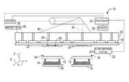
- FIGS. 5 and 6illustrate a chuck 128 in accordance with the present invention.
- Chuck 128provides for a second free span length w 2 prior to separation that is different from the first free span length w 1 during imprinting (needed to maintain middle radius r 3 contact and substantially uniform fluid front control).
- the magnitude of second free span length w 2may be larger than first free span length w 1 .
- the larger free span length prior to separationmay reduce the magnitude of force needed to separate template 18 from substrate 12 .
- Chuck 128may include first 66 and second 68 sides.
- First side 66may include recesses 70 a - 70 d and supports 72 a - 72 d .
- Chambers 62 a - 62 dmay be defined by recesses 70 a - 70 d and positioning of template 18 on supports 72 a - 72 d as illustrated in FIG. 6 .
- recesses 70 a , supports 72 a and 72 b , and a portion of template 18define chamber 62 a .
- Recesses 70 b and another portion of template 18define chamber 62 b .
- chambers 62 a - 62 dprovide four distinct zones, a separation outer bend zone Z 1 , an imprint outer bend zone Z 2 , a back pressure zone Z 3 , and an inner bend zone Z 4 .
- the separation outer bend zone Z 1cinctures the imprint outer bend zone Z 2 , which cinctures the back pressure zone Z 3 , which cinctures the inner bend zone Z 4 .
- dimensions of inner bend zone Z 4 , back pressure zone Z 3 and outer bend zone Z 2may be substantially similar to dimensions of prior art chucks such as those described in U.S. patent application Ser. No. 11/749,909, which is hereby incorporated by reference herein in its entirety.
- separation outer bend zone Z 1may be configured with an increased diameter as compared to outer zones of prior art chucks to provide second free span length w 2 during separation.
- Second free span length w 2may be approximately three times free span length w 1 .
- free span length w 1is generally about 2.5 mm.
- Separation outer bend zone Z 1may be configured with an increased diameter as compared to outer zones of prior art chucks to provide second free span length w 2 during separation of about 14 mm.
- inner bend zone Z 4may have a diameter of approximately 18 mm.
- Back pressure zone Z 3may extend from approximately 19 mm to approximately 67 mm.
- Imprint bend zone Z 2may extend from approximately 68 mm to approximately 90 mm, and separation bend zone Z 1 may extend from approximately 91 mm to approximately 117 mm. It should be noted that extension of separation outer bend zone Z 1 and dimensions of zones Z 1-3 may be determined based on size and configuration of template 18 .
- a pump systemmay operate to control pressure within each zone Z 1 -Z 4 .
- Pump systemmay be in fluid communication with throughways.
- a single pump systemmay operate to control pressure within each zone Z 1 -Z 4 .
- two or more pump systemsmay operate to control pressure within each zone Z 1 -Z 4 .
- Pressuremay include application of pressure (i.e., pressure state) within zones Z 1 -Z 4 and/or application of vacuum force (i.e., vacuum state) within zones Z 1 -Z 4 .
- pressure statemay be between approximately 0 to 10 kPa and vacuum state may be between approximately 0 to ⁇ 90 kPa.
- FIG. 7illustrates use of chuck 128 prior to imprinting.
- pump systemmay provide imprint outer bend zone Z 2 and inner bend zone Z 4 in a vacuum state.
- Vacuum state of outer bend zone Z 2 and inner bend zone Z 4may be substantially similar.
- magnitude of vacuum state of outer bend zone Z 2may be increased as compared to inner bend zone Z 4 or magnitude of vacuum state of outer bend zone Z 3 may be decreased as compared to inner bend zone Z 4 .
- back pressure zone Z 3may be provided in a pressure state. Having outer bend zone Z 2 and inner bend zone Z 4 in a vacuum state and back pressure zone Z 3 in a pressure state provides template 18 in a toroidal imprint shape as illustrated in FIG. 7 .
- the toroidal imprint shapeprovides template 18 with a first free span length w 1 .
- Magnitude of free span length w 1may be between approximately 1.5 mm-4 mm.
- magnitude of free span length w 1may be 2.5 mm.
- separation outer bend zone Z 1Prior to and/or during imprinting, separation outer bend zone Z 1 may be deactivated in an open and/or blocked state.
- FIG. 6illustrates separation outer bend zone Z 1 in a blocked state wherein no pressure or vacuum is applied to chamber 70 a by pump system.
- FIG. 7illustrates separation outer bend zone Z 1 in an open state wherein chamber 70 a is open in that template 18 only contacts support 72 b .
- separation outer bend zone Z 1may be provided in a pressure state, however, at significantly a lower pressure state as compared to back pressure zone Z 3 , or separation outer bend zone Z 1 may be provided in a vacuum state that is significantly lower than imprint outer bend zone Z 2 and/or inner bend zone Z 4 .
- the toroidal imprint shape created prior to imprintingmay provide deflection of template 18 symmetric about middle radius r 3 of substrate 12 during imprinting.
- Vacuum state and positioning of imprint outer bend zone Z 2 and inner bend zone Z 4(e.g., about the middle radius r 3 ) may be configured to provide a radius of curvature at the interface of substrate 12 and template 18 that accelerates filling of polymerizable material 34 .
- Radius of curvaturemay be on the order of 800 mm to 8000 mm.
- separation outer bend zone Z 1 and back pressure zone Z 3may be activated and imprint outer bend zone Z 2 and the inner bend zone Z 4 may be deactivated providing template 18 with a single wave having free span length w 2 .
- separation outer bend zone Z 1may be activated to be in a vacuum state and back pressure zone Z 3 may be activated to be in a pressure state while imprint outer bend zone Z 2 and the inner bend zone Z 4 may be deactivated in a blocked state.
- imprint outer bend zone Z 2 and/or inner bend zone Z 4may be activated in a minimal pressure state.
- first free span length w 1may be Activated with minimal or no interaction with imprint outer bend zone Z 2 and the inner bend zone Z 4 alters the first free span length w 1 to a second free span length w 2 .
- An increase from the first free span length w 1 to the second free span length w 2minimizes separation force.
- the increase in free span length w 2may amplify an upward separation force generally provided during separation of template 18 and substrate 12 , and as such, may provide a larger crack angle for the same upward force as compared to free span length w 1 . This may reduce the force needed to separate template 18 from substrate 12 .
- first free span length w 1 of approximately 2.5 mmmay provide a crack angle of approximately 0.8 mrad.
- Providing second free span length w 2 of approximately 14 mmmay provide a crack angle of approximately 3.1 mrad.
- crack anglemay thus be greater than approximately 1.5 mrad reducing separation force by greater than approximately 40% as compared to providing free span length w 1 during separation.
- vacuum state of substrate chuck 26may be increased during separation.
- substrate chuck 26is always in a vacuum state (e.g., ⁇ 5 kPa) in order to hold substrate 12 during imprinting.
- Increasing vacuum state of substrate chuck 26 during separationmay aid in retaining substrate 12 during separation.
- vacuum statemay be increased to approximately ⁇ 20 kPa during separation.
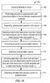
- FIG. 10illustrates a flow chart for a method 100 for imprinting polymerizable material 34 on substrate 12 .
- template 18may be coupled to chuck 28 b .
- template 18may be positioned in superimposition with substrate 12 defining a volume between template 18 and substrate 12 .
- polymerizable material 34may be deposited in the volume defined between template 18 and substrate 12 .
- pump systemmay activate imprint outer bend zone Z 2 , inner bend zone Z 4 , and back pressure zone Z 3 creating a toroidal imprint shape having free span length w 1 .
- pump systemmay provide imprint outer bend zone Z 2 and inner bend zone Z 4 in a vacuum state and back pressure zone Z 3 in a pressure state.
- template 18may contact polymerizable material 34 .
- polymerizable materialmay be solidified.
- pump systemmay activate separation outer bend zone Z 1 and back pressure zone Z 3 , and deactivate imprint outer bend zone Z 2 and the inner bend zone Z 4 to provide template 18 with a single wave having free span length w 2 .
- pump systemmay provide separation outer bend zone Z 1 in a vacuum state and back pressure zone Z 3 in a pressure state while outer bend zone Z 2 and the inner bend zone Z 4 are deactivated (e.g. blocked).
- pump systemmay increase vacuum state of substrate chuck 26 .
- pump systemmay increase vacuum state of substrate chuck 26 from approximately ⁇ 5 kPa to approximately ⁇ 20 kPa.
- template 18may be separated from at least a portion of patterned layer 46 . In one example, template 18 may be completely separated from the patterned layer 46 .
Landscapes
- Engineering & Computer Science (AREA)
- Chemical & Material Sciences (AREA)
- Nanotechnology (AREA)
- Physics & Mathematics (AREA)
- General Physics & Mathematics (AREA)
- Crystallography & Structural Chemistry (AREA)
- Condensed Matter Physics & Semiconductors (AREA)
- Manufacturing & Machinery (AREA)
- Mathematical Physics (AREA)
- Theoretical Computer Science (AREA)
- Shaping Of Tube Ends By Bending Or Straightening (AREA)
Abstract
Description
Claims (11)
Priority Applications (2)
| Application Number | Priority Date | Filing Date | Title |
|---|---|---|---|
| US12/817,787US9164375B2 (en) | 2009-06-19 | 2010-06-17 | Dual zone template chuck |
| PCT/US2010/001769WO2010147671A1 (en) | 2009-06-19 | 2010-06-18 | Dual zone template chuck |
Applications Claiming Priority (2)
| Application Number | Priority Date | Filing Date | Title |
|---|---|---|---|
| US21868609P | 2009-06-19 | 2009-06-19 | |
| US12/817,787US9164375B2 (en) | 2009-06-19 | 2010-06-17 | Dual zone template chuck |
Publications (2)
| Publication Number | Publication Date |
|---|---|
| US20100320645A1 US20100320645A1 (en) | 2010-12-23 |
| US9164375B2true US9164375B2 (en) | 2015-10-20 |
Family
ID=43353568
Family Applications (1)
| Application Number | Title | Priority Date | Filing Date |
|---|---|---|---|
| US12/817,787Expired - Fee RelatedUS9164375B2 (en) | 2009-06-19 | 2010-06-17 | Dual zone template chuck |
Country Status (3)
| Country | Link |
|---|---|
| US (1) | US9164375B2 (en) |
| TW (1) | TW201103721A (en) |
| WO (1) | WO2010147671A1 (en) |
Cited By (2)
| Publication number | Priority date | Publication date | Assignee | Title |
|---|---|---|---|---|
| US11222809B2 (en) | 2018-02-20 | 2022-01-11 | Applied Materials, Inc. | Patterned vacuum chuck for double-sided processing |
| US11289361B2 (en) | 2017-11-10 | 2022-03-29 | Applied Materials, Inc. | Patterned chuck for double-sided processing |
Families Citing this family (6)
| Publication number | Priority date | Publication date | Assignee | Title |
|---|---|---|---|---|
| EP2564271B1 (en) | 2010-04-27 | 2015-12-16 | Canon Nanotechnologies, Inc. | Separation control substrate/template for nanoimprint lithography |
| US8741199B2 (en) | 2010-12-22 | 2014-06-03 | Qingdao Technological University | Method and device for full wafer nanoimprint lithography |
| WO2015070054A1 (en) | 2013-11-08 | 2015-05-14 | Canon Nanotechnologies, Inc. | Low contact imprint lithography template chuck system for improved overlay correction |
| US10654216B2 (en)* | 2016-03-30 | 2020-05-19 | Canon Kabushiki Kaisha | System and methods for nanoimprint lithography |
| KR101853871B1 (en) | 2016-10-31 | 2018-05-03 | 한국기계연구원 | Imprint lithography equipment and method using the same |
| US10288999B2 (en)* | 2016-12-20 | 2019-05-14 | Canon Kabushiki Kaisha | Methods for controlling extrusions during imprint template replication processes |
Citations (21)
| Publication number | Priority date | Publication date | Assignee | Title |
|---|---|---|---|---|
| WO1997005608A1 (en) | 1995-07-27 | 1997-02-13 | Minnesota Mining And Manufacturing Company | Method and apparatus for making an optical information record |
| US20020150398A1 (en) | 2000-08-21 | 2002-10-17 | Choi Byung J. | Flexure based macro motion translation stage |
| US6696220B2 (en) | 2000-10-12 | 2004-02-24 | Board Of Regents, The University Of Texas System | Template for room temperature, low pressure micro-and nano-imprint lithography |
| US20040090611A1 (en) | 2002-11-13 | 2004-05-13 | Molecular Imprints, Inc. | Chucking system for modulating shapes of substrates |
| US20040149687A1 (en) | 1999-10-29 | 2004-08-05 | University Of Texas System, Board Of Regents, Ut System | Method of manufacturing a vacuum chuck used in imprint lithography |
| US20040197712A1 (en) | 2002-12-02 | 2004-10-07 | Jacobson Joseph M. | System for contact printing |
| US6951173B1 (en) | 2003-05-14 | 2005-10-04 | Molecular Imprints, Inc. | Assembly and method for transferring imprint lithography templates |
| US20050260295A1 (en) | 2000-10-27 | 2005-11-24 | Board Of Regents, The University Of Texas System | Remote center compliant flexure device |
| US20050275311A1 (en) | 2004-06-01 | 2005-12-15 | Molecular Imprints, Inc. | Compliant device for nano-scale manufacturing |
| US20050274219A1 (en) | 2004-06-01 | 2005-12-15 | Molecular Imprints, Inc. | Method and system to control movement of a body for nano-scale manufacturing |
| US20050275251A1 (en) | 2004-06-01 | 2005-12-15 | Molecular Imprints, Inc. | Compliant device for nano-scale manufacturing |
| US20060005657A1 (en) | 2004-06-01 | 2006-01-12 | Molecular Imprints, Inc. | Method and system to control movement of a body for nano-scale manufacturing |
| US7150622B2 (en) | 2003-07-09 | 2006-12-19 | Molecular Imprints, Inc. | Systems for magnification and distortion correction for imprint lithography processes |
| EP1830351A1 (en) | 2006-03-01 | 2007-09-05 | Hitachi Global Storage Technologies Netherlands B.V. | Method and apparatus for separating a stamper from a patterned substrate |
| US20070228589A1 (en)* | 2002-11-13 | 2007-10-04 | Molecular Imprints, Inc. | Method for expelling gas positioned between a substrate and a mold |
| WO2007136832A2 (en) | 2006-05-18 | 2007-11-29 | Molecular Imprints, Inc. | Method for expelling gas positioned between a substrate and a mold |
| US20080223237A1 (en)* | 2007-03-12 | 2008-09-18 | Takashi Ando | Imprint device, stamper and pattern transfer method |
| US20090026657A1 (en) | 2007-07-20 | 2009-01-29 | Molecular Imprints, Inc. | Alignment System and Method for a Substrate in a Nano-Imprint Process |
| US7670530B2 (en) | 2006-01-20 | 2010-03-02 | Molecular Imprints, Inc. | Patterning substrates employing multiple chucks |
| WO2010047788A2 (en) | 2008-10-23 | 2010-04-29 | Molecular Imprints, Inc. | Imprint lithography system and method |
| US7768624B2 (en) | 2004-06-03 | 2010-08-03 | Board Of Regents, The University Of Texas System | Method for obtaining force combinations for template deformation using nullspace and methods optimization techniques |
Family Cites Families (9)
| Publication number | Priority date | Publication date | Assignee | Title |
|---|---|---|---|---|
| US7077992B2 (en) | 2002-07-11 | 2006-07-18 | Molecular Imprints, Inc. | Step and repeat imprint lithography processes |
| US6932934B2 (en) | 2002-07-11 | 2005-08-23 | Molecular Imprints, Inc. | Formation of discontinuous films during an imprint lithography process |
| US6936194B2 (en) | 2002-09-05 | 2005-08-30 | Molecular Imprints, Inc. | Functional patterning material for imprint lithography processes |
| US20040065252A1 (en) | 2002-10-04 | 2004-04-08 | Sreenivasan Sidlgata V. | Method of forming a layer on a substrate to facilitate fabrication of metrology standards |
| US8349241B2 (en) | 2002-10-04 | 2013-01-08 | Molecular Imprints, Inc. | Method to arrange features on a substrate to replicate features having minimal dimensional variability |
| US7179396B2 (en) | 2003-03-25 | 2007-02-20 | Molecular Imprints, Inc. | Positive tone bi-layer imprint lithography method |
| US7396475B2 (en) | 2003-04-25 | 2008-07-08 | Molecular Imprints, Inc. | Method of forming stepped structures employing imprint lithography |
| US7157036B2 (en) | 2003-06-17 | 2007-01-02 | Molecular Imprints, Inc | Method to reduce adhesion between a conformable region and a pattern of a mold |
| US8076386B2 (en) | 2004-02-23 | 2011-12-13 | Molecular Imprints, Inc. | Materials for imprint lithography |
- 2010
- 2010-06-17USUS12/817,787patent/US9164375B2/ennot_activeExpired - Fee Related
- 2010-06-18WOPCT/US2010/001769patent/WO2010147671A1/enactiveApplication Filing
- 2010-06-18TWTW099119907Apatent/TW201103721A/enunknown
Patent Citations (29)
| Publication number | Priority date | Publication date | Assignee | Title |
|---|---|---|---|---|
| WO1997005608A1 (en) | 1995-07-27 | 1997-02-13 | Minnesota Mining And Manufacturing Company | Method and apparatus for making an optical information record |
| US6922906B2 (en) | 1999-10-29 | 2005-08-02 | Board Of Regents, The University Of Texas System | Apparatus to orientate a body with respect to a surface |
| US7098572B2 (en) | 1999-10-29 | 2006-08-29 | Board Of Regents, The University Of Texas System | Apparatus to control displacement of a body spaced-apart from a surface |
| US20050264132A1 (en) | 1999-10-29 | 2005-12-01 | Board Of Regents, The University Of Texas System | Apparatus to control displacement of a body spaced-apart from a surface |
| US20040149687A1 (en) | 1999-10-29 | 2004-08-05 | University Of Texas System, Board Of Regents, Ut System | Method of manufacturing a vacuum chuck used in imprint lithography |
| US6955868B2 (en) | 1999-10-29 | 2005-10-18 | Board Of Regents, The University Of Texas System | Method to control the relative position between a body and a surface |
| US6873087B1 (en) | 1999-10-29 | 2005-03-29 | Board Of Regents, The University Of Texas System | High precision orientation alignment and gap control stages for imprint lithography processes |
| US7708542B2 (en) | 2000-07-16 | 2010-05-04 | Board Of Regents, The University Of Texas System | Device for holding a template for use in imprint lithography |
| US20020150398A1 (en) | 2000-08-21 | 2002-10-17 | Choi Byung J. | Flexure based macro motion translation stage |
| US20090037004A1 (en) | 2000-10-12 | 2009-02-05 | Molecular Imprints, Inc. | Method and System to Control Movement of a Body for Nano-Scale Manufacturing |
| US6696220B2 (en) | 2000-10-12 | 2004-02-24 | Board Of Regents, The University Of Texas System | Template for room temperature, low pressure micro-and nano-imprint lithography |
| US20050260295A1 (en) | 2000-10-27 | 2005-11-24 | Board Of Regents, The University Of Texas System | Remote center compliant flexure device |
| US20040090611A1 (en) | 2002-11-13 | 2004-05-13 | Molecular Imprints, Inc. | Chucking system for modulating shapes of substrates |
| US20070114686A1 (en)* | 2002-11-13 | 2007-05-24 | Molecular Imprints, Inc. | Method for expelling gas positioned between a substrate and a mold |
| US20070228589A1 (en)* | 2002-11-13 | 2007-10-04 | Molecular Imprints, Inc. | Method for expelling gas positioned between a substrate and a mold |
| US20040197712A1 (en) | 2002-12-02 | 2004-10-07 | Jacobson Joseph M. | System for contact printing |
| US6951173B1 (en) | 2003-05-14 | 2005-10-04 | Molecular Imprints, Inc. | Assembly and method for transferring imprint lithography templates |
| US7150622B2 (en) | 2003-07-09 | 2006-12-19 | Molecular Imprints, Inc. | Systems for magnification and distortion correction for imprint lithography processes |
| US20050275251A1 (en) | 2004-06-01 | 2005-12-15 | Molecular Imprints, Inc. | Compliant device for nano-scale manufacturing |
| US20060005657A1 (en) | 2004-06-01 | 2006-01-12 | Molecular Imprints, Inc. | Method and system to control movement of a body for nano-scale manufacturing |
| US20050274219A1 (en) | 2004-06-01 | 2005-12-15 | Molecular Imprints, Inc. | Method and system to control movement of a body for nano-scale manufacturing |
| US20050275311A1 (en) | 2004-06-01 | 2005-12-15 | Molecular Imprints, Inc. | Compliant device for nano-scale manufacturing |
| US7768624B2 (en) | 2004-06-03 | 2010-08-03 | Board Of Regents, The University Of Texas System | Method for obtaining force combinations for template deformation using nullspace and methods optimization techniques |
| US7670530B2 (en) | 2006-01-20 | 2010-03-02 | Molecular Imprints, Inc. | Patterning substrates employing multiple chucks |
| EP1830351A1 (en) | 2006-03-01 | 2007-09-05 | Hitachi Global Storage Technologies Netherlands B.V. | Method and apparatus for separating a stamper from a patterned substrate |
| WO2007136832A2 (en) | 2006-05-18 | 2007-11-29 | Molecular Imprints, Inc. | Method for expelling gas positioned between a substrate and a mold |
| US20080223237A1 (en)* | 2007-03-12 | 2008-09-18 | Takashi Ando | Imprint device, stamper and pattern transfer method |
| US20090026657A1 (en) | 2007-07-20 | 2009-01-29 | Molecular Imprints, Inc. | Alignment System and Method for a Substrate in a Nano-Imprint Process |
| WO2010047788A2 (en) | 2008-10-23 | 2010-04-29 | Molecular Imprints, Inc. | Imprint lithography system and method |
Cited By (3)
| Publication number | Priority date | Publication date | Assignee | Title |
|---|---|---|---|---|
| US11289361B2 (en) | 2017-11-10 | 2022-03-29 | Applied Materials, Inc. | Patterned chuck for double-sided processing |
| US11764099B2 (en) | 2017-11-10 | 2023-09-19 | Applied Materials, Inc. | Patterned chuck for double-sided processing |
| US11222809B2 (en) | 2018-02-20 | 2022-01-11 | Applied Materials, Inc. | Patterned vacuum chuck for double-sided processing |
Also Published As
| Publication number | Publication date |
|---|---|
| WO2010147671A1 (en) | 2010-12-23 |
| TW201103721A (en) | 2011-02-01 |
| US20100320645A1 (en) | 2010-12-23 |
Similar Documents
| Publication | Publication Date | Title |
|---|---|---|
| US8913230B2 (en) | Chucking system with recessed support feature | |
| US9164375B2 (en) | Dual zone template chuck | |
| USRE47483E1 (en) | Template having a varying thickness to facilitate expelling a gas positioned between a substrate and the template | |
| US8215946B2 (en) | Imprint lithography system and method | |
| US7641840B2 (en) | Method for expelling gas positioned between a substrate and a mold | |
| TWI336422B (en) | Method for expelling gas positioned between a substrate and a mold | |
| JP6538695B2 (en) | Asymmetric template shape adjustment for partial field imprint | |
| EP2564271B1 (en) | Separation control substrate/template for nanoimprint lithography | |
| US20070114686A1 (en) | Method for expelling gas positioned between a substrate and a mold | |
| US20100096764A1 (en) | Gas Environment for Imprint Lithography | |
| US8309008B2 (en) | Separation in an imprint lithography process | |
| US20090212012A1 (en) | Critical dimension control during template formation | |
| US20100015270A1 (en) | Inner cavity system for nano-imprint lithography | |
| JP2011077529A (en) | Chucking system including array of fluid chambers | |
| WO2007136832A2 (en) | Method for expelling gas positioned between a substrate and a mold | |
| US20100096470A1 (en) | Drop volume reduction |
Legal Events
| Date | Code | Title | Description |
|---|---|---|---|
| AS | Assignment | Owner name:MOLECULAR IMPRINTS, INC., TEXAS Free format text:ASSIGNMENT OF ASSIGNORS INTEREST;ASSIGNORS:GANAPATHISUBRAMANIAN, MAHADEVAN;CHOI, BYUNG-JIN;REEL/FRAME:024553/0354 Effective date:20100617 | |
| AS | Assignment | Owner name:MII NEWCO, INC., TEXAS Free format text:ASSIGNMENT OF JOINT OWNERSHIP;ASSIGNOR:MOLECULAR IMPRINTS, INC.;REEL/FRAME:033329/0280 Effective date:20140710 | |
| AS | Assignment | Owner name:CANON NANOTECHNOLOGIES, INC., TEXAS Free format text:CHANGE OF NAME;ASSIGNOR:MOLECULAR IMPRINTS, INC.;REEL/FRAME:033400/0184 Effective date:20140417 | |
| AS | Assignment | Owner name:MOLECULAR IMPRINTS, INC., TEXAS Free format text:CHANGE OF NAME;ASSIGNOR:MII NEWCO, INC.;REEL/FRAME:033449/0684 Effective date:20140423 | |
| FEPP | Fee payment procedure | Free format text:PAYOR NUMBER ASSIGNED (ORIGINAL EVENT CODE: ASPN); ENTITY STATUS OF PATENT OWNER: LARGE ENTITY | |
| AS | Assignment | Owner name:MOLECULAR IMPRINTS, INC., TEXAS Free format text:CONFIRMATORY ASSIGNMENT OF JOINT PATENT OWNERSHIP;ASSIGNOR:CANON NANOTECHNOLOGIES, INC.;REEL/FRAME:035507/0559 Effective date:20150427 | |
| STCF | Information on status: patent grant | Free format text:PATENTED CASE | |
| MAFP | Maintenance fee payment | Free format text:PAYMENT OF MAINTENANCE FEE, 4TH YEAR, LARGE ENTITY (ORIGINAL EVENT CODE: M1551); ENTITY STATUS OF PATENT OWNER: LARGE ENTITY Year of fee payment:4 | |
| AS | Assignment | Owner name:JP MORGAN CHASE BANK, N.A., NEW YORK Free format text:PATENT SECURITY AGREEMENT;ASSIGNORS:MAGIC LEAP, INC.;MOLECULAR IMPRINTS, INC.;MENTOR ACQUISITION ONE, LLC;REEL/FRAME:050138/0287 Effective date:20190820 | |
| AS | Assignment | Owner name:CITIBANK, N.A., NEW YORK Free format text:ASSIGNMENT OF SECURITY INTEREST IN PATENTS;ASSIGNOR:JPMORGAN CHASE BANK, N.A.;REEL/FRAME:050967/0138 Effective date:20191106 | |
| FEPP | Fee payment procedure | Free format text:MAINTENANCE FEE REMINDER MAILED (ORIGINAL EVENT CODE: REM.); ENTITY STATUS OF PATENT OWNER: LARGE ENTITY | |
| LAPS | Lapse for failure to pay maintenance fees | Free format text:PATENT EXPIRED FOR FAILURE TO PAY MAINTENANCE FEES (ORIGINAL EVENT CODE: EXP.); ENTITY STATUS OF PATENT OWNER: LARGE ENTITY | |
| STCH | Information on status: patent discontinuation | Free format text:PATENT EXPIRED DUE TO NONPAYMENT OF MAINTENANCE FEES UNDER 37 CFR 1.362 | |
| FP | Lapsed due to failure to pay maintenance fee | Effective date:20231020 |