US9164136B2 - Capacitive measurement circuit for a touch sensor device - Google Patents
Capacitive measurement circuit for a touch sensor deviceDownload PDFInfo
- Publication number
- US9164136B2 US9164136B2US14/093,899US201314093899AUS9164136B2US 9164136 B2US9164136 B2US 9164136B2US 201314093899 AUS201314093899 AUS 201314093899AUS 9164136 B2US9164136 B2US 9164136B2
- Authority
- US
- United States
- Prior art keywords
- capacitance
- touch
- input signals
- touch sensor
- output signal
- Prior art date
- Legal status (The legal status is an assumption and is not a legal conclusion. Google has not performed a legal analysis and makes no representation as to the accuracy of the status listed.)
- Expired - Fee Related
Links
Images


Classifications
- G—PHYSICS
- G06—COMPUTING OR CALCULATING; COUNTING
- G06F—ELECTRIC DIGITAL DATA PROCESSING
- G06F3/00—Input arrangements for transferring data to be processed into a form capable of being handled by the computer; Output arrangements for transferring data from processing unit to output unit, e.g. interface arrangements
- G06F3/01—Input arrangements or combined input and output arrangements for interaction between user and computer
- G06F3/03—Arrangements for converting the position or the displacement of a member into a coded form
- G06F3/041—Digitisers, e.g. for touch screens or touch pads, characterised by the transducing means
- G06F3/0416—Control or interface arrangements specially adapted for digitisers
- G06F3/0418—Control or interface arrangements specially adapted for digitisers for error correction or compensation, e.g. based on parallax, calibration or alignment
- G06F3/04182—Filtering of noise external to the device and not generated by digitiser components
- G—PHYSICS
- G06—COMPUTING OR CALCULATING; COUNTING
- G06F—ELECTRIC DIGITAL DATA PROCESSING
- G06F3/00—Input arrangements for transferring data to be processed into a form capable of being handled by the computer; Output arrangements for transferring data from processing unit to output unit, e.g. interface arrangements
- G06F3/01—Input arrangements or combined input and output arrangements for interaction between user and computer
- G06F3/03—Arrangements for converting the position or the displacement of a member into a coded form
- G06F3/041—Digitisers, e.g. for touch screens or touch pads, characterised by the transducing means
- G06F3/044—Digitisers, e.g. for touch screens or touch pads, characterised by the transducing means by capacitive means
- G—PHYSICS
- G01—MEASURING; TESTING
- G01D—MEASURING NOT SPECIALLY ADAPTED FOR A SPECIFIC VARIABLE; ARRANGEMENTS FOR MEASURING TWO OR MORE VARIABLES NOT COVERED IN A SINGLE OTHER SUBCLASS; TARIFF METERING APPARATUS; MEASURING OR TESTING NOT OTHERWISE PROVIDED FOR
- G01D5/00—Mechanical means for transferring the output of a sensing member; Means for converting the output of a sensing member to another variable where the form or nature of the sensing member does not constrain the means for converting; Transducers not specially adapted for a specific variable
- G01D5/12—Mechanical means for transferring the output of a sensing member; Means for converting the output of a sensing member to another variable where the form or nature of the sensing member does not constrain the means for converting; Transducers not specially adapted for a specific variable using electric or magnetic means
- G01D5/14—Mechanical means for transferring the output of a sensing member; Means for converting the output of a sensing member to another variable where the form or nature of the sensing member does not constrain the means for converting; Transducers not specially adapted for a specific variable using electric or magnetic means influencing the magnitude of a current or voltage
- G01D5/24—Mechanical means for transferring the output of a sensing member; Means for converting the output of a sensing member to another variable where the form or nature of the sensing member does not constrain the means for converting; Transducers not specially adapted for a specific variable using electric or magnetic means influencing the magnitude of a current or voltage by varying capacitance
- G—PHYSICS
- G01—MEASURING; TESTING
- G01R—MEASURING ELECTRIC VARIABLES; MEASURING MAGNETIC VARIABLES
- G01R27/00—Arrangements for measuring resistance, reactance, impedance, or electric characteristics derived therefrom
- G01R27/02—Measuring real or complex resistance, reactance, impedance, or other two-pole characteristics derived therefrom, e.g. time constant
- G01R27/26—Measuring inductance or capacitance; Measuring quality factor, e.g. by using the resonance method; Measuring loss factor; Measuring dielectric constants ; Measuring impedance or related variables
- G01R27/2605—Measuring capacitance
- G—PHYSICS
- G06—COMPUTING OR CALCULATING; COUNTING
- G06F—ELECTRIC DIGITAL DATA PROCESSING
- G06F3/00—Input arrangements for transferring data to be processed into a form capable of being handled by the computer; Output arrangements for transferring data from processing unit to output unit, e.g. interface arrangements
- G06F3/01—Input arrangements or combined input and output arrangements for interaction between user and computer
- G06F3/03—Arrangements for converting the position or the displacement of a member into a coded form
- G06F3/041—Digitisers, e.g. for touch screens or touch pads, characterised by the transducing means
- G06F3/0416—Control or interface arrangements specially adapted for digitisers
- G06F3/0418—Control or interface arrangements specially adapted for digitisers for error correction or compensation, e.g. based on parallax, calibration or alignment
- G06F3/04186—Touch location disambiguation
Definitions
- This disclosuregenerally relates to touch sensors.
- a touch sensormay detect the presence and location of a touch or object or the proximity of an object (such as a user's finger or a stylus) within a touch-sensitive area of the touch sensor overlaid on a display screen, for example.
- the touch sensormay enable a user to interact directly with what is displayed on the screen, rather than indirectly with a mouse or touch pad.
- a touch sensormay be attached to or provided as part of a desktop computer, laptop computer, tablet computer, personal digital assistant (PDA), smartphone, satellite navigation device, portable media player, portable game console, kiosk computer, point-of-sale device, or other suitable device.
- a control panel on a household or other appliancemay include a touch sensor.
- touch sensorssuch as, for example, resistive touch screens, surface acoustic wave touch screens, and capacitive touch screens.
- reference to a touch sensormay encompass a touch screen, and vice versa, where appropriate.
- a touch-sensor controllermay process the change in capacitance to determine its position on the touch screen.
- FIG. 1illustrates an example touch sensor with an example touch-sensor controller.
- FIG. 2illustrates an example measurement circuit of a touch-sensor controller.
- FIG. 3illustrates another example capacitive measurement circuit of a touch-sensor controller.
- FIG. 4illustrates steps that may be performed by an example measurement circuit
- FIG. 1illustrates an example touch sensor 100 with an example touch-sensor controller 120 .
- Touch sensor 100 and touch-sensor controller 120may detect the presence and location of a touch or the proximity of an object within a touch-sensitive area of touch sensor 100 .
- reference to a touch sensormay encompass both the touch sensor and its touch-sensor controller, where appropriate.
- reference to a touch-sensor controllermay encompass both the touch-sensor controller and its touch sensor, where appropriate.
- Touch sensor 100may include one or more touch-sensitive areas, where appropriate.
- Touch sensor 100may include an array of drive and sense electrodes (or an array of electrodes of a single type) disposed on one or more substrates, which may be made of a dielectric material.
- reference to a touch sensormay encompass both the electrodes of the touch sensor and the substrate(s) that they are disposed on, where appropriate.
- reference to a touch sensormay encompass the electrodes of the touch sensor, but not the substrate(s) that they are disposed on.
- An electrodemay be an area of conductive material forming a shape, such as for example a disc, square, rectangle, thin line, other suitable shape, or suitable combination of these.
- One or more cuts in one or more layers of conductive materialmay (at least in part) create the shape of an electrode, and the area of the shape may (at least in part) be bounded by those cuts.
- the conductive material of an electrodemay occupy approximately 100% of the area of its shape.
- an electrodemay be made of indium tin oxide (ITO) and the ITO of the electrode may occupy approximately 100% of the area of its shape (sometimes referred to as 100% fill), where appropriate.
- ITOindium tin oxide
- the conductive material of an electrodemay occupy substantially less than 100% of the area of its shape.
- an electrodemay be made of fine lines of metal or other conductive material (FLM), such as for example copper, silver, or a copper- or silver-based material, and the fine lines of conductive material may occupy approximately 5% of the area of its shape in a hatched, mesh, or other suitable pattern.
- FLMconductive material
- reference to FLMencompasses such material, where appropriate.
- the shapes of the electrodes (or other elements) of a touch sensormay constitute in whole or in part one or more macro-features of the touch sensor.
- One or more characteristics of the implementation of those shapesmay constitute in whole or in part one or more micro-features of the touch sensor.
- One or more macro-features of a touch sensormay determine one or more characteristics of its functionality, and one or more micro-features of the touch sensor may determine one or more optical features of the touch sensor, such as transmittance, refraction, or reflection.
- a mechanical stackmay contain the substrate (or multiple substrates) and the conductive material forming the drive or sense electrodes of touch sensor 100 .
- the mechanical stackmay include a first layer of optically clear adhesive (OCA) beneath a cover panel.
- OCAoptically clear adhesive
- the cover panelmay be clear and made of a resilient material suitable for repeated touching, such as for example glass, polycarbonate, or poly(methyl methacrylate) (PMMA).
- PMMApoly(methyl methacrylate)
- This disclosurecontemplates any suitable cover panel made of any suitable material.
- the first layer of OCAmay be disposed between the cover panel and the substrate with the conductive material forming the drive or sense electrodes.
- the mechanical stackmay also include a second layer of OCA and a dielectric layer (which may be made of PET or another suitable material, similar to the substrate with the conductive material forming the drive or sense electrodes).
- a thin coating of a dielectric materialmay be applied instead of the second layer of OCA and the dielectric layer.
- the second layer of OCAmay be disposed between the substrate with the conductive material making up the drive or sense electrodes and the dielectric layer, and the dielectric layer may be disposed between the second layer of OCA and an air gap to a display of a device including touch sensor 100 and touch-sensor controller 120 .
- the cover panelmay have a thickness of approximately 1 millimeter (mm); the first layer of OCA may have a thickness of approximately 0.05 mm; the substrate with the conductive material forming the drive or sense electrodes may have a thickness of approximately 0.05 mm; the second layer of OCA may have a thickness of approximately 0.05 mm; and the dielectric layer may have a thickness of approximately 0.05 mm.
- this disclosuredescribes a particular mechanical stack with a particular number of particular layers made of particular materials and having particular thicknesses, this disclosure contemplates any suitable mechanical stack with any suitable number of any suitable layers made of any suitable materials and having any suitable thicknesses.
- a layer of adhesive or dielectricmay replace the dielectric layer, second layer of OCA, and air gap described above, with there being no air gap to the display.
- One or more portions of the substrate of touch sensor 100may be made of polyethylene terephthalate (PET) or another suitable material. This disclosure contemplates any suitable substrate with any suitable portions made of any suitable material.
- the drive or sense electrodes in touch sensor 100may be made of ITO in whole or in part.
- the drive or sense electrodes in touch sensor 100may be made of fine lines of metal or other conductive material.
- one or more portions of the conductive materialmay be copper or copper-based and have a thickness of approximately 5 microns ( ⁇ m) or less and a width of approximately 100 ⁇ m or less.
- one or more portions of the conductive materialmay be silver or silver-based and similarly have a thickness of approximately 5 ⁇ m or less and a width of approximately 100 ⁇ m or less.
- Touch sensor 100may implement a capacitive form of touch sensing.
- touch sensor 100may include an array of drive and sense electrodes forming an array of capacitive nodes.
- a drive electrode and a sense electrodemay form a capacitive node.
- the drive and sense electrodes forming the capacitive nodemay come near each other, but not make electrical contact with each other. Instead, the drive and sense electrodes may be capacitively coupled to each other across a space between them.
- a pulsed or alternating voltage applied to the drive electrode(by touch-sensor controller 120 ) may induce a charge on the sense electrode, and the amount of charge induced may be susceptible to external influence (such as a touch or the proximity of an object).
- touch-sensor controller 120may measure the change in capacitance. By measuring changes in capacitance throughout the array, touch-sensor controller 120 may determine the position of the touch or proximity within the touch-sensitive area(s) of touch sensor 100 .
- touch sensor 100may include an array of electrodes of a single type that may each form a capacitive node.
- touch-sensor controller 120may measure the change in capacitance, for example, as a change in the amount of charge needed to raise the voltage at the capacitive node by a pre-determined amount.
- touch-sensor controller 120may determine the position of the touch or proximity within the touch-sensitive area(s) of touch sensor 100 .
- This disclosurecontemplates any suitable form of capacitive touch sensing, where appropriate.
- one or more drive electrodesmay together form a drive line running horizontally or vertically or in any suitable orientation.
- one or more sense electrodesmay together form a sense line running horizontally or vertically or in any suitable orientation.
- drive linesmay run substantially perpendicular to sense lines.
- reference to a drive linemay encompass one or more drive electrodes making up the drive line, and vice versa, where appropriate.
- reference to a sense linemay encompass one or more sense electrodes making up the sense line, and vice versa, where appropriate.
- Touch sensor 100may have drive and sense electrodes disposed in a pattern on one side of a single substrate. In such a configuration, a pair of drive and sense electrodes capacitively coupled to each other across a space between them may form a capacitive node. For a self-capacitance implementation, electrodes of only a single type may be disposed in a pattern on a single substrate. In addition or as an alternative to having drive and sense electrodes disposed in a pattern on one side of a single substrate, touch sensor 100 may have drive electrodes disposed in a pattern on one side of a substrate and sense electrodes disposed in a pattern on another side of the substrate.
- touch sensor 100may have drive electrodes disposed in a pattern on one side of one substrate and sense electrodes disposed in a pattern on one side of another substrate.
- an intersection of a drive electrode and a sense electrodemay form a capacitive node.
- Such an intersectionmay be a location where the drive electrode and the sense electrode “cross” or come nearest each other in their respective planes.
- the drive and sense electrodesdo not make electrical contact with each other—instead they are capacitively coupled to each other across a dielectric at the intersection.
- this disclosuredescribes particular configurations of particular electrodes forming particular nodes, this disclosure contemplates any suitable configuration of any suitable electrodes forming any suitable nodes. Moreover, this disclosure contemplates any suitable electrodes disposed on any suitable number of any suitable substrates in any suitable patterns.
- a change in capacitance at a capacitive node of touch sensor 100may indicate a touch or proximity input at the position of the capacitive node.
- Touch-sensor controller 120may detect and process the change in capacitance to determine the presence and location of the touch or proximity input. Touch-sensor controller 120 may then communicate information about the touch or proximity input to one or more other components (such one or more central processing units (CPUs)) of a device that includes touch sensor 100 and touch-sensor controller 120 , which may respond to the touch or proximity input by initiating a function of the device (or an application running on the device).
- CPUscentral processing units
- Touch-sensor controller 120may be one or more integrated circuits (ICs), such as for example general-purpose microprocessors, microcontrollers, programmable logic devices or arrays, application-specific ICs (ASICs).
- touch-sensor controller 120comprises analog circuitry, digital logic, and digital non-volatile memory.
- touch-sensor controller 120is disposed on a flexible printed circuit (FPC) bonded to the substrate of touch sensor 100 , as described below.
- the FPCmay be active or passive, where appropriate.
- multiple touch-sensor controllers 120are disposed on the FPC.
- Touch-sensor controller 120may include a processor unit, a drive unit, a sense unit, and a storage unit.
- the drive unitmay supply drive signals to the drive electrodes of touch sensor 100 .
- the sense unitmay sense charge at the capacitive nodes of touch sensor 100 .
- the sense unitmay include a measurement circuit that measures the capacitances at the capacitive nodes and provides measurement signals to the processor unit representing capacitances at the capacitive nodes.
- the processor unitmay control the supply of drive signals to the drive electrodes by the drive unit and process measurement signals from the sense unit to detect and process the presence and location of a touch or proximity input within the touch-sensitive area(s) of touch sensor 100 .
- the processor unitmay also track changes in the position of a touch or proximity input within the touch-sensitive area(s) of touch sensor 100 .
- the storage unitmay store programming for execution by the processor unit, including programming for controlling the drive unit to supply drive signals to the drive electrodes, programming for processing measurement signals from the sense unit, and other suitable programming, where appropriate.
- Tracks 140 of conductive material disposed on the substrate of touch sensor 100may couple the drive or sense electrodes of touch sensor 100 to connection pads 160 , also disposed on the substrate of touch sensor 100 . As described below, connection pads 160 facilitate coupling of tracks 140 to touch-sensor controller 120 . Tracks 140 may extend into or around (e.g. at the edges of) the touch-sensitive area(s) of touch sensor 100 . Particular tracks 140 may provide drive connections for coupling touch-sensor controller 120 to drive electrodes of touch sensor 100 , through which the drive unit of touch-sensor controller 120 may supply drive signals to the drive electrodes.
- Tracks 140may provide sense connections for coupling touch-sensor controller 120 to sense electrodes of touch sensor 100 , through which the sense unit of touch-sensor controller 120 may sense charge at the capacitive nodes of touch sensor 100 .
- Tracks 140may be made of fine lines of metal or other conductive material.
- the conductive material of tracks 140may be copper or copper-based and have a width of approximately 1000 ⁇ m or less.
- the conductive material of tracks 140may be silver or silver-based and have a width of approximately 1000 ⁇ m or less.
- tracks 140may be made of ITO in whole or in part in addition or as an alternative to fine lines of metal or other conductive material.
- touch sensor 100may include one or more ground lines terminating at a ground connector (which may be a connection pad 160 ) at an edge of the substrate of touch sensor 100 (similar to tracks 140 ).
- Connection pads 160may be located along one or more edges of the substrate, outside the touch-sensitive area(s) of touch sensor 100 .
- touch-sensor controller 120may be on an FPC.
- Connection pads 160may be made of the same material as tracks 140 and may be bonded to the FPC using an anisotropic conductive film (ACF).
- ACFanisotropic conductive film
- Connection 180may include conductive lines on the FPC coupling touch-sensor controller 120 to connection pads 160 , in turn coupling touch-sensor controller 120 to tracks 140 and to the drive or sense electrodes of touch sensor 100 .
- connection pads 160may be connected an electro-mechanical connector (such as a zero insertion force wire-to-board connector). In these embodiments, connection 180 may not need to include an FPC. This disclosure contemplates any suitable connection 180 between touch-sensor controller 120 and touch sensor 100 .
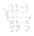
- FIG. 2illustrates an example measurement circuit 200 of touch-sensor controller 120 .
- the measurement circuit 200includes an input buffer 202 a-n , at least one compensation buffer 204 a-n , and an integrator 206 a-n for each input signal 208 a-n that is received.
- measurement circuit 200includes a current summer/divider 210 that provides mirrored output to a proximity circuit 212 and each of the integrators 206 a-n .
- a pad driver 216 a-nmay be associated with each sense line 214 a-n and input signal 208 a-n .
- Each input signal 208 a-n , i in a-nis received at an input buffer 202 a-n associated with that particular sense line 214 a-n of touch sensor 100 .
- Input buffers 202 a-nmay be configured to amplify the current and generate dual outputs.
- each input buffer 202 a-nmay output a first output signal 218 a-n , i od a-n , that is transmitted to and received by the current summer/divider 210 and a second output signal 220 a-n , i oint a-n , that is transmitted to and received by an integrator 206 a-n that is associated with the same sense line 214 a-n .
- first input signal 208 ai in a
- input buffer 202 areceives a first input signal 218 a , i od a , that is transmitted to current summer/divider 210 and a second signal 220 a , i oint a , that is transmitted to and received by integrator 206 a .
- Input buffers 202 b-nare depicted similarly.
- each input signal 208 a-nincludes both a touch capacitance, C P , and a parasitic capacitance, C P .
- a touch sensor 100includes uniform sense lines 214 a-n , the parasitic capacitance of each input 208 a-n will be substantially the same.
- current summer/divider 210may receive the total capacitance for each input signal 208 a-n and compute an average capacitance.
- current summer/divider 210may add the total capacitance of each input signal 208 a-n together and then divide the summed total of all capacitance by the total number of input signals, n, to calculate the average capacitance. This average capacitance can then be subtracted from each total capacitance to substantially remove the parasitic capacitance.
- measurement circuit 200includes one or more compensation buffers 204 a-n for each input signal 208 a-n .
- Compensation buffers 204 a-nmay include linearizers configured to linearize touch sensor 200 by applying a scaling factor to the first output signal 218 a-n .
- input signal 208 aincludes ten percent more parasitic capacitance than the other input signals 208 b-n . If the input signals 208 a-n are not linearized, the current summer/divider 210 will receive 10% more parasitic capacitance from the sense line 214 a associated with input signal 208 a than from the sense lines 214 b-n associated with input signals 208 b-n .
- compensation buffers 204 a-nmay be configured to reduce the effect of parasitic difference between sense lines by adjusting the capacitance of the input signals 208 a-n up or down.
- linearizers 204 a - nmay be configured to apply a scaling factor, s, to the first output signal 218 a-n .
- the outputs of each integrator 208 a-nmay be used to linearize the input signals 208 a-n .
- example measurement circuit 200may compensate for the parasitic capacitance exhibited by each input signals 208 a-n .
- current summer/divider 210may receive each first output signal 218 a-n from linearizers 204 a-n and compute an average capacitance, C AVG .
- the average capacitancerepresents the average current of all channels multiplied by the scaling factor, s.
- current summer/divider 210may add the total capacitance of each output signal 218 a-n together and then divide the summed total of all capacitance by the total number of input signals, n, to calculate the average capacitance.
- the average capacitancemay be represented as s (i s /n).
- Each integrator 206 a-nmay then receive the average capacitance from current summer/divider 210 and the second output signal from an associated input buffer 202 a-n .
- an integrator 206 nreceives average capacitance, s (i s /n), and second output signal, i oint n .
- the current into integrator 206 nmay be calculated as being equal to i oint n /[s (i s /n)].
- a proximity circuit 212which operates similar to integrators 206 a-n , may receive only the average capacitance measured by the current summer/divider 210 .
- Proximity circuit 210may operate to detect inadvertent touches on touch sensor 100 . For example, where touch sensor 200 is incorporated into a mobile phone, proximity circuit 210 may operate to turn off touch sensor 100 in response to a user placing a portion of a finger or hand on the touch sensor 100 while the user is currently on a phone call.
- FIG. 3illustrates still another example measurement circuit 300 according to certain embodiments.
- Example measurement circuit 300includes some components that may be similar to those described above with regard to example measurement circuit 200 .
- measurement circuit 300includes an input buffer 302 a-n , at least one compensation buffer 304 a-n , and an integrator 306 a-n for each input signal 308 a-n that is received.
- measurement circuit 300includes a current summer/divider 310 that provides n-mirrored output signals to each of integrators 306 a-n .
- Each inputs signal 308 a-nmay be received at an input buffer 302 a-n associated with that particular sense line.
- Input buffers 302 a - nmay be configured to amplify the current and generate dual outputs.
- each input buffer 302 a-nmay output a first output that is transmitted to and received by the current summer/divider 310 and a second output that is transmitted to and received by an integrator 306 a-n that is associated with that same sense line.
- example measurement circuit 300uses current sources 312 a-n to perform the scaling operation.
- current sources 312 a-nmay inject a compensation current that cancels the parasitic capacitance of the input signal 308 a-n .
- an proportional amount of currentmay be injected by current sources 312 b-n into input signals 308 a-n so as to make the parasitic capacitance of all signals substantially equal.
- currentmay be removed from input signals 308 a to decrease the parasitic capacitance of input signal 308 a such that input signals 308 a-n are of approximately equal parasitic capacitance.
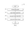
- FIG. 4illustrates the steps performed by an example measurement circuit such as those described above with regard to FIGS. 2-3 .
- the method 400may begin in response to a touch proximate to a location on a touch sensor 100 .
- a plurality of input signalsmay be received in response to the touch.
- each input signal 208 a-nmay have a total capacitance and may be associated with a sense line of a touch sensor 100 .
- the total capacitancemay include a first capacitance associated with the touch and a second capacitance comprising a parasitic capacitance.
- the parasitic capacitance of at least one of the plurality of input signals 208 a-nmay be adjusted.
- a linearizermay be provided for each input signal. The linearizers may operate to adjust the parasitic capacitance of a received input signal to result in the second capacitance of each of the plurality of input signals being substantially equal.
- an amount of capacitancemay be added or subtracted from at least one of the plurality of input signals 208 a-n . For example, capacitance may be subtracted from an input signal 208 a having a higher parasitic capacitance than other input signals 208 b-n . Alternatively, capacitance may be added to the other input signals 208 b-n to increase their parasitic capacitance to be substantially equal to the input signal 208 a having the highest parasitic capacitance.
- an average capacitance of the plurality of input signals 208 a-nmay be calculated from the plurality of adjusted input signals.
- a current summer/divider 210may communicated with each linearizer 204 a-n .
- Current summer/divider 210may receive the plurality of adjusted input signals 208 a-n from the plurality of linearizers 204 a-n .
- the average capacitanceis calculated based on the input signals 208 a-n having substantially equal parasitic capacitance.
- Current summer/divider 210may then calculate the average capacitance by summing the plurality of adjusted input signals 208 a-n and dividing the sum by the total number of input signals, n.
- current summer/divider 210may then generate n output signals, as was described with regard to FIG. 2 , or n+1 output signals, as was described with regard to FIG. 3 .
- n+1 output signalsmay be generated where a proximity circuit 212 is used to detect inadvertent touches that should not be ignored.
- the location of the touch on the touch sensor 100may be determined.
- at least one processormay be used to compare the total capacitance of the plurality of input signals 208 a-n and the average capacitance of the plurality of adjusted input signals 208 a-n .
- the average capacitancemay be subtracted from the total capacitance of each of the input signals 208 a-n to determine the first capacitance of each input signal 208 a-n . Because the average capacitance is calculated based on input signals 208 a-n having substantially equal parasitic capacitance, the parasitic capacitance of the plurality of input signals 208 a-n is substantially negated.
- the difference between the average capacitance and the total capacitance for an input signal 208 a-nmay be attributed to the capacitance generated by the touch.
- the input signal 208 a-n having the highest capacitance attributable by the touchmay be used to identify the location of the touch on the touchscreen.
- Particular embodimentsmay repeat the steps of the method of FIG. 4 , where appropriate.
- this disclosuredescribes and illustrates particular steps of the method of FIG. 4 as occurring in a particular order, this disclosure contemplates any suitable steps of the method of FIG. 4 occurring in any suitable order.
- this disclosuredescribes and illustrates particular components, devices, or systems carrying out particular steps of the method of FIG. 4 , this disclosure contemplates any suitable combination of any suitable components, devices, or systems carrying out any suitable steps of the method of FIG. 4 .
- a computer-readable non-transitory storage mediummay include a semiconductor-based or other integrated circuit (IC) (such as, for example, a field-programmable gate array (FPGA) or an application-specific IC (ASIC)), a hard disk, an HDD, a hybrid hard drive (HHDI)), an optical disc, an optical disc drive (ODD), a magneto-optical disc, a magneto-optical drive, a floppy disk, a floppy disk drive (FDD), magnetic tape, a holographic storage medium, a solid-state drive (SSD), a RAM-drive, a SECURE DIIGITAL card, a SECURE DIGITAL drive, another suitable computer-readable non-transitory storage medium, or a suitable combination of these, where appropriate.
- ICsemiconductor-based or other integrated circuit
- ICsuch as, for example, a field-programmable gate array (FPGA) or an application-specific IC (ASIC)
- HDDhigh-programmable gate array
Landscapes
- Engineering & Computer Science (AREA)
- General Engineering & Computer Science (AREA)
- Theoretical Computer Science (AREA)
- Physics & Mathematics (AREA)
- General Physics & Mathematics (AREA)
- Human Computer Interaction (AREA)
- Position Input By Displaying (AREA)
- Electronic Switches (AREA)
Abstract
Description
Claims (17)
Priority Applications (7)
| Application Number | Priority Date | Filing Date | Title |
|---|---|---|---|
| US14/093,899US9164136B2 (en) | 2013-12-02 | 2013-12-02 | Capacitive measurement circuit for a touch sensor device |
| DE102014222478.0ADE102014222478A1 (en) | 2013-12-02 | 2014-11-04 | Capacitive measuring circuit for a touch sensor device |
| CN201910147004.5ACN110083265A (en) | 2013-12-02 | 2014-11-13 | Capacitance measurement circuit for touch sensor apparatus |
| CN201410640098.7ACN104679368B (en) | 2013-12-02 | 2014-11-13 | Capacitance Measurement Circuit for Touch Sensor Devices |
| TW108100865ATWI693412B (en) | 2013-12-02 | 2014-12-02 | Capacitive measurement circuit for a touch sensor device |
| TW103141833ATWI655443B (en) | 2013-12-02 | 2014-12-02 | Capacitance measuring circuit for a touch sensor device |
| US14/885,061US10067619B2 (en) | 2013-12-02 | 2015-10-16 | Capacitive measurement circuit for a touch sensor drive |
Applications Claiming Priority (1)
| Application Number | Priority Date | Filing Date | Title |
|---|---|---|---|
| US14/093,899US9164136B2 (en) | 2013-12-02 | 2013-12-02 | Capacitive measurement circuit for a touch sensor device |
Related Child Applications (1)
| Application Number | Title | Priority Date | Filing Date |
|---|---|---|---|
| US14/885,061ContinuationUS10067619B2 (en) | 2013-12-02 | 2015-10-16 | Capacitive measurement circuit for a touch sensor drive |
Publications (2)
| Publication Number | Publication Date |
|---|---|
| US20150153398A1 US20150153398A1 (en) | 2015-06-04 |
| US9164136B2true US9164136B2 (en) | 2015-10-20 |
Family
ID=53058635
Family Applications (2)
| Application Number | Title | Priority Date | Filing Date |
|---|---|---|---|
| US14/093,899Expired - Fee RelatedUS9164136B2 (en) | 2013-12-02 | 2013-12-02 | Capacitive measurement circuit for a touch sensor device |
| US14/885,061Active2034-06-08US10067619B2 (en) | 2013-12-02 | 2015-10-16 | Capacitive measurement circuit for a touch sensor drive |
Family Applications After (1)
| Application Number | Title | Priority Date | Filing Date |
|---|---|---|---|
| US14/885,061Active2034-06-08US10067619B2 (en) | 2013-12-02 | 2015-10-16 | Capacitive measurement circuit for a touch sensor drive |
Country Status (4)
| Country | Link |
|---|---|
| US (2) | US9164136B2 (en) |
| CN (2) | CN104679368B (en) |
| DE (1) | DE102014222478A1 (en) |
| TW (2) | TWI655443B (en) |
Families Citing this family (7)
| Publication number | Priority date | Publication date | Assignee | Title |
|---|---|---|---|---|
| KR102061108B1 (en)* | 2013-01-16 | 2020-01-02 | 삼성디스플레이 주식회사 | Organic Light Emitting Display integrated Touch Screen Panel |
| US10061444B2 (en)* | 2013-07-31 | 2018-08-28 | Apple Inc. | Self capacitance touch sensing |
| US9778804B2 (en)* | 2015-06-04 | 2017-10-03 | Synaptics Incorporated | Calibrating charge mismatch in a baseline correction circuit |
| US10120513B2 (en)* | 2016-05-26 | 2018-11-06 | Atmel Corporation | Touch sensor compensation circuit |
| CN106468983B (en)* | 2016-08-31 | 2019-03-29 | 江西联思触控技术有限公司 | A kind of method of ground line position in touch panel and determining touch panel |
| CN112350707B (en)* | 2020-09-30 | 2024-04-05 | 青岛海尔智能家电科技有限公司 | Method, device and all-metal switch for controlling a touch switch |
| CN115493626A (en)* | 2021-06-18 | 2022-12-20 | 上海复旦微电子集团股份有限公司 | Sensing sensitivity testing device and method, and capacitance sensing equipment |
Citations (42)
| Publication number | Priority date | Publication date | Assignee | Title |
|---|---|---|---|---|
| US3805149A (en)* | 1971-06-24 | 1974-04-16 | Commissariat Energie Atomique | Method of linear measurement of a variation in capacitance and corresponding digital-display device |
| US6194903B1 (en)* | 1996-01-21 | 2001-02-27 | I F M Electronic Gmbh | Circuit for acquisition of the capacitance or capacitance change of a capacitive circuit element or component |
| US6456477B1 (en)* | 1998-03-10 | 2002-09-24 | Mcintosh Robert B. | Linear capacitance detection circuit |
| US20040004488A1 (en)* | 2002-07-02 | 2004-01-08 | Baxter Larry K. | Capacitive sensor circuit with good noise rejection |
| US20050030046A1 (en)* | 2001-09-06 | 2005-02-10 | Masami Yakabe | Impedance measuring circuit and capacitance measuring circuit |
| US20050068044A1 (en)* | 2001-10-24 | 2005-03-31 | William Peine | Array sensor electronics |
| US6977646B1 (en)* | 2001-11-30 | 2005-12-20 | 3M Innovative Properties Co. | Touch screen calibration system and method |
| US20060267953A1 (en)* | 2005-05-31 | 2006-11-30 | Peterson Richard A Jr | Detection of and compensation for stray capacitance in capacitive touch sensors |
| US7288945B2 (en)* | 2004-08-18 | 2007-10-30 | Southwest Research Institute | Systems and methods for detection of dielectric change in material and structure |
| US20070268272A1 (en)* | 2006-05-19 | 2007-11-22 | N-Trig Ltd. | Variable capacitor array |
| US20080170046A1 (en)* | 2007-01-16 | 2008-07-17 | N-Trig Ltd. | System and method for calibration of a capacitive touch digitizer system |
| US20090025987A1 (en)* | 2007-07-26 | 2009-01-29 | N-Trig Ltd. | System and method for diagnostics of a grid based digitizer |
| US7501836B2 (en)* | 2006-11-14 | 2009-03-10 | Avago Technologies Enterprise IP (Singapore) Pte. Ltd. | Apparatus and method for determining capacitance variation in an integrated circuit |
| US20090160461A1 (en)* | 2007-12-19 | 2009-06-25 | Infineon Technologies Ag | Capacitive sensor and measurement system |
| US20090315854A1 (en) | 2008-06-18 | 2009-12-24 | Epson Imaging Devices Corporation | Capacitance type input device and display device with input function |
| US7663607B2 (en) | 2004-05-06 | 2010-02-16 | Apple Inc. | Multipoint touchscreen |
| US20100060608A1 (en)* | 2008-09-10 | 2010-03-11 | Apple Inc. | Correction of parasitic capacitance effect in touch sensor panels |
| US20100073323A1 (en)* | 2008-09-24 | 2010-03-25 | Geaghan Bernard O | Mutual capacitance measuring circuits and methods |
| US20100073301A1 (en)* | 2008-09-19 | 2010-03-25 | Marduke Yousefpor | Correction of Parasitic Capacitance Effect in Touch Sensor Panels |
| US7875814B2 (en) | 2005-07-21 | 2011-01-25 | Tpo Displays Corp. | Electromagnetic digitizer sensor array structure |
| US7920129B2 (en) | 2007-01-03 | 2011-04-05 | Apple Inc. | Double-sided touch-sensitive panel with shield and drive combined layer |
| US8031174B2 (en) | 2007-01-03 | 2011-10-04 | Apple Inc. | Multi-touch surface stackup arrangement |
| US8031094B2 (en) | 2009-09-11 | 2011-10-04 | Apple Inc. | Touch controller with improved analog front end |
| US20110242050A1 (en)* | 2010-04-06 | 2011-10-06 | Samsung Electronics Co., Ltd. | Method and apparatus compensating parasitic capacitance in touch panel |
| US8040326B2 (en) | 2007-06-13 | 2011-10-18 | Apple Inc. | Integrated in-plane switching display and touch sensor |
| US8049732B2 (en) | 2007-01-03 | 2011-11-01 | Apple Inc. | Front-end signal compensation |
| US20110279170A1 (en)* | 2009-03-27 | 2011-11-17 | Texas Instruments Incorporated | Embedded sar based active gain capacitance measurement system and method |
| US20120024064A1 (en)* | 2010-07-29 | 2012-02-02 | Medtronic, Inc. | Techniques for approximating a difference between two capacitances |
| US8179381B2 (en) | 2008-02-28 | 2012-05-15 | 3M Innovative Properties Company | Touch screen sensor |
| US20120194492A1 (en)* | 2011-02-02 | 2012-08-02 | Benjamin James Hadwen | Active matrix device |
| US20120243151A1 (en) | 2011-03-21 | 2012-09-27 | Stephen Brian Lynch | Electronic Devices With Convex Displays |
| US20120243719A1 (en) | 2011-03-21 | 2012-09-27 | Franklin Jeremy C | Display-Based Speaker Structures for Electronic Devices |
| US20120242588A1 (en) | 2011-03-21 | 2012-09-27 | Myers Scott A | Electronic devices with concave displays |
| WO2012129247A2 (en) | 2011-03-21 | 2012-09-27 | Apple Inc. | Electronic devices with flexible displays |
| US20120242592A1 (en) | 2011-03-21 | 2012-09-27 | Rothkopf Fletcher R | Electronic devices with flexible displays |
| US20130069671A1 (en)* | 2011-09-15 | 2013-03-21 | Atmel Corporation | Low power capacitive touch detector |
| US20130076612A1 (en) | 2011-09-26 | 2013-03-28 | Apple Inc. | Electronic device with wrap around display |
| US20130106779A1 (en)* | 2011-10-31 | 2013-05-02 | Analog Devices, Inc. | Noise compensation techniques for capacitive touch screen systems |
| US20130120005A1 (en)* | 2011-11-11 | 2013-05-16 | Plantronics, Inc. | Separation of Capacitive Touch Areas |
| US8519722B1 (en)* | 2008-10-22 | 2013-08-27 | Cypress Semiconductor Corporation | Method and apparatus for testing projected capacitance matrices and determining the location and types of faults |
| US20130249570A1 (en)* | 2012-03-20 | 2013-09-26 | Pepperl + Fuchs Gmbh | Sensor and Method for Detecting an Object |
| US20130285972A1 (en)* | 2012-04-30 | 2013-10-31 | John Greer Elias | Capacitance touch near-field-far field switching |
Family Cites Families (19)
| Publication number | Priority date | Publication date | Assignee | Title |
|---|---|---|---|---|
| TW200709024A (en)* | 2005-08-31 | 2007-03-01 | Elan Microelectronics Corp | Touch sensor |
| US20070074913A1 (en)* | 2005-10-05 | 2007-04-05 | Geaghan Bernard O | Capacitive touch sensor with independently adjustable sense channels |
| TW200715176A (en)* | 2005-10-07 | 2007-04-16 | Elan Microelectronics Corp | Method for compensating sensitivity of sensor of touch panel |
| WO2008065605A2 (en)* | 2006-11-30 | 2008-06-05 | Koninklijke Philips Electronics N.V. | In-plane switching electrophoretic colour display |
| US7830158B2 (en)* | 2007-12-28 | 2010-11-09 | 3M Innovative Properties Company | Time-sloped capacitance measuring circuits and methods |
| US8482544B2 (en)* | 2009-07-10 | 2013-07-09 | Apple Inc. | Negative pixel compensation |
| US8310381B2 (en)* | 2009-09-28 | 2012-11-13 | Microchip Technology Incorporated | Capacitive key touch sensing using analog inputs and digital outputs |
| EP2491478A4 (en)* | 2009-10-20 | 2014-07-23 | Cypress Semiconductor Corp | Method and apparatus for reducing coupled noise influence in touch screen controllers. |
| US8174273B2 (en)* | 2010-01-07 | 2012-05-08 | 3M Innovative Properties Company | Capacitance measurement circuit with dynamic feedback |
| TWI410850B (en)* | 2010-01-29 | 2013-10-01 | Mstar Semiconductor Inc | Touch sensing device and associated method |
| KR20110091380A (en)* | 2010-02-05 | 2011-08-11 | 삼성전자주식회사 | Noise compensation method and device of touch panel |
| TWI417778B (en)* | 2010-02-26 | 2013-12-01 | Raydium Semiconductor Corp | Capacitance offset compensation for electronic device |
| US20120026123A1 (en)* | 2010-07-30 | 2012-02-02 | Grunthaner Martin Paul | Compensation for Capacitance Change in Touch Sensing Device |
| US10001883B2 (en)* | 2010-12-22 | 2018-06-19 | Elo Touch Solutions, Inc. | Mechanical deflection compensation for a capacitive touch input device |
| US20130127744A1 (en)* | 2011-11-22 | 2013-05-23 | Qualcomm Mems Technologies, Inc. | Wireframe touch sensor design and spatially linearized touch sensor design |
| US9100021B2 (en)* | 2012-01-19 | 2015-08-04 | Texas Instruments Incorporated | Linear capacitively coupled touch sensor and method |
| US8896327B2 (en)* | 2012-04-12 | 2014-11-25 | Atmel Corporation | Current mirror self-capacitance measurement |
| US9372582B2 (en)* | 2012-04-19 | 2016-06-21 | Atmel Corporation | Self-capacitance measurement |
| US20140354582A1 (en)* | 2013-05-30 | 2014-12-04 | Silicon Laboratories Inc. | Touch Sensor For Mobile Device With Radio |
- 2013
- 2013-12-02USUS14/093,899patent/US9164136B2/ennot_activeExpired - Fee Related
- 2014
- 2014-11-04DEDE102014222478.0Apatent/DE102014222478A1/ennot_activeWithdrawn
- 2014-11-13CNCN201410640098.7Apatent/CN104679368B/ennot_activeExpired - Fee Related
- 2014-11-13CNCN201910147004.5Apatent/CN110083265A/enactivePending
- 2014-12-02TWTW103141833Apatent/TWI655443B/ennot_activeIP Right Cessation
- 2014-12-02TWTW108100865Apatent/TWI693412B/ennot_activeIP Right Cessation
- 2015
- 2015-10-16USUS14/885,061patent/US10067619B2/enactiveActive
Patent Citations (43)
| Publication number | Priority date | Publication date | Assignee | Title |
|---|---|---|---|---|
| US3805149A (en)* | 1971-06-24 | 1974-04-16 | Commissariat Energie Atomique | Method of linear measurement of a variation in capacitance and corresponding digital-display device |
| US6194903B1 (en)* | 1996-01-21 | 2001-02-27 | I F M Electronic Gmbh | Circuit for acquisition of the capacitance or capacitance change of a capacitive circuit element or component |
| US6456477B1 (en)* | 1998-03-10 | 2002-09-24 | Mcintosh Robert B. | Linear capacitance detection circuit |
| US20050030046A1 (en)* | 2001-09-06 | 2005-02-10 | Masami Yakabe | Impedance measuring circuit and capacitance measuring circuit |
| US20050068044A1 (en)* | 2001-10-24 | 2005-03-31 | William Peine | Array sensor electronics |
| US6977646B1 (en)* | 2001-11-30 | 2005-12-20 | 3M Innovative Properties Co. | Touch screen calibration system and method |
| US20040004488A1 (en)* | 2002-07-02 | 2004-01-08 | Baxter Larry K. | Capacitive sensor circuit with good noise rejection |
| US7663607B2 (en) | 2004-05-06 | 2010-02-16 | Apple Inc. | Multipoint touchscreen |
| US7288945B2 (en)* | 2004-08-18 | 2007-10-30 | Southwest Research Institute | Systems and methods for detection of dielectric change in material and structure |
| US7567240B2 (en)* | 2005-05-31 | 2009-07-28 | 3M Innovative Properties Company | Detection of and compensation for stray capacitance in capacitive touch sensors |
| US20060267953A1 (en)* | 2005-05-31 | 2006-11-30 | Peterson Richard A Jr | Detection of and compensation for stray capacitance in capacitive touch sensors |
| US7875814B2 (en) | 2005-07-21 | 2011-01-25 | Tpo Displays Corp. | Electromagnetic digitizer sensor array structure |
| US20070268272A1 (en)* | 2006-05-19 | 2007-11-22 | N-Trig Ltd. | Variable capacitor array |
| US7501836B2 (en)* | 2006-11-14 | 2009-03-10 | Avago Technologies Enterprise IP (Singapore) Pte. Ltd. | Apparatus and method for determining capacitance variation in an integrated circuit |
| US8049732B2 (en) | 2007-01-03 | 2011-11-01 | Apple Inc. | Front-end signal compensation |
| US8031174B2 (en) | 2007-01-03 | 2011-10-04 | Apple Inc. | Multi-touch surface stackup arrangement |
| US7920129B2 (en) | 2007-01-03 | 2011-04-05 | Apple Inc. | Double-sided touch-sensitive panel with shield and drive combined layer |
| US20080170046A1 (en)* | 2007-01-16 | 2008-07-17 | N-Trig Ltd. | System and method for calibration of a capacitive touch digitizer system |
| US8040326B2 (en) | 2007-06-13 | 2011-10-18 | Apple Inc. | Integrated in-plane switching display and touch sensor |
| US20090025987A1 (en)* | 2007-07-26 | 2009-01-29 | N-Trig Ltd. | System and method for diagnostics of a grid based digitizer |
| US20090160461A1 (en)* | 2007-12-19 | 2009-06-25 | Infineon Technologies Ag | Capacitive sensor and measurement system |
| US8179381B2 (en) | 2008-02-28 | 2012-05-15 | 3M Innovative Properties Company | Touch screen sensor |
| US20090315854A1 (en) | 2008-06-18 | 2009-12-24 | Epson Imaging Devices Corporation | Capacitance type input device and display device with input function |
| US20100060608A1 (en)* | 2008-09-10 | 2010-03-11 | Apple Inc. | Correction of parasitic capacitance effect in touch sensor panels |
| US20100073301A1 (en)* | 2008-09-19 | 2010-03-25 | Marduke Yousefpor | Correction of Parasitic Capacitance Effect in Touch Sensor Panels |
| US20100073323A1 (en)* | 2008-09-24 | 2010-03-25 | Geaghan Bernard O | Mutual capacitance measuring circuits and methods |
| US8519722B1 (en)* | 2008-10-22 | 2013-08-27 | Cypress Semiconductor Corporation | Method and apparatus for testing projected capacitance matrices and determining the location and types of faults |
| US20110279170A1 (en)* | 2009-03-27 | 2011-11-17 | Texas Instruments Incorporated | Embedded sar based active gain capacitance measurement system and method |
| US8031094B2 (en) | 2009-09-11 | 2011-10-04 | Apple Inc. | Touch controller with improved analog front end |
| US20110242050A1 (en)* | 2010-04-06 | 2011-10-06 | Samsung Electronics Co., Ltd. | Method and apparatus compensating parasitic capacitance in touch panel |
| US20120024064A1 (en)* | 2010-07-29 | 2012-02-02 | Medtronic, Inc. | Techniques for approximating a difference between two capacitances |
| US20120194492A1 (en)* | 2011-02-02 | 2012-08-02 | Benjamin James Hadwen | Active matrix device |
| US20120243719A1 (en) | 2011-03-21 | 2012-09-27 | Franklin Jeremy C | Display-Based Speaker Structures for Electronic Devices |
| US20120242588A1 (en) | 2011-03-21 | 2012-09-27 | Myers Scott A | Electronic devices with concave displays |
| WO2012129247A2 (en) | 2011-03-21 | 2012-09-27 | Apple Inc. | Electronic devices with flexible displays |
| US20120242592A1 (en) | 2011-03-21 | 2012-09-27 | Rothkopf Fletcher R | Electronic devices with flexible displays |
| US20120243151A1 (en) | 2011-03-21 | 2012-09-27 | Stephen Brian Lynch | Electronic Devices With Convex Displays |
| US20130069671A1 (en)* | 2011-09-15 | 2013-03-21 | Atmel Corporation | Low power capacitive touch detector |
| US20130076612A1 (en) | 2011-09-26 | 2013-03-28 | Apple Inc. | Electronic device with wrap around display |
| US20130106779A1 (en)* | 2011-10-31 | 2013-05-02 | Analog Devices, Inc. | Noise compensation techniques for capacitive touch screen systems |
| US20130120005A1 (en)* | 2011-11-11 | 2013-05-16 | Plantronics, Inc. | Separation of Capacitive Touch Areas |
| US20130249570A1 (en)* | 2012-03-20 | 2013-09-26 | Pepperl + Fuchs Gmbh | Sensor and Method for Detecting an Object |
| US20130285972A1 (en)* | 2012-04-30 | 2013-10-31 | John Greer Elias | Capacitance touch near-field-far field switching |
Non-Patent Citations (3)
| Title |
|---|
| U.S. Appl. No. 61/454,894, filed Mar. 21, 2011, Rothkopf. |
| U.S. Appl. No. 61/454,936, filed Mar. 21, 2011, Myers. |
| U.S. Appl. No. 61/454,950, filed Mar. 21, 2011, Lynch. |
Also Published As
| Publication number | Publication date |
|---|---|
| US20150153398A1 (en) | 2015-06-04 |
| TW201525473A (en) | 2015-07-01 |
| TWI693412B (en) | 2020-05-11 |
| US20160098123A1 (en) | 2016-04-07 |
| TWI655443B (en) | 2019-04-01 |
| TW201920967A (en) | 2019-06-01 |
| US10067619B2 (en) | 2018-09-04 |
| CN104679368B (en) | 2019-03-29 |
| CN110083265A (en) | 2019-08-02 |
| CN104679368A (en) | 2015-06-03 |
| DE102014222478A1 (en) | 2015-06-03 |
Similar Documents
| Publication | Publication Date | Title |
|---|---|---|
| US10067619B2 (en) | Capacitive measurement circuit for a touch sensor drive | |
| US9372580B2 (en) | Enhanced touch detection methods | |
| US20190229729A1 (en) | On-Display-Sensor Stack | |
| US8860690B2 (en) | Touch sensor with capacitive nodes having a capacitance that is approximately the same | |
| US9535545B2 (en) | Common mode noise suppression during hovering and proximity detection | |
| US20210026491A1 (en) | Changing the detection range of a touch sensor | |
| US20130127772A1 (en) | Touch Sensor with Conductive Lines having Different Widths | |
| US9335873B2 (en) | Method of compensating for retransmission effects in a touch sensor | |
| US8847898B2 (en) | Signal-to-noise ratio in touch sensors | |
| US9098155B2 (en) | Self-capacitance measurement using compensation capacitor | |
| US10353502B2 (en) | Touch device | |
| US10635253B2 (en) | Pattern of electrodes for a touch sensor | |
| US20130207922A1 (en) | Preventing or reducing corrosion to conductive sensor traces | |
| US20140168133A1 (en) | Integrated Pixel Display and Touch Sensor | |
| US9081443B2 (en) | Shieldless touch sensor noise cancellation | |
| US10620761B2 (en) | Sending drive signals with an increased number of pulses to particular drive lines | |
| US20180032182A1 (en) | Variable-Pitch Tracking For Touch Sensors | |
| US20130141381A1 (en) | Surface Coverage Touch | |
| US9244570B2 (en) | System and method for reducing the effects of parasitic capacitances | |
| US9069423B2 (en) | Buffer-reference self-capacitance measurement | |
| US9354734B2 (en) | Common-mode hover detection |
Legal Events
| Date | Code | Title | Description |
|---|---|---|---|
| AS | Assignment | Owner name:ATMEL CORPORATION, CALIFORNIA Free format text:ASSIGNMENT OF ASSIGNORS INTEREST;ASSIGNORS:BAKKEN, VEMUND KVAL;MYREN, STEINAR;PEDERSEN, TROND JARLE;REEL/FRAME:031698/0360 Effective date:20131122 | |
| STCF | Information on status: patent grant | Free format text:PATENTED CASE | |
| AS | Assignment | Owner name:JPMORGAN CHASE BANK, N.A., AS ADMINISTRATIVE AGENT, ILLINOIS Free format text:SECURITY INTEREST;ASSIGNOR:ATMEL CORPORATION;REEL/FRAME:041715/0747 Effective date:20170208 Owner name:JPMORGAN CHASE BANK, N.A., AS ADMINISTRATIVE AGENT Free format text:SECURITY INTEREST;ASSIGNOR:ATMEL CORPORATION;REEL/FRAME:041715/0747 Effective date:20170208 | |
| AS | Assignment | Owner name:JPMORGAN CHASE BANK, N.A., AS ADMINISTRATIVE AGENT, ILLINOIS Free format text:SECURITY INTEREST;ASSIGNORS:MICROCHIP TECHNOLOGY INCORPORATED;SILICON STORAGE TECHNOLOGY, INC.;ATMEL CORPORATION;AND OTHERS;REEL/FRAME:046426/0001 Effective date:20180529 Owner name:JPMORGAN CHASE BANK, N.A., AS ADMINISTRATIVE AGENT Free format text:SECURITY INTEREST;ASSIGNORS:MICROCHIP TECHNOLOGY INCORPORATED;SILICON STORAGE TECHNOLOGY, INC.;ATMEL CORPORATION;AND OTHERS;REEL/FRAME:046426/0001 Effective date:20180529 | |
| AS | Assignment | Owner name:WELLS FARGO BANK, NATIONAL ASSOCIATION, AS NOTES COLLATERAL AGENT, CALIFORNIA Free format text:SECURITY INTEREST;ASSIGNORS:MICROCHIP TECHNOLOGY INCORPORATED;SILICON STORAGE TECHNOLOGY, INC.;ATMEL CORPORATION;AND OTHERS;REEL/FRAME:047103/0206 Effective date:20180914 Owner name:WELLS FARGO BANK, NATIONAL ASSOCIATION, AS NOTES C Free format text:SECURITY INTEREST;ASSIGNORS:MICROCHIP TECHNOLOGY INCORPORATED;SILICON STORAGE TECHNOLOGY, INC.;ATMEL CORPORATION;AND OTHERS;REEL/FRAME:047103/0206 Effective date:20180914 | |
| AS | Assignment | Owner name:MICROCHIP TECHNOLOGY INCORPORATED, ARIZONA Free format text:RELEASE OF SECURITY INTEREST IN CERTAIN PATENT RIGHTS;ASSIGNOR:JPMORGAN CHASE BANK, N.A., AS ADMINISTRATIVE AGENT;REEL/FRAME:047976/0884 Effective date:20181221 Owner name:ATMEL CORPORATION, ARIZONA Free format text:RELEASE OF SECURITY INTEREST IN CERTAIN PATENT RIGHTS;ASSIGNOR:WELLS FARGO BANK, NATIONAL ASSOCIATION, AS NOTES COLLATERAL AGENT;REEL/FRAME:047976/0937 Effective date:20181221 Owner name:ATMEL CORPORATION, ARIZONA Free format text:RELEASE OF SECURITY INTEREST IN CERTAIN PATENT RIGHTS;ASSIGNOR:JPMORGAN CHASE BANK, N.A., AS ADMINISTRATIVE AGENT;REEL/FRAME:047976/0884 Effective date:20181221 Owner name:MICROCHIP TECHNOLOGY INCORPORATED, ARIZONA Free format text:RELEASE OF SECURITY INTEREST IN CERTAIN PATENT RIGHTS;ASSIGNOR:WELLS FARGO BANK, NATIONAL ASSOCIATION, AS NOTES COLLATERAL AGENT;REEL/FRAME:047976/0937 Effective date:20181221 | |
| AS | Assignment | Owner name:NEODRON LIMITED, IRELAND Free format text:ASSIGNMENT OF ASSIGNORS INTEREST;ASSIGNORS:MICROCHIP TECHNOLOGY INC.;ATMEL CORPORATION;MICROCHIP TECHNOLOGY GERMANY GMBH;REEL/FRAME:048259/0840 Effective date:20181221 | |
| MAFP | Maintenance fee payment | Free format text:PAYMENT OF MAINTENANCE FEE, 4TH YEAR, LARGE ENTITY (ORIGINAL EVENT CODE: M1551); ENTITY STATUS OF PATENT OWNER: LARGE ENTITY Year of fee payment:4 | |
| AS | Assignment | Owner name:MICROSEMI STORAGE SOLUTIONS, INC., ARIZONA Free format text:RELEASE BY SECURED PARTY;ASSIGNOR:JPMORGAN CHASE BANK, N.A., AS ADMINISTRATIVE AGENT;REEL/FRAME:059333/0222 Effective date:20220218 Owner name:MICROSEMI CORPORATION, ARIZONA Free format text:RELEASE BY SECURED PARTY;ASSIGNOR:JPMORGAN CHASE BANK, N.A., AS ADMINISTRATIVE AGENT;REEL/FRAME:059333/0222 Effective date:20220218 Owner name:ATMEL CORPORATION, ARIZONA Free format text:RELEASE BY SECURED PARTY;ASSIGNOR:JPMORGAN CHASE BANK, N.A., AS ADMINISTRATIVE AGENT;REEL/FRAME:059333/0222 Effective date:20220218 Owner name:SILICON STORAGE TECHNOLOGY, INC., ARIZONA Free format text:RELEASE BY SECURED PARTY;ASSIGNOR:JPMORGAN CHASE BANK, N.A., AS ADMINISTRATIVE AGENT;REEL/FRAME:059333/0222 Effective date:20220218 Owner name:MICROCHIP TECHNOLOGY INCORPORATED, ARIZONA Free format text:RELEASE BY SECURED PARTY;ASSIGNOR:JPMORGAN CHASE BANK, N.A., AS ADMINISTRATIVE AGENT;REEL/FRAME:059333/0222 Effective date:20220218 | |
| AS | Assignment | Owner name:ATMEL CORPORATION, ARIZONA Free format text:RELEASE BY SECURED PARTY;ASSIGNOR:JPMORGAN CHASE BANK, N.A., AS ADMINISTRATIVE AGENT;REEL/FRAME:059262/0105 Effective date:20220218 | |
| AS | Assignment | Owner name:MICROSEMI STORAGE SOLUTIONS, INC., ARIZONA Free format text:RELEASE BY SECURED PARTY;ASSIGNOR:WELLS FARGO BANK, NATIONAL ASSOCIATION, AS NOTES COLLATERAL AGENT;REEL/FRAME:059358/0001 Effective date:20220228 Owner name:MICROSEMI CORPORATION, ARIZONA Free format text:RELEASE BY SECURED PARTY;ASSIGNOR:WELLS FARGO BANK, NATIONAL ASSOCIATION, AS NOTES COLLATERAL AGENT;REEL/FRAME:059358/0001 Effective date:20220228 Owner name:ATMEL CORPORATION, ARIZONA Free format text:RELEASE BY SECURED PARTY;ASSIGNOR:WELLS FARGO BANK, NATIONAL ASSOCIATION, AS NOTES COLLATERAL AGENT;REEL/FRAME:059358/0001 Effective date:20220228 Owner name:SILICON STORAGE TECHNOLOGY, INC., ARIZONA Free format text:RELEASE BY SECURED PARTY;ASSIGNOR:WELLS FARGO BANK, NATIONAL ASSOCIATION, AS NOTES COLLATERAL AGENT;REEL/FRAME:059358/0001 Effective date:20220228 Owner name:MICROCHIP TECHNOLOGY INCORPORATED, ARIZONA Free format text:RELEASE BY SECURED PARTY;ASSIGNOR:WELLS FARGO BANK, NATIONAL ASSOCIATION, AS NOTES COLLATERAL AGENT;REEL/FRAME:059358/0001 Effective date:20220228 | |
| FEPP | Fee payment procedure | Free format text:MAINTENANCE FEE REMINDER MAILED (ORIGINAL EVENT CODE: REM.); ENTITY STATUS OF PATENT OWNER: LARGE ENTITY | |
| LAPS | Lapse for failure to pay maintenance fees | Free format text:PATENT EXPIRED FOR FAILURE TO PAY MAINTENANCE FEES (ORIGINAL EVENT CODE: EXP.); ENTITY STATUS OF PATENT OWNER: LARGE ENTITY | |
| STCH | Information on status: patent discontinuation | Free format text:PATENT EXPIRED DUE TO NONPAYMENT OF MAINTENANCE FEES UNDER 37 CFR 1.362 | |
| FP | Lapsed due to failure to pay maintenance fee | Effective date:20231020 |