US9159869B2 - LED on silicon substrate using zinc-sulfide as buffer layer - Google Patents
LED on silicon substrate using zinc-sulfide as buffer layerDownload PDFInfo
- Publication number
- US9159869B2 US9159869B2US14/158,426US201414158426AUS9159869B2US 9159869 B2US9159869 B2US 9159869B2US 201414158426 AUS201414158426 AUS 201414158426AUS 9159869 B2US9159869 B2US 9159869B2
- Authority
- US
- United States
- Prior art keywords
- layer
- forming
- manufacturing
- metal layer
- light emitting
- Prior art date
- Legal status (The legal status is an assumption and is not a legal conclusion. Google has not performed a legal analysis and makes no representation as to the accuracy of the status listed.)
- Active
Links
Images


Classifications
- H01L33/007—
- H—ELECTRICITY
- H10—SEMICONDUCTOR DEVICES; ELECTRIC SOLID-STATE DEVICES NOT OTHERWISE PROVIDED FOR
- H10H—INORGANIC LIGHT-EMITTING SEMICONDUCTOR DEVICES HAVING POTENTIAL BARRIERS
- H10H20/00—Individual inorganic light-emitting semiconductor devices having potential barriers, e.g. light-emitting diodes [LED]
- H10H20/01—Manufacture or treatment
- H10H20/011—Manufacture or treatment of bodies, e.g. forming semiconductor layers
- H10H20/013—Manufacture or treatment of bodies, e.g. forming semiconductor layers having light-emitting regions comprising only Group III-V materials
- H10H20/0133—Manufacture or treatment of bodies, e.g. forming semiconductor layers having light-emitting regions comprising only Group III-V materials with a substrate not being Group III-V materials
- H10H20/01335—Manufacture or treatment of bodies, e.g. forming semiconductor layers having light-emitting regions comprising only Group III-V materials with a substrate not being Group III-V materials the light-emitting regions comprising nitride materials
- H—ELECTRICITY
- H01—ELECTRIC ELEMENTS
- H01L—SEMICONDUCTOR DEVICES NOT COVERED BY CLASS H10
- H01L24/00—Arrangements for connecting or disconnecting semiconductor or solid-state bodies; Methods or apparatus related thereto
- H01L24/01—Means for bonding being attached to, or being formed on, the surface to be connected, e.g. chip-to-package, die-attach, "first-level" interconnects; Manufacturing methods related thereto
- H01L24/26—Layer connectors, e.g. plate connectors, solder or adhesive layers; Manufacturing methods related thereto
- H01L24/31—Structure, shape, material or disposition of the layer connectors after the connecting process
- H01L24/32—Structure, shape, material or disposition of the layer connectors after the connecting process of an individual layer connector
- H01L33/0079—
- H01L33/10—
- H01L33/12—
- H01L33/62—
- H—ELECTRICITY
- H10—SEMICONDUCTOR DEVICES; ELECTRIC SOLID-STATE DEVICES NOT OTHERWISE PROVIDED FOR
- H10H—INORGANIC LIGHT-EMITTING SEMICONDUCTOR DEVICES HAVING POTENTIAL BARRIERS
- H10H20/00—Individual inorganic light-emitting semiconductor devices having potential barriers, e.g. light-emitting diodes [LED]
- H10H20/01—Manufacture or treatment
- H10H20/011—Manufacture or treatment of bodies, e.g. forming semiconductor layers
- H10H20/018—Bonding of wafers
- H—ELECTRICITY
- H10—SEMICONDUCTOR DEVICES; ELECTRIC SOLID-STATE DEVICES NOT OTHERWISE PROVIDED FOR
- H10H—INORGANIC LIGHT-EMITTING SEMICONDUCTOR DEVICES HAVING POTENTIAL BARRIERS
- H10H20/00—Individual inorganic light-emitting semiconductor devices having potential barriers, e.g. light-emitting diodes [LED]
- H10H20/80—Constructional details
- H10H20/81—Bodies
- H10H20/814—Bodies having reflecting means, e.g. semiconductor Bragg reflectors
- H—ELECTRICITY
- H10—SEMICONDUCTOR DEVICES; ELECTRIC SOLID-STATE DEVICES NOT OTHERWISE PROVIDED FOR
- H10H—INORGANIC LIGHT-EMITTING SEMICONDUCTOR DEVICES HAVING POTENTIAL BARRIERS
- H10H20/00—Individual inorganic light-emitting semiconductor devices having potential barriers, e.g. light-emitting diodes [LED]
- H10H20/80—Constructional details
- H10H20/81—Bodies
- H10H20/815—Bodies having stress relaxation structures, e.g. buffer layers
- H—ELECTRICITY
- H10—SEMICONDUCTOR DEVICES; ELECTRIC SOLID-STATE DEVICES NOT OTHERWISE PROVIDED FOR
- H10H—INORGANIC LIGHT-EMITTING SEMICONDUCTOR DEVICES HAVING POTENTIAL BARRIERS
- H10H20/00—Individual inorganic light-emitting semiconductor devices having potential barriers, e.g. light-emitting diodes [LED]
- H10H20/80—Constructional details
- H10H20/85—Packages
- H10H20/857—Interconnections, e.g. lead-frames, bond wires or solder balls
- H—ELECTRICITY
- H01—ELECTRIC ELEMENTS
- H01L—SEMICONDUCTOR DEVICES NOT COVERED BY CLASS H10
- H01L2224/00—Indexing scheme for arrangements for connecting or disconnecting semiconductor or solid-state bodies and methods related thereto as covered by H01L24/00
- H01L2224/01—Means for bonding being attached to, or being formed on, the surface to be connected, e.g. chip-to-package, die-attach, "first-level" interconnects; Manufacturing methods related thereto
- H01L2224/26—Layer connectors, e.g. plate connectors, solder or adhesive layers; Manufacturing methods related thereto
- H01L2224/31—Structure, shape, material or disposition of the layer connectors after the connecting process
- H01L2224/32—Structure, shape, material or disposition of the layer connectors after the connecting process of an individual layer connector
- H01L2224/321—Disposition
- H01L2224/32151—Disposition the layer connector connecting between a semiconductor or solid-state body and an item not being a semiconductor or solid-state body, e.g. chip-to-substrate, chip-to-passive
- H01L2224/32221—Disposition the layer connector connecting between a semiconductor or solid-state body and an item not being a semiconductor or solid-state body, e.g. chip-to-substrate, chip-to-passive the body and the item being stacked
- H01L2224/32225—Disposition the layer connector connecting between a semiconductor or solid-state body and an item not being a semiconductor or solid-state body, e.g. chip-to-substrate, chip-to-passive the body and the item being stacked the item being non-metallic, e.g. insulating substrate with or without metallisation
- H—ELECTRICITY
- H01—ELECTRIC ELEMENTS
- H01L—SEMICONDUCTOR DEVICES NOT COVERED BY CLASS H10
- H01L2224/00—Indexing scheme for arrangements for connecting or disconnecting semiconductor or solid-state bodies and methods related thereto as covered by H01L24/00
- H01L2224/01—Means for bonding being attached to, or being formed on, the surface to be connected, e.g. chip-to-package, die-attach, "first-level" interconnects; Manufacturing methods related thereto
- H01L2224/42—Wire connectors; Manufacturing methods related thereto
- H01L2224/47—Structure, shape, material or disposition of the wire connectors after the connecting process
- H01L2224/48—Structure, shape, material or disposition of the wire connectors after the connecting process of an individual wire connector
- H01L2224/4805—Shape
- H01L2224/4809—Loop shape
- H01L2224/48091—Arched
- H—ELECTRICITY
- H01—ELECTRIC ELEMENTS
- H01L—SEMICONDUCTOR DEVICES NOT COVERED BY CLASS H10
- H01L2224/00—Indexing scheme for arrangements for connecting or disconnecting semiconductor or solid-state bodies and methods related thereto as covered by H01L24/00
- H01L2224/01—Means for bonding being attached to, or being formed on, the surface to be connected, e.g. chip-to-package, die-attach, "first-level" interconnects; Manufacturing methods related thereto
- H01L2224/42—Wire connectors; Manufacturing methods related thereto
- H01L2224/47—Structure, shape, material or disposition of the wire connectors after the connecting process
- H01L2224/48—Structure, shape, material or disposition of the wire connectors after the connecting process of an individual wire connector
- H01L2224/481—Disposition
- H01L2224/48151—Connecting between a semiconductor or solid-state body and an item not being a semiconductor or solid-state body, e.g. chip-to-substrate, chip-to-passive
- H01L2224/48221—Connecting between a semiconductor or solid-state body and an item not being a semiconductor or solid-state body, e.g. chip-to-substrate, chip-to-passive the body and the item being stacked
- H01L2224/48225—Connecting between a semiconductor or solid-state body and an item not being a semiconductor or solid-state body, e.g. chip-to-substrate, chip-to-passive the body and the item being stacked the item being non-metallic, e.g. insulating substrate with or without metallisation
- H01L2224/48227—Connecting between a semiconductor or solid-state body and an item not being a semiconductor or solid-state body, e.g. chip-to-substrate, chip-to-passive the body and the item being stacked the item being non-metallic, e.g. insulating substrate with or without metallisation connecting the wire to a bond pad of the item
- H—ELECTRICITY
- H01—ELECTRIC ELEMENTS
- H01L—SEMICONDUCTOR DEVICES NOT COVERED BY CLASS H10
- H01L2224/00—Indexing scheme for arrangements for connecting or disconnecting semiconductor or solid-state bodies and methods related thereto as covered by H01L24/00
- H01L2224/73—Means for bonding being of different types provided for in two or more of groups H01L2224/10, H01L2224/18, H01L2224/26, H01L2224/34, H01L2224/42, H01L2224/50, H01L2224/63, H01L2224/71
- H01L2224/732—Location after the connecting process
- H01L2224/73251—Location after the connecting process on different surfaces
- H01L2224/73265—Layer and wire connectors
- H—ELECTRICITY
- H01—ELECTRIC ELEMENTS
- H01L—SEMICONDUCTOR DEVICES NOT COVERED BY CLASS H10
- H01L2924/00—Indexing scheme for arrangements or methods for connecting or disconnecting semiconductor or solid-state bodies as covered by H01L24/00
- H—ELECTRICITY
- H01—ELECTRIC ELEMENTS
- H01L—SEMICONDUCTOR DEVICES NOT COVERED BY CLASS H10
- H01L2924/00—Indexing scheme for arrangements or methods for connecting or disconnecting semiconductor or solid-state bodies as covered by H01L24/00
- H01L2924/0001—Technical content checked by a classifier
- H01L2924/00012—Relevant to the scope of the group, the symbol of which is combined with the symbol of this group
- H—ELECTRICITY
- H01—ELECTRIC ELEMENTS
- H01L—SEMICONDUCTOR DEVICES NOT COVERED BY CLASS H10
- H01L2924/00—Indexing scheme for arrangements or methods for connecting or disconnecting semiconductor or solid-state bodies as covered by H01L24/00
- H01L2924/0001—Technical content checked by a classifier
- H01L2924/00014—Technical content checked by a classifier the subject-matter covered by the group, the symbol of which is combined with the symbol of this group, being disclosed without further technical details
- H—ELECTRICITY
- H01—ELECTRIC ELEMENTS
- H01L—SEMICONDUCTOR DEVICES NOT COVERED BY CLASS H10
- H01L2924/00—Indexing scheme for arrangements or methods for connecting or disconnecting semiconductor or solid-state bodies as covered by H01L24/00
- H01L2924/01—Chemical elements
- H01L2924/01012—Magnesium [Mg]
- H—ELECTRICITY
- H01—ELECTRIC ELEMENTS
- H01L—SEMICONDUCTOR DEVICES NOT COVERED BY CLASS H10
- H01L2924/00—Indexing scheme for arrangements or methods for connecting or disconnecting semiconductor or solid-state bodies as covered by H01L24/00
- H01L2924/01—Chemical elements
- H01L2924/01029—Copper [Cu]
- H—ELECTRICITY
- H01—ELECTRIC ELEMENTS
- H01L—SEMICONDUCTOR DEVICES NOT COVERED BY CLASS H10
- H01L2924/00—Indexing scheme for arrangements or methods for connecting or disconnecting semiconductor or solid-state bodies as covered by H01L24/00
- H01L2924/013—Alloys
- H01L2924/0132—Binary Alloys
- H01L2924/01322—Eutectic Alloys, i.e. obtained by a liquid transforming into two solid phases
- H—ELECTRICITY
- H01—ELECTRIC ELEMENTS
- H01L—SEMICONDUCTOR DEVICES NOT COVERED BY CLASS H10
- H01L2924/00—Indexing scheme for arrangements or methods for connecting or disconnecting semiconductor or solid-state bodies as covered by H01L24/00
- H01L2924/10—Details of semiconductor or other solid state devices to be connected
- H01L2924/102—Material of the semiconductor or solid state bodies
- H01L2924/1025—Semiconducting materials
- H01L2924/10251—Elemental semiconductors, i.e. Group IV
- H01L2924/10253—Silicon [Si]
- H—ELECTRICITY
- H01—ELECTRIC ELEMENTS
- H01L—SEMICONDUCTOR DEVICES NOT COVERED BY CLASS H10
- H01L2924/00—Indexing scheme for arrangements or methods for connecting or disconnecting semiconductor or solid-state bodies as covered by H01L24/00
- H01L2924/10—Details of semiconductor or other solid state devices to be connected
- H01L2924/11—Device type
- H01L2924/12—Passive devices, e.g. 2 terminal devices
- H01L2924/1204—Optical Diode
- H01L2924/12041—LED
- H—ELECTRICITY
- H01—ELECTRIC ELEMENTS
- H01L—SEMICONDUCTOR DEVICES NOT COVERED BY CLASS H10
- H01L2924/00—Indexing scheme for arrangements or methods for connecting or disconnecting semiconductor or solid-state bodies as covered by H01L24/00
- H01L2924/10—Details of semiconductor or other solid state devices to be connected
- H01L2924/11—Device type
- H01L2924/12—Passive devices, e.g. 2 terminal devices
- H01L2924/1204—Optical Diode
- H01L2924/12042—LASER
- H—ELECTRICITY
- H01—ELECTRIC ELEMENTS
- H01L—SEMICONDUCTOR DEVICES NOT COVERED BY CLASS H10
- H01L2924/00—Indexing scheme for arrangements or methods for connecting or disconnecting semiconductor or solid-state bodies as covered by H01L24/00
- H01L2924/30—Technical effects
- H01L2924/35—Mechanical effects
- H01L2924/351—Thermal stress
- H01L2924/3512—Cracking
- H01L33/22—
- H—ELECTRICITY
- H10—SEMICONDUCTOR DEVICES; ELECTRIC SOLID-STATE DEVICES NOT OTHERWISE PROVIDED FOR
- H10H—INORGANIC LIGHT-EMITTING SEMICONDUCTOR DEVICES HAVING POTENTIAL BARRIERS
- H10H20/00—Individual inorganic light-emitting semiconductor devices having potential barriers, e.g. light-emitting diodes [LED]
- H10H20/80—Constructional details
- H10H20/81—Bodies
- H10H20/819—Bodies characterised by their shape, e.g. curved or truncated substrates
- H10H20/82—Roughened surfaces, e.g. at the interface between epitaxial layers
Definitions
- the present disclosurerelates generally to GaN-based blue LEDs manufactured on silicon substrates and related methods and structures.
- a Light Emitting Diodeis a solid state device that converts electrical energy to light. Light is emitted from an active layer of semiconductor materials sandwiched between oppositely doped layers when a voltage is applied across the doped layers.
- LED device structuresthat are made of different materials and have different structures and perform in different ways. Some emit laser light, and others generate non-monochromatic and non-coherent light. Some are optimized for performance in particular applications. Some are high power devices and others are not. Some emit light as infrared radiation, whereas others emit visible light of various colors, and still others emit ultraviolet light. Some are expensive to manufacture, whereas others are less expensive. For commercial general lighting applications, a blue LED structure is often used.
- Such a blue LED having a Multiple Quantum Well (MQW) active layer involving Indium-gallium-nitridemay, for example, emit non-monochromatic and non-coherent light having a wavelength in a range from 440 nanometers to 490 nanometers.
- a phosphor coatingis then typically provided that absorbs some of the emitted blue light. The phosphor in turn fluoresces to emit light of other wavelengths so that the light the overall LED device emits has a wider range of wavelengths.
- the overall LED device that emits the wider range of wavelengthsis often referred to as a “white” LED.
- gallium-nitride substrate wafersare available, they are very expensive.
- the epitaxial layers of commercial blue LEDsare therefore typically grown on wafers of other types of substrates such as, for example, sapphire wafers. These other substrates are, however, still undesirably expensive.
- Common integrated circuits of the type employed in personal computersare generally fabricated on silicon substrates. As a result of the high volumes of silicon substrates produced for the computer industry, silicon substrates are relatively inexpensive as compared to sapphire substrates.
- second hand semiconductor processing equipment for processing silicon substrate wafersis often available at low prices due to the fact that integrated circuit fabrication companies frequently upgrade their fabrication facilities in order to keep up with advances in integrated circuit manufacturing technology.
- the lattice constant of siliconis substantially different from the lattice constant of GaN.
- the epitaxial material being grownmay exhibit an undesirably high density of lattice defects. If the GaN layer is grown to be thick enough, then stress within the GaN layer may result in a type of cracking in the latter grown portions of the GaN material.
- silicon and GaNhave different coefficients of thermal expansion. If the temperature of a structure involving GaN disposed on a silicon substrate is increased, for example, then the silicon material portion of the structure will expand at a different rate from the rate at which the GaN material expands.
- the manufacture of blue LEDs grown on silicon substratesalso typically involves wafer bonding.
- an epitaxial blue LED structureis grown on a non-GaN substrate to form a device wafer structure.
- a layer of silveris formed on the epitaxial LED structure to function as a mirror.
- a barrier metal layer involving multiple periods of platinum and titanium-tungstenis then disposed on the silver mirror.
- the platinum layer in each periodis a thin 60 nm layer.
- the titanium/tungsten layer in each periodis about 10 nm thick and involves about approximately ninety percent tungsten. Five or more such periods are provided.
- the original non-GaN substrate of the device wafer structureis then removed and the resulting wafer bonded structure is singulated to form LED devices.
- a layer of bonding metalis used to wafer bond the carrier wafer structure to the device wafer structure.
- This bonding metal layerinvolves a gold/tin sublayer. When the gold/tin sublayer is melted during wafer bonding, tin from this gold/tin sublayer does not penetrate into the silver layer due to the thickness of the multi-period barrier metal layer and due to a short high temperature cycle being used to melt the bonding metal. This prior art process is recognized to work well.
- a white LED assemblyinvolves a blue LED device.
- the blue LED deviceis manufactured by epitaxially growing a Low Resistance Layer (LRL) over a silicon substrate.
- LRLLow Resistance Layer
- a buffer layeris grown directly on the silicon wafer substrate, and then a template layer of undoped gallium-nitride is grown directly on the buffer layer, and then the LRL is grown directly on the template layer.
- the LRLis a superlattice structure involving multiple periods, where each period is thin (less than 300 nm thick) and involves a relatively thick gallium-nitride sublayer (for example, 100 nm thick) and a relatively thin undoped aluminum-gallium-nitride sublayer (for example, 25 nm thick).
- the bottom sublayer of the LRLis a sublayer of GaN.
- the top sublayer of the LRLis also a sublayer of GaN. There are four undoped aluminum-gallium-nitride sublayers in the LRL.
- the blue LED deviceinvolves an indium-containing light-emitting active layer sandwiched between two oppositely doped layers.
- This structure of an active layer sandwiched between two oppositely doped layersis referred to here as a “PAN structure”.
- the n-type layer of the PAN structureis grown directly on the upper surface of the LRL so that the n-type layer is disposed directly on a GaN sublayer of the LRL.
- the n-type layermay involve periods of gallium-nitride and aluminum-gallium-nitride as well, but the gallium-nitride sublayers of the n-type layer are substantially thicker than are the gallium-nitride sublayers of the LRL.
- the aluminum-gallium-nitride sublayers of the n-type layerare substantially thinner than are the aluminum-gallium-nitride sublayers of the LRL.
- the aluminum-gallium-nitride sublayers of the n-type layerare silicon doped to have a silicon concentration of more than 1 ⁇ 10 18 atoms/cm 3
- the aluminum-gallium-nitride sublayers of the LRL layerare undoped and have a silicon concentration of less than 1 ⁇ 10 18 atoms/cm 3 .
- the face side of the silicon device wafer structureis wafer bonded to a carrier wafer structure involving a conductive carrier.
- the conductive carriermay, for example, be a monocrystalline silicon wafer that is doped to be conductive. After this wafer bonding, the original silicon wafer substrate is removed by chemical mechanical polishing and/or by other suitable methods.
- the original silicon wafer substrate, the buffer layer and the template layerare removed but at least a portion of the LRL layer is left.
- the exposed surface of the LRL that remainsis a sublayer of gallium-nitride.
- Electrodesare added and the wafer bonded structure is singulated into individual blue LED devices.
- the n-type layer of the PAN structureis in direct contact with at least a portion of the LRL layer.
- the LRL layerhas a sheet resistance at the LRL/n-type layer interface that is lower than the sheet resistance of the n-type layer at the LRL/n-type layer interface.
- the sheet resistance of the n-type layeris more than fifteen ohms per square.
- the LRLhas two functions.
- a first functionis that in the process of growing the n-type gallium-nitride layer, the presence of the LRL reduces the concentration of lattice defects in the n-type layer that otherwise would be present.
- the LRLfunctions to block dislocation threads originating in the lower template layer from extending up and into the n-type layer.
- a second functionis a current spreading function.
- the LRLis formed such that a so-called two-dimensional gas of high mobility electrons is present in the layers of the superlattice of the LRL. As a result of this two-dimensional electron gas, the sheet resistance of the LRL at the LRL/n-type layer interface is substantially lower than the sheet resistance of the n-type layer.
- the relatively low resistivity LRLfacilitates lateral current spreading on one side of the n-type layer. Current flow through the LRL/n-type layer interface plane during LED operation is therefore more uniform that it otherwise would be were the LRL not present.
- the original silicon wafer substrate, the buffer layer, the template layer, and the LRLare all removed.
- the LRLis entirely removed. Electrodes are added and the wafer bonded structure is singulated into individual LED devices. In each LED device, the n-type layer of the PAN structure is not in contact with any portion of the LRL because the LRL was completely removed.
- the LRLserves the first function of reducing the concentration of lattice defects in the n-type layer.
- a wafer bonding processinvolves wafer bonding a carrier wafer structure to a device wafer structure by melting a layer of eutectic metal and thereby forming a wafer bonded structure.
- the device wafer structurePrior to the melting, the device wafer structure involves an epitaxial LED structure disposed on a substrate, such as a silicon substrate upon which the epitaxial LED structure was grown.
- the device wafer structurefurther includes a layer of a non-reactive barrier metal disposed over the epitaxial LED structure.
- the layer of non-reactive barrier metalis a single layer of titanium that is more than 50 nm thick.
- the eutectic metal layerinvolves a first gold sublayer, a gold/tin sublayer, and a second gold sublayer, where the gold/tin sublayer is disposed between the two gold sublayers.
- the non-reactive barrier metal layerprevents tin from the eutectic layer from diffusing through the non-reactive barrier layer.
- there is a highly reflective layer of silverdisposed between the epitaxial LED structure and the non-reactive barrier metal layer. This silver layer provided a mirror function, and also serves as an electrical contact to the epitaxial LED structure.
- the non-reactive barrier metal layerprevents tin from the eutectic bonding metal layer from passing into this silver layer during the wafer bonding process. Were the tin allowed to diffuse into the silver mirror, then the reflectivity of the silver mirror might be decreased and the contact resistivity of the silver contact might be increased.
- a high temperature cycle that melts the eutectic metal layerinvolves heating the carrier wafer structure to a temperature of more than 280° C. (e.g., 310° C.), and maintaining this temperature for more than one minute.
- the platinum encapsulation layerhas a thickness of less than 200 nm. Wafer bonding results in a wafer bonded structure. After wafer bonding, the silicon substrate of the device wafer structure is removed, electrodes are added to the remaining wafer bonded structure, and the wafer bonded structure is singulated to form blue LED devices.
- Platinumis a quite expensive metal, whereas titanium is substantially less expensive.
- the prior art wafer bonding process described above in the background sectioninvolves five or more platinum layers, each of which may be 100 nm or more in thickness. 500 nm or more of platinum is used in the prior art process. By reducing the amount of platinum used to a single layer that is thinner than 200 nm, the novel non-reactive metal bonding process disclosed here can reduce the cost of manufacturing blue LEDs on silicon substrates.
- a blue LED deviceis manufactured by epitaxially growing an n-type Gallium-Nitride (GaN) layer over a silicon substrate using Zinc-Sulfide (ZnS) as a transitional buffer layer.
- the ZnS buffer layeris 50 nm thick, and the n-type GaN layer is at least 2000 nm thick.
- Growing the n-type GaN layer on the ZnS buffer layerreduces lattice defect density in the n-type GaN layer.
- the ZnS buffer layerprovides a good lattice constant match with the silicon substrate and a compound polar template for subsequent GaN growth.
- ZnScan be easily prepared by MOCVD such that all the epilayers are grown in one growth chamber.
- the melting point of ZnSis 1850° C., which is high enough to keep it from becoming unstable during GaN deposition.
- AlNaluminum-nitride
- the ZnS layeris used as a diffusion barrier between the AlN layer and the silicon substrate.
- a 250 nm thick layer of zinc-telluride (ZnTe) or a 250 nm thick layer of boron-nitride (BN)is formed on the ZnS.
- the ZnTe or BNhas a lattice constant closer to GaN whereas the ZnS has a lattice constant closer to silicon.
- a carrier wafer structureis wafer bonded to the structure where the carrier wafer structure includes a conductive carrier.
- the original silicon substrate and the ZnS buffer layerare then removed from the wafer bonded structure. Electrodes are added and the wafer bonded structure is singulated to form finished LED devices.
- a vertical GaN-based blue LED devicehas an n-type layer that comprises multiple conductive intervening layers.
- the n-type layercontains a plurality of periods, and each period of the n-type layer includes a gallium-nitride (GaN) sublayer and an aluminum-gallium-nitride doped with silicon (AlGaN:Si) intervening sublayer.
- GaNgallium-nitride
- AlGaN:Sialuminum-gallium-nitride doped with silicon
- the AlGaN:Si intervening layersprovide a compressive strain to the GaN sublayers and prevent cracking. After each intervening layer, the quality of the overlying GaN sublayer is of improved quality in terms of lower density of lattice defects.
- the AlGaN:Si layersare electronically conductive (e.g., 1 ⁇ 10 7 to 1 ⁇ 10 9 defects per cm 3 ) and have a silicon concentration greater than 1 ⁇ 10 18 atoms/cm 3 .
- FIG. 1is a cross-sectional diagram of a white LED assembly in accordance with one novel aspect.
- FIG. 2is a top-down diagram of the white LED assembly of FIG. 1 .
- FIG. 3is simplified and expanded cross-sectional diagram of the white LED assembly of FIG. 1 .
- FIG. 4is a top-down diagram of the blue LED device of the white LED assembly of FIG. 1 .
- FIG. 5is a cross-sectional diagram of a portion of the blue LED device of the white LED assembly of FIG. 1 .
- FIG. 6is a cross-sectional diagram of the epitaxial PAN structure layers of the blue LED device of FIG. 3 formed on a silicon substrate.
- FIG. 7is a diagram that illustrates a step in a method of manufacturing where current blocking structures are added to the structure of FIG. 6 .
- FIG. 8is a diagram that illustrates a step in the method of manufacturing where a highly reflective layer is added to the structure of FIG. 7 .
- FIG. 9is a diagram that illustrates a step in the method of manufacturing where an encapsulation layer is formed over the structure of FIG. 8 , and where a non-reactive barrier metal layer is formed over the encapsulation layer.
- FIG. 10is a diagram that illustrates a step in the method of manufacturing where bond metal is added to the structure of FIG. 9 .
- FIG. 11is a diagram that illustrates a step in the method of manufacturing where a carrier wafer structure is wafer bonded to the structure of FIG. 10 .
- FIG. 12is a graph that shows the temperature cycle of the thermal compressing wafer bonding process used.
- FIG. 13is a diagram that illustrates a step in the method of manufacturing where the wafer bonded structure is flipped.
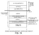
- FIG. 14is a diagram that illustrates a step in the method of manufacturing where the silicon substrate, the buffer layer, and the template layer are removed from the structure of FIG. 12 .
- FIG. 15is a top-down diagram of the wafer bonded structure after the removal step of FIG. 14 and after mesa have been formed.
- FIG. 16is a cross-sectional diagram of FIG. 15 taken along line B-B.
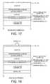
- FIG. 17is a diagram that illustrates a step in the method of manufacturing where the surface of the LRL is roughened.
- FIG. 18is a diagram that illustrates a step in the method of manufacturing where electrodes are added to the structure of FIG. 17 .
- FIGS. 19A and 19B togetherare a table that sets forth details about each of the steps in the method of manufacturing of FIGS. 6-18 .
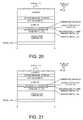
- FIG. 20is a cross-sectional diagram of a blue LED device 100 that is formed by the method of manufacture set forth above in connection with FIGS. 6-18 , except that all LRL 4 is removed in the removal step illustrated in FIG. 14 .
- FIG. 21is a cross-sectional diagram of a blue LED device 200 that is formed by the method of manufacture set forth above in connection with FIGS. 6-18 , except that all LRL 4 is removed and some of the n-type layer 5 is removed in the removal step illustrated in FIG. 14 .
- FIG. 22is a flowchart of a method in accordance with a first novel aspect.
- FIG. 23is a flowchart of a method in accordance with a second novel aspect.
- FIG. 24is a flowchart of a method in accordance with a third novel aspect.
- FIG. 25is a flowchart of a method in accordance with a fourth novel aspect.
- first layerwhen a first layer is referred to as being disposed “over” a second layer, it is to be understood that the first layer can be directly on the second layer, or an intervening layer or layers may be present between the first and second layers.
- the terms such as “over”, “under”, “upper”, “lower”, “top”, “bottom”, “upward”, “downward”, “vertically”, and “laterally”are used herein to describe relative orientations between different parts of the blue LED device being described, and it is to be understood that the overall blue LED device being described can actually be oriented in any way in three-dimensional space.
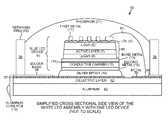
- FIG. 1is a cross-sectional side view of a white Light Emitting Diode (LED) assembly 50 .
- FIG. 2is a top-down diagram of the white LED assembly 50 .
- the white LED assembly 50includes four vertical blue LED devices 51 - 54 .
- a vertical LED deviceis also sometimes referred to as a vertically-contacted LED device to distinguish it from a lateral or a laterally-contacted LED device.
- the four vertical blue LED devices 51 - 54are mounted to a metal core Printed Circuit Board (PCB) 19 . From the top-down perspective, the four vertical blue LED devices 51 - 54 are surrounded by a retaining ring 20 .
- the retaining ring 20retains an amount of phosphor 21 that covers the blue LED devices 51 - 54 .
- a portion of a first metal structure 57is exposed through a first opening in a soldermask layer 58 .
- Anode electrodes of the blue LED devices 51 - 54are surface mounted via amounts of silver epoxy 18 to the first metal structure 57 in this first opening.
- the first opening in the soldermask layer 58also exposes a portion of a second metal structure 59 .
- Upwardly facing cathode electrodes of the blue LED devices 51 - 54are wirebonded to the exposed portion of the second metal structure 59 .
- a first pad 60is formed by another opening in soldermask layer 58 .
- a second pad 61is formed by yet another opening in soldermask layer 58 . As illustrated in the cross-sectional view of FIG.
- the first and second metal structures 57 and 59are portions of a metal layer that is disposed on a dielectric layer 62 .
- Dielectric layer 62is a 35 um to 250 um thick layer of an epoxy material containing inorganic fillers like Al 2 O 3 . This dielectric layer 62 insulates the first and second metal structures 57 and 59 from an aluminum or copper base portion 63 of the metal core PCB 19 .
- FIG. 3is a simplified cross-sectional side view of the white LED assembly 50 . Only one vertical blue LED device 54 is illustrated in the diagram.
- the vertical blue LED device 54includes numerous layers, some of which are illustrated in FIG. 3 : a first metal electrode 17 , a portion of a Low Resistance Layer (LRL) 4 , an n-type gallium-nitride layer 5 , an active layer 7 , a p-type gallium-nitride layer 8 , an amount of metal including a bond metal layer 13 , a conductive carrier 15 , and a second metal electrode 16 .
- Reference numeral 64identifies a wire bond that couples the first metal electrode 17 of the blue LED device 54 to the second metal structure 59 .
- Metal 17 and LRL 4are conductive and function to make electrical contact to the n-type layer 5 .
- All the layers below p-type layer 8(including layers 13 , 15 , 16 ) are conductive and function to make electrical contact to the p-type layer 8 .
- FIG. 4is a top-down diagram of the vertical blue LED device 54 .
- the first metal electrode 17has a grid shape.
- FIG. 5is a more detailed cross-sectional diagram of the vertical blue LED device 54 taken along sectional line A-A in FIG. 3 .
- the conductive carrier 15 and the p-type gallium-nitride 8are multiple layers and structures including: a barrier metal layer 14 , the bond metal layer 13 , a barrier metal layer 12 , a layer of an encapsulant metal 11 , a highly reflective layer 10 , and a current blocking layer 9 .
- the current blocking layer 9is patterned into current blocking structures.
- a strain release layer 6Between the active layer 7 and the n-type gallium-nitride layer 5 is a strain release layer 6 .
- non-monochromatic and non-coherent lightis emitted from the active layer 7 .
- the emitted lighthas a wavelength in a range of from approximately 440 nm to approximately 490 nm.
- non-monochromaticmeans that the light has a spectral line width that is substantially wider than the spectral line width of the light emitted by a typical laser diode.
- the spectral line width of an LEDis typically around 20 nm wide, whereas the spectral line width of a laser diode is typically less than 4.0 nm wide.
- FIGS. 6-18is a set of diagrams that sets forth steps in a method of manufacturing the blue LED device 54 .
- the diagramsare not to scale, but rather are conceptual diagrams.
- FIG. 6is a cross-sectional diagram that shows the result of several initial steps of forming epitaxial layers on a silicon substrate 1 .
- Silicon substrate 1is a monocrystalline silicon substrate wafer of the type commonly used in the manufacture of high volume CMOS integrated circuits.
- a buffer layer 2is formed on the silicon substrate. In the illustrated example, the forming of this buffer layer 2 involves first forming a less than 100 nm thick layer 65 of zinc-sulfide (for example, 50 nm) on silicon substrate 1 .
- a 200 nm thick layer 66 of aluminum-nitride (AlN)is then formed on the ZnS layer 65 .
- AlNaluminum-nitride
- a 250 nm thick layer 67 of aluminum-gallium-nitride (AlGaN)is then formed on the AlN layer 66 .
- AlGaNaluminum-gallium-nitride
- this particular buffer layer involving a layer of zinc-sulfideis shown, other types of buffer layers can be used.
- a 250 nm thick layer of zinc-telluride (ZnTe) or a 250 nm thick layer of boron-nitride (BN)is formed on the ZnS layer 65 .
- ZnTe or BNhas a lattice constant closer to GaN whereas the ZnS has a lattice constant closer to silicon.
- a buffer layer of a single layer of AlNmay, for example, be used. Where the ZnS layer 65 is provided, the AlN layer 66 and the AlGaN layer 67 illustrated in FIG. 6 are optional.
- the manufacturing of vertical LED device 54involves epitaxially later growing a Gallium-Nitride (GaN) layer (e.g., n-type GaN layer 5 ) over silicon substrate 1 .
- GaNGallium-Nitride
- This lattice mismatchcombined with a large difference in the thermal expansion coefficient between GaN and Si (e.g., 56%), makes growing high quality, thick, and crack-free GaN on silicon substrate a challenge.
- using a transitional buffer layer satisfying coincident lattice conditionscan alleviate the lattice mismatch.
- inter diffusion of Al and Si at the interfaceis severe, resulting in high unintentional doping levels.
- AlN crystal qualityis low because the lattice mismatch between AlN and Si is even higher than the lattice mismatch between GaN and Si.
- ZnS layer 65is used as a new transitional buffer layer.
- ZnSthus provides a good lattice constant match with Si and is also a compound material like GaN.
- ZnScan be easily prepared by metalorganic chemical vapor deposition (MOCVD) such that all the epilayers are grown in one growth chamber.
- MOCVDmetalorganic chemical vapor deposition
- MOCVDis a chemical vapor deposition method of epitaxial growth of materials, especially compound semiconductors from the surface reaction of organic compounds or metalorganics and metal hydrides containing the required chemicals.
- ZnSis grown on a silicon substrate in an MOSCVD chamber by introducing hydrogen sulfide with dimethyl zinc (DMZn), under 350° C. growth temperature and 100 Torr growth pressure.
- DMZndimethyl zinc
- the melting point of ZnSis 1850° C., which is high enough to keep it from becoming unstable during GaN deposition.
- AlN layeris also used as part of the buffer layer, then ZnS also serves as a diffusion barrier between AlN of the buffer and the silicon substrate.
- template layer 3is then formed on the buffer layer 2 .
- template layer 3is a 1000 nm thick layer of undoped gallium-nitride.
- LRL 4is a superlattice structure that is structured so that a two-dimensional gas of high mobility electrons is formed in its layers.
- the superlattice structureincludes multiple periods, where each period is less than 300 nm thick.
- each periodincludes a 100 nm thick n-type gallium-nitride sublayer and a 25 nm thick undoped aluminum-gallium-nitride sublayer.
- a 100 nm thick n-GaN sublayeris disposed directly on template layer 3 .
- the uppermost sublayer of the LRL 4is a 100 nm thick n-GaN sublayer.
- n-GaN sublayerThere are five GaN sublayers, and four AlGaN sublayers in the configuration illustrated.
- the n-GaN layersare doped with silicon to a concentration of 1 ⁇ 10 18 atoms/cm 3 .
- Each of the thinner AlGaN sublayersis strained to the lattice of a thicker GaN sublayer or sublayers.
- the n-type GaN layer 5is then grown on LRL 4 . It is difficult to grow a thick layer of high quality GaN that has a low lattice defect density and that does not suffer from cracking and other problems due to the buildup of stresses in the GaN layer. For example, there exists a large difference in thermal expansion coefficient (e.g., 56%) between GaN and Si. This thermal mismatch usually causes tensile stress in the GaN epilayer during cool down. When the thickness of the GaN epilayer is larger than 1000 nm, cracks usually occur.
- the quality of the overlying GaN sublayeris of improved quality in terms of lower density of lattice defects.
- typical GaN over Sihas a defect density as high as 1 ⁇ 10 10 defects per cm 3 .
- the defect density of improved quality GaN over Siis in the range from 1 ⁇ 10 7 to 1 ⁇ 10 9 defects per cm 3 .
- AlN intervening sublayersleads to one problem.
- AlNis an insulating material due to its wide bandgap (e.g., 6.2 eV) and therefore creates a barrier for current transportation in vertical direction.
- the GaN sublayer over the top AlN sublayeris usually less than 2000 nm, which could cause a current crowding problem in LED devices.
- a thin AlGaN:Si layeris used as a new intervening sublayer instead of using AlN.
- AlGaN:Siis an n-type material which allows electron transportation through it because AlGaN has smaller band energy (e.g., bandgap of 3.4 eV to 6.2 eV, depending on the Al concentration) than that of AlN, thus the activation energy of Si in AlGaN is smaller than that of Si in AlN.
- the AlGaN:Si intervening sublayersare electronically conductive and do not need to be removed in the final LED device.
- One example of the resistivity of the conductive AlGaN:Si layeris 1 ⁇ 10 ⁇ 2 ⁇ cm.
- AlGaNhas a smaller lattice constant than GaN and therefore provides a compressive strain to the subsequent GaN sublayers and helps prevent cracking.
- each of the GaN sublayers of n-type GaN layer 5has a thickness of about 900 nm and is doped with silicon at a concentration of 5 ⁇ 10 28 atoms/cm 3 .
- These AlGaN:Si intervening sublayersare relatively conductive, and the n-type GaN intervening sublayers are conductive, so the overall n-type GaN layer 5 can effectively conduct current in the direction from the LRL/n-type layer interface toward the active layer.
- the bottom sublayer of n-type GaN layer 5 that is in direct contact with LRL 4is a 900 nm thick GaN sublayer as illustrated.
- the upper sublayer of the n-type gallium-nitride layer 5is also a 900 nm sublayer of GaN as illustrated.
- the entire n-type GaN layer 5 with multiple AlGaN:Si conductive intervening sublayersis approximately 5000 nm thick, where each n-GaN sublayer is substantially thicker than the n-GaN sublayers of LRL 4 .
- the n-type GaN layer 5has a sheet resistance at this interface that is greater than 15 ohms per square.
- the LRL 4also has a sheet resistance at this interface, but the sheet resistance of LRL 4 is lower than the sheet resistance of the n-type GaN layer 5 .
- the sheet resistance of LRL 4can be destructively measured by grinding away the upper layers of a first LED device to expose a surface of LRL 4 at interface 74 , and then probing the exposed LRL surface and measuring its sheet resistance.
- the sheet resistance of n-type layer 5can be destructively measured by grinding away the lower layers of a second LED device to expose a surface of n-type layer 5 at interface 74 , and then probing the exposed n-type layer surface and measuring its sheet resistance.
- strain release layer 6is formed on the n-type GaN layer 5 .
- strain release layer 6is 120 nm thick and includes thirty periods. Each period includes a first sublayer of In x Ga 1-x N, where 0 ⁇ x ⁇ 0.12 and a second sublayer of In y Ga 1-y N where 0 ⁇ y ⁇ 0.12.
- the active layer 7is formed on the strain release layer 6 .
- the active layer 7is fashioned to emit blue light in the overall blue LED device.
- active layer 7is a 130 nm thick Multiple Quantum Well (MQW) structure that has ten periods. Each period includes a 3 nm thick InGaN sublayer (15% In), and a 10 nm thick GaN sublayer.
- MQWMultiple Quantum Well
- the active layer 7emits non-monochromatic light having a wavelength in the range of approximately 440 nm to approximately 490 nm.
- the p-type GaN layer 8is formed on the active layer 7 .
- the p-type GaN layeris 300 nm thick and has a magnesium dopant concentration of 1 ⁇ 10 20 atoms/cm 3 .
- the upper surface of p-type GaN layer 8is formed so that the completed LED device will emit non-monochromatic light and will include no current focusing ridge structures of the type used in laser diodes.
- the n-type layer 5 , the p-type layer 8 , and all layers in between including active layer 7 togetherare an epitaxial LED structure 80 .
- FIG. 7is a cross-sectional diagram that shows a subsequent step in the method of manufacture.
- a current blocking layer of an insulating materialis formed on the upper surface of the p-type GaN layer 8 .
- the current blocking layeris a patterned 200 nm thick layer of silicon dioxide. This silicon dioxide layer is deposited and patterned using photolithographic techniques to form structures that obstruct current flow in some places more than in other places.
- the large structure 66 of the current blocking layeris disposed directly under the location where the first electrode 17 will be formed later in the manufacturing method. The large structure 66 is placed in this location so that current will not flow through the active layer directly underneath the first electrode 17 , and therefore will not generate light directly under the first electrode 17 .
- the amount of current flowing through each individual sub-areais controlled to maximize light output from the LED device as compared to current flow through the overall LED device.
- FIG. 8is a cross-sectional diagram that shows a subsequent step in the method of manufacture.
- a highly reflective layer 10is deposited over the current blocking layer 9 .
- highly reflective layer 10is a 200 nm thick layer of silver that makes ohmic contact to the p-type GaN layer 8 . This silver layer does not cover the entire LED device wafer.
- the highly reflective layer 10is shown covering the entire structure of FIG. 8 because the cross-section of FIG. 8 is a cross-section of only a part of the LED device along line A-A.
- Highly reflective layer 10serves a first function of acting as a mirror to reflect light and serves a second function of making electrical contact to the p-type layer 8 .
- FIG. 9is a cross-sectional diagram that shows a subsequent step in the method of manufacture.
- An encapsulation layer 11covers the silver layer 10 .
- encapsulation layer 11is a 100 nm thick layer of platinum. This layer of platinum blocks the electromigration of silver.
- this layer of platinumis the only layer of platinum in the blue LED device. The sum of all the thicknesses of all platinum layers of the blue LED device (there is only one layer of platinum) is less than 200 nm.
- a non-reactive barrier metal layer 12 more than 50 nm thickis formed over the encapsulation layer.
- the non-reactive barrier metal layer 12is a 200 nm thick layer of titanium.
- the titaniumis a barrier in that it is a barrier to the diffusion of tin. Tin, from a bond metal layer to be later applied to the top of the structure, is blocked by the barrier layer from diffusing into the silver of layer 10 .
- Some other metalssuch as platinum, titanium/tungsten, gold and nickel that are sometimes used as barriers for tin, are actually somewhat reactive with tin.
- the combination of the thickness of the reactive metal provided and the limited time of the high temperature bonding cycleis such that the amount of tin incursion is kept within acceptable levels.
- the non-reactive barrier metal of layer 12is not such a reactive metal and in one example is a layer of titanium that is more than 50 nm thick.
- FIG. 10is a cross-sectional diagram that shows a subsequent step in the method of manufacture.
- a 500 nm thick sublayer of goldis formed to cover the top of non-reactive barrier metal layer 12 .
- Reference numeral 13 in FIG. 10denotes this gold sublayer that is one sublayer of three-sublayer Au/AuSn/Au sandwich structure of metal layers.
- FIG. 11is a cross-sectional diagram that shows a subsequent step in the method of manufacture.
- the conductive carrier 5is covered with an adhesion and barrier metal layer 14 .
- the conductive carrieris a monocrystalline silicon wafer and the adhesion and barrier metal layer 14 is a 200 nm thick layer of titanium.
- Golddoes not generally bond well to silicon, but titanium does, so the titanium layer 14 is provided to bond to the conductive silicon carrier 15 so that a subsequent sublayer of gold (part of the bond metal layer 13 ) can then in turn bond to the titanium.
- the titaniumalso acts as a barrier to prevent tin and gold from diffusing to the silicon surface and degrading the adhesion.
- the adhesion/barrier metal layer 14also includes a layer of platinum disposed over the titanium.
- a 500 nm thick sublayer of goldis then formed on the adhesion and barrier metal layer 14 , and a 3000 nm thick gold/tin sublayer is formed on the gold sublayer.
- the 3000 nm thick gold/tin sublayeris 80 percent gold and 20 percent tin by weight.
- the conductive carrier 15 , the barrier metal layer 14 , and the gold and gold/tin sublayers 13 togetherare a carrier wafer structure 68 .
- the silicon substrate 1 and the layers formed on it togetherare a device wafer structure 69 .
- the carrier wafer structure 68is wafer bonded to the gold covered upper surface of the device wafer structure 69 .
- FIG. 12is a graph showing the temperature cycle of the thermal compression wafer bonding process used.
- Carrier wafer structure 68is pressed against device wafer structure 69 with a pressure of approximately fifty pounds per square inch and the pressed together wafers are heated to at least 280° C. In the specific example, the wafers are heated to 310° C. The wafers remain at this elevated temperature for a period of more than one minute to ensure there is a uniform melting temperature all across the wafers. In the specific example, the elevated temperature is maintained for five minutes. The eutectic gold/tin sublayer melts, thereby wafer bonding the carrier wafer structure 68 to the device wafer structure 69 . This wafer bonding is represented by arrows 70 in FIG. 11 .
- the gold/tin sublayerhas a melting point of approximately 282° C. Once the gold/tin sublayer melts, however, some of the tin diffuses from this sublayer into the gold sublayers on either side of the gold/tin sublayer. The concentration of tin in the gold/tin sublayer therefor decreases. A gold/tin layer having a lower concentration of tin has a higher melting temperature. For every one percent that the tin concentration decreases in the gold/tin alloy, the melting temperature of the gold/tin alloy increases by approximately 30° C.
- the concentration of tin in the gold/tin sublayerdecreases to be below twenty percent and the overall wafer bonded structure can thereafter have its temperature raised to 282° C. without the gold/tin sublayer melting.
- FIG. 13shows a subsequent step in the method of manufacture.
- the resulting wafer bonded structure 71is flipped as indicated by arrow 72 .
- FIG. 14shows a subsequent step in the method of manufacture.
- the silicon substrate 1 , the buffer layer 2 and the template layer 3are removed from wafer bonded structure 71 as indicated by arrow 73 .
- these layersare removed using Chemical Mechanical Polishing (CMP) and reactive ion etching (RIE) techniques such that one of the GaN sublayers of LRL 4 is present and exposed at the top of the structure.
- CMPChemical Mechanical Polishing
- RIEreactive ion etching
- the n-type GaN layer 5is electrically conductive from the strain release layer to n-type layer interface, all the way through the n-type GaN layer, and to the n-type layer/LRL interface.
- An advantage of using AlGaN:Si for the intervening sublayers as opposed to using AlN intervening sublayersis that the AlGaN:Si intervening sublayers are conductive. There is no nonconductive intervening AlN sublayer within the n-type GaN layer that must be removed in the step of FIG. 13 in order to provide conductivity through the n-type layer. Rather, the entire n-type GaN layer 5 remains in the completed blue LED device.
- FIG. 15is a top-down diagram of the wafer bonded structure 71 .
- wet etchingis used to etch horizontal and vertical streets down to the encapsulation layer 11 , thereby forming a two-dimensional array of rows and columns of mesa structures.
- Reference numerals 75 , 76 and 77identify three such streets.
- Reference numerals 78 and 79identify two of the mesa structures.
- FIG. 16is a cross-sectional diagram of the structure of FIG. 15 taken along sectional line B-B.
- the non-reactive barrier layer 12 of titaniumis shown in cross-hatching.
- Non-reactive barrier layer 12is a single layer of titanium more than 50 nm thick and includes no sublayers, no platinum, and no tungsten.
- Silver of the highly reflective layer 10is blocked by the encapsulation layer 11 from moving laterally out from under the mesas.
- the silver of the highly reflective layer 10is contained from the top by the bottom surface of the p-type GaN layer 8 (the bottom of the mesas).
- FIG. 17shows a subsequent step in the method of manufacture.
- the upper surface of the exposed LRL 4 at the top of each mesais roughened. This roughening is the type of roughening customarily performed to facilitate the escape of light form the LED device. The roughening is actually more severe than is illustrated in FIG. 17 .
- the vertical distance from the highest peak to the deepest valley of the roughened surfaceis approximately 500 nm, so the deepest valleys extend down into the n-type layer 5 . It is desirable that the LRL not be penetrated, so in another example the amount material removed is preferably limited to removing the silicon substrate and part of the buffer layer.
- FIG. 18shows a subsequent step in the method of manufacture.
- the second electrode 16is formed on the conductive carrier 15 as illustrated.
- second electrode 16includes a first 20 nm thick nickel sublayer that is in direct contact with the conductive carrier 15 , and also includes a second 200 nm thick gold layer that covers the nickel sublayer. Second electrode 16 is therefore 220 nm thick.
- FIG. 18shows a subsequent step of forming the first electrode 17 on the upper surface of LRL 4 as illustrated.
- first electrode 17includes a 20 nm thick sublayer of titanium disposed directly on LRL 4 , a 100 nm thick sublayer of aluminum disposed on the titanium sublayer, a 20 nm thick sublayer of nickel disposed on the aluminum sublayer, and a 200 nm thick sublayer of gold disposed on the nickel sublayer.
- First electrode 17is therefore approximately 340 nm thick.
- the dopant concentration in the GaN sublayers of LRL 4is adequately high that good ohmic contact is formed between metal 17 and LRL 4 .
- the wafer bonded structureis singulated into separate blue LED devices. Singulation is performed by sawing the wafer bonded structure down the streets illustrated in FIG. 15 so that each mesa structure becomes a separate blue LED device. In the illustrated example, one of the resulting blue LED devices is then incorporated into the white LED assembly of FIGS. 1-3 .
- the second electrode 16is glued down to the metal core PCB 19 as illustrated in FIG. 3 using a layer of silver epoxy 18 .
- the first metal electrode 17is wirebonded via bond wire 64 to the second metal structure 59 of metal core PCB 19 as illustrated. After wirebonding, the retaining ring 20 of silicone is formed on the structure by silk screening.
- the retaining ring 20is cut and shaped to the right dimensions, and then applied. Ring 20 is 0.5 to 3.0 mm high, and 0.2 mm to 1.5 mm wide. After the silicone has cured, the amount of phosphor 21 is dropped onto the blue LED device 54 so that it is retained by ring 20 . The phosphor 21 is allowed to cure to form the completed white LED assembly 50 .
- FIG. 19is a table that sets forth details about each step of the method of manufacture.
- the numbers in the left column of the tableare the reference numerals for the various layers of the white LED assembly 50 .
- FIG. 20is a cross-sectional diagram of a blue LED device 100 that is formed by the method of manufacture set forth above in connection with FIGS. 6-18 , except that all LRL 4 is removed in the removal step illustrated in FIG. 13 . All or substantially all of the n-type layer 5 remains in the finished blue LED device 100 .
- FIG. 17is not to scale, but rather is a conceptual diagram.
- FIG. 21is a cross-sectional diagram of a blue LED device 200 that is formed by the method of manufacture set forth above in connection with FIGS. 6-18 , except that all LRL 4 is removed and some of the n-type layer 5 is removed in the removal step illustrated in FIG. 13 . All of the thin intervening sublayers of the n-type layer are removed, leaving only the last 900 nm thick GaN sublayer. This last GaN sublayer remains in the finished blue LED device 200 .
- FIG. 18is not to scale, but rather is a conceptual diagram.
- FIG. 22is a flowchart of a method 300 in accordance with a first novel aspect.
- a superlattice structureis formed (step 301 ) over a silicon substrate.
- the superlattice structureincludes a plurality of periods. Each period is less than 300 nm thick and includes a GaN sublayer.
- a buffer layeris formed on the silicon substrate, and a template layer is formed on the buffer layer, and the superlattice structure is formed on the template layer.
- an n-type GaN layeris formed (step 302 ) directly on the superlattice structure.
- An active layer containing indiumis formed (step 303 ) over the n-type layer.
- a p-type GaN layeris formed (step 304 ) over the active layer.
- the silicon substrate, the superlattice structure, the n-type layer, the active layer, and the p-type layer togetherare a first structure.
- a conductive carrieris bonded (step 305 ) to the first structure thereby forming a second structure.
- the silicon substrateis then removed (step 306 ) from the second structure thereby forming a third structure. Electrodes are formed (step 307 ) on the third structure.
- the third structureis then singulated (step 308 ) thereby forming a blue LED device.
- LRL 4can be fabricated in numerous different suitable ways.
- LRL 4involves periods, where each period includes a first aluminum-gallium-nitride layer and a second aluminum-gallium-nitride layer, where the aluminum concentrations in the two sublayers differ from one another.
- the composition of the two sublayersis given by Al x Ga 1-x N/Al y Ga 1-y N, where x and y are different nonzero numbers.
- the aluminum-gallium-nitride and gallium-nitride sublayers of the LRLare of different thicknesses, in other examples the sublayers are of substantially the same thickness.
- the aluminum concentration in one sublayer containing aluminumcan be graded.
- the LRLcan be an AlInN/GaN superlattice.
- the LRLcan be an AlGaN/AlGaN/GaN superlattice where each period involves three sublayers.
- the wafer bonding process involving a non-reactive barrier metal layeris described above in connection with an LED device that after wafer bonding is glued using silver epoxy to a metal core PCB to form the completed white LED assembly
- the wafer bonding processis usable where an LED is provided with a gold/tin layer for die attachment. Due to the decreased concentration of tin in the gold/tin sublayer of metal bonding layer 13 during wafer bonding, the melting temperature of the metal bonding layer 13 is higher than 280° C. after the wafer bonding process has been performed. Accordingly, a completed LED device can be heated to a high enough temperature to melt an amount of gold/tin provided for die attachment purposes without melting the metal bonding layer 13 within the LED device itself.
- the wafer bonding processis described above in connection with an example in which the eutectic layer is a gold/tin layer, the wafer bonding process is not limited to require a gold/tin eutectic layer.
- the eutectic layeris a type of metal layer such as, for example, a gold/indium metal layer, and a palladium/indium metal layer.
- the wafer bonding processis described above in connection with an example where the silver encapsulation layer is platinum, other encapsulation layers such as nickel and rhodium may be employed.
- FIG. 23is a flowchart of a method 400 in accordance with a second novel aspect.
- An epitaxial LED structureis grown (step 401 ) on a non-GaN substrate.
- the non-GaN substratein one example is a silicon substrate and appropriate intervening buffer and template layers are employed.
- a silver layeris then provided (step 402 ) over the epitaxial LED structure to function as a mirror and to function as an ohmic contact to the epitaxial LED structure.
- An encapsulating layeris provided (step 403 ) over the silver layer.
- the encapsulating layeris a single layer of platinum that is less than 200 nm thick.
- a layer of non-reactive barrier metalis provided (step 404 ) over the encapsulating layer, thereby forming a device wafer structure.
- this non-reactive barrier metal layeris a single layer of titanium that is more than 50 nm thick. This single layer of titanium layer includes substantially no tungsten.
- a carrier wafer structureincludes a conductive carrier.
- the conductive carriermay be conductive silicon wafer.
- the carrier wafer structureis then wafer bonded (step 405 ) to the device wafer structure by melting a eutectic metal layer between the two wafer structures, thereby forming a wafer bonded structure.
- the eutectic metal layerinvolves a gold/tin sublayer having a melting temperature of approximately 282° C. This eutectic metal layer is melted by raising the temperature of the carrier wafer structure to more than 280° C. (for example, to 310° C.) and maintaining this elevated temperature for more than one minute.
- the temperature of the carrier wafer structureis indirectly determined by placing an amount of gold/tin of the same composition of the eutectic bond metal layer in a fully loaded furnace chamber, and slowly increasing the set point of the furnace chamber until the gold/tin is observed to melt.
- This set pointis assumed to correspond to a carrier device wafer temperature of 282° C.
- the set point of the furnace chamberis then increased an additional amount that is known to correspond to an increased furnace chamber temperature of 30° C.
- the wafer bonding processis carried out by using this increased furnace chamber setting for at least one minute without actually directly measuring the temperature of the wafer bonded structure within the furnace chamber.
- the non-GaN substrate of the resulting wafer bonded structureis the removed (step 406 ). Electrodes are formed on the wafer bonded structure (step 407 ) and the wafer bonded structure is singulated thereby forming a plurality of blue LED devices (step 408 ).
- the total thickness of any and all platinum layers in the completed blue LED devicesis less than 200 nm and the high temperature bond metal melting cycle (when the temperature of the carrier wafer structure is greater than 280° C.) is more than one minute.
- FIG. 24is a flowchart of a method of manufacturing an LED device on silicon substrate using Zinc-Sulfide (ZnS) as a buffer layer in accordance with a third novel aspect.
- a Zinc-Sulfide (ZnS) layeris formed (step 501 ) over and directly on a silicon substrate.
- the ZnS layeris a buffer layer formed on the silicon substrate and a template layer is then formed on the buffer layer.
- an aluminum-nitride (AlN) layeris formed over the zinc-sulfide layer, and an aluminum-gallium-nitride (AlGaN) layer is formed over the aluminum-nitride layer.
- AlNaluminum-nitride
- AlGaNaluminum-gallium-nitride
- the ZnS layer, the AlN layer, and the AlGaN layerform the buffer layer.
- an n-type GaN layeris formed (step 502 ) over the template layer.
- An active layer containing indiumis formed (step 503 ) over the n-type layer.
- a p-type GaN layeris formed (step 504 ) over the active layer.
- the n-type layer, the active layer, and the p-type layer togetherare an epitaxial LED structure.
- the silicon substrate, the ZnS layer, the epitaxial LED structure togetherare a first structure.
- the first structureis device wafer structure 69 of FIG. 11 .
- a conductive carrieris then bonded (step 505 ) to the first structure thereby forming a second structure.
- the carrieris part of a carrier wafer structure such as carrier wafer structure 68 of FIG. 11 .
- the original silicon substrate and the ZnS layerare then removed (step 506 ) from the second structure thereby forming a third structure.
- Electrodesare formed (step 507 ) on the third structure.
- the third structureis then singulated (step 508 ) thereby forming a blue LED device.
- FIG. 25is a flowchart of a method of manufacturing a blue LED device on silicon substrate in accordance with a fourth novel aspect.
- the blue LED devicehas an n-type gallium-nitride layer with multiple conductive intervening sublayers.
- An n-type layeris formed (step 601 ) over a silicon substrate.
- the n-type layercomprises a plurality of periods, each period of the n-type layer includes a gallium-nitride (GaN) sublayer and an aluminum-gallium-nitride doped with silicon (AlGaN:Si) intervening sublayer.
- the AlGaN:Si intervening sublayersare doped with Si and are electronically conductive.
- an active layer containing indiumis formed (step 602 ) over the n-type layer.
- a p-type GaN layeris formed (step 603 ) over the active layer.
- the silicon substrate, the n-type layer, the active layer, and the p-type layertogether form a first structure.
- a conductive carrieris bonded (step 604 ) to the first structure thereby forming a second structure.
- the silicon substrateis then removed (step 605 ) from the second structure thereby forming a third structure. Electrodes are formed (step 606 ) on the third structure.
- the third structureis then singulated (step 607 ) thereby forming a blue LED device.
Landscapes
- Engineering & Computer Science (AREA)
- Computer Hardware Design (AREA)
- Microelectronics & Electronic Packaging (AREA)
- Power Engineering (AREA)
- Led Devices (AREA)
Abstract
Description
Claims (25)
Priority Applications (1)
| Application Number | Priority Date | Filing Date | Title |
|---|---|---|---|
| US14/158,426US9159869B2 (en) | 2011-08-03 | 2014-01-17 | LED on silicon substrate using zinc-sulfide as buffer layer |
Applications Claiming Priority (2)
| Application Number | Priority Date | Filing Date | Title |
|---|---|---|---|
| US13/197,765US20130032810A1 (en) | 2011-08-03 | 2011-08-03 | Led on silicon substrate using zinc-sulfide as buffer layer |
| US14/158,426US9159869B2 (en) | 2011-08-03 | 2014-01-17 | LED on silicon substrate using zinc-sulfide as buffer layer |
Related Parent Applications (1)
| Application Number | Title | Priority Date | Filing Date |
|---|---|---|---|
| US13/197,765DivisionUS20130032810A1 (en) | 2011-08-03 | 2011-08-03 | Led on silicon substrate using zinc-sulfide as buffer layer |
Publications (2)
| Publication Number | Publication Date |
|---|---|
| US20140134765A1 US20140134765A1 (en) | 2014-05-15 |
| US9159869B2true US9159869B2 (en) | 2015-10-13 |
Family
ID=47626400
Family Applications (2)
| Application Number | Title | Priority Date | Filing Date |
|---|---|---|---|
| US13/197,765AbandonedUS20130032810A1 (en) | 2011-08-03 | 2011-08-03 | Led on silicon substrate using zinc-sulfide as buffer layer |
| US14/158,426ActiveUS9159869B2 (en) | 2011-08-03 | 2014-01-17 | LED on silicon substrate using zinc-sulfide as buffer layer |
Family Applications Before (1)
| Application Number | Title | Priority Date | Filing Date |
|---|---|---|---|
| US13/197,765AbandonedUS20130032810A1 (en) | 2011-08-03 | 2011-08-03 | Led on silicon substrate using zinc-sulfide as buffer layer |
Country Status (4)
| Country | Link |
|---|---|
| US (2) | US20130032810A1 (en) |
| JP (1) | JP5752855B2 (en) |
| TW (1) | TWI533464B (en) |
| WO (1) | WO2013019310A2 (en) |
Cited By (2)
| Publication number | Priority date | Publication date | Assignee | Title |
|---|---|---|---|---|
| US20190051800A1 (en)* | 2015-11-10 | 2019-02-14 | Everlight Electronics Co., Ltd. | Light emitting diode device and method of manufacturing the same |
| US20210296381A1 (en)* | 2020-03-17 | 2021-09-23 | Kabushiki Kaisha Toshiba | Photodetector, optical detection system, lidar device, and movable body |
Families Citing this family (18)
| Publication number | Priority date | Publication date | Assignee | Title |
|---|---|---|---|---|
| US9082892B2 (en)* | 2007-06-11 | 2015-07-14 | Manulius IP, Inc. | GaN Based LED having reduced thickness and method for making the same |
| US9847372B2 (en)* | 2011-12-01 | 2017-12-19 | Micron Technology, Inc. | Solid state transducer devices with separately controlled regions, and associated systems and methods |
| JP5437538B1 (en)* | 2012-02-28 | 2014-03-12 | パナソニック株式会社 | Nitride semiconductor light emitting device and light source including the nitride semiconductor light emitting device |
| US9879357B2 (en) | 2013-03-11 | 2018-01-30 | Tivra Corporation | Methods and systems for thin film deposition processes |
| US9461212B2 (en) | 2012-07-02 | 2016-10-04 | Seoul Viosys Co., Ltd. | Light emitting diode module for surface mount technology and method of manufacturing the same |
| KR101740531B1 (en)* | 2012-07-02 | 2017-06-08 | 서울바이오시스 주식회사 | Light Emitting Diode Module for Surface Mount Technology and Method of manufacturing the same |
| JP5881560B2 (en)* | 2012-08-30 | 2016-03-09 | 株式会社東芝 | Semiconductor light emitting device and manufacturing method thereof |
| US20140097442A1 (en)* | 2012-10-09 | 2014-04-10 | Industrial Technology Research Institute | Nitride semiconductor device |
| US20140097444A1 (en)* | 2012-10-09 | 2014-04-10 | Industrial Technology Research Institute | Nitride semiconductor device |
| CN103236477B (en)* | 2013-04-19 | 2015-08-12 | 安徽三安光电有限公司 | A kind of LED epitaxial structure and preparation method thereof |
| TWI591848B (en) | 2013-11-28 | 2017-07-11 | 晶元光電股份有限公司 | Light-emitting element and method of manufacturing same |
| CN104701435A (en)* | 2013-12-06 | 2015-06-10 | 晶元光电股份有限公司 | Light emitting element and manufacturing method thereof |
| TWI612686B (en)* | 2014-09-03 | 2018-01-21 | 晶元光電股份有限公司 | Light-emitting element and method of manufacturing same |
| US10236413B2 (en) | 2015-04-20 | 2019-03-19 | Epistar Corporation | Light-emitting device and manufacturing method thereof |
| US20160380045A1 (en)* | 2015-06-25 | 2016-12-29 | Tivra Corporation | Crystalline semiconductor growth on amorphous and poly-crystalline substrates |
| US9722039B2 (en)* | 2015-12-31 | 2017-08-01 | International Business Machines Corporation | Fabricating high-power devices |
| CN110556453B (en)* | 2018-05-30 | 2020-11-06 | 中国科学院苏州纳米技术与纳米仿生研究所 | Ordered Si-based Al1-xGaxControllable epitaxial growth method of N quantum dots |
| JP7166818B2 (en)* | 2018-07-13 | 2022-11-08 | スタンレー電気株式会社 | Optical semiconductor device |
Citations (103)
| Publication number | Priority date | Publication date | Assignee | Title |
|---|---|---|---|---|
| JPH03135041A (en) | 1989-10-20 | 1991-06-10 | Nippon Steel Corp | Manufacturing method of bonding thin wire for semiconductors |
| JPH03209096A (en) | 1989-11-17 | 1991-09-12 | Union Carbide Ind Gases Technol Corp | Cylinder having improved mixing characteristics |
| JPH03223832A (en) | 1990-01-30 | 1991-10-02 | Fuji Photo Optical Co Ltd | Self-photographing method for camera |
| JPH03250438A (en) | 1990-02-27 | 1991-11-08 | Sanyo Electric Co Ltd | Optical recording medium |
| JPH04267376A (en) | 1991-02-22 | 1992-09-22 | Toshiba Corp | Semiconductor light emitting element and fabrication thereof |
| US5306662A (en) | 1991-11-08 | 1994-04-26 | Nichia Chemical Industries, Ltd. | Method of manufacturing P-type compound semiconductor |
| US5408120A (en) | 1992-07-23 | 1995-04-18 | Toyoda Gosei Co., Ltd. | Light-emitting device of gallium nitride compound semiconductor |
| US5432808A (en) | 1993-03-15 | 1995-07-11 | Kabushiki Kaisha Toshiba | Compound semicondutor light-emitting device |
| US5563422A (en) | 1993-04-28 | 1996-10-08 | Nichia Chemical Industries, Ltd. | Gallium nitride-based III-V group compound semiconductor device and method of producing the same |
| JPH08264894A (en) | 1995-03-20 | 1996-10-11 | Toshiba Corp | Semiconductor device and manufacturing method thereof |
| US5578839A (en) | 1992-11-20 | 1996-11-26 | Nichia Chemical Industries, Ltd. | Light-emitting gallium nitride-based compound semiconductor device |
| JP2626431B2 (en) | 1992-10-29 | 1997-07-02 | 豊田合成株式会社 | Nitrogen-3 group element compound semiconductor light emitting device |
| JP2666237B2 (en) | 1994-09-20 | 1997-10-22 | 豊田合成株式会社 | Group III nitride semiconductor light emitting device |
| JP2681733B2 (en) | 1992-10-29 | 1997-11-26 | 豊田合成株式会社 | Nitrogen-3 group element compound semiconductor light emitting device |
| JP2735057B2 (en) | 1994-12-22 | 1998-04-02 | 日亜化学工業株式会社 | Nitride semiconductor light emitting device |
| US5766783A (en) | 1995-03-01 | 1998-06-16 | Sumitomo Electric Industries Ltd. | Boron-aluminum nitride coating and method of producing same |
| US5777350A (en) | 1994-12-02 | 1998-07-07 | Nichia Chemical Industries, Ltd. | Nitride semiconductor light-emitting device |
| JP2778405B2 (en) | 1993-03-12 | 1998-07-23 | 日亜化学工業株式会社 | Gallium nitride based compound semiconductor light emitting device |
| JP2785254B2 (en) | 1993-06-28 | 1998-08-13 | 日亜化学工業株式会社 | Gallium nitride based compound semiconductor light emitting device |
| JP2803741B2 (en) | 1993-03-19 | 1998-09-24 | 日亜化学工業株式会社 | Gallium nitride based compound semiconductor electrode forming method |
| JP2827794B2 (en) | 1993-02-05 | 1998-11-25 | 日亜化学工業株式会社 | Method for growing p-type gallium nitride |
| JPH1140847A (en) | 1997-07-16 | 1999-02-12 | Toshiba Corp | Gallium nitride based semiconductor device and method of manufacturing the same |
| JP2890396B2 (en) | 1995-03-27 | 1999-05-10 | 日亜化学工業株式会社 | Nitride semiconductor light emitting device |
| JP2917742B2 (en) | 1992-07-07 | 1999-07-12 | 日亜化学工業株式会社 | Gallium nitride based compound semiconductor light emitting device and method of manufacturing the same |
| US5959307A (en) | 1995-11-06 | 1999-09-28 | Nichia Chemical Industries Ltd. | Nitride semiconductor device |
| US5959401A (en) | 1996-05-21 | 1999-09-28 | Toyoda Gosei Co., Ltd. | Light-emitting semiconductor device using group III nitride compound |
| JP2956489B2 (en) | 1994-06-24 | 1999-10-04 | 日亜化学工業株式会社 | Crystal growth method of gallium nitride based compound semiconductor |
| US6005258A (en) | 1994-03-22 | 1999-12-21 | Toyoda Gosei Co., Ltd. | Light-emitting semiconductor device using group III Nitrogen compound having emission layer doped with donor and acceptor impurities |
| US6040588A (en) | 1996-09-08 | 2000-03-21 | Toyoda Gosei Co., Ltd. | Semiconductor light-emitting device |
| JP3063757B1 (en) | 1998-11-17 | 2000-07-12 | 日亜化学工業株式会社 | Nitride semiconductor device |
| JP3063756B1 (en) | 1998-10-06 | 2000-07-12 | 日亜化学工業株式会社 | Nitride semiconductor device |
| US6121635A (en) | 1997-04-15 | 2000-09-19 | Kabushiki Kaisha Toshiba | Semiconductor light-emitting element having transparent electrode and current blocking layer, and semiconductor light-emitting including the same |
| JP3135041B2 (en) | 1995-09-29 | 2001-02-13 | 日亜化学工業株式会社 | Nitride semiconductor light emitting device |
| JP2001119013A (en) | 1999-10-19 | 2001-04-27 | Nippon Telegr & Teleph Corp <Ntt> | Nitride semiconductor and manufacturing method thereof |
| US6242764B1 (en) | 1997-07-17 | 2001-06-05 | Kabushiki Kaisha Toshiba | III-N semiconductor light-emitting element having strain-moderating crystalline buffer layers |
| JP3223832B2 (en) | 1997-02-24 | 2001-10-29 | 日亜化学工業株式会社 | Nitride semiconductor device and semiconductor laser diode |
| JP3250438B2 (en) | 1995-03-29 | 2002-01-28 | 日亜化学工業株式会社 | Nitride semiconductor light emitting device |
| JP3314666B2 (en) | 1997-06-09 | 2002-08-12 | 日亜化学工業株式会社 | Nitride semiconductor device |
| JP3344257B2 (en) | 1997-01-17 | 2002-11-11 | 豊田合成株式会社 | Gallium nitride based compound semiconductor and device manufacturing method |
| US20030006406A1 (en) | 2001-06-29 | 2003-01-09 | Toyohiro Chikyow | Thin film device and its fabrication method |
| JP3374737B2 (en) | 1997-01-09 | 2003-02-10 | 日亜化学工業株式会社 | Nitride semiconductor device |
| JP3424629B2 (en) | 1998-12-08 | 2003-07-07 | 日亜化学工業株式会社 | Nitride semiconductor device |
| JP3427265B2 (en) | 1998-12-08 | 2003-07-14 | 日亜化学工業株式会社 | Nitride semiconductor device |
| US6617060B2 (en) | 2000-12-14 | 2003-09-09 | Nitronex Corporation | Gallium nitride materials and methods |
| US20030178642A1 (en) | 2002-02-08 | 2003-09-25 | Ngk Insulators, Ltd. | Semiconductor light-emitting devices |
| US6657236B1 (en) | 1999-12-03 | 2003-12-02 | Cree Lighting Company | Enhanced light extraction in LEDs through the use of internal and external optical elements |
| JP3506874B2 (en) | 1997-03-24 | 2004-03-15 | 豊田合成株式会社 | Nitrogen-3 group element compound semiconductor light emitting device |
| JP3511970B2 (en) | 1995-06-15 | 2004-03-29 | 日亜化学工業株式会社 | Nitride semiconductor light emitting device |
| JP3548442B2 (en) | 1994-09-22 | 2004-07-28 | 日亜化学工業株式会社 | Gallium nitride based compound semiconductor light emitting device |
| JP3551101B2 (en) | 1999-03-29 | 2004-08-04 | 日亜化学工業株式会社 | Nitride semiconductor device |
| US6800500B2 (en) | 1999-02-05 | 2004-10-05 | Lumileds Lighting U.S., Llc | III-nitride light emitting devices fabricated by substrate removal |
| US6838693B2 (en) | 2000-07-07 | 2005-01-04 | Nichia Corporation | Nitride semiconductor device |
| US6849881B1 (en) | 1999-11-19 | 2005-02-01 | Osram Gmbh | Optical semiconductor device comprising a multiple quantum well structure |
| JP3622562B2 (en) | 1998-03-12 | 2005-02-23 | 日亜化学工業株式会社 | Nitride semiconductor light emitting diode |
| US6891197B2 (en) | 2001-05-09 | 2005-05-10 | Lumileds Lighting U.S., Llc | Semiconductor LED flip-chip with dielectric coating on the mesa |
| JP3646649B2 (en) | 1994-09-22 | 2005-05-11 | 日亜化学工業株式会社 | Gallium nitride compound semiconductor light emitting device |
| JP3654738B2 (en) | 1997-04-07 | 2005-06-02 | 豊田合成株式会社 | Group 3 nitride semiconductor light emitting device |
| US6906352B2 (en) | 2001-01-16 | 2005-06-14 | Cree, Inc. | Group III nitride LED with undoped cladding layer and multiple quantum well |
| US6916676B2 (en) | 2002-01-28 | 2005-07-12 | Nichia Corporation | Method for producing a nitride semiconductor element |
| US6951695B2 (en) | 2001-06-08 | 2005-10-04 | Cree, Inc. | High surface quality GaN wafer and method of fabricating same |
| US6977395B2 (en) | 2001-07-12 | 2005-12-20 | Nichia Corporation | Semiconductor device |
| JP3748011B2 (en) | 1999-06-11 | 2006-02-22 | 東芝セラミックス株式会社 | Si wafer for GaN semiconductor crystal growth, wafer for GaN light emitting device using the same, and manufacturing method thereof |
| US7026653B2 (en) | 2004-01-27 | 2006-04-11 | Lumileds Lighting, U.S., Llc | Semiconductor light emitting devices including current spreading layers |
| JP3780887B2 (en) | 1996-09-08 | 2006-05-31 | 豊田合成株式会社 | Semiconductor light emitting device and manufacturing method thereof |
| JP3786114B2 (en) | 2000-11-21 | 2006-06-14 | 日亜化学工業株式会社 | Nitride semiconductor device |
| JP3795624B2 (en) | 1997-03-31 | 2006-07-12 | 豊田合成株式会社 | Nitrogen-3 group element compound semiconductor light emitting device |
| US7115908B2 (en) | 2004-01-30 | 2006-10-03 | Philips Lumileds Lighting Company, Llc | III-nitride light emitting device with reduced polarization fields |
| US20070018183A1 (en) | 2005-07-21 | 2007-01-25 | Cree, Inc. | Roughened high refractive index layer/LED for high light extraction |
| JP3890930B2 (en) | 1995-03-29 | 2007-03-07 | 日亜化学工業株式会社 | Nitride semiconductor light emitting device |
| US7193246B1 (en) | 1998-03-12 | 2007-03-20 | Nichia Corporation | Nitride semiconductor device |
| US7247985B2 (en) | 2003-10-30 | 2007-07-24 | Sharp Kabushiki Kaisha | Semiconductor light-emitting device having annular shape light emitting region and current blocking layer |
| US7262436B2 (en) | 1997-12-15 | 2007-08-28 | Philips Lumileds Lighting Company, Llc | III-nitride semiconductor light emitting device having a silver p-contact |
| US20070210304A1 (en) | 2006-03-10 | 2007-09-13 | Toshiba Ceramics Co., Ltd. | Nitride semiconductor single crystal film |
| US7312474B2 (en) | 2001-05-30 | 2007-12-25 | Cree, Inc. | Group III nitride based superlattice structures |
| US7335920B2 (en) | 2005-01-24 | 2008-02-26 | Cree, Inc. | LED with current confinement structure and surface roughening |
| US7345297B2 (en) | 2004-02-09 | 2008-03-18 | Nichia Corporation | Nitride semiconductor device |
| US7348602B2 (en) | 1999-03-29 | 2008-03-25 | Nichia Corporation | Nitride semiconductor device |
| JP2008103665A (en) | 2006-09-22 | 2008-05-01 | Matsushita Electric Ind Co Ltd | Nitride semiconductor device and manufacturing method thereof |
| JP4118371B2 (en) | 1997-12-15 | 2008-07-16 | フィリップス ルミレッズ ライティング カンパニー リミテッド ライアビリティ カンパニー | Nitride semiconductor light emitting device having silver as electrode, method for manufacturing the same, and semiconductor optoelectronic device |
| JP4118370B2 (en) | 1997-12-15 | 2008-07-16 | フィリップス ルミレッズ ライティング カンパニー リミテッド ライアビリティ カンパニー | Nitride semiconductor light-emitting device having reflective p-electrode, method for manufacturing the same, and semiconductor optoelectronic device |
| US7442966B2 (en) | 2002-09-30 | 2008-10-28 | Osram Gmbh | Electromagnetic radiation emitting semiconductor chip and procedure for its production |
| US7446345B2 (en) | 2005-04-29 | 2008-11-04 | Cree, Inc. | Light emitting devices with active layers that extend into opened pits |
| EP2017898A1 (en) | 2007-07-17 | 2009-01-21 | Vishay Israel Ltd. | Semiconductor light-emitting device and method for the manufacture thereof |
| US20090085166A1 (en) | 2007-10-01 | 2009-04-02 | Fuji Electric Device Technology Co., Ltd. | Gallium nitride semiconductor device and manufacturing method thereof |
| US7547908B2 (en) | 2006-12-22 | 2009-06-16 | Philips Lumilieds Lighting Co, Llc | III-nitride light emitting devices grown on templates to reduce strain |
| US7547925B2 (en) | 2005-11-14 | 2009-06-16 | Palo Alto Research Center Incorporated | Superlattice strain relief layer for semiconductor devices |
| US7691651B2 (en) | 2005-06-10 | 2010-04-06 | Samsung Electro-Mechanics Co., Ltd. | Method for manufacturing nitride-based semiconductor device |
| US7709851B2 (en) | 2004-04-14 | 2010-05-04 | Osram Opto Semiconductors Gmbh | Light-emitting diode chip including a mirror layer and a light-generating active zone |
| US7737459B2 (en) | 2004-09-22 | 2010-06-15 | Cree, Inc. | High output group III nitride light emitting diodes |
| US7754514B2 (en) | 2006-08-22 | 2010-07-13 | Toyoda Gosei Co., Ltd. | Method of making a light emitting element |
| US7791101B2 (en) | 2008-03-28 | 2010-09-07 | Cree, Inc. | Indium gallium nitride-based ohmic contact layers for gallium nitride-based devices |
| US7791061B2 (en) | 2004-05-18 | 2010-09-07 | Cree, Inc. | External extraction light emitting diode based upon crystallographic faceted surfaces |
| US7795623B2 (en) | 2004-06-30 | 2010-09-14 | Cree, Inc. | Light emitting devices having current reducing structures and methods of forming light emitting devices having current reducing structures |
| US7813400B2 (en) | 2006-11-15 | 2010-10-12 | Cree, Inc. | Group-III nitride based laser diode and method for fabricating same |
| US20100258814A1 (en) | 2009-04-13 | 2010-10-14 | Oki Electric Industry Co., Ltd. | Light emitting diode and method of fabrication thereof |
| JP4629178B2 (en) | 1998-10-06 | 2011-02-09 | 日亜化学工業株式会社 | Nitride semiconductor device |
| US7910945B2 (en) | 2006-06-30 | 2011-03-22 | Cree, Inc. | Nickel tin bonding system with barrier layer for semiconductor wafers and devices |
| US7939844B2 (en) | 2000-05-26 | 2011-05-10 | Osram Gmbh | Light-emitting-diode chip comprising a sequence of GAN-based epitaxial layers which emit radiation and a method for producing the same |
| US7968865B2 (en) | 2006-11-08 | 2011-06-28 | Raytheon Company | Boron aluminum nitride diamond heterostructure |
| US8021904B2 (en) | 2007-02-01 | 2011-09-20 | Cree, Inc. | Ohmic contacts to nitrogen polarity GaN |
| US8030665B2 (en) | 2002-07-08 | 2011-10-04 | Nichia Corporation | Nitride semiconductor device comprising bonded substrate and fabrication method of the same |
| JP4904261B2 (en) | 2004-06-30 | 2012-03-28 | クリー インコーポレイテッド | Light emitting device having current blocking structure and method for manufacturing light emitting device having current blocking structure |
| US20130032836A1 (en)* | 2011-08-02 | 2013-02-07 | Bridgelux, Inc. | N-type gallium-nitride layer having multiple conductive intervening layers |
Family Cites Families (9)
| Publication number | Priority date | Publication date | Assignee | Title |
|---|---|---|---|---|
| US20020096683A1 (en)* | 2001-01-19 | 2002-07-25 | Motorola, Inc. | Structure and method for fabricating GaN devices utilizing the formation of a compliant substrate |
| JP2004006562A (en)* | 2001-06-29 | 2004-01-08 | National Institute For Materials Science | Thin film element and method of manufacturing the same |
| US20030034487A1 (en)* | 2001-08-16 | 2003-02-20 | Motorola, Inc. | Transmission line interconnect |
| JP3867161B2 (en)* | 2002-09-20 | 2007-01-10 | 独立行政法人物質・材料研究機構 | Thin film element |
| TWI289937B (en)* | 2003-03-04 | 2007-11-11 | Topco Scient Co Ltd | White light LED |
| WO2005015642A1 (en)* | 2003-08-08 | 2005-02-17 | Sanken Electric Co., Ltd. | Semiconductor device and manufacturing method thereof |
| GB0407804D0 (en)* | 2004-04-06 | 2004-05-12 | Qinetiq Ltd | Manufacture of cadmium mercury telluride |
| KR100994643B1 (en)* | 2009-01-21 | 2010-11-15 | 주식회사 실트론 | Method for manufacturing compound semiconductor substrate using spherical ball, compound semiconductor substrate and compound semiconductor device using same |
| US20110244663A1 (en)* | 2010-04-01 | 2011-10-06 | Applied Materials, Inc. | Forming a compound-nitride structure that includes a nucleation layer |
- 2011
- 2011-08-03USUS13/197,765patent/US20130032810A1/ennot_activeAbandoned
- 2012
- 2012-06-06JPJP2014523923Apatent/JP5752855B2/ennot_activeExpired - Fee Related
- 2012-06-06WOPCT/US2012/041123patent/WO2013019310A2/enactiveApplication Filing
- 2012-06-07TWTW101120369Apatent/TWI533464B/ennot_activeIP Right Cessation
- 2014
- 2014-01-17USUS14/158,426patent/US9159869B2/enactiveActive
Patent Citations (127)
| Publication number | Priority date | Publication date | Assignee | Title |
|---|---|---|---|---|
| JPH03135041A (en) | 1989-10-20 | 1991-06-10 | Nippon Steel Corp | Manufacturing method of bonding thin wire for semiconductors |
| JPH03209096A (en) | 1989-11-17 | 1991-09-12 | Union Carbide Ind Gases Technol Corp | Cylinder having improved mixing characteristics |
| JPH03223832A (en) | 1990-01-30 | 1991-10-02 | Fuji Photo Optical Co Ltd | Self-photographing method for camera |
| JPH03250438A (en) | 1990-02-27 | 1991-11-08 | Sanyo Electric Co Ltd | Optical recording medium |
| JPH04267376A (en) | 1991-02-22 | 1992-09-22 | Toshiba Corp | Semiconductor light emitting element and fabrication thereof |
| US5306662A (en) | 1991-11-08 | 1994-04-26 | Nichia Chemical Industries, Ltd. | Method of manufacturing P-type compound semiconductor |
| US5468678A (en) | 1991-11-08 | 1995-11-21 | Nichia Chemical Industries, Ltd. | Method of manufacturing P-type compound semiconductor |
| JP2917742B2 (en) | 1992-07-07 | 1999-07-12 | 日亜化学工業株式会社 | Gallium nitride based compound semiconductor light emitting device and method of manufacturing the same |
| US5408120A (en) | 1992-07-23 | 1995-04-18 | Toyoda Gosei Co., Ltd. | Light-emitting device of gallium nitride compound semiconductor |
| USRE36747E (en) | 1992-07-23 | 2000-06-27 | Toyoda Gosei Co., Ltd | Light-emitting device of gallium nitride compound semiconductor |
| JP2626431B2 (en) | 1992-10-29 | 1997-07-02 | 豊田合成株式会社 | Nitrogen-3 group element compound semiconductor light emitting device |
| JP2681733B2 (en) | 1992-10-29 | 1997-11-26 | 豊田合成株式会社 | Nitrogen-3 group element compound semiconductor light emitting device |
| US6215133B1 (en) | 1992-11-20 | 2001-04-10 | Nichia Chemical Industries, Ltd. | Light-emitting gallium nitride-based compound semiconductor device |
| US5578839A (en) | 1992-11-20 | 1996-11-26 | Nichia Chemical Industries, Ltd. | Light-emitting gallium nitride-based compound semiconductor device |
| US5734182A (en) | 1992-11-20 | 1998-03-31 | Nichia Chemical Industries Ltd. | Light-emitting gallium nitride-based compound semiconducor device |
| US5747832A (en) | 1992-11-20 | 1998-05-05 | Nichia Chemical Industries, Ltd. | Light-emitting gallium nitride-based compound semiconductor device |
| JP2827794B2 (en) | 1993-02-05 | 1998-11-25 | 日亜化学工業株式会社 | Method for growing p-type gallium nitride |
| JP2778405B2 (en) | 1993-03-12 | 1998-07-23 | 日亜化学工業株式会社 | Gallium nitride based compound semiconductor light emitting device |
| US5432808A (en) | 1993-03-15 | 1995-07-11 | Kabushiki Kaisha Toshiba | Compound semicondutor light-emitting device |
| JP2803741B2 (en) | 1993-03-19 | 1998-09-24 | 日亜化学工業株式会社 | Gallium nitride based compound semiconductor electrode forming method |
| US5563422A (en) | 1993-04-28 | 1996-10-08 | Nichia Chemical Industries, Ltd. | Gallium nitride-based III-V group compound semiconductor device and method of producing the same |
| US6610995B2 (en) | 1993-04-28 | 2003-08-26 | Nichia Corporation | Gallium nitride-based III-V group compound semiconductor |
| JP2785254B2 (en) | 1993-06-28 | 1998-08-13 | 日亜化学工業株式会社 | Gallium nitride based compound semiconductor light emitting device |
| US6265726B1 (en) | 1994-03-22 | 2001-07-24 | Toyoda Gosei Co., Ltd. | Light-emitting aluminum gallium indium nitride compound semiconductor device having an improved luminous intensity |
| US6005258A (en) | 1994-03-22 | 1999-12-21 | Toyoda Gosei Co., Ltd. | Light-emitting semiconductor device using group III Nitrogen compound having emission layer doped with donor and acceptor impurities |
| US7138286B2 (en) | 1994-03-22 | 2006-11-21 | Toyoda Gosei Co., Ltd. | Light-emitting semiconductor device using group III nitrogen compound |
| JP2956489B2 (en) | 1994-06-24 | 1999-10-04 | 日亜化学工業株式会社 | Crystal growth method of gallium nitride based compound semiconductor |
| US5753939A (en) | 1994-09-20 | 1998-05-19 | Toyoda Gosei Kk | Light-emitting semiconductor device using a Group III nitride compound and having a contact layer upon which an electrode is formed |
| JP2666237B2 (en) | 1994-09-20 | 1997-10-22 | 豊田合成株式会社 | Group III nitride semiconductor light emitting device |
| JP3646649B2 (en) | 1994-09-22 | 2005-05-11 | 日亜化学工業株式会社 | Gallium nitride compound semiconductor light emitting device |
| JP3548442B2 (en) | 1994-09-22 | 2004-07-28 | 日亜化学工業株式会社 | Gallium nitride based compound semiconductor light emitting device |
| US5777350A (en) | 1994-12-02 | 1998-07-07 | Nichia Chemical Industries, Ltd. | Nitride semiconductor light-emitting device |
| JP2735057B2 (en) | 1994-12-22 | 1998-04-02 | 日亜化学工業株式会社 | Nitride semiconductor light emitting device |
| US5766783A (en) | 1995-03-01 | 1998-06-16 | Sumitomo Electric Industries Ltd. | Boron-aluminum nitride coating and method of producing same |
| JPH08264894A (en) | 1995-03-20 | 1996-10-11 | Toshiba Corp | Semiconductor device and manufacturing method thereof |
| JP2890396B2 (en) | 1995-03-27 | 1999-05-10 | 日亜化学工業株式会社 | Nitride semiconductor light emitting device |
| JP3890930B2 (en) | 1995-03-29 | 2007-03-07 | 日亜化学工業株式会社 | Nitride semiconductor light emitting device |
| JP3250438B2 (en) | 1995-03-29 | 2002-01-28 | 日亜化学工業株式会社 | Nitride semiconductor light emitting device |
| JP3511970B2 (en) | 1995-06-15 | 2004-03-29 | 日亜化学工業株式会社 | Nitride semiconductor light emitting device |
| JP3135041B2 (en) | 1995-09-29 | 2001-02-13 | 日亜化学工業株式会社 | Nitride semiconductor light emitting device |
| US5959307A (en) | 1995-11-06 | 1999-09-28 | Nichia Chemical Industries Ltd. | Nitride semiconductor device |
| JP3209096B2 (en) | 1996-05-21 | 2001-09-17 | 豊田合成株式会社 | Group III nitride compound semiconductor light emitting device |
| US5959401A (en) | 1996-05-21 | 1999-09-28 | Toyoda Gosei Co., Ltd. | Light-emitting semiconductor device using group III nitride compound |
| US6420733B2 (en) | 1996-09-08 | 2002-07-16 | Toyoda Gosei Co., Ltd. | Semiconductor light-emitting device and manufacturing method thereof |
| US6040588A (en) | 1996-09-08 | 2000-03-21 | Toyoda Gosei Co., Ltd. | Semiconductor light-emitting device |
| US6326236B1 (en) | 1996-09-08 | 2001-12-04 | Toyoda Gosei Co., Ltd. | Semiconductor light-emitting device and manufacturing method thereof |
| JP3780887B2 (en) | 1996-09-08 | 2006-05-31 | 豊田合成株式会社 | Semiconductor light emitting device and manufacturing method thereof |
| US6541293B2 (en) | 1996-09-08 | 2003-04-01 | Toyoda Gosei Co., Ltd. | Semiconductor light-emitting device and manufacturing method thereof |
| JP3304787B2 (en) | 1996-09-08 | 2002-07-22 | 豊田合成株式会社 | Semiconductor light emitting device and method of manufacturing the same |
| JP3374737B2 (en) | 1997-01-09 | 2003-02-10 | 日亜化学工業株式会社 | Nitride semiconductor device |
| JP3344257B2 (en) | 1997-01-17 | 2002-11-11 | 豊田合成株式会社 | Gallium nitride based compound semiconductor and device manufacturing method |
| JP3223832B2 (en) | 1997-02-24 | 2001-10-29 | 日亜化学工業株式会社 | Nitride semiconductor device and semiconductor laser diode |
| JP3506874B2 (en) | 1997-03-24 | 2004-03-15 | 豊田合成株式会社 | Nitrogen-3 group element compound semiconductor light emitting device |
| JP3795624B2 (en) | 1997-03-31 | 2006-07-12 | 豊田合成株式会社 | Nitrogen-3 group element compound semiconductor light emitting device |
| JP3654738B2 (en) | 1997-04-07 | 2005-06-02 | 豊田合成株式会社 | Group 3 nitride semiconductor light emitting device |
| US6121635A (en) | 1997-04-15 | 2000-09-19 | Kabushiki Kaisha Toshiba | Semiconductor light-emitting element having transparent electrode and current blocking layer, and semiconductor light-emitting including the same |
| JP3314666B2 (en) | 1997-06-09 | 2002-08-12 | 日亜化学工業株式会社 | Nitride semiconductor device |
| JPH1140847A (en) | 1997-07-16 | 1999-02-12 | Toshiba Corp | Gallium nitride based semiconductor device and method of manufacturing the same |
| US6242764B1 (en) | 1997-07-17 | 2001-06-05 | Kabushiki Kaisha Toshiba | III-N semiconductor light-emitting element having strain-moderating crystalline buffer layers |
| US7262436B2 (en) | 1997-12-15 | 2007-08-28 | Philips Lumileds Lighting Company, Llc | III-nitride semiconductor light emitting device having a silver p-contact |
| JP4118371B2 (en) | 1997-12-15 | 2008-07-16 | フィリップス ルミレッズ ライティング カンパニー リミテッド ライアビリティ カンパニー | Nitride semiconductor light emitting device having silver as electrode, method for manufacturing the same, and semiconductor optoelectronic device |
| JP4118370B2 (en) | 1997-12-15 | 2008-07-16 | フィリップス ルミレッズ ライティング カンパニー リミテッド ライアビリティ カンパニー | Nitride semiconductor light-emitting device having reflective p-electrode, method for manufacturing the same, and semiconductor optoelectronic device |
| US7402838B2 (en) | 1998-03-12 | 2008-07-22 | Nichia Corporation | Nitride semiconductor device |
| US7947994B2 (en) | 1998-03-12 | 2011-05-24 | Nichia Corporation | Nitride semiconductor device |
| JP3622562B2 (en) | 1998-03-12 | 2005-02-23 | 日亜化学工業株式会社 | Nitride semiconductor light emitting diode |
| US7193246B1 (en) | 1998-03-12 | 2007-03-20 | Nichia Corporation | Nitride semiconductor device |
| JP4629178B2 (en) | 1998-10-06 | 2011-02-09 | 日亜化学工業株式会社 | Nitride semiconductor device |
| JP3063756B1 (en) | 1998-10-06 | 2000-07-12 | 日亜化学工業株式会社 | Nitride semiconductor device |
| JP2000244072A (en) | 1998-10-06 | 2000-09-08 | Nichia Chem Ind Ltd | Nitride semiconductor device |
| JP3063757B1 (en) | 1998-11-17 | 2000-07-12 | 日亜化学工業株式会社 | Nitride semiconductor device |
| JP3427265B2 (en) | 1998-12-08 | 2003-07-14 | 日亜化学工業株式会社 | Nitride semiconductor device |
| JP3424629B2 (en) | 1998-12-08 | 2003-07-07 | 日亜化学工業株式会社 | Nitride semiconductor device |
| US7491565B2 (en) | 1999-02-05 | 2009-02-17 | Philips Lumileds Lighting Company, Llc | III-nitride light emitting devices fabricated by substrate removal |
| US6800500B2 (en) | 1999-02-05 | 2004-10-05 | Lumileds Lighting U.S., Llc | III-nitride light emitting devices fabricated by substrate removal |
| JP4860024B2 (en) | 1999-02-05 | 2012-01-25 | フィリップス ルミレッズ ライティング カンパニー リミテッド ライアビリティ カンパニー | InXAlYGaZN light emitting device and manufacturing method thereof |
| US7348602B2 (en) | 1999-03-29 | 2008-03-25 | Nichia Corporation | Nitride semiconductor device |
| JP3551101B2 (en) | 1999-03-29 | 2004-08-04 | 日亜化学工業株式会社 | Nitride semiconductor device |
| JP3748011B2 (en) | 1999-06-11 | 2006-02-22 | 東芝セラミックス株式会社 | Si wafer for GaN semiconductor crystal growth, wafer for GaN light emitting device using the same, and manufacturing method thereof |
| JP2001119013A (en) | 1999-10-19 | 2001-04-27 | Nippon Telegr & Teleph Corp <Ntt> | Nitride semiconductor and manufacturing method thereof |
| US7106090B2 (en) | 1999-11-19 | 2006-09-12 | Osram Opto Semiconductors Gmbh | Optical semiconductor device with multiple quantum well structure |
| US6849881B1 (en) | 1999-11-19 | 2005-02-01 | Osram Gmbh | Optical semiconductor device comprising a multiple quantum well structure |
| US6657236B1 (en) | 1999-12-03 | 2003-12-02 | Cree Lighting Company | Enhanced light extraction in LEDs through the use of internal and external optical elements |
| US7939844B2 (en) | 2000-05-26 | 2011-05-10 | Osram Gmbh | Light-emitting-diode chip comprising a sequence of GAN-based epitaxial layers which emit radiation and a method for producing the same |
| US6838693B2 (en) | 2000-07-07 | 2005-01-04 | Nichia Corporation | Nitride semiconductor device |
| JP3786114B2 (en) | 2000-11-21 | 2006-06-14 | 日亜化学工業株式会社 | Nitride semiconductor device |
| US6617060B2 (en) | 2000-12-14 | 2003-09-09 | Nitronex Corporation | Gallium nitride materials and methods |
| US6906352B2 (en) | 2001-01-16 | 2005-06-14 | Cree, Inc. | Group III nitride LED with undoped cladding layer and multiple quantum well |
| US6891197B2 (en) | 2001-05-09 | 2005-05-10 | Lumileds Lighting U.S., Llc | Semiconductor LED flip-chip with dielectric coating on the mesa |
| US7312474B2 (en) | 2001-05-30 | 2007-12-25 | Cree, Inc. | Group III nitride based superlattice structures |
| US6951695B2 (en) | 2001-06-08 | 2005-10-04 | Cree, Inc. | High surface quality GaN wafer and method of fabricating same |
| US6888156B2 (en) | 2001-06-29 | 2005-05-03 | National Institute For Materials Science | Thin film device |
| US20050179034A1 (en) | 2001-06-29 | 2005-08-18 | National Institute For Materials Science | Thin film device and its fabrication method |
| US20030006406A1 (en) | 2001-06-29 | 2003-01-09 | Toyohiro Chikyow | Thin film device and its fabrication method |
| US6977395B2 (en) | 2001-07-12 | 2005-12-20 | Nichia Corporation | Semiconductor device |
| US6916676B2 (en) | 2002-01-28 | 2005-07-12 | Nichia Corporation | Method for producing a nitride semiconductor element |
| US20030178642A1 (en) | 2002-02-08 | 2003-09-25 | Ngk Insulators, Ltd. | Semiconductor light-emitting devices |
| US8030665B2 (en) | 2002-07-08 | 2011-10-04 | Nichia Corporation | Nitride semiconductor device comprising bonded substrate and fabrication method of the same |
| US7442966B2 (en) | 2002-09-30 | 2008-10-28 | Osram Gmbh | Electromagnetic radiation emitting semiconductor chip and procedure for its production |
| US7247985B2 (en) | 2003-10-30 | 2007-07-24 | Sharp Kabushiki Kaisha | Semiconductor light-emitting device having annular shape light emitting region and current blocking layer |
| US7026653B2 (en) | 2004-01-27 | 2006-04-11 | Lumileds Lighting, U.S., Llc | Semiconductor light emitting devices including current spreading layers |
| US7115908B2 (en) | 2004-01-30 | 2006-10-03 | Philips Lumileds Lighting Company, Llc | III-nitride light emitting device with reduced polarization fields |
| US7345297B2 (en) | 2004-02-09 | 2008-03-18 | Nichia Corporation | Nitride semiconductor device |
| US7709851B2 (en) | 2004-04-14 | 2010-05-04 | Osram Opto Semiconductors Gmbh | Light-emitting diode chip including a mirror layer and a light-generating active zone |
| US7791061B2 (en) | 2004-05-18 | 2010-09-07 | Cree, Inc. | External extraction light emitting diode based upon crystallographic faceted surfaces |
| JP4904261B2 (en) | 2004-06-30 | 2012-03-28 | クリー インコーポレイテッド | Light emitting device having current blocking structure and method for manufacturing light emitting device having current blocking structure |
| US7795623B2 (en) | 2004-06-30 | 2010-09-14 | Cree, Inc. | Light emitting devices having current reducing structures and methods of forming light emitting devices having current reducing structures |
| US7737459B2 (en) | 2004-09-22 | 2010-06-15 | Cree, Inc. | High output group III nitride light emitting diodes |
| US7335920B2 (en) | 2005-01-24 | 2008-02-26 | Cree, Inc. | LED with current confinement structure and surface roughening |
| US7611917B2 (en) | 2005-04-29 | 2009-11-03 | Cree, Inc. | Methods of forming light emitting devices with active layers that extend into opened pits |
| US7446345B2 (en) | 2005-04-29 | 2008-11-04 | Cree, Inc. | Light emitting devices with active layers that extend into opened pits |
| US7691651B2 (en) | 2005-06-10 | 2010-04-06 | Samsung Electro-Mechanics Co., Ltd. | Method for manufacturing nitride-based semiconductor device |
| US20070018183A1 (en) | 2005-07-21 | 2007-01-25 | Cree, Inc. | Roughened high refractive index layer/LED for high light extraction |
| US7547925B2 (en) | 2005-11-14 | 2009-06-16 | Palo Alto Research Center Incorporated | Superlattice strain relief layer for semiconductor devices |
| US20070210304A1 (en) | 2006-03-10 | 2007-09-13 | Toshiba Ceramics Co., Ltd. | Nitride semiconductor single crystal film |
| US7910945B2 (en) | 2006-06-30 | 2011-03-22 | Cree, Inc. | Nickel tin bonding system with barrier layer for semiconductor wafers and devices |
| US7754514B2 (en) | 2006-08-22 | 2010-07-13 | Toyoda Gosei Co., Ltd. | Method of making a light emitting element |
| JP2008103665A (en) | 2006-09-22 | 2008-05-01 | Matsushita Electric Ind Co Ltd | Nitride semiconductor device and manufacturing method thereof |
| US7968865B2 (en) | 2006-11-08 | 2011-06-28 | Raytheon Company | Boron aluminum nitride diamond heterostructure |
| US7813400B2 (en) | 2006-11-15 | 2010-10-12 | Cree, Inc. | Group-III nitride based laser diode and method for fabricating same |
| US7547908B2 (en) | 2006-12-22 | 2009-06-16 | Philips Lumilieds Lighting Co, Llc | III-nitride light emitting devices grown on templates to reduce strain |
| US8021904B2 (en) | 2007-02-01 | 2011-09-20 | Cree, Inc. | Ohmic contacts to nitrogen polarity GaN |
| EP2017898A1 (en) | 2007-07-17 | 2009-01-21 | Vishay Israel Ltd. | Semiconductor light-emitting device and method for the manufacture thereof |
| US20090085166A1 (en) | 2007-10-01 | 2009-04-02 | Fuji Electric Device Technology Co., Ltd. | Gallium nitride semiconductor device and manufacturing method thereof |
| JP2009088327A (en) | 2007-10-01 | 2009-04-23 | Fuji Electric Device Technology Co Ltd | Gallium nitride semiconductor device and manufacturing method thereof |
| US7791101B2 (en) | 2008-03-28 | 2010-09-07 | Cree, Inc. | Indium gallium nitride-based ohmic contact layers for gallium nitride-based devices |
| US20100258814A1 (en) | 2009-04-13 | 2010-10-14 | Oki Electric Industry Co., Ltd. | Light emitting diode and method of fabrication thereof |
| US20130032836A1 (en)* | 2011-08-02 | 2013-02-07 | Bridgelux, Inc. | N-type gallium-nitride layer having multiple conductive intervening layers |
Non-Patent Citations (8)
| Title |
|---|
| Bae et al., "Surface Investigation of a Cubic AlN Buffer Layer and GaN Grown on Si(111) and Si(100) as Revealed by Atomic Force Microscopy," Journal of the Korean Physical Society, vol. 49, No. 3, Sep. 2006, pp. 1092-1096 (5 pages). |
| Dagar et al., "Epitaxy of GaN on silicon-impact of symmetry and surface reconstruction," New Journal of Physics, vol. 9, No. 389 (2007); IOP Publishing Ltd., http://iopscience.iop.org/1367-2630/9/10/389 (10 pages). |
| International Search Report and Written Opinion by the Korean Intellectual Property Office (KIPO) as international searching authority (ISA) in the related international application PCT/US2010/041123 dated Feb. 25, 2013 (11 pages). |
| Japanese Office Action dated Jan. 27, 2015, corresponding to Japanese Application No. 2014-523923. |
| Keyan et al., "Structural analysis of metalorganic chemical vapor deposited AlN nucleation layers on Si(111)," Singapore-MIT Alliance, Jan. 2004, citable URI: http://hdl.handle.net/1721.1/3841 (4 pages). |
| Khenata et al. Elastic, electronic and optical properties of ZnS, ZnSe and ZnTe under pressure. Computational Materials Science 38 (2006), pp. 29-38.* |
| Kobayashi. Electronic and Lattice Properties of Layered Hexagonal Compounds LUnder Anisotropic Compression: A first-Principles Study. Materials Transactions, vol. 46, No. 6(2005), pp. 1094-1099.* |
| Mike Cooke, "High-Brightness Nitride LEDs On Silicon Through Wafer Bonding", Jun. 4, 2011. (URL: "http://www.semiconductor-today.com/news-items/2011/JUNE/KOREAPHOTONICS-040611.html") (4 pages). |
Cited By (2)
| Publication number | Priority date | Publication date | Assignee | Title |
|---|---|---|---|---|
| US20190051800A1 (en)* | 2015-11-10 | 2019-02-14 | Everlight Electronics Co., Ltd. | Light emitting diode device and method of manufacturing the same |
| US20210296381A1 (en)* | 2020-03-17 | 2021-09-23 | Kabushiki Kaisha Toshiba | Photodetector, optical detection system, lidar device, and movable body |
Also Published As
| Publication number | Publication date |
|---|---|
| US20140134765A1 (en) | 2014-05-15 |
| JP2014524660A (en) | 2014-09-22 |
| WO2013019310A2 (en) | 2013-02-07 |
| TW201314944A (en) | 2013-04-01 |
| WO2013019310A3 (en) | 2013-04-25 |
| US20130032810A1 (en) | 2013-02-07 |
| TWI533464B (en) | 2016-05-11 |
| JP5752855B2 (en) | 2015-07-22 |
Similar Documents
| Publication | Publication Date | Title |
|---|---|---|
| US9012939B2 (en) | N-type gallium-nitride layer having multiple conductive intervening layers | |
| US9159869B2 (en) | LED on silicon substrate using zinc-sulfide as buffer layer | |
| US8865565B2 (en) | LED having a low defect N-type layer that has grown on a silicon substrate | |
| US8686430B2 (en) | Buffer layer for GaN-on-Si LED | |
| US9343641B2 (en) | Non-reactive barrier metal for eutectic bonding process | |
| US8395165B2 (en) | Laterally contacted blue LED with superlattice current spreading layer | |
| HK1192797A (en) | N-type gallium-nitride layer having multiple conductive intervening layers | |
| HK1195394A (en) | Non-reactive barrier metal for eutectic bonding process |
Legal Events
| Date | Code | Title | Description |
|---|---|---|---|
| AS | Assignment | Owner name:BRIDGELUX, INC., CALIFORNIA Free format text:ASSIGNMENT OF ASSIGNORS INTEREST;ASSIGNOR:CHEN, ZHEN;REEL/FRAME:033258/0218 Effective date:20110801 Owner name:TOSHIBA TECHNO CENTER INC., JAPAN Free format text:ASSIGNMENT OF ASSIGNORS INTEREST;ASSIGNOR:BRIDGELUX, INC.;REEL/FRAME:033215/0059 Effective date:20130516 | |
| AS | Assignment | Owner name:KABUSHIKI KAISHA TOSHIBA, JAPAN Free format text:ASSIGNMENT OF ASSIGNORS INTEREST;ASSIGNOR:TOSHIBA TECHNO CENTER INC.;REEL/FRAME:033265/0062 Effective date:20140516 | |
| STCF | Information on status: patent grant | Free format text:PATENTED CASE | |
| MAFP | Maintenance fee payment | Free format text:PAYMENT OF MAINTENANCE FEE, 4TH YEAR, LARGE ENTITY (ORIGINAL EVENT CODE: M1551); ENTITY STATUS OF PATENT OWNER: LARGE ENTITY Year of fee payment:4 | |
| AS | Assignment | Owner name:TOSHIBA ELECTRONIC DEVICES AND STORAGE CORPORATION, JAPAN Free format text:ASSIGNMENT OF ASSIGNORS INTEREST;ASSIGNOR:KABUSHIKI KAISHA TOSHIBA;REEL/FRAME:051691/0442 Effective date:20200122 | |
| AS | Assignment | Owner name:SEOUL SEMICONDUCTOR CO., LTD., KOREA, REPUBLIC OF Free format text:ASSIGNMENT OF ASSIGNORS INTEREST;ASSIGNOR:TOSHIBA ELECTRONIC DEVICES & STORAGE CORPORATION;REEL/FRAME:052316/0044 Effective date:20200327 | |
| MAFP | Maintenance fee payment | Free format text:PAYMENT OF MAINTENANCE FEE, 8TH YEAR, LARGE ENTITY (ORIGINAL EVENT CODE: M1552); ENTITY STATUS OF PATENT OWNER: LARGE ENTITY Year of fee payment:8 |