US9159422B1 - Cross page management to avoid NAND physical page size limitation - Google Patents
Cross page management to avoid NAND physical page size limitationDownload PDFInfo
- Publication number
- US9159422B1 US9159422B1US13/445,139US201213445139AUS9159422B1US 9159422 B1US9159422 B1US 9159422B1US 201213445139 AUS201213445139 AUS 201213445139AUS 9159422 B1US9159422 B1US 9159422B1
- Authority
- US
- United States
- Prior art keywords
- logical page
- page
- data
- nand flash
- volatile computer
- Prior art date
- Legal status (The legal status is an assumption and is not a legal conclusion. Google has not performed a legal analysis and makes no representation as to the accuracy of the status listed.)
- Active, expires
Links
Images


Classifications
- G—PHYSICS
- G11—INFORMATION STORAGE
- G11C—STATIC STORES
- G11C16/00—Erasable programmable read-only memories
- G11C16/02—Erasable programmable read-only memories electrically programmable
- G11C16/04—Erasable programmable read-only memories electrically programmable using variable threshold transistors, e.g. FAMOS
- G11C16/0483—Erasable programmable read-only memories electrically programmable using variable threshold transistors, e.g. FAMOS comprising cells having several storage transistors connected in series
- G—PHYSICS
- G11—INFORMATION STORAGE
- G11C—STATIC STORES
- G11C16/00—Erasable programmable read-only memories
- G11C16/02—Erasable programmable read-only memories electrically programmable
- G11C16/04—Erasable programmable read-only memories electrically programmable using variable threshold transistors, e.g. FAMOS
- G—PHYSICS
- G06—COMPUTING OR CALCULATING; COUNTING
- G06F—ELECTRIC DIGITAL DATA PROCESSING
- G06F11/00—Error detection; Error correction; Monitoring
- G06F11/07—Responding to the occurrence of a fault, e.g. fault tolerance
- G06F11/08—Error detection or correction by redundancy in data representation, e.g. by using checking codes
- G06F11/10—Adding special bits or symbols to the coded information, e.g. parity check, casting out 9's or 11's
- G06F11/1008—Adding special bits or symbols to the coded information, e.g. parity check, casting out 9's or 11's in individual solid state devices
- G06F11/1048—Adding special bits or symbols to the coded information, e.g. parity check, casting out 9's or 11's in individual solid state devices using arrangements adapted for a specific error detection or correction feature
- G—PHYSICS
- G11—INFORMATION STORAGE
- G11C—STATIC STORES
- G11C16/00—Erasable programmable read-only memories
- G11C16/02—Erasable programmable read-only memories electrically programmable
- G11C16/06—Auxiliary circuits, e.g. for writing into memory
- G11C16/08—Address circuits; Decoders; Word-line control circuits
- G—PHYSICS
- G11—INFORMATION STORAGE
- G11C—STATIC STORES
- G11C16/00—Erasable programmable read-only memories
- G11C16/02—Erasable programmable read-only memories electrically programmable
- G11C16/06—Auxiliary circuits, e.g. for writing into memory
- G11C16/10—Programming or data input circuits
- G—PHYSICS
- G11—INFORMATION STORAGE
- G11C—STATIC STORES
- G11C16/00—Erasable programmable read-only memories
- G11C16/02—Erasable programmable read-only memories electrically programmable
- G11C16/06—Auxiliary circuits, e.g. for writing into memory
- G11C16/10—Programming or data input circuits
- G11C16/107—Programming all cells in an array, sector or block to the same state prior to flash erasing
- G—PHYSICS
- G11—INFORMATION STORAGE
- G11C—STATIC STORES
- G11C16/00—Erasable programmable read-only memories
- G11C16/02—Erasable programmable read-only memories electrically programmable
- G11C16/06—Auxiliary circuits, e.g. for writing into memory
- G11C16/26—Sensing or reading circuits; Data output circuits
Definitions
- datais typically read from NAND flash devices, and then the read data is processed by a decoder.
- the decodermay be an error-correcting code (ECC) decoder enabling reconstruction of the original error-free data.
- ECCerror-correcting code
- Data retentionis the ability of a memory bit to retain its data state over long periods of time.
- the data retention of NAND flash devicesmay be limited by charge leaking from the floating gates of the memory cell transistors. Furthermore, leakage is accelerated by high temperature or radiation.
- Program-erase cycles (P/E cycles)can also degrade a NAND flash device. Therefore, improved techniques that support a flexible error correction scheme for correcting the errors in data read from NAND flash devices would be desirable.
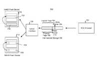
- FIG. 1is a block diagram illustrating an embodiment of a storage media device system 100 .
- FIG. 2is a diagram illustrating an embodiment of a NAND memory array and a NAND page register of a NAND flash device.
- FIG. 3is a diagram illustrating an embodiment of a physical page 300 of a NAND flash device.
- FIG. 4is a diagram illustrating an embodiment of a logical page 400 output by an ECC encoder.
- FIG. 5is a diagram illustrating an embodiment of a logical page having a page size that is greater than the physical page size.
- FIG. 6is a diagram illustrating an embodiment of a logical page having a page size that is smaller than the physical page size.
- FIG. 7is a block diagram illustrating an embodiment of a storage media device system 700 when the system is writing data to one or more NAND flash devices.
- FIG. 8is a block diagram illustrating an embodiment of a storage media device system 800 when the system is reading data back from the one or more NAND flash devices to ECC decoder 801 .
- FIG. 9is a flow diagram illustrating an embodiment of a process 900 for writing data to non-volatile computer storage, e.g., NAND flash devices.
- FIG. 10is a flow diagram illustrating an embodiment of a process 1000 for reading data from non-volatile computer storage, e.g., NAND flash devices.
- non-volatile computer storagee.g., NAND flash devices.
- the inventioncan be implemented in numerous ways, including as a process; an apparatus; a system; a composition of matter; a computer program product embodied on a computer readable storage medium; and/or a processor, such as a processor configured to execute instructions stored on and/or provided by a memory coupled to the processor.
- these implementations, or any other form that the invention may take,may be referred to as techniques.
- the order of the steps of disclosed processesmay be altered within the scope of the invention.
- a componentsuch as a processor or a memory described as being configured to perform a task may be implemented as a general component that is temporarily configured to perform the task at a given time or a specific component that is manufactured to perform the task.
- the term ‘processor’refers to one or more devices, circuits, and/or processing cores configured to process data, such as computer program instructions.
- FIG. 1is a block diagram illustrating an embodiment of a storage media device system 100 .
- Storage media device system 100includes one or more non-volatile computer storage chips 102 , such as NAND flash devices 102 .
- NAND flash devicesare selected as illustrative examples only. The techniques disclosed herein may apply to other computer storage chips as well; accordingly, the present application is not limited to the specific example of NAND flash devices only.
- Storage media device system 100also includes a computer storage chip interface 104 , such as a NAND flash interface 104 , which provides an interface to NAND flash devices 102 .
- a NAND flash interface 104provides an interface for NAND flash devices 102 to identify themselves and describe their capabilities. It also provides an interface for storage media device system 100 to perform commands, including reading, programming, erasing, and register changes on the NAND flash devices 102 .
- an encoder 106determines a plurality of parity bits for error correction of the user data. Encoder 106 then sends the user data and the corresponding parity bits to a NAND flash interface 104 , and the NAND flash interface 104 will in turn write the user data and the parity bits to the NAND flash device 102 .
- the NAND flash device 102when storage media device system 100 sends a read command via a NAND flash interface 104 to one of the NAND flash devices 102 , the NAND flash device 102 will send the read data to the NAND flash interface 104 , and the NAND flash interface 104 will in turn send the read data to a decoder 108 .
- decoder 108may be an error-correcting code (ECC) decoder enabling reconstruction of the original error-free data initially stored in the NAND flash device 102 .
- ECC decoder 108is a BCH decoder.
- ECC decoder 108is a low-density parity-check (LDPC) decoder.
- LDPC decoder 108may be implemented using various algorithms, including the sum-product algorithm, min-sum algorithm, and brief propagation algorithm.
- Data retentionis the ability of a memory bit to retain its data state over long periods of time.
- the data retention of NAND flash devicesis limited by various factors.
- the cell voltage level of a NAND flash devicecan decay or otherwise leak under certain circumstances. For example, after data is programmed onto a NAND flash device, the cell voltage levels slowly drift down after a period of time, typically months or years, because charge may slowly leak from the floating gates of the memory cell transistors. Furthermore, the speed of such voltage drift can be accelerated when the NAND flash device is kept in a high temperature environment for long hours or if many program-erase cycles have been performed on the NAND flash device. Because of the above factors, the number of bit flips in the data stored in a NAND flash device increases over time. When the number of bit flips is beyond the error-correcting capability of the ECC decoder, the life span of the NAND flash device will have been reached.
- FIG. 2is a diagram illustrating an embodiment of a NAND memory array and a NAND page register of a NAND flash device.
- a NAND flash deviceincludes a NAND memory array 202 and a NAND page register 206 .
- the reading and programming of the NAND flash deviceis performed on a page-by-page basis, a page being the smallest unit of physical space that can be read from or programmed into the NAND flash device at one time.
- to write data onto NAND memory array 202data is first written to NAND page register 206 , which has a size of one physical page.
- the physical page of data in NAND page register 206is then programmed into one of the rows 204 in NAND memory array 202 .
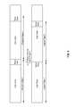
- FIG. 3is a diagram illustrating an embodiment of a physical page 300 of a NAND flash device.
- Physical page 300can be divided into one or more user data units 302 and a meta data area 304 .
- the size of the one or more user data units 302 , the number of user data units 302 in physical page 300 , and the size of meta data area 304are determined by the particular NAND manufacturer and may differ for different NAND manufacturers.
- User data units 302are used for storing user data. In some NAND flash devices, the size of each user data unit 302 in bytes is a power of two, such as 512, 2048, or 4096 bytes in size.
- Meta data area 304can be used for storing error correcting information, such as parity bits.
- Meta data area 304can also be used for storing other information, including decoding information, firmware assistance information, and the like.
- the size of meta data area 304is determined by the NAND manufacturer based on a target life span of the NAND flash device. For example, a NAND manufacturer may determine that to achieve a particular target life span (e.g., a target life span measured in P/E cycles) based on the NAND flash device's error correcting requirements, an ECC decoder would require y number of parity bits for error-correcting each Kbytes of user data. Then meta data area 304 may be determined as a function of y. For example, the NAND manufacturer may determine that the size of meta data area 304 may be set to be equal to y* the number of Kbytes of user data (the product being measured in bits)+z number of bytes for storing other types of information.
- FIG. 4is a diagram illustrating an embodiment of a logical page 400 output by an ECC encoder.
- logical page 400includes one or more codewords 402 and a meta data area 404 .
- the size of codewords 402is determined by the ECC encoder.
- the size of codewords 402can be any arbitrary number of bytes, such as 512 bytes, 520 bytes, 528 bytes, and the like.
- Meta data area 404can be used for storing error correcting information, such as parity bits. Meta data area 404 can also be used for storing other types of information, including decoding information, firmware assistance information, and the like.
- the ECC encoderforces the logical page size to be equal to or less than the physical page size of the NAND flash devices.
- fixing the logical page size to be equal to or less than the physical page sizehas a number of drawbacks.
- the ECC capability of the systemis not determined by the storage media device system but is bounded by the size of meta data area 304 , which is dictated by the NAND manufacturer. For example, a higher number of parity bits cannot be allocated to increase the ECC capability of the system, and thus the expected life span of the system, unless some of the physical space originally budgeted for user data is used for storing the extra parity bits instead; in such case the capacity or code rate of the system will be reduced.
- the memory space of the NAND flash devicemay not be fully utilized due to the constant nature of the physical page size and thus the logical page size.
- the codeword sizesmay not be equal to the size of the user data units designed by the NAND manufacturers.
- the user data unit sizemay be 512 bytes, while the codeword size is 520 bytes. Since the codeword size is larger than the user data unit size, fewer codewords may be fitted into the page, and some of the memory space in the page will not be used.
- swapping NAND flash devicesis not transparent to the encoder. For example, if 4 k page NAND flash devices are used to replace 8 k page NAND flash devices in a storage media device system, the encoder needs to be modified such that it writes logical pages having a size that matches with the physical page size of the new 4 k page NAND flash devices.
- the ECC encoderis configured to output logical pages with a size that is independent of the physical page size of the NAND flash devices.
- the codeword sizeis also independent of the physical page size of the NAND flash devices. For example, if the physical page size is equal to N bytes, then the logical page size is equal to M, where M may be greater than, equal to, or smaller than N.
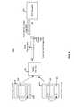
- FIG. 5is a diagram illustrating an embodiment of a logical page having a page size that is greater than the physical page size. As shown in FIG. 5 , when logical page 1 is greater than that which can fit into physical page 1 , the remainder of logical page 1 is stored in physical page 2 .
- a ECC codewordcan be programmed across multiple NAND physical pages.
- FIG. 6is a diagram illustrating an embodiment of a logical page having a page size that is smaller than the physical page size.
- the extra space left in physical page 1is used to store logical page 2 , which will allow the whole NAND physical page to be fully utilized without wasting bytes on account of the larger granularity of a physical page.
- a first portion of logical page 2is stored in physical page 1
- the remainder of logical page 2is stored in physical page 2 .
- a logical pagecan be programmed across multiple NAND physical pages.
- each bit of the physical page memorycan be utilized.
- the ECC encoderis also free to allocate the appropriate number of parity bits for error-correction based on other requirements and specifications. For example, the ECC encoder may allocate a higher number of parity bits to increase the ECC capability and thus the expected lifespan of the system.
- swapping NAND flash devicesno longer requires the design of the ECC encoder to be changed because the logical page size may remain unchanged.
- FIG. 7is a block diagram illustrating an embodiment of a storage media device system 700 when the system is writing data to one or more NAND flash devices.
- Storage media device system 700is similar to storage media device system 100 as shown in FIG. 1 , including one or more NAND flash devices ( 714 and 716 ), one or more NAND flash interfaces 726 , and an ECC encoder 701 .
- Storage media device system 700further includes an intermediate storage 702 .
- Intermediate storage 702is used to temporarily store a logical page 704 that is output by ECC encoder 701 before the logical page 704 is written to the one or more NAND flash devices ( 714 and 716 ) via NAND flash interface 726 .
- the temporary storage of a logical page 704 in intermediate storage 702allows ECC encoder 701 to write logical pages with a logical page size that is independent from the physical page size of NAND flash devices ( 714 and 716 ).
- intermediate storage 702may be a circular buffer.
- a write pointer 706is advanced to point to the next location within intermediate storage 702 to be written to.
- write pointer 706wraps around and writes to the beginning of the circular buffer again.
- a read pointer 710that always lags behind write pointer 706 may be used to read logical page 704 from intermediate storage 702 and send it to the one or more NAND flash devices ( 714 and 716 ) via NAND interface 726 . As shown in FIG.
- the size of logical page 704is greater than the size of physical page 708 .
- one portion of logical page 704 having a size equal to one physical pageis written to a page register 718 and then transferred from page register 718 to a row 722 of a NAND memory array on NAND flash device 716 .
- the remaining portion of logical page 704is written to a page register 720 and then transferred from page register 720 to a row 724 of a NAND memory array on NAND flash device 714 .
- the content of page register 720is not transferred until page register 720 is filled by subsequent writes.
- one logical pageis written to two different NAND flash devices.
- the logical pageis written to two different NAND flash devices in parallel.
- the logical pagemay be written to two rows of the NAND memory array of the same NAND flash device.
- FIG. 8is a block diagram illustrating an embodiment of a storage media device system 800 when the system is reading data back from the one or more NAND flash devices to ECC decoder 801 .
- the size of the logical pageis greater than the size of the physical page
- the first portion of the logical pageis read from a first physical page stored on a NAND flash device
- the second portion of the logical pageis read from a second physical page stored on another NAND flash device or the same NAND flash device.
- FIG. 7the size of the logical page is greater than the size of the physical page
- the first portion of the logical pageis read from a first physical page stored on a NAND flash device
- the second portion of the logical pageis read from a second physical page stored on another NAND flash device or the same NAND flash device.
- the first portion of the logical pageis read from a row 822 of a NAND memory array on NAND flash device 816 to a page register 818
- the second portion of the logical pageis read from a row 824 of a NAND memory array on NAND flash device 814 to a page register 820
- the first portion of the logical pageis then transferred from page register 818 to an intermediate storage 802 via a NAND interface 826 using a write pointer 804 .
- the second portion of the logical pageis transferred from page register 820 to intermediate storage 802 using a write pointer 806 .
- page register 820may include user data and/or meta data corresponding to another logical page. If the system determines that these user data and/or meta data is going to be read by ECC decoder soon, then they will be transferred from page register 820 to intermediate storage 802 at the same time as well.
- the first portion and the second portion of the logical pageare then concatenated to form a concatenated logical page 808 that is sent to ECC decoder 801 to be decoded.
- one logical pageis read from two different NAND flash devices.
- the first portion and the second portion of the logical pageis read from two different NAND flash devices in parallel.
- the logical pagemay be read from two rows of the NAND memory array of the same NAND flash device.
- FIG. 9is a flow diagram illustrating an embodiment of a process 900 for writing data to non-volatile computer storage, e.g., NAND flash devices.
- process 900is a process performed by storage media device system 700 shown in FIG. 7 .
- a logical page of datais received from an ECC encoder.
- the logical page of datais stored in an intermediate storage.
- a first portion of the logical pageis read from the intermediate storage. The first portion of the logical page is written to a first physical page in the non-volatile computer storage.
- a second portion of the logical pageis read from the intermediate storage. The second portion of the logical page is written to a second physical page in the non-volatile computer storage.
- FIG. 10is a flow diagram illustrating an embodiment of a process 1000 for reading data from non-volatile computer storage, e.g., NAND flash devices.
- process 1000is a process performed by storage media device system 800 shown in FIG. 8 .
- a first portion of a logical pageis read from a first physical page.
- the first portion of the logical pageis written to an intermediate storage.
- a second portion of the logical pageis read from a second physical page.
- the second portion of the logical pageis written to the intermediate storage.
- the first portion and the second portion of the logical pageare concatenated to form the logical page.
- the concatenated logical pageis then sent to an ECC decoder for decoding.
- the reading from two physical pagescan also occur at the same time to form a logical page in the intermediate storage.
Landscapes
- Engineering & Computer Science (AREA)
- Microelectronics & Electronic Packaging (AREA)
- Theoretical Computer Science (AREA)
- Quality & Reliability (AREA)
- Physics & Mathematics (AREA)
- General Engineering & Computer Science (AREA)
- General Physics & Mathematics (AREA)
- Techniques For Improving Reliability Of Storages (AREA)
Abstract
Description
Claims (18)
Priority Applications (1)
| Application Number | Priority Date | Filing Date | Title |
|---|---|---|---|
| US13/445,139US9159422B1 (en) | 2011-04-12 | 2012-04-12 | Cross page management to avoid NAND physical page size limitation |
Applications Claiming Priority (2)
| Application Number | Priority Date | Filing Date | Title |
|---|---|---|---|
| US201161474684P | 2011-04-12 | 2011-04-12 | |
| US13/445,139US9159422B1 (en) | 2011-04-12 | 2012-04-12 | Cross page management to avoid NAND physical page size limitation |
Publications (1)
| Publication Number | Publication Date |
|---|---|
| US9159422B1true US9159422B1 (en) | 2015-10-13 |
Family
ID=54252760
Family Applications (1)
| Application Number | Title | Priority Date | Filing Date |
|---|---|---|---|
| US13/445,139Active2034-03-28US9159422B1 (en) | 2011-04-12 | 2012-04-12 | Cross page management to avoid NAND physical page size limitation |
Country Status (1)
| Country | Link |
|---|---|
| US (1) | US9159422B1 (en) |
Cited By (127)
| Publication number | Priority date | Publication date | Assignee | Title |
|---|---|---|---|---|
| US20170052844A1 (en)* | 2015-08-19 | 2017-02-23 | International Business Machines Corporation | Flash memory codeword architectures |
| CN107273304A (en)* | 2017-05-24 | 2017-10-20 | 记忆科技(深圳)有限公司 | A kind of method and solid state hard disc for improving solid state hard disc order reading performance |
| US20180018223A1 (en)* | 2016-07-12 | 2018-01-18 | Futurewei Technologies, Inc. | Generating parity for storage device |
| US10817431B2 (en) | 2014-07-02 | 2020-10-27 | Pure Storage, Inc. | Distributed storage addressing |
| US10838633B2 (en) | 2014-06-04 | 2020-11-17 | Pure Storage, Inc. | Configurable hyperconverged multi-tenant storage system |
| CN112015334A (en)* | 2019-05-30 | 2020-12-01 | 慧荣科技股份有限公司 | Memory device access management method, memory device, controller thereof and electronic device |
| US10942869B2 (en) | 2017-03-30 | 2021-03-09 | Pure Storage, Inc. | Efficient coding in a storage system |
| US11030090B2 (en) | 2016-07-26 | 2021-06-08 | Pure Storage, Inc. | Adaptive data migration |
| US11074016B2 (en) | 2017-10-31 | 2021-07-27 | Pure Storage, Inc. | Using flash storage devices with different sized erase blocks |
| US11079962B2 (en) | 2014-07-02 | 2021-08-03 | Pure Storage, Inc. | Addressable non-volatile random access memory |
| US11086532B2 (en) | 2017-10-31 | 2021-08-10 | Pure Storage, Inc. | Data rebuild with changing erase block sizes |
| US11138082B2 (en) | 2014-06-04 | 2021-10-05 | Pure Storage, Inc. | Action determination based on redundancy level |
| US11144212B2 (en) | 2015-04-10 | 2021-10-12 | Pure Storage, Inc. | Independent partitions within an array |
| US11190580B2 (en) | 2017-07-03 | 2021-11-30 | Pure Storage, Inc. | Stateful connection resets |
| US11188476B1 (en) | 2014-08-20 | 2021-11-30 | Pure Storage, Inc. | Virtual addressing in a storage system |
| US11204830B2 (en) | 2014-08-07 | 2021-12-21 | Pure Storage, Inc. | Die-level monitoring in a storage cluster |
| US11204701B2 (en) | 2015-12-22 | 2021-12-21 | Pure Storage, Inc. | Token based transactions |
| US11240307B2 (en) | 2015-04-09 | 2022-02-01 | Pure Storage, Inc. | Multiple communication paths in a storage system |
| US11289169B2 (en) | 2017-01-13 | 2022-03-29 | Pure Storage, Inc. | Cycled background reads |
| US11310317B1 (en) | 2014-06-04 | 2022-04-19 | Pure Storage, Inc. | Efficient load balancing |
| US11307998B2 (en) | 2017-01-09 | 2022-04-19 | Pure Storage, Inc. | Storage efficiency of encrypted host system data |
| US11334254B2 (en) | 2019-03-29 | 2022-05-17 | Pure Storage, Inc. | Reliability based flash page sizing |
| US11340821B2 (en) | 2016-07-26 | 2022-05-24 | Pure Storage, Inc. | Adjustable migration utilization |
| US11354058B2 (en) | 2018-09-06 | 2022-06-07 | Pure Storage, Inc. | Local relocation of data stored at a storage device of a storage system |
| US11385979B2 (en) | 2014-07-02 | 2022-07-12 | Pure Storage, Inc. | Mirrored remote procedure call cache |
| US11385799B2 (en) | 2014-06-04 | 2022-07-12 | Pure Storage, Inc. | Storage nodes supporting multiple erasure coding schemes |
| US11392522B2 (en) | 2014-07-03 | 2022-07-19 | Pure Storage, Inc. | Transfer of segmented data |
| US11409437B2 (en) | 2016-07-22 | 2022-08-09 | Pure Storage, Inc. | Persisting configuration information |
| US11416144B2 (en) | 2019-12-12 | 2022-08-16 | Pure Storage, Inc. | Dynamic use of segment or zone power loss protection in a flash device |
| US11442645B2 (en) | 2018-01-31 | 2022-09-13 | Pure Storage, Inc. | Distributed storage system expansion mechanism |
| US11442625B2 (en) | 2014-08-07 | 2022-09-13 | Pure Storage, Inc. | Multiple read data paths in a storage system |
| US11489668B2 (en) | 2015-09-30 | 2022-11-01 | Pure Storage, Inc. | Secret regeneration in a storage system |
| US11494498B2 (en) | 2014-07-03 | 2022-11-08 | Pure Storage, Inc. | Storage data decryption |
| US11507597B2 (en) | 2021-03-31 | 2022-11-22 | Pure Storage, Inc. | Data replication to meet a recovery point objective |
| US11544143B2 (en) | 2014-08-07 | 2023-01-03 | Pure Storage, Inc. | Increased data reliability |
| US11550752B2 (en) | 2014-07-03 | 2023-01-10 | Pure Storage, Inc. | Administrative actions via a reserved filename |
| US11550473B2 (en) | 2016-05-03 | 2023-01-10 | Pure Storage, Inc. | High-availability storage array |
| US11567917B2 (en) | 2015-09-30 | 2023-01-31 | Pure Storage, Inc. | Writing data and metadata into storage |
| US11580028B2 (en)* | 2019-12-19 | 2023-02-14 | SK Hynix Inc. | Storage device and method of operating the same |
| US11582046B2 (en) | 2015-10-23 | 2023-02-14 | Pure Storage, Inc. | Storage system communication |
| US11593203B2 (en) | 2014-06-04 | 2023-02-28 | Pure Storage, Inc. | Coexisting differing erasure codes |
| US11592985B2 (en) | 2017-04-05 | 2023-02-28 | Pure Storage, Inc. | Mapping LUNs in a storage memory |
| US11604598B2 (en) | 2014-07-02 | 2023-03-14 | Pure Storage, Inc. | Storage cluster with zoned drives |
| US11604690B2 (en) | 2016-07-24 | 2023-03-14 | Pure Storage, Inc. | Online failure span determination |
| US11614880B2 (en) | 2020-12-31 | 2023-03-28 | Pure Storage, Inc. | Storage system with selectable write paths |
| US11620197B2 (en) | 2014-08-07 | 2023-04-04 | Pure Storage, Inc. | Recovering error corrected data |
| US11652884B2 (en) | 2014-06-04 | 2023-05-16 | Pure Storage, Inc. | Customized hash algorithms |
| US11650976B2 (en) | 2011-10-14 | 2023-05-16 | Pure Storage, Inc. | Pattern matching using hash tables in storage system |
| US11656768B2 (en) | 2016-09-15 | 2023-05-23 | Pure Storage, Inc. | File deletion in a distributed system |
| US11656961B2 (en) | 2020-02-28 | 2023-05-23 | Pure Storage, Inc. | Deallocation within a storage system |
| US11675762B2 (en) | 2015-06-26 | 2023-06-13 | Pure Storage, Inc. | Data structures for key management |
| US11704073B2 (en) | 2015-07-13 | 2023-07-18 | Pure Storage, Inc | Ownership determination for accessing a file |
| US11704192B2 (en) | 2019-12-12 | 2023-07-18 | Pure Storage, Inc. | Budgeting open blocks based on power loss protection |
| US11714708B2 (en) | 2017-07-31 | 2023-08-01 | Pure Storage, Inc. | Intra-device redundancy scheme |
| US11722455B2 (en) | 2017-04-27 | 2023-08-08 | Pure Storage, Inc. | Storage cluster address resolution |
| US11734169B2 (en) | 2016-07-26 | 2023-08-22 | Pure Storage, Inc. | Optimizing spool and memory space management |
| US11741003B2 (en) | 2017-11-17 | 2023-08-29 | Pure Storage, Inc. | Write granularity for storage system |
| US11740802B2 (en) | 2015-09-01 | 2023-08-29 | Pure Storage, Inc. | Error correction bypass for erased pages |
| US11775428B2 (en) | 2015-03-26 | 2023-10-03 | Pure Storage, Inc. | Deletion immunity for unreferenced data |
| US11775491B2 (en) | 2020-04-24 | 2023-10-03 | Pure Storage, Inc. | Machine learning model for storage system |
| US11782625B2 (en) | 2017-06-11 | 2023-10-10 | Pure Storage, Inc. | Heterogeneity supportive resiliency groups |
| US11789626B2 (en) | 2020-12-17 | 2023-10-17 | Pure Storage, Inc. | Optimizing block allocation in a data storage system |
| US11797212B2 (en) | 2016-07-26 | 2023-10-24 | Pure Storage, Inc. | Data migration for zoned drives |
| US11822807B2 (en) | 2019-06-24 | 2023-11-21 | Pure Storage, Inc. | Data replication in a storage system |
| US11822444B2 (en) | 2014-06-04 | 2023-11-21 | Pure Storage, Inc. | Data rebuild independent of error detection |
| US11836348B2 (en) | 2018-04-27 | 2023-12-05 | Pure Storage, Inc. | Upgrade for system with differing capacities |
| US11842053B2 (en) | 2016-12-19 | 2023-12-12 | Pure Storage, Inc. | Zone namespace |
| US11846968B2 (en) | 2018-09-06 | 2023-12-19 | Pure Storage, Inc. | Relocation of data for heterogeneous storage systems |
| US11847331B2 (en) | 2019-12-12 | 2023-12-19 | Pure Storage, Inc. | Budgeting open blocks of a storage unit based on power loss prevention |
| US11847324B2 (en) | 2020-12-31 | 2023-12-19 | Pure Storage, Inc. | Optimizing resiliency groups for data regions of a storage system |
| US11847013B2 (en) | 2018-02-18 | 2023-12-19 | Pure Storage, Inc. | Readable data determination |
| TWI827138B (en)* | 2021-08-27 | 2023-12-21 | 華邦電子股份有限公司 | Semiconductor storage device |
| US11861188B2 (en) | 2016-07-19 | 2024-01-02 | Pure Storage, Inc. | System having modular accelerators |
| US11869583B2 (en) | 2017-04-27 | 2024-01-09 | Pure Storage, Inc. | Page write requirements for differing types of flash memory |
| US11868309B2 (en) | 2018-09-06 | 2024-01-09 | Pure Storage, Inc. | Queue management for data relocation |
| US11886308B2 (en) | 2014-07-02 | 2024-01-30 | Pure Storage, Inc. | Dual class of service for unified file and object messaging |
| US11886288B2 (en) | 2016-07-22 | 2024-01-30 | Pure Storage, Inc. | Optimize data protection layouts based on distributed flash wear leveling |
| US11886334B2 (en) | 2016-07-26 | 2024-01-30 | Pure Storage, Inc. | Optimizing spool and memory space management |
| US11893023B2 (en) | 2015-09-04 | 2024-02-06 | Pure Storage, Inc. | Deterministic searching using compressed indexes |
| US11893126B2 (en) | 2019-10-14 | 2024-02-06 | Pure Storage, Inc. | Data deletion for a multi-tenant environment |
| US11899582B2 (en) | 2019-04-12 | 2024-02-13 | Pure Storage, Inc. | Efficient memory dump |
| US11922070B2 (en) | 2016-10-04 | 2024-03-05 | Pure Storage, Inc. | Granting access to a storage device based on reservations |
| US11955187B2 (en) | 2017-01-13 | 2024-04-09 | Pure Storage, Inc. | Refresh of differing capacity NAND |
| US11960371B2 (en) | 2014-06-04 | 2024-04-16 | Pure Storage, Inc. | Message persistence in a zoned system |
| US11966841B2 (en) | 2018-01-31 | 2024-04-23 | Pure Storage, Inc. | Search acceleration for artificial intelligence |
| US11971828B2 (en) | 2015-09-30 | 2024-04-30 | Pure Storage, Inc. | Logic module for use with encoded instructions |
| US11995318B2 (en) | 2016-10-28 | 2024-05-28 | Pure Storage, Inc. | Deallocated block determination |
| US12001700B2 (en) | 2018-10-26 | 2024-06-04 | Pure Storage, Inc. | Dynamically selecting segment heights in a heterogeneous RAID group |
| US12032724B2 (en) | 2017-08-31 | 2024-07-09 | Pure Storage, Inc. | Encryption in a storage array |
| US12038927B2 (en) | 2015-09-04 | 2024-07-16 | Pure Storage, Inc. | Storage system having multiple tables for efficient searching |
| US12046292B2 (en) | 2017-10-31 | 2024-07-23 | Pure Storage, Inc. | Erase blocks having differing sizes |
| US12050774B2 (en) | 2015-05-27 | 2024-07-30 | Pure Storage, Inc. | Parallel update for a distributed system |
| US12056365B2 (en) | 2020-04-24 | 2024-08-06 | Pure Storage, Inc. | Resiliency for a storage system |
| US12061814B2 (en) | 2021-01-25 | 2024-08-13 | Pure Storage, Inc. | Using data similarity to select segments for garbage collection |
| US12067274B2 (en) | 2018-09-06 | 2024-08-20 | Pure Storage, Inc. | Writing segments and erase blocks based on ordering |
| US12067282B2 (en) | 2020-12-31 | 2024-08-20 | Pure Storage, Inc. | Write path selection |
| US12079125B2 (en) | 2019-06-05 | 2024-09-03 | Pure Storage, Inc. | Tiered caching of data in a storage system |
| US12079494B2 (en) | 2018-04-27 | 2024-09-03 | Pure Storage, Inc. | Optimizing storage system upgrades to preserve resources |
| US12086472B2 (en) | 2015-03-27 | 2024-09-10 | Pure Storage, Inc. | Heterogeneous storage arrays |
| US12093545B2 (en) | 2020-12-31 | 2024-09-17 | Pure Storage, Inc. | Storage system with selectable write modes |
| US12105620B2 (en) | 2016-10-04 | 2024-10-01 | Pure Storage, Inc. | Storage system buffering |
| US12135878B2 (en) | 2019-01-23 | 2024-11-05 | Pure Storage, Inc. | Programming frequently read data to low latency portions of a solid-state storage array |
| US12137140B2 (en) | 2014-06-04 | 2024-11-05 | Pure Storage, Inc. | Scale out storage platform having active failover |
| US12141118B2 (en) | 2016-10-04 | 2024-11-12 | Pure Storage, Inc. | Optimizing storage system performance using data characteristics |
| US12158814B2 (en) | 2014-08-07 | 2024-12-03 | Pure Storage, Inc. | Granular voltage tuning |
| US12182044B2 (en) | 2014-07-03 | 2024-12-31 | Pure Storage, Inc. | Data storage in a zone drive |
| US12197390B2 (en) | 2017-11-20 | 2025-01-14 | Pure Storage, Inc. | Locks in a distributed file system |
| US12204768B2 (en) | 2019-12-03 | 2025-01-21 | Pure Storage, Inc. | Allocation of blocks based on power loss protection |
| US12204413B2 (en) | 2017-06-07 | 2025-01-21 | Pure Storage, Inc. | Snapshot commitment in a distributed system |
| US12204788B1 (en) | 2023-07-21 | 2025-01-21 | Pure Storage, Inc. | Dynamic plane selection in data storage system |
| US12212624B2 (en) | 2014-06-04 | 2025-01-28 | Pure Storage, Inc. | Independent communication pathways |
| US12216903B2 (en) | 2016-10-31 | 2025-02-04 | Pure Storage, Inc. | Storage node data placement utilizing similarity |
| US12229437B2 (en) | 2020-12-31 | 2025-02-18 | Pure Storage, Inc. | Dynamic buffer for storage system |
| US12235743B2 (en) | 2016-06-03 | 2025-02-25 | Pure Storage, Inc. | Efficient partitioning for storage system resiliency groups |
| US12242425B2 (en) | 2017-10-04 | 2025-03-04 | Pure Storage, Inc. | Similarity data for reduced data usage |
| US12271359B2 (en) | 2015-09-30 | 2025-04-08 | Pure Storage, Inc. | Device host operations in a storage system |
| US12282799B2 (en) | 2015-05-19 | 2025-04-22 | Pure Storage, Inc. | Maintaining coherency in a distributed system |
| US12314170B2 (en) | 2020-07-08 | 2025-05-27 | Pure Storage, Inc. | Guaranteeing physical deletion of data in a storage system |
| US12314163B2 (en) | 2022-04-21 | 2025-05-27 | Pure Storage, Inc. | Die-aware scheduler |
| US12341848B2 (en) | 2014-06-04 | 2025-06-24 | Pure Storage, Inc. | Distributed protocol endpoint services for data storage systems |
| US12340107B2 (en) | 2016-05-02 | 2025-06-24 | Pure Storage, Inc. | Deduplication selection and optimization |
| US12373340B2 (en) | 2019-04-03 | 2025-07-29 | Pure Storage, Inc. | Intelligent subsegment formation in a heterogeneous storage system |
| US12379854B2 (en) | 2015-04-10 | 2025-08-05 | Pure Storage, Inc. | Two or more logical arrays having zoned drives |
| US12393340B2 (en) | 2019-01-16 | 2025-08-19 | Pure Storage, Inc. | Latency reduction of flash-based devices using programming interrupts |
| US12430053B2 (en) | 2021-03-12 | 2025-09-30 | Pure Storage, Inc. | Data block allocation for storage system |
| US12430059B2 (en) | 2020-04-15 | 2025-09-30 | Pure Storage, Inc. | Tuning storage devices |
| US12439544B2 (en) | 2022-04-20 | 2025-10-07 | Pure Storage, Inc. | Retractable pivoting trap door |
Citations (8)
| Publication number | Priority date | Publication date | Assignee | Title |
|---|---|---|---|---|
| US20070005627A1 (en)* | 2005-07-01 | 2007-01-04 | Dan Dodge | File system having transaction record coalescing |
| US20070143566A1 (en)* | 2005-12-21 | 2007-06-21 | Gorobets Sergey A | Non-volatile memories with data alignment in a directly mapped file storage system |
| US20070143561A1 (en)* | 2005-12-21 | 2007-06-21 | Gorobets Sergey A | Methods for adaptive file data handling in non-volatile memories with a directly mapped file storage system |
| US20080192539A1 (en)* | 2007-02-09 | 2008-08-14 | Choi Jin-Hyeok | Memory System Including MLC Flash Memory |
| US20080195822A1 (en)* | 2007-02-12 | 2008-08-14 | Xueshi Yang | Pilot placement for non-volatile memory |
| US20100088557A1 (en)* | 2007-10-25 | 2010-04-08 | Hanan Weingarten | Systems and methods for multiple coding rates in flash devices |
| US20100241790A1 (en)* | 2009-03-18 | 2010-09-23 | Korea Advanced Institute Of Science And Technology | Method of storing data into flash memory in a dbms-independent manner using the page-differential |
| US20130246891A1 (en)* | 2012-03-15 | 2013-09-19 | Micron Technology, Inc. | Physical page, logical page, and codeword correspondence |
- 2012
- 2012-04-12USUS13/445,139patent/US9159422B1/enactiveActive
Patent Citations (9)
| Publication number | Priority date | Publication date | Assignee | Title |
|---|---|---|---|---|
| US20070005627A1 (en)* | 2005-07-01 | 2007-01-04 | Dan Dodge | File system having transaction record coalescing |
| US20070143566A1 (en)* | 2005-12-21 | 2007-06-21 | Gorobets Sergey A | Non-volatile memories with data alignment in a directly mapped file storage system |
| US20070143561A1 (en)* | 2005-12-21 | 2007-06-21 | Gorobets Sergey A | Methods for adaptive file data handling in non-volatile memories with a directly mapped file storage system |
| US20080192539A1 (en)* | 2007-02-09 | 2008-08-14 | Choi Jin-Hyeok | Memory System Including MLC Flash Memory |
| US20080195822A1 (en)* | 2007-02-12 | 2008-08-14 | Xueshi Yang | Pilot placement for non-volatile memory |
| US20140325179A1 (en)* | 2007-02-12 | 2014-10-30 | Marvell World Trade Ltd. | System and method for writing pilot data interspersed with user data for estimating disturbance experienced by user data |
| US20100088557A1 (en)* | 2007-10-25 | 2010-04-08 | Hanan Weingarten | Systems and methods for multiple coding rates in flash devices |
| US20100241790A1 (en)* | 2009-03-18 | 2010-09-23 | Korea Advanced Institute Of Science And Technology | Method of storing data into flash memory in a dbms-independent manner using the page-differential |
| US20130246891A1 (en)* | 2012-03-15 | 2013-09-19 | Micron Technology, Inc. | Physical page, logical page, and codeword correspondence |
Cited By (176)
| Publication number | Priority date | Publication date | Assignee | Title |
|---|---|---|---|---|
| US11650976B2 (en) | 2011-10-14 | 2023-05-16 | Pure Storage, Inc. | Pattern matching using hash tables in storage system |
| US12277106B2 (en) | 2011-10-14 | 2025-04-15 | Pure Storage, Inc. | Flash system having multiple fingerprint tables |
| US12212624B2 (en) | 2014-06-04 | 2025-01-28 | Pure Storage, Inc. | Independent communication pathways |
| US12101379B2 (en) | 2014-06-04 | 2024-09-24 | Pure Storage, Inc. | Multilevel load balancing |
| US11960371B2 (en) | 2014-06-04 | 2024-04-16 | Pure Storage, Inc. | Message persistence in a zoned system |
| US12066895B2 (en) | 2014-06-04 | 2024-08-20 | Pure Storage, Inc. | Heterogenous memory accommodating multiple erasure codes |
| US11671496B2 (en) | 2014-06-04 | 2023-06-06 | Pure Storage, Inc. | Load balacing for distibuted computing |
| US11385799B2 (en) | 2014-06-04 | 2022-07-12 | Pure Storage, Inc. | Storage nodes supporting multiple erasure coding schemes |
| US10838633B2 (en) | 2014-06-04 | 2020-11-17 | Pure Storage, Inc. | Configurable hyperconverged multi-tenant storage system |
| US11652884B2 (en) | 2014-06-04 | 2023-05-16 | Pure Storage, Inc. | Customized hash algorithms |
| US11500552B2 (en) | 2014-06-04 | 2022-11-15 | Pure Storage, Inc. | Configurable hyperconverged multi-tenant storage system |
| US12137140B2 (en) | 2014-06-04 | 2024-11-05 | Pure Storage, Inc. | Scale out storage platform having active failover |
| US12141449B2 (en) | 2014-06-04 | 2024-11-12 | Pure Storage, Inc. | Distribution of resources for a storage system |
| US11138082B2 (en) | 2014-06-04 | 2021-10-05 | Pure Storage, Inc. | Action determination based on redundancy level |
| US11310317B1 (en) | 2014-06-04 | 2022-04-19 | Pure Storage, Inc. | Efficient load balancing |
| US12341848B2 (en) | 2014-06-04 | 2025-06-24 | Pure Storage, Inc. | Distributed protocol endpoint services for data storage systems |
| US11822444B2 (en) | 2014-06-04 | 2023-11-21 | Pure Storage, Inc. | Data rebuild independent of error detection |
| US11593203B2 (en) | 2014-06-04 | 2023-02-28 | Pure Storage, Inc. | Coexisting differing erasure codes |
| US11886308B2 (en) | 2014-07-02 | 2024-01-30 | Pure Storage, Inc. | Dual class of service for unified file and object messaging |
| US11604598B2 (en) | 2014-07-02 | 2023-03-14 | Pure Storage, Inc. | Storage cluster with zoned drives |
| US11922046B2 (en) | 2014-07-02 | 2024-03-05 | Pure Storage, Inc. | Erasure coded data within zoned drives |
| US11079962B2 (en) | 2014-07-02 | 2021-08-03 | Pure Storage, Inc. | Addressable non-volatile random access memory |
| US12135654B2 (en) | 2014-07-02 | 2024-11-05 | Pure Storage, Inc. | Distributed storage system |
| US11385979B2 (en) | 2014-07-02 | 2022-07-12 | Pure Storage, Inc. | Mirrored remote procedure call cache |
| US10817431B2 (en) | 2014-07-02 | 2020-10-27 | Pure Storage, Inc. | Distributed storage addressing |
| US12182044B2 (en) | 2014-07-03 | 2024-12-31 | Pure Storage, Inc. | Data storage in a zone drive |
| US11392522B2 (en) | 2014-07-03 | 2022-07-19 | Pure Storage, Inc. | Transfer of segmented data |
| US11928076B2 (en) | 2014-07-03 | 2024-03-12 | Pure Storage, Inc. | Actions for reserved filenames |
| US11550752B2 (en) | 2014-07-03 | 2023-01-10 | Pure Storage, Inc. | Administrative actions via a reserved filename |
| US11494498B2 (en) | 2014-07-03 | 2022-11-08 | Pure Storage, Inc. | Storage data decryption |
| US12314131B2 (en) | 2014-08-07 | 2025-05-27 | Pure Storage, Inc. | Wear levelling for differing memory types |
| US11656939B2 (en) | 2014-08-07 | 2023-05-23 | Pure Storage, Inc. | Storage cluster memory characterization |
| US12271264B2 (en) | 2014-08-07 | 2025-04-08 | Pure Storage, Inc. | Adjusting a variable parameter to increase reliability of stored data |
| US12373289B2 (en) | 2014-08-07 | 2025-07-29 | Pure Storage, Inc. | Error correction incident tracking |
| US11442625B2 (en) | 2014-08-07 | 2022-09-13 | Pure Storage, Inc. | Multiple read data paths in a storage system |
| US11204830B2 (en) | 2014-08-07 | 2021-12-21 | Pure Storage, Inc. | Die-level monitoring in a storage cluster |
| US12158814B2 (en) | 2014-08-07 | 2024-12-03 | Pure Storage, Inc. | Granular voltage tuning |
| US12229402B2 (en) | 2014-08-07 | 2025-02-18 | Pure Storage, Inc. | Intelligent operation scheduling based on latency of operations |
| US12253922B2 (en) | 2014-08-07 | 2025-03-18 | Pure Storage, Inc. | Data rebuild based on solid state memory characteristics |
| US11544143B2 (en) | 2014-08-07 | 2023-01-03 | Pure Storage, Inc. | Increased data reliability |
| US11620197B2 (en) | 2014-08-07 | 2023-04-04 | Pure Storage, Inc. | Recovering error corrected data |
| US11188476B1 (en) | 2014-08-20 | 2021-11-30 | Pure Storage, Inc. | Virtual addressing in a storage system |
| US12314183B2 (en) | 2014-08-20 | 2025-05-27 | Pure Storage, Inc. | Preserved addressing for replaceable resources |
| US11734186B2 (en) | 2014-08-20 | 2023-08-22 | Pure Storage, Inc. | Heterogeneous storage with preserved addressing |
| US11775428B2 (en) | 2015-03-26 | 2023-10-03 | Pure Storage, Inc. | Deletion immunity for unreferenced data |
| US12253941B2 (en) | 2015-03-26 | 2025-03-18 | Pure Storage, Inc. | Management of repeatedly seen data |
| US12086472B2 (en) | 2015-03-27 | 2024-09-10 | Pure Storage, Inc. | Heterogeneous storage arrays |
| US12069133B2 (en) | 2015-04-09 | 2024-08-20 | Pure Storage, Inc. | Communication paths for differing types of solid state storage devices |
| US11240307B2 (en) | 2015-04-09 | 2022-02-01 | Pure Storage, Inc. | Multiple communication paths in a storage system |
| US11722567B2 (en) | 2015-04-09 | 2023-08-08 | Pure Storage, Inc. | Communication paths for storage devices having differing capacities |
| US11144212B2 (en) | 2015-04-10 | 2021-10-12 | Pure Storage, Inc. | Independent partitions within an array |
| US12379854B2 (en) | 2015-04-10 | 2025-08-05 | Pure Storage, Inc. | Two or more logical arrays having zoned drives |
| US12282799B2 (en) | 2015-05-19 | 2025-04-22 | Pure Storage, Inc. | Maintaining coherency in a distributed system |
| US12050774B2 (en) | 2015-05-27 | 2024-07-30 | Pure Storage, Inc. | Parallel update for a distributed system |
| US12093236B2 (en) | 2015-06-26 | 2024-09-17 | Pure Storage, Inc. | Probalistic data structure for key management |
| US11675762B2 (en) | 2015-06-26 | 2023-06-13 | Pure Storage, Inc. | Data structures for key management |
| US11704073B2 (en) | 2015-07-13 | 2023-07-18 | Pure Storage, Inc | Ownership determination for accessing a file |
| US12147715B2 (en) | 2015-07-13 | 2024-11-19 | Pure Storage, Inc. | File ownership in a distributed system |
| US9811419B2 (en) | 2015-08-19 | 2017-11-07 | International Business Machines Corporation | Validation bits and offsets to represent logical pages split between data containers |
| US9875153B2 (en) | 2015-08-19 | 2018-01-23 | International Business Machines Corporation | Validation bits and offsets to represent logical pages split between data containers |
| US9946594B2 (en)* | 2015-08-19 | 2018-04-17 | International Business Machines Corporation | Validation bits and offsets to represent logical pages split between data containers |
| US20170052844A1 (en)* | 2015-08-19 | 2017-02-23 | International Business Machines Corporation | Flash memory codeword architectures |
| US11740802B2 (en) | 2015-09-01 | 2023-08-29 | Pure Storage, Inc. | Error correction bypass for erased pages |
| US12038927B2 (en) | 2015-09-04 | 2024-07-16 | Pure Storage, Inc. | Storage system having multiple tables for efficient searching |
| US11893023B2 (en) | 2015-09-04 | 2024-02-06 | Pure Storage, Inc. | Deterministic searching using compressed indexes |
| US12072860B2 (en) | 2015-09-30 | 2024-08-27 | Pure Storage, Inc. | Delegation of data ownership |
| US11971828B2 (en) | 2015-09-30 | 2024-04-30 | Pure Storage, Inc. | Logic module for use with encoded instructions |
| US11489668B2 (en) | 2015-09-30 | 2022-11-01 | Pure Storage, Inc. | Secret regeneration in a storage system |
| US12271359B2 (en) | 2015-09-30 | 2025-04-08 | Pure Storage, Inc. | Device host operations in a storage system |
| US11567917B2 (en) | 2015-09-30 | 2023-01-31 | Pure Storage, Inc. | Writing data and metadata into storage |
| US11838412B2 (en) | 2015-09-30 | 2023-12-05 | Pure Storage, Inc. | Secret regeneration from distributed shares |
| US11582046B2 (en) | 2015-10-23 | 2023-02-14 | Pure Storage, Inc. | Storage system communication |
| US11204701B2 (en) | 2015-12-22 | 2021-12-21 | Pure Storage, Inc. | Token based transactions |
| US12067260B2 (en) | 2015-12-22 | 2024-08-20 | Pure Storage, Inc. | Transaction processing with differing capacity storage |
| US12340107B2 (en) | 2016-05-02 | 2025-06-24 | Pure Storage, Inc. | Deduplication selection and optimization |
| US11847320B2 (en) | 2016-05-03 | 2023-12-19 | Pure Storage, Inc. | Reassignment of requests for high availability |
| US11550473B2 (en) | 2016-05-03 | 2023-01-10 | Pure Storage, Inc. | High-availability storage array |
| US12235743B2 (en) | 2016-06-03 | 2025-02-25 | Pure Storage, Inc. | Efficient partitioning for storage system resiliency groups |
| US20180018223A1 (en)* | 2016-07-12 | 2018-01-18 | Futurewei Technologies, Inc. | Generating parity for storage device |
| US10169142B2 (en)* | 2016-07-12 | 2019-01-01 | Futurewei Technologies, Inc. | Generating parity for storage device |
| US11861188B2 (en) | 2016-07-19 | 2024-01-02 | Pure Storage, Inc. | System having modular accelerators |
| US11886288B2 (en) | 2016-07-22 | 2024-01-30 | Pure Storage, Inc. | Optimize data protection layouts based on distributed flash wear leveling |
| US11409437B2 (en) | 2016-07-22 | 2022-08-09 | Pure Storage, Inc. | Persisting configuration information |
| US11604690B2 (en) | 2016-07-24 | 2023-03-14 | Pure Storage, Inc. | Online failure span determination |
| US12105584B2 (en) | 2016-07-24 | 2024-10-01 | Pure Storage, Inc. | Acquiring failure information |
| US11797212B2 (en) | 2016-07-26 | 2023-10-24 | Pure Storage, Inc. | Data migration for zoned drives |
| US11340821B2 (en) | 2016-07-26 | 2022-05-24 | Pure Storage, Inc. | Adjustable migration utilization |
| US11030090B2 (en) | 2016-07-26 | 2021-06-08 | Pure Storage, Inc. | Adaptive data migration |
| US11886334B2 (en) | 2016-07-26 | 2024-01-30 | Pure Storage, Inc. | Optimizing spool and memory space management |
| US11734169B2 (en) | 2016-07-26 | 2023-08-22 | Pure Storage, Inc. | Optimizing spool and memory space management |
| US11922033B2 (en) | 2016-09-15 | 2024-03-05 | Pure Storage, Inc. | Batch data deletion |
| US12393353B2 (en) | 2016-09-15 | 2025-08-19 | Pure Storage, Inc. | Storage system with distributed deletion |
| US11656768B2 (en) | 2016-09-15 | 2023-05-23 | Pure Storage, Inc. | File deletion in a distributed system |
| US12105620B2 (en) | 2016-10-04 | 2024-10-01 | Pure Storage, Inc. | Storage system buffering |
| US11922070B2 (en) | 2016-10-04 | 2024-03-05 | Pure Storage, Inc. | Granting access to a storage device based on reservations |
| US12141118B2 (en) | 2016-10-04 | 2024-11-12 | Pure Storage, Inc. | Optimizing storage system performance using data characteristics |
| US11995318B2 (en) | 2016-10-28 | 2024-05-28 | Pure Storage, Inc. | Deallocated block determination |
| US12216903B2 (en) | 2016-10-31 | 2025-02-04 | Pure Storage, Inc. | Storage node data placement utilizing similarity |
| US11842053B2 (en) | 2016-12-19 | 2023-12-12 | Pure Storage, Inc. | Zone namespace |
| US11307998B2 (en) | 2017-01-09 | 2022-04-19 | Pure Storage, Inc. | Storage efficiency of encrypted host system data |
| US11289169B2 (en) | 2017-01-13 | 2022-03-29 | Pure Storage, Inc. | Cycled background reads |
| US11955187B2 (en) | 2017-01-13 | 2024-04-09 | Pure Storage, Inc. | Refresh of differing capacity NAND |
| US10942869B2 (en) | 2017-03-30 | 2021-03-09 | Pure Storage, Inc. | Efficient coding in a storage system |
| US11592985B2 (en) | 2017-04-05 | 2023-02-28 | Pure Storage, Inc. | Mapping LUNs in a storage memory |
| US11869583B2 (en) | 2017-04-27 | 2024-01-09 | Pure Storage, Inc. | Page write requirements for differing types of flash memory |
| US11722455B2 (en) | 2017-04-27 | 2023-08-08 | Pure Storage, Inc. | Storage cluster address resolution |
| CN107273304A (en)* | 2017-05-24 | 2017-10-20 | 记忆科技(深圳)有限公司 | A kind of method and solid state hard disc for improving solid state hard disc order reading performance |
| US12204413B2 (en) | 2017-06-07 | 2025-01-21 | Pure Storage, Inc. | Snapshot commitment in a distributed system |
| US11782625B2 (en) | 2017-06-11 | 2023-10-10 | Pure Storage, Inc. | Heterogeneity supportive resiliency groups |
| US11190580B2 (en) | 2017-07-03 | 2021-11-30 | Pure Storage, Inc. | Stateful connection resets |
| US11689610B2 (en) | 2017-07-03 | 2023-06-27 | Pure Storage, Inc. | Load balancing reset packets |
| US11714708B2 (en) | 2017-07-31 | 2023-08-01 | Pure Storage, Inc. | Intra-device redundancy scheme |
| US12086029B2 (en) | 2017-07-31 | 2024-09-10 | Pure Storage, Inc. | Intra-device and inter-device data recovery in a storage system |
| US12032724B2 (en) | 2017-08-31 | 2024-07-09 | Pure Storage, Inc. | Encryption in a storage array |
| US12242425B2 (en) | 2017-10-04 | 2025-03-04 | Pure Storage, Inc. | Similarity data for reduced data usage |
| US11086532B2 (en) | 2017-10-31 | 2021-08-10 | Pure Storage, Inc. | Data rebuild with changing erase block sizes |
| US11604585B2 (en) | 2017-10-31 | 2023-03-14 | Pure Storage, Inc. | Data rebuild when changing erase block sizes during drive replacement |
| US12046292B2 (en) | 2017-10-31 | 2024-07-23 | Pure Storage, Inc. | Erase blocks having differing sizes |
| US11704066B2 (en) | 2017-10-31 | 2023-07-18 | Pure Storage, Inc. | Heterogeneous erase blocks |
| US12293111B2 (en) | 2017-10-31 | 2025-05-06 | Pure Storage, Inc. | Pattern forming for heterogeneous erase blocks |
| US11074016B2 (en) | 2017-10-31 | 2021-07-27 | Pure Storage, Inc. | Using flash storage devices with different sized erase blocks |
| US12366972B2 (en) | 2017-10-31 | 2025-07-22 | Pure Storage, Inc. | Allocation of differing erase block sizes |
| US11741003B2 (en) | 2017-11-17 | 2023-08-29 | Pure Storage, Inc. | Write granularity for storage system |
| US12099441B2 (en) | 2017-11-17 | 2024-09-24 | Pure Storage, Inc. | Writing data to a distributed storage system |
| US12197390B2 (en) | 2017-11-20 | 2025-01-14 | Pure Storage, Inc. | Locks in a distributed file system |
| US11442645B2 (en) | 2018-01-31 | 2022-09-13 | Pure Storage, Inc. | Distributed storage system expansion mechanism |
| US11966841B2 (en) | 2018-01-31 | 2024-04-23 | Pure Storage, Inc. | Search acceleration for artificial intelligence |
| US11797211B2 (en) | 2018-01-31 | 2023-10-24 | Pure Storage, Inc. | Expanding data structures in a storage system |
| US11847013B2 (en) | 2018-02-18 | 2023-12-19 | Pure Storage, Inc. | Readable data determination |
| US11836348B2 (en) | 2018-04-27 | 2023-12-05 | Pure Storage, Inc. | Upgrade for system with differing capacities |
| US12079494B2 (en) | 2018-04-27 | 2024-09-03 | Pure Storage, Inc. | Optimizing storage system upgrades to preserve resources |
| US11354058B2 (en) | 2018-09-06 | 2022-06-07 | Pure Storage, Inc. | Local relocation of data stored at a storage device of a storage system |
| US12067274B2 (en) | 2018-09-06 | 2024-08-20 | Pure Storage, Inc. | Writing segments and erase blocks based on ordering |
| US11868309B2 (en) | 2018-09-06 | 2024-01-09 | Pure Storage, Inc. | Queue management for data relocation |
| US11846968B2 (en) | 2018-09-06 | 2023-12-19 | Pure Storage, Inc. | Relocation of data for heterogeneous storage systems |
| US12001700B2 (en) | 2018-10-26 | 2024-06-04 | Pure Storage, Inc. | Dynamically selecting segment heights in a heterogeneous RAID group |
| US12393340B2 (en) | 2019-01-16 | 2025-08-19 | Pure Storage, Inc. | Latency reduction of flash-based devices using programming interrupts |
| US12135878B2 (en) | 2019-01-23 | 2024-11-05 | Pure Storage, Inc. | Programming frequently read data to low latency portions of a solid-state storage array |
| US11334254B2 (en) | 2019-03-29 | 2022-05-17 | Pure Storage, Inc. | Reliability based flash page sizing |
| US12373340B2 (en) | 2019-04-03 | 2025-07-29 | Pure Storage, Inc. | Intelligent subsegment formation in a heterogeneous storage system |
| US11899582B2 (en) | 2019-04-12 | 2024-02-13 | Pure Storage, Inc. | Efficient memory dump |
| CN112015334A (en)* | 2019-05-30 | 2020-12-01 | 慧荣科技股份有限公司 | Memory device access management method, memory device, controller thereof and electronic device |
| CN112015334B (en)* | 2019-05-30 | 2024-01-19 | 慧荣科技股份有限公司 | Memory device access management method, memory device, controller thereof and electronic device |
| US12079125B2 (en) | 2019-06-05 | 2024-09-03 | Pure Storage, Inc. | Tiered caching of data in a storage system |
| US11822807B2 (en) | 2019-06-24 | 2023-11-21 | Pure Storage, Inc. | Data replication in a storage system |
| US11893126B2 (en) | 2019-10-14 | 2024-02-06 | Pure Storage, Inc. | Data deletion for a multi-tenant environment |
| US12204768B2 (en) | 2019-12-03 | 2025-01-21 | Pure Storage, Inc. | Allocation of blocks based on power loss protection |
| US11704192B2 (en) | 2019-12-12 | 2023-07-18 | Pure Storage, Inc. | Budgeting open blocks based on power loss protection |
| US12117900B2 (en) | 2019-12-12 | 2024-10-15 | Pure Storage, Inc. | Intelligent power loss protection allocation |
| US11947795B2 (en) | 2019-12-12 | 2024-04-02 | Pure Storage, Inc. | Power loss protection based on write requirements |
| US11847331B2 (en) | 2019-12-12 | 2023-12-19 | Pure Storage, Inc. | Budgeting open blocks of a storage unit based on power loss prevention |
| US11416144B2 (en) | 2019-12-12 | 2022-08-16 | Pure Storage, Inc. | Dynamic use of segment or zone power loss protection in a flash device |
| US11580028B2 (en)* | 2019-12-19 | 2023-02-14 | SK Hynix Inc. | Storage device and method of operating the same |
| US11656961B2 (en) | 2020-02-28 | 2023-05-23 | Pure Storage, Inc. | Deallocation within a storage system |
| US12430059B2 (en) | 2020-04-15 | 2025-09-30 | Pure Storage, Inc. | Tuning storage devices |
| US12056365B2 (en) | 2020-04-24 | 2024-08-06 | Pure Storage, Inc. | Resiliency for a storage system |
| US11775491B2 (en) | 2020-04-24 | 2023-10-03 | Pure Storage, Inc. | Machine learning model for storage system |
| US12079184B2 (en) | 2020-04-24 | 2024-09-03 | Pure Storage, Inc. | Optimized machine learning telemetry processing for a cloud based storage system |
| US12314170B2 (en) | 2020-07-08 | 2025-05-27 | Pure Storage, Inc. | Guaranteeing physical deletion of data in a storage system |
| US12236117B2 (en) | 2020-12-17 | 2025-02-25 | Pure Storage, Inc. | Resiliency management in a storage system |
| US11789626B2 (en) | 2020-12-17 | 2023-10-17 | Pure Storage, Inc. | Optimizing block allocation in a data storage system |
| US12067282B2 (en) | 2020-12-31 | 2024-08-20 | Pure Storage, Inc. | Write path selection |
| US12056386B2 (en) | 2020-12-31 | 2024-08-06 | Pure Storage, Inc. | Selectable write paths with different formatted data |
| US12229437B2 (en) | 2020-12-31 | 2025-02-18 | Pure Storage, Inc. | Dynamic buffer for storage system |
| US12093545B2 (en) | 2020-12-31 | 2024-09-17 | Pure Storage, Inc. | Storage system with selectable write modes |
| US11614880B2 (en) | 2020-12-31 | 2023-03-28 | Pure Storage, Inc. | Storage system with selectable write paths |
| US11847324B2 (en) | 2020-12-31 | 2023-12-19 | Pure Storage, Inc. | Optimizing resiliency groups for data regions of a storage system |
| US12061814B2 (en) | 2021-01-25 | 2024-08-13 | Pure Storage, Inc. | Using data similarity to select segments for garbage collection |
| US12430053B2 (en) | 2021-03-12 | 2025-09-30 | Pure Storage, Inc. | Data block allocation for storage system |
| US11507597B2 (en) | 2021-03-31 | 2022-11-22 | Pure Storage, Inc. | Data replication to meet a recovery point objective |
| US12067032B2 (en) | 2021-03-31 | 2024-08-20 | Pure Storage, Inc. | Intervals for data replication |
| US12051480B2 (en) | 2021-08-27 | 2024-07-30 | Winbond Electronics Corp. | Semiconductor storage device |
| TWI827138B (en)* | 2021-08-27 | 2023-12-21 | 華邦電子股份有限公司 | Semiconductor storage device |
| US12439544B2 (en) | 2022-04-20 | 2025-10-07 | Pure Storage, Inc. | Retractable pivoting trap door |
| US12314163B2 (en) | 2022-04-21 | 2025-05-27 | Pure Storage, Inc. | Die-aware scheduler |
| US12204788B1 (en) | 2023-07-21 | 2025-01-21 | Pure Storage, Inc. | Dynamic plane selection in data storage system |
Similar Documents
| Publication | Publication Date | Title |
|---|---|---|
| US9159422B1 (en) | Cross page management to avoid NAND physical page size limitation | |
| CN110998735B (en) | Memory device with read level calibration | |
| US8332725B2 (en) | Reprogramming non volatile memory portions | |
| US8589766B2 (en) | Codeword remapping schemes for non-volatile memories | |
| US7739576B2 (en) | Variable strength ECC | |
| US9535620B2 (en) | Flash memory system and method controlling same | |
| EP2199911B1 (en) | Flash memory controller, error correction code controller therein, and the methods and systems thereof | |
| KR101678909B1 (en) | Flash memory system and erase refresh methods for the same | |
| US8732553B2 (en) | Memory system and control method thereof | |
| US9673840B2 (en) | Turbo product codes for NAND flash | |
| US9270296B1 (en) | Method and system for soft decoding through single read | |
| US20150178155A1 (en) | Memory controller, storage device including the same and data encoding and decoding methods thereof | |
| US9471421B2 (en) | Data accessing method, memory storage device and memory controlling circuit unit | |
| US10103748B2 (en) | Decoding method, memory control circuit unit and memory storage device | |
| US20080163023A1 (en) | ECC controller for use in flash memory device and memory system including the same | |
| CN108062258A (en) | The XOR arrays to interlock for the Xun Huan of Fault recovery | |
| US9507658B2 (en) | Data reading method, memory storage device and memory controlling circuit unit | |
| US20130182503A1 (en) | Method, memory controller and system for reading data stored in flash memory | |
| US9396064B2 (en) | Error correction with secondary memory | |
| US10872667B2 (en) | Decoding method, memory controlling circuit unit and memory storage device | |
| US10804935B2 (en) | Techniques for reducing latency in the detection of uncorrectable codewords | |
| KR102866396B1 (en) | Nonvolatile memory bad row management | |
| EP3417457B1 (en) | Error rate reduction | |
| US10084487B2 (en) | Apparatuses and methods for erasure-assisted ECC decoding | |
| CN112562772B (en) | Adaptive low density parity check hard decoder |
Legal Events
| Date | Code | Title | Description |
|---|---|---|---|
| AS | Assignment | Owner name:LINK_A_MEDIA DEVICES CORPORATION, CALIFORNIA Free format text:ASSIGNMENT OF ASSIGNORS INTEREST;ASSIGNORS:LEE, MENG-KUN;THAKORE, PRIYANKA;CHU, DERRICK PRESTON;SIGNING DATES FROM 20120613 TO 20120620;REEL/FRAME:028447/0410 | |
| AS | Assignment | Owner name:SK HYNIX MEMORY SOLUTIONS INC., CALIFORNIA Free format text:CHANGE OF NAME;ASSIGNOR:LINK_A_MEDIA DEVICES CORPORATION;REEL/FRAME:029881/0754 Effective date:20130122 | |
| FEPP | Fee payment procedure | Free format text:PAYOR NUMBER ASSIGNED (ORIGINAL EVENT CODE: ASPN); ENTITY STATUS OF PATENT OWNER: LARGE ENTITY | |
| STCF | Information on status: patent grant | Free format text:PATENTED CASE | |
| MAFP | Maintenance fee payment | Free format text:PAYMENT OF MAINTENANCE FEE, 4TH YEAR, LARGE ENTITY (ORIGINAL EVENT CODE: M1551); ENTITY STATUS OF PATENT OWNER: LARGE ENTITY Year of fee payment:4 | |
| MAFP | Maintenance fee payment | Free format text:PAYMENT OF MAINTENANCE FEE, 8TH YEAR, LARGE ENTITY (ORIGINAL EVENT CODE: M1552); ENTITY STATUS OF PATENT OWNER: LARGE ENTITY Year of fee payment:8 |