US9154678B2 - Cover glass arrangement for an electronic device - Google Patents
Cover glass arrangement for an electronic deviceDownload PDFInfo
- Publication number
- US9154678B2 US9154678B2US14/103,661US201314103661AUS9154678B2US 9154678 B2US9154678 B2US 9154678B2US 201314103661 AUS201314103661 AUS 201314103661AUS 9154678 B2US9154678 B2US 9154678B2
- Authority
- US
- United States
- Prior art keywords
- cover glass
- camera
- electronic device
- region
- light
- Prior art date
- Legal status (The legal status is an assumption and is not a legal conclusion. Google has not performed a legal analysis and makes no representation as to the accuracy of the status listed.)
- Active
Links
Images


Classifications
- H04N5/2254—
- H—ELECTRICITY
- H04—ELECTRIC COMMUNICATION TECHNIQUE
- H04N—PICTORIAL COMMUNICATION, e.g. TELEVISION
- H04N23/00—Cameras or camera modules comprising electronic image sensors; Control thereof
- H04N23/50—Constructional details
- H04N23/55—Optical parts specially adapted for electronic image sensors; Mounting thereof
- G—PHYSICS
- G06—COMPUTING OR CALCULATING; COUNTING
- G06F—ELECTRIC DIGITAL DATA PROCESSING
- G06F1/00—Details not covered by groups G06F3/00 - G06F13/00 and G06F21/00
- G06F1/16—Constructional details or arrangements
- G06F1/1613—Constructional details or arrangements for portable computers
- G06F1/1633—Constructional details or arrangements of portable computers not specific to the type of enclosures covered by groups G06F1/1615 - G06F1/1626
- G06F1/1637—Details related to the display arrangement, including those related to the mounting of the display in the housing
- G—PHYSICS
- G06—COMPUTING OR CALCULATING; COUNTING
- G06F—ELECTRIC DIGITAL DATA PROCESSING
- G06F1/00—Details not covered by groups G06F3/00 - G06F13/00 and G06F21/00
- G06F1/16—Constructional details or arrangements
- G06F1/1613—Constructional details or arrangements for portable computers
- G06F1/1633—Constructional details or arrangements of portable computers not specific to the type of enclosures covered by groups G06F1/1615 - G06F1/1626
- G06F1/1656—Details related to functional adaptations of the enclosure, e.g. to provide protection against EMI, shock, water, or to host detachable peripherals like a mouse or removable expansions units like PCMCIA cards, or to provide access to internal components for maintenance or to removable storage supports like CDs or DVDs, or to mechanically mount accessories
- G—PHYSICS
- G06—COMPUTING OR CALCULATING; COUNTING
- G06F—ELECTRIC DIGITAL DATA PROCESSING
- G06F1/00—Details not covered by groups G06F3/00 - G06F13/00 and G06F21/00
- G06F1/16—Constructional details or arrangements
- G06F1/1613—Constructional details or arrangements for portable computers
- G06F1/1633—Constructional details or arrangements of portable computers not specific to the type of enclosures covered by groups G06F1/1615 - G06F1/1626
- G06F1/1684—Constructional details or arrangements related to integrated I/O peripherals not covered by groups G06F1/1635 - G06F1/1675
- G06F1/1686—Constructional details or arrangements related to integrated I/O peripherals not covered by groups G06F1/1635 - G06F1/1675 the I/O peripheral being an integrated camera
- G—PHYSICS
- G06—COMPUTING OR CALCULATING; COUNTING
- G06F—ELECTRIC DIGITAL DATA PROCESSING
- G06F2203/00—Indexing scheme relating to G06F3/00 - G06F3/048
- G06F2203/041—Indexing scheme relating to G06F3/041 - G06F3/045
- G06F2203/04104—Multi-touch detection in digitiser, i.e. details about the simultaneous detection of a plurality of touching locations, e.g. multiple fingers or pen and finger
- G—PHYSICS
- G06—COMPUTING OR CALCULATING; COUNTING
- G06F—ELECTRIC DIGITAL DATA PROCESSING
- G06F3/00—Input arrangements for transferring data to be processed into a form capable of being handled by the computer; Output arrangements for transferring data from processing unit to output unit, e.g. interface arrangements
- G06F3/01—Input arrangements or combined input and output arrangements for interaction between user and computer
- G06F3/03—Arrangements for converting the position or the displacement of a member into a coded form
- G06F3/041—Digitisers, e.g. for touch screens or touch pads, characterised by the transducing means
- G06F3/0414—Digitisers, e.g. for touch screens or touch pads, characterised by the transducing means using force sensing means to determine a position
- G—PHYSICS
- G06—COMPUTING OR CALCULATING; COUNTING
- G06F—ELECTRIC DIGITAL DATA PROCESSING
- G06F3/00—Input arrangements for transferring data to be processed into a form capable of being handled by the computer; Output arrangements for transferring data from processing unit to output unit, e.g. interface arrangements
- G06F3/01—Input arrangements or combined input and output arrangements for interaction between user and computer
- G06F3/03—Arrangements for converting the position or the displacement of a member into a coded form
- G06F3/041—Digitisers, e.g. for touch screens or touch pads, characterised by the transducing means
- G06F3/044—Digitisers, e.g. for touch screens or touch pads, characterised by the transducing means by capacitive means
- Y—GENERAL TAGGING OF NEW TECHNOLOGICAL DEVELOPMENTS; GENERAL TAGGING OF CROSS-SECTIONAL TECHNOLOGIES SPANNING OVER SEVERAL SECTIONS OF THE IPC; TECHNICAL SUBJECTS COVERED BY FORMER USPC CROSS-REFERENCE ART COLLECTIONS [XRACs] AND DIGESTS
- Y10—TECHNICAL SUBJECTS COVERED BY FORMER USPC
- Y10T—TECHNICAL SUBJECTS COVERED BY FORMER US CLASSIFICATION
- Y10T29/00—Metal working
- Y10T29/49—Method of mechanical manufacture
- Y10T29/49826—Assembling or joining
Definitions
- the present inventionrelates generally to electronic devices, and more specifically, to cameras in electronic devices. Still more particularly, the present invention relates to a cover glass arrangement for a camera included in an electronic device.
- FIG. 1is a cross-sectional view of a prior art electronic device.
- the electronic device 100includes a camera 102 positioned adjacent to a surface 104 of the electronic device.
- the surfacecan be the front or the back surface of the electronic device 100 .
- a cover glass 106is disposed over the surface 104 when the camera 102 is positioned adjacent to the front surface of the electronic device 100 .
- the cover glass 106can provide various functions or features for the electronic device.
- the cover glass 106can be a touchscreen and provide an aperture for a speaker and microphone.
- the cover glass 106can constrain the amount of space that is available to the camera 102 .
- the functionality of the cameracan be limited.
- a flash modulemay not be included in the electronic device, or the camera may not include an autofocus feature or a high quality lens.
- an electronic devicecan include a camera and a first cover glass disposed over the camera.
- An openingcan be formed through the first cover glass over a light-receiving region of the camera.
- a second cover glasscan be positioned in the opening over the light-receiving region of the camera.
- a thickness of the second cover glassis less than a thickness of the first cover glass.
- the second cover glassis a lens for the camera.
- an electronic devicecan include a camera and a monolithic cover glass disposed over the camera.
- the cover glassincludes a thinner region that is positioned over a light-receiving region of the camera.
- the thinner regioncan act as a lens for the camera.
- a method for producing an electronic devicecan include providing a first cover glass having an opening formed through the first cover glass, and providing a second cover glass in the opening. A location of the opening corresponds to a light-receiving region of a camera. A thickness of the second cover glass is less than a thickness of the first cover glass.
- a method for providing an electronic devicecan include providing a camera in the electronic device, and providing a monolithic cover glass over the camera.
- the cover glassincludes a thinner region that is positioned over a light-receiving region of the camera.
- FIG. 1is a cross-sectional view of a prior art electronic device
- FIG. 2Aillustrates a front perspective view of one example of an electronic device that includes one or more cameras
- FIG. 2Bdepicts a rear perspective view of the electronic device 200 shown in FIG. 2A ;
- FIGS. 3-5are simplified cross-section views of examples of the electronic device 200 taken along line A-A in FIG. 2A ;
- FIG. 6is a flowchart of a method for producing the cover glass arrangement shown in FIG. 5 ;
- FIG. 7is a flowchart of a method for producing the cover glass arrangement shown in FIGS. 3-4 .
- Embodiments described hereinprovide a cover glass arrangement for an electronic device that includes one or more cameras.
- the cover glass arrangementcan include a first cover glass and a second cover glass, where the second cover glass is positioned in an opening formed through the first cover glass.
- the second cover glasscan be disposed over a light-receiving region of a camera.
- the second cover glassis positioned over the light-receiving region and at least part of one or more non-light receiving regions of the camera.
- the second cover glasscan have a thickness that is less than the thickness of the first cover glass.
- the thinner second cover glasscan provide additional space for the camera and/or for an optional lens.
- a higher quality cameracan be included in an electronic device when the additional space is provided by the thinner second cover glass.
- a higher quality cameracan include a larger sensor, higher quality lenses, an autofocus feature, and/or a flash module.
- the cover glass arrangementcan include a monolithic cover glass that includes a thinner region formed in the cover glass.
- the thinner regioncan be disposed over the light-receiving region, or over the light-receiving region and at least part of one or more non-light receiving regions of the camera.
- the thinner regioncan provide additional space for the camera and/or for an optional lens.
- the electronic device 200includes a first camera 202 , a second camera 204 , an enclosure 206 , a display 210 , an input/output (I/O) member 208 , and an optional flash 212 or light source for the camera or cameras.
- the electronic device 200can also include one or more internal components (not shown) typical of a computing or electronic device, such as, for example, one or more processors, memory components, network interfaces, and so on.
- a cover glass 214is disposed over the front surface 216 of the electronic device 200 .
- the cover glass 214can be made of any suitable material, including, but not limited to, glass, plastic, acrylic, sapphire, and various combinations thereof.
- One or more portions of the cover glass 214can be an input region for a touch sensing device and/or a force sensing device.
- the cover glass 214can include one or more apertures, such as an aperture for a speaker and/or a microphone 218 and the I/O member 208 .
- the cover glass 214is positioned over the entire front surface 216 of the electronic device.
- the cover glass 214is disposed over the display, the first camera 202 , and the enclosure 206 .
- the cover glass 214can be disposed over one or more portions of a surface or surfaces of the electronic device.
- the electronic device 200is implemented as a smart telephone.
- Other embodiments, however,are not limited to this type of electronic device.
- Other types of computing or electronic devicescan include one or more cameras, examples of which include a netbook or laptop computer, a tablet computing device, a wearable computing or display device such as a watch or glasses, a digital camera, a printer, a scanner, a video recorder, and a copier.
- the enclosure 206can form an outer surface or partial outer surface and protective case for the internal components of the electronic device 200 , and may at least partially surround the display 210 .
- the enclosure 206can be formed of one or more components operably connected together, such as a front piece and a back piece. Alternatively, the enclosure 206 can be formed of a single piece operably connected to the display 210 .
- the I/O member 208can be implemented with any type of input or output member.
- the I/O member 208can be a switch, a button, a capacitive sensor, or other input mechanism.
- the I/O member 208allows a user to interact with the electronic device 200 .
- the I/O member 208may be a button or switch to alter the volume, return to a home screen, and the like.
- the electronic devicecan include one or more input members or output members, and each member can have a single I/O function or multiple I/O functions.
- the display 210can be operably or communicatively connected to the electronic device 200 .
- the display 210can be implemented with any type of suitable display, such as a retina display or an active matrix color liquid crystal display.
- the display 210can provide a visual output for the electronic device 200 or function to receive user inputs to the electronic device.
- the display 210can be a multi-touch capacitive sensing touchscreen that can detect one or more user touch and/or force inputs.
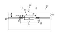
- FIGS. 3-5are simplified cross-sectional views of examples of the electronic device 200 taken along line A-A in FIG. 2A .
- a first cover glass 300is disposed over the surface 216 of the electronic device 200 .
- the first cover glass 300has a thickness T 1 .
- An opening 304can be formed through the first cover glass 300 around the light-receiving region 306 of a camera 308 .
- the light-receiving region of the camerais associated with one or more image sensors 310 included in the camera.
- a second cover glass 312can be disposed in the opening 304 .
- the second cover glass 312has a thickness T 2 , and T 2 is less than T 1 .
- the thinner second cover glass 312can be made of any suitable material, including, but not limited to, sapphire, glass, acrylic, plastic, and various combination thereof.
- the second cover glass 312is a first lens in optical communication with the camera 308 .
- a second lens 314can be positioned between the second cover glass 312 and the camera 308 .
- the second lens 314can be formed with one or more lenses that each have any given shape and dimensions. Example shapes include, but are not limited to, circular, lozenge, or triangular.
- the second cover glass 312can attach to one or more brackets 316 .
- the bracket or brackets 316can have any given configuration and size, and can be positioned at any location. Additionally or alternatively, the second cover glass 312 can be attached to a frame (not shown) that attaches to the first cover glass 300 . Any suitable attachment mechanism can be used to attach the second cover glass 312 to the bracket(s) 316 and/or to the frame. By way of example only, an adhesive material and/or a fastener can be used to attach the second cover glass 312 to the bracket(s) 316 and/or to the frame.
- a higher quality cameracan be included in the electronic device 200 when the additional space 318 is present.
- a higher quality cameracan include a larger sensor, higher quality lenses, an autofocus feature, and/or a flash module.
- a front-facing camerae.g., camera 202
- a rear-facing camerae.g., camera 204
- FIG. 4is similar to the embodiment shown in FIG. 3 except that the opening 304 in the first cover glass 300 is larger.
- the second cover glass 312is disposed over the light-receiving region 306 and at least part of one or more non-light receiving regions 400 of the camera.
- the cross-sectional view in FIG. 5includes a monolithic cover glass 500 .
- the cover glass 500has a region 502 that is thinner than other areas 504 of the cover glass 500 .
- Region 502can have any given shape and dimensions.
- the thinner region 502can be disposed over the light-receiving region 306 of the camera 308 .
- the thinner region 502can have a size and/or shape that positions the thinner region over some or all of the non-light receiving regions of the camera 308 .
- the cover glass 500can be made of any suitable material such as sapphire, glass, plastic, and various combinations of materials.
- the thinner region 502can be shaped such that the thinner region acts as a lens.
- the lenscan be in optical communication with the light-receiving region 306 of the camera 308 .
- the second lens 314can be positioned between the cover glass 500 and the camera 308 .
- the thinner region 502provides additional space 506 for the camera 308 and/or the optional second lens 314 .
- FIG. 6is a flowchart of a method for producing the cover glass arrangement shown in FIG. 5 .
- a thinner regioncan be formed in a monolithic cover glass, as shown in block 600 .
- the thinner regioncan be formed with any known cutting, shaping, or trimming process.
- the location of the thinner regioncan correspond to a light-receiving region of a camera, or to the light-receiving region and at least a part of one or more non-light receiving regions of the camera.
- the cover glass arrangementcan be attached to the electronic device.
- any suitable attachment mechanismcan be used to connect the cover glass arrangement to the electronic device.
- an adhesive material and/or a fastenercan attach the cover glass arrangement to the electronic device.
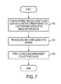
- FIG. 7is a flowchart of a method for producing the cover glass arrangement shown in FIGS. 3-4 .
- an openingcan be formed through a first cover glass (block 700 ).
- the openingcan be formed using any suitable process.
- the openingcan be formed through the first cover glass by etching or grinding the first cover glass.
- the location of the openingcan correspond to the light-receiving region of a camera, or to the light-receiving region and at least a part of one or more non-light receiving regions of the camera.
- a cover glass arrangementcan include multiple openings with a second cover glass positioned in each opening, or multiple thinner regions formed in a cover glass. Additionally or alternatively, a cover glass arrangement can include both one or more openings with a second cover glass positioned in each opening and one or more thinner regions.
Landscapes
- Engineering & Computer Science (AREA)
- Computer Hardware Design (AREA)
- Theoretical Computer Science (AREA)
- General Engineering & Computer Science (AREA)
- Human Computer Interaction (AREA)
- Physics & Mathematics (AREA)
- General Physics & Mathematics (AREA)
- Multimedia (AREA)
- Signal Processing (AREA)
- Studio Devices (AREA)
- Camera Bodies And Camera Details Or Accessories (AREA)
Abstract
Description
The present invention relates generally to electronic devices, and more specifically, to cameras in electronic devices. Still more particularly, the present invention relates to a cover glass arrangement for a camera included in an electronic device.
Many electronic devices, such as smart telephones, laptop computers, and tablet computing devices include a camera to capture images and video.FIG. 1 is a cross-sectional view of a prior art electronic device. Theelectronic device 100 includes acamera 102 positioned adjacent to asurface 104 of the electronic device. The surface can be the front or the back surface of theelectronic device 100. In some devices, acover glass 106 is disposed over thesurface 104 when thecamera 102 is positioned adjacent to the front surface of theelectronic device 100. Thecover glass 106 can provide various functions or features for the electronic device. For example, in some embodiments, thecover glass 106 can be a touchscreen and provide an aperture for a speaker and microphone.
In some embodiments, thecover glass 106 can constrain the amount of space that is available to thecamera 102. As a result, the functionality of the camera can be limited. For example, a flash module may not be included in the electronic device, or the camera may not include an autofocus feature or a high quality lens.
In one aspect, an electronic device can include a camera and a first cover glass disposed over the camera. An opening can be formed through the first cover glass over a light-receiving region of the camera. A second cover glass can be positioned in the opening over the light-receiving region of the camera. A thickness of the second cover glass is less than a thickness of the first cover glass. In some embodiments, the second cover glass is a lens for the camera.
In another aspect, an electronic device can include a camera and a monolithic cover glass disposed over the camera. The cover glass includes a thinner region that is positioned over a light-receiving region of the camera. The thinner region can act as a lens for the camera.
In yet another aspect, a method for producing an electronic device can include providing a first cover glass having an opening formed through the first cover glass, and providing a second cover glass in the opening. A location of the opening corresponds to a light-receiving region of a camera. A thickness of the second cover glass is less than a thickness of the first cover glass.
In another aspect, a method for providing an electronic device can include providing a camera in the electronic device, and providing a monolithic cover glass over the camera. The cover glass includes a thinner region that is positioned over a light-receiving region of the camera.
Embodiments of the invention are better understood with reference to the following drawings. The elements of the drawings are not necessarily to scale relative to each other. Identical reference numerals have been used, where possible, to designate identical features that are common to the figures.
Embodiments described herein provide a cover glass arrangement for an electronic device that includes one or more cameras. The cover glass arrangement can include a first cover glass and a second cover glass, where the second cover glass is positioned in an opening formed through the first cover glass. In one embodiment, the second cover glass can be disposed over a light-receiving region of a camera. In another embodiment, the second cover glass is positioned over the light-receiving region and at least part of one or more non-light receiving regions of the camera.
The second cover glass can have a thickness that is less than the thickness of the first cover glass. The thinner second cover glass can provide additional space for the camera and/or for an optional lens. In some embodiments, a higher quality camera can be included in an electronic device when the additional space is provided by the thinner second cover glass. For example, a higher quality camera can include a larger sensor, higher quality lenses, an autofocus feature, and/or a flash module.
In another embodiment, the cover glass arrangement can include a monolithic cover glass that includes a thinner region formed in the cover glass. The thinner region can be disposed over the light-receiving region, or over the light-receiving region and at least part of one or more non-light receiving regions of the camera. Like the second cover glass, the thinner region can provide additional space for the camera and/or for an optional lens.
Referring now toFIGS. 2A-2B , there are shown front and rear perspective views of one example of an electronic device that can include one or more cameras. Theelectronic device 200 includes afirst camera 202, asecond camera 204, anenclosure 206, adisplay 210, an input/output (I/O)member 208, and anoptional flash 212 or light source for the camera or cameras. Theelectronic device 200 can also include one or more internal components (not shown) typical of a computing or electronic device, such as, for example, one or more processors, memory components, network interfaces, and so on.
In the illustrated embodiment, acover glass 214 is disposed over thefront surface 216 of theelectronic device 200. Thecover glass 214 can be made of any suitable material, including, but not limited to, glass, plastic, acrylic, sapphire, and various combinations thereof. One or more portions of thecover glass 214 can be an input region for a touch sensing device and/or a force sensing device. Thecover glass 214 can include one or more apertures, such as an aperture for a speaker and/or amicrophone 218 and the I/O member 208. In the illustrated embodiment, thecover glass 214 is positioned over the entirefront surface 216 of the electronic device. Thus, thecover glass 214 is disposed over the display, thefirst camera 202, and theenclosure 206. In other embodiments, thecover glass 214 can be disposed over one or more portions of a surface or surfaces of the electronic device.
As shown inFIGS. 2A-2B , theelectronic device 200 is implemented as a smart telephone. Other embodiments, however, are not limited to this type of electronic device. Other types of computing or electronic devices can include one or more cameras, examples of which include a netbook or laptop computer, a tablet computing device, a wearable computing or display device such as a watch or glasses, a digital camera, a printer, a scanner, a video recorder, and a copier.
Theenclosure 206 can form an outer surface or partial outer surface and protective case for the internal components of theelectronic device 200, and may at least partially surround thedisplay 210. Theenclosure 206 can be formed of one or more components operably connected together, such as a front piece and a back piece. Alternatively, theenclosure 206 can be formed of a single piece operably connected to thedisplay 210.
The I/O member 208 can be implemented with any type of input or output member. By way of example only, the I/O member 208 can be a switch, a button, a capacitive sensor, or other input mechanism. The I/O member 208 allows a user to interact with theelectronic device 200. For example, the I/O member 208 may be a button or switch to alter the volume, return to a home screen, and the like. The electronic device can include one or more input members or output members, and each member can have a single I/O function or multiple I/O functions.
Thedisplay 210 can be operably or communicatively connected to theelectronic device 200. Thedisplay 210 can be implemented with any type of suitable display, such as a retina display or an active matrix color liquid crystal display. Thedisplay 210 can provide a visual output for theelectronic device 200 or function to receive user inputs to the electronic device. For example, thedisplay 210 can be a multi-touch capacitive sensing touchscreen that can detect one or more user touch and/or force inputs.
Asecond cover glass 312 can be disposed in theopening 304. Thesecond cover glass 312 has a thickness T2, and T2 is less than T1. The thinnersecond cover glass 312 can be made of any suitable material, including, but not limited to, sapphire, glass, acrylic, plastic, and various combination thereof. In some embodiments, thesecond cover glass 312 is a first lens in optical communication with thecamera 308. Additionally or alternatively, asecond lens 314 can be positioned between thesecond cover glass 312 and thecamera 308. Thesecond lens 314 can be formed with one or more lenses that each have any given shape and dimensions. Example shapes include, but are not limited to, circular, lozenge, or triangular.
Thesecond cover glass 312 can attach to one ormore brackets 316. The bracket orbrackets 316 can have any given configuration and size, and can be positioned at any location. Additionally or alternatively, thesecond cover glass 312 can be attached to a frame (not shown) that attaches to thefirst cover glass 300. Any suitable attachment mechanism can be used to attach thesecond cover glass 312 to the bracket(s)316 and/or to the frame. By way of example only, an adhesive material and/or a fastener can be used to attach thesecond cover glass 312 to the bracket(s)316 and/or to the frame.
Theopening 304 and the thinnersecond cover glass 312 providesadditional space 318 for thecamera 308 and/or the optionalsecond lens 314. In some embodiments, a higher quality camera can be included in theelectronic device 200 when theadditional space 318 is present. For example, a higher quality camera can include a larger sensor, higher quality lenses, an autofocus feature, and/or a flash module. In some embodiments, a front-facing camera (e.g., camera202) can be of equal or near-equal quality as a rear-facing camera (e.g., camera204).
The embodiment shown inFIG. 4 is similar to the embodiment shown inFIG. 3 except that theopening 304 in thefirst cover glass 300 is larger. Thesecond cover glass 312 is disposed over the light-receivingregion 306 and at least part of one or more non-light receivingregions 400 of the camera.
The cross-sectional view inFIG. 5 includes amonolithic cover glass 500. Thecover glass 500 has aregion 502 that is thinner thanother areas 504 of thecover glass 500.Region 502 can have any given shape and dimensions. Thethinner region 502 can be disposed over the light-receivingregion 306 of thecamera 308. Additionally, thethinner region 502 can have a size and/or shape that positions the thinner region over some or all of the non-light receiving regions of thecamera 308. Like the first andsecond cover glasses cover glass 500 can be made of any suitable material such as sapphire, glass, plastic, and various combinations of materials.
In some embodiments, thethinner region 502 can be shaped such that the thinner region acts as a lens. The lens can be in optical communication with the light-receivingregion 306 of thecamera 308. Additionally or alternatively, thesecond lens 314 can be positioned between thecover glass 500 and thecamera 308. Thethinner region 502 providesadditional space 506 for thecamera 308 and/or the optionalsecond lens 314.
Next, as shown inblock 602, the cover glass arrangement can be attached to the electronic device. As described earlier, any suitable attachment mechanism can be used to connect the cover glass arrangement to the electronic device. For example, an adhesive material and/or a fastener can attach the cover glass arrangement to the electronic device.
A second cover glass can then be positioned in the opening, as shown inblock 702. The thickness of the second cover glass is less than the thickness of the first cover glass. The cover glass arrangement can then be attached to the electronic device. In one embodiment, the first cover glass is affixed to a frame in the electronic device. The second cover glass can be attached to the first cover glass, to one or more brackets, and/or to the frame attached to the first cover glass.
Various embodiments have been described in detail with particular reference to certain features thereof, but it will be understood that variations and modifications can be effected within the spirit and scope of the disclosure. And even though specific embodiments have been described herein, it should be noted that the application is not limited to these embodiments. In particular, any features described with respect to one embodiment may also be used in other embodiments, where compatible. Likewise, the features of the different embodiments may be exchanged, where compatible. For example, although the embodiments shown inFIGS. 3-5 depict the front-facing first camera202 (FIG. 2 ), those skilled in the art will recognize that the invention can be used with the rear-facing second camera404. Additionally, a cover glass arrangement can include multiple openings with a second cover glass positioned in each opening, or multiple thinner regions formed in a cover glass. Additionally or alternatively, a cover glass arrangement can include both one or more openings with a second cover glass positioned in each opening and one or more thinner regions.
Claims (17)
1. An electronic device, comprising:
a camera;
a first cover glass disposed over the camera;
an opening formed through the first cover glass over a light-receiving region of the camera; and
a second cover glass positioned in the opening over the light-receiving region of the camera, wherein a thickness of the second cover glass is less than a thickness of the first cover glass.
2. The electronic device as inclaim 1 , wherein the second cover glass comprises sapphire.
3. The electronic device as inclaim 1 , wherein the second cover glass comprises a lens in optical communication with the light-receiving region of the camera.
4. The electronic device as inclaim 1 , wherein the electronic device comprises a smart telephone.
5. An electronic device, comprising:
a camera; and
a monolithic cover glass disposed over the camera, wherein:
the cover glass includes a first region that forms an outer surface of the electronic device, and a second region over a light-receiving region of the camera; and
the second region is thinner than the first region.
6. The electronic device as inclaim 5 , wherein the cover glass comprises sapphire.
7. The electronic device as inclaim 5 , wherein the second region comprises a lens in optical communication with the light-receiving region of the camera.
8. The electronic device as inclaim 5 , wherein the electronic device comprises a smart telephone.
9. A method for producing an electronic device, comprising:
providing a first cover glass having an opening formed through the first cover glass, wherein a location of the opening corresponds to a light-receiving region of a camera; and
disposing a second cover glass in the opening, wherein a thickness of the second cover glass is less than a thickness of the first cover glass.
10. The method as inclaim 9 , further comprising disposing a camera in the electronic device.
11. The method as inclaim 9 , further comprising attaching the first and second cover glasses to the electronic device.
12. The method as inclaim 9 , wherein disposing the second cover glass in the opening comprises disposing a sapphire cover glass in the opening.
13. The method as inclaim 9 , wherein disposing the second cover glass in the opening comprises disposing a lens in the opening such that the lens can be in optical communication with the light-receiving region of the camera.
14. A method for producing an electronic device, the method comprising:
disposing a camera in the electronic device; and
disposing a monolithic cover glass over the camera, wherein:
the cover glass includes a first region that forms an outer surface of the electronic device, and a second region over a light-receiving region of the camera; and
the second region is thinner than the first region.
15. The method as inclaim 14 , wherein disposing the monolithic cover glass over the camera comprises disposing a monolithic cover glass over a surface of the electronic device.
16. The method as inclaim 14 , wherein disposing the monolithic cover glass over the camera comprises disposing a monolithic sapphire cover glass over the camera.
17. The method as inclaim 14 , wherein the second region over the light-receiving region of the camera comprises a lens in optical communication with the light-receiving region of the camera.
Priority Applications (5)
| Application Number | Priority Date | Filing Date | Title |
|---|---|---|---|
| US14/103,661US9154678B2 (en) | 2013-12-11 | 2013-12-11 | Cover glass arrangement for an electronic device |
| CN201410699553.0ACN104717409A (en) | 2013-12-11 | 2014-11-27 | Cover glass arrangement for an electronic device |
| US14/875,402US9716815B2 (en) | 2013-12-11 | 2015-10-05 | Cover glass for covering a camera of an electronic device |
| US15/628,823US10324496B2 (en) | 2013-12-11 | 2017-06-21 | Cover glass arrangement for an electronic device |
| US16/138,929US10386889B2 (en) | 2013-12-11 | 2018-09-21 | Cover glass for an electronic device |
Applications Claiming Priority (1)
| Application Number | Priority Date | Filing Date | Title |
|---|---|---|---|
| US14/103,661US9154678B2 (en) | 2013-12-11 | 2013-12-11 | Cover glass arrangement for an electronic device |
Related Child Applications (1)
| Application Number | Title | Priority Date | Filing Date |
|---|---|---|---|
| US14/875,402ContinuationUS9716815B2 (en) | 2013-12-11 | 2015-10-05 | Cover glass for covering a camera of an electronic device |
Publications (2)
| Publication Number | Publication Date |
|---|---|
| US20150163382A1 US20150163382A1 (en) | 2015-06-11 |
| US9154678B2true US9154678B2 (en) | 2015-10-06 |
Family
ID=53272391
Family Applications (4)
| Application Number | Title | Priority Date | Filing Date |
|---|---|---|---|
| US14/103,661ActiveUS9154678B2 (en) | 2013-12-11 | 2013-12-11 | Cover glass arrangement for an electronic device |
| US14/875,402ActiveUS9716815B2 (en) | 2013-12-11 | 2015-10-05 | Cover glass for covering a camera of an electronic device |
| US15/628,823ActiveUS10324496B2 (en) | 2013-12-11 | 2017-06-21 | Cover glass arrangement for an electronic device |
| US16/138,929ActiveUS10386889B2 (en) | 2013-12-11 | 2018-09-21 | Cover glass for an electronic device |
Family Applications After (3)
| Application Number | Title | Priority Date | Filing Date |
|---|---|---|---|
| US14/875,402ActiveUS9716815B2 (en) | 2013-12-11 | 2015-10-05 | Cover glass for covering a camera of an electronic device |
| US15/628,823ActiveUS10324496B2 (en) | 2013-12-11 | 2017-06-21 | Cover glass arrangement for an electronic device |
| US16/138,929ActiveUS10386889B2 (en) | 2013-12-11 | 2018-09-21 | Cover glass for an electronic device |
Country Status (2)
| Country | Link |
|---|---|
| US (4) | US9154678B2 (en) |
| CN (1) | CN104717409A (en) |
Cited By (27)
| Publication number | Priority date | Publication date | Assignee | Title |
|---|---|---|---|---|
| US10015297B2 (en) | 2015-09-08 | 2018-07-03 | Apple Inc. | Display cover retention features for a portable electronic device |
| US10052848B2 (en) | 2012-03-06 | 2018-08-21 | Apple Inc. | Sapphire laminates |
| US10324496B2 (en) | 2013-12-11 | 2019-06-18 | Apple Inc. | Cover glass arrangement for an electronic device |
| US10406634B2 (en) | 2015-07-01 | 2019-09-10 | Apple Inc. | Enhancing strength in laser cutting of ceramic components |
| US20190349503A1 (en)* | 2017-06-12 | 2019-11-14 | Chengdu Boe Optoelectronics Technology Co., Ltd. | Camera module and manufacturing method thereof, display device and manufacturing method thereof |
| CN110691152A (en)* | 2018-07-06 | 2020-01-14 | 苹果公司 | Cover sheet and combined lens for camera of electronic device |
| US10827635B1 (en) | 2019-06-05 | 2020-11-03 | Apple Inc. | Electronic device enclosure having a textured glass component |
| US11109500B2 (en)* | 2019-06-05 | 2021-08-31 | Apple Inc. | Textured glass component for an electronic device enclosure |
| US11112827B2 (en) | 2018-07-20 | 2021-09-07 | Apple Inc. | Electronic device with glass housing member |
| US11192823B2 (en) | 2019-06-05 | 2021-12-07 | Apple Inc. | Electronic devices including laser-textured glass cover members |
| US11199929B2 (en) | 2019-03-21 | 2021-12-14 | Apple Inc. | Antireflective treatment for textured enclosure components |
| US20220071039A1 (en)* | 2020-09-02 | 2022-03-03 | Apple Inc. | Electronic devices with textured glass and glass ceramic components |
| US11372137B2 (en) | 2019-05-29 | 2022-06-28 | Apple Inc. | Textured cover assemblies for display applications |
| US11402669B2 (en) | 2018-04-27 | 2022-08-02 | Apple Inc. | Housing surface with tactile friction features |
| US11419231B1 (en) | 2016-09-22 | 2022-08-16 | Apple Inc. | Forming glass covers for electronic devices |
| US11420900B2 (en) | 2018-09-26 | 2022-08-23 | Apple Inc. | Localized control of bulk material properties |
| US11460892B2 (en)* | 2020-03-28 | 2022-10-04 | Apple Inc. | Glass cover member for an electronic device enclosure |
| US11535551B2 (en) | 2016-09-23 | 2022-12-27 | Apple Inc. | Thermoformed cover glass for an electronic device |
| US20230014168A1 (en)* | 2020-03-28 | 2023-01-19 | Apple Inc. | Glass cover member for an electronic device enclosure |
| US11565506B2 (en) | 2016-09-23 | 2023-01-31 | Apple Inc. | Thermoformed cover glass for an electronic device |
| US11666273B2 (en) | 2020-05-20 | 2023-06-06 | Apple Inc. | Electronic device enclosure including a glass ceramic region |
| US11680010B2 (en) | 2019-07-09 | 2023-06-20 | Apple Inc. | Evaluation of transparent components for electronic devices |
| US11691912B2 (en) | 2018-12-18 | 2023-07-04 | Apple Inc. | Chemically strengthened and textured glass housing member |
| US11850822B2 (en) | 2016-09-23 | 2023-12-26 | Apple Inc. | Electronic device having a component with crack hindering internal stress regions |
| US11945048B2 (en) | 2020-12-23 | 2024-04-02 | Apple Inc. | Laser-based cutting of transparent components for an electronic device |
| US12065372B2 (en) | 2020-12-17 | 2024-08-20 | Apple Inc. | Fluid forming a glass component for a portable electronic device |
| US12195379B2 (en) | 2020-12-17 | 2025-01-14 | Apple Inc. | Forming and bonding of glass components for portable electronic devices |
Families Citing this family (13)
| Publication number | Priority date | Publication date | Assignee | Title |
|---|---|---|---|---|
| JP6543848B2 (en)* | 2017-03-29 | 2019-07-17 | 本田技研工業株式会社 | Voice processing apparatus, voice processing method and program |
| US11445094B2 (en) | 2017-08-07 | 2022-09-13 | Apple Inc. | Electronic device having a vision system assembly held by a self-aligning bracket assembly |
| US10996713B2 (en) | 2017-08-07 | 2021-05-04 | Apple Inc. | Portable electronic device |
| US10268234B2 (en)* | 2017-08-07 | 2019-04-23 | Apple Inc. | Bracket assembly for a multi-component vision system in an electronic device |
| US10866615B1 (en) | 2017-08-16 | 2020-12-15 | Apple Inc. | Electronic devices with two-stage displays |
| US10425561B2 (en) | 2017-09-08 | 2019-09-24 | Apple Inc. | Portable electronic device |
| US10690986B2 (en) | 2017-09-13 | 2020-06-23 | Apple Inc. | Electronic devices having electrically adjustable optical shutters |
| US10990124B2 (en)* | 2018-01-29 | 2021-04-27 | Madelyn Murphy | Mobile computing device with camera lens identifier |
| CN109753113B (en)* | 2018-05-31 | 2020-10-30 | 北京字节跳动网络技术有限公司 | Electronic equipment and light sensation device thereof |
| CN111508993B (en)* | 2019-01-31 | 2022-10-04 | 武汉华星光电半导体显示技术有限公司 | An OLED display panel and its manufacturing method |
| KR102829759B1 (en)* | 2020-01-31 | 2025-07-04 | 삼성전자 주식회사 | Electronic device including display |
| US11435781B1 (en)* | 2021-03-23 | 2022-09-06 | Lenovo (Singapore) Pte. Ltd. | Computing device |
| EP4277244A4 (en)* | 2021-06-04 | 2024-09-04 | Samsung Electronics Co., Ltd. | Electronic device comprising window for optical module |
Citations (207)
| Publication number | Priority date | Publication date | Assignee | Title |
|---|---|---|---|---|
| US2248955A (en) | 1939-01-13 | 1941-07-15 | Frank L Capps | Sapphire grinding means |
| US2854794A (en) | 1955-09-22 | 1958-10-07 | Daystrom Inc | Treating sapphire objects of irregular shapes |
| GB1135886A (en) | 1966-09-26 | 1968-12-04 | Ibm | Method and apparatus for vibratory cutting |
| US3753775A (en) | 1971-03-01 | 1973-08-21 | Rca Corp | Chemical polishing of sapphire |
| US3964942A (en) | 1970-10-16 | 1976-06-22 | International Business Machines Corporation | Chemical polishing of single crystal dielectrics |
| US4008111A (en) | 1975-12-31 | 1977-02-15 | International Business Machines Corporation | AlN masking for selective etching of sapphire |
| US4054895A (en) | 1976-12-27 | 1977-10-18 | Rca Corporation | Silicon-on-sapphire mesa transistor having doped edges |
| US4070211A (en) | 1977-04-04 | 1978-01-24 | The United States Of America As Represented By The Secretary Of The Navy | Technique for threshold control over edges of devices on silicon-on-sapphire |
| US4085302A (en) | 1976-11-22 | 1978-04-18 | Control Data Corporation | Membrane-type touch panel |
| JPS5432062Y2 (en) | 1976-10-21 | 1979-10-05 | ||
| US4339300A (en) | 1977-07-25 | 1982-07-13 | Noble Lowell A | Process for smoothing surfaces of crystalline materials |
| US4393578A (en) | 1980-01-02 | 1983-07-19 | General Electric Company | Method of making silicon-on-sapphire FET |
| US4662124A (en) | 1980-11-17 | 1987-05-05 | Tokyo Shibaura Denki Kabushiki Kaisha | Method of grinding a sapphire wafer |
| US4732867A (en) | 1986-11-03 | 1988-03-22 | General Electric Company | Method of forming alignment marks in sapphire |
| US4735917A (en) | 1986-04-28 | 1988-04-05 | General Electric Company | Silicon-on-sapphire integrated circuits |
| US4775641A (en) | 1986-09-25 | 1988-10-04 | General Electric Company | Method of making silicon-on-sapphire semiconductor devices |
| US4811004A (en) | 1987-05-11 | 1989-03-07 | Dale Electronics, Inc. | Touch panel system and method for using same |
| EP0305626A1 (en) | 1987-09-03 | 1989-03-08 | W. Blösch AG | Wrist watch |
| US4826300A (en) | 1987-07-30 | 1989-05-02 | Hughes Aircraft Company | Silicon-on-sapphire liquid crystal light valve and method |
| US4849299A (en) | 1986-06-19 | 1989-07-18 | Montres Rado S.A. | Watch cover glass and process for the manufacture of such a glass |
| US4908074A (en) | 1986-02-28 | 1990-03-13 | Kyocera Corporation | Gallium arsenide on sapphire heterostructure |
| US4946546A (en) | 1987-12-23 | 1990-08-07 | U.S. Philips Corporation | Method of metallizing a substrate of silica, quartz, glass or sapphire |
| JPH03115200U (en) | 1990-02-16 | 1991-11-27 | ||
| US5151389A (en) | 1990-09-10 | 1992-09-29 | Rockwell International Corporation | Method for dicing semiconductor substrates using an excimer laser beam |
| US5154023A (en) | 1991-06-11 | 1992-10-13 | Spire Corporation | Polishing process for refractory materials |
| JPH06242260A (en) | 1993-02-12 | 1994-09-02 | Kyocera Corp | Cover glass for watches |
| JPH06337292A (en) | 1993-05-28 | 1994-12-06 | Citizen Watch Co Ltd | Cover glass for watch and production thereof |
| US5377669A (en) | 1992-04-06 | 1995-01-03 | Henke-Sass, Wolf Gmbh | Sapphire protective covering for medical endoscope |
| US5413360A (en) | 1992-12-01 | 1995-05-09 | Kyocera Corporation | Electrostatic chuck |
| JPH07145000A (en) | 1993-11-18 | 1995-06-06 | Yamatake Honeywell Co Ltd | Sapphire wafer bonding method |
| US5427051A (en) | 1993-05-21 | 1995-06-27 | General Electric Company | Solid state formation of sapphire using a localized energy source |
| US5441591A (en) | 1993-06-07 | 1995-08-15 | The United States Of America As Represented By The Secretary Of The Navy | Silicon to sapphire bond |
| US5451553A (en) | 1993-09-24 | 1995-09-19 | General Electric Company | Solid state thermal conversion of polycrystalline alumina to sapphire |
| US5543630A (en) | 1995-01-31 | 1996-08-06 | The United States Of America As Represented By The Secretary Of The Air Force | High Tc superconducting devices on bi-crystal substrates |
| US5549746A (en) | 1993-09-24 | 1996-08-27 | General Electric Company | Solid state thermal conversion of polycrystalline alumina to sapphire using a seed crystal |
| JPH098690A (en) | 1995-06-23 | 1997-01-10 | Kyocera Corp | Portable communication device |
| US5627109A (en) | 1994-09-16 | 1997-05-06 | Sassa; Michinari | Method of manufacturing a semiconductor device that uses a sapphire substrate |
| US5661313A (en) | 1993-09-09 | 1997-08-26 | The United States Of America As Represented By The Secretary Of The Navy | Electroluminescent device in silicon on sapphire |
| US5697998A (en) | 1996-03-05 | 1997-12-16 | The Aerospace Corporation | Sapphire window laser edge annealing |
| US5702654A (en) | 1996-08-30 | 1997-12-30 | Hughes Electronics | Method of making thermal shock resistant sapphire for IR windows and domes |
| US5804522A (en) | 1994-09-10 | 1998-09-08 | Uegami; Kenjiro | Hardened alumina material |
| JPH10239520A (en) | 1997-02-28 | 1998-09-11 | Kyocera Corp | Polarizing beam splitter |
| JPH10269543A (en) | 1997-03-27 | 1998-10-09 | Kyocera Corp | Substrate for magnetic disk |
| JPH10275955A (en) | 1997-03-31 | 1998-10-13 | Kyocera Corp | Semiconductor laser diode and method of manufacturing the same |
| WO1998056575A1 (en) | 1997-06-11 | 1998-12-17 | Saphikon Inc. | Eutectic bonding of single crystal components |
| JPH10335259A (en) | 1997-05-29 | 1998-12-18 | Kyocera Corp | Semiconductor device and manufacturing method thereof |
| US5852622A (en) | 1988-08-30 | 1998-12-22 | Onyx Optics, Inc. | Solid state lasers with composite crystal or glass components |
| US5877094A (en) | 1994-04-07 | 1999-03-02 | International Business Machines Corporation | Method for fabricating a silicon-on-sapphire wafer |
| JPH11135889A (en) | 1997-10-30 | 1999-05-21 | Kyocera Corp | Crystal growth substrate and light emitting device using the same |
| US6025060A (en) | 1988-08-30 | 2000-02-15 | Onyx Optics, Inc. | Method and apparatus for composite gemstones |
| US6028762A (en) | 1996-01-31 | 2000-02-22 | Kyocera Corporation | Electrostatic chuck |
| US6028711A (en)* | 1997-07-31 | 2000-02-22 | Asahi Kogaku Kogyo Kabushiki Kaisha | Reading lens |
| US6030849A (en) | 1997-06-16 | 2000-02-29 | Matsushita Electric Industrial Co. Ltd. | Methods of manufacturing semiconductor, semiconductor device and semiconductor substrate |
| US6038079A (en) | 1997-10-09 | 2000-03-14 | Imagyn Medical Technologies, Inc. | Sapphire objective system |
| JP2000183203A (en) | 1998-12-18 | 2000-06-30 | Kyocera Corp | Optical semiconductor element storage package |
| JP2000196149A (en) | 1998-12-25 | 2000-07-14 | Kyocera Corp | Semiconductor light emitting device and method of manufacturing the same |
| US6123026A (en) | 1996-11-12 | 2000-09-26 | Raytheon Company | System and method for increasing the durability of a sapphire window in high stress environments |
| JP2001134927A (en) | 1999-11-09 | 2001-05-18 | Kyocera Corp | Magnetic recording media |
| JP3177335B2 (en) | 1992-03-12 | 2001-06-18 | 三井化学株式会社 | Crosslinked polyolefin molded article and method for producing the same |
| JP2001176993A (en) | 1999-12-21 | 2001-06-29 | Kyocera Corp | Package for housing semiconductor element and method of manufacturing the same |
| US6265089B1 (en) | 1999-07-15 | 2001-07-24 | The United States Of America As Represented By The Secretary Of The Navy | Electronic devices grown on off-axis sapphire substrate |
| JP2001237335A (en) | 2000-02-24 | 2001-08-31 | Kyocera Corp | Package for housing semiconductor element and method of manufacturing the same |
| JP2001298170A (en) | 2000-04-13 | 2001-10-26 | Kyocera Corp | Sapphire substrate and device substrate using the same |
| JP2002015977A (en) | 2000-06-29 | 2002-01-18 | Kyocera Corp | Board holder |
| JP3250659B2 (en) | 1997-03-24 | 2002-01-28 | タイコエレクトロニクスアンプ株式会社 | Card connector |
| US20020017653A1 (en) | 1999-08-26 | 2002-02-14 | Feng-Ju Chuang | Blue light emitting diode with sapphire substrate and method for making the same |
| JP2002109854A (en) | 2000-09-29 | 2002-04-12 | Kyocera Corp | Tape cleaner |
| US6379985B1 (en) | 2001-08-01 | 2002-04-30 | Xerox Corporation | Methods for cleaving facets in III-V nitrides grown on c-face sapphire substrates |
| US6406769B1 (en) | 1998-04-02 | 2002-06-18 | Comadur S.A. | Watch crystal including a lens and manufacturing method for such a lens |
| JP2002184845A (en) | 2000-12-15 | 2002-06-28 | Kyocera Corp | Wafer support substrate |
| JP2002201096A (en) | 2000-10-31 | 2002-07-16 | Kyocera Corp | Single crystal sapphire substrate and heat treatment method thereof |
| US6424017B2 (en) | 1999-01-12 | 2002-07-23 | Kulite Semiconductor Products, Inc. | Silicon-on-sapphire transducer |
| JP2002255694A (en) | 2001-02-26 | 2002-09-11 | Kyocera Corp | Semiconductor substrate and manufacturing method thereof |
| JP2002289529A (en) | 2001-03-23 | 2002-10-04 | Yasuhiko Arakawa | Substrate for semiconductor layer growth |
| JP2002293692A (en) | 2001-03-29 | 2002-10-09 | Kyocera Corp | Single crystal sapphire substrate and heat treatment method thereof |
| US20020167068A1 (en) | 2001-05-09 | 2002-11-14 | International Business Machines Corporation | Silicon on sapphire structure (devices) with buffer layer |
| US20020168837A1 (en) | 2001-05-09 | 2002-11-14 | Ibm | Method of fabricating silicon devices on sapphire with wafer bonding |
| US6483237B2 (en) | 1999-02-01 | 2002-11-19 | Gem Lighting Llc | High intensity discharge lamp with single crystal sapphire envelope |
| US6489221B2 (en) | 1999-11-17 | 2002-12-03 | North Carolina State University | High temperature pendeoepitaxial methods of fabricating gallium nitride semiconductor layers on sapphire substrates |
| JP2003015156A (en) | 2001-06-28 | 2003-01-15 | Kyocera Corp | Liquid crystal display device and liquid crystal projector device using the same |
| JP2003069176A (en) | 2001-08-28 | 2003-03-07 | Kyocera Corp | Sapphire substrate, manufacturing method thereof, electronic device using the same, and manufacturing method thereof |
| US6547722B1 (en)* | 1999-07-13 | 2003-04-15 | Olympus Optical Co., Ltd. | Endoscope having resistance to high-temperature and high-pressure steam |
| WO2002054718A3 (en) | 2000-12-29 | 2003-04-17 | Vertu Ltd | A casing |
| JP2003133802A (en) | 2001-10-29 | 2003-05-09 | Kyocera Corp | High frequency window for microwave tube |
| JP2003137690A (en) | 2001-10-24 | 2003-05-14 | Kyocera Corp | Star blue sapphire and manufacturing method thereof |
| US6586819B2 (en) | 2000-08-14 | 2003-07-01 | Nippon Telegraph And Telephone Corporation | Sapphire substrate, semiconductor device, electronic component, and crystal growing method |
| JP2003245847A (en) | 2002-02-22 | 2003-09-02 | Kyocera Corp | Sapphire wafer processing method and electronic device manufacturing method |
| JP2003277194A (en) | 2002-03-22 | 2003-10-02 | Kyocera Corp | Single crystal sapphire substrate and method of manufacturing the same |
| JP2003282551A (en) | 2002-03-26 | 2003-10-03 | Kyocera Corp | Single crystal sapphire substrate and manufacturing method thereof |
| US6642989B2 (en) | 1998-12-28 | 2003-11-04 | Kyocera Corporation | Liquid crystal display device having particular constructed sapphire substrate |
| JP2003332234A (en) | 2002-05-15 | 2003-11-21 | Kyocera Corp | Sapphire substrate having nitrided layer and method of manufacturing the same |
| JP2004111848A (en) | 2002-09-20 | 2004-04-08 | Kyocera Corp | Sapphire substrate, epitaxial substrate using the same, and method of manufacturing the same |
| US20040105026A1 (en)* | 1998-12-24 | 2004-06-03 | Campbell Scott Patrick | Contoured surface cover plate for image sensor array |
| JP2004168622A (en) | 2002-11-22 | 2004-06-17 | Kyocera Corp | Single crystal sapphire substrate and method of manufacturing the same |
| WO2004059731A1 (en) | 2002-12-20 | 2004-07-15 | International Business Machines Corporation | Silicon on sapphire structure (devices) with buffer layer |
| US6775073B2 (en) | 2000-10-19 | 2004-08-10 | Olympus Corporation | Real image type zoom finder |
| JP2004288934A (en) | 2003-03-24 | 2004-10-14 | Kyocera Corp | Sapphire substrate and its manufacturing method, epitaxial substrate, semiconductor device and its manufacturing method |
| JP2004296575A (en) | 2003-03-26 | 2004-10-21 | Kyocera Corp | Light emitting element storage package and light emitting device |
| JP2004296912A (en) | 2003-03-27 | 2004-10-21 | Kyocera Corp | Wafer support substrate |
| JP2004296701A (en) | 2003-03-26 | 2004-10-21 | Kyocera Corp | Epitaxial substrate, semiconductor device, and crystal growth method for nitride semiconductor |
| US6819693B2 (en) | 1996-02-29 | 2004-11-16 | Kyocera Corporation | Sapphire monocrystal, semiconductor laser diode using the same for substrate, and method for manufacturing the same |
| US6818532B2 (en) | 2002-04-09 | 2004-11-16 | Oriol, Inc. | Method of etching substrates |
| US6849524B2 (en) | 1998-10-23 | 2005-02-01 | Emcore Corporation | Semiconductor wafer protection and cleaning for device separation using laser ablation |
| US6852253B2 (en) | 2000-04-27 | 2005-02-08 | Sony Corporation | Method of forming substrate |
| US6858274B2 (en) | 1998-12-22 | 2005-02-22 | Rion Co., Ltd. | Synthetic corundum cell |
| JP2005047718A (en) | 2003-07-28 | 2005-02-24 | Kyocera Corp | Single crystal sapphire substrate for semiconductor device, manufacturing method thereof, and semiconductor light emitting device |
| JP2005064492A (en) | 2003-07-28 | 2005-03-10 | Kyocera Corp | Single crystal sapphire substrate, manufacturing method thereof, and semiconductor light emitting device |
| JP2005079171A (en) | 2003-08-28 | 2005-03-24 | Kyocera Corp | Sapphire substrate for semiconductor device, manufacturing method thereof, GaN-based semiconductor light-emitting device and GaN-based semiconductor white light-emitting device using the same |
| US6872108B2 (en) | 2001-09-18 | 2005-03-29 | Honda Giken Kogyo Kabushiki Kaisha | Drive shaft bearing structure for watercraft |
| JP2005085888A (en) | 2003-09-05 | 2005-03-31 | Kyocera Corp | Single crystal sapphire substrate for semiconductor device, manufacturing method thereof, GaN-based semiconductor light-emitting device and GaN-based semiconductor white light-emitting device using the same |
| US6875099B2 (en) | 2000-10-24 | 2005-04-05 | Kodratenko Vladimir Stepanovich | Polishing tool and a composition for producing said tool |
| JP2005101230A (en) | 2003-09-24 | 2005-04-14 | Kyocera Corp | Single crystal sapphire substrate for semiconductor device, manufacturing method thereof, GaN-based semiconductor light-emitting device and GaN-based semiconductor white light-emitting device using the same |
| JP2005104742A (en) | 2003-09-26 | 2005-04-21 | Kyocera Corp | Single crystal growth substrate and semiconductor device |
| JP2005136106A (en) | 2003-10-29 | 2005-05-26 | Kyocera Corp | Single crystal sapphire substrate, manufacturing method thereof, and semiconductor light emitting device |
| US6911375B2 (en) | 2003-06-02 | 2005-06-28 | International Business Machines Corporation | Method of fabricating silicon devices on sapphire with wafer bonding at low temperature |
| JP2005277334A (en) | 2004-03-26 | 2005-10-06 | Kyocera Corp | Single crystal sapphire substrate and nitride semiconductor light emitting device using the same |
| JP2005285869A (en) | 2004-03-26 | 2005-10-13 | Kyocera Corp | Epitaxial substrate and semiconductor device using the same |
| JP2005314121A (en) | 2004-04-26 | 2005-11-10 | Kyocera Corp | Single crystal sapphire substrate, manufacturing method thereof, and semiconductor light emitting device |
| EP1013802B1 (en) | 1998-12-22 | 2006-01-04 | Japan cell Co., Ltd. | Method of joining synthetic corundum and method of manufacturing a synthetic corundum cell |
| US20060003587A1 (en) | 2004-07-02 | 2006-01-05 | Chih-Ming Hsu | Grinding method for a sapphire wafer |
| JP2006016239A (en) | 2004-06-30 | 2006-01-19 | Kyocera Kinseki Corp | Quartz wave plate and manufacturing method thereof |
| JP2006016230A (en) | 2004-06-30 | 2006-01-19 | Kyocera Kinseki Corp | Crystal thin film |
| US20060043396A1 (en) | 2004-08-30 | 2006-03-02 | Kyocera Corporation | Sapphire substrate, epitaxial substrate and semiconductor device |
| JP2006066442A (en) | 2004-08-24 | 2006-03-09 | Kyocera Corp | Single crystal sapphire substrate for semiconductor device, manufacturing method thereof, and semiconductor light emitting device |
| JP2006062931A (en) | 2004-08-30 | 2006-03-09 | Kyocera Corp | Sapphire substrate, heat treatment method thereof, and crystal growth method |
| US7018709B2 (en) | 2002-10-22 | 2006-03-28 | Luna Innovations Incorporated | Contamination-resistant coated substrates |
| US7030417B2 (en) | 2002-05-15 | 2006-04-18 | Matsushita Electric Industrial Co., Ltd. | Semiconductor light emitting device and fabrication method thereof |
| US7074652B2 (en) | 2003-09-23 | 2006-07-11 | Samsung Electro-Mechanics Co., Ltd. | Method for separating sapphire wafer into chips |
| US20060162849A1 (en) | 2003-06-13 | 2006-07-27 | Joo-Hwan Han | Method of joining ceramics: reaction diffusion-bonding |
| US20060196849A1 (en) | 2005-03-04 | 2006-09-07 | Kevin Moeggenborg | Composition and method for polishing a sapphire surface |
| JP2006232640A (en) | 2005-02-25 | 2006-09-07 | Kyocera Corp | R-plane sapphire substrate, epitaxial substrate and semiconductor device using the same, and manufacturing method thereof |
| JP2006232639A (en) | 2005-02-25 | 2006-09-07 | Kyocera Corp | Nitride-based semiconductor vapor phase growth method, nitride-based semiconductor epitaxial substrate using the same, free-standing substrate, and semiconductor device |
| US7128846B2 (en) | 2002-02-28 | 2006-10-31 | Toyoda Gosei Co., Ltd. | Process for producing group III nitride compound semiconductor |
| JP2006339308A (en) | 2005-05-31 | 2006-12-14 | Kyocera Kinseki Corp | Semiconductor light emitting device |
| US7150669B2 (en) | 2002-03-05 | 2006-12-19 | Sanyo Electric Co., Ltd. | Electroluminescent panel and a manufacturing method therefor |
| US7166909B2 (en) | 2001-08-22 | 2007-01-23 | Sony Corporation | Method and apparatus for molding module electronic devices and a module electronic device molded thereby |
| US7198505B2 (en) | 2002-03-20 | 2007-04-03 | Gabe Cherian | Light socket 3 |
| JP2007150072A (en) | 2005-11-29 | 2007-06-14 | Kyocera Corp | Stamper for imprint and light emitting device using the same |
| US7255740B2 (en) | 2003-02-18 | 2007-08-14 | Schott Ag | Method of growing hexagonal single crystals and use of same as substrates for semiconductor elements |
| EP1829846A1 (en) | 2004-11-29 | 2007-09-05 | Kyocera Corporation | Composite ceramic body, method for producing same, microchemical chip, and reformer |
| US20070204493A1 (en) | 2005-01-06 | 2007-09-06 | Arkwright, Inc. | Labels for electronic devices |
| JP2007237628A (en) | 2006-03-10 | 2007-09-20 | Allied Material Corp | Method and apparatus for cutting single crystal sapphire substrate |
| JP2007237627A (en) | 2006-03-10 | 2007-09-20 | Allied Material Corp | Method and apparatus for cutting single crystal sapphire substrate |
| JP2007269577A (en) | 2006-03-31 | 2007-10-18 | Kyocera Corp | Sapphire single crystal with yellow to sky blue color |
| WO2007143480A3 (en) | 2006-06-01 | 2008-02-14 | Ceralink Inc | Method of lamination using radio frequency heating and pressure |
| US20080055748A1 (en)* | 2006-09-01 | 2008-03-06 | Mitsujiro Konno | Imaging module for endoscopes |
| US20080075941A1 (en) | 2006-09-22 | 2008-03-27 | Saint-Gobain Ceramics & Plastics, Inc. | C-plane sapphire method and apparatus |
| DE202008002512U1 (en) | 2007-03-05 | 2008-05-08 | Schurter Gmbh | Electric switch |
| JP2008111984A (en) | 2006-10-30 | 2008-05-15 | Kyocera Corp | Portable electronic devices |
| US20080145632A1 (en) | 2004-11-26 | 2008-06-19 | Mitsui Chemicals, Inc. | Window Material for Display |
| US7390702B2 (en) | 2004-09-30 | 2008-06-24 | Oki Electric Industry Co., Ltd. | Method for manufacturing semiconductor device |
| JP2008211040A (en) | 2007-02-27 | 2008-09-11 | Kyocera Corp | Single crystal sapphire substrate, manufacturing method thereof, and semiconductor light emitting device using the same |
| WO2008122296A1 (en) | 2007-04-04 | 2008-10-16 | Nokia Corporation | Casing assembly |
| US20080264767A1 (en) | 2007-04-26 | 2008-10-30 | Hong Fu Jin Precision Industry (Shenzhen)Co., Ltd. | Push buttons |
| JP2008297150A (en) | 2007-05-30 | 2008-12-11 | Kyocera Corp | Sapphire single crystal and manufacturing method thereof |
| US7495615B2 (en) | 2003-03-25 | 2009-02-24 | Fujitsu Limited | Antenna coupling module |
| WO2009025842A1 (en) | 2007-08-22 | 2009-02-26 | Apple Inc. | Laminated display window and device incorporating same |
| US20090098807A1 (en) | 2007-10-05 | 2009-04-16 | Saint-Gobain Ceramics & Plastics, Inc. | Composite slurries of nano silicon carbide and alumina |
| US20090104409A1 (en) | 2005-06-14 | 2009-04-23 | The Swatch Group Research And Development Ltd | Technical or decorative piece associating a transparent material and a silicon based amorphous material and method of manufacturing the same |
| US20090130415A1 (en) | 2007-11-21 | 2009-05-21 | Saint-Gobain Ceramics & Plastics, Inc. | R-Plane Sapphire Method and Apparatus |
| US20090268019A1 (en)* | 2007-01-16 | 2009-10-29 | Olympus Medical Systems Corp. | Image pickup apparatus and endoscope |
| US7616951B2 (en) | 2006-10-16 | 2009-11-10 | Zaracom Technologies Inc. | Wireless coverage testing system based on simulations using radio resource parameters |
| JP2009263534A (en) | 2008-04-25 | 2009-11-12 | Yushiro Chem Ind Co Ltd | Abrasive grain dispersion medium, slurry composition, method of polishing of brittle material, and preparation method of sapphire substrate |
| US7619567B2 (en) | 2003-06-26 | 2009-11-17 | Hrl Laboratories, Llc | Integrated phased array antenna |
| WO2009151160A1 (en) | 2008-06-12 | 2009-12-17 | Korea Atomic Energy Research Institute | Method for manufacturing the color controlled sappire |
| US20090321234A1 (en) | 2008-06-27 | 2009-12-31 | Hong Fu Jin Precision Industry (Shenzhen) Co., Ltd | Input key |
| US7663189B2 (en) | 2004-12-20 | 2010-02-16 | Oki Semiconductor Co., Ltd. | Silicon-on-sapphire semiconductor device with shallow lightly-doped drain |
| JP2010056485A (en) | 2008-08-29 | 2010-03-11 | Yamaguchi Univ | Light emitting element, light emitting device, and method of processing sapphire substrate |
| US7683838B2 (en) | 2007-02-09 | 2010-03-23 | Semiconductor Energy Laboratory Co., Ltd | Semiconductor device |
| US20100092728A1 (en) | 2006-10-13 | 2010-04-15 | Masataka Hasegawa | Laminate, and polishing material and grinding material using the same, and method for producing the laminate |
| US7704321B2 (en) | 2002-05-13 | 2010-04-27 | Rutgers, The State University | Polycrystalline material having a plurality of single crystal particles |
| WO2010057842A1 (en) | 2008-11-19 | 2010-05-27 | S.O.I.Tec Silicon On Insulator Technologies | Preparing a surface of a sapphire substrate for fabricating heterostructures |
| KR20100090897A (en) | 2009-02-09 | 2010-08-18 | (주)한국니코 | Navigation key structure of mobile |
| US7803451B2 (en) | 2005-07-29 | 2010-09-28 | Onyx Optics, Inc. | Optical composites between similar and between dissimilar materials |
| US7807549B2 (en) | 2000-02-16 | 2010-10-05 | Ziptronix, Inc. | Method for low temperature bonding and bonded structure |
| US20110019123A1 (en) | 2009-03-02 | 2011-01-27 | Christopher Prest | Techniques for Strengthening Glass Covers for Portable Electronic Devices |
| US20110019354A1 (en) | 2009-03-02 | 2011-01-27 | Christopher Prest | Techniques for Strengthening Glass Covers for Portable Electronic Devices |
| US7883557B2 (en) | 2006-06-06 | 2011-02-08 | Yuling Liu | Slurry for chemical-mechanical planarization of sapphire and method for manufacturing the same |
| US7902474B2 (en) | 2008-05-01 | 2011-03-08 | Apple Inc. | Button assembly with inverted dome switch |
| US20110062394A1 (en) | 2009-08-05 | 2011-03-17 | University Of British Columbia | Rare earth-doped sapphire films and related methods |
| US7943953B2 (en) | 2006-01-31 | 2011-05-17 | Kyocera Corporation | Light emitting device and light emitting module |
| US7956356B2 (en) | 2006-12-28 | 2011-06-07 | Saint-Gobain Ceramics & Plastics, Inc. | Sapphire substrates and methods of making same |
| US7977587B2 (en) | 2008-10-08 | 2011-07-12 | Research In Motion Limited | Two-stage switch assembly |
| US20110177300A1 (en) | 2009-12-17 | 2011-07-21 | Apple Inc. | Dichroic glass for cosmetic appeal in an electronic device |
| US20110195560A1 (en) | 2008-11-24 | 2011-08-11 | S.O.I.Tec Silicon On Insulator Technologies | Method of producing a silicon-on-sapphire type heterostructure |
| US8003189B2 (en) | 2006-02-10 | 2011-08-23 | Saint-Gobain Ceramics & Plastics, Inc. | Optical scanning window |
| US20110223840A1 (en) | 2010-03-10 | 2011-09-15 | Fujimi Incorporated | Polishing Composition and Polishing Method Using The Same |
| US20120038471A1 (en) | 2010-08-13 | 2012-02-16 | Samsung Electro-Mechanics Co., Ltd. | Haptic feedback actuator, haptic feedback device and electronic device |
| US20120088099A1 (en) | 2006-12-01 | 2012-04-12 | Susos Ag | Ultra-thin hydrophobic and oleophobic layer, method of manufacture and use in watchmaking as an epilame and in mechanical engineering as a barrier film |
| US8157912B2 (en) | 2007-09-11 | 2012-04-17 | Osram Sylvania Inc. | Method of converting PCA to sapphire and converted article |
| US8158900B2 (en) | 2009-05-06 | 2012-04-17 | Nokia Corporation | Apparatus and method concerning modular keypad assembly |
| US20120118228A1 (en) | 2010-11-15 | 2012-05-17 | Sang Hoon Lee | Sapphire ingot grower |
| US20120135177A1 (en) | 2010-11-30 | 2012-05-31 | Cornejo Ivan A | Methods for forming grooves and separating strengthened glass substrate sheets |
| US8197303B2 (en) | 2006-12-28 | 2012-06-12 | Saint-Gobain Ceramics & Plastics, Inc. | Sapphire substrates and methods of making same |
| US20120212890A1 (en) | 2011-02-22 | 2012-08-23 | Hironari Hoshino | Cover and electronic device |
| US20120229424A1 (en) | 2009-11-04 | 2012-09-13 | Nokia Corporation | Apparatus |
| US8268656B2 (en) | 2009-04-20 | 2012-09-18 | Disco Corporation | Optical device wafer processing method |
| JP5027257B2 (en) | 2007-03-06 | 2012-09-19 | アレヴァ エヌペ | Nuclear power plants using nanoparticles in an emergency and related methods |
| JP5085894B2 (en) | 2006-07-11 | 2012-11-28 | 住友化学株式会社 | Propylene-based resin composition and molded body comprising the same |
| US8390023B2 (en) | 2006-10-20 | 2013-03-05 | Panasonic Corporation | Sapphire substrate, nitride semiconductor luminescent element using the sapphire substrate, and method for manufacturing the nitride semiconductor luminescent element |
| US20130102359A1 (en)* | 2011-10-20 | 2013-04-25 | Tien-Hwa Ho | Smart phone-combinable otologic inspection device |
| US8455879B2 (en) | 2006-12-28 | 2013-06-04 | Saint-Gobain Ceramics & Plastics, Inc. | Sapphire substrates and methods of making same |
| US20130237402A1 (en) | 2012-03-06 | 2013-09-12 | Tera Xtal Technology Corporation | Sapphire material and production method thereof |
| JP5313103B2 (en) | 2009-10-13 | 2013-10-09 | 信越ポリマー株式会社 | Electronic equipment and computer program |
| JP5335435B2 (en) | 2005-12-08 | 2013-11-06 | エルジー・ケム・リミテッド | Assemblyable spacer for battery module production |
| JP5333164B2 (en) | 2009-11-18 | 2013-11-06 | 株式会社島津製作所 | Radiography equipment |
| US8721917B2 (en) | 2007-10-05 | 2014-05-13 | Saint-Gobain Ceramics & Plastics, Inc. | Polishing of sapphire with composite slurries |
Family Cites Families (109)
| Publication number | Priority date | Publication date | Assignee | Title |
|---|---|---|---|---|
| US3658631A (en) | 1969-09-19 | 1972-04-25 | Itek Corp | Transparent non-wettable surface |
| JPS5027257A (en) | 1973-07-12 | 1975-03-20 | ||
| JPS5085894A (en) | 1973-12-03 | 1975-07-10 | ||
| CH67374A4 (en) | 1974-01-18 | 1975-09-15 | ||
| JPS5313103A (en) | 1976-07-23 | 1978-02-06 | Hitachi Ltd | Punching method of rotary machine cores |
| JPS5842920B2 (en) | 1976-09-09 | 1983-09-22 | 株式会社東芝 | Integration recording device |
| JPS5335435A (en) | 1976-09-14 | 1978-04-01 | Fujitsu Ltd | Automatic tlb erase and processing unit |
| JPS5432062A (en) | 1977-08-17 | 1979-03-09 | Agency Of Ind Science & Technol | Si single crystal substrate on sapphire |
| CH649436GA3 (en) | 1982-06-10 | 1985-05-31 | ||
| US4459038A (en) | 1982-08-04 | 1984-07-10 | Montres Rado S.A. | Protecting device of a descriptive information appearing on a watchcase piece |
| JPS5935721A (en) | 1982-08-20 | 1984-02-27 | Matsushita Electric Ind Co Ltd | combustion device |
| JP2512436B2 (en) | 1986-07-08 | 1996-07-03 | 武二 西川 | Tropoelastin cDNA |
| JPS6242260A (en) | 1986-08-01 | 1987-02-24 | Hitachi Ltd | Decentralized processing method |
| JP2566800B2 (en) | 1987-12-28 | 1996-12-25 | 京セラ株式会社 | Light emitting device manufacturing method |
| JP2759269B2 (en) | 1988-07-29 | 1998-05-28 | 京セラ株式会社 | Light emitting element |
| JPH0321048A (en) | 1989-06-19 | 1991-01-29 | Kyocera Corp | Package for storing semiconductor elements |
| JP2849602B2 (en) | 1989-09-29 | 1999-01-20 | 京セラ株式会社 | Joining method of single crystal sapphire |
| JPH0788240B2 (en) | 1989-12-05 | 1995-09-27 | セイコー電子工業株式会社 | How to engrave sapphire glass |
| JP2688718B2 (en) | 1990-02-27 | 1997-12-10 | 京セラ株式会社 | Package for storing semiconductor elements |
| US5069743A (en) | 1990-04-11 | 1991-12-03 | Hughes Aircraft Company | Orientation control of float-zone grown TiC crystals |
| JPH0527257A (en) | 1991-07-19 | 1993-02-05 | Kyocera Corp | Liquid crystal display |
| JP3152969B2 (en) | 1991-10-01 | 2001-04-03 | 京セラ株式会社 | Single crystal sapphire bonded body and method of manufacturing the same |
| JPH05313103A (en) | 1992-05-12 | 1993-11-26 | Miki:Kk | Glasses |
| JPH05335435A (en) | 1992-05-29 | 1993-12-17 | Kyocera Corp | Package for accommodating semiconductor element |
| JPH05333164A (en) | 1992-06-02 | 1993-12-17 | Seiko Epson Corp | Multi-layer cover glass for watches |
| NO931382L (en) | 1993-04-15 | 1994-10-17 | Arvid Inge Soervik | Neutralization of powdered waste from electronics scrap by production of glassy slag in plasma furnace, and recovery of valuable elements |
| JP3488724B2 (en) | 1993-04-28 | 2004-01-19 | 京セラ株式会社 | Semiconductor wafer heating equipment |
| JPH07129952A (en) | 1993-10-29 | 1995-05-19 | Kyocera Corp | Magnetic disk substrate and manufacturing method thereof |
| JP3264074B2 (en) | 1994-01-24 | 2002-03-11 | 松下電器産業株式会社 | Laminated ferroelectric and bonding method thereof |
| JPH0829952A (en) | 1994-07-19 | 1996-02-02 | Konica Corp | Automatic processing equipment |
| JPH0845000A (en) | 1994-07-28 | 1996-02-16 | Fuji Heavy Ind Ltd | Vehicle-to-vehicle distance controller |
| JP3559315B2 (en) | 1994-07-29 | 2004-09-02 | 京セラ株式会社 | Film composition analysis method |
| JPH08148594A (en) | 1994-11-25 | 1996-06-07 | Kyocera Corp | Package for storing optical semiconductor elements |
| JP3115200B2 (en) | 1995-01-30 | 2000-12-04 | ライト工業株式会社 | How to capture pollutants |
| JP3127103B2 (en) | 1995-07-24 | 2001-01-22 | 理学電機株式会社 | Orientation measurement method for single crystal ingot |
| US6024814A (en) | 1995-11-30 | 2000-02-15 | Nippei Toyama Corporation | Method for processing ingots |
| JPH09213773A (en) | 1996-01-30 | 1997-08-15 | Kyocera Corp | Wafer holding member and plasma resistant member |
| JPH09270565A (en) | 1996-04-01 | 1997-10-14 | Kyocera Corp | Semiconductor laser diode |
| CH691045A5 (en) | 1996-04-16 | 2001-04-12 | Hct Shaping Systems Sa | A method for the orientation of several crystalline parts placed side by side on a cutting support for a simultaneous cutting in a cutting machine and device for |
| JPH09295895A (en) | 1996-04-26 | 1997-11-18 | Kyocera Corp | Single crystal sapphire body containing metal wire, method of manufacturing the same and liquid level detector for molten metal using the same |
| CH692331A5 (en) | 1996-06-04 | 2002-05-15 | Tokyo Seimitsu Co Ltd | Wire saw and cutting method using the same. |
| CH691798A5 (en) | 1996-06-19 | 2001-10-31 | Hct Shaping Systems Sa | Cutting center for producing slices from slicing pieces. |
| JPH1173764A (en) | 1997-08-27 | 1999-03-16 | Kyocera Corp | D-RAM type determination method |
| GB9725571D0 (en)* | 1997-12-04 | 1998-02-04 | Philips Electronics Nv | Electronic apparatus comprising fingerprint sensing devices |
| US6159285A (en) | 1998-05-07 | 2000-12-12 | Virginia Semiconductor, Inc. | Converting <100> and <111> ingots to <110> ingots |
| US6119673A (en) | 1998-12-02 | 2000-09-19 | Tokyo Seimitsu Co., Ltd. | Wafer retrieval method in multiple slicing wire saw |
| US6514576B1 (en)* | 1999-03-11 | 2003-02-04 | Agency Of Industrial Science And Technology | Method of manufacturing a diffraction grating |
| US6683276B2 (en) | 1999-04-26 | 2004-01-27 | Ethicon, Inc. | Method of forming chamfered blind holes in surgical needles using a diode pumped Nd-YAG laser |
| AU2000251024A1 (en) | 2000-05-31 | 2001-12-11 | Memc Electronic Materials S.P.A. | Wire saw and process for slicing multiple semiconductor ingots |
| US6491424B1 (en) | 2000-07-31 | 2002-12-10 | Christian Bernard Stores Corp. | Apparatus for setting gems and providing hidden compartments in a timepiece |
| DE10052154A1 (en) | 2000-10-20 | 2002-05-08 | Freiberger Compound Mat Gmbh | Method and device for separating single crystals, adjusting device and test method for determining an orientation of a single crystal for such a method |
| US6864459B2 (en) | 2001-02-08 | 2005-03-08 | The Regents Of The University Of California | High precision, rapid laser hole drilling |
| FR2826470B1 (en) | 2001-06-26 | 2003-09-19 | Astrium Sas | METHOD AND DEVICE FOR STEERING THE ATTITUDE AND GUIDANCE OF A SATELLITE BY A GYRODYNES CLUSTER |
| EP2400539B1 (en) | 2002-03-12 | 2017-07-26 | Hamamatsu Photonics K.K. | Substrate dividing method |
| SG130935A1 (en) | 2002-06-26 | 2007-04-26 | Agency Science Tech & Res | Method of cleaving gan/sapphire for forming laser mirror facets |
| CN2657304Y (en)* | 2003-09-11 | 2004-11-17 | 鸿富锦精密工业(深圳)有限公司 | Action telephone with camera function |
| KR100550857B1 (en) | 2003-09-23 | 2006-02-10 | 삼성전기주식회사 | Segmentation Method of Sapphire Wafer Using Dry Etching |
| JP4471632B2 (en) | 2003-11-18 | 2010-06-02 | 株式会社ディスコ | Wafer processing method |
| DE102004014820B4 (en) | 2004-03-24 | 2006-10-05 | Fraunhofer-Gesellschaft zur Förderung der angewandten Forschung e.V. | Method for producing holes with a high aspect ratio in metallic materials and in layered metallic materials and those having at least one ceramic layer |
| US7285168B2 (en) | 2004-08-10 | 2007-10-23 | Efg Elektrotechnische Fabrikations-Und Grosshandelsgesellschaft Mnb | Method and apparatus for the measurement, orientation and fixation of at least one single crystal |
| US7268741B2 (en) | 2004-09-13 | 2007-09-11 | Emag Technologies, Inc. | Coupled sectorial loop antenna for ultra-wideband applications |
| JP2007010730A (en) | 2005-06-28 | 2007-01-18 | Fujifilm Holdings Corp | Shake correction device |
| WO2008093704A1 (en) | 2007-01-31 | 2008-08-07 | Seiko Instruments Inc. | Display |
| US20090035504A1 (en) | 2007-08-02 | 2009-02-05 | Pishchik Valerian | Welded crystal, system and method of producing thereof |
| JP4888276B2 (en) | 2007-08-09 | 2012-02-29 | 三菱電機株式会社 | Semiconductor wafer equipment |
| US8227082B2 (en) | 2007-09-26 | 2012-07-24 | Ut-Battelle, Llc | Faceted ceramic fibers, tapes or ribbons and epitaxial devices therefrom |
| US7558054B1 (en) | 2008-01-03 | 2009-07-07 | Apple Inc. | Display window securing system |
| FR2932411B1 (en) | 2008-06-12 | 2011-01-21 | Saint Gobain | INCREASED BULK RESISTANCE GLAZING |
| DK2141533T3 (en) | 2008-07-02 | 2011-05-02 | Jds Uniphase Corp | Contrast compensation of micro-screen panels containing a higher order corrugated board |
| US20120000415A1 (en) | 2010-06-18 | 2012-01-05 | Soraa, Inc. | Large Area Nitride Crystal and Method for Making It |
| EP2175107A1 (en) | 2008-10-08 | 2010-04-14 | Wärtsilä Schweiz AG | Method for lubricating a large diesel engine and large diesel engine |
| JP5132534B2 (en) | 2008-12-01 | 2013-01-30 | 日本電波工業株式会社 | Manufacturing method of optical components |
| US9346130B2 (en) | 2008-12-17 | 2016-05-24 | Electro Scientific Industries, Inc. | Method for laser processing glass with a chamfered edge |
| CN102362016B (en) | 2009-01-30 | 2014-10-22 | Amg艾迪卡斯特太阳能公司 | Seed layer and method for producing the seed layer |
| JPWO2010090116A1 (en) | 2009-02-04 | 2012-08-09 | 日本化薬株式会社 | Active energy ray-curable resin composition for hard coat and its use |
| KR101117715B1 (en) | 2009-04-30 | 2012-02-24 | 삼성모바일디스플레이주식회사 | Laser irradiation apparatus and manufacturing method of flat display apparatus using the same |
| DE102009028194B3 (en) | 2009-08-03 | 2011-03-24 | Robert Bosch Gmbh | Sensor element with through-hole |
| TW201117248A (en) | 2009-11-12 | 2011-05-16 | ren-wen Sun | Audio-visual multimedia transmitting/editing device |
| US20110181587A1 (en)* | 2010-01-22 | 2011-07-28 | Sony Corporation | Image display device having imaging device |
| US8797721B2 (en)* | 2010-02-02 | 2014-08-05 | Apple Inc. | Portable electronic device housing with outer glass surfaces |
| CN102131356B (en)* | 2010-02-02 | 2014-06-18 | 苹果公司 | Portable electronic device housing with exterior glass surface |
| JPWO2011102056A1 (en)* | 2010-02-19 | 2013-06-17 | コニカミノルタアドバンストレイヤー株式会社 | Imaging lens unit |
| US8624759B2 (en) | 2010-05-19 | 2014-01-07 | Nokia Corporation | Apparatus and method for an actuator in an electronic device |
| JP5477160B2 (en) | 2010-05-20 | 2014-04-23 | 信越化学工業株式会社 | Fluorine-containing (meth) acryl-modified organosilicon compound and curable composition containing the same |
| US8259901B1 (en) | 2010-05-25 | 2012-09-04 | Rubicon Technology, Inc. | Intelligent machines and process for production of monocrystalline products with goniometer continual feedback |
| TWI486254B (en) | 2010-09-20 | 2015-06-01 | Nitto Denko Corp | Luminous ceramic laminate and manufacturing method thereof |
| JP5766442B2 (en) | 2011-01-04 | 2015-08-19 | 住友化学株式会社 | Alpha alumina sintered body for sapphire single crystal production |
| EP2520401A1 (en) | 2011-05-05 | 2012-11-07 | Meyer Burger AG | Method for fixing a single-crystal workpiece to be treated on a processing device |
| DE102011080378A1 (en) | 2011-08-03 | 2013-02-07 | Fraunhofer-Gesellschaft zur Förderung der angewandten Forschung e.V. | Transparent composite pane for security applications |
| US8824706B2 (en)* | 2011-08-30 | 2014-09-02 | Qualcomm Mems Technologies, Inc. | Piezoelectric microphone fabricated on glass |
| US9011997B2 (en) | 2011-09-27 | 2015-04-21 | Apple Inc. | Multi-layered ceramic enclosure |
| US8894868B2 (en) | 2011-10-06 | 2014-11-25 | Electro Scientific Industries, Inc. | Substrate containing aperture and methods of forming the same |
| US10043052B2 (en)* | 2011-10-27 | 2018-08-07 | Synaptics Incorporated | Electronic device packages and methods |
| US20130127879A1 (en)* | 2011-11-18 | 2013-05-23 | Qualcomm Mems Technologies, Inc. | Glass-encapsulated pressure sensor |
| TWM438642U (en) | 2011-12-27 | 2012-10-01 | Tera Xtal Technology Corp | Apparatus for capturing image and LEN device |
| JP5878562B2 (en)* | 2011-12-27 | 2016-03-08 | Hoya株式会社 | Cover glass for electronic equipment, manufacturing method thereof, and touch sensor module for electronic equipment |
| US10133156B2 (en)* | 2012-01-10 | 2018-11-20 | Apple Inc. | Fused opaque and clear glass for camera or display window |
| US10052848B2 (en)* | 2012-03-06 | 2018-08-21 | Apple Inc. | Sapphire laminates |
| US9221289B2 (en) | 2012-07-27 | 2015-12-29 | Apple Inc. | Sapphire window |
| US9777398B2 (en) | 2012-09-25 | 2017-10-03 | Apple Inc. | Plane orientation of crystalline structures |
| US9718249B2 (en) | 2012-11-16 | 2017-08-01 | Apple Inc. | Laminated aluminum oxide cover component |
| US9232672B2 (en) | 2013-01-10 | 2016-01-05 | Apple Inc. | Ceramic insert control mechanism |
| CN203086550U (en)* | 2013-03-25 | 2013-07-24 | 广东欧珀移动通信有限公司 | Assembly structure of mobile phone camera |
| US9154678B2 (en) | 2013-12-11 | 2015-10-06 | Apple Inc. | Cover glass arrangement for an electronic device |
| US9225056B2 (en) | 2014-02-12 | 2015-12-29 | Apple Inc. | Antenna on sapphire structure |
| JP6242260B2 (en) | 2014-03-24 | 2017-12-06 | 日本電子株式会社 | Automatic analyzer and automatic analysis method |
| JP6314694B2 (en) | 2014-06-27 | 2018-04-25 | カシオ計算機株式会社 | Document management apparatus and program |
| US10406634B2 (en) | 2015-07-01 | 2019-09-10 | Apple Inc. | Enhancing strength in laser cutting of ceramic components |
| JP6337292B2 (en) | 2016-09-13 | 2018-06-06 | 株式会社サンセイアールアンドディ | Game machine |
- 2013
- 2013-12-11USUS14/103,661patent/US9154678B2/enactiveActive
- 2014
- 2014-11-27CNCN201410699553.0Apatent/CN104717409A/enactivePending
- 2015
- 2015-10-05USUS14/875,402patent/US9716815B2/enactiveActive
- 2017
- 2017-06-21USUS15/628,823patent/US10324496B2/enactiveActive
- 2018
- 2018-09-21USUS16/138,929patent/US10386889B2/enactiveActive
Patent Citations (209)
| Publication number | Priority date | Publication date | Assignee | Title |
|---|---|---|---|---|
| US2248955A (en) | 1939-01-13 | 1941-07-15 | Frank L Capps | Sapphire grinding means |
| US2854794A (en) | 1955-09-22 | 1958-10-07 | Daystrom Inc | Treating sapphire objects of irregular shapes |
| GB1135886A (en) | 1966-09-26 | 1968-12-04 | Ibm | Method and apparatus for vibratory cutting |
| US3964942A (en) | 1970-10-16 | 1976-06-22 | International Business Machines Corporation | Chemical polishing of single crystal dielectrics |
| US3753775A (en) | 1971-03-01 | 1973-08-21 | Rca Corp | Chemical polishing of sapphire |
| US4008111A (en) | 1975-12-31 | 1977-02-15 | International Business Machines Corporation | AlN masking for selective etching of sapphire |
| JPS5432062Y2 (en) | 1976-10-21 | 1979-10-05 | ||
| US4085302A (en) | 1976-11-22 | 1978-04-18 | Control Data Corporation | Membrane-type touch panel |
| US4054895A (en) | 1976-12-27 | 1977-10-18 | Rca Corporation | Silicon-on-sapphire mesa transistor having doped edges |
| US4070211A (en) | 1977-04-04 | 1978-01-24 | The United States Of America As Represented By The Secretary Of The Navy | Technique for threshold control over edges of devices on silicon-on-sapphire |
| US4339300A (en) | 1977-07-25 | 1982-07-13 | Noble Lowell A | Process for smoothing surfaces of crystalline materials |
| US4393578A (en) | 1980-01-02 | 1983-07-19 | General Electric Company | Method of making silicon-on-sapphire FET |
| US4662124A (en) | 1980-11-17 | 1987-05-05 | Tokyo Shibaura Denki Kabushiki Kaisha | Method of grinding a sapphire wafer |
| US4908074A (en) | 1986-02-28 | 1990-03-13 | Kyocera Corporation | Gallium arsenide on sapphire heterostructure |
| US4735917A (en) | 1986-04-28 | 1988-04-05 | General Electric Company | Silicon-on-sapphire integrated circuits |
| US4849299A (en) | 1986-06-19 | 1989-07-18 | Montres Rado S.A. | Watch cover glass and process for the manufacture of such a glass |
| US4775641A (en) | 1986-09-25 | 1988-10-04 | General Electric Company | Method of making silicon-on-sapphire semiconductor devices |
| US4732867A (en) | 1986-11-03 | 1988-03-22 | General Electric Company | Method of forming alignment marks in sapphire |
| US4811004A (en) | 1987-05-11 | 1989-03-07 | Dale Electronics, Inc. | Touch panel system and method for using same |
| US4826300A (en) | 1987-07-30 | 1989-05-02 | Hughes Aircraft Company | Silicon-on-sapphire liquid crystal light valve and method |
| EP0305626A1 (en) | 1987-09-03 | 1989-03-08 | W. Blösch AG | Wrist watch |
| US4946546A (en) | 1987-12-23 | 1990-08-07 | U.S. Philips Corporation | Method of metallizing a substrate of silica, quartz, glass or sapphire |
| US5852622A (en) | 1988-08-30 | 1998-12-22 | Onyx Optics, Inc. | Solid state lasers with composite crystal or glass components |
| US6025060A (en) | 1988-08-30 | 2000-02-15 | Onyx Optics, Inc. | Method and apparatus for composite gemstones |
| JPH03115200U (en) | 1990-02-16 | 1991-11-27 | ||
| US5151389A (en) | 1990-09-10 | 1992-09-29 | Rockwell International Corporation | Method for dicing semiconductor substrates using an excimer laser beam |
| US5154023A (en) | 1991-06-11 | 1992-10-13 | Spire Corporation | Polishing process for refractory materials |
| JP3177335B2 (en) | 1992-03-12 | 2001-06-18 | 三井化学株式会社 | Crosslinked polyolefin molded article and method for producing the same |
| US5377669A (en) | 1992-04-06 | 1995-01-03 | Henke-Sass, Wolf Gmbh | Sapphire protective covering for medical endoscope |
| US5413360A (en) | 1992-12-01 | 1995-05-09 | Kyocera Corporation | Electrostatic chuck |
| JPH06242260A (en) | 1993-02-12 | 1994-09-02 | Kyocera Corp | Cover glass for watches |
| US5427051A (en) | 1993-05-21 | 1995-06-27 | General Electric Company | Solid state formation of sapphire using a localized energy source |
| JPH06337292A (en) | 1993-05-28 | 1994-12-06 | Citizen Watch Co Ltd | Cover glass for watch and production thereof |
| US5441591A (en) | 1993-06-07 | 1995-08-15 | The United States Of America As Represented By The Secretary Of The Navy | Silicon to sapphire bond |
| US5661313A (en) | 1993-09-09 | 1997-08-26 | The United States Of America As Represented By The Secretary Of The Navy | Electroluminescent device in silicon on sapphire |
| US5549746A (en) | 1993-09-24 | 1996-08-27 | General Electric Company | Solid state thermal conversion of polycrystalline alumina to sapphire using a seed crystal |
| US5451553A (en) | 1993-09-24 | 1995-09-19 | General Electric Company | Solid state thermal conversion of polycrystalline alumina to sapphire |
| JPH07145000A (en) | 1993-11-18 | 1995-06-06 | Yamatake Honeywell Co Ltd | Sapphire wafer bonding method |
| US5877094A (en) | 1994-04-07 | 1999-03-02 | International Business Machines Corporation | Method for fabricating a silicon-on-sapphire wafer |
| US5804522A (en) | 1994-09-10 | 1998-09-08 | Uegami; Kenjiro | Hardened alumina material |
| US5627109A (en) | 1994-09-16 | 1997-05-06 | Sassa; Michinari | Method of manufacturing a semiconductor device that uses a sapphire substrate |
| US5543630A (en) | 1995-01-31 | 1996-08-06 | The United States Of America As Represented By The Secretary Of The Air Force | High Tc superconducting devices on bi-crystal substrates |
| JPH098690A (en) | 1995-06-23 | 1997-01-10 | Kyocera Corp | Portable communication device |
| US6028762A (en) | 1996-01-31 | 2000-02-22 | Kyocera Corporation | Electrostatic chuck |
| US6819693B2 (en) | 1996-02-29 | 2004-11-16 | Kyocera Corporation | Sapphire monocrystal, semiconductor laser diode using the same for substrate, and method for manufacturing the same |
| US5697998A (en) | 1996-03-05 | 1997-12-16 | The Aerospace Corporation | Sapphire window laser edge annealing |
| US5702654A (en) | 1996-08-30 | 1997-12-30 | Hughes Electronics | Method of making thermal shock resistant sapphire for IR windows and domes |
| US6123026A (en) | 1996-11-12 | 2000-09-26 | Raytheon Company | System and method for increasing the durability of a sapphire window in high stress environments |
| JPH10239520A (en) | 1997-02-28 | 1998-09-11 | Kyocera Corp | Polarizing beam splitter |
| JP3250659B2 (en) | 1997-03-24 | 2002-01-28 | タイコエレクトロニクスアンプ株式会社 | Card connector |
| JPH10269543A (en) | 1997-03-27 | 1998-10-09 | Kyocera Corp | Substrate for magnetic disk |
| JPH10275955A (en) | 1997-03-31 | 1998-10-13 | Kyocera Corp | Semiconductor laser diode and method of manufacturing the same |
| JPH10335259A (en) | 1997-05-29 | 1998-12-18 | Kyocera Corp | Semiconductor device and manufacturing method thereof |
| WO1998056575A1 (en) | 1997-06-11 | 1998-12-17 | Saphikon Inc. | Eutectic bonding of single crystal components |
| US6030849A (en) | 1997-06-16 | 2000-02-29 | Matsushita Electric Industrial Co. Ltd. | Methods of manufacturing semiconductor, semiconductor device and semiconductor substrate |
| US6028711A (en)* | 1997-07-31 | 2000-02-22 | Asahi Kogaku Kogyo Kabushiki Kaisha | Reading lens |
| US6038079A (en) | 1997-10-09 | 2000-03-14 | Imagyn Medical Technologies, Inc. | Sapphire objective system |
| JPH11135889A (en) | 1997-10-30 | 1999-05-21 | Kyocera Corp | Crystal growth substrate and light emitting device using the same |
| US6406769B1 (en) | 1998-04-02 | 2002-06-18 | Comadur S.A. | Watch crystal including a lens and manufacturing method for such a lens |
| US6849524B2 (en) | 1998-10-23 | 2005-02-01 | Emcore Corporation | Semiconductor wafer protection and cleaning for device separation using laser ablation |
| JP2000183203A (en) | 1998-12-18 | 2000-06-30 | Kyocera Corp | Optical semiconductor element storage package |
| US6858274B2 (en) | 1998-12-22 | 2005-02-22 | Rion Co., Ltd. | Synthetic corundum cell |
| EP1013802B1 (en) | 1998-12-22 | 2006-01-04 | Japan cell Co., Ltd. | Method of joining synthetic corundum and method of manufacturing a synthetic corundum cell |
| US20040105026A1 (en)* | 1998-12-24 | 2004-06-03 | Campbell Scott Patrick | Contoured surface cover plate for image sensor array |
| JP2000196149A (en) | 1998-12-25 | 2000-07-14 | Kyocera Corp | Semiconductor light emitting device and method of manufacturing the same |
| US6642989B2 (en) | 1998-12-28 | 2003-11-04 | Kyocera Corporation | Liquid crystal display device having particular constructed sapphire substrate |
| US6424017B2 (en) | 1999-01-12 | 2002-07-23 | Kulite Semiconductor Products, Inc. | Silicon-on-sapphire transducer |
| US6483237B2 (en) | 1999-02-01 | 2002-11-19 | Gem Lighting Llc | High intensity discharge lamp with single crystal sapphire envelope |
| US6547722B1 (en)* | 1999-07-13 | 2003-04-15 | Olympus Optical Co., Ltd. | Endoscope having resistance to high-temperature and high-pressure steam |
| US6265089B1 (en) | 1999-07-15 | 2001-07-24 | The United States Of America As Represented By The Secretary Of The Navy | Electronic devices grown on off-axis sapphire substrate |
| US20020017653A1 (en) | 1999-08-26 | 2002-02-14 | Feng-Ju Chuang | Blue light emitting diode with sapphire substrate and method for making the same |
| JP2001134927A (en) | 1999-11-09 | 2001-05-18 | Kyocera Corp | Magnetic recording media |
| US6489221B2 (en) | 1999-11-17 | 2002-12-03 | North Carolina State University | High temperature pendeoepitaxial methods of fabricating gallium nitride semiconductor layers on sapphire substrates |
| JP2001176993A (en) | 1999-12-21 | 2001-06-29 | Kyocera Corp | Package for housing semiconductor element and method of manufacturing the same |
| US7807549B2 (en) | 2000-02-16 | 2010-10-05 | Ziptronix, Inc. | Method for low temperature bonding and bonded structure |
| JP2001237335A (en) | 2000-02-24 | 2001-08-31 | Kyocera Corp | Package for housing semiconductor element and method of manufacturing the same |
| JP2001298170A (en) | 2000-04-13 | 2001-10-26 | Kyocera Corp | Sapphire substrate and device substrate using the same |
| US6852253B2 (en) | 2000-04-27 | 2005-02-08 | Sony Corporation | Method of forming substrate |
| JP2002015977A (en) | 2000-06-29 | 2002-01-18 | Kyocera Corp | Board holder |
| US6586819B2 (en) | 2000-08-14 | 2003-07-01 | Nippon Telegraph And Telephone Corporation | Sapphire substrate, semiconductor device, electronic component, and crystal growing method |
| JP2002109854A (en) | 2000-09-29 | 2002-04-12 | Kyocera Corp | Tape cleaner |
| US6775073B2 (en) | 2000-10-19 | 2004-08-10 | Olympus Corporation | Real image type zoom finder |
| US6875099B2 (en) | 2000-10-24 | 2005-04-05 | Kodratenko Vladimir Stepanovich | Polishing tool and a composition for producing said tool |
| JP2002201096A (en) | 2000-10-31 | 2002-07-16 | Kyocera Corp | Single crystal sapphire substrate and heat treatment method thereof |
| JP2002184845A (en) | 2000-12-15 | 2002-06-28 | Kyocera Corp | Wafer support substrate |
| WO2002054718A3 (en) | 2000-12-29 | 2003-04-17 | Vertu Ltd | A casing |
| JP2002255694A (en) | 2001-02-26 | 2002-09-11 | Kyocera Corp | Semiconductor substrate and manufacturing method thereof |
| JP2002289529A (en) | 2001-03-23 | 2002-10-04 | Yasuhiko Arakawa | Substrate for semiconductor layer growth |
| JP2002293692A (en) | 2001-03-29 | 2002-10-09 | Kyocera Corp | Single crystal sapphire substrate and heat treatment method thereof |
| US20020167068A1 (en) | 2001-05-09 | 2002-11-14 | International Business Machines Corporation | Silicon on sapphire structure (devices) with buffer layer |
| US20020168837A1 (en) | 2001-05-09 | 2002-11-14 | Ibm | Method of fabricating silicon devices on sapphire with wafer bonding |
| JP2003015156A (en) | 2001-06-28 | 2003-01-15 | Kyocera Corp | Liquid crystal display device and liquid crystal projector device using the same |
| US6379985B1 (en) | 2001-08-01 | 2002-04-30 | Xerox Corporation | Methods for cleaving facets in III-V nitrides grown on c-face sapphire substrates |
| US7166909B2 (en) | 2001-08-22 | 2007-01-23 | Sony Corporation | Method and apparatus for molding module electronic devices and a module electronic device molded thereby |
| JP2003069176A (en) | 2001-08-28 | 2003-03-07 | Kyocera Corp | Sapphire substrate, manufacturing method thereof, electronic device using the same, and manufacturing method thereof |
| US6872108B2 (en) | 2001-09-18 | 2005-03-29 | Honda Giken Kogyo Kabushiki Kaisha | Drive shaft bearing structure for watercraft |
| JP2003137690A (en) | 2001-10-24 | 2003-05-14 | Kyocera Corp | Star blue sapphire and manufacturing method thereof |
| JP2003133802A (en) | 2001-10-29 | 2003-05-09 | Kyocera Corp | High frequency window for microwave tube |
| JP2003245847A (en) | 2002-02-22 | 2003-09-02 | Kyocera Corp | Sapphire wafer processing method and electronic device manufacturing method |
| US7128846B2 (en) | 2002-02-28 | 2006-10-31 | Toyoda Gosei Co., Ltd. | Process for producing group III nitride compound semiconductor |
| US7150669B2 (en) | 2002-03-05 | 2006-12-19 | Sanyo Electric Co., Ltd. | Electroluminescent panel and a manufacturing method therefor |
| US7198505B2 (en) | 2002-03-20 | 2007-04-03 | Gabe Cherian | Light socket 3 |
| JP2003277194A (en) | 2002-03-22 | 2003-10-02 | Kyocera Corp | Single crystal sapphire substrate and method of manufacturing the same |
| JP2003282551A (en) | 2002-03-26 | 2003-10-03 | Kyocera Corp | Single crystal sapphire substrate and manufacturing method thereof |
| US6818532B2 (en) | 2002-04-09 | 2004-11-16 | Oriol, Inc. | Method of etching substrates |
| US7704321B2 (en) | 2002-05-13 | 2010-04-27 | Rutgers, The State University | Polycrystalline material having a plurality of single crystal particles |
| JP2003332234A (en) | 2002-05-15 | 2003-11-21 | Kyocera Corp | Sapphire substrate having nitrided layer and method of manufacturing the same |
| US7030417B2 (en) | 2002-05-15 | 2006-04-18 | Matsushita Electric Industrial Co., Ltd. | Semiconductor light emitting device and fabrication method thereof |
| JP2004111848A (en) | 2002-09-20 | 2004-04-08 | Kyocera Corp | Sapphire substrate, epitaxial substrate using the same, and method of manufacturing the same |
| US7018709B2 (en) | 2002-10-22 | 2006-03-28 | Luna Innovations Incorporated | Contamination-resistant coated substrates |
| JP2004168622A (en) | 2002-11-22 | 2004-06-17 | Kyocera Corp | Single crystal sapphire substrate and method of manufacturing the same |
| WO2004059731A1 (en) | 2002-12-20 | 2004-07-15 | International Business Machines Corporation | Silicon on sapphire structure (devices) with buffer layer |
| US7255740B2 (en) | 2003-02-18 | 2007-08-14 | Schott Ag | Method of growing hexagonal single crystals and use of same as substrates for semiconductor elements |
| JP2004288934A (en) | 2003-03-24 | 2004-10-14 | Kyocera Corp | Sapphire substrate and its manufacturing method, epitaxial substrate, semiconductor device and its manufacturing method |
| US7495615B2 (en) | 2003-03-25 | 2009-02-24 | Fujitsu Limited | Antenna coupling module |
| JP2004296575A (en) | 2003-03-26 | 2004-10-21 | Kyocera Corp | Light emitting element storage package and light emitting device |
| JP2004296701A (en) | 2003-03-26 | 2004-10-21 | Kyocera Corp | Epitaxial substrate, semiconductor device, and crystal growth method for nitride semiconductor |
| JP2004296912A (en) | 2003-03-27 | 2004-10-21 | Kyocera Corp | Wafer support substrate |
| US6911375B2 (en) | 2003-06-02 | 2005-06-28 | International Business Machines Corporation | Method of fabricating silicon devices on sapphire with wafer bonding at low temperature |
| US20060162849A1 (en) | 2003-06-13 | 2006-07-27 | Joo-Hwan Han | Method of joining ceramics: reaction diffusion-bonding |
| US7619567B2 (en) | 2003-06-26 | 2009-11-17 | Hrl Laboratories, Llc | Integrated phased array antenna |
| JP2005047718A (en) | 2003-07-28 | 2005-02-24 | Kyocera Corp | Single crystal sapphire substrate for semiconductor device, manufacturing method thereof, and semiconductor light emitting device |
| JP2005064492A (en) | 2003-07-28 | 2005-03-10 | Kyocera Corp | Single crystal sapphire substrate, manufacturing method thereof, and semiconductor light emitting device |
| JP2005079171A (en) | 2003-08-28 | 2005-03-24 | Kyocera Corp | Sapphire substrate for semiconductor device, manufacturing method thereof, GaN-based semiconductor light-emitting device and GaN-based semiconductor white light-emitting device using the same |
| JP2005085888A (en) | 2003-09-05 | 2005-03-31 | Kyocera Corp | Single crystal sapphire substrate for semiconductor device, manufacturing method thereof, GaN-based semiconductor light-emitting device and GaN-based semiconductor white light-emitting device using the same |
| US7074652B2 (en) | 2003-09-23 | 2006-07-11 | Samsung Electro-Mechanics Co., Ltd. | Method for separating sapphire wafer into chips |
| JP2005101230A (en) | 2003-09-24 | 2005-04-14 | Kyocera Corp | Single crystal sapphire substrate for semiconductor device, manufacturing method thereof, GaN-based semiconductor light-emitting device and GaN-based semiconductor white light-emitting device using the same |
| JP2005104742A (en) | 2003-09-26 | 2005-04-21 | Kyocera Corp | Single crystal growth substrate and semiconductor device |
| JP2005136106A (en) | 2003-10-29 | 2005-05-26 | Kyocera Corp | Single crystal sapphire substrate, manufacturing method thereof, and semiconductor light emitting device |
| JP2005277334A (en) | 2004-03-26 | 2005-10-06 | Kyocera Corp | Single crystal sapphire substrate and nitride semiconductor light emitting device using the same |
| JP2005285869A (en) | 2004-03-26 | 2005-10-13 | Kyocera Corp | Epitaxial substrate and semiconductor device using the same |
| JP2005314121A (en) | 2004-04-26 | 2005-11-10 | Kyocera Corp | Single crystal sapphire substrate, manufacturing method thereof, and semiconductor light emitting device |
| JP2006016230A (en) | 2004-06-30 | 2006-01-19 | Kyocera Kinseki Corp | Crystal thin film |
| JP2006016239A (en) | 2004-06-30 | 2006-01-19 | Kyocera Kinseki Corp | Quartz wave plate and manufacturing method thereof |
| US20060003587A1 (en) | 2004-07-02 | 2006-01-05 | Chih-Ming Hsu | Grinding method for a sapphire wafer |
| JP2006066442A (en) | 2004-08-24 | 2006-03-09 | Kyocera Corp | Single crystal sapphire substrate for semiconductor device, manufacturing method thereof, and semiconductor light emitting device |
| US20060043396A1 (en) | 2004-08-30 | 2006-03-02 | Kyocera Corporation | Sapphire substrate, epitaxial substrate and semiconductor device |
| JP2006062931A (en) | 2004-08-30 | 2006-03-09 | Kyocera Corp | Sapphire substrate, heat treatment method thereof, and crystal growth method |
| US7390702B2 (en) | 2004-09-30 | 2008-06-24 | Oki Electric Industry Co., Ltd. | Method for manufacturing semiconductor device |
| US20080145632A1 (en) | 2004-11-26 | 2008-06-19 | Mitsui Chemicals, Inc. | Window Material for Display |
| EP1829846A1 (en) | 2004-11-29 | 2007-09-05 | Kyocera Corporation | Composite ceramic body, method for producing same, microchemical chip, and reformer |
| US7663189B2 (en) | 2004-12-20 | 2010-02-16 | Oki Semiconductor Co., Ltd. | Silicon-on-sapphire semiconductor device with shallow lightly-doped drain |
| US20070204493A1 (en) | 2005-01-06 | 2007-09-06 | Arkwright, Inc. | Labels for electronic devices |
| JP2006232639A (en) | 2005-02-25 | 2006-09-07 | Kyocera Corp | Nitride-based semiconductor vapor phase growth method, nitride-based semiconductor epitaxial substrate using the same, free-standing substrate, and semiconductor device |
| JP2006232640A (en) | 2005-02-25 | 2006-09-07 | Kyocera Corp | R-plane sapphire substrate, epitaxial substrate and semiconductor device using the same, and manufacturing method thereof |
| US20060196849A1 (en) | 2005-03-04 | 2006-09-07 | Kevin Moeggenborg | Composition and method for polishing a sapphire surface |
| JP2006339308A (en) | 2005-05-31 | 2006-12-14 | Kyocera Kinseki Corp | Semiconductor light emitting device |
| US20090104409A1 (en) | 2005-06-14 | 2009-04-23 | The Swatch Group Research And Development Ltd | Technical or decorative piece associating a transparent material and a silicon based amorphous material and method of manufacturing the same |
| US7803451B2 (en) | 2005-07-29 | 2010-09-28 | Onyx Optics, Inc. | Optical composites between similar and between dissimilar materials |
| JP2007150072A (en) | 2005-11-29 | 2007-06-14 | Kyocera Corp | Stamper for imprint and light emitting device using the same |
| JP5335435B2 (en) | 2005-12-08 | 2013-11-06 | エルジー・ケム・リミテッド | Assemblyable spacer for battery module production |
| US7943953B2 (en) | 2006-01-31 | 2011-05-17 | Kyocera Corporation | Light emitting device and light emitting module |
| US8003189B2 (en) | 2006-02-10 | 2011-08-23 | Saint-Gobain Ceramics & Plastics, Inc. | Optical scanning window |
| JP2007237627A (en) | 2006-03-10 | 2007-09-20 | Allied Material Corp | Method and apparatus for cutting single crystal sapphire substrate |
| JP2007237628A (en) | 2006-03-10 | 2007-09-20 | Allied Material Corp | Method and apparatus for cutting single crystal sapphire substrate |
| JP2007269577A (en) | 2006-03-31 | 2007-10-18 | Kyocera Corp | Sapphire single crystal with yellow to sky blue color |
| WO2007143480A3 (en) | 2006-06-01 | 2008-02-14 | Ceralink Inc | Method of lamination using radio frequency heating and pressure |
| US7883557B2 (en) | 2006-06-06 | 2011-02-08 | Yuling Liu | Slurry for chemical-mechanical planarization of sapphire and method for manufacturing the same |
| JP5085894B2 (en) | 2006-07-11 | 2012-11-28 | 住友化学株式会社 | Propylene-based resin composition and molded body comprising the same |
| US20080055748A1 (en)* | 2006-09-01 | 2008-03-06 | Mitsujiro Konno | Imaging module for endoscopes |
| WO2008036888A1 (en) | 2006-09-22 | 2008-03-27 | Saint-Gobain Ceramics & Plastics, Inc. | C-plane sapphire method and apparatus |
| US20080075941A1 (en) | 2006-09-22 | 2008-03-27 | Saint-Gobain Ceramics & Plastics, Inc. | C-plane sapphire method and apparatus |
| US20100092728A1 (en) | 2006-10-13 | 2010-04-15 | Masataka Hasegawa | Laminate, and polishing material and grinding material using the same, and method for producing the laminate |
| US7616951B2 (en) | 2006-10-16 | 2009-11-10 | Zaracom Technologies Inc. | Wireless coverage testing system based on simulations using radio resource parameters |
| US8390023B2 (en) | 2006-10-20 | 2013-03-05 | Panasonic Corporation | Sapphire substrate, nitride semiconductor luminescent element using the sapphire substrate, and method for manufacturing the nitride semiconductor luminescent element |
| JP2008111984A (en) | 2006-10-30 | 2008-05-15 | Kyocera Corp | Portable electronic devices |
| US20120088099A1 (en) | 2006-12-01 | 2012-04-12 | Susos Ag | Ultra-thin hydrophobic and oleophobic layer, method of manufacture and use in watchmaking as an epilame and in mechanical engineering as a barrier film |
| US8197303B2 (en) | 2006-12-28 | 2012-06-12 | Saint-Gobain Ceramics & Plastics, Inc. | Sapphire substrates and methods of making same |
| US8455879B2 (en) | 2006-12-28 | 2013-06-04 | Saint-Gobain Ceramics & Plastics, Inc. | Sapphire substrates and methods of making same |
| US7956356B2 (en) | 2006-12-28 | 2011-06-07 | Saint-Gobain Ceramics & Plastics, Inc. | Sapphire substrates and methods of making same |
| US20090268019A1 (en)* | 2007-01-16 | 2009-10-29 | Olympus Medical Systems Corp. | Image pickup apparatus and endoscope |
| US7683838B2 (en) | 2007-02-09 | 2010-03-23 | Semiconductor Energy Laboratory Co., Ltd | Semiconductor device |
| JP2008211040A (en) | 2007-02-27 | 2008-09-11 | Kyocera Corp | Single crystal sapphire substrate, manufacturing method thereof, and semiconductor light emitting device using the same |
| DE202008002512U1 (en) | 2007-03-05 | 2008-05-08 | Schurter Gmbh | Electric switch |
| JP5027257B2 (en) | 2007-03-06 | 2012-09-19 | アレヴァ エヌペ | Nuclear power plants using nanoparticles in an emergency and related methods |
| WO2008122296A1 (en) | 2007-04-04 | 2008-10-16 | Nokia Corporation | Casing assembly |
| US20080264767A1 (en) | 2007-04-26 | 2008-10-30 | Hong Fu Jin Precision Industry (Shenzhen)Co., Ltd. | Push buttons |
| JP2008297150A (en) | 2007-05-30 | 2008-12-11 | Kyocera Corp | Sapphire single crystal and manufacturing method thereof |
| WO2009025842A1 (en) | 2007-08-22 | 2009-02-26 | Apple Inc. | Laminated display window and device incorporating same |
| US7966785B2 (en) | 2007-08-22 | 2011-06-28 | Apple Inc. | Laminated display window and device incorporating same |
| US8157912B2 (en) | 2007-09-11 | 2012-04-17 | Osram Sylvania Inc. | Method of converting PCA to sapphire and converted article |
| US8721917B2 (en) | 2007-10-05 | 2014-05-13 | Saint-Gobain Ceramics & Plastics, Inc. | Polishing of sapphire with composite slurries |
| US20090098807A1 (en) | 2007-10-05 | 2009-04-16 | Saint-Gobain Ceramics & Plastics, Inc. | Composite slurries of nano silicon carbide and alumina |
| US20090130415A1 (en) | 2007-11-21 | 2009-05-21 | Saint-Gobain Ceramics & Plastics, Inc. | R-Plane Sapphire Method and Apparatus |
| JP2009263534A (en) | 2008-04-25 | 2009-11-12 | Yushiro Chem Ind Co Ltd | Abrasive grain dispersion medium, slurry composition, method of polishing of brittle material, and preparation method of sapphire substrate |
| US7902474B2 (en) | 2008-05-01 | 2011-03-08 | Apple Inc. | Button assembly with inverted dome switch |
| WO2009151160A1 (en) | 2008-06-12 | 2009-12-17 | Korea Atomic Energy Research Institute | Method for manufacturing the color controlled sappire |
| US20090321234A1 (en) | 2008-06-27 | 2009-12-31 | Hong Fu Jin Precision Industry (Shenzhen) Co., Ltd | Input key |
| JP2010056485A (en) | 2008-08-29 | 2010-03-11 | Yamaguchi Univ | Light emitting element, light emitting device, and method of processing sapphire substrate |
| US7977587B2 (en) | 2008-10-08 | 2011-07-12 | Research In Motion Limited | Two-stage switch assembly |
| WO2010057842A1 (en) | 2008-11-19 | 2010-05-27 | S.O.I.Tec Silicon On Insulator Technologies | Preparing a surface of a sapphire substrate for fabricating heterostructures |
| US20110195560A1 (en) | 2008-11-24 | 2011-08-11 | S.O.I.Tec Silicon On Insulator Technologies | Method of producing a silicon-on-sapphire type heterostructure |
| KR20100090897A (en) | 2009-02-09 | 2010-08-18 | (주)한국니코 | Navigation key structure of mobile |
| US20110019354A1 (en) | 2009-03-02 | 2011-01-27 | Christopher Prest | Techniques for Strengthening Glass Covers for Portable Electronic Devices |
| US20110019123A1 (en) | 2009-03-02 | 2011-01-27 | Christopher Prest | Techniques for Strengthening Glass Covers for Portable Electronic Devices |
| US8268656B2 (en) | 2009-04-20 | 2012-09-18 | Disco Corporation | Optical device wafer processing method |
| US8158900B2 (en) | 2009-05-06 | 2012-04-17 | Nokia Corporation | Apparatus and method concerning modular keypad assembly |
| US20110062394A1 (en) | 2009-08-05 | 2011-03-17 | University Of British Columbia | Rare earth-doped sapphire films and related methods |
| JP5313103B2 (en) | 2009-10-13 | 2013-10-09 | 信越ポリマー株式会社 | Electronic equipment and computer program |
| US20120229424A1 (en) | 2009-11-04 | 2012-09-13 | Nokia Corporation | Apparatus |
| JP5333164B2 (en) | 2009-11-18 | 2013-11-06 | 株式会社島津製作所 | Radiography equipment |
| US20110177300A1 (en) | 2009-12-17 | 2011-07-21 | Apple Inc. | Dichroic glass for cosmetic appeal in an electronic device |
| US20110223840A1 (en) | 2010-03-10 | 2011-09-15 | Fujimi Incorporated | Polishing Composition and Polishing Method Using The Same |
| US20120038471A1 (en) | 2010-08-13 | 2012-02-16 | Samsung Electro-Mechanics Co., Ltd. | Haptic feedback actuator, haptic feedback device and electronic device |
| US20120118228A1 (en) | 2010-11-15 | 2012-05-17 | Sang Hoon Lee | Sapphire ingot grower |
| US20120135177A1 (en) | 2010-11-30 | 2012-05-31 | Cornejo Ivan A | Methods for forming grooves and separating strengthened glass substrate sheets |
| US20120212890A1 (en) | 2011-02-22 | 2012-08-23 | Hironari Hoshino | Cover and electronic device |
| US20130102359A1 (en)* | 2011-10-20 | 2013-04-25 | Tien-Hwa Ho | Smart phone-combinable otologic inspection device |
| US20130237402A1 (en) | 2012-03-06 | 2013-09-12 | Tera Xtal Technology Corporation | Sapphire material and production method thereof |
Non-Patent Citations (7)
| Title |
|---|
| Flores, Marc, "Can a Case Scratch the iPhone 4's Glass and Shatter it?," Oct. 8, 2010, pp. 1-10, retrieved from the internet: URL:http://www.intomobile.com/2010/10/08/glassgate-iphone-4. |
| International Search Report and Written Opinion, PCT Application No. PCT/US2013/0049444, 24 pages, Feb. 28, 2014. |
| International Search Report and Written Opinion, PCT Application No. PCT/US2014/0010145, 11 pages, Apr. 4, 2014. |
| Quick, Darren, "Aston Martin teams with Mobiado for transparent touchscreen concept phone," Mar. 28, 2011, pp. 1-5, retrieved from the internet: URL:http://www-gizmag.com/cpt002-aston-martin-concept-phone/18248. |
| Schmid et al., "Effect of Crystal Orientation and Temperature on the Strength of Sapphire," J.Am.Ceram.Soc., 81, 1998, pp. 885-893. |
| Sykes, Neil, "The Use of Lasers in Target Manufacture," 2010, pp. 1-24, retrieved from the internet: URL:http://www.stfc.ac.uk/CLF/resources/PDF/events-3effw-weds-sykes.pdf. |
| Zahler, James, "Sapphire and GaN Substrate Materials," DOE SSL Manufacturing R&D Workshop 2012, Presentation, Apr. 14, 2012, pp. 1-19. |
Cited By (43)
| Publication number | Priority date | Publication date | Assignee | Title |
|---|---|---|---|---|
| US10052848B2 (en) | 2012-03-06 | 2018-08-21 | Apple Inc. | Sapphire laminates |
| US10324496B2 (en) | 2013-12-11 | 2019-06-18 | Apple Inc. | Cover glass arrangement for an electronic device |
| US10406634B2 (en) | 2015-07-01 | 2019-09-10 | Apple Inc. | Enhancing strength in laser cutting of ceramic components |
| US10015297B2 (en) | 2015-09-08 | 2018-07-03 | Apple Inc. | Display cover retention features for a portable electronic device |
| US11419231B1 (en) | 2016-09-22 | 2022-08-16 | Apple Inc. | Forming glass covers for electronic devices |
| US11850822B2 (en) | 2016-09-23 | 2023-12-26 | Apple Inc. | Electronic device having a component with crack hindering internal stress regions |
| US11565506B2 (en) | 2016-09-23 | 2023-01-31 | Apple Inc. | Thermoformed cover glass for an electronic device |
| US11535551B2 (en) | 2016-09-23 | 2022-12-27 | Apple Inc. | Thermoformed cover glass for an electronic device |
| US20190349503A1 (en)* | 2017-06-12 | 2019-11-14 | Chengdu Boe Optoelectronics Technology Co., Ltd. | Camera module and manufacturing method thereof, display device and manufacturing method thereof |
| US10819891B2 (en)* | 2017-06-12 | 2020-10-27 | Chengdu Boe Optoelectronics Technology Co., Ltd | Camera module having transparent cover plate configured to be target optical lens and target optical lens used as external optical lens and method for manufacturing camera module, and display device having camera module and method for manufacturing display device |
| US11402669B2 (en) | 2018-04-27 | 2022-08-02 | Apple Inc. | Housing surface with tactile friction features |
| CN110691152B (en)* | 2018-07-06 | 2021-04-09 | 苹果公司 | Cover sheet and combined lens for camera of electronic device |
| US10694010B2 (en)* | 2018-07-06 | 2020-06-23 | Apple Inc. | Cover sheet and incorporated lens for a camera of an electronic device |
| CN110691152A (en)* | 2018-07-06 | 2020-01-14 | 苹果公司 | Cover sheet and combined lens for camera of electronic device |
| US10917505B2 (en) | 2018-07-06 | 2021-02-09 | Apple Inc. | Cover sheet and incorporated lens for a camera of an electronic device |
| US12197246B2 (en) | 2018-07-20 | 2025-01-14 | Apple Inc. | Electronic device with glass housing member |
| US11397449B2 (en) | 2018-07-20 | 2022-07-26 | Apple Inc. | Electronic device with glass housing member |
| US11112827B2 (en) | 2018-07-20 | 2021-09-07 | Apple Inc. | Electronic device with glass housing member |
| US11822385B2 (en) | 2018-07-20 | 2023-11-21 | Apple Inc. | Electronic device with glass housing member |
| US11420900B2 (en) | 2018-09-26 | 2022-08-23 | Apple Inc. | Localized control of bulk material properties |
| US11691912B2 (en) | 2018-12-18 | 2023-07-04 | Apple Inc. | Chemically strengthened and textured glass housing member |
| US11199929B2 (en) | 2019-03-21 | 2021-12-14 | Apple Inc. | Antireflective treatment for textured enclosure components |
| US11940594B2 (en) | 2019-05-29 | 2024-03-26 | Apple Inc. | Textured cover assemblies for display applications |
| US11372137B2 (en) | 2019-05-29 | 2022-06-28 | Apple Inc. | Textured cover assemblies for display applications |
| US11109500B2 (en)* | 2019-06-05 | 2021-08-31 | Apple Inc. | Textured glass component for an electronic device enclosure |
| US12177999B2 (en) | 2019-06-05 | 2024-12-24 | Apple Inc. | Textured glass component for an electronic device enclosure |
| US10827635B1 (en) | 2019-06-05 | 2020-11-03 | Apple Inc. | Electronic device enclosure having a textured glass component |
| US11533817B2 (en) | 2019-06-05 | 2022-12-20 | Apple Inc. | Textured glass component for an electronic device enclosure |
| US11849554B2 (en) | 2019-06-05 | 2023-12-19 | Apple Inc. | Electronic device enclosure having a textured glass component |
| US11369028B2 (en) | 2019-06-05 | 2022-06-21 | Apple Inc. | Electronic device enclosure having a textured glass component |
| US11910551B2 (en) | 2019-06-05 | 2024-02-20 | Apple Inc. | Textured glass component for an electronic device enclosure |
| US11192823B2 (en) | 2019-06-05 | 2021-12-07 | Apple Inc. | Electronic devices including laser-textured glass cover members |
| US11680010B2 (en) | 2019-07-09 | 2023-06-20 | Apple Inc. | Evaluation of transparent components for electronic devices |
| US11460892B2 (en)* | 2020-03-28 | 2022-10-04 | Apple Inc. | Glass cover member for an electronic device enclosure |
| US20230014168A1 (en)* | 2020-03-28 | 2023-01-19 | Apple Inc. | Glass cover member for an electronic device enclosure |
| US11927988B2 (en)* | 2020-03-28 | 2024-03-12 | Apple Inc. | Glass cover member for an electronic device enclosure |
| US11666273B2 (en) | 2020-05-20 | 2023-06-06 | Apple Inc. | Electronic device enclosure including a glass ceramic region |
| US11897809B2 (en)* | 2020-09-02 | 2024-02-13 | Apple Inc. | Electronic devices with textured glass and glass ceramic components |
| US20220071039A1 (en)* | 2020-09-02 | 2022-03-03 | Apple Inc. | Electronic devices with textured glass and glass ceramic components |
| US12215053B2 (en) | 2020-09-02 | 2025-02-04 | Apple Inc. | Electronic devices with textured glass and glass ceramic components |
| US12065372B2 (en) | 2020-12-17 | 2024-08-20 | Apple Inc. | Fluid forming a glass component for a portable electronic device |
| US12195379B2 (en) | 2020-12-17 | 2025-01-14 | Apple Inc. | Forming and bonding of glass components for portable electronic devices |
| US11945048B2 (en) | 2020-12-23 | 2024-04-02 | Apple Inc. | Laser-based cutting of transparent components for an electronic device |
Also Published As
| Publication number | Publication date |
|---|---|
| US9716815B2 (en) | 2017-07-25 |
| US20150163382A1 (en) | 2015-06-11 |
| CN104717409A (en) | 2015-06-17 |
| US20170285686A1 (en) | 2017-10-05 |
| US10386889B2 (en) | 2019-08-20 |
| US20190025885A1 (en) | 2019-01-24 |
| US20160028931A1 (en) | 2016-01-28 |
| US10324496B2 (en) | 2019-06-18 |
Similar Documents
| Publication | Publication Date | Title |
|---|---|---|
| US10386889B2 (en) | Cover glass for an electronic device | |
| EP3866456B1 (en) | Display screen assembly, electronic device and image acquisition method | |
| EP3006984B1 (en) | Periscope-type lens and terminal device | |
| KR101645495B1 (en) | Color sensor module and mobile terminal | |
| US9024250B2 (en) | Electronic device with light sensor alignment structures | |
| CN206674022U (en) | Input and output modules and electronic devices | |
| CN106850897A (en) | terminal | |
| EP4485957A3 (en) | Camera module and optical device comprising same | |
| TWI464514B (en) | Camera module and portable electronic device using the same | |
| US20170111568A1 (en) | Imaging device, imaging system and control method thereof | |
| CN210836877U (en) | Display panels and display devices | |
| CN110166679B (en) | Electronic equipment | |
| CN110266852A (en) | Electronic equipment | |
| EP2629147B1 (en) | Window for preventing camera distortion in an electronic device | |
| KR20170023481A (en) | Mobile terminal | |
| JP5066277B1 (en) | Television receiver | |
| CN209964155U (en) | Electronic device | |
| CN107666566B (en) | Camera module and display device | |
| US10823940B2 (en) | Mobile terminal | |
| CN111478995A (en) | Decorative components, housing components and electronic equipment | |
| JP5567075B2 (en) | Electronics | |
| WO2021162209A1 (en) | Electronic device including infrared light source | |
| TWM462378U (en) | Portable electronic device | |
| US11431832B2 (en) | Mobile terminal | |
| TWM500272U (en) | Lens structure for use in mobile device |
Legal Events
| Date | Code | Title | Description |
|---|---|---|---|
| AS | Assignment | Owner name:APPLE INC., CALIFORNIA Free format text:ASSIGNMENT OF ASSIGNORS INTEREST;ASSIGNORS:KWONG, KELVIN;HOOTON, LEE E.;HAVSKJOLD, DAVID G.;AND OTHERS;SIGNING DATES FROM 20131203 TO 20131210;REEL/FRAME:031763/0201 | |
| FEPP | Fee payment procedure | Free format text:PAYOR NUMBER ASSIGNED (ORIGINAL EVENT CODE: ASPN); ENTITY STATUS OF PATENT OWNER: LARGE ENTITY | |
| STCF | Information on status: patent grant | Free format text:PATENTED CASE | |
| MAFP | Maintenance fee payment | Free format text:PAYMENT OF MAINTENANCE FEE, 4TH YEAR, LARGE ENTITY (ORIGINAL EVENT CODE: M1551); ENTITY STATUS OF PATENT OWNER: LARGE ENTITY Year of fee payment:4 | |
| MAFP | Maintenance fee payment | Free format text:PAYMENT OF MAINTENANCE FEE, 8TH YEAR, LARGE ENTITY (ORIGINAL EVENT CODE: M1552); ENTITY STATUS OF PATENT OWNER: LARGE ENTITY Year of fee payment:8 |