US9148186B1 - Highly linear receiver front-end with thermal and phase noise cancellation - Google Patents
Highly linear receiver front-end with thermal and phase noise cancellationDownload PDFInfo
- Publication number
- US9148186B1 US9148186B1US14/262,978US201414262978AUS9148186B1US 9148186 B1US9148186 B1US 9148186B1US 201414262978 AUS201414262978 AUS 201414262978AUS 9148186 B1US9148186 B1US 9148186B1
- Authority
- US
- United States
- Prior art keywords
- signal
- converted
- component
- blocking
- baseband
- Prior art date
- Legal status (The legal status is an assumption and is not a legal conclusion. Google has not performed a legal analysis and makes no representation as to the accuracy of the status listed.)
- Expired - Fee Related
Links
- 230000000903blocking effectEffects0.000claimsabstractdescription68
- 230000006798recombinationEffects0.000claimsabstractdescription13
- 238000005215recombinationMethods0.000claimsabstractdescription13
- 238000012545processingMethods0.000claimsdescription55
- 238000004891communicationMethods0.000claimsdescription37
- 238000000034methodMethods0.000claimsdescription25
- 239000003990capacitorSubstances0.000claimsdescription17
- 230000010355oscillationEffects0.000claimsdescription14
- 230000008569processEffects0.000claimsdescription4
- 238000002347injectionMethods0.000claimsdescription2
- 239000007924injectionSubstances0.000claimsdescription2
- 238000006243chemical reactionMethods0.000abstractdescription12
- 230000006870functionEffects0.000description22
- 238000010586diagramMethods0.000description18
- 230000008878couplingEffects0.000description9
- 238000010168coupling processMethods0.000description9
- 238000005859coupling reactionMethods0.000description9
- 238000001914filtrationMethods0.000description7
- 238000005516engineering processMethods0.000description5
- 230000001413cellular effectEffects0.000description4
- 230000002776aggregationEffects0.000description2
- 238000004220aggregationMethods0.000description2
- 230000005540biological transmissionEffects0.000description2
- 230000010267cellular communicationEffects0.000description2
- 230000005669field effectEffects0.000description2
- 238000004519manufacturing processMethods0.000description2
- 230000003068static effectEffects0.000description2
- 239000000654additiveSubstances0.000description1
- 230000000996additive effectEffects0.000description1
- 230000035559beat frequencyEffects0.000description1
- 239000000969carrierSubstances0.000description1
- 230000006835compressionEffects0.000description1
- 238000007906compressionMethods0.000description1
- 238000006731degradation reactionMethods0.000description1
- 238000000586desensitisationMethods0.000description1
- 238000013461designMethods0.000description1
- 230000009977dual effectEffects0.000description1
- 230000000694effectsEffects0.000description1
- 230000007274generation of a signal involved in cell-cell signalingEffects0.000description1
- 230000006872improvementEffects0.000description1
- 238000013507mappingMethods0.000description1
- 238000005259measurementMethods0.000description1
- 229910044991metal oxideInorganic materials0.000description1
- 150000004706metal oxidesChemical class0.000description1
- 239000000203mixtureSubstances0.000description1
- 230000000644propagated effectEffects0.000description1
- 230000009467reductionEffects0.000description1
- 230000001105regulatory effectEffects0.000description1
- 230000004044responseEffects0.000description1
- 239000004065semiconductorSubstances0.000description1
- 238000001228spectrumMethods0.000description1
- 238000012546transferMethods0.000description1
Images


Classifications
- H—ELECTRICITY
- H04—ELECTRIC COMMUNICATION TECHNIQUE
- H04B—TRANSMISSION
- H04B1/00—Details of transmission systems, not covered by a single one of groups H04B3/00 - H04B13/00; Details of transmission systems not characterised by the medium used for transmission
- H04B1/06—Receivers
- H04B1/10—Means associated with receiver for limiting or suppressing noise or interference
- H04B1/12—Neutralising, balancing, or compensation arrangements
- H04B1/123—Neutralising, balancing, or compensation arrangements using adaptive balancing or compensation means
- H—ELECTRICITY
- H04—ELECTRIC COMMUNICATION TECHNIQUE
- H04L—TRANSMISSION OF DIGITAL INFORMATION, e.g. TELEGRAPHIC COMMUNICATION
- H04L25/00—Baseband systems
- H04L25/02—Details ; arrangements for supplying electrical power along data transmission lines
- H04L25/06—DC level restoring means; Bias distortion correction ; Decision circuits providing symbol by symbol detection
- H—ELECTRICITY
- H04—ELECTRIC COMMUNICATION TECHNIQUE
- H04L—TRANSMISSION OF DIGITAL INFORMATION, e.g. TELEGRAPHIC COMMUNICATION
- H04L25/00—Baseband systems
- H04L25/02—Details ; arrangements for supplying electrical power along data transmission lines
- H04L25/08—Modifications for reducing interference; Modifications for reducing effects due to line faults ; Receiver end arrangements for detecting or overcoming line faults
Definitions
- the present disclosurerelates generally to wireless communications and, more particularly, to noise cancellation in a receiver front-end.
- RFradio frequency
- reciprocal mixing of the phase noise of a local oscillator (LO) with an unwanted blockermay deposit additive noise, proportional to the blocker amplitude, on top of a desired signal.
- Receiver desensitization due to reciprocal mixingcan be mitigated, in some instances, by filtering unwanted blocking signals prior to down-conversion using fixed radio frequency (RF) bandpass filters placed immediately after the antenna.
- RFradio frequency
- phase noise improvementprovided by an LC-oscillator comes at the expense of increased power dissipation, the requirement of an integrated inductor, and other design trade-offs.
- FIG. 1is a system diagram illustrating an example wireless communication network connecting a number of different mobile devices to a transmitting/receiving node that transmits and receives RF signals.
- FIG. 2is a functional block diagram illustrating an exemplary embodiment of a wireless communication device incorporating receiver circuitry with thermal and phase noise cancellation.
- FIG. 3is a circuit diagram illustrating exemplary receiver circuitry to support thermal and phase noise cancellation.
- FIG. 4is a circuit diagram illustrating further details of exemplary receiver circuitry to support thermal and phase noise cancellation.
- FIG. 5is an operational flow diagram illustrating an exemplary method for cancelling reciprocal mixing caused by phase noise in an oscillator.
- FIG. 6is an operational flow diagram illustrating an exemplary method for further providing thermal noise cancellation in the method of FIG. 5 .
- FIG. 7is an operational flow diagram illustrating further exemplary details for cancelling reciprocal mixing caused by phase noise in accordance with the method of FIG. 5 .
- the embodiments described belowmay be practiced in a variety of communication networks that utilize wireless technology for communications between a transmission source or sources and a receiving device utilizing one or more communication protocols to transfer voice, video, data and/or other types of information.
- the particular technology described belowpertains generally to LTE/LTE-Advanced communication standards and other cellular communication standards as applied to mobile devices such as smartphones.
- the disclosed technologyis not limited to use with a particular standard and other wireless communication standards and protocols may be applicable for use with the described embodiments and/or other embodiments.
- FIG. 1is a system diagram illustrating an example wireless communication network connecting a number of different mobile devices to a transmitting/receiving node that transmits and receives RF signals.
- a system 100is shown that includes a variety of mobile devices 104 - 110 configured to operate within a network having a transmitting/receiving node 102 .
- transmitting/receiving node 102is a cellular communication node, commonly referred to as a base station or Node B.
- Other embodimentsmay employ different communication technology from different wireless transmitting sources.
- multiple such nodesmay be present.
- device 104is a mobile phone (e.g., cell phone, smartphone, etc.)
- device 106is a tablet computer with cellular capabilities
- device 108is a device affixed in a vehicle (e.g., a communication device or GPS navigation system with dual communication link)
- device 110is a notebook computer or a personal computer (PC) with wireless capabilities.
- Other types of wireless devicesmay be present within system 100 , and in some instances such devices may incorporate two or more radios (e.g., one radio covering various cellular modes and another radio for WiFi communications).
- mobile devices 104 - 110may utilize Software-Defined-Radios (SDRs) in which certain radio components that are typically implemented in hardware are instead implemented by means of software.
- SDRsSoftware-Defined-Radios
- Devices 104 - 110which are sometimes referred to as User Equipment (UE) in a cellular network, communicate with transmitting/receiving node 102 utilizing one or more communication protocols and/or standards.
- UEUser Equipment
- the network of system 100may use LTE or 4G communication standards/protocols to transmit voice, audio, video, data, etc. from transmitting/receiving node 102 to radio receivers incorporated in or coupled to devices 104 - 110 , and vice versa.
- transmitted carrier signalsmay carry multiple component carrier signals that are aggregated and directed to a receiving device.
- Carrier signalsinvolve a carrier frequency that typically represents a center frequency of a radio frequency (RF) channel.
- RFradio frequency
- the various RF frequency bands and carrier frequency allocationsmay differ.
- the network frequency allocationallows for two or more carrier signals to be in the same range of frequencies allocated as a particular frequency band so that the multiple component carriers reside within the same allocated band (intra-band), whereas in other applications, one or more carrier signals reside in different allocated frequency bands (inter-band).
- intra-bandfrequencies allocated band
- inter-bandallocated frequency bands
- frequency band and carrier frequency allocationsmay impose stringent requirements on the capacity of a receiver to tolerate large blocking signals in nearby channels or frequencies.
- FIG. 2is a functional block diagram illustrating an exemplary embodiment 200 of a wireless communication device (such as a wireless communication device 104 - 110 of FIG. 1 ) incorporating receiver circuitry with thermal and phase noise cancellation.
- a radio 230is operably coupled to host circuitry 210 of the wireless communication device 200 .
- the radio 230is typically a built-in component.
- the radio 230may be built-in or an externally coupled component.
- the structures and components described beloware illustrated in block diagram form in order to avoid obscuring the concepts of the subject technology.
- the term “front-end”refers in general to the circuitry between an antenna and the baseband (or “BB”) signal digital processing circuitry.
- the wireless communication device 200includes a processing module 212 , memory 214 , a radio interface 216 , an input interface 218 , and an output interface 220 .
- the processing module 212 and memory 214are configured to execute instructions that enable functionality of the wireless device. For example, for a smartphone the processing module 212 may perform communication functions in accordance with a particular cellular standard, multimedia processing functions, etc.
- the radio interface 216allows data to be received from and sent to the radio 230 .
- the radio interface 216provides the data to the processing module 212 for further processing and/or routing to the output interface 220 .
- the output interface 220provides connectivity to an output display device such as a display, monitor, speakers, LEDs, etc., such that the received data may be displayed or otherwise utilized.
- the radio interface 216also provides data from the processing module 212 to the radio 230 .
- the processing module 212may receive the outbound data from an input device such as a keyboard, keypad, microphone, biometric sensor, touch screen, etc., via the input interface 218 , or generate the data itself.
- the processing module 212may perform a corresponding host function on the data and/or route it to the radio 230 via the radio interface 216 .
- Radio 230includes a host interface 232 (in embodiments where separate integrated circuit devices are utilized), receiver (RX) BB digital processing circuitry 236 , RX front-end circuitry 240 including noise cancellation circuitry 248 (various exemplary embodiments of which are described more fully below with reference to FIGS. 3-7 ), local oscillation (LO) circuitry 260 (which may be implemented, at least in part, using one or more voltage controlled oscillator (VCOs), memory 244 , transmitter (TX) BB digital processing circuitry 250 , TX front-end circuitry 254 , and an antenna 268 .
- the antenna 268may be a single antenna or antenna array that is shared by the transmit path and receive path as regulated by a T/R switch module 266 . A given antenna implementation will generally depend on the particular standard or standards to which the wireless communication device is compliant.
- the RX BB digital processing circuitry 236 and the TX BB digital processing circuitry 250in combination with operational instructions stored in memory 244 , execute digital receiver functions and digital transmitter functions, respectively.
- the digital receiver functionsmay include, but are not limited to, digital intermediate frequency to baseband conversion, demodulation, constellation demapping, decoding, and/or descrambling.
- the digital transmitter functionsmay include, but are not limited to, scrambling, encoding, constellation mapping, modulation, carrier aggregation control signal generation, and/or digital baseband to IF conversion.
- the BB digital processing circuitry 236 and 250may be implemented using a shared processing device, individual processing devices, or a plurality of processing devices.
- Such a processing devicemay be a microprocessor, micro-controller, digital signal processor, microcomputer, central processing unit, field programmable gate array, programmable logic device, state machine, logic circuitry, analog and digital circuitry, and/or any device that manipulates signals (analog and/or digital) based on operational instructions.
- the memory 244may be a single memory device or a plurality of memory devices.
- Such a memory devicemay be a read-only memory, random access memory, volatile memory, non-volatile memory, static memory, dynamic memory, flash memory, and/or any device that stores digital information.
- the digital processing circuitry 236 and/or 250implements one or more of its functions via a state machine, analog circuitry, digital circuitry, and/or logic circuitry
- the memory storing the corresponding operational instructionsis embedded with the circuitry comprising the state machine, analog circuitry, digital circuitry, and/or logic circuitry.
- the radio 230receives outbound data 246 from the host circuitry 210 via the host interface 232 .
- the host interface 232routes the outbound data 246 to the TX BB digital processing circuitry 250 , which processes the outbound data 246 in accordance with a particular wireless communication standard to produce outbound baseband signals 252 .
- the outbound baseband signals 252will be digital baseband signals (e.g., have a zero IF) or digital low IF signals, where the low IF typically will generally be in the frequency range of one hundred kHz (kilo-Hertz) to a few MHz (Mega-Hertz).
- the TX front-end circuitry 254performs a number of functions, including converting the outbound baseband signals 252 from the digital domain to the analog domain and filtering and/or adjusting the gain of the analog signals prior to providing the signals to an IF mixing up conversion module that converts the analog baseband or low IF signals into RF signals based on a transmitter local oscillation (TX LO) signal 264 provided by local oscillation circuitry 260 .
- a power amplifier (PA)(not separately illustrated) amplifies the RF signals to produce outbound RF signals 256 (which may be filtered by TX filter module), and the antenna 268 transmits the outbound RF signals 256 to a targeted device such as a base station, an access point and/or another wireless communication device(s). Multiple RF signal paths may be provided to perform carrier aggregation-based transmissions.
- the radio 230also receives, via the antenna 268 , inbound RF signals 242 which were transmitted by a base station, an access point, or another wireless communication device.
- the antenna 268provides the inbound RF signals 242 , via the T/R switch module 266 , to the RX front-end circuitry 240 .
- traditional RX filtering and low noise amplifier (LNA) circuitry in the inbound RF signal pathis omitted.
- the RX front-end circuitry 240performs a number of functions, including converting the inbound RF signals 242 into inbound low IF signals or baseband signals based on a receiver local oscillation (Rx LO) signal 262 provided by local oscillation circuitry 260 .
- Rx LOreceiver local oscillation
- the inbound signalsare then converted from the analog domain to the digital domain to produce inbound baseband signals 238 , where the inbound baseband signals 238 will be digital baseband signals or digital low IF signals, and where the low IF typically will be in the frequency range of one hundred kHz to a few MHz.
- the RX BB digital processing circuitry 236decodes, descrambles, demaps, and/or demodulates the inbound baseband signals 238 to produce inbound data 234 in accordance with the particular wireless communication standard(s) being implemented by radio 230 .
- the host interface 232provides the inbound data 234 to the host circuitry 210 via the radio interface 216 .
- the wireless communication device of the embodiment 200 of FIG. 2may be implemented using one or more integrated circuits or RF integrated circuits (RF ICs).
- the host circuitry 210may be implemented on one integrated circuit
- the RX BB digital processing circuitry 236 , the TX BB digital processing circuitry 250 and memory 244may be implemented on a second integrated circuit
- the remaining components of the radio 230may be implemented on a third integrated circuit.
- the radio 230may be implemented on a single RF IC.
- the processing module 212 of the host circuitry 210 and the BB digital processing circuitry 236 and 250may be a common processing device implemented on a single integrated circuit.
- memory 214 and memory 244may be implemented on a single integrated circuit and/or on the same integrated circuit as processing module 212 and the BB digital processing circuitry 236 and 250 , respectively.
- FIG. 3is a circuit diagram illustrating exemplary receiver circuitry 300 to support thermal and phase noise cancellation.
- the receiver circuitry 300may be included, for example, in the RX front-end circuitry 240 and noise cancellation circuitry 248 of FIG. 2 .
- an inbound RF signal and blocking signalare provided directly to a passive mixer for down-conversion into a first baseband signal having data, thermal noise, and reciprocal mixing (RM) noise components.
- the inbound signalsare also provided to a transconductance circuit, the output of which is provided to a second passive mixer for conversion into a current signal having data and blocking signal components, and a RM image near a frequency offset 2 ⁇ fb from the data component.
- the blocking signal component and the RM imageare mixed with a second LO signal, derived from the blocking signal, to produce a RM noise cancellation signal.
- the data component of the current signalis converted into a second baseband signal having data and thermal noise components.
- the first baseband signal, second baseband signal and RM noise cancellation signalare then combined through harmonic recombination to remove noise from the first baseband signal before it is provided to baseband circuitry for further processing.
- Such noise cancellation techniquesprovide substantial reduction in RM noise in a manner that is relatively independent of the LO phase noise.
- the receiver circuitry 300includes a mixer-first main signal path 308 , thermal noise cancellation circuitry 310 and phase noise cancellation circuitry 312 .
- the mixer-first architecture of the main signal path 308provides for high linearity and wideband matching as compared to traditional architectures that employ passive RX filtering components and LNAs, and can tolerate relatively large blocking signals.
- the receiver circuitry 300may be particularly useful in applications such as SDRs in which no external RF filtering is available, and in applications where it may be desirable to avoid integrated inductors or reduce the typical power requirements of an LC oscillator.
- an exemplary inbound RF signalis received at an RF node 302 via an antenna (as represented by voltage source 304 and resistance 306 ).
- the inbound RF signalincludes a modulated RF signal and a blocking signal at a frequency offset of ⁇ fb from the modulated RF signal.
- a first passive mixer 316in the main signal path 308 , is configured to receive and mix the RF signal (including the blocking signal) and a first local oscillation (LO) signal to produce a down-converted RF signal.
- this passive mixer 316is a highly linear 8-phase mixer.
- the first LOmay be provided by a voltage controlled oscillator (VCO) (not separately illustrated) having phase noise.
- VCOvoltage controlled oscillator
- phase noisecan be viewed as random deviations or disturbances in the frequency of oscillation.
- phase noisemay result in unwanted RM images from both blocking signals and other noise sources, including thermal noise due, for example, to resistive elements.
- thermal noisemay also include other types of noise (e.g., flicker noise) that contributes to the relevant noise floor (NF) of the receiver circuitry 300 .
- a first amplifier circuitreceives the down-converted RF signal and converts it to a first baseband signal having a data component, a thermal noise component, and a reciprocal mixing (RM) noise component that is a product of reciprocal mixing of the blocking signal.
- the TIA 318e.g., an inverter circuit
- the TIA 318is configured with a feedback resistor 320 and capacitor 322 coupled in parallel between its input and output.
- a capacitor 324is coupled between the output of the TIA 318 and ground.
- the first baseband signal(at the output of TIA 318 ) is provided to harmonic recombination circuitry 314 , which performs noise cancellation operations as discussed more fully below.
- a transconductance (or Gm) circuit 326is also coupled to the RF node to receive the inbound RF signal and convert it to a corresponding current signal.
- This current signalis then provided to a second passive mixer 328 configured to mix the current signal with the first LO signal to produce a down-converted current signal having a data component near DC, a blocking signal component near a frequency offset ⁇ fb from the data component, and a RM image near a frequency offset 2 ⁇ fb from the data component.
- a low impedance at the input of the passive mixer 328is provided to suppress the signal swing at the output of the transconductance circuit 326 .
- the thermal noise cancellation circuitry 310 and the phase noise cancellation circuitry 312share the same transconductance circuit 326 and passive mixer 328 , and the down-converted current signal is utilized in both.
- the thermal noise cancellation circuitry 310is configured to convert the data component of the down-converted current signal to a second baseband signal that approximates the data component and the thermal noise component of the first baseband signal.
- This conversionis performed by a TIA 330 (e.g., an inverter circuit) having a feedback resistor 334 and capacitor 332 coupled in parallel between its input and output.
- a capacitor 336is coupled between the output of the TIA 330 and ground.
- the output of the TIA 330 (second baseband signal)is provided to harmonic recombination circuitry 314 for use in cancelling at least a portion of the thermal noise component of the first baseband signal.
- the thermal noise cancellation circuitry 310cancels the noise from the main signal path 308 by providing a measurement of the noise voltage at RF node 302 .
- the thermal noise cancellation circuitry 310presents a low-pass impedance to the (current-mode) passive mixer 328 , such that only the desired data component of the down-converted current signal is admitted to the TIA 330 .
- a low-frequency pole at the output of the TIA 330results in a zero in its input impedance.
- the phase noise cancellation circuitry 312is configured to mix the blocking signal component and the RM image of the down-converted current signal with a second LO signal to produce a RM noise cancellation signal used to cancel in-band RM noise.
- the phase noise cancellation circuitry 312presents a high-pass impedance to the passive mixer 328 , such that only the blocking signal component and the RM image of the down-converted current signal are admitted.
- This high-pass responseis realized by a series capacitor 338 coupled between the output of the passive mixer 328 and an input of a third passive mixer 340 (e.g., an 8-phase passive mixer).
- the passive mixer 340operates to mix the blocking signal component and the RM image of the down-converted current signal with the second LO signal to down-convert the RM image, and may also up-convert the baseband input impedance of the phase noise cancellation circuitry 312 by 2 ⁇ fb.
- a capacitor 346is coupled on one end to the output of the first passive mixer to pass the down-converted blocking signal component of the down-converted RF signal.
- a frequency doubling circuit 342coupled to the second end of the capacitor 346 , and operates to shift the frequency offset of the down-converted blocking signal from ⁇ fb to 2 ⁇ fb.
- An oscillator 344is coupled to the frequency doubling circuit 342 and configured to produce the second LO signal as derived from the shifted down-converted blocking signal.
- the output of the passive mixer 340is provided to a TIA 348 for conversion into a RM noise cancellation signal (comprised of the RM image down-converted to near DC).
- a feedback resistor 350 and capacitor 352are coupled in parallel between the input and output and output of the TIA 348 , and a capacitor 354 is coupled between the output of the TIA 348 and ground.
- a shunt capacitor 356is provided at the input of TIA 348 to filter current due to the blocking signal component of the down-converted current signal.
- the high-pass capacitoris of sufficiently high value that the input impedance of the phase noise cancellation circuitry 312 is low at ⁇ fb, but not of too high a value to cut into the bandwidth of the TIA 330 .
- the out-of-band input impedance of the thermal noise cancellation circuitry 310is higher (>1 k ⁇ ) than the up-converted in-band input impedance ( ⁇ 100 ⁇ ) of the TIA 348 , such that noise from the TIA 348 contributes negligibly after phase noise cancellation.
- the harmonic recombination circuitry 314is further configured to combine the first baseband signal and the RM noise cancellation signal to cancel at least a portion of the RM noise component of the first baseband signal.
- the output(s) of the harmonic recombination circuitry 314are provided to baseband digital processing circuitry for further signal processing such as described above.
- FIG. 4is a circuit diagram illustrating further details of exemplary receiver circuitry 400 to support thermal and phase noise cancellation.
- the frequency doubling circuit 342is implemented by a TIA 412 with variable feedback resistors 414 a and 414 b coupled to rectifying elements 416 and 418 (which operate to provide square wave outputs for use by the oscillator 344 ).
- the eight-phase outputs of these elementsare converted, by harmonic recombination circuitry 420 , into 4-phase signals used to drive the oscillator 344 .
- the illustrated amplifier 412 and associated elementsutilize complex (I/Q) signal paths. Such complex signal paths/elements may be utilized throughout the embodiments of FIGS. 3 and 4 , but have been omitted elsewhere for sake of clarity.
- the oscillator 344 of this embodimentmay be an injection-locked ring oscillator (ILRO) that locks to the frequency and phase of the outputs of the frequency doubling circuit 342 .
- ILROinjection-locked ring oscillator
- the frequency doubling circuit 342receives the down-converted blocking signal component of the down-converted RF signal, residing near ⁇ fb, and a RM image near a frequency offset 2 ⁇ fb ( 402 ) for use in deriving the second LO signal used to generate the RM noise cancellation signal.
- the blocking signal componentis shifted to 2 ⁇ fb ( 404 ) for use by oscillator 344 to produce the second LO signal, also centered at 2 ⁇ fb ( 406 ).
- the phase offset of the second LO signalis a constant, which can be easily compensated for via harmonic recombination after the RM image is down-converted.
- the capacitor 346Since 4-phase signals are produced by the frequency doubling circuit 342 , 3rd order non-linearities can be removed. As illustrated ( 402 ), along with the blocking signal component around ⁇ fb, the capacitor 346 also admits the RM image around 2 ⁇ fb. Due to strong second order nonlinearity in the frequency doubling circuit 342 , this RM image and any noise around DC (e.g., flicker noise) from the TIA 412 will be shifted to ⁇ fb, and reciprocally mixes with the blocker current through the mixer 340 . The oscillator 344 may be used to filter this shifted RM image and flicker noise from the TIA 412 at ⁇ fb.
- DCe.g., flicker noise
- the 8-phase operation of the illustrated embodimentcancels the folding of reciprocal mixing “skirts” at the second passive mixer's 3rd and 5th harmonic.
- phase noise generated by reciprocal mixingis perfectly canceled by the phase noise cancellation circuitry 312
- the phase noise of oscillator 344 at ⁇ fb offsetwill dominate the noise floor of the receiver, as it also reciprocally mixes with the blocking signal component current through the passive mixer 340 .
- the oscillator 344generally runs at a relatively low frequency, its performance requirements are greatly relaxed.
- receiver circuitry 400makes use of the symmetry of phase noise around the carrier signal by using an image of the reciprocal mixing noise at double the blocker beat frequency to generate a RM noise cancellation signal ( 410 ) to cancel noise in the receive-band.
- LC-oscillatormay instead be utilized, such as in applications wherein relatively higher power dissipation is acceptable and reliable inductor values can be fabricated without Q-degradation. While ring oscillators are generally more susceptible to power supply variations than LC-oscillators, which translates into higher phase noise and jitter, LC-oscillators may occupy a relatively larger area of an integrated circuit die, as such oscillators are typically constructed of on-chip inductors and tunable capacitors. Other topology variations may be implemented without departing from the spirit of the disclosure.
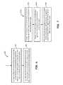
- FIG. 5is an operational flow diagram illustrating an exemplary method 500 for cancelling reciprocal mixing caused by phase noise in an oscillator.
- an inbound RF signalincluding a modulated RF signal and a blocking signal at a frequency offset ⁇ fb ( 502 )
- the RF signalis mixed with a first LO signal to produce a first baseband signal having a data component, a thermal noise component, and reciprocal mixing noise that is a product of reciprocal mixing of the blocking signal ( 504 ).
- the inbound RF signalis converted (e.g., via a transconductance amplifier) into a current signal ( 506 ).
- This current signalis mixed with the first LO signal to produce a down-converted current signal having a data component near DC, a blocking signal component near a frequency offset Mb from the data component, and a RM image near a frequency offset 2 ⁇ fb from the data component ( 508 ).
- the blocking signal component of the down-converted current signal (in the main RF signal path) and the RM image of the current signalare then mixed with a second LO signal to produce a RM noise cancellation signal ( 510 ).
- This RM noise cancellation signalis then combined (e.g., through harmonic recombination) with the first baseband signal in a manner that removes or cancels substantially all or a portion of the reciprocal mixing noise present in the first baseband signal ( 512 ).
- FIG. 6is an operational flow diagram illustrating an exemplary method 600 for further providing thermal noise cancellation in the method of FIG. 5 .
- the illustrated methodoperates to cancel thermal noise that is typically present at the RF node receiving the inbound signal and propagated through the main RF signal path.
- the methodfirst converts the data component of the down-converted current signal (see 508 ) to a second baseband signal that approximates the data component and the thermal noise component of the first baseband signal ( 602 ).
- the first baseband signal and the second baseband signalare combined to cancel at least a portion of the thermal noise component of the first baseband signal ( 604 ).
- the first baseband signalmay be combined with the second baseband signal through appropriately configured harmonic recombination.
- FIG. 7is an operational flow diagram illustrating further exemplary details for cancelling reciprocal mixing caused by phase noise in accordance with the method of FIG. 5 .
- mixing of the blocking signal component of the down-converted current signal and the RM imageis performed by first doubling the frequency offset of the down-converted blocking signal with respect to the data component of the first baseband signal ( 510 a ).
- the resultant down-converted blocking signalis provided to local oscillation circuitry, such as an injection locked ring oscillator, to derive a second LO signal ( 510 b ).
- the RM noise cancellation signalis then produced by mixing this second LO signal with the blocking signal component and the RM image of the current signal to down-convert the RM image to near DC ( 510 c ) for use in RM noise cancellation.
- the terms “near”, “substantially” and “approximately”provides an industry-accepted tolerance for its corresponding term and/or relativity between items. Such an industry-accepted tolerance ranges from less than one percent to fifty percent and corresponds to, but is not limited to, component values, integrated circuit process variations, temperature variations, rise and fall times, and/or thermal noise. Such relativity between items ranges from a difference of a few percent to magnitude differences.
- the term(s) “configured to”, “operably coupled to”, “coupled to”, and/or “coupling”includes direct coupling between items and/or indirect coupling between items via an intervening item (e.g., an item includes, but is not limited to, a component, an element, a circuit, and/or a module) where, for an example of indirect coupling, the intervening item does not modify the information of a signal but may adjust its current level, voltage level, and/or power level.
- inferred couplingi.e., where one element is coupled to another element by inference
- the term “configured to”, “operable to”, “coupled to”, or “operably coupled to”indicates that an item includes one or more of power connections, input(s), output(s), etc., to perform, when activated, one or more its corresponding functions and may further include inferred coupling to one or more other items.
- the term “associated with”,includes direct and/or indirect coupling of separate items and/or one item being embedded within another item.
- processing modulemay be a single processing device or a plurality of processing devices.
- a processing devicemay be a microprocessor, micro-controller, digital signal processor, microcomputer, central processing unit, field programmable gate array, programmable logic device, state machine, logic circuitry, analog circuitry, digital circuitry, and/or any device that manipulates signals (analog and/or digital) based on hard coding of the circuitry and/or operational instructions.
- the processing module, processing circuit, and/or processing unitmay be, or further include, memory and/or an integrated memory element, which may be a single memory device, a plurality of memory devices, and/or embedded circuitry of another processing module, processing circuit, and/or processing unit.
- a memory devicemay be a read-only memory, random access memory, volatile memory, non-volatile memory, static memory, dynamic memory, flash memory, cache memory, and/or any device that stores digital information.
- the processing module, processing circuit, and/or processing unitimplements one or more of its functions via a state machine, analog circuitry, digital circuitry, and/or logic circuitry
- the memory and/or memory element storing the corresponding operational instructionsmay be embedded within, or external to, the circuitry comprising the state machine, analog circuitry, digital circuitry, and/or logic circuitry.
- the memory elementmay store, and the processing module, processing circuit, and/or processing unit executes, hard coded and/or operational instructions corresponding to at least some of the steps and/or functions illustrated in one or more of the figures (FIGs).
- Such a memory device or memory elementcan be included in an article of manufacture.
- moduleis used in the description of one or more of the embodiments.
- a moduleincludes a processing module, a processor, a functional block, hardware, and/or memory that stores operational instructions for performing one or more functions as may be described herein. Note that, if the module is implemented via hardware, the hardware may operate independently and/or in conjunction with software and/or firmware. As also used herein, a module may contain one or more sub-modules, each of which may be one or more modules.
- the one or more embodimentsare used herein to illustrate one or more aspects, one or more features, one or more concepts, and/or one or more examples of the claimed subject matter.
- a physical embodiment of an apparatus, an article of manufacture, a machine, and/or of a processmay include one or more of the aspects, features, concepts, examples, etc. described with reference to one or more of the embodiments discussed herein.
- the embodimentsmay incorporate the same or similarly named functions, steps, modules, etc. that may use the same or different reference numbers and, as such, the functions, steps, modules, etc. may be the same or similar functions, steps, modules, etc. or different ones.
- transistors in the above described figure(s)is/are shown as field effect transistors (FETs), as one of ordinary skill in the art will appreciate, the transistors may be implemented using any type of transistor structure including, but not limited to, bipolar, metal oxide semiconductor field effect transistors (MOSFET), N-well transistors, P-well transistors, enhancement mode, depletion mode, and zero voltage threshold (VT) transistors.
- FETsfield effect transistors
- MOSFETmetal oxide semiconductor field effect transistors
- N-well transistorsN-well transistors
- P-well transistorsP-well transistors
- enhancement modeenhancement mode
- depletion modedepletion mode
- VTzero voltage threshold
- signals to, from, and/or between elements in a figure presented hereinmay be analog or digital, continuous time or discrete time, and single-ended or differential.
- signals to, from, and/or between elements in a figure presented hereinmay be analog or digital, continuous time or discrete time, and single-ended or differential.
- a signal pathis shown as a single-ended path, it also represents a differential signal path.
- a signal pathis shown as a differential path, it also represents a single-ended signal path.
- While one or more particular architecturesare described herein, other architectures can likewise be implemented that use one or more data buses not expressly shown, direct connectivity between elements, and/or indirect coupling between other elements as recognized by one of average skill in the art.
Landscapes
- Engineering & Computer Science (AREA)
- Computer Networks & Wireless Communication (AREA)
- Signal Processing (AREA)
- Power Engineering (AREA)
- Noise Elimination (AREA)
Abstract
Description
Claims (20)
Priority Applications (1)
| Application Number | Priority Date | Filing Date | Title |
|---|---|---|---|
| US14/262,978US9148186B1 (en) | 2014-04-08 | 2014-04-28 | Highly linear receiver front-end with thermal and phase noise cancellation |
Applications Claiming Priority (2)
| Application Number | Priority Date | Filing Date | Title |
|---|---|---|---|
| US201461976948P | 2014-04-08 | 2014-04-08 | |
| US14/262,978US9148186B1 (en) | 2014-04-08 | 2014-04-28 | Highly linear receiver front-end with thermal and phase noise cancellation |
Publications (2)
| Publication Number | Publication Date |
|---|---|
| US9148186B1true US9148186B1 (en) | 2015-09-29 |
| US20150288398A1 US20150288398A1 (en) | 2015-10-08 |
Family
ID=54149721
Family Applications (1)
| Application Number | Title | Priority Date | Filing Date |
|---|---|---|---|
| US14/262,978Expired - Fee RelatedUS9148186B1 (en) | 2014-04-08 | 2014-04-28 | Highly linear receiver front-end with thermal and phase noise cancellation |
Country Status (1)
| Country | Link |
|---|---|
| US (1) | US9148186B1 (en) |
Cited By (89)
| Publication number | Priority date | Publication date | Assignee | Title |
|---|---|---|---|---|
| US9413400B1 (en)* | 2015-04-30 | 2016-08-09 | Qualcomm Incorporated | Blocker filtering for carrier aggregation receiver |
| US9705610B2 (en) | 2014-10-21 | 2017-07-11 | At&T Intellectual Property I, L.P. | Transmission device with impairment compensation and methods for use therewith |
| US9735833B2 (en) | 2015-07-31 | 2017-08-15 | At&T Intellectual Property I, L.P. | Method and apparatus for communications management in a neighborhood network |
| US9742521B2 (en) | 2014-11-20 | 2017-08-22 | At&T Intellectual Property I, L.P. | Transmission device with mode division multiplexing and methods for use therewith |
| US9749053B2 (en) | 2015-07-23 | 2017-08-29 | At&T Intellectual Property I, L.P. | Node device, repeater and methods for use therewith |
| US9769020B2 (en) | 2014-10-21 | 2017-09-19 | At&T Intellectual Property I, L.P. | Method and apparatus for responding to events affecting communications in a communication network |
| US9769128B2 (en) | 2015-09-28 | 2017-09-19 | At&T Intellectual Property I, L.P. | Method and apparatus for encryption of communications over a network |
| US9787412B2 (en) | 2015-06-25 | 2017-10-10 | At&T Intellectual Property I, L.P. | Methods and apparatus for inducing a fundamental wave mode on a transmission medium |
| US9793955B2 (en) | 2015-04-24 | 2017-10-17 | At&T Intellectual Property I, Lp | Passive electrical coupling device and methods for use therewith |
| US9793954B2 (en) | 2015-04-28 | 2017-10-17 | At&T Intellectual Property I, L.P. | Magnetic coupling device and methods for use therewith |
| US9800280B2 (en) | 2016-01-12 | 2017-10-24 | Qualcomm Incorporated | Noise suppression in radio frequency receivers |
| US9800327B2 (en) | 2014-11-20 | 2017-10-24 | At&T Intellectual Property I, L.P. | Apparatus for controlling operations of a communication device and methods thereof |
| US9820146B2 (en) | 2015-06-12 | 2017-11-14 | At&T Intellectual Property I, L.P. | Method and apparatus for authentication and identity management of communicating devices |
| US9831912B2 (en) | 2015-04-24 | 2017-11-28 | At&T Intellectual Property I, Lp | Directional coupling device and methods for use therewith |
| US9838896B1 (en) | 2016-12-09 | 2017-12-05 | At&T Intellectual Property I, L.P. | Method and apparatus for assessing network coverage |
| US9838078B2 (en) | 2015-07-31 | 2017-12-05 | At&T Intellectual Property I, L.P. | Method and apparatus for exchanging communication signals |
| US9847850B2 (en) | 2014-10-14 | 2017-12-19 | At&T Intellectual Property I, L.P. | Method and apparatus for adjusting a mode of communication in a communication network |
| US9847566B2 (en) | 2015-07-14 | 2017-12-19 | At&T Intellectual Property I, L.P. | Method and apparatus for adjusting a field of a signal to mitigate interference |
| US9853342B2 (en) | 2015-07-14 | 2017-12-26 | At&T Intellectual Property I, L.P. | Dielectric transmission medium connector and methods for use therewith |
| US9860075B1 (en) | 2016-08-26 | 2018-01-02 | At&T Intellectual Property I, L.P. | Method and communication node for broadband distribution |
| US9866276B2 (en) | 2014-10-10 | 2018-01-09 | At&T Intellectual Property I, L.P. | Method and apparatus for arranging communication sessions in a communication system |
| US9865911B2 (en) | 2015-06-25 | 2018-01-09 | At&T Intellectual Property I, L.P. | Waveguide system for slot radiating first electromagnetic waves that are combined into a non-fundamental wave mode second electromagnetic wave on a transmission medium |
| US9866309B2 (en) | 2015-06-03 | 2018-01-09 | At&T Intellectual Property I, Lp | Host node device and methods for use therewith |
| US9871282B2 (en) | 2015-05-14 | 2018-01-16 | At&T Intellectual Property I, L.P. | At least one transmission medium having a dielectric surface that is covered at least in part by a second dielectric |
| US9871283B2 (en) | 2015-07-23 | 2018-01-16 | At&T Intellectual Property I, Lp | Transmission medium having a dielectric core comprised of plural members connected by a ball and socket configuration |
| US9876570B2 (en) | 2015-02-20 | 2018-01-23 | At&T Intellectual Property I, Lp | Guided-wave transmission device with non-fundamental mode propagation and methods for use therewith |
| US9876264B2 (en) | 2015-10-02 | 2018-01-23 | At&T Intellectual Property I, Lp | Communication system, guided wave switch and methods for use therewith |
| US9882257B2 (en) | 2015-07-14 | 2018-01-30 | At&T Intellectual Property I, L.P. | Method and apparatus for launching a wave mode that mitigates interference |
| US9887447B2 (en) | 2015-05-14 | 2018-02-06 | At&T Intellectual Property I, L.P. | Transmission medium having multiple cores and methods for use therewith |
| US9893795B1 (en) | 2016-12-07 | 2018-02-13 | At&T Intellectual Property I, Lp | Method and repeater for broadband distribution |
| US9904535B2 (en) | 2015-09-14 | 2018-02-27 | At&T Intellectual Property I, L.P. | Method and apparatus for distributing software |
| US9906269B2 (en) | 2014-09-17 | 2018-02-27 | At&T Intellectual Property I, L.P. | Monitoring and mitigating conditions in a communication network |
| US9912381B2 (en) | 2015-06-03 | 2018-03-06 | At&T Intellectual Property I, Lp | Network termination and methods for use therewith |
| US9912027B2 (en) | 2015-07-23 | 2018-03-06 | At&T Intellectual Property I, L.P. | Method and apparatus for exchanging communication signals |
| US9911020B1 (en) | 2016-12-08 | 2018-03-06 | At&T Intellectual Property I, L.P. | Method and apparatus for tracking via a radio frequency identification device |
| US9913139B2 (en) | 2015-06-09 | 2018-03-06 | At&T Intellectual Property I, L.P. | Signal fingerprinting for authentication of communicating devices |
| US9917341B2 (en) | 2015-05-27 | 2018-03-13 | At&T Intellectual Property I, L.P. | Apparatus and method for launching electromagnetic waves and for modifying radial dimensions of the propagating electromagnetic waves |
| US9929755B2 (en) | 2015-07-14 | 2018-03-27 | At&T Intellectual Property I, L.P. | Method and apparatus for coupling an antenna to a device |
| US9948333B2 (en) | 2015-07-23 | 2018-04-17 | At&T Intellectual Property I, L.P. | Method and apparatus for wireless communications to mitigate interference |
| US9954287B2 (en) | 2014-11-20 | 2018-04-24 | At&T Intellectual Property I, L.P. | Apparatus for converting wireless signals and electromagnetic waves and methods thereof |
| US9967173B2 (en) | 2015-07-31 | 2018-05-08 | At&T Intellectual Property I, L.P. | Method and apparatus for authentication and identity management of communicating devices |
| US9973940B1 (en) | 2017-02-27 | 2018-05-15 | At&T Intellectual Property I, L.P. | Apparatus and methods for dynamic impedance matching of a guided wave launcher |
| US9973416B2 (en) | 2014-10-02 | 2018-05-15 | At&T Intellectual Property I, L.P. | Method and apparatus that provides fault tolerance in a communication network |
| US9998870B1 (en) | 2016-12-08 | 2018-06-12 | At&T Intellectual Property I, L.P. | Method and apparatus for proximity sensing |
| US9999038B2 (en) | 2013-05-31 | 2018-06-12 | At&T Intellectual Property I, L.P. | Remote distributed antenna system |
| US9997819B2 (en) | 2015-06-09 | 2018-06-12 | At&T Intellectual Property I, L.P. | Transmission medium and method for facilitating propagation of electromagnetic waves via a core |
| US10009067B2 (en) | 2014-12-04 | 2018-06-26 | At&T Intellectual Property I, L.P. | Method and apparatus for configuring a communication interface |
| US10044409B2 (en) | 2015-07-14 | 2018-08-07 | At&T Intellectual Property I, L.P. | Transmission medium and methods for use therewith |
| US10069185B2 (en) | 2015-06-25 | 2018-09-04 | At&T Intellectual Property I, L.P. | Methods and apparatus for inducing a non-fundamental wave mode on a transmission medium |
| US10069535B2 (en) | 2016-12-08 | 2018-09-04 | At&T Intellectual Property I, L.P. | Apparatus and methods for launching electromagnetic waves having a certain electric field structure |
| US10090606B2 (en) | 2015-07-15 | 2018-10-02 | At&T Intellectual Property I, L.P. | Antenna system with dielectric array and methods for use therewith |
| US10097223B2 (en)* | 2015-12-14 | 2018-10-09 | Southeast University | Low power supply voltage double-conversion radio frequency receiving front end |
| US10103422B2 (en) | 2016-12-08 | 2018-10-16 | At&T Intellectual Property I, L.P. | Method and apparatus for mounting network devices |
| US10103801B2 (en) | 2015-06-03 | 2018-10-16 | At&T Intellectual Property I, L.P. | Host node device and methods for use therewith |
| CN108802729A (en)* | 2017-10-26 | 2018-11-13 | 中国测绘科学研究院 | Method and device of the best interference images of time series InSAR to selection |
| US10139820B2 (en) | 2016-12-07 | 2018-11-27 | At&T Intellectual Property I, L.P. | Method and apparatus for deploying equipment of a communication system |
| US10148016B2 (en) | 2015-07-14 | 2018-12-04 | At&T Intellectual Property I, L.P. | Apparatus and methods for communicating utilizing an antenna array |
| US10168695B2 (en) | 2016-12-07 | 2019-01-01 | At&T Intellectual Property I, L.P. | Method and apparatus for controlling an unmanned aircraft |
| US10178445B2 (en) | 2016-11-23 | 2019-01-08 | At&T Intellectual Property I, L.P. | Methods, devices, and systems for load balancing between a plurality of waveguides |
| US10205655B2 (en) | 2015-07-14 | 2019-02-12 | At&T Intellectual Property I, L.P. | Apparatus and methods for communicating utilizing an antenna array and multiple communication paths |
| US10225025B2 (en) | 2016-11-03 | 2019-03-05 | At&T Intellectual Property I, L.P. | Method and apparatus for detecting a fault in a communication system |
| US10243784B2 (en) | 2014-11-20 | 2019-03-26 | At&T Intellectual Property I, L.P. | System for generating topology information and methods thereof |
| US10243270B2 (en) | 2016-12-07 | 2019-03-26 | At&T Intellectual Property I, L.P. | Beam adaptive multi-feed dielectric antenna system and methods for use therewith |
| US10264586B2 (en) | 2016-12-09 | 2019-04-16 | At&T Mobility Ii Llc | Cloud-based packet controller and methods for use therewith |
| US10298293B2 (en) | 2017-03-13 | 2019-05-21 | At&T Intellectual Property I, L.P. | Apparatus of communication utilizing wireless network devices |
| US10312567B2 (en) | 2016-10-26 | 2019-06-04 | At&T Intellectual Property I, L.P. | Launcher with planar strip antenna and methods for use therewith |
| US10326689B2 (en) | 2016-12-08 | 2019-06-18 | At&T Intellectual Property I, L.P. | Method and system for providing alternative communication paths |
| US10340983B2 (en) | 2016-12-09 | 2019-07-02 | At&T Intellectual Property I, L.P. | Method and apparatus for surveying remote sites via guided wave communications |
| US10355367B2 (en) | 2015-10-16 | 2019-07-16 | At&T Intellectual Property I, L.P. | Antenna structure for exchanging wireless signals |
| US10359749B2 (en) | 2016-12-07 | 2019-07-23 | At&T Intellectual Property I, L.P. | Method and apparatus for utilities management via guided wave communication |
| US10389037B2 (en) | 2016-12-08 | 2019-08-20 | At&T Intellectual Property I, L.P. | Apparatus and methods for selecting sections of an antenna array and use therewith |
| US10389029B2 (en) | 2016-12-07 | 2019-08-20 | At&T Intellectual Property I, L.P. | Multi-feed dielectric antenna system with core selection and methods for use therewith |
| US10446936B2 (en) | 2016-12-07 | 2019-10-15 | At&T Intellectual Property I, L.P. | Multi-feed dielectric antenna system and methods for use therewith |
| US10530505B2 (en) | 2016-12-08 | 2020-01-07 | At&T Intellectual Property I, L.P. | Apparatus and methods for launching electromagnetic waves along a transmission medium |
| US10547348B2 (en) | 2016-12-07 | 2020-01-28 | At&T Intellectual Property I, L.P. | Method and apparatus for switching transmission mediums in a communication system |
| US10601494B2 (en) | 2016-12-08 | 2020-03-24 | At&T Intellectual Property I, L.P. | Dual-band communication device and method for use therewith |
| US10637149B2 (en) | 2016-12-06 | 2020-04-28 | At&T Intellectual Property I, L.P. | Injection molded dielectric antenna and methods for use therewith |
| US10650940B2 (en) | 2015-05-15 | 2020-05-12 | At&T Intellectual Property I, L.P. | Transmission medium having a conductive material and methods for use therewith |
| US10694379B2 (en) | 2016-12-06 | 2020-06-23 | At&T Intellectual Property I, L.P. | Waveguide system with device-based authentication and methods for use therewith |
| US10727599B2 (en) | 2016-12-06 | 2020-07-28 | At&T Intellectual Property I, L.P. | Launcher with slot antenna and methods for use therewith |
| US10777873B2 (en) | 2016-12-08 | 2020-09-15 | At&T Intellectual Property I, L.P. | Method and apparatus for mounting network devices |
| CN111669196A (en)* | 2019-03-05 | 2020-09-15 | 瑞昱半导体股份有限公司 | Device for processing signals |
| US10797781B2 (en) | 2015-06-03 | 2020-10-06 | At&T Intellectual Property I, L.P. | Client node device and methods for use therewith |
| US10811767B2 (en) | 2016-10-21 | 2020-10-20 | At&T Intellectual Property I, L.P. | System and dielectric antenna with convex dielectric radome |
| US10819035B2 (en) | 2016-12-06 | 2020-10-27 | At&T Intellectual Property I, L.P. | Launcher with helical antenna and methods for use therewith |
| US10938108B2 (en) | 2016-12-08 | 2021-03-02 | At&T Intellectual Property I, L.P. | Frequency selective multi-feed dielectric antenna system and methods for use therewith |
| US11095252B1 (en) | 2020-09-18 | 2021-08-17 | Apple Inc. | Mixer circuitry with noise cancellation |
| US11444819B1 (en) | 2022-05-29 | 2022-09-13 | IQ-Analog Corp. | Adaptive digital receiver path linearizer |
| US12237850B2 (en)* | 2022-09-23 | 2025-02-25 | Eridan Communications, Inc. | Wideband-tunable RF receiver with high dynamic range and high out-of-band rejection |
Families Citing this family (1)
| Publication number | Priority date | Publication date | Assignee | Title |
|---|---|---|---|---|
| DE102018210089A1 (en) | 2018-06-21 | 2019-12-24 | Infineon Technologies Ag | Frequency multiplier and method for frequency multiplication |
Citations (3)
| Publication number | Priority date | Publication date | Assignee | Title |
|---|---|---|---|---|
| US5584062A (en)* | 1994-01-24 | 1996-12-10 | Motorola, Inc. | Method and apparatus for compensating phase locked receivers |
| US20090221235A1 (en)* | 2008-02-29 | 2009-09-03 | Qualcomm Incorporated | Dynamic reference frequency for fractional-n phase-locked loop |
| US20110280344A1 (en)* | 2009-11-11 | 2011-11-17 | Maxlinear, Inc. | Dynamic bandwidth control scheme of a frac-n pll in a receiver |
- 2014
- 2014-04-28USUS14/262,978patent/US9148186B1/ennot_activeExpired - Fee Related
Patent Citations (3)
| Publication number | Priority date | Publication date | Assignee | Title |
|---|---|---|---|---|
| US5584062A (en)* | 1994-01-24 | 1996-12-10 | Motorola, Inc. | Method and apparatus for compensating phase locked receivers |
| US20090221235A1 (en)* | 2008-02-29 | 2009-09-03 | Qualcomm Incorporated | Dynamic reference frequency for fractional-n phase-locked loop |
| US20110280344A1 (en)* | 2009-11-11 | 2011-11-17 | Maxlinear, Inc. | Dynamic bandwidth control scheme of a frac-n pll in a receiver |
Cited By (103)
| Publication number | Priority date | Publication date | Assignee | Title |
|---|---|---|---|---|
| US9999038B2 (en) | 2013-05-31 | 2018-06-12 | At&T Intellectual Property I, L.P. | Remote distributed antenna system |
| US9906269B2 (en) | 2014-09-17 | 2018-02-27 | At&T Intellectual Property I, L.P. | Monitoring and mitigating conditions in a communication network |
| US9973416B2 (en) | 2014-10-02 | 2018-05-15 | At&T Intellectual Property I, L.P. | Method and apparatus that provides fault tolerance in a communication network |
| US9866276B2 (en) | 2014-10-10 | 2018-01-09 | At&T Intellectual Property I, L.P. | Method and apparatus for arranging communication sessions in a communication system |
| US9847850B2 (en) | 2014-10-14 | 2017-12-19 | At&T Intellectual Property I, L.P. | Method and apparatus for adjusting a mode of communication in a communication network |
| US9769020B2 (en) | 2014-10-21 | 2017-09-19 | At&T Intellectual Property I, L.P. | Method and apparatus for responding to events affecting communications in a communication network |
| US9705610B2 (en) | 2014-10-21 | 2017-07-11 | At&T Intellectual Property I, L.P. | Transmission device with impairment compensation and methods for use therewith |
| US9876587B2 (en) | 2014-10-21 | 2018-01-23 | At&T Intellectual Property I, L.P. | Transmission device with impairment compensation and methods for use therewith |
| US9742521B2 (en) | 2014-11-20 | 2017-08-22 | At&T Intellectual Property I, L.P. | Transmission device with mode division multiplexing and methods for use therewith |
| US9749083B2 (en) | 2014-11-20 | 2017-08-29 | At&T Intellectual Property I, L.P. | Transmission device with mode division multiplexing and methods for use therewith |
| US10243784B2 (en) | 2014-11-20 | 2019-03-26 | At&T Intellectual Property I, L.P. | System for generating topology information and methods thereof |
| US9800327B2 (en) | 2014-11-20 | 2017-10-24 | At&T Intellectual Property I, L.P. | Apparatus for controlling operations of a communication device and methods thereof |
| US9954287B2 (en) | 2014-11-20 | 2018-04-24 | At&T Intellectual Property I, L.P. | Apparatus for converting wireless signals and electromagnetic waves and methods thereof |
| US10009067B2 (en) | 2014-12-04 | 2018-06-26 | At&T Intellectual Property I, L.P. | Method and apparatus for configuring a communication interface |
| US9876571B2 (en) | 2015-02-20 | 2018-01-23 | At&T Intellectual Property I, Lp | Guided-wave transmission device with non-fundamental mode propagation and methods for use therewith |
| US9876570B2 (en) | 2015-02-20 | 2018-01-23 | At&T Intellectual Property I, Lp | Guided-wave transmission device with non-fundamental mode propagation and methods for use therewith |
| US9793955B2 (en) | 2015-04-24 | 2017-10-17 | At&T Intellectual Property I, Lp | Passive electrical coupling device and methods for use therewith |
| US9831912B2 (en) | 2015-04-24 | 2017-11-28 | At&T Intellectual Property I, Lp | Directional coupling device and methods for use therewith |
| US9793954B2 (en) | 2015-04-28 | 2017-10-17 | At&T Intellectual Property I, L.P. | Magnetic coupling device and methods for use therewith |
| US9413400B1 (en)* | 2015-04-30 | 2016-08-09 | Qualcomm Incorporated | Blocker filtering for carrier aggregation receiver |
| US9887447B2 (en) | 2015-05-14 | 2018-02-06 | At&T Intellectual Property I, L.P. | Transmission medium having multiple cores and methods for use therewith |
| US9871282B2 (en) | 2015-05-14 | 2018-01-16 | At&T Intellectual Property I, L.P. | At least one transmission medium having a dielectric surface that is covered at least in part by a second dielectric |
| US10650940B2 (en) | 2015-05-15 | 2020-05-12 | At&T Intellectual Property I, L.P. | Transmission medium having a conductive material and methods for use therewith |
| US9917341B2 (en) | 2015-05-27 | 2018-03-13 | At&T Intellectual Property I, L.P. | Apparatus and method for launching electromagnetic waves and for modifying radial dimensions of the propagating electromagnetic waves |
| US9866309B2 (en) | 2015-06-03 | 2018-01-09 | At&T Intellectual Property I, Lp | Host node device and methods for use therewith |
| US10812174B2 (en) | 2015-06-03 | 2020-10-20 | At&T Intellectual Property I, L.P. | Client node device and methods for use therewith |
| US10411788B2 (en) | 2015-06-03 | 2019-09-10 | At&T Intellectual Property I, L.P. | Host node device and methods for use therewith |
| US9967002B2 (en) | 2015-06-03 | 2018-05-08 | At&T Intellectual I, Lp | Network termination and methods for use therewith |
| US9935703B2 (en) | 2015-06-03 | 2018-04-03 | At&T Intellectual Property I, L.P. | Host node device and methods for use therewith |
| US10050697B2 (en)* | 2015-06-03 | 2018-08-14 | At&T Intellectual Property I, L.P. | Host node device and methods for use therewith |
| US10411787B2 (en) | 2015-06-03 | 2019-09-10 | At&T Intellectual Property I, L.P. | Host node device and methods for use therewith |
| US9912382B2 (en) | 2015-06-03 | 2018-03-06 | At&T Intellectual Property I, Lp | Network termination and methods for use therewith |
| US9912381B2 (en) | 2015-06-03 | 2018-03-06 | At&T Intellectual Property I, Lp | Network termination and methods for use therewith |
| US10797781B2 (en) | 2015-06-03 | 2020-10-06 | At&T Intellectual Property I, L.P. | Client node device and methods for use therewith |
| US10103801B2 (en) | 2015-06-03 | 2018-10-16 | At&T Intellectual Property I, L.P. | Host node device and methods for use therewith |
| US9913139B2 (en) | 2015-06-09 | 2018-03-06 | At&T Intellectual Property I, L.P. | Signal fingerprinting for authentication of communicating devices |
| US9997819B2 (en) | 2015-06-09 | 2018-06-12 | At&T Intellectual Property I, L.P. | Transmission medium and method for facilitating propagation of electromagnetic waves via a core |
| US9820146B2 (en) | 2015-06-12 | 2017-11-14 | At&T Intellectual Property I, L.P. | Method and apparatus for authentication and identity management of communicating devices |
| US10069185B2 (en) | 2015-06-25 | 2018-09-04 | At&T Intellectual Property I, L.P. | Methods and apparatus for inducing a non-fundamental wave mode on a transmission medium |
| US9865911B2 (en) | 2015-06-25 | 2018-01-09 | At&T Intellectual Property I, L.P. | Waveguide system for slot radiating first electromagnetic waves that are combined into a non-fundamental wave mode second electromagnetic wave on a transmission medium |
| US9787412B2 (en) | 2015-06-25 | 2017-10-10 | At&T Intellectual Property I, L.P. | Methods and apparatus for inducing a fundamental wave mode on a transmission medium |
| US9847566B2 (en) | 2015-07-14 | 2017-12-19 | At&T Intellectual Property I, L.P. | Method and apparatus for adjusting a field of a signal to mitigate interference |
| US9882257B2 (en) | 2015-07-14 | 2018-01-30 | At&T Intellectual Property I, L.P. | Method and apparatus for launching a wave mode that mitigates interference |
| US9929755B2 (en) | 2015-07-14 | 2018-03-27 | At&T Intellectual Property I, L.P. | Method and apparatus for coupling an antenna to a device |
| US9853342B2 (en) | 2015-07-14 | 2017-12-26 | At&T Intellectual Property I, L.P. | Dielectric transmission medium connector and methods for use therewith |
| US10044409B2 (en) | 2015-07-14 | 2018-08-07 | At&T Intellectual Property I, L.P. | Transmission medium and methods for use therewith |
| US10148016B2 (en) | 2015-07-14 | 2018-12-04 | At&T Intellectual Property I, L.P. | Apparatus and methods for communicating utilizing an antenna array |
| US10205655B2 (en) | 2015-07-14 | 2019-02-12 | At&T Intellectual Property I, L.P. | Apparatus and methods for communicating utilizing an antenna array and multiple communication paths |
| US10090606B2 (en) | 2015-07-15 | 2018-10-02 | At&T Intellectual Property I, L.P. | Antenna system with dielectric array and methods for use therewith |
| US9948333B2 (en) | 2015-07-23 | 2018-04-17 | At&T Intellectual Property I, L.P. | Method and apparatus for wireless communications to mitigate interference |
| US9871283B2 (en) | 2015-07-23 | 2018-01-16 | At&T Intellectual Property I, Lp | Transmission medium having a dielectric core comprised of plural members connected by a ball and socket configuration |
| US9749053B2 (en) | 2015-07-23 | 2017-08-29 | At&T Intellectual Property I, L.P. | Node device, repeater and methods for use therewith |
| US9806818B2 (en) | 2015-07-23 | 2017-10-31 | At&T Intellectual Property I, Lp | Node device, repeater and methods for use therewith |
| US9912027B2 (en) | 2015-07-23 | 2018-03-06 | At&T Intellectual Property I, L.P. | Method and apparatus for exchanging communication signals |
| US9838078B2 (en) | 2015-07-31 | 2017-12-05 | At&T Intellectual Property I, L.P. | Method and apparatus for exchanging communication signals |
| US9967173B2 (en) | 2015-07-31 | 2018-05-08 | At&T Intellectual Property I, L.P. | Method and apparatus for authentication and identity management of communicating devices |
| US9735833B2 (en) | 2015-07-31 | 2017-08-15 | At&T Intellectual Property I, L.P. | Method and apparatus for communications management in a neighborhood network |
| US9904535B2 (en) | 2015-09-14 | 2018-02-27 | At&T Intellectual Property I, L.P. | Method and apparatus for distributing software |
| US9769128B2 (en) | 2015-09-28 | 2017-09-19 | At&T Intellectual Property I, L.P. | Method and apparatus for encryption of communications over a network |
| US9876264B2 (en) | 2015-10-02 | 2018-01-23 | At&T Intellectual Property I, Lp | Communication system, guided wave switch and methods for use therewith |
| US10355367B2 (en) | 2015-10-16 | 2019-07-16 | At&T Intellectual Property I, L.P. | Antenna structure for exchanging wireless signals |
| US10097223B2 (en)* | 2015-12-14 | 2018-10-09 | Southeast University | Low power supply voltage double-conversion radio frequency receiving front end |
| US9800280B2 (en) | 2016-01-12 | 2017-10-24 | Qualcomm Incorporated | Noise suppression in radio frequency receivers |
| US9860075B1 (en) | 2016-08-26 | 2018-01-02 | At&T Intellectual Property I, L.P. | Method and communication node for broadband distribution |
| US10811767B2 (en) | 2016-10-21 | 2020-10-20 | At&T Intellectual Property I, L.P. | System and dielectric antenna with convex dielectric radome |
| US10312567B2 (en) | 2016-10-26 | 2019-06-04 | At&T Intellectual Property I, L.P. | Launcher with planar strip antenna and methods for use therewith |
| US10225025B2 (en) | 2016-11-03 | 2019-03-05 | At&T Intellectual Property I, L.P. | Method and apparatus for detecting a fault in a communication system |
| US10178445B2 (en) | 2016-11-23 | 2019-01-08 | At&T Intellectual Property I, L.P. | Methods, devices, and systems for load balancing between a plurality of waveguides |
| US10819035B2 (en) | 2016-12-06 | 2020-10-27 | At&T Intellectual Property I, L.P. | Launcher with helical antenna and methods for use therewith |
| US10637149B2 (en) | 2016-12-06 | 2020-04-28 | At&T Intellectual Property I, L.P. | Injection molded dielectric antenna and methods for use therewith |
| US10727599B2 (en) | 2016-12-06 | 2020-07-28 | At&T Intellectual Property I, L.P. | Launcher with slot antenna and methods for use therewith |
| US10694379B2 (en) | 2016-12-06 | 2020-06-23 | At&T Intellectual Property I, L.P. | Waveguide system with device-based authentication and methods for use therewith |
| US10139820B2 (en) | 2016-12-07 | 2018-11-27 | At&T Intellectual Property I, L.P. | Method and apparatus for deploying equipment of a communication system |
| US10243270B2 (en) | 2016-12-07 | 2019-03-26 | At&T Intellectual Property I, L.P. | Beam adaptive multi-feed dielectric antenna system and methods for use therewith |
| US9893795B1 (en) | 2016-12-07 | 2018-02-13 | At&T Intellectual Property I, Lp | Method and repeater for broadband distribution |
| US10547348B2 (en) | 2016-12-07 | 2020-01-28 | At&T Intellectual Property I, L.P. | Method and apparatus for switching transmission mediums in a communication system |
| US10446936B2 (en) | 2016-12-07 | 2019-10-15 | At&T Intellectual Property I, L.P. | Multi-feed dielectric antenna system and methods for use therewith |
| US10359749B2 (en) | 2016-12-07 | 2019-07-23 | At&T Intellectual Property I, L.P. | Method and apparatus for utilities management via guided wave communication |
| US10168695B2 (en) | 2016-12-07 | 2019-01-01 | At&T Intellectual Property I, L.P. | Method and apparatus for controlling an unmanned aircraft |
| US10389029B2 (en) | 2016-12-07 | 2019-08-20 | At&T Intellectual Property I, L.P. | Multi-feed dielectric antenna system with core selection and methods for use therewith |
| US10103422B2 (en) | 2016-12-08 | 2018-10-16 | At&T Intellectual Property I, L.P. | Method and apparatus for mounting network devices |
| US10777873B2 (en) | 2016-12-08 | 2020-09-15 | At&T Intellectual Property I, L.P. | Method and apparatus for mounting network devices |
| US9911020B1 (en) | 2016-12-08 | 2018-03-06 | At&T Intellectual Property I, L.P. | Method and apparatus for tracking via a radio frequency identification device |
| US10530505B2 (en) | 2016-12-08 | 2020-01-07 | At&T Intellectual Property I, L.P. | Apparatus and methods for launching electromagnetic waves along a transmission medium |
| US10326689B2 (en) | 2016-12-08 | 2019-06-18 | At&T Intellectual Property I, L.P. | Method and system for providing alternative communication paths |
| US10601494B2 (en) | 2016-12-08 | 2020-03-24 | At&T Intellectual Property I, L.P. | Dual-band communication device and method for use therewith |
| US10389037B2 (en) | 2016-12-08 | 2019-08-20 | At&T Intellectual Property I, L.P. | Apparatus and methods for selecting sections of an antenna array and use therewith |
| US10938108B2 (en) | 2016-12-08 | 2021-03-02 | At&T Intellectual Property I, L.P. | Frequency selective multi-feed dielectric antenna system and methods for use therewith |
| US10069535B2 (en) | 2016-12-08 | 2018-09-04 | At&T Intellectual Property I, L.P. | Apparatus and methods for launching electromagnetic waves having a certain electric field structure |
| US9998870B1 (en) | 2016-12-08 | 2018-06-12 | At&T Intellectual Property I, L.P. | Method and apparatus for proximity sensing |
| US10340983B2 (en) | 2016-12-09 | 2019-07-02 | At&T Intellectual Property I, L.P. | Method and apparatus for surveying remote sites via guided wave communications |
| US10264586B2 (en) | 2016-12-09 | 2019-04-16 | At&T Mobility Ii Llc | Cloud-based packet controller and methods for use therewith |
| US9838896B1 (en) | 2016-12-09 | 2017-12-05 | At&T Intellectual Property I, L.P. | Method and apparatus for assessing network coverage |
| US9973940B1 (en) | 2017-02-27 | 2018-05-15 | At&T Intellectual Property I, L.P. | Apparatus and methods for dynamic impedance matching of a guided wave launcher |
| US10298293B2 (en) | 2017-03-13 | 2019-05-21 | At&T Intellectual Property I, L.P. | Apparatus of communication utilizing wireless network devices |
| CN108802729A (en)* | 2017-10-26 | 2018-11-13 | 中国测绘科学研究院 | Method and device of the best interference images of time series InSAR to selection |
| CN111669196A (en)* | 2019-03-05 | 2020-09-15 | 瑞昱半导体股份有限公司 | Device for processing signals |
| CN111669196B (en)* | 2019-03-05 | 2021-07-16 | 瑞昱半导体股份有限公司 | Device for processing signals |
| US11095252B1 (en) | 2020-09-18 | 2021-08-17 | Apple Inc. | Mixer circuitry with noise cancellation |
| US11469710B2 (en) | 2020-09-18 | 2022-10-11 | Apple Inc. | Mixer circuitry with noise cancellation |
| US11664766B2 (en) | 2020-09-18 | 2023-05-30 | Apple Inc. | Mixer circuitry with noise cancellation |
| US11444819B1 (en) | 2022-05-29 | 2022-09-13 | IQ-Analog Corp. | Adaptive digital receiver path linearizer |
| US12237850B2 (en)* | 2022-09-23 | 2025-02-25 | Eridan Communications, Inc. | Wideband-tunable RF receiver with high dynamic range and high out-of-band rejection |
Also Published As
| Publication number | Publication date |
|---|---|
| US20150288398A1 (en) | 2015-10-08 |
Similar Documents
| Publication | Publication Date | Title |
|---|---|---|
| US9148186B1 (en) | Highly linear receiver front-end with thermal and phase noise cancellation | |
| US8655299B2 (en) | Saw-less receiver with RF frequency translated BPF | |
| US8483642B2 (en) | Saw-less receiver with offset RF frequency translated BPF | |
| US8725085B2 (en) | RF front-end module | |
| US8761710B2 (en) | Portable computing device with a saw-less transceiver | |
| US9031515B2 (en) | Transceiver including a weaved connection | |
| US20110300885A1 (en) | Front-end module network | |
| US20110299576A1 (en) | Polar-based rf receiver | |
| US9002295B2 (en) | SAW-less receiver including an if frequency translated BPF | |
| US8666351B2 (en) | Multiple band saw-less receiver including a frequency translated BPF | |
| Seok et al. | A 2.4 GHz,− 102dBm-sensitivity, 25kb/s, 0.466 mW interference resistant BFSK multi-channel sliding-IF ULP receiver | |
| US9231716B2 (en) | Methods and apparatus for generating two-tone calibration signals for performing linearity calibration | |
| EP2587667A1 (en) | Programmable low noise amplifier and methods for use therewith | |
| WO2015091140A1 (en) | Local oscillator signal generation | |
| US8565710B2 (en) | Wireless transmitter having frequency translated bandpass filter | |
| US9001740B2 (en) | Front-end module network for femtocell applications | |
| US8866557B2 (en) | XTAL oscillator | |
| US9553545B1 (en) | Stable differential crystal oscillator with active super diodes | |
| CA3012393C (en) | Generating local oscillator signals in a wireless sensor device | |
| Seo et al. | A low power fully CMOS integrated RF transceiver IC for wireless sensor networks | |
| US20110299634A1 (en) | Saw-less receiver with a frequency translated bpf having a negative resistance | |
| US8724747B2 (en) | Saw-less receiver including transimpedance amplifiers | |
| EP2587680A1 (en) | Down converter with offset cancellation and methods for use therewith | |
| Tao | A 2.4 GHz Dual-Mode CMOS Transceiver for Bluetooth and 802.11 b | |
| Seo | Realizing a CMOS RF Transceiver for Wireless Sensor Networks |
Legal Events
| Date | Code | Title | Description |
|---|---|---|---|
| AS | Assignment | Owner name:BROADCOM CORPORATION, CALIFORNIA Free format text:ASSIGNMENT OF ASSIGNORS INTEREST;ASSIGNORS:WU, HAO;MIKHEMAR, MOHYEE SALAHELDEN;MURPHY, DAVID PATRICK;AND OTHERS;REEL/FRAME:032766/0977 Effective date:20140424 | |
| STCF | Information on status: patent grant | Free format text:PATENTED CASE | |
| AS | Assignment | Owner name:BANK OF AMERICA, N.A., AS COLLATERAL AGENT, NORTH CAROLINA Free format text:PATENT SECURITY AGREEMENT;ASSIGNOR:BROADCOM CORPORATION;REEL/FRAME:037806/0001 Effective date:20160201 Owner name:BANK OF AMERICA, N.A., AS COLLATERAL AGENT, NORTH Free format text:PATENT SECURITY AGREEMENT;ASSIGNOR:BROADCOM CORPORATION;REEL/FRAME:037806/0001 Effective date:20160201 | |
| AS | Assignment | Owner name:AVAGO TECHNOLOGIES GENERAL IP (SINGAPORE) PTE. LTD., SINGAPORE Free format text:ASSIGNMENT OF ASSIGNORS INTEREST;ASSIGNOR:BROADCOM CORPORATION;REEL/FRAME:041706/0001 Effective date:20170120 Owner name:AVAGO TECHNOLOGIES GENERAL IP (SINGAPORE) PTE. LTD Free format text:ASSIGNMENT OF ASSIGNORS INTEREST;ASSIGNOR:BROADCOM CORPORATION;REEL/FRAME:041706/0001 Effective date:20170120 | |
| AS | Assignment | Owner name:BROADCOM CORPORATION, CALIFORNIA Free format text:TERMINATION AND RELEASE OF SECURITY INTEREST IN PATENTS;ASSIGNOR:BANK OF AMERICA, N.A., AS COLLATERAL AGENT;REEL/FRAME:041712/0001 Effective date:20170119 | |
| AS | Assignment | Owner name:AVAGO TECHNOLOGIES INTERNATIONAL SALES PTE. LIMITE Free format text:MERGER;ASSIGNOR:AVAGO TECHNOLOGIES GENERAL IP (SINGAPORE) PTE. LTD.;REEL/FRAME:047229/0408 Effective date:20180509 | |
| AS | Assignment | Owner name:AVAGO TECHNOLOGIES INTERNATIONAL SALES PTE. LIMITE Free format text:CORRECTIVE ASSIGNMENT TO CORRECT THE EFFECTIVE DATE PREVIOUSLY RECORDED ON REEL 047229 FRAME 0408. ASSIGNOR(S) HEREBY CONFIRMS THE THE EFFECTIVE DATE IS 09/05/2018;ASSIGNOR:AVAGO TECHNOLOGIES GENERAL IP (SINGAPORE) PTE. LTD.;REEL/FRAME:047349/0001 Effective date:20180905 | |
| AS | Assignment | Owner name:AVAGO TECHNOLOGIES INTERNATIONAL SALES PTE. LIMITE Free format text:CORRECTIVE ASSIGNMENT TO CORRECT THE PATENT NUMBER 9,385,856 TO 9,385,756 PREVIOUSLY RECORDED AT REEL: 47349 FRAME: 001. ASSIGNOR(S) HEREBY CONFIRMS THE MERGER;ASSIGNOR:AVAGO TECHNOLOGIES GENERAL IP (SINGAPORE) PTE. LTD.;REEL/FRAME:051144/0648 Effective date:20180905 | |
| FEPP | Fee payment procedure | Free format text:MAINTENANCE FEE REMINDER MAILED (ORIGINAL EVENT CODE: REM.); ENTITY STATUS OF PATENT OWNER: LARGE ENTITY | |
| LAPS | Lapse for failure to pay maintenance fees | Free format text:PATENT EXPIRED FOR FAILURE TO PAY MAINTENANCE FEES (ORIGINAL EVENT CODE: EXP.); ENTITY STATUS OF PATENT OWNER: LARGE ENTITY | |
| STCH | Information on status: patent discontinuation | Free format text:PATENT EXPIRED DUE TO NONPAYMENT OF MAINTENANCE FEES UNDER 37 CFR 1.362 | |
| FP | Expired due to failure to pay maintenance fee | Effective date:20190929 |