US9147760B2 - Transistors with isolation regions - Google Patents
Transistors with isolation regionsDownload PDFInfo
- Publication number
- US9147760B2 US9147760B2US14/260,808US201414260808AUS9147760B2US 9147760 B2US9147760 B2US 9147760B2US 201414260808 AUS201414260808 AUS 201414260808AUS 9147760 B2US9147760 B2US 9147760B2
- Authority
- US
- United States
- Prior art keywords
- gate
- region
- regions
- iii
- semiconductor material
- Prior art date
- Legal status (The legal status is an assumption and is not a legal conclusion. Google has not performed a legal analysis and makes no representation as to the accuracy of the status listed.)
- Active
Links
Images


Classifications
- H—ELECTRICITY
- H10—SEMICONDUCTOR DEVICES; ELECTRIC SOLID-STATE DEVICES NOT OTHERWISE PROVIDED FOR
- H10D—INORGANIC ELECTRIC SEMICONDUCTOR DEVICES
- H10D30/00—Field-effect transistors [FET]
- H10D30/01—Manufacture or treatment
- H10D30/015—Manufacture or treatment of FETs having heterojunction interface channels or heterojunction gate electrodes, e.g. HEMT
- H01L29/778—
- H01L29/0649—
- H01L29/0657—
- H01L29/407—
- H01L29/4238—
- H01L29/7786—
- H—ELECTRICITY
- H10—SEMICONDUCTOR DEVICES; ELECTRIC SOLID-STATE DEVICES NOT OTHERWISE PROVIDED FOR
- H10D—INORGANIC ELECTRIC SEMICONDUCTOR DEVICES
- H10D30/00—Field-effect transistors [FET]
- H10D30/40—FETs having zero-dimensional [0D], one-dimensional [1D] or two-dimensional [2D] charge carrier gas channels
- H10D30/47—FETs having zero-dimensional [0D], one-dimensional [1D] or two-dimensional [2D] charge carrier gas channels having 2D charge carrier gas channels, e.g. nanoribbon FETs or high electron mobility transistors [HEMT]
- H10D30/471—High electron mobility transistors [HEMT] or high hole mobility transistors [HHMT]
- H10D30/475—High electron mobility transistors [HEMT] or high hole mobility transistors [HHMT] having wider bandgap layer formed on top of lower bandgap active layer, e.g. undoped barrier HEMTs such as i-AlGaN/GaN HEMTs
- H—ELECTRICITY
- H10—SEMICONDUCTOR DEVICES; ELECTRIC SOLID-STATE DEVICES NOT OTHERWISE PROVIDED FOR
- H10D—INORGANIC ELECTRIC SEMICONDUCTOR DEVICES
- H10D62/00—Semiconductor bodies, or regions thereof, of devices having potential barriers
- H10D62/10—Shapes, relative sizes or dispositions of the regions of the semiconductor bodies; Shapes of the semiconductor bodies
- H10D62/113—Isolations within a component, i.e. internal isolations
- H10D62/115—Dielectric isolations, e.g. air gaps
- H—ELECTRICITY
- H10—SEMICONDUCTOR DEVICES; ELECTRIC SOLID-STATE DEVICES NOT OTHERWISE PROVIDED FOR
- H10D—INORGANIC ELECTRIC SEMICONDUCTOR DEVICES
- H10D62/00—Semiconductor bodies, or regions thereof, of devices having potential barriers
- H10D62/10—Shapes, relative sizes or dispositions of the regions of the semiconductor bodies; Shapes of the semiconductor bodies
- H10D62/117—Shapes of semiconductor bodies
- H—ELECTRICITY
- H10—SEMICONDUCTOR DEVICES; ELECTRIC SOLID-STATE DEVICES NOT OTHERWISE PROVIDED FOR
- H10D—INORGANIC ELECTRIC SEMICONDUCTOR DEVICES
- H10D64/00—Electrodes of devices having potential barriers
- H10D64/111—Field plates
- H10D64/117—Recessed field plates, e.g. trench field plates or buried field plates
- H—ELECTRICITY
- H10—SEMICONDUCTOR DEVICES; ELECTRIC SOLID-STATE DEVICES NOT OTHERWISE PROVIDED FOR
- H10D—INORGANIC ELECTRIC SEMICONDUCTOR DEVICES
- H10D64/00—Electrodes of devices having potential barriers
- H10D64/20—Electrodes characterised by their shapes, relative sizes or dispositions
- H10D64/27—Electrodes not carrying the current to be rectified, amplified, oscillated or switched, e.g. gates
- H10D64/311—Gate electrodes for field-effect devices
- H10D64/411—Gate electrodes for field-effect devices for FETs
- H10D64/511—Gate electrodes for field-effect devices for FETs for IGFETs
- H10D64/517—Gate electrodes for field-effect devices for FETs for IGFETs characterised by the conducting layers
- H10D64/519—Gate electrodes for field-effect devices for FETs for IGFETs characterised by the conducting layers characterised by their top-view geometrical layouts
- H01L29/2003—
- H01L29/207—
- H01L29/402—
- H01L29/41766—
- H01L29/42376—
- H—ELECTRICITY
- H01—ELECTRIC ELEMENTS
- H01L—SEMICONDUCTOR DEVICES NOT COVERED BY CLASS H10
- H01L2924/00—Indexing scheme for arrangements or methods for connecting or disconnecting semiconductor or solid-state bodies as covered by H01L24/00
- H—ELECTRICITY
- H01—ELECTRIC ELEMENTS
- H01L—SEMICONDUCTOR DEVICES NOT COVERED BY CLASS H10
- H01L2924/00—Indexing scheme for arrangements or methods for connecting or disconnecting semiconductor or solid-state bodies as covered by H01L24/00
- H01L2924/0001—Technical content checked by a classifier
- H01L2924/0002—Not covered by any one of groups H01L24/00, H01L24/00 and H01L2224/00
- H—ELECTRICITY
- H10—SEMICONDUCTOR DEVICES; ELECTRIC SOLID-STATE DEVICES NOT OTHERWISE PROVIDED FOR
- H10D—INORGANIC ELECTRIC SEMICONDUCTOR DEVICES
- H10D62/00—Semiconductor bodies, or regions thereof, of devices having potential barriers
- H10D62/80—Semiconductor bodies, or regions thereof, of devices having potential barriers characterised by the materials
- H10D62/85—Semiconductor bodies, or regions thereof, of devices having potential barriers characterised by the materials being Group III-V materials, e.g. GaAs
- H10D62/8503—Nitride Group III-V materials, e.g. AlN or GaN
- H—ELECTRICITY
- H10—SEMICONDUCTOR DEVICES; ELECTRIC SOLID-STATE DEVICES NOT OTHERWISE PROVIDED FOR
- H10D—INORGANIC ELECTRIC SEMICONDUCTOR DEVICES
- H10D62/00—Semiconductor bodies, or regions thereof, of devices having potential barriers
- H10D62/80—Semiconductor bodies, or regions thereof, of devices having potential barriers characterised by the materials
- H10D62/85—Semiconductor bodies, or regions thereof, of devices having potential barriers characterised by the materials being Group III-V materials, e.g. GaAs
- H10D62/854—Semiconductor bodies, or regions thereof, of devices having potential barriers characterised by the materials being Group III-V materials, e.g. GaAs further characterised by the dopants
- H—ELECTRICITY
- H10—SEMICONDUCTOR DEVICES; ELECTRIC SOLID-STATE DEVICES NOT OTHERWISE PROVIDED FOR
- H10D—INORGANIC ELECTRIC SEMICONDUCTOR DEVICES
- H10D64/00—Electrodes of devices having potential barriers
- H10D64/111—Field plates
- H—ELECTRICITY
- H10—SEMICONDUCTOR DEVICES; ELECTRIC SOLID-STATE DEVICES NOT OTHERWISE PROVIDED FOR
- H10D—INORGANIC ELECTRIC SEMICONDUCTOR DEVICES
- H10D64/00—Electrodes of devices having potential barriers
- H10D64/20—Electrodes characterised by their shapes, relative sizes or dispositions
- H10D64/23—Electrodes carrying the current to be rectified, amplified, oscillated or switched, e.g. sources, drains, anodes or cathodes
- H10D64/251—Source or drain electrodes for field-effect devices
- H10D64/256—Source or drain electrodes for field-effect devices for lateral devices wherein the source or drain electrodes are recessed in semiconductor bodies
- H—ELECTRICITY
- H10—SEMICONDUCTOR DEVICES; ELECTRIC SOLID-STATE DEVICES NOT OTHERWISE PROVIDED FOR
- H10D—INORGANIC ELECTRIC SEMICONDUCTOR DEVICES
- H10D64/00—Electrodes of devices having potential barriers
- H10D64/20—Electrodes characterised by their shapes, relative sizes or dispositions
- H10D64/27—Electrodes not carrying the current to be rectified, amplified, oscillated or switched, e.g. gates
- H10D64/311—Gate electrodes for field-effect devices
- H10D64/411—Gate electrodes for field-effect devices for FETs
- H10D64/511—Gate electrodes for field-effect devices for FETs for IGFETs
- H10D64/517—Gate electrodes for field-effect devices for FETs for IGFETs characterised by the conducting layers
- H10D64/518—Gate electrodes for field-effect devices for FETs for IGFETs characterised by the conducting layers characterised by their lengths or sectional shapes
Definitions
- Sisilicon
- Common transistor devices for power applicationsinclude Si CoolMOS, Si Power MOSFETs, and Si Insulated Gate Bipolar Transistors (IGBTs). While Si power devices are inexpensive, they suffer from a number of disadvantages, including relatively low switching speeds and high levels of electrical noise. More recently, silicon carbide (SiC) power devices have been considered due to their superior properties.
- III-N semiconductor devicessuch as gallium nitride (GaN) devices, are now emerging as attractive candidates to carry large currents, support high voltages and to provide very low on-resistance and fast switching times. While numerous III-N transistors and diodes have been demonstrated, improvements in reliability are still necessary in order to enable large scale manufacturing and more widespread adoption of these devices.
- FIG. 1shows a transistor of the prior art having source electrode 14 , drain electrode 15 , gate electrode 13 and access regions 23 and 24 .
- the “access regions” of a transistorrefer to the two regions between the source and gate electrodes, and between the gate and drain electrodes of the transistor, i.e., regions 23 and 24 , respectively, in FIG. 1 .
- Region 23the access region on the source side of the gate, is typically referred to as the source access region
- region 24the access region on the drain side of the gate
- the “gate region” 31 of a transistorrefers to the portion of the transistor between the two access regions 23 and 24 in FIG. 1 .
- the transistorIn typical power switching applications in which switching transistors are used, the transistor is at all times in one of two states.
- the first statewhich is commonly referred to as the “on state”
- the voltage at the gate electrode relative to the source electrodeis higher than the transistor threshold voltage, and substantial current flows through the transistor.
- the voltage difference between the source and drainis typically low, usually no more than a few volts, such as about 0.1-5 volts.
- the second statewhich is commonly referred to as the “off state”
- the voltage between the source and draincan range anywhere from about 0V to the value of the circuit high voltage supply, which in some cases can be as high as 100V, 300V, 600V, 1200V, 1700V, or higher.
- the term “blocking a voltage”refers to the ability of a transistor to prevent substantial current, such as a current that is greater than 0.001 times the operating current during regular conduction, from flowing through the transistor when a voltage is applied across the transistor. In other words, while a transistor is blocking a voltage applied across it, the total current passing through the transistor will not be greater than 0.001 times the operating current during regular conduction.
- a “high-voltage device”, such as a high-voltage transistor,is an electronic device which is optimized for high-voltage switching applications. That is, when the transistor is off, it is capable of blocking high voltages, such as about 300V or higher, about 600V or higher, about 1200V or higher, or about 1700V or higher, and when the transistor is on, it has a sufficiently low on-resistance (R ON ) for the application in which it is used, i.e., it experiences sufficiently low conduction loss when a substantial current passes through the device.
- R ONon-resistance
- a high-voltage devicecan at least be capable of blocking a voltage equal to the high-voltage supply or the maximum voltage in the circuit for which it is used.
- a high-voltage devicemay be capable of blocking 300V, 600V, 1200V, 1700V, or other suitable blocking voltage required by the application.
- a high-voltage devicecan block any voltage between 0V and at least V max , where V max is the maximum voltage that could be supplied by the circuit or power supply.
- a high-voltage devicecan block any voltage between 0V and at least 2*V max .
- a transistor device having a short-circuit survival timeincludes a source, a gate, a drain, and a semiconductor material which includes a gate region, the gate region being between the source and the drain.
- the transistor devicefurther includes a plurality of channel access regions in the semiconductor material between the source and the gate and between the drain and the gate, respectively, a channel in the semiconductor material having an effective width in the gate region and in the channel access regions, and an isolation region in the gate region serving to reduce the effective width of the channel in the gate region without substantially reducing the effective width of the channel in the access regions.
- a transistor devicein another aspect, includes a source, a gate, a drain, and a semiconductor material which includes a gate region, the gate region being between the source and the drain.
- the transistor devicefurther includes a plurality of channel access regions in the semiconductor material between the source and the gate and between the drain and the gate, respectively, a channel in the semiconductor material, and an isolation region in or near a region of the semiconductor material which has a high electric field or is at a low electric potential during device operation, serving to improve the efficiency of hole collection from the semiconductor material.
- a transistor devicein yet another aspect, includes a source having a source width, the transistor device having a maximum current and an on-resistance.
- the maximum current per unit source width of the transistor deviceis less than 500 milliamps/millimeter, and the on-resistance multiplied by the source width is less than 30 ohm-millimeters.
- the devicecan include a plurality of isolation regions in the gate region.
- An isolation regioncan be a region etched through the channel.
- the devicecan include a field plate, which can be along an edge of the isolation region or can lie over the channel access region between the gate and the drain.
- the field platecan be a slant field plate.
- the field platecan be connected to one of the gate, the source, the drain, ground or a DC voltage.
- the isolation regioncan lie beneath or near to the field plate.
- the isolation regioncan contain dopants implanted into the semiconductor material to a depth greater than the depth of the channel, and the dopants can be selected from the group consisting of Mg, Al and Fe.
- the devicecan be a III-N transistor.
- the devicecan be a field effect transistor.
- the isolation regioncan be capable of collecting holes generated in the semiconductor material.
- the gate or the sourcecan contact a surface of the isolation region.
- the isolation regioncan increase the short-circuit survival time of the transistor.
- the devicecan be a high-voltage device.
- the isolation regioncan lie beneath or near the source.
- the isolation regioncan lie beneath or near the gate.
- the isolation regioncan lie between the source and the gate.
- the devicemay further include a metal electrode contacting a surface of the isolation region.
- the devicecan be capable of blocking at least 600V.
- the on-resistance multiplied by the source widthcan be less than 15 ohm-millimeters.
- the maximum currentcan be less than 50 A.
- the on-resistancecan be less than 1 ohm.
- the product of the maximum current and the on-resistancecan be less than about 5 Amp-ohms.
- Isolation regionscan be used in transistor devices to limit the maximum current that can flow through the device without substantially increasing the on-resistance of the device.
- isolation structures or regionscan be configured to collect holes that are generated in the transistor device. The isolation regions may simultaneously achieve both of these functions.
- FIG. 1is a plan view of a prior art device
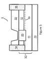
- FIG. 2is a plan view of a device according to this specification
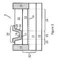
- FIG. 3is a cross-section through the cut 3 - 3 of the device of FIG. 2 ;
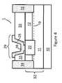
- FIG. 4is a cross-section through the cut 4 - 4 of the device of FIG. 2 ;
- FIG. 5is a cross-section through the cut 5 - 5 of the device of FIG. 2 ;
- FIG. 6is a cross-sectional view of a device according to this specification.
- Transistor 1includes isolation regions 20 , 21 and 22 between the source 14 and the drain 15 .
- the isolation regionscan be configured to increase or maximize the short-circuit survival time of the transistor 1 by reducing or minimizing the maximum channel current (short-circuit current) I max that can flow through the device, while maintaining an acceptably low on-resistance.
- the isolation structures or regionscan be configured to collect holes that are generated in the transistor 1 . The isolation regions may simultaneously achieve both of these functions.
- the transistorscan be lateral devices, III-N devices, field effect transistors, enhancement-mode devices (threshold voltage >0V), depletion-mode devices (threshold voltage ⁇ 0V), high-voltage devices, or any combination of these devices.
- III-N devicescan be III-polar (III-face) devices, N-polar (N-face) devices or semipolar devices.
- a Ga-face, III-face or III-polar III-N devicecan include III-N materials grown with a group III-face or [0 0 0 1] face furthest from the growth substrate, or can include source, gate, or drain electrodes on a group III-face or [0 0 0 1] face of the III-N materials.
- a nitrogen-face, N-face, or N-polar III-N devicecan include III-N materials grown with an N-face or [0 0 0 1 bar] face furthest from the growth substrate, or can include source, gate, or drain electrodes on an N-face or [0 0 0 1 bar] face of the III-N materials.
- the transistorcan be operated in the on state (i.e. conducting current) with a large voltage between the source and drain, for short periods of time.
- the current flowing through the transistoris the maximum current that the transistor is capable of conducting.
- This maximum current valueis typically referred to as the “short-circuit current” and is represented by the symbol I max .
- the motorcan stop turning, accompanied by a simultaneous large current (i.e., short-circuit current) through the high-voltage transistors in the motor drive circuit, and a large voltage across the source and drain terminals of these transistors.
- the control circuitrywhich can send a voltage signal to the gate of the transistors to turn the devices off and thereby prevent further current from flowing, has a finite response time, typically about 10 microseconds. Hence this high current, high voltage mode of operation is sustained for this entire response time of the control circuitry.
- the high-voltage transistors and/or other circuit componentscan become damaged or rendered inoperable.
- one way to increase ⁇is to decrease the short-circuit current I max without substantially affecting any of the other parameters in the equation for ⁇ .
- thiscan be accomplished by designing the transistor with a lower channel charge density and/or lower channel conductivity.
- reducing I max by this method, as well as by many other methodsincreases the transistor's on-resistance R on , hence increasing the power loss during normal operation. It is therefore desirable to reduce I max without substantially affecting any of these other parameters in the equation for ⁇ , while only minimally increasing the on-resistance.
- HEMTshigh electron mobility transistors
- D-modedepletion-mode
- normally-off devicesi.e., devices with positive threshold voltages, that cannot conduct current at zero gate voltage, in order to avoid damage to the device or to other circuit components by preventing accidental turn-on of the device.
- E-modeenhancement-mode
- the “gate region” of a transistorrefers to the portion 31 of the transistor between the two access regions 23 and 24 .
- the transistor of FIGS. 2-5includes isolation regions 20 , 21 , and 22 (shown in the plan view of FIG. 2 ) at least partially within the gate region 31 of the device.
- Isolation regions 20 - 22are regions through which substantial channel current cannot flow, i.e., they provide a break in the device channel between source 14 and drain 15 . They can be etched regions where semiconductor material has been etched through the channel, or ion-implanted regions implanted with Al, Mg or Fe ions, for example. As shown in the cross-sectional views of FIGS.
- the deviceincludes a substrate 10 , a semiconductor material structure 32 , a conductive channel 19 , such as a two-dimensional electron gas (2DEG) in the semiconductor material structure 32 , an insulating material layer 33 , which can include a gate insulator portion 17 beneath the gate of the device, source 14 , drain 15 , gate contacts 16 , 18 , 25 , and 26 (shown in the plan view of FIG. 2 ), and field plates 27 , 28 , 29 , and 30 (shown in the plan view of FIG. 2 ).
- 2DEGtwo-dimensional electron gas
- the portion of electrode 29 which is in the gate region 31is the gate contact 16
- the portion of electrode 29 which is in the drain access region 24is the field plate 28 .
- the gate contacts 16 , 18 , 25 , and 26can all be electrically connected to one another, for example externally in the circuit or outside the periphery of the intrinsic device (not shown).
- the semiconductor material structure 32can include multiple semiconductor layers, such as channel layer 11 and barrier layer 12 , as shown in FIGS. 3-5 .
- the semiconductor material structureincludes or is formed of III-N materials, and the device is a III-N device, such as a III-N transistor or FET.
- channel layer 11can be GaN
- barrier layer 12can be Al x Ga 1-x N.
- III-Nitride or III-N materials, layers, devices, structures, etc.refer to a material, device, or structure comprised of a compound semiconductor material according to the stoichiometric formula Al x In y Ga z N, where x+y+z is about 1.
- the conductive channelcan be partially or entirely contained within a III-N material layer.
- the slant field plates 27 - 30 shown in FIGS. 2-5are formed of the same conducting material as the gate contacts 16 , 18 , 25 and 26 .
- Examples of such conducting materialsare Ni, Pt, poly-silicon, Al, Ti, Au, or combinations thereof.
- Field platescan be used in semiconductor devices, such as transistors, to shape the electric field in the high-field region of the device in such a way that reduces the peak electric field and increases the device breakdown voltage, thereby allowing for higher voltage operation.
- a field platedoes not necessarily need to be formed of the same material as the gate, and it does not necessarily need to be connected to the gate; in some cases, it can be connected to the source, the drain, an electrical ground or a DC voltage source.
- Insulating material layer 33shown in FIGS.
- the insulating material layer 33includes a slanted edge 34 on the drain side of the gate, and the field plate 28 is on top of, and contacting slanted edge 34 .
- the field plate 28is a “slant field plate”, as shown in FIG. 3 .
- the slanted edge 34includes at least a substantial portion which is at a non-perpendicular angle to a main surface of the semiconductor material structure 32 .
- Alternative field plate structures to a slant field platemay also be used.
- the isolation regions 20 , 21 , and 22effectively reduce the width of the channel in the gate region 31 without substantially reducing the effective width of the channel in the access regions 23 and 24 .
- the deviceincludes three isolation regions 20 , 21 and 22 , each of width W iso (see FIG. 2 ), such that the total width of all the isolation regions, W tot , equals 3*W iso .
- the isolation regions 20 , 21 and 22reduce the channel width in the gate region 31 between source 14 and drain 15 from a value of W source (the entire extent of the source contact) to a value of (W source ⁇ W tot ).
- the maximum current I maxwhich is proportional to the channel width in the gate region, is thereby reduced by a factor (W source ⁇ W tot )/W source , while the access resistances (i.e., the channel resistances in the access regions) stay approximately the same.
- the total device on-resistancewhich is equal to the sum of the intrinsic channel on-resistances (i.e., the on-resistance of the portion of the channel in the gate region 31 ) and the access resistances, may not increase substantially.
- isolation regions 20 , 21 and 22are used to limit I max . They can be formed by implanting ions into the semiconductor material structure 32 .
- ions that may be implantedmay include, but are not limited to, Al, Mg, or Fe.
- the isolation regionscan be formed by etching the semiconductor material at least to a depth greater than the depth of the device channel, thereby physically removing a portion of the device channel.
- the isolation regionscan extend at least all the way from the side of the gate region 31 nearest the source 14 , to the other side of the gate region 31 nearest the drain 15 , as this may be necessary to ensure that current is reduced by a factor (W source ⁇ W tot )/W source , compared to an otherwise identical device which does not include isolation regions.
- the isolation regionsmay optionally further extend towards the drain beyond the drain-side edge of the field plates shown in FIG. 2 .
- W totcan be between about 1% and 99% of W source , such as between about 10% and 90%, between about 20% and 80%, or between about 10% and 20% of W source .
- the gatedoes not need to be directly over the isolation regions 20 , 21 and 22 , it may cover part or all of the portions of the isolation regions 20 , 21 and 22 that are in the gate region of the device. This can be advantageous as it may simplify the device fabrication process.
- the gate metalcan be in electrical contact with the isolation regions, or can be electrically isolated from them.
- the isolation regionsare etched regions, the electric fields along their edges may be increased or enhanced during device operation.
- the same or a similar field plate structure to the one used along the drain-side edge of the gatealso can be used along some or all of the edges of etched isolation regions.
- FIG. 6illustrates a device with an isolation region 40 , where the isolation region is formed by etching the semiconductor material at least to a depth greater than the depth of the device channel, thereby physically removing a portion of the device channel.
- the cross-section shown in FIG. 6is similar to that in FIG. 4 , except that in FIG. 6 the electrode 29 which includes the gate is deposited conformally along the portions of III-N layers 12 and 11 that were exposed by the etch.
- an insulatorcan be placed between the electrode 29 and III-N layers 11 and 12 (not shown).
- an aperturemay be etched through the insulator such that the electrode 29 directly contacts one or both of III-N layers 11 and 12 in the aperture region.
- Isolation regions 20 , 21 and 22may also be used to collect holes that are formed in the device material layers 32 during times when the electric fields in the device are sufficiently high, such as when the device is in the off-state and is blocking a high voltage. Isolation regions used as hole collectors can cause the holes to be transported away from the vicinity of the device channel, thereby mitigating their deleterious effects on device performance and reliability.
- the isolation regionscan be placed in a region of low electric potential (voltage), such that holes are drawn towards the isolation regions. Once the holes approach or are incident upon the isolation regions, they can be drawn away from the vicinity of the channel or other active regions of the device. For example, in some implementations, the holes can recombine with electrons near to or within the isolation regions 20 , 21 and 22 .
- a metal electrode(not shown) is connected to the surface of an isolation region, and a sufficiently low or negative voltage is applied to that electrode to carry the holes away through the electrode as an electrical current.
- the gate metalis in electrical contact with the surface of the isolation region. Since the gate 16 is typically at a low or negative voltage when the transistor 1 is in the off state, the voltage on the gate may be sufficient to draw the holes away from the vicinity of the device channel or other active regions.
- gate metal 16For isolation regions to function as hole collectors, in many cases it can be necessary for the gate metal 16 to electrically contact at least a portion of the underlying semiconductor material in the isolation regions 20 , 21 and 22 .
- Many transistorsinclude gate dielectrics 17 , which are insulators between the gate metal 16 and the underlying semiconductor material 12 . When gate dielectrics are used, a break in the dielectric may be required over at least a portion of isolation region 20 , 21 and 22 in order to allow the gate metal 16 or other electrode to contact the underlying isolation region.
- Isolation regions 20 , 21 and 22 used as hole collectorscan have the following properties. They can be regions in which the semiconductor material is etched, in some cases at least through the device channel. In this case, a metal electrode or a portion of the gate metal electrically contacts at least a portion of the semiconductor surface which was exposed by the etch. Alternatively, they can be ion implanted regions in the semiconductor material, where the implanted regions can extend through the channel region, thereby forming a break in the device channel. Ion implanted regions may be capable of conducting substantial hole, but not substantial electron currents. For example they can be p-type or nominally p-type regions. Isolation regions can be placed in regions of high electric field, or in the vicinity of regions of high electric fields.
- holesmay be generated in regions of high electric field
- placing an isolation region near the region where the holes are generatedcan improve hole collection efficiency.
- regions that typically have high electric fields during device operationinclude the regions between the gate and the drain electrode, particularly near the drain-side edge of the gate electrode, or near or beneath a field plate.
- Isolation regionscan also be placed in regions of low voltage or low electric potential, or in the vicinity of regions of low voltage or low electric potential. Since holes are drawn towards regions of low voltage or low electric potential, placing an isolation region near where the holes are drawn to can improve hole collection efficiency. Examples of regions that are typically at low voltage or low electric potential during device operation include the regions near or beneath the source electrode, the regions near or beneath the gate electrode, or the regions between the source and the gate electrode. Alternatively, isolation regions can be placed in regions of high electric fields (i.e., regions that have high electric fields during device operation). Since holes are generated in regions of high electric fields, placing an isolation region near where the holes are generated can improve hole collection efficiency.
- Examples of locations that hole collectors can be placedinclude, but are not limited to, beneath or near the source electrode 14 shown in FIG. 2 , beneath or near the gate electrode 16 , 18 , 25 and 26 , between the source electrode 14 and the gate electrode 16 , 18 , 25 and 26 , between the gate electrode 16 , 18 , 25 and 26 and the drain electrode 15 , or beneath or near to a field plate.
- W totcan be between about 1% and 99% of W source , such as between about 10% and 20% of W source , where again W tot is the total combined width of all the isolation regions, as depicted in FIG. 2 .
- the isolation regions 20 , 21 and 22are etched regions, the electric fields along the edges of the etched isolation regions may be increased or enhanced during device operation.
- the same or a similar field plate structure to the one used along the drain-side edge of the gatecan be used along some or all of the edges of the etched isolation regions.
- a III-N high electron mobility transistor (HEMT) with isolation regions that serve to limit the maximum currentcan have a maximum current level I max per unit source width which is less than 500 mA/mm, such as less than 350, 150, or 50 mA/mm, while the product of the on-resistance R on and the source width is less than about 30 ohm-millimeters, such less than about 15, 5, 3, 2, or 1 ohm-millimeters.
- the on-resistanceis typically larger for devices that are designed to block larger voltages.
- a device designed to be capable of blocking 1200Vmay have an on-resistance that is about 30 ohm-millimeters or less, while a device designed to be capable of blocking 600V may have an on-resistance that is about 15 ohm-millimeters or less.
- the maximum current level of a transistor which includes an isolation regionis less than 50 A, such as less than 25, 10, or 5 A.
- the on-resistance of a transistor which includes an isolation regionis less than 1 ohm, such as less than 0.5, 0.2, or 0.1 ohms.
- the product of the maximum current level and the on-resistancecan be less than about 5 Amp-ohms.
Landscapes
- Insulated Gate Type Field-Effect Transistor (AREA)
- Junction Field-Effect Transistors (AREA)
Abstract
Description
Claims (11)
Priority Applications (2)
| Application Number | Priority Date | Filing Date | Title |
|---|---|---|---|
| US14/260,808US9147760B2 (en) | 2010-12-15 | 2014-04-24 | Transistors with isolation regions |
| US14/810,906US9437707B2 (en) | 2010-12-15 | 2015-07-28 | Transistors with isolation regions |
Applications Claiming Priority (2)
| Application Number | Priority Date | Filing Date | Title |
|---|---|---|---|
| US12/968,704US8742460B2 (en) | 2010-12-15 | 2010-12-15 | Transistors with isolation regions |
| US14/260,808US9147760B2 (en) | 2010-12-15 | 2014-04-24 | Transistors with isolation regions |
Related Parent Applications (1)
| Application Number | Title | Priority Date | Filing Date |
|---|---|---|---|
| US12/968,704ContinuationUS8742460B2 (en) | 2010-12-15 | 2010-12-15 | Transistors with isolation regions |
Related Child Applications (1)
| Application Number | Title | Priority Date | Filing Date |
|---|---|---|---|
| US14/810,906ContinuationUS9437707B2 (en) | 2010-12-15 | 2015-07-28 | Transistors with isolation regions |
Publications (2)
| Publication Number | Publication Date |
|---|---|
| US20140231929A1 US20140231929A1 (en) | 2014-08-21 |
| US9147760B2true US9147760B2 (en) | 2015-09-29 |
Family
ID=46233265
Family Applications (3)
| Application Number | Title | Priority Date | Filing Date |
|---|---|---|---|
| US12/968,704Active2032-01-14US8742460B2 (en) | 2010-12-15 | 2010-12-15 | Transistors with isolation regions |
| US14/260,808ActiveUS9147760B2 (en) | 2010-12-15 | 2014-04-24 | Transistors with isolation regions |
| US14/810,906ActiveUS9437707B2 (en) | 2010-12-15 | 2015-07-28 | Transistors with isolation regions |
Family Applications Before (1)
| Application Number | Title | Priority Date | Filing Date |
|---|---|---|---|
| US12/968,704Active2032-01-14US8742460B2 (en) | 2010-12-15 | 2010-12-15 | Transistors with isolation regions |
Family Applications After (1)
| Application Number | Title | Priority Date | Filing Date |
|---|---|---|---|
| US14/810,906ActiveUS9437707B2 (en) | 2010-12-15 | 2015-07-28 | Transistors with isolation regions |
Country Status (4)
| Country | Link |
|---|---|
| US (3) | US8742460B2 (en) |
| CN (1) | CN103262244B (en) |
| TW (1) | TWI534906B (en) |
| WO (1) | WO2012082519A1 (en) |
Cited By (7)
| Publication number | Priority date | Publication date | Assignee | Title |
|---|---|---|---|---|
| US20150333147A1 (en)* | 2010-12-15 | 2015-11-19 | Transphorm Inc. | Transistors with isolation regions |
| US10630285B1 (en) | 2017-11-21 | 2020-04-21 | Transphorm Technology, Inc. | Switching circuits having drain connected ferrite beads |
| US10756207B2 (en) | 2018-10-12 | 2020-08-25 | Transphorm Technology, Inc. | Lateral III-nitride devices including a vertical gate module |
| US11749656B2 (en) | 2020-06-16 | 2023-09-05 | Transphorm Technology, Inc. | Module configurations for integrated III-Nitride devices |
| US11810971B2 (en) | 2019-03-21 | 2023-11-07 | Transphorm Technology, Inc. | Integrated design for III-Nitride devices |
| US11973138B2 (en) | 2020-08-05 | 2024-04-30 | Transphorm Technology, Inc. | N-polar devices including a depleting layer with improved conductivity |
| US12107585B2 (en) | 2022-09-29 | 2024-10-01 | Globalfoundries U.S. Inc. | Comparator circuits |
Families Citing this family (33)
| Publication number | Priority date | Publication date | Assignee | Title |
|---|---|---|---|---|
| US7965126B2 (en) | 2008-02-12 | 2011-06-21 | Transphorm Inc. | Bridge circuits and their components |
| US8390000B2 (en) | 2009-08-28 | 2013-03-05 | Transphorm Inc. | Semiconductor devices with field plates |
| US8138529B2 (en) | 2009-11-02 | 2012-03-20 | Transphorm Inc. | Package configurations for low EMI circuits |
| US8786327B2 (en) | 2011-02-28 | 2014-07-22 | Transphorm Inc. | Electronic components with reactive filters |
| US9024357B2 (en)* | 2011-04-15 | 2015-05-05 | Stmicroelectronics S.R.L. | Method for manufacturing a HEMT transistor and corresponding HEMT transistor |
| US8680535B2 (en) | 2011-12-23 | 2014-03-25 | Taiwan Semiconductor Manufacturing Company, Ltd. | High electron mobility transistor structure with improved breakdown voltage performance |
| US8648643B2 (en) | 2012-02-24 | 2014-02-11 | Transphorm Inc. | Semiconductor power modules and devices |
| JP6054620B2 (en)* | 2012-03-29 | 2016-12-27 | トランスフォーム・ジャパン株式会社 | Compound semiconductor device and manufacturing method thereof |
| US8803246B2 (en) | 2012-07-16 | 2014-08-12 | Transphorm Inc. | Semiconductor electronic components with integrated current limiters |
| US9076763B2 (en)* | 2012-08-13 | 2015-07-07 | Infineon Technologies Austria Ag | High breakdown voltage III-nitride device |
| US9087718B2 (en) | 2013-03-13 | 2015-07-21 | Transphorm Inc. | Enhancement-mode III-nitride devices |
| US9059076B2 (en) | 2013-04-01 | 2015-06-16 | Transphorm Inc. | Gate drivers for circuits based on semiconductor devices |
| FR3005202B1 (en) | 2013-04-30 | 2016-10-14 | Commissariat Energie Atomique | METHOD FOR FORMING AN IMPLANTED AREA FOR A NORMALLY BLOCKED TYPE HETEROJUNCTION TRANSISTOR |
| US9537425B2 (en) | 2013-07-09 | 2017-01-03 | Transphorm Inc. | Multilevel inverters and their components |
| US9443938B2 (en) | 2013-07-19 | 2016-09-13 | Transphorm Inc. | III-nitride transistor including a p-type depleting layer |
| TWI555209B (en)* | 2013-07-29 | 2016-10-21 | 高效電源轉換公司 | Gallium nitride device with reduced output capacitance and method of manufacturing same |
| US9263569B2 (en)* | 2013-08-05 | 2016-02-16 | Taiwan Semiconductor Manufacturing Company, Ltd. | MISFET device and method of forming the same |
| US10566192B2 (en)* | 2014-05-07 | 2020-02-18 | Cambridge Electronics, Inc. | Transistor structure having buried island regions |
| US9543940B2 (en) | 2014-07-03 | 2017-01-10 | Transphorm Inc. | Switching circuits having ferrite beads |
| US9590494B1 (en) | 2014-07-17 | 2017-03-07 | Transphorm Inc. | Bridgeless power factor correction circuits |
| US9318593B2 (en) | 2014-07-21 | 2016-04-19 | Transphorm Inc. | Forming enhancement mode III-nitride devices |
| US9536967B2 (en) | 2014-12-16 | 2017-01-03 | Transphorm Inc. | Recessed ohmic contacts in a III-N device |
| US9536966B2 (en) | 2014-12-16 | 2017-01-03 | Transphorm Inc. | Gate structures for III-N devices |
| WO2016149146A1 (en) | 2015-03-13 | 2016-09-22 | Transphorm, Inc. | Paralleling of switching devices for high power circuits |
| ITUB20155536A1 (en) | 2015-11-12 | 2017-05-12 | St Microelectronics Srl | NORMALLY OFF TYPE HEMT TRANSISTOR INCLUDING A TRINCE CONTAINING A REGION OF GATE AND FORMER AT LEAST ONE STEP, AND ITS PROCESS OF MANUFACTURE |
| US11322599B2 (en) | 2016-01-15 | 2022-05-03 | Transphorm Technology, Inc. | Enhancement mode III-nitride devices having an Al1-xSixO gate insulator |
| TWI762486B (en) | 2016-05-31 | 2022-05-01 | 美商創世舫科技有限公司 | Iii-nitride devices including a graded depleting layer |
| US10319648B2 (en) | 2017-04-17 | 2019-06-11 | Transphorm Inc. | Conditions for burn-in of high power semiconductors |
| CN107482006B (en)* | 2017-09-28 | 2019-03-15 | 英诺赛科(珠海)科技有限公司 | Transistor device with integrated diode |
| TWI661555B (en)* | 2017-12-28 | 2019-06-01 | 新唐科技股份有限公司 | Enhancement mode hemt device |
| CN110047910B (en)* | 2019-03-27 | 2020-07-31 | 东南大学 | A heterojunction semiconductor device with high withstand voltage capability |
| CN113823680A (en)* | 2021-01-21 | 2021-12-21 | 山东大学 | Novel AlGaN/GaN heterojunction field effect transistor and application |
| CN115148797B (en)* | 2021-06-04 | 2025-08-26 | 山东大学 | An open-gate AlGaN/GaN heterojunction field-effect transistor with auxiliary gate structure and its application |
Citations (232)
| Publication number | Priority date | Publication date | Assignee | Title |
|---|---|---|---|---|
| US4300091A (en) | 1980-07-11 | 1981-11-10 | Rca Corporation | Current regulating circuitry |
| US4532439A (en) | 1982-09-13 | 1985-07-30 | Tokyo Shibaura Denki Kabushiki Kaisha | Mosfet logical circuit with increased noise margin |
| US4645562A (en) | 1985-04-29 | 1987-02-24 | Hughes Aircraft Company | Double layer photoresist technique for side-wall profile control in plasma etching processes |
| US4728826A (en) | 1986-03-19 | 1988-03-01 | Siemens Aktiengesellschaft | MOSFET switch with inductive load |
| US4821093A (en) | 1986-08-18 | 1989-04-11 | The United States Of America As Represented By The Secretary Of The Army | Dual channel high electron mobility field effect transistor |
| US4914489A (en) | 1986-12-20 | 1990-04-03 | Fujitsu Limited | Constant current semiconductor device |
| US5051618A (en) | 1988-06-20 | 1991-09-24 | Idesco Oy | High voltage system using enhancement and depletion field effect transistors |
| US5329147A (en) | 1993-01-04 | 1994-07-12 | Xerox Corporation | High voltage integrated flyback circuit in 2 μm CMOS |
| US5618384A (en) | 1995-12-27 | 1997-04-08 | Chartered Semiconductor Manufacturing Pte, Ltd. | Method for forming residue free patterned conductor layers upon high step height integrated circuit substrates using reflow of photoresist |
| US5646069A (en) | 1995-06-07 | 1997-07-08 | Hughes Aircraft Company | Fabrication process for Alx In1-x As/Gay In1-y As power HFET ohmic contacts |
| US5663091A (en) | 1993-05-20 | 1997-09-02 | Actel Corporation | Method for fabricating an electrically programmable antifuse |
| US5705847A (en) | 1996-06-10 | 1998-01-06 | Mitsubishi Denki Kabushiki Kaisha | Semiconductor device |
| US5714393A (en) | 1996-12-09 | 1998-02-03 | Motorola, Inc. | Diode-connected semiconductor device and method of manufacture |
| US5909103A (en) | 1997-07-24 | 1999-06-01 | Siliconix Incorporated | Safety switch for lithium ion battery |
| JPH11224950A (en) | 1997-11-14 | 1999-08-17 | Matsushita Electric Works Ltd | Semiconductor device |
| US5998810A (en) | 1994-12-19 | 1999-12-07 | Kabushiki Kaisha Toshiba | Semiconductor light-emitting diode having a p-type semiconductor layer formed on a light-emitting layer |
| US6008684A (en) | 1996-10-23 | 1999-12-28 | Industrial Technology Research Institute | CMOS output buffer with CMOS-controlled lateral SCR devices |
| JP2000058871A (en) | 1999-07-02 | 2000-02-25 | Citizen Watch Co Ltd | Integrated circuit of electronic apparatus |
| US6097046A (en) | 1993-04-30 | 2000-08-01 | Texas Instruments Incorporated | Vertical field effect transistor and diode |
| US6100571A (en) | 1998-06-16 | 2000-08-08 | Nec Corporation | Fet having non-overlapping field control electrode between gate and drain |
| US6292500B1 (en) | 1998-04-23 | 2001-09-18 | Matsushita Electric Industrial Co., Ltd. | Semiconductor laser device |
| US6307220B1 (en) | 1997-08-05 | 2001-10-23 | Semiconductor Energy Laboratory Co., Ltd. | Semiconductor device |
| US20010032999A1 (en) | 2000-04-25 | 2001-10-25 | Seikoh Yoshida | GaN-based compound semiconductor device |
| US6316793B1 (en) | 1998-06-12 | 2001-11-13 | Cree, Inc. | Nitride based transistors on semi-insulating silicon carbide substrates |
| US20010040247A1 (en) | 2000-03-28 | 2001-11-15 | Yuji Ando | Hetero-junction field effect transistor having an intermediate layer |
| US20020036287A1 (en) | 2000-07-28 | 2002-03-28 | The Regents Of The University Of California | Gallium nitride-based HFET and a method for fabricating a gallium nitride-based HFET |
| US6373082B1 (en) | 1997-12-04 | 2002-04-16 | Nec Corporation | Compound semiconductor field effect transistor |
| US20020121648A1 (en) | 2000-12-30 | 2002-09-05 | Wei-Chou Hsu | An in0.34assb0.15/inp hfet utilizing inp channels |
| US6475889B1 (en) | 2000-04-11 | 2002-11-05 | Cree, Inc. | Method of forming vias in silicon carbide and resulting devices and circuits |
| US20020167023A1 (en) | 2001-05-11 | 2002-11-14 | Cree Lighting Company And Regents Of The University Of California | Group-III nitride based high electron mobility transistor (HEMT) with barrier/spacer layer |
| US20030003724A1 (en) | 2001-06-27 | 2003-01-02 | Hitachi, Ltd. | Manufacturing method of the semiconductor device |
| US6504235B2 (en) | 1997-07-25 | 2003-01-07 | Hughes Electronics Corporation | Passivation layer and process for semiconductor devices |
| US20030006437A1 (en) | 1998-09-22 | 2003-01-09 | Nec Corporation | Field effect transistor |
| US20030020092A1 (en) | 2001-07-24 | 2003-01-30 | Primit Parikh | Insulating gate AlGaN/GaN HEMT |
| US20030030056A1 (en) | 2001-08-06 | 2003-02-13 | Motorola, Inc. | Voltage and current reference circuits using different substrate-type components |
| US6548333B2 (en) | 2000-12-01 | 2003-04-15 | Cree, Inc. | Aluminum gallium nitride/gallium nitride high electron mobility transistors having a gate contact on a gallium nitride based cap segment |
| US6586781B2 (en) | 2000-02-04 | 2003-07-01 | Cree Lighting Company | Group III nitride based FETs and HEMTs with reduced trapping and method for producing the same |
| JP2003229566A (en) | 2001-11-27 | 2003-08-15 | Furukawa Electric Co Ltd:The | Power conversion device and GaN-based semiconductor device used therefor |
| JP2003244943A (en) | 2002-02-13 | 2003-08-29 | Honda Motor Co Ltd | Power supply booster |
| US20040041169A1 (en) | 2002-08-26 | 2004-03-04 | Fan Ren | GaN-type enhancement MOSFET using hetero structure |
| US20040061129A1 (en) | 2002-07-16 | 2004-04-01 | Saxler Adam William | Nitride-based transistors and methods of fabrication thereof using non-etched contact recesses |
| US6727531B1 (en) | 2000-08-07 | 2004-04-27 | Advanced Technology Materials, Inc. | Indium gallium nitride channel high electron mobility transistors, and method of making the same |
| US20040119067A1 (en) | 2000-12-14 | 2004-06-24 | Nitronex Corporation | Gallium nitride materials and methods |
| US20040164347A1 (en) | 2003-01-15 | 2004-08-26 | Advanced Power Technology, Inc., A Delaware Corporation | Design and fabrication of rugged FRED |
| JP2004260114A (en) | 2003-02-27 | 2004-09-16 | Shin Etsu Handotai Co Ltd | Compound semiconductor element |
| WO2004098060A1 (en) | 2003-04-29 | 2004-11-11 | Kinectrics Inc | High speed bi-directional solid state switch |
| US20050001235A1 (en) | 2003-05-15 | 2005-01-06 | Tomohiro Murata | Semiconductor device |
| US20050077541A1 (en) | 2003-10-10 | 2005-04-14 | The Regents Of The University Of California | GaN/AIGaN/GaN dispersion-free high electron mobility transistors |
| WO2005036749A1 (en) | 2003-09-26 | 2005-04-21 | Semiconductor Components Industries, L.L.C. | Differential transistor and method therefor |
| US20050133816A1 (en) | 2003-12-19 | 2005-06-23 | Zhaoyang Fan | III-nitride quantum-well field effect transistors |
| US20050189561A1 (en) | 2004-02-12 | 2005-09-01 | Kinzer Daniel M. | III-Nitride bidirectional switch |
| US20050189562A1 (en) | 2004-02-12 | 2005-09-01 | Kinzer Daniel M. | Integrated III-nitride power devices |
| US20050194612A1 (en) | 2004-01-23 | 2005-09-08 | International Rectifier Corp. | III-Nitride current control device and method of manufacture |
| WO2004070791A3 (en) | 2003-02-04 | 2005-09-22 | Great Wall Semiconductor | Bi-directional power switch |
| US20050253168A1 (en) | 2004-05-11 | 2005-11-17 | Cree, Inc. | Wide bandgap transistors with multiple field plates |
| US20050274977A1 (en) | 2004-06-15 | 2005-12-15 | Kabushiki Kaisha Toshiba | Nitride semiconductor device |
| US6979863B2 (en) | 2003-04-24 | 2005-12-27 | Cree, Inc. | Silicon carbide MOSFETs with integrated antiparallel junction barrier Schottky free wheeling diodes and methods of fabricating the same |
| US20060011915A1 (en) | 2004-07-14 | 2006-01-19 | Kabushiki Kaisha Toshiba | Nitride semiconductor device |
| JP2006033723A (en) | 2004-07-21 | 2006-02-02 | Sharp Corp | Optical coupling device for power control and electronic device using the optical coupling device for power control |
| JP2006032749A (en) | 2004-07-20 | 2006-02-02 | Toyota Motor Corp | Semiconductor device and manufacturing method thereof |
| US20060043499A1 (en) | 2002-10-29 | 2006-03-02 | Koninklijke Philips Electronics, N.V. | Bi-directional double nmos switch |
| CN1748320A (en) | 2002-12-16 | 2006-03-15 | 日本电气株式会社 | field effect transistor |
| US20060060871A1 (en) | 2004-01-23 | 2006-03-23 | International Rectifier Corp. | Enhancement mode III-nitride FET |
| US20060076677A1 (en) | 2004-10-12 | 2006-04-13 | International Business Machines Corporation | Resist sidewall spacer for C4 BLM undercut control |
| US7030428B2 (en) | 2001-12-03 | 2006-04-18 | Cree, Inc. | Strain balanced nitride heterojunction transistors |
| US7038252B2 (en) | 2004-02-27 | 2006-05-02 | Kabushiki Kaisha Toshiba | Semiconductor device using a nitride semiconductor |
| US7045404B2 (en) | 2004-01-16 | 2006-05-16 | Cree, Inc. | Nitride-based transistors with a protective layer and a low-damage recess and methods of fabrication thereof |
| US20060108605A1 (en) | 2004-11-22 | 2006-05-25 | Matsushita Electric Industrial Co., Ltd. | Schottky barrier diode and integrated circuit using the same |
| US20060108602A1 (en) | 2004-11-19 | 2006-05-25 | Masashi Tanimoto | Field effect transistor and method of manufacturing the same |
| US7053413B2 (en) | 2000-10-23 | 2006-05-30 | General Electric Company | Homoepitaxial gallium-nitride-based light emitting device and method for producing |
| US20060124962A1 (en) | 2004-12-09 | 2006-06-15 | Matsushita Electric Industrial Co., Ltd. | Field effect transistor and method for fabricating the same |
| US7071498B2 (en) | 2003-12-17 | 2006-07-04 | Nitronex Corporation | Gallium nitride material devices including an electrode-defining layer and methods of forming the same |
| US20060145189A1 (en) | 2004-12-30 | 2006-07-06 | Robert Beach | III-nitride power semiconductor with a field relaxation feature |
| US20060157729A1 (en) | 2005-01-14 | 2006-07-20 | Matsushita Electric Industrial Co., Ltd. | Semiconductor device |
| US7084475B2 (en) | 2004-02-17 | 2006-08-01 | Velox Semiconductor Corporation | Lateral conduction Schottky diode with plural mesas |
| US20060186422A1 (en) | 2005-02-22 | 2006-08-24 | Remigijus Gaska | Etching a nitride-based heterostructure |
| US20060189109A1 (en) | 2001-03-02 | 2006-08-24 | Amberwave Systems | Methods of fabricating contact regions for FET incorporating SiGe |
| US20060202272A1 (en) | 2005-03-11 | 2006-09-14 | Cree, Inc. | Wide bandgap transistors with gate-source field plates |
| US7109552B2 (en) | 2004-11-01 | 2006-09-19 | Silicon-Based Technology, Corp. | Self-aligned trench DMOS transistor structure and its manufacturing methods |
| JP2006253559A (en) | 2005-03-14 | 2006-09-21 | Nichia Chem Ind Ltd | Field effect transistor and manufacturing method thereof |
| US20060220063A1 (en) | 2005-03-30 | 2006-10-05 | Eudyna Devices Inc. | Semiconductor device having GaN-based semiconductor layer |
| US20060226442A1 (en) | 2005-04-07 | 2006-10-12 | An-Ping Zhang | GaN-based high electron mobility transistor and method for making the same |
| US7126212B2 (en) | 1999-10-01 | 2006-10-24 | Ziptronix, Inc. | Three dimensional device integration method and integrated device |
| US7125786B2 (en) | 2000-04-11 | 2006-10-24 | Cree, Inc. | Method of forming vias in silicon carbide and resulting devices and circuits |
| WO2006114883A1 (en) | 2005-04-22 | 2006-11-02 | Renesas Technology Corp. | Semiconductor device |
| US20060255364A1 (en) | 2004-02-05 | 2006-11-16 | Saxler Adam W | Heterojunction transistors including energy barriers and related methods |
| US20060289901A1 (en) | 2003-03-03 | 2006-12-28 | Cree, Inc. | Integrated nitride and silicon carbide-based devices and methods of fabricating integrated nitride-based devices |
| US7161194B2 (en) | 2004-12-06 | 2007-01-09 | Cree, Inc. | High power density and/or linearity transistors |
| US20070007547A1 (en) | 2005-07-06 | 2007-01-11 | Robert Beach | III-Nitride enhancement mode devices |
| US20070018210A1 (en) | 2005-07-21 | 2007-01-25 | Cree, Inc. | Switch mode power amplifier using MIS-HEMT with field plate extension |
| US20070018199A1 (en) | 2005-07-20 | 2007-01-25 | Cree, Inc. | Nitride-based transistors and fabrication methods with an etch stop layer |
| US20070018187A1 (en) | 2005-07-22 | 2007-01-25 | Samsung Electro-Mechanics Co., Ltd. | Vertical GaN-based LED and method of manfacturing the same |
| US7170111B2 (en) | 2004-02-05 | 2007-01-30 | Cree, Inc. | Nitride heterojunction transistors having charge-transfer induced energy barriers and methods of fabricating the same |
| JP2007036218A (en) | 2005-06-27 | 2007-02-08 | Internatl Rectifier Corp | Active drive of normally-on and normally-off cascode connection configuration device through unsymmetrical cmos |
| JP3129264U (en) | 2006-11-06 | 2007-02-15 | 株式会社 協和ロジテック | pot |
| US20070045670A1 (en) | 2005-08-31 | 2007-03-01 | Kabushiki Kaisha Toshiba | Nitride-based semiconductor device and method of manufacturing the same |
| US20070080672A1 (en) | 2005-10-12 | 2007-04-12 | System General Corp. | High efficiency buck converter for both full load and light load operations |
| US20070128743A1 (en) | 2005-12-05 | 2007-06-07 | National Chiao Tung University | Process of producing group III nitride based reflectors |
| US20070132037A1 (en) | 2005-12-12 | 2007-06-14 | Oki Electric Industry Co., Ltd. | Semiconductor device having ohmic recessed electrode |
| US20070134834A1 (en) | 2005-12-09 | 2007-06-14 | Samsung Electro-Mechanics Co., Ltd. | Method of manufacturing vertical gallium nitride based light emitting diode |
| US20070131968A1 (en) | 2005-11-25 | 2007-06-14 | Matsushita Electric Industrial Co., Ltd. | Field effect transistor |
| US20070145390A1 (en) | 2005-12-28 | 2007-06-28 | Kabushiki Kaisha Toshiba | Nitride-based semiconductor device |
| US20070145417A1 (en) | 2005-03-29 | 2007-06-28 | Brar Berinder P S | High voltage semiconductor device having a lateral channel and enhanced gate-to-drain separation |
| US7238560B2 (en) | 2004-07-23 | 2007-07-03 | Cree, Inc. | Methods of fabricating nitride-based transistors with a cap layer and a recessed gate |
| WO2007077666A1 (en) | 2005-12-28 | 2007-07-12 | Nec Corporation | Field effect transistor, and multilayered epitaxial film for use in preparation of field effect transistor |
| US20070158692A1 (en) | 2004-06-24 | 2007-07-12 | Nec Corporation | Semiconductor device |
| US20070164315A1 (en) | 2004-11-23 | 2007-07-19 | Cree, Inc. | Cap Layers Including Aluminum Nitride for Nitride-Based Transistors and Methods of Fabricating Same |
| US20070164322A1 (en) | 2006-01-17 | 2007-07-19 | Cree, Inc. | Methods of fabricating transistors including dielectrically-supported gate electrodes and related devices |
| US7253454B2 (en) | 2005-03-03 | 2007-08-07 | Cree, Inc. | High electron mobility transistor |
| US20070194354A1 (en) | 2006-02-23 | 2007-08-23 | Cree, Inc. | Nitride based transistors for millimeter wave operation |
| JP2007215331A (en) | 2006-02-10 | 2007-08-23 | Hitachi Ltd | Booster circuit |
| US7265399B2 (en) | 2004-10-29 | 2007-09-04 | Cree, Inc. | Asymetric layout structures for transistors and methods of fabricating the same |
| US7268375B2 (en) | 2003-10-27 | 2007-09-11 | Sensor Electronic Technology, Inc. | Inverted nitride-based semiconductor structure |
| US20070210329A1 (en) | 2006-03-08 | 2007-09-13 | Sanken Electric Co., Ltd. | Warp-free semiconductor wafer, and devices using the same |
| US20070215899A1 (en) | 2006-03-20 | 2007-09-20 | Thomas Herman | Merged gate cascode transistor |
| WO2007108404A1 (en) | 2006-03-17 | 2007-09-27 | Sumitomo Chemical Company, Limited | Semiconductor field effect transistor and method for fabricating the same |
| US20070224710A1 (en) | 2005-11-15 | 2007-09-27 | The Regents Of The University Of California | Methods to shape the electric field in electron devices, passivate dislocations and point defects, and enhance the luminescence efficiency of optical devices |
| US20070228477A1 (en) | 2006-03-31 | 2007-10-04 | Sanken Electric Co., Ltd. | Monolithic integrated circuit of a field-effect semiconductor device and a diode |
| US20070241368A1 (en) | 2006-04-18 | 2007-10-18 | University Of Massachusetts | Field effect transistor with independently biased gates |
| US20070249119A1 (en) | 2006-04-21 | 2007-10-25 | Kabushiki Kaisha Toshiba | Nitride semiconductor device |
| US20070278518A1 (en) | 2005-11-29 | 2007-12-06 | The Hong Kong University Of Science And Technology | Enhancement-Mode III-N Devices, Circuits, and Methods |
| US20070295985A1 (en) | 2001-02-23 | 2007-12-27 | Nitronex Corporation | Gallium nitride material devices and methods of forming the same |
| CN101107713A (en) | 2004-11-23 | 2008-01-16 | 克里公司 | Capping layer and/or passivation layer of nitride-based transistor, transistor structure and manufacturing method |
| US7321132B2 (en) | 2005-03-15 | 2008-01-22 | Lockheed Martin Corporation | Multi-layer structure for use in the fabrication of integrated circuit devices and methods for fabrication of same |
| US7326971B2 (en) | 2005-06-08 | 2008-02-05 | Cree, Inc. | Gallium nitride based high-electron mobility devices |
| US7332795B2 (en) | 2004-05-22 | 2008-02-19 | Cree, Inc. | Dielectric passivation for semiconductor devices |
| US20080073670A1 (en) | 2006-09-22 | 2008-03-27 | Korea Advanced Institute Of Science And Technology | Gallium nitride high electron mobility transistor having inner field-plate for high power applications |
| US20080093626A1 (en) | 2006-10-20 | 2008-04-24 | Kabushiki Kaisha Toshiba | Nitride semiconductor device |
| US7364988B2 (en) | 2005-06-08 | 2008-04-29 | Cree, Inc. | Method of manufacturing gallium nitride based high-electron mobility devices |
| US20080121876A1 (en) | 2005-07-13 | 2008-05-29 | Sanken Electric Co., Ltd. | Surface-stabilized semiconductor device |
| US7388236B2 (en) | 2006-03-29 | 2008-06-17 | Cree, Inc. | High efficiency and/or high power density wide bandgap transistors |
| US20080157121A1 (en) | 2006-12-28 | 2008-07-03 | Fujitsu Limited | High speed high power nitride semiconductor device |
| US20080203430A1 (en) | 2007-02-23 | 2008-08-28 | Grigory Simin | Enhancement mode insulated gate heterostructure field-effect transistor |
| JP2008199771A (en) | 2007-02-13 | 2008-08-28 | Fujitsu Ten Ltd | Boosting circuit control device and boosting circuit |
| US7419892B2 (en) | 2005-12-13 | 2008-09-02 | Cree, Inc. | Semiconductor devices including implanted regions and protective layers and methods of forming the same |
| US20080230784A1 (en) | 2007-03-20 | 2008-09-25 | Velox Semiconductor | Cascode circuit employing a depletion-mode, GaN-based fet |
| US20080237640A1 (en) | 2007-03-29 | 2008-10-02 | The Regents Of The University Of California | N-face high electron mobility transistors with low buffer leakage and low parasitic resistance |
| US20080237606A1 (en) | 2007-03-30 | 2008-10-02 | Fujitsu Limited | Compound semiconductor device |
| US7432142B2 (en) | 2004-05-20 | 2008-10-07 | Cree, Inc. | Methods of fabricating nitride-based transistors having regrown ohmic contact regions |
| WO2008120094A2 (en) | 2007-03-30 | 2008-10-09 | Picogiga International | Electronic device with improved ohmic contact |
| US20080272397A1 (en) | 2007-05-04 | 2008-11-06 | Alexei Koudymov | Semiconductor device with modulated field element |
| US20080274574A1 (en) | 2007-03-20 | 2008-11-06 | Luminus Devices, Inc. | Laser liftoff structure and related methods |
| US20080283844A1 (en) | 2007-05-16 | 2008-11-20 | Oki Electric Industry Co., Ltd. | Method for manufacturing a field effect transistor having a field plate |
| US20080296618A1 (en) | 2007-06-01 | 2008-12-04 | The Regents Of The University Of California | P-GaN/AlGaN/AlN/GaN ENHANCEMENT-MODE FIELD EFFECT TRANSISTOR |
| US7465967B2 (en) | 2005-03-15 | 2008-12-16 | Cree, Inc. | Group III nitride field effect transistors (FETS) capable of withstanding high temperature reverse bias test conditions |
| US20080308813A1 (en) | 2006-08-18 | 2008-12-18 | Chang Soo Suh | High breakdown enhancement mode gallium nitride based high electron mobility transistors with integrated slant field plate |
| US20090001409A1 (en) | 2005-09-05 | 2009-01-01 | Takayoshi Takano | Semiconductor Light Emitting Device And Illuminating Device Using It |
| US20090032820A1 (en) | 2007-08-03 | 2009-02-05 | The Hong Kong University Of Science & Technology | Reliable Normally-Off III-Nitride Active Device Structures, and Related Methods and Systems |
| US7488992B2 (en) | 2003-12-04 | 2009-02-10 | Lockheed Martin Corporation | Electronic device comprising enhancement mode pHEMT devices, depletion mode pHEMT devices, and power pHEMT devices on a single substrate and method of creation |
| US20090050936A1 (en) | 2007-08-24 | 2009-02-26 | Tohru Oka | Nitride semiconductor device and power converter including the same |
| US7501669B2 (en) | 2003-09-09 | 2009-03-10 | Cree, Inc. | Wide bandgap transistor devices with field plates |
| US20090065810A1 (en) | 2007-09-12 | 2009-03-12 | James Honea | Iii-nitride bidirectional switches |
| WO2009036181A2 (en) | 2007-09-14 | 2009-03-19 | Transphorm Inc. | Iii-nitride devices with recessed gates |
| US20090072269A1 (en) | 2007-09-17 | 2009-03-19 | Chang Soo Suh | Gallium nitride diodes and integrated components |
| US20090075455A1 (en) | 2007-09-14 | 2009-03-19 | Umesh Mishra | Growing N-polar III-nitride Structures |
| US20090085065A1 (en) | 2007-03-29 | 2009-04-02 | The Regents Of The University Of California | Method to fabricate iii-n semiconductor devices on the n-face of layers which are grown in the iii-face direction using wafer bonding and substrate removal |
| WO2009039041A3 (en) | 2007-09-17 | 2009-05-14 | Transphorm Inc | Enhancement mode gallium nitride power devices |
| US20090121775A1 (en) | 2005-07-08 | 2009-05-14 | Daisuke Ueda | Transistor and method for operating the same |
| US20090140262A1 (en) | 2006-09-20 | 2009-06-04 | Fujitsu Limited | Field-effect transistor |
| US7544963B2 (en) | 2005-04-29 | 2009-06-09 | Cree, Inc. | Binary group III-nitride based high electron mobility transistors |
| US20090146185A1 (en) | 2007-12-10 | 2009-06-11 | Transphorm Inc. | Insulated gate e-mode transistors |
| US7547925B2 (en) | 2005-11-14 | 2009-06-16 | Palo Alto Research Center Incorporated | Superlattice strain relief layer for semiconductor devices |
| US7550783B2 (en) | 2004-05-11 | 2009-06-23 | Cree, Inc. | Wide bandgap HEMTs with source connected field plates |
| US7566580B2 (en) | 2006-11-15 | 2009-07-28 | The Regents Of The University Of California | Method for heteroepitaxial growth of high-quality N-face GaN, InN, and AIN and their alloys by metal organic chemical vapor deposition |
| US20090201072A1 (en) | 2008-02-12 | 2009-08-13 | James Honea | Bridge circuits and their components |
| US7592211B2 (en) | 2006-01-17 | 2009-09-22 | Cree, Inc. | Methods of fabricating transistors including supported gate electrodes |
| US7598108B2 (en) | 2007-07-06 | 2009-10-06 | Sharp Laboratories Of America, Inc. | Gallium nitride-on-silicon interface using multiple aluminum compound buffer layers |
| US7605017B2 (en) | 2006-11-24 | 2009-10-20 | Nissan Motor Co., Ltd. | Method of manufacturing a semiconductor device and products made thereby |
| US20090267078A1 (en) | 2008-04-23 | 2009-10-29 | Transphorm Inc. | Enhancement Mode III-N HEMTs |
| US7612363B2 (en) | 2004-09-14 | 2009-11-03 | Showa Denko K.K. | N-type group III nitride semiconductor stacked layer structure |
| US7615774B2 (en) | 2005-04-29 | 2009-11-10 | Cree.Inc. | Aluminum free group III-nitride based high electron mobility transistors |
| US7638818B2 (en) | 2005-09-07 | 2009-12-29 | Cree, Inc. | Robust transistors with fluorine treatment |
| US20100019225A1 (en) | 2002-08-19 | 2010-01-28 | Suk Hun Lee | Nitride semiconductor led and fabrication method thereof |
| US20100019279A1 (en) | 2008-04-02 | 2010-01-28 | The Hong Kong University Of Science And Technology | Integrated HEMT and Lateral Field-Effect Rectifier Combinations, Methods, and Systems |
| US20100025730A1 (en) | 2008-07-31 | 2010-02-04 | Cree, Inc. | Normally-off Semiconductor Devices and Methods of Fabricating the Same |
| US20100067275A1 (en) | 2008-09-12 | 2010-03-18 | Chih-Liang Wang | Unidirectional mosfet and applications thereof |
| US20100065923A1 (en) | 2008-09-16 | 2010-03-18 | Alain Charles | Iii-nitride device with back-gate and field plate and process for its manufacture |
| US7692263B2 (en) | 2006-11-21 | 2010-04-06 | Cree, Inc. | High voltage GaN transistors |
| WO2010039463A2 (en) | 2008-09-23 | 2010-04-08 | Transphorm Inc. | Inductive load power switching circuits |
| JP2010087076A (en) | 2008-09-30 | 2010-04-15 | Oki Electric Ind Co Ltd | Semiconductor device |
| US20100133506A1 (en) | 2007-06-15 | 2010-06-03 | Rohm Co., Ltd. | Nitride semiconductor light emitting element and method for manufacturing nitride semiconductor |
| US7745851B2 (en) | 2006-04-13 | 2010-06-29 | Cree, Inc. | Polytype hetero-interface high electron mobility device and method of making |
| TW201027759A (en) | 2008-12-10 | 2010-07-16 | Transphorm Inc | Semiconductor heterostructure diodes |
| US7759700B2 (en) | 2005-12-01 | 2010-07-20 | Panasonic Corporation | Semiconductor device |
| WO2010090885A2 (en) | 2009-02-09 | 2010-08-12 | Transphorm Inc. | Iii-nitride devices and circuits |
| US20100203234A1 (en) | 2003-04-09 | 2010-08-12 | Medtronic, Inc. | Shape memory alloy actuators |
| US7777254B2 (en) | 2007-06-11 | 2010-08-17 | Sanken Electric Co., Ltd. | Normally-off field-effect semiconductor device |
| US20100219445A1 (en) | 2007-09-27 | 2010-09-02 | Yasunori Yokoyama | Group iii nitride semiconductor light-emitting device, method for manufacturing the same, and lamp |
| US20100244087A1 (en) | 2007-11-21 | 2010-09-30 | Mitsubishi Chemical Corporation | Nitride semiconductor, nitride semiconductor crystal growth method, and nitride semiconductor light emitting element |
| US7812369B2 (en) | 2003-09-09 | 2010-10-12 | The Regents Of The University Of California | Fabrication of single or multiple gate field plates |
| US20100288998A1 (en) | 2007-09-27 | 2010-11-18 | Showa Denko K.K. | Group iii nitride semiconductor light-emitting device |
| WO2010132587A2 (en) | 2009-05-14 | 2010-11-18 | Transphorm Inc. | High voltage iii-nitride semiconductor devices |
| US7855401B2 (en) | 2005-06-29 | 2010-12-21 | Cree, Inc. | Passivation of wide band-gap based semiconductor devices with hydrogen-free sputtered nitrides |
| US7859021B2 (en) | 2007-08-29 | 2010-12-28 | Sanken Electric Co., Ltd. | Field-effect semiconductor device |
| US7859020B2 (en) | 2007-08-31 | 2010-12-28 | Fujitsu Limited | Nitride semiconductor device, Doherty amplifier and drain voltage controlled amplifier |
| CN101312207B (en) | 2007-05-21 | 2011-01-05 | 西安捷威半导体有限公司 | Enhancement type HEMT device structure and its manufacture method |
| US20110006346A1 (en) | 2008-03-12 | 2011-01-13 | Yuji Ando | Semiconductor device |
| US7875537B2 (en) | 2007-08-29 | 2011-01-25 | Cree, Inc. | High temperature ion implantation of nitride based HEMTs |
| US7884395B2 (en) | 2007-06-26 | 2011-02-08 | Kabushiki Kaisha Toshiba | Semiconductor apparatus |
| US7892974B2 (en) | 2000-04-11 | 2011-02-22 | Cree, Inc. | Method of forming vias in silicon carbide and resulting devices and circuits |
| US7893424B2 (en) | 2006-07-27 | 2011-02-22 | Osram Opto Semiconductors Gmbh | Semiconductor layer structure with superlattice |
| US7901994B2 (en) | 2004-01-16 | 2011-03-08 | Cree, Inc. | Methods of manufacturing group III nitride semiconductor devices with silicon nitride layers |
| WO2011031431A2 (en) | 2009-08-28 | 2011-03-17 | Transphorm Inc. | Semiconductor devices with field plates |
| KR20110033584A (en) | 2009-09-25 | 2011-03-31 | 삼성전기주식회사 | Semiconductor device and manufacturing method thereof |
| US7919791B2 (en) | 2002-03-25 | 2011-04-05 | Cree, Inc. | Doped group III-V nitride materials, and microelectronic devices and device precursor structures comprising same |
| US7948011B2 (en) | 2005-09-16 | 2011-05-24 | The Regents Of The University Of California | N-polar aluminum gallium nitride/gallium nitride enhancement-mode field effect transistor |
| EP1998376B1 (en) | 2006-03-16 | 2011-08-03 | Fujitsu Ltd. | Compound semiconductor device and process for producing the same |
| WO2011072027A3 (en) | 2009-12-10 | 2011-09-22 | Transphorm Inc. | Reverse side engineered iii-nitride devices |
| US20110249359A1 (en) | 2010-04-08 | 2011-10-13 | Masafumi Mochizuki | Magnetic head having an asymmetrical shape and systems thereof |
| US8039352B2 (en) | 2007-05-24 | 2011-10-18 | The Regents Of The University Of California | Polarization-induced barriers for N-face nitride-based electronics |
| US8044380B2 (en) | 2004-12-23 | 2011-10-25 | Lg Innotek Co., Ltd. | Nitride semiconductor light emitting device and fabrication method thereof |
| US8093606B2 (en) | 2005-11-29 | 2012-01-10 | Rohm Co., Ltd. | Nitride semiconductor light emitting device |
| US20120153390A1 (en) | 2010-12-15 | 2012-06-21 | Transphorm Inc. | Transistors with isolation regions |
| US20120168822A1 (en) | 2008-01-24 | 2012-07-05 | Kabushiki Kaisha Toshiba | Semiconductor device and fabrication method of the semiconductor device |
| US20120193638A1 (en) | 2006-11-15 | 2012-08-02 | The Regents Of The University Of California | METHOD FOR HETEROEPITAXIAL GROWTH OF HIGH-QUALITY N-FACE GaN, InN, AND AIN AND THEIR ALLOYS BY METAL ORGANIC CHEMICAL VAPOR DEPOSITION |
| US8237196B2 (en) | 2009-03-13 | 2012-08-07 | Kabushiki Kaisha Toshiba | Semiconductor device |
| US20120211800A1 (en) | 2010-06-04 | 2012-08-23 | Hrl Laboratories, Llc | GaN HEMTs with a Back Gate Connected to the Source |
| US20120217512A1 (en) | 2009-11-19 | 2012-08-30 | Philippe Renaud | Lateral power transistor device and method of manufacturing the same |
| US20120267637A1 (en) | 2011-04-25 | 2012-10-25 | Samsung Electro-Mechanics Co., Ltd. | Nitride semiconductor device and manufacturing method thereof |
| US20130056744A1 (en) | 2011-09-06 | 2013-03-07 | Transphorm Inc. | Semiconductor Devices with Guard Rings |
| US8431960B2 (en) | 2009-04-08 | 2013-04-30 | Efficient Power Conversion Corporation | Dopant diffusion modulation in GaN buffer layers |
| TW201322443A (en) | 2011-10-07 | 2013-06-01 | Transphorm Inc | High-power semiconductor electronic components with improved reliability |
| US8471267B2 (en) | 2009-09-03 | 2013-06-25 | Panasonic Corporation | Semiconductor device and method for producing same |
| US8476125B2 (en) | 2006-12-15 | 2013-07-02 | University Of South Carolina | Fabrication technique for high frequency, high power group III nitride electronic devices |
| US8525231B2 (en) | 2010-03-26 | 2013-09-03 | Samsung Electro-Mechanics Co., Ltd. | Semiconductor device and method of manufacturing the same |
| US8603880B2 (en) | 2011-02-17 | 2013-12-10 | Fujitsu Limited | Semiconductor device including gate electrode provided over active region in P-type nitride semiconductor layer and method of manufacturing the same, and power supply apparatus |
| US20130328061A1 (en) | 2012-06-07 | 2013-12-12 | Hrl Laboratories, Llc. | Normally-off gallium nitride transistor with insulating gate and method of making the same |
| CN103477543A (en) | 2011-02-28 | 2013-12-25 | 特兰斯夫公司 | Electronic components with reactive filters |
| CN103493206A (en) | 2011-02-02 | 2014-01-01 | 特兰斯夫公司 | III-N device structures and methods |
| US20140015066A1 (en)* | 2012-07-16 | 2014-01-16 | Transphorm Inc. | Semiconductor electronic components with integrated current limiters |
| US20140084346A1 (en) | 2011-05-25 | 2014-03-27 | Sharp Kabushiki Kaisha | Switching element |
| US8716141B2 (en) | 2011-03-04 | 2014-05-06 | Transphorm Inc. | Electrode configurations for semiconductor devices |
Family Cites Families (4)
| Publication number | Priority date | Publication date | Assignee | Title |
|---|---|---|---|---|
| US6867078B1 (en) | 2003-11-19 | 2005-03-15 | Freescale Semiconductor, Inc. | Method for forming a microwave field effect transistor with high operating voltage |
| JP5332168B2 (en)* | 2006-11-17 | 2013-11-06 | 住友電気工業株式会社 | Method for producing group III nitride crystal |
| US9184275B2 (en)* | 2012-06-27 | 2015-11-10 | Transphorm Inc. | Semiconductor devices with integrated hole collectors |
| US9087718B2 (en)* | 2013-03-13 | 2015-07-21 | Transphorm Inc. | Enhancement-mode III-nitride devices |
- 2010
- 2010-12-15USUS12/968,704patent/US8742460B2/enactiveActive
- 2011
- 2011-12-08WOPCT/US2011/063975patent/WO2012082519A1/enactiveApplication Filing
- 2011-12-08CNCN201180059979.4Apatent/CN103262244B/enactiveActive
- 2011-12-14TWTW100146291Apatent/TWI534906B/enactive
- 2014
- 2014-04-24USUS14/260,808patent/US9147760B2/enactiveActive
- 2015
- 2015-07-28USUS14/810,906patent/US9437707B2/enactiveActive
Patent Citations (300)
| Publication number | Priority date | Publication date | Assignee | Title |
|---|---|---|---|---|
| US4300091A (en) | 1980-07-11 | 1981-11-10 | Rca Corporation | Current regulating circuitry |
| US4532439A (en) | 1982-09-13 | 1985-07-30 | Tokyo Shibaura Denki Kabushiki Kaisha | Mosfet logical circuit with increased noise margin |
| US4645562A (en) | 1985-04-29 | 1987-02-24 | Hughes Aircraft Company | Double layer photoresist technique for side-wall profile control in plasma etching processes |
| US4728826A (en) | 1986-03-19 | 1988-03-01 | Siemens Aktiengesellschaft | MOSFET switch with inductive load |
| US4821093A (en) | 1986-08-18 | 1989-04-11 | The United States Of America As Represented By The Secretary Of The Army | Dual channel high electron mobility field effect transistor |
| US4914489A (en) | 1986-12-20 | 1990-04-03 | Fujitsu Limited | Constant current semiconductor device |
| US5051618A (en) | 1988-06-20 | 1991-09-24 | Idesco Oy | High voltage system using enhancement and depletion field effect transistors |
| US5329147A (en) | 1993-01-04 | 1994-07-12 | Xerox Corporation | High voltage integrated flyback circuit in 2 μm CMOS |
| US6097046A (en) | 1993-04-30 | 2000-08-01 | Texas Instruments Incorporated | Vertical field effect transistor and diode |
| US5663091A (en) | 1993-05-20 | 1997-09-02 | Actel Corporation | Method for fabricating an electrically programmable antifuse |
| US5998810A (en) | 1994-12-19 | 1999-12-07 | Kabushiki Kaisha Toshiba | Semiconductor light-emitting diode having a p-type semiconductor layer formed on a light-emitting layer |
| US5646069A (en) | 1995-06-07 | 1997-07-08 | Hughes Aircraft Company | Fabrication process for Alx In1-x As/Gay In1-y As power HFET ohmic contacts |
| US5618384A (en) | 1995-12-27 | 1997-04-08 | Chartered Semiconductor Manufacturing Pte, Ltd. | Method for forming residue free patterned conductor layers upon high step height integrated circuit substrates using reflow of photoresist |
| US5705847A (en) | 1996-06-10 | 1998-01-06 | Mitsubishi Denki Kabushiki Kaisha | Semiconductor device |
| US6008684A (en) | 1996-10-23 | 1999-12-28 | Industrial Technology Research Institute | CMOS output buffer with CMOS-controlled lateral SCR devices |
| US5714393A (en) | 1996-12-09 | 1998-02-03 | Motorola, Inc. | Diode-connected semiconductor device and method of manufacture |
| US5909103A (en) | 1997-07-24 | 1999-06-01 | Siliconix Incorporated | Safety switch for lithium ion battery |
| US6504235B2 (en) | 1997-07-25 | 2003-01-07 | Hughes Electronics Corporation | Passivation layer and process for semiconductor devices |
| US6307220B1 (en) | 1997-08-05 | 2001-10-23 | Semiconductor Energy Laboratory Co., Ltd. | Semiconductor device |
| JPH11224950A (en) | 1997-11-14 | 1999-08-17 | Matsushita Electric Works Ltd | Semiconductor device |
| US6373082B1 (en) | 1997-12-04 | 2002-04-16 | Nec Corporation | Compound semiconductor field effect transistor |
| US6292500B1 (en) | 1998-04-23 | 2001-09-18 | Matsushita Electric Industrial Co., Ltd. | Semiconductor laser device |
| US6316793B1 (en) | 1998-06-12 | 2001-11-13 | Cree, Inc. | Nitride based transistors on semi-insulating silicon carbide substrates |
| US6583454B2 (en) | 1998-06-12 | 2003-06-24 | Cree, Inc. | Nitride based transistors on semi-insulating silicon carbide substrates |
| US6486502B1 (en) | 1998-06-12 | 2002-11-26 | Cree, Inc. | Nitride based transistors on semi-insulating silicon carbide substrates |
| US6100571A (en) | 1998-06-16 | 2000-08-08 | Nec Corporation | Fet having non-overlapping field control electrode between gate and drain |
| US20030006437A1 (en) | 1998-09-22 | 2003-01-09 | Nec Corporation | Field effect transistor |
| JP2000058871A (en) | 1999-07-02 | 2000-02-25 | Citizen Watch Co Ltd | Integrated circuit of electronic apparatus |
| US7126212B2 (en) | 1999-10-01 | 2006-10-24 | Ziptronix, Inc. | Three dimensional device integration method and integrated device |
| US6586781B2 (en) | 2000-02-04 | 2003-07-01 | Cree Lighting Company | Group III nitride based FETs and HEMTs with reduced trapping and method for producing the same |
| US20010040247A1 (en) | 2000-03-28 | 2001-11-15 | Yuji Ando | Hetero-junction field effect transistor having an intermediate layer |
| US6515303B2 (en) | 2000-04-11 | 2003-02-04 | Cree, Inc. | Method of forming vias in silicon carbide and resulting devices and circuits |
| US6475889B1 (en) | 2000-04-11 | 2002-11-05 | Cree, Inc. | Method of forming vias in silicon carbide and resulting devices and circuits |
| US6649497B2 (en) | 2000-04-11 | 2003-11-18 | Cree, Inc. | Method of forming vias in silicon carbide and resulting devices and circuits |
| US7892974B2 (en) | 2000-04-11 | 2011-02-22 | Cree, Inc. | Method of forming vias in silicon carbide and resulting devices and circuits |
| US7125786B2 (en) | 2000-04-11 | 2006-10-24 | Cree, Inc. | Method of forming vias in silicon carbide and resulting devices and circuits |
| US6946739B2 (en) | 2000-04-11 | 2005-09-20 | Cree, Inc. | Layered semiconductor devices with conductive vias |
| US20010032999A1 (en) | 2000-04-25 | 2001-10-25 | Seikoh Yoshida | GaN-based compound semiconductor device |
| US20020036287A1 (en) | 2000-07-28 | 2002-03-28 | The Regents Of The University Of California | Gallium nitride-based HFET and a method for fabricating a gallium nitride-based HFET |
| US6727531B1 (en) | 2000-08-07 | 2004-04-27 | Advanced Technology Materials, Inc. | Indium gallium nitride channel high electron mobility transistors, and method of making the same |
| US7053413B2 (en) | 2000-10-23 | 2006-05-30 | General Electric Company | Homoepitaxial gallium-nitride-based light emitting device and method for producing |
| US6548333B2 (en) | 2000-12-01 | 2003-04-15 | Cree, Inc. | Aluminum gallium nitride/gallium nitride high electron mobility transistors having a gate contact on a gallium nitride based cap segment |
| US6777278B2 (en) | 2000-12-01 | 2004-08-17 | Cree, Inc. | Methods of fabricating aluminum gallium nitride/gallium nitride high electron mobility transistors having a gate contact on a gallium nitride based cap segment |
| US20040119067A1 (en) | 2000-12-14 | 2004-06-24 | Nitronex Corporation | Gallium nitride materials and methods |
| US20020121648A1 (en) | 2000-12-30 | 2002-09-05 | Wei-Chou Hsu | An in0.34assb0.15/inp hfet utilizing inp channels |
| US20070295985A1 (en) | 2001-02-23 | 2007-12-27 | Nitronex Corporation | Gallium nitride material devices and methods of forming the same |
| US20060189109A1 (en) | 2001-03-02 | 2006-08-24 | Amberwave Systems | Methods of fabricating contact regions for FET incorporating SiGe |
| US6849882B2 (en) | 2001-05-11 | 2005-02-01 | Cree Inc. | Group-III nitride based high electron mobility transistor (HEMT) with barrier/spacer layer |
| US20020167023A1 (en) | 2001-05-11 | 2002-11-14 | Cree Lighting Company And Regents Of The University Of California | Group-III nitride based high electron mobility transistor (HEMT) with barrier/spacer layer |
| US20030003724A1 (en) | 2001-06-27 | 2003-01-02 | Hitachi, Ltd. | Manufacturing method of the semiconductor device |
| US20070205433A1 (en) | 2001-07-24 | 2007-09-06 | Cree, Inc. | Insulating gate AlGaN/GaN HEMTs |
| US20030020092A1 (en) | 2001-07-24 | 2003-01-30 | Primit Parikh | Insulating gate AlGaN/GaN HEMT |
| US7230284B2 (en) | 2001-07-24 | 2007-06-12 | Cree, Inc. | Insulating gate AlGaN/GaN HEMT |
| US20030030056A1 (en) | 2001-08-06 | 2003-02-13 | Motorola, Inc. | Voltage and current reference circuits using different substrate-type components |
| JP2003229566A (en) | 2001-11-27 | 2003-08-15 | Furukawa Electric Co Ltd:The | Power conversion device and GaN-based semiconductor device used therefor |
| US20060121682A1 (en) | 2001-12-03 | 2006-06-08 | Cree, Inc. | Strain balanced nitride heterojunction transistors and methods of fabricating strain balanced nitride heterojunction transistors |
| US7030428B2 (en) | 2001-12-03 | 2006-04-18 | Cree, Inc. | Strain balanced nitride heterojunction transistors |
| JP2003244943A (en) | 2002-02-13 | 2003-08-29 | Honda Motor Co Ltd | Power supply booster |
| US7919791B2 (en) | 2002-03-25 | 2011-04-05 | Cree, Inc. | Doped group III-V nitride materials, and microelectronic devices and device precursor structures comprising same |
| US6982204B2 (en) | 2002-07-16 | 2006-01-03 | Cree, Inc. | Nitride-based transistors and methods of fabrication thereof using non-etched contact recesses |
| US7550784B2 (en) | 2002-07-16 | 2009-06-23 | Cree, Inc. | Nitride-based transistors and methods of fabrication thereof using non-etched contact recesses |
| US20040061129A1 (en) | 2002-07-16 | 2004-04-01 | Saxler Adam William | Nitride-based transistors and methods of fabrication thereof using non-etched contact recesses |
| US20100019225A1 (en) | 2002-08-19 | 2010-01-28 | Suk Hun Lee | Nitride semiconductor led and fabrication method thereof |
| US20040041169A1 (en) | 2002-08-26 | 2004-03-04 | Fan Ren | GaN-type enhancement MOSFET using hetero structure |
| US20060043499A1 (en) | 2002-10-29 | 2006-03-02 | Koninklijke Philips Electronics, N.V. | Bi-directional double nmos switch |
| CN1748320A (en) | 2002-12-16 | 2006-03-15 | 日本电气株式会社 | field effect transistor |
| US20060102929A1 (en) | 2002-12-16 | 2006-05-18 | Yasuhiro Okamoto | Field-effect transistor |
| US20040164347A1 (en) | 2003-01-15 | 2004-08-26 | Advanced Power Technology, Inc., A Delaware Corporation | Design and fabrication of rugged FRED |
| WO2004070791A3 (en) | 2003-02-04 | 2005-09-22 | Great Wall Semiconductor | Bi-directional power switch |
| JP2004260114A (en) | 2003-02-27 | 2004-09-16 | Shin Etsu Handotai Co Ltd | Compound semiconductor element |
| US20060289901A1 (en) | 2003-03-03 | 2006-12-28 | Cree, Inc. | Integrated nitride and silicon carbide-based devices and methods of fabricating integrated nitride-based devices |
| US20100203234A1 (en) | 2003-04-09 | 2010-08-12 | Medtronic, Inc. | Shape memory alloy actuators |
| US6979863B2 (en) | 2003-04-24 | 2005-12-27 | Cree, Inc. | Silicon carbide MOSFETs with integrated antiparallel junction barrier Schottky free wheeling diodes and methods of fabricating the same |
| WO2004098060A1 (en) | 2003-04-29 | 2004-11-11 | Kinectrics Inc | High speed bi-directional solid state switch |
| US20050001235A1 (en) | 2003-05-15 | 2005-01-06 | Tomohiro Murata | Semiconductor device |
| US7812369B2 (en) | 2003-09-09 | 2010-10-12 | The Regents Of The University Of California | Fabrication of single or multiple gate field plates |
| US7928475B2 (en) | 2003-09-09 | 2011-04-19 | Cree, Inc. | Wide bandgap transistor devices with field plates |
| US7501669B2 (en) | 2003-09-09 | 2009-03-10 | Cree, Inc. | Wide bandgap transistor devices with field plates |
| WO2005036749A1 (en) | 2003-09-26 | 2005-04-21 | Semiconductor Components Industries, L.L.C. | Differential transistor and method therefor |
| US20050077541A1 (en) | 2003-10-10 | 2005-04-14 | The Regents Of The University Of California | GaN/AIGaN/GaN dispersion-free high electron mobility transistors |
| US7268375B2 (en) | 2003-10-27 | 2007-09-11 | Sensor Electronic Technology, Inc. | Inverted nitride-based semiconductor structure |
| US7488992B2 (en) | 2003-12-04 | 2009-02-10 | Lockheed Martin Corporation | Electronic device comprising enhancement mode pHEMT devices, depletion mode pHEMT devices, and power pHEMT devices on a single substrate and method of creation |
| US7071498B2 (en) | 2003-12-17 | 2006-07-04 | Nitronex Corporation | Gallium nitride material devices including an electrode-defining layer and methods of forming the same |
| US20050133816A1 (en) | 2003-12-19 | 2005-06-23 | Zhaoyang Fan | III-nitride quantum-well field effect transistors |
| US7906799B2 (en) | 2004-01-16 | 2011-03-15 | Cree, Inc. | Nitride-based transistors with a protective layer and a low-damage recess |
| US7901994B2 (en) | 2004-01-16 | 2011-03-08 | Cree, Inc. | Methods of manufacturing group III nitride semiconductor devices with silicon nitride layers |
| US7045404B2 (en) | 2004-01-16 | 2006-05-16 | Cree, Inc. | Nitride-based transistors with a protective layer and a low-damage recess and methods of fabrication thereof |
| WO2005070009A3 (en) | 2004-01-23 | 2007-11-22 | Int Rectifier Corp | Enhancement mode iii-nitride fet |
| US20060060871A1 (en) | 2004-01-23 | 2006-03-23 | International Rectifier Corp. | Enhancement mode III-nitride FET |
| US20050194612A1 (en) | 2004-01-23 | 2005-09-08 | International Rectifier Corp. | III-Nitride current control device and method of manufacture |
| WO2005070007A3 (en) | 2004-01-23 | 2006-11-23 | Int Rectifier Corp | Iii-nitride current control device and method of manufacture |
| US20060255364A1 (en) | 2004-02-05 | 2006-11-16 | Saxler Adam W | Heterojunction transistors including energy barriers and related methods |
| US7612390B2 (en) | 2004-02-05 | 2009-11-03 | Cree, Inc. | Heterojunction transistors including energy barriers |
| US7170111B2 (en) | 2004-02-05 | 2007-01-30 | Cree, Inc. | Nitride heterojunction transistors having charge-transfer induced energy barriers and methods of fabricating the same |
| US20050189561A1 (en) | 2004-02-12 | 2005-09-01 | Kinzer Daniel M. | III-Nitride bidirectional switch |
| US20050189562A1 (en) | 2004-02-12 | 2005-09-01 | Kinzer Daniel M. | Integrated III-nitride power devices |
| US7084475B2 (en) | 2004-02-17 | 2006-08-01 | Velox Semiconductor Corporation | Lateral conduction Schottky diode with plural mesas |
| US7038252B2 (en) | 2004-02-27 | 2006-05-02 | Kabushiki Kaisha Toshiba | Semiconductor device using a nitride semiconductor |
| US7550783B2 (en) | 2004-05-11 | 2009-06-23 | Cree, Inc. | Wide bandgap HEMTs with source connected field plates |
| US20050253168A1 (en) | 2004-05-11 | 2005-11-17 | Cree, Inc. | Wide bandgap transistors with multiple field plates |
| US7915644B2 (en) | 2004-05-11 | 2011-03-29 | Cree, Inc. | Wide bandgap HEMTs with source connected field plates |
| US7573078B2 (en) | 2004-05-11 | 2009-08-11 | Cree, Inc. | Wide bandgap transistors with multiple field plates |
| US7432142B2 (en) | 2004-05-20 | 2008-10-07 | Cree, Inc. | Methods of fabricating nitride-based transistors having regrown ohmic contact regions |
| US7332795B2 (en) | 2004-05-22 | 2008-02-19 | Cree, Inc. | Dielectric passivation for semiconductor devices |
| US20050274977A1 (en) | 2004-06-15 | 2005-12-15 | Kabushiki Kaisha Toshiba | Nitride semiconductor device |
| CN101002332A (en) | 2004-06-24 | 2007-07-18 | 日本电气株式会社 | Semiconductor device |
| US20070158692A1 (en) | 2004-06-24 | 2007-07-12 | Nec Corporation | Semiconductor device |
| US7304331B2 (en) | 2004-07-14 | 2007-12-04 | Kabushiki Kaisha Toshiba | Nitride semiconductor device such as transverse power FET for high frequency signal amplification or power control |
| US20060011915A1 (en) | 2004-07-14 | 2006-01-19 | Kabushiki Kaisha Toshiba | Nitride semiconductor device |
| JP2006032749A (en) | 2004-07-20 | 2006-02-02 | Toyota Motor Corp | Semiconductor device and manufacturing method thereof |
| US7777252B2 (en) | 2004-07-20 | 2010-08-17 | Toyota Jidosha Kabushiki Kaisha | III-V hemt devices |
| JP2006033723A (en) | 2004-07-21 | 2006-02-02 | Sharp Corp | Optical coupling device for power control and electronic device using the optical coupling device for power control |
| US7238560B2 (en) | 2004-07-23 | 2007-07-03 | Cree, Inc. | Methods of fabricating nitride-based transistors with a cap layer and a recessed gate |
| US7678628B2 (en) | 2004-07-23 | 2010-03-16 | Cree, Inc. | Methods of fabricating nitride-based transistors with a cap layer and a recessed gate |
| US7612363B2 (en) | 2004-09-14 | 2009-11-03 | Showa Denko K.K. | N-type group III nitride semiconductor stacked layer structure |
| US20060076677A1 (en) | 2004-10-12 | 2006-04-13 | International Business Machines Corporation | Resist sidewall spacer for C4 BLM undercut control |
| US7265399B2 (en) | 2004-10-29 | 2007-09-04 | Cree, Inc. | Asymetric layout structures for transistors and methods of fabricating the same |
| US7109552B2 (en) | 2004-11-01 | 2006-09-19 | Silicon-Based Technology, Corp. | Self-aligned trench DMOS transistor structure and its manufacturing methods |
| US20060108602A1 (en) | 2004-11-19 | 2006-05-25 | Masashi Tanimoto | Field effect transistor and method of manufacturing the same |
| US20060108605A1 (en) | 2004-11-22 | 2006-05-25 | Matsushita Electric Industrial Co., Ltd. | Schottky barrier diode and integrated circuit using the same |
| US7456443B2 (en) | 2004-11-23 | 2008-11-25 | Cree, Inc. | Transistors having buried n-type and p-type regions beneath the source region |
| CN101107713A (en) | 2004-11-23 | 2008-01-16 | 克里公司 | Capping layer and/or passivation layer of nitride-based transistor, transistor structure and manufacturing method |
| US20070164315A1 (en) | 2004-11-23 | 2007-07-19 | Cree, Inc. | Cap Layers Including Aluminum Nitride for Nitride-Based Transistors and Methods of Fabricating Same |
| US7709859B2 (en) | 2004-11-23 | 2010-05-04 | Cree, Inc. | Cap layers including aluminum nitride for nitride-based transistors |
| US7161194B2 (en) | 2004-12-06 | 2007-01-09 | Cree, Inc. | High power density and/or linearity transistors |
| US20060124962A1 (en) | 2004-12-09 | 2006-06-15 | Matsushita Electric Industrial Co., Ltd. | Field effect transistor and method for fabricating the same |
| US8044380B2 (en) | 2004-12-23 | 2011-10-25 | Lg Innotek Co., Ltd. | Nitride semiconductor light emitting device and fabrication method thereof |
| US20060145189A1 (en) | 2004-12-30 | 2006-07-06 | Robert Beach | III-nitride power semiconductor with a field relaxation feature |
| US20060157729A1 (en) | 2005-01-14 | 2006-07-20 | Matsushita Electric Industrial Co., Ltd. | Semiconductor device |
| US20060186422A1 (en) | 2005-02-22 | 2006-08-24 | Remigijus Gaska | Etching a nitride-based heterostructure |
| US7253454B2 (en) | 2005-03-03 | 2007-08-07 | Cree, Inc. | High electron mobility transistor |
| US20060202272A1 (en) | 2005-03-11 | 2006-09-14 | Cree, Inc. | Wide bandgap transistors with gate-source field plates |
| JP2006253559A (en) | 2005-03-14 | 2006-09-21 | Nichia Chem Ind Ltd | Field effect transistor and manufacturing method thereof |
| US7465967B2 (en) | 2005-03-15 | 2008-12-16 | Cree, Inc. | Group III nitride field effect transistors (FETS) capable of withstanding high temperature reverse bias test conditions |
| US7321132B2 (en) | 2005-03-15 | 2008-01-22 | Lockheed Martin Corporation | Multi-layer structure for use in the fabrication of integrated circuit devices and methods for fabrication of same |
| US20070145417A1 (en) | 2005-03-29 | 2007-06-28 | Brar Berinder P S | High voltage semiconductor device having a lateral channel and enhanced gate-to-drain separation |
| US20060220063A1 (en) | 2005-03-30 | 2006-10-05 | Eudyna Devices Inc. | Semiconductor device having GaN-based semiconductor layer |
| US20060226442A1 (en) | 2005-04-07 | 2006-10-12 | An-Ping Zhang | GaN-based high electron mobility transistor and method for making the same |
| WO2006114883A1 (en) | 2005-04-22 | 2006-11-02 | Renesas Technology Corp. | Semiconductor device |
| US7544963B2 (en) | 2005-04-29 | 2009-06-09 | Cree, Inc. | Binary group III-nitride based high electron mobility transistors |
| US7615774B2 (en) | 2005-04-29 | 2009-11-10 | Cree.Inc. | Aluminum free group III-nitride based high electron mobility transistors |
| US7326971B2 (en) | 2005-06-08 | 2008-02-05 | Cree, Inc. | Gallium nitride based high-electron mobility devices |
| US7364988B2 (en) | 2005-06-08 | 2008-04-29 | Cree, Inc. | Method of manufacturing gallium nitride based high-electron mobility devices |
| JP2007036218A (en) | 2005-06-27 | 2007-02-08 | Internatl Rectifier Corp | Active drive of normally-on and normally-off cascode connection configuration device through unsymmetrical cmos |
| US7855401B2 (en) | 2005-06-29 | 2010-12-21 | Cree, Inc. | Passivation of wide band-gap based semiconductor devices with hydrogen-free sputtered nitrides |
| US20070007547A1 (en) | 2005-07-06 | 2007-01-11 | Robert Beach | III-Nitride enhancement mode devices |
| US20090121775A1 (en) | 2005-07-08 | 2009-05-14 | Daisuke Ueda | Transistor and method for operating the same |
| US20080121876A1 (en) | 2005-07-13 | 2008-05-29 | Sanken Electric Co., Ltd. | Surface-stabilized semiconductor device |
| US20070018199A1 (en) | 2005-07-20 | 2007-01-25 | Cree, Inc. | Nitride-based transistors and fabrication methods with an etch stop layer |
| US7875914B2 (en) | 2005-07-21 | 2011-01-25 | Cree, Inc. | Switch mode power amplifier using mis-HEMT with field plate extension |
| US20070018210A1 (en) | 2005-07-21 | 2007-01-25 | Cree, Inc. | Switch mode power amplifier using MIS-HEMT with field plate extension |
| US7548112B2 (en) | 2005-07-21 | 2009-06-16 | Cree, Inc. | Switch mode power amplifier using MIS-HEMT with field plate extension |
| US20070018187A1 (en) | 2005-07-22 | 2007-01-25 | Samsung Electro-Mechanics Co., Ltd. | Vertical GaN-based LED and method of manfacturing the same |
| US20070045670A1 (en) | 2005-08-31 | 2007-03-01 | Kabushiki Kaisha Toshiba | Nitride-based semiconductor device and method of manufacturing the same |
| US20090001409A1 (en) | 2005-09-05 | 2009-01-01 | Takayoshi Takano | Semiconductor Light Emitting Device And Illuminating Device Using It |
| US7955918B2 (en) | 2005-09-07 | 2011-06-07 | Cree, Inc. | Robust transistors with fluorine treatment |
| US7638818B2 (en) | 2005-09-07 | 2009-12-29 | Cree, Inc. | Robust transistors with fluorine treatment |
| US7948011B2 (en) | 2005-09-16 | 2011-05-24 | The Regents Of The University Of California | N-polar aluminum gallium nitride/gallium nitride enhancement-mode field effect transistor |
| US20070080672A1 (en) | 2005-10-12 | 2007-04-12 | System General Corp. | High efficiency buck converter for both full load and light load operations |
| US7547925B2 (en) | 2005-11-14 | 2009-06-16 | Palo Alto Research Center Incorporated | Superlattice strain relief layer for semiconductor devices |
| US20070224710A1 (en) | 2005-11-15 | 2007-09-27 | The Regents Of The University Of California | Methods to shape the electric field in electron devices, passivate dislocations and point defects, and enhance the luminescence efficiency of optical devices |
| US20070131968A1 (en) | 2005-11-25 | 2007-06-14 | Matsushita Electric Industrial Co., Ltd. | Field effect transistor |
| US8093606B2 (en) | 2005-11-29 | 2012-01-10 | Rohm Co., Ltd. | Nitride semiconductor light emitting device |
| US20070278518A1 (en) | 2005-11-29 | 2007-12-06 | The Hong Kong University Of Science And Technology | Enhancement-Mode III-N Devices, Circuits, and Methods |
| US7759700B2 (en) | 2005-12-01 | 2010-07-20 | Panasonic Corporation | Semiconductor device |
| US20070128743A1 (en) | 2005-12-05 | 2007-06-07 | National Chiao Tung University | Process of producing group III nitride based reflectors |
| US20070134834A1 (en) | 2005-12-09 | 2007-06-14 | Samsung Electro-Mechanics Co., Ltd. | Method of manufacturing vertical gallium nitride based light emitting diode |
| US20070132037A1 (en) | 2005-12-12 | 2007-06-14 | Oki Electric Industry Co., Ltd. | Semiconductor device having ohmic recessed electrode |
| US7419892B2 (en) | 2005-12-13 | 2008-09-02 | Cree, Inc. | Semiconductor devices including implanted regions and protective layers and methods of forming the same |
| US7755108B2 (en) | 2005-12-28 | 2010-07-13 | Kabushiki Kaisha Toshiba | Nitride-based semiconductor device |
| US20090045438A1 (en) | 2005-12-28 | 2009-02-19 | Takashi Inoue | Field effect transistor, and multilayered epitaxial film for use in preparation of field effect transistor |
| US20090032879A1 (en) | 2005-12-28 | 2009-02-05 | Kabushiki Kaisha Toshiba | Nitride-based semiconductor device |
| US20070145390A1 (en) | 2005-12-28 | 2007-06-28 | Kabushiki Kaisha Toshiba | Nitride-based semiconductor device |
| WO2007077666A1 (en) | 2005-12-28 | 2007-07-12 | Nec Corporation | Field effect transistor, and multilayered epitaxial film for use in preparation of field effect transistor |
| US20070164322A1 (en) | 2006-01-17 | 2007-07-19 | Cree, Inc. | Methods of fabricating transistors including dielectrically-supported gate electrodes and related devices |
| US7592211B2 (en) | 2006-01-17 | 2009-09-22 | Cree, Inc. | Methods of fabricating transistors including supported gate electrodes |
| US7709269B2 (en) | 2006-01-17 | 2010-05-04 | Cree, Inc. | Methods of fabricating transistors including dielectrically-supported gate electrodes |
| US8049252B2 (en) | 2006-01-17 | 2011-11-01 | Cree, Inc. | Methods of fabricating transistors including dielectrically-supported gate electrodes and related devices |
| US7960756B2 (en) | 2006-01-17 | 2011-06-14 | Cree, Inc. | Transistors including supported gate electrodes |
| JP2007215331A (en) | 2006-02-10 | 2007-08-23 | Hitachi Ltd | Booster circuit |
| US7566918B2 (en) | 2006-02-23 | 2009-07-28 | Cree, Inc. | Nitride based transistors for millimeter wave operation |
| US20070194354A1 (en) | 2006-02-23 | 2007-08-23 | Cree, Inc. | Nitride based transistors for millimeter wave operation |
| US20070210329A1 (en) | 2006-03-08 | 2007-09-13 | Sanken Electric Co., Ltd. | Warp-free semiconductor wafer, and devices using the same |
| US20090218598A1 (en) | 2006-03-08 | 2009-09-03 | Sanken Electric Co., Ltd. | Warp-free semiconductor wafer, and devices using the same |
| EP1998376B1 (en) | 2006-03-16 | 2011-08-03 | Fujitsu Ltd. | Compound semiconductor device and process for producing the same |
| US20110012110A1 (en) | 2006-03-17 | 2011-01-20 | Sumitomo Chemical Company, Limited | Semiconductor field effect transistor and method for fabricating the same |
| WO2007108404A1 (en) | 2006-03-17 | 2007-09-27 | Sumitomo Chemical Company, Limited | Semiconductor field effect transistor and method for fabricating the same |
| US20070215899A1 (en) | 2006-03-20 | 2007-09-20 | Thomas Herman | Merged gate cascode transistor |
| US7388236B2 (en) | 2006-03-29 | 2008-06-17 | Cree, Inc. | High efficiency and/or high power density wide bandgap transistors |
| US20070228477A1 (en) | 2006-03-31 | 2007-10-04 | Sanken Electric Co., Ltd. | Monolithic integrated circuit of a field-effect semiconductor device and a diode |
| US7745851B2 (en) | 2006-04-13 | 2010-06-29 | Cree, Inc. | Polytype hetero-interface high electron mobility device and method of making |
| US20070241368A1 (en) | 2006-04-18 | 2007-10-18 | University Of Massachusetts | Field effect transistor with independently biased gates |
| US20070249119A1 (en) | 2006-04-21 | 2007-10-25 | Kabushiki Kaisha Toshiba | Nitride semiconductor device |
| US7893424B2 (en) | 2006-07-27 | 2011-02-22 | Osram Opto Semiconductors Gmbh | Semiconductor layer structure with superlattice |
| US20080308813A1 (en) | 2006-08-18 | 2008-12-18 | Chang Soo Suh | High breakdown enhancement mode gallium nitride based high electron mobility transistors with integrated slant field plate |
| US20090140262A1 (en) | 2006-09-20 | 2009-06-04 | Fujitsu Limited | Field-effect transistor |
| US20080073670A1 (en) | 2006-09-22 | 2008-03-27 | Korea Advanced Institute Of Science And Technology | Gallium nitride high electron mobility transistor having inner field-plate for high power applications |
| US20080093626A1 (en) | 2006-10-20 | 2008-04-24 | Kabushiki Kaisha Toshiba | Nitride semiconductor device |
| JP3129264U (en) | 2006-11-06 | 2007-02-15 | 株式会社 協和ロジテック | pot |
| US7566580B2 (en) | 2006-11-15 | 2009-07-28 | The Regents Of The University Of California | Method for heteroepitaxial growth of high-quality N-face GaN, InN, and AIN and their alloys by metal organic chemical vapor deposition |
| US20120193638A1 (en) | 2006-11-15 | 2012-08-02 | The Regents Of The University Of California | METHOD FOR HETEROEPITAXIAL GROWTH OF HIGH-QUALITY N-FACE GaN, InN, AND AIN AND THEIR ALLOYS BY METAL ORGANIC CHEMICAL VAPOR DEPOSITION |
| US7893500B2 (en) | 2006-11-21 | 2011-02-22 | Cree, Inc. | High voltage GaN transistors |
| US7692263B2 (en) | 2006-11-21 | 2010-04-06 | Cree, Inc. | High voltage GaN transistors |
| US7605017B2 (en) | 2006-11-24 | 2009-10-20 | Nissan Motor Co., Ltd. | Method of manufacturing a semiconductor device and products made thereby |
| US8476125B2 (en) | 2006-12-15 | 2013-07-02 | University Of South Carolina | Fabrication technique for high frequency, high power group III nitride electronic devices |
| US7955984B2 (en) | 2006-12-28 | 2011-06-07 | Fujitsu Limited | High speed high power nitride semiconductor device |
| US20080157121A1 (en) | 2006-12-28 | 2008-07-03 | Fujitsu Limited | High speed high power nitride semiconductor device |
| JP2008199771A (en) | 2007-02-13 | 2008-08-28 | Fujitsu Ten Ltd | Boosting circuit control device and boosting circuit |
| US20080203430A1 (en) | 2007-02-23 | 2008-08-28 | Grigory Simin | Enhancement mode insulated gate heterostructure field-effect transistor |
| US20080274574A1 (en) | 2007-03-20 | 2008-11-06 | Luminus Devices, Inc. | Laser liftoff structure and related methods |
| US20080230784A1 (en) | 2007-03-20 | 2008-09-25 | Velox Semiconductor | Cascode circuit employing a depletion-mode, GaN-based fet |
| US20090085065A1 (en) | 2007-03-29 | 2009-04-02 | The Regents Of The University Of California | Method to fabricate iii-n semiconductor devices on the n-face of layers which are grown in the iii-face direction using wafer bonding and substrate removal |
| US20080237640A1 (en) | 2007-03-29 | 2008-10-02 | The Regents Of The University Of California | N-face high electron mobility transistors with low buffer leakage and low parasitic resistance |
| WO2008120094A2 (en) | 2007-03-30 | 2008-10-09 | Picogiga International | Electronic device with improved ohmic contact |
| US20080237606A1 (en) | 2007-03-30 | 2008-10-02 | Fujitsu Limited | Compound semiconductor device |
| US20080272397A1 (en) | 2007-05-04 | 2008-11-06 | Alexei Koudymov | Semiconductor device with modulated field element |
| US20080283844A1 (en) | 2007-05-16 | 2008-11-20 | Oki Electric Industry Co., Ltd. | Method for manufacturing a field effect transistor having a field plate |
| CN101312207B (en) | 2007-05-21 | 2011-01-05 | 西安捷威半导体有限公司 | Enhancement type HEMT device structure and its manufacture method |
| US8039352B2 (en) | 2007-05-24 | 2011-10-18 | The Regents Of The University Of California | Polarization-induced barriers for N-face nitride-based electronics |
| US20080296618A1 (en) | 2007-06-01 | 2008-12-04 | The Regents Of The University Of California | P-GaN/AlGaN/AlN/GaN ENHANCEMENT-MODE FIELD EFFECT TRANSISTOR |
| US7777254B2 (en) | 2007-06-11 | 2010-08-17 | Sanken Electric Co., Ltd. | Normally-off field-effect semiconductor device |
| US20100133506A1 (en) | 2007-06-15 | 2010-06-03 | Rohm Co., Ltd. | Nitride semiconductor light emitting element and method for manufacturing nitride semiconductor |
| US7884395B2 (en) | 2007-06-26 | 2011-02-08 | Kabushiki Kaisha Toshiba | Semiconductor apparatus |
| US7598108B2 (en) | 2007-07-06 | 2009-10-06 | Sharp Laboratories Of America, Inc. | Gallium nitride-on-silicon interface using multiple aluminum compound buffer layers |
| US20090032820A1 (en) | 2007-08-03 | 2009-02-05 | The Hong Kong University Of Science & Technology | Reliable Normally-Off III-Nitride Active Device Structures, and Related Methods and Systems |
| US20090050936A1 (en) | 2007-08-24 | 2009-02-26 | Tohru Oka | Nitride semiconductor device and power converter including the same |
| US7985987B2 (en) | 2007-08-29 | 2011-07-26 | Sanken Electric Co., Ltd. | Field-effect semiconductor device |
| US7859021B2 (en) | 2007-08-29 | 2010-12-28 | Sanken Electric Co., Ltd. | Field-effect semiconductor device |
| US7875537B2 (en) | 2007-08-29 | 2011-01-25 | Cree, Inc. | High temperature ion implantation of nitride based HEMTs |
| US7859020B2 (en) | 2007-08-31 | 2010-12-28 | Fujitsu Limited | Nitride semiconductor device, Doherty amplifier and drain voltage controlled amplifier |
| WO2009036266A3 (en) | 2007-09-12 | 2009-05-07 | Transphorm Inc | Iii-nitride bidirectional switches |
| EP2188842B1 (en) | 2007-09-12 | 2015-02-18 | Transphorm Inc. | Iii-nitride bidirectional switches |
| JP2010539712A (en) | 2007-09-12 | 2010-12-16 | トランスフォーム インコーポレイテッド | III-nitride bidirectional switch |
| US20090065810A1 (en) | 2007-09-12 | 2009-03-12 | James Honea | Iii-nitride bidirectional switches |
| US7795642B2 (en) | 2007-09-14 | 2010-09-14 | Transphorm, Inc. | III-nitride devices with recessed gates |
| US20090072240A1 (en) | 2007-09-14 | 2009-03-19 | Transphorm Inc. | III-Nitride Devices with Recessed Gates |
| TW200924068A (en) | 2007-09-14 | 2009-06-01 | Transphorm Inc | III-nitride devices with recessed gates |
| WO2009036181A2 (en) | 2007-09-14 | 2009-03-19 | Transphorm Inc. | Iii-nitride devices with recessed gates |
| US20090075455A1 (en) | 2007-09-14 | 2009-03-19 | Umesh Mishra | Growing N-polar III-nitride Structures |
| US7939391B2 (en) | 2007-09-14 | 2011-05-10 | Transphorm Inc. | III-Nitride devices with recessed gates |
| WO2009039028A2 (en) | 2007-09-17 | 2009-03-26 | Transphorm Inc. | Gallium nitride diodes and integrated components |
| TW200924201A (en) | 2007-09-17 | 2009-06-01 | Transphorm Inc | Gallium nitride diodes and integrated components |
| WO2009039041A3 (en) | 2007-09-17 | 2009-05-14 | Transphorm Inc | Enhancement mode gallium nitride power devices |
| US20090072269A1 (en) | 2007-09-17 | 2009-03-19 | Chang Soo Suh | Gallium nitride diodes and integrated components |
| US7915643B2 (en) | 2007-09-17 | 2011-03-29 | Transphorm Inc. | Enhancement mode gallium nitride power devices |
| US20100288998A1 (en) | 2007-09-27 | 2010-11-18 | Showa Denko K.K. | Group iii nitride semiconductor light-emitting device |
| US20100219445A1 (en) | 2007-09-27 | 2010-09-02 | Yasunori Yokoyama | Group iii nitride semiconductor light-emitting device, method for manufacturing the same, and lamp |
| US20100244087A1 (en) | 2007-11-21 | 2010-09-30 | Mitsubishi Chemical Corporation | Nitride semiconductor, nitride semiconductor crystal growth method, and nitride semiconductor light emitting element |
| US20090146185A1 (en) | 2007-12-10 | 2009-06-11 | Transphorm Inc. | Insulated gate e-mode transistors |
| CN101897029B (en) | 2007-12-10 | 2015-08-12 | 特兰斯夫公司 | Insulated Gate E-Mode Transistor |
| TW200947703A (en) | 2007-12-10 | 2009-11-16 | Transphorm Inc | Insulated gate e-mode transistors |
| WO2009076076A2 (en) | 2007-12-10 | 2009-06-18 | Transphorm Inc. | Insulated gate e-mode transistors |
| US20120168822A1 (en) | 2008-01-24 | 2012-07-05 | Kabushiki Kaisha Toshiba | Semiconductor device and fabrication method of the semiconductor device |
| US20090201072A1 (en) | 2008-02-12 | 2009-08-13 | James Honea | Bridge circuits and their components |
| US20110006346A1 (en) | 2008-03-12 | 2011-01-13 | Yuji Ando | Semiconductor device |
| US20100019279A1 (en) | 2008-04-02 | 2010-01-28 | The Hong Kong University Of Science And Technology | Integrated HEMT and Lateral Field-Effect Rectifier Combinations, Methods, and Systems |
| CN102017160B (en) | 2008-04-23 | 2013-05-08 | 特兰斯夫公司 | Enhanced Mode III-N HEMT |
| TW201010076A (en) | 2008-04-23 | 2010-03-01 | Transphorm Inc | Enhancement mode III-N HEMTs |
| US8519438B2 (en) | 2008-04-23 | 2013-08-27 | Transphorm Inc. | Enhancement mode III-N HEMTs |
| WO2009132039A2 (en) | 2008-04-23 | 2009-10-29 | Transphorm Inc. | Enhancement mode iii-n hemts |
| US20090267078A1 (en) | 2008-04-23 | 2009-10-29 | Transphorm Inc. | Enhancement Mode III-N HEMTs |
| US7985986B2 (en) | 2008-07-31 | 2011-07-26 | Cree, Inc. | Normally-off semiconductor devices |
| US20100025730A1 (en) | 2008-07-31 | 2010-02-04 | Cree, Inc. | Normally-off Semiconductor Devices and Methods of Fabricating the Same |
| US20100067275A1 (en) | 2008-09-12 | 2010-03-18 | Chih-Liang Wang | Unidirectional mosfet and applications thereof |
| US20100065923A1 (en) | 2008-09-16 | 2010-03-18 | Alain Charles | Iii-nitride device with back-gate and field plate and process for its manufacture |
| TW201027912A (en) | 2008-09-23 | 2010-07-16 | Transphorm Inc | Inductive load power switching circuits |
| WO2010039463A2 (en) | 2008-09-23 | 2010-04-08 | Transphorm Inc. | Inductive load power switching circuits |
| JP2010087076A (en) | 2008-09-30 | 2010-04-15 | Oki Electric Ind Co Ltd | Semiconductor device |
| US7898004B2 (en) | 2008-12-10 | 2011-03-01 | Transphorm Inc. | Semiconductor heterostructure diodes |
| WO2010068554A3 (en) | 2008-12-10 | 2010-08-26 | Transphorm Inc. | Semiconductor heterostructure diodes |
| TW201027759A (en) | 2008-12-10 | 2010-07-16 | Transphorm Inc | Semiconductor heterostructure diodes |
| US8237198B2 (en) | 2008-12-10 | 2012-08-07 | Transphorm Inc. | Semiconductor heterostructure diodes |
| TW201036155A (en) | 2009-02-09 | 2010-10-01 | Transphorm Inc | III-nitride devices and circuits |
| WO2010090885A2 (en) | 2009-02-09 | 2010-08-12 | Transphorm Inc. | Iii-nitride devices and circuits |
| US20100201439A1 (en) | 2009-02-09 | 2010-08-12 | Transphorm Inc. | III-Nitride Devices and Circuits |
| US8237196B2 (en) | 2009-03-13 | 2012-08-07 | Kabushiki Kaisha Toshiba | Semiconductor device |
| US8431960B2 (en) | 2009-04-08 | 2013-04-30 | Efficient Power Conversion Corporation | Dopant diffusion modulation in GaN buffer layers |
| WO2010132587A2 (en) | 2009-05-14 | 2010-11-18 | Transphorm Inc. | High voltage iii-nitride semiconductor devices |
| US8390000B2 (en) | 2009-08-28 | 2013-03-05 | Transphorm Inc. | Semiconductor devices with field plates |
| WO2011031431A2 (en) | 2009-08-28 | 2011-03-17 | Transphorm Inc. | Semiconductor devices with field plates |
| US8471267B2 (en) | 2009-09-03 | 2013-06-25 | Panasonic Corporation | Semiconductor device and method for producing same |
| KR20110033584A (en) | 2009-09-25 | 2011-03-31 | 삼성전기주식회사 | Semiconductor device and manufacturing method thereof |
| US20120217512A1 (en) | 2009-11-19 | 2012-08-30 | Philippe Renaud | Lateral power transistor device and method of manufacturing the same |
| WO2011072027A3 (en) | 2009-12-10 | 2011-09-22 | Transphorm Inc. | Reverse side engineered iii-nitride devices |
| US8525231B2 (en) | 2010-03-26 | 2013-09-03 | Samsung Electro-Mechanics Co., Ltd. | Semiconductor device and method of manufacturing the same |
| US20110249359A1 (en) | 2010-04-08 | 2011-10-13 | Masafumi Mochizuki | Magnetic head having an asymmetrical shape and systems thereof |
| US20120211800A1 (en) | 2010-06-04 | 2012-08-23 | Hrl Laboratories, Llc | GaN HEMTs with a Back Gate Connected to the Source |
| US20120153390A1 (en) | 2010-12-15 | 2012-06-21 | Transphorm Inc. | Transistors with isolation regions |
| US8742460B2 (en)* | 2010-12-15 | 2014-06-03 | Transphorm Inc. | Transistors with isolation regions |
| CN103493206A (en) | 2011-02-02 | 2014-01-01 | 特兰斯夫公司 | III-N device structures and methods |
| US8603880B2 (en) | 2011-02-17 | 2013-12-10 | Fujitsu Limited | Semiconductor device including gate electrode provided over active region in P-type nitride semiconductor layer and method of manufacturing the same, and power supply apparatus |
| CN103477543A (en) | 2011-02-28 | 2013-12-25 | 特兰斯夫公司 | Electronic components with reactive filters |
| US8716141B2 (en) | 2011-03-04 | 2014-05-06 | Transphorm Inc. | Electrode configurations for semiconductor devices |
| US20120267637A1 (en) | 2011-04-25 | 2012-10-25 | Samsung Electro-Mechanics Co., Ltd. | Nitride semiconductor device and manufacturing method thereof |
| US20140084346A1 (en) | 2011-05-25 | 2014-03-27 | Sharp Kabushiki Kaisha | Switching element |
| US20130056744A1 (en) | 2011-09-06 | 2013-03-07 | Transphorm Inc. | Semiconductor Devices with Guard Rings |
| US8598937B2 (en) | 2011-10-07 | 2013-12-03 | Transphorm Inc. | High power semiconductor electronic components with increased reliability |
| TW201322443A (en) | 2011-10-07 | 2013-06-01 | Transphorm Inc | High-power semiconductor electronic components with improved reliability |
| US20130328061A1 (en) | 2012-06-07 | 2013-12-12 | Hrl Laboratories, Llc. | Normally-off gallium nitride transistor with insulating gate and method of making the same |
| US20140015066A1 (en)* | 2012-07-16 | 2014-01-16 | Transphorm Inc. | Semiconductor electronic components with integrated current limiters |
Non-Patent Citations (108)
| Title |
|---|
| "Planar, Low Switching Loss, Gallium Nitride Devices for Power Conversion Applications," SBIR N121-090 (Navy), 3 pages. |
| Ando et al., "10-W/mm AlGaN-GaN HFET with a Field Modulating Plate," IEEE Electron Device Letters, 2003, 24(5):289-291. |
| Arulkumaran et al. "Surface Passivation Effects on AlGaN/GaN High-Electron-Mobility Transistors with SiO2, Si3N4, and Silicon Oxynitride," Applied Physics Letters, 2004, 84(4):613-615. |
| Arulkumaran et al., "Enhancement of Breakdown Voltage by AlN Buffer Layer Thickness in AlGaN/GaN High-electron-mobility Transistors on 4 in. Diameter Silicon," Applied Physics Letters, 2005, 86:123503-1-3. |
| Authorized officer Agnés Wittmann-Regis, International Preliminary Report on Patentability in PCT/US2013/035837, mailed Oct. 23, 2014, 6 pages. |
| Authorized officer Athina Nickitas-Etienne, International Preliminary Report on Patentability in PCT/US2012/027146, mailed Sep. 19, 2013, 9 pages. |
| Authorized officer Athina Nikitas-Etienne, International Preliminary Report on Patentability in PCT/US2009/066647, mailed Jun. 23, 2011, 12 pages. |
| Authorized officer Beate Giffo-Schmitt, International Preliminary Report on Patentability in PCT/US2010/021824, mailed Aug. 18, 2011, 6 pages. |
| Authorized officer Cheon Whan Cho, International Search Report and Written Opinion in PCT/US2009/066647, mailed Jul. 1, 2010, 16 pages. |
| Authorized officer Chung Keun Lee, International Search Report and Written Opinion in PCT/US2008/076030, mailed Mar. 23, 2009, 10 pages. |
| Authorized officer Chung Keun Lee, International Search Report and Written Opinion in PCT/US2008/076079, mailed Mar. 20, 2009, 11 pages. |
| Authorized officer Chung Keun Lee, International Search Report and Written Opinion in PCT/US2008/076199, mailed Mar. 24, 2009, 11 pages. |
| Authorized officer Dorothée Mülhausen, International Preliminary Report on Patentability in PCT/US2008/076199, mailed Apr. 1, 2010, 6 pages. |
| Authorized officer Dorothée Mülhausen, International Preliminary Report on Patentability, in PCT/US2009/041304, mailed Nov. 4, 2010, 8 pages. |
| Authorized Officer Gijsbertus Beijer, International Preliminary Report on Patentability in PCT/US2009/057554, mailed Mar. 29, 2011, 7 pages. |
| Authorized officer Hye Lyun Park, International Search Report and Written Opinion in PCT/US2013/050914, mailed Oct. 18, 2013, 11 pages. |
| Authorized officer Jeongmin Choi, International Search Report and Written Opinion in PCT/US2010/046193, mailed Apr. 26, 2011, 13 pages. |
| Authorized officer Jeongmin Choi, International Search Report and Written Opinion in PCT/US2012/027146, mailed Sep. 24, 2012, 12 pages. |
| Authorized officer June Young Son, International Search Report and Written Opinion in PCT/US2014/016298, mailed May 23, 2014, 15 pages. |
| Authorized officer June Young Son, International Search Report and Written Opinion in PCT/US2014/024191, mailed Aug. 7, 2014, 11 pages. |
| Authorized officer June Young Son, International Search Report and Written Opinion in PCT/US2014/046030, mailed Oct. 21, 2014, 12 pages. |
| Authorized officer Keon Hyeong Kim, International Search Report and Written Opinion in PCT/US2008/076160 mailed Mar. 18, 2009, 11 pages. |
| Authorized officer Keon Hyeong Kim, International Search Report and Written Opinion in PCT/US2008/085031, mailed Jun. 24, 2009, 11 pages. |
| Authorized officer Kwan Sik Sul, International Search Report and Written Opinion in PCT/US2011/063975, mailed May 18, 2012, 8 pages. |
| Authorized officer Kwan Sik Sul, International Search Report and Written Opinion in PCT/US2012/023160, mailed May 24, 2012, 9 pages. |
| Authorized officer Lingfei Bai, International Preliminary Report on Patentability in PCT/US2011/061407, mailed Jun. 6, 2013, 7 pages. |
| Authorized officer Nora Lindner, International Preliminary Report on Patentability in PCT/US2008/076079, mailed Apr. 1, 2010, 6 pages. |
| Authorized officer Nora Lindner, International Preliminary Report on Patentability in PCT/US2010/034579, mailed Nov. 24, 2011, 7 pages. |
| Authorized officer Nora Lindner, International Preliminary Report on Patentability in PCT/US2010/059486, mailed Jun. 21, 2012, 6 pages. |
| Authorized officer Philippe Bécamel, International Preliminary Report on Patentability in PCT/US2010/046193, mailed Mar. 8, 2012, 10 pages. |
| Authorized officer Sang Ho Lee, International Search Report and Written Opinion in PCT/US2010/034579, mailed Dec. 24, 2010, 9 pages. |
| Authorized officer Sang Ho Lee, International Search Report and Written Opinion in PCT/US2010/059486, mailed Jul. 26, 2011, 9 pages. |
| Authorized officer Sang Won Choi, International Search Report and Written Opinion in PCT/US2013/024470, mailed May 27, 2013, 12 pages. |
| Authorized officer Sang Won Choi, International Search Report and Written Opinion in PCT/US2013/048275, mailed Oct. 14, 2013, 17 pages. |
| Authorized officer Sang-Taek Kim, International Search Report and Written Opinion in PCT/US2011/061407, mailed May 22, 2012, 10 pages. |
| Authorized officer Simin Baharlou, International Preliminary Report on Patentability in PCT/US2008/076160, mailed Mar. 25 2010, 6 pages. |
| Authorized officer Simin Baharlou, International Preliminary Report on Patentability in PCT/US2011/063975, mailed Jun. 27, 2013, 5 pages. |
| Authorized officer Simin Baharlou, International Preliminary Report on Patentability in PCT/US2012/023160, mailed Aug. 15, 2013, 6 pages. |
| Authorized officer Simin Baharlou, International Preliminary Report on Patentability in PCT/US2013/024470, mailed Aug. 14, 2014, 9 pages. |
| Authorized officer Sung Chan Chung, International Search Report and Written Opinion for PCT/US2010/021824, mailed Aug. 23, 2010, 9 pages. |
| Authorized officer Sung Hee Kim, International Search Report and the Written Opinion in PCT/US2009/057554, mailed May 10, 2010, 13 pages. |
| Authorized officer Tae Hoon Kim, International Search Report and Written Opinion in PCT/US2009/041304, mailed Dec. 18, 2009, 13 pages. |
| Authorized officer Tae Hoon Kim, International Search Report and Written Opinion in PCT/US2013/035837, mailed Jul. 30, 2013, 9 pages. |
| Authorized officer Tae Hoon Kim, International Search Report and Written Opinion in PCT/US2014/027523, mailed Jul. 30, 2014, 14 pages. |
| Authorized officer Yolaine Cussac, International Preliminary Report on Patentability in PCT/US2008/076030, Mar. 25, 2010, 5 pages. |
| Authorized officer Yolaine Cussac, International Preliminary Report on Patentability in PCT/US2008/085031, mailed Jun. 24, 2010, 6 pages. |
| Barnett and Shinn, "Plastic and Elastic Properties of Compositionally Modulated Thin Films," Annu. Rev. Mater. Sci., 1994, 24:481-511. |
| Chen et al., "High-performance AlGaN/GaN Lateral Field-effect Rectifiers Compatible with High Electron Mobility Transistors," Applied Physics Letters, 2008, 92, 253501-1-3. |
| Cheng et al., "Flat GaN Epitaxial Layers Grown on Si(1 1 1) by Metalorganic Vapor Phase Epitaxy Using Step-graded AlGaN Intermediate Layers," Journal of Electronic Materials, 2006, 35(4):592-598. |
| Chinese First Office Action for Application No. 200880120050.6, Aug. 2, 2011, 8 pages. |
| Chinese First Office Action for Application No. 200980114639.X, May 14, 2012, 13 pages. |
| Chu et al., "1200-V Normally Off GaN-on-Si Field-effect Transistors with Low Dynamic On-Resistance," IEEE Electron Device Letters, 2011, 32(5):632-634. |
| Coffie et al., "Unpassivated p-GaN/AlGaN/GaN HEMTs with 7.1 W/mm at 10 GhZ," Electronic Letters, 2003, 39(19):1419-1420. |
| Coffie, "Characterizing and Suppressing DC-to-RF Dispersion in AlGaN/GaN High Electron Mobility Transistors," 2003, PhD Thesis, University of California, Santa Barbara, 169 pages. |
| Dora et al., "High Breakdown Voltage Achieved on AlGaN/GaN HEMTs with Integrated Slant Field Plates," IEEE Electron Device Letters, 2006, 27(9):713-715. |
| Dora et al., "ZrO2 Gate Dielectrics Produced by Ultraviolet Ozone Oxidation for GaN and AlGaN/GaN Transistors," J. Vac. Sci. TechnoI. B, 2006, 24(2)575-581. |
| Dora, "Understanding Material and Process Limits for High Breakdown Voltage AlGaN/GaN HEMTs," PhD Thesis, University of California, Santa Barbara, Mar. 2006, 157 pages. |
| European Search Report in Application No. 10 81 5813.0, mailed Mar. 13, 2012, 9 pages. |
| Fanciulli et al., "Structural and Electrical Properties of HfO2 Films Grown by Atomic Layer Deposition on Si, Ge, GaAs and GaN," Mat. Res. Soc. Symp. Proc., 2004, vol. 786, 6 pages. |
| First Office Action in CN Application No. 201180059979.4, issued Jul. 27, 2015, 20 pages. |
| Green et al., "The Effect of Surface Passivation on the Microwave Characteristics of Undoped AlGaN/GaN HEMT's," IEEE Electron Device Letters, 2000, 21(6):268 270. |
| Gu et al., "AlGaN/GaN MOS Transistors using Crystalline ZrO2 as Gate Dielectric," Proceedings of SPIE, 2007, vol. 6473, 64730S-1-8. |
| Higashiwaki et al. "AlGaN/GaN Heterostructure Field-Effect Transistors on 4H-SiC Substrates with Current-Gain Cutoff Frequency of 190 GHz," Applied Physics Express, 2008, 021103-1-3. |
| Hwang et al., "Effects of a Molecular Beam Epitaxy Grown AIN Passivation Layer on AlGaN/GaN Heterojunction Field Effect Transistors," Solid-State Electronics, 2004, 48:363-366. |
| Im et al., "Normally Off GaN MOSFET Based on A1GaN/GaN Heterostructure with Extremely High 2DEG Density Grown on Silicon Substrate," IEEE Electron Device Letters, 2010, 31(3):192-194. |
| Karmalkar and Mishra, "Enhancement of Breakdown Voltage in AlGaN/GaN High Electron Mobility Transistors Using a Field Plate," IEEE Transactions on Electron Devices, 2001, 48(8):1515-1521. |
| Karmalkar and Mishra, "Very High Voltage AlGaN/GaN High Electron Mobility Transistors Using a Field Plate Deposited on a Stepped Insulator," Solid-State Electronics, 2001, 45:1645-1652. |
| Keller et al., "GaN-GaN Junctions with Ultrathin AlN Interlayers: Expanding Heterojunction Design." Applied Physics Letters, 2002, 80(23):4387-4389. |
| Keller et al., "Method for Heteroepitaxial Growth of High Quality N-Face GaN, InN and AlN and their Alloys by Metal Organic Chemical Vapor Deposition," U.S. Appl. No. 60/866,035, filed Nov. 15, 2006, 31 pages. |
| Khan et al., "AlGaN/GaN Metal Oxide Semiconductor Heterostructure Field Effect Transistor," IEEE Electron Device Letters, 2000, 21(2):63-65. |
| Kim, "Process Development and Device Characteristics of AlGaN/GaN HEMTs for High Frequency Applications," PhD Thesis, University of Illinois at Urbana-Champaign, 2007, 120 pages. |
| Kumar et al., "High Transconductance Enhancement-mode AlGaN/GaN HEMTs on SiC Substrate," Electronics Letters, 2003, 39(24):1758-1760. |
| Kuraguchi et al., "Normally-off GaN-MISFET with Well-controlled Threshold Voltage," Phys. Stats. Sol., 2007, 204(6):2010-2013. |
| Lanford et al., "Recessed-gate Enhancement-mode GaN HEMT with High Threshold Voltage," Electronic Letters, 2005, 41(7):449-450. |
| Lee et al., "Self-aligned Process for Emitter- and Base-regrowth GaN HBTs and BJTs," Solid-State Electronics, 2001, 45:243-247. |
| Marchand et al., "Metalorganic Chemical Vapor Deposition on GaN on Si(1 1 1): Stress Control and Application to Filed-effect Transistors," Journal of Applied Physics, 2001, 89(12):7846-7851. |
| Mishra et al., "AlGaN/GaN HEMTs-An Overview of Device Operation and Applications," Proceedings of the IEEE, 2002, 90(6):1022-1031. |
| Mishra et al., "Growing N-polar III-nitride structures," U.S. Appl. No. 60/972,467, filed Sep. 14, 2007, 7 pages. |
| Mishra et al., "N-face High Electron Mobility Transistors with Low Buffer Leakage and Low Parasitic Resistance," U.S. Appl. No. 60/908,914, filed Mar. 29, 2007, 21 pages. |
| Mishra et al., "Polarization-induced Barriers for N-face Nitride-based Electronics," U.S. Appl. No. 60/940,052, filed May 24, 2007, 29 pages. |
| Nanjo et al., "Remarkable Breakdown Voltage Enhancement in AlGaN Channel High Electron Mobility Transistors," Applied Physics Letters 92 (2008), 3 pages. |
| Napierala et al., "Selective GaN Epitaxy on Si(1 1 1) Substrates Using Porous Aluminum Oxide Buffer Layers," Journal of the Electrochemical Society, 2006. 153(2):G125-G127, 4 pages. |
| Ota and Nozawa, "AlGaN/GaN Recessed MIS-gate HFET with High-threshold-voltage Normally-off Operation for Power Electronics Applications," IEEE Electron Device Letters, 2008, 29(7):668-670. |
| Palacios et al., "AlGaN/GaN HEMTs with an InGaN-based Back-barrier," Device Research Conference Digest, 2005, DRC '05 63rd, pp. 181-182. |
| Palacios et al., "AlGaN/GaN High Electron Mobility Transistors with InGaN Back-Barriers," IEEE Electron Device Letters, 2006, 27(1):13-15. |
| Palacios et al., "Fluorine Treatment to Shape the Electric Field in Electron Devices, Passivate Dislocations and Point Defects, and Enhance the Luminescence Efficiency of Optical Devices," U.S. Appl. No. 60/736,628, filed Nov. 15, 2005, 21 pages. |
| Palacios et al., "Nitride-based High Electron Mobility Transistors with a GaN Spacer," Applied Physics Letters, 2006, 89:073508-1-3. |
| Pei et al., "Effect of Dielectric Thickness on Power Performance of AlGaN/GaN HEMTs," IEEE Electron Device Letters, 2009, 30(4):313-315. |
| Rajan et al., "Advanced Transistor Structures Based on N-face GaN," 32M International Symposium on Compound Semiconductors (ISCS), Sep. 18-22, 2005, Europa-Park Rust, Germany, 2 pages. |
| Reiher et al., "Efficient Stress Relief in GaN Heteroepitaxy on Si(1 1 1) Using Low-temperature Aln Interlayers," Journal of Crystal Growth, 2003, 248:563-567. |
| Saito et al., "Recessed-gate Structure Approach Toward Normally Off High-voltage AlGaN/GaN HEMT for Power Electronics Applications," IEEE Transactions on Electron Device, 2006, 53(2):356-362. |
| Search Report and Action in TW Application No. 098132132, issued Dec. 6, 2012, 8 pages. |
| Search Report and Action in TW Application No. 098141930, issued Jul. 10, 2014, 7 pages. |
| Shelton et al., "Selective Area Growth and Characterization of AlGaN/GaN Heterojunction Bipolar Transistors by Metalorganic Chemical Vapor Deposition," IEEE Transactions on Electron Devices, 2001, 48(3):490-494. |
| Shen, "Advanced Polarization-based Design of AlGaN/GaN HEMTs," Jun. 2004, PhD Thesis, University of California, Santa Barbara, 192 pages. |
| Sugiura et al., "Enhancement-mode n-channel GaN MOSFETs Fabricated on p-GaN Using HfO2 as Gate Oxide," Electronics Letters, 2007, vol. 43, No. 17, 2 pages. |
| Suh et al. "High-Breakdown Enhancement-mode AlGaN/GaN HEMTs with Integrated Slant Field-Plate," Electron Devices Meeting, 2006, IEDM '06 International, 3 pages. |
| Suh et al., "High Breakdown Enhancement Mode GaN-based HEMTs with Integrated Slant Field Plate," U.S. Appl. No. 60/822,886, filed Aug. 18, 2006, 16 pages. |
| Suh et al., "III-Nitride Devices with Recessed Gates," U.S. Appl. No. 60/972,481, filed Sep. 14, 2007, 18 pages. |
| Tipirneni et al. "Silicon Dioxide-encapsulated High-Voltage AlGaN/GaN HFETs for Power-Switching Applications," IEEE Electron Device Letters, 2007, 28(9):784-786. |
| Vetury et al., "Direct Measurement of Gate Depletion in High Breakdown (405V) Al/GaN/GaN Heterostructure Field Effect Transistors," IEDM 98, 1998, pp. 55-58. |
| Wang et al., "Comparison of the Effect of Gate Dielectric Layer on 2DEG Carrier Concentration in Strained AlGaN/GaN Heterostructure," Mater. Res. Soc. Symp. Proc., 2007, vol. 831, 6 pages. |
| Wang et al., "Enhancement-mode Si3N4/AlGaN/GaN MISHFETs," IEEE Electron Device Letters, 2006, 27(10):793-795. |
| Wu et al., "A 97.8% Efficient GaN HEMT Boost Converter with 300-W Output Power at 1MHz,"Electronic Device Letters, 2008, IEEE, 29(8):824-826. |
| Wu, "AlGaN/GaN Microwave Power High-Mobility Transistors," PhD Thesis, University of California, Santa Barbara, Jul. 1997, 134 pages. |
| Yoshida, "AlGan/GaN Power FET," Furukawa Review, 2002, 21:7-11. |
| Zhang, "High Voltage GaN HEMTs with Low On-resistance for Switching Applications," PhD Thesis, University of California, Santa Barbara, Sep. 2002, 166 pages. |
| Zhanghong Content, Shanghai Institute of Metallurgy, Chinese Academy of Sciences, "Two-Dimensional Electron Gas and High Electron Mobility Transistor (HEMT)," Dec. 31, 1984, 17 pages. |
Cited By (13)
| Publication number | Priority date | Publication date | Assignee | Title |
|---|---|---|---|---|
| US9437707B2 (en)* | 2010-12-15 | 2016-09-06 | Transphorm Inc. | Transistors with isolation regions |
| US20150333147A1 (en)* | 2010-12-15 | 2015-11-19 | Transphorm Inc. | Transistors with isolation regions |
| US10630285B1 (en) | 2017-11-21 | 2020-04-21 | Transphorm Technology, Inc. | Switching circuits having drain connected ferrite beads |
| US10897249B1 (en) | 2017-11-21 | 2021-01-19 | Transphorm Technology, Inc. | Switching circuits having drain connected ferrite beads |
| US11309884B1 (en) | 2017-11-21 | 2022-04-19 | Transphorm Technology, Inc. | Switching circuits having drain connected ferrite beads |
| US12266725B2 (en) | 2018-10-12 | 2025-04-01 | Transphorm Technology, Inc. | Lateral III-nitride devices including a vertical gate module |
| US10756207B2 (en) | 2018-10-12 | 2020-08-25 | Transphorm Technology, Inc. | Lateral III-nitride devices including a vertical gate module |
| US11810971B2 (en) | 2019-03-21 | 2023-11-07 | Transphorm Technology, Inc. | Integrated design for III-Nitride devices |
| US12324180B2 (en) | 2019-03-21 | 2025-06-03 | Transphorm Technology, Inc. | Integrated design for III-Nitride devices |
| US11749656B2 (en) | 2020-06-16 | 2023-09-05 | Transphorm Technology, Inc. | Module configurations for integrated III-Nitride devices |
| US12074150B2 (en) | 2020-06-16 | 2024-08-27 | Transphorm Technology, Inc. | Module configurations for integrated III-nitride devices |
| US11973138B2 (en) | 2020-08-05 | 2024-04-30 | Transphorm Technology, Inc. | N-polar devices including a depleting layer with improved conductivity |
| US12107585B2 (en) | 2022-09-29 | 2024-10-01 | Globalfoundries U.S. Inc. | Comparator circuits |
Also Published As
| Publication number | Publication date |
|---|---|
| US20150333147A1 (en) | 2015-11-19 |
| TWI534906B (en) | 2016-05-21 |
| US20140231929A1 (en) | 2014-08-21 |
| WO2012082519A1 (en) | 2012-06-21 |
| US20120153390A1 (en) | 2012-06-21 |
| CN103262244A (en) | 2013-08-21 |
| CN103262244B (en) | 2016-05-04 |
| TW201225184A (en) | 2012-06-16 |
| US8742460B2 (en) | 2014-06-03 |
| US9437707B2 (en) | 2016-09-06 |
Similar Documents
| Publication | Publication Date | Title |
|---|---|---|
| US9437707B2 (en) | Transistors with isolation regions | |
| US9443849B2 (en) | Semiconductor electronic components with integrated current limiters | |
| US10535763B2 (en) | Enhancement-mode III-nitride devices | |
| US20230299190A1 (en) | Iii-nitride devices including a depleting layer | |
| US10629681B2 (en) | III-nitride devices including a graded depleting layer | |
| US9634100B2 (en) | Semiconductor devices with integrated hole collectors | |
| US20090072269A1 (en) | Gallium nitride diodes and integrated components | |
| US20150357456A1 (en) | Semiconductor heterojunction device | |
| US20130240894A1 (en) | Overvoltage Protection Device for Compound Semiconductor Field Effect Transistors | |
| US7071503B2 (en) | Semiconductor structure with a switch element and an edge element |
Legal Events
| Date | Code | Title | Description |
|---|---|---|---|
| AS | Assignment | Owner name:TRANSPHORM INC., CALIFORNIA Free format text:ASSIGNMENT OF ASSIGNORS INTEREST;ASSIGNORS:MISHRA, UMESH;CHOWDHURY, SRABANTI;REEL/FRAME:033499/0844 Effective date:20110114 | |
| STCF | Information on status: patent grant | Free format text:PATENTED CASE | |
| AS | Assignment | Owner name:NEXPERIA B.V., NETHERLANDS Free format text:SECURITY INTEREST;ASSIGNOR:TRANSPHORM, INC.;REEL/FRAME:045853/0159 Effective date:20180404 | |
| MAFP | Maintenance fee payment | Free format text:PAYMENT OF MAINTENANCE FEE, 4TH YR, SMALL ENTITY (ORIGINAL EVENT CODE: M2551); ENTITY STATUS OF PATENT OWNER: SMALL ENTITY Year of fee payment:4 | |
| AS | Assignment | Owner name:TRANSPHORM TECHNOLOGY, INC., CALIFORNIA Free format text:CHANGE OF NAME;ASSIGNOR:TRANSPHORM, INC.;REEL/FRAME:052091/0697 Effective date:20200212 | |
| MAFP | Maintenance fee payment | Free format text:PAYMENT OF MAINTENANCE FEE, 8TH YR, SMALL ENTITY (ORIGINAL EVENT CODE: M2552); ENTITY STATUS OF PATENT OWNER: SMALL ENTITY Year of fee payment:8 | |
| AS | Assignment | Owner name:RENESAS ELECTRONICS AMERICA INC., JAPAN Free format text:SECURITY INTEREST;ASSIGNORS:TRANSPHORM TECHNOLOGY, INC.;TRANSPHORM, INC.;REEL/FRAME:066713/0531 Effective date:20240301 |