US9144147B2 - Semiconductor processing system and methods using capacitively coupled plasma - Google Patents
Semiconductor processing system and methods using capacitively coupled plasmaDownload PDFInfo
- Publication number
- US9144147B2 US9144147B2US13/773,067US201313773067AUS9144147B2US 9144147 B2US9144147 B2US 9144147B2US 201313773067 AUS201313773067 AUS 201313773067AUS 9144147 B2US9144147 B2US 9144147B2
- Authority
- US
- United States
- Prior art keywords
- gas
- plasma
- showerhead
- openings
- region
- Prior art date
- Legal status (The legal status is an assumption and is not a legal conclusion. Google has not performed a legal analysis and makes no representation as to the accuracy of the status listed.)
- Active
Links
Images


Classifications
- C—CHEMISTRY; METALLURGY
- C23—COATING METALLIC MATERIAL; COATING MATERIAL WITH METALLIC MATERIAL; CHEMICAL SURFACE TREATMENT; DIFFUSION TREATMENT OF METALLIC MATERIAL; COATING BY VACUUM EVAPORATION, BY SPUTTERING, BY ION IMPLANTATION OR BY CHEMICAL VAPOUR DEPOSITION, IN GENERAL; INHIBITING CORROSION OF METALLIC MATERIAL OR INCRUSTATION IN GENERAL
- C23C—COATING METALLIC MATERIAL; COATING MATERIAL WITH METALLIC MATERIAL; SURFACE TREATMENT OF METALLIC MATERIAL BY DIFFUSION INTO THE SURFACE, BY CHEMICAL CONVERSION OR SUBSTITUTION; COATING BY VACUUM EVAPORATION, BY SPUTTERING, BY ION IMPLANTATION OR BY CHEMICAL VAPOUR DEPOSITION, IN GENERAL
- C23C16/00—Chemical coating by decomposition of gaseous compounds, without leaving reaction products of surface material in the coating, i.e. chemical vapour deposition [CVD] processes
- C23C16/44—Chemical coating by decomposition of gaseous compounds, without leaving reaction products of surface material in the coating, i.e. chemical vapour deposition [CVD] processes characterised by the method of coating
- C23C16/455—Chemical coating by decomposition of gaseous compounds, without leaving reaction products of surface material in the coating, i.e. chemical vapour deposition [CVD] processes characterised by the method of coating characterised by the method used for introducing gases into reaction chamber or for modifying gas flows in reaction chamber
- C23C16/45563—Gas nozzles
- C23C16/45565—Shower nozzles
- H—ELECTRICITY
- H05—ELECTRIC TECHNIQUES NOT OTHERWISE PROVIDED FOR
- H05H—PLASMA TECHNIQUE; PRODUCTION OF ACCELERATED ELECTRICALLY-CHARGED PARTICLES OR OF NEUTRONS; PRODUCTION OR ACCELERATION OF NEUTRAL MOLECULAR OR ATOMIC BEAMS
- H05H1/00—Generating plasma; Handling plasma
- H05H1/24—Generating plasma
- C—CHEMISTRY; METALLURGY
- C23—COATING METALLIC MATERIAL; COATING MATERIAL WITH METALLIC MATERIAL; CHEMICAL SURFACE TREATMENT; DIFFUSION TREATMENT OF METALLIC MATERIAL; COATING BY VACUUM EVAPORATION, BY SPUTTERING, BY ION IMPLANTATION OR BY CHEMICAL VAPOUR DEPOSITION, IN GENERAL; INHIBITING CORROSION OF METALLIC MATERIAL OR INCRUSTATION IN GENERAL
- C23C—COATING METALLIC MATERIAL; COATING MATERIAL WITH METALLIC MATERIAL; SURFACE TREATMENT OF METALLIC MATERIAL BY DIFFUSION INTO THE SURFACE, BY CHEMICAL CONVERSION OR SUBSTITUTION; COATING BY VACUUM EVAPORATION, BY SPUTTERING, BY ION IMPLANTATION OR BY CHEMICAL VAPOUR DEPOSITION, IN GENERAL
- C23C16/00—Chemical coating by decomposition of gaseous compounds, without leaving reaction products of surface material in the coating, i.e. chemical vapour deposition [CVD] processes
- C23C16/44—Chemical coating by decomposition of gaseous compounds, without leaving reaction products of surface material in the coating, i.e. chemical vapour deposition [CVD] processes characterised by the method of coating
- C23C16/455—Chemical coating by decomposition of gaseous compounds, without leaving reaction products of surface material in the coating, i.e. chemical vapour deposition [CVD] processes characterised by the method of coating characterised by the method used for introducing gases into reaction chamber or for modifying gas flows in reaction chamber
- C23C16/45585—Compression of gas before it reaches the substrate
- H—ELECTRICITY
- H01—ELECTRIC ELEMENTS
- H01J—ELECTRIC DISCHARGE TUBES OR DISCHARGE LAMPS
- H01J37/00—Discharge tubes with provision for introducing objects or material to be exposed to the discharge, e.g. for the purpose of examination or processing thereof
- H01J37/32—Gas-filled discharge tubes
- H01J37/32009—Arrangements for generation of plasma specially adapted for examination or treatment of objects, e.g. plasma sources
- H01J37/32082—Radio frequency generated discharge
- H01J37/32091—Radio frequency generated discharge the radio frequency energy being capacitively coupled to the plasma
- H—ELECTRICITY
- H01—ELECTRIC ELEMENTS
- H01J—ELECTRIC DISCHARGE TUBES OR DISCHARGE LAMPS
- H01J37/00—Discharge tubes with provision for introducing objects or material to be exposed to the discharge, e.g. for the purpose of examination or processing thereof
- H01J37/32—Gas-filled discharge tubes
- H01J37/32009—Arrangements for generation of plasma specially adapted for examination or treatment of objects, e.g. plasma sources
- H01J37/32357—Generation remote from the workpiece, e.g. down-stream
- H—ELECTRICITY
- H01—ELECTRIC ELEMENTS
- H01J—ELECTRIC DISCHARGE TUBES OR DISCHARGE LAMPS
- H01J37/00—Discharge tubes with provision for introducing objects or material to be exposed to the discharge, e.g. for the purpose of examination or processing thereof
- H01J37/32—Gas-filled discharge tubes
- H01J37/32009—Arrangements for generation of plasma specially adapted for examination or treatment of objects, e.g. plasma sources
- H01J37/32422—Arrangement for selecting ions or species in the plasma
- H—ELECTRICITY
- H01—ELECTRIC ELEMENTS
- H01J—ELECTRIC DISCHARGE TUBES OR DISCHARGE LAMPS
- H01J37/00—Discharge tubes with provision for introducing objects or material to be exposed to the discharge, e.g. for the purpose of examination or processing thereof
- H01J37/32—Gas-filled discharge tubes
- H01J37/32431—Constructional details of the reactor
- H01J37/3244—Gas supply means
- H01J37/32449—Gas control, e.g. control of the gas flow
- H—ELECTRICITY
- H01—ELECTRIC ELEMENTS
- H01J—ELECTRIC DISCHARGE TUBES OR DISCHARGE LAMPS
- H01J37/00—Discharge tubes with provision for introducing objects or material to be exposed to the discharge, e.g. for the purpose of examination or processing thereof
- H01J37/32—Gas-filled discharge tubes
- H01J37/32431—Constructional details of the reactor
- H01J37/32532—Electrodes
- H01J37/32541—Shape
- H—ELECTRICITY
- H01—ELECTRIC ELEMENTS
- H01J—ELECTRIC DISCHARGE TUBES OR DISCHARGE LAMPS
- H01J37/00—Discharge tubes with provision for introducing objects or material to be exposed to the discharge, e.g. for the purpose of examination or processing thereof
- H01J37/32—Gas-filled discharge tubes
- H01J37/32431—Constructional details of the reactor
- H01J37/32532—Electrodes
- H01J37/32568—Relative arrangement or disposition of electrodes; moving means
- H—ELECTRICITY
- H01—ELECTRIC ELEMENTS
- H01J—ELECTRIC DISCHARGE TUBES OR DISCHARGE LAMPS
- H01J37/00—Discharge tubes with provision for introducing objects or material to be exposed to the discharge, e.g. for the purpose of examination or processing thereof
- H01J37/32—Gas-filled discharge tubes
- H01J37/32431—Constructional details of the reactor
- H01J37/32715—Workpiece holder
- H01J37/32724—Temperature
- H—ELECTRICITY
- H01—ELECTRIC ELEMENTS
- H01L—SEMICONDUCTOR DEVICES NOT COVERED BY CLASS H10
- H01L21/00—Processes or apparatus adapted for the manufacture or treatment of semiconductor or solid state devices or of parts thereof
- H01L21/02—Manufacture or treatment of semiconductor devices or of parts thereof
- H01L21/02104—Forming layers
- H01L21/02107—Forming insulating materials on a substrate
- H01L21/02225—Forming insulating materials on a substrate characterised by the process for the formation of the insulating layer
- H01L21/0226—Forming insulating materials on a substrate characterised by the process for the formation of the insulating layer formation by a deposition process
- H01L21/02263—Forming insulating materials on a substrate characterised by the process for the formation of the insulating layer formation by a deposition process deposition from the gas or vapour phase
- H01L21/02271—Forming insulating materials on a substrate characterised by the process for the formation of the insulating layer formation by a deposition process deposition from the gas or vapour phase deposition by decomposition or reaction of gaseous or vapour phase compounds, i.e. chemical vapour deposition
- H01L21/02274—Forming insulating materials on a substrate characterised by the process for the formation of the insulating layer formation by a deposition process deposition from the gas or vapour phase deposition by decomposition or reaction of gaseous or vapour phase compounds, i.e. chemical vapour deposition in the presence of a plasma [PECVD]
Definitions
- Plasma deposition and etching processes for fabricating semiconductor integrated circuitshave been in wide use for decades. These processes typically involve the formation of a plasma from plasma-generating gases that are exposed to electric fields of sufficient power inside the processing chamber to cause the gases to ionize. The temperatures needed to form these gases into plasmas can be much lower than needed to thermally ionize the same gases. Thus, plasma generation processes can be used to generate reactive radical and ion species from the starting gases at significantly lower chamber processing temperatures than is possible by simply heating the gases. This allows the plasma to deposit and/or etch materials from substrate surfaces without raising the substrate temperature above a threshold that will melt, decompose, or otherwise damage materials on the substrate.
- Exemplary plasma deposition processesinclude plasma-enhanced chemical vapor deposition (PECVD) of dielectric materials such as silicon oxide on exposed surfaces of a substrate wafer.
- PECVDplasma-enhanced chemical vapor deposition
- Conventional PECVDinvolves the mixing together of gases and/or deposition precursors in the processing chamber and striking a plasma from the gases to generate reactive species that react and deposit material on the substrate.
- the plasmais typically positioned close to the exposed surface of the substrate to facilitate the efficient deposition of the reaction products.
- plasma etching processesinclude exposing selected parts of the substrate to plasma activated etching species that chemically react and/or physically sputter materials from the substrate.
- the removal rates, selectivity, and direction for the plasma etched materialscan be controlled with adjustments to the etchant gases, plasma excitation energy, and electrical bias between the substrate and charged plasma species, among other parameters.
- Some plasma techniquessuch as high-density plasma chemical vapor deposition (HDP-CVD), rely on simultaneous plasma etching and deposition to create features on the substrate.
- HDP-CVDhigh-density plasma chemical vapor deposition
- the improved controlmay be realized at least in part by an ion suppression element positioned between the plasma and the substrate that reduces or eliminates the number of ionically-charged species that reach the substrate. Adjusting the concentration of ion species that reach the substrate surface allows more precise control of the etch rate, etch selectivity, and deposition chemistry (among other parameters) during a plasma assisted etch and/or deposition on the substrate.
- the ion suppression elementmay be part of the gas/precursor delivery equipment of a substrate processing chamber.
- a showerhead positioned inside the chamber between a plasma region and the substratemay act as both a distribution component for gases and precursors as well as an ion suppressor that reduces the amount of ionized species traveling through the showerhead from the plasma region to the substrate.
- the ion suppression elementmay be a partition between the plasma region and the substrate that has one or more openings through which plasma effluents may pass from the plasma region to the substrate. The size, position and geometry of the openings, the distance between the partition and the substrate, and the electrical bias on the partition, among other characteristics, may be selected to control the amounts of charged species reaching the substrate.
- the partitionmay also act as an electrode that helps generate and define the plasma region in the processing chamber.
- Embodiments of the inventioninclude a substrate processing system that has a capacitively coupled plasma (CCP) unit positioned inside the process chamber.
- the CCP unitmay include a plasma excitation region formed between a first electrode and a second electrode.
- the first electrodemay include a first plurality of openings to permit a first gas to enter the plasma excitation region
- the second electrodemay include a second plurality of openings to permit an activated gas to exit the plasma excitation region.
- the systemmay further include a gas inlet for supplying the first gas to the first electrode of the CCP unit, and a pedestal that is operable to support a substrate. The pedestal is positioned below a gas reaction region into which the activated gas travels from the CCP unit.
- Embodiments of the inventionfurther include additional substrate processing systems. These systems may include a gas inlet for supplying a first gas to a processing chamber, an electrode comprising a plurality of openings, and a showerhead.
- the showerheadmay include a first plurality of channels that permit the passage of an activated gas to a gas reaction region in the processing chamber, and a second plurality of channels that permit passage of a second gas to the gas reaction region.
- the activated gasis formed in a plasma excitation region between the electrode and the showerhead, which also acts as a second electrode.
- the systemsmay further include a pedestal positioned below the gas reaction region that is operable to support a substrate.
- Embodiments of the inventionstill further include substrate processing systems having an ion suppressor.
- These systemsmay include a gas inlet for supplying a first gas to a processing chamber, an electrode with a first plurality of openings, and the ion suppressor.
- the ion suppressormay include an electrically conductive plate having a second plurality of openings that permit the passage of an activated gas to a gas reaction region in the processing chamber.
- the activated gasis formed in a plasma excitation region between the electrode and the ion suppressor.
- These systemsmay further include a pedestal, positioned below the gas reaction region, that is operable to support a substrate.
- FIG. 1shows a simplified cross-sectional view of a processing system that includes a processing chamber having CCP unit and showerhead according to embodiments of the invention
- FIG. 2shows a simplified perspective view of a processing system that includes a processing chamber having a CCP unit and showerhead according to embodiments of the invention
- FIG. 3shows a simplified schematic of the gas flow paths of a pair of gas mixtures through a processing system according to embodiment of the invention
- FIG. 4shows a simplified cross-sectional view of a processing system that includes a processing chamber having a showerhead that also acts as an ion suppression element;
- FIG. 5shows a simplified cross-sectional view of a processing system that includes a processing chamber with an ion suppression plate partitioning a plasma region from gas reaction region according to embodiments of the invention
- FIG. 6Ashows a simplified perspective view of an ion-suppression element according to embodiments of the invention
- FIG. 6Bshows a simplified perspective view of a showerhead that also act as an ion-suppression element according to embodiments of the invention
- FIG. 7Ashows some exemplary hole geometries for the openings in an ion-suppression element according to embodiments of the invention
- FIG. 7Bshows a schematic of a hole geometry opening according to embodiments of the invention.
- FIG. 8shows an exemplary configuration of opposing openings in a pair of electrodes that help define a plasma region in a processing chamber according to embodiments of the invention.
- the plasmamay originate inside the processing chamber, outside the processing chamber in a remote plasma unit, or both.
- the plasmais contained and separated from the substrate wafer with the help of an ion suppression element that is positioned between the plasma and the substrate wafer.
- this ion suppression elementmay also function as part of a plasma generation unit (e.g., an electrode), a gas/precursor distribution system (e.g., a showerhead), and/or another component of the processor system.
- the ion suppression elementmay function primarily to define a partition between a plasma generation region and a gas reaction region that etches and/or deposits material on exposed surfaces of the substrate wafer.
- the ion suppression elementfunctions to reduce or eliminate the amount of ionically charged species traveling from the plasma generation region to the substrate. Uncharged neutral and radical species may still pass through the openings in the ion suppressor to react with substrate. It should be noted that the complete elimination of ionically charged species in the reaction region surrounding the substrate is not always the desired goal. In many instances, ionic species are required to reach the substrate in order to perform the etch and/or deposition process. In these instances, the ion suppressor helps control the concentration of ionic species in the reaction region at a level that assists the process.
- Exemplary processing system configurationsinclude an ion suppressor positioned inside a processing chamber to control the type and quantity of plasma excited species that reach the substrate.
- the ion suppressor unitmay be a perforated plate that may also act as an electrode of the plasma generating unit.
- the ion suppressormay be the showerhead that distributes gases and excited species to a reaction region in contact with the substrate.
- ion suppressionmay be realized by a perforated plate ion suppressor and a showerhead, both of which plasma excited species pass through to reach the reaction region.
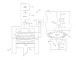
- FIGS. 1 and 2show simplified cross-sectional and perspective views, respectively, of a processing system that includes both an ion suppressor 110 as part of a capacitively coupled plasma (CCP) unit 102 and a showerhead 104 that may also contribute to ion suppression.
- the processing systemmay also optionally include components located outside the processing chamber 100 , such as fluid supply system 114 .
- the processing chamber 100may hold an internal pressure different than the surrounding pressure. For example, the pressure inside the processing chamber may be about 10 mTorr to about 20 Torr.
- the CCP unit 102may function to generate a plasma inside the processing chamber 100 .
- the components of the CCP unit 102may include a lid or hot electrode 106 and an ion suppression element 110 (also referred to herein as an ion suppressor).
- the lid 106 and ion suppressor 110are electrically conductive electrodes that can be electrically biased with respect to each other to generate an electric field strong enough to ionize gases between the electrodes into a plasma.
- An electrical insulator 108may separate the lid 106 and the ion suppressor 110 electrodes to prevent them from short circuiting when a plasma is generated.
- the plasma exposed surfaces of the lid 106 , insulator 108 , and ion suppressor 110may define a plasma excitation region 112 in the CCP unit 102 .
- Plasma generating gasesmay travel from a gas supply system 114 through a gas inlet 116 into the plasma excitation region 112 .
- the plasma generating gasesmay be used to strike a plasma in the excitation region 112 , or may maintain a plasma that has already been formed.
- the plasma generating gasesmay have already been at least partially converted into plasma excited species in a remote plasma system (not shown) positioned outside the processing chamber 100 before traveling downstream though the inlet 116 to the CCP unit 102 .
- the plasma excited speciesreach the plasma excitation region 112 , they may be further excited in the CCP unit 102 , or pass through the plasma excitation region without further excitation.
- the degree of added excitation provided by the CCP unit 102may change over time depending on the substrate processing sequence and/or conditions.
- the plasma generating gases and/or plasma excited speciesmay pass through a plurality of holes (not shown) in lid 106 for a more uniform delivery into the plasma excitation region 112 .
- Exemplary configurationsinclude having the inlet 116 open into a gas supply region 120 partitioned from the plasma excitation region 112 by lid 106 so that the gases/species flow through the holes in the lid 106 into the plasma excitation region 112 .
- Structural and operational featuresmay be selected to prevent significant backflow of plasma from the plasma excitation region 112 back into the supply region 120 , inlet 116 , and fluid supply system 114 .
- the structural featuresmay include the selection of dimensions and cross-sectional geometry of the holes in lid 106 that deactivates backstreaming plasma, as described below in FIGS. 7A and 7B .
- the operational featuresmay include maintaining a pressure difference between the gas supply region 120 and plasma excitation region 112 that maintains a unidirectional flow of plasma through the ion suppressor 110 .
- the lid 106 and the ion suppressor 110may function as a first electrode and second electrode, respectively, so that the lid 106 and/or ion suppressor 110 may receive an electric charge.
- electrical powere.g., RF power
- the substrate processing systemmay include a RF generator 140 that provides electrical power to the lid 106 and/or ion suppressor 110 .
- the electrically charged lid 106may facilitate a uniform distribution of plasma (i.e., reduce localized plasma) within the plasma excitation region 112 .
- insulator 108may electrically insulate lid 106 and ion suppressor 110 .
- Insulator 108may be made from a ceramic and may have a high breakdown voltage to avoid sparking.
- the CCP unit 102may further include a cooling unit (not shown) that includes one or more cooling fluid channels to cool surfaces exposed to the plasma with a circulating coolant (e.g., water).
- the ion suppressor 110may include a plurality of holes 122 that suppress the migration of ionically-charged species out of the plasma excitation region 112 while allowing uncharged neutral or radical species to pass through the ion suppressor 110 into an activated gas delivery region 124 .
- These uncharged speciesmay include highly reactive species that are transported with less reactive carrier gas through the holes 122 .
- adjustments in the ion concentration of the gas mixturecan significantly alter its etch selectivity (e.g., SiOx:SiNx etch ratios, Poly-Si:SiOx etch ratios, etc.). It can also shift the balance of conformal-to-flowable of a deposited dielectric material.
- etch selectivitye.g., SiOx:SiNx etch ratios, Poly-Si:SiOx etch ratios, etc.
- the plurality of holes 122may be configured to control the passage of the activated gas (i.e., the ionic, radical, and/or neutral species) through the ion suppressor 110 .
- the aspect ratio of the holes (i.e., the hole diameter to length) and/or the geometry of the holesmay be controlled so that the flow of ionically-charged species in the activated gas passing through the ion suppressor 110 is reduced.
- the holes in the ion suppressor 110may include a tapered portion that faces the plasma excitation region 112 , and a cylindrical portion that faces the showerhead 104 .
- the cylindrical portionmay be shaped and dimensioned to control the flow of ionic species passing to the showerhead 104 .
- An adjustable electrical biasmay also be applied to the ion suppressor 110 as an additional means to control the flow of ionic species through the suppressor.
- the showerhead 104is positioned between the ion suppressor 110 of the CCP unit 102 and a gas reaction region 130 (i.e., gas activation region) that makes contact with a substrate that may be mounted on a pedestal 150 .
- the gases and plasma excited speciesmay pass through the ion suppressor 110 into an activated gas delivery region 124 that is defined between the ion suppressor 110 and the showerhead 104 . A portion of these gases and species may further pass thorough the showerhead 104 into a gas reaction region 130 that makes contact with the substrate.
- the showerheadmay be a dual-zone showerhead that has a first set of channels 126 to permit the passage of plasma excited species, and a second set of channels that deliver a second gas/precursor mixture into the gas reaction/activation region 130 .
- the two sets of channelsprevent the plasma excited species and second gas/precursor mixture from combining until they reach the gas reaction region 130 .
- one or more of the holes 122 in the ion suppressor 110may be aligned with one or more of the channels 126 in the showerhead 104 to allow at least some of the plasma excited species to pass through a hole 122 and a channel 126 without altering their direction of flight.
- the second set of channelsmay have an annular shape at the opening facing the gas reaction region 130 , and these annular openings may be concentrically aligned around the circular openings of the first set of channels 126 .
- the second set of channels in the showerhead 104may be fluidly coupled to a source gas/precursor mixture (not shown) that is selected for the process to be performed.
- a source gas/precursor mixture(not shown) that is selected for the process to be performed.
- the gas/precursor mixturemay include a silicon-containing gas or precursor such as silane, disilane, TSA, DSA, TEOS, OMCTS, TMDSO, among other silicon-containing materials.
- This mixturemay react in gas reaction region 130 with an oxidizing gas mixture that may include plasma excited species such as plasma generated radical oxygen (O), activated molecular oxygen (O 2 ) and ozone (O 3 ), among other species.
- plasma excited speciessuch as plasma generated radical oxygen (O), activated molecular oxygen (O 2 ) and ozone (O 3 ), among other species.
- Excessive ions in the plasma excited speciesmay be reduced as the species move through the holes 122 in the ion suppressor 110 , and reduced further as the species move through the channels 126 in the showerhead 104 .
- the source gas/precursor mixturemay include etchants such as oxidants, halogens, water vapor and/or carrier gases that mix in the gas reaction region 130 with plasma excited species distributed from the first set of channels in the showerhead 104 .
- the processing systemmay further include a power supply 140 electrically coupled to the CCP unit 102 to provide electric power to the lid 106 and/or ion suppressor 110 to generate a plasma in the plasma excitation region 112 .
- the power supplymay be configured to deliver an adjustable amount of power to the CCP unit 102 depending on the process performed. In deposition processes for example, the power delivered to the CCP unit 102 may be adjusted to set the conformality of the deposited layer. Deposited dielectric films are typically more flowable at lower plasma powers and shift from flowable to conformal when the plasma power is increased.
- an argon containing plasma maintained in the plasma excitation region 112may produce a more flowable silicon oxide layer as the plasma power is decreased from about 1000 Watts to about 100 Watts or lower (e.g., about 900, 800, 700, 600, or 500 Watts or less), and a more conformal layer as the plasma power is increased from about 1000 Watts or more (e.g., about 1000, 1100, 1200, 1300, 1400, 1500, 1600, 1700 Watts or more).
- the plasma powerincreases from low to high, the transition from a flowable to conformal deposited film may be relatively smooth and continuous or progress through relatively discrete thresholds.
- the plasma power(either alone or in addition to other deposition parameters) may be adjusted to select a balance between the conformal and flowable properties of the deposited film.
- the processing systemmay still further include a pedestal 150 that is operable to support and move the substrate (e.g., a wafer substrate).
- the distance between the pedestal 150 and the showerhead 104help define the gas reaction region 130 .
- the pedestalmay be vertically or axially adjustable within the processing chamber 100 to increase or decrease the gas reaction region 130 and effect the deposition or etching of the wafer substrate by repositioning the wafer substrate with respect to the gases passed through the showerhead 104 .
- the pedestal 150may have a heat exchange channel through which a heat exchange fluid flows to control the temperature of the wafer substrate. Circulation of the heat exchange fluid allows the substrate temperature to be maintained at relatively low temperatures (e.g., about ⁇ 20° C. to about 90° C.).
- Exemplary heat exchange fluidsinclude ethylene glycol and water.
- the pedestal 150may also be configured with a heating element (such as a resistive heating element) to maintain the substrate at heating temperatures (e.g., about 90° C. to about 1100° C.).
- a heating elementsuch as a resistive heating element
- Exemplary heating elementsmay include a single-loop heater element embedded in the substrate support platter that makes two or more full turns in the form of parallel concentric circles. An outer portion of the heater element may run adjacent to a perimeter of the support platten, while an inner portion may run on the path of a concentric circle having a smaller radius.
- the wiring to the heater elementmay pass through the stem of the pedestal.
- FIG. 3shows a simplified schematic 300 of the gas flow paths of a pair of gas mixtures through a processing system that includes both an ion suppressor plate and a showerhead.
- a first gassuch as a plasma generating gas mixture
- the first gasmay include one or more of the following gases: CF 4 , NH 3 , NF 3 , Ar, He, H 2 O, H 2 , O 2 , etc.
- the first gasmay be excited through a plasma discharge to form one or more plasma effluents at block 310 .
- a remote plasma systemcoupled to the processing chamber may be used generate an ex-situ plasma whose plasma excitation products are introduced into the process chamber.
- the RPS plasma excitation productsmay include ionically-charged plasma species as well as neutral and radical species.
- the plasma effluentsare generated by an in-situ plasma unit, an RPS unit, or both, they may be passed through an ion suppressor in the processing chamber at block 315 .
- the ion suppressormay block and/or control the passage of ionic species while allowing the passage of radical and/or neutral species as the plasma activated first gas travels to the gas reaction region in the processing chamber.
- a second gasmay be introduced into the processing chamber.
- the contents of the second gasdepend on the process performed:
- the second gasmay include deposition compounds (e.g., Si-containing compounds) for deposition processes and etchants for etch processes. Contact and reaction between the first and second gases may be prevented until the gases arrive at the gas reaction region of the process chamber.
- Block 330shows the activated first gas and second gas passing through a DZSH that has a first plurality of channels that permit the activated first gas to pass through the showerhead without interacting with the second gas that passes through a second plurality of channels.
- the first and second gasesmay mix together in the gas reaction region of the processing chamber at block 335 .
- the combined gasesmay react to deposit a material on the exposed surfaces of the substrate, etch materials from the substrate, or both.
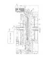
- FIG. 4a simplified cross-sectional view of a processing system 400 having a showerhead 402 that also acts as an ion suppression element is shown.
- a first gas source for plasma generation 402is fluidly coupled to an optional RPS unit 404 where a first plasma may be generated and the plasma effluents transported into the processing chamber 406 through gas inlet 408 .
- the gasesmay pass through holes 410 in a gas distribution plate 412 into a gas region 414 defined between the plate 412 and showerhead 402 .
- this region 414may be a plasma excitation/activation region where the gas distribution plate 412 and showerhead 402 act as first and second electrodes to further excite the gas and/or generate the first plasma.
- the holes 410 in the gas distribution plate 412may be dimensionally or geometrically structured to deactivate backstreaming plasma.
- the plate 412 and showerhead 402may be coupled with a RF power generator 422 that supplies a charge to the plate 412 and showerhead 402 to excite the gases and/or generate a plasma.
- the showerhead 402is grounded while a charge is applied to plate 412 .
- the excited gases or activated gases in the gas region 414may pass through showerhead 402 into a gas reaction region 416 adjacent a substrate 418 to etch material from the surface of the substrate and/or deposit material on the substrate's surface.
- the showerhead 402may be a dual zone showerhead (DZSH) that allows the excited gases to pass form the gas region 414 into the gas reaction region 416 while also allowing a second gas (i.e., precursor gas/mixture) to flow from an external source (not shown) into the gas reaction region 416 via a second gas inlet (not shown).
- the DZSHmay prevent the activated/excited gas from mixing with the second gas until the gases flow into the gas reaction region 416 .
- the excited gasmay flow through a plurality of holes 424 in the DZSH, which may be dimensionally and/or geometrically structured to control or prevent the passage plasma (i.e., ionically charged species) while allowing the passage of activated/excited gases (i.e., reactive radical or uncharged neutral species).
- FIG. 7Aprovides exemplary embodiments of hole configurations that may be used in the DZSH.
- the DZSHmay include a plurality of channels 426 through which the second gas flows.
- the second gas (precursor gas)may exit the showerhead 402 through one or more apertures (not shown) that are positioned adjacent holes 424 .
- the DZSHmay act as both a second gas delivery system and an ion suppression element.
- the mixed gasesmay deposit a material on and/or etch the surface of the substrate 418 , which may be positioned on a platen 420 .
- the platen 420may be vertically movable within the processing chamber 406 .
- the processing of the substrate 418 within the processing chamber 406may be affected by the configurations of the holes 424 , the pressure within the gas region 414 , and/or the position of the substrate 418 within the processing chamber. Further, the configuration of the holes 424 and/or pressure within the gas region 414 may control the amount of ion species (plasma) allowed to pass into the gas excitation region 416 .
- the ionic concentration of the gas mixturecan shift the balance of conformal-to-flowable of a deposited dielectric material in addition to altering the etch selectivity.
- FIG. 5a simplified cross-sectional view of another processing system 500 having a plate 512 (i.e., ion suppressor plate) that acts as an ion suppression element is shown.
- a first gas source 502is fluidly coupled to an RPS unit 504 where a first plasma may be generated and the plasma effluents transported into the processing chamber 506 through gas inlet 508 .
- the plasma effluentsmay be transported to a gas region 514 defined between the ion suppressor plate 512 and the gas inlet 508 .
- the gasesmay pass through holes 510 in the ion suppressor 512 into a gas reaction/activation region 516 defined between the ion suppressor 512 and a substrate 528 .
- the substrate 518may be supported on a platen 520 as described above so that the substrate is movable within the processing chamber 506 .
- the holes 510may be dimensionally and/or geometrically structured so that the passage of ionically charged species (i.e., plasma) is prevented and/or controlled while the passage of uncharged neutral or radical species (i.e., activated gas) is permitted.
- the passage of ionic speciesmay be controllable by varying the pressure of the plasma within gas region 514 .
- the pressure in gas region 514may be controlled by controlling the amount of gas delivered through gas inlet 508 .
- the precursor gasi.e., second gas
- the second gas inlet 522may include one or more apertures, tubes, etc.
- the ion suppressor 512includes one or more second gas inlets, through which the precursor gas flows.
- the second gas inlets of the ion suppressor 512may deliver the precursor gas into the gas reaction region 516 .
- the ion suppressor 512functions as both an ion suppressor and a dual zone showerhead as described previously.
- the activated gas that passes through the holes 510 and the precursor gas introduced in the processing chamber 506may be mixed in the gas reaction chamber 516 for etching and/or deposition processes.
- ion suppressorssuch as ion suppressor plates 412 and 512 and showerhead 402 .
- FIG. 6Ashows a simplified perspective view of an ion-suppression element 600 (ion suppressor) according to embodiments of the invention.
- the ion suppression element 600may correspond with the ion suppressor plates of FIGS. 4 and/or 5 .
- the perspective viewshows the top of the ion suppression element or plate 600 .
- the ion suppression plate 600may be generally circular shaped and may include a plurality of plasma effluent passageways 602 , where each of the passageways 602 includes one or more through holes that allow passage of the plasma effluents from a first region (e.g., plasma region) to a second region (e.g., gas reaction region or showerhead).
- the through holes of the passageway 602may be arranged to form one or more circular patterns, although other configurations are possible.
- the through holesmay be geometrically or dimensionally configured to control or prevent the passage of ion species while allowing the passage or uncharged neutral or radical species.
- the through holesmay have a larger inner diameter toward the top surface of the ion suppression plate 600 and a smaller inner diameter toward the bottom surface of the ion suppression plate.
- the through holesmay be generally cylindrical, conical, or any combination thereof. Exemplary embodiments of the configurations of the through holes are provided in FIGS. 7A-B .
- the plurality of passagewaysmay be distributed substantially evenly over the surface of the ion suppression plate 600 , which may provide even passage of neutral or radical species through the ion suppression plate 600 into the second region.
- the processing chambermay only include an ion suppression plate 600
- the processing chambermay include both a ion suppression plate 600 and a showerhead, such as the showerhead of FIG. 6B , or the processing chamber may include a single plate that acts as both a dual zone showerhead and an ion suppression plate.
- FIG. 6Bshows a simplified bottom view perspective of a showerhead 620 according to embodiments of the invention.
- the showerhead 620may correspond with the showerhead illustrated in FIG. 4 .
- the showerhead 620may be positioned vertically adjacent to and above a gas reaction region.
- the showerhead 620may be generally circular shaped and may include a plurality of first holes 622 and a plurality of second holes 624 .
- the plurality of first holes 622may allow plasma effluents to pass through the showerhead 620 into a gas reaction region, while the plurality of second holes 624 allows a precursor gas, such as a silicon precursor, etchants etc., to pass into the gas reaction region.
- the plurality of first holes 622may be through holes that extend from the top surface of the showerhead 620 through the showerhead.
- each of the plurality of first holes 622may have a smaller inner diameter (ID) toward the top surface of the showerhead 620 and a larger ID toward the bottom surface.
- the bottom edge of the plurality of first holes 622may be chamfered 626 to help evenly distribute the plasma effluents in the gas reaction region as the plasma effluents exit the showerhead and thereby promote even mixing of the plasma effluents and precursor gases.
- the smaller ID of the first holes 622may be between about 0.5 mm and about 20 mm. In one embodiment, the smaller ID may be between about 1 mm and 6 mm.
- the cross sectional shape of the first holes 622may be generally cylindrical, conical, or any combination thereof. Further, the first holes 622 may be concentrically aligned with the through holes of passageways 602 , when both and ion suppression element 600 and a showerhead 620 are used in a processing chamber. The concentric alignment may facilitate passage of an activated gas through both the ion suppression element 600 and showerhead 620 in the processing chamber.
- the plurality of first holesmay 622 be through holes that extend from the top surface of the showerhead 620 through the showerhead, where each of the first holes 622 have a larger ID toward the top surface of the showerhead and a smaller ID toward the bottom surface of the showerhead.
- the first holes 622may include a taper region that transition between the larger and smaller IDs. Such a configuration may prevent or regulate the passage of a plasma through the through holes while permitting the passage of an activated gas.
- Such embodimentsmay be used in place or in addition to ion suppression element 600 . Exemplary embodiments of such through holes are provided in FIG. 7A .
- the number of the plurality of first holes 622may be between about 60 and about 2000.
- the plurality of first holes 622may also have a variety of shapes, but are generally round.
- the plurality of first holes 622may be substantially aligned with the passageways 602 to facilitate passage of the plasma effluents through the ion suppression plate and showerhead.
- the plurality of second holes 624may extend partially through the showerhead from the bottom surface of the showerhead 620 partially through the showerhead.
- the plurality of second holesmay be coupled with or connected to a plurality of channels (not shown) that deliver the precursor gas (e.g., deposition compounds, etchants, etc.) to the second holes 624 from an external gas source (not shown).
- the second holesmay include a smaller ID at the bottom surface of the showerhead 620 and a larger ID in the interior of the showerhead.
- the number of second holes 624may be between about 100 and about 5000 or between about 500 and about 2000 in different embodiments.
- the diameter of the second hole's smaller IDi.e., the diameter of the hole at the bottom surface
- the second holes 624are generally round and may likewise be cylindrical, conical, or any combination thereof. Both the first and second holes may be evenly distributed over the bottom surface of the showerhead 620 to promote even mixing of the plasma effluents and precursor gases.
- the through holes depictedgenerally include a large inner diameter (ID) region toward an upper end of the hole and a smaller ID region toward the bottom or lower end of the hole.
- the smaller IDmay be between about 0.2 mm and about 5 mm.
- the aspect ratio of the holesi.e., the smaller ID to hole length
- Such configurationsmay substantially block and/or control passage of ion species of the plasma effluent while allowing the passage of radical or neutral species.
- varying the aspect ratiomay regulate the amount of plasma that is allowed to pass through the through holes.
- Plasma passagemay further be regulated by varying the pressure of the plasma within a region directly above the through holes.
- through hole 702may include a large ID region 704 at an upper end of the hole and a small ID region 706 at a lower end of the hole with a stepped edge between the large and small IDs.
- Through hole 710may include a large ID region 712 on an upper end and a large ID region 716 on a lower end of the hole with a small ID region 714 therebetween.
- the transition between the large and small ID regionsmay be stepped or blunt to provide an abrupt transition between the regions.
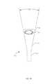
- Through hole 720may include a large ID region 722 at the upper end of the hole and small ID region 726 at a lower end of the hole with a tapered region 724 that transitions at an angle ⁇ between the large and small regions.
- the height 728 of the small ID region 726may depend on the overall height 727 of the hole, the angle ⁇ of tapered region 724 , the large ID, and the small ID.
- the tapered region 724comprises an angle of between about 15° and about 30°, and preferably about 22°; the overall height 727 is between about 4 mm and about 8 mm, and preferably about 6.35 mm; the large ID is between about 1 mm and about 4 mm, and preferably about 2.54 mm; the small ID is between about 0.2 mm and 1.2 mm, and preferably about 0.89 mm, so that the height 728 of the small ID region 726 region is between about 1 mm and about 3 mm, and preferably about 2.1 mm.
- Through hole 730may include a first ID region 732 at the upper end of the hole, a second ID region 734 concentrically aligned with and positioned vertically below first ID region 732 , and a third ID region 736 concentrically aligned with and positioned vertically below second ID region 734 .
- First ID region 732may comprise a large ID
- second ID region 734may comprise a small ID
- third ID region 736may comprise a slightly larger ID than second ID region 734 .
- Third ID region 736may extend to the lower end of the hole or may be outwardly tapered to an exit ID 737 .
- the taper between the third ID region 736 and the exit ID 737may taper at an angle ⁇ 3 , which may be between about 15° and about 30°, and preferably about 22°.
- the second ID region 734may include a chamfered edge that transitions from the first ID region 732 at an angle ⁇ 1 , which may be between about 110° and about 140°.
- the second ID region 734may include a chamfered edge that transitions into the third ID region 736 at an angle ⁇ 2 , which may also be between about 110° and about 140°.
- the large ID of first region 732may be between about 2.5 mm and about 7 mm, and preferably about 3.8 mm; the small ID of second ID region 734 may be between about 0.2 mm and about 5 mm, and preferably about 0.04 mm; the slightly larger ID of third ID region 736 may be between about 0.75 mm and about 2 mm, and preferably about 1.1 mm; and the exit ID may be between about 2.5 mm and about 5 mm, and preferably about 3.8 mm.
- the transition (blunt, stepped, tapered, etc.) between the large ID regions and small ID regionsmay substantially block the passage of ion species from passing through the holes while allowing the passage or radical or neutral species.
- FIG. 7Bshown is an enlarged illustration of through hole 720 that includes the transition region 724 between the large ID region 722 and the small ID region 726 .
- the tapered region 724may substantially prevent plasma 725 from penetrating through the through hole 702 .
- the ion speciesmay deactivate or ground out by contacting the walls of the tapered region 724 , thereby limiting the passage of the plasma through the through hole and containing the plasma within the region above the through hole 720 .
- the radical or neutral speciesmay pass through the through hole 720 .
- the through hole 720may filter the plasma 720 to prevent or control the passage of unwanted species.
- the small ID region 726 of the through holescomprises an ID of 1 mm or smaller. To maintain a signification concentration of radical and/or neutral species penetrating through the through holes, the length of the small ID region and/or the taper angle may be controlled.
- the through holes described hereinmay be used to regulate the passage of plasma so that a desired level of plasma is allowed to pass through the through hole. Regulating the flow of plasma through the through holes may include increasing the pressure of the plasma in the gas region above the ion suppressor plate so that a desired fraction of the plasma is able to pass through the ion suppressor without deactivating or grounding out.
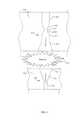
- the CCP unit 800 shownincludes a top plate 802 and a bottom plate 804 that define a plasma generation region 810 in which a plasma is contained.
- the plasmamay be generated by an RPS (not shown) and delivered to the plasma generation region 810 via through hole 806 .
- the plasmamay be generated in the CCP unit 800 , for example, by utilizing top plate 802 and bottom plate 804 as first and second electrodes coupled to a power generation unit (not shown).
- the top plate 802may include a through hole 806 that allows process gas and/or plasma to be delivered into the plasma generation region 810 while preventing backstreaming of plasma through the top plate 802 .
- the through hole 806may be configured similar to through hole 730 having first, second, and third ID regions ( 820 , 822 , and 824 respectively), with a chamfered edge between adjacent regions ( 828 and 829 ) and a tapered region 826 transitioning between third ID region 824 and an exit ID.
- the tapered region 826 between third ID region 824 and the exit ID and/or the chamfered edge between second and third ID regions ( 822 and 824 respectively)may prevent backstreaming of plasma by deactivating or grounding ion species as the plasma penetrates into the through hole 806 .
- the bottom plate 804may include a through hole 808 that allows the radical or neutral species to pass through the through hole while preventing or controlling the passage of ion species.
- the through hole 808may be configured similar to through hole 720 having a large ID region 830 , a small ID region 832 , and a tapered region 834 that transitions between the large ID region 830 and the small ID region 832 .
- the tapered region 834may prevent the flow of plasma through the through hole 808 by deactivating or grounding ion species as previously explained while allowing radical or neutral species to pass therethrough.
- the top plate 802 and/or bottom plate 804may receive a charge to electrically bias the plasma and contain the plasma within plasma generation region 810 and/or adjust an ion concentration in the activated gas that passes through the bottom plate.
- the plasmamay be substantially generated and/or maintained in the plasma generation region 810 , while radical and neutral species are delivered to a gas reaction region to be mixed with one or more precursor gases to etch material from or deposit material on a substrate surface.
Landscapes
- Chemical & Material Sciences (AREA)
- Engineering & Computer Science (AREA)
- Physics & Mathematics (AREA)
- Plasma & Fusion (AREA)
- Analytical Chemistry (AREA)
- Chemical Kinetics & Catalysis (AREA)
- Mechanical Engineering (AREA)
- Organic Chemistry (AREA)
- Metallurgy (AREA)
- Materials Engineering (AREA)
- General Chemical & Material Sciences (AREA)
- Manufacturing & Machinery (AREA)
- General Physics & Mathematics (AREA)
- Condensed Matter Physics & Semiconductors (AREA)
- Computer Hardware Design (AREA)
- Microelectronics & Electronic Packaging (AREA)
- Power Engineering (AREA)
- Drying Of Semiconductors (AREA)
- Plasma Technology (AREA)
- Spectroscopy & Molecular Physics (AREA)
- Chemical Vapour Deposition (AREA)
Abstract
Description
This application is a continuation of U.S. patent application Ser. No. 13/251,663 filed Oct. 3, 2011 titled “SEMICONDUCTOR PROCESSING SYSTEM AND METHODS USING CAPACITIVELY COUPLED PLASMA,” which is a nonprovisional of, and claims the benefit of the filing date of, U.S. Provisional Patent Application No. 61/433,633, entitled “SEMICONDUCTOR PROCESSING SYSTEM AND METHODS USING CAPACITIVELY COUPLED PLASMA, filed Jan. 18, 2011, the entire disclosure of which is incorporated herein by reference for all purposes.
Plasma deposition and etching processes for fabricating semiconductor integrated circuits have been in wide use for decades. These processes typically involve the formation of a plasma from plasma-generating gases that are exposed to electric fields of sufficient power inside the processing chamber to cause the gases to ionize. The temperatures needed to form these gases into plasmas can be much lower than needed to thermally ionize the same gases. Thus, plasma generation processes can be used to generate reactive radical and ion species from the starting gases at significantly lower chamber processing temperatures than is possible by simply heating the gases. This allows the plasma to deposit and/or etch materials from substrate surfaces without raising the substrate temperature above a threshold that will melt, decompose, or otherwise damage materials on the substrate.
Exemplary plasma deposition processes include plasma-enhanced chemical vapor deposition (PECVD) of dielectric materials such as silicon oxide on exposed surfaces of a substrate wafer. Conventional PECVD involves the mixing together of gases and/or deposition precursors in the processing chamber and striking a plasma from the gases to generate reactive species that react and deposit material on the substrate. The plasma is typically positioned close to the exposed surface of the substrate to facilitate the efficient deposition of the reaction products.
Similarly, plasma etching processes include exposing selected parts of the substrate to plasma activated etching species that chemically react and/or physically sputter materials from the substrate. The removal rates, selectivity, and direction for the plasma etched materials can be controlled with adjustments to the etchant gases, plasma excitation energy, and electrical bias between the substrate and charged plasma species, among other parameters. Some plasma techniques, such as high-density plasma chemical vapor deposition (HDP-CVD), rely on simultaneous plasma etching and deposition to create features on the substrate.
While plasma environments are generally less destructive to substrates than high-temperature deposition environments, they still create fabrication challenges. Etching precision can be a problem with energetic plasmas that over-etch shallow trenches and gaps. Energetic species in the plasmas, especially ionized species, can create unwanted reactions in a deposited material that adversely affect the material's performance. Thus, there is a need for systems and methods to provide more precise control over the plasma components that make contact with a substrate wafer during fabrication.
Systems and methods are described for improved control of the environment between a plasma and the surfaces of a substrate wafer that are exposed to plasma and/or its effluents. The improved control may be realized at least in part by an ion suppression element positioned between the plasma and the substrate that reduces or eliminates the number of ionically-charged species that reach the substrate. Adjusting the concentration of ion species that reach the substrate surface allows more precise control of the etch rate, etch selectivity, and deposition chemistry (among other parameters) during a plasma assisted etch and/or deposition on the substrate.
In some examples, the ion suppression element may be part of the gas/precursor delivery equipment of a substrate processing chamber. For example, a showerhead positioned inside the chamber between a plasma region and the substrate may act as both a distribution component for gases and precursors as well as an ion suppressor that reduces the amount of ionized species traveling through the showerhead from the plasma region to the substrate. In additional examples, the ion suppression element may be a partition between the plasma region and the substrate that has one or more openings through which plasma effluents may pass from the plasma region to the substrate. The size, position and geometry of the openings, the distance between the partition and the substrate, and the electrical bias on the partition, among other characteristics, may be selected to control the amounts of charged species reaching the substrate. In some instances the partition may also act as an electrode that helps generate and define the plasma region in the processing chamber.
Embodiments of the invention include a substrate processing system that has a capacitively coupled plasma (CCP) unit positioned inside the process chamber. The CCP unit may include a plasma excitation region formed between a first electrode and a second electrode. The first electrode may include a first plurality of openings to permit a first gas to enter the plasma excitation region, and the second electrode may include a second plurality of openings to permit an activated gas to exit the plasma excitation region. The system may further include a gas inlet for supplying the first gas to the first electrode of the CCP unit, and a pedestal that is operable to support a substrate. The pedestal is positioned below a gas reaction region into which the activated gas travels from the CCP unit.
Embodiments of the invention further include additional substrate processing systems. These systems may include a gas inlet for supplying a first gas to a processing chamber, an electrode comprising a plurality of openings, and a showerhead. The showerhead may include a first plurality of channels that permit the passage of an activated gas to a gas reaction region in the processing chamber, and a second plurality of channels that permit passage of a second gas to the gas reaction region. The activated gas is formed in a plasma excitation region between the electrode and the showerhead, which also acts as a second electrode. The systems may further include a pedestal positioned below the gas reaction region that is operable to support a substrate.
Embodiments of the invention still further include substrate processing systems having an ion suppressor. These systems may include a gas inlet for supplying a first gas to a processing chamber, an electrode with a first plurality of openings, and the ion suppressor. The ion suppressor may include an electrically conductive plate having a second plurality of openings that permit the passage of an activated gas to a gas reaction region in the processing chamber. The activated gas is formed in a plasma excitation region between the electrode and the ion suppressor. These systems may further include a pedestal, positioned below the gas reaction region, that is operable to support a substrate.
Additional embodiments and features are set forth in part in the description that follows, and in part will become apparent to those skilled in the art upon examination of the specification or may be learned by the practice of the invention. The features and advantages of the invention may be realized and attained by means of the instrumentalities, combinations, and methods described in the specification.
A further understanding of the nature and advantages of the present invention may be realized by reference to the remaining portions of the specification and the drawings wherein like reference numerals are used throughout the several drawings to refer to similar components. In some instances, a sublabel is associated with a reference numeral and follows a hyphen to denote one of multiple similar components. When reference is made to a reference numeral without specification to an existing sublabel, it is intended to refer to all such multiple similar components.
Systems and methods are described for the generation and control of a plasma inside a semiconductor processing chamber. The plasma may originate inside the processing chamber, outside the processing chamber in a remote plasma unit, or both. Inside the chamber, the plasma is contained and separated from the substrate wafer with the help of an ion suppression element that is positioned between the plasma and the substrate wafer. In some instances, this ion suppression element may also function as part of a plasma generation unit (e.g., an electrode), a gas/precursor distribution system (e.g., a showerhead), and/or another component of the processor system. In additional instances, the ion suppression element may function primarily to define a partition between a plasma generation region and a gas reaction region that etches and/or deposits material on exposed surfaces of the substrate wafer.
The ion suppression element functions to reduce or eliminate the amount of ionically charged species traveling from the plasma generation region to the substrate. Uncharged neutral and radical species may still pass through the openings in the ion suppressor to react with substrate. It should be noted that the complete elimination of ionically charged species in the reaction region surrounding the substrate is not always the desired goal. In many instances, ionic species are required to reach the substrate in order to perform the etch and/or deposition process. In these instances, the ion suppressor helps control the concentration of ionic species in the reaction region at a level that assists the process.
Exemplary Processing System Configurations
Exemplary processing system configurations include an ion suppressor positioned inside a processing chamber to control the type and quantity of plasma excited species that reach the substrate. In some embodiments the ion suppressor unit may be a perforated plate that may also act as an electrode of the plasma generating unit. In additional embodiments the ion suppressor may be the showerhead that distributes gases and excited species to a reaction region in contact with the substrate. In still more embodiments ion suppression may be realized by a perforated plate ion suppressor and a showerhead, both of which plasma excited species pass through to reach the reaction region.
The CCP unit102 may function to generate a plasma inside theprocessing chamber 100. The components of the CCP unit102 may include a lid orhot electrode 106 and an ion suppression element110 (also referred to herein as an ion suppressor). In some embodiments, thelid 106 andion suppressor 110 are electrically conductive electrodes that can be electrically biased with respect to each other to generate an electric field strong enough to ionize gases between the electrodes into a plasma. An electrical insulator108, may separate thelid 106 and theion suppressor 110 electrodes to prevent them from short circuiting when a plasma is generated. The plasma exposed surfaces of thelid 106, insulator108, andion suppressor 110 may define aplasma excitation region 112 in the CCP unit102.
Plasma generating gases may travel from agas supply system 114 through a gas inlet116 into theplasma excitation region 112. The plasma generating gases may be used to strike a plasma in theexcitation region 112, or may maintain a plasma that has already been formed. In some embodiments, the plasma generating gases may have already been at least partially converted into plasma excited species in a remote plasma system (not shown) positioned outside theprocessing chamber 100 before traveling downstream though the inlet116 to the CCP unit102. When the plasma excited species reach theplasma excitation region 112, they may be further excited in the CCP unit102, or pass through the plasma excitation region without further excitation. In some operations, the degree of added excitation provided by the CCP unit102 may change over time depending on the substrate processing sequence and/or conditions.
The plasma generating gases and/or plasma excited species may pass through a plurality of holes (not shown) inlid 106 for a more uniform delivery into theplasma excitation region 112. Exemplary configurations include having the inlet116 open into agas supply region 120 partitioned from theplasma excitation region 112 bylid 106 so that the gases/species flow through the holes in thelid 106 into theplasma excitation region 112. Structural and operational features may be selected to prevent significant backflow of plasma from theplasma excitation region 112 back into thesupply region 120, inlet116, andfluid supply system 114. The structural features may include the selection of dimensions and cross-sectional geometry of the holes inlid 106 that deactivates backstreaming plasma, as described below inFIGS. 7A and 7B . The operational features may include maintaining a pressure difference between thegas supply region 120 andplasma excitation region 112 that maintains a unidirectional flow of plasma through theion suppressor 110.
As noted above, thelid 106 and theion suppressor 110 may function as a first electrode and second electrode, respectively, so that thelid 106 and/orion suppressor 110 may receive an electric charge. In these configurations, electrical power (e.g., RF power) may be applied to thelid 106,ion suppressor 110, or both. For example, electrical power may be applied to thelid 106 while theion suppressor 110 is grounded. The substrate processing system may include a RF generator140 that provides electrical power to thelid 106 and/orion suppressor 110. The electrically chargedlid 106 may facilitate a uniform distribution of plasma (i.e., reduce localized plasma) within theplasma excitation region 112. To enable the formation of a plasma in theplasma excitation region 112, insulator108 may electrically insulatelid 106 andion suppressor 110. Insulator108 may be made from a ceramic and may have a high breakdown voltage to avoid sparking. The CCP unit102 may further include a cooling unit (not shown) that includes one or more cooling fluid channels to cool surfaces exposed to the plasma with a circulating coolant (e.g., water).
Theion suppressor 110 may include a plurality ofholes 122 that suppress the migration of ionically-charged species out of theplasma excitation region 112 while allowing uncharged neutral or radical species to pass through theion suppressor 110 into an activatedgas delivery region 124. These uncharged species may include highly reactive species that are transported with less reactive carrier gas through theholes 122. As noted above, the migration of ionic species through theholes 122 may be reduced, and in some instances completely suppressed. Controlling the amount of ionic species passing through theion suppressor 110 provides increased control over the gas mixture brought into contact with the underlying wafer substrate, which in turn increases control of the deposition and/or etch characteristics of the gas mixture. For example, adjustments in the ion concentration of the gas mixture can significantly alter its etch selectivity (e.g., SiOx:SiNx etch ratios, Poly-Si:SiOx etch ratios, etc.). It can also shift the balance of conformal-to-flowable of a deposited dielectric material.
The plurality ofholes 122 may be configured to control the passage of the activated gas (i.e., the ionic, radical, and/or neutral species) through theion suppressor 110. For example, the aspect ratio of the holes (i.e., the hole diameter to length) and/or the geometry of the holes may be controlled so that the flow of ionically-charged species in the activated gas passing through theion suppressor 110 is reduced. The holes in theion suppressor 110 may include a tapered portion that faces theplasma excitation region 112, and a cylindrical portion that faces theshowerhead 104. The cylindrical portion may be shaped and dimensioned to control the flow of ionic species passing to theshowerhead 104. An adjustable electrical bias may also be applied to theion suppressor 110 as an additional means to control the flow of ionic species through the suppressor.
Theshowerhead 104 is positioned between theion suppressor 110 of the CCP unit102 and a gas reaction region130 (i.e., gas activation region) that makes contact with a substrate that may be mounted on a pedestal150. The gases and plasma excited species may pass through theion suppressor 110 into an activatedgas delivery region 124 that is defined between theion suppressor 110 and theshowerhead 104. A portion of these gases and species may further pass thorough theshowerhead 104 into agas reaction region 130 that makes contact with the substrate.
The showerhead may be a dual-zone showerhead that has a first set ofchannels 126 to permit the passage of plasma excited species, and a second set of channels that deliver a second gas/precursor mixture into the gas reaction/activation region 130. The two sets of channels prevent the plasma excited species and second gas/precursor mixture from combining until they reach thegas reaction region 130. In some embodiments, one or more of theholes 122 in theion suppressor 110 may be aligned with one or more of thechannels 126 in theshowerhead 104 to allow at least some of the plasma excited species to pass through ahole 122 and achannel 126 without altering their direction of flight. In additional embodiments, the second set of channels may have an annular shape at the opening facing thegas reaction region 130, and these annular openings may be concentrically aligned around the circular openings of the first set ofchannels 126.
The second set of channels in theshowerhead 104 may be fluidly coupled to a source gas/precursor mixture (not shown) that is selected for the process to be performed. For example, when the processing system is configured to perform a deposition of a dielectric material such as silicon dioxide (SiOx) the gas/precursor mixture may include a silicon-containing gas or precursor such as silane, disilane, TSA, DSA, TEOS, OMCTS, TMDSO, among other silicon-containing materials. This mixture may react ingas reaction region 130 with an oxidizing gas mixture that may include plasma excited species such as plasma generated radical oxygen (O), activated molecular oxygen (O2) and ozone (O3), among other species. Excessive ions in the plasma excited species may be reduced as the species move through theholes 122 in theion suppressor 110, and reduced further as the species move through thechannels 126 in theshowerhead 104. In another example, when the processing system in configured to perform an etch on the substrate surface, the source gas/precursor mixture may include etchants such as oxidants, halogens, water vapor and/or carrier gases that mix in thegas reaction region 130 with plasma excited species distributed from the first set of channels in theshowerhead 104.
The processing system may further include a power supply140 electrically coupled to the CCP unit102 to provide electric power to thelid 106 and/orion suppressor 110 to generate a plasma in theplasma excitation region 112. The power supply may be configured to deliver an adjustable amount of power to the CCP unit102 depending on the process performed. In deposition processes for example, the power delivered to the CCP unit102 may be adjusted to set the conformality of the deposited layer. Deposited dielectric films are typically more flowable at lower plasma powers and shift from flowable to conformal when the plasma power is increased. For example, an argon containing plasma maintained in theplasma excitation region 112 may produce a more flowable silicon oxide layer as the plasma power is decreased from about 1000 Watts to about 100 Watts or lower (e.g., about 900, 800, 700, 600, or 500 Watts or less), and a more conformal layer as the plasma power is increased from about 1000 Watts or more (e.g., about 1000, 1100, 1200, 1300, 1400, 1500, 1600, 1700 Watts or more). As the plasma power increases from low to high, the transition from a flowable to conformal deposited film may be relatively smooth and continuous or progress through relatively discrete thresholds. The plasma power (either alone or in addition to other deposition parameters) may be adjusted to select a balance between the conformal and flowable properties of the deposited film.
The processing system may still further include a pedestal150 that is operable to support and move the substrate (e.g., a wafer substrate). The distance between the pedestal150 and theshowerhead 104 help define thegas reaction region 130. The pedestal may be vertically or axially adjustable within theprocessing chamber 100 to increase or decrease thegas reaction region 130 and effect the deposition or etching of the wafer substrate by repositioning the wafer substrate with respect to the gases passed through theshowerhead 104. The pedestal150 may have a heat exchange channel through which a heat exchange fluid flows to control the temperature of the wafer substrate. Circulation of the heat exchange fluid allows the substrate temperature to be maintained at relatively low temperatures (e.g., about −20° C. to about 90° C.). Exemplary heat exchange fluids include ethylene glycol and water.
The pedestal150 may also be configured with a heating element (such as a resistive heating element) to maintain the substrate at heating temperatures (e.g., about 90° C. to about 1100° C.). Exemplary heating elements may include a single-loop heater element embedded in the substrate support platter that makes two or more full turns in the form of parallel concentric circles. An outer portion of the heater element may run adjacent to a perimeter of the support platten, while an inner portion may run on the path of a concentric circle having a smaller radius. The wiring to the heater element may pass through the stem of the pedestal.
Whether the plasma effluents are generated by an in-situ plasma unit, an RPS unit, or both, they may be passed through an ion suppressor in the processing chamber atblock 315. The ion suppressor may block and/or control the passage of ionic species while allowing the passage of radical and/or neutral species as the plasma activated first gas travels to the gas reaction region in the processing chamber. Atblock 320, a second gas may be introduced into the processing chamber. As noted above, the contents of the second gas depend on the process performed: For example, the second gas may include deposition compounds (e.g., Si-containing compounds) for deposition processes and etchants for etch processes. Contact and reaction between the first and second gases may be prevented until the gases arrive at the gas reaction region of the process chamber.
One way to prevent the first and second gases from interacting before the gas reaction region is to have them flow though separate channels in a dual-zone showerhead.Block 330 shows the activated first gas and second gas passing through a DZSH that has a first plurality of channels that permit the activated first gas to pass through the showerhead without interacting with the second gas that passes through a second plurality of channels. After exiting the DZSH, the first and second gases may mix together in the gas reaction region of the processing chamber at block335. Depending on the process performed, the combined gases may react to deposit a material on the exposed surfaces of the substrate, etch materials from the substrate, or both.
Referring now toFIG. 4 , a simplified cross-sectional view of aprocessing system 400 having ashowerhead 402 that also acts as an ion suppression element is shown. In the configuration shown, a first gas source forplasma generation 402 is fluidly coupled to anoptional RPS unit 404 where a first plasma may be generated and the plasma effluents transported into theprocessing chamber 406 throughgas inlet 408. Inside theprocessing chamber 406, the gases may pass throughholes 410 in agas distribution plate 412 into agas region 414 defined between theplate 412 andshowerhead 402. In some embodiments, thisregion 414 may be a plasma excitation/activation region where thegas distribution plate 412 andshowerhead 402 act as first and second electrodes to further excite the gas and/or generate the first plasma. Theholes 410 in thegas distribution plate 412 may be dimensionally or geometrically structured to deactivate backstreaming plasma. Theplate 412 andshowerhead 402 may be coupled with aRF power generator 422 that supplies a charge to theplate 412 and showerhead402 to excite the gases and/or generate a plasma. In one embodiment, theshowerhead 402 is grounded while a charge is applied toplate 412.
The excited gases or activated gases in thegas region 414 may pass throughshowerhead 402 into agas reaction region 416 adjacent asubstrate 418 to etch material from the surface of the substrate and/or deposit material on the substrate's surface. Theshowerhead 402 may be a dual zone showerhead (DZSH) that allows the excited gases to pass form thegas region 414 into thegas reaction region 416 while also allowing a second gas (i.e., precursor gas/mixture) to flow from an external source (not shown) into thegas reaction region 416 via a second gas inlet (not shown). The DZSH may prevent the activated/excited gas from mixing with the second gas until the gases flow into thegas reaction region 416.
The excited gas may flow through a plurality ofholes 424 in the DZSH, which may be dimensionally and/or geometrically structured to control or prevent the passage plasma (i.e., ionically charged species) while allowing the passage of activated/excited gases (i.e., reactive radical or uncharged neutral species).FIG. 7A provides exemplary embodiments of hole configurations that may be used in the DZSH. In addition to theholes 424, the DZSH may include a plurality of channels426 through which the second gas flows. The second gas (precursor gas) may exit theshowerhead 402 through one or more apertures (not shown) that are positionedadjacent holes 424. The DZSH may act as both a second gas delivery system and an ion suppression element.
As described above, the mixed gases may deposit a material on and/or etch the surface of thesubstrate 418, which may be positioned on aplaten 420. Theplaten 420 may be vertically movable within theprocessing chamber 406. The processing of thesubstrate 418 within theprocessing chamber 406 may be affected by the configurations of theholes 424, the pressure within thegas region 414, and/or the position of thesubstrate 418 within the processing chamber. Further, the configuration of theholes 424 and/or pressure within thegas region 414 may control the amount of ion species (plasma) allowed to pass into thegas excitation region 416. The ionic concentration of the gas mixture can shift the balance of conformal-to-flowable of a deposited dielectric material in addition to altering the etch selectivity.
Referring now toFIG. 5 , a simplified cross-sectional view of anotherprocessing system 500 having a plate512 (i.e., ion suppressor plate) that acts as an ion suppression element is shown. In the configuration shown, a first gas source502 is fluidly coupled to anRPS unit 504 where a first plasma may be generated and the plasma effluents transported into theprocessing chamber 506 through gas inlet508. The plasma effluents may be transported to agas region 514 defined between theion suppressor plate 512 and the gas inlet508. Inside thegas region 514, the gases may pass through holes510 in theion suppressor 512 into a gas reaction/activation region516 defined between theion suppressor 512 and a substrate528. Thesubstrate 518 may be supported on a platen520 as described above so that the substrate is movable within theprocessing chamber 506.
Also as described above, the holes510 may be dimensionally and/or geometrically structured so that the passage of ionically charged species (i.e., plasma) is prevented and/or controlled while the passage of uncharged neutral or radical species (i.e., activated gas) is permitted. The passage of ionic species may be controllable by varying the pressure of the plasma withingas region 514. The pressure ingas region 514 may be controlled by controlling the amount of gas delivered through gas inlet508. The precursor gas (i.e., second gas) may be introduced into theprocessing chamber 506 at one moresecond gas inlets 522 positioned vertically below or parallel withion suppressor 512. Thesecond gas inlet 522 may include one or more apertures, tubes, etc. (not shown) in theprocessing chamber 506 walls and may further include one or more gas distribution channels (not shown) to deliver the precursor gas to the apertures, tubes, etc. In one embodiment, theion suppressor 512 includes one or more second gas inlets, through which the precursor gas flows. The second gas inlets of theion suppressor 512 may deliver the precursor gas into the gas reaction region516. In such an embodiment, theion suppressor 512 functions as both an ion suppressor and a dual zone showerhead as described previously. The activated gas that passes through the holes510 and the precursor gas introduced in theprocessing chamber 506 may be mixed in the gas reaction chamber516 for etching and/or deposition processes.
Having now described exemplary embodiments of processing chambers, attention is now directed to exemplary embodiments of ion suppressors, such asion suppressor plates showerhead 402.
Exemplary Ion Suppressors
The plurality of passageways may be distributed substantially evenly over the surface of the ion suppression plate600, which may provide even passage of neutral or radical species through the ion suppression plate600 into the second region. In some embodiments, such as the embodiment ofFIG. 5 , the processing chamber may only include an ion suppression plate600, while in other embodiments, the processing chamber may include both a ion suppression plate600 and a showerhead, such as the showerhead ofFIG. 6B , or the processing chamber may include a single plate that acts as both a dual zone showerhead and an ion suppression plate.
The plurality offirst holes 622 may be through holes that extend from the top surface of theshowerhead 620 through the showerhead. In one embodiment, each of the plurality offirst holes 622 may have a smaller inner diameter (ID) toward the top surface of theshowerhead 620 and a larger ID toward the bottom surface. In addition, the bottom edge of the plurality offirst holes 622 may be chamfered626 to help evenly distribute the plasma effluents in the gas reaction region as the plasma effluents exit the showerhead and thereby promote even mixing of the plasma effluents and precursor gases. The smaller ID of thefirst holes 622 may be between about 0.5 mm and about 20 mm. In one embodiment, the smaller ID may be between about 1 mm and 6 mm. The cross sectional shape of thefirst holes 622 may be generally cylindrical, conical, or any combination thereof. Further, thefirst holes 622 may be concentrically aligned with the through holes ofpassageways 602, when both and ion suppression element600 and ashowerhead 620 are used in a processing chamber. The concentric alignment may facilitate passage of an activated gas through both the ion suppression element600 andshowerhead 620 in the processing chamber.
In another embodiment, the plurality of first holes may622 be through holes that extend from the top surface of theshowerhead 620 through the showerhead, where each of thefirst holes 622 have a larger ID toward the top surface of the showerhead and a smaller ID toward the bottom surface of the showerhead. Further, thefirst holes 622 may include a taper region that transition between the larger and smaller IDs. Such a configuration may prevent or regulate the passage of a plasma through the through holes while permitting the passage of an activated gas. Such embodiments may be used in place or in addition to ion suppression element600. Exemplary embodiments of such through holes are provided inFIG. 7A .
The number of the plurality offirst holes 622 may be between about 60 and about 2000. The plurality offirst holes 622 may also have a variety of shapes, but are generally round. In embodiments where the processing chamber includes both a ion suppression plate600 and ashowerhead 620, the plurality offirst holes 622 may be substantially aligned with thepassageways 602 to facilitate passage of the plasma effluents through the ion suppression plate and showerhead.
The plurality ofsecond holes 624 may extend partially through the showerhead from the bottom surface of theshowerhead 620 partially through the showerhead. The plurality of second holes may be coupled with or connected to a plurality of channels (not shown) that deliver the precursor gas (e.g., deposition compounds, etchants, etc.) to thesecond holes 624 from an external gas source (not shown). The second holes may include a smaller ID at the bottom surface of theshowerhead 620 and a larger ID in the interior of the showerhead. The number ofsecond holes 624 may be between about 100 and about 5000 or between about 500 and about 2000 in different embodiments. The diameter of the second hole's smaller ID (i.e., the diameter of the hole at the bottom surface) may be between about 0.1 mm and about 2 mm. Thesecond holes 624 are generally round and may likewise be cylindrical, conical, or any combination thereof. Both the first and second holes may be evenly distributed over the bottom surface of theshowerhead 620 to promote even mixing of the plasma effluents and precursor gases.
With reference toFIG. 7A , exemplary embodiments of the configurations of the through holes are shown. The through holes depicted generally include a large inner diameter (ID) region toward an upper end of the hole and a smaller ID region toward the bottom or lower end of the hole. The smaller ID may be between about 0.2 mm and about 5 mm. Further the aspect ratio of the holes (i.e., the smaller ID to hole length) may be approximately 1 to 20. Such configurations may substantially block and/or control passage of ion species of the plasma effluent while allowing the passage of radical or neutral species. For example, varying the aspect ratio may regulate the amount of plasma that is allowed to pass through the through holes. Plasma passage may further be regulated by varying the pressure of the plasma within a region directly above the through holes.
Referring now to specific configurations, through hole702 may include a large ID region704 at an upper end of the hole and a small ID region706 at a lower end of the hole with a stepped edge between the large and small IDs. Throughhole 710 may include alarge ID region 712 on an upper end and alarge ID region 716 on a lower end of the hole with asmall ID region 714 therebetween. The transition between the large and small ID regions may be stepped or blunt to provide an abrupt transition between the regions.
Throughhole 720 may include alarge ID region 722 at the upper end of the hole and small ID region726 at a lower end of the hole with a tapered region724 that transitions at an angle θ between the large and small regions. Theheight 728 of the small ID region726 may depend on theoverall height 727 of the hole, the angle θ of tapered region724, the large ID, and the small ID. In one embodiment, the tapered region724 comprises an angle of between about 15° and about 30°, and preferably about 22°; theoverall height 727 is between about 4 mm and about 8 mm, and preferably about 6.35 mm; the large ID is between about 1 mm and about 4 mm, and preferably about 2.54 mm; the small ID is between about 0.2 mm and 1.2 mm, and preferably about 0.89 mm, so that theheight 728 of the small ID region726 region is between about 1 mm and about 3 mm, and preferably about 2.1 mm.
Through hole730 may include afirst ID region 732 at the upper end of the hole, a second ID region734 concentrically aligned with and positioned vertically belowfirst ID region 732, and athird ID region 736 concentrically aligned with and positioned vertically below second ID region734.First ID region 732 may comprise a large ID, second ID region734 may comprise a small ID, andthird ID region 736 may comprise a slightly larger ID than second ID region734.Third ID region 736 may extend to the lower end of the hole or may be outwardly tapered to an exit ID737. The taper between thethird ID region 736 and the exit ID737 may taper at an angle θ3, which may be between about 15° and about 30°, and preferably about 22°. The second ID region734 may include a chamfered edge that transitions from thefirst ID region 732 at an angle θ1, which may be between about 110° and about 140°. Similarly, the second ID region734 may include a chamfered edge that transitions into thethird ID region 736 at an angle θ2, which may also be between about 110° and about 140°. In one embodiment, the large ID offirst region 732 may be between about 2.5 mm and about 7 mm, and preferably about 3.8 mm; the small ID of second ID region734 may be between about 0.2 mm and about 5 mm, and preferably about 0.04 mm; the slightly larger ID ofthird ID region 736 may be between about 0.75 mm and about 2 mm, and preferably about 1.1 mm; and the exit ID may be between about 2.5 mm and about 5 mm, and preferably about 3.8 mm.
The transition (blunt, stepped, tapered, etc.) between the large ID regions and small ID regions may substantially block the passage of ion species from passing through the holes while allowing the passage or radical or neutral species. For example, referring now toFIG. 7B , shown is an enlarged illustration of throughhole 720 that includes the transition region724 between thelarge ID region 722 and the small ID region726. The tapered region724 may substantially prevent plasma725 from penetrating through the through hole702. For example, as the plasma725 penetrates into the throughhole 720, the ion species may deactivate or ground out by contacting the walls of the tapered region724, thereby limiting the passage of the plasma through the through hole and containing the plasma within the region above the throughhole 720. The radical or neutral species, however, may pass through the throughhole 720. Thus, the throughhole 720 may filter theplasma 720 to prevent or control the passage of unwanted species. In an exemplary embodiment, the small ID region726 of the through holes comprises an ID of 1 mm or smaller. To maintain a signification concentration of radical and/or neutral species penetrating through the through holes, the length of the small ID region and/or the taper angle may be controlled.
In addition to preventing the passage of plasma, the through holes described herein may be used to regulate the passage of plasma so that a desired level of plasma is allowed to pass through the through hole. Regulating the flow of plasma through the through holes may include increasing the pressure of the plasma in the gas region above the ion suppressor plate so that a desired fraction of the plasma is able to pass through the ion suppressor without deactivating or grounding out.
Referring now toFIG. 8 , a simplified illustration of a capacitively coupled plasma (CCP)unit 800 is shown. Specifically, theCCP unit 800 shown includes atop plate 802 and abottom plate 804 that define aplasma generation region 810 in which a plasma is contained. As previously described, the plasma may be generated by an RPS (not shown) and delivered to theplasma generation region 810 via throughhole 806. Alternatively or additionally, the plasma may be generated in theCCP unit 800, for example, by utilizingtop plate 802 andbottom plate 804 as first and second electrodes coupled to a power generation unit (not shown).
Thetop plate 802 may include a throughhole 806 that allows process gas and/or plasma to be delivered into theplasma generation region 810 while preventing backstreaming of plasma through thetop plate 802. The throughhole 806 may be configured similar to through hole730 having first, second, and third ID regions (820,822, and824 respectively), with a chamfered edge between adjacent regions (828 and829) and atapered region 826 transitioning betweenthird ID region 824 and an exit ID. The taperedregion 826 betweenthird ID region 824 and the exit ID and/or the chamfered edge between second and third ID regions (822 and824 respectively) may prevent backstreaming of plasma by deactivating or grounding ion species as the plasma penetrates into the throughhole 806.
Similarly, thebottom plate 804 may include a throughhole 808 that allows the radical or neutral species to pass through the through hole while preventing or controlling the passage of ion species. The throughhole 808 may be configured similar to throughhole 720 having alarge ID region 830, asmall ID region 832, and atapered region 834 that transitions between thelarge ID region 830 and thesmall ID region 832. The taperedregion 834 may prevent the flow of plasma through the throughhole 808 by deactivating or grounding ion species as previously explained while allowing radical or neutral species to pass therethrough.
To further prevent passage of the plasma through the through holes,802 and/or804, thetop plate 802 and/orbottom plate 804 may receive a charge to electrically bias the plasma and contain the plasma withinplasma generation region 810 and/or adjust an ion concentration in the activated gas that passes through the bottom plate. Usingtop plate 802 andbottom plate 804 inCCP unit 800, the plasma may be substantially generated and/or maintained in theplasma generation region 810, while radical and neutral species are delivered to a gas reaction region to be mixed with one or more precursor gases to etch material from or deposit material on a substrate surface.
Having described several embodiments, it will be recognized by those of skill in the art that various modifications, alternative constructions, and equivalents may be used without departing from the spirit of the invention. Additionally, a number of well-known processes and elements have not been described in order to avoid unnecessarily obscuring the present invention. Accordingly, the above description should not be taken as limiting the scope of the invention.
Where a range of values is provided, it is understood that each intervening value, to the tenth of the unit of the lower limit unless the context clearly dictates otherwise, between the upper and lower limits of that range is also specifically disclosed. Each smaller range between any stated value or intervening value in a stated range and any other stated or intervening value in that stated range is encompassed. The upper and lower limits of these smaller ranges may independently be included or excluded in the range, and each range where either, neither or both limits are included in the smaller ranges is also encompassed within the invention, subject to any specifically excluded limit in the stated range. Where the stated range includes one or both of the limits, ranges excluding either or both of those included limits are also included.
As used herein and in the appended claims, the singular forms “a”, “an”, and “the” include plural referents unless the context clearly dictates otherwise. Thus, for example, reference to “a process” includes a plurality of such processes and reference to “the electrode opening” includes reference to one or more electrode openings and equivalents thereof known to those skilled in the art, and so forth.
Also, the words “comprise,” “comprising,” “include,” “including,” and “includes” when used in this specification and in the following claims are intended to specify the presence of stated features, integers, components, or steps, but they do not preclude the presence or addition of one or more other features, integers, components, steps, acts, or groups.
Claims (11)
1. A substrate processing system comprising:
a gas inlet for supplying a first gas to a processing chamber;
a remote plasma unit coupled with the gas inlet and configured to provide radical precursor species to the chamber;
a showerhead having a first plurality of openings, wherein each opening of the first plurality of openings is characterized by a length extending through the showerhead, and wherein each opening of the first plurality of openings tapers in diameter from the upper surface of the showerhead at least partially along the length of the respective opening;
an activation region inside the processing chamber to excite the first gas into an activated gas, wherein the activation region is defined between:
an electrode comprising at least one opening; and
an ion suppressor plate located above the showerhead and comprising an electrically conductive plate having a second plurality of openings to permit passage of the activated gas, wherein the ion suppressor plate divides the activation region into an upper region and a lower region, wherein the lower region is defined between a lower surface of the ion suppressor plate and an upper surface of the showerhead, wherein
each opening of the second plurality of openings is characterized by a length extending through the ion suppressor plate, wherein each opening of the second plurality of openings tapers in diameter from the lower surface of the ion suppressor plate at least partially along the length of the respective opening, and wherein the taper in diameter of each opening of the second plurality of openings is characterized by a taper angle between about 15° and about 30° to at least partially prevent plasma particles generated below the ion suppressor plate from flowing up through the second plurality of openings;
a reaction region defined between the showerhead and a substrate; and
an electrical power supply coupled with the ion suppressor and the showerhead, wherein the electrical power supply is configured to produce a plasma in the lower region of the activation region.
2. The system ofclaim 1 , wherein the substrate is supported by a pedestal positioned below the reaction region.
3. The system ofclaim 1 , wherein the electrical power supply is operable to create an adjustable bias voltage in the ion suppressor plate to adjust an ion concentration in the activated gas passing from the activation region to the reaction region.
4. The system ofclaim 3 , wherein the ion suppressor plate reduces the ion concentration in the activated gas passing to the reaction region.
5. The system ofclaim 1 , wherein electrode and the ion suppressor plate comprise the electrodes of a capacitively coupled plasma (CCP) unit positioned inside the processing chamber.
6. The system ofclaim 1 , wherein the first plurality of openings is concentrically aligned with the second plurality of openings.
7. The system ofclaim 1 , wherein the taper in diameter of each opening of the first plurality of openings is characterized by a taper angle between about 15° and about 30°.
8. A plasma processing system comprising:
a gas inlet;
a pedestal configured to support a substrate;
a showerhead positioned between the gas inlet and the pedestal, the showerhead comprising an electrically conductive plate defining a first plurality of openings;
a gas distribution plate positioned between the gas inlet and the showerhead, the gas distribution plate comprising an electrically conductive plate defining a second plurality of openings, wherein the gas distribution plate is coupled with a first electrical power supply, and wherein each opening of the second plurality of openings is characterized by a length extending through the gas distribution plate;
an activation region defined between a first surface of the gas distribution plate and a first surface of the showerhead; and
a reaction region defined between a second surface of the showerhead opposite the first surface and the pedestal, wherein:
the second surface of the showerhead is nearer to the pedestal than the first surface is to the pedestal,
the first surface of the as distribution plate is nearer to the pedestal than a second surface of the as distribution plate opposite the first surface is to the pedestal,
each opening of the first plurality of openings is characterized by a length extending through the showerhead, and wherein each opening of the first plurality of openings tapers in diameter from the first surface of the showerhead at least partially along the length of the respective opening, and
each opening of the second plurality of openings tapers in diameter from the first surface of the as distribution plate at least partially along the length of the respective opening, and wherein the taper in diameter of each opening of the second plurality of openings is characterized by a taper angle between about 15° and about 30°.
9. The substrate processing system ofclaim 8 , wherein the taper in diameter of each opening of the first plurality of openings is characterized by a taper angle between about 15° and about 30°.
10. The substrate processing system ofclaim 9 , wherein the showerhead comprises a plurality of gas injection apertures that do not intersect with the first plurality of openings.
11. The substrate processing system ofclaim 8 , wherein at least one opening of the first plurality of openings is concentrically aligned with at least one opening of the second plurality of openings.
Priority Applications (1)
| Application Number | Priority Date | Filing Date | Title |
|---|---|---|---|
| US13/773,067US9144147B2 (en) | 2011-01-18 | 2013-02-21 | Semiconductor processing system and methods using capacitively coupled plasma |
Applications Claiming Priority (3)
| Application Number | Priority Date | Filing Date | Title |
|---|---|---|---|
| US201161433633P | 2011-01-18 | 2011-01-18 | |
| US13/251,663US20120180954A1 (en) | 2011-01-18 | 2011-10-03 | Semiconductor processing system and methods using capacitively coupled plasma |
| US13/773,067US9144147B2 (en) | 2011-01-18 | 2013-02-21 | Semiconductor processing system and methods using capacitively coupled plasma |
Related Parent Applications (1)
| Application Number | Title | Priority Date | Filing Date |
|---|---|---|---|
| US13/251,663ContinuationUS20120180954A1 (en) | 2011-01-18 | 2011-10-03 | Semiconductor processing system and methods using capacitively coupled plasma |
Publications (2)
| Publication Number | Publication Date |
|---|---|
| US20130153148A1 US20130153148A1 (en) | 2013-06-20 |
| US9144147B2true US9144147B2 (en) | 2015-09-22 |
Family
ID=46489871
Family Applications (2)
| Application Number | Title | Priority Date | Filing Date |
|---|---|---|---|
| US13/251,663AbandonedUS20120180954A1 (en) | 2011-01-18 | 2011-10-03 | Semiconductor processing system and methods using capacitively coupled plasma |
| US13/773,067ActiveUS9144147B2 (en) | 2011-01-18 | 2013-02-21 | Semiconductor processing system and methods using capacitively coupled plasma |
Family Applications Before (1)
| Application Number | Title | Priority Date | Filing Date |
|---|---|---|---|
| US13/251,663AbandonedUS20120180954A1 (en) | 2011-01-18 | 2011-10-03 | Semiconductor processing system and methods using capacitively coupled plasma |
Country Status (6)
| Country | Link |
|---|---|
| US (2) | US20120180954A1 (en) |
| JP (1) | JP2014510390A (en) |
| KR (1) | KR101697479B1 (en) |
| CN (1) | CN103329251A (en) |
| TW (1) | TW201234461A (en) |
| WO (1) | WO2012099681A2 (en) |
Cited By (130)
| Publication number | Priority date | Publication date | Assignee | Title |
|---|---|---|---|---|
| US20140057447A1 (en)* | 2012-08-02 | 2014-02-27 | Applied Materials, Inc. | Semiconductor processing with dc assisted rf power for improved control |
| US9287134B2 (en) | 2014-01-17 | 2016-03-15 | Applied Materials, Inc. | Titanium oxide etch |
| US9287095B2 (en) | 2013-12-17 | 2016-03-15 | Applied Materials, Inc. | Semiconductor system assemblies and methods of operation |
| US9293568B2 (en) | 2014-01-27 | 2016-03-22 | Applied Materials, Inc. | Method of fin patterning |
| US9299538B2 (en) | 2014-03-20 | 2016-03-29 | Applied Materials, Inc. | Radial waveguide systems and methods for post-match control of microwaves |
| US9299575B2 (en) | 2014-03-17 | 2016-03-29 | Applied Materials, Inc. | Gas-phase tungsten etch |
| US9299537B2 (en) | 2014-03-20 | 2016-03-29 | Applied Materials, Inc. | Radial waveguide systems and methods for post-match control of microwaves |
| US9309598B2 (en) | 2014-05-28 | 2016-04-12 | Applied Materials, Inc. | Oxide and metal removal |
| US9324576B2 (en) | 2010-05-27 | 2016-04-26 | Applied Materials, Inc. | Selective etch for silicon films |
| US9343272B1 (en) | 2015-01-08 | 2016-05-17 | Applied Materials, Inc. | Self-aligned process |
| US9349605B1 (en) | 2015-08-07 | 2016-05-24 | Applied Materials, Inc. | Oxide etch selectivity systems and methods |
| US9355922B2 (en) | 2014-10-14 | 2016-05-31 | Applied Materials, Inc. | Systems and methods for internal surface conditioning in plasma processing equipment |
| US9355863B2 (en) | 2012-12-18 | 2016-05-31 | Applied Materials, Inc. | Non-local plasma oxide etch |
| US9355856B2 (en) | 2014-09-12 | 2016-05-31 | Applied Materials, Inc. | V trench dry etch |
| US9355862B2 (en) | 2014-09-24 | 2016-05-31 | Applied Materials, Inc. | Fluorine-based hardmask removal |
| US9362130B2 (en) | 2013-03-01 | 2016-06-07 | Applied Materials, Inc. | Enhanced etching processes using remote plasma sources |
| US9368364B2 (en) | 2014-09-24 | 2016-06-14 | Applied Materials, Inc. | Silicon etch process with tunable selectivity to SiO2 and other materials |
| US9373522B1 (en) | 2015-01-22 | 2016-06-21 | Applied Mateials, Inc. | Titanium nitride removal |
| US9378969B2 (en) | 2014-06-19 | 2016-06-28 | Applied Materials, Inc. | Low temperature gas-phase carbon removal |
| US9378978B2 (en) | 2014-07-31 | 2016-06-28 | Applied Materials, Inc. | Integrated oxide recess and floating gate fin trimming |
| US9385028B2 (en) | 2014-02-03 | 2016-07-05 | Applied Materials, Inc. | Air gap process |
| US9384997B2 (en) | 2012-11-20 | 2016-07-05 | Applied Materials, Inc. | Dry-etch selectivity |
| US9390937B2 (en) | 2012-09-20 | 2016-07-12 | Applied Materials, Inc. | Silicon-carbon-nitride selective etch |
| US9396989B2 (en) | 2014-01-27 | 2016-07-19 | Applied Materials, Inc. | Air gaps between copper lines |
| US9406523B2 (en) | 2014-06-19 | 2016-08-02 | Applied Materials, Inc. | Highly selective doped oxide removal method |
| US9412608B2 (en) | 2012-11-30 | 2016-08-09 | Applied Materials, Inc. | Dry-etch for selective tungsten removal |
| US9418858B2 (en) | 2011-10-07 | 2016-08-16 | Applied Materials, Inc. | Selective etch of silicon by way of metastable hydrogen termination |
| US9425058B2 (en) | 2014-07-24 | 2016-08-23 | Applied Materials, Inc. | Simplified litho-etch-litho-etch process |
| US9437451B2 (en) | 2012-09-18 | 2016-09-06 | Applied Materials, Inc. | Radical-component oxide etch |
| US9449850B2 (en) | 2013-03-15 | 2016-09-20 | Applied Materials, Inc. | Processing systems and methods for halide scavenging |
| US9449845B2 (en) | 2012-12-21 | 2016-09-20 | Applied Materials, Inc. | Selective titanium nitride etching |
| US9449846B2 (en) | 2015-01-28 | 2016-09-20 | Applied Materials, Inc. | Vertical gate separation |
| US9472412B2 (en) | 2013-12-02 | 2016-10-18 | Applied Materials, Inc. | Procedure for etch rate consistency |
| US9478432B2 (en) | 2014-09-25 | 2016-10-25 | Applied Materials, Inc. | Silicon oxide selective removal |
| US9493879B2 (en) | 2013-07-12 | 2016-11-15 | Applied Materials, Inc. | Selective sputtering for pattern transfer |
| US9496167B2 (en) | 2014-07-31 | 2016-11-15 | Applied Materials, Inc. | Integrated bit-line airgap formation and gate stack post clean |
| US9499898B2 (en) | 2014-03-03 | 2016-11-22 | Applied Materials, Inc. | Layered thin film heater and method of fabrication |
| US9502258B2 (en) | 2014-12-23 | 2016-11-22 | Applied Materials, Inc. | Anisotropic gap etch |
| US9520303B2 (en) | 2013-11-12 | 2016-12-13 | Applied Materials, Inc. | Aluminum selective etch |
| US9553102B2 (en) | 2014-08-19 | 2017-01-24 | Applied Materials, Inc. | Tungsten separation |
| US9576809B2 (en) | 2013-11-04 | 2017-02-21 | Applied Materials, Inc. | Etch suppression with germanium |
| US9607856B2 (en) | 2013-03-05 | 2017-03-28 | Applied Materials, Inc. | Selective titanium nitride removal |
| US9659753B2 (en) | 2014-08-07 | 2017-05-23 | Applied Materials, Inc. | Grooved insulator to reduce leakage current |
| US9691645B2 (en) | 2015-08-06 | 2017-06-27 | Applied Materials, Inc. | Bolted wafer chuck thermal management systems and methods for wafer processing systems |
| US9721789B1 (en) | 2016-10-04 | 2017-08-01 | Applied Materials, Inc. | Saving ion-damaged spacers |
| US9728437B2 (en) | 2015-02-03 | 2017-08-08 | Applied Materials, Inc. | High temperature chuck for plasma processing systems |
| US9741593B2 (en) | 2015-08-06 | 2017-08-22 | Applied Materials, Inc. | Thermal management systems and methods for wafer processing systems |
| US9768034B1 (en) | 2016-11-11 | 2017-09-19 | Applied Materials, Inc. | Removal methods for high aspect ratio structures |
| US9773648B2 (en) | 2013-08-30 | 2017-09-26 | Applied Materials, Inc. | Dual discharge modes operation for remote plasma |
| US20170301517A1 (en)* | 2014-01-31 | 2017-10-19 | Applied Materials, Inc. | Rps assisted rf plasma source for semiconductor processing |
| US9842744B2 (en) | 2011-03-14 | 2017-12-12 | Applied Materials, Inc. | Methods for etch of SiN films |
| US9865484B1 (en) | 2016-06-29 | 2018-01-09 | Applied Materials, Inc. | Selective etch using material modification and RF pulsing |
| US9881805B2 (en) | 2015-03-02 | 2018-01-30 | Applied Materials, Inc. | Silicon selective removal |
| US9885117B2 (en) | 2014-03-31 | 2018-02-06 | Applied Materials, Inc. | Conditioned semiconductor system parts |
| US9887096B2 (en) | 2012-09-17 | 2018-02-06 | Applied Materials, Inc. | Differential silicon oxide etch |
| US9934942B1 (en) | 2016-10-04 | 2018-04-03 | Applied Materials, Inc. | Chamber with flow-through source |
| US9947549B1 (en) | 2016-10-10 | 2018-04-17 | Applied Materials, Inc. | Cobalt-containing material removal |
| US9966240B2 (en) | 2014-10-14 | 2018-05-08 | Applied Materials, Inc. | Systems and methods for internal surface conditioning assessment in plasma processing equipment |
| US9978564B2 (en) | 2012-09-21 | 2018-05-22 | Applied Materials, Inc. | Chemical control features in wafer process equipment |
| US10026621B2 (en) | 2016-11-14 | 2018-07-17 | Applied Materials, Inc. | SiN spacer profile patterning |
| US10043684B1 (en) | 2017-02-06 | 2018-08-07 | Applied Materials, Inc. | Self-limiting atomic thermal etching systems and methods |
| US10043674B1 (en) | 2017-08-04 | 2018-08-07 | Applied Materials, Inc. | Germanium etching systems and methods |
| US10049891B1 (en) | 2017-05-31 | 2018-08-14 | Applied Materials, Inc. | Selective in situ cobalt residue removal |
| US10062579B2 (en) | 2016-10-07 | 2018-08-28 | Applied Materials, Inc. | Selective SiN lateral recess |
| US10062587B2 (en) | 2012-07-18 | 2018-08-28 | Applied Materials, Inc. | Pedestal with multi-zone temperature control and multiple purge capabilities |
| US10062575B2 (en) | 2016-09-09 | 2018-08-28 | Applied Materials, Inc. | Poly directional etch by oxidation |
| US10062578B2 (en) | 2011-03-14 | 2018-08-28 | Applied Materials, Inc. | Methods for etch of metal and metal-oxide films |
| US10062585B2 (en) | 2016-10-04 | 2018-08-28 | Applied Materials, Inc. | Oxygen compatible plasma source |
| US10128086B1 (en) | 2017-10-24 | 2018-11-13 | Applied Materials, Inc. | Silicon pretreatment for nitride removal |
| US10163696B2 (en) | 2016-11-11 | 2018-12-25 | Applied Materials, Inc. | Selective cobalt removal for bottom up gapfill |
| US10170336B1 (en) | 2017-08-04 | 2019-01-01 | Applied Materials, Inc. | Methods for anisotropic control of selective silicon removal |
| US10224210B2 (en) | 2014-12-09 | 2019-03-05 | Applied Materials, Inc. | Plasma processing system with direct outlet toroidal plasma source |
| US10242908B2 (en) | 2016-11-14 | 2019-03-26 | Applied Materials, Inc. | Airgap formation with damage-free copper |
| US10256079B2 (en) | 2013-02-08 | 2019-04-09 | Applied Materials, Inc. | Semiconductor processing systems having multiple plasma configurations |
| US10256112B1 (en) | 2017-12-08 | 2019-04-09 | Applied Materials, Inc. | Selective tungsten removal |
| US10283321B2 (en) | 2011-01-18 | 2019-05-07 | Applied Materials, Inc. | Semiconductor processing system and methods using capacitively coupled plasma |
| US10283324B1 (en) | 2017-10-24 | 2019-05-07 | Applied Materials, Inc. | Oxygen treatment for nitride etching |
| US10297458B2 (en) | 2017-08-07 | 2019-05-21 | Applied Materials, Inc. | Process window widening using coated parts in plasma etch processes |
| US10319600B1 (en) | 2018-03-12 | 2019-06-11 | Applied Materials, Inc. | Thermal silicon etch |
| US10319739B2 (en) | 2017-02-08 | 2019-06-11 | Applied Materials, Inc. | Accommodating imperfectly aligned memory holes |
| US10319649B2 (en) | 2017-04-11 | 2019-06-11 | Applied Materials, Inc. | Optical emission spectroscopy (OES) for remote plasma monitoring |
| US10354889B2 (en) | 2017-07-17 | 2019-07-16 | Applied Materials, Inc. | Non-halogen etching of silicon-containing materials |
| US10403507B2 (en) | 2017-02-03 | 2019-09-03 | Applied Materials, Inc. | Shaped etch profile with oxidation |
| US10431429B2 (en) | 2017-02-03 | 2019-10-01 | Applied Materials, Inc. | Systems and methods for radial and azimuthal control of plasma uniformity |
| US10468267B2 (en) | 2017-05-31 | 2019-11-05 | Applied Materials, Inc. | Water-free etching methods |
| US10490406B2 (en) | 2018-04-10 | 2019-11-26 | Appled Materials, Inc. | Systems and methods for material breakthrough |
| US10497573B2 (en) | 2018-03-13 | 2019-12-03 | Applied Materials, Inc. | Selective atomic layer etching of semiconductor materials |
| US10504754B2 (en) | 2016-05-19 | 2019-12-10 | Applied Materials, Inc. | Systems and methods for improved semiconductor etching and component protection |
| US10504700B2 (en) | 2015-08-27 | 2019-12-10 | Applied Materials, Inc. | Plasma etching systems and methods with secondary plasma injection |
| US10522371B2 (en) | 2016-05-19 | 2019-12-31 | Applied Materials, Inc. | Systems and methods for improved semiconductor etching and component protection |
| US10541246B2 (en) | 2017-06-26 | 2020-01-21 | Applied Materials, Inc. | 3D flash memory cells which discourage cross-cell electrical tunneling |
| US10541184B2 (en) | 2017-07-11 | 2020-01-21 | Applied Materials, Inc. | Optical emission spectroscopic techniques for monitoring etching |
| US10546729B2 (en) | 2016-10-04 | 2020-01-28 | Applied Materials, Inc. | Dual-channel showerhead with improved profile |
| US10566206B2 (en) | 2016-12-27 | 2020-02-18 | Applied Materials, Inc. | Systems and methods for anisotropic material breakthrough |
| US10573496B2 (en) | 2014-12-09 | 2020-02-25 | Applied Materials, Inc. | Direct outlet toroidal plasma source |
| US10573527B2 (en) | 2018-04-06 | 2020-02-25 | Applied Materials, Inc. | Gas-phase selective etching systems and methods |
| US10593560B2 (en) | 2018-03-01 | 2020-03-17 | Applied Materials, Inc. | Magnetic induction plasma source for semiconductor processes and equipment |
| US10615047B2 (en) | 2018-02-28 | 2020-04-07 | Applied Materials, Inc. | Systems and methods to form airgaps |
| US10629473B2 (en) | 2016-09-09 | 2020-04-21 | Applied Materials, Inc. | Footing removal for nitride spacer |
| US10672642B2 (en) | 2018-07-24 | 2020-06-02 | Applied Materials, Inc. | Systems and methods for pedestal configuration |
| US10679870B2 (en) | 2018-02-15 | 2020-06-09 | Applied Materials, Inc. | Semiconductor processing chamber multistage mixing apparatus |
| US10699879B2 (en) | 2018-04-17 | 2020-06-30 | Applied Materials, Inc. | Two piece electrode assembly with gap for plasma control |
| US10727080B2 (en) | 2017-07-07 | 2020-07-28 | Applied Materials, Inc. | Tantalum-containing material removal |
| US10755941B2 (en) | 2018-07-06 | 2020-08-25 | Applied Materials, Inc. | Self-limiting selective etching systems and methods |
| US10854426B2 (en) | 2018-01-08 | 2020-12-01 | Applied Materials, Inc. | Metal recess for semiconductor structures |
| US10872778B2 (en) | 2018-07-06 | 2020-12-22 | Applied Materials, Inc. | Systems and methods utilizing solid-phase etchants |
| US10886137B2 (en) | 2018-04-30 | 2021-01-05 | Applied Materials, Inc. | Selective nitride removal |
| US10892198B2 (en) | 2018-09-14 | 2021-01-12 | Applied Materials, Inc. | Systems and methods for improved performance in semiconductor processing |
| US10903054B2 (en) | 2017-12-19 | 2021-01-26 | Applied Materials, Inc. | Multi-zone gas distribution systems and methods |
| US10920319B2 (en) | 2019-01-11 | 2021-02-16 | Applied Materials, Inc. | Ceramic showerheads with conductive electrodes |
| US10920320B2 (en) | 2017-06-16 | 2021-02-16 | Applied Materials, Inc. | Plasma health determination in semiconductor substrate processing reactors |
| US10943834B2 (en) | 2017-03-13 | 2021-03-09 | Applied Materials, Inc. | Replacement contact process |
| US10964512B2 (en) | 2018-02-15 | 2021-03-30 | Applied Materials, Inc. | Semiconductor processing chamber multistage mixing apparatus and methods |
| US11049755B2 (en) | 2018-09-14 | 2021-06-29 | Applied Materials, Inc. | Semiconductor substrate supports with embedded RF shield |
| US11062887B2 (en) | 2018-09-17 | 2021-07-13 | Applied Materials, Inc. | High temperature RF heater pedestals |
| US11121002B2 (en) | 2018-10-24 | 2021-09-14 | Applied Materials, Inc. | Systems and methods for etching metals and metal derivatives |
| US11239061B2 (en) | 2014-11-26 | 2022-02-01 | Applied Materials, Inc. | Methods and systems to enhance process uniformity |
| US11257693B2 (en) | 2015-01-09 | 2022-02-22 | Applied Materials, Inc. | Methods and systems to improve pedestal temperature control |
| US11276590B2 (en) | 2017-05-17 | 2022-03-15 | Applied Materials, Inc. | Multi-zone semiconductor substrate supports |
| US11276559B2 (en) | 2017-05-17 | 2022-03-15 | Applied Materials, Inc. | Semiconductor processing chamber for multiple precursor flow |
| US11328909B2 (en) | 2017-12-22 | 2022-05-10 | Applied Materials, Inc. | Chamber conditioning and removal processes |
| US20220246407A1 (en)* | 2019-06-11 | 2022-08-04 | Iucf-Hyu (Industry-University Cooperation Foundation Hanyang University) | Substrate processing apparatus and substrate processing method |
| US11417534B2 (en) | 2018-09-21 | 2022-08-16 | Applied Materials, Inc. | Selective material removal |
| US11437242B2 (en) | 2018-11-27 | 2022-09-06 | Applied Materials, Inc. | Selective removal of silicon-containing materials |
| US20220290300A1 (en)* | 2019-08-28 | 2022-09-15 | Lam Research Corporation | Metal deposition |
| US11594428B2 (en) | 2015-02-03 | 2023-02-28 | Applied Materials, Inc. | Low temperature chuck for plasma processing systems |
| US11682560B2 (en) | 2018-10-11 | 2023-06-20 | Applied Materials, Inc. | Systems and methods for hafnium-containing film removal |
| US11721527B2 (en) | 2019-01-07 | 2023-08-08 | Applied Materials, Inc. | Processing chamber mixing systems |
| US11978625B2 (en) | 2021-10-18 | 2024-05-07 | Applied Materials, Inc. | Methods of forming metal nitride films |
| US12340979B2 (en) | 2017-05-17 | 2025-06-24 | Applied Materials, Inc. | Semiconductor processing chamber for improved precursor flow |
Families Citing this family (378)
| Publication number | Priority date | Publication date | Assignee | Title |
|---|---|---|---|---|
| US20070281106A1 (en)* | 2006-05-30 | 2007-12-06 | Applied Materials, Inc. | Process chamber for dielectric gapfill |
| US20090120368A1 (en)* | 2007-11-08 | 2009-05-14 | Applied Materials, Inc. | Rotating temperature controlled substrate pedestal for film uniformity |
| US20090277587A1 (en)* | 2008-05-09 | 2009-11-12 | Applied Materials, Inc. | Flowable dielectric equipment and processes |
| US8291857B2 (en) | 2008-07-03 | 2012-10-23 | Applied Materials, Inc. | Apparatuses and methods for atomic layer deposition |
| US10378106B2 (en) | 2008-11-14 | 2019-08-13 | Asm Ip Holding B.V. | Method of forming insulation film by modified PEALD |
| US9394608B2 (en) | 2009-04-06 | 2016-07-19 | Asm America, Inc. | Semiconductor processing reactor and components thereof |
| US8802201B2 (en) | 2009-08-14 | 2014-08-12 | Asm America, Inc. | Systems and methods for thin-film deposition of metal oxides using excited nitrogen-oxygen species |
| US10658161B2 (en)* | 2010-10-15 | 2020-05-19 | Applied Materials, Inc. | Method and apparatus for reducing particle defects in plasma etch chambers |
| US9312155B2 (en) | 2011-06-06 | 2016-04-12 | Asm Japan K.K. | High-throughput semiconductor-processing apparatus equipped with multiple dual-chamber modules |
| US10854498B2 (en) | 2011-07-15 | 2020-12-01 | Asm Ip Holding B.V. | Wafer-supporting device and method for producing same |
| US20130023129A1 (en) | 2011-07-20 | 2013-01-24 | Asm America, Inc. | Pressure transmitter for a semiconductor processing environment |
| US9017481B1 (en) | 2011-10-28 | 2015-04-28 | Asm America, Inc. | Process feed management for semiconductor substrate processing |
| US9659799B2 (en) | 2012-08-28 | 2017-05-23 | Asm Ip Holding B.V. | Systems and methods for dynamic semiconductor process scheduling |
| TWI467625B (en)* | 2012-08-30 | 2015-01-01 | Univ Chang Gung | The plasma processing device |
| US8889566B2 (en) | 2012-09-11 | 2014-11-18 | Applied Materials, Inc. | Low cost flowable dielectric films |
| US9048190B2 (en)* | 2012-10-09 | 2015-06-02 | Applied Materials, Inc. | Methods and apparatus for processing substrates using an ion shield |
| US10714315B2 (en) | 2012-10-12 | 2020-07-14 | Asm Ip Holdings B.V. | Semiconductor reaction chamber showerhead |
| US9165783B2 (en)* | 2012-11-01 | 2015-10-20 | Applied Materials, Inc. | Method of patterning a low-k dielectric film |
| KR101379701B1 (en)* | 2012-11-28 | 2014-04-01 | 한국표준과학연구원 | Substrate processing apparatus and substrate processing method |
| US9064816B2 (en)* | 2012-11-30 | 2015-06-23 | Applied Materials, Inc. | Dry-etch for selective oxidation removal |
| US9018108B2 (en) | 2013-01-25 | 2015-04-28 | Applied Materials, Inc. | Low shrinkage dielectric films |
| US20160376700A1 (en) | 2013-02-01 | 2016-12-29 | Asm Ip Holding B.V. | System for treatment of deposition reactor |
| US20140262028A1 (en)* | 2013-03-13 | 2014-09-18 | Intermolecular, Inc. | Non-Contact Wet-Process Cell Confining Liquid to a Region of a Solid Surface by Differential Pressure |
| US9536771B2 (en)* | 2013-04-11 | 2017-01-03 | Taiwan Semiconductor Manufacturing Co., Ltd. | Gap fill self planarization on post EPI |
| CN104342632B (en)* | 2013-08-07 | 2017-06-06 | 北京北方微电子基地设备工艺研究中心有限责任公司 | Pre-cleaning cavity and plasma processing device |
| SG11201600129XA (en)* | 2013-08-09 | 2016-02-26 | Tokyo Electron Ltd | Plasma processing apparatus and plasma processing method |
| US20150167160A1 (en)* | 2013-12-16 | 2015-06-18 | Applied Materials, Inc. | Enabling radical-based deposition of dielectric films |
| US10683571B2 (en) | 2014-02-25 | 2020-06-16 | Asm Ip Holding B.V. | Gas supply manifold and method of supplying gases to chamber using same |
| US10167557B2 (en) | 2014-03-18 | 2019-01-01 | Asm Ip Holding B.V. | Gas distribution system, reactor including the system, and methods of using the same |
| US11015245B2 (en) | 2014-03-19 | 2021-05-25 | Asm Ip Holding B.V. | Gas-phase reactor and system having exhaust plenum and components thereof |
| US9269590B2 (en) | 2014-04-07 | 2016-02-23 | Applied Materials, Inc. | Spacer formation |
| US9412581B2 (en) | 2014-07-16 | 2016-08-09 | Applied Materials, Inc. | Low-K dielectric gapfill by flowable deposition |
| US10858737B2 (en) | 2014-07-28 | 2020-12-08 | Asm Ip Holding B.V. | Showerhead assembly and components thereof |
| US9890456B2 (en) | 2014-08-21 | 2018-02-13 | Asm Ip Holding B.V. | Method and system for in situ formation of gas-phase compounds |
| US9528185B2 (en)* | 2014-08-22 | 2016-12-27 | Applied Materials, Inc. | Plasma uniformity control by arrays of unit cell plasmas |
| US10941490B2 (en) | 2014-10-07 | 2021-03-09 | Asm Ip Holding B.V. | Multiple temperature range susceptor, assembly, reactor and system including the susceptor, and methods of using the same |
| US9657845B2 (en) | 2014-10-07 | 2017-05-23 | Asm Ip Holding B.V. | Variable conductance gas distribution apparatus and method |
| JP6501493B2 (en)* | 2014-11-05 | 2019-04-17 | 東京エレクトロン株式会社 | Plasma processing system |
| US9299583B1 (en) | 2014-12-05 | 2016-03-29 | Applied Materials, Inc. | Aluminum oxide selective etch |
| KR102263121B1 (en) | 2014-12-22 | 2021-06-09 | 에이에스엠 아이피 홀딩 비.브이. | Semiconductor device and manufacuring method thereof |
| US10529542B2 (en) | 2015-03-11 | 2020-01-07 | Asm Ip Holdings B.V. | Cross-flow reactor and method |
| US10276355B2 (en) | 2015-03-12 | 2019-04-30 | Asm Ip Holding B.V. | Multi-zone reactor, system including the reactor, and method of using the same |
| US10458018B2 (en) | 2015-06-26 | 2019-10-29 | Asm Ip Holding B.V. | Structures including metal carbide material, devices including the structures, and methods of forming same |
| US10600673B2 (en) | 2015-07-07 | 2020-03-24 | Asm Ip Holding B.V. | Magnetic susceptor to baseplate seal |
| US11004661B2 (en)* | 2015-09-04 | 2021-05-11 | Applied Materials, Inc. | Process chamber for cyclic and selective material removal and etching |
| US9960072B2 (en) | 2015-09-29 | 2018-05-01 | Asm Ip Holding B.V. | Variable adjustment for precise matching of multiple chamber cavity housings |
| US10211308B2 (en) | 2015-10-21 | 2019-02-19 | Asm Ip Holding B.V. | NbMC layers |
| US11139308B2 (en) | 2015-12-29 | 2021-10-05 | Asm Ip Holding B.V. | Atomic layer deposition of III-V compounds to form V-NAND devices |
| WO2017120241A1 (en)* | 2016-01-07 | 2017-07-13 | Applied Materials, Inc. | Atomic layer etching system with remote plasma source and dc electrode |
| US10204795B2 (en)* | 2016-02-04 | 2019-02-12 | Applied Materials, Inc. | Flow distribution plate for surface fluorine reduction |
| US10529554B2 (en) | 2016-02-19 | 2020-01-07 | Asm Ip Holding B.V. | Method for forming silicon nitride film selectively on sidewalls or flat surfaces of trenches |
| US10468251B2 (en) | 2016-02-19 | 2019-11-05 | Asm Ip Holding B.V. | Method for forming spacers using silicon nitride film for spacer-defined multiple patterning |
| MX2018010985A (en)* | 2016-03-17 | 2019-05-06 | Jcu Corp | Plasma generating device. |
| US10343920B2 (en) | 2016-03-18 | 2019-07-09 | Asm Ip Holding B.V. | Aligned carbon nanotubes |
| US10865475B2 (en) | 2016-04-21 | 2020-12-15 | Asm Ip Holding B.V. | Deposition of metal borides and silicides |
| US10190213B2 (en) | 2016-04-21 | 2019-01-29 | Asm Ip Holding B.V. | Deposition of metal borides |
| US10367080B2 (en) | 2016-05-02 | 2019-07-30 | Asm Ip Holding B.V. | Method of forming a germanium oxynitride film |
| US10032628B2 (en) | 2016-05-02 | 2018-07-24 | Asm Ip Holding B.V. | Source/drain performance through conformal solid state doping |
| US11453943B2 (en) | 2016-05-25 | 2022-09-27 | Asm Ip Holding B.V. | Method for forming carbon-containing silicon/metal oxide or nitride film by ALD using silicon precursor and hydrocarbon precursor |
| US10388509B2 (en) | 2016-06-28 | 2019-08-20 | Asm Ip Holding B.V. | Formation of epitaxial layers via dislocation filtering |
| US10612137B2 (en) | 2016-07-08 | 2020-04-07 | Asm Ip Holdings B.V. | Organic reactants for atomic layer deposition |
| US9859151B1 (en) | 2016-07-08 | 2018-01-02 | Asm Ip Holding B.V. | Selective film deposition method to form air gaps |
| US10714385B2 (en) | 2016-07-19 | 2020-07-14 | Asm Ip Holding B.V. | Selective deposition of tungsten |
| US9887082B1 (en) | 2016-07-28 | 2018-02-06 | Asm Ip Holding B.V. | Method and apparatus for filling a gap |
| US9812320B1 (en) | 2016-07-28 | 2017-11-07 | Asm Ip Holding B.V. | Method and apparatus for filling a gap |
| US10395919B2 (en) | 2016-07-28 | 2019-08-27 | Asm Ip Holding B.V. | Method and apparatus for filling a gap |
| KR102532607B1 (en) | 2016-07-28 | 2023-05-15 | 에이에스엠 아이피 홀딩 비.브이. | Substrate processing apparatus and method of operating the same |
| US10410943B2 (en) | 2016-10-13 | 2019-09-10 | Asm Ip Holding B.V. | Method for passivating a surface of a semiconductor and related systems |
| US10643826B2 (en) | 2016-10-26 | 2020-05-05 | Asm Ip Holdings B.V. | Methods for thermally calibrating reaction chambers |
| US11532757B2 (en) | 2016-10-27 | 2022-12-20 | Asm Ip Holding B.V. | Deposition of charge trapping layers |
| US10714350B2 (en) | 2016-11-01 | 2020-07-14 | ASM IP Holdings, B.V. | Methods for forming a transition metal niobium nitride film on a substrate by atomic layer deposition and related semiconductor device structures |
| US10229833B2 (en) | 2016-11-01 | 2019-03-12 | Asm Ip Holding B.V. | Methods for forming a transition metal nitride film on a substrate by atomic layer deposition and related semiconductor device structures |
| US10435790B2 (en) | 2016-11-01 | 2019-10-08 | Asm Ip Holding B.V. | Method of subatmospheric plasma-enhanced ALD using capacitively coupled electrodes with narrow gap |
| US10134757B2 (en) | 2016-11-07 | 2018-11-20 | Asm Ip Holding B.V. | Method of processing a substrate and a device manufactured by using the method |
| KR102546317B1 (en) | 2016-11-15 | 2023-06-21 | 에이에스엠 아이피 홀딩 비.브이. | Gas supply unit and substrate processing apparatus including the same |
| US10340135B2 (en)* | 2016-11-28 | 2019-07-02 | Asm Ip Holding B.V. | Method of topologically restricted plasma-enhanced cyclic deposition of silicon or metal nitride |
| KR102762543B1 (en) | 2016-12-14 | 2025-02-05 | 에이에스엠 아이피 홀딩 비.브이. | Substrate processing apparatus |
| US11581186B2 (en) | 2016-12-15 | 2023-02-14 | Asm Ip Holding B.V. | Sequential infiltration synthesis apparatus |
| US11447861B2 (en) | 2016-12-15 | 2022-09-20 | Asm Ip Holding B.V. | Sequential infiltration synthesis apparatus and a method of forming a patterned structure |
| KR102700194B1 (en) | 2016-12-19 | 2024-08-28 | 에이에스엠 아이피 홀딩 비.브이. | Substrate processing apparatus |
| US10269558B2 (en) | 2016-12-22 | 2019-04-23 | Asm Ip Holding B.V. | Method of forming a structure on a substrate |
| US10867788B2 (en) | 2016-12-28 | 2020-12-15 | Asm Ip Holding B.V. | Method of forming a structure on a substrate |
| US11390950B2 (en) | 2017-01-10 | 2022-07-19 | Asm Ip Holding B.V. | Reactor system and method to reduce residue buildup during a film deposition process |
| US10655221B2 (en) | 2017-02-09 | 2020-05-19 | Asm Ip Holding B.V. | Method for depositing oxide film by thermal ALD and PEALD |
| US20180230597A1 (en)* | 2017-02-14 | 2018-08-16 | Applied Materials, Inc. | Method and apparatus of remote plasmas flowable cvd chamber |
| US10468261B2 (en) | 2017-02-15 | 2019-11-05 | Asm Ip Holding B.V. | Methods for forming a metallic film on a substrate by cyclical deposition and related semiconductor device structures |
| US10529563B2 (en) | 2017-03-29 | 2020-01-07 | Asm Ip Holdings B.V. | Method for forming doped metal oxide films on a substrate by cyclical deposition and related semiconductor device structures |
| JP2020517103A (en)* | 2017-04-10 | 2020-06-11 | アプライド マテリアルズ インコーポレイテッドApplied Materials,Incorporated | High Deposition Rate High Quality Silicon Nitride Enabled by Remote Nitrogen Radical Source |
| KR102457289B1 (en) | 2017-04-25 | 2022-10-21 | 에이에스엠 아이피 홀딩 비.브이. | Method for depositing a thin film and manufacturing a semiconductor device |
| US10770286B2 (en) | 2017-05-08 | 2020-09-08 | Asm Ip Holdings B.V. | Methods for selectively forming a silicon nitride film on a substrate and related semiconductor device structures |
| US10892156B2 (en) | 2017-05-08 | 2021-01-12 | Asm Ip Holding B.V. | Methods for forming a silicon nitride film on a substrate and related semiconductor device structures |
| US10446393B2 (en) | 2017-05-08 | 2019-10-15 | Asm Ip Holding B.V. | Methods for forming silicon-containing epitaxial layers and related semiconductor device structures |
| US10504742B2 (en) | 2017-05-31 | 2019-12-10 | Asm Ip Holding B.V. | Method of atomic layer etching using hydrogen plasma |
| US10886123B2 (en) | 2017-06-02 | 2021-01-05 | Asm Ip Holding B.V. | Methods for forming low temperature semiconductor layers and related semiconductor device structures |
| US12040200B2 (en) | 2017-06-20 | 2024-07-16 | Asm Ip Holding B.V. | Semiconductor processing apparatus and methods for calibrating a semiconductor processing apparatus |
| US11306395B2 (en) | 2017-06-28 | 2022-04-19 | Asm Ip Holding B.V. | Methods for depositing a transition metal nitride film on a substrate by atomic layer deposition and related deposition apparatus |
| US10685834B2 (en) | 2017-07-05 | 2020-06-16 | Asm Ip Holdings B.V. | Methods for forming a silicon germanium tin layer and related semiconductor device structures |
| KR20190009245A (en) | 2017-07-18 | 2019-01-28 | 에이에스엠 아이피 홀딩 비.브이. | Methods for forming a semiconductor device structure and related semiconductor device structures |
| US10541333B2 (en) | 2017-07-19 | 2020-01-21 | Asm Ip Holding B.V. | Method for depositing a group IV semiconductor and related semiconductor device structures |
| US11018002B2 (en) | 2017-07-19 | 2021-05-25 | Asm Ip Holding B.V. | Method for selectively depositing a Group IV semiconductor and related semiconductor device structures |
| US11374112B2 (en) | 2017-07-19 | 2022-06-28 | Asm Ip Holding B.V. | Method for depositing a group IV semiconductor and related semiconductor device structures |
| US10590535B2 (en) | 2017-07-26 | 2020-03-17 | Asm Ip Holdings B.V. | Chemical treatment, deposition and/or infiltration apparatus and method for using the same |
| US10605530B2 (en) | 2017-07-26 | 2020-03-31 | Asm Ip Holding B.V. | Assembly of a liner and a flange for a vertical furnace as well as the liner and the vertical furnace |
| TWI815813B (en) | 2017-08-04 | 2023-09-21 | 荷蘭商Asm智慧財產控股公司 | Showerhead assembly for distributing a gas within a reaction chamber |
| US10692741B2 (en) | 2017-08-08 | 2020-06-23 | Asm Ip Holdings B.V. | Radiation shield |
| US10770336B2 (en) | 2017-08-08 | 2020-09-08 | Asm Ip Holding B.V. | Substrate lift mechanism and reactor including same |
| US10249524B2 (en) | 2017-08-09 | 2019-04-02 | Asm Ip Holding B.V. | Cassette holder assembly for a substrate cassette and holding member for use in such assembly |
| US11769682B2 (en) | 2017-08-09 | 2023-09-26 | Asm Ip Holding B.V. | Storage apparatus for storing cassettes for substrates and processing apparatus equipped therewith |
| US11139191B2 (en) | 2017-08-09 | 2021-10-05 | Asm Ip Holding B.V. | Storage apparatus for storing cassettes for substrates and processing apparatus equipped therewith |
| US20190048467A1 (en)* | 2017-08-10 | 2019-02-14 | Applied Materials, Inc. | Showerhead and process chamber incorporating same |
| USD900036S1 (en) | 2017-08-24 | 2020-10-27 | Asm Ip Holding B.V. | Heater electrical connector and adapter |
| US11830730B2 (en) | 2017-08-29 | 2023-11-28 | Asm Ip Holding B.V. | Layer forming method and apparatus |
| KR102491945B1 (en) | 2017-08-30 | 2023-01-26 | 에이에스엠 아이피 홀딩 비.브이. | Substrate processing apparatus |
| US11295980B2 (en) | 2017-08-30 | 2022-04-05 | Asm Ip Holding B.V. | Methods for depositing a molybdenum metal film over a dielectric surface of a substrate by a cyclical deposition process and related semiconductor device structures |
| US11056344B2 (en) | 2017-08-30 | 2021-07-06 | Asm Ip Holding B.V. | Layer forming method |
| KR102401446B1 (en) | 2017-08-31 | 2022-05-24 | 에이에스엠 아이피 홀딩 비.브이. | Substrate processing apparatus |
| US10607895B2 (en) | 2017-09-18 | 2020-03-31 | Asm Ip Holdings B.V. | Method for forming a semiconductor device structure comprising a gate fill metal |
| KR102630301B1 (en) | 2017-09-21 | 2024-01-29 | 에이에스엠 아이피 홀딩 비.브이. | Method of sequential infiltration synthesis treatment of infiltrateable material and structures and devices formed using same |
| US10844484B2 (en) | 2017-09-22 | 2020-11-24 | Asm Ip Holding B.V. | Apparatus for dispensing a vapor phase reactant to a reaction chamber and related methods |
| US10658205B2 (en) | 2017-09-28 | 2020-05-19 | Asm Ip Holdings B.V. | Chemical dispensing apparatus and methods for dispensing a chemical to a reaction chamber |
| US10403504B2 (en) | 2017-10-05 | 2019-09-03 | Asm Ip Holding B.V. | Method for selectively depositing a metallic film on a substrate |
| US10319588B2 (en) | 2017-10-10 | 2019-06-11 | Asm Ip Holding B.V. | Method for depositing a metal chalcogenide on a substrate by cyclical deposition |
| JP7109902B2 (en) | 2017-10-26 | 2022-08-01 | 株式会社ジャパンディスプレイ | Display device and manufacturing method thereof |
| US10923344B2 (en) | 2017-10-30 | 2021-02-16 | Asm Ip Holding B.V. | Methods for forming a semiconductor structure and related semiconductor structures |
| US10910262B2 (en) | 2017-11-16 | 2021-02-02 | Asm Ip Holding B.V. | Method of selectively depositing a capping layer structure on a semiconductor device structure |
| KR102443047B1 (en) | 2017-11-16 | 2022-09-14 | 에이에스엠 아이피 홀딩 비.브이. | Method of processing a substrate and a device manufactured by the same |
| US11022879B2 (en) | 2017-11-24 | 2021-06-01 | Asm Ip Holding B.V. | Method of forming an enhanced unexposed photoresist layer |
| CN111344522B (en) | 2017-11-27 | 2022-04-12 | 阿斯莫Ip控股公司 | Including clean mini-environment device |
| WO2019103613A1 (en) | 2017-11-27 | 2019-05-31 | Asm Ip Holding B.V. | A storage device for storing wafer cassettes for use with a batch furnace |
| US10872771B2 (en) | 2018-01-16 | 2020-12-22 | Asm Ip Holding B. V. | Method for depositing a material film on a substrate within a reaction chamber by a cyclical deposition process and related device structures |
| TWI799494B (en) | 2018-01-19 | 2023-04-21 | 荷蘭商Asm 智慧財產控股公司 | Deposition method |
| KR102695659B1 (en) | 2018-01-19 | 2024-08-14 | 에이에스엠 아이피 홀딩 비.브이. | Method for depositing a gap filling layer by plasma assisted deposition |
| USD903477S1 (en) | 2018-01-24 | 2020-12-01 | Asm Ip Holdings B.V. | Metal clamp |
| US11018047B2 (en) | 2018-01-25 | 2021-05-25 | Asm Ip Holding B.V. | Hybrid lift pin |
| USD880437S1 (en) | 2018-02-01 | 2020-04-07 | Asm Ip Holding B.V. | Gas supply plate for semiconductor manufacturing apparatus |
| US10535516B2 (en) | 2018-02-01 | 2020-01-14 | Asm Ip Holdings B.V. | Method for depositing a semiconductor structure on a surface of a substrate and related semiconductor structures |
| US11081345B2 (en) | 2018-02-06 | 2021-08-03 | Asm Ip Holding B.V. | Method of post-deposition treatment for silicon oxide film |
| US10896820B2 (en) | 2018-02-14 | 2021-01-19 | Asm Ip Holding B.V. | Method for depositing a ruthenium-containing film on a substrate by a cyclical deposition process |
| WO2019158960A1 (en) | 2018-02-14 | 2019-08-22 | Asm Ip Holding B.V. | A method for depositing a ruthenium-containing film on a substrate by a cyclical deposition process |
| US10731249B2 (en) | 2018-02-15 | 2020-08-04 | Asm Ip Holding B.V. | Method of forming a transition metal containing film on a substrate by a cyclical deposition process, a method for supplying a transition metal halide compound to a reaction chamber, and related vapor deposition apparatus |
| US10658181B2 (en) | 2018-02-20 | 2020-05-19 | Asm Ip Holding B.V. | Method of spacer-defined direct patterning in semiconductor fabrication |
| KR102636427B1 (en) | 2018-02-20 | 2024-02-13 | 에이에스엠 아이피 홀딩 비.브이. | Substrate processing method and apparatus |
| US10975470B2 (en) | 2018-02-23 | 2021-04-13 | Asm Ip Holding B.V. | Apparatus for detecting or monitoring for a chemical precursor in a high temperature environment |
| US11473195B2 (en) | 2018-03-01 | 2022-10-18 | Asm Ip Holding B.V. | Semiconductor processing apparatus and a method for processing a substrate |
| US11629406B2 (en) | 2018-03-09 | 2023-04-18 | Asm Ip Holding B.V. | Semiconductor processing apparatus comprising one or more pyrometers for measuring a temperature of a substrate during transfer of the substrate |
| US11114283B2 (en) | 2018-03-16 | 2021-09-07 | Asm Ip Holding B.V. | Reactor, system including the reactor, and methods of manufacturing and using same |
| KR102646467B1 (en) | 2018-03-27 | 2024-03-11 | 에이에스엠 아이피 홀딩 비.브이. | Method of forming an electrode on a substrate and a semiconductor device structure including an electrode |
| WO2019190751A1 (en)* | 2018-03-28 | 2019-10-03 | Applied Materials, Inc. | Remote capacitively coupled plasma deposition of amorphous silicon |
| US10510536B2 (en) | 2018-03-29 | 2019-12-17 | Asm Ip Holding B.V. | Method of depositing a co-doped polysilicon film on a surface of a substrate within a reaction chamber |
| US11230766B2 (en) | 2018-03-29 | 2022-01-25 | Asm Ip Holding B.V. | Substrate processing apparatus and method |
| US11088002B2 (en) | 2018-03-29 | 2021-08-10 | Asm Ip Holding B.V. | Substrate rack and a substrate processing system and method |
| KR102501472B1 (en) | 2018-03-30 | 2023-02-20 | 에이에스엠 아이피 홀딩 비.브이. | Substrate processing method |
| KR102600229B1 (en) | 2018-04-09 | 2023-11-10 | 에이에스엠 아이피 홀딩 비.브이. | Substrate supporting device, substrate processing apparatus including the same and substrate processing method |
| US11393661B2 (en)* | 2018-04-20 | 2022-07-19 | Applied Materials, Inc. | Remote modular high-frequency source |
| TWI811348B (en) | 2018-05-08 | 2023-08-11 | 荷蘭商Asm 智慧財產控股公司 | Methods for depositing an oxide film on a substrate by a cyclical deposition process and related device structures |
| US12025484B2 (en) | 2018-05-08 | 2024-07-02 | Asm Ip Holding B.V. | Thin film forming method |
| US12272527B2 (en) | 2018-05-09 | 2025-04-08 | Asm Ip Holding B.V. | Apparatus for use with hydrogen radicals and method of using same |
| KR20190129718A (en) | 2018-05-11 | 2019-11-20 | 에이에스엠 아이피 홀딩 비.브이. | Methods for forming a doped metal carbide film on a substrate and related semiconductor device structures |
| KR102596988B1 (en) | 2018-05-28 | 2023-10-31 | 에이에스엠 아이피 홀딩 비.브이. | Method of processing a substrate and a device manufactured by the same |
| US11718913B2 (en) | 2018-06-04 | 2023-08-08 | Asm Ip Holding B.V. | Gas distribution system and reactor system including same |
| TWI840362B (en) | 2018-06-04 | 2024-05-01 | 荷蘭商Asm Ip私人控股有限公司 | Wafer handling chamber with moisture reduction |
| US11286562B2 (en) | 2018-06-08 | 2022-03-29 | Asm Ip Holding B.V. | Gas-phase chemical reactor and method of using same |
| US10797133B2 (en) | 2018-06-21 | 2020-10-06 | Asm Ip Holding B.V. | Method for depositing a phosphorus doped silicon arsenide film and related semiconductor device structures |
| KR102568797B1 (en) | 2018-06-21 | 2023-08-21 | 에이에스엠 아이피 홀딩 비.브이. | Substrate processing system |
| EP3588533A1 (en)* | 2018-06-21 | 2020-01-01 | Nederlandse Organisatie voor toegepast- natuurwetenschappelijk onderzoek TNO | Plasma source and method of operating the same |
| TWI873894B (en) | 2018-06-27 | 2025-02-21 | 荷蘭商Asm Ip私人控股有限公司 | Cyclic deposition methods for forming metal-containing material and films and structures including the metal-containing material |
| KR102854019B1 (en) | 2018-06-27 | 2025-09-02 | 에이에스엠 아이피 홀딩 비.브이. | Periodic deposition method for forming a metal-containing material and films and structures comprising the metal-containing material |
| KR102686758B1 (en) | 2018-06-29 | 2024-07-18 | 에이에스엠 아이피 홀딩 비.브이. | Method for depositing a thin film and manufacturing a semiconductor device |
| US10612136B2 (en) | 2018-06-29 | 2020-04-07 | ASM IP Holding, B.V. | Temperature-controlled flange and reactor system including same |
| US10388513B1 (en) | 2018-07-03 | 2019-08-20 | Asm Ip Holding B.V. | Method for depositing silicon-free carbon-containing film as gap-fill layer by pulse plasma-assisted deposition |
| US10755922B2 (en) | 2018-07-03 | 2020-08-25 | Asm Ip Holding B.V. | Method for depositing silicon-free carbon-containing film as gap-fill layer by pulse plasma-assisted deposition |
| US10767789B2 (en) | 2018-07-16 | 2020-09-08 | Asm Ip Holding B.V. | Diaphragm valves, valve components, and methods for forming valve components |
| US10483099B1 (en) | 2018-07-26 | 2019-11-19 | Asm Ip Holding B.V. | Method for forming thermally stable organosilicon polymer film |
| TWI764021B (en)* | 2018-07-27 | 2022-05-11 | 美商應用材料股份有限公司 | Remote capacitively coupled plasma source with improved ion blocker |
| US11053591B2 (en) | 2018-08-06 | 2021-07-06 | Asm Ip Holding B.V. | Multi-port gas injection system and reactor system including same |
| US10883175B2 (en) | 2018-08-09 | 2021-01-05 | Asm Ip Holding B.V. | Vertical furnace for processing substrates and a liner for use therein |
| US10829852B2 (en) | 2018-08-16 | 2020-11-10 | Asm Ip Holding B.V. | Gas distribution device for a wafer processing apparatus |
| US11430674B2 (en) | 2018-08-22 | 2022-08-30 | Asm Ip Holding B.V. | Sensor array, apparatus for dispensing a vapor phase reactant to a reaction chamber and related methods |
| US11024523B2 (en) | 2018-09-11 | 2021-06-01 | Asm Ip Holding B.V. | Substrate processing apparatus and method |
| KR102707956B1 (en) | 2018-09-11 | 2024-09-19 | 에이에스엠 아이피 홀딩 비.브이. | Method for deposition of a thin film |
| US11049751B2 (en) | 2018-09-14 | 2021-06-29 | Asm Ip Holding B.V. | Cassette supply system to store and handle cassettes and processing apparatus equipped therewith |
| CN110970344B (en) | 2018-10-01 | 2024-10-25 | Asmip控股有限公司 | Substrate holding apparatus, system comprising the same and method of using the same |
| US11232963B2 (en) | 2018-10-03 | 2022-01-25 | Asm Ip Holding B.V. | Substrate processing apparatus and method |
| KR102592699B1 (en) | 2018-10-08 | 2023-10-23 | 에이에스엠 아이피 홀딩 비.브이. | Substrate support unit and apparatuses for depositing thin film and processing the substrate including the same |
| US10847365B2 (en) | 2018-10-11 | 2020-11-24 | Asm Ip Holding B.V. | Method of forming conformal silicon carbide film by cyclic CVD |
| US10811256B2 (en) | 2018-10-16 | 2020-10-20 | Asm Ip Holding B.V. | Method for etching a carbon-containing feature |
| KR102605121B1 (en) | 2018-10-19 | 2023-11-23 | 에이에스엠 아이피 홀딩 비.브이. | Substrate processing apparatus and substrate processing method |
| KR102546322B1 (en) | 2018-10-19 | 2023-06-21 | 에이에스엠 아이피 홀딩 비.브이. | Substrate processing apparatus and substrate processing method |
| USD948463S1 (en) | 2018-10-24 | 2022-04-12 | Asm Ip Holding B.V. | Susceptor for semiconductor substrate supporting apparatus |
| US10381219B1 (en) | 2018-10-25 | 2019-08-13 | Asm Ip Holding B.V. | Methods for forming a silicon nitride film |
| US12378665B2 (en) | 2018-10-26 | 2025-08-05 | Asm Ip Holding B.V. | High temperature coatings for a preclean and etch apparatus and related methods |
| US11087997B2 (en) | 2018-10-31 | 2021-08-10 | Asm Ip Holding B.V. | Substrate processing apparatus for processing substrates |
| KR102748291B1 (en) | 2018-11-02 | 2024-12-31 | 에이에스엠 아이피 홀딩 비.브이. | Substrate support unit and substrate processing apparatus including the same |
| US11572620B2 (en) | 2018-11-06 | 2023-02-07 | Asm Ip Holding B.V. | Methods for selectively depositing an amorphous silicon film on a substrate |
| US11031242B2 (en) | 2018-11-07 | 2021-06-08 | Asm Ip Holding B.V. | Methods for depositing a boron doped silicon germanium film |
| US10818758B2 (en) | 2018-11-16 | 2020-10-27 | Asm Ip Holding B.V. | Methods for forming a metal silicate film on a substrate in a reaction chamber and related semiconductor device structures |
| US10847366B2 (en) | 2018-11-16 | 2020-11-24 | Asm Ip Holding B.V. | Methods for depositing a transition metal chalcogenide film on a substrate by a cyclical deposition process |
| US10559458B1 (en) | 2018-11-26 | 2020-02-11 | Asm Ip Holding B.V. | Method of forming oxynitride film |
| US12040199B2 (en) | 2018-11-28 | 2024-07-16 | Asm Ip Holding B.V. | Substrate processing apparatus for processing substrates |
| US11217444B2 (en) | 2018-11-30 | 2022-01-04 | Asm Ip Holding B.V. | Method for forming an ultraviolet radiation responsive metal oxide-containing film |
| KR102636428B1 (en) | 2018-12-04 | 2024-02-13 | 에이에스엠 아이피 홀딩 비.브이. | A method for cleaning a substrate processing apparatus |
| US11158513B2 (en) | 2018-12-13 | 2021-10-26 | Asm Ip Holding B.V. | Methods for forming a rhenium-containing film on a substrate by a cyclical deposition process and related semiconductor device structures |
| TWI874340B (en) | 2018-12-14 | 2025-03-01 | 荷蘭商Asm Ip私人控股有限公司 | Method of forming device structure, structure formed by the method and system for performing the method |
| TWI866480B (en) | 2019-01-17 | 2024-12-11 | 荷蘭商Asm Ip 私人控股有限公司 | Methods of forming a transition metal containing film on a substrate by a cyclical deposition process |
| KR102727227B1 (en) | 2019-01-22 | 2024-11-07 | 에이에스엠 아이피 홀딩 비.브이. | Semiconductor processing device |
| CN111524788B (en) | 2019-02-01 | 2023-11-24 | Asm Ip私人控股有限公司 | Method for forming topologically selective films of silicon oxide |
| TWI838458B (en) | 2019-02-20 | 2024-04-11 | 荷蘭商Asm Ip私人控股有限公司 | Apparatus and methods for plug fill deposition in 3-d nand applications |
| KR102626263B1 (en) | 2019-02-20 | 2024-01-16 | 에이에스엠 아이피 홀딩 비.브이. | Cyclical deposition method including treatment step and apparatus for same |
| TWI873122B (en) | 2019-02-20 | 2025-02-21 | 荷蘭商Asm Ip私人控股有限公司 | Method of filling a recess formed within a surface of a substrate, semiconductor structure formed according to the method, and semiconductor processing apparatus |
| TWI845607B (en) | 2019-02-20 | 2024-06-21 | 荷蘭商Asm Ip私人控股有限公司 | Cyclical deposition method and apparatus for filling a recess formed within a substrate surface |
| TWI842826B (en) | 2019-02-22 | 2024-05-21 | 荷蘭商Asm Ip私人控股有限公司 | Substrate processing apparatus and method for processing substrate |
| KR102858005B1 (en) | 2019-03-08 | 2025-09-09 | 에이에스엠 아이피 홀딩 비.브이. | Method for Selective Deposition of Silicon Nitride Layer and Structure Including Selectively-Deposited Silicon Nitride Layer |
| US11742198B2 (en) | 2019-03-08 | 2023-08-29 | Asm Ip Holding B.V. | Structure including SiOCN layer and method of forming same |
| KR102782593B1 (en) | 2019-03-08 | 2025-03-14 | 에이에스엠 아이피 홀딩 비.브이. | Structure Including SiOC Layer and Method of Forming Same |
| SG11202109959TA (en) | 2019-03-12 | 2021-10-28 | Lam Res Corp | Multi-station semiconductor processing with independently adjustable pedestals |
| JP2020167398A (en) | 2019-03-28 | 2020-10-08 | エーエスエム・アイピー・ホールディング・ベー・フェー | Door openers and substrate processing equipment provided with door openers |
| KR102809999B1 (en) | 2019-04-01 | 2025-05-19 | 에이에스엠 아이피 홀딩 비.브이. | Method of manufacturing semiconductor device |
| KR20200123380A (en) | 2019-04-19 | 2020-10-29 | 에이에스엠 아이피 홀딩 비.브이. | Layer forming method and apparatus |
| KR20200125453A (en) | 2019-04-24 | 2020-11-04 | 에이에스엠 아이피 홀딩 비.브이. | Gas-phase reactor system and method of using same |
| KR20200130121A (en) | 2019-05-07 | 2020-11-18 | 에이에스엠 아이피 홀딩 비.브이. | Chemical source vessel with dip tube |
| US11289326B2 (en) | 2019-05-07 | 2022-03-29 | Asm Ip Holding B.V. | Method for reforming amorphous carbon polymer film |
| KR20200130652A (en) | 2019-05-10 | 2020-11-19 | 에이에스엠 아이피 홀딩 비.브이. | Method of depositing material onto a surface and structure formed according to the method |
| JP7612342B2 (en) | 2019-05-16 | 2025-01-14 | エーエスエム・アイピー・ホールディング・ベー・フェー | Wafer boat handling apparatus, vertical batch furnace and method |
| JP7598201B2 (en) | 2019-05-16 | 2024-12-11 | エーエスエム・アイピー・ホールディング・ベー・フェー | Wafer boat handling apparatus, vertical batch furnace and method |
| USD947913S1 (en) | 2019-05-17 | 2022-04-05 | Asm Ip Holding B.V. | Susceptor shaft |
| USD975665S1 (en) | 2019-05-17 | 2023-01-17 | Asm Ip Holding B.V. | Susceptor shaft |
| USD935572S1 (en) | 2019-05-24 | 2021-11-09 | Asm Ip Holding B.V. | Gas channel plate |
| CN112017932B (en)* | 2019-05-31 | 2022-11-29 | 中微半导体设备(上海)股份有限公司 | Corrosion-resistant structure of gas delivery system in plasma processing device |
| USD922229S1 (en) | 2019-06-05 | 2021-06-15 | Asm Ip Holding B.V. | Device for controlling a temperature of a gas supply unit |
| KR20200141002A (en) | 2019-06-06 | 2020-12-17 | 에이에스엠 아이피 홀딩 비.브이. | Method of using a gas-phase reactor system including analyzing exhausted gas |
| KR20200141931A (en) | 2019-06-10 | 2020-12-21 | 에이에스엠 아이피 홀딩 비.브이. | Method for cleaning quartz epitaxial chambers |
| KR20200143254A (en) | 2019-06-11 | 2020-12-23 | 에이에스엠 아이피 홀딩 비.브이. | Method of forming an electronic structure using an reforming gas, system for performing the method, and structure formed using the method |
| USD944946S1 (en) | 2019-06-14 | 2022-03-01 | Asm Ip Holding B.V. | Shower plate |
| USD931978S1 (en) | 2019-06-27 | 2021-09-28 | Asm Ip Holding B.V. | Showerhead vacuum transport |
| KR20210005515A (en) | 2019-07-03 | 2021-01-14 | 에이에스엠 아이피 홀딩 비.브이. | Temperature control assembly for substrate processing apparatus and method of using same |
| JP7499079B2 (en) | 2019-07-09 | 2024-06-13 | エーエスエム・アイピー・ホールディング・ベー・フェー | Plasma device using coaxial waveguide and substrate processing method |
| CN112216646A (en) | 2019-07-10 | 2021-01-12 | Asm Ip私人控股有限公司 | Substrate supporting assembly and substrate processing device comprising same |
| KR20210010307A (en) | 2019-07-16 | 2021-01-27 | 에이에스엠 아이피 홀딩 비.브이. | Substrate processing apparatus |
| KR20210010816A (en) | 2019-07-17 | 2021-01-28 | 에이에스엠 아이피 홀딩 비.브이. | Radical assist ignition plasma system and method |
| KR102860110B1 (en) | 2019-07-17 | 2025-09-16 | 에이에스엠 아이피 홀딩 비.브이. | Methods of forming silicon germanium structures |
| US11643724B2 (en) | 2019-07-18 | 2023-05-09 | Asm Ip Holding B.V. | Method of forming structures using a neutral beam |
| KR20210010817A (en) | 2019-07-19 | 2021-01-28 | 에이에스엠 아이피 홀딩 비.브이. | Method of Forming Topology-Controlled Amorphous Carbon Polymer Film |
| TWI839544B (en) | 2019-07-19 | 2024-04-21 | 荷蘭商Asm Ip私人控股有限公司 | Method of forming topology-controlled amorphous carbon polymer film |
| TWI851767B (en) | 2019-07-29 | 2024-08-11 | 荷蘭商Asm Ip私人控股有限公司 | Methods for selective deposition utilizing n-type dopants and/or alternative dopants to achieve high dopant incorporation |
| US12169361B2 (en) | 2019-07-30 | 2024-12-17 | Asm Ip Holding B.V. | Substrate processing apparatus and method |
| CN112309899A (en) | 2019-07-30 | 2021-02-02 | Asm Ip私人控股有限公司 | Substrate processing apparatus |
| CN112309900A (en) | 2019-07-30 | 2021-02-02 | Asm Ip私人控股有限公司 | Substrate processing apparatus |
| US11587814B2 (en) | 2019-07-31 | 2023-02-21 | Asm Ip Holding B.V. | Vertical batch furnace assembly |
| US11227782B2 (en) | 2019-07-31 | 2022-01-18 | Asm Ip Holding B.V. | Vertical batch furnace assembly |
| US11587815B2 (en) | 2019-07-31 | 2023-02-21 | Asm Ip Holding B.V. | Vertical batch furnace assembly |
| CN112323048B (en) | 2019-08-05 | 2024-02-09 | Asm Ip私人控股有限公司 | Liquid level sensor for chemical source container |
| CN112342526A (en) | 2019-08-09 | 2021-02-09 | Asm Ip私人控股有限公司 | Heater assembly including cooling device and method of using same |
| USD965524S1 (en) | 2019-08-19 | 2022-10-04 | Asm Ip Holding B.V. | Susceptor support |
| USD965044S1 (en) | 2019-08-19 | 2022-09-27 | Asm Ip Holding B.V. | Susceptor shaft |
| JP2021031769A (en) | 2019-08-21 | 2021-03-01 | エーエスエム アイピー ホールディング ビー.ブイ. | Production apparatus of mixed gas of film deposition raw material and film deposition apparatus |
| KR20210024423A (en) | 2019-08-22 | 2021-03-05 | 에이에스엠 아이피 홀딩 비.브이. | Method for forming a structure with a hole |
| USD940837S1 (en) | 2019-08-22 | 2022-01-11 | Asm Ip Holding B.V. | Electrode |
| USD930782S1 (en) | 2019-08-22 | 2021-09-14 | Asm Ip Holding B.V. | Gas distributor |
| USD979506S1 (en) | 2019-08-22 | 2023-02-28 | Asm Ip Holding B.V. | Insulator |
| USD949319S1 (en) | 2019-08-22 | 2022-04-19 | Asm Ip Holding B.V. | Exhaust duct |
| KR20210024420A (en) | 2019-08-23 | 2021-03-05 | 에이에스엠 아이피 홀딩 비.브이. | Method for depositing silicon oxide film having improved quality by peald using bis(diethylamino)silane |
| US11286558B2 (en) | 2019-08-23 | 2022-03-29 | Asm Ip Holding B.V. | Methods for depositing a molybdenum nitride film on a surface of a substrate by a cyclical deposition process and related semiconductor device structures including a molybdenum nitride film |
| KR102806450B1 (en) | 2019-09-04 | 2025-05-12 | 에이에스엠 아이피 홀딩 비.브이. | Methods for selective deposition using a sacrificial capping layer |
| KR102733104B1 (en) | 2019-09-05 | 2024-11-22 | 에이에스엠 아이피 홀딩 비.브이. | Substrate processing apparatus |
| US11791181B2 (en) | 2019-09-18 | 2023-10-17 | Beijing E-Town Semiconductor Technology Co., Ltd | Methods for the treatment of workpieces |
| US11562901B2 (en) | 2019-09-25 | 2023-01-24 | Asm Ip Holding B.V. | Substrate processing method |
| CN112593212B (en) | 2019-10-02 | 2023-12-22 | Asm Ip私人控股有限公司 | Method for forming topologically selective silicon oxide film by cyclic plasma enhanced deposition process |
| TW202128273A (en) | 2019-10-08 | 2021-08-01 | 荷蘭商Asm Ip私人控股有限公司 | Gas injection system, reactor system, and method of depositing material on surface of substratewithin reaction chamber |
| TWI846953B (en) | 2019-10-08 | 2024-07-01 | 荷蘭商Asm Ip私人控股有限公司 | Substrate processing device |
| KR20210042810A (en) | 2019-10-08 | 2021-04-20 | 에이에스엠 아이피 홀딩 비.브이. | Reactor system including a gas distribution assembly for use with activated species and method of using same |
| TWI846966B (en) | 2019-10-10 | 2024-07-01 | 荷蘭商Asm Ip私人控股有限公司 | Method of forming a photoresist underlayer and structure including same |
| US12009241B2 (en) | 2019-10-14 | 2024-06-11 | Asm Ip Holding B.V. | Vertical batch furnace assembly with detector to detect cassette |
| TWI834919B (en) | 2019-10-16 | 2024-03-11 | 荷蘭商Asm Ip私人控股有限公司 | Method of topology-selective film formation of silicon oxide |
| US11637014B2 (en) | 2019-10-17 | 2023-04-25 | Asm Ip Holding B.V. | Methods for selective deposition of doped semiconductor material |
| KR102845724B1 (en) | 2019-10-21 | 2025-08-13 | 에이에스엠 아이피 홀딩 비.브이. | Apparatus and methods for selectively etching films |
| KR20210050453A (en) | 2019-10-25 | 2021-05-07 | 에이에스엠 아이피 홀딩 비.브이. | Methods for filling a gap feature on a substrate surface and related semiconductor structures |
| US11646205B2 (en) | 2019-10-29 | 2023-05-09 | Asm Ip Holding B.V. | Methods of selectively forming n-type doped material on a surface, systems for selectively forming n-type doped material, and structures formed using same |
| KR20210054983A (en) | 2019-11-05 | 2021-05-14 | 에이에스엠 아이피 홀딩 비.브이. | Structures with doped semiconductor layers and methods and systems for forming same |
| US11501968B2 (en) | 2019-11-15 | 2022-11-15 | Asm Ip Holding B.V. | Method for providing a semiconductor device with silicon filled gaps |
| KR102861314B1 (en) | 2019-11-20 | 2025-09-17 | 에이에스엠 아이피 홀딩 비.브이. | Method of depositing carbon-containing material on a surface of a substrate, structure formed using the method, and system for forming the structure |
| US11450529B2 (en) | 2019-11-26 | 2022-09-20 | Asm Ip Holding B.V. | Methods for selectively forming a target film on a substrate comprising a first dielectric surface and a second metallic surface |
| CN112951697B (en) | 2019-11-26 | 2025-07-29 | Asmip私人控股有限公司 | Substrate processing apparatus |
| CN112885692B (en) | 2019-11-29 | 2025-08-15 | Asmip私人控股有限公司 | Substrate processing apparatus |
| CN120432376A (en) | 2019-11-29 | 2025-08-05 | Asm Ip私人控股有限公司 | Substrate processing apparatus |
| JP7527928B2 (en) | 2019-12-02 | 2024-08-05 | エーエスエム・アイピー・ホールディング・ベー・フェー | Substrate processing apparatus and substrate processing method |
| KR20210070898A (en) | 2019-12-04 | 2021-06-15 | 에이에스엠 아이피 홀딩 비.브이. | Substrate processing apparatus |
| KR20210078405A (en) | 2019-12-17 | 2021-06-28 | 에이에스엠 아이피 홀딩 비.브이. | Method of forming vanadium nitride layer and structure including the vanadium nitride layer |
| KR20210080214A (en) | 2019-12-19 | 2021-06-30 | 에이에스엠 아이피 홀딩 비.브이. | Methods for filling a gap feature on a substrate and related semiconductor structures |
| JP7636892B2 (en) | 2020-01-06 | 2025-02-27 | エーエスエム・アイピー・ホールディング・ベー・フェー | Channeled Lift Pins |
| JP7730637B2 (en) | 2020-01-06 | 2025-08-28 | エーエスエム・アイピー・ホールディング・ベー・フェー | Gas delivery assembly, components thereof, and reactor system including same |
| US11993847B2 (en) | 2020-01-08 | 2024-05-28 | Asm Ip Holding B.V. | Injector |
| KR20210093163A (en) | 2020-01-16 | 2021-07-27 | 에이에스엠 아이피 홀딩 비.브이. | Method of forming high aspect ratio features |
| KR102675856B1 (en) | 2020-01-20 | 2024-06-17 | 에이에스엠 아이피 홀딩 비.브이. | Method of forming thin film and method of modifying surface of thin film |
| TWI889744B (en) | 2020-01-29 | 2025-07-11 | 荷蘭商Asm Ip私人控股有限公司 | Contaminant trap system, and baffle plate stack |
| TW202513845A (en) | 2020-02-03 | 2025-04-01 | 荷蘭商Asm Ip私人控股有限公司 | Semiconductor structures and methods for forming the same |
| KR20210100010A (en) | 2020-02-04 | 2021-08-13 | 에이에스엠 아이피 홀딩 비.브이. | Method and apparatus for transmittance measurements of large articles |
| US11776846B2 (en) | 2020-02-07 | 2023-10-03 | Asm Ip Holding B.V. | Methods for depositing gap filling fluids and related systems and devices |
| KR20210103956A (en) | 2020-02-13 | 2021-08-24 | 에이에스엠 아이피 홀딩 비.브이. | Substrate processing apparatus including light receiving device and calibration method of light receiving device |
| TW202146691A (en) | 2020-02-13 | 2021-12-16 | 荷蘭商Asm Ip私人控股有限公司 | Gas distribution assembly, shower plate assembly, and method of adjusting conductance of gas to reaction chamber |
| TWI855223B (en) | 2020-02-17 | 2024-09-11 | 荷蘭商Asm Ip私人控股有限公司 | Method for growing phosphorous-doped silicon layer |
| CN113410160A (en) | 2020-02-28 | 2021-09-17 | Asm Ip私人控股有限公司 | System specially used for cleaning parts |
| KR20210113043A (en) | 2020-03-04 | 2021-09-15 | 에이에스엠 아이피 홀딩 비.브이. | Alignment fixture for a reactor system |
| KR20210116240A (en) | 2020-03-11 | 2021-09-27 | 에이에스엠 아이피 홀딩 비.브이. | Substrate handling device with adjustable joints |
| US11876356B2 (en) | 2020-03-11 | 2024-01-16 | Asm Ip Holding B.V. | Lockout tagout assembly and system and method of using same |
| KR102775390B1 (en) | 2020-03-12 | 2025-02-28 | 에이에스엠 아이피 홀딩 비.브이. | Method for Fabricating Layer Structure Having Target Topological Profile |
| US12173404B2 (en) | 2020-03-17 | 2024-12-24 | Asm Ip Holding B.V. | Method of depositing epitaxial material, structure formed using the method, and system for performing the method |
| KR102755229B1 (en) | 2020-04-02 | 2025-01-14 | 에이에스엠 아이피 홀딩 비.브이. | Thin film forming method |
| TWI887376B (en) | 2020-04-03 | 2025-06-21 | 荷蘭商Asm Ip私人控股有限公司 | Method for manufacturing semiconductor device |
| TWI888525B (en) | 2020-04-08 | 2025-07-01 | 荷蘭商Asm Ip私人控股有限公司 | Apparatus and methods for selectively etching silcon oxide films |
| US11821078B2 (en) | 2020-04-15 | 2023-11-21 | Asm Ip Holding B.V. | Method for forming precoat film and method for forming silicon-containing film |
| KR20210128343A (en) | 2020-04-15 | 2021-10-26 | 에이에스엠 아이피 홀딩 비.브이. | Method of forming chromium nitride layer and structure including the chromium nitride layer |
| US11996289B2 (en) | 2020-04-16 | 2024-05-28 | Asm Ip Holding B.V. | Methods of forming structures including silicon germanium and silicon layers, devices formed using the methods, and systems for performing the methods |
| KR20210130646A (en) | 2020-04-21 | 2021-11-01 | 에이에스엠 아이피 홀딩 비.브이. | Method for processing a substrate |
| KR20210132600A (en) | 2020-04-24 | 2021-11-04 | 에이에스엠 아이피 홀딩 비.브이. | Methods and systems for depositing a layer comprising vanadium, nitrogen, and a further element |
| CN113555279A (en) | 2020-04-24 | 2021-10-26 | Asm Ip私人控股有限公司 | Methods of forming vanadium nitride-containing layers and structures comprising the same |
| KR102866804B1 (en) | 2020-04-24 | 2025-09-30 | 에이에스엠 아이피 홀딩 비.브이. | Vertical batch furnace assembly comprising a cooling gas supply |
| TW202208671A (en) | 2020-04-24 | 2022-03-01 | 荷蘭商Asm Ip私人控股有限公司 | Methods of forming structures including vanadium boride and vanadium phosphide layers |
| KR20210132612A (en) | 2020-04-24 | 2021-11-04 | 에이에스엠 아이피 홀딩 비.브이. | Methods and apparatus for stabilizing vanadium compounds |
| KR102783898B1 (en) | 2020-04-29 | 2025-03-18 | 에이에스엠 아이피 홀딩 비.브이. | Solid source precursor vessel |
| KR20210134869A (en) | 2020-05-01 | 2021-11-11 | 에이에스엠 아이피 홀딩 비.브이. | Fast FOUP swapping with a FOUP handler |
| JP7726664B2 (en) | 2020-05-04 | 2025-08-20 | エーエスエム・アイピー・ホールディング・ベー・フェー | Substrate processing system for processing a substrate |
| KR102788543B1 (en) | 2020-05-13 | 2025-03-27 | 에이에스엠 아이피 홀딩 비.브이. | Laser alignment fixture for a reactor system |
| TW202146699A (en) | 2020-05-15 | 2021-12-16 | 荷蘭商Asm Ip私人控股有限公司 | Method of forming a silicon germanium layer, semiconductor structure, semiconductor device, method of forming a deposition layer, and deposition system |
| KR20210143653A (en) | 2020-05-19 | 2021-11-29 | 에이에스엠 아이피 홀딩 비.브이. | Substrate processing apparatus |
| KR102795476B1 (en) | 2020-05-21 | 2025-04-11 | 에이에스엠 아이피 홀딩 비.브이. | Structures including multiple carbon layers and methods of forming and using same |
| KR20210145079A (en) | 2020-05-21 | 2021-12-01 | 에이에스엠 아이피 홀딩 비.브이. | Flange and apparatus for processing substrates |
| TWI873343B (en) | 2020-05-22 | 2025-02-21 | 荷蘭商Asm Ip私人控股有限公司 | Reaction system for forming thin film on substrate |
| KR20210146802A (en) | 2020-05-26 | 2021-12-06 | 에이에스엠 아이피 홀딩 비.브이. | Method for depositing boron and gallium containing silicon germanium layers |
| TWI876048B (en) | 2020-05-29 | 2025-03-11 | 荷蘭商Asm Ip私人控股有限公司 | Substrate processing device |
| TW202212620A (en) | 2020-06-02 | 2022-04-01 | 荷蘭商Asm Ip私人控股有限公司 | Apparatus for processing substrate, method of forming film, and method of controlling apparatus for processing substrate |
| TW202208659A (en) | 2020-06-16 | 2022-03-01 | 荷蘭商Asm Ip私人控股有限公司 | Method for depositing boron containing silicon germanium layers |
| TW202218133A (en) | 2020-06-24 | 2022-05-01 | 荷蘭商Asm Ip私人控股有限公司 | Method for forming a layer provided with silicon |
| TWI873359B (en) | 2020-06-30 | 2025-02-21 | 荷蘭商Asm Ip私人控股有限公司 | Substrate processing method |
| US12431354B2 (en) | 2020-07-01 | 2025-09-30 | Asm Ip Holding B.V. | Silicon nitride and silicon oxide deposition methods using fluorine inhibitor |
| TW202202649A (en) | 2020-07-08 | 2022-01-16 | 荷蘭商Asm Ip私人控股有限公司 | Substrate processing method |
| KR20220010438A (en) | 2020-07-17 | 2022-01-25 | 에이에스엠 아이피 홀딩 비.브이. | Structures and methods for use in photolithography |
| KR20220011092A (en) | 2020-07-20 | 2022-01-27 | 에이에스엠 아이피 홀딩 비.브이. | Method and system for forming structures including transition metal layers |
| TWI878570B (en) | 2020-07-20 | 2025-04-01 | 荷蘭商Asm Ip私人控股有限公司 | Method and system for depositing molybdenum layers |
| US12322591B2 (en) | 2020-07-27 | 2025-06-03 | Asm Ip Holding B.V. | Thin film deposition process |
| KR20220021863A (en) | 2020-08-14 | 2022-02-22 | 에이에스엠 아이피 홀딩 비.브이. | Method for processing a substrate |
| US12040177B2 (en) | 2020-08-18 | 2024-07-16 | Asm Ip Holding B.V. | Methods for forming a laminate film by cyclical plasma-enhanced deposition processes |
| TW202228863A (en) | 2020-08-25 | 2022-08-01 | 荷蘭商Asm Ip私人控股有限公司 | Method for cleaning a substrate, method for selectively depositing, and reaction system |
| US11725280B2 (en) | 2020-08-26 | 2023-08-15 | Asm Ip Holding B.V. | Method for forming metal silicon oxide and metal silicon oxynitride layers |
| TW202229601A (en) | 2020-08-27 | 2022-08-01 | 荷蘭商Asm Ip私人控股有限公司 | Method of forming patterned structures, method of manipulating mechanical property, device structure, and substrate processing system |
| TW202217045A (en) | 2020-09-10 | 2022-05-01 | 荷蘭商Asm Ip私人控股有限公司 | Methods for depositing gap filing fluids and related systems and devices |
| USD990534S1 (en) | 2020-09-11 | 2023-06-27 | Asm Ip Holding B.V. | Weighted lift pin |
| KR20220036866A (en) | 2020-09-16 | 2022-03-23 | 에이에스엠 아이피 홀딩 비.브이. | Silicon oxide deposition method |
| USD1012873S1 (en) | 2020-09-24 | 2024-01-30 | Asm Ip Holding B.V. | Electrode for semiconductor processing apparatus |
| TWI889903B (en) | 2020-09-25 | 2025-07-11 | 荷蘭商Asm Ip私人控股有限公司 | Semiconductor processing method |
| US12009224B2 (en) | 2020-09-29 | 2024-06-11 | Asm Ip Holding B.V. | Apparatus and method for etching metal nitrides |
| KR20220045900A (en) | 2020-10-06 | 2022-04-13 | 에이에스엠 아이피 홀딩 비.브이. | Deposition method and an apparatus for depositing a silicon-containing material |
| CN114293174A (en) | 2020-10-07 | 2022-04-08 | Asm Ip私人控股有限公司 | Gas supply unit and substrate processing apparatus including the same |
| TW202229613A (en) | 2020-10-14 | 2022-08-01 | 荷蘭商Asm Ip私人控股有限公司 | Method of depositing material on stepped structure |
| TW202232565A (en) | 2020-10-15 | 2022-08-16 | 荷蘭商Asm Ip私人控股有限公司 | Method of manufacturing semiconductor device, and substrate treatment apparatus using ether-cat |
| US20220122811A1 (en)* | 2020-10-16 | 2022-04-21 | Applied Materials, Inc. | Electric arc mitigating faceplate |
| TW202217037A (en) | 2020-10-22 | 2022-05-01 | 荷蘭商Asm Ip私人控股有限公司 | Method of depositing vanadium metal, structure, device and a deposition assembly |
| US12205845B2 (en)* | 2020-10-23 | 2025-01-21 | Applied Materials, Inc. | Semiconductor processing chamber to accommodate parasitic plasma formation |
| TW202223136A (en) | 2020-10-28 | 2022-06-16 | 荷蘭商Asm Ip私人控股有限公司 | Method for forming layer on substrate, and semiconductor processing system |
| TW202229620A (en) | 2020-11-12 | 2022-08-01 | 特文特大學 | Deposition system, method for controlling reaction condition, method for depositing |
| TW202229795A (en) | 2020-11-23 | 2022-08-01 | 荷蘭商Asm Ip私人控股有限公司 | A substrate processing apparatus with an injector |
| TW202235649A (en) | 2020-11-24 | 2022-09-16 | 荷蘭商Asm Ip私人控股有限公司 | Methods for filling a gap and related systems and devices |
| TW202235675A (en) | 2020-11-30 | 2022-09-16 | 荷蘭商Asm Ip私人控股有限公司 | Injector, and substrate processing apparatus |
| US12255053B2 (en) | 2020-12-10 | 2025-03-18 | Asm Ip Holding B.V. | Methods and systems for depositing a layer |
| TW202233884A (en) | 2020-12-14 | 2022-09-01 | 荷蘭商Asm Ip私人控股有限公司 | Method of forming structures for threshold voltage control |
| US11946137B2 (en) | 2020-12-16 | 2024-04-02 | Asm Ip Holding B.V. | Runout and wobble measurement fixtures |
| TW202232639A (en) | 2020-12-18 | 2022-08-16 | 荷蘭商Asm Ip私人控股有限公司 | Wafer processing apparatus with a rotatable table |
| TW202226899A (en) | 2020-12-22 | 2022-07-01 | 荷蘭商Asm Ip私人控股有限公司 | Plasma treatment device having matching box |
| TW202242184A (en) | 2020-12-22 | 2022-11-01 | 荷蘭商Asm Ip私人控股有限公司 | Precursor capsule, precursor vessel, vapor deposition assembly, and method of loading solid precursor into precursor vessel |
| TW202231903A (en) | 2020-12-22 | 2022-08-16 | 荷蘭商Asm Ip私人控股有限公司 | Transition metal deposition method, transition metal layer, and deposition assembly for depositing transition metal on substrate |
| USD980813S1 (en) | 2021-05-11 | 2023-03-14 | Asm Ip Holding B.V. | Gas flow control plate for substrate processing apparatus |
| USD1023959S1 (en) | 2021-05-11 | 2024-04-23 | Asm Ip Holding B.V. | Electrode for substrate processing apparatus |
| USD980814S1 (en) | 2021-05-11 | 2023-03-14 | Asm Ip Holding B.V. | Gas distributor for substrate processing apparatus |
| USD981973S1 (en) | 2021-05-11 | 2023-03-28 | Asm Ip Holding B.V. | Reactor wall for substrate processing apparatus |
| US20230005765A1 (en)* | 2021-07-02 | 2023-01-05 | Applied Materials, Inc. | Semiconductor processing chamber adapter |
| USD990441S1 (en) | 2021-09-07 | 2023-06-27 | Asm Ip Holding B.V. | Gas flow control plate |
| KR102618464B1 (en)* | 2021-11-10 | 2023-12-27 | (주)티로보틱스 | Semiconductor manufacturing system |
| USD1060598S1 (en) | 2021-12-03 | 2025-02-04 | Asm Ip Holding B.V. | Split showerhead cover |
| CN120425321B (en)* | 2025-07-07 | 2025-09-12 | 青岛思锐智能科技股份有限公司 | Plasma enhanced atomic layer deposition apparatus and method |
Citations (212)
| Publication number | Priority date | Publication date | Assignee | Title |
|---|---|---|---|---|
| US4147571A (en) | 1977-07-11 | 1979-04-03 | Hewlett-Packard Company | Method for vapor epitaxial deposition of III/V materials utilizing organometallic compounds and a halogen or halide in a hot wall system |
| JPS5775738A (en) | 1980-10-29 | 1982-05-12 | Yokohama Soken Kogyo Kk | Electrode position holder for diesinking electric discharge machine |
| US4848400A (en) | 1988-02-19 | 1989-07-18 | Fsi International, Inc. | Rotary fluid coupling |
| JPH01241826A (en) | 1988-03-23 | 1989-09-26 | Mitsubishi Electric Corp | Thin film forming device |
| US5016332A (en) | 1990-04-13 | 1991-05-21 | Branson International Plasma Corporation | Plasma reactor and process with wafer temperature control |
| US5081069A (en) | 1989-12-26 | 1992-01-14 | Texas Instruments Incorporated | Method for depositing a Tio2 layer using a periodic and simultaneous tilting and rotating platform motion |
| US5125360A (en) | 1986-10-30 | 1992-06-30 | Nihon Shinku Gijutsu Kabushiki Kaisha | Vacuum processing apparatus |
| US5148714A (en) | 1990-10-24 | 1992-09-22 | Ag Processing Technology, Inc. | Rotary/linear actuator for closed chamber, and reaction chamber utilizing same |
| US5252178A (en) | 1992-06-24 | 1993-10-12 | Texas Instruments Incorporated | Multi-zone plasma processing method and apparatus |
| JPH0677150A (en) | 1992-06-10 | 1994-03-18 | Applied Materials Inc | Deposition method of ozone/teos silicon oxide film with reduced surface susceptibility |
| US5304250A (en) | 1991-07-11 | 1994-04-19 | Sony Corporation | Plasma system comprising hollow mesh plate electrode |
| US5328558A (en) | 1992-03-25 | 1994-07-12 | Tokyo Electron Limited | Method for etching an SiO2 film |
| US5364488A (en) | 1991-09-30 | 1994-11-15 | Tokyo Ohka Kogyo Co., Ltd. | Coaxial plasma processing apparatus |
| US5412180A (en) | 1993-12-02 | 1995-05-02 | The Regents Of The University Of California | Ultra high vacuum heating and rotating specimen stage |
| US5443647A (en) | 1993-04-28 | 1995-08-22 | The United States Of America As Represented By The Secretary Of The Army | Method and apparatus for depositing a refractory thin film by chemical vapor deposition |
| US5558717A (en) | 1994-11-30 | 1996-09-24 | Applied Materials | CVD Processing chamber |
| US5569350A (en) | 1994-03-18 | 1996-10-29 | Anelva Corporation | Mechanism and method for mechanically removing a substrate |
| US5587014A (en) | 1993-12-22 | 1996-12-24 | Sumitomo Chemical Company, Limited | Method for manufacturing group III-V compound semiconductor crystals |
| JPH098014A (en) | 1995-06-15 | 1997-01-10 | Tokyo Electron Ltd | Method and apparatus for forming plasma film |
| US5630881A (en) | 1993-08-16 | 1997-05-20 | Ebara Corporation | Thin-film forming apparatus with magnetic bearings and a non-contact seal and drive |
| US5635409A (en) | 1991-05-20 | 1997-06-03 | Texas Instruments Incorporated | Real-time multi-zone semiconductor wafer temperature and process uniformity control system |
| DE19654737A1 (en) | 1995-12-28 | 1997-07-03 | Toshiba Kawasaki Kk | Semiconductor device for LSI devices |
| US5683518A (en) | 1993-01-21 | 1997-11-04 | Moore Epitaxial, Inc. | Rapid thermal processing apparatus for processing semiconductor wafers |
| US5686734A (en) | 1993-01-22 | 1997-11-11 | Canon Kabushiki Kaisha | Thin film semiconductor device and photoelectric conversion device using the thin film semiconductor device |
| US5812403A (en) | 1996-11-13 | 1998-09-22 | Applied Materials, Inc. | Methods and apparatus for cleaning surfaces in a substrate processing system |
| KR19990010957A (en) | 1997-07-19 | 1999-02-18 | 김상호 | Shower head device having a plasma generator |
| US5882414A (en) | 1996-09-09 | 1999-03-16 | Applied Materials, Inc. | Method and apparatus for self-cleaning a blocker plate |
| US5902407A (en) | 1987-03-31 | 1999-05-11 | Deboer; Wiebe B. | Rotatable substrate supporting mechanism with temperature sensing device for use in chemical vapor deposition equipment |
| US5926737A (en) | 1997-08-19 | 1999-07-20 | Tokyo Electron Limited | Use of TiCl4 etchback process during integrated CVD-Ti/TiN wafer processing |
| US5961850A (en) | 1995-03-20 | 1999-10-05 | Hitachi, Ltd. | Plasma processing method and apparatus |
| US5966595A (en) | 1995-10-05 | 1999-10-12 | Micron Technology, Inc. | Method to form a DRAM capacitor using low temperature reoxidation |
| US6009830A (en) | 1997-11-21 | 2000-01-04 | Applied Materials Inc. | Independent gas feeds in a plasma reactor |
| US6021785A (en) | 1996-07-24 | 2000-02-08 | Grutzediek; Hartmut | Procedure and device for cleaning disk-shaped objects in particular wafers by sonification with water as rinsing medium |
| US6024044A (en) | 1997-10-09 | 2000-02-15 | Applied Komatsu Technology, Inc. | Dual frequency excitation of plasma for film deposition |
| KR20000011360A (en) | 1998-07-03 | 2000-02-25 | 히가시 데쓰로 | Single-substrate-heat-processing apparatus and method for performing reformation and crystallization |
| US6074696A (en) | 1994-09-16 | 2000-06-13 | Kabushiki Kaisha Toshiba | Substrate processing method which utilizes a rotary member coupled to a substrate holder which holds a target substrate |
| US6077412A (en) | 1997-08-22 | 2000-06-20 | Cutek Research, Inc. | Rotating anode for a wafer processing chamber |
| US6110838A (en) | 1994-04-29 | 2000-08-29 | Texas Instruments Incorporated | Isotropic polysilicon plus nitride stripping |
| US6148761A (en) | 1998-06-16 | 2000-11-21 | Applied Materials, Inc. | Dual channel gas distribution plate |
| US6156581A (en) | 1994-01-27 | 2000-12-05 | Advanced Technology Materials, Inc. | GaN-based devices using (Ga, AL, In)N base layers |
| US6203657B1 (en) | 1998-03-31 | 2001-03-20 | Lam Research Corporation | Inductively coupled plasma downstream strip module |
| US6211040B1 (en) | 1999-09-20 | 2001-04-03 | Chartered Semiconductor Manufacturing Ltd. | Two-step, low argon, HDP CVD oxide deposition process |
| US20010006070A1 (en) | 1998-07-13 | 2001-07-05 | Komatsu Technology, Inc. | Surface-treated shower head for use in a substrate processing chamber |
| US20010021595A1 (en) | 1998-10-30 | 2001-09-13 | Taiwan Semiconductor Manufacturing Company | Sub-atmospheric pressure thermal chemical vapor deposition (SACVD) trench isolation method with attenuated surface sensitivity |
| US20010024691A1 (en) | 1999-12-24 | 2001-09-27 | Norio Kimura | Semiconductor substrate processing apparatus and method |
| US6296255B1 (en) | 1998-10-26 | 2001-10-02 | Teijin Seiki Co., Ltd. | Sealing mechanism for sealing a vacuum chamber |
| US6302964B1 (en) | 1998-06-16 | 2001-10-16 | Applied Materials, Inc. | One-piece dual gas faceplate for a showerhead in a semiconductor wafer processing system |
| US20010029892A1 (en) | 1997-08-11 | 2001-10-18 | Robert C. Cook | Vertical plasma enhanced process apparatus & method |
| US20010040099A1 (en) | 1999-08-31 | 2001-11-15 | Pedersen John M. | Method and apparatus for providing electrical and fluid communication to a rotating microelectronic workpiece during electrochemical processing |
| US20010054387A1 (en) | 1996-11-14 | 2001-12-27 | Jonathan Frankel | Heater/lift assembly for high temperature processing chamber |
| US20020000202A1 (en) | 2000-06-29 | 2002-01-03 | Katsuhisa Yuda | Remote plasma apparatus for processing sustrate with two types of gases |
| US6339997B1 (en) | 1999-04-12 | 2002-01-22 | Anelva Corporation | Plasma processing apparatus |
| KR20020013383A (en) | 2000-08-09 | 2002-02-20 | 황 철 주 | Semiconductor device fabrication apparatus having rotatable gas injector and thin film deposition method using the same |
| US20020027286A1 (en) | 1999-09-30 | 2002-03-07 | Srinivasan Sundararajan | Low leakage current silicon carbonitride prepared using methane, ammonia and silane for copper diffusion barrier, etchstop and passivation applications |
| US6355581B1 (en) | 2000-02-23 | 2002-03-12 | Chartered Semiconductor Manufacturing Ltd. | Gas-phase additives for an enhancement of lateral etch component during high density plasma film deposition to improve film gap-fill capability |
| US6383954B1 (en) | 1999-07-27 | 2002-05-07 | Applied Materials, Inc. | Process gas distribution for forming stable fluorine-doped silicate glass and other films |
| US6387207B1 (en) | 2000-04-28 | 2002-05-14 | Applied Materials, Inc. | Integration of remote plasma generator with semiconductor processing chamber |
| US6406677B1 (en) | 1998-07-22 | 2002-06-18 | Eltron Research, Inc. | Methods for low and ambient temperature preparation of precursors of compounds of group III metals and group V elements |
| US20020081842A1 (en) | 2000-04-14 | 2002-06-27 | Sambucetti Carlos J. | Electroless metal liner formation methods |
| US6436193B1 (en)* | 1999-04-07 | 2002-08-20 | Tokyo Electron Limited | Gas processing apparatus baffle member, and gas processing method |
| US20020119607A1 (en) | 1997-12-26 | 2002-08-29 | Seiko Epson Corporation | Method for manufacturing silicon oxide film, method for manufacturing semiconductor device, semiconductor device, display device and infrared light irradiating device |
| US6447651B1 (en) | 2001-03-07 | 2002-09-10 | Applied Materials, Inc. | High-permeability magnetic shield for improved process uniformity in nonmagnetized plasma process chambers |
| US6450117B1 (en) | 2000-08-07 | 2002-09-17 | Applied Materials, Inc. | Directing a flow of gas in a substrate processing chamber |
| US20020129769A1 (en)* | 2001-03-19 | 2002-09-19 | Apex Co. Ltd. | Chemical vapor deposition apparatus |
| US20020139307A1 (en) | 2000-12-04 | 2002-10-03 | Applied Materials, Inc. | Cooling gas delivery system for a rotatable semiconductor substrate support assembly |
| US20020160585A1 (en) | 2001-02-02 | 2002-10-31 | Chang-Boo Park | Thin film deposition method |
| US20020164421A1 (en) | 2000-12-06 | 2002-11-07 | Chiang Tony P. | Sequential method for depositing a film by modulated ion-induced atomic layer deposition (MII-ALD) |
| US20020163637A1 (en) | 2001-02-08 | 2002-11-07 | Applied Materials Inc. | Method for using an in situ particle sensor for monitoring particle performance in plasma deposition processes |
| US20020185067A1 (en) | 2001-06-07 | 2002-12-12 | International Business Machines Corporation | Apparatus and method for in-situ cleaning of a throttle valve in a CVD system |
| US20020189760A1 (en) | 2001-06-16 | 2002-12-19 | Min-O Park | Ashing apparatus for semiconductor device |
| US6508879B1 (en) | 1999-11-12 | 2003-01-21 | Sony Corporation | Method of fabricating group III-V nitride compound semiconductor and method of fabricating semiconductor device |
| US20030019580A1 (en)* | 2000-03-30 | 2003-01-30 | Strang Eric J. | Method of and apparatus for tunable gas injection in a plasma processing system |
| US6528332B2 (en) | 2001-04-27 | 2003-03-04 | Advanced Micro Devices, Inc. | Method and system for reducing polymer build up during plasma etch of an intermetal dielectric |
| US20030064154A1 (en) | 2001-08-06 | 2003-04-03 | Laxman Ravi K. | Low-K dielectric thin films and chemical vapor deposition method of making same |
| US6548416B2 (en) | 2001-07-24 | 2003-04-15 | Axcelis Technolgoies, Inc. | Plasma ashing process |
| US20030073310A1 (en) | 2001-10-16 | 2003-04-17 | Applied Materials, Inc. | Planarization of metal layers on a semiconductor wafer through non-contact de-plating and control with endpoint detection |
| US6565661B1 (en) | 1999-06-04 | 2003-05-20 | Simplus Systems Corporation | High flow conductance and high thermal conductance showerhead system and method |
| US20030094773A1 (en) | 2001-11-16 | 2003-05-22 | Applied Materials, Inc. | Rotary vacuum-chuck with water-assisted labyrinth seal |
| US6583069B1 (en) | 1999-12-13 | 2003-06-24 | Chartered Semiconductor Manufacturing Co., Ltd. | Method of silicon oxide and silicon glass films deposition |
| JP2003179054A (en) | 2001-08-30 | 2003-06-27 | Tokyo Electron Ltd | Method of forming insulation film and apparatus of forming the insulation film |
| US20030143328A1 (en)* | 2002-01-26 | 2003-07-31 | Applied Materials, Inc. | Apparatus and method for plasma assisted deposition |
| US20030143841A1 (en) | 2002-01-26 | 2003-07-31 | Yang Michael X. | Integration of titanium and titanium nitride layers |
| US20030159656A1 (en) | 2001-05-11 | 2003-08-28 | Applied Materials, Inc. | Hydrogen assisted undoped silicon oxide deposition process for HDP-CVD |
| US6614181B1 (en) | 2000-08-23 | 2003-09-02 | Applied Materials, Inc. | UV radiation source for densification of CVD carbon-doped silicon oxide films |
| US20030172872A1 (en) | 2002-01-25 | 2003-09-18 | Applied Materials, Inc. | Apparatus for cyclical deposition of thin films |
| US20030207561A1 (en) | 2002-05-03 | 2003-11-06 | Dubin Valery M. | Interconnect structures containing conductive electrolessly deposited etch stop layers, liner layers, and via plugs |
| US6656540B2 (en) | 2000-03-27 | 2003-12-02 | Mitsubishi Heavy Industries, Ltd. | Method for forming metallic film and apparatus for forming the same |
| US6660662B2 (en) | 2001-01-26 | 2003-12-09 | Applied Materials, Inc. | Method of reducing plasma charge damage for plasma processes |
| US6660391B1 (en) | 1998-04-28 | 2003-12-09 | Asml Us, Inc. | Low κ dielectric inorganic/organic hybrid films and method of making |
| US6676751B2 (en) | 1999-05-07 | 2004-01-13 | Cbl Technologies, Inc | Epitaxial film produced by sequential hydride vapor phase epitaxy |
| JP2004012315A (en) | 2002-06-07 | 2004-01-15 | Toshiba Ceramics Co Ltd | Method for measuring impurity concentration distribution in silicon carbide or silicon nitride material and method for measuring impurity concentration distribution in ceramics |
| US20040008334A1 (en) | 2002-07-11 | 2004-01-15 | Sreenivasan Sidlgata V. | Step and repeat imprint lithography systems |
| US20040065253A1 (en) | 1999-12-03 | 2004-04-08 | Eva Tois | Method of growing oxide thin films |
| US20040079118A1 (en) | 2002-10-23 | 2004-04-29 | Applied Materials Inc | Method of forming a phosphorus doped optical core using a PECVD process |
| US20040083967A1 (en)* | 1999-11-10 | 2004-05-06 | Nec Corporation | Plasma CVD apparatus for large area CVD film |
| US20040084680A1 (en) | 2002-10-31 | 2004-05-06 | Hartmut Ruelke | Barrier layer for a copper metallization layer including a low k dielectric |
| US20040094091A1 (en) | 1997-04-22 | 2004-05-20 | Yang Chang-Jip | Apparatus and method for manufacturing a semiconductor device having hemispherical grains |
| US6758224B2 (en) | 2001-01-22 | 2004-07-06 | Anelva Corporation | Method of cleaning CVD device |
| US20040146661A1 (en) | 2003-01-23 | 2004-07-29 | Applied Materials, Inc. | Hydrogen assisted hdp-cvd deposition process for aggressive gap-fill technology |
| US20040144490A1 (en) | 2003-01-27 | 2004-07-29 | Applied Materials, Inc. | Method and apparatus for cleaning a CVD chamber |
| US20040161899A1 (en) | 2003-02-14 | 2004-08-19 | Luo Tien Ying | Radical oxidation and/or nitridation during metal oxide layer deposition process |
| US20040159343A1 (en) | 2002-07-26 | 2004-08-19 | Dainippon Screen Mfg. Co., Ltd. | Substrate treatment method and substrate treatment apparatus |
| US20040175501A1 (en) | 2003-03-04 | 2004-09-09 | Lukas Aaron Scott | Mechanical enhancement of dense and porous organosilicate materials by UV exposure |
| US6793733B2 (en) | 2002-01-25 | 2004-09-21 | Applied Materials Inc. | Gas distribution showerhead |
| US6794290B1 (en) | 2001-12-03 | 2004-09-21 | Novellus Systems, Inc. | Method of chemical modification of structure topography |
| US20040183202A1 (en) | 2003-01-31 | 2004-09-23 | Nec Electronics Corporation | Semiconductor device having copper damascene interconnection and fabricating method thereof |
| EP1469509A1 (en) | 2002-01-23 | 2004-10-20 | Tokyo Electron Limited | Method and device for processing substrate, and apparatus for manufacturing semiconductor device |
| US20040206305A1 (en) | 2003-04-16 | 2004-10-21 | Applied Materials, Inc. | Gas distribution plate assembly for large area plasma enhanced chemical vapor deposition |
| US20040211664A1 (en) | 1998-09-08 | 2004-10-28 | Acm Research, Inc. | Methods and apparatus for holding and positioning semiconductor workpieces during electropolishing and/or electroplating of the workpieces |
| US6812157B1 (en) | 1999-06-24 | 2004-11-02 | Prasad Narhar Gadgil | Apparatus for atomic layer chemical vapor deposition |
| US20040224534A1 (en) | 2002-12-18 | 2004-11-11 | Beulens Jacobus Johannes | Method of fabricating silicon nitride nanodots |
| JP2004328825A (en) | 2003-04-22 | 2004-11-18 | Tdk Corp | Dc-dc converter |
| US20040231799A1 (en) | 2001-08-06 | 2004-11-25 | Lee Chun Soo | Plasma enhanced atomic layer deposition (peald) equipment and method of forming a conducting thin film using the same thereof |
| US6830007B2 (en)* | 2002-02-19 | 2004-12-14 | Asm Japan K.K. | Apparatus and method for forming low dielectric constant film |
| US6830624B2 (en) | 2003-05-02 | 2004-12-14 | Applied Materials, Inc. | Blocker plate by-pass for remote plasma clean |
| US20040253826A1 (en) | 2003-06-16 | 2004-12-16 | Ivanov Igor C. | Methods for making and processing diffusion barrier layers |
| US6833578B1 (en) | 2003-12-11 | 2004-12-21 | Taiwan Semiconductor Manufacturing Company, Ltd. | Method and structure improving isolation between memory cell passing gate and capacitor |
| US6833052B2 (en) | 1996-05-13 | 2004-12-21 | Applied Materials, Inc. | Deposition chamber and method for depositing low dielectric constant films |
| US20050001556A1 (en) | 2002-07-09 | 2005-01-06 | Applied Materials, Inc. | Capacitively coupled plasma reactor with magnetic plasma control |
| US20050042889A1 (en) | 2001-12-14 | 2005-02-24 | Albert Lee | Bi-layer approach for a hermetic low dielectric constant layer for barrier applications |
| US6867086B1 (en) | 2003-03-13 | 2005-03-15 | Novellus Systems, Inc. | Multi-step deposition and etch back gap fill process |
| US6890403B2 (en) | 2000-01-28 | 2005-05-10 | Applied Materials Inc. | Apparatus and process for controlling the temperature of a substrate in a plasma reactor |
| US6892669B2 (en)* | 1998-02-26 | 2005-05-17 | Anelva Corporation | CVD apparatus |
| US20050103267A1 (en) | 2003-11-14 | 2005-05-19 | Hur Gwang H. | Flat panel display manufacturing apparatus |
| US20050112901A1 (en) | 2003-09-30 | 2005-05-26 | Bing Ji | Removal of transition metal ternary and/or quaternary barrier materials from a substrate |
| US6900067B2 (en) | 2002-12-11 | 2005-05-31 | Lumileds Lighting U.S., Llc | Growth of III-nitride films on mismatched substrates without conventional low temperature nucleation layers |
| US20050121145A1 (en) | 2003-09-25 | 2005-06-09 | Du Bois Dale R. | Thermal processing system with cross flow injection system with rotatable injectors |
| KR20050072332A (en) | 2004-01-06 | 2005-07-11 | 학교법인 동서학원 | Fabrication method of silicon carbon-nitride microstructures using pdms mold for high-temperature micro electro mechanical system applications |
| US20050160974A1 (en) | 2003-06-16 | 2005-07-28 | Ivanov Igor C. | Microelectronic fabrication system components and method for processing a wafer using such components |
| KR20050085838A (en) | 2002-12-20 | 2005-08-29 | 어플라이드 머티어리얼스, 인코포레이티드 | A method and apparatus for forming a high quality low temperature silicon nitride film |
| US6935466B2 (en) | 2001-03-01 | 2005-08-30 | Applied Materials, Inc. | Lift pin alignment and operation methods and apparatus |
| US20050217578A1 (en) | 2001-06-07 | 2005-10-06 | Alexander Gurary | Reactor having a movable shutter |
| US6958112B2 (en) | 2003-05-27 | 2005-10-25 | Applied Materials, Inc. | Methods and systems for high-aspect-ratio gapfill using atomic-oxygen generation |
| US20050250340A1 (en) | 2004-05-07 | 2005-11-10 | Applied Materials, Inc., A Delaware Corporation | HDP-CVD seasoning process for high power HDP-CVD gapfil to improve particle performance |
| US20060021702A1 (en) | 2004-07-29 | 2006-02-02 | Ajay Kumar | Cluster tool and method for process integration in manufacture of a gate structure of a field effect transistor |
| JP2006041539A (en) | 2004-07-29 | 2006-02-09 | Asm Japan Kk | Dual-chamber plasma processing apparatus |
| WO2006014034A1 (en) | 2004-08-04 | 2006-02-09 | Industry-University Cooperation Foundation Hanyang University | Remote plasma atomic layer deposition apparatus and method using dc bias |
| US7018902B2 (en) | 2001-11-30 | 2006-03-28 | Texas Instruments Incorporated | Gate dielectric and method |
| US20060075967A1 (en) | 2004-10-12 | 2006-04-13 | Applied Materials, Inc. | Magnetic-field concentration in inductively coupled plasma reactors |
| US7037846B2 (en)* | 2001-04-06 | 2006-05-02 | Axcelis Technologies, Inc. | Method and apparatus for micro-jet enabled, low energy ion generation and transport in plasma processing |
| US20060096540A1 (en) | 2004-11-11 | 2006-05-11 | Choi Jin H | Apparatus to manufacture semiconductor |
| US20060105106A1 (en) | 2004-11-16 | 2006-05-18 | Applied Materials, Inc. | Tensile and compressive stressed materials for semiconductors |
| US20060160372A1 (en) | 2004-09-09 | 2006-07-20 | Dorfman Benjamin F | Method and apparatus for fabricating low-k dielectrics, conducting films, and strain-controlling conformable silica-carbon materials |
| US20060158101A1 (en) | 2003-03-04 | 2006-07-20 | Dow Corning Corporation | Organic light-emitting diode |
| US20060162661A1 (en)* | 2005-01-22 | 2006-07-27 | Applied Materials, Inc. | Mixing energized and non-energized gases for silicon nitride deposition |
| JP2006210878A (en) | 2005-01-24 | 2006-08-10 | Samsung Electronics Co Ltd | Semiconductor manufacturing equipment |
| CN1830072A (en) | 2003-09-03 | 2006-09-06 | 东京毅力科创株式会社 | Gas treatment device and heat dissipation method |
| US20060211265A1 (en) | 2005-03-21 | 2006-09-21 | Trott Gary R | Method for forming a multiple layer passivation film and a device incorporating the same |
| KR20060103640A (en) | 2005-03-28 | 2006-10-04 | 삼성전자주식회사 | Semi-conductor manufacturing apparatus |
| US20060225648A1 (en) | 2004-07-01 | 2006-10-12 | Applied Materials, Inc. | Use of enhanced turbomolecular pump for gapfill deposition using high flows of low-mass fluent gas |
| US20060251499A1 (en) | 2005-05-09 | 2006-11-09 | Lunday Andrew P | Linear substrate delivery system with intermediate carousel |
| JP2007019067A (en) | 2005-07-05 | 2007-01-25 | Sekisui Chem Co Ltd | Stage structure for surface treatment |
| US20070065578A1 (en) | 2005-09-21 | 2007-03-22 | Applied Materials, Inc. | Treatment processes for a batch ALD reactor |
| US20070080057A1 (en) | 2003-01-21 | 2007-04-12 | Dainippon Screen Mfg. Co., Ltd. | Plating apparatus, plating cup and cathode ring |
| US20070111546A1 (en) | 2005-11-12 | 2007-05-17 | Applied Materials, Inc. | Method for fabricating controlled stress silicon nitride films |
| EP1791161A2 (en) | 2005-11-24 | 2007-05-30 | Tokyo Electron Limited | Liquid processing method and liquid processing apparatus |
| US20070128864A1 (en) | 2005-11-04 | 2007-06-07 | Paul Ma | Apparatus and process for plasma-enhanced atomic layer deposition |
| JP2007191728A (en) | 2006-01-17 | 2007-08-02 | Ulvac Japan Ltd | Vacuum processing device |
| US20070235062A1 (en) | 2006-04-11 | 2007-10-11 | Naozumi Fujiwara | Substrate processing method and substrate processing apparatus |
| US20070277734A1 (en) | 2006-05-30 | 2007-12-06 | Applied Materials, Inc. | Process chamber for dielectric gapfill |
| JP2007324154A (en) | 2006-05-30 | 2007-12-13 | Matsushita Electric Ind Co Ltd | Plasma processing equipment |
| US20080014711A1 (en) | 2006-07-12 | 2008-01-17 | Samsung Electronics Co., Ltd. | Semiconductor device isolation structures and methods of fabricating such structures |
| US20080020591A1 (en) | 2005-05-26 | 2008-01-24 | Applied Materials, Inc. | Method to increase silicon nitride tensile stress using nitrogen plasma in-situ treatment and ex-situ uv cure |
| US20080070409A1 (en) | 2006-09-18 | 2008-03-20 | Park Wan-Jae | Method of Fabricating Interconnections of Microelectronic Device Using Dual Damascene Process |
| US20080096364A1 (en) | 2006-10-18 | 2008-04-24 | Spansion Llc | Conformal liner for gap-filling |
| US20080099431A1 (en)* | 2006-10-30 | 2008-05-01 | Applied Materials, Inc. | Method and apparatus for photomask plasma etching |
| US20080178805A1 (en)* | 2006-12-05 | 2008-07-31 | Applied Materials, Inc. | Mid-chamber gas distribution plate, tuned plasma flow control grid and electrode |
| US7479210B2 (en) | 2005-04-14 | 2009-01-20 | Tango Systems, Inc. | Temperature control of pallet in sputtering system |
| KR20090011765A (en) | 2007-07-27 | 2009-02-02 | 주식회사 아이피에스 | Silicon oxide film deposition method with improved gap-fill capability |
| EP2022087A2 (en) | 2006-05-30 | 2009-02-11 | Applied Materials, INC. | Process chamber for dielectric gapfill |
| US7514375B1 (en) | 2006-08-08 | 2009-04-07 | Novellus Systems, Inc. | Pulsed bias having high pulse frequency for filling gaps with dielectric material |
| US20090093132A1 (en) | 2007-10-09 | 2009-04-09 | Applied Materials, Inc. | Methods to obtain low k dielectric barrier with superior etch resistivity |
| US20090120464A1 (en) | 2007-11-08 | 2009-05-14 | Applied Materials, Inc. | Multi-port pumping system for substrate processing chambers |
| US20090120368A1 (en) | 2007-11-08 | 2009-05-14 | Applied Materials, Inc. | Rotating temperature controlled substrate pedestal for film uniformity |
| US20090120584A1 (en) | 2007-11-08 | 2009-05-14 | Applied Materials, Inc. | Counter-balanced substrate support |
| US20090170282A1 (en) | 2007-12-28 | 2009-07-02 | Cha Deok Dong | Method of Forming Isolation Layer in Semiconductor Device |
| US20090206409A1 (en) | 2005-06-07 | 2009-08-20 | Kabushiki Kaisha Toshiba | Semiconductor device and method of manufacturing the same |
| US20090277587A1 (en) | 2008-05-09 | 2009-11-12 | Applied Materials, Inc. | Flowable dielectric equipment and processes |
| US7622369B1 (en) | 2008-05-30 | 2009-11-24 | Asm Japan K.K. | Device isolation technology on semiconductor substrate |
| KR20090121361A (en) | 2007-02-27 | 2009-11-25 | 식스트론 어드밴스드 머티리얼즈 인코포레이티드 | How to Form a Film on a Substrate |
| US20100052066A1 (en) | 2008-08-26 | 2010-03-04 | Taiwan Semiconductor Manufacturing Company, Ltd. | structure and method for a cmos device with doped conducting metal oxide as the gate electrode |
| US20100059889A1 (en) | 2006-12-20 | 2010-03-11 | Nxp, B.V. | Adhesion of diffusion barrier on copper-containing interconnect element |
| US20100099236A1 (en) | 2008-10-16 | 2010-04-22 | Applied Materials, Inc. | Gapfill improvement with low etch rate dielectric liners |
| WO2010080216A2 (en) | 2008-12-18 | 2010-07-15 | Applied Materials, Inc. | Precursor addition to silicon oxide cvd for improved low temperature gapfill |
| US20100190317A1 (en) | 2009-01-23 | 2010-07-29 | Kazuaki Iwasawa | Semiconductor device manufacturing method and silicon oxide film forming method |
| KR20100085743A (en) | 2009-01-21 | 2010-07-29 | 삼성전자주식회사 | Method of forming pattern structure |
| US20100227276A1 (en) | 2009-03-09 | 2010-09-09 | Hitachi-Kokusai Electric Inc. | Method of manufacturing semiconductor device |
| US20100230052A1 (en) | 2009-03-10 | 2010-09-16 | Tokyo Electron Limited | Shower head and plasma processing apparatus having same |
| US20100261318A1 (en) | 2009-01-22 | 2010-10-14 | International Business Machines Corporation | 3d chip-stack with fuse-type through silicon via |
| US7915139B1 (en) | 2005-12-29 | 2011-03-29 | Novellus Systems, Inc. | CVD flowable gap fill |
| US7943514B2 (en) | 2009-09-03 | 2011-05-17 | Texas Instruments Incorporated | Integrated circuits having TSVs including metal gettering dielectric liners |
| US20110186990A1 (en) | 2010-01-29 | 2011-08-04 | Texas Instruments Incorporated | Protruding tsv tips for enhanced heat dissipation for ic devices |
| US20120074387A1 (en) | 2010-09-23 | 2012-03-29 | Sean King | Microelectronic transistor having an epitaxial graphene channel layer |
| US20120083133A1 (en) | 2010-10-05 | 2012-04-05 | Applied Materials, Inc. | Amine curing silicon-nitride-hydride films |
| US20120094468A1 (en) | 2010-10-15 | 2012-04-19 | Applied Materials, Inc. | Two silicon-containing precursors for gapfill enhancing dielectric liner |
| US20120122302A1 (en) | 2010-11-03 | 2012-05-17 | Applied Materials, Inc. | Apparatus And Methods For Deposition Of Silicon Carbide And Silicon Carbonitride Films |
| US20120142192A1 (en) | 2010-07-30 | 2012-06-07 | Applied Materials, Inc. | Oxide-rich liner layer for flowable cvd gapfill |
| US20120161405A1 (en) | 2010-12-20 | 2012-06-28 | Mohn Jonathan D | System and apparatus for flowable deposition in semiconductor fabrication |
| US20120190178A1 (en) | 2011-01-24 | 2012-07-26 | Applied Materials, Inc. | Polysilicon films by hdp-cvd |
| US20120193778A1 (en) | 2011-01-27 | 2012-08-02 | Texas Instruments Incorporated | Integrated circuit having protruding bonding features with reinforcing dielectric supports |
| US20120213940A1 (en) | 2010-10-04 | 2012-08-23 | Applied Materials, Inc. | Atomic layer deposition of silicon nitride using dual-source precursor and interleaved plasma |
| US8264066B2 (en) | 2009-07-08 | 2012-09-11 | Taiwan Semiconductor Manufacturing Company, Ltd. | Liner formation in 3DIC structures |
| WO2012145148A2 (en) | 2011-04-20 | 2012-10-26 | Applied Materials, Inc. | Low temperature silicon oxide conversion |
| US20120292720A1 (en) | 2011-05-18 | 2012-11-22 | Chih-Chung Chen | Metal gate structure and manufacturing method thereof |
| WO2013025336A1 (en) | 2011-08-18 | 2013-02-21 | Applied Materials, Inc. | Dry-etch for silicon-and-nitrogen-containing films |
| US20130062736A1 (en) | 2011-09-09 | 2013-03-14 | Texas Instruments Incorporated | Post-polymer revealing of through-substrate via tips |
| US20130084711A1 (en) | 2011-10-04 | 2013-04-04 | Applied Materials, Inc. | Remote plasma burn-in |
| US8449942B2 (en) | 2009-11-12 | 2013-05-28 | Applied Materials, Inc. | Methods of curing non-carbon flowable CVD films |
| US20130149462A1 (en) | 2011-07-15 | 2013-06-13 | Applied Materials, Inc. | Surface treatment and deposition for reduced outgassing |
| US8466067B2 (en) | 2009-10-05 | 2013-06-18 | Applied Materials, Inc. | Post-planarization densification |
| US8466073B2 (en) | 2011-06-03 | 2013-06-18 | Applied Materials, Inc. | Capping layer for reduced outgassing |
| US20130193578A1 (en) | 2011-04-13 | 2013-08-01 | Taiwan Semiconductor Manufacturing Company, Ltd. | Through-silicon vias for semicondcutor substrate and method of manufacture |
Family Cites Families (1)
| Publication number | Priority date | Publication date | Assignee | Title |
|---|---|---|---|---|
| KR100423953B1 (en)* | 2001-03-19 | 2004-03-24 | 디지웨이브 테크놀러지스 주식회사 | Chemical Vapor Deposition Apparatus |
- 2011
- 2011-10-03USUS13/251,663patent/US20120180954A1/ennot_activeAbandoned
- 2011-12-20WOPCT/US2011/066281patent/WO2012099681A2/enactiveApplication Filing
- 2011-12-20JPJP2013549429Apatent/JP2014510390A/enactivePending
- 2011-12-20CNCN2011800659032Apatent/CN103329251A/enactivePending
- 2011-12-20KRKR1020137021493Apatent/KR101697479B1/enactiveActive
- 2012
- 2012-01-16TWTW101101602Apatent/TW201234461A/enunknown
- 2013
- 2013-02-21USUS13/773,067patent/US9144147B2/enactiveActive
Patent Citations (224)
| Publication number | Priority date | Publication date | Assignee | Title |
|---|---|---|---|---|
| US4147571A (en) | 1977-07-11 | 1979-04-03 | Hewlett-Packard Company | Method for vapor epitaxial deposition of III/V materials utilizing organometallic compounds and a halogen or halide in a hot wall system |
| JPS5775738A (en) | 1980-10-29 | 1982-05-12 | Yokohama Soken Kogyo Kk | Electrode position holder for diesinking electric discharge machine |
| US5125360A (en) | 1986-10-30 | 1992-06-30 | Nihon Shinku Gijutsu Kabushiki Kaisha | Vacuum processing apparatus |
| US5902407A (en) | 1987-03-31 | 1999-05-11 | Deboer; Wiebe B. | Rotatable substrate supporting mechanism with temperature sensing device for use in chemical vapor deposition equipment |
| US4848400A (en) | 1988-02-19 | 1989-07-18 | Fsi International, Inc. | Rotary fluid coupling |
| JPH01241826A (en) | 1988-03-23 | 1989-09-26 | Mitsubishi Electric Corp | Thin film forming device |
| US5081069A (en) | 1989-12-26 | 1992-01-14 | Texas Instruments Incorporated | Method for depositing a Tio2 layer using a periodic and simultaneous tilting and rotating platform motion |
| US5016332A (en) | 1990-04-13 | 1991-05-21 | Branson International Plasma Corporation | Plasma reactor and process with wafer temperature control |
| US5148714A (en) | 1990-10-24 | 1992-09-22 | Ag Processing Technology, Inc. | Rotary/linear actuator for closed chamber, and reaction chamber utilizing same |
| US5635409A (en) | 1991-05-20 | 1997-06-03 | Texas Instruments Incorporated | Real-time multi-zone semiconductor wafer temperature and process uniformity control system |
| US5304250A (en) | 1991-07-11 | 1994-04-19 | Sony Corporation | Plasma system comprising hollow mesh plate electrode |
| US5364488A (en) | 1991-09-30 | 1994-11-15 | Tokyo Ohka Kogyo Co., Ltd. | Coaxial plasma processing apparatus |
| US5328558A (en) | 1992-03-25 | 1994-07-12 | Tokyo Electron Limited | Method for etching an SiO2 film |
| JPH0677150A (en) | 1992-06-10 | 1994-03-18 | Applied Materials Inc | Deposition method of ozone/teos silicon oxide film with reduced surface susceptibility |
| US5252178A (en) | 1992-06-24 | 1993-10-12 | Texas Instruments Incorporated | Multi-zone plasma processing method and apparatus |
| US5683518A (en) | 1993-01-21 | 1997-11-04 | Moore Epitaxial, Inc. | Rapid thermal processing apparatus for processing semiconductor wafers |
| US5686734A (en) | 1993-01-22 | 1997-11-11 | Canon Kabushiki Kaisha | Thin film semiconductor device and photoelectric conversion device using the thin film semiconductor device |
| US5443647A (en) | 1993-04-28 | 1995-08-22 | The United States Of America As Represented By The Secretary Of The Army | Method and apparatus for depositing a refractory thin film by chemical vapor deposition |
| US5630881A (en) | 1993-08-16 | 1997-05-20 | Ebara Corporation | Thin-film forming apparatus with magnetic bearings and a non-contact seal and drive |
| US5412180A (en) | 1993-12-02 | 1995-05-02 | The Regents Of The University Of California | Ultra high vacuum heating and rotating specimen stage |
| US5587014A (en) | 1993-12-22 | 1996-12-24 | Sumitomo Chemical Company, Limited | Method for manufacturing group III-V compound semiconductor crystals |
| US6156581A (en) | 1994-01-27 | 2000-12-05 | Advanced Technology Materials, Inc. | GaN-based devices using (Ga, AL, In)N base layers |
| US5569350A (en) | 1994-03-18 | 1996-10-29 | Anelva Corporation | Mechanism and method for mechanically removing a substrate |
| US6110838A (en) | 1994-04-29 | 2000-08-29 | Texas Instruments Incorporated | Isotropic polysilicon plus nitride stripping |
| US6074696A (en) | 1994-09-16 | 2000-06-13 | Kabushiki Kaisha Toshiba | Substrate processing method which utilizes a rotary member coupled to a substrate holder which holds a target substrate |
| US5558717A (en) | 1994-11-30 | 1996-09-24 | Applied Materials | CVD Processing chamber |
| US5853607A (en) | 1994-11-30 | 1998-12-29 | Applied Materials, Inc. | CVD processing chamber |
| US5961850A (en) | 1995-03-20 | 1999-10-05 | Hitachi, Ltd. | Plasma processing method and apparatus |
| JPH098014A (en) | 1995-06-15 | 1997-01-10 | Tokyo Electron Ltd | Method and apparatus for forming plasma film |
| US5966595A (en) | 1995-10-05 | 1999-10-12 | Micron Technology, Inc. | Method to form a DRAM capacitor using low temperature reoxidation |
| DE19654737A1 (en) | 1995-12-28 | 1997-07-03 | Toshiba Kawasaki Kk | Semiconductor device for LSI devices |
| US6833052B2 (en) | 1996-05-13 | 2004-12-21 | Applied Materials, Inc. | Deposition chamber and method for depositing low dielectric constant films |
| US6021785A (en) | 1996-07-24 | 2000-02-08 | Grutzediek; Hartmut | Procedure and device for cleaning disk-shaped objects in particular wafers by sonification with water as rinsing medium |
| US5882414A (en) | 1996-09-09 | 1999-03-16 | Applied Materials, Inc. | Method and apparatus for self-cleaning a blocker plate |
| US5812403A (en) | 1996-11-13 | 1998-09-22 | Applied Materials, Inc. | Methods and apparatus for cleaning surfaces in a substrate processing system |
| US20010054387A1 (en) | 1996-11-14 | 2001-12-27 | Jonathan Frankel | Heater/lift assembly for high temperature processing chamber |
| US20040094091A1 (en) | 1997-04-22 | 2004-05-20 | Yang Chang-Jip | Apparatus and method for manufacturing a semiconductor device having hemispherical grains |
| KR19990010957A (en) | 1997-07-19 | 1999-02-18 | 김상호 | Shower head device having a plasma generator |
| US20010029892A1 (en) | 1997-08-11 | 2001-10-18 | Robert C. Cook | Vertical plasma enhanced process apparatus & method |
| US5926737A (en) | 1997-08-19 | 1999-07-20 | Tokyo Electron Limited | Use of TiCl4 etchback process during integrated CVD-Ti/TiN wafer processing |
| US6077412A (en) | 1997-08-22 | 2000-06-20 | Cutek Research, Inc. | Rotating anode for a wafer processing chamber |
| US6024044A (en) | 1997-10-09 | 2000-02-15 | Applied Komatsu Technology, Inc. | Dual frequency excitation of plasma for film deposition |
| US6009830A (en) | 1997-11-21 | 2000-01-04 | Applied Materials Inc. | Independent gas feeds in a plasma reactor |
| US20020119607A1 (en) | 1997-12-26 | 2002-08-29 | Seiko Epson Corporation | Method for manufacturing silicon oxide film, method for manufacturing semiconductor device, semiconductor device, display device and infrared light irradiating device |
| US6892669B2 (en)* | 1998-02-26 | 2005-05-17 | Anelva Corporation | CVD apparatus |
| US6203657B1 (en) | 1998-03-31 | 2001-03-20 | Lam Research Corporation | Inductively coupled plasma downstream strip module |
| US6660391B1 (en) | 1998-04-28 | 2003-12-09 | Asml Us, Inc. | Low κ dielectric inorganic/organic hybrid films and method of making |
| US6148761A (en) | 1998-06-16 | 2000-11-21 | Applied Materials, Inc. | Dual channel gas distribution plate |
| US6302964B1 (en) | 1998-06-16 | 2001-10-16 | Applied Materials, Inc. | One-piece dual gas faceplate for a showerhead in a semiconductor wafer processing system |
| KR20000011360A (en) | 1998-07-03 | 2000-02-25 | 히가시 데쓰로 | Single-substrate-heat-processing apparatus and method for performing reformation and crystallization |
| US20010006070A1 (en) | 1998-07-13 | 2001-07-05 | Komatsu Technology, Inc. | Surface-treated shower head for use in a substrate processing chamber |
| US6406677B1 (en) | 1998-07-22 | 2002-06-18 | Eltron Research, Inc. | Methods for low and ambient temperature preparation of precursors of compounds of group III metals and group V elements |
| US20040211664A1 (en) | 1998-09-08 | 2004-10-28 | Acm Research, Inc. | Methods and apparatus for holding and positioning semiconductor workpieces during electropolishing and/or electroplating of the workpieces |
| US6296255B1 (en) | 1998-10-26 | 2001-10-02 | Teijin Seiki Co., Ltd. | Sealing mechanism for sealing a vacuum chamber |
| US20010021595A1 (en) | 1998-10-30 | 2001-09-13 | Taiwan Semiconductor Manufacturing Company | Sub-atmospheric pressure thermal chemical vapor deposition (SACVD) trench isolation method with attenuated surface sensitivity |
| US6436193B1 (en)* | 1999-04-07 | 2002-08-20 | Tokyo Electron Limited | Gas processing apparatus baffle member, and gas processing method |
| US6339997B1 (en) | 1999-04-12 | 2002-01-22 | Anelva Corporation | Plasma processing apparatus |
| US6676751B2 (en) | 1999-05-07 | 2004-01-13 | Cbl Technologies, Inc | Epitaxial film produced by sequential hydride vapor phase epitaxy |
| US6565661B1 (en) | 1999-06-04 | 2003-05-20 | Simplus Systems Corporation | High flow conductance and high thermal conductance showerhead system and method |
| US6812157B1 (en) | 1999-06-24 | 2004-11-02 | Prasad Narhar Gadgil | Apparatus for atomic layer chemical vapor deposition |
| US6383954B1 (en) | 1999-07-27 | 2002-05-07 | Applied Materials, Inc. | Process gas distribution for forming stable fluorine-doped silicate glass and other films |
| US20010040099A1 (en) | 1999-08-31 | 2001-11-15 | Pedersen John M. | Method and apparatus for providing electrical and fluid communication to a rotating microelectronic workpiece during electrochemical processing |
| US20040134773A1 (en) | 1999-08-31 | 2004-07-15 | Pedersen John M | Method and apparatus for providing electrical and fluid communication to a rotating microelectronic workpiece during electrochemical processing |
| US6211040B1 (en) | 1999-09-20 | 2001-04-03 | Chartered Semiconductor Manufacturing Ltd. | Two-step, low argon, HDP CVD oxide deposition process |
| US20020027286A1 (en) | 1999-09-30 | 2002-03-07 | Srinivasan Sundararajan | Low leakage current silicon carbonitride prepared using methane, ammonia and silane for copper diffusion barrier, etchstop and passivation applications |
| US20040083967A1 (en)* | 1999-11-10 | 2004-05-06 | Nec Corporation | Plasma CVD apparatus for large area CVD film |
| US6508879B1 (en) | 1999-11-12 | 2003-01-21 | Sony Corporation | Method of fabricating group III-V nitride compound semiconductor and method of fabricating semiconductor device |
| US20040065253A1 (en) | 1999-12-03 | 2004-04-08 | Eva Tois | Method of growing oxide thin films |
| US6583069B1 (en) | 1999-12-13 | 2003-06-24 | Chartered Semiconductor Manufacturing Co., Ltd. | Method of silicon oxide and silicon glass films deposition |
| US20010024691A1 (en) | 1999-12-24 | 2001-09-27 | Norio Kimura | Semiconductor substrate processing apparatus and method |
| US6890403B2 (en) | 2000-01-28 | 2005-05-10 | Applied Materials Inc. | Apparatus and process for controlling the temperature of a substrate in a plasma reactor |
| US6355581B1 (en) | 2000-02-23 | 2002-03-12 | Chartered Semiconductor Manufacturing Ltd. | Gas-phase additives for an enhancement of lateral etch component during high density plasma film deposition to improve film gap-fill capability |
| US6656540B2 (en) | 2000-03-27 | 2003-12-02 | Mitsubishi Heavy Industries, Ltd. | Method for forming metallic film and apparatus for forming the same |
| US20030019580A1 (en)* | 2000-03-30 | 2003-01-30 | Strang Eric J. | Method of and apparatus for tunable gas injection in a plasma processing system |
| US20020081842A1 (en) | 2000-04-14 | 2002-06-27 | Sambucetti Carlos J. | Electroless metal liner formation methods |
| US6387207B1 (en) | 2000-04-28 | 2002-05-14 | Applied Materials, Inc. | Integration of remote plasma generator with semiconductor processing chamber |
| US20020000202A1 (en) | 2000-06-29 | 2002-01-03 | Katsuhisa Yuda | Remote plasma apparatus for processing sustrate with two types of gases |
| US6450117B1 (en) | 2000-08-07 | 2002-09-17 | Applied Materials, Inc. | Directing a flow of gas in a substrate processing chamber |
| KR20020013383A (en) | 2000-08-09 | 2002-02-20 | 황 철 주 | Semiconductor device fabrication apparatus having rotatable gas injector and thin film deposition method using the same |
| US6614181B1 (en) | 2000-08-23 | 2003-09-02 | Applied Materials, Inc. | UV radiation source for densification of CVD carbon-doped silicon oxide films |
| JP2004536444A (en) | 2000-12-04 | 2004-12-02 | アプライド マテリアルズ インコーポレイテッド | Cooling gas delivery device for rotatable semiconductor substrate support assembly |
| US20020139307A1 (en) | 2000-12-04 | 2002-10-03 | Applied Materials, Inc. | Cooling gas delivery system for a rotatable semiconductor substrate support assembly |
| US20020164421A1 (en) | 2000-12-06 | 2002-11-07 | Chiang Tony P. | Sequential method for depositing a film by modulated ion-induced atomic layer deposition (MII-ALD) |
| US6758224B2 (en) | 2001-01-22 | 2004-07-06 | Anelva Corporation | Method of cleaning CVD device |
| US6660662B2 (en) | 2001-01-26 | 2003-12-09 | Applied Materials, Inc. | Method of reducing plasma charge damage for plasma processes |
| US20040048492A1 (en) | 2001-01-26 | 2004-03-11 | Applied Materials, Inc. | Apparatus for reducing plasma charge damage for plasma processes |
| US20020160585A1 (en) | 2001-02-02 | 2002-10-31 | Chang-Boo Park | Thin film deposition method |
| US20020163637A1 (en) | 2001-02-08 | 2002-11-07 | Applied Materials Inc. | Method for using an in situ particle sensor for monitoring particle performance in plasma deposition processes |
| US6935466B2 (en) | 2001-03-01 | 2005-08-30 | Applied Materials, Inc. | Lift pin alignment and operation methods and apparatus |
| US20020127350A1 (en) | 2001-03-07 | 2002-09-12 | Applied Materials, Inc. | High-permeability magnetic shield for improved process uniformity in nonmagnetized plasma process chambers |
| US6447651B1 (en) | 2001-03-07 | 2002-09-10 | Applied Materials, Inc. | High-permeability magnetic shield for improved process uniformity in nonmagnetized plasma process chambers |
| US7410676B2 (en)* | 2001-03-19 | 2008-08-12 | Ips Ltd. | Chemical vapor deposition method |
| US20020129769A1 (en)* | 2001-03-19 | 2002-09-19 | Apex Co. Ltd. | Chemical vapor deposition apparatus |
| US7037846B2 (en)* | 2001-04-06 | 2006-05-02 | Axcelis Technologies, Inc. | Method and apparatus for micro-jet enabled, low energy ion generation and transport in plasma processing |
| US6528332B2 (en) | 2001-04-27 | 2003-03-04 | Advanced Micro Devices, Inc. | Method and system for reducing polymer build up during plasma etch of an intermetal dielectric |
| US20030159656A1 (en) | 2001-05-11 | 2003-08-28 | Applied Materials, Inc. | Hydrogen assisted undoped silicon oxide deposition process for HDP-CVD |
| US20050217578A1 (en) | 2001-06-07 | 2005-10-06 | Alexander Gurary | Reactor having a movable shutter |
| US20020185067A1 (en) | 2001-06-07 | 2002-12-12 | International Business Machines Corporation | Apparatus and method for in-situ cleaning of a throttle valve in a CVD system |
| US20020189760A1 (en) | 2001-06-16 | 2002-12-19 | Min-O Park | Ashing apparatus for semiconductor device |
| US6548416B2 (en) | 2001-07-24 | 2003-04-15 | Axcelis Technolgoies, Inc. | Plasma ashing process |
| US20040231799A1 (en) | 2001-08-06 | 2004-11-25 | Lee Chun Soo | Plasma enhanced atomic layer deposition (peald) equipment and method of forming a conducting thin film using the same thereof |
| US20030064154A1 (en) | 2001-08-06 | 2003-04-03 | Laxman Ravi K. | Low-K dielectric thin films and chemical vapor deposition method of making same |
| JP2003179054A (en) | 2001-08-30 | 2003-06-27 | Tokyo Electron Ltd | Method of forming insulation film and apparatus of forming the insulation film |
| US20030073310A1 (en) | 2001-10-16 | 2003-04-17 | Applied Materials, Inc. | Planarization of metal layers on a semiconductor wafer through non-contact de-plating and control with endpoint detection |
| US20030094773A1 (en) | 2001-11-16 | 2003-05-22 | Applied Materials, Inc. | Rotary vacuum-chuck with water-assisted labyrinth seal |
| US7018902B2 (en) | 2001-11-30 | 2006-03-28 | Texas Instruments Incorporated | Gate dielectric and method |
| US6794290B1 (en) | 2001-12-03 | 2004-09-21 | Novellus Systems, Inc. | Method of chemical modification of structure topography |
| US20050042889A1 (en) | 2001-12-14 | 2005-02-24 | Albert Lee | Bi-layer approach for a hermetic low dielectric constant layer for barrier applications |
| EP1469509A1 (en) | 2002-01-23 | 2004-10-20 | Tokyo Electron Limited | Method and device for processing substrate, and apparatus for manufacturing semiconductor device |
| US20030172872A1 (en) | 2002-01-25 | 2003-09-18 | Applied Materials, Inc. | Apparatus for cyclical deposition of thin films |
| US6793733B2 (en) | 2002-01-25 | 2004-09-21 | Applied Materials Inc. | Gas distribution showerhead |
| US20030143328A1 (en)* | 2002-01-26 | 2003-07-31 | Applied Materials, Inc. | Apparatus and method for plasma assisted deposition |
| US20030143841A1 (en) | 2002-01-26 | 2003-07-31 | Yang Michael X. | Integration of titanium and titanium nitride layers |
| US6830007B2 (en)* | 2002-02-19 | 2004-12-14 | Asm Japan K.K. | Apparatus and method for forming low dielectric constant film |
| US20030207561A1 (en) | 2002-05-03 | 2003-11-06 | Dubin Valery M. | Interconnect structures containing conductive electrolessly deposited etch stop layers, liner layers, and via plugs |
| JP2004012315A (en) | 2002-06-07 | 2004-01-15 | Toshiba Ceramics Co Ltd | Method for measuring impurity concentration distribution in silicon carbide or silicon nitride material and method for measuring impurity concentration distribution in ceramics |
| US20050001556A1 (en) | 2002-07-09 | 2005-01-06 | Applied Materials, Inc. | Capacitively coupled plasma reactor with magnetic plasma control |
| US20040008334A1 (en) | 2002-07-11 | 2004-01-15 | Sreenivasan Sidlgata V. | Step and repeat imprint lithography systems |
| US20040159343A1 (en) | 2002-07-26 | 2004-08-19 | Dainippon Screen Mfg. Co., Ltd. | Substrate treatment method and substrate treatment apparatus |
| US20040079118A1 (en) | 2002-10-23 | 2004-04-29 | Applied Materials Inc | Method of forming a phosphorus doped optical core using a PECVD process |
| US20040084680A1 (en) | 2002-10-31 | 2004-05-06 | Hartmut Ruelke | Barrier layer for a copper metallization layer including a low k dielectric |
| US6900067B2 (en) | 2002-12-11 | 2005-05-31 | Lumileds Lighting U.S., Llc | Growth of III-nitride films on mismatched substrates without conventional low temperature nucleation layers |
| US20040224534A1 (en) | 2002-12-18 | 2004-11-11 | Beulens Jacobus Johannes | Method of fabricating silicon nitride nanodots |
| KR20050085838A (en) | 2002-12-20 | 2005-08-29 | 어플라이드 머티어리얼스, 인코포레이티드 | A method and apparatus for forming a high quality low temperature silicon nitride film |
| US20070080057A1 (en) | 2003-01-21 | 2007-04-12 | Dainippon Screen Mfg. Co., Ltd. | Plating apparatus, plating cup and cathode ring |
| US20040146661A1 (en) | 2003-01-23 | 2004-07-29 | Applied Materials, Inc. | Hydrogen assisted hdp-cvd deposition process for aggressive gap-fill technology |
| US20040144490A1 (en) | 2003-01-27 | 2004-07-29 | Applied Materials, Inc. | Method and apparatus for cleaning a CVD chamber |
| US20040183202A1 (en) | 2003-01-31 | 2004-09-23 | Nec Electronics Corporation | Semiconductor device having copper damascene interconnection and fabricating method thereof |
| US20040161899A1 (en) | 2003-02-14 | 2004-08-19 | Luo Tien Ying | Radical oxidation and/or nitridation during metal oxide layer deposition process |
| US6884685B2 (en) | 2003-02-14 | 2005-04-26 | Freescale Semiconductors, Inc. | Radical oxidation and/or nitridation during metal oxide layer deposition process |
| US20060158101A1 (en) | 2003-03-04 | 2006-07-20 | Dow Corning Corporation | Organic light-emitting diode |
| US20040175501A1 (en) | 2003-03-04 | 2004-09-09 | Lukas Aaron Scott | Mechanical enhancement of dense and porous organosilicate materials by UV exposure |
| US20090054674A1 (en) | 2003-03-04 | 2009-02-26 | Air Products And Chemicals, Inc. | Mechanical Enhancement of Dense and Porous Organosilicate Materials by UV Exposure |
| US6867086B1 (en) | 2003-03-13 | 2005-03-15 | Novellus Systems, Inc. | Multi-step deposition and etch back gap fill process |
| US20040206305A1 (en) | 2003-04-16 | 2004-10-21 | Applied Materials, Inc. | Gas distribution plate assembly for large area plasma enhanced chemical vapor deposition |
| JP2004328825A (en) | 2003-04-22 | 2004-11-18 | Tdk Corp | Dc-dc converter |
| US6830624B2 (en) | 2003-05-02 | 2004-12-14 | Applied Materials, Inc. | Blocker plate by-pass for remote plasma clean |
| US6958112B2 (en) | 2003-05-27 | 2005-10-25 | Applied Materials, Inc. | Methods and systems for high-aspect-ratio gapfill using atomic-oxygen generation |
| US20050160974A1 (en) | 2003-06-16 | 2005-07-28 | Ivanov Igor C. | Microelectronic fabrication system components and method for processing a wafer using such components |
| US20040253826A1 (en) | 2003-06-16 | 2004-12-16 | Ivanov Igor C. | Methods for making and processing diffusion barrier layers |
| CN1830072A (en) | 2003-09-03 | 2006-09-06 | 东京毅力科创株式会社 | Gas treatment device and heat dissipation method |
| US20050121145A1 (en) | 2003-09-25 | 2005-06-09 | Du Bois Dale R. | Thermal processing system with cross flow injection system with rotatable injectors |
| US20050112901A1 (en) | 2003-09-30 | 2005-05-26 | Bing Ji | Removal of transition metal ternary and/or quaternary barrier materials from a substrate |
| US20050103267A1 (en) | 2003-11-14 | 2005-05-19 | Hur Gwang H. | Flat panel display manufacturing apparatus |
| US6833578B1 (en) | 2003-12-11 | 2004-12-21 | Taiwan Semiconductor Manufacturing Company, Ltd. | Method and structure improving isolation between memory cell passing gate and capacitor |
| KR20050072332A (en) | 2004-01-06 | 2005-07-11 | 학교법인 동서학원 | Fabrication method of silicon carbon-nitride microstructures using pdms mold for high-temperature micro electro mechanical system applications |
| US20050250340A1 (en) | 2004-05-07 | 2005-11-10 | Applied Materials, Inc., A Delaware Corporation | HDP-CVD seasoning process for high power HDP-CVD gapfil to improve particle performance |
| US20060225648A1 (en) | 2004-07-01 | 2006-10-12 | Applied Materials, Inc. | Use of enhanced turbomolecular pump for gapfill deposition using high flows of low-mass fluent gas |
| JP2006041539A (en) | 2004-07-29 | 2006-02-09 | Asm Japan Kk | Dual-chamber plasma processing apparatus |
| US20060021702A1 (en) | 2004-07-29 | 2006-02-02 | Ajay Kumar | Cluster tool and method for process integration in manufacture of a gate structure of a field effect transistor |
| WO2006014034A1 (en) | 2004-08-04 | 2006-02-09 | Industry-University Cooperation Foundation Hanyang University | Remote plasma atomic layer deposition apparatus and method using dc bias |
| US20060160372A1 (en) | 2004-09-09 | 2006-07-20 | Dorfman Benjamin F | Method and apparatus for fabricating low-k dielectrics, conducting films, and strain-controlling conformable silica-carbon materials |
| US20060075967A1 (en) | 2004-10-12 | 2006-04-13 | Applied Materials, Inc. | Magnetic-field concentration in inductively coupled plasma reactors |
| US20060096540A1 (en) | 2004-11-11 | 2006-05-11 | Choi Jin H | Apparatus to manufacture semiconductor |
| US20060105106A1 (en) | 2004-11-16 | 2006-05-18 | Applied Materials, Inc. | Tensile and compressive stressed materials for semiconductors |
| US20060162661A1 (en)* | 2005-01-22 | 2006-07-27 | Applied Materials, Inc. | Mixing energized and non-energized gases for silicon nitride deposition |
| JP2006210878A (en) | 2005-01-24 | 2006-08-10 | Samsung Electronics Co Ltd | Semiconductor manufacturing equipment |
| US20060211265A1 (en) | 2005-03-21 | 2006-09-21 | Trott Gary R | Method for forming a multiple layer passivation film and a device incorporating the same |
| KR20060103640A (en) | 2005-03-28 | 2006-10-04 | 삼성전자주식회사 | Semi-conductor manufacturing apparatus |
| US7479210B2 (en) | 2005-04-14 | 2009-01-20 | Tango Systems, Inc. | Temperature control of pallet in sputtering system |
| US20060251499A1 (en) | 2005-05-09 | 2006-11-09 | Lunday Andrew P | Linear substrate delivery system with intermediate carousel |
| US20080020591A1 (en) | 2005-05-26 | 2008-01-24 | Applied Materials, Inc. | Method to increase silicon nitride tensile stress using nitrogen plasma in-situ treatment and ex-situ uv cure |
| US20090206409A1 (en) | 2005-06-07 | 2009-08-20 | Kabushiki Kaisha Toshiba | Semiconductor device and method of manufacturing the same |
| JP2007019067A (en) | 2005-07-05 | 2007-01-25 | Sekisui Chem Co Ltd | Stage structure for surface treatment |
| US20070065578A1 (en) | 2005-09-21 | 2007-03-22 | Applied Materials, Inc. | Treatment processes for a batch ALD reactor |
| US20070128864A1 (en) | 2005-11-04 | 2007-06-07 | Paul Ma | Apparatus and process for plasma-enhanced atomic layer deposition |
| US20070111546A1 (en) | 2005-11-12 | 2007-05-17 | Applied Materials, Inc. | Method for fabricating controlled stress silicon nitride films |
| EP1791161A2 (en) | 2005-11-24 | 2007-05-30 | Tokyo Electron Limited | Liquid processing method and liquid processing apparatus |
| US7915139B1 (en) | 2005-12-29 | 2011-03-29 | Novellus Systems, Inc. | CVD flowable gap fill |
| JP2007191728A (en) | 2006-01-17 | 2007-08-02 | Ulvac Japan Ltd | Vacuum processing device |
| US20070235062A1 (en) | 2006-04-11 | 2007-10-11 | Naozumi Fujiwara | Substrate processing method and substrate processing apparatus |
| JP2007324154A (en) | 2006-05-30 | 2007-12-13 | Matsushita Electric Ind Co Ltd | Plasma processing equipment |
| US20120073501A1 (en) | 2006-05-30 | 2012-03-29 | Applied Materials, Inc. | Process chamber for dielectric gapfill |
| EP2022087A2 (en) | 2006-05-30 | 2009-02-11 | Applied Materials, INC. | Process chamber for dielectric gapfill |
| US20070277734A1 (en) | 2006-05-30 | 2007-12-06 | Applied Materials, Inc. | Process chamber for dielectric gapfill |
| US20080014711A1 (en) | 2006-07-12 | 2008-01-17 | Samsung Electronics Co., Ltd. | Semiconductor device isolation structures and methods of fabricating such structures |
| US7514375B1 (en) | 2006-08-08 | 2009-04-07 | Novellus Systems, Inc. | Pulsed bias having high pulse frequency for filling gaps with dielectric material |
| US20080070409A1 (en) | 2006-09-18 | 2008-03-20 | Park Wan-Jae | Method of Fabricating Interconnections of Microelectronic Device Using Dual Damascene Process |
| US20080096364A1 (en) | 2006-10-18 | 2008-04-24 | Spansion Llc | Conformal liner for gap-filling |
| US20080099431A1 (en)* | 2006-10-30 | 2008-05-01 | Applied Materials, Inc. | Method and apparatus for photomask plasma etching |
| US20080178805A1 (en)* | 2006-12-05 | 2008-07-31 | Applied Materials, Inc. | Mid-chamber gas distribution plate, tuned plasma flow control grid and electrode |
| US20100059889A1 (en) | 2006-12-20 | 2010-03-11 | Nxp, B.V. | Adhesion of diffusion barrier on copper-containing interconnect element |
| KR20090121361A (en) | 2007-02-27 | 2009-11-25 | 식스트론 어드밴스드 머티리얼즈 인코포레이티드 | How to Form a Film on a Substrate |
| KR20090011765A (en) | 2007-07-27 | 2009-02-02 | 주식회사 아이피에스 | Silicon oxide film deposition method with improved gap-fill capability |
| US20090093132A1 (en) | 2007-10-09 | 2009-04-09 | Applied Materials, Inc. | Methods to obtain low k dielectric barrier with superior etch resistivity |
| US20090120584A1 (en) | 2007-11-08 | 2009-05-14 | Applied Materials, Inc. | Counter-balanced substrate support |
| US20090120368A1 (en) | 2007-11-08 | 2009-05-14 | Applied Materials, Inc. | Rotating temperature controlled substrate pedestal for film uniformity |
| US20090120464A1 (en) | 2007-11-08 | 2009-05-14 | Applied Materials, Inc. | Multi-port pumping system for substrate processing chambers |
| US7964040B2 (en) | 2007-11-08 | 2011-06-21 | Applied Materials, Inc. | Multi-port pumping system for substrate processing chambers |
| US20090170282A1 (en) | 2007-12-28 | 2009-07-02 | Cha Deok Dong | Method of Forming Isolation Layer in Semiconductor Device |
| US20090277587A1 (en) | 2008-05-09 | 2009-11-12 | Applied Materials, Inc. | Flowable dielectric equipment and processes |
| US7622369B1 (en) | 2008-05-30 | 2009-11-24 | Asm Japan K.K. | Device isolation technology on semiconductor substrate |
| US20100052066A1 (en) | 2008-08-26 | 2010-03-04 | Taiwan Semiconductor Manufacturing Company, Ltd. | structure and method for a cmos device with doped conducting metal oxide as the gate electrode |
| US20100099236A1 (en) | 2008-10-16 | 2010-04-22 | Applied Materials, Inc. | Gapfill improvement with low etch rate dielectric liners |
| WO2010080216A2 (en) | 2008-12-18 | 2010-07-15 | Applied Materials, Inc. | Precursor addition to silicon oxide cvd for improved low temperature gapfill |
| KR20100085743A (en) | 2009-01-21 | 2010-07-29 | 삼성전자주식회사 | Method of forming pattern structure |
| US20100261318A1 (en) | 2009-01-22 | 2010-10-14 | International Business Machines Corporation | 3d chip-stack with fuse-type through silicon via |
| US20100190317A1 (en) | 2009-01-23 | 2010-07-29 | Kazuaki Iwasawa | Semiconductor device manufacturing method and silicon oxide film forming method |
| US20100227276A1 (en) | 2009-03-09 | 2010-09-09 | Hitachi-Kokusai Electric Inc. | Method of manufacturing semiconductor device |
| US20100230052A1 (en) | 2009-03-10 | 2010-09-16 | Tokyo Electron Limited | Shower head and plasma processing apparatus having same |
| US8264066B2 (en) | 2009-07-08 | 2012-09-11 | Taiwan Semiconductor Manufacturing Company, Ltd. | Liner formation in 3DIC structures |
| US7943514B2 (en) | 2009-09-03 | 2011-05-17 | Texas Instruments Incorporated | Integrated circuits having TSVs including metal gettering dielectric liners |
| US20110187000A1 (en) | 2009-09-03 | 2011-08-04 | Texas Instruments Incorporated | Integrated Circuits Having TSVS Including Metal Gettering Dielectric Liners |
| US8466067B2 (en) | 2009-10-05 | 2013-06-18 | Applied Materials, Inc. | Post-planarization densification |
| US8449942B2 (en) | 2009-11-12 | 2013-05-28 | Applied Materials, Inc. | Methods of curing non-carbon flowable CVD films |
| US20110186990A1 (en) | 2010-01-29 | 2011-08-04 | Texas Instruments Incorporated | Protruding tsv tips for enhanced heat dissipation for ic devices |
| US20120142192A1 (en) | 2010-07-30 | 2012-06-07 | Applied Materials, Inc. | Oxide-rich liner layer for flowable cvd gapfill |
| US20120074387A1 (en) | 2010-09-23 | 2012-03-29 | Sean King | Microelectronic transistor having an epitaxial graphene channel layer |
| US20120213940A1 (en) | 2010-10-04 | 2012-08-23 | Applied Materials, Inc. | Atomic layer deposition of silicon nitride using dual-source precursor and interleaved plasma |
| US20120083133A1 (en) | 2010-10-05 | 2012-04-05 | Applied Materials, Inc. | Amine curing silicon-nitride-hydride films |
| US20120094468A1 (en) | 2010-10-15 | 2012-04-19 | Applied Materials, Inc. | Two silicon-containing precursors for gapfill enhancing dielectric liner |
| US20120122302A1 (en) | 2010-11-03 | 2012-05-17 | Applied Materials, Inc. | Apparatus And Methods For Deposition Of Silicon Carbide And Silicon Carbonitride Films |
| US20120161405A1 (en) | 2010-12-20 | 2012-06-28 | Mohn Jonathan D | System and apparatus for flowable deposition in semiconductor fabrication |
| US20120190178A1 (en) | 2011-01-24 | 2012-07-26 | Applied Materials, Inc. | Polysilicon films by hdp-cvd |
| US20120193778A1 (en) | 2011-01-27 | 2012-08-02 | Texas Instruments Incorporated | Integrated circuit having protruding bonding features with reinforcing dielectric supports |
| US20130193578A1 (en) | 2011-04-13 | 2013-08-01 | Taiwan Semiconductor Manufacturing Company, Ltd. | Through-silicon vias for semicondcutor substrate and method of manufacture |
| US8445078B2 (en) | 2011-04-20 | 2013-05-21 | Applied Materials, Inc. | Low temperature silicon oxide conversion |
| WO2012145148A2 (en) | 2011-04-20 | 2012-10-26 | Applied Materials, Inc. | Low temperature silicon oxide conversion |
| US20120292720A1 (en) | 2011-05-18 | 2012-11-22 | Chih-Chung Chen | Metal gate structure and manufacturing method thereof |
| US8466073B2 (en) | 2011-06-03 | 2013-06-18 | Applied Materials, Inc. | Capping layer for reduced outgassing |
| US20130149462A1 (en) | 2011-07-15 | 2013-06-13 | Applied Materials, Inc. | Surface treatment and deposition for reduced outgassing |
| WO2013025336A1 (en) | 2011-08-18 | 2013-02-21 | Applied Materials, Inc. | Dry-etch for silicon-and-nitrogen-containing films |
| US20130062736A1 (en) | 2011-09-09 | 2013-03-14 | Texas Instruments Incorporated | Post-polymer revealing of through-substrate via tips |
| US20130084711A1 (en) | 2011-10-04 | 2013-04-04 | Applied Materials, Inc. | Remote plasma burn-in |
Non-Patent Citations (9)
| Title |
|---|
| Coltrin, M.E., et al., "Chemistry of AlGaN Particulate Formation," National Nuclear Security Administration, Physical, Chemical, & Nano Sciences Center, Research Briefs, 2005, pp. 42-43. |
| International Search Report and Written Opinion of PCT/US2011/066281, mailed Jul. 19, 2012, 10 pages. |
| International Search Report and Written Opinion of PCT/US2012/053999, mailed Feb. 27, 2013, 12 pages. |
| International Search Report and Written Opinion of PCT/US2012/059400, mailed Mar. 26, 2013, 11 pages. |
| International Search Report and Written Opinion of PCT/US2012/065086, mailed Mar. 25, 2013, 10 pages. |
| Kang, Hun, "A Study of the Nucleation and Formation of Multi-functional Nanostructures using GaN-Based Materials for Device Applications," Georgia Institute of Technology, Doctor of Philosophy in the School of Electrical & Computer Engineering Dissertation, Dec. 2006, 187 pages. |
| Search Report mailed Sep. 4, 2012, European Application No. 07811964, now patent No. 2022087, 8 pages. |
| Wang Li et al., "Properties of Hydrogenated Amorphous Silicon Caarbide Films Irradiated by Excimer Pulse Laser," 1998, Abstract Only. |
| Ying-Yu et al., "Preparation of SiC Thin Film Using Organosilicon by Remote Plasma CVD Method," 1999, Abstract Only. |
Cited By (186)
| Publication number | Priority date | Publication date | Assignee | Title |
|---|---|---|---|---|
| US9324576B2 (en) | 2010-05-27 | 2016-04-26 | Applied Materials, Inc. | Selective etch for silicon films |
| US9754800B2 (en) | 2010-05-27 | 2017-09-05 | Applied Materials, Inc. | Selective etch for silicon films |
| US10283321B2 (en) | 2011-01-18 | 2019-05-07 | Applied Materials, Inc. | Semiconductor processing system and methods using capacitively coupled plasma |
| US10062578B2 (en) | 2011-03-14 | 2018-08-28 | Applied Materials, Inc. | Methods for etch of metal and metal-oxide films |
| US9842744B2 (en) | 2011-03-14 | 2017-12-12 | Applied Materials, Inc. | Methods for etch of SiN films |
| US9418858B2 (en) | 2011-10-07 | 2016-08-16 | Applied Materials, Inc. | Selective etch of silicon by way of metastable hydrogen termination |
| US10062587B2 (en) | 2012-07-18 | 2018-08-28 | Applied Materials, Inc. | Pedestal with multi-zone temperature control and multiple purge capabilities |
| US9373517B2 (en)* | 2012-08-02 | 2016-06-21 | Applied Materials, Inc. | Semiconductor processing with DC assisted RF power for improved control |
| US10032606B2 (en)* | 2012-08-02 | 2018-07-24 | Applied Materials, Inc. | Semiconductor processing with DC assisted RF power for improved control |
| US20140057447A1 (en)* | 2012-08-02 | 2014-02-27 | Applied Materials, Inc. | Semiconductor processing with dc assisted rf power for improved control |
| US9887096B2 (en) | 2012-09-17 | 2018-02-06 | Applied Materials, Inc. | Differential silicon oxide etch |
| US9437451B2 (en) | 2012-09-18 | 2016-09-06 | Applied Materials, Inc. | Radical-component oxide etch |
| US9390937B2 (en) | 2012-09-20 | 2016-07-12 | Applied Materials, Inc. | Silicon-carbon-nitride selective etch |
| US11264213B2 (en) | 2012-09-21 | 2022-03-01 | Applied Materials, Inc. | Chemical control features in wafer process equipment |
| US9978564B2 (en) | 2012-09-21 | 2018-05-22 | Applied Materials, Inc. | Chemical control features in wafer process equipment |
| US10354843B2 (en) | 2012-09-21 | 2019-07-16 | Applied Materials, Inc. | Chemical control features in wafer process equipment |
| US9384997B2 (en) | 2012-11-20 | 2016-07-05 | Applied Materials, Inc. | Dry-etch selectivity |
| US9412608B2 (en) | 2012-11-30 | 2016-08-09 | Applied Materials, Inc. | Dry-etch for selective tungsten removal |
| US9355863B2 (en) | 2012-12-18 | 2016-05-31 | Applied Materials, Inc. | Non-local plasma oxide etch |
| US9449845B2 (en) | 2012-12-21 | 2016-09-20 | Applied Materials, Inc. | Selective titanium nitride etching |
| US10256079B2 (en) | 2013-02-08 | 2019-04-09 | Applied Materials, Inc. | Semiconductor processing systems having multiple plasma configurations |
| US11024486B2 (en) | 2013-02-08 | 2021-06-01 | Applied Materials, Inc. | Semiconductor processing systems having multiple plasma configurations |
| US10424485B2 (en) | 2013-03-01 | 2019-09-24 | Applied Materials, Inc. | Enhanced etching processes using remote plasma sources |
| US9362130B2 (en) | 2013-03-01 | 2016-06-07 | Applied Materials, Inc. | Enhanced etching processes using remote plasma sources |
| US9607856B2 (en) | 2013-03-05 | 2017-03-28 | Applied Materials, Inc. | Selective titanium nitride removal |
| US9704723B2 (en) | 2013-03-15 | 2017-07-11 | Applied Materials, Inc. | Processing systems and methods for halide scavenging |
| US9449850B2 (en) | 2013-03-15 | 2016-09-20 | Applied Materials, Inc. | Processing systems and methods for halide scavenging |
| US9659792B2 (en) | 2013-03-15 | 2017-05-23 | Applied Materials, Inc. | Processing systems and methods for halide scavenging |
| US9493879B2 (en) | 2013-07-12 | 2016-11-15 | Applied Materials, Inc. | Selective sputtering for pattern transfer |
| US9773648B2 (en) | 2013-08-30 | 2017-09-26 | Applied Materials, Inc. | Dual discharge modes operation for remote plasma |
| US9576809B2 (en) | 2013-11-04 | 2017-02-21 | Applied Materials, Inc. | Etch suppression with germanium |
| US9520303B2 (en) | 2013-11-12 | 2016-12-13 | Applied Materials, Inc. | Aluminum selective etch |
| US9711366B2 (en) | 2013-11-12 | 2017-07-18 | Applied Materials, Inc. | Selective etch for metal-containing materials |
| US9472412B2 (en) | 2013-12-02 | 2016-10-18 | Applied Materials, Inc. | Procedure for etch rate consistency |
| US9287095B2 (en) | 2013-12-17 | 2016-03-15 | Applied Materials, Inc. | Semiconductor system assemblies and methods of operation |
| US9287134B2 (en) | 2014-01-17 | 2016-03-15 | Applied Materials, Inc. | Titanium oxide etch |
| US9396989B2 (en) | 2014-01-27 | 2016-07-19 | Applied Materials, Inc. | Air gaps between copper lines |
| US9293568B2 (en) | 2014-01-27 | 2016-03-22 | Applied Materials, Inc. | Method of fin patterning |
| US10056233B2 (en)* | 2014-01-31 | 2018-08-21 | Applied Materials, Inc. | RPS assisted RF plasma source for semiconductor processing |
| US20170301517A1 (en)* | 2014-01-31 | 2017-10-19 | Applied Materials, Inc. | Rps assisted rf plasma source for semiconductor processing |
| US9385028B2 (en) | 2014-02-03 | 2016-07-05 | Applied Materials, Inc. | Air gap process |
| US9499898B2 (en) | 2014-03-03 | 2016-11-22 | Applied Materials, Inc. | Layered thin film heater and method of fabrication |
| US9299575B2 (en) | 2014-03-17 | 2016-03-29 | Applied Materials, Inc. | Gas-phase tungsten etch |
| US9299538B2 (en) | 2014-03-20 | 2016-03-29 | Applied Materials, Inc. | Radial waveguide systems and methods for post-match control of microwaves |
| US9837249B2 (en) | 2014-03-20 | 2017-12-05 | Applied Materials, Inc. | Radial waveguide systems and methods for post-match control of microwaves |
| US9564296B2 (en) | 2014-03-20 | 2017-02-07 | Applied Materials, Inc. | Radial waveguide systems and methods for post-match control of microwaves |
| US9299537B2 (en) | 2014-03-20 | 2016-03-29 | Applied Materials, Inc. | Radial waveguide systems and methods for post-match control of microwaves |
| US9903020B2 (en) | 2014-03-31 | 2018-02-27 | Applied Materials, Inc. | Generation of compact alumina passivation layers on aluminum plasma equipment components |
| US9885117B2 (en) | 2014-03-31 | 2018-02-06 | Applied Materials, Inc. | Conditioned semiconductor system parts |
| US10465294B2 (en) | 2014-05-28 | 2019-11-05 | Applied Materials, Inc. | Oxide and metal removal |
| US9309598B2 (en) | 2014-05-28 | 2016-04-12 | Applied Materials, Inc. | Oxide and metal removal |
| US9378969B2 (en) | 2014-06-19 | 2016-06-28 | Applied Materials, Inc. | Low temperature gas-phase carbon removal |
| US9406523B2 (en) | 2014-06-19 | 2016-08-02 | Applied Materials, Inc. | Highly selective doped oxide removal method |
| US9425058B2 (en) | 2014-07-24 | 2016-08-23 | Applied Materials, Inc. | Simplified litho-etch-litho-etch process |
| US9773695B2 (en) | 2014-07-31 | 2017-09-26 | Applied Materials, Inc. | Integrated bit-line airgap formation and gate stack post clean |
| US9496167B2 (en) | 2014-07-31 | 2016-11-15 | Applied Materials, Inc. | Integrated bit-line airgap formation and gate stack post clean |
| US9378978B2 (en) | 2014-07-31 | 2016-06-28 | Applied Materials, Inc. | Integrated oxide recess and floating gate fin trimming |
| US9659753B2 (en) | 2014-08-07 | 2017-05-23 | Applied Materials, Inc. | Grooved insulator to reduce leakage current |
| US9553102B2 (en) | 2014-08-19 | 2017-01-24 | Applied Materials, Inc. | Tungsten separation |
| US9355856B2 (en) | 2014-09-12 | 2016-05-31 | Applied Materials, Inc. | V trench dry etch |
| US9368364B2 (en) | 2014-09-24 | 2016-06-14 | Applied Materials, Inc. | Silicon etch process with tunable selectivity to SiO2 and other materials |
| US9355862B2 (en) | 2014-09-24 | 2016-05-31 | Applied Materials, Inc. | Fluorine-based hardmask removal |
| US9478434B2 (en) | 2014-09-24 | 2016-10-25 | Applied Materials, Inc. | Chlorine-based hardmask removal |
| US9613822B2 (en) | 2014-09-25 | 2017-04-04 | Applied Materials, Inc. | Oxide etch selectivity enhancement |
| US9837284B2 (en) | 2014-09-25 | 2017-12-05 | Applied Materials, Inc. | Oxide etch selectivity enhancement |
| US9478432B2 (en) | 2014-09-25 | 2016-10-25 | Applied Materials, Inc. | Silicon oxide selective removal |
| US9966240B2 (en) | 2014-10-14 | 2018-05-08 | Applied Materials, Inc. | Systems and methods for internal surface conditioning assessment in plasma processing equipment |
| US9355922B2 (en) | 2014-10-14 | 2016-05-31 | Applied Materials, Inc. | Systems and methods for internal surface conditioning in plasma processing equipment |
| US10490418B2 (en) | 2014-10-14 | 2019-11-26 | Applied Materials, Inc. | Systems and methods for internal surface conditioning assessment in plasma processing equipment |
| US10796922B2 (en) | 2014-10-14 | 2020-10-06 | Applied Materials, Inc. | Systems and methods for internal surface conditioning assessment in plasma processing equipment |
| US10707061B2 (en) | 2014-10-14 | 2020-07-07 | Applied Materials, Inc. | Systems and methods for internal surface conditioning in plasma processing equipment |
| US10593523B2 (en) | 2014-10-14 | 2020-03-17 | Applied Materials, Inc. | Systems and methods for internal surface conditioning in plasma processing equipment |
| US11239061B2 (en) | 2014-11-26 | 2022-02-01 | Applied Materials, Inc. | Methods and systems to enhance process uniformity |
| US11637002B2 (en) | 2014-11-26 | 2023-04-25 | Applied Materials, Inc. | Methods and systems to enhance process uniformity |
| US10224210B2 (en) | 2014-12-09 | 2019-03-05 | Applied Materials, Inc. | Plasma processing system with direct outlet toroidal plasma source |
| US10573496B2 (en) | 2014-12-09 | 2020-02-25 | Applied Materials, Inc. | Direct outlet toroidal plasma source |
| US9502258B2 (en) | 2014-12-23 | 2016-11-22 | Applied Materials, Inc. | Anisotropic gap etch |
| US9343272B1 (en) | 2015-01-08 | 2016-05-17 | Applied Materials, Inc. | Self-aligned process |
| US11257693B2 (en) | 2015-01-09 | 2022-02-22 | Applied Materials, Inc. | Methods and systems to improve pedestal temperature control |
| US9373522B1 (en) | 2015-01-22 | 2016-06-21 | Applied Mateials, Inc. | Titanium nitride removal |
| US9449846B2 (en) | 2015-01-28 | 2016-09-20 | Applied Materials, Inc. | Vertical gate separation |
| US9728437B2 (en) | 2015-02-03 | 2017-08-08 | Applied Materials, Inc. | High temperature chuck for plasma processing systems |
| US10468285B2 (en) | 2015-02-03 | 2019-11-05 | Applied Materials, Inc. | High temperature chuck for plasma processing systems |
| US11594428B2 (en) | 2015-02-03 | 2023-02-28 | Applied Materials, Inc. | Low temperature chuck for plasma processing systems |
| US12009228B2 (en) | 2015-02-03 | 2024-06-11 | Applied Materials, Inc. | Low temperature chuck for plasma processing systems |
| US9881805B2 (en) | 2015-03-02 | 2018-01-30 | Applied Materials, Inc. | Silicon selective removal |
| US10607867B2 (en) | 2015-08-06 | 2020-03-31 | Applied Materials, Inc. | Bolted wafer chuck thermal management systems and methods for wafer processing systems |
| US9741593B2 (en) | 2015-08-06 | 2017-08-22 | Applied Materials, Inc. | Thermal management systems and methods for wafer processing systems |
| US10468276B2 (en) | 2015-08-06 | 2019-11-05 | Applied Materials, Inc. | Thermal management systems and methods for wafer processing systems |
| US9691645B2 (en) | 2015-08-06 | 2017-06-27 | Applied Materials, Inc. | Bolted wafer chuck thermal management systems and methods for wafer processing systems |
| US11158527B2 (en) | 2015-08-06 | 2021-10-26 | Applied Materials, Inc. | Thermal management systems and methods for wafer processing systems |
| US10147620B2 (en) | 2015-08-06 | 2018-12-04 | Applied Materials, Inc. | Bolted wafer chuck thermal management systems and methods for wafer processing systems |
| US9349605B1 (en) | 2015-08-07 | 2016-05-24 | Applied Materials, Inc. | Oxide etch selectivity systems and methods |
| US10424464B2 (en) | 2015-08-07 | 2019-09-24 | Applied Materials, Inc. | Oxide etch selectivity systems and methods |
| US10424463B2 (en) | 2015-08-07 | 2019-09-24 | Applied Materials, Inc. | Oxide etch selectivity systems and methods |
| US10504700B2 (en) | 2015-08-27 | 2019-12-10 | Applied Materials, Inc. | Plasma etching systems and methods with secondary plasma injection |
| US11476093B2 (en) | 2015-08-27 | 2022-10-18 | Applied Materials, Inc. | Plasma etching systems and methods with secondary plasma injection |
| US11735441B2 (en) | 2016-05-19 | 2023-08-22 | Applied Materials, Inc. | Systems and methods for improved semiconductor etching and component protection |
| US10522371B2 (en) | 2016-05-19 | 2019-12-31 | Applied Materials, Inc. | Systems and methods for improved semiconductor etching and component protection |
| US10504754B2 (en) | 2016-05-19 | 2019-12-10 | Applied Materials, Inc. | Systems and methods for improved semiconductor etching and component protection |
| US9865484B1 (en) | 2016-06-29 | 2018-01-09 | Applied Materials, Inc. | Selective etch using material modification and RF pulsing |
| US12057329B2 (en) | 2016-06-29 | 2024-08-06 | Applied Materials, Inc. | Selective etch using material modification and RF pulsing |
| US10062575B2 (en) | 2016-09-09 | 2018-08-28 | Applied Materials, Inc. | Poly directional etch by oxidation |
| US10629473B2 (en) | 2016-09-09 | 2020-04-21 | Applied Materials, Inc. | Footing removal for nitride spacer |
| US10546729B2 (en) | 2016-10-04 | 2020-01-28 | Applied Materials, Inc. | Dual-channel showerhead with improved profile |
| US11049698B2 (en) | 2016-10-04 | 2021-06-29 | Applied Materials, Inc. | Dual-channel showerhead with improved profile |
| US9934942B1 (en) | 2016-10-04 | 2018-04-03 | Applied Materials, Inc. | Chamber with flow-through source |
| US9721789B1 (en) | 2016-10-04 | 2017-08-01 | Applied Materials, Inc. | Saving ion-damaged spacers |
| US10062585B2 (en) | 2016-10-04 | 2018-08-28 | Applied Materials, Inc. | Oxygen compatible plasma source |
| US10541113B2 (en) | 2016-10-04 | 2020-01-21 | Applied Materials, Inc. | Chamber with flow-through source |
| US10224180B2 (en) | 2016-10-04 | 2019-03-05 | Applied Materials, Inc. | Chamber with flow-through source |
| US10062579B2 (en) | 2016-10-07 | 2018-08-28 | Applied Materials, Inc. | Selective SiN lateral recess |
| US10319603B2 (en) | 2016-10-07 | 2019-06-11 | Applied Materials, Inc. | Selective SiN lateral recess |
| US9947549B1 (en) | 2016-10-10 | 2018-04-17 | Applied Materials, Inc. | Cobalt-containing material removal |
| US10163696B2 (en) | 2016-11-11 | 2018-12-25 | Applied Materials, Inc. | Selective cobalt removal for bottom up gapfill |
| US10186428B2 (en) | 2016-11-11 | 2019-01-22 | Applied Materials, Inc. | Removal methods for high aspect ratio structures |
| US10770346B2 (en) | 2016-11-11 | 2020-09-08 | Applied Materials, Inc. | Selective cobalt removal for bottom up gapfill |
| US9768034B1 (en) | 2016-11-11 | 2017-09-19 | Applied Materials, Inc. | Removal methods for high aspect ratio structures |
| US10242908B2 (en) | 2016-11-14 | 2019-03-26 | Applied Materials, Inc. | Airgap formation with damage-free copper |
| US10600639B2 (en) | 2016-11-14 | 2020-03-24 | Applied Materials, Inc. | SiN spacer profile patterning |
| US10026621B2 (en) | 2016-11-14 | 2018-07-17 | Applied Materials, Inc. | SiN spacer profile patterning |
| US10566206B2 (en) | 2016-12-27 | 2020-02-18 | Applied Materials, Inc. | Systems and methods for anisotropic material breakthrough |
| US10431429B2 (en) | 2017-02-03 | 2019-10-01 | Applied Materials, Inc. | Systems and methods for radial and azimuthal control of plasma uniformity |
| US10403507B2 (en) | 2017-02-03 | 2019-09-03 | Applied Materials, Inc. | Shaped etch profile with oxidation |
| US10903052B2 (en) | 2017-02-03 | 2021-01-26 | Applied Materials, Inc. | Systems and methods for radial and azimuthal control of plasma uniformity |
| US10043684B1 (en) | 2017-02-06 | 2018-08-07 | Applied Materials, Inc. | Self-limiting atomic thermal etching systems and methods |
| US10325923B2 (en) | 2017-02-08 | 2019-06-18 | Applied Materials, Inc. | Accommodating imperfectly aligned memory holes |
| US10319739B2 (en) | 2017-02-08 | 2019-06-11 | Applied Materials, Inc. | Accommodating imperfectly aligned memory holes |
| US10529737B2 (en) | 2017-02-08 | 2020-01-07 | Applied Materials, Inc. | Accommodating imperfectly aligned memory holes |
| US10943834B2 (en) | 2017-03-13 | 2021-03-09 | Applied Materials, Inc. | Replacement contact process |
| US10319649B2 (en) | 2017-04-11 | 2019-06-11 | Applied Materials, Inc. | Optical emission spectroscopy (OES) for remote plasma monitoring |
| US11276590B2 (en) | 2017-05-17 | 2022-03-15 | Applied Materials, Inc. | Multi-zone semiconductor substrate supports |
| US11915950B2 (en) | 2017-05-17 | 2024-02-27 | Applied Materials, Inc. | Multi-zone semiconductor substrate supports |
| US12340979B2 (en) | 2017-05-17 | 2025-06-24 | Applied Materials, Inc. | Semiconductor processing chamber for improved precursor flow |
| US11361939B2 (en) | 2017-05-17 | 2022-06-14 | Applied Materials, Inc. | Semiconductor processing chamber for multiple precursor flow |
| US11276559B2 (en) | 2017-05-17 | 2022-03-15 | Applied Materials, Inc. | Semiconductor processing chamber for multiple precursor flow |
| US10049891B1 (en) | 2017-05-31 | 2018-08-14 | Applied Materials, Inc. | Selective in situ cobalt residue removal |
| US10497579B2 (en) | 2017-05-31 | 2019-12-03 | Applied Materials, Inc. | Water-free etching methods |
| US10468267B2 (en) | 2017-05-31 | 2019-11-05 | Applied Materials, Inc. | Water-free etching methods |
| US10920320B2 (en) | 2017-06-16 | 2021-02-16 | Applied Materials, Inc. | Plasma health determination in semiconductor substrate processing reactors |
| US10541246B2 (en) | 2017-06-26 | 2020-01-21 | Applied Materials, Inc. | 3D flash memory cells which discourage cross-cell electrical tunneling |
| US10727080B2 (en) | 2017-07-07 | 2020-07-28 | Applied Materials, Inc. | Tantalum-containing material removal |
| US10541184B2 (en) | 2017-07-11 | 2020-01-21 | Applied Materials, Inc. | Optical emission spectroscopic techniques for monitoring etching |
| US10354889B2 (en) | 2017-07-17 | 2019-07-16 | Applied Materials, Inc. | Non-halogen etching of silicon-containing materials |
| US10043674B1 (en) | 2017-08-04 | 2018-08-07 | Applied Materials, Inc. | Germanium etching systems and methods |
| US10170336B1 (en) | 2017-08-04 | 2019-01-01 | Applied Materials, Inc. | Methods for anisotropic control of selective silicon removal |
| US10593553B2 (en) | 2017-08-04 | 2020-03-17 | Applied Materials, Inc. | Germanium etching systems and methods |
| US10297458B2 (en) | 2017-08-07 | 2019-05-21 | Applied Materials, Inc. | Process window widening using coated parts in plasma etch processes |
| US11101136B2 (en) | 2017-08-07 | 2021-08-24 | Applied Materials, Inc. | Process window widening using coated parts in plasma etch processes |
| US10128086B1 (en) | 2017-10-24 | 2018-11-13 | Applied Materials, Inc. | Silicon pretreatment for nitride removal |
| US10283324B1 (en) | 2017-10-24 | 2019-05-07 | Applied Materials, Inc. | Oxygen treatment for nitride etching |
| US10256112B1 (en) | 2017-12-08 | 2019-04-09 | Applied Materials, Inc. | Selective tungsten removal |
| US12148597B2 (en) | 2017-12-19 | 2024-11-19 | Applied Materials, Inc. | Multi-zone gas distribution systems and methods |
| US10903054B2 (en) | 2017-12-19 | 2021-01-26 | Applied Materials, Inc. | Multi-zone gas distribution systems and methods |
| US11328909B2 (en) | 2017-12-22 | 2022-05-10 | Applied Materials, Inc. | Chamber conditioning and removal processes |
| US10854426B2 (en) | 2018-01-08 | 2020-12-01 | Applied Materials, Inc. | Metal recess for semiconductor structures |
| US10861676B2 (en) | 2018-01-08 | 2020-12-08 | Applied Materials, Inc. | Metal recess for semiconductor structures |
| US10679870B2 (en) | 2018-02-15 | 2020-06-09 | Applied Materials, Inc. | Semiconductor processing chamber multistage mixing apparatus |
| US10964512B2 (en) | 2018-02-15 | 2021-03-30 | Applied Materials, Inc. | Semiconductor processing chamber multistage mixing apparatus and methods |
| US10699921B2 (en) | 2018-02-15 | 2020-06-30 | Applied Materials, Inc. | Semiconductor processing chamber multistage mixing apparatus |
| US10615047B2 (en) | 2018-02-28 | 2020-04-07 | Applied Materials, Inc. | Systems and methods to form airgaps |
| US10593560B2 (en) | 2018-03-01 | 2020-03-17 | Applied Materials, Inc. | Magnetic induction plasma source for semiconductor processes and equipment |
| US11004689B2 (en) | 2018-03-12 | 2021-05-11 | Applied Materials, Inc. | Thermal silicon etch |
| US10319600B1 (en) | 2018-03-12 | 2019-06-11 | Applied Materials, Inc. | Thermal silicon etch |
| US10497573B2 (en) | 2018-03-13 | 2019-12-03 | Applied Materials, Inc. | Selective atomic layer etching of semiconductor materials |
| US10573527B2 (en) | 2018-04-06 | 2020-02-25 | Applied Materials, Inc. | Gas-phase selective etching systems and methods |
| US10490406B2 (en) | 2018-04-10 | 2019-11-26 | Appled Materials, Inc. | Systems and methods for material breakthrough |
| US10699879B2 (en) | 2018-04-17 | 2020-06-30 | Applied Materials, Inc. | Two piece electrode assembly with gap for plasma control |
| US10886137B2 (en) | 2018-04-30 | 2021-01-05 | Applied Materials, Inc. | Selective nitride removal |
| US10755941B2 (en) | 2018-07-06 | 2020-08-25 | Applied Materials, Inc. | Self-limiting selective etching systems and methods |
| US10872778B2 (en) | 2018-07-06 | 2020-12-22 | Applied Materials, Inc. | Systems and methods utilizing solid-phase etchants |
| US10672642B2 (en) | 2018-07-24 | 2020-06-02 | Applied Materials, Inc. | Systems and methods for pedestal configuration |
| US11049755B2 (en) | 2018-09-14 | 2021-06-29 | Applied Materials, Inc. | Semiconductor substrate supports with embedded RF shield |
| US10892198B2 (en) | 2018-09-14 | 2021-01-12 | Applied Materials, Inc. | Systems and methods for improved performance in semiconductor processing |
| US11062887B2 (en) | 2018-09-17 | 2021-07-13 | Applied Materials, Inc. | High temperature RF heater pedestals |
| US11417534B2 (en) | 2018-09-21 | 2022-08-16 | Applied Materials, Inc. | Selective material removal |
| US11682560B2 (en) | 2018-10-11 | 2023-06-20 | Applied Materials, Inc. | Systems and methods for hafnium-containing film removal |
| US11121002B2 (en) | 2018-10-24 | 2021-09-14 | Applied Materials, Inc. | Systems and methods for etching metals and metal derivatives |
| US11437242B2 (en) | 2018-11-27 | 2022-09-06 | Applied Materials, Inc. | Selective removal of silicon-containing materials |
| US11721527B2 (en) | 2019-01-07 | 2023-08-08 | Applied Materials, Inc. | Processing chamber mixing systems |
| US10920319B2 (en) | 2019-01-11 | 2021-02-16 | Applied Materials, Inc. | Ceramic showerheads with conductive electrodes |
| US20220246407A1 (en)* | 2019-06-11 | 2022-08-04 | Iucf-Hyu (Industry-University Cooperation Foundation Hanyang University) | Substrate processing apparatus and substrate processing method |
| US12406834B2 (en)* | 2019-06-11 | 2025-09-02 | Iucf-Hyu (Industry-University Cooperation Foundation Hanyang University) | Substrate processing apparatus and substrate processing method |
| US20220290300A1 (en)* | 2019-08-28 | 2022-09-15 | Lam Research Corporation | Metal deposition |
| US12203168B2 (en)* | 2019-08-28 | 2025-01-21 | Lam Research Corporation | Metal deposition |
| US11978625B2 (en) | 2021-10-18 | 2024-05-07 | Applied Materials, Inc. | Methods of forming metal nitride films |
Also Published As
| Publication number | Publication date |
|---|---|
| CN103329251A (en) | 2013-09-25 |
| US20120180954A1 (en) | 2012-07-19 |
| JP2014510390A (en) | 2014-04-24 |
| US20130153148A1 (en) | 2013-06-20 |
| KR101697479B1 (en) | 2017-01-18 |
| WO2012099681A3 (en) | 2012-09-13 |
| KR20140043721A (en) | 2014-04-10 |
| WO2012099681A2 (en) | 2012-07-26 |
| TW201234461A (en) | 2012-08-16 |
Similar Documents
| Publication | Publication Date | Title |
|---|---|---|
| US9144147B2 (en) | Semiconductor processing system and methods using capacitively coupled plasma | |
| US10283321B2 (en) | Semiconductor processing system and methods using capacitively coupled plasma | |
| US9842744B2 (en) | Methods for etch of SiN films | |
| US10062578B2 (en) | Methods for etch of metal and metal-oxide films | |
| US10056233B2 (en) | RPS assisted RF plasma source for semiconductor processing | |
| JP7176860B2 (en) | Semiconductor processing chamber to improve precursor flow | |
| TWI697954B (en) | Semiconductor processing systems having multiple plasma configurations | |
| CN105719932B (en) | Double plasma volume processing unit for neutral particle/ion flux control | |
| TW201928109A (en) | Multi-zone gas distribution systems and methods |
Legal Events
| Date | Code | Title | Description |
|---|---|---|---|
| AS | Assignment | Owner name:APPLIED MATERIALS, INC., CALIFORNIA Free format text:ASSIGNMENT OF ASSIGNORS INTEREST;ASSIGNORS:YANG, JANG-GYOO;MILLER, MATTHEW L.;CHEN, XINGLONG;AND OTHERS;SIGNING DATES FROM 20130322 TO 20130329;REEL/FRAME:031691/0604 | |
| FEPP | Fee payment procedure | Free format text:PAYOR NUMBER ASSIGNED (ORIGINAL EVENT CODE: ASPN); ENTITY STATUS OF PATENT OWNER: LARGE ENTITY | |
| STCF | Information on status: patent grant | Free format text:PATENTED CASE | |
| MAFP | Maintenance fee payment | Free format text:PAYMENT OF MAINTENANCE FEE, 4TH YEAR, LARGE ENTITY (ORIGINAL EVENT CODE: M1551); ENTITY STATUS OF PATENT OWNER: LARGE ENTITY Year of fee payment:4 | |
| MAFP | Maintenance fee payment | Free format text:PAYMENT OF MAINTENANCE FEE, 8TH YEAR, LARGE ENTITY (ORIGINAL EVENT CODE: M1552); ENTITY STATUS OF PATENT OWNER: LARGE ENTITY Year of fee payment:8 |