US9140430B2 - Method and system for managing light from a light emitting diode - Google Patents
Method and system for managing light from a light emitting diodeDownload PDFInfo
- Publication number
- US9140430B2 US9140430B2US13/828,670US201313828670AUS9140430B2US 9140430 B2US9140430 B2US 9140430B2US 201313828670 AUS201313828670 AUS 201313828670AUS 9140430 B2US9140430 B2US 9140430B2
- Authority
- US
- United States
- Prior art keywords
- light
- optic
- emitting diode
- light emitting
- cavity
- Prior art date
- Legal status (The legal status is an assumption and is not a legal conclusion. Google has not performed a legal analysis and makes no representation as to the accuracy of the status listed.)
- Active, expires
Links
Images


Classifications
- F—MECHANICAL ENGINEERING; LIGHTING; HEATING; WEAPONS; BLASTING
- F21—LIGHTING
- F21K—NON-ELECTRIC LIGHT SOURCES USING LUMINESCENCE; LIGHT SOURCES USING ELECTROCHEMILUMINESCENCE; LIGHT SOURCES USING CHARGES OF COMBUSTIBLE MATERIAL; LIGHT SOURCES USING SEMICONDUCTOR DEVICES AS LIGHT-GENERATING ELEMENTS; LIGHT SOURCES NOT OTHERWISE PROVIDED FOR
- F21K9/00—Light sources using semiconductor devices as light-generating elements, e.g. using light-emitting diodes [LED] or lasers
- F21K9/60—Optical arrangements integrated in the light source, e.g. for improving the colour rendering index or the light extraction
- F—MECHANICAL ENGINEERING; LIGHTING; HEATING; WEAPONS; BLASTING
- F21—LIGHTING
- F21V—FUNCTIONAL FEATURES OR DETAILS OF LIGHTING DEVICES OR SYSTEMS THEREOF; STRUCTURAL COMBINATIONS OF LIGHTING DEVICES WITH OTHER ARTICLES, NOT OTHERWISE PROVIDED FOR
- F21V13/00—Producing particular characteristics or distribution of the light emitted by means of a combination of elements specified in two or more of main groups F21V1/00 - F21V11/00
- F21V13/02—Combinations of only two kinds of elements
- F21V13/04—Combinations of only two kinds of elements the elements being reflectors and refractors
- F—MECHANICAL ENGINEERING; LIGHTING; HEATING; WEAPONS; BLASTING
- F21—LIGHTING
- F21V—FUNCTIONAL FEATURES OR DETAILS OF LIGHTING DEVICES OR SYSTEMS THEREOF; STRUCTURAL COMBINATIONS OF LIGHTING DEVICES WITH OTHER ARTICLES, NOT OTHERWISE PROVIDED FOR
- F21V5/00—Refractors for light sources
- F21V5/04—Refractors for light sources of lens shape
- F—MECHANICAL ENGINEERING; LIGHTING; HEATING; WEAPONS; BLASTING
- F21—LIGHTING
- F21V—FUNCTIONAL FEATURES OR DETAILS OF LIGHTING DEVICES OR SYSTEMS THEREOF; STRUCTURAL COMBINATIONS OF LIGHTING DEVICES WITH OTHER ARTICLES, NOT OTHERWISE PROVIDED FOR
- F21V5/00—Refractors for light sources
- F21V5/08—Refractors for light sources producing an asymmetric light distribution
- F—MECHANICAL ENGINEERING; LIGHTING; HEATING; WEAPONS; BLASTING
- F21—LIGHTING
- F21V—FUNCTIONAL FEATURES OR DETAILS OF LIGHTING DEVICES OR SYSTEMS THEREOF; STRUCTURAL COMBINATIONS OF LIGHTING DEVICES WITH OTHER ARTICLES, NOT OTHERWISE PROVIDED FOR
- F21V7/00—Reflectors for light sources
- F21V7/0091—Reflectors for light sources using total internal reflection
- F—MECHANICAL ENGINEERING; LIGHTING; HEATING; WEAPONS; BLASTING
- F21—LIGHTING
- F21W—INDEXING SCHEME ASSOCIATED WITH SUBCLASSES F21K, F21L, F21S and F21V, RELATING TO USES OR APPLICATIONS OF LIGHTING DEVICES OR SYSTEMS
- F21W2131/00—Use or application of lighting devices or systems not provided for in codes F21W2102/00-F21W2121/00
- F21W2131/10—Outdoor lighting
- F21W2131/103—Outdoor lighting of streets or roads
- F21Y2101/02—
- F—MECHANICAL ENGINEERING; LIGHTING; HEATING; WEAPONS; BLASTING
- F21—LIGHTING
- F21Y—INDEXING SCHEME ASSOCIATED WITH SUBCLASSES F21K, F21L, F21S and F21V, RELATING TO THE FORM OR THE KIND OF THE LIGHT SOURCES OR OF THE COLOUR OF THE LIGHT EMITTED
- F21Y2115/00—Light-generating elements of semiconductor light sources
- F21Y2115/10—Light-emitting diodes [LED]
Definitions
- the present technologyrelates to managing light emitted by one or more light emitting diodes (“LEDs”), including to optical elements that can form a beam from a section of such emitted light and that can apply total internal reflection to direct such a beam towards a desired location.
- LEDslight emitting diodes
- Light emitting diodesare useful for indoor and outdoor illumination, as well as other applications. Many such applications would benefit from an improved technology for managing light produced by a light emitting diode, such as forming an illumination pattern matched or tailored to application parameters.
- An apparatuscan process light emitted by one or more light emitting diodes to form a desired illumination pattern, for example successively applying refraction and total internal reflection to light headed in certain directions, resulting in beneficial redirection of that light.
- a light emitting diodecan produce light and have an associated optical axis.
- a body of optical materialcan be oriented with respect to the light emitting diode to process the produced light.
- the bodycan be either seamless or formed from multiple elements joined or bonded together, for example.
- a first section of the produced lightcan transmit through the body of optical material, for example towards an area to be illuminated.
- the body of optical materialcan redirect a second section of the produced light, for example so that light headed in a non-strategic direction is redirected towards the area to be illuminated.
- a refractive surface on an interior side of the body of optical materialcan form a beam from the second section of the produced light.
- the beamcan propagate in the optical material at an angle relative to the optical axis of the light emitting diode while heading towards a reflective surface on an exterior side of the body of optical material.
- the reflective surfacecan redirect the beam out of the body of optical material, for example through a surface region that refracts the beam as the beam exits the body of optical material.
- the refractioncan cause beam divergence, for example.
- the reflective surfacecan be reflective as a result of comprising an interface between a transparent optical material having a relatively high refractive index and an optical medium having relatively low refractive index, such as a totally internally reflective interface between optical plastic and air.
- the reflective surfacecan comprise a coating that is reflective, such as a sputtered aluminum coating applied to a region of the body of optical material.
- an opticcan receive light from a light emitting diode.
- the light emitting diodecan comprise a chip-on-board light emitting diode package.
- the opticcan comprise a cavity into which the light emitting diode emits light.
- the chip-on-board light emitting diode packagecan be mounted adjacent the cavity, for example in a recess or receptacle of the optic. Such a recess or receptacle of the optic may be viewed as part of the cavity.
- the recess or receptaclecan be irregularly shaped, for example.
- an opticcan receive light from a light emitting diode.
- the opticcan comprise a cavity into which the light emitting diode emits light.
- the cavitycan have an outline or footprint when viewed from overhead (or underneath).
- the outlinecan be egg-shaped, for example formed by a combination of two different ovals or ellipses that have different elongations.
- a light emitting diodecan emit light into an associated optic that comprises molded plastic material.
- Ray tracingcan indicate portions of the optic that implement most or essentially all of the relevant ray management and other portions of the optic that relevant rays essentially miss.
- the portions of the optic that the relevant rays miss or bypasscan be eliminated as optically inactive or as having low optical relevance from a light management perspective. Eliminating such portions of the optic, for example peripheral regions disposed laterally with respect to the light emitting diode, can reduce the amount of plastic material in the optic, the mass of the optic, and/or the footprint of the optic.
- the fabrication processcan be improved. For example, reducing the overall size of the molded optic can improve dimensional stability during cooling, thus supporting enhanced optical performance and optical consistency.
- FIG. 1is an illustration of an illumination system comprising a light emitting diode and an optic that manages light emitted by the light emitting diode according to some example embodiments of the present technology.
- FIG. 2is another illustration of the illumination system that FIG. 1 illustrates, further illustrating the optic managing representative rays emitted by the light emitting diode according to some example embodiments of the present technology.
- FIG. 3is a perspective view of the illumination system that FIG. 1 illustrates, wherein the optic is depicted as opaque to promote reader visualization according to some example embodiments of the present technology.
- FIG. 4is a plan view illustration of the illumination system that FIG. 1 illustrates, from a vantage point on the optical axis of the light emitting diode (looking at the light-emitting side of the optic) according to some example embodiments of the present technology.
- FIGS. 5A , 5 B, 5 C, 5 D, and 5 Eare perspective views of the optic that FIG. 1 illustrates, where the optic is depicted as opaque to promote reader visualization according to some example embodiments of the present technology.
- FIGS. 5A , 5 B, and 5 Care taken from different vantage points looking at the light-emitting side of the optic.
- FIGS. 5E and 5Fare taken from different vantage points looking at the light-receiving side of the optic.
- FIGS. 6A , 6 B, 6 C, 6 D, and 6 Eare illustrations, from different perspectives, of a cavity on the light-receiving side of the optic that FIG. 1 illustrates, where the cavity is depicted as a solid, opaque three-dimensional rendering of the cavity to promote reader visualization according to some example embodiments of the present technology.
- FIG. 6describes representative contours of the light-receiving side of the optic by depicting a computer generated solid of the type that could formed by filling the cavity of the optic with a resin, curing the resin, and then separating the cured, solid resin from the optic.
- FIG. 7is an illustration of an array of optics for coupling to a corresponding array of light emitting diodes to provide an array of the illumination systems illustrated in FIG. 1 according to some example embodiments of the present technology.
- FIG. 8is a perspective view illustration of another optic for managing light emitted by a light emitting diode according to some example embodiments of the present technology.
- FIG. 9is an illustration in side view the optic that FIG. 8 illustrates and further illustrates the optic managing rays as could be emitted by an associated light emitting diode according to some example embodiments of the present technology.
- FIG. 10is an illustration of a representative computer-generated isofootcandle diagram of photometric performance for the optic of FIGS. 8 and 9 as coupled to a light emitting diode, with the lines depicting points of equal illuminance according to some example embodiments of the present technology.
- FIG. 11is an illustration in side view of another optic for managing light emitted by a light emitting diode and further illustrates the optic managing rays as could be emitted by an associated light emitting diode according to some example embodiments of the present technology.
- FIG. 12is an illustration in side view of a representative optical function of inner refractive features of the optic that FIG. 11 illustrates, wherein optical function of exterior features of the optic are ignored in order to promote reader visualization, according to some example embodiments of the present technology.
- FIGS. 13A and 13Bare illustrations of an illumination system that comprises a light emitting diode coupled to another optic according to some example embodiments of the present technology.
- FIG. 14is an illustration of a representative computer-generated intensity polar plot for the illumination system that FIG. 13 illustrates according to some example embodiments of the present technology.
- FIG. 15is an illustration of a representative computer-generated illuminance plot for the illumination system that FIG. 13 illustrates according to some example embodiments of the present technology.
- FIG. 16is a plan view illustration of representative computer-generated ray traces for an embodiment of the illumination system that FIG. 13 illustrates according to some example embodiments of the present technology.
- FIG. 17is a plan view illustration of representative computer-generated ray traces for another embodiment of the illumination system that FIG. 13 illustrates according to some example embodiments of the present technology.
- FIG. 18is a flow chart of a process for managing light emitted by a light emitting diode according to some example embodiments of the present technology.
- FIG. 19is a perspective view of an optic for managing light emitted by a light emitting diode according to some example embodiments of the present technology.
- FIG. 20is another perspective view of the optic of FIG. 19 for managing light emitted by a light emitting diode according to some example embodiments of the present technology.
- FIG. 21is a cutaway perspective view of the optic of FIG. 19 for managing light emitted by a light emitting diode according to some example embodiments of the present technology.
- FIGS. 22A and 22Bare cutaway perspective views (shown shaded and un-shaded) of the optic of FIG. 19 for managing light emitted by a light emitting diode according to some example embodiments of the present technology.
- FIGS. 23A and 23Bare overhead views (shown shaded and un-shaded) of the optic of FIG. 19 for managing light emitted by a light emitting diode according to some example embodiments of the present technology.
- FIGS. 24A and 24Bare side views (shown shaded and un-shaded) of the optic of FIG. 19 for managing light emitted by a light emitting diode according to some example embodiments of the present technology.
- FIG. 25is a cross sectional view of the optic of FIG. 19 for managing light emitted by a light emitting diode according to some example embodiments of the present technology.
- FIG. 26is a cross sectional view, overlaid with representative ray traces for light emitted in certain directions, of the optic of FIG. 19 for managing light emitted by a light emitting diode according to some example embodiments of the present technology.
- FIG. 27is a cross sectional view, overlaid with representative ray traces for light emitted in certain directions, of the optic of FIG. 19 for managing light emitted by a light emitting diode according to some example embodiments of the present technology.
- FIG. 28is a cross sectional view, overlaid with representative ray traces for light emitted in certain directions, of the optic of FIG. 19 for managing light emitted by a light emitting diode according to some example embodiments of the present technology.
- FIG. 29is a simulated illumination pattern for the optic of FIG. 19 for managing light emitted by a light emitting diode according to some example embodiments of the present technology.
- FIG. 30is a simulated light level contour plot for the optic of FIG. 19 for managing light emitted by a light emitting diode according to some example embodiments of the present technology.
- FIG. 31is a rendered perspective view of the exterior of the optic of FIG. 19 for managing light emitted by a light emitting diode according to some example embodiments of the present technology.
- FIGS. 32A and 32Bare rendered perspective views of the underside of the optic of FIG. 19 , for managing light emitted by a light emitting diode according to some example embodiments of the present technology.
- FIG. 32Ashows the underside of the optic without an accompanying light emitting diode
- FIG. 32Bshows the underside with an accompanying light emitting diode.
- FIGS. 33A and 33Bare rendered views of the underside of the optic of FIG. 19 , for managing light emitted by a light emitting diode according to some example embodiments of the present technology.
- FIG. 33Ashows the underside of the optic without an accompanying light emitting diode
- FIG. 33Bshows the underside with an accompanying light emitting diode.
- FIGS. 34A and 34Bare views of the underside of an optic for managing light emitted by a light emitting diode according to some example embodiments of the present technology.
- FIGS. 35A and 35Bare bottom views of the optic of FIG. 19 , showing the optic's cavity shaded and un-shaded, for managing light emitted by a light emitting diode according to some example embodiments of the present technology.
- FIGS. 36A and 36Bare bottom views of the optic of FIG. 19 with an accompanying light emitting diode, showing the light emitting diode shaded and un-shaded, according to some example embodiments of the present technology.
- FIGS. 37A , 37 B, 37 C, and 37 Dare views of an optic for managing light emitted by a light emitting diode according to some example embodiments of the present technology.
- FIGS. 37A and 37Brespectively show the optic in clear form (wire frame) and as opaque prior to eliminating optically inactive portions of optical material to promote manufacturing efficiency.
- FIGS. 37C and 37Drespectively show the optic in clear form (wire frame) and as opaque after eliminating optically inactive portions of optical material to promote manufacturing efficiency.
- FIGS. 38A , 38 B, 38 C, and 38 Dare views of an optic for managing light emitted by a light emitting diode according to some example embodiments of the present technology.
- FIG. 38Ashows the optic prior to eliminating optically inactive portions of optical material to promote manufacturing efficiency.
- FIG. 38Bshows the optic after eliminating optically inactive portions of optical material to promote manufacturing efficiency.
- FIGS. 38C and 38Dshow the optic with overlaid ray traces in two views after eliminating optically inactive portions of optical material to promote manufacturing efficiency.
- FIGS. 39A and 39Bare overhead views of an optic for managing light emitted by a light emitting diode according to some example embodiments of the present technology.
- the viewsshow a representative outline of a cavity of the optic, where the outline is egg-shaped.
- a light sourcecan emit light.
- the light sourcecan be or comprise one or more light emitting diodes, for example.
- the light source and/or the emitted lightcan have an associated optical axis.
- the light sourcecan be deployed in applications where it is desirable to bias illumination laterally relative to the optical axis. For example, in a street luminaire where the optical axis is pointed down towards the ground, it may be beneficial to direct light towards the street side of the optical axis, rather than towards a row of houses that are beside the street.
- the light sourcecan be coupled to an optic that receives light propagating on one side of the optical axis and redirects that light across the optical axis. For example, the optic can receive light that is headed towards the houses and redirect that light towards the street.
- the opticcan comprise an inner surface facing the light source and an outer surface facing away from the light source, opposite the inner surface.
- the inner surfacecan comprise a refractive feature that receives light headed away from the optical axis of the light source, for example away from the street to be lighted.
- the refractive featurecan comprise a convex lens surface bulging towards the light source, for example.
- the refractive featurecan form the received, incident light into a beam headed along another optical axis. That optical axis can form an acute angle with respect to the optical axis of the light source itself.
- the outer surface of the opticcan comprise a reflective feature that receives the beam.
- the reflective featurecan comprise a totally internally reflective surface that reflects part, most, or substantially all of the beam back across the optical axis.
- the reflected beamexits the optic through a surface that causes the beam to diverge.
- the surfacecan be concave, for example. Accordingly, the optic can form a beam from light headed in a non-strategic direction and redirect the beam in a strategic direction.
- the opticcan comprise a cavity that has an egg-shaped outline, where the cavity receives light from the light source.
- the egg-shaped outlinemay be oval shaped with one end or side fattened relative to the other.
- the opticcomprises a receptacle in which the light source is seated or is otherwise disposed.
- the receptaclemay be irregularly shaped to receive a circuit board to which one or more light emitting diodes is mounted, for example.
- the opticmay have a truncated design so that an optically inactive sidewall of the optic extends between two corners of the optic, thereby promoting efficient molding.
- the opticdiverts light to its backside, underside, or base, where a portion of the diverted light is sent in a beneficial direction, such as to illuminate a street.
- FIGS. 1 , 2 , 3 , 4 , 5 , and 6describe certain representative embodiments of an illumination system comprising a light emitting diode and an associated optic.
- FIG. 7describes certain representative embodiments of a sheet comprising a two-dimensional array of optics for managing light emitted by a corresponding array of light emitting diodes.
- FIGS. 8 , 9 , 10 , 11 , and 12describe certain representative embodiments of an optic for managing light emitted by a light emitting diode.
- FIGS. 1 , 2 , 3 , 4 , 5 , and 6describe certain representative embodiments of an illumination system comprising a light emitting diode and an associated optic.
- FIG. 7describes certain representative embodiments of a sheet comprising a two-dimensional array of optics for managing light emitted by a corresponding array of light emitting diodes.
- FIGS. 8 , 9 , 10 , 11 , and 12describe certain representative embodiments of an optic for managing light
- FIGS. 19-39describe additional embodiments that may comprise a cavity having an egg-shaped outline, a receptacle that receives a circuit board, an optically inactive sidewall, and/or a backside or base that manipulates light.
- the teaching presented hereinis sufficiently detailed and rich so that one of ordinary skill in the art having benefit of this disclosure can readily apply the features illustrated in FIGS. 19-39 to the embodiments of FIGS. 1-39 .
- the various illustrated embodimentsmay be distinct and/or may have common features.
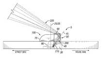
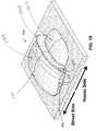
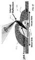
- an illumination system 5can comprise a light emitting diode 10 that produces and emits light and an associated optic 100 managing the light so emitted.
- the light emitting diode 10can produce light that is headed house side, opposite from the street (see light 210 illustrated in FIG. 2 ), and other light that is headed street side (opposite light 210 illustrated in FIG. 2 ).
- the optic 100can redirect a substantial portion of the house-side light towards the street, where higher illumination intensity is often desired.
- street illuminationis but one of many applications that the present technology supports.
- the present technologycan be applied in numerous lighting systems and illumination applications, including indoor and outdoor lighting, automobiles, general transportation lighting, and portable lights, to mention a few representative examples without limitation.
- FIGS. 1 , 2 , 3 , 4 , 5 A, 5 B, 5 C, 5 D, and 5 Eillustrate the optic 100 that manages light emitted by the light emitting diode 10 .
- FIGS. 1 and 2illustrate a side view, with FIG. 2 illustrating ray paths for a section 210 of light emitted from the light emitting diode 10 .
- FIG. 3illustrates a perspective view.
- FIG. 4illustrates a plan view, specifically from a perspective looking down the optical axis 25 towards the light emitting dome 20 of the light emitting diode 10 .
- the observerwould be below the light emitting diode 10 looking straight up; and, if the light emitting diode was mounted on the ground so at to emit light towards the sky or a ceiling, the observer would be above the light emitting diode 10 looking straight down.
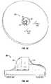
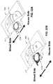
- FIGS. 5A , 5 B, 5 C, 5 D, and 5 Eillustrate the optic 100 as a three-dimensional rendering from five respective perspectives.
- the rendering of these illustrationsrepresents the optic 100 as an opaque solid to facilitate visualization of transparent optical material.
- the views of FIGS. 5A , 5 B, and 5 Care taken from vantage points on the side of the optic 100 that is opposite the light emitting diode 10 . Thus, the observer is on the side of the optic 100 that emits light (facing the outer side of the optic 100 ), but off the axis 25 shown in FIGS. 1 , 3 and 4 .
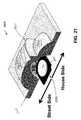
- the views of FIGS. 5D and 5Eare taken from the LED-side of the optic 100 , looking into a cavity 30 that the optic 100 comprises.
- the observeris on the side of the optic that receives light from the light emitting diode 10 (facing the inner side of the optic 100 ), again off the axis 25 .
- the cavity 30faces and receives light from the light emitting diode 10 .
- FIGS. 6A , 6 B, 6 C, 6 D, and 6 Eillustrate the cavity 30 in the form of a three-dimensional solid rendering (from five perspective views) to facilitate reader visualization.
- FIGS. 6A , 6 B, 6 C, 6 D, and 6 Edepict a solid that would be formed by filling the cavity 30 with an opaque resin, curing the resin, and then removing the resulting solid.
- the illustrated light emitting diode 10(see FIGS. 1 , 2 and 4 ) comprises an integral dome 20 that provides environmental protection to the light emitting diode's semiconductor materials and that emits the light that the light emitting diode 10 generates.
- the dome 20projects or protrudes into the cavity 30 that the optic 100 forms.
- the dome 20comprises material that encapsulates the light generating optical element of the light emitting diode 10 , for example an optoelectronic semiconductor structure or feature on a substrate of the light emitting diode 10 .
- the dome 20radiates light at highly diverse angles, for example providing a light distribution pattern that can be characterized, modeled, or approximated as Lambertian.
- the illustrated light emitting diode 10comprises an optical axis 25 associated with the pattern of light emitting from the dome 20 and/or associated with physical structure or mechanical features of the light emitting diode 10 .
- optical axisgenerally refers to a reference line along which there is some degree of rotational or other symmetry in an optical system, or a reference line defining a path along which light propagates through a system. Such reference lines are often imaginary or intangible lines.
- the optical axis 25lies in a reference plane 35 that sections the light emitting dome 20 , and/or the associated light emission pattern of the light emitting diode 10 , into two portions.
- reference plane 35can be positioned in other locations that may or may not be arbitrary. As will be appreciated by those of ordinary skill having benefit of this disclosure, a “reference plane” can be thought of as an imaginary or intangible plane providing a useful aid in describing, characterizing, or visualizing something.
- the cavity 30comprises an inner refractive surface 80 opposite an outer refractive surface 70 .
- Light emitted from the street side of the dome 20 and that is headed street sideis incident upon the inner refractive surface 80 , transmits through the optic 100 , and passes through the outer refractive surface 70 .
- Such lightmay be characterized as a solid angle or represented as a ray or a bundle of rays. Accordingly, the light that is emitted from the light emitting diode 10 and headed street side continues heading street side after interacting with the optic 100 .
- the inner refractive surface 80 and the outer refractive surface 70cooperatively manipulate this light with sequential refraction to produce a selected pattern, for example concentrating the light downward or outward depending upon desired level of beam spread. In the illustrated embodiment, the light sequentially encounters and is processed by two refractive interfaces of the optic 100 , first as the light enters the optic 100 , and second as the light exits the optic 100 .
- the inner refractive surface 80 and the outer refractive surface 70can be formed to spread, concentrate, bend, or otherwise manage the light emitted street side according to various application parameters.
- the inner and outer refractive surfaces 80 and 70can be concave or convex.
- the inner refractive surface 80is convex and the outer refractive surface 70 is convex.
- the inner refractive surface 80is convex and the outer refractive surface 70 is concave.
- the inner refractive surface 80is concave and the outer refractive surface 70 is convex.
- the inner refractive surface 80is concave and the outer refractive surface 70 is concave.
- at least one of the inner refractive surface 80 and the outer refractive surface 70may be substantially planar or flat.
- the light emitting diode 10further emits a section of light 210 that is headed house side or away from the street.
- This section of light 210is incident upon an inner refractive surface 40 of the cavity 30 that forms a beam 200 within the optic 100 .
- the refractive surface 40has an associated optical axis 45 .
- the optical axis 45can form an angle with the optical axis 25 associated with the light emitting diode 10 itself.
- the optical axis 45 and the optical axis 25can form an angle whether they actually intersect or not.
- the anglecan be acute. In some example embodiments, the angle is between about 10 degrees and about 80 degrees, when measured in side view such as provided in FIG. 2 . In some example embodiments, the angle is in a range between approximately 20 degrees and approximately 70 degrees. In some example embodiments, the angle is in a range between approximately 30 degrees and approximately 60 degrees, i.e. the angle is within 15 degrees of 45 degrees.
- the inner refractive surface 40projects, protrudes, or bulges into the cavity 30 , which is typically filled with a gas such as air.
- the refractive surface 40can be characterized as convex and further as a collimating lens.
- the term “collimating,” as used herein in the context of a lens or other optic,generally refers to a property of causing light to become more parallel that the light would otherwise be in the absence of the collimating lens or optic. Accordingly, a collimating lens may provide a degree of focusing.
- the beam 200propagates or travels through the optic 100 along the optical axis 45 and is incident upon a reflective surface 50 that redirects the beam 200 towards an outer refractive surface 60 .
- the redirected beam 200exits the optic 100 through the outer refractive surface 60 , which further steers the refracted beam 220 street side and can produce a desired level of beam spread.
- the reflective surface 50is typically totally internally reflective as a result of the angle of light incidence exceeding the “critical angle” for total internal reflection.
- the reflective surface 50is typically an interface between solid, transparent optical material of the optic 100 and a surrounding gaseous medium such as air.
- critical anglegenerally refers to a parameter for an optical system describing the angle of light incidence above which total internal reflection occurs.
- critical angle and total internal reflectionare believed to conform with terminology commonly recognized in the optics field.
- the refracted beam 220(which is formed by the section of light 210 sequentially refracted, reflected, and refracted) and the twice refracted section of light (that is emitted by the street side of the light emitting diode) collectively provide street-side illumination.
- the optic 100is a unitary optical element that comprises molded plastic material that is transparent. In some example embodiments, the optic 100 is a seamless unitary optical element. In some example embodiments, the optic 100 is formed of multiple transparent optical elements bonded, fused, glued, or otherwise joined together to form a unitary optical element that is void of air gaps yet made of multiple elements.
- FIG. 7illustrates an example array 800 of optics 100 provided in a sheet form to facilitate coupling multiple optics 100 to a corresponding array of light emitting diodes.
- an illumination systemcan comprise a two-dimensional array of light sources, each comprising the illumination system 5 illustrated in example form in FIG. 1 inter alia.
- the resulting two-dimensional array of light sourcescan comprise a light module or light bar, one or more of which can be disposed in a luminaire or other lighting apparatus, for example.
- the array 800can be formed of optical grade silicone and may be pliable and/or elastic, for example.
- the array 800can be formed of an optical plastic such as poly-methyl-methacrylate (“PMMA”), polycarbonate, or an appropriate acrylic, to mention a few representative material options without limitation.
- PMMApoly-methyl-methacrylate
- polycarbonatepolycarbonate
- acrylican appropriate acrylic
- FIG. 8illustrates a perspective view of an optic 800 that manages light emitted from a light emitting diode 10 .
- the light emitting diode 10is not illustrated in FIGS. 8 , 9 , and 10 , but is depicted FIG. 1 and elsewhere as discussed above.
- the optic 800can be coupled to a light emitting diode 10 or other light source for managing emitted light to form a light pattern comprising redirected light.
- FIG. 9illustrates the optic 800 in side view overlaid with representative ray paths as would begin at a light emitting diode 10 .
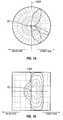
- FIG. 10illustrates an example diagram of photometric performance, wherein the lines plot common illuminance, analogous to how a contour map plots land elevation.
- FIG. 10describes a computer-generated isofootcandle diagram of example photometric performance for the optic of FIGS. 8 and 9 as coupled to a light emitting diode, with the lines depicting points of equal illuminance.
- the optic 800comprises an outer refractive surface 870 .
- Light emitted from the light emitting diode 10 in a street directionprogresses towards the street through the outer refractive surface 870 , which can refract the light to produce desired beam spread.
- light emitted from a street-side of the light emitting diode 10can propagate out of the light emitting diode, through an air gap, into the optic 800 , and then out of the optic 800 through the outer refractive surface 870 .
- Such an air gapmay be filled with air, nitrogen, or other suitable gas.
- the outer refractive surface 860is concave, but may be convex or substantially planar in other embodiments.
- the reflective surface 850can be oriented with respect to the beam 920 to exceed the “critical angle” for total internal reflection, so that the reflective surface 850 totally internally reflects the beam 920 .
- the internally reflective surface 850can be formed by an interface between air and plastic or other transparent material of the optic 800 .
- the internally reflective surface 850can comprise a reflective metallic coating.
- FIGS. 11 and 12describe some example embodiments in which an optic 1100 comprises multiple inner refractive surfaces 1150 , each forming a separate beam that is individually reflected and then refracted out of the optic 1100 . Similar to FIGS. 8 , 9 , and 10 as discussed above, a light generating element is not shown in FIG. 11 in order to promote reader visualization.
- the optic 1100can be coupled to a light emitting diode 10 or other appropriate light source, and the optic 1100 can manage the generated light.
- FIG. 12illustrates the optic 1100 in side view overlaid with representative ray paths as would begin at an example light emitting diode 10 (see light emitting diode 10 illustrated in FIG. 2 ).
- light emitted in the house side directionencounters the three inner refractive surfaces 1150 , each receiving a respective solid angle of emitted light.
- the three inner refractive surfaces 1150which can be convex from the illustrated viewing perspective, form three respective beams of light. As illustrated in FIG. 12 and discussed below, the three beams can have different focal lengths 1210 .
- Three totally internally reflective features 1160respectively reflect the three beams to increase street-side illumination.
- the configurations of the totally internally reflective features 1160avoid occlusion or unwanted distortion of those three redirected beams thereby avoiding uncontrolled incidence or grazing off the outer surface of the optic 1100 .
- two of the three totally internally reflective features 1160are undercut, and all three jut outward.
- FIG. 12illustrates how the inner refractive surfaces 1150 create beams with different focal lengths 1210 , which would be reflected and refracted by the totally internally reflective features 1160 as shown in FIG. 11 in a physical implementation. That is, to convey an example principle of the embodiment of FIG. 11 , FIG. 12 illustrates the three inner refractive surfaces 1150 forming three beams, and the beams are depicted as propagating within optical material of the optic 1100 without interacting with any subsequent optical features.
- FIGS. 13A and 13B , 14 , 15 , 16 , and 17describe some example embodiments in which the street side of the optic 1300 is smooth and the house side comprises prismatic grooves 1350 , as an example embodiment of a pattern of retroreflectors.
- a reference plane 1368containing an optical axis 25 , that demarcates the two sides of the optic 1300 and can cut through the dome 20 of the light emitting diode 10 (see FIG. 1 as the dome is not labeled in FIG. 13B to avoid line clutter).
- FIGS. 13A and 13Bare renderings respectively illustrating the optic 1300 as an opaque solid and as a transparent line drawing that shows an example light emitting diode 10 positioned to emit light into the optic 1300 .
- each prismatic groove 1350comprises a retroreflector.
- Each prismatic groove 1350comprises a pair of totally internally reflective surfaces 1375 or facets that collaboratively reflect light back in the general direction from which the light came.
- the totally internally reflective surfaces 1375are substantially perpendicular to one another.
- the totally internally reflective surfaces 1375meet to form a corner functioning as a retroreflecting edge of a cube, and may be characterized as a cube edge.
- a light rayis incident on the first surface of the pair of totally internally reflective surfaces 1375 .
- the first surface of the pair of totally internally reflective surfaces 1375bounces the light to the second surface of the pair of totally internally reflective surfaces 1375 .
- the second surface of the pair of totally internally reflective surfaces 1375bounces the light backwards, providing retroreflection.
- the pair of totally internally reflective surfaces 1375can form a two-bounce retroreflector.
- the retroreflected light rayis parallel to the light ray incident on a prismatic groove 1350 .
- the light raywould have an angle of reflection substantially equal to the angle of incidence. Accordingly, in the illustrated embodiment, the inclination of the light ray can be preserved (albeit reversed), so that the light ray can continue vertically, thereby retroreflecting back over the light emitting diode 10 .
- FIG. 14illustrates an intensity polar plot based on a computer simulation for the illumination system 1390 .
- FIG. 15illustrates an isofootcandle plot based on a computer simulation for the illumination system 1390 .
- FIGS. 16 and 17illustrate ray tracing analyses, from plan perspective, specifically looking down the optical axis 25 .
- FIGS. 16 and 17further illustrate how varying the dimensions of the prismatic grooves 1350 / 1775 can control the level of light leaking through the prismatic grooves as a result of certain rays being oriented for total internal reflection while other rays are oriented below the critical angle and will be refracted out of the prismatic groove.
- Increasing groove widthas illustrated in FIG. 17 , can increase house-side illumination, for example.
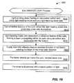
- FIG. 18illustrates a flow chart of an embodiment of such a process in the form of process 1800 , entitled “Manage Light.”
- process 1800will refer to certain elements illustrated in FIGS. 1 , 2 , 3 , 4 , 5 A, 5 B, 5 C, 5 D, 5 E, 6 A, 6 B, 6 C, 6 D, and 6 E.
- process 1800can function with and/or accommodate a wide range of devices, systems, and hardware (including elements illustrated in other figures as well as elements not expressly illustrated) and can function in a wide range of applications and situations. Accordingly, such referenced elements are examples, are provided without being exhaustive and without limitation, and are among many other supported by the present technology.
- the light emitting diode 10converts electricity into light and emits light.
- the emitted light and/or the light emitting diode 10has an associated optical axis 25 .
- a portion of the emitted lightis emitted in the street-side direction.
- Another portion, including the section 210is emitted in the house-side direction.
- the inner refractive surface 80 and the outer refractive surface 70 of the optic 100transmit and refract the light emitted in the desired, street-side direction. Accordingly, the optic 100 directs light to and illuminates the street.
- step 1815which typically proceeds substantially in parallel with step 1810 , the section of light 210 that is headed house side encounters the inner refractive surface 40 of the optic 100 .
- the inner refractive surface 40forms a beam 200 propagating within the solid optical material of the optic 100 , along the optical axis 45 .
- the optical axis 45is typically oriented at an acute angle relative to the optical axis 25 and/or with respect to the light emitting diode's substrate (e.g. the flat portion of the LED chip from which the dome 20 projects).
- step 1820which likewise typically proceeds substantially in parallel with step 1810 , the beam 200 encounters the reflective surface 50 , which is typically totally internally reflective but may be mirrored with a metal coating as an alternative suitable for certain applications.
- the reflective surface 50reverses the beam 200 , sending the beam 200 in a street-side direction.
- the beam 200exits the optic 100 heading street side, and may be refracted upon exit. Step 1825 may likewise proceed substantially in parallel with Step 1810 .
- the optic 100emits a pattern of light that, as illustrated in FIG. 10 , can be biased towards a street.
- Process 1800iterates from step 1830 , and management of light to provide biased illumination continues.
- FIGS. 19-39which describe additional example embodiments, will now be discussed.
- FIG. 19illustrates a perspective view of an example optic 1900 for managing light emitted by a light emitting diode in accordance with some embodiments of the present technology.
- FIG. 20is another perspective view of the example optic 1900 of FIG. 19 for managing light emitted by a light emitting diode in accordance with some embodiments of the present technology.
- Optically inactive edges of the optic 1900have been truncated, forming a peripheral sideway 1950 , thereby reducing volume and material usage of the optic 1900 to facilitate efficient manufacturing via molding or other appropriate process.
- the peripheral sidewall 1950extends peripherally to a corner 1925 , which may also be viewed as an edge. Laterally, the peripheral sidewall 1950 extends between two corners 1930 , which may also be viewed as edges.
- the exterior surface of the optic 1900is symmetric with respect to a plane (shown as a line) 1920 running street side to house side.
- the plane of symmetry 1920may be oriented perpendicular to a street, for example.
- the exterior surface of the optic 1900comprises a region 1915 that transmits light that is emitted from a light emitting diode 2100 (hidden in FIG. 19 , visible in FIG. 21 ) in a street side direction.
- Another region 1910 of the exterior surface of the optic 1900is internally reflective and reflects incident light towards the backside of the optic 1900 for further processing, which can include sending some incident light street side while other incident light is sent house side.
- Another region 1905 of the exterior surface of the optic 1900forms a prism jutting from the optic 1900 , and that region 1905 reflects in the street side direction incident light that would otherwise be headed house side.
- FIG. 21illustrates a cutaway perspective view of the example optic 1900 of FIG. 19 for managing light emitted by a light emitting diode 2100 in accordance with some embodiments of the present technology.
- the cutawayfollows a plane of symmetry 1920 for the optic 1900 .
- a light emitting diode 2100is positioned in a cavity 2150 of the optic 1900 and emits light into the cavity 2150 , with a portion of emitted light headed street side and another portion headed house side as initially incident on the optic 1900 .
- the light emitting diode 2100comprises a chip-on-board system.
- the chip-on-board systemcomprises a circuit board 2105 and one or more light emitting diode chips mounted on the circuit board.
- the LED chipsare encapsulated so that one body of encapsulant covers multiple chips.
- Other embodimentsmay incorporate light emitting diodes that utilize known mounting technologies other than chip-on-board systems.
- FIGS. 22A and 22Billustrate cutaway perspective views (respectively un-shaded and shaded) of the example optic 1900 of FIG. 19 for managing light emitted by a light emitting diode 2100 in accordance with some embodiments of the present technology.
- FIGS. 23A and 23Billustrate overhead views (shown shaded and un-shaded respectively) of the example optic 1900 of FIG. 19 for managing light emitted by a light emitting diode 2100 in accordance with some embodiments of the present technology.
- FIGS. 24A and 24Billustrate side views (shown shaded and un-shaded respectively) of the example optic 1900 of FIG. 19 for managing light emitted by a light emitting diode 2100 in accordance with some embodiments of the present technology.
- FIG. 25illustrates a cross sectional view (taken along the plane of symmetry 1920 ) of the example optic 1900 of FIG. 19 for managing light emitted by a light emitting diode 2100 in accordance with some embodiments of the present technology.
- the optic 1900comprises a cavity 2150 oriented to receive light emitted by the light emitting diode 2100 .
- the optic 1900can process and direct the emitted light according to direction of the emitted light, resulting in biasing the overall pattern in a street side direction.
- FIG. 26illustrates the cross sectional view of FIG. 25 , overlaid with representative ray traces 2610 for light emitted in certain directions, of the example optic 1900 of FIG. 19 for managing light emitted by a light emitting diode 1900 in accordance with some embodiments of the present technology.
- a portion of raysemanate from the light emitting diode 2100 in a street side direction, and those rays generally continue propagating street side as they transmit through and exit the optic 1900 .
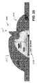
- FIG. 27illustrates the cross sectional view of FIG. 25 , overlaid with representative ray traces 2710 for light emitted in certain directions, of the example optic 1900 of FIG. 19 for managing light emitted by a light emitting diode 2100 in accordance with some embodiments of the present technology.
- a portion of raysemanate from the light emitting diode 2100 in a house side direction, and are focused by a focusing feature 2715 towards a region 1905 of the exterior surface of the optic 1905 that forms a prism.
- the focusing feature 2715comprises a convex lens that uses refraction for focusing.
- the feature 2715can implement imaging or collimation, for example.
- the region 1905comprises an internally reflective surface that redirects incident rays in the street side direction, typically via total internal reflection but alternatively via a reflective coating such as aluminum or other appropriate material.
- FIG. 28illustrates the cross sectional view of FIG. 25 , overlaid with representative ray traces 2810 for light emitted in certain directions, of the example optic 1900 of FIG. 19 for managing light emitted by a light emitting diode 2100 in accordance with some embodiments of the present technology.
- a portion of the raysemanate from the light emitting diode 2100 in a house side direction and are incident on a region 1910 of the exterior surface of the optic 1900 that is internally reflective.
- the region 1910utilizes total internal reflection so that the region 1910 internally reflects or transmits light according to angle of incidence.
- the light emitting diode 2100illuminates a portion of the region 1910 with light oriented at angles that support total internal reflection and another portion of the region 1910 with light oriented at angles that are transmitted without total internal reflection. Accordingly, part of the region 1910 is illuminated with light at the so called “critical angle” where a transition between total internal reflection and refractive transmission occurs.
- internal reflection occurring at the region 1910directs the incident rays towards horizontal and/or towards the backside 2825 of the optic 1900 , which may further be characterized as the base, underside, or rear of the optic 1900 .
- the backside 2825 of the optic 1900recycles or returns incident light into the optic 1900 where the light can radiate diffusely as an alternative to directionally house side. Accordingly, the backside 2825 of the optic 1900 can send street side a portion of the incident light that is received via internal reflection from the region 1910 .
- FIG. 29illustrates a simulated illumination pattern 2900 for the example optic 1900 of FIG. 19 for managing light emitted by a light emitting diode 2100 in accordance with some embodiments of the present technology.
- the illumination pattern 2900is biased street side relative to house side.
- the illumination pattern 2900is further symmetrical about a line 1920 that corresponds with the plane of symmetry 1920 illustrated and discussed above with respect to FIGS. 19-28 inter alia.
- FIG. 30illustrates a simulated light level contour plot 3000 for the example optic 1900 of FIG. 19 for managing light emitted by a light emitting diode 2100 in accordance with some embodiments of the present technology. More specifically, FIG. 30 shows representative light level contours for the illumination pattern 2900 of FIG. 29 . Accordingly, the light level contours are likewise biased street side relative to house side. Additionally, in the illustrated example embodiment, the light level contour plot 3000 is likewise symmetrical about the line 1920 .
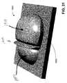
- FIG. 31illustrates a rendered perspective view of the exterior of the example optic 1900 of FIG. 19 for managing light emitted by a light emitting diode 2100 in accordance with some embodiments of the present technology.
- FIGS. 32A and 32Billustrate rendered perspective views of the underside of the example optic 1900 of FIG. 19 , for managing light emitted by a light emitting diode 2100 in accordance with some embodiments of the present technology.
- FIG. 32Ashows the underside and base of the optic 1900 without an accompanying light emitting diode 2100 .
- FIG. 32Bshows the underside and base with the accompanying light emitting diode 2100 forming an example embodiment of an illumination system.
- FIGS. 33A and 33Billustrate rendered views of the underside (including the backside 2825 ) of the example optic 1900 of FIG. 19 , for managing light emitted by a light emitting diode 2100 in accordance with some embodiments of the present technology.
- FIG. 33Ashows the underside of the optic 1900 without an accompanying light emitting diode 2100
- FIG. 33Bshows the underside with the accompanying light emitting diode 2100 .
- FIGS. 33A and 33Bfurther illustrate a recess 3520 adjacent optically active portions of the cavity 2150 that forms a receptacle for the light emitting diode 2100 in the chip-on-board format.
- the recess 3520forms a receptacle having an irregular outline that matches and is fitted to the outline of the light emitting diode 2100 , which comprises a chip-on-board system as discussed above.
- the resulting receptacleincludes channels 3530 for electrical leads and areas 3510 for fasteners.
- a gasketseats in a circumferential groove 3500 to provide environmental protection, for example against moisture.
- FIGS. 34A and 34Billustrate further views of the underside of an example optic 3400 for managing light emitted by a light emitting diode 2100 in accordance with some embodiments of the present technology.
- the figuresdescribe another representative embodiment that comprises features analogous to those discussed above with reference to FIG. 33 , inter alia.
- the embodiment of FIGS. 34A and 34Bcomprises wings 3408 with holes sized for screws to support fastener-based mounting.
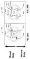
- FIGS. 35A and 35Billustrate bottom views of the example optic 1900 of FIG. 19 , respectively showing the optic's cavity 2150 shaded and un-shaded, for managing light emitted by a light emitting diode 2100 in accordance with some embodiments of the present technology.
- the example cavity 2150has an egg-shaped outline and may be further characterized as having an elongated or oblong footprint. As shown in FIG. 39 , the outline is taken perpendicular to the direction in which the light emitting diode 2100 is pointed or to the axis of the light emitting diode.
- the illustrated egg-shaped outlineis an oval form with one end larger than the other. In the illustrated embodiment, the egg-shaped outline is two dimensional and is symmetrical in one of those two dimensions and is asymmetrical in the other of those two dimensions.
- FIGS. 36A and 36Billustrate bottom views of the example optic 1900 of FIG. 19 with an accompanying light emitting diode 2100 , showing the light emitting diode 2100 shaded and un-shaded respectively, in accordance with some embodiments of the present technology.
- the light emitting diode 2100comprises a substrate in the form of a circuit board with one or more light emitting diode chips mounted thereto, and the optic 1900 comprises an irregularly shaped receptacle in which the light emitting diode is disposed.
- FIGS. 37A , 37 B, 37 C, and 37 Dillustrate views of an example optic 3700 for managing light emitted by a light emitting diode 2100 in accordance with some embodiments of the present technology.
- FIGS. 37A and 37Brespectively illustrate the optic 3700 in clear form (wire frame) and as opaque showing the optic 3700 prior to eliminating optically inactive portions of optical material to promote manufacturing efficiency.
- FIGS. 37C and 37Drespectively show the optic 3750 in clear form (wire frame) and as opaque after eliminating optically inactive portions of optical material to promote manufacturing efficiency.
- eliminating such optical materialcan beneficially truncate the optic 3750 in a manner that forms a peripheral sidewall 1950 and facilitates efficient molding fabrication, offering improvement in manufacturing economics and speed.
- the illustrated embodiment of the peripheral sidewall 1950has a corner or edge that extends fully around the peripheral sidewall 1950 , defining a perimeter or boundary of the sidewall 1950 .
- FIGS. 38A , 38 B, 38 C, and 38 Dillustrate views of an example optic 3700 , 3750 for managing light emitted by a light emitting diode 2100 in accordance with some embodiments of the present technology.
- FIG. 38Ashows the optic 3700 prior to eliminating optically inactive portions of optical material to promote manufacturing efficiency.
- FIG. 38Bshows the optic 3750 after eliminating optically inactive portions of optical material to promote manufacturing efficiency.
- FIGS. 38C and 38Dshow the optic 3750 with overlaid ray traces in two views after eliminating optically inactive portions of optical material to promote manufacturing efficiency. In the illustrated embodiment, the rays bypass the resulting peripheral sidewalls 1950 .
- the optic 3750can be designed to eliminated optically inactive regions as discussed above. In other words, truncation of the optic 3750 typically occurs in the design or engineering phase and may be implemented during manufacture by using a mold having appropriate contours. As discussed above, reducing the amount of material in the optic 3750 facilitates efficient manufacturing and promotes fast post molding cooling.
- FIGS. 39A and 39Billustrate overhead views of an example optic 3905 for managing light emitted by a light emitting diode 2100 in accordance with some embodiments of the present technology.
- the viewsshow a representative outline or footprint 3900 of a cavity 2150 of the optic 3905 , where the outline 3900 is egg-shaped.
- the egg-shaped outline 3900can be formed by a combination of two different ovals or ellipses that have different elongations, for example.
- the egg-shaped outline 3900is symmetrical about the line 1920 but is asymmetrical in the opposing dimension.
Landscapes
- Engineering & Computer Science (AREA)
- General Engineering & Computer Science (AREA)
- Physics & Mathematics (AREA)
- Microelectronics & Electronic Packaging (AREA)
- Optics & Photonics (AREA)
- Led Device Packages (AREA)
- Non-Portable Lighting Devices Or Systems Thereof (AREA)
- Planar Illumination Modules (AREA)
Abstract
Description
Claims (18)
Priority Applications (9)
| Application Number | Priority Date | Filing Date | Title |
|---|---|---|---|
| US13/828,670US9140430B2 (en) | 2011-02-28 | 2013-03-14 | Method and system for managing light from a light emitting diode |
| PCT/US2013/069491WO2014078240A1 (en) | 2012-11-14 | 2013-11-11 | Method and system for managing light from a light emitting diode |
| AU2013345044AAU2013345044B2 (en) | 2012-11-14 | 2013-11-11 | Method and system for managing light from a light emitting diode |
| EP13855404.3AEP2920510A4 (en) | 2012-11-14 | 2013-11-11 | Method and system for managing light from a light emitting diode |
| CN201380069359.8ACN104919243A (en) | 2012-11-14 | 2013-11-11 | Method and system for managing light from a light emitting diode |
| US14/860,524US9494283B2 (en) | 2011-02-28 | 2015-09-21 | Method and system for managing light from a light emitting diode |
| US15/351,056US10006606B2 (en) | 2011-02-28 | 2016-11-14 | Method and system for managing light from a light emitting diode |
| US16/017,521US10222027B2 (en) | 2011-02-28 | 2018-06-25 | Method and system for managing light from a light emitting diode |
| US16/292,105US11009214B2 (en) | 2011-02-28 | 2019-03-04 | Method and system for managing light from a light emitting diode |
Applications Claiming Priority (5)
| Application Number | Priority Date | Filing Date | Title |
|---|---|---|---|
| US201161447173P | 2011-02-28 | 2011-02-28 | |
| US13/407,401US9052086B2 (en) | 2011-02-28 | 2012-02-28 | Method and system for managing light from a light emitting diode |
| US201261726365P | 2012-11-14 | 2012-11-14 | |
| US201261728475P | 2012-11-20 | 2012-11-20 | |
| US13/828,670US9140430B2 (en) | 2011-02-28 | 2013-03-14 | Method and system for managing light from a light emitting diode |
Related Parent Applications (1)
| Application Number | Title | Priority Date | Filing Date |
|---|---|---|---|
| US13/407,401Continuation-In-PartUS9052086B2 (en) | 2011-02-28 | 2012-02-28 | Method and system for managing light from a light emitting diode |
Related Child Applications (1)
| Application Number | Title | Priority Date | Filing Date |
|---|---|---|---|
| US14/860,524ContinuationUS9494283B2 (en) | 2011-02-28 | 2015-09-21 | Method and system for managing light from a light emitting diode |
Publications (2)
| Publication Number | Publication Date |
|---|---|
| US20140085905A1 US20140085905A1 (en) | 2014-03-27 |
| US9140430B2true US9140430B2 (en) | 2015-09-22 |
Family
ID=50338671
Family Applications (5)
| Application Number | Title | Priority Date | Filing Date |
|---|---|---|---|
| US13/828,670Active2032-08-18US9140430B2 (en) | 2011-02-28 | 2013-03-14 | Method and system for managing light from a light emitting diode |
| US14/860,524ActiveUS9494283B2 (en) | 2011-02-28 | 2015-09-21 | Method and system for managing light from a light emitting diode |
| US15/351,056Active2032-04-11US10006606B2 (en) | 2011-02-28 | 2016-11-14 | Method and system for managing light from a light emitting diode |
| US16/017,521ActiveUS10222027B2 (en) | 2011-02-28 | 2018-06-25 | Method and system for managing light from a light emitting diode |
| US16/292,105Active2032-07-30US11009214B2 (en) | 2011-02-28 | 2019-03-04 | Method and system for managing light from a light emitting diode |
Family Applications After (4)
| Application Number | Title | Priority Date | Filing Date |
|---|---|---|---|
| US14/860,524ActiveUS9494283B2 (en) | 2011-02-28 | 2015-09-21 | Method and system for managing light from a light emitting diode |
| US15/351,056Active2032-04-11US10006606B2 (en) | 2011-02-28 | 2016-11-14 | Method and system for managing light from a light emitting diode |
| US16/017,521ActiveUS10222027B2 (en) | 2011-02-28 | 2018-06-25 | Method and system for managing light from a light emitting diode |
| US16/292,105Active2032-07-30US11009214B2 (en) | 2011-02-28 | 2019-03-04 | Method and system for managing light from a light emitting diode |
Country Status (1)
| Country | Link |
|---|---|
| US (5) | US9140430B2 (en) |
Cited By (5)
| Publication number | Priority date | Publication date | Assignee | Title |
|---|---|---|---|---|
| US20150226404A1 (en)* | 2013-03-15 | 2015-08-13 | Abl Ip Holding Llc | Led assembly having a refractor that provides improved light control |
| US11460175B2 (en) | 2021-01-08 | 2022-10-04 | Abl Ip Holding Llc | Reversible mounting arm for pole-mounted light fixtures |
| USD1011603S1 (en) | 2022-03-04 | 2024-01-16 | Abl Ip Holding Llc | Optic |
| US12050006B2 (en) | 2022-03-04 | 2024-07-30 | Abl Ip Holding Llc | Optic with total internal reflection refractor for back light control |
| USD1052777S1 (en) | 2021-01-08 | 2024-11-26 | Abl Ip Holding Llc | Light fixture |
Families Citing this family (12)
| Publication number | Priority date | Publication date | Assignee | Title |
|---|---|---|---|---|
| DE102013106158A1 (en)* | 2012-06-14 | 2013-12-19 | Universal Lighting Technologies, Inc. | Lens for the asymmetrical illumination of an area |
| US8974077B2 (en) | 2012-07-30 | 2015-03-10 | Ultravision Technologies, Llc | Heat sink for LED light source |
| EP2924345B1 (en)* | 2014-03-28 | 2018-07-18 | Swarco Futurit Verkehrssignalsysteme Ges.m.b.H. | Lighting devices with asymmetrical light distribution |
| US10253956B2 (en) | 2015-08-26 | 2019-04-09 | Abl Ip Holding Llc | LED luminaire with mounting structure for LED circuit board |
| US9903561B1 (en)* | 2015-11-09 | 2018-02-27 | Abl Ip Holding Llc | Asymmetric vision enhancement optics, luminaires providing asymmetric light distributions and associated methods |
| US20180286295A1 (en)* | 2017-03-28 | 2018-10-04 | GE Lighting Solutions, LLC | Light emitting diode assembly |
| US10468566B2 (en)* | 2017-04-10 | 2019-11-05 | Ideal Industries Lighting Llc | Hybrid lens for controlled light distribution |
| US10274159B2 (en) | 2017-07-07 | 2019-04-30 | RAB Lighting Inc. | Lenses and methods for directing light toward a side of a luminaire |
| US10251279B1 (en) | 2018-01-04 | 2019-04-02 | Abl Ip Holding Llc | Printed circuit board mounting with tabs |
| EP3762646B1 (en)* | 2018-03-07 | 2025-04-30 | Ledil Oy | An optical device for modifying light distribution |
| US11899202B2 (en) | 2022-03-04 | 2024-02-13 | Abl Ip Holding Llc | Extreme cutoff beam control optics |
| US11746989B1 (en) | 2022-03-04 | 2023-09-05 | Abl Ip Holding Llc | Extreme cutoff beam control optics |
Citations (171)
| Publication number | Priority date | Publication date | Assignee | Title |
|---|---|---|---|---|
| US1758977A (en) | 1926-04-21 | 1930-05-20 | Holophane Co Inc | Reflecting prism |
| US2254961A (en) | 1937-08-21 | 1941-09-02 | George M Cressaty | Unitary lens system |
| US2394992A (en) | 1943-06-30 | 1946-02-19 | Holophane Co Inc | Lighting unit |
| GB718425A (en) | 1951-05-10 | 1954-11-17 | Gen Electric Co Ltd | Improvements in or relating to refractor members for lighting fittings |
| US2818500A (en) | 1953-07-03 | 1957-12-31 | Holophane Co Inc | Prismatic reflectors |
| GB794670A (en) | 1955-05-20 | 1958-05-07 | Gen Electric Co Ltd | Improvements in or relating to refractor members for lighting fittings |
| GB815609A (en) | 1955-04-26 | 1959-07-01 | Corning Glass Works | Street lighting luminaire |
| US2908197A (en) | 1954-01-29 | 1959-10-13 | Westinghouse Air Brake Co | Wide angle lenses |
| US3278743A (en) | 1963-12-16 | 1966-10-11 | Holophane Co Inc | Street light refractor |
| US3596136A (en) | 1969-05-13 | 1971-07-27 | Rca Corp | Optical semiconductor device with glass dome |
| US3647148A (en) | 1969-12-11 | 1972-03-07 | Holophane Co Inc | Veiling glare control with luminaires |
| US3927290A (en) | 1974-11-14 | 1975-12-16 | Teletype Corp | Selectively illuminated pushbutton switch |
| US4345308A (en) | 1978-08-25 | 1982-08-17 | General Instrument Corporation | Alpha-numeric display array and method of manufacture |
| US4460945A (en) | 1982-09-30 | 1984-07-17 | Southern California Edison Company, Inc. | Luminaire shield |
| US4729076A (en) | 1984-11-15 | 1988-03-01 | Tsuzawa Masami | Signal light unit having heat dissipating function |
| US4734836A (en) | 1984-09-29 | 1988-03-29 | Masataka Negishi | Lighting apparatus |
| US4860177A (en) | 1988-01-25 | 1989-08-22 | John B. Simms | Bicycle safety light |
| US4907044A (en) | 1987-10-15 | 1990-03-06 | Siemens Aktiengesellschaft | Optical emission device |
| US4941072A (en) | 1988-04-08 | 1990-07-10 | Sanyo Electric Co., Ltd. | Linear light source |
| JPH06177424A (en) | 1992-12-03 | 1994-06-24 | Rohm Co Ltd | Light emitting diode lamp and collective type light emitting diode display device |
| US5404869A (en) | 1992-04-16 | 1995-04-11 | Tir Technologies, Inc. | Faceted totally internally reflecting lens with individually curved faces on facets |
| US5424931A (en) | 1994-05-09 | 1995-06-13 | Wheeler; Todd D. | Mobile illumination device |
| WO1996024802A1 (en) | 1995-02-10 | 1996-08-15 | Ecolux Inc. | Prismatic toroidal lens and traffic signal light using this lens |
| US5782555A (en) | 1996-06-27 | 1998-07-21 | Hochstein; Peter A. | Heat dissipating L.E.D. traffic light |
| WO1998033007A1 (en) | 1997-01-23 | 1998-07-30 | Koninklijke Philips Electronics N.V. | Luminaire |
| US5857767A (en) | 1996-09-23 | 1999-01-12 | Relume Corporation | Thermal management system for L.E.D. arrays |
| JPH11154766A (en) | 1997-09-22 | 1999-06-08 | Nichia Chem Ind Ltd | Light emitting diode and traffic light using the same |
| US5926320A (en) | 1997-05-29 | 1999-07-20 | Teldedyne Lighting And Display Products, Inc. | Ring-lens system for efficient beam formation |
| US5924788A (en) | 1997-09-23 | 1999-07-20 | Teledyne Lighting And Display Products | Illuminating lens designed by extrinsic differential geometry |
| US5939996A (en) | 1996-03-29 | 1999-08-17 | Rolls-Royce Power Engineering Plc | Display sign and an optical element for use in the same |
| US6045240A (en) | 1996-06-27 | 2000-04-04 | Relume Corporation | LED lamp assembly with means to conduct heat away from the LEDS |
| US6050707A (en) | 1996-06-14 | 2000-04-18 | Stanley Electric Co., Ltd. | Light emitting diode device |
| US6102558A (en) | 1997-05-23 | 2000-08-15 | Valeo Vision | Motor vehicle headlight with a reflector for generating a wide beam, and with a striated cover lens |
| US6227685B1 (en) | 1996-10-11 | 2001-05-08 | Mcdermott Kevin | Electronic wide angle lighting device |
| US6227684B1 (en) | 1997-04-07 | 2001-05-08 | U.S. Philips Corporation | Luminaire |
| US6273596B1 (en) | 1997-09-23 | 2001-08-14 | Teledyne Lighting And Display Products, Inc. | Illuminating lens designed by extrinsic differential geometry |
| US6341466B1 (en) | 2000-01-19 | 2002-01-29 | Cooper Technologies Company | Clip for securing an elongate member to a T-bar of a ceiling grid |
| US6345800B1 (en) | 1998-07-27 | 2002-02-12 | Nsi Enterprises, Inc. | Universal load-bearing hanger bracket and method for hanging a lighting fixture below a grid ceiling system at on-grid or off-grid locations |
| US20020034081A1 (en) | 2000-09-18 | 2002-03-21 | Koito Manufacturing Co., Ltd. | Vehicle lamp |
| US6441558B1 (en) | 2000-12-07 | 2002-08-27 | Koninklijke Philips Electronics N.V. | White LED luminary light control system |
| US6461008B1 (en) | 1999-08-04 | 2002-10-08 | 911 Emergency Products, Inc. | Led light bar |
| US20020196623A1 (en) | 2001-06-21 | 2002-12-26 | Star-Reach Corporation | High efficient tubular light emitting cylinder |
| US6502956B1 (en) | 1999-03-25 | 2003-01-07 | Leotek Electronics Corporation | Light emitting diode lamp with individual LED lenses |
| US6527422B1 (en) | 2000-08-17 | 2003-03-04 | Power Signal Technologies, Inc. | Solid state light with solar shielded heatsink |
| US6536923B1 (en) | 1998-07-01 | 2003-03-25 | Sidler Gmbh & Co. | Optical attachment for a light-emitting diode and brake light for a motor vehicle |
| US20030067787A1 (en) | 2001-10-04 | 2003-04-10 | Koito Manufacturing Co., Ltd. | Vehicle lamp |
| US6547423B2 (en) | 2000-12-22 | 2003-04-15 | Koninklijke Phillips Electronics N.V. | LED collimation optics with improved performance and reduced size |
| US6560038B1 (en) | 2001-12-10 | 2003-05-06 | Teledyne Lighting And Display Products, Inc. | Light extraction from LEDs with light pipes |
| US20030099115A1 (en) | 2001-11-28 | 2003-05-29 | Joachim Reill | Led illumination system |
| WO2003044870A1 (en) | 2001-11-22 | 2003-05-30 | Mireille Georges | Light-emitting diode illuminating optical device |
| US6582103B1 (en) | 1996-12-12 | 2003-06-24 | Teledyne Lighting And Display Products, Inc. | Lighting apparatus |
| US6598998B2 (en) | 2001-05-04 | 2003-07-29 | Lumileds Lighting, U.S., Llc | Side emitting light emitting device |
| US6639733B2 (en) | 2000-03-16 | 2003-10-28 | Light Prescriptions Innovators, Llc. | High efficiency non-imaging optics |
| US20040004828A1 (en) | 2002-07-05 | 2004-01-08 | Mark Chernick | Spinning illuminated novelty device with syncronized light sources |
| US20040037076A1 (en) | 2002-07-17 | 2004-02-26 | Sharp Kabushiki Kaisha | Light emitting diode lamp and light emitting diode display unit |
| US20040070855A1 (en) | 2002-10-11 | 2004-04-15 | Light Prescriptions Innovators, Llc, A Delaware Limited Liability Company | Compact folded-optics illumination lens |
| US20040105264A1 (en) | 2002-07-12 | 2004-06-03 | Yechezkal Spero | Multiple Light-Source Illuminating System |
| US20040105261A1 (en) | 1997-12-17 | 2004-06-03 | Color Kinetics, Incorporated | Methods and apparatus for generating and modulating illumination conditions |
| US20040105171A1 (en) | 2002-12-02 | 2004-06-03 | Light Prescriptions Innovators, Llc, A Delaware Limited Liability Company | Asymmetric TIR lenses producing off-axis beams |
| EP1431653A2 (en) | 2002-12-19 | 2004-06-23 | Toshiji Kishimura | Light source for white color LED lighting and white color led lighting device |
| WO2004068909A1 (en) | 2003-01-27 | 2004-08-12 | Matsushita Electric Industrial Co., Ltd. | Multichip led lighting device |
| US6785053B2 (en) | 2002-09-27 | 2004-08-31 | John M. Savage, Jr. | Threaded lens coupling to LED apparatus |
| US6784357B1 (en) | 2002-02-07 | 2004-08-31 | Chao Hsiang Wang | Solar energy-operated street-lamp system |
| US20040189933A1 (en) | 2002-12-02 | 2004-09-30 | Light Prescription Innovators, Llc | Apparatus and method for use in fulfilling illumination prescription |
| US20040207999A1 (en) | 2003-03-14 | 2004-10-21 | Toyoda Gosei Co., Ltd. | LED package |
| US20040218388A1 (en) | 2003-03-31 | 2004-11-04 | Fujitsu Display Technologies Corporation | Surface lighting device and liquid crystal display device using the same |
| US20040222947A1 (en) | 2003-05-07 | 2004-11-11 | James Newton | LED lighting array for a portable task light |
| US20040228127A1 (en) | 2003-05-16 | 2004-11-18 | Squicciarini John B. | LED clusters and related methods |
| US6850001B2 (en) | 2001-10-09 | 2005-02-01 | Agilent Technologies, Inc. | Light emitting diode |
| JP2005062461A (en) | 2003-08-12 | 2005-03-10 | Matsushita Electric Ind Co Ltd | Display device |
| US20050073849A1 (en) | 2003-10-06 | 2005-04-07 | Greg Rhoads | Light source using light emitting diodes and an improved method of collecting the energy radiating from them |
| US6895334B2 (en) | 2000-11-02 | 2005-05-17 | Fujinon Corporation | Method and apparatus for optimizing optical system and recording medium with program for optimizing optical system |
| WO2005057082A1 (en) | 2003-12-10 | 2005-06-23 | Okaya Electric Industries Co., Ltd. | Indicator lamp |
| US20050207165A1 (en) | 2001-08-09 | 2005-09-22 | Matsushita Electric Industrial Co., Ltd. | LED illumination apparatus and card-type LED illumination source |
| US6948838B2 (en) | 2002-01-15 | 2005-09-27 | Fer Fahrzeugelektrik Gmbh | Vehicle lamp having prismatic element |
| WO2005093316A1 (en) | 2004-03-25 | 2005-10-06 | Zhoulong Peng | Leds based street lamp |
| US6965715B2 (en) | 2001-10-01 | 2005-11-15 | Karl Storz Gmbh & Co. Kg | Lens and method for producing a lens |
| CN2750186Y (en) | 2004-12-01 | 2006-01-04 | 陈甲乙 | street lights with cooling effect |
| US6997580B2 (en) | 2003-09-19 | 2006-02-14 | Mattel, Inc. | Multidirectional light emitting diode unit |
| US20060034082A1 (en) | 2004-08-12 | 2006-02-16 | Samsung Electro-Mechanics Co., Ltd. | Multi-lens light emitting diode |
| CN1737418A (en) | 2005-08-11 | 2006-02-22 | 周应东 | LED lamp for improving heat radiation effect |
| KR20060033572A (en) | 2004-10-15 | 2006-04-19 | 삼성전기주식회사 | Lens for LED Light Source |
| US20060081863A1 (en) | 2004-10-20 | 2006-04-20 | Samsung Electro-Mechanics Co., Ltd. | Dipolar side-emitting led lens and led module incorporating the same |
| KR20060071033A (en) | 2004-12-21 | 2006-06-26 | 엘지전자 주식회사 | LED lighting system and optical system |
| US20060138437A1 (en) | 2004-12-29 | 2006-06-29 | Tien-Fu Huang | Lens and LED using the lens to achieve homogeneous illumination |
| US7070310B2 (en) | 2002-10-01 | 2006-07-04 | Truck-Lite Co., Inc. | Light emitting diode headlamp |
| US7073931B2 (en) | 2003-02-10 | 2006-07-11 | Koito Manufacturing Co., Ltd. | Vehicular headlamp and optical unit |
| EP1686630A2 (en) | 2005-01-31 | 2006-08-02 | Samsung Electronics Co., Ltd. | Led device having diffuse reflective surface |
| US7090370B2 (en) | 2001-06-08 | 2006-08-15 | Advanced Leds Limited | Exterior luminaire |
| US7102172B2 (en) | 2003-10-09 | 2006-09-05 | Permlight Products, Inc. | LED luminaire |
| US7104672B2 (en) | 2004-10-04 | 2006-09-12 | A.L. Lightech, Inc. | Projection lens for light source arrangement |
| US20060238884A1 (en) | 2005-04-26 | 2006-10-26 | Jang Jun H | Optical lens, light emitting device package using the optical lens, and backlight unit |
| US20060245083A1 (en) | 2005-04-19 | 2006-11-02 | Coretronic Corporation | Lens for sideward light emission |
| US20060250803A1 (en) | 2005-05-04 | 2006-11-09 | Chia-Yi Chen | Street light with heat dispensing device |
| US20060255353A1 (en) | 2003-09-08 | 2006-11-16 | Taskar Nikhil R | Light efficient packaging configurations for LED lamps using high refractive index encapsulants |
| US20060285311A1 (en) | 2005-06-19 | 2006-12-21 | Chih-Li Chang | Light-emitting device, backlight module, and liquid crystal display using the same |
| DE202006015981U1 (en) | 2006-07-06 | 2006-12-21 | AUGUX CO., LTD., Gueishan | LED street light combination with a heat dissipation arrangement has LED set in a frame and heat dissipating tubules connected to a heat dissipating body |
| US7153015B2 (en) | 2001-12-31 | 2006-12-26 | Innovations In Optics, Inc. | Led white light optical system |
| US20070019416A1 (en) | 2005-07-19 | 2007-01-25 | Samsung Electro-Mechanics Co., Ltd. | Light emitting diode package having dual lens structure for lateral light emission |
| US20070019415A1 (en) | 2005-04-22 | 2007-01-25 | Itt Industries | LED floodlight system |
| US7172319B2 (en) | 2004-03-30 | 2007-02-06 | Illumination Management Solutions, Inc. | Apparatus and method for improved illumination area fill |
| KR20070015738A (en) | 2005-08-01 | 2007-02-06 | 서울반도체 주식회사 | Light emitting device having a silicon lens |
| US20070058369A1 (en) | 2005-01-26 | 2007-03-15 | Parkyn William A | Linear lenses for LEDs |
| US20070063210A1 (en) | 2005-09-21 | 2007-03-22 | Tien-Lung Chiu | Backlight module and a light-emitting-diode package structure therefor |
| US20070066310A1 (en) | 2005-09-21 | 2007-03-22 | Haar Rob V D | Mobile communication terminal and method |
| US20070081340A1 (en) | 2005-10-07 | 2007-04-12 | Chung Huai-Ku | LED light source module with high efficiency heat dissipation |
| US20070081338A1 (en) | 2005-10-06 | 2007-04-12 | Thermalking Technology International Co. | Illumination device |
| US7204627B2 (en) | 2003-09-29 | 2007-04-17 | Koito Manufacturing Co., Ltd. | Lamp unit for forming a cut-off line and vehicular headlamp using the same |
| US20070091615A1 (en) | 2005-10-25 | 2007-04-26 | Chi-Tang Hsieh | Backlight module for LCD monitors and method of backlighting the same |
| US7237936B1 (en) | 2005-05-27 | 2007-07-03 | Gibson David J | Vehicle light assembly and its associated method of manufacture |
| US20070183736A1 (en) | 2005-12-15 | 2007-08-09 | Pozdnyakov Vadim V | Lens for reforming light-emitting diode radiation |
| US20070201225A1 (en) | 2006-02-27 | 2007-08-30 | Illumination Management Systems | LED device for wide beam generation |
| US7281820B2 (en) | 2006-01-10 | 2007-10-16 | Bayco Products, Ltd. | Lighting module assembly and method for a compact lighting device |
| US20070258214A1 (en) | 2006-05-08 | 2007-11-08 | Yu-Nung Shen | Heat-Dissipating Device with Tapered Fins |
| US20080013322A1 (en) | 2006-04-24 | 2008-01-17 | Enplas Corporation | Illumination device and lens of illumination device |
| US20080019129A1 (en) | 2006-07-24 | 2008-01-24 | Chin-Wen Wang | LED Lamp Illumination Projecting Structure |
| US20080025044A1 (en) | 2006-02-09 | 2008-01-31 | Se-Ki Park | Point Light Source, Backlight Assembly Having the Same and Display Apparatus Having the Same |
| US7329029B2 (en) | 2003-05-13 | 2008-02-12 | Light Prescriptions Innovators, Llc | Optical device for LED-based lamp |
| US7329033B2 (en) | 2005-10-25 | 2008-02-12 | Visteon Global Technologies, Inc. | Convectively cooled headlamp assembly |
| US7329030B1 (en) | 2006-08-17 | 2008-02-12 | Augux., Ltd. | Assembling structure for LED road lamp and heat dissipating module |
| US20080043473A1 (en) | 2004-11-01 | 2008-02-21 | Nobuyuki Matsui | Light emitting module, lighting device, and display device |
| USD563036S1 (en) | 2005-03-02 | 2008-02-26 | Nichia Corporation | Light emitting diode lens |
| US7339200B2 (en) | 2005-08-05 | 2008-03-04 | Koito Manufacturing Co., Ltd. | Light-emitting diode and vehicular lamp |
| US20080055908A1 (en) | 2006-08-30 | 2008-03-06 | Chung Wu | Assembled structure of large-sized led lamp |
| US20080068799A1 (en) | 2006-09-14 | 2008-03-20 | Topson Optoelectronics Semi-Conductor Co., Ltd. | Heat sink structure for light-emitting diode based streetlamp |
| US7347599B2 (en) | 2003-02-04 | 2008-03-25 | Light Prescriptions Innovators, Llc | Etendue-squeezing illumination optics |
| US7348723B2 (en) | 2004-09-27 | 2008-03-25 | Enplas Corporation | Emission device, surface light source device, display and light flux control member |
| US7348604B2 (en) | 2005-05-20 | 2008-03-25 | Tir Technology Lp | Light-emitting module |
| US7352011B2 (en) | 2004-11-15 | 2008-04-01 | Philips Lumileds Lighting Company, Llc | Wide emitting lens for LED useful for backlighting |
| US20080080188A1 (en) | 2006-09-29 | 2008-04-03 | Chin-Wen Wang | Modulized Assembly Of A Large-sized LED Lamp |
| US20080100773A1 (en) | 2006-10-31 | 2008-05-01 | Hwang Seong Yong | Backlight, a lens for a backlight, and a backlight assembly having the same |
| US7374322B2 (en) | 2002-02-06 | 2008-05-20 | Steen Ronald L | Center high mounted stop lamp including leds and tir lens |
| US20080174996A1 (en) | 2007-01-18 | 2008-07-24 | Hong Kong Applied Science And Technology Research Institute Co., Ltd. | Light-emitting devices and lens therefor |
| US7410275B2 (en) | 2004-09-21 | 2008-08-12 | Lumination Llc | Refractive optic for uniform illumination |
| US20080239722A1 (en) | 2007-04-02 | 2008-10-02 | Ruud Lighting, Inc. | Light-Directing LED Apparatus |
| US20080273327A1 (en) | 2007-05-04 | 2008-11-06 | Ruud Lighting, Inc. | Safety Accommodation Arrangement in LED Package/Secondary Lens Structure |
| WO2008144672A1 (en) | 2007-05-21 | 2008-11-27 | Illumination Management Solutions, Inc. | An improved led device for wide beam generation and method of making the same |
| US7460985B2 (en) | 2003-07-28 | 2008-12-02 | Light Prescriptions Innovators, Llc | Three-dimensional simultaneous multiple-surface method and free-form illumination-optics designed therefrom |
| US7461948B2 (en) | 2005-10-25 | 2008-12-09 | Philips Lumileds Lighting Company, Llc | Multiple light emitting diodes with different secondary optics |
| JP2009021086A (en) | 2007-07-11 | 2009-01-29 | Panasonic Electric Works Co Ltd | Light emitting unit |
| US7507001B2 (en) | 2002-11-19 | 2009-03-24 | Denovo Lighting, Llc | Retrofit LED lamp for fluorescent fixtures without ballast |
| US7513639B2 (en) | 2006-09-29 | 2009-04-07 | Pyroswift Holding Co., Limited | LED illumination apparatus |
| US7553051B2 (en) | 2004-03-18 | 2009-06-30 | Brasscorp Limited | LED work light |
| US7569802B1 (en) | 2003-03-20 | 2009-08-04 | Patrick Mullins | Photosensor control unit for a lighting module |
| US7572654B2 (en) | 2006-09-22 | 2009-08-11 | Hon Hai Precision Industry Co., Ltd. | Method for making light emitting diode |
| US7572027B2 (en) | 2005-09-15 | 2009-08-11 | Integrated Illumination Systems, Inc. | Interconnection arrangement having mortise and tenon connection features |
| US7575354B2 (en) | 2004-09-16 | 2009-08-18 | Magna International Inc. | Thermal management system for solid state automotive lighting |
| US20090244895A1 (en) | 2006-05-30 | 2009-10-01 | Neobulb Technologies, Inc. | Light-Emitting Diode Illuminating Equipment with High Power and High Heat Dissipation Efficiency |
| US20090262543A1 (en) | 2008-04-18 | 2009-10-22 | Genius Electronic Optical Co., Ltd. | Light base structure of high-power LED street lamp |
| US7618162B1 (en) | 2004-11-12 | 2009-11-17 | Inteled Corp. | Irradiance-redistribution lens and its applications to LED downlights |
| US7625102B2 (en) | 2004-10-14 | 2009-12-01 | Stanley Electric Co., Ltd. | Lighting device |
| US7637633B2 (en) | 2005-10-18 | 2009-12-29 | National Tsing Hua University | Heat dissipation devices for an LED lamp set |
| US20100014290A1 (en) | 2008-07-15 | 2010-01-21 | Ruud Lighting, Inc. | Light-directing apparatus with protected reflector-shield and lighting fixture utilizing same |
| US7651240B2 (en) | 2006-01-10 | 2010-01-26 | Bayco Products. Ltd. | Combination task lamp and flash light |
| WO2010019810A1 (en) | 2008-08-14 | 2010-02-18 | Cooper Technologies Company | Led devices for offset wide beam generation |
| US20100085763A1 (en)* | 2007-01-26 | 2010-04-08 | Sic Divisione Elettronica S.R.L. | Lens for a light emitting diode and manufacturing method therefor |
| US7775679B2 (en) | 2004-08-18 | 2010-08-17 | Advanced Illumination, Inc. | High intensity light source for a machine vision system and method of making same |
| US7777405B2 (en) | 2002-07-16 | 2010-08-17 | Odelo Gmbh | White LED headlight |
| US20100232166A1 (en)* | 2009-03-13 | 2010-09-16 | Genius Electronics Optical Co., Ltd. | LED illumination lens |
| KR20100105388A (en) | 2009-03-18 | 2010-09-29 | (주)알텍테크놀로지스 | Method for fabricating light emitting diode divice and light emitting diode package and light emitting diode module and lamp device having the same |
| US7817909B2 (en) | 2004-12-21 | 2010-10-19 | Sharp Kabushiki Kaisha | Optical device and light source |
| US7841750B2 (en) | 2008-08-01 | 2010-11-30 | Ruud Lighting, Inc. | Light-directing lensing member with improved angled light distribution |
| US20110075428A1 (en)* | 2009-09-30 | 2011-03-31 | Fu Zhun Precision Industry (Shen Zhen) Co., Ltd. | Led module |
| US7972035B2 (en) | 2007-10-24 | 2011-07-05 | Lsi Industries, Inc. | Adjustable lighting apparatus |
| US7972036B1 (en) | 2008-04-30 | 2011-07-05 | Genlyte Thomas Group Llc | Modular bollard luminaire louver |
| US7985009B2 (en)* | 2008-09-19 | 2011-07-26 | Yen-Wei Ho | Two-side asymmetric light-shift illuminating lens body |
| WO2011098515A1 (en) | 2010-02-11 | 2011-08-18 | Ewo Srl/Gmbh | Lighting module for illuminating traffic routes, and traffic route luminaire |
| US8007140B2 (en) | 2009-09-03 | 2011-08-30 | Fu Zhun Precision Industry (Shen Zhen) Co., Ltd. | LED module |
| US20110227105A1 (en)* | 2010-03-17 | 2011-09-22 | Jon-Fwu Hwu | Multi-Layer LED Array Engine |
| US8025428B2 (en) | 2004-12-07 | 2011-09-27 | Elumen Lighting Networks Inc. | Assembly of light emitting diodes for lighting applications |
| US20110317432A1 (en)* | 2010-06-25 | 2011-12-29 | Lite-On Technology Corp. | Light-emitting diode lens |
Family Cites Families (17)
| Publication number | Priority date | Publication date | Assignee | Title |
|---|---|---|---|---|
| US3927707A (en) | 1973-10-11 | 1975-12-23 | Trw Inc | Clip nut |
| US5458497A (en) | 1993-05-27 | 1995-10-17 | Beta Phase, Inc. | Connector assembly |
| JPH08320403A (en) | 1995-05-25 | 1996-12-03 | Nikon Corp | Optical lens |
| US6543098B2 (en) | 2001-03-02 | 2003-04-08 | Tektronix, Inc. | Printed circuit board mounting facility |
| TW587733U (en) | 2002-12-20 | 2004-05-11 | Hon Hai Prec Ind Co Ltd | Circuit board mounting apparatus |
| US6865091B2 (en) | 2003-06-23 | 2005-03-08 | Inventec Corporation | Mechanism for supporting edge of motherboard |
| US7554815B2 (en) | 2006-05-31 | 2009-06-30 | Hewlett-Packard Development Company, L.P. | Resilient clip for circuit board |
| US7583517B2 (en) | 2006-07-06 | 2009-09-01 | Dell Products L.P. | Method and apparatus for coupling a card to an information handling system chassis |
| US8348475B2 (en) | 2008-05-23 | 2013-01-08 | Ruud Lighting, Inc. | Lens with controlled backlight management |
| CN201521897U (en) | 2009-10-20 | 2010-07-07 | 明达实业(厦门)有限公司 | Pool wall lamp shade |
| WO2012021718A1 (en) | 2010-08-11 | 2012-02-16 | Fraen Corporation | Area lighting devices and methods |
| US9052086B2 (en) | 2011-02-28 | 2015-06-09 | Cooper Technologies Company | Method and system for managing light from a light emitting diode |
| JP5178930B1 (en)* | 2011-03-11 | 2013-04-10 | 株式会社東芝 | Lighting device |
| US8628222B2 (en) | 2011-05-13 | 2014-01-14 | Lighting Science Group Corporation | Light directing apparatus |
| CN103672730B (en) | 2012-09-13 | 2017-02-22 | 赛尔富电子有限公司 | Lens, LED module and lighting system using LED module |
| DE112013005281T5 (en) | 2012-11-05 | 2015-08-13 | Koninklijke Philips N.V. | Optical element with a TIR surface section for improved spatial light distribution |
| US8964406B2 (en) | 2012-12-11 | 2015-02-24 | ESPi LLC | Battery backup cover system |
- 2013
- 2013-03-14USUS13/828,670patent/US9140430B2/enactiveActive
- 2015
- 2015-09-21USUS14/860,524patent/US9494283B2/enactiveActive
- 2016
- 2016-11-14USUS15/351,056patent/US10006606B2/enactiveActive
- 2018
- 2018-06-25USUS16/017,521patent/US10222027B2/enactiveActive
- 2019
- 2019-03-04USUS16/292,105patent/US11009214B2/enactiveActive
Patent Citations (195)
| Publication number | Priority date | Publication date | Assignee | Title |
|---|---|---|---|---|
| US1758977A (en) | 1926-04-21 | 1930-05-20 | Holophane Co Inc | Reflecting prism |
| US2254961A (en) | 1937-08-21 | 1941-09-02 | George M Cressaty | Unitary lens system |
| US2394992A (en) | 1943-06-30 | 1946-02-19 | Holophane Co Inc | Lighting unit |
| GB718425A (en) | 1951-05-10 | 1954-11-17 | Gen Electric Co Ltd | Improvements in or relating to refractor members for lighting fittings |
| US2818500A (en) | 1953-07-03 | 1957-12-31 | Holophane Co Inc | Prismatic reflectors |
| US2908197A (en) | 1954-01-29 | 1959-10-13 | Westinghouse Air Brake Co | Wide angle lenses |
| GB815609A (en) | 1955-04-26 | 1959-07-01 | Corning Glass Works | Street lighting luminaire |
| GB794670A (en) | 1955-05-20 | 1958-05-07 | Gen Electric Co Ltd | Improvements in or relating to refractor members for lighting fittings |
| US3278743A (en) | 1963-12-16 | 1966-10-11 | Holophane Co Inc | Street light refractor |
| US3596136A (en) | 1969-05-13 | 1971-07-27 | Rca Corp | Optical semiconductor device with glass dome |
| US3647148A (en) | 1969-12-11 | 1972-03-07 | Holophane Co Inc | Veiling glare control with luminaires |
| US3927290A (en) | 1974-11-14 | 1975-12-16 | Teletype Corp | Selectively illuminated pushbutton switch |
| US4345308A (en) | 1978-08-25 | 1982-08-17 | General Instrument Corporation | Alpha-numeric display array and method of manufacture |
| US4460945A (en) | 1982-09-30 | 1984-07-17 | Southern California Edison Company, Inc. | Luminaire shield |
| US4734836A (en) | 1984-09-29 | 1988-03-29 | Masataka Negishi | Lighting apparatus |
| US4729076A (en) | 1984-11-15 | 1988-03-01 | Tsuzawa Masami | Signal light unit having heat dissipating function |
| US4907044A (en) | 1987-10-15 | 1990-03-06 | Siemens Aktiengesellschaft | Optical emission device |
| US4860177A (en) | 1988-01-25 | 1989-08-22 | John B. Simms | Bicycle safety light |
| US4941072A (en) | 1988-04-08 | 1990-07-10 | Sanyo Electric Co., Ltd. | Linear light source |
| US5404869A (en) | 1992-04-16 | 1995-04-11 | Tir Technologies, Inc. | Faceted totally internally reflecting lens with individually curved faces on facets |
| JPH06177424A (en) | 1992-12-03 | 1994-06-24 | Rohm Co Ltd | Light emitting diode lamp and collective type light emitting diode display device |
| US5424931A (en) | 1994-05-09 | 1995-06-13 | Wheeler; Todd D. | Mobile illumination device |
| WO1996024802A1 (en) | 1995-02-10 | 1996-08-15 | Ecolux Inc. | Prismatic toroidal lens and traffic signal light using this lens |
| US5636057A (en) | 1995-02-10 | 1997-06-03 | Ecolux Inc. | Prismatic toroidal lens and traffic signal light using this lens |
| US5939996A (en) | 1996-03-29 | 1999-08-17 | Rolls-Royce Power Engineering Plc | Display sign and an optical element for use in the same |
| US6050707A (en) | 1996-06-14 | 2000-04-18 | Stanley Electric Co., Ltd. | Light emitting diode device |
| US5782555A (en) | 1996-06-27 | 1998-07-21 | Hochstein; Peter A. | Heat dissipating L.E.D. traffic light |
| US6045240A (en) | 1996-06-27 | 2000-04-04 | Relume Corporation | LED lamp assembly with means to conduct heat away from the LEDS |
| US5857767A (en) | 1996-09-23 | 1999-01-12 | Relume Corporation | Thermal management system for L.E.D. arrays |
| US6227685B1 (en) | 1996-10-11 | 2001-05-08 | Mcdermott Kevin | Electronic wide angle lighting device |
| US6582103B1 (en) | 1996-12-12 | 2003-06-24 | Teledyne Lighting And Display Products, Inc. | Lighting apparatus |
| WO1998033007A1 (en) | 1997-01-23 | 1998-07-30 | Koninklijke Philips Electronics N.V. | Luminaire |
| US6227684B1 (en) | 1997-04-07 | 2001-05-08 | U.S. Philips Corporation | Luminaire |
| US6102558A (en) | 1997-05-23 | 2000-08-15 | Valeo Vision | Motor vehicle headlight with a reflector for generating a wide beam, and with a striated cover lens |
| US5926320A (en) | 1997-05-29 | 1999-07-20 | Teldedyne Lighting And Display Products, Inc. | Ring-lens system for efficient beam formation |
| JPH11154766A (en) | 1997-09-22 | 1999-06-08 | Nichia Chem Ind Ltd | Light emitting diode and traffic light using the same |
| JP2001517855A (en) | 1997-09-23 | 2001-10-09 | テレダイン・ライティング・アンド・ディスプレイ・プロダクツ・インコーポレーテッド | Illumination lens designed by extrinsic differential geometry |
| US5924788A (en) | 1997-09-23 | 1999-07-20 | Teledyne Lighting And Display Products | Illuminating lens designed by extrinsic differential geometry |
| US6273596B1 (en) | 1997-09-23 | 2001-08-14 | Teledyne Lighting And Display Products, Inc. | Illuminating lens designed by extrinsic differential geometry |
| US20040105261A1 (en) | 1997-12-17 | 2004-06-03 | Color Kinetics, Incorporated | Methods and apparatus for generating and modulating illumination conditions |
| US6536923B1 (en) | 1998-07-01 | 2003-03-25 | Sidler Gmbh & Co. | Optical attachment for a light-emitting diode and brake light for a motor vehicle |
| US6345800B1 (en) | 1998-07-27 | 2002-02-12 | Nsi Enterprises, Inc. | Universal load-bearing hanger bracket and method for hanging a lighting fixture below a grid ceiling system at on-grid or off-grid locations |
| US6502956B1 (en) | 1999-03-25 | 2003-01-07 | Leotek Electronics Corporation | Light emitting diode lamp with individual LED lenses |
| US6461008B1 (en) | 1999-08-04 | 2002-10-08 | 911 Emergency Products, Inc. | Led light bar |
| US6341466B1 (en) | 2000-01-19 | 2002-01-29 | Cooper Technologies Company | Clip for securing an elongate member to a T-bar of a ceiling grid |
| US6639733B2 (en) | 2000-03-16 | 2003-10-28 | Light Prescriptions Innovators, Llc. | High efficiency non-imaging optics |
| US6527422B1 (en) | 2000-08-17 | 2003-03-04 | Power Signal Technologies, Inc. | Solid state light with solar shielded heatsink |
| US20020034081A1 (en) | 2000-09-18 | 2002-03-21 | Koito Manufacturing Co., Ltd. | Vehicle lamp |
| US6895334B2 (en) | 2000-11-02 | 2005-05-17 | Fujinon Corporation | Method and apparatus for optimizing optical system and recording medium with program for optimizing optical system |
| US6441558B1 (en) | 2000-12-07 | 2002-08-27 | Koninklijke Philips Electronics N.V. | White LED luminary light control system |
| US6547423B2 (en) | 2000-12-22 | 2003-04-15 | Koninklijke Phillips Electronics N.V. | LED collimation optics with improved performance and reduced size |
| US6598998B2 (en) | 2001-05-04 | 2003-07-29 | Lumileds Lighting, U.S., Llc | Side emitting light emitting device |
| US7090370B2 (en) | 2001-06-08 | 2006-08-15 | Advanced Leds Limited | Exterior luminaire |
| US20020196623A1 (en) | 2001-06-21 | 2002-12-26 | Star-Reach Corporation | High efficient tubular light emitting cylinder |
| US20050207165A1 (en) | 2001-08-09 | 2005-09-22 | Matsushita Electric Industrial Co., Ltd. | LED illumination apparatus and card-type LED illumination source |
| US6965715B2 (en) | 2001-10-01 | 2005-11-15 | Karl Storz Gmbh & Co. Kg | Lens and method for producing a lens |
| US20030067787A1 (en) | 2001-10-04 | 2003-04-10 | Koito Manufacturing Co., Ltd. | Vehicle lamp |
| US6850001B2 (en) | 2001-10-09 | 2005-02-01 | Agilent Technologies, Inc. | Light emitting diode |
| WO2003044870A1 (en) | 2001-11-22 | 2003-05-30 | Mireille Georges | Light-emitting diode illuminating optical device |
| US20030099115A1 (en) | 2001-11-28 | 2003-05-29 | Joachim Reill | Led illumination system |
| US6837605B2 (en) | 2001-11-28 | 2005-01-04 | Osram Opto Semiconductors Gmbh | Led illumination system |
| US6560038B1 (en) | 2001-12-10 | 2003-05-06 | Teledyne Lighting And Display Products, Inc. | Light extraction from LEDs with light pipes |
| US7153015B2 (en) | 2001-12-31 | 2006-12-26 | Innovations In Optics, Inc. | Led white light optical system |
| US6948838B2 (en) | 2002-01-15 | 2005-09-27 | Fer Fahrzeugelektrik Gmbh | Vehicle lamp having prismatic element |
| US7374322B2 (en) | 2002-02-06 | 2008-05-20 | Steen Ronald L | Center high mounted stop lamp including leds and tir lens |
| US6784357B1 (en) | 2002-02-07 | 2004-08-31 | Chao Hsiang Wang | Solar energy-operated street-lamp system |
| US20040004828A1 (en) | 2002-07-05 | 2004-01-08 | Mark Chernick | Spinning illuminated novelty device with syncronized light sources |
| US20040105264A1 (en) | 2002-07-12 | 2004-06-03 | Yechezkal Spero | Multiple Light-Source Illuminating System |
| US7777405B2 (en) | 2002-07-16 | 2010-08-17 | Odelo Gmbh | White LED headlight |
| US20040037076A1 (en) | 2002-07-17 | 2004-02-26 | Sharp Kabushiki Kaisha | Light emitting diode lamp and light emitting diode display unit |
| US20060039143A1 (en) | 2002-07-17 | 2006-02-23 | Sharp Kabushiki Kaisha | Light emitting diode lamp and light emitting diode display unit |
| US6785053B2 (en) | 2002-09-27 | 2004-08-31 | John M. Savage, Jr. | Threaded lens coupling to LED apparatus |
| US7070310B2 (en) | 2002-10-01 | 2006-07-04 | Truck-Lite Co., Inc. | Light emitting diode headlamp |
| US20040070855A1 (en) | 2002-10-11 | 2004-04-15 | Light Prescriptions Innovators, Llc, A Delaware Limited Liability Company | Compact folded-optics illumination lens |
| US7181378B2 (en) | 2002-10-11 | 2007-02-20 | Light Prescriptions Innovators, Llc | Compact folded-optics illumination lens |
| US7507001B2 (en) | 2002-11-19 | 2009-03-24 | Denovo Lighting, Llc | Retrofit LED lamp for fluorescent fixtures without ballast |
| US20040189933A1 (en) | 2002-12-02 | 2004-09-30 | Light Prescription Innovators, Llc | Apparatus and method for use in fulfilling illumination prescription |
| US20040105171A1 (en) | 2002-12-02 | 2004-06-03 | Light Prescriptions Innovators, Llc, A Delaware Limited Liability Company | Asymmetric TIR lenses producing off-axis beams |
| US6942361B1 (en) | 2002-12-19 | 2005-09-13 | Toshiji Kishimura | Light source for white color LED lighting and white color LED lighting device |
| EP1431653A2 (en) | 2002-12-19 | 2004-06-23 | Toshiji Kishimura | Light source for white color LED lighting and white color led lighting device |
| US7322718B2 (en) | 2003-01-27 | 2008-01-29 | Matsushita Electric Industrial Co., Ltd. | Multichip LED lighting device |
| WO2004068909A1 (en) | 2003-01-27 | 2004-08-12 | Matsushita Electric Industrial Co., Ltd. | Multichip led lighting device |
| US7347599B2 (en) | 2003-02-04 | 2008-03-25 | Light Prescriptions Innovators, Llc | Etendue-squeezing illumination optics |
| US7073931B2 (en) | 2003-02-10 | 2006-07-11 | Koito Manufacturing Co., Ltd. | Vehicular headlamp and optical unit |
| US20040207999A1 (en) | 2003-03-14 | 2004-10-21 | Toyoda Gosei Co., Ltd. | LED package |
| US7569802B1 (en) | 2003-03-20 | 2009-08-04 | Patrick Mullins | Photosensor control unit for a lighting module |
| US20040218388A1 (en) | 2003-03-31 | 2004-11-04 | Fujitsu Display Technologies Corporation | Surface lighting device and liquid crystal display device using the same |
| US20040222947A1 (en) | 2003-05-07 | 2004-11-11 | James Newton | LED lighting array for a portable task light |
| US7329029B2 (en) | 2003-05-13 | 2008-02-12 | Light Prescriptions Innovators, Llc | Optical device for LED-based lamp |
| US20040228127A1 (en) | 2003-05-16 | 2004-11-18 | Squicciarini John B. | LED clusters and related methods |
| US7460985B2 (en) | 2003-07-28 | 2008-12-02 | Light Prescriptions Innovators, Llc | Three-dimensional simultaneous multiple-surface method and free-form illumination-optics designed therefrom |
| JP2005062461A (en) | 2003-08-12 | 2005-03-10 | Matsushita Electric Ind Co Ltd | Display device |
| US20060255353A1 (en) | 2003-09-08 | 2006-11-16 | Taskar Nikhil R | Light efficient packaging configurations for LED lamps using high refractive index encapsulants |
| US6997580B2 (en) | 2003-09-19 | 2006-02-14 | Mattel, Inc. | Multidirectional light emitting diode unit |
| US7204627B2 (en) | 2003-09-29 | 2007-04-17 | Koito Manufacturing Co., Ltd. | Lamp unit for forming a cut-off line and vehicular headlamp using the same |
| US20050073849A1 (en) | 2003-10-06 | 2005-04-07 | Greg Rhoads | Light source using light emitting diodes and an improved method of collecting the energy radiating from them |
| WO2005041254A3 (en) | 2003-10-06 | 2005-06-23 | Illumination Man Solutions Inc | Improved light source using light emitting diodes and an improved method of collecting the energy radiating from them |
| US7102172B2 (en) | 2003-10-09 | 2006-09-05 | Permlight Products, Inc. | LED luminaire |
| WO2005057082A1 (en) | 2003-12-10 | 2005-06-23 | Okaya Electric Industries Co., Ltd. | Indicator lamp |
| US7553051B2 (en) | 2004-03-18 | 2009-06-30 | Brasscorp Limited | LED work light |
| WO2005093316A1 (en) | 2004-03-25 | 2005-10-06 | Zhoulong Peng | Leds based street lamp |
| US20070076414A1 (en) | 2004-03-30 | 2007-04-05 | Holder Ronald G | Apparatus and method for improved illumination area fill |
| US7172319B2 (en) | 2004-03-30 | 2007-02-06 | Illumination Management Solutions, Inc. | Apparatus and method for improved illumination area fill |
| US20060034082A1 (en) | 2004-08-12 | 2006-02-16 | Samsung Electro-Mechanics Co., Ltd. | Multi-lens light emitting diode |
| US7775679B2 (en) | 2004-08-18 | 2010-08-17 | Advanced Illumination, Inc. | High intensity light source for a machine vision system and method of making same |
| US7575354B2 (en) | 2004-09-16 | 2009-08-18 | Magna International Inc. | Thermal management system for solid state automotive lighting |
| US7410275B2 (en) | 2004-09-21 | 2008-08-12 | Lumination Llc | Refractive optic for uniform illumination |
| US7348723B2 (en) | 2004-09-27 | 2008-03-25 | Enplas Corporation | Emission device, surface light source device, display and light flux control member |
| US7104672B2 (en) | 2004-10-04 | 2006-09-12 | A.L. Lightech, Inc. | Projection lens for light source arrangement |
| US7625102B2 (en) | 2004-10-14 | 2009-12-01 | Stanley Electric Co., Ltd. | Lighting device |
| US20060083003A1 (en) | 2004-10-15 | 2006-04-20 | Samsung Electro-Mechanics Co., Ltd. | Lens for LED light sources |
| KR20060033572A (en) | 2004-10-15 | 2006-04-19 | 삼성전기주식회사 | Lens for LED Light Source |
| US20060081863A1 (en) | 2004-10-20 | 2006-04-20 | Samsung Electro-Mechanics Co., Ltd. | Dipolar side-emitting led lens and led module incorporating the same |
| US20080043473A1 (en) | 2004-11-01 | 2008-02-21 | Nobuyuki Matsui | Light emitting module, lighting device, and display device |
| US7618162B1 (en) | 2004-11-12 | 2009-11-17 | Inteled Corp. | Irradiance-redistribution lens and its applications to LED downlights |
| US7352011B2 (en) | 2004-11-15 | 2008-04-01 | Philips Lumileds Lighting Company, Llc | Wide emitting lens for LED useful for backlighting |
| CN2750186Y (en) | 2004-12-01 | 2006-01-04 | 陈甲乙 | street lights with cooling effect |
| US8025428B2 (en) | 2004-12-07 | 2011-09-27 | Elumen Lighting Networks Inc. | Assembly of light emitting diodes for lighting applications |
| KR20060071033A (en) | 2004-12-21 | 2006-06-26 | 엘지전자 주식회사 | LED lighting system and optical system |
| US7817909B2 (en) | 2004-12-21 | 2010-10-19 | Sharp Kabushiki Kaisha | Optical device and light source |
| US7582913B2 (en) | 2004-12-29 | 2009-09-01 | Industrial Technology Research Institute | Lens and LED using the lens to achieve homogeneous illumination |
| US20060138437A1 (en) | 2004-12-29 | 2006-06-29 | Tien-Fu Huang | Lens and LED using the lens to achieve homogeneous illumination |
| US20070058369A1 (en) | 2005-01-26 | 2007-03-15 | Parkyn William A | Linear lenses for LEDs |
| EP1686630A2 (en) | 2005-01-31 | 2006-08-02 | Samsung Electronics Co., Ltd. | Led device having diffuse reflective surface |
| USD563036S1 (en) | 2005-03-02 | 2008-02-26 | Nichia Corporation | Light emitting diode lens |
| USD577852S1 (en) | 2005-03-02 | 2008-09-30 | Nichia Corporation | Light emitting diode lens |
| US20060245083A1 (en) | 2005-04-19 | 2006-11-02 | Coretronic Corporation | Lens for sideward light emission |
| US20070019415A1 (en) | 2005-04-22 | 2007-01-25 | Itt Industries | LED floodlight system |
| US20060238884A1 (en) | 2005-04-26 | 2006-10-26 | Jang Jun H | Optical lens, light emitting device package using the optical lens, and backlight unit |
| US20060250803A1 (en) | 2005-05-04 | 2006-11-09 | Chia-Yi Chen | Street light with heat dispensing device |
| US7348604B2 (en) | 2005-05-20 | 2008-03-25 | Tir Technology Lp | Light-emitting module |
| US7237936B1 (en) | 2005-05-27 | 2007-07-03 | Gibson David J | Vehicle light assembly and its associated method of manufacture |
| US20060285311A1 (en) | 2005-06-19 | 2006-12-21 | Chih-Li Chang | Light-emitting device, backlight module, and liquid crystal display using the same |
| US20070019416A1 (en) | 2005-07-19 | 2007-01-25 | Samsung Electro-Mechanics Co., Ltd. | Light emitting diode package having dual lens structure for lateral light emission |
| KR20070015738A (en) | 2005-08-01 | 2007-02-06 | 서울반도체 주식회사 | Light emitting device having a silicon lens |
| US7339200B2 (en) | 2005-08-05 | 2008-03-04 | Koito Manufacturing Co., Ltd. | Light-emitting diode and vehicular lamp |
| CN1737418A (en) | 2005-08-11 | 2006-02-22 | 周应东 | LED lamp for improving heat radiation effect |
| US7572027B2 (en) | 2005-09-15 | 2009-08-11 | Integrated Illumination Systems, Inc. | Interconnection arrangement having mortise and tenon connection features |
| US20070063210A1 (en) | 2005-09-21 | 2007-03-22 | Tien-Lung Chiu | Backlight module and a light-emitting-diode package structure therefor |
| US20070066310A1 (en) | 2005-09-21 | 2007-03-22 | Haar Rob V D | Mobile communication terminal and method |
| US20070081338A1 (en) | 2005-10-06 | 2007-04-12 | Thermalking Technology International Co. | Illumination device |
| US7278761B2 (en) | 2005-10-06 | 2007-10-09 | Thermalking Technology International Co. | Heat dissipating pole illumination device |
| US20070081340A1 (en) | 2005-10-07 | 2007-04-12 | Chung Huai-Ku | LED light source module with high efficiency heat dissipation |
| US7637633B2 (en) | 2005-10-18 | 2009-12-29 | National Tsing Hua University | Heat dissipation devices for an LED lamp set |
| US20070091615A1 (en) | 2005-10-25 | 2007-04-26 | Chi-Tang Hsieh | Backlight module for LCD monitors and method of backlighting the same |
| US7329033B2 (en) | 2005-10-25 | 2008-02-12 | Visteon Global Technologies, Inc. | Convectively cooled headlamp assembly |
| US7461948B2 (en) | 2005-10-25 | 2008-12-09 | Philips Lumileds Lighting Company, Llc | Multiple light emitting diodes with different secondary optics |
| US20070183736A1 (en) | 2005-12-15 | 2007-08-09 | Pozdnyakov Vadim V | Lens for reforming light-emitting diode radiation |
| US7809237B2 (en) | 2005-12-15 | 2010-10-05 | Samsung Electronics Co., Ltd. | Lens for reforming light-emitting diode radiation |
| US7281820B2 (en) | 2006-01-10 | 2007-10-16 | Bayco Products, Ltd. | Lighting module assembly and method for a compact lighting device |
| US7651240B2 (en) | 2006-01-10 | 2010-01-26 | Bayco Products. Ltd. | Combination task lamp and flash light |
| US20080025044A1 (en) | 2006-02-09 | 2008-01-31 | Se-Ki Park | Point Light Source, Backlight Assembly Having the Same and Display Apparatus Having the Same |
| US7993036B2 (en) | 2006-02-27 | 2011-08-09 | Illumination Management Solutions, Inc. | LED device for wide beam generation |
| US8414161B2 (en) | 2006-02-27 | 2013-04-09 | Cooper Technologies Company | LED device for wide beam generation |
| US8210722B2 (en) | 2006-02-27 | 2012-07-03 | Cooper Technologies Company | LED device for wide beam generation |
| US7674018B2 (en) | 2006-02-27 | 2010-03-09 | Illumination Management Solutions Inc. | LED device for wide beam generation |
| WO2007100837A2 (en) | 2006-02-27 | 2007-09-07 | Illumination Management Solutions, Inc. | An improved led device for wide beam generation |
| US20070201225A1 (en) | 2006-02-27 | 2007-08-30 | Illumination Management Systems | LED device for wide beam generation |
| US7942559B2 (en) | 2006-02-27 | 2011-05-17 | Cooper Technologies Company | LED device for wide beam generation |
| US20080013322A1 (en) | 2006-04-24 | 2008-01-17 | Enplas Corporation | Illumination device and lens of illumination device |
| US20070258214A1 (en) | 2006-05-08 | 2007-11-08 | Yu-Nung Shen | Heat-Dissipating Device with Tapered Fins |
| US20090244895A1 (en) | 2006-05-30 | 2009-10-01 | Neobulb Technologies, Inc. | Light-Emitting Diode Illuminating Equipment with High Power and High Heat Dissipation Efficiency |
| DE202006015981U1 (en) | 2006-07-06 | 2006-12-21 | AUGUX CO., LTD., Gueishan | LED street light combination with a heat dissipation arrangement has LED set in a frame and heat dissipating tubules connected to a heat dissipating body |
| US20080019129A1 (en) | 2006-07-24 | 2008-01-24 | Chin-Wen Wang | LED Lamp Illumination Projecting Structure |
| US7329030B1 (en) | 2006-08-17 | 2008-02-12 | Augux., Ltd. | Assembling structure for LED road lamp and heat dissipating module |
| US20080055908A1 (en) | 2006-08-30 | 2008-03-06 | Chung Wu | Assembled structure of large-sized led lamp |
| US20080068799A1 (en) | 2006-09-14 | 2008-03-20 | Topson Optoelectronics Semi-Conductor Co., Ltd. | Heat sink structure for light-emitting diode based streetlamp |
| US7572654B2 (en) | 2006-09-22 | 2009-08-11 | Hon Hai Precision Industry Co., Ltd. | Method for making light emitting diode |
| US20080080188A1 (en) | 2006-09-29 | 2008-04-03 | Chin-Wen Wang | Modulized Assembly Of A Large-sized LED Lamp |
| US7513639B2 (en) | 2006-09-29 | 2009-04-07 | Pyroswift Holding Co., Limited | LED illumination apparatus |
| US20080100773A1 (en) | 2006-10-31 | 2008-05-01 | Hwang Seong Yong | Backlight, a lens for a backlight, and a backlight assembly having the same |
| US20080174996A1 (en) | 2007-01-18 | 2008-07-24 | Hong Kong Applied Science And Technology Research Institute Co., Ltd. | Light-emitting devices and lens therefor |
| US20100085763A1 (en)* | 2007-01-26 | 2010-04-08 | Sic Divisione Elettronica S.R.L. | Lens for a light emitting diode and manufacturing method therefor |
| US7618163B2 (en) | 2007-04-02 | 2009-11-17 | Ruud Lighting, Inc. | Light-directing LED apparatus |
| US20080239722A1 (en) | 2007-04-02 | 2008-10-02 | Ruud Lighting, Inc. | Light-Directing LED Apparatus |
| KR20100015957A (en) | 2007-04-02 | 2010-02-12 | 루드 라이팅 인코포레이티드 | Light-directing led apparatus |
| US20080273327A1 (en) | 2007-05-04 | 2008-11-06 | Ruud Lighting, Inc. | Safety Accommodation Arrangement in LED Package/Secondary Lens Structure |
| WO2008144672A1 (en) | 2007-05-21 | 2008-11-27 | Illumination Management Solutions, Inc. | An improved led device for wide beam generation and method of making the same |
| JP2009021086A (en) | 2007-07-11 | 2009-01-29 | Panasonic Electric Works Co Ltd | Light emitting unit |
| US7972035B2 (en) | 2007-10-24 | 2011-07-05 | Lsi Industries, Inc. | Adjustable lighting apparatus |
| US20090262543A1 (en) | 2008-04-18 | 2009-10-22 | Genius Electronic Optical Co., Ltd. | Light base structure of high-power LED street lamp |
| US7972036B1 (en) | 2008-04-30 | 2011-07-05 | Genlyte Thomas Group Llc | Modular bollard luminaire louver |
| US20100014290A1 (en) | 2008-07-15 | 2010-01-21 | Ruud Lighting, Inc. | Light-directing apparatus with protected reflector-shield and lighting fixture utilizing same |
| US7841750B2 (en) | 2008-08-01 | 2010-11-30 | Ruud Lighting, Inc. | Light-directing lensing member with improved angled light distribution |
| US7854536B2 (en) | 2008-08-14 | 2010-12-21 | Cooper Technologies Company | LED devices for offset wide beam generation |
| WO2010019810A1 (en) | 2008-08-14 | 2010-02-18 | Cooper Technologies Company | Led devices for offset wide beam generation |
| US7985009B2 (en)* | 2008-09-19 | 2011-07-26 | Yen-Wei Ho | Two-side asymmetric light-shift illuminating lens body |
| US20100232166A1 (en)* | 2009-03-13 | 2010-09-16 | Genius Electronics Optical Co., Ltd. | LED illumination lens |
| KR20100105388A (en) | 2009-03-18 | 2010-09-29 | (주)알텍테크놀로지스 | Method for fabricating light emitting diode divice and light emitting diode package and light emitting diode module and lamp device having the same |
| US8007140B2 (en) | 2009-09-03 | 2011-08-30 | Fu Zhun Precision Industry (Shen Zhen) Co., Ltd. | LED module |
| US20110075428A1 (en)* | 2009-09-30 | 2011-03-31 | Fu Zhun Precision Industry (Shen Zhen) Co., Ltd. | Led module |
| WO2011098515A1 (en) | 2010-02-11 | 2011-08-18 | Ewo Srl/Gmbh | Lighting module for illuminating traffic routes, and traffic route luminaire |
| US20110227105A1 (en)* | 2010-03-17 | 2011-09-22 | Jon-Fwu Hwu | Multi-Layer LED Array Engine |
| US20110317432A1 (en)* | 2010-06-25 | 2011-12-29 | Lite-On Technology Corp. | Light-emitting diode lens |
| US8382338B2 (en) | 2010-06-25 | 2013-02-26 | Silitek Electronic (Guangzhou) Co., Ltd. | Light-emitting diode lens |
Non-Patent Citations (33)
| Title |
|---|
| Aoyama, Y.; Yachi, T., "An LED Module Array System Designed for Streetlight Use," Energy 2030 Conference, 2008. Energy 2008. IEEE , vol., no., pp. 1-5, Nov. 17-18, 2008, doi: 10.1109/ENERGY.2008.4780996; URL: http://ieeexplore.ieee.org/stamp/stamp.jsp?tp=&arnumber=4780996&isnumber=4780986. |
| Bisberg, LED Magazine, The 5mm. Package Versus the Power LED: Not a Light choice for the Luminaire Designer, pp. 19-21, Dec. 2005. |
| Bortz, "Optimal Design of a Non imaging Projection Lens for Use with an LED Light Source and a Rectangular Sheet." SPIE, pp. 130-138, vol. 4092, USA, published 2000. |
| European Search Report for application No. 09807313.3, mailed Sep. 25, 2014. |
| Expert Report of Dr. Rick Mistrick; Rebuttal of Dr. Roland Winston; Civil Action 2:11-cv-00034-JPS; Aug. 17, 2012. |
| Expert Report of Dr. Rick Mistrick; Validity of the '018 and'036 Patents; Civil Action 2:11-cv-00034-JPS; Aug. 17, 2012. |
| Expert Report of Dr. Roland Winston Regarding Invalidity, Civil Action 2:11-cv-00034-JPS; Jul. 17, 2012; Exhibits A-C. |
| Expert Report of Waqidi Falicoff; Civil Action 2:11-cv-00034-JPS; Jul. 17, 2012; Exhibits 1-24. |
| Extended Search Report for EP Application No. 08755907.6 mailed May 10, 2012. |
| Extended Search Report for EP Application No. 11006189 mailed Nov. 7, 2011. |
| Extended Search Report for EP Application No. 11006190 mailed Nov. 7, 2011. |
| Extended Search Report for EP Application No. 11006191 mailed Nov. 7, 2011. |
| International Search Report and Written Opinion for WO 2008-144672 mailed Nov. 27, 2008. |
| International Search Report and Written Opinion for WO 2010-019810 mailed Sep. 30, 2009. |
| International Search Report for PCT/US2012/026971; mailed Sep. 27, 2012. |
| International Search Report for PCT-US08-64168 mailed on Aug. 15, 2008. |
| International Search Report for PCT-US11-049388 mailed on Apr. 9, 2012. |
| ISR and Written Opinion of ISA, PCT-US07-05118 mailed Mar. 11, 2008. |
| Jolley L.B.W. et al., The Therory and Design of Illuminating Engineering Equipment, 1931. |
| LED Magazine, p. 36 Oct. 2005. |
| LED's Magazine; High-Power LED's; multi-watt LED light Engines Offer Challenges and Opportun-ities; ledmagazine.com Oct. 2005. |
| Order, Case No. 11-CV-34-JPS; United States District Court Eastern District of Wisconsin; filed Oct. 31, 2012. |
| Order; Case No. 11-CV-34-JPS United States District Court Eastern District of Wisconsin; Jun. 8, 2012; (referencing U.S. Patent Nos. 7,674,018 and 7,993,036). |
| Petroski, J.; Norley, J.; Schober, J.; Reis, B.; Reynolds, R.A.; , "Conduction cooling of large LED array systems," Thermal and Thermomechanical Phenomena in Electronic Systems (ITherm), 2010 12th IEEE Intersociety Conference on , vol., no., pp. 1-10, Jun. 2-5, 2010; doi: 10.1109/ITHERM.2010.5501350; URL: http://ieeexplore.ieee.org/stamp/stamp.jsp?tp=&arnumber=5501350&isnumber=5501251. |
| Plantiff Illumination Management Solutions, Inc.'s Initial Claim Construction Brief; Case No. 2:11-cv-00034 JPS; Apr. 5, 2012. |
| Ries, Harold & Julius Muschaweck, Tailored Freeform Optical Surfaces, Optical Society of America, vol. 19, No. 3, Mar. 2002. |
| Ruud Lighting's Notice Pursuant to 35 U.S.C. §282; Civil Action 2:11-cv-00034-JPS; Oct. 12, 2012. |
| Streetworks fixture from Cooper Lighting and 2 IES files, Aug. 14, 2001. |
| Timinger, "Tailored Optical Surfaces Step up Illumination Design," Europhonics; Aug.-Sep. 2002. |
| Timinger, Andreas, "Optical Design for LED-Street Lamps," Conference Paper, Solid-State and Or-ganic Lighting (SOLED), Karlsruhe, Germany, Jun. 21, 2010. |
| Timinger, Andreas, Strategies Unlimited, "Charting New Directions in High-Brightness LED's ," Strategies in Light, Feb. 5-7, 2003. |
| Timinger, Dr. Andreas, High Performance Optics Design for LEDs, Strategies in Light, Feb. 2005. |
| Wankhede, M.; Khaire, V.; Goswami, A.; Mahajan, S.D.; , "Evaluation of Cooling Solutions for Out-door Electronics," Electronics Packaging Technology Conference, 2007. EPTC 2007. 9th , vol., no., pp. 858-863, Dec. 10-12, 2007; doi: 10.1109/EPTC.2007.4469682; URL: http://ieeexplore.ieee.org/stamp/stamp.jsp?tp=&arnumber=4469682&isnumber=4469670. |
Cited By (6)
| Publication number | Priority date | Publication date | Assignee | Title |
|---|---|---|---|---|
| US20150226404A1 (en)* | 2013-03-15 | 2015-08-13 | Abl Ip Holding Llc | Led assembly having a refractor that provides improved light control |
| US9587802B2 (en)* | 2013-03-15 | 2017-03-07 | Abl Ip Holding Llc | LED assembly having a refractor that provides improved light control |
| US11460175B2 (en) | 2021-01-08 | 2022-10-04 | Abl Ip Holding Llc | Reversible mounting arm for pole-mounted light fixtures |
| USD1052777S1 (en) | 2021-01-08 | 2024-11-26 | Abl Ip Holding Llc | Light fixture |
| USD1011603S1 (en) | 2022-03-04 | 2024-01-16 | Abl Ip Holding Llc | Optic |
| US12050006B2 (en) | 2022-03-04 | 2024-07-30 | Abl Ip Holding Llc | Optic with total internal reflection refractor for back light control |
Also Published As
| Publication number | Publication date |
|---|---|
| US11009214B2 (en) | 2021-05-18 |
| US10222027B2 (en) | 2019-03-05 |
| US9494283B2 (en) | 2016-11-15 |
| US20190203910A1 (en) | 2019-07-04 |
| US10006606B2 (en) | 2018-06-26 |
| US20140085905A1 (en) | 2014-03-27 |
| US20170059124A1 (en) | 2017-03-02 |
| US20190003678A1 (en) | 2019-01-03 |
| US20160076710A1 (en) | 2016-03-17 |
Similar Documents
| Publication | Publication Date | Title |
|---|---|---|
| US11009214B2 (en) | Method and system for managing light from a light emitting diode | |
| US9574746B2 (en) | Method and system for managing light from a light emitting diode | |
| US9200765B1 (en) | Method and system for redirecting light emitted from a light emitting diode | |
| EP1994389B1 (en) | An improved led device for wide beam generation | |
| US8434912B2 (en) | LED device for wide beam generation | |
| US9080739B1 (en) | System for producing a slender illumination pattern from a light emitting diode | |
| TW201610490A (en) | Light guide | |
| AU2013345044B2 (en) | Method and system for managing light from a light emitting diode |
Legal Events
| Date | Code | Title | Description |
|---|---|---|---|
| AS | Assignment | Owner name:COOPER TECHNOLOGIES COMPANY, TEXAS Free format text:ASSIGNMENT OF ASSIGNORS INTEREST;ASSIGNOR:BROUGHTON, KEVIN CHARLES;REEL/FRAME:030657/0301 Effective date:20130313 | |
| FEPP | Fee payment procedure | Free format text:PAYOR NUMBER ASSIGNED (ORIGINAL EVENT CODE: ASPN); ENTITY STATUS OF PATENT OWNER: LARGE ENTITY | |
| STCF | Information on status: patent grant | Free format text:PATENTED CASE | |
| CC | Certificate of correction | ||
| AS | Assignment | Owner name:EATON INTELLIGENT POWER LIMITED, IRELAND Free format text:ASSIGNMENT OF ASSIGNORS INTEREST;ASSIGNOR:COOPER TECHNOLOGIES COMPANY;REEL/FRAME:048207/0819 Effective date:20171231 | |
| MAFP | Maintenance fee payment | Free format text:PAYMENT OF MAINTENANCE FEE, 4TH YEAR, LARGE ENTITY (ORIGINAL EVENT CODE: M1551); ENTITY STATUS OF PATENT OWNER: LARGE ENTITY Year of fee payment:4 | |
| AS | Assignment | Owner name:EATON INTELLIGENT POWER LIMITED, IRELAND Free format text:CORRECTIVE ASSIGNMENT TO CORRECT THE COVER SHEET TO REMOVE APPLICATION NO. 15567271 PREVIOUSLY RECORDED ON REEL 048207 FRAME 0819. ASSIGNOR(S) HEREBY CONFIRMS THE ASSIGNMENT;ASSIGNOR:COOPER TECHNOLOGIES COMPANY;REEL/FRAME:048655/0114 Effective date:20171231 | |
| AS | Assignment | Owner name:SIGNIFY HOLDING B.V., NETHERLANDS Free format text:ASSIGNMENT OF ASSIGNORS INTEREST;ASSIGNOR:EATON INTELLIGENT POWER LIMITED;REEL/FRAME:052681/0475 Effective date:20200302 | |
| AS | Assignment | Owner name:SIGNIFY HOLDING B.V., NETHERLANDS Free format text:CORRECTIVE ASSIGNMENT TO CORRECT THE APPLICATION NUMBERS 12183490, 12183499, 12494944, 12961315, 13528561, 13600790, 13826197, 14605880, 15186648, RECORDED IN ERROR PREVIOUSLY RECORDED ON REEL 052681 FRAME 0475. ASSIGNOR(S) HEREBY CONFIRMS THE ASSIGNMENT;ASSIGNOR:EATON INTELLIGENT POWER LIMITED;REEL/FRAME:055965/0721 Effective date:20200302 | |
| MAFP | Maintenance fee payment | Free format text:PAYMENT OF MAINTENANCE FEE, 8TH YEAR, LARGE ENTITY (ORIGINAL EVENT CODE: M1552); ENTITY STATUS OF PATENT OWNER: LARGE ENTITY Year of fee payment:8 |