US9134825B2 - Systems and methods for display systems with dynamic power control - Google Patents
Systems and methods for display systems with dynamic power controlDownload PDFInfo
- Publication number
- US9134825B2 US9134825B2US13/474,131US201213474131AUS9134825B2US 9134825 B2US9134825 B2US 9134825B2US 201213474131 AUS201213474131 AUS 201213474131AUS 9134825 B2US9134825 B2US 9134825B2
- Authority
- US
- United States
- Prior art keywords
- supply
- display
- voltage
- pixel circuits
- subsections
- Prior art date
- Legal status (The legal status is an assumption and is not a legal conclusion. Google has not performed a legal analysis and makes no representation as to the accuracy of the status listed.)
- Active, expires
Links
Images


Classifications
- G—PHYSICS
- G06—COMPUTING OR CALCULATING; COUNTING
- G06F—ELECTRIC DIGITAL DATA PROCESSING
- G06F3/00—Input arrangements for transferring data to be processed into a form capable of being handled by the computer; Output arrangements for transferring data from processing unit to output unit, e.g. interface arrangements
- G06F3/01—Input arrangements or combined input and output arrangements for interaction between user and computer
- G06F3/03—Arrangements for converting the position or the displacement of a member into a coded form
- G06F3/033—Pointing devices displaced or positioned by the user, e.g. mice, trackballs, pens or joysticks; Accessories therefor
- G06F3/038—Control and interface arrangements therefor, e.g. drivers or device-embedded control circuitry
- G—PHYSICS
- G06—COMPUTING OR CALCULATING; COUNTING
- G06F—ELECTRIC DIGITAL DATA PROCESSING
- G06F1/00—Details not covered by groups G06F3/00 - G06F13/00 and G06F21/00
- G06F1/26—Power supply means, e.g. regulation thereof
- G06F1/32—Means for saving power
- G06F1/3203—Power management, i.e. event-based initiation of a power-saving mode
- G06F1/3206—Monitoring of events, devices or parameters that trigger a change in power modality
- G06F1/3215—Monitoring of peripheral devices
- G06F1/3218—Monitoring of peripheral devices of display devices
- G—PHYSICS
- G06—COMPUTING OR CALCULATING; COUNTING
- G06F—ELECTRIC DIGITAL DATA PROCESSING
- G06F1/00—Details not covered by groups G06F3/00 - G06F13/00 and G06F21/00
- G06F1/26—Power supply means, e.g. regulation thereof
- G06F1/32—Means for saving power
- G06F1/3203—Power management, i.e. event-based initiation of a power-saving mode
- G06F1/3234—Power saving characterised by the action undertaken
- G06F1/325—Power saving in peripheral device
- G06F1/3265—Power saving in display device
- G—PHYSICS
- G09—EDUCATION; CRYPTOGRAPHY; DISPLAY; ADVERTISING; SEALS
- G09G—ARRANGEMENTS OR CIRCUITS FOR CONTROL OF INDICATING DEVICES USING STATIC MEANS TO PRESENT VARIABLE INFORMATION
- G09G3/00—Control arrangements or circuits, of interest only in connection with visual indicators other than cathode-ray tubes
- G09G3/20—Control arrangements or circuits, of interest only in connection with visual indicators other than cathode-ray tubes for presentation of an assembly of a number of characters, e.g. a page, by composing the assembly by combination of individual elements arranged in a matrix no fixed position being assigned to or needed to be assigned to the individual characters or partial characters
- G09G3/22—Control arrangements or circuits, of interest only in connection with visual indicators other than cathode-ray tubes for presentation of an assembly of a number of characters, e.g. a page, by composing the assembly by combination of individual elements arranged in a matrix no fixed position being assigned to or needed to be assigned to the individual characters or partial characters using controlled light sources
- G09G3/30—Control arrangements or circuits, of interest only in connection with visual indicators other than cathode-ray tubes for presentation of an assembly of a number of characters, e.g. a page, by composing the assembly by combination of individual elements arranged in a matrix no fixed position being assigned to or needed to be assigned to the individual characters or partial characters using controlled light sources using electroluminescent panels
- G09G3/32—Control arrangements or circuits, of interest only in connection with visual indicators other than cathode-ray tubes for presentation of an assembly of a number of characters, e.g. a page, by composing the assembly by combination of individual elements arranged in a matrix no fixed position being assigned to or needed to be assigned to the individual characters or partial characters using controlled light sources using electroluminescent panels semiconductive, e.g. using light-emitting diodes [LED]
- G09G3/3208—Control arrangements or circuits, of interest only in connection with visual indicators other than cathode-ray tubes for presentation of an assembly of a number of characters, e.g. a page, by composing the assembly by combination of individual elements arranged in a matrix no fixed position being assigned to or needed to be assigned to the individual characters or partial characters using controlled light sources using electroluminescent panels semiconductive, e.g. using light-emitting diodes [LED] organic, e.g. using organic light-emitting diodes [OLED]
- G09G3/3225—Control arrangements or circuits, of interest only in connection with visual indicators other than cathode-ray tubes for presentation of an assembly of a number of characters, e.g. a page, by composing the assembly by combination of individual elements arranged in a matrix no fixed position being assigned to or needed to be assigned to the individual characters or partial characters using controlled light sources using electroluminescent panels semiconductive, e.g. using light-emitting diodes [LED] organic, e.g. using organic light-emitting diodes [OLED] using an active matrix
- G—PHYSICS
- G09—EDUCATION; CRYPTOGRAPHY; DISPLAY; ADVERTISING; SEALS
- G09G—ARRANGEMENTS OR CIRCUITS FOR CONTROL OF INDICATING DEVICES USING STATIC MEANS TO PRESENT VARIABLE INFORMATION
- G09G2300/00—Aspects of the constitution of display devices
- G09G2300/08—Active matrix structure, i.e. with use of active elements, inclusive of non-linear two terminal elements, in the pixels together with light emitting or modulating elements
- G09G2300/0809—Several active elements per pixel in active matrix panels
- G09G2300/0842—Several active elements per pixel in active matrix panels forming a memory circuit, e.g. a dynamic memory with one capacitor
- G09G2300/0861—Several active elements per pixel in active matrix panels forming a memory circuit, e.g. a dynamic memory with one capacitor with additional control of the display period without amending the charge stored in a pixel memory, e.g. by means of additional select electrodes
- G09G2300/0866—Several active elements per pixel in active matrix panels forming a memory circuit, e.g. a dynamic memory with one capacitor with additional control of the display period without amending the charge stored in a pixel memory, e.g. by means of additional select electrodes by means of changes in the pixel supply voltage
- G—PHYSICS
- G09—EDUCATION; CRYPTOGRAPHY; DISPLAY; ADVERTISING; SEALS
- G09G—ARRANGEMENTS OR CIRCUITS FOR CONTROL OF INDICATING DEVICES USING STATIC MEANS TO PRESENT VARIABLE INFORMATION
- G09G2320/00—Control of display operating conditions
- G09G2320/04—Maintaining the quality of display appearance
- G09G2320/043—Preventing or counteracting the effects of ageing
- G09G2320/045—Compensation of drifts in the characteristics of light emitting or modulating elements
- G—PHYSICS
- G09—EDUCATION; CRYPTOGRAPHY; DISPLAY; ADVERTISING; SEALS
- G09G—ARRANGEMENTS OR CIRCUITS FOR CONTROL OF INDICATING DEVICES USING STATIC MEANS TO PRESENT VARIABLE INFORMATION
- G09G2320/00—Control of display operating conditions
- G09G2320/04—Maintaining the quality of display appearance
- G09G2320/043—Preventing or counteracting the effects of ageing
- G09G2320/048—Preventing or counteracting the effects of ageing using evaluation of the usage time
- G—PHYSICS
- G09—EDUCATION; CRYPTOGRAPHY; DISPLAY; ADVERTISING; SEALS
- G09G—ARRANGEMENTS OR CIRCUITS FOR CONTROL OF INDICATING DEVICES USING STATIC MEANS TO PRESENT VARIABLE INFORMATION
- G09G2320/00—Control of display operating conditions
- G09G2320/06—Adjustment of display parameters
- G09G2320/0613—The adjustment depending on the type of the information to be displayed
- G—PHYSICS
- G09—EDUCATION; CRYPTOGRAPHY; DISPLAY; ADVERTISING; SEALS
- G09G—ARRANGEMENTS OR CIRCUITS FOR CONTROL OF INDICATING DEVICES USING STATIC MEANS TO PRESENT VARIABLE INFORMATION
- G09G2320/00—Control of display operating conditions
- G09G2320/06—Adjustment of display parameters
- G09G2320/0626—Adjustment of display parameters for control of overall brightness
- G—PHYSICS
- G09—EDUCATION; CRYPTOGRAPHY; DISPLAY; ADVERTISING; SEALS
- G09G—ARRANGEMENTS OR CIRCUITS FOR CONTROL OF INDICATING DEVICES USING STATIC MEANS TO PRESENT VARIABLE INFORMATION
- G09G2320/00—Control of display operating conditions
- G09G2320/06—Adjustment of display parameters
- G09G2320/0686—Adjustment of display parameters with two or more screen areas displaying information with different brightness or colours
- G—PHYSICS
- G09—EDUCATION; CRYPTOGRAPHY; DISPLAY; ADVERTISING; SEALS
- G09G—ARRANGEMENTS OR CIRCUITS FOR CONTROL OF INDICATING DEVICES USING STATIC MEANS TO PRESENT VARIABLE INFORMATION
- G09G2330/00—Aspects of power supply; Aspects of display protection and defect management
- G09G2330/02—Details of power systems and of start or stop of display operation
- G09G2330/021—Power management, e.g. power saving
- G09G2330/022—Power management, e.g. power saving in absence of operation, e.g. no data being entered during a predetermined time
- Y02B60/1242—
- Y02B60/32—
- Y—GENERAL TAGGING OF NEW TECHNOLOGICAL DEVELOPMENTS; GENERAL TAGGING OF CROSS-SECTIONAL TECHNOLOGIES SPANNING OVER SEVERAL SECTIONS OF THE IPC; TECHNICAL SUBJECTS COVERED BY FORMER USPC CROSS-REFERENCE ART COLLECTIONS [XRACs] AND DIGESTS
- Y02—TECHNOLOGIES OR APPLICATIONS FOR MITIGATION OR ADAPTATION AGAINST CLIMATE CHANGE
- Y02D—CLIMATE CHANGE MITIGATION TECHNOLOGIES IN INFORMATION AND COMMUNICATION TECHNOLOGIES [ICT], I.E. INFORMATION AND COMMUNICATION TECHNOLOGIES AIMING AT THE REDUCTION OF THEIR OWN ENERGY USE
- Y02D10/00—Energy efficient computing, e.g. low power processors, power management or thermal management
- Y—GENERAL TAGGING OF NEW TECHNOLOGICAL DEVELOPMENTS; GENERAL TAGGING OF CROSS-SECTIONAL TECHNOLOGIES SPANNING OVER SEVERAL SECTIONS OF THE IPC; TECHNICAL SUBJECTS COVERED BY FORMER USPC CROSS-REFERENCE ART COLLECTIONS [XRACs] AND DIGESTS
- Y02—TECHNOLOGIES OR APPLICATIONS FOR MITIGATION OR ADAPTATION AGAINST CLIMATE CHANGE
- Y02D—CLIMATE CHANGE MITIGATION TECHNOLOGIES IN INFORMATION AND COMMUNICATION TECHNOLOGIES [ICT], I.E. INFORMATION AND COMMUNICATION TECHNOLOGIES AIMING AT THE REDUCTION OF THEIR OWN ENERGY USE
- Y02D30/00—Reducing energy consumption in communication networks
- Y02D30/50—Reducing energy consumption in communication networks in wire-line communication networks, e.g. low power modes or reduced link rate
Definitions
- the present inventiongenerally relates to emissive displays, and particularly to displays incorporating a dynamically adjustable power supply adjusting a supply voltage based on the luminance of the display.
- AMOLEDactive matrix organic light emitting device
- the OLEDsemit light based on current supplied through a drive transistor.
- the drive transistoris typically a thin film transistor (TFT), and the current level through the drive transistor is dependent on a voltage applied to the gate terminal of the drive transistor.
- TFTthin film transistor
- Some displaysinclude capacitors within each pixel to be charged according to programming information and then apply the stored charge to the drive transistor to control its current level. The power consumed in each pixel at any instant is related to the current through the pixel and the voltage across the pixel.
- the systemcan include a first plurality of pixel circuits, a first plurality of supply lines, an adjustable voltage supply, and a controller.
- the first plurality of pixel circuitscan be arranged in an array, and each of the first plurality of pixel circuits can include a light emitting device and a driving transistor for conveying a driving current through the light emitting device.
- Each of the first plurality of supply linescan be associated with one or more of the first plurality of pixel circuits.
- the first plurality of supply linescan provide driving currents to the one or more of the first plurality of pixel circuits associated therewith.
- the adjustable voltage supplycan be configured to provide a supply voltage to at least one of the first plurality of supply lines.
- the controllercan be for determining, based on digital data indicative of an amount of luminance to be emitted from the first plurality of pixel circuits, an output level from the adjustable voltage supply to apply to the at least one of the first plurality of supply lines.
- the output levelcan be sufficient to enable the one or more of the first plurality of pixel circuits associated with the at least one of the first plurality of supply lines to emit light according to the digital data.
- Some embodiments of the present disclosureprovide a method of operating a display.
- the methodcan include receiving digital data input; determining, based on the input, one of a plurality of supply voltages to apply to the first plurality of pixels; and adjusting a voltage of one or more supply voltage lines.
- the received digital data inputcan be indicative of an amount of luminance to be emitted from a first plurality of pixels in the display.
- the one or more supply voltage linescan be associated with the first plurality of pixels, and can be adjusted according to the determined one of the plurality of supply voltages.
- Some embodiments of the present disclosureprovide a method of operating a display.
- the methodcan include turning off a voltage supply line associated with a first portion of the display during an idle mode of the display while the first portion is set to a dark setting; and ceasing programming of the first portion of the display.
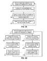
- FIG. 1Ais a diagram of a display system incorporating an adjustable voltage supply.
- FIG. 1Bis a circuit diagram of an exemplary pixel circuit showing voltage levels across the drive transistor and the light emitting device.
- FIG. 2is a diagram of a display system incorporating an adjustable voltage supply to separately adjust supply lines for a plurality of subsections of a display.
- FIG. 3Aillustrates a flow chart for an exemplary method of operating a display while decreasing the power consumption of the display.
- FIG. 3Billustrates a flow chart for another exemplary method of operating a display.
- FIG. 4illustrates a flowchart for another exemplary method of operating a display.
- FIG. 5illustrates an example screen capture of a display of a list of emails and incorporating selectable features.
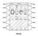
- FIG. 6Ais an example screen capture of a display menu with selectable features.
- FIG. 6Bis another example screen capture of the screen shown in FIG. 6A , but with an additional highlighted region shown.
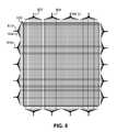
- FIG. 7illustrates an example configuration for electrode patterning of a display array where supply lines are separately adjustable.
- FIG. 8illustrates another example configuration for a pattern of electrodes in a display array where supply lines are separately adjustable.
- FIG. 1Ais a block diagram of an exemplary display system 100 incorporating an adjustable voltage supply 140 .
- the display system 100includes an address driver 120 , a data driver 110 , and a controller 130 .
- the controller 130receives digital data indicative of information to be displayed via the display system 100 .
- the controller 130sends data signals 134 to the data driver 110 , scheduling signals 132 to the address driver 120 , and control signals 136 to the adjustable voltage supply 140 to drive a display array to display the information indicated.
- the display system 100generally includes a display array with an array of pixels, such as the pixel 10 , arranged in rows in columns.
- the display arraycan include conductive and/or semi-conductive elements formed (e.g., by a deposition process) on a display substrate, an encapsulation substrate (e.g., glass), or a combination of substrates.
- Each of the pixelse.g., the pixel 10
- the array of pixelsthus comprise the display array (“display screen”) adapted to dynamically display information according to the digital display data input to the controller 130 .
- the display screencan display, for example, video information from a stream of video data received by the controller 130 .
- the display system 100 in FIG. 1Ais illustrated with a single pixel 10 . It is understood that the display system 100 can be implemented with a display screen that includes an array of similar pixels, such as the pixel 10 , and that the display screen is not limited to a particular number of rows and columns of pixels. For example, the display system 100 can be implemented with a display array with a number of rows and columns of pixels commonly available in displays for mobile devices, television displays, computer monitors, heads up displays, etc.
- the pixel 10is operated by a driving circuit (“pixel circuit”) that includes a driving transistor and a light emitting device.
- pixel circuita driving circuit
- the light emitting devicecan optionally be an organic light emitting diode, but implementations of the present disclosure apply to pixel circuits having other electroluminescence devices, including current-driven light emitting devices.
- the driving transistor in the pixel 10can optionally be an n-type or p-type thin-film transistor, but implementations of the present disclosure are not limited to pixel circuits having a particular polarity of transistor or only to pixel circuits having thin-film transistors.
- the pixel 10is coupled to a select line 122 , a first supply line 142 , a second supply line 144 , a data line 114 , and a monitor line 112 .
- the select line 122is provided by the address driver 120 , and can be utilized to enable, for example, a programming operation of the pixel 10 by activating a switch or transistor to allow the data line 114 to program the pixel 10 .
- the data line 114conveys programming information from the data driver 110 to the pixel 10 .
- the data line 114can be utilized to apply a programming voltage or a programming current to the pixel 10 .
- the programming voltage/currentcan be at a level sufficient to charge a capacitor within the pixel 10 such that the drive transistor is operated to convey current through the light emitting device to emit light with a desired amount of luminance.
- the programming voltage (or programming current) supplied by the data driver 110 via the data line 114is generally related to the digital data received by the controller 130 by a relationship expressed as a formula and/or by a lookup table that maps digital data values to programming voltage/current levels.
- the programming voltage/currentcan be applied to the pixel 10 during a programming operation of the pixel 10 so as to charge a storage device within the pixel 10 , such as a capacitor.
- the pixel 10can emit light with the desired amount of luminance during an emission operation.
- the storage device in the pixel 10can be charged during a programming operation to apply a voltage to one or more of a gate and/or source terminal of the drive transistor during the emission operation.
- the conductance of the drive transistoris adjusted according to the current-voltage characteristics of the drive transistor, and a current is conveyed through the light emitting device according to the voltage stored on the capacitor.
- the driving current that is conveyed through the light emitting device by the driving transistor during the emission operation of the pixel 10is a current that is supplied by the first supply line 142 and is drained to the second supply line 144 .
- the first supply line 142 and the second supply line 144are coupled to the adjustable voltage supply 140 .
- the first supply line 142can provide a positive supply voltage (e.g., the voltage commonly referred to in circuit design as “Vdd”) and the second supply line 144 can provide a negative supply voltage (e.g., the voltage commonly referred to in circuit design as “Vss”).
- one or the other of the supply lines 142 , 144are fixed at a ground voltage or at another reference voltage, and need not be connected to the adjustable voltage supply.
- either the first supply line 142 , or the second supply line 144 , or bothare adjustable by the adjustable voltage supply 140 according to the control signals 136 from the controller 130 .
- the value of the positive supply voltage Vdd and/or the value of the negative supply voltage Vsscan be adjusted by the adjustable voltage supply 140 .
- the difference between the voltages on the first supply line 142 and the second supply line 144influences the amount of power drawn by the pixel 10 during the programming operation of the pixel 10 .
- the power required by the pixel 10 during the emission phase of the pixel 10is proportional to (Vdd ⁇ Vss) ⁇ Idrive, where Idrive is the driving current conveyed through the driving transistor, and through the light emitting device, as previously described.
- Idrivethe driving current conveyed through the driving transistor, and through the light emitting device, as previously described.
- the difference between Vdd and Vss (“ ⁇ V”) supplied to the pixel 10can be controlled (e.g., reduced) by adjusting the voltage on the first supply line 142 and/or the second supply line 144 .
- FIG. 1Bis a circuit diagram of an exemplary pixel circuit showing voltage levels across a drive transistor 152 and a light emitting device 154 .
- the pixel circuit in FIG. 1Bis provided for illustrative purposes only to illustrate the series connection between the drive transistor 152 , the light emitting device 154 between the two voltage supply lines 142 , 144 .
- the pixel circuit 10 shown in FIG. 1Acan include an n-type or p-type drive transistor, and an arrangement of additional transistors and/or capacitors arranged to selectively connect to the data line 114 for programming the pixel circuit 10 according to voltage programming and/or current programming information and charging one or more capacitors within the pixel circuit to influence the conductance of a drive transistor.
- the drive transistor 152is connected in series between the high voltage supply line 142 (“Vdd line”) and the light emitting device 154 .
- the drive transistor 152can have a drain and source and the drain of the drive transistor 152 can be connected to the high voltage supply line 142 and the source of the drive transistor 152 can be connected to the light emitting device 154 .
- the light emitting device 154is connected between the drive transistor 152 and the low voltage supply line 144 (“Vss line”).
- the light emitting device 154can have an anode and cathode and the anode of the light emitting device 154 can be connected to the drive transistor 152 and the cathode of the light emitting device 154 can be connected to the low voltage supply line 144 .
- the gate terminal of the drive transistor 152is connected to a storage capacitor 156 .
- the storage capacitor 156is configured to apply a voltage to the gate of the drive transistor 152 so as to influence the conductance of the drive transistor 152 such that the current conveyed through the light emitting device 154 via the drive transistor 152 is controlled by the voltage on the storage capacitor 156 .
- the storage capacitor 156is shown connected to a ground voltage, but can alternatively be connected to the anode terminal of the light emitting device 154 , one or the other of the supply voltage lines 142 , 144 , a reference voltage, and/or another stable voltage sufficient to allow the storage capacitor 154 to be charged according to programming information and apply a voltage to the drive transistor so as to influence the conductance of the drive transistor 152 .
- FIG. 1Balso includes a diagram showing the voltage across the pixel circuit between the two voltage supply lines 142 , 144 .
- the voltages on the voltage supply lines 142 , 144are generally decreased/increased due to the resistive line losses between the adjustable voltage supply 140 and the pixel circuit being powered.
- Vss supply⁇ (Vss IR Rise).
- the “IR Drop” and “IR Rise”refers to the voltages resulting from resistive line losses, where “I” refers to the current on the line and “R” refers to the line resistance.
- the voltage across the light emitting device(which can optionally be an OLED) is shown as V OLED .
- the value of V OLEDgenerally depends on the characteristics of the light emitting device 154 , the aging history of the light emitting device 154 , and/or the current being conveyed through the light emitting device 154 .
- the value of V OLEDcan increase with increasing drive current (i.e., increased luminance) and the increase can be compensated for by measuring and/or predicting the increase based on measurements from the monitoring system 115 or based on calibrated look-up tables stored in a memory 116 to map predicted aging degradation to usage histories/profiles.
- the voltage across the drive transistor 152is shown as V DS , where V DS can refer to the “drain-source” voltage across the drive transistor 152 .
- the value of voltage across the transistore.g., the drain-source voltage V DS
- V DSthe drain-source voltage
- the drive transistor 152can operate in the saturation mode while V DS >V GS ⁇ Vth, where V GS is the voltage between gate and source terminals of the drive transistor 152 and Vth is the threshold voltage of the drive transistor 152 .
- VDS required to maintain the drive transistor 152 in saturation modeis dependent on the values of VGS and the threshold voltage, Vth.
- the value of Vthcan change over time due to electrical degradation of the drive transistor 152 . Similar to the discussion of V OLED above, the value of Vth can be compensated for over time according to measured and/or predicted values based on, for example, measurements via the monitoring system 115 and/or look-up tables stored in the memory 116 and mapped to usage profiles/histories.
- the excess voltagei.e., the excess amount of V DS still applied across the drive transistor 152
- the excess voltageis generally dissipated within the channel region of the drive transistor 152 as heat energy.
- excessive heat generation in the channel regionundesirably contributes to degradation of the drive transistor 152 , and thus, the aging of the display system 100 .
- the values of Vdd supply and/or Vss supplyare selected to provide a voltage across the drive transistor 152 (e.g., the voltage V DS ) sufficient to set the drive transistor 152 in the saturated mode.
- the required value of V DScan be determined, at least in part, according to the measured and/or predicted values of Vdd IR Drop, Vss IR Rise, V OLED , Vth.
- the required value of V DScan be determined, at least in part, according to the programming information for the pixel circuit, because the programming information influences the value of V GS , because the luminance of the light emitting device 154 is generally related to the current through the drive transistor 152 , and the current through the drive transistor 152 is regulated, at least in part, by V GS .
- the value of V GSis determined, at least in part, according to the luminance output from pixel circuit, and thus is determined, at least in part, according to the programming information for the pixel circuit.
- the controller 130analyzes the digital data indicating luminance values for the display to determine an amount to adjust the voltage on the first supply 142 and/or the second supply 144 such that the pixels in the display array will have sufficient power to produce the desired amount of luminance. In some embodiments, the controller 130 analyzes the digital data and/or measured, stored, and/or predicted degradation information for pixels in the display (such as values of V OLED , Vth, etc.), and adjusts the voltage on the first supply line 142 and/or the second supply line 144 such that the pixels in the display array are each set in the saturated condition.
- the controller 130can analyze the incoming digital data to determine the required values of ⁇ V TOTAL to set each pixel in the display system 100 in the saturated mode, and then the values of Vdd and/or Vss supplied via the adjustable voltage supply 140 can be set according to the maximum required value of ⁇ V TOTAL in the display for each frame.
- the value of DVTOTALcan be set according to the maximum required value for each frame, rather than the maximum required value across all frames, the value of voltage across each pixel can be no greater than necessary on a frame-by-frame basis.
- the pixelsare all set in the saturated condition, there is generally no decrease in luminance, because the currents through the pixels are unaffected. Because the power through the display panel is set dependent on the product of voltage across each pixel and current through each pixel, decreasing the voltage also decreases power consumption (and also decreases heat generation within the drive transistor channel regions).
- the controller 130can be configured to advantageously calculate an optimum magnitude of the difference between Vdd and Vss (“ ⁇ V”) such that the power consumed by the display system 100 is reduced as much as possible while still providing sufficient power to the pixels to produce the luminance values specified by the input data.
- the determination of the voltages to provide on the first supply line 142 and/or the second supply line 144can be carried out in the controller 130 dynamically, such as on a frame-by-frame basis when the display system 100 is displaying video.
- the controller 130can select a desired voltage to provide on the supply lines 142 , 144 by analyzing the input data to determine, for example, the maximum luminance value to be emitted from the display.
- the controller 130can also compute the total cumulative current to be drawn by all the pixels in the display to determine a total load placed on the adjustable voltage supply 140 during a particular frame.
- the controller 130selects desired voltages to be provided via the supply lines 142 , 144 by using a formula and/or a look up table.
- the selection of the desired voltagescan be accomplished by first calculating an optimal voltage (e.g., an optimal level of ⁇ V).
- the adjustable voltage supply 140can be configured to provide output voltages at a series of predetermined voltage levels (e.g., a series of voltages separated by a resolution of the driver of the adjustable voltage supply 140 ).
- the controller 130can optionally select the closest available value of ⁇ V TOTAL by adjusting one or both of the supply lines 142 , 144 to predetermined levels.
- the controller 130selects the predetermined levels of the supply lines 142 , 144 to select the next highest value of ⁇ V TOTAL over the determined optimal value.
- the selection of the desired voltagecan also be accomplished by the controller 130 by determining, based on the digital input data, whether the total load to be drawn by the display and/or the maximum desired luminance value of the display are above or below a set of trigger values, or within a range specified by trigger values.
- the set of trigger values, or the ranges specified between the trigger valuescan correspond to particular voltages provided by the adjustable voltage supply 140 .
- the supply lines 142 , 144 providing supply voltages to the pixels in the displayare coupled to the adjustable voltage supply 140 .
- the individual supply lines coupled to the adjustable voltage supply 140can be arranged along rows (or columns) of the display such that each supply line supplies a supply voltage to pixels in a common row (or column) of the display. Implementations can also provide for each supply line to be shared by pixels in adjacent rows (or columns) of the display.
- the pixel 10is also coupled to a monitor line 112 .
- the monitor line 112connects the pixel 10 to the monitor system 115 .
- the monitor system 115can be integrated with the data driver 110 , or can be a separate stand-alone system.
- the monitoring system 115can optionally be implemented by monitoring the current and/or voltage of the data line 114 during a monitoring operation of the pixel 10 , and the monitor line 112 can be entirely omitted.
- the display system 100can be implemented without the monitoring system 115 or the monitor line 112 .
- the monitor line 112allows the monitoring system 115 to measure a current or voltage associated with the pixel 10 and thereby extract information indicative of a degradation of the pixel 10 .
- the monitoring system 115can extract, via the monitor line 112 , a current flowing through the drive transistor (e.g., the drive transistor 152 ) within the pixel 10 and thereby determine, based on the measured current and based on the voltages applied to the driving transistor during the measurement, a threshold voltage of the driving transistor or a shift thereof.
- the monitoring system 115can also extract an operating voltage of the light emitting device (e.g., a voltage drop across the light emitting device while the light emitting device is operating to emit light, such as V OLED across the light emitting device 154 ).
- the monitoring system 115can then communicate the signals 134 to the controller 130 and/or the memory 116 to allow the display system 100 to compensate for the extracted degradation information in subsequent programming and/or emission operations of the pixel 10 .
- the programming information conveyed to the pixel 10 via the data line 114can be appropriate adjusted during a subsequent programming and/or emission operation of the pixel 10 such that the pixel 10 emits light with a desired amount of luminance that is independent of the degradation of the pixel 10 . It is specifically noted that implementations of the present disclosure can be realized with or without the monitoring system 115 .
- FIG. 2is a diagram of a display system 200 incorporating an adjustable voltage supply 240 to separately adjust supply lines (e.g., the supply lines 241 , 242 ) for a plurality of subsections (e.g., the subsections 211 to 216 ) of a display 210 .
- the display system 200also includes a controller 230 for receiving digital data 232 and for controlling the adjustable voltage supply 240 via control signals 234 .
- the display 210generally includes an array of pixels that are individually programmable to emit light with individually programmable luminance values according to information indicated by the digital data 232 .
- the display 210differs from the display screen previously described in that the display 210 includes a plurality of discrete subsections.
- the display 210includes a first subsection 211 , a second subsection 212 , a third subsection 213 , a fourth subsection 214 , a fifth subsection 215 , and a sixth subsection 216 .
- the subsections 211 - 216can be supplied with supply voltages that are distinct from one another.
- the first subsection 211is supplied with the first supply voltage Vdd 1 via the first supply line 241 ;
- the second subsection 212is supplied with the second supply voltage Vdd 2 via the second supply line 242 ;
- the sixth subsection 216is supplied with the sixth supply voltage Vdd 6 via the sixth supply line 243 .
- the remaining subsections 213 - 215are supplied with respective, separately controllable supply voltages Vdd 3 , Vdd 4 , Vdd 5 via respective supply lines for each subsection.
- the supply linese.g., the supply lines 241 , 242 , . . . , 243
- the adjustable voltage supply 240is configured to separately, and simultaneously, provide distinct supply voltages to the respective subsections 211 - 216 .
- the first supply line 241 and the second supply line 242 in FIG. 2are related, but separate from, the pixel-level supply lines 142 and 144 illustrated in FIG. 1A .
- the first supply line 241 and the second supply line 242are conductive lines that connect entire portions (i.e., subsections) of the display 210 to a supply voltage appropriate to the respective portion.
- the first display line 241 and the second display line 242can each be electrically connected to a plurality of individual lines (“power rails”), akin to the supply lines 142 and 144 illustrated in FIG. 1 , that are then connected to individual pixels within the respective subsections 211 - 216 .
- the connection between the first supply line 241 and the plurality of individual lines in the first subsection 211is illustrated symbolically by the first terminal 211 a and the second terminal 211 b .
- the first terminal 211 aprovides a point of coupling between the plurality of power rails, or positive voltage supply lines, that are connected to the pixels in the first subsection 211 .
- the second terminal 211 balso provides a point of coupling between the plurality of power rails that are connected to the pixels in the first subsection 211 , but from a side of the display 210 opposite a side having the first terminal 211 a .
- the pixels in the subsection 211are advantageously less affected by variations in the supply voltage across the subsection 211 .
- the effect of Vdd IR Drop discussed in connection with FIG. 1Bcan be less severe in the display system 200 than in other systems.
- the displays system 200can be implemented with the power supply lines (e.g., the power supply lines 241 , 242 ) connected to each respective subsection 211 - 216 via a single terminal (e.g., the first terminal 211 a ) rather than via two terminals.
- the remaining subsections 212 to 216can be connected to the adjustable voltage supply 240 via terminals similar to the terminals 211 a and 211 b described for the first subsection 211 .
- the second supply voltage Vdd 2can be delivered to power rails in the second subsection 212 via the terminals 212 a , 212 b ; and the sixth supply voltage Vdd 6 can be delivered to power rails in the sixth subsection 216 via the terminals 216 a , 216 b.
- the controller 230is adapted to receive the digital data 232 and determine appropriate voltages to provide to each subsection 211 - 216 based on the digital data 232 (and optionally based on measured and/or predicted degradation information for the display).
- the controller 232then sends the control signals 234 to the adjustable voltage supply 240 to instruct the adjustable voltage supply 240 to supply the appropriate voltages to the subsections 211 - 216 .
- the controller 230can determine the appropriate supply voltages for each subsection in a manner similar to the description of the operation of the controller 130 and the adjustable voltage supply 140 in connection with FIG.
- control 230can determine voltage levels required to set pixels in each subsection 211 - 216 in the saturated mode.
- the controller 230 in FIG. 2can separately determine an appropriate voltage to be provided to each of the plurality of subsections 211 - 216 .
- the determination of the appropriate voltage to provide to the subsections 211 - 216can be carried out dynamically to adjust the supply voltages provided to the subsections of the display 210 in real time, and can be performed to adjust the supply voltage for each frame of a video signal.
- Implementations of the present disclosurealso allow for adjusting the supply voltage provided to each subsection at a frequency less than the frame rate of a video signal.
- the display system 200can allow for the supply voltage provided to the subsection 211 to be fixed at the same level for two or more sequential frames of a video before being adjusted again.
- the subsections 211 - 216 of the display 210can also be referred to as regions or portions of the display.
- the subsections 211 - 216can be non-overlapping subsections.
- the subsections 211 - 216span the width of the display 210 .
- aspects of the present disclosureapply to displays having subsections that encompass less than the width of a display.
- aspects of the present disclosureapply to displays with subsections that are not regularly or evenly spaced.
- subsections of a displaymay be arranged such that each subsection of the display corresponds to a region of the display that displays features of a graphical user interface.
- the separate subsectionscan be highlighted (“selected”) according to user inputs to enable the user to, for example, navigate menus associated with the graphical user interface.
- the voltage supplied to the subsectionscan be varied depending on whether the respective subsection is selected to be brightened or is deselected to be subdued.
- subsections of the displaycan be separately addressable to adjust the power drawn by highlighted (“selected”) subsections of the display.
- FIG. 2is illustrated with reference to adjusting the positive supply voltage (i.e., Vdd 1 , Vdd 2 , etc.) to each subsection of the display 210 , it is understood that the display system 200 can also be implemented while adjusting a negative supply voltage (such as supply voltages Vss 1 , Vss 2 , etc.) or by adjusting both a positive supply voltage and a negative supply voltage for each subsection 211 - 216 of the display 210 .
- a negative supply voltagesuch as supply voltages Vss 1 , Vss 2 , etc.
- FIG. 3Aillustrates a flow chart for an exemplary method of operating a display while decreasing the power consumption of the display.
- the flow chart of FIG. 3Ais described with reference to FIG. 2 for example purposes.
- the controller 230receives the digital data 232 ( 310 ).
- the digital data 232is indicative of an image to be displayed on the display 210 .
- the controller 230analyzes the received digital data 232 to corresponding to a first plurality of pixels ( 320 ).
- the first plurality of pixelscan be, for example, the pixels in the subsection 211 , or can be the pixels in the entirety of the display 210 .
- the controller 230selects a supply voltage to be applied to the first plurality of pixels based on the analyzed digital data ( 330 ).
- the selection of an appropriate supply voltagecan be performed based on a range of the luminance values for the pixels in the display, on a maximum and/or minimum of such luminance values, on a voltage necessary to set the drive transistor in saturation mode, and/or based on a total anticipated cumulative load to be drawn to supply the desired luminance values, and can be carried out by using look up tables, threshold values, and/or formulas.
- the controller 230then sends the control signals 234 to the adjustable voltage supply 240 such that the adjustable voltage supply 240 supplies the selected supply voltage to the first plurality of pixels ( 340 ).
- FIG. 3Billustrates a flow chart for another exemplary method of operating a display.
- the flow chart in FIG. 3Bis similar to the flow chart of FIG. 3A except that the blocks 320 , 330 , and 340 are carried out for a plurality (n) of subsections of the display 210 .
- Each of the subsectionsincludes a plurality of pixels.
- the controller 230also analyzes the received digital data corresponding to the additional pluralities of pixels according to the number of subsections in the display being operated. For example, with reference to the display 210 in FIG.
- the received digital datais analyzed for the second through sixth subsections ( 212 to 216 ) in addition to the first subsection 211 .
- the received digital datais thus analyzed for each subsection of the display through the “nth” plurality of pixels ( 320 n ).
- a supply voltageis selected to be applied to each subsection of the display through the “nth” plurality of pixels ( 330 n ), and the respective selected supply voltages are supplied to each subsection in the display through the “nth” plurality of pixels ( 340 n ).
- FIG. 4illustrates a flowchart for another exemplary method of operating a display. It is determined whether the display is operating in an idle mode ( 410 ). If the display is operating in an idle mode, portions (“subsections”) of the display are identified that are set to a dark setting during the idle mode ( 420 ). The supply voltage to the identified portions of the display are then turned off ( 430 ). Turning off the supply voltage to the identified portions of the display prevents current from being conveyed through pixels in the identified portions. In addition, the programming operation of the identified portions of the display can be ceased ( 440 ). Ceasing the programming operation in the identified portions advantageously prevents the display from drawing power during the programming operation.
- the compensation and monitoring operationgenerally requires additional power to be drawn during monitoring and/or compensation operations of the display.
- the monitoring and compensation functions for the identified portions of the display that are set to a dark settingare advantageously ceased during the idle mode of the display.
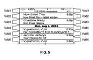
- FIG. 5illustrates an example screen capture of a display of a list of emails and incorporating selectable features.
- an email with the subject line “Now Smell This”is operated according to a second positive supply voltage Vdd 2 .
- Vdd 2can be adjusted relative to the other voltage values (e.g., the voltages Vdd 3 , Vdd 4 , Vdd 5 , Vdd 6 ) such that the top email in the list can be shown highlighted relative to the other emails listed without wasting energy in the channel regions of the drive transistors in the pixel circuits of the other sections of the display.
- a header menuis separately controlled by the supply voltage Vdd 1 such that the header menu can be shown bright (such as to indicate selection) while other sections of the display are shown subdued (“dimmed”).
- the screen capture in FIG. 5illustrates a display system for a phone or other mobile device that has been segmented into subsections that have separately adjustable supply voltages.
- the subsectionscoincide with regions on the graphical user interface that are separately highlighted (e.g., highlighted and/or dimmed) to allow a user to navigate the user interface (e.g., the list of emails).
- Vdd 2can be set at a higher level than Vdd 3 -Vdd 6 to allow the display in the subsection indicated by Vdd 2 to be brighter than the other subsections of the display without unnecessarily wasting power in the dimmed regions.
- FIG. 6Ais an example screen capture of a display menu with selectable features.
- FIG. 6Bis another example screen capture of the screen shown in FIG. 6A , but with an additional highlighted region shown.
- the screen capture in FIGS. 6A and 6Bis another example display of a graphical user interface for a mobile device, such as a phone, PDA, or similar device.
- the graphical user interface illustrated in FIGS. 6A and 6Bpresents a menu of available programs and features on the device that is navigated according to user inputs provided by a user of the device.
- the various menu items on the displayare indicated by iconographic symbols and are arranged in rows coinciding with the separately adjustable subsections of the display in FIGS. 6A and 6B .
- the subsection (“region”) indicated by Vdd 3is highlighted relative to the adjacent subsections of the display.
- the icons in the highlighted subsectiontherefore appear brightened (“highlighted”) relative to the icons in the adjacent subsections (e.g., the subsections indicated by Vdd 2 , Vdd 4 , Vdd 5 , Vdd 6 ), which are subdued.
- energycan be saved by decreasing the voltage supply (i.e., decreasing ⁇ V) provided to the deselected subsections (e.g., the subsections indicated by Vdd 2 , Vdd 4 , Vdd 5 , Vdd 6 ).
- the screen shot in FIG. 6Bshows the header bar in the region indicated by Vdd 1 in a highlighted state.
- the header baris in a subdued/dimmed state in FIG. 6A .
- the header bar in FIGS. 6A and 6Bis of a different size than the other subsections of the display, such as the subsection indicated by Vdd 2 , and the size of the segmented subsections of the display are selected to correspond to the brightness-variable regions of the user interface shown on the display.
- display panels with segmented adjustable power supply regionsare designed to have sizes and/or shapes of distinct adjustable regions correspond to sizes and/or shapes of a user interface to be operated on the display.
- the magnitude of Vdd 1can be increased relative to the value of Vdd 1 in FIG. 6A .
- the magnitude of Vdd 1can be decreased relative to the value of Vdd 1 when the header bar is highlighted.
- saving energy in the operation of the displays shown in FIGS. 5 through 6Ballows the device to operate for a longer duration from a given battery charge.
- decreasing the amount of energy converted to heat energy in the channel regions of the dimmed regions of the displayextends the lifetime of the display panel by decreasing the electrical degradation of the drive transistors within the pixels of the display.
- FIG. 7illustrates an example configuration for electrode patterning of a display array 710 where supply lines are separately adjustable.
- the display array 710includes a plurality of subsections arranged in a grid. Each of the subsections are separately controllable by supply lines (e.g., the supply lines 701 , 702 ) which connect to an adjustable voltage supply.
- the display array 710 illustrated in FIG. 7has a fixed positive voltage supply Vdd (not shown) and the negative voltages supply Vss(i, j) is separately controllable (“addressable”) via the plurality of supply lines that are provided for each subsection in a one to one ratio.
- the supply lines for the array of Vss(i, j) regionscan be considered a passive power supply matrix of the display 710 . That is, by controlling the magnitude of Vss(i, j), each subsection in the grid of subsections can be dynamically supplied with a selected value of ⁇ V which is appropriate to the respective subsection based on the luminance values desired for the respective subsection as indicated by a digital data input.
- FIG. 8illustrates another example configuration for a pattern of electrodes in a display array 810 where supply lines are separately adjustable.
- the display array 810also includes a plurality of subsections arranged in a grid.
- the positive supply voltage Vdd(i)is separately controllable along the rows of the grid formed by the plurality of subsections
- the negative supply voltage Vss(j)is separately controllable along the columns of the grid formed by the plurality of subsections.
- the ⁇ V applied to each subsection in the grid of subsectionsis separately adjustable.
- the column terminal connectors and the row terminal connectorsare connected to an adjustable voltage supply and are dynamically set to appropriate voltages according the systems and methods described herein.
- the first power supply linese.g., the power rails set to Vdd(i)
- the second power supply linese.g., the power rails set to Vss(j)
- the first power supply linescan be situated generally on one side of a display substrate, running horizontally
- the second power supply linese.g., the power rails set to Vss(j)
- the pixel circuits in the display panel 810are deposited between the Vdd and Vss power rails.
- the sizes and arrangements of the subsections of the display arraysare selected to correspond to portions of a display that are selectively highlighted according to a graphical user interface.
- the selectable features shown in FIGS. 6A and 6Bi.e., the iconographic menu items
- the selectable features shown in FIGS. 6A and 6Bcan be dimensioned so as to coincide with separately adjustable subsections of a display that displays the graphical user interface.
- Two or more computing systems or devicesmay be substituted for any one of the controllers described herein. Accordingly, principles and advantages of distributed processing, such as redundancy, replication, and the like, also can be implemented, as desired, to increase the robustness and performance of controllers described herein.
- machine readable instructionscomprise an algorithm for execution by: (a) a processor, (b) a controller, and/or (c) one or more other suitable processing device(s).
- the algorithmmay be embodied in software stored on tangible media such as, for example, a flash memory, a CD-ROM, a floppy disk, a hard drive, a digital video (versatile) disk (DVD), or other memory devices, but persons of ordinary skill in the art will readily appreciate that the entire algorithm and/or parts thereof could alternatively be executed by a device other than a processor and/or embodied in firmware or dedicated hardware in a well known manner (e.g., it may be implemented by an application specific integrated circuit (ASIC), a programmable logic device (PLD), a field programmable logic device (FPLD), a field programmable gate array (FPGA), discrete logic, etc.).
- ASICapplication specific integrated circuit
- PLDprogrammable logic device
- FPLDfield programmable logic device
- FPGAfield programmable gate array
- any or all of the components of the baseline data determination methodscould be implemented by software, hardware, and/or firmware.
- some or all of the machine readable instructions representedmay be implemented
Landscapes
- Engineering & Computer Science (AREA)
- Theoretical Computer Science (AREA)
- Physics & Mathematics (AREA)
- General Physics & Mathematics (AREA)
- General Engineering & Computer Science (AREA)
- Computer Hardware Design (AREA)
- Human Computer Interaction (AREA)
- Control Of Indicators Other Than Cathode Ray Tubes (AREA)
- Control Of El Displays (AREA)
Abstract
Description
Claims (16)
Priority Applications (6)
| Application Number | Priority Date | Filing Date | Title |
|---|---|---|---|
| US13/474,131US9134825B2 (en) | 2011-05-17 | 2012-05-17 | Systems and methods for display systems with dynamic power control |
| US14/459,979US9606607B2 (en) | 2011-05-17 | 2014-08-14 | Systems and methods for display systems with dynamic power control |
| US14/491,763US9886899B2 (en) | 2011-05-17 | 2014-09-19 | Pixel Circuits for AMOLED displays |
| US15/431,974US10249237B2 (en) | 2011-05-17 | 2017-02-14 | Systems and methods for display systems with dynamic power control |
| US15/867,937US10515585B2 (en) | 2011-05-17 | 2018-01-11 | Pixel circuits for AMOLED displays |
| US16/275,904US10607543B2 (en) | 2011-05-17 | 2019-02-14 | Systems and methods for display systems with dynamic power control |
Applications Claiming Priority (2)
| Application Number | Priority Date | Filing Date | Title |
|---|---|---|---|
| US201161487272P | 2011-05-17 | 2011-05-17 | |
| US13/474,131US9134825B2 (en) | 2011-05-17 | 2012-05-17 | Systems and methods for display systems with dynamic power control |
Related Parent Applications (1)
| Application Number | Title | Priority Date | Filing Date |
|---|---|---|---|
| US14/474,977Continuation-In-PartUS20140368491A1 (en) | 2011-05-17 | 2014-09-02 | Pixel circuits for amoled displays |
Related Child Applications (2)
| Application Number | Title | Priority Date | Filing Date |
|---|---|---|---|
| US14/459,979Continuation-In-PartUS9606607B2 (en) | 2011-05-17 | 2014-08-14 | Systems and methods for display systems with dynamic power control |
| US14/491,763Continuation-In-PartUS9886899B2 (en) | 2011-05-17 | 2014-09-19 | Pixel Circuits for AMOLED displays |
Publications (2)
| Publication Number | Publication Date |
|---|---|
| US20120293481A1 US20120293481A1 (en) | 2012-11-22 |
| US9134825B2true US9134825B2 (en) | 2015-09-15 |
Family
ID=47174591
Family Applications (1)
| Application Number | Title | Priority Date | Filing Date |
|---|---|---|---|
| US13/474,131Active2033-02-13US9134825B2 (en) | 2011-05-17 | 2012-05-17 | Systems and methods for display systems with dynamic power control |
Country Status (4)
| Country | Link |
|---|---|
| US (1) | US9134825B2 (en) |
| EP (1) | EP2710578B1 (en) |
| CN (3) | CN109272933A (en) |
| WO (1) | WO2012156942A1 (en) |
Cited By (7)
| Publication number | Priority date | Publication date | Assignee | Title |
|---|---|---|---|---|
| US20160293102A1 (en)* | 2015-04-01 | 2016-10-06 | Ignis Innovation Inc. | Systems and methods of display brightness adjustment |
| US20170154574A1 (en)* | 2011-05-17 | 2017-06-01 | Ignis Innovation Inc. | Systems and methods for display systems with dynamic power control |
| US20180144688A1 (en)* | 2016-11-21 | 2018-05-24 | Lg Display Co., Ltd. | Gate Driver and Display Panel Using the Same |
| US10026348B2 (en) | 2016-03-11 | 2018-07-17 | Apple Inc. | Driving scheme for high brightness and fast response panel flash |
| US10187691B2 (en) | 2016-05-25 | 2019-01-22 | Electronics And Telecommunications Research Institute | Method and system for providing video |
| US10297191B2 (en) | 2016-01-29 | 2019-05-21 | Samsung Display Co., Ltd. | Dynamic net power control for OLED and local dimming LCD displays |
| US10650732B2 (en) | 2016-03-03 | 2020-05-12 | Electronics And Telecommunications Research Institute | Display device including power delivery network controller for controlling reconfigurable power delivery network for reducing power comsumption and display power management method using the display device |
Families Citing this family (48)
| Publication number | Priority date | Publication date | Assignee | Title |
|---|---|---|---|---|
| US9886899B2 (en)* | 2011-05-17 | 2018-02-06 | Ignis Innovation Inc. | Pixel Circuits for AMOLED displays |
| US9201483B2 (en)* | 2013-01-16 | 2015-12-01 | Novatek Microelectronics Corp. | Image processing unit, image processing apparatus and image display system |
| CA2894717A1 (en) | 2015-06-19 | 2016-12-19 | Ignis Innovation Inc. | Optoelectronic device characterization in array with shared sense line |
| US9368067B2 (en)* | 2013-05-14 | 2016-06-14 | Apple Inc. | Organic light-emitting diode display with dynamic power supply control |
| FR3005754B1 (en)* | 2013-05-17 | 2019-04-05 | Thales | ELECTROOPTIC DEVICE WITH HIGH-DIMENSIONAL PIXEL MATRIX |
| KR20150006731A (en)* | 2013-07-09 | 2015-01-19 | 삼성디스플레이 주식회사 | Display device and driving method thereof |
| US9189114B2 (en)* | 2013-07-24 | 2015-11-17 | Synaptics Incorporated | Face detection with transcapacitive sensing |
| US9620057B2 (en) | 2013-08-16 | 2017-04-11 | Boe Technology Group Co., Ltd. | Method and apparatus for adjusting driving voltage for pixel circuit, and display device |
| CN103559860B (en)* | 2013-08-16 | 2015-07-22 | 京东方科技集团股份有限公司 | Pixel circuit driving voltage adjusting method, pixel circuit driving voltage adjusting device, and display apparatus |
| EP2854125A1 (en)* | 2013-09-27 | 2015-04-01 | Siemens Aktiengesellschaft | Display device adapted for energy conservation |
| US20150168973A1 (en)* | 2013-12-18 | 2015-06-18 | Hashfast LLC | Stacked chips powered from shared voltage sources |
| CN104036722B (en)* | 2014-05-16 | 2016-03-23 | 京东方科技集团股份有限公司 | Pixel unit driving circuit, driving method thereof, and display device |
| KR20160010680A (en)* | 2014-07-17 | 2016-01-28 | 삼성디스플레이 주식회사 | Method of operating an organic light emitting display device and organic light emitting display device |
| DE102014214767B4 (en) | 2014-07-28 | 2019-03-21 | Continental Automotive Gmbh | Display device for a motor vehicle, in particular head-up display and method for controlling a display device |
| CN105374318A (en)* | 2014-08-14 | 2016-03-02 | 伊格尼斯创新公司 | System and method for usage dynamic power control of display system |
| US20160131904A1 (en)* | 2014-11-07 | 2016-05-12 | Osterhout Group, Inc. | Power management for head worn computing |
| CN104867454A (en)* | 2015-06-10 | 2015-08-26 | 深圳市华星光电技术有限公司 | Control circuit and control method used for AMOLED partition driving |
| US10332482B2 (en)* | 2015-09-25 | 2019-06-25 | Fresenius Medical Care Holdings, Inc. | Automated display dimness control for a medical device |
| CN105304025B (en)* | 2015-12-08 | 2018-01-16 | 昆山工研院新型平板显示技术中心有限公司 | Organic Light Emitting Diode drive control method and system |
| KR102511363B1 (en)* | 2016-02-04 | 2023-03-17 | 삼성전자주식회사 | A display apparatus and a display method |
| KR102544322B1 (en)* | 2016-09-26 | 2023-06-19 | 삼성디스플레이 주식회사 | Light emitting display device |
| CN106531083A (en)* | 2016-12-15 | 2017-03-22 | 上海天马有机发光显示技术有限公司 | Pixel circuit compensation method, OLED display panel and compensation method thereof |
| KR20180077804A (en)* | 2016-12-29 | 2018-07-09 | 엘지디스플레이 주식회사 | Display panel having gate driving circuit |
| US10068551B1 (en)* | 2017-05-01 | 2018-09-04 | Microsoft Technology Licensing, Llc | Localized high brightness mode |
| EP3435192B1 (en)* | 2017-07-28 | 2022-08-24 | NXP USA, Inc. | Ultra low power linear voltage regulator |
| CN107393477B (en)* | 2017-08-24 | 2019-10-11 | 深圳市华星光电半导体显示技术有限公司 | Top-emitting AMOLED pixel circuit and driving method thereof |
| CN107301843A (en)* | 2017-08-28 | 2017-10-27 | 深圳市华星光电半导体显示技术有限公司 | The power configuration structure and collocation method of top emitting AMOLED panel |
| CN109920372B (en) | 2017-12-12 | 2021-01-29 | 京东方科技集团股份有限公司 | Display driving module, display device and voltage adjusting method |
| CN108154847A (en)* | 2018-01-19 | 2018-06-12 | 昆山国显光电有限公司 | The driving device and driving method of organic light emitting display |
| US11416053B2 (en)* | 2018-07-31 | 2022-08-16 | Hewlett-Packard Development Company, L.P. | Operating modes of a computer display |
| KR102528519B1 (en)* | 2018-08-23 | 2023-05-03 | 삼성디스플레이 주식회사 | Display device |
| CN109036286A (en)* | 2018-09-19 | 2018-12-18 | 京东方科技集团股份有限公司 | The method for managing power supply and device of display screen and its pixel circuit unit |
| JP2020060650A (en)* | 2018-10-09 | 2020-04-16 | シナプティクス インコーポレイテッド | Display driver, display module and display method |
| CN111369946A (en)* | 2018-12-25 | 2020-07-03 | 华为终端有限公司 | Display screen, mobile terminal and control method thereof |
| CN109686308B (en)* | 2019-01-10 | 2021-01-08 | 云谷(固安)科技有限公司 | Display panel, display device and driving method of display panel |
| US12136394B2 (en)* | 2019-04-19 | 2024-11-05 | Apple Inc. | Systems and methods for external off-time pixel sensing |
| CN110164368A (en)* | 2019-05-16 | 2019-08-23 | 湖南科比特电气技术有限公司 | Display panel, display device and its brightness adjusting method and device |
| CN112086067B (en)* | 2019-06-14 | 2022-05-13 | 华为技术有限公司 | A voltage adjustment method and electronic device |
| CN110111730B (en)* | 2019-06-21 | 2023-08-22 | 深圳市洲明科技股份有限公司 | Display screen dynamic control system and display screen |
| KR102715436B1 (en)* | 2019-08-07 | 2024-10-10 | 삼성전자주식회사 | Electronic device controlling luminance and its luminance control method |
| CN110782854B (en)* | 2019-10-08 | 2020-09-08 | 深圳市华星光电半导体显示技术有限公司 | Electronic equipment and reading mode identification method thereof |
| CN110940685A (en)* | 2019-11-22 | 2020-03-31 | 南昌航空大学 | Organic electroluminescent material, organic electroluminescent device and control method |
| CN111179826A (en)* | 2020-01-03 | 2020-05-19 | 京东方科技集团股份有限公司 | Display panel driving method, driving device and display device |
| US11984073B2 (en) | 2020-09-29 | 2024-05-14 | Tcl China Star Optoelectronics Technology Co., Ltd. | Partitioned display structure, display panel, and organic light-emitting diode display panel |
| CN112086069B (en)* | 2020-09-29 | 2021-11-23 | Tcl华星光电技术有限公司 | Partition display structure, display panel and organic light emitting diode display panel |
| KR20220151075A (en)* | 2021-05-04 | 2022-11-14 | 삼성디스플레이 주식회사 | Display apparatus and driving method of display apparatus |
| CN113299232A (en)* | 2021-06-01 | 2021-08-24 | 合肥维信诺科技有限公司 | Display panel, driving method thereof and display device |
| CN117409711A (en)* | 2023-04-14 | 2024-01-16 | 深圳Tcl新技术有限公司 | Driving method, driving device, storage medium and display apparatus |
Citations (350)
| Publication number | Priority date | Publication date | Assignee | Title |
|---|---|---|---|---|
| US4354162A (en) | 1981-02-09 | 1982-10-12 | National Semiconductor Corporation | Wide dynamic range control amplifier with offset correction |
| US4758831A (en) | 1984-11-05 | 1988-07-19 | Kabushiki Kaisha Toshiba | Matrix-addressed display device |
| US4963860A (en) | 1988-02-01 | 1990-10-16 | General Electric Company | Integrated matrix display circuitry |
| US4975691A (en) | 1987-06-16 | 1990-12-04 | Interstate Electronics Corporation | Scan inversion symmetric drive |
| GB2205431B (en) | 1986-09-27 | 1991-01-23 | Junichi Nishizawa | Colour display device |
| US4996523A (en) | 1988-10-20 | 1991-02-26 | Eastman Kodak Company | Electroluminescent storage display with improved intensity driver circuits |
| US5051739A (en) | 1986-05-13 | 1991-09-24 | Sanyo Electric Co., Ltd. | Driving circuit for an image display apparatus with improved yield and performance |
| CA1294034C (en) | 1985-01-09 | 1992-01-07 | Hiromu Hosokawa | Color uniformity compensation apparatus for cathode ray tubes |
| CA2109951A1 (en) | 1991-05-24 | 1992-11-26 | Robert Hotto | Dc integrating display driver employing pixel status memories |
| US5222082A (en) | 1991-02-28 | 1993-06-22 | Thomson Consumer Electronics, S.A. | Shift register useful as a select line scanner for liquid crystal display |
| US5266515A (en) | 1992-03-02 | 1993-11-30 | Motorola, Inc. | Fabricating dual gate thin film transistors |
| WO1994025954A1 (en) | 1993-04-30 | 1994-11-10 | Prime View Hk Limited | Apparatus for recovery of threshold voltage shift in amorphous silicon thin-film transistor device |
| US5498880A (en) | 1995-01-12 | 1996-03-12 | E. I. Du Pont De Nemours And Company | Image capture panel using a solid state device |
| US5589847A (en) | 1991-09-23 | 1996-12-31 | Xerox Corporation | Switched capacitor analog circuits using polysilicon thin film technology |
| JPH0990405A (en) | 1995-09-21 | 1997-04-04 | Sharp Corp | Thin film transistor |
| US5619033A (en) | 1995-06-07 | 1997-04-08 | Xerox Corporation | Layered solid state photodiode sensor array |
| US5648276A (en) | 1993-05-27 | 1997-07-15 | Sony Corporation | Method and apparatus for fabricating a thin film semiconductor device |
| US5670973A (en) | 1993-04-05 | 1997-09-23 | Cirrus Logic, Inc. | Method and apparatus for compensating crosstalk in liquid crystal displays |
| US5686935A (en) | 1995-03-06 | 1997-11-11 | Thomson Consumer Electronics, S.A. | Data line drivers with column initialization transistor |
| US5712653A (en) | 1993-12-27 | 1998-01-27 | Sharp Kabushiki Kaisha | Image display scanning circuit with outputs from sequentially switched pulse signals |
| US5714968A (en) | 1994-08-09 | 1998-02-03 | Nec Corporation | Current-dependent light-emitting element drive circuit for use in active matrix display device |
| US5747928A (en) | 1994-10-07 | 1998-05-05 | Iowa State University Research Foundation, Inc. | Flexible panel display having thin film transistors driving polymer light-emitting diodes |
| US5748160A (en) | 1995-08-21 | 1998-05-05 | Mororola, Inc. | Active driven LED matrices |
| JPH10153759A (en) | 1996-11-26 | 1998-06-09 | Matsushita Electric Ind Co Ltd | Liquid crystal display |
| US5784042A (en) | 1991-03-19 | 1998-07-21 | Hitachi, Ltd. | Liquid crystal display device and method for driving the same |
| US5790234A (en) | 1995-12-27 | 1998-08-04 | Canon Kabushiki Kaisha | Eyeball detection apparatus |
| JPH10254410A (en) | 1997-03-12 | 1998-09-25 | Pioneer Electron Corp | Organic electroluminescent display device, and driving method therefor |
| US5815303A (en) | 1997-06-26 | 1998-09-29 | Xerox Corporation | Fault tolerant projective display having redundant light modulators |
| EP0811866A4 (en) | 1995-12-14 | 1998-12-02 | Seiko Epson Corp | METHOD FOR OPERATING A DISPLAY, DISPLAY AND ELECTRONIC DEVICE |
| US5870071A (en) | 1995-09-07 | 1999-02-09 | Frontec Incorporated | LCD gate line drive circuit |
| US5874803A (en) | 1997-09-09 | 1999-02-23 | The Trustees Of Princeton University | Light emitting device with stack of OLEDS and phosphor downconverter |
| US5880582A (en) | 1996-09-04 | 1999-03-09 | Sumitomo Electric Industries, Ltd. | Current mirror circuit and reference voltage generating and light emitting element driving circuits using the same |
| US5903248A (en) | 1997-04-11 | 1999-05-11 | Spatialight, Inc. | Active matrix display having pixel driving circuits with integrated charge pumps |
| US5917280A (en) | 1997-02-03 | 1999-06-29 | The Trustees Of Princeton University | Stacked organic light emitting devices |
| US5923794A (en) | 1996-02-06 | 1999-07-13 | Polaroid Corporation | Current-mediated active-pixel image sensing device with current reset |
| JPH11231805A (en) | 1998-02-10 | 1999-08-27 | Sanyo Electric Co Ltd | Display device |
| US5952789A (en) | 1997-04-14 | 1999-09-14 | Sarnoff Corporation | Active matrix organic light emitting diode (amoled) display pixel structure and data load/illuminate circuit therefor |
| WO1999048079A1 (en) | 1998-03-19 | 1999-09-23 | Holloman Charles J | Analog driver for led or similar display element |
| JPH11282419A (en) | 1998-03-31 | 1999-10-15 | Nec Corp | Element driving device and method and image display device |
| US5990629A (en) | 1997-01-28 | 1999-11-23 | Casio Computer Co., Ltd. | Electroluminescent display device and a driving method thereof |
| US6023259A (en) | 1997-07-11 | 2000-02-08 | Fed Corporation | OLED active matrix using a single transistor current mode pixel design |
| JP2000056847A (en) | 1998-08-14 | 2000-02-25 | Nec Corp | Constant current driving circuit |
| JP2000077192A (en) | 1998-09-01 | 2000-03-14 | Pioneer Electronic Corp | Organic electroluminescent panel and manufacture thereof |
| JP2000089198A (en) | 1998-09-11 | 2000-03-31 | Seiko Epson Corp | Compensation method for liquid crystal applied voltage of liquid crystal display device, liquid crystal display device, electronic device, and voltage detection method for liquid crystal layer |
| CA2242720C (en) | 1998-07-09 | 2000-05-16 | Ibm Canada Limited-Ibm Canada Limitee | Programmable led driver |
| US6069365A (en) | 1997-11-25 | 2000-05-30 | Alan Y. Chow | Optical processor based imaging system |
| CA2354018A1 (en) | 1998-12-14 | 2000-06-22 | Alan Richard | Portable microdisplay system |
| US6081131A (en) | 1997-11-12 | 2000-06-27 | Seiko Epson Corporation | Logical amplitude level conversion circuit, liquid crystal device and electronic apparatus |
| US6157583A (en) | 1999-03-02 | 2000-12-05 | Motorola, Inc. | Integrated circuit memory having a fuse detect circuit and method therefor |
| JP2000352941A (en) | 1999-06-14 | 2000-12-19 | Sony Corp | Display device |
| US6166489A (en) | 1998-09-15 | 2000-12-26 | The Trustees Of Princeton University | Light emitting device using dual light emitting stacks to achieve full-color emission |
| US6177915B1 (en) | 1990-06-11 | 2001-01-23 | International Business Machines Corporation | Display system having section brightness control and method of operating system |
| WO2001027910A1 (en) | 1999-10-12 | 2001-04-19 | Koninklijke Philips Electronics N.V. | Led display device |
| US6225846B1 (en) | 1997-01-23 | 2001-05-01 | Mitsubishi Denki Kabushiki Kaisha | Body voltage controlled semiconductor integrated circuit |
| US6229508B1 (en) | 1997-09-29 | 2001-05-08 | Sarnoff Corporation | Active matrix light emitting diode pixel structure and concomitant method |
| US6232939B1 (en) | 1997-11-10 | 2001-05-15 | Hitachi, Ltd. | Liquid crystal display apparatus including scanning circuit having bidirectional shift register stages |
| US20010002703A1 (en) | 1999-11-30 | 2001-06-07 | Jun Koyama | Electric device |
| US6246180B1 (en) | 1999-01-29 | 2001-06-12 | Nec Corporation | Organic el display device having an improved image quality |
| US20010004190A1 (en) | 1999-12-15 | 2001-06-21 | Semiconductor Energy Laboratory Co., Ltd. | EL disply device |
| US6252248B1 (en) | 1998-06-08 | 2001-06-26 | Sanyo Electric Co., Ltd. | Thin film transistor and display |
| US6259424B1 (en) | 1998-03-04 | 2001-07-10 | Victor Company Of Japan, Ltd. | Display matrix substrate, production method of the same and display matrix circuit |
| US6274887B1 (en) | 1998-11-02 | 2001-08-14 | Semiconductor Energy Laboratory Co., Ltd. | Semiconductor device and manufacturing method therefor |
| US20010013806A1 (en) | 2000-02-15 | 2001-08-16 | Hiromi Notani | Semiconductor integrated circuit |
| US20010015653A1 (en) | 2000-02-23 | 2001-08-23 | U.S. Philips Corporation. | Integrated circuit with test interface |
| EP1130565A1 (en) | 1999-07-14 | 2001-09-05 | Sony Corporation | Current drive circuit and display comprising the same, pixel circuit, and drive method |
| US20010020926A1 (en) | 2000-02-15 | 2001-09-13 | Kuijk Karel Elbert | Display device |
| US20010026257A1 (en) | 2000-03-27 | 2001-10-04 | Hajime Kimura | Electro-optical device |
| US20010026127A1 (en) | 1998-02-27 | 2001-10-04 | Kiyoshi Yoneda | Color display apparatus having electroluminescence elements |
| US20010026179A1 (en) | 2000-03-24 | 2001-10-04 | Takanori Saeki | Clock control circuit and clock control method |
| US6300928B1 (en) | 1997-08-09 | 2001-10-09 | Lg Electronics Inc. | Scanning circuit for driving liquid crystal display |
| US6303963B1 (en) | 1998-12-03 | 2001-10-16 | Semiconductor Energy Laboratory Co., Ltd. | Electro-optical device and semiconductor circuit |
| US20010030323A1 (en) | 2000-03-29 | 2001-10-18 | Sony Corporation | Thin film semiconductor apparatus and method for driving the same |
| US6306694B1 (en) | 1999-03-12 | 2001-10-23 | Semiconductor Energy Laboratory Co., Ltd. | Process of fabricating a semiconductor device |
| US6307322B1 (en) | 1999-12-28 | 2001-10-23 | Sarnoff Corporation | Thin-film transistor circuitry with reduced sensitivity to variance in transistor threshold voltage |
| US20010033199A1 (en) | 2000-02-07 | 2001-10-25 | Yuuichi Aoki | Variable-gain circuit |
| US20010038098A1 (en) | 2000-02-29 | 2001-11-08 | Shunpei Yamazaki | Light-emitting device |
| US6316786B1 (en) | 1998-08-29 | 2001-11-13 | International Business Machines Corporation | Organic opto-electronic devices |
| US6320325B1 (en) | 2000-11-06 | 2001-11-20 | Eastman Kodak Company | Emissive display with luminance feedback from a representative pixel |
| US20010043173A1 (en) | 1997-09-04 | 2001-11-22 | Ronald Roy Troutman | Field sequential gray in active matrix led display using complementary transistor pixel circuits |
| US6323832B1 (en) | 1986-09-27 | 2001-11-27 | Junichi Nishizawa | Color display device |
| US6323631B1 (en) | 2001-01-18 | 2001-11-27 | Sunplus Technology Co., Ltd. | Constant current driver with auto-clamped pre-charge function |
| US20010045929A1 (en) | 2000-01-21 | 2001-11-29 | Prache Olivier F. | Gray scale pixel driver for electronic display and method of operation therefor |
| US20010052606A1 (en) | 2000-05-22 | 2001-12-20 | Koninklijke Philips Electronics N.V. | Display device |
| US20010052898A1 (en) | 2000-02-01 | 2001-12-20 | Semiconductor Energy Laboratory Co., Ltd. | Semiconductor display device and method of driving the same |
| US20020000576A1 (en) | 2000-06-22 | 2002-01-03 | Kazutaka Inukai | Display device |
| US20020011981A1 (en) | 2000-07-20 | 2002-01-31 | Koninklijke Philips Electronics N.V. | Display device |
| US20020011796A1 (en) | 2000-05-08 | 2002-01-31 | Semiconductor Energy Laboratory Co., Ltd. | Light-emitting device, and electric device using the same |
| US20020011799A1 (en) | 2000-04-06 | 2002-01-31 | Semiconductor Energy Laboratory Co., Ltd. | Electronic device and driving method |
| US6345085B1 (en) | 1999-11-05 | 2002-02-05 | Lg. Philips Lcd Co., Ltd. | Shift register |
| US20020015032A1 (en) | 2000-07-25 | 2002-02-07 | Jun Koyama | Driver circuit of a display device |
| US20020015031A1 (en) | 2000-07-24 | 2002-02-07 | Seiko Epson Corporation | Electro-optical panel, method for driving the same, electrooptical device, and electronic equipment |
| US6348835B1 (en) | 1999-05-27 | 2002-02-19 | Nec Corporation | Semiconductor device with constant current source circuit not influenced by noise |
| US20020030647A1 (en) | 2000-06-06 | 2002-03-14 | Michael Hack | Uniform active matrix oled displays |
| US20020030528A1 (en) | 2000-06-14 | 2002-03-14 | Shoichiro Matsumoto | Level shifter for use in active matrix display apparatus |
| JP2002091376A (en) | 2000-06-27 | 2002-03-27 | Hitachi Ltd | Image display device and driving method thereof |
| US6365917B1 (en) | 1998-11-25 | 2002-04-02 | Semiconductor Energy Laboratory Co., Ltd. | Semiconductor device |
| US6373453B1 (en) | 1997-08-21 | 2002-04-16 | Seiko Epson Corporation | Active matrix display |
| US20020048829A1 (en) | 2000-04-19 | 2002-04-25 | Shunpei Yamazaki | Light emitting device and fabricating method thereof |
| US20020047852A1 (en) | 2000-09-04 | 2002-04-25 | Kazutaka Inukai | Method of driving EL display device |
| US20020050795A1 (en) | 2000-10-27 | 2002-05-02 | Nec Corporation | Active matrix organic el display device and method of forming the same |
| US6384427B1 (en) | 1999-10-29 | 2002-05-07 | Semiconductor Energy Laboratory Co., Ltd. | Electronic device |
| US20020053401A1 (en) | 2000-10-31 | 2002-05-09 | Nobuyuki Ishikawa | Organic luminescence display device and process for production thereof |
| US6392617B1 (en) | 1999-10-27 | 2002-05-21 | Agilent Technologies, Inc. | Active matrix light emitting diode display |
| US6399988B1 (en) | 1999-03-26 | 2002-06-04 | Semiconductor Energy Laboratory Co., Ltd. | Thin film transistor having lightly doped regions |
| US20020070909A1 (en) | 2000-11-22 | 2002-06-13 | Mitsuru Asano | Active matrix type display apparatus |
| US20020080108A1 (en) | 2000-12-26 | 2002-06-27 | Hannstar Display Corp. | Gate lines driving circuit and driving method |
| US6414661B1 (en) | 2000-02-22 | 2002-07-02 | Sarnoff Corporation | Method and apparatus for calibrating display devices and automatically compensating for loss in their efficiency over time |
| US20020084463A1 (en) | 2001-01-04 | 2002-07-04 | International Business Machines Corporation | Low-power organic light emitting diode pixel circuit |
| US6420758B1 (en) | 1998-11-17 | 2002-07-16 | Semiconductor Energy Laboratory Co., Ltd. | Semiconductor device having an impurity region overlapping a gate electrode |
| US6420834B2 (en) | 2000-03-27 | 2002-07-16 | Semiconductor Energy Laboratory Co., Ltd. | Light emitting device and a method of manufacturing the same |
| US6420988B1 (en) | 1998-12-03 | 2002-07-16 | Semiconductor Energy Laboratory Co., Ltd. | Digital analog converter and electronic device using the same |
| US20020101433A1 (en) | 1996-12-19 | 2002-08-01 | Mcknight Douglas | Display system having electrode modulation to alter a state of an electro-optic layer |
| US20020101172A1 (en) | 2001-01-02 | 2002-08-01 | Bu Lin-Kai | Oled active driving system with current feedback |
| CA2436451A1 (en) | 2001-02-05 | 2002-08-15 | International Business Machines Corporation | Liquid crystal display device |
| US20020113248A1 (en) | 2001-02-19 | 2002-08-22 | Semiconductor Energy Laboratory Co., Ltd. | Light emitting device and method of manufacturing the same |
| US6445376B2 (en) | 1997-09-12 | 2002-09-03 | Sean T. Parrish | Alternative power for a portable computer via solar cells |
| US20020122308A1 (en) | 2001-03-05 | 2002-09-05 | Fuji Xerox Co., Ltd. | Apparatus for driving light emitting element and system for driving light emitting element |
| TW502233B (en) | 1999-06-17 | 2002-09-11 | Sony Corp | Image display apparatus |
| US20020130686A1 (en) | 2001-03-14 | 2002-09-19 | Micron Technology, Inc. | CMOS gate array with vertical transistors |
| JP2002268576A (en) | 2000-12-05 | 2002-09-20 | Matsushita Electric Ind Co Ltd | Image display device, method of manufacturing image display device, and image display driver IC |
| JP2002278513A (en) | 2001-03-19 | 2002-09-27 | Sharp Corp | Electro-optical device |
| US6468638B2 (en) | 1999-03-16 | 2002-10-22 | Alien Technology Corporation | Web process interconnect in electronic assemblies |
| US20020154084A1 (en) | 2000-06-16 | 2002-10-24 | Yukio Tanaka | Active matrix display device, its driving method, and display element |
| US20020158823A1 (en) | 1997-10-31 | 2002-10-31 | Matthew Zavracky | Portable microdisplay system |
| JP2002333862A (en) | 2001-02-21 | 2002-11-22 | Semiconductor Energy Lab Co Ltd | Light emission device and electronic equipment |
| US6489952B1 (en) | 1998-11-17 | 2002-12-03 | Semiconductor Energy Laboratory Co., Ltd. | Active matrix type semiconductor display device |
| US20020180369A1 (en) | 2001-02-21 | 2002-12-05 | Jun Koyama | Light emitting device and electronic appliance |
| US20020180721A1 (en) | 1997-03-12 | 2002-12-05 | Mutsumi Kimura | Pixel circuit display apparatus and electronic apparatus equipped with current driving type light-emitting device |
| US20020186214A1 (en) | 2001-06-05 | 2002-12-12 | Eastman Kodak Company | Method for saving power in an organic electroluminescent display using white light emitting elements |
| US20020190924A1 (en) | 2001-01-19 | 2002-12-19 | Mitsuru Asano | Active matrix display |
| US20020190971A1 (en) | 2001-04-27 | 2002-12-19 | Kabushiki Kaisha Toshiba | Display apparatus, digital-to-analog conversion circuit and digital-to-analog conversion method |
| US20020190332A1 (en) | 2001-06-15 | 2002-12-19 | Lg Electronics Inc. | Thin film transistor, and organic EL display thereof and method for fabricating the same |
| US20020195968A1 (en) | 2001-06-22 | 2002-12-26 | International Business Machines Corporation | Oled current drive pixel circuit |
| US20020195967A1 (en) | 2001-06-22 | 2002-12-26 | Kim Sung Ki | Electro-luminescence panel |
| US6501466B1 (en) | 1999-11-18 | 2002-12-31 | Sony Corporation | Active matrix type display apparatus and drive circuit thereof |
| US6501098B2 (en) | 1998-11-25 | 2002-12-31 | Semiconductor Energy Laboratory Co, Ltd. | Semiconductor device |
| JP2003022035A (en) | 2001-07-10 | 2003-01-24 | Sharp Corp | Organic EL panel and manufacturing method thereof |
| US6512271B1 (en) | 1998-11-16 | 2003-01-28 | Semiconductor Energy Laboratory Co., Ltd. | Semiconductor device |
| US20030020413A1 (en) | 2001-07-27 | 2003-01-30 | Masanobu Oomura | Active matrix display |
| US6518594B1 (en) | 1998-11-16 | 2003-02-11 | Semiconductor Energy Laboratory Co., Ltd. | Semiconductor devices |
| US20030030603A1 (en) | 2001-08-09 | 2003-02-13 | Nec Corporation | Drive circuit for display device |
| US6524895B2 (en) | 1998-12-25 | 2003-02-25 | Semiconductor Energy Laboratory Co., Ltd. | Semiconductor device and method of fabricating the same |
| US6531713B1 (en) | 1999-03-19 | 2003-03-11 | Semiconductor Energy Laboratory Co., Ltd. | Electro-optical device and manufacturing method thereof |
| JP2003076331A (en) | 2001-08-31 | 2003-03-14 | Seiko Epson Corp | Display device and electronic equipment |
| US20030062524A1 (en) | 2001-08-29 | 2003-04-03 | Hajime Kimura | Light emitting device, method of driving a light emitting device, element substrate, and electronic equipment |
| US20030071804A1 (en) | 2001-09-28 | 2003-04-17 | Semiconductor Energy Laboratory Co., Ltd. | Light emitting device and electronic apparatus using the same |
| US20030076048A1 (en) | 2001-10-23 | 2003-04-24 | Rutherford James C. | Organic electroluminescent display device driving method and apparatus |
| US6559594B2 (en) | 2000-02-03 | 2003-05-06 | Semiconductor Energy Laboratory Co., Ltd. | Light-emitting device |
| US20030090445A1 (en) | 2001-11-14 | 2003-05-15 | Industrial Technology Research Institute | Current driver for active matrix organic light emitting diode |
| US20030090447A1 (en) | 2001-09-21 | 2003-05-15 | Hajime Kimura | Display device and driving method thereof |
| US20030090481A1 (en) | 2001-11-13 | 2003-05-15 | Hajime Kimura | Display device and method for driving the same |
| JP2003150082A (en) | 2001-11-15 | 2003-05-21 | Matsushita Electric Ind Co Ltd | EL display device driving method, EL display device, manufacturing method thereof, and information display device |
| US20030095087A1 (en) | 2001-11-20 | 2003-05-22 | International Business Machines Corporation | Data voltage current drive amoled pixel circuit |
| US6573195B1 (en) | 1999-01-26 | 2003-06-03 | Semiconductor Energy Laboratory Co., Ltd. | Method for manufacturing a semiconductor device by performing a heat-treatment in a hydrogen atmosphere |
| US6573584B1 (en) | 1999-10-29 | 2003-06-03 | Kyocera Corporation | Thin film electronic device and circuit board mounting the same |
| US6576926B1 (en) | 1999-02-23 | 2003-06-10 | Semiconductor Energy Laboratory Co., Ltd. | Semiconductor device and fabrication method thereof |
| US20030107560A1 (en) | 2001-01-15 | 2003-06-12 | Akira Yumoto | Active-matrix display, active-matrix organic electroluminescent display, and methods of driving them |
| US6580408B1 (en) | 1999-06-03 | 2003-06-17 | Lg. Philips Lcd Co., Ltd. | Electro-luminescent display including a current mirror |
| US20030111966A1 (en) | 2001-12-19 | 2003-06-19 | Yoshiro Mikami | Image display apparatus |
| TW538650B (en) | 2000-09-29 | 2003-06-21 | Seiko Epson Corp | Driving method for electro-optical device, electro-optical device, and electronic apparatus |
| JP2003177709A (en) | 2001-12-13 | 2003-06-27 | Seiko Epson Corp | Pixel circuit for light emitting element |
| US6587086B1 (en) | 1999-10-26 | 2003-07-01 | Semiconductor Energy Laboratory Co., Ltd. | Electro-optical device |
| US6594606B2 (en) | 2001-05-09 | 2003-07-15 | Clare Micronix Integrated Systems, Inc. | Matrix element voltage sensing for precharge |
| US20030140958A1 (en) | 2002-01-28 | 2003-07-31 | Cheng-Chieh Yang | Solar photoelectric module |
| WO2003063124A1 (en) | 2002-01-17 | 2003-07-31 | Nec Corporation | Semiconductor device incorporating matrix type current load driving circuits, and driving method thereof |
| EP1335430A1 (en) | 2002-02-12 | 2003-08-13 | Eastman Kodak Company | A flat-panel light emitting pixel with luminance feedback |
| US6611108B2 (en) | 2000-04-26 | 2003-08-26 | Semiconductor Energy Laboratory Co., Ltd. | Electronic device and driving method thereof |
| US6617644B1 (en) | 1998-11-09 | 2003-09-09 | Semiconductor Energy Laboratory Co., Ltd. | Semiconductor device and method of manufacturing the same |
| EP1194013B1 (en) | 2000-09-29 | 2003-09-10 | Eastman Kodak Company | A flat-panel display with luminance feedback |
| US20030169219A1 (en) | 2001-10-19 | 2003-09-11 | Lechevalier Robert | System and method for exposure timing compensation for row resistance |
| US20030174152A1 (en) | 2002-02-04 | 2003-09-18 | Yukihiro Noguchi | Display apparatus with function which makes gradiation control easier |
| JP2003271095A (en) | 2002-03-14 | 2003-09-25 | Nec Corp | Driving circuit for current control element and image display device |
| US20030197663A1 (en) | 2001-12-27 | 2003-10-23 | Lee Han Sang | Electroluminescent display panel and method for operating the same |
| JP2003308046A (en) | 2002-02-18 | 2003-10-31 | Sanyo Electric Co Ltd | Display device |
| US6641933B1 (en) | 1999-09-24 | 2003-11-04 | Semiconductor Energy Laboratory Co., Ltd. | Light-emitting EL display device |
| US20030206060A1 (en) | 2000-05-16 | 2003-11-06 | Fujitsu Limited | Operational amplifier circuit |
| US6661397B2 (en) | 2001-03-30 | 2003-12-09 | Hitachi, Ltd. | Emissive display using organic electroluminescent devices |
| US6661180B2 (en) | 2001-03-22 | 2003-12-09 | Semiconductor Energy Laboratory Co., Ltd. | Light emitting device, driving method for the same and electronic apparatus |
| EP1372136A1 (en) | 2002-06-12 | 2003-12-17 | Seiko Epson Corporation | Scan driver and a column driver for active matrix display device and corresponding method |
| US20030230980A1 (en) | 2002-06-18 | 2003-12-18 | Forrest Stephen R | Very low voltage, high efficiency phosphorescent oled in a p-i-n structure |
| WO2003077231A3 (en) | 2002-03-13 | 2003-12-24 | Koninkl Philips Electronics Nv | Two sided display device |
| TW569173B (en) | 2002-08-05 | 2004-01-01 | Etoms Electronics Corp | Driver for controlling display cycle of OLED and its method |
| US6677713B1 (en) | 2002-08-28 | 2004-01-13 | Au Optronics Corporation | Driving circuit and method for light emitting device |
| EP1381019A1 (en) | 2002-07-10 | 2004-01-14 | Pioneer Corporation | Automatic luminance adjustment device and method |
| US6680577B1 (en) | 1999-11-29 | 2004-01-20 | Semiconductor Energy Laboratory Co., Ltd. | EL display device and electronic apparatus |
| US6687266B1 (en) | 2002-11-08 | 2004-02-03 | Universal Display Corporation | Organic light emitting materials and devices |
| US6690344B1 (en) | 1999-05-14 | 2004-02-10 | Ngk Insulators, Ltd. | Method and apparatus for driving device and display |
| US20040027063A1 (en) | 2002-03-13 | 2004-02-12 | Ryuji Nishikawa | Organic EL panel and manufacturing method thereof |
| US6693610B2 (en) | 1999-09-11 | 2004-02-17 | Koninklijke Philips Electronics N.V. | Active matrix electroluminescent display device |
| US6697057B2 (en) | 2000-10-27 | 2004-02-24 | Semiconductor Energy Laboratory Co., Ltd. | Display device and method of driving the same |
| CA2498136A1 (en) | 2002-09-09 | 2004-03-18 | Matthew Stevenson | Organic electronic device having improved homogeneity |
| US20040056604A1 (en) | 2002-09-19 | 2004-03-25 | Jun-Ren Shih | Pixel structure for an active matrix OLED |
| US20040066357A1 (en) | 2002-09-02 | 2004-04-08 | Canon Kabushiki Kaisha | Drive circuit, display apparatus, and information display apparatus |
| US20040070557A1 (en) | 2002-10-11 | 2004-04-15 | Mitsuru Asano | Active-matrix display device and method of driving the same |
| WO2004003877A3 (en) | 2002-06-27 | 2004-04-22 | Casio Computer Co Ltd | Current drive apparatus and drive method thereof, and electroluminescent display apparatus using the circuit |
| WO2004034364A1 (en) | 2002-10-08 | 2004-04-22 | Koninklijke Philips Electronics N.V. | Electroluminescent display devices |
| US20040080262A1 (en) | 2002-10-29 | 2004-04-29 | Lg.Philips Lcd Co., Ltd. | Dual panel type organic electro luminescent display device and manufacturing method for the same |
| US20040090400A1 (en) | 2002-11-05 | 2004-05-13 | Yoo Juhn Suk | Data driving apparatus and method of driving organic electro luminescence display panel |
| US6738035B1 (en) | 1997-09-22 | 2004-05-18 | Nongqiang Fan | Active matrix LCD based on diode switches and methods of improving display uniformity of same |
| US6738034B2 (en) | 2000-06-27 | 2004-05-18 | Hitachi, Ltd. | Picture image display device and method of driving the same |
| US20040108518A1 (en) | 2002-03-29 | 2004-06-10 | Seiko Epson Corporation | Electronic device, method for driving the electronic device, electro-optical device, and electronic equipment |
| US20040113903A1 (en) | 2002-12-11 | 2004-06-17 | Yoshiro Mikami | Low-power driven display device |
| WO2003105117A3 (en) | 2002-06-07 | 2004-06-17 | Casio Computer Co Ltd | Active matrix light emitting diode pixel structure and its driving method |
| US20040130516A1 (en) | 2001-02-16 | 2004-07-08 | Arokia Nathan | Organic light emitting diode display having shield electrodes |
| US20040129933A1 (en) | 2001-02-16 | 2004-07-08 | Arokia Nathan | Pixel current driver for organic light emitting diode displays |
| US20040135749A1 (en) | 2003-01-14 | 2004-07-15 | Eastman Kodak Company | Compensating for aging in OLED devices |
| EP1439520A2 (en) | 2003-01-20 | 2004-07-21 | SANYO ELECTRIC Co., Ltd. | Display device of active matrix drive type |
| US20040145547A1 (en) | 2003-01-21 | 2004-07-29 | Oh Choon-Yul | Luminescent display, and driving method and pixel circuit thereof, and display device |
| US6771028B1 (en) | 2003-04-30 | 2004-08-03 | Eastman Kodak Company | Drive circuitry for four-color organic light-emitting device |
| US20040150594A1 (en) | 2002-07-25 | 2004-08-05 | Semiconductor Energy Laboratory Co., Ltd. | Display device and drive method therefor |
| US20040150595A1 (en) | 2002-12-12 | 2004-08-05 | Seiko Epson Corporation | Electro-optical device, method of driving electro-optical device, and electronic apparatus |
| US20040150592A1 (en) | 2003-01-10 | 2004-08-05 | Eastman Kodak Company | Correction of pixels in an organic EL display device |
| US20040155841A1 (en) | 2002-11-27 | 2004-08-12 | Seiko Epson Corporation | Electro-optical device, method of driving electro-optical device, and electronic apparatus |
| US6780687B2 (en) | 2000-01-28 | 2004-08-24 | Semiconductor Energy Laboratory Co., Ltd. | Method of manufacturing a semiconductor device having a heat absorbing layer |
| US20040174349A1 (en) | 2003-03-04 | 2004-09-09 | Libsch Frank Robert | Driving circuits for displays |
| US20040174347A1 (en) | 2003-03-07 | 2004-09-09 | Wein-Town Sun | Data driver and related method used in a display device for saving space |
| US20040189627A1 (en) | 2003-03-05 | 2004-09-30 | Casio Computer Co., Ltd. | Display device and method for driving display device |
| US20040196275A1 (en) | 2002-07-09 | 2004-10-07 | Casio Computer Co., Ltd. | Driving device, display apparatus using the same, and driving method therefor |
| US20040201554A1 (en) | 2003-04-10 | 2004-10-14 | Shinichi Satoh | Method of driving display panel and drive for carrying out same |
| US6806638B2 (en) | 2002-12-27 | 2004-10-19 | Au Optronics Corporation | Display of active matrix organic light emitting diode and fabricating method |
| US20040207615A1 (en) | 1999-07-14 | 2004-10-21 | Akira Yumoto | Current drive circuit and display device using same pixel circuit, and drive method |
| CA2522396A1 (en) | 2003-04-25 | 2004-11-11 | Visioneered Image Systems, Inc. | Led illumination source/display with individual led brightness monitoring capability and calibration method |
| US20040239596A1 (en) | 2003-02-19 | 2004-12-02 | Shinya Ono | Image display apparatus using current-controlled light emitting element |
| US20040252089A1 (en) | 2003-05-16 | 2004-12-16 | Shinya Ono | Image display apparatus controlling brightness of current-controlled light emitting element |
| US20040257355A1 (en) | 2003-06-18 | 2004-12-23 | Nuelight Corporation | Method and apparatus for controlling an active matrix display |
| US20050007357A1 (en) | 2003-05-19 | 2005-01-13 | Sony Corporation | Pixel circuit, display device, and driving method of pixel circuit |
| US20050035709A1 (en) | 2003-08-11 | 2005-02-17 | Hitachi Displays, Ltd. | Organic electroluminescent display device |
| US6861670B1 (en) | 1999-04-01 | 2005-03-01 | Semiconductor Energy Laboratory Co., Ltd. | Semiconductor device having multi-layer wiring |
| JP2005057217A (en) | 2003-08-07 | 2005-03-03 | Renesas Technology Corp | Semiconductor integrated circuit device |
| WO2005022498A2 (en) | 2003-09-02 | 2005-03-10 | Koninklijke Philips Electronics N.V. | Active matrix display devices |
| CA2443206A1 (en) | 2003-09-23 | 2005-03-23 | Ignis Innovation Inc. | Amoled display backplanes - pixel driver circuits, array architecture, and external compensation |
| US6873117B2 (en) | 2002-09-30 | 2005-03-29 | Pioneer Corporation | Display panel and display device |
| US6873320B2 (en) | 2000-09-05 | 2005-03-29 | Kabushiki Kaisha Toshiba | Display device and driving method thereof |
| US20050067970A1 (en) | 2003-09-26 | 2005-03-31 | International Business Machines Corporation | Active-matrix light emitting display and method for obtaining threshold voltage compensation for same |
| US20050068270A1 (en) | 2003-09-17 | 2005-03-31 | Hiroki Awakura | Display apparatus and display control method |
| US20050067971A1 (en) | 2003-09-29 | 2005-03-31 | Michael Gillis Kane | Pixel circuit for an active matrix organic light-emitting diode display |
| EP1521203A2 (en) | 2003-10-02 | 2005-04-06 | Alps Electric Co., Ltd. | Capacitance detector circuit, capacitance detector method and fingerprint sensor using the same |
| US6878968B1 (en) | 1999-05-10 | 2005-04-12 | Semiconductor Energy Laboratory Co., Ltd. | Semiconductor device |
| US20050088085A1 (en) | 2003-09-30 | 2005-04-28 | Ryuji Nishikawa | Organic EL panel |
| US20050088103A1 (en) | 2003-10-28 | 2005-04-28 | Hitachi., Ltd. | Image display device |
| US20050110420A1 (en) | 2003-11-25 | 2005-05-26 | Eastman Kodak Company | OLED display with aging compensation |
| US20050117096A1 (en) | 2003-12-02 | 2005-06-02 | Motorola, Inc. | Color Display and Solar Cell Device |
| WO2005055185A1 (en) | 2003-11-25 | 2005-06-16 | Eastman Kodak Company | Aceing compensation in an oled display |
| US6909114B1 (en) | 1998-11-17 | 2005-06-21 | Semiconductor Energy Laboratory Co., Ltd. | Semiconductor device having LDD regions |
| US20050140598A1 (en) | 2003-12-30 | 2005-06-30 | Kim Chang Y. | Electro-luminescence display device and driving method thereof |
| US20050140610A1 (en) | 2002-03-14 | 2005-06-30 | Smith Euan C. | Display driver circuits |
| US6919871B2 (en) | 2003-04-01 | 2005-07-19 | Samsung Sdi Co., Ltd. | Light emitting display, display panel, and driving method thereof |
| US20050156831A1 (en) | 2002-04-23 | 2005-07-21 | Semiconductor Energy Laboratory Co., Ltd. | Light emitting device and production system of the same |
| US20050168416A1 (en) | 2004-01-30 | 2005-08-04 | Nec Electronics Corporation | Display apparatus, and driving circuit for the same |
| US6937215B2 (en) | 2003-11-03 | 2005-08-30 | Wintek Corporation | Pixel driving circuit of an organic light emitting diode display panel |
| US6940214B1 (en) | 1999-02-09 | 2005-09-06 | Sanyo Electric Co., Ltd. | Electroluminescence display device |
| US6943500B2 (en) | 2001-10-19 | 2005-09-13 | Clare Micronix Integrated Systems, Inc. | Matrix element precharge voltage adjusting apparatus and method |
| US20050206590A1 (en) | 2002-03-05 | 2005-09-22 | Nec Corporation | Image display and Its control method |
| US6954194B2 (en) | 2002-04-04 | 2005-10-11 | Sanyo Electric Co., Ltd. | Semiconductor device and display apparatus |
| US20050225686A1 (en) | 2002-05-14 | 2005-10-13 | Hanna Brummack | Device comprising a solar cell arrangement and a liquid crystal display |
| US6956547B2 (en) | 2001-06-30 | 2005-10-18 | Lg.Philips Lcd Co., Ltd. | Driving circuit and method of driving an organic electroluminescence device |
| US20050260777A1 (en) | 2001-08-21 | 2005-11-24 | Brabec Christoph J | Organic luminous diode, method for the production thefeof and uses thereof |
| US20050269959A1 (en) | 2004-06-02 | 2005-12-08 | Sony Corporation | Pixel circuit, active matrix apparatus and display apparatus |
| US20050269960A1 (en) | 2004-06-07 | 2005-12-08 | Kyocera Corporation | Display with current controlled light-emitting device |
| CA2472671A1 (en) | 2004-06-29 | 2005-12-29 | Ignis Innovation Inc. | Voltage-programming scheme for current-driven amoled displays |
| US20050285825A1 (en) | 2004-06-29 | 2005-12-29 | Ki-Myeong Eom | Light emitting display and driving method thereof |
| US20050285822A1 (en) | 2004-06-29 | 2005-12-29 | Damoder Reddy | High-performance emissive display device for computers, information appliances, and entertainment systems |
| US20060007072A1 (en) | 2004-06-02 | 2006-01-12 | Samsung Electronics Co., Ltd. | Display device and driving method thereof |
| US20060012310A1 (en) | 2004-07-16 | 2006-01-19 | Zhining Chen | Circuit for driving an electronic component and method of operating an electronic device having the circuit |
| US20060012311A1 (en) | 2004-07-12 | 2006-01-19 | Sanyo Electric Co., Ltd. | Organic electroluminescent display device |
| US6995510B2 (en) | 2001-12-07 | 2006-02-07 | Hitachi Cable, Ltd. | Light-emitting unit and method for producing same as well as lead frame used for producing light-emitting unit |
| US20060030084A1 (en) | 2002-08-24 | 2006-02-09 | Koninklijke Philips Electronics, N.V. | Manufacture of electronic devices comprising thin-film circuit elements |
| US20060038758A1 (en) | 2002-06-18 | 2006-02-23 | Routley Paul R | Display driver circuits |
| JP2006065148A (en) | 2004-08-30 | 2006-03-09 | Sony Corp | Display device, and its driving method |
| US20060066527A1 (en) | 2004-09-24 | 2006-03-30 | Chen-Jean Chou | Active matrix light emitting device display pixel circuit and drive method |
| US7023408B2 (en) | 2003-03-21 | 2006-04-04 | Industrial Technology Research Institute | Pixel circuit for active matrix OLED and driving method |
| US7022556B1 (en) | 1998-11-11 | 2006-04-04 | Semiconductor Energy Laboratory Co., Ltd. | Exposure device, exposure method and method of manufacturing semiconductor device |
| US7027015B2 (en) | 2001-08-31 | 2006-04-11 | Intel Corporation | Compensating organic light emitting device displays for color variations |
| US7034793B2 (en) | 2001-05-23 | 2006-04-25 | Au Optronics Corporation | Liquid crystal display device |
| US20060092185A1 (en) | 2004-10-19 | 2006-05-04 | Seiko Epson Corporation | Electro-optical device, method of driving the same, and electronic apparatus |
| WO2006053424A1 (en) | 2004-11-16 | 2006-05-26 | Ignis Innovation Inc. | System and driving method for active matrix light emitting device display |
| DE202006005427U1 (en) | 2006-04-04 | 2006-06-08 | Emde, Thomas | lighting device |
| US7088051B1 (en) | 2005-04-08 | 2006-08-08 | Eastman Kodak Company | OLED display with control |
| CA2438577C (en) | 2001-02-16 | 2006-08-22 | Ignis Innovation Inc. | Pixel current driver for organic light emitting diode displays |
| US7116058B2 (en) | 2004-11-30 | 2006-10-03 | Wintek Corporation | Method of improving the stability of active matrix OLED displays driven by amorphous silicon thin-film transistors |
| US20060232522A1 (en) | 2005-04-14 | 2006-10-19 | Roy Philippe L | Active-matrix display, the emitters of which are supplied by voltage-controlled current generators |
| US7129914B2 (en) | 2001-12-20 | 2006-10-31 | Koninklijke Philips Electronics N. V. | Active matrix electroluminescent display device |
| US20060264143A1 (en) | 2003-12-08 | 2006-11-23 | Ritdisplay Corporation | Fabricating method of an organic electroluminescent device having solar cells |
| US20060261841A1 (en) | 2004-08-20 | 2006-11-23 | Koninklijke Philips Electronics N.V. | Data signal driver for light emitting display |
| US7141821B1 (en) | 1998-11-10 | 2006-11-28 | Semiconductor Energy Laboratory Co., Ltd. | Semiconductor device having an impurity gradient in the impurity regions and method of manufacture |
| US20060273997A1 (en) | 2005-04-12 | 2006-12-07 | Ignis Innovation, Inc. | Method and system for compensation of non-uniformities in light emitting device displays |
| US20060284801A1 (en) | 2005-06-20 | 2006-12-21 | Lg Philips Lcd Co., Ltd. | Driving circuit for organic light emitting diode, display device using the same and driving method of organic light emitting diode display device |
| WO2006137337A1 (en) | 2005-06-23 | 2006-12-28 | Tpo Hong Kong Holding Limited | Liquid crystal display having photoelectric converting function |
| US20070001937A1 (en) | 2005-06-30 | 2007-01-04 | Lg. Philips Lcd Co., Ltd. | Organic light emitting diode display |
| US20070008268A1 (en) | 2005-06-25 | 2007-01-11 | Lg. Philips Lcd Co., Ltd. | Organic light emitting diode display |
| US20070008297A1 (en)* | 2005-04-20 | 2007-01-11 | Bassetti Chester F | Method and apparatus for image based power control of drive circuitry of a display pixel |
| US20070046195A1 (en) | 2005-08-31 | 2007-03-01 | Univision Technology Inc. | Organic light-emitting display and fabricating method thereof |
| US7193589B2 (en) | 2002-11-08 | 2007-03-20 | Tohoku Pioneer Corporation | Drive methods and drive devices for active type light emitting display panel |
| US7199516B2 (en) | 2002-01-25 | 2007-04-03 | Semiconductor Energy Laboratory Co., Ltd. | Display device and method for manufacturing thereof |
| US20070080905A1 (en) | 2003-05-07 | 2007-04-12 | Toshiba Matsushita Display Technology Co., Ltd. | El display and its driving method |
| US20070080906A1 (en) | 2003-10-02 | 2007-04-12 | Pioneer Corporation | Display apparatus with active matrix display panel, and method for driving same |
| US20070080918A1 (en) | 2001-11-29 | 2007-04-12 | Genshiro Kawachi | Display device |
| US7220997B2 (en) | 2002-06-21 | 2007-05-22 | Josuke Nakata | Light receiving or light emitting device and itsd production method |
| US7235810B1 (en) | 1998-12-03 | 2007-06-26 | Semiconductor Energy Laboratory Co., Ltd. | Semiconductor device and method of fabricating the same |
| WO2007079572A1 (en) | 2006-01-09 | 2007-07-19 | Ignis Innovation Inc. | Method and system for driving an active matrix display circuit |
| CA2526782C (en) | 2004-12-15 | 2007-08-21 | Ignis Innovation Inc. | Method and system for programming, calibrating and driving a light emitting device display |
| US7274345B2 (en) | 2003-05-19 | 2007-09-25 | Seiko Epson Corporation | Electro-optical device and driving device thereof |
| US7274363B2 (en) | 2001-12-28 | 2007-09-25 | Pioneer Corporation | Panel display driving device and driving method |
| US20070273294A1 (en) | 2006-05-23 | 2007-11-29 | Canon Kabushiki Kaisha | Organic elecroluminescence display apparatus, method of producing the same, and method of repairing a defect |
| US7304621B2 (en) | 2003-04-09 | 2007-12-04 | Matsushita Electric Industrial Co., Ltd. | Display apparatus, source driver and display panel |
| US20070285359A1 (en) | 2006-05-16 | 2007-12-13 | Shinya Ono | Display apparatus |
| US7310092B2 (en) | 2002-04-24 | 2007-12-18 | Seiko Epson Corporation | Electronic apparatus, electronic system, and driving method for electronic apparatus |
| US20070296672A1 (en) | 2006-06-22 | 2007-12-27 | Lg.Philips Lcd Co., Ltd. | Organic light-emitting diode display device and driving method thereof |
| US7315295B2 (en) | 2000-09-29 | 2008-01-01 | Seiko Epson Corporation | Driving method for electro-optical device, electro-optical device, and electronic apparatus |
| US7317429B2 (en) | 2001-12-28 | 2008-01-08 | Casio Computer Co., Ltd. | Display panel and display panel driving method |
| US7321348B2 (en) | 2000-05-24 | 2008-01-22 | Eastman Kodak Company | OLED display with aging compensation |
| US20080042948A1 (en) | 2006-08-17 | 2008-02-21 | Sony Corporation | Display device and electronic equipment |
| US20080055209A1 (en) | 2006-08-30 | 2008-03-06 | Eastman Kodak Company | Method and apparatus for uniformity and brightness correction in an amoled display |
| US20080074413A1 (en) | 2006-09-26 | 2008-03-27 | Casio Computer Co., Ltd. | Display apparatus, display driving apparatus and method for driving same |
| US7355574B1 (en) | 2007-01-24 | 2008-04-08 | Eastman Kodak Company | OLED display with aging and efficiency compensation |
| US20080150847A1 (en) | 2006-12-21 | 2008-06-26 | Hyung-Soo Kim | Organic light emitting display |
| US7402467B1 (en) | 1999-03-26 | 2008-07-22 | Semiconductor Energy Laboratory Co., Ltd. | Method of manufacturing a semiconductor device |
| CA2567076C (en) | 2004-06-29 | 2008-10-21 | Ignis Innovation Inc. | Voltage-programming scheme for current-driven amoled displays |
| US7474285B2 (en) | 2002-05-17 | 2009-01-06 | Semiconductor Energy Laboratory Co., Ltd. | Display apparatus and driving method thereof |
| US20090032807A1 (en) | 2005-04-18 | 2009-02-05 | Seiko Epson Corporation | Method of Manufacturing Semiconductor Element, Semiconductor Element, Electronic Device, and Electronic Equipment |
| US20090051283A1 (en) | 2007-08-21 | 2009-02-26 | Cok Ronald S | Led device having improved contrast |
| US7502000B2 (en) | 2004-02-12 | 2009-03-10 | Canon Kabushiki Kaisha | Drive circuit and image forming apparatus using the same |
| EP1517290A3 (en) | 2003-08-29 | 2009-03-18 | Seiko Epson Corporation | Driving circuit for electroluminescent display device and its related method of operation |
| US7535449B2 (en) | 2003-02-12 | 2009-05-19 | Seiko Epson Corporation | Method of driving electro-optical device and electronic apparatus |
| US20090160743A1 (en) | 2007-12-21 | 2009-06-25 | Sony Corporation | Self-luminous display device and driving method of the same |
| US7569849B2 (en) | 2001-02-16 | 2009-08-04 | Ignis Innovation Inc. | Pixel driver circuit and pixel circuit having the pixel driver circuit |
| US20090213046A1 (en) | 2008-02-22 | 2009-08-27 | Lg Display Co., Ltd. | Organic light emitting diode display and method of driving the same |
| US7619597B2 (en) | 2004-12-15 | 2009-11-17 | Ignis Innovation Inc. | Method and system for programming, calibrating and driving a light emitting device display |
| US7619594B2 (en) | 2005-05-23 | 2009-11-17 | Au Optronics Corp. | Display unit, array display and display panel utilizing the same and control method thereof |
| JP2009282158A (en) | 2008-05-20 | 2009-12-03 | Samsung Electronics Co Ltd | Display device |
| WO2010023270A1 (en) | 2008-09-01 | 2010-03-04 | Barco N.V. | Method and system for compensating ageing effects in light emitting diode display devices |
| US20100052524A1 (en) | 2008-08-29 | 2010-03-04 | Fujifilm Corporation | Color display device and method for manufacturing the same |
| US7697052B1 (en) | 1999-02-17 | 2010-04-13 | Semiconductor Energy Laboratory Co., Ltd. | Electronic view finder utilizing an organic electroluminescence display |
| US20100097335A1 (en) | 2008-10-20 | 2010-04-22 | Samsung Electronics Co. Ltd. | Apparatus and method for determining input in computing equipment with touch screen |
| US20100149218A1 (en) | 2008-08-08 | 2010-06-17 | Oqo, Inc. | Pixel-level power optimization for oled displays |
| US20100149223A1 (en) | 2008-08-08 | 2010-06-17 | Oqo, Inc. | Selective dimming of oled displays |
| US20100156279A1 (en) | 2008-12-19 | 2010-06-24 | Shinichiro Tamura | Organic emitting device |
| US7859492B2 (en) | 2005-06-15 | 2010-12-28 | Global Oled Technology Llc | Assuring uniformity in the output of an OLED |
| EP2317499A2 (en) | 2009-10-09 | 2011-05-04 | Samsung Mobile Display Co., Ltd. | Organic light emitting display and method of driving the same |
| US7948170B2 (en) | 2003-02-24 | 2011-05-24 | Ignis Innovation Inc. | Pixel having an organic light emitting diode and method of fabricating the pixel |
| EP1467408B1 (en) | 2003-04-09 | 2011-06-15 | Global OLED Technology LLC | An oled display with integrated photosensor |
| US7969390B2 (en) | 2005-09-15 | 2011-06-28 | Semiconductor Energy Laboratory Co., Ltd. | Display device and driving method thereof |
| US20110180825A1 (en) | 2010-01-27 | 2011-07-28 | Sang-Pil Lee | Organic light emitting device display and method of manufacturing the same |
| US8044893B2 (en) | 2005-01-28 | 2011-10-25 | Ignis Innovation Inc. | Voltage programmed pixel circuit, display system and driving method thereof |
| US20120212468A1 (en) | 2008-02-11 | 2012-08-23 | Qualcomm Mems Technologies, Inc. | Method and apparatus for sensing, measurement or characterization of display elements integrated with the display drive scheme, and system and applications using the same |
| US20130009930A1 (en) | 2011-07-08 | 2013-01-10 | Se Hyoung Cho | Display device and driving method thereof |
| US20130032831A1 (en) | 2011-08-03 | 2013-02-07 | Ignis Innovation Inc. | Organic light emitting diode and method of manufacturing |
| US8378362B2 (en) | 2009-08-05 | 2013-02-19 | Lg Display Co., Ltd. | Organic light emitting diode display and method of manufacturing the same |
| EP1310939B1 (en) | 2001-09-28 | 2013-04-03 | Semiconductor Energy Laboratory Co., Ltd. | A light emitting device and electronic apparatus using the same |
| US20130113785A1 (en) | 2011-11-08 | 2013-05-09 | Chimei Innolux Corporation | Stereophonic display devices |
Family Cites Families (14)
| Publication number | Priority date | Publication date | Assignee | Title |
|---|---|---|---|---|
| JPS6341889A (en)* | 1986-08-07 | 1988-02-23 | キヤノン株式会社 | display device |
| US5512921A (en)* | 1994-06-22 | 1996-04-30 | Microsoft Corporation | Visual display system having low energy data storage subsystem with date compression capabilities, and method for operating same |
| US5615376A (en)* | 1994-08-03 | 1997-03-25 | Neomagic Corp. | Clock management for power reduction in a video display sub-system |
| KR970008512B1 (en)* | 1994-11-30 | 1997-05-24 | 엘지전자 주식회사 | Energy saving auto detection device |
| US6124853A (en)* | 1996-09-03 | 2000-09-26 | Lear Automotive Dearborn, Inc. | Power dissipation control for a visual display screen |
| JP2001202053A (en)* | 1999-11-09 | 2001-07-27 | Matsushita Electric Ind Co Ltd | Display device and portable information terminal |
| JP3730159B2 (en)* | 2001-01-12 | 2005-12-21 | シャープ株式会社 | Display device driving method and display device |
| JP2005099515A (en)* | 2003-09-25 | 2005-04-14 | Toshiba Corp | Information processing apparatus and power saving control method. |
| KR100595193B1 (en)* | 2003-12-01 | 2006-06-30 | 엘지전자 주식회사 | Display Backlight Power Control Device of Mobile Communication Terminal |
| JP4798342B2 (en)* | 2005-03-31 | 2011-10-19 | カシオ計算機株式会社 | Display drive device and drive control method thereof, and display device and drive control method thereof |
| JP5046355B2 (en)* | 2005-12-26 | 2012-10-10 | 東北パイオニア株式会社 | Display control apparatus and display control method for video signal |
| KR101266721B1 (en)* | 2005-12-29 | 2013-06-04 | 엘지디스플레이 주식회사 | Liquid Crystal Display Device and Driving Method thereof |
| JP5023756B2 (en)* | 2006-04-27 | 2012-09-12 | ソニー株式会社 | Display image quality control device by region, self-luminous display device, and computer program |
| EP2065783B1 (en)* | 2007-11-30 | 2010-01-13 | Telefonaktiebolaget LM Ericsson (publ) | A portable electronic apparatus having more than one display area, and a method of controlling a user interface thereof |
- 2012
- 2012-05-17CNCN201810947086.7Apatent/CN109272933A/enactivePending
- 2012-05-17CNCN201280023695.4Apatent/CN103688302B/enactiveActive
- 2012-05-17WOPCT/IB2012/052491patent/WO2012156942A1/enactiveApplication Filing
- 2012-05-17CNCN201610344219.2Apatent/CN105869575B/enactiveActive
- 2012-05-17USUS13/474,131patent/US9134825B2/enactiveActive
- 2012-05-17EPEP12785333.1Apatent/EP2710578B1/ennot_activeNot-in-force
Patent Citations (421)
| Publication number | Priority date | Publication date | Assignee | Title |
|---|---|---|---|---|
| US4354162A (en) | 1981-02-09 | 1982-10-12 | National Semiconductor Corporation | Wide dynamic range control amplifier with offset correction |
| US4758831A (en) | 1984-11-05 | 1988-07-19 | Kabushiki Kaisha Toshiba | Matrix-addressed display device |
| CA1294034C (en) | 1985-01-09 | 1992-01-07 | Hiromu Hosokawa | Color uniformity compensation apparatus for cathode ray tubes |
| US5051739A (en) | 1986-05-13 | 1991-09-24 | Sanyo Electric Co., Ltd. | Driving circuit for an image display apparatus with improved yield and performance |
| GB2205431B (en) | 1986-09-27 | 1991-01-23 | Junichi Nishizawa | Colour display device |
| US6323832B1 (en) | 1986-09-27 | 2001-11-27 | Junichi Nishizawa | Color display device |
| US4975691A (en) | 1987-06-16 | 1990-12-04 | Interstate Electronics Corporation | Scan inversion symmetric drive |
| US4963860A (en) | 1988-02-01 | 1990-10-16 | General Electric Company | Integrated matrix display circuitry |
| US4996523A (en) | 1988-10-20 | 1991-02-26 | Eastman Kodak Company | Electroluminescent storage display with improved intensity driver circuits |
| US6177915B1 (en) | 1990-06-11 | 2001-01-23 | International Business Machines Corporation | Display system having section brightness control and method of operating system |
| US5222082A (en) | 1991-02-28 | 1993-06-22 | Thomson Consumer Electronics, S.A. | Shift register useful as a select line scanner for liquid crystal display |
| US5784042A (en) | 1991-03-19 | 1998-07-21 | Hitachi, Ltd. | Liquid crystal display device and method for driving the same |
| CA2109951A1 (en) | 1991-05-24 | 1992-11-26 | Robert Hotto | Dc integrating display driver employing pixel status memories |
| US5589847A (en) | 1991-09-23 | 1996-12-31 | Xerox Corporation | Switched capacitor analog circuits using polysilicon thin film technology |
| US5266515A (en) | 1992-03-02 | 1993-11-30 | Motorola, Inc. | Fabricating dual gate thin film transistors |
| US5670973A (en) | 1993-04-05 | 1997-09-23 | Cirrus Logic, Inc. | Method and apparatus for compensating crosstalk in liquid crystal displays |
| WO1994025954A1 (en) | 1993-04-30 | 1994-11-10 | Prime View Hk Limited | Apparatus for recovery of threshold voltage shift in amorphous silicon thin-film transistor device |
| US5648276A (en) | 1993-05-27 | 1997-07-15 | Sony Corporation | Method and apparatus for fabricating a thin film semiconductor device |
| US5712653A (en) | 1993-12-27 | 1998-01-27 | Sharp Kabushiki Kaisha | Image display scanning circuit with outputs from sequentially switched pulse signals |
| US5714968A (en) | 1994-08-09 | 1998-02-03 | Nec Corporation | Current-dependent light-emitting element drive circuit for use in active matrix display device |
| US5747928A (en) | 1994-10-07 | 1998-05-05 | Iowa State University Research Foundation, Inc. | Flexible panel display having thin film transistors driving polymer light-emitting diodes |
| US5498880A (en) | 1995-01-12 | 1996-03-12 | E. I. Du Pont De Nemours And Company | Image capture panel using a solid state device |
| US5686935A (en) | 1995-03-06 | 1997-11-11 | Thomson Consumer Electronics, S.A. | Data line drivers with column initialization transistor |
| US5619033A (en) | 1995-06-07 | 1997-04-08 | Xerox Corporation | Layered solid state photodiode sensor array |
| US5748160A (en) | 1995-08-21 | 1998-05-05 | Mororola, Inc. | Active driven LED matrices |
| US5870071A (en) | 1995-09-07 | 1999-02-09 | Frontec Incorporated | LCD gate line drive circuit |
| JPH0990405A (en) | 1995-09-21 | 1997-04-04 | Sharp Corp | Thin film transistor |
| EP0811866A4 (en) | 1995-12-14 | 1998-12-02 | Seiko Epson Corp | METHOD FOR OPERATING A DISPLAY, DISPLAY AND ELECTRONIC DEVICE |
| US5790234A (en) | 1995-12-27 | 1998-08-04 | Canon Kabushiki Kaisha | Eyeball detection apparatus |
| US5923794A (en) | 1996-02-06 | 1999-07-13 | Polaroid Corporation | Current-mediated active-pixel image sensing device with current reset |
| US5880582A (en) | 1996-09-04 | 1999-03-09 | Sumitomo Electric Industries, Ltd. | Current mirror circuit and reference voltage generating and light emitting element driving circuits using the same |
| JPH10153759A (en) | 1996-11-26 | 1998-06-09 | Matsushita Electric Ind Co Ltd | Liquid crystal display |
| US20020101433A1 (en) | 1996-12-19 | 2002-08-01 | Mcknight Douglas | Display system having electrode modulation to alter a state of an electro-optic layer |
| US6225846B1 (en) | 1997-01-23 | 2001-05-01 | Mitsubishi Denki Kabushiki Kaisha | Body voltage controlled semiconductor integrated circuit |
| US5990629A (en) | 1997-01-28 | 1999-11-23 | Casio Computer Co., Ltd. | Electroluminescent display device and a driving method thereof |
| CA2249592C (en) | 1997-01-28 | 2002-05-21 | Casio Computer Co., Ltd. | Active matrix electroluminescent display device and a driving method thereof |
| US5917280A (en) | 1997-02-03 | 1999-06-29 | The Trustees Of Princeton University | Stacked organic light emitting devices |
| JPH10254410A (en) | 1997-03-12 | 1998-09-25 | Pioneer Electron Corp | Organic electroluminescent display device, and driving method therefor |
| US20020180721A1 (en) | 1997-03-12 | 2002-12-05 | Mutsumi Kimura | Pixel circuit display apparatus and electronic apparatus equipped with current driving type light-emitting device |
| US20030063081A1 (en) | 1997-03-12 | 2003-04-03 | Seiko Epson Corporation | Pixel circuit, display apparatus and electronic apparatus equipped with current driving type light-emitting device |
| US5903248A (en) | 1997-04-11 | 1999-05-11 | Spatialight, Inc. | Active matrix display having pixel driving circuits with integrated charge pumps |
| US5952789A (en) | 1997-04-14 | 1999-09-14 | Sarnoff Corporation | Active matrix organic light emitting diode (amoled) display pixel structure and data load/illuminate circuit therefor |
| US5815303A (en) | 1997-06-26 | 1998-09-29 | Xerox Corporation | Fault tolerant projective display having redundant light modulators |
| US6023259A (en) | 1997-07-11 | 2000-02-08 | Fed Corporation | OLED active matrix using a single transistor current mode pixel design |
| US6300928B1 (en) | 1997-08-09 | 2001-10-09 | Lg Electronics Inc. | Scanning circuit for driving liquid crystal display |
| US6373453B1 (en) | 1997-08-21 | 2002-04-16 | Seiko Epson Corporation | Active matrix display |
| EP0940796B1 (en) | 1997-08-21 | 2005-03-16 | Seiko Epson Corporation | Active matrix display |
| US20010043173A1 (en) | 1997-09-04 | 2001-11-22 | Ronald Roy Troutman | Field sequential gray in active matrix led display using complementary transistor pixel circuits |
| US5874803A (en) | 1997-09-09 | 1999-02-23 | The Trustees Of Princeton University | Light emitting device with stack of OLEDS and phosphor downconverter |
| US6445376B2 (en) | 1997-09-12 | 2002-09-03 | Sean T. Parrish | Alternative power for a portable computer via solar cells |
| US6738035B1 (en) | 1997-09-22 | 2004-05-18 | Nongqiang Fan | Active matrix LCD based on diode switches and methods of improving display uniformity of same |
| US6229508B1 (en) | 1997-09-29 | 2001-05-08 | Sarnoff Corporation | Active matrix light emitting diode pixel structure and concomitant method |
| US6618030B2 (en) | 1997-09-29 | 2003-09-09 | Sarnoff Corporation | Active matrix light emitting diode pixel structure and concomitant method |
| US20020158823A1 (en) | 1997-10-31 | 2002-10-31 | Matthew Zavracky | Portable microdisplay system |
| US6909419B2 (en) | 1997-10-31 | 2005-06-21 | Kopin Corporation | Portable microdisplay system |
| US6232939B1 (en) | 1997-11-10 | 2001-05-15 | Hitachi, Ltd. | Liquid crystal display apparatus including scanning circuit having bidirectional shift register stages |
| US6081131A (en) | 1997-11-12 | 2000-06-27 | Seiko Epson Corporation | Logical amplitude level conversion circuit, liquid crystal device and electronic apparatus |
| US6069365A (en) | 1997-11-25 | 2000-05-30 | Alan Y. Chow | Optical processor based imaging system |
| JPH11231805A (en) | 1998-02-10 | 1999-08-27 | Sanyo Electric Co Ltd | Display device |
| US20010026127A1 (en) | 1998-02-27 | 2001-10-04 | Kiyoshi Yoneda | Color display apparatus having electroluminescence elements |
| US20020036463A1 (en) | 1998-02-27 | 2002-03-28 | Kiyoshi Yoneda | Color display apparatus having electroluminescence elements |
| US6259424B1 (en) | 1998-03-04 | 2001-07-10 | Victor Company Of Japan, Ltd. | Display matrix substrate, production method of the same and display matrix circuit |
| US6097360A (en) | 1998-03-19 | 2000-08-01 | Holloman; Charles J | Analog driver for LED or similar display element |
| US6288696B1 (en) | 1998-03-19 | 2001-09-11 | Charles J Holloman | Analog driver for led or similar display element |
| WO1999048079A1 (en) | 1998-03-19 | 1999-09-23 | Holloman Charles J | Analog driver for led or similar display element |
| CA2368386C (en) | 1998-03-19 | 2004-08-17 | Charles J. Holloman | Analog driver for led or similar display element |
| US6091203A (en) | 1998-03-31 | 2000-07-18 | Nec Corporation | Image display device with element driving device for matrix drive of multiple active elements |
| JPH11282419A (en) | 1998-03-31 | 1999-10-15 | Nec Corp | Element driving device and method and image display device |
| US6252248B1 (en) | 1998-06-08 | 2001-06-26 | Sanyo Electric Co., Ltd. | Thin film transistor and display |
| US6144222A (en) | 1998-07-09 | 2000-11-07 | International Business Machines Corporation | Programmable LED driver |
| CA2242720C (en) | 1998-07-09 | 2000-05-16 | Ibm Canada Limited-Ibm Canada Limitee | Programmable led driver |
| JP2000056847A (en) | 1998-08-14 | 2000-02-25 | Nec Corp | Constant current driving circuit |
| US6316786B1 (en) | 1998-08-29 | 2001-11-13 | International Business Machines Corporation | Organic opto-electronic devices |
| JP2000077192A (en) | 1998-09-01 | 2000-03-14 | Pioneer Electronic Corp | Organic electroluminescent panel and manufacture thereof |
| JP2000089198A (en) | 1998-09-11 | 2000-03-31 | Seiko Epson Corp | Compensation method for liquid crystal applied voltage of liquid crystal display device, liquid crystal display device, electronic device, and voltage detection method for liquid crystal layer |
| US6166489A (en) | 1998-09-15 | 2000-12-26 | The Trustees Of Princeton University | Light emitting device using dual light emitting stacks to achieve full-color emission |
| US6274887B1 (en) | 1998-11-02 | 2001-08-14 | Semiconductor Energy Laboratory Co., Ltd. | Semiconductor device and manufacturing method therefor |
| US6617644B1 (en) | 1998-11-09 | 2003-09-09 | Semiconductor Energy Laboratory Co., Ltd. | Semiconductor device and method of manufacturing the same |
| US7279711B1 (en) | 1998-11-09 | 2007-10-09 | Semiconductor Energy Laboratory Co., Ltd. | Ferroelectric liquid crystal and goggle type display devices |
| US7141821B1 (en) | 1998-11-10 | 2006-11-28 | Semiconductor Energy Laboratory Co., Ltd. | Semiconductor device having an impurity gradient in the impurity regions and method of manufacture |
| US7022556B1 (en) | 1998-11-11 | 2006-04-04 | Semiconductor Energy Laboratory Co., Ltd. | Exposure device, exposure method and method of manufacturing semiconductor device |
| US6518594B1 (en) | 1998-11-16 | 2003-02-11 | Semiconductor Energy Laboratory Co., Ltd. | Semiconductor devices |
| US6512271B1 (en) | 1998-11-16 | 2003-01-28 | Semiconductor Energy Laboratory Co., Ltd. | Semiconductor device |
| US6489952B1 (en) | 1998-11-17 | 2002-12-03 | Semiconductor Energy Laboratory Co., Ltd. | Active matrix type semiconductor display device |
| US6420758B1 (en) | 1998-11-17 | 2002-07-16 | Semiconductor Energy Laboratory Co., Ltd. | Semiconductor device having an impurity region overlapping a gate electrode |
| US6909114B1 (en) | 1998-11-17 | 2005-06-21 | Semiconductor Energy Laboratory Co., Ltd. | Semiconductor device having LDD regions |
| US6365917B1 (en) | 1998-11-25 | 2002-04-02 | Semiconductor Energy Laboratory Co., Ltd. | Semiconductor device |
| US6501098B2 (en) | 1998-11-25 | 2002-12-31 | Semiconductor Energy Laboratory Co, Ltd. | Semiconductor device |
| US7235810B1 (en) | 1998-12-03 | 2007-06-26 | Semiconductor Energy Laboratory Co., Ltd. | Semiconductor device and method of fabricating the same |
| US6303963B1 (en) | 1998-12-03 | 2001-10-16 | Semiconductor Energy Laboratory Co., Ltd. | Electro-optical device and semiconductor circuit |
| US6420988B1 (en) | 1998-12-03 | 2002-07-16 | Semiconductor Energy Laboratory Co., Ltd. | Digital analog converter and electronic device using the same |
| CA2354018A1 (en) | 1998-12-14 | 2000-06-22 | Alan Richard | Portable microdisplay system |
| US6524895B2 (en) | 1998-12-25 | 2003-02-25 | Semiconductor Energy Laboratory Co., Ltd. | Semiconductor device and method of fabricating the same |
| US6573195B1 (en) | 1999-01-26 | 2003-06-03 | Semiconductor Energy Laboratory Co., Ltd. | Method for manufacturing a semiconductor device by performing a heat-treatment in a hydrogen atmosphere |
| US6246180B1 (en) | 1999-01-29 | 2001-06-12 | Nec Corporation | Organic el display device having an improved image quality |
| US6940214B1 (en) | 1999-02-09 | 2005-09-06 | Sanyo Electric Co., Ltd. | Electroluminescence display device |
| US7697052B1 (en) | 1999-02-17 | 2010-04-13 | Semiconductor Energy Laboratory Co., Ltd. | Electronic view finder utilizing an organic electroluminescence display |
| US6576926B1 (en) | 1999-02-23 | 2003-06-10 | Semiconductor Energy Laboratory Co., Ltd. | Semiconductor device and fabrication method thereof |
| US6157583A (en) | 1999-03-02 | 2000-12-05 | Motorola, Inc. | Integrated circuit memory having a fuse detect circuit and method therefor |
| US6306694B1 (en) | 1999-03-12 | 2001-10-23 | Semiconductor Energy Laboratory Co., Ltd. | Process of fabricating a semiconductor device |
| US6468638B2 (en) | 1999-03-16 | 2002-10-22 | Alien Technology Corporation | Web process interconnect in electronic assemblies |
| US6531713B1 (en) | 1999-03-19 | 2003-03-11 | Semiconductor Energy Laboratory Co., Ltd. | Electro-optical device and manufacturing method thereof |
| US7402467B1 (en) | 1999-03-26 | 2008-07-22 | Semiconductor Energy Laboratory Co., Ltd. | Method of manufacturing a semiconductor device |
| US6399988B1 (en) | 1999-03-26 | 2002-06-04 | Semiconductor Energy Laboratory Co., Ltd. | Thin film transistor having lightly doped regions |
| US6861670B1 (en) | 1999-04-01 | 2005-03-01 | Semiconductor Energy Laboratory Co., Ltd. | Semiconductor device having multi-layer wiring |
| US6878968B1 (en) | 1999-05-10 | 2005-04-12 | Semiconductor Energy Laboratory Co., Ltd. | Semiconductor device |
| US6690344B1 (en) | 1999-05-14 | 2004-02-10 | Ngk Insulators, Ltd. | Method and apparatus for driving device and display |
| US6348835B1 (en) | 1999-05-27 | 2002-02-19 | Nec Corporation | Semiconductor device with constant current source circuit not influenced by noise |
| US6580408B1 (en) | 1999-06-03 | 2003-06-17 | Lg. Philips Lcd Co., Ltd. | Electro-luminescent display including a current mirror |
| JP2000352941A (en) | 1999-06-14 | 2000-12-19 | Sony Corp | Display device |
| US6583775B1 (en) | 1999-06-17 | 2003-06-24 | Sony Corporation | Image display apparatus |
| TW502233B (en) | 1999-06-17 | 2002-09-11 | Sony Corp | Image display apparatus |
| US20040207615A1 (en) | 1999-07-14 | 2004-10-21 | Akira Yumoto | Current drive circuit and display device using same pixel circuit, and drive method |
| EP1130565A1 (en) | 1999-07-14 | 2001-09-05 | Sony Corporation | Current drive circuit and display comprising the same, pixel circuit, and drive method |
| US6859193B1 (en) | 1999-07-14 | 2005-02-22 | Sony Corporation | Current drive circuit and display device using the same, pixel circuit, and drive method |
| US6693610B2 (en) | 1999-09-11 | 2004-02-17 | Koninklijke Philips Electronics N.V. | Active matrix electroluminescent display device |
| US6641933B1 (en) | 1999-09-24 | 2003-11-04 | Semiconductor Energy Laboratory Co., Ltd. | Light-emitting EL display device |
| WO2001027910A1 (en) | 1999-10-12 | 2001-04-19 | Koninklijke Philips Electronics N.V. | Led display device |
| US6587086B1 (en) | 1999-10-26 | 2003-07-01 | Semiconductor Energy Laboratory Co., Ltd. | Electro-optical device |
| US6392617B1 (en) | 1999-10-27 | 2002-05-21 | Agilent Technologies, Inc. | Active matrix light emitting diode display |
| US6384427B1 (en) | 1999-10-29 | 2002-05-07 | Semiconductor Energy Laboratory Co., Ltd. | Electronic device |
| US6670637B2 (en) | 1999-10-29 | 2003-12-30 | Semiconductor Energy Laboratory Co., Ltd. | Electronic device |
| US6573584B1 (en) | 1999-10-29 | 2003-06-03 | Kyocera Corporation | Thin film electronic device and circuit board mounting the same |
| US6345085B1 (en) | 1999-11-05 | 2002-02-05 | Lg. Philips Lcd Co., Ltd. | Shift register |
| US6501466B1 (en) | 1999-11-18 | 2002-12-31 | Sony Corporation | Active matrix type display apparatus and drive circuit thereof |
| EP1103947A3 (en) | 1999-11-29 | 2007-10-31 | Sel Semiconductor Energy Laboratory Co., Ltd. | EL display device and electronic apparatus |
| US6680577B1 (en) | 1999-11-29 | 2004-01-20 | Semiconductor Energy Laboratory Co., Ltd. | EL display device and electronic apparatus |
| US20010002703A1 (en) | 1999-11-30 | 2001-06-07 | Jun Koyama | Electric device |
| US6593691B2 (en) | 1999-12-15 | 2003-07-15 | Semiconductor Energy Laboratory Co., Ltd. | EL display device |
| US20010004190A1 (en) | 1999-12-15 | 2001-06-21 | Semiconductor Energy Laboratory Co., Ltd. | EL disply device |
| US6307322B1 (en) | 1999-12-28 | 2001-10-23 | Sarnoff Corporation | Thin-film transistor circuitry with reduced sensitivity to variance in transistor threshold voltage |
| US20010045929A1 (en) | 2000-01-21 | 2001-11-29 | Prache Olivier F. | Gray scale pixel driver for electronic display and method of operation therefor |
| US6780687B2 (en) | 2000-01-28 | 2004-08-24 | Semiconductor Energy Laboratory Co., Ltd. | Method of manufacturing a semiconductor device having a heat absorbing layer |
| US20010052898A1 (en) | 2000-02-01 | 2001-12-20 | Semiconductor Energy Laboratory Co., Ltd. | Semiconductor display device and method of driving the same |
| US6559594B2 (en) | 2000-02-03 | 2003-05-06 | Semiconductor Energy Laboratory Co., Ltd. | Light-emitting device |
| US20010033199A1 (en) | 2000-02-07 | 2001-10-25 | Yuuichi Aoki | Variable-gain circuit |
| US20010020926A1 (en) | 2000-02-15 | 2001-09-13 | Kuijk Karel Elbert | Display device |
| US20010013806A1 (en) | 2000-02-15 | 2001-08-16 | Hiromi Notani | Semiconductor integrated circuit |
| US6414661B1 (en) | 2000-02-22 | 2002-07-02 | Sarnoff Corporation | Method and apparatus for calibrating display devices and automatically compensating for loss in their efficiency over time |
| US20010015653A1 (en) | 2000-02-23 | 2001-08-23 | U.S. Philips Corporation. | Integrated circuit with test interface |
| US8493295B2 (en) | 2000-02-29 | 2013-07-23 | Semiconductor Energy Laboratory Co., Ltd. | Light-emitting device |
| US6583776B2 (en) | 2000-02-29 | 2003-06-24 | Semiconductor Energy Laboratory Co., Ltd. | Light-emitting device |
| US7129917B2 (en) | 2000-02-29 | 2006-10-31 | Semiconductor Energy Laboratory Co., Ltd. | Light-emitting device |
| US7995010B2 (en) | 2000-02-29 | 2011-08-09 | Semiconductor Energy Laboratory Co., Ltd. | Light-emitting device |
| US20040080470A1 (en) | 2000-02-29 | 2004-04-29 | Semiconductor Energy Laboratory Co., Ltd., A Japan Corporation | Light-emitting device |
| JP2001318627A (en) | 2000-02-29 | 2001-11-16 | Semiconductor Energy Lab Co Ltd | Light emitting device |
| US20010038098A1 (en) | 2000-02-29 | 2001-11-08 | Shunpei Yamazaki | Light-emitting device |
| US20010026179A1 (en) | 2000-03-24 | 2001-10-04 | Takanori Saeki | Clock control circuit and clock control method |
| US20020163314A1 (en) | 2000-03-27 | 2002-11-07 | Semiconductor Energy Laboratory Co., Ltd., A Japan Corporation | Light emitting device and a method of manufacturing the same |
| US6420834B2 (en) | 2000-03-27 | 2002-07-16 | Semiconductor Energy Laboratory Co., Ltd. | Light emitting device and a method of manufacturing the same |
| US20010026257A1 (en) | 2000-03-27 | 2001-10-04 | Hajime Kimura | Electro-optical device |
| US20010030323A1 (en) | 2000-03-29 | 2001-10-18 | Sony Corporation | Thin film semiconductor apparatus and method for driving the same |
| US20020011799A1 (en) | 2000-04-06 | 2002-01-31 | Semiconductor Energy Laboratory Co., Ltd. | Electronic device and driving method |
| US20020048829A1 (en) | 2000-04-19 | 2002-04-25 | Shunpei Yamazaki | Light emitting device and fabricating method thereof |
| US6611108B2 (en) | 2000-04-26 | 2003-08-26 | Semiconductor Energy Laboratory Co., Ltd. | Electronic device and driving method thereof |
| US20020011796A1 (en) | 2000-05-08 | 2002-01-31 | Semiconductor Energy Laboratory Co., Ltd. | Light-emitting device, and electric device using the same |
| US20030206060A1 (en) | 2000-05-16 | 2003-11-06 | Fujitsu Limited | Operational amplifier circuit |
| CN1381032A (en) | 2000-05-22 | 2002-11-20 | 皇家菲利浦电子有限公司 | Active matrix electroluminescent display device |
| US6806857B2 (en) | 2000-05-22 | 2004-10-19 | Koninklijke Philips Electronics N.V. | Display device |
| US20010052606A1 (en) | 2000-05-22 | 2001-12-20 | Koninklijke Philips Electronics N.V. | Display device |
| US7321348B2 (en) | 2000-05-24 | 2008-01-22 | Eastman Kodak Company | OLED display with aging compensation |
| US20020030647A1 (en) | 2000-06-06 | 2002-03-14 | Michael Hack | Uniform active matrix oled displays |
| US20020030528A1 (en) | 2000-06-14 | 2002-03-14 | Shoichiro Matsumoto | Level shifter for use in active matrix display apparatus |
| US20020154084A1 (en) | 2000-06-16 | 2002-10-24 | Yukio Tanaka | Active matrix display device, its driving method, and display element |
| US20020000576A1 (en) | 2000-06-22 | 2002-01-03 | Kazutaka Inukai | Display device |
| JP2002091376A (en) | 2000-06-27 | 2002-03-27 | Hitachi Ltd | Image display device and driving method thereof |
| US6738034B2 (en) | 2000-06-27 | 2004-05-18 | Hitachi, Ltd. | Picture image display device and method of driving the same |
| US20020011981A1 (en) | 2000-07-20 | 2002-01-31 | Koninklijke Philips Electronics N.V. | Display device |
| US20020015031A1 (en) | 2000-07-24 | 2002-02-07 | Seiko Epson Corporation | Electro-optical panel, method for driving the same, electrooptical device, and electronic equipment |
| US20020015032A1 (en) | 2000-07-25 | 2002-02-07 | Jun Koyama | Driver circuit of a display device |
| EP1184833A3 (en) | 2000-09-04 | 2002-06-12 | Sel Semiconductor Energy Laboratory Co., Ltd. | Method of driving EL display device |
| US20020047852A1 (en) | 2000-09-04 | 2002-04-25 | Kazutaka Inukai | Method of driving EL display device |
| US6873320B2 (en) | 2000-09-05 | 2005-03-29 | Kabushiki Kaisha Toshiba | Display device and driving method thereof |
| US7315295B2 (en) | 2000-09-29 | 2008-01-01 | Seiko Epson Corporation | Driving method for electro-optical device, electro-optical device, and electronic apparatus |
| TW538650B (en) | 2000-09-29 | 2003-06-21 | Seiko Epson Corp | Driving method for electro-optical device, electro-optical device, and electronic apparatus |
| EP1194013B1 (en) | 2000-09-29 | 2003-09-10 | Eastman Kodak Company | A flat-panel display with luminance feedback |
| US6697057B2 (en) | 2000-10-27 | 2004-02-24 | Semiconductor Energy Laboratory Co., Ltd. | Display device and method of driving the same |
| US20020050795A1 (en) | 2000-10-27 | 2002-05-02 | Nec Corporation | Active matrix organic el display device and method of forming the same |
| US20020053401A1 (en) | 2000-10-31 | 2002-05-09 | Nobuyuki Ishikawa | Organic luminescence display device and process for production thereof |
| US6320325B1 (en) | 2000-11-06 | 2001-11-20 | Eastman Kodak Company | Emissive display with luminance feedback from a representative pixel |
| US20020070909A1 (en) | 2000-11-22 | 2002-06-13 | Mitsuru Asano | Active matrix type display apparatus |
| JP2002268576A (en) | 2000-12-05 | 2002-09-20 | Matsushita Electric Ind Co Ltd | Image display device, method of manufacturing image display device, and image display driver IC |
| US20020080108A1 (en) | 2000-12-26 | 2002-06-27 | Hannstar Display Corp. | Gate lines driving circuit and driving method |
| US6433488B1 (en) | 2001-01-02 | 2002-08-13 | Chi Mei Optoelectronics Corp. | OLED active driving system with current feedback |
| US20020101172A1 (en) | 2001-01-02 | 2002-08-01 | Bu Lin-Kai | Oled active driving system with current feedback |
| US20020084463A1 (en) | 2001-01-04 | 2002-07-04 | International Business Machines Corporation | Low-power organic light emitting diode pixel circuit |
| US6580657B2 (en) | 2001-01-04 | 2003-06-17 | International Business Machines Corporation | Low-power organic light emitting diode pixel circuit |
| US6777712B2 (en) | 2001-01-04 | 2004-08-17 | International Business Machines Corporation | Low-power organic light emitting diode pixel circuit |
| US20030179626A1 (en) | 2001-01-04 | 2003-09-25 | International Business Machines Corporation | Low-power organic light emitting diode pixel circuit |
| US20030107560A1 (en) | 2001-01-15 | 2003-06-12 | Akira Yumoto | Active-matrix display, active-matrix organic electroluminescent display, and methods of driving them |
| US6323631B1 (en) | 2001-01-18 | 2001-11-27 | Sunplus Technology Co., Ltd. | Constant current driver with auto-clamped pre-charge function |
| US7432885B2 (en) | 2001-01-19 | 2008-10-07 | Sony Corporation | Active matrix display |
| US20020190924A1 (en) | 2001-01-19 | 2002-12-19 | Mitsuru Asano | Active matrix display |
| CA2436451A1 (en) | 2001-02-05 | 2002-08-15 | International Business Machines Corporation | Liquid crystal display device |
| US7569849B2 (en) | 2001-02-16 | 2009-08-04 | Ignis Innovation Inc. | Pixel driver circuit and pixel circuit having the pixel driver circuit |
| US20060027807A1 (en) | 2001-02-16 | 2006-02-09 | Arokia Nathan | Pixel current driver for organic light emitting diode displays |
| US7414600B2 (en) | 2001-02-16 | 2008-08-19 | Ignis Innovation Inc. | Pixel current driver for organic light emitting diode displays |
| US7248236B2 (en) | 2001-02-16 | 2007-07-24 | Ignis Innovation Inc. | Organic light emitting diode display having shield electrodes |
| US20040130516A1 (en) | 2001-02-16 | 2004-07-08 | Arokia Nathan | Organic light emitting diode display having shield electrodes |
| CA2438577C (en) | 2001-02-16 | 2006-08-22 | Ignis Innovation Inc. | Pixel current driver for organic light emitting diode displays |
| US20040129933A1 (en) | 2001-02-16 | 2004-07-08 | Arokia Nathan | Pixel current driver for organic light emitting diode displays |
| US7264979B2 (en) | 2001-02-19 | 2007-09-04 | Semiconductor Energy Laboratory Co., Ltd. | Method of manufacturing light emitting device |
| US8497525B2 (en) | 2001-02-19 | 2013-07-30 | Semiconductor Energy Laboratory Co., Ltd. | Light emitting device and method of manufacturing the same |
| US7485478B2 (en) | 2001-02-19 | 2009-02-03 | Semiconductor Energy Laboratory Co., Ltd. | Light emitting device and method of manufacturing the same |
| US20020113248A1 (en) | 2001-02-19 | 2002-08-22 | Semiconductor Energy Laboratory Co., Ltd. | Light emitting device and method of manufacturing the same |
| US7825419B2 (en) | 2001-02-19 | 2010-11-02 | Semiconductor Energy Laboratory Co., Ltd. | Light emitting device and method of manufacturing the same |
| US20020180369A1 (en) | 2001-02-21 | 2002-12-05 | Jun Koyama | Light emitting device and electronic appliance |
| JP2002333862A (en) | 2001-02-21 | 2002-11-22 | Semiconductor Energy Lab Co Ltd | Light emission device and electronic equipment |
| US20020122308A1 (en) | 2001-03-05 | 2002-09-05 | Fuji Xerox Co., Ltd. | Apparatus for driving light emitting element and system for driving light emitting element |
| US20020130686A1 (en) | 2001-03-14 | 2002-09-19 | Micron Technology, Inc. | CMOS gate array with vertical transistors |
| US6597203B2 (en) | 2001-03-14 | 2003-07-22 | Micron Technology, Inc. | CMOS gate array with vertical transistors |
| JP2002278513A (en) | 2001-03-19 | 2002-09-27 | Sharp Corp | Electro-optical device |
| US6661180B2 (en) | 2001-03-22 | 2003-12-09 | Semiconductor Energy Laboratory Co., Ltd. | Light emitting device, driving method for the same and electronic apparatus |
| US6661397B2 (en) | 2001-03-30 | 2003-12-09 | Hitachi, Ltd. | Emissive display using organic electroluminescent devices |
| US20020190971A1 (en) | 2001-04-27 | 2002-12-19 | Kabushiki Kaisha Toshiba | Display apparatus, digital-to-analog conversion circuit and digital-to-analog conversion method |
| US6594606B2 (en) | 2001-05-09 | 2003-07-15 | Clare Micronix Integrated Systems, Inc. | Matrix element voltage sensing for precharge |
| US7034793B2 (en) | 2001-05-23 | 2006-04-25 | Au Optronics Corporation | Liquid crystal display device |
| US20020186214A1 (en) | 2001-06-05 | 2002-12-12 | Eastman Kodak Company | Method for saving power in an organic electroluminescent display using white light emitting elements |
| US20020190332A1 (en) | 2001-06-15 | 2002-12-19 | Lg Electronics Inc. | Thin film transistor, and organic EL display thereof and method for fabricating the same |
| US20020195968A1 (en) | 2001-06-22 | 2002-12-26 | International Business Machines Corporation | Oled current drive pixel circuit |
| US20020195967A1 (en) | 2001-06-22 | 2002-12-26 | Kim Sung Ki | Electro-luminescence panel |
| US6734636B2 (en) | 2001-06-22 | 2004-05-11 | International Business Machines Corporation | OLED current drive pixel circuit |
| US6956547B2 (en) | 2001-06-30 | 2005-10-18 | Lg.Philips Lcd Co., Ltd. | Driving circuit and method of driving an organic electroluminescence device |
| JP2003022035A (en) | 2001-07-10 | 2003-01-24 | Sharp Corp | Organic EL panel and manufacturing method thereof |
| US6693388B2 (en) | 2001-07-27 | 2004-02-17 | Canon Kabushiki Kaisha | Active matrix display |
| US20030020413A1 (en) | 2001-07-27 | 2003-01-30 | Masanobu Oomura | Active matrix display |
| US20030030603A1 (en) | 2001-08-09 | 2003-02-13 | Nec Corporation | Drive circuit for display device |
| US6809706B2 (en) | 2001-08-09 | 2004-10-26 | Nec Corporation | Drive circuit for display device |
| US20050260777A1 (en) | 2001-08-21 | 2005-11-24 | Brabec Christoph J | Organic luminous diode, method for the production thefeof and uses thereof |
| US20030062524A1 (en) | 2001-08-29 | 2003-04-03 | Hajime Kimura | Light emitting device, method of driving a light emitting device, element substrate, and electronic equipment |
| US7027015B2 (en) | 2001-08-31 | 2006-04-11 | Intel Corporation | Compensating organic light emitting device displays for color variations |
| JP2003076331A (en) | 2001-08-31 | 2003-03-14 | Seiko Epson Corp | Display device and electronic equipment |
| US20030090447A1 (en) | 2001-09-21 | 2003-05-15 | Hajime Kimura | Display device and driving method thereof |
| US20030071804A1 (en) | 2001-09-28 | 2003-04-17 | Semiconductor Energy Laboratory Co., Ltd. | Light emitting device and electronic apparatus using the same |
| EP1310939B1 (en) | 2001-09-28 | 2013-04-03 | Semiconductor Energy Laboratory Co., Ltd. | A light emitting device and electronic apparatus using the same |
| US6943500B2 (en) | 2001-10-19 | 2005-09-13 | Clare Micronix Integrated Systems, Inc. | Matrix element precharge voltage adjusting apparatus and method |
| US20030169219A1 (en) | 2001-10-19 | 2003-09-11 | Lechevalier Robert | System and method for exposure timing compensation for row resistance |
| US20030076048A1 (en) | 2001-10-23 | 2003-04-24 | Rutherford James C. | Organic electroluminescent display device driving method and apparatus |
| US20030090481A1 (en) | 2001-11-13 | 2003-05-15 | Hajime Kimura | Display device and method for driving the same |
| US20030090445A1 (en) | 2001-11-14 | 2003-05-15 | Industrial Technology Research Institute | Current driver for active matrix organic light emitting diode |
| JP2003150082A (en) | 2001-11-15 | 2003-05-21 | Matsushita Electric Ind Co Ltd | EL display device driving method, EL display device, manufacturing method thereof, and information display device |
| US20030095087A1 (en) | 2001-11-20 | 2003-05-22 | International Business Machines Corporation | Data voltage current drive amoled pixel circuit |
| US20070080918A1 (en) | 2001-11-29 | 2007-04-12 | Genshiro Kawachi | Display device |
| US6995510B2 (en) | 2001-12-07 | 2006-02-07 | Hitachi Cable, Ltd. | Light-emitting unit and method for producing same as well as lead frame used for producing light-emitting unit |
| US20030122745A1 (en) | 2001-12-13 | 2003-07-03 | Seiko Epson Corporation | Pixel circuit for light emitting element |
| JP2003177709A (en) | 2001-12-13 | 2003-06-27 | Seiko Epson Corp | Pixel circuit for light emitting element |
| US20030111966A1 (en) | 2001-12-19 | 2003-06-19 | Yoshiro Mikami | Image display apparatus |
| US7129914B2 (en) | 2001-12-20 | 2006-10-31 | Koninklijke Philips Electronics N. V. | Active matrix electroluminescent display device |
| US20030197663A1 (en) | 2001-12-27 | 2003-10-23 | Lee Han Sang | Electroluminescent display panel and method for operating the same |
| US7274363B2 (en) | 2001-12-28 | 2007-09-25 | Pioneer Corporation | Panel display driving device and driving method |
| US7317429B2 (en) | 2001-12-28 | 2008-01-08 | Casio Computer Co., Ltd. | Display panel and display panel driving method |
| WO2003063124A1 (en) | 2002-01-17 | 2003-07-31 | Nec Corporation | Semiconductor device incorporating matrix type current load driving circuits, and driving method thereof |
| US20050145891A1 (en) | 2002-01-17 | 2005-07-07 | Nec Corporation | Semiconductor device provided with matrix type current load driving circuits, and driving method thereof |
| US7199516B2 (en) | 2002-01-25 | 2007-04-03 | Semiconductor Energy Laboratory Co., Ltd. | Display device and method for manufacturing thereof |
| US20030140958A1 (en) | 2002-01-28 | 2003-07-31 | Cheng-Chieh Yang | Solar photoelectric module |
| US20030174152A1 (en) | 2002-02-04 | 2003-09-18 | Yukihiro Noguchi | Display apparatus with function which makes gradiation control easier |
| US20030151569A1 (en) | 2002-02-12 | 2003-08-14 | Eastman Kodak Company | Flat-panel light emitting pixel with luminance feedback |
| US6720942B2 (en) | 2002-02-12 | 2004-04-13 | Eastman Kodak Company | Flat-panel light emitting pixel with luminance feedback |
| EP1335430A1 (en) | 2002-02-12 | 2003-08-13 | Eastman Kodak Company | A flat-panel light emitting pixel with luminance feedback |
| JP2003308046A (en) | 2002-02-18 | 2003-10-31 | Sanyo Electric Co Ltd | Display device |
| US20110090210A1 (en) | 2002-03-05 | 2011-04-21 | Isao Sasaki | Image display apparatus and control method therefor |
| US7876294B2 (en) | 2002-03-05 | 2011-01-25 | Nec Corporation | Image display and its control method |
| US20100328294A1 (en) | 2002-03-05 | 2010-12-30 | Isao Sasaki | Image display apparatus and control method therefor |
| US20050206590A1 (en) | 2002-03-05 | 2005-09-22 | Nec Corporation | Image display and Its control method |
| US20040027063A1 (en) | 2002-03-13 | 2004-02-12 | Ryuji Nishikawa | Organic EL panel and manufacturing method thereof |
| WO2003077231A3 (en) | 2002-03-13 | 2003-12-24 | Koninkl Philips Electronics Nv | Two sided display device |
| US20050140610A1 (en) | 2002-03-14 | 2005-06-30 | Smith Euan C. | Display driver circuits |
| JP2003271095A (en) | 2002-03-14 | 2003-09-25 | Nec Corp | Driving circuit for current control element and image display device |
| US20040108518A1 (en) | 2002-03-29 | 2004-06-10 | Seiko Epson Corporation | Electronic device, method for driving the electronic device, electro-optical device, and electronic equipment |
| US6954194B2 (en) | 2002-04-04 | 2005-10-11 | Sanyo Electric Co., Ltd. | Semiconductor device and display apparatus |
| US20050156831A1 (en) | 2002-04-23 | 2005-07-21 | Semiconductor Energy Laboratory Co., Ltd. | Light emitting device and production system of the same |
| US7310092B2 (en) | 2002-04-24 | 2007-12-18 | Seiko Epson Corporation | Electronic apparatus, electronic system, and driving method for electronic apparatus |
| US20050225686A1 (en) | 2002-05-14 | 2005-10-13 | Hanna Brummack | Device comprising a solar cell arrangement and a liquid crystal display |
| US7474285B2 (en) | 2002-05-17 | 2009-01-06 | Semiconductor Energy Laboratory Co., Ltd. | Display apparatus and driving method thereof |
| WO2003105117A3 (en) | 2002-06-07 | 2004-06-17 | Casio Computer Co Ltd | Active matrix light emitting diode pixel structure and its driving method |
| EP1372136A1 (en) | 2002-06-12 | 2003-12-17 | Seiko Epson Corporation | Scan driver and a column driver for active matrix display device and corresponding method |
| US20060038758A1 (en) | 2002-06-18 | 2006-02-23 | Routley Paul R | Display driver circuits |
| US20030230980A1 (en) | 2002-06-18 | 2003-12-18 | Forrest Stephen R | Very low voltage, high efficiency phosphorescent oled in a p-i-n structure |
| US7220997B2 (en) | 2002-06-21 | 2007-05-22 | Josuke Nakata | Light receiving or light emitting device and itsd production method |
| CA2483645C (en) | 2002-06-21 | 2008-11-25 | Josuke Nakata | Light-receiving or light-emitting device and its production method |
| WO2004003877A3 (en) | 2002-06-27 | 2004-04-22 | Casio Computer Co Ltd | Current drive apparatus and drive method thereof, and electroluminescent display apparatus using the circuit |
| US20040263437A1 (en) | 2002-06-27 | 2004-12-30 | Casio Computer Co., Ltd. | Current drive circuit and drive method thereof, and electroluminescent display apparatus using the circuit |
| CA2463653C (en) | 2002-07-09 | 2009-03-10 | Casio Computer Co., Ltd. | Driving device, display apparatus using the same, and driving method therefor |
| US20040196275A1 (en) | 2002-07-09 | 2004-10-07 | Casio Computer Co., Ltd. | Driving device, display apparatus using the same, and driving method therefor |
| EP1381019A1 (en) | 2002-07-10 | 2004-01-14 | Pioneer Corporation | Automatic luminance adjustment device and method |
| US7245277B2 (en) | 2002-07-10 | 2007-07-17 | Pioneer Corporation | Display panel and display device |
| US20040150594A1 (en) | 2002-07-25 | 2004-08-05 | Semiconductor Energy Laboratory Co., Ltd. | Display device and drive method therefor |
| TW569173B (en) | 2002-08-05 | 2004-01-01 | Etoms Electronics Corp | Driver for controlling display cycle of OLED and its method |
| US20060030084A1 (en) | 2002-08-24 | 2006-02-09 | Koninklijke Philips Electronics, N.V. | Manufacture of electronic devices comprising thin-film circuit elements |
| US6677713B1 (en) | 2002-08-28 | 2004-01-13 | Au Optronics Corporation | Driving circuit and method for light emitting device |
| US20040066357A1 (en) | 2002-09-02 | 2004-04-08 | Canon Kabushiki Kaisha | Drive circuit, display apparatus, and information display apparatus |
| US20040183759A1 (en) | 2002-09-09 | 2004-09-23 | Matthew Stevenson | Organic electronic device having improved homogeneity |
| CA2498136A1 (en) | 2002-09-09 | 2004-03-18 | Matthew Stevenson | Organic electronic device having improved homogeneity |
| US20040056604A1 (en) | 2002-09-19 | 2004-03-25 | Jun-Ren Shih | Pixel structure for an active matrix OLED |
| US6873117B2 (en) | 2002-09-30 | 2005-03-29 | Pioneer Corporation | Display panel and display device |
| US7554512B2 (en) | 2002-10-08 | 2009-06-30 | Tpo Displays Corp. | Electroluminescent display devices |
| WO2004034364A1 (en) | 2002-10-08 | 2004-04-22 | Koninklijke Philips Electronics N.V. | Electroluminescent display devices |
| US20040070557A1 (en) | 2002-10-11 | 2004-04-15 | Mitsuru Asano | Active-matrix display device and method of driving the same |
| US20040080262A1 (en) | 2002-10-29 | 2004-04-29 | Lg.Philips Lcd Co., Ltd. | Dual panel type organic electro luminescent display device and manufacturing method for the same |
| US20040090400A1 (en) | 2002-11-05 | 2004-05-13 | Yoo Juhn Suk | Data driving apparatus and method of driving organic electro luminescence display panel |
| EP1418566A3 (en) | 2002-11-08 | 2007-08-22 | Tohoku Pioneer Corporation | Drive methods and drive devices for active type light emitting display panel |
| US7193589B2 (en) | 2002-11-08 | 2007-03-20 | Tohoku Pioneer Corporation | Drive methods and drive devices for active type light emitting display panel |
| US6687266B1 (en) | 2002-11-08 | 2004-02-03 | Universal Display Corporation | Organic light emitting materials and devices |
| US20040155841A1 (en) | 2002-11-27 | 2004-08-12 | Seiko Epson Corporation | Electro-optical device, method of driving electro-optical device, and electronic apparatus |
| US20040113903A1 (en) | 2002-12-11 | 2004-06-17 | Yoshiro Mikami | Low-power driven display device |
| US7319465B2 (en) | 2002-12-11 | 2008-01-15 | Hitachi, Ltd. | Low-power driven display device |
| US20040150595A1 (en) | 2002-12-12 | 2004-08-05 | Seiko Epson Corporation | Electro-optical device, method of driving electro-optical device, and electronic apparatus |
| US6806638B2 (en) | 2002-12-27 | 2004-10-19 | Au Optronics Corporation | Display of active matrix organic light emitting diode and fabricating method |
| US20040150592A1 (en) | 2003-01-10 | 2004-08-05 | Eastman Kodak Company | Correction of pixels in an organic EL display device |
| US20040135749A1 (en) | 2003-01-14 | 2004-07-15 | Eastman Kodak Company | Compensating for aging in OLED devices |
| EP1439520A2 (en) | 2003-01-20 | 2004-07-21 | SANYO ELECTRIC Co., Ltd. | Display device of active matrix drive type |
| US20040145547A1 (en) | 2003-01-21 | 2004-07-29 | Oh Choon-Yul | Luminescent display, and driving method and pixel circuit thereof, and display device |
| US7535449B2 (en) | 2003-02-12 | 2009-05-19 | Seiko Epson Corporation | Method of driving electro-optical device and electronic apparatus |
| US7358941B2 (en) | 2003-02-19 | 2008-04-15 | Kyocera Corporation | Image display apparatus using current-controlled light emitting element |
| US20040239596A1 (en) | 2003-02-19 | 2004-12-02 | Shinya Ono | Image display apparatus using current-controlled light emitting element |
| US7948170B2 (en) | 2003-02-24 | 2011-05-24 | Ignis Innovation Inc. | Pixel having an organic light emitting diode and method of fabricating the pixel |
| US20040174349A1 (en) | 2003-03-04 | 2004-09-09 | Libsch Frank Robert | Driving circuits for displays |
| US20040189627A1 (en) | 2003-03-05 | 2004-09-30 | Casio Computer Co., Ltd. | Display device and method for driving display device |
| US20040174347A1 (en) | 2003-03-07 | 2004-09-09 | Wein-Town Sun | Data driver and related method used in a display device for saving space |
| US7023408B2 (en) | 2003-03-21 | 2006-04-04 | Industrial Technology Research Institute | Pixel circuit for active matrix OLED and driving method |
| US6919871B2 (en) | 2003-04-01 | 2005-07-19 | Samsung Sdi Co., Ltd. | Light emitting display, display panel, and driving method thereof |
| US7304621B2 (en) | 2003-04-09 | 2007-12-04 | Matsushita Electric Industrial Co., Ltd. | Display apparatus, source driver and display panel |
| EP1467408B1 (en) | 2003-04-09 | 2011-06-15 | Global OLED Technology LLC | An oled display with integrated photosensor |
| US20040201554A1 (en) | 2003-04-10 | 2004-10-14 | Shinichi Satoh | Method of driving display panel and drive for carrying out same |
| CA2522396A1 (en) | 2003-04-25 | 2004-11-11 | Visioneered Image Systems, Inc. | Led illumination source/display with individual led brightness monitoring capability and calibration method |
| US6771028B1 (en) | 2003-04-30 | 2004-08-03 | Eastman Kodak Company | Drive circuitry for four-color organic light-emitting device |
| US20070080905A1 (en) | 2003-05-07 | 2007-04-12 | Toshiba Matsushita Display Technology Co., Ltd. | El display and its driving method |
| US20040252089A1 (en) | 2003-05-16 | 2004-12-16 | Shinya Ono | Image display apparatus controlling brightness of current-controlled light emitting element |
| US7274345B2 (en) | 2003-05-19 | 2007-09-25 | Seiko Epson Corporation | Electro-optical device and driving device thereof |
| US20050007357A1 (en) | 2003-05-19 | 2005-01-13 | Sony Corporation | Pixel circuit, display device, and driving method of pixel circuit |
| US7106285B2 (en) | 2003-06-18 | 2006-09-12 | Nuelight Corporation | Method and apparatus for controlling an active matrix display |
| US20070069998A1 (en) | 2003-06-18 | 2007-03-29 | Naugler W Edward Jr | Method and apparatus for controlling pixel emission |
| US20040257355A1 (en) | 2003-06-18 | 2004-12-23 | Nuelight Corporation | Method and apparatus for controlling an active matrix display |
| JP2005057217A (en) | 2003-08-07 | 2005-03-03 | Renesas Technology Corp | Semiconductor integrated circuit device |
| US20050035709A1 (en) | 2003-08-11 | 2005-02-17 | Hitachi Displays, Ltd. | Organic electroluminescent display device |
| EP1517290A3 (en) | 2003-08-29 | 2009-03-18 | Seiko Epson Corporation | Driving circuit for electroluminescent display device and its related method of operation |
| WO2005022498A2 (en) | 2003-09-02 | 2005-03-10 | Koninklijke Philips Electronics N.V. | Active matrix display devices |
| US20050068270A1 (en) | 2003-09-17 | 2005-03-31 | Hiroki Awakura | Display apparatus and display control method |
| US20070080908A1 (en) | 2003-09-23 | 2007-04-12 | Arokia Nathan | Circuit and method for driving an array of light emitting pixels |
| CA2443206A1 (en) | 2003-09-23 | 2005-03-23 | Ignis Innovation Inc. | Amoled display backplanes - pixel driver circuits, array architecture, and external compensation |
| WO2005029455A1 (en) | 2003-09-23 | 2005-03-31 | Ignis Innovation Inc. | Pixel driver circuit |
| US20070182671A1 (en) | 2003-09-23 | 2007-08-09 | Arokia Nathan | Pixel driver circuit |
| US20050067970A1 (en) | 2003-09-26 | 2005-03-31 | International Business Machines Corporation | Active-matrix light emitting display and method for obtaining threshold voltage compensation for same |
| US20050067971A1 (en) | 2003-09-29 | 2005-03-31 | Michael Gillis Kane | Pixel circuit for an active matrix organic light-emitting diode display |
| US20050088085A1 (en) | 2003-09-30 | 2005-04-28 | Ryuji Nishikawa | Organic EL panel |
| US20070080906A1 (en) | 2003-10-02 | 2007-04-12 | Pioneer Corporation | Display apparatus with active matrix display panel, and method for driving same |
| EP1521203A2 (en) | 2003-10-02 | 2005-04-06 | Alps Electric Co., Ltd. | Capacitance detector circuit, capacitance detector method and fingerprint sensor using the same |
| US20050088103A1 (en) | 2003-10-28 | 2005-04-28 | Hitachi., Ltd. | Image display device |
| US6937215B2 (en) | 2003-11-03 | 2005-08-30 | Wintek Corporation | Pixel driving circuit of an organic light emitting diode display panel |
| US20050110420A1 (en) | 2003-11-25 | 2005-05-26 | Eastman Kodak Company | OLED display with aging compensation |
| US6995519B2 (en) | 2003-11-25 | 2006-02-07 | Eastman Kodak Company | OLED display with aging compensation |
| WO2005055185A1 (en) | 2003-11-25 | 2005-06-16 | Eastman Kodak Company | Aceing compensation in an oled display |
| US7339636B2 (en) | 2003-12-02 | 2008-03-04 | Motorola, Inc. | Color display and solar cell device |
| US20050117096A1 (en) | 2003-12-02 | 2005-06-02 | Motorola, Inc. | Color Display and Solar Cell Device |
| US20060264143A1 (en) | 2003-12-08 | 2006-11-23 | Ritdisplay Corporation | Fabricating method of an organic electroluminescent device having solar cells |
| US20050140598A1 (en) | 2003-12-30 | 2005-06-30 | Kim Chang Y. | Electro-luminescence display device and driving method thereof |
| US20070001939A1 (en) | 2004-01-30 | 2007-01-04 | Nec Electronics Corporation | Display apparatus, and driving circuit for the same |
| US20050168416A1 (en) | 2004-01-30 | 2005-08-04 | Nec Electronics Corporation | Display apparatus, and driving circuit for the same |
| US7502000B2 (en) | 2004-02-12 | 2009-03-10 | Canon Kabushiki Kaisha | Drive circuit and image forming apparatus using the same |
| US20050269959A1 (en) | 2004-06-02 | 2005-12-08 | Sony Corporation | Pixel circuit, active matrix apparatus and display apparatus |
| US20060007072A1 (en) | 2004-06-02 | 2006-01-12 | Samsung Electronics Co., Ltd. | Display device and driving method thereof |
| US20070103419A1 (en) | 2004-06-02 | 2007-05-10 | Sony Corporation | Pixel circuit, active matrix apparatus and display apparatus |
| US20050269960A1 (en) | 2004-06-07 | 2005-12-08 | Kyocera Corporation | Display with current controlled light-emitting device |
| CA2567076C (en) | 2004-06-29 | 2008-10-21 | Ignis Innovation Inc. | Voltage-programming scheme for current-driven amoled displays |
| US20050285825A1 (en) | 2004-06-29 | 2005-12-29 | Ki-Myeong Eom | Light emitting display and driving method thereof |
| US20050285822A1 (en) | 2004-06-29 | 2005-12-29 | Damoder Reddy | High-performance emissive display device for computers, information appliances, and entertainment systems |
| CA2472671A1 (en) | 2004-06-29 | 2005-12-29 | Ignis Innovation Inc. | Voltage-programming scheme for current-driven amoled displays |
| US20060012311A1 (en) | 2004-07-12 | 2006-01-19 | Sanyo Electric Co., Ltd. | Organic electroluminescent display device |
| US20060012310A1 (en) | 2004-07-16 | 2006-01-19 | Zhining Chen | Circuit for driving an electronic component and method of operating an electronic device having the circuit |
| US20060261841A1 (en) | 2004-08-20 | 2006-11-23 | Koninklijke Philips Electronics N.V. | Data signal driver for light emitting display |
| JP2006065148A (en) | 2004-08-30 | 2006-03-09 | Sony Corp | Display device, and its driving method |
| US20060066527A1 (en) | 2004-09-24 | 2006-03-30 | Chen-Jean Chou | Active matrix light emitting device display pixel circuit and drive method |
| US20060092185A1 (en) | 2004-10-19 | 2006-05-04 | Seiko Epson Corporation | Electro-optical device, method of driving the same, and electronic apparatus |
| WO2006053424A1 (en) | 2004-11-16 | 2006-05-26 | Ignis Innovation Inc. | System and driving method for active matrix light emitting device display |
| US7116058B2 (en) | 2004-11-30 | 2006-10-03 | Wintek Corporation | Method of improving the stability of active matrix OLED displays driven by amorphous silicon thin-film transistors |
| US7619597B2 (en) | 2004-12-15 | 2009-11-17 | Ignis Innovation Inc. | Method and system for programming, calibrating and driving a light emitting device display |
| CA2526782C (en) | 2004-12-15 | 2007-08-21 | Ignis Innovation Inc. | Method and system for programming, calibrating and driving a light emitting device display |
| US8044893B2 (en) | 2005-01-28 | 2011-10-25 | Ignis Innovation Inc. | Voltage programmed pixel circuit, display system and driving method thereof |
| US7088051B1 (en) | 2005-04-08 | 2006-08-08 | Eastman Kodak Company | OLED display with control |
| US20060273997A1 (en) | 2005-04-12 | 2006-12-07 | Ignis Innovation, Inc. | Method and system for compensation of non-uniformities in light emitting device displays |
| US20060232522A1 (en) | 2005-04-14 | 2006-10-19 | Roy Philippe L | Active-matrix display, the emitters of which are supplied by voltage-controlled current generators |
| US20090032807A1 (en) | 2005-04-18 | 2009-02-05 | Seiko Epson Corporation | Method of Manufacturing Semiconductor Element, Semiconductor Element, Electronic Device, and Electronic Equipment |
| US20070008297A1 (en)* | 2005-04-20 | 2007-01-11 | Bassetti Chester F | Method and apparatus for image based power control of drive circuitry of a display pixel |
| US7619594B2 (en) | 2005-05-23 | 2009-11-17 | Au Optronics Corp. | Display unit, array display and display panel utilizing the same and control method thereof |
| US7859492B2 (en) | 2005-06-15 | 2010-12-28 | Global Oled Technology Llc | Assuring uniformity in the output of an OLED |
| US20060284801A1 (en) | 2005-06-20 | 2006-12-21 | Lg Philips Lcd Co., Ltd. | Driving circuit for organic light emitting diode, display device using the same and driving method of organic light emitting diode display device |
| US20100079711A1 (en) | 2005-06-23 | 2010-04-01 | TPO Hong Holding Limited | Liquid crystal display device equipped with a photovoltaic conversion function |
| WO2006137337A1 (en) | 2005-06-23 | 2006-12-28 | Tpo Hong Kong Holding Limited | Liquid crystal display having photoelectric converting function |
| US20070008268A1 (en) | 2005-06-25 | 2007-01-11 | Lg. Philips Lcd Co., Ltd. | Organic light emitting diode display |
| US20070001937A1 (en) | 2005-06-30 | 2007-01-04 | Lg. Philips Lcd Co., Ltd. | Organic light emitting diode display |
| US20070046195A1 (en) | 2005-08-31 | 2007-03-01 | Univision Technology Inc. | Organic light-emitting display and fabricating method thereof |
| US7969390B2 (en) | 2005-09-15 | 2011-06-28 | Semiconductor Energy Laboratory Co., Ltd. | Display device and driving method thereof |
| WO2007079572A1 (en) | 2006-01-09 | 2007-07-19 | Ignis Innovation Inc. | Method and system for driving an active matrix display circuit |
| US20080088549A1 (en) | 2006-01-09 | 2008-04-17 | Arokia Nathan | Method and system for driving an active matrix display circuit |
| DE202006005427U1 (en) | 2006-04-04 | 2006-06-08 | Emde, Thomas | lighting device |
| US20070285359A1 (en) | 2006-05-16 | 2007-12-13 | Shinya Ono | Display apparatus |
| US20070273294A1 (en) | 2006-05-23 | 2007-11-29 | Canon Kabushiki Kaisha | Organic elecroluminescence display apparatus, method of producing the same, and method of repairing a defect |
| US20070296672A1 (en) | 2006-06-22 | 2007-12-27 | Lg.Philips Lcd Co., Ltd. | Organic light-emitting diode display device and driving method thereof |
| US20080042948A1 (en) | 2006-08-17 | 2008-02-21 | Sony Corporation | Display device and electronic equipment |
| US20080055209A1 (en) | 2006-08-30 | 2008-03-06 | Eastman Kodak Company | Method and apparatus for uniformity and brightness correction in an amoled display |
| US20080074413A1 (en) | 2006-09-26 | 2008-03-27 | Casio Computer Co., Ltd. | Display apparatus, display driving apparatus and method for driving same |
| US20080150847A1 (en) | 2006-12-21 | 2008-06-26 | Hyung-Soo Kim | Organic light emitting display |
| US7355574B1 (en) | 2007-01-24 | 2008-04-08 | Eastman Kodak Company | OLED display with aging and efficiency compensation |
| US20090051283A1 (en) | 2007-08-21 | 2009-02-26 | Cok Ronald S | Led device having improved contrast |
| US7868859B2 (en) | 2007-12-21 | 2011-01-11 | Sony Corporation | Self-luminous display device and driving method of the same |
| US20090160743A1 (en) | 2007-12-21 | 2009-06-25 | Sony Corporation | Self-luminous display device and driving method of the same |
| US20120212468A1 (en) | 2008-02-11 | 2012-08-23 | Qualcomm Mems Technologies, Inc. | Method and apparatus for sensing, measurement or characterization of display elements integrated with the display drive scheme, and system and applications using the same |
| US20090213046A1 (en) | 2008-02-22 | 2009-08-27 | Lg Display Co., Ltd. | Organic light emitting diode display and method of driving the same |
| JP2009282158A (en) | 2008-05-20 | 2009-12-03 | Samsung Electronics Co Ltd | Display device |
| US20100149223A1 (en) | 2008-08-08 | 2010-06-17 | Oqo, Inc. | Selective dimming of oled displays |
| US20100149218A1 (en) | 2008-08-08 | 2010-06-17 | Oqo, Inc. | Pixel-level power optimization for oled displays |
| US20100052524A1 (en) | 2008-08-29 | 2010-03-04 | Fujifilm Corporation | Color display device and method for manufacturing the same |
| WO2010023270A1 (en) | 2008-09-01 | 2010-03-04 | Barco N.V. | Method and system for compensating ageing effects in light emitting diode display devices |
| US20100097335A1 (en) | 2008-10-20 | 2010-04-22 | Samsung Electronics Co. Ltd. | Apparatus and method for determining input in computing equipment with touch screen |
| US20100156279A1 (en) | 2008-12-19 | 2010-06-24 | Shinichiro Tamura | Organic emitting device |
| US8378362B2 (en) | 2009-08-05 | 2013-02-19 | Lg Display Co., Ltd. | Organic light emitting diode display and method of manufacturing the same |
| EP2317499A2 (en) | 2009-10-09 | 2011-05-04 | Samsung Mobile Display Co., Ltd. | Organic light emitting display and method of driving the same |
| US20110180825A1 (en) | 2010-01-27 | 2011-07-28 | Sang-Pil Lee | Organic light emitting device display and method of manufacturing the same |
| US20130009930A1 (en) | 2011-07-08 | 2013-01-10 | Se Hyoung Cho | Display device and driving method thereof |
| US20130032831A1 (en) | 2011-08-03 | 2013-02-07 | Ignis Innovation Inc. | Organic light emitting diode and method of manufacturing |
| US20130113785A1 (en) | 2011-11-08 | 2013-05-09 | Chimei Innolux Corporation | Stereophonic display devices |
Non-Patent Citations (95)
| Title |
|---|
| Ahnood et al.: "Effect of threshold voltage instability on field effect mobility in thin film transistors deduced from constant current measurements"; dated Aug. 2009. |
| Alexander et al.: "Pixel circuits and drive schemes for glass and elastic AMOLED displays"; dated Jul. 2005 (9 pages). |
| Alexander et al.: "Unique Electrical Measurement Technology for Compensation, Inspection, and Process Diagnostics of AMOLED HDTV"; dated May 2010 (4 pages). |
| Arokia Nathan et al., "Amorphous Silicon Thin Film Transistor Circuit Integration for Organic LED Displays on Glass and Plastic", IEEE Journal of Solid-State Circuits, vol. 39, No. 9, Sep. 2004, pp. 1477-1486. |
| Ashtiani et al.: "AMOLED Pixel Circuit With Electronic Compensation of Luminance Degradation"; dated Mar. 2007 (4 pages). |
| Chaji et al.: "A Current-Mode Comparator for Digital Calibration of Amorphous Silicon AMOLED Displays"; dated Jul. 2008 (5 pages). |
| Chaji et al.: "A fast settling current driver based on the CCII for AMOLED displays"; dated Dec. 2009 (6 pages). |
| Chaji et al.: "A Low-Cost Stable Amorphous Silicon AMOLED Display with Full V~T- and V~O~L~E~D Shift Compensation"; dated May 2007 (4 pages). |
| Chaji et al.: "A Low-Cost Stable Amorphous Silicon AMOLED Display with Full V˜T- and V˜O˜L˜E˜D Shift Compensation"; dated May 2007 (4 pages). |
| Chaji et al.: "A low-power driving scheme for a-Si:H active-matrix organic light-emitting diode displays"; dated Jun. 2005 (4 pages). |
| Chaji et al.: "A low-power high-performance digital circuit for deep submicron technologies"; dated Jun. 2005 (4 pages). |
| Chaji et al.: "A novel a-Si:H AMOLED pixel circuit based on short-term stress stability of a-Si:H TFTs"; dated Oct. 2005 (3 pages). |
| Chaji et al.: "A Novel Driving Scheme and Pixel Circuit for AMOLED Displays"; dated Jun. 2006 (4 pages). |
| Chaji et al.: "A novel driving scheme for high-resolution large-area a-Si:H AMOLED displays"; dated Aug. 2005 (4 pages). |
| Chaji et al.: "A Stable Voltage-Programmed Pixel Circuit for a-Si:H AMOLED Displays"; dated Dec. 2006 (12 pages). |
| Chaji et al.: "A Sub-muA fast-settling current-programmed pixel circuit for AMOLED displays"; dated Sep. 2007. |
| Chaji et al.: "A Sub-μA fast-settling current-programmed pixel circuit for AMOLED displays"; dated Sep. 2007. |
| Chaji et al.: "An Enhanced and Simplified Optical Feedback Pixel Circuit for AMOLED Displays"; dated Oct. 2006. |
| Chaji et al.: "Compensation technique for DC and transient instability of thin film transistor circuits for large-area devices"; dated Aug. 2008. |
| Chaji et al.: "Driving scheme for stable operation of 2-TFT a-Si AMOLED pixel"; dated Apr. 2005 (2 pages). |
| Chaji et al.: "Dynamic-effect compensating technique for stable a-Si:H AMOLED displays"; dated Aug. 2005 (4 pages). |
| Chaji et al.: "Electrical Compensation of OLED Luminance Degradation"; dated Dec. 2007 (3 pages). |
| Chaji et al.: "eUTDSP: a design study of a new VLIW-based DSP architecture"; dated May 2003 (4 pages). |
| Chaji et al.: "Fast and Offset-Leakage Insensitive Current-Mode Line Driver for Active Matrix Displays and Sensors"; dated Feb. 2009 (8 pages). |
| Chaji et al.: "High Speed Low Power Adder Design With a New Logic Style: Pseudo Dynamic Logic (SDL)"; dated Oct. 2001 (4 pages). |
| Chaji et al.: "High-precision, fast current source for large-area current-programmed a-Si flat panels"; dated Sep. 2006 (4 pages). |
| Chaji et al.: "Low-Cost AMOLED Television with IGNIS Compensating Technology"; dated May 2008 (4 pages). |
| Chaji et al.: "Low-Cost Stable a-Si:H AMOLED Display for Portable Applications"; dated Jun. 2006 (4 pages). |
| Chaji et al.: "Low-Power Low-Cost Voltage-Programmed a-Si:H AMOLED Display"; dated Jun. 2008 (5 pages). |
| Chaji et al.: "Merged phototransistor pixel with enhanced near infrared response and flicker noise reduction for biomolecular imaging"; dated Nov. 2008 (3 pages). |
| Chaji et al.: "Parallel Addressing Scheme for Voltage-Programmed Active-Matrix OLED Displays"; dated May 2007 (6 pages). |
| Chaji et al.: "Pseudo dynamic logic (SDL): a high-speed and low-power dynamic logic family"; dated 2002 (4 pages). |
| Chaji et al.: "Stable a-Si:H circuits based on short-term stress stability of amorphous silicon thin film transistors"; dated May 2006 (4 pages). |
| Chaji et al.: "Stable Pixel Circuit for Small-Area High- Resolution a-Si:H AMOLED Displays"; dated Oct. 2008 (6 pages). |
| Chaji et al.: "Stable RGBW AMOLED display with OLED degradation compensation using electrical feedback"; dated Feb. 2010 (2 pages). |
| Chaji et al.: "Thin-Film Transistor Integration for Biomedical Imaging and AMOLED Displays"; dated 2008 (177 pages). |
| Chen et al.: "Fine-Grained Dynamic Voltage Scaling on OLED Display;" 17th Asia and South Pacific Design Auatomation Conference (ASPDAC), dated Jan. 30, 2012-Feb. 2, 2012, pp. 807-812 (6 pages). http:/ /ieeexplore.ieee .org/ stamp/ stamp. j sp? arnumber=06165066. |
| European Search Report and Written Opinion for Application No. 08 86 5338 mailed Nov. 2, 2011 (7 pages). |
| European Search Report for European Application No. EP 04 78 6661 dated Mar. 9, 2009. |
| European Search Report for European Application No. EP 05 75 9141 dated Oct. 30, 2009. |
| European Search Report for European Application No. EP 05 82 1114 dated Mar. 27, 2009 (2 pages). |
| European Search Report for European Application No. EP 07 71 9579 dated May 20, 2009. |
| European Search Report mailed Mar. 26, 2012 in corresponding European Patent Application No. 10000421.7 (6 pages). |
| Extended European Search Report mailed Apr. 27, 2011 issued during prosecution of European patent application No. 09733076.5 (13 pages). |
| International Search Report for Application No. PCT/IB2014/059409, Canadian Intellectual Property Office, dated Jun. 12, 2014 (4 pages). |
| International Search Report for International Application No. PCT/CA02/00180 dated Jul. 31, 2002 (3 pages). |
| International Search Report for International Application No. PCT/CA2004/001741 dated Feb. 21, 2005. |
| International Search Report for International Application No. PCT/CA2005/001007 dated Oct. 18, 2005. |
| International Search Report for International Application No. PCT/CA2005/001844 dated Mar. 28, 2006 (2 pages). |
| International Search Report for International Application No. PCT/CA2007/000652 dated Jul. 25, 2007. |
| International Search Report for International Application No. PCT/CA2008/002307, mailed Apr. 28. 2009 (3 pages). |
| International Search Report for International Application No. PCT/IB2011/055135, Canadian Patent Office, dated Apr. 16, 2012 (5 pages). |
| International Search Report mailed Aug. 10, 2012 which issued in corresponding International Patent Application No. PCT/IB2012/052491 (5 pages). |
| International Search Report mailed Jul. 30, 2009 for International Application No. PCT/CA2009/000501 (4 pages). |
| International Searching Authority Search Report, PCT/IB2010/055481, dated Apr. 7, 2011, 2 pages. |
| International Searching Authority Written Opinion, PCT/IB2010/055481, dated Apr. 7, 2011, 6 pages. |
| Jafarabadiashtiani et al.: "A New Driving Method for a-Si AMOLED Displays Based on Voltage Feedback"; dated 2005 (4 pages). |
| Joon-Chul Goh et al., "A New a-Si:H Thin-Film Transistor Pixel Circuit for Active-Matrix Organic Light-Emitting Diodes", IEEE Electron Device Letters, vol. 24, No. 9, Sep. 2003, pp. 583-585. |
| Lee et al.: "Ambipolar Thin-Film Transistors Fabricated by PECVD Nanocrystalline Silicon"; dated 2006 (6 pages). |
| Ma E Y et al.: "organic light emitting diode/thin film transistor integration for foldable displays" dated Sep. 15, 1997(4 pages). |
| Machine English translation of JP 2002-333862, 49 pages. |
| Matsueda y et al.: "35.1: 2.5-in. AMOLED with Integrated 6-bit Gamma Compensated Digital Data Driver"; dated May 2004. |
| Nathan A. et al., "Thin Film imaging technology on glass and plastic" ICM 2000, proceedings of the 12 international conference on microelectronics, dated Oct. 31, 2001 (4 pages). |
| Nathan et al.: "Backplane Requirements for Active Matrix Organic Light Emitting Diode Displays"; dated 2006 (16 pages). |
| Nathan et al.: "Call for papers second international workshop on compact thin-film transistor (TFT) modeling for circuit simulation"; dated Sep. 2009 (1 page). |
| Nathan et al.: "Driving schemes for a-Si and LTPS AMOLED displays"; dated Dec. 2005 (11 pages). |
| Nathan et al.: "Invited Paper: a -Si for AMOLED-Meeting the Performance and Cost Demands of Display Applications (Cell Phone to HDTV)", dated 2006 (4 pages). |
| Nathan et al.: "Thin film imaging technology on glass and plastic" ICM 2000, Proceedings of the 12th International Conference on Microelectronics, (IEEE Cat. No. 00EX453), Tehran Iran; dated Oct. 31-Nov. 2, 2000, pp. 11-14, ISBN: 964-360-057-2, p. 13, col. 1, line 11-48; (4 pages). |
| Office Action issued in Chinese Patent Application 200910246264.4 Dated Jul. 5, 2013; 8 pages. |
| Patent Abstracts of Japan, vol. 1997, No. 08, Aug. 29, 1997, & JP 09 090405 A, Apr. 4, 1997 Abstract. |
| Patent Abstracts of Japan, vol. 1999, No. 13, Nov. 30, 1999, & JP 11 231805 A, Aug. 27, 1999 Abstract. |
| Patent Abstracts of Japan, vol. 2000, No. 09, Oct. 13, 2000-JP 2000 172199 A, Jun. 3, 2000, abstract. |
| Patent Abstracts of Japan, vol. 2002, No. 03, Apr. 3, 2002 (2004-04-04 & JP 2001 318627 A (Semiconductor EnergyLab DO LTD), Nov. 16, 2001, abstract, paragraphs ′01331-01801, paragraph ′01691, paragraph ′01701, paragraph ′01721 and figure 10. |
| Patent Abstracts of Japan, vol. 2002, No. 03, Apr. 3, 2002 (2004-04-04 & JP 2001 318627 A (Semiconductor EnergyLab DO LTD), Nov. 16, 2001, abstract, paragraphs '01331-01801, paragraph '01691, paragraph '01701, paragraph'01721 and figure 10. |
| Philipp: "Charge transfer sensing" Sensor Review, vol. 19, No. 2, Dec. 31, 1999, 10 pages. |
| Rafati et al.: "Comparison of a 17 b multiplier in Dual-rail domino and in Dual-rail D L (D L) logic styles"; dated 2002 (4 pages). |
| Safavaian et al.: "Three-TFT image sensor for real-time digital X-ray imaging"; dated Feb. 2, 2006 (2 pages). |
| Safavian et al.: "3-TFT active pixel sensor with correlated double sampling readout circuit for real-time medical x-ray imaging"; dated Jun. 2006 (4 pages). |
| Safavian et al.: "A novel current scaling active pixel sensor with correlated double sampling readout circuit for real time medical x-ray imaging"; dated May 2007 (7 pages). |
| Safavian et al.: "A novel hybrid active-passive pixel with correlated double sampling CMOS readout circuit for medical x-ray imaging"; dated May 2008 (4 pages). |
| Safavian et al.: "Self-compensated a-Si:H detector with current-mode readout circuit for digital X-ray fluoroscopy"; dated Aug. 2005 (4 pages). |
| Safavian et al.: "TFT active image sensor with current-mode readout circuit for digital x-ray fluoroscopy [5969D-82]"; dated Sep. 2005 (9 pages). |
| Sanford, James L., et al., "4.2 TFT AMOLED Pixel Circuits and Driving Methods", SID 03 Digest, ISSN/0003, 2003, pp. 10-13. |
| Shin et al.: "Dynamic Voltage Scaling of OLED Displays;" 48th Design Automation Conference, San Diego, California, dated Jun. 5-10, 2011, pp. 53-58 (6 pages). http://atrak.usc.edu/~massoud/Papers/OLED-DVS-dac !!.pdf. |
| Shin et al.: "Dynamic Voltage Scaling of OLED Displays;" 48th Design Automation Conference, San Diego, California, dated Jun. 5-10, 2011, pp. 53-58 (6 pages). http://atrak.usc.edu/˜massoud/Papers/OLED-DVS-dac !!.pdf. |
| Stewart M. et al., "polysilicon TFT technology for active matrix oled displays" IEEE transactions on electron devices, vol. 48, No. 5, dated May 2001 (7 pages). |
| Supplementary Partial European Search Report, Application No. EP12785333, dated Nov. 5, 2014, 8 page. |
| Tatsuya Sasaoka et al., 24.4L; Late-News Paper: A 13.0-inch AM-Oled Display with Top Emitting Structure and Adaptive Current Mode Programmed Pixel Circuit (TAC), SID 01 Digest, (2001), pp. 384-387. |
| Vygranenko et al.: "Stability of indium-oxide thin-film transistors by reactive ion beam assisted deposition"; dated 2009. |
| Wang et al.: "Indium oxides by reactive ion beam assisted evaporation: From material study to device application"; dated Mar. 2009 (6 pages). |
| Written Opinion for Application No. PCT/IB2014/059409, Canadian Intellectual Property Office, dated Jun. 12, 2014 (5 pages). |
| Written Opinion mailed Aug. 10, 2012 which issued in corresponding International Patent Application No. PCT/IB2012/052491 (8 pages). |
| Written Opinion mailed Jul. 30, 2009 for International Application No. PCT/CA2009/000501 (6 pages). |
| Yi He et al., "Current-Source a-Si:H Thin Film Transistor Circuit for Active-Matrix Organic Light-Emitting Displays", IEEE Electron Device Letters, vol. 21, No. 12, Dec. 2000, pp. 590-592. |
| Zhiguo Meng et al; "24.3: Active-Matrix Organic Light-Emitting Diode Display implemented Using Metal-Induced Unilaterally Crystallized Polycrystalline Silicon Thin-Film Transistors", SID 01Digest, (2001), pp. 380-383. |
Cited By (13)
| Publication number | Priority date | Publication date | Assignee | Title |
|---|---|---|---|---|
| US10607543B2 (en)* | 2011-05-17 | 2020-03-31 | Ignis Innovation Inc. | Systems and methods for display systems with dynamic power control |
| US20170154574A1 (en)* | 2011-05-17 | 2017-06-01 | Ignis Innovation Inc. | Systems and methods for display systems with dynamic power control |
| US10249237B2 (en)* | 2011-05-17 | 2019-04-02 | Ignis Innovation Inc. | Systems and methods for display systems with dynamic power control |
| US20190197952A1 (en)* | 2011-05-17 | 2019-06-27 | Ignis Innovation Inc. | Systems and methods for display systems with dynamic power control |
| US10152915B2 (en)* | 2015-04-01 | 2018-12-11 | Ignis Innovation Inc. | Systems and methods of display brightness adjustment |
| US20160293102A1 (en)* | 2015-04-01 | 2016-10-06 | Ignis Innovation Inc. | Systems and methods of display brightness adjustment |
| US10297191B2 (en) | 2016-01-29 | 2019-05-21 | Samsung Display Co., Ltd. | Dynamic net power control for OLED and local dimming LCD displays |
| US10650732B2 (en) | 2016-03-03 | 2020-05-12 | Electronics And Telecommunications Research Institute | Display device including power delivery network controller for controlling reconfigurable power delivery network for reducing power comsumption and display power management method using the display device |
| US10977988B2 (en) | 2016-03-03 | 2021-04-13 | Electronics And Telecommunications Research Institute | Display device including power delivery network controller and display power management method using the same |
| US10026348B2 (en) | 2016-03-11 | 2018-07-17 | Apple Inc. | Driving scheme for high brightness and fast response panel flash |
| US10187691B2 (en) | 2016-05-25 | 2019-01-22 | Electronics And Telecommunications Research Institute | Method and system for providing video |
| US20180144688A1 (en)* | 2016-11-21 | 2018-05-24 | Lg Display Co., Ltd. | Gate Driver and Display Panel Using the Same |
| US10665172B2 (en)* | 2016-11-21 | 2020-05-26 | Lg Display Co., Ltd. | Gate driver and display panel using the same |
Also Published As
| Publication number | Publication date |
|---|---|
| EP2710578A4 (en) | 2015-04-22 |
| EP2710578B1 (en) | 2019-04-24 |
| WO2012156942A1 (en) | 2012-11-22 |
| CN103688302B (en) | 2016-06-29 |
| EP2710578A1 (en) | 2014-03-26 |
| CN105869575B (en) | 2018-09-21 |
| CN103688302A (en) | 2014-03-26 |
| US20120293481A1 (en) | 2012-11-22 |
| CN105869575A (en) | 2016-08-17 |
| CN109272933A (en) | 2019-01-25 |
Similar Documents
| Publication | Publication Date | Title |
|---|---|---|
| US10607543B2 (en) | Systems and methods for display systems with dynamic power control | |
| US9134825B2 (en) | Systems and methods for display systems with dynamic power control | |
| US10937356B2 (en) | Display device and method of driving display device | |
| US10008159B2 (en) | Organic electroluminescent display panel, display apparatus and luminance compensation method | |
| US20230419906A1 (en) | Pixel circuits for amoled displays | |
| US8941638B2 (en) | Display device | |
| KR101382001B1 (en) | Pixel unit circuit and oled display apparatus | |
| US9262965B2 (en) | System and methods for power conservation for AMOLED pixel drivers | |
| US9351368B2 (en) | Pixel circuits for AMOLED displays | |
| JP5485155B2 (en) | Display device and driving method thereof | |
| US8952953B2 (en) | Display device | |
| JP2008176287A (en) | Luminescent display device | |
| WO2006090560A1 (en) | Image display device | |
| US9019323B2 (en) | Display device and method for driving display device | |
| WO2016203430A1 (en) | Pixel circuits for amoled displays | |
| US9886899B2 (en) | Pixel Circuits for AMOLED displays | |
| JP5779656B2 (en) | Image display device | |
| CN105374318A (en) | System and method for usage dynamic power control of display system | |
| WO2014141148A1 (en) | Integrated compensation datapath | |
| WO2015059593A1 (en) | System and methods for power conservation for amoled pixel drivers |
Legal Events
| Date | Code | Title | Description |
|---|---|---|---|
| AS | Assignment | Owner name:IGNIS INNOVATION INC., CANADA Free format text:ASSIGNMENT OF ASSIGNORS INTEREST;ASSIGNOR:CHAJI, GHOLAMREZA;REEL/FRAME:028632/0707 Effective date:20120712 | |
| STCF | Information on status: patent grant | Free format text:PATENTED CASE | |
| FEPP | Fee payment procedure | Free format text:ENTITY STATUS SET TO UNDISCOUNTED (ORIGINAL EVENT CODE: BIG.) | |
| MAFP | Maintenance fee payment | Free format text:PAYMENT OF MAINTENANCE FEE, 4TH YEAR, LARGE ENTITY (ORIGINAL EVENT CODE: M1551); ENTITY STATUS OF PATENT OWNER: LARGE ENTITY Year of fee payment:4 | |
| MAFP | Maintenance fee payment | Free format text:PAYMENT OF MAINTENANCE FEE, 8TH YEAR, LARGE ENTITY (ORIGINAL EVENT CODE: M1552); ENTITY STATUS OF PATENT OWNER: LARGE ENTITY Year of fee payment:8 | |
| AS | Assignment | Owner name:IGNIS INNOVATION INC., VIRGIN ISLANDS, BRITISH Free format text:ASSIGNMENT OF ASSIGNORS INTEREST;ASSIGNOR:IGNIS INNOVATION INC.;REEL/FRAME:063706/0406 Effective date:20230331 |