US9134556B2 - Liquid crystal variable drive voltage - Google Patents
Liquid crystal variable drive voltageDownload PDFInfo
- Publication number
- US9134556B2 US9134556B2US14/335,708US201414335708AUS9134556B2US 9134556 B2US9134556 B2US 9134556B2US 201414335708 AUS201414335708 AUS 201414335708AUS 9134556 B2US9134556 B2US 9134556B2
- Authority
- US
- United States
- Prior art keywords
- voltage
- segment
- function
- polarization switch
- relaxed
- Prior art date
- Legal status (The legal status is an assumption and is not a legal conclusion. Google has not performed a legal analysis and makes no representation as to the accuracy of the status listed.)
- Active
Links
Images


Classifications
- G—PHYSICS
- G02—OPTICS
- G02F—OPTICAL DEVICES OR ARRANGEMENTS FOR THE CONTROL OF LIGHT BY MODIFICATION OF THE OPTICAL PROPERTIES OF THE MEDIA OF THE ELEMENTS INVOLVED THEREIN; NON-LINEAR OPTICS; FREQUENCY-CHANGING OF LIGHT; OPTICAL LOGIC ELEMENTS; OPTICAL ANALOGUE/DIGITAL CONVERTERS
- G02F1/00—Devices or arrangements for the control of the intensity, colour, phase, polarisation or direction of light arriving from an independent light source, e.g. switching, gating or modulating; Non-linear optics
- G02F1/01—Devices or arrangements for the control of the intensity, colour, phase, polarisation or direction of light arriving from an independent light source, e.g. switching, gating or modulating; Non-linear optics for the control of the intensity, phase, polarisation or colour
- G02F1/13—Devices or arrangements for the control of the intensity, colour, phase, polarisation or direction of light arriving from an independent light source, e.g. switching, gating or modulating; Non-linear optics for the control of the intensity, phase, polarisation or colour based on liquid crystals, e.g. single liquid crystal display cells
- G02F1/133—Constructional arrangements; Operation of liquid crystal cells; Circuit arrangements
- G02F1/13306—Circuit arrangements or driving methods for the control of single liquid crystal cells
- G—PHYSICS
- G09—EDUCATION; CRYPTOGRAPHY; DISPLAY; ADVERTISING; SEALS
- G09G—ARRANGEMENTS OR CIRCUITS FOR CONTROL OF INDICATING DEVICES USING STATIC MEANS TO PRESENT VARIABLE INFORMATION
- G09G3/00—Control arrangements or circuits, of interest only in connection with visual indicators other than cathode-ray tubes
- G09G3/001—Control arrangements or circuits, of interest only in connection with visual indicators other than cathode-ray tubes using specific devices not provided for in groups G09G3/02 - G09G3/36, e.g. using an intermediate record carrier such as a film slide; Projection systems; Display of non-alphanumerical information, solely or in combination with alphanumerical information, e.g. digital display on projected diapositive as background
- G09G3/003—Control arrangements or circuits, of interest only in connection with visual indicators other than cathode-ray tubes using specific devices not provided for in groups G09G3/02 - G09G3/36, e.g. using an intermediate record carrier such as a film slide; Projection systems; Display of non-alphanumerical information, solely or in combination with alphanumerical information, e.g. digital display on projected diapositive as background to produce spatial visual effects
- G—PHYSICS
- G09—EDUCATION; CRYPTOGRAPHY; DISPLAY; ADVERTISING; SEALS
- G09G—ARRANGEMENTS OR CIRCUITS FOR CONTROL OF INDICATING DEVICES USING STATIC MEANS TO PRESENT VARIABLE INFORMATION
- G09G3/00—Control arrangements or circuits, of interest only in connection with visual indicators other than cathode-ray tubes
- G09G3/20—Control arrangements or circuits, of interest only in connection with visual indicators other than cathode-ray tubes for presentation of an assembly of a number of characters, e.g. a page, by composing the assembly by combination of individual elements arranged in a matrix no fixed position being assigned to or needed to be assigned to the individual characters or partial characters
- G09G3/34—Control arrangements or circuits, of interest only in connection with visual indicators other than cathode-ray tubes for presentation of an assembly of a number of characters, e.g. a page, by composing the assembly by combination of individual elements arranged in a matrix no fixed position being assigned to or needed to be assigned to the individual characters or partial characters by control of light from an independent source
- G09G3/3406—Control of illumination source
- G09G3/342—Control of illumination source using several illumination sources separately controlled corresponding to different display panel areas, e.g. along one dimension such as lines
- G—PHYSICS
- G09—EDUCATION; CRYPTOGRAPHY; DISPLAY; ADVERTISING; SEALS
- G09G—ARRANGEMENTS OR CIRCUITS FOR CONTROL OF INDICATING DEVICES USING STATIC MEANS TO PRESENT VARIABLE INFORMATION
- G09G3/00—Control arrangements or circuits, of interest only in connection with visual indicators other than cathode-ray tubes
- G09G3/20—Control arrangements or circuits, of interest only in connection with visual indicators other than cathode-ray tubes for presentation of an assembly of a number of characters, e.g. a page, by composing the assembly by combination of individual elements arranged in a matrix no fixed position being assigned to or needed to be assigned to the individual characters or partial characters
- G09G3/34—Control arrangements or circuits, of interest only in connection with visual indicators other than cathode-ray tubes for presentation of an assembly of a number of characters, e.g. a page, by composing the assembly by combination of individual elements arranged in a matrix no fixed position being assigned to or needed to be assigned to the individual characters or partial characters by control of light from an independent source
- G09G3/36—Control arrangements or circuits, of interest only in connection with visual indicators other than cathode-ray tubes for presentation of an assembly of a number of characters, e.g. a page, by composing the assembly by combination of individual elements arranged in a matrix no fixed position being assigned to or needed to be assigned to the individual characters or partial characters by control of light from an independent source using liquid crystals
- H—ELECTRICITY
- H04—ELECTRIC COMMUNICATION TECHNIQUE
- H04N—PICTORIAL COMMUNICATION, e.g. TELEVISION
- H04N13/00—Stereoscopic video systems; Multi-view video systems; Details thereof
- H04N13/30—Image reproducers
- H04N13/302—Image reproducers for viewing without the aid of special glasses, i.e. using autostereoscopic displays
- H04N13/31—Image reproducers for viewing without the aid of special glasses, i.e. using autostereoscopic displays using parallax barriers
- H04N13/315—Image reproducers for viewing without the aid of special glasses, i.e. using autostereoscopic displays using parallax barriers the parallax barriers being time-variant
- H—ELECTRICITY
- H04—ELECTRIC COMMUNICATION TECHNIQUE
- H04N—PICTORIAL COMMUNICATION, e.g. TELEVISION
- H04N13/00—Stereoscopic video systems; Multi-view video systems; Details thereof
- H04N13/30—Image reproducers
- H04N13/332—Displays for viewing with the aid of special glasses or head-mounted displays [HMD]
- H04N13/337—Displays for viewing with the aid of special glasses or head-mounted displays [HMD] using polarisation multiplexing
- H—ELECTRICITY
- H04—ELECTRIC COMMUNICATION TECHNIQUE
- H04N—PICTORIAL COMMUNICATION, e.g. TELEVISION
- H04N13/00—Stereoscopic video systems; Multi-view video systems; Details thereof
- H04N13/30—Image reproducers
- H04N13/332—Displays for viewing with the aid of special glasses or head-mounted displays [HMD]
- H04N13/341—Displays for viewing with the aid of special glasses or head-mounted displays [HMD] using temporal multiplexing
- G—PHYSICS
- G09—EDUCATION; CRYPTOGRAPHY; DISPLAY; ADVERTISING; SEALS
- G09G—ARRANGEMENTS OR CIRCUITS FOR CONTROL OF INDICATING DEVICES USING STATIC MEANS TO PRESENT VARIABLE INFORMATION
- G09G2310/00—Command of the display device
- G09G2310/02—Addressing, scanning or driving the display screen or processing steps related thereto
- G09G2310/024—Scrolling of light from the illumination source over the display in combination with the scanning of the display screen
Definitions
- This disclosurerelates to the field of liquid crystal devices such as LCD displays, and more particularly to driving liquid crystals.
- Polarization switchesmay be utilized in conjunction with a light source to control how much light is transmitted to the display at a given time.
- polarization switchesmay include liquid crystals (LCs) that twist and rotate in response to a voltage, thereby affecting light transmittance. Transitioning an LC from a driven voltage state to the relaxed voltage state may create an optical bounce that may result in a bounce of the optical characteristics of the LCD device as it transitions from its black normal or white normal state.
- FIG. 1Ashows typical optical responses (luminance versus time) for a twisted nematic (TN) polarization switch at 5V and 10V. The increase in luminance after time zero represents the transition of the polarization switch (and the LCs) from the driven voltage state to the relaxed voltage state.
- FIG. 1Ashows typical optical responses (luminance versus time) for a twisted nematic (TN) polarization switch at 5V and 10V. The increase in luminance after time zero represents the transition of the polarization switch (and the LCs) from the
- FIG. 1Bis a zoomed in view of the 5V and 10V optical responses of FIG. 1A .
- Such a bouncemay cause a PS to suffer delay (about 1-2 ms), and may introduce unwanted optical effects.
- the degraded performancemay affect both two-dimensional (2D) and three-dimensional (3D) displays.
- the effects of optical bouncemay be more pronounced in 3D displays, which produce frames that alternate between left and right eye frames.
- a voltagemay be provided to a liquid crystal addressable element of a liquid crystal device, such as a polarization switch.
- the provided voltagemay be at a driven voltage level.
- the provided voltagemay be reduced to a relaxed voltage level over a time period greater than 1 ⁇ s.
- the polarization switchmay be in a relaxed state.
- the voltage reductionmay be performed in less than 20 ms.
- pulses of limited duration of a light sourcemay be provided to the polarization switch.
- the voltage reductionmay result in a reduced optical bounce of the liquid crystal device. Such a voltage reduction may also allow one or more of the pulses of the light source to be shifted later in time.
- the polarization switchmay be a multi-segment polarization switch.
- the provided voltagemay be independently driven to provide each segment of the polarization switch with an independent, time-shifted voltage in relation to the independently driven voltages that are provided to each other segment.
- the light sourcemay likewise be segmented such that subsidiary pulses of a pulse may be provided to corresponding segments of the polarization switch.
- FIGS. 1A and 1Billustrate typical optical responses for a twisted nematic polarization switch at 5V and 10V.
- FIGS. 2A and 2Billustrate example liquid crystal systems that may incorporate a variable drive voltage, according to some embodiments.
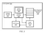
- FIG. 3is a block diagram illustrating one embodiment of a liquid crystal display system that may incorporate a variable drive voltage.
- FIG. 4illustrates one example of variable drive voltage circuitry, according to some embodiments.
- FIG. 5is a timing diagram of a section of an LCD system, according to some embodiments.
- FIG. 6is a diagram of optical responses of an LCD panel and polarization switch, according to some embodiments.
- FIG. 7Ais a timing diagram of a typical optical bounce.
- FIG. 7Bis a timing diagram showing a reduced optical bounce, according to some embodiments.
- FIG. 8illustrates example variable drive voltages, according to some embodiments.
- FIG. 9is a flowchart diagram illustrating one embodiment of a variable drive voltage.
- FIG. 10illustrates another embodiment of a variable drive voltage, according to some embodiments.
- a storage mediummay include any non-transitory/tangible storage media readable by a computer/processor to provide instructions and/or data to the computer/processor.
- a computer readable storage mediummay include storage media such as magnetic or optical media, e.g., disk (fixed or removable), tape, CD-ROM, or DVD-ROM, CD-R, CD-RW, DVD-R, DVD-RW, or Blu-Ray.
- Storage mediamay further include volatile or non-volatile memory media such as RAM (e.g.
- SDRAMsynchronous dynamic RAM
- DDRdouble data rate SDRAM
- LPDDR2, etc.low-power DDR SDRAM
- RDRAMRambus DRAM
- SRAMstatic RAM
- ROMFlash memory
- Flash memorynon-volatile memory (e.g. Flash memory) accessible via a peripheral interface such as the Universal Serial Bus (USB) interface
- Storage mediamay include microelectromechanical systems (MEMS), as well as storage media accessible via a communication medium such as a network and/or a wireless link.
- MEMSmicroelectromechanical systems
- Carrier Mediuma storage medium as described above, as well as a physical transmission medium, such as a bus, network, and/or other physical transmission medium that conveys signals such as electrical, electromagnetic, or digital signals.
- LC Devicean electro-optical device that uses an LC material to manipulate light by the application of a voltage.
- LC Light Modulatoran LC device that manipulates the intensity of light passing through it.
- An example of a type of LC Light Modulatoris an LCD, which may be pixelated.
- Polarization Switchan LC device that manipulates the polarization of light passing through it.
- PSdoes not generally change the intensity of light on its own. It may typically be accomplished when the PS is used in conjunction with an analyzer.
- An analyzermay be a polarizer that is used to block or pass some predetermined polarization state.
- an LCDtypically has a polarizer on the input side and a polarizer on the output side. The output polarizer is called an analyzer. Eyewear may act as an analyzer in some embodiments.
- PS Segmenta segment of a PS that is independently controllable.
- Pixelan individually addressable element of an LCD.
- LC Cell or LC Layerthe layer of LC material enclosed by the top and bottom substrates of an LC device.
- LC Modethe LC design used in an LC device.
- the designmay include the specific type of LC material, the thickness of the cell, the orientation of the alignment directions, etc.
- Typical LC modesinclude TN, VA (vertical alignment), IPS (In Plane Switching), etc.
- the term driven statemay refer to the high voltage state of an LC (e.g., +/ ⁇ 10 V, +/ ⁇ 12 V, etc.).
- the driven state of the LCmay correspond to the position and orientation of the LC such that the LC rotates the polarization of polarized light entering the liquid crystal device from the non-driven state in a manner that the polarization of the incoming light equals the polarization of the outgoing light.
- TNTwisted Nematic
- the term relaxed statemay refer to the low voltage state of an LC (e.g., 0 V).
- the relaxed state of the LCmay correspond to the position and orientation of the LC such that the polarized light entering the LC rotates the polarization.
- Frame Timethe period that contains one driven state and one relaxed state.
- the frame timemay include two frames worth of data.
- a frame timemay include one left eye frame and one right eye frame.
- Normal Whitecorresponds to a white optical state at 0V.
- normal whitecorresponds to a normally high luminance state at 0V where light is transmitted through a polarization switch (and LCs).
- a normal white polarization switchincludes 90° twisted nematic liquid crystals.
- normal whitemeans that, at the relaxed state of the PS, the lens that is at same polarization to the PS at the relaxed state is normally white (i.e. light passing through the PS is seen through normal white lens.)
- Normal Blackcorresponds to a black optical state at 0V. Thus, if no voltage is applied, light may not be transmitted through a polarization switch (and LCs).
- a PSmay be used in both a normal black and normal white mode simultaneously. For example, in a 3D system that alternates between left and right eye images, one eye may be the normal black eye and the other may be the normal white eye. Eyewear (e.g., passive eyewear or shutter glasses) may be used in conjunction with such a system.
- normal blackmeans that, at the driven state of the PS, the lens that is at same polarization to the PS at the driven state is normally black (i.e. light passing through the PS is seen through normal black lens.)
- Optical BounceA temporary increase or decrease in the optical response of an LC device due to backflow effect in certain LC configurations.
- the optical bouncemay appear as an oscillation in the transmission-time curve after an electric or magnetic field has been removed from an LC cell. Therefore, optical bounce may include a delay in reaching the relaxed state and an unintended optical effect as well.
- the optical effectmay result in light leakage in the white normal state and a drop in luminance in the black normal state.
- Configured Tovarious units, circuits, or other components may be described or claimed as “configured to” perform a task or tasks.
- “configured to”is used to connote structure by indicating that the units/circuits/components include structure (e.g., circuitry) that performs those task or tasks during operation.
- the unit/circuit/componentcan be said to be configured to perform the task even when the specified unit/circuit/component is not currently operational (e.g., is not on).
- the units/circuits/components used with the “configured to” languageinclude hardware—for example, circuits, memory storing program instructions executable to implement the operation, etc.
- a unit/circuit/componentis “configured to” perform one or more tasks is expressly intended not to invoke 35 U.S.C. ⁇ 112, sixth paragraph, for that unit/circuit/component.
- “configured to”can include generic structure (e.g., generic circuitry) that is manipulated by software and/or firmware (e.g., an FPGA or a general-purpose processor executing software) to operate in manner that is capable of performing the task(s) at issue.
- First, Second, etc.these terms are used as labels for nouns that they precede, and do not imply any type of ordering (e.g., spatial, temporal, logical, etc.).
- first and second pulses of a light sourcecan be used to refer to any two pulses.
- first and second pulsesare not limited to logical instances 0 and 1.
- this termis used to describe one or more factors that affect a determination. This term does not foreclose additional factors that may affect a determination. That is, a determination may be solely based on those factors or based, at least in part, on those factors.
- a determinationmay be solely based on those factors or based, at least in part, on those factors.
- FIGS. 2A , 2 B, and 3Example System
- FIGS. 2A and 2Billustrate example liquid crystal display (LCD) systems that may incorporate a variable drive voltage, and which may be configured to perform various embodiments described below.
- FIG. 2Aillustrates an LCD television as well as shutter glasses.
- the shutter glassesmay implement a variable drive voltage or may be standard shutter glasses that may be used with an LCD television that implements the variable drive voltage.
- Other systems that drive twisted-nematic junctionsmay also incorporate a variable drive voltage, such as an organic light emitting diode (OLED) system that includes a polarization switch.
- LCD system 200may include light source 202 , control circuitry 204 , LCD panel 206 , and a liquid crystal device, such as polarization switch 208 .
- light source 202may be coupled to control electronics 204 , LCD panel 206 , and polarization switch 208 .
- Light source 202may receive power and/or control indications from control circuitry 204 .
- light source 202may provide light to LCD panel 206 and polarization switch 208 .
- Light source 202may be referred to as a backlight.
- light source 202may include a plurality of light emitting diodes (LEDs) that may provide pulses of light to various components of LCD system 200 .
- the backlightmay, in various embodiments, be segmented. In one embodiment, the backlight may be segmented into five independently addressable rows. For instance, light source 202 may be segmented into sections that may extend across horizontal bands of the display.
- the LEDs of light source 202may pulse at different times, which may be optimized for timing one segment's pulse separate from other segments. Further, a segmented light source 202 may include segmented lightguides that may help minimize row-to-row crosstalk. Light source 202 may be positioned in LCD system 200 behind LCD panel and polarization switch from the perspective of the front of LCD system 200 (where the viewer would be). In one embodiment, the LEDs may be edge LEDs that provide illumination from both sides of LCD system 200 . Light source 202 may redirect the illumination from the edge LEDs so that the illumination may be perpendicular to LCD panel 206 and polarization switch 208 . LCD system 200 may additionally include an enclosure that may include heatsinks for the LEDs.
- light source 202may be shifted, or extended, in conjunction with the variable drive voltage, according to some embodiments.
- the shutter glassesmay not require any backlight pulsing.
- an accompanying LCD as part of such a systemmay include a backlight capable of being pulsed, or in some embodiments, it may include a light source that is incapable of being pulsed (e.g., a CCFL).
- LCD system 200may include control circuitry 204 .
- Control circuitry 204may receive a voltage from a voltage source (not shown).
- Control circuitry 204may, in turn, provide one or more voltages and/or other indications to light source 202 , LCD panel 206 , and/or polarization switch 208 .
- control circuitry 204may provide a voltage and a backlight enable indication to light source 202 , which, in turn, may cause light source 202 to provide a light pulse to LCD panel 206 and polarization switch 208 .
- control circuitry 204may independently address different segments of light source 202 , LCD panel 206 , and polarization switch 208 .
- control circuitry 204may provide a voltage and a backlight enable indication to a backlight driver board (not shown) of light source 202 .
- Light source 202may then provided appropriate pulsed voltages to each independently addressable segment of light source 202 .
- control circuitry 204may provide a pulsed voltage directly to each segment of LEDs, without necessarily providing the voltage to a backlight driver board.
- the addressed light source 202 segmentmay then provide one or more light pulses to LCD panel 206 , and polarization switch 208 .
- Control circuitry 204may include circuitry to implement one or more variable drive voltages to polarization switch 208 , according to some embodiments.
- LCD panel 206may include a plurality of pixels that may collectively produce images.
- the plurality of pixels of the LC panelmay be addressed with data that conveys the image to be displayed.
- LCD panel 206may be updated from one frame to the next in a progressive scan manner, and hence updating may not occur all at once.
- the pixels of LCD panel 206may be updated, for example, sequentially by row from top to bottom.
- LCD panel 206may refresh at a frequency of 120 Hz. For a 120 Hz system, every 8.3 ms the entire panel's data may be updated. The transition from one frame to another may proceed as a progressive scan; the scan may start at the top row, and then proceed through the rest of the rows.
- the time difference from updating the top row to updating the bottom rowmay be approximately 5-6 ms. Accordingly, the scan time to write frame data to LCD panel 206 may take a large portion of each frame. As a result, the portion of each frame where the entire display is in the same state may be minimal.
- the subsequent framesmay be a left eye frame (image) followed by a right eye frame (or vice versa) for a 3D display, or may simply be sequential frames for a 2D display.
- backlight and polarization switch segmentingmay be applied to maintain synchronization with the progressive scan data write of LCD panel 206 .
- an OLED panelmay be used in LCD system 200 instead of LCD panel 206 and light source 202 .
- the OLED-based systemmay likewise benefit from the variable drive techniques described herein.
- Other imagers, such as a cathode ray tube (CRT), rear projection, or any other imagersmay also benefit from the variable drive techniques described herein.
- LCD system 200may include a liquid crystal device, such as polarization switch 208 .
- Polarization switch 208may use a twisted-nematic liquid crystal mode and may include a plurality of distinct individually addressable elements, called segments.
- Polarization switch 208may receive one or more voltages from control circuitry 204 and may receive a light pulse from light source 202 . As was the case with light source 202 , polarization switch 208 may be segmented into horizontal bands.
- Polarization switch 208may be used in LCD system 200 to simultaneously provide a normal black and normal white mode, when used in conjunction with the appropriate eyewear, wherein each eye has the appropriate lens.
- a normal white modemay be provided in a 3D LCD system 200 for one eye, while concurrently a normal black mode may be provided for the other eye.
- Polarization switch 208may control the luminance of LCD system 200 .
- a normal white modemay allow full luminance in a low voltage state (e.g., 0V) of polarization switch 208 while normal black mode may block all luminance for the corresponding lens of the eyewear.
- a normal white modemay block all luminance in a driven voltage state (e.g., +/ ⁇ 12V), while a normal black mode may allow full luminance for the corresponding lens of the eyewear. Accordingly, in a 3D context, one eye may see an image or frame in a normal white mode while the other eye sees an image or frame in a normal black mode.
- polarization switchis used in combination with the eyewear, a higher voltage in the driven state may result in a greater drop in luminance in the normal white state. As a result, higher contrast may be achieved with a high voltage, such as +/ ⁇ 12 V, +/ ⁇ 20 V, etc.
- polarization switch 208may be a multi-segment polarization switch, as described herein.
- FIG. 3is a block diagram illustrating one embodiment of the LCD system of FIG. 2 , which may be configured to perform various embodiments described below.
- LCD system 300may include voltage source 302 , control circuitry 304 , liquid crystal devices, such as a polarization switch 308 , shown as segments of a multi-segment polarization switch, LCD panel 310 , and light source 312 .
- Control circuitry 304may include drive module 306 .
- voltage source 302may be a power supply for LCD system 300 or may receive one or more voltages from an external power supply. Voltage source 302 may output one or more voltages. The one or more voltages may be provided to control circuitry 304 . In some embodiments, voltage source 302 may also provide one or more voltages directly to LCD panel 310 , light source 312 , a polarization switch 308 , or other components (not shown) of LCD system 300 . The one or more voltages may be provided to control circuitry 304 , and, in turn, to the polarization switch 308 , may be a drive voltage.
- the illustrated embodimentshows control circuitry 304 and voltage source 302 as separate modules, yet, in some embodiments, voltage source 302 may be a subcomponent of control circuitry 304 .
- control circuitry 304may receive the voltage from voltage source 302 and provide a drive voltage to the polarization switch 308 .
- the drive voltage provided to the polarization switch 308may be provided to a LC addressable element of the polarization switch, or other LC device.
- the drive voltagemay be +/ ⁇ 12 V.
- the drive voltagemay be +/ ⁇ 10V, or +/ ⁇ 20 V, for example.
- the drive voltagemay maintain an overall DC bias of 0V across the LC over time.
- Control circuitry 304may include drive module 306 .
- Drive module 306may include a programmable waveform generator.
- drive module 306may vary the drive voltage it provides to the one or more polarization switches 308 as a function of time.
- the drive voltagemay include a driven function portion and a relaxed function portion.
- the driven functionmay correspond to the portion of the drive voltage when transitioning from a low, or relaxed voltage, to a high, or driven voltage.
- the relaxed functionmay correspond to the portion of the drive voltage when transitioning from a driven voltage to a relaxed voltage.
- the driven functionmay be a normal step function while the relaxed function may be one or more of a number of alternative functions, not equivalent to a step function.
- the relaxed functionmay be continuous, i.e., in an analog manner.
- control circuitry 304may include a temperature sensor that may affect the voltage level and/or shape of the drive voltage waveform.
- the relaxed functionmay rapidly reduce the drive voltage to an intermediate voltage before slowly reducing the drive voltage from the intermediate voltage a relaxed voltage (e.g., 0V, corresponding to the relaxed state). For example, if the driven voltage level is +/ ⁇ 20V, the relaxed function may rapidly reduce the voltage to +/ ⁇ 2V and then slowly reduce the voltage to 0V. Thus, the reduction may occur at different rates, for example a first and second rate, with the second rate being lower than the first rate.
- control circuitry 304may drive the polarization switch 308 at full rate, then transition to a lower intermediate drive voltage in anticipation of the transition to the relaxed state.
- the intermediate drive voltagemay be close to the threshold of the relaxed state, yet the one or more polarization switches may maintain optical properties consistent with the driven state. Maintaining the optical properties consistent with the driven state is used herein to mean that the normal black mode should allow approximately full luminance and the normal white mode should block approximately all luminance.
- the threshold of the relaxed statemay be approximately 1-2V.
- the relaxed functionmay consist of small decremented step functions that approximate a continuous waveform.
- the full reduction from the driven voltage to the relaxed voltagemay be sufficiently slow to reduce the optical bounce, yet fast enough to fit within the time constraints of LCD panel 310 updating.
- LCD panel 310may be fully updated or refreshed every 8.333 ms.
- the full voltage transitionmay take less than 8.3 ms in such an example (or in other embodiments, in a time period less than a frame time/period). For instance, for an 8.3 ms frame time, the full voltage transition, from driven to relaxed, may take 3.5 ms +/ ⁇ 1 ms.
- panel update time constraintsmay be different (e.g., 16.667 ms, 4.166 ms). Accordingly, the full voltage transition time may be different as well. In various embodiments, the full voltage transition make take less than 20 ms, 10 ms, 5 ms, 3 ms, etc., depending on various timing considerations. In various embodiments, the full transition from driven state to relaxed state may be performed over a time period greater than 1 is and less than 20 ms.
- the drive voltage applied to the polarization switch 308may present as a variety of different waveforms and timings.
- the waveformcould be an arbitrary descending waveform, a linear descending ramp, or other waveform.
- Some factors that may be considered in determining the waveform and timingmay include: contrast level, the presence of ghosting/crosstalk, balance between left and right eye performance, and color in bright and dark states.
- the drive voltage swing and offsetmay be varied.
- the drive voltagemay be a pulse-width modulated (PWM) waveform, as described herein.
- PWMpulse-width modulated
- different drive voltagesmay be provided to different segments, of a segmented polarization switch 308 .
- a polarization switch 308may be segmented into five different segments.
- a different phase-shifted drive voltageeach of which may have a function (e.g., cosine) applied to the high-low-voltage transition, may be provided to each of the segments.
- the provided voltagemay be independently driven to provide each segment with an independent and time-shifted voltage from the independently driven voltages being provided to each other segment.
- the timing of the polarization switch transitionsmay be synchronized with the timing of the backlight pulses and the data of the frames.
- control circuitry 304may supply one or more voltages and/or other indications to LCD panel 310 and light source 312 , in addition to, the one or more polarization switches 308 .
- the voltagesmay be driven in a different manner than the one or more voltages provided to polarization switches 308 .
- control circuitry 304may provide a voltage, and a power-on indication to LCD panel 310 and/or light source 312 .
- Control circuitry 304may also provide a backlight enable indication to light source 312 .
- Control circuitry 304may, in some embodiments, receive an indication of data writes to LCD panel 310 , from LCD panel 310 , or from another source (e.g., an external source such as a set-top box, Ethernet, Wifi, DVD player, Blu-Ray player, etc.).
- Control circuitry 304may include circuitry to synchronize the drive voltage to the one or more polarization switches and to left and right frame timing.
- Control circuitry 304may further include circuitry to synchronize backlight enable indications with left and right frame timing. Accordingly, the variable drive voltage, described herein, may be used in conjunction with a shifted or extended backlight, to enhance the benefits of the variable drive voltage.
- control circuitry 304may receive video, manipulate and process the video, and provide it to the LCD panel 310 .
- Control circuitry 304may generate an indication (e.g., Vsync) and data enable indication.
- Vsync indicationmay be used to synchronize timing of the polarization switch and backlight segments, among other components.
- the data enable indicationmay indicate when data is written.
- one or more polarization switches 308may receive the drive voltage from control circuitry 304 (and drive module 306 ). As described above, the drive voltage may have a function applied to it before reaching polarization switches 308 . In some embodiments, the one or more polarization switches 308 may receive a drive voltage directly from voltage source 302 , which may or may not apply a function to the drive voltage.
- Polarization switches 308may be a liquid crystal device, such as twisted-nematic panel, homogeneous cells, chiral-homeotropic LC cells, optically compensated birefringence (OCB) cells, pi-cells, etc. Twisted-nematic panels have cells which may twist up to a full 90 degrees in response to a voltage change, to allow varying degrees of light to pass through.
- LCD system 300may include only a single polarization switch.
- the polarization switch 308may cover the entire display of LCD system 300 . Accordingly, the single polarization switch 308 may change the polarization state of the light emitted by the display. For a 3D display, this may correspond to two different states: one polarization state that is passed by the right eye polarizer and blocked by the left eye polarizer and another polarization state that is passed by the left eye polarizer and blocked by the right eye polarizer.
- the polarization switch 308may be segmented, for example, into horizontal sections, similar to the backlight segmenting described herein.
- the correct polarization statemay be achieved for corresponding data on LCD panel 310 at a given time.
- the polarization switch 308may be divided into five horizontal sections of equal size. The various segments of polarization switch 308 may be synchronized or timed according to the progressive-scan-based panel write times.
- a polarization switch 308may switch states when the first row of the segment receives new data (i.e., when LCD panel 310 begins to write data to that row).
- LCD panel 310may include a plurality of pixels that may collectively produce images. The plurality of pixels may be addressed with data that may reflect the image to be display. As discussed herein, LCD panel 310 may be updated from one frame to the next in a progressive scan manner and may not occur all at once. In such an embodiment, the pixels of LCD panel 310 may be updated, for example, sequentially by row from top to bottom. As an example, LCD panel 310 may refresh at a frequency of 120 Hz. For a 120 Hz system, every 8.3 ms the entire panel's data may be updated. In one embodiment, the time to update the entire panel, from the top row to the bottom row, may be approximately 5-6 ms.
- the scan time to write frame data to LCD panel 310may take a significant time percentage of each frame and the portion of each frame where the entire display is in the same state may likewise be minimal.
- backlight and polarization switch segmenting timing and/or segmentingmay be applied to maintain synchronization with the progressive scan data write of LCD panel 310 .
- LCD system 300may include a light source 312 .
- Light source 312may provide an instance (e.g., a pulse) of the light source to the polarization switch 308 .
- Light source 312may be a backlight, such as incandescent light bulbs, fluorescent lamps, or one or more light emitting diodes (LEDs).
- Light source 312may include one or more white backlights or different colored backlights (e.g., RGB LEDs).
- Light source 312may be positioned in LCD system 300 behind LCD panel 310 and polarization switch 308 from the perspective of the front of LCD system 300 (where the viewer would be).
- the LEDsmay be edge LEDs that provide illumination from both sides of LCD system 300 .
- Light source 312may include a manner in which to redirect the illumination from the edge LEDs so that the illumination may be perpendicular to LCD panel 310 and polarization switch 308 .
- light source 312may pulse twice per frame time (i.e., once for a left eye frame and once for a right eye frame), with each pulse being a pulse of limited duration. For example, starting with a driven state, a first pulse of light source 312 may occur after the drive voltage reduction from the driven state begins. Specifically, in one example, the first pulse may take place during the voltage transition from the driven state to the relaxed state. A second pulse of light source 312 may occur during the relaxed state (i.e., before the drive voltage transitions back to the driven state). In other words, a pulse of the light source, or backlight enable, may be shifted to a later time for the period when the polarization switch drive voltage has a function applied during the high to low voltage transition.
- both pulses of a light source in a frame timemay be shifted later in time.
- the shifted amountmay be different for each pulse.
- the pulse of light source that may occur during the driven-to-relaxed state transitionmay be shifted 2 ms later in time while the second pulse of a light source in a frame time may be shifted 1 ms later. Therefore, the pulses from light source 312 may not be spaced equally apart from one frame time to the next.
- An example of unequal spacing between light pulsescan be seen below in FIG. 7B .
- the backlightmay be extended in terms of pulse duration.
- one pulse of light source 312may begin before the drive voltage transitions from the driven to the relaxed state but may complete after the voltage transition is complete.
- a light pulseis typically 2 ms
- extending the light pulsemay increase its duration to 3 ms.
- Extending or shifting the backlightmay enable more of the data of LCD panel 310 to be in a steady, same state for a frame and a polarization switch 308 to be in an appropriate state when the backlight is enabled.
- shifting the backlight into the minimal optical bounce periodmay produce only a minimal amount of light leakage in the normal white state and a minimal drop in luminance for the normal black state.
- the time difference between the start of the first pulse of limited duration and the start of the second pulse of limited duration in a framemay be less than the time difference from the start of the voltage reduction to the start of the voltage return to the driven level.
- Light source 312may, in various embodiments, be segmented.
- the backlightmay be segmented into five independently addressable rows.
- light source 312may be segmented into sections that may extend across horizontal bands of the display.
- the LEDs of light source 202may pulse at different times, which may be optimized for timing one segment's pulse separate from other segments.
- a segmented light source 202may include segmented lightguides that may help minimize row-to-row crosstalk.
- the backlightmay be shifted later in time. Light contamination may extend into the optical bounce area but may not have significant effects in terms of light leakage and luminance drops in normal white and normal black modes, respectively.
- FIGS. 5 and 6illustrate examples of timing and optical response according to the LCD system of FIGS. 2-3 .
- FIG. 5is one example of a timing diagram of a section of an LCD system, according to some embodiments.
- FIG. 5may be the timing for segment 2 of a segmented polarization switch.
- the backlightis not shown segmented but may be segmented in some embodiments.
- FIG. 5shows the 1st row and last row of the LCD panel being written. The segment as active for the left eye frame at a time between the two panel writes. Active may correspond to 0 V for a normal white mode or a driven voltage (e.g., +/ ⁇ 12 V) for a normal black mode.
- a driven voltagee.g., +/ ⁇ 12 V
- FIG. 6is a diagram of optical responses of an LCD panel and polarization switch, according to some embodiments.
- the top 3 portions of FIG. 6correspond to the optical response of the LCD at different rows of a section of the LCD. Note the slight phase shift in the data write from first row to last row. This corresponds to the progressive scan data write.
- the optical response of the polarization switchas viewed through right and left eyewear is shown.
- the optical responsesdemonstrate a reduced area of cross-talk, which may result from the variable drive voltage techniques described herein. Note that the shapes of the waveforms in FIG. 5 may not be an accurate representation of the actual waveforms used in various embodiments.
- one or more components of LCD display 300may, in some embodiments, be implemented by a computer-readable storage medium, memory, or some other component.
- a computer-readable storage mediummay be one embodiment of an article of manufacture that stores instructions that are executable by a processor.
- a computer-readable storage mediumcan be used to store instructions read by a program and used, directly or indirectly, to fabricate hardware for control circuitry 304 , described above.
- the instructionsmay outline one or more data structures describing a behavioral-level or register-transfer level (RTL) description of the hardware functionality in a high level design language (HDL) such as Verilog or VHDL.
- RTLregister-transfer level
- the descriptionmay be read by a synthesis tool, which may synthesize the description to produce a netlist.
- the netlistmay include a set of gates (e.g., defined in a synthesis library), which represent the functionality of control circuitry 304 .
- the netlistmay then be placed and routed to produce a data set describing geometric shapes to be applied to masks.
- the masksmay then be used in various semiconductor fabrication steps to produce a semiconductor circuit or circuits corresponding to control circuitry 304 .
- LCD system 300may not include LCD panel 310 or light source 312 .
- LCD systemmay include an organic light emitting diode (OLED) panel.
- OLEDorganic light emitting diode
- all rows of the panelmay be written simultaneously (i.e., not in a progressive scan manner). In such an embodiment, segmenting may not be used.
- control circuitry 304may pulse the OLED panel itself. Further, the variable drive voltage of control circuitry 304 may be used with the OLED-based LCD system 300 , in a similar manner, which may reduce the optical bounce and therefore maximize the amount of steady state time of the display, among other benefits.
- variable drive voltagemay increase frame utilization by reducing optical bounce and accelerating the transition between the driven and relaxed states. This may be valuable in minimizing cross-talk (ghosting) in 3D displays by increasing the duration of steady state time in the optical response of the polarization switch.
- cross-talkcross-talk
- the LCD pixelsmay further stabilize before the backlight is applied, which may also reduce the ghosting effect. Segmenting the backlight may further enhance the benefits of the variable drive voltage. This may minimize the momentary reduction the amount of light transmitted (on the order of nits) in the polarization switch normal black state. It may also minimize light leakage in the normal white state, in what should be a no or low luminance state.
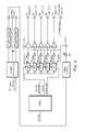
- FIG. 4Example Drive Voltage Module
- FIG. 4illustrates an example of a drive module, according to some embodiments.
- the example implementation of drive module 306 in FIG. 4illustrates a polarization switch that is segmented into five different segments.
- the isolated power supplymay receive an input voltage, which may be an AC or DC input voltage.
- the input voltagemay be from a power supply for the entire LCD system or from another source.
- Isolated power supplymay output a positive and negative voltage as well as an isolated ground.
- the isolated groundmay be a common ground for the segments.
- the positive and negative voltagesmay be processed by an analog regulator before being provided to a voltage reference. This may provide a clean voltage to voltage reference such that downstream circuitry may receive a clean voltage as well.
- Voltage referencemay output one or more voltages that may be provided to one or more variable gain amplifiers and, in turn, provided to one or more A/D converters.
- voltage referencemay output five voltages (one for each of the five segments in this example), each of which may be provided to a different variable gain amplifier and a different A/D converter.
- a system clockmay be provided to a field-programmable gate array (FPGA).
- FPGAfield-programmable gate array
- a 32 MHz system clockmay be provided to the FPGA to drive discrete values to the one or more A/D converters.
- the FPGAmay include a function, such as a cosine or Gaussian among other functions, embedded in the FPGA table. Discrete values from the table may be taken over time, which may produce the function. In one embodiment, voltage increments may be based on a 25 V swing over 2 16 bits.
- the FPGAmay output a plurality of digital commands (e.g., clocked serial data, and enable) to each of the A/D converters.
- the clocked serial data and enable digital commandsmay be common between the various A/D converters or may be unique commands for each A/D converter.
- the FPGAmay output five clocked serial data digital commands and five enable commands, with one serial data command and one enable command being provided to each A/D converter.
- FPGAmay provide a common clocked serial data digital command to the A/D converters and a separate enable digital command for each A/D converter.
- the enable commandsmay be staggered in accordance with the polarization switch segmentation scheme, described herein. For example, the voltage transitions of one segment may occur at different times than the voltage transitions of the other segments. Accordingly, the enable indications may likewise occur at different times.
- FPGAmay also provide a clock to the A/D converters. In the illustrated example, the clock may be a 16 MHz clock.
- Each A/D convertermay receive the digital commands and the clock from the FPGA as well as the reference voltage, shown here at 12.5 V.
- the A/D convertersmay be 18-bit high precision A/D converters.
- Each A/D convertermay convert the input analog voltage into a discrete representation of that voltage.
- the discrete representation of the voltagemay then be provided to a high-precision buffer (e.g., 18 bit) and a hi-power amplifier and, ultimately, to one of the segments of the polarization switch.
- the illustrated exampleshows a single polarization switch segmented into five segments. Each segment may receive a separate drive voltage, which may be phase shifted compared to the drive voltages of the other segments.
- the signals in the illustrated exampleare bipolar signals that may allow arbitrary positive and negative waveforms.
- the illustrated exampleis also high speed meaning greater than 888 KHz per segment.
- FIGS. 5 and 6Timing and Optical Response of Example LCD System
- FIGS. 5 and 6illustrate examples of timing and optical response according to the LCD system.
- FIGS. 5 and 6are described in further detail in connection with the description of LCD system 300 .
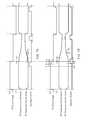
- FIGS. 7A , 7 B, and 8Timing Diagrams
- FIG. 7Ais a timing diagram of a typical optical bounce that does not use a variable drive voltage while FIG. 7B is a timing diagram showing a reduced optical bounce, according to some embodiments.
- FIG. 7Aillustrates a drive voltage according to a step function and corresponding transmittance-time curves.
- the step functionapplies to both transitions, driven to relaxed state and relaxed to drive state.
- one portion of a framemay produce an image for one eye and the next portion of a frame may produce an image for the other eye.
- the normal black PS responsemay correspond to the luminance for one eye and the normal white PS response may correspond to the luminance for the other eye.
- the luminance for the normal black eyemay be high while the luminance for the normal white eye may be low.
- the luminance for the normal white eyeis high and the luminance for the normal black eye is low.
- the optical bounce in both PS responsesThe bounce occurs in FIG. 7A at a time t a approximately 1 ms after the voltage transition. The bounce represents dead time that adds delay to the system and negatively affects optical properties of the display (e.g., leakage in a black state or drops in luminance in a white state).
- the leakage in luminance in the normal white mode when it is supposed to be blackmay be very noticeable to a viewer of the display.
- b ais approximately 10% of peak normal white luminance, at a time when the normal white mode should be near 0% luminance.
- the drop in luminance in the normal black modemay not be as significant to a viewer but is still shown in FIG. 7A .
- the backlight enable in FIG. 7Ais a 1-2 ms pulse, represented by t p .
- the pulses from frame time to frame timeare approximately equally spaced apart, about 8.3 ms apart for a 120 Hz display, which corresponds to the frame time of the display.
- the first and third pulses (and subsequent odd pulses) in the examplecorrespond to frames for the normal black eye and the second pulse (and subsequent even pulses) correspond to frames for the normal white eye.
- the pulsesmay occur a short period before each transition from driven to relaxed state, and a short period before each transition from relaxed to driven state.
- FIG. 7Billustrates a drive voltage and corresponding transmittance-time curves, with a continuous function applied to the driven to relaxed state portion of the drive voltage.
- the continuous functionis a 3.5 ms wide cosine function with a zero point 0.5 ms beyond the relaxed step function (of FIG. 7A ) zero point.
- the optical bounce in FIG. 7Brepresents only a bounce of 4% (b aa ) of the peak normal white luminance—a more than double reduction over FIG. 7A . This may increase the steady state of the PS responses as compared to FIG. 7A . By reducing the optical bounce, the backlight enable may be shifted into the optical bounce period.
- the luminancemay be sufficiently low such that some of the time within that period may actually be reclaimed, in some embodiments, by allowing some backlight pulsing in this period of time.
- the LCsmay be more stabilized at the time the backlight is enabled.
- greater image qualitye.g., reduced ghosting/crosstalk, increased contrast, etc.
- the resultsmay be further enhanced by segmenting the one or more polarization switches and backlight, as described herein.
- subsidiary pulses of the main backlight pulsemay extend into the optical bounce period resulting in an even lesser amount of light leakage.
- the backlight enableis shifted approximately 1.5 ms later in time in FIG. 7B .
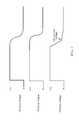
- FIG. 8illustrates various example drive voltage curves, according to embodiments.
- the top curveillustrates a drive voltage curve with the transition from driven to relaxed state performed according to a cosine function.
- the middle curveillustrates a driven to relaxed state transition according to a Gaussian function while the bottom curve illustrates a curve according to a first rate and a second rate, with the first rate being a more rapid voltage drop than the second rate.
- the indicated intermediate voltagemay be the transition point between the first rate and the second rate.
- the polarization switchmay maintain an optical property of the driven state at the intermediate voltage.
- FIG. 9Driving a Voltage of a Polarization Switch
- FIG. 9illustrates a method 900 for driving a voltage of a polarization switch 308 .
- the method shown in FIG. 9may be used in conjunction with any of the systems or devices shown in the above figures, among other devices. In various embodiments, some of the method elements shown may be performed concurrently, in a different order than shown, or may be omitted. In some embodiments, method 900 may include additional (or fewer) blocks than shown. For example, in some embodiments, only blocks 902 and 904 may be used while in others, all illustrated blocks may be used. As shown, method 900 may operate as follows.
- a voltagemay be provided to a liquid crystal addressable element of a liquid crystal device, such as a polarization switch, to a driven voltage level.
- the driven voltage levelmay represent a driven state.
- the provided voltagemay be +/ ⁇ 12 V.
- the voltagemay be provided by voltage source 302 directly to polarization switch 308 .
- the voltagemay be generated by voltage source 302 , modified or passed on by control circuitry 304 and/or drive module 306 , and then provided to the liquid crystal element of the liquid crystal device, such as polarization switch 308 .
- the portion of the drive voltage that drives polarization switch 308 to the driven statemay be performed according to a step function.
- Polarization switch 308may be a liquid crystal cell device, such as a twisted-nematic device that may include one or more liquid crystal addressable elements.
- the liquid crystal addressable elementsare defined herein as regions of an LC device that can be independently controlled (e.g., electronically).
- the liquid crystal addressable elementmay be a pixel, and for a multi-segment polarization switch, the liquid crystal addressable element may be a segment.
- the provided voltagemay be independently driven to provide each segment with an independent and time-shifted voltage.
- the LC devicemay use a TN LC mode.
- the provided voltagemay be reduced to a relaxed level (e.g., 0 V) over a period of time greater than 1 ⁇ s.
- a voltage reduction approximately equivalent to a step functionwould take less than 1 ⁇ s and other functions taking less than 1 ⁇ s may be seen by the LC device as equivalent to a step function.
- the full reduction from driven to relaxed levelmay take less than 20 ms.
- the transition for a 120 Hz LCD systemmay take approximately 3.5 ms.
- drive module 306may apply a relaxed function to the drive voltage it provides to polarization switch 308 .
- the relaxed functionmay be a continuous function, such as the decreasing portion of a cosine or Gaussian.
- the relaxed functionmay cause the voltage to decrease as a function of time until reaching the relaxed state.
- the provided voltage functionmay be a PWM waveform function.
- the relaxed function over timemay include a voltage rise, provided the total relaxed voltage function occurs within the window of 20 us to 20 ms.
- a light pulse of limited durationmay be provided to the LC device, such as polarization switch 308 and/or LCD panel 310 .
- the pulse of light source 312may be a pulsed backlight that may be enabled during a continuous transition from the driven state to the relaxed state.
- the pulse of light source 312 during this transitionmay be extended such that the pulse extends later into a period where the cells may be more stable.
- the pulse of light source 312may extend into the time period coincident with the optical bounce period.
- Light source 312may be segmented to extend into the optical bounce period. For a next frame, the voltage provided to the polarization switch may be returned to a driven state.
- another pulse of limited duration of light source 312may be enabled and provided to polarization switch 308 .
- the time difference between the start of the first pulse of limited duration in a frame and the second pulse of limited durationmay be less than the time difference from the start of the voltage reduction to the start of the voltage return to the driven level.
- the pulse of light source 312 during the driven statemay correspond to a portion of a frame for one eye (in a 3D display) and the second pulse, during the relaxed state, may correspond to a second portion of a frame for the other eye. Or, they may correspond to subsequent frames in a 2D display. In general the light pulses may be approximately equally spaced apart.
- the timing and duration of light pulsesmay vary depending on the drive function's waveform and timing.
- One embodimentmay include applying a different portion (e.g., increasing portion) of the same waveform to the driven state.
- the method of 900may be used for each segment of the polarization switch. This may create a phase-shifted variable drive voltage for the various segments of the polarization switch and enable the polarization switch segments to be synchronized with data writing of the panel. Likewise, the pulse of limited duration may be divided into a plurality of subsidiary pulses that may be provided to corresponding segments of the polarization switch.
- method 900could also be applied in situations other than an LCD system.
- method 900may apply equally as well to an OLED-based system.
- An OLED-based systemmay not require a separate light source or and LCD panel. Instead, the OLED panel may be pulsed itself, that is, the duty cycle of on-pixels to off-pixels may be short.
- an OLED-based systemmay benefit from the disclosed variable drive voltage techniques.
- the methodmay apply to more than just polarization switches, such as other applications using a TN device.
- method 900could be applied to shutter glasses.
- shutter glassesmay be used as a switch, in which case, the disclosed techniques may offer similar benefits to those gained by a polarization switch.
- Each eyepiece of the shutter glassesmay be an LC shutter, which may have similar time constraints to the LCD system.
- the above blocks of method 900may be initiated by a processor, processors, a CPU, a memory, a computer-readable storage medium, other hardware, or any combination thereof.
- optical bouncemay be minimized. Further, delay as a result of the voltage transition may also be minimized and therefore allow a longer steady state period for the LCs. This may provide additional time for LCD pixels to stabilize before the light source is enabled. This may reduce ghosting and may reduce the amount of light that may be transmitted in an off-state due to any remaining optical bounce.
- FIG. 10illustrates an alternate embodiment of a variable drive voltage.
- the top waveformshows an analog voltage that may be applied to a liquid crystal device, such as a polarization switch.
- the waveformmay be a direct representation of how the polarization switch is excited (driven).
- the bottom waveformis the PWM equivalent of the top waveform.
- PWMis a completely digital technique that varies the pulse width to correspond to a particular RMS voltage. Note that on the left side, the PWM waveform is mostly “high”, representing a higher RMS voltage. In the 2nd part and the 4th part of the waveform (the flat part) note that the PWM duty cycle is 50%—that part of the waveform represents half the maximum voltage. Finally, in the 3rd part of the waveform, note that the pulses are narrow, which represents lower RMS voltages.
- the PWM signalmay be low-pass filtered to better approximate the target waveform.
- a low-pass filtermay be implemented by utilizing the R-C characteristics of the polarization switch itself, which may allow the polarization switch to be directly driven from an entirely digital source.
Landscapes
- Engineering & Computer Science (AREA)
- Physics & Mathematics (AREA)
- General Physics & Mathematics (AREA)
- Multimedia (AREA)
- Signal Processing (AREA)
- Theoretical Computer Science (AREA)
- Computer Hardware Design (AREA)
- Nonlinear Science (AREA)
- Chemical & Material Sciences (AREA)
- Crystallography & Structural Chemistry (AREA)
- Mathematical Physics (AREA)
- Optics & Photonics (AREA)
- Liquid Crystal Display Device Control (AREA)
- Liquid Crystal (AREA)
- Control Of Indicators Other Than Cathode Ray Tubes (AREA)
Abstract
Description
| ta= 1.5 ms +/− .5 | tda= 2 ms | taa= 1.5 ms +/− .5 |
| tp= 1-2 ms | tea= 6 ms +/− 2 | ts= 1.5 ms +/− .5 |
| ba= 10% norm +/− 2% | twa= 3.5 ms +/− 1 | baa= 4% norm |
Claims (20)
Priority Applications (2)
| Application Number | Priority Date | Filing Date | Title |
|---|---|---|---|
| US14/335,708US9134556B2 (en) | 2011-05-18 | 2014-07-18 | Liquid crystal variable drive voltage |
| US14/838,248US9958712B2 (en) | 2011-05-18 | 2015-08-27 | Liquid crystal variable drive voltage |
Applications Claiming Priority (2)
| Application Number | Priority Date | Filing Date | Title |
|---|---|---|---|
| US13/110,562US8786529B1 (en) | 2011-05-18 | 2011-05-18 | Liquid crystal variable drive voltage |
| US14/335,708US9134556B2 (en) | 2011-05-18 | 2014-07-18 | Liquid crystal variable drive voltage |
Related Parent Applications (1)
| Application Number | Title | Priority Date | Filing Date |
|---|---|---|---|
| US13/110,562ContinuationUS8786529B1 (en) | 2011-05-18 | 2011-05-18 | Liquid crystal variable drive voltage |
Related Child Applications (1)
| Application Number | Title | Priority Date | Filing Date |
|---|---|---|---|
| US14/838,248ContinuationUS9958712B2 (en) | 2011-05-18 | 2015-08-27 | Liquid crystal variable drive voltage |
Publications (2)
| Publication Number | Publication Date |
|---|---|
| US20140327850A1 US20140327850A1 (en) | 2014-11-06 |
| US9134556B2true US9134556B2 (en) | 2015-09-15 |
Family
ID=51177884
Family Applications (3)
| Application Number | Title | Priority Date | Filing Date |
|---|---|---|---|
| US13/110,562Active2032-07-27US8786529B1 (en) | 2011-05-18 | 2011-05-18 | Liquid crystal variable drive voltage |
| US14/335,708ActiveUS9134556B2 (en) | 2011-05-18 | 2014-07-18 | Liquid crystal variable drive voltage |
| US14/838,248Active2031-06-11US9958712B2 (en) | 2011-05-18 | 2015-08-27 | Liquid crystal variable drive voltage |
Family Applications Before (1)
| Application Number | Title | Priority Date | Filing Date |
|---|---|---|---|
| US13/110,562Active2032-07-27US8786529B1 (en) | 2011-05-18 | 2011-05-18 | Liquid crystal variable drive voltage |
Family Applications After (1)
| Application Number | Title | Priority Date | Filing Date |
|---|---|---|---|
| US14/838,248Active2031-06-11US9958712B2 (en) | 2011-05-18 | 2015-08-27 | Liquid crystal variable drive voltage |
Country Status (1)
| Country | Link |
|---|---|
| US (3) | US8786529B1 (en) |
Cited By (1)
| Publication number | Priority date | Publication date | Assignee | Title |
|---|---|---|---|---|
| US20150370111A1 (en)* | 2011-05-18 | 2015-12-24 | Zspace, Inc. | Liquid Crystal Variable Drive Voltage |
Families Citing this family (10)
| Publication number | Priority date | Publication date | Assignee | Title |
|---|---|---|---|---|
| TWI466080B (en)* | 2012-12-10 | 2014-12-21 | Novatek Microelectronics Corp | Backlight module and switching method |
| US9520091B2 (en)* | 2013-06-17 | 2016-12-13 | Shenzhen China Star Optoelectronics Technology Co., Ltd | Liquid crystal cell and the liquid crystal display with the same |
| US20150062201A1 (en)* | 2013-08-27 | 2015-03-05 | Boe Technology Group Co., Ltd. | Display device |
| US10424241B2 (en) | 2016-11-22 | 2019-09-24 | Google Llc | Display panel with concurrent global illumination and next frame buffering |
| US10068521B2 (en) | 2016-12-19 | 2018-09-04 | Google Llc | Partial memory method and system for bandwidth and frame rate improvement in global illumination |
| CN107204174B (en)* | 2017-05-12 | 2019-11-26 | 武汉华星光电技术有限公司 | Liquid crystal display panel and its driving method, liquid crystal display |
| CN109346022B (en)* | 2018-12-11 | 2022-05-06 | 惠科股份有限公司 | Protection method of display panel, display panel and computer readable storage medium |
| US11435602B2 (en)* | 2019-12-12 | 2022-09-06 | Zspace, Inc. | PI cell drive waveform |
| CN112992079B (en)* | 2019-12-17 | 2024-04-16 | 咸阳彩虹光电科技有限公司 | Method for improving display image quality and display device |
| CN119811330A (en)* | 2025-01-27 | 2025-04-11 | 北京润科通用技术有限公司 | Color adjustment driving device of electrochromic device and control method thereof |
Citations (152)
| Publication number | Priority date | Publication date | Assignee | Title |
|---|---|---|---|---|
| US1592034A (en) | 1924-09-06 | 1926-07-13 | Macy Art Process Corp | Process and method of effective angular levitation of printed images and the resulting product |
| US4182053A (en) | 1977-09-14 | 1980-01-08 | Systems Technology, Inc. | Display generator for simulating vehicle operation |
| US4291380A (en) | 1979-05-14 | 1981-09-22 | The Singer Company | Resolvability test and projection size clipping for polygon face display |
| US4677576A (en) | 1983-06-27 | 1987-06-30 | Grumman Aerospace Corporation | Non-edge computer image generation system |
| US4763280A (en) | 1985-04-29 | 1988-08-09 | Evans & Sutherland Computer Corp. | Curvilinear dynamic image generation system |
| US4795248A (en) | 1984-08-31 | 1989-01-03 | Olympus Optical Company Ltd. | Liquid crystal eyeglass |
| US4984179A (en) | 1987-01-21 | 1991-01-08 | W. Industries Limited | Method and apparatus for the perception of computer-generated imagery |
| US5079699A (en) | 1987-11-27 | 1992-01-07 | Picker International, Inc. | Quick three-dimensional display |
| US5168531A (en) | 1991-06-27 | 1992-12-01 | Digital Equipment Corporation | Real-time recognition of pointing information from video |
| US5237647A (en) | 1989-09-15 | 1993-08-17 | Massachusetts Institute Of Technology | Computer aided drawing in three dimensions |
| US5264964A (en) | 1991-12-18 | 1993-11-23 | Sades Faris | Multi-mode stereoscopic imaging system |
| US5276785A (en) | 1990-08-02 | 1994-01-04 | Xerox Corporation | Moving viewpoint with respect to a target in a three-dimensional workspace |
| US5287437A (en) | 1992-06-02 | 1994-02-15 | Sun Microsystems, Inc. | Method and apparatus for head tracked display of precomputed stereo images |
| US5327285A (en) | 1990-06-11 | 1994-07-05 | Faris Sadeg M | Methods for manufacturing micropolarizers |
| US5361386A (en) | 1987-12-04 | 1994-11-01 | Evans & Sutherland Computer Corp. | System for polygon interpolation using instantaneous values in a variable |
| US5381158A (en) | 1991-07-12 | 1995-01-10 | Kabushiki Kaisha Toshiba | Information retrieval apparatus |
| US5381127A (en) | 1993-12-22 | 1995-01-10 | Intel Corporation | Fast static cross-unit comparator |
| US5400177A (en) | 1993-11-23 | 1995-03-21 | Petitto; Tony | Technique for depth of field viewing of images with improved clarity and contrast |
| US5438623A (en) | 1993-10-04 | 1995-08-01 | The United States Of America As Represented By The Administrator Of National Aeronautics And Space Administration | Multi-channel spatialization system for audio signals |
| US5515079A (en) | 1989-11-07 | 1996-05-07 | Proxima Corporation | Computer input system and method of using same |
| US5537144A (en) | 1990-06-11 | 1996-07-16 | Revfo, Inc. | Electro-optical display system for visually displaying polarized spatially multiplexed images of 3-D objects for use in stereoscopically viewing the same with high image quality and resolution |
| US5559937A (en) | 1993-08-28 | 1996-09-24 | Namco Ltd. | Clipping processing device, three-dimensional simulator device, and clipping processing method |
| US5574835A (en) | 1993-04-06 | 1996-11-12 | Silicon Engines, Inc. | Bounding box and projections detection of hidden polygons in three-dimensional spatial databases |
| US5574836A (en) | 1996-01-22 | 1996-11-12 | Broemmelsiek; Raymond M. | Interactive display apparatus and method with viewer position compensation |
| US5652617A (en) | 1995-06-06 | 1997-07-29 | Barbour; Joel | Side scan down hole video tool having two camera |
| US5659969A (en) | 1991-07-24 | 1997-08-26 | British Technology Group Limited | Position determining probe |
| US5686975A (en) | 1993-10-18 | 1997-11-11 | Stereographics Corporation | Polarel panel for stereoscopic displays |
| US5696892A (en) | 1992-07-10 | 1997-12-09 | The Walt Disney Company | Method and apparatus for providing animation in a three-dimensional computer generated virtual world using a succession of textures derived from temporally related source images |
| US5745164A (en) | 1993-11-12 | 1998-04-28 | Reveo, Inc. | System and method for electro-optically producing and displaying spectrally-multiplexed images of three-dimensional imagery for use in stereoscopic viewing thereof |
| US5795154A (en) | 1995-07-07 | 1998-08-18 | Woods; Gail Marjorie | Anaglyphic drawing device |
| US5862229A (en) | 1996-06-12 | 1999-01-19 | Nintendo Co., Ltd. | Sound generator synchronized with image display |
| US5880883A (en) | 1994-12-07 | 1999-03-09 | Canon Kabushiki Kaisha | Apparatus for displaying image recognized by observer as stereoscopic image, and image pick-up apparatus |
| US5880733A (en) | 1996-04-30 | 1999-03-09 | Microsoft Corporation | Display system and method for displaying windows of an operating system to provide a three-dimensional workspace for a computer system |
| US5945985A (en) | 1992-10-27 | 1999-08-31 | Technology International, Inc. | Information system for interactive access to geographic information |
| US5956046A (en) | 1997-12-17 | 1999-09-21 | Sun Microsystems, Inc. | Scene synchronization of multiple computer displays |
| US6028593A (en) | 1995-12-01 | 2000-02-22 | Immersion Corporation | Method and apparatus for providing simulated physical interactions within computer generated environments |
| US6034717A (en) | 1993-09-23 | 2000-03-07 | Reveo, Inc. | Projection display system for viewing displayed imagery over a wide field of view |
| US6064354A (en) | 1998-07-01 | 2000-05-16 | Deluca; Michael Joseph | Stereoscopic user interface method and apparatus |
| US6069649A (en) | 1994-08-05 | 2000-05-30 | Hattori; Tomohiko | Stereoscopic display |
| US6072495A (en) | 1997-04-21 | 2000-06-06 | Doryokuro Kakunenryo Kaihatsu Jigyodan | Object search method and object search system |
| US6100903A (en) | 1996-08-16 | 2000-08-08 | Goettsche; Mark T | Method for generating an ellipse with texture and perspective |
| US6108005A (en) | 1996-08-30 | 2000-08-22 | Space Corporation | Method for producing a synthesized stereoscopic image |
| US6115022A (en) | 1996-12-10 | 2000-09-05 | Metavision Corporation | Method and apparatus for adjusting multiple projected raster images |
| US6125337A (en) | 1993-07-16 | 2000-09-26 | Microscribe, Llc | Probe apparatus and method for tracking the position and orientation of a stylus and controlling a cursor |
| US6139434A (en) | 1996-09-24 | 2000-10-31 | Nintendo Co., Ltd. | Three-dimensional image processing apparatus with enhanced automatic and user point of view control |
| US6163336A (en) | 1994-12-13 | 2000-12-19 | Richards; Angus Duncan | Tracking system for stereoscopic display systems |
| US6198524B1 (en) | 1999-04-19 | 2001-03-06 | Evergreen Innovations Llc | Polarizing system for motion visual depth effects |
| US6208346B1 (en) | 1996-09-18 | 2001-03-27 | Fujitsu Limited | Attribute information presenting apparatus and multimedia system |
| US6211848B1 (en) | 1998-05-15 | 2001-04-03 | Massachusetts Institute Of Technology | Dynamic holographic video with haptic interaction |
| US6226008B1 (en) | 1997-09-04 | 2001-05-01 | Kabushiki Kaisha Sega Enterprises | Image processing device |
| US6241609B1 (en) | 1998-01-09 | 2001-06-05 | U.S. Philips Corporation | Virtual environment viewpoint control |
| US6252707B1 (en) | 1996-01-22 | 2001-06-26 | 3Ality, Inc. | Systems for three-dimensional viewing and projection |
| US20010033327A1 (en) | 1995-06-29 | 2001-10-25 | Kenya Uomori | Stereoscopic computer graphics image generating apparatus and stereoscopic TV apparatus |
| US6317127B1 (en) | 1996-10-16 | 2001-11-13 | Hughes Electronics Corporation | Multi-user real-time augmented reality system and method |
| US20020008906A1 (en) | 2000-05-12 | 2002-01-24 | Seijiro Tomita | Stereoscopic picture displaying apparatus |
| US6346938B1 (en) | 1999-04-27 | 2002-02-12 | Harris Corporation | Computer-resident mechanism for manipulating, navigating through and mensurating displayed image of three-dimensional geometric model |
| US6351280B1 (en) | 1998-11-20 | 2002-02-26 | Massachusetts Institute Of Technology | Autostereoscopic display system |
| US20020041327A1 (en) | 2000-07-24 | 2002-04-11 | Evan Hildreth | Video-based image control system |
| US6373482B1 (en) | 1998-12-23 | 2002-04-16 | Microsoft Corporation | Method, system, and computer program product for modified blending between clip-map tiles |
| US6392689B1 (en) | 1991-02-21 | 2002-05-21 | Eugene Dolgoff | System for displaying moving images pseudostereoscopically |
| US20020080094A1 (en) | 2000-12-22 | 2002-06-27 | Frank Biocca | Teleportal face-to-face system |
| US6431705B1 (en) | 1999-11-10 | 2002-08-13 | Infoeye | Eyewear heart rate monitor |
| US20020113752A1 (en) | 1998-04-20 | 2002-08-22 | Alan Sullivan | Multi-planar volumetric display system and method of operation using psychological vision cues |
| US6452593B1 (en) | 1999-02-19 | 2002-09-17 | International Business Machines Corporation | Method and system for rendering a virtual three-dimensional graphical display |
| US20020140698A1 (en) | 2001-03-29 | 2002-10-03 | Robertson George G. | 3D navigation techniques |
| US20020163482A1 (en) | 1998-04-20 | 2002-11-07 | Alan Sullivan | Multi-planar volumetric display system including optical elements made from liquid crystal having polymer stabilized cholesteric textures |
| US6478432B1 (en) | 2001-07-13 | 2002-11-12 | Chad D. Dyner | Dynamically generated interactive real imaging device |
| US6483499B1 (en) | 2000-04-21 | 2002-11-19 | Hong Kong Productivity Council | 3D sculpturing input device |
| US20020174121A1 (en) | 2001-05-16 | 2002-11-21 | Graham Clemie | Information management system and method |
| US20020176636A1 (en) | 2001-05-22 | 2002-11-28 | Yoav Shefi | Method and system for displaying visual content in a virtual three-dimensional space |
| US20020180727A1 (en) | 2000-11-22 | 2002-12-05 | Guckenberger Ronald James | Shadow buffer control module method and software construct for adjusting per pixel raster images attributes to screen space and projector features for digital warp, intensity transforms, color matching, soft-edge blending, and filtering for multiple projectors and laser projectors |
| US20020186221A1 (en) | 2001-06-05 | 2002-12-12 | Reactrix Systems, Inc. | Interactive video display system |
| US20020190961A1 (en) | 2001-06-13 | 2002-12-19 | Eturbotouch Technology Inc. | Current-type touch control panel |
| US20030006943A1 (en) | 2000-02-07 | 2003-01-09 | Seiji Sato | Multiple-screen simultaneous displaying apparatus, multi-screen simultaneous displaying method, video signal generating device, and recorded medium |
| US20030011535A1 (en) | 2001-06-27 | 2003-01-16 | Tohru Kikuchi | Image display device, image displaying method, information storage medium, and image display program |
| US6529210B1 (en) | 1998-04-08 | 2003-03-04 | Altor Systems, Inc. | Indirect object manipulation in a simulation |
| US6556197B1 (en) | 1995-11-22 | 2003-04-29 | Nintendo Co., Ltd. | High performance low cost video game system with coprocessor providing high speed efficient 3D graphics and digital audio signal processing |
| US20030085896A1 (en) | 2001-11-07 | 2003-05-08 | Freeman Kyle G. | Method for rendering realistic terrain simulation |
| US20030085866A1 (en) | 2000-06-06 | 2003-05-08 | Oliver Bimber | Extended virtual table: an optical extension for table-like projection systems |
| US20030112328A1 (en) | 2001-08-17 | 2003-06-19 | Byoungyi Yoon | Method and system for controlling the motion of stereoscopic cameras using a three-dimensional mouse |
| US6593924B1 (en) | 1999-10-04 | 2003-07-15 | Intel Corporation | Rendering a non-photorealistic image |
| US6614427B1 (en) | 1999-02-01 | 2003-09-02 | Steve Aubrey | Process for making stereoscopic images which are congruent with viewer space |
| US6618049B1 (en) | 1999-11-30 | 2003-09-09 | Silicon Graphics, Inc. | Method and apparatus for preparing a perspective view of an approximately spherical surface portion |
| US6643124B1 (en) | 2000-08-09 | 2003-11-04 | Peter J. Wilk | Multiple display portable computing devices |
| US20030206653A1 (en) | 1995-07-28 | 2003-11-06 | Tatsushi Katayama | Image sensing and image processing apparatuses |
| US20030227470A1 (en) | 2002-06-06 | 2003-12-11 | Yakup Genc | System and method for measuring the registration accuracy of an augmented reality system |
| US20030231177A1 (en) | 2002-05-17 | 2003-12-18 | Catherine Montagnese | Method and system for inversion of detail-in-context presentations with folding |
| US6680735B1 (en) | 2000-10-04 | 2004-01-20 | Terarecon, Inc. | Method for correcting gradients of irregular spaced graphic data |
| US6690337B1 (en) | 1999-06-09 | 2004-02-10 | Panoram Technologies, Inc. | Multi-panel video display |
| US20040037459A1 (en) | 2000-10-27 | 2004-02-26 | Dodge Alexandre Percival | Image processing apparatus |
| US6715620B2 (en) | 2001-10-05 | 2004-04-06 | Martin Taschek | Display frame for album covers |
| US20040066376A1 (en) | 2000-07-18 | 2004-04-08 | Max Donath | Mobility assist device |
| US20040066384A1 (en) | 2002-09-06 | 2004-04-08 | Sony Computer Entertainment Inc. | Image processing method and apparatus |
| US6734847B1 (en) | 1997-10-30 | 2004-05-11 | Dr. Baldeweg Gmbh | Method and device for processing imaged objects |
| US6753847B2 (en) | 2002-01-25 | 2004-06-22 | Silicon Graphics, Inc. | Three dimensional volumetric display input and output configurations |
| GB2396421A (en) | 2002-12-16 | 2004-06-23 | Orange Personal Comm Serv Ltd | Head-worn device measuring brain and facial muscle activity |
| US20040125103A1 (en) | 2000-02-25 | 2004-07-01 | Kaufman Arie E. | Apparatus and method for volume processing and rendering |
| US20040130525A1 (en) | 2002-11-19 | 2004-07-08 | Suchocki Edward J. | Dynamic touch screen amusement game controller |
| US20040135780A1 (en) | 2002-08-30 | 2004-07-15 | Nims Jerry C. | Multi-dimensional images system for digital image input and output |
| US20040135744A1 (en) | 2001-08-10 | 2004-07-15 | Oliver Bimber | Virtual showcases |
| US20040164956A1 (en) | 2003-02-26 | 2004-08-26 | Kosuke Yamaguchi | Three-dimensional object manipulating apparatus, method and computer program |
| US20040169649A1 (en) | 2000-12-11 | 2004-09-02 | Namco Ltd. | Method, apparatus, storage medium, program, and program product for generating image data of virtual three-dimensional space |
| US20040169670A1 (en) | 2003-02-27 | 2004-09-02 | Nec Corporation | Image display device, portable terminal device and display panel |
| US20040196359A1 (en) | 2002-05-28 | 2004-10-07 | Blackham Geoffrey Howard | Video conferencing terminal apparatus with part-transmissive curved mirror |
| US20040208358A1 (en) | 2002-11-12 | 2004-10-21 | Namco Ltd. | Image generation system, image generation method, program, and information storage medium |
| US20040227703A1 (en) | 2003-05-13 | 2004-11-18 | Mcnc Research And Development Institute | Visual display with increased field of view |
| US6827446B2 (en) | 2000-08-08 | 2004-12-07 | Bae Systems Plc | Stereoscopic visualization display apparatus |
| US20040249303A1 (en) | 2002-11-29 | 2004-12-09 | Luis Serra | System and method for displaying and comparing 3D models ("3D matching") |
| US20050024331A1 (en) | 2003-03-26 | 2005-02-03 | Mimic Technologies, Inc. | Method, apparatus, and article for force feedback based on tension control and tracking through cables |
| US20050030308A1 (en) | 2001-11-02 | 2005-02-10 | Yasuhiro Takaki | Three-dimensional display method and device therefor |
| US20050057579A1 (en) | 2003-07-21 | 2005-03-17 | Young Mark J. | Adaptive manipulators |
| US6882953B2 (en) | 2000-09-11 | 2005-04-19 | Intel Corporation | Stylus with position signal transmission |
| US20050093859A1 (en) | 2003-11-04 | 2005-05-05 | Siemens Medical Solutions Usa, Inc. | Viewing direction dependent acquisition or processing for 3D ultrasound imaging |
| US20050093876A1 (en) | 2002-06-28 | 2005-05-05 | Microsoft Corporation | Systems and methods for providing image rendering using variable rate source sampling |
| US6898307B1 (en) | 1999-09-22 | 2005-05-24 | Xerox Corporation | Object identification method and system for an augmented-reality display |
| US20050151742A1 (en) | 2003-12-19 | 2005-07-14 | Palo Alto Research Center, Incorporated | Systems and method for turning pages in a three-dimensional electronic document |
| US20050156881A1 (en) | 2002-04-11 | 2005-07-21 | Synaptics, Inc. | Closed-loop sensor on a solid-state object position detector |
| US20050162447A1 (en) | 2004-01-28 | 2005-07-28 | Tigges Mark H.A. | Dynamic width adjustment for detail-in-context lenses |
| US20050195276A1 (en) | 2003-10-02 | 2005-09-08 | Lenny Lipton | Hardware based interdigitation |
| US6943754B2 (en) | 2002-09-27 | 2005-09-13 | The Boeing Company | Gaze tracking system, eye-tracking assembly and an associated method of calibration |
| US20050219693A1 (en) | 2004-04-02 | 2005-10-06 | David Hartkop | Scanning aperture three dimensional display device |
| US20050219694A1 (en) | 2004-04-05 | 2005-10-06 | Vesely Michael A | Horizontal perspective display |
| US20050219240A1 (en) | 2004-04-05 | 2005-10-06 | Vesely Michael A | Horizontal perspective hands-on simulator |
| US6956576B1 (en) | 2000-05-16 | 2005-10-18 | Sun Microsystems, Inc. | Graphics system using sample masks for motion blur, depth of field, and transparency |
| US20050231532A1 (en) | 2004-03-31 | 2005-10-20 | Canon Kabushiki Kaisha | Image processing method and image processing apparatus |
| US20050248566A1 (en) | 2004-04-05 | 2005-11-10 | Vesely Michael A | Horizontal perspective hands-on simulator |
| US20050264857A1 (en) | 2004-06-01 | 2005-12-01 | Vesely Michael A | Binaural horizontal perspective display |
| US20050264651A1 (en) | 2004-05-21 | 2005-12-01 | Tatsuo Saishu | Method for displaying three-dimensional image, method for capturing three-dimensional image, and three-dimensional display apparatus |
| US20060126926A1 (en) | 2004-11-30 | 2006-06-15 | Vesely Michael A | Horizontal perspective representation |
| US20060170652A1 (en) | 2005-01-31 | 2006-08-03 | Canon Kabushiki Kaisha | System, image processing apparatus, and information processing method |
| US7102635B2 (en) | 1998-07-17 | 2006-09-05 | Sensable Technologies, Inc. | Systems and methods for sculpting virtual objects in a haptic virtual reality environment |
| US20060221071A1 (en) | 2005-04-04 | 2006-10-05 | Vesely Michael A | Horizontal perspective display |
| US20060227151A1 (en) | 2005-04-08 | 2006-10-12 | Canon Kabushiki Kaisha | Information processing method and apparatus |
| US20060250390A1 (en) | 2005-04-04 | 2006-11-09 | Vesely Michael A | Horizontal perspective display |
| US20060250392A1 (en) | 2005-05-09 | 2006-11-09 | Vesely Michael A | Three dimensional horizontal perspective workstation |
| US20060252978A1 (en) | 2005-05-09 | 2006-11-09 | Vesely Michael A | Biofeedback eyewear system |
| US7161615B2 (en) | 2001-11-30 | 2007-01-09 | Pelco | System and method for tracking objects and obscuring fields of view under video surveillance |
| US20070035511A1 (en) | 2005-01-25 | 2007-02-15 | The Board Of Trustees Of The University Of Illinois. | Compact haptic and augmented virtual reality system |
| US20070040905A1 (en) | 2005-08-18 | 2007-02-22 | Vesely Michael A | Stereoscopic display using polarized eyewear |
| US20070043466A1 (en) | 2005-08-18 | 2007-02-22 | Vesely Michael A | Stereoscopic display using polarized eyewear |
| US20070109296A1 (en) | 2002-07-19 | 2007-05-17 | Canon Kabushiki Kaisha | Virtual space rendering/display apparatus and virtual space rendering/display method |
| US7236618B1 (en) | 2000-07-07 | 2007-06-26 | Chee-Kong Chui | Virtual surgery system with force feedback |
| US7249952B2 (en) | 2000-10-03 | 2007-07-31 | President And Fellows Of Harvard College | Methods and apparatus for simulating dental procedures and for training dental students |
| US20070229951A1 (en) | 2006-04-03 | 2007-10-04 | Samsung Electronics Co., Ltd. | Time sharing type autostereoscopic display apparatus and method for driving the same |
| US20070279541A1 (en)* | 2005-06-29 | 2007-12-06 | Nano Loa, Inc. | Method of driving liquid crystal display device |
| US7353134B2 (en) | 2006-03-09 | 2008-04-01 | Dean A. Cirielli | Three-dimensional position and motion telemetry input |
| US20080087378A1 (en) | 2004-12-23 | 2008-04-17 | Coadna Photonics, Inc. | Apparatus and method for optical switching with liquid crystals and birefringent wedges |
| US20080225187A1 (en) | 2005-10-31 | 2008-09-18 | Olympus Corporation | Polarization switching liquid crystal element and image display apparatus having the same |
| US20080239176A1 (en) | 2007-03-26 | 2008-10-02 | Samsung Electronics Co., Ltd | Method of driving liquid crystal polarization switch |
| US7477232B2 (en) | 2001-08-28 | 2009-01-13 | Volume Interactions Pte., Ltd. | Methods and systems for interaction with three-dimensional computer models |
| US7492986B1 (en) | 2004-12-23 | 2009-02-17 | Coadna Photonics, Inc. | Apparatus and method for optical switching with liquid crystals and birefringent wedges |
| US8482506B2 (en)* | 2007-01-25 | 2013-07-09 | The Hong Kong University Of Science And Technology | Transient liquid crystal architecture |
Family Cites Families (12)
| Publication number | Priority date | Publication date | Assignee | Title |
|---|---|---|---|---|
| US6975345B1 (en)* | 1998-03-27 | 2005-12-13 | Stereographics Corporation | Polarizing modulator for an electronic stereoscopic display |
| US6535195B1 (en)* | 2000-09-05 | 2003-03-18 | Terence John Nelson | Large-area, active-backlight display |
| KR100540109B1 (en)* | 2003-02-06 | 2006-01-10 | 가부시끼가이샤 도시바 | Stereoscopic image display apparatus |
| EP1807732B1 (en)* | 2004-10-25 | 2008-10-01 | Koninklijke Philips Electronics N.V. | Display device |
| US7477206B2 (en)* | 2005-12-06 | 2009-01-13 | Real D | Enhanced ZScreen modulator techniques |
| KR100782831B1 (en)* | 2006-01-03 | 2007-12-06 | 삼성전자주식회사 | Field sequential autostereoscopic display arrangement with high resolution |
| US7528906B2 (en)* | 2006-01-23 | 2009-05-05 | Real D | Achromatic polarization switches |
| US20080158214A1 (en)* | 2006-12-29 | 2008-07-03 | Lg Electronics Inc. | Method of driving plasma display panel |
| US20100231700A1 (en)* | 2009-03-10 | 2010-09-16 | Lsi Industries, Inc. | 3d screen with modular polarized pixels |
| EP2684184A4 (en)* | 2011-03-09 | 2014-08-13 | Dolby Lab Licensing Corp | HIGH CONTRAST COLOR GRAVEL SCALE DISPLAYS |
| US8786529B1 (en)* | 2011-05-18 | 2014-07-22 | Zspace, Inc. | Liquid crystal variable drive voltage |
| US9520091B2 (en)* | 2013-06-17 | 2016-12-13 | Shenzhen China Star Optoelectronics Technology Co., Ltd | Liquid crystal cell and the liquid crystal display with the same |
- 2011
- 2011-05-18USUS13/110,562patent/US8786529B1/enactiveActive
- 2014
- 2014-07-18USUS14/335,708patent/US9134556B2/enactiveActive
- 2015
- 2015-08-27USUS14/838,248patent/US9958712B2/enactiveActive
Patent Citations (172)
| Publication number | Priority date | Publication date | Assignee | Title |
|---|---|---|---|---|
| US1592034A (en) | 1924-09-06 | 1926-07-13 | Macy Art Process Corp | Process and method of effective angular levitation of printed images and the resulting product |
| US4182053A (en) | 1977-09-14 | 1980-01-08 | Systems Technology, Inc. | Display generator for simulating vehicle operation |
| US4291380A (en) | 1979-05-14 | 1981-09-22 | The Singer Company | Resolvability test and projection size clipping for polygon face display |
| US4677576A (en) | 1983-06-27 | 1987-06-30 | Grumman Aerospace Corporation | Non-edge computer image generation system |
| US4795248A (en) | 1984-08-31 | 1989-01-03 | Olympus Optical Company Ltd. | Liquid crystal eyeglass |
| US4763280A (en) | 1985-04-29 | 1988-08-09 | Evans & Sutherland Computer Corp. | Curvilinear dynamic image generation system |
| US4984179A (en) | 1987-01-21 | 1991-01-08 | W. Industries Limited | Method and apparatus for the perception of computer-generated imagery |
| US5079699A (en) | 1987-11-27 | 1992-01-07 | Picker International, Inc. | Quick three-dimensional display |
| US5361386A (en) | 1987-12-04 | 1994-11-01 | Evans & Sutherland Computer Corp. | System for polygon interpolation using instantaneous values in a variable |
| US5237647A (en) | 1989-09-15 | 1993-08-17 | Massachusetts Institute Of Technology | Computer aided drawing in three dimensions |
| US5515079A (en) | 1989-11-07 | 1996-05-07 | Proxima Corporation | Computer input system and method of using same |
| US5844717A (en) | 1990-06-11 | 1998-12-01 | Reveo, Inc. | Method and system for producing micropolarization panels for use in micropolarizing spatially multiplexed images of 3-D objects during stereoscopic display processes |
| US5537144A (en) | 1990-06-11 | 1996-07-16 | Revfo, Inc. | Electro-optical display system for visually displaying polarized spatially multiplexed images of 3-D objects for use in stereoscopically viewing the same with high image quality and resolution |
| US5327285A (en) | 1990-06-11 | 1994-07-05 | Faris Sadeg M | Methods for manufacturing micropolarizers |
| US6384971B1 (en) | 1990-06-11 | 2002-05-07 | Reveo, Inc. | Methods for manufacturing micropolarizers |
| US5276785A (en) | 1990-08-02 | 1994-01-04 | Xerox Corporation | Moving viewpoint with respect to a target in a three-dimensional workspace |
| US6392689B1 (en) | 1991-02-21 | 2002-05-21 | Eugene Dolgoff | System for displaying moving images pseudostereoscopically |
| US5168531A (en) | 1991-06-27 | 1992-12-01 | Digital Equipment Corporation | Real-time recognition of pointing information from video |
| US5381158A (en) | 1991-07-12 | 1995-01-10 | Kabushiki Kaisha Toshiba | Information retrieval apparatus |
| US5659969A (en) | 1991-07-24 | 1997-08-26 | British Technology Group Limited | Position determining probe |
| US6195205B1 (en) | 1991-12-18 | 2001-02-27 | Reveo, Inc. | Multi-mode stereoscopic imaging system |
| US5264964A (en) | 1991-12-18 | 1993-11-23 | Sades Faris | Multi-mode stereoscopic imaging system |
| US5287437A (en) | 1992-06-02 | 1994-02-15 | Sun Microsystems, Inc. | Method and apparatus for head tracked display of precomputed stereo images |
| US5696892A (en) | 1992-07-10 | 1997-12-09 | The Walt Disney Company | Method and apparatus for providing animation in a three-dimensional computer generated virtual world using a succession of textures derived from temporally related source images |
| US5945985A (en) | 1992-10-27 | 1999-08-31 | Technology International, Inc. | Information system for interactive access to geographic information |
| US5574835A (en) | 1993-04-06 | 1996-11-12 | Silicon Engines, Inc. | Bounding box and projections detection of hidden polygons in three-dimensional spatial databases |
| US6125337A (en) | 1993-07-16 | 2000-09-26 | Microscribe, Llc | Probe apparatus and method for tracking the position and orientation of a stylus and controlling a cursor |
| US5559937A (en) | 1993-08-28 | 1996-09-24 | Namco Ltd. | Clipping processing device, three-dimensional simulator device, and clipping processing method |
| US6034717A (en) | 1993-09-23 | 2000-03-07 | Reveo, Inc. | Projection display system for viewing displayed imagery over a wide field of view |
| US5438623A (en) | 1993-10-04 | 1995-08-01 | The United States Of America As Represented By The Administrator Of National Aeronautics And Space Administration | Multi-channel spatialization system for audio signals |
| US5686975A (en) | 1993-10-18 | 1997-11-11 | Stereographics Corporation | Polarel panel for stereoscopic displays |
| US5745164A (en) | 1993-11-12 | 1998-04-28 | Reveo, Inc. | System and method for electro-optically producing and displaying spectrally-multiplexed images of three-dimensional imagery for use in stereoscopic viewing thereof |
| US5400177A (en) | 1993-11-23 | 1995-03-21 | Petitto; Tony | Technique for depth of field viewing of images with improved clarity and contrast |
| US5381127A (en) | 1993-12-22 | 1995-01-10 | Intel Corporation | Fast static cross-unit comparator |
| US6069649A (en) | 1994-08-05 | 2000-05-30 | Hattori; Tomohiko | Stereoscopic display |
| US5880883A (en) | 1994-12-07 | 1999-03-09 | Canon Kabushiki Kaisha | Apparatus for displaying image recognized by observer as stereoscopic image, and image pick-up apparatus |
| US6163336A (en) | 1994-12-13 | 2000-12-19 | Richards; Angus Duncan | Tracking system for stereoscopic display systems |
| US5652617A (en) | 1995-06-06 | 1997-07-29 | Barbour; Joel | Side scan down hole video tool having two camera |
| US20010033327A1 (en) | 1995-06-29 | 2001-10-25 | Kenya Uomori | Stereoscopic computer graphics image generating apparatus and stereoscopic TV apparatus |
| US5795154A (en) | 1995-07-07 | 1998-08-18 | Woods; Gail Marjorie | Anaglyphic drawing device |
| US20030206653A1 (en) | 1995-07-28 | 2003-11-06 | Tatsushi Katayama | Image sensing and image processing apparatuses |
| US6134506A (en) | 1995-08-07 | 2000-10-17 | Microscribe Llc | Method and apparatus for tracking the position and orientation of a stylus and for digitizing a 3-D object |
| US6556197B1 (en) | 1995-11-22 | 2003-04-29 | Nintendo Co., Ltd. | High performance low cost video game system with coprocessor providing high speed efficient 3D graphics and digital audio signal processing |
| US6028593A (en) | 1995-12-01 | 2000-02-22 | Immersion Corporation | Method and apparatus for providing simulated physical interactions within computer generated environments |
| US6252707B1 (en) | 1996-01-22 | 2001-06-26 | 3Ality, Inc. | Systems for three-dimensional viewing and projection |
| US5574836A (en) | 1996-01-22 | 1996-11-12 | Broemmelsiek; Raymond M. | Interactive display apparatus and method with viewer position compensation |
| US5880733A (en) | 1996-04-30 | 1999-03-09 | Microsoft Corporation | Display system and method for displaying windows of an operating system to provide a three-dimensional workspace for a computer system |
| US5862229A (en) | 1996-06-12 | 1999-01-19 | Nintendo Co., Ltd. | Sound generator synchronized with image display |
| US6100903A (en) | 1996-08-16 | 2000-08-08 | Goettsche; Mark T | Method for generating an ellipse with texture and perspective |
| US6108005A (en) | 1996-08-30 | 2000-08-22 | Space Corporation | Method for producing a synthesized stereoscopic image |
| US6208346B1 (en) | 1996-09-18 | 2001-03-27 | Fujitsu Limited | Attribute information presenting apparatus and multimedia system |
| US6139434A (en) | 1996-09-24 | 2000-10-31 | Nintendo Co., Ltd. | Three-dimensional image processing apparatus with enhanced automatic and user point of view control |
| US6317127B1 (en) | 1996-10-16 | 2001-11-13 | Hughes Electronics Corporation | Multi-user real-time augmented reality system and method |
| US6115022A (en) | 1996-12-10 | 2000-09-05 | Metavision Corporation | Method and apparatus for adjusting multiple projected raster images |
| US6072495A (en) | 1997-04-21 | 2000-06-06 | Doryokuro Kakunenryo Kaihatsu Jigyodan | Object search method and object search system |
| US6226008B1 (en) | 1997-09-04 | 2001-05-01 | Kabushiki Kaisha Sega Enterprises | Image processing device |
| US6734847B1 (en) | 1997-10-30 | 2004-05-11 | Dr. Baldeweg Gmbh | Method and device for processing imaged objects |
| US5956046A (en) | 1997-12-17 | 1999-09-21 | Sun Microsystems, Inc. | Scene synchronization of multiple computer displays |
| US6241609B1 (en) | 1998-01-09 | 2001-06-05 | U.S. Philips Corporation | Virtual environment viewpoint control |
| US6529210B1 (en) | 1998-04-08 | 2003-03-04 | Altor Systems, Inc. | Indirect object manipulation in a simulation |
| US20020163482A1 (en) | 1998-04-20 | 2002-11-07 | Alan Sullivan | Multi-planar volumetric display system including optical elements made from liquid crystal having polymer stabilized cholesteric textures |
| US20020113752A1 (en) | 1998-04-20 | 2002-08-22 | Alan Sullivan | Multi-planar volumetric display system and method of operation using psychological vision cues |
| US6211848B1 (en) | 1998-05-15 | 2001-04-03 | Massachusetts Institute Of Technology | Dynamic holographic video with haptic interaction |
| US6064354A (en) | 1998-07-01 | 2000-05-16 | Deluca; Michael Joseph | Stereoscopic user interface method and apparatus |
| US7102635B2 (en) | 1998-07-17 | 2006-09-05 | Sensable Technologies, Inc. | Systems and methods for sculpting virtual objects in a haptic virtual reality environment |
| US6351280B1 (en) | 1998-11-20 | 2002-02-26 | Massachusetts Institute Of Technology | Autostereoscopic display system |
| US6373482B1 (en) | 1998-12-23 | 2002-04-16 | Microsoft Corporation | Method, system, and computer program product for modified blending between clip-map tiles |
| US6614427B1 (en) | 1999-02-01 | 2003-09-02 | Steve Aubrey | Process for making stereoscopic images which are congruent with viewer space |
| US6452593B1 (en) | 1999-02-19 | 2002-09-17 | International Business Machines Corporation | Method and system for rendering a virtual three-dimensional graphical display |
| US6198524B1 (en) | 1999-04-19 | 2001-03-06 | Evergreen Innovations Llc | Polarizing system for motion visual depth effects |
| US6346938B1 (en) | 1999-04-27 | 2002-02-12 | Harris Corporation | Computer-resident mechanism for manipulating, navigating through and mensurating displayed image of three-dimensional geometric model |
| US6690337B1 (en) | 1999-06-09 | 2004-02-10 | Panoram Technologies, Inc. | Multi-panel video display |
| US6898307B1 (en) | 1999-09-22 | 2005-05-24 | Xerox Corporation | Object identification method and system for an augmented-reality display |
| US6593924B1 (en) | 1999-10-04 | 2003-07-15 | Intel Corporation | Rendering a non-photorealistic image |
| US6431705B1 (en) | 1999-11-10 | 2002-08-13 | Infoeye | Eyewear heart rate monitor |
| US6618049B1 (en) | 1999-11-30 | 2003-09-09 | Silicon Graphics, Inc. | Method and apparatus for preparing a perspective view of an approximately spherical surface portion |
| US20030006943A1 (en) | 2000-02-07 | 2003-01-09 | Seiji Sato | Multiple-screen simultaneous displaying apparatus, multi-screen simultaneous displaying method, video signal generating device, and recorded medium |
| US20040125103A1 (en) | 2000-02-25 | 2004-07-01 | Kaufman Arie E. | Apparatus and method for volume processing and rendering |
| US6483499B1 (en) | 2000-04-21 | 2002-11-19 | Hong Kong Productivity Council | 3D sculpturing input device |
| US20020008906A1 (en) | 2000-05-12 | 2002-01-24 | Seijiro Tomita | Stereoscopic picture displaying apparatus |
| US6956576B1 (en) | 2000-05-16 | 2005-10-18 | Sun Microsystems, Inc. | Graphics system using sample masks for motion blur, depth of field, and transparency |
| US20030085866A1 (en) | 2000-06-06 | 2003-05-08 | Oliver Bimber | Extended virtual table: an optical extension for table-like projection systems |
| US7236618B1 (en) | 2000-07-07 | 2007-06-26 | Chee-Kong Chui | Virtual surgery system with force feedback |
| US20040066376A1 (en) | 2000-07-18 | 2004-04-08 | Max Donath | Mobility assist device |
| US20020041327A1 (en) | 2000-07-24 | 2002-04-11 | Evan Hildreth | Video-based image control system |
| US6827446B2 (en) | 2000-08-08 | 2004-12-07 | Bae Systems Plc | Stereoscopic visualization display apparatus |
| US6643124B1 (en) | 2000-08-09 | 2003-11-04 | Peter J. Wilk | Multiple display portable computing devices |
| US6882953B2 (en) | 2000-09-11 | 2005-04-19 | Intel Corporation | Stylus with position signal transmission |
| US7249952B2 (en) | 2000-10-03 | 2007-07-31 | President And Fellows Of Harvard College | Methods and apparatus for simulating dental procedures and for training dental students |
| US6680735B1 (en) | 2000-10-04 | 2004-01-20 | Terarecon, Inc. | Method for correcting gradients of irregular spaced graphic data |
| US6912490B2 (en) | 2000-10-27 | 2005-06-28 | Canon Kabushiki Kaisha | Image processing apparatus |
| US20040037459A1 (en) | 2000-10-27 | 2004-02-26 | Dodge Alexandre Percival | Image processing apparatus |
| US20020180727A1 (en) | 2000-11-22 | 2002-12-05 | Guckenberger Ronald James | Shadow buffer control module method and software construct for adjusting per pixel raster images attributes to screen space and projector features for digital warp, intensity transforms, color matching, soft-edge blending, and filtering for multiple projectors and laser projectors |
| US20040169649A1 (en) | 2000-12-11 | 2004-09-02 | Namco Ltd. | Method, apparatus, storage medium, program, and program product for generating image data of virtual three-dimensional space |
| US20020080094A1 (en) | 2000-12-22 | 2002-06-27 | Frank Biocca | Teleportal face-to-face system |
| US20020140698A1 (en) | 2001-03-29 | 2002-10-03 | Robertson George G. | 3D navigation techniques |
| US6987512B2 (en) | 2001-03-29 | 2006-01-17 | Microsoft Corporation | 3D navigation techniques |
| US20020174121A1 (en) | 2001-05-16 | 2002-11-21 | Graham Clemie | Information management system and method |
| US20020176636A1 (en) | 2001-05-22 | 2002-11-28 | Yoav Shefi | Method and system for displaying visual content in a virtual three-dimensional space |
| US20020186221A1 (en) | 2001-06-05 | 2002-12-12 | Reactrix Systems, Inc. | Interactive video display system |
| US20020190961A1 (en) | 2001-06-13 | 2002-12-19 | Eturbotouch Technology Inc. | Current-type touch control panel |
| US20030011535A1 (en) | 2001-06-27 | 2003-01-16 | Tohru Kikuchi | Image display device, image displaying method, information storage medium, and image display program |
| US6478432B1 (en) | 2001-07-13 | 2002-11-12 | Chad D. Dyner | Dynamically generated interactive real imaging device |
| US20040135744A1 (en) | 2001-08-10 | 2004-07-15 | Oliver Bimber | Virtual showcases |
| US20030112328A1 (en) | 2001-08-17 | 2003-06-19 | Byoungyi Yoon | Method and system for controlling the motion of stereoscopic cameras using a three-dimensional mouse |
| US20030117396A1 (en) | 2001-08-17 | 2003-06-26 | Byoungyi Yoon | Method and system of stereoscopic image display for guiding a viewer's eye motion using a three-dimensional mouse |
| US7477232B2 (en) | 2001-08-28 | 2009-01-13 | Volume Interactions Pte., Ltd. | Methods and systems for interaction with three-dimensional computer models |
| US6715620B2 (en) | 2001-10-05 | 2004-04-06 | Martin Taschek | Display frame for album covers |
| US20050030308A1 (en) | 2001-11-02 | 2005-02-10 | Yasuhiro Takaki | Three-dimensional display method and device therefor |
| US20030085896A1 (en) | 2001-11-07 | 2003-05-08 | Freeman Kyle G. | Method for rendering realistic terrain simulation |
| US7161615B2 (en) | 2001-11-30 | 2007-01-09 | Pelco | System and method for tracking objects and obscuring fields of view under video surveillance |
| US7583252B2 (en) | 2002-01-25 | 2009-09-01 | Autodesk, Inc. | Three dimensional volumetric display input and output configurations |
| US6753847B2 (en) | 2002-01-25 | 2004-06-22 | Silicon Graphics, Inc. | Three dimensional volumetric display input and output configurations |
| US20050156881A1 (en) | 2002-04-11 | 2005-07-21 | Synaptics, Inc. | Closed-loop sensor on a solid-state object position detector |
| US20030231177A1 (en) | 2002-05-17 | 2003-12-18 | Catherine Montagnese | Method and system for inversion of detail-in-context presentations with folding |
| US20040196359A1 (en) | 2002-05-28 | 2004-10-07 | Blackham Geoffrey Howard | Video conferencing terminal apparatus with part-transmissive curved mirror |
| US20030227470A1 (en) | 2002-06-06 | 2003-12-11 | Yakup Genc | System and method for measuring the registration accuracy of an augmented reality system |
| US20050093876A1 (en) | 2002-06-28 | 2005-05-05 | Microsoft Corporation | Systems and methods for providing image rendering using variable rate source sampling |
| US20070109296A1 (en) | 2002-07-19 | 2007-05-17 | Canon Kabushiki Kaisha | Virtual space rendering/display apparatus and virtual space rendering/display method |
| US20040135780A1 (en) | 2002-08-30 | 2004-07-15 | Nims Jerry C. | Multi-dimensional images system for digital image input and output |
| US20040066384A1 (en) | 2002-09-06 | 2004-04-08 | Sony Computer Entertainment Inc. | Image processing method and apparatus |
| US6943754B2 (en) | 2002-09-27 | 2005-09-13 | The Boeing Company | Gaze tracking system, eye-tracking assembly and an associated method of calibration |
| US7321682B2 (en) | 2002-11-12 | 2008-01-22 | Namco Bandai Games, Inc. | Image generation system, image generation method, program, and information storage medium |
| US20040208358A1 (en) | 2002-11-12 | 2004-10-21 | Namco Ltd. | Image generation system, image generation method, program, and information storage medium |
| US20040130525A1 (en) | 2002-11-19 | 2004-07-08 | Suchocki Edward J. | Dynamic touch screen amusement game controller |
| US20040249303A1 (en) | 2002-11-29 | 2004-12-09 | Luis Serra | System and method for displaying and comparing 3D models ("3D matching") |
| GB2396421A (en) | 2002-12-16 | 2004-06-23 | Orange Personal Comm Serv Ltd | Head-worn device measuring brain and facial muscle activity |
| US20040164956A1 (en) | 2003-02-26 | 2004-08-26 | Kosuke Yamaguchi | Three-dimensional object manipulating apparatus, method and computer program |
| US20040169670A1 (en) | 2003-02-27 | 2004-09-02 | Nec Corporation | Image display device, portable terminal device and display panel |
| US20050024331A1 (en) | 2003-03-26 | 2005-02-03 | Mimic Technologies, Inc. | Method, apparatus, and article for force feedback based on tension control and tracking through cables |
| US20040227703A1 (en) | 2003-05-13 | 2004-11-18 | Mcnc Research And Development Institute | Visual display with increased field of view |
| US20050057579A1 (en) | 2003-07-21 | 2005-03-17 | Young Mark J. | Adaptive manipulators |
| US20050195276A1 (en) | 2003-10-02 | 2005-09-08 | Lenny Lipton | Hardware based interdigitation |
| US20050093859A1 (en) | 2003-11-04 | 2005-05-05 | Siemens Medical Solutions Usa, Inc. | Viewing direction dependent acquisition or processing for 3D ultrasound imaging |
| US20050151742A1 (en) | 2003-12-19 | 2005-07-14 | Palo Alto Research Center, Incorporated | Systems and method for turning pages in a three-dimensional electronic document |
| US20050162447A1 (en) | 2004-01-28 | 2005-07-28 | Tigges Mark H.A. | Dynamic width adjustment for detail-in-context lenses |
| US20050231532A1 (en) | 2004-03-31 | 2005-10-20 | Canon Kabushiki Kaisha | Image processing method and image processing apparatus |
| US20050219693A1 (en) | 2004-04-02 | 2005-10-06 | David Hartkop | Scanning aperture three dimensional display device |
| US20050219240A1 (en) | 2004-04-05 | 2005-10-06 | Vesely Michael A | Horizontal perspective hands-on simulator |
| US20050219694A1 (en) | 2004-04-05 | 2005-10-06 | Vesely Michael A | Horizontal perspective display |
| US20050248566A1 (en) | 2004-04-05 | 2005-11-10 | Vesely Michael A | Horizontal perspective hands-on simulator |
| US20050219695A1 (en) | 2004-04-05 | 2005-10-06 | Vesely Michael A | Horizontal perspective display |
| US20050264651A1 (en) | 2004-05-21 | 2005-12-01 | Tatsuo Saishu | Method for displaying three-dimensional image, method for capturing three-dimensional image, and three-dimensional display apparatus |
| US20050281411A1 (en) | 2004-06-01 | 2005-12-22 | Vesely Michael A | Binaural horizontal perspective display |
| US20050275914A1 (en) | 2004-06-01 | 2005-12-15 | Vesely Michael A | Binaural horizontal perspective hands-on simulator |
| US20050264559A1 (en) | 2004-06-01 | 2005-12-01 | Vesely Michael A | Multi-plane horizontal perspective hands-on simulator |
| US20050264857A1 (en) | 2004-06-01 | 2005-12-01 | Vesely Michael A | Binaural horizontal perspective display |
| US20050264858A1 (en) | 2004-06-01 | 2005-12-01 | Vesely Michael A | Multi-plane horizontal perspective display |
| US20050275913A1 (en) | 2004-06-01 | 2005-12-15 | Vesely Michael A | Binaural horizontal perspective hands-on simulator |
| US20050275915A1 (en) | 2004-06-01 | 2005-12-15 | Vesely Michael A | Multi-plane horizontal perspective display |
| US20050264558A1 (en) | 2004-06-01 | 2005-12-01 | Vesely Michael A | Multi-plane horizontal perspective hands-on simulator |
| US20060126927A1 (en) | 2004-11-30 | 2006-06-15 | Vesely Michael A | Horizontal perspective representation |
| US20060126926A1 (en) | 2004-11-30 | 2006-06-15 | Vesely Michael A | Horizontal perspective representation |
| US20080087378A1 (en) | 2004-12-23 | 2008-04-17 | Coadna Photonics, Inc. | Apparatus and method for optical switching with liquid crystals and birefringent wedges |
| US7492986B1 (en) | 2004-12-23 | 2009-02-17 | Coadna Photonics, Inc. | Apparatus and method for optical switching with liquid crystals and birefringent wedges |
| US20070035511A1 (en) | 2005-01-25 | 2007-02-15 | The Board Of Trustees Of The University Of Illinois. | Compact haptic and augmented virtual reality system |
| US20060170652A1 (en) | 2005-01-31 | 2006-08-03 | Canon Kabushiki Kaisha | System, image processing apparatus, and information processing method |
| US20060250390A1 (en) | 2005-04-04 | 2006-11-09 | Vesely Michael A | Horizontal perspective display |
| US20060221071A1 (en) | 2005-04-04 | 2006-10-05 | Vesely Michael A | Horizontal perspective display |
| US20060227151A1 (en) | 2005-04-08 | 2006-10-12 | Canon Kabushiki Kaisha | Information processing method and apparatus |
| US20060252979A1 (en) | 2005-05-09 | 2006-11-09 | Vesely Michael A | Biofeedback eyewear system |
| US20060250391A1 (en) | 2005-05-09 | 2006-11-09 | Vesely Michael A | Three dimensional horizontal perspective workstation |
| US20060252978A1 (en) | 2005-05-09 | 2006-11-09 | Vesely Michael A | Biofeedback eyewear system |
| US20060250392A1 (en) | 2005-05-09 | 2006-11-09 | Vesely Michael A | Three dimensional horizontal perspective workstation |
| US20070279541A1 (en)* | 2005-06-29 | 2007-12-06 | Nano Loa, Inc. | Method of driving liquid crystal display device |
| US20070043466A1 (en) | 2005-08-18 | 2007-02-22 | Vesely Michael A | Stereoscopic display using polarized eyewear |
| US20070040905A1 (en) | 2005-08-18 | 2007-02-22 | Vesely Michael A | Stereoscopic display using polarized eyewear |
| US20080225187A1 (en) | 2005-10-31 | 2008-09-18 | Olympus Corporation | Polarization switching liquid crystal element and image display apparatus having the same |
| US7353134B2 (en) | 2006-03-09 | 2008-04-01 | Dean A. Cirielli | Three-dimensional position and motion telemetry input |
| US20070229951A1 (en) | 2006-04-03 | 2007-10-04 | Samsung Electronics Co., Ltd. | Time sharing type autostereoscopic display apparatus and method for driving the same |
| US8482506B2 (en)* | 2007-01-25 | 2013-07-09 | The Hong Kong University Of Science And Technology | Transient liquid crystal architecture |
| US20080239176A1 (en) | 2007-03-26 | 2008-10-02 | Samsung Electronics Co., Ltd | Method of driving liquid crystal polarization switch |
Non-Patent Citations (46)
| Title |
|---|
| Agrawala, et al. "The Two-User Responsive Workbench: Support for Collaboration Through Individual Views of a Shared Space"; Proceedings of the 24th Annual Conference on Computer Graphics and Interactive Techniques; 1997 (6 pages). |
| Arvo, "Responsive Workbench: Algorithms and Methodologies"; California Institute of Technology; Aug. 1998; Retrieved from the Internet: (4 pages). |
| Arvo, "Responsive Workbench: Algorithms and Methodologies"; California Institute of Technology; Aug. 1998; Retrieved from the Internet: <http://www.gg.caltech.edu/workbench/intro.html> (4 pages). |
| Bares, et al. "Virtual 3D Camera Composition from Frame Contraints"; University of Louisiana at Layfayette; 2000 (10 pages). |
| Beardsley, Important Concepts from Projective Geometry; University of Edinburgh; Jan. 1995 (16 pages). |
| Berezin, et al. "Electrooptic switching in oriented liquid-cyrstal films," American Institute of Physics, 1973, pp. 78-79 (2 pages). |
| Berman, "Basics of Stereoscopic Displays," Analyst, Insight Media, Dec. 2, 2008 (84 pages). |
| Berreman, "Liquid-crystal twist cell dynamics with backflow," Journal of Applied Physics, vol. 46, No. 9, Sep. 1975, pp. 3746-3751 (5 pages). |
| Chen, et al. "Dynamics of twisted nematic liquid crystal pi-cells," Applied Physics Letters, vol. 80, No. 20, May 20, 2002, pp. 3721-3723 (3 pages). |
| Chen, et al. "Homeotropic liquid-crystal device with two metastable states," Applied Physics Letters, vol. 74, No. 25, Jun. 21, 1999, pp. 3779-3781 (3 pages). |
| Chen, et al. "The Optical Bounce Effect of the Chiral-Homeotropic Cell," ASID 1999, pp. 171-175 (5 pages). |
| Cutler, et al. "Two-Handed Direct Manipulation on the Responsive Workbench"; Proceedings of the 1997 Symposium on Interactive 3D Graphics, ACM; 1997 (9 pages). |
| Frohlich, (stills from video) "Physically-based Manipulation on the Responsive Workbench"; Stanford University, Jan. 2000 (2 pages). |
| Frohlich, et al. "Physically-Based Manipulation on the Responsive Workbench"; Proceedings, IEEE, Jan. 2000 (7 pages). |
| Frohlich, et al. "The Responsive Workbench: A Virtual Working Environment for Physicians"; Computers in Biology and Medicine, Elsevier Science, Mar. 1995, vol. 25, No. 2; pp. 301-308 (8 pages). |
| Girling; "Stereoscopic Drawings: A Theory of 3-D Vision and Its Application to Stereoscopic Drawing"; 1990, Free Standing Projection, Chap. 2 (12 pages). |
| Hanrahan, et al. "The Responsive Workbench"; Stanford University, Nov. 1996 (23 pages). |
| Hubbard, et al. "Optical-Bounce Removal and Turnoff-Time Reduction in Twisted-Nematic Displays," IEEE, 1981 (3 pages). |
| Hughes; "An Introduction to Making Phantograms"; Jul. 7-12, 2004 (60 pages). |
| International Search Report for Application No. PCT/US2005/11252, mailed May 30, 2006 (11 pages). |
| International Search Report for Application No. PCT/US2005/11253, mailed Jun. 2, 2006 (9 pages). |
| International Search Report for Application No. PCT/US2005/11254, mailed Mar. 26, 2007 (10 pages). |
| International Search Report for Application No. PCT/US2005/11255, mailed Mar. 2, 2006 (9 pages). |
| International Search Report for Application No. PCT/US2005/19068, mailed Feb. 27, 2006 (8 pages). |
| International Search Report for Application No. PCT/US2005/19069, mailed Feb. 22, 2006 (9 pages). |
| International Search Report for Application No. PCT/US2005/47659, mailed Dec. 4, 2006 (6 pages). |
| International Search Report for Application No. PCT/US2006/17596, mailed Nov. 28, 2006 (11 pages). |
| International Search Report for Application No. PCT/US2006/17597, mailed Sep. 20, 2006 (7 pages). |
| International Search Report for Application No. PCT/US2006/17598, mailed Apr. 26, 2007 (8 pages). |
| Jhun, et al. "Optical Bouncing in Bistable Chiral Splay Nematic Liquid Crystal Device," Japanese Journal of Applied Physics, vol. 45, No. 1A, 2006, pp. 128-132 (5 pages). |
| Kelly, et al., "Simulation of the dynamics of twisted nematic devices including flow," Journal of Applied Physics, vol. 86, No. 8, Oct. 15, 1999, pp. 4091-4095 (5 pages). |
| Kim, et al., "Numerical analysis on the dynamical behavior of the TN and OCB modes including flow," Proc. of ASID'06, Oct. 8-12, pp. 179-182 (4 pages). |
| Kwok, et al., "Optical Properties of Bistable Twisted Nematic LCD and Its Switching Mechanisms," Centre for Display Research, Hong Kong University of Science and Technology, 1997 (4 pages). |
| Lu, et al., "Variable optical attenuator based on polymer stabilized twisted nematic liquid crystal," Optics Express, vol. 12, No. 7, Apr. 5, 2004, pp. 1221-1227 (7 pages). |
| Nicholson, et al., "Dynamic Response of Twisted Nematic Liquid Crystal Cells to Transiently Pulsed Fields," Optic Communications, vol. 40, No. 4, Jan. 15, 1982, pp. 283-287 (5 pages). |
| Official Action mailed Aug. 20, 2007 for U.S. Appl. No. 11/141,650 (22 pages). |
| Official Action mailed Feb. 23, 2007 for U.S. Appl. No. 11/141,650 (10 pages). |
| Qian, et al., "Dynamic flow and switching bistability in twisted nematic liquid crystal cells," Applied Physics Letters, vol. 71, No. 5, Aug. 4, 1997, pp. 596-598 (3 pages). |
| Smith, et al., "Direct Optical Quantification of Backflow in a 90 degree Twisted Nematic Cell," Physical Review Letters, vol. 88, No. 8, Feb. 25, 2002 4 pages). |
| U.S. Appl. No. 11/724,523, entitled "Horizontal Perspective Polarizing Media", by Michael A. Vesely and Nancy L. Clemens, filed on Mar. 14, 2007 (42 pages). |
| U.S. Appl. No. 11/724,524, entitled "Shifted Pixel Polarized Stereoscopic Display", by Michael A. Vesely and Nancy L. Clemens, filed on Mar. 14, 2007 (45 pages). |
| U.S. Appl. No. 11/724,525, entitled "Composite Pointer for Stereoscopic Simulation", by Michael A. Vesely and Nancy L. Clemens, filed on Mar. 14, 2007 (27 pages). |
| Van Sprang, et al., "Experimental and calculated results for the dynamics of oriented nematics with twist angles from 210 degrees to 270 degrees," Journal of Applied Physics, vol. 64, No. 10, Nov. 15, 1988, pp. 4873-4883 (11 pages). |
| Vesely, "Aspects of the IZ User Interface Shown in Prior Demos"; Infinite Z, 2003 (10 pages). |
| Wang, et al., "Bistable Twist Nematic Display d/p Ratio Optimization," Liquid Crystal Institute, Kent State University, Kent, Ohio, US (6 pages). |
| Xie, et al., "Reflective Bistable Twisted Nematic Liquid Crystal Display," Journal of Applied Physics, vol. 37 Pt.1, No. 5A, 1998, pp. 2572-2575 (3 pages). |
Cited By (2)
| Publication number | Priority date | Publication date | Assignee | Title |
|---|---|---|---|---|
| US20150370111A1 (en)* | 2011-05-18 | 2015-12-24 | Zspace, Inc. | Liquid Crystal Variable Drive Voltage |
| US9958712B2 (en)* | 2011-05-18 | 2018-05-01 | Zspace, Inc. | Liquid crystal variable drive voltage |
Also Published As
| Publication number | Publication date |
|---|---|
| US8786529B1 (en) | 2014-07-22 |
| US20140327850A1 (en) | 2014-11-06 |
| US9958712B2 (en) | 2018-05-01 |
| US20150370111A1 (en) | 2015-12-24 |
Similar Documents
| Publication | Publication Date | Title |
|---|---|---|
| US9958712B2 (en) | Liquid crystal variable drive voltage | |
| KR102156769B1 (en) | Display device and gate shift resgister initialting method of the same | |
| US7764262B2 (en) | Liquid crystal display device and method of driving the same | |
| EP2525349B1 (en) | Gate driver and liquid crystal display including the same | |
| KR102169169B1 (en) | Display device and method for driving the same | |
| WO2020192351A1 (en) | Backlight driving method and circuit, driving method and device for display, and display device | |
| KR20170002776A (en) | Method of driving display panel and display apparatus for performing the same | |
| KR102104979B1 (en) | Shift register and display device using the same | |
| KR102050442B1 (en) | Display device | |
| KR20110126883A (en) | Stereoscopic image display device | |
| US9341871B2 (en) | Method of driving liquid crystal lens, liquid crystal lens module for performing the method and display apparatus having the liquid crystal lens module | |
| US20160155373A1 (en) | Display apparatus and method of driving the same | |
| US20110032343A1 (en) | Liquid crystal shutter device and picture display system | |
| KR101549291B1 (en) | Display device | |
| US9183800B2 (en) | Liquid crystal device and the driven method thereof | |
| US9958695B2 (en) | System and methods for using modified driving waveforms to inhibit acoustic noise during driving of a liquid crystal polarization rotator | |
| KR101806504B1 (en) | Stereoscopic image display device | |
| US20150185522A1 (en) | Three-level-driven array substrate row driving circuit | |
| KR101820839B1 (en) | LCD and method of driving the same | |
| KR101585691B1 (en) | Liquid crystal display | |
| KR20140041023A (en) | Liquid crystal display and method of driving the same | |
| KR102113737B1 (en) | Liquid crystal display device And a method of driving the same | |
| KR102686165B1 (en) | Display device and driving method the same | |
| EP1598806A1 (en) | Method and device for driving liquid crystal display | |
| KR101780821B1 (en) | Stereoscopic image display device |
Legal Events
| Date | Code | Title | Description |
|---|---|---|---|
| AS | Assignment | Owner name:ZSPACE, INC., CALIFORNIA Free format text:ASSIGNMENT OF ASSIGNORS INTEREST;ASSIGNORS:CHAVEZ, DAVID A.;CHEPONIS, MICHAEL A.;FLYNN, MARK F.;SIGNING DATES FROM 20140929 TO 20141010;REEL/FRAME:033942/0392 | |
| STCF | Information on status: patent grant | Free format text:PATENTED CASE | |
| AS | Assignment | Owner name:RUNWAY GROWTH CREDIT FUND INC., ILLINOIS Free format text:SECURITY INTEREST;ASSIGNOR:ZSPACE, INC. (F/K/A INFINITE Z, INC.);REEL/FRAME:044985/0721 Effective date:20171229 | |
| MAFP | Maintenance fee payment | Free format text:PAYMENT OF MAINTENANCE FEE, 4TH YR, SMALL ENTITY (ORIGINAL EVENT CODE: M2551); ENTITY STATUS OF PATENT OWNER: SMALL ENTITY Year of fee payment:4 | |
| AS | Assignment | Owner name:ZSPACE, INC. (F/K/A INFINITE Z, INC.), CALIFORNIA Free format text:RELEASE BY SECURED PARTY;ASSIGNOR:RUNWAY GROWTH CREDIT FUND INC.;REEL/FRAME:049113/0898 Effective date:20190506 | |
| AS | Assignment | Owner name:BSPACE INVESTMENTS LIMITED, UNITED ARAB EMIRATES Free format text:SECURITY INTEREST;ASSIGNOR:ZSPACE, INC.;REEL/FRAME:049259/0533 Effective date:20190506 | |
| AS | Assignment | Owner name:EAST WEST BANK, CALIFORNIA Free format text:SECURITY INTEREST;ASSIGNOR:ZPACE, INC.;REEL/FRAME:057651/0222 Effective date:20210908 | |
| AS | Assignment | Owner name:ZSPACE, INC., CALIFORNIA Free format text:RELEASE OF PATENT SECURITY AGREEMENT;ASSIGNOR:EAST WEST BANK;REEL/FRAME:062640/0162 Effective date:20230202 | |
| MAFP | Maintenance fee payment | Free format text:PAYMENT OF MAINTENANCE FEE, 8TH YR, SMALL ENTITY (ORIGINAL EVENT CODE: M2552); ENTITY STATUS OF PATENT OWNER: SMALL ENTITY Year of fee payment:8 | |
| AS | Assignment | Owner name:3I, L.P., NEW YORK Free format text:SECURITY INTEREST;ASSIGNOR:ZSPACE, INC.;REEL/FRAME:070826/0887 Effective date:20250411 |