US9128568B2 - Capacitive touch panel with FPC connector electrically coupled to conductive traces of face-to-face ITO pattern structure in single plane - Google Patents
Capacitive touch panel with FPC connector electrically coupled to conductive traces of face-to-face ITO pattern structure in single planeDownload PDFInfo
- Publication number
- US9128568B2 US9128568B2US12/501,840US50184009AUS9128568B2US 9128568 B2US9128568 B2US 9128568B2US 50184009 AUS50184009 AUS 50184009AUS 9128568 B2US9128568 B2US 9128568B2
- Authority
- US
- United States
- Prior art keywords
- electrodes
- conductive
- layer
- touch screen
- metal traces
- Prior art date
- Legal status (The legal status is an assumption and is not a legal conclusion. Google has not performed a legal analysis and makes no representation as to the accuracy of the status listed.)
- Active, expires
Links
Images


Classifications
- G—PHYSICS
- G06—COMPUTING OR CALCULATING; COUNTING
- G06F—ELECTRIC DIGITAL DATA PROCESSING
- G06F3/00—Input arrangements for transferring data to be processed into a form capable of being handled by the computer; Output arrangements for transferring data from processing unit to output unit, e.g. interface arrangements
- G06F3/01—Input arrangements or combined input and output arrangements for interaction between user and computer
- G06F3/03—Arrangements for converting the position or the displacement of a member into a coded form
- G06F3/041—Digitisers, e.g. for touch screens or touch pads, characterised by the transducing means
- G06F3/044—Digitisers, e.g. for touch screens or touch pads, characterised by the transducing means by capacitive means
- B—PERFORMING OPERATIONS; TRANSPORTING
- B32—LAYERED PRODUCTS
- B32B—LAYERED PRODUCTS, i.e. PRODUCTS BUILT-UP OF STRATA OF FLAT OR NON-FLAT, e.g. CELLULAR OR HONEYCOMB, FORM
- B32B17/00—Layered products essentially comprising sheet glass, or glass, slag, or like fibres
- B32B17/06—Layered products essentially comprising sheet glass, or glass, slag, or like fibres comprising glass as the main or only constituent of a layer, next to another layer of a specific material
- B32B17/10—Layered products essentially comprising sheet glass, or glass, slag, or like fibres comprising glass as the main or only constituent of a layer, next to another layer of a specific material of synthetic resin
- B32B17/10005—Layered products essentially comprising sheet glass, or glass, slag, or like fibres comprising glass as the main or only constituent of a layer, next to another layer of a specific material of synthetic resin laminated safety glass or glazing
- B32B17/10009—Layered products essentially comprising sheet glass, or glass, slag, or like fibres comprising glass as the main or only constituent of a layer, next to another layer of a specific material of synthetic resin laminated safety glass or glazing characterized by the number, the constitution or treatment of glass sheets
- B32B17/10036—Layered products essentially comprising sheet glass, or glass, slag, or like fibres comprising glass as the main or only constituent of a layer, next to another layer of a specific material of synthetic resin laminated safety glass or glazing characterized by the number, the constitution or treatment of glass sheets comprising two outer glass sheets
- B—PERFORMING OPERATIONS; TRANSPORTING
- B32—LAYERED PRODUCTS
- B32B—LAYERED PRODUCTS, i.e. PRODUCTS BUILT-UP OF STRATA OF FLAT OR NON-FLAT, e.g. CELLULAR OR HONEYCOMB, FORM
- B32B17/00—Layered products essentially comprising sheet glass, or glass, slag, or like fibres
- B32B17/06—Layered products essentially comprising sheet glass, or glass, slag, or like fibres comprising glass as the main or only constituent of a layer, next to another layer of a specific material
- B32B17/10—Layered products essentially comprising sheet glass, or glass, slag, or like fibres comprising glass as the main or only constituent of a layer, next to another layer of a specific material of synthetic resin
- B32B17/10005—Layered products essentially comprising sheet glass, or glass, slag, or like fibres comprising glass as the main or only constituent of a layer, next to another layer of a specific material of synthetic resin laminated safety glass or glazing
- B32B17/10165—Functional features of the laminated safety glass or glazing
- B32B17/10247—Laminated safety glass or glazing containing decorations or patterns for aesthetic reasons
- B—PERFORMING OPERATIONS; TRANSPORTING
- B32—LAYERED PRODUCTS
- B32B—LAYERED PRODUCTS, i.e. PRODUCTS BUILT-UP OF STRATA OF FLAT OR NON-FLAT, e.g. CELLULAR OR HONEYCOMB, FORM
- B32B17/00—Layered products essentially comprising sheet glass, or glass, slag, or like fibres
- B32B17/06—Layered products essentially comprising sheet glass, or glass, slag, or like fibres comprising glass as the main or only constituent of a layer, next to another layer of a specific material
- B32B17/10—Layered products essentially comprising sheet glass, or glass, slag, or like fibres comprising glass as the main or only constituent of a layer, next to another layer of a specific material of synthetic resin
- B32B17/10005—Layered products essentially comprising sheet glass, or glass, slag, or like fibres comprising glass as the main or only constituent of a layer, next to another layer of a specific material of synthetic resin laminated safety glass or glazing
- B32B17/10807—Making laminated safety glass or glazing; Apparatus therefor
- G—PHYSICS
- G06—COMPUTING OR CALCULATING; COUNTING
- G06F—ELECTRIC DIGITAL DATA PROCESSING
- G06F3/00—Input arrangements for transferring data to be processed into a form capable of being handled by the computer; Output arrangements for transferring data from processing unit to output unit, e.g. interface arrangements
- G06F3/01—Input arrangements or combined input and output arrangements for interaction between user and computer
- G06F3/03—Arrangements for converting the position or the displacement of a member into a coded form
- G06F3/041—Digitisers, e.g. for touch screens or touch pads, characterised by the transducing means
- G06F3/044—Digitisers, e.g. for touch screens or touch pads, characterised by the transducing means by capacitive means
- G06F3/0445—Digitisers, e.g. for touch screens or touch pads, characterised by the transducing means by capacitive means using two or more layers of sensing electrodes, e.g. using two layers of electrodes separated by a dielectric layer
- G—PHYSICS
- G06—COMPUTING OR CALCULATING; COUNTING
- G06F—ELECTRIC DIGITAL DATA PROCESSING
- G06F3/00—Input arrangements for transferring data to be processed into a form capable of being handled by the computer; Output arrangements for transferring data from processing unit to output unit, e.g. interface arrangements
- G06F3/01—Input arrangements or combined input and output arrangements for interaction between user and computer
- G06F3/03—Arrangements for converting the position or the displacement of a member into a coded form
- G06F3/041—Digitisers, e.g. for touch screens or touch pads, characterised by the transducing means
- G06F3/044—Digitisers, e.g. for touch screens or touch pads, characterised by the transducing means by capacitive means
- G06F3/0446—Digitisers, e.g. for touch screens or touch pads, characterised by the transducing means by capacitive means using a grid-like structure of electrodes in at least two directions, e.g. using row and column electrodes
- H—ELECTRICITY
- H05—ELECTRIC TECHNIQUES NOT OTHERWISE PROVIDED FOR
- H05K—PRINTED CIRCUITS; CASINGS OR CONSTRUCTIONAL DETAILS OF ELECTRIC APPARATUS; MANUFACTURE OF ASSEMBLAGES OF ELECTRICAL COMPONENTS
- H05K3/00—Apparatus or processes for manufacturing printed circuits
- H05K3/36—Assembling printed circuits with other printed circuits
- H05K3/361—Assembling flexible printed circuits with other printed circuits
Definitions
- Touch screensallow a user to interact with a device by using a finger or stylus to touch objects displayed on a screen, such as icons, text, buttons, etc.
- a usermay also “write” directly on a touch screen, such as in a PDA or other device that implements character recognition.
- a capacitive touch screen sensoris one type of sensor that generally operates by capacitive coupling of current through a transparent dielectric layer to a user's finger (or stylus).
- This type of sensortypically includes a capacitive sensing circuit with multiple transparent electrodes, each producing an electric field across a touch sensitive area of the sensor.
- the capacitive sensing circuitmay be adjacent to a transparent sensor substrate (e.g., glass).
- a touch near one or more electrodes of the sensing circuitmay affect the electric field and create a signal that can be detected.
- a set of electrical connectionsmay be made between the sensing circuit and detection electronics (e.g., a controller) that resolves the signals to determine the location of the touch on the sensor.
- detection electronicse.g., a controller
- the coordinates of the locationmay then be communicated to another processor such as a host computer for further processing.
- a stackthat comprises a plurality of transparent layers is utilized, including substrate layers (e.g., glass), transparent conductive layers (e.g., indium tin oxide (ITO)) adjacent to the substrates, and possibly a layer acting as a shield on the bottom of the stack.
- substrate layerse.g., glass
- transparent conductive layerse.g., indium tin oxide (ITO)
- ITOindium tin oxide
- FPCflexible printed circuit
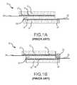
- FIGS. 1A-1Billustrate one type of prior art capacitive touch panel 10 that includes top and bottom glass substrates 12 , 14 that are each coated with ITO layers 16 , 18 , respectively.
- the ITO layers 16 , 18each include a pattern of electrodes positioned across a surface of the top and bottom glass substrates 12 , 14 .
- the top and bottom glass substrates 12 , 14are arranged in a face-to-face ITO pattern structure, such that the surfaces of the top and bottom glass substrates 12 , 14 coated with the ITO layers 16 , 18 are facing each other.
- the top and bottom glass substrates 12 , 14may be bonded together by an optically clear adhesive (OCA) 20 , such as an OCA sold by 3M Electronics.
- OCAoptically clear adhesive
- the pattern of electrodes in both the top and bottom ITO layers 16 , 18may be coupled to metal traces 22 , 24 to connect the ITO electrodes to touch detection electronics such as a controller.
- the metal traces 22 , 24may be positioned at opposite edges of the top and bottom glass substrates 12 , 14 with portions thereof in contact with the ITO layers 16 , 18 .
- Two flexible printed circuit (FPC) connectors 26 , 28may then be connected to the metal traces 22 , 24 by a bonding process for instance.
- the FPC connectors 26 , 28are discussed in further detail below in reference to FIG. 4 .
- FIG. 1Bis similar to FIG. 1A but additionally illustrates a hot bar 30 that may be used in a process for bonding the FPC connector 28 to the metal traces 24 associated with the bottom substrate 14 .
- the hot bar 30may be pressed onto the surface of the FPC connector 28 to urge the FPC connector 28 against the metal traces 24 for a predetermined period of time (e.g., several seconds). To perform this bonding process, there must be sufficient clearance above the metal traces 24 to place the hot bar 30 , as well as a pressing mechanism (not shown).
- the metal traces 22 positioned on the lower surface of the top substrate 12may be on a side of the panel 10 different from the metal traces 24 , so that there will be sufficient clearance for the hot bar 30 and pressing mechanism to secure the FPC connector 26 to the top ITO layer 16 via the top metal traces 22 .
- the use of two FPC connectors 26 , 28increases cost and the complexity of the manufacturing design and process.
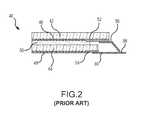
- the prior art touch panel 40 illustrated in FIG. 2may be used. Similar to the panel 10 shown in FIG. 1 , the panel 40 includes top and bottom glass substrates 42 , 44 coated with respective top and bottom ITO layers 46 , 48 and adhered to each other by an OCA 50 . In this touch panel however, the bottom ITO layer 48 is coated onto the lower surface of the bottom substrate 44 , rather than the upper surface as shown in FIG. 1 , such that the ITO pattern structure is in a “face-to-back” configuration.
- This designhas the advantage of permitting a single bifurcated FPC connector 56 (a top view of FPC connector 56 is shown in FIG.
- the single FPC connector 56may be used because there is sufficient clearance above the metal traces 52 , 54 for the bonding process, this design also possesses significant disadvantages.
- the design for the FPC connector 56is complex because it must be operable to connect to metal traces 52 , 54 in two different planes.
- the FPC connector bonding process for the panel 40may be complicated because two separate hot bar assemblies (e.g., each being similar to the hot bar 30 shown in FIG. 1B ) are required to bond the bifurcated FPC connector to the metal traces 52 , 54 .
- the bottom ITO layer 48is significantly further away from a user's touch (e.g., using a finger or stylus) than the top ITO layer 46 .
- This differenceresults in reduced signal strength from the electrodes on the bottom ITO layer 48 , which in turn reduces the performance of the touch panel.
- increasing the distance between the top and bottom ITO layers 46 , 48reduces the capacitance of the touch panel.
- an ITO layer that has a relatively low resistancemay be used, but this has the negative effect of increasing the visibility of the ITO layer, thereby reducing the contrast of the display device.
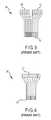
- FIG. 3illustrates a top view of the bifurcated FPC connector 56 also shown in FIG. 2 .
- a first set of conductive pads 58may be coupled to the metal traces 52 associated with the top ITO pattern 46
- another set of pads 60may be connected to the metal traces 54 associated with the bottom ITO pattern 48 .
- the other end of the connector 56may include a plurality of pads 62 that may be coupled to touch detection electronics such as a controller.
- FIG. 4illustrates a top view of the normal (e.g., not bifurcated) FPC connector 26 that is also shown in FIGS. 1A-1B .
- the constructionis relatively simple and includes conductive pads 27 that may be coupled to the metal traces 22 of the top ITO pattern 16 and a pad of connectors 29 that may be coupled touch detection electronics.
- the design and construction of the FPC connector 26is relatively simple, the need for two FPC connectors on different sides of the touch panel 10 is costly, increases complexity of manufacturing, and increases the surface area required for the touch panel.
- a capacitive touch screen panelincluding a first transparent substrate that includes a first conductive layer disposed adjacent to a surface thereof, a second transparent substrate that includes a second conductive layer disposed adjacent to a surface thereof, and a transparent material disposed between the first and second transparent substrates such that the first and second conductive layers are arranged in a face-to-face relationship.
- a first set of conductive tracesis disposed on the first transparent substrate such that at least one trace of the first set of conductive traces is coupled to the first conductive layer
- a second set of conductive tracesis disposed on the second transparent substrate such that at least one trace of the second set of conductive traces is coupled to the second conductive layer and at least another trace of the second set of conductive traces is not coupled to the second conductive layer.
- An electrically conductive adhesiveis disposed between the at least one trace of the first set of conductive traces and the at least another trace of the second set of conductive traces, and a flexible printed circuit connector is coupled to each of the at least one trace of the second set of conductive traces and the at least another trace of the second set of conductive traces.
- the at least another trace of the first set of conductive tracesmay not coupled to the first conductive layer.
- the face-to-face relationship of the first and second conductive layersmay be operable to align the at least one trace of the first set of conductive traces with the at least another trace of the second set of conductive traces, and the at least another trace of the first set of conductive traces with the at least one trace of the second set of conductive traces.
- the electrically conductive adhesivemay be disposed between the at least one trace of the first set of conductive traces and the at least another trace of the second set of conductive traces, and the at least another trace of the first set of conductive traces and the at least one trace of the second set of conductive traces.
- the electrically conductive adhesivemay include a seal frit that extends around a substantial portion of each of the first and second transparent substrates.
- the flexible printed circuit connectormay includes a plurality of pads, a first pad of the plurality of pads being coupled to the at least one trace of the second set of conductive traces, and a second pad of the plurality of pads being coupled to the at least another trace of the second set of conductive traces.
- Each of the first and second conductive layersmay include at least one row of electrodes.
- Each of the electrodes in the at least one row of electrodes in each of the first and second conductive layersmay be diamond-shaped.
- the at least one row of electrodes of the first conductive layermay be generally perpendicular to the at least one row of electrodes of the second conductive layer.
- a first portion of the flexible printed circuit connectormay be coupled to each of the at least one trace of the second set of conductive traces and the at least another trace of the second set of conductive traces, the first portion of the flexible printed circuit connector generally residing in a single plane.
- the electrically conductive adhesivemay include a mixture of epoxy resin and Au balls. At least one Au ball may be disposed between the at least one trace of the first set of conductive traces and the at least another trace of the second set of conductive traces.
- the electrically conductive adhesivemay include a liquid crystal.
- the first and second conductive layersmay include indium tin oxide (ITO).
- ITOindium tin oxide
- a plurality of spacersmay be disposed between the first and second transparent substrates, and the spacers may include glass or plastic balls.
- a capacitive touch screen panelincluding a first transparent substrate that includes a first conductive layer disposed adjacent to a surface thereof, a second transparent substrate that includes a second conductive layer disposed adjacent to a surface thereof, a transparent material disposed between the first and second transparent substrates such that the first and second conductive layers are arranged in a face-to-face relationship, and a plurality of spacers disposed between the first and second transparent substrates.
- the first transparent substrate, second transparent substrate, and transparent materialhave approximately the same refractive index.
- the transparent materialmay include optical glue.
- a capacitive touch screen panelincluding a first transparent substrate that includes a first conductive layer disposed adjacent to a surface thereof, a second transparent substrate that includes a second conductive layer disposed adjacent to a surface thereof, a transparent material disposed between the first and second transparent substrates such that the first and second conductive layers are arranged in a face-to-face relationship, a first set of conductive traces disposed on the first transparent substrate, a second set of conductive traces disposed on the second transparent substrate, and a flexible printed circuit connector having a first portion that is coupled to at least some of the conductive traces of the first set of conductive traces and at least some of the conductive traces of the second set of conductive traces.
- the first portion of the flexible printed circuit connectorgenerally resides in a single plane.
- a method for forming a capacitive touch screenincluding providing top and bottom glass sheets, each of the top and bottom glass sheets including a surface having a conductive pattern and a number of conductive traces, laminating an optically clear adhesive onto the surface having a conductive pattern of one of the top and bottom glass sheets, printing seal glue mixed with Au balls onto the number of conductive traces of the other of the top and bottom glass sheets, assembling the top and bottom glass sheets together such that each of the surfaces having a conductive pattern of each of the top and bottom sheets face each other, scribing the top and bottom glass sheets to form a number of individual units, curing the seal glue mixed with Au balls of at least one of the individual units, and bonding a flexible printed circuit connector to the number of conductive traces of one of the top and bottom glass sheets.
- the methodmay include aligning each metal trace of the number of metal traces of the top glass sheet with a respective metal trace of the number of metal traces of the bottom glass sheet.
- the methodmay include performing an autoclave process on each of the individual units.
- the autoclave processmay be performed at about 150 degrees Celsius and at about 18 psi.
- FIGS. 1A-1Billustrate a prior art touch panel assembly.
- FIG. 2illustrates another prior art touch panel assembly.
- FIG. 3illustrates a bifurcated flexible printed circuit (FPC) connector for a touch panel assembly.
- FPCflexible printed circuit
- FIG. 4illustrates another flexible printed circuit (FPC) connector for a touch panel assembly.
- FPCflexible printed circuit
- FIG. 5illustrates an embodiment of a display device that incorporates a touch screen panel assembly.
- FIG. 6Aillustrates one embodiment of a touch panel assembly.
- FIG. 6Billustrates a top view of a bottom glass substrate and an FPC connector of the touch panel assembly of FIG. 6A .
- FIG. 6Cillustrates a top view of a top glass substrate of the touch panel assembly of FIG. 6A before being assembled with the bottom glass substrate of FIG. 6B .
- FIG. 7illustrates a method of manufacturing an exemplary touch panel assembly.
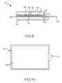
- FIG. 8is a cross-sectional view taken along the line 8 - 8 in FIG. 6A .
- FIG. 9illustrates another embodiment of a touch panel assembly.
- FIG. 10illustrates a top view of a bottom glass substrate of the touch panel of FIG. 9 .
- FIG. 5illustrates a device 100 having an integrated touch screen display 102 .
- the device 100may also include a housing 104 and a number of buttons 110 .
- the device 100may be, by way of example and not of limitation, a cell phone, game system, PDA, media player, or any other device that includes a touch screen display. In this regard, specific features of the device 100 may vary.
- One or more objects 108may be displayed on the integrated touch screen display 102 .
- the objects 108may include, without limitation, graphics, icons, text, buttons, images, etc.
- a usermay interact with the device 100 by touching the touch screen display 102 where one or more objects 108 appear, for example with a stylus 106 or a finger (not shown).
- FIG. 6Aillustrates an exemplary touch panel 150 that may be used in a display device, such as the display device 100 illustrated in FIG. 5 .
- the panel 150may include a top glass substrate 152 coated with a top ITO pattern 156 on a lower surface (not labeled).
- the panel 150also may include a bottom glass substrate 154 coated with a bottom ITO pattern 158 on an upper surface (not labeled).
- the top and bottom glass substrates 152 , 154may be disposed in a parallel arrangement and adhered together by a bonding agent which may be in the form of a transparent material such as an optically clear adhesive 160 (OCA).
- OCAoptically clear adhesive
- the OCAmay be in direct contact with the top and bottom ITO coated patterns 156 , 158 .
- the OCAmay not be in direct contact with top and bottom ITO coated patterns 156 , 158 .
- another appropriate layer of materiale.g., an alignment layer, not shown
- the top and bottom ITO patterns 156 , 158may be positioned in a face-to-face relationship, which, as described above, reduces or eliminates the need for low resistive ITO layers that may be required when the ITO pattern structure is in a face-to-back arrangement as illustrated in the prior art touch screen assembly of FIG. 2 .
- the bottom ITO pattern 158 on the bottom glass substrate 154may include four rows of electrodes (not labeled).
- the bottom glass substrate 154also includes a number of metal traces 164 .
- the bottom glass substrate 154may include a first set of metal traces 165 a (e.g., four metal traces), each of which may be appropriately electrically coupled to a respective row of electrodes.
- the bottom glass substrate 154may also include a second set of metal traces 165 b that are not coupled to any rows of electrodes on the bottom glass substrate 154 for reasons that will be described below.
- the top ITO pattern 156may have four rows of electrodes (not labeled) and a number of metal traces 162 .
- each of the top and bottom glass substrates 152 , 154has been described as including at least one metal trace electrically connected to one row of electrodes in addition to metal traces that are not electrically connected to any rows of electrodes, it is contemplated that one of the top or bottom substrates 152 , 154 (e.g., the substrate not directly electrically connected to an FPC connector) may have only traces that are electrically connected to rows of electrodes.
- the metal traces 162 , 164may be of any appropriate design and shape.
- a single, normal (e.g., not bifurcated) FPC connector 166may be used to couple both the top and bottom ITO patterns 156 , 158 to detection electronics.
- an electrically conductive adhesive 168may couple the metal traces 162 associated with the top ITO pattern 156 of the top glass substrate 152 to the metal traces 164 associated with the bottom ITO pattern 158 of the bottom glass substrate 154 .
- the metal traces 164 associated with the bottom ITO pattern 158may be electrically bonded to the FPC connector 166 by any appropriate material (e.g., anistropic conductive film), although it is envisioned that the metal traces 162 associated with the top ITO pattern 156 could be bonded to the FPC connector 166 .
- the electrically conductive adhesive 168may be seal glue (e.g., epoxy resin) mixed with a relatively small amount of metallic balls (e.g., about 2-4% Au balls). Further, the size of each Au ball may be larger (e.g., 5 um larger) than the thickness of the layer of the OCA 160 to provide a reliable connection between the metal traces 162 and 164 .
- seal gluee.g., epoxy resin
- metallic ballse.g., about 2-4% Au balls
- the size of each Au ballmay be larger (e.g., 5 um larger) than the thickness of the layer of the OCA 160 to provide a reliable connection between the metal traces 162 and 164 .
- the metal traces 162 , 164may be constructed from any suitable material.
- at least one of the metal tracesmay include a composite metal layer that includes two layers of molybdenum with a layer of aluminum disposed therebetween (e.g., Mo/Al/Mo composite metal layers).
- FIG. 6Bshows a top view of the bottom glass substrate 154 and the FPC connector 166
- FIG. 6Cshows a top view of the top glass substrate 152 before being assembled with the bottom glass substrate of FIG. 6B
- the FPC connector 166may include any appropriate number of pads 167 (e.g., eight pads) each of which may be appropriately electrically bonded to each of the metal traces 164 of the bottom glass substrate 154 , e.g., each metal trace of the first and second sets of metal traces 165 a , 165 b
- the FPC connector 166may include first and second sets of pads 168 a , 168 b .
- each metal trace of the first set of metal traces 165 amay be respectively appropriately electrically coupled to a row of electrodes of the bottom ITO pattern 158 disposed on the bottom glass substrate 154 , to a pad of the first set of pads 168 a of the FPC connector 166 , and to a metal trace 162 of the top glass substrate 152 (e.g., the second set of metal traces 163 b not connected to electrode rows) by way of any appropriate adhesive or other bonding substance (e.g., electrically conductive adhesive, anisotropic conductive films).
- any appropriate adhesive or other bonding substancee.g., electrically conductive adhesive, anisotropic conductive films.
- Each metal trace of the second set of metal traces 165 b(e.g., four metal traces), none of which is electrically connected to a row of electrodes on the bottom glass substrate 154 , may be appropriately coupled to a pad of the second set of pads 168 b of the FPC connector 166 and to one of the metal traces 162 associated with the top ITO pattern 156 that is electrically coupled to a respective row of electrodes on the top glass substrate 152 (e.g., from the first set of metal traces 163 a of the top glass substrate 152 ).
- the ITO layer 156 of the top glass substrate 152may include four rows of electrodes (not labeled) and first and second sets of metal traces 163 a , 163 b .
- Each metal trace of the first set of metal traces 163 a of the top glass substrate 152may be respectively electrically coupled to a row of electrodes on the top glass substrate 152 and each metal trace of the second set of metal traces 163 b of the top glass substrate 152 may not be electrically coupled to any rows of electrodes on the top glass substrate 152 .
- other numbers and arrangements of electrodes and metal tracesare envisioned and are encompassed within the scope of the embodiments.
- each of the electrodes of the top and bottom ITO layers 156 , 158may include a diamond shape and may be of any appropriate size. In one arrangement, one or more of the electrodes may be between 3 and 9 mm in width and in another arrangement, between 5 and 7 mm in width.
- the single FPC connector 166may be electrically connected to both the top ITO pattern 156 and to the bottom ITO pattern 158 in at least a generally single plane with the top and bottom ITO patterns 156 , 158 in a face to face relationship.
- a conductive adhesive 168e.g., epoxy resin mixed with Au balls
- FIG. 6Amay be applied to all of the metal traces 162 , 164 of the top and/or bottom glass substrates 152 , 154 .
- top and bottom glass substrates 152 , 154may then be arranged in a face to face relationship such that the metal traces 162 of the top glass substrate 152 that are electrically connected to rows of electrodes on the top glass substrate 152 (e.g., the first set of traces 163 a ) are aligned only with metal traces 164 of the bottom glass substrate 154 that are not electrically connected to any rows of the electrodes on the bottom glass substrate 154 (e.g., the second set of traces 165 b ).
- the metal traces 162 of the top glass substrate 152 that are not electrically connected to any rows of electrodes on the top glass substrate 152are aligned only with metal traces 164 of the bottom glass substrate 154 that are electrically connected to rows of the electrodes on the bottom glass substrate 154 (e.g., first set of metal traces 165 a ). Due to the presence of the Au balls in the electrically conductive adhesive 168 and as illustrated in FIG. 8 , at least one Au ball may be present between respective aligned metal traces 162 , 164 of the top and bottom glass substrates 152 , 154 to electrically connect such respective metal traces as will be described in more detail below.
- the single, normal FPC connector 166(e.g., as in FIG. 6B ) may be appropriately bonded to only the metal traces 164 (instead of both metal traces 162 , 164 ), which greatly reduces the complexity of the manufacturing process over the prior art panels 10 , 40 shown in FIGS. 1-2 .
- the single, normal FPC connector 166e.g., as in FIG. 6B
- the metal traces 164instead of both metal traces 162 , 164
- the first set of pads 168 a of the FPC connector 166may be electrically connected to the first set of metal traces 165 a and the second set of pads 168 b of the FPC connector 166 may be electrically connected to the second set of metal traces 165 b that are not electrically connected to any rows of the electrodes on the bottom glass substrate 154 .
- FIG. 7illustrates a method ( 200 ) for manufacturing a touch panel, such as the touch panel 150 shown in FIGS. 6A-6C .
- the methodmay begin by providing ( 202 ) a top and bottom sheet of ITO coated glass (e.g., the top and bottom glass substrates 152 and 154 shown in FIG. 6A ).
- the sheetsmay be sized such that several individual touch panels may be made from the two sheets.
- the surface area of each sheete.g., 14′′ ⁇ 16′′
- Each of the top and bottom glass sheetsmay be cleaned ( 204 ) in any appropriate manner or with any appropriate solution (e.g., isopropyl alcohol, ethyl alcohol, trichlorotriflorothane), and then a photo resist process may be applied ( 206 ) to each of the top and bottom glass sheets.
- a photoresist layersuch as diazonaphthoquinone (DNQ), various bisphenols, and the like may be appropriately applied to one surface to each of the sheets.
- DNQdiazonaphthoquinone
- Each sheetcan be covered with the photoresist layer by spin coating, prebaking, and/or other appropriate processes to form a desired thickness.
- the photoresist layermay be exposed ( 208 ) to an appropriate pattern of a light source (e.g., UV light) to chemically change a desired pattern of the photoresist layer.
- a light sourcee.g., UV light
- those portions of the photoresist layer exposed to UV light in a positive photoresist processwill become soluble in a developer and can be removed as will be later described.
- those portions of the photoresist layer exposed to UV in a negative photoresist processwill become insoluable in the developer and thus those portions of the photoresist layer not exposed to the UV light can be removed.
- a mask other appropriate layercan be disposed between the photoresist layer and the UV light source to form an appropriate pattern in the photoresist layer.
- the maskcan have apertures or “cut-outs” therethrough in a pattern that will eventually allow a desired pattern of electrodes to be formed on the sheets.
- the portion of the UV light that shines through the apertures of the maskwill cause those portions of the photoresist layer that absorb the UV light to become insoluble.
- the sheetcan be appropriately exposed ( 210 ) to a chemical developer (e.g., mixture of Metol, Phenidone or Dimezone and hydroquinone) to remove those portions of the photoresist layer that absorbed the UV light (assuming a positive photoresist process).
- a chemical developere.g., mixture of Metol, Phenidone or Dimezone and hydroquinone
- those portions of the ITO layer of the upper and lower sheets not protected by the photoresist layercan be etched ( 212 ) using for instance a liquid (“wet”) or plasma (“dry”) chemical agent.
- the remaining portions of the photoresist layercan be removed by way of a stripping process ( 214 ).
- each of the sheetscan then be appropriately cleaned ( 216 ).
- each of the sheetshas an appropriately formed ITO electrode pattern or ITO coated surface formed thereon (e.g., that in FIG. 6B ) that may be in the form of one or more rows of electrodes (e.g., four rows). Each row of electrodes may include a number of square, diamond or other appropriately shaped electrodes.
- metal tracesmay be appropriately incorporated ( 218 ) with each of the top and bottom sheets.
- first and second sets of metal tracesmay be appropriately applied to each of the top and bottom sheet, each of the first and second sets of metal traces including four metal traces.
- Each metal trace of each first set of four metal traces on the top and bottom sheetscan be appropriately electrically connected to a respective row of electrodes (e.g., the first set of traces of the top sheet being electrically connected to rows of electrodes of the top sheet and the first set of traces of the bottom sheet being electrically connected to rows of electrodes of the bottom sheet) while the second sets of four metal traces are not electrically connected to any ITO electrode patterns of the top or bottom sheets.
- one of the top and bottom sheetsneed only be connected to a single set of metal traces, each metal trace of which is connected to a respective ITO electrode pattern on such top and/or bottom sheet.
- the metal tracesmay be appropriately mounted to the top and bottom sheets before the electrode patterns are formed on the top and bottom glass sheets. Thereafter, the previously discussed process may be performed to form electrode patterns, at least some of which are aligned and/or coupled to the metal traces.
- an OCAe.g., an optically clear laminating adhesive sold by 3M Electronics
- An electrically conductive adhesivee.g., seal glue with Au balls
- FIG. 8a cross-sectional view along the lines 8 - 8 of FIG.
- seal glue with Au ballsmay be applied over the metal traces 164 on the bottom glass sheet 154 such that at least one Au ball 169 is in contact with each of the metal traces 164 .
- a trace gap 171may be designed to be a number of orders larger than the diameter of each Au ball 169 .
- the trace gap 171may be approximately 0.15 mm while the diameter of each Au ball 169 may be approximately 35 micrometers.
- the top and bottom sheetsmay be assembled together ( 224 ) such that the top and bottom ITO patterns are arranged in a face-to-face manner.
- the top and bottom sheetsmay be arranged such that each trace of the first set of metal traces (e.g., four traces) of the top sheet is in a respective face to face and aligned relationship with each trace of the second set of metal traces (e.g. four metal traces) on the bottom glass sheet.
- the top and bottom sheetsmay also be arranged such that each trace of the second set of metal traces of the top sheet is in a respective face to face and aligned relationship with each trace of the first set of metal traces of the bottom glass sheet.
- each of the metal traces of the top sheetwill be aligned with a respective metal trace of the bottom sheet as previously described and will be in electrical contact via at least one Au ball. Excess Au balls in the seal glue with Au ball mixture will fall or otherwise be disposed into and/or within the trace gaps to prevent or otherwise reduce short circuit situations. Also, the OCA serves to bond the top ITO pattern of the top glass sheet to the bottom ITO pattern of the bottom glass sheet.
- top and bottom sheetsmay be scribed ( 226 ) to form individual touch panels.
- the top and bottom sheetsmay have dimensions of about 14′′ ⁇ 16′′, whereas each individual unit may be much smaller (e.g., 2′′ ⁇ 3′′) such that several individual touch panels may be cut (e.g., using scribing equipment that includes a diamond-edged cutting surface) from a single pair of top and bottom ITO sheets.
- Bubbles in the OCAare undesirable because they may cause visual blemishes in the resulting display device, and therefore touch panels with bubbles in the OCA may have to be discarded.
- the unitsmay be placed in an autoclave for an appropriate period of time at an appropriate temperature and pressure (e.g., 50 minutes at 50 degrees Celsius and 5 standard atmospheres (atm)).
- an appropriate temperature and pressuree.g., 50 minutes at 50 degrees Celsius and 5 standard atmospheres (atm)
- Performing the autoclave process after forming the individual touch screen units from the larger sheetsmay increase bubble removal as compared to performing the autoclave process on the larger sheets (e.g., before scribing or otherwise forming the individual units).
- other manners of removing bubbles from the OCAare contemplated.
- the next stepis to cure ( 230 ) the conductive adhesive (e.g., seal glue with Au balls) using a high temperature and pressure process so that the conductive adhesive forms a reliable connection between the above-described metal traces associated with the top and bottom glass sheets or substrates.
- the individual unitsmay be placed into a container at an appropriate temperature (e.g., 150 degrees Celsius) and an appropriate force may be applied (e.g., 18 psi).
- an appropriate temperaturee.g. 150 degrees Celsius
- an appropriate forcee.g., 18 psi
- first and second sets of pads of a single non-bifurcated FPC connectore.g., that of FIG.
- the FPC connectormay be respectively bonded ( 232 ) to the first and second sets of metal traces positioned at the edge of the bottom glass sheet (e.g., the first and second sets of metal traces 165 a , 165 b shown in FIGS. 6A-6B ) via a conductive adhesive (e.g., anistropic conductive film).
- a conductive adhesivee.g., anistropic conductive film.
- the FPC connectormay be bonded to the metal traces by positioning the pads of the FPC connector over the metal traces of the bottom sheet and then pressing a hot bar onto the top surface of the FPC connector for several seconds such that the pads of the FPC connector are in contact with the metal traces of the bottom sheet.
- the individual touch panelis ready to be integrated into a device that utilizes a touch screen. While the above method ( 200 ) has been described with the pads of the FPC connector being directly bonded to the metal traces of the bottom sheet, it is envisioned that the FPC connector could be directly bonded to the metal traces of the top sheet. In other embodiments, the top sheet may include only a single set of four traces that are directly electrically connected to rows of electrodes on the top sheet. Other arrangements are also envisioned so long as the top and bottom sheets are not electrically connected with each other which may destroy or at least inhibit the capacitive coupling effect of the touch screen assembly.
- FIGS. 9-10present a variation of the touch panel 150 of FIGS. 6A-6C and corresponding components between the two embodiments are identified by a common reference numeral. Those corresponding components that differ in at least some respect are identified by a “single prime” designation in FIGS. 9-10 .
- the bonding agent between the top and bottom glass substrates 152 , 154 of the touch panel 150 ′may be in the form of a liquid crystal 160 ′ instead of the OCA 160 , and a number of spacers 264 may be disposed within the liquid crystal 160 ′ to maintain a gap 255 between the top and bottom glass substrates 152 , 154 .
- the spacers 264may be any appropriate object or device that can maintain the dielectric effect between the top and bottom ITO patterns 156 , 158 .
- the spacers 264may be in the form of a number of glass and/or plastic balls that may be appropriately applied (e.g., via spraying) onto the surface one of the top and bottom substrates 152 , 154 (e.g., top or bottom ITO layers 156 , 158 ) before the top and bottom substrates 152 , 154 are placed in the face-to-face relationship during the manufacturing process. While plastic balls may provide increased integrity in both low and high temperatures and reduce production costs, the use of glass balls may facilitate maintaining a desired gap 255 as glass has increased rigidity and robustness.
- each of the spacers 264may be of any appropriate size.
- the spacers 264may be substantially smaller than a width of the electrodes.
- one or more of the spacers 264may be between 3 and 30 microns in diameter.
- the spacers 264may be between 6 and 20 microns in diameter.
- any appropriate sealmay be formed around a perimeter of the assembly 250 .
- a seal frit 262 of a seal glue with Au ballsmay be applied or otherwise deposited (e.g., by screen printing) around a perimeter of the touch screen 150 ′.
- an aperturemay be formed in the seal frit 262 or at least left around the perimeter of the assembly touch screen 150 ′ to allow for the introduction of the liquid crystal 160 ′ into the gap 255 so as to at least partially surround or encompass the spacers 264 .
- the liquid crystal 160 ′may be chosen to have a refractive index that is the same as, or close to that of the top and bottom substrates 152 , 154 . Moreover, increasing or decreasing the size of the gap 255 (e.g., by changing the size of the spacers 264 ) can correspondingly provide a desired capacitance of the touch screen.
- an end seal 268 of any appropriate materiale.g., an electrically conductive adhesive
- liquid crystal 160 ′has been described as being deposited between the top and bottom substrates 152 , 154 , it is contemplated that other bonding agents (e.g., liquid glue) could be used additionally or alternatively. It may be necessary to apply a UV light source to the touch screen 150 ′ if a liquid glue is utilized.
- other bonding agentse.g., liquid glue
- the spacers 264may be applied to one of the top and bottom substrates 152 , 154 and the seal frit 262 may be applied around the perimeter of one of the top and bottom substrates 152 , 154 (either the same substrate that the spacers 264 are applied to or the other of the top and bottom substrates 152 , 154 ) with an aperture being appropriately formed in the seal frit 262 . Thereafter, the top and bottom substrates 152 , 154 may be appropriately brought into the aforementioned parallel and adjoining face-to-face relationship and bonded together and the gap 255 filled with the liquid crystal 160 ′ or other bonding agent.
- the seal glue with Au balls of the seal frit 262will be disposed over and between the metal traces 162 , 164 of the top and bottom substrates 152 , 154 when the top and bottom substrates 152 , 154 are brought into the face to face relationship during the manufacturing process.
- the Au ballsmay serve to respectively electrically connect each of the metal traces 162 of the top substrate 152 to each of the metal traces of the bottom substrate 154 .
- the top and bottom substrateswill not be directly electrically connected and the capacitive coupling effect of the touch screen will be maintained.
- a single, non-bifurcated FPC connectormay be used. This advantageously reduces the number of FPC connectors required, the physical space required, and the complexity of the FPC bonding process. Further, by not using a bifurcated FPC connector, the bonding process is further simplified due to the fact that there is no need to bond an FPC connector in two different planes (e.g., two different ITO layers).
- Another advantage of the present designresults from using a face-to-face ITO pattern structure, rather than a face-to-back structure. By doing this, there is no need to use a low resistance ITO layer to increase the signal strength of the bottom ITO pattern, which may cause reduced contrast levels for the resulting display device.
- FIGS. 9-10may be implemented as shown or in combination with previously described embodiments and provides several advantages over prior art designs. For example, by matching the refractive index of the liquid crystal 160 ′ (or optical glue) with that of the glass substrates 152 , 154 , an assembly with high transparency is provided. Further, the spacers 264 may provide a uniform and predetermined gap width and thus reduce the effects of Newton Rings.
Landscapes
- Engineering & Computer Science (AREA)
- General Engineering & Computer Science (AREA)
- Theoretical Computer Science (AREA)
- Human Computer Interaction (AREA)
- Physics & Mathematics (AREA)
- General Physics & Mathematics (AREA)
- Position Input By Displaying (AREA)
- Switches That Are Operated By Magnetic Or Electric Fields (AREA)
Abstract
Description
Claims (10)
Priority Applications (3)
| Application Number | Priority Date | Filing Date | Title |
|---|---|---|---|
| US12/501,840US9128568B2 (en) | 2008-07-30 | 2009-07-13 | Capacitive touch panel with FPC connector electrically coupled to conductive traces of face-to-face ITO pattern structure in single plane |
| CN200980138382.1ACN102171630B (en) | 2008-07-30 | 2009-07-30 | Glass substrate for capacitive touch panel and manufacturing method thereof |
| PCT/US2009/052208WO2010014783A2 (en) | 2008-07-30 | 2009-07-30 | Glass substrate for capacitive touch panel and manufacturing method thereof |
Applications Claiming Priority (3)
| Application Number | Priority Date | Filing Date | Title |
|---|---|---|---|
| US8487708P | 2008-07-30 | 2008-07-30 | |
| US8701508P | 2008-08-07 | 2008-08-07 | |
| US12/501,840US9128568B2 (en) | 2008-07-30 | 2009-07-13 | Capacitive touch panel with FPC connector electrically coupled to conductive traces of face-to-face ITO pattern structure in single plane |
Publications (2)
| Publication Number | Publication Date |
|---|---|
| US20100026659A1 US20100026659A1 (en) | 2010-02-04 |
| US9128568B2true US9128568B2 (en) | 2015-09-08 |
Family
ID=41607839
Family Applications (1)
| Application Number | Title | Priority Date | Filing Date |
|---|---|---|---|
| US12/501,840Active2033-01-01US9128568B2 (en) | 2008-07-30 | 2009-07-13 | Capacitive touch panel with FPC connector electrically coupled to conductive traces of face-to-face ITO pattern structure in single plane |
Country Status (3)
| Country | Link |
|---|---|
| US (1) | US9128568B2 (en) |
| CN (1) | CN102171630B (en) |
| WO (1) | WO2010014783A2 (en) |
Cited By (6)
| Publication number | Priority date | Publication date | Assignee | Title |
|---|---|---|---|---|
| US20140313437A1 (en)* | 2013-04-17 | 2014-10-23 | E Ink Holdings Inc. | Touch panel |
| US20150021153A1 (en)* | 2012-03-02 | 2015-01-22 | Novalia Ltd | Touch-sensitive input device |
| US9627463B2 (en)* | 2014-11-28 | 2017-04-18 | Lg Display Co., Ltd. | Flexible display device with space reducing wire configuration |
| US20170131809A1 (en)* | 2015-11-05 | 2017-05-11 | Acer Incorporated | Touch display device and manufacturing method thereof |
| US11048111B2 (en) | 2015-03-27 | 2021-06-29 | Semiconductor Energy Laboratory Co., Ltd. | Display device equipped touch panel |
| US11372488B2 (en) | 2016-07-13 | 2022-06-28 | Semiconductor Energy Laboratory Co., Ltd. | Input/output panel, input/output device, and semiconductor device |
Families Citing this family (53)
| Publication number | Priority date | Publication date | Assignee | Title |
|---|---|---|---|---|
| TWI393110B (en)* | 2008-09-26 | 2013-04-11 | Au Optronics Corp | Apparatus, shift register unit, liquid crystal displaying device and method for eliminating afterimage |
| TWI460639B (en)* | 2009-02-23 | 2014-11-11 | Innolux Corp | System for display images |
| TWM375253U (en)* | 2009-09-21 | 2010-03-01 | Emerging Display Tech Corp | Touch panel input device having electric stimulation tactile feedback function |
| US20110172887A1 (en)* | 2009-11-30 | 2011-07-14 | Reeve David R | Vehicle assembly control method for collaborative behavior |
| JP5413171B2 (en)* | 2009-12-14 | 2014-02-12 | カシオ計算機株式会社 | Touch panel |
| TW201128261A (en)* | 2010-02-03 | 2011-08-16 | J Touch Corp | Improved structure for touch panel |
| CN102163094A (en)* | 2010-02-24 | 2011-08-24 | 介面光电股份有限公司 | Improved structure of touch panel |
| US9244573B2 (en)* | 2010-03-03 | 2016-01-26 | Miraenanotech Co., Ltd. | Capacitive touch panel including embedded sensing electrodes |
| KR101689331B1 (en)* | 2010-11-23 | 2016-12-26 | 삼성디스플레이 주식회사 | flat panel display integrated touch screen panel |
| CN102479011B (en)* | 2010-11-29 | 2015-07-22 | 北京京东方光电科技有限公司 | Capacitive touch screen |
| KR101181342B1 (en)* | 2011-02-16 | 2012-09-11 | 에쓰이에이치에프코리아 (주) | Touch screen |
| TW201235901A (en)* | 2011-02-21 | 2012-09-01 | Wistron Corp | Touch control device |
| CN102279683A (en)* | 2011-08-30 | 2011-12-14 | 深圳市豪威薄膜技术有限公司 | Integrated capacitive touch screen and manufacturing method thereof and touch screen terminal |
| US9283217B2 (en) | 2011-11-10 | 2016-03-15 | Allergan, Inc. | Pharmaceutical compositions comprising 7-(1 H-imidazol-4-ylmethyl)-5,6,7,8-tetrahydro-quinoline for treating skin diseases and conditions |
| KR20130067730A (en)* | 2011-12-14 | 2013-06-25 | 삼성전기주식회사 | Touch panel |
| US9266310B2 (en) | 2011-12-16 | 2016-02-23 | Apple Inc. | Methods of joining device structures with adhesive |
| KR20130071863A (en)* | 2011-12-21 | 2013-07-01 | 삼성전기주식회사 | Touch panel |
| KR101370453B1 (en)* | 2011-12-22 | 2014-03-06 | 엘지이노텍 주식회사 | Touch panel |
| CN102566844A (en)* | 2011-12-29 | 2012-07-11 | 深圳市力合光电传感技术有限公司 | Process for eliminating dominance of indium tin oxide (ITO) pattern |
| US20130264183A1 (en)* | 2012-04-10 | 2013-10-10 | Chih-Chung Lin | Capacitive touch unit |
| CN102681740A (en)* | 2012-05-16 | 2012-09-19 | 金百芳 | Capacitive touch screen plate device |
| US9282686B2 (en) | 2012-07-10 | 2016-03-08 | Flextronics International Usa, Inc. | System and method for high resolution, high throughput processing of conductive patterns of flexible substrates |
| KR102173801B1 (en) | 2012-07-12 | 2020-11-04 | 가부시키가이샤 한도오따이 에네루기 켄큐쇼 | Display device and method for manufacturing display device |
| US9144938B2 (en) | 2012-08-06 | 2015-09-29 | Apple Inc. | Methods for attaching structures using ultraviolet and visible light curing adhesive |
| CN102830885A (en)* | 2012-09-14 | 2012-12-19 | 常州裕成光电有限公司 | Component of capacitive touch screen sensor |
| CN104769531A (en)* | 2012-09-14 | 2015-07-08 | 尤尼皮克塞尔显示器有限公司 | Foldable multi-touch surface |
| US9928762B2 (en)* | 2012-09-28 | 2018-03-27 | Apple Inc. | Electronic devices with flexible circuit light shields |
| CN103885651A (en)* | 2012-12-21 | 2014-06-25 | 苏州市健邦触摸屏技术有限公司 | Modified capacitive touch screen |
| TW201426444A (en)* | 2012-12-27 | 2014-07-01 | Wintek Corp | Touch display device |
| KR102107383B1 (en)* | 2012-12-27 | 2020-05-07 | 엘지디스플레이 주식회사 | Array substrate for display device |
| CN103970312B (en)* | 2013-01-24 | 2017-10-27 | 联胜(中国)科技有限公司 | Touch control display apparatus |
| JP6119518B2 (en) | 2013-02-12 | 2017-04-26 | ソニー株式会社 | Sensor device, input device and electronic apparatus |
| JP6288073B2 (en) | 2013-03-18 | 2018-03-07 | ソニー株式会社 | Sensor device, input device and electronic device |
| JP6134965B2 (en)* | 2013-03-22 | 2017-05-31 | グンゼ株式会社 | Touch panel device |
| CN103324346A (en)* | 2013-06-11 | 2013-09-25 | 业成光电(深圳)有限公司 | Touch device and touch panel thereof |
| US9501186B2 (en) | 2013-07-12 | 2016-11-22 | Xiaomi Inc. | Touch screen and mobile terminal including same |
| CN103383615B (en)* | 2013-07-12 | 2016-12-28 | 小米科技有限责任公司 | Touch screen and mobile terminal |
| JP6142745B2 (en) | 2013-09-10 | 2017-06-07 | ソニー株式会社 | Sensor device, input device and electronic apparatus |
| CN103488343B (en)* | 2013-09-27 | 2016-10-19 | 南昌欧菲光科技有限公司 | Touch elements and touch screens |
| US9677168B2 (en)* | 2013-10-08 | 2017-06-13 | TPK America, LLC | Touch panel and method for manufacturing the same |
| KR101800813B1 (en)* | 2013-10-15 | 2017-12-20 | 엘지디스플레이 주식회사 | Touch panel and display device |
| JP2015190859A (en)* | 2014-03-28 | 2015-11-02 | ソニー株式会社 | Sensor device, input device, and electronic apparatus |
| US20150331507A1 (en)* | 2014-05-14 | 2015-11-19 | Motorola Solutions, Inc | Method and apparatus for embedding radiated elements in a touch panel |
| KR102272953B1 (en)* | 2014-09-05 | 2021-07-06 | 엘지디스플레이 주식회사 | Touch sensor module capable of reducing size of flexible printed circuit board |
| CN104461124A (en)* | 2014-10-31 | 2015-03-25 | 业成光电(深圳)有限公司 | Touch panel and manufacturing method thereof |
| KR102369089B1 (en)* | 2015-04-17 | 2022-03-02 | 삼성디스플레이 주식회사 | Flexible display device |
| MX381491B (en)* | 2016-04-13 | 2025-03-12 | Tactotek Oy | Multilayer structure with embedded multilayer electronics |
| RU2695493C2 (en)* | 2016-05-31 | 2019-07-23 | Общество с ограниченной ответственностью "Научно-производственное предприятие Тачскрин технологии" | Projective-capacitance touch panel and method of its manufacturing |
| US11353754B2 (en) | 2017-02-21 | 2022-06-07 | Semiconductor Energy Laboratory Co., Ltd. | Display panel, display device, input/output device, and data processing device |
| CN109375838A (en)* | 2018-11-16 | 2019-02-22 | 深圳晶华显示器材有限公司 | a touch screen |
| CN109920331B (en) | 2019-02-23 | 2020-05-05 | 昆山工研院新型平板显示技术中心有限公司 | Display panel and display device |
| CN110174976A (en)* | 2019-04-26 | 2019-08-27 | 康惠(惠州)半导体有限公司 | High reliability capacitance touch screen |
| KR102694363B1 (en)* | 2019-11-01 | 2024-08-14 | 삼성디스플레이 주식회사 | Electronic device |
Citations (195)
| Publication number | Priority date | Publication date | Assignee | Title |
|---|---|---|---|---|
| US4290052A (en) | 1979-10-26 | 1981-09-15 | General Electric Company | Capacitive touch entry apparatus having high degree of personal safety |
| US4550221A (en) | 1983-10-07 | 1985-10-29 | Scott Mabusth | Touch sensitive control device |
| US5062198A (en) | 1990-05-08 | 1991-11-05 | Keytec, Inc. | Method of making a transparent touch screen switch assembly |
| US5379057A (en) | 1988-11-14 | 1995-01-03 | Microslate, Inc. | Portable computer with touch screen and computer system employing same |
| US5459463A (en) | 1990-05-25 | 1995-10-17 | Sextant Avionique | Device for locating an object situated close to a detection area and a transparent keyboard using said device |
| US5488204A (en) | 1992-06-08 | 1996-01-30 | Synaptics, Incorporated | Paintbrush stylus for capacitive touch sensor pad |
| US5495077A (en) | 1992-06-08 | 1996-02-27 | Synaptics, Inc. | Object position and proximity detector |
| US5543592A (en) | 1993-07-23 | 1996-08-06 | Sextant Avionique | Multimode manipulator |
| US5543590A (en) | 1992-06-08 | 1996-08-06 | Synaptics, Incorporated | Object position detector with edge motion feature |
| US5543588A (en) | 1992-06-08 | 1996-08-06 | Synaptics, Incorporated | Touch pad driven handheld computing device |
| US5650597A (en) | 1995-01-20 | 1997-07-22 | Dynapro Systems, Inc. | Capacitive touch sensor |
| US5730165A (en) | 1995-12-26 | 1998-03-24 | Philipp; Harald | Time domain capacitive field detector |
| US5825352A (en) | 1996-01-04 | 1998-10-20 | Logitech, Inc. | Multiple fingers contact sensing method for emulating mouse buttons and mouse operations on a touch sensor pad |
| US5838412A (en)* | 1995-11-16 | 1998-11-17 | Hitachi, Ltd. | Liquid crystal display device assembled by flip chip technology comprising a folded multi-layered flexible driving circuit substrate |
| US5844506A (en) | 1994-04-05 | 1998-12-01 | Binstead; Ronald Peter | Multiple input proximity detector and touchpad system |
| US5854450A (en) | 1995-04-19 | 1998-12-29 | Elo Touchsystems, Inc. | Acoustic condition sensor employing a plurality of mutually non-orthogonal waves |
| US5854625A (en) | 1996-11-06 | 1998-12-29 | Synaptics, Incorporated | Force sensing touchpad |
| US5861583A (en) | 1992-06-08 | 1999-01-19 | Synaptics, Incorporated | Object position detector |
| US5880411A (en) | 1992-06-08 | 1999-03-09 | Synaptics, Incorporated | Object position detector with edge motion feature and gesture recognition |
| US5920310A (en) | 1996-11-15 | 1999-07-06 | Synaptics, Incorporated | Electronic device employing a touch sensitive transducer |
| US5940065A (en) | 1996-03-15 | 1999-08-17 | Elo Touchsystems, Inc. | Algorithmic compensation system and method therefor for a touch sensor panel |
| US5943052A (en) | 1997-08-12 | 1999-08-24 | Synaptics, Incorporated | Method and apparatus for scroll bar control |
| US6091406A (en) | 1996-12-25 | 2000-07-18 | Elo Touchsystems, Inc. | Grating transducer for acoustic touchscreens |
| US6188391B1 (en) | 1998-07-09 | 2001-02-13 | Synaptics, Inc. | Two-layer capacitive touchpad and method of making same |
| US6236391B1 (en) | 1995-01-24 | 2001-05-22 | Elo Touchsystems, Inc. | Acoustic touch position sensor using a low acoustic loss transparent substrate |
| KR200229845Y1 (en) | 2001-02-23 | 2001-07-19 | 주식회사 에이터치 | Structure of Contact of Substrate in Touch Screen |
| US6288707B1 (en) | 1996-07-29 | 2001-09-11 | Harald Philipp | Capacitive position sensor |
| US6297811B1 (en) | 1999-06-02 | 2001-10-02 | Elo Touchsystems, Inc. | Projective capacitive touchscreen |
| US20010026330A1 (en) | 2000-03-28 | 2001-10-04 | Oh Hyeok-Jin | Liquid crystal display employing touch panel |
| US20020030666A1 (en) | 1999-01-25 | 2002-03-14 | Harald Philipp | Capacitive position sensor |
| US6373474B1 (en) | 1998-10-27 | 2002-04-16 | Pentel Kabushiki Kaisha | Real contact type touch panel apparatus |
| US6379509B2 (en) | 1998-01-20 | 2002-04-30 | 3M Innovative Properties Company | Process for forming electrodes |
| US6380929B1 (en) | 1996-09-20 | 2002-04-30 | Synaptics, Incorporated | Pen drawing computer input device |
| US6441809B2 (en) | 1995-01-24 | 2002-08-27 | Elo Touchsystems, Inc. | Acoustic touch position sensor using a low acoustic loss transparent substrate |
| US6452514B1 (en) | 1999-01-26 | 2002-09-17 | Harald Philipp | Capacitive sensor and array |
| US20020145593A1 (en) | 2001-04-06 | 2002-10-10 | 3M Innovative Properties Company | Frontlit illuminated touch panel |
| US6466036B1 (en) | 1998-11-25 | 2002-10-15 | Harald Philipp | Charge transfer capacitance measurement circuit |
| US6488981B1 (en) | 2001-06-20 | 2002-12-03 | 3M Innovative Properties Company | Method of manufacturing a touch screen panel |
| US6492979B1 (en) | 1999-09-07 | 2002-12-10 | Elo Touchsystems, Inc. | Dual sensor touchscreen utilizing projective-capacitive and force touch sensors |
| US20020191029A1 (en) | 2001-05-16 | 2002-12-19 | Synaptics, Inc. | Touch screen with user interface enhancement |
| US6504530B1 (en) | 1999-09-07 | 2003-01-07 | Elo Touchsystems, Inc. | Touch confirming touchscreen utilizing plural touch sensors |
| US6504583B2 (en) | 1998-10-02 | 2003-01-07 | 3M Innovative Properties Company | Anti-microbial touch panel and method of making same using homeotropic liquid crystal silanes |
| US6549193B1 (en) | 1998-10-09 | 2003-04-15 | 3M Innovative Properties Company | Touch panel with improved linear response and minimal border width electrode pattern |
| US6555235B1 (en) | 2000-07-06 | 2003-04-29 | 3M Innovative Properties Co. | Touch screen system |
| US20030095111A1 (en) | 2001-11-14 | 2003-05-22 | In-Duk Song | Touch panel |
| US20030103043A1 (en) | 2001-11-30 | 2003-06-05 | 3M Innovative Properties Company | System and method for locating a touch on a capacitive touch screen |
| US6587097B1 (en) | 2000-11-28 | 2003-07-01 | 3M Innovative Properties Co. | Display system |
| US20030132922A1 (en) | 2002-01-17 | 2003-07-17 | Harald Philipp | Touch screen detection apparatus |
| US20030184523A1 (en) | 2002-03-29 | 2003-10-02 | 3M Innovative Properties Company | Moisture deflector for capacitive NFI touch screens for use with bezels of conductive material |
| US20030205450A1 (en) | 2002-05-02 | 2003-11-06 | 3M Innovative Properties Company | Pressure activated switch and touch panel |
| US20040008129A1 (en) | 2002-07-12 | 2004-01-15 | Harald Philipp | Keyboard with reduced keying ambiguity |
| US20040061687A1 (en) | 2002-09-17 | 2004-04-01 | Elo Touchsystems, Inc. | Dynamic corrections for a non-linear touchscreen |
| US20040100448A1 (en) | 2002-11-25 | 2004-05-27 | 3M Innovative Properties Company | Touch display |
| US20040104826A1 (en) | 2002-10-31 | 2004-06-03 | Harald Philipp | Charge transfer capacitive position sensor |
| US20040135773A1 (en) | 2002-12-24 | 2004-07-15 | Bang Yong Ik | Touch panel integrated with liquid crystal display |
| US6784873B1 (en) | 2000-08-04 | 2004-08-31 | Peter V. Boesen | Method and medium for computer readable keyboard display incapable of user termination |
| US20040189882A1 (en) | 1999-04-13 | 2004-09-30 | Jeong Yun Cheol | Polarizer integrated with transparent conductive film, a touch panel integrated with the polarizer and a flat panel display integrated with the touch panel |
| US20040188150A1 (en) | 2003-03-25 | 2004-09-30 | 3M Innovative Properties Company | High transparency touch screen |
| JP2004280720A (en) | 2003-03-18 | 2004-10-07 | Kawaguchiko Seimitsu Co Ltd | Touch panel and screen input type display device provided with it |
| US6819316B2 (en) | 2001-04-17 | 2004-11-16 | 3M Innovative Properties Company | Flexible capacitive touch sensor |
| US20040252109A1 (en) | 2002-04-11 | 2004-12-16 | Synaptics, Inc. | Closed-loop sensor on a solid-state object position detector |
| US20050024341A1 (en) | 2001-05-16 | 2005-02-03 | Synaptics, Inc. | Touch screen with user interface enhancement |
| US6856259B1 (en) | 2004-02-06 | 2005-02-15 | Elo Touchsystems, Inc. | Touch sensor system to detect multiple touch events |
| US20050035953A1 (en) | 2003-06-20 | 2005-02-17 | Richard Woolley | Single-layer touchpad and methods of use |
| US20050041018A1 (en) | 2003-08-21 | 2005-02-24 | Harald Philipp | Anisotropic touch screen element |
| US20050052429A1 (en) | 2003-08-21 | 2005-03-10 | Harald Philipp | Capacitive position sensor |
| US20050078027A1 (en) | 2003-10-08 | 2005-04-14 | Harald Philipp | Touch sensitive control panel |
| US20050110767A1 (en) | 2003-11-24 | 2005-05-26 | Elo Touchsystems, Inc. | Method of manufacturing touch sensor with switch tape strips |
| US20050110766A1 (en) | 2003-11-24 | 2005-05-26 | Elo Touchsystems, Inc. | Touch sensor with conductive polymer switches |
| US6904570B2 (en) | 2001-06-07 | 2005-06-07 | Synaptics, Inc. | Method and apparatus for controlling a display of data on a display screen |
| US20050162408A1 (en) | 2004-01-27 | 2005-07-28 | Elo Touchsystems, Inc. | Capacitive touch sensor |
| US20050174335A1 (en) | 2004-02-10 | 2005-08-11 | Elo Touchsystems, Inc. | Resistive touchscreen with programmable display coversheet |
| US20050179673A1 (en) | 2004-02-13 | 2005-08-18 | Harald Philipp | Capacitive sensor |
| US6943705B1 (en) | 2002-05-03 | 2005-09-13 | Synaptics, Inc. | Method and apparatus for providing an integrated membrane switch and capacitive sensor |
| KR20050100274A (en) | 2004-04-13 | 2005-10-18 | 삼성전자주식회사 | Reinforcement device for touch panel |
| US6961049B2 (en) | 2002-06-21 | 2005-11-01 | 3M Innovative Properties Company | Capacitive touch sensor architecture with unique sensor bar addressing |
| US20050246459A1 (en) | 2003-07-11 | 2005-11-03 | Harald Philipp | Keyboard With Reduced Keying Ambiguity |
| US20050260338A1 (en) | 2004-05-19 | 2005-11-24 | Trendon Touch Technology Corp. | Method of manufacturing circuit layout on touch panel by utilizing metal plating technology |
| US6970160B2 (en) | 2002-12-19 | 2005-11-29 | 3M Innovative Properties Company | Lattice touch-sensing system |
| US6977646B1 (en) | 2001-11-30 | 2005-12-20 | 3M Innovative Properties Co. | Touch screen calibration system and method |
| US7000474B2 (en) | 2003-02-28 | 2006-02-21 | Elo Touchsystems, Inc. | Acoustic device using higher order harmonic piezoelectric element |
| US7006081B2 (en) | 2000-10-20 | 2006-02-28 | Elo Touchsystems, Inc. | Acoustic touch sensor with laminated substrate |
| US7030860B1 (en) | 1999-10-08 | 2006-04-18 | Synaptics Incorporated | Flexible transparent touch sensing system for electronic devices |
| US20060097991A1 (en) | 2004-05-06 | 2006-05-11 | Apple Computer, Inc. | Multipoint touchscreen |
| US20060132462A1 (en) | 2004-12-22 | 2006-06-22 | 3M Innovative Properties Company | Touch sensors incorporating capacitively coupled electrodes |
| US20060139340A1 (en) | 2001-10-03 | 2006-06-29 | 3M Innovative Properties Company | Touch panel system and method for distinguishing multiple touch inputs |
| US20060187214A1 (en) | 1992-06-08 | 2006-08-24 | Synaptics, Inc, A California Corporation | Object position detector with edge motion feature and gesture recognition |
| US20060192690A1 (en) | 2002-07-12 | 2006-08-31 | Harald Philipp | Capacitive Keyboard with Non-Locking Reduced Keying Ambiguity |
| US7102621B2 (en) | 1997-09-30 | 2006-09-05 | 3M Innovative Properties Company | Force measurement system correcting for inertial interference |
| US20060202970A1 (en) | 2005-03-11 | 2006-09-14 | Jia-Yih Lii | Touchpad with single-layered printed circuit board structure |
| US7109976B2 (en) | 2003-04-01 | 2006-09-19 | 3M Innovative Properties Company | Display screen seal |
| CN1838151A (en) | 2005-03-22 | 2006-09-27 | 义隆电子股份有限公司 | Single-layer printed circuit board structure touch panel |
| US20060223346A1 (en)* | 2005-03-31 | 2006-10-05 | Shoji Fujii | Wiring board, input device using the same wiring board and method of manufacturing the same input device |
| US20060238513A1 (en) | 2004-05-21 | 2006-10-26 | Harald Philipp | Touch sensitive control panel |
| US7129935B2 (en) | 2003-06-02 | 2006-10-31 | Synaptics Incorporated | Sensor patterns for a capacitive sensing apparatus |
| US20060274047A1 (en) | 2005-06-02 | 2006-12-07 | Eastman Kodak Company | Touchscreen with one carbon nanotube conductive layer |
| US20060274055A1 (en) | 2005-06-01 | 2006-12-07 | Synaptics Incorporated | Touch pad with flexible substrate |
| US7148882B2 (en) | 2003-05-16 | 2006-12-12 | 3M Innovatie Properties Company | Capacitor based force sensor |
| US20060279548A1 (en) | 2005-06-08 | 2006-12-14 | Geaghan Bernard O | Touch location determination involving multiple touch location processes |
| US7151532B2 (en) | 2002-08-09 | 2006-12-19 | 3M Innovative Properties Company | Multifunctional multilayer optical film |
| US20060284836A1 (en) | 2005-06-17 | 2006-12-21 | Harald Philipp | Control Panel |
| US7154481B2 (en) | 2002-06-25 | 2006-12-26 | 3M Innovative Properties Company | Touch sensor |
| US7158122B2 (en) | 2002-05-17 | 2007-01-02 | 3M Innovative Properties Company | Calibration of force based touch panel systems |
| US20070002192A1 (en) | 2005-06-29 | 2007-01-04 | Casio Computer Co., Ltd. | Liquid crystal display apparatus including touch panel |
| US20070008299A1 (en) | 2005-07-08 | 2007-01-11 | Harald Philipp | Two-Dimensional Position Sensor |
| US20070013671A1 (en) | 2001-10-22 | 2007-01-18 | Apple Computer, Inc. | Touch pad for handheld device |
| US20070026089A1 (en) | 2005-07-29 | 2007-02-01 | Trendon Touch Technology Corp. | Touch screen with bacteria inhibition layer and manufacturing method thereof |
| US7176902B2 (en) | 2003-10-10 | 2007-02-13 | 3M Innovative Properties Company | Wake-on-touch for vibration sensing touch input devices |
| US7176897B2 (en) | 2002-05-17 | 2007-02-13 | 3M Innovative Properties Company | Correction of memory effect errors in force-based touch panel systems |
| US7183948B2 (en) | 2001-04-13 | 2007-02-27 | 3M Innovative Properties Company | Tangential force control in a touch location device |
| US7190352B2 (en) | 2002-10-31 | 2007-03-13 | Ownway Biotronics Inc. | Method and apparatus of electrotactile panel with pointing system |
| US7190350B2 (en) | 2001-04-13 | 2007-03-13 | 3M Innovative Properties Company | Touch screen with rotationally isolated force sensor |
| US20070062739A1 (en) | 2005-09-20 | 2007-03-22 | Harald Philipp | Touch Sensitive Screen |
| US20070074914A1 (en) | 2005-10-05 | 2007-04-05 | Geaghan Bernard O | Interleaved electrodes for touch sensing |
| US7202859B1 (en) | 2002-08-09 | 2007-04-10 | Synaptics, Inc. | Capacitive sensing pattern |
| US20070085838A1 (en) | 2005-10-17 | 2007-04-19 | Ricks Theodore K | Method for making a display with integrated touchscreen |
| US7212189B2 (en) | 1999-11-04 | 2007-05-01 | Synaptics Incorporated | Capacitive mouse |
| US20070103446A1 (en) | 2005-11-04 | 2007-05-10 | Trendon Touch Technology Corp. | Wiring of touch panel |
| US20070109274A1 (en) | 2005-11-15 | 2007-05-17 | Synaptics Incorporated | Methods and systems for detecting a position-based attribute of an object using digital codes |
| US7227538B2 (en) | 2004-02-25 | 2007-06-05 | 3M Innovative Properties Company | Touch sensor with linearized response |
| US7236161B2 (en) | 2003-03-21 | 2007-06-26 | 3M Innovative Properties Company | Remote touch simulation systems and methods |
| US20070159561A1 (en) | 2006-01-10 | 2007-07-12 | Trendon Touch Technology Corp. | Display panel having touching circuit |
| US20070176906A1 (en) | 2006-02-01 | 2007-08-02 | Synaptics Incorporated | Proximity sensor and method for indicating extended interface results |
| US7253643B1 (en) | 2006-07-19 | 2007-08-07 | Cypress Semiconductor Corporation | Uninterrupted radial capacitive sense interface |
| US20070188476A1 (en) | 2006-02-10 | 2007-08-16 | Awq Consulting Inc. | Touch detection |
| KR20070081902A (en) | 2006-02-14 | 2007-08-20 | 삼성전자주식회사 | Liquid crystal display |
| US20070222766A1 (en) | 2006-03-24 | 2007-09-27 | Synaptics Incorporated | Touch sensor effective area enhancement |
| US7277087B2 (en) | 2003-12-31 | 2007-10-02 | 3M Innovative Properties Company | Touch sensing with touch down and lift off sensitivity |
| US20070229468A1 (en) | 2006-03-30 | 2007-10-04 | Cypress Semiconductor Corporation | Apparatus and method for reducing average scan rate to detect a conductive object on a sensing device |
| US20070229466A1 (en) | 2006-03-30 | 2007-10-04 | Cypress Semiconductor Corporation | Apparatus and method for recognizing a tap gesture on a touch sensing device |
| US20070229470A1 (en) | 2006-03-31 | 2007-10-04 | Warren Snyder | Capacitive touch sense device having polygonal shaped sensor elements |
| US20070236475A1 (en) | 2006-04-05 | 2007-10-11 | Synaptics Incorporated | Graphical scroll wheel |
| US20070236618A1 (en) | 2006-03-31 | 2007-10-11 | 3M Innovative Properties Company | Touch Screen Having Reduced Visibility Transparent Conductor Pattern |
| US20070247443A1 (en) | 2006-04-25 | 2007-10-25 | Harald Philipp | Hybrid Capacitive Touch Screen Element |
| US20070257893A1 (en) | 2006-05-02 | 2007-11-08 | Harald Philipp | Touch Screen |
| US20070257894A1 (en) | 2006-05-05 | 2007-11-08 | Harald Philipp | Touch Screen Element |
| US20070264844A1 (en) | 2006-05-10 | 2007-11-15 | Trendon Touch Technology Corp. | Method of hiding transparent electrodes on a transparent substrate |
| US20070262963A1 (en) | 2006-05-11 | 2007-11-15 | Cypress Semiconductor Corporation | Apparatus and method for recognizing a button operation on a sensing device |
| US20070262962A1 (en) | 2006-05-10 | 2007-11-15 | Cypress Semiconductor Corporation | Apparatus and method for reducing charge time and power consumption of a sensing device |
| US7298367B2 (en) | 2003-11-25 | 2007-11-20 | 3M Innovative Properties Company | Light emitting stylus and user input device using same |
| US20070268265A1 (en) | 2006-05-18 | 2007-11-22 | Cypress Semiconductor Corporation | Two-pin buttons |
| US20070268276A1 (en) | 2003-06-24 | 2007-11-22 | Kent Joel C | Acoustic Touch Sensor with Low Profile Diffractive Grating Transducer Assembly |
| US20070268266A1 (en) | 2006-05-18 | 2007-11-22 | Cypress Semiconductor Corporation | Toothed slider |
| US20070273560A1 (en) | 2006-05-25 | 2007-11-29 | Cypress Semiconductor Corporation | Low pin count solution using capacitance sensing matrix for keyboard architecture |
| US20070273561A1 (en) | 2006-05-25 | 2007-11-29 | Harald Philipp | Capacitive Keyboard with Position Dependent Reduced Keying Ambiguity |
| US20070279395A1 (en) | 2006-05-31 | 2007-12-06 | Harald Philipp | Two Dimensional Position Sensor |
| US7307624B2 (en) | 2003-12-30 | 2007-12-11 | 3M Innovative Properties Company | Touch sensor with linearized response |
| US20070291016A1 (en) | 2006-06-20 | 2007-12-20 | Harald Philipp | Capacitive Position Sensor |
| US20070291009A1 (en) | 2006-06-19 | 2007-12-20 | Cypress Semiconductor Corporation | Apparatus and method for detecting a touch-sensor pad gesture |
| US20070296709A1 (en) | 2006-06-27 | 2007-12-27 | Cypress Semiconductor Corporation | Apparatus and method for detecting multiple buttons with one pin |
| US7315300B2 (en) | 2003-12-31 | 2008-01-01 | 3M Innovative Properties Company | Touch sensitive device employing impulse reconstruction |
| US20080001925A1 (en) | 2006-06-30 | 2008-01-03 | Cypress Semiconductor Corporation | Navigation panel |
| US20080007534A1 (en)* | 2006-07-10 | 2008-01-10 | Cypress Semiconductor Corporation | Touch-sensor with shared capacitive sensors |
| US20080007434A1 (en) | 2006-07-10 | 2008-01-10 | Luben Hristov | Priority and Combination Suppression Techniques (PST/CST) for a Capacitive Keyboard |
| US20080012832A1 (en) | 2006-07-13 | 2008-01-17 | Guanghai Li | Multi-function touchpad |
| US20080024461A1 (en) | 2003-12-15 | 2008-01-31 | 3M Innovative Properties Company | Wiring harness and touch sensor incorporating same |
| US7327352B2 (en) | 2002-06-14 | 2008-02-05 | 3M Innovative Properties Company | Linearized conductive surface |
| US20080029292A1 (en) | 2004-04-20 | 2008-02-07 | Ryuji Takayama | Transparent Conductive Formed Article for a Touch Panel and Touch Panel |
| CN101122839A (en) | 2007-10-11 | 2008-02-13 | 友达光电股份有限公司 | Capacitive touch pad with low impedance structure and manufacturing method thereof |
| US20080048997A1 (en) | 1992-06-08 | 2008-02-28 | Synaptics Incorporated | Object position detector with edge motion feature and gesture recognition |
| US20080062139A1 (en) | 2006-06-09 | 2008-03-13 | Apple Inc. | Touch screen liquid crystal display |
| US20080074398A1 (en) | 2006-09-26 | 2008-03-27 | David Gordon Wright | Single-layer capacitive sensing device |
| US20080111714A1 (en) | 2006-11-14 | 2008-05-15 | Viktor Kremin | Capacitance to code converter with sigma-delta modulator |
| US20080122802A1 (en) | 2006-11-29 | 2008-05-29 | Tsutomu Furuhashi | Liquid crystal dispaly device with touch screen |
| US20080138589A1 (en) | 2005-05-26 | 2008-06-12 | Gunze Limited | Transparent Planar Body and Transparent Touch Switch |
| US20080142352A1 (en) | 2006-12-18 | 2008-06-19 | Wright David G | Two circuit board touch-sensor device |
| US20080143683A1 (en)* | 2006-12-15 | 2008-06-19 | Apple Inc. | Pet-based touch pad |
| US20080150906A1 (en) | 2006-12-22 | 2008-06-26 | Grivna Edward L | Multi-axial touch-sensor device with multi-touch resolution |
| US20080150905A1 (en) | 2006-12-21 | 2008-06-26 | Grivna Edward L | Feedback mechanism for user detection of reference location on a sensing device |
| US20080158181A1 (en) | 2007-01-03 | 2008-07-03 | Apple Computer, Inc. | Double-sided touch sensitive panel and flex circuit bonding |
| US20080158183A1 (en) | 2007-01-03 | 2008-07-03 | Apple Computer, Inc. | Double-sided touch-sensitive panel with shield and drive combined layer |
| US20080165139A1 (en) | 2007-01-05 | 2008-07-10 | Apple Inc. | Touch screen stack-up processing |
| US20080165158A1 (en) | 2007-01-05 | 2008-07-10 | Apple Inc. | Touch screen stack-ups |
| US20080264699A1 (en) | 2007-04-27 | 2008-10-30 | Trendon Touch Technology Corp. | Conductor pattern structure of capacitive touch panel |
| US20080309635A1 (en) | 2007-06-14 | 2008-12-18 | Epson Imaging Devices Corporation | Capacitive input device |
| US20090008160A1 (en) | 2007-07-02 | 2009-01-08 | Aroyan James L | Method and system for detecting touch events based on magnitude ratios |
| US20090085891A1 (en) | 2007-09-29 | 2009-04-02 | Au Optronics Corporation | Capacitive Touch Panel with Low Impedance |
| US20090135151A1 (en) | 2007-11-23 | 2009-05-28 | Acrosense Technology Co., Ltd. | High transmittance touch panel |
| US20090160817A1 (en) | 2007-12-24 | 2009-06-25 | Wintek Corporation | Transparent capacitive touch panel and manufacturing method thereof |
| US20090160824A1 (en) | 2007-12-25 | 2009-06-25 | Cando Corporation | Sensory structure of touch panel |
| US20090167710A1 (en) | 2007-12-27 | 2009-07-02 | Tsinghua University | Touch panel and display device using the same |
| KR100907512B1 (en) | 2006-12-29 | 2009-07-14 | (주)탑나노시스 | Method of forming a touch panel and a conductive layer of the touch panel |
| US20090194344A1 (en) | 2008-01-31 | 2009-08-06 | Avago Technologies Ecbu Ip (Singapore) Pte. Ltd. | Single Layer Mutual Capacitance Sensing Systems, Device, Components and Methods |
| US20090236151A1 (en) | 2008-03-21 | 2009-09-24 | I-Hau Yeh | Touch Panel Device |
| US20090309850A1 (en) | 2008-06-16 | 2009-12-17 | Kai-Ti Yang | Capacitive touch panel |
| US20100026655A1 (en) | 2008-07-31 | 2010-02-04 | Avago Technologies Ecbu Ip (Singapore) Pte. Ltd. | Capacitive Touchscreen or Touchpad for Finger or Stylus |
| US20100024573A1 (en) | 2008-07-29 | 2010-02-04 | Dodge Daverman | Single Sided Capacitive Force Sensor for Electronic Devices |
| US20100045625A1 (en) | 2008-08-21 | 2010-02-25 | Tpo Displays Corp. | Touch panel and system for displaying images utilizing the same |
| US20100066700A1 (en) | 2008-09-12 | 2010-03-18 | Ocular Lcd Inc. | Capacitive Touch Screen |
| US20100073319A1 (en) | 2008-09-25 | 2010-03-25 | Apple Inc. | Capacitive sensor having electrodes arranged on the substrate and the flex circuit |
| US20100078230A1 (en) | 2008-09-30 | 2010-04-01 | Michael Nathaniel Rosenblatt | Integrated touch sensor and solar assembly |
| US20100085326A1 (en) | 2008-10-03 | 2010-04-08 | Hitachi Displays, Ltd. | Display device |
| US20100309145A1 (en) | 2009-06-04 | 2010-12-09 | Taiwan Electrets Electronics Co., Ltd. | 3-dimension non-bias electrets multi-touch device |
| US20110012845A1 (en) | 2009-07-20 | 2011-01-20 | Rothkopf Fletcher R | Touch sensor structures for displays |
| US7945297B2 (en) | 2005-09-30 | 2011-05-17 | Atmel Corporation | Headsets and headset power management |
- 2009
- 2009-07-13USUS12/501,840patent/US9128568B2/enactiveActive
- 2009-07-30WOPCT/US2009/052208patent/WO2010014783A2/enactiveApplication Filing
- 2009-07-30CNCN200980138382.1Apatent/CN102171630B/enactiveActive
Patent Citations (246)
| Publication number | Priority date | Publication date | Assignee | Title |
|---|---|---|---|---|
| US4290052A (en) | 1979-10-26 | 1981-09-15 | General Electric Company | Capacitive touch entry apparatus having high degree of personal safety |
| US4550221A (en) | 1983-10-07 | 1985-10-29 | Scott Mabusth | Touch sensitive control device |
| US5675362A (en) | 1988-11-14 | 1997-10-07 | Microslate, Inc. | Portable computer with touch screen and computing system employing same |
| US5379057A (en) | 1988-11-14 | 1995-01-03 | Microslate, Inc. | Portable computer with touch screen and computer system employing same |
| US5062198A (en) | 1990-05-08 | 1991-11-05 | Keytec, Inc. | Method of making a transparent touch screen switch assembly |
| US5459463A (en) | 1990-05-25 | 1995-10-17 | Sextant Avionique | Device for locating an object situated close to a detection area and a transparent keyboard using said device |
| US20060092142A1 (en) | 1992-06-08 | 2006-05-04 | Synaptics, Inc., A California Corporation | Object position detector with edge motion feature and gesture recognition |
| US20040178997A1 (en) | 1992-06-08 | 2004-09-16 | Synaptics, Inc., A California Corporation | Object position detector with edge motion feature and gesture recognition |
| US5543590A (en) | 1992-06-08 | 1996-08-06 | Synaptics, Incorporated | Object position detector with edge motion feature |
| US5543588A (en) | 1992-06-08 | 1996-08-06 | Synaptics, Incorporated | Touch pad driven handheld computing device |
| US5841078A (en) | 1992-06-08 | 1998-11-24 | Synaptics, Inc. | Object position detector |
| US5495077A (en) | 1992-06-08 | 1996-02-27 | Synaptics, Inc. | Object position and proximity detector |
| US20080042994A1 (en) | 1992-06-08 | 2008-02-21 | Synaptics Incorporated | Object position detector with edge motion feature and gesture recognition |
| US20060187214A1 (en) | 1992-06-08 | 2006-08-24 | Synaptics, Inc, A California Corporation | Object position detector with edge motion feature and gesture recognition |
| US6414671B1 (en) | 1992-06-08 | 2002-07-02 | Synaptics Incorporated | Object position detector with edge motion feature and gesture recognition |
| US20080048997A1 (en) | 1992-06-08 | 2008-02-28 | Synaptics Incorporated | Object position detector with edge motion feature and gesture recognition |
| US6380931B1 (en) | 1992-06-08 | 2002-04-30 | Synaptics Incorporated | Object position detector with edge motion feature and gesture recognition |
| US7109978B2 (en) | 1992-06-08 | 2006-09-19 | Synaptics, Inc. | Object position detector with edge motion feature and gesture recognition |
| US5488204A (en) | 1992-06-08 | 1996-01-30 | Synaptics, Incorporated | Paintbrush stylus for capacitive touch sensor pad |
| US5861583A (en) | 1992-06-08 | 1999-01-19 | Synaptics, Incorporated | Object position detector |
| US5880411A (en) | 1992-06-08 | 1999-03-09 | Synaptics, Incorporated | Object position detector with edge motion feature and gesture recognition |
| US6750852B2 (en) | 1992-06-08 | 2004-06-15 | Synaptics, Inc. | Object position detector with edge motion feature and gesture recognition |
| US5543592A (en) | 1993-07-23 | 1996-08-06 | Sextant Avionique | Multimode manipulator |
| US5844506A (en) | 1994-04-05 | 1998-12-01 | Binstead; Ronald Peter | Multiple input proximity detector and touchpad system |
| US5650597A (en) | 1995-01-20 | 1997-07-22 | Dynapro Systems, Inc. | Capacitive touch sensor |
| US6441809B2 (en) | 1995-01-24 | 2002-08-27 | Elo Touchsystems, Inc. | Acoustic touch position sensor using a low acoustic loss transparent substrate |
| US6236391B1 (en) | 1995-01-24 | 2001-05-22 | Elo Touchsystems, Inc. | Acoustic touch position sensor using a low acoustic loss transparent substrate |
| US6723929B2 (en) | 1995-04-19 | 2004-04-20 | Elo Touchsystems, Inc. | Acoustic condition sensor employing a plurality of mutually non-orthogonal waves |
| US7061475B2 (en) | 1995-04-19 | 2006-06-13 | Elo Touchsystems, Inc. | Acoustic condition sensor employing a plurality of mutually non-orthogonal waves |
| US5854450A (en) | 1995-04-19 | 1998-12-29 | Elo Touchsystems, Inc. | Acoustic condition sensor employing a plurality of mutually non-orthogonal waves |
| US5838412A (en)* | 1995-11-16 | 1998-11-17 | Hitachi, Ltd. | Liquid crystal display device assembled by flip chip technology comprising a folded multi-layered flexible driving circuit substrate |
| US5730165A (en) | 1995-12-26 | 1998-03-24 | Philipp; Harald | Time domain capacitive field detector |
| US5825352A (en) | 1996-01-04 | 1998-10-20 | Logitech, Inc. | Multiple fingers contact sensing method for emulating mouse buttons and mouse operations on a touch sensor pad |
| US5940065A (en) | 1996-03-15 | 1999-08-17 | Elo Touchsystems, Inc. | Algorithmic compensation system and method therefor for a touch sensor panel |
| US6506983B1 (en) | 1996-03-15 | 2003-01-14 | Elo Touchsystems, Inc. | Algorithmic compensation system and method therefor for a touch sensor panel |
| US6288707B1 (en) | 1996-07-29 | 2001-09-11 | Harald Philipp | Capacitive position sensor |
| US6380929B1 (en) | 1996-09-20 | 2002-04-30 | Synaptics, Incorporated | Pen drawing computer input device |
| US5854625A (en) | 1996-11-06 | 1998-12-29 | Synaptics, Incorporated | Force sensing touchpad |
| US5920310A (en) | 1996-11-15 | 1999-07-06 | Synaptics, Incorporated | Electronic device employing a touch sensitive transducer |
| US6091406A (en) | 1996-12-25 | 2000-07-18 | Elo Touchsystems, Inc. | Grating transducer for acoustic touchscreens |
| US5943052A (en) | 1997-08-12 | 1999-08-24 | Synaptics, Incorporated | Method and apparatus for scroll bar control |
| US7102621B2 (en) | 1997-09-30 | 2006-09-05 | 3M Innovative Properties Company | Force measurement system correcting for inertial interference |
| US7303809B2 (en) | 1998-01-20 | 2007-12-04 | 3M Innovative Properties Company | Process for forming electrodes |
| US6379509B2 (en) | 1998-01-20 | 2002-04-30 | 3M Innovative Properties Company | Process for forming electrodes |
| US6188391B1 (en) | 1998-07-09 | 2001-02-13 | Synaptics, Inc. | Two-layer capacitive touchpad and method of making same |
| US6504583B2 (en) | 1998-10-02 | 2003-01-07 | 3M Innovative Properties Company | Anti-microbial touch panel and method of making same using homeotropic liquid crystal silanes |
| US20030137498A1 (en) | 1998-10-09 | 2003-07-24 | 3M Innovative Properties Company | Touch panel with improved linear response and minimal border width electrode pattern |
| US6549193B1 (en) | 1998-10-09 | 2003-04-15 | 3M Innovative Properties Company | Touch panel with improved linear response and minimal border width electrode pattern |
| US6781579B2 (en) | 1998-10-09 | 2004-08-24 | 3M Innovative Properties Company | Touch panel with improved linear response and minimal border width electrode pattern |
| US6373474B1 (en) | 1998-10-27 | 2002-04-16 | Pentel Kabushiki Kaisha | Real contact type touch panel apparatus |
| US6466036B1 (en) | 1998-11-25 | 2002-10-15 | Harald Philipp | Charge transfer capacitance measurement circuit |
| US20020030666A1 (en) | 1999-01-25 | 2002-03-14 | Harald Philipp | Capacitive position sensor |
| US6535200B2 (en) | 1999-01-25 | 2003-03-18 | Harald Philipp | Capacitive position sensor |
| US6452514B1 (en) | 1999-01-26 | 2002-09-17 | Harald Philipp | Capacitive sensor and array |
| US20040189882A1 (en) | 1999-04-13 | 2004-09-30 | Jeong Yun Cheol | Polarizer integrated with transparent conductive film, a touch panel integrated with the polarizer and a flat panel display integrated with the touch panel |
| US6297811B1 (en) | 1999-06-02 | 2001-10-02 | Elo Touchsystems, Inc. | Projective capacitive touchscreen |
| US6504530B1 (en) | 1999-09-07 | 2003-01-07 | Elo Touchsystems, Inc. | Touch confirming touchscreen utilizing plural touch sensors |
| US6492979B1 (en) | 1999-09-07 | 2002-12-10 | Elo Touchsystems, Inc. | Dual sensor touchscreen utilizing projective-capacitive and force touch sensors |
| US7030860B1 (en) | 1999-10-08 | 2006-04-18 | Synaptics Incorporated | Flexible transparent touch sensing system for electronic devices |
| US7212189B2 (en) | 1999-11-04 | 2007-05-01 | Synaptics Incorporated | Capacitive mouse |
| US20010026330A1 (en) | 2000-03-28 | 2001-10-04 | Oh Hyeok-Jin | Liquid crystal display employing touch panel |
| US6555235B1 (en) | 2000-07-06 | 2003-04-29 | 3M Innovative Properties Co. | Touch screen system |
| US6784873B1 (en) | 2000-08-04 | 2004-08-31 | Peter V. Boesen | Method and medium for computer readable keyboard display incapable of user termination |
| US7006081B2 (en) | 2000-10-20 | 2006-02-28 | Elo Touchsystems, Inc. | Acoustic touch sensor with laminated substrate |
| US6587097B1 (en) | 2000-11-28 | 2003-07-01 | 3M Innovative Properties Co. | Display system |
| KR200229845Y1 (en) | 2001-02-23 | 2001-07-19 | 주식회사 에이터치 | Structure of Contact of Substrate in Touch Screen |
| US6738051B2 (en) | 2001-04-06 | 2004-05-18 | 3M Innovative Properties Company | Frontlit illuminated touch panel |
| US7253809B2 (en) | 2001-04-06 | 2007-08-07 | 3M Innovative Properties Company | Frontlit illuminated touch panel |
| US20060132453A1 (en) | 2001-04-06 | 2006-06-22 | 3M Innovative Properties Company | Frontlit illuminated touch panel |
| US20020145593A1 (en) | 2001-04-06 | 2002-10-10 | 3M Innovative Properties Company | Frontlit illuminated touch panel |
| US7183948B2 (en) | 2001-04-13 | 2007-02-27 | 3M Innovative Properties Company | Tangential force control in a touch location device |
| US7190350B2 (en) | 2001-04-13 | 2007-03-13 | 3M Innovative Properties Company | Touch screen with rotationally isolated force sensor |
| US7196694B2 (en) | 2001-04-13 | 2007-03-27 | 3M Innovative Properties Company | Force sensors and touch panels using same |
| US6819316B2 (en) | 2001-04-17 | 2004-11-16 | 3M Innovative Properties Company | Flexible capacitive touch sensor |
| US20050024341A1 (en) | 2001-05-16 | 2005-02-03 | Synaptics, Inc. | Touch screen with user interface enhancement |
| US20020191029A1 (en) | 2001-05-16 | 2002-12-19 | Synaptics, Inc. | Touch screen with user interface enhancement |
| US6904570B2 (en) | 2001-06-07 | 2005-06-07 | Synaptics, Inc. | Method and apparatus for controlling a display of data on a display screen |
| US6842171B2 (en) | 2001-06-20 | 2005-01-11 | 3M Innovative Properties Company | Touch panel having edge electrodes extending through a protective coating |
| US6488981B1 (en) | 2001-06-20 | 2002-12-03 | 3M Innovative Properties Company | Method of manufacturing a touch screen panel |
| US20030001826A1 (en) | 2001-06-20 | 2003-01-02 | 3M Innovative Properties Company | Method of manufacturing a touch screen panel |
| US20060139340A1 (en) | 2001-10-03 | 2006-06-29 | 3M Innovative Properties Company | Touch panel system and method for distinguishing multiple touch inputs |
| US20070236478A1 (en) | 2001-10-03 | 2007-10-11 | 3M Innovative Properties Company | Touch panel system and method for distinguishing multiple touch inputs |
| US7254775B2 (en) | 2001-10-03 | 2007-08-07 | 3M Innovative Properties Company | Touch panel system and method for distinguishing multiple touch inputs |
| US20070013671A1 (en) | 2001-10-22 | 2007-01-18 | Apple Computer, Inc. | Touch pad for handheld device |
| US20030095111A1 (en) | 2001-11-14 | 2003-05-22 | In-Duk Song | Touch panel |
| US6977646B1 (en) | 2001-11-30 | 2005-12-20 | 3M Innovative Properties Co. | Touch screen calibration system and method |
| US6825833B2 (en) | 2001-11-30 | 2004-11-30 | 3M Innovative Properties Company | System and method for locating a touch on a capacitive touch screen |
| US20030103043A1 (en) | 2001-11-30 | 2003-06-05 | 3M Innovative Properties Company | System and method for locating a touch on a capacitive touch screen |
| US20060202969A1 (en) | 2001-11-30 | 2006-09-14 | 3M Innovative Properties Company | Method for simulating a touch on a touch screen |
| US20030132922A1 (en) | 2002-01-17 | 2003-07-17 | Harald Philipp | Touch screen detection apparatus |
| US6927761B2 (en) | 2002-03-29 | 2005-08-09 | 3M Innovative Properties Company | Moisture deflector for capacitive NFI touch screens for use with bezels of conductive material |
| US20030184523A1 (en) | 2002-03-29 | 2003-10-02 | 3M Innovative Properties Company | Moisture deflector for capacitive NFI touch screens for use with bezels of conductive material |
| US20060187216A1 (en) | 2002-04-11 | 2006-08-24 | Synaptics, Inc. | Closed-loop sensor on a solid-state object position detector |
| US20080048978A1 (en) | 2002-04-11 | 2008-02-28 | Synaptics Incorporated | Closed-loop sensor on a solid-state object position detector |
| US20040252109A1 (en) | 2002-04-11 | 2004-12-16 | Synaptics, Inc. | Closed-loop sensor on a solid-state object position detector |
| US6809280B2 (en) | 2002-05-02 | 2004-10-26 | 3M Innovative Properties Company | Pressure activated switch and touch panel |
| US20030205450A1 (en) | 2002-05-02 | 2003-11-06 | 3M Innovative Properties Company | Pressure activated switch and touch panel |
| US6943705B1 (en) | 2002-05-03 | 2005-09-13 | Synaptics, Inc. | Method and apparatus for providing an integrated membrane switch and capacitive sensor |
| US7158122B2 (en) | 2002-05-17 | 2007-01-02 | 3M Innovative Properties Company | Calibration of force based touch panel systems |
| US7176897B2 (en) | 2002-05-17 | 2007-02-13 | 3M Innovative Properties Company | Correction of memory effect errors in force-based touch panel systems |
| US20070052690A1 (en) | 2002-05-17 | 2007-03-08 | 3M Innovative Properties Company | Calibration of force based touch panel systems |
| US7327352B2 (en) | 2002-06-14 | 2008-02-05 | 3M Innovative Properties Company | Linearized conductive surface |
| US6961049B2 (en) | 2002-06-21 | 2005-11-01 | 3M Innovative Properties Company | Capacitive touch sensor architecture with unique sensor bar addressing |
| US7154481B2 (en) | 2002-06-25 | 2006-12-26 | 3M Innovative Properties Company | Touch sensor |
| US7821425B2 (en) | 2002-07-12 | 2010-10-26 | Atmel Corporation | Capacitive keyboard with non-locking reduced keying ambiguity |
| US6993607B2 (en) | 2002-07-12 | 2006-01-31 | Harald Philipp | Keyboard with reduced keying ambiguity |
| US20040008129A1 (en) | 2002-07-12 | 2004-01-15 | Harald Philipp | Keyboard with reduced keying ambiguity |
| US20060192690A1 (en) | 2002-07-12 | 2006-08-31 | Harald Philipp | Capacitive Keyboard with Non-Locking Reduced Keying Ambiguity |
| US7151532B2 (en) | 2002-08-09 | 2006-12-19 | 3M Innovative Properties Company | Multifunctional multilayer optical film |
| US7202859B1 (en) | 2002-08-09 | 2007-04-10 | Synaptics, Inc. | Capacitive sensing pattern |
| US20070091076A1 (en) | 2002-08-09 | 2007-04-26 | 3M Innovative Properties Company | Multifunctional multilayer optical film |
| US20040061687A1 (en) | 2002-09-17 | 2004-04-01 | Elo Touchsystems, Inc. | Dynamic corrections for a non-linear touchscreen |
| US7148704B2 (en) | 2002-10-31 | 2006-12-12 | Harald Philipp | Charge transfer capacitive position sensor |
| US7190352B2 (en) | 2002-10-31 | 2007-03-13 | Ownway Biotronics Inc. | Method and apparatus of electrotactile panel with pointing system |
| US20040104826A1 (en) | 2002-10-31 | 2004-06-03 | Harald Philipp | Charge transfer capacitive position sensor |
| US20040100448A1 (en) | 2002-11-25 | 2004-05-27 | 3M Innovative Properties Company | Touch display |
| US6970160B2 (en) | 2002-12-19 | 2005-11-29 | 3M Innovative Properties Company | Lattice touch-sensing system |
| US20040135773A1 (en) | 2002-12-24 | 2004-07-15 | Bang Yong Ik | Touch panel integrated with liquid crystal display |
| US7000474B2 (en) | 2003-02-28 | 2006-02-21 | Elo Touchsystems, Inc. | Acoustic device using higher order harmonic piezoelectric element |
| JP2004280720A (en) | 2003-03-18 | 2004-10-07 | Kawaguchiko Seimitsu Co Ltd | Touch panel and screen input type display device provided with it |
| US7236161B2 (en) | 2003-03-21 | 2007-06-26 | 3M Innovative Properties Company | Remote touch simulation systems and methods |
| US20040188150A1 (en) | 2003-03-25 | 2004-09-30 | 3M Innovative Properties Company | High transparency touch screen |
| US7109976B2 (en) | 2003-04-01 | 2006-09-19 | 3M Innovative Properties Company | Display screen seal |
| US7148882B2 (en) | 2003-05-16 | 2006-12-12 | 3M Innovatie Properties Company | Capacitor based force sensor |
| US7129935B2 (en) | 2003-06-02 | 2006-10-31 | Synaptics Incorporated | Sensor patterns for a capacitive sensing apparatus |
| US20050035953A1 (en) | 2003-06-20 | 2005-02-17 | Richard Woolley | Single-layer touchpad and methods of use |
| US20070268276A1 (en) | 2003-06-24 | 2007-11-22 | Kent Joel C | Acoustic Touch Sensor with Low Profile Diffractive Grating Transducer Assembly |
| US20050246459A1 (en) | 2003-07-11 | 2005-11-03 | Harald Philipp | Keyboard With Reduced Keying Ambiguity |
| US7256714B2 (en) | 2003-07-11 | 2007-08-14 | Harald Philipp | Keyboard with reduced keying ambiguity |
| US20060207806A1 (en) | 2003-08-21 | 2006-09-21 | Harald Philipp | Anisotropic Touch Screen Element |
| US20050041018A1 (en) | 2003-08-21 | 2005-02-24 | Harald Philipp | Anisotropic touch screen element |
| US7825905B2 (en) | 2003-08-21 | 2010-11-02 | Atmel Corporation | Anisotropic touch screen element |
| US20050052429A1 (en) | 2003-08-21 | 2005-03-10 | Harald Philipp | Capacitive position sensor |
| US7969330B2 (en) | 2003-10-08 | 2011-06-28 | Atmel Corporation | Touch sensitive control panel |
| US20060038793A1 (en) | 2003-10-08 | 2006-02-23 | Harald Philipp | Touch Sensitive Control Panel |
| US20050078027A1 (en) | 2003-10-08 | 2005-04-14 | Harald Philipp | Touch sensitive control panel |
| US7176902B2 (en) | 2003-10-10 | 2007-02-13 | 3M Innovative Properties Company | Wake-on-touch for vibration sensing touch input devices |
| US20050110767A1 (en) | 2003-11-24 | 2005-05-26 | Elo Touchsystems, Inc. | Method of manufacturing touch sensor with switch tape strips |
| US20050110766A1 (en) | 2003-11-24 | 2005-05-26 | Elo Touchsystems, Inc. | Touch sensor with conductive polymer switches |
| US7298367B2 (en) | 2003-11-25 | 2007-11-20 | 3M Innovative Properties Company | Light emitting stylus and user input device using same |
| US20080024461A1 (en) | 2003-12-15 | 2008-01-31 | 3M Innovative Properties Company | Wiring harness and touch sensor incorporating same |
| US7339579B2 (en) | 2003-12-15 | 2008-03-04 | 3M Innovative Properties Company | Wiring harness and touch sensor incorporating same |
| US7307624B2 (en) | 2003-12-30 | 2007-12-11 | 3M Innovative Properties Company | Touch sensor with linearized response |
| US20080041641A1 (en) | 2003-12-30 | 2008-02-21 | 3M Innovative Properties Company | Touch sensor with linearized response |
| US7315300B2 (en) | 2003-12-31 | 2008-01-01 | 3M Innovative Properties Company | Touch sensitive device employing impulse reconstruction |
| US20080018618A1 (en) | 2003-12-31 | 2008-01-24 | 3M Innovative Properties Company | Touch sensing with touch down and lift off sensitivity |
| US7277087B2 (en) | 2003-12-31 | 2007-10-02 | 3M Innovative Properties Company | Touch sensing with touch down and lift off sensitivity |
| US20050162408A1 (en) | 2004-01-27 | 2005-07-28 | Elo Touchsystems, Inc. | Capacitive touch sensor |
| US6856259B1 (en) | 2004-02-06 | 2005-02-15 | Elo Touchsystems, Inc. | Touch sensor system to detect multiple touch events |
| US20050174335A1 (en) | 2004-02-10 | 2005-08-11 | Elo Touchsystems, Inc. | Resistive touchscreen with programmable display coversheet |
| US7515140B2 (en) | 2004-02-13 | 2009-04-07 | Atmel Corporation | Capacitive sensor |
| US20050179673A1 (en) | 2004-02-13 | 2005-08-18 | Harald Philipp | Capacitive sensor |
| US7227538B2 (en) | 2004-02-25 | 2007-06-05 | 3M Innovative Properties Company | Touch sensor with linearized response |
| KR20050100274A (en) | 2004-04-13 | 2005-10-18 | 삼성전자주식회사 | Reinforcement device for touch panel |
| US20080029292A1 (en) | 2004-04-20 | 2008-02-07 | Ryuji Takayama | Transparent Conductive Formed Article for a Touch Panel and Touch Panel |
| US20060097991A1 (en) | 2004-05-06 | 2006-05-11 | Apple Computer, Inc. | Multipoint touchscreen |
| US20050260338A1 (en) | 2004-05-19 | 2005-11-24 | Trendon Touch Technology Corp. | Method of manufacturing circuit layout on touch panel by utilizing metal plating technology |
| US20060238513A1 (en) | 2004-05-21 | 2006-10-26 | Harald Philipp | Touch sensitive control panel |
| US7295190B2 (en) | 2004-05-21 | 2007-11-13 | Harald Philipp | Touch sensitive control panel |
| US20060132462A1 (en) | 2004-12-22 | 2006-06-22 | 3M Innovative Properties Company | Touch sensors incorporating capacitively coupled electrodes |
| US20060202970A1 (en) | 2005-03-11 | 2006-09-14 | Jia-Yih Lii | Touchpad with single-layered printed circuit board structure |
| CN1838151A (en) | 2005-03-22 | 2006-09-27 | 义隆电子股份有限公司 | Single-layer printed circuit board structure touch panel |
| US20060223346A1 (en)* | 2005-03-31 | 2006-10-05 | Shoji Fujii | Wiring board, input device using the same wiring board and method of manufacturing the same input device |
| US20080138589A1 (en) | 2005-05-26 | 2008-06-12 | Gunze Limited | Transparent Planar Body and Transparent Touch Switch |
| US20060274055A1 (en) | 2005-06-01 | 2006-12-07 | Synaptics Incorporated | Touch pad with flexible substrate |
| US20060274047A1 (en) | 2005-06-02 | 2006-12-07 | Eastman Kodak Company | Touchscreen with one carbon nanotube conductive layer |
| US20060279548A1 (en) | 2005-06-08 | 2006-12-14 | Geaghan Bernard O | Touch location determination involving multiple touch location processes |
| US20060284836A1 (en) | 2005-06-17 | 2006-12-21 | Harald Philipp | Control Panel |
| US7279647B2 (en) | 2005-06-17 | 2007-10-09 | Harald Philipp | Control panel |
| US20070002192A1 (en) | 2005-06-29 | 2007-01-04 | Casio Computer Co., Ltd. | Liquid crystal display apparatus including touch panel |
| US7821502B2 (en) | 2005-07-08 | 2010-10-26 | Atmel Corporation | Two-dimensional position sensor |
| US20070008299A1 (en) | 2005-07-08 | 2007-01-11 | Harald Philipp | Two-Dimensional Position Sensor |
| US20070026089A1 (en) | 2005-07-29 | 2007-02-01 | Trendon Touch Technology Corp. | Touch screen with bacteria inhibition layer and manufacturing method thereof |
| US20070062739A1 (en) | 2005-09-20 | 2007-03-22 | Harald Philipp | Touch Sensitive Screen |
| US7932898B2 (en) | 2005-09-20 | 2011-04-26 | Atmel Corporation | Touch sensitive screen |
| US7945297B2 (en) | 2005-09-30 | 2011-05-17 | Atmel Corporation | Headsets and headset power management |
| US20070074914A1 (en) | 2005-10-05 | 2007-04-05 | Geaghan Bernard O | Interleaved electrodes for touch sensing |
| US20070085838A1 (en) | 2005-10-17 | 2007-04-19 | Ricks Theodore K | Method for making a display with integrated touchscreen |
| US20070103446A1 (en) | 2005-11-04 | 2007-05-10 | Trendon Touch Technology Corp. | Wiring of touch panel |
| US20070109274A1 (en) | 2005-11-15 | 2007-05-17 | Synaptics Incorporated | Methods and systems for detecting a position-based attribute of an object using digital codes |
| US20070159561A1 (en) | 2006-01-10 | 2007-07-12 | Trendon Touch Technology Corp. | Display panel having touching circuit |
| US20070176906A1 (en) | 2006-02-01 | 2007-08-02 | Synaptics Incorporated | Proximity sensor and method for indicating extended interface results |
| US20070188476A1 (en) | 2006-02-10 | 2007-08-16 | Awq Consulting Inc. | Touch detection |
| KR20070081902A (en) | 2006-02-14 | 2007-08-20 | 삼성전자주식회사 | Liquid crystal display |
| US20070222766A1 (en) | 2006-03-24 | 2007-09-27 | Synaptics Incorporated | Touch sensor effective area enhancement |
| US20070229468A1 (en) | 2006-03-30 | 2007-10-04 | Cypress Semiconductor Corporation | Apparatus and method for reducing average scan rate to detect a conductive object on a sensing device |
| US20070229466A1 (en) | 2006-03-30 | 2007-10-04 | Cypress Semiconductor Corporation | Apparatus and method for recognizing a tap gesture on a touch sensing device |
| US20070236618A1 (en) | 2006-03-31 | 2007-10-11 | 3M Innovative Properties Company | Touch Screen Having Reduced Visibility Transparent Conductor Pattern |
| US20070229470A1 (en) | 2006-03-31 | 2007-10-04 | Warren Snyder | Capacitive touch sense device having polygonal shaped sensor elements |
| US20070236475A1 (en) | 2006-04-05 | 2007-10-11 | Synaptics Incorporated | Graphical scroll wheel |
| US20070247443A1 (en) | 2006-04-25 | 2007-10-25 | Harald Philipp | Hybrid Capacitive Touch Screen Element |
| US20070257893A1 (en) | 2006-05-02 | 2007-11-08 | Harald Philipp | Touch Screen |
| US20070257894A1 (en) | 2006-05-05 | 2007-11-08 | Harald Philipp | Touch Screen Element |
| US20100271330A1 (en) | 2006-05-05 | 2010-10-28 | Atmel Corporation | Touch screen element |
| US20070264844A1 (en) | 2006-05-10 | 2007-11-15 | Trendon Touch Technology Corp. | Method of hiding transparent electrodes on a transparent substrate |
| US20070262962A1 (en) | 2006-05-10 | 2007-11-15 | Cypress Semiconductor Corporation | Apparatus and method for reducing charge time and power consumption of a sensing device |
| US20070262963A1 (en) | 2006-05-11 | 2007-11-15 | Cypress Semiconductor Corporation | Apparatus and method for recognizing a button operation on a sensing device |
| US20070268266A1 (en) | 2006-05-18 | 2007-11-22 | Cypress Semiconductor Corporation | Toothed slider |
| US20070268265A1 (en) | 2006-05-18 | 2007-11-22 | Cypress Semiconductor Corporation | Two-pin buttons |
| US20070273560A1 (en) | 2006-05-25 | 2007-11-29 | Cypress Semiconductor Corporation | Low pin count solution using capacitance sensing matrix for keyboard architecture |
| US20070273561A1 (en) | 2006-05-25 | 2007-11-29 | Harald Philipp | Capacitive Keyboard with Position Dependent Reduced Keying Ambiguity |
| US20110157085A1 (en) | 2006-05-25 | 2011-06-30 | Atmel Corporation | Capacitive Keyboard with Position-Dependent Reduced Keying Ambiguity |
| US7903092B2 (en) | 2006-05-25 | 2011-03-08 | Atmel Corporation | Capacitive keyboard with position dependent reduced keying ambiguity |
| US20070279395A1 (en) | 2006-05-31 | 2007-12-06 | Harald Philipp | Two Dimensional Position Sensor |
| US20080062139A1 (en) | 2006-06-09 | 2008-03-13 | Apple Inc. | Touch screen liquid crystal display |
| US20070291009A1 (en) | 2006-06-19 | 2007-12-20 | Cypress Semiconductor Corporation | Apparatus and method for detecting a touch-sensor pad gesture |
| US20070291016A1 (en) | 2006-06-20 | 2007-12-20 | Harald Philipp | Capacitive Position Sensor |
| US20070296709A1 (en) | 2006-06-27 | 2007-12-27 | Cypress Semiconductor Corporation | Apparatus and method for detecting multiple buttons with one pin |
| US20080001925A1 (en) | 2006-06-30 | 2008-01-03 | Cypress Semiconductor Corporation | Navigation panel |
| US20080007434A1 (en) | 2006-07-10 | 2008-01-10 | Luben Hristov | Priority and Combination Suppression Techniques (PST/CST) for a Capacitive Keyboard |
| US20080007534A1 (en)* | 2006-07-10 | 2008-01-10 | Cypress Semiconductor Corporation | Touch-sensor with shared capacitive sensors |
| US20080012832A1 (en) | 2006-07-13 | 2008-01-17 | Guanghai Li | Multi-function touchpad |
| US7253643B1 (en) | 2006-07-19 | 2007-08-07 | Cypress Semiconductor Corporation | Uninterrupted radial capacitive sense interface |
| US20080074398A1 (en) | 2006-09-26 | 2008-03-27 | David Gordon Wright | Single-layer capacitive sensing device |
| US20080111714A1 (en) | 2006-11-14 | 2008-05-15 | Viktor Kremin | Capacitance to code converter with sigma-delta modulator |
| US20080122802A1 (en) | 2006-11-29 | 2008-05-29 | Tsutomu Furuhashi | Liquid crystal dispaly device with touch screen |
| US20080143683A1 (en)* | 2006-12-15 | 2008-06-19 | Apple Inc. | Pet-based touch pad |
| US20080142352A1 (en) | 2006-12-18 | 2008-06-19 | Wright David G | Two circuit board touch-sensor device |
| US20080150905A1 (en) | 2006-12-21 | 2008-06-26 | Grivna Edward L | Feedback mechanism for user detection of reference location on a sensing device |
| US20080150906A1 (en) | 2006-12-22 | 2008-06-26 | Grivna Edward L | Multi-axial touch-sensor device with multi-touch resolution |
| KR100907512B1 (en) | 2006-12-29 | 2009-07-14 | (주)탑나노시스 | Method of forming a touch panel and a conductive layer of the touch panel |
| US20080158183A1 (en) | 2007-01-03 | 2008-07-03 | Apple Computer, Inc. | Double-sided touch-sensitive panel with shield and drive combined layer |
| US20080158181A1 (en) | 2007-01-03 | 2008-07-03 | Apple Computer, Inc. | Double-sided touch sensitive panel and flex circuit bonding |
| US20080165158A1 (en) | 2007-01-05 | 2008-07-10 | Apple Inc. | Touch screen stack-ups |
| US20080165139A1 (en) | 2007-01-05 | 2008-07-10 | Apple Inc. | Touch screen stack-up processing |
| US20080264699A1 (en) | 2007-04-27 | 2008-10-30 | Trendon Touch Technology Corp. | Conductor pattern structure of capacitive touch panel |
| US20080309635A1 (en) | 2007-06-14 | 2008-12-18 | Epson Imaging Devices Corporation | Capacitive input device |
| US20090008160A1 (en) | 2007-07-02 | 2009-01-08 | Aroyan James L | Method and system for detecting touch events based on magnitude ratios |
| US20090085891A1 (en) | 2007-09-29 | 2009-04-02 | Au Optronics Corporation | Capacitive Touch Panel with Low Impedance |
| CN101122839A (en) | 2007-10-11 | 2008-02-13 | 友达光电股份有限公司 | Capacitive touch pad with low impedance structure and manufacturing method thereof |
| US20090135151A1 (en) | 2007-11-23 | 2009-05-28 | Acrosense Technology Co., Ltd. | High transmittance touch panel |
| US20090160817A1 (en) | 2007-12-24 | 2009-06-25 | Wintek Corporation | Transparent capacitive touch panel and manufacturing method thereof |
| US20090160824A1 (en) | 2007-12-25 | 2009-06-25 | Cando Corporation | Sensory structure of touch panel |
| US20090167710A1 (en) | 2007-12-27 | 2009-07-02 | Tsinghua University | Touch panel and display device using the same |
| US20090194344A1 (en) | 2008-01-31 | 2009-08-06 | Avago Technologies Ecbu Ip (Singapore) Pte. Ltd. | Single Layer Mutual Capacitance Sensing Systems, Device, Components and Methods |
| US20090236151A1 (en) | 2008-03-21 | 2009-09-24 | I-Hau Yeh | Touch Panel Device |
| US20090309850A1 (en) | 2008-06-16 | 2009-12-17 | Kai-Ti Yang | Capacitive touch panel |
| US20100024573A1 (en) | 2008-07-29 | 2010-02-04 | Dodge Daverman | Single Sided Capacitive Force Sensor for Electronic Devices |
| US20100026655A1 (en) | 2008-07-31 | 2010-02-04 | Avago Technologies Ecbu Ip (Singapore) Pte. Ltd. | Capacitive Touchscreen or Touchpad for Finger or Stylus |
| US20100045625A1 (en) | 2008-08-21 | 2010-02-25 | Tpo Displays Corp. | Touch panel and system for displaying images utilizing the same |
| US20100066700A1 (en) | 2008-09-12 | 2010-03-18 | Ocular Lcd Inc. | Capacitive Touch Screen |
| US20100073319A1 (en) | 2008-09-25 | 2010-03-25 | Apple Inc. | Capacitive sensor having electrodes arranged on the substrate and the flex circuit |
| US20100078230A1 (en) | 2008-09-30 | 2010-04-01 | Michael Nathaniel Rosenblatt | Integrated touch sensor and solar assembly |
| US20100085326A1 (en) | 2008-10-03 | 2010-04-08 | Hitachi Displays, Ltd. | Display device |
| US20100309145A1 (en) | 2009-06-04 | 2010-12-09 | Taiwan Electrets Electronics Co., Ltd. | 3-dimension non-bias electrets multi-touch device |
| US20110012845A1 (en) | 2009-07-20 | 2011-01-20 | Rothkopf Fletcher R | Touch sensor structures for displays |
Non-Patent Citations (3)
| Title |
|---|
| Adler, R., et al., An Economical Touch Panel using SAW Absorption, IEEE Transactions on Ultrasonics, Ferroelectrics and Frequency Control, Mar. 1987, vol. 34, No. 2, pp. 195-201. |
| International Search Report, WIPO, pp. 5-7, Date Mailed: Mar. 16, 2010. |
| Touchscreenguide.com (http://www.touchscreenguide.com/touchscreen/res.html), as printed from the Internet on Oct. 28, 2011, 1 pg. |
Cited By (15)
| Publication number | Priority date | Publication date | Assignee | Title |
|---|---|---|---|---|
| US9762235B2 (en)* | 2012-03-02 | 2017-09-12 | Novalia Ltd | Touch-sensitive input device |
| US20150021153A1 (en)* | 2012-03-02 | 2015-01-22 | Novalia Ltd | Touch-sensitive input device |
| US9442588B2 (en)* | 2013-04-17 | 2016-09-13 | E Ink Holdings Inc. | Touch panel |
| US20140313437A1 (en)* | 2013-04-17 | 2014-10-23 | E Ink Holdings Inc. | Touch panel |
| US9985086B2 (en) | 2014-11-28 | 2018-05-29 | Lg Display Co., Ltd. | Flexible display device with space reducing wire configuration |
| US9627463B2 (en)* | 2014-11-28 | 2017-04-18 | Lg Display Co., Ltd. | Flexible display device with space reducing wire configuration |
| US11048111B2 (en) | 2015-03-27 | 2021-06-29 | Semiconductor Energy Laboratory Co., Ltd. | Display device equipped touch panel |
| US11803074B2 (en) | 2015-03-27 | 2023-10-31 | Semiconductor Energy Laboratory Co., Ltd. | Display device |
| US11835810B2 (en) | 2015-03-27 | 2023-12-05 | Semiconductor Energy Laboratory Co., Ltd. | Display device |
| US12339536B2 (en) | 2015-03-27 | 2025-06-24 | Semiconductor Energy Laboratory Co., Ltd. | Display device |
| US20170131809A1 (en)* | 2015-11-05 | 2017-05-11 | Acer Incorporated | Touch display device and manufacturing method thereof |
| US11372488B2 (en) | 2016-07-13 | 2022-06-28 | Semiconductor Energy Laboratory Co., Ltd. | Input/output panel, input/output device, and semiconductor device |
| US11675452B2 (en) | 2016-07-13 | 2023-06-13 | Semiconductor Energy Laboratory Co., Ltd. | Input/output panel, input/output device, and semiconductor device |
| US12008185B2 (en) | 2016-07-13 | 2024-06-11 | Semiconductor Energy Laboratory Co., Ltd. | Input/output panel, input/output device, and semiconductor device |
| US12353658B2 (en) | 2016-07-13 | 2025-07-08 | Semiconductor Energy Laboratory Co., Ltd. | Input/output panel, input/output device, and semiconductor device |
Also Published As
| Publication number | Publication date |
|---|---|
| CN102171630A (en) | 2011-08-31 |
| WO2010014783A3 (en) | 2010-05-06 |
| US20100026659A1 (en) | 2010-02-04 |
| WO2010014783A2 (en) | 2010-02-04 |
| CN102171630B (en) | 2015-04-08 |
Similar Documents
| Publication | Publication Date | Title |
|---|---|---|
| US9128568B2 (en) | Capacitive touch panel with FPC connector electrically coupled to conductive traces of face-to-face ITO pattern structure in single plane | |
| US10613665B2 (en) | Touch screen stack-up processing | |
| CN106227395B (en) | Multi-touch sensor panel and method of forming the same | |
| EP2090967B1 (en) | Capacitive touch panel | |
| US9007309B2 (en) | Input device, and electro-optical device | |
| TWI428796B (en) | Touch panel and manufacturing method thereof | |
| US20110001717A1 (en) | Narrow Border for Capacitive Touch Panels | |
| US20090086113A1 (en) | Touch panel and touch liquid crystal display using the same | |
| TWI595220B (en) | Pressure sensing device and manufacturing method thereof | |
| CN102135845A (en) | Sensor element and display apparatus | |
| JP2000284913A (en) | Touch panel input device | |
| US20110205183A1 (en) | Touch panel and display device including the same | |
| JP2010108038A (en) | Touch panel, manufacturing method thereof, and touch panel display device | |
| KR20150075908A (en) | Touch sensor and method of manufacturing the same | |
| US9098152B2 (en) | Dielectric layer for touch sensor stack | |
| CN106055155B (en) | Integrated pressure-sensitive display panel and electronic device | |
| GB2500749A (en) | Structures and manufacturing methods for impact-resistant glass-covered electronic display devices | |
| JP4048664B2 (en) | Electro-optical device and manufacturing method thereof | |
| CN112131913A (en) | Display assembly device, electronic equipment, and assembly method of display assembly device | |
| CN106445250A (en) | Pressure touch screen and display device | |
| TWI636390B (en) | Touch panel | |
| CN206331402U (en) | Pressure touch screen and display device | |
| CN107045397B (en) | Pressure sensor and method for manufacturing the same | |
| KR20150077854A (en) | Touch Screen Bonding Element and Manufacturing Method of Touch Screen Display Panel using the same | |
| CN112131911A (en) | Display assembly device, electronic equipment, and assembly method of display assembly device |
Legal Events
| Date | Code | Title | Description |
|---|---|---|---|
| AS | Assignment | Owner name:FLEXTRONICS AP, LLC,COLORADO Free format text:ASSIGNMENT OF ASSIGNORS INTEREST;ASSIGNORS:LONG, DING HUA;ZHANG, HAI HUI;ZHANG, HAI LONG;REEL/FRAME:022947/0110 Effective date:20090713 Owner name:FLEXTRONICS AP, LLC, COLORADO Free format text:ASSIGNMENT OF ASSIGNORS INTEREST;ASSIGNORS:LONG, DING HUA;ZHANG, HAI HUI;ZHANG, HAI LONG;REEL/FRAME:022947/0110 Effective date:20090713 | |
| AS | Assignment | Owner name:MULTEK DISPLAY (HONG KONG), HONG KONG Free format text:ASSIGNMENT OF ASSIGNORS INTEREST;ASSIGNOR:FLEXTRONICS AP, LLC;REEL/FRAME:029297/0197 Effective date:20121106 | |
| AS | Assignment | Owner name:MULTEK DISPLAY (HONG KONG) LIMITED, HONG KONG Free format text:CORRECTIVE ASSIGNMENT TO CORRECT THE ASSIGNEE NAME PREVIOUSLY RECORDED ON REEL 029297 FRAME 0197. ASSIGNOR(S) HEREBY CONFIRMS THE ASSIGNMENT;ASSIGNOR:FLEXTRONICS AP, LLC;REEL/FRAME:029351/0681 Effective date:20121106 | |
| AS | Assignment | Owner name:NEW VISION DISPLAY (HONG KONG) LIMITED, HONG KONG Free format text:CHANGE OF NAME;ASSIGNOR:MULTEK DISPLAY (HONG KONG) LIMITED;REEL/FRAME:034565/0153 Effective date:20121221 Owner name:NEW VISION DISPLAY (SHENZHEN) CO., LIMITED, CHINA Free format text:ASSIGNMENT OF ASSIGNORS INTEREST;ASSIGNOR:NEW VISION DISPLAY (HONG KONG) LIMITED;REEL/FRAME:034565/0217 Effective date:20140917 | |
| STCF | Information on status: patent grant | Free format text:PATENTED CASE | |
| MAFP | Maintenance fee payment | Free format text:PAYMENT OF MAINTENANCE FEE, 4TH YEAR, LARGE ENTITY (ORIGINAL EVENT CODE: M1551); ENTITY STATUS OF PATENT OWNER: LARGE ENTITY Year of fee payment:4 | |
| MAFP | Maintenance fee payment | Free format text:PAYMENT OF MAINTENANCE FEE, 8TH YEAR, LARGE ENTITY (ORIGINAL EVENT CODE: M1552); ENTITY STATUS OF PATENT OWNER: LARGE ENTITY Year of fee payment:8 |