US9127362B2 - Process kit and target for substrate processing chamber - Google Patents
Process kit and target for substrate processing chamberDownload PDFInfo
- Publication number
- US9127362B2 US9127362B2US11/553,982US55398206AUS9127362B2US 9127362 B2US9127362 B2US 9127362B2US 55398206 AUS55398206 AUS 55398206AUS 9127362 B2US9127362 B2US 9127362B2
- Authority
- US
- United States
- Prior art keywords
- ring
- cover ring
- cylindrical wall
- substrate
- deposition
- Prior art date
- Legal status (The legal status is an assumption and is not a legal conclusion. Google has not performed a legal analysis and makes no representation as to the accuracy of the status listed.)
- Active, expires
Links
Images


Classifications
- H—ELECTRICITY
- H01—ELECTRIC ELEMENTS
- H01J—ELECTRIC DISCHARGE TUBES OR DISCHARGE LAMPS
- H01J37/00—Discharge tubes with provision for introducing objects or material to be exposed to the discharge, e.g. for the purpose of examination or processing thereof
- H01J37/32—Gas-filled discharge tubes
- H01J37/34—Gas-filled discharge tubes operating with cathodic sputtering
- H01J37/3488—Constructional details of particle beam apparatus not otherwise provided for, e.g. arrangement, mounting, housing, environment; special provisions for cleaning or maintenance of the apparatus
- C—CHEMISTRY; METALLURGY
- C23—COATING METALLIC MATERIAL; COATING MATERIAL WITH METALLIC MATERIAL; CHEMICAL SURFACE TREATMENT; DIFFUSION TREATMENT OF METALLIC MATERIAL; COATING BY VACUUM EVAPORATION, BY SPUTTERING, BY ION IMPLANTATION OR BY CHEMICAL VAPOUR DEPOSITION, IN GENERAL; INHIBITING CORROSION OF METALLIC MATERIAL OR INCRUSTATION IN GENERAL
- C23C—COATING METALLIC MATERIAL; COATING MATERIAL WITH METALLIC MATERIAL; SURFACE TREATMENT OF METALLIC MATERIAL BY DIFFUSION INTO THE SURFACE, BY CHEMICAL CONVERSION OR SUBSTITUTION; COATING BY VACUUM EVAPORATION, BY SPUTTERING, BY ION IMPLANTATION OR BY CHEMICAL VAPOUR DEPOSITION, IN GENERAL
- C23C14/00—Coating by vacuum evaporation, by sputtering or by ion implantation of the coating forming material
- C23C14/22—Coating by vacuum evaporation, by sputtering or by ion implantation of the coating forming material characterised by the process of coating
- C23C14/34—Sputtering
- C23C14/3407—Cathode assembly for sputtering apparatus, e.g. Target
- C—CHEMISTRY; METALLURGY
- C23—COATING METALLIC MATERIAL; COATING MATERIAL WITH METALLIC MATERIAL; CHEMICAL SURFACE TREATMENT; DIFFUSION TREATMENT OF METALLIC MATERIAL; COATING BY VACUUM EVAPORATION, BY SPUTTERING, BY ION IMPLANTATION OR BY CHEMICAL VAPOUR DEPOSITION, IN GENERAL; INHIBITING CORROSION OF METALLIC MATERIAL OR INCRUSTATION IN GENERAL
- C23C—COATING METALLIC MATERIAL; COATING MATERIAL WITH METALLIC MATERIAL; SURFACE TREATMENT OF METALLIC MATERIAL BY DIFFUSION INTO THE SURFACE, BY CHEMICAL CONVERSION OR SUBSTITUTION; COATING BY VACUUM EVAPORATION, BY SPUTTERING, BY ION IMPLANTATION OR BY CHEMICAL VAPOUR DEPOSITION, IN GENERAL
- C23C14/00—Coating by vacuum evaporation, by sputtering or by ion implantation of the coating forming material
- C23C14/22—Coating by vacuum evaporation, by sputtering or by ion implantation of the coating forming material characterised by the process of coating
- C23C14/50—Substrate holders
- H—ELECTRICITY
- H01—ELECTRIC ELEMENTS
- H01J—ELECTRIC DISCHARGE TUBES OR DISCHARGE LAMPS
- H01J37/00—Discharge tubes with provision for introducing objects or material to be exposed to the discharge, e.g. for the purpose of examination or processing thereof
- H01J37/32—Gas-filled discharge tubes
- H01J37/34—Gas-filled discharge tubes operating with cathodic sputtering
- H01J37/3411—Constructional aspects of the reactor
- H01J37/3441—Dark space shields
- H—ELECTRICITY
- H01—ELECTRIC ELEMENTS
- H01J—ELECTRIC DISCHARGE TUBES OR DISCHARGE LAMPS
- H01J37/00—Discharge tubes with provision for introducing objects or material to be exposed to the discharge, e.g. for the purpose of examination or processing thereof
- H01J37/32—Gas-filled discharge tubes
- H01J37/34—Gas-filled discharge tubes operating with cathodic sputtering
- H01J37/3411—Constructional aspects of the reactor
- H01J37/3447—Collimators, shutters, apertures
- H—ELECTRICITY
- H01—ELECTRIC ELEMENTS
- H01L—SEMICONDUCTOR DEVICES NOT COVERED BY CLASS H10
- H01L21/00—Processes or apparatus adapted for the manufacture or treatment of semiconductor or solid state devices or of parts thereof
- H01L21/67—Apparatus specially adapted for handling semiconductor or electric solid state devices during manufacture or treatment thereof; Apparatus specially adapted for handling wafers during manufacture or treatment of semiconductor or electric solid state devices or components ; Apparatus not specifically provided for elsewhere
- H01L21/683—Apparatus specially adapted for handling semiconductor or electric solid state devices during manufacture or treatment thereof; Apparatus specially adapted for handling wafers during manufacture or treatment of semiconductor or electric solid state devices or components ; Apparatus not specifically provided for elsewhere for supporting or gripping
- H01L21/687—Apparatus specially adapted for handling semiconductor or electric solid state devices during manufacture or treatment thereof; Apparatus specially adapted for handling wafers during manufacture or treatment of semiconductor or electric solid state devices or components ; Apparatus not specifically provided for elsewhere for supporting or gripping using mechanical means, e.g. chucks, clamps or pinches
- H01L21/68714—Apparatus specially adapted for handling semiconductor or electric solid state devices during manufacture or treatment thereof; Apparatus specially adapted for handling wafers during manufacture or treatment of semiconductor or electric solid state devices or components ; Apparatus not specifically provided for elsewhere for supporting or gripping using mechanical means, e.g. chucks, clamps or pinches the wafers being placed on a susceptor, stage or support
- H01L21/68735—Apparatus specially adapted for handling semiconductor or electric solid state devices during manufacture or treatment thereof; Apparatus specially adapted for handling wafers during manufacture or treatment of semiconductor or electric solid state devices or components ; Apparatus not specifically provided for elsewhere for supporting or gripping using mechanical means, e.g. chucks, clamps or pinches the wafers being placed on a susceptor, stage or support characterised by edge profile or support profile
Definitions
- Embodiments of the present inventionrelate to process kit and target for a substrate processing chamber.
- a substrateis placed in a process chamber and processing conditions are set in the chamber to deposit or etch material on the substrate.
- a typical process chambercomprises chamber components that include an enclosure wall that encloses a process zone, a gas supply to provide a gas in the chamber, a gas energizer to energize the process gas to process the substrate, a substrate support to hold the substrate, and a gas exhaust to remove spent gas and maintain a gas pressure in the chamber.
- Such chamberscan include, for example, CVD, PVD and etching chambers.
- a targetis sputtered to cause sputtered target material to deposit on a substrate facing the target.
- an inert or reactive gasis supplied into the chamber, the target is typically electrically biased, and the substrate maintained at an electrical floating potential, to generate a plasma in the chamber which causes sputtering of the target.
- the PVD chambercan include a process kit comprising chamber components which are positioned the substrate support to reduce the formation of PVD deposits on the interior chamber walls or other regions.
- a typical PVD chamber process kitcan include, for example, deposition, cover, and/or shadow rings, all of which are located about the periphery of the substrate. Various configurations of rings are arranged to receive sputtering deposits, which would otherwise accumulate on the side surfaces of the support or on the exposed backside surfaces of the substrate.
- the process kitcan also include chamber shields and liners which protect the sidewalls of the chamber by serving as a receiving surface to receive PVD sputtering deposits which would otherwise deposit on the sidewalls of the chamber.
- the process kit componentsalso reduce the accumulation of sputtered deposits on these surfaces, which would otherwise eventually flake off to form contaminant particles that deposit on the substrate.
- the kit componentsalso reduce erosion of the internal chamber structures by the energized plasma. They can also be designed to be easily removable for cleaning of accumulated deposits. After processing of a batch of substrates, for example, 1000 substrates, the process kit components are typically removed and cleaned with an acidic solution comprising for example, HF and HNO3, to remove the sputtered deposits accumulated on the kit components during the substrate process cycles.
- the sputtered aluminum depositsaccumulate in the gaps between the various deposition, cover, and other rings around the periphery of the substrate, and also form on the backside of the substrate.
- the accumulated sputtered depositscause the substrate to stick to the deposition ring causing substrate damage when the substrate is attempted to be removed from the support.
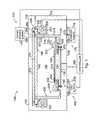
- FIG. 1is a schematic sectional side view of a substrate processing chamber having an embodiment of the process kit
- FIG. 2is a sectional side view of the process kit shown in FIG. 1 ;
- FIG. 3is a perspective view of the process kit of FIG. 2 ;
- FIG. 4Ais a perspective view of the retaining bracket for the anti-lift bracket
- FIG. 4Bis a perspective view of the backside of the support showing the positioned retaining bracket for the anti-lift bracket;
- FIG. 5is a perspective view of the anti-lift bracket sliding onto the holding post in a recessed pocket on a deposition ring which surrounds the substrate support;
- FIG. 6is a perspective view of the anti-lift bracket after it is fitted onto the holding post of the deposition ring which is around the substrate support;
- FIG. 7is an exploded perspective view of the anti-lift bracket sliding onto a ceramic isolator which couples to a prong of the restraint beam with a pin holding the assembly together;
- FIG. 8is a perspective view of the anti-lift bracket, ceramic isolator, pin, and restraint beam, as assembled onto a substrate support 130 ;
- FIG. 9is a top sectional view of a heat exchanger showing the polygonal conduit therein.
- FIG. 10is a graph of modeling results obtained for a scaled geometry of the process kit showing the thickness of deposits formed on the components as a function of distance from the substrate and support.
- FIG. 1An example of a suitable process chamber 100 capable of processing a substrate 104 is shown in FIG. 1 .
- the chamber 100comprises enclosure walls 108 that enclose a process zone 106 , the walls 108 including sidewalls 116 , a bottom wall 120 , and a ceiling 124 .
- the chamber 100can be a part of a multi-chamber platform (not shown) having a cluster of interconnected chambers connected by a robot arm mechanism that transfers substrates 104 between the chambers 106 .
- the process chamber 100comprises a sputter deposition chamber, also called a physical vapor deposition or PVD chamber, which is capable of sputter depositing material on a substrate 104 , such as one or more of tantalum, tantalum nitride, titanium, titanium nitride, copper, tungsten, tungsten nitride and aluminum.
- a sputter deposition chamberalso called a physical vapor deposition or PVD chamber, which is capable of sputter depositing material on a substrate 104 , such as one or more of tantalum, tantalum nitride, titanium, titanium nitride, copper, tungsten, tungsten nitride and aluminum.
- the chamber 100comprises a substrate support 130 to support the substrate 104 which comprises a pedestal 134 .
- the pedestal 134has a substrate receiving surface 138 that receives and supports the substrate 104 during processing, and may include an electrostatic chuck or a heater, such as an electrical resistance heater or heat exchanger (not shown).
- a substrate 104is introduced into the chamber 100 through a substrate loading inlet (not shown) in the sidewall 116 of the chamber 100 and placed on the substrate support 130 .
- the support 130can be lifted or lowered by support lift bellows and/or a lift finger assembly (not shown) can be used to lift and lower the substrate onto the support 130 during placement of a substrate 104 on the support 130 .
- the pedestal 134can be maintained at an electrically floating potential or grounded during plasma operation.
- the chamber 100further comprises a sputtering target 140 comprising a sputtering surface 142 facing the substrate 104 , which comprises the material to be sputtered onto the substrate 104 .
- the target 140is electrically isolated from the chamber 100 by an isolator 144 which is typically made from a dielectric or insulator material.
- the target 140is connected to a target power supply 148 which applies a bias voltage to the target 140 relative to a shield 150 which is in front of the walls of the chamber components, and/or the support 130 which is electrically floated.
- the target 140 , shield 150 , support 130 , and other chamber components connected to the target power supply 148operate as a gas energizer 152 to form a plasma of the sputtering gas.
- the gas energizer 152can also include a source coil 153 which is used to generate a plasma in the chamber 100 by application of a current through the coil. The generated plasma energetically impinges upon and bombards the sputtering surface 142 of the target 140 to sputter material off the surface 142 onto the substrate 104 .
- the sputtering gasis introduced into the chamber 100 through a gas delivery system 160 provides gas from a gas supply 162 via conduits 164 having gas flow control valves 166 , such as a mass flow controllers, to pass a set flow rate of the gas therethrough.
- the gasesare fed to a mixing manifold (also not shown) in which the gases are mixed to from a desired process gas composition and fed to a gas distributor 168 having gas outlets in the chamber 100 .
- the process gasmay comprise a non-reactive gas, such as argon or xenon, which is capable of energetically impinging upon and sputtering material from a target.
- the process gasmay also comprise a reactive gas, such as one or more of an oxygen-containing gas and a nitrogen-containing gas, that are capable of reacting with the sputtered material to form a layer on the substrate 104 .
- Spent process gas and byproductsare exhausted from the chamber 100 through an exhaust 170 which includes exhaust ports 172 that receive spent process gas and pass the spent gas to an exhaust conduit 174 having a throttle valve 176 to control the pressure of the gas in the chamber 100 .
- the exhaust conduit 174is connected to one or more exhaust pumps 178 .
- the pressure of the sputtering gas in the chamber 100is set to sub-atmospheric levels, such as a vacuum environment, for example, gas pressures of 1 mTorr to 400 mTorr.
- the chamber 100is controlled by a controller 180 that comprises program code having instruction sets to operate components of the chamber 100 to process substrates 104 in the chamber 100 .
- the controller 180can comprise program code that includes a substrate positioning instruction set to operate the substrate support 130 and substrate transport; a gas flow control instruction set to operate gas flow control valves to set a flow of sputtering gas to the chamber 100 ; a gas pressure control instruction set to operate the exhaust throttle valve to maintain a pressure in the chamber 100 ; a gas energizer control instruction set to operate the gas energizer to set a gas energizing power level; a temperature control instruction set to control a temperature control system to set temperatures of various components in the chamber 100 ; and a process monitoring instruction set to monitor the process in the chamber 100 .
- the chambercomprises a process kit 200 comprising various components that can be easily removed from the chamber 100 , for example, to clean sputtering deposits off the component surfaces, replace or repair eroded components, or to adapt the chamber for other processes.
- the process kit 200comprises a ring assembly 202 for placement about a peripheral wall 204 of the substrate support 130 that terminates before an overhanging edge 206 of the substrate.
- the ring assembly 202comprises a deposition ring 208 and a cover ring 212 that cooperate with one another to reduce formation of sputter deposits on the peripheral walls 204 of the support 130 or the overhanging edge 206 of the substrate 104 .
- the deposition ring 208comprises an annular band 216 that extends about and surrounds the peripheral wall 204 of the support 130 as shown in FIGS. 2 and 3 .
- the annular band 216comprises an inner lip 218 which extends transversely from the band and is substantially parallel to the peripheral wall 204 of the support 130 .
- the inner lip 218terminates immediately below the overhanging edge 206 of the substrate 104 .
- the inner lip 218defines an inner perimeter of the deposition ring 208 which surrounds the periphery of the substrate 104 and support 130 to protect regions of the support 130 that are not covered by the substrate 104 during processing.
- the inner lip 218surrounds and at least partially covers the peripheral wall 204 of the support 130 that would otherwise be exposed to the processing environment to reduce or even entirely preclude deposition of sputtering deposits on the peripheral wall 204 .
- the deposition ring 208can be easily removed to clean sputtering deposits from the exposed surfaces of the ring so that the support 130 does not have to be dismantled to be cleaned.
- the deposition ring 208can also serve to protect the exposed side surfaces of the support 130 to reduce their erosion by the energized plasma species.
- the deposition ring 208is typically made from a metal, such as stainless steel or aluminum, or can be made from a ceramic material, such as aluminum oxide.
- the annular band 216 of the deposition ring 208has a raised ridge 224 that extends along the central portion of the band 216 .
- the raised ridge 224has a flat top surface 228 which is spaced apart from the cover ring 212 to form a convoluted gap 229 therebetween which acts an a labyrinth to reduce penetration of plasma species into the convoluted gap.
- An open inner channel 230lies between the inner lip 218 and the raised ridge 224 .
- the open inner channel 230extends radially inward to terminate at least partially below the overhanging edge 206 of the substrate 104 .
- the inner channel 230has a first rounded corner 232 joining to the inner lip 218 and a gently sloped surface 234 joining to the raised ridge 224 .
- the smooth corner 232 and sloped surface 234facilitate the removal of sputtering deposits from these portions during cleaning of the deposition ring 208 .
- the deposition ring 208also has a ledge 236 which is located radially outward of the raised ridge 224 and serves to support the cover ring 212 .
- a U-shaped channel 237is provided between the raised ridge 224 and the ledge 236 to form a convoluted passageway therebetween which further prevents the flow the passage of plasma or gaseous species though the passageway thereby reducing the deposition of process deposits in the regions radially outward of the passageway.
- the contour and profile of the deposition ringis shaped to reduce passage of process deposits through these regions.
- pinsare not needed in the deposition ring 208 to retain the substrate 104 in the event that the substrate 104 slides or is misplaced in the chamber 100 , due to accurate positioning of the substrate in the chamber during its transportation into the chamber.
- the cover ring 212 of the ring assembly 202encircles and at least partially covers the deposition ring 208 to receive, and thus, shadow the deposition ring 208 from the bulk of the sputtering deposits.
- the cover ring 212is fabricated from a material that can resist erosion by the sputtering plasma, for example, a metallic material such as stainless steel, titanium or aluminum, or a ceramic material, such as aluminum oxide. In one version, the cover ring 212 is fabricated from titanium.
- the cover ring 212comprises an annular wedge 244 which has a footing 246 which rests on the ledge 236 of the deposition ring 208 to support the cover ring 212 . The footing 246 extends downwardly from the wedge 244 to press against the deposition ring 208 substantially without cracking or fracturing the ring 208 .
- the annular wedge 244 of the cover ring 212has an inclined surface 248 that serves as a boundary to contain the sputtering plasma within the process zone between the target and the support 130 .
- the inclined surface 248provides a smooth and continuous surface on which sputtering deposits can deposit and be easily removed.
- the inclined surface 248is inclined at an angle relative to an axis which is perpendicular to the flat plane formed by the processing surface of the substrate 104 . In one version, the angle is at least about 60°, and can be even from about 65 to about 85°, or even about 80°.
- the angle of the inclined surface of the cover ring 212is designed to minimize the buildup of sputter deposits nearest to the overhanging edge 206 of the substrate 104 , which would otherwise negatively impact the deposition uniformity obtained across the substrate 104 .
- the inclined surface 248extends continuously from an outer cylindrical wall 260 b to the edge of a projecting brim 252 .
- the wedge 244tapers to the projecting brim 252 which overlies the inner channel 230 of the deposition ring 208 .
- the projecting brim 252terminates in a rounded edge 256 and has a planar bottom surface 268 .
- the projecting brim 252reduces deposition of sputtering deposits on the open inner channel of the deposition ring 208 .
- the projecting brim 252projects a distance corresponding to at least about half the width of the open inner channel of the deposition ring 208 . For example, if the inner channel 230 has a width of at least about 12 mm, the projecting brim 252 has a width of at least about 6 mm.
- the projecting brim 252projects over the open inner channel 230 of the deposition ring 208 to reach closer to the peripheral edge 206 of the substrate cover a portion of the open inner channel 230 of the deposition ring 208 .
- the projecting brim 252has a raised ridge 253 which extends downwardly and has an external shape with a profile which matches and follows the contour of the surface 234 of the underlying deposition ring 208 . This shaped and closely matching contoured features inhibit the deposition of sputtering deposits on the peripheral overhang edge 206 of the substrate and also reduces deposits on the peripheral walls 204 of the support 130 .
- the contour of the raised ridge of the projecting brim 252is sized, shaped, and positioned to cooperate with and complement the open inner channel 230 of the deposition ring 208 to form a convoluted and constricted flow path between the cover ring 212 and deposition ring 208 to inhibit the flow of process deposits onto the peripheral edge 204 .
- the constricted flow pathalso restricts the build-up of low-energy sputter deposits on the mating surfaces of the deposition ring 208 and cover ring 212 , which would otherwise cause them to stick to one another or to the peripheral overhang edge 206 of the substrate 104 .
- the open inner channel 230 of the deposition ring 208 which extends underneath the substrate overhang edge 206is designed in conjunction with shadowing from the projecting brim 252 of the cover ring 208 to collect, for example, a minimum of 3900 ⁇ m of aluminum sputter deposits in an aluminum sputtering chamber 100 , while reducing or even substantially precluding sputter deposition on the mating surfaces of the two rings 208 , 212 .
- the cover ring 212also has a pair of cylindrical walls 260 that extend downwardly from the annular wedge 244 .
- the cylindrical walls 260are located radially outward of the footing 246 of the wedge 244 .
- the cylindrical walls 260comprise an inner wall 260 a and the outer wall 260 b , the inner wall 260 a having a smaller height than the outer wall 260 b .
- the radially internal surface 262 of the inner wall 260 ais sloped to match a slope angle of the radially outer surface 264 of the deposition ring 208 to form yet another convoluted pathway 266 which impedes travel of plasma species and glow discharges to the surrounding area.
- the height of the outer wall 260 ais at least about 1.2 times the height of the inner wall 260 b .
- the height of the outer wall 160 ais from about 25 mm
- the height of the inner wall 260 bis from about 19 mm.
- the process kit 200also includes an anti-lift bracket 270 is used to retain the deposition ring 208 about the periphery of the substrate support 130 in the chamber 100 , as shown in FIGS. 3-6 .
- the anti-lift bracket 270cooperates with additional structural features of the deposition ring 208 and support 130 .
- the deposition ring 208comprises two peripheral recessed pockets 274 with holding posts 278 extending out from the pockets 274 to receive a pair of anti-lift brackets 270 on either side, one side being shown in FIG. 5 .
- the pairs of pocketsare located diametrically opposing one another across the support 130 .
- a restraint beam 280is also mounted on a backside surface 276 of the support 130 to hold onto the anti-lift bracket 270 , as shown in FIGS. 4A and 4B .
- the restraint beam 280comprises two opposing flat prongs 282 a,b which extend radially outward of a circular ring 284 in the backside surface 276 of the support 130 .
- the two opposing flat prongs 282 a,bare mounted on the vertical arms 286 a,b which are joined to the circular ring 284 .
- the circular ring 284is shaped and sized to fit into a recess 287 in the backside of the support 130 .
- the anti-lift bracket 270comprises a block 290 comprising a through-channel 294 which receives a prong end 282 a of the restraint beam 280 as shown in FIGS. 5 and 6 .
- the through-channel 294comprises an oval shaped slot 296 sized larger than the prong 282 a of the restraint beam 280 .
- a retaining hoop 298 attached to the block 290is sized to slide over a holding post 278 in a recessed pocket 274 of the deposition ring 208 .
- the anti-lift bracket 270is brought alongside the outer periphery of the deposition ring 208 and the slot 296 of the through-channel 294 is slid onto a prong 282 of the restraint beam 280 as shown by the arrows 283 so that the access hole 299 of the retaining hoop 298 is directly above the holding post 278 as shown in FIG. 5 .
- the anti-lift bracket 274is then lowered, as shown by the arrow 285 , so that the retaining hoop 298 drops down and encircles the holding post 278 allowing the weight of the block 290 of the bracket 270 to stably hold down the deposition ring 208 as shown in FIG. 6 .
- the anti-lift bracket 270only engages the restraint beam 280 when the deposition ring 208 is pulled upwards, for example, when the deposition ring becomes stuck to the substrate 104 . This design minimizes the thermal and mechanical strain on the ceramic deposition ring 208 and cover ring 212 in normal use.
- FIGS. 7 and 8Another version of an assembly comprising the anti-lift bracket 270 which is used to retain the deposition ring 208 about the periphery of the substrate support 130 in the chamber 100 , is shown in FIGS. 7 and 8 .
- the anti-lift bracket 270is attached to a ceramic isolator 400 which then couples to a flat prongs 282 a,b of the restraint beam 280 .
- the anti-lift bracket 270slides onto a ledge 402 which extends out of a block 404 of the ceramic isolator 400 .
- the ceramic isolator 400serves to electrically isolate the restraint beam 280 from the other components by providing an insulating member in the electrical pathway between the support 130 and the deposition ring 208 .
- the block 404 of the ceramic isolator 400also has a recessed surface 408 for resting the restraint beam 280 .
- a through-hole 410 in the block 404is provided for the pin 414 to connect the ceramic isolator 400 to the matching holes 422 a,b in the facing and parallel extensions 420 a,b of the prong 282 a of the restraint beam 280 .
- the pin 414has two reduced diameter posts 418 a,b which are passed through the through hole and a flat edge which rests against the surface of the parallel extensions 420 a,b of the prong 282 a .
- the pin 414can be made from a metal, such as stainless steel.
- the ledge 402 of the ceramic isolatorextends radially outward from the block 404 and has a protrusion 424 which acts as a stop against a receiving surface 430 of the anti-lift bracket 270 .
- the ceramic isolator 400is typically machine from a ceramic, such as aluminum oxide. It should be noted that while one ceramic structure is described, other ceramic structures blocks can also be placed in the pathway between the restraint beam 280 and the anti-lift bracket 270 to further isolate the structures, such as a ceramic block (not shown) placed between the beam 280 and the substrate support 130 at their interface.
- the process kit 200also includes a unitary cylindrical shield 150 that encircles the sputtering surface of a sputtering target that faces the substrate support 130 , the outer periphery of the substrate support 130 , and the shadows the sidewalls 116 of the chamber 100 .
- the shield 150serves to reduce deposition of sputtering deposits originating from the sputtering surface of the sputtering target 140 on the surfaces of support 130 , and the sidewalls 116 and bottom wall 120 of the chamber 100 .
- the shield 150comprises a cylindrical outer band 314 having a diameter sized to encircle the sputtering surface 142 of the sputtering target 140 and the substrate support 130 .
- the outer band 314has an upper end 316 and a bottom end 318 .
- the upper end 316has a radially outwardly tapered surface 320 adjacent to a sloped peripheral surface 322 of the sputtering target 140 .
- the shield 150further comprises a base plane 324 extending radially inward from the bottom end 318 of the outer band 314 to join a cylindrical inner band 328 that at least partially surrounds the peripheral edge 204 of the substrate support 130 .
- the inner band 328comprises a height that is smaller than the outer band 314 , for example, the inner band 328 has a height which is 0.8 times smaller than the height of the outer band 314 .
- the gaps between the inner and outer bands 328 , 314 , respectively, and the outer wall 260 b and inner wall 260 a of the cover ring 212again serve to hinder and impede ingress of plasma species into this region.
- the outer band 314 , base plate 324 and inner band 328 of the unitary shield 150comprise a unitary monolith structure that is a single piece.
- the entire shield 150can be made from 300 series stainless steel. This is advantageous over prior shields which included multiple components, often two or three separate pieces to make up the complete shield, which makes it more difficult and laborious to remove the shield for cleaning.
- the single piece shield 150has a continuous surface 326 exposed to the sputtering deposits without interfaces or corners that are more difficult to clean out.
- the single piece shield 150is more thermally uniform than multiple shields, both for heating during the periodic maintenance as well as cooling during process when the plasma is heating the shield/s.
- the single piece shield 150has only one thermal interface to the heat exchanger 330 .
- the single piece shield 150also shields the chamber walls 108 from sputter deposition during process cycles.
- the shield 150also creates a contoured gap in the region of the target 140 referred to as the “darkspace” to help shape the plasma while preventing arcing between target 140 and chamber 100 .
- a heat exchanger 330was used to cool the shield 150 to reduce the thermal expansion stresses. Portions of the shield 150 can become excessively heated by exposure to the plasma formed in the substrate processing chamber. Excessive heating of the shield 150 results in its thermal expansion which causes sputtering deposits formed on the shield to flake off from the shield to fall upon and contaminate the substrate 104 .
- the heat exchanger 330comprises a plate 332 made of metal, such as stainless steel.
- the plate 332has an inner perimeter 335 comprising a circular aperture 336 sized to fit around the cylindrical shield 150 , and an outer perimeter 338 comprising hexagonal sides 340 , as shown in FIG. 9 .
- the heat exchanger 330has a polygon conduit 334 to flow heat exchange fluid from a fluid source (not shown) therethrough to cool the plate 332 .
- the polygon conduit 334comprises a plurality of legs 344 that are interconnected in a polygonal pattern around the circular aperture 336 .
- the legs 344 a - hwhich are each drilled at an acute angle starting from a hexagonal side 340 of the outer perimeter of the plate 332 , the acute angles being from about 20 to about 45°.
- the conduit 334also comprises channels 342 a - c that are each covered by a cover plate 345 a - c which has an oval O-ring 347 a - c in a groove 349 a - c in the plate 345 a - c to seal the interface.
- the polygonal conduit 334also has an inlet 346 and outlet 348 to receive and pass out the heat exchange fluid.
- the inlet and outlet 346 , 348comprise channels 352 a,b that feed into a manifold 350 .
- the heat exchange fluidis flowed through the polygonal conduit 334 to exchange heat with the shield 150 and control its temperature.
- a suitable heat exchange fluidmay be, for example, water.
- Controlling the temperature of the shield 150reduces expansion of the shield in the plasma environment limiting the flaking of the sputtering deposits from the shield.
- Fastening the shield 150 to the heat exchanger 330provides better heat transfer between the shield and the heat exchanger plate.
- the shield 150is fastened to the heat exchanger by a fastener 358 , and in this version, the shield comprises a ledge 360 having a substantially vertical opening 362 extending therethrough.
- the fastener 358is shaped and sized to pass through the opening 362 in the ledge 360 to fasten the shield 150 to the heat exchanger 330 .
- the heat exchanger 330integrates the source coil 153 and target 140 to the chamber 100 while also holding the shield 150 . Water-cooling also provides greater thermal stability of the single piece shield 150 during the process.
- the sputtering target 140comprises a backing plate 370 , typically made from a high strength aluminum alloy, which supports a sputtering plate 374 comprising the sputtering surface 142 .
- the backing plate 370 of the target 140is separated and the electrically isolated from the chamber 100 by the isolator 144 which is typically a ring made from a ceramic material, such as aluminum oxide.
- the sputtering plate 374is composed of a high purity sputtering material to be sputtered onto the substrate 104 , such as for example, aluminum, tantalum, titanium, and other such metals, typically at a purity of 99.99% or higher.
- the sputtering plate 374comprises a perimeter with a sloped edge 322 adjacent to the sloped surface 320 of the shield 150 , which defines a gap 380 therebetween which serves as another plasma retarding convoluted labyrinth.
- the backplate of the target 140comprises a peripheral ledge 390 which extends beyond the radius of the sputtering plate 374 .
- the peripheral ledge 390supports the target 140 by resting on the isolator 144 and can be fastened to the isolator 144 or the chamber sidewall 116 .
- the peripheral ledge 390extends beyond the sloped edge 322 of the sputtering plate 374 and comprises an outer footing section 392 which rests on the isolator 144 in the chamber 100 .
- the peripheral ledge 390comprises an inner bump 394 which is shaped and sized to reduce deposition of sputtering deposits on the isolator 144 and shield 150 .
- the bump 394in combination with a preceding groove 396 reduces plasma formation and the deposition of sputtering process deposits on undesired areas of the chamber walls 108 , isolator 144 and heat exchanger 330 .
- the bump 394is shaped, sized and positioned to inhibit the flow or migration of plasma and sputtered species through the gap between the target 140 and the isolator 144 .
- the bump 394impedes the penetration of low-angle sputtered deposits into the gap between the target and the isolator.
- the bump 394comprises a curved cross-section with a height of from about 1.5 to about 2 mm.
- the various components of the process kit 200 and the target 140significantly increase the number of process cycles and process on-time that the process kit can be used in the chamber without removing the process kit for cleaning. This is accomplished by reducing the amount of sputtering deposits formed on the components around the substrate which are difficult to clean.
- the components of the process kit 200 and target 140are designed to allow increased power and pressure in the sputtering zone 106 to yield higher deposition throughput by reducing the temperature in the darkspace region which is near the upper end 316 of the shield 150 and near the target 140 . It also improves the thermal uniformity of the shield 150 using the heat exchanger 330 .
- the process kit 200is designed to allow at least 85% more aluminum to be deposited in the chamber 100 before the kit 200 has to be changed, and therefore a maintenance cycle performed. This is a significant improvement in the uptime of the chamber and also increases process throughput.
- FIG. 10is a graph of modeling results obtained for a scaled geometry of the process kit in aluminum sputter deposition showing the thickness of deposits formed on the deposition ring 208 and cover ring 212 as a function of distance from the substrate 104 and support 130 .
- the modeling programwas PVD ProTM program and it uses parameters for the type of metal being deposited as well as the geometry of the target and other chamber components.
- the modelallowed the comparison of several different configurations for the features of, and position of the cover ring 212 and deposition ring 208 . This allowed optimization for minimum buildup of aluminum deposits on the surfaces of the groove 230 in the deposition ring 208 , as well as in the line of sight of the edge 252 of the cover ring 212 .
- the modeling accuracywas determined with a test run of prototype hardware, and also by modeling geometry of known performance, to obtain the designs presented herein. It is seen that changing the shape and design configurations of the chamber components and the spaces and gaps therebetween, significantly changed the thickness of deposition material on the surfaces of the components. Further, the rate of increase in the amount of deposition on the deposition ring remained at about the same for increasing distance from the substrate center as shown by the same angle of the linear sections of the graph between 0.5 and 1.5 on the x-axis. There is a vertical change in the net amount of deposition for different configurations, but the shape of the curve remains essentially the same.
- the present inventionhas been described with reference to certain preferred versions thereof; however, other versions are possible.
- the process kit 200 and ring assembly 202can be used in other types of applications, as would be apparent to one of ordinary skill, for example, etching, CVD and etching chambers.
- Other shapes and configurations of the deposition ring 208 , cover ring 212 , shield 150 and anti-lift bracket 270can also be used. Therefore, the spirit and scope of the appended claims should not be limited to the description of the preferred versions contained herein.
Landscapes
- Chemical & Material Sciences (AREA)
- Engineering & Computer Science (AREA)
- Physics & Mathematics (AREA)
- Plasma & Fusion (AREA)
- Analytical Chemistry (AREA)
- Chemical Kinetics & Catalysis (AREA)
- Materials Engineering (AREA)
- Mechanical Engineering (AREA)
- Metallurgy (AREA)
- Organic Chemistry (AREA)
- Condensed Matter Physics & Semiconductors (AREA)
- General Physics & Mathematics (AREA)
- Manufacturing & Machinery (AREA)
- Computer Hardware Design (AREA)
- Microelectronics & Electronic Packaging (AREA)
- Power Engineering (AREA)
- Physical Vapour Deposition (AREA)
- Drying Of Semiconductors (AREA)
- Chemical Vapour Deposition (AREA)
- Physical Deposition Of Substances That Are Components Of Semiconductor Devices (AREA)
Abstract
Description
Claims (25)
Priority Applications (10)
| Application Number | Priority Date | Filing Date | Title |
|---|---|---|---|
| US11/553,982US9127362B2 (en) | 2005-10-31 | 2006-10-27 | Process kit and target for substrate processing chamber |
| DE102006051443ADE102006051443A1 (en) | 2005-10-31 | 2006-10-31 | Process equipment and target object for a substrate processing chamber |
| TW095140305ATWI435941B (en) | 2005-10-31 | 2006-10-31 | Process kit and target for substrate processing chamber |
| CN2006101366947ACN101089220B (en) | 2005-10-31 | 2006-10-31 | Process kit and target for substrate processing chamber |
| CN201310053011.1ACN103147049B (en) | 2005-10-31 | 2006-10-31 | Process kit and target for substrate processing chamber |
| JP2006296371AJP2007146290A (en) | 2005-10-31 | 2006-10-31 | Process kit and target for substrate processing chamber |
| KR1020060106729AKR101322342B1 (en) | 2005-10-31 | 2006-10-31 | Process kit and target for substrate processing chamber |
| KR1020130042352AKR101394085B1 (en) | 2005-10-31 | 2013-04-17 | Target and process kit for substrate processing chamber |
| US14/846,951US10347475B2 (en) | 2005-10-31 | 2015-09-07 | Holding assembly for substrate processing chamber |
| US16/409,757US11658016B2 (en) | 2005-10-31 | 2019-05-10 | Shield for a substrate processing chamber |
Applications Claiming Priority (2)
| Application Number | Priority Date | Filing Date | Title |
|---|---|---|---|
| US73232405P | 2005-10-31 | 2005-10-31 | |
| US11/553,982US9127362B2 (en) | 2005-10-31 | 2006-10-27 | Process kit and target for substrate processing chamber |
Related Child Applications (1)
| Application Number | Title | Priority Date | Filing Date |
|---|---|---|---|
| US14/846,951DivisionUS10347475B2 (en) | 2005-10-31 | 2015-09-07 | Holding assembly for substrate processing chamber |
Publications (2)
| Publication Number | Publication Date |
|---|---|
| US20070102286A1 US20070102286A1 (en) | 2007-05-10 |
| US9127362B2true US9127362B2 (en) | 2015-09-08 |
Family
ID=37989705
Family Applications (3)
| Application Number | Title | Priority Date | Filing Date |
|---|---|---|---|
| US11/553,982Active2032-05-04US9127362B2 (en) | 2005-10-31 | 2006-10-27 | Process kit and target for substrate processing chamber |
| US14/846,951Active2028-09-27US10347475B2 (en) | 2005-10-31 | 2015-09-07 | Holding assembly for substrate processing chamber |
| US16/409,757Active2027-04-08US11658016B2 (en) | 2005-10-31 | 2019-05-10 | Shield for a substrate processing chamber |
Family Applications After (2)
| Application Number | Title | Priority Date | Filing Date |
|---|---|---|---|
| US14/846,951Active2028-09-27US10347475B2 (en) | 2005-10-31 | 2015-09-07 | Holding assembly for substrate processing chamber |
| US16/409,757Active2027-04-08US11658016B2 (en) | 2005-10-31 | 2019-05-10 | Shield for a substrate processing chamber |
Country Status (6)
| Country | Link |
|---|---|
| US (3) | US9127362B2 (en) |
| JP (1) | JP2007146290A (en) |
| KR (2) | KR101322342B1 (en) |
| CN (2) | CN103147049B (en) |
| DE (1) | DE102006051443A1 (en) |
| TW (1) | TWI435941B (en) |
Cited By (301)
| Publication number | Priority date | Publication date | Assignee | Title |
|---|---|---|---|---|
| US9502223B2 (en) | 2011-12-12 | 2016-11-22 | Canon Anelva Corporation | Sputtering apparatus, target and shield |
| US9818585B2 (en) | 2009-02-27 | 2017-11-14 | Applied Materials, Inc. | In situ plasma clean for removal of residue from pedestal surface without breaking vacuum |
| US10017855B2 (en) | 2014-12-22 | 2018-07-10 | Applied Materials, Inc. | Process kit for a high throughput processing chamber |
| US10113231B2 (en) | 2015-04-24 | 2018-10-30 | Applied Materials, Inc. | Process kit including flow isolator ring |
| US20200083068A1 (en)* | 2018-09-11 | 2020-03-12 | Asm Ip Holding B.V. | Substrate processing apparatus and method |
| US10844484B2 (en) | 2017-09-22 | 2020-11-24 | Asm Ip Holding B.V. | Apparatus for dispensing a vapor phase reactant to a reaction chamber and related methods |
| US10844486B2 (en) | 2009-04-06 | 2020-11-24 | Asm Ip Holding B.V. | Semiconductor processing reactor and components thereof |
| US10847366B2 (en) | 2018-11-16 | 2020-11-24 | Asm Ip Holding B.V. | Methods for depositing a transition metal chalcogenide film on a substrate by a cyclical deposition process |
| US10851456B2 (en) | 2016-04-21 | 2020-12-01 | Asm Ip Holding B.V. | Deposition of metal borides |
| US10858737B2 (en) | 2014-07-28 | 2020-12-08 | Asm Ip Holding B.V. | Showerhead assembly and components thereof |
| US10867788B2 (en) | 2016-12-28 | 2020-12-15 | Asm Ip Holding B.V. | Method of forming a structure on a substrate |
| US10867786B2 (en) | 2018-03-30 | 2020-12-15 | Asm Ip Holding B.V. | Substrate processing method |
| US10883175B2 (en) | 2018-08-09 | 2021-01-05 | Asm Ip Holding B.V. | Vertical furnace for processing substrates and a liner for use therein |
| US10886123B2 (en) | 2017-06-02 | 2021-01-05 | Asm Ip Holding B.V. | Methods for forming low temperature semiconductor layers and related semiconductor device structures |
| US10892156B2 (en) | 2017-05-08 | 2021-01-12 | Asm Ip Holding B.V. | Methods for forming a silicon nitride film on a substrate and related semiconductor device structures |
| US10910262B2 (en) | 2017-11-16 | 2021-02-02 | Asm Ip Holding B.V. | Method of selectively depositing a capping layer structure on a semiconductor device structure |
| US10914004B2 (en) | 2018-06-29 | 2021-02-09 | Asm Ip Holding B.V. | Thin-film deposition method and manufacturing method of semiconductor device |
| US10923344B2 (en) | 2017-10-30 | 2021-02-16 | Asm Ip Holding B.V. | Methods for forming a semiconductor structure and related semiconductor structures |
| US10928731B2 (en) | 2017-09-21 | 2021-02-23 | Asm Ip Holding B.V. | Method of sequential infiltration synthesis treatment of infiltrateable material and structures and devices formed using same |
| US10934619B2 (en) | 2016-11-15 | 2021-03-02 | Asm Ip Holding B.V. | Gas supply unit and substrate processing apparatus including the gas supply unit |
| US10941490B2 (en) | 2014-10-07 | 2021-03-09 | Asm Ip Holding B.V. | Multiple temperature range susceptor, assembly, reactor and system including the susceptor, and methods of using the same |
| US10943771B2 (en) | 2016-10-26 | 2021-03-09 | Asm Ip Holding B.V. | Methods for thermally calibrating reaction chambers |
| US10950432B2 (en) | 2017-04-25 | 2021-03-16 | Asm Ip Holding B.V. | Method of depositing thin film and method of manufacturing semiconductor device |
| USD913980S1 (en) | 2018-02-01 | 2021-03-23 | Asm Ip Holding B.V. | Gas supply plate for semiconductor manufacturing apparatus |
| US10975470B2 (en) | 2018-02-23 | 2021-04-13 | Asm Ip Holding B.V. | Apparatus for detecting or monitoring for a chemical precursor in a high temperature environment |
| US11004977B2 (en) | 2017-07-19 | 2021-05-11 | Asm Ip Holding B.V. | Method for depositing a group IV semiconductor and related semiconductor device structures |
| US11001925B2 (en) | 2016-12-19 | 2021-05-11 | Asm Ip Holding B.V. | Substrate processing apparatus |
| US11015245B2 (en) | 2014-03-19 | 2021-05-25 | Asm Ip Holding B.V. | Gas-phase reactor and system having exhaust plenum and components thereof |
| US11018002B2 (en) | 2017-07-19 | 2021-05-25 | Asm Ip Holding B.V. | Method for selectively depositing a Group IV semiconductor and related semiconductor device structures |
| US11018047B2 (en) | 2018-01-25 | 2021-05-25 | Asm Ip Holding B.V. | Hybrid lift pin |
| US11022879B2 (en) | 2017-11-24 | 2021-06-01 | Asm Ip Holding B.V. | Method of forming an enhanced unexposed photoresist layer |
| US11031242B2 (en) | 2018-11-07 | 2021-06-08 | Asm Ip Holding B.V. | Methods for depositing a boron doped silicon germanium film |
| USD922229S1 (en) | 2019-06-05 | 2021-06-15 | Asm Ip Holding B.V. | Device for controlling a temperature of a gas supply unit |
| US11049751B2 (en) | 2018-09-14 | 2021-06-29 | Asm Ip Holding B.V. | Cassette supply system to store and handle cassettes and processing apparatus equipped therewith |
| US11056344B2 (en) | 2017-08-30 | 2021-07-06 | Asm Ip Holding B.V. | Layer forming method |
| US11056567B2 (en) | 2018-05-11 | 2021-07-06 | Asm Ip Holding B.V. | Method of forming a doped metal carbide film on a substrate and related semiconductor device structures |
| US11053591B2 (en) | 2018-08-06 | 2021-07-06 | Asm Ip Holding B.V. | Multi-port gas injection system and reactor system including same |
| US11069510B2 (en) | 2017-08-30 | 2021-07-20 | Asm Ip Holding B.V. | Substrate processing apparatus |
| US11081345B2 (en) | 2018-02-06 | 2021-08-03 | Asm Ip Holding B.V. | Method of post-deposition treatment for silicon oxide film |
| US11088002B2 (en) | 2018-03-29 | 2021-08-10 | Asm Ip Holding B.V. | Substrate rack and a substrate processing system and method |
| US11087997B2 (en) | 2018-10-31 | 2021-08-10 | Asm Ip Holding B.V. | Substrate processing apparatus for processing substrates |
| US11094582B2 (en) | 2016-07-08 | 2021-08-17 | Asm Ip Holding B.V. | Selective deposition method to form air gaps |
| US11094546B2 (en) | 2017-10-05 | 2021-08-17 | Asm Ip Holding B.V. | Method for selectively depositing a metallic film on a substrate |
| US11101370B2 (en) | 2016-05-02 | 2021-08-24 | Asm Ip Holding B.V. | Method of forming a germanium oxynitride film |
| US11107676B2 (en) | 2016-07-28 | 2021-08-31 | Asm Ip Holding B.V. | Method and apparatus for filling a gap |
| US11114283B2 (en) | 2018-03-16 | 2021-09-07 | Asm Ip Holding B.V. | Reactor, system including the reactor, and methods of manufacturing and using same |
| US11114294B2 (en) | 2019-03-08 | 2021-09-07 | Asm Ip Holding B.V. | Structure including SiOC layer and method of forming same |
| USD930782S1 (en) | 2019-08-22 | 2021-09-14 | Asm Ip Holding B.V. | Gas distributor |
| US11127617B2 (en) | 2017-11-27 | 2021-09-21 | Asm Ip Holding B.V. | Storage device for storing wafer cassettes for use with a batch furnace |
| US11127589B2 (en) | 2019-02-01 | 2021-09-21 | Asm Ip Holding B.V. | Method of topology-selective film formation of silicon oxide |
| USD931978S1 (en) | 2019-06-27 | 2021-09-28 | Asm Ip Holding B.V. | Showerhead vacuum transport |
| US11139191B2 (en) | 2017-08-09 | 2021-10-05 | Asm Ip Holding B.V. | Storage apparatus for storing cassettes for substrates and processing apparatus equipped therewith |
| US11139308B2 (en) | 2015-12-29 | 2021-10-05 | Asm Ip Holding B.V. | Atomic layer deposition of III-V compounds to form V-NAND devices |
| US11158513B2 (en) | 2018-12-13 | 2021-10-26 | Asm Ip Holding B.V. | Methods for forming a rhenium-containing film on a substrate by a cyclical deposition process and related semiconductor device structures |
| US11164955B2 (en) | 2017-07-18 | 2021-11-02 | Asm Ip Holding B.V. | Methods for forming a semiconductor device structure and related semiconductor device structures |
| USD935572S1 (en) | 2019-05-24 | 2021-11-09 | Asm Ip Holding B.V. | Gas channel plate |
| US11171025B2 (en) | 2019-01-22 | 2021-11-09 | Asm Ip Holding B.V. | Substrate processing device |
| US11168395B2 (en) | 2018-06-29 | 2021-11-09 | Asm Ip Holding B.V. | Temperature-controlled flange and reactor system including same |
| US11205585B2 (en) | 2016-07-28 | 2021-12-21 | Asm Ip Holding B.V. | Substrate processing apparatus and method of operating the same |
| US11217444B2 (en) | 2018-11-30 | 2022-01-04 | Asm Ip Holding B.V. | Method for forming an ultraviolet radiation responsive metal oxide-containing film |
| USD940837S1 (en) | 2019-08-22 | 2022-01-11 | Asm Ip Holding B.V. | Electrode |
| US11222772B2 (en) | 2016-12-14 | 2022-01-11 | Asm Ip Holding B.V. | Substrate processing apparatus |
| US11227789B2 (en) | 2019-02-20 | 2022-01-18 | Asm Ip Holding B.V. | Method and apparatus for filling a recess formed within a substrate surface |
| US11227782B2 (en) | 2019-07-31 | 2022-01-18 | Asm Ip Holding B.V. | Vertical batch furnace assembly |
| US11233133B2 (en) | 2015-10-21 | 2022-01-25 | Asm Ip Holding B.V. | NbMC layers |
| US11232963B2 (en) | 2018-10-03 | 2022-01-25 | Asm Ip Holding B.V. | Substrate processing apparatus and method |
| US11230766B2 (en) | 2018-03-29 | 2022-01-25 | Asm Ip Holding B.V. | Substrate processing apparatus and method |
| US11242598B2 (en) | 2015-06-26 | 2022-02-08 | Asm Ip Holding B.V. | Structures including metal carbide material, devices including the structures, and methods of forming same |
| US11251035B2 (en) | 2016-12-22 | 2022-02-15 | Asm Ip Holding B.V. | Method of forming a structure on a substrate |
| US11251040B2 (en) | 2019-02-20 | 2022-02-15 | Asm Ip Holding B.V. | Cyclical deposition method including treatment step and apparatus for same |
| US11251068B2 (en) | 2018-10-19 | 2022-02-15 | Asm Ip Holding B.V. | Substrate processing apparatus and substrate processing method |
| USD944946S1 (en) | 2019-06-14 | 2022-03-01 | Asm Ip Holding B.V. | Shower plate |
| US11270899B2 (en) | 2018-06-04 | 2022-03-08 | Asm Ip Holding B.V. | Wafer handling chamber with moisture reduction |
| US11274369B2 (en) | 2018-09-11 | 2022-03-15 | Asm Ip Holding B.V. | Thin film deposition method |
| US11282698B2 (en) | 2019-07-19 | 2022-03-22 | Asm Ip Holding B.V. | Method of forming topology-controlled amorphous carbon polymer film |
| US11286558B2 (en) | 2019-08-23 | 2022-03-29 | Asm Ip Holding B.V. | Methods for depositing a molybdenum nitride film on a surface of a substrate by a cyclical deposition process and related semiconductor device structures including a molybdenum nitride film |
| US11286562B2 (en) | 2018-06-08 | 2022-03-29 | Asm Ip Holding B.V. | Gas-phase chemical reactor and method of using same |
| US11289326B2 (en) | 2019-05-07 | 2022-03-29 | Asm Ip Holding B.V. | Method for reforming amorphous carbon polymer film |
| US11289312B2 (en) | 2019-06-12 | 2022-03-29 | Applied Materials, Inc. | Physical vapor deposition (PVD) chamber with in situ chamber cleaning capability |
| US11296189B2 (en) | 2018-06-21 | 2022-04-05 | Asm Ip Holding B.V. | Method for depositing a phosphorus doped silicon arsenide film and related semiconductor device structures |
| US11295980B2 (en) | 2017-08-30 | 2022-04-05 | Asm Ip Holding B.V. | Methods for depositing a molybdenum metal film over a dielectric surface of a substrate by a cyclical deposition process and related semiconductor device structures |
| USD947913S1 (en) | 2019-05-17 | 2022-04-05 | Asm Ip Holding B.V. | Susceptor shaft |
| US20220108872A1 (en)* | 2020-10-05 | 2022-04-07 | Applied Materials, Inc. | Bevel backside deposition elimination |
| USD948463S1 (en) | 2018-10-24 | 2022-04-12 | Asm Ip Holding B.V. | Susceptor for semiconductor substrate supporting apparatus |
| US11306395B2 (en) | 2017-06-28 | 2022-04-19 | Asm Ip Holding B.V. | Methods for depositing a transition metal nitride film on a substrate by atomic layer deposition and related deposition apparatus |
| USD949319S1 (en)* | 2019-08-22 | 2022-04-19 | Asm Ip Holding B.V. | Exhaust duct |
| US11315794B2 (en) | 2019-10-21 | 2022-04-26 | Asm Ip Holding B.V. | Apparatus and methods for selectively etching films |
| US11342216B2 (en) | 2019-02-20 | 2022-05-24 | Asm Ip Holding B.V. | Cyclical deposition method and apparatus for filling a recess formed within a substrate surface |
| US11339476B2 (en) | 2019-10-08 | 2022-05-24 | Asm Ip Holding B.V. | Substrate processing device having connection plates, substrate processing method |
| US11345999B2 (en) | 2019-06-06 | 2022-05-31 | Asm Ip Holding B.V. | Method of using a gas-phase reactor system including analyzing exhausted gas |
| US11355338B2 (en) | 2019-05-10 | 2022-06-07 | Asm Ip Holding B.V. | Method of depositing material onto a surface and structure formed according to the method |
| US11361990B2 (en) | 2018-05-28 | 2022-06-14 | Asm Ip Holding B.V. | Substrate processing method and device manufactured by using the same |
| US11374112B2 (en) | 2017-07-19 | 2022-06-28 | Asm Ip Holding B.V. | Method for depositing a group IV semiconductor and related semiconductor device structures |
| US11378337B2 (en) | 2019-03-28 | 2022-07-05 | Asm Ip Holding B.V. | Door opener and substrate processing apparatus provided therewith |
| US11387120B2 (en) | 2017-09-28 | 2022-07-12 | Asm Ip Holding B.V. | Chemical dispensing apparatus and methods for dispensing a chemical to a reaction chamber |
| US11387106B2 (en) | 2018-02-14 | 2022-07-12 | Asm Ip Holding B.V. | Method for depositing a ruthenium-containing film on a substrate by a cyclical deposition process |
| US11390950B2 (en) | 2017-01-10 | 2022-07-19 | Asm Ip Holding B.V. | Reactor system and method to reduce residue buildup during a film deposition process |
| US11393690B2 (en) | 2018-01-19 | 2022-07-19 | Asm Ip Holding B.V. | Deposition method |
| US11390945B2 (en) | 2019-07-03 | 2022-07-19 | Asm Ip Holding B.V. | Temperature control assembly for substrate processing apparatus and method of using same |
| US11390946B2 (en) | 2019-01-17 | 2022-07-19 | Asm Ip Holding B.V. | Methods of forming a transition metal containing film on a substrate by a cyclical deposition process |
| US11398382B2 (en) | 2018-03-27 | 2022-07-26 | Asm Ip Holding B.V. | Method of forming an electrode on a substrate and a semiconductor device structure including an electrode |
| US11401605B2 (en) | 2019-11-26 | 2022-08-02 | Asm Ip Holding B.V. | Substrate processing apparatus |
| US11410851B2 (en) | 2017-02-15 | 2022-08-09 | Asm Ip Holding B.V. | Methods for forming a metallic film on a substrate by cyclical deposition and related semiconductor device structures |
| US11411088B2 (en) | 2018-11-16 | 2022-08-09 | Asm Ip Holding B.V. | Methods for forming a metal silicate film on a substrate in a reaction chamber and related semiconductor device structures |
| US11417545B2 (en) | 2017-08-08 | 2022-08-16 | Asm Ip Holding B.V. | Radiation shield |
| US11414760B2 (en) | 2018-10-08 | 2022-08-16 | Asm Ip Holding B.V. | Substrate support unit, thin film deposition apparatus including the same, and substrate processing apparatus including the same |
| US11424119B2 (en) | 2019-03-08 | 2022-08-23 | Asm Ip Holding B.V. | Method for selective deposition of silicon nitride layer and structure including selectively-deposited silicon nitride layer |
| US11430640B2 (en) | 2019-07-30 | 2022-08-30 | Asm Ip Holding B.V. | Substrate processing apparatus |
| US11430674B2 (en) | 2018-08-22 | 2022-08-30 | Asm Ip Holding B.V. | Sensor array, apparatus for dispensing a vapor phase reactant to a reaction chamber and related methods |
| US11437241B2 (en) | 2020-04-08 | 2022-09-06 | Asm Ip Holding B.V. | Apparatus and methods for selectively etching silicon oxide films |
| US11443926B2 (en) | 2019-07-30 | 2022-09-13 | Asm Ip Holding B.V. | Substrate processing apparatus |
| US11447861B2 (en) | 2016-12-15 | 2022-09-20 | Asm Ip Holding B.V. | Sequential infiltration synthesis apparatus and a method of forming a patterned structure |
| US11447864B2 (en) | 2019-04-19 | 2022-09-20 | Asm Ip Holding B.V. | Layer forming method and apparatus |
| US11453943B2 (en) | 2016-05-25 | 2022-09-27 | Asm Ip Holding B.V. | Method for forming carbon-containing silicon/metal oxide or nitride film by ALD using silicon precursor and hydrocarbon precursor |
| USD965044S1 (en) | 2019-08-19 | 2022-09-27 | Asm Ip Holding B.V. | Susceptor shaft |
| USD965524S1 (en) | 2019-08-19 | 2022-10-04 | Asm Ip Holding B.V. | Susceptor support |
| US11469098B2 (en) | 2018-05-08 | 2022-10-11 | Asm Ip Holding B.V. | Methods for depositing an oxide film on a substrate by a cyclical deposition process and related device structures |
| US11473195B2 (en) | 2018-03-01 | 2022-10-18 | Asm Ip Holding B.V. | Semiconductor processing apparatus and a method for processing a substrate |
| US11476109B2 (en) | 2019-06-11 | 2022-10-18 | Asm Ip Holding B.V. | Method of forming an electronic structure using reforming gas, system for performing the method, and structure formed using the method |
| US11482418B2 (en) | 2018-02-20 | 2022-10-25 | Asm Ip Holding B.V. | Substrate processing method and apparatus |
| US11482533B2 (en) | 2019-02-20 | 2022-10-25 | Asm Ip Holding B.V. | Apparatus and methods for plug fill deposition in 3-D NAND applications |
| US11482412B2 (en) | 2018-01-19 | 2022-10-25 | Asm Ip Holding B.V. | Method for depositing a gap-fill layer by plasma-assisted deposition |
| US11488819B2 (en) | 2018-12-04 | 2022-11-01 | Asm Ip Holding B.V. | Method of cleaning substrate processing apparatus |
| US11488854B2 (en) | 2020-03-11 | 2022-11-01 | Asm Ip Holding B.V. | Substrate handling device with adjustable joints |
| US11492703B2 (en) | 2018-06-27 | 2022-11-08 | Asm Ip Holding B.V. | Cyclic deposition methods for forming metal-containing material and films and structures including the metal-containing material |
| US11495459B2 (en) | 2019-09-04 | 2022-11-08 | Asm Ip Holding B.V. | Methods for selective deposition using a sacrificial capping layer |
| US11499222B2 (en) | 2018-06-27 | 2022-11-15 | Asm Ip Holding B.V. | Cyclic deposition methods for forming metal-containing material and films and structures including the metal-containing material |
| US11501973B2 (en) | 2018-01-16 | 2022-11-15 | Asm Ip Holding B.V. | Method for depositing a material film on a substrate within a reaction chamber by a cyclical deposition process and related device structures |
| US11499226B2 (en) | 2018-11-02 | 2022-11-15 | Asm Ip Holding B.V. | Substrate supporting unit and a substrate processing device including the same |
| US11501956B2 (en) | 2012-10-12 | 2022-11-15 | Asm Ip Holding B.V. | Semiconductor reaction chamber showerhead |
| US11501968B2 (en) | 2019-11-15 | 2022-11-15 | Asm Ip Holding B.V. | Method for providing a semiconductor device with silicon filled gaps |
| US11515188B2 (en) | 2019-05-16 | 2022-11-29 | Asm Ip Holding B.V. | Wafer boat handling device, vertical batch furnace and method |
| US11515187B2 (en) | 2020-05-01 | 2022-11-29 | Asm Ip Holding B.V. | Fast FOUP swapping with a FOUP handler |
| US11521851B2 (en) | 2020-02-03 | 2022-12-06 | Asm Ip Holding B.V. | Method of forming structures including a vanadium or indium layer |
| US11527400B2 (en) | 2019-08-23 | 2022-12-13 | Asm Ip Holding B.V. | Method for depositing silicon oxide film having improved quality by peald using bis(diethylamino)silane |
| US11527403B2 (en) | 2019-12-19 | 2022-12-13 | Asm Ip Holding B.V. | Methods for filling a gap feature on a substrate surface and related semiconductor structures |
| US11530483B2 (en) | 2018-06-21 | 2022-12-20 | Asm Ip Holding B.V. | Substrate processing system |
| US11530876B2 (en) | 2020-04-24 | 2022-12-20 | Asm Ip Holding B.V. | Vertical batch furnace assembly comprising a cooling gas supply |
| US11532757B2 (en) | 2016-10-27 | 2022-12-20 | Asm Ip Holding B.V. | Deposition of charge trapping layers |
| US11551912B2 (en) | 2020-01-20 | 2023-01-10 | Asm Ip Holding B.V. | Method of forming thin film and method of modifying surface of thin film |
| US11551925B2 (en) | 2019-04-01 | 2023-01-10 | Asm Ip Holding B.V. | Method for manufacturing a semiconductor device |
| USD975665S1 (en) | 2019-05-17 | 2023-01-17 | Asm Ip Holding B.V. | Susceptor shaft |
| US11557474B2 (en) | 2019-07-29 | 2023-01-17 | Asm Ip Holding B.V. | Methods for selective deposition utilizing n-type dopants and/or alternative dopants to achieve high dopant incorporation |
| US11562901B2 (en) | 2019-09-25 | 2023-01-24 | Asm Ip Holding B.V. | Substrate processing method |
| US11572620B2 (en) | 2018-11-06 | 2023-02-07 | Asm Ip Holding B.V. | Methods for selectively depositing an amorphous silicon film on a substrate |
| US11581186B2 (en) | 2016-12-15 | 2023-02-14 | Asm Ip Holding B.V. | Sequential infiltration synthesis apparatus |
| US11587815B2 (en) | 2019-07-31 | 2023-02-21 | Asm Ip Holding B.V. | Vertical batch furnace assembly |
| US11587821B2 (en) | 2017-08-08 | 2023-02-21 | Asm Ip Holding B.V. | Substrate lift mechanism and reactor including same |
| US11587814B2 (en) | 2019-07-31 | 2023-02-21 | Asm Ip Holding B.V. | Vertical batch furnace assembly |
| US11594450B2 (en) | 2019-08-22 | 2023-02-28 | Asm Ip Holding B.V. | Method for forming a structure with a hole |
| USD979506S1 (en) | 2019-08-22 | 2023-02-28 | Asm Ip Holding B.V. | Insulator |
| US11594600B2 (en) | 2019-11-05 | 2023-02-28 | Asm Ip Holding B.V. | Structures with doped semiconductor layers and methods and systems for forming same |
| USD980813S1 (en) | 2021-05-11 | 2023-03-14 | Asm Ip Holding B.V. | Gas flow control plate for substrate processing apparatus |
| US11605528B2 (en) | 2019-07-09 | 2023-03-14 | Asm Ip Holding B.V. | Plasma device using coaxial waveguide, and substrate treatment method |
| USD980814S1 (en) | 2021-05-11 | 2023-03-14 | Asm Ip Holding B.V. | Gas distributor for substrate processing apparatus |
| US11610775B2 (en) | 2016-07-28 | 2023-03-21 | Asm Ip Holding B.V. | Method and apparatus for filling a gap |
| US11610774B2 (en) | 2019-10-02 | 2023-03-21 | Asm Ip Holding B.V. | Methods for forming a topographically selective silicon oxide film by a cyclical plasma-enhanced deposition process |
| USD981973S1 (en) | 2021-05-11 | 2023-03-28 | Asm Ip Holding B.V. | Reactor wall for substrate processing apparatus |
| US11615970B2 (en) | 2019-07-17 | 2023-03-28 | Asm Ip Holding B.V. | Radical assist ignition plasma system and method |
| US11626316B2 (en) | 2019-11-20 | 2023-04-11 | Asm Ip Holding B.V. | Method of depositing carbon-containing material on a surface of a substrate, structure formed using the method, and system for forming the structure |
| US11626308B2 (en) | 2020-05-13 | 2023-04-11 | Asm Ip Holding B.V. | Laser alignment fixture for a reactor system |
| US11629406B2 (en) | 2018-03-09 | 2023-04-18 | Asm Ip Holding B.V. | Semiconductor processing apparatus comprising one or more pyrometers for measuring a temperature of a substrate during transfer of the substrate |
| US11629407B2 (en) | 2019-02-22 | 2023-04-18 | Asm Ip Holding B.V. | Substrate processing apparatus and method for processing substrates |
| US11637011B2 (en) | 2019-10-16 | 2023-04-25 | Asm Ip Holding B.V. | Method of topology-selective film formation of silicon oxide |
| US11637014B2 (en) | 2019-10-17 | 2023-04-25 | Asm Ip Holding B.V. | Methods for selective deposition of doped semiconductor material |
| US11639811B2 (en) | 2017-11-27 | 2023-05-02 | Asm Ip Holding B.V. | Apparatus including a clean mini environment |
| US11639548B2 (en) | 2019-08-21 | 2023-05-02 | Asm Ip Holding B.V. | Film-forming material mixed-gas forming device and film forming device |
| US11646204B2 (en) | 2020-06-24 | 2023-05-09 | Asm Ip Holding B.V. | Method for forming a layer provided with silicon |
| US11646184B2 (en) | 2019-11-29 | 2023-05-09 | Asm Ip Holding B.V. | Substrate processing apparatus |
| US11646205B2 (en) | 2019-10-29 | 2023-05-09 | Asm Ip Holding B.V. | Methods of selectively forming n-type doped material on a surface, systems for selectively forming n-type doped material, and structures formed using same |
| US11646197B2 (en) | 2018-07-03 | 2023-05-09 | Asm Ip Holding B.V. | Method for depositing silicon-free carbon-containing film as gap-fill layer by pulse plasma-assisted deposition |
| US11644758B2 (en) | 2020-07-17 | 2023-05-09 | Asm Ip Holding B.V. | Structures and methods for use in photolithography |
| US11643724B2 (en) | 2019-07-18 | 2023-05-09 | Asm Ip Holding B.V. | Method of forming structures using a neutral beam |
| US11649546B2 (en) | 2016-07-08 | 2023-05-16 | Asm Ip Holding B.V. | Organic reactants for atomic layer deposition |
| US11658029B2 (en) | 2018-12-14 | 2023-05-23 | Asm Ip Holding B.V. | Method of forming a device structure using selective deposition of gallium nitride and system for same |
| US11658030B2 (en) | 2017-03-29 | 2023-05-23 | Asm Ip Holding B.V. | Method for forming doped metal oxide films on a substrate by cyclical deposition and related semiconductor device structures |
| US11658016B2 (en) | 2005-10-31 | 2023-05-23 | Applied Materials, Inc. | Shield for a substrate processing chamber |
| US11658035B2 (en) | 2020-06-30 | 2023-05-23 | Asm Ip Holding B.V. | Substrate processing method |
| US11664245B2 (en) | 2019-07-16 | 2023-05-30 | Asm Ip Holding B.V. | Substrate processing device |
| US11664267B2 (en) | 2019-07-10 | 2023-05-30 | Asm Ip Holding B.V. | Substrate support assembly and substrate processing device including the same |
| US11664199B2 (en) | 2018-10-19 | 2023-05-30 | Asm Ip Holding B.V. | Substrate processing apparatus and substrate processing method |
| US11674220B2 (en) | 2020-07-20 | 2023-06-13 | Asm Ip Holding B.V. | Method for depositing molybdenum layers using an underlayer |
| US11676812B2 (en) | 2016-02-19 | 2023-06-13 | Asm Ip Holding B.V. | Method for forming silicon nitride film selectively on top/bottom portions |
| US11680839B2 (en) | 2019-08-05 | 2023-06-20 | Asm Ip Holding B.V. | Liquid level sensor for a chemical source vessel |
| USD990441S1 (en) | 2021-09-07 | 2023-06-27 | Asm Ip Holding B.V. | Gas flow control plate |
| US11688603B2 (en) | 2019-07-17 | 2023-06-27 | Asm Ip Holding B.V. | Methods of forming silicon germanium structures |
| US11685991B2 (en) | 2018-02-14 | 2023-06-27 | Asm Ip Holding B.V. | Method for depositing a ruthenium-containing film on a substrate by a cyclical deposition process |
| USD990534S1 (en) | 2020-09-11 | 2023-06-27 | Asm Ip Holding B.V. | Weighted lift pin |
| US11705333B2 (en) | 2020-05-21 | 2023-07-18 | Asm Ip Holding B.V. | Structures including multiple carbon layers and methods of forming and using same |
| US11718913B2 (en) | 2018-06-04 | 2023-08-08 | Asm Ip Holding B.V. | Gas distribution system and reactor system including same |
| US11725277B2 (en) | 2011-07-20 | 2023-08-15 | Asm Ip Holding B.V. | Pressure transmitter for a semiconductor processing environment |
| US11725280B2 (en) | 2020-08-26 | 2023-08-15 | Asm Ip Holding B.V. | Method for forming metal silicon oxide and metal silicon oxynitride layers |
| US11735422B2 (en) | 2019-10-10 | 2023-08-22 | Asm Ip Holding B.V. | Method of forming a photoresist underlayer and structure including same |
| US11742189B2 (en) | 2015-03-12 | 2023-08-29 | Asm Ip Holding B.V. | Multi-zone reactor, system including the reactor, and method of using the same |
| US11742198B2 (en) | 2019-03-08 | 2023-08-29 | Asm Ip Holding B.V. | Structure including SiOCN layer and method of forming same |
| US11769682B2 (en) | 2017-08-09 | 2023-09-26 | Asm Ip Holding B.V. | Storage apparatus for storing cassettes for substrates and processing apparatus equipped therewith |
| US11767589B2 (en) | 2020-05-29 | 2023-09-26 | Asm Ip Holding B.V. | Substrate processing device |
| US11776846B2 (en) | 2020-02-07 | 2023-10-03 | Asm Ip Holding B.V. | Methods for depositing gap filling fluids and related systems and devices |
| US11781221B2 (en) | 2019-05-07 | 2023-10-10 | Asm Ip Holding B.V. | Chemical source vessel with dip tube |
| US11781243B2 (en) | 2020-02-17 | 2023-10-10 | Asm Ip Holding B.V. | Method for depositing low temperature phosphorous-doped silicon |
| US11804364B2 (en) | 2020-05-19 | 2023-10-31 | Asm Ip Holding B.V. | Substrate processing apparatus |
| US11802338B2 (en) | 2017-07-26 | 2023-10-31 | Asm Ip Holding B.V. | Chemical treatment, deposition and/or infiltration apparatus and method for using the same |
| US11810788B2 (en) | 2016-11-01 | 2023-11-07 | Asm Ip Holding B.V. | Methods for forming a transition metal niobium nitride film on a substrate by atomic layer deposition and related semiconductor device structures |
| US11814747B2 (en) | 2019-04-24 | 2023-11-14 | Asm Ip Holding B.V. | Gas-phase reactor system-with a reaction chamber, a solid precursor source vessel, a gas distribution system, and a flange assembly |
| US11823866B2 (en) | 2020-04-02 | 2023-11-21 | Asm Ip Holding B.V. | Thin film forming method |
| US11823876B2 (en) | 2019-09-05 | 2023-11-21 | Asm Ip Holding B.V. | Substrate processing apparatus |
| US11821078B2 (en) | 2020-04-15 | 2023-11-21 | Asm Ip Holding B.V. | Method for forming precoat film and method for forming silicon-containing film |
| US11830730B2 (en) | 2017-08-29 | 2023-11-28 | Asm Ip Holding B.V. | Layer forming method and apparatus |
| US11828707B2 (en) | 2020-02-04 | 2023-11-28 | Asm Ip Holding B.V. | Method and apparatus for transmittance measurements of large articles |
| US11830738B2 (en) | 2020-04-03 | 2023-11-28 | Asm Ip Holding B.V. | Method for forming barrier layer and method for manufacturing semiconductor device |
| US11827981B2 (en) | 2020-10-14 | 2023-11-28 | Asm Ip Holding B.V. | Method of depositing material on stepped structure |
| US11840761B2 (en) | 2019-12-04 | 2023-12-12 | Asm Ip Holding B.V. | Substrate processing apparatus |
| US11848200B2 (en) | 2017-05-08 | 2023-12-19 | Asm Ip Holding B.V. | Methods for selectively forming a silicon nitride film on a substrate and related semiconductor device structures |
| US11873557B2 (en) | 2020-10-22 | 2024-01-16 | Asm Ip Holding B.V. | Method of depositing vanadium metal |
| US11876356B2 (en) | 2020-03-11 | 2024-01-16 | Asm Ip Holding B.V. | Lockout tagout assembly and system and method of using same |
| US20240026522A1 (en)* | 2021-04-07 | 2024-01-25 | Applied Materials, Inc. | Overlap susceptor and preheat ring |
| US11885023B2 (en) | 2018-10-01 | 2024-01-30 | Asm Ip Holding B.V. | Substrate retaining apparatus, system including the apparatus, and method of using same |
| USD1012873S1 (en) | 2020-09-24 | 2024-01-30 | Asm Ip Holding B.V. | Electrode for semiconductor processing apparatus |
| US11885020B2 (en) | 2020-12-22 | 2024-01-30 | Asm Ip Holding B.V. | Transition metal deposition method |
| US11887857B2 (en) | 2020-04-24 | 2024-01-30 | Asm Ip Holding B.V. | Methods and systems for depositing a layer comprising vanadium, nitrogen, and a further element |
| US11885013B2 (en) | 2019-12-17 | 2024-01-30 | Asm Ip Holding B.V. | Method of forming vanadium nitride layer and structure including the vanadium nitride layer |
| US11891696B2 (en) | 2020-11-30 | 2024-02-06 | Asm Ip Holding B.V. | Injector configured for arrangement within a reaction chamber of a substrate processing apparatus |
| US11898243B2 (en) | 2020-04-24 | 2024-02-13 | Asm Ip Holding B.V. | Method of forming vanadium nitride-containing layer |
| US11901179B2 (en) | 2020-10-28 | 2024-02-13 | Asm Ip Holding B.V. | Method and device for depositing silicon onto substrates |
| US11915918B2 (en) | 2021-06-29 | 2024-02-27 | Applied Materials, Inc. | Cleaning of sin with CCP plasma or RPS clean |
| US11915929B2 (en) | 2019-11-26 | 2024-02-27 | Asm Ip Holding B.V. | Methods for selectively forming a target film on a substrate comprising a first dielectric surface and a second metallic surface |
| US11923190B2 (en) | 2018-07-03 | 2024-03-05 | Asm Ip Holding B.V. | Method for depositing silicon-free carbon-containing film as gap-fill layer by pulse plasma-assisted deposition |
| US11923181B2 (en) | 2019-11-29 | 2024-03-05 | Asm Ip Holding B.V. | Substrate processing apparatus for minimizing the effect of a filling gas during substrate processing |
| US11929251B2 (en) | 2019-12-02 | 2024-03-12 | Asm Ip Holding B.V. | Substrate processing apparatus having electrostatic chuck and substrate processing method |
| US11946137B2 (en) | 2020-12-16 | 2024-04-02 | Asm Ip Holding B.V. | Runout and wobble measurement fixtures |
| US11959168B2 (en) | 2020-04-29 | 2024-04-16 | Asm Ip Holding B.V. | Solid source precursor vessel |
| US11961741B2 (en) | 2020-03-12 | 2024-04-16 | Asm Ip Holding B.V. | Method for fabricating layer structure having target topological profile |
| USD1023959S1 (en) | 2021-05-11 | 2024-04-23 | Asm Ip Holding B.V. | Electrode for substrate processing apparatus |
| US11967488B2 (en) | 2013-02-01 | 2024-04-23 | Asm Ip Holding B.V. | Method for treatment of deposition reactor |
| US11976359B2 (en) | 2020-01-06 | 2024-05-07 | Asm Ip Holding B.V. | Gas supply assembly, components thereof, and reactor system including same |
| US11987881B2 (en) | 2020-05-22 | 2024-05-21 | Asm Ip Holding B.V. | Apparatus for depositing thin films using hydrogen peroxide |
| US11986868B2 (en) | 2020-02-28 | 2024-05-21 | Asm Ip Holding B.V. | System dedicated for parts cleaning |
| US11993843B2 (en) | 2017-08-31 | 2024-05-28 | Asm Ip Holding B.V. | Substrate processing apparatus |
| US11996309B2 (en) | 2019-05-16 | 2024-05-28 | Asm Ip Holding B.V. | Wafer boat handling device, vertical batch furnace and method |
| US11993847B2 (en) | 2020-01-08 | 2024-05-28 | Asm Ip Holding B.V. | Injector |
| US11996292B2 (en) | 2019-10-25 | 2024-05-28 | Asm Ip Holding B.V. | Methods for filling a gap feature on a substrate surface and related semiconductor structures |
| US11996289B2 (en) | 2020-04-16 | 2024-05-28 | Asm Ip Holding B.V. | Methods of forming structures including silicon germanium and silicon layers, devices formed using the methods, and systems for performing the methods |
| US12009224B2 (en) | 2020-09-29 | 2024-06-11 | Asm Ip Holding B.V. | Apparatus and method for etching metal nitrides |
| US12009241B2 (en) | 2019-10-14 | 2024-06-11 | Asm Ip Holding B.V. | Vertical batch furnace assembly with detector to detect cassette |
| US12006572B2 (en) | 2019-10-08 | 2024-06-11 | Asm Ip Holding B.V. | Reactor system including a gas distribution assembly for use with activated species and method of using same |
| US12020934B2 (en) | 2020-07-08 | 2024-06-25 | Asm Ip Holding B.V. | Substrate processing method |
| US12025484B2 (en) | 2018-05-08 | 2024-07-02 | Asm Ip Holding B.V. | Thin film forming method |
| US12027365B2 (en) | 2020-11-24 | 2024-07-02 | Asm Ip Holding B.V. | Methods for filling a gap and related systems and devices |
| US12033885B2 (en) | 2020-01-06 | 2024-07-09 | Asm Ip Holding B.V. | Channeled lift pin |
| US12040199B2 (en) | 2018-11-28 | 2024-07-16 | Asm Ip Holding B.V. | Substrate processing apparatus for processing substrates |
| US12040177B2 (en) | 2020-08-18 | 2024-07-16 | Asm Ip Holding B.V. | Methods for forming a laminate film by cyclical plasma-enhanced deposition processes |
| US12040200B2 (en) | 2017-06-20 | 2024-07-16 | Asm Ip Holding B.V. | Semiconductor processing apparatus and methods for calibrating a semiconductor processing apparatus |
| US12051567B2 (en) | 2020-10-07 | 2024-07-30 | Asm Ip Holding B.V. | Gas supply unit and substrate processing apparatus including gas supply unit |
| US12051602B2 (en) | 2020-05-04 | 2024-07-30 | Asm Ip Holding B.V. | Substrate processing system for processing substrates with an electronics module located behind a door in a front wall of the substrate processing system |
| US12057314B2 (en) | 2020-05-15 | 2024-08-06 | Asm Ip Holding B.V. | Methods for silicon germanium uniformity control using multiple precursors |
| US12074022B2 (en) | 2020-08-27 | 2024-08-27 | Asm Ip Holding B.V. | Method and system for forming patterned structures using multiple patterning process |
| US12087586B2 (en) | 2020-04-15 | 2024-09-10 | Asm Ip Holding B.V. | Method of forming chromium nitride layer and structure including the chromium nitride layer |
| US12107005B2 (en) | 2020-10-06 | 2024-10-01 | Asm Ip Holding B.V. | Deposition method and an apparatus for depositing a silicon-containing material |
| US12106944B2 (en) | 2020-06-02 | 2024-10-01 | Asm Ip Holding B.V. | Rotating substrate support |
| US12112940B2 (en) | 2019-07-19 | 2024-10-08 | Asm Ip Holding B.V. | Method of forming topology-controlled amorphous carbon polymer film |
| US12125700B2 (en) | 2020-01-16 | 2024-10-22 | Asm Ip Holding B.V. | Method of forming high aspect ratio features |
| US12129545B2 (en) | 2020-12-22 | 2024-10-29 | Asm Ip Holding B.V. | Precursor capsule, a vessel and a method |
| US12131885B2 (en) | 2020-12-22 | 2024-10-29 | Asm Ip Holding B.V. | Plasma treatment device having matching box |
| US20240371675A1 (en)* | 2023-05-03 | 2024-11-07 | Applied Materials, Inc. | Electrostatic clamp having charge control assembly |
| US12148609B2 (en) | 2020-09-16 | 2024-11-19 | Asm Ip Holding B.V. | Silicon oxide deposition method |
| US12154824B2 (en) | 2020-08-14 | 2024-11-26 | Asm Ip Holding B.V. | Substrate processing method |
| US12159788B2 (en) | 2020-12-14 | 2024-12-03 | Asm Ip Holding B.V. | Method of forming structures for threshold voltage control |
| US12169361B2 (en) | 2019-07-30 | 2024-12-17 | Asm Ip Holding B.V. | Substrate processing apparatus and method |
| US12173402B2 (en) | 2018-02-15 | 2024-12-24 | Asm Ip Holding B.V. | Method of forming a transition metal containing film on a substrate by a cyclical deposition process, a method for supplying a transition metal halide compound to a reaction chamber, and related vapor deposition apparatus |
| US12173404B2 (en) | 2020-03-17 | 2024-12-24 | Asm Ip Holding B.V. | Method of depositing epitaxial material, structure formed using the method, and system for performing the method |
| US12195852B2 (en) | 2020-11-23 | 2025-01-14 | Asm Ip Holding B.V. | Substrate processing apparatus with an injector |
| US12211742B2 (en) | 2020-09-10 | 2025-01-28 | Asm Ip Holding B.V. | Methods for depositing gap filling fluid |
| US12209308B2 (en) | 2020-11-12 | 2025-01-28 | Asm Ip Holding B.V. | Reactor and related methods |
| US12217946B2 (en) | 2020-10-15 | 2025-02-04 | Asm Ip Holding B.V. | Method of manufacturing semiconductor device, and substrate treatment apparatus using ether-CAT |
| US12218000B2 (en) | 2020-09-25 | 2025-02-04 | Asm Ip Holding B.V. | Semiconductor processing method |
| USD1060598S1 (en) | 2021-12-03 | 2025-02-04 | Asm Ip Holding B.V. | Split showerhead cover |
| US12217954B2 (en) | 2020-08-25 | 2025-02-04 | Asm Ip Holding B.V. | Method of cleaning a surface |
| US12218269B2 (en) | 2020-02-13 | 2025-02-04 | Asm Ip Holding B.V. | Substrate processing apparatus including light receiving device and calibration method of light receiving device |
| US12221357B2 (en) | 2020-04-24 | 2025-02-11 | Asm Ip Holding B.V. | Methods and apparatus for stabilizing vanadium compounds |
| US12230531B2 (en) | 2018-04-09 | 2025-02-18 | Asm Ip Holding B.V. | Substrate supporting apparatus, substrate processing apparatus including the same, and substrate processing method |
| US12240760B2 (en) | 2016-03-18 | 2025-03-04 | Asm Ip Holding B.V. | Aligned carbon nanotubes |
| US12241158B2 (en) | 2020-07-20 | 2025-03-04 | Asm Ip Holding B.V. | Method for forming structures including transition metal layers |
| US12243757B2 (en) | 2020-05-21 | 2025-03-04 | Asm Ip Holding B.V. | Flange and apparatus for processing substrates |
| US12243742B2 (en) | 2020-04-21 | 2025-03-04 | Asm Ip Holding B.V. | Method for processing a substrate |
| US12243747B2 (en) | 2020-04-24 | 2025-03-04 | Asm Ip Holding B.V. | Methods of forming structures including vanadium boride and vanadium phosphide layers |
| US12247286B2 (en) | 2019-08-09 | 2025-03-11 | Asm Ip Holding B.V. | Heater assembly including cooling apparatus and method of using same |
| US12252785B2 (en) | 2019-06-10 | 2025-03-18 | Asm Ip Holding B.V. | Method for cleaning quartz epitaxial chambers |
| US12255053B2 (en) | 2020-12-10 | 2025-03-18 | Asm Ip Holding B.V. | Methods and systems for depositing a layer |
| US12266524B2 (en) | 2020-06-16 | 2025-04-01 | Asm Ip Holding B.V. | Method for depositing boron containing silicon germanium layers |
| US12272527B2 (en) | 2018-05-09 | 2025-04-08 | Asm Ip Holding B.V. | Apparatus for use with hydrogen radicals and method of using same |
| US12276023B2 (en) | 2017-08-04 | 2025-04-15 | Asm Ip Holding B.V. | Showerhead assembly for distributing a gas within a reaction chamber |
| US12278129B2 (en) | 2020-03-04 | 2025-04-15 | Asm Ip Holding B.V. | Alignment fixture for a reactor system |
| US12288710B2 (en) | 2020-12-18 | 2025-04-29 | Asm Ip Holding B.V. | Wafer processing apparatus with a rotatable table |
| US12322591B2 (en) | 2020-07-27 | 2025-06-03 | Asm Ip Holding B.V. | Thin film deposition process |
| US12378665B2 (en) | 2018-10-26 | 2025-08-05 | Asm Ip Holding B.V. | High temperature coatings for a preclean and etch apparatus and related methods |
| US12406846B2 (en) | 2020-05-26 | 2025-09-02 | Asm Ip Holding B.V. | Method for depositing boron and gallium containing silicon germanium layers |
| US12410515B2 (en) | 2020-01-29 | 2025-09-09 | Asm Ip Holding B.V. | Contaminant trap system for a reactor system |
| US12428726B2 (en) | 2019-10-08 | 2025-09-30 | Asm Ip Holding B.V. | Gas injection system and reactor system including same |
| US12431354B2 (en) | 2020-07-01 | 2025-09-30 | Asm Ip Holding B.V. | Silicon nitride and silicon oxide deposition methods using fluorine inhibitor |
| US12431334B2 (en) | 2020-02-13 | 2025-09-30 | Asm Ip Holding B.V. | Gas distribution assembly |
| US12444599B2 (en) | 2021-12-08 | 2025-10-14 | Asm Ip Holding B.V. | Method for forming an ultraviolet radiation responsive metal oxide-containing film |
Families Citing this family (96)
| Publication number | Priority date | Publication date | Assignee | Title |
|---|---|---|---|---|
| US20060226003A1 (en)* | 2003-01-22 | 2006-10-12 | John Mize | Apparatus and methods for ionized deposition of a film or thin layer |
| US7297247B2 (en)* | 2003-05-06 | 2007-11-20 | Applied Materials, Inc. | Electroformed sputtering target |
| US7910218B2 (en) | 2003-10-22 | 2011-03-22 | Applied Materials, Inc. | Cleaning and refurbishing chamber components having metal coatings |
| US7670436B2 (en) | 2004-11-03 | 2010-03-02 | Applied Materials, Inc. | Support ring assembly |
| US9659758B2 (en)* | 2005-03-22 | 2017-05-23 | Honeywell International Inc. | Coils utilized in vapor deposition applications and methods of production |
| US20060278520A1 (en)* | 2005-06-13 | 2006-12-14 | Lee Eal H | Use of DC magnetron sputtering systems |
| US8617672B2 (en) | 2005-07-13 | 2013-12-31 | Applied Materials, Inc. | Localized surface annealing of components for substrate processing chambers |
| US7762114B2 (en) | 2005-09-09 | 2010-07-27 | Applied Materials, Inc. | Flow-formed chamber component having a textured surface |
| US8647484B2 (en)* | 2005-11-25 | 2014-02-11 | Applied Materials, Inc. | Target for sputtering chamber |
| US20070283884A1 (en)* | 2006-05-30 | 2007-12-13 | Applied Materials, Inc. | Ring assembly for substrate processing chamber |
| US7981262B2 (en)* | 2007-01-29 | 2011-07-19 | Applied Materials, Inc. | Process kit for substrate processing chamber |
| US7942969B2 (en) | 2007-05-30 | 2011-05-17 | Applied Materials, Inc. | Substrate cleaning chamber and components |
| US8968536B2 (en) | 2007-06-18 | 2015-03-03 | Applied Materials, Inc. | Sputtering target having increased life and sputtering uniformity |
| US7901552B2 (en)* | 2007-10-05 | 2011-03-08 | Applied Materials, Inc. | Sputtering target with grooves and intersecting channels |
| CN101452821B (en)* | 2007-12-07 | 2011-09-14 | 北京北方微电子基地设备工艺研究中心有限责任公司 | Plasma treatment apparatus and shield ring thereof |
| US20090194414A1 (en)* | 2008-01-31 | 2009-08-06 | Nolander Ira G | Modified sputtering target and deposition components, methods of production and uses thereof |
| KR102025330B1 (en) | 2008-04-16 | 2019-09-25 | 어플라이드 머티어리얼스, 인코포레이티드 | Wafer processing deposition shielding components |
| US9062379B2 (en) | 2008-04-16 | 2015-06-23 | Applied Materials, Inc. | Wafer processing deposition shielding components |
| US8409355B2 (en)* | 2008-04-24 | 2013-04-02 | Applied Materials, Inc. | Low profile process kit |
| CN102017077B (en)* | 2008-05-02 | 2012-09-19 | 应用材料公司 | Processing Kits for RF Physical Vapor Deposition |
| JP5194315B2 (en)* | 2008-07-04 | 2013-05-08 | 株式会社昭和真空 | Sputtering equipment |
| US8287650B2 (en)* | 2008-09-10 | 2012-10-16 | Applied Materials, Inc. | Low sloped edge ring for plasma processing chamber |
| US20100126854A1 (en)* | 2008-11-24 | 2010-05-27 | Applied Materials, Inc. | Sputtering target |
| US9752228B2 (en)* | 2009-04-03 | 2017-09-05 | Applied Materials, Inc. | Sputtering target for PVD chamber |
| CN102301451A (en)* | 2009-04-24 | 2011-12-28 | 应用材料公司 | Wafer processing deposition shield |
| WO2011019566A2 (en)* | 2009-08-11 | 2011-02-17 | Applied Materials, Inc. | Process kit for rf physical vapor deposition |
| CN203103267U (en) | 2010-01-29 | 2013-07-31 | 应用材料公司 | Shields and Handling Kits |
| US9834840B2 (en)* | 2010-05-14 | 2017-12-05 | Applied Materials, Inc. | Process kit shield for improved particle reduction |
| CN103069542A (en)* | 2010-08-20 | 2013-04-24 | 应用材料公司 | Extended life deposition ring |
| SG189129A1 (en)* | 2010-09-27 | 2013-05-31 | Beijing Nmc Co Ltd | Plasma processing apparatus |
| CN103189957B (en)* | 2010-10-05 | 2016-01-20 | 欧瑞康先进科技股份公司 | In-Situ Conditioning for Vacuum Processing of Polymer Substrates |
| CN108359957A (en)* | 2010-10-29 | 2018-08-03 | 应用材料公司 | Deposition ring and electrostatic chuck for physical vapor deposition chamber |
| US11171008B2 (en) | 2011-03-01 | 2021-11-09 | Applied Materials, Inc. | Abatement and strip process chamber in a dual load lock configuration |
| US10453694B2 (en) | 2011-03-01 | 2019-10-22 | Applied Materials, Inc. | Abatement and strip process chamber in a dual loadlock configuration |
| WO2012148568A1 (en)* | 2011-03-01 | 2012-11-01 | Applied Materials, Inc. | Method and apparatus for substrate transfer and radical confinement |
| US9905443B2 (en)* | 2011-03-11 | 2018-02-27 | Applied Materials, Inc. | Reflective deposition rings and substrate processing chambers incorporating same |
| JP5477671B2 (en) | 2012-02-28 | 2014-04-23 | 三菱マテリアル株式会社 | Metal nitride material for thermistor, manufacturing method thereof, and film type thermistor sensor |
| JP6545460B2 (en) | 2012-02-29 | 2019-07-17 | アプライド マテリアルズ インコーポレイテッドApplied Materials,Incorporated | Abatement and stripping process chamber in load lock configuration |
| US10177014B2 (en)* | 2012-12-14 | 2019-01-08 | Applied Materials, Inc. | Thermal radiation barrier for substrate processing chamber components |
| US9633824B2 (en)* | 2013-03-05 | 2017-04-25 | Applied Materials, Inc. | Target for PVD sputtering system |
| CN104342758B (en)* | 2013-07-24 | 2017-07-21 | 北京北方微电子基地设备工艺研究中心有限责任公司 | pressure ring and plasma processing device |
| WO2015023329A1 (en)* | 2013-08-10 | 2015-02-19 | Applied Materials, Inc. | A method of polishing a new or a refurbished electrostatic chuck |
| US9799497B2 (en)* | 2013-08-16 | 2017-10-24 | Taiwan Semiconductor Manufacturing Company Limited | Patterned processing kits for material processing |
| WO2015116245A1 (en)* | 2014-01-30 | 2015-08-06 | Applied Materials, Inc. | Gas confiner assembly for eliminating shadow frame |
| US10008372B2 (en)* | 2014-02-19 | 2018-06-26 | Sakai Display Products Corporation | Film deposition apparatus |
| CN105097604B (en)* | 2014-05-05 | 2018-11-06 | 北京北方华创微电子装备有限公司 | Processing chamber |
| US20150354054A1 (en)* | 2014-06-06 | 2015-12-10 | Applied Materials, Inc. | Cooled process tool adapter for use in substrate processing chambers |
| CN105331933B (en)* | 2014-08-13 | 2018-05-25 | 北京北方华创微电子装备有限公司 | A kind of physical gas-phase deposite method |
| US10115573B2 (en)* | 2014-10-14 | 2018-10-30 | Applied Materials, Inc. | Apparatus for high compressive stress film deposition to improve kit life |
| CN105624634B (en)* | 2014-11-04 | 2018-05-08 | 北京北方华创微电子装备有限公司 | Reaction chamber and semiconductor processing equipment |
| CN105779932B (en)* | 2014-12-26 | 2018-08-24 | 北京北方华创微电子装备有限公司 | Technique liner and Pvd equipment for processing chamber housing |
| US10546733B2 (en)* | 2014-12-31 | 2020-01-28 | Applied Materials, Inc. | One-piece process kit shield |
| TWI588081B (en)* | 2015-04-30 | 2017-06-21 | Target laminating machine structure | |
| WO2016191621A1 (en)* | 2015-05-27 | 2016-12-01 | Applied Materials, Inc. | Methods and apparatus for a microwave batch curing process |
| KR102709082B1 (en)* | 2015-07-03 | 2024-09-23 | 어플라이드 머티어리얼스, 인코포레이티드 | Process kit with high deposition ring and deposition ring clamp |
| US10103012B2 (en) | 2015-09-11 | 2018-10-16 | Applied Materials, Inc. | One-piece process kit shield for reducing the impact of an electric field near the substrate |
| WO2017044791A1 (en)* | 2015-09-11 | 2017-03-16 | Applied Materials, Inc. | One-piece process kit shield for reducing the impact of an electric field near the substrate |
| US9953812B2 (en)* | 2015-10-06 | 2018-04-24 | Applied Materials, Inc. | Integrated process kit for a substrate processing chamber |
| KR102709229B1 (en)* | 2015-12-07 | 2024-09-23 | 어플라이드 머티어리얼스, 인코포레이티드 | Merge Cover Ring |
| US10361069B2 (en)* | 2016-04-04 | 2019-07-23 | Axcelis Technologies, Inc. | Ion source repeller shield comprising a labyrinth seal |
| CN108779548B (en)* | 2016-07-06 | 2020-09-08 | 株式会社爱发科 | Film forming apparatus and platen ring |
| US10435784B2 (en)* | 2016-08-10 | 2019-10-08 | Applied Materials, Inc. | Thermally optimized rings |
| US10858727B2 (en) | 2016-08-19 | 2020-12-08 | Applied Materials, Inc. | High density, low stress amorphous carbon film, and process and equipment for its deposition |
| CN108010718B (en)* | 2016-10-31 | 2020-10-13 | 北京北方华创微电子装备有限公司 | Magnetic thin film deposition chamber and thin film deposition equipment |
| KR101930788B1 (en)* | 2016-11-23 | 2018-12-24 | 주식회사 조인솔루션 | Cooling unit of substrate processing chamber |
| CN108231526B (en)* | 2016-12-14 | 2020-06-19 | 北京北方华创微电子装备有限公司 | Chamber and semiconductor equipment |
| US10662520B2 (en) | 2017-03-29 | 2020-05-26 | Applied Materials, Inc. | Method for recycling substrate process components |
| US11043364B2 (en)* | 2017-06-05 | 2021-06-22 | Applied Materials, Inc. | Process kit for multi-cathode processing chamber |
| CN109023287B (en)* | 2017-06-08 | 2024-05-17 | 北京北方华创微电子装备有限公司 | Deposition ring and chuck assembly |
| US11183373B2 (en) | 2017-10-11 | 2021-11-23 | Honeywell International Inc. | Multi-patterned sputter traps and methods of making |
| CN109837518B (en)* | 2017-11-28 | 2021-06-08 | 北京北方华创微电子装备有限公司 | Deposition ring fixing assembly, bearing device and reaction chamber |
| KR20200102484A (en)* | 2017-12-27 | 2020-08-31 | 가부시키가이샤 알박 | Sputtering method and sputtering device |
| WO2019147493A1 (en)* | 2018-01-29 | 2019-08-01 | Applied Materials, Inc. | Process kit geometry for particle reduction in pvd processes |
| US20190259635A1 (en)* | 2018-02-17 | 2019-08-22 | Applied Materials, Inc. | Process kit for processing reduced sized substrates |
| CN110344006B (en)* | 2018-04-02 | 2020-08-21 | 北京北方华创微电子装备有限公司 | Process kit in reaction chamber and reaction chamber |
| US20190301012A1 (en)* | 2018-04-02 | 2019-10-03 | Veeco Instruments Inc. | Wafer processing system with flow extender |
| JP7290413B2 (en)* | 2018-11-20 | 2023-06-13 | 株式会社アルバック | Vacuum processing equipment |
| USD888903S1 (en) | 2018-12-17 | 2020-06-30 | Applied Materials, Inc. | Deposition ring for physical vapor deposition chamber |
| US11961723B2 (en) | 2018-12-17 | 2024-04-16 | Applied Materials, Inc. | Process kit having tall deposition ring for PVD chamber |
| USD941787S1 (en)* | 2020-03-03 | 2022-01-25 | Applied Materials, Inc. | Substrate transfer blade |
| USD941372S1 (en) | 2020-03-20 | 2022-01-18 | Applied Materials, Inc. | Process shield for a substrate processing chamber |
| USD941371S1 (en) | 2020-03-20 | 2022-01-18 | Applied Materials, Inc. | Process shield for a substrate processing chamber |
| USD934315S1 (en) | 2020-03-20 | 2021-10-26 | Applied Materials, Inc. | Deposition ring for a substrate processing chamber |
| US11339466B2 (en)* | 2020-03-20 | 2022-05-24 | Applied Materials, Inc. | Heated shield for physical vapor deposition chamber |
| USD933726S1 (en) | 2020-07-31 | 2021-10-19 | Applied Materials, Inc. | Deposition ring for a semiconductor processing chamber |
| US11846013B2 (en)* | 2020-07-31 | 2023-12-19 | Applied Materials, Inc. | Methods and apparatus for extended chamber for through silicon via deposition |
| US11581166B2 (en)* | 2020-07-31 | 2023-02-14 | Applied Materials, Inc. | Low profile deposition ring for enhanced life |
| TWI780572B (en)* | 2021-01-13 | 2022-10-11 | 台灣積體電路製造股份有限公司 | Wafer processing apparatus and method of manufacturing semiconductor device |
| CN114763602B (en)* | 2021-01-13 | 2023-09-29 | 台湾积体电路制造股份有限公司 | Wafer processing equipment and method of manufacturing semiconductor device |
| USD1038901S1 (en) | 2022-01-12 | 2024-08-13 | Applied Materials, Inc. | Collimator for a physical vapor deposition chamber |
| CN114899141B (en)* | 2022-05-27 | 2025-09-16 | 北京北方华创微电子装备有限公司 | Semiconductor process equipment and bearing device thereof |
| US12195843B2 (en)* | 2023-01-19 | 2025-01-14 | Applied Materials, Inc. | Multicathode PVD system for high aspect ratio barrier seed deposition |
| US20250051910A1 (en)* | 2023-08-07 | 2025-02-13 | Applied Materials, Inc. | Chamber component for improved cleaning efficiency |
| CN116904953A (en)* | 2023-09-14 | 2023-10-20 | 上海陛通半导体能源科技股份有限公司 | Vapor deposition equipment |
| CN117089822B (en)* | 2023-10-20 | 2024-01-02 | 研微(江苏)半导体科技有限公司 | Semiconductor reaction chamber, isolation device and isolation control method thereof |
| WO2025122447A1 (en)* | 2023-12-06 | 2025-06-12 | Lam Research Corporation | Shield for plasma chambers |
Citations (364)
| Publication number | Priority date | Publication date | Assignee | Title |
|---|---|---|---|---|
| US3482082A (en) | 1966-03-18 | 1969-12-02 | Techicon Corp | Sample identification apparatus |
| US3679460A (en) | 1970-10-08 | 1972-07-25 | Union Carbide Corp | Composite wear resistant material and method of making same |
| US3716462A (en) | 1970-10-05 | 1973-02-13 | D Jensen | Copper plating on zinc and its alloys |
| US3725220A (en) | 1972-04-27 | 1973-04-03 | Lea Ronal Inc | Electrodeposition of copper from acidic baths |
| US3748253A (en) | 1972-01-24 | 1973-07-24 | Gte Automatic Electric Lab Inc | Apparatus with labyrinth heat exchanger for the sputtering depositionof thin films |
| JPS54162969U (en) | 1978-05-04 | 1979-11-14 | ||
| GB2049737A (en) | 1979-06-01 | 1980-12-31 | Gen Eng Radcliffe | Sputtering Device Target |
| US4374722A (en) | 1980-08-08 | 1983-02-22 | Battelle Development Corporation | Cathodic sputtering target including means for detecting target piercing |
| US4384918A (en) | 1980-09-30 | 1983-05-24 | Fujitsu Limited | Method and apparatus for dry etching and electrostatic chucking device used therein |
| JPS58147558U (en) | 1982-03-31 | 1983-10-04 | 板羽 哲也 | golf ball portable device |
| US4412133A (en) | 1982-01-05 | 1983-10-25 | The Perkin-Elmer Corp. | Electrostatic cassette |
| US4415421A (en) | 1982-03-05 | 1983-11-15 | Citizen Watch Co., Ltd. | Process for manufacturing ornamental parts and ion plating apparatus to be used therefor |
| US4419201A (en) | 1981-08-24 | 1983-12-06 | Bell Telephone Laboratories, Incorporated | Apparatus and method for plasma-assisted etching of wafers |
| US4430173A (en) | 1981-07-24 | 1984-02-07 | Rhone-Poulenc Specialties Chimiques | Additive composition, bath and process for acid copper electroplating |
| US4480284A (en) | 1982-02-03 | 1984-10-30 | Tokyo Shibaura Denki Kabushiki Kaisha | Electrostatic chuck plate |
| US4491496A (en) | 1983-01-05 | 1985-01-01 | Commissariat A L'energie Atomique | Enclosure for the treatment, and particularly for the etching of substrates by the reactive plasma method |
| US4505947A (en) | 1982-07-14 | 1985-03-19 | The Standard Oil Company (Ohio) | Method for the deposition of coatings upon substrates utilizing a high pressure, non-local thermal equilibrium arc plasma |
| US4545882A (en) | 1983-09-02 | 1985-10-08 | Shatterproof Glass Corporation | Method and apparatus for detecting sputtering target depletion |
| US4606802A (en) | 1983-12-21 | 1986-08-19 | Hitachi, Ltd. | Planar magnetron sputtering with modified field configuration |
| US4645218A (en) | 1984-07-31 | 1987-02-24 | Kabushiki Kaisha Tokuda Seisakusho | Electrostatic chuck |
| US4665463A (en) | 1983-09-30 | 1987-05-12 | U.S. Philips Corporation | Electrostatic chuck |
| GB2155495B (en) | 1984-02-24 | 1987-08-26 | Honda Motor Co Ltd | Cast iron article surface hardened by plasma arc deposition |
| US4717462A (en) | 1985-10-25 | 1988-01-05 | Hitachi, Ltd. | Sputtering apparatus |
| JPS63290270A (en) | 1987-05-20 | 1988-11-28 | Toshiba Corp | Method for measuring thickness of target in sputtering device |
| US4832781A (en) | 1988-01-07 | 1989-05-23 | Varian Associates, Inc. | Methods and apparatus for thermal transfer with a semiconductor wafer in vacuum |
| US4872250A (en) | 1986-09-18 | 1989-10-10 | Ernst Grob Ag | Method for fabricating a dished hollow body possessing a linear or helical inner toothing |
| US4872964A (en) | 1985-08-02 | 1989-10-10 | Fujitsu Limited | Planar magnetron sputtering apparatus and its magnetic source |
| US4905886A (en) | 1988-07-20 | 1990-03-06 | Grumman Aerospace Corporation | Method for diffusion bonding of metals and alloys using thermal spray deposition |
| US4913784A (en) | 1985-07-04 | 1990-04-03 | Licentia Patent-Verwaltungs Gmbh | Process for metallizing a ceramic substrate |
| US4924436A (en) | 1987-06-22 | 1990-05-08 | Energy Conversion Devices, Inc. | Data storage device having a phase change memory medium reversible by direct overwrite and method of direct overwrite |
| JPH0227748Y2 (en) | 1984-05-22 | 1990-07-26 | ||
| US4949783A (en)* | 1988-05-18 | 1990-08-21 | Veeco Instruments, Inc. | Substrate transport and cooling apparatus and method for same |
| US4983269A (en) | 1986-12-23 | 1991-01-08 | Balzers Aktiengesellschaft | Method for erosion detection of a sputtering target and target arrangement |
| US4995958A (en) | 1989-05-22 | 1991-02-26 | Varian Associates, Inc. | Sputtering apparatus with a rotating magnet array having a geometry for specified target erosion profile |
| US5041194A (en) | 1989-05-18 | 1991-08-20 | Mitsubishi Petrochemical Co., Ltd. | Aluminum electroplating method |
| US5055964A (en) | 1990-09-07 | 1991-10-08 | International Business Machines Corporation | Electrostatic chuck having tapered electrodes |
| US5064511A (en) | 1989-06-05 | 1991-11-12 | Diaprint S.R.L. | Electrochemical graining of aluminum or aluminum alloy surfaces |
| US5104834A (en) | 1988-04-26 | 1992-04-14 | Tot Ltd. | Dielectric ceramics for electrostatic chucks and method of making them |
| US5117121A (en) | 1989-04-25 | 1992-05-26 | Toto Ltd. | Method of and apparatus for applying voltage to electrostatic chuck |
| EP0239349B1 (en) | 1986-03-24 | 1992-07-01 | Conoco Inc. | Improved method for applying protective coatings |
| US5151845A (en) | 1988-09-19 | 1992-09-29 | Toto Ltd. | Electrostatic chuck |
| US5166856A (en) | 1991-01-31 | 1992-11-24 | International Business Machines Corporation | Electrostatic chuck with diamond coating |
| US5166758A (en) | 1991-01-18 | 1992-11-24 | Energy Conversion Devices, Inc. | Electrically erasable phase change memory |
| JPH04367247A (en) | 1991-06-14 | 1992-12-18 | Kyocera Corp | Ceramic electrostatic chuck |
| US5191506A (en) | 1991-05-02 | 1993-03-02 | International Business Machines Corporation | Ceramic electrostatic chuck |
| US5215639A (en) | 1984-10-09 | 1993-06-01 | Genus, Inc. | Composite sputtering target structures and process for producing such structures |
| US5258047A (en) | 1990-11-30 | 1993-11-02 | Hitachi, Ltd. | Holder device and semiconductor producing apparatus having same |
| US5270266A (en) | 1991-12-13 | 1993-12-14 | Tokyo Electron Limited | Method of adjusting the temperature of a semiconductor wafer |
| US5275683A (en) | 1991-10-24 | 1994-01-04 | Tokyo Electron Limited | Mount for supporting substrates and plasma processing apparatus using the same |
| US5280156A (en) | 1990-12-25 | 1994-01-18 | Ngk Insulators, Ltd. | Wafer heating apparatus and with ceramic substrate and dielectric layer having electrostatic chucking means |
| US5315473A (en) | 1992-01-21 | 1994-05-24 | Applied Materials, Inc. | Isolated electrostatic chuck and excitation method |
| US5314597A (en) | 1992-03-20 | 1994-05-24 | Varian Associates, Inc. | Sputtering apparatus with a magnet array having a geometry for a specified target erosion profile |
| US5325261A (en) | 1991-05-17 | 1994-06-28 | Unisearch Limited | Electrostatic chuck with improved release |
| US5324053A (en) | 1992-02-20 | 1994-06-28 | Shin-Etsu Chemical Co., Ltd. | Electrostatic chuck |
| JPH06232243A (en) | 1993-01-29 | 1994-08-19 | Sumitomo Metal Ind Ltd | Electrostatic chuck |
| US5342496A (en) | 1993-05-18 | 1994-08-30 | Tosoh Smd, Inc. | Method of welding sputtering target/backing plate assemblies |
| EP0439000B1 (en) | 1990-01-25 | 1994-09-14 | Applied Materials, Inc. | Electrostatic clamp and method |
| US5350479A (en) | 1992-12-02 | 1994-09-27 | Applied Materials, Inc. | Electrostatic chuck for high power plasma processing |
| US5356723A (en) | 1991-12-18 | 1994-10-18 | Sumitomo Metal Industries, Ltd. | Multilayer plated aluminum sheets |
| US5382469A (en) | 1992-06-26 | 1995-01-17 | Shin-Etsu Chemical Co., Ltd. | Ceramic-titanium nitride electrostatic chuck |
| EP0635869A1 (en) | 1993-04-22 | 1995-01-25 | Applied Materials, Inc. | Semiconductor processing apparatus, method of making and use of same |
| US5391275A (en) | 1990-03-02 | 1995-02-21 | Applied Materials, Inc. | Method for preparing a shield to reduce particles in a physical vapor deposition chamber |
| US5401319A (en) | 1992-08-27 | 1995-03-28 | Applied Materials, Inc. | Lid and door for a vacuum chamber and pretreatment therefor |
| US5407551A (en) | 1993-07-13 | 1995-04-18 | The Boc Group, Inc. | Planar magnetron sputtering apparatus |
| US5409590A (en) | 1989-04-17 | 1995-04-25 | Materials Research Corporation | Target cooling and support for magnetron sputter coating apparatus |
| US5429711A (en) | 1992-09-18 | 1995-07-04 | Mitsubishi Materials Corporation | Method for manufacturing wafer |
| US5433835A (en) | 1993-11-24 | 1995-07-18 | Applied Materials, Inc. | Sputtering device and target with cover to hold cooling fluid |
| US5435965A (en) | 1991-02-19 | 1995-07-25 | Mitsubishi Materials Corporation | Sputtering target and method for manufacturing same |
| JPH07197272A (en) | 1993-12-29 | 1995-08-01 | Kobe Steel Ltd | Surface treated aluminum and aluminum alloy plate excellent in film adhesibility |
| JPH07224377A (en) | 1994-02-14 | 1995-08-22 | Nec Corp | Sputtering device and method for measuring sputtering face of target |
| US5458759A (en) | 1991-08-02 | 1995-10-17 | Anelva Corporation | Magnetron sputtering cathode apparatus |
| US5460694A (en) | 1992-06-17 | 1995-10-24 | C.F.P.I. | Process for the treatment of aluminum based substrates for the purpose of anodic oxidation, bath used in said process and concentrate to prepare the bath |
| US5463526A (en) | 1994-01-21 | 1995-10-31 | Lam Research Corporation | Hybrid electrostatic chuck |
| US5474649A (en) | 1994-03-08 | 1995-12-12 | Applied Materials, Inc. | Plasma processing apparatus employing a textured focus ring |
| US5487822A (en) | 1993-11-24 | 1996-01-30 | Applied Materials, Inc. | Integrated sputtering target assembly |
| US5487823A (en) | 1993-04-28 | 1996-01-30 | Japan Energy Corporation | Sputtering targets having life alarm function |
| US5490913A (en) | 1993-05-04 | 1996-02-13 | Balzers Aktiengesellschaft | Magnetic field enhanced sputtering arrangement with vacuum treatment apparatus |
| US5512078A (en) | 1994-03-24 | 1996-04-30 | Griffin; Stephen E. | Apparatus for making linearly tapered bores in quartz tubing with a controlled laser |
| US5538603A (en) | 1993-05-19 | 1996-07-23 | Applied Materials, Inc. | Apparatus and process for increasing uniformity of sputtering rate in sputtering apparatus |
| US5542559A (en) | 1993-02-16 | 1996-08-06 | Tokyo Electron Kabushiki Kaisha | Plasma treatment apparatus |
| US5549802A (en) | 1993-05-17 | 1996-08-27 | Applied Materials, Inc. | Cleaning of a PVD chamber containing a collimator |
| US5587039A (en) | 1992-01-09 | 1996-12-24 | Varian Associates, Inc. | Plasma etch equipment |
| JPH0917850A (en) | 1995-06-30 | 1997-01-17 | Tokyo Electron Ltd | Plasma treatment device |
| US5595938A (en) | 1993-12-28 | 1997-01-21 | Mitsubishi Denki Kabushiki Kaisha | Method of manufacturing semiconductor device |
| JPH09111452A (en) | 1995-10-16 | 1997-04-28 | Nec Kyushu Ltd | Sputtering target monitor |
| US5628889A (en) | 1994-09-06 | 1997-05-13 | International Business Machines Corporation | High power capacity magnetron cathode |
| US5643422A (en) | 1994-12-29 | 1997-07-01 | Nec Corporation | Reactive sputtering system for depositing titanium nitride without formation of titanium nitride on titanium target and process of depositing titanium nitride layer |
| US5684669A (en) | 1995-06-07 | 1997-11-04 | Applied Materials, Inc. | Method for dechucking a workpiece from an electrostatic chuck |
| US5685914A (en) | 1994-04-05 | 1997-11-11 | Applied Materials, Inc. | Focus ring for semiconductor wafer processing in a plasma reactor |
| US5685959A (en) | 1996-10-25 | 1997-11-11 | Hmt Technology Corporation | Cathode assembly having rotating magnetic-field shunt and method of making magnetic recording media |
| US5693203A (en) | 1992-09-29 | 1997-12-02 | Japan Energy Corporation | Sputtering target assembly having solid-phase bonded interface |
| US5695825A (en) | 1995-05-31 | 1997-12-09 | Amorphous Technologies International | Titanium-containing ferrous hard-facing material source and method for hard facing a substrate |
| US5697427A (en)* | 1995-12-22 | 1997-12-16 | Applied Materials, Inc. | Apparatus and method for cooling a substrate |
| US5700179A (en) | 1995-07-28 | 1997-12-23 | Shin-Etsu Handotai Co., Ltd. | Method of manufacturing semiconductor wafers and process of and apparatus for grinding used for the same method of manufacture |
| US5714768A (en) | 1995-10-24 | 1998-02-03 | Energy Conversion Devices, Inc. | Second-layer phase change memory array on top of a logic device |
| US5720818A (en) | 1996-04-26 | 1998-02-24 | Applied Materials, Inc. | Conduits for flow of heat transfer fluid to the surface of an electrostatic chuck |
| US5772858A (en) | 1995-07-24 | 1998-06-30 | Applied Materials, Inc. | Method and apparatus for cleaning a target in a sputtering source |
| US5789717A (en) | 1996-04-26 | 1998-08-04 | Aichi Sangyo Co., Ltd. | Semi-automatic TIG welding apparatus |
| US5792562A (en) | 1995-01-12 | 1998-08-11 | Applied Materials, Inc. | Electrostatic chuck with polymeric impregnation and method of making |
| US5798029A (en) | 1994-04-22 | 1998-08-25 | Applied Materials, Inc. | Target for sputtering equipment |
| US5799860A (en) | 1995-08-07 | 1998-09-01 | Applied Materials, Inc. | Preparation and bonding of workpieces to form sputtering targets and other assemblies |
| US5800725A (en) | 1996-01-31 | 1998-09-01 | Shin-Etsu Handotai Co., Ltd. | Method of manufacturing semiconductor wafers |
| US5803342A (en) | 1996-12-26 | 1998-09-08 | Johnson Matthey Electronics, Inc. | Method of making high purity copper sputtering targets |
| US5808270A (en) | 1997-02-14 | 1998-09-15 | Ford Global Technologies, Inc. | Plasma transferred wire arc thermal spray apparatus and method |
| US5812362A (en) | 1996-06-14 | 1998-09-22 | Applied Materials, Inc. | Method and apparatus for the use of diamond films as dielectric coatings on electrostatic chucks |
| US5821166A (en) | 1996-12-12 | 1998-10-13 | Komatsu Electronic Metals Co., Ltd. | Method of manufacturing semiconductor wafers |
| US5824197A (en) | 1996-06-05 | 1998-10-20 | Applied Materials, Inc. | Shield for a physical vapor deposition chamber |
| US5830327A (en) | 1996-10-02 | 1998-11-03 | Intevac, Inc. | Methods and apparatus for sputtering with rotating magnet sputter sources |
| US5858100A (en) | 1994-04-06 | 1999-01-12 | Semiconductor Process Co., Ltd. | Substrate holder and reaction apparatus |
| US5876573A (en) | 1995-07-10 | 1999-03-02 | Cvc, Inc. | High magnetic flux cathode apparatus and method for high productivity physical-vapor deposition |
| US5879524A (en) | 1996-02-29 | 1999-03-09 | Sony Corporation | Composite backing plate for a sputtering target |
| US5879523A (en) | 1997-09-29 | 1999-03-09 | Applied Materials, Inc. | Ceramic coated metallic insulator particularly useful in a plasma sputter reactor |
| US5886863A (en) | 1995-05-09 | 1999-03-23 | Kyocera Corporation | Wafer support member |
| US5887481A (en) | 1996-02-13 | 1999-03-30 | Aluminium Pechiney | Cathode sputtering targets with a low level of particle emission, precursors of these targets, and processes for obtaining them |
| JPH11106904A (en) | 1997-09-29 | 1999-04-20 | Riyouka Massey Kk | Production of sputtering target |
| US5903428A (en) | 1997-09-25 | 1999-05-11 | Applied Materials, Inc. | Hybrid Johnsen-Rahbek electrostatic chuck having highly resistive mesas separating the chuck from a wafer supported thereupon and method of fabricating same |
| JPH11137440A (en) | 1997-09-10 | 1999-05-25 | Seb Sa | Multi-layer coating of aluminum or aluminum alloy, aluminum or aluminum alloy, and kitchen utensil using same |
| US5910338A (en) | 1996-04-26 | 1999-06-08 | Applied Materials, Inc. | Surface preparation to enhance adhesion of a dielectric layer |
| US5914018A (en) | 1996-08-23 | 1999-06-22 | Applied Materials, Inc. | Sputter target for eliminating redeposition on the target sidewall |
| US5916454A (en) | 1996-08-30 | 1999-06-29 | Lam Research Corporation | Methods and apparatus for reducing byproduct particle generation in a plasma processing chamber |
| US5916378A (en) | 1997-03-11 | 1999-06-29 | Wj Semiconductor Equipment Group, Inc. | Method of reducing metal contamination during semiconductor processing in a reactor having metal components |
| US5919345A (en) | 1994-09-27 | 1999-07-06 | Applied Materials, Inc. | Uniform film thickness deposition of sputtered materials |
| US5920764A (en) | 1997-09-30 | 1999-07-06 | International Business Machines Corporation | Process for restoring rejected wafers in line for reuse as new |
| EP0601788B1 (en) | 1992-12-02 | 1999-07-14 | Applied Materials, Inc. | Electrostatic chuck usable in high density plasma |
| US5942041A (en) | 1996-09-16 | 1999-08-24 | Mosel-Vitelic, Inc. | Non-sticking semi-conductor wafer clamp and method of making same |
| US5942089A (en) | 1996-04-22 | 1999-08-24 | Northwestern University | Method for sputtering compounds on a substrate |
| US5942445A (en) | 1996-03-25 | 1999-08-24 | Shin-Etsu Handotai Co., Ltd. | Method of manufacturing semiconductor wafers |
| DE19719133C2 (en) | 1997-05-07 | 1999-09-02 | Heraeus Quarzglas | Quartz glass bell and process for its manufacture |
| US5948288A (en) | 1996-05-28 | 1999-09-07 | Komag, Incorporated | Laser disk texturing apparatus |
| US5951374A (en) | 1996-01-31 | 1999-09-14 | Shin-Etsu Handotai Co., Ltd. | Method of polishing semiconductor wafers |
| US5953827A (en) | 1997-11-05 | 1999-09-21 | Applied Materials, Inc. | Magnetron with cooling system for process chamber of processing system |
| US5963778A (en) | 1997-02-13 | 1999-10-05 | Tosoh Smd, Inc. | Method for producing near net shape planar sputtering targets and an intermediate therefor |
| US5976327A (en) | 1997-12-12 | 1999-11-02 | Applied Materials, Inc. | Step coverage and overhang improvement by pedestal bias voltage modulation |
| US6001426A (en) | 1996-07-25 | 1999-12-14 | Utron Inc. | High velocity pulsed wire-arc spray |
| US6010583A (en) | 1997-09-09 | 2000-01-04 | Sony Corporation | Method of making unreacted metal/aluminum sputter target |
| US6015465A (en) | 1998-04-08 | 2000-01-18 | Applied Materials, Inc. | Temperature control system for semiconductor process chamber |
| US6024852A (en) | 1996-12-04 | 2000-02-15 | Sony Corporation | Sputtering target and production method thereof |
| US6026666A (en) | 1994-12-28 | 2000-02-22 | Dynamit Nobel Aktiengesellschaft | Method for manufacturing internally geared parts |
| US6040545A (en) | 1997-06-10 | 2000-03-21 | Kabushiki Kaisha Toshiba | TIG welding method and welding apparatus |
| US6042706A (en) | 1997-01-14 | 2000-03-28 | Applied Materials, Inc. | Ionized PVD source to produce uniform low-particle deposition |
| US6051122A (en)* | 1997-08-21 | 2000-04-18 | Applied Materials, Inc. | Deposition shield assembly for a semiconductor wafer processing system |
| US6051114A (en) | 1997-06-23 | 2000-04-18 | Applied Materials, Inc. | Use of pulsed-DC wafer bias for filling vias/trenches with metal in HDP physical vapor deposition |
| US6071389A (en) | 1998-08-21 | 2000-06-06 | Tosoh Smd, Inc. | Diffusion bonded sputter target assembly and method of making |
| US6071323A (en) | 1997-03-07 | 2000-06-06 | Tdkcorporation | Alloy target, its fabrication, and regeneration processes |
| US6073830A (en) | 1995-04-21 | 2000-06-13 | Praxair S.T. Technology, Inc. | Sputter target/backing plate assembly and method of making same |
| US6086735A (en) | 1998-06-01 | 2000-07-11 | Praxair S.T. Technology, Inc. | Contoured sputtering target |
| US6108189A (en) | 1996-04-26 | 2000-08-22 | Applied Materials, Inc. | Electrostatic chuck having improved gas conduits |
| US6120640A (en) | 1996-12-19 | 2000-09-19 | Applied Materials, Inc. | Boron carbide parts and coatings in a plasma reactor |
| JP2000265265A (en) | 1999-03-12 | 2000-09-26 | Kojundo Chem Lab Co Ltd | Integrated structure type sputtering target |
| US6139701A (en) | 1997-11-26 | 2000-10-31 | Applied Materials, Inc. | Copper target for sputter deposition |
| US6143432A (en) | 1998-01-09 | 2000-11-07 | L. Pierre deRochemont | Ceramic composites with improved interfacial properties and methods to make such composites |
| US6146509A (en) | 1999-06-11 | 2000-11-14 | Scivac | Inverted field circular magnetron sputtering device |
| US6150762A (en) | 1998-01-26 | 2000-11-21 | Samsung Electronics Co., Ltd. | Method of manufacturing cathode for plasma etching apparatus using chemical surface treatment with potassium hydroxide (KOH), and cathode manufactured thereby |
| US6149776A (en) | 1998-11-12 | 2000-11-21 | Applied Materials, Inc. | Copper sputtering target |
| US6149784A (en) | 1999-10-22 | 2000-11-21 | Applied Materials, Inc. | Sputtering chamber shield promoting reliable plasma ignition |
| US6152071A (en) | 1996-12-11 | 2000-11-28 | Canon Kabushiki Kaisha | High-frequency introducing means, plasma treatment apparatus, and plasma treatment method |
| US6159299A (en) | 1999-02-09 | 2000-12-12 | Applied Materials, Inc. | Wafer pedestal with a purge ring |
| US6162297A (en) | 1997-09-05 | 2000-12-19 | Applied Materials, Inc. | Embossed semiconductor fabrication parts |
| US6170429B1 (en) | 1998-09-30 | 2001-01-09 | Lam Research Corporation | Chamber liner for semiconductor process chambers |
| US6179973B1 (en) | 1999-01-05 | 2001-01-30 | Novellus Systems, Inc. | Apparatus and method for controlling plasma uniformity across a substrate |
| US6183614B1 (en) | 1999-02-12 | 2001-02-06 | Applied Materials, Inc. | Rotating sputter magnetron assembly |
| US6183686B1 (en) | 1998-08-04 | 2001-02-06 | Tosoh Smd, Inc. | Sputter target assembly having a metal-matrix-composite backing plate and methods of making same |
| US6187682B1 (en) | 1998-05-26 | 2001-02-13 | Motorola Inc. | Inert plasma gas surface cleaning process performed insitu with physical vapor deposition (PVD) of a layer of material |
| US6190516B1 (en) | 1999-10-06 | 2001-02-20 | Praxair S.T. Technology, Inc. | High magnetic flux sputter targets with varied magnetic permeability in selected regions |
| US6198067B1 (en) | 1998-12-28 | 2001-03-06 | Nippon Mektron, Ltd. | Plasma processing device for circuit supports |
| US6199259B1 (en) | 1993-11-24 | 2001-03-13 | Applied Komatsu Technology, Inc. | Autoclave bonding of sputtering target assembly |
| US6221217B1 (en) | 1995-07-10 | 2001-04-24 | Cvc, Inc. | Physical vapor deposition system having reduced thickness backing plate |
| US6227435B1 (en) | 2000-02-02 | 2001-05-08 | Ford Global Technologies, Inc. | Method to provide a smooth paintable surface after aluminum joining |
| US6231725B1 (en) | 1998-08-04 | 2001-05-15 | Applied Materials, Inc. | Apparatus for sputtering material onto a workpiece with the aid of a plasma |
| US20010001367A1 (en) | 1998-07-09 | 2001-05-24 | Karl-Heinz Koestermeier | Method for forming a workpiece by flow-forming |
| US6238528B1 (en) | 1998-10-13 | 2001-05-29 | Applied Materials, Inc. | Plasma density modulator for improved plasma density uniformity and thickness uniformity in an ionized metal plasma source |
| US6244121B1 (en) | 1998-03-06 | 2001-06-12 | Applied Materials, Inc. | Sensor device for non-intrusive diagnosis of a semiconductor processing system |
| US6248667B1 (en) | 1999-03-18 | 2001-06-19 | Samsung Electronics Co., Ltd. | Chemical mechanical polishing method using double polishing stop layer |
| US6251242B1 (en) | 2000-01-21 | 2001-06-26 | Applied Materials, Inc. | Magnetron and target producing an extended plasma region in a sputter reactor |
| US6250251B1 (en) | 1998-03-31 | 2001-06-26 | Canon Kabushiki Kaisha | Vacuum processing apparatus and vacuum processing method |
| US6267851B1 (en) | 1999-10-28 | 2001-07-31 | Applied Komatsu Technology, Inc. | Tilted sputtering target with shield to block contaminants |
| US6274008B1 (en) | 2000-01-21 | 2001-08-14 | Applied Materials, Inc. | Integrated process for copper via filling |
| US6276997B1 (en) | 1998-12-23 | 2001-08-21 | Shinhwa Li | Use of chemical mechanical polishing and/or poly-vinyl-acetate scrubbing to restore quality of used semiconductor wafers |
| US6277263B1 (en) | 1998-03-20 | 2001-08-21 | Semitool, Inc. | Apparatus and method for electrolytically depositing copper on a semiconductor workpiece |
| US6284628B1 (en) | 1998-04-23 | 2001-09-04 | Shin-Etsu Handotai Co., Ltd. | Method of recycling a delaminated wafer and a silicon wafer used for the recycling |
| US6284093B1 (en) | 1996-11-29 | 2001-09-04 | Applied Materials, Inc. | Shield or ring surrounding semiconductor workpiece in plasma chamber |
| US6283357B1 (en) | 1999-08-03 | 2001-09-04 | Praxair S.T. Technology, Inc. | Fabrication of clad hollow cathode magnetron sputter targets |
| US6287437B1 (en) | 2000-05-05 | 2001-09-11 | Alcatel | Recessed bonding of target for RF diode sputtering |
| US6299740B1 (en) | 2000-01-19 | 2001-10-09 | Veeco Instrument, Inc. | Sputtering assembly and target therefor |
| US20010030172A1 (en) | 1999-01-08 | 2001-10-18 | Hideyuki Takahashi | Sputtering target and method for the manufacture thereof |
| US6306498B1 (en) | 1997-12-22 | 2001-10-23 | Asahi Kasei Kabushiki Kaisha | Fibers for electric flocking and electrically flocked article |
| US6306226B1 (en) | 1997-10-24 | 2001-10-23 | Nihon Papkerizing Co., Ltd. | Process for surface-treating an aluminum-containing metal |
| US20010033706A1 (en) | 2000-03-16 | 2001-10-25 | Yuji Shimomura | Rolling sliding member, process for the production thereof and rolling sliding unit |
| US6309556B1 (en) | 1998-09-03 | 2001-10-30 | Praxair S.T. Technology, Inc. | Method of manufacturing enhanced finish sputtering targets |
| US20010035238A1 (en) | 1999-11-24 | 2001-11-01 | Shozo Nagano | Physical vapor deposition target |
| US6337453B1 (en) | 1999-06-25 | 2002-01-08 | West Bond, Inc. | Method and apparatus for arc-forming a bonding wire ball with attenuated electro-magnetic interference |
| US6337151B1 (en) | 1999-08-18 | 2002-01-08 | International Business Machines Corporation | Graded composition diffusion barriers for chip wiring applications |
| US6338781B1 (en) | 1996-12-21 | 2002-01-15 | Singulus Technologies Ag | Magnetron sputtering cathode with magnet disposed between two yoke plates |
| US6338906B1 (en) | 1992-09-17 | 2002-01-15 | Coorstek, Inc. | Metal-infiltrated ceramic seal |
| US6340415B1 (en) | 1998-01-05 | 2002-01-22 | Applied Materials, Inc. | Method and apparatus for enhancing a sputtering target's lifetime |
| US6346177B2 (en) | 1997-01-02 | 2002-02-12 | Micron Technology, Inc. | Method of in-situ cleaning and deposition of device structures in a high density plasma environment |
| JP2002060935A (en) | 2000-08-09 | 2002-02-28 | Anelva Corp | Sputtering equipment that enables target erosion measurement |
| JP2002069696A (en) | 2000-09-05 | 2002-03-08 | Nippon Light Metal Co Ltd | Surface-treated aluminum material with excellent coating film hardness, coating adhesion and impact resistance |
| JP2002069695A (en) | 2000-09-05 | 2002-03-08 | Nippon Light Metal Co Ltd | Surface treated aluminum material and method of manufacturing the same |
| US20020029745A1 (en) | 2000-04-25 | 2002-03-14 | Toshifumi Nagaiwa | Worktable device and plasma processing apparatus for semiconductor process |
| US20020033330A1 (en) | 2000-08-07 | 2002-03-21 | Demaray Richard E. | Planar optical devices and methods for their manufacture |
| US6365010B1 (en) | 1998-11-06 | 2002-04-02 | Scivac | Sputtering apparatus and process for high rate coatings |
| US6372609B1 (en) | 1998-10-16 | 2002-04-16 | Shin-Etsu Handotai Co., Ltd. | Method of Fabricating SOI wafer by hydrogen ION delamination method and SOI wafer fabricated by the method |
| US6387809B2 (en) | 1998-03-23 | 2002-05-14 | Shin-Etsu Handotai Co., Ltd. | Method and apparatus for lapping or polishing semiconductor silicon single crystal wafer |
| US6406599B1 (en) | 2000-11-01 | 2002-06-18 | Applied Materials, Inc. | Magnetron with a rotating center magnet for a vault shaped sputtering target |
| US20020076490A1 (en) | 2000-12-15 | 2002-06-20 | Chiang Tony P. | Variable gas conductance control for a process chamber |
| US20020075631A1 (en) | 1999-12-30 | 2002-06-20 | Applied Materials, Inc. | Iridium and iridium oxide electrodes used in ferroelectric capacitors |
| US6409965B1 (en) | 1999-09-21 | 2002-06-25 | Sony Corporation | Sputtering target and its manufacturing method |
| US20020079217A1 (en) | 2000-10-13 | 2002-06-27 | Jane Buehler | Methods of treating physical vapor deposition targets |
| US20020081804A1 (en) | 2000-12-27 | 2002-06-27 | Manzur Gill | Phase-change memory cell using silicon on insulator |
| US6413387B1 (en) | 1997-10-24 | 2002-07-02 | Filplas Vacuum Technology Pte Ltd. | Cathode arc source for metallic and dielectric coatings |
| US6413858B1 (en) | 1999-08-27 | 2002-07-02 | Micron Technology, Inc. | Barrier and electroplating seed layer |
| US6413382B1 (en) | 2000-11-03 | 2002-07-02 | Applied Materials, Inc. | Pulsed sputtering with a small rotating magnetron |
| US20020083571A1 (en) | 2000-12-29 | 2002-07-04 | Solar Applied Material Technology Corp. | Method for producing metal sputtering target |
| US20020086118A1 (en) | 2000-12-29 | 2002-07-04 | Chang Christopher C. | Low contamination plasma chamber components and methods for making the same |
| US6416634B1 (en) | 2000-04-05 | 2002-07-09 | Applied Materials, Inc. | Method and apparatus for reducing target arcing during sputter deposition |
| US20020090464A1 (en) | 2000-11-28 | 2002-07-11 | Mingwei Jiang | Sputter chamber shield |
| US6419806B1 (en) | 1998-12-03 | 2002-07-16 | Tosoh Smd, Inc. | Insert target assembly and method of making same |
| US6423175B1 (en) | 1999-10-06 | 2002-07-23 | Taiwan Semiconductor Manufacturing Co., Ltd | Apparatus and method for reducing particle contamination in an etcher |
| US20020100680A1 (en) | 2001-01-29 | 2002-08-01 | Tatsushi Yamamoto | Backing plate used for sputtering apparatus and sputtering method |
| US6436251B2 (en) | 2000-01-21 | 2002-08-20 | Applied Materials, Inc. | Vault-shaped target and magnetron having both distributed and localized magnets |
| US6437383B1 (en) | 2000-12-21 | 2002-08-20 | Intel Corporation | Dual trench isolation for a phase-change memory cell and method of making same |
| US20020112955A1 (en) | 2001-02-14 | 2002-08-22 | H.C. Starck, Inc. | Rejuvenation of refractory metal products |
| US6440221B2 (en) | 1996-05-13 | 2002-08-27 | Applied Materials, Inc. | Process chamber having improved temperature control |
| US20020121436A1 (en) | 2000-07-17 | 2002-09-05 | Applied Materials, Inc. | Target sidewall design to reduce particle generation during magnetron sputtering |
| US6454919B1 (en) | 1998-04-14 | 2002-09-24 | Applied Materials, Inc. | Physical vapor deposition apparatus with deposition and DC target power control |
| US6464889B1 (en) | 1996-01-22 | 2002-10-15 | Etex Corporation | Surface modification of medical implants |
| US6464794B1 (en) | 1998-09-23 | 2002-10-15 | Samsung Electronics Co., Ltd. | Process chamber used in manufacture of semiconductor device, capable of reducing contamination by particulates |
| US6475336B1 (en) | 2000-10-06 | 2002-11-05 | Lam Research Corporation | Electrostatically clamped edge ring for plasma processing |
| US6475854B2 (en) | 1999-12-30 | 2002-11-05 | Applied Materials, Inc. | Method of forming metal electrodes |
| US6482302B1 (en) | 2000-10-13 | 2002-11-19 | Honeywell International Inc. | Container-shaped physical vapor deposition targets |
| US6487910B1 (en) | 1998-06-09 | 2002-12-03 | Tosoh Smd, Inc. | Method and apparatus for quantitative sputter target cleanliness and characterization |
| US6491801B1 (en) | 2001-08-07 | 2002-12-10 | Applied Materials, Inc. | Auxiliary vertical magnet outside a nested unbalanced magnetron |
| US6494098B1 (en) | 1998-01-16 | 2002-12-17 | Tosoh Smd, Inc. | Method of ultrasonic on-line texture characterization |
| US6495009B1 (en) | 2001-08-07 | 2002-12-17 | Applied Materials, Inc. | Auxiliary in-plane magnet inside a nested unbalanced magnetron |
| US6500321B1 (en) | 1999-05-26 | 2002-12-31 | Novellus Systems, Inc. | Control of erosion profile and process characteristics in magnetron sputtering by geometrical shaping of the sputtering target |
| WO2002093624A3 (en) | 2001-05-15 | 2003-01-09 | Applied Materials Inc | Apparatus for regulating temperature of a process kit in a semiconductor wafer-processing chamber |
| US6507061B1 (en) | 2001-08-31 | 2003-01-14 | Intel Corporation | Multiple layer phase-change memory |
| US6506312B1 (en) | 1997-01-16 | 2003-01-14 | Roger L. Bottomfield | Vapor deposition chamber components and methods of making the same |
| US20030026917A1 (en) | 2001-06-27 | 2003-02-06 | Shyh-Nung Lin | Process chamber components having textured internal surfaces and method of manufacture |
| US6518086B2 (en) | 1999-11-16 | 2003-02-11 | Midwest Research Institute | Processing approach towards the formation of thin-film Cu(In,Ga)Se2 |
| US20030035906A1 (en) | 2001-05-09 | 2003-02-20 | Hassan Memarian | Transparent conductive stratiform coating of indium tin oxide |
| US20030047464A1 (en) | 2001-07-27 | 2003-03-13 | Applied Materials, Inc. | Electrochemically roughened aluminum semiconductor processing apparatus surfaces |
| US6537428B1 (en) | 1999-09-02 | 2003-03-25 | Veeco Instruments, Inc. | Stable high rate reactive sputtering |
| US6555471B2 (en) | 1997-02-18 | 2003-04-29 | Micron Technology, Inc. | Method of making a void-free aluminum film |
| US6558505B2 (en) | 1998-11-30 | 2003-05-06 | Kawasaki Microelectronics, Inc. | Method and apparatus for processing semiconductor substrates |
| US20030102207A1 (en) | 2001-11-30 | 2003-06-05 | L. W. Wu | Method for producing nano powder |
| US6576909B2 (en) | 2001-02-28 | 2003-06-10 | International Business Machines Corp. | Ion generation chamber |
| US6579431B1 (en) | 1998-01-14 | 2003-06-17 | Tosoh Smd, Inc. | Diffusion bonding of high purity metals and metal alloys to aluminum backing plates using nickel or nickel alloy interlayers |
| US20030118731A1 (en) | 2001-12-21 | 2003-06-26 | Applied Materials, Inc. | Method of fabricating a coated process chamber component |
| US20030116276A1 (en) | 2001-12-21 | 2003-06-26 | Weldon Edwin Charles | Methods of roughening a ceramic surface |
| US20030124748A1 (en) | 2001-12-31 | 2003-07-03 | Summerfelt Scott R. | Method of forming an FeRAM having a multi-layer hard mask and patterning thereof |
| US6599405B2 (en) | 2001-05-30 | 2003-07-29 | Praxair S.T. Technology, Inc. | Recessed sputter target |
| US6610959B2 (en) | 2001-04-26 | 2003-08-26 | Regents Of The University Of Minnesota | Single-wire arc spray apparatus and methods of using same |
| US6613959B1 (en) | 1998-08-10 | 2003-09-02 | The General Hospital Corporation | Transgenic plants expressing a MAPKKK protein kinase domain |
| US20030168168A1 (en) | 2002-03-06 | 2003-09-11 | Applied Materials, Inc. | Unitary removable shield assembly |
| US6619537B1 (en) | 2000-06-12 | 2003-09-16 | Tosoh Smd, Inc. | Diffusion bonding of copper sputtering targets to backing plates using nickel alloy interlayers |
| US6620736B2 (en) | 2001-07-24 | 2003-09-16 | Tokyo Electron Limited | Electrostatic control of deposition of, and etching by, ionized materials in semiconductor processing |
| US20030175142A1 (en) | 2002-03-16 | 2003-09-18 | Vassiliki Milonopoulou | Rare-earth pre-alloyed PVD targets for dielectric planar applications |
| US20030173526A1 (en) | 2002-03-13 | 2003-09-18 | Applied Materials, Inc. | Method of surface texturizing |
| US6623597B1 (en) | 1999-09-29 | 2003-09-23 | Samsung Electronics Co., Ltd. | Focus ring and apparatus for processing a semiconductor wafer comprising the same |
| US6623610B1 (en) | 2002-03-02 | 2003-09-23 | Shinzo Onishi | Magnetron sputtering target for magnetic materials |
| US6627050B2 (en) | 2000-07-28 | 2003-09-30 | Applied Materials, Inc. | Method and apparatus for depositing a tantalum-containing layer on a substrate |
| US20030185965A1 (en) | 2002-03-27 | 2003-10-02 | Applied Materials, Inc. | Evaluation of chamber components having textured coatings |
| EP1350861A1 (en) | 2002-03-29 | 2003-10-08 | Alloys for Technical Applications S.A. | Process for fabrication and regeneration of sputtering targets |
| US6635219B2 (en) | 2001-03-13 | 2003-10-21 | Industrial Technology Research Institute | Method of regenerating a phase-change sputtering target for optical storage media |
| US6652668B1 (en) | 2002-05-31 | 2003-11-25 | Praxair S.T. Technology, Inc. | High-purity ferromagnetic sputter targets and method of manufacture |
| US20030218054A1 (en) | 2002-05-24 | 2003-11-27 | Koenigsmann Holger J. | Method for forming sputter target assemblies |
| US6660135B2 (en) | 1999-06-28 | 2003-12-09 | Applied Materials, Inc. | Staged aluminum deposition process for filling vias |
| WO2003062491A3 (en) | 2002-01-24 | 2003-12-24 | Starck H C Inc | Refractrory metal and alloy refining by laser forming and melting |
| WO2004001094A1 (en) | 2002-06-19 | 2003-12-31 | Tosoh Smd, Inc. | Sputter target monitoring system |
| US6677254B2 (en) | 2001-07-23 | 2004-01-13 | Applied Materials, Inc. | Processes for making a barrier between a dielectric and a conductor and products produced therefrom |
| WO2004010494A2 (en) | 2002-07-18 | 2004-01-29 | Commissariat A L'energie Atomique | Method for transferring an electrically active thin layer |
| US20040016635A1 (en) | 2002-07-19 | 2004-01-29 | Ford Robert B. | Monolithic sputtering target assembly |
| US20040020769A1 (en) | 2000-08-17 | 2004-02-05 | Ivannov Eugene Y | High purity sputter targets with target end-of-life indication and method of manufacture |
| US20040035698A1 (en) | 2000-12-15 | 2004-02-26 | Ivanov Eugene Y. | Friction fit target assembly for high power sputtering operation |
| US6699375B1 (en) | 2000-06-29 | 2004-03-02 | Applied Materials, Inc. | Method of extending process kit consumable recycling life |
| US6709557B1 (en) | 2002-02-28 | 2004-03-23 | Novellus Systems, Inc. | Sputter apparatus for producing multi-component metal alloy films and method for making the same |
| US20040056070A1 (en) | 2000-09-11 | 2004-03-25 | Ivanov Eugene Y | Method of manufacturing sputter targets with internal cooling channels |
| US20040056211A1 (en) | 2002-03-13 | 2004-03-25 | Applied Materials, Inc. | Method of surface texturizing |
| US6716321B2 (en) | 2001-10-04 | 2004-04-06 | Northrop Grumman Corporation | Modified electrical properties of sputtered thermal coatings |
| WO2004002979A3 (en) | 2002-07-01 | 2004-04-22 | Basf Ag | Chiral 3,4-dihydro-2h-pyran compounds |
| US20040079634A1 (en) | 2002-10-21 | 2004-04-29 | Wickersham Charles E. | Method of forming a sputtering target assembly and assembly made therefrom |
| JP2004132725A (en) | 2002-10-08 | 2004-04-30 | Mitsui Mining & Smelting Co Ltd | Method for inspecting sputtering target |
| US6730196B2 (en) | 2002-08-01 | 2004-05-04 | Applied Materials, Inc. | Auxiliary electromagnets in a magnetron sputter reactor |
| US20040089542A1 (en) | 2002-11-12 | 2004-05-13 | Applied Materials,Inc. | Design of hardware features to facilitate arc-spray coating applications and functions |
| US6739196B2 (en) | 2000-05-11 | 2004-05-25 | Tosoh Smd, Inc. | Cleanliness evaluation in sputter targets using phase |
| US20040099285A1 (en) | 2002-11-25 | 2004-05-27 | Applied Materials, Inc. | Method of cleaning a coated process chamber component |
| US6743340B2 (en) | 2002-02-05 | 2004-06-01 | Applied Materials, Inc. | Sputtering of aligned magnetic materials and magnetic dipole ring used therefor |
| US6743342B2 (en) | 2002-03-12 | 2004-06-01 | Applied Materials, Inc. | Sputtering target with a partially enclosed vault |
| US6749103B1 (en) | 1998-09-11 | 2004-06-15 | Tosoh Smd, Inc. | Low temperature sputter target bonding method and target assemblies produced thereby |
| US6750156B2 (en) | 2001-10-24 | 2004-06-15 | Applied Materials, Inc. | Method and apparatus for forming an anti-reflective coating on a substrate |
| US20040115945A1 (en) | 2002-12-13 | 2004-06-17 | Lowrey Tyler A. | Using an electron beam to write phase change memory devices |
| US20040113364A1 (en) | 2000-12-18 | 2004-06-17 | Eugene Ivanov | Low temperature sputter target/backing plate joining technique and assemblies made thereby |
| WO2004033748A3 (en) | 2002-10-04 | 2004-07-01 | Cabot Corp | Method to recover spent components of a sputter target |
| US6759267B2 (en) | 2002-07-19 | 2004-07-06 | Macronix International Co., Ltd. | Method for forming a phase change memory |
| US20040144638A1 (en) | 2003-01-27 | 2004-07-29 | Jaso Mark A. | Device for measuring the profile of a metal film sputter deposition target, and system and method employing same |
| US20040165422A1 (en) | 2003-02-24 | 2004-08-26 | Horii Hideki | Phase changeable memory devices and methods for fabricating the same |
| US6797362B2 (en) | 2000-01-20 | 2004-09-28 | Honeywell International Inc. | Physical vapor deposition target constructions |
| US20040222088A1 (en) | 2003-05-06 | 2004-11-11 | Applied Materials, Inc. | Electroformed sputtering target |
| US6824652B2 (en) | 2002-03-02 | 2004-11-30 | Lg.Philips Lcd Co., Ltd. | Sputtering target assembly and sputtering apparatus using the same |
| US20040256226A1 (en) | 2003-06-20 | 2004-12-23 | Wickersham Charles E. | Method and design for sputter target attachment to a backing plate |
| US20040261946A1 (en) | 2003-04-24 | 2004-12-30 | Tokyo Electron Limited | Plasma processing apparatus, focus ring, and susceptor |
| US20050002227A1 (en) | 2003-02-24 | 2005-01-06 | Horii Hideki | Phase changeable memory devices including nitrogen and/or silicon and methods for fabricating the same |
| US6841050B2 (en) | 2002-05-21 | 2005-01-11 | Applied Materials, Inc. | Small planetary magnetron |
| US20050011749A1 (en) | 2003-07-15 | 2005-01-20 | Kachalov Mikhail Y. | Sputtering target assemblies using resistance welding |
| US6848608B2 (en) | 2002-10-01 | 2005-02-01 | Cabot Corporation | Method of bonding sputtering target materials |
| US6852202B2 (en) | 2002-05-21 | 2005-02-08 | Applied Materials, Inc. | Small epicyclic magnetron with controlled radial sputtering profile |
| US20050029094A1 (en) | 2000-09-07 | 2005-02-10 | Koichi Watanabe | Tungsten sputtering target and method of manufacturing the target |
| US20050029502A1 (en) | 2003-08-04 | 2005-02-10 | Hudgens Stephen J. | Processing phase change material to improve programming speed |
| US6858277B1 (en) | 1999-03-15 | 2005-02-22 | Matsushita Electric Industrial Co., Ltd. | Information recording medium and method for manufacturing the same |
| US6858116B2 (en) | 2000-11-17 | 2005-02-22 | Nikko Materials Company, Limited | Sputtering target producing few particles, backing plate or sputtering apparatus and sputtering method producing few particles |
| US20050061857A1 (en) | 2003-09-24 | 2005-03-24 | Hunt Thomas J. | Method for bonding a sputter target to a backing plate and the assembly thereof |
| US6872284B2 (en) | 2001-04-24 | 2005-03-29 | Tosoh Smd, Inc. | Target and method of optimizing target profile |
| US20050067469A1 (en) | 2003-09-26 | 2005-03-31 | Facey Joseph C. | Method for centering a sputter target onto a backing plate and the assembly thereof |
| US20050072668A1 (en) | 2003-10-06 | 2005-04-07 | Heraeus, Inc. | Sputter target having modified surface texture |
| US20050089699A1 (en) | 2003-10-22 | 2005-04-28 | Applied Materials, Inc. | Cleaning and refurbishing chamber components having metal coatings |
| US6887356B2 (en) | 2000-11-27 | 2005-05-03 | Cabot Corporation | Hollow cathode target and methods of making same |
| US20050115045A1 (en) | 2003-12-01 | 2005-06-02 | Koenigsmann Holger J. | High purity ferromagnetic sputter target, assembly and method of manufacturing same |
| US20050147150A1 (en) | 2003-07-16 | 2005-07-07 | Wickersham Charles E.Jr. | Thermography test method and apparatus for bonding evaluation in sputtering targets |
| US6916407B2 (en) | 2000-11-27 | 2005-07-12 | Unaxis Trading Ag | Target comprising thickness profiling for an RF magnetron |
| US20050161322A1 (en) | 2002-05-20 | 2005-07-28 | Tosoh Smd, Inc | Replaceable target sidewall insert with texturing |
| WO2005071137A1 (en) | 2004-01-14 | 2005-08-04 | Applied Materials, Inc. | Process kit design for deposition chamber |
| US20050178653A1 (en) | 2004-02-17 | 2005-08-18 | Charles Fisher | Method for elimination of sputtering into the backing plate of a target/backing plate assembly |
| US6946408B2 (en) | 2001-10-24 | 2005-09-20 | Applied Materials, Inc. | Method and apparatus for depositing dielectric films |
| US20050211548A1 (en) | 2004-03-24 | 2005-09-29 | Tza-Jing Gung | Selectable dual position magnetron |
| US20060005767A1 (en) | 2004-06-28 | 2006-01-12 | Applied Materials, Inc. | Chamber component having knurled surface |
| US20060021870A1 (en) | 2004-07-27 | 2006-02-02 | Applied Materials, Inc. | Profile detection and refurbishment of deposition targets |
| US20060070876A1 (en) | 2004-02-03 | 2006-04-06 | Wu Chi T | Physical vapor deposition target constructions |
| US20060081459A1 (en) | 2004-10-18 | 2006-04-20 | Applied Materials, Inc. | In-situ monitoring of target erosion |
| US7037762B2 (en) | 2002-05-10 | 2006-05-02 | Samsung Electronics Co., Ltd. | Phase changeable memory devices having multi-level data storage elements and methods of fabricating the same |
| EP0791956B1 (en) | 1995-09-06 | 2006-05-03 | Ngk Insulators, Ltd. | Electrostatic chuck |
| US20060099126A1 (en) | 2003-03-04 | 2006-05-11 | Nikko Materials Co., Ltd. | Sputtering target and process for producing the same |
| US20060105182A1 (en) | 2004-11-16 | 2006-05-18 | Applied Materials, Inc. | Erosion resistant textured chamber surface |
| US20060108217A1 (en) | 2004-11-19 | 2006-05-25 | Jorg Krempel-Hesse | Cooled backing plate for a sputtering target, and sputtering target comprising a plurality of backing plates |
| US20060188742A1 (en) | 2005-01-18 | 2006-08-24 | Applied Materials, Inc. | Chamber component having grooved surface |
| US7115193B2 (en) | 2001-03-14 | 2006-10-03 | Nippon Mining & Metals Co., Ltd. | Sputtering target producing very few particles, backing plate or apparatus within sputtering device and roughening method by electric discharge machining |
| US7131883B2 (en) | 2002-01-30 | 2006-11-07 | Samsung Sdi Co., Ltd. | Field emission display manufacturing method having integrated getter arrangement |
| US20060266639A1 (en) | 2005-05-24 | 2006-11-30 | Applied Materials, Inc. | Sputtering target tiles having structured edges separated by a gap |
| US20060283703A1 (en) | 2005-06-06 | 2006-12-21 | Le Hien-Minh H | Bonding of target tiles to backing plate with patterned bonding agent |
| US20060289305A1 (en) | 2005-06-27 | 2006-12-28 | Applied Materials, Inc. | Centering mechanism for aligning sputtering target tiles |
| WO2006078709A3 (en) | 2005-01-19 | 2007-02-01 | Tosoh Smd Etna Llc | Automated sputtering target production |
| US7175802B2 (en) | 2001-09-17 | 2007-02-13 | Heraeus, Inc. | Refurbishing spent sputtering targets |
| US20070056845A1 (en) | 2005-09-13 | 2007-03-15 | Applied Materials, Inc. | Multiple zone sputtering target created through conductive and insulation bonding |
| WO2007037796A2 (en) | 2005-09-19 | 2007-04-05 | Honeywell International Inc. | Chalcogenide pvd components and methods of formation |
| US20070102286A1 (en) | 2005-10-31 | 2007-05-10 | Applied Materials, Inc. | Process kit and target for substrate processing chamber |
| US20070125646A1 (en) | 2005-11-25 | 2007-06-07 | Applied Materials, Inc. | Sputtering target for titanium sputtering chamber |
| US20070215463A1 (en) | 2006-03-14 | 2007-09-20 | Applied Materials, Inc. | Pre-conditioning a sputtering target prior to sputtering |
| US7316763B2 (en) | 2005-05-24 | 2008-01-08 | Applied Materials, Inc. | Multiple target tiles with complementary beveled edges forming a slanted gap therebetween |
| WO2008079722A2 (en) | 2006-12-19 | 2008-07-03 | Applied Materials, Inc. | Non-contact process kit |
| US20080178801A1 (en) | 2007-01-29 | 2008-07-31 | Applied Materials, Inc. | Process kit for substrate processing chamber |
| US20080257263A1 (en) | 2007-04-23 | 2008-10-23 | Applied Materials, Inc. | Cooling shield for substrate processing chamber |
| US20080308416A1 (en) | 2007-06-18 | 2008-12-18 | Applied Materials, Inc. | Sputtering target having increased life and sputtering uniformity |
| US7476289B2 (en) | 2006-06-29 | 2009-01-13 | Applied Materials, Inc. | Vacuum elastomer bonding apparatus and method |
| US7504008B2 (en) | 2004-03-12 | 2009-03-17 | Applied Materials, Inc. | Refurbishment of sputtering targets |
| US20090090620A1 (en) | 2007-10-05 | 2009-04-09 | Applied Materials, Inc. | Sputtering target with grooves and intersecting channels |
| US20090107834A1 (en) | 2007-10-29 | 2009-04-30 | Applied Materials, Inc. | Chalcogenide target and method |
| US20090114528A1 (en) | 2007-11-07 | 2009-05-07 | Applied Materials, Inc. | Sputter coating device and coating method |
| US7550066B2 (en) | 2004-07-09 | 2009-06-23 | Applied Materials, Inc. | Staggered target tiles |
| US7550055B2 (en) | 2005-05-31 | 2009-06-23 | Applied Materials, Inc. | Elastomer bonding of large area sputtering target |
| US20090178919A1 (en) | 2008-01-16 | 2009-07-16 | Applied Materials, Inc. | Sputter coating device |
| US7588668B2 (en) | 2005-09-13 | 2009-09-15 | Applied Materials, Inc. | Thermally conductive dielectric bonding of sputtering targets using diamond powder filler or thermally conductive ceramic fillers |
| US20090272641A1 (en) | 2008-04-30 | 2009-11-05 | Applied Materials, Inc. | Sputter target, method for manufacturing a layer, particularly a tco (transparent conductive oxide) layer, and method for manufacturing a thin layer solar cell |
| EP0838838B1 (en) | 1996-10-02 | 2009-12-23 | Panasonic Corporation | Apparatus and method of producing an electronic device |
Family Cites Families (24)
| Publication number | Priority date | Publication date | Assignee | Title |
|---|---|---|---|---|
| JPS54162969A (en) | 1978-06-14 | 1979-12-25 | Mitsubishi Electric Corp | Plasma etching device |
| JPS58147558A (en) | 1982-02-26 | 1983-09-02 | Anelva Corp | Chromium film formation method using sputtering |
| JPH0227748A (en) | 1988-07-16 | 1990-01-30 | Tomoegawa Paper Co Ltd | Electrostatic chucking device and forming method therefor |
| JP3563095B2 (en)* | 1993-10-28 | 2004-09-08 | 株式会社ルネサステクノロジ | Method for manufacturing semiconductor device |
| US5518593A (en)* | 1994-04-29 | 1996-05-21 | Applied Komatsu Technology, Inc. | Shield configuration for vacuum chamber |
| US5690795A (en)* | 1995-06-05 | 1997-11-25 | Applied Materials, Inc. | Screwless shield assembly for vacuum processing chambers |
| JP3545123B2 (en)* | 1996-01-26 | 2004-07-21 | アプライド マテリアルズ インコーポレイテッド | Film protector for wafer heater |
| US5736021A (en) | 1996-07-10 | 1998-04-07 | Applied Materials, Inc. | Electrically floating shield in a plasma reactor |
| US6190513B1 (en)* | 1997-05-14 | 2001-02-20 | Applied Materials, Inc. | Darkspace shield for improved RF transmission in inductively coupled plasma sources for sputter deposition |
| US6432203B1 (en)* | 1997-03-17 | 2002-08-13 | Applied Komatsu Technology, Inc. | Heated and cooled vacuum chamber shield |
| US6361661B2 (en)* | 1997-05-16 | 2002-03-26 | Applies Materials, Inc. | Hybrid coil design for ionized deposition |
| JP4164154B2 (en)* | 1998-05-01 | 2008-10-08 | キヤノンアネルバ株式会社 | Ionization sputtering equipment |
| JP2000144399A (en)* | 1998-10-30 | 2000-05-26 | Applied Materials Inc | Sputtering equipment |
| JP3234576B2 (en) | 1998-10-30 | 2001-12-04 | アプライド マテリアルズ インコーポレイテッド | Wafer support device in semiconductor manufacturing equipment |
| JP4101966B2 (en)* | 1999-03-24 | 2008-06-18 | 三菱電機株式会社 | Thin film deposition equipment |
| CN1307143A (en)* | 2000-01-21 | 2001-08-08 | 李京熙 | Method and device for producing film |
| JP2001313329A (en) | 2000-04-28 | 2001-11-09 | Applied Materials Inc | Wafer support device in semiconductor manufacturing equipment |
| JP4673478B2 (en)* | 2000-10-05 | 2011-04-20 | キヤノンアネルバ株式会社 | Bias sputtering apparatus and bias sputtering method |
| JP3818084B2 (en)* | 2000-12-22 | 2006-09-06 | 日立電線株式会社 | Cooling plate and manufacturing method thereof, and sputtering target and manufacturing method thereof |
| US7041201B2 (en)* | 2001-11-14 | 2006-05-09 | Applied Materials, Inc. | Sidewall magnet improving uniformity of inductively coupled plasma and shields used therewith |
| US6730175B2 (en)* | 2002-01-22 | 2004-05-04 | Applied Materials, Inc. | Ceramic substrate support |
| KR20050038898A (en)* | 2003-10-23 | 2005-04-29 | 삼성전자주식회사 | Apparatus for dry etching a semiconductor substrate |
| US20050147742A1 (en)* | 2004-01-07 | 2005-07-07 | Tokyo Electron Limited | Processing chamber components, particularly chamber shields, and method of controlling temperature thereof |
| US20080006523A1 (en)* | 2006-06-26 | 2008-01-10 | Akihiro Hosokawa | Cooled pvd shield |
- 2006
- 2006-10-27USUS11/553,982patent/US9127362B2/enactiveActive
- 2006-10-31TWTW095140305Apatent/TWI435941B/enactive
- 2006-10-31CNCN201310053011.1Apatent/CN103147049B/enactiveActive
- 2006-10-31KRKR1020060106729Apatent/KR101322342B1/enactiveActive
- 2006-10-31DEDE102006051443Apatent/DE102006051443A1/ennot_activeWithdrawn
- 2006-10-31JPJP2006296371Apatent/JP2007146290A/enactivePending
- 2006-10-31CNCN2006101366947Apatent/CN101089220B/enactiveActive
- 2013
- 2013-04-17KRKR1020130042352Apatent/KR101394085B1/enactiveActive
- 2015
- 2015-09-07USUS14/846,951patent/US10347475B2/enactiveActive
- 2019
- 2019-05-10USUS16/409,757patent/US11658016B2/enactiveActive
Patent Citations (401)
| Publication number | Priority date | Publication date | Assignee | Title |
|---|---|---|---|---|
| US3482082A (en) | 1966-03-18 | 1969-12-02 | Techicon Corp | Sample identification apparatus |
| US3716462A (en) | 1970-10-05 | 1973-02-13 | D Jensen | Copper plating on zinc and its alloys |
| US3679460A (en) | 1970-10-08 | 1972-07-25 | Union Carbide Corp | Composite wear resistant material and method of making same |
| US3748253A (en) | 1972-01-24 | 1973-07-24 | Gte Automatic Electric Lab Inc | Apparatus with labyrinth heat exchanger for the sputtering depositionof thin films |
| US3725220A (en) | 1972-04-27 | 1973-04-03 | Lea Ronal Inc | Electrodeposition of copper from acidic baths |
| JPS54162969U (en) | 1978-05-04 | 1979-11-14 | ||
| GB2049737A (en) | 1979-06-01 | 1980-12-31 | Gen Eng Radcliffe | Sputtering Device Target |
| US4374722A (en) | 1980-08-08 | 1983-02-22 | Battelle Development Corporation | Cathodic sputtering target including means for detecting target piercing |
| US4384918A (en) | 1980-09-30 | 1983-05-24 | Fujitsu Limited | Method and apparatus for dry etching and electrostatic chucking device used therein |
| US4430173A (en) | 1981-07-24 | 1984-02-07 | Rhone-Poulenc Specialties Chimiques | Additive composition, bath and process for acid copper electroplating |
| US4419201A (en) | 1981-08-24 | 1983-12-06 | Bell Telephone Laboratories, Incorporated | Apparatus and method for plasma-assisted etching of wafers |
| US4412133A (en) | 1982-01-05 | 1983-10-25 | The Perkin-Elmer Corp. | Electrostatic cassette |
| US4480284A (en) | 1982-02-03 | 1984-10-30 | Tokyo Shibaura Denki Kabushiki Kaisha | Electrostatic chuck plate |
| US4415421A (en) | 1982-03-05 | 1983-11-15 | Citizen Watch Co., Ltd. | Process for manufacturing ornamental parts and ion plating apparatus to be used therefor |
| JPS58147558U (en) | 1982-03-31 | 1983-10-04 | 板羽 哲也 | golf ball portable device |
| US4505947A (en) | 1982-07-14 | 1985-03-19 | The Standard Oil Company (Ohio) | Method for the deposition of coatings upon substrates utilizing a high pressure, non-local thermal equilibrium arc plasma |
| US4491496A (en) | 1983-01-05 | 1985-01-01 | Commissariat A L'energie Atomique | Enclosure for the treatment, and particularly for the etching of substrates by the reactive plasma method |
| US4545882A (en) | 1983-09-02 | 1985-10-08 | Shatterproof Glass Corporation | Method and apparatus for detecting sputtering target depletion |
| US4665463A (en) | 1983-09-30 | 1987-05-12 | U.S. Philips Corporation | Electrostatic chuck |
| US4606802A (en) | 1983-12-21 | 1986-08-19 | Hitachi, Ltd. | Planar magnetron sputtering with modified field configuration |
| GB2155495B (en) | 1984-02-24 | 1987-08-26 | Honda Motor Co Ltd | Cast iron article surface hardened by plasma arc deposition |
| JPH0227748Y2 (en) | 1984-05-22 | 1990-07-26 | ||
| US4645218A (en) | 1984-07-31 | 1987-02-24 | Kabushiki Kaisha Tokuda Seisakusho | Electrostatic chuck |
| US5215639A (en) | 1984-10-09 | 1993-06-01 | Genus, Inc. | Composite sputtering target structures and process for producing such structures |
| US4913784A (en) | 1985-07-04 | 1990-04-03 | Licentia Patent-Verwaltungs Gmbh | Process for metallizing a ceramic substrate |
| US4872964A (en) | 1985-08-02 | 1989-10-10 | Fujitsu Limited | Planar magnetron sputtering apparatus and its magnetic source |
| US4717462A (en) | 1985-10-25 | 1988-01-05 | Hitachi, Ltd. | Sputtering apparatus |
| EP0239349B1 (en) | 1986-03-24 | 1992-07-01 | Conoco Inc. | Improved method for applying protective coatings |
| US4872250A (en) | 1986-09-18 | 1989-10-10 | Ernst Grob Ag | Method for fabricating a dished hollow body possessing a linear or helical inner toothing |
| US4983269A (en) | 1986-12-23 | 1991-01-08 | Balzers Aktiengesellschaft | Method for erosion detection of a sputtering target and target arrangement |
| JPS63290270A (en) | 1987-05-20 | 1988-11-28 | Toshiba Corp | Method for measuring thickness of target in sputtering device |
| US4924436A (en) | 1987-06-22 | 1990-05-08 | Energy Conversion Devices, Inc. | Data storage device having a phase change memory medium reversible by direct overwrite and method of direct overwrite |
| US4832781A (en) | 1988-01-07 | 1989-05-23 | Varian Associates, Inc. | Methods and apparatus for thermal transfer with a semiconductor wafer in vacuum |
| US5104834A (en) | 1988-04-26 | 1992-04-14 | Tot Ltd. | Dielectric ceramics for electrostatic chucks and method of making them |
| US4949783A (en)* | 1988-05-18 | 1990-08-21 | Veeco Instruments, Inc. | Substrate transport and cooling apparatus and method for same |
| US4905886A (en) | 1988-07-20 | 1990-03-06 | Grumman Aerospace Corporation | Method for diffusion bonding of metals and alloys using thermal spray deposition |
| US5151845A (en) | 1988-09-19 | 1992-09-29 | Toto Ltd. | Electrostatic chuck |
| US5409590A (en) | 1989-04-17 | 1995-04-25 | Materials Research Corporation | Target cooling and support for magnetron sputter coating apparatus |
| US5117121A (en) | 1989-04-25 | 1992-05-26 | Toto Ltd. | Method of and apparatus for applying voltage to electrostatic chuck |
| US5041194A (en) | 1989-05-18 | 1991-08-20 | Mitsubishi Petrochemical Co., Ltd. | Aluminum electroplating method |
| US4995958A (en) | 1989-05-22 | 1991-02-26 | Varian Associates, Inc. | Sputtering apparatus with a rotating magnet array having a geometry for specified target erosion profile |
| US5064511A (en) | 1989-06-05 | 1991-11-12 | Diaprint S.R.L. | Electrochemical graining of aluminum or aluminum alloy surfaces |
| EP0439000B1 (en) | 1990-01-25 | 1994-09-14 | Applied Materials, Inc. | Electrostatic clamp and method |
| US5391275A (en) | 1990-03-02 | 1995-02-21 | Applied Materials, Inc. | Method for preparing a shield to reduce particles in a physical vapor deposition chamber |
| US5055964A (en) | 1990-09-07 | 1991-10-08 | International Business Machines Corporation | Electrostatic chuck having tapered electrodes |
| US5258047A (en) | 1990-11-30 | 1993-11-02 | Hitachi, Ltd. | Holder device and semiconductor producing apparatus having same |
| US5280156A (en) | 1990-12-25 | 1994-01-18 | Ngk Insulators, Ltd. | Wafer heating apparatus and with ceramic substrate and dielectric layer having electrostatic chucking means |
| US5166758A (en) | 1991-01-18 | 1992-11-24 | Energy Conversion Devices, Inc. | Electrically erasable phase change memory |
| US5166856A (en) | 1991-01-31 | 1992-11-24 | International Business Machines Corporation | Electrostatic chuck with diamond coating |
| US5435965A (en) | 1991-02-19 | 1995-07-25 | Mitsubishi Materials Corporation | Sputtering target and method for manufacturing same |
| US5191506A (en) | 1991-05-02 | 1993-03-02 | International Business Machines Corporation | Ceramic electrostatic chuck |
| US5325261A (en) | 1991-05-17 | 1994-06-28 | Unisearch Limited | Electrostatic chuck with improved release |
| JPH04367247A (en) | 1991-06-14 | 1992-12-18 | Kyocera Corp | Ceramic electrostatic chuck |
| US5458759A (en) | 1991-08-02 | 1995-10-17 | Anelva Corporation | Magnetron sputtering cathode apparatus |
| US5275683A (en) | 1991-10-24 | 1994-01-04 | Tokyo Electron Limited | Mount for supporting substrates and plasma processing apparatus using the same |
| US5270266A (en) | 1991-12-13 | 1993-12-14 | Tokyo Electron Limited | Method of adjusting the temperature of a semiconductor wafer |
| US5356723A (en) | 1991-12-18 | 1994-10-18 | Sumitomo Metal Industries, Ltd. | Multilayer plated aluminum sheets |
| US5587039A (en) | 1992-01-09 | 1996-12-24 | Varian Associates, Inc. | Plasma etch equipment |
| US5315473A (en) | 1992-01-21 | 1994-05-24 | Applied Materials, Inc. | Isolated electrostatic chuck and excitation method |
| US5324053A (en) | 1992-02-20 | 1994-06-28 | Shin-Etsu Chemical Co., Ltd. | Electrostatic chuck |
| US5314597A (en) | 1992-03-20 | 1994-05-24 | Varian Associates, Inc. | Sputtering apparatus with a magnet array having a geometry for a specified target erosion profile |
| US5460694A (en) | 1992-06-17 | 1995-10-24 | C.F.P.I. | Process for the treatment of aluminum based substrates for the purpose of anodic oxidation, bath used in said process and concentrate to prepare the bath |
| US5382469A (en) | 1992-06-26 | 1995-01-17 | Shin-Etsu Chemical Co., Ltd. | Ceramic-titanium nitride electrostatic chuck |
| US5401319A (en) | 1992-08-27 | 1995-03-28 | Applied Materials, Inc. | Lid and door for a vacuum chamber and pretreatment therefor |
| US5762748A (en) | 1992-08-27 | 1998-06-09 | Applied Materials, Inc | Lid and door for a vacuum chamber and pretreatment therefor |
| US6338906B1 (en) | 1992-09-17 | 2002-01-15 | Coorstek, Inc. | Metal-infiltrated ceramic seal |
| US5429711A (en) | 1992-09-18 | 1995-07-04 | Mitsubishi Materials Corporation | Method for manufacturing wafer |
| US5693203A (en) | 1992-09-29 | 1997-12-02 | Japan Energy Corporation | Sputtering target assembly having solid-phase bonded interface |
| EP0601788B1 (en) | 1992-12-02 | 1999-07-14 | Applied Materials, Inc. | Electrostatic chuck usable in high density plasma |
| US5350479A (en) | 1992-12-02 | 1994-09-27 | Applied Materials, Inc. | Electrostatic chuck for high power plasma processing |
| JPH06232243A (en) | 1993-01-29 | 1994-08-19 | Sumitomo Metal Ind Ltd | Electrostatic chuck |
| US5542559A (en) | 1993-02-16 | 1996-08-06 | Tokyo Electron Kabushiki Kaisha | Plasma treatment apparatus |
| EP0635869A1 (en) | 1993-04-22 | 1995-01-25 | Applied Materials, Inc. | Semiconductor processing apparatus, method of making and use of same |
| US5487823A (en) | 1993-04-28 | 1996-01-30 | Japan Energy Corporation | Sputtering targets having life alarm function |
| US5490913A (en) | 1993-05-04 | 1996-02-13 | Balzers Aktiengesellschaft | Magnetic field enhanced sputtering arrangement with vacuum treatment apparatus |
| US5549802A (en) | 1993-05-17 | 1996-08-27 | Applied Materials, Inc. | Cleaning of a PVD chamber containing a collimator |
| US5342496A (en) | 1993-05-18 | 1994-08-30 | Tosoh Smd, Inc. | Method of welding sputtering target/backing plate assemblies |
| US5538603A (en) | 1993-05-19 | 1996-07-23 | Applied Materials, Inc. | Apparatus and process for increasing uniformity of sputtering rate in sputtering apparatus |
| US5407551A (en) | 1993-07-13 | 1995-04-18 | The Boc Group, Inc. | Planar magnetron sputtering apparatus |
| US6199259B1 (en) | 1993-11-24 | 2001-03-13 | Applied Komatsu Technology, Inc. | Autoclave bonding of sputtering target assembly |
| US5487822A (en) | 1993-11-24 | 1996-01-30 | Applied Materials, Inc. | Integrated sputtering target assembly |
| US5565071A (en) | 1993-11-24 | 1996-10-15 | Applied Materials, Inc. | Integrated sputtering target assembly |
| US5433835B1 (en) | 1993-11-24 | 1997-05-20 | Applied Materials Inc | Sputtering device and target with cover to hold cooling fluid |
| US5433835A (en) | 1993-11-24 | 1995-07-18 | Applied Materials, Inc. | Sputtering device and target with cover to hold cooling fluid |
| US5595337A (en) | 1993-11-24 | 1997-01-21 | Applied Materials, Inc. | Sputtering device and target with cover to hold cooling fluid |
| US5595938A (en) | 1993-12-28 | 1997-01-21 | Mitsubishi Denki Kabushiki Kaisha | Method of manufacturing semiconductor device |
| JPH07197272A (en) | 1993-12-29 | 1995-08-01 | Kobe Steel Ltd | Surface treated aluminum and aluminum alloy plate excellent in film adhesibility |
| US5463526A (en) | 1994-01-21 | 1995-10-31 | Lam Research Corporation | Hybrid electrostatic chuck |
| JPH07224377A (en) | 1994-02-14 | 1995-08-22 | Nec Corp | Sputtering device and method for measuring sputtering face of target |
| US5474649A (en) | 1994-03-08 | 1995-12-12 | Applied Materials, Inc. | Plasma processing apparatus employing a textured focus ring |
| US5512078A (en) | 1994-03-24 | 1996-04-30 | Griffin; Stephen E. | Apparatus for making linearly tapered bores in quartz tubing with a controlled laser |
| US5685914A (en) | 1994-04-05 | 1997-11-11 | Applied Materials, Inc. | Focus ring for semiconductor wafer processing in a plasma reactor |
| US5858100A (en) | 1994-04-06 | 1999-01-12 | Semiconductor Process Co., Ltd. | Substrate holder and reaction apparatus |
| US5798029A (en) | 1994-04-22 | 1998-08-25 | Applied Materials, Inc. | Target for sputtering equipment |
| US5628889A (en) | 1994-09-06 | 1997-05-13 | International Business Machines Corporation | High power capacity magnetron cathode |
| US5919345A (en) | 1994-09-27 | 1999-07-06 | Applied Materials, Inc. | Uniform film thickness deposition of sputtered materials |
| US6026666A (en) | 1994-12-28 | 2000-02-22 | Dynamit Nobel Aktiengesellschaft | Method for manufacturing internally geared parts |
| US5643422A (en) | 1994-12-29 | 1997-07-01 | Nec Corporation | Reactive sputtering system for depositing titanium nitride without formation of titanium nitride on titanium target and process of depositing titanium nitride layer |
| US5792562A (en) | 1995-01-12 | 1998-08-11 | Applied Materials, Inc. | Electrostatic chuck with polymeric impregnation and method of making |
| US6073830A (en) | 1995-04-21 | 2000-06-13 | Praxair S.T. Technology, Inc. | Sputter target/backing plate assembly and method of making same |
| US5886863A (en) | 1995-05-09 | 1999-03-23 | Kyocera Corporation | Wafer support member |
| US5695825A (en) | 1995-05-31 | 1997-12-09 | Amorphous Technologies International | Titanium-containing ferrous hard-facing material source and method for hard facing a substrate |
| US5684669A (en) | 1995-06-07 | 1997-11-04 | Applied Materials, Inc. | Method for dechucking a workpiece from an electrostatic chuck |
| JPH0917850A (en) | 1995-06-30 | 1997-01-17 | Tokyo Electron Ltd | Plasma treatment device |
| US5876573A (en) | 1995-07-10 | 1999-03-02 | Cvc, Inc. | High magnetic flux cathode apparatus and method for high productivity physical-vapor deposition |
| US6221217B1 (en) | 1995-07-10 | 2001-04-24 | Cvc, Inc. | Physical vapor deposition system having reduced thickness backing plate |
| US5772858A (en) | 1995-07-24 | 1998-06-30 | Applied Materials, Inc. | Method and apparatus for cleaning a target in a sputtering source |
| US5700179A (en) | 1995-07-28 | 1997-12-23 | Shin-Etsu Handotai Co., Ltd. | Method of manufacturing semiconductor wafers and process of and apparatus for grinding used for the same method of manufacture |
| US5799860A (en) | 1995-08-07 | 1998-09-01 | Applied Materials, Inc. | Preparation and bonding of workpieces to form sputtering targets and other assemblies |
| EP0791956B1 (en) | 1995-09-06 | 2006-05-03 | Ngk Insulators, Ltd. | Electrostatic chuck |
| JPH09111452A (en) | 1995-10-16 | 1997-04-28 | Nec Kyushu Ltd | Sputtering target monitor |
| US5714768A (en) | 1995-10-24 | 1998-02-03 | Energy Conversion Devices, Inc. | Second-layer phase change memory array on top of a logic device |
| US5697427A (en)* | 1995-12-22 | 1997-12-16 | Applied Materials, Inc. | Apparatus and method for cooling a substrate |
| US6464889B1 (en) | 1996-01-22 | 2002-10-15 | Etex Corporation | Surface modification of medical implants |
| US5951374A (en) | 1996-01-31 | 1999-09-14 | Shin-Etsu Handotai Co., Ltd. | Method of polishing semiconductor wafers |
| US5800725A (en) | 1996-01-31 | 1998-09-01 | Shin-Etsu Handotai Co., Ltd. | Method of manufacturing semiconductor wafers |
| US5887481A (en) | 1996-02-13 | 1999-03-30 | Aluminium Pechiney | Cathode sputtering targets with a low level of particle emission, precursors of these targets, and processes for obtaining them |
| US5879524A (en) | 1996-02-29 | 1999-03-09 | Sony Corporation | Composite backing plate for a sputtering target |
| US5942445A (en) | 1996-03-25 | 1999-08-24 | Shin-Etsu Handotai Co., Ltd. | Method of manufacturing semiconductor wafers |
| US5942089A (en) | 1996-04-22 | 1999-08-24 | Northwestern University | Method for sputtering compounds on a substrate |
| US5789717A (en) | 1996-04-26 | 1998-08-04 | Aichi Sangyo Co., Ltd. | Semi-automatic TIG welding apparatus |
| US5910338A (en) | 1996-04-26 | 1999-06-08 | Applied Materials, Inc. | Surface preparation to enhance adhesion of a dielectric layer |
| US6108189A (en) | 1996-04-26 | 2000-08-22 | Applied Materials, Inc. | Electrostatic chuck having improved gas conduits |
| US5720818A (en) | 1996-04-26 | 1998-02-24 | Applied Materials, Inc. | Conduits for flow of heat transfer fluid to the surface of an electrostatic chuck |
| US6440221B2 (en) | 1996-05-13 | 2002-08-27 | Applied Materials, Inc. | Process chamber having improved temperature control |
| US5948288A (en) | 1996-05-28 | 1999-09-07 | Komag, Incorporated | Laser disk texturing apparatus |
| US5824197A (en) | 1996-06-05 | 1998-10-20 | Applied Materials, Inc. | Shield for a physical vapor deposition chamber |
| US5812362A (en) | 1996-06-14 | 1998-09-22 | Applied Materials, Inc. | Method and apparatus for the use of diamond films as dielectric coatings on electrostatic chucks |
| US6001426A (en) | 1996-07-25 | 1999-12-14 | Utron Inc. | High velocity pulsed wire-arc spray |
| US6059945A (en) | 1996-08-23 | 2000-05-09 | Applied Materials, Inc. | Sputter target for eliminating redeposition on the target sidewall |
| US5914018A (en) | 1996-08-23 | 1999-06-22 | Applied Materials, Inc. | Sputter target for eliminating redeposition on the target sidewall |
| US5916454A (en) | 1996-08-30 | 1999-06-29 | Lam Research Corporation | Methods and apparatus for reducing byproduct particle generation in a plasma processing chamber |
| US5942041A (en) | 1996-09-16 | 1999-08-24 | Mosel-Vitelic, Inc. | Non-sticking semi-conductor wafer clamp and method of making same |
| EP0838838B1 (en) | 1996-10-02 | 2009-12-23 | Panasonic Corporation | Apparatus and method of producing an electronic device |
| US5830327A (en) | 1996-10-02 | 1998-11-03 | Intevac, Inc. | Methods and apparatus for sputtering with rotating magnet sputter sources |
| US5685959A (en) | 1996-10-25 | 1997-11-11 | Hmt Technology Corporation | Cathode assembly having rotating magnetic-field shunt and method of making magnetic recording media |
| US6284093B1 (en) | 1996-11-29 | 2001-09-04 | Applied Materials, Inc. | Shield or ring surrounding semiconductor workpiece in plasma chamber |
| US6024852A (en) | 1996-12-04 | 2000-02-15 | Sony Corporation | Sputtering target and production method thereof |
| US6152071A (en) | 1996-12-11 | 2000-11-28 | Canon Kabushiki Kaisha | High-frequency introducing means, plasma treatment apparatus, and plasma treatment method |
| US5821166A (en) | 1996-12-12 | 1998-10-13 | Komatsu Electronic Metals Co., Ltd. | Method of manufacturing semiconductor wafers |
| US6120640A (en) | 1996-12-19 | 2000-09-19 | Applied Materials, Inc. | Boron carbide parts and coatings in a plasma reactor |
| US6338781B1 (en) | 1996-12-21 | 2002-01-15 | Singulus Technologies Ag | Magnetron sputtering cathode with magnet disposed between two yoke plates |
| US6344114B1 (en) | 1996-12-21 | 2002-02-05 | Singulus Technologies Ag | Magnetron sputtering cathode with magnet disposed between two yoke plates |
| US5803342A (en) | 1996-12-26 | 1998-09-08 | Johnson Matthey Electronics, Inc. | Method of making high purity copper sputtering targets |
| US6346177B2 (en) | 1997-01-02 | 2002-02-12 | Micron Technology, Inc. | Method of in-situ cleaning and deposition of device structures in a high density plasma environment |
| US6042706A (en) | 1997-01-14 | 2000-03-28 | Applied Materials, Inc. | Ionized PVD source to produce uniform low-particle deposition |
| US6506312B1 (en) | 1997-01-16 | 2003-01-14 | Roger L. Bottomfield | Vapor deposition chamber components and methods of making the same |
| US5963778A (en) | 1997-02-13 | 1999-10-05 | Tosoh Smd, Inc. | Method for producing near net shape planar sputtering targets and an intermediate therefor |
| US5808270A (en) | 1997-02-14 | 1998-09-15 | Ford Global Technologies, Inc. | Plasma transferred wire arc thermal spray apparatus and method |
| US6555471B2 (en) | 1997-02-18 | 2003-04-29 | Micron Technology, Inc. | Method of making a void-free aluminum film |
| US6071323A (en) | 1997-03-07 | 2000-06-06 | Tdkcorporation | Alloy target, its fabrication, and regeneration processes |
| US5916378A (en) | 1997-03-11 | 1999-06-29 | Wj Semiconductor Equipment Group, Inc. | Method of reducing metal contamination during semiconductor processing in a reactor having metal components |
| DE19719133C2 (en) | 1997-05-07 | 1999-09-02 | Heraeus Quarzglas | Quartz glass bell and process for its manufacture |
| US6040545A (en) | 1997-06-10 | 2000-03-21 | Kabushiki Kaisha Toshiba | TIG welding method and welding apparatus |
| US6051114A (en) | 1997-06-23 | 2000-04-18 | Applied Materials, Inc. | Use of pulsed-DC wafer bias for filling vias/trenches with metal in HDP physical vapor deposition |
| US6051122A (en)* | 1997-08-21 | 2000-04-18 | Applied Materials, Inc. | Deposition shield assembly for a semiconductor wafer processing system |
| US6162297A (en) | 1997-09-05 | 2000-12-19 | Applied Materials, Inc. | Embossed semiconductor fabrication parts |
| US6010583A (en) | 1997-09-09 | 2000-01-04 | Sony Corporation | Method of making unreacted metal/aluminum sputter target |
| JPH11137440A (en) | 1997-09-10 | 1999-05-25 | Seb Sa | Multi-layer coating of aluminum or aluminum alloy, aluminum or aluminum alloy, and kitchen utensil using same |
| US5903428A (en) | 1997-09-25 | 1999-05-11 | Applied Materials, Inc. | Hybrid Johnsen-Rahbek electrostatic chuck having highly resistive mesas separating the chuck from a wafer supported thereupon and method of fabricating same |
| WO1999017336A1 (en) | 1997-09-29 | 1999-04-08 | Applied Materials, Inc. | Insulating ceramic coated metallic part in a plasma sputter reactor |
| JPH11106904A (en) | 1997-09-29 | 1999-04-20 | Riyouka Massey Kk | Production of sputtering target |
| US5879523A (en) | 1997-09-29 | 1999-03-09 | Applied Materials, Inc. | Ceramic coated metallic insulator particularly useful in a plasma sputter reactor |
| US5920764A (en) | 1997-09-30 | 1999-07-06 | International Business Machines Corporation | Process for restoring rejected wafers in line for reuse as new |
| US6413387B1 (en) | 1997-10-24 | 2002-07-02 | Filplas Vacuum Technology Pte Ltd. | Cathode arc source for metallic and dielectric coatings |
| US6306226B1 (en) | 1997-10-24 | 2001-10-23 | Nihon Papkerizing Co., Ltd. | Process for surface-treating an aluminum-containing metal |
| US5953827A (en) | 1997-11-05 | 1999-09-21 | Applied Materials, Inc. | Magnetron with cooling system for process chamber of processing system |
| US6139701A (en) | 1997-11-26 | 2000-10-31 | Applied Materials, Inc. | Copper target for sputter deposition |
| US5976327A (en) | 1997-12-12 | 1999-11-02 | Applied Materials, Inc. | Step coverage and overhang improvement by pedestal bias voltage modulation |
| US6306498B1 (en) | 1997-12-22 | 2001-10-23 | Asahi Kasei Kabushiki Kaisha | Fibers for electric flocking and electrically flocked article |
| US6340415B1 (en) | 1998-01-05 | 2002-01-22 | Applied Materials, Inc. | Method and apparatus for enhancing a sputtering target's lifetime |
| US6143432A (en) | 1998-01-09 | 2000-11-07 | L. Pierre deRochemont | Ceramic composites with improved interfacial properties and methods to make such composites |
| US6579431B1 (en) | 1998-01-14 | 2003-06-17 | Tosoh Smd, Inc. | Diffusion bonding of high purity metals and metal alloys to aluminum backing plates using nickel or nickel alloy interlayers |
| US6494098B1 (en) | 1998-01-16 | 2002-12-17 | Tosoh Smd, Inc. | Method of ultrasonic on-line texture characterization |
| US6150762A (en) | 1998-01-26 | 2000-11-21 | Samsung Electronics Co., Ltd. | Method of manufacturing cathode for plasma etching apparatus using chemical surface treatment with potassium hydroxide (KOH), and cathode manufactured thereby |
| US6244121B1 (en) | 1998-03-06 | 2001-06-12 | Applied Materials, Inc. | Sensor device for non-intrusive diagnosis of a semiconductor processing system |
| US7331250B2 (en) | 1998-03-06 | 2008-02-19 | Applied Materials, Inc. | Sensor device for non-intrusive diagnosis of a semiconductor processing system |
| US6277263B1 (en) | 1998-03-20 | 2001-08-21 | Semitool, Inc. | Apparatus and method for electrolytically depositing copper on a semiconductor workpiece |
| US6387809B2 (en) | 1998-03-23 | 2002-05-14 | Shin-Etsu Handotai Co., Ltd. | Method and apparatus for lapping or polishing semiconductor silicon single crystal wafer |
| US6250251B1 (en) | 1998-03-31 | 2001-06-26 | Canon Kabushiki Kaisha | Vacuum processing apparatus and vacuum processing method |
| US6015465A (en) | 1998-04-08 | 2000-01-18 | Applied Materials, Inc. | Temperature control system for semiconductor process chamber |
| US6454919B1 (en) | 1998-04-14 | 2002-09-24 | Applied Materials, Inc. | Physical vapor deposition apparatus with deposition and DC target power control |
| US6284628B1 (en) | 1998-04-23 | 2001-09-04 | Shin-Etsu Handotai Co., Ltd. | Method of recycling a delaminated wafer and a silicon wafer used for the recycling |
| US6187682B1 (en) | 1998-05-26 | 2001-02-13 | Motorola Inc. | Inert plasma gas surface cleaning process performed insitu with physical vapor deposition (PVD) of a layer of material |
| US6086735A (en) | 1998-06-01 | 2000-07-11 | Praxair S.T. Technology, Inc. | Contoured sputtering target |
| US6487910B1 (en) | 1998-06-09 | 2002-12-03 | Tosoh Smd, Inc. | Method and apparatus for quantitative sputter target cleanliness and characterization |
| US6269670B2 (en) | 1998-07-09 | 2001-08-07 | Leico Gmbh & Co. Werkzeugmaschinenbau | Method for forming a workpiece by flow-forming |
| US20010001367A1 (en) | 1998-07-09 | 2001-05-24 | Karl-Heinz Koestermeier | Method for forming a workpiece by flow-forming |
| US6183686B1 (en) | 1998-08-04 | 2001-02-06 | Tosoh Smd, Inc. | Sputter target assembly having a metal-matrix-composite backing plate and methods of making same |
| US6231725B1 (en) | 1998-08-04 | 2001-05-15 | Applied Materials, Inc. | Apparatus for sputtering material onto a workpiece with the aid of a plasma |
| US6613959B1 (en) | 1998-08-10 | 2003-09-02 | The General Hospital Corporation | Transgenic plants expressing a MAPKKK protein kinase domain |
| US6071389A (en) | 1998-08-21 | 2000-06-06 | Tosoh Smd, Inc. | Diffusion bonded sputter target assembly and method of making |
| US6309556B1 (en) | 1998-09-03 | 2001-10-30 | Praxair S.T. Technology, Inc. | Method of manufacturing enhanced finish sputtering targets |
| US6749103B1 (en) | 1998-09-11 | 2004-06-15 | Tosoh Smd, Inc. | Low temperature sputter target bonding method and target assemblies produced thereby |
| US6464794B1 (en) | 1998-09-23 | 2002-10-15 | Samsung Electronics Co., Ltd. | Process chamber used in manufacture of semiconductor device, capable of reducing contamination by particulates |
| US6170429B1 (en) | 1998-09-30 | 2001-01-09 | Lam Research Corporation | Chamber liner for semiconductor process chambers |
| US6238528B1 (en) | 1998-10-13 | 2001-05-29 | Applied Materials, Inc. | Plasma density modulator for improved plasma density uniformity and thickness uniformity in an ionized metal plasma source |
| US6372609B1 (en) | 1998-10-16 | 2002-04-16 | Shin-Etsu Handotai Co., Ltd. | Method of Fabricating SOI wafer by hydrogen ION delamination method and SOI wafer fabricated by the method |
| US6365010B1 (en) | 1998-11-06 | 2002-04-02 | Scivac | Sputtering apparatus and process for high rate coatings |
| US6149776A (en) | 1998-11-12 | 2000-11-21 | Applied Materials, Inc. | Copper sputtering target |
| US6558505B2 (en) | 1998-11-30 | 2003-05-06 | Kawasaki Microelectronics, Inc. | Method and apparatus for processing semiconductor substrates |
| US6419806B1 (en) | 1998-12-03 | 2002-07-16 | Tosoh Smd, Inc. | Insert target assembly and method of making same |
| US6276997B1 (en) | 1998-12-23 | 2001-08-21 | Shinhwa Li | Use of chemical mechanical polishing and/or poly-vinyl-acetate scrubbing to restore quality of used semiconductor wafers |
| US6198067B1 (en) | 1998-12-28 | 2001-03-06 | Nippon Mektron, Ltd. | Plasma processing device for circuit supports |
| US6179973B1 (en) | 1999-01-05 | 2001-01-30 | Novellus Systems, Inc. | Apparatus and method for controlling plasma uniformity across a substrate |
| US20010030172A1 (en) | 1999-01-08 | 2001-10-18 | Hideyuki Takahashi | Sputtering target and method for the manufacture thereof |
| US6159299A (en) | 1999-02-09 | 2000-12-12 | Applied Materials, Inc. | Wafer pedestal with a purge ring |
| US6183614B1 (en) | 1999-02-12 | 2001-02-06 | Applied Materials, Inc. | Rotating sputter magnetron assembly |
| JP2000265265A (en) | 1999-03-12 | 2000-09-26 | Kojundo Chem Lab Co Ltd | Integrated structure type sputtering target |
| US6858277B1 (en) | 1999-03-15 | 2005-02-22 | Matsushita Electric Industrial Co., Ltd. | Information recording medium and method for manufacturing the same |
| US6248667B1 (en) | 1999-03-18 | 2001-06-19 | Samsung Electronics Co., Ltd. | Chemical mechanical polishing method using double polishing stop layer |
| US6500321B1 (en) | 1999-05-26 | 2002-12-31 | Novellus Systems, Inc. | Control of erosion profile and process characteristics in magnetron sputtering by geometrical shaping of the sputtering target |
| US6146509A (en) | 1999-06-11 | 2000-11-14 | Scivac | Inverted field circular magnetron sputtering device |
| US6337453B1 (en) | 1999-06-25 | 2002-01-08 | West Bond, Inc. | Method and apparatus for arc-forming a bonding wire ball with attenuated electro-magnetic interference |
| US6660135B2 (en) | 1999-06-28 | 2003-12-09 | Applied Materials, Inc. | Staged aluminum deposition process for filling vias |
| US6283357B1 (en) | 1999-08-03 | 2001-09-04 | Praxair S.T. Technology, Inc. | Fabrication of clad hollow cathode magnetron sputter targets |
| US6337151B1 (en) | 1999-08-18 | 2002-01-08 | International Business Machines Corporation | Graded composition diffusion barriers for chip wiring applications |
| US6413858B1 (en) | 1999-08-27 | 2002-07-02 | Micron Technology, Inc. | Barrier and electroplating seed layer |
| US6537428B1 (en) | 1999-09-02 | 2003-03-25 | Veeco Instruments, Inc. | Stable high rate reactive sputtering |
| US6409965B1 (en) | 1999-09-21 | 2002-06-25 | Sony Corporation | Sputtering target and its manufacturing method |
| US6623597B1 (en) | 1999-09-29 | 2003-09-23 | Samsung Electronics Co., Ltd. | Focus ring and apparatus for processing a semiconductor wafer comprising the same |
| US6190516B1 (en) | 1999-10-06 | 2001-02-20 | Praxair S.T. Technology, Inc. | High magnetic flux sputter targets with varied magnetic permeability in selected regions |
| US6423175B1 (en) | 1999-10-06 | 2002-07-23 | Taiwan Semiconductor Manufacturing Co., Ltd | Apparatus and method for reducing particle contamination in an etcher |
| US6149784A (en) | 1999-10-22 | 2000-11-21 | Applied Materials, Inc. | Sputtering chamber shield promoting reliable plasma ignition |
| US6267851B1 (en) | 1999-10-28 | 2001-07-31 | Applied Komatsu Technology, Inc. | Tilted sputtering target with shield to block contaminants |
| US6518086B2 (en) | 1999-11-16 | 2003-02-11 | Midwest Research Institute | Processing approach towards the formation of thin-film Cu(In,Ga)Se2 |
| WO2001039250A3 (en) | 1999-11-24 | 2001-12-13 | Honeywell Int Inc | Conductive interconnection |
| US20010035238A1 (en) | 1999-11-24 | 2001-11-01 | Shozo Nagano | Physical vapor deposition target |
| US20020014289A1 (en) | 1999-11-24 | 2002-02-07 | Shozo Nagano | Physical vapor deposition targets |
| US20010035237A1 (en) | 1999-11-24 | 2001-11-01 | Shozo Nagano | Conductive integrated circuit metal alloy interconnections, electroplating anodes; metal alloys for use as a conductive interconnection in an integrated circuit; and physical vapor deposition targets |
| US6475854B2 (en) | 1999-12-30 | 2002-11-05 | Applied Materials, Inc. | Method of forming metal electrodes |
| US20020075631A1 (en) | 1999-12-30 | 2002-06-20 | Applied Materials, Inc. | Iridium and iridium oxide electrodes used in ferroelectric capacitors |
| US6299740B1 (en) | 2000-01-19 | 2001-10-09 | Veeco Instrument, Inc. | Sputtering assembly and target therefor |
| US20010045353A1 (en) | 2000-01-19 | 2001-11-29 | Veeco Instrument Inc. | Sputtering assembly and target therefor |
| US6797362B2 (en) | 2000-01-20 | 2004-09-28 | Honeywell International Inc. | Physical vapor deposition target constructions |
| US6451177B1 (en) | 2000-01-21 | 2002-09-17 | Applied Materials, Inc. | Vault shaped target and magnetron operable in two sputtering modes |
| US6436251B2 (en) | 2000-01-21 | 2002-08-20 | Applied Materials, Inc. | Vault-shaped target and magnetron having both distributed and localized magnets |
| US6444104B2 (en) | 2000-01-21 | 2002-09-03 | Applied Materials, Inc. | Sputtering target having an annular vault |
| US6277249B1 (en) | 2000-01-21 | 2001-08-21 | Applied Materials Inc. | Integrated process for copper via filling using a magnetron and target producing highly energetic ions |
| US6274008B1 (en) | 2000-01-21 | 2001-08-14 | Applied Materials, Inc. | Integrated process for copper via filling |
| US6251242B1 (en) | 2000-01-21 | 2001-06-26 | Applied Materials, Inc. | Magnetron and target producing an extended plasma region in a sputter reactor |
| US6227435B1 (en) | 2000-02-02 | 2001-05-08 | Ford Global Technologies, Inc. | Method to provide a smooth paintable surface after aluminum joining |
| US20010033706A1 (en) | 2000-03-16 | 2001-10-25 | Yuji Shimomura | Rolling sliding member, process for the production thereof and rolling sliding unit |
| US6416634B1 (en) | 2000-04-05 | 2002-07-09 | Applied Materials, Inc. | Method and apparatus for reducing target arcing during sputter deposition |
| US20020029745A1 (en) | 2000-04-25 | 2002-03-14 | Toshifumi Nagaiwa | Worktable device and plasma processing apparatus for semiconductor process |
| US6287437B1 (en) | 2000-05-05 | 2001-09-11 | Alcatel | Recessed bonding of target for RF diode sputtering |
| US6739196B2 (en) | 2000-05-11 | 2004-05-25 | Tosoh Smd, Inc. | Cleanliness evaluation in sputter targets using phase |
| US6619537B1 (en) | 2000-06-12 | 2003-09-16 | Tosoh Smd, Inc. | Diffusion bonding of copper sputtering targets to backing plates using nickel alloy interlayers |
| US6699375B1 (en) | 2000-06-29 | 2004-03-02 | Applied Materials, Inc. | Method of extending process kit consumable recycling life |
| US6620296B2 (en) | 2000-07-17 | 2003-09-16 | Applied Materials, Inc. | Target sidewall design to reduce particle generation during magnetron sputtering |
| US20020121436A1 (en) | 2000-07-17 | 2002-09-05 | Applied Materials, Inc. | Target sidewall design to reduce particle generation during magnetron sputtering |
| US6627050B2 (en) | 2000-07-28 | 2003-09-30 | Applied Materials, Inc. | Method and apparatus for depositing a tantalum-containing layer on a substrate |
| US20020033330A1 (en) | 2000-08-07 | 2002-03-21 | Demaray Richard E. | Planar optical devices and methods for their manufacture |
| US20030127319A1 (en) | 2000-08-07 | 2003-07-10 | Demaray Richard E. | Planar optical devices and methods for their manufacture |
| JP2002060935A (en) | 2000-08-09 | 2002-02-28 | Anelva Corp | Sputtering equipment that enables target erosion measurement |
| US20040020769A1 (en) | 2000-08-17 | 2004-02-05 | Ivannov Eugene Y | High purity sputter targets with target end-of-life indication and method of manufacture |
| US7063773B2 (en) | 2000-08-17 | 2006-06-20 | Tosoh Smd, Inc. | High purity sputter targets with target end-of-life indication and method of manufacture |
| JP2002069695A (en) | 2000-09-05 | 2002-03-08 | Nippon Light Metal Co Ltd | Surface treated aluminum material and method of manufacturing the same |
| JP2002069696A (en) | 2000-09-05 | 2002-03-08 | Nippon Light Metal Co Ltd | Surface-treated aluminum material with excellent coating film hardness, coating adhesion and impact resistance |
| US20050029094A1 (en) | 2000-09-07 | 2005-02-10 | Koichi Watanabe | Tungsten sputtering target and method of manufacturing the target |
| US6840427B2 (en) | 2000-09-11 | 2005-01-11 | Tosoh Smd, Inc. | Method of manufacturing sputter targets with internal cooling channels |
| US6955852B2 (en) | 2000-09-11 | 2005-10-18 | Tosoh Smd, Inc. | Method of manufacturing sputter targets with internal cooling channels |
| US20050092604A1 (en) | 2000-09-11 | 2005-05-05 | Tosoh Smd, Inc. | Method of manufacturing sputter targets with internal cooling channels |
| US20040056070A1 (en) | 2000-09-11 | 2004-03-25 | Ivanov Eugene Y | Method of manufacturing sputter targets with internal cooling channels |
| US6475336B1 (en) | 2000-10-06 | 2002-11-05 | Lam Research Corporation | Electrostatically clamped edge ring for plasma processing |
| US20020079217A1 (en) | 2000-10-13 | 2002-06-27 | Jane Buehler | Methods of treating physical vapor deposition targets |
| US6482302B1 (en) | 2000-10-13 | 2002-11-19 | Honeywell International Inc. | Container-shaped physical vapor deposition targets |
| US6406599B1 (en) | 2000-11-01 | 2002-06-18 | Applied Materials, Inc. | Magnetron with a rotating center magnet for a vault shaped sputtering target |
| US6413382B1 (en) | 2000-11-03 | 2002-07-02 | Applied Materials, Inc. | Pulsed sputtering with a small rotating magnetron |
| US6858116B2 (en) | 2000-11-17 | 2005-02-22 | Nikko Materials Company, Limited | Sputtering target producing few particles, backing plate or sputtering apparatus and sputtering method producing few particles |
| US6916407B2 (en) | 2000-11-27 | 2005-07-12 | Unaxis Trading Ag | Target comprising thickness profiling for an RF magnetron |
| US6887356B2 (en) | 2000-11-27 | 2005-05-03 | Cabot Corporation | Hollow cathode target and methods of making same |
| US20020090464A1 (en) | 2000-11-28 | 2002-07-11 | Mingwei Jiang | Sputter chamber shield |
| US20040035698A1 (en) | 2000-12-15 | 2004-02-26 | Ivanov Eugene Y. | Friction fit target assembly for high power sputtering operation |
| US20020076490A1 (en) | 2000-12-15 | 2002-06-20 | Chiang Tony P. | Variable gas conductance control for a process chamber |
| US20040113364A1 (en) | 2000-12-18 | 2004-06-17 | Eugene Ivanov | Low temperature sputter target/backing plate joining technique and assemblies made thereby |
| US7146703B2 (en) | 2000-12-18 | 2006-12-12 | Tosoh Smd | Low temperature sputter target/backing plate method and assembly |
| US6437383B1 (en) | 2000-12-21 | 2002-08-20 | Intel Corporation | Dual trench isolation for a phase-change memory cell and method of making same |
| US20020081804A1 (en) | 2000-12-27 | 2002-06-27 | Manzur Gill | Phase-change memory cell using silicon on insulator |
| US20020083571A1 (en) | 2000-12-29 | 2002-07-04 | Solar Applied Material Technology Corp. | Method for producing metal sputtering target |
| US20020086118A1 (en) | 2000-12-29 | 2002-07-04 | Chang Christopher C. | Low contamination plasma chamber components and methods for making the same |
| US20020100680A1 (en) | 2001-01-29 | 2002-08-01 | Tatsushi Yamamoto | Backing plate used for sputtering apparatus and sputtering method |
| US6776879B2 (en) | 2001-01-29 | 2004-08-17 | Sharp Kabushiki Kaisha | Backing plate used for sputtering apparatus and sputtering method |
| US20020112955A1 (en) | 2001-02-14 | 2002-08-22 | H.C. Starck, Inc. | Rejuvenation of refractory metal products |
| US6576909B2 (en) | 2001-02-28 | 2003-06-10 | International Business Machines Corp. | Ion generation chamber |
| US6635219B2 (en) | 2001-03-13 | 2003-10-21 | Industrial Technology Research Institute | Method of regenerating a phase-change sputtering target for optical storage media |
| US7115193B2 (en) | 2001-03-14 | 2006-10-03 | Nippon Mining & Metals Co., Ltd. | Sputtering target producing very few particles, backing plate or apparatus within sputtering device and roughening method by electric discharge machining |
| US6872284B2 (en) | 2001-04-24 | 2005-03-29 | Tosoh Smd, Inc. | Target and method of optimizing target profile |
| US6610959B2 (en) | 2001-04-26 | 2003-08-26 | Regents Of The University Of Minnesota | Single-wire arc spray apparatus and methods of using same |
| US20030035906A1 (en) | 2001-05-09 | 2003-02-20 | Hassan Memarian | Transparent conductive stratiform coating of indium tin oxide |
| WO2002093624A3 (en) | 2001-05-15 | 2003-01-09 | Applied Materials Inc | Apparatus for regulating temperature of a process kit in a semiconductor wafer-processing chamber |
| US6599405B2 (en) | 2001-05-30 | 2003-07-29 | Praxair S.T. Technology, Inc. | Recessed sputter target |
| US20030026917A1 (en) | 2001-06-27 | 2003-02-06 | Shyh-Nung Lin | Process chamber components having textured internal surfaces and method of manufacture |
| US6933025B2 (en) | 2001-06-27 | 2005-08-23 | Applied Materials, Inc. | Chamber having components with textured surfaces and method of manufacture |
| US6777045B2 (en) | 2001-06-27 | 2004-08-17 | Applied Materials Inc. | Chamber components having textured surfaces and method of manufacture |
| US6677254B2 (en) | 2001-07-23 | 2004-01-13 | Applied Materials, Inc. | Processes for making a barrier between a dielectric and a conductor and products produced therefrom |
| US6620736B2 (en) | 2001-07-24 | 2003-09-16 | Tokyo Electron Limited | Electrostatic control of deposition of, and etching by, ionized materials in semiconductor processing |
| US20030047464A1 (en) | 2001-07-27 | 2003-03-13 | Applied Materials, Inc. | Electrochemically roughened aluminum semiconductor processing apparatus surfaces |
| US6495009B1 (en) | 2001-08-07 | 2002-12-17 | Applied Materials, Inc. | Auxiliary in-plane magnet inside a nested unbalanced magnetron |
| US6491801B1 (en) | 2001-08-07 | 2002-12-10 | Applied Materials, Inc. | Auxiliary vertical magnet outside a nested unbalanced magnetron |
| US6507061B1 (en) | 2001-08-31 | 2003-01-14 | Intel Corporation | Multiple layer phase-change memory |
| US7175802B2 (en) | 2001-09-17 | 2007-02-13 | Heraeus, Inc. | Refurbishing spent sputtering targets |
| US6716321B2 (en) | 2001-10-04 | 2004-04-06 | Northrop Grumman Corporation | Modified electrical properties of sputtered thermal coatings |
| US6946408B2 (en) | 2001-10-24 | 2005-09-20 | Applied Materials, Inc. | Method and apparatus for depositing dielectric films |
| US6750156B2 (en) | 2001-10-24 | 2004-06-15 | Applied Materials, Inc. | Method and apparatus for forming an anti-reflective coating on a substrate |
| US20030102207A1 (en) | 2001-11-30 | 2003-06-05 | L. W. Wu | Method for producing nano powder |
| US20030116276A1 (en) | 2001-12-21 | 2003-06-26 | Weldon Edwin Charles | Methods of roughening a ceramic surface |
| US20030118731A1 (en) | 2001-12-21 | 2003-06-26 | Applied Materials, Inc. | Method of fabricating a coated process chamber component |
| US20030124748A1 (en) | 2001-12-31 | 2003-07-03 | Summerfelt Scott R. | Method of forming an FeRAM having a multi-layer hard mask and patterning thereof |
| WO2003062491A3 (en) | 2002-01-24 | 2003-12-24 | Starck H C Inc | Refractrory metal and alloy refining by laser forming and melting |
| US7131883B2 (en) | 2002-01-30 | 2006-11-07 | Samsung Sdi Co., Ltd. | Field emission display manufacturing method having integrated getter arrangement |
| US6743340B2 (en) | 2002-02-05 | 2004-06-01 | Applied Materials, Inc. | Sputtering of aligned magnetic materials and magnetic dipole ring used therefor |
| US6709557B1 (en) | 2002-02-28 | 2004-03-23 | Novellus Systems, Inc. | Sputter apparatus for producing multi-component metal alloy films and method for making the same |
| US6824652B2 (en) | 2002-03-02 | 2004-11-30 | Lg.Philips Lcd Co., Ltd. | Sputtering target assembly and sputtering apparatus using the same |
| US6623610B1 (en) | 2002-03-02 | 2003-09-23 | Shinzo Onishi | Magnetron sputtering target for magnetic materials |
| US20030168168A1 (en) | 2002-03-06 | 2003-09-11 | Applied Materials, Inc. | Unitary removable shield assembly |
| US6743342B2 (en) | 2002-03-12 | 2004-06-01 | Applied Materials, Inc. | Sputtering target with a partially enclosed vault |
| US20030173526A1 (en) | 2002-03-13 | 2003-09-18 | Applied Materials, Inc. | Method of surface texturizing |
| US20040056211A1 (en) | 2002-03-13 | 2004-03-25 | Applied Materials, Inc. | Method of surface texturizing |
| US20030175142A1 (en) | 2002-03-16 | 2003-09-18 | Vassiliki Milonopoulou | Rare-earth pre-alloyed PVD targets for dielectric planar applications |
| US7026009B2 (en) | 2002-03-27 | 2006-04-11 | Applied Materials, Inc. | Evaluation of chamber components having textured coatings |
| US20030185965A1 (en) | 2002-03-27 | 2003-10-02 | Applied Materials, Inc. | Evaluation of chamber components having textured coatings |
| EP1350861A1 (en) | 2002-03-29 | 2003-10-08 | Alloys for Technical Applications S.A. | Process for fabrication and regeneration of sputtering targets |
| US7037762B2 (en) | 2002-05-10 | 2006-05-02 | Samsung Electronics Co., Ltd. | Phase changeable memory devices having multi-level data storage elements and methods of fabricating the same |
| US20050161322A1 (en) | 2002-05-20 | 2005-07-28 | Tosoh Smd, Inc | Replaceable target sidewall insert with texturing |
| US6841050B2 (en) | 2002-05-21 | 2005-01-11 | Applied Materials, Inc. | Small planetary magnetron |
| US6852202B2 (en) | 2002-05-21 | 2005-02-08 | Applied Materials, Inc. | Small epicyclic magnetron with controlled radial sputtering profile |
| US6708870B2 (en) | 2002-05-24 | 2004-03-23 | Praxair S.T. Technology, Inc. | Method for forming sputter target assemblies |
| US20030218054A1 (en) | 2002-05-24 | 2003-11-27 | Koenigsmann Holger J. | Method for forming sputter target assemblies |
| US6652668B1 (en) | 2002-05-31 | 2003-11-25 | Praxair S.T. Technology, Inc. | High-purity ferromagnetic sputter targets and method of manufacture |
| WO2004001094A1 (en) | 2002-06-19 | 2003-12-31 | Tosoh Smd, Inc. | Sputter target monitoring system |
| WO2004002979A3 (en) | 2002-07-01 | 2004-04-22 | Basf Ag | Chiral 3,4-dihydro-2h-pyran compounds |
| WO2004010494A2 (en) | 2002-07-18 | 2004-01-29 | Commissariat A L'energie Atomique | Method for transferring an electrically active thin layer |
| US20050282358A1 (en) | 2002-07-18 | 2005-12-22 | Commissariat A L'energie Atomique | Method for transferring an electrically active thin layer |
| US6759267B2 (en) | 2002-07-19 | 2004-07-06 | Macronix International Co., Ltd. | Method for forming a phase change memory |
| US20040016635A1 (en) | 2002-07-19 | 2004-01-29 | Ford Robert B. | Monolithic sputtering target assembly |
| US6730196B2 (en) | 2002-08-01 | 2004-05-04 | Applied Materials, Inc. | Auxiliary electromagnets in a magnetron sputter reactor |
| US6848608B2 (en) | 2002-10-01 | 2005-02-01 | Cabot Corporation | Method of bonding sputtering target materials |
| WO2004033748A3 (en) | 2002-10-04 | 2004-07-01 | Cabot Corp | Method to recover spent components of a sputter target |
| JP2004132725A (en) | 2002-10-08 | 2004-04-30 | Mitsui Mining & Smelting Co Ltd | Method for inspecting sputtering target |
| US20040079634A1 (en) | 2002-10-21 | 2004-04-29 | Wickersham Charles E. | Method of forming a sputtering target assembly and assembly made therefrom |
| US20040089542A1 (en) | 2002-11-12 | 2004-05-13 | Applied Materials,Inc. | Design of hardware features to facilitate arc-spray coating applications and functions |
| US20040099285A1 (en) | 2002-11-25 | 2004-05-27 | Applied Materials, Inc. | Method of cleaning a coated process chamber component |
| US20040115945A1 (en) | 2002-12-13 | 2004-06-17 | Lowrey Tyler A. | Using an electron beam to write phase change memory devices |
| US20040144638A1 (en) | 2003-01-27 | 2004-07-29 | Jaso Mark A. | Device for measuring the profile of a metal film sputter deposition target, and system and method employing same |
| US7115927B2 (en) | 2003-02-24 | 2006-10-03 | Samsung Electronics Co., Ltd. | Phase changeable memory devices |
| US20040165422A1 (en) | 2003-02-24 | 2004-08-26 | Horii Hideki | Phase changeable memory devices and methods for fabricating the same |
| US20050002227A1 (en) | 2003-02-24 | 2005-01-06 | Horii Hideki | Phase changeable memory devices including nitrogen and/or silicon and methods for fabricating the same |
| US20060099126A1 (en) | 2003-03-04 | 2006-05-11 | Nikko Materials Co., Ltd. | Sputtering target and process for producing the same |
| US20040261946A1 (en) | 2003-04-24 | 2004-12-30 | Tokyo Electron Limited | Plasma processing apparatus, focus ring, and susceptor |
| US7297247B2 (en) | 2003-05-06 | 2007-11-20 | Applied Materials, Inc. | Electroformed sputtering target |
| US20040222088A1 (en) | 2003-05-06 | 2004-11-11 | Applied Materials, Inc. | Electroformed sputtering target |
| US20070246346A1 (en) | 2003-05-06 | 2007-10-25 | Applied Materials, Inc. | Electroformed sputtering target |
| US20040256226A1 (en) | 2003-06-20 | 2004-12-23 | Wickersham Charles E. | Method and design for sputter target attachment to a backing plate |
| US6992261B2 (en) | 2003-07-15 | 2006-01-31 | Cabot Corporation | Sputtering target assemblies using resistance welding |
| US20050011749A1 (en) | 2003-07-15 | 2005-01-20 | Kachalov Mikhail Y. | Sputtering target assemblies using resistance welding |
| US20050147150A1 (en) | 2003-07-16 | 2005-07-07 | Wickersham Charles E.Jr. | Thermography test method and apparatus for bonding evaluation in sputtering targets |
| US20050029502A1 (en) | 2003-08-04 | 2005-02-10 | Hudgens Stephen J. | Processing phase change material to improve programming speed |
| US20050061857A1 (en) | 2003-09-24 | 2005-03-24 | Hunt Thomas J. | Method for bonding a sputter target to a backing plate and the assembly thereof |
| US20050067469A1 (en) | 2003-09-26 | 2005-03-31 | Facey Joseph C. | Method for centering a sputter target onto a backing plate and the assembly thereof |
| US20050072668A1 (en) | 2003-10-06 | 2005-04-07 | Heraeus, Inc. | Sputter target having modified surface texture |
| US20050089699A1 (en) | 2003-10-22 | 2005-04-28 | Applied Materials, Inc. | Cleaning and refurbishing chamber components having metal coatings |
| US20050115045A1 (en) | 2003-12-01 | 2005-06-02 | Koenigsmann Holger J. | High purity ferromagnetic sputter target, assembly and method of manufacturing same |
| WO2005071137A1 (en) | 2004-01-14 | 2005-08-04 | Applied Materials, Inc. | Process kit design for deposition chamber |
| US20060070876A1 (en) | 2004-02-03 | 2006-04-06 | Wu Chi T | Physical vapor deposition target constructions |
| US20050178653A1 (en) | 2004-02-17 | 2005-08-18 | Charles Fisher | Method for elimination of sputtering into the backing plate of a target/backing plate assembly |
| US7504008B2 (en) | 2004-03-12 | 2009-03-17 | Applied Materials, Inc. | Refurbishment of sputtering targets |
| US20050211548A1 (en) | 2004-03-24 | 2005-09-29 | Tza-Jing Gung | Selectable dual position magnetron |
| US20060005767A1 (en) | 2004-06-28 | 2006-01-12 | Applied Materials, Inc. | Chamber component having knurled surface |
| US7550066B2 (en) | 2004-07-09 | 2009-06-23 | Applied Materials, Inc. | Staggered target tiles |
| US20060021870A1 (en) | 2004-07-27 | 2006-02-02 | Applied Materials, Inc. | Profile detection and refurbishment of deposition targets |
| US20060081459A1 (en) | 2004-10-18 | 2006-04-20 | Applied Materials, Inc. | In-situ monitoring of target erosion |
| US20060105182A1 (en) | 2004-11-16 | 2006-05-18 | Applied Materials, Inc. | Erosion resistant textured chamber surface |
| US20060108217A1 (en) | 2004-11-19 | 2006-05-25 | Jorg Krempel-Hesse | Cooled backing plate for a sputtering target, and sputtering target comprising a plurality of backing plates |
| US20060188742A1 (en) | 2005-01-18 | 2006-08-24 | Applied Materials, Inc. | Chamber component having grooved surface |
| WO2006078709A3 (en) | 2005-01-19 | 2007-02-01 | Tosoh Smd Etna Llc | Automated sputtering target production |
| US20060266639A1 (en) | 2005-05-24 | 2006-11-30 | Applied Materials, Inc. | Sputtering target tiles having structured edges separated by a gap |
| US7316763B2 (en) | 2005-05-24 | 2008-01-08 | Applied Materials, Inc. | Multiple target tiles with complementary beveled edges forming a slanted gap therebetween |
| US7550055B2 (en) | 2005-05-31 | 2009-06-23 | Applied Materials, Inc. | Elastomer bonding of large area sputtering target |
| US7644745B2 (en) | 2005-06-06 | 2010-01-12 | Applied Materials, Inc. | Bonding of target tiles to backing plate with patterned bonding agent |
| US20060283703A1 (en) | 2005-06-06 | 2006-12-21 | Le Hien-Minh H | Bonding of target tiles to backing plate with patterned bonding agent |
| US20060289305A1 (en) | 2005-06-27 | 2006-12-28 | Applied Materials, Inc. | Centering mechanism for aligning sputtering target tiles |
| US7588668B2 (en) | 2005-09-13 | 2009-09-15 | Applied Materials, Inc. | Thermally conductive dielectric bonding of sputtering targets using diamond powder filler or thermally conductive ceramic fillers |
| US20070056845A1 (en) | 2005-09-13 | 2007-03-15 | Applied Materials, Inc. | Multiple zone sputtering target created through conductive and insulation bonding |
| WO2007037796A2 (en) | 2005-09-19 | 2007-04-05 | Honeywell International Inc. | Chalcogenide pvd components and methods of formation |
| US20070102286A1 (en) | 2005-10-31 | 2007-05-10 | Applied Materials, Inc. | Process kit and target for substrate processing chamber |
| US20070125646A1 (en) | 2005-11-25 | 2007-06-07 | Applied Materials, Inc. | Sputtering target for titanium sputtering chamber |
| US20070173059A1 (en) | 2005-11-25 | 2007-07-26 | Applied Materials, Inc. | Process kit components for titanium sputtering chamber |
| US20070170052A1 (en) | 2005-11-25 | 2007-07-26 | Applied Materials, Inc. | Target for sputtering chamber |
| US20070215463A1 (en) | 2006-03-14 | 2007-09-20 | Applied Materials, Inc. | Pre-conditioning a sputtering target prior to sputtering |
| US7476289B2 (en) | 2006-06-29 | 2009-01-13 | Applied Materials, Inc. | Vacuum elastomer bonding apparatus and method |
| WO2008079722A2 (en) | 2006-12-19 | 2008-07-03 | Applied Materials, Inc. | Non-contact process kit |
| US20080178801A1 (en) | 2007-01-29 | 2008-07-31 | Applied Materials, Inc. | Process kit for substrate processing chamber |
| US20080257263A1 (en) | 2007-04-23 | 2008-10-23 | Applied Materials, Inc. | Cooling shield for substrate processing chamber |
| WO2008156794A2 (en) | 2007-06-18 | 2008-12-24 | Applied Materials, Inc. | Sputtering target having increased life and sputtering uniformity |
| US20080308416A1 (en) | 2007-06-18 | 2008-12-18 | Applied Materials, Inc. | Sputtering target having increased life and sputtering uniformity |
| US20090090620A1 (en) | 2007-10-05 | 2009-04-09 | Applied Materials, Inc. | Sputtering target with grooves and intersecting channels |
| US20090107834A1 (en) | 2007-10-29 | 2009-04-30 | Applied Materials, Inc. | Chalcogenide target and method |
| US20090114528A1 (en) | 2007-11-07 | 2009-05-07 | Applied Materials, Inc. | Sputter coating device and coating method |
| US20090178919A1 (en) | 2008-01-16 | 2009-07-16 | Applied Materials, Inc. | Sputter coating device |
| US20090272641A1 (en) | 2008-04-30 | 2009-11-05 | Applied Materials, Inc. | Sputter target, method for manufacturing a layer, particularly a tco (transparent conductive oxide) layer, and method for manufacturing a thin layer solar cell |
Non-Patent Citations (18)
| Title |
|---|
| Daviet, et al., "Electrostatic Clamping Applied to Semiconductor Plasma Processing-I. Theoretical Modeling," J. Electrochem. Soc., 140(11):3245-3255 (Nov. 1993). |
| Daviet, et al., "Electrostatic Clamping Applied to Semiconductor Plasma Processing-II. Experimental Results," J. Electrochem. Soc., 140(11):3256-3261 (Nov. 1993). |
| Final Office Action in U.S. Appl. No. 10/981,261 dated Dec. 16, 2008. |
| Final Office Action in U.S. Appl. No. 10/981,261 dated Oct. 30, 2007. |
| Ford, N., Final Office Action dated Jul. 20, 2009 in U.S. Appl. No. 11/444,175, entitled "Ring assembly for substrate processing chamber". |
| Ford, N., Office Action dated Dec. 15, 2008 in U.S. Appl. No. 11/444,175, entitled "Ring assembly for substrate processing chamber". |
| Nakasuji, et al., "Low Voltage and High Speed Operating Electrostatic Wafer Chuck," J. Vac. Sci. Technol. A, 10(6):3573-3578 (Nov./Dec. 1992). |
| Non-Final Office Action from U.S. Appl. No. 10/981,261 dated Mar. 6, 2009. |
| Non-Final Office Action in U.S. Appl. No. 10/981,261 dated Jun. 4, 2008. |
| Non-Final Office Action in U.S. Appl. No. 10/981,261 dated May 17, 2007. |
| Rosenberg, RW, "Increasing PVD Tool Uptime and Particle Control with Twin-Wire-Arc Spray Coatings", Mar. 2001, p. 103-105, 108, 11, vol. 19, No. 3, Cannon Comm., Santa Monica, CA. |
| Tiller et al., "Ring assembly for substrate processing chamber", U.S. Appl. No. 12/623,324 (unpublished), filed Nov. 20, 2009. |
| Tucker, Jr., Robert C., "Plasma and Detonation Gun Deposition Techniques and Coating Properties," Union Carbide Corp., Coatings Service Dept., Indianapolis, IN, pp. 454-489. |
| Watanabe, et al., "Effect of Additives on the Electrostatic Force of Alumina Electrostatic Chucks," J. of the Ceramic Soc. of Jpn., 100(1):1-6 (1992). |
| Watanabe, et al., "Electrostatic Force and Absorption Current of Alumina Electrostatic Chucks," Jpn. J. Appl. Phy., 31(pt1, No. 7):2145-2150 (1992). |
| Watanabe, et al., "Relationship Between Electrical Resistivity and Electrostatic Force of Alumina Electrostatic Chuck," Jpn. J. Appl. Phy., 32(Pt1, No. 2):864-871 (1993). |
| Watanabe, et al., "Resistivity and Microstructure of Alumina Ceramics Added with TiO2 Fired in Reducing Atmosphere," J. of the Ceramic Doc. of Jpn. Int. Ed., 101-1076-1083. |
| Wright, et al., "Low Temperature Etch Chuck: Modeling and Experimental Results of Heat Transfer and Wafer Temperature," J. Vac. Sci. Technol. A, 10(4):1065-1070(Jul./Aug. 1992.). |
Cited By (364)
| Publication number | Priority date | Publication date | Assignee | Title |
|---|---|---|---|---|
| US11658016B2 (en) | 2005-10-31 | 2023-05-23 | Applied Materials, Inc. | Shield for a substrate processing chamber |
| US9818585B2 (en) | 2009-02-27 | 2017-11-14 | Applied Materials, Inc. | In situ plasma clean for removal of residue from pedestal surface without breaking vacuum |
| US10844486B2 (en) | 2009-04-06 | 2020-11-24 | Asm Ip Holding B.V. | Semiconductor processing reactor and components thereof |
| US11725277B2 (en) | 2011-07-20 | 2023-08-15 | Asm Ip Holding B.V. | Pressure transmitter for a semiconductor processing environment |
| US9502223B2 (en) | 2011-12-12 | 2016-11-22 | Canon Anelva Corporation | Sputtering apparatus, target and shield |
| US11501956B2 (en) | 2012-10-12 | 2022-11-15 | Asm Ip Holding B.V. | Semiconductor reaction chamber showerhead |
| US11967488B2 (en) | 2013-02-01 | 2024-04-23 | Asm Ip Holding B.V. | Method for treatment of deposition reactor |
| US11015245B2 (en) | 2014-03-19 | 2021-05-25 | Asm Ip Holding B.V. | Gas-phase reactor and system having exhaust plenum and components thereof |
| US10858737B2 (en) | 2014-07-28 | 2020-12-08 | Asm Ip Holding B.V. | Showerhead assembly and components thereof |
| US11795545B2 (en) | 2014-10-07 | 2023-10-24 | Asm Ip Holding B.V. | Multiple temperature range susceptor, assembly, reactor and system including the susceptor, and methods of using the same |
| US10941490B2 (en) | 2014-10-07 | 2021-03-09 | Asm Ip Holding B.V. | Multiple temperature range susceptor, assembly, reactor and system including the susceptor, and methods of using the same |
| US10017855B2 (en) | 2014-12-22 | 2018-07-10 | Applied Materials, Inc. | Process kit for a high throughput processing chamber |
| US11512391B2 (en) | 2014-12-22 | 2022-11-29 | Applied Materials, Inc. | Process kit for a high throughput processing chamber |
| US10724138B2 (en) | 2014-12-22 | 2020-07-28 | Applied Materials, Inc. | Process kit for a high throughput processing chamber |
| US11742189B2 (en) | 2015-03-12 | 2023-08-29 | Asm Ip Holding B.V. | Multi-zone reactor, system including the reactor, and method of using the same |
| US10113231B2 (en) | 2015-04-24 | 2018-10-30 | Applied Materials, Inc. | Process kit including flow isolator ring |
| US11242598B2 (en) | 2015-06-26 | 2022-02-08 | Asm Ip Holding B.V. | Structures including metal carbide material, devices including the structures, and methods of forming same |
| US11233133B2 (en) | 2015-10-21 | 2022-01-25 | Asm Ip Holding B.V. | NbMC layers |
| US11956977B2 (en) | 2015-12-29 | 2024-04-09 | Asm Ip Holding B.V. | Atomic layer deposition of III-V compounds to form V-NAND devices |
| US11139308B2 (en) | 2015-12-29 | 2021-10-05 | Asm Ip Holding B.V. | Atomic layer deposition of III-V compounds to form V-NAND devices |
| US11676812B2 (en) | 2016-02-19 | 2023-06-13 | Asm Ip Holding B.V. | Method for forming silicon nitride film selectively on top/bottom portions |
| US12240760B2 (en) | 2016-03-18 | 2025-03-04 | Asm Ip Holding B.V. | Aligned carbon nanotubes |
| US10851456B2 (en) | 2016-04-21 | 2020-12-01 | Asm Ip Holding B.V. | Deposition of metal borides |
| US11101370B2 (en) | 2016-05-02 | 2021-08-24 | Asm Ip Holding B.V. | Method of forming a germanium oxynitride film |
| US11453943B2 (en) | 2016-05-25 | 2022-09-27 | Asm Ip Holding B.V. | Method for forming carbon-containing silicon/metal oxide or nitride film by ALD using silicon precursor and hydrocarbon precursor |
| US11094582B2 (en) | 2016-07-08 | 2021-08-17 | Asm Ip Holding B.V. | Selective deposition method to form air gaps |
| US11649546B2 (en) | 2016-07-08 | 2023-05-16 | Asm Ip Holding B.V. | Organic reactants for atomic layer deposition |
| US11749562B2 (en) | 2016-07-08 | 2023-09-05 | Asm Ip Holding B.V. | Selective deposition method to form air gaps |
| US11694892B2 (en) | 2016-07-28 | 2023-07-04 | Asm Ip Holding B.V. | Method and apparatus for filling a gap |
| US11205585B2 (en) | 2016-07-28 | 2021-12-21 | Asm Ip Holding B.V. | Substrate processing apparatus and method of operating the same |
| US11610775B2 (en) | 2016-07-28 | 2023-03-21 | Asm Ip Holding B.V. | Method and apparatus for filling a gap |
| US11107676B2 (en) | 2016-07-28 | 2021-08-31 | Asm Ip Holding B.V. | Method and apparatus for filling a gap |
| US10943771B2 (en) | 2016-10-26 | 2021-03-09 | Asm Ip Holding B.V. | Methods for thermally calibrating reaction chambers |
| US11532757B2 (en) | 2016-10-27 | 2022-12-20 | Asm Ip Holding B.V. | Deposition of charge trapping layers |
| US11810788B2 (en) | 2016-11-01 | 2023-11-07 | Asm Ip Holding B.V. | Methods for forming a transition metal niobium nitride film on a substrate by atomic layer deposition and related semiconductor device structures |
| US10934619B2 (en) | 2016-11-15 | 2021-03-02 | Asm Ip Holding B.V. | Gas supply unit and substrate processing apparatus including the gas supply unit |
| US11396702B2 (en) | 2016-11-15 | 2022-07-26 | Asm Ip Holding B.V. | Gas supply unit and substrate processing apparatus including the gas supply unit |
| US11222772B2 (en) | 2016-12-14 | 2022-01-11 | Asm Ip Holding B.V. | Substrate processing apparatus |
| US11447861B2 (en) | 2016-12-15 | 2022-09-20 | Asm Ip Holding B.V. | Sequential infiltration synthesis apparatus and a method of forming a patterned structure |
| US11851755B2 (en) | 2016-12-15 | 2023-12-26 | Asm Ip Holding B.V. | Sequential infiltration synthesis apparatus and a method of forming a patterned structure |
| US12000042B2 (en) | 2016-12-15 | 2024-06-04 | Asm Ip Holding B.V. | Sequential infiltration synthesis apparatus and a method of forming a patterned structure |
| US11581186B2 (en) | 2016-12-15 | 2023-02-14 | Asm Ip Holding B.V. | Sequential infiltration synthesis apparatus |
| US11970766B2 (en) | 2016-12-15 | 2024-04-30 | Asm Ip Holding B.V. | Sequential infiltration synthesis apparatus |
| US11001925B2 (en) | 2016-12-19 | 2021-05-11 | Asm Ip Holding B.V. | Substrate processing apparatus |
| US11251035B2 (en) | 2016-12-22 | 2022-02-15 | Asm Ip Holding B.V. | Method of forming a structure on a substrate |
| US10867788B2 (en) | 2016-12-28 | 2020-12-15 | Asm Ip Holding B.V. | Method of forming a structure on a substrate |
| US12043899B2 (en) | 2017-01-10 | 2024-07-23 | Asm Ip Holding B.V. | Reactor system and method to reduce residue buildup during a film deposition process |
| US11390950B2 (en) | 2017-01-10 | 2022-07-19 | Asm Ip Holding B.V. | Reactor system and method to reduce residue buildup during a film deposition process |
| US11410851B2 (en) | 2017-02-15 | 2022-08-09 | Asm Ip Holding B.V. | Methods for forming a metallic film on a substrate by cyclical deposition and related semiconductor device structures |
| US12106965B2 (en) | 2017-02-15 | 2024-10-01 | Asm Ip Holding B.V. | Methods for forming a metallic film on a substrate by cyclical deposition and related semiconductor device structures |
| US11658030B2 (en) | 2017-03-29 | 2023-05-23 | Asm Ip Holding B.V. | Method for forming doped metal oxide films on a substrate by cyclical deposition and related semiconductor device structures |
| US10950432B2 (en) | 2017-04-25 | 2021-03-16 | Asm Ip Holding B.V. | Method of depositing thin film and method of manufacturing semiconductor device |
| US11848200B2 (en) | 2017-05-08 | 2023-12-19 | Asm Ip Holding B.V. | Methods for selectively forming a silicon nitride film on a substrate and related semiconductor device structures |
| US10892156B2 (en) | 2017-05-08 | 2021-01-12 | Asm Ip Holding B.V. | Methods for forming a silicon nitride film on a substrate and related semiconductor device structures |
| US10886123B2 (en) | 2017-06-02 | 2021-01-05 | Asm Ip Holding B.V. | Methods for forming low temperature semiconductor layers and related semiconductor device structures |
| US12040200B2 (en) | 2017-06-20 | 2024-07-16 | Asm Ip Holding B.V. | Semiconductor processing apparatus and methods for calibrating a semiconductor processing apparatus |
| US11306395B2 (en) | 2017-06-28 | 2022-04-19 | Asm Ip Holding B.V. | Methods for depositing a transition metal nitride film on a substrate by atomic layer deposition and related deposition apparatus |
| US11976361B2 (en) | 2017-06-28 | 2024-05-07 | Asm Ip Holding B.V. | Methods for depositing a transition metal nitride film on a substrate by atomic layer deposition and related deposition apparatus |
| US11695054B2 (en) | 2017-07-18 | 2023-07-04 | Asm Ip Holding B.V. | Methods for forming a semiconductor device structure and related semiconductor device structures |
| US11164955B2 (en) | 2017-07-18 | 2021-11-02 | Asm Ip Holding B.V. | Methods for forming a semiconductor device structure and related semiconductor device structures |
| US11018002B2 (en) | 2017-07-19 | 2021-05-25 | Asm Ip Holding B.V. | Method for selectively depositing a Group IV semiconductor and related semiconductor device structures |
| US11004977B2 (en) | 2017-07-19 | 2021-05-11 | Asm Ip Holding B.V. | Method for depositing a group IV semiconductor and related semiconductor device structures |
| US12363960B2 (en) | 2017-07-19 | 2025-07-15 | Asm Ip Holding B.V. | Method for depositing a Group IV semiconductor and related semiconductor device structures |
| US11374112B2 (en) | 2017-07-19 | 2022-06-28 | Asm Ip Holding B.V. | Method for depositing a group IV semiconductor and related semiconductor device structures |
| US11802338B2 (en) | 2017-07-26 | 2023-10-31 | Asm Ip Holding B.V. | Chemical treatment, deposition and/or infiltration apparatus and method for using the same |
| US12276023B2 (en) | 2017-08-04 | 2025-04-15 | Asm Ip Holding B.V. | Showerhead assembly for distributing a gas within a reaction chamber |
| US11417545B2 (en) | 2017-08-08 | 2022-08-16 | Asm Ip Holding B.V. | Radiation shield |
| US11587821B2 (en) | 2017-08-08 | 2023-02-21 | Asm Ip Holding B.V. | Substrate lift mechanism and reactor including same |
| US11769682B2 (en) | 2017-08-09 | 2023-09-26 | Asm Ip Holding B.V. | Storage apparatus for storing cassettes for substrates and processing apparatus equipped therewith |
| US11139191B2 (en) | 2017-08-09 | 2021-10-05 | Asm Ip Holding B.V. | Storage apparatus for storing cassettes for substrates and processing apparatus equipped therewith |
| US11830730B2 (en) | 2017-08-29 | 2023-11-28 | Asm Ip Holding B.V. | Layer forming method and apparatus |
| US11069510B2 (en) | 2017-08-30 | 2021-07-20 | Asm Ip Holding B.V. | Substrate processing apparatus |
| US11581220B2 (en) | 2017-08-30 | 2023-02-14 | Asm Ip Holding B.V. | Methods for depositing a molybdenum metal film over a dielectric surface of a substrate by a cyclical deposition process and related semiconductor device structures |
| US11056344B2 (en) | 2017-08-30 | 2021-07-06 | Asm Ip Holding B.V. | Layer forming method |
| US11295980B2 (en) | 2017-08-30 | 2022-04-05 | Asm Ip Holding B.V. | Methods for depositing a molybdenum metal film over a dielectric surface of a substrate by a cyclical deposition process and related semiconductor device structures |
| US11993843B2 (en) | 2017-08-31 | 2024-05-28 | Asm Ip Holding B.V. | Substrate processing apparatus |
| US10928731B2 (en) | 2017-09-21 | 2021-02-23 | Asm Ip Holding B.V. | Method of sequential infiltration synthesis treatment of infiltrateable material and structures and devices formed using same |
| US10844484B2 (en) | 2017-09-22 | 2020-11-24 | Asm Ip Holding B.V. | Apparatus for dispensing a vapor phase reactant to a reaction chamber and related methods |
| US11387120B2 (en) | 2017-09-28 | 2022-07-12 | Asm Ip Holding B.V. | Chemical dispensing apparatus and methods for dispensing a chemical to a reaction chamber |
| US11094546B2 (en) | 2017-10-05 | 2021-08-17 | Asm Ip Holding B.V. | Method for selectively depositing a metallic film on a substrate |
| US12033861B2 (en) | 2017-10-05 | 2024-07-09 | Asm Ip Holding B.V. | Method for selectively depositing a metallic film on a substrate |
| US10923344B2 (en) | 2017-10-30 | 2021-02-16 | Asm Ip Holding B.V. | Methods for forming a semiconductor structure and related semiconductor structures |
| US12040184B2 (en) | 2017-10-30 | 2024-07-16 | Asm Ip Holding B.V. | Methods for forming a semiconductor structure and related semiconductor structures |
| US10910262B2 (en) | 2017-11-16 | 2021-02-02 | Asm Ip Holding B.V. | Method of selectively depositing a capping layer structure on a semiconductor device structure |
| US11022879B2 (en) | 2017-11-24 | 2021-06-01 | Asm Ip Holding B.V. | Method of forming an enhanced unexposed photoresist layer |
| US11127617B2 (en) | 2017-11-27 | 2021-09-21 | Asm Ip Holding B.V. | Storage device for storing wafer cassettes for use with a batch furnace |
| US11682572B2 (en) | 2017-11-27 | 2023-06-20 | Asm Ip Holdings B.V. | Storage device for storing wafer cassettes for use with a batch furnace |
| US11639811B2 (en) | 2017-11-27 | 2023-05-02 | Asm Ip Holding B.V. | Apparatus including a clean mini environment |
| US11501973B2 (en) | 2018-01-16 | 2022-11-15 | Asm Ip Holding B.V. | Method for depositing a material film on a substrate within a reaction chamber by a cyclical deposition process and related device structures |
| US11482412B2 (en) | 2018-01-19 | 2022-10-25 | Asm Ip Holding B.V. | Method for depositing a gap-fill layer by plasma-assisted deposition |
| US12119228B2 (en) | 2018-01-19 | 2024-10-15 | Asm Ip Holding B.V. | Deposition method |
| US11972944B2 (en) | 2018-01-19 | 2024-04-30 | Asm Ip Holding B.V. | Method for depositing a gap-fill layer by plasma-assisted deposition |
| US11393690B2 (en) | 2018-01-19 | 2022-07-19 | Asm Ip Holding B.V. | Deposition method |
| US11018047B2 (en) | 2018-01-25 | 2021-05-25 | Asm Ip Holding B.V. | Hybrid lift pin |
| USD913980S1 (en) | 2018-02-01 | 2021-03-23 | Asm Ip Holding B.V. | Gas supply plate for semiconductor manufacturing apparatus |
| US11735414B2 (en) | 2018-02-06 | 2023-08-22 | Asm Ip Holding B.V. | Method of post-deposition treatment for silicon oxide film |
| US11081345B2 (en) | 2018-02-06 | 2021-08-03 | Asm Ip Holding B.V. | Method of post-deposition treatment for silicon oxide film |
| US11685991B2 (en) | 2018-02-14 | 2023-06-27 | Asm Ip Holding B.V. | Method for depositing a ruthenium-containing film on a substrate by a cyclical deposition process |
| US11387106B2 (en) | 2018-02-14 | 2022-07-12 | Asm Ip Holding B.V. | Method for depositing a ruthenium-containing film on a substrate by a cyclical deposition process |
| US12173402B2 (en) | 2018-02-15 | 2024-12-24 | Asm Ip Holding B.V. | Method of forming a transition metal containing film on a substrate by a cyclical deposition process, a method for supplying a transition metal halide compound to a reaction chamber, and related vapor deposition apparatus |
| US11482418B2 (en) | 2018-02-20 | 2022-10-25 | Asm Ip Holding B.V. | Substrate processing method and apparatus |
| US11939673B2 (en) | 2018-02-23 | 2024-03-26 | Asm Ip Holding B.V. | Apparatus for detecting or monitoring for a chemical precursor in a high temperature environment |
| US10975470B2 (en) | 2018-02-23 | 2021-04-13 | Asm Ip Holding B.V. | Apparatus for detecting or monitoring for a chemical precursor in a high temperature environment |
| US11473195B2 (en) | 2018-03-01 | 2022-10-18 | Asm Ip Holding B.V. | Semiconductor processing apparatus and a method for processing a substrate |
| US11629406B2 (en) | 2018-03-09 | 2023-04-18 | Asm Ip Holding B.V. | Semiconductor processing apparatus comprising one or more pyrometers for measuring a temperature of a substrate during transfer of the substrate |
| US11114283B2 (en) | 2018-03-16 | 2021-09-07 | Asm Ip Holding B.V. | Reactor, system including the reactor, and methods of manufacturing and using same |
| US12020938B2 (en) | 2018-03-27 | 2024-06-25 | Asm Ip Holding B.V. | Method of forming an electrode on a substrate and a semiconductor device structure including an electrode |
| US11398382B2 (en) | 2018-03-27 | 2022-07-26 | Asm Ip Holding B.V. | Method of forming an electrode on a substrate and a semiconductor device structure including an electrode |
| US11088002B2 (en) | 2018-03-29 | 2021-08-10 | Asm Ip Holding B.V. | Substrate rack and a substrate processing system and method |
| US11230766B2 (en) | 2018-03-29 | 2022-01-25 | Asm Ip Holding B.V. | Substrate processing apparatus and method |
| US10867786B2 (en) | 2018-03-30 | 2020-12-15 | Asm Ip Holding B.V. | Substrate processing method |
| US12230531B2 (en) | 2018-04-09 | 2025-02-18 | Asm Ip Holding B.V. | Substrate supporting apparatus, substrate processing apparatus including the same, and substrate processing method |
| US12025484B2 (en) | 2018-05-08 | 2024-07-02 | Asm Ip Holding B.V. | Thin film forming method |
| US11469098B2 (en) | 2018-05-08 | 2022-10-11 | Asm Ip Holding B.V. | Methods for depositing an oxide film on a substrate by a cyclical deposition process and related device structures |
| US12272527B2 (en) | 2018-05-09 | 2025-04-08 | Asm Ip Holding B.V. | Apparatus for use with hydrogen radicals and method of using same |
| US11056567B2 (en) | 2018-05-11 | 2021-07-06 | Asm Ip Holding B.V. | Method of forming a doped metal carbide film on a substrate and related semiconductor device structures |
| US11908733B2 (en) | 2018-05-28 | 2024-02-20 | Asm Ip Holding B.V. | Substrate processing method and device manufactured by using the same |
| US11361990B2 (en) | 2018-05-28 | 2022-06-14 | Asm Ip Holding B.V. | Substrate processing method and device manufactured by using the same |
| US11718913B2 (en) | 2018-06-04 | 2023-08-08 | Asm Ip Holding B.V. | Gas distribution system and reactor system including same |
| US11837483B2 (en) | 2018-06-04 | 2023-12-05 | Asm Ip Holding B.V. | Wafer handling chamber with moisture reduction |
| US11270899B2 (en) | 2018-06-04 | 2022-03-08 | Asm Ip Holding B.V. | Wafer handling chamber with moisture reduction |
| US11286562B2 (en) | 2018-06-08 | 2022-03-29 | Asm Ip Holding B.V. | Gas-phase chemical reactor and method of using same |
| US11530483B2 (en) | 2018-06-21 | 2022-12-20 | Asm Ip Holding B.V. | Substrate processing system |
| US11296189B2 (en) | 2018-06-21 | 2022-04-05 | Asm Ip Holding B.V. | Method for depositing a phosphorus doped silicon arsenide film and related semiconductor device structures |
| US11952658B2 (en) | 2018-06-27 | 2024-04-09 | Asm Ip Holding B.V. | Cyclic deposition methods for forming metal-containing material and films and structures including the metal-containing material |
| US11499222B2 (en) | 2018-06-27 | 2022-11-15 | Asm Ip Holding B.V. | Cyclic deposition methods for forming metal-containing material and films and structures including the metal-containing material |
| US11492703B2 (en) | 2018-06-27 | 2022-11-08 | Asm Ip Holding B.V. | Cyclic deposition methods for forming metal-containing material and films and structures including the metal-containing material |
| US11814715B2 (en) | 2018-06-27 | 2023-11-14 | Asm Ip Holding B.V. | Cyclic deposition methods for forming metal-containing material and films and structures including the metal-containing material |
| US11168395B2 (en) | 2018-06-29 | 2021-11-09 | Asm Ip Holding B.V. | Temperature-controlled flange and reactor system including same |
| US10914004B2 (en) | 2018-06-29 | 2021-02-09 | Asm Ip Holding B.V. | Thin-film deposition method and manufacturing method of semiconductor device |
| US11646197B2 (en) | 2018-07-03 | 2023-05-09 | Asm Ip Holding B.V. | Method for depositing silicon-free carbon-containing film as gap-fill layer by pulse plasma-assisted deposition |
| US11923190B2 (en) | 2018-07-03 | 2024-03-05 | Asm Ip Holding B.V. | Method for depositing silicon-free carbon-containing film as gap-fill layer by pulse plasma-assisted deposition |
| US11053591B2 (en) | 2018-08-06 | 2021-07-06 | Asm Ip Holding B.V. | Multi-port gas injection system and reactor system including same |
| US10883175B2 (en) | 2018-08-09 | 2021-01-05 | Asm Ip Holding B.V. | Vertical furnace for processing substrates and a liner for use therein |
| US11430674B2 (en) | 2018-08-22 | 2022-08-30 | Asm Ip Holding B.V. | Sensor array, apparatus for dispensing a vapor phase reactant to a reaction chamber and related methods |
| US11024523B2 (en)* | 2018-09-11 | 2021-06-01 | Asm Ip Holding B.V. | Substrate processing apparatus and method |
| US20200083068A1 (en)* | 2018-09-11 | 2020-03-12 | Asm Ip Holding B.V. | Substrate processing apparatus and method |
| US11804388B2 (en) | 2018-09-11 | 2023-10-31 | Asm Ip Holding B.V. | Substrate processing apparatus and method |
| US11274369B2 (en) | 2018-09-11 | 2022-03-15 | Asm Ip Holding B.V. | Thin film deposition method |
| US11049751B2 (en) | 2018-09-14 | 2021-06-29 | Asm Ip Holding B.V. | Cassette supply system to store and handle cassettes and processing apparatus equipped therewith |
| US11885023B2 (en) | 2018-10-01 | 2024-01-30 | Asm Ip Holding B.V. | Substrate retaining apparatus, system including the apparatus, and method of using same |
| US11232963B2 (en) | 2018-10-03 | 2022-01-25 | Asm Ip Holding B.V. | Substrate processing apparatus and method |
| US11414760B2 (en) | 2018-10-08 | 2022-08-16 | Asm Ip Holding B.V. | Substrate support unit, thin film deposition apparatus including the same, and substrate processing apparatus including the same |
| US11251068B2 (en) | 2018-10-19 | 2022-02-15 | Asm Ip Holding B.V. | Substrate processing apparatus and substrate processing method |
| US11664199B2 (en) | 2018-10-19 | 2023-05-30 | Asm Ip Holding B.V. | Substrate processing apparatus and substrate processing method |
| USD948463S1 (en) | 2018-10-24 | 2022-04-12 | Asm Ip Holding B.V. | Susceptor for semiconductor substrate supporting apparatus |
| US12378665B2 (en) | 2018-10-26 | 2025-08-05 | Asm Ip Holding B.V. | High temperature coatings for a preclean and etch apparatus and related methods |
| US11735445B2 (en) | 2018-10-31 | 2023-08-22 | Asm Ip Holding B.V. | Substrate processing apparatus for processing substrates |
| US11087997B2 (en) | 2018-10-31 | 2021-08-10 | Asm Ip Holding B.V. | Substrate processing apparatus for processing substrates |
| US11866823B2 (en) | 2018-11-02 | 2024-01-09 | Asm Ip Holding B.V. | Substrate supporting unit and a substrate processing device including the same |
| US11499226B2 (en) | 2018-11-02 | 2022-11-15 | Asm Ip Holding B.V. | Substrate supporting unit and a substrate processing device including the same |
| US11572620B2 (en) | 2018-11-06 | 2023-02-07 | Asm Ip Holding B.V. | Methods for selectively depositing an amorphous silicon film on a substrate |
| US11031242B2 (en) | 2018-11-07 | 2021-06-08 | Asm Ip Holding B.V. | Methods for depositing a boron doped silicon germanium film |
| US11244825B2 (en) | 2018-11-16 | 2022-02-08 | Asm Ip Holding B.V. | Methods for depositing a transition metal chalcogenide film on a substrate by a cyclical deposition process |
| US11411088B2 (en) | 2018-11-16 | 2022-08-09 | Asm Ip Holding B.V. | Methods for forming a metal silicate film on a substrate in a reaction chamber and related semiconductor device structures |
| US11798999B2 (en) | 2018-11-16 | 2023-10-24 | Asm Ip Holding B.V. | Methods for forming a metal silicate film on a substrate in a reaction chamber and related semiconductor device structures |
| US10847366B2 (en) | 2018-11-16 | 2020-11-24 | Asm Ip Holding B.V. | Methods for depositing a transition metal chalcogenide film on a substrate by a cyclical deposition process |
| US12040199B2 (en) | 2018-11-28 | 2024-07-16 | Asm Ip Holding B.V. | Substrate processing apparatus for processing substrates |
| US11217444B2 (en) | 2018-11-30 | 2022-01-04 | Asm Ip Holding B.V. | Method for forming an ultraviolet radiation responsive metal oxide-containing film |
| US11488819B2 (en) | 2018-12-04 | 2022-11-01 | Asm Ip Holding B.V. | Method of cleaning substrate processing apparatus |
| US11158513B2 (en) | 2018-12-13 | 2021-10-26 | Asm Ip Holding B.V. | Methods for forming a rhenium-containing film on a substrate by a cyclical deposition process and related semiconductor device structures |
| US11769670B2 (en) | 2018-12-13 | 2023-09-26 | Asm Ip Holding B.V. | Methods for forming a rhenium-containing film on a substrate by a cyclical deposition process and related semiconductor device structures |
| US11658029B2 (en) | 2018-12-14 | 2023-05-23 | Asm Ip Holding B.V. | Method of forming a device structure using selective deposition of gallium nitride and system for same |
| US11390946B2 (en) | 2019-01-17 | 2022-07-19 | Asm Ip Holding B.V. | Methods of forming a transition metal containing film on a substrate by a cyclical deposition process |
| US11959171B2 (en) | 2019-01-17 | 2024-04-16 | Asm Ip Holding B.V. | Methods of forming a transition metal containing film on a substrate by a cyclical deposition process |
| US11171025B2 (en) | 2019-01-22 | 2021-11-09 | Asm Ip Holding B.V. | Substrate processing device |
| US11127589B2 (en) | 2019-02-01 | 2021-09-21 | Asm Ip Holding B.V. | Method of topology-selective film formation of silicon oxide |
| US11482533B2 (en) | 2019-02-20 | 2022-10-25 | Asm Ip Holding B.V. | Apparatus and methods for plug fill deposition in 3-D NAND applications |
| US12176243B2 (en) | 2019-02-20 | 2024-12-24 | Asm Ip Holding B.V. | Method and apparatus for filling a recess formed within a substrate surface |
| US11342216B2 (en) | 2019-02-20 | 2022-05-24 | Asm Ip Holding B.V. | Cyclical deposition method and apparatus for filling a recess formed within a substrate surface |
| US11615980B2 (en) | 2019-02-20 | 2023-03-28 | Asm Ip Holding B.V. | Method and apparatus for filling a recess formed within a substrate surface |
| US11798834B2 (en) | 2019-02-20 | 2023-10-24 | Asm Ip Holding B.V. | Cyclical deposition method and apparatus for filling a recess formed within a substrate surface |
| US11251040B2 (en) | 2019-02-20 | 2022-02-15 | Asm Ip Holding B.V. | Cyclical deposition method including treatment step and apparatus for same |
| US11227789B2 (en) | 2019-02-20 | 2022-01-18 | Asm Ip Holding B.V. | Method and apparatus for filling a recess formed within a substrate surface |
| US12410522B2 (en) | 2019-02-22 | 2025-09-09 | Asm Ip Holding B.V. | Substrate processing apparatus and method for processing substrates |
| US11629407B2 (en) | 2019-02-22 | 2023-04-18 | Asm Ip Holding B.V. | Substrate processing apparatus and method for processing substrates |
| US11742198B2 (en) | 2019-03-08 | 2023-08-29 | Asm Ip Holding B.V. | Structure including SiOCN layer and method of forming same |
| US11901175B2 (en) | 2019-03-08 | 2024-02-13 | Asm Ip Holding B.V. | Method for selective deposition of silicon nitride layer and structure including selectively-deposited silicon nitride layer |
| US11114294B2 (en) | 2019-03-08 | 2021-09-07 | Asm Ip Holding B.V. | Structure including SiOC layer and method of forming same |
| US11424119B2 (en) | 2019-03-08 | 2022-08-23 | Asm Ip Holding B.V. | Method for selective deposition of silicon nitride layer and structure including selectively-deposited silicon nitride layer |
| US11378337B2 (en) | 2019-03-28 | 2022-07-05 | Asm Ip Holding B.V. | Door opener and substrate processing apparatus provided therewith |
| US11551925B2 (en) | 2019-04-01 | 2023-01-10 | Asm Ip Holding B.V. | Method for manufacturing a semiconductor device |
| US11447864B2 (en) | 2019-04-19 | 2022-09-20 | Asm Ip Holding B.V. | Layer forming method and apparatus |
| US11814747B2 (en) | 2019-04-24 | 2023-11-14 | Asm Ip Holding B.V. | Gas-phase reactor system-with a reaction chamber, a solid precursor source vessel, a gas distribution system, and a flange assembly |
| US11781221B2 (en) | 2019-05-07 | 2023-10-10 | Asm Ip Holding B.V. | Chemical source vessel with dip tube |
| US11289326B2 (en) | 2019-05-07 | 2022-03-29 | Asm Ip Holding B.V. | Method for reforming amorphous carbon polymer film |
| US11355338B2 (en) | 2019-05-10 | 2022-06-07 | Asm Ip Holding B.V. | Method of depositing material onto a surface and structure formed according to the method |
| US11515188B2 (en) | 2019-05-16 | 2022-11-29 | Asm Ip Holding B.V. | Wafer boat handling device, vertical batch furnace and method |
| US11996309B2 (en) | 2019-05-16 | 2024-05-28 | Asm Ip Holding B.V. | Wafer boat handling device, vertical batch furnace and method |
| USD947913S1 (en) | 2019-05-17 | 2022-04-05 | Asm Ip Holding B.V. | Susceptor shaft |
| USD975665S1 (en) | 2019-05-17 | 2023-01-17 | Asm Ip Holding B.V. | Susceptor shaft |
| USD935572S1 (en) | 2019-05-24 | 2021-11-09 | Asm Ip Holding B.V. | Gas channel plate |
| USD922229S1 (en) | 2019-06-05 | 2021-06-15 | Asm Ip Holding B.V. | Device for controlling a temperature of a gas supply unit |
| US11345999B2 (en) | 2019-06-06 | 2022-05-31 | Asm Ip Holding B.V. | Method of using a gas-phase reactor system including analyzing exhausted gas |
| US11453946B2 (en) | 2019-06-06 | 2022-09-27 | Asm Ip Holding B.V. | Gas-phase reactor system including a gas detector |
| US12195855B2 (en) | 2019-06-06 | 2025-01-14 | Asm Ip Holding B.V. | Gas-phase reactor system including a gas detector |
| US12252785B2 (en) | 2019-06-10 | 2025-03-18 | Asm Ip Holding B.V. | Method for cleaning quartz epitaxial chambers |
| US11476109B2 (en) | 2019-06-11 | 2022-10-18 | Asm Ip Holding B.V. | Method of forming an electronic structure using reforming gas, system for performing the method, and structure formed using the method |
| US11908684B2 (en) | 2019-06-11 | 2024-02-20 | Asm Ip Holding B.V. | Method of forming an electronic structure using reforming gas, system for performing the method, and structure formed using the method |
| US11289312B2 (en) | 2019-06-12 | 2022-03-29 | Applied Materials, Inc. | Physical vapor deposition (PVD) chamber with in situ chamber cleaning capability |
| USD944946S1 (en) | 2019-06-14 | 2022-03-01 | Asm Ip Holding B.V. | Shower plate |
| USD931978S1 (en) | 2019-06-27 | 2021-09-28 | Asm Ip Holding B.V. | Showerhead vacuum transport |
| US11390945B2 (en) | 2019-07-03 | 2022-07-19 | Asm Ip Holding B.V. | Temperature control assembly for substrate processing apparatus and method of using same |
| US11746414B2 (en) | 2019-07-03 | 2023-09-05 | Asm Ip Holding B.V. | Temperature control assembly for substrate processing apparatus and method of using same |
| US11605528B2 (en) | 2019-07-09 | 2023-03-14 | Asm Ip Holding B.V. | Plasma device using coaxial waveguide, and substrate treatment method |
| US12107000B2 (en) | 2019-07-10 | 2024-10-01 | Asm Ip Holding B.V. | Substrate support assembly and substrate processing device including the same |
| US11664267B2 (en) | 2019-07-10 | 2023-05-30 | Asm Ip Holding B.V. | Substrate support assembly and substrate processing device including the same |
| US11664245B2 (en) | 2019-07-16 | 2023-05-30 | Asm Ip Holding B.V. | Substrate processing device |
| US11996304B2 (en) | 2019-07-16 | 2024-05-28 | Asm Ip Holding B.V. | Substrate processing device |
| US11688603B2 (en) | 2019-07-17 | 2023-06-27 | Asm Ip Holding B.V. | Methods of forming silicon germanium structures |
| US11615970B2 (en) | 2019-07-17 | 2023-03-28 | Asm Ip Holding B.V. | Radical assist ignition plasma system and method |
| US11643724B2 (en) | 2019-07-18 | 2023-05-09 | Asm Ip Holding B.V. | Method of forming structures using a neutral beam |
| US12129548B2 (en) | 2019-07-18 | 2024-10-29 | Asm Ip Holding B.V. | Method of forming structures using a neutral beam |
| US12112940B2 (en) | 2019-07-19 | 2024-10-08 | Asm Ip Holding B.V. | Method of forming topology-controlled amorphous carbon polymer film |
| US11282698B2 (en) | 2019-07-19 | 2022-03-22 | Asm Ip Holding B.V. | Method of forming topology-controlled amorphous carbon polymer film |
| US11557474B2 (en) | 2019-07-29 | 2023-01-17 | Asm Ip Holding B.V. | Methods for selective deposition utilizing n-type dopants and/or alternative dopants to achieve high dopant incorporation |
| US11430640B2 (en) | 2019-07-30 | 2022-08-30 | Asm Ip Holding B.V. | Substrate processing apparatus |
| US11443926B2 (en) | 2019-07-30 | 2022-09-13 | Asm Ip Holding B.V. | Substrate processing apparatus |
| US12169361B2 (en) | 2019-07-30 | 2024-12-17 | Asm Ip Holding B.V. | Substrate processing apparatus and method |
| US11587814B2 (en) | 2019-07-31 | 2023-02-21 | Asm Ip Holding B.V. | Vertical batch furnace assembly |
| US11227782B2 (en) | 2019-07-31 | 2022-01-18 | Asm Ip Holding B.V. | Vertical batch furnace assembly |
| US11876008B2 (en) | 2019-07-31 | 2024-01-16 | Asm Ip Holding B.V. | Vertical batch furnace assembly |
| US11587815B2 (en) | 2019-07-31 | 2023-02-21 | Asm Ip Holding B.V. | Vertical batch furnace assembly |
| US11680839B2 (en) | 2019-08-05 | 2023-06-20 | Asm Ip Holding B.V. | Liquid level sensor for a chemical source vessel |
| US12247286B2 (en) | 2019-08-09 | 2025-03-11 | Asm Ip Holding B.V. | Heater assembly including cooling apparatus and method of using same |
| USD965524S1 (en) | 2019-08-19 | 2022-10-04 | Asm Ip Holding B.V. | Susceptor support |
| USD965044S1 (en) | 2019-08-19 | 2022-09-27 | Asm Ip Holding B.V. | Susceptor shaft |
| US11639548B2 (en) | 2019-08-21 | 2023-05-02 | Asm Ip Holding B.V. | Film-forming material mixed-gas forming device and film forming device |
| USD940837S1 (en) | 2019-08-22 | 2022-01-11 | Asm Ip Holding B.V. | Electrode |
| USD930782S1 (en) | 2019-08-22 | 2021-09-14 | Asm Ip Holding B.V. | Gas distributor |
| USD949319S1 (en)* | 2019-08-22 | 2022-04-19 | Asm Ip Holding B.V. | Exhaust duct |
| US12040229B2 (en) | 2019-08-22 | 2024-07-16 | Asm Ip Holding B.V. | Method for forming a structure with a hole |
| US11594450B2 (en) | 2019-08-22 | 2023-02-28 | Asm Ip Holding B.V. | Method for forming a structure with a hole |
| USD979506S1 (en) | 2019-08-22 | 2023-02-28 | Asm Ip Holding B.V. | Insulator |
| US11286558B2 (en) | 2019-08-23 | 2022-03-29 | Asm Ip Holding B.V. | Methods for depositing a molybdenum nitride film on a surface of a substrate by a cyclical deposition process and related semiconductor device structures including a molybdenum nitride film |
| US11527400B2 (en) | 2019-08-23 | 2022-12-13 | Asm Ip Holding B.V. | Method for depositing silicon oxide film having improved quality by peald using bis(diethylamino)silane |
| US11827978B2 (en) | 2019-08-23 | 2023-11-28 | Asm Ip Holding B.V. | Methods for depositing a molybdenum nitride film on a surface of a substrate by a cyclical deposition process and related semiconductor device structures including a molybdenum nitride film |
| US12033849B2 (en) | 2019-08-23 | 2024-07-09 | Asm Ip Holding B.V. | Method for depositing silicon oxide film having improved quality by PEALD using bis(diethylamino)silane |
| US11898242B2 (en) | 2019-08-23 | 2024-02-13 | Asm Ip Holding B.V. | Methods for forming a polycrystalline molybdenum film over a surface of a substrate and related structures including a polycrystalline molybdenum film |
| US11495459B2 (en) | 2019-09-04 | 2022-11-08 | Asm Ip Holding B.V. | Methods for selective deposition using a sacrificial capping layer |
| US11823876B2 (en) | 2019-09-05 | 2023-11-21 | Asm Ip Holding B.V. | Substrate processing apparatus |
| US11562901B2 (en) | 2019-09-25 | 2023-01-24 | Asm Ip Holding B.V. | Substrate processing method |
| US12230497B2 (en) | 2019-10-02 | 2025-02-18 | Asm Ip Holding B.V. | Methods for forming a topographically selective silicon oxide film by a cyclical plasma-enhanced deposition process |
| US11610774B2 (en) | 2019-10-02 | 2023-03-21 | Asm Ip Holding B.V. | Methods for forming a topographically selective silicon oxide film by a cyclical plasma-enhanced deposition process |
| US12006572B2 (en) | 2019-10-08 | 2024-06-11 | Asm Ip Holding B.V. | Reactor system including a gas distribution assembly for use with activated species and method of using same |
| US12428726B2 (en) | 2019-10-08 | 2025-09-30 | Asm Ip Holding B.V. | Gas injection system and reactor system including same |
| US11339476B2 (en) | 2019-10-08 | 2022-05-24 | Asm Ip Holding B.V. | Substrate processing device having connection plates, substrate processing method |
| US11735422B2 (en) | 2019-10-10 | 2023-08-22 | Asm Ip Holding B.V. | Method of forming a photoresist underlayer and structure including same |
| US12009241B2 (en) | 2019-10-14 | 2024-06-11 | Asm Ip Holding B.V. | Vertical batch furnace assembly with detector to detect cassette |
| US11637011B2 (en) | 2019-10-16 | 2023-04-25 | Asm Ip Holding B.V. | Method of topology-selective film formation of silicon oxide |
| US11637014B2 (en) | 2019-10-17 | 2023-04-25 | Asm Ip Holding B.V. | Methods for selective deposition of doped semiconductor material |
| US11315794B2 (en) | 2019-10-21 | 2022-04-26 | Asm Ip Holding B.V. | Apparatus and methods for selectively etching films |
| US11996292B2 (en) | 2019-10-25 | 2024-05-28 | Asm Ip Holding B.V. | Methods for filling a gap feature on a substrate surface and related semiconductor structures |
| US11646205B2 (en) | 2019-10-29 | 2023-05-09 | Asm Ip Holding B.V. | Methods of selectively forming n-type doped material on a surface, systems for selectively forming n-type doped material, and structures formed using same |
| US12266695B2 (en) | 2019-11-05 | 2025-04-01 | Asm Ip Holding B.V. | Structures with doped semiconductor layers and methods and systems for forming same |
| US11594600B2 (en) | 2019-11-05 | 2023-02-28 | Asm Ip Holding B.V. | Structures with doped semiconductor layers and methods and systems for forming same |
| US11501968B2 (en) | 2019-11-15 | 2022-11-15 | Asm Ip Holding B.V. | Method for providing a semiconductor device with silicon filled gaps |
| US11626316B2 (en) | 2019-11-20 | 2023-04-11 | Asm Ip Holding B.V. | Method of depositing carbon-containing material on a surface of a substrate, structure formed using the method, and system for forming the structure |
| US11915929B2 (en) | 2019-11-26 | 2024-02-27 | Asm Ip Holding B.V. | Methods for selectively forming a target film on a substrate comprising a first dielectric surface and a second metallic surface |
| US11401605B2 (en) | 2019-11-26 | 2022-08-02 | Asm Ip Holding B.V. | Substrate processing apparatus |
| US11923181B2 (en) | 2019-11-29 | 2024-03-05 | Asm Ip Holding B.V. | Substrate processing apparatus for minimizing the effect of a filling gas during substrate processing |
| US11646184B2 (en) | 2019-11-29 | 2023-05-09 | Asm Ip Holding B.V. | Substrate processing apparatus |
| US11929251B2 (en) | 2019-12-02 | 2024-03-12 | Asm Ip Holding B.V. | Substrate processing apparatus having electrostatic chuck and substrate processing method |
| US11840761B2 (en) | 2019-12-04 | 2023-12-12 | Asm Ip Holding B.V. | Substrate processing apparatus |
| US11885013B2 (en) | 2019-12-17 | 2024-01-30 | Asm Ip Holding B.V. | Method of forming vanadium nitride layer and structure including the vanadium nitride layer |
| US12119220B2 (en) | 2019-12-19 | 2024-10-15 | Asm Ip Holding B.V. | Methods for filling a gap feature on a substrate surface and related semiconductor structures |
| US11527403B2 (en) | 2019-12-19 | 2022-12-13 | Asm Ip Holding B.V. | Methods for filling a gap feature on a substrate surface and related semiconductor structures |
| US12033885B2 (en) | 2020-01-06 | 2024-07-09 | Asm Ip Holding B.V. | Channeled lift pin |
| US11976359B2 (en) | 2020-01-06 | 2024-05-07 | Asm Ip Holding B.V. | Gas supply assembly, components thereof, and reactor system including same |
| US11993847B2 (en) | 2020-01-08 | 2024-05-28 | Asm Ip Holding B.V. | Injector |
| US12125700B2 (en) | 2020-01-16 | 2024-10-22 | Asm Ip Holding B.V. | Method of forming high aspect ratio features |
| US11551912B2 (en) | 2020-01-20 | 2023-01-10 | Asm Ip Holding B.V. | Method of forming thin film and method of modifying surface of thin film |
| US12410515B2 (en) | 2020-01-29 | 2025-09-09 | Asm Ip Holding B.V. | Contaminant trap system for a reactor system |
| US11521851B2 (en) | 2020-02-03 | 2022-12-06 | Asm Ip Holding B.V. | Method of forming structures including a vanadium or indium layer |
| US11828707B2 (en) | 2020-02-04 | 2023-11-28 | Asm Ip Holding B.V. | Method and apparatus for transmittance measurements of large articles |
| US11776846B2 (en) | 2020-02-07 | 2023-10-03 | Asm Ip Holding B.V. | Methods for depositing gap filling fluids and related systems and devices |
| US12431334B2 (en) | 2020-02-13 | 2025-09-30 | Asm Ip Holding B.V. | Gas distribution assembly |
| US12218269B2 (en) | 2020-02-13 | 2025-02-04 | Asm Ip Holding B.V. | Substrate processing apparatus including light receiving device and calibration method of light receiving device |
| US11781243B2 (en) | 2020-02-17 | 2023-10-10 | Asm Ip Holding B.V. | Method for depositing low temperature phosphorous-doped silicon |
| US11986868B2 (en) | 2020-02-28 | 2024-05-21 | Asm Ip Holding B.V. | System dedicated for parts cleaning |
| US12278129B2 (en) | 2020-03-04 | 2025-04-15 | Asm Ip Holding B.V. | Alignment fixture for a reactor system |
| US11837494B2 (en) | 2020-03-11 | 2023-12-05 | Asm Ip Holding B.V. | Substrate handling device with adjustable joints |
| US11876356B2 (en) | 2020-03-11 | 2024-01-16 | Asm Ip Holding B.V. | Lockout tagout assembly and system and method of using same |
| US11488854B2 (en) | 2020-03-11 | 2022-11-01 | Asm Ip Holding B.V. | Substrate handling device with adjustable joints |
| US11961741B2 (en) | 2020-03-12 | 2024-04-16 | Asm Ip Holding B.V. | Method for fabricating layer structure having target topological profile |
| US12173404B2 (en) | 2020-03-17 | 2024-12-24 | Asm Ip Holding B.V. | Method of depositing epitaxial material, structure formed using the method, and system for performing the method |
| US11823866B2 (en) | 2020-04-02 | 2023-11-21 | Asm Ip Holding B.V. | Thin film forming method |
| US11830738B2 (en) | 2020-04-03 | 2023-11-28 | Asm Ip Holding B.V. | Method for forming barrier layer and method for manufacturing semiconductor device |
| US11437241B2 (en) | 2020-04-08 | 2022-09-06 | Asm Ip Holding B.V. | Apparatus and methods for selectively etching silicon oxide films |
| US12087586B2 (en) | 2020-04-15 | 2024-09-10 | Asm Ip Holding B.V. | Method of forming chromium nitride layer and structure including the chromium nitride layer |
| US11821078B2 (en) | 2020-04-15 | 2023-11-21 | Asm Ip Holding B.V. | Method for forming precoat film and method for forming silicon-containing film |
| US11996289B2 (en) | 2020-04-16 | 2024-05-28 | Asm Ip Holding B.V. | Methods of forming structures including silicon germanium and silicon layers, devices formed using the methods, and systems for performing the methods |
| US12243742B2 (en) | 2020-04-21 | 2025-03-04 | Asm Ip Holding B.V. | Method for processing a substrate |
| US11898243B2 (en) | 2020-04-24 | 2024-02-13 | Asm Ip Holding B.V. | Method of forming vanadium nitride-containing layer |
| US11887857B2 (en) | 2020-04-24 | 2024-01-30 | Asm Ip Holding B.V. | Methods and systems for depositing a layer comprising vanadium, nitrogen, and a further element |
| US12243747B2 (en) | 2020-04-24 | 2025-03-04 | Asm Ip Holding B.V. | Methods of forming structures including vanadium boride and vanadium phosphide layers |
| US12130084B2 (en) | 2020-04-24 | 2024-10-29 | Asm Ip Holding B.V. | Vertical batch furnace assembly comprising a cooling gas supply |
| US12221357B2 (en) | 2020-04-24 | 2025-02-11 | Asm Ip Holding B.V. | Methods and apparatus for stabilizing vanadium compounds |
| US11530876B2 (en) | 2020-04-24 | 2022-12-20 | Asm Ip Holding B.V. | Vertical batch furnace assembly comprising a cooling gas supply |
| US11959168B2 (en) | 2020-04-29 | 2024-04-16 | Asm Ip Holding B.V. | Solid source precursor vessel |
| US11798830B2 (en) | 2020-05-01 | 2023-10-24 | Asm Ip Holding B.V. | Fast FOUP swapping with a FOUP handler |
| US11515187B2 (en) | 2020-05-01 | 2022-11-29 | Asm Ip Holding B.V. | Fast FOUP swapping with a FOUP handler |
| US12051602B2 (en) | 2020-05-04 | 2024-07-30 | Asm Ip Holding B.V. | Substrate processing system for processing substrates with an electronics module located behind a door in a front wall of the substrate processing system |
| US11626308B2 (en) | 2020-05-13 | 2023-04-11 | Asm Ip Holding B.V. | Laser alignment fixture for a reactor system |
| US12057314B2 (en) | 2020-05-15 | 2024-08-06 | Asm Ip Holding B.V. | Methods for silicon germanium uniformity control using multiple precursors |
| US11804364B2 (en) | 2020-05-19 | 2023-10-31 | Asm Ip Holding B.V. | Substrate processing apparatus |
| US12243757B2 (en) | 2020-05-21 | 2025-03-04 | Asm Ip Holding B.V. | Flange and apparatus for processing substrates |
| US11705333B2 (en) | 2020-05-21 | 2023-07-18 | Asm Ip Holding B.V. | Structures including multiple carbon layers and methods of forming and using same |
| US11987881B2 (en) | 2020-05-22 | 2024-05-21 | Asm Ip Holding B.V. | Apparatus for depositing thin films using hydrogen peroxide |
| US12406846B2 (en) | 2020-05-26 | 2025-09-02 | Asm Ip Holding B.V. | Method for depositing boron and gallium containing silicon germanium layers |
| US11767589B2 (en) | 2020-05-29 | 2023-09-26 | Asm Ip Holding B.V. | Substrate processing device |
| US12106944B2 (en) | 2020-06-02 | 2024-10-01 | Asm Ip Holding B.V. | Rotating substrate support |
| US12266524B2 (en) | 2020-06-16 | 2025-04-01 | Asm Ip Holding B.V. | Method for depositing boron containing silicon germanium layers |
| US11646204B2 (en) | 2020-06-24 | 2023-05-09 | Asm Ip Holding B.V. | Method for forming a layer provided with silicon |
| US11658035B2 (en) | 2020-06-30 | 2023-05-23 | Asm Ip Holding B.V. | Substrate processing method |
| US12431354B2 (en) | 2020-07-01 | 2025-09-30 | Asm Ip Holding B.V. | Silicon nitride and silicon oxide deposition methods using fluorine inhibitor |
| US12020934B2 (en) | 2020-07-08 | 2024-06-25 | Asm Ip Holding B.V. | Substrate processing method |
| US12055863B2 (en) | 2020-07-17 | 2024-08-06 | Asm Ip Holding B.V. | Structures and methods for use in photolithography |
| US11644758B2 (en) | 2020-07-17 | 2023-05-09 | Asm Ip Holding B.V. | Structures and methods for use in photolithography |
| US11674220B2 (en) | 2020-07-20 | 2023-06-13 | Asm Ip Holding B.V. | Method for depositing molybdenum layers using an underlayer |
| US12241158B2 (en) | 2020-07-20 | 2025-03-04 | Asm Ip Holding B.V. | Method for forming structures including transition metal layers |
| US12322591B2 (en) | 2020-07-27 | 2025-06-03 | Asm Ip Holding B.V. | Thin film deposition process |
| US12154824B2 (en) | 2020-08-14 | 2024-11-26 | Asm Ip Holding B.V. | Substrate processing method |
| US12040177B2 (en) | 2020-08-18 | 2024-07-16 | Asm Ip Holding B.V. | Methods for forming a laminate film by cyclical plasma-enhanced deposition processes |
| US12217954B2 (en) | 2020-08-25 | 2025-02-04 | Asm Ip Holding B.V. | Method of cleaning a surface |
| US11725280B2 (en) | 2020-08-26 | 2023-08-15 | Asm Ip Holding B.V. | Method for forming metal silicon oxide and metal silicon oxynitride layers |
| US12074022B2 (en) | 2020-08-27 | 2024-08-27 | Asm Ip Holding B.V. | Method and system for forming patterned structures using multiple patterning process |
| US12211742B2 (en) | 2020-09-10 | 2025-01-28 | Asm Ip Holding B.V. | Methods for depositing gap filling fluid |
| USD990534S1 (en) | 2020-09-11 | 2023-06-27 | Asm Ip Holding B.V. | Weighted lift pin |
| US12148609B2 (en) | 2020-09-16 | 2024-11-19 | Asm Ip Holding B.V. | Silicon oxide deposition method |
| USD1012873S1 (en) | 2020-09-24 | 2024-01-30 | Asm Ip Holding B.V. | Electrode for semiconductor processing apparatus |
| US12218000B2 (en) | 2020-09-25 | 2025-02-04 | Asm Ip Holding B.V. | Semiconductor processing method |
| US12009224B2 (en) | 2020-09-29 | 2024-06-11 | Asm Ip Holding B.V. | Apparatus and method for etching metal nitrides |
| US20220108872A1 (en)* | 2020-10-05 | 2022-04-07 | Applied Materials, Inc. | Bevel backside deposition elimination |
| US12107005B2 (en) | 2020-10-06 | 2024-10-01 | Asm Ip Holding B.V. | Deposition method and an apparatus for depositing a silicon-containing material |
| US12051567B2 (en) | 2020-10-07 | 2024-07-30 | Asm Ip Holding B.V. | Gas supply unit and substrate processing apparatus including gas supply unit |
| US11827981B2 (en) | 2020-10-14 | 2023-11-28 | Asm Ip Holding B.V. | Method of depositing material on stepped structure |
| US12217946B2 (en) | 2020-10-15 | 2025-02-04 | Asm Ip Holding B.V. | Method of manufacturing semiconductor device, and substrate treatment apparatus using ether-CAT |
| US11873557B2 (en) | 2020-10-22 | 2024-01-16 | Asm Ip Holding B.V. | Method of depositing vanadium metal |
| US11901179B2 (en) | 2020-10-28 | 2024-02-13 | Asm Ip Holding B.V. | Method and device for depositing silicon onto substrates |
| US12209308B2 (en) | 2020-11-12 | 2025-01-28 | Asm Ip Holding B.V. | Reactor and related methods |
| US12195852B2 (en) | 2020-11-23 | 2025-01-14 | Asm Ip Holding B.V. | Substrate processing apparatus with an injector |
| US12027365B2 (en) | 2020-11-24 | 2024-07-02 | Asm Ip Holding B.V. | Methods for filling a gap and related systems and devices |
| US11891696B2 (en) | 2020-11-30 | 2024-02-06 | Asm Ip Holding B.V. | Injector configured for arrangement within a reaction chamber of a substrate processing apparatus |
| US12255053B2 (en) | 2020-12-10 | 2025-03-18 | Asm Ip Holding B.V. | Methods and systems for depositing a layer |
| US12159788B2 (en) | 2020-12-14 | 2024-12-03 | Asm Ip Holding B.V. | Method of forming structures for threshold voltage control |
| US11946137B2 (en) | 2020-12-16 | 2024-04-02 | Asm Ip Holding B.V. | Runout and wobble measurement fixtures |
| US12288710B2 (en) | 2020-12-18 | 2025-04-29 | Asm Ip Holding B.V. | Wafer processing apparatus with a rotatable table |
| US11885020B2 (en) | 2020-12-22 | 2024-01-30 | Asm Ip Holding B.V. | Transition metal deposition method |
| US12131885B2 (en) | 2020-12-22 | 2024-10-29 | Asm Ip Holding B.V. | Plasma treatment device having matching box |
| US12129545B2 (en) | 2020-12-22 | 2024-10-29 | Asm Ip Holding B.V. | Precursor capsule, a vessel and a method |
| US20240026522A1 (en)* | 2021-04-07 | 2024-01-25 | Applied Materials, Inc. | Overlap susceptor and preheat ring |
| US12371776B2 (en)* | 2021-04-07 | 2025-07-29 | Applied Materials, Inc. | Overlap susceptor and preheat ring |
| US12442082B2 (en) | 2021-05-04 | 2025-10-14 | Asm Ip Holding B.V. | Reactor system comprising a tuning circuit |
| USD980814S1 (en) | 2021-05-11 | 2023-03-14 | Asm Ip Holding B.V. | Gas distributor for substrate processing apparatus |
| USD980813S1 (en) | 2021-05-11 | 2023-03-14 | Asm Ip Holding B.V. | Gas flow control plate for substrate processing apparatus |
| USD981973S1 (en) | 2021-05-11 | 2023-03-28 | Asm Ip Holding B.V. | Reactor wall for substrate processing apparatus |
| USD1023959S1 (en) | 2021-05-11 | 2024-04-23 | Asm Ip Holding B.V. | Electrode for substrate processing apparatus |
| US11915918B2 (en) | 2021-06-29 | 2024-02-27 | Applied Materials, Inc. | Cleaning of sin with CCP plasma or RPS clean |
| US12027354B2 (en) | 2021-06-29 | 2024-07-02 | Applied Materials, Inc. | Cleaning of SIN with CCP plasma or RPS clean |
| USD990441S1 (en) | 2021-09-07 | 2023-06-27 | Asm Ip Holding B.V. | Gas flow control plate |
| USD1060598S1 (en) | 2021-12-03 | 2025-02-04 | Asm Ip Holding B.V. | Split showerhead cover |
| US12444599B2 (en) | 2021-12-08 | 2025-10-14 | Asm Ip Holding B.V. | Method for forming an ultraviolet radiation responsive metal oxide-containing film |
| US20240371675A1 (en)* | 2023-05-03 | 2024-11-07 | Applied Materials, Inc. | Electrostatic clamp having charge control assembly |
Also Published As
| Publication number | Publication date |
|---|---|
| US10347475B2 (en) | 2019-07-09 |
| KR20130062955A (en) | 2013-06-13 |
| US11658016B2 (en) | 2023-05-23 |
| KR20070046765A (en) | 2007-05-03 |
| US20190267220A1 (en) | 2019-08-29 |
| CN101089220B (en) | 2013-03-27 |
| CN103147049B (en) | 2015-04-08 |
| KR101394085B1 (en) | 2014-05-13 |
| US20150380223A1 (en) | 2015-12-31 |
| CN103147049A (en) | 2013-06-12 |
| TWI435941B (en) | 2014-05-01 |
| JP2007146290A (en) | 2007-06-14 |
| CN101089220A (en) | 2007-12-19 |
| TW200730645A (en) | 2007-08-16 |
| KR101322342B1 (en) | 2013-10-28 |
| US20070102286A1 (en) | 2007-05-10 |
| DE102006051443A1 (en) | 2007-05-24 |
Similar Documents
| Publication | Publication Date | Title |
|---|---|---|
| US11658016B2 (en) | Shield for a substrate processing chamber | |
| US20240242947A1 (en) | Process kit having tall deposition ring for pvd chamber | |
| US7981262B2 (en) | Process kit for substrate processing chamber | |
| KR101702895B1 (en) | The cooling shield for the substrate processing chamber | |
| US8696878B2 (en) | Wafer processing deposition shielding components | |
| US8790499B2 (en) | Process kit components for titanium sputtering chamber | |
| US9062379B2 (en) | Wafer processing deposition shielding components | |
| US11581167B2 (en) | Process kit having tall deposition ring and smaller diameter electrostatic chuck (ESC) for PVD chamber |
Legal Events
| Date | Code | Title | Description |
|---|---|---|---|
| AS | Assignment | Owner name:APPLIED MATERIALS, INC., CALIFORNIA Free format text:ASSIGNMENT OF ASSIGNORS INTEREST;ASSIGNORS:SCHEIBLE, KATHLEEN;FLANIGAN, MICHAEL ALLEN;YOSHIDOME, GOICHI;AND OTHERS;REEL/FRAME:018788/0120;SIGNING DATES FROM 20070117 TO 20070118 Owner name:APPLIED MATERIALS, INC., CALIFORNIA Free format text:ASSIGNMENT OF ASSIGNORS INTEREST;ASSIGNORS:SCHEIBLE, KATHLEEN;FLANIGAN, MICHAEL ALLEN;YOSHIDOME, GOICHI;AND OTHERS;SIGNING DATES FROM 20070117 TO 20070118;REEL/FRAME:018788/0120 | |
| STCF | Information on status: patent grant | Free format text:PATENTED CASE | |
| MAFP | Maintenance fee payment | Free format text:PAYMENT OF MAINTENANCE FEE, 4TH YEAR, LARGE ENTITY (ORIGINAL EVENT CODE: M1551); ENTITY STATUS OF PATENT OWNER: LARGE ENTITY Year of fee payment:4 | |
| MAFP | Maintenance fee payment | Free format text:PAYMENT OF MAINTENANCE FEE, 8TH YEAR, LARGE ENTITY (ORIGINAL EVENT CODE: M1552); ENTITY STATUS OF PATENT OWNER: LARGE ENTITY Year of fee payment:8 |