US9122625B1 - Error correcting code encoder supporting multiple code rates and throughput speeds for data storage systems - Google Patents
Error correcting code encoder supporting multiple code rates and throughput speeds for data storage systemsDownload PDFInfo
- Publication number
- US9122625B1 US9122625B1US13/718,289US201213718289AUS9122625B1US 9122625 B1US9122625 B1US 9122625B1US 201213718289 AUS201213718289 AUS 201213718289AUS 9122625 B1US9122625 B1US 9122625B1
- Authority
- US
- United States
- Prior art keywords
- data
- subset
- parity data
- sraa
- parity
- Prior art date
- Legal status (The legal status is an assumption and is not a legal conclusion. Google has not performed a legal analysis and makes no representation as to the accuracy of the status listed.)
- Expired - Fee Related, expires
Links
Images


Classifications
- G—PHYSICS
- G06—COMPUTING OR CALCULATING; COUNTING
- G06F—ELECTRIC DIGITAL DATA PROCESSING
- G06F11/00—Error detection; Error correction; Monitoring
- G06F11/07—Responding to the occurrence of a fault, e.g. fault tolerance
- G06F11/08—Error detection or correction by redundancy in data representation, e.g. by using checking codes
- G06F11/10—Adding special bits or symbols to the coded information, e.g. parity check, casting out 9's or 11's
- G06F11/1008—Adding special bits or symbols to the coded information, e.g. parity check, casting out 9's or 11's in individual solid state devices
- G06F11/1068—Adding special bits or symbols to the coded information, e.g. parity check, casting out 9's or 11's in individual solid state devices in sector programmable memories, e.g. flash disk
- G—PHYSICS
- G06—COMPUTING OR CALCULATING; COUNTING
- G06F—ELECTRIC DIGITAL DATA PROCESSING
- G06F11/00—Error detection; Error correction; Monitoring
- G06F11/07—Responding to the occurrence of a fault, e.g. fault tolerance
- G06F11/08—Error detection or correction by redundancy in data representation, e.g. by using checking codes
- G06F11/10—Adding special bits or symbols to the coded information, e.g. parity check, casting out 9's or 11's
- G06F11/1008—Adding special bits or symbols to the coded information, e.g. parity check, casting out 9's or 11's in individual solid state devices
- G06F11/1048—Adding special bits or symbols to the coded information, e.g. parity check, casting out 9's or 11's in individual solid state devices using arrangements adapted for a specific error detection or correction feature
- G—PHYSICS
- G06—COMPUTING OR CALCULATING; COUNTING
- G06F—ELECTRIC DIGITAL DATA PROCESSING
- G06F11/00—Error detection; Error correction; Monitoring
- G06F11/07—Responding to the occurrence of a fault, e.g. fault tolerance
- G06F11/08—Error detection or correction by redundancy in data representation, e.g. by using checking codes
- G06F11/10—Adding special bits or symbols to the coded information, e.g. parity check, casting out 9's or 11's
- G06F11/1008—Adding special bits or symbols to the coded information, e.g. parity check, casting out 9's or 11's in individual solid state devices
- G06F11/1072—Adding special bits or symbols to the coded information, e.g. parity check, casting out 9's or 11's in individual solid state devices in multilevel memories
- G—PHYSICS
- G11—INFORMATION STORAGE
- G11C—STATIC STORES
- G11C29/00—Checking stores for correct operation ; Subsequent repair; Testing stores during standby or offline operation
- G11C29/52—Protection of memory contents; Detection of errors in memory contents
Definitions
- This disclosurerelates to data storage systems for computer systems. More particularly, the disclosure relates to ECC encoder supporting multiple code rates and throughput speeds.
- Non-volatile memory arraysoften have limited endurance.
- the endurance of the memory arrayis typically contingent on usage pattern and wear.
- the endurancedepends on a type of the non-volatile memory array used.
- memory arrays with multi-level cell (MLC) NAND mediatypically have a lower endurance than memory arrays with single-level cell (SLC) NAND media.
- MLCmulti-level cell
- SLCsingle-level cell
- parity datacan be generated and stored along with user data to facilitate error detection and/or correction. Generation of parity data can time consuming and resource intensive. Accordingly, it is desirable to provide more efficient mechanisms for generating parity data.
- FIG. 1Aillustrates a combination of a host system and a data storage system that implements ECC encoder supporting multiple code rates and throughput speeds according to one embodiment of the invention.
- FIG. 1Billustrates a combination of a host system and a data storage system that implements ECC encoder supporting multiple code rates and throughput speeds according to another embodiment of the invention.
- FIG. 2illustrates encoding performed by ECC encoder supporting multiple code rates and throughput speeds according to one embodiment of the invention.
- FIG. 3illustrates a block diagram of a portion of ECC encoder supporting multiple code rates and throughput speeds according to one embodiment of the invention.
- FIG. 4illustrates a block diagram of a portion of ECC encoder supporting multiple code rates and throughput speeds according to another embodiment of the invention.
- FIG. 5Aillustrates a data path of ECC encoder supporting multiple code rates and throughput speeds according to one embodiment of the invention.
- FIG. 5Billustrates an encoder module of ECC encoder supporting multiple code rates and throughput speeds according to one embodiment of the invention.
- FIG. 6illustrates a data path of ECC encoder supporting multiple code rates and throughput speeds according to another embodiment of the invention.
- FIG. 7is a flow diagram illustrating a process of storing data according to one embodiment of the invention.
- Data storage systemssuch as solid state drives, typically include one or more controllers coupled with one or more non-volatile memory arrays. Depending on the type of non-volatile memory array used, stored data may be subject to corruption as a result of, for example, read/write disturbs, loss of data retention, and/or loss of endurance.
- Data storage systemscan utilize one or more error correction or error coding mechanisms to detect and/or correct errors in the stored data.
- One such mechanismcan determine parity data when writing user data. Parity data can be stored, for example, in a memory array. When stored user data is retrieved, parity data can be utilized to determine the integrity of the retrieved user data. If one or more errors are detected in the retrieved user data, such errors may be corrected.
- parity datacan involve considerable system overhead, such as processing time overhead, system resources overhead, and/or system components overhead (e.g., necessity to use additional hardware, firmware, etc.). Furthermore, storing parity data (e.g., in a memory array) can reduce memory space available for storage of user data. Accordingly, it can be advantageous for a data storage system to support different error code rates, code lengths, and/or different coding throughput speeds. For example, a data storage system can encode stored data using a higher coding rate, so that less parity data is generated and stored, when non-volatile memory is early in the lifecycle and thus has sufficient retention and/or endurance.
- the data storage systemcan switch to lower coding rates such that more parity data is generated to protect user data from errors.
- supporting multiple code rates, lengths, and/or throughput speedscan require adding and/or duplicating system components (hardware, firmware, etc.).
- Embodiments of the present inventionare directed to an ECC encoder supporting multiple code rates and throughput speeds.
- the ECC encodercan support multiple error code rates and/or error code lengths by using nominal or no redundancy of system components.
- the ECC encodercan be configured so that the existing encoding components can be used and/or reused for supporting various code rates and/or lengths.
- the ECC encodercan further support multiple error coding throughput speeds by, for example, utilizing parallel computation techniques.
- the architecture of the ECC encodercan be scalable and/or flexible. Accordingly, encoding efficiency and, consequently, data storage system performance can be increased without a substantial increase in the number and/or size of system components data encoding.
- FIG. 1Aillustrates a combination 100 A of a host system and a data storage system that implements an ECC encoder supporting multiple code rates and throughput speeds according to one embodiment of the invention.
- the data storage system 120 Ae.g., a solid-state drive
- the controller 130includes a controller 130 and a non-volatile memory array 150 .
- the non-volatile memory array 150may comprise non-volatile memory, such as flash integrated circuits, Chalcogenide RAM (C-RAM), Phase Change Memory (PC-RAM or PRAM), Programmable Metallization Cell RAM (PMC-RAM or PMCm), Ovonic Unified Memory (OUM), Resistance RAM (RRAM), NAND memory (e.g., single-level cell (SLC) memory, multi-level cell (MLC) memory, or any combination thereof), NOR memory, EEPROM, Ferroelectric Memory (FeRAM), Magnetoresistive RAM (MRAM), other discrete NVM (non-volatile memory) chips, or any combination thereof.
- the data storage system 120 Acan further comprise other types of storage.
- the controller 130can be configured to receive data and/or storage access commands from a storage interface module 112 (e.g., a device driver) of a host system 110 .
- Storage access commands communicated by the storage interface 112can include write data and read data commands issued by the host system 110 .
- Read and write commandscan specify a logical address (e.g., logical block addresses or LBAs) used to access the data storage system 120 A.
- the controller 130can execute the received commands in the non-volatile memory array 150 .
- Data storage system 120 Acan store data communicated by the host system 110 .
- the data storage system 120 Acan act as memory storage for the host system 110 .
- the controller 130can implement a logical interface.
- the logical interfacecan present to the host system 110 data storage system's memory as a set of logical addresses (e.g., contiguous address) where user data can be stored.
- the controller 130can map logical addresses to various physical locations or addresses in the non-volatile memory array 150 and/or other storage modules.
- the controller 130includes a data storage and error correction module 132 configured to store data in and retrieve data from the non-volatile memory array 150 , determine integrity of data retrieved from the non-volatile memory array, perform, if necessary, error correction of retrieved data, and perform transfer of data between the data storage system 120 A and the host system 110 .
- a data storage and error correction module 132configured to store data in and retrieve data from the non-volatile memory array 150 , determine integrity of data retrieved from the non-volatile memory array, perform, if necessary, error correction of retrieved data, and perform transfer of data between the data storage system 120 A and the host system 110 .
- FIG. 1Billustrates a combination 100 B of a host system and a data storage system that ECC encoder supporting multiple code rates and throughput speeds according to another embodiment of the invention.
- data storage system 120 Be.g., hybrid disk drive
- controller 130includes a controller 130 , a non-volatile memory array 150 , and magnetic storage 160 , which comprises magnetic media 164 .
- magnetic storage 160which comprises magnetic media 164 .
- an ECC encodercan utilize low-density parity-check (LDPC) linear block codes for generation of data.
- a generator matrix of an LDPC codercan be referred to as matrix producing systematic codes if the encoded codewords include the original user data bits followed by N ⁇ K parity check bits.
- Q submatrix of the generator matrix Gis generally a high density matrix
- I submatrixis a k ⁇ k identity matrix
- the generator matrix G used for Quasi-Cyclic LDPC (QC-LDPC) encodingcan have the following form:
- G Q ⁇ ⁇ C[ I 0 ... 0 0 I ... 0 ⁇ ⁇ ⁇ ⁇ 0 0 ... I
- G 1 , 1 G 1 , 2 ... G 1 , m G 2 , 1 G 2 , 2 ... G 2 , m ⁇ ⁇ ⁇ ⁇ G n - m , 1 G n - m , 2 ... G n - m , m ][ l ( n - m ) ⁇ p
- code rate for QC-LDPC encodingcan be defined as:
- a systematic portion of the generator matrix G QC(e.g., I (n-m)p ) may be dispensed with.
- non-systematic portion Q of the generator matrixis not a low-density matrix.
- matrix Qmay be follow QC format (e.g., be circulant).
- s jis a jth subsegment of user data of size P (e.g., P bits).
- Pe.g., P bits
- g i,jcan correspond to the first row of G i,j matrix and h i,j can correspond to the first column of G i,j matrix.
- g i,j (f)can correspond to g i,j right-shifted by f and h i,j (f) can correspond to h i,j right-shifted by f.
- Jth segment of parity data with size of P bitscan be represented as:
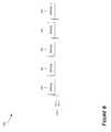
- FIG. 2illustrates encoding 200 performed by an ECC encoder supporting multiple code rates and throughput speeds according to one embodiment of the invention.
- matrix multiplicationis performed by the controller 130 and/or data storage and error correction module 132 .
- Row 210represents a segment of user data having length k. This segment comprises subsegments 212 , 214 , . . . , 216 having length P, where P is an integer (e.g., 128, 256, 512, 1024, etc.).
- Matrix 220represents generator matrix G.
- matrix 220can correspond to matrix Q of equation (3).
- Matrix 220can be divided into a plurality of submatrices 228 , which can be, for example, of size P ⁇ P.
- the number of submatrices 228 along the column dimension 230 of matrix 220can be, for example, n ⁇ k, (n ⁇ k)/P, and so on.
- the number of submatrices 228 along the row dimension 232 of matrix 220can be, for example, k, k/P, and so on.
- encoding 200can include the following operations.
- user data 210 subsegment 216can be multiplied by submatrices 228 in row 226 in order to determine the final value of Q j .
- the resultcan be saved in a row vector 230 .
- FIG. 3illustrates a block diagram of a portion of ECC encoder 300 supporting multiple code rates and throughput speeds according to one embodiment of the invention.
- the encoder 300can perform the multiplication s i ⁇ G i,j of equation (6).
- Register 310can be configured to store a subsegment of user data (e.g., of size p).
- Register 320can be configured to store a row of a submatrix 228 (e.g., of size 1 ⁇ p) of the matrix G.
- matrix Gcan be a circulant matrix and the submatrix can also be circulant.
- Register 320can be configured to perform the multiplication operations. In one embodiment, AND and XOR gates can be utilized. In other embodiments, any other suitable combinations of logic gates can be used, such as NAND, OR, NOR, etc.
- Register 350can be configured to store the result of the multiplication.
- the encoder 300can determine s i ⁇ G i,j as follows. A row g i,j of the submatrix is loaded into the register 320 and next user subsegment (e.g., of size p bits) is loaded in the register 310 . Every computational cycle one bit s i of register 310 is feed to as input into the logic gates 330 . This can be accomplished by right shifting the register 310 . The result of the multiplication by s i is computed and stored in the register 350 , which can indicate a completion of a computational cycle. In one embodiment, a computational cycle can correspond to a system clock cycle.
- the contents of the register 320can be right-rotated by one, which results in loading the next row of the submatrix. Then, the next bit s i from register 310 is feed as input to the logic gates 330 , and the foregoing process is repeated. In one embodiment, the contents of the register 320 are right-rotated by one every computational cycle. It can take a total of P computational cycles to perform the operation s i ⁇ G i,j . At the completion of P cycles, the encoder 300 can compute s i ⁇ G i+1,j by loading a row g i+1,j of the next submatrix into the register 320 . As is illustrated in FIG.
- the encoder 300comprises three registers having size P, P logic gates 330 (e.g., AND gates), and P logic gates 340 (e.g., XOR).
- P logic gates 330e.g., AND gates
- P logic gates 340e.g., XOR
- the encoder 300can be referred to as shift-register-adder-accumulator (SRAA).
- any number of encoders 300can be utilized in order to improve throughput associated with the computation of parity data.
- an LDPC encodercomprising, for example, an encoding module having five encoders 300 configured to compute parity data associated with user data in parallel may still provide throughput below a target throughput.
- the throughputin one embodiment can be about 100 MBytes/s when clock frequency of about 800 MHz is used.
- Many encoding modulesmay be needed to achieve higher throughput.
- 80 or more encoding modulesmay be needed to achieve the throughput of about 8 GBytes/s or higher, with each encoding module having five encoders 300 .
- the overall logicmay comprise multiple million(s) of logic gates and use a large amount of buffer memory.
- FIG. 4illustrates a block diagram of a portion of ECC encoder 400 supporting multiple code rates and throughput speeds according to another embodiment of the invention.
- the encoder 400can perform the multiplication s i ⁇ G i,j of equation (6).
- Register 410can be configured to store a subsegment of user data (e.g., of size p).
- Register 420can be configured to store a row of a submatrix 228 (e.g., of size 1 ⁇ p) of the matrix G.
- matrix Gcan be a circulant matrix and the submatrix can also be circulant.
- Register 450can be configured to store the result of the multiplication.
- the encoder 400is configured to perform in parallel and/or substantially in parallel multiplication of X bits of user data stored in the register 410 .
- Xcan be an integer value, such as 2, 8, 16, 32, 64, and so on, and X corresponds to the internal parallelism of the encoder 400 .
- the internal parallelismcan be scaled up and/or down depending on the desired tradeoff between throughput of the encoder and size of logic associated with the encoder.
- the encoder 400configured can determine s i ⁇ G i,j as follows.
- a row g i,j of the submatrixis loaded into the register 420 and next user subsegment (e.g., of size p bits) is loaded in the register 410 .
- Every computational cycleX bits (e.g., 32 bits or 4 bytes) of user data s i,X stored in register 410 are feed as input to the logic gates 430 . This can be accomplished by right shifting the register 410 by X.
- the result of the multiplication by s i,Xis computed and stored in the register 450 , which can indicate a completion of a computational cycle.
- the contents of the register 420can be right-rotated by X (e.g., 32 bits or 4 bytes). Then, the next X bits s i+1,X stored in register 410 is feed to as input into the logic gates 430 , and the foregoing process is repeated. In one embodiment, the contents of the register 420 are right-rotated by X every computational cycle. In one embodiment, there are X ⁇ 1 virtual copies of the register 420 having corresponding matrix data corresponding to right-rotated data by 1, 2, . . . , X ⁇ 1. It can take a total of P/X (e.g., P/32) computational cycles to perform the operation s i ⁇ G i,j .
- P/Xe.g., P/32
- the encoder 400can compute the s i ⁇ G i+1,j by loading a row g i+1,j of the next submatrix into the register 420 .
- the encoder 400comprises three registers having size P, X*P logic gates 430 (e.g., AND gates) having X inputs, and P logic gates 440 (e.g., XOR) having X+1 inputs.
- FIG. 5Aillustrates a data path of ECC encoder 500 supporting multiple code rates and throughput speeds according to one embodiment of the invention.
- the encoder 500comprises a plurality of encoder modules 520 configured to compute in parallel and/or substantially in parallel parity data associated with a plurality of user data units 510 , each unit comprising subsegments of user data.
- the encoder 400 illustrated in FIG. 4can be used as the encoder modules 520 .
- a number of encoder modules 520can be selected in accordance with a desired throughput.
- the number of encoder modulescan be 1, 2, 3, 4, and so on.
- the upper limit on the number of encoder modulescan be selected as a number of submatrices in the generator matrix.
- parity datacan be determined in parallel or substantially in parallel using all submatrices.
- coding rate of the encoder 500can be selected based on the combination of the number of submatrices and the value of P. In another embodiment, coding rate of the encoder 500 can be selected based on the combination of the values of X and P.
- FIG. 5Billustrates an encoder module 520 of the ECC encoder 500 supporting multiple code rates and throughput speeds according to one embodiment of the invention.
- the encoder module 520accepts and operates on one or more subunits of user data 530 .
- the encoder module 520can be partitioned into a plurality of encoding blocks 540 .
- the partitioningis depicted by lines 542 .
- One or more encoding blocks 540can be configured to compute parity data associated with one or more subunits of user data.
- one or more encoding block 540can be configured with desired X and/or P.
- FIG. 6illustrates a data path of ECC encoder 600 supporting multiple code rates and throughput speeds according to another embodiment of the invention.
- the encoder 600comprises five encoder modules 620 operating on user data 610 .
- one or more encoder modules 620can be configured with any suitable value(s) of X.
- a double buffermay be used for registers 410 , 420 , and/or 450 of FIG. 4 to provide a sustained throughput, such as to provide output and queue input simultaneously or nearly simultaneously.
- routing complexity associated with the logic of the encoder module 620may increase with increase in X.
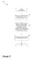
- FIG. 7is a flow diagram illustrating a process 700 of storing data according to one embodiment of the invention.
- the process 700can be executed by the controller 130 and/or the data storage and error correction module 132 .
- the process 700starts in block 702 where it selects size of a subset or subsegment of user data to be stored. The selection can be performed based in part on a size (e.g., P) of the submatrices of the generator matrix. For example, as explained above, user data subsegments of size P can be selected.
- the process 700generates in parallel or substantially in parallel subsets of parity data corresponding to the subsegments of user data.
- parity datacan be generated by multiplying subsegments of user data by the plurality of submatrices of the generator matrix. Further, parity data corresponding to a given subsegment of user data can be generated in parallel or substantially in parallel. For example, multiplications of the subsegment or part of the subsegment by at least some submatrices of the generator matrix can be performed in parallel or substantially in parallel. Accordingly, parity data can be generated in parallel or substantially in parallel across the subsegments of the user data as well for data bits of a given subsegment.
- the process 700stores the user data along with generated parity data in data storage system memory. For example, the process 700 can store the user data and parity data in the non-volatile memory array 150 .
- ECC encodersupporting multiple code rates and throughput speeds as is disclosed herein can provide for flexible and scalable encoding of user data, particularly when QC-LDPC encoding is used.
- the encodercan be scaled in size based on, for example, the desired encoding throughput and/or computational cycle duration.
- the encoder architecturecan thus be used to support multiple code rates and throughput speeds. Accordingly, encoding speed and efficiency and system performance is improved.
- LDPC codingcan be used in addition to and/or in place of LDPC coding.
- error correction mechanismscan be used in addition to and/or in place of LDPC coding.
- Hamming codingReed-Solomon coding, BCH coding, and the like can be used.
- user datacan encompass data provided by a host system, data generated internally by a data storage system, etc., and/or a combination thereof.
- any suitable unit or grouping of datasuch as octet, nibble, word, byte, etc., can be used in addition to or in place of a bit of user data.
- code shortening techniquesare utilized, encoding may be partially or fully skipped. The actual steps taken in the disclosed processes, such as the processes illustrated in FIG.
Landscapes
- Engineering & Computer Science (AREA)
- Theoretical Computer Science (AREA)
- Quality & Reliability (AREA)
- Physics & Mathematics (AREA)
- General Engineering & Computer Science (AREA)
- General Physics & Mathematics (AREA)
- Error Detection And Correction (AREA)
Abstract
Description
v=u×G (1)
GK×N=[IK×K/Qk×(N-K)] (2)
u={s1,s2,s3, . . . ,sn-m} (5)
Qj=si×Gi,j=s1G1,j+s2G2,j+ . . . +sn-mGn-m,j (6)
Qj=s1G1,jforj={0,m−1} (7a)
Qj=Qj+s2G2,jforj={0,m−1} (7b)
Qj=Qj+sn-mGn-m,jforj={0,m−1} (7c)
Claims (27)
Priority Applications (2)
| Application Number | Priority Date | Filing Date | Title |
|---|---|---|---|
| US13/718,289US9122625B1 (en) | 2012-12-18 | 2012-12-18 | Error correcting code encoder supporting multiple code rates and throughput speeds for data storage systems |
| US14/841,607US9495243B2 (en) | 2012-12-18 | 2015-08-31 | Error correcting code encoder supporting multiple code rates and throughput speeds for data storage systems |
Applications Claiming Priority (1)
| Application Number | Priority Date | Filing Date | Title |
|---|---|---|---|
| US13/718,289US9122625B1 (en) | 2012-12-18 | 2012-12-18 | Error correcting code encoder supporting multiple code rates and throughput speeds for data storage systems |
Related Child Applications (1)
| Application Number | Title | Priority Date | Filing Date |
|---|---|---|---|
| US14/841,607ContinuationUS9495243B2 (en) | 2012-12-18 | 2015-08-31 | Error correcting code encoder supporting multiple code rates and throughput speeds for data storage systems |
Publications (1)
| Publication Number | Publication Date |
|---|---|
| US9122625B1true US9122625B1 (en) | 2015-09-01 |
Family
ID=53938878
Family Applications (2)
| Application Number | Title | Priority Date | Filing Date |
|---|---|---|---|
| US13/718,289Expired - Fee RelatedUS9122625B1 (en) | 2012-12-18 | 2012-12-18 | Error correcting code encoder supporting multiple code rates and throughput speeds for data storage systems |
| US14/841,607Expired - Fee RelatedUS9495243B2 (en) | 2012-12-18 | 2015-08-31 | Error correcting code encoder supporting multiple code rates and throughput speeds for data storage systems |
Family Applications After (1)
| Application Number | Title | Priority Date | Filing Date |
|---|---|---|---|
| US14/841,607Expired - Fee RelatedUS9495243B2 (en) | 2012-12-18 | 2015-08-31 | Error correcting code encoder supporting multiple code rates and throughput speeds for data storage systems |
Country Status (1)
| Country | Link |
|---|---|
| US (2) | US9122625B1 (en) |
Cited By (9)
| Publication number | Priority date | Publication date | Assignee | Title |
|---|---|---|---|---|
| US20150046768A1 (en)* | 2013-08-12 | 2015-02-12 | Nec Laboratories America, Inc. | Encoding method and system for quasi-cyclic low-density parity-check code |
| US20150370633A1 (en)* | 2012-12-18 | 2015-12-24 | Western Digital Technologies, Inc. | Error correcting code encoder supporting multiple code rates and throughput speeds for data storage systems |
| US20160028419A1 (en)* | 2014-07-22 | 2016-01-28 | Lsi Corporation | Systems and Methods for Rank Independent Cyclic Data Encoding |
| US9529671B2 (en)* | 2014-06-17 | 2016-12-27 | Arm Limited | Error detection in stored data values |
| US20170034272A1 (en)* | 2015-07-31 | 2017-02-02 | International Business Machines Corporation | Data transfer priority levels |
| US9760438B2 (en) | 2014-06-17 | 2017-09-12 | Arm Limited | Error detection in stored data values |
| US9891976B2 (en) | 2015-02-26 | 2018-02-13 | Arm Limited | Error detection circuitry for use with memory |
| US10838811B1 (en)* | 2019-08-14 | 2020-11-17 | Silicon Motion, Inc. | Non-volatile memory write method using data protection with aid of pre-calculation information rotation, and associated apparatus |
| US11133032B1 (en) | 2020-10-20 | 2021-09-28 | Seagate Technology Llc | Reader instability detection and recovery |
Families Citing this family (7)
| Publication number | Priority date | Publication date | Assignee | Title |
|---|---|---|---|---|
| US11177835B2 (en) | 2015-09-25 | 2021-11-16 | SK Hynix Inc. | Data storage device |
| US11515897B2 (en) | 2015-05-29 | 2022-11-29 | SK Hynix Inc. | Data storage device |
| KR102285940B1 (en) | 2015-05-29 | 2021-08-05 | 에스케이하이닉스 주식회사 | Data processing circuit, data storage device comprising data processing circuit and operating method thereof |
| US11611359B2 (en) | 2015-05-29 | 2023-03-21 | SK Hynix Inc. | Data storage device |
| US10396827B2 (en) | 2015-09-25 | 2019-08-27 | SK Hynix Inc. | Data storage device |
| KR20180059150A (en)* | 2016-11-25 | 2018-06-04 | 에스케이하이닉스 주식회사 | ECC encoder and encoding method capable of encoding during one clock cycle and memory controller having the ECC encoder |
| US10523239B2 (en) | 2018-04-12 | 2019-12-31 | National Chiao Tung University | Method for generating encoded data that is encoded based on low-density parity-check codes, and method for decoding the encoded data |
Citations (135)
| Publication number | Priority date | Publication date | Assignee | Title |
|---|---|---|---|---|
| US2728222A (en) | 1950-10-17 | 1955-12-27 | Leitz Ernst Gmbh | Apparatus for measuring surface irregularities |
| US4760358A (en) | 1985-08-07 | 1988-07-26 | Murata Manufacturing Co., Ltd. | Piezoelectric element |
| US5118982A (en) | 1989-05-31 | 1992-06-02 | Nec Corporation | Thickness mode vibration piezoelectric transformer |
| US5262643A (en) | 1992-06-12 | 1993-11-16 | International Business Machines Corp. | Automatic tip approach method and apparatus for scanning probe microscope |
| US5301558A (en) | 1992-10-02 | 1994-04-12 | Caterpillar Inc. | Testing apparatus for a multilayer piezoelectric actuator |
| USRE37030E1 (en) | 1992-12-24 | 2001-01-30 | Renishaw Plc | Touch probe and signal processing circuit therefor |
| US6249890B1 (en) | 1998-06-05 | 2001-06-19 | Seagate Technology Llc | Detecting head readback response degradation in a disc drive |
| US6510752B1 (en) | 1999-02-22 | 2003-01-28 | Seagate Technology Llc | Method and apparatus for testing microactuators on a suspension assembly |
| US20030037298A1 (en) | 2001-07-11 | 2003-02-20 | International Business Machines Corporation | Method and apparatus for low density parity check encoding of data |
| US20030065992A1 (en) | 2001-09-04 | 2003-04-03 | Samsung Electronics Co., Ltd. | Method and apparatus to control head instability in a data storage system |
| US20030076121A1 (en) | 2001-10-23 | 2003-04-24 | Wei Guo | Peizoelectric microactuator and sensor failure detection in disk drives |
| US6556933B1 (en) | 1999-10-28 | 2003-04-29 | Seagate Technology Llc | Transducer instability detection in a digital channel |
| US6556028B1 (en) | 2001-05-07 | 2003-04-29 | Storage Test Solutions, Inc. | Method and apparatus for detecting defects in piezoelectric actuators |
| US20030123563A1 (en) | 2001-07-11 | 2003-07-03 | Guangming Lu | Method and apparatus for turbo encoding and decoding |
| US6639411B1 (en) | 2000-09-05 | 2003-10-28 | Hutchinson Technology Incorporated | Microactuated suspension motor failure detection system |
| US20040098659A1 (en) | 2002-11-18 | 2004-05-20 | Bjerke Bjorn A. | Rate-compatible LDPC codes |
| US6831807B2 (en) | 2001-11-05 | 2004-12-14 | Matsushita Electric Industrial Co., Ltd. | Head positioner and disk drive using the same |
| US6856556B1 (en) | 2003-04-03 | 2005-02-15 | Siliconsystems, Inc. | Storage subsystem with embedded circuit for protecting against anomalies in power signal from host |
| US20050204253A1 (en) | 2004-03-11 | 2005-09-15 | Nortel Networks Limited | Algebraic low-density parity check code design for variable block sizes and code rates |
| US20050216821A1 (en) | 2004-03-24 | 2005-09-29 | Kohsuke Harada | Mapping method for encoded bits using LDPC code, transmitting and receiving apparatuses employing this method, and program for executing this method |
| US20050246617A1 (en) | 2004-04-28 | 2005-11-03 | Samsung Electronics Co., Ltd. | Apparatus and method for coding/decoding block low density parity check code with variable block length |
| US6975477B1 (en) | 2002-05-03 | 2005-12-13 | Maxtor Corporation | Micro actuator DC gain calibration scheme for HDD dual-stage actuator systems |
| US6977793B2 (en) | 2004-03-16 | 2005-12-20 | Hitachi Global Storage Technologies Netherlands B.V. | Magnetic recording disk drive with dual-stage actuator and control system with multiple controllers |
| US20060036933A1 (en) | 2004-08-12 | 2006-02-16 | Blankenship Yufei W | Method and apparatus for encoding and decoding data |
| US20060036925A1 (en) | 2004-08-16 | 2006-02-16 | Samsung Electronics Co., Ltd. | Apparatus and method for coding/decoding block low density parity check code with variable block length |
| US7009804B2 (en) | 2004-07-29 | 2006-03-07 | Samsung Electronics Co., Ltd. | Method and apparatus for micro-actuator stroke sensitivity calibration in a hard disk drive |
| US7072134B1 (en) | 2005-02-03 | 2006-07-04 | Hitachi Global Storage Technologies Netherlands B.V. | Dual-stage actuator disk drive with secondary actuator failure detection and recovery using relative-position signal |
| US7072417B1 (en) | 2000-06-28 | 2006-07-04 | Marvell International Ltd. | LDPC encoder and method thereof |
| US7075748B2 (en) | 2004-11-24 | 2006-07-11 | Hitachi Global Storage Technologies Netherlands B.V. | Disk drive with a dual-stage actuator and failure detection and recovery system for the secondary actuator |
| US7079338B1 (en) | 2005-06-03 | 2006-07-18 | Hitachi Global Storagetechnologies Netherlands B.V. | Dual-stage actuator disk drive with method for secondary-actuator failure detection and recovery while track-following |
| US7079339B1 (en) | 2005-06-03 | 2006-07-18 | Hitachi Global Storage Technologies Netherlands B.V. | Dual-stage actuator disk drive with method for secondary-actuator failure detection and recovery using a relative-position sensor while track following |
| US20060171062A1 (en) | 2005-02-03 | 2006-08-03 | Toshiki Hirano | Method for secondary-actuator failure detection and recovery in a dual-stage actuator disk drive |
| US7124654B1 (en) | 2004-09-30 | 2006-10-24 | Western Digital (Fremont), Inc. | Method for determining a microactuator range of movement |
| UA20943U (en) | 2006-09-11 | 2007-02-15 | Valerii Mykhailovych Sharapov | Device for testing a bimorph piezoelectric element |
| US7184230B1 (en) | 2002-06-01 | 2007-02-27 | Western Digital Technologies, Inc. | System and method for processing track identifier errors to mitigate head instability in data storage devices |
| US20080028274A1 (en)* | 2006-07-25 | 2008-01-31 | Communications Coding Corporation | Universal error control coding scheme for digital communication and data storage systems |
| US7336434B2 (en) | 2005-07-18 | 2008-02-26 | Hitachi Global Storage Technologies Netherlands B.V. | Predictive failure analysis of thermal flying height control system and method |
| US7346832B2 (en) | 2004-07-21 | 2008-03-18 | Qualcomm Incorporated | LDPC encoding methods and apparatus |
| US7395490B2 (en) | 2004-07-21 | 2008-07-01 | Qualcomm Incorporated | LDPC decoding methods and apparatus |
| US20080165444A1 (en) | 2007-01-05 | 2008-07-10 | Broadcom Corporation, A California Corporation | Baseline popping noise detection circuit |
| US20080172592A1 (en) | 2005-04-29 | 2008-07-17 | Norbert Wehn | Method and Device For Controlling the Decoding of a Ldpc Encoded Codeword, In Particular For Dvb-S2 Ldpc Encoded Codewords |
| US7423837B2 (en) | 2006-03-23 | 2008-09-09 | Seagate Technology Llc | Micro actuator gain calibration based on a sinusoidal input signal |
| US7430136B2 (en) | 2004-11-30 | 2008-09-30 | Siliconsystems, Inc. | Purge operations for solid-state storage devices |
| US7447807B1 (en) | 2006-06-30 | 2008-11-04 | Siliconsystems, Inc. | Systems and methods for storing data in segments of a storage subsystem |
| US20080301521A1 (en) | 2007-05-01 | 2008-12-04 | Texas A&M University System | Low density parity check decoder for irregular ldpc codes |
| US7500172B2 (en) | 2005-02-26 | 2009-03-03 | Broadcom Corporation | AMP (accelerated message passing) decoder adapted for LDPC (low density parity check) codes |
| US7509441B1 (en) | 2006-06-30 | 2009-03-24 | Siliconsystems, Inc. | Systems and methods for segmenting and protecting a storage subsystem |
| US20090113256A1 (en) | 2007-10-24 | 2009-04-30 | Nokia Corporation | Method, computer program product, apparatus and device providing scalable structured high throughput LDPC decoding |
| US7577892B1 (en) | 2005-08-25 | 2009-08-18 | Marvell International Ltd | High speed iterative decoder |
| US7596643B2 (en) | 2007-02-07 | 2009-09-29 | Siliconsystems, Inc. | Storage subsystem with configurable buffer |
| US20090249160A1 (en) | 2005-06-27 | 2009-10-01 | Wen Gao | Methods and apparatus for power reduction in iterative decoders |
| US20090249159A1 (en) | 2004-12-08 | 2009-10-01 | Electronics And Telecommunications Research | Ldpc encoder and decoder and ldpc encoding and decoding methods |
| WO2009128546A1 (en) | 2008-04-18 | 2009-10-22 | 日本碍子株式会社 | Method for testing piezoelectric/electrostrictive device, testing apparatus, and method for adjusting piezoelectric/electrostrictive device |
| US20090303839A1 (en) | 2007-07-31 | 2009-12-10 | Manoj Narayanan | Stress-biased cymbals incorporating a shape memory alloy |
| US7653778B2 (en) | 2006-05-08 | 2010-01-26 | Siliconsystems, Inc. | Systems and methods for measuring the useful life of solid-state storage devices |
| US7657816B2 (en) | 2005-07-13 | 2010-02-02 | Leanics Corporation | Low-complexity hybrid LDPC code encoder |
| US20100037121A1 (en) | 2008-08-05 | 2010-02-11 | The Hong Kong University Of Science And Technology | Low power layered decoding for low density parity check decoders |
| US20100037674A1 (en) | 2008-03-21 | 2010-02-18 | The Regents Of The University Of California | Test Surfaces Useful for Calibration of Surface Profilometers |
| US7685338B2 (en) | 2007-05-24 | 2010-03-23 | Siliconsystems, Inc. | Solid state storage subsystem for embedded applications |
| US7685374B2 (en) | 2007-07-26 | 2010-03-23 | Siliconsystems, Inc. | Multi-interface and multi-bus structured solid-state storage subsystem |
| US7685337B2 (en) | 2007-05-24 | 2010-03-23 | Siliconsystems, Inc. | Solid state storage subsystem for embedded applications |
| US20100100788A1 (en) | 2008-10-17 | 2010-04-22 | Shaohua Yang | Programmable quasi-cyclic low-density parity check (QC LDPC) encoder for read channel |
| US20100107030A1 (en) | 2008-10-29 | 2010-04-29 | Agere Systems Inc. | Ldpc decoders using fixed and adjustable permutators |
| US20100131819A1 (en) | 2008-11-26 | 2010-05-27 | Agere Systems Inc. | Ldpc decoder variable node units having fewer adder stages |
| US7733712B1 (en) | 2008-05-20 | 2010-06-08 | Siliconsystems, Inc. | Storage subsystem with embedded circuit for protecting against anomalies in power signal from host |
| US20100169735A1 (en) | 2008-12-31 | 2010-07-01 | Texas Instruments Incorporated | Low density parity check code row update instruction |
| US20100174849A1 (en) | 2009-01-07 | 2010-07-08 | Siliconsystems, Inc. | Systems and methods for improving the performance of non-volatile memory operations |
| US7765373B1 (en) | 2006-06-27 | 2010-07-27 | Siliconsystems, Inc. | System for controlling use of a solid-state storage subsystem |
| US7768276B2 (en) | 2006-11-06 | 2010-08-03 | Sae Magnetics (H. K.) Ltd. | Systems and methods for identifying problems with PZT elements of micro-actuators |
| US7783950B2 (en) | 2005-09-22 | 2010-08-24 | Rohm Co., Ltd. | Data writing apparatus and a storage system |
| US20100250793A1 (en) | 2009-03-24 | 2010-09-30 | Western Digital Technologies, Inc. | Adjusting access of non-volatile semiconductor memory based on access time |
| UA20940S (en) | 2010-04-15 | 2010-10-11 | Бакарді Енд Комп | COOLING MACHINE FOR BOTTLES |
| US7814393B2 (en) | 2005-10-19 | 2010-10-12 | Samsung Electronics Co., Ltd | Apparatus and method for coding/decoding block low density parity check code with variable block length |
| US20100275088A1 (en) | 2009-04-22 | 2010-10-28 | Agere Systems Inc. | Low-latency decoder |
| US20100318872A1 (en) | 2006-12-29 | 2010-12-16 | Zte Corporation | Decoding Method for LDPC Code Based on BP Arithmetic |
| US7913149B2 (en) | 2006-12-20 | 2011-03-22 | Lsi Corporation | Low complexity LDPC encoding algorithm |
| US20110099323A1 (en) | 2009-10-27 | 2011-04-28 | Western Digital Technologies, Inc. | Non-volatile semiconductor memory segregating sequential, random, and system data to reduce garbage collection for page based mapping |
| US20110126078A1 (en) | 2009-11-23 | 2011-05-26 | Yeong-Luh Ueng | Decoder and decoding method for low-density parity check codes constructed based on reed-solomon codes |
| US7962792B2 (en) | 2008-02-11 | 2011-06-14 | Siliconsystems, Inc. | Interface for enabling a host computer to retrieve device monitor data from a solid state storage subsystem |
| US20110179333A1 (en) | 2008-05-21 | 2011-07-21 | The Regents Of The University Of California | Lower-complexity layered belief propagation decoding ldpc codes |
| US20110246862A1 (en) | 2010-03-31 | 2011-10-06 | Nils Graef | Hard input low density parity check decoder |
| US8037388B2 (en) | 2006-08-24 | 2011-10-11 | Stmicroelectronics Sa | Method and device for layered decoding of a succession of blocks encoded with an LDPC code |
| WO2011127287A1 (en) | 2010-04-08 | 2011-10-13 | Marvell World Trade Ltd. | Non-binary ldpc code decoder |
| US20110252294A1 (en) | 2010-04-09 | 2011-10-13 | Link_A_Media Devices Corporation | Implementation of ldpc selective decoding scheduling |
| US20110283049A1 (en) | 2010-05-12 | 2011-11-17 | Western Digital Technologies, Inc. | System and method for managing garbage collection in solid-state memory |
| US8078918B2 (en) | 2008-02-07 | 2011-12-13 | Siliconsystems, Inc. | Solid state storage subsystem that maintains and provides access to data reflective of a failure risk |
| US8090899B1 (en) | 2009-03-04 | 2012-01-03 | Western Digital Technologies, Inc. | Solid state drive power safe wear-leveling |
| US8095851B2 (en) | 2007-09-06 | 2012-01-10 | Siliconsystems, Inc. | Storage subsystem capable of adjusting ECC settings based on monitored conditions |
| US8108692B1 (en) | 2006-06-27 | 2012-01-31 | Siliconsystems, Inc. | Solid-state storage subsystem security solution |
| US8135903B1 (en) | 2009-10-30 | 2012-03-13 | Western Digital Technologies, Inc. | Non-volatile semiconductor memory compressing data to improve performance |
| US20120079341A1 (en) | 2009-05-27 | 2012-03-29 | Novelsat Ltd. | Iterative decoding of ldpc codes with iteration scheduling |
| US8161227B1 (en) | 2006-10-30 | 2012-04-17 | Siliconsystems, Inc. | Storage subsystem capable of programming field-programmable devices of a target computer system |
| US8243525B1 (en) | 2009-09-30 | 2012-08-14 | Western Digital Technologies, Inc. | Refreshing non-volatile semiconductor memory by reading without rewriting |
| US8254172B1 (en) | 2009-09-30 | 2012-08-28 | Western Digital Technologies, Inc. | Wear leveling non-volatile semiconductor memory based on erase times and program times |
| US8261012B2 (en) | 2009-10-30 | 2012-09-04 | Western Digital Technologies, Inc. | Non-volatile semiconductor memory comprising power fail circuitry for flushing write data in response to a power fail signal |
| US20120260020A1 (en) | 2011-04-06 | 2012-10-11 | Western Digital Technologies, Inc. | Non-volatile semiconductor memory module enabling out of order host command chunk media access |
| US20120278531A1 (en) | 2011-04-29 | 2012-11-01 | Western Digital Technologies, Inc. | System and method for improved parity determination within a data redundancy scheme in a solid state memory |
| US20120284460A1 (en) | 2011-05-02 | 2012-11-08 | Western Digital Technologies, Inc. | High performance path for command processing |
| US8316176B1 (en) | 2010-02-17 | 2012-11-20 | Western Digital Technologies, Inc. | Non-volatile semiconductor memory segregating sequential data during garbage collection to reduce write amplification |
| US20120297267A1 (en) | 2010-01-27 | 2012-11-22 | Telefonaktiebolaget L M Ericsson (Publ) | Error floor reduction in iteratively decoded fec codes |
| US8322235B1 (en) | 2011-02-18 | 2012-12-04 | Western Digital Technologies, Inc. | Microactuator test assembly comprising a spreader pin for engaging a load beam of an actuator arm |
| US8335049B1 (en) | 2010-06-07 | 2012-12-18 | Western Digital Technologies, Inc. | Disk drive detecting crack in microactuator |
| US20120324191A1 (en) | 2011-06-14 | 2012-12-20 | Western Digital Technologies, Inc. | System and method for performing data retention that incorporates environmental conditions |
| US8341339B1 (en) | 2010-06-14 | 2012-12-25 | Western Digital Technologies, Inc. | Hybrid drive garbage collecting a non-volatile semiconductor memory by migrating valid data to a disk |
| US8347195B1 (en) | 2009-01-22 | 2013-01-01 | Marvell International Ltd. | Systems and methods for near-codeword detection and correction on the fly |
| US20130031447A1 (en) | 2011-07-31 | 2013-01-31 | Sandisk Technologies Inc. | Fast detection of convergence or divergence in iterative decoding |
| US8375151B1 (en) | 2009-02-12 | 2013-02-12 | Siliconsystems, Inc. | Command portal for securely communicating and executing non-standard storage subsystem commands |
| US8392635B2 (en) | 2010-12-22 | 2013-03-05 | Western Digital Technologies, Inc. | Selectively enabling a host transfer interrupt |
| US8397107B1 (en) | 2009-12-11 | 2013-03-12 | Western Digital Technologies, Inc. | Data storage device employing data path protection using both LBA and PBA |
| US8407449B1 (en) | 2010-02-26 | 2013-03-26 | Western Digital Technologies, Inc. | Non-volatile semiconductor memory storing an inverse map for rebuilding a translation table |
| US8423722B1 (en) | 2011-08-26 | 2013-04-16 | Western Digital Technologies, Inc. | System and method for high performance command processing in solid state drives |
| US8443167B1 (en) | 2009-12-16 | 2013-05-14 | Western Digital Technologies, Inc. | Data storage device employing a run-length mapping table and a single address mapping table |
| US8447920B1 (en) | 2010-06-29 | 2013-05-21 | Western Digital Technologies, Inc. | System and method for managing data access in non-volatile memory |
| US20130132638A1 (en) | 2011-11-21 | 2013-05-23 | Western Digital Technologies, Inc. | Disk drive data caching using a multi-tiered memory |
| US8458435B1 (en) | 2010-12-20 | 2013-06-04 | Western Digital Technologies, Inc. | Sequential write thread detection |
| US8495479B1 (en) | 2010-11-22 | 2013-07-23 | Marvell International Ltd. | Defect detection and correction via monitoring of syndromes and bit flips in decoder |
| US8503237B1 (en) | 2011-05-18 | 2013-08-06 | Western Digital Technologies, Inc. | System and method for data recovery in a solid state storage device |
| US8521972B1 (en) | 2010-06-30 | 2013-08-27 | Western Digital Technologies, Inc. | System and method for optimizing garbage collection in data storage |
| US8549236B2 (en) | 2006-12-15 | 2013-10-01 | Siliconsystems, Inc. | Storage subsystem with multiple non-volatile memory arrays to protect against data losses |
| US20130290793A1 (en) | 2012-04-25 | 2013-10-31 | Western Digital Technologies, Inc. | Managing unreliable memory in data storage systems |
| US8583835B1 (en) | 2008-08-06 | 2013-11-12 | Siliconsystems, Inc. | Command portal for executing non-standard storage subsystem commands |
| US8601311B2 (en) | 2010-12-14 | 2013-12-03 | Western Digital Technologies, Inc. | System and method for using over-provisioned data capacity to maintain a data redundancy scheme in a solid state memory |
| US8601313B1 (en) | 2010-12-13 | 2013-12-03 | Western Digital Technologies, Inc. | System and method for a data reliability scheme in a solid state memory |
| US8612804B1 (en) | 2010-09-30 | 2013-12-17 | Western Digital Technologies, Inc. | System and method for improving wear-leveling performance in solid-state memory |
| US8612669B1 (en) | 2010-06-28 | 2013-12-17 | Western Digital Technologies, Inc. | System and method for performing data retention in solid-state memory using copy commands and validity and usage data |
| US8615681B2 (en) | 2010-12-14 | 2013-12-24 | Western Digital Technologies, Inc. | System and method for maintaining a data redundancy scheme in a solid state memory in the event of a power loss |
| US8638602B1 (en) | 2010-09-10 | 2014-01-28 | Western Digital Technologies, Inc. | Background selection of voltage reference values for performing memory read operations |
| US8639872B1 (en) | 2010-08-13 | 2014-01-28 | Western Digital Technologies, Inc. | Hybrid drive comprising write cache spanning non-volatile semiconductor memory and disk |
| US20140059405A1 (en) | 2012-08-21 | 2014-02-27 | Western Digital Technologies, Inc. | Solid-state drive retention monitor using reference blocks |
| US8683113B2 (en) | 2011-02-04 | 2014-03-25 | Western Digital Technologies, Inc. | Concurrently searching multiple devices of a non-volatile semiconductor memory |
| US8700951B1 (en) | 2011-03-09 | 2014-04-15 | Western Digital Technologies, Inc. | System and method for improving a data redundancy scheme in a solid state subsystem with additional metadata |
| US8700950B1 (en) | 2011-02-11 | 2014-04-15 | Western Digital Technologies, Inc. | System and method for data error recovery in a solid state subsystem |
| US8700834B2 (en) | 2011-09-06 | 2014-04-15 | Western Digital Technologies, Inc. | Systems and methods for an enhanced controller architecture in data storage systems |
| US8707104B1 (en) | 2011-09-06 | 2014-04-22 | Western Digital Technologies, Inc. | Systems and methods for error injection in data storage systems |
| US20140115427A1 (en) | 2012-10-24 | 2014-04-24 | Western Digital Technologies, Inc. | Adaptive error correction codes for data storage systems |
Family Cites Families (6)
| Publication number | Priority date | Publication date | Assignee | Title |
|---|---|---|---|---|
| UA20948U (en) | 2006-09-11 | 2007-02-15 | Method for production of grape beverage | |
| US8095859B1 (en)* | 2008-01-09 | 2012-01-10 | L-3 Communications, Corp. | Encoder for low-density parity check codes |
| US9298542B2 (en)* | 2012-10-30 | 2016-03-29 | Cleversafe, Inc. | Recovering data from corrupted encoded data slices |
| US8966339B1 (en) | 2012-12-18 | 2015-02-24 | Western Digital Technologies, Inc. | Decoder supporting multiple code rates and code lengths for data storage systems |
| US9122625B1 (en)* | 2012-12-18 | 2015-09-01 | Western Digital Technologies, Inc. | Error correcting code encoder supporting multiple code rates and throughput speeds for data storage systems |
| US20140223255A1 (en) | 2012-12-18 | 2014-08-07 | Western Digital Technologies, Inc. | Decoder having early decoding termination detection |
- 2012
- 2012-12-18USUS13/718,289patent/US9122625B1/ennot_activeExpired - Fee Related
- 2015
- 2015-08-31USUS14/841,607patent/US9495243B2/ennot_activeExpired - Fee Related
Patent Citations (161)
| Publication number | Priority date | Publication date | Assignee | Title |
|---|---|---|---|---|
| US2728222A (en) | 1950-10-17 | 1955-12-27 | Leitz Ernst Gmbh | Apparatus for measuring surface irregularities |
| US4760358A (en) | 1985-08-07 | 1988-07-26 | Murata Manufacturing Co., Ltd. | Piezoelectric element |
| US5118982A (en) | 1989-05-31 | 1992-06-02 | Nec Corporation | Thickness mode vibration piezoelectric transformer |
| US5262643A (en) | 1992-06-12 | 1993-11-16 | International Business Machines Corp. | Automatic tip approach method and apparatus for scanning probe microscope |
| US5301558A (en) | 1992-10-02 | 1994-04-12 | Caterpillar Inc. | Testing apparatus for a multilayer piezoelectric actuator |
| USRE37030E1 (en) | 1992-12-24 | 2001-01-30 | Renishaw Plc | Touch probe and signal processing circuit therefor |
| US6249890B1 (en) | 1998-06-05 | 2001-06-19 | Seagate Technology Llc | Detecting head readback response degradation in a disc drive |
| US6510752B1 (en) | 1999-02-22 | 2003-01-28 | Seagate Technology Llc | Method and apparatus for testing microactuators on a suspension assembly |
| US6556933B1 (en) | 1999-10-28 | 2003-04-29 | Seagate Technology Llc | Transducer instability detection in a digital channel |
| US7072417B1 (en) | 2000-06-28 | 2006-07-04 | Marvell International Ltd. | LDPC encoder and method thereof |
| US6639411B1 (en) | 2000-09-05 | 2003-10-28 | Hutchinson Technology Incorporated | Microactuated suspension motor failure detection system |
| US6870377B2 (en) | 2000-09-05 | 2005-03-22 | Hutchinson Technology Incorporated | Method for detecting piezoelectric element failures in head suspensions |
| US6556028B1 (en) | 2001-05-07 | 2003-04-29 | Storage Test Solutions, Inc. | Method and apparatus for detecting defects in piezoelectric actuators |
| US20030123563A1 (en) | 2001-07-11 | 2003-07-03 | Guangming Lu | Method and apparatus for turbo encoding and decoding |
| US6895547B2 (en) | 2001-07-11 | 2005-05-17 | International Business Machines Corporation | Method and apparatus for low density parity check encoding of data |
| US20030037298A1 (en) | 2001-07-11 | 2003-02-20 | International Business Machines Corporation | Method and apparatus for low density parity check encoding of data |
| US20030065992A1 (en) | 2001-09-04 | 2003-04-03 | Samsung Electronics Co., Ltd. | Method and apparatus to control head instability in a data storage system |
| US7062698B2 (en) | 2001-09-04 | 2006-06-13 | Samsung Electronics Co., Ltd. | Method and apparatus to control head instability in a data storage system |
| US20030076121A1 (en) | 2001-10-23 | 2003-04-24 | Wei Guo | Peizoelectric microactuator and sensor failure detection in disk drives |
| US6861854B1 (en) | 2001-10-23 | 2005-03-01 | Maxtor Corporation | Peizoelectric microactuator and sensor failure detection in disk drives |
| US6831807B2 (en) | 2001-11-05 | 2004-12-14 | Matsushita Electric Industrial Co., Ltd. | Head positioner and disk drive using the same |
| US6975477B1 (en) | 2002-05-03 | 2005-12-13 | Maxtor Corporation | Micro actuator DC gain calibration scheme for HDD dual-stage actuator systems |
| US7184230B1 (en) | 2002-06-01 | 2007-02-27 | Western Digital Technologies, Inc. | System and method for processing track identifier errors to mitigate head instability in data storage devices |
| US20040098659A1 (en) | 2002-11-18 | 2004-05-20 | Bjerke Bjorn A. | Rate-compatible LDPC codes |
| US6856556B1 (en) | 2003-04-03 | 2005-02-15 | Siliconsystems, Inc. | Storage subsystem with embedded circuit for protecting against anomalies in power signal from host |
| US7126857B2 (en) | 2003-04-03 | 2006-10-24 | Siliconsystems, Inc. | Storage subsystem with embedded circuit for protecting against anomalies in power signal from host |
| US20050204253A1 (en) | 2004-03-11 | 2005-09-15 | Nortel Networks Limited | Algebraic low-density parity check code design for variable block sizes and code rates |
| US6977793B2 (en) | 2004-03-16 | 2005-12-20 | Hitachi Global Storage Technologies Netherlands B.V. | Magnetic recording disk drive with dual-stage actuator and control system with multiple controllers |
| US20050216821A1 (en) | 2004-03-24 | 2005-09-29 | Kohsuke Harada | Mapping method for encoded bits using LDPC code, transmitting and receiving apparatuses employing this method, and program for executing this method |
| US20050246617A1 (en) | 2004-04-28 | 2005-11-03 | Samsung Electronics Co., Ltd. | Apparatus and method for coding/decoding block low density parity check code with variable block length |
| US7395490B2 (en) | 2004-07-21 | 2008-07-01 | Qualcomm Incorporated | LDPC decoding methods and apparatus |
| US7346832B2 (en) | 2004-07-21 | 2008-03-18 | Qualcomm Incorporated | LDPC encoding methods and apparatus |
| US7009804B2 (en) | 2004-07-29 | 2006-03-07 | Samsung Electronics Co., Ltd. | Method and apparatus for micro-actuator stroke sensitivity calibration in a hard disk drive |
| US20060036933A1 (en) | 2004-08-12 | 2006-02-16 | Blankenship Yufei W | Method and apparatus for encoding and decoding data |
| US20060036925A1 (en) | 2004-08-16 | 2006-02-16 | Samsung Electronics Co., Ltd. | Apparatus and method for coding/decoding block low density parity check code with variable block length |
| US7124654B1 (en) | 2004-09-30 | 2006-10-24 | Western Digital (Fremont), Inc. | Method for determining a microactuator range of movement |
| US7075748B2 (en) | 2004-11-24 | 2006-07-11 | Hitachi Global Storage Technologies Netherlands B.V. | Disk drive with a dual-stage actuator and failure detection and recovery system for the secondary actuator |
| US7936603B2 (en) | 2004-11-30 | 2011-05-03 | Siliconsystems, Inc. | Purge operations for solid-state storage devices |
| US7502256B2 (en) | 2004-11-30 | 2009-03-10 | Siliconsystems, Inc. | Systems and methods for reducing unauthorized data recovery from solid-state storage devices |
| US7430136B2 (en) | 2004-11-30 | 2008-09-30 | Siliconsystems, Inc. | Purge operations for solid-state storage devices |
| US7898855B2 (en) | 2004-11-30 | 2011-03-01 | Siliconsystems, Inc. | Systems and methods for reducing unauthorized data recovery from solid-state storage devices |
| US20090249159A1 (en) | 2004-12-08 | 2009-10-01 | Electronics And Telecommunications Research | Ldpc encoder and decoder and ldpc encoding and decoding methods |
| US20060171062A1 (en) | 2005-02-03 | 2006-08-03 | Toshiki Hirano | Method for secondary-actuator failure detection and recovery in a dual-stage actuator disk drive |
| US7106552B2 (en) | 2005-02-03 | 2006-09-12 | Hitachi Global Storage Technologies Netherlands B.V. | Method for secondary-actuator failure detection and recovery in a dual-stage actuator disk drive |
| US7072134B1 (en) | 2005-02-03 | 2006-07-04 | Hitachi Global Storage Technologies Netherlands B.V. | Dual-stage actuator disk drive with secondary actuator failure detection and recovery using relative-position signal |
| US7500172B2 (en) | 2005-02-26 | 2009-03-03 | Broadcom Corporation | AMP (accelerated message passing) decoder adapted for LDPC (low density parity check) codes |
| US8010869B2 (en) | 2005-04-29 | 2011-08-30 | Stmicroelectronics N.V. | Method and device for controlling the decoding of a LDPC encoded codeword, in particular for DVB-S2 LDPC encoded codewords |
| US20080172592A1 (en) | 2005-04-29 | 2008-07-17 | Norbert Wehn | Method and Device For Controlling the Decoding of a Ldpc Encoded Codeword, In Particular For Dvb-S2 Ldpc Encoded Codewords |
| US7079339B1 (en) | 2005-06-03 | 2006-07-18 | Hitachi Global Storage Technologies Netherlands B.V. | Dual-stage actuator disk drive with method for secondary-actuator failure detection and recovery using a relative-position sensor while track following |
| US7079338B1 (en) | 2005-06-03 | 2006-07-18 | Hitachi Global Storagetechnologies Netherlands B.V. | Dual-stage actuator disk drive with method for secondary-actuator failure detection and recovery while track-following |
| US8171367B2 (en) | 2005-06-27 | 2012-05-01 | Thomson Licensing | Stopping criteria in iterative decoders |
| US20090249160A1 (en) | 2005-06-27 | 2009-10-01 | Wen Gao | Methods and apparatus for power reduction in iterative decoders |
| US7657816B2 (en) | 2005-07-13 | 2010-02-02 | Leanics Corporation | Low-complexity hybrid LDPC code encoder |
| US7336434B2 (en) | 2005-07-18 | 2008-02-26 | Hitachi Global Storage Technologies Netherlands B.V. | Predictive failure analysis of thermal flying height control system and method |
| US7577892B1 (en) | 2005-08-25 | 2009-08-18 | Marvell International Ltd | High speed iterative decoder |
| US7783950B2 (en) | 2005-09-22 | 2010-08-24 | Rohm Co., Ltd. | Data writing apparatus and a storage system |
| US7814393B2 (en) | 2005-10-19 | 2010-10-12 | Samsung Electronics Co., Ltd | Apparatus and method for coding/decoding block low density parity check code with variable block length |
| US7423837B2 (en) | 2006-03-23 | 2008-09-09 | Seagate Technology Llc | Micro actuator gain calibration based on a sinusoidal input signal |
| US8312207B2 (en) | 2006-05-08 | 2012-11-13 | Siliconsystems, Inc. | Systems and methods for measuring the useful life of solid-state storage devices |
| US8122185B2 (en) | 2006-05-08 | 2012-02-21 | Siliconsystems, Inc. | Systems and methods for measuring the useful life of solid-state storage devices |
| US7653778B2 (en) | 2006-05-08 | 2010-01-26 | Siliconsystems, Inc. | Systems and methods for measuring the useful life of solid-state storage devices |
| US7765373B1 (en) | 2006-06-27 | 2010-07-27 | Siliconsystems, Inc. | System for controlling use of a solid-state storage subsystem |
| US8108692B1 (en) | 2006-06-27 | 2012-01-31 | Siliconsystems, Inc. | Solid-state storage subsystem security solution |
| US7509441B1 (en) | 2006-06-30 | 2009-03-24 | Siliconsystems, Inc. | Systems and methods for segmenting and protecting a storage subsystem |
| US8127048B1 (en) | 2006-06-30 | 2012-02-28 | Siliconsystems, Inc. | Systems and methods for segmenting and protecting a storage subsystem |
| US7912991B1 (en) | 2006-06-30 | 2011-03-22 | Siliconsystems, Inc. | Systems and methods for segmenting and protecting a storage subsystem |
| US7447807B1 (en) | 2006-06-30 | 2008-11-04 | Siliconsystems, Inc. | Systems and methods for storing data in segments of a storage subsystem |
| US20080126908A1 (en)* | 2006-07-25 | 2008-05-29 | Communications Coding Corporation | Universal error control coding system for digital communication and data storage systems |
| US20080028274A1 (en)* | 2006-07-25 | 2008-01-31 | Communications Coding Corporation | Universal error control coding scheme for digital communication and data storage systems |
| US8037388B2 (en) | 2006-08-24 | 2011-10-11 | Stmicroelectronics Sa | Method and device for layered decoding of a succession of blocks encoded with an LDPC code |
| UA20943U (en) | 2006-09-11 | 2007-02-15 | Valerii Mykhailovych Sharapov | Device for testing a bimorph piezoelectric element |
| US8161227B1 (en) | 2006-10-30 | 2012-04-17 | Siliconsystems, Inc. | Storage subsystem capable of programming field-programmable devices of a target computer system |
| US7768276B2 (en) | 2006-11-06 | 2010-08-03 | Sae Magnetics (H. K.) Ltd. | Systems and methods for identifying problems with PZT elements of micro-actuators |
| US8549236B2 (en) | 2006-12-15 | 2013-10-01 | Siliconsystems, Inc. | Storage subsystem with multiple non-volatile memory arrays to protect against data losses |
| US7913149B2 (en) | 2006-12-20 | 2011-03-22 | Lsi Corporation | Low complexity LDPC encoding algorithm |
| US20100318872A1 (en) | 2006-12-29 | 2010-12-16 | Zte Corporation | Decoding Method for LDPC Code Based on BP Arithmetic |
| US20080165444A1 (en) | 2007-01-05 | 2008-07-10 | Broadcom Corporation, A California Corporation | Baseline popping noise detection circuit |
| US8151020B2 (en) | 2007-02-07 | 2012-04-03 | Siliconsystems, Inc. | Storage subsystem with configurable buffer |
| US7596643B2 (en) | 2007-02-07 | 2009-09-29 | Siliconsystems, Inc. | Storage subsystem with configurable buffer |
| US20080301521A1 (en) | 2007-05-01 | 2008-12-04 | Texas A&M University System | Low density parity check decoder for irregular ldpc codes |
| US7685337B2 (en) | 2007-05-24 | 2010-03-23 | Siliconsystems, Inc. | Solid state storage subsystem for embedded applications |
| US7685338B2 (en) | 2007-05-24 | 2010-03-23 | Siliconsystems, Inc. | Solid state storage subsystem for embedded applications |
| US7685374B2 (en) | 2007-07-26 | 2010-03-23 | Siliconsystems, Inc. | Multi-interface and multi-bus structured solid-state storage subsystem |
| US8433858B1 (en) | 2007-07-26 | 2013-04-30 | Siliconsystems, Inc. | Multi-interface and multi-bus structured solid-state storage subsystem |
| US8166245B2 (en) | 2007-07-26 | 2012-04-24 | Siliconsystems, Inc. | Multi-interface and multi-bus structured solid-state storage subsystem |
| US20090303839A1 (en) | 2007-07-31 | 2009-12-10 | Manoj Narayanan | Stress-biased cymbals incorporating a shape memory alloy |
| US8095851B2 (en) | 2007-09-06 | 2012-01-10 | Siliconsystems, Inc. | Storage subsystem capable of adjusting ECC settings based on monitored conditions |
| US8296625B2 (en) | 2007-09-06 | 2012-10-23 | Siliconsystems, Inc. | Storage subsystem capable of adjusting ECC settings based on monitored conditions |
| US20090113256A1 (en) | 2007-10-24 | 2009-04-30 | Nokia Corporation | Method, computer program product, apparatus and device providing scalable structured high throughput LDPC decoding |
| US8078918B2 (en) | 2008-02-07 | 2011-12-13 | Siliconsystems, Inc. | Solid state storage subsystem that maintains and provides access to data reflective of a failure risk |
| US7962792B2 (en) | 2008-02-11 | 2011-06-14 | Siliconsystems, Inc. | Interface for enabling a host computer to retrieve device monitor data from a solid state storage subsystem |
| US20100037674A1 (en) | 2008-03-21 | 2010-02-18 | The Regents Of The University Of California | Test Surfaces Useful for Calibration of Surface Profilometers |
| WO2009128546A1 (en) | 2008-04-18 | 2009-10-22 | 日本碍子株式会社 | Method for testing piezoelectric/electrostrictive device, testing apparatus, and method for adjusting piezoelectric/electrostrictive device |
| US7733712B1 (en) | 2008-05-20 | 2010-06-08 | Siliconsystems, Inc. | Storage subsystem with embedded circuit for protecting against anomalies in power signal from host |
| US20110179333A1 (en) | 2008-05-21 | 2011-07-21 | The Regents Of The University Of California | Lower-complexity layered belief propagation decoding ldpc codes |
| US20100037121A1 (en) | 2008-08-05 | 2010-02-11 | The Hong Kong University Of Science And Technology | Low power layered decoding for low density parity check decoders |
| US20130145106A1 (en) | 2008-08-06 | 2013-06-06 | Western Digital Technologies, Inc. | Command portal for securely communicating and executing non-standard storage subsystem commands |
| US8583835B1 (en) | 2008-08-06 | 2013-11-12 | Siliconsystems, Inc. | Command portal for executing non-standard storage subsystem commands |
| US20100100788A1 (en) | 2008-10-17 | 2010-04-22 | Shaohua Yang | Programmable quasi-cyclic low-density parity check (QC LDPC) encoder for read channel |
| US20100107030A1 (en) | 2008-10-29 | 2010-04-29 | Agere Systems Inc. | Ldpc decoders using fixed and adjustable permutators |
| US8161345B2 (en) | 2008-10-29 | 2012-04-17 | Agere Systems Inc. | LDPC decoders using fixed and adjustable permutators |
| US20100131819A1 (en) | 2008-11-26 | 2010-05-27 | Agere Systems Inc. | Ldpc decoder variable node units having fewer adder stages |
| US20100169735A1 (en) | 2008-12-31 | 2010-07-01 | Texas Instruments Incorporated | Low density parity check code row update instruction |
| US20100174849A1 (en) | 2009-01-07 | 2010-07-08 | Siliconsystems, Inc. | Systems and methods for improving the performance of non-volatile memory operations |
| US8347195B1 (en) | 2009-01-22 | 2013-01-01 | Marvell International Ltd. | Systems and methods for near-codeword detection and correction on the fly |
| US8375151B1 (en) | 2009-02-12 | 2013-02-12 | Siliconsystems, Inc. | Command portal for securely communicating and executing non-standard storage subsystem commands |
| US8090899B1 (en) | 2009-03-04 | 2012-01-03 | Western Digital Technologies, Inc. | Solid state drive power safe wear-leveling |
| US8478930B1 (en) | 2009-03-04 | 2013-07-02 | Western Digital Technologies, Inc. | Solid state drive power safe wear-leveling |
| US20100250793A1 (en) | 2009-03-24 | 2010-09-30 | Western Digital Technologies, Inc. | Adjusting access of non-volatile semiconductor memory based on access time |
| US20100275088A1 (en) | 2009-04-22 | 2010-10-28 | Agere Systems Inc. | Low-latency decoder |
| US20120079341A1 (en) | 2009-05-27 | 2012-03-29 | Novelsat Ltd. | Iterative decoding of ldpc codes with iteration scheduling |
| US8243525B1 (en) | 2009-09-30 | 2012-08-14 | Western Digital Technologies, Inc. | Refreshing non-volatile semiconductor memory by reading without rewriting |
| US8254172B1 (en) | 2009-09-30 | 2012-08-28 | Western Digital Technologies, Inc. | Wear leveling non-volatile semiconductor memory based on erase times and program times |
| US20110099323A1 (en) | 2009-10-27 | 2011-04-28 | Western Digital Technologies, Inc. | Non-volatile semiconductor memory segregating sequential, random, and system data to reduce garbage collection for page based mapping |
| US8261012B2 (en) | 2009-10-30 | 2012-09-04 | Western Digital Technologies, Inc. | Non-volatile semiconductor memory comprising power fail circuitry for flushing write data in response to a power fail signal |
| US8135903B1 (en) | 2009-10-30 | 2012-03-13 | Western Digital Technologies, Inc. | Non-volatile semiconductor memory compressing data to improve performance |
| US20110126078A1 (en) | 2009-11-23 | 2011-05-26 | Yeong-Luh Ueng | Decoder and decoding method for low-density parity check codes constructed based on reed-solomon codes |
| US8397107B1 (en) | 2009-12-11 | 2013-03-12 | Western Digital Technologies, Inc. | Data storage device employing data path protection using both LBA and PBA |
| US8443167B1 (en) | 2009-12-16 | 2013-05-14 | Western Digital Technologies, Inc. | Data storage device employing a run-length mapping table and a single address mapping table |
| US20120297267A1 (en) | 2010-01-27 | 2012-11-22 | Telefonaktiebolaget L M Ericsson (Publ) | Error floor reduction in iteratively decoded fec codes |
| US8316176B1 (en) | 2010-02-17 | 2012-11-20 | Western Digital Technologies, Inc. | Non-volatile semiconductor memory segregating sequential data during garbage collection to reduce write amplification |
| US8407449B1 (en) | 2010-02-26 | 2013-03-26 | Western Digital Technologies, Inc. | Non-volatile semiconductor memory storing an inverse map for rebuilding a translation table |
| US8489854B1 (en) | 2010-02-26 | 2013-07-16 | Western Digital Technologies, Inc. | Non-volatile semiconductor memory storing an inverse map for rebuilding a translation table |
| US20110246862A1 (en) | 2010-03-31 | 2011-10-06 | Nils Graef | Hard input low density parity check decoder |
| WO2011127287A1 (en) | 2010-04-08 | 2011-10-13 | Marvell World Trade Ltd. | Non-binary ldpc code decoder |
| US20110252286A1 (en) | 2010-04-08 | 2011-10-13 | Shu Li | Non-binary ldpc code decoder |
| US20110252294A1 (en) | 2010-04-09 | 2011-10-13 | Link_A_Media Devices Corporation | Implementation of ldpc selective decoding scheduling |
| UA20940S (en) | 2010-04-15 | 2010-10-11 | Бакарді Енд Комп | COOLING MACHINE FOR BOTTLES |
| US20110283049A1 (en) | 2010-05-12 | 2011-11-17 | Western Digital Technologies, Inc. | System and method for managing garbage collection in solid-state memory |
| US8335049B1 (en) | 2010-06-07 | 2012-12-18 | Western Digital Technologies, Inc. | Disk drive detecting crack in microactuator |
| US8341339B1 (en) | 2010-06-14 | 2012-12-25 | Western Digital Technologies, Inc. | Hybrid drive garbage collecting a non-volatile semiconductor memory by migrating valid data to a disk |
| US8612669B1 (en) | 2010-06-28 | 2013-12-17 | Western Digital Technologies, Inc. | System and method for performing data retention in solid-state memory using copy commands and validity and usage data |
| US8447920B1 (en) | 2010-06-29 | 2013-05-21 | Western Digital Technologies, Inc. | System and method for managing data access in non-volatile memory |
| US8521972B1 (en) | 2010-06-30 | 2013-08-27 | Western Digital Technologies, Inc. | System and method for optimizing garbage collection in data storage |
| US8706985B1 (en) | 2010-06-30 | 2014-04-22 | Western Digital Technologies, Inc. | System and method for optimizing garbage collection in data storage |
| US8639872B1 (en) | 2010-08-13 | 2014-01-28 | Western Digital Technologies, Inc. | Hybrid drive comprising write cache spanning non-volatile semiconductor memory and disk |
| US8638602B1 (en) | 2010-09-10 | 2014-01-28 | Western Digital Technologies, Inc. | Background selection of voltage reference values for performing memory read operations |
| US8612804B1 (en) | 2010-09-30 | 2013-12-17 | Western Digital Technologies, Inc. | System and method for improving wear-leveling performance in solid-state memory |
| US8495479B1 (en) | 2010-11-22 | 2013-07-23 | Marvell International Ltd. | Defect detection and correction via monitoring of syndromes and bit flips in decoder |
| US8601313B1 (en) | 2010-12-13 | 2013-12-03 | Western Digital Technologies, Inc. | System and method for a data reliability scheme in a solid state memory |
| US8615681B2 (en) | 2010-12-14 | 2013-12-24 | Western Digital Technologies, Inc. | System and method for maintaining a data redundancy scheme in a solid state memory in the event of a power loss |
| US8601311B2 (en) | 2010-12-14 | 2013-12-03 | Western Digital Technologies, Inc. | System and method for using over-provisioned data capacity to maintain a data redundancy scheme in a solid state memory |
| US8458435B1 (en) | 2010-12-20 | 2013-06-04 | Western Digital Technologies, Inc. | Sequential write thread detection |
| US8392635B2 (en) | 2010-12-22 | 2013-03-05 | Western Digital Technologies, Inc. | Selectively enabling a host transfer interrupt |
| US8683113B2 (en) | 2011-02-04 | 2014-03-25 | Western Digital Technologies, Inc. | Concurrently searching multiple devices of a non-volatile semiconductor memory |
| US8700950B1 (en) | 2011-02-11 | 2014-04-15 | Western Digital Technologies, Inc. | System and method for data error recovery in a solid state subsystem |
| US8322235B1 (en) | 2011-02-18 | 2012-12-04 | Western Digital Technologies, Inc. | Microactuator test assembly comprising a spreader pin for engaging a load beam of an actuator arm |
| US8700951B1 (en) | 2011-03-09 | 2014-04-15 | Western Digital Technologies, Inc. | System and method for improving a data redundancy scheme in a solid state subsystem with additional metadata |
| US20120260020A1 (en) | 2011-04-06 | 2012-10-11 | Western Digital Technologies, Inc. | Non-volatile semiconductor memory module enabling out of order host command chunk media access |
| US20120278531A1 (en) | 2011-04-29 | 2012-11-01 | Western Digital Technologies, Inc. | System and method for improved parity determination within a data redundancy scheme in a solid state memory |
| US20120284460A1 (en) | 2011-05-02 | 2012-11-08 | Western Digital Technologies, Inc. | High performance path for command processing |
| US8503237B1 (en) | 2011-05-18 | 2013-08-06 | Western Digital Technologies, Inc. | System and method for data recovery in a solid state storage device |
| US20120324191A1 (en) | 2011-06-14 | 2012-12-20 | Western Digital Technologies, Inc. | System and method for performing data retention that incorporates environmental conditions |
| US20130031447A1 (en) | 2011-07-31 | 2013-01-31 | Sandisk Technologies Inc. | Fast detection of convergence or divergence in iterative decoding |
| US8423722B1 (en) | 2011-08-26 | 2013-04-16 | Western Digital Technologies, Inc. | System and method for high performance command processing in solid state drives |
| US8700834B2 (en) | 2011-09-06 | 2014-04-15 | Western Digital Technologies, Inc. | Systems and methods for an enhanced controller architecture in data storage systems |
| US8707104B1 (en) | 2011-09-06 | 2014-04-22 | Western Digital Technologies, Inc. | Systems and methods for error injection in data storage systems |
| US20130132638A1 (en) | 2011-11-21 | 2013-05-23 | Western Digital Technologies, Inc. | Disk drive data caching using a multi-tiered memory |
| US20130290793A1 (en) | 2012-04-25 | 2013-10-31 | Western Digital Technologies, Inc. | Managing unreliable memory in data storage systems |
| US20140059405A1 (en) | 2012-08-21 | 2014-02-27 | Western Digital Technologies, Inc. | Solid-state drive retention monitor using reference blocks |
| US20140115427A1 (en) | 2012-10-24 | 2014-04-24 | Western Digital Technologies, Inc. | Adaptive error correction codes for data storage systems |
Non-Patent Citations (6)
| Title |
|---|
| Bernhard M.J. Leiner, "LDPC Codes-a brief Tutorial", Stud. ID: 53418L, Apr. 8, 2005, pp. 1-9. |
| Li, Z., et al., "Efficient Encoding of Quasi-Cyclic Low-Density Parity-Check Codes", Communications, IEEE Transactions: vol. 54, No. 1, pp. 71-81 (Jan. 2006).* |
| U.S. Appl. No. 13/417,057, filed Mar. 9, 2012, 30 pages. |
| U.S. Appl. No. 13/742,243, filed Jan. 15, 2013, 28 pages. |
| U.S. Appl. No. 13/742,248, filed Jan. 15, 2013, 32 pages. |
| U.S. Appl. No. 13/918,400, filed Jun. 14, 2013, 41 pages. |
Cited By (14)
| Publication number | Priority date | Publication date | Assignee | Title |
|---|---|---|---|---|
| US20150370633A1 (en)* | 2012-12-18 | 2015-12-24 | Western Digital Technologies, Inc. | Error correcting code encoder supporting multiple code rates and throughput speeds for data storage systems |
| US9495243B2 (en)* | 2012-12-18 | 2016-11-15 | Western Digital Technologies, Inc. | Error correcting code encoder supporting multiple code rates and throughput speeds for data storage systems |
| US9450612B2 (en)* | 2013-08-12 | 2016-09-20 | Nec Corporation | Encoding method and system for quasi-cyclic low-density parity-check code |
| US20150046768A1 (en)* | 2013-08-12 | 2015-02-12 | Nec Laboratories America, Inc. | Encoding method and system for quasi-cyclic low-density parity-check code |
| US9529671B2 (en)* | 2014-06-17 | 2016-12-27 | Arm Limited | Error detection in stored data values |
| US9760438B2 (en) | 2014-06-17 | 2017-09-12 | Arm Limited | Error detection in stored data values |
| US20160028419A1 (en)* | 2014-07-22 | 2016-01-28 | Lsi Corporation | Systems and Methods for Rank Independent Cyclic Data Encoding |
| US9891976B2 (en) | 2015-02-26 | 2018-02-13 | Arm Limited | Error detection circuitry for use with memory |
| US20170034272A1 (en)* | 2015-07-31 | 2017-02-02 | International Business Machines Corporation | Data transfer priority levels |
| US10229004B2 (en)* | 2015-07-31 | 2019-03-12 | International Business Machines Corporation | Data transfer priority levels |
| US10838811B1 (en)* | 2019-08-14 | 2020-11-17 | Silicon Motion, Inc. | Non-volatile memory write method using data protection with aid of pre-calculation information rotation, and associated apparatus |
| TWI740499B (en)* | 2019-08-14 | 2021-09-21 | 慧榮科技股份有限公司 | Non-volatile memory write method using data protection with aid of pre-calculation information rotation, and associated apparatus |
| TWI751096B (en)* | 2019-08-14 | 2021-12-21 | 慧榮科技股份有限公司 | Non-volatile memory write method using data protection with aid of pre-calculation information rotation, and associated apparatus |
| US11133032B1 (en) | 2020-10-20 | 2021-09-28 | Seagate Technology Llc | Reader instability detection and recovery |
Also Published As
| Publication number | Publication date |
|---|---|
| US20150370633A1 (en) | 2015-12-24 |
| US9495243B2 (en) | 2016-11-15 |
Similar Documents
| Publication | Publication Date | Title |
|---|---|---|
| US9122625B1 (en) | Error correcting code encoder supporting multiple code rates and throughput speeds for data storage systems | |
| US20140223255A1 (en) | Decoder having early decoding termination detection | |
| US8966339B1 (en) | Decoder supporting multiple code rates and code lengths for data storage systems | |
| US9262268B2 (en) | Method to distribute user data and error correction data over different page types by leveraging error rate variations | |
| KR102108386B1 (en) | Storage device and data encoding and decoding methods thereof | |
| US9768807B2 (en) | On-the-fly syndrome and syndrome weight computation architecture for LDPC decoding | |
| US9602141B2 (en) | High-speed multi-block-row layered decoder for low density parity check (LDPC) codes | |
| US9734129B2 (en) | Low complexity partial parallel architectures for Fourier transform and inverse Fourier transform over subfields of a finite field | |
| KR102275717B1 (en) | Flash memory system and operating method thereof | |
| US10142419B2 (en) | Erasure correcting coding using data subsets and partial parity symbols | |
| US10461777B2 (en) | Error locator polynomial decoder and method | |
| US11095310B2 (en) | Error correction apparatus, operation method thereof and memory system using the same | |
| US8347200B1 (en) | Reduced memory multi-channel parallel encoder system | |
| US10484014B2 (en) | Controller, semiconductor memory system and operating method thereof | |
| US20170116077A1 (en) | Pipelined decoder with syndrome feedback path | |
| EP2992429B1 (en) | Decoder having early decoding termination detection | |
| US10289348B2 (en) | Tapered variable node memory | |
| US10942805B2 (en) | Error correcting circuit performing error correction on user data and error correcting method using the error correcting circuit | |
| US9838033B1 (en) | Encoder supporting multiple code rates and code lengths | |
| US20160329911A1 (en) | Low-power partial-parallel chien search architecture with polynomial degree reduction | |
| US9619317B1 (en) | Decoder having early decoding termination detection | |
| US20160006458A1 (en) | Decoding techniques for low-density parity check codes | |
| US12437788B2 (en) | Syndrome decoding system | |
| US20250150095A1 (en) | Apparatus and method for power reduction in a bit flipping decoder | |
| US20240338146A1 (en) | Separation of Parity Columns in Bit-Flip Decoding of Low-Density Parity-Check Codes with Pipelining and Column Parallelism |
Legal Events
| Date | Code | Title | Description |
|---|---|---|---|
| AS | Assignment | Owner name:WESTERN DIGITAL TECHNOLOGIES, INC., CALIFORNIA Free format text:ASSIGNMENT OF ASSIGNORS INTEREST;ASSIGNORS:LU, GUANGMING;HO, LEADER;SIGNING DATES FROM 20121212 TO 20130111;REEL/FRAME:029616/0966 | |
| STCF | Information on status: patent grant | Free format text:PATENTED CASE | |
| AS | Assignment | Owner name:JPMORGAN CHASE BANK, N.A., AS COLLATERAL AGENT, ILLINOIS Free format text:SECURITY AGREEMENT;ASSIGNOR:WESTERN DIGITAL TECHNOLOGIES, INC.;REEL/FRAME:038722/0229 Effective date:20160512 Owner name:JPMORGAN CHASE BANK, N.A., AS COLLATERAL AGENT, ILLINOIS Free format text:SECURITY AGREEMENT;ASSIGNOR:WESTERN DIGITAL TECHNOLOGIES, INC.;REEL/FRAME:038744/0481 Effective date:20160512 Owner name:U.S. BANK NATIONAL ASSOCIATION, AS COLLATERAL AGENT, CALIFORNIA Free format text:SECURITY AGREEMENT;ASSIGNOR:WESTERN DIGITAL TECHNOLOGIES, INC.;REEL/FRAME:038744/0281 Effective date:20160512 Owner name:JPMORGAN CHASE BANK, N.A., AS COLLATERAL AGENT, IL Free format text:SECURITY AGREEMENT;ASSIGNOR:WESTERN DIGITAL TECHNOLOGIES, INC.;REEL/FRAME:038722/0229 Effective date:20160512 Owner name:U.S. BANK NATIONAL ASSOCIATION, AS COLLATERAL AGEN Free format text:SECURITY AGREEMENT;ASSIGNOR:WESTERN DIGITAL TECHNOLOGIES, INC.;REEL/FRAME:038744/0281 Effective date:20160512 Owner name:JPMORGAN CHASE BANK, N.A., AS COLLATERAL AGENT, IL Free format text:SECURITY AGREEMENT;ASSIGNOR:WESTERN DIGITAL TECHNOLOGIES, INC.;REEL/FRAME:038744/0481 Effective date:20160512 | |
| AS | Assignment | Owner name:WESTERN DIGITAL TECHNOLOGIES, INC., CALIFORNIA Free format text:RELEASE BY SECURED PARTY;ASSIGNOR:U.S. BANK NATIONAL ASSOCIATION, AS COLLATERAL AGENT;REEL/FRAME:045501/0714 Effective date:20180227 | |
| FEPP | Fee payment procedure | Free format text:MAINTENANCE FEE REMINDER MAILED (ORIGINAL EVENT CODE: REM.); ENTITY STATUS OF PATENT OWNER: LARGE ENTITY | |
| LAPS | Lapse for failure to pay maintenance fees | Free format text:PATENT EXPIRED FOR FAILURE TO PAY MAINTENANCE FEES (ORIGINAL EVENT CODE: EXP.); ENTITY STATUS OF PATENT OWNER: LARGE ENTITY | |
| STCH | Information on status: patent discontinuation | Free format text:PATENT EXPIRED DUE TO NONPAYMENT OF MAINTENANCE FEES UNDER 37 CFR 1.362 | |
| FP | Lapsed due to failure to pay maintenance fee | Effective date:20190901 | |
| AS | Assignment | Owner name:WESTERN DIGITAL TECHNOLOGIES, INC., CALIFORNIA Free format text:RELEASE OF SECURITY INTEREST AT REEL 038744 FRAME 0481;ASSIGNOR:JPMORGAN CHASE BANK, N.A.;REEL/FRAME:058982/0556 Effective date:20220203 |