US9121979B2 - Illumination devices and methods of fabrication thereof - Google Patents
Illumination devices and methods of fabrication thereofDownload PDFInfo
- Publication number
- US9121979B2 US9121979B2US12/789,415US78941510AUS9121979B2US 9121979 B2US9121979 B2US 9121979B2US 78941510 AUS78941510 AUS 78941510AUS 9121979 B2US9121979 B2US 9121979B2
- Authority
- US
- United States
- Prior art keywords
- turning
- light
- layer
- light guide
- features
- Prior art date
- Legal status (The legal status is an assumption and is not a legal conclusion. Google has not performed a legal analysis and makes no representation as to the accuracy of the status listed.)
- Expired - Fee Related, expires
Links
- 238000000034methodMethods0.000titleclaimsabstractdescription102
- 238000005286illuminationMethods0.000titleabstractdescription73
- 238000004519manufacturing processMethods0.000titledescription41
- 238000007514turningMethods0.000claimsabstractdescription697
- 229910010272inorganic materialInorganic materials0.000claimsabstractdescription22
- 239000011147inorganic materialSubstances0.000claimsabstractdescription22
- 239000000463materialSubstances0.000claimsdescription59
- 238000000576coating methodMethods0.000claimsdescription56
- 230000003287optical effectEffects0.000claimsdescription48
- 239000000758substrateSubstances0.000claimsdescription36
- XUIMIQQOPSSXEZ-UHFFFAOYSA-NSiliconChemical compound[Si]XUIMIQQOPSSXEZ-UHFFFAOYSA-N0.000claimsdescription19
- 239000010703siliconSubstances0.000claimsdescription19
- 230000001902propagating effectEffects0.000claimsdescription18
- 229910052710siliconInorganic materials0.000claimsdescription17
- 238000002955isolationMethods0.000claimsdescription11
- 239000010980sapphireSubstances0.000claimsdescription6
- 229910052594sapphireInorganic materials0.000claimsdescription6
- 229910000323aluminium silicateInorganic materials0.000claimsdescription5
- HNPSIPDUKPIQMN-UHFFFAOYSA-Ndioxosilane;oxo(oxoalumanyloxy)alumaneChemical compoundO=[Si]=O.O=[Al]O[Al]=OHNPSIPDUKPIQMN-UHFFFAOYSA-N0.000claimsdescription5
- 239000010410layerSubstances0.000description410
- 239000010408filmSubstances0.000description303
- 238000000151depositionMethods0.000description39
- 238000005530etchingMethods0.000description37
- 239000011248coating agentSubstances0.000description33
- 238000010586diagramMethods0.000description28
- 239000006096absorbing agentSubstances0.000description22
- 229920002120photoresistant polymerPolymers0.000description20
- VYPSYNLAJGMNEJ-UHFFFAOYSA-NSilicium dioxideChemical compoundO=[Si]=OVYPSYNLAJGMNEJ-UHFFFAOYSA-N0.000description19
- 239000000203mixtureSubstances0.000description16
- GQPLMRYTRLFLPF-UHFFFAOYSA-NNitrous OxideChemical compound[O-][N+]#NGQPLMRYTRLFLPF-UHFFFAOYSA-N0.000description14
- 238000002161passivationMethods0.000description13
- 239000012703sol-gel precursorSubstances0.000description12
- QGZKDVFQNNGYKY-UHFFFAOYSA-NAmmoniaChemical compoundNQGZKDVFQNNGYKY-UHFFFAOYSA-N0.000description10
- -1polyethylene terephthalatePolymers0.000description9
- 230000008901benefitEffects0.000description8
- 229910052751metalInorganic materials0.000description8
- 239000002184metalSubstances0.000description8
- 239000000377silicon dioxideSubstances0.000description8
- 239000001272nitrous oxideSubstances0.000description7
- 235000012239silicon dioxideNutrition0.000description7
- 239000000853adhesiveSubstances0.000description6
- 230000001070adhesive effectEffects0.000description6
- PXHVJJICTQNCMI-UHFFFAOYSA-NNickelChemical compound[Ni]PXHVJJICTQNCMI-UHFFFAOYSA-N0.000description5
- 229910052782aluminiumInorganic materials0.000description5
- XAGFODPZIPBFFR-UHFFFAOYSA-NaluminiumChemical compound[Al]XAGFODPZIPBFFR-UHFFFAOYSA-N0.000description5
- 239000011651chromiumSubstances0.000description5
- 230000003750conditioning effectEffects0.000description5
- 230000008021depositionEffects0.000description5
- 229910000069nitrogen hydrideInorganic materials0.000description5
- LFQSCWFLJHTTHZ-UHFFFAOYSA-NEthanolChemical compoundCCOLFQSCWFLJHTTHZ-UHFFFAOYSA-N0.000description4
- ZOKXTWBITQBERF-UHFFFAOYSA-NMolybdenumChemical compound[Mo]ZOKXTWBITQBERF-UHFFFAOYSA-N0.000description4
- QDOXWKRWXJOMAK-UHFFFAOYSA-Ndichromium trioxideChemical compoundO=[Cr]O[Cr]=OQDOXWKRWXJOMAK-UHFFFAOYSA-N0.000description4
- 238000009713electroplatingMethods0.000description4
- 238000000605extractionMethods0.000description4
- 229910052750molybdenumInorganic materials0.000description4
- 239000011733molybdenumSubstances0.000description4
- 239000011368organic materialSubstances0.000description4
- 239000004033plasticSubstances0.000description4
- 229920003023plasticPolymers0.000description4
- 229910052814silicon oxideInorganic materials0.000description4
- 230000003068static effectEffects0.000description4
- 239000000126substanceSubstances0.000description4
- 239000010936titaniumSubstances0.000description4
- VXUYXOFXAQZZMF-UHFFFAOYSA-Ntitanium(IV) isopropoxideChemical compoundCC(C)O[Ti](OC(C)C)(OC(C)C)OC(C)CVXUYXOFXAQZZMF-UHFFFAOYSA-N0.000description4
- QTBSBXVTEAMEQO-UHFFFAOYSA-NAcetic acidChemical compoundCC(O)=OQTBSBXVTEAMEQO-UHFFFAOYSA-N0.000description3
- VYZAMTAEIAYCRO-UHFFFAOYSA-NChromiumChemical compound[Cr]VYZAMTAEIAYCRO-UHFFFAOYSA-N0.000description3
- VEXZGXHMUGYJMC-UHFFFAOYSA-NHydrochloric acidChemical compoundClVEXZGXHMUGYJMC-UHFFFAOYSA-N0.000description3
- 229910052581Si3N4Inorganic materials0.000description3
- BLRPTPMANUNPDV-UHFFFAOYSA-NSilaneChemical compound[SiH4]BLRPTPMANUNPDV-UHFFFAOYSA-N0.000description3
- BOTDANWDWHJENH-UHFFFAOYSA-NTetraethyl orthosilicateChemical compoundCCO[Si](OCC)(OCC)OCCBOTDANWDWHJENH-UHFFFAOYSA-N0.000description3
- GWEVSGVZZGPLCZ-UHFFFAOYSA-NTitan oxideChemical compoundO=[Ti]=OGWEVSGVZZGPLCZ-UHFFFAOYSA-N0.000description3
- RTAQQCXQSZGOHL-UHFFFAOYSA-NTitaniumChemical compound[Ti]RTAQQCXQSZGOHL-UHFFFAOYSA-N0.000description3
- 230000003139buffering effectEffects0.000description3
- 239000003990capacitorSubstances0.000description3
- 230000001413cellular effectEffects0.000description3
- 229910052804chromiumInorganic materials0.000description3
- 239000011247coating layerSubstances0.000description3
- 239000003086colorantSubstances0.000description3
- 238000004049embossingMethods0.000description3
- 239000007789gasSubstances0.000description3
- 239000011521glassSubstances0.000description3
- 238000001459lithographyMethods0.000description3
- 230000033001locomotionEffects0.000description3
- TWNQGVIAIRXVLR-UHFFFAOYSA-Noxo(oxoalumanyloxy)alumaneChemical compoundO=[Al]O[Al]=OTWNQGVIAIRXVLR-UHFFFAOYSA-N0.000description3
- 238000000623plasma-assisted chemical vapour depositionMethods0.000description3
- 239000004417polycarbonateSubstances0.000description3
- 229920000139polyethylene terephthalatePolymers0.000description3
- 239000005020polyethylene terephthalateSubstances0.000description3
- 229920000642polymerPolymers0.000description3
- 238000002310reflectometryMethods0.000description3
- HQVNEWCFYHHQES-UHFFFAOYSA-Nsilicon nitrideChemical compoundN12[Si]34N5[Si]62N3[Si]51N64HQVNEWCFYHHQES-UHFFFAOYSA-N0.000description3
- 239000002356single layerSubstances0.000description3
- 229910052719titaniumInorganic materials0.000description3
- 239000012780transparent materialSubstances0.000description3
- XKRFYHLGVUSROY-UHFFFAOYSA-NArgonChemical compound[Ar]XKRFYHLGVUSROY-UHFFFAOYSA-N0.000description2
- RYGMFSIKBFXOCR-UHFFFAOYSA-NCopperChemical compound[Cu]RYGMFSIKBFXOCR-UHFFFAOYSA-N0.000description2
- LYCAIKOWRPUZTN-UHFFFAOYSA-NEthylene glycolChemical compoundOCCOLYCAIKOWRPUZTN-UHFFFAOYSA-N0.000description2
- KFZMGEQAYNKOFK-UHFFFAOYSA-NIsopropanolChemical compoundCC(C)OKFZMGEQAYNKOFK-UHFFFAOYSA-N0.000description2
- BQCADISMDOOEFD-UHFFFAOYSA-NSilverChemical compound[Ag]BQCADISMDOOEFD-UHFFFAOYSA-N0.000description2
- 229920006397acrylic thermoplasticPolymers0.000description2
- 229910045601alloyInorganic materials0.000description2
- 239000000956alloySubstances0.000description2
- PNEYBMLMFCGWSK-UHFFFAOYSA-Naluminium oxideInorganic materials[O-2].[O-2].[O-2].[Al+3].[Al+3]PNEYBMLMFCGWSK-UHFFFAOYSA-N0.000description2
- 229910021529ammoniaInorganic materials0.000description2
- 230000003669anti-smudgeEffects0.000description2
- 238000003491arrayMethods0.000description2
- 239000003795chemical substances by applicationSubstances0.000description2
- 238000005229chemical vapour depositionMethods0.000description2
- 150000001875compoundsChemical class0.000description2
- 229910052802copperInorganic materials0.000description2
- 239000010949copperSubstances0.000description2
- 230000003247decreasing effectEffects0.000description2
- 238000001312dry etchingMethods0.000description2
- 238000001914filtrationMethods0.000description2
- 239000010931goldSubstances0.000description2
- AMGQUBHHOARCQH-UHFFFAOYSA-Nindium;oxotinChemical compound[In].[Sn]=OAMGQUBHHOARCQH-UHFFFAOYSA-N0.000description2
- 230000001788irregularEffects0.000description2
- 230000000670limiting effectEffects0.000description2
- 239000012528membraneSubstances0.000description2
- 150000002739metalsChemical class0.000description2
- 238000002156mixingMethods0.000description2
- 239000002991molded plasticSubstances0.000description2
- 238000000465mouldingMethods0.000description2
- 229910052759nickelInorganic materials0.000description2
- 238000005457optimizationMethods0.000description2
- 238000000206photolithographyMethods0.000description2
- 238000005498polishingMethods0.000description2
- 229920003229poly(methyl methacrylate)Polymers0.000description2
- 229920000515polycarbonatePolymers0.000description2
- 238000000926separation methodMethods0.000description2
- 229910000077silaneInorganic materials0.000description2
- 150000004760silicatesChemical class0.000description2
- 229910052709silverInorganic materials0.000description2
- 239000004332silverSubstances0.000description2
- 229910052715tantalumInorganic materials0.000description2
- GUVRBAGPIYLISA-UHFFFAOYSA-Ntantalum atomChemical compound[Ta]GUVRBAGPIYLISA-UHFFFAOYSA-N0.000description2
- ISXSCDLOGDJUNJ-UHFFFAOYSA-Ntert-butyl prop-2-enoateChemical compoundCC(C)(C)OC(=O)C=CISXSCDLOGDJUNJ-UHFFFAOYSA-N0.000description2
- XJDNKRIXUMDJCW-UHFFFAOYSA-Jtitanium tetrachlorideChemical compoundCl[Ti](Cl)(Cl)ClXJDNKRIXUMDJCW-UHFFFAOYSA-J0.000description2
- 230000000007visual effectEffects0.000description2
- 238000001039wet etchingMethods0.000description2
- IRLPACMLTUPBCL-KQYNXXCUSA-N5'-adenylyl sulfateChemical compoundC1=NC=2C(N)=NC=NC=2N1[C@@H]1O[C@H](COP(O)(=O)OS(O)(=O)=O)[C@@H](O)[C@H]1OIRLPACMLTUPBCL-KQYNXXCUSA-N0.000description1
- 229910000599Cr alloyInorganic materials0.000description1
- 229920000089Cyclic olefin copolymerPolymers0.000description1
- HBBGRARXTFLTSG-UHFFFAOYSA-NLithium ionChemical compound[Li+]HBBGRARXTFLTSG-UHFFFAOYSA-N0.000description1
- 229910015202MoCrInorganic materials0.000description1
- 244000208734Pisonia aculeataSpecies0.000description1
- 239000004820Pressure-sensitive adhesiveSubstances0.000description1
- 229910003074TiCl4Inorganic materials0.000description1
- XLOMVQKBTHCTTD-UHFFFAOYSA-NZinc monoxideChemical compound[Zn]=OXLOMVQKBTHCTTD-UHFFFAOYSA-N0.000description1
- 230000002378acidificating effectEffects0.000description1
- 239000000654additiveSubstances0.000description1
- 230000032683agingEffects0.000description1
- 229910052786argonInorganic materials0.000description1
- 238000009638autodisplayMethods0.000description1
- 230000009286beneficial effectEffects0.000description1
- 230000005540biological transmissionEffects0.000description1
- OJIJEKBXJYRIBZ-UHFFFAOYSA-Ncadmium nickelChemical compound[Ni].[Cd]OJIJEKBXJYRIBZ-UHFFFAOYSA-N0.000description1
- 239000000919ceramicSubstances0.000description1
- 238000005524ceramic coatingMethods0.000description1
- 239000000788chromium alloySubstances0.000description1
- VNTLIPZTSJSULJ-UHFFFAOYSA-Nchromium molybdenumChemical compound[Cr].[Mo]VNTLIPZTSJSULJ-UHFFFAOYSA-N0.000description1
- 238000004140cleaningMethods0.000description1
- 239000004020conductorSubstances0.000description1
- 229920001577copolymerPolymers0.000description1
- 229910003460diamondInorganic materials0.000description1
- 239000010432diamondSubstances0.000description1
- 238000007516diamond turningMethods0.000description1
- 239000003989dielectric materialSubstances0.000description1
- 238000009826distributionMethods0.000description1
- 238000001035dryingMethods0.000description1
- 230000000694effectsEffects0.000description1
- 238000005323electroformingMethods0.000description1
- 238000004146energy storageMethods0.000description1
- 230000007613environmental effectEffects0.000description1
- 230000006353environmental stressEffects0.000description1
- 230000001747exhibiting effectEffects0.000description1
- 239000000284extractSubstances0.000description1
- 238000011049fillingMethods0.000description1
- PCHJSUWPFVWCPO-UHFFFAOYSA-NgoldChemical compound[Au]PCHJSUWPFVWCPO-UHFFFAOYSA-N0.000description1
- 229910052737goldInorganic materials0.000description1
- 238000010438heat treatmentMethods0.000description1
- 230000003301hydrolyzing effectEffects0.000description1
- WGCNASOHLSPBMP-UHFFFAOYSA-NhydroxyacetaldehydeNatural productsOCC=OWGCNASOHLSPBMP-UHFFFAOYSA-N0.000description1
- 238000002513implantationMethods0.000description1
- 238000007373indentationMethods0.000description1
- 238000001746injection mouldingMethods0.000description1
- 238000003475laminationMethods0.000description1
- 239000004973liquid crystal related substanceSubstances0.000description1
- 229910001416lithium ionInorganic materials0.000description1
- ORUIBWPALBXDOA-UHFFFAOYSA-Lmagnesium fluorideChemical compound[F-].[F-].[Mg+2]ORUIBWPALBXDOA-UHFFFAOYSA-L0.000description1
- 239000011159matrix materialSubstances0.000description1
- 239000007769metal materialSubstances0.000description1
- 238000005459micromachiningMethods0.000description1
- 238000010137moulding (plastic)Methods0.000description1
- 238000004806packaging method and processMethods0.000description1
- 239000003973paintSubstances0.000description1
- 230000036961partial effectEffects0.000description1
- 238000009304pastoral farmingMethods0.000description1
- 238000005240physical vapour depositionMethods0.000description1
- 229920005644polyethylene terephthalate glycol copolymerPolymers0.000description1
- 239000002243precursorSubstances0.000description1
- 238000003825pressingMethods0.000description1
- 230000002829reductive effectEffects0.000description1
- 230000002040relaxant effectEffects0.000description1
- 229920005989resinPolymers0.000description1
- 239000011347resinSubstances0.000description1
- 239000005060rubberSubstances0.000description1
- 239000004576sandSubstances0.000description1
- 239000004065semiconductorSubstances0.000description1
- 239000007787solidSubstances0.000description1
- 239000011343solid materialSubstances0.000description1
- 239000000243solutionSubstances0.000description1
- 239000002904solventSubstances0.000description1
- 125000006850spacer groupChemical group0.000description1
- 238000003860storageMethods0.000description1
- 239000010409thin filmSubstances0.000description1
- 239000004408titanium dioxideSubstances0.000description1
- 238000012876topographyMethods0.000description1
- 238000002834transmittanceMethods0.000description1
- WFKWXMTUELFFGS-UHFFFAOYSA-NtungstenChemical compound[W]WFKWXMTUELFFGS-UHFFFAOYSA-N0.000description1
- 229910052721tungstenInorganic materials0.000description1
- 239000010937tungstenSubstances0.000description1
- 238000007666vacuum formingMethods0.000description1
- 235000012431wafersNutrition0.000description1
- XLYOFNOQVPJJNP-UHFFFAOYSA-NwaterSubstancesOXLYOFNOQVPJJNP-UHFFFAOYSA-N0.000description1
- 210000000707wristAnatomy0.000description1
Images


Classifications
- G—PHYSICS
- G02—OPTICS
- G02B—OPTICAL ELEMENTS, SYSTEMS OR APPARATUS
- G02B6/00—Light guides; Structural details of arrangements comprising light guides and other optical elements, e.g. couplings
- G02B6/0001—Light guides; Structural details of arrangements comprising light guides and other optical elements, e.g. couplings specially adapted for lighting devices or systems
- G02B6/0011—Light guides; Structural details of arrangements comprising light guides and other optical elements, e.g. couplings specially adapted for lighting devices or systems the light guides being planar or of plate-like form
- G02B6/0033—Means for improving the coupling-out of light from the light guide
- G02B6/0035—Means for improving the coupling-out of light from the light guide provided on the surface of the light guide or in the bulk of it
- G02B6/0036—2-D arrangement of prisms, protrusions, indentations or roughened surfaces
- G—PHYSICS
- G02—OPTICS
- G02B—OPTICAL ELEMENTS, SYSTEMS OR APPARATUS
- G02B6/00—Light guides; Structural details of arrangements comprising light guides and other optical elements, e.g. couplings
- G02B6/0001—Light guides; Structural details of arrangements comprising light guides and other optical elements, e.g. couplings specially adapted for lighting devices or systems
- G02B6/0011—Light guides; Structural details of arrangements comprising light guides and other optical elements, e.g. couplings specially adapted for lighting devices or systems the light guides being planar or of plate-like form
- G02B6/0065—Manufacturing aspects; Material aspects
- G—PHYSICS
- G02—OPTICS
- G02F—OPTICAL DEVICES OR ARRANGEMENTS FOR THE CONTROL OF LIGHT BY MODIFICATION OF THE OPTICAL PROPERTIES OF THE MEDIA OF THE ELEMENTS INVOLVED THEREIN; NON-LINEAR OPTICS; FREQUENCY-CHANGING OF LIGHT; OPTICAL LOGIC ELEMENTS; OPTICAL ANALOGUE/DIGITAL CONVERTERS
- G02F1/00—Devices or arrangements for the control of the intensity, colour, phase, polarisation or direction of light arriving from an independent light source, e.g. switching, gating or modulating; Non-linear optics
- G02F1/01—Devices or arrangements for the control of the intensity, colour, phase, polarisation or direction of light arriving from an independent light source, e.g. switching, gating or modulating; Non-linear optics for the control of the intensity, phase, polarisation or colour
- G02F1/13—Devices or arrangements for the control of the intensity, colour, phase, polarisation or direction of light arriving from an independent light source, e.g. switching, gating or modulating; Non-linear optics for the control of the intensity, phase, polarisation or colour based on liquid crystals, e.g. single liquid crystal display cells
- G02F1/133—Constructional arrangements; Operation of liquid crystal cells; Circuit arrangements
- G02F1/1333—Constructional arrangements; Manufacturing methods
- G02F1/1335—Structural association of cells with optical devices, e.g. polarisers or reflectors
- G02F1/1336—Illuminating devices
- G02F1/133616—Front illuminating devices
- G—PHYSICS
- G02—OPTICS
- G02B—OPTICAL ELEMENTS, SYSTEMS OR APPARATUS
- G02B26/00—Optical devices or arrangements for the control of light using movable or deformable optical elements
- G02B26/001—Optical devices or arrangements for the control of light using movable or deformable optical elements based on interference in an adjustable optical cavity
- G02F2001/133616—
Definitions
- the field of the inventionrelates to electromechanical systems.
- Electromechanical systemsinclude devices having electrical and mechanical elements, actuators, transducers, sensors, optical components (e.g., mirrors), and electronics. Electromechanical systems can be manufactured at a variety of scales including, but not limited to, microscales and nanoscales.
- microelectromechanical systems (MEMS) devicescan include structures having sizes ranging from about a micron to hundreds of microns or more.
- Nanoelectromechanical systems (NEMS) devicescan include structures having sizes smaller than a micron including, for example, sizes smaller than several hundred nanometers.
- Electromechanical elementsmay be created using deposition, etching, lithography, and/or other micromachining processes that etch away parts of substrates and/or deposited material layers or that add layers to form electrical and electromechanical devices.
- an interferometric modulatorrefers to a device that selectively absorbs and/or reflects light using the principles of optical interference.
- an interferometric modulatormay comprise a pair of conductive plates, one or both of which may be transparent and/or reflective in whole or part and capable of relative motion upon application of an appropriate electrical signal.
- one platemay comprise a stationary layer deposited on a substrate and the other plate may comprise a metallic membrane separated from the stationary layer by an air gap.
- the position of one plate in relation to anothercan change the optical interference of light incident on the interferometric modulator.
- Such deviceshave a wide range of applications, and it would be beneficial in the art to utilize and/or modify the characteristics of these types of devices so that their features can be exploited in improving existing products and creating new products that have not yet been developed.
- an illumination deviceincluding a substrate layer and a turning layer including light turning features coated with reflective layers configured to turn light propagating within the substrate toward a display.
- a display devicecomprises an array of light modulating elements, a light guide disposed over the array, the light guide having at least one edge configured to receive light into the light guide, the light guide characterized by a first refractive index, and a turning layer disposed such that the light guide is at least partially between the turning layer and the array, the turning layer comprising an inorganic material characterized by a second refractive index that is substantially the same as the first refractive index.
- the light guidecan comprise an inorganic material.
- the light guidecan comprise an aluminosilicate or sapphire.
- the turning layercan comprise silicon oxynitride (SiO x N).
- the first refractive indexcan be between about 1.45 and about 2.06.
- the devicecan further comprise a light source disposed to provide light into an edge of the light guide.
- the devicecan further comprise an isolation layer disposed between the light guide and the array.
- the isolation layercan be characterized by a third refractive index that is substantially less than the first refractive index.
- Each turning featurecan comprise a depression formed in a surface of the turning layer, for example, a frustoconical shape.
- Each light turning featurecan have a tapered sidewall with an interferometric modulator disposed on the tapered sidewall.
- the interferometric modulatorcan comprise a first reflective layer, a second layer, and a third partially reflective layer disposed respectively on the tapered sidewall, wherein the first layer is configured to receive light propagating within the turning layer and reflect at least a portion of the received light toward the array.
- the interferometric modulatorcan be configured to block a portion of light incident on the turning layer from reflecting from the light guide.
- the display devicecan further comprise a processor that is configured to communicate with the array of light modulating elements, the processor being configured to process image data, and a memory device that is configured to communicate with the processor.
- the display devicecan further comprise a driver circuit configured to send at least one signal to the array of light modulating elements.
- the display devicecan further include a controller configured to send at least a portion of the image data to the driver circuit.
- the display devicecan further include an image source module configured to send the image data to the processor.
- the image source modulecan comprise at least one of a receiver, transceiver, and transmitter.
- the display devicecan further include an input device configured to receive input data and to communicate said input data to said processor.
- a display devicecomprises a light modulating device and a light guide disposed over the light modulating device, the light guide being configured to receive light into at least one edge of the light guide.
- the light guidecan comprise a first light-transmissive inorganic substrate layer characterized by a first refractive index and a second light-transmissive inorganic substrate layer disposed over the first light-transmissive inorganic substrate layer, the second light-transmissive inorganic substrate layer characterized by a second refractive index that is substantially the same as the first refractive index, the second inorganic substrate layer comprising a plurality of light turning features configured to receive at least a portion of light propagating within the light guide and reflect at least a portion of the received light toward the light modulating device.
- the devicecan also comprise a plurality of optical masks formed on the turning features.
- the optical maskscan comprise, for example, dark coatings or interferometric stacks.
- a display devicecomprises means for modulating light, means for guiding light disposed over the modulating means, the guiding means characterized by a first refractive index, and means for turning light disposed such that the guiding means is at least partially between the modulating means and the turning means, the turning means comprising an inorganic material characterized by a second refractive index that is substantially the same as the first refractive index.
- a method of making a light guide for a reflective displaycomprises providing an inorganic substrate, the inorganic substrate having an upper surface, a lower surface, and a first refractive index, depositing an inorganic layer over the upper surface of the inorganic substrate, adjusting a chemical characteristic of the layer such that the refractive index of the layer has a second refractive index, the second refractive index substantially matching the first refractive index, and etching the layer to form at least one light turning feature in the layer, the light turning feature configured to receive light propagating in the light guide and reflect at least a portion of the received light toward the lower surface of the inorganic substrate.
- the layercan comprise silicon oxynitride.
- the chemical characteristicis the N 2 O:NH3 molar ratio.
- a method of making a light guide for a reflective displaycomprises molding a layer on a top surface of an inorganic substrate to form light turning features comprising sloped sidewalls, the light turning features configured to reflect light propagating in the light guide through a bottom surface of the inorganic substrate, and exposing the layer to heat such that the refractive index of the layer substantially matches the refractive index of the inorganic substrate.
- FIG. 1is an isometric view depicting a portion of one embodiment of an interferometric modulator display in which a movable reflective layer of a first interferometric modulator is in a relaxed position and a movable reflective layer of a second interferometric modulator is in an actuated position.
- FIG. 2is a system block diagram illustrating one embodiment of an electronic device incorporating a 3 ⁇ 3 interferometric modulator display.
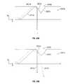
- FIG. 3is a diagram of movable mirror position versus applied voltage for one exemplary embodiment of an interferometric modulator of FIG. 1 .
- FIG. 4is an illustration of a set of row and column voltages that may be used to drive an interferometric modulator display.
- FIGS. 5A and 5Billustrate one exemplary timing diagram for row and column signals that may be used to write a frame of display data to the 3 ⁇ 3 interferometric modulator display of FIG. 2 .
- FIGS. 6A and 6Bare system block diagrams illustrating an embodiment of a visual display device comprising a plurality of interferometric modulators.
- FIG. 7Ais a cross-section of the device of FIG. 1 .
- FIG. 7Bis a cross-section of an alternative embodiment of an interferometric modulator.
- FIG. 7Cis a cross-section of another alternative embodiment of an interferometric modulator.
- FIG. 7Dis a cross-section of yet another alternative embodiment of an interferometric modulator.
- FIG. 7Eis a cross-section of an additional alternative embodiment of an interferometric modulator.
- FIG. 8is a cross-section of an embodiment of a display device having an illumination device and a reflective display.
- FIG. 9Ais a top plan view of an embodiment of a display device having turning features disposed in a uniform pattern on a turning film.
- FIG. 9Bis a top plan view of an embodiment of a display device having turning features disposed in a non-uniform pattern on a turning film.
- FIG. 9Cis a cross-section of an embodiment of an illumination device having a turning film and a substrate.
- FIG. 9Dillustrates certain dimensions of one embodiment of a turning feature rotationally.
- FIG. 10is a cross-section of an embodiment of an illumination device illustrating several embodiments of light turning features.
- FIG. 11is a cross-section of an embodiment of an illumination device including a substrate with light turning features.
- FIG. 12is a cross-section of an embodiment of an illumination device having two turning films.
- FIG. 13is a cross-section of an embodiment of an illumination device having two turning films, each turning film having light turning features, where at least some of the light turning features in each turning film are disposed vertically offset from those in the other turning film.
- FIG. 14is a cross-section of an embodiment of an illumination device having light turning features configured in the shape of a truncated cone and a lens.
- FIG. 15is a cross-section of an embodiment of another illumination device illustrating a turning film and a light guide with curved edges.
- FIG. 16is a cross-section of an illumination device illustrating an embodiment that includes a light source providing light through an angled edge of a turning film and/or a light guide.
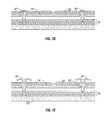
- FIG. 17Ais a cross-section of an embodiment of an illumination device that depicts light turning features having multi-coated edges.
- FIG. 17Bis a top plan view of an embodiment of an illumination device.
- FIG. 19Ais a cross-section of a turning film during a step of one example of a process for forming interferometric stacks on a light turning feature.
- FIG. 19Bis a cross-section of the turning film of FIG. 19A in an intermediate process step.
- FIGS. 20A-20Eare schematic cross-sectional views illustrating steps in a process of manufacturing an illumination device.
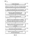
- FIG. 20Fis a block diagram schematically illustrating one embodiment of a method of making the illumination device of FIG. 20E .
- FIGS. 21A-21Hare schematic cross-sectional views illustrating steps in a process of manufacturing an illumination device.
- FIG. 21Iis a block diagram schematically illustrating one embodiment of a method of making the illumination device of FIG. 21H .
- FIG. 22A-22Eare schematic cross-sectional views illustrating steps in a process of manufacturing an illumination device.
- FIG. 22Fis a block diagram schematically illustrating one embodiment of a method of making the illumination device of FIG. 22E .
- FIG. 23A-23Jare schematic cross-sectional views illustrating steps in a process of manufacturing an illumination device.
- FIG. 23Kis a block diagram schematically illustrating one embodiment of a method of making the illumination device of FIG. 23J .
- FIG. 24A-24Fare schematic cross-sectional views illustrating steps in a process of manufacturing an illumination device.
- FIG. 24Gis a block diagram schematically illustrating one embodiment of a method of making the illumination device of FIG. 24F .
- FIG. 25A-25Gare schematic cross-sectional views illustrating steps in a process of manufacturing an illumination device.
- FIG. 25His a block diagram schematically illustrating one embodiment of a method of making the illumination device of FIG. 25G .
- FIG. 26A-26Fare schematic cross-sectional views illustrating steps in a process of manufacturing an illumination device.
- FIG. 26Gis a block diagram schematically illustrating one embodiment of a method of making the illumination device of FIG. 26F .
- FIG. 27A-27Care schematic cross-sectional views illustrating steps in a process of manufacturing an illumination device.
- FIG. 27Dis a block diagram schematically illustrating one embodiment of a method of making the illumination device of FIG. 27C .
- FIG. 27Eis a block diagram schematically illustrating one embodiment of a method of making the illumination device of FIG. 27C .
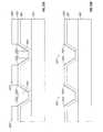
- FIG. 28is a cross-section of an embodiment of a turning film having tapered walls.
- FIG. 29Ais a schematic of a cross-section of an embodiment of a turning film having a polygonal turning feature.
- FIG. 29Bis a schematic of a cross-section of an embodiment of a turning film having a concave curvilinear turning feature.
- FIG. 29Cis a schematic of a cross-section of an embodiment of a turning film having a convex curvilinear turning feature.
- FIG. 29Dis a schematic of a cross-section of an embodiment of a turning film having a frustum shaped turning feature with concave sidewalls.
- FIG. 29Eis a schematic of a cross-section of an embodiment of a turning film having a frustum shaped turning feature with convex sidewalls.
- FIG. 29Fis a perspective view of the turning feature of FIG. 29D .
- FIG. 29Gis a perspective view of the turning feature of FIG. 29F .
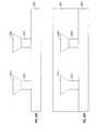
- FIG. 30Ais a schematic of a cross-section of an embodiment of a turning film having a concave curvilinear turning feature with multi-coated edges.
- FIG. 30Bis a schematic of a cross-section of an embodiment of a turning film having a convex curvilinear turning feature with multi-coated edges.
- FIG. 30Cis a schematic of a cross-section of an embodiment of a turning film having a frustum shaped turning feature with concave sidewalls and multi-coated edges.
- FIG. 30Dis a schematic of a cross-section of an embodiment of a turning film having a frustum shaped turning feature with convex sidewalls and multi-coated edges.
- FIGS. 31A-31Eare schematics of cross-sectional views illustrating steps in a process of manufacturing a turning film having convex turning features.
- FIGS. 32A-32Eare schematics of cross-sectional views illustrating steps in a process of manufacturing a turning film having a concave turning feature.
- the embodimentsmay be implemented in or associated with a variety of electronic devices such as, but not limited to, mobile telephones, wireless devices, personal data assistants (PDAs), hand-held or portable computers, GPS receivers/navigators, cameras, MP3 players, camcorders, game consoles, wrist watches, clocks, calculators, television monitors, flat panel displays, computer monitors, auto displays (e.g., odometer display, etc.), cockpit controls and/or displays, display of camera views (e.g., display of a rear view camera in a vehicle), electronic photographs, electronic billboards or signs, projectors, architectural structures, packaging, and aesthetic structures (e.g., display of images on a piece of jewelry).
- MEMS devices of similar structure to those described hereincan also be used in non-display applications such as in electronic switching devices.
- Illumination devicescan be used to provide light for reflective displays when ambient light is insufficient.
- an illumination devicecomprises a light source and a light guide that receives the light from the light source.
- the light sourcemay be positioned or offset relative to the display, and in such a position it may not provide sufficient or uniform light directly to the reflective display.
- an illumination devicecan also include light turning features that re-direct light from the light source towards the display, and such turning features can be included in a turning film positioned on the light guide.
- turning featureshave reflective coatings configured to (better) reflect light propagating within the light guide and/or turning film towards the reflective display.
- the reflective coatingscould appear shiny or bright, but they can be masked to a viewer by forming a dark coating (e.g., black mask) over the reflective coating to absorb light such that the turning features appear dark or black, resulting in improving contrast of the display.
- the black maskcan include the reflective layer, and an absorber layer, and be configured as a “static” interferometric modulator configured to appear dark or black.
- the light guide and the turning filmmay be made from an inorganic material. To facilitate light propagating between the turning film and the light guide, the turning film may have an index of refraction that matched to the light guide.
- Embodiments disclosed hereinrelate to different configurations of illumination devices that include one or more reflective coatings on turning features. Additional embodiments disclosed herein relate to processes of forming illumination devices that include an inorganic light guide and/or inorganic turning film.
- FIG. 1One interferometric modulator display embodiment comprising an interferometric MEMS display element is illustrated in FIG. 1 .
- the pixelsare in either a bright or dark state.
- the display elementIn the bright (“relaxed” or “open”) state, the display element reflects a large portion of incident visible light to a user.
- the dark (“actuated” or “closed”) stateWhen in the dark (“actuated” or “closed”) state, the display element reflects little incident visible light to the user.
- the light reflectance properties of the “on” and “off” statesmay be reversed.
- MEMS pixelscan be configured to reflect predominantly at selected colors, allowing for a color display in addition to black and white.
- FIG. 1is an isometric view depicting two adjacent pixels in a series of pixels of a visual display, wherein each pixel comprises a MEMS interferometric modulator.
- an interferometric modulator displaycomprises a row/column array of these interferometric modulators.
- Each interferometric modulatorincludes a pair of reflective layers positioned at a variable and controllable distance from each other to form a resonant optical gap with at least one variable dimension.
- one of the reflective layersmay be moved between two positions. In the first position, referred to herein as the relaxed position, the movable reflective layer is positioned at a relatively large distance from a fixed partially reflective layer.
- the movable reflective layerIn the second position, referred to herein as the actuated position, the movable reflective layer is positioned more closely adjacent to the partially reflective layer. Incident light that reflects from the two layers interferes constructively or destructively depending on the position of the movable reflective layer, producing either an overall reflective or non-reflective state for each pixel.
- the depicted portion of the pixel array in FIG. 1includes two adjacent interferometric modulators 12 a and 12 b .
- a movable reflective layer 14 ais illustrated in a relaxed position at a predetermined distance from an optical stack 16 a , which includes a partially reflective layer.
- the movable reflective layer 14 bis illustrated in an actuated position adjacent to the optical stack 16 b.
- optical stack 16typically comprise several fused layers, which can include an electrode layer, such as indium tin oxide (ITO), a partially reflective layer, such as chromium, and a transparent dielectric.
- ITOindium tin oxide
- the optical stack 16is thus electrically conductive, partially transparent and partially reflective, and may be fabricated, for example, by depositing one or more of the above layers onto a transparent substrate 20 .
- the partially reflective layercan be formed from a variety of materials that are partially reflective such as various metals, semiconductors, and dielectrics.
- the partially reflective layercan be formed of one or more layers of materials, and each of the layers can be formed of a single material or a combination of materials.
- the layers of the optical stack 16are patterned into parallel strips, and may form row electrodes in a display device as described further below.
- the movable reflective layers 14 a , 14 bmay be formed as a series of parallel strips of a deposited metal layer or layers (orthogonal to the row electrodes of 16 a , 16 b ) to form columns deposited on top of posts 18 and an intervening sacrificial material deposited between the posts 18 . When the sacrificial material is etched away, the movable reflective layers 14 a , 14 b are separated from the optical stacks 16 a , 16 b by a defined gap 19 .
- a highly conductive and reflective material such as aluminummay be used for the reflective layers 14 , and these strips may form column electrodes in a display device. Note that FIG. 1 may not be to scale. In some embodiments, the spacing between posts 18 may be on the order of 10-100 um, while the gap 19 may be on the order of ⁇ 1000 Angstroms.
- the gap 19remains between the movable reflective layer 14 a and optical stack 16 a , with the movable reflective layer 14 a in a mechanically relaxed state, as illustrated by the pixel 12 a in FIG. 1 .
- a potential (voltage) differenceis applied to a selected row and column, the capacitor formed at the intersection of the row and column electrodes at the corresponding pixel becomes charged, and electrostatic forces pull the electrodes together. If the voltage is high enough, the movable reflective layer 14 is deformed and is forced against the optical stack 16 .
- a dielectric layerwithin the optical stack 16 may prevent shorting and control the separation distance between layers 14 and 16 , as illustrated by actuated pixel 12 b on the right in FIG. 1 . The behavior is the same regardless of the polarity of the applied potential difference.
- FIGS. 2 through 5illustrate one exemplary process and system for using an array of interferometric modulators in a display application.
- FIG. 2is a system block diagram illustrating one embodiment of an electronic device that may incorporate interferometric modulators.
- the electronic deviceincludes a processor 21 which may be any general purpose single- or multi-chip microprocessor such as an ARM®, PentiumTM, 8051, MIPS®, Power PC®, or ALPHA®, or any special purpose microprocessor such as a digital signal processor, microcontroller, or a programmable gate array.
- the processor 21may be configured to execute one or more software modules.
- the processormay be configured to execute one or more software applications, including a web browser, a telephone application, an email program, or any other software application.
- the processor 21is also configured to communicate with an array driver 22 .
- the array driver 22includes a row driver circuit 24 and a column driver circuit 26 that provide signals to a display array or panel 30 .
- the cross-section of the array illustrated in FIG. 1is shown by the lines 1 - 1 in FIG. 2 .
- FIG. 2illustrates a 3 ⁇ 3 array of interferometric modulators for the sake of clarity, the display array 30 may contain a very large number of interferometric modulators, and may have a different number of interferometric modulators in rows than in columns (e.g., 300 pixels per row by 190 pixels per column).
- FIG. 3is a diagram of movable mirror position versus applied voltage for one exemplary embodiment of an interferometric modulator of FIG. 1 .
- the row/column actuation protocolmay take advantage of a hysteresis property of these devices as illustrated in FIG. 3 .
- An interferometric modulatormay require, for example, a 10 volt potential difference to cause a movable layer to deform from the relaxed state to the actuated state. However, when the voltage is reduced from that value, the movable layer maintains its state as the voltage drops back below 10 volts. In the exemplary embodiment of FIG. 3 , the movable layer does not relax completely until the voltage drops below 2 volts.
- the row/column actuation protocolcan be designed such that during row strobing, pixels in the strobed row that are to be actuated are exposed to a voltage difference of about 10 volts, and pixels that are to be relaxed are exposed to a voltage difference of close to zero volts.
- each pixelsees a potential difference within the “stability window” of 3-7 volts in this example.
- This featuremakes the pixel design illustrated in FIG. 1 stable under the same applied voltage conditions in either an actuated or relaxed pre-existing state. Since each pixel of the interferometric modulator, whether in the actuated or relaxed state, is essentially a capacitor formed by the fixed and moving reflective layers, this stable state can be held at a voltage within the hysteresis window with almost no power dissipation. Essentially no current flows into the pixel if the applied potential is fixed.
- a frame of an imagemay be created by sending a set of data signals (each having a certain voltage level) across the set of column electrodes in accordance with the desired set of actuated pixels in the first row.
- a row pulseis then applied to a first row electrode, actuating the pixels corresponding to the set of data signals.
- the set of data signalsis then changed to correspond to the desired set of actuated pixels in a second row.
- a pulseis then applied to the second row electrode, actuating the appropriate pixels in the second row in accordance with the data signals.
- the first row of pixelsare unaffected by the second row pulse, and remain in the state they were set to during the first row pulse. This may be repeated for the entire series of rows in a sequential fashion to produce the frame.
- the framesare refreshed and/or updated with new image data by continually repeating this process at some desired number of frames per second.
- a wide variety of protocols for driving row and column electrodes of pixel arrays to produce image framesmay be used.
- FIGS. 4 and 5illustrate one possible actuation protocol for creating a display frame on the 3 ⁇ 3 array of FIG. 2 .
- FIG. 4illustrates a possible set of column and row voltage levels that may be used for pixels exhibiting the hysteresis curves of FIG. 3 .
- actuating a pixelinvolves setting the appropriate column to ⁇ V bias , and the appropriate row to + ⁇ V, which may correspond to ⁇ 5 volts and +5 volts respectively Relaxing the pixel is accomplished by setting the appropriate column to +V bias , and the appropriate row to the same + ⁇ V, producing a zero volt potential difference across the pixel.
- the pixelsare stable in whatever state they were originally in, regardless of whether the column is at +V bias , or ⁇ V bias .
- voltages of opposite polarity than those described abovecan be used, e.g., actuating a pixel can involve setting the appropriate column to +V bias , and the appropriate row to ⁇ V.
- releasing the pixelis accomplished by setting the appropriate column to ⁇ V bias , and the appropriate row to the same ⁇ V, producing a zero volt potential difference across the pixel.
- FIG. 5Bis a timing diagram showing a series of row and column signals applied to the 3 ⁇ 3 array of FIG. 2 which will result in the display arrangement illustrated in FIG. 5A , where actuated pixels are non-reflective.
- the pixelsPrior to writing the frame illustrated in FIG. 5A , the pixels can be in any state, and in this example, all the rows are initially at 0 volts, and all the columns are at +5 volts. With these applied voltages, all pixels are stable in their existing actuated or relaxed states.
- pixels (1,1), (1,2), (2,2), (3,2) and (3,3)are actuated.
- columns 1 and 2are set to ⁇ 5 volts, and column 3 is set to +5 volts. This does not change the state of any pixels, because all the pixels remain in the 3-7 volt stability window.
- Row 1is then strobed with a pulse that goes from 0, up to 5 volts, and back to zero. This actuates the (1,1) and (1,2) pixels and relaxes the (1,3) pixel. No other pixels in the array are affected.
- column 2is set to ⁇ 5 volts
- columns 1 and 3are set to +5 volts.
- Row 3is similarly set by setting columns 2 and 3 to ⁇ 5 volts, and column 1 to +5 volts.
- the row 3 strobesets the row 3 pixels as shown in FIG. 5A .
- the row potentialsare zero, and the column potentials can remain at either +5 or ⁇ 5 volts, and the display is then stable in the arrangement of FIG. 5A .
- the same procedurecan be employed for arrays of dozens or hundreds of rows and columns.
- the timing, sequence, and levels of voltages used to perform row and column actuationcan be varied widely within the general principles outlined above, and the above example is exemplary only, and any actuation voltage method can be used with the systems and methods described herein.
- FIGS. 6A and 6Bare system block diagrams illustrating an embodiment of a display device 40 .
- the display device 40can be, for example, a cellular or mobile telephone.
- the same components of display device 40 or slight variations thereofare also illustrative of various types of display devices such as televisions and portable media players.
- the display device 40includes a housing 41 , a display 30 , an antenna 43 , a speaker 45 , an input device 48 , and a microphone 46 .
- the housing 41is generally formed from any of a variety of manufacturing processes, including injection molding, and vacuum forming.
- the housing 41may be made from any of a variety of materials, including but not limited to plastic, metal, glass, rubber, and ceramic, or a combination thereof.
- the housing 41includes removable portions (not shown) that may be interchanged with other removable portions of different color, or containing different logos, pictures, or symbols.
- the display 30 of exemplary display device 40may be any of a variety of displays, including a bi-stable display, as described herein.
- the display 30includes a flat-panel display, such as plasma, EL, OLED, STN LCD, or TFT LCD as described above, or a non-flat-panel display, such as a CRT or other tube device.
- the display 30includes an interferometric modulator display, as described herein.
- the components of one embodiment of exemplary display device 40are schematically illustrated in FIG. 6B .
- the illustrated exemplary display device 40includes a housing 41 and can include additional components at least partially enclosed therein.
- the exemplary display device 40includes a network interface 27 that includes an antenna 43 which is coupled to a transceiver 47 .
- the transceiver 47is connected to a processor 21 , which is connected to conditioning hardware 52 .
- the conditioning hardware 52may be configured to condition a signal (e.g. filter a signal).
- the conditioning hardware 52is connected to a speaker 45 and a microphone 46 .
- the processor 21is also connected to an input device 48 and a driver controller 29 .
- the driver controller 29is coupled to a frame buffer 28 , and to an array driver 22 , which in turn is coupled to a display array 30 .
- a power supply 50provides power to all components as required by the particular exemplary display device 40 design.
- the network interface 27includes the antenna 43 and the transceiver 47 so that the exemplary display device 40 can communicate with one or more devices over a network. In one embodiment the network interface 27 may also have some processing capabilities to relieve requirements of the processor 21 .
- the antenna 43is any antenna for transmitting and receiving signals. In one embodiment, the antenna transmits and receives RF signals according to the IEEE 802.11 standard, including IEEE 802.11(a), (b), or (g). In another embodiment, the antenna transmits and receives RF signals according to the BLUETOOTH standard. In the case of a cellular telephone, the antenna is designed to receive CDMA, GSM, AMPS, W-CDMA, or other known signals that are used to communicate within a wireless cell phone network.
- the transceiver 47pre-processes the signals received from the antenna 43 so that they may be received by and further manipulated by the processor 21 .
- the transceiver 47also processes signals received from the processor 21 so that they may be transmitted from the exemplary display device 40 via the antenna 43 .
- the transceiver 47can be replaced by a receiver.
- network interface 27can be replaced by an image source, which can store or generate image data to be sent to the processor 21 .
- the image sourcecan be a digital video disc (DVD) or a hard-disc drive that contains image data, or a software module that generates image data.
- Processor 21generally controls the overall operation of the exemplary display device 40 .
- the processor 21receives data, such as compressed image data from the network interface 27 or an image source, and processes the data into raw image data or into a format that is readily processed into raw image data.
- the processor 21then sends the processed data to the driver controller 29 or to frame buffer 28 for storage.
- Raw datatypically refers to the information that identifies the image characteristics at each location within an image. For example, such image characteristics can include color, saturation, and gray-scale level.
- the processor 21includes a microcontroller, CPU, or logic unit to control operation of the exemplary display device 40 .
- Conditioning hardware 52generally includes amplifiers and filters for transmitting signals to the speaker 45 , and for receiving signals from the microphone 46 .
- Conditioning hardware 52may be discrete components within the exemplary display device 40 , or may be incorporated within the processor 21 or other components.
- the driver controller 29takes the raw image data generated by the processor 21 either directly from the processor 21 or from the frame buffer 28 and reformats the raw image data appropriately for high speed transmission to the array driver 22 . Specifically, the driver controller 29 reformats the raw image data into a data flow having a raster-like format, such that it has a time order suitable for scanning across the display array 30 . Then the driver controller 29 sends the formatted information to the array driver 22 .
- a driver controller 29such as a LCD controller, is often associated with the system processor 21 as a stand-alone Integrated Circuit (IC), such controllers may be implemented in many ways. They may be embedded in the processor 21 as hardware, embedded in the processor 21 as software, or fully integrated in hardware with the array driver 22 .
- the array driver 22receives the formatted information from the driver controller 29 and reformats the video data into a parallel set of waveforms that are applied many times per second to the hundreds and sometimes thousands of leads coming from the display's x-y matrix of pixels.
- driver controller 29is a conventional display controller or a bi-stable display controller (e.g., an interferometric modulator controller).
- array driver 22is a conventional driver or a bi-stable display driver (e.g., an interferometric modulator display).
- a driver controller 29is integrated with the array driver 22 .
- display array 30is a typical display array or a bi-stable display array (e.g., a display including an array of interferometric modulators).
- the input device 48allows a user to control the operation of the exemplary display device 40 .
- input device 48includes a keypad, such as a QWERTY keyboard or a telephone keypad, a button, a switch, a touch-sensitive screen, a pressure- or heat-sensitive membrane.
- the microphone 46is an input device for the exemplary display device 40 . When the microphone 46 is used to input data to the device, voice commands may be provided by a user for controlling operations of the exemplary display device 40 .
- Power supply 50can include a variety of energy storage devices as are well known in the art.
- power supply 50is a rechargeable battery, such as a nickel-cadmium battery or a lithium ion battery.
- power supply 50is a renewable energy source, a capacitor, or a solar cell, including a plastic solar cell, and solar-cell paint.
- power supply 50is configured to receive power from a wall outlet.
- control programmabilityresides, as described above, in a driver controller which can be located in several places in the electronic display system. In some cases control programmability resides in the array driver 22 .
- the above-described optimizationmay be implemented in any number of hardware and/or software components and in various configurations.
- FIGS. 7A-7Eillustrate five different embodiments of the movable reflective layer 14 and its supporting structures.
- FIG. 7Ais a cross-section of the embodiment of FIG. 1 , where a strip of metal material 14 is deposited on orthogonally extending supports 18 .
- the moveable reflective layer 14 of each interferometric modulatoris square or rectangular in shape and attached to supports at the corners only, on tethers 32 .
- the moveable reflective layer 14is square or rectangular in shape and suspended from a deformable layer 34 , which may comprise a flexible metal.
- the deformable layer 34connects, directly or indirectly, to the substrate 20 around the perimeter of the deformable layer 34 . These connections are herein referred to as support posts.
- the embodiment illustrated in FIG. 7Dhas support post plugs 42 upon which the deformable layer 34 rests.
- the movable reflective layer 14remains suspended over the gap, as in FIGS. 7A-7C , but the deformable layer 34 does not form the support posts by filling holes between the deformable layer 34 and the optical stack 16 . Rather, the support posts are formed of a planarization material, which is used to form support post plugs 42 .
- the embodiment illustrated in FIG. 7Eis based on the embodiment shown in FIG. 7D , but may also be adapted to work with any of the embodiments illustrated in FIGS.
- FIG. 7Ean extra layer of metal or other conductive material has been used to form a bus structure 44 . This allows signal routing along the back of the interferometric modulators, eliminating a number of electrodes that may otherwise have had to be formed on the substrate 20 .
- the interferometric modulatorsfunction as direct-view devices, in which images are viewed from the front side of the transparent substrate 20 , the side opposite to that upon which the modulator is arranged.
- the reflective layer 14optically shields the portions of the interferometric modulator on the side of the reflective layer opposite the substrate 20 , including the deformable layer 34 . This allows the shielded areas to be configured and operated upon without negatively affecting the image quality. For example, such shielding allows the bus structure 44 in FIG. 7E , which provides the ability to separate the optical properties of the modulator from the electromechanical properties of the modulator, such as addressing and the movements that result from that addressing.
- This separable modulator architectureallows the structural design and materials used for the electromechanical aspects and the optical aspects of the modulator to be selected and to function independently of each other.
- the embodiments shown in FIGS. 7C-7Ehave additional benefits deriving from the decoupling of the optical properties of the reflective layer 14 from its mechanical properties, which are carried out by the deformable layer 34 .
- Thisallows the structural design and materials used for the reflective layer 14 to be optimized with respect to the optical properties, and the structural design and materials used for the deformable layer 34 to be optimized with respect to desired mechanical properties.
- Interferometric modulatorsare reflective elements that can be configured to reflect ambient lighting in daylight or well-lit environments to produce a display.
- a light sourcecan provide the required illumination, either directly or through a light guide that provides a propagation path from the light source to the display elements.
- an illumination deviceprovides light from a light source to the display elements.
- the illumination devicecan include a light guide and light turning features, which may be disposed in or on a turning film disposed on the light guide.
- the illumination devicealso includes a light source.
- the light guidecan be a planar optical device disposed over and parallel to the display such that incident light passes through the light guide to the display, and light reflected from the display also passes through the light guide.
- the light sourceincludes an optical device (for example, a light bar) that is configured to receive light from a point source (e.g., a light emitting diode) and provides light as a line source.
- a point sourcee.g., a light emitting diode
- Light entering the light barmay propagate along some or all of the length of the bar and exit out of a surface or edge of the light bar over a portion or all of the length of the light bar.
- Light exiting the light barmay enter an edge of a light guide and/or a turning film, and then propagate within the light guide and/or turning film such that a portion of the light propagates in a direction across at least a portion of the display at a low-graze angle relative to the surface of the light guide aligned with the display such that the light is reflected within the light guide by total internal reflection (“TIR”).
- TIRtotal internal reflection
- turning features in the light guide and/or turning filmdirect the light towards the display elements at an angle sufficient so that at least some of the light passes through the light guide to the reflective display.
- the turning featuresmay include one or more coatings (or layers).
- the coatingscan be configured to increase reflectivity of a turning feature and/or function as a black mask to improve contrast of the display as seen by a viewer.
- the coatings on the turning featuresmay be configured as an interferometric stack having a reflective layer that re-directs light propagating within the light guide and/or turning film, a partially reflective absorber layer disposed between the reflective layer and the direction exposed to ambient light, and a layer disposed between the reflective layer and the absorber layer which defines an optical resonant cavity by its thickness.
- FIG. 8illustrates a cross-sectional view of one embodiment of a display device 800 that includes an illumination device configured to provide front light illumination to a reflective display 807 .
- the display device 800includes a turning film 801 shown in FIG. 8 as forming a first side 800 a of the device 800 .
- the turning film 801is disposed on a light guide 803 .
- a reflective display 807is disposed underneath the light guide 803 and defines a second side 800 b of the display device 800 .
- an optical isolation layer 805may optionally be disposed between the reflective display 807 and the light guide 803 .
- a light source 809may be disposed near the light guide 803 and turning film 801 and configured to input light into at least one edge or surface of either, or both, the turning film 801 and the light guide 803 , illustrated in FIG. 8 as providing light into both the turning film 810 and the light guide 803 .
- the light source 809may comprise any suitable light source, for example, an incandescent bulb, a light bar, a light emitting diode (“LED”), a fluorescent lamp, an LED light bar, an array of LEDs, and/or another light source.
- the reflective display 807comprises a plurality of reflective elements, for example, interferometric modulators, MEMS devices, NEMS devices, reflective spatial light modulators, electromechanical devices, liquid crystal structures, and/or any other suitable reflective display.
- the reflective elementsmay be configured in an array.
- the reflective display 807includes a first planar side that is configured to modulate light incident thereon and a second planar side disposed opposite to the first planar side.
- the size of the reflective display 807can vary depending upon the application. For example, in some embodiments, the reflective display 807 is sized to fit within a notebook computer casing. In other embodiments, the reflective display 807 is sized to fit within or form part of a mobile phone or similar mobile device.
- the turning film 801 and light guide 803can comprise any substantially optically transmissive material that allows light to propagate along the length thereof.
- the turning film 801 and the light guide 803may each comprise one or more of the following materials: acrylics, acrylate copolymers, UV-curable resins, polycarbonates, cycloolefin polymers, polymers, organic materials, inorganic materials, silicates, alumina, sapphire, glasses, polyethylene terephthalate (“PET”), polyethylene terephthalate glycol (“PET-G”), silicon oxy-nitride, and/or other optically transparent materials.
- PETpolyethylene terephthalate
- PET-Gpolyethylene terephthalate glycol
- silicon oxy-nitrideand/or other optically transparent materials.
- the turning film 801 and the light guide 803comprise the same material and in other embodiments, the turning film and the light guide 803 comprise different materials.
- the indices of refraction of the turning film 801 and the light guide 803may be close or equal to one another such that light may propagate successively through the two layers without being substantially reflected or refracted at the interface between the two layers.
- the light guide 803 and the turning film 801each have an index of refraction of about 1.52. According to other embodiments, the indices of refraction of the light guide 803 and/or the turning film 801 can range from about 1.45 to about 2.05.
- the light guide 803 and turning film 801may be held together by an adhesive, which may have an index of refraction similar or equal to the index of refraction of one or both of the light guide and turning film.
- the reflective display 807is laminated to the light guide 803 using a refractive-index matched pressure-sensitive adhesive (“PSA”) or similar adhesive.
- PSApressure-sensitive adhesive
- Both the light guide 803 and the turning film 801can include one or more turning features 820 .
- the light guide 803 and the turning film 801each comprise a single layer.
- the light guide 803 and/or the turning film 801comprise more than one layer.
- the light guide 803 and the turning film 801can have differing thicknesses and/or other dimensions.
- the turning film 801can have a thickness of between about 40 and about 100 microns
- the light guide 803can have a thickness of between about 40 and about 200 microns. Uniformity of brightness across the display device 800 and efficiency of the display device may be affected by the thickness of the light guide 803 and of the turning film 801 .
- the turning film 801can include one or more turning features 820 disposed on or along the first side 800 a of the display device 800 .
- one or more turning features 820may be disposed on the side of the turning film 801 and/or light guide 803 nearest to the reflective display 807 .
- the turning features 820 depicted throughout the attached figuresare schematic and exaggerated in size and spacing therebetween for clarity of illustration.
- the turning features 820can comprise one or more angled and/or curved surfaces configured to refract (or reflect) at least some of the light which is traveling through the light guide (e.g., at an oblique angle) away from the display 807 at the interface between the angled or curved surface of the feature 820 and the air, and redirect that light towards the reflective display 807 .
- the turning featurescan comprise a plurality of surface features or volume features.
- the turning features 820comprise one or more diffractive optical elements, grooves, depressions, and/or pits.
- the turning features 820comprise holograms or holographic features. The holograms may include holographic volume or surface features.
- the size, shape, quantity, and pattern of the turning features 820may vary. In some embodiments, the turning features 820 may be disposed along the length and width of the turning film 801 . In some embodiments, turning features 820 are disposed on about 5% of the area of the first side 800 a of the turning film 801 .
- the turning features 820are configured to receive light propagating along the length of the turning film 801 and turn the light through a large angle, for example, between about 70-90°.
- the turning features 820can have one or more edges shaped such that they can reflect light incident on the edges from certain directions via total internal reflection (“TIR”) and cause the light to be turned toward the reflective display 807 at a normal or near-normal angle of incidence (with respect to the display).
- TIRtotal internal reflection
- the turning features 820 illustrated and described hereinmay include a reflective coating which is selected and/or configured to increase light reflection properties (for example, reflective coatings as described in reference to FIGS. 17A , 18 , 19 C, 20 D, 20 E, 21 H, and others).
- the turning features 820may be molded, etched, or machined in the turning film 801 .
- the turning features described hereinmay be molded, etched, or machined directly in the light guide 803 and a separate turning film 801 is not included, such that the light guide itself forms a turning film.
- both the light guide 803 and the turning film 801include turning features 820 . Methods for forming turning features are described herein below in reference to FIGS. 19A-D , 20 A-F, 21 .
- light 811 emitted from the light source 809enters the light guide 803 and/or the turning film 801 along one or more edges or surfaces of the light guide and/or the turning film.
- a portion of light 811propagates within the light guide 803 and turning film 801 at shallow angles (e.g., not near-perpendicular to the reflective display 807 ) and may generally remain within the light guide 803 and turning film 801 by TIR.
- light 811 impinges on turning features 820it may be turned at a perpendicular or near-perpendicular angle toward the display 807 allowing the light 811 to break TIR and illuminate the display 807 .
- Light 811 that illuminates the reflective display 811may be reflected towards the first side 800 a and out of the display deice 800 towards a viewer.
- the light turning features 820can be configured to reflect light at an angle normal to the display or close thereto.
- Light 811 that does not at first reflect off of one of the turning features 820may continue to propagate through the light guide 803 and turning film 801 and subsequently reflect off another of the turning features 820 and be redirected towards the display 807 , for example at a location further from the light source 809 .
- one or more optical isolation layers 805may be disposed between the light guide 803 and the reflective display 807 to improve the optical performance of the display 800 .
- An optical isolation layer 805may be disposed between the light guide 803 and an array of interferometric modulators to prevent light propagating through the light guide 803 at shallow angles from reaching the array, because such light would also be reflected from the display at a shallow angle and may not reach a viewer.
- the optical isolation layer 805has an index of refraction substantially lower than the light guide 803 such that light traveling through the light guide 803 and striking the optical isolation layer 805 at an oblique or low grazing angle, for example, light traveling at a lower angle than the critical angle (which may be, for example, greater than 50° or 60°), will be reflected back into the light guide 803 and turning film 801 .
- the optical isolation layer 805can include, for example, silicon dioxide, fluorinated silicon dioxide, or another material with a suitable index of refraction.
- the size, shape, pattern, and quantity of the turning features 820can vary.
- the quantity of turning features 820can vary from one turning film 801 to another and the density of turning features 820 can vary from one portion of a turning film 801 to another portion of the turning film.
- FIG. 9Aillustrates an embodiment having turning features 820 disposed across a turning film 801 in a uniform pattern.
- FIG. 9Billustrates an embodiment where the density of turning features 820 is higher towards the middle or center of the turning film 801 than near the edges of the turning film 801 .
- the quantity and pattern of turning features 820can affect the total illumination efficiency of a display device and/or the uniformity of light extraction across a display device.
- An illumination efficiency of a display devicecan be determined, for example, by comparing the amount of light provided by a light source with the amount of light reflected from the reflective display 807 .
- the quantity and pattern of turning features 820 on a given turning film 801may depend upon the size and/or shape of the turning features.
- the turning features 820comprise between about 2% and 10% of the total top surface area of a turning film 801 and/or light guide 803 .
- the turning features 820comprise about 5% of the total top surface area of a turning film 801 .
- turning features 820are disposed about 100 microns from one another on a turning film 801 .
- each turning feature 820 on a turning film 801can be substantially the same size and shape. In other embodiments, the turning features 820 on a turning film 801 may vary in size and/or shape. In some embodiments, a turning film 801 comprises a plurality of turning features 820 each having a generally different cross-sectional shape. In some embodiments, a turning film 801 comprises a plurality of turning features 820 each having a generally similar cross-sectional shape. In some embodiments, a turning film 801 comprises a first group of turning features 820 each having a generally similar cross-sectional shape and a second group of turning features 820 each having a generally similar cross-sectional shape wherein the first group of features 820 are differently shaped than the second group of turning features.
- a turning feature 820may have a generally polygonal cross-sectional shape, for example, square, rectangular, trapezoidal, triangular, hexagonal, octagonal, or some other polygonal shape. In other embodiments, a turning feature 820 may have a generally curvilinear cross-sectional shape. In some embodiments, a turning feature 820 has an irregular cross-sectional shape. The cross-sectional shape of a turning feature 820 may be symmetric or asymmetric. In some embodiments, the shape formed by the surface of a turning feature may resemble a cone, a frustum of a cone, a pyramid, a frustum of a pyramid, a prism, a polyhedron, or another three-dimensional shape.
- the shape of the turning features 820 viewed from the topmay vary.
- the shape of the turning features 820 viewed from the topmay be polygonal, curvilinear, irregular, generally polygonal, generally curvilinear, square, triangular, rectangular, circular, round, or another shape.
- the turning features 820 in a turning film 801can be configured to vary in depth and width.
- turning features 820 on a turning film 801each have a similar depth measured from the top of the turning film 801 to the bottom of the turning features 820 .
- a turning film 801comprises a plurality of turning features 820 which may be of different depths.
- the volume of each turning feature 820can vary from turning film 801 to turning film 801 or from turning feature 820 to turning feature 820 on a common turning film.
- the volume, depth, or width of turning features 820 on a given turning film 801may vary depending on the distance from the turning feature to the light source.
- the number of turning features 820increases from the light input edge of the turning film 801 towards the center of the turning film 801 to facilitate uniform light extraction.
- the width of each turning feature 820is between about one micron and about six microns. In some embodiment, the width of each turning feature 820 is about two microns.
- the size and shape of each turning feature 820can be varied by using different patterns, etching agents, process recipes, and/or different lithography and deposition conditions of the turning film 801 and/or light guide 803 .
- a first set of turning features 820may be formed using a first timed etch and a differently shaped and/or sized set of turning features 820 may be formed using a second timed etch.
- FIG. 9Dillustrates additional examples of turning features 820 a , 820 b which are rotationally symmetrical.
- the turning features 820 a , 820 bmay comprise indentations in the material comprising the light guide and/or turning film.
- feature 820 bmay take on a conical shape having an apex.
- the conemay be truncated, removing the apex and creating a frustoconical shape, so as to create the structure 820 a .
- 820 a ′shows a cross-sectional view of one exemplary implementation of the feature 820 a .
- FIG. 10shows an embodiment comprising a plurality of variously-shaped turning features 820 .
- componentse.g., layers
- film and layershave been used herein, such terms as used herein include film stacks and multilayered structures. Such film stacks and multilayered structures can be adhered to other structures using adhesive, or can be formed on other structures using deposition or in other manners.
- FIGS. 11 and 12illustrate cross-sectional views of a light guide 803 ( FIG. 11 ) and a turning film 801 ( FIG. 12 ) that include one or more light turning features 820 .
- the light turning features 820include one or more edges that extend from a top side or surface 823 to a bottom side or surface 825 of the turning film 801 or light guide 803 .
- Such a configurationcan also be referred to as “running through” the turning film 801 and/or light guide 803 .
- light turning features 820are shown running through a light guide 803 .
- the light turning features 820may have similar cross-sectional shapes or different cross-sectional shapes.
- the light turning features 820may be formed using different etching agents and techniques, for example, timed etching. In some embodiments, the light turning features 820 may be formed by standard wet or dry etching processes. In certain embodiments, the light turning features 820 may be formed by sand blast processes.
- light turning features 820are shown running through a turning film that includes two layers 801 a , 801 b .
- the two turning film layers 801 a , 801 bare disposed on light guide 803 , but the turning features 820 do not extend into the light guide 803 from the turning film layers 801 a , 801 b .
- the turning features 820may be formed through a single or multilayer turning film 801 into a light guide 803 .
- turning features 820can may be formed through a single or multilayer turning film 801 and extend through a single or multilayer light guide 803 .
- a turning filmmay include a plurality of layers 801 a , 801 b each including turning one or more turning features 820 .
- a turning filmincludes a first layer 801 a and a second layer 801 b .
- the first layer 801 ais disposed on the second layer 801 b such that the second layer 801 b is disposed between the light guide 803 and the first layer 801 a .
- the first layer 801 a and the second layer 801 bmay each include separate turning features 820 .
- the turning features 820may be offset from one another (e.g., laterally offset relative to the length or width of the film turning layers) such that a turning feature 820 in the first layer 801 a is not disposed directly above another turning feature 820 in the second layer 801 b .
- the turning features 820 in the first layer 801 amay overlap one or more turning features 820 in the second layer 801 b .
- the turning features 820 in the first layer 801 ahave a height “h” ( FIG. 13 ) such that the turning features run through the first layer but do not extend into the second layer 801 b .
- the turning features 820 in the second layer 801 bmay run through the second layer but do not extend into the first layer 801 a .
- one or more turning features 820may be disposed in both the first layer 801 a and the second layer 801 b as illustrated in FIG. 12 .
- the turning features 820vary in shape, size, pattern, quantity, and/or volume from layer to layer or within a single layer.
- the turning features 820 in a first layer 801 aare each substantially the same size but vary in cross-sectional shape and the turning features 820 in a second layer 801 b are each differently sized and differently shaped from one another and the turning features 820 in the first layer 801 a.
- a turning film 801 and/or light guide 803can include additional features in addition to turning features 820 .
- FIG. 14illustrates a turning film 801 that includes a plurality of turning features 820 having a first configuration.
- the turning film 801includes an additional optical device, edge 1400 , which may be configured in different shapes and sizes to optimize performance and provide multiple operational advantages.
- edges 1400may be included in addition to turning features 820 .
- the structure of additional edges 1400can vary depending upon application.
- edge 1400is configured as a Fresnel lens.
- an additional edgeincludes a micro lens.
- the shape of one or more edges or sides of the light guide 803 and/or turning film 801can be configured to affect the introduction of light from a light source into the turning film 801 and/or light guide 803 .
- FIG. 15illustrates an embodiment of a light guide 803 and a turning film 801 where the two layers have beveled or curved edges that are not perpendicular to the faces of the light guide 803 or turning film 801 .
- such beveled or curved sides or edges of the turning film 801 and/or light guide 803may be employed to reduce or eliminate bright spots near the edges where light is introduced by a light source, and to increase the uniformity of light extraction across the display.
- providing unpolished edges or sides on the light guide 803 and/or turning film 801can serve to eliminate bright spots of light extraction by acting as a diffuser and reflector.
- such beveled edgescan be covered by a reflector when appropriate to recycle light propagating within the turning film 801 and/or light guide 803 .
- one or more edges or surfaces of the light guide 803 and/or turning film 801may be angled relative to the first side 800 a and/or second side 800 b of the display device.
- the edges of the turning film 801 and the light guide 803may be disposed at an angle of about 45° relative to the first side 800 a and second side 800 b .
- the edges of the turning film 801 and the light guide 803may be disposed at an angle of between about 0° and about 90° relative to the first side 800 a and second side 800 b .
- a light source 809may be configured to introduce light at an angle about normal to the angled edges of the turning film 801 and the light guide 803 in order to increase the efficiency of the display device. In some embodiments, when light is introduced into the light guide 803 and/or turning film 801 at an angle, the light propagates within the light guide 803 and turning film 801 at shallow angles and more light is turned by the light turning features 820 .
- turning featuresmay turn light at the air/turning feature interface via TIR and direct the light towards one or more directions (e.g., towards a reflective display).
- a turning featuremay include a reflective coating configured to provide desirable optical characteristics.
- the coatingcan include one or more layers. One of the layers may be an additional coating configured to increase the reflectivity of a turning feature.
- the reflective coatingmay be metallic.
- some of the plurality of turning featuresmay include a reflective coating and others may not.
- a portion (or portions) of a turning featuremay be covered with a reflective coating and another portion (or portions) of the turning feature may not be covered with a reflective coating.
- a reflective coatingcan improve the efficiency of a display device because the reflective coatings can be configured to reflect substantially all of the light that encounters the coatings and redirect that light toward the display. Additionally, in some applications, it may be desirable to add or build additional layers or features on top of one or more turning features.
- one or more cover layersfor example, anti-glare layers, anti-reflection layers, anti-scratch layers, anti-smudge layers, diffuser layers, color filtering layers, lenses, or other layers, may be added on top of one or more turning features.
- conductive electrode platesmay be added on top of a turning film including turning features.
- a touch sensormay be added over one or more turning features.
- turning featuresrely solely on the air/feature interface to turn light
- having additional layers on the turning featuresmay complicate the desired optical functionality because adhesives or laminates may cover or partially cover one or more turning features and affect TIR characteristics of the light turning feature.
- adhesives or laminatesmay cover or partially cover one or more turning features and affect TIR characteristics of the light turning feature.
- one or more additional layerscan be added over the turning features without affecting the light turning properties of the turning features because they no longer rely on the TIR properties of a material-air interface.
- a static interferometric stackmay include a reflector layer deposited on the turning film or light guide, an absorber layer, and an optical resonant cavity defined by the reflector layer and the absorber layer.
- the reflector layeris a partial reflector.
- reflective coatingsare covered by one or more dark or black coatings to form a black mask which prevents reflection of light towards a viewer from the reflective coating.
- FIG. 17Aillustrates a turning film 801 that includes turning features 820 (note: FIG. 17A and the other figures herein are not drawn to scale).
- An interferometric stack 1707is formed over portions of certain surfaces of each turning feature 820 .
- An interferometric stack 1707includes a reflective layer 1705 disposed on one or more portions of the turning feature 820 surface.
- the interferometric stack 1707also includes an optically resonant layer 1703 formed on top of the reflective layer 1705 , and an absorber layer 1701 disposed over the optically resonant layer 1703 .
- the interferometric stacks 1707can be configured to interferometrically reflect selected wavelengths of light. This reflected light is incident on the absorber layer 1701 .
- the absorber layer 1701 and the interferometric stacks 1707are configured such that the absorber layer 1701 absorbs light of the reflected wavelength such that the stack 1707 appears black or dark, which can increase the contrast of the display.
- the reflective layer 1705is formed on the tapered sidewalls 831 of each turning feature 820 but not the bottom 833 . In some embodiments, the reflective layer 1705 may be formed on portions of the tapered sidewalls 831 and/or certain lower portions or the bottoms 833 .
- the reflector layer 1705includes a single layer and in other embodiments the reflector layer 1705 includes multiple layers of material.
- the thicknesses of the absorber 1701 and reflective layers 1705may be selected to control relative amounts of reflectance and transmittance of light.
- both the absorber 1701 and reflective 1705 layersmay comprise metal, and both can be configured to be partially transmissive.
- the amount of light substantially reflected or transmitted through the reflective layer 1705can be affected by varying the thickness and the composition of the reflective layer 1705 , whereas the apparent color of reflection is largely determined by the interference effect governed by the size or thickness of the optically resonant layer 1703 and the material properties of the absorber layer 1701 that determine the difference in optical path length.
- modulating the bottom reflective layer 1705 thicknesscan modulate the intensity of the reflected color versus the overall reflectivity of the interferometric stack 1707 .
- the optically resonant layer 1703is defined by a solid layer, for example, an optically transparent dielectric layer, or plurality of layers. In other embodiments, the optically transparent layer 1703 is defined by an air gap or combination of optically transparent solid material layer(s) and an air gap. In some embodiments, the thickness of the optically resonant layer 1704 may be selected to maximize or minimize the reflection of one or more specific colors of the light incident on the absorber 1701 side of the stack 1707 . In various embodiments, the color or colors reflected by the optically resonant layer 1703 may be changed by changing the thickness of the layer.
- the absorber layer 1701can comprise various materials, for example, molybdenum (Mo), titanium (Ti), tungsten (W), chromium (Cr), etc., as well as alloys, for example, MoCr.
- the absorber 1701can be between about 20 and about 300 ⁇ thick. In one embodiment, the absorber 1701 is about 80 ⁇ thick.
- the reflective layer 1705may, for example, comprise a metal layer, for example, aluminum (Al), nickel (Ni), silver (Ag), molybdenum (Mo), gold (Au), and chromium (Cr).
- the reflective layer 1701can be between about 100 ⁇ and about 700 ⁇ thick. In one embodiment, the reflective layer 1701 is about 300 ⁇ thick.
- the optically resonant layer 1703can comprise various optically resonant materials, for example, air, silicon oxy-nitride (SiO x N), silicon dioxide (SiO 2 ), aluminum oxide (Al 2 O 3 ), titanium dioxide (TiO 2 ), magnesium fluoride (MgF 2 ), chromium (III) oxide (Cr 3 O 2 ), silicon nitride (Si 3 N 4 ), transparent conductive oxides (TCOs), indium tin oxide (ITO), and zinc oxide (ZnO).
- any dielectric with an index of refraction (n) between 1 and 3can be used to form a suitable spacer layer.
- the optically resonant layer 1703is between about 500 ⁇ and about 1500 ⁇ thick. In one embodiment, the optically resonant layer 1703 is about 800 ⁇ thick.
- An interferometric stack 1707 as shown in FIG. 17can be configured to selectively produce a desired reflection output using optical interference. As discussed above, in some embodiments, this reflected output may be “modulated” by selection of the thickness and optical properties of the layers that form the stack 1707 . The color observed by a viewer viewing the absorber layer 1701 side of the stack will correspond to the frequencies which are substantially reflected out of the interferometric stack 1707 and which are not substantially absorbed or destructively interfered by one or more layers in the stack 1707 . As shown in FIG. 17B , the interferometric stacks 1707 depicted in FIG. 17A can be configured to appear dark or black to a viewer viewing the absorber layer 1701 side of the turning film 801 .
- configuring the coated portions of the turning features 820 to appear dark or blackimproves the contrast of the display device while providing other benefits discussed above (e.g., improved light turning functionality and easily building layers on top of the turning features 820 without disrupting the turning functionality). Additionally, selectively coating only portions of the turning features 820 , for example, the side-walls, with interferometric stack layers can limit the total area of the turning film 801 that appears dark to a viewer due to interferometric disruption.
- each turning feature 820differs in size and cross-sectional shape. Additionally, each turning feature includes an interferometric stack 1707 covering at least a portion of the turning feature 820 surface. As discussed above, turning features 820 that include interferometric stacks 1707 can vary in size, shape, quantity, and pattern depending on the application. For example, in some embodiments, some turning features 820 on a turning film 801 can be covered at least partially by an interferometric stack 1707 and other turning features 820 on the film 801 may not be covered by an interferometric stack.
- each turning feature 820can vary in shape and/or size but each turning feature 820 may be covered at least partially by an interferometric stack 1707 . In some embodiments, each turning feature 820 can be covered at least partially by an interferometric stack 1707 but the coverage may vary from one turning feature 820 to another.
- FIG. 19Ashows an embodiment of a turning film 801 including turning features 820 formed thereon.
- the turning features 820may be etched, molded, machined, or otherwise formed in or on the turning layer 801 using known methods.
- the turning film 801can include multiple layers.
- the turning features 820are formed directly on a light guide or on a turning film 801 that comprises a light guide.
- FIG. 19Bshows an embodiment of a turning film 801 with an interferometric stack 1707 deposited on the turning feature 820 side of the turning film 801 .
- the interferometric stack 1707may contain a plurality of layers configured to produce a desired reflection output using optical interference.
- the interferometric stackincludes a reflective layer 1701 deposited on the turning feature 820 side of the turning film 801 , an optically resonant layer 1703 deposited on the reflective layer 1701 , and an absorber layer 1707 deposited on the optically resonant cavity layer.
- an interferometric stack 1707Methods of depositing the layers of an interferometric stack 1707 are known to those of skill in the art and include, for example, physical vapor deposition, chemical vapor deposition, electro-chemical vapor deposition, plasma-enhanced chemical vapor deposition, and/or other deposition techniques.
- a single interferometric stack 1707covers the entire turning feature 820 surface of the turning film 801 .
- the interferometric stack 1707is configured to appear dark or black to a viewer and thus, the entire turning film 801 shown in FIG. 19B would appear dark or black to viewer looking at the turning feature side of the turning film.
- the interferometric stack 1707it is important to limit the coverage of the interferometric stack 1707 to one or more portions of the turning film 801 surface.
- one or more interferometric stacks 1707are disposed near or over only the turning features 820 .
- the turning film 801 in FIG. 19Bcan be processed further to limit the coverage of the interferometric stack 1707 .
- FIG. 19Cshows an embodiment of the turning film 801 depicted in FIGS. 19A and 19B with interferometric stacks 1707 disposed only over portions of the turning features 820 .
- the turning film 801 depicted in FIG. 19Ccan be formed by polishing the turning feature side of the turning film 801 depicted in FIG. 19B and thinning the opposite side.
- the turning feature side of the turning film 801may be polished until the interferometric stack 1707 is removed from surfaces other than the turning features 820 .
- the opposite side of the turning film 801may be optionally thinned until the interferometric stack 1707 is removed from a portion of the turning features 820 , for example, a bottom portion.
- the turning film 801 depicted in FIG. 19Bmay be polished and/or thinned such that the interferometric stack 1707 is divided into separate interferometric stacks that cover only a portion or portions of the turning features 820 resulting in a turning film 801 similar to the turning film schematically depicted in FIG. 19C .
- FIG. 19Dis a block diagram depicting a method 1920 of manufacturing the turning film shown in FIG. 19C , according to one embodiment.
- Method 1920includes providing a turning film having a first side and a second side opposite the first side, the turning film including turning features formed on the first side as illustrated in block 1921 , depositing an interferometric stack on the first side of the turning film as illustrated in block 1923 , polishing the first side of the turning film until the interferometric stack is removed from surfaces other than the turning features as illustrated in block 1925 , and thinning the second side until the interferometric stack is removed from at least the bottom portion of each turning features as illustrated in block 1927 .
- FIGS. 20A-20Eillustrate an embodiment of another method of forming interferometric stacks 1707 over turning features 820 .
- FIG. 20Ashows an embodiment of a light guide 803 and a turning film 801 disposed on the light guide 803 .
- a dissolvable layer 2001for example, a photoresist coating or layer, can be formed or deposited over the turning film 801 as shown in FIG. 20B .
- a plurality of light turning features 820can then be formed in the dissolvable layer 2001 and the turning film 801 as shown in FIG. 20C .
- the turning features 820can have varying shapes and sizes.
- the turning features 820are formed by etching or embossing. In some embodiments, the turning features 820 run through the turning film 801 to the light guide 803 . In other embodiments, the turning features 820 are shallower and do not run through the turning film 801 .
- an interferometric stack 1707is formed over the dissolvable layer 2001 , the exposed portions of the turning film 801 , and the exposed portions of the light guide 803 shown in FIG. 20C , such that the interferometric stack 1707 covers the turning feature 820 side of the light guide 803 and turning film 801 stack.
- the interferometric stack 1707includes an aluminum layer, a silicon dioxide layer, and a molybdenum-chromium alloy.
- portions of the deposited interferometric stack 1707are removed from the turning feature side of the turning film 801 by stripping or dissolving the dissolvable layer 2001 .
- FIG. 20Eshows an embodiment of the light guide 803 and turning film 801 depicted in FIG. 20D with the portions of the interferometric stack 1707 removed from portions of the turning film 801 .
- the turning film 801 and light guide 803 shown in FIG. 20Ecan be used to efficiently turn light towards a reflective display while still allowing a viewer to see the reflection from the display through the two layers.
- additional layersfor example, a cover, can be added to the turning film 801 with adhesives or by lamination without sacrificing the light turning performance of the light turning features 820 .
- FIG. 20Fis a block diagram depicting a method 2020 of manufacturing the illumination device shown in FIG. 20E , according to one embodiment.
- Method 2020includes the steps of providing a light guide with a light turning film disposed thereon as illustrated in block 2021 , depositing a dissolvable layer over the turning film as illustrated in block 2023 , etching one or more turning features in the dissolvable layer and turning film as illustrated in block 2025 , depositing an interferometric stack over the dissolvable layer and exposed portions of the turning film and light guide as illustrated in block 2027 , and removing the dissolvable layer as illustrated in block 2029 .
- FIGS. 21A-21Hillustrate an embodiment of a method of forming interferometric stacks 1707 over different portions of turning features 820 .
- the processbegins by providing a light guide 803 , depositing a turning film 801 onto the light guide 803 , and then depositing a dissolvable layer 2001 over certain portions of the turning film 801 .
- the light guide 803 and the turning filmcan comprise any optically transparent material.
- the dissolvable layer 2001comprises a light-sensitive material, for example, a photoresist.
- a dissolvable layer 2001 ais deposited across an entire side or surface of the turning film 801 and then portions of the photoresist layer are removed by etching. According to certain embodiments, the dissolvable layer 2001 a is selectively deposited on portions of the turning film 801 .
- turning features 820may be formed in the turning film 801 in portions of the turning film 801 that are not covered by the dissolvable layer 2001 a .
- the turning features 820are formed by various etching processes including dry etch processes and/or wet etch processes. As discussed above, the turning features 820 can vary at least in size, shape, quantity, and/or pattern.
- the dissolvable layer 2001 ais stripped or dissolved and another dissolvable layer 2001 b is added to certain portions of the turning film 801 and/or the light guide 803 .
- the dissolvable layer 2001 bmay be a photoresist layer that is patterned over certain portions of the turning film 801 and the light guide 803 by a spin-coat, expose, and develop process.
- a photoresist layercan be deposited using known methods to leave a resist pattern that serves as a physical mask to cover surfaces that are desired to be protected from subsequent etching, implantation, lift-off, and/or deposition steps. As shown in FIG. 21E , portions of the turning features 820 are exposed and other portions of the turning features 820 , light guide 803 , and turning film 801 are covered by the dissolvable layer 2001 b.
- an interferometric stack 1707can be deposited layer by layer over a dissolvable layer 2001 b and the exposed portions of the turning film 801 .
- the interferometric stack 1707includes a reflective layer, an optically resonant layer, and an absorber layer.
- a reflective layer and black coating layermay be deposited over the dissolvable layer 2001 b and the exposed portions of the turning film 801 .
- the dissolvable layer 2001 bmay be removed or lifted-off from the turning film 801 and the light guide 803 .
- interferometric stacks 1707may remain over certain portions of turning features 1707 and/or the turning film 801 and light guide 803 after the dissolvable layer 2001 is removed. Limiting interferometric stack 1707 coverage to certain portions of the turning features 820 and/or turning film 801 can be used to balance contrast concerns with the light turning benefits provided by a reflective layer included as part of the interferometric stacks 1707 .
- interferometric stacks 1707are deposited over the side-walls of the turning features 820 and are configured to appear as black or dark rings to a viewer. In other embodiments, interferometric stacks 1707 are deposited over the entire surfaces of the turning features 820 and appear as black or dark circles or dots to a viewer.
- a passivation layer 2101can be added over a turning film 801 that includes interferometric stack 1707 coated turning features 820 .
- FIG. 21Hshows an embodiment where a passivation layer 2101 has been added over the embodiment shown in FIG. 21G .
- the passivation layer 2101can include silicon dioxide, silicon oxy-nitride, aluminum oxide, and/or any optically transparent material.
- the passivation layer 2101includes more than one layer.
- the passivation layer 2101includes an anti-glare layer, an anti-reflection layer, an anti-scratch layer, an anti-smudge layer, a diffuser layer, a color filtering layer, and/or a lens.
- additional layerscan be added over the passivation layer 2101 .
- the passivation layer 2101can comprise an adhesive or material used to couple an additional layer (not shown) with the turning film 801 .
- FIG. 21Jis a block diagram depicting a method 2120 of manufacturing the illumination device shown in FIG. 21H , according to one embodiment.
- Method 2120includes the steps of providing a light guide at block 2121 , disposing a turning film on one surface of the light guide at block 2123 , depositing a first dissolvable layer on the turning film at block 2125 , etching one or more turning features in the first dissolvable layer and turning film at block 2127 , removing the first dissolvable layer at block 2129 , depositing a second dissolvable layer over exposed portions of the light guide and portions of the turning film where a light turning feature is not formed at block 2131 , depositing an interferometric stack over the second dissolvable layer and exposed portions of the turning film at block 2133 , removing the second dissolvable layer at block 2135 , and depositing a passivation layer over the turning film and turning features at block 2137 .
- FIGS. 22A-22Eillustrate another embodiment of a method of forming interferometric stacks 1707 over turning features 820 .
- the method depicted in FIGS. 22A-22Eis similar to the method depicted in FIGS. 21A-21H except that a dissolvable layer 2001 is not deposited within the turning features 820 .
- an interferometric stack 1707is then deposited directly onto the entire surface of each turning feature 820 and also onto the dissolvable layer 2001 .
- the dissolvable layer 2001is then lifted-off or removed resulting in the embodiment shown in FIG. 22D . Because the interferometric stack 1707 in FIG.
- interferometric stacks 1707can be added to the same portions of each turning feature 820 or different portions.
- turning features 820can vary in size, shape, quantity, and pattern and the coverage of these turning features 820 by interferometric stacks 1707 can also vary. For example, in one embodiment, a first turning feature 820 may not be covered by an interferometric stack 1707 , a second turning feature 820 may be completely covered by an interferometric stack 1707 , and a third turning feature 820 may be covered partially by one or more interferometric stacks 1707 .
- a reflective layer and one or more dark coating layersmay be deposited over turning features or portions of turning features.
- FIG. 22Fis a block diagram depicting a method 2220 of manufacturing the illumination device shown in FIG. 22E , according to one embodiment.
- Method 2220includes the steps of providing a light guide at block 2221 , disposing a turning film on one surface of the light guide at block 2223 , depositing a dissolvable layer on the turning film at block 2225 , etching one or more turning features in the dissolvable layer and turning film at block 2227 , depositing an interferometric stack over the dissolvable layer and the light turning features at block 2229 , removing the dissolvable layer at block 2231 , and depositing a passivation layer over the turning film and turning features at block 2233 .
- FIGS. 23A-23Jan embodiment of a method of forming a reflective coating over turning features 820 is shown.
- the processbegins by adding a turning film 801 to a light guide 803 , applying a dissolvable layer 2001 in a particular pattern over the turning film 801 , etching turning features 820 into the turning film 801 , and stripping the dissolvable layer 2001 from the turning film 801 .
- an electroplating processmay start by applying a seed layer 2301 over the turning film 801 and the surfaces of the turning features 820 .
- the seed layermay comprise any suitable material, for example, copper or silver.
- a stick layer(not shown) may optionally be added over the turning film 801 and the turning features 820 .
- suitable stick layersinclude tantalum, titanium, and molybdenum.
- a dissolvable layer 2001may be added over the turning film 801 and the portions of the turning features 820 .
- the dissolvable layer 2001includes a photoresist layer that is spin-coated, exposed, and developed.
- the dissolvable layer 2001may be applied in a pattern to expose all, or certain portions, of the turning features 820 .
- the dissolvable layer 2001is patterned to leave the sidewalls of one or more turning features 820 exposed.
- portions of the seed layer 2301 that are not covered by the dissolvable layer 2001are electroplated and the dissolvable layer 2001 is stripped or removed from the turning film 801 and the turning features 820 .
- portions of the seed layer 2301may then be etched or removed with another process resulting in the turning film 801 and light guide stack 803 shown in FIG. 231 .
- portions of the seed layer 2301 that are not over turning features 820may be removed by etching or another process.
- portions of the seed layer 2301 that have not been electroplatedare removed by etching.
- portions of the seed layer 2301 that were electroplatedmay be removed using various methods known in the art.
- a passivation layer 2101can optionally be applied over the turning film 801 and turning features 820 as schematically depicted in FIG. 23J . Because the turning features 820 rely on a reflective coating applied to at least a portion of the turning features 820 surfaces to turn light instead of total internal reflection, an air pocket over the turning features 820 does not necessarily have to be maintained.
- FIG. 23Kis a block diagram depicting a method 2320 of manufacturing the illumination device shown in FIG. 23J , according to one embodiment.
- Method 2320includes the steps of providing a light guide at block 2321 , disposing a turning film on one surface of the light guide at block 2323 , depositing a first dissolvable layer on the turning film at block 2325 , etching one or more turning features in the first dissolvable layer and turning film at block 2327 , removing the first dissolvable layer at block 2329 , depositing a seed layer over the dissolvable layer and the light turning features at block 2331 , depositing a second dissolvable layer over portions of the seed layer at block 2333 , electroplating exposed portions of the seed layer at block 2335 , removing the second dissolvable layer at block 2337 , etching portions of the seed layer that are not electroplated at block 2339 , and depositing a passivation layer over the turning film and turning features at block 2341 .
- FIGS. 24A-24Fdepict an embodiment of a method of forming turning features 820 with a reflective coating on the side of a light guide 803 opposite a reflective display.
- a reflective displaymay include the light guide 803 and thus, the light guide 803 can be used both for light turning and as part of the reflective display assembly.
- the processbegins in FIGS. 24A and 24B by depositing a seed layer 2301 onto a light guide 803 .
- the light guide 803may comprise any suitable material, for example, inorganic materials and/or organic materials.
- the seed layer 2301may comprise any suitable material, for example, tantalum, titanium, and molybdenum. As shown in FIG.
- a dissolvable layer 2001may be added over the seed layer 2301 in a pattern leaving certain portions of the seed layer 2301 exposed.
- the exposed portions of the seed layer 2301may be electroplated using known methods, resulting in an electroplate layer 2303 disposed over at least a portion of the seed layer 2301 .
- the dissolvable layer 2001may then be removed and portions of the seed layer 2301 that were not electroplated may be etched or otherwise removed resulting in the light guide 803 , seed layer 2301 , and electroplate 2303 stack depicted in FIG. 24E .
- the dissolvable layer 2001comprises a photoresist and the photoresist is removed using known methods.
- a turning film 801can then be added over the light guide 803 surrounding the seed layer 2301 portions and electroplate portions 2303 .
- the light guide 803may comprise material that is index matched to the light guide 803 .
- the light guide 803 and the turning film 803have about the same index of refraction.
- the light guide 803 and the turning film 801each have an index of refraction between about 1.45 and 2.05.
- the light turning film 801comprises the same material(s) as the light guide 803 .
- the surface or side of the turning film 801 opposite the light guide 803may be substantially planar.
- additional layersmay be added over the turning film 801 .
- a cover layermay be added over the turning film 801 .
- FIG. 24Gis a block diagram depicting a method 2420 of manufacturing the illumination device shown in FIG. 24F , according to one embodiment.
- Method 2420includes the steps of providing a light guide 2421 , depositing a seed layer on one surface of the light guide 2423 , depositing a dissolvable layer on the seed layer 2425 , etching one or more turning features in the dissolvable layer 2427 , electroplating exposed portions of the seed layer 2429 , removing the dissolvable layer 2431 , etching portions of the seed layer that are not electroplated 2433 , and depositing a turning film layer on the light guide over portions of the seed layer that are not electroplated 2435 .
- FIGS. 25A-25Gshow another embodiment of a method of forming turning features 820 with a reflective coating on the side of a light guide 803 opposite a reflective display.
- the methodincludes providing a light guide 803 , depositing a seed layer 2301 on one surface of the light guide 803 , and adding a dissolvable layer 2001 over the seed layer 2301 .
- the dissolvable layer 2001may be added in a certain pattern or it may be deposited over the entire surface of the seed layer 2301 and have certain portions removed to create a desired pattern. Comparing FIGS.
- the dissolvable layer 2001 patterncan be used to create differently shaped voids defined by sides or surfaces of different portions of the dissolvable layer 2001 and the seed layer 2301 .
- voidsmay be formed with generally trapezoidal cross-sectional shapes or inverted trapezoidal cross-sectional shapes.
- exposed portions of the seed layer 2301may be electroplated, resulting in an electroplate layer 2303 that partially fills the voids shown in FIG. 25C .
- the dissolvable layer 2001may then be removed and portions of the seed layer 2301 that were not electroplated may be etched or otherwise removed resulting in the light guide 803 , seed layer 2301 , and electroplate 2303 stack depicted in FIG. 25E .
- a turning film 801may be added over the light guide 803 and surround the seed layer 2301 portions and electroplate layers 2303 .
- a buffering layer 2501may be added on top of the turning film 801 .
- the buffering layer 2501may comprise varying materials or layers configured to protect the turning film 801 from scratches or other damage.
- FIG. 25His a block diagram depicting a method 2520 of manufacturing the illumination device shown in FIG. 25G , according to one embodiment.
- Method 2520includes the steps of providing a light guide at block 2521 , depositing a seed layer on one surface of the light guide at block 2523 , depositing a dissolvable layer on the seed layer at block 2525 , etching one or more turning features in the dissolvable layer at block 2527 , electroplating exposed portions of the seed layer at block 2529 , removing the dissolvable layer at block 2531 , etching portions of the seed layer that are not electroplated at block 2533 , depositing a turning film layer on the light guide over portions of the seed layer that are not electroplated at block 2535 , and depositing a buffering layer over the turning film layer at block 2537 .
- FIGS. 26A-26Fanother embodiment of a method of forming turning features 820 with a reflective coating on a turning film 801 is shown.
- the methodbegins with providing a turning film 801 and forming turning features 820 on at least one surface of the turning film 801 .
- a light guidemay be provided and turning features 820 may be formed on the light guide using known methods.
- an interferometric stack 1707is deposited over the turning feature 820 side of the turning film 801 .
- a reflective coatingis applied instead of an interferometric stack and a dark coating layer is applied over the reflective coating.
- a dissolvable layer 2001is then formed in a pattern covering certain portions of the interferometric stack 1707 as shown in FIG. 26D .
- the dissolvable layer 2001includes a photoresist material.
- portions of the interferometric stack 1707 that are not covered by the dissolvable layer 2001are removed.
- the portions of the interferometric stack 1707 that are not covered by the dissolvable layer 2001are etched away using known methods and the dissolvable layer 2001 is then removed resulting in the embodiment shown in FIG. 26E .
- an additional layer 2101may then be added over the turning film 801 and the interferometric stacks 1707 .
- a passivation layer or cover layermay then be added over the turning film 801 and the interferometric stacks 1707 .
- FIG. 26Gis a block diagram depicting a method 2620 of manufacturing the illumination device shown in FIG. 26F , according to one embodiment.
- Method 2620includes the steps of providing a turning film having a first side and a second side opposite the first side at block 2621 , etching turning features in the first side at block 2623 , depositing an interferometric stack over the first side of the turning film at block 2625 , depositing a dissolvable layer over the sidewalls of the turning features at block 2627 , etching exposed portions of the interferometric stack at block 2629 , removing the dissolvable layer at block 2631 , and depositing a passivation layer over the turning film and turning features at block 2633 .
- turning films and light guidescan comprise various materials.
- Light guides or turning filmsare commonly formed by organic materials such as polymers or plastics.
- plastics in the light guide and/or turning filmcan limit the mechanical, environmental, and/or chemical robustness of an illumination device.
- Certain molded plasticsfor example, acrylics, polycarbonates, and cyclooelfin polymers, have low scratch resistance, limited chemical resistance, and have limited lifetime, as their optical properties can degrade from exposure to environmental stress factors. In some cases, cleaning and/or exposure to ultraviolet rays, temperature, and humidity, can cause molded plastics to degrade over time.
- inorganic materialsfor example, silicates and alumina
- a substrate, light guide, turning feature, or other layers of the devicecan comprise an inorganic material.
- inorganic materialscan also provide superior optical properties, for example, higher transparency and higher refractive indices, than those of organic materials.
- an inorganic turning filmcan be formed on an inorganic light guide using the methods disclosed below.
- FIG. 27Ashows an embodiment of a light guide 803 comprising an inorganic material.
- the light guide 803comprises an aluminosilicate or sapphire.
- a mixture of high purity silane (SiH 4 dilute in argon), nitrous oxide (N 2 O), and ammonia (NH 3 ) gasesmay be mixed to form an illumination device comprising silicon oxy-nitride having a desired refractive index.
- the refractive index of the silicon oxy-nitridecan be adjusted to a desired level, for example, to match the index of the light guide 803 .
- the refractive index of the silicon oxy-nitridecan be adjusted to the desired level by adjusting the N 2 O: NH 3 molar ratio.
- the N 2 O: NH 3 molar ratiomay be adjusted by controlling the flow rates of the respective gases.
- Example refractive indices of materials used in some embodimentsinclude indices ranging from about 1.46 to about 2.05 as the N 2 O: NH 3 molar ratio increases from 0 to 100%.
- silicon oxy-nitridecan be deposited on the light guide 803 to form a turning film 801 which can be configured with an index of refraction matched to that of the light guide 803 .
- a silicon oxy-nitride materialcan be deposited on the light guide 803 using plasma enhanced chemical vapor deposition (“PECVD”).
- PECVDplasma enhanced chemical vapor deposition
- turning features 820can then be formed in the surface of the turning film 801 opposite the light guide 803 , for example as illustrated in FIG. 27C .
- the turning features 820can be etched to form sloped side-walls, for example using a photolithographically patterned mask layer and a suitable wet or dry etching method.
- Differently sized and shaped turning features 820can be formed in the turning film 801 using various manufacturing methods.
- the shape formed by the surface of a turning feature 820may comprise a cone, a frustum of a cone, a pyramid, a frustum of a pyramid, a prism, a polyhedron, or another three-dimensional shape.
- additional coatingsfor example, reflective coatings, interferometric stacks, and/or dark coatings may be added over the turning features 820 or portions of the turning features.
- an illumination devicecomprising an inorganic light guide and turning film can be made using a sol-gel precursor mixture to form the light turning film.
- the sol-gel precursor mixturecan comprise organosilicon and organotitanium compounds which, when combined, form mixtures of silicon oxide and titanium dioxide.
- the index of refraction of the structure produced from a sol-gel precursor mixturecan be adjusted by adjusting the ratios of the precursors and/or by applying heat treatment. In some embodiments, the index of refraction of a structure produced from a sol-gel precursor mixture can be adjusted to a level anywhere between about 1.4 to about 2.4.
- the light guidecan comprise glass (e.g., TFT substrate type or aluminosilicate) having a refractive index of about 1.52.
- a light guidecan comprise sapphire having a refractive index of about 1.77.
- a sol-gel precursor mixturecan comprise tetraethaoxysilane (TEOS or tetraethyl orthosilicate), titanium isopropoxide, solvents, for example, ethanol, isopropanol, or mixtures thereof, and can also include one or more additives, for example, hydrochloric acid, acetic acid, and titanium chloride.
- a sol-gel precursor mixtureis formed by hydrolyzing TEOS and titanium isopropoxide, at a ratio chosen to match the refractive index of the light guide, along with TiCl 4 in an ethanol/IPA mixture with water at an acidic pH of about 1 (which can be obtained, for example, by addition of HCl), and aging the solution at about 40° C.
- the sol-gel precursor mixturecan then be coated over the light guide.
- turning featuresmay be formed in the sol-gel precursor mixture layer by pressing a mold onto the gelled ceramic coating, ramping the temperature to increase cross-link density, and drying at about 110 C.
- the turning film comprising the sol-gel mixturecan be further processed by densifying the sol-gel precursor mixture between about 600 C and about 800 C, so that the final refractive index of the turning film matches the refractive index of the light guide.
- FIG. 27Dis a block diagram depicting a method 2720 of manufacturing the illumination device shown in FIG. 27C , according to one embodiment.
- Method 2720includes the steps of providing a light guide comprising an inorganic material, the light guide having a known index of refraction at block 2721 , mixing high purity silane, nitrous oxide, and ammonia to create a silicon oxy-nitride having the same index of refraction as the light guide at block 2723 , depositing the silicon oxy-nitride on one surface of the light guide at block 2725 , and etching turning features in the silicon oxy-nitride layer at block 2727 .
- FIG. 27Eis a block diagram depicting a method at block 2750 of manufacturing the illumination device shown in FIG.
- Method 2750includes the steps of providing a light guide comprising an inorganic material, the light guide having a known index of refraction at block 2751 , mixing organosilicon and organotitanium compounds to form a sol-gel precursor having the same index of refraction as the light guide at block 2753 , depositing the sol-gel precursor on one surface of the light guide at block 2755 , and molding turning features in the sol-gel precursor layer at block 2757 .
- the turning film 801comprises silicon oxy-nitride and includes one or more turning feature 820 .
- the one or more turning features 820can be formed by an etching process.
- the etching processuses an etching gas comprising a mixture of SiON etchant, for example, CF 4 , and a mask material etchant, for example, O 2 for photoresist.
- the silicon oxy-nitrideis pulled back from its initial profile 2801 as it is removed during etching, resulting in one or more light turning features 820 with tapered side walls.
- the turning film 801can be disposed on a light guide 803 .
- the turning film 801can have an index of refraction that is, or is about, the same as the index of refraction of the light guide 803 .
- a reflective layer(not shown), an interferometric stack (not shown), and/or a black or dark coating (not shown) can be disposed over portions of the turning film 801 including portions of the turning features 820 .
- turning filmscan include turning features having curvilinear cross-sectional shapes.
- each edgeextracts light and produces an emission cone based on the collimation of the light propagating in the turning film.
- Turning features with curved edgescan be configured to adjust the angular width of the illumination cone of light produced by the turning features.
- curved edgescan be configured to focus (e.g., reduce the angular width of the emission cone) or to disperse (e.g., increase the angular width of the emission cone) light propagating inside the turning film.
- Adjustinge.g., increasing or decreasing the angular width of the illumination cone can enable embodiments of displays to have thinner front lights by abrogating the need for a diffusing isolation layer that is sometimes used to produce a uniform display.
- turning features having curved edgescan be placed farther apart from one another than turning features with straight edges because each curved turning feature illuminates a larger area of the display due to the increased width of the illumination cone.
- Turning films configured with increased spatial separation between light turning featurescan also be configured such that the thickness of the turning film is decreased.
- FIG. 29Aillustrates a cross-sectional view of one embodiment of a turning film 2901 a that includes a turning feature 2920 a .
- the turning film 2901 ais illustrated with an x-axis extending generally parallel to a bottom surface of the turning film, a z-axis extending generally normal to the bottom surface and a top surface of the turning film, and a y-axis extending generally normal to the x-axis and z-axis.
- Turning feature 2920 ais v-shaped and includes a left edge 2921 a and a right edge 2923 a configured to direct light towards the bottom of the turning film 2901 a .
- a first ray of light 2911 a and a second ray of light 2911 a ′are propagating within the turning film 2901 a at the same angle relative to the top and bottom of the turning film and the light rays 2911 a , 2911 a ′ are offset or spaced apart from one another. Because the left edge 2921 a of the turning feature 2920 a is at a constant angle relative to the top of the turning film 2901 a , the light rays 2911 a , 2911 a ′ reflect off of the left edge 2921 a at the same angle towards the bottom of the turning film 2901 a (in this illustration, downward).
- the illumination cone of light produced by the turning feature 2920 ais collimated (e.g., the rays of light that form the cone are substantially parallel to one another) as the light travels away from the turning feature 2920 a . While only the cross-section of the prismatic turning feature 2920 a is shown in FIG. 29A , it should be understood by those of skill in the art that the in-plane distribution of the light turning features disclosed herein can be linear, curvilinear, etc., so that a variety of front light configurations can be implemented, for example, light bar sources or LED sources.
- FIG. 29Billustrates a cross-sectional view of another embodiment of a turning film 2901 b that includes a turning feature 2920 b .
- Turning feature 2920 bincludes a left curved edge 2921 b and a right curved edge 2923 b .
- Edges 2921 b , 2923 bform a turning feature 2920 b that is concave relative to the turning film 2901 b .
- Curved edges 2921 b , 2923 bcan be disposed in the turning film in one or more planes that are at least substantially parallel to the illustrated x-z plane of the turning film.
- rays of light 2911 b , 2911 b ′that are propagating within the turning film 2901 b at the same angles relative to the top and bottom of the turning film.
- the rays 2911 b , 2911 b ′are directed away from one another after reflecting off of the left edge 2921 b because the edge is curved.
- the curved turning feature 2920 bcan create an illumination cone of light with an angular width that is greater than the cone of light produced by the turning feature 2920 a shown in FIG. 29A (e.g., an illumination cone of light that is not collimated).
- FIG. 29Cillustrates a cross-sectional view of another embodiment of a turning film 2901 c that includes a turning feature 2920 c .
- Turning feature 2920 cincludes a left curved edge 2921 c and a right curved edge 2923 c .
- Edges 2921 c , 2923 cform a turning feature 2920 c that is convex relative to the turning film 2901 c .
- Curved edges 2921 c , 2923 ccan be disposed in the turning film in one or more planes that are at least substantially parallel to the illustrated x-z plane of the turning film. Rays of light 2911 c , 2911 c ′ are directed away from one another after reflecting off the left edge 2921 c because the edge is curved.
- FIG. 29Dillustrates a cross-sectional view of another embodiment of a turning film 2901 d that includes a turning feature 2920 d .
- Turning feature 2920 dincludes a left curved edge 2921 d and a right curved edge 2923 d .
- Turning feature 2920 dalso includes a substantially straight edge 2925 d between the left and right edges and disposed substantially parallel to the top and bottom of the turning film.
- Edges 2921 d , 2923 d , and 2925 dform a turning feature 2920 d with sidewalls that are convex relative to the turning film 2901 d and disposed in the turning film in one or more planes that are at least substantially parallel to the illustrated x-z plane of the turning film.
- Rays of light 2911 d , 2911 d ′are directed away from one another after reflecting off the left edge 2921 d because the edge is curved. Similarly to the turning features illustrated in FIGS. 29B and 29C this results in an illumination cone of light that has an angular width that is greater than the cone of light produced by the turning feature 2920 a shown in FIG. 29A (e.g., an illumination cone of light that is not collimated).
- FIG. 29Eillustrates a cross-sectional view of another embodiment of a turning film 2901 e that includes a turning feature 2920 e .
- Turning feature 2920 eincludes a left curved edge 2921 e and a right curved edge 2923 e .
- Turning feature 2920 ealso includes a substantially straight edge 2925 e between the left and right edges and disposed substantially parallel to the top and bottom of the turning film.
- Edges 2921 e , 2923 e , and 2925 eform a turning feature 2920 e with sidewalls that are concave relative to the turning film 2901 e and disposed in the turning film in one or more planes that are at least substantially parallel to the illustrated x-z plane of the turning film.
- Rays of light 2911 e , 2911 e ′are directed away from one another after reflecting off the left edge 2921 e because the edge is curved. Similarly to the turning features illustrated in FIGS. 29B and 29C this results in an illumination cone of light that has an angular width that is greater than the cone of light produced by the turning feature 2920 a shown in FIG. 29A (e.g., an illumination cone of light that is not collimated).
- FIG. 29Fillustrates a perspective view of the turning feature 2920 d of FIG. 29D .
- the surfaces of the turning feature 2920 dform a truncated curvilinear shape or frustum having sidewalls that are concave relative to the space adjacent the turning feature.
- FIG. 29Gillustrates a perspective view of the turning feature 2920 e of FIG. 29E .
- the surfaces of the turning feature 2920 eform a truncated curvilinear shape or frustum having sidewalls that are convex relative to the space adjacent the turning feature.
- turning featurescan be coated with reflective layers or coatings to provide desirable optical characteristics and additional layers can be deposited over the reflective coating to prevent the reflection of light from the reflective coating towards a viewer.
- additional layerscan be deposited over the reflective coating to form a static interferometric stack, or optical mask, that appears dark or black to a viewer in order to improve the contrast of the display device while reflecting light incident on the reflective coating side of the stack towards a reflective display.
- FIGS. 30A-30Dillustrate embodiments of turning features 3020 that have curved sidewalls or edges 3021 , 3023 with reflective coatings 3003 deposited over the curved sidewalls.
- An optically resonant layer 3005 and absorber layer 3007can optionally be deposited over the reflective coating 3003 to form an interferometric stack 3009 .
- the interferometric stacks 3009can be configured such that the absorber layers 3007 absorb light of the reflected wavelength such that the stack 3009 appears black or dark, which can increase the contrast of the display.
- the reflective coatings 3003 and/or interferometric stacks 3009can be disposed over only a portion or portions of the surface of a turning feature 3020 or they can be disposed over the entire surface of a turning feature.
- frustum shaped turning features similar to turning feature 2920 d of FIG. 29F and turning feature 2920 e of FIG. 29Gcan be easier to manufacture or produce than the turning features shown in FIGS. 29B and 29C which do not have flat bottom edges.
- All of the turning features discussed hereincan be manufactured, fabricated, or produced using plastic molding or by using the inorganic material system deposition and etching techniques discussed above.
- a thin film front lightcan be manufactured using known film embossing techniques, for example hot or UV embossing, using a master mold tool produced by diamond turning techniques.
- a diamond toolcan be machined so that its tip has a curved-wall cross-section and can be used to cut into a substrate (e.g., metals or alloys based on copper or nickel) to fabricate a mold with the desired curved sidewall grooves.
- a substratee.g., metals or alloys based on copper or nickel
- photolithography and etching techniquescan be used to produce wafers with desired surface topography.
- Photolithography and etchingcan be used to produce a light guide by producing one or more turning features directly in a substrate, or such techniques can be used to produce a surface relief that can be used to produce turning films.
- an etchantcan be chosen that etches the photoresist material and another layer of material in order to control the curvature of the etching.
- FIGS. 31A-31Eillustrate one example of a process for fabricating a turning film or light guide including convex turning features.
- a process for fabricating a turning film or light guidecan begin by providing a substrate 3101 .
- the substrate 3101comprises silicon or silicon dioxide.
- a layer of material 3103can then be deposited on the substrate.
- the layer of material 3103can later be etched and can comprise, for example, silicon oxy-nitride, aluminum, and other suitable materials.
- the layer of material 3103can then be coated with a photoresist 3105 .
- the photoresist 3105can be exposed and patterned through a specially designed photolithographic mask and developed to leave portions of the coat of photoresist 3105 on the layer of material 3103 .
- the layer of material 3103can then be etched to produce curved sidewalls or edges. The etching process can be controlled to pull-back or etch certain portions of the photoresist in addition to the material 3103 to produce curved sidewalls (edges).
- the material 3103can be etched isotropically or with a combination of isotropic with anisotropic etching for tailoring the curved shape of the sidewalls.
- the photoresist layercan be removed resulting in a light guide or a surface relief that can be used to manufacture a turning film.
- the surface reliefcan be electroplated to produce a mold that can be used to manufacture turning films that match the surface relief. As shown in FIG. 31E , with the surface relief replicated, a front light turning film 3110 including convex turning features 3120 can be tooled and embossed.
- FIGS. 32A-32Eillustrate one example of a process for fabricating a turning film including concave turning features.
- a process for fabricating a turning filmcan begin by providing a substrate 3201 .
- the substrate 3201comprises silicon or silicon dioxide.
- a layer of material 3203can then be deposited on the substrate.
- the layer of material 3203can later be etched and can comprise, for example, silicon dioxide, aluminum, silicon nitride, and other suitable materials.
- the layer of material 3203can then be coated with a photoresist 3205 .
- the photoresist 3205can be exposed through a specially designed photolithographic mask and developed to leave portions of the coat of photoresist 3205 on the layer of material 3203 .
- the layer of material 3203can then be etched to produce curved sidewalls or edges.
- the material 3203can be etched isotropically or with a combination of isotropic with anisotropic etching for tailoring the curved shape of the sidewalls.
- the photoresist layercan be removed and the surface relief can be replicated by electroforming the surface.
- a front light film 3210 including a convex turning feature 3220can be tooled and embossed.
Landscapes
- Physics & Mathematics (AREA)
- General Physics & Mathematics (AREA)
- Optics & Photonics (AREA)
- Engineering & Computer Science (AREA)
- Manufacturing & Machinery (AREA)
- Nonlinear Science (AREA)
- Chemical & Material Sciences (AREA)
- Crystallography & Structural Chemistry (AREA)
- Mathematical Physics (AREA)
- Spectroscopy & Molecular Physics (AREA)
- Mechanical Light Control Or Optical Switches (AREA)
- Devices For Indicating Variable Information By Combining Individual Elements (AREA)
- Planar Illumination Modules (AREA)
- Light Guides In General And Applications Therefor (AREA)
- Micromachines (AREA)
Abstract
Description
Claims (27)
Priority Applications (1)
| Application Number | Priority Date | Filing Date | Title |
|---|---|---|---|
| US12/789,415US9121979B2 (en) | 2009-05-29 | 2010-05-27 | Illumination devices and methods of fabrication thereof |
Applications Claiming Priority (3)
| Application Number | Priority Date | Filing Date | Title |
|---|---|---|---|
| US18259409P | 2009-05-29 | 2009-05-29 | |
| US29278310P | 2010-01-06 | 2010-01-06 | |
| US12/789,415US9121979B2 (en) | 2009-05-29 | 2010-05-27 | Illumination devices and methods of fabrication thereof |
Publications (2)
| Publication Number | Publication Date |
|---|---|
| US20100302616A1 US20100302616A1 (en) | 2010-12-02 |
| US9121979B2true US9121979B2 (en) | 2015-09-01 |
Family
ID=42341633
Family Applications (3)
| Application Number | Title | Priority Date | Filing Date |
|---|---|---|---|
| US12/789,412AbandonedUS20100302218A1 (en) | 2009-05-29 | 2010-05-27 | Illumination devices and methods of fabrication thereof |
| US12/789,404Expired - Fee RelatedUS8979349B2 (en) | 2009-05-29 | 2010-05-27 | Illumination devices and methods of fabrication thereof |
| US12/789,415Expired - Fee RelatedUS9121979B2 (en) | 2009-05-29 | 2010-05-27 | Illumination devices and methods of fabrication thereof |
Family Applications Before (2)
| Application Number | Title | Priority Date | Filing Date |
|---|---|---|---|
| US12/789,412AbandonedUS20100302218A1 (en) | 2009-05-29 | 2010-05-27 | Illumination devices and methods of fabrication thereof |
| US12/789,404Expired - Fee RelatedUS8979349B2 (en) | 2009-05-29 | 2010-05-27 | Illumination devices and methods of fabrication thereof |
Country Status (8)
| Country | Link |
|---|---|
| US (3) | US20100302218A1 (en) |
| EP (3) | EP2435865A1 (en) |
| JP (4) | JP5442113B2 (en) |
| KR (3) | KR20120030460A (en) |
| CN (3) | CN102449512A (en) |
| BR (2) | BRPI1012084A2 (en) |
| TW (3) | TW201118440A (en) |
| WO (3) | WO2010138763A1 (en) |
Cited By (4)
| Publication number | Priority date | Publication date | Assignee | Title |
|---|---|---|---|---|
| US9678329B2 (en) | 2011-12-22 | 2017-06-13 | Qualcomm Inc. | Angled facets for display devices |
| US9919553B2 (en) | 2014-09-02 | 2018-03-20 | E Ink California, Llc | Embossing tool and methods of preparation |
| US20220317359A1 (en)* | 2020-10-23 | 2022-10-06 | Beijing Boe Display Technology Co., Ltd. | Light source module, method of manufacturing light source module, and display module |
| US20230358940A1 (en)* | 2022-05-06 | 2023-11-09 | Materion Corporation | Light tunnel and method of manufacturing the same |
Families Citing this family (112)
| Publication number | Priority date | Publication date | Assignee | Title |
|---|---|---|---|---|
| TWI289708B (en) | 2002-12-25 | 2007-11-11 | Qualcomm Mems Technologies Inc | Optical interference type color display |
| US7342705B2 (en) | 2004-02-03 | 2008-03-11 | Idc, Llc | Spatial light modulator with integrated optical compensation structure |
| US7813026B2 (en) | 2004-09-27 | 2010-10-12 | Qualcomm Mems Technologies, Inc. | System and method of reducing color shift in a display |
| US7807488B2 (en) | 2004-09-27 | 2010-10-05 | Qualcomm Mems Technologies, Inc. | Display element having filter material diffused in a substrate of the display element |
| US7561323B2 (en) | 2004-09-27 | 2009-07-14 | Idc, Llc | Optical films for directing light towards active areas of displays |
| US7603001B2 (en) | 2006-02-17 | 2009-10-13 | Qualcomm Mems Technologies, Inc. | Method and apparatus for providing back-lighting in an interferometric modulator display device |
| EP1943551A2 (en) | 2006-10-06 | 2008-07-16 | Qualcomm Mems Technologies, Inc. | Light guide |
| EP1943555B1 (en)* | 2006-10-06 | 2012-05-02 | QUALCOMM MEMS Technologies, Inc. | Optical loss structure integrated in an illumination apparatus of a display |
| US7733439B2 (en)* | 2007-04-30 | 2010-06-08 | Qualcomm Mems Technologies, Inc. | Dual film light guide for illuminating displays |
| US8068710B2 (en) | 2007-12-07 | 2011-11-29 | Qualcomm Mems Technologies, Inc. | Decoupled holographic film and diffuser |
| US8654061B2 (en) | 2008-02-12 | 2014-02-18 | Qualcomm Mems Technologies, Inc. | Integrated front light solution |
| KR20110104090A (en) | 2009-01-13 | 2011-09-21 | 퀄컴 엠이엠스 테크놀로지스, 인크. | Large Area Light Panels and Screens |
| CN102449512A (en) | 2009-05-29 | 2012-05-09 | 高通Mems科技公司 | Illumination devices and methods of fabrication thereof |
| CN102696005B (en) | 2009-12-29 | 2015-09-02 | 高通Mems科技公司 | There is the coated light steering lighting device of auxiliary electrode structure |
| US8848294B2 (en) | 2010-05-20 | 2014-09-30 | Qualcomm Mems Technologies, Inc. | Method and structure capable of changing color saturation |
| US8735791B2 (en) | 2010-07-13 | 2014-05-27 | Svv Technology Innovations, Inc. | Light harvesting system employing microstructures for efficient light trapping |
| US8402647B2 (en) | 2010-08-25 | 2013-03-26 | Qualcomm Mems Technologies Inc. | Methods of manufacturing illumination systems |
| US20120120682A1 (en)* | 2010-11-16 | 2012-05-17 | Qualcomm Mems Technologies, Inc. | Illumination device with light guide coating |
| US8988440B2 (en)* | 2011-03-15 | 2015-03-24 | Qualcomm Mems Technologies, Inc. | Inactive dummy pixels |
| US8705915B2 (en)* | 2011-03-15 | 2014-04-22 | Qualcomm Mems Technologies, Inc. | Light turning feature patterns for lightguides |
| KR20120112896A (en)* | 2011-04-04 | 2012-10-12 | 삼성디스플레이 주식회사 | Backlight assembly, method of manufacturing the same and display apparatus having the same |
| US8708543B2 (en)* | 2011-08-10 | 2014-04-29 | Osram Sylvania Inc. | Light engine having distributed remote phosphors |
| US20130100144A1 (en)* | 2011-10-20 | 2013-04-25 | Qualcomm Mems Technologies, Inc. | Illumination device and process for forming coated recessed light guide features |
| JP5846631B2 (en)* | 2011-11-02 | 2016-01-20 | 株式会社エンプラス | Light guide plate and optical system including the same |
| US20130127880A1 (en)* | 2011-11-21 | 2013-05-23 | Qualcomm Mems Technologies, Inc. | Display device and dual-sided process for forming light turning features and display elements |
| US20130127784A1 (en)* | 2011-11-22 | 2013-05-23 | Qualcomm Mems Technologies, Inc. | Methods and apparatuses for hiding optical contrast features |
| US8789995B2 (en)* | 2012-01-06 | 2014-07-29 | Qualcomm Mems Technologies, Inc. | Light guide with at least partially non-transmissive coating on ledge region |
| US9821522B2 (en)* | 2012-04-16 | 2017-11-21 | Poincare Systems, Inc. | Axicons and methods of making the same |
| US9459461B2 (en) | 2012-05-31 | 2016-10-04 | Leia Inc. | Directional backlight |
| US9201270B2 (en) | 2012-06-01 | 2015-12-01 | Leia Inc. | Directional backlight with a modulation layer |
| US20130321432A1 (en)* | 2012-06-01 | 2013-12-05 | QUALCOMM MEMES Technologies, Inc. | Light guide with embedded fresnel reflectors |
| US9225131B2 (en) | 2012-06-15 | 2015-12-29 | RTC Industries, Incorporated | Low voltage power supply with magnetic connections |
| US9146029B2 (en) | 2012-06-15 | 2015-09-29 | RTC Industries, Incorporated | Power supply with mechanical connections |
| US9360196B2 (en) | 2012-06-15 | 2016-06-07 | Rtc Industries, Inc. | Low voltage power supply for a merchandise display system |
| US8872764B2 (en) | 2012-06-29 | 2014-10-28 | Qualcomm Mems Technologies, Inc. | Illumination systems incorporating a light guide and a reflective structure and related methods |
| US8717660B2 (en)* | 2012-07-03 | 2014-05-06 | Qualcomm Mems Technologies, Inc. | Annulus scattering diffuser for reflective display |
| US20140023430A1 (en)* | 2012-07-19 | 2014-01-23 | Apple Inc. | Attachment Techniques |
| US20140110040A1 (en)* | 2012-10-23 | 2014-04-24 | Ronald Steven Cok | Imprinted micro-louver structure method |
| US20140192006A1 (en)* | 2013-01-04 | 2014-07-10 | Amazon Technologies, Inc. | Touch sensor integrated with a light guide |
| US9291320B2 (en) | 2013-01-30 | 2016-03-22 | Cree, Inc. | Consolidated troffer |
| US9366396B2 (en) | 2013-01-30 | 2016-06-14 | Cree, Inc. | Optical waveguide and lamp including same |
| US9869432B2 (en) | 2013-01-30 | 2018-01-16 | Cree, Inc. | Luminaires using waveguide bodies and optical elements |
| US9442243B2 (en) | 2013-01-30 | 2016-09-13 | Cree, Inc. | Waveguide bodies including redirection features and methods of producing same |
| US9690029B2 (en) | 2013-01-30 | 2017-06-27 | Cree, Inc. | Optical waveguides and luminaires incorporating same |
| US9519095B2 (en) | 2013-01-30 | 2016-12-13 | Cree, Inc. | Optical waveguides |
| US9625638B2 (en) | 2013-03-15 | 2017-04-18 | Cree, Inc. | Optical waveguide body |
| US9298168B2 (en) | 2013-01-31 | 2016-03-29 | Leia Inc. | Multiview 3D wrist watch |
| US9712962B2 (en)* | 2013-02-22 | 2017-07-18 | Intel Corporation | Public and private geo-fences |
| KR102067763B1 (en)* | 2013-03-13 | 2020-01-17 | 삼성전자주식회사 | Spatial light modulator, apparatus for holography 3-dimensional display and method for modulating spatial light |
| US10209429B2 (en) | 2013-03-15 | 2019-02-19 | Cree, Inc. | Luminaire with selectable luminous intensity pattern |
| US10400984B2 (en) | 2013-03-15 | 2019-09-03 | Cree, Inc. | LED light fixture and unitary optic member therefor |
| US10379278B2 (en)* | 2013-03-15 | 2019-08-13 | Ideal Industries Lighting Llc | Outdoor and/or enclosed structure LED luminaire outdoor and/or enclosed structure LED luminaire having outward illumination |
| US9798072B2 (en) | 2013-03-15 | 2017-10-24 | Cree, Inc. | Optical element and method of forming an optical element |
| US10502899B2 (en)* | 2013-03-15 | 2019-12-10 | Ideal Industries Lighting Llc | Outdoor and/or enclosed structure LED luminaire |
| US10436970B2 (en) | 2013-03-15 | 2019-10-08 | Ideal Industries Lighting Llc | Shaped optical waveguide bodies |
| US9920901B2 (en) | 2013-03-15 | 2018-03-20 | Cree, Inc. | LED lensing arrangement |
| US9366799B2 (en) | 2013-03-15 | 2016-06-14 | Cree, Inc. | Optical waveguide bodies and luminaires utilizing same |
| CN103197370B (en)* | 2013-04-07 | 2015-05-13 | 京东方科技集团股份有限公司 | Light guide plate manufacturing method |
| CN103185294A (en) | 2013-04-07 | 2013-07-03 | 京东方科技集团股份有限公司 | Light guide plate manufacturing method |
| US10260704B2 (en)* | 2013-05-28 | 2019-04-16 | Honda Motor Co., Ltd. | Vehicle lamp |
| KR102087023B1 (en)* | 2013-07-29 | 2020-03-11 | 삼성디스플레이 주식회사 | Bottom chasis, fabricating method thereof and display apparatus having the same |
| US20150109675A1 (en)* | 2013-10-18 | 2015-04-23 | Qualcomm Mems Technologies, Inc. | Embedded surface diffuser |
| TWI518386B (en)* | 2014-04-02 | 2016-01-21 | 群創光電股份有限公司 | Display device |
| US12372219B2 (en)* | 2014-05-30 | 2025-07-29 | Cree Lighting Usa Llc | LED luminaire with a cavity, finned interior, and a curved outer wall extending from a surface on which the light source is mounted |
| US9557466B2 (en) | 2014-07-30 | 2017-01-31 | Leia, Inc | Multibeam diffraction grating-based color backlighting |
| KR102278308B1 (en)* | 2014-10-15 | 2021-07-19 | 삼성디스플레이 주식회사 | Backlight unit and display device having the same |
| JP6567058B2 (en) | 2015-01-10 | 2019-08-28 | レイア、インコーポレイテッドLeia Inc. | 2D / 3D (2D / 3D) switchable display backlight and electronic display |
| CN107111084A (en) | 2015-01-10 | 2017-08-29 | 镭亚股份有限公司 | Polarization mixing light guide and use its backlight based on multi-beam grating |
| KR102322340B1 (en) | 2015-01-10 | 2021-11-05 | 레이아 인코포레이티드 | Diffraction grating-based backlighting having controlled diffractive coupling efficiency |
| PT3248058T (en) | 2015-01-19 | 2020-07-28 | Leia Inc | Unidirectional grating-based backlighting employing a reflective island |
| EP3250960B1 (en) | 2015-01-28 | 2023-06-07 | LEIA Inc. | Three-dimensional (3d) electronic display |
| WO2016148689A1 (en) | 2015-03-16 | 2016-09-22 | Leia Inc. | Unidirectional grating-based backlighting employing an angularly selective reflective layer |
| WO2016146478A1 (en)* | 2015-03-17 | 2016-09-22 | Philips Lighting Holding B.V. | Light spreading in textiles |
| JP6457872B2 (en)* | 2015-04-10 | 2019-01-23 | 株式会社ジャパンディスプレイ | Display device, lighting device, light guide plate, and manufacturing method thereof |
| WO2016171705A1 (en) | 2015-04-23 | 2016-10-27 | Leia Inc. | Dual light guide grating-based backlight and electronic display using same |
| US20160329020A1 (en)* | 2015-05-04 | 2016-11-10 | Qualcomm Mems Technologies, Inc. | Frontlight system with multiple angle light-turning features |
| PT3295242T (en) | 2015-05-09 | 2020-07-31 | Leia Inc | Color-scanning grating-based backlight and electronic display using same |
| US10436409B2 (en)* | 2015-05-28 | 2019-10-08 | Texas Instruments Incorporated | Methods and apparatus for light efficient programmable headlamp with anamorphic optics |
| CN107771344B (en) | 2015-05-30 | 2021-05-07 | 镭亚股份有限公司 | Vehicle monitoring system |
| KR102546307B1 (en) | 2015-12-02 | 2023-06-21 | 삼성전자주식회사 | Light emitting device and display device including the same |
| US10373544B1 (en) | 2016-01-29 | 2019-08-06 | Leia, Inc. | Transformation from tiled to composite images |
| US10416377B2 (en) | 2016-05-06 | 2019-09-17 | Cree, Inc. | Luminaire with controllable light emission |
| US11156764B2 (en)* | 2016-06-17 | 2021-10-26 | Ideal Industries Lighting Llc | Bonded optical systems and applications thereof |
| US11719882B2 (en) | 2016-05-06 | 2023-08-08 | Ideal Industries Lighting Llc | Waveguide-based light sources with dynamic beam shaping |
| KR102568383B1 (en)* | 2016-06-17 | 2023-08-21 | 삼성디스플레이 주식회사 | Organic light emitting diode display |
| KR102671558B1 (en)* | 2016-07-06 | 2024-06-04 | 삼성디스플레이 주식회사 | Backlight unit, display device including the same, and fabrication method thereof |
| KR20180017299A (en)* | 2016-08-08 | 2018-02-21 | 삼성디스플레이 주식회사 | Light plate, display device including the light plate and method for manufacturing the light plate |
| JP2018101521A (en) | 2016-12-20 | 2018-06-28 | オムロン株式会社 | Light guide plate, surface light source device, display device, and electronic device |
| JP6929057B2 (en)* | 2016-12-27 | 2021-09-01 | キヤノン株式会社 | Photoelectric conversion element, imaging system |
| WO2018128657A1 (en) | 2017-01-06 | 2018-07-12 | Leia Inc. | Static multiview display and method |
| CA3055529C (en) | 2017-04-04 | 2022-08-30 | Leia Inc. | Multilayer multiview display and method |
| KR102411120B1 (en) | 2017-09-22 | 2022-06-21 | 삼성디스플레이 주식회사 | Display apparatus |
| EP3688370A4 (en) | 2017-09-27 | 2021-04-28 | LEIA Inc. | MULTI-COLOR STATIC MULTI-VIEW DISPLAY DEVICE AND ASSOCIATED PROCESS |
| KR102615891B1 (en) | 2017-09-28 | 2023-12-21 | 레이아 인코포레이티드 | Grating-coupled light guide, display system, and method employing optical concentration |
| WO2019070071A1 (en)* | 2017-10-06 | 2019-04-11 | デクセリアルズ株式会社 | Optical body, method for producing optical body, light-emitting device and display device for game device |
| KR102551354B1 (en)* | 2018-04-20 | 2023-07-04 | 삼성전자 주식회사 | Semiconductor light emitting devices and methods of manufacturing the same |
| US10594121B2 (en)* | 2018-07-09 | 2020-03-17 | Vynckier Enclosure Systems, Inc. | Weatherproof multipurpose enclosure with integrated flashing |
| USD1015279S1 (en) | 2018-07-09 | 2024-02-20 | Hoffman Enclosures Inc. | Rooftop junction box |
| JP7519295B2 (en)* | 2018-08-31 | 2024-07-19 | シーシーエス株式会社 | Light irradiation device |
| JP6613359B2 (en)* | 2018-12-19 | 2019-11-27 | 株式会社ジャパンディスプレイ | Display device, lighting device, and light guide plate |
| CN114175264A (en)* | 2019-05-17 | 2022-03-11 | 康宁公司 | Optical Display Device with Ambient Contrast Enhancement Cover |
| US11709308B2 (en)* | 2019-05-20 | 2023-07-25 | Meta Platforms Technologies, Llc | Optical waveguide beam splitter for directional illumination of display |
| US11307347B2 (en) | 2019-05-20 | 2022-04-19 | Facebook Technologies, Llc | Display illumination using a wedge waveguide |
| US11391948B2 (en) | 2019-09-10 | 2022-07-19 | Facebook Technologies, Llc | Display illumination using a grating |
| US11467332B2 (en) | 2019-09-10 | 2022-10-11 | Meta Platforms Technologies, Llc | Display with switchable retarder array |
| US11726336B2 (en) | 2019-09-10 | 2023-08-15 | Meta Platforms Technologies, Llc | Active zonal display illumination using a chopped lightguide |
| FI130707B1 (en)* | 2020-03-31 | 2024-01-31 | Teknologian Tutkimuskeskus Vtt Oy | Fabry-Perot interferometer with support elements |
| US20230161127A1 (en)* | 2020-04-15 | 2023-05-25 | CommScope Connectivity Belgium BV | Device and method for sealing cables in telecommunications enclosures |
| TWI747247B (en) | 2020-04-24 | 2021-11-21 | 元太科技工業股份有限公司 | Front light module and display device having the same |
| DE102020127717B4 (en) | 2020-10-21 | 2023-03-16 | Marelli Automotive Lighting Reutlingen (Germany) GmbH | Coated component with a base structure made of a transparent material |
| WO2022104604A1 (en)* | 2020-11-18 | 2022-05-27 | 京东方科技集团股份有限公司 | Light source module and preparation method therefor, and display module |
| TWI808634B (en)* | 2022-01-28 | 2023-07-11 | 大陸商廣州印芯半導體技術有限公司 | Surface light source projection device |
Citations (1110)
| Publication number | Priority date | Publication date | Assignee | Title |
|---|---|---|---|---|
| US2590906A (en) | 1946-11-22 | 1952-04-01 | Farrand Optical Co Inc | Reflection interference filter |
| US2677714A (en) | 1951-09-21 | 1954-05-04 | Alois Vogt Dr | Optical-electrical conversion device comprising a light-permeable metal electrode |
| US3247392A (en) | 1961-05-17 | 1966-04-19 | Optical Coating Laboratory Inc | Optical coating and assembly used as a band pass interference filter reflecting in the ultraviolet and infrared |
| US3439973A (en) | 1963-06-28 | 1969-04-22 | Siemens Ag | Polarizing reflector for electromagnetic wave radiation in the micron wavelength |
| US3679313A (en) | 1970-10-23 | 1972-07-25 | Bell Telephone Labor Inc | Dispersive element for optical pulse compression |
| US3728030A (en) | 1970-06-22 | 1973-04-17 | Cary Instruments | Polarization interferometer |
| US3886310A (en) | 1973-08-22 | 1975-05-27 | Westinghouse Electric Corp | Electrostatically deflectable light valve with improved diffraction properties |
| US3924929A (en) | 1966-11-14 | 1975-12-09 | Minnesota Mining & Mfg | Retro-reflective sheet material |
| US3955190A (en) | 1972-09-11 | 1976-05-04 | Kabushiki Kaisha Suwa Seikosha | Electro-optical digital display |
| US4154219A (en) | 1977-03-11 | 1979-05-15 | E-Systems, Inc. | Prismatic solar reflector apparatus and method of solar tracking |
| US4228437A (en) | 1979-06-26 | 1980-10-14 | The United States Of America As Represented By The Secretary Of The Navy | Wideband polarization-transforming electromagnetic mirror |
| JPS5610977A (en) | 1979-07-09 | 1981-02-03 | Agency Of Ind Science & Technol | Manufacture of photoelectric converter |
| JPS5610976B2 (en) | 1974-08-13 | 1981-03-11 | ||
| JPS5688111A (en) | 1979-12-19 | 1981-07-17 | Citizen Watch Co Ltd | Liquid crystal display device with solar battery |
| US4282862A (en) | 1979-11-09 | 1981-08-11 | Soleau Bertrand S | Thin-line collectors |
| US4287449A (en) | 1978-02-03 | 1981-09-01 | Sharp Kabushiki Kaisha | Light-absorption film for rear electrodes of electroluminescent display panel |
| EP0035299A2 (en) | 1980-03-04 | 1981-09-09 | Koninklijke Philips Electronics N.V. | Display device |
| US4375312A (en) | 1980-08-07 | 1983-03-01 | Hughes Aircraft Company | Graded index waveguide structure and process for forming same |
| US4378567A (en) | 1981-01-29 | 1983-03-29 | Eastman Kodak Company | Electronic imaging apparatus having means for reducing inter-pixel transmission nonuniformity |
| JPS58115781U (en) | 1982-02-01 | 1983-08-08 | カルソニックカンセイ株式会社 | liquid crystal display device |
| US4421381A (en) | 1980-04-04 | 1983-12-20 | Yokogawa Hokushin Electric Corp. | Mechanical vibrating element |
| US4441791A (en) | 1980-09-02 | 1984-04-10 | Texas Instruments Incorporated | Deformable mirror light modulator |
| US4441789A (en) | 1980-03-31 | 1984-04-10 | Jenoptik Jena Gmbh | Resonance absorber |
| US4460940A (en) | 1981-11-07 | 1984-07-17 | Kei Mori | Apparatus for uniform illumination employing light diffuser |
| US4471412A (en) | 1982-01-09 | 1984-09-11 | Kei Mori | Illumination device |
| US4497974A (en) | 1982-11-22 | 1985-02-05 | Exxon Research & Engineering Co. | Realization of a thin film solar cell with a detached reflector |
| US4498953A (en) | 1983-07-27 | 1985-02-12 | At&T Bell Laboratories | Etching techniques |
| DE3402746A1 (en) | 1984-01-27 | 1985-08-08 | Robert Bosch Gmbh, 7000 Stuttgart | Liquid crystal display |
| JPS60165621A (en) | 1984-02-08 | 1985-08-28 | Nec Corp | Transmission type display element |
| JPS60242408A (en) | 1984-05-17 | 1985-12-02 | Seiko Epson Corp | Light source optical system for light guide |
| US4560435A (en) | 1984-10-01 | 1985-12-24 | International Business Machines Corporation | Composite back-etch/lift-off stencil for proximity effect minimization |
| US4655554A (en) | 1985-03-06 | 1987-04-07 | The United States Of America As Represented By The Secretary Of The Air Force | Spatial light modulator having a capacitively coupled photoconductor |
| US4705361A (en) | 1985-11-27 | 1987-11-10 | Texas Instruments Incorporated | Spatial light modulator |
| EP0278038A1 (en) | 1987-02-13 | 1988-08-17 | Battelle-Institut e.V. | Active flat type display panel |
| US4779959A (en) | 1986-09-05 | 1988-10-25 | The Secretary Of State For Defence In Her Britannic Majesty's Government Of The United Kingdom Of Great Britain And Northern Ireland | Liquid crystal electro-optic modulator in a fabry-perot interferometer |
| US4786128A (en) | 1986-12-02 | 1988-11-22 | Quantum Diagnostics, Ltd. | Device for modulating and reflecting electromagnetic radiation employing electro-optic layer having a variable index of refraction |
| US4822993A (en) | 1987-02-17 | 1989-04-18 | Optron Systems, Inc. | Low-cost, substantially cross-talk free high spatial resolution 2-D bistable light modulator |
| US4832459A (en) | 1984-02-06 | 1989-05-23 | Rogers Corporation | Backlighting for electro-optical passive displays and transflective layer useful therewith |
| US4850682A (en) | 1986-07-14 | 1989-07-25 | Advanced Environmental Research Group | Diffraction grating structures |
| US4859060A (en) | 1985-11-26 | 1989-08-22 | 501 Sharp Kabushiki Kaisha | Variable interferometric device and a process for the production of the same |
| US4915479A (en) | 1986-12-17 | 1990-04-10 | U.S. Philips Corporation | Liquid crystal display illumination system |
| EP0362993A2 (en) | 1988-10-05 | 1990-04-11 | Hewlett-Packard Company | Nonimaging light source |
| US4918577A (en) | 1988-01-16 | 1990-04-17 | Alps Electric Co., Ltd. | Illumination light transmitting device |
| CN2056903U (en) | 1989-06-02 | 1990-05-09 | 陈远星 | Decorative leaves with rainbow colour |
| US4925259A (en) | 1988-10-20 | 1990-05-15 | The United States Of America As Represented By The United States Department Of Energy | Multilayer optical dielectric coating |
| US4947291A (en) | 1988-06-17 | 1990-08-07 | Mcdermott Kevin | Lighting device |
| US4954789A (en) | 1989-09-28 | 1990-09-04 | Texas Instruments Incorporated | Spatial light modulator |
| US4956619A (en) | 1988-02-19 | 1990-09-11 | Texas Instruments Incorporated | Spatial light modulator |
| US4961617A (en) | 1989-07-19 | 1990-10-09 | Ferrydon Shahidi | Fibre optic waveguide illuminating elements |
| US4973131A (en) | 1989-02-03 | 1990-11-27 | Mcdonnell Douglas Corporation | Modulator mirror |
| US4982184A (en) | 1989-01-03 | 1991-01-01 | General Electric Company | Electrocrystallochromic display and element |
| US5022745A (en) | 1989-09-07 | 1991-06-11 | Massachusetts Institute Of Technology | Electrostatically deformable single crystal dielectrically coated mirror |
| US5028939A (en) | 1988-08-23 | 1991-07-02 | Texas Instruments Incorporated | Spatial light modulator system |
| US5042921A (en) | 1988-10-25 | 1991-08-27 | Casio Computer Co., Ltd. | Liquid crystal display apparatus |
| US5050946A (en) | 1990-09-27 | 1991-09-24 | Compaq Computer Corporation | Faceted light pipe |
| US5062689A (en) | 1990-08-21 | 1991-11-05 | Koehler Dale R | Electrostatically actuatable light modulating device |
| US5091983A (en) | 1987-06-04 | 1992-02-25 | Walter Lukosz | Optical modulation apparatus and measurement method |
| US5096279A (en) | 1984-08-31 | 1992-03-17 | Texas Instruments Incorporated | Spatial light modulator and method |
| JPH0488392A (en) | 1990-07-31 | 1992-03-23 | Meitaku Syst:Kk | Plane light source panel for edge light |
| US5110370A (en) | 1990-09-20 | 1992-05-05 | United Solar Systems Corporation | Photovoltaic device with decreased gridline shading and method for its manufacture |
| US5123247A (en) | 1990-02-14 | 1992-06-23 | 116736 (Canada) Inc. | Solar roof collector |
| US5136483A (en) | 1989-09-08 | 1992-08-04 | Schoeniger Karl Heinz | Illuminating device |
| US5142414A (en) | 1991-04-22 | 1992-08-25 | Koehler Dale R | Electrically actuatable temporal tristimulus-color device |
| US5151801A (en) | 1989-11-30 | 1992-09-29 | Pioneer Electronic Corporation | Liquid crystal display apparatus providing improved illumination via trucated prisms |
| US5164858A (en) | 1990-03-07 | 1992-11-17 | Deposition Sciences, Inc. | Multi-spectral filter |
| US5170283A (en) | 1991-07-24 | 1992-12-08 | Northrop Corporation | Silicon spatial light modulator |
| GB2260203A (en) | 1991-10-04 | 1993-04-07 | Marconi Gec Ltd | Transmissive colour display system illuminated using a holographic element |
| US5206747A (en) | 1988-09-28 | 1993-04-27 | Taliq Corporation | Polymer dispersed liquid crystal display with birefringence of the liquid crystal at least 0.23 |
| EP0539099A2 (en) | 1991-10-25 | 1993-04-28 | Optical Coating Laboratory, Inc. | Repositionable optical cover for monitors |
| US5221982A (en) | 1991-07-05 | 1993-06-22 | Faris Sadeg M | Polarizing wavelength separator |
| US5226099A (en) | 1991-04-26 | 1993-07-06 | Texas Instruments Incorporated | Digital micromirror shutter device |
| JPH0549238B2 (en) | 1987-02-06 | 1993-07-23 | Sharp Kk | |
| US5231532A (en) | 1992-02-05 | 1993-07-27 | Texas Instruments Incorporated | Switchable resonant filter for optical radiation |
| JPH05281479A (en) | 1992-03-31 | 1993-10-29 | Nippon Steel Corp | Display device |
| US5261970A (en) | 1992-04-08 | 1993-11-16 | Sverdrup Technology, Inc. | Optoelectronic and photovoltaic devices with low-reflectance surfaces |
| US5272496A (en) | 1991-08-06 | 1993-12-21 | Thomson-Csf | Image projector with optimized luminous efficiency |
| US5278680A (en) | 1989-10-05 | 1994-01-11 | Seiko Epson Corporation | Projection type liquid crystal display system and method of polarized light component projection |
| US5283600A (en) | 1992-02-21 | 1994-02-01 | Nec Corporation | LCD projector |
| US5291314A (en) | 1990-07-27 | 1994-03-01 | France Telecom | Spatial light modulator device and a conoscopic holography system of large dynamic range including such a modulator device |
| JPH0682771A (en) | 1991-12-31 | 1994-03-25 | American Teleph & Telegr Co <Att> | Transparent display device and manufacture thereof |
| WO1994006871A1 (en) | 1992-09-17 | 1994-03-31 | Canterbury Park Limited | A sign, a method of making the sign and an ink therefor |
| WO1994006979A1 (en) | 1992-09-23 | 1994-03-31 | Geoffrey Anderson | Improvements in skylights |
| EP0590511A1 (en) | 1992-10-01 | 1994-04-06 | International Business Machines Corporation | Edge-lit transflective non-emissive display |
| US5311360A (en) | 1992-04-28 | 1994-05-10 | The Board Of Trustees Of The Leland Stanford, Junior University | Method and apparatus for modulating a light beam |
| US5315370A (en) | 1991-10-23 | 1994-05-24 | Bulow Jeffrey A | Interferometric modulator for optical signal processing |
| JPH06176607A (en) | 1992-12-04 | 1994-06-24 | Koito Mfg Co Ltd | Structure for sealing between leg portion of front lens and seal groove in automobile lamp |
| US5326426A (en) | 1991-11-14 | 1994-07-05 | Tam Andrew C | Undercut membrane mask for high energy photon patterning |
| US5341242A (en) | 1991-09-05 | 1994-08-23 | Elbit Ltd. | Helmet mounted display |
| EP0621500A1 (en) | 1993-04-23 | 1994-10-26 | AT&T Corp. | Illuminated transparent display with microtextured back reflector |
| US5361190A (en) | 1990-02-20 | 1994-11-01 | K. W. Muth Co. Inc. | Mirror assembly |
| GB2278222A (en) | 1993-05-20 | 1994-11-23 | Sharp Kk | Spatial light modulator |
| US5381232A (en) | 1992-05-19 | 1995-01-10 | Akzo Nobel N.V. | Fabry-perot with device mirrors including a dielectric coating outside the resonant cavity |
| WO1995001584A1 (en) | 1993-07-01 | 1995-01-12 | Alliedsignal Inc. | Direct view display device with array of tapered waveguide |
| US5387953A (en) | 1990-12-27 | 1995-02-07 | Canon Kabushiki Kaisha | Polarization illumination device and projector having the same |
| US5387991A (en) | 1990-05-18 | 1995-02-07 | Canon Kabushiki Kaisha | Polarization converting device and polarized-light illuminating system using the device and image display unit using the device |
| WO1995014256A1 (en) | 1993-11-15 | 1995-05-26 | Alliedsignal Inc. | Optical element for use in an array of optical elements in a display arrangement |
| US5422683A (en) | 1992-11-04 | 1995-06-06 | U.S. Philips Corporation | Image display and pick-up apparatus |
| WO1995015582A1 (en) | 1993-12-02 | 1995-06-08 | R & S Renewable Energy Systems B.V. | A photovoltaic solar panel and a method for producing same |
| EP0668490A2 (en) | 1994-02-17 | 1995-08-23 | Vaisala Oy | Electrically tunable fabry-perot interferometer produced by surface micromechanical techniques for use in optical material analysis |
| US5446510A (en) | 1989-12-20 | 1995-08-29 | Canon Kabushiki Kaisha | Image display apparatus |
| US5452385A (en) | 1993-03-09 | 1995-09-19 | Sharp Kabushiki Kaisha | Optical scanning device an optical scanning type display and an image data input/output device |
| US5452138A (en) | 1991-07-31 | 1995-09-19 | Texas Instruments Incorporated | Deformable mirror device with integral color filter |
| US5467417A (en) | 1992-09-16 | 1995-11-14 | Hitachi, Ltd. | Prism plate for efficiently emitting light flux within a predetermined range, and liquid crystal indicator and indicator illumination method using the same |
| US5471341A (en) | 1991-07-17 | 1995-11-28 | Optron Systems, Inc. | Membrane light modulating systems |
| US5474865A (en) | 1994-11-21 | 1995-12-12 | Sematech, Inc. | Globally planarized binary optical mask using buried absorbers |
| EP0695959A1 (en) | 1994-07-29 | 1996-02-07 | AT&T Corp. | Direct view display based on a micromechanical modulator |
| US5497293A (en) | 1994-04-22 | 1996-03-05 | Enplas Corporation | Surface illuminant device |
| US5500761A (en) | 1994-01-27 | 1996-03-19 | At&T Corp. | Micromechanical modulator |
| WO1996008833A1 (en) | 1994-09-15 | 1996-03-21 | Panocorp Display Systems, Inc. | Electronic fluorescent display system with simplified multiple electrode structure and its processing |
| US5506929A (en) | 1994-10-19 | 1996-04-09 | Clio Technologies, Inc. | Light expanding system for producing a linear or planar light beam from a point-like light source |
| US5515184A (en) | 1991-11-12 | 1996-05-07 | The University Of Alabama In Huntsville | Waveguide hologram illuminators |
| US5517366A (en) | 1993-10-22 | 1996-05-14 | Olympus Optical Co., Ltd. | Concentric optical system |
| US5526172A (en) | 1993-07-27 | 1996-06-11 | Texas Instruments Incorporated | Microminiature, monolithic, variable electrical signal processor and apparatus including same |
| US5544268A (en) | 1994-09-09 | 1996-08-06 | Deacon Research | Display panel with electrically-controlled waveguide-routing |
| US5550373A (en) | 1994-12-30 | 1996-08-27 | Honeywell Inc. | Fabry-Perot micro filter-detector |
| US5555186A (en) | 1994-02-15 | 1996-09-10 | Nec Corporation | Projection type liquid crystal display apparatus using multiple polarizing beam splitters |
| US5555160A (en) | 1991-06-27 | 1996-09-10 | Nissen Chemitec Co., Ltd. | Light-guiding panel for surface lighting and a surface lighting body |
| US5559358A (en) | 1993-05-25 | 1996-09-24 | Honeywell Inc. | Opto-electro-mechanical device or filter, process for making, and sensors made therefrom |
| US5579149A (en) | 1993-09-13 | 1996-11-26 | Csem Centre Suisse D'electronique Et De Microtechnique Sa | Miniature network of light obturators |
| US5587816A (en) | 1992-10-09 | 1996-12-24 | Asahi Glass Company Ltd. | LCD device including an illumination device having a polarized light separating sheet between a light guide and the display |
| US5592332A (en) | 1992-12-25 | 1997-01-07 | Dai Nippon Printing Co., Ltd. | Renticular lens, surface light source, and liquid crystal display apparatus |
| WO1997001240A1 (en) | 1995-06-20 | 1997-01-09 | Thomson Consumer Electronics, Inc. | Back lit electronic viewfinder |
| US5594830A (en) | 1992-03-23 | 1997-01-14 | Minnesota Mining And Manufacturing Co. | Luminaire device |
| JPH0922012A (en) | 1995-07-06 | 1997-01-21 | Mitsubishi Rayon Co Ltd | Backlight and liquid crystal display device using the same |
| US5597736A (en) | 1992-08-11 | 1997-01-28 | Texas Instruments Incorporated | High-yield spatial light modulator with light blocking layer |
| US5600383A (en) | 1990-06-29 | 1997-02-04 | Texas Instruments Incorporated | Multi-level deformable mirror device with torsion hinges placed in a layer different from the torsion beam layer |
| US5601351A (en) | 1994-06-01 | 1997-02-11 | U.S. Philips Corporation | High-efficiency illumination device and image projection apparatus comprising such a device |
| US5606441A (en) | 1992-04-03 | 1997-02-25 | Texas Instruments Incorporated | Multiple phase light modulation using binary addressing |
| US5615024A (en) | 1992-08-11 | 1997-03-25 | Sharp Kabushiki Kaisha | Color display device with chirped diffraction gratings |
| US5626408A (en) | 1993-12-17 | 1997-05-06 | U.S. Philips Corporation | Illumination system for a color projection device and circular polarizer suitable for use in such an illumination system, and color image projection device comprising such an illumination system and circular polarizer |
| US5633739A (en) | 1994-11-07 | 1997-05-27 | Hitachi, Ltd. | Color liquid crystal display device composed of color filter with a layer of three primary color array patterns fabricated by thermal dye transfer technology |
| JPH09147615A (en) | 1995-11-24 | 1997-06-06 | Sanyo Electric Co Ltd | Surface light emitter |
| JPH09160032A (en) | 1995-12-12 | 1997-06-20 | Omron Corp | Illuminator, liquid crystal display device using the illuminator, portable terminal equipment, on board equipment and optical recognition device |
| US5647036A (en) | 1994-09-09 | 1997-07-08 | Deacon Research | Projection display with electrically-controlled waveguide routing |
| US5646768A (en) | 1994-07-29 | 1997-07-08 | Texas Instruments Incorporated | Support posts for micro-mechanical devices |
| US5646729A (en) | 1993-01-13 | 1997-07-08 | Vaisala Oy | Single-channel gas concentration measurement method and apparatus using a short-resonator Fabry-Perot interferometer |
| US5648642A (en) | 1992-06-08 | 1997-07-15 | Synaptics, Incorporated | Object position detector |
| US5650865A (en) | 1995-03-21 | 1997-07-22 | Hughes Electronics | Holographic backlight for flat panel displays |
| JPH09189910A (en) | 1996-10-28 | 1997-07-22 | Seiko Epson Corp | Color display |
| US5659410A (en) | 1993-12-28 | 1997-08-19 | Enplas Corporation | Surface light source device and liquid crystal display |
| US5661592A (en) | 1995-06-07 | 1997-08-26 | Silicon Light Machines | Method of making and an apparatus for a flat diffraction grating light valve |
| US5664862A (en) | 1994-11-29 | 1997-09-09 | Precision Lamp, Inc. | Edge light for panel display |
| US5665997A (en) | 1994-03-31 | 1997-09-09 | Texas Instruments Incorporated | Grated landing area to eliminate sticking of micro-mechanical devices |
| US5671994A (en) | 1994-06-08 | 1997-09-30 | Clio Technologies, Inc. | Flat and transparent front-lighting system using microprisms |
| US5673128A (en) | 1995-01-31 | 1997-09-30 | Sharp Kabushiki Kaisha | Back light device of liquid crystal device |
| JPH09260696A (en) | 1996-03-19 | 1997-10-03 | Daido Hoxan Inc | Solar cell |
| JPH09281917A (en) | 1996-04-17 | 1997-10-31 | Dainippon Printing Co Ltd | Image display device using hologram color filter |
| JPH09311333A (en) | 1996-05-17 | 1997-12-02 | Matsushita Electric Ind Co Ltd | Lighting device for reflective display and reflective liquid crystal display device |
| WO1997046908A1 (en) | 1996-06-05 | 1997-12-11 | Forschungszentrum Jülich GmbH | Interference filter based on porous silicon |
| US5699181A (en) | 1995-07-27 | 1997-12-16 | Samsung Electronics Co., Ltd. | Deformable mirror device and manufacturing method thereof |
| US5703667A (en) | 1996-05-31 | 1997-12-30 | Shimada Precision, Co., Ltd. | Light guide plates and light guide plate assembly utilizing diffraction grating |
| US5710656A (en) | 1996-07-30 | 1998-01-20 | Lucent Technologies Inc. | Micromechanical optical modulator having a reduced-mass composite membrane |
| US5712694A (en) | 1994-09-16 | 1998-01-27 | Kabushiki Kaisha Toshiba | LCD comprising a light separating element including a cholesteric liquid crystal sheet |
| GB2315356A (en) | 1996-07-15 | 1998-01-28 | Lg Electronics Inc | Liquid crystal display with microlenses |
| EP0822441A2 (en) | 1996-08-01 | 1998-02-04 | Sharp Kabushiki Kaisha | Optical device and directional display |
| US5719068A (en) | 1994-11-25 | 1998-02-17 | Semiconductor Energy Laboratory Co., Ltd. | Method for anisotropic etching conductive film |
| US5731857A (en) | 1995-11-02 | 1998-03-24 | U.S. Philips Corporation | Picture display device with microlens array and beam refracting element array on each side or opposite reflector |
| US5734177A (en) | 1995-10-31 | 1998-03-31 | Sharp Kabushiki Kaisha | Semiconductor device, active-matrix substrate and method for fabricating the same |
| EP0833172A2 (en) | 1996-09-26 | 1998-04-01 | Matsushita Electric Industrial Co., Ltd | Light absorber and optical equipment |
| US5735590A (en) | 1994-03-02 | 1998-04-07 | Tosoh Corporation | Backlighting device with a transparent sheet having straight ridges |
| WO1998014804A1 (en) | 1996-10-03 | 1998-04-09 | Valtion Teknillinen Tutkimuskeskus | Electrically adjustable optical filter |
| WO1998019201A1 (en) | 1996-10-29 | 1998-05-07 | Xeotron Corporation | Optical device utilizing optical waveguides and mechanical light-switches |
| US5749642A (en) | 1992-03-18 | 1998-05-12 | Canon Kabushiki Kaisha | Illuminating optical system and projector utilizing the same |
| US5751492A (en) | 1996-06-14 | 1998-05-12 | Eastman Kodak Company | Diffractive/Refractive lenslet array incorporating a second aspheric surface |
| US5754260A (en) | 1992-10-09 | 1998-05-19 | Ag Technology Co., Ltd. | Projection type color liquid crystal optical apparatus |
| US5771321A (en) | 1996-01-04 | 1998-06-23 | Massachusetts Institute Of Technology | Micromechanical optical switch and flat panel display |
| US5771116A (en) | 1996-10-21 | 1998-06-23 | Texas Instruments Incorporated | Multiple bias level reset waveform for enhanced DMD control |
| US5772299A (en) | 1994-11-25 | 1998-06-30 | Lg Electronics Inc. | Optical apparatus for liquid crystal display projector |
| US5777589A (en) | 1995-04-26 | 1998-07-07 | Texas Instruments Incorporated | Color display system with spatial light modulator(s) having color-to-color variations in data sequencing |
| JPH10186249A (en) | 1996-12-24 | 1998-07-14 | Casio Comput Co Ltd | Display device |
| US5783614A (en) | 1997-02-21 | 1998-07-21 | Copytele, Inc. | Polymeric-coated dielectric particles and formulation and method for preparing same |
| WO1998032047A1 (en) | 1997-01-16 | 1998-07-23 | Motorola Inc. | Ambient illuminated electro-optic display device |
| US5786927A (en) | 1997-03-12 | 1998-07-28 | Lucent Technologies Inc. | Gas-damped micromechanical structure |
| EP0855745A2 (en) | 1997-01-24 | 1998-07-29 | Eastman Kodak Company | Method of making color filter arrays |
| GB2321532A (en) | 1997-01-22 | 1998-07-29 | Sharp Kk | Multi-colour reflector device and display |
| WO1998035182A1 (en) | 1997-02-07 | 1998-08-13 | Alliedsignal Inc. | Reflective display |
| US5805117A (en) | 1994-05-12 | 1998-09-08 | Samsung Electronics Co., Ltd. | Large area tiled modular display system |
| US5808781A (en) | 1996-02-01 | 1998-09-15 | Lucent Technologies Inc. | Method and apparatus for an improved micromechanical modulator |
| US5808708A (en) | 1994-12-15 | 1998-09-15 | Sharp Kabushiki Kaisha | Lighting apparatus |
| US5810464A (en) | 1995-02-03 | 1998-09-22 | Enplas Corporation | Surface light source device of side light type |
| EP0866264A1 (en) | 1997-03-18 | 1998-09-23 | Seiko Epson Corporation | Lighting device, liquid crystal display unit, and electronic equipment |
| JPH10261309A (en) | 1997-03-18 | 1998-09-29 | Toray Ind Inc | Optical sheet and directional surface light source |
| US5815229A (en) | 1994-11-21 | 1998-09-29 | Proxima Corporation | Microlens imbedded liquid crystal projection panel including thermal insulation layer |
| EP0867747A2 (en) | 1997-03-25 | 1998-09-30 | Sony Corporation | Reflective display device |
| WO1998043129A1 (en) | 1997-03-22 | 1998-10-01 | Kent Displays Incorporated | Display device reflecting visible and infrared radiation |
| US5825528A (en) | 1995-12-26 | 1998-10-20 | Lucent Technologies Inc. | Phase-mismatched fabry-perot cavity micromechanical modulator |
| US5835255A (en) | 1986-04-23 | 1998-11-10 | Etalon, Inc. | Visible spectrum modulator arrays |
| US5838484A (en) | 1996-08-19 | 1998-11-17 | Lucent Technologies Inc. | Micromechanical optical modulator with linear operating characteristic |
| WO1998052094A1 (en) | 1997-05-14 | 1998-11-19 | Seiko Epson Corporation | Display and electronic device comprising the same |
| JPH10311915A (en) | 1997-05-13 | 1998-11-24 | Matsushita Electric Ind Co Ltd | Lighting equipment |
| EP0879991A2 (en) | 1997-05-13 | 1998-11-25 | Matsushita Electric Industrial Co., Ltd. | Illuminating system |
| US5845035A (en) | 1996-09-23 | 1998-12-01 | U.S. Philips Corporation | Illumination system for a flat-panel picture display device |
| JPH10326515A (en) | 1997-03-28 | 1998-12-08 | Sharp Corp | Forward illumination device and reflection type liquid crystal display device having the same |
| JPH10325953A (en) | 1997-03-21 | 1998-12-08 | Sony Corp | Reflection type-cum-transmission type display device |
| US5854872A (en) | 1996-10-08 | 1998-12-29 | Clio Technologies, Inc. | Divergent angle rotator system and method for collimating light beams |
| US5853240A (en) | 1995-12-22 | 1998-12-29 | Sharp Kabushiki Kaisha | Projector using a small-size optical system |
| JPH112764A (en) | 1997-06-10 | 1999-01-06 | Sharp Corp | Optical switching device, display device, and method of manufacturing optical switching device |
| JPH116999A (en) | 1997-06-17 | 1999-01-12 | Asahi Glass Co Ltd | Manufacturing method of liquid crystal substrate, liquid crystal display element and projection type liquid crystal display device |
| US5867302A (en) | 1997-08-07 | 1999-02-02 | Sandia Corporation | Bistable microelectromechanical actuator |
| EP0895274A1 (en) | 1996-04-19 | 1999-02-03 | Sharp Kabushiki Kaisha | Illuminator and display utilizing the same |
| US5870221A (en) | 1997-07-25 | 1999-02-09 | Lucent Technologies, Inc. | Micromechanical modulator having enhanced performance |
| JPH1152887A (en) | 1997-07-30 | 1999-02-26 | Seiko Instr Inc | Light scatter type liquid crystal display device |
| US5883684A (en) | 1997-06-19 | 1999-03-16 | Three-Five Systems, Inc. | Diffusively reflecting shield optically, coupled to backlit lightguide, containing LED's completely surrounded by the shield |
| US5892598A (en) | 1994-07-15 | 1999-04-06 | Matsushita Electric Industrial Co., Ltd. | Head up display unit, liquid crystal display panel, and method of fabricating the liquid crystal display panel |
| EP0907050A1 (en) | 1997-10-03 | 1999-04-07 | THOMSON multimedia | Back-lighting system for a transmissive electrooptic modulator using the light polarization effect |
| GB2331615A (en) | 1997-11-21 | 1999-05-26 | Mitsubishi Electric Corp | A backlight for a liquid crystal display |
| US5913594A (en) | 1997-02-25 | 1999-06-22 | Iimura; Keiji | Flat panel light source device and passive display device utilizing the light source device |
| JPH11167808A (en) | 1997-12-04 | 1999-06-22 | Hitachi Ltd | Liquid crystal display device having illumination device and backlight |
| US5914760A (en) | 1996-06-21 | 1999-06-22 | Casio Computer Co., Ltd. | Surface light source device and liquid crystal display device using the same |
| US5914804A (en) | 1998-01-28 | 1999-06-22 | Lucent Technologies Inc | Double-cavity micromechanical optical modulator with plural multilayer mirrors |
| JPH11174234A (en) | 1997-12-05 | 1999-07-02 | Victor Co Of Japan Ltd | Hologram color filter, manufacture of hologram color filter and spatial light modulation device using the same |
| US5920417A (en) | 1993-07-19 | 1999-07-06 | Medcam, Inc. | Microelectromechanical television scanning device and method for making the same |
| US5920418A (en) | 1994-06-21 | 1999-07-06 | Matsushita Electric Industrial Co., Ltd. | Diffractive optical modulator and method for producing the same, infrared sensor including such a diffractive optical modulator and method for producing the same, and display device including such a diffractive optical modulator |
| US5933183A (en) | 1995-12-12 | 1999-08-03 | Fuji Photo Film Co., Ltd. | Color spatial light modulator and color printer using the same |
| JPH11211999A (en) | 1998-01-28 | 1999-08-06 | Teijin Ltd | Optical modulating element and display device |
| JPH11224524A (en) | 1998-02-04 | 1999-08-17 | Kajima Corp | Fluorescent lighting equipment |
| JPH11227248A (en) | 1998-02-13 | 1999-08-24 | Ricoh Co Ltd | Micro-reflection optical element array |
| JPH11231321A (en) | 1998-02-17 | 1999-08-27 | Enplas Corp | Side light type planar light source unit and liquid crystal display device |
| JPH11232919A (en) | 1998-02-17 | 1999-08-27 | Fuji Xerox Co Ltd | Front light lighting system and reflecting type display device |
| JPH11249132A (en) | 1998-02-27 | 1999-09-17 | Sanyo Electric Co Ltd | Reflection type liquid crystal display device |
| US5961198A (en) | 1996-02-02 | 1999-10-05 | Hitachi, Ltd. | Liquid crystal display device and method of manufacturing backlighting light guide panel therefor |
| US5961848A (en) | 1994-11-10 | 1999-10-05 | Thomson-Csf | Process for producing magnetoresistive transducers |
| US5975703A (en) | 1996-09-30 | 1999-11-02 | Digital Optics International | Image projection system |
| US5982540A (en) | 1994-03-16 | 1999-11-09 | Enplas Corporation | Surface light source device with polarization function |
| JPH11316553A (en) | 1998-04-30 | 1999-11-16 | Matsushita Electric Ind Co Ltd | Portable electronic devices |
| EP0957392A1 (en) | 1998-05-11 | 1999-11-17 | Nitto Denko Corporation | Reflection type liquid-crystal display unit |
| US5991073A (en) | 1996-01-26 | 1999-11-23 | Sharp Kabushiki Kaisha | Autostereoscopic display including a viewing window that may receive black view data |
| JPH11326898A (en) | 1998-05-11 | 1999-11-26 | Toshiba Corp | Reflective liquid crystal display |
| WO1999063394A1 (en) | 1998-06-02 | 1999-12-09 | Nissha Printing Co., Ltd. | Touch screen with front lighting |
| US6002829A (en) | 1992-03-23 | 1999-12-14 | Minnesota Mining And Manufacturing Company | Luminaire device |
| WO1999064785A1 (en) | 1998-06-11 | 1999-12-16 | Zumtobel Staff Gmbh | Light distribution system |
| DE19926227A1 (en) | 1998-06-12 | 1999-12-23 | Nat Semiconductor Corp | Light absorbing thin film stack for an LCD light valve useful in high density projection color display equipment |
| US6008449A (en) | 1997-08-19 | 1999-12-28 | Cole; Eric D. | Reflective concentrating solar cell assembly |
| WO1999067680A1 (en) | 1998-06-25 | 1999-12-29 | Citizen Watch Co., Ltd. | Reflective liquid crystal display |
| EP0969306A1 (en) | 1998-01-20 | 2000-01-05 | Seiko Epson Corporation | Optical switching device and image display device |
| US6014192A (en) | 1996-07-16 | 2000-01-11 | Thomson-Csf | Illumination device and application thereof to the illumination of a transmissive screen |
| JP2000028933A (en) | 1998-05-07 | 2000-01-28 | Fuji Photo Film Co Ltd | Array type optical modulation element, array type exposure element, plane display device, and method for driving array type optical modulation element |
| US6021007A (en) | 1997-10-18 | 2000-02-01 | Murtha; R. Michael | Side-collecting lightguide |
| US6023373A (en) | 1998-03-26 | 2000-02-08 | Mixed Reality Systems Laboratory Inc. | Reflective image display apparatus |
| US6028689A (en) | 1997-01-24 | 2000-02-22 | The United States Of America As Represented By The Secretary Of The Air Force | Multi-motion micromirror |
| US6031653A (en) | 1997-08-28 | 2000-02-29 | California Institute Of Technology | Low-cost thin-metal-film interference filters |
| WO2000011502A1 (en) | 1998-08-24 | 2000-03-02 | Southwall Technologies, Inc. | Wavelength selective applied films with glare control |
| EP0984314A2 (en) | 1998-09-03 | 2000-03-08 | Sel Semiconductor Energy Laboratory Co., Ltd. | Electronic device with liquid crystal display |
| JP2000075293A (en) | 1998-09-02 | 2000-03-14 | Matsushita Electric Ind Co Ltd | Illumination device, illuminated touch panel and reflective liquid crystal display device |
| JP2000075287A (en) | 1998-09-01 | 2000-03-14 | Toshiba Corp | Reflective liquid crystal display |
| EP0986077A2 (en) | 1998-09-12 | 2000-03-15 | Lucent Technologies Inc. | Article comprising a multi-port variable capacitor |
| US6040937A (en) | 1994-05-05 | 2000-03-21 | Etalon, Inc. | Interferometric modulation |
| US6046659A (en) | 1998-05-15 | 2000-04-04 | Hughes Electronics Corporation | Design and fabrication of broadband surface-micromachined micro-electro-mechanical switches for microwave and millimeter-wave applications |
| US6049317A (en) | 1989-02-27 | 2000-04-11 | Texas Instruments Incorporated | System for imaging of light-sensitive media |
| US6048071A (en) | 1997-03-28 | 2000-04-11 | Sharp Kabushiki Kaisha | Front illumination device and reflection-type liquid crystal display device incorporating same |
| EP1003062A1 (en) | 1998-06-05 | 2000-05-24 | Seiko Epson Corporation | Light source and display device |
| JP2000147262A (en) | 1998-11-11 | 2000-05-26 | Nobuyuki Higuchi | Converging device and photovoltaic power generation system utilizing the device |
| US6073034A (en) | 1996-10-31 | 2000-06-06 | Kopin Corporation | Wireless telephone display system |
| US6074069A (en) | 1998-11-17 | 2000-06-13 | Industrial Technology Research Institute | Backlight source device with circular arc diffusion units |
| JP2000162594A (en) | 1998-11-30 | 2000-06-16 | Nissha Printing Co Ltd | Front light integrated type transparent touch panel |
| JP2000171798A (en) | 1998-12-08 | 2000-06-23 | Toshiba Corp | Backlight device |
| JP2000181367A (en) | 1998-10-05 | 2000-06-30 | Semiconductor Energy Lab Co Ltd | Reflection type semiconductor display device |
| JP2000193933A (en) | 1998-12-25 | 2000-07-14 | Matsushita Electric Works Ltd | Display device |
| US6091469A (en) | 1998-05-19 | 2000-07-18 | Dai Nippon Printing Co., Ltd. | Light reflector for use in a reflective-type liquid-crystal display |
| US6094285A (en) | 1996-12-04 | 2000-07-25 | Trw Inc. | All optical RF signal channelizer |
| JP2000214804A (en) | 1999-01-20 | 2000-08-04 | Fuji Photo Film Co Ltd | Light modulation element, aligner, and planar display |
| US6100861A (en) | 1998-02-17 | 2000-08-08 | Rainbow Displays, Inc. | Tiled flat panel display with improved color gamut |
| US6099134A (en) | 1996-09-27 | 2000-08-08 | Hitachi, Ltd. | Liquid crystal display device |
| US6104454A (en) | 1995-11-22 | 2000-08-15 | Hitachi, Ltd | Liquid crystal display |
| WO2000050808A1 (en) | 1999-02-24 | 2000-08-31 | 3M Innovative Properties Company | Illumination device for producing predetermined intensity patterns |
| WO2000050807A1 (en) | 1999-02-23 | 2000-08-31 | Solid State Opto Limited | Light emitting panel assemblies |
| JP2000258622A (en) | 1999-03-10 | 2000-09-22 | Canon Inc | Color filter, method of manufacturing the same, and liquid crystal element using the color filter |
| US6123431A (en) | 1997-03-19 | 2000-09-26 | Sanyo Electric Co., Ltd | Backlight apparatus and light guide plate |
| US6124851A (en) | 1995-07-20 | 2000-09-26 | E Ink Corporation | Electronic book with multiple page displays |
| US6128077A (en) | 1997-11-17 | 2000-10-03 | Max Planck Gesellschaft | Confocal spectroscopy system and method |
| JP2000294021A (en) | 1999-04-06 | 2000-10-20 | Matsushita Electric Works Ltd | Flat light emitting body |
| JP2000314882A (en) | 1999-04-30 | 2000-11-14 | Hitachi Ltd | Liquid crystal display device, light guide plate and method of manufacturing light guide plate |
| US6151089A (en) | 1998-01-20 | 2000-11-21 | Sony Corporation | Reflection type display with light waveguide with inclined and planar surface sections |
| US6158156A (en) | 1995-10-30 | 2000-12-12 | John Mcgavigan Limited | Display panels |
| GB2351834A (en) | 1999-07-06 | 2001-01-10 | Nec Corp | Liquid crystal display |
| JP2001057106A (en) | 1999-08-19 | 2001-02-27 | Minebea Co Ltd | Surface lighting system |
| US6195196B1 (en) | 1998-03-13 | 2001-02-27 | Fuji Photo Film Co., Ltd. | Array-type exposing device and flat type display incorporating light modulator and driving method thereof |
| US6196691B1 (en) | 1998-04-01 | 2001-03-06 | Shimada Precision, Co., Ltd. | Light guide plate for point source |
| EP1081633A2 (en) | 1999-08-31 | 2001-03-07 | Daicel Chemical Industries, Ltd. | Touch panel and display device using the same |
| DE19942513A1 (en) | 1999-09-07 | 2001-03-08 | Gerhard Karl | Luminous body for images capable of screening |
| US6199989B1 (en) | 1998-10-29 | 2001-03-13 | Sumitomo Chemical Company, Limited | Optical plate having reflecting function and transmitting function |
| US6211853B1 (en) | 1996-12-16 | 2001-04-03 | Ngk Insulators, Ltd. | Optical waveguide display with voltage-modulated controlled movable actuators which cause light leakage in waveguide at each display element to provide gradation in a display image |
| EP1089115A1 (en) | 1999-10-02 | 2001-04-04 | Sharp Kabushiki Kaisha | Optical device and projection display |
| JP2001110221A (en) | 1999-10-01 | 2001-04-20 | Seiko Epson Corp | Planar light-emitting body, reflective display device and electronic equipment |
| WO2001029148A1 (en) | 1999-10-19 | 2001-04-26 | Rolic Ag | Topologically structured polymer coating |
| JP2001126518A (en) | 1999-10-25 | 2001-05-11 | Nitto Denko Corp | Surface light source device and reflection type liquid crystal display device |
| JP2001133774A (en) | 1999-11-02 | 2001-05-18 | Seiko Epson Corp | Planar light-emitting body, reflective display device and electronic equipment |
| JP2001135117A (en) | 1999-11-09 | 2001-05-18 | Seiko Epson Corp | Planar light-emitting body, reflective display device and electronic equipment |
| JP2001133775A (en) | 1999-11-02 | 2001-05-18 | Seiko Epson Corp | Planar light-emitting body, reflective display device and electronic equipment |
| US6242932B1 (en) | 1999-02-19 | 2001-06-05 | Micron Technology, Inc. | Interposer for semiconductor components having contact balls |
| US20010003487A1 (en) | 1996-11-05 | 2001-06-14 | Mark W. Miles | Visible spectrum modulator arrays |
| US20010003504A1 (en) | 1999-12-10 | 2001-06-14 | Takayuki Ishihara | Illuminator for liquid crystal display apparatus |
| EP1113218A1 (en) | 1999-12-28 | 2001-07-04 | Fujitsu Kasei Limited | Lighting apparatus for a display |
| US6259082B1 (en) | 1997-07-31 | 2001-07-10 | Rohm Co., Ltd. | Image reading apparatus |
| WO2001050444A1 (en) | 2000-01-06 | 2001-07-12 | Koninklijke Philips Electronics N.V. | Luminaire and light-emitting panel |
| US6262697B1 (en) | 1998-03-20 | 2001-07-17 | Eastman Kodak Company | Display having viewable and conductive images |
| EP1116987A2 (en) | 2000-01-17 | 2001-07-18 | Nitto Denko Corporation | Organic electroluminescent device, polarizing surface light source, and liquid-crystal display |
| WO2001053113A1 (en) | 2000-01-21 | 2001-07-26 | Flex Products, Inc. | Optically variable security devices |
| EP1122586A2 (en) | 2000-02-02 | 2001-08-08 | Nitto Denko Corporation | Optical film |
| EP1122577A2 (en) | 2000-01-26 | 2001-08-08 | Eastman Kodak Company | Spatial light modulator with conformal grating device |
| WO2001057434A1 (en) | 2000-02-04 | 2001-08-09 | Robert Bosch Gmbh | Display device |
| US6273577B1 (en) | 1997-10-31 | 2001-08-14 | Sanyo Electric Co., Ltd. | Light guide plate, surface light source using the light guide plate, and liquid crystal display using the surface light source |
| WO2001059362A2 (en) | 2000-02-09 | 2001-08-16 | Robert Bosch Gmbh | Illumination device for a reflexively operated flat screen |
| JP2001221913A (en) | 2000-02-08 | 2001-08-17 | Yokogawa Electric Corp | Fabry-Perot filter and infrared gas analyzer |
| US6282010B1 (en) | 1998-05-14 | 2001-08-28 | Texas Instruments Incorporated | Anti-reflective coatings for spatial light modulators |
| EP1127984A1 (en) | 1999-08-30 | 2001-08-29 | Matsushita Shokai Co., LTD. | Planar light emitting device and light-emitting guide |
| US6285424B1 (en) | 1997-11-07 | 2001-09-04 | Sumitomo Chemical Company, Limited | Black mask, color filter and liquid crystal display |
| US20010019380A1 (en) | 2000-03-03 | 2001-09-06 | Takayuki Ishihara | Lighting unit and liquid crystal display utilizing the same |
| US20010019240A1 (en) | 1999-12-09 | 2001-09-06 | Kenji Takahashi | Display apparatus |
| JP2001243822A (en) | 2000-02-28 | 2001-09-07 | Omron Corp | Surface light source and method of fabricating it |
| US6288824B1 (en) | 1998-11-03 | 2001-09-11 | Alex Kastalsky | Display device based on grating electromechanical shutter |
| JP2001249283A (en) | 2000-02-22 | 2001-09-14 | Marconi Communications Ltd | Wavelength selective optical filter |
| US6292504B1 (en) | 1999-03-16 | 2001-09-18 | Raytheon Company | Dual cavity laser resonator |
| US6301000B1 (en) | 1999-01-11 | 2001-10-09 | Kenneth Carlisle Johnson | Dual-flexure light valve |
| EP1143270A2 (en) | 2000-01-13 | 2001-10-10 | Nitto Denko Corporation | Optical film and liquid-crystal display device |
| US20010028503A1 (en) | 2000-03-03 | 2001-10-11 | Flanders Dale C. | Integrated tunable fabry-perot filter and method of making same |
| JP2001283622A (en) | 2000-03-29 | 2001-10-12 | Matsushita Electric Ind Co Ltd | Illumination device and reflective liquid crystal display device |
| US20010030861A1 (en) | 1996-02-01 | 2001-10-18 | Mitsubishi Rayon Co., Ltd. | Surface light source device, and liquid crystal display device, sign display apparatus and traffic sign display apparatus using the surface light source device |
| US6305813B1 (en) | 1999-08-11 | 2001-10-23 | North American Lighting, Inc. | Display device using a light guide for exterior automotive lighting |
| JP2001297615A (en) | 2000-04-12 | 2001-10-26 | Keiwa Inc | Optical sheet and backlight unit using the same |
| WO2001081994A1 (en) | 2000-04-21 | 2001-11-01 | Seiko Epson Corporation | Electrooptic device, projection type display and method for manufacturing electrooptic device |
| WO2001084229A1 (en) | 2000-05-04 | 2001-11-08 | Koninklijke Philips Electronics N.V. | Illumination system, light mixing chamber and display device |
| WO2001084228A1 (en) | 2000-05-04 | 2001-11-08 | Koninklijke Philips Electronics N.V. | Image display device and method of manufacturing a light conductor for such an image display device |
| JP2001320092A (en) | 2000-05-08 | 2001-11-16 | Rohm Co Ltd | Edge emission semiconductor light emitting device and method of its manufacture |
| US20010043171A1 (en) | 2000-02-24 | 2001-11-22 | Van Gorkom Gerardus Gegorius Petrus | Display device comprising a light guide |
| US6323987B1 (en) | 1999-05-14 | 2001-11-27 | Agere Systems Optoelectronics Guardian Corp. | Controlled multi-wavelength etalon |
| US6323415B1 (en) | 1998-09-18 | 2001-11-27 | Hitachi, Ltd. | Light concentrator photovoltaic module method of manufacturing same and light concentrator photovoltaic system |
| US6322236B1 (en) | 1999-02-09 | 2001-11-27 | 3M Innovative Properties Company | Optical film with defect-reducing surface and method for making same |
| US6327071B1 (en) | 1998-10-16 | 2001-12-04 | Fuji Photo Film Co., Ltd. | Drive methods of array-type light modulation element and flat-panel display |
| US20010049061A1 (en) | 1997-12-05 | 2001-12-06 | Shintaro Nakagaki | Method for producing hologram lens, method for producing hologram color filter, and space light modulating apparatuses using the hologram lens and the hologram color filter respectively |
| JP2001343514A (en) | 2000-05-30 | 2001-12-14 | Victor Co Of Japan Ltd | Hologram color filter |
| US20010055076A1 (en) | 2000-04-28 | 2001-12-27 | Keizou Ochi | Reflective liquid crystal display apparatus |
| US6335235B1 (en) | 1999-08-17 | 2002-01-01 | Advanced Micro Devices, Inc. | Simplified method of patterning field dielectric regions in a semiconductor device |
| US20020001189A1 (en) | 2000-07-03 | 2002-01-03 | Minebea Co., Ltd. | Spread illuminating apparatus |
| JP2002008424A (en) | 2000-04-18 | 2002-01-11 | Matsushita Electric Ind Co Ltd | Reflective screen lighting device |
| US20020006036A1 (en) | 2000-07-11 | 2002-01-17 | Minebea Co., Ltd. | Spread illuminating apparatus |
| JP2002014344A (en) | 2000-04-28 | 2002-01-18 | Minolta Co Ltd | Liquid crystal display device |
| WO2002006858A2 (en) | 2000-07-18 | 2002-01-24 | Optaglio Limited | Achromatic diffractive device |
| US6342970B1 (en) | 1994-03-03 | 2002-01-29 | Unaxis Balzers Aktiengesellschaft | Dielectric interference filter system, LCD-display and CCD-arrangement as well as process for manufacturing a dielectric interference filter system and use of this process |
| KR20020010322A (en) | 2000-07-29 | 2002-02-04 | 구본준, 론 위라하디락사 | Display device using micro electro-mechanical system |
| JP2002040339A (en) | 2000-07-21 | 2002-02-06 | Fuji Photo Film Co Ltd | Method for driving optical modulation element, optical mounting element, aligner and flat display device both using the element |
| JP2002050222A (en) | 2000-08-04 | 2002-02-15 | Toray Ind Inc | White film for reflecting plate of surface light source |
| US6351329B1 (en) | 1999-10-08 | 2002-02-26 | Lucent Technologies Inc. | Optical attenuator |
| JP2002062490A (en) | 2000-08-14 | 2002-02-28 | Canon Inc | Interferometric modulator |
| US6356378B1 (en) | 1995-06-19 | 2002-03-12 | Reflectivity, Inc. | Double substrate reflective spatial light modulator |
| US20020034071A1 (en) | 2000-09-20 | 2002-03-21 | Sanyo Electric Co., Ltd. | Beam light source and lighting device using same |
| JP2002090549A (en) | 2000-09-13 | 2002-03-27 | Shimada Precision Kk | Front light light guide plate |
| WO2002024570A1 (en) | 2000-09-25 | 2002-03-28 | Bookham Technology Plc | Micro electro-mechanical systems |
| WO2002025359A2 (en) | 2000-09-19 | 2002-03-28 | Honeywell International Inc. | Display screen with metallized tapered waveguides |
| JP2002098838A (en) | 2000-07-19 | 2002-04-05 | Sanyo Electric Co Ltd | Rod-like light guide body, linear illumination device which uses the same and surface illumination device which uses the linear illumination device |
| US6368885B1 (en) | 1999-08-19 | 2002-04-09 | Robert Bosch Gmbh | Method for manufacturing a micromechanical component |
| US6369947B1 (en) | 1996-12-12 | 2002-04-09 | Ovd Kinegram Ag | Surface pattern |
| JP2002108227A (en) | 2000-07-26 | 2002-04-10 | Bridgestone Corp | Front light and liquid crystal display device |
| JP2002109937A (en) | 2000-09-29 | 2002-04-12 | Sanyo Electric Co Ltd | Flat lighting device and display device |
| US20020044233A1 (en) | 2000-03-31 | 2002-04-18 | Shingo Ohkawa | Light guide plate, surface light source device and liquid crystal display |
| US20020044445A1 (en) | 1999-12-03 | 2002-04-18 | Bohler Christopher L. | Sold state light source augmentation for slm display systems |
| US6377233B2 (en) | 1998-10-08 | 2002-04-23 | International Business Machines Corporation | Micromechanical display and fabrication method |
| EP1199512A1 (en) | 2000-10-11 | 2002-04-24 | Nitto Denko Corporation | Glass substrate and liquid-crystal display device |
| US20020048444A1 (en) | 2000-10-21 | 2002-04-25 | Au Optronics Corp. | Lightguide and method for manufacturing the same |
| US6381022B1 (en) | 1992-01-22 | 2002-04-30 | Northeastern University | Light modulating device |
| WO2002035145A1 (en) | 2000-10-25 | 2002-05-02 | Lumileds Lighting B.V. | Illumination system and display device |
| US6384952B1 (en) | 1997-03-27 | 2002-05-07 | Mems Optical Inc. | Vertical comb drive actuated deformable mirror device and method |
| US20020054258A1 (en) | 2000-11-08 | 2002-05-09 | Nitto Denko Corporation | Optical film and reflective liquid-crystal display device |
| EP1205782A2 (en) | 2000-11-01 | 2002-05-15 | Agilent Technologies, Inc. (a Delaware corporation) | Optically tunable Fabry-Perot micro-electromechanical resonator |
| US6392368B1 (en) | 2000-10-26 | 2002-05-21 | Home Touch Lighting Systems Llc | Distributed lighting control system |
| US20020060907A1 (en) | 2000-04-25 | 2002-05-23 | Honeywell International Inc. | Hollow cavity light guide for the distriubution of collimated light to a liquid crystal display |
| US6400738B1 (en) | 2000-04-14 | 2002-06-04 | Agilent Technologies, Inc. | Tunable Fabry-Perot filters and lasers |
| JP2002163907A (en) | 2000-11-24 | 2002-06-07 | Moriyama Sangyo Kk | Lighting system and lighting unit |
| US6402325B1 (en) | 1999-04-16 | 2002-06-11 | Fuji Photo Optical Co., Ltd. | Illuminating optical system having multiple light sources and lenticular arrays for use with a projection-type display unit |
| US20020070931A1 (en) | 2000-07-03 | 2002-06-13 | Hiroichi Ishikawa | Optical multilayer structure, optical switching device, and image display |
| US6407785B1 (en) | 1998-10-05 | 2002-06-18 | Semiconductor Energy Laboratory Co., Ltd. | Reflection type semiconductor display device having optical fiber adjacent the surface of the main body |
| US20020075245A1 (en) | 2000-12-20 | 2002-06-20 | Satoshi Kawashima | Touch panel for display device integrated with front light unit |
| US20020075555A1 (en) | 1994-05-05 | 2002-06-20 | Iridigm Display Corporation | Interferometric modulation of radiation |
| JP2002174780A (en) | 2000-12-08 | 2002-06-21 | Stanley Electric Co Ltd | Reflective color display |
| JP2002174732A (en) | 2000-12-07 | 2002-06-21 | Mark:Kk | Light guide plate, display device and electronic device using the same, and method of manufacturing light guide plate |
| US6411423B2 (en) | 1999-12-10 | 2002-06-25 | Lg.Philips Lcd Co., Ltd. | Transmissive display device using micro light modulator |
| US6412969B1 (en) | 1998-12-14 | 2002-07-02 | Sharp Kabushiki Kaisha | Backlighting device and a method of manufacturing the same, and a liquid crystal display apparatus |
| JP2002196152A (en) | 2000-12-27 | 2002-07-10 | Mitsubishi Rayon Co Ltd | Light guide for light source device, light source device using the same, and front light |
| JP2002196325A (en) | 2000-12-25 | 2002-07-12 | Kyocera Corp | Manufacturing method of reflective liquid crystal display |
| US6421103B2 (en) | 1999-12-28 | 2002-07-16 | Fuji Photo Film Co., Ltd. | Liquid-crystal display apparatus including a backlight section using collimating plate |
| EP1227346A2 (en) | 1996-09-23 | 2002-07-31 | Qinetiq Limited | Multi layer interference coatings |
| US20020101551A1 (en) | 2001-01-31 | 2002-08-01 | Minebea Co., Ltd. | Spread illuminating apparatus |
| US20020106182A1 (en) | 2001-02-02 | 2002-08-08 | Minebea Co., Ltd. | Spread illuminating apparatus with cover provided over transparent substrate |
| JP2002221678A (en) | 2001-01-25 | 2002-08-09 | Seiko Epson Corp | Optical switching device, manufacturing method thereof, and image display device |
| US6433917B1 (en) | 2000-11-22 | 2002-08-13 | Ball Semiconductor, Inc. | Light modulation device and system |
| US6431716B1 (en) | 1999-07-26 | 2002-08-13 | Minebea Co., Ltd. | Spread illuminating apparatus |
| JP2002229023A (en) | 2001-02-05 | 2002-08-14 | Rohm Co Ltd | Color liquid crystal display device |
| EP1231757A2 (en) | 2001-02-07 | 2002-08-14 | Hyundai Curitel, Inc. | Folder-type mobile communication terminal having double-sided LCD |
| US6437583B1 (en) | 1996-02-14 | 2002-08-20 | Stmicroelectronics, Inc.. | Capacitive distance sensor |
| US20020113241A1 (en) | 2000-07-24 | 2002-08-22 | Tdk Corporation | Light emitting device |
| JP2002236290A (en) | 2001-02-09 | 2002-08-23 | Fujitsu Ltd | Liquid crystal display device and lighting device |
| US6442124B1 (en) | 1998-03-14 | 2002-08-27 | Samsung Electronics Co., Ltd. | Compatible optical pick-up apparatus for recording and reproducing information from recording media having different formats |
| WO2001006816A9 (en) | 1999-07-19 | 2002-08-29 | Luxell Technologies Inc | Optical interference layer for electroluminescent devices |
| JP2002245835A (en) | 2001-02-15 | 2002-08-30 | Minolta Co Ltd | Illumination device, display device, and electronic equipment |
| US6448709B1 (en) | 1999-09-15 | 2002-09-10 | Industrial Technology Research Institute | Field emission display panel having diode structure and method for fabricating |
| WO2002071132A2 (en) | 2001-03-02 | 2002-09-12 | Massachusetts Institute Of Technology | Methods and apparatus for diffractive optical processing using an actuatable structure |
| US6452712B2 (en) | 1995-12-01 | 2002-09-17 | Seiko Epson Corporation | Method of manufacturing spatial light modulator and electronic device employing it |
| US20020131151A1 (en) | 2001-03-14 | 2002-09-19 | 3M Innovative Properties Company | Microstructured segmented electrode film for electronic displays |
| US6456279B1 (en) | 1998-07-14 | 2002-09-24 | Hitachi, Ltd. | Liquid crystal display device with a touch panel |
| US6454452B1 (en) | 1999-04-22 | 2002-09-24 | Mitsubishi Denki Kabushiki Kaisha | Backlight for liquid crystal display device |
| US20020146200A1 (en) | 2001-03-16 | 2002-10-10 | Kudrle Thomas David | Electrostatically actuated micro-electro-mechanical devices and method of manufacture |
| US6466354B1 (en) | 2000-09-19 | 2002-10-15 | Silicon Light Machines | Method and apparatus for interferometric modulation of light |
| US20020149584A1 (en) | 2001-04-13 | 2002-10-17 | Simpson John T. | Reflective coherent spatial light modulator |
| US20020149834A1 (en) | 2000-12-22 | 2002-10-17 | Ball Semiconductor, Inc. | Light modulation device and system |
| EP1251454A2 (en) | 2001-04-16 | 2002-10-23 | Nitto Denko Corporation | Touch panel including illuminator and reflective liquid-crystal display device |
| US20020154422A1 (en) | 2001-04-23 | 2002-10-24 | Sniegowski Jeffry J. | Surface micromachined optical system with reinforced mirror microstructure |
| WO2002086582A1 (en) | 2001-04-20 | 2002-10-31 | Solus Micro Technologies, Inc. | Mems-based tunable fabry-perot filters and method of forming same |
| US6480634B1 (en) | 2000-05-18 | 2002-11-12 | Silicon Light Machines | Image projector including optical fiber which couples laser illumination to light modulator |
| US20020167730A1 (en) | 2001-05-02 | 2002-11-14 | Anthony Needham | Wavelength selectable optical filter |
| FR2824643A1 (en) | 2001-05-10 | 2002-11-15 | Jean Pierre Lazzari | LIGHT MODULATION DEVICE |
| US6483613B1 (en) | 1998-08-04 | 2002-11-19 | Sharp Kabushiki Kaisha | Reflective display device and a light source for a display device |
| US20020172039A1 (en) | 2001-05-16 | 2002-11-21 | Ben-Zion Inditsky | Ultra-thin backlight |
| WO2002097324A1 (en) | 2001-06-01 | 2002-12-05 | Lumileds Lighting U.S., Llc | Compact illumination system and display device |
| US6494588B1 (en) | 1999-07-26 | 2002-12-17 | Minebea Co., Ltd. | Spread illuminating apparatus with an optical path conversion means |
| JP2002365438A (en) | 2001-06-05 | 2002-12-18 | Mark:Kk | Linear light guide, display device and electronic device using the same, and method of manufacturing linear light guide |
| US20020197761A1 (en) | 2001-05-22 | 2002-12-26 | Reflectivity, Inc. | Method for making a micromechanical device by removing a sacrificial layer with multiple sequential etchants |
| US20030001985A1 (en) | 2001-06-28 | 2003-01-02 | Steve Doe | Electronic display |
| JP2003007114A (en) | 2001-06-26 | 2003-01-10 | Sharp Corp | Front light and reflective display device using the same |
| EP1275997A2 (en) | 2001-07-11 | 2003-01-15 | Canon Kabushiki Kaisha | Light deflector, method of manufacturing light deflector, optical device using light deflector, and torsion oscillating member |
| US20030011720A1 (en) | 2001-07-13 | 2003-01-16 | Satoshi Kawashima | Touch panel for display device with pet film having transparent gel layer |
| US20030011864A1 (en) | 2001-07-16 | 2003-01-16 | Axsun Technologies, Inc. | Tilt mirror fabry-perot filter system, fabrication process therefor, and method of operation thereof |
| US20030012009A1 (en) | 2001-07-13 | 2003-01-16 | Minebea Co., Ltd | Spread illuminating apparatus with light reflection member |
| US20030016930A1 (en) | 2001-07-23 | 2003-01-23 | Ben-Zion Inditsky | Ultra thin radiation management and distribution systems with hybrid optical waveguide |
| JP2003021835A (en) | 2001-07-09 | 2003-01-24 | Minolta Co Ltd | Frontlight and reflection type liquid crystal display device using the same |
| US6512626B1 (en) | 1999-06-16 | 2003-01-28 | Creavis Gesellschaft Fuer Technologie Und Innovation Mbh | Composite sheets with electrically switchable optical properties made of light-scattering base material |
| EP1279892A1 (en) | 2001-07-27 | 2003-01-29 | Nissen Chemitec Corporation | Planar lighting device |
| US20030020189A1 (en) | 2001-07-24 | 2003-01-30 | Shih-Chou Chen | Light guide and stamper production method |
| US20030026536A1 (en) | 2001-08-02 | 2003-02-06 | Edward Ho | Apparatus and method for collecting light |
| US6519073B1 (en) | 2000-01-10 | 2003-02-11 | Lucent Technologies Inc. | Micromechanical modulator and methods for fabricating the same |
| US6519379B1 (en) | 1999-05-31 | 2003-02-11 | Pioneer Corporation | Optical integrated device and manufacturing method thereof |
| CN1396483A (en) | 2001-07-13 | 2003-02-12 | 兴隆发电子股份有限公司 | Light guide plate and manufacturing method thereof |
| US20030030764A1 (en) | 2001-07-13 | 2003-02-13 | Hea-Chun Lee | Light guiding plate, method of manufacturing the same and liquid crystal display having the light guiding plate |
| JP2003045678A (en) | 2001-07-31 | 2003-02-14 | Matsushita Electric Works Ltd | Lighting controller |
| US20030035196A1 (en) | 2001-08-17 | 2003-02-20 | Walker James A. | Optical modulator and method of manufacture thereof |
| US20030034445A1 (en) | 2001-08-15 | 2003-02-20 | Boyd Gary T. | Light guide for use with backlit display |
| JP2003057652A (en) | 2001-08-20 | 2003-02-26 | Japan Science & Technology Corp | Image display devices, lighting devices |
| US6527410B2 (en) | 2000-02-02 | 2003-03-04 | Fuji Photo Film Co., Ltd. | Illuminating device and liquid-crystal display apparatus |
| US6529854B2 (en) | 2000-04-25 | 2003-03-04 | Pioneer Corporation | Coordinate position detecting method and display apparatus using the same |
| JP2003066237A (en) | 2001-08-27 | 2003-03-05 | Sanyo Electric Co Ltd | Display device |
| JP2003066451A (en) | 2001-08-30 | 2003-03-05 | Matsushita Electric Ind Co Ltd | Liquid crystal display |
| US20030053078A1 (en) | 2001-09-17 | 2003-03-20 | Mark Missey | Microelectromechanical tunable fabry-perot wavelength monitor with thermal actuators |
| EP1296094A1 (en) | 2001-09-21 | 2003-03-26 | Omron Corporation | Plane light source apparatus |
| US6540368B2 (en) | 2001-03-26 | 2003-04-01 | Minebea Co., Ltd. | Spread illuminating apparatus with multi-layer light conductive member |
| JP2003098093A (en) | 2001-09-25 | 2003-04-03 | Ccs Inc | Lighting system for examination |
| JP2003107465A (en) | 2001-09-26 | 2003-04-09 | Nidec Copal Corp | Front light |
| US20030067760A1 (en) | 2001-09-26 | 2003-04-10 | Jagt Hendrik Johannes Boudewijn | Waveguide, edge-lit illumination arrangement and display comprising such |
| WO2003032058A1 (en) | 2001-10-11 | 2003-04-17 | Deep Video Imaging Limited | Visual display unit illumination |
| US20030071947A1 (en) | 2001-07-05 | 2003-04-17 | Miki Shiraogawa | Optical film and a liquid crystal display using the same |
| JP2003115209A (en) | 2001-10-04 | 2003-04-18 | Sanyo Electric Co Ltd | Linear lighting system and planar lighting system using linear light guide body |
| US6556338B2 (en) | 2000-11-03 | 2003-04-29 | Intpax, Inc. | MEMS based variable optical attenuator (MBVOA) |
| CN1414418A (en) | 2001-10-23 | 2003-04-30 | 阿尔卑斯电气株式会社 | Surface luminous device and liquid crystal display device |
| US20030083429A1 (en) | 1995-09-28 | 2003-05-01 | Alliedsignal Inc. | Colored articles and compositions and methods for their fabrication |
| US20030086030A1 (en) | 2001-11-08 | 2003-05-08 | Hitoshi Taniguchi | Backlit lighting device, liquid crystal display device utilizing same, and liquid crystal display device manufacturing method |
| JP2003131206A (en) | 2001-10-29 | 2003-05-08 | Nippon Electric Glass Co Ltd | Liquid crystal panel and counter substrate for liquid crystal panel |
| WO2003038509A2 (en) | 2001-11-01 | 2003-05-08 | Motorola, Inc., A Corporation Of The State Of Delaware | Reflective liquid crystal display with improved contrast |
| JP2003131215A (en) | 2001-10-29 | 2003-05-08 | Optrex Corp | Reflective display device |
| US20030086031A1 (en) | 2000-06-29 | 2003-05-08 | Hitoshi Taniguchi | Liquid crystal display device |
| US6561661B2 (en) | 2000-11-02 | 2003-05-13 | Minebea Co., Ltd. | Spread illuminating apparatus with a pair of light sources overlapped in a thickness direction of a transparent substrate |
| JP2003140118A (en) | 2001-11-02 | 2003-05-14 | Nec Access Technica Ltd | Liquid crystal display device |
| US20030090887A1 (en) | 2001-11-12 | 2003-05-15 | Nidec Copal Corporation | Light-guide plate and method for manufacturing the same |
| US6565225B2 (en) | 2000-07-19 | 2003-05-20 | Sanyo Electric Co., Ltd. | Bar-shaped light guide, beam lighting device using the bar-shaped light guide, and surface lighting device using the beam lighting device |
| JP2003149642A (en) | 2001-11-13 | 2003-05-21 | Matsushita Electric Works Ltd | Front light for liquid crystal |
| US20030095401A1 (en) | 2001-11-20 | 2003-05-22 | Palm, Inc. | Non-visible light display illumination system and method |
| US20030099118A1 (en) | 2001-11-29 | 2003-05-29 | Nec Corporation | Light source and liquid crystal display device using this light source |
| US20030098957A1 (en) | 2001-11-28 | 2003-05-29 | Haldiman Robert C. | System, method and apparatus for ambient video projection |
| US6574033B1 (en) | 2002-02-27 | 2003-06-03 | Iridigm Display Corporation | Microelectromechanical systems device and method for fabricating same |
| US20030103344A1 (en) | 2001-11-30 | 2003-06-05 | Eiki Niida | Wedge plate type light guiding plate for front light |
| US20030103177A1 (en) | 2001-04-10 | 2003-06-05 | Seiko Epson Corporation | Liquid crystal device and electronic apparatus |
| US20030107692A1 (en) | 2000-06-27 | 2003-06-12 | Citizen Watch Co., Ltd. | Liquid crystal display device |
| JP2003173713A (en) | 2001-12-04 | 2003-06-20 | Rohm Co Ltd | Illumination device and liquid crystal display device |
| US6582095B1 (en) | 1999-07-23 | 2003-06-24 | Minebea Co., Ltd. | Spread illuminating apparatus |
| US20030119221A1 (en) | 2001-11-09 | 2003-06-26 | Coventor, Inc. | Trilayered beam MEMS device and related methods |
| JP2003177336A (en) | 2001-12-11 | 2003-06-27 | Fuji Photo Film Co Ltd | Optical modulating element, optical modulating element array, and exposure device using the same |
| US20030123125A1 (en) | 2000-03-20 | 2003-07-03 | Np Photonics, Inc. | Detunable Fabry-Perot interferometer and an add/drop multiplexer using the same |
| JP2003186008A (en) | 2001-12-14 | 2003-07-03 | Dainippon Printing Co Ltd | Front light sheet and display device using the same |
| JP2003188959A (en) | 2001-12-14 | 2003-07-04 | Nec Access Technica Ltd | Portable telephone set |
| JP2003195201A (en) | 2001-12-27 | 2003-07-09 | Fuji Photo Film Co Ltd | Optical modulation element, optical modulation element array and exposure device using the same |
| US6592234B2 (en) | 2001-04-06 | 2003-07-15 | 3M Innovative Properties Company | Frontlit display |
| US6597490B2 (en) | 1995-09-29 | 2003-07-22 | Coretek, Inc. | Electrically tunable fabry-perot structure utilizing a deformable multi-layer mirror and method of making the same |
| EP1329664A1 (en) | 2000-09-25 | 2003-07-23 | Mitsubishi Rayon Co., Ltd. | Light source device |
| US20030138669A1 (en) | 2001-12-07 | 2003-07-24 | Rie Kojima | Information recording medium and method for producing the same |
| US6598987B1 (en) | 2000-06-15 | 2003-07-29 | Nokia Mobile Phones Limited | Method and apparatus for distributing light to the user interface of an electronic device |
| WO2003062912A1 (en) | 2002-01-25 | 2003-07-31 | Koninklijke Philips Electronics N.V. | Display device |
| US6603520B2 (en) | 2000-12-21 | 2003-08-05 | Nitto Denko Corporation | Optical film and liquid-crystal display device |
| US6601984B2 (en) | 2001-02-14 | 2003-08-05 | Estec Co., Ltd. | LED illuminating device and lighting apparatus employing the same |
| US20030151821A1 (en) | 2001-12-19 | 2003-08-14 | Favalora Gregg E. | Radiation conditioning system |
| US6608268B1 (en) | 2002-02-05 | 2003-08-19 | Memtronics, A Division Of Cogent Solutions, Inc. | Proximity micro-electro-mechanical system |
| CN1437058A (en) | 2002-02-06 | 2003-08-20 | 阿尔卑斯电气株式会社 | Lighting device and liquid crystal display |
| EP1336876A1 (en) | 2002-02-05 | 2003-08-20 | Alps Electric Co., Ltd. | Illumination device having a single light source and liquid crystal display device |
| US20030161040A1 (en) | 2002-02-26 | 2003-08-28 | Namco Ltd. | Stereoscopic image display device and electronic apparatus |
| US6613620B2 (en)* | 2000-07-31 | 2003-09-02 | Semiconductor Energy Laboratory Co., Ltd. | Semiconductor device and method of manufacturing the same |
| EP1341025A1 (en) | 2002-03-01 | 2003-09-03 | Microsoft Corporation | Reflective microelectrical mechanical structure (mems) optical modulator and optical display system |
| US20030165067A1 (en) | 2001-12-04 | 2003-09-04 | Norihiro Imamura | Liquid crystal display and lighting unit used for the same |
| US20030169385A1 (en) | 2002-03-05 | 2003-09-11 | Citizen Electronics Co., Ltd. | Illumination device for a color liquid crystal display |
| WO2003075207A2 (en) | 2002-03-01 | 2003-09-12 | Planar Systems, Inc. | Reflection resistant touch screens |
| US20030173504A1 (en) | 2002-03-18 | 2003-09-18 | Honeywell International Inc. | Spectrally tunable detector |
| JP2003263915A (en) | 2002-03-07 | 2003-09-19 | Seiko Instruments Inc | Display device and lighting apparatus for display element |
| EP1347315A1 (en) | 2000-12-28 | 2003-09-24 | Fuji Electric Co., Ltd. | Light guiding plate and liquid crystal display device with the light guiding plate |
| JP2003272424A (en) | 2002-03-12 | 2003-09-26 | Fujitsu Kasei Kk | Surface lighting system and liquid crystal display device |
| US6628246B1 (en) | 1997-11-29 | 2003-09-30 | Koninklijke Philips Electronics N.V. | Display device comprising a light guide |
| US6630786B2 (en) | 2001-03-30 | 2003-10-07 | Candescent Technologies Corporation | Light-emitting device having light-reflective layer formed with, or/and adjacent to, material that enhances device performance |
| US6630968B1 (en) | 1999-02-01 | 2003-10-07 | Seiko Epson Corporation | Display device, electronic apparatus using the same, and light guider for display devices |
| US6631998B2 (en) | 2000-09-05 | 2003-10-14 | Minebea Co., Ltd. | Spread illuminating apparatus |
| US6632698B2 (en) | 2001-08-07 | 2003-10-14 | Hewlett-Packard Development Company, L.P. | Microelectromechanical device having a stiffened support beam, and methods of forming stiffened support beams in MEMS |
| US20030193630A1 (en) | 2002-04-10 | 2003-10-16 | Au Optronics Corp. | Light guide plate capable of controlling light-emitting angle and liquid crystal display therewith |
| US6636322B1 (en) | 1999-05-07 | 2003-10-21 | Sharp Kabushiki Kaisha | Method and device for measuring cell gap of liquid crystal display using near-IR radiation |
| US20030202266A1 (en) | 2002-04-30 | 2003-10-30 | Ring James W. | Micro-mirror device with light angle amplification |
| US20030202265A1 (en) | 2002-04-30 | 2003-10-30 | Reboa Paul F. | Micro-mirror device including dielectrophoretic liquid |
| JP2003307728A (en) | 2002-04-18 | 2003-10-31 | Nitto Denko Corp | Reflective liquid crystal display |
| US6643067B2 (en) | 2000-11-22 | 2003-11-04 | Seiko Epson Corporation | Electro-optical device and electronic apparatus |
| CN1453610A (en) | 2002-04-23 | 2003-11-05 | 诠兴开发科技股份有限公司 | Manufacturing method of light guide plate mold |
| JP2003315694A (en) | 2002-04-25 | 2003-11-06 | Fuji Photo Film Co Ltd | Image display element and image display device using the same |
| US20030210367A1 (en) | 2002-05-07 | 2003-11-13 | Nitto Denko Corporation | Reflection-type liquid-crystal display, and optical film |
| US20030210222A1 (en) | 2000-07-31 | 2003-11-13 | Akifumi Ogiwara | Illuminator, image display, liquid crystal monitor, liquid crystal television, liquid crystal information terminal, and method for producing light guide plate |
| US6650455B2 (en) | 1994-05-05 | 2003-11-18 | Iridigm Display Corporation | Photonic mems and structures |
| US6652109B2 (en) | 2000-12-14 | 2003-11-25 | Alps Electric Co., Ltd. | Surface light emission device, method of manufacturing the same, and liquid crystal display device |
| JP2003338213A (en) | 2002-05-21 | 2003-11-28 | Nippon Leiz Co Ltd | Light guide plate and plane lighting system |
| US6657700B2 (en) | 1999-12-15 | 2003-12-02 | Sharp Kabushiki Kaisha | Reflection-type and transmission-type liquid crystal display devices |
| US6657832B2 (en) | 2001-04-26 | 2003-12-02 | Texas Instruments Incorporated | Mechanically assisted restoring force support for micromachined membranes |
| US6657683B2 (en) | 1999-10-22 | 2003-12-02 | Motorola, Inc. | Front illuminator for a liquid crystal display and method of making same |
| JP2003340795A (en) | 2002-05-20 | 2003-12-02 | Sony Corp | Electrostatic drive type mems element and manufacturing method therefor, optical mems element, optical modulator, glv device and laser display |
| JP2003344881A (en) | 2002-05-22 | 2003-12-03 | Alps Electric Co Ltd | Electrophoretic display |
| US6661561B2 (en) | 2001-03-26 | 2003-12-09 | Creo Inc. | High frequency deformable mirror device |
| US6659615B2 (en) | 2000-01-13 | 2003-12-09 | Nitto Denko Corporation | Light pipe and method for producing the same |
| US6660997B2 (en) | 2001-04-26 | 2003-12-09 | Creo Srl | Absolute position Moiré type encoder for use in a control system |
| US20030231483A1 (en) | 2002-06-17 | 2003-12-18 | Casio Computer Co., Ltd. | Surface light source for emitting light from two surfaces and double-sided display device using the same |
| WO2003105198A1 (en) | 2002-06-11 | 2003-12-18 | Reflectivity, Inc. | Methods for depositing, releasing and packaging micro-electromechanical devices on wafer substrates |
| TW567388B (en) | 2001-06-16 | 2003-12-21 | Che-Chih Tsao | Pattern projection techniques for volumetric 3D displays and 2D displays |
| US6667782B1 (en) | 1999-10-08 | 2003-12-23 | International Business Machines Corporation | Light guide apparatus, a backlight apparatus and a liquid crystal display apparatus |
| US6669350B2 (en) | 2000-12-14 | 2003-12-30 | Mitsubish Rayon Co., Ltd. | Planar light source system and light deflecting device therefor |
| US20040001169A1 (en) | 2002-02-12 | 2004-01-01 | Yuuji Saiki | Polarizer, polarizing plate, liquid crystal display, and image display, and a method for producing the polarizer |
| US6674562B1 (en) | 1994-05-05 | 2004-01-06 | Iridigm Display Corporation | Interferometric modulation of radiation |
| WO2004003643A1 (en) | 2002-07-01 | 2004-01-08 | Matsushita Electric Industrial Co., Ltd. | Portable terminal apparatus |
| CA2490975A1 (en) | 2002-07-02 | 2004-01-14 | Iridigm Display Corporation | A device having a light-absorbing mask and a method for fabricating same |
| US20040008438A1 (en) | 2002-06-04 | 2004-01-15 | Nec Corporation | Tunable filter, manufacturing method thereof and optical switching device comprising the tunable filter |
| JP2004012918A (en) | 2002-06-07 | 2004-01-15 | Dainippon Printing Co Ltd | Light direction control sheet, visibility improving sheet, light source device and display |
| US20040008396A1 (en) | 2002-01-09 | 2004-01-15 | The Regents Of The University Of California | Differentially-driven MEMS spatial light modulator |
| US6683693B1 (en) | 1999-05-21 | 2004-01-27 | Kabushiki Kaisha Topcon | Target device |
| US20040017599A1 (en) | 2002-07-29 | 2004-01-29 | Xiaofeng Yang | Micro-mirror with rotor structure |
| US6685342B2 (en) | 2000-11-06 | 2004-02-03 | Olympus Optical Co., Ltd. | Prism structure for flash illumination devices |
| WO2004012004A1 (en) | 2002-07-26 | 2004-02-05 | Samsung Electronics Co., Ltd. | Liquid crystal display device |
| US20040027671A1 (en) | 2002-08-09 | 2004-02-12 | Xingtao Wu | Tunable optical filter |
| US20040027701A1 (en) | 2001-07-12 | 2004-02-12 | Hiroichi Ishikawa | Optical multilayer structure and its production method, optical switching device, and image display |
| US6693690B2 (en) | 2001-05-07 | 2004-02-17 | Nitto Denko Corporation | Reflective liquid-crystal display device |
| EP1389775A2 (en) | 2002-08-09 | 2004-02-18 | Sanyo Electric Co., Ltd. | Display including a plurality of display panels |
| US20040032401A1 (en) | 2002-08-19 | 2004-02-19 | Fujitsu Limited | Touch panel device |
| WO2004015489A1 (en) | 2002-08-07 | 2004-02-19 | Koninklijke Philips Electronics N.V. | Display device with light guiding substrate |
| KR20040016570A (en) | 2002-08-19 | 2004-02-25 | 비오이 하이디스 테크놀로지 주식회사 | Fringe field switching mode liquid crystal display device |
| JP2004062099A (en) | 2002-07-31 | 2004-02-26 | Dainippon Printing Co Ltd | Visibility improving sheet, display using the same, and transmissive projection screen |
| US6698295B1 (en) | 2000-03-31 | 2004-03-02 | Shipley Company, L.L.C. | Microstructures comprising silicon nitride layer and thin conductive polysilicon layer |
| JP2004070189A (en) | 2002-08-09 | 2004-03-04 | Hitachi Ltd | Liquid crystal display |
| US20040042233A1 (en) | 2002-08-30 | 2004-03-04 | Fujitsu Display Technologies Corporation | Lighting unit and display device |
| US20040043552A1 (en) | 2000-12-15 | 2004-03-04 | Strumpell Mark H. | Surface micro-planarization for enhanced optical efficiency and pixel performance in SLM devices |
| US6706339B1 (en) | 1999-04-26 | 2004-03-16 | Nitto Denko Corporation | Laminate polarizer and liquid crystal display |
| JP2004087409A (en) | 2002-08-29 | 2004-03-18 | Citizen Electronics Co Ltd | Both-side emission lighting unit |
| US6710908B2 (en) | 1994-05-05 | 2004-03-23 | Iridigm Display Corporation | Controlling micro-electro-mechanical cavities |
| EP1403212A2 (en) | 2002-09-26 | 2004-03-31 | Samsung Electronics Co., Ltd. | Flexible mems transducer and manufacturing method thereof, and flexible mems wireless microphone |
| WO2004027514A2 (en) | 2002-09-20 | 2004-04-01 | Honeywell International, Inc. | High efficiency viewing screen |
| US20040061946A1 (en) | 2001-08-07 | 2004-04-01 | Takehisa Yoshikawa | Microlens array, a method for making a transfer master pattern for microlens array, a concave and convex pattern obtained from the transfer master pattern, a laminate for transfer, a diffuse reflection plate and a liquid crystal display device |
| JP2004111278A (en) | 2002-09-19 | 2004-04-08 | Dainippon Printing Co Ltd | Method and apparatus for manufacturing organic EL display device and color filter by inkjet method |
| US20040066477A1 (en) | 2002-09-19 | 2004-04-08 | Kabushiki Kaisha Toshiba | Liquid crystal display device |
| US20040076802A1 (en) | 2000-12-22 | 2004-04-22 | Tompkin Wayne Robert | Decorative foil |
| JP2004126196A (en) | 2002-10-02 | 2004-04-22 | Toshiba Corp | Liquid crystal display |
| US20040075967A1 (en) | 2002-10-21 | 2004-04-22 | Hrl Laboratories, Llc | Variable capacitance membrane actuator for wide band tuning of microstrip resonators and filters |
| EP1413543A1 (en) | 2002-10-24 | 2004-04-28 | Hewlett-Packard Development Company, L.P. | Micro electro mechanical (MEMS) actuated colour light modulator grating and method for its manufacture |
| US20040080035A1 (en) | 2002-10-24 | 2004-04-29 | Commissariat A L'energie Atomique | Integrated electromechanical microstructure comprising pressure adjusting means in a sealed cavity and pressure adjustment process |
| WO2004036270A1 (en) | 2002-10-14 | 2004-04-29 | 3M Innovative Properties Company | Antireflection films for use with displays |
| US20040085748A1 (en) | 2002-10-16 | 2004-05-06 | Alps Electric Co., Ltd. | Lighting device and liquid crystal display device |
| US6738194B1 (en) | 2002-07-22 | 2004-05-18 | The United States Of America As Represented By The Secretary Of The Navy | Resonance tunable optical filter |
| JP2004145109A (en) | 2002-10-25 | 2004-05-20 | Alps Electric Co Ltd | Display device and portable information terminal equipment |
| US20040100796A1 (en) | 2002-11-21 | 2004-05-27 | Matthew Ward | Light emitting diode (LED) picture element |
| US20040100594A1 (en) | 2002-11-26 | 2004-05-27 | Reflectivity, Inc., A California Corporation | Spatial light modulators with light absorbing areas |
| US20040100677A1 (en) | 2000-12-07 | 2004-05-27 | Reflectivity, Inc., A California Corporation | Spatial light modulators with light blocking/absorbing areas |
| JP2004149643A (en) | 2002-10-29 | 2004-05-27 | Sanei Gen Ffi Inc | Colorant and method for producing the same |
| US6742907B2 (en) | 1996-09-24 | 2004-06-01 | Seiko Epson Corporation | Illumination device and display device using it |
| US6742921B2 (en) | 2000-06-26 | 2004-06-01 | Nitto Denko Corporation | Light pipe, plate light source unit and reflection type liquid-crystal display device |
| US20040109305A1 (en) | 2002-12-04 | 2004-06-10 | General Electric Company | High index coated light management films |
| US6751023B2 (en) | 2000-02-02 | 2004-06-15 | Nitto Denko Corporation | Optical film |
| CN1506728A (en) | 2002-12-10 | 2004-06-23 | 统宝光电股份有限公司 | planar light source structure |
| US20040125048A1 (en) | 2002-09-20 | 2004-07-01 | Toshihiro Fukuda | Display element , display device, and microlens array |
| JP2004186024A (en) | 2002-12-04 | 2004-07-02 | Mitsubishi Electric Corp | Surface light source device, liquid crystal display device and portable information device |
| US6760146B2 (en) | 2001-07-06 | 2004-07-06 | Sony Corporation | Light modulation element, GLV device, and laser display |
| US6761461B2 (en) | 2001-11-15 | 2004-07-13 | Minebea Co., Ltd. | Spread illuminating apparatus without light conductive bar |
| EP1437610A1 (en) | 2003-01-07 | 2004-07-14 | Samsung Electronics Co., Ltd. | Backlight unit |
| US20040135494A1 (en) | 2002-12-26 | 2004-07-15 | Nitto Denko Corporation | Optical element, as well as polarized-light-emitting surface light source and display device using the same |
| US20040137361A1 (en) | 2002-05-14 | 2004-07-15 | French Roger Harquail | Polymer-liquid compositions useful in ultraviolet and vacuum ultraviolet uses |
| JP2004205769A (en) | 2002-12-25 | 2004-07-22 | Sanyo Electric Co Ltd | Light guide and liquid crystal display device |
| US6768555B2 (en) | 2002-03-21 | 2004-07-27 | Industrial Technology Research Institute | Fabry-Perot filter apparatus with enhanced optical discrimination |
| US20040147198A1 (en) | 2003-01-29 | 2004-07-29 | Prime View International Co., Ltd. | Optical-interference type display panel and method for making the same |
| US20040145811A1 (en) | 2003-01-29 | 2004-07-29 | Prime View International Co., Ltd. | Optical-interference type reflective panel and method for making the same |
| JP2004212680A (en) | 2002-12-27 | 2004-07-29 | Fuji Photo Film Co Ltd | Optical modulator array and method of manufacturing same |
| JP2004212638A (en) | 2002-12-27 | 2004-07-29 | Fuji Photo Film Co Ltd | Optical modulator and plane display element |
| JP2004212673A (en) | 2002-12-27 | 2004-07-29 | Fuji Photo Film Co Ltd | Planar display device and its driving method |
| CN1517743A (en) | 2003-01-16 | 2004-08-04 | 精工爱普生株式会社 | Optical modulator, display device and manufacturing method thereof |
| US6773126B1 (en) | 1999-05-28 | 2004-08-10 | Oy Modilis Ltd. | Light panel with improved diffraction |
| EP1445629A1 (en) | 2003-02-04 | 2004-08-11 | Fawoo Technology Co., Ltd | A light guide panel with slant light guiding parts |
| US6778746B2 (en) | 1997-05-16 | 2004-08-17 | Btg International Limited | Optical devices and methods of fabrication thereof |
| EP1450418A2 (en) | 2003-02-19 | 2004-08-25 | Kabushiki Kaisha Toyoda Jidoshokki | Area light emitting device, method for manufacturing the same, and liquid crystal display unit |
| US20040170373A1 (en) | 2003-02-18 | 2004-09-02 | Kim Jae Bum | Backlight unit |
| US20040175577A1 (en) | 2003-03-05 | 2004-09-09 | Prime View International Co., Ltd. | Structure of a light-incidence electrode of an optical interference display plate |
| US6792293B1 (en) | 2000-09-13 | 2004-09-14 | Motorola, Inc. | Apparatus and method for orienting an image on a display of a wireless communication device |
| US6794119B2 (en) | 2002-02-12 | 2004-09-21 | Iridigm Display Corporation | Method for fabricating a structure for a microelectromechanical systems (MEMS) device |
| US6798469B2 (en) | 2000-06-15 | 2004-09-28 | Fuji Photo Film Co., Ltd. | Optical element, optical light source unit and optical display device equipped with the optical light source unit |
| US20040188599A1 (en) | 2000-06-29 | 2004-09-30 | Pierre Viktorovitch | Optoelectronic device with integrated wavelength filtering |
| JP2004273147A (en) | 2003-03-05 | 2004-09-30 | Alps Electric Co Ltd | Light guide body, illuminating device and liquid crystal display |
| US6799860B2 (en) | 2001-10-01 | 2004-10-05 | Rohm Co., Ltd. | Point light source-oriented light guiding means and lighting unit utilizing the same |
| WO2004088372A1 (en) | 2003-03-31 | 2004-10-14 | Osram Opto Semiconductors Gmbh | Method for the production of an illumination device and illumination device |
| US20040209195A1 (en) | 2003-04-21 | 2004-10-21 | Wen-Jian Lin | Method for fabricating an interference display unit |
| US20040207897A1 (en) | 2003-04-21 | 2004-10-21 | Wen-Jian Lin | Method for fabricating an interference display unit |
| US20040207995A1 (en) | 2003-04-18 | 2004-10-21 | Park Jong Hwa | Light unit for display device |
| US6813059B2 (en) | 2002-06-28 | 2004-11-02 | Silicon Light Machines, Inc. | Reduced formation of asperities in contact micro-structures |
| EP1473581A2 (en) | 2003-04-30 | 2004-11-03 | Hewlett-Packard Development Company, L.P. | Optical interference pixel display with charge control |
| CN1543549A (en) | 2001-07-19 | 2004-11-03 | 固态奥普托有限公司 | Light Redirecting Films and Film Systems |
| US20040217919A1 (en) | 2003-04-30 | 2004-11-04 | Arthur Piehl | Self-packaged optical interference display device having anti-stiction bumps, integral micro-lens, and reflection-absorbing layers |
| US20040217264A1 (en) | 2002-03-18 | 2004-11-04 | Wood Roland A. | Tunable sensor |
| US6819380B2 (en) | 2002-10-11 | 2004-11-16 | Toppoly Optoelectronics Corp. | Double-sided LCD panel |
| US20040228109A1 (en) | 2002-11-22 | 2004-11-18 | Hon Hai Precision Ind. Co., Ltd | Light guide module having uniform light diffusion arrangement and method for making the same |
| US20040228112A1 (en) | 2003-02-28 | 2004-11-18 | Yoshiki Takata | Surface radiation conversion element, liquid crystal display device, and method of producing a surface radiation conversion element |
| US20040233357A1 (en) | 2001-10-02 | 2004-11-25 | Sharp Kabushiki Kaisha | Liquid crystal display device |
| US6828606B2 (en) | 2003-04-15 | 2004-12-07 | Fujitsu Limited | Substrate with embedded free space optical interconnects |
| US6829258B1 (en) | 2002-06-26 | 2004-12-07 | Silicon Light Machines, Inc. | Rapidly tunable external cavity laser |
| US20040245511A1 (en) | 2003-06-06 | 2004-12-09 | Mitsubishi Gas Chemical Company Inc. | Polycarbonate resin composition and polarizing sheet used the same |
| US20040246743A1 (en) | 2001-06-30 | 2004-12-09 | Lee Moon-Gyu | Backlight using planar hologram for flat display device |
| US20040259010A1 (en) | 2003-05-06 | 2004-12-23 | Hideo Kanbe | Solid-state imaging device |
| WO2004114418A1 (en) | 2003-06-23 | 2004-12-29 | Hitachi Chemical Co., Ltd. | Concentrating photovoltaic power generation system |
| US20050002175A1 (en) | 2003-05-15 | 2005-01-06 | Yuki Matsui | Front light, reflective type of display, and light controlling method |
| US20050003667A1 (en) | 2003-05-26 | 2005-01-06 | Prime View International Co., Ltd. | Method for fabricating optical interference display cell |
| WO2005001892A2 (en) | 2003-06-23 | 2005-01-06 | Solid State Opto Limited | Light emitting panel assemblies |
| US6841787B2 (en) | 2001-11-07 | 2005-01-11 | Applied Materials, Inc. | Maskless photon-electron spot-grid array printer |
| US6841081B2 (en) | 2003-06-09 | 2005-01-11 | Taiwan Semiconductor Manufacturing Co. Ltd | Method for manufacturing reflective spatial light modulator mirror devices |
| US20050010568A1 (en) | 2002-11-29 | 2005-01-13 | Casio Computer Co., Ltd. | Portable wireless communication terminal, picked-up image editing apparatus, and picked-up image editing method |
| US6844959B2 (en) | 2002-11-26 | 2005-01-18 | Reflectivity, Inc | Spatial light modulators with light absorbing areas |
| JP2005024866A (en) | 2003-07-02 | 2005-01-27 | Casio Comput Co Ltd | Liquid crystal display |
| US6849471B2 (en) | 2003-03-28 | 2005-02-01 | Reflectivity, Inc. | Barrier layers for microelectromechanical systems |
| JP2005031219A (en) | 2003-07-09 | 2005-02-03 | Toppoly Optoelectronics Corp | Double-sided liquid crystal display |
| US20050024557A1 (en) | 2002-12-25 | 2005-02-03 | Wen-Jian Lin | Optical interference type of color display |
| US20050024890A1 (en) | 2003-06-19 | 2005-02-03 | Alps Electric Co., Ltd. | Light guide plate, surface light-emitting unit, and liquid crystal display device and method for manufacturing the same |
| WO2005011012A1 (en) | 2003-07-21 | 2005-02-03 | Schott Ag | Luminous element |
| US20050024849A1 (en) | 1999-02-23 | 2005-02-03 | Parker Jeffery R. | Methods of cutting or forming cavities in a substrate for use in making optical films, components or wave guides |
| US6852396B1 (en) | 1998-09-17 | 2005-02-08 | Keiwa, Inc. | Photodiffusion sheet and backlight unit using this |
| US6853418B2 (en) | 2002-02-28 | 2005-02-08 | Mitsubishi Denki Kabushiki Kaisha | Liquid crystal display device |
| US20050030732A1 (en) | 2000-04-12 | 2005-02-10 | Semiconductor Energy Laboratory Co., Ltd., A Japan Corporation | Illumination apparatus |
| US20050036095A1 (en) | 2003-08-15 | 2005-02-17 | Jia-Jiun Yeh | Color-changeable pixels of an optical interference display panel |
| US20050035699A1 (en) | 2003-08-15 | 2005-02-17 | Hsiung-Kuang Tsai | Optical interference display panel |
| US20050041175A1 (en) | 2003-06-18 | 2005-02-24 | Citizen Watch Co., Ltd. | Display device employing light control member and display device manufacturing method |
| US6862127B1 (en) | 2003-11-01 | 2005-03-01 | Fusao Ishii | High performance micromirror arrays and methods of manufacturing the same |
| TWI228622B (en) | 2003-11-06 | 2005-03-01 | Chi Mei Optoelectronics Corp | Trans-flective liquid crystal display and pixel structure of the same |
| US6862141B2 (en) | 2002-05-20 | 2005-03-01 | General Electric Company | Optical substrate and method of making |
| US20050046948A1 (en) | 2003-08-26 | 2005-03-03 | Wen-Jian Lin | Interference display cell and fabrication method thereof |
| US20050046922A1 (en) | 2003-09-03 | 2005-03-03 | Wen-Jian Lin | Interferometric modulation pixels and manufacturing method thereof |
| US20050046011A1 (en) | 2003-07-07 | 2005-03-03 | Board Of Regents, The University Of Texas System | System, method and apparatus for improved electrical-to-optical transmitters disposed within printed circuit boards |
| US6865312B2 (en) | 2000-12-14 | 2005-03-08 | Planop-Planar Optics Ltd. | Compact dynamic crossbar switch by means of planar optics |
| US6864882B2 (en) | 2000-05-24 | 2005-03-08 | Next Holdings Limited | Protected touch panel display system |
| US6863428B2 (en) | 1997-10-24 | 2005-03-08 | 3M Innovative Properties Company | Light guide illumination device appearing uniform in brightness along its length |
| US6870654B2 (en) | 2003-05-26 | 2005-03-22 | Prime View International Co., Ltd. | Structure of a structure release and a method for manufacturing the same |
| US6871982B2 (en) | 2003-01-24 | 2005-03-29 | Digital Optics International Corporation | High-density illumination system |
| US20050068627A1 (en) | 2003-08-11 | 2005-03-31 | Ryosuke Nakamura | Tunable optical filter and method of manufacturing same |
| US20050069254A1 (en) | 2003-08-08 | 2005-03-31 | Bernd Schultheis | Method for producing light-scattering structures on flat optical waveguides |
| US6879354B1 (en) | 1997-03-28 | 2005-04-12 | Sharp Kabushiki Kaisha | Front-illuminating device and a reflection-type liquid crystal display using such a device |
| US20050078348A1 (en) | 2003-09-30 | 2005-04-14 | Wen-Jian Lin | Structure of a micro electro mechanical system and the manufacturing method thereof |
| US6882458B2 (en) | 2003-04-21 | 2005-04-19 | Prime View International Co., Ltd. | Structure of an optical interference display cell |
| US6882461B1 (en) | 2004-02-18 | 2005-04-19 | Prime View International Co., Ltd | Micro electro mechanical system display cell and method for fabricating thereof |
| US6880959B2 (en) | 2003-08-25 | 2005-04-19 | Timothy K. Houston | Vehicle illumination guide |
| US6883924B2 (en) | 2001-08-31 | 2005-04-26 | Fujitsu Limited | Lighting apparatus and liquid crystal display |
| US6885377B2 (en) | 2001-11-19 | 2005-04-26 | Samsung Electronics Co., Ltd. | Image data output controller using double buffering |
| US20050088719A1 (en) | 2003-07-03 | 2005-04-28 | Patel Satyadev R. | Micromirror having reduced space between hinge and mirror plate of the micromirror |
| US6892009B2 (en) | 2000-10-11 | 2005-05-10 | Matsushita Electric Industrial Co., Ltd. | Apparatus and method for transmitting and detecting light |
| US6891658B2 (en) | 2002-03-04 | 2005-05-10 | The University Of British Columbia | Wide viewing angle reflective display |
| EP1531302A1 (en) | 2002-08-23 | 2005-05-18 | Fujitsu Limited | Illuminator and liquid crystal display |
| US6896386B2 (en) | 2002-02-04 | 2005-05-24 | Nidec Copal Corporation | Surface emitting device |
| US6897855B1 (en) | 1998-02-17 | 2005-05-24 | Sarnoff Corporation | Tiled electronic display structure |
| US20050117190A1 (en) | 2002-03-01 | 2005-06-02 | Kenichi Iwauchi | Light emitting device and display unit using the light emitting device and reading device |
| US20050116924A1 (en) | 2003-10-07 | 2005-06-02 | Rolltronics Corporation | Micro-electromechanical switching backplane |
| US20050117623A1 (en) | 2003-12-01 | 2005-06-02 | Nl-Nanosemiconductor Gmbh | Optoelectronic device incorporating an interference filter |
| US20050120553A1 (en) | 2003-12-08 | 2005-06-09 | Brown Dirk D. | Method for forming MEMS grid array connector |
| EP1544537A1 (en) | 2002-08-30 | 2005-06-22 | Hitachi Chemical Co., Ltd. | Light guide plate and backlight device |
| WO2005057261A2 (en) | 2003-12-08 | 2005-06-23 | University Of Cincinnati | Light emissive display based on lightwave coupling |
| US20050133761A1 (en) | 2003-12-19 | 2005-06-23 | Robbie Thielemans | Broadband full white reflective display structure |
| US6912022B2 (en) | 2002-12-27 | 2005-06-28 | Prime View International Co., Ltd. | Optical interference color display and optical interference modulator |
| US20050141837A1 (en) | 2003-12-30 | 2005-06-30 | Au Optronics Corporation | Bendable light guide |
| US20050140849A1 (en) | 2002-04-25 | 2005-06-30 | Hoelen Christoph G.A. | Compact lighting system and display device |
| US6913942B2 (en) | 2003-03-28 | 2005-07-05 | Reflectvity, Inc | Sacrificial layers for use in fabrications of microelectromechanical devices |
| US20050146897A1 (en) | 2002-03-14 | 2005-07-07 | Nec Corporation | Optical modulating/display device and production method therefor and display apparatus mounting the optical modulating/displaying device thereon |
| JP2000081848A5 (en) | 1998-09-03 | 2005-07-07 | Liquid crystal display devices and mobile phones equipped with them, notebook personal computers, digital still cameras, car navigation systems, and information processing devices. | |
| US6917469B2 (en) | 2003-06-27 | 2005-07-12 | Japan Acryace Co., Ltd. | Light diffusing laminated plate |
| CN1639596A (en) | 2002-03-08 | 2005-07-13 | 皇家飞利浦电子股份有限公司 | Display device comprising a light guide |
| US20050157518A1 (en) | 2004-01-20 | 2005-07-21 | Miyashita Kazuhiro | Small-angled, specifically-positioned and specifically-orientated light emitting device of backlight module of liquid crystal display |
| WO2005073622A1 (en) | 2004-01-30 | 2005-08-11 | Koninklijke Philips Electronics N.V. | Light-emitting panel and illumination system |
| US6930816B2 (en) | 2003-01-17 | 2005-08-16 | Fuji Photo Film Co., Ltd. | Spatial light modulator, spatial light modulator array, image forming device and flat panel display |
| US20050179378A1 (en) | 2004-02-17 | 2005-08-18 | Hiroshi Oooka | Organic electroluminescent display device |
| US20050185416A1 (en) | 2004-02-24 | 2005-08-25 | Eastman Kodak Company | Brightness enhancement film using light concentrator array |
| US6940630B2 (en) | 2003-05-01 | 2005-09-06 | University Of Florida Research Foundation, Inc. | Vertical displacement device |
| US20050195462A1 (en) | 2004-03-05 | 2005-09-08 | Prime View International Co., Ltd. | Interference display plate and manufacturing method thereof |
| US20050195370A1 (en) | 2004-03-02 | 2005-09-08 | Gore Makarand P. | Transmissive/reflective light engine |
| US20050195175A1 (en) | 2004-03-05 | 2005-09-08 | Anderson Daryl E. | Method for driving display device |
| EP1577701A1 (en) | 2004-03-17 | 2005-09-21 | National Institute of Advanced Industrial Science and Technology | Reflective light control element with diffusely reflecting surface |
| WO2005088367A1 (en) | 2004-02-13 | 2005-09-22 | Nokia Corporation | Method of manufacturing a light guide |
| JP2005259365A (en) | 2004-03-09 | 2005-09-22 | International Display Technology Kk | Planar light generator, image display device |
| JP2005266343A (en) | 2004-03-18 | 2005-09-29 | Nippon Zeon Co Ltd | Optical member |
| US6952303B2 (en) | 2003-08-29 | 2005-10-04 | Prime View International Co., Ltd | Interferometric modulation pixels and manufacturing method thereof |
| JP2005279831A (en) | 2004-03-29 | 2005-10-13 | Sony Corp | Mems element, optical mems element, diffraction type optical mems element and laser display |
| US20050231982A1 (en) | 2004-04-14 | 2005-10-20 | Nobutaka Kajiura | Light-guidance plate for liquid crystal display |
| US20050231981A1 (en) | 2002-03-05 | 2005-10-20 | Koninklijke Philips Electronics N.V. | Illumination system combining diffuse homogeneous lighting with direct spot illumination |
| US6958847B2 (en) | 2004-01-20 | 2005-10-25 | Prime View International Co., Ltd. | Structure of an optical interference display unit |
| US6960305B2 (en) | 1999-10-26 | 2005-11-01 | Reflectivity, Inc | Methods for forming and releasing microelectromechanical structures |
| US6960010B2 (en) | 2002-03-29 | 2005-11-01 | Citizen Watch Co., Ltd. | Polarized light emitting device for illuminating a display |
| JP2005308871A (en) | 2004-04-19 | 2005-11-04 | Aterio Design Kk | Interference color filter |
| JP2005316178A (en) | 2004-04-28 | 2005-11-10 | Hitachi Chem Co Ltd | Optical element, its manufacturing method and surface light source device |
| US20050248524A1 (en) | 2004-05-04 | 2005-11-10 | Sharp Laboratories Of America, Inc. | Liquid crystal display with colored backlight |
| US6964484B2 (en) | 2004-02-02 | 2005-11-15 | Hewlett-Packard Development Company, L.P. | Overfill reduction for an optical modulator |
| US6967779B2 (en) | 1998-04-15 | 2005-11-22 | Bright View Technologies, Inc. | Micro-lens array with precisely aligned aperture mask and methods of producing same |
| US6966685B2 (en) | 2004-02-26 | 2005-11-22 | World Hint Limited | Distributed light illumination system |
| WO2005111669A1 (en) | 2004-05-17 | 2005-11-24 | Nikon Corporation | Optical element, combiner optical system, and image display unit |
| US20050259302A9 (en) | 1987-09-11 | 2005-11-24 | Metz Michael H | Holographic light panels and flat panel display systems and method and apparatus for making same |
| US20050257709A1 (en) | 2003-08-28 | 2005-11-24 | Tony Mule | Systems and methods for three-dimensional lithography and nano-indentation |
| US20050259939A1 (en) | 2004-04-30 | 2005-11-24 | Kari Rinko | Ultra thin lighting element |
| US6972753B1 (en) | 1998-10-02 | 2005-12-06 | Semiconductor Energy Laboratory Co., Ltd. | Touch panel, display device provided with touch panel and electronic equipment provided with display device |
| US6972827B2 (en) | 2003-12-19 | 2005-12-06 | Eastman Kodak Company | Transflective film and display |
| US20050271325A1 (en) | 2004-01-22 | 2005-12-08 | Anderson Michael H | Liquid crystal waveguide having refractive shapes for dynamically controlling light |
| US20050270798A1 (en) | 2004-06-03 | 2005-12-08 | Eastman Kodak Company | Brightness enhancement film using a linear arrangement of light concentrators |
| US20050275930A1 (en) | 2004-06-15 | 2005-12-15 | Satyadev Patel | Micromirror array assembly with in-array pillars |
| JP2005350653A (en) | 2004-05-11 | 2005-12-22 | Jsr Corp | Method for forming organic silica film, organic silica film, wiring structure, semiconductor device, and film forming composition |
| US6980350B2 (en) | 2004-03-10 | 2005-12-27 | Prime View International Co., Ltd. | Optical interference reflective element and repairing and manufacturing methods thereof |
| US6982820B2 (en) | 2003-09-26 | 2006-01-03 | Prime View International Co., Ltd. | Color changeable pixel |
| US20060002141A1 (en) | 2004-06-30 | 2006-01-05 | Ouderkirk Andrew J | Phosphor based illumination system having a short pass reflector and method of making same |
| US20060002675A1 (en) | 2004-07-01 | 2006-01-05 | Lg Electronics Inc. | Light guide plate for surface light-emitting device and method of manufacturing the same |
| US20060007517A1 (en) | 2004-07-09 | 2006-01-12 | Prime View International Co., Ltd. | Structure of a micro electro mechanical system |
| WO2006008702A2 (en) | 2004-07-15 | 2006-01-26 | Koninklijke Philips Electronics N.V. | A flexible display device |
| US20060017379A1 (en) | 2004-07-23 | 2006-01-26 | Au Optronics Corp. | Dual-sided display |
| US20060017689A1 (en) | 2003-04-30 | 2006-01-26 | Faase Kenneth J | Light modulator with concentric control-electrode structure |
| US20060024017A1 (en) | 2004-07-27 | 2006-02-02 | Page David J | Flat optical fiber light emitters |
| US6998196B2 (en) | 2001-12-28 | 2006-02-14 | Wavefront Technology | Diffractive optical element and method of manufacture |
| US7002726B2 (en) | 2003-07-24 | 2006-02-21 | Reflectivity, Inc. | Micromirror having reduced space between hinge and mirror plate of the micromirror |
| CN1737659A (en) | 2004-08-16 | 2006-02-22 | 鸿富锦精密工业(深圳)有限公司 | Light guide plate manufacturing method |
| US20060038643A1 (en) | 2004-08-20 | 2006-02-23 | Palo Alto Research Center Incorporated | Stressed material and shape memory material MEMS devices and methods for manufacturing |
| US20060044523A1 (en) | 2002-11-07 | 2006-03-02 | Teijido Juan M | Illumination arrangement for a projection system |
| US20060044246A1 (en) | 2004-08-27 | 2006-03-02 | Marc Mignard | Staggered column drive circuit systems and methods |
| US7010212B2 (en) | 2002-05-28 | 2006-03-07 | 3M Innovative Properties Company | Multifunctional optical assembly |
| JP2006065360A (en) | 2005-11-16 | 2006-03-09 | Omron Corp | Light guide and display apparatus |
| US20060050032A1 (en) | 2002-05-01 | 2006-03-09 | Gunner Alec G | Electroluminiscent display and driver circuit to reduce photoluminesence |
| US20060051048A1 (en) | 1999-10-08 | 2006-03-09 | Gardiner Mark E | Backlight with structured surfaces |
| US20060056000A1 (en) | 2004-08-27 | 2006-03-16 | Marc Mignard | Current mode display driver circuit realization feature |
| JP2006075362A (en) | 2004-09-09 | 2006-03-23 | Omron Corp | Display device |
| US20060062016A1 (en) | 2004-08-24 | 2006-03-23 | Norihiro Dejima | Illumination device and display device using the same |
| US20060061705A1 (en) | 2004-09-21 | 2006-03-23 | Yasunori Onishi | Optical waveguide, illumination device, electro-optical device, and electronic apparatus |
| US7019734B2 (en) | 2002-07-17 | 2006-03-28 | 3M Innovative Properties Company | Resistive touch sensor having microstructured conductive layer |
| US7018088B2 (en) | 2002-11-08 | 2006-03-28 | Hon Hai Precision Ind. Co., Ltd. | Light guide plate for liquid crystal display |
| US20060066935A1 (en) | 2004-09-27 | 2006-03-30 | Cummings William J | Process for modifying offset voltage characteristics of an interferometric modulator |
| US20060066641A1 (en) | 2004-09-27 | 2006-03-30 | Gally Brian J | Method and device for manipulating color in a display |
| US20060065940A1 (en) | 2004-09-27 | 2006-03-30 | Manish Kothari | Analog interferometric modulator device |
| US20060066586A1 (en) | 2004-09-27 | 2006-03-30 | Gally Brian J | Touchscreens for displays |
| US20060066541A1 (en) | 2004-09-27 | 2006-03-30 | Gally Brian J | Method and device for manipulating color in a display |
| US20060066640A1 (en) | 2004-09-27 | 2006-03-30 | Manish Kothari | Display region architectures |
| US20060066557A1 (en) | 2004-09-27 | 2006-03-30 | Floyd Philip D | Method and device for reflective display with time sequential color illumination |
| US20060072315A1 (en) | 2004-10-05 | 2006-04-06 | Byung-Woong Han | White light generating unit, backlight assembly having the same and liquid crystal display device having the same |
| US20060072339A1 (en) | 2004-10-01 | 2006-04-06 | Hsiao-I Li | Backlight module |
| WO2006036451A1 (en) | 2004-09-27 | 2006-04-06 | Idc, Llc | Optical films for controlling angular characteristics of display |
| WO2006035698A1 (en) | 2004-09-27 | 2006-04-06 | Dueller Corporation | Sheet-like concentrator and solar cell sheet employing it |
| WO2006036496A1 (en) | 2004-09-27 | 2006-04-06 | Idc, Llc | Optical films for directing light towards active areas of displays |
| US7027204B2 (en) | 2003-09-26 | 2006-04-11 | Silicon Light Machines Corporation | High-density spatial light modulator |
| US20060077122A1 (en) | 2004-09-27 | 2006-04-13 | Gally Brian J | Apparatus and method for reducing perceived color shift |
| JP2006099105A (en) | 2004-09-27 | 2006-04-13 | Idc Llc | System and method for illuminating light interference modulator display |
| US20060077156A1 (en) | 2004-09-27 | 2006-04-13 | Clarence Chui | MEMS device having deformable membrane characterized by mechanical persistence |
| US20060082588A1 (en) | 2004-10-15 | 2006-04-20 | Kabushiki Kaisha Toshiba | Display device |
| JP2006107993A (en) | 2004-10-07 | 2006-04-20 | Dainippon Printing Co Ltd | Condensing sheet, surface light source device, and manufacturing method of condensing sheet |
| US20060083028A1 (en) | 2004-10-19 | 2006-04-20 | Yi-Ting Sun | Light guide plate and method for fabricating the same |
| US7042444B2 (en) | 2003-01-17 | 2006-05-09 | Eastman Kodak Company | OLED display and touch screen |
| US7041344B2 (en) | 2000-06-15 | 2006-05-09 | Teijin Limited | Biaxially oriented polyester film for light-diffusing plate and light-diffusing plate |
| JP2006120571A (en) | 2004-10-25 | 2006-05-11 | Fujikura Ltd | Lighting device |
| US7046422B2 (en) | 2003-10-16 | 2006-05-16 | Fuji Photo Film Co., Ltd. | Reflection-type light modulating array element and exposure apparatus |
| US7048426B2 (en) | 2004-03-24 | 2006-05-23 | Au Optronics Corp. | Backlight module |
| US7050219B2 (en) | 2001-07-19 | 2006-05-23 | Fuji Photo Film Co., Ltd. | Light-modulating element, display element, and exposure element |
| US20060110090A1 (en) | 2004-02-12 | 2006-05-25 | Panorama Flat Ltd. | Apparatus, method, and computer program product for substrated/componentized waveguided goggle system |
| JP2006134632A (en) | 2004-11-04 | 2006-05-25 | Alps Electric Co Ltd | Light guide plate and surface light emitting device and display device using it |
| US20060114244A1 (en) | 2004-11-30 | 2006-06-01 | Saxena Kuldeep K | Touch input system using light guides |
| US7056001B2 (en) | 2003-01-30 | 2006-06-06 | Toppoly Optoelectronics Corp. | Back light module for flat display device |
| US7061226B2 (en) | 2003-01-15 | 2006-06-13 | Micronic Laser Systems Ab | Method to detect a defective element |
| US20060126142A1 (en) | 2004-12-14 | 2006-06-15 | Samsung Electronics Co., Ltd. | Illumination apparatus for display device using hologram-based light guide plate (LGP) |
| US20060132927A1 (en) | 2004-11-30 | 2006-06-22 | Yoon Frank C | Electrowetting chromatophore |
| CN1795403A (en) | 2003-05-22 | 2006-06-28 | 日立化成工业株式会社 | Optical film and surface light source using it |
| US7072096B2 (en) | 2001-12-14 | 2006-07-04 | Digital Optics International, Corporation | Uniform illumination system |
| US20060164861A1 (en) | 2003-08-13 | 2006-07-27 | Fujitsu Limited | Lighting apparatus and liquid crystal display |
| US20060164740A1 (en) | 2003-06-26 | 2006-07-27 | Atsushi Sone | Optical multilayer film, polarizing plate and optical product |
| US7092163B2 (en) | 2004-07-22 | 2006-08-15 | General Electric Company | Light collimating and diffusing film and system for making the film |
| JP2006215509A (en) | 2005-02-04 | 2006-08-17 | Hiroshi Inoue | Flat backlight of liquid crystal display device |
| US20060180886A1 (en) | 2005-02-17 | 2006-08-17 | Tsang Koon W | Ambient light filter structure |
| US20060181903A1 (en) | 2005-01-24 | 2006-08-17 | Citizen Electronics Co. Ltd. | Planar light source unit |
| US20060187676A1 (en) | 2005-02-18 | 2006-08-24 | Sharp Kabushiki Kaisha | Light guide plate, light guide device, lighting device, light guide system, and drive circuit |
| CN1272922C (en) | 2000-09-29 | 2006-08-30 | 阿雷伊通讯有限公司 | Method and apparatus for separating multiple users in a shared-channel communication system |
| EP1698918A1 (en) | 1998-11-27 | 2006-09-06 | Sharp Kabushiki Kaisha | Illuminator, illuminating device, front light and liquid crystal display |
| US7110158B2 (en) | 1999-10-05 | 2006-09-19 | Idc, Llc | Photonic MEMS and structures |
| US20060209012A1 (en) | 2005-02-23 | 2006-09-21 | Pixtronix, Incorporated | Devices having MEMS displays |
| US7113339B2 (en) | 2003-08-29 | 2006-09-26 | Sharp Kabushiki Kaisha | Interferometric modulator and display unit |
| US20060215958A1 (en) | 2004-11-17 | 2006-09-28 | Yeo Terence E | Enhanced electroluminescent sign |
| US20060220160A1 (en) | 2003-08-19 | 2006-10-05 | Miles Mark W | Structure of a structure release and a method for manufacturing the same |
| US7119945B2 (en) | 2004-03-03 | 2006-10-10 | Idc, Llc | Altering temporal response of microelectromechanical elements |
| TWM299644U (en) | 2006-05-19 | 2006-10-21 | Taiwan Nano Electro Opt Tech | Mold forming structure for light guiding plate |
| JP2006292839A (en) | 2005-04-06 | 2006-10-26 | Teijin Dupont Films Japan Ltd | Light diffusion plate film and liquid crystal light diffusion plate |
| US7130104B2 (en) | 2004-09-27 | 2006-10-31 | Idc, Llc | Methods and devices for inhibiting tilting of a mirror in an interferometric modulator |
| JP2006301326A (en) | 2005-04-21 | 2006-11-02 | Toppan Printing Co Ltd | Light guide plate and liquid crystal display device |
| US7133022B2 (en) | 2001-11-06 | 2006-11-07 | Keyotee, Inc. | Apparatus for image projection |
| CN2837886Y (en) | 2005-11-07 | 2006-11-15 | 比亚迪股份有限公司 | LCD backlight module |
| US7138984B1 (en) | 2001-06-05 | 2006-11-21 | Idc, Llc | Directly laminated touch sensitive screen |
| US20060262562A1 (en) | 2005-05-10 | 2006-11-23 | Citizen Electronics Co. Ltd | Multifunctional-type backlight unit and information device using said backlight unit |
| US7142347B2 (en) | 2000-08-01 | 2006-11-28 | Cheetah Omni, Llc | Method and system for processing photonic systems using semiconductor devices |
| CN1286424C (en) | 2001-03-08 | 2006-11-29 | 戴森技术有限公司 | Rod-shaped components for home appliances |
| US20060265919A1 (en) | 2005-05-30 | 2006-11-30 | Hui-Tung Huang | Transparent light-conducting module |
| US20060268574A1 (en) | 2005-05-31 | 2006-11-30 | Samsung Electronics Co., Ltd. | Backlight system and liquid crystal display employing the same |
| US20060274400A1 (en) | 1995-11-06 | 2006-12-07 | Miles Mark W | Method and device for modulating light with optical compensation |
| US20060274243A1 (en) | 2003-04-21 | 2006-12-07 | Seiko Epson Corporation | Liquid crystal display device and electronic apparatus |
| EP1732141A1 (en) | 2005-06-06 | 2006-12-13 | The General Electric Company | Optical concentrator for solar cells |
| US20060279558A1 (en) | 2003-09-22 | 2006-12-14 | Koninklike Phillips Electronics N.V. | Touc input screen using a light guide |
| EP1734401A1 (en) | 2005-06-18 | 2006-12-20 | Samsung Electro-Mechanics Co. Ltd. | Backlight unit for flat panel display and flat panel display apparatus having the same |
| US20060291769A1 (en) | 2005-05-27 | 2006-12-28 | Eastman Kodak Company | Light emitting source incorporating vertical cavity lasers and other MEMS devices within an electro-optical addressing architecture |
| JP2006351286A (en) | 2005-06-14 | 2006-12-28 | Nippon Leiz Co Ltd | Light guide plate and flat lighting system |
| US20070001187A1 (en) | 2005-07-04 | 2007-01-04 | Samsung Electro-Mechanics Co., Ltd. | Side-view light emitting diode having improved side-wall reflection structure |
| US7161730B2 (en) | 2004-09-27 | 2007-01-09 | Idc, Llc | System and method for providing thermal compensation for an interferometric modulator display |
| US7161136B1 (en) | 2005-07-06 | 2007-01-09 | Avago Technologies Ecbu Ip (Singapore) Pte. Ltd. | Light modulating input device for capturing user control inputs |
| JP2007026463A (en) | 2006-10-20 | 2007-02-01 | Fujitsu Ltd | Touch panel device |
| US20070036492A1 (en) | 2005-08-15 | 2007-02-15 | Lee Yee C | System and method for fiber optics based direct view giant screen flat panel display |
| US7180672B2 (en) | 2002-05-20 | 2007-02-20 | General Electric Company | Optical substrate and method of making |
| US20070042524A1 (en) | 2005-08-19 | 2007-02-22 | Lior Kogut | MEMS devices having support structures with substantially vertical sidewalls and methods for fabricating the same |
| US7184202B2 (en) | 2004-09-27 | 2007-02-27 | Idc, Llc | Method and system for packaging a MEMS device |
| US7184195B2 (en) | 2005-06-15 | 2007-02-27 | Miradia Inc. | Method and structure reducing parasitic influences of deflection devices in an integrated spatial light modulator |
| US20070047887A1 (en) | 2005-08-30 | 2007-03-01 | Uni-Pixel Displays, Inc. | Reducing light leakage and improving contrast ratio performance in FTIR display devices |
| US7186014B2 (en) | 2003-08-08 | 2007-03-06 | Citizen Electronics Co., Ltd. | Double-faced lighting device |
| CN1926497A (en) | 2003-12-09 | 2007-03-07 | 雷阿卡特瑞克斯系统公司 | Interactive video display system |
| JP2007080789A (en) | 2005-09-16 | 2007-03-29 | New Industry Research Organization | Light guide |
| US7198973B2 (en) | 2003-04-21 | 2007-04-03 | Qualcomm Mems Technologies, Inc. | Method for fabricating an interference display unit |
| WO2007036422A1 (en) | 2005-09-27 | 2007-04-05 | Siemens Aktiengesellschaft | Device with stress-compensated membrane |
| US20070077525A1 (en) | 2005-10-05 | 2007-04-05 | Hewlett-Packard Development Company Lp | Multi-level layer |
| US7206133B2 (en) | 2003-05-22 | 2007-04-17 | Optical Research Associates | Light distribution apparatus and methods for illuminating optical systems |
| US20070086078A1 (en) | 2005-02-23 | 2007-04-19 | Pixtronix, Incorporated | Circuits for controlling display apparatus |
| WO2007045875A1 (en) | 2005-10-19 | 2007-04-26 | Qinetiq Limited | Optical modulation |
| US7212345B2 (en) | 2004-09-13 | 2007-05-01 | Eastman Kodak Company | Randomized patterns of individual optical elements |
| US20070097694A1 (en) | 2005-10-31 | 2007-05-03 | Faase Kenneth J | Fabry-perot interferometric MEMS electromagnetic wave modulator with zero-electric field |
| US7218812B2 (en) | 2003-10-27 | 2007-05-15 | Rpo Pty Limited | Planar waveguide with patterned cladding and method for producing the same |
| US7218429B2 (en) | 2000-10-20 | 2007-05-15 | Batchko Robert G | Digital focus lens system |
| US7221495B2 (en) | 2003-06-24 | 2007-05-22 | Idc Llc | Thin film precursor stack for MEMS manufacturing |
| US20070116424A1 (en) | 2005-11-11 | 2007-05-24 | Chunghwa Picture Tubes, Ltd | Backlight module structure for LED chip holder |
| US20070115686A1 (en) | 2005-11-23 | 2007-05-24 | Luc Tyberghien | Lighting assembly, backlight assembly, display panel, and methods of temperature control |
| US20070115415A1 (en) | 2005-11-21 | 2007-05-24 | Arthur Piehl | Light absorbers and methods |
| US7224512B2 (en) | 2005-03-15 | 2007-05-29 | Motorola, Inc. | Microelectromechanical system optical apparatus and method |
| US7223010B2 (en) | 2003-04-16 | 2007-05-29 | Samsung Electronics Co., Ltd. | Light guide panel of edge-light type backlight system and edge-light type backlight system employing the same |
| WO2007041302A3 (en) | 2005-09-30 | 2007-05-31 | Qualcomm Mems Technologies Inc | Mems device and interconnects for same |
| US20070121118A1 (en) | 2005-05-27 | 2007-05-31 | Gally Brian J | White interferometric modulators and methods for forming the same |
| US20070125415A1 (en) | 2005-12-05 | 2007-06-07 | Massachusetts Institute Of Technology | Light capture with patterned solar cell bus wires |
| WO2007064133A1 (en) | 2005-11-29 | 2007-06-07 | Korea Institute Of Industrial Technology | Light guiding panel using point lights and fabricating method thereof |
| US20070133226A1 (en) | 2005-12-13 | 2007-06-14 | Eastman Kodak Company | Polarizing turning film with multiple operating orientations |
| US20070138608A1 (en) | 2005-12-20 | 2007-06-21 | Kabushiki Kaisha Toshiba | Device with beam structure, and semiconductor device |
| US7236663B2 (en) | 2002-11-05 | 2007-06-26 | Matsushita Electric Industrial Co., Ltd. | Display element and display device using the same |
| US7234854B2 (en) | 2003-12-22 | 2007-06-26 | Seiko Epson Corporation | Illuminating device, electro-optical device, and electronic apparatus |
| WO2007073203A1 (en) | 2005-12-19 | 2007-06-28 | Renewable Energy Corporation Asa | Solar cell module |
| WO2007072998A1 (en) | 2005-12-21 | 2007-06-28 | Fujifilm Corporation | Black-matrix-equipped filter and liquid color display |
| US20070153860A1 (en) | 2004-01-14 | 2007-07-05 | Connie Chang-Hasnain | Sub-wavelength grating integrated VCSEL |
| US7245285B2 (en) | 2004-04-28 | 2007-07-17 | Hewlett-Packard Development Company, L.P. | Pixel device |
| US20070171418A1 (en) | 2002-02-15 | 2007-07-26 | Nyhart Eldon H Jr | Communication Terminal Apparatus And Wireless Transmission Method |
| US20070177247A1 (en) | 1998-04-08 | 2007-08-02 | Miles Mark W | Method and device for modulating light with multiple electrodes |
| US7256922B2 (en) | 2004-07-02 | 2007-08-14 | Idc, Llc | Interferometric modulators with thin film transistors |
| US20070189036A1 (en) | 2006-02-10 | 2007-08-16 | Wintek Corporation | Backlight module |
| US20070187852A1 (en) | 1999-02-23 | 2007-08-16 | Solid State Opto Limited | Transreflectors, transreflector systems and displays and methods of making transreflectors |
| WO2007094558A1 (en) | 2005-12-30 | 2007-08-23 | Doosan Corporation | Integrated light guide panel and method of manufacturing the same |
| JP2007214082A (en) | 2006-02-13 | 2007-08-23 | Seiko Instruments Inc | Light guide plate, surface light emitting device, and display device |
| US7262916B2 (en) | 2005-03-16 | 2007-08-28 | Au Optronicscorp. | Backlight module and brightness enhancement film thereof |
| JP2007218540A (en) | 2006-02-17 | 2007-08-30 | Nagaoka Univ Of Technology | Solar collector, solar cell and solar collector using the same |
| KR100754400B1 (en) | 2006-04-21 | 2007-08-31 | 삼성전자주식회사 | Backlight Unit and Display Device Employing the Same |
| US7265800B2 (en) | 2001-09-26 | 2007-09-04 | Koninklijke Philips Electronics N.V. | Micro-structured illumination system for providing polarized light |
| US20070210163A1 (en) | 2006-02-28 | 2007-09-13 | Samsung Electronics Co.; Ltd | Touch sensor device |
| US20070216987A1 (en) | 2005-02-23 | 2007-09-20 | Pixtronix, Incorporated | Methods and apparatus for actuating displays |
| US20070222922A1 (en) | 2006-03-22 | 2007-09-27 | Eastman Kodak Company | Graded contrast enhancing layer for use in displays |
| US20070223249A1 (en) | 2006-03-24 | 2007-09-27 | Eastman Kodak Company | Light redirecting film |
| US20070229737A1 (en) | 2006-03-31 | 2007-10-04 | Hitachi Displays, Ltd. | Liquid crystal display apparatus |
| US7278774B2 (en) | 2005-10-03 | 2007-10-09 | Radiant Opto-Electronics Corporation | Light-conductive panel of side-light type backlight module |
| US20070236957A1 (en) | 2006-04-10 | 2007-10-11 | Hitachi Displays, Ltd. | Liquid crystal display device |
| US20070241340A1 (en) | 2006-04-17 | 2007-10-18 | Pan Shaoher X | Micro-mirror based display device having an improved light source |
| US7289259B2 (en) | 2004-09-27 | 2007-10-30 | Idc, Llc | Conductive bus structure for interferometric modulator array |
| US20070253717A1 (en) | 2005-10-24 | 2007-11-01 | Rpo Pty Limited | Optical Elements for Waveguide-based Optical Touch Screens |
| US7290917B2 (en) | 2004-11-19 | 2007-11-06 | Innolux Display Corp. | Light guide plate with internal light guide elements and backlight module using the same |
| US20070258123A1 (en) | 2006-05-03 | 2007-11-08 | Gang Xu | Electrode and interconnect materials for MEMS devices |
| US20070268695A1 (en) | 2004-12-23 | 2007-11-22 | Dolby Canada Corporation | Wide color gamut displays |
| US7302157B2 (en) | 2004-09-27 | 2007-11-27 | Idc, Llc | System and method for multi-level brightness in interferometric modulation |
| US7304784B2 (en) | 2004-09-27 | 2007-12-04 | Idc, Llc | Reflective display device having viewable display on both sides |
| US20070279727A1 (en) | 2006-06-05 | 2007-12-06 | Pixtronix, Inc. | Display apparatus with optical cavities |
| US20070285761A1 (en) | 2006-01-27 | 2007-12-13 | Fan Zhong | MEMS device with integrated optical element |
| US20070285406A1 (en) | 2006-05-01 | 2007-12-13 | Rpo Pty Limited | Waveguide Materials for Optical Touch Screens |
| WO2007142978A2 (en) | 2006-06-01 | 2007-12-13 | Light Resonance Technologies, Llc | Light filter/modulator and array of filters/modulators |
| US20070292091A1 (en) | 2006-06-19 | 2007-12-20 | Fuji Xerox Co., Ltd. | Optical waveguide, method of manufacturing the same and optical communication module |
| US20080002299A1 (en) | 2006-06-30 | 2008-01-03 | Seagate Technology Llc | Head gimbal assembly to reduce slider distortion due to thermal stress |
| US20080013145A1 (en) | 2004-09-27 | 2008-01-17 | Idc, Llc | Microelectromechanical device with optical function separated from mechanical and electrical function |
| US7321457B2 (en) | 2006-06-01 | 2008-01-22 | Qualcomm Incorporated | Process and structure for fabrication of MEMS device having isolated edge posts |
| US7321456B2 (en) | 2004-09-27 | 2008-01-22 | Idc, Llc | Method and device for corner interferometric modulation |
| US20080018617A1 (en) | 2005-12-30 | 2008-01-24 | Apple Computer, Inc. | Illuminated touch pad |
| US20080030657A1 (en) | 2006-08-04 | 2008-02-07 | Au Optronics Corporation | Color filter and fabricating method thereof |
| FR2889597B1 (en) | 2005-08-02 | 2008-02-08 | Saint Gobain | TEXTURE PLATE WITH ASYMMETRIC PATTERNS |
| DE102006039071A1 (en) | 2006-08-09 | 2008-02-21 | Universität Kassel | Making optical filter array with two distributed Bragg reflectors and intervening Fabry Perot filter elements, employs nano-imprint procedure to form differentiated filter cavities |
| US7336329B2 (en) | 2001-11-08 | 2008-02-26 | Lg.Philips Lcd Co., Ltd. | Liquid crystal display device using holographic diffuser |
| US20080049450A1 (en) | 2006-08-28 | 2008-02-28 | Sampsell Jeffrey B | Angle sweeping holographic illuminator |
| US7342705B2 (en) | 2004-02-03 | 2008-03-11 | Idc, Llc | Spatial light modulator with integrated optical compensation structure |
| US20080068697A1 (en) | 2004-10-29 | 2008-03-20 | Haluzak Charles C | Micro-Displays and Their Manufacture |
| US7349141B2 (en) | 2004-09-27 | 2008-03-25 | Idc, Llc | Method and post structures for interferometric modulation |
| US7349139B2 (en) | 2004-09-27 | 2008-03-25 | Idc, Llc | System and method of illuminating interferometric modulators using backlighting |
| US20080074402A1 (en) | 2006-09-22 | 2008-03-27 | Rpo Pty Limited | Waveguide configurations for optical touch systems |
| US7352501B2 (en) | 2005-03-31 | 2008-04-01 | Xerox Corporation | Electrophoretic caps prepared from encapsulated electrophoretic particles |
| US7352940B2 (en) | 2005-02-07 | 2008-04-01 | Rpo Pty Limited | Waveguide design incorporating reflective optics |
| US20080079687A1 (en) | 2006-09-28 | 2008-04-03 | Honeywell International Inc. | LCD touchscreen panel with external optical path |
| US20080079870A1 (en) | 2004-03-29 | 2008-04-03 | Miyashita Kazuhiro | Small-angled, predetermined-positioned and predetermined-orientated light emitting device of backlight module of liquid crystal display |
| US20080084600A1 (en) | 2006-10-06 | 2008-04-10 | Ion Bita | System and method for reducing visual artifacts in displays |
| JP2008084544A (en) | 2006-09-25 | 2008-04-10 | Harison Toshiba Lighting Corp | Light guide plate, lighting device, and backlight for liquid crystal display device |
| US7359011B2 (en) | 2003-03-31 | 2008-04-15 | Sharp Kabushiki Kaisha | Reflection-type liquid crystal display device |
| US20080090025A1 (en) | 2005-01-14 | 2008-04-17 | 3M Innovative Properties Company | Pre-stacked optical films |
| WO2008045311A2 (en) | 2006-10-06 | 2008-04-17 | Qualcomm Mems Technologies, Inc. | Illumination device with built-in light coupler |
| WO2008045364A2 (en) | 2006-10-06 | 2008-04-17 | Qualcomm Mems Technologies, Inc. | Illumination assemblies comprising light bars |
| WO2008045312A1 (en) | 2006-10-06 | 2008-04-17 | Qualcomm Mems Technologies, Inc. | Apparatus and method for reducing back reflection from an illumination device |
| WO2008045462A2 (en) | 2006-10-10 | 2008-04-17 | Qualcomm Mems Technologies, Inc. | Display device with diffractive optics |
| US20080089092A1 (en) | 2006-10-16 | 2008-04-17 | Samsung Electronics Co., Ltd. | Illumination device for liquid crystal display |
| US20080088910A1 (en) | 1994-05-05 | 2008-04-17 | Idc, Llc | System and method for a mems device |
| WO2008045200A2 (en) | 2006-10-06 | 2008-04-17 | Qualcomm Mems Technologies, Inc. | Optical loss structure integrated in an illumination apparatus of a display |
| US7360899B2 (en) | 2003-05-22 | 2008-04-22 | Optical Research Associates | Beamsplitting structures and methods in optical systems |
| US7360939B2 (en) | 2004-09-17 | 2008-04-22 | Alps Electric Co., Ltd | Surface emitting device, backside illumination device, and liquid crystal display device |
| US20080094853A1 (en) | 2006-10-20 | 2008-04-24 | Pixtronix, Inc. | Light guides and backlight systems incorporating light redirectors at varying densities |
| WO2008047274A2 (en) | 2006-10-16 | 2008-04-24 | Koninklijke Philips Electronics N.V. | Luminaire arrangement with a cover layer |
| US7366393B2 (en) | 2006-01-13 | 2008-04-29 | Optical Research Associates | Light enhancing structures with three or more arrays of elongate features |
| JP2008103110A (en) | 2006-10-17 | 2008-05-01 | Nippon Leiz Co Ltd | Light guide plate and flat lighting device |
| US7372613B2 (en) | 2004-09-27 | 2008-05-13 | Idc, Llc | Method and device for multistate interferometric light modulation |
| US7376308B2 (en) | 2003-12-24 | 2008-05-20 | National Research Council Of Canada | Optical off-chip interconnects in multichannel planar waveguide devices |
| US7374327B2 (en) | 2004-03-31 | 2008-05-20 | Schexnaider Craig J | Light panel illuminated by light emitting diodes |
| US7375779B2 (en) | 2002-10-05 | 2008-05-20 | Samsung Electronics Co., Ltd. | Optical member, method of fabricating the same and liquid crystal display apparatus having the same |
| WO2008062363A2 (en) | 2006-11-22 | 2008-05-29 | Koninklijke Philips Electronics N.V. | Illumination system and display device |
| US7380970B2 (en) | 2005-10-19 | 2008-06-03 | Lg Electronics Inc. | Prism sheet employed in a backlight unit |
| EP1928028A1 (en) | 2006-11-28 | 2008-06-04 | General Electric Company | Photovoltaic roof tile system based on a fluorescent concentrator |
| US7385744B2 (en) | 2006-06-28 | 2008-06-10 | Qualcomm Mems Technologies, Inc. | Support structure for free-standing MEMS device and methods for forming the same |
| TW200825468A (en) | 2006-09-29 | 2008-06-16 | Toray Industries | Surface light source device and liquid crystal display apparatus having the same |
| US20080170179A1 (en) | 2007-01-17 | 2008-07-17 | Naoya Shiraishi | Liquid crystal display module |
| US20080170414A1 (en) | 2007-01-15 | 2008-07-17 | Dynascan Technology Corp. | LED backlight module for an LCD device |
| US7405852B2 (en) | 2005-02-23 | 2008-07-29 | Pixtronix, Inc. | Display apparatus and methods for manufacture thereof |
| US20080186581A1 (en) | 2007-02-01 | 2008-08-07 | Qualcomm Incorporated | Modulating the intensity of light from an interferometric reflector |
| US20080192484A1 (en) | 2006-12-28 | 2008-08-14 | Cheil Industries, Inc. | Optical sheet and display device including the same |
| US7417746B2 (en) | 2005-12-29 | 2008-08-26 | Xerox Corporation | Fabry-perot tunable filter systems and methods |
| US7417784B2 (en) | 2006-04-19 | 2008-08-26 | Qualcomm Mems Technologies, Inc. | Microelectromechanical device and method utilizing a porous surface |
| US7420725B2 (en) | 2004-09-27 | 2008-09-02 | Idc, Llc | Device having a conductive light absorbing mask and method for fabricating same |
| US7420638B2 (en) | 1998-07-07 | 2008-09-02 | Sharp Kabushiki Kaisha | Liquid crystal display device with mask for alignment |
| US20080232135A1 (en) | 2006-05-31 | 2008-09-25 | 3M Innovative Properties Company | Light guide |
| EP1975651A1 (en) | 2007-03-31 | 2008-10-01 | Sony Deutschland Gmbh | Spatial light modulator display |
| KR20080088683A (en) | 2007-03-30 | 2008-10-06 | (주)온앤오프 | Lighting equipment |
| WO2008045207A3 (en) | 2006-10-06 | 2008-10-09 | Qualcomm Mems Technologies Inc | Light guide |
| US7436573B2 (en) | 2003-02-12 | 2008-10-14 | Texas Instruments Incorporated | Electrical connections in microelectromechanical devices |
| WO2008122915A2 (en) | 2007-04-06 | 2008-10-16 | Koninklijke Philips Electronics N.V. | Lighting structure |
| US7450295B2 (en) | 2006-03-02 | 2008-11-11 | Qualcomm Mems Technologies, Inc. | Methods for producing MEMS with protective coatings using multi-component sacrificial layers |
| US20080278460A1 (en) | 2007-05-11 | 2008-11-13 | Rpo Pty Limited | Transmissive Body |
| US7452120B2 (en) | 2006-03-24 | 2008-11-18 | Rohm And Haas Denmark Finance A/S | Illumination apparatus and film |
| US20080285308A1 (en) | 2004-03-23 | 2008-11-20 | Donald Burris Clary | Light Guide and Apparatus For Using Light Guide |
| US20080285307A1 (en) | 2007-05-16 | 2008-11-20 | Aylward Peter T | Lcd displays with light redirection |
| US7460292B2 (en) | 2005-06-03 | 2008-12-02 | Qualcomm Mems Technologies, Inc. | Interferometric modulator with internal polarization and drive method |
| US7459402B2 (en) | 2003-02-12 | 2008-12-02 | Texas Instruments Incorporated | Protection layers in micromirror array devices |
| DE102007025092A1 (en) | 2007-05-30 | 2008-12-04 | Osram Opto Semiconductors Gmbh | LED chip |
| US20080297880A1 (en) | 2004-07-09 | 2008-12-04 | The University Of Cincinnati | Display Capable Electrowetting Light Valve |
| US20080295307A1 (en) | 2005-12-20 | 2008-12-04 | Thomas Yiu-Tai Tam | Heating Apparatus and Process for Drawing Polyolefin Fibers |
| US7477809B1 (en) | 2007-07-31 | 2009-01-13 | Hewlett-Packard Development Company, L.P. | Photonic guiding device |
| US7477440B1 (en) | 2006-04-06 | 2009-01-13 | Miradia Inc. | Reflective spatial light modulator having dual layer electrodes and method of fabricating same |
| US7476327B2 (en) | 2004-05-04 | 2009-01-13 | Idc, Llc | Method of manufacture for microelectromechanical devices |
| US20090015753A1 (en) | 2007-07-12 | 2009-01-15 | Wintek Corporation | Light guide place and light-diffusing structure thereof |
| US20090021884A1 (en) | 2006-03-28 | 2009-01-22 | Fujitsu Limited | Movable device |
| WO2009011922A1 (en) | 2007-07-18 | 2009-01-22 | Qd Vision, Inc. | Quantum dot-based light sheets useful for solid-state lighting |
| US7494830B2 (en) | 2007-04-06 | 2009-02-24 | Taiwan Semiconductor Manufacturing Company | Method and device for wafer backside alignment overlay accuracy |
| US20090050454A1 (en) | 2006-01-20 | 2009-02-26 | Nissha Printing Co., Ltd. | Capacitance type light-emitting switch and light-emitting switch element used for such capacitance type light-emitting switch |
| US7508566B2 (en) | 2002-09-19 | 2009-03-24 | Koninklijke Philips Electronics N.V. | Switchable optical element |
| US20090078316A1 (en) | 2007-09-24 | 2009-03-26 | Qualcomm Incorporated | Interferometric photovoltaic cell |
| US20090085497A1 (en) | 2007-09-29 | 2009-04-02 | Ian Osborn | Skylight LED lighting system |
| US20090086301A1 (en) | 2004-09-27 | 2009-04-02 | Idc, Llc | Display element having filter material diffused in a substrate of the display element |
| US20090086466A1 (en) | 2007-09-27 | 2009-04-02 | Hitachi Displays, Ltd. | Planar Light Emitting Element, Image Display Element, and Image Display Device Using the Same |
| US7515336B2 (en) | 2001-12-21 | 2009-04-07 | Bose Corporation | Selective reflecting |
| US20090090611A1 (en) | 2007-10-08 | 2009-04-09 | Whirlpool Corporation | Capacitive touch switch and domestic appliance provided with such switch |
| US20090096956A1 (en) | 2004-10-13 | 2009-04-16 | Nec Corporation | Light source apparatus |
| US20090101192A1 (en) | 2007-10-19 | 2009-04-23 | Qualcomm Incorporated | Photovoltaic devices with integrated color interferometric film stacks |
| US20090103166A1 (en) | 2007-10-23 | 2009-04-23 | Qualcomm Mems Technologies, Inc. | Adjustably transmissive mems-based devices |
| US7527995B2 (en) | 2004-09-27 | 2009-05-05 | Qualcomm Mems Technologies, Inc. | Method of making prestructure for MEMS systems |
| US20090115937A1 (en) | 2007-11-02 | 2009-05-07 | Jian Guo | Light guide plate and liquid crystal display using the same |
| US7532800B2 (en) | 2004-06-14 | 2009-05-12 | Keiji Iimura | Light guide unit |
| US7532377B2 (en) | 1998-04-08 | 2009-05-12 | Idc, Llc | Movable micro-electromechanical device |
| US20090122384A1 (en) | 2007-11-12 | 2009-05-14 | Qualcomm Incorporated | Capacitive mems device with programmable offset voltage control |
| US7535621B2 (en) | 2006-12-27 | 2009-05-19 | Qualcomm Mems Technologies, Inc. | Aluminum fluoride films for microelectromechanical system applications |
| US20090126792A1 (en) | 2007-11-16 | 2009-05-21 | Qualcomm Incorporated | Thin film solar concentrator/collector |
| US20090126777A1 (en) | 2007-11-16 | 2009-05-21 | Qualcomm Mems Technologies, Inc. | Simultaneous light collection and illumination on an active display |
| US20090129119A1 (en) | 2007-11-16 | 2009-05-21 | Samsung Electronics Co., Ltd. | Light guide member, lighting apparatus using the light guide member, and method of fabricating the light guide member |
| US20090135469A1 (en) | 2007-11-28 | 2009-05-28 | Samsung Electronics Co., Ltd. | Reflection type display apparatus and method for manufacturing light guide plate |
| US7545569B2 (en) | 2006-01-13 | 2009-06-09 | Avery Dennison Corporation | Optical apparatus with flipped compound prism structures |
| US7543974B2 (en) | 2007-03-06 | 2009-06-09 | Skc Haas Display Films Co., Ltd. | Light redirecting film having variable thickness |
| US20090147332A1 (en) | 2007-12-07 | 2009-06-11 | Quanlcomm Incorporated | Decoupled holographic film and diffuser |
| US20090145479A1 (en) | 2007-12-11 | 2009-06-11 | Evergreen Solar, Inc. | Shaped Tab Conductors for a Photovoltaic Cell |
| US20090147535A1 (en) | 2007-12-07 | 2009-06-11 | Qualcomm Incorporated | Light illumination of displays with front light guide and coupling elements |
| US20090151771A1 (en) | 2007-12-17 | 2009-06-18 | Qualcomm Mems Technologies, Inc. | Photovoltaics with interferometric ribbon masks |
| US7550794B2 (en) | 2002-09-20 | 2009-06-23 | Idc, Llc | Micromechanical systems device comprising a displaceable electrode and a charge-trapping layer |
| US7550810B2 (en) | 2006-02-23 | 2009-06-23 | Qualcomm Mems Technologies, Inc. | MEMS device having a layer movable at asymmetric rates |
| US20090159123A1 (en) | 2007-12-21 | 2009-06-25 | Qualcomm Mems Technologies, Inc. | Multijunction photovoltaic cells |
| US7554714B2 (en) | 2004-09-27 | 2009-06-30 | Idc, Llc | Device and method for manipulation of thermal response in a modulator |
| US20090168459A1 (en) | 2007-12-27 | 2009-07-02 | Qualcomm Incorporated | Light guide including conjugate film |
| JP2009526244A (en) | 2006-02-06 | 2009-07-16 | キネテイツク・リミテツド | Light modulator |
| US7564612B2 (en) | 2004-09-27 | 2009-07-21 | Idc, Llc | Photonic MEMS and structures |
| US7566664B2 (en) | 2006-08-02 | 2009-07-28 | Qualcomm Mems Technologies, Inc. | Selective etching of MEMS using gaseous halides and reactive co-etchants |
| US7567373B2 (en) | 2004-07-29 | 2009-07-28 | Idc, Llc | System and method for micro-electromechanical operation of an interferometric modulator |
| US7569488B2 (en) | 2007-06-22 | 2009-08-04 | Qualcomm Mems Technologies, Inc. | Methods of making a MEMS device by monitoring a process parameter |
| US20090194344A1 (en) | 2008-01-31 | 2009-08-06 | Avago Technologies Ecbu Ip (Singapore) Pte. Ltd. | Single Layer Mutual Capacitance Sensing Systems, Device, Components and Methods |
| US7573550B2 (en) | 2003-05-20 | 2009-08-11 | Brilliant Film, Llc | Devices for use in non-emissive displays |
| US7573631B1 (en) | 2005-02-22 | 2009-08-11 | Silicon Light Machines Corporation | Hybrid analog/digital spatial light modulator |
| US20090201301A1 (en) | 2008-02-12 | 2009-08-13 | Qualcomm Mems Technologies, Inc. | Integrated front light solution |
| US20090201565A1 (en) | 2008-02-12 | 2009-08-13 | Qualcomm Mems Technologies, Inc. | Devices and methods for enhancing brightness of displays using angle conversion layers |
| US20090201571A1 (en) | 2008-02-12 | 2009-08-13 | Qualcomm Mems Technologies, Inc. | Integrated front light diffuser for reflective displays |
| US20090213451A1 (en) | 2006-06-30 | 2009-08-27 | Qualcomm Mems Technology, Inc. | Method of manufacturing mems devices providing air gap control |
| US20090211885A1 (en) | 2004-10-27 | 2009-08-27 | Koninklijke Philips Electronics N.V. | Electronic device |
| US20090225395A1 (en) | 2008-03-07 | 2009-09-10 | Qualcomm Mems Technologies, Inc. | Interferometric modulator in transmission mode |
| US20090231666A1 (en) | 2008-02-22 | 2009-09-17 | Sauri Gudlavalleti | Microelectromechanical device with thermal expansion balancing layer or stiffening layer |
| US20090231877A1 (en) | 2006-10-06 | 2009-09-17 | Qualcomm Mems Technologies, Inc. | Thin light bar and method of manufacturing |
| US20090244690A1 (en) | 2008-03-27 | 2009-10-01 | Rohm And Haas Electronic Materials Llc | Light guiding film having light extraction features |
| US20090251761A1 (en) | 2008-04-02 | 2009-10-08 | Kasra Khazeni | Microelectromechanical systems display element with photovoltaic structure |
| US7603001B2 (en) | 2006-02-17 | 2009-10-13 | Qualcomm Mems Technologies, Inc. | Method and apparatus for providing back-lighting in an interferometric modulator display device |
| US20090255569A1 (en) | 2008-04-11 | 2009-10-15 | Qualcomm Mems Technologies, Inc. | Method to improve pv aesthetics and efficiency |
| US20090257108A1 (en) | 2008-04-15 | 2009-10-15 | Qualcomm Mems Technologies, Inc. | Light with bi-directional propagation |
| US20090257105A1 (en) | 2008-04-10 | 2009-10-15 | Qualcomm Mems Technologies, Inc. | Device having thin black mask and method of fabricating the same |
| US7612932B2 (en) | 2004-09-27 | 2009-11-03 | Idc, Llc | Microelectromechanical device with optical function separated from mechanical and electrical function |
| US7612933B2 (en) | 2008-03-27 | 2009-11-03 | Qualcomm Mems Technologies, Inc. | Microelectromechanical device with spacing layer |
| US20090273824A1 (en) | 2007-05-09 | 2009-11-05 | Qualcomm Mems Techologies, Inc. | Electromechanical system having a dielectric movable membrane |
| US20090279173A1 (en) | 2008-05-07 | 2009-11-12 | Qualcomm Mems Technologies, Inc. | Apparatus and methods for providing a static interferometric display device |
| US20090293955A1 (en) | 2007-11-07 | 2009-12-03 | Qualcomm Incorporated | Photovoltaics with interferometric masks |
| US20090296193A1 (en)* | 2008-05-28 | 2009-12-03 | Qualcomm Mems Technologies, Inc. | Front Light Devices and Methods of Fabrication Thereof |
| US7630119B2 (en) | 2004-09-27 | 2009-12-08 | Qualcomm Mems Technologies, Inc. | Apparatus and method for reducing slippage between structures in an interferometric modulator |
| US7630121B2 (en) | 2007-07-02 | 2009-12-08 | Qualcomm Mems Technologies, Inc. | Electromechanical device with optical function separated from mechanical and electrical function |
| US7629197B2 (en) | 2006-10-18 | 2009-12-08 | Qualcomm Mems Technologies, Inc. | Spatial light modulator |
| US20090303417A1 (en) | 2005-11-15 | 2009-12-10 | Tetsuro Mizushima | Surface illuminator and liquid crystal display using same |
| US20090303746A1 (en) | 2008-06-04 | 2009-12-10 | Qualcomm Mems Technologies, Inc. | Edge shadow reducing methods for prismatic front light |
| US20090309176A1 (en) | 2008-06-13 | 2009-12-17 | Micron Technology, Inc. | Methods for protecting imaging elements of photoimagers during back side processing, photoimagers and systems |
| US20090315854A1 (en) | 2008-06-18 | 2009-12-24 | Epson Imaging Devices Corporation | Capacitance type input device and display device with input function |
| US20090315858A1 (en) | 2008-06-19 | 2009-12-24 | Hitachi Displays, Ltd. | Display Device with Touch Panel |
| US20090323153A1 (en) | 2008-06-25 | 2009-12-31 | Qualcomm Mems Technologies, Inc. | Backlight displays |
| US7643199B2 (en) | 2007-06-19 | 2010-01-05 | Qualcomm Mems Technologies, Inc. | High aperture-ratio top-reflective AM-iMod displays |
| US7649671B2 (en) | 2006-06-01 | 2010-01-19 | Qualcomm Mems Technologies, Inc. | Analog interferometric modulator device with electrostatic actuation and release |
| US7653371B2 (en) | 2004-09-27 | 2010-01-26 | Qualcomm Mems Technologies, Inc. | Selectable capacitance circuit |
| US7663714B2 (en) | 2004-08-18 | 2010-02-16 | Sony Corporation | Backlight device and color liquid crystal display apparatus |
| US20100039832A1 (en) | 2006-07-03 | 2010-02-18 | Pentti Ahlgren | Changing Graphics in an Apparatus Including User Interface Illumination |
| US20100045630A1 (en) | 2008-08-19 | 2010-02-25 | Qualcomm Incorporated | Capacitive MEMS-Based Display with Touch Position Sensing |
| US20100051089A1 (en) | 2008-09-02 | 2010-03-04 | Qualcomm Mems Technologies, Inc. | Light collection device with prismatic light turning features |
| US20100079384A1 (en) | 2008-09-26 | 2010-04-01 | Cypress Semiconductor Corporation | Capacitance touch screen |
| US20100096718A1 (en) | 2008-10-21 | 2010-04-22 | Jaroslav Hynecek | Backside illuminated image sensor |
| US7706050B2 (en) | 2004-03-05 | 2010-04-27 | Qualcomm Mems Technologies, Inc. | Integrated modulator illumination |
| US7715079B2 (en) | 2007-12-07 | 2010-05-11 | Qualcomm Mems Technologies, Inc. | MEMS devices requiring no mechanical support |
| US7715085B2 (en) | 2007-05-09 | 2010-05-11 | Qualcomm Mems Technologies, Inc. | Electromechanical system having a dielectric movable membrane and a mirror |
| US20100118563A1 (en) | 2008-11-12 | 2010-05-13 | Au Optronics (Suzhou) Corp | Light guide plate and display apparatus |
| US7719500B2 (en) | 2004-09-27 | 2010-05-18 | Qualcomm Mems Technologies, Inc. | Reflective display pixels arranged in non-rectangular arrays |
| US7722790B2 (en) | 2007-05-11 | 2010-05-25 | Skc Haas Display Films Co., Ltd. | Anamorphic microlens array |
| US20100126777A1 (en) | 2007-04-26 | 2010-05-27 | Welltec A/S | Drilling System with a Barrel Drilling Head Driven by a Downhole Tractor |
| US20100128337A1 (en) | 2008-07-11 | 2010-05-27 | Yeh-Jiun Tung | Stiction mitigation with integrated mech micro-cantilevers through vertical stress gradient control |
| US7733439B2 (en) | 2007-04-30 | 2010-06-08 | Qualcomm Mems Technologies, Inc. | Dual film light guide for illuminating displays |
| US20100142226A1 (en) | 2006-08-10 | 2010-06-10 | 3M Innovative Properties Company | Light guide for a lighting device |
| US7738157B2 (en) | 1994-05-05 | 2010-06-15 | Qualcomm Mems Technologies, Inc. | System and method for a MEMS device |
| WO2010068160A1 (en) | 2008-12-08 | 2010-06-17 | Telefonaktiebolaget L M Ericsson (Publ) | Adaptive power control in tdd mode |
| US7742123B2 (en) | 2006-03-06 | 2010-06-22 | Samsung Electronics Co., Ltd. | Color-filterless LCD |
| US7742220B2 (en) | 2007-03-28 | 2010-06-22 | Qualcomm Mems Technologies, Inc. | Microelectromechanical device and method utilizing conducting layers separated by stops |
| US20100157624A1 (en) | 2008-12-24 | 2010-06-24 | Coretronic Corporation | Light Guide Plate and Backlight Module |
| US7746539B2 (en) | 2008-06-25 | 2010-06-29 | Qualcomm Mems Technologies, Inc. | Method for packing a display device and the device obtained thereof |
| US7750886B2 (en) | 2004-09-27 | 2010-07-06 | Qualcomm Mems Technologies, Inc. | Methods and devices for lighting displays |
| US20100177533A1 (en) | 2009-01-13 | 2010-07-15 | Qualcomm Mems Technologies, Inc. | Large area light panel and screen |
| US20100180946A1 (en) | 2008-09-18 | 2010-07-22 | Qualcomm Mems Technologies, Inc. | Increasing the angular range of light collection in solar collectors/concentrators |
| US20100187422A1 (en) | 2009-01-23 | 2010-07-29 | Qualcomm Mems Technologies, Inc. | Integrated light emitting and light detecting device |
| US7766498B2 (en) | 2006-06-21 | 2010-08-03 | Qualcomm Mems Technologies, Inc. | Linear solid state illuminator |
| US7768690B2 (en) | 2008-06-25 | 2010-08-03 | Qualcomm Mems Technologies, Inc. | Backlight displays |
| US7766531B2 (en) | 2006-03-29 | 2010-08-03 | 3M Innovative Properties Company | Edge-lit optical display with fluted optical plate |
| US20100195310A1 (en) | 2009-02-04 | 2010-08-05 | Qualcomm Mems Technologies, Inc. | Shaped frontlight reflector for use with display |
| US7773286B2 (en) | 2007-09-14 | 2010-08-10 | Qualcomm Mems Technologies, Inc. | Periodic dimple array |
| US7777954B2 (en) | 2007-01-30 | 2010-08-17 | Qualcomm Mems Technologies, Inc. | Systems and methods of providing a light guiding layer |
| US7782523B2 (en) | 2003-11-01 | 2010-08-24 | Fusao Ishii | Analog micromirror devices with continuous intermediate states |
| US7782517B2 (en) | 2007-06-21 | 2010-08-24 | Qualcomm Mems Technologies, Inc. | Infrared and dual mode displays |
| US20100226118A1 (en) | 2009-03-06 | 2010-09-09 | Qualcomm Mems Technologies, Inc. | Shaped frontlight reflector for use with display |
| US20100238529A1 (en) | 2009-03-23 | 2010-09-23 | Qualcomm Mems Technologies, Inc. | Dithered holographic frontlight |
| US7808694B2 (en) | 1994-05-05 | 2010-10-05 | Qualcomm Mems Technologies, Inc. | Method and device for modulating light |
| US7813029B2 (en) | 2007-07-31 | 2010-10-12 | Qualcomm Mems Technologies, Inc. | Devices and methods for enhancing color shift of interferometric modulators |
| US7826120B2 (en) | 1994-05-05 | 2010-11-02 | Qualcomm Mems Technologies, Inc. | Method and device for multi-color interferometric modulation |
| US20100275999A1 (en) | 2009-05-04 | 2010-11-04 | Energy Focus, Inc. | Photovoltaic Conversion Assembly with Concentrating Optics |
| US7830587B2 (en) | 1993-03-17 | 2010-11-09 | Qualcomm Mems Technologies, Inc. | Method and device for modulating light with semiconductor substrate |
| US7830588B2 (en) | 1996-12-19 | 2010-11-09 | Qualcomm Mems Technologies, Inc. | Method of making a light modulating display device and associated transistor circuitry and structures thereof |
| US7835061B2 (en) | 2006-06-28 | 2010-11-16 | Qualcomm Mems Technologies, Inc. | Support structures for free-standing electromechanical devices |
| US20100302218A1 (en) | 2009-05-29 | 2010-12-02 | Qualcomm Mems Technologies, Inc. | Illumination devices and methods of fabrication thereof |
| US20100302802A1 (en) | 2009-05-29 | 2010-12-02 | QUALCOMM MEMS Tecnologies, Inc. | Illumination devices |
| US7848003B2 (en) | 2007-09-17 | 2010-12-07 | Qualcomm Mems Technologies, Inc. | Semi-transparent/transflective lighted interferometric devices |
| US7847999B2 (en) | 2007-09-14 | 2010-12-07 | Qualcomm Mems Technologies, Inc. | Interferometric modulator display devices |
| US7847880B2 (en) | 2005-06-14 | 2010-12-07 | Samsung Electronics Co., Ltd. | Light guiding plate with refractive member, backlight assembly having the same, and display device having the same |
| US7852545B2 (en) | 1994-05-05 | 2010-12-14 | Qualcomm Mems Technologies, Inc. | Method and device for modulating light |
| US7855826B2 (en) | 2008-08-12 | 2010-12-21 | Qualcomm Mems Technologies, Inc. | Method and apparatus to reduce or eliminate stiction and image retention in interferometric modulator devices |
| US7855827B2 (en) | 2006-10-06 | 2010-12-21 | Qualcomm Mems Technologies, Inc. | Internal optical isolation structure for integrated front or back lighting |
| US7864395B2 (en) | 2006-10-27 | 2011-01-04 | Qualcomm Mems Technologies, Inc. | Light guide including optical scattering elements and a method of manufacture |
| US20110007020A1 (en) | 2009-04-10 | 2011-01-13 | Seung Jae Hong | Touch sensor panel design |
| US7872394B1 (en) | 2001-12-13 | 2011-01-18 | Joseph E Ford | MEMS device with two axes comb drive actuators |
| US20110019380A1 (en) | 1998-04-08 | 2011-01-27 | Qualcomm Mems Technologies, Inc. | Method and device for modulating light |
| US20110032214A1 (en) | 2009-06-01 | 2011-02-10 | Qualcomm Mems Technologies, Inc. | Front light based optical touch screen |
| US7898722B2 (en) | 1995-05-01 | 2011-03-01 | Qualcomm Mems Technologies, Inc. | Microelectromechanical device with restoring electrode |
| US20110062604A1 (en) | 2009-09-16 | 2011-03-17 | Brewer Science Inc. | Scratch-resistant coatings for protecting front-side circuitry during backside processing |
| US7916378B2 (en) | 2007-03-08 | 2011-03-29 | Qualcomm Mems Technologies, Inc. | Method and apparatus for providing a light absorbing mask in an interferometric modulator display |
| US7927003B2 (en) | 2007-10-12 | 2011-04-19 | Industrial Technology Research Institute | Light guide plate with micro-structured reflective film and light-emitting apparatus |
| US20110115747A1 (en) | 2009-11-17 | 2011-05-19 | Karlton Powell | Infrared vision with liquid crystal display device |
| US7969531B1 (en) | 2007-03-08 | 2011-06-28 | Jabil Circuit, Inc. | Integrated multi-function light guide for LCD backlighting |
| US20110157058A1 (en) | 2009-12-29 | 2011-06-30 | Qualcomm Mems Technologies, Inc. | Coated light-turning feature with auxiliary structure |
| US20110169428A1 (en) | 2010-01-08 | 2011-07-14 | Qualcomm Mems Technologies, Inc. | Edge bar designs to mitigate edge shadow artifact |
| US20110175553A1 (en) | 2008-10-10 | 2011-07-21 | Qualcomm Mems Technologies, Inc. | Distributed lighting control system |
| US20110175533A1 (en) | 2008-10-10 | 2011-07-21 | Qualcomm Mems Technologies, Inc | Distributed illumination system |
| US20110226332A1 (en) | 2008-09-19 | 2011-09-22 | The Regents Of The University Of California | System and method for solar energy capture and related method of manufacturing |
| US8053987B2 (en) | 2006-12-05 | 2011-11-08 | Semiconductor Energy Laboratory Co., Ltd. | Plasma display panel and field emission display |
| US20120051088A1 (en) | 2010-08-25 | 2012-03-01 | Qualcomm Mems Technologies, Inc. | Methods of manufacturing illumination systems |
| US20120075269A1 (en) | 2007-08-29 | 2012-03-29 | Qualcomm Mems Technologies, Inc. | Interferometric optical modulator with broadband reflection characteristics |
| US20120120682A1 (en) | 2010-11-16 | 2012-05-17 | Qualcomm Mems Technologies, Inc. | Illumination device with light guide coating |
| US20120314451A1 (en) | 2011-06-13 | 2012-12-13 | Canon Kabushiki Kaisha | Lighting apparatus |
| US8358266B2 (en) | 2008-09-02 | 2013-01-22 | Qualcomm Mems Technologies, Inc. | Light turning device with prismatic light turning features |
| US8402647B2 (en) | 2010-08-25 | 2013-03-26 | Qualcomm Mems Technologies Inc. | Methods of manufacturing illumination systems |
Family Cites Families (13)
| Publication number | Priority date | Publication date | Assignee | Title |
|---|---|---|---|---|
| JPS5610977Y2 (en) | 1973-02-19 | 1981-03-12 | ||
| JPS5610976Y2 (en) | 1975-02-20 | 1981-03-12 | ||
| JP3442418B2 (en) | 1993-01-12 | 2003-09-02 | 三洋電機株式会社 | Photovoltaic element |
| JPH06265870A (en) | 1993-03-17 | 1994-09-22 | Fujitsu Ltd | Formation of color filter for liquid crystal display plate |
| JPH0850283A (en) | 1994-05-31 | 1996-02-20 | Sanyo Electric Co Ltd | Liquid crystal display panel |
| JP4431196B2 (en) | 1995-11-06 | 2010-03-10 | アイディーシー エルエルシー | Interferometric modulation |
| JP3497934B2 (en) | 1995-12-19 | 2004-02-16 | 株式会社クラレ | Light guide |
| US7079712B1 (en) | 1999-05-25 | 2006-07-18 | Silverbrook Research Pty Ltd | Method and system for providing information in a document |
| JP2003057653A (en) | 2001-08-21 | 2003-02-26 | Citizen Watch Co Ltd | Liquid crystal display device |
| US7891852B2 (en) | 2005-10-17 | 2011-02-22 | Koninklijke Philips Electronics Nv | Illumination system using phosphor remote from light source |
| TWI330738B (en) | 2005-10-19 | 2010-09-21 | Ind Tech Res Inst | Sine-wave-like diffusion panel of a backlight module of direct type liquid crystal display |
| WO2007064032A1 (en) | 2005-12-01 | 2007-06-07 | Fujifilm Corporation | Optical sheet for display, and manufacturing method and apparatus therefor |
| JP3898217B1 (en) | 2006-05-30 | 2007-03-28 | 日立マクセル株式会社 | Backlight unit and liquid crystal display device |
- 2010
- 2010-05-27CNCN2010800238289Apatent/CN102449512A/enactivePending
- 2010-05-27JPJP2012513269Apatent/JP5442113B2/ennot_activeExpired - Fee Related
- 2010-05-27KRKR1020117031094Apatent/KR20120030460A/ennot_activeCeased
- 2010-05-27USUS12/789,412patent/US20100302218A1/ennot_activeAbandoned
- 2010-05-27BRBRPI1012084Apatent/BRPI1012084A2/ennot_activeIP Right Cessation
- 2010-05-27WOPCT/US2010/036473patent/WO2010138763A1/enactiveApplication Filing
- 2010-05-27EPEP10727230Apatent/EP2435865A1/ennot_activeCeased
- 2010-05-27WOPCT/US2010/036477patent/WO2010138765A1/enactiveApplication Filing
- 2010-05-27EPEP10727232Apatent/EP2435867A1/ennot_activeWithdrawn
- 2010-05-27KRKR1020117031093Apatent/KR20120090771A/ennot_activeCeased
- 2010-05-27USUS12/789,404patent/US8979349B2/ennot_activeExpired - Fee Related
- 2010-05-27EPEP10727233Apatent/EP2435868A1/ennot_activeWithdrawn
- 2010-05-27USUS12/789,415patent/US9121979B2/ennot_activeExpired - Fee Related
- 2010-05-27BRBRPI1011614Apatent/BRPI1011614A2/ennot_activeApplication Discontinuation
- 2010-05-27KRKR1020117031201Apatent/KR20120090772A/ennot_activeWithdrawn
- 2010-05-27JPJP2012513270Apatent/JP5484567B2/ennot_activeExpired - Fee Related
- 2010-05-27JPJP2012513267Apatent/JP5449539B2/ennot_activeExpired - Fee Related
- 2010-05-27CNCN2010800238274Apatent/CN102449511A/enactivePending
- 2010-05-27CNCN201080023869.8Apatent/CN102449513B/ennot_activeExpired - Fee Related
- 2010-05-27WOPCT/US2010/036471patent/WO2010138761A1/enactiveApplication Filing
- 2010-05-28TWTW099117291Apatent/TW201118440A/enunknown
- 2010-05-28TWTW099117289Apatent/TW201111707A/enunknown
- 2010-05-28TWTW099117288Apatent/TW201118417A/enunknown
- 2013
- 2013-10-30JPJP2013225192Apatent/JP5712267B2/ennot_activeExpired - Fee Related
Patent Citations (1313)
| Publication number | Priority date | Publication date | Assignee | Title |
|---|---|---|---|---|
| US2590906A (en) | 1946-11-22 | 1952-04-01 | Farrand Optical Co Inc | Reflection interference filter |
| US2677714A (en) | 1951-09-21 | 1954-05-04 | Alois Vogt Dr | Optical-electrical conversion device comprising a light-permeable metal electrode |
| US3247392A (en) | 1961-05-17 | 1966-04-19 | Optical Coating Laboratory Inc | Optical coating and assembly used as a band pass interference filter reflecting in the ultraviolet and infrared |
| US3439973A (en) | 1963-06-28 | 1969-04-22 | Siemens Ag | Polarizing reflector for electromagnetic wave radiation in the micron wavelength |
| US3924929A (en) | 1966-11-14 | 1975-12-09 | Minnesota Mining & Mfg | Retro-reflective sheet material |
| US3728030A (en) | 1970-06-22 | 1973-04-17 | Cary Instruments | Polarization interferometer |
| US3679313A (en) | 1970-10-23 | 1972-07-25 | Bell Telephone Labor Inc | Dispersive element for optical pulse compression |
| US3955190A (en) | 1972-09-11 | 1976-05-04 | Kabushiki Kaisha Suwa Seikosha | Electro-optical digital display |
| US3886310A (en) | 1973-08-22 | 1975-05-27 | Westinghouse Electric Corp | Electrostatically deflectable light valve with improved diffraction properties |
| JPS5610976B2 (en) | 1974-08-13 | 1981-03-11 | ||
| US4154219A (en) | 1977-03-11 | 1979-05-15 | E-Systems, Inc. | Prismatic solar reflector apparatus and method of solar tracking |
| US4287449A (en) | 1978-02-03 | 1981-09-01 | Sharp Kabushiki Kaisha | Light-absorption film for rear electrodes of electroluminescent display panel |
| US4228437A (en) | 1979-06-26 | 1980-10-14 | The United States Of America As Represented By The Secretary Of The Navy | Wideband polarization-transforming electromagnetic mirror |
| JPS5610977A (en) | 1979-07-09 | 1981-02-03 | Agency Of Ind Science & Technol | Manufacture of photoelectric converter |
| US4282862A (en) | 1979-11-09 | 1981-08-11 | Soleau Bertrand S | Thin-line collectors |
| JPS5688111A (en) | 1979-12-19 | 1981-07-17 | Citizen Watch Co Ltd | Liquid crystal display device with solar battery |
| EP0035299A2 (en) | 1980-03-04 | 1981-09-09 | Koninklijke Philips Electronics N.V. | Display device |
| US4403248A (en) | 1980-03-04 | 1983-09-06 | U.S. Philips Corporation | Display device with deformable reflective medium |
| US4441789A (en) | 1980-03-31 | 1984-04-10 | Jenoptik Jena Gmbh | Resonance absorber |
| US4421381A (en) | 1980-04-04 | 1983-12-20 | Yokogawa Hokushin Electric Corp. | Mechanical vibrating element |
| US4375312A (en) | 1980-08-07 | 1983-03-01 | Hughes Aircraft Company | Graded index waveguide structure and process for forming same |
| US4441791A (en) | 1980-09-02 | 1984-04-10 | Texas Instruments Incorporated | Deformable mirror light modulator |
| US4378567A (en) | 1981-01-29 | 1983-03-29 | Eastman Kodak Company | Electronic imaging apparatus having means for reducing inter-pixel transmission nonuniformity |
| US4460940A (en) | 1981-11-07 | 1984-07-17 | Kei Mori | Apparatus for uniform illumination employing light diffuser |
| US4471412A (en) | 1982-01-09 | 1984-09-11 | Kei Mori | Illumination device |
| JPS58115781U (en) | 1982-02-01 | 1983-08-08 | カルソニックカンセイ株式会社 | liquid crystal display device |
| US4497974A (en) | 1982-11-22 | 1985-02-05 | Exxon Research & Engineering Co. | Realization of a thin film solar cell with a detached reflector |
| US4498953A (en) | 1983-07-27 | 1985-02-12 | At&T Bell Laboratories | Etching techniques |
| DE3402746A1 (en) | 1984-01-27 | 1985-08-08 | Robert Bosch Gmbh, 7000 Stuttgart | Liquid crystal display |
| US4832459A (en) | 1984-02-06 | 1989-05-23 | Rogers Corporation | Backlighting for electro-optical passive displays and transflective layer useful therewith |
| JPS60165621A (en) | 1984-02-08 | 1985-08-28 | Nec Corp | Transmission type display element |
| JPS60242408A (en) | 1984-05-17 | 1985-12-02 | Seiko Epson Corp | Light source optical system for light guide |
| US5096279A (en) | 1984-08-31 | 1992-03-17 | Texas Instruments Incorporated | Spatial light modulator and method |
| US4560435A (en) | 1984-10-01 | 1985-12-24 | International Business Machines Corporation | Composite back-etch/lift-off stencil for proximity effect minimization |
| US4655554A (en) | 1985-03-06 | 1987-04-07 | The United States Of America As Represented By The Secretary Of The Air Force | Spatial light modulator having a capacitively coupled photoconductor |
| US4859060A (en) | 1985-11-26 | 1989-08-22 | 501 Sharp Kabushiki Kaisha | Variable interferometric device and a process for the production of the same |
| US4705361A (en) | 1985-11-27 | 1987-11-10 | Texas Instruments Incorporated | Spatial light modulator |
| US5835255A (en) | 1986-04-23 | 1998-11-10 | Etalon, Inc. | Visible spectrum modulator arrays |
| US4850682A (en) | 1986-07-14 | 1989-07-25 | Advanced Environmental Research Group | Diffraction grating structures |
| US4779959A (en) | 1986-09-05 | 1988-10-25 | The Secretary Of State For Defence In Her Britannic Majesty's Government Of The United Kingdom Of Great Britain And Northern Ireland | Liquid crystal electro-optic modulator in a fabry-perot interferometer |
| US4786128A (en) | 1986-12-02 | 1988-11-22 | Quantum Diagnostics, Ltd. | Device for modulating and reflecting electromagnetic radiation employing electro-optic layer having a variable index of refraction |
| US4915479A (en) | 1986-12-17 | 1990-04-10 | U.S. Philips Corporation | Liquid crystal display illumination system |
| JPH0549238B2 (en) | 1987-02-06 | 1993-07-23 | Sharp Kk | |
| EP0278038A1 (en) | 1987-02-13 | 1988-08-17 | Battelle-Institut e.V. | Active flat type display panel |
| US4974942A (en) | 1987-02-13 | 1990-12-04 | Battelle Memorial Institute | Active flat-design video screen |
| US4822993A (en) | 1987-02-17 | 1989-04-18 | Optron Systems, Inc. | Low-cost, substantially cross-talk free high spatial resolution 2-D bistable light modulator |
| US5091983A (en) | 1987-06-04 | 1992-02-25 | Walter Lukosz | Optical modulation apparatus and measurement method |
| US20050259302A9 (en) | 1987-09-11 | 2005-11-24 | Metz Michael H | Holographic light panels and flat panel display systems and method and apparatus for making same |
| US4918577A (en) | 1988-01-16 | 1990-04-17 | Alps Electric Co., Ltd. | Illumination light transmitting device |
| US4956619A (en) | 1988-02-19 | 1990-09-11 | Texas Instruments Incorporated | Spatial light modulator |
| US4947291A (en) | 1988-06-17 | 1990-08-07 | Mcdermott Kevin | Lighting device |
| US5028939A (en) | 1988-08-23 | 1991-07-02 | Texas Instruments Incorporated | Spatial light modulator system |
| US5206747A (en) | 1988-09-28 | 1993-04-27 | Taliq Corporation | Polymer dispersed liquid crystal display with birefringence of the liquid crystal at least 0.23 |
| EP0362993A2 (en) | 1988-10-05 | 1990-04-11 | Hewlett-Packard Company | Nonimaging light source |
| US4925259A (en) | 1988-10-20 | 1990-05-15 | The United States Of America As Represented By The United States Department Of Energy | Multilayer optical dielectric coating |
| US5042921A (en) | 1988-10-25 | 1991-08-27 | Casio Computer Co., Ltd. | Liquid crystal display apparatus |
| US4982184A (en) | 1989-01-03 | 1991-01-01 | General Electric Company | Electrocrystallochromic display and element |
| US4973131A (en) | 1989-02-03 | 1990-11-27 | Mcdonnell Douglas Corporation | Modulator mirror |
| US6049317A (en) | 1989-02-27 | 2000-04-11 | Texas Instruments Incorporated | System for imaging of light-sensitive media |
| CN2056903U (en) | 1989-06-02 | 1990-05-09 | 陈远星 | Decorative leaves with rainbow colour |
| US4961617A (en) | 1989-07-19 | 1990-10-09 | Ferrydon Shahidi | Fibre optic waveguide illuminating elements |
| US5022745A (en) | 1989-09-07 | 1991-06-11 | Massachusetts Institute Of Technology | Electrostatically deformable single crystal dielectrically coated mirror |
| US5136483A (en) | 1989-09-08 | 1992-08-04 | Schoeniger Karl Heinz | Illuminating device |
| US4954789A (en) | 1989-09-28 | 1990-09-04 | Texas Instruments Incorporated | Spatial light modulator |
| US5278680A (en) | 1989-10-05 | 1994-01-11 | Seiko Epson Corporation | Projection type liquid crystal display system and method of polarized light component projection |
| US5151801A (en) | 1989-11-30 | 1992-09-29 | Pioneer Electronic Corporation | Liquid crystal display apparatus providing improved illumination via trucated prisms |
| US5446510A (en) | 1989-12-20 | 1995-08-29 | Canon Kabushiki Kaisha | Image display apparatus |
| US5123247A (en) | 1990-02-14 | 1992-06-23 | 116736 (Canada) Inc. | Solar roof collector |
| US5361190A (en) | 1990-02-20 | 1994-11-01 | K. W. Muth Co. Inc. | Mirror assembly |
| US5164858A (en) | 1990-03-07 | 1992-11-17 | Deposition Sciences, Inc. | Multi-spectral filter |
| US5387991A (en) | 1990-05-18 | 1995-02-07 | Canon Kabushiki Kaisha | Polarization converting device and polarized-light illuminating system using the device and image display unit using the device |
| US5600383A (en) | 1990-06-29 | 1997-02-04 | Texas Instruments Incorporated | Multi-level deformable mirror device with torsion hinges placed in a layer different from the torsion beam layer |
| US5291314A (en) | 1990-07-27 | 1994-03-01 | France Telecom | Spatial light modulator device and a conoscopic holography system of large dynamic range including such a modulator device |
| JPH0488392A (en) | 1990-07-31 | 1992-03-23 | Meitaku Syst:Kk | Plane light source panel for edge light |
| US5062689A (en) | 1990-08-21 | 1991-11-05 | Koehler Dale R | Electrostatically actuatable light modulating device |
| US5110370A (en) | 1990-09-20 | 1992-05-05 | United Solar Systems Corporation | Photovoltaic device with decreased gridline shading and method for its manufacture |
| US5050946A (en) | 1990-09-27 | 1991-09-24 | Compaq Computer Corporation | Faceted light pipe |
| US5387953A (en) | 1990-12-27 | 1995-02-07 | Canon Kabushiki Kaisha | Polarization illumination device and projector having the same |
| US5142414A (en) | 1991-04-22 | 1992-08-25 | Koehler Dale R | Electrically actuatable temporal tristimulus-color device |
| US5226099A (en) | 1991-04-26 | 1993-07-06 | Texas Instruments Incorporated | Digital micromirror shutter device |
| US5555160A (en) | 1991-06-27 | 1996-09-10 | Nissen Chemitec Co., Ltd. | Light-guiding panel for surface lighting and a surface lighting body |
| US5221982A (en) | 1991-07-05 | 1993-06-22 | Faris Sadeg M | Polarizing wavelength separator |
| US5471341A (en) | 1991-07-17 | 1995-11-28 | Optron Systems, Inc. | Membrane light modulating systems |
| US5170283A (en) | 1991-07-24 | 1992-12-08 | Northrop Corporation | Silicon spatial light modulator |
| US5452138A (en) | 1991-07-31 | 1995-09-19 | Texas Instruments Incorporated | Deformable mirror device with integral color filter |
| US5272496A (en) | 1991-08-06 | 1993-12-21 | Thomson-Csf | Image projector with optimized luminous efficiency |
| US5341242A (en) | 1991-09-05 | 1994-08-23 | Elbit Ltd. | Helmet mounted display |
| GB2260203A (en) | 1991-10-04 | 1993-04-07 | Marconi Gec Ltd | Transmissive colour display system illuminated using a holographic element |
| US5315370A (en) | 1991-10-23 | 1994-05-24 | Bulow Jeffrey A | Interferometric modulator for optical signal processing |
| EP0539099A2 (en) | 1991-10-25 | 1993-04-28 | Optical Coating Laboratory, Inc. | Repositionable optical cover for monitors |
| JPH05303004A (en) | 1991-10-25 | 1993-11-16 | Optical Coating Lab Inc | Repositionable optical cover for monitor |
| US5515184A (en) | 1991-11-12 | 1996-05-07 | The University Of Alabama In Huntsville | Waveguide hologram illuminators |
| US5326426A (en) | 1991-11-14 | 1994-07-05 | Tam Andrew C | Undercut membrane mask for high energy photon patterning |
| JPH0682771A (en) | 1991-12-31 | 1994-03-25 | American Teleph & Telegr Co <Att> | Transparent display device and manufacture thereof |
| US6381022B1 (en) | 1992-01-22 | 2002-04-30 | Northeastern University | Light modulating device |
| US5231532A (en) | 1992-02-05 | 1993-07-27 | Texas Instruments Incorporated | Switchable resonant filter for optical radiation |
| US5283600A (en) | 1992-02-21 | 1994-02-01 | Nec Corporation | LCD projector |
| US5749642A (en) | 1992-03-18 | 1998-05-12 | Canon Kabushiki Kaisha | Illuminating optical system and projector utilizing the same |
| US6002829A (en) | 1992-03-23 | 1999-12-14 | Minnesota Mining And Manufacturing Company | Luminaire device |
| US5594830A (en) | 1992-03-23 | 1997-01-14 | Minnesota Mining And Manufacturing Co. | Luminaire device |
| JPH05281479A (en) | 1992-03-31 | 1993-10-29 | Nippon Steel Corp | Display device |
| US5606441A (en) | 1992-04-03 | 1997-02-25 | Texas Instruments Incorporated | Multiple phase light modulation using binary addressing |
| US5261970A (en) | 1992-04-08 | 1993-11-16 | Sverdrup Technology, Inc. | Optoelectronic and photovoltaic devices with low-reflectance surfaces |
| US5311360A (en) | 1992-04-28 | 1994-05-10 | The Board Of Trustees Of The Leland Stanford, Junior University | Method and apparatus for modulating a light beam |
| US5381232A (en) | 1992-05-19 | 1995-01-10 | Akzo Nobel N.V. | Fabry-perot with device mirrors including a dielectric coating outside the resonant cavity |
| US5648642A (en) | 1992-06-08 | 1997-07-15 | Synaptics, Incorporated | Object position detector |
| US5615024A (en) | 1992-08-11 | 1997-03-25 | Sharp Kabushiki Kaisha | Color display device with chirped diffraction gratings |
| US5597736A (en) | 1992-08-11 | 1997-01-28 | Texas Instruments Incorporated | High-yield spatial light modulator with light blocking layer |
| US5818095A (en) | 1992-08-11 | 1998-10-06 | Texas Instruments Incorporated | High-yield spatial light modulator with light blocking layer |
| US5467417A (en) | 1992-09-16 | 1995-11-14 | Hitachi, Ltd. | Prism plate for efficiently emitting light flux within a predetermined range, and liquid crystal indicator and indicator illumination method using the same |
| WO1994006871A1 (en) | 1992-09-17 | 1994-03-31 | Canterbury Park Limited | A sign, a method of making the sign and an ink therefor |
| WO1994006979A1 (en) | 1992-09-23 | 1994-03-31 | Geoffrey Anderson | Improvements in skylights |
| US5339179A (en) | 1992-10-01 | 1994-08-16 | International Business Machines Corp. | Edge-lit transflective non-emissive display with angled interface means on both sides of light conducting panel |
| EP0590511A1 (en) | 1992-10-01 | 1994-04-06 | International Business Machines Corporation | Edge-lit transflective non-emissive display |
| US5587816A (en) | 1992-10-09 | 1996-12-24 | Asahi Glass Company Ltd. | LCD device including an illumination device having a polarized light separating sheet between a light guide and the display |
| US5754260A (en) | 1992-10-09 | 1998-05-19 | Ag Technology Co., Ltd. | Projection type color liquid crystal optical apparatus |
| US5422683A (en) | 1992-11-04 | 1995-06-06 | U.S. Philips Corporation | Image display and pick-up apparatus |
| JPH06176607A (en) | 1992-12-04 | 1994-06-24 | Koito Mfg Co Ltd | Structure for sealing between leg portion of front lens and seal groove in automobile lamp |
| US5592332A (en) | 1992-12-25 | 1997-01-07 | Dai Nippon Printing Co., Ltd. | Renticular lens, surface light source, and liquid crystal display apparatus |
| US5646729A (en) | 1993-01-13 | 1997-07-08 | Vaisala Oy | Single-channel gas concentration measurement method and apparatus using a short-resonator Fabry-Perot interferometer |
| US5452385A (en) | 1993-03-09 | 1995-09-19 | Sharp Kabushiki Kaisha | Optical scanning device an optical scanning type display and an image data input/output device |
| US7830587B2 (en) | 1993-03-17 | 2010-11-09 | Qualcomm Mems Technologies, Inc. | Method and device for modulating light with semiconductor substrate |
| EP0621500A1 (en) | 1993-04-23 | 1994-10-26 | AT&T Corp. | Illuminated transparent display with microtextured back reflector |
| JPH075464A (en) | 1993-04-23 | 1995-01-10 | At & T Corp | Lightening device |
| GB2278222A (en) | 1993-05-20 | 1994-11-23 | Sharp Kk | Spatial light modulator |
| US5559358A (en) | 1993-05-25 | 1996-09-24 | Honeywell Inc. | Opto-electro-mechanical device or filter, process for making, and sensors made therefrom |
| US5481385A (en) | 1993-07-01 | 1996-01-02 | Alliedsignal Inc. | Direct view display device with array of tapered waveguide on viewer side |
| WO1995001584A1 (en) | 1993-07-01 | 1995-01-12 | Alliedsignal Inc. | Direct view display device with array of tapered waveguide |
| US5920417C1 (en) | 1993-07-19 | 2002-04-02 | Medcam Inc | Microelectromechanical television scanning device and method for making the same |
| US5920417A (en) | 1993-07-19 | 1999-07-06 | Medcam, Inc. | Microelectromechanical television scanning device and method for making the same |
| US5526172A (en) | 1993-07-27 | 1996-06-11 | Texas Instruments Incorporated | Microminiature, monolithic, variable electrical signal processor and apparatus including same |
| US5579149A (en) | 1993-09-13 | 1996-11-26 | Csem Centre Suisse D'electronique Et De Microtechnique Sa | Miniature network of light obturators |
| US5517366A (en) | 1993-10-22 | 1996-05-14 | Olympus Optical Co., Ltd. | Concentric optical system |
| WO1995014256A1 (en) | 1993-11-15 | 1995-05-26 | Alliedsignal Inc. | Optical element for use in an array of optical elements in a display arrangement |
| WO1995015582A1 (en) | 1993-12-02 | 1995-06-08 | R & S Renewable Energy Systems B.V. | A photovoltaic solar panel and a method for producing same |
| US5626408A (en) | 1993-12-17 | 1997-05-06 | U.S. Philips Corporation | Illumination system for a color projection device and circular polarizer suitable for use in such an illumination system, and color image projection device comprising such an illumination system and circular polarizer |
| US5659410A (en) | 1993-12-28 | 1997-08-19 | Enplas Corporation | Surface light source device and liquid crystal display |
| US5500761A (en) | 1994-01-27 | 1996-03-19 | At&T Corp. | Micromechanical modulator |
| US5555186A (en) | 1994-02-15 | 1996-09-10 | Nec Corporation | Projection type liquid crystal display apparatus using multiple polarizing beam splitters |
| US5561523A (en) | 1994-02-17 | 1996-10-01 | Vaisala Oy | Electrically tunable fabry-perot interferometer produced by surface micromechanical techniques for use in optical material analysis |
| EP0668490A2 (en) | 1994-02-17 | 1995-08-23 | Vaisala Oy | Electrically tunable fabry-perot interferometer produced by surface micromechanical techniques for use in optical material analysis |
| US5735590A (en) | 1994-03-02 | 1998-04-07 | Tosoh Corporation | Backlighting device with a transparent sheet having straight ridges |
| US6342970B1 (en) | 1994-03-03 | 2002-01-29 | Unaxis Balzers Aktiengesellschaft | Dielectric interference filter system, LCD-display and CCD-arrangement as well as process for manufacturing a dielectric interference filter system and use of this process |
| US5982540A (en) | 1994-03-16 | 1999-11-09 | Enplas Corporation | Surface light source device with polarization function |
| US5665997A (en) | 1994-03-31 | 1997-09-09 | Texas Instruments Incorporated | Grated landing area to eliminate sticking of micro-mechanical devices |
| US5497293A (en) | 1994-04-22 | 1996-03-05 | Enplas Corporation | Surface illuminant device |
| US7460291B2 (en) | 1994-05-05 | 2008-12-02 | Idc, Llc | Separable modulator |
| US6710908B2 (en) | 1994-05-05 | 2004-03-23 | Iridigm Display Corporation | Controlling micro-electro-mechanical cavities |
| US6867896B2 (en) | 1994-05-05 | 2005-03-15 | Idc, Llc | Interferometric modulation of radiation |
| US20020075555A1 (en) | 1994-05-05 | 2002-06-20 | Iridigm Display Corporation | Interferometric modulation of radiation |
| US20080088910A1 (en) | 1994-05-05 | 2008-04-17 | Idc, Llc | System and method for a mems device |
| US6055090A (en) | 1994-05-05 | 2000-04-25 | Etalon, Inc. | Interferometric modulation |
| US20050002082A1 (en) | 1994-05-05 | 2005-01-06 | Miles Mark W. | Interferometric modulation of radiation |
| US7692844B2 (en) | 1994-05-05 | 2010-04-06 | Qualcomm Mems Technologies, Inc. | Interferometric modulation of radiation |
| US6650455B2 (en) | 1994-05-05 | 2003-11-18 | Iridigm Display Corporation | Photonic mems and structures |
| US6674562B1 (en) | 1994-05-05 | 2004-01-06 | Iridigm Display Corporation | Interferometric modulation of radiation |
| US6680792B2 (en) | 1994-05-05 | 2004-01-20 | Iridigm Display Corporation | Interferometric modulation of radiation |
| US7372619B2 (en) | 1994-05-05 | 2008-05-13 | Idc, Llc | Display device having a movable structure for modulating light and method thereof |
| US7738157B2 (en) | 1994-05-05 | 2010-06-15 | Qualcomm Mems Technologies, Inc. | System and method for a MEMS device |
| US6040937A (en) | 1994-05-05 | 2000-03-21 | Etalon, Inc. | Interferometric modulation |
| US20070253054A1 (en) | 1994-05-05 | 2007-11-01 | Miles Mark W | Display devices comprising of interferometric modulator and sensor |
| US7808694B2 (en) | 1994-05-05 | 2010-10-05 | Qualcomm Mems Technologies, Inc. | Method and device for modulating light |
| US7042643B2 (en) | 1994-05-05 | 2006-05-09 | Idc, Llc | Interferometric modulation of radiation |
| US20110038027A1 (en) | 1994-05-05 | 2011-02-17 | Qualcomm Mems Technologies, Inc. | Method and device for modulating light with semiconductor substrate |
| US20110026096A1 (en) | 1994-05-05 | 2011-02-03 | Qualcomm Mems Technologies, Inc. | Method and device for multi-color interferometric modulation |
| US7826120B2 (en) | 1994-05-05 | 2010-11-02 | Qualcomm Mems Technologies, Inc. | Method and device for multi-color interferometric modulation |
| US7123216B1 (en) | 1994-05-05 | 2006-10-17 | Idc, Llc | Photonic MEMS and structures |
| US20100309540A1 (en) | 1994-05-05 | 2010-12-09 | Qualcomm Mems Technologies, Inc. | Method and device for providing illumination to interferometric modulators |
| US7852545B2 (en) | 1994-05-05 | 2010-12-14 | Qualcomm Mems Technologies, Inc. | Method and device for modulating light |
| US5805117A (en) | 1994-05-12 | 1998-09-08 | Samsung Electronics Co., Ltd. | Large area tiled modular display system |
| US5601351A (en) | 1994-06-01 | 1997-02-11 | U.S. Philips Corporation | High-efficiency illumination device and image projection apparatus comprising such a device |
| US5671994A (en) | 1994-06-08 | 1997-09-30 | Clio Technologies, Inc. | Flat and transparent front-lighting system using microprisms |
| US5920418A (en) | 1994-06-21 | 1999-07-06 | Matsushita Electric Industrial Co., Ltd. | Diffractive optical modulator and method for producing the same, infrared sensor including such a diffractive optical modulator and method for producing the same, and display device including such a diffractive optical modulator |
| US5892598A (en) | 1994-07-15 | 1999-04-06 | Matsushita Electric Industrial Co., Ltd. | Head up display unit, liquid crystal display panel, and method of fabricating the liquid crystal display panel |
| EP0695959A1 (en) | 1994-07-29 | 1996-02-07 | AT&T Corp. | Direct view display based on a micromechanical modulator |
| US5646768A (en) | 1994-07-29 | 1997-07-08 | Texas Instruments Incorporated | Support posts for micro-mechanical devices |
| US5636052A (en) | 1994-07-29 | 1997-06-03 | Lucent Technologies Inc. | Direct view display based on a micromechanical modulation |
| US6522794B1 (en) | 1994-09-09 | 2003-02-18 | Gemfire Corporation | Display panel with electrically-controlled waveguide-routing |
| US5544268A (en) | 1994-09-09 | 1996-08-06 | Deacon Research | Display panel with electrically-controlled waveguide-routing |
| US5647036A (en) | 1994-09-09 | 1997-07-08 | Deacon Research | Projection display with electrically-controlled waveguide routing |
| CN1158182A (en) | 1994-09-15 | 1997-08-27 | 潘诺科普显示系统公司 | Electronic fluorescent display system with simplified multiple electrode structure and its processing |
| WO1996008833A1 (en) | 1994-09-15 | 1996-03-21 | Panocorp Display Systems, Inc. | Electronic fluorescent display system with simplified multiple electrode structure and its processing |
| US5712694A (en) | 1994-09-16 | 1998-01-27 | Kabushiki Kaisha Toshiba | LCD comprising a light separating element including a cholesteric liquid crystal sheet |
| US5506929A (en) | 1994-10-19 | 1996-04-09 | Clio Technologies, Inc. | Light expanding system for producing a linear or planar light beam from a point-like light source |
| US5633739A (en) | 1994-11-07 | 1997-05-27 | Hitachi, Ltd. | Color liquid crystal display device composed of color filter with a layer of three primary color array patterns fabricated by thermal dye transfer technology |
| US5961848A (en) | 1994-11-10 | 1999-10-05 | Thomson-Csf | Process for producing magnetoresistive transducers |
| US5474865A (en) | 1994-11-21 | 1995-12-12 | Sematech, Inc. | Globally planarized binary optical mask using buried absorbers |
| US5815229A (en) | 1994-11-21 | 1998-09-29 | Proxima Corporation | Microlens imbedded liquid crystal projection panel including thermal insulation layer |
| US5772299A (en) | 1994-11-25 | 1998-06-30 | Lg Electronics Inc. | Optical apparatus for liquid crystal display projector |
| US5719068A (en) | 1994-11-25 | 1998-02-17 | Semiconductor Energy Laboratory Co., Ltd. | Method for anisotropic etching conductive film |
| US5664862A (en) | 1994-11-29 | 1997-09-09 | Precision Lamp, Inc. | Edge light for panel display |
| US5808708A (en) | 1994-12-15 | 1998-09-15 | Sharp Kabushiki Kaisha | Lighting apparatus |
| US5550373A (en) | 1994-12-30 | 1996-08-27 | Honeywell Inc. | Fabry-Perot micro filter-detector |
| US5673128A (en) | 1995-01-31 | 1997-09-30 | Sharp Kabushiki Kaisha | Back light device of liquid crystal device |
| US5810464A (en) | 1995-02-03 | 1998-09-22 | Enplas Corporation | Surface light source device of side light type |
| US5650865A (en) | 1995-03-21 | 1997-07-22 | Hughes Electronics | Holographic backlight for flat panel displays |
| US5777589A (en) | 1995-04-26 | 1998-07-07 | Texas Instruments Incorporated | Color display system with spatial light modulator(s) having color-to-color variations in data sequencing |
| US20110188110A1 (en) | 1995-05-01 | 2011-08-04 | Miles Mark W | Microelectromechanical device with restoring electrode |
| US7236284B2 (en) | 1995-05-01 | 2007-06-26 | Idc, Llc | Photonic MEMS and structures |
| US7898722B2 (en) | 1995-05-01 | 2011-03-01 | Qualcomm Mems Technologies, Inc. | Microelectromechanical device with restoring electrode |
| US7126738B2 (en) | 1995-05-01 | 2006-10-24 | Idc, Llc | Visible spectrum modulator arrays |
| US7388706B2 (en) | 1995-05-01 | 2008-06-17 | Idc, Llc | Photonic MEMS and structures |
| US5661592A (en) | 1995-06-07 | 1997-08-26 | Silicon Light Machines | Method of making and an apparatus for a flat diffraction grating light valve |
| US6947200B2 (en) | 1995-06-19 | 2005-09-20 | Reflectivity, Inc | Double substrate reflective spatial light modulator with self-limiting micro-mechanical elements |
| US7009754B2 (en) | 1995-06-19 | 2006-03-07 | Reflectivity, Inc | Double substrate reflective spatial light modulator with self-limiting micro-mechanical elements |
| US6356378B1 (en) | 1995-06-19 | 2002-03-12 | Reflectivity, Inc. | Double substrate reflective spatial light modulator |
| WO1997001240A1 (en) | 1995-06-20 | 1997-01-09 | Thomson Consumer Electronics, Inc. | Back lit electronic viewfinder |
| US20070147087A1 (en) | 1995-06-27 | 2007-06-28 | Parker Jeffery R | Light emitting panel assemblies |
| US20030123245A1 (en) | 1995-06-27 | 2003-07-03 | Parker Jeffery R. | Light emitting panel assemblies |
| JPH0922012A (en) | 1995-07-06 | 1997-01-21 | Mitsubishi Rayon Co Ltd | Backlight and liquid crystal display device using the same |
| US6124851A (en) | 1995-07-20 | 2000-09-26 | E Ink Corporation | Electronic book with multiple page displays |
| US5699181A (en) | 1995-07-27 | 1997-12-16 | Samsung Electronics Co., Ltd. | Deformable mirror device and manufacturing method thereof |
| US20030083429A1 (en) | 1995-09-28 | 2003-05-01 | Alliedsignal Inc. | Colored articles and compositions and methods for their fabrication |
| US6597490B2 (en) | 1995-09-29 | 2003-07-22 | Coretek, Inc. | Electrically tunable fabry-perot structure utilizing a deformable multi-layer mirror and method of making the same |
| US6158156A (en) | 1995-10-30 | 2000-12-12 | John Mcgavigan Limited | Display panels |
| US5734177A (en) | 1995-10-31 | 1998-03-31 | Sharp Kabushiki Kaisha | Semiconductor device, active-matrix substrate and method for fabricating the same |
| US5731857A (en) | 1995-11-02 | 1998-03-24 | U.S. Philips Corporation | Picture display device with microlens array and beam refracting element array on each side or opposite reflector |
| US20060274400A1 (en) | 1995-11-06 | 2006-12-07 | Miles Mark W | Method and device for modulating light with optical compensation |
| US6104454A (en) | 1995-11-22 | 2000-08-15 | Hitachi, Ltd | Liquid crystal display |
| JPH09147615A (en) | 1995-11-24 | 1997-06-06 | Sanyo Electric Co Ltd | Surface light emitter |
| US6452712B2 (en) | 1995-12-01 | 2002-09-17 | Seiko Epson Corporation | Method of manufacturing spatial light modulator and electronic device employing it |
| US5933183A (en) | 1995-12-12 | 1999-08-03 | Fuji Photo Film Co., Ltd. | Color spatial light modulator and color printer using the same |
| JPH09160032A (en) | 1995-12-12 | 1997-06-20 | Omron Corp | Illuminator, liquid crystal display device using the illuminator, portable terminal equipment, on board equipment and optical recognition device |
| US5853240A (en) | 1995-12-22 | 1998-12-29 | Sharp Kabushiki Kaisha | Projector using a small-size optical system |
| US5825528A (en) | 1995-12-26 | 1998-10-20 | Lucent Technologies Inc. | Phase-mismatched fabry-perot cavity micromechanical modulator |
| US5771321A (en) | 1996-01-04 | 1998-06-23 | Massachusetts Institute Of Technology | Micromechanical optical switch and flat panel display |
| US5991073A (en) | 1996-01-26 | 1999-11-23 | Sharp Kabushiki Kaisha | Autostereoscopic display including a viewing window that may receive black view data |
| US20010030861A1 (en) | 1996-02-01 | 2001-10-18 | Mitsubishi Rayon Co., Ltd. | Surface light source device, and liquid crystal display device, sign display apparatus and traffic sign display apparatus using the surface light source device |
| US5808781A (en) | 1996-02-01 | 1998-09-15 | Lucent Technologies Inc. | Method and apparatus for an improved micromechanical modulator |
| US5961198A (en) | 1996-02-02 | 1999-10-05 | Hitachi, Ltd. | Liquid crystal display device and method of manufacturing backlighting light guide panel therefor |
| US6437583B1 (en) | 1996-02-14 | 2002-08-20 | Stmicroelectronics, Inc.. | Capacitive distance sensor |
| JPH09260696A (en) | 1996-03-19 | 1997-10-03 | Daido Hoxan Inc | Solar cell |
| JPH09281917A (en) | 1996-04-17 | 1997-10-31 | Dainippon Printing Co Ltd | Image display device using hologram color filter |
| EP0895274A1 (en) | 1996-04-19 | 1999-02-03 | Sharp Kabushiki Kaisha | Illuminator and display utilizing the same |
| JPH09311333A (en) | 1996-05-17 | 1997-12-02 | Matsushita Electric Ind Co Ltd | Lighting device for reflective display and reflective liquid crystal display device |
| US5703667A (en) | 1996-05-31 | 1997-12-30 | Shimada Precision, Co., Ltd. | Light guide plates and light guide plate assembly utilizing diffraction grating |
| DE19622748A1 (en) | 1996-06-05 | 1997-12-11 | Forschungszentrum Juelich Gmbh | Interference filter based on porous silicon |
| WO1997046908A1 (en) | 1996-06-05 | 1997-12-11 | Forschungszentrum Jülich GmbH | Interference filter based on porous silicon |
| JP2000514568A (en) | 1996-06-05 | 2000-10-31 | フォルシュングスツェントルム・ユーリッヒ・ゲゼルシャフト・ミト・ベシュレンクテル・ハフツング | Interference membrane filters based on porous silicon |
| US5751492A (en) | 1996-06-14 | 1998-05-12 | Eastman Kodak Company | Diffractive/Refractive lenslet array incorporating a second aspheric surface |
| US5914760A (en) | 1996-06-21 | 1999-06-22 | Casio Computer Co., Ltd. | Surface light source device and liquid crystal display device using the same |
| GB2315356A (en) | 1996-07-15 | 1998-01-28 | Lg Electronics Inc | Liquid crystal display with microlenses |
| JPH1096910A (en) | 1996-07-15 | 1998-04-14 | Lg Electron Inc | Liquid crystal display device having micro lenses |
| US6014192A (en) | 1996-07-16 | 2000-01-11 | Thomson-Csf | Illumination device and application thereof to the illumination of a transmissive screen |
| US5710656A (en) | 1996-07-30 | 1998-01-20 | Lucent Technologies Inc. | Micromechanical optical modulator having a reduced-mass composite membrane |
| EP0822441A2 (en) | 1996-08-01 | 1998-02-04 | Sharp Kabushiki Kaisha | Optical device and directional display |
| US5838484A (en) | 1996-08-19 | 1998-11-17 | Lucent Technologies Inc. | Micromechanical optical modulator with linear operating characteristic |
| EP1227346A2 (en) | 1996-09-23 | 2002-07-31 | Qinetiq Limited | Multi layer interference coatings |
| US5845035A (en) | 1996-09-23 | 1998-12-01 | U.S. Philips Corporation | Illumination system for a flat-panel picture display device |
| US6742907B2 (en) | 1996-09-24 | 2004-06-01 | Seiko Epson Corporation | Illumination device and display device using it |
| EP0833172A2 (en) | 1996-09-26 | 1998-04-01 | Matsushita Electric Industrial Co., Ltd | Light absorber and optical equipment |
| US6099134A (en) | 1996-09-27 | 2000-08-08 | Hitachi, Ltd. | Liquid crystal display device |
| US6213606B1 (en) | 1996-09-30 | 2001-04-10 | Digital Optics International | Image projection system |
| US6520643B1 (en) | 1996-09-30 | 2003-02-18 | Digital Optics International | Image projection system |
| US6375327B2 (en) | 1996-09-30 | 2002-04-23 | Digital Optics Internat | Image projection system |
| US5975703A (en) | 1996-09-30 | 1999-11-02 | Digital Optics International | Image projection system |
| WO1998014804A1 (en) | 1996-10-03 | 1998-04-09 | Valtion Teknillinen Tutkimuskeskus | Electrically adjustable optical filter |
| US5854872A (en) | 1996-10-08 | 1998-12-29 | Clio Technologies, Inc. | Divergent angle rotator system and method for collimating light beams |
| US5771116A (en) | 1996-10-21 | 1998-06-23 | Texas Instruments Incorporated | Multiple bias level reset waveform for enhanced DMD control |
| JPH09189910A (en) | 1996-10-28 | 1997-07-22 | Seiko Epson Corp | Color display |
| WO1998019201A1 (en) | 1996-10-29 | 1998-05-07 | Xeotron Corporation | Optical device utilizing optical waveguides and mechanical light-switches |
| US6232937B1 (en) | 1996-10-31 | 2001-05-15 | Kopin Corporation | Low power active display system |
| US6073034A (en) | 1996-10-31 | 2000-06-06 | Kopin Corporation | Wireless telephone display system |
| US20010003487A1 (en) | 1996-11-05 | 2001-06-14 | Mark W. Miles | Visible spectrum modulator arrays |
| US6094285A (en) | 1996-12-04 | 2000-07-25 | Trw Inc. | All optical RF signal channelizer |
| US6369947B1 (en) | 1996-12-12 | 2002-04-09 | Ovd Kinegram Ag | Surface pattern |
| US6211853B1 (en) | 1996-12-16 | 2001-04-03 | Ngk Insulators, Ltd. | Optical waveguide display with voltage-modulated controlled movable actuators which cause light leakage in waveguide at each display element to provide gradation in a display image |
| US20110080632A1 (en) | 1996-12-19 | 2011-04-07 | Qualcomm Mems Technologies, Inc. | Method of making a light modulating display device and associated transistor circuitry and structures thereof |
| US7830588B2 (en) | 1996-12-19 | 2010-11-09 | Qualcomm Mems Technologies, Inc. | Method of making a light modulating display device and associated transistor circuitry and structures thereof |
| US7672035B2 (en) | 1996-12-19 | 2010-03-02 | Qualcomm Mems Technologies, Inc. | Separable modulator |
| US7852544B2 (en) | 1996-12-19 | 2010-12-14 | Qualcomm Mems Technologies, Inc. | Separable modulator |
| JPH10186249A (en) | 1996-12-24 | 1998-07-14 | Casio Comput Co Ltd | Display device |
| WO1998032047A1 (en) | 1997-01-16 | 1998-07-23 | Motorola Inc. | Ambient illuminated electro-optic display device |
| GB2321532A (en) | 1997-01-22 | 1998-07-29 | Sharp Kk | Multi-colour reflector device and display |
| JPH112712A (en) | 1997-01-24 | 1999-01-06 | Eastman Kodak Co | Method for manufacturing color filter array |
| EP0855745A2 (en) | 1997-01-24 | 1998-07-29 | Eastman Kodak Company | Method of making color filter arrays |
| US6028689A (en) | 1997-01-24 | 2000-02-22 | The United States Of America As Represented By The Secretary Of The Air Force | Multi-motion micromirror |
| WO1998035182A1 (en) | 1997-02-07 | 1998-08-13 | Alliedsignal Inc. | Reflective display |
| US5783614A (en) | 1997-02-21 | 1998-07-21 | Copytele, Inc. | Polymeric-coated dielectric particles and formulation and method for preparing same |
| US5913594A (en) | 1997-02-25 | 1999-06-22 | Iimura; Keiji | Flat panel light source device and passive display device utilizing the light source device |
| US5786927A (en) | 1997-03-12 | 1998-07-28 | Lucent Technologies Inc. | Gas-damped micromechanical structure |
| US6283602B1 (en) | 1997-03-18 | 2001-09-04 | Seiko Epson Corporation | Lighting device, liquid crystal display unit, and electronic equipment |
| JPH10260405A (en) | 1997-03-18 | 1998-09-29 | Seiko Epson Corp | Lighting device, liquid crystal display device and electronic equipment |
| JPH10261309A (en) | 1997-03-18 | 1998-09-29 | Toray Ind Inc | Optical sheet and directional surface light source |
| EP0866264A1 (en) | 1997-03-18 | 1998-09-23 | Seiko Epson Corporation | Lighting device, liquid crystal display unit, and electronic equipment |
| US6123431A (en) | 1997-03-19 | 2000-09-26 | Sanyo Electric Co., Ltd | Backlight apparatus and light guide plate |
| JPH10325953A (en) | 1997-03-21 | 1998-12-08 | Sony Corp | Reflection type-cum-transmission type display device |
| WO1998043129A1 (en) | 1997-03-22 | 1998-10-01 | Kent Displays Incorporated | Display device reflecting visible and infrared radiation |
| US20010022636A1 (en) | 1997-03-25 | 2001-09-20 | Sony Corporation | Reflective display device |
| EP0867747A2 (en) | 1997-03-25 | 1998-09-30 | Sony Corporation | Reflective display device |
| US6384952B1 (en) | 1997-03-27 | 2002-05-07 | Mems Optical Inc. | Vertical comb drive actuated deformable mirror device and method |
| JPH10326515A (en) | 1997-03-28 | 1998-12-08 | Sharp Corp | Forward illumination device and reflection type liquid crystal display device having the same |
| US6879354B1 (en) | 1997-03-28 | 2005-04-12 | Sharp Kabushiki Kaisha | Front-illuminating device and a reflection-type liquid crystal display using such a device |
| US6048071A (en) | 1997-03-28 | 2000-04-11 | Sharp Kabushiki Kaisha | Front illumination device and reflection-type liquid crystal display device incorporating same |
| US6379017B2 (en) | 1997-05-13 | 2002-04-30 | Matsushita Electric Industrial Co., Ltd. | Illuminating system |
| EP0879991A2 (en) | 1997-05-13 | 1998-11-25 | Matsushita Electric Industrial Co., Ltd. | Illuminating system |
| JPH10311915A (en) | 1997-05-13 | 1998-11-24 | Matsushita Electric Ind Co Ltd | Lighting equipment |
| WO1998052094A1 (en) | 1997-05-14 | 1998-11-19 | Seiko Epson Corporation | Display and electronic device comprising the same |
| US6359668B1 (en) | 1997-05-14 | 2002-03-19 | Seiko Epson Corporation | Display device and electronic apparatus using the same |
| US6778746B2 (en) | 1997-05-16 | 2004-08-17 | Btg International Limited | Optical devices and methods of fabrication thereof |
| JPH112764A (en) | 1997-06-10 | 1999-01-06 | Sharp Corp | Optical switching device, display device, and method of manufacturing optical switching device |
| JPH116999A (en) | 1997-06-17 | 1999-01-12 | Asahi Glass Co Ltd | Manufacturing method of liquid crystal substrate, liquid crystal display element and projection type liquid crystal display device |
| US5883684A (en) | 1997-06-19 | 1999-03-16 | Three-Five Systems, Inc. | Diffusively reflecting shield optically, coupled to backlit lightguide, containing LED's completely surrounded by the shield |
| US5870221A (en) | 1997-07-25 | 1999-02-09 | Lucent Technologies, Inc. | Micromechanical modulator having enhanced performance |
| JPH1152887A (en) | 1997-07-30 | 1999-02-26 | Seiko Instr Inc | Light scatter type liquid crystal display device |
| US6259082B1 (en) | 1997-07-31 | 2001-07-10 | Rohm Co., Ltd. | Image reading apparatus |
| US5867302A (en) | 1997-08-07 | 1999-02-02 | Sandia Corporation | Bistable microelectromechanical actuator |
| US6008449A (en) | 1997-08-19 | 1999-12-28 | Cole; Eric D. | Reflective concentrating solar cell assembly |
| US6031653A (en) | 1997-08-28 | 2000-02-29 | California Institute Of Technology | Low-cost thin-metal-film interference filters |
| EP0907050A1 (en) | 1997-10-03 | 1999-04-07 | THOMSON multimedia | Back-lighting system for a transmissive electrooptic modulator using the light polarization effect |
| US6021007A (en) | 1997-10-18 | 2000-02-01 | Murtha; R. Michael | Side-collecting lightguide |
| US6863428B2 (en) | 1997-10-24 | 2005-03-08 | 3M Innovative Properties Company | Light guide illumination device appearing uniform in brightness along its length |
| US6273577B1 (en) | 1997-10-31 | 2001-08-14 | Sanyo Electric Co., Ltd. | Light guide plate, surface light source using the light guide plate, and liquid crystal display using the surface light source |
| US6285424B1 (en) | 1997-11-07 | 2001-09-04 | Sumitomo Chemical Company, Limited | Black mask, color filter and liquid crystal display |
| US6128077A (en) | 1997-11-17 | 2000-10-03 | Max Planck Gesellschaft | Confocal spectroscopy system and method |
| JPH11160699A (en) | 1997-11-21 | 1999-06-18 | Mitsubishi Electric Corp | LCD panel module |
| GB2331615A (en) | 1997-11-21 | 1999-05-26 | Mitsubishi Electric Corp | A backlight for a liquid crystal display |
| US6147725A (en) | 1997-11-21 | 2000-11-14 | Mitsubishi Denki Kabushiki Kaisha | Liquid crystal panel module with polarization transformation for increased brightness |
| US6628246B1 (en) | 1997-11-29 | 2003-09-30 | Koninklijke Philips Electronics N.V. | Display device comprising a light guide |
| JPH11167808A (en) | 1997-12-04 | 1999-06-22 | Hitachi Ltd | Liquid crystal display device having illumination device and backlight |
| US20010049061A1 (en) | 1997-12-05 | 2001-12-06 | Shintaro Nakagaki | Method for producing hologram lens, method for producing hologram color filter, and space light modulating apparatuses using the hologram lens and the hologram color filter respectively |
| JPH11174234A (en) | 1997-12-05 | 1999-07-02 | Victor Co Of Japan Ltd | Hologram color filter, manufacture of hologram color filter and spatial light modulation device using the same |
| US6438282B1 (en) | 1998-01-20 | 2002-08-20 | Seiko Epson Corporation | Optical switching device and image display device |
| EP0969306A1 (en) | 1998-01-20 | 2000-01-05 | Seiko Epson Corporation | Optical switching device and image display device |
| US6151089A (en) | 1998-01-20 | 2000-11-21 | Sony Corporation | Reflection type display with light waveguide with inclined and planar surface sections |
| JPH11211999A (en) | 1998-01-28 | 1999-08-06 | Teijin Ltd | Optical modulating element and display device |
| US5914804A (en) | 1998-01-28 | 1999-06-22 | Lucent Technologies Inc | Double-cavity micromechanical optical modulator with plural multilayer mirrors |
| JPH11224524A (en) | 1998-02-04 | 1999-08-17 | Kajima Corp | Fluorescent lighting equipment |
| JPH11227248A (en) | 1998-02-13 | 1999-08-24 | Ricoh Co Ltd | Micro-reflection optical element array |
| JPH11231321A (en) | 1998-02-17 | 1999-08-27 | Enplas Corp | Side light type planar light source unit and liquid crystal display device |
| US6100861A (en) | 1998-02-17 | 2000-08-08 | Rainbow Displays, Inc. | Tiled flat panel display with improved color gamut |
| US6897855B1 (en) | 1998-02-17 | 2005-05-24 | Sarnoff Corporation | Tiled electronic display structure |
| JPH11232919A (en) | 1998-02-17 | 1999-08-27 | Fuji Xerox Co Ltd | Front light lighting system and reflecting type display device |
| JPH11249132A (en) | 1998-02-27 | 1999-09-17 | Sanyo Electric Co Ltd | Reflection type liquid crystal display device |
| US6195196B1 (en) | 1998-03-13 | 2001-02-27 | Fuji Photo Film Co., Ltd. | Array-type exposing device and flat type display incorporating light modulator and driving method thereof |
| US6442124B1 (en) | 1998-03-14 | 2002-08-27 | Samsung Electronics Co., Ltd. | Compatible optical pick-up apparatus for recording and reproducing information from recording media having different formats |
| US6262697B1 (en) | 1998-03-20 | 2001-07-17 | Eastman Kodak Company | Display having viewable and conductive images |
| US6023373A (en) | 1998-03-26 | 2000-02-08 | Mixed Reality Systems Laboratory Inc. | Reflective image display apparatus |
| US6196691B1 (en) | 1998-04-01 | 2001-03-06 | Shimada Precision, Co., Ltd. | Light guide plate for point source |
| US20070177247A1 (en) | 1998-04-08 | 2007-08-02 | Miles Mark W | Method and device for modulating light with multiple electrodes |
| US7554711B2 (en) | 1998-04-08 | 2009-06-30 | Idc, Llc. | MEMS devices with stiction bumps |
| US7532377B2 (en) | 1998-04-08 | 2009-05-12 | Idc, Llc | Movable micro-electromechanical device |
| US20110170166A1 (en) | 1998-04-08 | 2011-07-14 | Qualcomm Mems Technologies, Inc. | Device for modulating light with multiple electrodes |
| US20110170167A1 (en) | 1998-04-08 | 2011-07-14 | Qualcomm Mems Technologies, Inc. | Method for modulating light with multiple electrodes |
| US20110019380A1 (en) | 1998-04-08 | 2011-01-27 | Qualcomm Mems Technologies, Inc. | Method and device for modulating light |
| US6967779B2 (en) | 1998-04-15 | 2005-11-22 | Bright View Technologies, Inc. | Micro-lens array with precisely aligned aperture mask and methods of producing same |
| GB2336933B (en) | 1998-04-30 | 2000-12-06 | Matsushita Electric Industrial Co Ltd | Portable electronic apparatus having liquid crystal display device |
| JPH11316553A (en) | 1998-04-30 | 1999-11-16 | Matsushita Electric Ind Co Ltd | Portable electronic devices |
| JP2000028933A (en) | 1998-05-07 | 2000-01-28 | Fuji Photo Film Co Ltd | Array type optical modulation element, array type exposure element, plane display device, and method for driving array type optical modulation element |
| EP0957392A1 (en) | 1998-05-11 | 1999-11-17 | Nitto Denko Corporation | Reflection type liquid-crystal display unit |
| JPH11326898A (en) | 1998-05-11 | 1999-11-26 | Toshiba Corp | Reflective liquid crystal display |
| US6282010B1 (en) | 1998-05-14 | 2001-08-28 | Texas Instruments Incorporated | Anti-reflective coatings for spatial light modulators |
| US6046659A (en) | 1998-05-15 | 2000-04-04 | Hughes Electronics Corporation | Design and fabrication of broadband surface-micromachined micro-electro-mechanical switches for microwave and millimeter-wave applications |
| US6091469A (en) | 1998-05-19 | 2000-07-18 | Dai Nippon Printing Co., Ltd. | Light reflector for use in a reflective-type liquid-crystal display |
| WO1999063394A1 (en) | 1998-06-02 | 1999-12-09 | Nissha Printing Co., Ltd. | Touch screen with front lighting |
| EP1003062A1 (en) | 1998-06-05 | 2000-05-24 | Seiko Epson Corporation | Light source and display device |
| WO1999064785A1 (en) | 1998-06-11 | 1999-12-16 | Zumtobel Staff Gmbh | Light distribution system |
| DE19926227A1 (en) | 1998-06-12 | 1999-12-23 | Nat Semiconductor Corp | Light absorbing thin film stack for an LCD light valve useful in high density projection color display equipment |
| US6452652B1 (en) | 1998-06-12 | 2002-09-17 | National Semiconductor Corporation | Light absorbing thin film stack in a light valve structure |
| WO1999067680A1 (en) | 1998-06-25 | 1999-12-29 | Citizen Watch Co., Ltd. | Reflective liquid crystal display |
| EP1014161A1 (en) | 1998-06-25 | 2000-06-28 | Citizen Watch Co., Ltd. | Reflective liquid crystal display |
| US7420638B2 (en) | 1998-07-07 | 2008-09-02 | Sharp Kabushiki Kaisha | Liquid crystal display device with mask for alignment |
| US6456279B1 (en) | 1998-07-14 | 2002-09-24 | Hitachi, Ltd. | Liquid crystal display device with a touch panel |
| US6483613B1 (en) | 1998-08-04 | 2002-11-19 | Sharp Kabushiki Kaisha | Reflective display device and a light source for a display device |
| WO2000011502A1 (en) | 1998-08-24 | 2000-03-02 | Southwall Technologies, Inc. | Wavelength selective applied films with glare control |
| JP2002523798A (en) | 1998-08-24 | 2002-07-30 | サウスウォール テクノロジーズ インコーポレイテッド | Glare-suppressing selective wavelength processing film |
| JP2000075287A (en) | 1998-09-01 | 2000-03-14 | Toshiba Corp | Reflective liquid crystal display |
| JP2000075293A (en) | 1998-09-02 | 2000-03-14 | Matsushita Electric Ind Co Ltd | Illumination device, illuminated touch panel and reflective liquid crystal display device |
| EP0984314A2 (en) | 1998-09-03 | 2000-03-08 | Sel Semiconductor Energy Laboratory Co., Ltd. | Electronic device with liquid crystal display |
| JP2000081848A5 (en) | 1998-09-03 | 2005-07-07 | Liquid crystal display devices and mobile phones equipped with them, notebook personal computers, digital still cameras, car navigation systems, and information processing devices. | |
| US7262754B1 (en) | 1998-09-03 | 2007-08-28 | Semiconductor Energy Laboratory Co., Ltd. | Electronic device with liquid crystal display |
| EP0986077A2 (en) | 1998-09-12 | 2000-03-15 | Lucent Technologies Inc. | Article comprising a multi-port variable capacitor |
| US6852396B1 (en) | 1998-09-17 | 2005-02-08 | Keiwa, Inc. | Photodiffusion sheet and backlight unit using this |
| US6323415B1 (en) | 1998-09-18 | 2001-11-27 | Hitachi, Ltd. | Light concentrator photovoltaic module method of manufacturing same and light concentrator photovoltaic system |
| US7656391B2 (en) | 1998-10-02 | 2010-02-02 | Semiconductor Energy Laboratory Co., Ltd. | Touch panel, display device provided with touch panel and electronic equipment provided with display device |
| US6972753B1 (en) | 1998-10-02 | 2005-12-06 | Semiconductor Energy Laboratory Co., Ltd. | Touch panel, display device provided with touch panel and electronic equipment provided with display device |
| US20020176035A1 (en) | 1998-10-05 | 2002-11-28 | Semiconductor Energy Laboratory Co., Ltd. | Reflection type semiconductor display device |
| JP2000181367A (en) | 1998-10-05 | 2000-06-30 | Semiconductor Energy Lab Co Ltd | Reflection type semiconductor display device |
| US6407785B1 (en) | 1998-10-05 | 2002-06-18 | Semiconductor Energy Laboratory Co., Ltd. | Reflection type semiconductor display device having optical fiber adjacent the surface of the main body |
| US6377233B2 (en) | 1998-10-08 | 2002-04-23 | International Business Machines Corporation | Micromechanical display and fabrication method |
| US6327071B1 (en) | 1998-10-16 | 2001-12-04 | Fuji Photo Film Co., Ltd. | Drive methods of array-type light modulation element and flat-panel display |
| US6199989B1 (en) | 1998-10-29 | 2001-03-13 | Sumitomo Chemical Company, Limited | Optical plate having reflecting function and transmitting function |
| US6288824B1 (en) | 1998-11-03 | 2001-09-11 | Alex Kastalsky | Display device based on grating electromechanical shutter |
| JP2000147262A (en) | 1998-11-11 | 2000-05-26 | Nobuyuki Higuchi | Converging device and photovoltaic power generation system utilizing the device |
| US6074069A (en) | 1998-11-17 | 2000-06-13 | Industrial Technology Research Institute | Backlight source device with circular arc diffusion units |
| EP1698918A1 (en) | 1998-11-27 | 2006-09-06 | Sharp Kabushiki Kaisha | Illuminator, illuminating device, front light and liquid crystal display |
| JP2000162594A (en) | 1998-11-30 | 2000-06-16 | Nissha Printing Co Ltd | Front light integrated type transparent touch panel |
| JP2000171798A (en) | 1998-12-08 | 2000-06-23 | Toshiba Corp | Backlight device |
| US6412969B1 (en) | 1998-12-14 | 2002-07-02 | Sharp Kabushiki Kaisha | Backlighting device and a method of manufacturing the same, and a liquid crystal display apparatus |
| JP2000193933A (en) | 1998-12-25 | 2000-07-14 | Matsushita Electric Works Ltd | Display device |
| US6301000B1 (en) | 1999-01-11 | 2001-10-09 | Kenneth Carlisle Johnson | Dual-flexure light valve |
| JP2000214804A (en) | 1999-01-20 | 2000-08-04 | Fuji Photo Film Co Ltd | Light modulation element, aligner, and planar display |
| US6642913B1 (en) | 1999-01-20 | 2003-11-04 | Fuji Photo Film Co., Ltd. | Light modulation element, exposure unit, and flat-panel display unit |
| US6630968B1 (en) | 1999-02-01 | 2003-10-07 | Seiko Epson Corporation | Display device, electronic apparatus using the same, and light guider for display devices |
| US6322236B1 (en) | 1999-02-09 | 2001-11-27 | 3M Innovative Properties Company | Optical film with defect-reducing surface and method for making same |
| US6242932B1 (en) | 1999-02-19 | 2001-06-05 | Micron Technology, Inc. | Interposer for semiconductor components having contact balls |
| WO2000050807A1 (en) | 1999-02-23 | 2000-08-31 | Solid State Opto Limited | Light emitting panel assemblies |
| US20050024849A1 (en) | 1999-02-23 | 2005-02-03 | Parker Jeffery R. | Methods of cutting or forming cavities in a substrate for use in making optical films, components or wave guides |
| US20070187852A1 (en) | 1999-02-23 | 2007-08-16 | Solid State Opto Limited | Transreflectors, transreflector systems and displays and methods of making transreflectors |
| US20080239755A1 (en) | 1999-02-23 | 2008-10-02 | Parker Jeffery R | Light redirecting films and film systems |
| WO2000050808A1 (en) | 1999-02-24 | 2000-08-31 | 3M Innovative Properties Company | Illumination device for producing predetermined intensity patterns |
| JP2002538578A (en) | 1999-02-24 | 2002-11-12 | スリーエム イノベイティブ プロパティズ カンパニー | Lighting device that produces a predetermined intensity pattern |
| US6399257B1 (en) | 1999-03-10 | 2002-06-04 | Canon Kabushiki Kaisha | Color filter manufacturing method, color filter manufactured by the method, and liquid crystal device employing the color filter |
| JP2000258622A (en) | 1999-03-10 | 2000-09-22 | Canon Inc | Color filter, method of manufacturing the same, and liquid crystal element using the color filter |
| US6292504B1 (en) | 1999-03-16 | 2001-09-18 | Raytheon Company | Dual cavity laser resonator |
| JP2000294021A (en) | 1999-04-06 | 2000-10-20 | Matsushita Electric Works Ltd | Flat light emitting body |
| US6402325B1 (en) | 1999-04-16 | 2002-06-11 | Fuji Photo Optical Co., Ltd. | Illuminating optical system having multiple light sources and lenticular arrays for use with a projection-type display unit |
| US6454452B1 (en) | 1999-04-22 | 2002-09-24 | Mitsubishi Denki Kabushiki Kaisha | Backlight for liquid crystal display device |
| US6706339B1 (en) | 1999-04-26 | 2004-03-16 | Nitto Denko Corporation | Laminate polarizer and liquid crystal display |
| US6522373B1 (en) | 1999-04-30 | 2003-02-18 | Hitachi, Ltd. | Liquid crystal display device, light guide plate, and method for producing light guide plate |
| JP2000314882A (en) | 1999-04-30 | 2000-11-14 | Hitachi Ltd | Liquid crystal display device, light guide plate and method of manufacturing light guide plate |
| US6636322B1 (en) | 1999-05-07 | 2003-10-21 | Sharp Kabushiki Kaisha | Method and device for measuring cell gap of liquid crystal display using near-IR radiation |
| US6323987B1 (en) | 1999-05-14 | 2001-11-27 | Agere Systems Optoelectronics Guardian Corp. | Controlled multi-wavelength etalon |
| US6683693B1 (en) | 1999-05-21 | 2004-01-27 | Kabushiki Kaisha Topcon | Target device |
| US6773126B1 (en) | 1999-05-28 | 2004-08-10 | Oy Modilis Ltd. | Light panel with improved diffraction |
| US6519379B1 (en) | 1999-05-31 | 2003-02-11 | Pioneer Corporation | Optical integrated device and manufacturing method thereof |
| US6512626B1 (en) | 1999-06-16 | 2003-01-28 | Creavis Gesellschaft Fuer Technologie Und Innovation Mbh | Composite sheets with electrically switchable optical properties made of light-scattering base material |
| GB2351834A (en) | 1999-07-06 | 2001-01-10 | Nec Corp | Liquid crystal display |
| JP2001021883A (en) | 1999-07-06 | 2001-01-26 | Nec Corp | Reflective liquid crystal display device and electronic equipment |
| WO2001006816A9 (en) | 1999-07-19 | 2002-08-29 | Luxell Technologies Inc | Optical interference layer for electroluminescent devices |
| US6582095B1 (en) | 1999-07-23 | 2003-06-24 | Minebea Co., Ltd. | Spread illuminating apparatus |
| US6494588B1 (en) | 1999-07-26 | 2002-12-17 | Minebea Co., Ltd. | Spread illuminating apparatus with an optical path conversion means |
| US6431716B1 (en) | 1999-07-26 | 2002-08-13 | Minebea Co., Ltd. | Spread illuminating apparatus |
| US6305813B1 (en) | 1999-08-11 | 2001-10-23 | North American Lighting, Inc. | Display device using a light guide for exterior automotive lighting |
| US6335235B1 (en) | 1999-08-17 | 2002-01-01 | Advanced Micro Devices, Inc. | Simplified method of patterning field dielectric regions in a semiconductor device |
| JP2001057106A (en) | 1999-08-19 | 2001-02-27 | Minebea Co Ltd | Surface lighting system |
| US6368885B1 (en) | 1999-08-19 | 2002-04-09 | Robert Bosch Gmbh | Method for manufacturing a micromechanical component |
| EP1127984A1 (en) | 1999-08-30 | 2001-08-29 | Matsushita Shokai Co., LTD. | Planar light emitting device and light-emitting guide |
| EP1081633A2 (en) | 1999-08-31 | 2001-03-07 | Daicel Chemical Industries, Ltd. | Touch panel and display device using the same |
| DE19942513A1 (en) | 1999-09-07 | 2001-03-08 | Gerhard Karl | Luminous body for images capable of screening |
| US6448709B1 (en) | 1999-09-15 | 2002-09-10 | Industrial Technology Research Institute | Field emission display panel having diode structure and method for fabricating |
| JP2001110221A (en) | 1999-10-01 | 2001-04-20 | Seiko Epson Corp | Planar light-emitting body, reflective display device and electronic equipment |
| EP1089115A1 (en) | 1999-10-02 | 2001-04-04 | Sharp Kabushiki Kaisha | Optical device and projection display |
| US7830586B2 (en) | 1999-10-05 | 2010-11-09 | Qualcomm Mems Technologies, Inc. | Transparent thin films |
| US7187489B2 (en) | 1999-10-05 | 2007-03-06 | Idc, Llc | Photonic MEMS and structures |
| US7110158B2 (en) | 1999-10-05 | 2006-09-19 | Idc, Llc | Photonic MEMS and structures |
| US6667782B1 (en) | 1999-10-08 | 2003-12-23 | International Business Machines Corporation | Light guide apparatus, a backlight apparatus and a liquid crystal display apparatus |
| US6351329B1 (en) | 1999-10-08 | 2002-02-26 | Lucent Technologies Inc. | Optical attenuator |
| US20060051048A1 (en) | 1999-10-08 | 2006-03-09 | Gardiner Mark E | Backlight with structured surfaces |
| WO2001029148A1 (en) | 1999-10-19 | 2001-04-26 | Rolic Ag | Topologically structured polymer coating |
| US6657683B2 (en) | 1999-10-22 | 2003-12-02 | Motorola, Inc. | Front illuminator for a liquid crystal display and method of making same |
| US6863413B1 (en) | 1999-10-25 | 2005-03-08 | Nitto Denko Corporation | Plane light source unit and reflection type liquid-crystal display device |
| JP2001126518A (en) | 1999-10-25 | 2001-05-11 | Nitto Denko Corp | Surface light source device and reflection type liquid crystal display device |
| US6960305B2 (en) | 1999-10-26 | 2005-11-01 | Reflectivity, Inc | Methods for forming and releasing microelectromechanical structures |
| JP2001133774A (en) | 1999-11-02 | 2001-05-18 | Seiko Epson Corp | Planar light-emitting body, reflective display device and electronic equipment |
| JP2001133775A (en) | 1999-11-02 | 2001-05-18 | Seiko Epson Corp | Planar light-emitting body, reflective display device and electronic equipment |
| JP2001135117A (en) | 1999-11-09 | 2001-05-18 | Seiko Epson Corp | Planar light-emitting body, reflective display device and electronic equipment |
| US20020044445A1 (en) | 1999-12-03 | 2002-04-18 | Bohler Christopher L. | Sold state light source augmentation for slm display systems |
| US20010019240A1 (en) | 1999-12-09 | 2001-09-06 | Kenji Takahashi | Display apparatus |
| US6411423B2 (en) | 1999-12-10 | 2002-06-25 | Lg.Philips Lcd Co., Ltd. | Transmissive display device using micro light modulator |
| US20010003504A1 (en) | 1999-12-10 | 2001-06-14 | Takayuki Ishihara | Illuminator for liquid crystal display apparatus |
| US6657700B2 (en) | 1999-12-15 | 2003-12-02 | Sharp Kabushiki Kaisha | Reflection-type and transmission-type liquid crystal display devices |
| US6421103B2 (en) | 1999-12-28 | 2002-07-16 | Fuji Photo Film Co., Ltd. | Liquid-crystal display apparatus including a backlight section using collimating plate |
| US6474826B1 (en) | 1999-12-28 | 2002-11-05 | Fujitsu Kasei Limited | Lighting apparatus |
| EP1113218A1 (en) | 1999-12-28 | 2001-07-04 | Fujitsu Kasei Limited | Lighting apparatus for a display |
| WO2001050444A1 (en) | 2000-01-06 | 2001-07-12 | Koninklijke Philips Electronics N.V. | Luminaire and light-emitting panel |
| US20030046842A1 (en) | 2000-01-06 | 2003-03-13 | U.S. Philis Corporation | Luminaire and light-emitting panel |
| US6519073B1 (en) | 2000-01-10 | 2003-02-11 | Lucent Technologies Inc. | Micromechanical modulator and methods for fabricating the same |
| EP1143270A2 (en) | 2000-01-13 | 2001-10-10 | Nitto Denko Corporation | Optical film and liquid-crystal display device |
| US6747801B2 (en) | 2000-01-13 | 2004-06-08 | Nitto Denko Corporation | Optical film and liquid-crystal display device |
| US6659615B2 (en) | 2000-01-13 | 2003-12-09 | Nitto Denko Corporation | Light pipe and method for producing the same |
| EP1116987A2 (en) | 2000-01-17 | 2001-07-18 | Nitto Denko Corporation | Organic electroluminescent device, polarizing surface light source, and liquid-crystal display |
| WO2001053113A1 (en) | 2000-01-21 | 2001-07-26 | Flex Products, Inc. | Optically variable security devices |
| US20050128543A1 (en) | 2000-01-21 | 2005-06-16 | Flex Products, Inc. | Optically variable security devices |
| EP1122577A2 (en) | 2000-01-26 | 2001-08-08 | Eastman Kodak Company | Spatial light modulator with conformal grating device |
| US6636358B2 (en) | 2000-02-02 | 2003-10-21 | Nitto Denko Corporation | Optical film |
| US6751023B2 (en) | 2000-02-02 | 2004-06-15 | Nitto Denko Corporation | Optical film |
| US6527410B2 (en) | 2000-02-02 | 2003-03-04 | Fuji Photo Film Co., Ltd. | Illuminating device and liquid-crystal display apparatus |
| EP1122586A2 (en) | 2000-02-02 | 2001-08-08 | Nitto Denko Corporation | Optical film |
| US6709123B2 (en) | 2000-02-04 | 2004-03-23 | Robert Bosch Gmbh | Display device |
| WO2001057434A1 (en) | 2000-02-04 | 2001-08-09 | Robert Bosch Gmbh | Display device |
| JP2001221913A (en) | 2000-02-08 | 2001-08-17 | Yokogawa Electric Corp | Fabry-Perot filter and infrared gas analyzer |
| WO2001059362A2 (en) | 2000-02-09 | 2001-08-16 | Robert Bosch Gmbh | Illumination device for a reflexively operated flat screen |
| JP2001249283A (en) | 2000-02-22 | 2001-09-14 | Marconi Communications Ltd | Wavelength selective optical filter |
| US20010043171A1 (en) | 2000-02-24 | 2001-11-22 | Van Gorkom Gerardus Gegorius Petrus | Display device comprising a light guide |
| CN1612013A (en) | 2000-02-28 | 2005-05-04 | 欧姆龙株式会社 | Surface light source, method for manufacturing the same and apparatus using it |
| US20050201122A1 (en) | 2000-02-28 | 2005-09-15 | Omron Corporation | Surface light source, method for manufacturing the same and apparatus using it |
| JP2001243822A (en) | 2000-02-28 | 2001-09-07 | Omron Corp | Surface light source and method of fabricating it |
| EP1762778A1 (en) | 2000-02-28 | 2007-03-14 | Omron Corporation | Surface light source and manufacturing method for the same and apparatus using the same device |
| US7014349B2 (en) | 2000-02-28 | 2006-03-21 | Omron Corporation | Surface light source, method for manufacturing the same and apparatus using it |
| US20010028503A1 (en) | 2000-03-03 | 2001-10-11 | Flanders Dale C. | Integrated tunable fabry-perot filter and method of making same |
| US20010019380A1 (en) | 2000-03-03 | 2001-09-06 | Takayuki Ishihara | Lighting unit and liquid crystal display utilizing the same |
| US6836366B1 (en) | 2000-03-03 | 2004-12-28 | Axsun Technologies, Inc. | Integrated tunable fabry-perot filter and method of making same |
| US20030123125A1 (en) | 2000-03-20 | 2003-07-03 | Np Photonics, Inc. | Detunable Fabry-Perot interferometer and an add/drop multiplexer using the same |
| JP2001283622A (en) | 2000-03-29 | 2001-10-12 | Matsushita Electric Ind Co Ltd | Illumination device and reflective liquid crystal display device |
| US6698295B1 (en) | 2000-03-31 | 2004-03-02 | Shipley Company, L.L.C. | Microstructures comprising silicon nitride layer and thin conductive polysilicon layer |
| US20020044233A1 (en) | 2000-03-31 | 2002-04-18 | Shingo Ohkawa | Light guide plate, surface light source device and liquid crystal display |
| JP2001297615A (en) | 2000-04-12 | 2001-10-26 | Keiwa Inc | Optical sheet and backlight unit using the same |
| US20050030732A1 (en) | 2000-04-12 | 2005-02-10 | Semiconductor Energy Laboratory Co., Ltd., A Japan Corporation | Illumination apparatus |
| US6400738B1 (en) | 2000-04-14 | 2002-06-04 | Agilent Technologies, Inc. | Tunable Fabry-Perot filters and lasers |
| JP2002008424A (en) | 2000-04-18 | 2002-01-11 | Matsushita Electric Ind Co Ltd | Reflective screen lighting device |
| WO2001081994A1 (en) | 2000-04-21 | 2001-11-01 | Seiko Epson Corporation | Electrooptic device, projection type display and method for manufacturing electrooptic device |
| US20030210363A1 (en) | 2000-04-21 | 2003-11-13 | Seiko Epson Corporation | Electrooptical device, projection-type display apparatus, and method for manufacturing the electrooptical device |
| US20020057403A1 (en) | 2000-04-21 | 2002-05-16 | Seiko Epson Corporation | Electrooptical device, projection-type display apparatus, and method for manufacturing the electrooptical device |
| US6529854B2 (en) | 2000-04-25 | 2003-03-04 | Pioneer Corporation | Coordinate position detecting method and display apparatus using the same |
| US20020060907A1 (en) | 2000-04-25 | 2002-05-23 | Honeywell International Inc. | Hollow cavity light guide for the distriubution of collimated light to a liquid crystal display |
| US20010055076A1 (en) | 2000-04-28 | 2001-12-27 | Keizou Ochi | Reflective liquid crystal display apparatus |
| JP2002014344A (en) | 2000-04-28 | 2002-01-18 | Minolta Co Ltd | Liquid crystal display device |
| WO2001084228A1 (en) | 2000-05-04 | 2001-11-08 | Koninklijke Philips Electronics N.V. | Image display device and method of manufacturing a light conductor for such an image display device |
| WO2001084229A1 (en) | 2000-05-04 | 2001-11-08 | Koninklijke Philips Electronics N.V. | Illumination system, light mixing chamber and display device |
| JP2001320092A (en) | 2000-05-08 | 2001-11-16 | Rohm Co Ltd | Edge emission semiconductor light emitting device and method of its manufacture |
| US6480634B1 (en) | 2000-05-18 | 2002-11-12 | Silicon Light Machines | Image projector including optical fiber which couples laser illumination to light modulator |
| US6864882B2 (en) | 2000-05-24 | 2005-03-08 | Next Holdings Limited | Protected touch panel display system |
| JP2001343514A (en) | 2000-05-30 | 2001-12-14 | Victor Co Of Japan Ltd | Hologram color filter |
| US7041344B2 (en) | 2000-06-15 | 2006-05-09 | Teijin Limited | Biaxially oriented polyester film for light-diffusing plate and light-diffusing plate |
| US6598987B1 (en) | 2000-06-15 | 2003-07-29 | Nokia Mobile Phones Limited | Method and apparatus for distributing light to the user interface of an electronic device |
| US6798469B2 (en) | 2000-06-15 | 2004-09-28 | Fuji Photo Film Co., Ltd. | Optical element, optical light source unit and optical display device equipped with the optical light source unit |
| US6742921B2 (en) | 2000-06-26 | 2004-06-01 | Nitto Denko Corporation | Light pipe, plate light source unit and reflection type liquid-crystal display device |
| US20030107692A1 (en) | 2000-06-27 | 2003-06-12 | Citizen Watch Co., Ltd. | Liquid crystal display device |
| US20030086031A1 (en) | 2000-06-29 | 2003-05-08 | Hitoshi Taniguchi | Liquid crystal display device |
| US20040188599A1 (en) | 2000-06-29 | 2004-09-30 | Pierre Viktorovitch | Optoelectronic device with integrated wavelength filtering |
| JP2002025320A (en) | 2000-07-03 | 2002-01-25 | Minebea Co Ltd | Planar lighting device |
| US20020070931A1 (en) | 2000-07-03 | 2002-06-13 | Hiroichi Ishikawa | Optical multilayer structure, optical switching device, and image display |
| US20020001189A1 (en) | 2000-07-03 | 2002-01-03 | Minebea Co., Ltd. | Spread illuminating apparatus |
| US20020006036A1 (en) | 2000-07-11 | 2002-01-17 | Minebea Co., Ltd. | Spread illuminating apparatus |
| US20040032659A1 (en) | 2000-07-18 | 2004-02-19 | Drinkwater John K | Difractive device |
| WO2002006858A2 (en) | 2000-07-18 | 2002-01-24 | Optaglio Limited | Achromatic diffractive device |
| US6565225B2 (en) | 2000-07-19 | 2003-05-20 | Sanyo Electric Co., Ltd. | Bar-shaped light guide, beam lighting device using the bar-shaped light guide, and surface lighting device using the beam lighting device |
| JP2002098838A (en) | 2000-07-19 | 2002-04-05 | Sanyo Electric Co Ltd | Rod-like light guide body, linear illumination device which uses the same and surface illumination device which uses the linear illumination device |
| JP2002040339A (en) | 2000-07-21 | 2002-02-06 | Fuji Photo Film Co Ltd | Method for driving optical modulation element, optical mounting element, aligner and flat display device both using the element |
| US6687040B2 (en) | 2000-07-21 | 2004-02-03 | Fuji Photo Film Co., Ltd. | Light modulating element array and method of driving the light modulating element array |
| US20020113241A1 (en) | 2000-07-24 | 2002-08-22 | Tdk Corporation | Light emitting device |
| JP2002108227A (en) | 2000-07-26 | 2002-04-10 | Bridgestone Corp | Front light and liquid crystal display device |
| KR20020010322A (en) | 2000-07-29 | 2002-02-04 | 구본준, 론 위라하디락사 | Display device using micro electro-mechanical system |
| US20030210222A1 (en) | 2000-07-31 | 2003-11-13 | Akifumi Ogiwara | Illuminator, image display, liquid crystal monitor, liquid crystal television, liquid crystal information terminal, and method for producing light guide plate |
| US6613620B2 (en)* | 2000-07-31 | 2003-09-02 | Semiconductor Energy Laboratory Co., Ltd. | Semiconductor device and method of manufacturing the same |
| US7142347B2 (en) | 2000-08-01 | 2006-11-28 | Cheetah Omni, Llc | Method and system for processing photonic systems using semiconductor devices |
| JP2002050222A (en) | 2000-08-04 | 2002-02-15 | Toray Ind Inc | White film for reflecting plate of surface light source |
| JP2002062490A (en) | 2000-08-14 | 2002-02-28 | Canon Inc | Interferometric modulator |
| US6631998B2 (en) | 2000-09-05 | 2003-10-14 | Minebea Co., Ltd. | Spread illuminating apparatus |
| US6792293B1 (en) | 2000-09-13 | 2004-09-14 | Motorola, Inc. | Apparatus and method for orienting an image on a display of a wireless communication device |
| JP2002090549A (en) | 2000-09-13 | 2002-03-27 | Shimada Precision Kk | Front light light guide plate |
| WO2002025359A2 (en) | 2000-09-19 | 2002-03-28 | Honeywell International Inc. | Display screen with metallized tapered waveguides |
| US6466354B1 (en) | 2000-09-19 | 2002-10-15 | Silicon Light Machines | Method and apparatus for interferometric modulation of light |
| US20020034071A1 (en) | 2000-09-20 | 2002-03-21 | Sanyo Electric Co., Ltd. | Beam light source and lighting device using same |
| WO2002024570A1 (en) | 2000-09-25 | 2002-03-28 | Bookham Technology Plc | Micro electro-mechanical systems |
| EP1329664A1 (en) | 2000-09-25 | 2003-07-23 | Mitsubishi Rayon Co., Ltd. | Light source device |
| CN1272922C (en) | 2000-09-29 | 2006-08-30 | 阿雷伊通讯有限公司 | Method and apparatus for separating multiple users in a shared-channel communication system |
| JP2002109937A (en) | 2000-09-29 | 2002-04-12 | Sanyo Electric Co Ltd | Flat lighting device and display device |
| US6892009B2 (en) | 2000-10-11 | 2005-05-10 | Matsushita Electric Industrial Co., Ltd. | Apparatus and method for transmitting and detecting light |
| EP1199512A1 (en) | 2000-10-11 | 2002-04-24 | Nitto Denko Corporation | Glass substrate and liquid-crystal display device |
| US7218429B2 (en) | 2000-10-20 | 2007-05-15 | Batchko Robert G | Digital focus lens system |
| US20020048444A1 (en) | 2000-10-21 | 2002-04-25 | Au Optronics Corp. | Lightguide and method for manufacturing the same |
| WO2002035145A1 (en) | 2000-10-25 | 2002-05-02 | Lumileds Lighting B.V. | Illumination system and display device |
| US6392368B1 (en) | 2000-10-26 | 2002-05-21 | Home Touch Lighting Systems Llc | Distributed lighting control system |
| EP1205782A2 (en) | 2000-11-01 | 2002-05-15 | Agilent Technologies, Inc. (a Delaware corporation) | Optically tunable Fabry-Perot micro-electromechanical resonator |
| US6561661B2 (en) | 2000-11-02 | 2003-05-13 | Minebea Co., Ltd. | Spread illuminating apparatus with a pair of light sources overlapped in a thickness direction of a transparent substrate |
| US6556338B2 (en) | 2000-11-03 | 2003-04-29 | Intpax, Inc. | MEMS based variable optical attenuator (MBVOA) |
| US6685342B2 (en) | 2000-11-06 | 2004-02-03 | Olympus Optical Co., Ltd. | Prism structure for flash illumination devices |
| US20020054258A1 (en) | 2000-11-08 | 2002-05-09 | Nitto Denko Corporation | Optical film and reflective liquid-crystal display device |
| US6643067B2 (en) | 2000-11-22 | 2003-11-04 | Seiko Epson Corporation | Electro-optical device and electronic apparatus |
| US6433917B1 (en) | 2000-11-22 | 2002-08-13 | Ball Semiconductor, Inc. | Light modulation device and system |
| JP2002163907A (en) | 2000-11-24 | 2002-06-07 | Moriyama Sangyo Kk | Lighting system and lighting unit |
| JP2002174732A (en) | 2000-12-07 | 2002-06-21 | Mark:Kk | Light guide plate, display device and electronic device using the same, and method of manufacturing light guide plate |
| US20040100677A1 (en) | 2000-12-07 | 2004-05-27 | Reflectivity, Inc., A California Corporation | Spatial light modulators with light blocking/absorbing areas |
| JP2002174780A (en) | 2000-12-08 | 2002-06-21 | Stanley Electric Co Ltd | Reflective color display |
| US7380969B2 (en) | 2000-12-14 | 2008-06-03 | Mitsubishi Rayon Co., Ltd. | Planar light source system and light deflecting device therefor |
| US6669350B2 (en) | 2000-12-14 | 2003-12-30 | Mitsubish Rayon Co., Ltd. | Planar light source system and light deflecting device therefor |
| US6865312B2 (en) | 2000-12-14 | 2005-03-08 | Planop-Planar Optics Ltd. | Compact dynamic crossbar switch by means of planar optics |
| US6652109B2 (en) | 2000-12-14 | 2003-11-25 | Alps Electric Co., Ltd. | Surface light emission device, method of manufacturing the same, and liquid crystal display device |
| US20040043552A1 (en) | 2000-12-15 | 2004-03-04 | Strumpell Mark H. | Surface micro-planarization for enhanced optical efficiency and pixel performance in SLM devices |
| US20020075245A1 (en) | 2000-12-20 | 2002-06-20 | Satoshi Kawashima | Touch panel for display device integrated with front light unit |
| US6603520B2 (en) | 2000-12-21 | 2003-08-05 | Nitto Denko Corporation | Optical film and liquid-crystal display device |
| US20020149834A1 (en) | 2000-12-22 | 2002-10-17 | Ball Semiconductor, Inc. | Light modulation device and system |
| US20040076802A1 (en) | 2000-12-22 | 2004-04-22 | Tompkin Wayne Robert | Decorative foil |
| JP2002196325A (en) | 2000-12-25 | 2002-07-12 | Kyocera Corp | Manufacturing method of reflective liquid crystal display |
| JP2002196152A (en) | 2000-12-27 | 2002-07-10 | Mitsubishi Rayon Co Ltd | Light guide for light source device, light source device using the same, and front light |
| EP1347315A1 (en) | 2000-12-28 | 2003-09-24 | Fuji Electric Co., Ltd. | Light guiding plate and liquid crystal display device with the light guiding plate |
| JP2002221678A (en) | 2001-01-25 | 2002-08-09 | Seiko Epson Corp | Optical switching device, manufacturing method thereof, and image display device |
| US20020101551A1 (en) | 2001-01-31 | 2002-08-01 | Minebea Co., Ltd. | Spread illuminating apparatus |
| US20020106182A1 (en) | 2001-02-02 | 2002-08-08 | Minebea Co., Ltd. | Spread illuminating apparatus with cover provided over transparent substrate |
| JP2002229023A (en) | 2001-02-05 | 2002-08-14 | Rohm Co Ltd | Color liquid crystal display device |
| EP1231757A2 (en) | 2001-02-07 | 2002-08-14 | Hyundai Curitel, Inc. | Folder-type mobile communication terminal having double-sided LCD |
| JP2002236290A (en) | 2001-02-09 | 2002-08-23 | Fujitsu Ltd | Liquid crystal display device and lighting device |
| US20020154256A1 (en) | 2001-02-09 | 2002-10-24 | Fujitsu Limited | Liquid-crystal display and a lighting apparatus |
| US6601984B2 (en) | 2001-02-14 | 2003-08-05 | Estec Co., Ltd. | LED illuminating device and lighting apparatus employing the same |
| JP2002245835A (en) | 2001-02-15 | 2002-08-30 | Minolta Co Ltd | Illumination device, display device, and electronic equipment |
| WO2002071132A2 (en) | 2001-03-02 | 2002-09-12 | Massachusetts Institute Of Technology | Methods and apparatus for diffractive optical processing using an actuatable structure |
| CN1286424C (en) | 2001-03-08 | 2006-11-29 | 戴森技术有限公司 | Rod-shaped components for home appliances |
| US20020131151A1 (en) | 2001-03-14 | 2002-09-19 | 3M Innovative Properties Company | Microstructured segmented electrode film for electronic displays |
| US20020146200A1 (en) | 2001-03-16 | 2002-10-10 | Kudrle Thomas David | Electrostatically actuated micro-electro-mechanical devices and method of manufacture |
| US6661561B2 (en) | 2001-03-26 | 2003-12-09 | Creo Inc. | High frequency deformable mirror device |
| US6540368B2 (en) | 2001-03-26 | 2003-04-01 | Minebea Co., Ltd. | Spread illuminating apparatus with multi-layer light conductive member |
| US6630786B2 (en) | 2001-03-30 | 2003-10-07 | Candescent Technologies Corporation | Light-emitting device having light-reflective layer formed with, or/and adjacent to, material that enhances device performance |
| US6592234B2 (en) | 2001-04-06 | 2003-07-15 | 3M Innovative Properties Company | Frontlit display |
| US20030103177A1 (en) | 2001-04-10 | 2003-06-05 | Seiko Epson Corporation | Liquid crystal device and electronic apparatus |
| US20020149584A1 (en) | 2001-04-13 | 2002-10-17 | Simpson John T. | Reflective coherent spatial light modulator |
| JP2002313121A (en) | 2001-04-16 | 2002-10-25 | Nitto Denko Corp | Illumination device with touch panel and reflective liquid crystal display device |
| US6891530B2 (en) | 2001-04-16 | 2005-05-10 | Nitto Denko Corporation | Touch panel-including illuminator and reflective liquid-crystal display device |
| CN1381752A (en) | 2001-04-16 | 2002-11-27 | 日东电工株式会社 | Contact screen with lighting device and reflection liquid crystal display unit |
| EP1251454A2 (en) | 2001-04-16 | 2002-10-23 | Nitto Denko Corporation | Touch panel including illuminator and reflective liquid-crystal display device |
| WO2002086582A1 (en) | 2001-04-20 | 2002-10-31 | Solus Micro Technologies, Inc. | Mems-based tunable fabry-perot filters and method of forming same |
| US20020154422A1 (en) | 2001-04-23 | 2002-10-24 | Sniegowski Jeffry J. | Surface micromachined optical system with reinforced mirror microstructure |
| US6660997B2 (en) | 2001-04-26 | 2003-12-09 | Creo Srl | Absolute position Moiré type encoder for use in a control system |
| US6657832B2 (en) | 2001-04-26 | 2003-12-02 | Texas Instruments Incorporated | Mechanically assisted restoring force support for micromachined membranes |
| US20020167730A1 (en) | 2001-05-02 | 2002-11-14 | Anthony Needham | Wavelength selectable optical filter |
| US6693690B2 (en) | 2001-05-07 | 2004-02-17 | Nitto Denko Corporation | Reflective liquid-crystal display device |
| FR2824643A1 (en) | 2001-05-10 | 2002-11-15 | Jean Pierre Lazzari | LIGHT MODULATION DEVICE |
| US20020172039A1 (en) | 2001-05-16 | 2002-11-21 | Ben-Zion Inditsky | Ultra-thin backlight |
| US20020197761A1 (en) | 2001-05-22 | 2002-12-26 | Reflectivity, Inc. | Method for making a micromechanical device by removing a sacrificial layer with multiple sequential etchants |
| US6951401B2 (en) | 2001-06-01 | 2005-10-04 | Koninklijke Philips Electronics N.V. | Compact illumination system and display device |
| WO2002097324A1 (en) | 2001-06-01 | 2002-12-05 | Lumileds Lighting U.S., Llc | Compact illumination system and display device |
| US7138984B1 (en) | 2001-06-05 | 2006-11-21 | Idc, Llc | Directly laminated touch sensitive screen |
| JP2002365438A (en) | 2001-06-05 | 2002-12-18 | Mark:Kk | Linear light guide, display device and electronic device using the same, and method of manufacturing linear light guide |
| US6961045B2 (en) | 2001-06-16 | 2005-11-01 | Che-Chih Tsao | Pattern projection techniques for volumetric 3D displays and 2D displays |
| TW567388B (en) | 2001-06-16 | 2003-12-21 | Che-Chih Tsao | Pattern projection techniques for volumetric 3D displays and 2D displays |
| JP2003007114A (en) | 2001-06-26 | 2003-01-10 | Sharp Corp | Front light and reflective display device using the same |
| EP1271223A2 (en) | 2001-06-28 | 2003-01-02 | Nokia Corporation | Electronic display |
| US20030001985A1 (en) | 2001-06-28 | 2003-01-02 | Steve Doe | Electronic display |
| US20040246743A1 (en) | 2001-06-30 | 2004-12-09 | Lee Moon-Gyu | Backlight using planar hologram for flat display device |
| US20030071947A1 (en) | 2001-07-05 | 2003-04-17 | Miki Shiraogawa | Optical film and a liquid crystal display using the same |
| US6760146B2 (en) | 2001-07-06 | 2004-07-06 | Sony Corporation | Light modulation element, GLV device, and laser display |
| JP2003021835A (en) | 2001-07-09 | 2003-01-24 | Minolta Co Ltd | Frontlight and reflection type liquid crystal display device using the same |
| EP1275997A2 (en) | 2001-07-11 | 2003-01-15 | Canon Kabushiki Kaisha | Light deflector, method of manufacturing light deflector, optical device using light deflector, and torsion oscillating member |
| US20030016428A1 (en) | 2001-07-11 | 2003-01-23 | Takahisa Kato | Light deflector, method of manufacturing light deflector, optical device using light deflector, and torsion oscillating member |
| US20040027701A1 (en) | 2001-07-12 | 2004-02-12 | Hiroichi Ishikawa | Optical multilayer structure and its production method, optical switching device, and image display |
| US20030011720A1 (en) | 2001-07-13 | 2003-01-16 | Satoshi Kawashima | Touch panel for display device with pet film having transparent gel layer |
| CN1396483A (en) | 2001-07-13 | 2003-02-12 | 兴隆发电子股份有限公司 | Light guide plate and manufacturing method thereof |
| US20030030764A1 (en) | 2001-07-13 | 2003-02-13 | Hea-Chun Lee | Light guiding plate, method of manufacturing the same and liquid crystal display having the light guiding plate |
| US20030012009A1 (en) | 2001-07-13 | 2003-01-16 | Minebea Co., Ltd | Spread illuminating apparatus with light reflection member |
| JP2007148413A (en) | 2001-07-13 | 2007-06-14 | Samsung Electronics Co Ltd | Light guide plate manufacturing method |
| US20030011864A1 (en) | 2001-07-16 | 2003-01-16 | Axsun Technologies, Inc. | Tilt mirror fabry-perot filter system, fabrication process therefor, and method of operation thereof |
| US7050219B2 (en) | 2001-07-19 | 2006-05-23 | Fuji Photo Film Co., Ltd. | Light-modulating element, display element, and exposure element |
| CN1543549A (en) | 2001-07-19 | 2004-11-03 | 固态奥普托有限公司 | Light Redirecting Films and Film Systems |
| US20030016930A1 (en) | 2001-07-23 | 2003-01-23 | Ben-Zion Inditsky | Ultra thin radiation management and distribution systems with hybrid optical waveguide |
| US20030020189A1 (en) | 2001-07-24 | 2003-01-30 | Shih-Chou Chen | Light guide and stamper production method |
| EP1279892A1 (en) | 2001-07-27 | 2003-01-29 | Nissen Chemitec Corporation | Planar lighting device |
| JP2003045678A (en) | 2001-07-31 | 2003-02-14 | Matsushita Electric Works Ltd | Lighting controller |
| US20030026536A1 (en) | 2001-08-02 | 2003-02-06 | Edward Ho | Apparatus and method for collecting light |
| US6632698B2 (en) | 2001-08-07 | 2003-10-14 | Hewlett-Packard Development Company, L.P. | Microelectromechanical device having a stiffened support beam, and methods of forming stiffened support beams in MEMS |
| US20040061946A1 (en) | 2001-08-07 | 2004-04-01 | Takehisa Yoshikawa | Microlens array, a method for making a transfer master pattern for microlens array, a concave and convex pattern obtained from the transfer master pattern, a laminate for transfer, a diffuse reflection plate and a liquid crystal display device |
| US20030034445A1 (en) | 2001-08-15 | 2003-02-20 | Boyd Gary T. | Light guide for use with backlit display |
| US20030035196A1 (en) | 2001-08-17 | 2003-02-20 | Walker James A. | Optical modulator and method of manufacture thereof |
| JP2003057652A (en) | 2001-08-20 | 2003-02-26 | Japan Science & Technology Corp | Image display devices, lighting devices |
| JP2003057653A5 (en) | 2001-08-21 | 2008-09-04 | ||
| JP2003066237A (en) | 2001-08-27 | 2003-03-05 | Sanyo Electric Co Ltd | Display device |
| JP2003066451A (en) | 2001-08-30 | 2003-03-05 | Matsushita Electric Ind Co Ltd | Liquid crystal display |
| US6883924B2 (en) | 2001-08-31 | 2005-04-26 | Fujitsu Limited | Lighting apparatus and liquid crystal display |
| US20030053078A1 (en) | 2001-09-17 | 2003-03-20 | Mark Missey | Microelectromechanical tunable fabry-perot wavelength monitor with thermal actuators |
| EP1296094A1 (en) | 2001-09-21 | 2003-03-26 | Omron Corporation | Plane light source apparatus |
| JP2003098093A (en) | 2001-09-25 | 2003-04-03 | Ccs Inc | Lighting system for examination |
| US7265800B2 (en) | 2001-09-26 | 2007-09-04 | Koninklijke Philips Electronics N.V. | Micro-structured illumination system for providing polarized light |
| US20030067760A1 (en) | 2001-09-26 | 2003-04-10 | Jagt Hendrik Johannes Boudewijn | Waveguide, edge-lit illumination arrangement and display comprising such |
| JP2003107465A (en) | 2001-09-26 | 2003-04-09 | Nidec Copal Corp | Front light |
| US6799860B2 (en) | 2001-10-01 | 2004-10-05 | Rohm Co., Ltd. | Point light source-oriented light guiding means and lighting unit utilizing the same |
| US20040233357A1 (en) | 2001-10-02 | 2004-11-25 | Sharp Kabushiki Kaisha | Liquid crystal display device |
| JP2003115209A (en) | 2001-10-04 | 2003-04-18 | Sanyo Electric Co Ltd | Linear lighting system and planar lighting system using linear light guide body |
| WO2003032058A1 (en) | 2001-10-11 | 2003-04-17 | Deep Video Imaging Limited | Visual display unit illumination |
| EP1306609A1 (en) | 2001-10-23 | 2003-05-02 | Alps Electric Co., Ltd. | Surface-emitting device and liquid crystal display device with enhanced utilization efficiency of light from light source |
| CN1414418A (en) | 2001-10-23 | 2003-04-30 | 阿尔卑斯电气株式会社 | Surface luminous device and liquid crystal display device |
| JP2003131206A (en) | 2001-10-29 | 2003-05-08 | Nippon Electric Glass Co Ltd | Liquid crystal panel and counter substrate for liquid crystal panel |
| JP2003131215A (en) | 2001-10-29 | 2003-05-08 | Optrex Corp | Reflective display device |
| WO2003038509A2 (en) | 2001-11-01 | 2003-05-08 | Motorola, Inc., A Corporation Of The State Of Delaware | Reflective liquid crystal display with improved contrast |
| JP2003140118A (en) | 2001-11-02 | 2003-05-14 | Nec Access Technica Ltd | Liquid crystal display device |
| US7133022B2 (en) | 2001-11-06 | 2006-11-07 | Keyotee, Inc. | Apparatus for image projection |
| US6841787B2 (en) | 2001-11-07 | 2005-01-11 | Applied Materials, Inc. | Maskless photon-electron spot-grid array printer |
| US20030086030A1 (en) | 2001-11-08 | 2003-05-08 | Hitoshi Taniguchi | Backlit lighting device, liquid crystal display device utilizing same, and liquid crystal display device manufacturing method |
| US7336329B2 (en) | 2001-11-08 | 2008-02-26 | Lg.Philips Lcd Co., Ltd. | Liquid crystal display device using holographic diffuser |
| JP2003140150A (en) | 2001-11-08 | 2003-05-14 | Hitachi Ltd | Backlighting device, liquid crystal display device using the same, and illumination method for liquid crystal display device |
| US20030119221A1 (en) | 2001-11-09 | 2003-06-26 | Coventor, Inc. | Trilayered beam MEMS device and related methods |
| US20030090887A1 (en) | 2001-11-12 | 2003-05-15 | Nidec Copal Corporation | Light-guide plate and method for manufacturing the same |
| JP2003149642A (en) | 2001-11-13 | 2003-05-21 | Matsushita Electric Works Ltd | Front light for liquid crystal |
| US6761461B2 (en) | 2001-11-15 | 2004-07-13 | Minebea Co., Ltd. | Spread illuminating apparatus without light conductive bar |
| US6885377B2 (en) | 2001-11-19 | 2005-04-26 | Samsung Electronics Co., Ltd. | Image data output controller using double buffering |
| US20030095401A1 (en) | 2001-11-20 | 2003-05-22 | Palm, Inc. | Non-visible light display illumination system and method |
| US20030098957A1 (en) | 2001-11-28 | 2003-05-29 | Haldiman Robert C. | System, method and apparatus for ambient video projection |
| US20030099118A1 (en) | 2001-11-29 | 2003-05-29 | Nec Corporation | Light source and liquid crystal display device using this light source |
| US20030103344A1 (en) | 2001-11-30 | 2003-06-05 | Eiki Niida | Wedge plate type light guiding plate for front light |
| US20030165067A1 (en) | 2001-12-04 | 2003-09-04 | Norihiro Imamura | Liquid crystal display and lighting unit used for the same |
| JP2003173713A (en) | 2001-12-04 | 2003-06-20 | Rohm Co Ltd | Illumination device and liquid crystal display device |
| US20030138669A1 (en) | 2001-12-07 | 2003-07-24 | Rie Kojima | Information recording medium and method for producing the same |
| JP2003177336A (en) | 2001-12-11 | 2003-06-27 | Fuji Photo Film Co Ltd | Optical modulating element, optical modulating element array, and exposure device using the same |
| US7872394B1 (en) | 2001-12-13 | 2011-01-18 | Joseph E Ford | MEMS device with two axes comb drive actuators |
| US7400439B2 (en) | 2001-12-14 | 2008-07-15 | Digital Optics International Corporation | Uniform illumination system |
| JP2003186008A (en) | 2001-12-14 | 2003-07-03 | Dainippon Printing Co Ltd | Front light sheet and display device using the same |
| JP2003188959A (en) | 2001-12-14 | 2003-07-04 | Nec Access Technica Ltd | Portable telephone set |
| US7072096B2 (en) | 2001-12-14 | 2006-07-04 | Digital Optics International, Corporation | Uniform illumination system |
| US20030151821A1 (en) | 2001-12-19 | 2003-08-14 | Favalora Gregg E. | Radiation conditioning system |
| US7515336B2 (en) | 2001-12-21 | 2009-04-07 | Bose Corporation | Selective reflecting |
| JP2003195201A (en) | 2001-12-27 | 2003-07-09 | Fuji Photo Film Co Ltd | Optical modulation element, optical modulation element array and exposure device using the same |
| US6998196B2 (en) | 2001-12-28 | 2006-02-14 | Wavefront Technology | Diffractive optical element and method of manufacture |
| US20040008396A1 (en) | 2002-01-09 | 2004-01-15 | The Regents Of The University Of California | Differentially-driven MEMS spatial light modulator |
| WO2003062912A1 (en) | 2002-01-25 | 2003-07-31 | Koninklijke Philips Electronics N.V. | Display device |
| US6896386B2 (en) | 2002-02-04 | 2005-05-24 | Nidec Copal Corporation | Surface emitting device |
| US6608268B1 (en) | 2002-02-05 | 2003-08-19 | Memtronics, A Division Of Cogent Solutions, Inc. | Proximity micro-electro-mechanical system |
| US20030174261A1 (en) | 2002-02-05 | 2003-09-18 | Takuro Sugiura | Illumination device having a single light source and liquid crystal display device |
| EP1336876A1 (en) | 2002-02-05 | 2003-08-20 | Alps Electric Co., Ltd. | Illumination device having a single light source and liquid crystal display device |
| CN1437058A (en) | 2002-02-06 | 2003-08-20 | 阿尔卑斯电气株式会社 | Lighting device and liquid crystal display |
| US20040001169A1 (en) | 2002-02-12 | 2004-01-01 | Yuuji Saiki | Polarizer, polarizing plate, liquid crystal display, and image display, and a method for producing the polarizer |
| US6794119B2 (en) | 2002-02-12 | 2004-09-21 | Iridigm Display Corporation | Method for fabricating a structure for a microelectromechanical systems (MEMS) device |
| US20070171418A1 (en) | 2002-02-15 | 2007-07-26 | Nyhart Eldon H Jr | Communication Terminal Apparatus And Wireless Transmission Method |
| US20030161040A1 (en) | 2002-02-26 | 2003-08-28 | Namco Ltd. | Stereoscopic image display device and electronic apparatus |
| US6574033B1 (en) | 2002-02-27 | 2003-06-03 | Iridigm Display Corporation | Microelectromechanical systems device and method for fabricating same |
| US6853418B2 (en) | 2002-02-28 | 2005-02-08 | Mitsubishi Denki Kabushiki Kaisha | Liquid crystal display device |
| WO2003075207A2 (en) | 2002-03-01 | 2003-09-12 | Planar Systems, Inc. | Reflection resistant touch screens |
| EP1341025A1 (en) | 2002-03-01 | 2003-09-03 | Microsoft Corporation | Reflective microelectrical mechanical structure (mems) optical modulator and optical display system |
| US20050117190A1 (en) | 2002-03-01 | 2005-06-02 | Kenichi Iwauchi | Light emitting device and display unit using the light emitting device and reading device |
| US6891658B2 (en) | 2002-03-04 | 2005-05-10 | The University Of British Columbia | Wide viewing angle reflective display |
| US20030169385A1 (en) | 2002-03-05 | 2003-09-11 | Citizen Electronics Co., Ltd. | Illumination device for a color liquid crystal display |
| US20050231981A1 (en) | 2002-03-05 | 2005-10-20 | Koninklijke Philips Electronics N.V. | Illumination system combining diffuse homogeneous lighting with direct spot illumination |
| JP2003263915A (en) | 2002-03-07 | 2003-09-19 | Seiko Instruments Inc | Display device and lighting apparatus for display element |
| US20050206802A1 (en) | 2002-03-08 | 2005-09-22 | Creemers Tijsbert M H | Display device comprising a light guide |
| CN1639596A (en) | 2002-03-08 | 2005-07-13 | 皇家飞利浦电子股份有限公司 | Display device comprising a light guide |
| JP2003272424A (en) | 2002-03-12 | 2003-09-26 | Fujitsu Kasei Kk | Surface lighting system and liquid crystal display device |
| CN1643439A (en) | 2002-03-14 | 2005-07-20 | 日本电气株式会社 | Light modulation display device, manufacturing method thereof, and display device equipped with the light modulation display device |
| US20050146897A1 (en) | 2002-03-14 | 2005-07-07 | Nec Corporation | Optical modulating/display device and production method therefor and display apparatus mounting the optical modulating/displaying device thereon |
| US20040217264A1 (en) | 2002-03-18 | 2004-11-04 | Wood Roland A. | Tunable sensor |
| US20030173504A1 (en) | 2002-03-18 | 2003-09-18 | Honeywell International Inc. | Spectrally tunable detector |
| US6768555B2 (en) | 2002-03-21 | 2004-07-27 | Industrial Technology Research Institute | Fabry-Perot filter apparatus with enhanced optical discrimination |
| US6960010B2 (en) | 2002-03-29 | 2005-11-01 | Citizen Watch Co., Ltd. | Polarized light emitting device for illuminating a display |
| US20030193630A1 (en) | 2002-04-10 | 2003-10-16 | Au Optronics Corp. | Light guide plate capable of controlling light-emitting angle and liquid crystal display therewith |
| JP2003307728A (en) | 2002-04-18 | 2003-10-31 | Nitto Denko Corp | Reflective liquid crystal display |
| CN1453610A (en) | 2002-04-23 | 2003-11-05 | 诠兴开发科技股份有限公司 | Manufacturing method of light guide plate mold |
| JP2003315694A (en) | 2002-04-25 | 2003-11-06 | Fuji Photo Film Co Ltd | Image display element and image display device using the same |
| US20050140849A1 (en) | 2002-04-25 | 2005-06-30 | Hoelen Christoph G.A. | Compact lighting system and display device |
| US20030202265A1 (en) | 2002-04-30 | 2003-10-30 | Reboa Paul F. | Micro-mirror device including dielectrophoretic liquid |
| US20030202266A1 (en) | 2002-04-30 | 2003-10-30 | Ring James W. | Micro-mirror device with light angle amplification |
| US20060050032A1 (en) | 2002-05-01 | 2006-03-09 | Gunner Alec G | Electroluminiscent display and driver circuit to reduce photoluminesence |
| US20030210367A1 (en) | 2002-05-07 | 2003-11-13 | Nitto Denko Corporation | Reflection-type liquid-crystal display, and optical film |
| US20040137361A1 (en) | 2002-05-14 | 2004-07-15 | French Roger Harquail | Polymer-liquid compositions useful in ultraviolet and vacuum ultraviolet uses |
| US6862141B2 (en) | 2002-05-20 | 2005-03-01 | General Electric Company | Optical substrate and method of making |
| JP2003340795A (en) | 2002-05-20 | 2003-12-02 | Sony Corp | Electrostatic drive type mems element and manufacturing method therefor, optical mems element, optical modulator, glv device and laser display |
| US7180672B2 (en) | 2002-05-20 | 2007-02-20 | General Electric Company | Optical substrate and method of making |
| US7324284B2 (en) | 2002-05-20 | 2008-01-29 | General Electric Company | Optical substrate and method of making |
| JP2003338213A (en) | 2002-05-21 | 2003-11-28 | Nippon Leiz Co Ltd | Light guide plate and plane lighting system |
| JP2003344881A (en) | 2002-05-22 | 2003-12-03 | Alps Electric Co Ltd | Electrophoretic display |
| US7010212B2 (en) | 2002-05-28 | 2006-03-07 | 3M Innovative Properties Company | Multifunctional optical assembly |
| US20040008438A1 (en) | 2002-06-04 | 2004-01-15 | Nec Corporation | Tunable filter, manufacturing method thereof and optical switching device comprising the tunable filter |
| JP2004012642A (en) | 2002-06-04 | 2004-01-15 | Nec Corp | Tunable filter, method of manufacturing the same, and optical switching apparatus using the same |
| JP2004012918A (en) | 2002-06-07 | 2004-01-15 | Dainippon Printing Co Ltd | Light direction control sheet, visibility improving sheet, light source device and display |
| WO2003105198A1 (en) | 2002-06-11 | 2003-12-18 | Reflectivity, Inc. | Methods for depositing, releasing and packaging micro-electromechanical devices on wafer substrates |
| US7156546B2 (en) | 2002-06-17 | 2007-01-02 | Casio Computer Co., Ltd. | Surface light source for emitting light from two surfaces and double-sided display device using the same |
| US20030231483A1 (en) | 2002-06-17 | 2003-12-18 | Casio Computer Co., Ltd. | Surface light source for emitting light from two surfaces and double-sided display device using the same |
| US6829258B1 (en) | 2002-06-26 | 2004-12-07 | Silicon Light Machines, Inc. | Rapidly tunable external cavity laser |
| US6813059B2 (en) | 2002-06-28 | 2004-11-02 | Silicon Light Machines, Inc. | Reduced formation of asperities in contact micro-structures |
| WO2004003643A1 (en) | 2002-07-01 | 2004-01-08 | Matsushita Electric Industrial Co., Ltd. | Portable terminal apparatus |
| EP1519218A1 (en) | 2002-07-01 | 2005-03-30 | Matsushita Electric Industrial Co., Ltd. | Portable terminal apparatus |
| US20050231977A1 (en) | 2002-07-01 | 2005-10-20 | Matsushita Electric Industrial Co., Ltd. | Portable terminal apparatus |
| US6741377B2 (en) | 2002-07-02 | 2004-05-25 | Iridigm Display Corporation | Device having a light-absorbing mask and a method for fabricating same |
| CA2490975A1 (en) | 2002-07-02 | 2004-01-14 | Iridigm Display Corporation | A device having a light-absorbing mask and a method for fabricating same |
| US7019734B2 (en) | 2002-07-17 | 2006-03-28 | 3M Innovative Properties Company | Resistive touch sensor having microstructured conductive layer |
| US6738194B1 (en) | 2002-07-22 | 2004-05-18 | The United States Of America As Represented By The Secretary Of The Navy | Resonance tunable optical filter |
| WO2004012004A1 (en) | 2002-07-26 | 2004-02-05 | Samsung Electronics Co., Ltd. | Liquid crystal display device |
| US20040017599A1 (en) | 2002-07-29 | 2004-01-29 | Xiaofeng Yang | Micro-mirror with rotor structure |
| JP2004062099A (en) | 2002-07-31 | 2004-02-26 | Dainippon Printing Co Ltd | Visibility improving sheet, display using the same, and transmissive projection screen |
| WO2004015489A1 (en) | 2002-08-07 | 2004-02-19 | Koninklijke Philips Electronics N.V. | Display device with light guiding substrate |
| US20040027671A1 (en) | 2002-08-09 | 2004-02-12 | Xingtao Wu | Tunable optical filter |
| EP1389775A2 (en) | 2002-08-09 | 2004-02-18 | Sanyo Electric Co., Ltd. | Display including a plurality of display panels |
| JP2004070189A (en) | 2002-08-09 | 2004-03-04 | Hitachi Ltd | Liquid crystal display |
| US7389476B2 (en) | 2002-08-09 | 2008-06-17 | Sanyo Electric Co., Ltd. | Display including a plurality of display panels |
| US20040032401A1 (en) | 2002-08-19 | 2004-02-19 | Fujitsu Limited | Touch panel device |
| KR20040016570A (en) | 2002-08-19 | 2004-02-25 | 비오이 하이디스 테크놀로지 주식회사 | Fringe field switching mode liquid crystal display device |
| CN1671991A (en) | 2002-08-23 | 2005-09-21 | 富士通株式会社 | Lighting device and liquid crystal display device |
| EP1531302A1 (en) | 2002-08-23 | 2005-05-18 | Fujitsu Limited | Illuminator and liquid crystal display |
| JP2004087409A (en) | 2002-08-29 | 2004-03-18 | Citizen Electronics Co Ltd | Both-side emission lighting unit |
| US20040042233A1 (en) | 2002-08-30 | 2004-03-04 | Fujitsu Display Technologies Corporation | Lighting unit and display device |
| EP1544537A1 (en) | 2002-08-30 | 2005-06-22 | Hitachi Chemical Co., Ltd. | Light guide plate and backlight device |
| JP2004111278A (en) | 2002-09-19 | 2004-04-08 | Dainippon Printing Co Ltd | Method and apparatus for manufacturing organic EL display device and color filter by inkjet method |
| US20040115339A1 (en) | 2002-09-19 | 2004-06-17 | Nobuyuki Ito | Method and apparatus for manufacturing organic EL display and color filter by ink jet method |
| US7508566B2 (en) | 2002-09-19 | 2009-03-24 | Koninklijke Philips Electronics N.V. | Switchable optical element |
| US20040066477A1 (en) | 2002-09-19 | 2004-04-08 | Kabushiki Kaisha Toshiba | Liquid crystal display device |
| WO2004027514A2 (en) | 2002-09-20 | 2004-04-01 | Honeywell International, Inc. | High efficiency viewing screen |
| US7550794B2 (en) | 2002-09-20 | 2009-06-23 | Idc, Llc | Micromechanical systems device comprising a displaceable electrode and a charge-trapping layer |
| US20040125048A1 (en) | 2002-09-20 | 2004-07-01 | Toshihiro Fukuda | Display element , display device, and microlens array |
| EP1403212A2 (en) | 2002-09-26 | 2004-03-31 | Samsung Electronics Co., Ltd. | Flexible mems transducer and manufacturing method thereof, and flexible mems wireless microphone |
| JP2004126196A (en) | 2002-10-02 | 2004-04-22 | Toshiba Corp | Liquid crystal display |
| US7375779B2 (en) | 2002-10-05 | 2008-05-20 | Samsung Electronics Co., Ltd. | Optical member, method of fabricating the same and liquid crystal display apparatus having the same |
| US6819380B2 (en) | 2002-10-11 | 2004-11-16 | Toppoly Optoelectronics Corp. | Double-sided LCD panel |
| WO2004036270A1 (en) | 2002-10-14 | 2004-04-29 | 3M Innovative Properties Company | Antireflection films for use with displays |
| US20040085748A1 (en) | 2002-10-16 | 2004-05-06 | Alps Electric Co., Ltd. | Lighting device and liquid crystal display device |
| US20040075967A1 (en) | 2002-10-21 | 2004-04-22 | Hrl Laboratories, Llc | Variable capacitance membrane actuator for wide band tuning of microstrip resonators and filters |
| US7400488B2 (en) | 2002-10-21 | 2008-07-15 | Hrl Laboratories, Llc | Variable capacitance membrane actuator for wide band tuning of microstrip resonators and filters |
| US6747785B2 (en) | 2002-10-24 | 2004-06-08 | Hewlett-Packard Development Company, L.P. | MEMS-actuated color light modulator and methods |
| EP1413543A1 (en) | 2002-10-24 | 2004-04-28 | Hewlett-Packard Development Company, L.P. | Micro electro mechanical (MEMS) actuated colour light modulator grating and method for its manufacture |
| US20040080035A1 (en) | 2002-10-24 | 2004-04-29 | Commissariat A L'energie Atomique | Integrated electromechanical microstructure comprising pressure adjusting means in a sealed cavity and pressure adjustment process |
| JP2004145109A (en) | 2002-10-25 | 2004-05-20 | Alps Electric Co Ltd | Display device and portable information terminal equipment |
| JP2004149643A (en) | 2002-10-29 | 2004-05-27 | Sanei Gen Ffi Inc | Colorant and method for producing the same |
| US20070020948A1 (en) | 2002-10-30 | 2007-01-25 | Arthur Piehl | Self-packaged optical interference display device having anti-stiction bumps, integral micro-lens, and reflection-absorbing layers |
| US7236663B2 (en) | 2002-11-05 | 2007-06-26 | Matsushita Electric Industrial Co., Ltd. | Display element and display device using the same |
| US20060044523A1 (en) | 2002-11-07 | 2006-03-02 | Teijido Juan M | Illumination arrangement for a projection system |
| US7018088B2 (en) | 2002-11-08 | 2006-03-28 | Hon Hai Precision Ind. Co., Ltd. | Light guide plate for liquid crystal display |
| US20040100796A1 (en) | 2002-11-21 | 2004-05-27 | Matthew Ward | Light emitting diode (LED) picture element |
| US20040228109A1 (en) | 2002-11-22 | 2004-11-18 | Hon Hai Precision Ind. Co., Ltd | Light guide module having uniform light diffusion arrangement and method for making the same |
| US20040100594A1 (en) | 2002-11-26 | 2004-05-27 | Reflectivity, Inc., A California Corporation | Spatial light modulators with light absorbing areas |
| US6844959B2 (en) | 2002-11-26 | 2005-01-18 | Reflectivity, Inc | Spatial light modulators with light absorbing areas |
| US20050010568A1 (en) | 2002-11-29 | 2005-01-13 | Casio Computer Co., Ltd. | Portable wireless communication terminal, picked-up image editing apparatus, and picked-up image editing method |
| US20040109305A1 (en) | 2002-12-04 | 2004-06-10 | General Electric Company | High index coated light management films |
| JP2004186024A (en) | 2002-12-04 | 2004-07-02 | Mitsubishi Electric Corp | Surface light source device, liquid crystal display device and portable information device |
| CN1506728A (en) | 2002-12-10 | 2004-06-23 | 统宝光电股份有限公司 | planar light source structure |
| US7342709B2 (en) | 2002-12-25 | 2008-03-11 | Qualcomm Mems Technologies, Inc. | Optical interference type of color display having optical diffusion layer between substrate and electrode |
| JP2004205769A (en) | 2002-12-25 | 2004-07-22 | Sanyo Electric Co Ltd | Light guide and liquid crystal display device |
| US20050024557A1 (en) | 2002-12-25 | 2005-02-03 | Wen-Jian Lin | Optical interference type of color display |
| US20040135494A1 (en) | 2002-12-26 | 2004-07-15 | Nitto Denko Corporation | Optical element, as well as polarized-light-emitting surface light source and display device using the same |
| JP2004212680A (en) | 2002-12-27 | 2004-07-29 | Fuji Photo Film Co Ltd | Optical modulator array and method of manufacturing same |
| US6912022B2 (en) | 2002-12-27 | 2005-06-28 | Prime View International Co., Ltd. | Optical interference color display and optical interference modulator |
| JP2004212673A (en) | 2002-12-27 | 2004-07-29 | Fuji Photo Film Co Ltd | Planar display device and its driving method |
| JP2004212638A (en) | 2002-12-27 | 2004-07-29 | Fuji Photo Film Co Ltd | Optical modulator and plane display element |
| EP1437610A1 (en) | 2003-01-07 | 2004-07-14 | Samsung Electronics Co., Ltd. | Backlight unit |
| US7061226B2 (en) | 2003-01-15 | 2006-06-13 | Micronic Laser Systems Ab | Method to detect a defective element |
| CN1517743A (en) | 2003-01-16 | 2004-08-04 | 精工爱普生株式会社 | Optical modulator, display device and manufacturing method thereof |
| JP2004219843A (en) | 2003-01-16 | 2004-08-05 | Seiko Epson Corp | Optical modulator, display device and manufacturing method thereof |
| US7034981B2 (en) | 2003-01-16 | 2006-04-25 | Seiko Epson Corporation | Optical modulator, display device and manufacturing method for same |
| US6930816B2 (en) | 2003-01-17 | 2005-08-16 | Fuji Photo Film Co., Ltd. | Spatial light modulator, spatial light modulator array, image forming device and flat panel display |
| US7042444B2 (en) | 2003-01-17 | 2006-05-09 | Eastman Kodak Company | OLED display and touch screen |
| US7210806B2 (en) | 2003-01-24 | 2007-05-01 | Digital Optics International Corporation | High-density illumination system |
| US7520642B2 (en) | 2003-01-24 | 2009-04-21 | Digital Optics International Corporation | High-density illumination system |
| US6871982B2 (en) | 2003-01-24 | 2005-03-29 | Digital Optics International Corporation | High-density illumination system |
| US20040147198A1 (en) | 2003-01-29 | 2004-07-29 | Prime View International Co., Ltd. | Optical-interference type display panel and method for making the same |
| US20040145811A1 (en) | 2003-01-29 | 2004-07-29 | Prime View International Co., Ltd. | Optical-interference type reflective panel and method for making the same |
| US7056001B2 (en) | 2003-01-30 | 2006-06-06 | Toppoly Optoelectronics Corp. | Back light module for flat display device |
| EP1445629A1 (en) | 2003-02-04 | 2004-08-11 | Fawoo Technology Co., Ltd | A light guide panel with slant light guiding parts |
| US7459402B2 (en) | 2003-02-12 | 2008-12-02 | Texas Instruments Incorporated | Protection layers in micromirror array devices |
| US7436573B2 (en) | 2003-02-12 | 2008-10-14 | Texas Instruments Incorporated | Electrical connections in microelectromechanical devices |
| US20040170373A1 (en) | 2003-02-18 | 2004-09-02 | Kim Jae Bum | Backlight unit |
| EP1450418A2 (en) | 2003-02-19 | 2004-08-25 | Kabushiki Kaisha Toyoda Jidoshokki | Area light emitting device, method for manufacturing the same, and liquid crystal display unit |
| US20040228112A1 (en) | 2003-02-28 | 2004-11-18 | Yoshiki Takata | Surface radiation conversion element, liquid crystal display device, and method of producing a surface radiation conversion element |
| JP2004273147A (en) | 2003-03-05 | 2004-09-30 | Alps Electric Co Ltd | Light guide body, illuminating device and liquid crystal display |
| US20040175577A1 (en) | 2003-03-05 | 2004-09-09 | Prime View International Co., Ltd. | Structure of a light-incidence electrode of an optical interference display plate |
| US6913942B2 (en) | 2003-03-28 | 2005-07-05 | Reflectvity, Inc | Sacrificial layers for use in fabrications of microelectromechanical devices |
| US6849471B2 (en) | 2003-03-28 | 2005-02-01 | Reflectivity, Inc. | Barrier layers for microelectromechanical systems |
| US7359011B2 (en) | 2003-03-31 | 2008-04-15 | Sharp Kabushiki Kaisha | Reflection-type liquid crystal display device |
| WO2004088372A1 (en) | 2003-03-31 | 2004-10-14 | Osram Opto Semiconductors Gmbh | Method for the production of an illumination device and illumination device |
| US6828606B2 (en) | 2003-04-15 | 2004-12-07 | Fujitsu Limited | Substrate with embedded free space optical interconnects |
| US7223010B2 (en) | 2003-04-16 | 2007-05-29 | Samsung Electronics Co., Ltd. | Light guide panel of edge-light type backlight system and edge-light type backlight system employing the same |
| US20040207995A1 (en) | 2003-04-18 | 2004-10-21 | Park Jong Hwa | Light unit for display device |
| US20040209195A1 (en) | 2003-04-21 | 2004-10-21 | Wen-Jian Lin | Method for fabricating an interference display unit |
| US20040207897A1 (en) | 2003-04-21 | 2004-10-21 | Wen-Jian Lin | Method for fabricating an interference display unit |
| US20060274243A1 (en) | 2003-04-21 | 2006-12-07 | Seiko Epson Corporation | Liquid crystal display device and electronic apparatus |
| US7198973B2 (en) | 2003-04-21 | 2007-04-03 | Qualcomm Mems Technologies, Inc. | Method for fabricating an interference display unit |
| US6882458B2 (en) | 2003-04-21 | 2005-04-19 | Prime View International Co., Ltd. | Structure of an optical interference display cell |
| US20050168849A1 (en) | 2003-04-21 | 2005-08-04 | Prime View International Co., Ltd. | Method for fabricating an interference display unit |
| US20060017689A1 (en) | 2003-04-30 | 2006-01-26 | Faase Kenneth J | Light modulator with concentric control-electrode structure |
| EP1473581A2 (en) | 2003-04-30 | 2004-11-03 | Hewlett-Packard Development Company, L.P. | Optical interference pixel display with charge control |
| US7072093B2 (en) | 2003-04-30 | 2006-07-04 | Hewlett-Packard Development Company, L.P. | Optical interference pixel display with charge control |
| US20040217919A1 (en) | 2003-04-30 | 2004-11-04 | Arthur Piehl | Self-packaged optical interference display device having anti-stiction bumps, integral micro-lens, and reflection-absorbing layers |
| US20060082863A1 (en) | 2003-04-30 | 2006-04-20 | Arthur Piehl | Optical interference pixel display |
| US6940630B2 (en) | 2003-05-01 | 2005-09-06 | University Of Florida Research Foundation, Inc. | Vertical displacement device |
| US20040259010A1 (en) | 2003-05-06 | 2004-12-23 | Hideo Kanbe | Solid-state imaging device |
| US20050002175A1 (en) | 2003-05-15 | 2005-01-06 | Yuki Matsui | Front light, reflective type of display, and light controlling method |
| US7573550B2 (en) | 2003-05-20 | 2009-08-11 | Brilliant Film, Llc | Devices for use in non-emissive displays |
| CN1795403A (en) | 2003-05-22 | 2006-06-28 | 日立化成工业株式会社 | Optical film and surface light source using it |
| US7206133B2 (en) | 2003-05-22 | 2007-04-17 | Optical Research Associates | Light distribution apparatus and methods for illuminating optical systems |
| US20070064294A1 (en) | 2003-05-22 | 2007-03-22 | Tetsuya Hoshino | Optical film and surface light source using it |
| US7360899B2 (en) | 2003-05-22 | 2008-04-22 | Optical Research Associates | Beamsplitting structures and methods in optical systems |
| US6870654B2 (en) | 2003-05-26 | 2005-03-22 | Prime View International Co., Ltd. | Structure of a structure release and a method for manufacturing the same |
| US20050003667A1 (en) | 2003-05-26 | 2005-01-06 | Prime View International Co., Ltd. | Method for fabricating optical interference display cell |
| US20040245511A1 (en) | 2003-06-06 | 2004-12-09 | Mitsubishi Gas Chemical Company Inc. | Polycarbonate resin composition and polarizing sheet used the same |
| US6841081B2 (en) | 2003-06-09 | 2005-01-11 | Taiwan Semiconductor Manufacturing Co. Ltd | Method for manufacturing reflective spatial light modulator mirror devices |
| US20050041175A1 (en) | 2003-06-18 | 2005-02-24 | Citizen Watch Co., Ltd. | Display device employing light control member and display device manufacturing method |
| US20050024890A1 (en) | 2003-06-19 | 2005-02-03 | Alps Electric Co., Ltd. | Light guide plate, surface light-emitting unit, and liquid crystal display device and method for manufacturing the same |
| WO2005001892A2 (en) | 2003-06-23 | 2005-01-06 | Solid State Opto Limited | Light emitting panel assemblies |
| WO2004114418A1 (en) | 2003-06-23 | 2004-12-29 | Hitachi Chemical Co., Ltd. | Concentrating photovoltaic power generation system |
| JP2007027150A (en) | 2003-06-23 | 2007-02-01 | Hitachi Chem Co Ltd | Concentrating photovoltaic system |
| US7221495B2 (en) | 2003-06-24 | 2007-05-22 | Idc Llc | Thin film precursor stack for MEMS manufacturing |
| US20060164740A1 (en) | 2003-06-26 | 2006-07-27 | Atsushi Sone | Optical multilayer film, polarizing plate and optical product |
| US6917469B2 (en) | 2003-06-27 | 2005-07-12 | Japan Acryace Co., Ltd. | Light diffusing laminated plate |
| JP2005024866A (en) | 2003-07-02 | 2005-01-27 | Casio Comput Co Ltd | Liquid crystal display |
| US20050088719A1 (en) | 2003-07-03 | 2005-04-28 | Patel Satyadev R. | Micromirror having reduced space between hinge and mirror plate of the micromirror |
| US20050046011A1 (en) | 2003-07-07 | 2005-03-03 | Board Of Regents, The University Of Texas System | System, method and apparatus for improved electrical-to-optical transmitters disposed within printed circuit boards |
| JP2005031219A (en) | 2003-07-09 | 2005-02-03 | Toppoly Optoelectronics Corp | Double-sided liquid crystal display |
| US20070201234A1 (en) | 2003-07-21 | 2007-08-30 | Clemens Ottermann | Luminous element |
| WO2005011012A1 (en) | 2003-07-21 | 2005-02-03 | Schott Ag | Luminous element |
| US7002726B2 (en) | 2003-07-24 | 2006-02-21 | Reflectivity, Inc. | Micromirror having reduced space between hinge and mirror plate of the micromirror |
| US7186014B2 (en) | 2003-08-08 | 2007-03-06 | Citizen Electronics Co., Ltd. | Double-faced lighting device |
| US20050069254A1 (en) | 2003-08-08 | 2005-03-31 | Bernd Schultheis | Method for producing light-scattering structures on flat optical waveguides |
| US20050068627A1 (en) | 2003-08-11 | 2005-03-31 | Ryosuke Nakamura | Tunable optical filter and method of manufacturing same |
| US20060164861A1 (en) | 2003-08-13 | 2006-07-27 | Fujitsu Limited | Lighting apparatus and liquid crystal display |
| US20050035699A1 (en) | 2003-08-15 | 2005-02-17 | Hsiung-Kuang Tsai | Optical interference display panel |
| US20050036095A1 (en) | 2003-08-15 | 2005-02-17 | Jia-Jiun Yeh | Color-changeable pixels of an optical interference display panel |
| US20060220160A1 (en) | 2003-08-19 | 2006-10-05 | Miles Mark W | Structure of a structure release and a method for manufacturing the same |
| US6880959B2 (en) | 2003-08-25 | 2005-04-19 | Timothy K. Houston | Vehicle illumination guide |
| US20050046948A1 (en) | 2003-08-26 | 2005-03-03 | Wen-Jian Lin | Interference display cell and fabrication method thereof |
| US20050257709A1 (en) | 2003-08-28 | 2005-11-24 | Tony Mule | Systems and methods for three-dimensional lithography and nano-indentation |
| US6952303B2 (en) | 2003-08-29 | 2005-10-04 | Prime View International Co., Ltd | Interferometric modulation pixels and manufacturing method thereof |
| US7113339B2 (en) | 2003-08-29 | 2006-09-26 | Sharp Kabushiki Kaisha | Interferometric modulator and display unit |
| US20050046922A1 (en) | 2003-09-03 | 2005-03-03 | Wen-Jian Lin | Interferometric modulation pixels and manufacturing method thereof |
| US20060279558A1 (en) | 2003-09-22 | 2006-12-14 | Koninklike Phillips Electronics N.V. | Touc input screen using a light guide |
| US7006272B2 (en) | 2003-09-26 | 2006-02-28 | Prime View International Co., Ltd. | Color changeable pixel |
| US7027204B2 (en) | 2003-09-26 | 2006-04-11 | Silicon Light Machines Corporation | High-density spatial light modulator |
| US6982820B2 (en) | 2003-09-26 | 2006-01-03 | Prime View International Co., Ltd. | Color changeable pixel |
| US20050078348A1 (en) | 2003-09-30 | 2005-04-14 | Wen-Jian Lin | Structure of a micro electro mechanical system and the manufacturing method thereof |
| US20050116924A1 (en) | 2003-10-07 | 2005-06-02 | Rolltronics Corporation | Micro-electromechanical switching backplane |
| US7046422B2 (en) | 2003-10-16 | 2006-05-16 | Fuji Photo Film Co., Ltd. | Reflection-type light modulating array element and exposure apparatus |
| US7218812B2 (en) | 2003-10-27 | 2007-05-15 | Rpo Pty Limited | Planar waveguide with patterned cladding and method for producing the same |
| US7782523B2 (en) | 2003-11-01 | 2010-08-24 | Fusao Ishii | Analog micromirror devices with continuous intermediate states |
| US6862127B1 (en) | 2003-11-01 | 2005-03-01 | Fusao Ishii | High performance micromirror arrays and methods of manufacturing the same |
| TWI228622B (en) | 2003-11-06 | 2005-03-01 | Chi Mei Optoelectronics Corp | Trans-flective liquid crystal display and pixel structure of the same |
| US20050117623A1 (en) | 2003-12-01 | 2005-06-02 | Nl-Nanosemiconductor Gmbh | Optoelectronic device incorporating an interference filter |
| US20050120553A1 (en) | 2003-12-08 | 2005-06-09 | Brown Dirk D. | Method for forming MEMS grid array connector |
| WO2005057261A2 (en) | 2003-12-08 | 2005-06-23 | University Of Cincinnati | Light emissive display based on lightwave coupling |
| CN1926497A (en) | 2003-12-09 | 2007-03-07 | 雷阿卡特瑞克斯系统公司 | Interactive video display system |
| US6972827B2 (en) | 2003-12-19 | 2005-12-06 | Eastman Kodak Company | Transflective film and display |
| US20050133761A1 (en) | 2003-12-19 | 2005-06-23 | Robbie Thielemans | Broadband full white reflective display structure |
| US7234854B2 (en) | 2003-12-22 | 2007-06-26 | Seiko Epson Corporation | Illuminating device, electro-optical device, and electronic apparatus |
| US7376308B2 (en) | 2003-12-24 | 2008-05-20 | National Research Council Of Canada | Optical off-chip interconnects in multichannel planar waveguide devices |
| JP2005197227A (en) | 2003-12-30 | 2005-07-21 | Au Optronics Corp | LIGHT GUIDE DEVICE, ITS MANUFACTURING METHOD, AND OPERATION METHOD |
| US20050141837A1 (en) | 2003-12-30 | 2005-06-30 | Au Optronics Corporation | Bendable light guide |
| US20070153860A1 (en) | 2004-01-14 | 2007-07-05 | Connie Chang-Hasnain | Sub-wavelength grating integrated VCSEL |
| US20050157518A1 (en) | 2004-01-20 | 2005-07-21 | Miyashita Kazuhiro | Small-angled, specifically-positioned and specifically-orientated light emitting device of backlight module of liquid crystal display |
| US6958847B2 (en) | 2004-01-20 | 2005-10-25 | Prime View International Co., Ltd. | Structure of an optical interference display unit |
| US20050271325A1 (en) | 2004-01-22 | 2005-12-08 | Anderson Michael H | Liquid crystal waveguide having refractive shapes for dynamically controlling light |
| TW200540476A (en) | 2004-01-30 | 2005-12-16 | Koninkl Philips Electronics Nv | Light-emitting panel and illumination system |
| WO2005073622A1 (en) | 2004-01-30 | 2005-08-11 | Koninklijke Philips Electronics N.V. | Light-emitting panel and illumination system |
| US6964484B2 (en) | 2004-02-02 | 2005-11-15 | Hewlett-Packard Development Company, L.P. | Overfill reduction for an optical modulator |
| US20080151347A1 (en) | 2004-02-03 | 2008-06-26 | Idc, Llc | Spatial light modulator with integrated optical compensation structure |
| US7342705B2 (en) | 2004-02-03 | 2008-03-11 | Idc, Llc | Spatial light modulator with integrated optical compensation structure |
| US20080112039A1 (en) | 2004-02-03 | 2008-05-15 | Idc, Llc | Spatial light modulator with integrated optical compensation structure |
| US20060110090A1 (en) | 2004-02-12 | 2006-05-25 | Panorama Flat Ltd. | Apparatus, method, and computer program product for substrated/componentized waveguided goggle system |
| WO2005088367A1 (en) | 2004-02-13 | 2005-09-22 | Nokia Corporation | Method of manufacturing a light guide |
| US20050179378A1 (en) | 2004-02-17 | 2005-08-18 | Hiroshi Oooka | Organic electroluminescent display device |
| US6882461B1 (en) | 2004-02-18 | 2005-04-19 | Prime View International Co., Ltd | Micro electro mechanical system display cell and method for fabricating thereof |
| US20050185416A1 (en) | 2004-02-24 | 2005-08-25 | Eastman Kodak Company | Brightness enhancement film using light concentrator array |
| US6966685B2 (en) | 2004-02-26 | 2005-11-22 | World Hint Limited | Distributed light illumination system |
| US20050195370A1 (en) | 2004-03-02 | 2005-09-08 | Gore Makarand P. | Transmissive/reflective light engine |
| US7119945B2 (en) | 2004-03-03 | 2006-10-10 | Idc, Llc | Altering temporal response of microelectromechanical elements |
| US20050195462A1 (en) | 2004-03-05 | 2005-09-08 | Prime View International Co., Ltd. | Interference display plate and manufacturing method thereof |
| US20110122479A1 (en) | 2004-03-05 | 2011-05-26 | Qualcomm Mems Technologies, Inc. | Integrated modulator illumination |
| US20050195175A1 (en) | 2004-03-05 | 2005-09-08 | Anderson Daryl E. | Method for driving display device |
| US7880954B2 (en) | 2004-03-05 | 2011-02-01 | Qualcomm Mems Technologies, Inc. | Integrated modulator illumination |
| US7706050B2 (en) | 2004-03-05 | 2010-04-27 | Qualcomm Mems Technologies, Inc. | Integrated modulator illumination |
| JP2005259365A (en) | 2004-03-09 | 2005-09-22 | International Display Technology Kk | Planar light generator, image display device |
| US6980350B2 (en) | 2004-03-10 | 2005-12-27 | Prime View International Co., Ltd. | Optical interference reflective element and repairing and manufacturing methods thereof |
| EP1577701A1 (en) | 2004-03-17 | 2005-09-21 | National Institute of Advanced Industrial Science and Technology | Reflective light control element with diffusely reflecting surface |
| JP2005266343A (en) | 2004-03-18 | 2005-09-29 | Nippon Zeon Co Ltd | Optical member |
| US20080285308A1 (en) | 2004-03-23 | 2008-11-20 | Donald Burris Clary | Light Guide and Apparatus For Using Light Guide |
| US7048426B2 (en) | 2004-03-24 | 2006-05-23 | Au Optronics Corp. | Backlight module |
| JP2005279831A (en) | 2004-03-29 | 2005-10-13 | Sony Corp | Mems element, optical mems element, diffraction type optical mems element and laser display |
| US20080079870A1 (en) | 2004-03-29 | 2008-04-03 | Miyashita Kazuhiro | Small-angled, predetermined-positioned and predetermined-orientated light emitting device of backlight module of liquid crystal display |
| US7374327B2 (en) | 2004-03-31 | 2008-05-20 | Schexnaider Craig J | Light panel illuminated by light emitting diodes |
| US20050231982A1 (en) | 2004-04-14 | 2005-10-20 | Nobutaka Kajiura | Light-guidance plate for liquid crystal display |
| JP2005301016A (en) | 2004-04-14 | 2005-10-27 | Yowa:Kk | Light guide plate for backlight of liquid crystal display device |
| JP2005308871A (en) | 2004-04-19 | 2005-11-04 | Aterio Design Kk | Interference color filter |
| JP2005316178A (en) | 2004-04-28 | 2005-11-10 | Hitachi Chem Co Ltd | Optical element, its manufacturing method and surface light source device |
| US7245285B2 (en) | 2004-04-28 | 2007-07-17 | Hewlett-Packard Development Company, L.P. | Pixel device |
| US20050259939A1 (en) | 2004-04-30 | 2005-11-24 | Kari Rinko | Ultra thin lighting element |
| US7704772B2 (en) | 2004-05-04 | 2010-04-27 | Qualcomm Mems Technologies, Inc. | Method of manufacture for microelectromechanical devices |
| US7476327B2 (en) | 2004-05-04 | 2009-01-13 | Idc, Llc | Method of manufacture for microelectromechanical devices |
| US20050248524A1 (en) | 2004-05-04 | 2005-11-10 | Sharp Laboratories Of America, Inc. | Liquid crystal display with colored backlight |
| JP2005350653A (en) | 2004-05-11 | 2005-12-22 | Jsr Corp | Method for forming organic silica film, organic silica film, wiring structure, semiconductor device, and film forming composition |
| EP1748305A1 (en) | 2004-05-17 | 2007-01-31 | Nikon Corporation | Optical element, combiner optical system, and image display unit |
| WO2005111669A1 (en) | 2004-05-17 | 2005-11-24 | Nikon Corporation | Optical element, combiner optical system, and image display unit |
| US20050270798A1 (en) | 2004-06-03 | 2005-12-08 | Eastman Kodak Company | Brightness enhancement film using a linear arrangement of light concentrators |
| US7532800B2 (en) | 2004-06-14 | 2009-05-12 | Keiji Iimura | Light guide unit |
| US20050275930A1 (en) | 2004-06-15 | 2005-12-15 | Satyadev Patel | Micromirror array assembly with in-array pillars |
| US20060002141A1 (en) | 2004-06-30 | 2006-01-05 | Ouderkirk Andrew J | Phosphor based illumination system having a short pass reflector and method of making same |
| US20060002675A1 (en) | 2004-07-01 | 2006-01-05 | Lg Electronics Inc. | Light guide plate for surface light-emitting device and method of manufacturing the same |
| US7256922B2 (en) | 2004-07-02 | 2007-08-14 | Idc, Llc | Interferometric modulators with thin film transistors |
| US20080297880A1 (en) | 2004-07-09 | 2008-12-04 | The University Of Cincinnati | Display Capable Electrowetting Light Valve |
| US20060007517A1 (en) | 2004-07-09 | 2006-01-12 | Prime View International Co., Ltd. | Structure of a micro electro mechanical system |
| WO2006008702A2 (en) | 2004-07-15 | 2006-01-26 | Koninklijke Philips Electronics N.V. | A flexible display device |
| US7092163B2 (en) | 2004-07-22 | 2006-08-15 | General Electric Company | Light collimating and diffusing film and system for making the film |
| US20060017379A1 (en) | 2004-07-23 | 2006-01-26 | Au Optronics Corp. | Dual-sided display |
| US20060024017A1 (en) | 2004-07-27 | 2006-02-02 | Page David J | Flat optical fiber light emitters |
| US7567373B2 (en) | 2004-07-29 | 2009-07-28 | Idc, Llc | System and method for micro-electromechanical operation of an interferometric modulator |
| CN1737659A (en) | 2004-08-16 | 2006-02-22 | 鸿富锦精密工业(深圳)有限公司 | Light guide plate manufacturing method |
| US7663714B2 (en) | 2004-08-18 | 2010-02-16 | Sony Corporation | Backlight device and color liquid crystal display apparatus |
| US20060038643A1 (en) | 2004-08-20 | 2006-02-23 | Palo Alto Research Center Incorporated | Stressed material and shape memory material MEMS devices and methods for manufacturing |
| US20060062016A1 (en) | 2004-08-24 | 2006-03-23 | Norihiro Dejima | Illumination device and display device using the same |
| US20060056000A1 (en) | 2004-08-27 | 2006-03-16 | Marc Mignard | Current mode display driver circuit realization feature |
| US20060044246A1 (en) | 2004-08-27 | 2006-03-02 | Marc Mignard | Staggered column drive circuit systems and methods |
| JP2006075362A (en) | 2004-09-09 | 2006-03-23 | Omron Corp | Display device |
| US7212345B2 (en) | 2004-09-13 | 2007-05-01 | Eastman Kodak Company | Randomized patterns of individual optical elements |
| US7360939B2 (en) | 2004-09-17 | 2008-04-22 | Alps Electric Co., Ltd | Surface emitting device, backside illumination device, and liquid crystal display device |
| US20060061705A1 (en) | 2004-09-21 | 2006-03-23 | Yasunori Onishi | Optical waveguide, illumination device, electro-optical device, and electronic apparatus |
| WO2006035698A1 (en) | 2004-09-27 | 2006-04-06 | Dueller Corporation | Sheet-like concentrator and solar cell sheet employing it |
| US20100085626A1 (en) | 2004-09-27 | 2010-04-08 | Qualcomm Mems Technologies, Inc. | Apparatus and method for reducing slippage between structures in an interferometric modulator |
| US7986451B2 (en) | 2004-09-27 | 2011-07-26 | Qualcomm Mems Technologies, Inc. | Optical films for directing light towards active areas of displays |
| US20090086301A1 (en) | 2004-09-27 | 2009-04-02 | Idc, Llc | Display element having filter material diffused in a substrate of the display element |
| US20110188109A1 (en) | 2004-09-27 | 2011-08-04 | Qualcomm Mems Technologies, Inc. | Electromechanical device with optical function separated from mechanical and electrical function |
| US20060066935A1 (en) | 2004-09-27 | 2006-03-30 | Cummings William J | Process for modifying offset voltage characteristics of an interferometric modulator |
| US20090097100A1 (en) | 2004-09-27 | 2009-04-16 | Idc, Llc | Optical films for controlling angular characteristics of displays |
| US7492503B2 (en) | 2004-09-27 | 2009-02-17 | Idc, Llc | System and method for multi-level brightness in interferometric modulation |
| US7527995B2 (en) | 2004-09-27 | 2009-05-05 | Qualcomm Mems Technologies, Inc. | Method of making prestructure for MEMS systems |
| US7130104B2 (en) | 2004-09-27 | 2006-10-31 | Idc, Llc | Methods and devices for inhibiting tilting of a mirror in an interferometric modulator |
| US7542198B2 (en) | 2004-09-27 | 2009-06-02 | Idc, Llc | Device having a conductive light absorbing mask and method for fabricating same |
| US20060066641A1 (en) | 2004-09-27 | 2006-03-30 | Gally Brian J | Method and device for manipulating color in a display |
| US20110116156A1 (en) | 2004-09-27 | 2011-05-19 | Qualcomm Mems Technologies, Inc. | Device having a conductive light absorbing mask and method for fabricating same |
| US20060065940A1 (en) | 2004-09-27 | 2006-03-30 | Manish Kothari | Analog interferometric modulator device |
| US7554714B2 (en) | 2004-09-27 | 2009-06-30 | Idc, Llc | Device and method for manipulation of thermal response in a modulator |
| US7561323B2 (en) | 2004-09-27 | 2009-07-14 | Idc, Llc | Optical films for directing light towards active areas of displays |
| US20110044496A1 (en) | 2004-09-27 | 2011-02-24 | Qualcomm Mems Technologies, Inc. | Method and device for multistate interferometric light modulation |
| US7564612B2 (en) | 2004-09-27 | 2009-07-21 | Idc, Llc | Photonic MEMS and structures |
| US20060066586A1 (en) | 2004-09-27 | 2006-03-30 | Gally Brian J | Touchscreens for displays |
| US20090201566A1 (en) | 2004-09-27 | 2009-08-13 | Idc, Llc | Device having a conductive light absorbing mask and method for fabricating same |
| US20060066541A1 (en) | 2004-09-27 | 2006-03-30 | Gally Brian J | Method and device for manipulating color in a display |
| US20060066640A1 (en) | 2004-09-27 | 2006-03-30 | Manish Kothari | Display region architectures |
| US7289259B2 (en) | 2004-09-27 | 2007-10-30 | Idc, Llc | Conductive bus structure for interferometric modulator array |
| US20060066557A1 (en) | 2004-09-27 | 2006-03-30 | Floyd Philip D | Method and device for reflective display with time sequential color illumination |
| US7420725B2 (en) | 2004-09-27 | 2008-09-02 | Idc, Llc | Device having a conductive light absorbing mask and method for fabricating same |
| US20090213450A1 (en) | 2004-09-27 | 2009-08-27 | Idc, Llc | Support structures for electromechanical systems and methods of fabricating the same |
| US20090225394A1 (en) | 2004-09-27 | 2009-09-10 | Idc, Llc | System and method of illuminating interferometric modulators using backlighting |
| US7612932B2 (en) | 2004-09-27 | 2009-11-03 | Idc, Llc | Microelectromechanical device with optical function separated from mechanical and electrical function |
| US7302157B2 (en) | 2004-09-27 | 2007-11-27 | Idc, Llc | System and method for multi-level brightness in interferometric modulation |
| US7304784B2 (en) | 2004-09-27 | 2007-12-04 | Idc, Llc | Reflective display device having viewable display on both sides |
| US20090279162A1 (en) | 2004-09-27 | 2009-11-12 | Idc, Llc | Photonic mems and structures |
| US7630119B2 (en) | 2004-09-27 | 2009-12-08 | Qualcomm Mems Technologies, Inc. | Apparatus and method for reducing slippage between structures in an interferometric modulator |
| WO2006036451A1 (en) | 2004-09-27 | 2006-04-06 | Idc, Llc | Optical films for controlling angular characteristics of display |
| US20100309103A1 (en) | 2004-09-27 | 2010-12-09 | Qualcomm Mems Technologies, Inc. | Methods and devices for lighting displays |
| US7653371B2 (en) | 2004-09-27 | 2010-01-26 | Qualcomm Mems Technologies, Inc. | Selectable capacitance circuit |
| US7839557B2 (en) | 2004-09-27 | 2010-11-23 | Qualcomm Mems Technologies, Inc. | Method and device for multistate interferometric light modulation |
| US20080013145A1 (en) | 2004-09-27 | 2008-01-17 | Idc, Llc | Microelectromechanical device with optical function separated from mechanical and electrical function |
| US7385762B2 (en) | 2004-09-27 | 2008-06-10 | Idc, Llc | Methods and devices for inhibiting tilting of a mirror in an interferometric modulator |
| US7321456B2 (en) | 2004-09-27 | 2008-01-22 | Idc, Llc | Method and device for corner interferometric modulation |
| US7663794B2 (en) | 2004-09-27 | 2010-02-16 | Qualcomm Mems Technologies, Inc. | Methods and devices for inhibiting tilting of a movable element in a MEMS device |
| US7515327B2 (en) | 2004-09-27 | 2009-04-07 | Idc, Llc | Method and device for corner interferometric modulation |
| US7161730B2 (en) | 2004-09-27 | 2007-01-09 | Idc, Llc | System and method for providing thermal compensation for an interferometric modulator display |
| WO2006036496A1 (en) | 2004-09-27 | 2006-04-06 | Idc, Llc | Optical films for directing light towards active areas of displays |
| US20060132383A1 (en) | 2004-09-27 | 2006-06-22 | Idc, Llc | System and method for illuminating interferometric modulator display |
| US20080110855A1 (en) | 2004-09-27 | 2008-05-15 | Idc, Llc | Methods and devices for inhibiting tilting of a mirror in an interferometric modulator |
| US20060077122A1 (en) | 2004-09-27 | 2006-04-13 | Gally Brian J | Apparatus and method for reducing perceived color shift |
| US20080055706A1 (en) | 2004-09-27 | 2008-03-06 | Clarence Chui | Reflective display device having viewable display on both sides |
| US7372613B2 (en) | 2004-09-27 | 2008-05-13 | Idc, Llc | Method and device for multistate interferometric light modulation |
| US20100080890A1 (en) | 2004-09-27 | 2010-04-01 | Qualcomm Mems Technologies, Inc. | Apparatus and method for reducing slippage between structures in an interferometric modulator |
| US7184202B2 (en) | 2004-09-27 | 2007-02-27 | Idc, Llc | Method and system for packaging a MEMS device |
| US7349141B2 (en) | 2004-09-27 | 2008-03-25 | Idc, Llc | Method and post structures for interferometric modulation |
| US7349139B2 (en) | 2004-09-27 | 2008-03-25 | Idc, Llc | System and method of illuminating interferometric modulators using backlighting |
| US7807488B2 (en) | 2004-09-27 | 2010-10-05 | Qualcomm Mems Technologies, Inc. | Display element having filter material diffused in a substrate of the display element |
| US20060077123A1 (en) | 2004-09-27 | 2006-04-13 | Gally Brian J | Optical films for controlling angular characteristics of displays |
| JP2006099105A (en) | 2004-09-27 | 2006-04-13 | Idc Llc | System and method for illuminating light interference modulator display |
| US7719500B2 (en) | 2004-09-27 | 2010-05-18 | Qualcomm Mems Technologies, Inc. | Reflective display pixels arranged in non-rectangular arrays |
| US20080080043A1 (en) | 2004-09-27 | 2008-04-03 | Idc, Llc | Conductive bus structure for interferometric modulator array |
| US7719747B2 (en) | 2004-09-27 | 2010-05-18 | Qualcomm Mems Technologies, Inc. | Method and post structures for interferometric modulation |
| US7355780B2 (en) | 2004-09-27 | 2008-04-08 | Idc, Llc | System and method of illuminating interferometric modulators using backlighting |
| US7787173B2 (en) | 2004-09-27 | 2010-08-31 | Qualcomm Mems Technologies, Inc. | System and method for multi-level brightness in interferometric modulation |
| US7750886B2 (en) | 2004-09-27 | 2010-07-06 | Qualcomm Mems Technologies, Inc. | Methods and devices for lighting displays |
| US20060077156A1 (en) | 2004-09-27 | 2006-04-13 | Clarence Chui | MEMS device having deformable membrane characterized by mechanical persistence |
| US20060072339A1 (en) | 2004-10-01 | 2006-04-06 | Hsiao-I Li | Backlight module |
| US20060072315A1 (en) | 2004-10-05 | 2006-04-06 | Byung-Woong Han | White light generating unit, backlight assembly having the same and liquid crystal display device having the same |
| JP2006107993A (en) | 2004-10-07 | 2006-04-20 | Dainippon Printing Co Ltd | Condensing sheet, surface light source device, and manufacturing method of condensing sheet |
| US20090096956A1 (en) | 2004-10-13 | 2009-04-16 | Nec Corporation | Light source apparatus |
| US20060082588A1 (en) | 2004-10-15 | 2006-04-20 | Kabushiki Kaisha Toshiba | Display device |
| US20060083028A1 (en) | 2004-10-19 | 2006-04-20 | Yi-Ting Sun | Light guide plate and method for fabricating the same |
| JP2006120571A (en) | 2004-10-25 | 2006-05-11 | Fujikura Ltd | Lighting device |
| US20090211885A1 (en) | 2004-10-27 | 2009-08-27 | Koninklijke Philips Electronics N.V. | Electronic device |
| US20080068697A1 (en) | 2004-10-29 | 2008-03-20 | Haluzak Charles C | Micro-Displays and Their Manufacture |
| JP2006134632A (en) | 2004-11-04 | 2006-05-25 | Alps Electric Co Ltd | Light guide plate and surface light emitting device and display device using it |
| US20060215958A1 (en) | 2004-11-17 | 2006-09-28 | Yeo Terence E | Enhanced electroluminescent sign |
| US7290917B2 (en) | 2004-11-19 | 2007-11-06 | Innolux Display Corp. | Light guide plate with internal light guide elements and backlight module using the same |
| US20060114244A1 (en) | 2004-11-30 | 2006-06-01 | Saxena Kuldeep K | Touch input system using light guides |
| US20060132927A1 (en) | 2004-11-30 | 2006-06-22 | Yoon Frank C | Electrowetting chromatophore |
| US20060126142A1 (en) | 2004-12-14 | 2006-06-15 | Samsung Electronics Co., Ltd. | Illumination apparatus for display device using hologram-based light guide plate (LGP) |
| US20070268695A1 (en) | 2004-12-23 | 2007-11-22 | Dolby Canada Corporation | Wide color gamut displays |
| US20080090025A1 (en) | 2005-01-14 | 2008-04-17 | 3M Innovative Properties Company | Pre-stacked optical films |
| US20060181903A1 (en) | 2005-01-24 | 2006-08-17 | Citizen Electronics Co. Ltd. | Planar light source unit |
| JP2006215509A (en) | 2005-02-04 | 2006-08-17 | Hiroshi Inoue | Flat backlight of liquid crystal display device |
| US7352940B2 (en) | 2005-02-07 | 2008-04-01 | Rpo Pty Limited | Waveguide design incorporating reflective optics |
| US20060180886A1 (en) | 2005-02-17 | 2006-08-17 | Tsang Koon W | Ambient light filter structure |
| US20060187676A1 (en) | 2005-02-18 | 2006-08-24 | Sharp Kabushiki Kaisha | Light guide plate, light guide device, lighting device, light guide system, and drive circuit |
| US7573631B1 (en) | 2005-02-22 | 2009-08-11 | Silicon Light Machines Corporation | Hybrid analog/digital spatial light modulator |
| US20070086078A1 (en) | 2005-02-23 | 2007-04-19 | Pixtronix, Incorporated | Circuits for controlling display apparatus |
| US20060209012A1 (en) | 2005-02-23 | 2006-09-21 | Pixtronix, Incorporated | Devices having MEMS displays |
| US20070216987A1 (en) | 2005-02-23 | 2007-09-20 | Pixtronix, Incorporated | Methods and apparatus for actuating displays |
| US7405852B2 (en) | 2005-02-23 | 2008-07-29 | Pixtronix, Inc. | Display apparatus and methods for manufacture thereof |
| US7224512B2 (en) | 2005-03-15 | 2007-05-29 | Motorola, Inc. | Microelectromechanical system optical apparatus and method |
| US7262916B2 (en) | 2005-03-16 | 2007-08-28 | Au Optronicscorp. | Backlight module and brightness enhancement film thereof |
| US7352501B2 (en) | 2005-03-31 | 2008-04-01 | Xerox Corporation | Electrophoretic caps prepared from encapsulated electrophoretic particles |
| JP2006292839A (en) | 2005-04-06 | 2006-10-26 | Teijin Dupont Films Japan Ltd | Light diffusion plate film and liquid crystal light diffusion plate |
| JP2006301326A (en) | 2005-04-21 | 2006-11-02 | Toppan Printing Co Ltd | Light guide plate and liquid crystal display device |
| US20060262562A1 (en) | 2005-05-10 | 2006-11-23 | Citizen Electronics Co. Ltd | Multifunctional-type backlight unit and information device using said backlight unit |
| US20060291769A1 (en) | 2005-05-27 | 2006-12-28 | Eastman Kodak Company | Light emitting source incorporating vertical cavity lasers and other MEMS devices within an electro-optical addressing architecture |
| US20070121118A1 (en) | 2005-05-27 | 2007-05-31 | Gally Brian J | White interferometric modulators and methods for forming the same |
| US20060265919A1 (en) | 2005-05-30 | 2006-11-30 | Hui-Tung Huang | Transparent light-conducting module |
| US20060268574A1 (en) | 2005-05-31 | 2006-11-30 | Samsung Electronics Co., Ltd. | Backlight system and liquid crystal display employing the same |
| US7460292B2 (en) | 2005-06-03 | 2008-12-02 | Qualcomm Mems Technologies, Inc. | Interferometric modulator with internal polarization and drive method |
| EP1732141A1 (en) | 2005-06-06 | 2006-12-13 | The General Electric Company | Optical concentrator for solar cells |
| US7847880B2 (en) | 2005-06-14 | 2010-12-07 | Samsung Electronics Co., Ltd. | Light guiding plate with refractive member, backlight assembly having the same, and display device having the same |
| JP2006351286A (en) | 2005-06-14 | 2006-12-28 | Nippon Leiz Co Ltd | Light guide plate and flat lighting system |
| US7184195B2 (en) | 2005-06-15 | 2007-02-27 | Miradia Inc. | Method and structure reducing parasitic influences of deflection devices in an integrated spatial light modulator |
| EP1734401A1 (en) | 2005-06-18 | 2006-12-20 | Samsung Electro-Mechanics Co. Ltd. | Backlight unit for flat panel display and flat panel display apparatus having the same |
| US20070001187A1 (en) | 2005-07-04 | 2007-01-04 | Samsung Electro-Mechanics Co., Ltd. | Side-view light emitting diode having improved side-wall reflection structure |
| US7161136B1 (en) | 2005-07-06 | 2007-01-09 | Avago Technologies Ecbu Ip (Singapore) Pte. Ltd. | Light modulating input device for capturing user control inputs |
| FR2889597B1 (en) | 2005-08-02 | 2008-02-08 | Saint Gobain | TEXTURE PLATE WITH ASYMMETRIC PATTERNS |
| US20070036492A1 (en) | 2005-08-15 | 2007-02-15 | Lee Yee C | System and method for fiber optics based direct view giant screen flat panel display |
| US20070042524A1 (en) | 2005-08-19 | 2007-02-22 | Lior Kogut | MEMS devices having support structures with substantially vertical sidewalls and methods for fabricating the same |
| US20070047887A1 (en) | 2005-08-30 | 2007-03-01 | Uni-Pixel Displays, Inc. | Reducing light leakage and improving contrast ratio performance in FTIR display devices |
| JP2007080789A (en) | 2005-09-16 | 2007-03-29 | New Industry Research Organization | Light guide |
| WO2007036422A1 (en) | 2005-09-27 | 2007-04-05 | Siemens Aktiengesellschaft | Device with stress-compensated membrane |
| US7580172B2 (en) | 2005-09-30 | 2009-08-25 | Qualcomm Mems Technologies, Inc. | MEMS device and interconnects for same |
| WO2007041302A3 (en) | 2005-09-30 | 2007-05-31 | Qualcomm Mems Technologies Inc | Mems device and interconnects for same |
| US7278774B2 (en) | 2005-10-03 | 2007-10-09 | Radiant Opto-Electronics Corporation | Light-conductive panel of side-light type backlight module |
| US20070077525A1 (en) | 2005-10-05 | 2007-04-05 | Hewlett-Packard Development Company Lp | Multi-level layer |
| US7380970B2 (en) | 2005-10-19 | 2008-06-03 | Lg Electronics Inc. | Prism sheet employed in a backlight unit |
| WO2007045875A1 (en) | 2005-10-19 | 2007-04-26 | Qinetiq Limited | Optical modulation |
| US20070253717A1 (en) | 2005-10-24 | 2007-11-01 | Rpo Pty Limited | Optical Elements for Waveguide-based Optical Touch Screens |
| US20070097694A1 (en) | 2005-10-31 | 2007-05-03 | Faase Kenneth J | Fabry-perot interferometric MEMS electromagnetic wave modulator with zero-electric field |
| WO2007053438A1 (en) | 2005-10-31 | 2007-05-10 | Hewlett-Packard Development Company, L.P. | Fabry-perot interferometric mems electromagnetic wave modulator with zero-electric field |
| CN2837886Y (en) | 2005-11-07 | 2006-11-15 | 比亚迪股份有限公司 | LCD backlight module |
| US20070116424A1 (en) | 2005-11-11 | 2007-05-24 | Chunghwa Picture Tubes, Ltd | Backlight module structure for LED chip holder |
| US20090303417A1 (en) | 2005-11-15 | 2009-12-10 | Tetsuro Mizushima | Surface illuminator and liquid crystal display using same |
| JP2006065360A (en) | 2005-11-16 | 2006-03-09 | Omron Corp | Light guide and display apparatus |
| US20070115415A1 (en) | 2005-11-21 | 2007-05-24 | Arthur Piehl | Light absorbers and methods |
| US20070115686A1 (en) | 2005-11-23 | 2007-05-24 | Luc Tyberghien | Lighting assembly, backlight assembly, display panel, and methods of temperature control |
| WO2007064133A1 (en) | 2005-11-29 | 2007-06-07 | Korea Institute Of Industrial Technology | Light guiding panel using point lights and fabricating method thereof |
| US20070125415A1 (en) | 2005-12-05 | 2007-06-07 | Massachusetts Institute Of Technology | Light capture with patterned solar cell bus wires |
| US20070133226A1 (en) | 2005-12-13 | 2007-06-14 | Eastman Kodak Company | Polarizing turning film with multiple operating orientations |
| WO2007073203A1 (en) | 2005-12-19 | 2007-06-28 | Renewable Energy Corporation Asa | Solar cell module |
| US20080295307A1 (en) | 2005-12-20 | 2008-12-04 | Thomas Yiu-Tai Tam | Heating Apparatus and Process for Drawing Polyolefin Fibers |
| US20070138608A1 (en) | 2005-12-20 | 2007-06-21 | Kabushiki Kaisha Toshiba | Device with beam structure, and semiconductor device |
| WO2007072998A1 (en) | 2005-12-21 | 2007-06-28 | Fujifilm Corporation | Black-matrix-equipped filter and liquid color display |
| US7417746B2 (en) | 2005-12-29 | 2008-08-26 | Xerox Corporation | Fabry-perot tunable filter systems and methods |
| US20080018617A1 (en) | 2005-12-30 | 2008-01-24 | Apple Computer, Inc. | Illuminated touch pad |
| WO2007094558A1 (en) | 2005-12-30 | 2007-08-23 | Doosan Corporation | Integrated light guide panel and method of manufacturing the same |
| US7366393B2 (en) | 2006-01-13 | 2008-04-29 | Optical Research Associates | Light enhancing structures with three or more arrays of elongate features |
| US7545569B2 (en) | 2006-01-13 | 2009-06-09 | Avery Dennison Corporation | Optical apparatus with flipped compound prism structures |
| US20090050454A1 (en) | 2006-01-20 | 2009-02-26 | Nissha Printing Co., Ltd. | Capacitance type light-emitting switch and light-emitting switch element used for such capacitance type light-emitting switch |
| US20070285761A1 (en) | 2006-01-27 | 2007-12-13 | Fan Zhong | MEMS device with integrated optical element |
| JP2009526244A (en) | 2006-02-06 | 2009-07-16 | キネテイツク・リミテツド | Light modulator |
| US20070189036A1 (en) | 2006-02-10 | 2007-08-16 | Wintek Corporation | Backlight module |
| JP2007214082A (en) | 2006-02-13 | 2007-08-23 | Seiko Instruments Inc | Light guide plate, surface light emitting device, and display device |
| US20110199667A1 (en) | 2006-02-17 | 2011-08-18 | Qualcomm Mems Technologies, Inc. | Method and apparatus for lighting a display device |
| JP2007218540A (en) | 2006-02-17 | 2007-08-30 | Nagaoka Univ Of Technology | Solar collector, solar cell and solar collector using the same |
| US7933475B2 (en) | 2006-02-17 | 2011-04-26 | Qualcomm Mems Technologies, Inc. | Method and apparatus for providing back-lighting in a display device |
| US7603001B2 (en) | 2006-02-17 | 2009-10-13 | Qualcomm Mems Technologies, Inc. | Method and apparatus for providing back-lighting in an interferometric modulator display device |
| US7550810B2 (en) | 2006-02-23 | 2009-06-23 | Qualcomm Mems Technologies, Inc. | MEMS device having a layer movable at asymmetric rates |
| US20090256218A1 (en) | 2006-02-23 | 2009-10-15 | Qualcomm Mems Technologies, Inc. | Mems device having a layer movable at asymmetric rates |
| US20070210163A1 (en) | 2006-02-28 | 2007-09-13 | Samsung Electronics Co.; Ltd | Touch sensor device |
| US7450295B2 (en) | 2006-03-02 | 2008-11-11 | Qualcomm Mems Technologies, Inc. | Methods for producing MEMS with protective coatings using multi-component sacrificial layers |
| US7742123B2 (en) | 2006-03-06 | 2010-06-22 | Samsung Electronics Co., Ltd. | Color-filterless LCD |
| US20070222922A1 (en) | 2006-03-22 | 2007-09-27 | Eastman Kodak Company | Graded contrast enhancing layer for use in displays |
| US20070223249A1 (en) | 2006-03-24 | 2007-09-27 | Eastman Kodak Company | Light redirecting film |
| US7452120B2 (en) | 2006-03-24 | 2008-11-18 | Rohm And Haas Denmark Finance A/S | Illumination apparatus and film |
| US20090021884A1 (en) | 2006-03-28 | 2009-01-22 | Fujitsu Limited | Movable device |
| US7766531B2 (en) | 2006-03-29 | 2010-08-03 | 3M Innovative Properties Company | Edge-lit optical display with fluted optical plate |
| US20070229737A1 (en) | 2006-03-31 | 2007-10-04 | Hitachi Displays, Ltd. | Liquid crystal display apparatus |
| US7477440B1 (en) | 2006-04-06 | 2009-01-13 | Miradia Inc. | Reflective spatial light modulator having dual layer electrodes and method of fabricating same |
| JP2007279474A (en) | 2006-04-10 | 2007-10-25 | Hitachi Displays Ltd | Liquid crystal display |
| US20070236957A1 (en) | 2006-04-10 | 2007-10-11 | Hitachi Displays, Ltd. | Liquid crystal display device |
| US20070241340A1 (en) | 2006-04-17 | 2007-10-18 | Pan Shaoher X | Micro-mirror based display device having an improved light source |
| US7417784B2 (en) | 2006-04-19 | 2008-08-26 | Qualcomm Mems Technologies, Inc. | Microelectromechanical device and method utilizing a porous surface |
| US20070247872A1 (en) | 2006-04-21 | 2007-10-25 | Samsung Electronics Co., Ltd. | Backlight unit and display device employing the same |
| KR100754400B1 (en) | 2006-04-21 | 2007-08-31 | 삼성전자주식회사 | Backlight Unit and Display Device Employing the Same |
| US20070285406A1 (en) | 2006-05-01 | 2007-12-13 | Rpo Pty Limited | Waveguide Materials for Optical Touch Screens |
| US20070258123A1 (en) | 2006-05-03 | 2007-11-08 | Gang Xu | Electrode and interconnect materials for MEMS devices |
| TWM299644U (en) | 2006-05-19 | 2006-10-21 | Taiwan Nano Electro Opt Tech | Mold forming structure for light guiding plate |
| US20080232135A1 (en) | 2006-05-31 | 2008-09-25 | 3M Innovative Properties Company | Light guide |
| WO2007142978A2 (en) | 2006-06-01 | 2007-12-13 | Light Resonance Technologies, Llc | Light filter/modulator and array of filters/modulators |
| US20100118382A1 (en) | 2006-06-01 | 2010-05-13 | Qualcomm Mems Technologies, Inc. | Analog interferometric modulator device with electrostatic actuation and release |
| US7321457B2 (en) | 2006-06-01 | 2008-01-22 | Qualcomm Incorporated | Process and structure for fabrication of MEMS device having isolated edge posts |
| US7561321B2 (en) | 2006-06-01 | 2009-07-14 | Qualcomm Mems Technologies, Inc. | Process and structure for fabrication of MEMS device having isolated edge posts |
| US7649671B2 (en) | 2006-06-01 | 2010-01-19 | Qualcomm Mems Technologies, Inc. | Analog interferometric modulator device with electrostatic actuation and release |
| US20070279727A1 (en) | 2006-06-05 | 2007-12-06 | Pixtronix, Inc. | Display apparatus with optical cavities |
| US20070292091A1 (en) | 2006-06-19 | 2007-12-20 | Fuji Xerox Co., Ltd. | Optical waveguide, method of manufacturing the same and optical communication module |
| US7766498B2 (en) | 2006-06-21 | 2010-08-03 | Qualcomm Mems Technologies, Inc. | Linear solid state illuminator |
| US7835061B2 (en) | 2006-06-28 | 2010-11-16 | Qualcomm Mems Technologies, Inc. | Support structures for free-standing electromechanical devices |
| US7385744B2 (en) | 2006-06-28 | 2008-06-10 | Qualcomm Mems Technologies, Inc. | Support structure for free-standing MEMS device and methods for forming the same |
| US20080002299A1 (en) | 2006-06-30 | 2008-01-03 | Seagate Technology Llc | Head gimbal assembly to reduce slider distortion due to thermal stress |
| US20090273823A1 (en) | 2006-06-30 | 2009-11-05 | Qualcomm Mems Technologies, Inc. | Method of manufacturing mems devices providing air gap control |
| US20090213451A1 (en) | 2006-06-30 | 2009-08-27 | Qualcomm Mems Technology, Inc. | Method of manufacturing mems devices providing air gap control |
| US20100039832A1 (en) | 2006-07-03 | 2010-02-18 | Pentti Ahlgren | Changing Graphics in an Apparatus Including User Interface Illumination |
| US7566664B2 (en) | 2006-08-02 | 2009-07-28 | Qualcomm Mems Technologies, Inc. | Selective etching of MEMS using gaseous halides and reactive co-etchants |
| US20080030657A1 (en) | 2006-08-04 | 2008-02-07 | Au Optronics Corporation | Color filter and fabricating method thereof |
| DE102006039071A1 (en) | 2006-08-09 | 2008-02-21 | Universität Kassel | Making optical filter array with two distributed Bragg reflectors and intervening Fabry Perot filter elements, employs nano-imprint procedure to form differentiated filter cavities |
| US20100142226A1 (en) | 2006-08-10 | 2010-06-10 | 3M Innovative Properties Company | Light guide for a lighting device |
| US20080049450A1 (en) | 2006-08-28 | 2008-02-28 | Sampsell Jeffrey B | Angle sweeping holographic illuminator |
| US20080074402A1 (en) | 2006-09-22 | 2008-03-27 | Rpo Pty Limited | Waveguide configurations for optical touch systems |
| JP2008084544A (en) | 2006-09-25 | 2008-04-10 | Harison Toshiba Lighting Corp | Light guide plate, lighting device, and backlight for liquid crystal display device |
| US20080079687A1 (en) | 2006-09-28 | 2008-04-03 | Honeywell International Inc. | LCD touchscreen panel with external optical path |
| TW200825468A (en) | 2006-09-29 | 2008-06-16 | Toray Industries | Surface light source device and liquid crystal display apparatus having the same |
| US20090231877A1 (en) | 2006-10-06 | 2009-09-17 | Qualcomm Mems Technologies, Inc. | Thin light bar and method of manufacturing |
| US20100182308A1 (en) | 2006-10-06 | 2010-07-22 | Holman Robert L | Light bar including turning microstructures and contoured back reflector |
| WO2008045312A1 (en) | 2006-10-06 | 2008-04-17 | Qualcomm Mems Technologies, Inc. | Apparatus and method for reducing back reflection from an illumination device |
| WO2008045362A2 (en) | 2006-10-06 | 2008-04-17 | Qualcomm Mems Technologies, Inc. | Increasing collimation of light from light bar to light panel using tapering |
| WO2008045200A2 (en) | 2006-10-06 | 2008-04-17 | Qualcomm Mems Technologies, Inc. | Optical loss structure integrated in an illumination apparatus of a display |
| US7855827B2 (en) | 2006-10-06 | 2010-12-21 | Qualcomm Mems Technologies, Inc. | Internal optical isolation structure for integrated front or back lighting |
| WO2008045364A2 (en) | 2006-10-06 | 2008-04-17 | Qualcomm Mems Technologies, Inc. | Illumination assemblies comprising light bars |
| WO2008045207A3 (en) | 2006-10-06 | 2008-10-09 | Qualcomm Mems Technologies Inc | Light guide |
| WO2008045311A2 (en) | 2006-10-06 | 2008-04-17 | Qualcomm Mems Technologies, Inc. | Illumination device with built-in light coupler |
| US20090190373A1 (en) | 2006-10-06 | 2009-07-30 | Qualcomm Mems Technologies, Inc. | Illumination device with built-in light coupler |
| US20080084600A1 (en) | 2006-10-06 | 2008-04-10 | Ion Bita | System and method for reducing visual artifacts in displays |
| WO2008045363A3 (en) | 2006-10-06 | 2008-07-24 | Qualcomm Mems Technologies Inc | Light bar with reflector |
| WO2008045463A3 (en) | 2006-10-10 | 2008-12-11 | Qualcomm Mems Technologies Inc | Display device with diffractive optics |
| WO2008045462A2 (en) | 2006-10-10 | 2008-04-17 | Qualcomm Mems Technologies, Inc. | Display device with diffractive optics |
| US20080089092A1 (en) | 2006-10-16 | 2008-04-17 | Samsung Electronics Co., Ltd. | Illumination device for liquid crystal display |
| WO2008047274A2 (en) | 2006-10-16 | 2008-04-24 | Koninklijke Philips Electronics N.V. | Luminaire arrangement with a cover layer |
| JP2008103110A (en) | 2006-10-17 | 2008-05-01 | Nippon Leiz Co Ltd | Light guide plate and flat lighting device |
| US7629197B2 (en) | 2006-10-18 | 2009-12-08 | Qualcomm Mems Technologies, Inc. | Spatial light modulator |
| JP2007026463A (en) | 2006-10-20 | 2007-02-01 | Fujitsu Ltd | Touch panel device |
| US20080094853A1 (en) | 2006-10-20 | 2008-04-24 | Pixtronix, Inc. | Light guides and backlight systems incorporating light redirectors at varying densities |
| US7864395B2 (en) | 2006-10-27 | 2011-01-04 | Qualcomm Mems Technologies, Inc. | Light guide including optical scattering elements and a method of manufacture |
| WO2008062363A2 (en) | 2006-11-22 | 2008-05-29 | Koninklijke Philips Electronics N.V. | Illumination system and display device |
| EP1928028A1 (en) | 2006-11-28 | 2008-06-04 | General Electric Company | Photovoltaic roof tile system based on a fluorescent concentrator |
| US8053987B2 (en) | 2006-12-05 | 2011-11-08 | Semiconductor Energy Laboratory Co., Ltd. | Plasma display panel and field emission display |
| US7535621B2 (en) | 2006-12-27 | 2009-05-19 | Qualcomm Mems Technologies, Inc. | Aluminum fluoride films for microelectromechanical system applications |
| US20080192484A1 (en) | 2006-12-28 | 2008-08-14 | Cheil Industries, Inc. | Optical sheet and display device including the same |
| US20080170414A1 (en) | 2007-01-15 | 2008-07-17 | Dynascan Technology Corp. | LED backlight module for an LCD device |
| US20080170179A1 (en) | 2007-01-17 | 2008-07-17 | Naoya Shiraishi | Liquid crystal display module |
| US7777954B2 (en) | 2007-01-30 | 2010-08-17 | Qualcomm Mems Technologies, Inc. | Systems and methods of providing a light guiding layer |
| US20080186581A1 (en) | 2007-02-01 | 2008-08-07 | Qualcomm Incorporated | Modulating the intensity of light from an interferometric reflector |
| US7543974B2 (en) | 2007-03-06 | 2009-06-09 | Skc Haas Display Films Co., Ltd. | Light redirecting film having variable thickness |
| US20110075246A1 (en) | 2007-03-08 | 2011-03-31 | Qualcomm Mems Technologies, Inc. | Method and apparatus for providing a light absorbing mask in an interferometric modulator display |
| US7969531B1 (en) | 2007-03-08 | 2011-06-28 | Jabil Circuit, Inc. | Integrated multi-function light guide for LCD backlighting |
| US7916378B2 (en) | 2007-03-08 | 2011-03-29 | Qualcomm Mems Technologies, Inc. | Method and apparatus for providing a light absorbing mask in an interferometric modulator display |
| US7742220B2 (en) | 2007-03-28 | 2010-06-22 | Qualcomm Mems Technologies, Inc. | Microelectromechanical device and method utilizing conducting layers separated by stops |
| KR20080088683A (en) | 2007-03-30 | 2008-10-06 | (주)온앤오프 | Lighting equipment |
| EP1975651A1 (en) | 2007-03-31 | 2008-10-01 | Sony Deutschland Gmbh | Spatial light modulator display |
| WO2008122915A2 (en) | 2007-04-06 | 2008-10-16 | Koninklijke Philips Electronics N.V. | Lighting structure |
| US7494830B2 (en) | 2007-04-06 | 2009-02-24 | Taiwan Semiconductor Manufacturing Company | Method and device for wafer backside alignment overlay accuracy |
| US20100126777A1 (en) | 2007-04-26 | 2010-05-27 | Welltec A/S | Drilling System with a Barrel Drilling Head Driven by a Downhole Tractor |
| US7733439B2 (en) | 2007-04-30 | 2010-06-08 | Qualcomm Mems Technologies, Inc. | Dual film light guide for illuminating displays |
| US20100231510A1 (en) | 2007-04-30 | 2010-09-16 | Qualcomm Mems Technologies, Inc. | Dual film light guide for illuminating displays |
| US8373821B2 (en) | 2007-04-30 | 2013-02-12 | Qualcomm Mems Technologies, Inc. | Dual film light guide for illuminating displays |
| US20110134505A1 (en) | 2007-05-09 | 2011-06-09 | Qualcomm Mems Technologies, Inc. | Electromechanical system having a dielectric movable membrane |
| US20090273824A1 (en) | 2007-05-09 | 2009-11-05 | Qualcomm Mems Techologies, Inc. | Electromechanical system having a dielectric movable membrane |
| US7643202B2 (en) | 2007-05-09 | 2010-01-05 | Qualcomm Mems Technologies, Inc. | Microelectromechanical system having a dielectric movable membrane and a mirror |
| US7715085B2 (en) | 2007-05-09 | 2010-05-11 | Qualcomm Mems Technologies, Inc. | Electromechanical system having a dielectric movable membrane and a mirror |
| US7722790B2 (en) | 2007-05-11 | 2010-05-25 | Skc Haas Display Films Co., Ltd. | Anamorphic microlens array |
| US20080278460A1 (en) | 2007-05-11 | 2008-11-13 | Rpo Pty Limited | Transmissive Body |
| US20080285307A1 (en) | 2007-05-16 | 2008-11-20 | Aylward Peter T | Lcd displays with light redirection |
| WO2008145096A1 (en) | 2007-05-30 | 2008-12-04 | Osram Opto Semiconductors Gmbh | Luminescence diode chip with an angle filter element |
| DE102007025092A1 (en) | 2007-05-30 | 2008-12-04 | Osram Opto Semiconductors Gmbh | LED chip |
| US7643199B2 (en) | 2007-06-19 | 2010-01-05 | Qualcomm Mems Technologies, Inc. | High aperture-ratio top-reflective AM-iMod displays |
| US7782517B2 (en) | 2007-06-21 | 2010-08-24 | Qualcomm Mems Technologies, Inc. | Infrared and dual mode displays |
| US7569488B2 (en) | 2007-06-22 | 2009-08-04 | Qualcomm Mems Technologies, Inc. | Methods of making a MEMS device by monitoring a process parameter |
| US7630121B2 (en) | 2007-07-02 | 2009-12-08 | Qualcomm Mems Technologies, Inc. | Electromechanical device with optical function separated from mechanical and electrical function |
| US20110170168A1 (en) | 2007-07-02 | 2011-07-14 | Qualcomm Mems Technologies, Inc. | Electromechanical device with optical function separated from mechanical and electrical function |
| US20090015753A1 (en) | 2007-07-12 | 2009-01-15 | Wintek Corporation | Light guide place and light-diffusing structure thereof |
| WO2009011922A1 (en) | 2007-07-18 | 2009-01-22 | Qd Vision, Inc. | Quantum dot-based light sheets useful for solid-state lighting |
| US20110026095A1 (en) | 2007-07-31 | 2011-02-03 | Qualcomm Mems Technologies, Inc. | Devices and methods for enhancing color shift of interferometric modulators |
| US7813029B2 (en) | 2007-07-31 | 2010-10-12 | Qualcomm Mems Technologies, Inc. | Devices and methods for enhancing color shift of interferometric modulators |
| US7477809B1 (en) | 2007-07-31 | 2009-01-13 | Hewlett-Packard Development Company, L.P. | Photonic guiding device |
| US20120075269A1 (en) | 2007-08-29 | 2012-03-29 | Qualcomm Mems Technologies, Inc. | Interferometric optical modulator with broadband reflection characteristics |
| US7773286B2 (en) | 2007-09-14 | 2010-08-10 | Qualcomm Mems Technologies, Inc. | Periodic dimple array |
| US20100309572A1 (en) | 2007-09-14 | 2010-12-09 | Qualcomm Mems Technologies, Inc. | Periodic dimple array |
| US7847999B2 (en) | 2007-09-14 | 2010-12-07 | Qualcomm Mems Technologies, Inc. | Interferometric modulator display devices |
| US7848003B2 (en) | 2007-09-17 | 2010-12-07 | Qualcomm Mems Technologies, Inc. | Semi-transparent/transflective lighted interferometric devices |
| US20110069371A1 (en) | 2007-09-17 | 2011-03-24 | Qualcomm Mems Technologies, Inc. | Semi-transparent/transflective lighted interferometric devices |
| US20100236624A1 (en) | 2007-09-24 | 2010-09-23 | Qualcomm Mems Technologies, Inc. | Interferometric photovoltaic cell |
| US20090078316A1 (en) | 2007-09-24 | 2009-03-26 | Qualcomm Incorporated | Interferometric photovoltaic cell |
| US20090086466A1 (en) | 2007-09-27 | 2009-04-02 | Hitachi Displays, Ltd. | Planar Light Emitting Element, Image Display Element, and Image Display Device Using the Same |
| US20090085497A1 (en) | 2007-09-29 | 2009-04-02 | Ian Osborn | Skylight LED lighting system |
| US20090090611A1 (en) | 2007-10-08 | 2009-04-09 | Whirlpool Corporation | Capacitive touch switch and domestic appliance provided with such switch |
| US7927003B2 (en) | 2007-10-12 | 2011-04-19 | Industrial Technology Research Institute | Light guide plate with micro-structured reflective film and light-emitting apparatus |
| US20090101192A1 (en) | 2007-10-19 | 2009-04-23 | Qualcomm Incorporated | Photovoltaic devices with integrated color interferometric film stacks |
| US20090103166A1 (en) | 2007-10-23 | 2009-04-23 | Qualcomm Mems Technologies, Inc. | Adjustably transmissive mems-based devices |
| US20090115937A1 (en) | 2007-11-02 | 2009-05-07 | Jian Guo | Light guide plate and liquid crystal display using the same |
| US20090293955A1 (en) | 2007-11-07 | 2009-12-03 | Qualcomm Incorporated | Photovoltaics with interferometric masks |
| US20090122384A1 (en) | 2007-11-12 | 2009-05-14 | Qualcomm Incorporated | Capacitive mems device with programmable offset voltage control |
| US20090126792A1 (en) | 2007-11-16 | 2009-05-21 | Qualcomm Incorporated | Thin film solar concentrator/collector |
| US20090129119A1 (en) | 2007-11-16 | 2009-05-21 | Samsung Electronics Co., Ltd. | Light guide member, lighting apparatus using the light guide member, and method of fabricating the light guide member |
| US20090126777A1 (en) | 2007-11-16 | 2009-05-21 | Qualcomm Mems Technologies, Inc. | Simultaneous light collection and illumination on an active display |
| US20090135469A1 (en) | 2007-11-28 | 2009-05-28 | Samsung Electronics Co., Ltd. | Reflection type display apparatus and method for manufacturing light guide plate |
| US20090147332A1 (en) | 2007-12-07 | 2009-06-11 | Quanlcomm Incorporated | Decoupled holographic film and diffuser |
| US20110182086A1 (en) | 2007-12-07 | 2011-07-28 | Qualcomm Incorporated | Light illumination of displays with front light guide and coupling elements |
| US7715079B2 (en) | 2007-12-07 | 2010-05-11 | Qualcomm Mems Technologies, Inc. | MEMS devices requiring no mechanical support |
| US20090147535A1 (en) | 2007-12-07 | 2009-06-11 | Qualcomm Incorporated | Light illumination of displays with front light guide and coupling elements |
| US20090145479A1 (en) | 2007-12-11 | 2009-06-11 | Evergreen Solar, Inc. | Shaped Tab Conductors for a Photovoltaic Cell |
| US20090151771A1 (en) | 2007-12-17 | 2009-06-18 | Qualcomm Mems Technologies, Inc. | Photovoltaics with interferometric ribbon masks |
| US20090159123A1 (en) | 2007-12-21 | 2009-06-25 | Qualcomm Mems Technologies, Inc. | Multijunction photovoltaic cells |
| US20090168459A1 (en) | 2007-12-27 | 2009-07-02 | Qualcomm Incorporated | Light guide including conjugate film |
| US20090194344A1 (en) | 2008-01-31 | 2009-08-06 | Avago Technologies Ecbu Ip (Singapore) Pte. Ltd. | Single Layer Mutual Capacitance Sensing Systems, Device, Components and Methods |
| US20090201565A1 (en) | 2008-02-12 | 2009-08-13 | Qualcomm Mems Technologies, Inc. | Devices and methods for enhancing brightness of displays using angle conversion layers |
| US20090201571A1 (en) | 2008-02-12 | 2009-08-13 | Qualcomm Mems Technologies, Inc. | Integrated front light diffuser for reflective displays |
| US20090201301A1 (en) | 2008-02-12 | 2009-08-13 | Qualcomm Mems Technologies, Inc. | Integrated front light solution |
| US20090231666A1 (en) | 2008-02-22 | 2009-09-17 | Sauri Gudlavalleti | Microelectromechanical device with thermal expansion balancing layer or stiffening layer |
| US20090225395A1 (en) | 2008-03-07 | 2009-09-10 | Qualcomm Mems Technologies, Inc. | Interferometric modulator in transmission mode |
| US20110194169A1 (en) | 2008-03-07 | 2011-08-11 | Qualcomm Mems Technologies, Inc. | Interferometric modulator in transmission mode |
| US20100014148A1 (en) | 2008-03-27 | 2010-01-21 | Qualcomm Mems Technologies, Inc. | Microelectromechanical device with spacing layer |
| US7612933B2 (en) | 2008-03-27 | 2009-11-03 | Qualcomm Mems Technologies, Inc. | Microelectromechanical device with spacing layer |
| US20090244690A1 (en) | 2008-03-27 | 2009-10-01 | Rohm And Haas Electronic Materials Llc | Light guiding film having light extraction features |
| US20090251761A1 (en) | 2008-04-02 | 2009-10-08 | Kasra Khazeni | Microelectromechanical systems display element with photovoltaic structure |
| US20090257105A1 (en) | 2008-04-10 | 2009-10-15 | Qualcomm Mems Technologies, Inc. | Device having thin black mask and method of fabricating the same |
| US20090255569A1 (en) | 2008-04-11 | 2009-10-15 | Qualcomm Mems Technologies, Inc. | Method to improve pv aesthetics and efficiency |
| US20090257108A1 (en) | 2008-04-15 | 2009-10-15 | Qualcomm Mems Technologies, Inc. | Light with bi-directional propagation |
| US20090279173A1 (en) | 2008-05-07 | 2009-11-12 | Qualcomm Mems Technologies, Inc. | Apparatus and methods for providing a static interferometric display device |
| US20130114294A1 (en) | 2008-05-28 | 2013-05-09 | Qualcomm Mems Technologies, Inc. | Front light devices and methods of fabrication thereof |
| US20090296193A1 (en)* | 2008-05-28 | 2009-12-03 | Qualcomm Mems Technologies, Inc. | Front Light Devices and Methods of Fabrication Thereof |
| US20090303746A1 (en) | 2008-06-04 | 2009-12-10 | Qualcomm Mems Technologies, Inc. | Edge shadow reducing methods for prismatic front light |
| US20090309176A1 (en) | 2008-06-13 | 2009-12-17 | Micron Technology, Inc. | Methods for protecting imaging elements of photoimagers during back side processing, photoimagers and systems |
| US20090315854A1 (en) | 2008-06-18 | 2009-12-24 | Epson Imaging Devices Corporation | Capacitance type input device and display device with input function |
| US20090315858A1 (en) | 2008-06-19 | 2009-12-24 | Hitachi Displays, Ltd. | Display Device with Touch Panel |
| US7768690B2 (en) | 2008-06-25 | 2010-08-03 | Qualcomm Mems Technologies, Inc. | Backlight displays |
| US7746539B2 (en) | 2008-06-25 | 2010-06-29 | Qualcomm Mems Technologies, Inc. | Method for packing a display device and the device obtained thereof |
| US20090323153A1 (en) | 2008-06-25 | 2009-12-31 | Qualcomm Mems Technologies, Inc. | Backlight displays |
| US20100128337A1 (en) | 2008-07-11 | 2010-05-27 | Yeh-Jiun Tung | Stiction mitigation with integrated mech micro-cantilevers through vertical stress gradient control |
| US20110090554A1 (en) | 2008-07-11 | 2011-04-21 | Qualcomm Mems Technologies, Inc. | Stiction mitigation with integrated mech micro-cantilevers through vertical stress gradient control |
| US7855826B2 (en) | 2008-08-12 | 2010-12-21 | Qualcomm Mems Technologies, Inc. | Method and apparatus to reduce or eliminate stiction and image retention in interferometric modulator devices |
| US20100045630A1 (en) | 2008-08-19 | 2010-02-25 | Qualcomm Incorporated | Capacitive MEMS-Based Display with Touch Position Sensing |
| US20130141938A1 (en) | 2008-09-02 | 2013-06-06 | Qualcomm Mems Technologies, Inc. | Light turning device with prismatic light turning features |
| US8358266B2 (en) | 2008-09-02 | 2013-01-22 | Qualcomm Mems Technologies, Inc. | Light turning device with prismatic light turning features |
| US20100051089A1 (en) | 2008-09-02 | 2010-03-04 | Qualcomm Mems Technologies, Inc. | Light collection device with prismatic light turning features |
| US20100180946A1 (en) | 2008-09-18 | 2010-07-22 | Qualcomm Mems Technologies, Inc. | Increasing the angular range of light collection in solar collectors/concentrators |
| US20110226332A1 (en) | 2008-09-19 | 2011-09-22 | The Regents Of The University Of California | System and method for solar energy capture and related method of manufacturing |
| US20100079384A1 (en) | 2008-09-26 | 2010-04-01 | Cypress Semiconductor Corporation | Capacitance touch screen |
| US20110175533A1 (en) | 2008-10-10 | 2011-07-21 | Qualcomm Mems Technologies, Inc | Distributed illumination system |
| US20110175553A1 (en) | 2008-10-10 | 2011-07-21 | Qualcomm Mems Technologies, Inc. | Distributed lighting control system |
| US20100096718A1 (en) | 2008-10-21 | 2010-04-22 | Jaroslav Hynecek | Backside illuminated image sensor |
| US20100118563A1 (en) | 2008-11-12 | 2010-05-13 | Au Optronics (Suzhou) Corp | Light guide plate and display apparatus |
| WO2010068160A1 (en) | 2008-12-08 | 2010-06-17 | Telefonaktiebolaget L M Ericsson (Publ) | Adaptive power control in tdd mode |
| US20100157624A1 (en) | 2008-12-24 | 2010-06-24 | Coretronic Corporation | Light Guide Plate and Backlight Module |
| US20100177533A1 (en) | 2009-01-13 | 2010-07-15 | Qualcomm Mems Technologies, Inc. | Large area light panel and screen |
| US20100187422A1 (en) | 2009-01-23 | 2010-07-29 | Qualcomm Mems Technologies, Inc. | Integrated light emitting and light detecting device |
| US20100195310A1 (en) | 2009-02-04 | 2010-08-05 | Qualcomm Mems Technologies, Inc. | Shaped frontlight reflector for use with display |
| US20100226118A1 (en) | 2009-03-06 | 2010-09-09 | Qualcomm Mems Technologies, Inc. | Shaped frontlight reflector for use with display |
| US20100238529A1 (en) | 2009-03-23 | 2010-09-23 | Qualcomm Mems Technologies, Inc. | Dithered holographic frontlight |
| US20110007020A1 (en) | 2009-04-10 | 2011-01-13 | Seung Jae Hong | Touch sensor panel design |
| US20100275999A1 (en) | 2009-05-04 | 2010-11-04 | Energy Focus, Inc. | Photovoltaic Conversion Assembly with Concentrating Optics |
| US20100302802A1 (en) | 2009-05-29 | 2010-12-02 | QUALCOMM MEMS Tecnologies, Inc. | Illumination devices |
| WO2010138763A1 (en) | 2009-05-29 | 2010-12-02 | Qualcomm Mems Technologies, Inc. | Illumination devices and methods of fabrication thereof |
| US20100302218A1 (en) | 2009-05-29 | 2010-12-02 | Qualcomm Mems Technologies, Inc. | Illumination devices and methods of fabrication thereof |
| WO2010138765A1 (en) | 2009-05-29 | 2010-12-02 | Qualcomm Mems Technologies, Inc. | Illumination devices and methods of fabrication thereof |
| WO2010138761A1 (en) | 2009-05-29 | 2010-12-02 | Qualcomm Mems Technologies, Inc. | Illumination devices and methods of fabrication thereof |
| US20100302803A1 (en) | 2009-05-29 | 2010-12-02 | Qualcomm Mems Technologies, Inc. | Illumination devices and methods of fabrication thereof |
| US20110032214A1 (en) | 2009-06-01 | 2011-02-10 | Qualcomm Mems Technologies, Inc. | Front light based optical touch screen |
| US20110062604A1 (en) | 2009-09-16 | 2011-03-17 | Brewer Science Inc. | Scratch-resistant coatings for protecting front-side circuitry during backside processing |
| US20110115747A1 (en) | 2009-11-17 | 2011-05-19 | Karlton Powell | Infrared vision with liquid crystal display device |
| US20110157093A1 (en) | 2009-12-29 | 2011-06-30 | Qualcomm Mems Technologies, Inc. | Illumination device with metalized light-turning features |
| US20110157058A1 (en) | 2009-12-29 | 2011-06-30 | Qualcomm Mems Technologies, Inc. | Coated light-turning feature with auxiliary structure |
| US20110169428A1 (en) | 2010-01-08 | 2011-07-14 | Qualcomm Mems Technologies, Inc. | Edge bar designs to mitigate edge shadow artifact |
| US8402647B2 (en) | 2010-08-25 | 2013-03-26 | Qualcomm Mems Technologies Inc. | Methods of manufacturing illumination systems |
| US20120051088A1 (en) | 2010-08-25 | 2012-03-01 | Qualcomm Mems Technologies, Inc. | Methods of manufacturing illumination systems |
| US20130212859A1 (en) | 2010-08-25 | 2013-08-22 | Qualcomm Mems Technologies, Inc. | Methods of manufacturing illumination systems |
| US20120120682A1 (en) | 2010-11-16 | 2012-05-17 | Qualcomm Mems Technologies, Inc. | Illumination device with light guide coating |
| US20120314451A1 (en) | 2011-06-13 | 2012-12-13 | Canon Kabushiki Kaisha | Lighting apparatus |
Non-Patent Citations (66)
| Title |
|---|
| "Material PDMS (polydimethylsiloxane)," Webpage, http://wvvw.mit.edu/--6.777/matproos/pdms.htm,Printed Dec. 9, 2010, available Jan. 2005, 2 pages. |
| Anonymously, "Spreaders in light-guide optics", IP.com number: IPCOM000136314D, pp. 3, May 15, 2006. |
| Aratani K. et al., "Surface Micromachined Tuneable Interferometer Array," Sensors and Actuators A, Elsevier Sequoia S.A., Lausanne, CH, A, 1994, 43(1/3), 17-23. |
| Austrian Search Report for U.S. Appl. No. 11/064,143 (IRDM.067A) dated Aug. 12, 2005. |
| Bass, M., et al., Handbook of Optics vol. I: Fundamentals, Techniques, and Design. Second Edition, McGraw-Hill, Inc., New York, 1995, pp. 2.29-2.36. |
| Billard C, "Tunable Capacitor," 5th Annual Review of LETI, 2003, p. 7. |
| Brosnihan, et al., "Optical MEMS-A Fabrication Process for Mems Optical Switches With Integrated On-Chip Electronics," 12th International Conference on Transducers, Solid-State Sensors, Actuators and Microsystems, 2003, vol. 2, pp. 1638-1642. |
| Cacharelis, et al., "A Reflective-Mode PDLC Light Valve Display Technology," Proceedings of European Solid State Device Research Conference (ESSDERC), 1997, pp. 596-599. |
| Conner, "Hybrid Color Display using Optical Interference Filter Array," SID Digest, 1993, 577-580. |
| Dokmeci, et al., "Two-Axis Single-Crytal Silicon Micromirror Arrays," Journal of Microelectromechanical Systems, Dec. 2004, 13(6), 1006-1017. |
| Fan, et al., "Channel Drop Filters in Photonic Crystals," Optics Express, 1998, vol. 3(1), pp. 4- 11. |
| Feenstra, et al., "Electrowetting displays," Liquavista BV, Jan. 2006, 16 pp. |
| Feng, et al., "Novel Integrated Light-Guide Plates for Liquid Crystal Display Backlight," Journal of optics a Pure and applied optics, 2005, 7, 111-117. |
| Giles, et al., "A Silicon Mems Optical Switch Attenuator And its Use In Lightwave Subsystems," IEEE Journal of Selected Topics in Quantum Electronics, 1999, 5 (1), 18-25. |
| Hohlfeld, et al., "Micro-Machined Tunable Optical Filters With Optimized Band-Pass Spectrum," 12th International Conference on Transducers, Solid-State Sensors, Actuators and Microsystems, 2003, vol. 2, 1494-1497. |
| International Preliminary Report on Patentability in PCT/US2010/036471 dated May 12, 2011. |
| International Preliminary Report on Patentability in PCT/US2010/036473 dated May 12, 2011. |
| International Preliminary Report on Patentability in PCT/US2010/036477 dated May 12, 2011. |
| International Search Report and Written Opinion dated Nov. 4, 2010 for PCT Application No. PCT/US2010/036471. |
| International Search Report and Written Opinion in PCT/US2010/036477 dated Nov. 4, 2010 |
| International Search Report and Written Opinion in PCT/US2010/063473 dated Nov. 4, 2010. |
| Invitation to Pay Additional Fees dated Aug. 23, 2010 for PCT Application No. PCT/US2010/036471. |
| Jerman et al., "A Miniature Fabry-Perot Interferometer with a Corrugated Silicon Diaphragm Support", IEEE Electron Devices Society, pp. 140-144, 1990. |
| Jerman, et al., "Miniature Fabry-Perot Interferometers Micromachined in Silicon for use in Optical Fiber WDM Systems," Transducers, Proceedings on the International Conference on Solid State Sensors and Actuators, 1991, vol. ConF. 6, San Francisco, 372-375. |
| Jothimuthu P., et al., "Photodefinable PDMS thin films for Mircofabrication Applications", Journal of Micromechanics and Microengineering 19.4 (2009): 045024. (Published Mar. 26, 2009). |
| Kowarz, et al., "Conformal Grating Electromechanical System (Gems) for High-Speed Digital Light Modulation," Proceedings of the IEEE 15th Annual International Conference on Micro Electro Mechanical Systems, MEMS 2002, pp. 568-573. |
| Lezec, "Submicrometer Dimple Array Based Interference Color Field Displays and Sensors," Nano Letters, 2006, 7(2), 329-333. |
| Little, et al., "Vertically Coupled Glass Microring Resonator Channel Dropping Filters," IEEE Photonics Technology Letters, Feb. 1999, 11(2), 215-217. |
| Londergan, et al., "Advanced processes for MEMS-based displays," Proceedings of the Asia Display, 2007, SID, 1, 107-112. |
| Longhurst R.S., "Geometrical and Physical Optics", Chapter IX: Multiple Beam Interferometry, pp. 153-157, 1963. |
| Magel G.A., "Integrated Optic Devices using Micromachined Metal Membranes," SPIE, 1996, vol. 2686, 54-63. |
| Maier et al., 1996 1 .3 ActiveMatrix liquid crystal spatial light modulator with 508 dpi resolution, SPIE vol. 2754, pp. 171-179. |
| Mehregany, et al., "MEMS Applications in Optical Systems," IEEE/Leos 1996 Summer Topical Meetings, 1996, 75-76. |
| Miles M., et al., "Digital Paper (TM) for reflective displays", Journal of the Society forInformation Display, Society for Information Display, vol. 11 (1), pp. 209-215, 2003, XP002358929, ISSN: 1071-0922. |
| Miles M.W., "A MEMS Based Interferometric Modulator (IMOD) for Display Applications".Proceedings of Sensors Expo, Oct. 21, 1997 © 1997 Helmer's Publishing, Inc. (Oct. 21, 1997), pp. 281-284 XP009058455. |
| Miles M.W., "A New Reflective FPD Technology using Interferometric Modulation," Journal of the SID, 1997, vol. 5(4), 379-382. |
| Miles M.W., et al., "Interferometric Modulation MOEMS as an enabling technology for high-performance reflective displays," Proceedings of the SPIE, 2003, 4985, 131-139. |
| Moreau, W.M., "Semiconductor Lithography: Principles, Practices, and Materials," 1988 Plenum Press, New York, Chapter 1, Introduction, pp. 1-27. |
| Nakagawa et al., "Wide-Field-of-View Narrow-Band Spectral Filters Based on Photonic Crystal Nanocavities", Optical Society of America, Optics Letters, vol. 27, No. 3, pp. 191-193, Feb. 1, 2002. |
| Neal T.D. et al., "Surface Plasmon Enhanced Emission From Dye Doped Polymer Layers," Optics Express Opt. Soc. America, USA, Jul. 11, 2005, vol. 13(14), 5522-5527. |
| Nieminen, et al., "Design of a Temperature-Stable RF MEMS Capacitor," Institute of Electrical and Electronics Engineers (IEEE) Journal of Microelectromechanical Systems, 2004, vol. 13(5), 705-714. |
| Official Communication in Chinese Patent Application No. 201080023827.4, dated May 22, 2013. |
| Official Communication in Chinese Patent Application No. 201080023828.9, dated Apr. 19, 2013. |
| Official Communication in Chinese Patent Application No. 201080023869.8, dated Mar. 4, 2013. |
| Official Communication in European Patent Application No. 10727232.0, dated Feb. 11, 2013. |
| Official Communication in European Patent Application No. 10727233.8, dated Feb. 14, 2013. |
| Official Communication in Japanese Patent Application No. 2012-513267, dated Jul. 30, 2013. |
| Official Communication in Japanese Patent Application No. 2012-513269, dated Mar. 12, 2013. |
| Official Communication in Japanese Patent Application No. 2012-513270, dated Mar. 19, 2013. |
| Official Communication in Japanese Patent Application No. 2012-513270, dated Sep. 10, 2013. |
| Oliner, "Radiating Elements and Mutual Coupling," Microwave Scanning Antennas, 1966, vol. 2, 131-157 and pp. 190-194. |
| Pape, et al., "Characteristics of the Deformable Mirror Device for Optical Information Processing," Optical Engineering, Nov.-Dec. 1983, 22(6), 676-681. |
| Petschick, et.al., "Fabry-Perot-lnterferometer," available at http://pl.physik.tuberlin. de/groups/pg279/protokolless02/04-fpi.pdf, pp. 50-60, May 14, 2002. |
| Qualcomm MEMS Technologies, Inc., May 2008, Interferometric Modulator (IMOD), Technology Overview, White Paper, 14 pp. |
| Shestopal, A.N., "Reference book on welding and adhesion bonding of plastic materials", Kiev: Tekhnika, 1986, 192 pages. |
| Solid surface energy data (SFE) for common polymers, Webpage, http://www.surface-.tension.de/solid-surface-enerciv.htm, Printed Dec. 9, 2010, updated Nov. 20, 2007, 2 pages. |
| Surface Energy and Wetting, Webpage,.http://wvvw.adhesives.orq/StructuralDesidn/SurfaceEnergyandWettinq.aspx, Printed Dec.9, 2010, 2 pp. |
| Tai C. Y., et al., "A Transparent Front Lighting System for Reflective-type Displays," SID International Symposium Digest of Technical Papers, Orlando,SID International Symposium.Digest of Technical Papers, Santa Ana, SID, vol. 26, 375-378,1995, (XP000657155). |
| Taii Y. et al., "A Transparent Sheet Display by Plastic MEMS," Journal of the SID, 2006, vol. 14 (8), 735-741. |
| Taiwan Search Report-TW099117288-TIPO-Nov. 5, 2014 (091552TW). |
| Tolansky, "Multiple-Beam Interference in Multiple-Beam Interferometry of Surfaces and Films," Chap II Oxford at the Clarendon Press, 1948, pp. 8-11. |
| U.S. Appl. No. 08/554,630, filed on Nov. 6, 1995 by Miles, Mark W (101147B1-Abandoned). |
| Wang, et al., "Design and Fabrication of a Novel Two-Dimension MEMS-Based Tunable.Capacitor," IEEE International Conference on Communications, Circuits and Systems and West.Sino Expositions, 2002, vol. 2, 1766-1769. |
| Yan, et al., "Edge-Lighting Light Guide Plate Based on Micro-Prism for Liquid Crystal Display," Journal of Display Technology, vol. 5, No. 9, pp. 355-357, Sep. 2009. |
| Yu et al., "Design Optimization and Stamper Fabrication of Light Guiding Plates Using Silicon Based Micro-Features," IEEE Symposium on DTIP of MEMS/MOEMS, Rome, Apr. 1-3, 2009. |
| Zhou et al., "Waveguide Panel Display Using Electromechanism Spatial Modulators," SID Digest, 1998, vol. XXIX. |
Cited By (4)
| Publication number | Priority date | Publication date | Assignee | Title |
|---|---|---|---|---|
| US9678329B2 (en) | 2011-12-22 | 2017-06-13 | Qualcomm Inc. | Angled facets for display devices |
| US9919553B2 (en) | 2014-09-02 | 2018-03-20 | E Ink California, Llc | Embossing tool and methods of preparation |
| US20220317359A1 (en)* | 2020-10-23 | 2022-10-06 | Beijing Boe Display Technology Co., Ltd. | Light source module, method of manufacturing light source module, and display module |
| US20230358940A1 (en)* | 2022-05-06 | 2023-11-09 | Materion Corporation | Light tunnel and method of manufacturing the same |
Also Published As
| Publication number | Publication date |
|---|---|
| WO2010138765A1 (en) | 2010-12-02 |
| BRPI1012084A2 (en) | 2017-01-10 |
| US20100302218A1 (en) | 2010-12-02 |
| KR20120030460A (en) | 2012-03-28 |
| KR20120090771A (en) | 2012-08-17 |
| KR20120090772A (en) | 2012-08-17 |
| JP2014059572A (en) | 2014-04-03 |
| JP5712267B2 (en) | 2015-05-07 |
| US8979349B2 (en) | 2015-03-17 |
| WO2010138763A1 (en) | 2010-12-02 |
| US20100302616A1 (en) | 2010-12-02 |
| US20100302803A1 (en) | 2010-12-02 |
| BRPI1011614A2 (en) | 2016-03-15 |
| EP2435865A1 (en) | 2012-04-04 |
| CN102449512A (en) | 2012-05-09 |
| JP5449539B2 (en) | 2014-03-19 |
| JP2012528467A (en) | 2012-11-12 |
| CN102449513A (en) | 2012-05-09 |
| TW201118417A (en) | 2011-06-01 |
| TW201118440A (en) | 2011-06-01 |
| JP5484567B2 (en) | 2014-05-07 |
| JP5442113B2 (en) | 2014-03-12 |
| EP2435868A1 (en) | 2012-04-04 |
| CN102449511A (en) | 2012-05-09 |
| CN102449513B (en) | 2015-01-21 |
| JP2012528468A (en) | 2012-11-12 |
| TW201111707A (en) | 2011-04-01 |
| EP2435867A1 (en) | 2012-04-04 |
| WO2010138761A1 (en) | 2010-12-02 |
| JP2012528360A (en) | 2012-11-12 |
Similar Documents
| Publication | Publication Date | Title |
|---|---|---|
| US9121979B2 (en) | Illumination devices and methods of fabrication thereof | |
| US8358266B2 (en) | Light turning device with prismatic light turning features | |
| US20100302802A1 (en) | Illumination devices | |
| US7855827B2 (en) | Internal optical isolation structure for integrated front or back lighting | |
| US9678329B2 (en) | Angled facets for display devices | |
| US20110025727A1 (en) | Microstructures for light guide illumination | |
| US20110026095A1 (en) | Devices and methods for enhancing color shift of interferometric modulators | |
| WO2008045311A2 (en) | Illumination device with built-in light coupler | |
| US20130106918A1 (en) | Multilayer light guide assembly | |
| US20130328838A1 (en) | Diffusers for different color display elements |
Legal Events
| Date | Code | Title | Description |
|---|---|---|---|
| AS | Assignment | Owner name:QUALCOMM MEMS TECHNOLOGIES, INC., CALIFORNIA Free format text:ASSIGNMENT OF ASSIGNORS INTEREST;ASSIGNORS:BITA, ION;PATAL, SAPNA;CHAN, CLAYTONKA TSUN;AND OTHERS;SIGNING DATES FROM 20100608 TO 20100614;REEL/FRAME:024578/0443 | |
| FEPP | Fee payment procedure | Free format text:PAYOR NUMBER ASSIGNED (ORIGINAL EVENT CODE: ASPN); ENTITY STATUS OF PATENT OWNER: LARGE ENTITY | |
| STCF | Information on status: patent grant | Free format text:PATENTED CASE | |
| AS | Assignment | Owner name:SNAPTRACK, INC., CALIFORNIA Free format text:ASSIGNMENT OF ASSIGNORS INTEREST;ASSIGNOR:QUALCOMM MEMS TECHNOLOGIES, INC.;REEL/FRAME:039891/0001 Effective date:20160830 | |
| FEPP | Fee payment procedure | Free format text:MAINTENANCE FEE REMINDER MAILED (ORIGINAL EVENT CODE: REM.); ENTITY STATUS OF PATENT OWNER: LARGE ENTITY | |
| LAPS | Lapse for failure to pay maintenance fees | Free format text:PATENT EXPIRED FOR FAILURE TO PAY MAINTENANCE FEES (ORIGINAL EVENT CODE: EXP.); ENTITY STATUS OF PATENT OWNER: LARGE ENTITY | |
| STCH | Information on status: patent discontinuation | Free format text:PATENT EXPIRED DUE TO NONPAYMENT OF MAINTENANCE FEES UNDER 37 CFR 1.362 | |
| FP | Lapsed due to failure to pay maintenance fee | Effective date:20190901 |