US9118825B2 - Attachment of wafer level optics - Google Patents
Attachment of wafer level opticsDownload PDFInfo
- Publication number
- US9118825B2 US9118825B2US12/368,454US36845409AUS9118825B2US 9118825 B2US9118825 B2US 9118825B2US 36845409 AUS36845409 AUS 36845409AUS 9118825 B2US9118825 B2US 9118825B2
- Authority
- US
- United States
- Prior art keywords
- image sensor
- top surface
- optics
- optics stack
- stack
- Prior art date
- Legal status (The legal status is an assumption and is not a legal conclusion. Google has not performed a legal analysis and makes no representation as to the accuracy of the status listed.)
- Expired - Fee Related, expires
Links
Images


Classifications
- H04N5/2254—
- G—PHYSICS
- G02—OPTICS
- G02B—OPTICAL ELEMENTS, SYSTEMS OR APPARATUS
- G02B13/00—Optical objectives specially designed for the purposes specified below
- G02B13/001—Miniaturised objectives for electronic devices, e.g. portable telephones, webcams, PDAs, small digital cameras
- G02B13/0015—Miniaturised objectives for electronic devices, e.g. portable telephones, webcams, PDAs, small digital cameras characterised by the lens design
- G02B13/002—Miniaturised objectives for electronic devices, e.g. portable telephones, webcams, PDAs, small digital cameras characterised by the lens design having at least one aspherical surface
- G02B13/0035—Miniaturised objectives for electronic devices, e.g. portable telephones, webcams, PDAs, small digital cameras characterised by the lens design having at least one aspherical surface having three lenses
- G—PHYSICS
- G02—OPTICS
- G02B—OPTICAL ELEMENTS, SYSTEMS OR APPARATUS
- G02B13/00—Optical objectives specially designed for the purposes specified below
- G02B13/001—Miniaturised objectives for electronic devices, e.g. portable telephones, webcams, PDAs, small digital cameras
- G02B13/0015—Miniaturised objectives for electronic devices, e.g. portable telephones, webcams, PDAs, small digital cameras characterised by the lens design
- G02B13/005—Miniaturised objectives for electronic devices, e.g. portable telephones, webcams, PDAs, small digital cameras characterised by the lens design having spherical lenses only
- G—PHYSICS
- G02—OPTICS
- G02B—OPTICAL ELEMENTS, SYSTEMS OR APPARATUS
- G02B13/00—Optical objectives specially designed for the purposes specified below
- G02B13/001—Miniaturised objectives for electronic devices, e.g. portable telephones, webcams, PDAs, small digital cameras
- G02B13/0085—Miniaturised objectives for electronic devices, e.g. portable telephones, webcams, PDAs, small digital cameras employing wafer level optics
- G—PHYSICS
- G02—OPTICS
- G02B—OPTICAL ELEMENTS, SYSTEMS OR APPARATUS
- G02B7/00—Mountings, adjusting means, or light-tight connections, for optical elements
- G02B7/02—Mountings, adjusting means, or light-tight connections, for optical elements for lenses
- G02B7/021—Mountings, adjusting means, or light-tight connections, for optical elements for lenses for more than one lens
- H01L27/14618—
- H01L27/14625—
- H01L27/14685—
- H—ELECTRICITY
- H10—SEMICONDUCTOR DEVICES; ELECTRIC SOLID-STATE DEVICES NOT OTHERWISE PROVIDED FOR
- H10F—INORGANIC SEMICONDUCTOR DEVICES SENSITIVE TO INFRARED RADIATION, LIGHT, ELECTROMAGNETIC RADIATION OF SHORTER WAVELENGTH OR CORPUSCULAR RADIATION
- H10F39/00—Integrated devices, or assemblies of multiple devices, comprising at least one element covered by group H10F30/00, e.g. radiation detectors comprising photodiode arrays
- H10F39/011—Manufacture or treatment of image sensors covered by group H10F39/12
- H10F39/024—Manufacture or treatment of image sensors covered by group H10F39/12 of coatings or optical elements
- H—ELECTRICITY
- H10—SEMICONDUCTOR DEVICES; ELECTRIC SOLID-STATE DEVICES NOT OTHERWISE PROVIDED FOR
- H10F—INORGANIC SEMICONDUCTOR DEVICES SENSITIVE TO INFRARED RADIATION, LIGHT, ELECTROMAGNETIC RADIATION OF SHORTER WAVELENGTH OR CORPUSCULAR RADIATION
- H10F39/00—Integrated devices, or assemblies of multiple devices, comprising at least one element covered by group H10F30/00, e.g. radiation detectors comprising photodiode arrays
- H10F39/80—Constructional details of image sensors
- H10F39/804—Containers or encapsulations
- H—ELECTRICITY
- H10—SEMICONDUCTOR DEVICES; ELECTRIC SOLID-STATE DEVICES NOT OTHERWISE PROVIDED FOR
- H10F—INORGANIC SEMICONDUCTOR DEVICES SENSITIVE TO INFRARED RADIATION, LIGHT, ELECTROMAGNETIC RADIATION OF SHORTER WAVELENGTH OR CORPUSCULAR RADIATION
- H10F39/00—Integrated devices, or assemblies of multiple devices, comprising at least one element covered by group H10F30/00, e.g. radiation detectors comprising photodiode arrays
- H10F39/80—Constructional details of image sensors
- H10F39/806—Optical elements or arrangements associated with the image sensors
- G—PHYSICS
- G02—OPTICS
- G02B—OPTICAL ELEMENTS, SYSTEMS OR APPARATUS
- G02B13/00—Optical objectives specially designed for the purposes specified below
- G02B13/001—Miniaturised objectives for electronic devices, e.g. portable telephones, webcams, PDAs, small digital cameras
- H—ELECTRICITY
- H01—ELECTRIC ELEMENTS
- H01L—SEMICONDUCTOR DEVICES NOT COVERED BY CLASS H10
- H01L2924/00—Indexing scheme for arrangements or methods for connecting or disconnecting semiconductor or solid-state bodies as covered by H01L24/00
- H01L2924/0001—Technical content checked by a classifier
- H01L2924/0002—Not covered by any one of groups H01L24/00, H01L24/00 and H01L2224/00
Definitions
- the camera modulemay include a PCB or flex circuit, an image sensor, a housing, and a lens assembly.
- camera modulesit is desirable for camera modules to be compact, inexpensive, and to have increased capabilities. These capabilities may include higher resolution image sensors and higher-quality optics/lenses. Further, it is desirable to minimize the components and materials used in manufacturing a camera module, to reduce the time to manufacture such modules, to reduce the human involvement in manufacturing such modules, and to decrease the number of defective modules produced.
- camera modulesare manufactured by attaching the image sensor to a circuit board and then attaching a housing containing the lens to the same circuit board.
- other manufacturing techniquesinclude covering the image sensor with a cover glass and then attaching the lens or lens housing to the cover glass.
- the lensis contained in a lens assembly that is threadedly received in a housing and the lens assembly is rotated until it provides a properly focused image for the image sensor. At this point, the lens assembly can be fixed to the housing.
- a camera module assemblyincludes a substrate, an image sensor coupled to the substrate, and an optics stack attached directly the image sensor. Variations of the camera module assembly may also include a housing that is coupled to the substrate and the optics stack. Glue, epoxy, adhesive, tape, or any other appropriate attachment mechanism may be used to couple the housing to the substrate and the optics stack and/or to couple the optics stack to the image sensor.
- Another camera module assemblyincludes an image sensor and an optics stack attached directly to a top surface of the image sensor. Variations of this camera module assembly may include partially encapsulating the optics stack in molding material, where the molding material includes an opening to allow light to pass through the molding material to the optics stack.
- a substratemay be attached directly to a bottom surface of the image sensor. The substrate may include vias that extend through the substrate from an exterior surface of the substrate to bond pads located on the bottom surface of the image sensor. The vias may be filled with conductive material, and solder balls may be attached to the vias at the exterior surface of the substrate.
- a method for producing camera modulesincludes: (1) providing a wafer that includes a plurality of image sensors; (2) coupling an optics stack directly to each of the image sensors; (3) partially encapsulating the optics stack with transfer molding, leaving an opening through the transfer molding to allow light to pass through to the optics stack; and (4) singulating the assembly into separate camera modules.
- Variations of the method for producing camera modulesmay include each of the optics stacks having one or more lens elements located a designated distance from the image sensor.
- the designated distancemay have a tolerance of 5 ⁇ m or less.
- Another method for producing camera modulesincludes: (1) providing a substrate that has an image sensor; and (2) coupling an optics stack directly to the image sensor.
- Variations of the above-noted method for producing camera modulesmay include coupling a housing directly to the substrate such that the housing is disposed about the image sensor and the optics stack.
- the housingmay include an upper port to allow light to pass through the housing to the optics stack.
- FIG. 1is a cross-sectional view of a camera module produced by the techniques described herein.
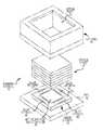
- FIG. 2is an exploded view of the camera module of FIG. 1 , showing an image sensor already mounted on a circuit board, and optics stack, and a housing.
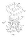
- FIG. 3is similar to the exploded view of FIG. 2 , shown after glue has been applied to a peripheral area of the image sensor.
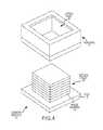
- FIG. 4is similar to the exploded view of FIG. 3 , shown after an optics stack has been attached to the image sensor.
- FIG. 5is similar to the exploded view of FIG. 4 , shown after glue has been applied to a peripheral area of the circuit board and a peripheral area on top of the optics stack.
- FIG. 6is similar to the exploded view of FIG. 5 , shown after a housing has been attached to the portions of the camera module having the exposed glue.
- FIG. 7is a diagram showing the various stages in an array processing technique for producing multiple camera modules.
- FIG. 1shows an assembled camera module 10 .
- the camera module 10includes a printed circuit board (PCB) 12 to which an image sensor 14 has been attached using chip-on-board (COB) technology.
- the image sensor 14includes an active area 16 in a central region of a top surface 18 thereof.
- An optics stack 20has been attached to the top surface 18 of the image a sensor 14 so as to surround the active area 16 .
- the optics stack 20includes one or more lens elements.
- the optics stack 20includes three lens elements, a first lens element 22 , a second lens element 24 , and a third lens element 26 .
- the three lens elements 22 , 24 , and 26are separated from each other and from the image sensor 14 by a first spacer 28 , a second spacer 30 , and a third spacer 32 , respectively.
- Other examples of optics stacksmay include one, two, four, or more lens elements.
- the optics stackmay be manufactured with replication technology (using molds) that is known in the art.
- the optics stackmay include aspheric lens surface on either side of one or more lens elements.
- Each of the spacers 28 , 30 , and 32are hollow, having a cavity in a central region thereof to allow light to pass through each successive lens element, as light passes through the camera module 10 toward the active area 16 of the image sensor 14 .
- the spacersmay be composed of any suitable material, with two examples being glass or polymer materials. Three examples of companies that have replication technology are Anteryon, Tessera/Digital Optics Corporation, and Heptagon.
- a housing 34(which may be composed of CBT, LCP, glass, or other suitable material) is attached to the PCB 12 and the top of the optics stack 20 to minimize the amount of stray light impinging upon the active area 16 of the image sensor 14 and to increase the mechanical strength of the camera module 10 .
- the housing 34includes an internal cavity 36 that receives the optics stack 20 and image sensor 14 .
- the housing 34also includes an upper port 38 through which light can enter the camera module 10 , pass through the optics stack 20 , and impinge upon the active area 16 of the image sensor 14 .
- the upper port 38may be of any suitable shape. In this example, the upper port is a rectangular opening, while in other examples other shapes may be used. For example, a smaller, circular opening may be employed.
- FIGS. 2-6A process for assembling the camera module 10 of FIG. 1 is shown in FIGS. 2-6 .
- FIG. 2shows an image sensor 14 (with its active area 16 on a top surface 18 thereof) already attached to the PCB 12 . The initial portions of this process may be performed in a clean room having special vacuum features.
- the optics stack 20(including lens elements 22 , 24 , and 26 and spacers 28 , 30 , and 32 ) is shown spaced apart from the combination of the image sensor 14 and PCB 12 .
- the housing 34is shown spaced apart from the optics stack 20 . While the combination of the housing 34 , the optics stack 20 , and the image sensor 14 and PCB 12 are shown in spaced apart relationship in FIG. 2 , this is merely for ease of understanding and illustration. In fact, the housing 34 and optics stack 20 may of course be located in different positions or in a completely different location while the step illustrated by the differences between FIGS. 2 and 3 is performed.
- the dispense patternmay be broken lines of glue applied to the peripheral area of the image sensor (as shown) or it may be a continuous line of glue or multiple dots of glue applied to the peripheral area of the image sensor.
- Any suitable glue, epoxy, or other type of adhesivecan be used and a precision or semi-automatic dispensing method may be used.
- a suitable glueis Ablelux A4502. Care is taken to accurately place the glue lines an appropriate distance away from the active area 16 of the image sensor 14 .
- each glue linemay be spaced apart from the active area 16 by a distance of 300 ⁇ m or greater, while the width of each glue line may be in the range of 300 to 350 ⁇ m, for example. Since the thickness of the glue line helps determine the spacing of the lens elements in the lens optics stack 20 from the active area 16 of the image sensor 14 , it may be desirable to maintain the thickness of the glue line at a reasonable level (for example ⁇ 12-15 um). In addition, it may be desirable to control the viscosity (for example ⁇ 20,000 cps) and thixotropic index (for example ⁇ 3-5) of the glue.
- FIG. 4shows the partial assembly of the camera module in which the optics stack 20 has already been attached to the image sensor 14 .
- the partially assembled camera moduleis subjected to UV light to cure the glue.
- a thermal-setting (or other type of) gluecan be used, and appropriate methods can be used to cure that adhesive.
- glueis provided, both along the periphery of the upper surface of the first lens element 22 and along the outer periphery of a top surface of the PCB 12 , as shown in FIG. 5 .
- gluecould be applied to the appropriate mating surfaces on the housing 34 .
- two-sided tapemay be used to apply to attach to be housing 34 to the remainder of the camera module 10 .
- glue patternsthere are many suitable glue patterns that could be employed.
- dashed glue lines 52are used on the PCB 12 and a series of glue dots 54 is used on the periphery of the first lens element 22 of the optics stack 20 .
- glue patterns 50 , 52 , and 54could be used in any of these three locations shown in FIGS. 3 and 5 .
- the housing 34is then attached, either manually using jigs and fixtures, or by use of an automated housing attach system.
- the camera moduleis then placed in an oven to cure the epoxy (in this example a thermal-setting glue is used to attach the housing 34 ). In this manner, the assembled camera module 10 is produced, as shown in FIG. 6 .
- a silicon wafer 70that includes a plurality of non-singulated image sensors 72 thereon is employed.
- the wafermay be any suitably-sized wafer. For example, a 6 inch, 8 inch, or 12 inch wafer could be used.
- a through silicon via (TSV) waferis employed. TSV technology is known in the art and examples of such technology are available from Micron and STMicroelectronics.
- TSV waferhas already had vias created from a bottom surface of the wafer to the bond pads on the bottom of the image sensors 72 .
- the bond pad connectionsare brought to the bottom side through these vias in the silicon using redistribution technology (RDL) and are distributed over the entire bottom side.
- RDLredistribution technology
- an optics stack 74is attached to each of the image sensors 72 on the wafer 70 .
- the wafer 70with a plurality of optics stacks 74 attached thereto, is shown at 76 .
- a magnified view of one of the optics stacks 74 attached to one of the image sensors 72 on the wafer 70is shown at 78 .
- the optics stacks 74 on the waferare encapsulated with molding material 80 , with an opening 82 through the molding material defined so that light can pass into the optics stack 74 and to the image sensor 72 .
- the wafer 70 , with the molding material 80 encapsulating the optics stack 74is shown at 84 .
- solder ball attach processmay be a reflow process.
- the wafer 70with solder balls 86 attached thereto, is shown at 88 .
- the wafer 70is singulated in a conventional manner with a saw and then the molding material 80 is singulated in a conventional manner with a saw.
- the dicing of the wafer 70 and the molding material 80may occur from opposite sides of the assembly.
- the wafer 70 in the molding materialmay be singulated in a single step with a saw from the same side of the assembly.
- the assemblycan be singulated into separate camera modules in any conventional manner.
- the techniques disclosed hereinoffer several advantages to prior techniques. It is believed that the techniques described herein are the first to attach an optics stack, or any type of lens directly to the silicon of an image sensor in the assembly of a camera module. It is believed that in other assembly methods, the optical elements are either attached to a cover glass that is attached to the silicon of the image sensor, or attached to the PCB to which the image sensor is attached, or the optical elements are attached to a lens housing that is attached to the PCB.
- the cover glassmay generally have a thickness of 300 to 500 ⁇ m and a tolerance in the range of 10 to 100 ⁇ m.
- the techniques taught hereinit has been found that the overall tolerance of the distance of the lens elements from the image sensor can be reduced to a level of less than 5 ⁇ m.
- the techniques taught hereineliminate the material cost and production time of attaching a cover glass to the sensor.
- TSV waferby using a TSV wafer, several piece parts, such as a substrate, housing, and gold wire for wire bonding can be eliminated. This helps to improve and lower the cost of producing such camera modules.
Landscapes
- Physics & Mathematics (AREA)
- General Physics & Mathematics (AREA)
- Optics & Photonics (AREA)
- Solid State Image Pick-Up Elements (AREA)
- Studio Devices (AREA)
- Transforming Light Signals Into Electric Signals (AREA)
- Camera Bodies And Camera Details Or Accessories (AREA)
- Lens Barrels (AREA)
Abstract
Description
Claims (15)
Priority Applications (5)
| Application Number | Priority Date | Filing Date | Title |
|---|---|---|---|
| US12/368,454US9118825B2 (en) | 2008-02-22 | 2009-02-10 | Attachment of wafer level optics |
| PCT/US2009/034528WO2009105547A1 (en) | 2008-02-22 | 2009-02-19 | Attachment of wafer level optics |
| JP2010547748AJP5829025B2 (en) | 2008-02-22 | 2009-02-19 | Mounting wafer level optics |
| CN200980111373.3ACN101981913B (en) | 2008-02-22 | 2009-02-19 | Attachment of wafer level optics |
| JP2014151679AJP6054344B2 (en) | 2008-02-22 | 2014-07-25 | Mounting wafer level optics |
Applications Claiming Priority (2)
| Application Number | Priority Date | Filing Date | Title |
|---|---|---|---|
| US3093708P | 2008-02-22 | 2008-02-22 | |
| US12/368,454US9118825B2 (en) | 2008-02-22 | 2009-02-10 | Attachment of wafer level optics |
Publications (2)
| Publication Number | Publication Date |
|---|---|
| US20090213262A1 US20090213262A1 (en) | 2009-08-27 |
| US9118825B2true US9118825B2 (en) | 2015-08-25 |
Family
ID=40985899
Family Applications (1)
| Application Number | Title | Priority Date | Filing Date |
|---|---|---|---|
| US12/368,454Expired - Fee RelatedUS9118825B2 (en) | 2008-02-22 | 2009-02-10 | Attachment of wafer level optics |
Country Status (4)
| Country | Link |
|---|---|
| US (1) | US9118825B2 (en) |
| JP (2) | JP5829025B2 (en) |
| CN (1) | CN101981913B (en) |
| WO (1) | WO2009105547A1 (en) |
Cited By (3)
| Publication number | Priority date | Publication date | Assignee | Title |
|---|---|---|---|---|
| US20150116562A1 (en)* | 2013-10-28 | 2015-04-30 | Omnivision Technologies, Inc. | Compact spacer in multi-lens array module |
| US20180357895A1 (en)* | 2015-12-31 | 2018-12-13 | Robert Bosch Gmbh | Intelligent Distributed Vision Traffic Marker and Method Thereof |
| US12408829B2 (en)* | 2021-08-12 | 2025-09-09 | Olympus Medical Systems Corp. | Image pickup unit and endoscope applying the same |
Families Citing this family (34)
| Publication number | Priority date | Publication date | Assignee | Title |
|---|---|---|---|---|
| US8456560B2 (en)* | 2007-01-26 | 2013-06-04 | Digitaloptics Corporation | Wafer level camera module and method of manufacture |
| CA2685080A1 (en) | 2007-04-24 | 2008-11-06 | Flextronics Ap Llc | Small form factor modules using wafer level optics with bottom cavity and flip-chip assembly |
| US9419032B2 (en)* | 2009-08-14 | 2016-08-16 | Nanchang O-Film Optoelectronics Technology Ltd | Wafer level camera module with molded housing and method of manufacturing |
| US20140320621A1 (en)* | 2009-09-16 | 2014-10-30 | Medigus Ltd. | Small diameter video camera heads and visualization probes and medical devices containing them |
| KR101814830B1 (en)* | 2009-09-16 | 2018-01-04 | 메디거스 엘티디. | Small diameter video camera heads and visualization probes and medical devices containing them |
| US8760571B2 (en)* | 2009-09-21 | 2014-06-24 | Microsoft Corporation | Alignment of lens and image sensor |
| JP2011082215A (en)* | 2009-10-02 | 2011-04-21 | Olympus Corp | Image sensor, and imaging unit |
| CN102096168A (en)* | 2009-12-14 | 2011-06-15 | 昆山西钛微电子科技有限公司 | Focusing-free optical camera module |
| US8538215B2 (en) | 2010-05-20 | 2013-09-17 | Analog Devices, Inc. | Optical package and related methods |
| US8308379B2 (en) | 2010-12-01 | 2012-11-13 | Digitaloptics Corporation | Three-pole tilt control system for camera module |
| CN102486560A (en)* | 2010-12-04 | 2012-06-06 | 鸿富锦精密工业(深圳)有限公司 | camera module |
| US8593561B2 (en)* | 2011-03-01 | 2013-11-26 | Omnivision Technologies, Inc. | Camera module and method for fabricating the same |
| TW201307938A (en)* | 2011-08-10 | 2013-02-16 | Hon Hai Prec Ind Co Ltd | Spacer and lens module thereof |
| US8853839B2 (en) | 2011-10-07 | 2014-10-07 | Analog Devices, Inc. | Air-release features in cavity packages |
| CN103091808A (en)* | 2011-11-03 | 2013-05-08 | 昆山西钛微电子科技有限公司 | Focusing-free optical camera module |
| US8842951B2 (en) | 2012-03-02 | 2014-09-23 | Analog Devices, Inc. | Systems and methods for passive alignment of opto-electronic components |
| US9029759B2 (en)* | 2012-04-12 | 2015-05-12 | Nan Chang O-Film Optoelectronics Technology Ltd | Compact camera modules with features for reducing Z-height and facilitating lens alignment and methods for manufacturing the same |
| US9716193B2 (en) | 2012-05-02 | 2017-07-25 | Analog Devices, Inc. | Integrated optical sensor module |
| US9001268B2 (en) | 2012-08-10 | 2015-04-07 | Nan Chang O-Film Optoelectronics Technology Ltd | Auto-focus camera module with flexible printed circuit extension |
| US10884551B2 (en) | 2013-05-16 | 2021-01-05 | Analog Devices, Inc. | Integrated gesture sensor module |
| SG11201606706WA (en)* | 2014-02-18 | 2016-09-29 | Heptagon Micro Optics Pte Ltd | Optical modules including customizable spacers for focal length adjustment and/or reduction of tilt, and fabrication of the optical modules |
| EP2942938B1 (en)* | 2014-05-07 | 2021-01-27 | Veoneer Sweden AB | Camera module for a motor vehicle and method of pre-focusing a lens objective in a lens holder |
| US9590129B2 (en) | 2014-11-19 | 2017-03-07 | Analog Devices Global | Optical sensor module |
| FR3029013A1 (en) | 2014-11-21 | 2016-05-27 | Stmicroelectronics (Grenoble 2) Sas | ELECTRONIC DEVICE COMPRISING STACKED CHIPS |
| US9773740B2 (en) | 2014-11-26 | 2017-09-26 | Stmicroelectronics (Grenoble 2) Sas | Stacked electronic device including a protective wafer bonded to a chip by an infused adhesive |
| US9728510B2 (en) | 2015-04-10 | 2017-08-08 | Analog Devices, Inc. | Cavity package with composite substrate |
| EP3112924B1 (en) | 2015-06-30 | 2021-07-28 | ams AG | Optical hybrid lens and method for producing an optical hybrid lens |
| US10488632B2 (en)* | 2016-01-20 | 2019-11-26 | Mems Optical Zoom Corporation | MEMS lens actuator |
| TWM556869U (en)* | 2016-03-15 | 2018-03-11 | Sunny Optical Tech Group Company Limited | Photographing module and array photographing module based upon integrally packaging technique |
| CN109152518A (en)* | 2016-05-24 | 2019-01-04 | 奥林巴斯株式会社 | Endoscopic image pickup unit and endoscope |
| JP6390763B1 (en)* | 2017-06-28 | 2018-09-19 | Smk株式会社 | Camera module and method for manufacturing camera module |
| US10712197B2 (en) | 2018-01-11 | 2020-07-14 | Analog Devices Global Unlimited Company | Optical sensor package |
| CN111487729A (en)* | 2020-04-10 | 2020-08-04 | 武汉昱升光器件有限公司 | Optical device coupling UV glue dispensing method |
| CN111853699B (en)* | 2020-08-28 | 2021-02-12 | 广东烨嘉光电科技股份有限公司 | Large-aperture three-piece lens optical lens |
Citations (168)
| Publication number | Priority date | Publication date | Assignee | Title |
|---|---|---|---|---|
| JPS61129616A (en) | 1984-11-28 | 1986-06-17 | Olympus Optical Co Ltd | Endoscope |
| US4681416A (en) | 1986-02-10 | 1987-07-21 | W. Haking Enterprises Limited | Camera shutter cocking mechanism |
| US4687314A (en) | 1986-02-07 | 1987-08-18 | W. Haking Enterprises Limited | Shutter release mechanism for automatic cameras |
| US4690512A (en) | 1985-01-28 | 1987-09-01 | Polaroid Corporation | Composite lens assembly |
| US4727389A (en) | 1986-02-07 | 1988-02-23 | W. Haking Enterprises Limited | Automatic focus and exposure controlled camera |
| JPH0279685A (en) | 1988-09-16 | 1990-03-20 | Hitachi Ltd | Image pickup device |
| US4987435A (en) | 1989-03-29 | 1991-01-22 | Copal Company Limited | Compact camera with apparatus size adjustment by zooming |
| JPH0423469A (en) | 1990-05-18 | 1992-01-27 | Toshiba Corp | Solid-state image sensor module |
| US5149181A (en) | 1990-11-02 | 1992-09-22 | Pilkington Visioncare, Inc. | Lens wafer, laminate lens and method of fabrication thereof |
| JPH07131701A (en) | 1993-10-29 | 1995-05-19 | Nec Corp | Television camera device |
| JPH07181389A (en) | 1993-12-22 | 1995-07-21 | Minolta Co Ltd | Compact macro-lens |
| US5529936A (en) | 1992-09-30 | 1996-06-25 | Lsi Logic Corporation | Method of etching a lens for a semiconductor solid state image sensor |
| JPH08288484A (en) | 1995-04-20 | 1996-11-01 | Sony Corp | Manufacture of solid-state image pickup element |
| JPH09329818A (en) | 1996-06-11 | 1997-12-22 | Minolta Co Ltd | Shake correction camera |
| US5815742A (en) | 1996-06-11 | 1998-09-29 | Minolta Co., Ltd. | Apparatus having a driven member and a drive controller therefor |
| JPH10327344A (en) | 1997-05-22 | 1998-12-08 | Mitsubishi Electric Corp | Imaging device and image data correction method |
| US5866942A (en) | 1995-04-28 | 1999-02-02 | Nec Corporation | Metal base package for a semiconductor device |
| JP2000155270A (en) | 1998-11-24 | 2000-06-06 | Mitsubishi Cable Ind Ltd | Image guide lens structural body |
| JP2000323692A (en) | 1999-05-07 | 2000-11-24 | Canon Inc | Solid-state imaging device |
| US6249311B1 (en) | 1998-02-24 | 2001-06-19 | Inframetrics Inc. | Lens assembly with incorporated memory module |
| US6255640B1 (en)* | 1998-03-27 | 2001-07-03 | Sony Corporation | Solid-state image sensing device and method for manufacturing solid-state image sensing device |
| JP2001292365A (en) | 2000-04-07 | 2001-10-19 | Mitsubishi Electric Corp | Imaging device and method of manufacturing the same |
| JP2001292354A (en) | 2000-04-07 | 2001-10-19 | Mitsubishi Electric Corp | Imaging device |
| JP2001333332A (en) | 2000-05-24 | 2001-11-30 | Matsushita Electric Works Ltd | Lens barrel and image pickup device using it |
| US6330400B1 (en) | 2000-01-28 | 2001-12-11 | Concord Camera-Corp. | Compact through-the-lens digital camera |
| JP2002010123A (en) | 2000-06-23 | 2002-01-11 | Olympus Optical Co Ltd | Electronic camera |
| JP2002016194A (en) | 2000-06-29 | 2002-01-18 | Kyocera Corp | Semiconductor device |
| US6381072B1 (en) | 1998-01-23 | 2002-04-30 | Proxemics | Lenslet array systems and methods |
| WO2002065208A1 (en) | 2001-02-14 | 2002-08-22 | Arisawa Optics Co., Ltd. | Reflection projection screen |
| JP2002246638A (en) | 2001-02-21 | 2002-08-30 | Sanyo Electric Co Ltd | Optical communication apparatus |
| JP2002280535A (en) | 2001-03-16 | 2002-09-27 | Mdi Kk | Solid-state imaging device and its manufacturing method |
| US20030016452A1 (en) | 2001-07-20 | 2003-01-23 | Michel Sayag | Design and fabrication process for a lens system optically coupled to an image-capture device |
| JP2003110891A (en) | 2001-09-26 | 2003-04-11 | Fuji Photo Optical Co Ltd | Imaging optical system |
| US6582079B2 (en) | 2001-06-05 | 2003-06-24 | Metrologic Instruments, Inc. | Modular adaptive optical subsystem for integration with a fundus camera body and CCD camera unit and improved fundus camera employing same |
| US6670205B1 (en) | 2002-09-18 | 2003-12-30 | Hynix Semiconductor Inc | Method of fabricating image sensor equipped with lens |
| JP2004016410A (en) | 2002-06-14 | 2004-01-22 | Fuji Photo Optical Co Ltd | Three-dimensional electronic endoscope apparatus |
| US6683298B1 (en) | 2000-11-20 | 2004-01-27 | Agilent Technologies Inc. | Image sensor packaging with package cavity sealed by the imaging optics |
| JP2004029554A (en) | 2002-06-27 | 2004-01-29 | Olympus Corp | Image pickup lens unit and image pickup device |
| US6686588B1 (en) | 2001-01-16 | 2004-02-03 | Amkor Technology, Inc. | Optical module with lens integral holder |
| JP2004053648A (en) | 2002-07-16 | 2004-02-19 | Sharp Corp | Optical communication module |
| JP2004061623A (en) | 2002-07-25 | 2004-02-26 | Rohm Co Ltd | Image sensor module and its manufacture method |
| US20040042779A1 (en)* | 2002-09-02 | 2004-03-04 | Elmo Co., Ltd. | Monitoring camera with detachable lens housing |
| JP2004080774A (en) | 2002-08-02 | 2004-03-11 | Rohm Co Ltd | Method of manufacturing image sensors module |
| JP2004088713A (en) | 2002-06-27 | 2004-03-18 | Olympus Corp | Imaging lens unit and imaging device |
| US20040056970A1 (en) | 2002-09-23 | 2004-03-25 | Lothar Westerweck | Image capture device |
| WO2004027880A2 (en) | 2002-09-17 | 2004-04-01 | Koninklijke Philips Electronics N.V. | Camera device, method of manufacturing a camera device, wafer scale package |
| US20040089859A1 (en) | 2002-03-19 | 2004-05-13 | Matsushita Electric Industrial Co., Ltd. | Integrated circuit device installed structure and installation method |
| JP2004200965A (en) | 2002-12-18 | 2004-07-15 | Sanyo Electric Co Ltd | Camera module and manufacturing method thereof |
| JP2004207461A (en) | 2002-12-25 | 2004-07-22 | Olympus Corp | Solid-state imaging device and method of manufacturing the same |
| EP1441509A2 (en) | 2003-01-27 | 2004-07-28 | Sanyo Electric Co., Ltd. | Camera module and manufacturing method thereof |
| JP2004226872A (en) | 2003-01-27 | 2004-08-12 | Sanyo Electric Co Ltd | Camera module and manufacturing method thereof |
| JP2004282778A (en) | 1995-05-31 | 2004-10-07 | Sony Corp | Imaging apparatus, signal processing instrument, and signal processing method |
| JP2004304605A (en) | 2003-03-31 | 2004-10-28 | Mitsumi Electric Co Ltd | Small camera module |
| JP2004328474A (en) | 2003-04-25 | 2004-11-18 | Mitsumi Electric Co Ltd | Packaging structure for camera module |
| US20040245649A1 (en)* | 2003-04-16 | 2004-12-09 | Seiko Epson Corporation | Optical device, optical module, semiconductor apparatus and its manufacturing method, and electronic apparatus |
| KR20050000722A (en) | 2003-06-24 | 2005-01-06 | 카스크테크놀러지 주식회사 | Small camera optical system |
| US6841883B1 (en) | 2003-03-31 | 2005-01-11 | Micron Technology, Inc. | Multi-dice chip scale semiconductor components and wafer level methods of fabrication |
| US20050046010A1 (en)* | 2003-04-29 | 2005-03-03 | Stmicroelectronics S.A. | Semiconductor package |
| US6869233B2 (en) | 2002-09-23 | 2005-03-22 | Concord Camera Corp. | Image capture device |
| US20050077458A1 (en)* | 2003-10-14 | 2005-04-14 | Guolin Ma | Integrally packaged imaging module |
| JP2005116628A (en) | 2003-10-03 | 2005-04-28 | Matsushita Electric Ind Co Ltd | Solid-state imaging device and manufacturing method thereof |
| JP2005148109A (en) | 2003-11-11 | 2005-06-09 | Konica Minolta Opto Inc | Imaging device and portable terminal equipped with the imaging device |
| JP2005173265A (en) | 2003-12-11 | 2005-06-30 | Canon Inc | Optical element, optical filter device, and optical instrument |
| US20050146800A1 (en) | 2001-12-04 | 2005-07-07 | Sony Corporation | Optical pickup device and optical disc apparatus |
| US20050179805A1 (en)* | 2003-12-30 | 2005-08-18 | Jerome Avron | Assembly and method for aligning an optical system |
| US20050185088A1 (en) | 2004-02-20 | 2005-08-25 | Kale Vidyadhar S. | Integrated lens and chip assembly for a digital camera |
| JP2005266129A (en) | 2004-03-17 | 2005-09-29 | Olympus Corp | Zoom lens and electronic imaging apparatus having the same |
| JP2005295050A (en) | 2004-03-31 | 2005-10-20 | Miyota Kk | Camera module |
| US20050237418A1 (en)* | 2002-07-01 | 2005-10-27 | Rohm Co., Ltd | Image sensor module |
| JP2005317745A (en) | 2004-04-28 | 2005-11-10 | Renesas Technology Corp | Solid-state imaging device and manufacturing method thereof |
| JP2005340539A (en) | 2004-05-27 | 2005-12-08 | Kyocera Corp | Imaging device and imaging module |
| JP2005338749A (en) | 2004-05-27 | 2005-12-08 | Ashu Kogaku Kofun Yugenkoshi | Lens unit and optical device using the same |
| US20050285973A1 (en) | 2004-06-25 | 2005-12-29 | Harpuneet Singh | System and method for mounting an image capture device on a flexible substrate |
| US20060001759A1 (en) | 2004-07-02 | 2006-01-05 | Raschke Klaus G | Pop up prism lens assembly |
| US20060006511A1 (en)* | 2004-07-06 | 2006-01-12 | Samsung Electronics Co., Ltd. | Ultrathin module for semiconductor device and method of fabricating the same |
| US20060023108A1 (en) | 2004-07-27 | 2006-02-02 | Fujitsu Limited | Image capturing device |
| US6995462B2 (en) | 2003-09-17 | 2006-02-07 | Micron Technology, Inc. | Image sensor packages |
| US20060028573A1 (en) | 2004-08-06 | 2006-02-09 | Byoung-Rim Seo | Image sensor camera module and method of fabricating the same |
| JP2006054506A (en) | 2004-08-09 | 2006-02-23 | Seiko Precision Inc | Imaging apparatus |
| WO2006025698A1 (en) | 2004-09-02 | 2006-03-09 | Optopac, Inc. | Method of making camera module in wafer level |
| US20060054787A1 (en) | 2004-08-25 | 2006-03-16 | Olsen Richard I | Apparatus for multiple camera devices and method of operating same |
| US7019374B2 (en) | 2003-08-13 | 2006-03-28 | Citizen Electronics Co., Ltd. | Small-sized image pick up module |
| US20060066959A1 (en) | 2004-09-24 | 2006-03-30 | Akihiro Koga | Zoom lens unit and image pickup apparatus |
| US7043284B2 (en) | 2003-02-06 | 2006-05-09 | Flextronics Ap, Llc | Integrated cellular phone, digital camera, and PDA, with swivel mechanism providing access to the interface elements of each function |
| US7046296B2 (en) | 2000-06-16 | 2006-05-16 | Renesas Technology Corp | Solid state imaging apparatus |
| US20060109367A1 (en) | 2004-11-22 | 2006-05-25 | Sharp Kabushiki Kaisha | Image pickup module and manufacturing method of image pickup module |
| US20060127085A1 (en) | 2003-08-21 | 2006-06-15 | Kaoru Matsuki | Electrostatic actuator, shutter device, imaging module, and camera |
| US20060132644A1 (en) | 2004-02-20 | 2006-06-22 | Dongkai Shangguan | Wafer based camera module and method of manufacture |
| JP2006180487A (en) | 2001-01-12 | 2006-07-06 | Konica Minolta Holdings Inc | Image pickup device |
| US7083999B2 (en) | 2001-12-27 | 2006-08-01 | Seiko Epson Corporation | Optical device, method of manufacturing the same, optical module, circuit board and electronic instrument |
| US20060181748A1 (en) | 2005-02-15 | 2006-08-17 | Sony Corporation | Lens unit and imaging apparatus |
| WO2006093377A1 (en) | 2005-03-04 | 2006-09-08 | Hyun-Joo Jung | Camera module without focusing adjustment and method of assembling thereof |
| JP2006248878A (en) | 2005-03-14 | 2006-09-21 | Nippon Electric Glass Co Ltd | Apparatus for manufacturing glass article |
| US20060215053A1 (en) | 2005-03-22 | 2006-09-28 | Sharp Kabushiki Kaisha | Lens-position controller and imaging module |
| US20060219885A1 (en) | 2005-03-31 | 2006-10-05 | Sharp Kabushiki Kaisha | Optical device module |
| JP2006276897A (en) | 1999-01-12 | 2006-10-12 | Konica Minolta Opto Inc | Zoom lens |
| JP2006294720A (en) | 2005-04-07 | 2006-10-26 | Hitachi Maxell Ltd | The camera module |
| US20060251414A1 (en) | 2003-04-28 | 2006-11-09 | Hiroshi Nishizawa | Imaging apparatus |
| US7167376B2 (en) | 2003-05-19 | 2007-01-23 | Fuji Photo Film Co., Ltd. | Multilayer wiring board, method of mounting components, and image pick-up device |
| JP2007017974A (en) | 2005-07-06 | 2007-01-25 | Ashu Kogaku Kofun Yugenkoshi | Miniaturized lens assembly and method for making the same |
| US20070019102A1 (en) | 2005-07-01 | 2007-01-25 | Hironori Nakajo | Micro camera module and method of manufacturing the same |
| WO2007016414A2 (en) | 2005-07-29 | 2007-02-08 | Flextronics Ap, Llc | Method of aligning the upper and lower centering bells of a lens doublet assembly machine |
| US20070032169A1 (en) | 2005-07-29 | 2007-02-08 | Ron Neely | Method for aligning and assembling two lens pieces, and a machine to accomplish this task |
| US20070053672A1 (en) | 2005-09-08 | 2007-03-08 | Flextronics Ap, Llc | Auto-focus and zoom module |
| US20070053685A1 (en) | 2005-09-06 | 2007-03-08 | Hisashi Shibata | Camera module |
| US20070052050A1 (en) | 2005-09-07 | 2007-03-08 | Bart Dierickx | Backside thinned image sensor with integrated lens stack |
| US20070058964A1 (en) | 2005-09-15 | 2007-03-15 | Dongkai Shangguan | External adjustment mechanism for a camera lens and electronic imager |
| US7199438B2 (en) | 2003-09-23 | 2007-04-03 | Advanced Semiconductor Engineering, Inc. | Overmolded optical package |
| US20070077051A1 (en) | 2005-10-03 | 2007-04-05 | Toor John W | Micro camera module with discrete manual focal positions |
| US20070091198A1 (en)* | 2005-10-21 | 2007-04-26 | Fujitsu Limited | Image pickup apparatus and method of manufacturing the same |
| US20070096284A1 (en)* | 2005-11-01 | 2007-05-03 | Sandisk Corporation | Methods for a multiple die integrated circuit package |
| US20070126914A1 (en) | 2005-11-18 | 2007-06-07 | Tomoko Komatsu | Solid state imaging device |
| US7245319B1 (en) | 1998-06-11 | 2007-07-17 | Fujifilm Corporation | Digital image shooting device with lens characteristic correction unit |
| US20070166029A1 (en)* | 2006-01-18 | 2007-07-19 | Visera Technologies, Co. Ltd. | Image sensor module having precise image-projection control |
| US20070164409A1 (en) | 2003-12-18 | 2007-07-19 | Andrew Holland | Semiconductor package with integrated heatsink and electromagnetic shield |
| US20070212061A1 (en) | 2006-03-10 | 2007-09-13 | Jae Kun Woo | Camera Module and Method of Manufacturing The same |
| US7280149B2 (en) | 2001-12-21 | 2007-10-09 | Flextronics Sales & Marketing (A-P) Ltd. | Method and apparatus for detecting optimum lens focus position |
| US20070236591A1 (en) | 2006-04-11 | 2007-10-11 | Tam Samuel W | Method for mounting protective covers over image capture devices and devices manufactured thereby |
| JP2007292845A (en) | 2006-04-21 | 2007-11-08 | Citizen Holdings Co Ltd | The camera module |
| US20070258006A1 (en) | 2005-08-25 | 2007-11-08 | Olsen Richard I | Solid state camera optics frame and assembly |
| US7301577B2 (en) | 2003-05-15 | 2007-11-27 | Asia Optical Co., Inc. | Digital camera with a collapsible lens barrel |
| US20070278394A1 (en) | 2006-05-31 | 2007-12-06 | Dongkai Shangguan | Camera module with premolded lens housing and method of manufacture |
| US20070279518A1 (en) | 2004-01-13 | 2007-12-06 | Uwe Apel | Optical Module |
| JP4027962B1 (en) | 2006-12-29 | 2007-12-26 | 株式会社小松ライト製作所 | Imaging device |
| WO2008011003A2 (en) | 2006-07-17 | 2008-01-24 | Tessera North America, Inc. | Camera system and associated methods |
| US20080040069A1 (en) | 2005-09-08 | 2008-02-14 | Wolfram Grziwa | Manufacturable micropositioning system |
| US20080058010A1 (en) | 2006-08-31 | 2008-03-06 | Wicky Lee | Discreetly positionable camera housing |
| US20080068728A1 (en) | 2006-09-15 | 2008-03-20 | Flextronics Ap, Llc | Auto-focus and zoom module with vibrational actuator and position sensing method |
| US20080074528A1 (en) | 2005-09-08 | 2008-03-27 | Lothar Westerweck | Zoom module using rotational actuator with anti-lock feature, even force distribution and shock damage prevention methods |
| US20080118241A1 (en) | 2006-11-16 | 2008-05-22 | Tekolste Robert | Control of stray light in camera systems employing an optics stack and associated methods |
| US7378724B2 (en) | 2005-03-24 | 2008-05-27 | Taiwan Semiconductor Manufacturing Company, Ltd. | Cavity structure for semiconductor structures |
| WO2008070125A2 (en) | 2006-12-01 | 2008-06-12 | Flextronics Ap Llc | Actuated stepper lens camera module |
| US20080143864A1 (en) | 2001-01-12 | 2008-06-19 | Konica Corporation | Image pickup device and image pickup lens |
| US20080152339A1 (en) | 2006-11-03 | 2008-06-26 | Westerweck Lothar R | Camera module with contamination reduction feature |
| US20080158362A1 (en) | 2006-12-28 | 2008-07-03 | Mark Melvin Butterworth | Digital camera calibration method |
| WO2008079403A2 (en) | 2006-12-22 | 2008-07-03 | Flextronics Ap, Llc | Three-element photographic objective with reduced tolerance sensitivities |
| US20080170141A1 (en) | 2007-01-11 | 2008-07-17 | Samuel Waising Tam | Folded package camera module and method of manufacture |
| US20080180566A1 (en)* | 2007-01-26 | 2008-07-31 | Harpuneet Singh | Wafer level camera module and method of manufacture |
| US7414661B2 (en) | 2002-08-13 | 2008-08-19 | Micron Technology, Inc. | CMOS image sensor using gradient index chip scale lenses |
| US7433555B2 (en) | 2006-05-22 | 2008-10-07 | Visera Technologies Company Ltd | Optoelectronic device chip having a composite spacer structure and method making same |
| US20080252795A1 (en) | 2007-04-13 | 2008-10-16 | Bone Matthew F | System and method for improving image quality by synchronizing display modulation with light source pulses |
| WO2008133943A1 (en) | 2007-04-24 | 2008-11-06 | Flextronics Ap Llc | Small form factor modules using wafer level optics with bottom cavity and flip chip assembly |
| WO2008133946A1 (en) | 2007-04-24 | 2008-11-06 | Flextronics Ap Llc | Auto focus/ zoom modules using wafer level optics |
| US20080278617A1 (en)* | 2007-05-10 | 2008-11-13 | Sharp Kabushiki Kaisha | Image capturing device module, manufacturing method of the image capturing device module, and electronic information device |
| US20080279545A1 (en) | 2007-05-07 | 2008-11-13 | Flextronics Ap, Llc. | Miniature camera shutter and filter/aperture |
| US7457050B2 (en) | 2006-03-24 | 2008-11-25 | Flextronics Ap, Llc | Zoom lens system for use with small electronic sensor |
| US20090021624A1 (en) | 2007-07-19 | 2009-01-22 | Lothar Westerweck | Camera module back-focal length adjustment method and ultra compact components packaging |
| US20090027869A1 (en) | 2007-07-27 | 2009-01-29 | Nec Electronics Corporation | Electronic device and method for manufacturing electronic device |
| US7494292B2 (en) | 2004-06-29 | 2009-02-24 | Samsung Electronics Co., Ltd. | Image sensor module structure comprising wire bonding package and method of manufacturing the image sensor module structure |
| US20090068798A1 (en)* | 2007-09-07 | 2009-03-12 | Micron Technology, Inc. | Imager die package and methods of packaging an imager die on a temporary carrier |
| US20090103193A1 (en) | 2007-10-18 | 2009-04-23 | Berube Dennis R | Laser bonding camera modules to lock focus |
| US20090115891A1 (en) | 2007-11-01 | 2009-05-07 | Samsung Electronics Co., Ltd. | Camera module |
| US20090122178A1 (en)* | 2007-11-12 | 2009-05-14 | Samsung Electronics Co., Ltd. | Camera module and electronic apparatus having the same |
| US20090206431A1 (en)* | 2008-02-20 | 2009-08-20 | Micron Technology, Inc. | Imager wafer level module and method of fabrication and use |
| US7593057B2 (en) | 2004-07-28 | 2009-09-22 | Microsoft Corp. | Multi-view integrated camera system with housing |
| US20090243051A1 (en)* | 2008-03-28 | 2009-10-01 | Micron Technology, Inc. | Integrated conductive shield for microelectronic device assemblies and associated methods |
| US20090267170A1 (en) | 2008-04-29 | 2009-10-29 | Omnivision Technologies, Inc. | Apparatus and Method For Using Spacer Paste to Package an Image Sensor |
| US7622786B2 (en)* | 2007-12-28 | 2009-11-24 | Aptina Imaging Corporation | EMI shielding for imager devices |
| US20100044814A1 (en)* | 2008-08-25 | 2010-02-25 | Cheng Uei Precision Industry Co., Ltd. | Camera Module and Manufacturing Method Thereof |
| US20110037886A1 (en) | 2009-08-14 | 2011-02-17 | Harpuneet Singh | Wafer level camera module with molded housing and method of manufacturing |
| US7901973B2 (en) | 2005-12-14 | 2011-03-08 | Fujifilm Corporation | Solid state imaging device and manufacturing method thereof |
| US20110096213A1 (en) | 2008-03-21 | 2011-04-28 | Sharp Kabushiki Kaisha | Wafer-shaped optical apparatus and manufacturing method thereof, electronic element wafer module, sensor wafer module, electronic element module,sensor module, and electronic information device |
| US7939901B2 (en) | 2007-10-15 | 2011-05-10 | Panasonic Corporation | Optical device for reducing disturbance light and manufacturing method thereof |
| US20110134303A1 (en)* | 2009-12-07 | 2011-06-09 | Samsung Electronics Co., Ltd. | Image pickup device and manufacturing method thereof |
| US8110884B2 (en)* | 2007-12-18 | 2012-02-07 | Micron Technology, Inc. | Methods of packaging imager devices and optics modules, and resulting assemblies |
| US8300143B2 (en)* | 2006-12-29 | 2012-10-30 | Manabu Bonkohara | Solid-state imaging device, method of fabricating the same, and camera module |
| US8481343B2 (en)* | 2010-09-17 | 2013-07-09 | Kingpak Technology Inc. | Manufacturing method of molded image sensor packaging structure with predetermined focal length and the structure using the same |
| US8599301B2 (en)* | 2006-04-17 | 2013-12-03 | Omnivision Technologies, Inc. | Arrayed imaging systems having improved alignment and associated methods |
Family Cites Families (1)
| Publication number | Priority date | Publication date | Assignee | Title |
|---|---|---|---|---|
| JP3498775B2 (en)* | 1995-05-31 | 2004-02-16 | ソニー株式会社 | Imaging device |
- 2009
- 2009-02-10USUS12/368,454patent/US9118825B2/ennot_activeExpired - Fee Related
- 2009-02-19WOPCT/US2009/034528patent/WO2009105547A1/enactiveApplication Filing
- 2009-02-19CNCN200980111373.3Apatent/CN101981913B/ennot_activeExpired - Fee Related
- 2009-02-19JPJP2010547748Apatent/JP5829025B2/ennot_activeExpired - Fee Related
- 2014
- 2014-07-25JPJP2014151679Apatent/JP6054344B2/ennot_activeExpired - Fee Related
Patent Citations (199)
| Publication number | Priority date | Publication date | Assignee | Title |
|---|---|---|---|---|
| JPS61129616A (en) | 1984-11-28 | 1986-06-17 | Olympus Optical Co Ltd | Endoscope |
| US4690512A (en) | 1985-01-28 | 1987-09-01 | Polaroid Corporation | Composite lens assembly |
| US4687314A (en) | 1986-02-07 | 1987-08-18 | W. Haking Enterprises Limited | Shutter release mechanism for automatic cameras |
| US4727389A (en) | 1986-02-07 | 1988-02-23 | W. Haking Enterprises Limited | Automatic focus and exposure controlled camera |
| US4681416A (en) | 1986-02-10 | 1987-07-21 | W. Haking Enterprises Limited | Camera shutter cocking mechanism |
| JPH0279685A (en) | 1988-09-16 | 1990-03-20 | Hitachi Ltd | Image pickup device |
| US4987435A (en) | 1989-03-29 | 1991-01-22 | Copal Company Limited | Compact camera with apparatus size adjustment by zooming |
| JPH0423469A (en) | 1990-05-18 | 1992-01-27 | Toshiba Corp | Solid-state image sensor module |
| US5149181A (en) | 1990-11-02 | 1992-09-22 | Pilkington Visioncare, Inc. | Lens wafer, laminate lens and method of fabrication thereof |
| US5529936A (en) | 1992-09-30 | 1996-06-25 | Lsi Logic Corporation | Method of etching a lens for a semiconductor solid state image sensor |
| JPH07131701A (en) | 1993-10-29 | 1995-05-19 | Nec Corp | Television camera device |
| JPH07181389A (en) | 1993-12-22 | 1995-07-21 | Minolta Co Ltd | Compact macro-lens |
| JPH08288484A (en) | 1995-04-20 | 1996-11-01 | Sony Corp | Manufacture of solid-state image pickup element |
| US5866942A (en) | 1995-04-28 | 1999-02-02 | Nec Corporation | Metal base package for a semiconductor device |
| JP2004282778A (en) | 1995-05-31 | 2004-10-07 | Sony Corp | Imaging apparatus, signal processing instrument, and signal processing method |
| JPH09329818A (en) | 1996-06-11 | 1997-12-22 | Minolta Co Ltd | Shake correction camera |
| US5815742A (en) | 1996-06-11 | 1998-09-29 | Minolta Co., Ltd. | Apparatus having a driven member and a drive controller therefor |
| JPH10327344A (en) | 1997-05-22 | 1998-12-08 | Mitsubishi Electric Corp | Imaging device and image data correction method |
| US6381072B1 (en) | 1998-01-23 | 2002-04-30 | Proxemics | Lenslet array systems and methods |
| US6249311B1 (en) | 1998-02-24 | 2001-06-19 | Inframetrics Inc. | Lens assembly with incorporated memory module |
| US6255640B1 (en)* | 1998-03-27 | 2001-07-03 | Sony Corporation | Solid-state image sensing device and method for manufacturing solid-state image sensing device |
| US7245319B1 (en) | 1998-06-11 | 2007-07-17 | Fujifilm Corporation | Digital image shooting device with lens characteristic correction unit |
| JP2000155270A (en) | 1998-11-24 | 2000-06-06 | Mitsubishi Cable Ind Ltd | Image guide lens structural body |
| JP2006276897A (en) | 1999-01-12 | 2006-10-12 | Konica Minolta Opto Inc | Zoom lens |
| JP2000323692A (en) | 1999-05-07 | 2000-11-24 | Canon Inc | Solid-state imaging device |
| US6330400B1 (en) | 2000-01-28 | 2001-12-11 | Concord Camera-Corp. | Compact through-the-lens digital camera |
| JP2001292354A (en) | 2000-04-07 | 2001-10-19 | Mitsubishi Electric Corp | Imaging device |
| JP2001292365A (en) | 2000-04-07 | 2001-10-19 | Mitsubishi Electric Corp | Imaging device and method of manufacturing the same |
| JP2001333332A (en) | 2000-05-24 | 2001-11-30 | Matsushita Electric Works Ltd | Lens barrel and image pickup device using it |
| US7046296B2 (en) | 2000-06-16 | 2006-05-16 | Renesas Technology Corp | Solid state imaging apparatus |
| JP2002010123A (en) | 2000-06-23 | 2002-01-11 | Olympus Optical Co Ltd | Electronic camera |
| JP2002016194A (en) | 2000-06-29 | 2002-01-18 | Kyocera Corp | Semiconductor device |
| US6683298B1 (en) | 2000-11-20 | 2004-01-27 | Agilent Technologies Inc. | Image sensor packaging with package cavity sealed by the imaging optics |
| JP2006180487A (en) | 2001-01-12 | 2006-07-06 | Konica Minolta Holdings Inc | Image pickup device |
| US20080143864A1 (en) | 2001-01-12 | 2008-06-19 | Konica Corporation | Image pickup device and image pickup lens |
| US6686588B1 (en) | 2001-01-16 | 2004-02-03 | Amkor Technology, Inc. | Optical module with lens integral holder |
| WO2002065208A1 (en) | 2001-02-14 | 2002-08-22 | Arisawa Optics Co., Ltd. | Reflection projection screen |
| US20030137728A1 (en) | 2001-02-14 | 2003-07-24 | Kazumi Kuroda | Reflection projection screen |
| JP2002246638A (en) | 2001-02-21 | 2002-08-30 | Sanyo Electric Co Ltd | Optical communication apparatus |
| JP2002280535A (en) | 2001-03-16 | 2002-09-27 | Mdi Kk | Solid-state imaging device and its manufacturing method |
| US6582079B2 (en) | 2001-06-05 | 2003-06-24 | Metrologic Instruments, Inc. | Modular adaptive optical subsystem for integration with a fundus camera body and CCD camera unit and improved fundus camera employing same |
| US20030016452A1 (en) | 2001-07-20 | 2003-01-23 | Michel Sayag | Design and fabrication process for a lens system optically coupled to an image-capture device |
| JP2003110891A (en) | 2001-09-26 | 2003-04-11 | Fuji Photo Optical Co Ltd | Imaging optical system |
| US20050146800A1 (en) | 2001-12-04 | 2005-07-07 | Sony Corporation | Optical pickup device and optical disc apparatus |
| US7280149B2 (en) | 2001-12-21 | 2007-10-09 | Flextronics Sales & Marketing (A-P) Ltd. | Method and apparatus for detecting optimum lens focus position |
| US7083999B2 (en) | 2001-12-27 | 2006-08-01 | Seiko Epson Corporation | Optical device, method of manufacturing the same, optical module, circuit board and electronic instrument |
| US20040089859A1 (en) | 2002-03-19 | 2004-05-13 | Matsushita Electric Industrial Co., Ltd. | Integrated circuit device installed structure and installation method |
| JP2004016410A (en) | 2002-06-14 | 2004-01-22 | Fuji Photo Optical Co Ltd | Three-dimensional electronic endoscope apparatus |
| JP2004088713A (en) | 2002-06-27 | 2004-03-18 | Olympus Corp | Imaging lens unit and imaging device |
| US6954311B2 (en) | 2002-06-27 | 2005-10-11 | Olympus Corporation | Image pickup lens unit and image pickup device |
| US20050030647A1 (en) | 2002-06-27 | 2005-02-10 | Takahiro Amanai | Image pickup lens unit and image pickup device |
| US6903883B2 (en) | 2002-06-27 | 2005-06-07 | Olympus Corporation | Image pickup lens unit and image pickup device |
| JP2004029554A (en) | 2002-06-27 | 2004-01-29 | Olympus Corp | Image pickup lens unit and image pickup device |
| US20050237418A1 (en)* | 2002-07-01 | 2005-10-27 | Rohm Co., Ltd | Image sensor module |
| JP2004053648A (en) | 2002-07-16 | 2004-02-19 | Sharp Corp | Optical communication module |
| JP2004061623A (en) | 2002-07-25 | 2004-02-26 | Rohm Co Ltd | Image sensor module and its manufacture method |
| JP2004080774A (en) | 2002-08-02 | 2004-03-11 | Rohm Co Ltd | Method of manufacturing image sensors module |
| US7414661B2 (en) | 2002-08-13 | 2008-08-19 | Micron Technology, Inc. | CMOS image sensor using gradient index chip scale lenses |
| US20040042779A1 (en)* | 2002-09-02 | 2004-03-04 | Elmo Co., Ltd. | Monitoring camera with detachable lens housing |
| US20060044450A1 (en) | 2002-09-17 | 2006-03-02 | Koninklijke Philips Electronics, N.C. | Camera device, method of manufacturing a camera device, wafer scale package |
| WO2004027880A3 (en) | 2002-09-17 | 2005-01-13 | Koninkl Philips Electronics Nv | Camera device, method of manufacturing a camera device, wafer scale package |
| JP2005539276A (en) | 2002-09-17 | 2005-12-22 | コーニンクレッカ フィリップス エレクトロニクス エヌ ヴィ | CAMERA DEVICE AND METHOD FOR MANUFACTURING CAMERA DEVICE AND WAFER SCALE PACKAGE |
| WO2004027880A2 (en) | 2002-09-17 | 2004-04-01 | Koninklijke Philips Electronics N.V. | Camera device, method of manufacturing a camera device, wafer scale package |
| US20070275505A1 (en) | 2002-09-17 | 2007-11-29 | Wolterink Edwin M | Camera device, method of manufacturing a camera device, wafer scale package |
| US6670205B1 (en) | 2002-09-18 | 2003-12-30 | Hynix Semiconductor Inc | Method of fabricating image sensor equipped with lens |
| US20040056970A1 (en) | 2002-09-23 | 2004-03-25 | Lothar Westerweck | Image capture device |
| US6869233B2 (en) | 2002-09-23 | 2005-03-22 | Concord Camera Corp. | Image capture device |
| JP2004200965A (en) | 2002-12-18 | 2004-07-15 | Sanyo Electric Co Ltd | Camera module and manufacturing method thereof |
| JP2004207461A (en) | 2002-12-25 | 2004-07-22 | Olympus Corp | Solid-state imaging device and method of manufacturing the same |
| US20060249737A1 (en)* | 2002-12-25 | 2006-11-09 | Olympus Corporation | Solid-state imaging device and manufacturing method thereof |
| JP2004226872A (en) | 2003-01-27 | 2004-08-12 | Sanyo Electric Co Ltd | Camera module and manufacturing method thereof |
| CN1517735A (en) | 2003-01-27 | 2004-08-04 | ������������ʽ���� | Camera module and manufacturing method thereof |
| EP1441509A2 (en) | 2003-01-27 | 2004-07-28 | Sanyo Electric Co., Ltd. | Camera module and manufacturing method thereof |
| US20040207036A1 (en) | 2003-01-27 | 2004-10-21 | Sanyo Electric Co., Ltd. | Camera module and manufacturing method thereof |
| US20040212719A1 (en) | 2003-01-27 | 2004-10-28 | Sanyo Electric Co., Ltd. | Camera module and manufacturing method thereof |
| US6853005B2 (en) | 2003-01-27 | 2005-02-08 | Sanyo Electric Co., Ltd. | Camera module and manufacturing method thereof |
| US7043284B2 (en) | 2003-02-06 | 2006-05-09 | Flextronics Ap, Llc | Integrated cellular phone, digital camera, and PDA, with swivel mechanism providing access to the interface elements of each function |
| US6841883B1 (en) | 2003-03-31 | 2005-01-11 | Micron Technology, Inc. | Multi-dice chip scale semiconductor components and wafer level methods of fabrication |
| JP2004304605A (en) | 2003-03-31 | 2004-10-28 | Mitsumi Electric Co Ltd | Small camera module |
| US20040245649A1 (en)* | 2003-04-16 | 2004-12-09 | Seiko Epson Corporation | Optical device, optical module, semiconductor apparatus and its manufacturing method, and electronic apparatus |
| JP2004328474A (en) | 2003-04-25 | 2004-11-18 | Mitsumi Electric Co Ltd | Packaging structure for camera module |
| US20060251414A1 (en) | 2003-04-28 | 2006-11-09 | Hiroshi Nishizawa | Imaging apparatus |
| US20050046010A1 (en)* | 2003-04-29 | 2005-03-03 | Stmicroelectronics S.A. | Semiconductor package |
| US7078799B2 (en) | 2003-04-29 | 2006-07-18 | Stmicroelectronics S.A. | Semiconductor package |
| US7301577B2 (en) | 2003-05-15 | 2007-11-27 | Asia Optical Co., Inc. | Digital camera with a collapsible lens barrel |
| US7167376B2 (en) | 2003-05-19 | 2007-01-23 | Fuji Photo Film Co., Ltd. | Multilayer wiring board, method of mounting components, and image pick-up device |
| KR20050000722A (en) | 2003-06-24 | 2005-01-06 | 카스크테크놀러지 주식회사 | Small camera optical system |
| US7019374B2 (en) | 2003-08-13 | 2006-03-28 | Citizen Electronics Co., Ltd. | Small-sized image pick up module |
| US20060127085A1 (en) | 2003-08-21 | 2006-06-15 | Kaoru Matsuki | Electrostatic actuator, shutter device, imaging module, and camera |
| US6995462B2 (en) | 2003-09-17 | 2006-02-07 | Micron Technology, Inc. | Image sensor packages |
| US7199438B2 (en) | 2003-09-23 | 2007-04-03 | Advanced Semiconductor Engineering, Inc. | Overmolded optical package |
| JP2005116628A (en) | 2003-10-03 | 2005-04-28 | Matsushita Electric Ind Co Ltd | Solid-state imaging device and manufacturing method thereof |
| US20050077458A1 (en)* | 2003-10-14 | 2005-04-14 | Guolin Ma | Integrally packaged imaging module |
| JP2005148109A (en) | 2003-11-11 | 2005-06-09 | Konica Minolta Opto Inc | Imaging device and portable terminal equipped with the imaging device |
| JP2005173265A (en) | 2003-12-11 | 2005-06-30 | Canon Inc | Optical element, optical filter device, and optical instrument |
| US20070164409A1 (en) | 2003-12-18 | 2007-07-19 | Andrew Holland | Semiconductor package with integrated heatsink and electromagnetic shield |
| US20050179805A1 (en)* | 2003-12-30 | 2005-08-18 | Jerome Avron | Assembly and method for aligning an optical system |
| US20070279518A1 (en) | 2004-01-13 | 2007-12-06 | Uwe Apel | Optical Module |
| US20060132644A1 (en) | 2004-02-20 | 2006-06-22 | Dongkai Shangguan | Wafer based camera module and method of manufacture |
| US20050185088A1 (en) | 2004-02-20 | 2005-08-25 | Kale Vidyadhar S. | Integrated lens and chip assembly for a digital camera |
| US7796187B2 (en) | 2004-02-20 | 2010-09-14 | Flextronics Ap Llc | Wafer based camera module and method of manufacture |
| JP2005266129A (en) | 2004-03-17 | 2005-09-29 | Olympus Corp | Zoom lens and electronic imaging apparatus having the same |
| JP2005295050A (en) | 2004-03-31 | 2005-10-20 | Miyota Kk | Camera module |
| JP2005317745A (en) | 2004-04-28 | 2005-11-10 | Renesas Technology Corp | Solid-state imaging device and manufacturing method thereof |
| JP2005338749A (en) | 2004-05-27 | 2005-12-08 | Ashu Kogaku Kofun Yugenkoshi | Lens unit and optical device using the same |
| JP2005340539A (en) | 2004-05-27 | 2005-12-08 | Kyocera Corp | Imaging device and imaging module |
| US20050285973A1 (en) | 2004-06-25 | 2005-12-29 | Harpuneet Singh | System and method for mounting an image capture device on a flexible substrate |
| US7494292B2 (en) | 2004-06-29 | 2009-02-24 | Samsung Electronics Co., Ltd. | Image sensor module structure comprising wire bonding package and method of manufacturing the image sensor module structure |
| US20060001759A1 (en) | 2004-07-02 | 2006-01-05 | Raschke Klaus G | Pop up prism lens assembly |
| US20080252770A1 (en) | 2004-07-02 | 2008-10-16 | Raschke Klaus G | Pop up prism lens assembly |
| US7388613B2 (en) | 2004-07-02 | 2008-06-17 | Flextronics International Usa, Inc. | Pop up prism lens assembly |
| US20060006511A1 (en)* | 2004-07-06 | 2006-01-12 | Samsung Electronics Co., Ltd. | Ultrathin module for semiconductor device and method of fabricating the same |
| US20060023108A1 (en) | 2004-07-27 | 2006-02-02 | Fujitsu Limited | Image capturing device |
| US7593057B2 (en) | 2004-07-28 | 2009-09-22 | Microsoft Corp. | Multi-view integrated camera system with housing |
| US20060028573A1 (en) | 2004-08-06 | 2006-02-09 | Byoung-Rim Seo | Image sensor camera module and method of fabricating the same |
| JP2006054506A (en) | 2004-08-09 | 2006-02-23 | Seiko Precision Inc | Imaging apparatus |
| US20060054787A1 (en) | 2004-08-25 | 2006-03-16 | Olsen Richard I | Apparatus for multiple camera devices and method of operating same |
| WO2006025698A1 (en) | 2004-09-02 | 2006-03-09 | Optopac, Inc. | Method of making camera module in wafer level |
| US20060066959A1 (en) | 2004-09-24 | 2006-03-30 | Akihiro Koga | Zoom lens unit and image pickup apparatus |
| US20060109367A1 (en) | 2004-11-22 | 2006-05-25 | Sharp Kabushiki Kaisha | Image pickup module and manufacturing method of image pickup module |
| US20060181748A1 (en) | 2005-02-15 | 2006-08-17 | Sony Corporation | Lens unit and imaging apparatus |
| WO2006093377A1 (en) | 2005-03-04 | 2006-09-08 | Hyun-Joo Jung | Camera module without focusing adjustment and method of assembling thereof |
| JP2006248878A (en) | 2005-03-14 | 2006-09-21 | Nippon Electric Glass Co Ltd | Apparatus for manufacturing glass article |
| US20060215053A1 (en) | 2005-03-22 | 2006-09-28 | Sharp Kabushiki Kaisha | Lens-position controller and imaging module |
| US7378724B2 (en) | 2005-03-24 | 2008-05-27 | Taiwan Semiconductor Manufacturing Company, Ltd. | Cavity structure for semiconductor structures |
| US20060219885A1 (en) | 2005-03-31 | 2006-10-05 | Sharp Kabushiki Kaisha | Optical device module |
| JP2006294720A (en) | 2005-04-07 | 2006-10-26 | Hitachi Maxell Ltd | The camera module |
| US20070019102A1 (en) | 2005-07-01 | 2007-01-25 | Hironori Nakajo | Micro camera module and method of manufacturing the same |
| JP2007017974A (en) | 2005-07-06 | 2007-01-25 | Ashu Kogaku Kofun Yugenkoshi | Miniaturized lens assembly and method for making the same |
| WO2007016414A2 (en) | 2005-07-29 | 2007-02-08 | Flextronics Ap, Llc | Method of aligning the upper and lower centering bells of a lens doublet assembly machine |
| US20070032169A1 (en) | 2005-07-29 | 2007-02-08 | Ron Neely | Method for aligning and assembling two lens pieces, and a machine to accomplish this task |
| WO2007016413A2 (en) | 2005-07-29 | 2007-02-08 | Flextronics Ap, Llc | Method for aligning and assembling two lens pieces, and a machine to accomplish this task |
| US20070037485A1 (en) | 2005-07-29 | 2007-02-15 | Ron Neely | Method of aligning the upper and lower centering bells of a lens doublet assembly machine |
| US20070258006A1 (en) | 2005-08-25 | 2007-11-08 | Olsen Richard I | Solid state camera optics frame and assembly |
| US20070053685A1 (en) | 2005-09-06 | 2007-03-08 | Hisashi Shibata | Camera module |
| US20070052050A1 (en) | 2005-09-07 | 2007-03-08 | Bart Dierickx | Backside thinned image sensor with integrated lens stack |
| US7531773B2 (en) | 2005-09-08 | 2009-05-12 | Flextronics Ap, Llc | Auto-focus and zoom module having a lead screw with its rotation results in translation of an optics group |
| US20070053672A1 (en) | 2005-09-08 | 2007-03-08 | Flextronics Ap, Llc | Auto-focus and zoom module |
| US20080074528A1 (en) | 2005-09-08 | 2008-03-27 | Lothar Westerweck | Zoom module using rotational actuator with anti-lock feature, even force distribution and shock damage prevention methods |
| US20080040069A1 (en) | 2005-09-08 | 2008-02-14 | Wolfram Grziwa | Manufacturable micropositioning system |
| US20070058964A1 (en) | 2005-09-15 | 2007-03-15 | Dongkai Shangguan | External adjustment mechanism for a camera lens and electronic imager |
| US20070077051A1 (en) | 2005-10-03 | 2007-04-05 | Toor John W | Micro camera module with discrete manual focal positions |
| US7469100B2 (en) | 2005-10-03 | 2008-12-23 | Flextronics Ap Llc | Micro camera module with discrete manual focal positions |
| US20090110385A1 (en) | 2005-10-03 | 2009-04-30 | Toor John W | Micro camera module with discrete manual focal positions |
| US20070091198A1 (en)* | 2005-10-21 | 2007-04-26 | Fujitsu Limited | Image pickup apparatus and method of manufacturing the same |
| US20070096284A1 (en)* | 2005-11-01 | 2007-05-03 | Sandisk Corporation | Methods for a multiple die integrated circuit package |
| US20070126914A1 (en) | 2005-11-18 | 2007-06-07 | Tomoko Komatsu | Solid state imaging device |
| US7901973B2 (en) | 2005-12-14 | 2011-03-08 | Fujifilm Corporation | Solid state imaging device and manufacturing method thereof |
| US20070166029A1 (en)* | 2006-01-18 | 2007-07-19 | Visera Technologies, Co. Ltd. | Image sensor module having precise image-projection control |
| US20070212061A1 (en) | 2006-03-10 | 2007-09-13 | Jae Kun Woo | Camera Module and Method of Manufacturing The same |
| US7457050B2 (en) | 2006-03-24 | 2008-11-25 | Flextronics Ap, Llc | Zoom lens system for use with small electronic sensor |
| US20070236591A1 (en) | 2006-04-11 | 2007-10-11 | Tam Samuel W | Method for mounting protective covers over image capture devices and devices manufactured thereby |
| US8599301B2 (en)* | 2006-04-17 | 2013-12-03 | Omnivision Technologies, Inc. | Arrayed imaging systems having improved alignment and associated methods |
| JP2007292845A (en) | 2006-04-21 | 2007-11-08 | Citizen Holdings Co Ltd | The camera module |
| US7433555B2 (en) | 2006-05-22 | 2008-10-07 | Visera Technologies Company Ltd | Optoelectronic device chip having a composite spacer structure and method making same |
| US20070278394A1 (en) | 2006-05-31 | 2007-12-06 | Dongkai Shangguan | Camera module with premolded lens housing and method of manufacture |
| WO2008011003A2 (en) | 2006-07-17 | 2008-01-24 | Tessera North America, Inc. | Camera system and associated methods |
| WO2008021167A2 (en) | 2006-08-08 | 2008-02-21 | Flextronics Ap, Llc | Manufacturable micropositioning system emplyoying non-linear actuator |
| US20080058010A1 (en) | 2006-08-31 | 2008-03-06 | Wicky Lee | Discreetly positionable camera housing |
| US20080068728A1 (en) | 2006-09-15 | 2008-03-20 | Flextronics Ap, Llc | Auto-focus and zoom module with vibrational actuator and position sensing method |
| US20090046376A1 (en) | 2006-09-15 | 2009-02-19 | Lothar Westerweck | Auto-focus and zoom module with vibrational actuator and position sensing method |
| US20080152339A1 (en) | 2006-11-03 | 2008-06-26 | Westerweck Lothar R | Camera module with contamination reduction feature |
| US20080159734A1 (en) | 2006-11-03 | 2008-07-03 | Westerweck Lothar R | Camera module with contamination reduction feature |
| US20080118241A1 (en) | 2006-11-16 | 2008-05-22 | Tekolste Robert | Control of stray light in camera systems employing an optics stack and associated methods |
| US20080225415A1 (en) | 2006-12-01 | 2008-09-18 | Bogue Elaine B | Actuated stepper lens camera module |
| WO2008070125A2 (en) | 2006-12-01 | 2008-06-12 | Flextronics Ap Llc | Actuated stepper lens camera module |
| WO2008079403A2 (en) | 2006-12-22 | 2008-07-03 | Flextronics Ap, Llc | Three-element photographic objective with reduced tolerance sensitivities |
| US7477461B2 (en) | 2006-12-22 | 2009-01-13 | Flextronics Ap, Llc | Three-element photographic objective with reduced tolerance sensitivities |
| US20080158362A1 (en) | 2006-12-28 | 2008-07-03 | Mark Melvin Butterworth | Digital camera calibration method |
| WO2008085489A1 (en) | 2006-12-28 | 2008-07-17 | Flextronics International Usa, Inc. | Digital camera calibration method |
| JP4027962B1 (en) | 2006-12-29 | 2007-12-26 | 株式会社小松ライト製作所 | Imaging device |
| US8300143B2 (en)* | 2006-12-29 | 2012-10-30 | Manabu Bonkohara | Solid-state imaging device, method of fabricating the same, and camera module |
| US20080170141A1 (en) | 2007-01-11 | 2008-07-17 | Samuel Waising Tam | Folded package camera module and method of manufacture |
| US20080180566A1 (en)* | 2007-01-26 | 2008-07-31 | Harpuneet Singh | Wafer level camera module and method of manufacture |
| US20080252795A1 (en) | 2007-04-13 | 2008-10-16 | Bone Matthew F | System and method for improving image quality by synchronizing display modulation with light source pulses |
| WO2008133943A1 (en) | 2007-04-24 | 2008-11-06 | Flextronics Ap Llc | Small form factor modules using wafer level optics with bottom cavity and flip chip assembly |
| US20100053423A1 (en) | 2007-04-24 | 2010-03-04 | Harpuneet Singh | Small form factor modules using wafer level optics with bottom cavity and flip-chip assembly |
| US20090015706A1 (en) | 2007-04-24 | 2009-01-15 | Harpuneet Singh | Auto focus/zoom modules using wafer level optics |
| WO2008133946A1 (en) | 2007-04-24 | 2008-11-06 | Flextronics Ap Llc | Auto focus/ zoom modules using wafer level optics |
| US20080279545A1 (en) | 2007-05-07 | 2008-11-13 | Flextronics Ap, Llc. | Miniature camera shutter and filter/aperture |
| US20080279544A1 (en) | 2007-05-07 | 2008-11-13 | Flextronics Ap, Llc. | Camera blade shutter module |
| US20080278617A1 (en)* | 2007-05-10 | 2008-11-13 | Sharp Kabushiki Kaisha | Image capturing device module, manufacturing method of the image capturing device module, and electronic information device |
| US20090021624A1 (en) | 2007-07-19 | 2009-01-22 | Lothar Westerweck | Camera module back-focal length adjustment method and ultra compact components packaging |
| US20090027869A1 (en) | 2007-07-27 | 2009-01-29 | Nec Electronics Corporation | Electronic device and method for manufacturing electronic device |
| US20090068798A1 (en)* | 2007-09-07 | 2009-03-12 | Micron Technology, Inc. | Imager die package and methods of packaging an imager die on a temporary carrier |
| US7939901B2 (en) | 2007-10-15 | 2011-05-10 | Panasonic Corporation | Optical device for reducing disturbance light and manufacturing method thereof |
| US20090103193A1 (en) | 2007-10-18 | 2009-04-23 | Berube Dennis R | Laser bonding camera modules to lock focus |
| US20090115891A1 (en) | 2007-11-01 | 2009-05-07 | Samsung Electronics Co., Ltd. | Camera module |
| US20090122178A1 (en)* | 2007-11-12 | 2009-05-14 | Samsung Electronics Co., Ltd. | Camera module and electronic apparatus having the same |
| US8110884B2 (en)* | 2007-12-18 | 2012-02-07 | Micron Technology, Inc. | Methods of packaging imager devices and optics modules, and resulting assemblies |
| US7622786B2 (en)* | 2007-12-28 | 2009-11-24 | Aptina Imaging Corporation | EMI shielding for imager devices |
| US20090206431A1 (en)* | 2008-02-20 | 2009-08-20 | Micron Technology, Inc. | Imager wafer level module and method of fabrication and use |
| US20110096213A1 (en) | 2008-03-21 | 2011-04-28 | Sharp Kabushiki Kaisha | Wafer-shaped optical apparatus and manufacturing method thereof, electronic element wafer module, sensor wafer module, electronic element module,sensor module, and electronic information device |
| US20090243051A1 (en)* | 2008-03-28 | 2009-10-01 | Micron Technology, Inc. | Integrated conductive shield for microelectronic device assemblies and associated methods |
| US20090267170A1 (en) | 2008-04-29 | 2009-10-29 | Omnivision Technologies, Inc. | Apparatus and Method For Using Spacer Paste to Package an Image Sensor |
| US20100044814A1 (en)* | 2008-08-25 | 2010-02-25 | Cheng Uei Precision Industry Co., Ltd. | Camera Module and Manufacturing Method Thereof |
| US20110037886A1 (en) | 2009-08-14 | 2011-02-17 | Harpuneet Singh | Wafer level camera module with molded housing and method of manufacturing |
| US20110134303A1 (en)* | 2009-12-07 | 2011-06-09 | Samsung Electronics Co., Ltd. | Image pickup device and manufacturing method thereof |
| US8481343B2 (en)* | 2010-09-17 | 2013-07-09 | Kingpak Technology Inc. | Manufacturing method of molded image sensor packaging structure with predetermined focal length and the structure using the same |
Non-Patent Citations (73)
| Title |
|---|
| CA Patent Application Serial No. 2,685,080, Office Action dated Nov. 20, 2013. |
| CA Patent Application Serial No. 2,685,083, Office Action dated Nov. 20, 2013. |
| CN Application No. 200780049903.7, Office Action dated Jul. 13, 2011 (English translation). |
| CN Application No. 200780049903.7, Office Action dated Sep. 21, 2010 (English translation). |
| CN Application No. 200880021337.3, Office Action dated Feb. 28, 2011 (English translation). |
| CN Application No. 200880021357.0, Office Action dated Dec. 21, 2012 (English translation). |
| CN Application No. 200880021357.0, Office Action dated Mar. 30, 2012 (English translation). |
| CN Application No. 200880021357.0, Office Action dated Mar. 9, 2011 (English translation). |
| CN Patent Application Serial No. 200880021357.0, Office Action dated Apr. 11, 2014 (English translation). |
| CN Patent Application Serial No. 200880021357.0, Office Action dated Jul. 3, 2013 (English translation). |
| CN Patent Application Serial No. 200980111373.3, Office Action dated Aug. 21, 2013. |
| CN Patent Application Serial No. 200980111373.3, Office Action dated Feb. 17, 2013 (English Translation). |
| CN Patent Application Serial No. 200980111373.3, Office Action dated May 17, 2012 (English Translation). |
| CN Patent Application Serial No. 201080046149.3, Office Action dated May 5, 2014 (English translation). |
| EP Application No. 07840058.7-1524, Office Action dated Oct. 10, 2011. |
| JP Application No. 2009-0537200, Appeal Interrrogatory dated Sep. 10, 2013. (Non-English translation). |
| JP Application No. 2009-0537200, Decision of Refusal dated Feb. 12, 2013 (English translation). |
| JP Application No. 2009-0537200, Office Action dated May 15, 2012 (English translation). |
| JP Application No. 2009-0537200, Office Action dated Sep. 6, 2011 (English translation). |
| JP Application No. 2010-506257, Office Action dated Oct. 17, 2011 (English translation). |
| JP Application No. 2010-506257, Office Action dated Sep. 6, 2012 (English translation). |
| JP Application No. 2010-506259, Office Action dated Jun. 11, 2012 (English translation). |
| JP Application No. 2010-506259, Office Action dated Oct. 17, 2011 (English translation). |
| JP Application No. 2010-547748, Office Action dated Jun. 25, 2013 (English Translation). |
| JP Application No. 2012-524704, Office Action dated Apr. 4, 2013 (English translation). |
| JP Patent App. Serial No. 2010-506259, Office Action dated Oct. 7, 2013 (English translation). |
| JP Patent Application Serial No. 2010-506257, OA dated Oct. 16, 2013 (English translation). |
| JP Patent Application Serial No. 2010-547748, Office Action dated Sep. 9, 2014 (English translation). |
| JP Patent Application Serial No. 2012-226416, Office Action dated Sep. 11, 2013 (English translation). |
| JP Patent Application U.S. Appl. No. 2013-043381, Office Action dated Jan. 22, 2014 (English translation). |
| KR Application No. 10-2012-7006585, Office Action dated Mar. 4, 2013 (English translation). |
| Microchip Fabrication, 5th edition; Van Zant, Peter; McGraw-Hill Companies, Inc.; New York; Copyright 2004; p. 616. |
| NPL: Dictionary.com; Attach definition; http://dictionary.reference.com/browse/attach?s=t.* |
| NPL: Dictionary.com; Bearing definition; http://dictionary.reference.com/browse/bearing?s=t.* |
| NPL: Online Merriam-Webster Dictionary; Attach definition; http://www.merriam-webster.com/dictionary/attach.* |
| PCT Application No. PCT/US09/034528 International Preliminary Report on Patentability dated Aug. 24, 2010. |
| PCT Application No. PCT/US2007/023961, International Preliminary Report on Patentability dated May 19, 2009. |
| PCT Application No. PCT/US2007/023961, International Search Report & Written Opinion dated May 26, 2008. |
| PCT Application No. PCT/US2008/005289, International Preliminary Report on Patentability dated Nov. 5, 2009. |
| PCT Application No. PCT/US2008/005289, International Search Report and Written Opinion dated Sep. 2, 2008. |
| PCT Application No. PCT/US2008/005298, International Preliminary Report on Patentability dated Nov. 5, 2009. |
| PCT Application No. PCT/US2008/005298, International Search Report and Written Opinion dated Sep. 2, 2008. |
| PCT Application No. PCT/US2010/002251, International Preliminary Report on Patentability dated Feb. 23, 2012. |
| PCT Application No. PCT/US2010/002251, International Search Report and Written Opinion dated Oct. 4, 2010. |
| PCT International Search Report, PCT/US2009/034528, Apr. 30, 2009. |
| TW Application No. 2007 0143796, Decision of Refusal dated May 15, 2013 (English translation). |
| TW Application No. 2007 0143796, Office Action dated Jan. 17, 2013 (Non-English translation). |
| TW Application No. 2007 0143796, Office Action dated Jul. 28, 2011 (Non-English translation). |
| U.S. Appl. No. 11/600,282, Abandonment Notice dated Jun. 8, 2012. |
| U.S. Appl. No. 11/600,282, Office Action dated Dec. 24, 2009. |
| U.S. Appl. No. 11/600,282, Office Action dated Feb. 4, 2011. |
| U.S. Appl. No. 11/600,282, Office Action dated Jul. 23, 2010. |
| U.S. Appl. No. 11/600,282, Office Action dated Jul. 6, 2011. |
| U.S. Appl. No. 11/600,282, Office Action dated Nov. 28, 2011. |
| U.S. Appl. No. 11/600,282, Restriction Requirement dated Oct. 9, 2009. |
| U.S. Appl. No. 12/150,118, Corrected Notice of Allowance after IDS dated Sep. 26, 2013. |
| U.S. Appl. No. 12/150,118, Corrected Notice of Allowance dated Jul. 24, 2013. |
| U.S. Appl. No. 12/150,118, Notice of Allowance dated Dec. 14, 2012. |
| U.S. Appl. No. 12/150,118, Office Action dated Dec. 20, 2010. |
| U.S. Appl. No. 12/150,118, Office Action dated May 24, 2012. |
| U.S. Appl. No. 12/150,118, Office Action dated Oct. 11, 2011. |
| U.S. Appl. No. 12/150,118, Supplemental Notice of Allowance dated Jun. 13, 2013. |
| U.S. Appl. No. 12/150,119, Office Action dated Apr. 16, 2013. |
| U.S. Appl. No. 12/150,119, Office Action dated Apr. 30, 2012. |
| U.S. Appl. No. 12/150,119, Office Action dated Dec. 16, 2010. |
| U.S. Appl. No. 12/150,119, Office Action dated May 7, 2014. |
| U.S. Appl. No. 12/150,119, Office Action dated Oct. 18, 2013. |
| U.S. Appl. No. 12/150,119, Office Action dated Sep. 28, 2011. |
| U.S. Appl. No. 12/583,193, Interview Summary dated Jul. 28, 2014. |
| U.S. Appl. No. 12/583,193, Office Action dated Apr. 16, 2014. |
| U.S. Appl. No. 12/583,193, Office Action dated Jan. 18, 2012. |
| U.S. Appl. No. 12/583,193, Office Action dated Jun. 27, 2013. |
| U.S. Appl. No. 12/583,193, Office Action dated Oct. 12, 2012. |
Cited By (5)
| Publication number | Priority date | Publication date | Assignee | Title |
|---|---|---|---|---|
| US20150116562A1 (en)* | 2013-10-28 | 2015-04-30 | Omnivision Technologies, Inc. | Compact spacer in multi-lens array module |
| US9386203B2 (en)* | 2013-10-28 | 2016-07-05 | Omnivision Technologies, Inc. | Compact spacer in multi-lens array module |
| US20180357895A1 (en)* | 2015-12-31 | 2018-12-13 | Robert Bosch Gmbh | Intelligent Distributed Vision Traffic Marker and Method Thereof |
| US10607482B2 (en)* | 2015-12-31 | 2020-03-31 | Robert Bosch Gmbh | Intelligent distributed vision traffic marker and method thereof |
| US12408829B2 (en)* | 2021-08-12 | 2025-09-09 | Olympus Medical Systems Corp. | Image pickup unit and endoscope applying the same |
Also Published As
| Publication number | Publication date |
|---|---|
| CN101981913B (en) | 2014-08-13 |
| CN101981913A (en) | 2011-02-23 |
| JP2011514054A (en) | 2011-04-28 |
| JP6054344B2 (en) | 2016-12-27 |
| WO2009105547A1 (en) | 2009-08-27 |
| JP2014238596A (en) | 2014-12-18 |
| JP5829025B2 (en) | 2015-12-09 |
| US20090213262A1 (en) | 2009-08-27 |
Similar Documents
| Publication | Publication Date | Title |
|---|---|---|
| US9118825B2 (en) | Attachment of wafer level optics | |
| KR101378418B1 (en) | image sensor module and fabrication method thereof | |
| US7696465B2 (en) | Image sensor package, camera module having same and manufacturing method for the same | |
| US7728398B2 (en) | Micro camera module and method of manufacturing the same | |
| US9258467B2 (en) | Camera module | |
| US8890269B2 (en) | Optical sensor package with through vias | |
| US9029759B2 (en) | Compact camera modules with features for reducing Z-height and facilitating lens alignment and methods for manufacturing the same | |
| US7919410B2 (en) | Packaging methods for imager devices | |
| KR100735446B1 (en) | Imaging device and its manufacturing method | |
| KR100839976B1 (en) | How to manufacture a camera module at the wafer level | |
| US8709878B2 (en) | Methods of packaging imager devices and optics modules, and resulting assemblies | |
| US9419047B2 (en) | Image sensor device with aligned IR filter and dielectric layer and related methods | |
| US11670521B2 (en) | Reliable semiconductor packages for sensor chips | |
| CN105762159A (en) | Image sensor device with sensing surface cavity and related methods | |
| US20070210246A1 (en) | Stacked image sensor optical module and fabrication method | |
| US11094722B2 (en) | Image sensor package and imaging apparatus | |
| JP2005191660A (en) | Optical module | |
| US10916578B2 (en) | Semiconductor apparatus and camera | |
| KR100956381B1 (en) | Manufacturing Method of Wafer Level Camera Module | |
| KR20170037459A (en) | Image sensor module and method of manufacturing thereof | |
| TW201713105A (en) | Camera module and method for fabricating the same |
Legal Events
| Date | Code | Title | Description |
|---|---|---|---|
| AS | Assignment | Owner name:FLEXTRONICS AP, LLC, COLORADO Free format text:ASSIGNMENT OF ASSIGNORS INTEREST;ASSIGNORS:SINGH, HARPUNEET;CARPIO, IRMINA;YEOW, GUAN HOCK;REEL/FRAME:022233/0383;SIGNING DATES FROM 20090128 TO 20090210 Owner name:FLEXTRONICS AP, LLC, COLORADO Free format text:ASSIGNMENT OF ASSIGNORS INTEREST;ASSIGNORS:SINGH, HARPUNEET;CARPIO, IRMINA;YEOW, GUAN HOCK;SIGNING DATES FROM 20090128 TO 20090210;REEL/FRAME:022233/0383 | |
| AS | Assignment | Owner name:DIGITALOPTICS CORPORATION, CALIFORNIA Free format text:ASSIGNMENT OF ASSIGNORS INTEREST;ASSIGNOR:FLEXTRONICS AP, LLC;REEL/FRAME:028948/0790 Effective date:20120628 | |
| AS | Assignment | Owner name:NAN CHANG O-FILM OPTOELECTRONICS TECHNOLOGY LTD, C Free format text:ASSIGNMENT OF ASSIGNORS INTEREST;ASSIGNORS:DIGITALOPTICS CORPORATION;DIGITALOPTICS CORPORATION MEMS;FOTONATION LIMITED;REEL/FRAME:034883/0237 Effective date:20141114 | |
| ZAAA | Notice of allowance and fees due | Free format text:ORIGINAL CODE: NOA | |
| ZAAB | Notice of allowance mailed | Free format text:ORIGINAL CODE: MN/=. | |
| STCF | Information on status: patent grant | Free format text:PATENTED CASE | |
| MAFP | Maintenance fee payment | Free format text:PAYMENT OF MAINTENANCE FEE, 4TH YEAR, LARGE ENTITY (ORIGINAL EVENT CODE: M1551); ENTITY STATUS OF PATENT OWNER: LARGE ENTITY Year of fee payment:4 | |
| FEPP | Fee payment procedure | Free format text:MAINTENANCE FEE REMINDER MAILED (ORIGINAL EVENT CODE: REM.); ENTITY STATUS OF PATENT OWNER: LARGE ENTITY | |
| LAPS | Lapse for failure to pay maintenance fees | Free format text:PATENT EXPIRED FOR FAILURE TO PAY MAINTENANCE FEES (ORIGINAL EVENT CODE: EXP.); ENTITY STATUS OF PATENT OWNER: LARGE ENTITY | |
| STCH | Information on status: patent discontinuation | Free format text:PATENT EXPIRED DUE TO NONPAYMENT OF MAINTENANCE FEES UNDER 37 CFR 1.362 | |
| FP | Lapsed due to failure to pay maintenance fee | Effective date:20230825 |