US9117991B1 - Use of flexible circuits incorporating a heat spreading layer and the rigidizing specific areas within such a construction by creating stiffening structures within said circuits by either folding, bending, forming or combinations thereof - Google Patents
Use of flexible circuits incorporating a heat spreading layer and the rigidizing specific areas within such a construction by creating stiffening structures within said circuits by either folding, bending, forming or combinations thereofDownload PDFInfo
- Publication number
- US9117991B1 US9117991B1US13/763,214US201313763214AUS9117991B1US 9117991 B1US9117991 B1US 9117991B1US 201313763214 AUS201313763214 AUS 201313763214AUS 9117991 B1US9117991 B1US 9117991B1
- Authority
- US
- United States
- Prior art keywords
- layer
- heat spreading
- led assembly
- spreading layer
- micrometers
- Prior art date
- Legal status (The legal status is an assumption and is not a legal conclusion. Google has not performed a legal analysis and makes no representation as to the accuracy of the status listed.)
- Active, expires
Links
Images


Classifications
- H01L33/642—
- H—ELECTRICITY
- H10—SEMICONDUCTOR DEVICES; ELECTRIC SOLID-STATE DEVICES NOT OTHERWISE PROVIDED FOR
- H10H—INORGANIC LIGHT-EMITTING SEMICONDUCTOR DEVICES HAVING POTENTIAL BARRIERS
- H10H20/00—Individual inorganic light-emitting semiconductor devices having potential barriers, e.g. light-emitting diodes [LED]
- H10H20/80—Constructional details
- H10H20/85—Packages
- H10H20/858—Means for heat extraction or cooling
- H10H20/8582—Means for heat extraction or cooling characterised by their shape
- F—MECHANICAL ENGINEERING; LIGHTING; HEATING; WEAPONS; BLASTING
- F21—LIGHTING
- F21S—NON-PORTABLE LIGHTING DEVICES; SYSTEMS THEREOF; VEHICLE LIGHTING DEVICES SPECIALLY ADAPTED FOR VEHICLE EXTERIORS
- F21S4/00—Lighting devices or systems using a string or strip of light sources
- F21S4/20—Lighting devices or systems using a string or strip of light sources with light sources held by or within elongate supports
- F21S4/22—Lighting devices or systems using a string or strip of light sources with light sources held by or within elongate supports flexible or deformable, e.g. into a curved shape
- F—MECHANICAL ENGINEERING; LIGHTING; HEATING; WEAPONS; BLASTING
- F21—LIGHTING
- F21S—NON-PORTABLE LIGHTING DEVICES; SYSTEMS THEREOF; VEHICLE LIGHTING DEVICES SPECIALLY ADAPTED FOR VEHICLE EXTERIORS
- F21S43/00—Signalling devices specially adapted for vehicle exteriors, e.g. brake lamps, direction indicator lights or reversing lights
- F21S43/10—Signalling devices specially adapted for vehicle exteriors, e.g. brake lamps, direction indicator lights or reversing lights characterised by the light source
- F21S43/13—Signalling devices specially adapted for vehicle exteriors, e.g. brake lamps, direction indicator lights or reversing lights characterised by the light source characterised by the type of light source
- F21S43/14—Light emitting diodes [LED]
- F—MECHANICAL ENGINEERING; LIGHTING; HEATING; WEAPONS; BLASTING
- F21—LIGHTING
- F21S—NON-PORTABLE LIGHTING DEVICES; SYSTEMS THEREOF; VEHICLE LIGHTING DEVICES SPECIALLY ADAPTED FOR VEHICLE EXTERIORS
- F21S43/00—Signalling devices specially adapted for vehicle exteriors, e.g. brake lamps, direction indicator lights or reversing lights
- F21S43/10—Signalling devices specially adapted for vehicle exteriors, e.g. brake lamps, direction indicator lights or reversing lights characterised by the light source
- F21S43/13—Signalling devices specially adapted for vehicle exteriors, e.g. brake lamps, direction indicator lights or reversing lights characterised by the light source characterised by the type of light source
- F21S43/15—Strips of light sources
- F—MECHANICAL ENGINEERING; LIGHTING; HEATING; WEAPONS; BLASTING
- F21—LIGHTING
- F21S—NON-PORTABLE LIGHTING DEVICES; SYSTEMS THEREOF; VEHICLE LIGHTING DEVICES SPECIALLY ADAPTED FOR VEHICLE EXTERIORS
- F21S43/00—Signalling devices specially adapted for vehicle exteriors, e.g. brake lamps, direction indicator lights or reversing lights
- F21S43/10—Signalling devices specially adapted for vehicle exteriors, e.g. brake lamps, direction indicator lights or reversing lights characterised by the light source
- F21S43/19—Attachment of light sources or lamp holders
- F21S43/195—Details of lamp holders, terminals or connectors
- H—ELECTRICITY
- H05—ELECTRIC TECHNIQUES NOT OTHERWISE PROVIDED FOR
- H05K—PRINTED CIRCUITS; CASINGS OR CONSTRUCTIONAL DETAILS OF ELECTRIC APPARATUS; MANUFACTURE OF ASSEMBLAGES OF ELECTRICAL COMPONENTS
- H05K1/00—Printed circuits
- H05K1/02—Details
- H05K1/03—Use of materials for the substrate
- H05K1/05—Insulated conductive substrates, e.g. insulated metal substrate
- H05K1/056—Insulated conductive substrates, e.g. insulated metal substrate the metal substrate being covered by an organic insulating layer
- F—MECHANICAL ENGINEERING; LIGHTING; HEATING; WEAPONS; BLASTING
- F21—LIGHTING
- F21V—FUNCTIONAL FEATURES OR DETAILS OF LIGHTING DEVICES OR SYSTEMS THEREOF; STRUCTURAL COMBINATIONS OF LIGHTING DEVICES WITH OTHER ARTICLES, NOT OTHERWISE PROVIDED FOR
- F21V29/00—Protecting lighting devices from thermal damage; Cooling or heating arrangements specially adapted for lighting devices or systems
- F21V29/50—Cooling arrangements
- F21V29/70—Cooling arrangements characterised by passive heat-dissipating elements, e.g. heat-sinks
- F—MECHANICAL ENGINEERING; LIGHTING; HEATING; WEAPONS; BLASTING
- F21—LIGHTING
- F21Y—INDEXING SCHEME ASSOCIATED WITH SUBCLASSES F21K, F21L, F21S and F21V, RELATING TO THE FORM OR THE KIND OF THE LIGHT SOURCES OR OF THE COLOUR OF THE LIGHT EMITTED
- F21Y2115/00—Light-generating elements of semiconductor light sources
- F21Y2115/10—Light-emitting diodes [LED]
- H—ELECTRICITY
- H05—ELECTRIC TECHNIQUES NOT OTHERWISE PROVIDED FOR
- H05K—PRINTED CIRCUITS; CASINGS OR CONSTRUCTIONAL DETAILS OF ELECTRIC APPARATUS; MANUFACTURE OF ASSEMBLAGES OF ELECTRICAL COMPONENTS
- H05K2201/00—Indexing scheme relating to printed circuits covered by H05K1/00
- H05K2201/01—Dielectrics
- H05K2201/0137—Materials
- H05K2201/0154—Polyimide
- H—ELECTRICITY
- H05—ELECTRIC TECHNIQUES NOT OTHERWISE PROVIDED FOR
- H05K—PRINTED CIRCUITS; CASINGS OR CONSTRUCTIONAL DETAILS OF ELECTRIC APPARATUS; MANUFACTURE OF ASSEMBLAGES OF ELECTRICAL COMPONENTS
- H05K2201/00—Indexing scheme relating to printed circuits covered by H05K1/00
- H05K2201/01—Dielectrics
- H05K2201/0183—Dielectric layers
- H05K2201/0195—Dielectric or adhesive layers comprising a plurality of layers, e.g. in a multilayer structure
- H—ELECTRICITY
- H05—ELECTRIC TECHNIQUES NOT OTHERWISE PROVIDED FOR
- H05K—PRINTED CIRCUITS; CASINGS OR CONSTRUCTIONAL DETAILS OF ELECTRIC APPARATUS; MANUFACTURE OF ASSEMBLAGES OF ELECTRICAL COMPONENTS
- H05K2201/00—Indexing scheme relating to printed circuits covered by H05K1/00
- H05K2201/10—Details of components or other objects attached to or integrated in a printed circuit board
- H05K2201/10007—Types of components
- H05K2201/10106—Light emitting diode [LED]
- H—ELECTRICITY
- H05—ELECTRIC TECHNIQUES NOT OTHERWISE PROVIDED FOR
- H05K—PRINTED CIRCUITS; CASINGS OR CONSTRUCTIONAL DETAILS OF ELECTRIC APPARATUS; MANUFACTURE OF ASSEMBLAGES OF ELECTRICAL COMPONENTS
- H05K2203/00—Indexing scheme relating to apparatus or processes for manufacturing printed circuits covered by H05K3/00
- H05K2203/30—Details of processes not otherwise provided for in H05K2203/01 - H05K2203/17
- H05K2203/302—Bending a rigid substrate; Breaking rigid substrates by bending
Definitions
- the present inventionrelates to the field of LED fabrication. More specifically, the present invention relates to LED constructions.
- LEDsin lighting applications presents many advantages with regards to energy conservation and less maintenance. While LEDs produce less waste heat per lumen than other sources, the waste heat that is produced is concentrated in a small area. As the efficiency and life expectancy of LEDs drops dramatically with increased operating temperature, it is preferred that these components operate at a lower feasible temperature. Circuits used to power LEDs typically have oversize traces and a heat-spreading layer on the opposite side of the traces. Typically the heat spreading layer is insulated from the power traces by an interposing dielectric layer that is designed to have favorable thermal communication while maintaining some minimum required dielectric strength.
- the typical LED circuitryis either built on a flexible printed circuit (FPC) and bonded to thick, rigid aluminum heat sinks.
- Other typical LED circuitryis built on metal-clad PC board material such as Bergquist T-Clad®.
- the use of thick aluminum heat sinks, such as 1,000 micrometers, and metal-clad PC board materialadd cost and weight to the LED units.
- the thick aluminum heat sinks and metal-clad PC board materialalso make the LED assembly rigid and not flexible.
- the LED assemblycomprises a flexible structure, which allows the LED assembly to be folded, bent, and/or formed while it contains specific stiff areas within the LED assembly to form a regionally rigid structure, such as a horseshoe structure and/or a stair step structure.
- the material used to make the LED assemblyfurther enhances the cooling efficiency (such as heat conductivity and thermal emissivity) of the assembly.
- a method of making an electronic assemblycomprises making a regionally stiffening structure by changing a shape a flexible heat dissipating laminate, wherein the flexible heat dissipating laminate comprises a conducting layer, a dielectric layer, and a heat spreading layer.
- the methodfurther comprises coupling a LED chip with the conducting layer.
- the methodfurther comprises making a horseshoe structure by bending both terminal ends of the flexible heat dissipating laminate toward a same direction.
- the methodfurther comprises making a hook structure on either or both of the terminal ends of the flexible heat dissipating laminate.
- the methodfurther comprises making a stair step structure by bending terminal ends of the flexible heat dissipating laminate toward different directions. In other embodiments, the method further comprises making a hook structure on either or both of the terminal ends of the flexible heat dissipating laminate. In some other embodiments, the method further comprises a hook structure.
- the heat spreading layercomprises a metallic layer. In other embodiments, the metallic layer comprises aluminum. In some other embodiments, the metallic layer comprises copper. In some embodiments, the heat spreading layer has a thickness in a range between 90 micrometers and 150 micrometers. In other embodiments, the heat spreading layer having a thickness less than 500 micrometers. In some other embodiments, the dielectric layer comprises polyimide. In other embodiments, the conducting layer comprises copper.
- a method of making a flexible LED assemblycomprises using a roll-to-roll process to form a laminate structure, wherein the laminate structure comprises a conducting layer, a dielectric layer, and a heat spreader layer having a thickness within 500 micrometers and making an electric circuitry on the laminate structure.
- the methodfurther comprises coupling a LED die to the electrical circuitry.
- the methodfurther comprises storing the laminate structure in a reel form.
- the methodfurther comprises snug-fitting the flexible LED assembly to a non-planner base of an automobile.
- the methodfurther comprises making a regionally rigid structure by bending the laminate structure.
- a thermal emissivity enhanced LED assemblycomprises a heat spreading layer thermally coupled with a dielectric layer, an electrical conducting layer coupled with the dielectric layer, a LED electrically coupled with the electrical conducting layer, and a thermal emissive material having a thermal emissivity higher than the heat spreading layer coupled with the heat spreading layer.
- the thermal emissive material with the heat spreading layercomprises a greater heat emitting area than the heat spreading layer of a typical LED construction.
- the thermal emissive materialincreases the thermal emissivity when compared with the thermal emissivity of the heat spreading layer alone such that the total emissivity increases by at least 6 times.
- the electrical conducting layercomprises copper.
- the copperhas a thickness in a range between 9 micrometers and 140 micrometers.
- the heat spreading layerhas a thickness in a range between 12 micrometers and 250 micrometers.
- the dielectric layerhas a thickness in a range between 5 micrometers and 75 micrometers.
- thermal emissivity enhanced LEDhas a value of thermal emissivity greater than 0.6.
- the heat spreading layercomprises aluminum.
- the heat spreading layercomprises copper.
- FIG. 1illustrates a LED assembly used on an automobile in accordance with some embodiments of the present invention.
- FIG. 2illustrates a LED laminate base structure in accordance with some embodiments of the present invention.
- FIG. 3illustrates some LED assemblies in bending modes in accordance with some embodiments of the present invention.
- FIG. 4illustrates a method of making the LED assembly in accordance with some embodiments of the present invention.
- FIG. 1illustrates a LED assembly 100 used on an automobile 102 in accordance with some embodiments of the present invention.
- Modern automobilesuse LED to replace traditional light bulb for energy saving, light weight, and better illumination.
- a light panel 104 on the automobile 102contains the LEDs 100 that are arranged on a non-planner surface such that the LEDs 100 can focus on different spots and have different illuminating effects.
- the view 106is a side cross-sectional view of 104 A of the light panel 104 .
- the LED 100 Cis at a vertical position higher than the LED 100 B
- the LED 100 Bis at a vertical position that is higher than the LED 100 A.
- the LEDs 100are able to be applied on various surfaces and for various applications.
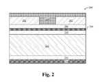
- FIG. 2illustrates a LED laminate base structure 200 in accordance with some embodiments of the present invention.
- the LED laminate base structure 200comprises a covercoat 204 on top of a portion of the copper trace 202 .
- a first thermal conductive adhesive layer 206couples with the copper trace 202 and/or the covercoat 204 .
- a polyimide layer 208is underneath the first thermal conductive adhesive layer 206 .
- the polyimide layer 208comprise Kapton®.
- the polyimide layer 208sandwiched by a second thermal conductive adhesive layer 210 .
- the first, the second, or both of thermal conductive adhesive layerscomprise an adhesive A523, which is able to be an epoxy adhesive.
- a heat spreading layer (e.g. a heat sink) 212couples with the second thermal conductive adhesive layer 210 .
- FIG. 3illustrates some LED assembly 300 in accordance with some embodiments of the present invention.
- the LED assembly 300forms a regionally rigid structure by bending and/or folding a flexible LED laminate base structure (such as the LED laminate base structure 200 of FIG. 2 ) to form an angled structured, such as a horseshoe structure and a stair step structure.
- a flexible LED laminate base structuresuch as the LED laminate base structure 200 of FIG. 2
- a LED assembly 303comprises a LED die containing unit 302 on a LED laminate base structure 304 .
- the LED laminate base structure 304comprises the LED laminate base structure 200 ( FIG. 2 ).
- the LED laminate base structure 304comprises a left section 304 A, middle section 304 B, and right section 304 C.
- the middle section 304 Bthermally couples with the LED containing unit 302 .
- the middle section 304 Belectrically couples with the LED containing unit 302 .
- the middle section 304 Bis electrically isolated from the LED containing unit 302 .
- the left section 304 A and the right section 304 Care bending downward making a LED upward pointing structure.
- the LED assembly 306contains a LED laminate base structure having a left section 306 A, middle section 306 B, and right section 306 C.
- the left section 306 Ais bending upward and the right section is bending downward making a stair step structure.
- the LED assembly 308contains a LED laminate base structure having hooks.
- the left section 308 A and the right section 308 Cboth comprise a hook structure, so that a structure strength/thickness of both left section 308 A and right section 308 C are reinforced.
- the hook structure of the LED assembly 308is able to hook on another supporting structure, such as a loop structure.
- the LED assembly 310comprises a left section 310 A, middle section 310 B, and the right section 310 C, wherein the left and right sections comprise hooks.
- the left section 310 Ais bending upward and the right section 310 C is bending downward, so that the LED assembly 310 forms a stair step structure with hooks on each side.
- the LED assembly 312comprise a left section 312 A, middle section 312 B, and right section 312 C. Crease lines 312 D and 312 E are form by folding, bending, crushing, or pressing the left section 312 A and/or the right section 312 C.
- a LED assembly 314comprises a LED laminate base structure having a corrugated structure 314 B.
- the LED assembly disclosed hereinis thin and flexible to be bent in various geometries and is sufficiently stiff to hold the structure as bended. In some embodiments, the LED assembly having the LED die 302 is stiff and rigid such that it cannot be bent.
- any part of the LED assembly(such as 304 A and 304 C) having the LED laminate base structures without the LED die 302 is flexible and is able to be freely bent and folded, such as at the point 304 A′ and/or at the point 304 A′′.
- FIG. 4illustrates a method 400 of making the LED assembly in accordance with some embodiments of the present invention.
- the methodcan start from Step 402 .
- a hybrid laminate structureis formed.
- the making of the hybrid laminate structurecan be done by using a typical roll-to-roll process.
- the hybrid laminate structurecomprises a conducting layer attached to an interposing dielectric layer.
- the dielectric layeris attached to a bottom heat spreading layer, which is generally made by a metallic material, such as aluminum, having a thickness between 100-150 micrometers.
- a circuitryis created on the hybrid laminate structure.
- the circuitrysuch as electronic circuit patterns, are formed using a photolithography process.
- LED chipsare attached to the circuitry at a pre-determined location to form an assembled LED assembly.
- the LED assemblyis bent to a pre-determined shape to enhance the selected regional rigidity for further application, such as installing on a headlight of an automobile. The method stops at Step 412 .
- the heat spreading layer of the LED assembly disclosed hereinis advantageous in many ways, such as having a lower thermal resistivity and higher thermal emissivity.
- the lower thermal resistivity and higher thermal emissivityare able to be achieved by incorporating additional layers of heat conductive material (such as coupling heat conductive adhesive A523 and polyimide with the bottom of the heat spreading layer, e.g., aluminum heat spreading layer) and increasing heat emitting areas when compared with the typical heat sink of the typical LED assembly.
- the thermal resistivityis 465 C-mm 2 /Watt.
- the heat spreading layer of the LED assemblyhaving a construction of 1 oz copper, 18 micrometers adhesive A523, 12 micron polyimide, 18 micrometers adhesive A523, 100 micrometers aluminum, 18 micron heat conductive A523, and 12 micrometer polyimide, the thermal resistivity is 240 C-mm 2 /Watt.
- the thermal resistivity of the dielectric layercan be as low as 96 C-mm 2 /Watt.
- the total thermal emission of the heat spreading layercan be 6 to 13 times better than a typical heat sink plate of a typical LED assembly.
- the heat spreading layercan be manufactured by using a standard sheet metal fabrication procedure to generate three-dimensional beam structures from planar sheets to generate heat spreaders of greater rigidity and improved thermal performance.
- the methods disclosed hereinallows LED assembly to be manufactured on specific FPC materials that can be mass produced on a roll-to-roll equipment. After the LED assembly is manufactured, it can be bent and/or formed into relatively rigid structures, which allows to be manufactured in a fully automated assembly process.
- the term “forming”comprising having a sheet of the laminate to be pressed by a die with a protrusion to make a dimple on the laminate such that a structural strength is created/enhanced with the creation of the dimple.
- the term “forming”comprises the action of pressing a sheet of a material, such as the laminate, that is performed by a person skill in the art in the automobile manufacturing industry. The actions of forming, bending, and folding are able to be performed separately and/or together.
- the roll-to-roll processcomprises a process of creating electronic devices on a roll of flexible plastic or metal foil, which includes any process of applying coatings, printing, or performing other processes starting with a roll of a flexible material and re-reeling after the process to create an output roll. Once the rolls of material have been coated, laminated or printed, they can be slitted to their finished size on a slitter rewinder.
- the LED assemblycan be utilized in various fields, such as lightings for automobile, houses, and streets.
- the manufacturing processcan fabricate LED assemblies on FPC materials having a top circuitry layer attached to an interposing dielectric layer.
- the dielectric layeris attached to a bottom metallic heat spreading layer.
- the circuit assemblycan be completed in a planar form.
- the LED assemblycan be populated in a planar form and then bent and/or formed into relatively rigid structures. Alternatively, the LED assembly can be first bent and/or form into relatively rigid structures and then populated. In both cases, the areas around the pads of the populated components are not deformed and retain their planar format.
Landscapes
- Engineering & Computer Science (AREA)
- General Engineering & Computer Science (AREA)
- Microelectronics & Electronic Packaging (AREA)
- Physics & Mathematics (AREA)
- Optics & Photonics (AREA)
- Led Device Packages (AREA)
- Laminated Bodies (AREA)
Abstract
Description
Claims (38)
Priority Applications (1)
| Application Number | Priority Date | Filing Date | Title |
|---|---|---|---|
| US13/763,214US9117991B1 (en) | 2012-02-10 | 2013-02-08 | Use of flexible circuits incorporating a heat spreading layer and the rigidizing specific areas within such a construction by creating stiffening structures within said circuits by either folding, bending, forming or combinations thereof |
Applications Claiming Priority (2)
| Application Number | Priority Date | Filing Date | Title |
|---|---|---|---|
| US201261597619P | 2012-02-10 | 2012-02-10 | |
| US13/763,214US9117991B1 (en) | 2012-02-10 | 2013-02-08 | Use of flexible circuits incorporating a heat spreading layer and the rigidizing specific areas within such a construction by creating stiffening structures within said circuits by either folding, bending, forming or combinations thereof |
Publications (1)
| Publication Number | Publication Date |
|---|---|
| US9117991B1true US9117991B1 (en) | 2015-08-25 |
Family
ID=53838551
Family Applications (1)
| Application Number | Title | Priority Date | Filing Date |
|---|---|---|---|
| US13/763,214Active2033-06-23US9117991B1 (en) | 2012-02-10 | 2013-02-08 | Use of flexible circuits incorporating a heat spreading layer and the rigidizing specific areas within such a construction by creating stiffening structures within said circuits by either folding, bending, forming or combinations thereof |
Country Status (1)
| Country | Link |
|---|---|
| US (1) | US9117991B1 (en) |
Cited By (8)
| Publication number | Priority date | Publication date | Assignee | Title |
|---|---|---|---|---|
| US20160353564A1 (en)* | 2014-11-27 | 2016-12-01 | Shenzhen China Star Optoelectronics Technology Co. Ltd. | L-Bending PCB |
| US9763327B2 (en) | 2015-03-19 | 2017-09-12 | Multek Technologies Limited | Selective segment via plating process and structure |
| US20180106432A1 (en)* | 2015-04-15 | 2018-04-19 | Ledvance Gmbh | Lighting means comprising LEDs |
| US10697592B2 (en) | 2015-04-15 | 2020-06-30 | Ledvance Gmbh | Lighting means comprising LEDs |
| US10969067B2 (en) | 2017-01-30 | 2021-04-06 | Signify Holding B.V. | Light emitting device having flexible substrate with plurality of folds |
| US11404343B2 (en)* | 2020-02-12 | 2022-08-02 | Qualcomm Incorporated | Package comprising a substrate configured as a heat spreader |
| US11454027B2 (en) | 2020-10-29 | 2022-09-27 | GAF Energy LLC | System of roofing and photovoltaic shingles and methods of installing same |
| US11486144B2 (en) | 2020-11-12 | 2022-11-01 | GAF Energy LLC | Roofing shingles with handles |
Citations (114)
| Publication number | Priority date | Publication date | Assignee | Title |
|---|---|---|---|---|
| US2911605A (en) | 1956-10-02 | 1959-11-03 | Monroe Calculating Machine | Printed circuitry |
| US4051425A (en) | 1975-02-03 | 1977-09-27 | Telephone Utilities And Communications Industries, Inc. | Ac to dc power supply circuit |
| US4495546A (en) | 1981-05-18 | 1985-01-22 | Matsushita Electric Industrial Co., Ltd. | Hybrid integrated circuit component and printed circuit board mounting said component |
| US4712160A (en) | 1985-07-02 | 1987-12-08 | Matsushita Electric Industrial Co., Ltd. | Power supply module |
| US4729076A (en) | 1984-11-15 | 1988-03-01 | Tsuzawa Masami | Signal light unit having heat dissipating function |
| US4771824A (en) | 1985-03-08 | 1988-09-20 | Institut Francais Du Petrole | Method of transferring heat from a hot fluid A to a cold fluid using a composite fluid as heat carrying agent |
| US4788626A (en) | 1986-02-15 | 1988-11-29 | Brown, Boveri & Cie Ag | Power semiconductor module |
| US4893227A (en) | 1988-07-08 | 1990-01-09 | Venus Scientific, Inc. | Push pull resonant flyback switchmode power supply converter |
| US4899256A (en) | 1988-06-01 | 1990-02-06 | Chrysler Motors Corporation | Power module |
| US4901069A (en) | 1987-07-16 | 1990-02-13 | Schlumberger Technology Corporation | Apparatus for electromagnetically coupling power and data signals between a first unit and a second unit and in particular between well bore apparatus and the surface |
| US4975821A (en) | 1989-10-10 | 1990-12-04 | Lethellier Patrice R | High frequency switched mode resonant commutation power supply |
| US5101322A (en) | 1990-03-07 | 1992-03-31 | Motorola, Inc. | Arrangement for electronic circuit module |
| US5164657A (en) | 1988-08-08 | 1992-11-17 | Zdzislaw Gulczynski | Synchronous switching power supply comprising buck converter |
| US5235491A (en) | 1990-05-10 | 1993-08-10 | Bicc-Vero Electronics Gmbh | Safety power supply |
| US5262932A (en) | 1991-03-04 | 1993-11-16 | Stanley David L | Power converter |
| US5295044A (en) | 1991-09-26 | 1994-03-15 | Kabushiki Kaisah Toshiba | Semiconductor device |
| US5490052A (en) | 1992-04-24 | 1996-02-06 | Matsushita Electric Industrial Co., Ltd. | Switching power supply |
| US5565781A (en) | 1991-07-09 | 1996-10-15 | Dauge; Gilbert | Device for detecting the malfunctioning of a load such as a magnetron |
| US5565761A (en) | 1994-09-02 | 1996-10-15 | Micro Linear Corp | Synchronous switching cascade connected offline PFC-PWM combination power converter controller |
| US5592128A (en) | 1995-03-30 | 1997-01-07 | Micro Linear Corporation | Oscillator for generating a varying amplitude feed forward PFC modulation ramp |
| US5632551A (en) | 1994-07-18 | 1997-05-27 | Grote Industries, Inc. | LED vehicle lamp assembly |
| US5712772A (en) | 1995-02-03 | 1998-01-27 | Ericsson Raynet | Controller for high efficiency resonant switching converters |
| US5742151A (en) | 1996-06-20 | 1998-04-21 | Micro Linear Corporation | Input current shaping technique and low pin count for pfc-pwm boost converter |
| US5747977A (en) | 1995-03-30 | 1998-05-05 | Micro Linear Corporation | Switching regulator having low power mode responsive to load power consumption |
| US5798635A (en) | 1996-06-20 | 1998-08-25 | Micro Linear Corporation | One pin error amplifier and switched soft-start for an eight pin PFC-PWM combination integrated circuit converter controller |
| US5804950A (en) | 1996-06-20 | 1998-09-08 | Micro Linear Corporation | Input current modulation for power factor correction |
| US5811895A (en) | 1994-08-12 | 1998-09-22 | International Business Machines Corp. | Power supply circuit for use with a battery and an AC power adaptor |
| US5818207A (en) | 1996-12-11 | 1998-10-06 | Micro Linear Corporation | Three-pin buck converter and four-pin power amplifier having closed loop output voltage control |
| US5890794A (en) | 1996-04-03 | 1999-04-06 | Abtahi; Homayoon | Lighting units |
| US5903138A (en) | 1995-03-30 | 1999-05-11 | Micro Linear Corporation | Two-stage switching regulator having low power modes responsive to load power consumption |
| US5905369A (en) | 1996-10-17 | 1999-05-18 | Matsushita Electric Industrial Co., Ltd. | Variable frequency switching of synchronized interleaved switching converters |
| US5923543A (en) | 1996-12-14 | 1999-07-13 | Samsung Electronics Co., Ltd. | Resonance-type power switching device |
| US6032698A (en)* | 1998-09-11 | 2000-03-07 | Karl Weiss Hoch-Tief- Und Rohrleitungsbau Gmbh & Co. | Method and an apparatus for lining a pipe or duct |
| US6039600A (en) | 1997-10-10 | 2000-03-21 | Molex Incorporated | Male connector for flat flexible circuit |
| US6058026A (en) | 1999-07-26 | 2000-05-02 | Lucent Technologies, Inc. | Multiple output converter having a single transformer winding and independent output regulation |
| US6069803A (en) | 1999-02-12 | 2000-05-30 | Astec International Limited | Offset resonance zero volt switching flyback converter |
| US6074074A (en)* | 1996-07-11 | 2000-06-13 | Happich Fahrzeug-Und Industrieteile Gmbh | Lighting strip and method for production |
| US6077124A (en)* | 1997-10-10 | 2000-06-20 | Molex Incorporated | Electrical connectors for flat flexible circuitry with yieldable backing structure |
| US6160725A (en) | 1999-03-12 | 2000-12-12 | Nmb Usa Inc. | System and method using phase detection to equalize power from multiple power sources |
| US6272015B1 (en) | 1997-11-24 | 2001-08-07 | International Rectifier Corp. | Power semiconductor module with insulation shell support for plural separate substrates |
| US6282092B1 (en) | 1998-06-12 | 2001-08-28 | Shindengen Electric Manufacturing Co., Ltd. | Electronic circuit device and method of fabricating the same |
| US20010042865A1 (en) | 1997-01-15 | 2001-11-22 | Kabushiki Kaisha Toshiba | Semiconductor light emitting device and its manufacturing method |
| US20020011823A1 (en) | 2000-07-28 | 2002-01-31 | Lg Electronics Inc. | Smart battery, secondary smart battery connection apparatus of portable computer system, AC adapter implementing same, and connection method thereof |
| US6344980B1 (en) | 1999-01-14 | 2002-02-05 | Fairchild Semiconductor Corporation | Universal pulse width modulating power converter |
| US6358064B2 (en) | 1999-03-29 | 2002-03-19 | Delphi Technologies, Inc. | Z-axis electrical interconnect |
| US6396277B1 (en) | 1999-10-01 | 2002-05-28 | Snap-On Technologies, Inc. | Coil on plug signal detection |
| US6407514B1 (en) | 2001-03-29 | 2002-06-18 | General Electric Company | Non-synchronous control of self-oscillating resonant converters |
| US6445008B1 (en)* | 2001-10-25 | 2002-09-03 | Opto Tech Corporation | Photo sensing device and the manufacturing method thereof |
| US6469980B1 (en) | 1996-04-15 | 2002-10-22 | Matsushita Electric Industrial Co., Ltd. | Optical disk and a recording/reproduction apparatus using multiple address block groups shifted oppositely with multiple address blocks and non-pit data |
| US6483281B2 (en) | 2000-02-11 | 2002-11-19 | Champion Microelectronic Corporation | Low power mode and feedback arrangement for a switching power converter |
| US20030035303A1 (en) | 2000-03-02 | 2003-02-20 | Power Integrations, Inc. | Switched mode power supply responsive to current derived from voltage across energy transfer element input |
| US6531854B2 (en) | 2001-03-30 | 2003-03-11 | Champion Microelectronic Corp. | Power factor correction circuit arrangement |
| US6578253B1 (en) | 1991-10-04 | 2003-06-17 | Fmtt, Inc. | Transformer and inductor modules having directly bonded terminals and heat-sink fins |
| US6657417B1 (en) | 2002-05-31 | 2003-12-02 | Champion Microelectronic Corp. | Power factor correction with carrier control and input voltage sensing |
| US6671189B2 (en) | 2001-11-09 | 2003-12-30 | Minebea Co., Ltd. | Power converter having primary and secondary side switches |
| US6674272B2 (en) | 2001-06-21 | 2004-01-06 | Champion Microelectronic Corp. | Current limiting technique for a switching power converter |
| US20040228153A1 (en) | 2003-05-14 | 2004-11-18 | Cao Xiao Hong | Soft-switching techniques for power inverter legs |
| US20050104059A1 (en)* | 2003-11-14 | 2005-05-19 | Friedman Marc D. | Flexible array |
| US20050105224A1 (en) | 2003-11-13 | 2005-05-19 | Sharp Kabushiki Kaisha | Inverter apparatus connected to a plurality of direct current power sources and dispersed-power-source system having inverter apparatus linked to commercial power system to operate |
| US20050146886A1 (en)* | 2003-12-24 | 2005-07-07 | Ichikoh Industries, Ltd. | Vehicle outside-mirror unit including lamp unit |
| US6958920B2 (en) | 2003-10-02 | 2005-10-25 | Supertex, Inc. | Switching power converter and method of controlling output voltage thereof using predictive sensing of magnetic flux |
| US20050281425A1 (en) | 2004-06-21 | 2005-12-22 | Nokia Corporation | Apparatus and methods for increasing magnetic field in an audio device |
| US20060090787A1 (en)* | 2004-10-28 | 2006-05-04 | Onvural O R | Thermoelectric alternators and thermoelectric climate control devices with controlled current flow for motor vehicles |
| US7047059B2 (en) | 1998-08-18 | 2006-05-16 | Quantum Magnetics, Inc | Simplified water-bag technique for magnetic susceptibility measurements on the human body and other specimens |
| US20060186430A1 (en) | 2005-02-23 | 2006-08-24 | Samsung Electro-Mechanics Co., Ltd. | Light emitting diode package and fabrication method thereof |
| US20070025108A1 (en)* | 2005-07-28 | 2007-02-01 | Kingsford Howard A | Mounting light emitting diodes |
| US20070028626A1 (en) | 2003-09-02 | 2007-02-08 | Sharp Kabushiki Kaisha | Loop type thermo siphon, stirling cooling chamber, and cooling apparatus |
| US20070081332A1 (en)* | 2005-08-25 | 2007-04-12 | He Zheng Z | Strip light structure |
| US7210832B2 (en) | 2003-09-26 | 2007-05-01 | Advanced Thermal Devices, Inc. | Illumination apparatus of light emitting diodes and method of heat dissipation thereof |
| US7259403B2 (en) | 2001-08-09 | 2007-08-21 | Matsushita Electric Industrial Co., Ltd. | Card-type LED illumination source |
| US7286376B2 (en) | 2005-11-23 | 2007-10-23 | System General Corp. | Soft-switching power converter having power saving circuit for light load operations |
| WO2008003289A2 (en)* | 2006-07-06 | 2008-01-10 | Osram Gesellschaft mit beschränkter Haftung | Illuminating system of flexible shape |
| US20080048200A1 (en) | 2004-11-15 | 2008-02-28 | Philips Lumileds Lighting Company, Llc | LED with Phosphor Tile and Overmolded Phosphor in Lens |
| US20080225523A1 (en)* | 2005-03-30 | 2008-09-18 | Koninklijke Philips Electronics N.V. | Flexible Led Array |
| US7439962B2 (en) | 2005-06-01 | 2008-10-21 | Synaptics Incorporated | Touch pad with flexible substrate |
| US20090032295A1 (en)* | 2005-04-19 | 2009-02-05 | Denki Kagaku Kogyo Kabushiki Kaisha | Metal base circuit board, led, and led light source unit |
| US20090118800A1 (en)* | 2007-10-31 | 2009-05-07 | Karl Deisseroth | Implantable optical stimulators |
| US7549786B2 (en)* | 2006-12-01 | 2009-06-23 | Cree, Inc. | LED socket and replaceable LED assemblies |
| US20090179207A1 (en) | 2008-01-11 | 2009-07-16 | Cree, Inc. | Flip-chip phosphor coating method and devices fabricated utilizing method |
| US7611261B2 (en) | 2005-09-29 | 2009-11-03 | Hallmark Cards, Incorporated | Decorating with a lighted device |
| US20100083912A1 (en)* | 2008-10-02 | 2010-04-08 | Marni Markell Hurwitz | Omnidirectionally reflective pet leash |
| US20100142215A1 (en)* | 2008-12-10 | 2010-06-10 | Waring Jennifer S | Annular lighting fixture and method for illumination |
| US20100214799A1 (en)* | 2009-02-23 | 2010-08-26 | Koito Manufacturing Co., Ltd. | Vehicular light source unit |
| US20100277666A1 (en)* | 2007-05-22 | 2010-11-04 | OSRAM Gelsellschaft mit beschrankter | Lighting Device, Backlighting Device, and Display Device |
| US20100295077A1 (en) | 2009-05-19 | 2010-11-25 | Intematix Corporation | Manufacture of light emitting devices with phosphor wavelength conversion |
| US20100295070A1 (en) | 2009-05-20 | 2010-11-25 | Intematix Corporation | Light emitting device |
| US20110018017A1 (en) | 2009-07-23 | 2011-01-27 | Koninklijke Philips Electronics N.V. | Led with molded reflective sidewall coating |
| DE102009034841A1 (en) | 2009-07-27 | 2011-02-03 | Emz-Hanauer Gmbh & Co. Kgaa | Light-emitting device for a drum of a household appliance |
| US20110050381A1 (en) | 2007-03-29 | 2011-03-03 | Flextronics Ap, Llc | Method of producing a multi-turn coil from folded flexible circuitry |
| US20110051413A1 (en) | 2009-08-25 | 2011-03-03 | Abl Ip Holding Llc | Optic shielding |
| US20110085336A1 (en) | 2005-02-28 | 2011-04-14 | Osram Opto Semiconductors Gmbh, A Corporation Of Germany | Illumination device |
| US20110180818A1 (en)* | 2010-08-27 | 2011-07-28 | Quarkstar, Llc | Solid State Light Sheet Using Thin LEDs For General Illumination |
| US20110204391A1 (en)* | 2010-08-27 | 2011-08-25 | Quarkstar, Llc | Solid State Light Sheet or Strip Having Cavities Formed in Top Substrate |
| US20110278049A1 (en)* | 2009-10-15 | 2011-11-17 | Lg Chem, Ltd. | Photosensitive resin composition and dry film comprising the same |
| US20110286222A1 (en)* | 2007-05-16 | 2011-11-24 | Fusion Optix Inc. | Method of manufacturing an optical composite |
| US20120036750A1 (en)* | 2010-08-12 | 2012-02-16 | Sun Inno Tech | Internally Illuminated Panel and Method of Making the Same |
| US20120057099A1 (en)* | 2010-08-27 | 2012-03-08 | Rohm Co., Ltd. | Led light source unit for backlight of liquid crystal display, and liquid crystal display |
| US20120097985A1 (en) | 2010-10-21 | 2012-04-26 | Wen-Huang Liu | Light Emitting Diode (LED) Package And Method Of Fabrication |
| US20120165759A1 (en)* | 2009-12-16 | 2012-06-28 | Rogers John A | Waterproof stretchable optoelectronics |
| US8227269B2 (en) | 2009-05-19 | 2012-07-24 | Intematix Corporation | Manufacture of light emitting devices with phosphor wavelength conversion |
| WO2012104800A2 (en)* | 2011-02-04 | 2012-08-09 | Koninklijke Philips Electronics N.V. | Lighting unit with led strip |
| US20120201104A1 (en)* | 2011-02-08 | 2012-08-09 | Amenduni Gresele Massimo | Wrist belt or bracelet having a timepiece function |
| US20120205697A1 (en) | 2011-02-10 | 2012-08-16 | Kwon Joong Kim | Flip chip light emitting device package and manufacturing method thereof |
| US20130027906A1 (en) | 2010-03-03 | 2013-01-31 | Panasonic Corporation | Refrigerator |
| US8378559B2 (en) | 2009-08-20 | 2013-02-19 | Progressive Cooling Solutions, Inc. | LED bulb for high intensity discharge bulb replacement |
| US20130092421A1 (en)* | 2010-05-27 | 2013-04-18 | Nippon Mektron, Ltd. | Flexible circuit board |
| US20130155674A1 (en) | 2011-12-15 | 2013-06-20 | Samsung Electronics Co., Ltd. | Light-emitting device lamp |
| USD687179S1 (en) | 2012-07-31 | 2013-07-30 | Jung Hoon Kim | Protective cover for LED module |
| US8591051B2 (en) | 2009-07-28 | 2013-11-26 | Sumitomo Wiring Systems, Ltd. | Panel and method for producing the same |
| US20140003053A1 (en) | 2012-06-27 | 2014-01-02 | Flextronics Ap, Llc | Multi-facet light engine |
| US20140043810A1 (en) | 2012-08-10 | 2014-02-13 | Samsung Electronics Co.,Ltd. | Lighting apparatus |
| US8661660B2 (en) | 2005-09-22 | 2014-03-04 | The Artak Ter-Hovhanissian Patent Trust | Process for manufacturing LED lighting with integrated heat sink |
| US8761565B1 (en)* | 2009-04-16 | 2014-06-24 | Fusion Optix, Inc. | Arcuate lightguide and light emitting device comprising the same |
| US20150016123A1 (en) | 2012-06-27 | 2015-01-15 | Flextronics Ap, Llc | Automotive led headlight cooling system |
- 2013
- 2013-02-08USUS13/763,214patent/US9117991B1/enactiveActive
Patent Citations (123)
| Publication number | Priority date | Publication date | Assignee | Title |
|---|---|---|---|---|
| US2911605A (en) | 1956-10-02 | 1959-11-03 | Monroe Calculating Machine | Printed circuitry |
| US4051425A (en) | 1975-02-03 | 1977-09-27 | Telephone Utilities And Communications Industries, Inc. | Ac to dc power supply circuit |
| US4495546A (en) | 1981-05-18 | 1985-01-22 | Matsushita Electric Industrial Co., Ltd. | Hybrid integrated circuit component and printed circuit board mounting said component |
| US4729076A (en) | 1984-11-15 | 1988-03-01 | Tsuzawa Masami | Signal light unit having heat dissipating function |
| US4771824A (en) | 1985-03-08 | 1988-09-20 | Institut Francais Du Petrole | Method of transferring heat from a hot fluid A to a cold fluid using a composite fluid as heat carrying agent |
| US4712160A (en) | 1985-07-02 | 1987-12-08 | Matsushita Electric Industrial Co., Ltd. | Power supply module |
| US4788626A (en) | 1986-02-15 | 1988-11-29 | Brown, Boveri & Cie Ag | Power semiconductor module |
| US4901069A (en) | 1987-07-16 | 1990-02-13 | Schlumberger Technology Corporation | Apparatus for electromagnetically coupling power and data signals between a first unit and a second unit and in particular between well bore apparatus and the surface |
| US4899256A (en) | 1988-06-01 | 1990-02-06 | Chrysler Motors Corporation | Power module |
| US4893227A (en) | 1988-07-08 | 1990-01-09 | Venus Scientific, Inc. | Push pull resonant flyback switchmode power supply converter |
| US5164657A (en) | 1988-08-08 | 1992-11-17 | Zdzislaw Gulczynski | Synchronous switching power supply comprising buck converter |
| US4975821A (en) | 1989-10-10 | 1990-12-04 | Lethellier Patrice R | High frequency switched mode resonant commutation power supply |
| US5101322A (en) | 1990-03-07 | 1992-03-31 | Motorola, Inc. | Arrangement for electronic circuit module |
| US5235491A (en) | 1990-05-10 | 1993-08-10 | Bicc-Vero Electronics Gmbh | Safety power supply |
| US5262932A (en) | 1991-03-04 | 1993-11-16 | Stanley David L | Power converter |
| US5565781A (en) | 1991-07-09 | 1996-10-15 | Dauge; Gilbert | Device for detecting the malfunctioning of a load such as a magnetron |
| US5295044A (en) | 1991-09-26 | 1994-03-15 | Kabushiki Kaisah Toshiba | Semiconductor device |
| US6578253B1 (en) | 1991-10-04 | 2003-06-17 | Fmtt, Inc. | Transformer and inductor modules having directly bonded terminals and heat-sink fins |
| US5490052A (en) | 1992-04-24 | 1996-02-06 | Matsushita Electric Industrial Co., Ltd. | Switching power supply |
| US5632551A (en) | 1994-07-18 | 1997-05-27 | Grote Industries, Inc. | LED vehicle lamp assembly |
| US5811895A (en) | 1994-08-12 | 1998-09-22 | International Business Machines Corp. | Power supply circuit for use with a battery and an AC power adaptor |
| US5565761A (en) | 1994-09-02 | 1996-10-15 | Micro Linear Corp | Synchronous switching cascade connected offline PFC-PWM combination power converter controller |
| US5712772A (en) | 1995-02-03 | 1998-01-27 | Ericsson Raynet | Controller for high efficiency resonant switching converters |
| US5747977A (en) | 1995-03-30 | 1998-05-05 | Micro Linear Corporation | Switching regulator having low power mode responsive to load power consumption |
| US5592128A (en) | 1995-03-30 | 1997-01-07 | Micro Linear Corporation | Oscillator for generating a varying amplitude feed forward PFC modulation ramp |
| US5903138A (en) | 1995-03-30 | 1999-05-11 | Micro Linear Corporation | Two-stage switching regulator having low power modes responsive to load power consumption |
| US5890794A (en) | 1996-04-03 | 1999-04-06 | Abtahi; Homayoon | Lighting units |
| US6469980B1 (en) | 1996-04-15 | 2002-10-22 | Matsushita Electric Industrial Co., Ltd. | Optical disk and a recording/reproduction apparatus using multiple address block groups shifted oppositely with multiple address blocks and non-pit data |
| US5804950A (en) | 1996-06-20 | 1998-09-08 | Micro Linear Corporation | Input current modulation for power factor correction |
| US5742151A (en) | 1996-06-20 | 1998-04-21 | Micro Linear Corporation | Input current shaping technique and low pin count for pfc-pwm boost converter |
| US5798635A (en) | 1996-06-20 | 1998-08-25 | Micro Linear Corporation | One pin error amplifier and switched soft-start for an eight pin PFC-PWM combination integrated circuit converter controller |
| US6074074A (en)* | 1996-07-11 | 2000-06-13 | Happich Fahrzeug-Und Industrieteile Gmbh | Lighting strip and method for production |
| US5905369A (en) | 1996-10-17 | 1999-05-18 | Matsushita Electric Industrial Co., Ltd. | Variable frequency switching of synchronized interleaved switching converters |
| US5818207A (en) | 1996-12-11 | 1998-10-06 | Micro Linear Corporation | Three-pin buck converter and four-pin power amplifier having closed loop output voltage control |
| US5923543A (en) | 1996-12-14 | 1999-07-13 | Samsung Electronics Co., Ltd. | Resonance-type power switching device |
| US20010042865A1 (en) | 1997-01-15 | 2001-11-22 | Kabushiki Kaisha Toshiba | Semiconductor light emitting device and its manufacturing method |
| US6039600A (en) | 1997-10-10 | 2000-03-21 | Molex Incorporated | Male connector for flat flexible circuit |
| US6077124A (en)* | 1997-10-10 | 2000-06-20 | Molex Incorporated | Electrical connectors for flat flexible circuitry with yieldable backing structure |
| US6272015B1 (en) | 1997-11-24 | 2001-08-07 | International Rectifier Corp. | Power semiconductor module with insulation shell support for plural separate substrates |
| US6282092B1 (en) | 1998-06-12 | 2001-08-28 | Shindengen Electric Manufacturing Co., Ltd. | Electronic circuit device and method of fabricating the same |
| US7047059B2 (en) | 1998-08-18 | 2006-05-16 | Quantum Magnetics, Inc | Simplified water-bag technique for magnetic susceptibility measurements on the human body and other specimens |
| US6032698A (en)* | 1998-09-11 | 2000-03-07 | Karl Weiss Hoch-Tief- Und Rohrleitungsbau Gmbh & Co. | Method and an apparatus for lining a pipe or duct |
| US6344980B1 (en) | 1999-01-14 | 2002-02-05 | Fairchild Semiconductor Corporation | Universal pulse width modulating power converter |
| US6469914B1 (en) | 1999-01-14 | 2002-10-22 | Fairchild Semiconductor Corporation | Universal pulse width modulating power converter |
| US6069803A (en) | 1999-02-12 | 2000-05-30 | Astec International Limited | Offset resonance zero volt switching flyback converter |
| US6160725A (en) | 1999-03-12 | 2000-12-12 | Nmb Usa Inc. | System and method using phase detection to equalize power from multiple power sources |
| US6358064B2 (en) | 1999-03-29 | 2002-03-19 | Delphi Technologies, Inc. | Z-axis electrical interconnect |
| US6058026A (en) | 1999-07-26 | 2000-05-02 | Lucent Technologies, Inc. | Multiple output converter having a single transformer winding and independent output regulation |
| US6396277B1 (en) | 1999-10-01 | 2002-05-28 | Snap-On Technologies, Inc. | Coil on plug signal detection |
| US6541944B2 (en) | 2000-02-11 | 2003-04-01 | Champion Microelectronic Corp. | Low power mode and feedback arrangement for a switching power converter |
| US6605930B2 (en) | 2000-02-11 | 2003-08-12 | Champion Microelectronic Corp. | Low power mode and feedback arrangement for a switching power converter |
| US6483281B2 (en) | 2000-02-11 | 2002-11-19 | Champion Microelectronic Corporation | Low power mode and feedback arrangement for a switching power converter |
| US20030035303A1 (en) | 2000-03-02 | 2003-02-20 | Power Integrations, Inc. | Switched mode power supply responsive to current derived from voltage across energy transfer element input |
| US20020011823A1 (en) | 2000-07-28 | 2002-01-31 | Lg Electronics Inc. | Smart battery, secondary smart battery connection apparatus of portable computer system, AC adapter implementing same, and connection method thereof |
| US6407514B1 (en) | 2001-03-29 | 2002-06-18 | General Electric Company | Non-synchronous control of self-oscillating resonant converters |
| US6531854B2 (en) | 2001-03-30 | 2003-03-11 | Champion Microelectronic Corp. | Power factor correction circuit arrangement |
| US6674272B2 (en) | 2001-06-21 | 2004-01-06 | Champion Microelectronic Corp. | Current limiting technique for a switching power converter |
| US7259403B2 (en) | 2001-08-09 | 2007-08-21 | Matsushita Electric Industrial Co., Ltd. | Card-type LED illumination source |
| US6445008B1 (en)* | 2001-10-25 | 2002-09-03 | Opto Tech Corporation | Photo sensing device and the manufacturing method thereof |
| US6671189B2 (en) | 2001-11-09 | 2003-12-30 | Minebea Co., Ltd. | Power converter having primary and secondary side switches |
| US6657417B1 (en) | 2002-05-31 | 2003-12-02 | Champion Microelectronic Corp. | Power factor correction with carrier control and input voltage sensing |
| US20040228153A1 (en) | 2003-05-14 | 2004-11-18 | Cao Xiao Hong | Soft-switching techniques for power inverter legs |
| US20070028626A1 (en) | 2003-09-02 | 2007-02-08 | Sharp Kabushiki Kaisha | Loop type thermo siphon, stirling cooling chamber, and cooling apparatus |
| US7210832B2 (en) | 2003-09-26 | 2007-05-01 | Advanced Thermal Devices, Inc. | Illumination apparatus of light emitting diodes and method of heat dissipation thereof |
| US6958920B2 (en) | 2003-10-02 | 2005-10-25 | Supertex, Inc. | Switching power converter and method of controlling output voltage thereof using predictive sensing of magnetic flux |
| US20050105224A1 (en) | 2003-11-13 | 2005-05-19 | Sharp Kabushiki Kaisha | Inverter apparatus connected to a plurality of direct current power sources and dispersed-power-source system having inverter apparatus linked to commercial power system to operate |
| US20070123957A1 (en)* | 2003-11-14 | 2007-05-31 | Lumerx, Inc. | Flexible array |
| US20050104059A1 (en)* | 2003-11-14 | 2005-05-19 | Friedman Marc D. | Flexible array |
| US20050146886A1 (en)* | 2003-12-24 | 2005-07-07 | Ichikoh Industries, Ltd. | Vehicle outside-mirror unit including lamp unit |
| US20050281425A1 (en) | 2004-06-21 | 2005-12-22 | Nokia Corporation | Apparatus and methods for increasing magnetic field in an audio device |
| US20060090787A1 (en)* | 2004-10-28 | 2006-05-04 | Onvural O R | Thermoelectric alternators and thermoelectric climate control devices with controlled current flow for motor vehicles |
| US20080048200A1 (en) | 2004-11-15 | 2008-02-28 | Philips Lumileds Lighting Company, Llc | LED with Phosphor Tile and Overmolded Phosphor in Lens |
| US20060186430A1 (en) | 2005-02-23 | 2006-08-24 | Samsung Electro-Mechanics Co., Ltd. | Light emitting diode package and fabrication method thereof |
| US20110085336A1 (en) | 2005-02-28 | 2011-04-14 | Osram Opto Semiconductors Gmbh, A Corporation Of Germany | Illumination device |
| US20080225523A1 (en)* | 2005-03-30 | 2008-09-18 | Koninklijke Philips Electronics N.V. | Flexible Led Array |
| US20090032295A1 (en)* | 2005-04-19 | 2009-02-05 | Denki Kagaku Kogyo Kabushiki Kaisha | Metal base circuit board, led, and led light source unit |
| US7439962B2 (en) | 2005-06-01 | 2008-10-21 | Synaptics Incorporated | Touch pad with flexible substrate |
| US20070025108A1 (en)* | 2005-07-28 | 2007-02-01 | Kingsford Howard A | Mounting light emitting diodes |
| US20070081332A1 (en)* | 2005-08-25 | 2007-04-12 | He Zheng Z | Strip light structure |
| US8661660B2 (en) | 2005-09-22 | 2014-03-04 | The Artak Ter-Hovhanissian Patent Trust | Process for manufacturing LED lighting with integrated heat sink |
| US7611261B2 (en) | 2005-09-29 | 2009-11-03 | Hallmark Cards, Incorporated | Decorating with a lighted device |
| US7286376B2 (en) | 2005-11-23 | 2007-10-23 | System General Corp. | Soft-switching power converter having power saving circuit for light load operations |
| WO2008003289A2 (en)* | 2006-07-06 | 2008-01-10 | Osram Gesellschaft mit beschränkter Haftung | Illuminating system of flexible shape |
| US20120182755A1 (en)* | 2006-07-06 | 2012-07-19 | Osram Gesellschaft Mit Beschrankter Haftung | Illuminating system of flexible shape |
| US7549786B2 (en)* | 2006-12-01 | 2009-06-23 | Cree, Inc. | LED socket and replaceable LED assemblies |
| US20110050381A1 (en) | 2007-03-29 | 2011-03-03 | Flextronics Ap, Llc | Method of producing a multi-turn coil from folded flexible circuitry |
| US20110286222A1 (en)* | 2007-05-16 | 2011-11-24 | Fusion Optix Inc. | Method of manufacturing an optical composite |
| US20100277666A1 (en)* | 2007-05-22 | 2010-11-04 | OSRAM Gelsellschaft mit beschrankter | Lighting Device, Backlighting Device, and Display Device |
| US20090118800A1 (en)* | 2007-10-31 | 2009-05-07 | Karl Deisseroth | Implantable optical stimulators |
| US20090179207A1 (en) | 2008-01-11 | 2009-07-16 | Cree, Inc. | Flip-chip phosphor coating method and devices fabricated utilizing method |
| US20100083912A1 (en)* | 2008-10-02 | 2010-04-08 | Marni Markell Hurwitz | Omnidirectionally reflective pet leash |
| US20100142215A1 (en)* | 2008-12-10 | 2010-06-10 | Waring Jennifer S | Annular lighting fixture and method for illumination |
| US8342734B2 (en)* | 2009-02-23 | 2013-01-01 | Koito Manufacturing Co., Ltd. | Vehicular light source unit |
| US20100214799A1 (en)* | 2009-02-23 | 2010-08-26 | Koito Manufacturing Co., Ltd. | Vehicular light source unit |
| US8761565B1 (en)* | 2009-04-16 | 2014-06-24 | Fusion Optix, Inc. | Arcuate lightguide and light emitting device comprising the same |
| US20100295077A1 (en) | 2009-05-19 | 2010-11-25 | Intematix Corporation | Manufacture of light emitting devices with phosphor wavelength conversion |
| US8227269B2 (en) | 2009-05-19 | 2012-07-24 | Intematix Corporation | Manufacture of light emitting devices with phosphor wavelength conversion |
| US20100295070A1 (en) | 2009-05-20 | 2010-11-25 | Intematix Corporation | Light emitting device |
| US20110018017A1 (en) | 2009-07-23 | 2011-01-27 | Koninklijke Philips Electronics N.V. | Led with molded reflective sidewall coating |
| DE102009034841A1 (en) | 2009-07-27 | 2011-02-03 | Emz-Hanauer Gmbh & Co. Kgaa | Light-emitting device for a drum of a household appliance |
| US20120120667A1 (en) | 2009-07-27 | 2012-05-17 | Emz-Hanauer Gmbh & Co. Kgaa | Light emitting device for a drum of a household appliance |
| US8591051B2 (en) | 2009-07-28 | 2013-11-26 | Sumitomo Wiring Systems, Ltd. | Panel and method for producing the same |
| US8378559B2 (en) | 2009-08-20 | 2013-02-19 | Progressive Cooling Solutions, Inc. | LED bulb for high intensity discharge bulb replacement |
| US20110051413A1 (en) | 2009-08-25 | 2011-03-03 | Abl Ip Holding Llc | Optic shielding |
| US20110278049A1 (en)* | 2009-10-15 | 2011-11-17 | Lg Chem, Ltd. | Photosensitive resin composition and dry film comprising the same |
| US20120165759A1 (en)* | 2009-12-16 | 2012-06-28 | Rogers John A | Waterproof stretchable optoelectronics |
| US20130027906A1 (en) | 2010-03-03 | 2013-01-31 | Panasonic Corporation | Refrigerator |
| US20130092421A1 (en)* | 2010-05-27 | 2013-04-18 | Nippon Mektron, Ltd. | Flexible circuit board |
| US20120036750A1 (en)* | 2010-08-12 | 2012-02-16 | Sun Inno Tech | Internally Illuminated Panel and Method of Making the Same |
| US20110180818A1 (en)* | 2010-08-27 | 2011-07-28 | Quarkstar, Llc | Solid State Light Sheet Using Thin LEDs For General Illumination |
| US20110204391A1 (en)* | 2010-08-27 | 2011-08-25 | Quarkstar, Llc | Solid State Light Sheet or Strip Having Cavities Formed in Top Substrate |
| US20120057099A1 (en)* | 2010-08-27 | 2012-03-08 | Rohm Co., Ltd. | Led light source unit for backlight of liquid crystal display, and liquid crystal display |
| US20120097985A1 (en) | 2010-10-21 | 2012-04-26 | Wen-Huang Liu | Light Emitting Diode (LED) Package And Method Of Fabrication |
| US20130313983A1 (en)* | 2011-02-04 | 2013-11-28 | Koninklijke Philips N.V. | Lighting unit with led strip |
| WO2012104800A2 (en)* | 2011-02-04 | 2012-08-09 | Koninklijke Philips Electronics N.V. | Lighting unit with led strip |
| US20120201104A1 (en)* | 2011-02-08 | 2012-08-09 | Amenduni Gresele Massimo | Wrist belt or bracelet having a timepiece function |
| US20120205697A1 (en) | 2011-02-10 | 2012-08-16 | Kwon Joong Kim | Flip chip light emitting device package and manufacturing method thereof |
| US20130155674A1 (en) | 2011-12-15 | 2013-06-20 | Samsung Electronics Co., Ltd. | Light-emitting device lamp |
| US20140003053A1 (en) | 2012-06-27 | 2014-01-02 | Flextronics Ap, Llc | Multi-facet light engine |
| US20140001496A1 (en) | 2012-06-27 | 2014-01-02 | Flextronics Ap, Llc | Relampable led structure |
| US20150016123A1 (en) | 2012-06-27 | 2015-01-15 | Flextronics Ap, Llc | Automotive led headlight cooling system |
| USD687179S1 (en) | 2012-07-31 | 2013-07-30 | Jung Hoon Kim | Protective cover for LED module |
| US20140043810A1 (en) | 2012-08-10 | 2014-02-13 | Samsung Electronics Co.,Ltd. | Lighting apparatus |
Non-Patent Citations (5)
| Title |
|---|
| "Electronic Transformer for a 12V Halogen Lamp", 1999, ST Microelectronics pp. 1-4. |
| "New Architectures for Radio Frequency dc/dc Power Conversion", Juan Rivas et al.,Laboratory for Electromagnetic and Electronic Systems, Massachusetts Institute of Technology, Room 10-171 Cambridge, MA 02139, pp. 4074-4084. |
| "Novel Zero-Voltage and Zero-Current Switching (ZVZCS) Full-Bridge PWM Converter Using Coupled Output Inductor", Sep. 2002 IEEE, pp. 641-648. |
| EE Times. com-"Team Claims Midrange Wireless Energy Transfer", by R. Colin Johnson, 4 pages, Nov. 6, 2007. |
| EE Times.com-"Wireless Beacon Could Recharge Consumer Devices", by R. Colin Johnson, 3 pages, Nov. 6, 2007. |
Cited By (12)
| Publication number | Priority date | Publication date | Assignee | Title |
|---|---|---|---|---|
| US20160353564A1 (en)* | 2014-11-27 | 2016-12-01 | Shenzhen China Star Optoelectronics Technology Co. Ltd. | L-Bending PCB |
| US9706645B2 (en)* | 2014-11-27 | 2017-07-11 | Shenzhen China Star Optoelectronics Technology Co., Ltd | L-bending PCB |
| US9763327B2 (en) | 2015-03-19 | 2017-09-12 | Multek Technologies Limited | Selective segment via plating process and structure |
| US9867290B2 (en) | 2015-03-19 | 2018-01-09 | Multek Technologies Limited | Selective segment via plating process and structure |
| US20180106432A1 (en)* | 2015-04-15 | 2018-04-19 | Ledvance Gmbh | Lighting means comprising LEDs |
| US10495262B2 (en)* | 2015-04-15 | 2019-12-03 | Ledvance Gmbh | Lighting means comprising LEDs |
| US10697592B2 (en) | 2015-04-15 | 2020-06-30 | Ledvance Gmbh | Lighting means comprising LEDs |
| US10969067B2 (en) | 2017-01-30 | 2021-04-06 | Signify Holding B.V. | Light emitting device having flexible substrate with plurality of folds |
| US11404343B2 (en)* | 2020-02-12 | 2022-08-02 | Qualcomm Incorporated | Package comprising a substrate configured as a heat spreader |
| US11454027B2 (en) | 2020-10-29 | 2022-09-27 | GAF Energy LLC | System of roofing and photovoltaic shingles and methods of installing same |
| US11486144B2 (en) | 2020-11-12 | 2022-11-01 | GAF Energy LLC | Roofing shingles with handles |
| US11661745B2 (en) | 2020-11-12 | 2023-05-30 | GAF Energy LLC | Roofing shingles with handles |
Similar Documents
| Publication | Publication Date | Title |
|---|---|---|
| US9117991B1 (en) | Use of flexible circuits incorporating a heat spreading layer and the rigidizing specific areas within such a construction by creating stiffening structures within said circuits by either folding, bending, forming or combinations thereof | |
| CN102203504B (en) | Method for producing a flexible light strip | |
| CN201426214Y (en) | PCB board with heat radiation structure capable of conducting heat and radiating ink | |
| CN102291938B (en) | Manufacturing method of PCB (Printed Circuit Board) with metal micro-radiator | |
| US20150257250A1 (en) | Heat radiation member, heat radiation circuit board, and heat emission device package | |
| EP3288350B1 (en) | Flexible light engine with bus bars and interconnectors | |
| JP2010010298A (en) | Flexible printed wiring base material and semiconductor apparatus | |
| JP5813367B2 (en) | Electronic module, wiring substrate, and lighting device | |
| WO2013117213A1 (en) | Heat sink with laminated fins and method for production of such a heat sink | |
| JP2008288457A (en) | Ultraviolet light source using light emitting diode | |
| WO2012172937A1 (en) | Wiring body and method for making wiring body | |
| KR20130068657A (en) | The printed circuit board and the method for manufacturing the same | |
| JP2012231061A (en) | Electronic component module and manufacturing method of the same | |
| US8279608B2 (en) | Heatsink device directly contacting a heat source to achieve a quick dissipation effect | |
| US20140226296A1 (en) | Multi-layer wiring board and method for producing multi-layer wiring board | |
| KR101257789B1 (en) | High heat conductive pcb, heat emission module using the high heat conductive pcb, led lighting module using the heat emission module | |
| US20070131448A1 (en) | Circuit board structure with heat radiating layer | |
| KR101155645B1 (en) | Heat spreading printed circuit board and method for fabricating the same | |
| KR101419200B1 (en) | Method for manufacturing flexible printed circuit board | |
| JP6147645B2 (en) | LED circuit board, lighting device including the same, and method for manufacturing LED circuit board | |
| CN111447728B (en) | Flexible circuit board and electronic equipment | |
| CN203445158U (en) | Light-emitting diode module using metal substrate printed circuit board having heat radiation pattern | |
| JP2012038894A (en) | Substrate module for mounting heat generator, and illumination device | |
| CN209964358U (en) | Composite heat dissipation type circuit board and ultraviolet curing module | |
| JP2006324542A (en) | Printed wiring board and manufacturing method thereof |
Legal Events
| Date | Code | Title | Description |
|---|---|---|---|
| AS | Assignment | Owner name:FLEXTRONICS AP, LLC, COLORADO Free format text:ASSIGNMENT OF ASSIGNORS INTEREST;ASSIGNORS:OLSON, BRUCE;BUERMANN, KEVIN;SHEEHAN, SAHUN;REEL/FRAME:030340/0007 Effective date:20130501 | |
| STCF | Information on status: patent grant | Free format text:PATENTED CASE | |
| AS | Assignment | Owner name:MULTEK TECHNOLOGIES LIMITED, CALIFORNIA Free format text:ASSIGNMENT OF ASSIGNORS INTEREST;ASSIGNOR:FLEXTRONICS AP, LLC;REEL/FRAME:042382/0045 Effective date:20170511 | |
| AS | Assignment | Owner name:FLEX LTD, SINGAPORE Free format text:ASSIGNMENT OF ASSIGNORS INTEREST;ASSIGNOR:MULTEK TECHNOLOGIES LIMITED;REEL/FRAME:044596/0965 Effective date:20180108 | |
| MAFP | Maintenance fee payment | Free format text:PAYMENT OF MAINTENANCE FEE, 4TH YEAR, LARGE ENTITY (ORIGINAL EVENT CODE: M1551); ENTITY STATUS OF PATENT OWNER: LARGE ENTITY Year of fee payment:4 | |
| MAFP | Maintenance fee payment | Free format text:PAYMENT OF MAINTENANCE FEE, 8TH YEAR, LARGE ENTITY (ORIGINAL EVENT CODE: M1552); ENTITY STATUS OF PATENT OWNER: LARGE ENTITY Year of fee payment:8 |