US9117739B2 - Semiconductor devices with heterojunction barrier regions and methods of fabricating same - Google Patents
Semiconductor devices with heterojunction barrier regions and methods of fabricating sameDownload PDFInfo
- Publication number
- US9117739B2 US9117739B2US12/719,412US71941210AUS9117739B2US 9117739 B2US9117739 B2US 9117739B2US 71941210 AUS71941210 AUS 71941210AUS 9117739 B2US9117739 B2US 9117739B2
- Authority
- US
- United States
- Prior art keywords
- region
- drift region
- contact
- heterojunction
- type
- Prior art date
- Legal status (The legal status is an assumption and is not a legal conclusion. Google has not performed a legal analysis and makes no representation as to the accuracy of the status listed.)
- Active, expires
Links
Images


Classifications
- H—ELECTRICITY
- H10—SEMICONDUCTOR DEVICES; ELECTRIC SOLID-STATE DEVICES NOT OTHERWISE PROVIDED FOR
- H10D—INORGANIC ELECTRIC SEMICONDUCTOR DEVICES
- H10D8/00—Diodes
- H10D8/60—Schottky-barrier diodes
- H01L29/1608—
- H01L29/0619—
- H01L29/165—
- H01L29/47—
- H01L29/66068—
- H01L29/861—
- H01L29/872—
- H—ELECTRICITY
- H10—SEMICONDUCTOR DEVICES; ELECTRIC SOLID-STATE DEVICES NOT OTHERWISE PROVIDED FOR
- H10D—INORGANIC ELECTRIC SEMICONDUCTOR DEVICES
- H10D12/00—Bipolar devices controlled by the field effect, e.g. insulated-gate bipolar transistors [IGBT]
- H10D12/01—Manufacture or treatment
- H10D12/031—Manufacture or treatment of IGBTs
- H—ELECTRICITY
- H10—SEMICONDUCTOR DEVICES; ELECTRIC SOLID-STATE DEVICES NOT OTHERWISE PROVIDED FOR
- H10D—INORGANIC ELECTRIC SEMICONDUCTOR DEVICES
- H10D62/00—Semiconductor bodies, or regions thereof, of devices having potential barriers
- H10D62/10—Shapes, relative sizes or dispositions of the regions of the semiconductor bodies; Shapes of the semiconductor bodies
- H10D62/102—Constructional design considerations for preventing surface leakage or controlling electric field concentration
- H10D62/103—Constructional design considerations for preventing surface leakage or controlling electric field concentration for increasing or controlling the breakdown voltage of reverse-biased devices
- H10D62/105—Constructional design considerations for preventing surface leakage or controlling electric field concentration for increasing or controlling the breakdown voltage of reverse-biased devices by having particular doping profiles, shapes or arrangements of PN junctions; by having supplementary regions, e.g. junction termination extension [JTE]
- H10D62/106—Constructional design considerations for preventing surface leakage or controlling electric field concentration for increasing or controlling the breakdown voltage of reverse-biased devices by having particular doping profiles, shapes or arrangements of PN junctions; by having supplementary regions, e.g. junction termination extension [JTE] having supplementary regions doped oppositely to or in rectifying contact with regions of the semiconductor bodies, e.g. guard rings with PN or Schottky junctions
- H—ELECTRICITY
- H10—SEMICONDUCTOR DEVICES; ELECTRIC SOLID-STATE DEVICES NOT OTHERWISE PROVIDED FOR
- H10D—INORGANIC ELECTRIC SEMICONDUCTOR DEVICES
- H10D62/00—Semiconductor bodies, or regions thereof, of devices having potential barriers
- H10D62/80—Semiconductor bodies, or regions thereof, of devices having potential barriers characterised by the materials
- H10D62/82—Heterojunctions
- H10D62/822—Heterojunctions comprising only Group IV materials heterojunctions, e.g. Si/Ge heterojunctions
- H—ELECTRICITY
- H10—SEMICONDUCTOR DEVICES; ELECTRIC SOLID-STATE DEVICES NOT OTHERWISE PROVIDED FOR
- H10D—INORGANIC ELECTRIC SEMICONDUCTOR DEVICES
- H10D62/00—Semiconductor bodies, or regions thereof, of devices having potential barriers
- H10D62/80—Semiconductor bodies, or regions thereof, of devices having potential barriers characterised by the materials
- H10D62/83—Semiconductor bodies, or regions thereof, of devices having potential barriers characterised by the materials being Group IV materials, e.g. B-doped Si or undoped Ge
- H10D62/832—Semiconductor bodies, or regions thereof, of devices having potential barriers characterised by the materials being Group IV materials, e.g. B-doped Si or undoped Ge being Group IV materials comprising two or more elements, e.g. SiGe
- H10D62/8325—Silicon carbide
- H—ELECTRICITY
- H10—SEMICONDUCTOR DEVICES; ELECTRIC SOLID-STATE DEVICES NOT OTHERWISE PROVIDED FOR
- H10D—INORGANIC ELECTRIC SEMICONDUCTOR DEVICES
- H10D64/00—Electrodes of devices having potential barriers
- H10D64/60—Electrodes characterised by their materials
- H10D64/64—Electrodes comprising a Schottky barrier to a semiconductor
- H—ELECTRICITY
- H10—SEMICONDUCTOR DEVICES; ELECTRIC SOLID-STATE DEVICES NOT OTHERWISE PROVIDED FOR
- H10D—INORGANIC ELECTRIC SEMICONDUCTOR DEVICES
- H10D8/00—Diodes
- H—ELECTRICITY
- H10—SEMICONDUCTOR DEVICES; ELECTRIC SOLID-STATE DEVICES NOT OTHERWISE PROVIDED FOR
- H10D—INORGANIC ELECTRIC SEMICONDUCTOR DEVICES
- H10D8/00—Diodes
- H10D8/01—Manufacture or treatment
- H10D8/051—Manufacture or treatment of Schottky diodes
Definitions
- the present inventionrelates to semiconductor devices and the fabrication of semiconductor devices and more particularly, to Junction Barrier Schottky (JBS) diodes, and the fabrication of such diodes.
- JBSJunction Barrier Schottky
- High voltage silicon carbide (SiC) Schottky diodeswhich may have voltage blocking ratings between, for example, about 600V and about 2.5 kV, are expected to compete with silicon PIN diodes having similar voltage ratings. Such diodes may handle as much as about 100 amps or more of forward current, depending on their active area design. High voltage Schottky diodes have a number of important applications, particularly in the field of power conditioning, distribution and control.
- SiC Schottky diodeAn important characteristic of a SiC Schottky diode in such applications is its switching speed. Silicon-based PIN devices typically exhibit relatively poor switching speeds. A silicon PIN diode may have a maximum switching speed of approximately 20 kHz, depending on its voltage rating. In contrast, silicon carbide-based Schottky devices are theoretically capable of much higher switching speeds, for example, in excess of about 100 times better than silicon. In addition, silicon carbide devices may be capable of handling a higher current density than silicon devices.
- a conventional SiC Schottky diode structurehas an n-type SiC substrate on which an n ⁇ epitaxial layer, which functions as a drift region, is formed.
- the devicetypically includes a Schottky contact formed directly on the n ⁇ layer.
- a junction termination regionsuch as a guard ring and/or p-type JTE (junction termination extension) region, is typically formed to surround the Schottky junction active region. The purpose of junction termination region is to reduce or prevent electric field crowding at the edges of the Schottky junction, and to reduce or prevent the depletion region from interacting with the surface of the device. Surface effects may cause the depletion region to spread unevenly, which may adversely affect the breakdown voltage of the device.
- Other termination techniquesinclude field plates and floating field rings that may be more strongly influenced by surface effects.
- a channel stop regionmay also be formed by implantation of n-type dopants in order to prevent the depletion region from extending to the edge of the device.
- JBS diodesare sometimes referred to as Merged PIN-Schottky (MPS) diodes.
- FIG. 1A conventional JBS diode 10 is illustrated in FIG. 1 . As shown therein, a conventional JBS diode includes an n-type substrate 12 on which an n ⁇ drift layer 14 is formed.
- a plurality of p+ regions 16are formed, typically by ion implantation, in the surface of the n ⁇ drift layer 14 .
- a metal anode contact 18is formed on the surface of the n ⁇ drift layer 14 in contact with both the n ⁇ drift layer 14 and the p+ regions 16 .
- the anode contact 18forms a Schottky junction with the exposed portions of the drift layer 14 , and may form an ohmic contact with the p+ regions 16 .
- a cathode contact 20is formed on the substrate 12 .
- Silicon carbide-based JBS diodesare described, for example, in U.S. Pat. Nos. 6,104,043 and 6,524,900.
- the junction J 1 between the anode contact 18 and the drift layer 14turns on before the junction J 2 between the p+ regions 16 and the drift layer 14 .
- the deviceexhibits Schottky diode behavior. That is, current transport in the device is dominated by majority carriers (electrons) injected across the Schottky junction J 1 at low forward voltages.
- majority carrierselectrons
- JBS diodeshave fast switching speeds characteristic of Schottky diodes.
- the JBS diode 10behaves like a PIN diode.
- the voltage blocking ability of the device 10is typically determined by the thickness and doping of the drift layer 14 and the design of the edge termination.
- An electronic deviceincludes a silicon carbide layer including an n-type drift region therein, a contact forming a Schottky junction with the drift region, and a p-type junction barrier region on the silicon carbide layer.
- the p-type junction barrier regionincludes a p-type polysilicon region forming a P-N heterojunction with the drift region and the p-type junction barrier region is electrically connected to the contact.
- the Schottky junction between the contact and the drift regionmay be configured to turn on at a lower forward voltage than the P-N heterojunction between the junction barrier region and the drift region.
- the contactmay form an ohmic contact to the p-type polysilicon region, and the P-N heterojunction between the heterojunction barrier region and the drift region may be configured to begin to conduct majority carriers at a higher forward voltage than a turn on voltage of the Schottky junction and at a lower voltage at which the P-N heterojunction between the heterojunction barrier region and the drift region begins to inject minority carriers into the drift region.
- the electronic devicemay further include a guard ring termination region at a surface of the silicon carbide layer laterally adjacent to the contact.
- the guard ring termination regionmay include a second p-type polysilicon region on the drift region, the second p-type polysilicon region being electrically isolated from the contact under zero bias conditions.
- the electronic devicemay further include a junction termination region at the surface of the silicon carbide layer having a conductivity type opposite the conductivity type of the drift region, the second p-type polysilicon region extends into the junction termination region.
- the junction barrier regionmay include a plurality of p-type polysilicon regions in the drift region and at least one p-type polysilicon minority injector pad in the drift region beneath the contact and electrically connected to the contact.
- the minority injector padmay have a surface area in a horizontal plane parallel to a major surface of the silicon carbide layer that is larger than a surface area in the horizontal plane of one of the plurality of p-type polysilicon regions in the junction barrier region.
- the minority carrier injector padmay have a surface area in a horizontal plane parallel to a major surface of the silicon carbide layer that is at least about 10% of a surface area of the drift region in the horizontal plane below the contact.
- the electronic devicemay further include an n+ silicon carbide contact layer on the drift region opposite the contact, and a second contact on the contact layer.
- An electronic deviceincludes a drift region having a first conductivity type, a contact forming a junction with the drift region, and a junction barrier region on the drift region, the junction barrier region having a second conductivity type opposite the first conductivity type and including a heterojunction barrier region on the drift region.
- the heterojunction barrier regionforms a P-N heterojunction with the drift region and is in electrical contact with the contact.
- the Schottky junction between the contact and the drift regionmay be configured to turn on at a lower forward voltage than the P-N heterojunction between the heterojunction barrier region and the drift region.
- the contactmay form an ohmic contact to the heterojunction barrier region, and the P-N heterojunction between the heterojunction barrier region and the drift region may be configured to begin to conduct majority carriers at a higher forward voltage than a turn on voltage of the Schottky junction and at a lower voltage at which the P-N heterojunction between the heterojunction barrier region and the drift region begins to inject minority carriers into the drift region.
- the electronic devicemay further include a guard ring termination region on the drift region and laterally adjacent to the Schottky junction.
- the guard ring termination regionmay include a second heterojunction barrier region.
- the heterojunction barrier regionmay include a plurality of p-type polysilicon regions on the drift region and at least one p-type polysilicon minority injector pad on the drift region beneath the contact and electrically connected to the contact.
- the minority carrier injection padmay have a width that is greater than a width of the junction barrier region.
- the minority injector padmay have a horizontal surface area that is larger than a horizontal surface area of one of the plurality of p-type polysilicon regions in the junction barrier region.
- the drift regionmay include n-type silicon carbide and the heterojunction barrier region may include p-type polysilicon.
- the drift regionmay include n-type silicon carbide and the heterojunction barrier region may include p-type gallium nitride.
- Some embodimentsinclude a termination region at a surface of the drift region and defining an active region of the device within the termination region, wherein a ratio of a surface area of the active region occupied by the heterojunction barrier regions to a total surface area of the active region is about 2% to about 40%. In some embodiments, the ratio is about 4% to about 30%. In some other embodiments, the ratio is about 10% to about 30%, and in further embodiments the ratio is about 20% to about 30%.
- Methods of forming an electronic deviceinclude providing a drift region having a first conductivity type, providing a heterojunction barrier region on the drift region, the heterojunction barrier region including a material different from the drift region and having a conductivity type opposite the conductivity type of the drift region and providing a P-N heterojunction with the drift region, and forming a contact on the drift region and on the heterojunction barrier region, the contact forming a Schottky junction with the drift region and forming an ohmic junction with the heterojunction barrier region.
- the drift regionmay include n-type silicon carbide and the heterojunction barrier region may include p-type polysilicon.
- the methodsmay further include providing a guard ring termination region on the drift region laterally adjacent to the Schottky junction, the guard ring termination region may include a second heterojunction barrier region on the drift region.
- Providing the heterojunction barrier regionmay include etching a recess in the drift region, depositing a polysilicon layer in the recess, doping the polysilicon layer to have a conductivity type opposite the conductivity type of the drift region, and patterning the polysilicon layer.
- An electronic deviceincludes a silicon carbide layer including a drift region having a first conductivity type, a contact on a surface of the drift region and forming a Schottky junction with the drift region, and a guard ring in contact with the surface of the silicon carbide layer adjacent to the Schottky junction.
- the guard ringhas a conductivity type opposite the conductivity type of the drift region and includes a material that forms a heterojunction with the silicon carbide layer.
- the guard ringmay include polysilicon and/or gallium nitride.
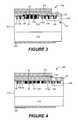
- FIG. 1is a cross-sectional view of a conventional JBS diode.
- FIG. 2is a top view of a JBS diode according to some embodiments of the present invention.
- FIGS. 3 , 4 and 5are cross-sectional views of JBS diodes according to some embodiments of the present invention.
- FIG. 6is a cross-sectional detail of portions of a JBS diode according to some embodiments of the invention.
- FIG. 7is a graph that schematically illustrates various regions in a current-voltage characteristic of a JBS diode according to some embodiments of the invention.
- FIG. 8is a graph illustrating simulated forward current-voltage curves at operating temperatures ranging from 25° C. to 200° C. for a device according to some embodiments.
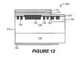
- FIGS. 9-12are cross-sectional views illustrating the formation of JBS diodes according to some embodiments of the present invention.
- FIGS. 13A and 13Bare cross-sectional views of JBS diodes according to some embodiments of the present invention.
- FIG. 14is a graph illustrating simulated horizontal electric field distributions for a device according to some embodiments.
- Relative terms such as “below” or “above” or “upper” or “lower” or “horizontal” or “lateral” or “vertical”may be used herein to describe a relationship of one element, layer or region to another element, layer or region as illustrated in the figures. It will be understood that these terms are intended to encompass different orientations of the device in addition to the orientation depicted in the figures.
- Embodiments of the inventionare described herein with reference to cross-section illustrations that are schematic illustrations of idealized embodiments (and intermediate structures) of the invention.
- the thickness of layers and regions in the drawingsmay be exaggerated for clarity. Additionally, variations from the shapes of the illustrations as a result, for example, of manufacturing techniques and/or tolerances, are to be expected.
- embodiments of the inventionshould not be construed as limited to the particular shapes of regions illustrated herein but are to include deviations in shapes that result, for example, from manufacturing.
- an implanted region illustrated as a rectanglewill, typically, have rounded or curved features and/or a gradient of implant concentration at its edges rather than a discrete change from implanted to non-implanted region.
- a buried region formed by implantationmay result in some implantation in the region between the buried region and the surface through which the implantation takes place.
- the regions illustrated in the figuresare schematic in nature and their shapes are not intended to illustrate the actual shape of a region of a device and are not intended to limit the scope of the invention.
- n-type materialhas a majority equilibrium concentration of negatively charged electrons
- p-type materialhas a majority equilibrium concentration of positively charged holes.
- Some materialmay be designated with a “+” or “ ⁇ ” (as in n+, n ⁇ , p+, p ⁇ , n++, n ⁇ , p++, p ⁇ , or the like), to indicate a relatively larger (“+”) or smaller (“ ⁇ ”) concentration of majority carriers compared to another layer or region.
- ⁇concentration of majority carriers
- a junction barrier Schottky diodeincludes features, such as junction barrier regions and/or edge termination features, on or in a drift layer, wherein the junction barrier regions and/or edge termination features are provided by regions of a different material type than the drift layer, and form respective heterojunctions with the drift layer.
- the features, such as junction barrier regions and/or edge termination featuresmay include doped polysilicon, which can be formed, for example, using conventional processes that may not require ion implantation.
- FIG. 2is a top view of a diode 100 according to some embodiments of the invention
- FIG. 3is a partial cross-sectional view of the diode 100 taken along line A-A of FIG. 2
- FIGS. 4 and 5are similar cross sectional illustrations of diodes 100 ′ and 100 ′′, respectively, according to other embodiments. The dimensions of some features of the diodes 100 , 100 ′, 100 ′′ are exaggerated for clarity.
- the diode 100includes an optional substrate 112 on which a layer 113 including a drift region 114 is formed.
- the layer 113has an upper surface, opposite the substrate, in which a plurality of heterojunction barrier regions 130 are formed.
- a Schottky contact 118is on the drift region 114 .
- the Schottky contact 118contacts the surface of the drift region 114 and forms a Schottky junction with the drift region 114 .
- the Schottky contact 118also contacts the plurality of heterojunction barrier regions 130 .
- the layer 113may be formed, for example, from n-type silicon carbide of the 2H, 4H, 6H, 3C and/or 15R polytype.
- the drift region 114may have a dopant concentration of about 2 ⁇ 10 14 to about 1 ⁇ 10 17 cm ⁇ 3 , depending on design requirements for voltage blocking and on-resistance for the diode 100 .
- Other types of semiconductor materialssuch as GaN, GaAs, silicon or germanium may be used.
- the drift region 114includes 4H-SiC doped with n-type dopants at a concentration of about 5 ⁇ 10 15 cm ⁇ 3 .
- the heterojunction barrier regions 130are formed from a semiconducting material that is different from the material of the drift region 114 .
- the heterojunction barrier regions 130have a conductivity type that is opposite the conductivity type of the drift region 114 . Accordingly, the heterojunction barrier regions 130 form P-N heterojunctions with the drift region 114 .
- the Schottky contact 118may form an ohmic junction with the heterojunction barrier regions 130 .
- the barrier height of the P-N heterojunction J 3 between the heterojunction barrier regions 130 and the drift layermay be higher than a barrier height of a Schottky junction J 4 between a Schottky contact 118 and the drift region 114 , so that the P-N heterojunction will turn on at a higher forward voltage than the Schottky junction J 4 between the drift region 114 and the Schottky contact 118 , as will be discussed in more detail below.
- the heterojunction barrier regions 130are formed as stripe-shaped regions in the drift region 114 .
- the heterojunction barrier regions 130may be formed in other shapes, such as islands, squares, dots, hexagons, or any other desired shape.
- the heterojunction barrier regions 130may be provided as regions of doped polysilicon.
- the heterojunction barrier regions 130may include polysilicon regions doped to have a conductivity that is opposite the conductivity type of the drift region 114 , so that the heterojunction barrier regions 130 form P-N heterojunctions J 3 with the drift region 114 .
- the heterojunction barrier regions 130may be doped with p-type dopants, such as boron and/or aluminum, at a concentration of about 1 ⁇ 10 17 to about 1 ⁇ 10 20 cm ⁇ 3 , and may extend to a depth of about 0.3 to about 0.5 ⁇ m into the drift region 114 from the surface of the drift region 114 .
- the heterojunction barrier regions 130may be doped at a dopant concentration of about 5 ⁇ 10 18 cm ⁇ 3 , and may extend to a depth of about 0.3 ⁇ m into the drift region 114 from the surface of the drift region 114 .
- One or more current surge pads 116may also be provided in the drift region 114 .
- the current surge pads 116may be formed of the same material as the heterojunction barrier regions 130 .
- the current surge pads 116may be provided as polysilicon regions doped with p-type dopants, such as boron and/or aluminum, at a concentration of about 1 ⁇ 10 18 to about 1 ⁇ 10 20 cm ⁇ 3 , and may extend to a depth of about 0.3 to about 0.5 ⁇ m into the drift region 114 .
- the current surge pads 116may be doped at a dopant concentration of about 5 ⁇ 10 18 cm ⁇ 3 , and may extend to a depth of about 0.3 ⁇ m into the drift region 114 .
- the current surge pads 116have a larger width than the heterojunction barrier regions 130 to encourage the flow of surge current through the current surge pads at high forward voltages, as will be discussed in more detail below.
- the current surge pads 116may have a width of about 10 ⁇ m to about 250 ⁇ m.
- the current surge pads 116may have a width of about 20 ⁇ m.
- the current surge pads 116 and/or heterojunction barrier regions 130may be formed of other types of materials that can be doped to have a conductivity that is opposite the conductivity of the drift region 114 and can form a heterojunction with the drift region 114 .
- the drift regioncomprises n-type silicon carbide
- a material such as p-type gallium nitridecan be used to form the current surge pads 116 and/or heterojunction barrier regions 130 .
- the heterojunction barrier regions 130 shown in the embodiments of FIGS. 2 and 3are provided as spaced apart striped regions that expose portions 114 A of the surface of the drift region 114 and that extend across an active region 110 of the drift region 114 (except for the exposed portions 114 A of the drift layer and the current surge pads 116 ).
- a metal Schottky contact 118covers the drift region 114 and forms Schottky rectifying junctions with the exposed portions 114 A of the drift region 114 as well as the heterojunction barrier regions 130 and the current surge pads 116 .
- the term “active region”refers to the two dimensional area of the device in which the Schottky metal contacts the drift layer, and includes the exposed portions 114 A of the drift region 114 , the heterojunction barrier 130 and the current surge pads 116 . Accordingly, the active region includes the Schottky junction area but does not include, for example, the edge termination region described below.
- the diode 100may include an edge termination region 115 surrounding the active region 110 of the diode 100 .
- the edge termination region 115may include a junction termination extension (JTE) region, field rings, field plates, guard rings, and/or a combination of the foregoing or other terminations.
- the device 100may include a plurality of guard rings 125 , which may be formed of the same material as the heterojunction barrier regions 130 and the current surge pad 116 and may also be doped to have a conductivity opposite the conductivity type of the drift region 114 .
- a passivation layer, such as a field oxide layer 127may be formed on the drift layer and may cover the guard rings 125 .
- the guard rings 125may be floating guard rings that are electrically isolated from the anode contact 118 under zero bias conditions.
- the edge termination region 115includes a robust guard ring (RGR) termination as described in U.S. Pat. No. 7,026,650, which is assigned to the assignee of the present invention, the disclosure of which is incorporated herein by reference as if set forth fully.
- the RGR terminationmay include an implanted region 160 of dopants having a conductivity opposite the conductivity of the drift layer.
- the implanted region 160may extend to a depth in the drift region 114 that is greater or less than the depth of the guard rings 125 .
- the implanted region 160may have a net concentration of dopants having a conductivity opposite the conductivity type of the drift region 114 of about 1 ⁇ 10 17 cm ⁇ 3 .
- SiC Schottky diodesPlant Terminations in 4H-SiC Schottky Diodes With Low Leakage And High Yields” by Singh et al., ISPSD '97, pp. 157 160.
- a p-type epitaxy guard ring termination for a SiC Schottky Barrier Diodeis described in “The Guard-Ring Termination for High-Voltage SiC Schottky Barrier Diodes” by Ueno et al., IEEE Electron Device Letters, Vol. 16, No. 7, July, 1995, pp. 331 332.
- other termination techniquesare described in published PCT Application No. WO 97/08754 entitled “SiC Semiconductor Device Comprising A PN Junction With A Voltage Absorbing Edge.”
- the current surge pads 116 and the heterojunction barrier regions 130may be formed within recesses in the drift region 114 , and may protrude above an upper surface of the drift region 114 . As the current surge pads 116 and the heterojunction barrier regions 130 have an opposite conductivity type from the drift region 114 , the heterojunction barrier regions 130 form P-N junctions J 3 with the drift region 114 , while the current surge pads 116 form P-N junctions J 5 with the drift region 114 .
- the current surge pads 116 ′, the heterojunction barrier regions 130 ′ and the guard rings 125 ′are formed within recesses in the drift region 114 , and are flush with the upper surface of the drift region 114 .
- polysiliconmay be deposited into the recesses in the drift region 114 and planarized using a chemical-mechanical polish (CMP) or etch back technique to form the current surge pads 116 ′, the heterojunction barrier regions 130 ′, and/or the guard rings 125 ′, as shown in FIG. 4 .
- CMPchemical-mechanical polish
- the current surge pads 116 ′′, the heterojunction barrier regions 130 ′′ and the guard rings 125 ′′are formed as discrete regions on the upper surface of the drift region 114 , and do not extend into the drift region 114 .
- polysiliconmay be deposited onto the drift region 114 and patterned using photolithography to form the current surge pads 116 ′′, the heterojunction barrier regions 130 ′′, and/or the guard rings 125 ′′, as shown in FIG. 5 .
- the ratio of the surface area of the active region 110 of the device 100 occupied by the heterojunction barrier regions 130 and the current surge pads 116 to the total surface area of the active region 110may affect both the reverse leakage current of the device 100 and the forward voltage drop of the device 100 .
- the reverse leakage currentmay be reduced, but the forward voltage drop of the device 100 may increase.
- the selection of the ratio of the surface area of the active region 110 of the device 100 occupied by the heterojunction barrier regions 130 and the current surge pads 116 to the total surface area of the active region 110may entail a trade-off between reverse leakage current and forward voltage drop.
- the ratio of the surface area of the active region 110 of the device 100 occupied by the heterojunction barrier regions 130 and the current surge pads 116 to the total surface area of the active region 110may be between about 2% and 40%.
- the ratio of the surface area of the active region 110 of the device 100 occupied by the heterojunction barrier regions 130 and the current surge pads 116 to the total surface area of the active region 110may be between about 4% and 30%.
- the ratiomay be about 10% to about 30%, and in still further embodiments, the ratio may be about 20% to about 30%.
- the Schottky contact 118 on the surface of the drift region 114forms a Schottky junction J 4 with the exposed portions 114 A of the drift region 114 between adjacent heterojunction barrier regions 130 .
- the anode contact 118may include a metal, such as aluminum, titanium and/or nickel. In some embodiments, the anode contact 118 may form an ohmic contact with the current surge pad 116 .
- a metal overlayer 119may be formed on the Schottky contact 118 .
- the metal overlayer 119may comprise TiW/Al, for example, and may be provided as a contact layer on the Schottky contact 118 .
- a cathode contact 120is formed on a side of the substrate 112 opposite the drift region 114 and/or directly on the drift region 114 .
- the cathode contact 120may include a metal, such as nickel, that is capable of forming an ohmic contact to n-type silicon carbide.
- the depletion regions formed by the p-n junctions J 3 between the heterojunction barrier regions 130 and the drift region 114 , as well as the depletion region of the p-n junction J 5may expand to block reverse current through the device 100 , protecting the Schottky junction J 4 and limiting reverse leakage current in the device 100 .
- the diode 100may function substantially like a PIN diode.
- the Schottky junction J 4 between the anode contact 118 and the exposed portions 114 A of the drift region 114turns on before the heterojunction J 3 and the junction J 5 between the current surge pad 116 and the drift region 114 .
- the deviceexhibits Schottky diode behavior, and the operation of the diode 100 will be dominated by the injection of majority carriers across the Schottky junctions J 3 and J 4 . Due to the absence of minority carrier injection under normal operating conditions, the diode 100 may have a very fast switching capability, which is characteristic of Schottky diodes in general.
- the current surge pad 116may be designed to begin to conduct at a forward voltage that is higher than the turn-on voltage of the Schottky junction J 3 .
- the p-n junction J 5will begin to conduct.
- the operation of the diode 100is dominated by the injection and recombination of minority carriers across the p-n junction J 5 .
- the forward voltage drop of the diode 100may be clamped, which may decrease the amount of power dissipated by the diode 100 for a given level of current.
- turn-on of the p-n junction J 5 when the forward voltage of the diode 100 increasesmay reduce and/or prevent forward current runaway in the diode 100 .
- the turn-on of the p-n junctions J 3 and J 5may occur in stages.
- the Schottky junction J 4 between the drift region 114 and the Schottky contact 118may turn on, resulting in majority carrier conduction.
- majority carriersmay be injected across the P-N heterojunction J 3 , allowing for further reduction in on-resistance.
- the turn on of junction J 5may occur in stages, resulting in minority carrier injection allowing for surge current capability.
- FIGS. 6 and 7Forward current operation of a device according to some embodiments is illustrated in FIGS. 6 and 7 .
- FIG. 6is a magnified illustration of a portion of a drift region 114 include a current surge pad 116 and two heterojunction barrier regions 130 .
- Forward current components 40 , 41 and 42are illustrated in FIG. 6 .
- FIG. 7is a schematic graph of current density (J) versus forward voltage (V) for a Schottky diode according to some embodiments.
- the current-voltage characteristic of a Schottky diodemay have three distinct regions of operation, shown in FIG. 7 as Region 1 , Region 2 and Region 3 .
- V 1represents the turn-on voltage of the Schottky junction J 4
- V 2represents the turn-on voltage of the heterojunction J 3 between the heterojunction barrier region 130 and the drift region 114 .
- the turn-on voltage of the Schottky junction J 4may be about 0.8 V when the Schottky contact 118 is titanium and the drift region 114 is n-type silicon carbide, while the turn-on voltage of the junction J 3 between the heterojunction barrier region 130 and the drift region 114 may be about 1.5 V.
- the Schottky current 40spreads laterally beneath the current surge pad 116 and the heterojunction barrier regions 130 , resulting in spreading resistance in the device.
- the current-voltage curve shown in FIG. 7may have a relatively low slope in Region 1 .
- the heterojunction J 3 between the heterojunction barrier region 130 and the drift region 114 and the heterojunction J 5 between the current surge pad 116 and the drift region 114may turn on, resulting in unipolar injection of electrons 41 into the drift region.
- the devicemay still exhibit some spreading resistance. However, the overall resistance of the device may decrease, resulting in a increased slope in Region 2 of the current-voltage curve shown in FIG. 7 relative to Region 1 .
- the Schottky current through junction J 4increases.
- the voltage drop ⁇ V across the current surge pad 116also increases to the point where the P-N heterojunction J 5 between the current surge pad 116 and the drift region 114 begins to inject minority carriers 42 (e.g., holes in the case of an n-type drift layer) into the drift region 114 .
- This conditionis illustrated as Region 3 of FIG. 7 .
- the resistance of the deviceis further reduced, increasing the slope of the current-voltage curve in Region 3 .
- the voltage drop ⁇ V across the half-width of the current surge pad 116which is greater than the half-width of the heterojunction barrier regions 130 , where “half-width” refers to the minimum lateral distance from an edge of the feature to a center of the feature, i.e., the minimum distance that laterally spreading current must travel to reach the center point of the feature.
- the width of the current surge pad 116is greater than the widths of the heterojunction barrier regions 130 , the junction J 5 between the current surge pad 116 and the drift layer will tend to turn on before the junctions between the heterojunction barrier regions 130 and the drift region 114 .
- Empirical forward current-voltage curves at operating temperatures ranging from 25° C. to 200° C. for a device according to some embodiments with p+ polysilicon as the Schottky contactare illustrated in FIG. 8 .
- a current-voltage curve according to some embodiments at 25° C.is illustrated as curve 191
- a current-voltage curve according to some embodiments at 200° C.is illustrated as curve 192 .
- These curvesindicate that surge capability of diodes according to some embodiments is enhanced at high temperature, as the slope of the curves increases with temperature and forward voltage.
- the device illustrated in FIG. 8starts conducting at about 1.8 V instead of the Ti—SiC Schottky turn-on voltage of 0.8V because polysilicon was used as the anode contact 118 .
- FIGS. 9-12illustrate methods of forming devices according to some embodiments.
- a drift region 114is provided.
- the drift region 114may be provided on a substrate 112 .
- the substrate 112is optional and may be removed or omitted in some embodiments.
- the drift region 114may be formed, for example, from n-type silicon carbide of the 2H, 4H, 6H, 3C and/or 15R polytype having a dopant concentration of about 2 ⁇ 10 14 to about 1 ⁇ 10 17 cm ⁇ 3 , depending on design requirements for voltage blocking and on-resistance for the diode 100 .
- Other types of semiconductor materialssuch as GaN, GaAs, silicon or germanium may be used.
- the drift region 114includes 4H-SiC doped with n-type dopants at a concentration of about 5 ⁇ 10 15 cm ⁇ 3 .
- Optional implanted regions 160may be formed at the device periphery to provide a robust guard ring termination.
- a plurality of recesses 170 , 171 and 172are formed in a surface of a drift region 114 , for example by masking and etching techniques which are well known in the art.
- the recesses 170 , 171 and 172may extend to a depth of about 0.3 to about 0.5 ⁇ m into the drift region 114 from the surface of the drift region 114 .
- a layer of a material 180such as polysilicon, which forms a heterojunction with the drift layer, is deposited on the surface of the drift layer and into the recesses 170 , 171 , 172 .
- the layer 180 of polysiliconmay be doped with p-type dopants, such as boron and/or aluminum, at a concentration of about 1 ⁇ 10 18 to about 1 ⁇ 10 19 cm ⁇ 3 , and in particular embodiments at a dopant concentration of about 5 ⁇ 10 18 cm ⁇ 3 .
- the layer 180 of polysiliconmay be doped using any conventional doping technique, such as in-situ doping, spinning-on, diffusion and drive-in annealing, etc.
- the layer 180may be patterned using photolithographic techniques to form respective current surge pads 116 , heterojunction barrier regions 130 and/or guard rings 125 that protrude above the surface of the drift region 114 ( FIG. 10 ). In some embodiments, the layer 180 may be planarized using chemical-mechanical polish and/or etchback techniques to form respective current surge pads 116 , heterojunction barrier regions 130 and guard rings 125 that are flush with the surface of the drift region 114 ( FIG. 11 ).
- a Schottky contact 118may be formed on the drive region 114 and may include a metal, such as aluminum, titanium and/or nickel. In some embodiments, the contact 118 may form an ohmic contact with the current surge pad 116 and a Schottky contact with the drift region 114 .
- a metal overlayer 119may be formed on the Schottky contact 118 .
- the metal overlayer 119may comprise TiW/Al, for example, and may be provided as a contact layer on the Schottky contact 118 .
- a cathode contact 120is formed on a side of the substrate 112 opposite the drift region 114 .
- the cathode contact 120may include a metal, such as nickel, that is capable of forming an ohmic contact to n-type silicon carbide.
- An implanted region 160 of dopants having a conductivity opposite the conductivity of the drift layermay be formed beneath the guard rings 125 to probed a robust guard ring (RGR) termination.
- the implanted region 160may extend to a depth in the drift layer that is greater or less than the depth of the guard rings, and may have a net concentration of dopants having a conductivity opposite the conductivity type of the drift region 114 of about 1 ⁇ 10 17 cm ⁇ 3 .
- a field oxide layer 127may be formed on the drift layer and may cover the guard rings 125 .
- FIGS. 13A and 13Bare a cross-sectional views of devices 300 and 300 ′, respectively, that have a mesa termination ( FIG. 13A ) and a beveled edge termination ( FIG. 13B ), as opposed to guard ring termination.
- FIG. 14is a graph illustrating simulated horizontal electric field distributions for a device according to some embodiments including heterojunction barrier regions and a heterojunction guard ring termination (curve 201 ) and a device according to some embodiments including heterojunction barrier regions and a heterojunction guard ring termination with a robust guard ring termination including implanted regions 160 (curve 202 ).
- a peak electric field 201 P for the device represented by curve 201may be substantially higher than a peak electric field 202 P for the device represented by curve 202 .
- Embodiments of the present inventionprovide junction barrier Schottky semiconductor devices that may require no, or fewer, implantation steps compared to conventional JBS devices. Thus, cost and/or complexity of fabrication of such devices can be reduced. Furthermore, some embodiments use doped polysilicon features in a JBS diode. Polysilicon can be doped in many conventional techniques, and polysilicon processing techniques are compatible with high throughput processing. Furthermore, p-type polysilicon can act as a minority injector in surge current conditions in some embodiments, and the surge capability may be further enhanced at high temperature operation.
Landscapes
- Electrodes Of Semiconductors (AREA)
Abstract
Description
Claims (24)
Priority Applications (7)
| Application Number | Priority Date | Filing Date | Title |
|---|---|---|---|
| US12/719,412US9117739B2 (en) | 2010-03-08 | 2010-03-08 | Semiconductor devices with heterojunction barrier regions and methods of fabricating same |
| EP11753868.6AEP2545587B1 (en) | 2010-03-08 | 2011-03-07 | Schottky diode with heterojunction barrier regions and methods of fabricating the same |
| JP2012557150AJP5663045B2 (en) | 2010-03-08 | 2011-03-07 | Semiconductor device including heterojunction barrier region and manufacturing method thereof |
| PCT/US2011/027383WO2011112504A1 (en) | 2010-03-08 | 2011-03-07 | Semiconductor devices with heterojunction barrier regions and methods of fabricating same |
| US13/605,324US9466674B2 (en) | 2010-03-08 | 2012-09-06 | Semiconductor devices with non-implanted barrier regions and methods of fabricating same |
| US14/499,390US9595618B2 (en) | 2010-03-08 | 2014-09-29 | Semiconductor devices with heterojunction barrier regions and methods of fabricating same |
| JP2014247217AJP6203703B2 (en) | 2010-03-08 | 2014-12-05 | Semiconductor device including heterojunction barrier region and manufacturing method thereof |
Applications Claiming Priority (1)
| Application Number | Priority Date | Filing Date | Title |
|---|---|---|---|
| US12/719,412US9117739B2 (en) | 2010-03-08 | 2010-03-08 | Semiconductor devices with heterojunction barrier regions and methods of fabricating same |
Related Child Applications (2)
| Application Number | Title | Priority Date | Filing Date |
|---|---|---|---|
| US13/605,324Continuation-In-PartUS9466674B2 (en) | 2010-03-08 | 2012-09-06 | Semiconductor devices with non-implanted barrier regions and methods of fabricating same |
| US14/499,390ContinuationUS9595618B2 (en) | 2010-03-08 | 2014-09-29 | Semiconductor devices with heterojunction barrier regions and methods of fabricating same |
Publications (2)
| Publication Number | Publication Date |
|---|---|
| US20110215338A1 US20110215338A1 (en) | 2011-09-08 |
| US9117739B2true US9117739B2 (en) | 2015-08-25 |
Family
ID=44530531
Family Applications (2)
| Application Number | Title | Priority Date | Filing Date |
|---|---|---|---|
| US12/719,412Active2031-11-13US9117739B2 (en) | 2010-03-08 | 2010-03-08 | Semiconductor devices with heterojunction barrier regions and methods of fabricating same |
| US14/499,390ActiveUS9595618B2 (en) | 2010-03-08 | 2014-09-29 | Semiconductor devices with heterojunction barrier regions and methods of fabricating same |
Family Applications After (1)
| Application Number | Title | Priority Date | Filing Date |
|---|---|---|---|
| US14/499,390ActiveUS9595618B2 (en) | 2010-03-08 | 2014-09-29 | Semiconductor devices with heterojunction barrier regions and methods of fabricating same |
Country Status (4)
| Country | Link |
|---|---|
| US (2) | US9117739B2 (en) |
| EP (1) | EP2545587B1 (en) |
| JP (2) | JP5663045B2 (en) |
| WO (1) | WO2011112504A1 (en) |
Cited By (7)
| Publication number | Priority date | Publication date | Assignee | Title |
|---|---|---|---|---|
| US20140210037A1 (en)* | 2013-01-30 | 2014-07-31 | Fuji Electric Co., Ltd. | Semiconductor device |
| US20150115284A1 (en)* | 2012-05-17 | 2015-04-30 | General Electric Company | Semiconductor device with junction termination extension |
| US9865750B2 (en) | 2011-09-11 | 2018-01-09 | Cree, Inc. | Schottky diode |
| US11195922B2 (en)* | 2019-07-11 | 2021-12-07 | Fast SiC Semiconductor Incorporated | Silicon carbide semiconductor device |
| US20220028857A1 (en)* | 2020-02-06 | 2022-01-27 | POSTECH Research and Business Development Foundation | Memory device including double pn junctions and driving method thereof, and capacitor-less memory device including double pn junctions and control gates and operation method thereof |
| US11495695B2 (en) | 2018-07-12 | 2022-11-08 | Flosfia Inc. | Semiconductor device |
| US12148804B2 (en) | 2018-07-12 | 2024-11-19 | Flosfia Inc. | Semiconductor device including one or more p-type semiconductors provided between an n-type semiconductor layer and an electrode |
Families Citing this family (56)
| Publication number | Priority date | Publication date | Assignee | Title |
|---|---|---|---|---|
| US9117739B2 (en) | 2010-03-08 | 2015-08-25 | Cree, Inc. | Semiconductor devices with heterojunction barrier regions and methods of fabricating same |
| JP5787655B2 (en)* | 2010-11-26 | 2015-09-30 | 三菱電機株式会社 | Silicon carbide semiconductor device and manufacturing method thereof |
| JP5406171B2 (en)* | 2010-12-08 | 2014-02-05 | ローム株式会社 | SiC semiconductor device |
| JP5474218B2 (en)* | 2010-12-28 | 2014-04-16 | 三菱電機株式会社 | Semiconductor device |
| JP5455973B2 (en)* | 2011-05-27 | 2014-03-26 | 三菱電機株式会社 | Method for manufacturing silicon carbide semiconductor device |
| JP6072799B2 (en)* | 2011-09-09 | 2017-02-01 | クリー インコーポレイテッドCree Inc. | Semiconductor device including non-injection barrier region and method of manufacturing the same |
| US8664665B2 (en) | 2011-09-11 | 2014-03-04 | Cree, Inc. | Schottky diode employing recesses for elements of junction barrier array |
| US8618582B2 (en) | 2011-09-11 | 2013-12-31 | Cree, Inc. | Edge termination structure employing recesses for edge termination elements |
| US8933532B2 (en) | 2011-10-11 | 2015-01-13 | Avogy, Inc. | Schottky diode with buried layer in GaN materials |
| US8778788B2 (en)* | 2011-10-11 | 2014-07-15 | Avogy, Inc. | Method of fabricating a gallium nitride merged P-i-N Schottky (MPS) diode |
| JP5999678B2 (en)* | 2011-12-28 | 2016-09-28 | ローム株式会社 | Semiconductor device and manufacturing method of semiconductor device |
| US10164043B2 (en)* | 2012-01-11 | 2018-12-25 | Infineon Technologies Ag | Semiconductor diode and method for forming a semiconductor diode |
| JP6384944B2 (en)* | 2012-05-31 | 2018-09-05 | 富士電機株式会社 | Silicon carbide semiconductor device and method for manufacturing silicon carbide semiconductor device |
| US8969994B2 (en)* | 2012-08-14 | 2015-03-03 | Avogy, Inc. | Method of fabricating a gallium nitride merged P-i-N Schottky (MPS) diode by regrowth and etch back |
| US9064887B2 (en) | 2012-09-04 | 2015-06-23 | Infineon Technologies Austria Ag | Field-effect semiconductor device and manufacturing method therefor |
| JP6029397B2 (en)* | 2012-09-14 | 2016-11-24 | 三菱電機株式会社 | Silicon carbide semiconductor device |
| US8952481B2 (en)* | 2012-11-20 | 2015-02-10 | Cree, Inc. | Super surge diodes |
| US10181532B2 (en)* | 2013-03-15 | 2019-01-15 | Cree, Inc. | Low loss electronic devices having increased doping for reduced resistance and methods of forming the same |
| CN104282732B (en)* | 2013-07-01 | 2017-06-27 | 株式会社东芝 | Semiconductor device |
| JP6197995B2 (en)* | 2013-08-23 | 2017-09-20 | 富士電機株式会社 | Wide band gap insulated gate semiconductor device |
| JP6053645B2 (en)* | 2013-09-10 | 2016-12-27 | 三菱電機株式会社 | Method for manufacturing SiC semiconductor device |
| DE102013019851B4 (en)* | 2013-11-26 | 2015-10-22 | Infineon Technologies Ag | Schottky diode with reduced forward voltage |
| US9478426B2 (en)* | 2014-02-27 | 2016-10-25 | Semiconductor Components Industries, Llc | Semiconductor device and manufacturing method thereof |
| EP2942805B1 (en)* | 2014-05-08 | 2017-11-01 | Nexperia B.V. | Semiconductor device and manufacturing method |
| WO2016043247A1 (en) | 2014-09-17 | 2016-03-24 | 富士電機株式会社 | Semiconductor device |
| EP3051593B1 (en)* | 2015-01-30 | 2020-05-27 | Nexperia B.V. | Semiconductor device |
| US10892356B2 (en) | 2016-06-24 | 2021-01-12 | Cree, Inc. | Group III-nitride high-electron mobility transistors with buried p-type layers and process for making the same |
| US11430882B2 (en) | 2016-06-24 | 2022-08-30 | Wolfspeed, Inc. | Gallium nitride high-electron mobility transistors with p-type layers and process for making the same |
| CN106898638B (en)* | 2017-01-16 | 2019-09-10 | 中国电子科技集团公司第五十五研究所 | A kind of SiC schottky diode structure and preparation method improving surge capacity |
| US10083952B2 (en)* | 2017-02-02 | 2018-09-25 | Globalfoundries Inc. | Diode-triggered schottky silicon-controlled rectifier for Fin-FET electrostatic discharge control |
| JP6999106B2 (en)* | 2017-07-08 | 2022-01-18 | 株式会社Flosfia | Semiconductor device |
| WO2019013136A1 (en)* | 2017-07-08 | 2019-01-17 | 株式会社Flosfia | Semiconductor device |
| SE541291C2 (en)* | 2017-09-15 | 2019-06-11 | Ascatron Ab | Feeder design with high current capability |
| CN108281491B (en)* | 2017-12-28 | 2021-04-16 | 厦门市三安集成电路有限公司 | Silicon carbide power device with stepped structure and preparation method thereof |
| JP7132719B2 (en)* | 2018-01-19 | 2022-09-07 | ローム株式会社 | semiconductor equipment |
| CN111656532B (en) | 2018-02-09 | 2023-05-09 | 三菱电机株式会社 | Semiconductor Devices for Electric Power |
| US10361276B1 (en)* | 2018-03-17 | 2019-07-23 | Littelfuse, Inc. | Embedded field plate field effect transistor |
| WO2020013243A1 (en)* | 2018-07-12 | 2020-01-16 | 株式会社Flosfia | Semiconductor apparatus |
| US10593760B2 (en) | 2018-08-02 | 2020-03-17 | Semiconductor Components Industries, Llc | Method for forming trench semiconductor device having Schottky barrier structure |
| CN109004023A (en)* | 2018-08-13 | 2018-12-14 | 济南晶恒电子有限责任公司 | A kind of low cost SiC schottky diode chip and preparation method thereof |
| WO2020039971A1 (en)* | 2018-08-22 | 2020-02-27 | 三菱電機株式会社 | Oxide semiconductor device and method of manufacturing same |
| US11374094B2 (en)* | 2018-08-29 | 2022-06-28 | Wuxi Nce Power Co., Ltd | Silicon carbide diode having high surge current capability and manufacturing method thereof |
| CN109449085A (en)* | 2018-09-12 | 2019-03-08 | 秦皇岛京河科学技术研究院有限公司 | A kind of 4H-SiC Schottky diode and preparation method thereof that Surge handling capability is enhanced |
| CN109461654A (en)* | 2018-09-12 | 2019-03-12 | 秦皇岛京河科学技术研究院有限公司 | A kind of SiC Schottky diode and preparation method thereof of no injection type termination end structure |
| CN109801958B (en)* | 2019-01-21 | 2020-09-15 | 厦门市三安集成电路有限公司 | A kind of silicon carbide trench Schottky diode device and preparation method thereof |
| CN112216746B (en)* | 2019-07-11 | 2024-05-14 | 即思创意股份有限公司 | Silicon carbide semiconductor device |
| JP7367777B2 (en)* | 2020-01-14 | 2023-10-24 | 三菱電機株式会社 | schottky barrier diode |
| CN111244189B (en)* | 2020-01-20 | 2022-08-26 | 西安理工大学 | SiC MPS diode containing NiO/SiC heterojunction |
| US11164979B1 (en)* | 2020-08-06 | 2021-11-02 | Vanguard International Semiconductor Corporation | Semiconductor device |
| CN113053997B (en)* | 2020-12-28 | 2022-06-10 | 全球能源互联网研究院有限公司 | Junction terminal extension structure of high-voltage silicon carbide device and method for manufacturing the same |
| US12402346B2 (en)* | 2021-05-17 | 2025-08-26 | Wolfspeed, Inc. | Circuits and group III-nitride transistors with buried p-layers and controlled gate voltages and methods thereof |
| US11929428B2 (en) | 2021-05-17 | 2024-03-12 | Wolfspeed, Inc. | Circuits and group III-nitride high-electron mobility transistors with buried p-type layers improving overload recovery and process for implementing the same |
| CN115101583A (en)* | 2022-07-27 | 2022-09-23 | 电子科技大学 | Gallium Oxide Junction Barrier Schottky Diode with Beveled Compound Termination |
| JP2024083005A (en)* | 2022-12-09 | 2024-06-20 | 株式会社タムラ製作所 | Junction barrier Schottky diode and manufacturing method thereof |
| CN117316766A (en)* | 2023-11-29 | 2023-12-29 | 深圳基本半导体有限公司 | Preparation method of silicon carbide diode device and device |
| CN117497601B (en)* | 2023-12-28 | 2024-05-07 | 深圳天狼芯半导体有限公司 | Structure, manufacturing method and electronic equipment of planar silicon carbide transistor |
Citations (301)
| Publication number | Priority date | Publication date | Assignee | Title |
|---|---|---|---|---|
| US3439189A (en) | 1965-12-28 | 1969-04-15 | Teletype Corp | Gated switching circuit comprising parallel combination of latching and shunt switches series-connected with input-output control means |
| US3629011A (en) | 1967-09-11 | 1971-12-21 | Matsushita Electric Industrial Co Ltd | Method for diffusing an impurity substance into silicon carbide |
| US3924024A (en) | 1973-04-02 | 1975-12-02 | Ncr Co | Process for fabricating MNOS non-volatile memories |
| US4160920A (en) | 1976-07-21 | 1979-07-10 | Bicosa Societe De Recherches | Bistable element and a switch circuit comprising such a bistable element |
| US4242690A (en) | 1978-06-06 | 1980-12-30 | General Electric Company | High breakdown voltage semiconductor device |
| US4466172A (en) | 1979-01-08 | 1984-08-21 | American Microsystems, Inc. | Method for fabricating MOS device with self-aligned contacts |
| JPS60240158A (en) | 1984-05-14 | 1985-11-29 | Mitsubishi Electric Corp | semiconductor circuit |
| US4581542A (en) | 1983-11-14 | 1986-04-08 | General Electric Company | Driver circuits for emitter switch gate turn-off SCR devices |
| EP0176778A2 (en) | 1984-09-28 | 1986-04-09 | Siemens Aktiengesellschaft | Method of producing a pu junction with a high disruptive breakdown voltage |
| US4641174A (en) | 1983-08-08 | 1987-02-03 | General Electric Company | Pinch rectifier |
| US4644637A (en) | 1983-12-30 | 1987-02-24 | General Electric Company | Method of making an insulated-gate semiconductor device with improved shorting region |
| JPS62136072A (en)* | 1985-12-10 | 1987-06-19 | Fuji Electric Co Ltd | Manufacturing method of shot key barrier diode |
| US4811065A (en) | 1987-06-11 | 1989-03-07 | Siliconix Incorporated | Power DMOS transistor with high speed body diode |
| JPH01117363A (en) | 1987-10-30 | 1989-05-10 | Nec Corp | Vertical insulated gate field effect transistor |
| US4875083A (en) | 1987-10-26 | 1989-10-17 | North Carolina State University | Metal-insulator-semiconductor capacitor formed on silicon carbide |
| US4927772A (en) | 1989-05-30 | 1990-05-22 | General Electric Company | Method of making high breakdown voltage semiconductor device |
| EP0372412A1 (en) | 1988-12-06 | 1990-06-13 | Fujitsu Limited | A method for fabricating a semiconductor film which is electrically isolated from substrate |
| US4945394A (en) | 1987-10-26 | 1990-07-31 | North Carolina State University | Bipolar junction transistor on silicon carbide |
| EP0380340A2 (en) | 1989-01-25 | 1990-08-01 | Cree Research, Inc. | Silicon carbide Schottky diode and method of making same |
| DE3942640A1 (en) | 1988-12-29 | 1990-08-02 | Fuji Electric Co Ltd | Matrix-form MOS device structure - has ring channel layers in each cell and fourth zone symmetric to four cells |
| US4946547A (en) | 1989-10-13 | 1990-08-07 | Cree Research, Inc. | Method of preparing silicon carbide surfaces for crystal growth |
| EP0389863A1 (en) | 1989-03-29 | 1990-10-03 | Siemens Aktiengesellschaft | Process for manufacturing a high-voltage withstanding planar p-n junction |
| US5011549A (en) | 1987-10-26 | 1991-04-30 | North Carolina State University | Homoepitaxial growth of Alpha-SiC thin films and semiconductor devices fabricated thereon |
| JPH03105975A (en) | 1989-09-20 | 1991-05-02 | Hitachi Ltd | Semiconductor rectifier diodes, power supplies and electronic computers using them |
| US5017976A (en) | 1988-12-02 | 1991-05-21 | Kabushiki Kaisha Toshiba | Semiconductor device having intermediate layer for pinching off conductive path during reverse bias application |
| US5028977A (en) | 1989-06-16 | 1991-07-02 | Massachusetts Institute Of Technology | Merged bipolar and insulated gate transistors |
| JPH03157974A (en) | 1989-11-15 | 1991-07-05 | Nec Corp | vertical field effect transistor |
| US5032888A (en) | 1989-08-25 | 1991-07-16 | Fuji Electric Co., Ltd. | Conductivity modulation buried gate trench type MOSFET |
| JPH0334466Y2 (en) | 1984-05-02 | 1991-07-22 | ||
| US5041881A (en) | 1987-05-18 | 1991-08-20 | The United States Of America As Represented By The Administrator Of The National Aeronautics And Space Administration | Whiskerless Schottky diode |
| JPH03225870A (en) | 1990-01-31 | 1991-10-04 | Toshiba Corp | Manufacturing method of heterojunction bipolar transistor |
| US5111253A (en) | 1989-05-09 | 1992-05-05 | General Electric Company | Multicellular FET having a Schottky diode merged therewith |
| DE4210402A1 (en) | 1991-03-29 | 1992-10-01 | Kobe Steel Ltd | DIAMOND SCHOTTKY DIODE |
| US5155289A (en) | 1991-07-01 | 1992-10-13 | General Atomics | High-voltage solid-state switching devices |
| US5166760A (en) | 1990-02-28 | 1992-11-24 | Hitachi, Ltd. | Semiconductor Schottky barrier device with pn junctions |
| US5170231A (en) | 1990-05-24 | 1992-12-08 | Sharp Kabushiki Kaisha | Silicon carbide field-effect transistor with improved breakdown voltage and low leakage current |
| US5170455A (en) | 1991-10-30 | 1992-12-08 | At&T Bell Laboratories | Optical connective device |
| US5184199A (en) | 1989-06-07 | 1993-02-02 | Sharp Kabushiki Kaisha | Silicon carbide semiconductor device |
| US5192987A (en) | 1991-05-17 | 1993-03-09 | Apa Optics, Inc. | High electron mobility transistor with GaN/Alx Ga1-x N heterojunctions |
| US5200022A (en) | 1990-10-03 | 1993-04-06 | Cree Research, Inc. | Method of improving mechanically prepared substrate surfaces of alpha silicon carbide for deposition of beta silicon carbide thereon and resulting product |
| US5210051A (en) | 1990-03-27 | 1993-05-11 | Cree Research, Inc. | High efficiency light emitting diodes from bipolar gallium nitride |
| US5262669A (en) | 1991-04-19 | 1993-11-16 | Shindengen Electric Manufacturing Co., Ltd. | Semiconductor rectifier having high breakdown voltage and high speed operation |
| US5270554A (en) | 1991-06-14 | 1993-12-14 | Cree Research, Inc. | High power high frequency metal-semiconductor field-effect transistor formed in silicon carbide |
| US5292501A (en) | 1990-06-25 | 1994-03-08 | Degenhardt Charles R | Use of a carboxy-substituted polymer to inhibit plaque formation without tooth staining |
| US5345100A (en) | 1991-03-29 | 1994-09-06 | Shindengen Electric Manufacturing Co., Ltd. | Semiconductor rectifier having high breakdown voltage and high speed operation |
| EP0615292A1 (en) | 1993-03-10 | 1994-09-14 | Hitachi, Ltd. | Insulated gate bipolar transistor |
| US5348895A (en) | 1992-03-25 | 1994-09-20 | Texas Instruments Incorporated | LDMOS transistor with self-aligned source/backgate and photo-aligned gate |
| US5371383A (en) | 1993-05-14 | 1994-12-06 | Kobe Steel Usa Inc. | Highly oriented diamond film field-effect transistor |
| US5384270A (en) | 1992-11-12 | 1995-01-24 | Fuji Electric Co., Ltd. | Method of producing silicon carbide MOSFET |
| US5385855A (en) | 1994-02-24 | 1995-01-31 | General Electric Company | Fabrication of silicon carbide integrated circuits |
| EP0637069A1 (en) | 1992-06-05 | 1995-02-01 | Cree Research, Inc. | Method of obtaining high quality silicon dioxide passivation on silicon carbide and resulting passivated structures |
| USRE34861E (en) | 1987-10-26 | 1995-02-14 | North Carolina State University | Sublimation of silicon carbide to produce large, device quality single crystals of silicon carbide |
| US5393993A (en) | 1993-12-13 | 1995-02-28 | Cree Research, Inc. | Buffer structure between silicon carbide and gallium nitride and resulting semiconductor devices |
| US5393999A (en) | 1993-02-22 | 1995-02-28 | Texas Instruments Incorporated | SiC power MOSFET device structure |
| US5396085A (en) | 1993-12-28 | 1995-03-07 | North Carolina State University | Silicon carbide switching device with rectifying-gate |
| US5399887A (en) | 1994-05-03 | 1995-03-21 | Motorola, Inc. | Modulation doped field effect transistor |
| DE29504629U1 (en) | 1994-09-26 | 1995-06-29 | Fuji Electric Co., Ltd., Kawasaki, Kanagawa | Silicon carbide Schottky diode |
| US5468654A (en) | 1987-08-19 | 1995-11-21 | Mitsubishi Denki Kabushiki Kaisha | Method of manufacturing an insulated gate bipolar transistor |
| US5473176A (en) | 1993-09-01 | 1995-12-05 | Kabushiki Kaisha Toshiba | Vertical insulated gate transistor and method of manufacture |
| US5479316A (en) | 1993-08-24 | 1995-12-26 | Analog Devices, Inc. | Integrated circuit metal-oxide-metal capacitor and method of making same |
| US5488236A (en) | 1994-05-26 | 1996-01-30 | North Carolina State University | Latch-up resistant bipolar transistor with trench IGFET and buried collector |
| WO1996003774A1 (en) | 1994-07-27 | 1996-02-08 | Siemens Aktiengesellschaft | Semiconductor component with a high blocking capability edge termination |
| US5506421A (en) | 1992-11-24 | 1996-04-09 | Cree Research, Inc. | Power MOSFET in silicon carbide |
| US5510630A (en) | 1993-10-18 | 1996-04-23 | Westinghouse Electric Corporation | Non-volatile random access memory cell constructed of silicon carbide |
| US5510281A (en) | 1995-03-20 | 1996-04-23 | General Electric Company | Method of fabricating a self-aligned DMOS transistor device using SiC and spacers |
| US5523589A (en) | 1994-09-20 | 1996-06-04 | Cree Research, Inc. | Vertical geometry light emitting diode with group III nitride active layer and extended lifetime |
| US5539217A (en) | 1993-08-09 | 1996-07-23 | Cree Research, Inc. | Silicon carbide thyristor |
| US5545905A (en) | 1993-04-19 | 1996-08-13 | Toyo Denki Seizo Kabushiki Kaisha | Static induction semiconductor device with a static induction schottky shorted structure |
| EP0735591A1 (en) | 1995-03-31 | 1996-10-02 | Consorzio per la Ricerca sulla Microelettronica nel Mezzogiorno - CoRiMMe | Improved DMOS device structure, and related manufacturing process |
| JPH08264766A (en) | 1995-03-27 | 1996-10-11 | Oki Electric Ind Co Ltd | Field effect transistor and method of manufacturing the same |
| JPH08316164A (en) | 1995-05-17 | 1996-11-29 | Hitachi Ltd | Method of making semiconductor device |
| US5587870A (en) | 1992-09-17 | 1996-12-24 | Research Foundation Of State University Of New York | Nanocrystalline layer thin film capacitors |
| JPH099522A (en) | 1995-06-23 | 1997-01-10 | Nippondenso Co Ltd | Vehicle ac generator and schottky barrier diode |
| US5629531A (en) | 1992-06-05 | 1997-05-13 | Cree Research, Inc. | Method of obtaining high quality silicon dioxide passivation on silicon carbide and resulting passivated structures |
| WO1997017730A1 (en) | 1995-11-08 | 1997-05-15 | Cree Research, Inc. | Process for reducing defects in oxide layers on silicon carbide |
| JPH09205202A (en) | 1996-01-26 | 1997-08-05 | Matsushita Electric Works Ltd | Semiconductor device |
| WO1997039485A1 (en) | 1996-04-15 | 1997-10-23 | Cree Research, Inc. | Silicon carbide cmos and method of fabrication |
| WO1997008754A3 (en) | 1995-08-30 | 1997-10-30 | Asea Brown Boveri | SiC semiconductor device comprising a pn junction with a voltage absorbing edge |
| US5710059A (en) | 1996-03-27 | 1998-01-20 | Abb Research Ltd. | Method for producing a semiconductor device having a semiconductor layer of SiC by implanting |
| WO1998002916A1 (en) | 1996-07-11 | 1998-01-22 | Abb Research Limited | A METHOD FOR PRODUCING A CHANNEL REGION LAYER IN A SiC-LAYER FOR A VOLTAGE CONTROLLED SEMICONDUCTOR DEVICE |
| WO1998002924A2 (en) | 1996-07-16 | 1998-01-22 | Abb Research Ltd. | SiC SEMICONDUCTOR DEVICE COMPRISING A pn JUNCTION WITH A VOLTAGE ABSORBING EDGE |
| DE19633183A1 (en) | 1996-08-17 | 1998-02-19 | Daimler Benz Ag | Semiconductor component with foreign atoms introduced by ion implantation and method for its production |
| DE19633184A1 (en) | 1996-08-17 | 1998-02-19 | Daimler Benz Ag | Semiconductor component with foreign atoms introduced by ion implantation and a method for its production |
| WO1998008259A1 (en) | 1996-08-16 | 1998-02-26 | Abb Research Ltd. | A BIPOLAR SEMICONDUCTOR DEVICE HAVING SEMICONDUCTOR LAYERS OF SiC AND A METHOD FOR PRODUCING A SEMICONDUCTOR DEVICE OF SiC |
| US5726469A (en) | 1994-07-20 | 1998-03-10 | University Of Elec. Sci. & Tech. Of China | Surface voltage sustaining structure for semiconductor devices |
| US5726463A (en) | 1992-08-07 | 1998-03-10 | General Electric Company | Silicon carbide MOSFET having self-aligned gate structure |
| US5734180A (en) | 1995-06-02 | 1998-03-31 | Texas Instruments Incorporated | High-performance high-voltage device structures |
| US5739564A (en) | 1992-12-11 | 1998-04-14 | Motorola, Inc. | Semiconductor device having a static-random-access memory cell |
| EP0837508A2 (en) | 1996-10-18 | 1998-04-22 | Hitachi, Ltd. | Semiconductor device and electric power conversion apparatus therewith |
| US5753960A (en) | 1995-08-19 | 1998-05-19 | Daimler Benz Ag | Circuit with monolitically integrated p-i-n/Schottky diode arrangement |
| US5763905A (en) | 1996-07-09 | 1998-06-09 | Abb Research Ltd. | Semiconductor device having a passivation layer |
| WO1998032178A1 (en) | 1997-01-21 | 1998-07-23 | Abb Research Ltd. | JUNCTION TERMINATION FOR SiC SCHOTTKY DIODE |
| DE19723176C1 (en) | 1997-06-03 | 1998-08-27 | Daimler Benz Ag | Semiconductor device with alternate p-n and Schottky junctions |
| EP0865085A1 (en) | 1997-03-11 | 1998-09-16 | STMicroelectronics S.r.l. | Insulated gate bipolar transistor with high dynamic ruggedness |
| US5831288A (en) | 1996-06-06 | 1998-11-03 | Cree Research, Inc. | Silicon carbide metal-insulator semiconductor field effect transistor |
| US5837572A (en) | 1997-01-10 | 1998-11-17 | Advanced Micro Devices, Inc. | CMOS integrated circuit formed by using removable spacers to produce asymmetrical NMOS junctions before asymmetrical PMOS junctions for optimizing thermal diffusivity of dopants implanted therein |
| US5851908A (en) | 1995-04-10 | 1998-12-22 | Abb Research Ltd. | Method for introduction of an impurity dopant in SiC, a semiconductor device formed by the method and a use of highly doped amorphous layer as a source for dopant diffusion into SiC |
| JPH118399A (en) | 1997-06-18 | 1999-01-12 | Mitsubishi Electric Corp | Semiconductor device and manufacturing method thereof |
| DE19832329A1 (en) | 1997-07-31 | 1999-02-04 | Siemens Ag | Silicon carbide semiconductor structure manufacturing method |
| US5877041A (en) | 1997-06-30 | 1999-03-02 | Harris Corporation | Self-aligned power field effect transistor in silicon carbide |
| US5877045A (en) | 1996-04-10 | 1999-03-02 | Lsi Logic Corporation | Method of forming a planar surface during multi-layer interconnect formation by a laser-assisted dielectric deposition |
| US5885870A (en) | 1995-11-03 | 1999-03-23 | Motorola, Inc. | Method for forming a semiconductor device having a nitrided oxide dielectric layer |
| US5917203A (en) | 1996-07-29 | 1999-06-29 | Motorola, Inc. | Lateral gate vertical drift region transistor |
| JPH11191559A (en) | 1997-12-26 | 1999-07-13 | Matsushita Electric Works Ltd | Method of manufacturing MOSFET |
| US5939763A (en) | 1996-09-05 | 1999-08-17 | Advanced Micro Devices, Inc. | Ultrathin oxynitride structure and process for VLSI applications |
| JPH11238742A (en) | 1998-02-23 | 1999-08-31 | Denso Corp | Method for manufacturing silicon carbide semiconductor device |
| WO1999046809A1 (en) | 1998-03-09 | 1999-09-16 | Harris Corporation | Devices formable by low temperature direct bonding |
| JPH11261061A (en) | 1998-03-11 | 1999-09-24 | Denso Corp | Silicon carbide semiconductor device and method of manufacturing the same |
| JPH11266017A (en) | 1998-01-14 | 1999-09-28 | Denso Corp | Silicon carbide semiconductor device and method of manufacturing the same |
| US5960289A (en) | 1998-06-22 | 1999-09-28 | Motorola, Inc. | Method for making a dual-thickness gate oxide layer using a nitride/oxide composite region |
| JPH11274487A (en) | 1998-03-25 | 1999-10-08 | Denso Corp | Method for manufacturing silicon carbide semiconductor device |
| US5969378A (en) | 1997-06-12 | 1999-10-19 | Cree Research, Inc. | Latch-up free power UMOS-bipolar transistor |
| US5976936A (en) | 1995-09-06 | 1999-11-02 | Denso Corporation | Silicon carbide semiconductor device |
| WO1999063591A1 (en) | 1998-05-29 | 1999-12-09 | Conexant Systems, Inc. | Dual-damascene interconnect structures employing low-k dielectric materials |
| US6025608A (en) | 1997-11-13 | 2000-02-15 | Abb Research Ltd. | Semiconductor device of SiC with insulating layer and a refractory metal nitride layer |
| US6025233A (en) | 1995-02-08 | 2000-02-15 | Ngk Insulators, Ltd. | Method of manufacturing a semiconductor device |
| JP2000049167A (en) | 1998-07-31 | 2000-02-18 | Denso Corp | Silicon carbide semiconductor device and method of manufacturing the same |
| US6028012A (en) | 1996-12-04 | 2000-02-22 | Yale University | Process for forming a gate-quality insulating layer on a silicon carbide substrate |
| JP2000077682A (en) | 1998-08-28 | 2000-03-14 | Hitachi Ltd | Schottky diode |
| JP2000082812A (en) | 1998-06-22 | 2000-03-21 | Denso Corp | Silicon carbide semiconductor device and method of manufacturing the same |
| JP2000106371A (en) | 1998-07-31 | 2000-04-11 | Denso Corp | Method for manufacturing silicon carbide semiconductor device |
| US6048766A (en) | 1998-10-14 | 2000-04-11 | Advanced Micro Devices | Flash memory device having high permittivity stacked dielectric and fabrication thereof |
| US6054728A (en) | 1997-04-08 | 2000-04-25 | Fuji Electric Co., Ltd. | Insulated gate thyristor |
| US6054352A (en) | 1997-02-20 | 2000-04-25 | Fuji Electric Co., Ltd. | Method of manufacturing a silicon carbide vertical MOSFET |
| US6063698A (en) | 1997-06-30 | 2000-05-16 | Motorola, Inc. | Method for manufacturing a high dielectric constant gate oxide for use in semiconductor integrated circuits |
| US6078090A (en) | 1997-04-02 | 2000-06-20 | Siliconix Incorporated | Trench-gated Schottky diode with integral clamping diode |
| US6083814A (en) | 1998-08-31 | 2000-07-04 | Abb Research Ltd. | Method for producing a pn-junction for a semiconductor device of SiC |
| US6097046A (en) | 1993-04-30 | 2000-08-01 | Texas Instruments Incorporated | Vertical field effect transistor and diode |
| US6096607A (en) | 1997-08-18 | 2000-08-01 | Fuji Electric Co., Ltd. | Method for manufacturing silicon carbide semiconductor device |
| US6100169A (en) | 1998-06-08 | 2000-08-08 | Cree, Inc. | Methods of fabricating silicon carbide power devices by controlled annealing |
| US6104043A (en) | 1997-01-20 | 2000-08-15 | Abb Research Ltd. | Schottky diode of SiC and a method for production thereof |
| US6107142A (en) | 1998-06-08 | 2000-08-22 | Cree Research, Inc. | Self-aligned methods of fabricating silicon carbide power devices by implantation and lateral diffusion |
| WO2000013236A3 (en) | 1998-08-28 | 2000-08-24 | Cree Research Inc | Layered dielectric on silicon carbide semiconductor structures |
| US6117735A (en) | 1998-01-06 | 2000-09-12 | Fuji Electric Co., Ltd. | Silicon carbide vertical FET and method for manufacturing the same |
| JP2000252461A (en) | 1999-03-01 | 2000-09-14 | Agency Of Ind Science & Technol | Method for manufacturing semiconductor device |
| JP2000252478A (en) | 1999-02-26 | 2000-09-14 | Hitachi Ltd | Schottky barrier diode |
| US6121633A (en) | 1997-06-12 | 2000-09-19 | Cree Research, Inc. | Latch-up free power MOS-bipolar transistor |
| US6133587A (en) | 1996-01-23 | 2000-10-17 | Denso Corporation | Silicon carbide semiconductor device and process for manufacturing same |
| US6136727A (en) | 1997-12-19 | 2000-10-24 | Fuji Eletric Co., Ltd. | Method for forming thermal oxide film of silicon carbide semiconductor device |
| US6136728A (en) | 1996-01-05 | 2000-10-24 | Yale University | Water vapor annealing process |
| EP1058317A2 (en) | 1999-06-03 | 2000-12-06 | Intersil Corporation | Low voltage dual-well MOS device |
| US6165822A (en) | 1998-01-05 | 2000-12-26 | Denso Corporation | Silicon carbide semiconductor device and method of manufacturing the same |
| US6180958B1 (en) | 1997-02-07 | 2001-01-30 | James Albert Cooper, Jr. | Structure for increasing the maximum voltage of silicon carbide power transistors |
| US6190973B1 (en) | 1998-12-18 | 2001-02-20 | Zilog Inc. | Method of fabricating a high quality thin oxide |
| US6204203B1 (en) | 1998-10-14 | 2001-03-20 | Applied Materials, Inc. | Post deposition treatment of dielectric films for interface control |
| JP2001085704A (en) | 1999-09-14 | 2001-03-30 | Hitachi Ltd | SiC SCHOTTKY DIODE |
| US6211035B1 (en) | 1998-09-09 | 2001-04-03 | Texas Instruments Incorporated | Integrated circuit and method |
| US6218254B1 (en) | 1999-09-22 | 2001-04-17 | Cree Research, Inc. | Method of fabricating a self-aligned bipolar junction transistor in silicon carbide and resulting devices |
| US6218680B1 (en) | 1999-05-18 | 2001-04-17 | Cree, Inc. | Semi-insulating silicon carbide without vanadium domination |
| US6221688B1 (en) | 1997-06-02 | 2001-04-24 | Fuji Electric Co. Ltd. | Diode and method for manufacturing the same |
| US6221700B1 (en) | 1998-07-31 | 2001-04-24 | Denso Corporation | Method of manufacturing silicon carbide semiconductor device with high activation rate of impurities |
| US6228720B1 (en) | 1999-02-23 | 2001-05-08 | Matsushita Electric Industrial Co., Ltd. | Method for making insulated-gate semiconductor element |
| US6239463B1 (en) | 1997-08-28 | 2001-05-29 | Siliconix Incorporated | Low resistance power MOSFET or other device containing silicon-germanium layer |
| US6239466B1 (en) | 1998-12-04 | 2001-05-29 | General Electric Company | Insulated gate bipolar transistor for zero-voltage switching |
| US6238967B1 (en) | 1999-04-12 | 2001-05-29 | Motorola, Inc. | Method of forming embedded DRAM structure |
| US6252288B1 (en) | 1999-01-19 | 2001-06-26 | Rockwell Science Center, Llc | High power trench-based rectifier with improved reverse breakdown characteristic |
| US6297172B1 (en) | 1999-06-07 | 2001-10-02 | Sony Corporation | Method of forming oxide film |
| US6297100B1 (en) | 1998-09-30 | 2001-10-02 | Denso Corporation | Method of manufacturing silicon carbide semiconductor device using active and inactive ion species |
| US6303508B1 (en) | 1999-12-16 | 2001-10-16 | Philips Electronics North America Corporation | Superior silicon carbide integrated circuits and method of fabricating |
| WO2001078134A1 (en) | 2000-04-06 | 2001-10-18 | Apd Semiconductor Corporation | Method of fabricating power rectifier device to vary operating parameters and resulting device |
| US6316793B1 (en) | 1998-06-12 | 2001-11-13 | Cree, Inc. | Nitride based transistors on semi-insulating silicon carbide substrates |
| US6316791B1 (en) | 1997-08-20 | 2001-11-13 | Siced Electronics Development Gmbh & Co. Kg | Semiconductor structure having a predetermined alpha-silicon carbide region, and use of this semiconductor structure |
| US6329675B2 (en) | 1999-08-06 | 2001-12-11 | Cree, Inc. | Self-aligned bipolar junction silicon carbide transistors |
| JP2002026341A (en) | 2000-06-30 | 2002-01-25 | Toshiba Corp | Semiconductor device and manufacturing method thereof |
| DE10036208A1 (en) | 2000-07-25 | 2002-02-14 | Siced Elect Dev Gmbh & Co Kg | Semiconductor structure with buried island area and contact area |
| US20020030191A1 (en) | 1998-08-28 | 2002-03-14 | Das Mrinal Kanti | High voltage, high temperature capacitor structures and methods of fabricating same |
| US6365932B1 (en) | 1999-08-20 | 2002-04-02 | Denso Corporation | Power MOS transistor |
| US20020038891A1 (en) | 2000-10-03 | 2002-04-04 | Sei-Hyung Ryu | Silicon carbide power metal-oxide semiconductor field effect transistors having a shorting channel and methods of fabricating silicon carbide metal-oxide semiconductor field effect transistors having a shorting channel |
| US20020047125A1 (en) | 2000-11-14 | 2002-04-25 | Nat ' L Inst. Of Advanced Industrial And Technology | SiC semicoductor device |
| US6388271B1 (en) | 1997-09-10 | 2002-05-14 | Siemens Aktiengesellschaft | Semiconductor component |
| US6399996B1 (en) | 1999-04-01 | 2002-06-04 | Apd Semiconductor, Inc. | Schottky diode having increased active surface area and method of fabrication |
| US20020072247A1 (en) | 2000-10-03 | 2002-06-13 | Lipkin Lori A. | Method of N2O growth of an oxide layer on a silicon carbide layer |
| US6420225B1 (en) | 1999-04-01 | 2002-07-16 | Apd Semiconductor, Inc. | Method of fabricating power rectifier device |
| US20020102358A1 (en) | 2000-10-03 | 2002-08-01 | Das Mrinal Kanti | Method of fabricating an oxide layer on a silicon carbide layer utilizing an anneal in a hydrogen environment |
| US6429041B1 (en) | 2000-07-13 | 2002-08-06 | Cree, Inc. | Methods of fabricating silicon carbide inversion channel devices without the need to utilize P-type implantation |
| US20020121641A1 (en) | 1999-12-07 | 2002-09-05 | Philips Electronics North America Corporation | Passivated silicon carbide devices with low leakage current and method of fabricating |
| US20020125482A1 (en) | 1999-09-22 | 2002-09-12 | Peter Friedrichs | Semiconductor device made from silicon carbide with a schottky contact and an ohmic contact made from a nickel-aluminum material and process for producing the semiconductor device |
| US20020125541A1 (en) | 1999-12-30 | 2002-09-12 | Jacek Korec | Method of fabricating trench junction barrier rectifier |
| US6455892B1 (en) | 1999-09-21 | 2002-09-24 | Denso Corporation | Silicon carbide semiconductor device and method for manufacturing the same |
| JP2002314099A (en) | 2001-04-09 | 2002-10-25 | Denso Corp | Schottky diode and method of manufacturing the same |
| US6475889B1 (en) | 2000-04-11 | 2002-11-05 | Cree, Inc. | Method of forming vias in silicon carbide and resulting devices and circuits |
| US20030025175A1 (en) | 2001-07-27 | 2003-02-06 | Sanyo Electric Company, Ltd. | Schottky barrier diode |
| US6524900B2 (en) | 2001-07-25 | 2003-02-25 | Abb Research, Ltd | Method concerning a junction barrier Schottky diode, such a diode and use thereof |
| US6548333B2 (en) | 2000-12-01 | 2003-04-15 | Cree, Inc. | Aluminum gallium nitride/gallium nitride high electron mobility transistors having a gate contact on a gallium nitride based cap segment |
| US6551865B2 (en) | 2001-03-30 | 2003-04-22 | Denso Corporation | Silicon carbide semiconductor device and method of fabricating the same |
| US6573534B1 (en) | 1995-09-06 | 2003-06-03 | Denso Corporation | Silicon carbide semiconductor device |
| US20030107041A1 (en) | 2001-12-11 | 2003-06-12 | Nissan Motor Co., Ltd. | Silicon carbide semiconductor device and its manufacturing method |
| US6593620B1 (en) | 2000-10-06 | 2003-07-15 | General Semiconductor, Inc. | Trench DMOS transistor with embedded trench schottky rectifier |
| US6610366B2 (en) | 2000-10-03 | 2003-08-26 | Cree, Inc. | Method of N2O annealing an oxide layer on a silicon carbide layer |
| US20030178672A1 (en) | 2002-03-25 | 2003-09-25 | Tetsuo Hatakeyama | High-breakdown-voltage semiconductor device |
| US20030201455A1 (en) | 1995-07-19 | 2003-10-30 | Mitsubishi Denki Kabushiki Kaisha | Semiconductor device and manufacturing method thereof |
| JP2003318389A (en) | 2002-02-19 | 2003-11-07 | Nissan Motor Co Ltd | Silicon carbide Schottky diode and method of manufacturing the same |
| EP1361614A1 (en) | 2001-01-25 | 2003-11-12 | National Institute of Advanced Industrial Science and Technology | Semiconductor device manufacturing method |
| US6649995B2 (en) | 2001-10-18 | 2003-11-18 | Mitsubishi Denki Kabushiki Kaisha | Semiconductor device and method of manufacturing the same |
| US20040016929A1 (en) | 2001-09-06 | 2004-01-29 | Osamu Nakatsuka | Electrode for p-type sic |
| US20040031971A1 (en) | 2002-02-19 | 2004-02-19 | Yoshio Shimoida | High reverse voltage silicon carbide diode and method of manufacturing the same high reverse voltage silicon carbide diode |
| US6696705B1 (en) | 1999-01-12 | 2004-02-24 | Eupec Europaeische Gesellschaft Fuer Leistungshalbleiter Mbh & Co. Kg | Power semiconductor component having a mesa edge termination |
| US6703642B1 (en) | 2000-02-08 | 2004-03-09 | The United States Of America As Represented By The Secretary Of The Army | Silicon carbide (SiC) gate turn-off (GTO) thyristor structure for higher turn-off gain and larger voltage blocking when in the off-state |
| WO2004020706A1 (en) | 2002-08-30 | 2004-03-11 | Okmetic Oyj | Lightly doped silicon carbide wafer and use thereof in high power devices |
| US20040079989A1 (en) | 2002-10-11 | 2004-04-29 | Nissan Motor Co., Ltd. | Insulated gate tunnel-injection device having heterojunction and method for manufacturing the same |
| US20040082116A1 (en) | 2002-10-24 | 2004-04-29 | Kub Francis J. | Vertical conducting power semiconductor devices implemented by deep etch |
| US20040173801A1 (en) | 2002-12-18 | 2004-09-09 | Infineon Technologies Ag | Schottky diode having overcurrent protection and low reverse current |
| WO2004079789A2 (en) | 2003-03-05 | 2004-09-16 | Rensselaer Polytechnic Institute | Interstage isolation in darlington transistors |
| EP1460681A2 (en) | 2003-03-18 | 2004-09-22 | Matsushita Electric Industrial Co., Ltd. | Silicon carbide semiconductor device and method for fabricating the same |
| US20040183079A1 (en) | 2003-02-14 | 2004-09-23 | Nissan Motor Co., Ltd. | Semiconductor device and manufacturing method thereof |
| US20040211980A1 (en) | 2003-04-24 | 2004-10-28 | Sei-Hyung Ryu | Silicon carbide power devices with self-aligned source and well regions and methods of fabricating same |
| US20040212011A1 (en) | 2003-04-24 | 2004-10-28 | Sei-Hyung Ryu | Silicon carbide mosfets with integrated antiparallel junction barrier schottky free wheeling diodes and methods of fabricating the same |
| US20040259339A1 (en) | 1998-05-20 | 2004-12-23 | Yoshikazu Tanabe | Process for producing semiconductor integrated circuit device and semiconductor integrated circuit device |
| US20040256659A1 (en) | 2003-03-24 | 2004-12-23 | Kim Soo-Seong | MOS-gated transistor with improved UIS capability |
| US20050001268A1 (en) | 2000-06-23 | 2005-01-06 | Baliga Bantval Jayant | Power semiconductor devices having linear transfer characteristics when regions therein are in velocity saturation modes and methods of forming and operating same |
| US20050012143A1 (en) | 2003-06-24 | 2005-01-20 | Hideaki Tanaka | Semiconductor device and method of manufacturing the same |
| EP1503425A2 (en) | 2003-07-30 | 2005-02-02 | Nissan Motor Co., Ltd. | Heterojunction semiconductor device and method of manufacturing the same |
| WO2005020308A1 (en) | 2003-08-14 | 2005-03-03 | Cree, Inc. | Localized annealing of metal-silicon carbide ohmic contacts and devices so formed |
| JP2005057080A (en) | 2003-08-05 | 2005-03-03 | Nippon Inter Electronics Corp | Semiconductor device |
| US20050062124A1 (en) | 2003-09-08 | 2005-03-24 | Davide Chiola | Thick field oxide termination for trench schottky device and process for manufacture |
| US20050139936A1 (en) | 2003-12-30 | 2005-06-30 | Hong-Jyh Li | Transistor with silicon and carbon layer in the channel region |
| US20050151138A1 (en) | 2003-11-12 | 2005-07-14 | Slater David B.Jr. | Methods of processing semiconductor wafer backsides having light emitting devices (LEDS) thereon and leds so formed |
| US20050181536A1 (en) | 2004-01-27 | 2005-08-18 | Fuji Electric Holdings Co., Ltd. | Method of manufacturing silicon carbide semiconductor device |
| US20050224838A1 (en) | 2004-04-13 | 2005-10-13 | Nissan Motor Co., Ltd. | Semiconductor device with heterojunction |
| US20050245034A1 (en) | 2002-06-28 | 2005-11-03 | National Institute Of Advanced Indust Sci& Tech | Semiconductor device and its manufacturing method |
| US20050275055A1 (en) | 2004-05-28 | 2005-12-15 | Vijay Parthasarathy | Schottky device |
| US20060011128A1 (en) | 2004-07-19 | 2006-01-19 | Norstel Ab | Homoepitaxial growth of SiC on low off-axis SiC wafers |
| US20060060884A1 (en) | 2004-09-21 | 2006-03-23 | Takasumi Ohyanagi | Semiconductor devices |
| US7026650B2 (en) | 2003-01-15 | 2006-04-11 | Cree, Inc. | Multiple floating guard ring edge termination for silicon carbide devices |
| US20060086997A1 (en) | 2004-10-22 | 2006-04-27 | Mitsubishi Denki Kabushiki Kaisha | Schottky barrier diode |
| EP1693896A1 (en) | 2003-12-03 | 2006-08-23 | The Kansai Electric Power Co., Inc. | Silicon carbide semiconductor device and its manufacturing method |
| US20060211210A1 (en) | 2004-08-27 | 2006-09-21 | Rensselaer Polytechnic Institute | Material for selective deposition and etching |
| US7118970B2 (en) | 2004-06-22 | 2006-10-10 | Cree, Inc. | Methods of fabricating silicon carbide devices with hybrid well regions |
| US7125786B2 (en) | 2000-04-11 | 2006-10-24 | Cree, Inc. | Method of forming vias in silicon carbide and resulting devices and circuits |
| US20060244010A1 (en) | 2005-04-29 | 2006-11-02 | Saxler Adam W | Aluminum free group III-nitride based high electron mobility transistors and methods of fabricating same |
| US20060255423A1 (en) | 2005-05-11 | 2006-11-16 | Sei-Hyung Ryu | Silicon carbide junction barrier schottky diodes with supressed minority carrier injection |
| US20060261347A1 (en) | 2005-05-18 | 2006-11-23 | Sei-Hyung Ryu | High voltage silicon carbide MOS-bipolar devices having bi-directional blocking capabilities and methods of fabricating the same |
| US20060261876A1 (en) | 2005-05-13 | 2006-11-23 | Cree, Inc. | Optically triggered wide bandgap bipolar power switching devices and circuits |
| JP2006324585A (en) | 2005-05-20 | 2006-11-30 | Nissan Motor Co Ltd | Silicon carbide semiconductor device and manufacturing method thereof |
| US20060267021A1 (en) | 2005-05-27 | 2006-11-30 | General Electric Company | Power devices and methods of manufacture |
| WO2006135031A2 (en) | 2005-06-13 | 2006-12-21 | Honda Motor Co., Ltd. | Bipolar semiconductor device and manufacturing method thereof |
| US20070023781A1 (en) | 2005-07-28 | 2007-02-01 | Kabushiki Kaisha Toshiba | Semiconductor rectifier |
| US20070066039A1 (en) | 2005-09-16 | 2007-03-22 | Cree, Inc. | Methods of processing semiconductor wafers having silicon carbide power devices thereon |
| WO2007040710A1 (en) | 2005-09-16 | 2007-04-12 | Cree, Inc. | Silicon carbide bipolar junction transistors having epitaxial base regions and multilayer emitters and methods of fabricating the same |
| US7221010B2 (en) | 2002-12-20 | 2007-05-22 | Cree, Inc. | Vertical JFET limited silicon carbide power metal-oxide semiconductor field effect transistors |
| US20070120148A1 (en) | 2005-10-06 | 2007-05-31 | Masanobu Nogome | Hetero-junction bipolar transistor |
| EP1806787A1 (en) | 2005-12-22 | 2007-07-11 | Cree, Inc. | Silicon carbide bipolar transistor and method of fabricating thereof |
| US20070164321A1 (en) | 2006-01-17 | 2007-07-19 | Cree, Inc. | Methods of fabricating transistors including supported gate electrodes and related devices |
| US7247550B2 (en) | 2005-02-08 | 2007-07-24 | Teledyne Licensing, Llc | Silicon carbide-based device contact and contact fabrication method |
| US20070205122A1 (en) | 2006-03-02 | 2007-09-06 | Sharp Kabushiki Kaisha | Folding portable electronic equipment |
| JP2007235768A (en) | 2006-03-03 | 2007-09-13 | Nappu Enterprise Kk | Voice input ear microphone |
| US20070228505A1 (en) | 2006-04-04 | 2007-10-04 | Mazzola Michael S | Junction barrier schottky rectifiers having epitaxially grown p+-n junctions and methods of making |
| US7279115B1 (en) | 2003-09-22 | 2007-10-09 | Cree, Inc. | Method to reduce stacking fault nucleation sites and reduce Vf drift in bipolar devices |
| EP1845561A2 (en) | 2006-04-11 | 2007-10-17 | Nissan Motor Co., Ltd. | Semiconductor device including a heterojunction diode and manufacturing method thereof |
| US20070241427A1 (en) | 2006-04-13 | 2007-10-18 | Kazuhiro Mochizuki | Mesa-type bipolar transistor |
| US7304363B1 (en) | 2004-11-26 | 2007-12-04 | United States Of America As Represented By The Secretary Of The Army | Interacting current spreader and junction extender to increase the voltage blocked in the off state of a high power semiconductor device |
| WO2007139487A1 (en) | 2006-05-31 | 2007-12-06 | Cree Sweden Ab | Schottky diode with incorporated pn- junctions |
| US20080003731A1 (en) | 2004-07-08 | 2008-01-03 | Mazzola Michael S | Monolithic vertical junction field effect transistor and schottky barrier diode fabricated from silicon carbide and method for fabricating the same |
| US20080001158A1 (en) | 2006-06-29 | 2008-01-03 | Cree, Inc. | Silicon carbide switching devices including p-type channels and methods of forming the same |
| US20080006848A1 (en) | 2006-06-01 | 2008-01-10 | Li-Shu Chen | Semiconductor structure for use in a static induction transistor having improved gate-to-drain breakdown voltage |
| EP1885000A2 (en) | 2006-08-01 | 2008-02-06 | Cree Inc. | Semiconductor devices including Schottky diodes with controlled breakdown and methods of fabricating same |
| DE19809554B4 (en) | 1997-03-05 | 2008-04-03 | Denso Corp., Kariya | silicon carbide semiconductor device |
| US7365363B2 (en) | 2004-04-19 | 2008-04-29 | Denso Corporation | Silicon carbide semiconductor device and method for manufacturing the same |
| US20080105949A1 (en) | 2006-08-17 | 2008-05-08 | Cree, Inc. | High power insulated gate bipolar transistors |
| JP2008112774A (en) | 2006-10-30 | 2008-05-15 | Fuji Electric Device Technology Co Ltd | Insulated gate type semiconductor device using wide band gap semiconductor and manufacturing method thereof |
| US20080121993A1 (en) | 2006-11-03 | 2008-05-29 | Allen Hefner | Power switching semiconductor devices including rectifying junction-shunts |
| US20080169475A1 (en) | 2007-01-11 | 2008-07-17 | Kabushiki Kaisha Toshiba | SiC Schottky barrier semiconductor device |
| US20080191304A1 (en) | 2007-02-09 | 2008-08-14 | Cree, Inc. | Schottky Diode Structure with Silicon Mesa and Junction Barrier Schottky Wells |
| US20080197439A1 (en)* | 2004-11-08 | 2008-08-21 | Alfred Goerlach | Semiconductor Device And Method For Manufacturing Same |
| US20080230787A1 (en) | 2007-03-20 | 2008-09-25 | Denso Corporation | Silicon carbide semiconductor device, and method of manufacturing the same |
| US20080246085A1 (en) | 2007-04-03 | 2008-10-09 | Kabushiki Kaisha Toshiba | Power semiconductor device |
| US20080277669A1 (en) | 2007-05-10 | 2008-11-13 | Denso Corporation | SiC semiconductor having junction barrier Schottky device |
| US20080296771A1 (en) | 2007-05-31 | 2008-12-04 | Cree, Inc. | Methods of fabricating silicon carbide power devices by at least partially removing an n-type silicon carbide substrate, and silicon carbide power devices so fabricated |
| US20080296587A1 (en) | 2007-05-30 | 2008-12-04 | Denso Corporation | Silicon carbide semiconductor device having junction barrier schottky diode |
| US20090008651A1 (en) | 2007-07-05 | 2009-01-08 | Denso Corporation | Silicon carbide semiconductor device having junction barrier schottky diode |
| EP2015364A2 (en) | 2007-06-21 | 2009-01-14 | Denso Corporation | SiC semiconductor device with BPSG insulation film and method for manufacturing the same |
| US20090085064A1 (en) | 2007-09-27 | 2009-04-02 | Infineon Technologies Austria Ag | Heterojunction semiconductor device and method |
| US7528040B2 (en) | 2005-05-24 | 2009-05-05 | Cree, Inc. | Methods of fabricating silicon carbide devices having smooth channels |
| US20090121319A1 (en) | 2007-11-09 | 2009-05-14 | Qingchun Zhang | Power semiconductor devices with mesa structures and buffer layers including mesa steps |
| US7544963B2 (en) | 2005-04-29 | 2009-06-09 | Cree, Inc. | Binary group III-nitride based high electron mobility transistors |
| US20090146154A1 (en) | 2007-12-07 | 2009-06-11 | Cree, Inc. | Transistor with A-Face Conductive Channel and Trench Protecting Well Region |
| US7548112B2 (en) | 2005-07-21 | 2009-06-16 | Cree, Inc. | Switch mode power amplifier using MIS-HEMT with field plate extension |
| US20090212301A1 (en) | 2008-02-26 | 2009-08-27 | Cree, Inc. | Double Guard Ring Edge Termination for Silicon Carbide Devices and Methods of Fabricating Silicon Carbide Devices Incorporating Same |
| US7605441B2 (en) | 2006-04-10 | 2009-10-20 | Panasonic Corporation | Semiconductor device |
| US20090267200A1 (en) | 2008-04-28 | 2009-10-29 | Infineon Technologies Austria Ag | Method for manufacturing a semiconductor substrate including laser annealing |
| US20090267141A1 (en) | 2006-08-23 | 2009-10-29 | General Electric Company | Method for fabricating silicon carbide vertical mosfet devices |
| US20090272983A1 (en) | 2004-11-08 | 2009-11-05 | Denso Corporation | Silicon carbide semiconductor device and method for manufacturing the same |
| US20090289262A1 (en) | 2008-05-21 | 2009-11-26 | Cree, Inc. | Junction barrier schottky diodes with current surge capability |
| US7649213B2 (en) | 2004-09-29 | 2010-01-19 | Kabushiki Kaisha Toshiba | Semiconductor device |
| US20100032685A1 (en) | 2008-08-11 | 2010-02-11 | Qingchun Zhang | Mesa termination structures for power semiconductor devices and methods of forming power semiconductor devices with mesa termination structures |
| US7687825B2 (en) | 2007-09-18 | 2010-03-30 | Cree, Inc. | Insulated gate bipolar conduction transistors (IBCTS) and related methods of fabrication |
| US20100133550A1 (en) | 2008-12-01 | 2010-06-03 | Qingchun Zhang | Stable power devices on low-angle off-cut silicon carbide crystals |
| US20100133549A1 (en) | 2008-12-01 | 2010-06-03 | Qingchun Zhang | Semiconductor Devices with Current Shifting Regions and Related Methods |
| US20100140628A1 (en) | 2007-02-27 | 2010-06-10 | Qingchun Zhang | Insulated gate bipolar transistors including current suppressing layers |
| US20100244047A1 (en) | 2009-03-27 | 2010-09-30 | Cree, Inc. | Methods of Forming Semiconductor Devices Including Epitaxial Layers and Related Structures |
| US20100277839A1 (en) | 2009-04-29 | 2010-11-04 | Agilent Technologies, Inc. | Overpower protection circuit |
| EP2259326A1 (en) | 2008-03-17 | 2010-12-08 | Mitsubishi Electric Corporation | Semiconductor device |
| US7851881B1 (en) | 2008-03-21 | 2010-12-14 | Microsemi Corporation | Schottky barrier diode (SBD) and its off-shoot merged PN/Schottky diode or junction barrier Schottky (JBS) diode |
| US7902054B2 (en) | 2006-02-16 | 2011-03-08 | Central Research Institute Of Electric Power Industry | Schottky barrier semiconductor device and method for manufacturing the same |
| US20110095301A1 (en) | 2009-10-28 | 2011-04-28 | Mitsubishi Electric Corporation | Silicon carbide semiconductor device |
| US7994033B2 (en) | 2007-12-05 | 2011-08-09 | Panasonic Corporation | Semiconductor apparatus and manufacturing method thereof |
| US20110207321A1 (en) | 2010-02-19 | 2011-08-25 | Toyota Jidosha Kabushiki Kaisha | Semiconductor device manufacturiing method |
| US20110204435A1 (en) | 2010-02-23 | 2011-08-25 | Disney Donald R | Vertical capacitive depletion field effect transistor |
| US8168582B2 (en) | 2005-06-14 | 2012-05-01 | The Sun Products Corporation | Fabric softening composition comprising a polymeric viscosity modifier |
| WO2012128934A1 (en) | 2011-03-18 | 2012-09-27 | Cree, Inc. | Semiconductor devices including schottky diodes having overlapping doped regions and methods of fabricating same |
| US8664665B2 (en) | 2011-09-11 | 2014-03-04 | Cree, Inc. | Schottky diode employing recesses for elements of junction barrier array |
Family Cites Families (30)
| Publication number | Priority date | Publication date | Assignee | Title |
|---|---|---|---|---|
| JPS59104165A (en) | 1982-12-06 | 1984-06-15 | Mitsubishi Electric Corp | power transistor |
| US4570328A (en) | 1983-03-07 | 1986-02-18 | Motorola, Inc. | Method of producing titanium nitride MOS device gate electrode |
| JPS61191071A (en) | 1985-02-20 | 1986-08-25 | Toshiba Corp | Conductivity modulation type semiconductor device and manufacture thereof |
| JP2633536B2 (en) | 1986-11-05 | 1997-07-23 | 株式会社東芝 | Method for manufacturing junction type semiconductor substrate |
| US5342803A (en) | 1993-02-03 | 1994-08-30 | Rohm, Co., Ltd. | Method for isolating circuit elements for semiconductor device |
| JP3117831B2 (en) | 1993-02-17 | 2000-12-18 | シャープ株式会社 | Semiconductor device |
| JPH0766433A (en) | 1993-08-26 | 1995-03-10 | Hitachi Ltd | Semiconductor rectifier |
| JPH07221327A (en) | 1994-02-01 | 1995-08-18 | Murata Mfg Co Ltd | Semiconductor device |
| EP0825988A1 (en) | 1995-05-17 | 1998-03-04 | E.I. Du Pont De Nemours And Company | Fungicidal cyclic amides |
| US5612567A (en) | 1996-05-13 | 1997-03-18 | North Carolina State University | Schottky barrier rectifiers and methods of forming same |
| JP3361062B2 (en) | 1998-09-17 | 2003-01-07 | 株式会社東芝 | Semiconductor device |
| JP2000261006A (en) | 1999-03-12 | 2000-09-22 | Nippon Inter Electronics Corp | Semiconductor substrate for forming schottky junction, semiconductor element using the same, and schottky battier diode |
| JP4044332B2 (en) | 2001-12-26 | 2008-02-06 | 関西電力株式会社 | High voltage semiconductor device |
| JP4319810B2 (en) | 2002-07-16 | 2009-08-26 | 日本インター株式会社 | Semiconductor device and manufacturing method thereof |
| JP4086602B2 (en) | 2002-09-17 | 2008-05-14 | 株式会社日立製作所 | Control device and control method for multi-cylinder engine |
| JP4903055B2 (en) | 2003-12-30 | 2012-03-21 | フェアチャイルド・セミコンダクター・コーポレーション | Power semiconductor device and manufacturing method thereof |
| US7737522B2 (en) | 2005-02-11 | 2010-06-15 | Alpha & Omega Semiconductor, Ltd. | Trench junction barrier controlled Schottky device with top and bottom doped regions for enhancing forward current in a vertical direction |
| US9419092B2 (en)* | 2005-03-04 | 2016-08-16 | Vishay-Siliconix | Termination for SiC trench devices |
| JP5303819B2 (en) | 2005-08-05 | 2013-10-02 | 住友電気工業株式会社 | Semiconductor device and manufacturing method thereof |
| JP4921880B2 (en) | 2006-07-28 | 2012-04-25 | 株式会社東芝 | High voltage semiconductor device |
| JP5046083B2 (en) | 2006-08-24 | 2012-10-10 | 独立行政法人産業技術総合研究所 | Method for manufacturing silicon carbide semiconductor device |
| JP2008147362A (en) | 2006-12-08 | 2008-06-26 | Toyota Central R&D Labs Inc | Semiconductor device |
| JP2009177028A (en) | 2008-01-25 | 2009-08-06 | Toshiba Corp | Semiconductor device |
| JP5415018B2 (en) | 2008-05-13 | 2014-02-12 | 新電元工業株式会社 | Semiconductor device |
| US8372738B2 (en) | 2009-10-30 | 2013-02-12 | Alpha & Omega Semiconductor, Inc. | Method for manufacturing a gallium nitride based semiconductor device with improved termination scheme |
| US9117739B2 (en) | 2010-03-08 | 2015-08-25 | Cree, Inc. | Semiconductor devices with heterojunction barrier regions and methods of fabricating same |
| JP2014503928A (en) | 2011-01-27 | 2014-02-13 | ヒューレット−パッカード デベロップメント カンパニー エル.ピー. | E-book with changeable path |
| WO2013019466A1 (en) | 2011-08-04 | 2013-02-07 | 3M Innovative Properties Company | Barrier assemblies |
| US8680587B2 (en)* | 2011-09-11 | 2014-03-25 | Cree, Inc. | Schottky diode |
| US8618582B2 (en) | 2011-09-11 | 2013-12-31 | Cree, Inc. | Edge termination structure employing recesses for edge termination elements |
- 2010
- 2010-03-08USUS12/719,412patent/US9117739B2/enactiveActive
- 2011
- 2011-03-07EPEP11753868.6Apatent/EP2545587B1/enactiveActive
- 2011-03-07WOPCT/US2011/027383patent/WO2011112504A1/enactiveApplication Filing
- 2011-03-07JPJP2012557150Apatent/JP5663045B2/enactiveActive
- 2014
- 2014-09-29USUS14/499,390patent/US9595618B2/enactiveActive
- 2014-12-05JPJP2014247217Apatent/JP6203703B2/enactiveActive
Patent Citations (352)
| Publication number | Priority date | Publication date | Assignee | Title |
|---|---|---|---|---|
| US3439189A (en) | 1965-12-28 | 1969-04-15 | Teletype Corp | Gated switching circuit comprising parallel combination of latching and shunt switches series-connected with input-output control means |
| US3629011A (en) | 1967-09-11 | 1971-12-21 | Matsushita Electric Industrial Co Ltd | Method for diffusing an impurity substance into silicon carbide |
| US3924024A (en) | 1973-04-02 | 1975-12-02 | Ncr Co | Process for fabricating MNOS non-volatile memories |
| US4160920A (en) | 1976-07-21 | 1979-07-10 | Bicosa Societe De Recherches | Bistable element and a switch circuit comprising such a bistable element |
| US4242690A (en) | 1978-06-06 | 1980-12-30 | General Electric Company | High breakdown voltage semiconductor device |
| US4466172A (en) | 1979-01-08 | 1984-08-21 | American Microsystems, Inc. | Method for fabricating MOS device with self-aligned contacts |
| US4641174A (en) | 1983-08-08 | 1987-02-03 | General Electric Company | Pinch rectifier |
| US4581542A (en) | 1983-11-14 | 1986-04-08 | General Electric Company | Driver circuits for emitter switch gate turn-off SCR devices |
| US4644637A (en) | 1983-12-30 | 1987-02-24 | General Electric Company | Method of making an insulated-gate semiconductor device with improved shorting region |
| JPH0334466Y2 (en) | 1984-05-02 | 1991-07-22 | ||
| JPS60240158A (en) | 1984-05-14 | 1985-11-29 | Mitsubishi Electric Corp | semiconductor circuit |
| EP0176778A2 (en) | 1984-09-28 | 1986-04-09 | Siemens Aktiengesellschaft | Method of producing a pu junction with a high disruptive breakdown voltage |
| JPS62136072A (en)* | 1985-12-10 | 1987-06-19 | Fuji Electric Co Ltd | Manufacturing method of shot key barrier diode |
| US5041881A (en) | 1987-05-18 | 1991-08-20 | The United States Of America As Represented By The Administrator Of The National Aeronautics And Space Administration | Whiskerless Schottky diode |
| US4811065A (en) | 1987-06-11 | 1989-03-07 | Siliconix Incorporated | Power DMOS transistor with high speed body diode |
| US5468654A (en) | 1987-08-19 | 1995-11-21 | Mitsubishi Denki Kabushiki Kaisha | Method of manufacturing an insulated gate bipolar transistor |
| US5011549A (en) | 1987-10-26 | 1991-04-30 | North Carolina State University | Homoepitaxial growth of Alpha-SiC thin films and semiconductor devices fabricated thereon |
| US4875083A (en) | 1987-10-26 | 1989-10-17 | North Carolina State University | Metal-insulator-semiconductor capacitor formed on silicon carbide |
| US4945394A (en) | 1987-10-26 | 1990-07-31 | North Carolina State University | Bipolar junction transistor on silicon carbide |
| USRE34861E (en) | 1987-10-26 | 1995-02-14 | North Carolina State University | Sublimation of silicon carbide to produce large, device quality single crystals of silicon carbide |
| JPH01117363A (en) | 1987-10-30 | 1989-05-10 | Nec Corp | Vertical insulated gate field effect transistor |
| US5017976A (en) | 1988-12-02 | 1991-05-21 | Kabushiki Kaisha Toshiba | Semiconductor device having intermediate layer for pinching off conductive path during reverse bias application |
| EP0372412A1 (en) | 1988-12-06 | 1990-06-13 | Fujitsu Limited | A method for fabricating a semiconductor film which is electrically isolated from substrate |
| DE3942640A1 (en) | 1988-12-29 | 1990-08-02 | Fuji Electric Co Ltd | Matrix-form MOS device structure - has ring channel layers in each cell and fourth zone symmetric to four cells |
| EP0380340A2 (en) | 1989-01-25 | 1990-08-01 | Cree Research, Inc. | Silicon carbide Schottky diode and method of making same |
| EP0389863A1 (en) | 1989-03-29 | 1990-10-03 | Siemens Aktiengesellschaft | Process for manufacturing a high-voltage withstanding planar p-n junction |
| US5111253A (en) | 1989-05-09 | 1992-05-05 | General Electric Company | Multicellular FET having a Schottky diode merged therewith |
| US4927772A (en) | 1989-05-30 | 1990-05-22 | General Electric Company | Method of making high breakdown voltage semiconductor device |
| US5184199A (en) | 1989-06-07 | 1993-02-02 | Sharp Kabushiki Kaisha | Silicon carbide semiconductor device |
| US5028977A (en) | 1989-06-16 | 1991-07-02 | Massachusetts Institute Of Technology | Merged bipolar and insulated gate transistors |
| US5032888A (en) | 1989-08-25 | 1991-07-16 | Fuji Electric Co., Ltd. | Conductivity modulation buried gate trench type MOSFET |
| JPH03105975A (en) | 1989-09-20 | 1991-05-02 | Hitachi Ltd | Semiconductor rectifier diodes, power supplies and electronic computers using them |
| US4946547A (en) | 1989-10-13 | 1990-08-07 | Cree Research, Inc. | Method of preparing silicon carbide surfaces for crystal growth |
| JPH03157974A (en) | 1989-11-15 | 1991-07-05 | Nec Corp | vertical field effect transistor |
| JPH03225870A (en) | 1990-01-31 | 1991-10-04 | Toshiba Corp | Manufacturing method of heterojunction bipolar transistor |
| US5166760A (en) | 1990-02-28 | 1992-11-24 | Hitachi, Ltd. | Semiconductor Schottky barrier device with pn junctions |
| US5210051A (en) | 1990-03-27 | 1993-05-11 | Cree Research, Inc. | High efficiency light emitting diodes from bipolar gallium nitride |
| US5170231A (en) | 1990-05-24 | 1992-12-08 | Sharp Kabushiki Kaisha | Silicon carbide field-effect transistor with improved breakdown voltage and low leakage current |
| US5292501A (en) | 1990-06-25 | 1994-03-08 | Degenhardt Charles R | Use of a carboxy-substituted polymer to inhibit plaque formation without tooth staining |
| US5200022A (en) | 1990-10-03 | 1993-04-06 | Cree Research, Inc. | Method of improving mechanically prepared substrate surfaces of alpha silicon carbide for deposition of beta silicon carbide thereon and resulting product |
| US5345100A (en) | 1991-03-29 | 1994-09-06 | Shindengen Electric Manufacturing Co., Ltd. | Semiconductor rectifier having high breakdown voltage and high speed operation |
| DE4210402A1 (en) | 1991-03-29 | 1992-10-01 | Kobe Steel Ltd | DIAMOND SCHOTTKY DIODE |
| US5262669A (en) | 1991-04-19 | 1993-11-16 | Shindengen Electric Manufacturing Co., Ltd. | Semiconductor rectifier having high breakdown voltage and high speed operation |
| US5192987A (en) | 1991-05-17 | 1993-03-09 | Apa Optics, Inc. | High electron mobility transistor with GaN/Alx Ga1-x N heterojunctions |
| US5296395A (en) | 1991-05-17 | 1994-03-22 | Apa Optics, Inc. | Method of making a high electron mobility transistor |
| US5270554A (en) | 1991-06-14 | 1993-12-14 | Cree Research, Inc. | High power high frequency metal-semiconductor field-effect transistor formed in silicon carbide |
| US5155289A (en) | 1991-07-01 | 1992-10-13 | General Atomics | High-voltage solid-state switching devices |
| US5170455A (en) | 1991-10-30 | 1992-12-08 | At&T Bell Laboratories | Optical connective device |
| US5348895A (en) | 1992-03-25 | 1994-09-20 | Texas Instruments Incorporated | LDMOS transistor with self-aligned source/backgate and photo-aligned gate |
| US6344663B1 (en) | 1992-06-05 | 2002-02-05 | Cree, Inc. | Silicon carbide CMOS devices |
| US5776837A (en) | 1992-06-05 | 1998-07-07 | Cree Research, Inc. | Method of obtaining high quality silicon dioxide passivation on silicon carbide and resulting passivated structures |
| EP0637069A1 (en) | 1992-06-05 | 1995-02-01 | Cree Research, Inc. | Method of obtaining high quality silicon dioxide passivation on silicon carbide and resulting passivated structures |
| US5629531A (en) | 1992-06-05 | 1997-05-13 | Cree Research, Inc. | Method of obtaining high quality silicon dioxide passivation on silicon carbide and resulting passivated structures |
| US5459107A (en) | 1992-06-05 | 1995-10-17 | Cree Research, Inc. | Method of obtaining high quality silicon dioxide passivation on silicon carbide and resulting passivated structures |
| US5726463A (en) | 1992-08-07 | 1998-03-10 | General Electric Company | Silicon carbide MOSFET having self-aligned gate structure |
| US5587870A (en) | 1992-09-17 | 1996-12-24 | Research Foundation Of State University Of New York | Nanocrystalline layer thin film capacitors |
| US5384270A (en) | 1992-11-12 | 1995-01-24 | Fuji Electric Co., Ltd. | Method of producing silicon carbide MOSFET |
| US5506421A (en) | 1992-11-24 | 1996-04-09 | Cree Research, Inc. | Power MOSFET in silicon carbide |
| US5739564A (en) | 1992-12-11 | 1998-04-14 | Motorola, Inc. | Semiconductor device having a static-random-access memory cell |
| US5393999A (en) | 1993-02-22 | 1995-02-28 | Texas Instruments Incorporated | SiC power MOSFET device structure |
| EP0615292A1 (en) | 1993-03-10 | 1994-09-14 | Hitachi, Ltd. | Insulated gate bipolar transistor |
| US5545905A (en) | 1993-04-19 | 1996-08-13 | Toyo Denki Seizo Kabushiki Kaisha | Static induction semiconductor device with a static induction schottky shorted structure |
| US6097046A (en) | 1993-04-30 | 2000-08-01 | Texas Instruments Incorporated | Vertical field effect transistor and diode |
| US5371383A (en) | 1993-05-14 | 1994-12-06 | Kobe Steel Usa Inc. | Highly oriented diamond film field-effect transistor |
| US5539217A (en) | 1993-08-09 | 1996-07-23 | Cree Research, Inc. | Silicon carbide thyristor |
| US5479316A (en) | 1993-08-24 | 1995-12-26 | Analog Devices, Inc. | Integrated circuit metal-oxide-metal capacitor and method of making same |
| US5473176A (en) | 1993-09-01 | 1995-12-05 | Kabushiki Kaisha Toshiba | Vertical insulated gate transistor and method of manufacture |
| US5510630A (en) | 1993-10-18 | 1996-04-23 | Westinghouse Electric Corporation | Non-volatile random access memory cell constructed of silicon carbide |
| US5393993A (en) | 1993-12-13 | 1995-02-28 | Cree Research, Inc. | Buffer structure between silicon carbide and gallium nitride and resulting semiconductor devices |
| US5396085A (en) | 1993-12-28 | 1995-03-07 | North Carolina State University | Silicon carbide switching device with rectifying-gate |
| US5385855A (en) | 1994-02-24 | 1995-01-31 | General Electric Company | Fabrication of silicon carbide integrated circuits |
| US5399887A (en) | 1994-05-03 | 1995-03-21 | Motorola, Inc. | Modulation doped field effect transistor |
| US5488236A (en) | 1994-05-26 | 1996-01-30 | North Carolina State University | Latch-up resistant bipolar transistor with trench IGFET and buried collector |
| US5726469A (en) | 1994-07-20 | 1998-03-10 | University Of Elec. Sci. & Tech. Of China | Surface voltage sustaining structure for semiconductor devices |
| WO1996003774A1 (en) | 1994-07-27 | 1996-02-08 | Siemens Aktiengesellschaft | Semiconductor component with a high blocking capability edge termination |
| US5523589A (en) | 1994-09-20 | 1996-06-04 | Cree Research, Inc. | Vertical geometry light emitting diode with group III nitride active layer and extended lifetime |
| JPH0897441A (en) | 1994-09-26 | 1996-04-12 | Fuji Electric Co Ltd | Method for manufacturing silicon carbide Schottky diode |
| DE29504629U1 (en) | 1994-09-26 | 1995-06-29 | Fuji Electric Co., Ltd., Kawasaki, Kanagawa | Silicon carbide Schottky diode |
| US6025233A (en) | 1995-02-08 | 2000-02-15 | Ngk Insulators, Ltd. | Method of manufacturing a semiconductor device |
| US5510281A (en) | 1995-03-20 | 1996-04-23 | General Electric Company | Method of fabricating a self-aligned DMOS transistor device using SiC and spacers |
| US5814859A (en) | 1995-03-20 | 1998-09-29 | General Electric Company | Self-aligned transistor device including a patterned refracting dielectric layer |
| JPH08264766A (en) | 1995-03-27 | 1996-10-11 | Oki Electric Ind Co Ltd | Field effect transistor and method of manufacturing the same |
| EP0735591A1 (en) | 1995-03-31 | 1996-10-02 | Consorzio per la Ricerca sulla Microelettronica nel Mezzogiorno - CoRiMMe | Improved DMOS device structure, and related manufacturing process |
| US5851908A (en) | 1995-04-10 | 1998-12-22 | Abb Research Ltd. | Method for introduction of an impurity dopant in SiC, a semiconductor device formed by the method and a use of highly doped amorphous layer as a source for dopant diffusion into SiC |
| JPH08316164A (en) | 1995-05-17 | 1996-11-29 | Hitachi Ltd | Method of making semiconductor device |
| US5734180A (en) | 1995-06-02 | 1998-03-31 | Texas Instruments Incorporated | High-performance high-voltage device structures |
| JPH099522A (en) | 1995-06-23 | 1997-01-10 | Nippondenso Co Ltd | Vehicle ac generator and schottky barrier diode |
| US7253031B2 (en) | 1995-07-19 | 2007-08-07 | Mitsubishi Denki Kabushiki Kaisha | Semiconductor device and manufacturing method thereof |
| US20030201455A1 (en) | 1995-07-19 | 2003-10-30 | Mitsubishi Denki Kabushiki Kaisha | Semiconductor device and manufacturing method thereof |
| US5753960A (en) | 1995-08-19 | 1998-05-19 | Daimler Benz Ag | Circuit with monolitically integrated p-i-n/Schottky diode arrangement |
| US5977605A (en) | 1995-08-30 | 1999-11-02 | Asea Brown Boveri Ab | SiC Semiconductor device comprising a pn Junction with a voltage absorbing edge |
| WO1997008754A3 (en) | 1995-08-30 | 1997-10-30 | Asea Brown Boveri | SiC semiconductor device comprising a pn junction with a voltage absorbing edge |
| US5976936A (en) | 1995-09-06 | 1999-11-02 | Denso Corporation | Silicon carbide semiconductor device |
| US6020600A (en) | 1995-09-06 | 2000-02-01 | Nippondenso Co., Ltd. | Silicon carbide semiconductor device with trench |
| US6573534B1 (en) | 1995-09-06 | 2003-06-03 | Denso Corporation | Silicon carbide semiconductor device |
| US5885870A (en) | 1995-11-03 | 1999-03-23 | Motorola, Inc. | Method for forming a semiconductor device having a nitrided oxide dielectric layer |
| US5972801A (en) | 1995-11-08 | 1999-10-26 | Cree Research, Inc. | Process for reducing defects in oxide layers on silicon carbide |
| WO1997017730A1 (en) | 1995-11-08 | 1997-05-15 | Cree Research, Inc. | Process for reducing defects in oxide layers on silicon carbide |
| US6136728A (en) | 1996-01-05 | 2000-10-24 | Yale University | Water vapor annealing process |
| US6133587A (en) | 1996-01-23 | 2000-10-17 | Denso Corporation | Silicon carbide semiconductor device and process for manufacturing same |
| JPH09205202A (en) | 1996-01-26 | 1997-08-05 | Matsushita Electric Works Ltd | Semiconductor device |
| US5710059A (en) | 1996-03-27 | 1998-01-20 | Abb Research Ltd. | Method for producing a semiconductor device having a semiconductor layer of SiC by implanting |
| US5877045A (en) | 1996-04-10 | 1999-03-02 | Lsi Logic Corporation | Method of forming a planar surface during multi-layer interconnect formation by a laser-assisted dielectric deposition |
| WO1997039485A1 (en) | 1996-04-15 | 1997-10-23 | Cree Research, Inc. | Silicon carbide cmos and method of fabrication |
| US5831288A (en) | 1996-06-06 | 1998-11-03 | Cree Research, Inc. | Silicon carbide metal-insulator semiconductor field effect transistor |
| US5763905A (en) | 1996-07-09 | 1998-06-09 | Abb Research Ltd. | Semiconductor device having a passivation layer |
| US5804483A (en) | 1996-07-11 | 1998-09-08 | Abb Research Ltd. | Method for producing a channel region layer in a sic-layer for a voltage controlled semiconductor device |
| WO1998002916A1 (en) | 1996-07-11 | 1998-01-22 | Abb Research Limited | A METHOD FOR PRODUCING A CHANNEL REGION LAYER IN A SiC-LAYER FOR A VOLTAGE CONTROLLED SEMICONDUCTOR DEVICE |
| US6040237A (en) | 1996-07-16 | 2000-03-21 | Abb Research Ltd. | Fabrication of a SiC semiconductor device comprising a pn junction with a voltage absorbing edge |
| WO1998002924A2 (en) | 1996-07-16 | 1998-01-22 | Abb Research Ltd. | SiC SEMICONDUCTOR DEVICE COMPRISING A pn JUNCTION WITH A VOLTAGE ABSORBING EDGE |
| US5917203A (en) | 1996-07-29 | 1999-06-29 | Motorola, Inc. | Lateral gate vertical drift region transistor |
| WO1998008259A1 (en) | 1996-08-16 | 1998-02-26 | Abb Research Ltd. | A BIPOLAR SEMICONDUCTOR DEVICE HAVING SEMICONDUCTOR LAYERS OF SiC AND A METHOD FOR PRODUCING A SEMICONDUCTOR DEVICE OF SiC |
| DE19633184A1 (en) | 1996-08-17 | 1998-02-19 | Daimler Benz Ag | Semiconductor component with foreign atoms introduced by ion implantation and a method for its production |
| DE19633183A1 (en) | 1996-08-17 | 1998-02-19 | Daimler Benz Ag | Semiconductor component with foreign atoms introduced by ion implantation and method for its production |
| US5939763A (en) | 1996-09-05 | 1999-08-17 | Advanced Micro Devices, Inc. | Ultrathin oxynitride structure and process for VLSI applications |
| EP0837508A2 (en) | 1996-10-18 | 1998-04-22 | Hitachi, Ltd. | Semiconductor device and electric power conversion apparatus therewith |
| US6028012A (en) | 1996-12-04 | 2000-02-22 | Yale University | Process for forming a gate-quality insulating layer on a silicon carbide substrate |
| US5837572A (en) | 1997-01-10 | 1998-11-17 | Advanced Micro Devices, Inc. | CMOS integrated circuit formed by using removable spacers to produce asymmetrical NMOS junctions before asymmetrical PMOS junctions for optimizing thermal diffusivity of dopants implanted therein |
| US6104043A (en) | 1997-01-20 | 2000-08-15 | Abb Research Ltd. | Schottky diode of SiC and a method for production thereof |
| US5914500A (en) | 1997-01-21 | 1999-06-22 | Abb Research Ltd. | Junction termination for SiC Schottky diode |
| WO1998032178A1 (en) | 1997-01-21 | 1998-07-23 | Abb Research Ltd. | JUNCTION TERMINATION FOR SiC SCHOTTKY DIODE |
| US6180958B1 (en) | 1997-02-07 | 2001-01-30 | James Albert Cooper, Jr. | Structure for increasing the maximum voltage of silicon carbide power transistors |
| US6054352A (en) | 1997-02-20 | 2000-04-25 | Fuji Electric Co., Ltd. | Method of manufacturing a silicon carbide vertical MOSFET |
| DE19809554B4 (en) | 1997-03-05 | 2008-04-03 | Denso Corp., Kariya | silicon carbide semiconductor device |
| EP0865085A1 (en) | 1997-03-11 | 1998-09-16 | STMicroelectronics S.r.l. | Insulated gate bipolar transistor with high dynamic ruggedness |
| US6078090A (en) | 1997-04-02 | 2000-06-20 | Siliconix Incorporated | Trench-gated Schottky diode with integral clamping diode |
| US6054728A (en) | 1997-04-08 | 2000-04-25 | Fuji Electric Co., Ltd. | Insulated gate thyristor |
| US6221688B1 (en) | 1997-06-02 | 2001-04-24 | Fuji Electric Co. Ltd. | Diode and method for manufacturing the same |
| US20060244006A1 (en) | 1997-06-02 | 2006-11-02 | Fuji Electric Holdings Co., Ltd. | Diode and method for manufacturing the same |
| CN1259228A (en) | 1997-06-03 | 2000-07-05 | 戴姆勒-克莱斯勒股份公司 | Semiconductor component and method for producing the same |
| US6949401B2 (en) | 1997-06-03 | 2005-09-27 | Daimler Chrysler Ag | Semiconductor component and method for producing the same |
| EP0992070A1 (en) | 1997-06-03 | 2000-04-12 | DaimlerChrysler AG | Semiconductor component and method for producing the same |
| US6501145B1 (en) | 1997-06-03 | 2002-12-31 | Daimlerchrysler Ag | Semiconductor component and method for producing the same |
| DE19723176C1 (en) | 1997-06-03 | 1998-08-27 | Daimler Benz Ag | Semiconductor device with alternate p-n and Schottky junctions |
| US6121633A (en) | 1997-06-12 | 2000-09-19 | Cree Research, Inc. | Latch-up free power MOS-bipolar transistor |
| US5969378A (en) | 1997-06-12 | 1999-10-19 | Cree Research, Inc. | Latch-up free power UMOS-bipolar transistor |
| US20030057482A1 (en) | 1997-06-18 | 2003-03-27 | Masana Harada | Semiconductor device and method for manufacturing thereof |
| JPH118399A (en) | 1997-06-18 | 1999-01-12 | Mitsubishi Electric Corp | Semiconductor device and manufacturing method thereof |
| US5877041A (en) | 1997-06-30 | 1999-03-02 | Harris Corporation | Self-aligned power field effect transistor in silicon carbide |
| US6063698A (en) | 1997-06-30 | 2000-05-16 | Motorola, Inc. | Method for manufacturing a high dielectric constant gate oxide for use in semiconductor integrated circuits |
| DE19832329A1 (en) | 1997-07-31 | 1999-02-04 | Siemens Ag | Silicon carbide semiconductor structure manufacturing method |
| US6204135B1 (en) | 1997-07-31 | 2001-03-20 | Siced Electronics Development Gmbh & Co Kg | Method for patterning semiconductors with high precision, good homogeneity and reproducibility |
| US6096607A (en) | 1997-08-18 | 2000-08-01 | Fuji Electric Co., Ltd. | Method for manufacturing silicon carbide semiconductor device |
| US6316791B1 (en) | 1997-08-20 | 2001-11-13 | Siced Electronics Development Gmbh & Co. Kg | Semiconductor structure having a predetermined alpha-silicon carbide region, and use of this semiconductor structure |
| US6239463B1 (en) | 1997-08-28 | 2001-05-29 | Siliconix Incorporated | Low resistance power MOSFET or other device containing silicon-germanium layer |
| US6388271B1 (en) | 1997-09-10 | 2002-05-14 | Siemens Aktiengesellschaft | Semiconductor component |
| US6025608A (en) | 1997-11-13 | 2000-02-15 | Abb Research Ltd. | Semiconductor device of SiC with insulating layer and a refractory metal nitride layer |
| US6136727A (en) | 1997-12-19 | 2000-10-24 | Fuji Eletric Co., Ltd. | Method for forming thermal oxide film of silicon carbide semiconductor device |
| JPH11191559A (en) | 1997-12-26 | 1999-07-13 | Matsushita Electric Works Ltd | Method of manufacturing MOSFET |
| US6165822A (en) | 1998-01-05 | 2000-12-26 | Denso Corporation | Silicon carbide semiconductor device and method of manufacturing the same |
| DE19900171B4 (en) | 1998-01-05 | 2009-02-12 | Denso Corp., Kariya-shi | Silicon carbide semiconductor device and method for its production |
| US6117735A (en) | 1998-01-06 | 2000-09-12 | Fuji Electric Co., Ltd. | Silicon carbide vertical FET and method for manufacturing the same |
| JPH11266017A (en) | 1998-01-14 | 1999-09-28 | Denso Corp | Silicon carbide semiconductor device and method of manufacturing the same |
| JPH11238742A (en) | 1998-02-23 | 1999-08-31 | Denso Corp | Method for manufacturing silicon carbide semiconductor device |
| WO1999046809A1 (en) | 1998-03-09 | 1999-09-16 | Harris Corporation | Devices formable by low temperature direct bonding |
| JPH11261061A (en) | 1998-03-11 | 1999-09-24 | Denso Corp | Silicon carbide semiconductor device and method of manufacturing the same |
| JPH11274487A (en) | 1998-03-25 | 1999-10-08 | Denso Corp | Method for manufacturing silicon carbide semiconductor device |
| US20040259339A1 (en) | 1998-05-20 | 2004-12-23 | Yoshikazu Tanabe | Process for producing semiconductor integrated circuit device and semiconductor integrated circuit device |
| WO1999063591A1 (en) | 1998-05-29 | 1999-12-09 | Conexant Systems, Inc. | Dual-damascene interconnect structures employing low-k dielectric materials |
| US6627539B1 (en) | 1998-05-29 | 2003-09-30 | Newport Fab, Llc | Method of forming dual-damascene interconnect structures employing low-k dielectric materials |
| US6107142A (en) | 1998-06-08 | 2000-08-22 | Cree Research, Inc. | Self-aligned methods of fabricating silicon carbide power devices by implantation and lateral diffusion |
| US6100169A (en) | 1998-06-08 | 2000-08-08 | Cree, Inc. | Methods of fabricating silicon carbide power devices by controlled annealing |
| US6316793B1 (en) | 1998-06-12 | 2001-11-13 | Cree, Inc. | Nitride based transistors on semi-insulating silicon carbide substrates |
| US5960289A (en) | 1998-06-22 | 1999-09-28 | Motorola, Inc. | Method for making a dual-thickness gate oxide layer using a nitride/oxide composite region |
| JP2000082812A (en) | 1998-06-22 | 2000-03-21 | Denso Corp | Silicon carbide semiconductor device and method of manufacturing the same |
| JP2000106371A (en) | 1998-07-31 | 2000-04-11 | Denso Corp | Method for manufacturing silicon carbide semiconductor device |
| US6221700B1 (en) | 1998-07-31 | 2001-04-24 | Denso Corporation | Method of manufacturing silicon carbide semiconductor device with high activation rate of impurities |
| JP2000049167A (en) | 1998-07-31 | 2000-02-18 | Denso Corp | Silicon carbide semiconductor device and method of manufacturing the same |
| US6246076B1 (en) | 1998-08-28 | 2001-06-12 | Cree, Inc. | Layered dielectric on silicon carbide semiconductor structures |
| US20020030191A1 (en) | 1998-08-28 | 2002-03-14 | Das Mrinal Kanti | High voltage, high temperature capacitor structures and methods of fabricating same |
| JP2000077682A (en) | 1998-08-28 | 2000-03-14 | Hitachi Ltd | Schottky diode |
| WO2000013236A3 (en) | 1998-08-28 | 2000-08-24 | Cree Research Inc | Layered dielectric on silicon carbide semiconductor structures |
| US6083814A (en) | 1998-08-31 | 2000-07-04 | Abb Research Ltd. | Method for producing a pn-junction for a semiconductor device of SiC |
| US20010055852A1 (en) | 1998-09-09 | 2001-12-27 | Moise Theodore S. | Integrated circuit and method |
| US6211035B1 (en) | 1998-09-09 | 2001-04-03 | Texas Instruments Incorporated | Integrated circuit and method |
| US6297100B1 (en) | 1998-09-30 | 2001-10-02 | Denso Corporation | Method of manufacturing silicon carbide semiconductor device using active and inactive ion species |
| US6204203B1 (en) | 1998-10-14 | 2001-03-20 | Applied Materials, Inc. | Post deposition treatment of dielectric films for interface control |
| US6048766A (en) | 1998-10-14 | 2000-04-11 | Advanced Micro Devices | Flash memory device having high permittivity stacked dielectric and fabrication thereof |
| US6239466B1 (en) | 1998-12-04 | 2001-05-29 | General Electric Company | Insulated gate bipolar transistor for zero-voltage switching |
| US6190973B1 (en) | 1998-12-18 | 2001-02-20 | Zilog Inc. | Method of fabricating a high quality thin oxide |
| US6696705B1 (en) | 1999-01-12 | 2004-02-24 | Eupec Europaeische Gesellschaft Fuer Leistungshalbleiter Mbh & Co. Kg | Power semiconductor component having a mesa edge termination |
| US6252288B1 (en) | 1999-01-19 | 2001-06-26 | Rockwell Science Center, Llc | High power trench-based rectifier with improved reverse breakdown characteristic |
| US6228720B1 (en) | 1999-02-23 | 2001-05-08 | Matsushita Electric Industrial Co., Ltd. | Method for making insulated-gate semiconductor element |
| JP2000252478A (en) | 1999-02-26 | 2000-09-14 | Hitachi Ltd | Schottky barrier diode |
| JP2000252461A (en) | 1999-03-01 | 2000-09-14 | Agency Of Ind Science & Technol | Method for manufacturing semiconductor device |
| US6399996B1 (en) | 1999-04-01 | 2002-06-04 | Apd Semiconductor, Inc. | Schottky diode having increased active surface area and method of fabrication |
| US6420225B1 (en) | 1999-04-01 | 2002-07-16 | Apd Semiconductor, Inc. | Method of fabricating power rectifier device |
| US6448160B1 (en) | 1999-04-01 | 2002-09-10 | Apd Semiconductor, Inc. | Method of fabricating power rectifier device to vary operating parameters and resulting device |
| US6238967B1 (en) | 1999-04-12 | 2001-05-29 | Motorola, Inc. | Method of forming embedded DRAM structure |
| US6218680B1 (en) | 1999-05-18 | 2001-04-17 | Cree, Inc. | Semi-insulating silicon carbide without vanadium domination |
| EP1058317A2 (en) | 1999-06-03 | 2000-12-06 | Intersil Corporation | Low voltage dual-well MOS device |
| US6297172B1 (en) | 1999-06-07 | 2001-10-02 | Sony Corporation | Method of forming oxide film |
| US6329675B2 (en) | 1999-08-06 | 2001-12-11 | Cree, Inc. | Self-aligned bipolar junction silicon carbide transistors |
| US6365932B1 (en) | 1999-08-20 | 2002-04-02 | Denso Corporation | Power MOS transistor |
| JP2001085704A (en) | 1999-09-14 | 2001-03-30 | Hitachi Ltd | SiC SCHOTTKY DIODE |
| US6455892B1 (en) | 1999-09-21 | 2002-09-24 | Denso Corporation | Silicon carbide semiconductor device and method for manufacturing the same |
| US6936850B2 (en) | 1999-09-22 | 2005-08-30 | Siced Electronics Development Gmbh & Co. Kg | Semiconductor device made from silicon carbide with a Schottky contact and an ohmic contact made from a nickel-aluminum material |
| US20020125482A1 (en) | 1999-09-22 | 2002-09-12 | Peter Friedrichs | Semiconductor device made from silicon carbide with a schottky contact and an ohmic contact made from a nickel-aluminum material and process for producing the semiconductor device |
| US6218254B1 (en) | 1999-09-22 | 2001-04-17 | Cree Research, Inc. | Method of fabricating a self-aligned bipolar junction transistor in silicon carbide and resulting devices |
| US20020121641A1 (en) | 1999-12-07 | 2002-09-05 | Philips Electronics North America Corporation | Passivated silicon carbide devices with low leakage current and method of fabricating |
| US6303508B1 (en) | 1999-12-16 | 2001-10-16 | Philips Electronics North America Corporation | Superior silicon carbide integrated circuits and method of fabricating |
| US7186609B2 (en)* | 1999-12-30 | 2007-03-06 | Siliconix Incorporated | Method of fabricating trench junction barrier rectifier |
| US20020125541A1 (en) | 1999-12-30 | 2002-09-12 | Jacek Korec | Method of fabricating trench junction barrier rectifier |
| US6703642B1 (en) | 2000-02-08 | 2004-03-09 | The United States Of America As Represented By The Secretary Of The Army | Silicon carbide (SiC) gate turn-off (GTO) thyristor structure for higher turn-off gain and larger voltage blocking when in the off-state |
| WO2001078134A1 (en) | 2000-04-06 | 2001-10-18 | Apd Semiconductor Corporation | Method of fabricating power rectifier device to vary operating parameters and resulting device |
| US6743703B2 (en) | 2000-04-06 | 2004-06-01 | Apd Semiconductor, Inc. | Power diode having improved on resistance and breakdown voltage |
| US6946739B2 (en) | 2000-04-11 | 2005-09-20 | Cree, Inc. | Layered semiconductor devices with conductive vias |
| US7125786B2 (en) | 2000-04-11 | 2006-10-24 | Cree, Inc. | Method of forming vias in silicon carbide and resulting devices and circuits |
| US6515303B2 (en) | 2000-04-11 | 2003-02-04 | Cree, Inc. | Method of forming vias in silicon carbide and resulting devices and circuits |
| US6649497B2 (en) | 2000-04-11 | 2003-11-18 | Cree, Inc. | Method of forming vias in silicon carbide and resulting devices and circuits |
| US6475889B1 (en) | 2000-04-11 | 2002-11-05 | Cree, Inc. | Method of forming vias in silicon carbide and resulting devices and circuits |
| US20050001268A1 (en) | 2000-06-23 | 2005-01-06 | Baliga Bantval Jayant | Power semiconductor devices having linear transfer characteristics when regions therein are in velocity saturation modes and methods of forming and operating same |
| JP2002026341A (en) | 2000-06-30 | 2002-01-25 | Toshiba Corp | Semiconductor device and manufacturing method thereof |
| US6653659B2 (en) | 2000-07-13 | 2003-11-25 | Cree, Inc. | Silicon carbide inversion channel mosfets |
| US6429041B1 (en) | 2000-07-13 | 2002-08-06 | Cree, Inc. | Methods of fabricating silicon carbide inversion channel devices without the need to utilize P-type implantation |
| US20030137010A1 (en) | 2000-07-25 | 2003-07-24 | Peter Friedrichs | Semiconductor construction with buried island region and contact region |
| DE10036208A1 (en) | 2000-07-25 | 2002-02-14 | Siced Elect Dev Gmbh & Co Kg | Semiconductor structure with buried island area and contact area |
| US20020102358A1 (en) | 2000-10-03 | 2002-08-01 | Das Mrinal Kanti | Method of fabricating an oxide layer on a silicon carbide layer utilizing an anneal in a hydrogen environment |
| US6956238B2 (en) | 2000-10-03 | 2005-10-18 | Cree, Inc. | Silicon carbide power metal-oxide semiconductor field effect transistors having a shorting channel and methods of fabricating silicon carbide metal-oxide semiconductor field effect transistors having a shorting channel |
| US6610366B2 (en) | 2000-10-03 | 2003-08-26 | Cree, Inc. | Method of N2O annealing an oxide layer on a silicon carbide layer |
| US20020072247A1 (en) | 2000-10-03 | 2002-06-13 | Lipkin Lori A. | Method of N2O growth of an oxide layer on a silicon carbide layer |
| US6767843B2 (en) | 2000-10-03 | 2004-07-27 | Cree, Inc. | Method of N2O growth of an oxide layer on a silicon carbide layer |
| US20020038891A1 (en) | 2000-10-03 | 2002-04-04 | Sei-Hyung Ryu | Silicon carbide power metal-oxide semiconductor field effect transistors having a shorting channel and methods of fabricating silicon carbide metal-oxide semiconductor field effect transistors having a shorting channel |
| US6593620B1 (en) | 2000-10-06 | 2003-07-15 | General Semiconductor, Inc. | Trench DMOS transistor with embedded trench schottky rectifier |
| US20020047125A1 (en) | 2000-11-14 | 2002-04-25 | Nat ' L Inst. Of Advanced Industrial And Technology | SiC semicoductor device |
| US6548333B2 (en) | 2000-12-01 | 2003-04-15 | Cree, Inc. | Aluminum gallium nitride/gallium nitride high electron mobility transistors having a gate contact on a gallium nitride based cap segment |
| EP1361614A1 (en) | 2001-01-25 | 2003-11-12 | National Institute of Advanced Industrial Science and Technology | Semiconductor device manufacturing method |
| US6551865B2 (en) | 2001-03-30 | 2003-04-22 | Denso Corporation | Silicon carbide semiconductor device and method of fabricating the same |
| JP2002314099A (en) | 2001-04-09 | 2002-10-25 | Denso Corp | Schottky diode and method of manufacturing the same |
| US6524900B2 (en) | 2001-07-25 | 2003-02-25 | Abb Research, Ltd | Method concerning a junction barrier Schottky diode, such a diode and use thereof |
| US20030025175A1 (en) | 2001-07-27 | 2003-02-06 | Sanyo Electric Company, Ltd. | Schottky barrier diode |
| US20040016929A1 (en) | 2001-09-06 | 2004-01-29 | Osamu Nakatsuka | Electrode for p-type sic |
| US6649995B2 (en) | 2001-10-18 | 2003-11-18 | Mitsubishi Denki Kabushiki Kaisha | Semiconductor device and method of manufacturing the same |
| US20030107041A1 (en) | 2001-12-11 | 2003-06-12 | Nissan Motor Co., Ltd. | Silicon carbide semiconductor device and its manufacturing method |
| US7183575B2 (en)* | 2002-02-19 | 2007-02-27 | Nissan Motor Co., Ltd. | High reverse voltage silicon carbide diode and method of manufacturing the same high reverse voltage silicon carbide diode |
| US20040031971A1 (en) | 2002-02-19 | 2004-02-19 | Yoshio Shimoida | High reverse voltage silicon carbide diode and method of manufacturing the same high reverse voltage silicon carbide diode |
| JP2003318389A (en) | 2002-02-19 | 2003-11-07 | Nissan Motor Co Ltd | Silicon carbide Schottky diode and method of manufacturing the same |
| US20030178672A1 (en) | 2002-03-25 | 2003-09-25 | Tetsuo Hatakeyama | High-breakdown-voltage semiconductor device |
| US20050245034A1 (en) | 2002-06-28 | 2005-11-03 | National Institute Of Advanced Indust Sci& Tech | Semiconductor device and its manufacturing method |
| WO2004020706A1 (en) | 2002-08-30 | 2004-03-11 | Okmetic Oyj | Lightly doped silicon carbide wafer and use thereof in high power devices |
| US20040079989A1 (en) | 2002-10-11 | 2004-04-29 | Nissan Motor Co., Ltd. | Insulated gate tunnel-injection device having heterojunction and method for manufacturing the same |
| US20040082116A1 (en) | 2002-10-24 | 2004-04-29 | Kub Francis J. | Vertical conducting power semiconductor devices implemented by deep etch |
| US6861723B2 (en) | 2002-12-18 | 2005-03-01 | Infineon Technologies Ag | Schottky diode having overcurrent protection and low reverse current |
| US20040173801A1 (en) | 2002-12-18 | 2004-09-09 | Infineon Technologies Ag | Schottky diode having overcurrent protection and low reverse current |
| US7221010B2 (en) | 2002-12-20 | 2007-05-22 | Cree, Inc. | Vertical JFET limited silicon carbide power metal-oxide semiconductor field effect transistors |
| US7026650B2 (en) | 2003-01-15 | 2006-04-11 | Cree, Inc. | Multiple floating guard ring edge termination for silicon carbide devices |
| US20040183079A1 (en) | 2003-02-14 | 2004-09-23 | Nissan Motor Co., Ltd. | Semiconductor device and manufacturing method thereof |
| WO2004079789A2 (en) | 2003-03-05 | 2004-09-16 | Rensselaer Polytechnic Institute | Interstage isolation in darlington transistors |
| EP1460681A2 (en) | 2003-03-18 | 2004-09-22 | Matsushita Electric Industrial Co., Ltd. | Silicon carbide semiconductor device and method for fabricating the same |
| US20040256659A1 (en) | 2003-03-24 | 2004-12-23 | Kim Soo-Seong | MOS-gated transistor with improved UIS capability |
| US7074643B2 (en) | 2003-04-24 | 2006-07-11 | Cree, Inc. | Silicon carbide power devices with self-aligned source and well regions and methods of fabricating same |
| US20040211980A1 (en) | 2003-04-24 | 2004-10-28 | Sei-Hyung Ryu | Silicon carbide power devices with self-aligned source and well regions and methods of fabricating same |
| US7381992B2 (en) | 2003-04-24 | 2008-06-03 | Cree, Inc. | Silicon carbide power devices with self-aligned source and well regions |
| US20040212011A1 (en) | 2003-04-24 | 2004-10-28 | Sei-Hyung Ryu | Silicon carbide mosfets with integrated antiparallel junction barrier schottky free wheeling diodes and methods of fabricating the same |
| US6979863B2 (en) | 2003-04-24 | 2005-12-27 | Cree, Inc. | Silicon carbide MOSFETs with integrated antiparallel junction barrier Schottky free wheeling diodes and methods of fabricating the same |
| US20050012143A1 (en) | 2003-06-24 | 2005-01-20 | Hideaki Tanaka | Semiconductor device and method of manufacturing the same |
| EP1503425A2 (en) | 2003-07-30 | 2005-02-02 | Nissan Motor Co., Ltd. | Heterojunction semiconductor device and method of manufacturing the same |
| JP2005057080A (en) | 2003-08-05 | 2005-03-03 | Nippon Inter Electronics Corp | Semiconductor device |
| US20050104072A1 (en) | 2003-08-14 | 2005-05-19 | Slater David B.Jr. | Localized annealing of metal-silicon carbide ohmic contacts and devices so formed |
| WO2005020308A1 (en) | 2003-08-14 | 2005-03-03 | Cree, Inc. | Localized annealing of metal-silicon carbide ohmic contacts and devices so formed |
| US20050062124A1 (en) | 2003-09-08 | 2005-03-24 | Davide Chiola | Thick field oxide termination for trench schottky device and process for manufacture |
| US7279115B1 (en) | 2003-09-22 | 2007-10-09 | Cree, Inc. | Method to reduce stacking fault nucleation sites and reduce Vf drift in bipolar devices |
| US20050151138A1 (en) | 2003-11-12 | 2005-07-14 | Slater David B.Jr. | Methods of processing semiconductor wafer backsides having light emitting devices (LEDS) thereon and leds so formed |
| EP1693896A1 (en) | 2003-12-03 | 2006-08-23 | The Kansai Electric Power Co., Inc. | Silicon carbide semiconductor device and its manufacturing method |
| US20050139936A1 (en) | 2003-12-30 | 2005-06-30 | Hong-Jyh Li | Transistor with silicon and carbon layer in the channel region |
| US20050181536A1 (en) | 2004-01-27 | 2005-08-18 | Fuji Electric Holdings Co., Ltd. | Method of manufacturing silicon carbide semiconductor device |
| US20050224838A1 (en) | 2004-04-13 | 2005-10-13 | Nissan Motor Co., Ltd. | Semiconductor device with heterojunction |
| US7365363B2 (en) | 2004-04-19 | 2008-04-29 | Denso Corporation | Silicon carbide semiconductor device and method for manufacturing the same |
| US20050275055A1 (en) | 2004-05-28 | 2005-12-15 | Vijay Parthasarathy | Schottky device |
| US7118970B2 (en) | 2004-06-22 | 2006-10-10 | Cree, Inc. | Methods of fabricating silicon carbide devices with hybrid well regions |
| US20080003731A1 (en) | 2004-07-08 | 2008-01-03 | Mazzola Michael S | Monolithic vertical junction field effect transistor and schottky barrier diode fabricated from silicon carbide and method for fabricating the same |
| US20060011128A1 (en) | 2004-07-19 | 2006-01-19 | Norstel Ab | Homoepitaxial growth of SiC on low off-axis SiC wafers |
| US20060211210A1 (en) | 2004-08-27 | 2006-09-21 | Rensselaer Polytechnic Institute | Material for selective deposition and etching |
| US20060060884A1 (en) | 2004-09-21 | 2006-03-23 | Takasumi Ohyanagi | Semiconductor devices |
| US7649213B2 (en) | 2004-09-29 | 2010-01-19 | Kabushiki Kaisha Toshiba | Semiconductor device |
| US20060086997A1 (en) | 2004-10-22 | 2006-04-27 | Mitsubishi Denki Kabushiki Kaisha | Schottky barrier diode |
| US20080197439A1 (en)* | 2004-11-08 | 2008-08-21 | Alfred Goerlach | Semiconductor Device And Method For Manufacturing Same |
| US20090272983A1 (en) | 2004-11-08 | 2009-11-05 | Denso Corporation | Silicon carbide semiconductor device and method for manufacturing the same |
| US7304363B1 (en) | 2004-11-26 | 2007-12-04 | United States Of America As Represented By The Secretary Of The Army | Interacting current spreader and junction extender to increase the voltage blocked in the off state of a high power semiconductor device |
| US7247550B2 (en) | 2005-02-08 | 2007-07-24 | Teledyne Licensing, Llc | Silicon carbide-based device contact and contact fabrication method |
| US20060244010A1 (en) | 2005-04-29 | 2006-11-02 | Saxler Adam W | Aluminum free group III-nitride based high electron mobility transistors and methods of fabricating same |
| US7544963B2 (en) | 2005-04-29 | 2009-06-09 | Cree, Inc. | Binary group III-nitride based high electron mobility transistors |
| US20060255423A1 (en) | 2005-05-11 | 2006-11-16 | Sei-Hyung Ryu | Silicon carbide junction barrier schottky diodes with supressed minority carrier injection |
| US20060261876A1 (en) | 2005-05-13 | 2006-11-23 | Cree, Inc. | Optically triggered wide bandgap bipolar power switching devices and circuits |
| US20060261347A1 (en) | 2005-05-18 | 2006-11-23 | Sei-Hyung Ryu | High voltage silicon carbide MOS-bipolar devices having bi-directional blocking capabilities and methods of fabricating the same |
| JP2006324585A (en) | 2005-05-20 | 2006-11-30 | Nissan Motor Co Ltd | Silicon carbide semiconductor device and manufacturing method thereof |
| US7528040B2 (en) | 2005-05-24 | 2009-05-05 | Cree, Inc. | Methods of fabricating silicon carbide devices having smooth channels |
| US20060267021A1 (en) | 2005-05-27 | 2006-11-30 | General Electric Company | Power devices and methods of manufacture |
| WO2006135031A2 (en) | 2005-06-13 | 2006-12-21 | Honda Motor Co., Ltd. | Bipolar semiconductor device and manufacturing method thereof |
| US8168582B2 (en) | 2005-06-14 | 2012-05-01 | The Sun Products Corporation | Fabric softening composition comprising a polymeric viscosity modifier |
| US7548112B2 (en) | 2005-07-21 | 2009-06-16 | Cree, Inc. | Switch mode power amplifier using MIS-HEMT with field plate extension |
| US20070023781A1 (en) | 2005-07-28 | 2007-02-01 | Kabushiki Kaisha Toshiba | Semiconductor rectifier |
| US7547578B2 (en) | 2005-09-16 | 2009-06-16 | Cree, Inc. | Methods of processing semiconductor wafers having silicon carbide power devices thereon |
| US20070066039A1 (en) | 2005-09-16 | 2007-03-22 | Cree, Inc. | Methods of processing semiconductor wafers having silicon carbide power devices thereon |
| WO2007040710A1 (en) | 2005-09-16 | 2007-04-12 | Cree, Inc. | Silicon carbide bipolar junction transistors having epitaxial base regions and multilayer emitters and methods of fabricating the same |
| US20070120148A1 (en) | 2005-10-06 | 2007-05-31 | Masanobu Nogome | Hetero-junction bipolar transistor |
| EP1806787A1 (en) | 2005-12-22 | 2007-07-11 | Cree, Inc. | Silicon carbide bipolar transistor and method of fabricating thereof |
| US20070164321A1 (en) | 2006-01-17 | 2007-07-19 | Cree, Inc. | Methods of fabricating transistors including supported gate electrodes and related devices |
| US7902054B2 (en) | 2006-02-16 | 2011-03-08 | Central Research Institute Of Electric Power Industry | Schottky barrier semiconductor device and method for manufacturing the same |
| US20070205122A1 (en) | 2006-03-02 | 2007-09-06 | Sharp Kabushiki Kaisha | Folding portable electronic equipment |
| JP2007235768A (en) | 2006-03-03 | 2007-09-13 | Nappu Enterprise Kk | Voice input ear microphone |
| US20070228505A1 (en) | 2006-04-04 | 2007-10-04 | Mazzola Michael S | Junction barrier schottky rectifiers having epitaxially grown p+-n junctions and methods of making |
| US20080251793A1 (en) | 2006-04-04 | 2008-10-16 | Semisouth Laboratories, Inc. | Junction barrier schottky rectifiers having epitaxially grown p+-n junctions and methods of making |
| US7605441B2 (en) | 2006-04-10 | 2009-10-20 | Panasonic Corporation | Semiconductor device |
| EP1845561A2 (en) | 2006-04-11 | 2007-10-17 | Nissan Motor Co., Ltd. | Semiconductor device including a heterojunction diode and manufacturing method thereof |
| US7781786B2 (en)* | 2006-04-11 | 2010-08-24 | Nissan Motor Co., Ltd. | Semiconductor device having a heterojunction diode and manufacturing method thereof |
| US20070241427A1 (en) | 2006-04-13 | 2007-10-18 | Kazuhiro Mochizuki | Mesa-type bipolar transistor |
| WO2007139487A1 (en) | 2006-05-31 | 2007-12-06 | Cree Sweden Ab | Schottky diode with incorporated pn- junctions |
| US20070278609A1 (en) | 2006-05-31 | 2007-12-06 | Christopher Harris | Semiconductor device |
| US20080006848A1 (en) | 2006-06-01 | 2008-01-10 | Li-Shu Chen | Semiconductor structure for use in a static induction transistor having improved gate-to-drain breakdown voltage |
| US20080001158A1 (en) | 2006-06-29 | 2008-01-03 | Cree, Inc. | Silicon carbide switching devices including p-type channels and methods of forming the same |
| US20080029838A1 (en)* | 2006-08-01 | 2008-02-07 | Cree, Inc. | Semiconductor devices including Schottky diodes with controlled breakdown and methods of fabricating same |
| EP1885000A2 (en) | 2006-08-01 | 2008-02-06 | Cree Inc. | Semiconductor devices including Schottky diodes with controlled breakdown and methods of fabricating same |
| US7728402B2 (en) | 2006-08-01 | 2010-06-01 | Cree, Inc. | Semiconductor devices including schottky diodes with controlled breakdown |
| JP2008042198A (en) | 2006-08-01 | 2008-02-21 | Cree Inc | Semiconductor device and manufacturing method thereof |
| US20080105949A1 (en) | 2006-08-17 | 2008-05-08 | Cree, Inc. | High power insulated gate bipolar transistors |
| US20090267141A1 (en) | 2006-08-23 | 2009-10-29 | General Electric Company | Method for fabricating silicon carbide vertical mosfet devices |
| JP2008112774A (en) | 2006-10-30 | 2008-05-15 | Fuji Electric Device Technology Co Ltd | Insulated gate type semiconductor device using wide band gap semiconductor and manufacturing method thereof |
| US20080121993A1 (en) | 2006-11-03 | 2008-05-29 | Allen Hefner | Power switching semiconductor devices including rectifying junction-shunts |
| US20080169475A1 (en) | 2007-01-11 | 2008-07-17 | Kabushiki Kaisha Toshiba | SiC Schottky barrier semiconductor device |
| US20080191304A1 (en) | 2007-02-09 | 2008-08-14 | Cree, Inc. | Schottky Diode Structure with Silicon Mesa and Junction Barrier Schottky Wells |
| US20100140628A1 (en) | 2007-02-27 | 2010-06-10 | Qingchun Zhang | Insulated gate bipolar transistors including current suppressing layers |
| US20080230787A1 (en) | 2007-03-20 | 2008-09-25 | Denso Corporation | Silicon carbide semiconductor device, and method of manufacturing the same |
| US20080246085A1 (en) | 2007-04-03 | 2008-10-09 | Kabushiki Kaisha Toshiba | Power semiconductor device |
| US20080277669A1 (en) | 2007-05-10 | 2008-11-13 | Denso Corporation | SiC semiconductor having junction barrier Schottky device |
| US7893467B2 (en) | 2007-05-30 | 2011-02-22 | Denso Corporation | Silicon carbide semiconductor device having junction barrier Schottky diode |
| US20080296587A1 (en) | 2007-05-30 | 2008-12-04 | Denso Corporation | Silicon carbide semiconductor device having junction barrier schottky diode |
| US20080296771A1 (en) | 2007-05-31 | 2008-12-04 | Cree, Inc. | Methods of fabricating silicon carbide power devices by at least partially removing an n-type silicon carbide substrate, and silicon carbide power devices so fabricated |
| EP2015364A2 (en) | 2007-06-21 | 2009-01-14 | Denso Corporation | SiC semiconductor device with BPSG insulation film and method for manufacturing the same |
| US20090008651A1 (en) | 2007-07-05 | 2009-01-08 | Denso Corporation | Silicon carbide semiconductor device having junction barrier schottky diode |
| US7687825B2 (en) | 2007-09-18 | 2010-03-30 | Cree, Inc. | Insulated gate bipolar conduction transistors (IBCTS) and related methods of fabrication |
| US20090085064A1 (en) | 2007-09-27 | 2009-04-02 | Infineon Technologies Austria Ag | Heterojunction semiconductor device and method |
| US20090121319A1 (en) | 2007-11-09 | 2009-05-14 | Qingchun Zhang | Power semiconductor devices with mesa structures and buffer layers including mesa steps |
| US7994033B2 (en) | 2007-12-05 | 2011-08-09 | Panasonic Corporation | Semiconductor apparatus and manufacturing method thereof |
| US20090146154A1 (en) | 2007-12-07 | 2009-06-11 | Cree, Inc. | Transistor with A-Face Conductive Channel and Trench Protecting Well Region |
| US20090212301A1 (en) | 2008-02-26 | 2009-08-27 | Cree, Inc. | Double Guard Ring Edge Termination for Silicon Carbide Devices and Methods of Fabricating Silicon Carbide Devices Incorporating Same |
| EP2259326A1 (en) | 2008-03-17 | 2010-12-08 | Mitsubishi Electric Corporation | Semiconductor device |
| US7851881B1 (en) | 2008-03-21 | 2010-12-14 | Microsemi Corporation | Schottky barrier diode (SBD) and its off-shoot merged PN/Schottky diode or junction barrier Schottky (JBS) diode |
| US20090267200A1 (en) | 2008-04-28 | 2009-10-29 | Infineon Technologies Austria Ag | Method for manufacturing a semiconductor substrate including laser annealing |
| US20090289262A1 (en) | 2008-05-21 | 2009-11-26 | Cree, Inc. | Junction barrier schottky diodes with current surge capability |
| US8232558B2 (en) | 2008-05-21 | 2012-07-31 | Cree, Inc. | Junction barrier Schottky diodes with current surge capability |
| US8653534B2 (en) | 2008-05-21 | 2014-02-18 | Cree, Inc. | Junction Barrier Schottky diodes with current surge capability |
| US20100032685A1 (en) | 2008-08-11 | 2010-02-11 | Qingchun Zhang | Mesa termination structures for power semiconductor devices and methods of forming power semiconductor devices with mesa termination structures |
| US20100133549A1 (en) | 2008-12-01 | 2010-06-03 | Qingchun Zhang | Semiconductor Devices with Current Shifting Regions and Related Methods |
| US20100133550A1 (en) | 2008-12-01 | 2010-06-03 | Qingchun Zhang | Stable power devices on low-angle off-cut silicon carbide crystals |
| US20100244047A1 (en) | 2009-03-27 | 2010-09-30 | Cree, Inc. | Methods of Forming Semiconductor Devices Including Epitaxial Layers and Related Structures |
| US20100277839A1 (en) | 2009-04-29 | 2010-11-04 | Agilent Technologies, Inc. | Overpower protection circuit |
| US20110095301A1 (en) | 2009-10-28 | 2011-04-28 | Mitsubishi Electric Corporation | Silicon carbide semiconductor device |
| US20110207321A1 (en) | 2010-02-19 | 2011-08-25 | Toyota Jidosha Kabushiki Kaisha | Semiconductor device manufacturiing method |
| US20110204435A1 (en) | 2010-02-23 | 2011-08-25 | Disney Donald R | Vertical capacitive depletion field effect transistor |
| WO2012128934A1 (en) | 2011-03-18 | 2012-09-27 | Cree, Inc. | Semiconductor devices including schottky diodes having overlapping doped regions and methods of fabricating same |
| US8664665B2 (en) | 2011-09-11 | 2014-03-04 | Cree, Inc. | Schottky diode employing recesses for elements of junction barrier array |
Non-Patent Citations (200)
| Title |
|---|
| "Insulated-gate bipolar transistor." Wikipedia, the Free Encyclopedia. Web. Jun. 21, 2010. http://en.wikipedia.org. |
| A.K. Agarwal, J.B. Casady, L.B. Rowland, W.F. Valek, and C.D. Brandt, "1400 V 4H-SiC Power MOSFET's," Materials Science Forum vols. 264-268, pp. 989-992, 1998. |
| A.K. Agarwal, J.B. Casady, L.B. Rowland, W.F. Valek, M.H. White, and C.D. Brandt, "1.1 kV 4H-SiC Power UMOSFET's," IEEE Electron Device Letters, vol. 18, No. 12, pp. 586-588, Dec. 1997. |
| A.K. Agarwal, N.S. Saks, S.S. Mani, V.S. Hegde and P.A. Sanger, "Investigation of Lateral RESURF, 6H-SiC MOSFETs," Materials Science Forum, vols. 338-342, pp. 1307-1310, 2000. |
| A.K. Agarwal, S. Seshadri, and L.B. Rowland, "Temperature Dependence of Fowler-Nordheim Current in 6H-and 4H-SiC MOS Capacitors," IEEE Electron Device Letters, vol. 18, No. 12, Dec. 1997, pp. 592-594. |
| A.V. Suvorov, L.A. Lipkin, G.M. Johnson, R. Singh and J.W. Palmour, "4H-SiC Self-Aligned Implant-Diffused Structure for Power DMOSFETs," Materials Science Forum vols. 338-342, pp. 1275-1278, 2000. |
| Advisory Action for U.S. Appl. No. 13/547,014, mailed Jul. 31, 2013, 3 pages. |
| Advisory Action for U.S. Appl. No. 14/087,416, mailed Dec. 29, 2014, 3 pages. |
| Agarwal et al. "A Critical Look at the Performance Advantages and Limitations of 4H-SiC Power UMOSFET Structures," 1996 IEEE ISPSD and IC's Proc. , May 20-23, 1996, pp. 119-122. |
| Asano et al., "Dynamic Characteristics of 6.2kV High Voltage 4H-SiC pn Diode with Low Loss", Transactions of the Institute of Electrical Engineers of Japan, Part D Inst. Electr. Eng. Japan, vol. 123D, No. 5, May 2003, pp. 623-627, XP8124184. |
| Ayalew, T, "Dissertation of Tesfaye Ayalew", Section 4.4.3.1 MPS Diode Structure, SiC Semiconductor Devices Technology, Modeling, and Simulation, 2006. |
| Baliga "Insulated Gate Biopolar Transistor" Power Semiconductor Devices. PWS Publishing Company, Boston, MA. 426-502 (1996). |
| Baliga "Power MOSFET" Power Semiconductor Devices. PWS Publishing Company, Boston, MA 335-425 (1996). |
| Baliga, B.J., "The Pinch Rectifier: A Low-Forward-Drop High-Speed Power Diode," IEEE Electron Device Letters, vol. EDL-5, No. 6, Jun. 1984, 3 pages. |
| Baliga, Power Semiconductor Devices, Chapter 7, PWS Publishing, 1996. |
| Bhatnagar et al. "Comparison of 6H-SiC, 3C-SiC, and Si for Power Devices," IEEE Transactions on Electron Devices, vol. 40, No. 3, Mar. 1993, pp. 645-655. |
| Buchner et al., "Laser Recrystallization of Polysilicon for Improved Device Quality", Springer Proceedings in Physics, vol. 35, Polycrystalline Semiconductors, pp. 289-294. |
| Capano, M.A., et al., Ionization Energies and Electron Mobilities in Phosphorus-and Nitrogen-Implanted 4H-Silicon Carbide, IEEE ICSCRM Conference 1999, Research Triangle Park, North Carolina (Oct. 10-13, 1999). |
| Chakraborty et al. "Interface Properties of N2O-annealed SiO2/SiC system," Proceedings IEEE Hong Kong Electron Devices Meeting. Jun. 24, 2000, pp. 108-111. |
| Chang et al. "Observation of a Non-stoichiometric Layer at the Silicon Dioxide-Silicon Carbide Interface: Effect of Oxidation Temperature and Post-Oxidation Processing Conditions," Mat. Res. Soc. Symp. Proc. vol. 640, 2001. |
| Chen et al. "Theoretical Analysis of Current Crowding Effect in Metal/AlGaN/GaN Schottky Diodes and Its Reduction by Using Polysilicon in Anode," Chin. Phys. Lett., vol. 24, No. 7 (2007) pp. 2112-2114. |
| Chinese Office Action dated Jan. 22, 2010, corresponding to Chinese Patent Application No. 200780029460.5, 7 pages. |
| Cho et al. "Improvement of charge trapping by hydrogen post-oxidation annealing in gate oxide of 4H-SiC methel-oxide-semiconductor capacitors," Applied Physics Letters. vol. 77, No. 8, pp. 1215-1217 (Aug. 21, 2000). |
| Chung et al. "Effects of anneals in ammonia on the interface trap density near athe band edges in 4H-silicon carbide metal-oxide-semiconductor capacitors," Applied Physics Letters. vol. 77, Nov. 27, 2000, pp. 3601-3603. |
| Chung et al., "The Effect of Si:C Source Ratio on SiO2/SiC Interface State Density for Nitrogen Doped 4H and 6H-SiC," Materials Science Forum. (2000) vols. 338-342, pp. 1097-1100. |
| D. Alok, E. Arnold, and R. Egloff, "Process Dependence of Inversion Layer Mobility in 4H-SiC Devices," Materials Science Forum, vols. 338-342, pp. 1077-1080, 2000. |
| Dahlquist et al. "A 2.8kV, Forward Drop JBS Diode with Low Leakage," Materials Science Forum, vols. 338-342, (2000) pp. 1179-1182. |
| Das, Mrinal K. Graduate thesis entitled, Fundamental Studies of the Silicon Carbide MOS Structure. Purdue University, 1999. |
| Dastidar, Sujoyita, A Study of P-Type Activation in Silicon Carbide, Thesis (Purdue University, May 1998). |
| De Meo et al., "Thermal Oxidation of SiC in N2O", J. Electrochem. Soc., vol. 141, 1994, pp. L150-L152. |
| Decision of Grant for Japanese Patent Application No. 2012-557150, issued Nov. 5, 2014, 6 pages. |
| Decision of the Intellectual Property Office for Taiwanese Patent Application No. 101133188, issued Mar. 24, 2015, 24 pages. |
| del Prado et al. "Full Composition Range Silicon Oxynitride Films Deposited by ECR-PECVD at Room Temperatures," Thin Solid Films. vol. 343-344 (1999) p. 437-440. |
| Dimitrijev et al., "Nitridation of Silicon-Dioxide Films Grown on 6H Silicon Carbide", IEEE Electronic Device Letters, vol. 18, No. 5, May 5, 1997, pp. 175-177. |
| European Search Report for corresponding EP patent application No. 09163424.6 dated Apr. 9, 2010. |
| European Search Report for corresponding EP patent application No. 09177558.5 dated Feb. 22, 2010. |
| European Search Report for European Patent Application No. 09750952.5-1235, mailed Mar. 8, 2012, 5 pages. |
| European Search Report for European Patent Application No. 11753868.6-1552, mailed Mar. 25, 2014, 9 pages. |
| European Search Report; Application No. EP07120038; Jun. 16, 2008. |
| Extended European Search Report (12 pages) corresponding to European Application No. 07112298; Dated Feb. 18, 2009. |
| Extended European Search Report for European Patent Application No. 14184967.9, mailed Feb. 6, 2015, 6 pages. |
| Final Office Action for U.S. Appl. No. 12/124,341, mailed Jun. 21, 2011, 8 pages. |
| Final Office Action for U.S. Appl. No. 13/229,749, mailed Jun. 10, 2013, 33 pages. |
| Final Office Action for U.S. Appl. No. 13/229,752, mailed Jul. 29, 2013, 6 pages. |
| Final Office Action for U.S. Appl. No. 13/547,014, mailed Apr. 4, 2013, 8 pages. |
| Final Office for U.S. Appl. No. 14/087,416, mailed Sep. 30, 2014, 9 pages. |
| Fisher, C.A. et al., "The performance of high-voltage field relieved Schottky barrier diodes", IEE Proceedings, vol. 132:6, Pt. I, pp. 257-260 (Dec. 1985). |
| Fukuda et al. "Improvement of SiO2/4H-SiC Interface by Using High Temperature Hydrogen Annealing at 1000° C.," Extended Abstracts of the International Conference on Solid State Devices and Materials. Japan Society of Applied Physics, Tokyo, Japan, Sep. 1998. |
| Fukuda et al. "Improvement of SiO2/4H-SiC Interface Using High-Temperature Hydrogen Annealing at Low Pressure and Vacuum Annealing," Jpn J. Appl. Phys. vol. 38, Apr. 1999, pp. 2306-2309. |
| G.Y. Chung, C.C. Tin, J.R. Williams, K. McDonald, M. Di Ventra, S.T. Pantelides, L.C. Feldman, and R.A. Weller, "Effect of nitric oxide annealing on the interface trap densities near the band edges in the 4H polytype of silicon carbide," Applied Physics Letters, vol. 76, No. 13, pp. 1713-1715, Mar. 2000. |
| G.Y. Chung, C.C. Tin, J.R. Williams, K. McDonald, R.K. Chanana, R.A. Weller, S.T. Pantelides, L.C. Feldman, O.W. Holland, M.K. Das, and J.W. Palmour, "Improved Inversion Channel Mobility for 4H-SiC MOSETs Following High Temperature Anneals in Nitric Oxide," IEEE Electron Device Letters, vol. 22, No. 4, Apr. 2001. |
| H.F. Li, S. Dimitrijev, H.B. Harrison, D. Sweatman, P.T. Tanner. "Improving SiO2 Grown on P-Type 4H-SiC by NO Annealing," Materials Science Forum. vols. 264-268 (1998) pp. 869-872. |
| http://www.elec.gla.ac.uk; The Insulated Gate Bipolar Transistor (IGBT); Feb. 14, 2007. |
| Hubel, K, "Hybrid design improves diode robustness and boosts efficiency," Compoundsemiconductor.net, 2006. |
| Hull et al., "Drift-Free 10-kV, 20-A 4H-SiC PiN Diodes," Journal of Electronic Materials, vol. 34, No. 4, 2005, pp. 341-344. |
| International Preliminary Report on Patentability (9 pages) corresponding to International Application No. PCT/US2007/010192; Mailing Date: Sep. 23, 2008. |
| International Preliminary Report on Patentability Corresponding to International Application No. PCT/US2010/035709; Date of Mailing: Dec. 15, 2011; 8 pages. |
| International Preliminary Report on Patentability Corresponding to International Application No. PCT/US2010/035713; Date of Mailing: Dec. 15, 2011; 8 pages. |
| International Preliminary Report on Patentability Corresponding to International Application No. PCT/US2011/031150; Date of Mailing: Oct. 26, 2012; 8 Pages. |
| International Preliminary Report on Patentability for International Patent Application No. PCT/US2009/003089, mailed Nov. 23, 2010, 7 pages. |
| International Preliminary Report on Patentability for International Patent Application No. PCT/US2012/054091, mailed Mar. 20, 2014, 7 pages. |
| International Preliminary Report on Patentability for International Patent Application No. PCT/US2012/054092, mailed Mar. 20, 2014, 7 pages. |
| International Preliminary Report on Patentability for International Patent Application No. PCT/US2012/054093, mailed Mar. 20, 2014, 7 pages. |
| International Search Report and the Written Opinion of the International Searching Authority corresponding to Application No. PCT/US2011/027383; Date of Mailing: May 20, 2011; 8 Pages. |
| International Search Report and Written Opinion (13 pages) corresponding to International Application No. PCT/US2008/010538; Mailing Date: Dec. 22, 2008. |
| International Search Report and Written Opinion (14 pages) corresponding to International Application No. PCT/US2009/065251; Mailing Date: Jun. 1, 2010. |
| International Search Report and Written Opinion (14 pages) corresponding to International Application No. PCT/US2010/020071; Mailing Date: Mar. 26, 2010. |
| International Search Report and Written Opinion (16 pages) corresponding to International Application No. PCT/US2009/003089; Mailing Date: Aug. 20, 2009. |
| International Search Report and Written Opinion for corresponding International Application No. PCT/US2004/004982, dated Jul. 22, 2004. |
| International Search Report and Written Opinion for PCT/US2007/014139; Feb. 4, 2008. |
| International Search Report and Written Opinion for PCT/US2010/025053 mailed on Jul. 2, 2010. |
| International Search Report and Written Opinion, International Application No. PCT/US2009/000734, Apr. 23, 2009. |
| International Search Report for Patent Application No. PCT/2012/27874, mailed Jul. 13, 2012, 7 pages. |
| International Search Report for PCT/US01/30715. |
| International Search Report for PCT/US01/42414, dated Apr. 23, 2002. |
| International Search Report for PCT/US02/11691 dated Dec. 4, 2002. |
| International Search Report for PCT/US2012/054091 mailed Dec. 5, 2012, 12 pages. |
| International Search Report for PCT/US2012/054092 mailed Dec. 5, 2012, 12 pages. |
| International Search Report for PCT/US2012/054093 mailed Dec. 5, 2012, 12 pages. |
| International Search Report, PCT/US2008/008574, Sep. 26, 2008. |
| Invitation to Pay Additional Fees for PCT/US2007/010192; Oct. 29, 2007. |
| Invitation to Pay Additional Fees for PCT/US2010/025053 mailed on May 3, 2010. |
| Itoh "Analysis of Schottky Barrier Heights of Metal/SiC Contacts and Its Possible Application to High-Voltage Rectifying Devices" Phys. Stat. Sol. (A), vol. 162, 1997, pp. 225-245. |
| Itoh "Excellent Reverse Blocking Characteristics of High-Voltage 4H-SiC Schottky Rectifiers with Boron-Implanted Edge Termination" IEEE Electron Device Letters, vol. 17, No. 3, Mar. 1996, pp. 139-141. |
| J. Tan, J.A. Cooper, Jr., and Mr. R. Melloch, "High-Voltage Accumulation-Layer UMOSFETs in 4H-SiC," IEEE Electron Device Letters, vol. 19, No. 12, pp. 487-489, Dec. 1998. |
| J.B. Casady, A.K. Agarwal, L.B. Rowland, W.F. Valek, and C.D. Brandt, "900 V DMOS and 1100 V UMOS 4H-SiC Power FETs," IEEE Device Research Conference, Ft. Collins, CO Jun. 23-25, 1997. |
| J.N. Shenoy, J.A. Cooper and M.R. Meelock, "High-Voltage Double-Implanted Power MOSFETs in 6H-SiC," IEEE Electron Device Letters, vol. 18, No. 3, pp. 93-95, Mar. 1997. |
| J.T. Richmond, S. Ryu, A.K. Agarwal and J.W. Palmour, "Hybrid 4H-SiC MOS Gated Transistor (MGT)" (admitted prior art). |
| Jamet, et al. "Physical properties of N2O and NO-nitrided gate oxides grown on 4H SiC," Applied Physics Letters. vol. 79, No. 3, Jul. 16, 2001, pp. 323-325. |
| Japanese Office Action for Japanese Patent Application No. 2011-510504, mailed Apr. 26, 2013, 8 pages. |
| Japanese Office Action for Japanese Patent Application No. 2011-510504, mailed Mar. 26, 2013, 2 pages. |
| K. Ueno and Tadaaki Oikawa, "Counter-Doped MOSFET's of 4H-SiC," IEEE Electron Device Letters, vol. 20, No. 12, pp. 624-626, Dec. 1999. |
| K. Ueno, R. Asai, and T. Tsuji. "4H-SiC MOSFET's Utilizing the H2 Surface Cleaning Technique." IEEE Electron Device Letters, vol. 19, No. 7, Jul. 1998, pp. 244-246. |
| Karlsteen et al., "Electrical Properties of Inhomogeneous SiC MIS Structures," Journal of Electronic Materials, vol. 24, No. 7, 1995, pp. 853-861. |
| Katsunori Ueno, Tatsue Urushidani, Kouicki Hahimoto, and Yasukazu Seki. "The Guard-Ring Termination for the High-Voltage SiC Schottky Barrier Diodes". IEEE Electron Device Letters. vol. 16. No. 7, Jul. 1995, pp. 331-332. |
| Kinoshita et al., "Guard Ring Assisted RESURF: A New Termination Structure Providing Stable and High Breakdown Voltage for SiC Power Devices," Tech. Digest of ISPSD '02, pp. 253-256. |
| Kobayashi et al. "Dielectric Breakdown and Current Conduction of Oxide/Nitride/Oxide Multi-Layer Structures," 1990 IEEE Symposium on VLSI Technology. pp. 119-120. |
| Krishnaswami et al., "High Temperature characterization of 4H-SiC bipolar junction transistors", Materials Science Forum, Aedermannsfdorf, CH, vol. 527-529, Jan. 1, 2006, pp. 1437-1440, XP009138720, ISSN: 0255-5476. |
| L.A. Lipkin and J.W. Palmour, "Low interface state density oxides on p-type SiC," Materials Science Forum vols. 264-268, pp. 853-856, 1998. |
| Lai et al., "Interface Properties of N2O-Annealed NH3-Treated 6H-SiC MOS Capacitor," Proc. 1999 IEEE Hong Kong Electron Devices Meeting, Jun. 26, 1999, pp. 46-49. |
| Leonhard et al. "Long term stability of gate-oxides on n- and p-type silicon carbide studied by charge injection techniques," Materials Science Engineering, vol. 46, No. 1-3, Apr. 1997, pp. 263-266. |
| Levinshtein et al., "On the homogeneity of the turn-on process in high voltage 4H-SiC thyristors", Solid-State Electronics, vol. 49, No. 2, Feb. 1, 2005, pp. 233-237, XP004645018 Elsevier Science Publishers, Barking (GB) ISSN: 0038-1101. |
| Lipkin et al. "Challenges and State-of-the-Art Oxides in SiC," Mat. Res. Soc. Symp. Proc. vol. 640, 2001, pp. 27-29. |
| Lipkin et al. "Insulator Investigation on SiC for Improved Reliability," IEEE Transactions on Electron Devices. vol. 46, No. 3, Mar. 1999, pp. 525-532. |
| Losee et al., "Degraded Blocking Performance of 4H-SiC Rectifiers Under High dV/dt Conditions", Proceedings of 17th International Symposium on Power Semiconductor Devices & IC's, 4 pages (May 23-26, 2005). XP010820730. |
| Losee et al., "High-Voltage 4H-SiC PiN Rectifiers with Single-Implant, Multi-Zone JTE Termination", Power Semiconductor Devices and ICs, 2004 Proceedings. ISPSB '04. The 16th International Symposium on Kitakyushu Int. Conf. Center, Japan May 24-27, 2004, Piscataway, NJ, USA, IEEE, May 24, 2004, pp. 301-304, XP010723398. |
| M. Das et al., "A 13 kV 4H-SiC N-Channel IGBT with Low Rdiff, on and Fast Switching" presented at: International Conference on Silicon Carbide and Related Materials )ICSCRM), Otsu, Japan, Oct. 14-19, 2007. |
| M. K. Das, L.A. Lipkin, J.W. Palmour, G.Y. Chung, J.R. Williams, K. McDonald, and L.C. Feldman, "High Mobility 4H-SiC Inversion Mode MOSFETs Using Thermally Grown, NO Annealed SiO2," IEEE Device Research Conference, Denver, CO Jun. 19-21, 2000. |
| M.A. Capano, S. Ryu, J.A. Cooper, Jr., M.R. Melloch, K. Rottner, S. Karlsson, N. Nordell, A. Powell, and D.E. Walker, Jr., "Surface Roughening in Ion Implanted 4H-Silicon Carbide," Journal of Electronic Materials, vol. 28, No. 3, pp. 214-218, Mar. 1999. |
| M.K. Das, J.A. Cooper, Jr., M.R. Melloch, and M.A. Capano, "Inversion Channel Mobility in 4H- and 6H-SiC MOSFETs," IEEE Semiconductor Interface Specialists Conference, San Diego, CA, Dec. 3-5, 1998. |
| Ma et al. "Fixed and trapped charges at oxide-nitride-oxide heterostructure interfaces formed by remote plasma enhanced chemical vapor deposition," J. Vac. Sci. Technol. B. vol. 11, No. 4, Jul./Aug. 1993, pp. 1533-1540. |
| Matsunami, "Step-Controlled Epitaxial Growth of SiC: High Quality Honnoepitaxy," Materials Science and Engineering, vol. B201997, Oct. 27, 1996, pp. 153-173. |
| Mohammad, "Near Ideal Plantinum-GaN Schottky Diodes," Electronic Letters, Mar. 14, 1996, vol. 32, No. 6, pp. 598-599. |
| Mondal et al. "An Integrated 500-V Power DSMOSFET/Antiparallel Rectifier Device with Improved Diode Reverse Recovery Characteristics," IEEE Electron Device Letters, vol. 23, No. 9, Sep. 2002, pp. 562-564. |
| Motorola Power MOSFET Transistor Databook, 4th edition. Motorola, INc., 1989, pp. 2-5-4-2-5-7. |
| Mutin, P. Herbert, "Control of the Composition and Structure of Silicon Oxycarbide and Oxynitride Glasses Derived from Polysiloxane Precursors," Journal of Sol-Gel Science and Technology. vol. 14 (1999) pp. 27-38. |
| Myer-Ward et al. "Turning of Basal Plane Dislocations During Epitaxial Growth on 4 off-axis 4h-SiC" 7th European Conference on Silicon Carbide and Related Materials, Barcelona-Spain, Sep. 7-11, 2008 retrieved from http://ecscrm08.com/invited-presentations.html , retrieved Jul. 1, 2009. |
| Non-Final Office Action for U.S. Appl. No. 12/124,341, mailed Oct. 18, 2010, 7 pages. |
| Non-Final Office Action for U.S. Appl. No. 13/229,749 mailed Jan. 25, 2013, 29 pages. |
| Non-Final Office Action for U.S. Appl. No. 13/229,750 mailed Oct. 2, 2012, 15 pages. |
| Non-Final Office Action for U.S. Appl. No. 13/229,752 mailed Mar. 21, 2013, 17 pages. |
| Non-Final Office Action for U.S. Appl. No. 13/547,014, mailed Nov. 9, 2012, 13 pages. |
| Non-Final Office Action for U.S. Appl. No. 14/087,416, mailed May 23, 2014, 11 pages. |
| Non-Final Office Action for U.S. Appl. No. 14/087,416, mailed May 26, 2015, 11 pages. |
| Non-Final Office Action for U.S. Appl. No. 14/169,266, mailed Mar. 20, 2015, 8 pages. |
| Non-Final Office Action for U.S. Appl. No. 14/169,266, mailed Oct. 22, 2014, 8 pages. |
| Non-Final Office Action for U.S. Appl. No. 14/499,390, mailed Feb. 20, 2015, 15 pages. |
| Notice of Allowance for U.S. Appl. No. 12/124,341, mailed Apr. 9, 2012, 8 pages. |
| Notice of Allowance for U.S. Appl. No. 13/229,749, mailed Aug. 20, 2013, 9 pages. |
| Notice of Allowance for U.S. Appl. No. 13/229,749, mailed Oct. 28, 2013, 11 pages. |
| Notice of Allowance for U.S. Appl. No. 13/229,750 mailed Jan. 31, 2013, 7 pages. |
| Notice of Allowance for U.S. Appl. No. 13/229,750, mailed Aug. 23, 2013, 8 pages. |
| Notice of Allowance for U.S. Appl. No. 13/229,750, mailed May 14, 2013, 8 pages. |
| Notice of Allowance for U.S. Appl. No. 13/229,752, mailed Jan. 13, 2014, 5 pages. |
| Notice of Allowance for U.S. Appl. No. 13/229,752, mailed Oct. 10, 2013, 10 pages. |
| Notice of Allowance for U.S. Appl. No. 13/547,014, mailed Aug. 30, 2013, 8 pages. |
| Notification Concerning Transmittal of International Preliminary Report on Patentability, issued in corresponding application No. PCT/US2011/027383, Mailed Sep. 20, 2012, 7 pages. |
| Notification of Transmittal of the International Search Report and the Written Opinion of the International Searching Authority, or the Declaration, International Search Report, Written Opinion of the International Searching Authority, PCT/US2010/026632, Date of Mailing: Oct. 8, 2010, 16 pages. |
| Notification of Transmittal of the International Search Report and the Written Opinion of the International Searching Authority, or the Declaration, International Search Report, Written Opinion of the International Searching Authority, PCT/US2010/035713, Date of Mailing: Jul. 27, 2010, 14 pages. |
| Notification of Transmittal of the International Search Report and the Written Opinion of the International Searching Authority, or the Declaration, International Search Report, Written Opinion of the International Searching Authority, PCT/US2010/042075, Date of Mailing: Sep. 24, 2010, 15 pages. |
| Notification of Transmittal of the International Search Report and the Written Opinion of the International Searching Authority, or the Declaration, PCT/US2010/028612, Jun. 17, 2010. |
| Notification of Transmittal of the International Search Report and the Written Opinion of the International Searching Authority, or the Declaration; International Search Report; Written Opinion of the International Searching Authority, PCT/US2008/004239, Mar. 2, 2009. |
| Office Action for Japanese Patent Application No. 2012-557150, mailed Jan. 29, 2014, 9 pages. |
| Office Action for Japanese Patent Application No. 2014-091318, mailed Feb. 24, 2015, 17 pages. |
| Office Action for Taiwanese Patent Application No. 101133188, mailed Aug. 14, 2014, 18 pages. |
| Office Action for Taiwanese Patent Application No. 101133190, mailed Sep. 24, 2014, 16 pages. |
| Office Action for Taiwanese Patent Application No. 101133195, mailed Sep. 1, 2014, 27 pages. |
| Office Action of the Intellectual Property Office for Taiwanese Patent Application No. 101133195, issued Jun. 8, 2015, 4 pages. |
| P.J. Tobin, Y. Okada, S. A. Ajuria, V. Lakhotia, W.A. Feil, and R. I. Hedge, "Furnace formation of silicon oxynitride thin dielectrics in nitrous oxide (N20): The role of nitric oxide (NO)." Journal of Applied Physics. vol. 75, No. 3, Feb. 1, 1994, pp. 1811-1817. |
| P.M. Shenoy and B.J. Baliga, "The Planar 6H-SiC ACCUFET: A New High-Voltage Power MOSFET Structure," IEEE Electron Device Letters, vol. 18, No. 12, pp. 589-591, Dec. 1997. |
| P.T. Lai, Supratic Chakraborty, C.L. Chan, and Y.C. Cheng, "Effects of nitridation and annealing on interface properties of thermally oxidized SiO2/SiC metal-oxide-semiconductor system," Applied Physics Letters, vol. 76, No. 25, pp. 3744-3746, Jun. 2000. |
| Palmour et al. "SiC Device Technology: Remaining Issues," Diamond and Related Materials. vol. 6, 1997, pp. 1400-1404. |
| Palmour J: "Silicon Carbide npnp Thyristors", NASA Technical Briefs-Electronics and Computers, Dec. 1, 2000, John H. Glenn Research Center, Cleveland, Ohio (US); XP-002567723, http://www.techbriefs.com/component/content/article/7031-lew-16750?tmpl=component&print=1&page= retrieved on Feb. 10, 2010). |
| Panknin et al., "Electrical and microstructural properties of highly boron-implantation doped 6H-SiC", Journal of Applied Physics 89:6, pp. 3162-3167 (Mar. 15, 2001). |
| Pantelides et al., "Atomic-Scale Engineering of the SiC-SiO2 Interface," Materials Science Forum. (2000) vols. 338-342, pp. 1133-1136. |
| Patel, R., et al., Phosphorus-Implanted High-Voltage N.sup.+ P 4H-SiC Junction Rectifiers, Proceedings of 1998 International Symposium on Poer Semiconductor Devices & ICs, pp. 387-390 (Kyoto). |
| Perez, Raul et al., "Planar Edge Termination Design and Technology, Considerations for 1.7-kV 4H-Sic PiN Diodes," IEEE Transactions on Electron Devices, vol. 53, No. 10, Oct. 2005, IEEE, pp. 2309-2316. |
| Q. Zhang et al. "12 kV 4H-SiC p-IGBTs with Record Low Specific On-Resistance" presented at: International Conference on Silicon Carbide and Related Materials (ICSCRM), Otsu, Japan, Oct. 14-19, 2007. |
| R. Schörner, P. Friedrichs, D. Peters, and D. Stephani, "Significantly Improved Performance of MOSFETs on Silicon Carbide Using the 15R-SiC Polytype," IEEE Electron Device Letters, vol. 20, No. 5, pp. 241-244, May 1999. |
| R. Schörner, P. Friedrichs, D. Peters, H. Mitlehner, B. Weis, and D. Stephani, "Rugged Power MOSFETs in 6H-SiC with Blocking Capability up to 1800 V," Materials Science Forum vols. 338-342, pp. 1295-1298, 2000. |
| Ranbir Singh, Sei-Hyung Ryu and John W. Palmour, "High Temperature, High Current, 4H-SiC Accu-DMOSFET," Materials Science Forum vols. 338-342, pp. 1271-1274, 2000. |
| Rao et al. "Al and N Ion Implantations in 6H-SiC," Silicon Carbide and Related Materials. 1995 Conf, Kyoto, Japan. Published 1996. |
| Rao et al. "P-N Junction Formation in 6H-SiC by Acceptor Implantation into N-Type Substrate," Nuclear Instruments and Methods in Physics Research B. vol. 106, 1995, pp. 333-338. |
| Rao et al. "Silane overpressure post-implant annealing of A1 dopants in SiC: Cold wall CVD apparatus" Applied Surface Science 252: 3837-3842 (2006). |
| Rao, "Maturing ion-implantation technology and its device applications in SiC", Solid State Electronics 47:2, pp. 213-222, Elsevier Science Publishers (Feb. 2003). |
| Restriction Requirement for U.S. Appl. No. 12/124,341, mailed Jul. 13, 2010, 6 pages. |
| Ryu et al. Article and Presentation: "27 mΩ-cm2, 1.6 kV Power DiMOSFETs in 4H-SiC," Proceedings of the 14 International Symposium on Power Semiconductor Devices & ICs 2002, Jun. 4-7, 2002, Santa Fe, NM. |
| S. Sridevan and B. Jayant Baliga, "Lateral N-Channel Inversion Mode 4H-SiC MOSFET's," IEEE Electron Device Letters, vol. 19, No. 7, pp. 228-230, Jul. 1998. |
| S. Sridevan, P.K. McLarty, and B.J. Baliga, "On the Presence of Aluminum in Thermally Grown Oxides on 6H-Silicon Carbide," IEEE Electron Device Letters, vol. 17, No. 3, pp. 136-138, Mar. 1996. |
| S.M. Sze Semiconductor Devices, Physics and Technology. 2nd Edition, © 2002 John Wiley and Sons, p. 130. |
| S.T. Pantelides, "Atomic Scale Engineering of SiC Dielectric Interfaces," DARPA/MTO High Power and ONR Power Switching MURI Reviews, Rosslyn, VA, Aug. 10-12, 1999. |
| Second European Examination Report Corresponding to International Application No. 07112298.0-2203; Date of Mailing: Jan. 16, 2012; 7 pages. |
| Senzaki et al.; Effects of Pyrogenic Reoxidation Annealing on Inversion Channel Mobility of 4H-SiC Metal-Oxide-Semiconductor Field-Effect Transistor Fabricated on (1120) Face; Japanese Journal of Applied Physics, Japan Society of Applied Physics, Tokyo, JP; vol. 40, No. 11B, Part 2; Nov. 2001; pp. L1201-L1203. |
| Singh, R. and J.W. Palmour, "Planer Terminations in 4H-SiC Schottky Diodes with Low Leakage and High Yields,"IEEE International Symposium on Power Semiconductor Devices and ICs, 1997, pp. 157-160. |
| Stengl et al., "Variation of Lateral Doping-A New Concept to Avoid High Voltage Breakdown of Planar Junctions", International Electron Devices Meeting; Washington, Dec. 1-4, 1985; pp. 154-157, XP002013050. |
| Stengl et al., Variation of Lateral Doping as a Field Terminator for High-Voltage Power Devices, IEEE Transactions on Electron Devices; vol. ED-33, No. 3, Mar. 1986, pp. 426-428, XP000836911. |
| Streetman "Bipolar Junction Transistors" Solid State Electronic Devices. Prentice Hall, Englewood Cliffs, NJ. 228-284 (1980). |
| Sugawara et al., "3.6 kV 4H-SiC JBS Diodes with Low RonS". Materials Science Forum, vols. 338-342:2, pp. 1183-1186 (2000). XP-000944901. |
| Sundaresan et al., "Ultra-low resistivity A1 + implanted 4H-SiC obtained by microwave annealing and a protective graphite cap", Solid-State Electronics vol. 52, 2008, pp. 140-145, XP022360431. |
| Suzuki et al. "Effect of Post-oxidation-annealing in Hydrogen on SiO2/4H-SiC Interface," Materials Science Forum, vols. 338-342 (2000) 1073-6. |
| Sze, S.M. Physics of Semiconductor Devices, John Wiley & Sons, p. 383-390, 1981. |
| Thomas et al., "Annealing of Ion Implantation Damage in SiC Using a Graphite Mask", Material Research Society Symposium Y Proceedings vol. 572, Spring 1999, pp. 45-50. |
| Torvik et al., Electrical characterization of GaN/SiC n-p. heterojunction diodes, Appl. Phys. Lett. 72, (1998), pp. 1371-1373.* |
| Treu et al. "A Surge Current Stable and Avalanche Rugged SiC Merged pn Schottky Diode Blocking 600V Especially Suited for PFC Applications" Materials Science Forum vols. 527-529: 1155-1158 (2006). |
| Unknown, "Data Book for Metals" published as early as Mar. 19, 2009, p. 194. |
| V.R. Vathulya and M.H. White, "Characterization of Channel Mobility on Implanted SiC to Determine Polytype Suitability for the Power DIMOS Structure," Electronic Materials Conference, Santa Barbara, CA, Jun. 30-Jul. 2, 1999. |
| V.R. Vathulya, H. Shang, and M.H. White, "A Novel 6H-SiC Power DMOSFET with Implanted P-Well Spacer," IEEE Electronic Device Letters, vol. 20, No. 7, Jul. 1999, pp. 354-356. |
| V.V. Afanasev, M. Bassler, G. Pensl, and M. Schulz, "Intrinsic SiC/SiO2 Interface States," Phy. Stat. Sol. (a), vol. 162, pp. 321-337, 1997. |
| Vassilevski et al., "High Voltage Silicon Carbide Schottky Diodes with Single Zone Junction Termination Extension", Materials Science Forum, 2007 Trans Tech Publications, vols. 556-557 (2007) pp. 873-876, XP8124186. |
| Vassilevski et al., "Protection of selectively implanted and patterned silicon carbide surfaces with graphite capping layer during post-implantation annealing," Institute of Physics Publishing, Semicond. Sci. Technol. 20 (2005) 271-278. |
| Wang et al. "High Temperature Characteristics of High-Quality SiC MIS Capacitors with O/N/O Gate Dielectric," IEEE Transactions on Electron Devices. vol. 47, No. 2, Feb. 2000, pp. 458-462. |
| Wang, "High Barrier Heigh GaN Schottky Diodes: Pt/GaN and Pd/GaN," Applied Phys. Letters, vol. 68, No. 9, Feb. 26, 1996, pp. 1267-1269. |
| Wilamoski, "Schottky Diodes with High Breakdown Voltages," Solid-State Electronics, vol. 26, No. 5, 1983, pp. 491-493. |
| Williams et al. "Passivation of the 4H-SiC/SiO2 Interface with Nitric Oxide," Materials Science Forum. vols. 389-393 (2002), pp. 967-972. |
| Xu et al. "Improved Performance and Reliability of N2O-Grown Oxynitride on 6H-SiH," IEEE Electron Device Letters. vol. 21, No. 6, Jun. 2000, p. 298-300. |
| Y. Li et al., "High Voltage (3 kV) UMOSFETs in 4H-SiC," Transactions on Electron Devices, vol. 49, No. 6, Jun. 2002. |
| Y. Wang, C. Weitzel, and M. Bhatnagar, "Accumulation-Mode SiC Power MOSFET Design Issues," Materials Science Forum, vols. 338-342, pp. 1287-1290. |
| Yilmaz, "Optimization and Surface Charge Sensitivity of High Voltage Blocking Structures with Shallow Junctions," IEEE Transactions on Electron Devices, vol. 38, No. 3, Jul. 1991, pp. 1666-1675. |
| Zhang et al., "A 10-kV Monolithic Darlington Transistor with βforced of 336 in 4H-SiC," IEEE Electron Device Letters, vol. 30, No. 2, pp. 142-144, XP011240662. |
| Zhang et al.; Design and Fabrications of High Voltage IGBTs on 4H-SiC; 2006 IEEE Proceedings of the 18th International Symposium on Power Semiconductor Devices & ICs, Napels, Italy Jun. 4-8, 2006, pp. 1-4. |
Cited By (11)
| Publication number | Priority date | Publication date | Assignee | Title |
|---|---|---|---|---|
| US9865750B2 (en) | 2011-09-11 | 2018-01-09 | Cree, Inc. | Schottky diode |
| US20150115284A1 (en)* | 2012-05-17 | 2015-04-30 | General Electric Company | Semiconductor device with junction termination extension |
| US9406762B2 (en)* | 2012-05-17 | 2016-08-02 | General Electric Company | Semiconductor device with junction termination extension |
| US20140210037A1 (en)* | 2013-01-30 | 2014-07-31 | Fuji Electric Co., Ltd. | Semiconductor device |
| US9443942B2 (en)* | 2013-01-30 | 2016-09-13 | Fuji Electric Co., Ltd. | Semiconductor device |
| US11495695B2 (en) | 2018-07-12 | 2022-11-08 | Flosfia Inc. | Semiconductor device |
| US12148804B2 (en) | 2018-07-12 | 2024-11-19 | Flosfia Inc. | Semiconductor device including one or more p-type semiconductors provided between an n-type semiconductor layer and an electrode |
| US11195922B2 (en)* | 2019-07-11 | 2021-12-07 | Fast SiC Semiconductor Incorporated | Silicon carbide semiconductor device |
| TWI776173B (en)* | 2019-07-11 | 2022-09-01 | 即思創意股份有限公司 | Silicon carbide semiconductor device |
| US20220028857A1 (en)* | 2020-02-06 | 2022-01-27 | POSTECH Research and Business Development Foundation | Memory device including double pn junctions and driving method thereof, and capacitor-less memory device including double pn junctions and control gates and operation method thereof |
| US11664382B2 (en)* | 2020-02-06 | 2023-05-30 | POSTECH Research and Business Development Foundation | Memory device including double PN junctions and driving method thereof, and capacitor-less memory device including double PN junctions and control gates and operation method thereof |
Also Published As
| Publication number | Publication date |
|---|---|
| WO2011112504A1 (en) | 2011-09-15 |
| EP2545587B1 (en) | 2018-05-02 |
| JP5663045B2 (en) | 2015-02-04 |
| EP2545587A4 (en) | 2014-04-23 |
| US20150076522A1 (en) | 2015-03-19 |
| US20110215338A1 (en) | 2011-09-08 |
| US9595618B2 (en) | 2017-03-14 |
| JP2013522876A (en) | 2013-06-13 |
| JP6203703B2 (en) | 2017-09-27 |
| JP2015065469A (en) | 2015-04-09 |
| EP2545587A1 (en) | 2013-01-16 |
Similar Documents
| Publication | Publication Date | Title |
|---|---|---|
| US9117739B2 (en) | Semiconductor devices with heterojunction barrier regions and methods of fabricating same | |
| US9466674B2 (en) | Semiconductor devices with non-implanted barrier regions and methods of fabricating same | |
| US8330244B2 (en) | Semiconductor devices including Schottky diodes having doped regions arranged as islands and methods of fabricating same | |
| US8232558B2 (en) | Junction barrier Schottky diodes with current surge capability | |
| US8432012B2 (en) | Semiconductor devices including schottky diodes having overlapping doped regions and methods of fabricating same | |
| US10121909B2 (en) | Power semiconductor rectifier with controllable on-state voltage | |
| JP2016502763A (en) | Schottky diode and method of manufacturing Schottky diode |
Legal Events
| Date | Code | Title | Description |
|---|---|---|---|
| AS | Assignment | Owner name:CREE, INC., NORTH CAROLINA Free format text:ASSIGNMENT OF ASSIGNORS INTEREST;ASSIGNOR:ZHANG, QINGCHUN;REEL/FRAME:024048/0434 Effective date:20100305 | |
| STCF | Information on status: patent grant | Free format text:PATENTED CASE | |
| MAFP | Maintenance fee payment | Free format text:PAYMENT OF MAINTENANCE FEE, 4TH YEAR, LARGE ENTITY (ORIGINAL EVENT CODE: M1551); ENTITY STATUS OF PATENT OWNER: LARGE ENTITY Year of fee payment:4 | |
| AS | Assignment | Owner name:WOLFSPEED, INC., NORTH CAROLINA Free format text:CHANGE OF NAME;ASSIGNOR:CREE, INC.;REEL/FRAME:057891/0880 Effective date:20211001 | |
| MAFP | Maintenance fee payment | Free format text:PAYMENT OF MAINTENANCE FEE, 8TH YEAR, LARGE ENTITY (ORIGINAL EVENT CODE: M1552); ENTITY STATUS OF PATENT OWNER: LARGE ENTITY Year of fee payment:8 | |
| AS | Assignment | Owner name:U.S. BANK TRUST COMPANY, NATIONAL ASSOCIATION, NORTH CAROLINA Free format text:SECURITY INTEREST;ASSIGNOR:WOLFSPEED, INC.;REEL/FRAME:064185/0755 Effective date:20230623 |